668 IEEE JOURNAL OF SOLID-STATE CIRCUITS, VOL. 45, NO. 3, MARCH 2010 An Ultra-Low-Energy Multi-Standard JPEG Co-Processor in 65 nm CMOS With Sub/Near Threshold Supply Voltage Yu Pu, Member, IEEE, Jose Pineda de Gyvez, Fellow, IEEE, Henk Corporaal, Member, IEEE, and Yajun Ha, Senior Member, IEEE Abstract—We present a design technique for (near) subthreshold operation that achieves ultra low energy dissipation at through- puts of up to 100 MB/s suitable for digital consumer electronic ap- plications. Our approach employs i) architecture-level parallelism to compensate throughput degradation, ii) a configurable bal- ancer to mitigate the mismatch of nMOS and pMOS transis- tors operating in sub/near threshold, and iii) a fingered-structured parallel transistor that exploits mismatch to improve current drivability. Additionally, we describe the selection procedure of the standard cells and how they were modified for higher relia- bility in the subthreshold regime. All these concepts are demon- strated using SubJPEG,a mm 65 nm CMOS stan- dard- multi-standard JPEG co-processor. Measurement results of the discrete cosine transform (DCT) and quantization processing engines, operating in the subthreshold regime, show an energy dis- sipation of only 0.75 pJ per cycle with a supply voltage of 0.4 V at 2.5 MHz. This leads to energy reduction when compared to using a 1.2 V nominal supply. In the near-threshold regime the en- ergy dissipation is 1.0 pJ per cycle with a 0.45 V supply voltage at 4.5 MHz. The system throughput can meet 15 fps 640 480 pixel VGA standard. Our methodology is largely applicable to designing other sound/graphic and streaming processors. Index Terms—JPEG, parallel architecture, sub-threshold, ultra low energy. I. INTRODUCTION W ITH the ever-shrinking feature size, the number of transistors integrated in one digital core doubles ap- proximately every two years. The increasing transistor density greatly challenges the limited battery life and thermal properties of the IC. Exploring a design methodology for ultra low-energy, “green” digital circuits is thus very important. One of the most effective means to achieve these goals is to scale the supply voltage along with the operating frequency. As scales, not only does the dynamic energy reduce quadratically, but also the leakage current does reduce super-linearly due to the drain-induced barrier-lowering (DIBL) effect. Therefore, Manuscript received June 24, 2009; revised September 09, 2009. Current ver- sion published February 24, 2010. This paper was approved by Associate Editor Bevan Baas. Y. Pu was with the Ultra Low Power DSP Processor Group, IMEC-NL, 5656 AE Eindhoven, The Netherlands, and is now with the Sakurai Lab, University of Tokyo, Tokyo 153-8505, Japan (e-mail: [email protected]). J. Pineda de Gyvez is with NXP Semiconductors, 5656 AE Eindhoven, The Netherlands. H. Corporaal is with the Faculty of Electrical Engineering, Eindhoven Uni- versity of Technology, 5612 AZ Eindhoven, The Netherlands. Y. Ha is with the Department of Electrical and Computer Engineering, Na- tional University of Singapore, 117576 Singapore. Digital Object Identifier 10.1109/JSSC.2009.2039684 the total energy dissipation of a circuit can considerably be reduced. In addition, scaling reduces transient current spikes, hence lowering the notorious ground bounce noise. This also helps to improve the performance of sensitive analog circuits on the chip, such as delay-lock loops (DLL), which are crucial for the functioning of large digital circuits. In contrast to analog circuit design where lowering the to the subthreshold region is generally avoided because of the small values of the driving currents and the exceedingly large noise, CMOS digital logic gates can work seamlessly from full to well below threshold voltage . Theoretically, oper- ating digital circuits in the near/sub-threshold region can help obtain huge energy savings. However, the design rules provided by foundries normally set 2/3 of the full as the practical limitation for scaling. Taking Samsung’s DVFS Design Technology [1] and TSMC’s design rules as ex- amples, the constraint of for digital circuits designed in CMOS 65 nm Standard Process is in the 1.2 range. The reasoning behind the limitation is twofold. First, as scales, the driving capability of transistors reduces ac- cordingly. Most consumer electronic applications need oper- ating frequencies in the range of tens of MHz to reach cer- tain throughput, which might not be fulfilled with aggressive scaling. Second, digital circuits become particularly sensi- tive to process variations when scales below 2/3 full . Process variations are likely to cause malfunctioning, and both the timing yield and functional yield may tremendously de- crease. As a result, is generally chosen to maintain an adequate margin to prevent high yield loss and to keep quality according to industrial standards. The goal of our work is to safely evade this limitation so as to enable wide range voltage scaling, from nominal supply to near/sub threshold. Sub/near threshold techniques have been explored in recent years. Fig. 1 shows a comparison of the computation effi- ciency (GOPS/W) and throughput (MOPS) of our SubJPEG co-processor and other existing subthreshold processors. Like- wise, Table I summarizes the most relevant work in the field. In contrast to the work presented in those publications, our work has some unique features. Firstly, we explore the use of architecture-level parallelism to compensate throughput degradation at ultra-low supply values. Parallelism along with sub/near threshold techniques is best suited for low-energy and medium frequency applications, such as mobile image processing. Secondly, this work proposes a configurable balancer to lessen the mismatch between nMOS and pMOS transistors, such that both the functional and the timing yield 0018-9200/$26.00 © 2010 IEEE

Welcome message from author
This document is posted to help you gain knowledge. Please leave a comment to let me know what you think about it! Share it to your friends and learn new things together.
Transcript

668 IEEE JOURNAL OF SOLID-STATE CIRCUITS, VOL. 45, NO. 3, MARCH 2010
An Ultra-Low-Energy Multi-Standard JPEGCo-Processor in 65 nm CMOS WithSub/Near Threshold Supply Voltage
Yu Pu, Member, IEEE, Jose Pineda de Gyvez, Fellow, IEEE, Henk Corporaal, Member, IEEE, andYajun Ha, Senior Member, IEEE
Abstract—We present a design technique for (near) subthresholdoperation that achieves ultra low energy dissipation at through-puts of up to 100 MB/s suitable for digital consumer electronic ap-plications. Our approach employs i) architecture-level parallelismto compensate throughput degradation, ii) a configurable � bal-ancer to mitigate the � mismatch of nMOS and pMOS transis-tors operating in sub/near threshold, and iii) a fingered-structuredparallel transistor that exploits � mismatch to improve currentdrivability. Additionally, we describe the selection procedure ofthe standard cells and how they were modified for higher relia-bility in the subthreshold regime. All these concepts are demon-strated using SubJPEG, a � � � � mm� 65 nm CMOS stan-dard- � multi-standard JPEG co-processor. Measurement resultsof the discrete cosine transform (DCT) and quantization processingengines, operating in the subthreshold regime, show an energy dis-sipation of only 0.75 pJ per cycle with a supply voltage of 0.4 V at2.5 MHz. This leads to � � energy reduction when compared tousing a 1.2 V nominal supply. In the near-threshold regime the en-ergy dissipation is 1.0 pJ per cycle with a 0.45 V supply voltage at4.5 MHz. The system throughput can meet 15 fps 640 480 pixelVGA standard. Our methodology is largely applicable to designingother sound/graphic and streaming processors.
Index Terms—JPEG, parallel architecture, sub-threshold, ultralow energy.
I. INTRODUCTION
W ITH the ever-shrinking feature size, the number oftransistors integrated in one digital core doubles ap-
proximately every two years. The increasing transistor densitygreatly challenges the limited battery life and thermal propertiesof the IC. Exploring a design methodology for ultra low-energy,“green” digital circuits is thus very important. One of the mosteffective means to achieve these goals is to scale the supplyvoltage along with the operating frequency. Asscales, not only does the dynamic energy reduce quadratically,but also the leakage current does reduce super-linearly due tothe drain-induced barrier-lowering (DIBL) effect. Therefore,
Manuscript received June 24, 2009; revised September 09, 2009. Current ver-sion published February 24, 2010. This paper was approved by Associate EditorBevan Baas.
Y. Pu was with the Ultra Low Power DSP Processor Group, IMEC-NL, 5656AE Eindhoven, The Netherlands, and is now with the Sakurai Lab, Universityof Tokyo, Tokyo 153-8505, Japan (e-mail: [email protected]).
J. Pineda de Gyvez is with NXP Semiconductors, 5656 AE Eindhoven, TheNetherlands.
H. Corporaal is with the Faculty of Electrical Engineering, Eindhoven Uni-versity of Technology, 5612 AZ Eindhoven, The Netherlands.
Y. Ha is with the Department of Electrical and Computer Engineering, Na-tional University of Singapore, 117576 Singapore.
Digital Object Identifier 10.1109/JSSC.2009.2039684
the total energy dissipation of a circuit can considerably bereduced. In addition, scaling reduces transient currentspikes, hence lowering the notorious ground bounce noise.This also helps to improve the performance of sensitive analogcircuits on the chip, such as delay-lock loops (DLL), which arecrucial for the functioning of large digital circuits.
In contrast to analog circuit design where lowering theto the subthreshold region is generally avoided because of thesmall values of the driving currents and the exceedingly largenoise, CMOS digital logic gates can work seamlessly from full
to well below threshold voltage . Theoretically, oper-ating digital circuits in the near/sub-threshold region
can help obtain huge energy savings. However, the designrules provided by foundries normally set 2/3 of the fullas the practical limitation for scaling. Taking Samsung’sDVFS Design Technology [1] and TSMC’s design rules as ex-amples, the constraint of for digital circuits designed inCMOS 65 nm Standard Process is in the 1.2range. The reasoning behind the limitation is twofold. First,as scales, the driving capability of transistors reduces ac-cordingly. Most consumer electronic applications need oper-ating frequencies in the range of tens of MHz to reach cer-tain throughput, which might not be fulfilled with aggressive
scaling. Second, digital circuits become particularly sensi-tive to process variations when scales below 2/3 full .Process variations are likely to cause malfunctioning, and boththe timing yield and functional yield may tremendously de-crease. As a result, is generally chosen to maintain anadequate margin to prevent high yield loss and to keep qualityaccording to industrial standards. The goal of our work is tosafely evade this limitation so as to enable wide range voltagescaling, from nominal supply to near/sub threshold.
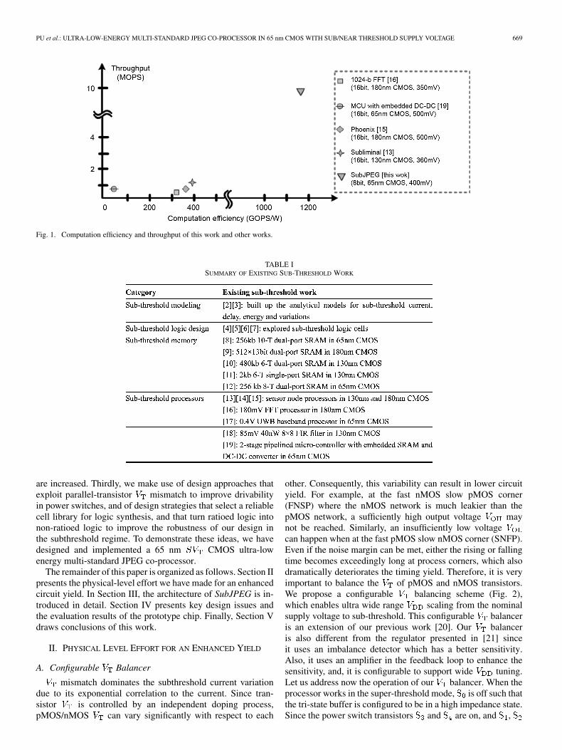
Sub/near threshold techniques have been explored in recentyears. Fig. 1 shows a comparison of the computation effi-ciency (GOPS/W) and throughput (MOPS) of our SubJPEGco-processor and other existing subthreshold processors. Like-wise, Table I summarizes the most relevant work in the field.In contrast to the work presented in those publications, ourwork has some unique features. Firstly, we explore the useof architecture-level parallelism to compensate throughputdegradation at ultra-low supply values. Parallelism along withsub/near threshold techniques is best suited for low-energyand medium frequency applications, such as mobile imageprocessing. Secondly, this work proposes a configurablebalancer to lessen the mismatch between nMOS and pMOStransistors, such that both the functional and the timing yield
0018-9200/$26.00 © 2010 IEEE
PU et al.: ULTRA-LOW-ENERGY MULTI-STANDARD JPEG CO-PROCESSOR IN 65 nm CMOS WITH SUB/NEAR THRESHOLD SUPPLY VOLTAGE 669
Fig. 1. Computation efficiency and throughput of this work and other works.
TABLE ISUMMARY OF EXISTING SUB-THRESHOLD WORK
are increased. Thirdly, we make use of design approaches thatexploit parallel-transistor mismatch to improve drivabilityin power switches, and of design strategies that select a reliablecell library for logic synthesis, and that turn ratioed logic intonon-ratioed logic to improve the robustness of our design inthe subthreshold regime. To demonstrate these ideas, we havedesigned and implemented a 65 nm CMOS ultra-lowenergy multi-standard JPEG co-processor.
The remainder of this paper is organized as follows. Section IIpresents the physical-level effort we have made for an enhancedcircuit yield. In Section III, the architecture of SubJPEG is in-troduced in detail. Section IV presents key design issues andthe evaluation results of the prototype chip. Finally, Section Vdraws conclusions of this work.
II. PHYSICAL LEVEL EFFORT FOR AN ENHANCED YIELD
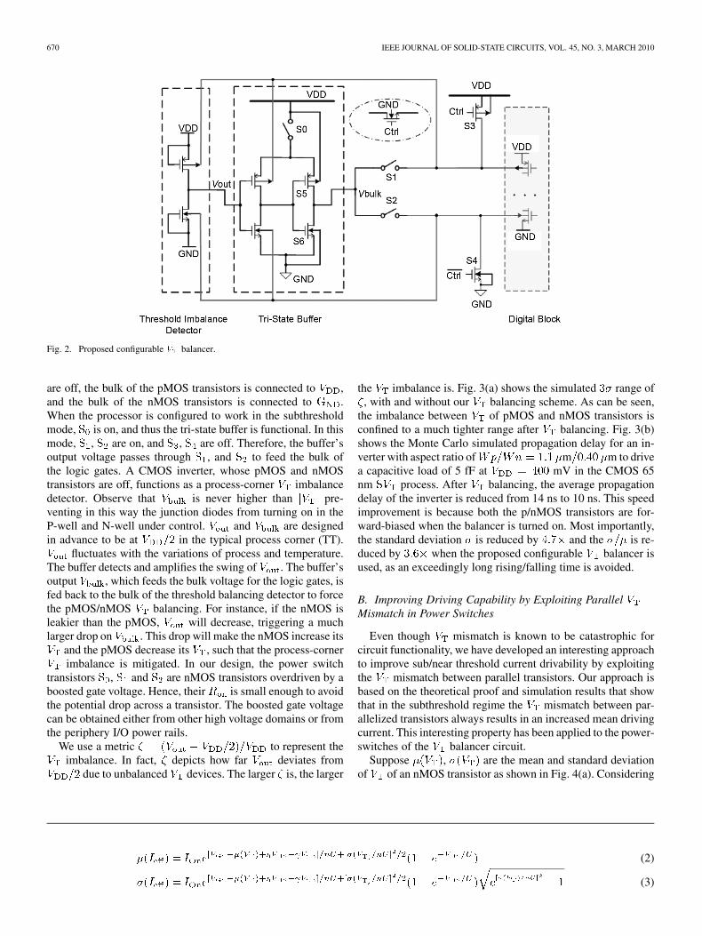
A. Configurable Balancer
mismatch dominates the subthreshold current variationdue to its exponential correlation to the current. Since tran-sistor is controlled by an independent doping process,pMOS/nMOS can vary significantly with respect to each
other. Consequently, this variability can result in lower circuityield. For example, at the fast nMOS slow pMOS corner(FNSP) where the nMOS network is much leakier than thepMOS network, a sufficiently high output voltage maynot be reached. Similarly, an insufficiently low voltagecan happen when at the fast pMOS slow nMOS corner (SNFP).Even if the noise margin can be met, either the rising or fallingtime becomes exceedingly long at process corners, which alsodramatically deteriorates the timing yield. Therefore, it is veryimportant to balance the of pMOS and nMOS transistors.We propose a configurable balancing scheme (Fig. 2),which enables ultra wide range scaling from the nominalsupply voltage to sub-threshold. This configurable balanceris an extension of our previous work [20]. Our balanceris also different from the regulator presented in [21] sinceit uses an imbalance detector which has a better sensitivity.Also, it uses an amplifier in the feedback loop to enhance thesensitivity, and, it is configurable to support wide tuning.Let us address now the operation of our balancer. When theprocessor works in the super-threshold mode, is off such thatthe tri-state buffer is configured to be in a high impedance state.Since the power switch transistors and are on, and ,
670 IEEE JOURNAL OF SOLID-STATE CIRCUITS, VOL. 45, NO. 3, MARCH 2010
Fig. 2. Proposed configurable � balancer.
are off, the bulk of the pMOS transistors is connected to ,and the bulk of the nMOS transistors is connected to .When the processor is configured to work in the subthresholdmode, is on, and thus the tri-state buffer is functional. In thismode, , are on, and , are off. Therefore, the buffer’soutput voltage passes through , and to feed the bulk ofthe logic gates. A CMOS inverter, whose pMOS and nMOStransistors are off, functions as a process-corner imbalancedetector. Observe that is never higher than pre-venting in this way the junction diodes from turning on in theP-well and N-well under control. and are designedin advance to be at in the typical process corner (TT).
fluctuates with the variations of process and temperature.The buffer detects and amplifies the swing of . The buffer’soutput , which feeds the bulk voltage for the logic gates, isfed back to the bulk of the threshold balancing detector to forcethe pMOS/nMOS balancing. For instance, if the nMOS isleakier than the pMOS, will decrease, triggering a muchlarger drop on . This drop will make the nMOS increase its
and the pMOS decrease its , such that the process-cornerimbalance is mitigated. In our design, the power switch
transistors , and are nMOS transistors overdriven by aboosted gate voltage. Hence, their is small enough to avoidthe potential drop across a transistor. The boosted gate voltagecan be obtained either from other high voltage domains or fromthe periphery I/O power rails.
We use a metric to represent theimbalance. In fact, depicts how far deviates from
due to unbalanced devices. The larger is, the larger
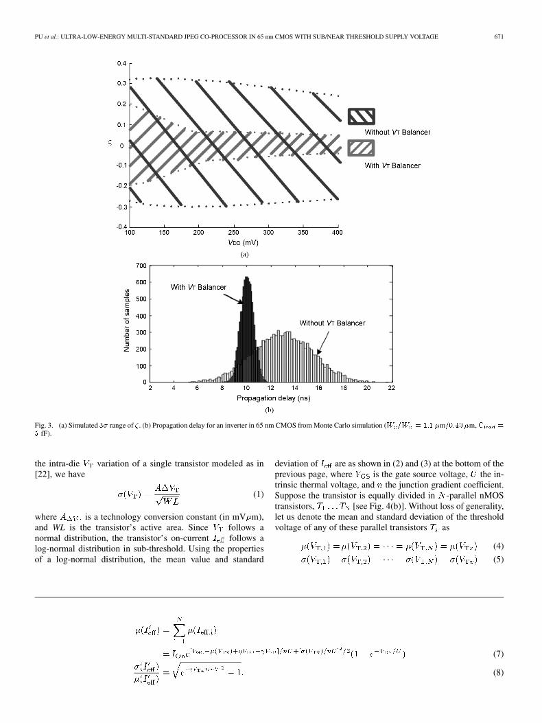
the imbalance is. Fig. 3(a) shows the simulated range of, with and without our balancing scheme. As can be seen,
the imbalance between of pMOS and nMOS transistors isconfined to a much tighter range after balancing. Fig. 3(b)shows the Monte Carlo simulated propagation delay for an in-verter with aspect ratio of m m to drivea capacitive load of 5 fF at mV in the CMOS 65nm process. After balancing, the average propagationdelay of the inverter is reduced from 14 ns to 10 ns. This speedimprovement is because both the p/nMOS transistors are for-ward-biased when the balancer is turned on. Most importantly,the standard deviation is reduced by and the is re-duced by when the proposed configurable balancer isused, as an exceedingly long rising/falling time is avoided.
B. Improving Driving Capability by Exploiting ParallelMismatch in Power Switches
Even though mismatch is known to be catastrophic forcircuit functionality, we have developed an interesting approachto improve sub/near threshold current drivability by exploitingthe mismatch between parallel transistors. Our approach isbased on the theoretical proof and simulation results that showthat in the subthreshold regime the mismatch between par-allelized transistors always results in an increased mean drivingcurrent. This interesting property has been applied to the power-switches of the balancer circuit.
Suppose , are the mean and standard deviationof of an nMOS transistor as shown in Fig. 4(a). Considering
(2)
(3)
PU et al.: ULTRA-LOW-ENERGY MULTI-STANDARD JPEG CO-PROCESSOR IN 65 nm CMOS WITH SUB/NEAR THRESHOLD SUPPLY VOLTAGE 671
Fig. 3. (a) Simulated �� range of � . (b) Propagation delay for an inverter in 65 nm CMOS from Monte Carlo simulation (� �� � ��� �m������m,� �
� fF).
the intra-die variation of a single transistor modeled as in[22], we have
(1)
where is a technology conversion constant (in mV m),and WL is the transistor’s active area. Since follows anormal distribution, the transistor’s on-current follows alog-normal distribution in sub-threshold. Using the propertiesof a log-normal distribution, the mean value and standard
deviation of are as shown in (2) and (3) at the bottom of theprevious page, where is the gate source voltage, the in-trinsic thermal voltage, and the junction gradient coefficient.Suppose the transistor is equally divided in -parallel nMOStransistors, [see Fig. 4(b)]. Without loss of generality,let us denote the mean and standard deviation of the thresholdvoltage of any of these parallel transistors as
(4)
(5)
(7)
(8)
672 IEEE JOURNAL OF SOLID-STATE CIRCUITS, VOL. 45, NO. 3, MARCH 2010
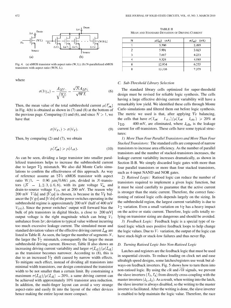
Fig. 4. (a) nMOS transistor with aspect ratio (W, L); (b) N-parallelized nMOStransistors with aspect ratio (W/N, L).
where
(6)
Then, the mean value of the total subthreshold currentin Fig. 4(b) is obtained as shown in (7) and (8) at the bottom ofthe previous page. Comparing (1) and (6), and since , wehave that
(9)
Then, by comparing (2) and (7), we obtain
(10)
As can be seen, dividing a large transistor into smaller paral-lelized transistors helps to increase the subthreshold currentdue to larger mismatch. We also did Monte Carlo simu-lations to confirm the effectiveness of this approach. As wayof reference assume an nMOS transistor with aspectratio m m, divided in -transis-tors , with its gate voltage anddrain-to-source voltage set at 200 mV. The reason why200 mV and is chosen, is because in the bal-ancer the and of the power switches operating in thesubthreshold regime is approximately 200 mV (half of 400 mV
). Since the power switches’ output will forward bias thebulk of p/n transistors in digital blocks, a close to 200 mVoutput voltage is the right magnitude which can bringunbalance from ; deviation to typical value without incurringtoo much excessive leakage current. The simulated mean andstandard deviation values of the effective driving current arelisted in Table II. As seen, the larger the number of segments ,the larger the mismatch, consequently the larger the meansubthreshold driving current. However, Table II also shows anincreasing driving current variability and largeras the transistor becomes narrower. According to (8), this isdue to an increased shift caused by narrow width effects.To mitigate such effect, instead of dividing all transistors intominimal width transistors, our design constrained the transistorwidth to be not smaller than a certain limit. By constraining amaximum 20%, a same driving current canbe achieved with approximately 10% transistor area reduction.In addition, the multi-finger layout can avoid a very strangeaspect-ratio and easily fit into the layout of the other deviceshence making the entire layout more compact.
TABLE IIMEAN AND STANDARD DEVIATION OF DRIVING CURRENT
C. Sub-Threshold Library Selection
The standard library cells optimized for super-thresholddesign must be revised for reliable logic synthesis. The cellshaving a large effective driving current variability will have aremarkably low yield. We identified these cells through MonteCarlo simulations and filtered them out before logic synthesis.The metric we used is that, after applying balancing,the cells that have 20% at
400 mV, are eliminated, where is the leakagecurrent for off-transistors. These cells have some typical struc-tures:
1) More Than Four Parallel Transistors and More Than FourStacked Transistors: The standard cells are composed of narrowtransistors to increase area efficiency. As the number of paralleltransistors and the number of stacked-transistors increases, theleakage current variability increases dramatically, as shown inSection II-B. We simply discarded logic gates with more thanfour parallel transistors or more than four stacked transistors,such as 4-input NAND and NOR gates.
2) Ratioed Logic: Ratioed logic can reduce the number oftransistors required to implement a given logic function, butit must be sized carefully to guarantee that the active currentis stronger than the static current. Therefore, the correct func-tioning of ratioed logic cells depends largely on the sizing. Inthe subthreshold region, the largest current variability is due to
variation. Even a small variation on has a heavy impacton the active or static current. Therefore, logic cells totally re-lying on transistor sizing are dangerous and should be avoided.
3) Feedback Logic: Feedback logic is a special type of ra-tioed logic which uses positive feedback loops to help changethe logic values. Due to variation, the output of the logic canhave stuck-high or stuck-low failures and thus never flip.
D. Turning Ratioed Logic Into Non-Ratioed Logic
Latches and registers are the feedback logic that must be usedin sequential circuits. To reduce loading on clock net and easeultrahigh speed designs, some latches/registers use weak but al-ways-on feedback inverters. Fig. 5 shows how to turn them intonon-ratioed logic. By using the clk and signals, we preventthe slave inverters from directly cross-coupling with themaster inverters . As a result, when writing into the latch,the slave inverter is always disabled, so the writing to the masterinverter is facilitated. After the writing is done, the slave inverteris enabled to help maintain the logic value. Therefore, the race

PU et al.: ULTRA-LOW-ENERGY MULTI-STANDARD JPEG CO-PROCESSOR IN 65 nm CMOS WITH SUB/NEAR THRESHOLD SUPPLY VOLTAGE 673
Fig. 5. Turning ratioed logic into non-ratioed logic.
Fig. 6. Monte Carlo simulation results at node � at � � ��� mV: (a) before turning ratioed logic into non-ratioed logic; (b) after turning ratioed logic intonon-ratioed logic.
between the slave and master inverters is avoided. Fig. 6 com-pares the Monte Carlo simulation results at node (the outputfrom the negative latch) at mV before and afterturning ratioed logic into non-ratioed logic. With this modifica-tion, the stuck high and stuck low failures are avoided. In addi-tion, the propagation delay becomes more than an order tighter.
III. SUBJPEG ARCHITECTURE
JPEG is an international compression standard for contin-uous-tone still images, both grayscale and color [23], [24]. As ageneric image compression standard, JPEG supports a wide va-riety of image applications. The baseline JPEG encoding pro-cessing has three primary steps: 8 8 discrete cosine trans-formation (DCT), quantization, entropy encoding. Our goal isto design a JPEG compression co-processor that consumes ex-tremely low energy and thus can be used in application fieldssuch as image sensoring, digital still cameras, mobile image,etc. The design challenge is to explore an architecture with ef-ficient parallelism to trade-off area, throughput and energy.
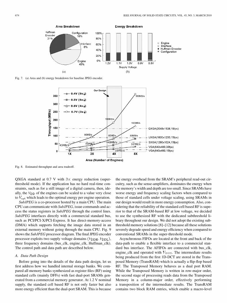
Our baseline design was built from scratch to accommodatearchitectural changes required for subthreshold operation in a65 nm CMOS process. Its area and energy breakdownare shown in Fig. 7. The term “engine” denotes a combined
2D-DCT and Quantization module. As seen, the engine dom-inates both the energy and area. At the nominal supply voltagethe engine occupies less than 50% of the total silicon area butconsumes around 70% of the total energy. The rest of the com-ponents, such as the Huffman encoder and the configurationlogic, are of less importance. Thus, minimizing the energy con-sumption of the engine becomes our primary target when de-signing the new architecture. Therefore, instead of parallelizingthe entire data-path, we decided to parallelize only the engine.Another reason for making this decision is because of the dif-ficulty in parallelizing the Huffman encoder. The Huffman en-coding for the DC value of an 8 8 block depends on the DCvalue of the previous block. If the Huffman encoder is also par-allelized, additional effort must be drawn to handle this data de-pendency. Also, it would be difficult to align the output streamsfrom each Huffman encoder which have unpredictable lengths,a memory shuffler and many memory operations would becomeunavoidable. Fig. 8 indicates the estimated throughput versusarea tradeoff for the engines with annotated application stan-dards. Four parallel engines were chosen in our design becausefrom simulations we observed that the encoder was already ca-pable of meeting 15 fps VGA standard at 0.4 V with en-ergy reduction (in subthreshold mode), 30 fps VGA standard at0.5 V with energy reduction (in near-threshold mode), 15 fps
674 IEEE JOURNAL OF SOLID-STATE CIRCUITS, VOL. 45, NO. 3, MARCH 2010
Fig. 7. (a) Area and (b) energy breakdown for baseline JPEG encoder.
Fig. 8. Estimated throughput and area tradeoff.
QXGA standard at 0.7 V with energy reduction (super-threshold mode). If the application has no hard real-time con-straints, such as for a still image of a digital camera, then, ide-ally, the of the engines can be scaled to a value very closeto which leads to the optimal energy per engine operation.
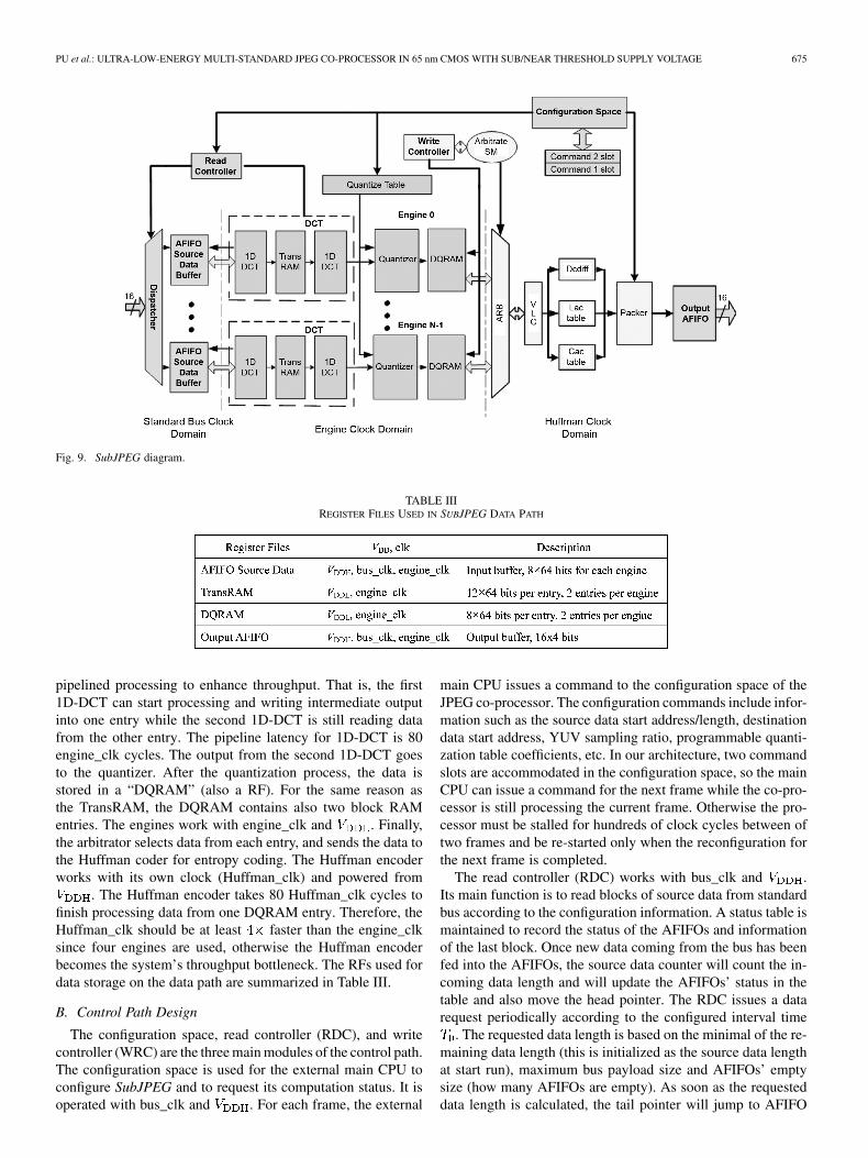
SubJPEG is a co-processor hosted by a main CPU. The mainCPU can communicate with SubJPEG, issue commands and ac-cess the status registers in SubJPEG through the control lines.SubJPEG interfaces directly with a commercial standard bus,such as PCI/PCI-X/PCI-Express. It has direct-memory-access(DMA) which supports fetching the image data stored in anexternal memory without going through the main CPU. Fig. 9shows the SubJPEG processor diagram. The final JPEG encoderprocessor exploits two supply voltage domains ,three frequency domains (bus_clk, engine_clk, Huffman_clk).The control path and data path are described below.
A. Data Path Design
Before going into the details of the data path design, let usfirst address how we handled internal storage banks. We com-pared all memory banks synthesized as register files (RF) usingstandard cells (mainly DFFs) with fast dual-port SRAMs gen-erated from a commercial memory generator. At 1.2 V nominalsupply, the standard cell based RF is not only faster but alsomore energy efficient than the dual-port SRAM. This is because
the energy overhead from the SRAM’s peripheral read-out cir-cuitry, such as the sense-amplifiers, dominates the energy whenthe memory’s width and depth are too small. Since SRAMs haveworse energy and frequency scaling factors when compared tothose of standard cells under voltage scaling, using SRAMs inour design would result in more energy consumption. Also, con-sidering that the reliability of the standard cell based RF is supe-rior to that of the SRAM-based RF at low voltage, we decidedto use the synthesized RF with the dedicated subthreshold li-brary throughout our design. We did not adopt the existing sub-threshold memory solutions [8]–[12] because all these solutionsseverely degrade speed and energy efficiency when compared toconventional SRAMs in the super-threshold mode.
Asynchronous FIFOs are located at the front and back of thedata-path to enable a flexible interface to a commercial stan-dard bus interface. The AFIFOs are connected with bus_clk,engine_clk and operated with . The intermediate resultsbeing produced from the first 1D-DCT are stored in the Trans-posed Memory (TransRAM) which is actually a flip-flop basedRF. The Transposed Memory behaves as a dual port RAM.While the Transposed Memory is written in row-major order,the second stage of processing reads data from the TransposedMemory in a column-major order, effectively performinga transposition of the intermediate results. The TransRAMcontains two block RAM entries, which enable a macro-level
PU et al.: ULTRA-LOW-ENERGY MULTI-STANDARD JPEG CO-PROCESSOR IN 65 nm CMOS WITH SUB/NEAR THRESHOLD SUPPLY VOLTAGE 675
Fig. 9. SubJPEG diagram.
TABLE IIIREGISTER FILES USED IN SUBJPEG DATA PATH
pipelined processing to enhance throughput. That is, the first1D-DCT can start processing and writing intermediate outputinto one entry while the second 1D-DCT is still reading datafrom the other entry. The pipeline latency for 1D-DCT is 80engine_clk cycles. The output from the second 1D-DCT goesto the quantizer. After the quantization process, the data isstored in a “DQRAM” (also a RF). For the same reason asthe TransRAM, the DQRAM contains also two block RAMentries. The engines work with engine_clk and . Finally,the arbitrator selects data from each entry, and sends the data tothe Huffman coder for entropy coding. The Huffman encoderworks with its own clock (Huffman_clk) and powered from
. The Huffman encoder takes 80 Huffman_clk cycles tofinish processing data from one DQRAM entry. Therefore, theHuffman_clk should be at least faster than the engine_clksince four engines are used, otherwise the Huffman encoderbecomes the system’s throughput bottleneck. The RFs used fordata storage on the data path are summarized in Table III.
B. Control Path Design
The configuration space, read controller (RDC), and writecontroller (WRC) are the three main modules of the control path.The configuration space is used for the external main CPU toconfigure SubJPEG and to request its computation status. It isoperated with bus_clk and . For each frame, the external
main CPU issues a command to the configuration space of theJPEG co-processor. The configuration commands include infor-mation such as the source data start address/length, destinationdata start address, YUV sampling ratio, programmable quanti-zation table coefficients, etc. In our architecture, two commandslots are accommodated in the configuration space, so the mainCPU can issue a command for the next frame while the co-pro-cessor is still processing the current frame. Otherwise the pro-cessor must be stalled for hundreds of clock cycles between oftwo frames and be re-started only when the reconfiguration forthe next frame is completed.
The read controller (RDC) works with bus_clk and .Its main function is to read blocks of source data from standardbus according to the configuration information. A status table ismaintained to record the status of the AFIFOs and informationof the last block. Once new data coming from the bus has beenfed into the AFIFOs, the source data counter will count the in-coming data length and will update the AFIFOs’ status in thetable and also move the head pointer. The RDC issues a datarequest periodically according to the configured interval time
. The requested data length is based on the minimal of the re-maining data length (this is initialized as the source data lengthat start run), maximum bus payload size and AFIFOs’ emptysize (how many AFIFOs are empty). As soon as the requesteddata length is calculated, the tail pointer will jump to AFIFO

676 IEEE JOURNAL OF SOLID-STATE CIRCUITS, VOL. 45, NO. 3, MARCH 2010
Fig. 10. Pseudo code algorithm for RDC.
where the latest requested source data block will be stored. Thenew requested data address and the remaining data length arealso updated. If the remaining data length is zero, meaning thatthe last requested data block is the ending block of the currentframe, the column logging the information of the last block inthe status table will be updated. Fig. 10 shows the pseudo codealgorithm of the RDC.
The write controller (WRC) works with the Huffman_clkand uses as power supply. It checks the status of theDCT-Quantization RAM (DQRAM), from each engine, andcontrols writing data from DQRAMs to the arbitrator. Similarto the RDC, the WRC also maintains a status table to logthe DQRAMs’ status and the last block information. Once aDQRAM entry of an engine is full, the header pointer willmove to the next engine’s DQRAM entry and the DQRAMs’status will update. If the entropy encoder is idle, the WRCwill indicate the arbitrator to push the data out of an engine’sDQRAM. Once the data is completely pushed out, the DQRAMstatus will be updated and the tail pointer will jump to the nextengine’s DQRAM entry. In this way the engines’ DQRAMsare circulated for writing and reading. Fig. 11 shows the pseudocode algorithm of the WRC.
IV. IMPLEMENTATION AND EVALUATION
The implemented core is fully compliant with the JPEG en-coder baseline standard. Signals across different clock domainsare hand-shacked to increase communication robustness. Weused a hierarchical logic synthesis approach: the engines aresynthesized with a dedicated subthreshold library, as mentionedin Section II. The other blocks are synthesized with a conven-tional CMOS65 standard cell library. According to synthesis re-sults, the engines and the Huffman encoder can operate easilybeyond 250 MHz with a 65 nm CMOS process at 1.2 Vnominal supply voltage. Some signals in the design have to crossthe and domains. Therefore, a level shifting schemeis needed. In addition, the digital I/O pads in 65 nm CMOS mustuse a reference voltage of 1.2 V, so we also need a level shiftingscheme to convert the signal level from the SubJPEG core to
the I/O pads. Shown in Fig. 12 is the 2-stage level shift schemeused in SubJPEG. The first stage level shifting is performedthrough simple buffers which are capable enough of pulling upsignals from subthreshold to . The difference be-tween and is less than 300 mV. The second stagelevel shifting is performed through positive feedback structuredlevel-shifters from to 1.2 V I/O pads.
Each engine has its own deep n-well to separate its bulk fromthe rest of the chip and also has a balancer located at one ofits corners. Each balancer is m and the core sizeis mm . The testchip was fabricated using TSMC’s65 nm seven-layer low-power standard CMOS process. Thecore layout and the microphotograph of the prototype chip areshown in Fig. 13. Compared to the baseline processor, the areaof SubJPEG is about larger, including overhead from im-plementing parallel engines and bulk biasing, etc. The area andsimulated energy breakdown in the digital still image mode areshown in Fig. 14. The circuits that are required to parallelizethe engines, i.e., dispatcher, RDC, WRC, arbiter and interfaceAFIFOs, occupy 8% area of the core. For digital still image pro-cessing ( and in simulation) and
, these circuits woulddissipate approximately 12% of the total energy.
To test the functionality of the chip, a 9-layer PCB was de-signed. On the board a Xilinx Spartan-3 FPGA chip functions asthe main CPU and SubJPEG functions as its co-processor. The1.2 V and 2.5 V I/O voltages are generated with on-boardDC-DC converters. The other supply voltages are supplied fromexternal voltage generators.
The measured behavior of the configurable balancer atmV is shown in Fig. 15. An off-chip capacitor
is needed to mitigate the ripple. As it can be seen, before thebalancer is activated, the n-well is connected to and
the p-well is connected to . Then, within 1 ms after thebalancer is turned on, the supply voltages of both n-well
and p-well converge at near . At mV, thetested samples could not function correctly with a 2 MHzengine_clk frequency without balancing. With the help
PU et al.: ULTRA-LOW-ENERGY MULTI-STANDARD JPEG CO-PROCESSOR IN 65 nm CMOS WITH SUB/NEAR THRESHOLD SUPPLY VOLTAGE 677
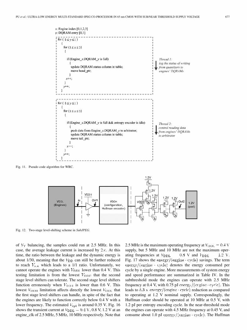
Fig. 11. Pseudo code algorithm for WRC.
Fig. 12. Two-stage level-shifting scheme in SubJPEG.
of balancing, the samples could run at 2.5 MHz. In thiscase, the average leakage current is increased by . At thistime, the ratio between the leakage and the dynamic energy isabout 1/30, meaning that the can still be further reducedto reach which leads to a 1/1 ratio. Unfortunately, wecannot operate the engines with lower than 0.4 V. Thistesting limitation is from the lowest that the secondstage level shifters can tolerate. The second stage level shiftersfunction erroneously when is lower than 0.6 V. Thislowest limitation affects directly the lowest thatthe first stage level shifters can handle, in spite of the fact thatthe engines are likely to function correctly below 0.4 V with alower frequency. The estimated is around 0.35 V. Fig. 16shows the transient current at , 0.8 V, 1.2 V at anengine_clk of 2.5 MHz, 5 MHz, 10 MHz respectively. Note that
2.5 MHz is the maximum operating frequency atsupply, but 5 MHz and 10 MHz are not the maximum oper-ating frequencies at and .Fig. 17 shows the savings. The term
denotes the energy consumed percycle by a single engine. More measurements of system energyand speed performance are summarized in Table IV. In thesubthreshold mode the engines can operate with 2.5 MHzfrequency at 0.4 V, with 0.75 pJ . Thisleads to reduction as comparedto operating at 1.2 V nominal supply. Correspondingly, theHuffman coder should be operated at 10 MHz at 0.5 V, with1.2 pJ per entropy encoding cycle. In the near-threshold modethe engines can operate with 4.5 MHz frequency at 0.45 V, andconsume about 1.0 pJ . The Huffman

678 IEEE JOURNAL OF SOLID-STATE CIRCUITS, VOL. 45, NO. 3, MARCH 2010
Fig. 13. Core layout and prototype chip microphotograph.
Fig. 14. SubJPEG (a) area (b) energy breakdown in digital still image mode.
Fig. 15. Measurement results of switching on the � balancer.
coder operates at 18 MHz frequency with a less than 0.7 Vsupply, and dissipates around 2.0 pJ per entropy encodingcycle. The overall system throughput meets the 15 fps VGAcompression requirement. By further increasing bothand , and exploring distinct combinations,the prototype chip can achieve multi-standard image encoding.
Fig. 16. Transient and average current with ����� amplified magnitude at(0.4 V, 2.5 MHz), (0.8 V, 5 MHz) and (1.2 V, 10 MHz).
V. CONCLUSION
This paper presents our work on exploiting a sub/nearthreshold supply voltage in the design of ultra low energy andmedium throughput (up to 100 MB/s) consumer digital elec-tronic applications. We utilize architecture-level parallelism tocompensate for throughput degradation at very low voltage.Several physical-level design techniques were developed toimprove circuit robustness. Among them is a configurable
PU et al.: ULTRA-LOW-ENERGY MULTI-STANDARD JPEG CO-PROCESSOR IN 65 nm CMOS WITH SUB/NEAR THRESHOLD SUPPLY VOLTAGE 679
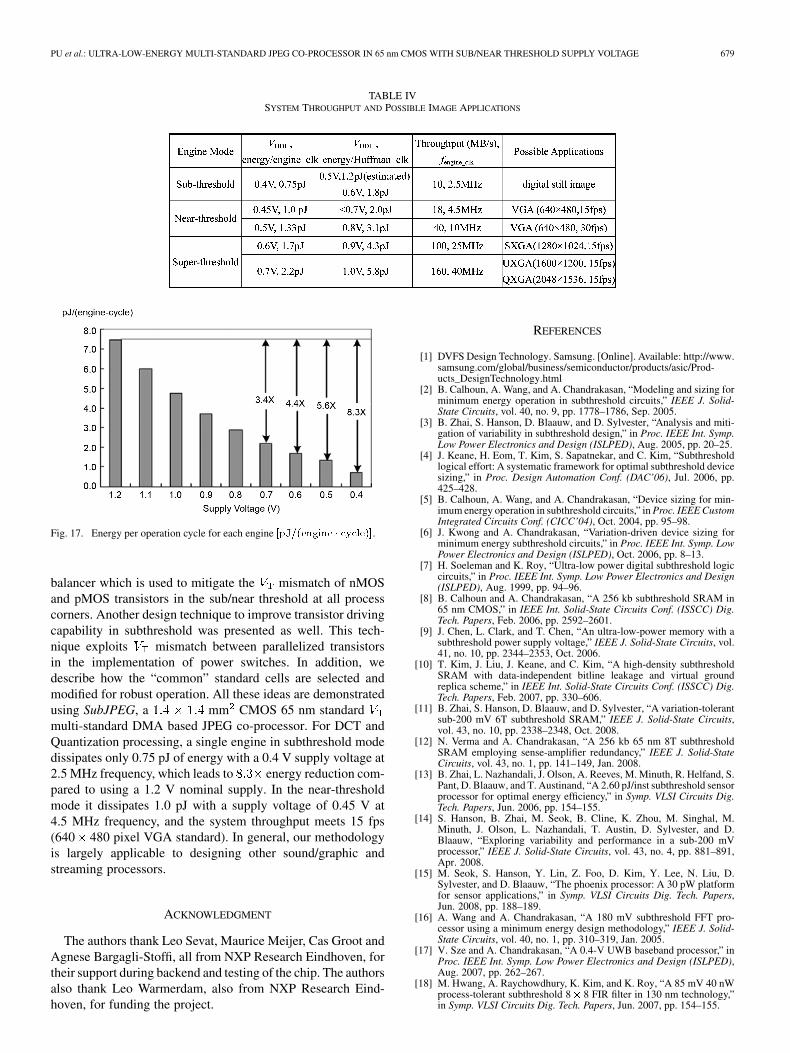
TABLE IVSYSTEM THROUGHPUT AND POSSIBLE IMAGE APPLICATIONS
Fig. 17. Energy per operation cycle for each engine ����������� � ��� .
balancer which is used to mitigate the mismatch of nMOSand pMOS transistors in the sub/near threshold at all processcorners. Another design technique to improve transistor drivingcapability in subthreshold was presented as well. This tech-nique exploits mismatch between parallelized transistorsin the implementation of power switches. In addition, wedescribe how the “common” standard cells are selected andmodified for robust operation. All these ideas are demonstratedusing SubJPEG, a mm CMOS 65 nm standardmulti-standard DMA based JPEG co-processor. For DCT andQuantization processing, a single engine in subthreshold modedissipates only 0.75 pJ of energy with a 0.4 V supply voltage at2.5 MHz frequency, which leads to energy reduction com-pared to using a 1.2 V nominal supply. In the near-thresholdmode it dissipates 1.0 pJ with a supply voltage of 0.45 V at4.5 MHz frequency, and the system throughput meets 15 fps(640 480 pixel VGA standard). In general, our methodologyis largely applicable to designing other sound/graphic andstreaming processors.
ACKNOWLEDGMENT
The authors thank Leo Sevat, Maurice Meijer, Cas Groot andAgnese Bargagli-Stoffi, all from NXP Research Eindhoven, fortheir support during backend and testing of the chip. The authorsalso thank Leo Warmerdam, also from NXP Research Eind-hoven, for funding the project.
REFERENCES
[1] DVFS Design Technology. Samsung. [Online]. Available: http://www.samsung.com/global/business/semiconductor/products/asic/Prod-ucts_DesignTechnology.html
[2] B. Calhoun, A. Wang, and A. Chandrakasan, “Modeling and sizing forminimum energy operation in subthreshold circuits,” IEEE J. Solid-State Circuits, vol. 40, no. 9, pp. 1778–1786, Sep. 2005.
[3] B. Zhai, S. Hanson, D. Blaauw, and D. Sylvester, “Analysis and miti-gation of variability in subthreshold design,” in Proc. IEEE Int. Symp.Low Power Electronics and Design (ISLPED), Aug. 2005, pp. 20–25.
[4] J. Keane, H. Eom, T. Kim, S. Sapatnekar, and C. Kim, “Subthresholdlogical effort: A systematic framework for optimal subthreshold devicesizing,” in Proc. Design Automation Conf. (DAC’06), Jul. 2006, pp.425–428.
[5] B. Calhoun, A. Wang, and A. Chandrakasan, “Device sizing for min-imum energy operation in subthreshold circuits,” in Proc. IEEE CustomIntegrated Circuits Conf. (CICC’04), Oct. 2004, pp. 95–98.
[6] J. Kwong and A. Chandrakasan, “Variation-driven device sizing forminimum energy subthreshold circuits,” in Proc. IEEE Int. Symp. LowPower Electronics and Design (ISLPED), Oct. 2006, pp. 8–13.
[7] H. Soeleman and K. Roy, “Ultra-low power digital subthreshold logiccircuits,” in Proc. IEEE Int. Symp. Low Power Electronics and Design(ISLPED), Aug. 1999, pp. 94–96.
[8] B. Calhoun and A. Chandrakasan, “A 256 kb subthreshold SRAM in65 nm CMOS,” in IEEE Int. Solid-State Circuits Conf. (ISSCC) Dig.Tech. Papers, Feb. 2006, pp. 2592–2601.
[9] J. Chen, L. Clark, and T. Chen, “An ultra-low-power memory with asubthreshold power supply voltage,” IEEE J. Solid-State Circuits, vol.41, no. 10, pp. 2344–2353, Oct. 2006.
[10] T. Kim, J. Liu, J. Keane, and C. Kim, “A high-density subthresholdSRAM with data-independent bitline leakage and virtual groundreplica scheme,” in IEEE Int. Solid-State Circuits Conf. (ISSCC) Dig.Tech. Papers, Feb. 2007, pp. 330–606.
[11] B. Zhai, S. Hanson, D. Blaauw, and D. Sylvester, “A variation-tolerantsub-200 mV 6T subthreshold SRAM,” IEEE J. Solid-State Circuits,vol. 43, no. 10, pp. 2338–2348, Oct. 2008.
[12] N. Verma and A. Chandrakasan, “A 256 kb 65 nm 8T subthresholdSRAM employing sense-amplifier redundancy,” IEEE J. Solid-StateCircuits, vol. 43, no. 1, pp. 141–149, Jan. 2008.
[13] B. Zhai, L. Nazhandali, J. Olson, A. Reeves, M. Minuth, R. Helfand, S.Pant, D. Blaauw, and T. Austinand, “A 2.60 pJ/inst subthreshold sensorprocessor for optimal energy efficiency,” in Symp. VLSI Circuits Dig.Tech. Papers, Jun. 2006, pp. 154–155.
[14] S. Hanson, B. Zhai, M. Seok, B. Cline, K. Zhou, M. Singhal, M.Minuth, J. Olson, L. Nazhandali, T. Austin, D. Sylvester, and D.Blaauw, “Exploring variability and performance in a sub-200 mVprocessor,” IEEE J. Solid-State Circuits, vol. 43, no. 4, pp. 881–891,Apr. 2008.
[15] M. Seok, S. Hanson, Y. Lin, Z. Foo, D. Kim, Y. Lee, N. Liu, D.Sylvester, and D. Blaauw, “The phoenix processor: A 30 pW platformfor sensor applications,” in Symp. VLSI Circuits Dig. Tech. Papers,Jun. 2008, pp. 188–189.
[16] A. Wang and A. Chandrakasan, “A 180 mV subthreshold FFT pro-cessor using a minimum energy design methodology,” IEEE J. Solid-State Circuits, vol. 40, no. 1, pp. 310–319, Jan. 2005.
[17] V. Sze and A. Chandrakasan, “A 0.4-V UWB baseband processor,” inProc. IEEE Int. Symp. Low Power Electronics and Design (ISLPED),Aug. 2007, pp. 262–267.
[18] M. Hwang, A. Raychowdhury, K. Kim, and K. Roy, “A 85 mV 40 nWprocess-tolerant subthreshold 8� 8 FIR filter in 130 nm technology,”in Symp. VLSI Circuits Dig. Tech. Papers, Jun. 2007, pp. 154–155.
680 IEEE JOURNAL OF SOLID-STATE CIRCUITS, VOL. 45, NO. 3, MARCH 2010
[19] J. Kwong, Y. Ramadass, N. Verma, and A. Chandrakasan, “A 65 nmsub-Vt microcontroller with integrated SRAM and switched capacitorDC-DC converter,” IEEE J. Solid-State Circuits, vol. 44, no. 1, pp.115–126, Jan. 2009.
[20] Y. Pu, J. P. de Gyvez, H. Corporaal, and Y. Ha, “� balancing anddevice sizing towards high yield of subthreshold static logic gates,” inProc. IEEE Int. Symp. Low Power Electronics and Design (ISLPED),Aug. 2007, pp. 355–358.
[21] A. Bryant, J. Brown, P. Cottrell, M. Ketchen, J. Ellis-Monaghan, andE. J. Nowak, “Low-power CMOS at��� � � ����,” in Proc. DeviceResearch Conf., Jun. 2001, pp. 22–23.
[22] M. Pelgrom, A. Duinmaijer, and A. Welbers, “Matching propertiesof MOS transistors,” IEEE J. Solid-State Circuits, vol. 24, no. 5, pp.1433–1439, Oct. 1989.
[23] G. Wallace, “The JPEG still picture compression standard,” IEEETrans. Consumer Electron., vol. 38, no. 1, pp. XVIII–XXXIV, Feb.1992.
[24] Digital Compression and Coding of Continuous Tone Still Images, Part1, Requirements and Guidelines, ISO/IEC JTC1 Draft InternationalStandard 10918-1, Nov. 1991.
[25] Y. Pu, J. P. de Gyvez, H. Corporaal, and Y. Ha, “An ultra low-energy/frame multi-standard JPEG co-processor in 65 nm CMOS with sub/near threshold power supply,” in IEEE Int. Solid-State Circuits Conf.(ISSCC) Dig. Tech. Papers, Feb. 2009, pp. 146–147.
Yu Pu (M’09) received the B.S. degree (cum laude)in electrical engineering from Zhejiang University,Hangzhou, China, in 2004. In 2009, he receivedthe Ph.D. degree in electrical engineering from theEindhoven University of Technology, The Nether-lands, in association with the National University ofSingapore.
From November 2006 to February 2009, he waswith the Mixed-Signal Circuit and System Groupin NXP Research Eindhoven. From March 2009 toSeptember 2009 he was a research scientist in the
Ultra Low-Power DSP Processor Group of IMEC, The Netherlands. He is nowwith the Sakurai Lab, University of Tokyo, Japan. His research interests focuson ultra low-energy digital circuit design and EDA methodologies.
Jose Pineda de Gyvez (F’09) received the Ph.D. de-gree from the Eindhoven University of Technology,The Netherlands, in 1991.
From 1991 until 1999 he was a Faculty memberin the Department of Electrical Engineering at TexasA&M University. He is currently a Senior Principalat NXP Semiconductors in The Netherlands. Since2006 he also holds the professorship “Deep Submi-cron Integration” in the Department of Electrical En-gineering at the Eindhoven University of Technology.
Dr. Pineda de Gyvez has been an Associate Ed-itor of the IEEE TRANSACTIONS ON CIRCUITS AND SYSTEMS PART I and PART
II, and also Associate Editor for Technology of the IEEE TRANSACTIONS ON
SEMICONDUCTOR MANUFACTURING. He is also a member of the editorial boardof the Journal of Low Power Electronics. He has co-authored more than 100combined publications in the fields of testing, nonlinear circuits, and low powerdesign. He is author or co-author of three books, and holds several grantedpatents. His work has been acknowledged in academic environments as wellas in patent portfolios of many companies. His research has been funded by theDutch Ministry of Science, U.S. Office of Naval Research, and U.S. NationalScience Foundation, among others.
Henk Corporaal (M’09) received the M.Sc. de-gree in theoretical physics from the University ofGroningen, and the Ph.D. degree in electrical engi-neering in the area of computer architecture fromDelft University of Technology, The Netherlands.
He has been teaching at several schools for highereducation, has been Associate Professor at the DelftUniversity of Technology in the field of computer ar-chitecture and code generation, had a joint professorappointment at the National University of Singapore,and has been scientific director of the joint NUS-TUE
Design Technology Institute. He also has been department head and chief sci-entist within the DESICS (Design Technology for Integrated Information andCommunication Systems) division at IMEC, Leuven (Belgium). Currently he isa Professor in Embedded System Architectures at the Eindhoven University ofTechnology (TU/e), The Netherlands. He has co-authored over 250 journal andconference papers in the (multi-)processor architecture and embedded systemdesign area. Furthermore, he invented a new class of VLIW architectures, theTransport Triggered Architectures, which is used in several commercial prod-ucts, and by many research groups. His current research projects are on multi-processor architectures and the predictable design of soft and hard real-time em-bedded systems.
Yajun Ha (SM’09) received the B.S. degree inelectrical engineering from Zhejiang University,Hangzhou, China, in 1996, the M.Eng. degree inelectrical engineering from the National Univer-sity of Singapore (NUS), Singapore, in 1999, andthe Ph.D. degree in electrical engineering fromKatholieke Universiteit Leuven, Leuven, Belgium,in 2004. Between 1999 and 2004, he did his Ph.D.research project at IMEC, Leuven.
He has been an Assistant Professor in the Depart-ment of Electrical and Computer Engineering, NUS,
since 2004. His research interests lie in the embedded system architecture anddesign methodologies, particularly in the area of reconfigurable computing. Heholds one U.S. patent and has published more than 50 internationally refereedtechnical papers in his areas of interest.
Related Documents