Published: September 07, 2011 r2011 American Chemical Society 18663 dx.doi.org/10.1021/ja2044216 | J. Am. Chem. Soc. 2011, 133, 18663–18672 ARTICLE pubs.acs.org/JACS An Interfacial and Bulk Charge Transport Model for Dye-Sensitized Solar Cells Based on Photoanodes Consisting of CoreShell Nanowire Arrays Justin J. Hill, †,‡ Nick Banks, † Kelly Haller, † Mark E. Orazem, † and Kirk J. Ziegler* ,†,z † Department of Chemical Engineering, University of Florida, Gainesville, Florida 32611, United States z Center for Surface Science and Engineering, University of Florida, Gainesville, Florida 32611, United States b S Supporting Information ’ INTRODUCTION Dye-sensitized solar cells (DSSC) are traditionally based on films of titania nanoparticles (NP-DSSC). 1 These devices mimic photosynthesis and currently have achieved conversion efficien- cies in excess of 11%. 2 They can be fabricated at lower costs than silicon-based photovoltaics, making them an attractive alternative for producing low-cost, clean energy. 35 Additionally, DSSCs have been shown to outperform silicon-based photo- voltaics on cloudy days. 6 The interfacial kinetics and energy levels of the heterogeneous components of traditional NP-DSSCs are designed to optimize performance. 1,4,7 The maximum output voltage is determined by the difference between the flat-band potential of the semicon- ductor and the electrochemical potential of the electrolyte, E REDOX . Once an electron is photoexcited from the highest occupied molecular orbital of the dye (HOMO) to the lowest unoccupied molecular orbital (LUMO), the electron can either relax back to the ground state, be injected into the semiconductor layer, or back-react with the electrolyte. Most electrons should be injected into the semiconductor region to achieve maximum performance; however, loss of photogenerated electrons to the electrolyte is energetically favorable. Therefore, the kinetics of electron injection into the semiconductor must be much faster than electron loss to the electrolyte (10 13 vs 10 2 s 1 ). The electrolyte can be modified to increase the REDOX poten- tial, but this typically increases the rate of back reaction. 8 Therefore, the requirement that reactions be controlled by kinetics rather than thermodynamics results in lower output potential of the cell. When the interface of a DSSC is illuminated, an excess of positive charge will build up in the space-charge layer of the n-type semiconductor. This accumulation in the space-charge layer helps establish an interfacial electric field that separates charge. However, Figure 1a shows that this field will disappear at a finite, and nonzero, nanoparticle diameter. This field becomes negligible for particle sizes below ∼30 nm 9 such that typical DSSC systems have the flat-band potential illustrated in Figure 1b. In addition, Figure 1a shows that any charge driven into the center of the particle by this field experiences a barrier to transport out of the nanoparticle. Therefore, electron transport in the porous, nanocrystalline photoanode of the NP-DSSC is governed by trap-limited diffusive transport of conduction band electrons on the surface of the nanoparticle. 1015 Unfortunately, the competing relationship between electron diffusion and life- time limits the electron diffusion length to about 10 μm within a nanoparticle film. 11 Attempts to increase photocurrent by fabri- cating nanoparticle photoanodes with dimensions in excess of 10 μm are often futile because almost none of the electrons generated in this region are collected. 11,1618 The limits of NP-DSSCs have led researchers to investigate nanowire-based DSSCs (NW-DSSCs) as an alternative config- uration for the photoanode. In these systems, an interfacial electric field is established that is not present in NP-DSSCs. This field aids interfacial charge transfer and minimizes electron loss. 1922 However, the effect of the electric field diminishes as Received: May 19, 2011 ABSTRACT: Dye-sensitized solar cells (DSSCs) based on ordered photoanode morphologies, such as nanotubes and nanowires, are widely gaining attention because these geome- tries are believed to enhance interfacial charge transfer and bulk charge transport. Unfortunately, experimental results have yet to show substantial improvement to conversion efficiency over nanoparticle-based DSSCs. A model is developed to character- ize the performance of an idealized photoanode based on an ordered array of transparent conductive nanowires coated with an anatase titania shell. The role of the interfacial electric field in nanowire-based DSSCs is explored computationally by turning electron migration ON or OFF. The results show that back-reaction rates are most strongly influenced by the electric field. These electron loss mechanisms can be reduced by several orders of magnitude, leading to improvements in short-circuit current, open- circuit voltage, and fill factor.

Welcome message from author
This document is posted to help you gain knowledge. Please leave a comment to let me know what you think about it! Share it to your friends and learn new things together.
Transcript
Published: September 07, 2011
r 2011 American Chemical Society 18663 dx.doi.org/10.1021/ja2044216 | J. Am. Chem. Soc. 2011, 133, 18663–18672
ARTICLE
pubs.acs.org/JACS
An Interfacial and Bulk Charge Transport Model for Dye-SensitizedSolar Cells Based on Photoanodes Consisting of Core�ShellNanowire ArraysJustin J. Hill,†,‡ Nick Banks,† Kelly Haller,† Mark E. Orazem,† and Kirk J. Ziegler*,†,z
†Department of Chemical Engineering, University of Florida, Gainesville, Florida 32611, United StateszCenter for Surface Science and Engineering, University of Florida, Gainesville, Florida 32611, United States
bS Supporting Information
’ INTRODUCTION
Dye-sensitized solar cells (DSSC) are traditionally based onfilms of titania nanoparticles (NP-DSSC).1 These devices mimicphotosynthesis and currently have achieved conversion efficien-cies in excess of 11%.2 They can be fabricated at lower coststhan silicon-based photovoltaics, making them an attractivealternative for producing low-cost, clean energy.3�5 Additionally,DSSCs have been shown to outperform silicon-based photo-voltaics on cloudy days.6
The interfacial kinetics and energy levels of the heterogeneouscomponents of traditional NP-DSSCs are designed to optimizeperformance.1,4,7 The maximum output voltage is determined bythe difference between the flat-band potential of the semicon-ductor and the electrochemical potential of the electrolyte,EREDOX.Once an electron is photoexcited from the highest occupiedmolecular orbital of the dye (HOMO) to the lowest unoccupiedmolecular orbital (LUMO), the electron can either relaxback to the ground state, be injected into the semiconductorlayer, or back-react with the electrolyte. Most electrons shouldbe injected into the semiconductor region to achieve maximumperformance; however, loss of photogenerated electrons tothe electrolyte is energetically favorable. Therefore, the kineticsof electron injection into the semiconductor must be muchfaster than electron loss to the electrolyte (1013 vs 102 s�1).The electrolyte can be modified to increase the REDOX poten-tial, but this typically increases the rate of back reaction.8
Therefore, the requirement that reactions be controlled bykinetics rather than thermodynamics results in lower outputpotential of the cell.
When the interface of a DSSC is illuminated, an excess ofpositive charge will build up in the space-charge layer of then-type semiconductor. This accumulation in the space-chargelayer helps establish an interfacial electric field that separatescharge. However, Figure 1a shows that this field will disappearat a finite, and nonzero, nanoparticle diameter. This fieldbecomes negligible for particle sizes below ∼30 nm9 such thattypical DSSC systems have the flat-band potential illustrated inFigure 1b. In addition, Figure 1a shows that any charge driveninto the center of the particle by this field experiences a barrier totransport out of the nanoparticle. Therefore, electron transportin the porous, nanocrystalline photoanode of the NP-DSSC isgoverned by trap-limited diffusive transport of conduction bandelectrons on the surface of the nanoparticle.10�15 Unfortunately,the competing relationship between electron diffusion and life-time limits the electron diffusion length to about 10 μm within ananoparticle film.11 Attempts to increase photocurrent by fabri-cating nanoparticle photoanodes with dimensions in excess of10 μm are often futile because almost none of the electronsgenerated in this region are collected.11,16�18
The limits of NP-DSSCs have led researchers to investigatenanowire-based DSSCs (NW-DSSCs) as an alternative config-uration for the photoanode. In these systems, an interfacialelectric field is established that is not present in NP-DSSCs.This field aids interfacial charge transfer and minimizes electronloss.19�22 However, the effect of the electric field diminishes as
Received: May 19, 2011
ABSTRACT: Dye-sensitized solar cells (DSSCs) based onordered photoanode morphologies, such as nanotubes andnanowires, are widely gaining attention because these geome-tries are believed to enhance interfacial charge transfer and bulkcharge transport. Unfortunately, experimental results have yetto show substantial improvement to conversion efficiency overnanoparticle-based DSSCs. A model is developed to character-ize the performance of an idealized photoanode based on an ordered array of transparent conductive nanowires coated with ananatase titania shell. The role of the interfacial electric field in nanowire-based DSSCs is explored computationally by turningelectron migration ON or OFF. The results show that back-reaction rates are most strongly influenced by the electric field. Theseelectron loss mechanisms can be reduced by several orders of magnitude, leading to improvements in short-circuit current, open-circuit voltage, and fill factor.

18664 dx.doi.org/10.1021/ja2044216 |J. Am. Chem. Soc. 2011, 133, 18663–18672
Journal of the American Chemical Society ARTICLE
the diameter of the nanowire decreases, leading several research-ers to investigate conductive core�semiconductive shell nano-wires in order to enhance axial transport of electrons.21�24
Figure 1c shows that these core�shell nanowire systems exhibitthe same charge buildup at the semiconductor�electrolyteinterface. However, the direct electrical contact of the core tothe current collector allows the charge to be removed from thetitania layer without going through the potential energy barrierthat NP-DSSCs experience. Therefore, an electric field is estab-lished that helps separate the charge at the interface and drive theelectrons to the nanowire core, as shown in Figure 1d. Even in theabsence of this field, the probability of radial electron transport tothe conductive core followed by axial transport is higher thanaxial transport of electrons solely through the titania shell or onits surface to the current collector. This preferential directionin transport is especially important for electrons injected atlengths greater than an electron can diffuse to the currentcollector.11,16�18 Therefore, electrons are expected to preferen-tially flow radially toward the nanowire core. Due to the rapidtransport of electrons in the conductive core, it is believed thatinjected electrons in even small core�shell nanowires will bedriven to the core. This effectively decouples charge collectiondistance from photoanode thickness and allows for photoactivesurface area (and photogenerated current) to be increasedbeyond the current transport-driven limitations of NP-DSSCs.
Mathematical models of NP-DSSCs that account for inter-facial reaction dynamics and energy levels have been developedin conjunction with dynamic response measurements.8,16,25,26
Both discrete and continuum-based computations indicate thatthe transport of electrons within the nanoparticle photoanode ispurely diffusive.11,13�15 Furthermore, the overall performance ofNP-DSSCs has been accurately predicted through both a con-tinuum model of the photoanode15 and a circuit model of thephotoelectrochemical cell.12 Although the performance anddynamics of NP-DSSCs can be calculated, no comparablemodels exist for the NW-DSSC. To our knowledge, this paperdescribes the first model that can predict the overall behavior ofDSSCs based on nanowire photoanodes composed of a con-ductive core and a semiconductive shell. The model is used toillustrate how the interfacial processes are affected by the electricfield and conductive core present in core�shell NW-DSSCs and,thus, only includes the dominant routes of charge transport in the
radial direction. The electric field in the system is not artificiallyimposed, but arises solely as a result of charge carrier distribu-tions in the semiconductor through diffusion and migration.As such, the thickness of the shell significantly alters the electricfield gradients. The effect of the field and conductive core isquantified by eliminating migrational contributions to electrontransport and comparing the changes to interfacial reactions andoverall performance. The results show that back-reaction ratescan change by as much as 4 orders of magnitude in the presenceof an electric field.
’MODEL DEVELOPMENT
The structure of the photoanode, shown in Figure 2a, consistsof transparent conductive nanowires with high aspect ratios. Thenanowires are coated with a conformal semiconductive layer anda photoactive dye. The nanowire array is immersed in a REDOXelectrolyte, which for the purposes of these computationsonly includes a cylindrical shell of electrolyte. Therefore, thereis a small region between the nanowires that is neglected, asis shown in Figure 2b. The coaxial nanowire has a conductivecore of radius ro and length lo, a semiconducting shell (sh)that is bounded between r ∈[ro, ro + τsh] and z ∈[0, lo] and a
Figure 1. Schematic comparison of the energy level diagrams for thesemiconductor�dye�electrolyte interface of DSSCs based on (top)titania nanoparticles and (bottom) titania core�shell nanowires. Theenergy levels within the nanoparticle and shell are shown in (a) and (c),respectively. The resulting energy level diagrams for the devices areshown in (b) and (d), respectively.
Figure 2. (a) Side-view and (b) top-view schematic diagrams of thenanowire photoanode. The nanowires are coated with a semiconductorshell and surrounded by an electrolyte. Only a cylindrical shell ofelectrolyte is considered.

18665 dx.doi.org/10.1021/ja2044216 |J. Am. Chem. Soc. 2011, 133, 18663–18672
Journal of the American Chemical Society ARTICLE
surrounding electrolyte region (el) bounded between r ∈[ro +τsh, ro + τsh + τel] and z ∈[0, lo], where τsh is the semiconductorshell thickness and τel is half of the nanowire�nanowire spacing.The distance separating the current collector from the counterelectrode is given by L. Because the array consists of closelypacked nanowires with high aspect ratios, any contributions tophotovoltaic performance from the tips of the nanowires or thesemiconductor�TCO substrate (i.e., the bottom of the photo-anode) were neglected since the planar surface area contributesonly a minor fraction of the total photoactive surface area. Theelectrolyte was taken to be an iodide/triiodide system (I�/I3
�),with Li+ as the counterion.
Key components of the NW-DSSC, such as carrier concentra-tion, potential, flux of charge carriers, and electrolyte concentra-tion, are dependent on the radial and axial dimensions. However,scaling arguments simplify the mathematics and decrease com-putational expense. The spatial coordinates were scaled suchthat ~Z = z/lo, ~Rel = (r� ro� τsh)/τel, and ~Rsh = (r� ro)/τsh, where~Z is the dimensionless length scale in the z-direction and ~Rel and~Rsh are the dimensionless length scales in the radial direction forthe electrolyte and semiconductor, respectively. In this study, thelengths of the nanowires (lo) were on the order of 1�10μmand thesemiconducting (τsh) and electrolyte (τel) regionswere on the orderof 10 nm. Therefore, for any function, F (~Rj, ~Z), the differentialoperatorrB = r(∂/∂r) + z(∂/∂z) can be approximated by
∇~F ¼ 1τj
r∂
∂~Rjþ 1
ajz∂
∂~Z
!F =
1τjr∂
∂~RjF ð1Þ
and similarly 32 becomes
∇2F ¼ 1τ2j
∂
∂~R2j
þ 1a2j
∂
∂~Z2
!F =
1τ2j
∂2
∂~R2j
F ð2Þ
where aj = lo/τj is the aspect ratio associated with the semi-conductor and electrolyte regions.
Equations 1 and 2 provide reasonable approximations if thegradient of the state variables in the axial direction are on thesame order or smaller than changes to those variables in the radialdirection. The distance over which large changes to the statevariables (i.e., potential, concentration, etc.) occur is determinedby the region where charge density varies dramatically, which iscorrelated to the Debye length. For an electrolyte, the Debyelength, λD,el, is given by
λD, el ¼ εelRTF2 ∑
iz2i Ci,∞
24
351=2
ð3Þ
where Ci,∞, εel, and zi are the bulk (reference) concentrations ofthe electrolyte ions, the electrolyte permittivity and the chargeof the electrolyte species, respectively. Typically, the value ofthe charge density approaches zero at a distance of roughly10�20λD,el from the interface. Using reasonable values for theelectrolyte, eq 3 yields λD,el = 0.95 nm. Thus, the diffuse region ofcharge will have a thickness of approximately 20 nm.
Similarly, the Debye length for the semiconductor, λD,sh, canbe written as
λD, sh ¼ εshRT
F2ðNd þ NaÞ
" #1=2ð4Þ
where Nd and Na are the donor and acceptor concentrations,respectively, and F is Faraday's constant. Equation 4 yields λD,sh =28.2 nm. The width of the space-charge region in the semicon-ductor is a factor of (2FV/RT)1/2 larger than the Debye length.This factor is equal to 6.84 for an interfacial potential drop of0.6 V (the dark interfacial potential difference of a NP-DSSC),10
yielding a space-charge region thickness of approximately200 nm in the semiconductive shell of the nanowire. Thesevalues are consistent with the expectation that the depletionregion is much larger in a semiconductor than an electrolytewhen the two are in electrical contact.
The Debye lengths calculated from eq 3 and 4 suggest that theapproximations given by eq 1 and 2 may not be valid in thesemiconductor within 200 nm of the ITO current collector orwithin 20 nm of the ITO in the electrolyte. However, theseregions only encompass 1% of the total photoactive surface areafor nanowires with lengths of 10 μm and diameters of 200 nm.
An anodic half-cell DSSC encompasses three domains: (i) thesemiconductor�dye�electrolyte interface, (ii) the semiconduc-tor, and (iii) the electrolyte. Therefore, the model includes theequations that govern the physics of these three distinct regions.An interfacial kinetic model presented below shows the interac-tion of charge carriers with the dye, electrolyte, and semicon-ductor interfacial states. The bulk charge carrier transportthrough the semiconductor shell and electrolyte are then mod-eled as having a position-dependent distribution of charge carrierdensity, which can give rise to an electric field that sweeps chargecarriers preferentially to the current collector (conductive nano-wire core). To evaluate the current�voltage profile, the inter-facial model is coupled with the equations of bulk chargetransport and potential distribution within both the semicon-ductor and electrolyte. A list of variables and constants used forthis study are presented in Tables S1�S5 (Supporting Informa-tion [SI]).
’ INTERFACIAL KINETICS
The generation and transfer of charge at the semiconductor�dye�electrolyte interface involves a complex arrangement ofseries and parallel reaction pathways. As shown in Figure 3a, it isassumed that the titania covers completely the conductive coreof the nanowire. However, the photoactive dyemay not cover theentire surface of the titania layer. Therefore, charge transportcan occur between the electrolyte and either the dye or titania.Charge transfer reactions mediated through photoexcitation ofcharge within the dye either: (1) produce the desired anodicreaction (electron injection into the semiconductor) or (2) serveas a localized cathode, resulting in no usable conversion of solarenergy (i.e., back react). The various states that exist in eachregion of the DSSC and the reactions between them areillustrated in Figure 3b. The dye exists at the interface and hasboth a singlet (S1
/) and triplet excited state (S3/). Electrons in the
semiconductor region may have energies associated with thevalence (VB) and conduction bands (CB) as well as trap states(t). The inner surface state (ISS) represents a plane of chargeassociated with electrons occupying surface states, and the outersurface state (OSS) represents a plane of closest approach forelectrons in the space-charge region. An analogous description isapplied for the electrolyte, where the inner Helmholtz plane(IHP) is associated with adsorbed ions and the outer Helmholtzplane (OHP) is the plane of closest approach for hydrated ions inthe diffuse region of charge.

18666 dx.doi.org/10.1021/ja2044216 |J. Am. Chem. Soc. 2011, 133, 18663–18672
Journal of the American Chemical Society ARTICLE
Multiple charge-transfer reactions can occur between theseenergy states as shown by the lines connecting each state inFigure 3b. However, only reactions 1�7 (marked in blue inFigure 3b) are considered in the present work because thesereactions produced a good correlation with experimental data forNP-DSSCs.14,15 The specific reactions occurring between thesestates are presented in Table 1. The reactions listed in Figure 3bfollow those developed by Penny et al.,14 with the exceptionthat the effect of surface area is taken into account. They areoutlined here for clarity using general notation.27 Reactions r2,r3a, and r3b do not depend on potential as they occur within agiven plane of charge; otherwise, the rate of a generic reaction canbe written as
rl ¼ kf , lebaΔϕl
Yi
Cpi, li � kb, le
�bcΔϕlYi
Cqi, li ð5Þ
The generic rate of reaction, rl, has forward and backwardreaction rate constants, kf,l and kb,l, as well as the anodic andcathodic exponential constants, ba = (1 � α)nF/RT and bc =αnF/RT. The reaction energetics are assumed to be symmetricabout the activation energy (i.e., α = 1/2 so that ba = bc = 19.47nV�1). The reaction orders, pi,l and qi,l, are related to thestoichiometric coefficients, si,l, which are defined by27
si, l ¼pi, l for si, l > 0�qi, l for si, l < 0
(
This interfacial model neglects the surface charge due toadsorbed charge carriers and ions that would be described in amodel of the double layer at the electrolyte and semiconductorinterface, respectively. The only adsorbed charge species in-cluded is the oxidized state of the dye. In addition, this studydid not consider surface trap states or the conduction of holes.The concentration of vacancies in the conduction band wasbalanced by the density of conduction band states and theconcentration of electrons, Cγ = Γ� Ce. This constraint ensuresthat the number of electrons does not exceed the number ofavailable states. In writing this equation, it is assumed thatphotoexcitation within the semiconductor is negligible whencompared to electron injection by the sensitizer.
The following discussion highlights the fundamental compo-nents to aid comprehension of the model as a whole as well ashighlight the primary departures from the interfacial model pre-viously reported by Penny et al.14 The primary difference betweenthe rates listed in Table 1 from prior work is that these rates aredependent on the nanowire length, lo, rather than the surface area tovolume ratio, SV. Therefore, the total rates of reaction increase withlonger nanowires. Higher densities of nanowires also correspond toan increase in the total rates of reaction. The total current density,í, was then obtained by integrating over the nanowire length.
Reaction1a (Table 1) represents thedark current (electrolyte-semi-conductor charge transfer) that passes across the fraction ofexposed semiconductor surface given by 1 � θ, where θ is thefractional semiconductor surface coverage of the photoactivedye. Reaction 2 (Table 1) accounts for the photoexcitation of aground state dye molecule, Sg, to the singlet excited state of thedye, S1
/ The rate of this reaction is a function of the wavelength-dependent photon flux, ho(λ), molar extinction coefficient of thedye molecule, ε(λ), and quantum yield of the dye molecule,Φ(λ). The solar radiation in terms of ho(λ) was obtained fromthe National Renewable Energy Laboratories database, theextinction coefficient of N719 dye was measured experimentally,and the quantum yield was obtained from Gratzel.1 The rate ofthis reaction decays along the nanowire length according to Beer’sLaw and it is a function of the available dye in the ground state, Sg.It is important to note that this absorbance model neglects theabsorbance of the nanowire core and shell material as well as theelectrolyte that permeates the photoanode. In addition, theexpression for r2 does not include photonic or plasmonic inter-actions that could occur in ordered structures.28 Reactions 3a and3b (Table 1) represent the relaxation of the excited state of thedye molecule through an intermediate triplet state, S3
/.Reactions 4a and 4b (Table 1) represent the injection of an
electron from either S1/ or S3
/ into the conduction band of thesemiconductor. However, photogenerated electrons can also belost to the electrolyte through reactions 6a and 6b. (Table 1) Therates associated with reactions 4a and 4b, 6a and 6b (Table 1) aredependent only on the concentration of the respective excited
Figure 3. (a) Schematic diagram for modeling the charge transport inNW-based DSSCs with an electric field. The electron is injected into thetitania layer while the hole is injected into the electrolyte. (b) At theinterface of the electrolyte and nanostructures, numerous reactions canoccur between the dye, electrolyte, and semiconductor regions. Thepaths shown in blue are the kinetic reactions modeled in this study.States are defined as: OHP/IHP =Outer/Inner Helmholtz Plane; OSS/ISS = Outer/Inner Surface States; Ox/Red = Oxidized/ReducedElectrolyte Atom; S1
//S3/ = excited dye states; Sg/S
+ = dye in ground/reduced state; VB/CB = valence/conduction band state; a = adsorbedspecies.
18667 dx.doi.org/10.1021/ja2044216 |J. Am. Chem. Soc. 2011, 133, 18663–18672
Journal of the American Chemical Society ARTICLE
state of the dye (S1/ or S3
/) since the ultra fast electron kineticscause these reactions to be limited by the concentration of thecorresponding species. Rates for reactions 4a and 4b (Table 1)were assumed to be only anodic in direction with the potentialdriving force given by the difference between the interfacialpotential of the semiconductor and either the S1
/ or S3/ electronic
state, i.e., (ϕsh � ϕS1*o ) and (ϕsh � ϕS3*
o ), respectively. Similarly,rates for reactions 6a and 6b are considered to be purely cathodicand represent two loss mechanisms to the photogeneratedcurrent that are dependent on the change in interfacial potential,i.e., (ϕS1/
o � ϕel) and (ϕS3/o � ϕel), respectively.
Reaction 5 (Table 1) is the only other loss mechanismconsidered in this study. Upon injection of the electron fromthe excited state of the dye into the conduction band of thesemiconductor, the electron can be lost to the oxidized state ofthe dye, S+. This reaction rate is dependent on both the interfacialconcentration of electrons as well as the concentration of S+. Therate of reaction 5 (Table 1) is taken to be purely cathodic indirection, and the reaction is driven by the difference in interfacialpotential, i.e., (ϕsh � ϕS+
o ).Reaction 7 (Table 1) describes the regeneration of the oxidized
state of the dye, S+, by electron donation from the reduced-state ion,Red, in the electrolyte. The rate of reaction 7 (Table 1) is dependenton both the concentration of Red and S+ and is considered to bepurely anodic. Once again, the driving force of this reaction is thedifference between the potential of each state, i.e., (ϕS+
o � ϕel).Under steady-state conditions, balances on the individual
electronic states of the dye yield
0 ¼ � r2 þ r3b � r5 þ nr7 ð6Þ
0 ¼ r2 � r3a � r4a þ nr6a ð7Þand
0 ¼ r3a � r3b � r4b þ nr6b ð8Þ
for Sg, S1/, and S3
/, respectively. Addition of eqs 6 to 8 yields amoreconvenient result that equates the flux of charge on either side ofthe interface, i.e.,
0 ¼ r4a þ r4b þ r5 � nðr6a þ r6b þ r7Þ ð9Þ
Thus, the concentrations of each dye state can be calculated fromeqs 7�9 once the interfacial values for ϕsh, ϕel, Ce, COx, and CRed
are known.
’BULK CHARGE CARRIER TRANSPORT IN THESEMICONDUCTOR AND ELECTROLYTE REGIONS
Equilibrium in the system can be defined by equating theelectrochemical potential of charge carriers in the semiconductorto the ions in the electrolyte. The electrochemical potential, μi,for each charged species, i, is defined as
μi ¼ μrefi þ RT lnðCiγiÞ þ ziFϕj ð10Þ
where j denotes the region (i.e., semiconductor or electrolyte) inwhich the potential ϕj is being evaluated. The activity coefficient,γi, in eq 10 is assumed to be unity in this study.
The flux of species i is proportional to the product of the con-centration and the gradient of the electrochemical potential, i.e.,
NBi ¼ � uiCi~∇μi ð11Þ
where the charge carrier/ionic mobility, ui, can be related to thediffusion coefficient by the Einstein�Smoluchowski relationwritten in macroscopic units as ui = Di/RT.
Because of the high degree of confinement associated withthe semiconductive shell, this region is not electrically neutral.In other words, the shell thickness is much less than the dep-letion region thickness defined by the Debye length of the
Table 1. Interfacial Reactions and Their Corresponding Rates
reaction no. reaction rate
(1a) A Red þ nγsFRskf , 1a
kb, 1aB Ox þ ne � �i1a
�io1a, ref¼ CRed
CRed,∞
!ACγ
Cγ,∞
!n
exp½baðϕsh � ϕel � ϕo1aÞ� �COx
COx,∞
!BCe
Ce,∞
!n
exp½ � bcðϕsh � ϕel � ϕo1aÞ�
(2) Sg þ hv f S/1 r2 ¼Z
ΦðλÞεðλÞCSg lo lnð10ÞhoðλÞ exp½ � εðλÞCSg lnð10Þlo~Z�dλ
(3a) S/1 sfk3a
S/3r3a ¼ k3aloCS
�1
(3b) S/3 sfk3b
Sgr3b ¼ k3bloCS
�3
(4a) S/1 þ γ sfk4a
S þ þ e � r4a ¼ ko4aloCS�1exp½baðϕsh � ϕo
S�1Þ�
(4b) S�3 þ γ sf
k4bS þ þ e � r4b ¼ ko4bloCS
�3exp½baðϕsh � ϕo
S�3Þ�
(5) S þ þ e � sfk5b
γ þ Sg r5 ¼ �ko5 loCeCS þ
CSTexp½ �bcðϕsh � ϕoSþ Þ�
(6a) BOx þ nS�1 sf
kb, 6anS þ þ A Red
r6a ¼ �kob, 6aloCnS�1exp½ �bcðϕoS�1 � ϕelÞ�
(6b) BOx þ nS�3 sf
kb, 6bnS þ þ A Red
r6b ¼ �kob, 6bloCnS�3exp½ �bcðϕoS�3 � ϕelÞ�
(7) A Red þ nS þ sfkf , 7
BOx þ nSg r7 ¼ kof , 7loCnS þ
CRed
CRed,∞
!Aexp½baðϕoS þ � ϕelÞ�
18668 dx.doi.org/10.1021/ja2044216 |J. Am. Chem. Soc. 2011, 133, 18663–18672
Journal of the American Chemical Society ARTICLE
semiconductor. Thus, the potential is given by Poisson’s equation,
∇2ϕj ¼ � FεjFj ð12Þ
where Fj is the charge density given by
Fj ¼ ∑izi, jCi, j ð13Þ
Finally, the gradient of the flux within the semiconductor isdistributed according to the net rate of homogeneous productionand/or consumption of each charged species,
∇~ 3 NBi ¼ Rnet, i ð14ÞThe rB operators in eqs 11, 12, and 14 are scaled to a one-
dimensional derivative according to eqs 1 and 2. Thus, theequations governing charge transport and the potential distribu-tion within the semiconductor are given as
∂2ϕsh∂~R2
¼ � τ2shFεsh
ðNa � CeÞ ð15Þ
Ne, ~R ¼ De
τsh�∂Ce
∂~Rþ fCe
∂ϕsh∂~R
� �ð16Þ
and
∂Ne, ~R
∂~R¼ τshRnet, e ð17Þ
where Ne, ~R is the flux solely in the radial direction and f = F/RT.Once again, hole transport was not considered, and the concen-tration of vacant conduction band states was taken to be Cγ =Γ � Ce so that Rnet,e can be described by a simple band-to-bandkinetic model.29
Equations 10�14 are utilized again for the electrolyte outsidethe diffuse double layer with the exception that the region wasassumed to be electrically neutral. Thus, the potential distribu-tion is given by
∇~ϕj ¼ � ík� Fk∑i
ziDi∇~Ci ð18Þ
where the current is given by
í ¼ ∑izi NBi
and the conductivity is given by
k ¼ F2∑iz2i uiCi
The equations that govern concentration and potential distribu-tion within the diffusion layer of the electrolyte are
∂ϕel∂~R
¼ � τelík� Fk∑i
ziDi∂Ci
∂~Rð19Þ
NOx, ~R ¼ DOx
τel� ∂COx
∂~Rþ fCOx
∂ϕel∂~R
� �ð20Þ
NRed, ~R ¼ DRed
τel� ∂CRed
∂~Rþ fCRed
∂ϕel∂~R
� �ð21Þ
∂NOx, ~R
∂~R¼ 0 ð22Þ
∂NRed, ~R
∂~R¼ 0 ð23Þ
and
∂CC
∂~Rþ fCC
∂ϕel∂~R
¼ 0 ð24Þ
where CC is the concentration of the counterion.Transport of ions in the axial direction (~Z-direction) was
neglected in these scaled equations. A subsequent study willinclude contributions to the flow of ions in the ~Z-direction, whichbecomes more important when considering photoanodes withlonger nanowires.
’BOUNDARY CONDITIONS
Twelve boundary conditions were needed to solve the abovedifferential equations. For the semiconductor region, the poten-tial at the semiconductor�metal contact is the applied potential,and the concentration of electrons was assumed to be propor-tional to the ratio of the electron flux and the electric field, i.e.,
Ceð~Rsh ¼ 0Þ ¼ τshRTNe, ~R
FDe∂ϕsh∂~R
ð25Þ
which can be obtained from the electron diffusion�migrationequation, eq 16, under the assumption that the diffusion con-tribution to electron flux is negligible. The metal�semiconduc-tor interface was assumed to be an ideal ohmic contact with noaccumulation of charge. The flux of electrons through thesemiconductor region was defined by the net rate of productionfrom the interfacial kinetic model. As seen in Figure 3, the netreaction rate entering the conduction band is given by reactions1a, 4a, 4b, and 5 (Table 1) such that
Ne, ~R ¼ � ½ð1� θÞnr1a þ θðr4a þ r4b þ r5Þ� ð26ÞLikewise, the fluxes of the charge carriers at the interface in theelectrolyte are
NOx, ~R ¼ ð1� θÞBr1a þ θðr6a þ r6b þ r7Þ ð27Þ
NRed, ~R ¼ � ½ð1� θÞAr1a þ θðr6a þ r6b þ r7Þ� ð28ÞFurthermore, the current at any point in the axial direction, ~Z, isgiven by
í ~Z,V� �
¼ � nNe, ~R ¼ nNOx, ~R ¼ � nNRed, ~R
Gauss’ Law holds that the potential gradient must be con-tinuous across boundaries that do not represent planes of charge.Thus, at the OSS,
∂ϕsh∂~R
�����~Rsh f 1
¼ τshϕint � ϕOSSsh
δshð29Þ
and, at the OHP,
∂ϕel∂~R
�����~Rel f 1
¼ τelϕOHPel � ϕint
δelð30Þ

18669 dx.doi.org/10.1021/ja2044216 |J. Am. Chem. Soc. 2011, 133, 18663–18672
Journal of the American Chemical Society ARTICLE
where τj in each equation arises from scaling ~Rj, δj is the doublelayer thickness, and the potentials are referenced to the OSS andOHP for the semiconductor and electrolyte, respectively. TheISS, associated with electrons in surface states, and the IHP,associated with adsorbed ionic species, were assumed to belocated at the same position and were assigned the potentialϕint. The ISS, OSS, interfacial, IHP, andOHP planes are shown inFigure 3. The charge held in the interfacial plane is related topotential though Gauss’ Law, i.e.,
εshδsh
ðϕOSSsh � ϕintÞ �εelδel
ðϕint � ϕOHPel Þ ¼ FSV
CSþ ð31Þ
The boundary conditions in the electrolyte are that thepotential at the symmetric boundary between nanowires is zero.In addition, all electrolyte concentrations have their bulk valuesat the outer boundary of the diffusion layer.
’COMPUTATIONAL DETAILS
The parameters used in the model are listed in Table 2. It is importantto note that the standard rate constants listed in Table 2 are assumed notto deviate from those measured in NP-DSSC systems for Ru-based dyes.Therefore, the standard rate constants are independent of the energylevels in the dye�semiconductor�electrolyte interface, while the ratesin Table 1 are dependent on these differences. The model and boundaryconditions were discretized using a central difference approximation andsolved using an algorithm that varied the root-finding scheme between aNewton’s method and the method of steepest descent. This allowed thesearch-direction step size to vary, depending on how far the system wasfrom the converged solution. The system of equations was broken intothree sets: those describing the interfacial model, eqs 7�9, and the bulkcharge transport in the semiconductor, eqs 15�17, and electrolyte,eqs 19�24. Additionally, the state variables in each systemwere scaled to
the order of 1 through an eigenvalue matrix. The interfacial boundaryconditions coupled each set of the charge transport equations. Aseach system converged to an acceptable tolerance (10�20), a fixed pointiteration was performed between the two systems of equations. Thefixed point iteration continued until both the interfacial boundaryconditions were satisfied and the shared interfacial variables convergedto equivalent values about each fixed point to a tolerance of 10�10.Furthermore, initial guesses were chosen on the basis of either knownfixed constants, such as bulk concentrations, or assumptions about theanticipated device performance. Multiple initial guesses were used toavoid local minima.
The current at each voltage was obtained by using a variable pointGaussian quadrature method to integrate the local current at any point~Z, í(~Z,V), over the length of the nanowire
íðVÞ ¼ SVjZ 1
0íð~Z,VÞd~Z ð32Þ
where j is the photoanode porosity. Furthermore, the photoactivesurface area to cell volume ratio, SV, is related to the nanowire numberdensity, ~Nnw by
SV ¼ 2πðro þ 2τshÞ~Nnw þ 1l0= 2πðro þ 2τshÞ~Nnw ð33Þ
where the two terms in eq 33 account for the surface area of the nanowireand the projected surface area. Once a solution is found at a designatedapplied potential, this solution is used as the initial guess for subsequentpotentials. Convergence was better when the initial potential calculatedwas slightly negative.
As described in the SI, the potential distributions and concentrationprofiles for the relevant species were checked in each region to ensurethe solution met the required boundary conditions. Figure S1(SI) showsthat NW-DSSCs have potential differences across the semiconductorregion that can generate large electric fields. Furthermore, Table S6 (SI)
Table 2. Constants Used for the Numerical Model
constant value notes
Ce,∞/Na 1.66 � 10�8 mol/cm3 bulk electron concentration/dopant level10,30
COx,∞ 5 � 10�5 mol/cm3 Ox concentration (provided by Solaronix)
CRed,∞ 4.5 � 10�4 mol/cm3 Red concentration (Provided by Solaronix)
CST 7.5 SV�1 � 10�5 mol/cm2 total dye concentration
De 5 cm2/s electron diffusion coefficient in single-crystal anatase TiO2
DOx, DRed 5 � 10�5 cm2/s Ox and Red diffusion coefficient
í1a,refo 5 � 10�13 mA/cm2 reaction 1a (Table 1) exchange current density5
k3ao 6.67 � 1012 s�1 standard rate constant for r3a
31
k3bo 1.67 � 106 s�1 standard rate constant for r3b
32
k4ao 1.0 � 1013 s�1 standard rate constant for r4a
5,31
k4bo 5.0 � 1010 s�1 standard rate constant for r4b
31
k5o 5.0 � 104 s�1 standard rate constant for r5
5
k6ao 1.0 � 102 s�1 standard rate constant for r6a
33
k6bo 1.0 � 102 s�1 standard rate constant for r6b
33
k7o 1.0 � 108 s�1 standard rate constant for r7
33
Γ 1.125 � 10�3 mol/cm3 density of states for anatase TiO234
δsh 0.2 nm double layer thickness of semiconductor shell
δel 1 nm double layer thickness of electrolyte~Nnw 1010 cm�2 nanowire density
j 0.5 porosity of photoanode
ϕS1/ �1.3 V vs SCE singlet excited state energy level of dye33
ϕS3/ �0.75 V vs SCE estimated triplet excited state energy level of dye based on ref 35
ϕS+ 0.5 V vs SCE oxidized energy level of dye33

18670 dx.doi.org/10.1021/ja2044216 |J. Am. Chem. Soc. 2011, 133, 18663–18672
Journal of the American Chemical Society ARTICLE
shows the effect of various constants on short-circuit current. Thesolution is sensitive to the values of k3a, k3b, k4a, k4b, k5, and DRed.As shown in Figure 3, these rate constants are responsible for theconcentration of dye in the excited state and the injection of the electroninto the conduction band. While the solution was most sensitive to theprimary injection rate constant (k4a), this rate constant has been wellstudied,5,31 and the value should not deviate significantly from that listedin Table 2.
’EXPERIMENTAL DETAILS
Anodic aluminum oxide (AAO) templates were fabricated directly onITO.36 The pores were widened to remove the barrier layer, facilitatingthe adhesion of the nanowires during electrodeposition. In-doped ZnO(IZO) nanowires were then deposited inside the porous template.37-The IZO nanowires were electrodeposited using an aqueous solutionof 0.1 M hydrated Zn(NO3)2 and 0.75�1.0 mM InCl3 that was pH-adjusted to 2.56 with HCl. After electrodeposition, the AAO templatewas selectively etched, using our previously reported drying methodaided by electrostatic repulsion.38 The nanowire array was then placedinto a custom, atomic layer deposition chamber (Planar Systems, Inc.)for growth of the shell around each nanowire. The titania shells weredeposited by cycling TiCl4 and H2O pulses separated by dry nitrogenpurges, where 1 cycle represents the sequence consisting of 1 s H2O/1 spurge/1 s TiCl4/1 s purge. The N719 organic dye (Solaronix) waschemisorbed onto the core�shell nanowire array by heating thenanowire array to 200 �C and immersing it in 0.3 mM N719/ethanolfor 12 h. The substrates were subsequently rinsed with dry ethanol andstored in an argon glovebox until used. The cell was completed byimmersing it in an iodide REDOX couple (Iodolyte, Solaronix) andconnecting it to a thermally platinized counter electrode. Hot meltspacers with a thickness of 40 μm (Surlyn 1702, DuPont) were usedto sandwich and seal the counterelectrode to the photoanode. Theelectrolyte was introduced via capillary action. The devices were testedimmediately after electrolyte immersion under AM 1.5 simulated sun-light (Solar Light, Inc.) using a potentiostat (Princeton AppliedResearch, Versastat 3).
’RESULTS AND DISCUSSION
The numerical results obtained by the model were comparedto experimental polarization curves. In addition, the role of theinterfacial electric field, which is only present in NW-basedDSSCs, was explored by comparison of numerical results ob-tained with and without the migration term in the flux expres-sions for electrons.Calculated Device Performance and Experimental Com-
parison. A comparison between the calculated and experimentalpolarization curves for DSSCs based on both IZO and ZnOnanowires22 is presented in Figure 4. Both of these nanowiresystems have a titania shell thickness of 10 nm, which was foundto be the optimal thickness in the experimental devices. Theperformance of the DSSCs based on ZnO arrays is better, but thisphotoanode has much larger surface area since the nanowires are6 times longer. The dye uptake was quite good for the IZOnanowire arrays, and it was assumed that the surface coverage, θ,was equal to 0.85. On the other hand, a smaller value of 0.77 wasassumed for the ZnO-based DSSC since Law et al. attributed itspoor performance to low dye coverage.The model was able to capture some of the qualitative and
quantitative features of the experimental polarization curves. Inboth devices, the short-circuit current, ísc, was well representedby the model. The small disparity in ísc could be due to errorsin experimental measurement of the device area. Note that the
physics needed to describe the lowered shunt resistance (estimatedby the inverse slope at ísc) found in the IZO-based DSSCs ofFigure 4a is not included in the model. While the model was ableto predict the open-circuit voltage, Voc, for the NW-DSSCs basedon ZnO (within 2%), a significant deviation was observed for theNW-DSSCs based on IZO. The large deviation in Voc for thesedevices is likely due to the poorly crystalline titania shell, whichwas also observed in some ZnO NW-DSSCs.22 The majordifference in the polarization curves of Figure 4 is the fill factor,which is a measure of device performance. In both nanowiredevices, the model predicts high fill factors of 0.74 for both IZOand ZnONW-DSSCs. However, the experimental data has lowerfill factors of 0.62 and 0.58 for IZO and ZnO NW-DSSCs,respectively. These deviations in fill factor are likely associatedwith the fact that the model is assuming a conductive rather thansemiconductive nanowire core. Thus, the electrons injected intothe semiconductor region are quickly being swept away inthe model results, allowing better charge transport and deviceperformance. Interestingly, the series resistance of the curvesfor the NW-DSSCs based on IZO are nearly identical. Thesimilarity is likely due to the fact that IZO is more conductivethan ZnO.Influence of Interfacial Electric Field. A key difference
between NP- and NW-DSSCs is the presence of an interfacialelectric field, which many researchers believe enhances thecharge transfer and transport physics in the latter system. Thedifferent geometries of the systems and the inability to removethe effect of the electric field in experiments has made it difficultto quantify its importance in device performance. However,elimination of the electron migration term in eq 16 effectivelyturns the electric field OFF in the model. Therefore, comparison
Figure 4. Comparison of experimental and calculated polarizationcurves for NW-DSSCs based on titania-coated (a) 2.5 μm long IZOand (b) 15 μm long ZnO nanowires.22
18671 dx.doi.org/10.1021/ja2044216 |J. Am. Chem. Soc. 2011, 133, 18663–18672
Journal of the American Chemical Society ARTICLE
of the ON and OFF states of the electric field allows the benefitsfrom a field to be quantified, especially the changes to speciesconcentrations and the rates of charge transfer/transport pro-cesses. To depict succinctly the effect of the interfacial field oncharge transfer reactions, each reaction was written in terms ofan enhancement ratio. This ratio is defined in the direction ofcurrent flow so the ratio for back reactions (ratio of OFF/ONstates) is opposite of the forward reactions (ON/OFF). Anenhancement ratio of unity indicates that the field has no effecton the process, while values greater than unity indicate improve-ments to charge transfer due to the interfacial electric field.The enhancement ratio for each reaction due to the electric
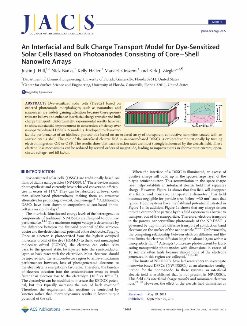
field is shown in Figure 5. The most critical process within allDSSCs is the injection of the electron from the singlet state tothe conduction band, which is given by r4a. As can be seen fromFigure 5, the primary injection rate from the singlet state remainsessentially unchanged. The lack of changes is due to the fact thatthe dye is designed to heavily favor injection over back reaction.On the other hand, the back-reaction rate from the singlet state(r6a) decreases by a factor of about 100 in the presence of anelectric field. This indicates that the back reaction of primaryelectrons is 100 times slower in the presence of an interfacialelectric field, providing significant benefits to charge transport.The decrease in electron injection from the triplet state (r4b) issurprising. However, charge transport from the triplet state is lessimportant than the primary dye state since the majority of thecharge is concentrated in the singlet state. Further, this decreaseis only 100 times smaller while the corresponding back reactionrate (r6b) shows a 10,000-fold improvement to charge transfer.This difference effectively results in a 100-fold improvement tothe charge transport of photogenerated electrons from the tripletstate of the dye to the semiconductor. The excited states ofthe dye are also subject to relaxation mechanisms (r3a and r3b).The changes for these reactions follow the back reaction rates(r6a and r6b) very closely. The similarity is associated with thefact that the concentration of S1
/ and S3/ dictate these rates. The
improvement of these loss mechanisms is likely due to theimproved charge transport that keeps the concentration of S1
/
and S3/ lower. For this reason, the back-reaction rate for the direct
loss of an electron from the conduction band to the electrolyte(r1a) displays similar behavior. It should be noted that identical
enhancement ratios do not mean that the reaction rates are thesame but instead indicate that the effect of the electric field onthe reaction is similar. For example, r1a, r3a, and r6a have identicalenhancement ratios but the rates are approximately 10�11, 10�35,and 10�15 s�1, respectively.Another electron-loss mechanism is the direct transfer of
electrons from the semiconductor conduction band to theoxidized state of the dye (r5). As shown in Table 1, this rate isa function of the concentration of conduction band electrons atthe interface of the semiconductor and electrolyte. Because of theimproved transport of electrons, it was expected that the ratewould decrease. However, this electron loss rate increases whenan interfacial electric field is present within the semiconductor, asshown in Figure 5. The change to the rate is quite substantial atlow applied potentials but the loss mechanism reaches a mini-mum at an applied potential of 0.25 V and then becomes lessaffected. The change in behavior is due to the competingchanges to electron and S+ concentration between the ON andOFF states. At low potentials, the difference in electron con-centration between the two states is high, but the effect startsto plateau at∼0.3 V. At∼0.4 V, the concentration of S+ starts todrop in the ON state, which results in better rates for this backreaction.Finally, the regeneration of the dye is described by reaction
rate r7. This reaction rate remains unaffected by the electric fielduntil applied potentials are greater than 0.4 V. At these higherpotentials, the electric field causes the reaction to be slower.This behavior is due to a reduction in S+ concentration when thefield is ON.The various reaction pathways described above can be sum-
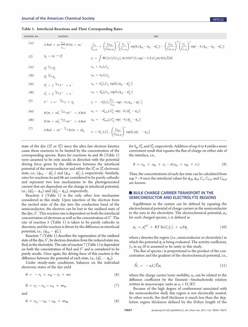
marized by looking at the changes to device performance. Thesimulated current�voltage characteristics of a NW-DSSC withthe field ON or OFF is shown in Figure 6. The shape of thecurves are similar; however, the device with the field ON hassmall but significant increases to short-circuit current and open-circuit voltage. The field also improves the fill factor of the device(0.72 vs 0.68). Combining these changes to the current�voltagecharacteristics leads to approximately a 15% increase in effi-ciency, i.e., ηON ≈ 1.15ηOFF. It should be noted that the fieldOFF state cannot be directly related to NP-DSSCs since themodel does not account for diffusion through the entire titaniafilm. While the presence of an electric field in NW-DSSCsyields an appreciable gain in performance, these devices havesubstantially lower photoactive surface area than NP-DSSCs
Figure 5. Comparison of the interfacial reaction rates for the ON andOFF states of the electric field. The enhancement ratio relates the ONand OFF states (written in the forward direction) to characterize theeffect of the interfacial electric field on the performance of NW-DSSCs.Therefore, values greater than 1 indicate improved charge transport.
Figure 6. Comparison of the polarization curves for NW-DSSCs for theON and OFF states of the electric field.

18672 dx.doi.org/10.1021/ja2044216 |J. Am. Chem. Soc. 2011, 133, 18663–18672
Journal of the American Chemical Society ARTICLE
(often more than 75% lower). Therefore, the beneftis from theelectric field will not likely improve performance of NW- overNP-DSSCs without comparable photoactive surface area.
’CONCLUSIONS
This report introduces a continuum-based mathematicalmodel of DSSCs based on nanowire arrays as the photoanode.The model results were in quantitative and qualitative agreementwith experimental polarization curves. The ability to neglectartificially the effect of electron migration in the model, i.e.,ignore the interfacial electric field present in nanowire systems,allowed its importance to specific interfacial charge-transferreactions to be evaluated. The calculations showed that theelectric field dramatically decreases photoexcited electron backreactions without a significant decrease to electron injection.The enhanced transport from the electric field leads to bettershort-circuit current, open-circuit voltage, and fill factor of thedevice. While these results show moderate improvementsto performance, the components of NW-DSSCs can be furtheroptimized to take full advantage of the benefits from theelectric field.
’ASSOCIATED CONTENT
bS Supporting Information. Variable lists, concentrationprofiles, potential distributions, and sensitivity analysis. Thismaterial is available free of charge via the Internet at http://pubs.acs.org.
’AUTHOR INFORMATION
Corresponding [email protected]
Present Address‡Mainstream Engineering, Rockledge, Florida 32955, UnitedStates
’ACKNOWLEDGMENT
We acknowledge the support of the Donors of the AmericanChemical Society Petroleum Research Fund, the University ofFlorida Opportunity Fund, and the National Science Foundation(CBET-1033736) for support of this research.
’REFERENCES
(1) Gratzel, M. J. Photochem. Photobiol., A 2004, 164, 3–14.(2) Gao, F.; Wang, Y.; Shi, D.; Zhang, J.; Wang, M.; Jing, X.;
Humphry-Baker, R.; Wang, P.; Zakeeruddin, S.; Gratzel, M. J. Am.Chem. Soc. 2008, 130 (32), 10720–10728.(3) Gratzel, M.; Frank, A. J. J. Phys. Chem. 1982, 86, 2964–2967.(4) Gratzel, M. Nature 2001, 414, 338–344.(5) Hagfeldt, A.; Gratzel, M. Chem. Rev. 1995, 95, 49–68.(6) Toyoda, T.; Sano, T.; Nakajima, J.; Doi, S.; Fukumotoa, S.; Ito,
A.; Tohyamaa, T.; Yoshida, M.; Kanagawa, T.; Motohiro, T.; Shiga, T.;Higuchi, K.; Tanaka, H. J. Photochem. Photobiol., A 2004, 164, 203–207.(7) O’Regan, B.; Gratzel, M. Nature 1991, 353, 737–740.(8) Schlichthorl, G.; Huang, S. Y.; Sprague, J.; Frank, A. J. J. Phys.
Chem. B 1997, 101 (41), 8141–8155.(9) Albery, W. J.; Bartlett, P. N. J. Electrochem. Soc. 1984, 131, 315–
325.(10) Ferber, J.; Luther, J. J. Phys. Chem. B 2001, 105, 4895–4903.(11) Peter, L. J. Electroanal. Chem. 2007, 599, 233–240.
(12) Ferber, J.; Stangl, R.; Luther, J. Sol. EnergyMater. Sol. Cells 1998,53, 29–54.
(13) Nelson, J.; Chandler, R. E. Coord. Chem. Rev. 2004, 248,1181–1194.
(14) Penny, M.; Farrell, T.; Please, C. Sol. Energy Mater. Sol. Cells2008, 92, 11–23.
(15) Penny,M.; Farrell, T.;Will, G. Sol. EnergyMater. Sol. Cells 2008,92, 24–37.
(16) Villanueva-Cab, J.; Wang, H.; Oskam, G.; Peter, L. M. J. Phys.Chem. Lett. 2010, 1 (4), 748–751.
(17) Peter, L. M.; Wijayantha, K. G. U. Electrochim. Acta 2000,45, 4543–4551.
(18) Duffy, N. W.; Peter, L. M.; Wijayantha, K. G. U. Electrochem.Commun. 2000, 2, 262–266.
(19) Pasquier, A. D.; Chen, H.; Lu, Y. Appl. Phys. Lett. 2006,89, 253513–253516.
(20) Adachi, M.; Murata, Y.; Takao, J.; Jiu, J.; Sakamoto, M.; Wang,F. J. Am. Chem. Soc. 2004, 126 (45), 14943–14949.
(21) Law, M.; Greene, L. E.; Johnson, J. C.; Saykally, R.; Yang, P. D.Nat. Mater. 2005, 4, 455–459.
(22) Law, M.; Greene, L. E.; Radenovic, A.; Kuykendall, T.;Liphardt, J.; Yang, P. J. Phys. Chem. B 2006, 110, 22652–22663.
(23) Wang, H.; Ting, C.; Hung, M.; Chiou, C.; Liu, Y.; Liu, Z.;Ratinac, K.; Ringer, S. Nanotechnology 2009, 20, 055601.
(24) Gubbala, S.; Chakrapani, V.; Kumar, V.; Sunkara, M. K. Adv.Funct. Mater. 2008, 18, 2411–2418.
(25) Bisquert, J.; Zaban, A.; Greenshtein, M.; Mora-Sero, I. J. Am.Chem. Soc. 2004, 126 (41), 13550–13559.
(26) Zaban, A.; Greenshtein, M.; Bisquert, J. Chem. Phys. Chem.Comm. 2003, 4, 859–865.
(27) Orazem, M. E.; Newman, J. J. Electrochem. Soc. 1984, 131 (11),2569–2574.
(28) Kelzenberg, M. D.; Boettcher, S. W.; Petykiewicz, J. A.; Turner-Evans, D. B.; Putnam, M. C.; Warren, E. L.; Spurgeon, J. M.; Briggs,R. M.; Lewis, N. S.; Atwater, H. A. Nat. Mater. 2009, 9, 239–244.
(29) Asano, T.; Kubo, T.; Nishikitani, Y. Jpn. J. Appl. Phys. 2005,44, 6776–6780.
(30) Zaban, A.; Meier, A.; Gregg, B. A. J. Phys. Chem. B 1997,101, 7985–7988.
(31) Asbury, J. A.; Anderson, N. A.; Hao, E.; Ai, X.; Lian, T. J. Phys.Chem. B 2003, 107, 7376–7379.
(32) Smestad, G.; Bignozzi, C.; Argazzi, R. Sol. Energy Mater. Sol.Cells 1994, 32, 259–265.
(33) Hagfeldt, A.; Gratzel, M. Acc. Chem. Res. 2000, 33, 269–272.(34) Kambili, A.; Walker, A. B.; Qiu, F. L.; Fisher, A. C.; Savin, A. D.;
Peter, L. M. Physica E 2002, 14, 203–205.(35) Junghanel, M. Novel aqueous electrolyte films for hole con-
duction in dye sensitized solar cells and development of an electrontransport model. Ph.D. Thesis, 2007.
(36) Hill, J. J.; Haller, K.; Ziegler, K. J. J. Electrochem. Soc. 2011,158, E1–E7.
(37) Hill, J. J. Photoelectrochemical Energy Conversion in Nano-wire-Based Dye-Sensitized Solar Cells: Modeling, Optimization andTemplated Fabrication. Ph.D. Thesis, University of Florida, Departmentof Chemical Engineering, 2010.
(38) Hill, J. J.; Haller, K.; Gelfand, B.; Ziegler, K. J. ACS Appl. Mater.Int. 2010, 7, 1992–1998.
Related Documents