ABSTRACT AN IMPROVED MAXIMUM POWER POINT TRACKING ALGORITHM USING FUZZY LOGIC CONTROLLER FOR PHOTOVOLTAIC APPLICATIONS This thesis proposes an advanced maximum power point tracking (MPPT) algorithm using Fuzzy Logic Controller (FLC) in order to extract potential maximum power from photovoltaic cells. The objectives of the FLC are to increase tracking velocity and to simultaneously solve inherent drawbacks in conventional MPPT algorithms. The performances of the conventional Perturb & Observe (P&O) algorithm and the proposed algorithm are compared by using MATLAB/Simulink, and the theoretical advantages of FLC were demonstrated. To further validate the practical performance of the proposed algorithm, the two algorithms were experimentally applied to a DSP-Controlled boost DC-DC converter. The experimental results indicated that the proposed algorithm performed with faster tracking time, smaller output power oscillation, and higher efficiency, compared to that of the conventional P&O algorithm. Pengyuan Chen August 2015

Welcome message from author
This document is posted to help you gain knowledge. Please leave a comment to let me know what you think about it! Share it to your friends and learn new things together.
Transcript

ABSTRACT
AN IMPROVED MAXIMUM POWER POINT TRACKING ALGORITHM USING FUZZY LOGIC CONTROLLER
FOR PHOTOVOLTAIC APPLICATIONS
This thesis proposes an advanced maximum power point tracking (MPPT)
algorithm using Fuzzy Logic Controller (FLC) in order to extract potential
maximum power from photovoltaic cells. The objectives of the FLC are to
increase tracking velocity and to simultaneously solve inherent drawbacks in
conventional MPPT algorithms. The performances of the conventional
Perturb & Observe (P&O) algorithm and the proposed algorithm are compared by
using MATLAB/Simulink, and the theoretical advantages of FLC were
demonstrated. To further validate the practical performance of the proposed
algorithm, the two algorithms were experimentally applied to a DSP-Controlled
boost DC-DC converter. The experimental results indicated that the proposed
algorithm performed with faster tracking time, smaller output power oscillation,
and higher efficiency, compared to that of the conventional P&O algorithm.
Pengyuan Chen August 2015


AN IMPROVED MAXIMUM POWER POINT TRACKING
ALGORITHM USING FUZZY LOGIC CONTROLLER
FOR PHOTOVOLTAIC APPLICATIONS
by
Pengyuan Chen
A thesis
submitted in partial
fulfillment of the requirements for the degree of
Master of Science in Engineering
in the Lyles of College of Engineering
California State University, Fresno
August 2015

© 2015 Pengyuan Chen

APPROVED
For the Department of Electrical and Computer Engineering:
We, the undersigned, certify that the thesis of the following student meets the required standards of scholarship, format, and style of the university and the student's graduate degree program for the awarding of the master's degree. Pengyuan Chen
Thesis Author
Woonki Na (Chair) Electrical and Computer Engineering
Nagy Bengiamin Electrical and Computer Engineering
Ajith Weerasinghe Mechanical Engineering
For the University Graduate Committee:
Dean, Division of Graduate Studies

AUTHORIZATION FOR REPRODUCTION
OF MASTER’S THESIS
I grant permission for the reproduction of this thesis in part or in
its entirety without further authorization from me, on the
condition that the person or agency requesting reproduction
absorbs the cost and provides proper acknowledgment of
authorship.
X Permission to reproduce this thesis in part or in its entirety must
be obtained from me.
Signature of thesis author:

ACKNOWLEDGMENTS
I wish to thank my major professor, Dr. Woonki Na most deeply for his
support, guidance, and encouragement through my graduate study. I would like to
thank to Dr. Nagy Bengiamin who helped me to establish my background of the
power electronics and control theory solidly. I want to thank Dr. Ajith A.
Weerasinghe who provided me valuable suggestions of photovoltaic applications.
Also, I would like to thank Dr. Daniel Bukofzer who helped me to enhance my
background of the mathematics and system modelling.
Finally, I would like to extend my heartfelt gratitude to my parents, Lin
Chen and Xiaomeng Chen, and my friends for their love, support, and
encouragement while pursuing my course of study.
TABLE OF CONTENTS
Page
LIST OF TABLES ................................................................................................ viii
LIST OF FIGURES ................................................................................................. ix
1 INTRODUCTION ................................................................................................. 1
1.1 Characteristics of Photovoltaics .................................................................. 1
1.2 Topology of Stand-Alone Photovoltaic Systems ........................................ 4
1.3 Topology of Grid-Connected Photovoltaics Systems ................................. 8
1.4 Scope of This Thesis ................................................................................. 11
2 PHOTOVOLTAICS MODELLING ................................................................... 13
2.1 Structure of Photovoltaics ......................................................................... 13
2.2 PV Modelling and Simulation ................................................................... 15
2.3 The Internal Impedance of Photovoltaics ................................................. 25
3 MAXIMUM POWER POINT TRACKING ALGORITHM .............................. 30
3.1 Conventional MPPT Algorithms .............................................................. 30
3.2 Performance of the Conventional P&O Algorithm .................................. 37
3.3 Fuzzy Logic Controller (FLC) .................................................................. 42
3.4 Simulation and Comparison ...................................................................... 50
4 BOOST DC-DC CONVERTER ......................................................................... 56
4.1 Topology of the Typical Boost DC-DC Converter ................................... 56
4.2 Small Signal Model ................................................................................... 61
5 PROTOTYPE IMPLEMENTATION ................................................................. 70
5.1 Parameters of the Boost DC-DC Circuit ................................................... 71
5.2 Peripheral Circuits ..................................................................................... 75
5.3 Signal Process System .............................................................................. 88

Page
vii vii
5.4 Implementations of the MPPT Algorithm ................................................ 96
6 CONCLUSION ................................................................................................... 99
REFERENCES ..................................................................................................... 101
APPENDICES ...................................................................................................... 105
APPENDIX A: MATLAB CODE ....................................................................... 106
APPENDIX B: SYSTEM SCHEMATICS .......................................................... 111

LIST OF TABLES
Page
Table 2-1 The Specification of SW-260-mono [31] .............................................. 22
Table 2-2 Simulated Parameters of the SW-260-mono ......................................... 22
Table 2-3 The Rmpp of the SW-260-mono under Different Irradiation Conditions ................................................................................................ 28
Table 2-4 The Rmpp of the SW-260-mono under Various Temperature Conditions ................................................................................................ 28
Table 3-1 Parameters of Photovoltaics .................................................................. 31
Table 3-2 The Numerical Unions Corresponding to the Fuzzy Sets ..................... 45
Table 3-3 Rules for the Proposed FLC .................................................................. 47
Table 3-4 The Configuration of Simulations ......................................................... 50
Table 4-1 Parameters of the Designed PV System ................................................ 66
Table 4-2 Linear Approximations with Different values of Rpv .......................... 67
Table 4-3 Effects of Independently Increasing a Parameter in a PI Controller [22] ........................................................................................................... 68
Table 4-4 Step Response of the Closed-Loop Compensated System .................... 69
Table 5-1. Parameters of Components of the Boost Circuit .................................. 71
Table 5-2 Parameters of the Solar Panel under Testing Conditions ...................... 72
Table 5-3 Parameters of the Voltage Divider ........................................................ 83
Table 5-4 Parameters of the Analog Low Pass Filter for Voltage Measurement .. 85
Table 5-5 Parameters of the Current Sensing Circuit ............................................ 88

LIST OF FIGURES
Page
Figure 1-1 Definitions of the solar cell, solar panel, and solar array ...................... 3
Figure 1-2 I-V curve (left) and P-V curve (right) .................................................... 4
Figure 1-3 The topology of the stand-alone photovoltaic system. .......................... 5
Figure 1-4 The topology of the voltage regulation of photovoltaics [10] ............... 6
Figure 1-5 A power system with its PWM signal ................................................... 7
Figure 1-6 The general topology of a grid-connect photovoltaic system................ 9
Figure 1-7 A grid-connect photovoltaic system with micro inverters................... 10
Figure 1-8 A grid-connected photovoltaic system with power optimizers ........... 10
Figure 2-1 P-N junction of a solar cell [16] .......................................................... 14
Figure 2-2 The simplest single diode model ......................................................... 15
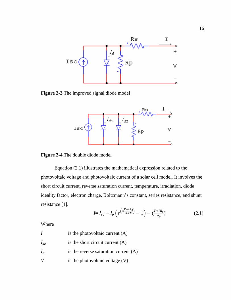
Figure 2-3 The improved signal diode model ....................................................... 16
Figure 2-4 The double diode model ...................................................................... 16
Figure 2-5 Short circuit current ............................................................................. 17
Figure 2-6 Open-circuit voltage ............................................................................ 18
Figure 2-7 The equivalent circuit model of a photovoltaic matrix ........................ 20
Figure 2-8 The diagram of the algorithm for finding the parameter pair (Rs,Rp) .................................................................................................... 21
Figure 2-9 The simulated I-V curves of the SW-260-mono operating under different irradiation conditions. .............................................................. 23
Figure 2-10 The simulated P-V curves of the SW-260-mono operating under different irradiation conditions. .............................................................. 23
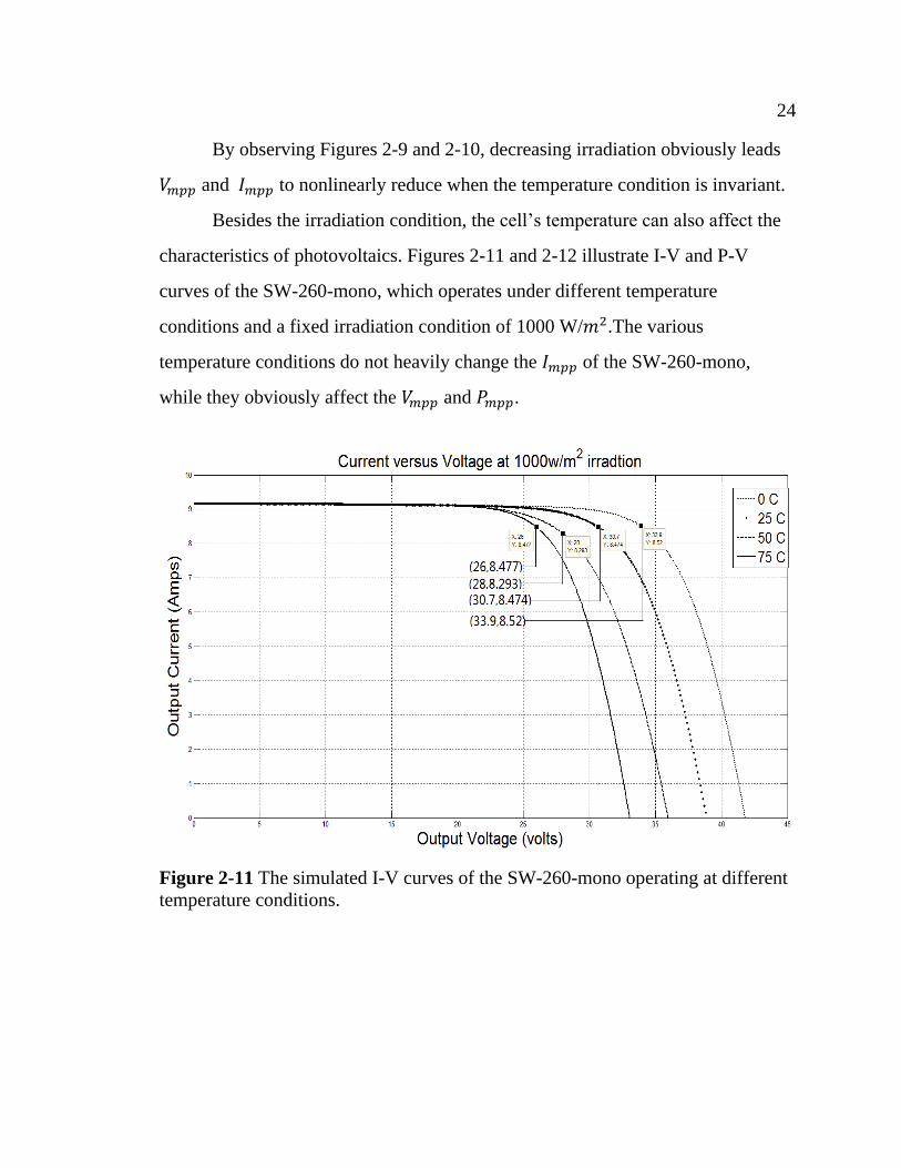
Figure 2-11 The simulated I-V curves of the SW-260-mono operating at different temperature conditions. ............................................................ 24
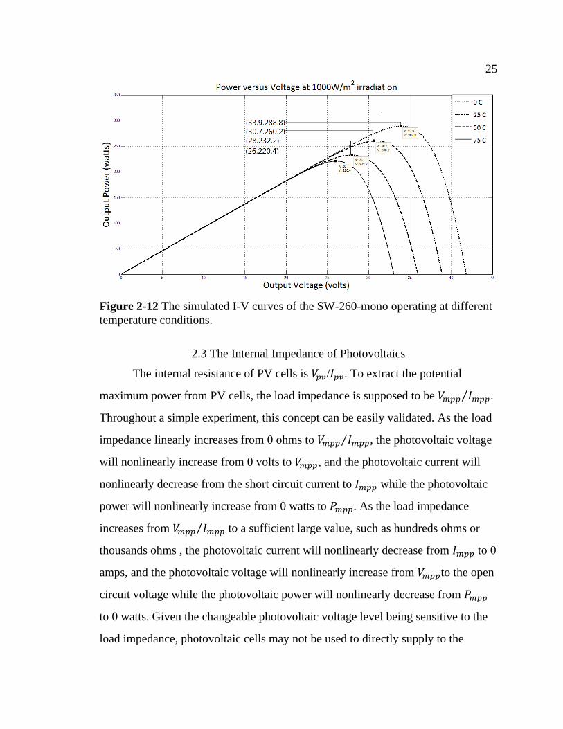
Figure 2-12 The simulated I-V curves of the SW-260-mono operating at different temperature conditions. ............................................................ 25
Page
x x
Figure 2-13 The I-V curve for different resistive load .......................................... 26
Figure 2-14 A wrong topology for changing the internal resistance of a solar panel ........................................................................................................ 27
Figure 2-15 The proper system diagram of a photovoltaic system. ...................... 27
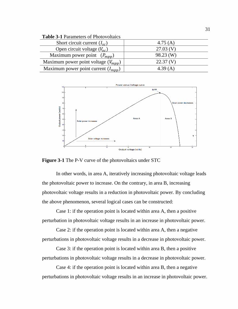
Figure 3-1 The P-V curve of the photovoltaics under STC .................................. 31
Figure 3-2 The general mechanism of the P&O algorithm ................................... 32
Figure 3-3 The flow chart of the conventional P&O algorithm [19] .................... 33
Figure 3-4 Derivative photovoltaic power with respect to photovoltaic voltage .. 35
Figure 3-5 The flow chart of the InC algorithm [19] ............................................ 35
Figure 3-6 Power with P&O p-i 0.1 vs p-i 2.0 ...................................................... 38
Figure 3-7 Average power conducted by P&O with p-i 0.1 vs p-i 2.0 ................. 38
Figure 3-8 Tracking time of P&O with p-i 2.0 volts ............................................. 39
Figure 3-9 Tracking time of P&O with perturbation intensity 0.1 volts ............... 39
Figure 3-10 Energy with P&O: p-i 0.1 vs p-i 2.0 (the 1000th
second) .................. 40
Figure 3-11 Energy with P&O: p-i 0.1 vs p-i 2.0 (the 7000th
second) .................. 41
Figure 3-12 An illustration of the membership function μAx ............................... 43
Figure 3-13 The sectionalized P-V curve with different operating zones. ............ 44
Figure 3-14 The membership function E ............................................................... 46
Figure 3-15 The membership function CE ............................................................ 46
Figure 3-16 The membership function PT ............................................................ 46
Figure 3-17 The output surface of the proposed FLC ........................................... 48
Figure 3-18 Unexpected problem .......................................................................... 49
Figure 3-20 The Simulink block diagram of the Fuzzy Logic Controller............. 51
Figure 3-21 The variable short circuit current of the simulated solar panel. ........ 51
Figure 3-22 The MPPT traces of the two MPPT strategies .................................. 52
Figure 3-23 MPPT traces of two MPPT strategies in the time interval (0s,3s) .... 53

Page
xi xi
Figure 3-24 MPPT traces of the two MPPT strategies during the decrease of the irradiation .......................................................................................... 53
Figure 3-25 The decisions of FLC in the transition period (3.0s, 3.16s) .............. 54
Figure 3-26 The responses of the two strategies during the change in the irradiation condition ................................................................................ 55
Figure 4-1 The typical topology of a boost DC-DC converter. ............................. 57
Figure 4-2 The equivalent circuit during switching on periods ............................ 58
Figure 4-3 Inductor current and voltage during switching on periods .................. 58
Figure 4-4 The equivalent circuit during switching off periods ............................ 59
Figure 4-5 Inductor current and voltage during switching off periods ................. 59
Figure 4-6 The average dynamic model of a boost DC-DC converter ................. 61
Figure 4-7 The equivalent circuit of small signal model (a) [21] ......................... 62
Figure 4-8 The equivalent circuit of small signal model (b) [21] ......................... 63
Figure 4-9 Small signal model: output terminal of a boost DC-DC converter [21] .......................................................................................................... 63
Figure 4-10 Equivalent circuit of a boost converter with irregular input source .. 64
Figure 4-11 Bode plot of the variable-parameters system .................................... 67
Figure 4-12 Step response of the closed-loop compensated system. .................... 69
Figure 5-1 The proposed topology of the PV boost DC-DC circuit ..................... 71
Figure 5-2 Amplitude of the ripple current versus photovoltaic voltage .............. 74
Figure 5-3 Current waveforms of the PV model, inductor and input capacitor .... 75
Figure 5-4 The gate drive circuit ........................................................................... 76
Figure 5-5 The peak-peak voltage of the noise on the 5 volts DC bus (without filtering capacitor) ................................................................................... 77
Figure 5-6 The fundamental frequency of the noise on the 5 volts DC bus (without filtering capacitor) .................................................................... 78
Figure 5-7 The suppressed switching noise........................................................... 78
Page
xii xii
Figure 5-8 The drain-source voltage of the IRFP460A (without gate resistor and RC snubber circuit) .......................................................................... 81
Figure 5-9 The drain-source voltage of the IRFP460A (with gate resistor and RC snubber circuit) ................................................................................. 81
Figure 5-10 The topology of the voltage divider .................................................. 82
Figure 5-11 The bode plot of the proposed low pass filter ................................... 84
Figure 5-12 The low pass filter for voltage sensing .............................................. 85
Figure 5-13 The topology of High-Side Current Sensing ..................................... 86
Figure 5-14 The topology of Low-Side Current Sensing ...................................... 87
Figure 5-15 The Low-Side Current Sensing circuit. ............................................. 87
Figure 5-16 The layout of the MPPT system. ....................................................... 89
Figure 5-17 The topology of the MPPT system. ................................................... 89
Figure 5-18 The designed MPPT system .............................................................. 90
Figure 5-19 Simulink block of the digital PI controller ........................................ 91
Figure 5-20 The voltage regulation of photovoltaics ............................................ 92
Figure 5-21 The inductor voltage waveform (CCM) ............................................ 93
Figure 5-22 The inductor voltage waveform (DCM) ............................................ 93
Figure 5-23 The illustration of DCM detection mechanism ................................. 94
Figure 5-24 The flow chart of the DCM detection mechanism. ........................... 95
Figure 5-25 The performance of the conventional P&O algorithm ...................... 96
Figure 5-26 The performance of the improved MPPT algorithm using FLC ....... 98
1 INTRODUCTION
As the demand for solar energy is dramatically increasing, solar energy
applications have been massively studied for the last decade. Solar panels can
conveniently convert the received light energy to electricity without any pollution.
However, the potential maximum power generated by a solar panel heavily
depends on irradiation and temperature conditions. Additionally, due to the
nonlinear current-voltage (I-V) characteristics of photovoltaic cells, the output
voltage of photovoltaics is determined by the photovoltaic current so that the
output power cannot be forthrightly predicted by the load impedance. To achieve
the maximum power point (MPP) of photovoltaics, a photovoltaic MPPT control
system is normally needed. A tracking control system can continuously changes its
operation status, and keeps perturbing the voltage or current level of its input
power in order to find the potential maximum power point. Photovoltaic systems
can be generally categorized into stand-alone and grid-connected photovoltaic
systems. In this thesis, the proposed MPPT control strategy for stand-alone
photovoltaic systems has been discussed and validated throughout simulation and
experimental results. The characteristics of photovoltaics are briefly addressed in
the section 1.1. The topologies of the two types of photovoltaic systems and their
components are introduced in sections 1.2 and 1.3. The scope of this thesis is
described in section 1.4.
1.1 Characteristics of Photovoltaics
In photovoltaic systems, the core elements for converting solar energy into
electricity are the photovoltaic (PV) cells. Irradiated PV cells can generate DC
power and supply their direct-connected load. However, the photovoltaic power
and its voltage level may not always meet the desired requirements. This is

2 2
because the photovoltaics are well-known by their nonlinear voltage-current and
voltage-power characteristics [1]. Given the load impedance and environmental
conditions, photovoltaics can perform as irregular current source or voltage
source, which may be unacceptable for most power electronic applications. To
compensate for these disadvantages, photovoltaic systems are designed to regulate
the performance of photovoltaics in terms of their output voltage and power. The
two primary objectives of a photovoltaic system are to extract maximum power
from photovoltaics and to regulate the voltage level of the photovoltaic power. A
photovoltaic system generally contains variable system structures in order to shift
the operation point of photovoltaics. Hence the stability and efficiency of a
photovoltaic system is commonly challenged by the variable power load,
irradiation, temperature, and shading condition [1-2]. To enhance stability,
robustness and efficiency of photovoltaic systems, sufficient statistical efforts and
uncommon control strategies are normally involved in the system design.
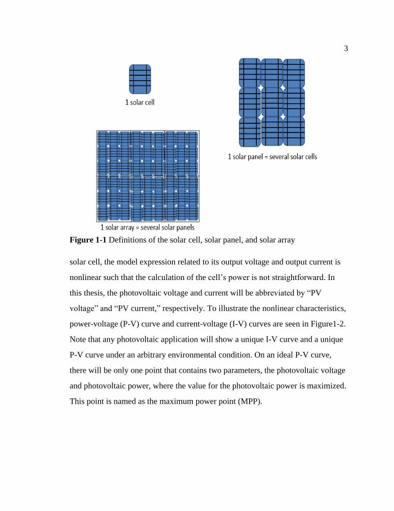
A solar panel normally consists of numbers of inter-connected solar cells.
The pattern of the connection can be cascaded, paralleled or both. The size and
rated power of a solar panel is determined by the number of its solar cells, by the
area of each solar cell, and by the efficiency of each solar cell. If a solar panel can
be defined as a matrix of inter-connected solar cells, a solar array can be defined
as a matrix of inter-connected solar panels. A straightforward illustration is shown
in Figure 1-1.
Throughout the photovoltaic effect, irradiated photovoltaics can generate
DC power. The electronic characteristics, such as the output current, output
voltage and internal resistance of a solar cell are generally determined by the
intensity of the received irradiation, by the temperature of the cells’ surface, by the
efficiency of the photovoltaic conversion, and by the load impedance. For each
3 3
Figure 1-1 Definitions of the solar cell, solar panel, and solar array
solar cell, the model expression related to its output voltage and output current is
nonlinear such that the calculation of the cell’s power is not straightforward. In
this thesis, the photovoltaic voltage and current will be abbreviated by “PV
voltage” and “PV current,” respectively. To illustrate the nonlinear characteristics,
power-voltage (P-V) curve and current-voltage (I-V) curves are seen in Figure1-2.
Note that any photovoltaic application will show a unique I-V curve and a unique
P-V curve under an arbitrary environmental condition. On an ideal P-V curve,
there will be only one point that contains two parameters, the photovoltaic voltage
and photovoltaic power, where the value for the photovoltaic power is maximized.
This point is named as the maximum power point (MPP).

4 4
Figure 1-2 I-V curve (left) and P-V curve (right)
1.2 Topology of Stand-Alone Photovoltaic Systems
According to objectives of photovoltaic systems, photovoltaic systems can
be generally classified into stand-alone and grid-connected photovoltaic systems
[3]. Stand-alone photovoltaic systems are designed to supply local electric load,
and generally consist of energy storage devices for meeting excessive electricity
demands. Grid-connected photovoltaic systems are designed to deliver
photovoltaic power to electric grids [4]. In this section, a brief introduction of
stand-alone photovoltaic systems will be presented.
The fundamental topology of a stand-alone photovoltaic system is shown in
Figure 1-3.
A stand-alone system consists of the following components:
- Solar Cells/Solar Panels/Solar Arrays
- Maximum Power Point Tracking Controller
- Voltage regulator of photovoltaics
- PWM Generator
- DC-DC Converter
- DC Electric Load
- DC-AC Inverter (Optional)

5 5
Figure 1-3 The topology of the stand-alone photovoltaic system.
Maximum Power Point Tracking (MPPT) controllers are popular in both
stand-alone and grid-connected photovoltaic systems. A MPPT controller can be
designed as a physical analog circuit or an embedded system. The main objective
of a MPPT controller is to extract potential maximum power from photovoltaic
cells by continuously perturbing the operation point of the photovoltaic cells. The
operation point of photovoltaics consists of two parameters, the photovoltaic
voltage and photovoltaic power. It can be treated as a point on a P-V curve. The
operation point will reach the maximum power point if the MPPT controller
rationally perturbs the photovoltaic voltage. At the end of every control interval, a
new photovoltaic voltage reference is calculated by the MPPT algorithm and sent
to the photovoltaic voltage regulator. Recently, even though numerous MPPT
algorithms have been researched [5-9], the adopted MPPT algorithms of
commercialized solar energy applications are still based on the conventional
6 6
Perturb & Observe (P&O) algorithm due to its easy implementation and robust
performance. Related discussions will be presented in chapter 3.
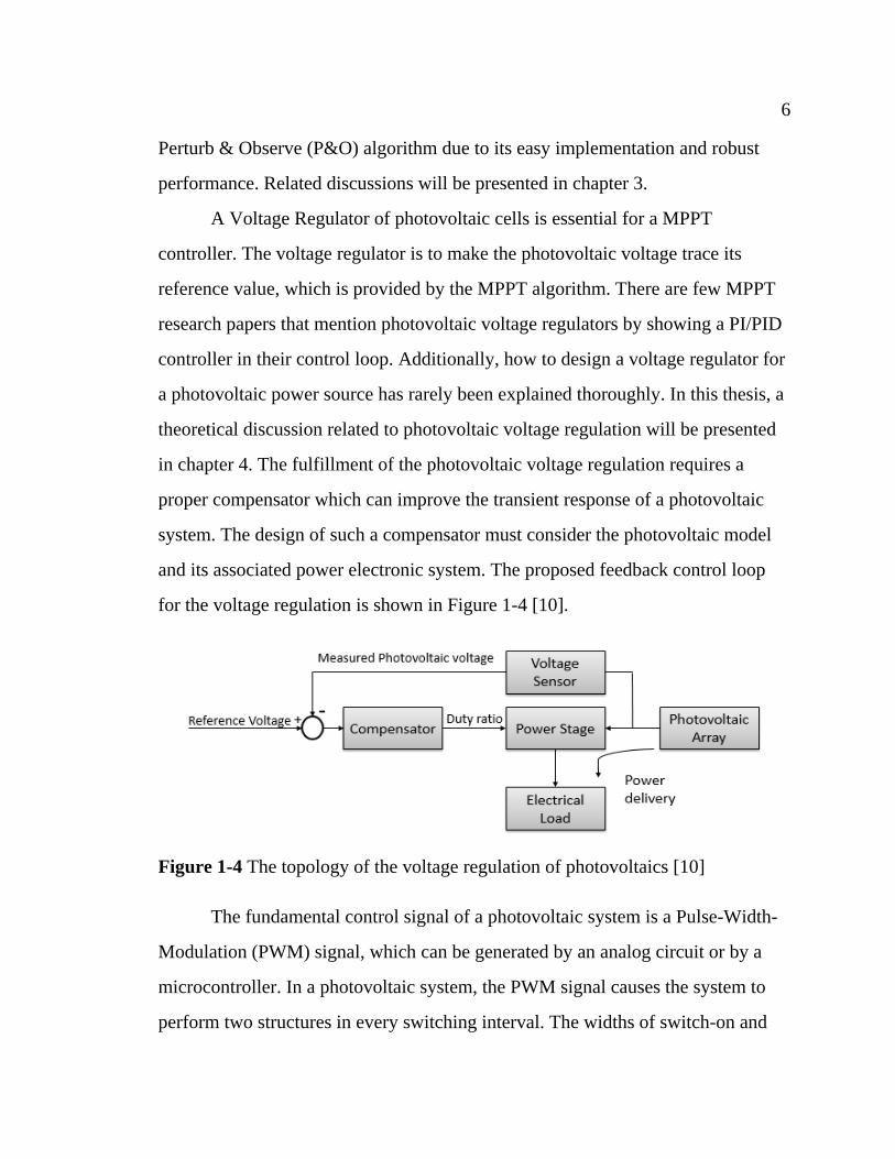
A Voltage Regulator of photovoltaic cells is essential for a MPPT
controller. The voltage regulator is to make the photovoltaic voltage trace its
reference value, which is provided by the MPPT algorithm. There are few MPPT
research papers that mention photovoltaic voltage regulators by showing a PI/PID
controller in their control loop. Additionally, how to design a voltage regulator for
a photovoltaic power source has rarely been explained thoroughly. In this thesis, a
theoretical discussion related to photovoltaic voltage regulation will be presented
in chapter 4. The fulfillment of the photovoltaic voltage regulation requires a
proper compensator which can improve the transient response of a photovoltaic
system. The design of such a compensator must consider the photovoltaic model
and its associated power electronic system. The proposed feedback control loop
for the voltage regulation is shown in Figure 1-4 [10].
Figure 1-4 The topology of the voltage regulation of photovoltaics [10]
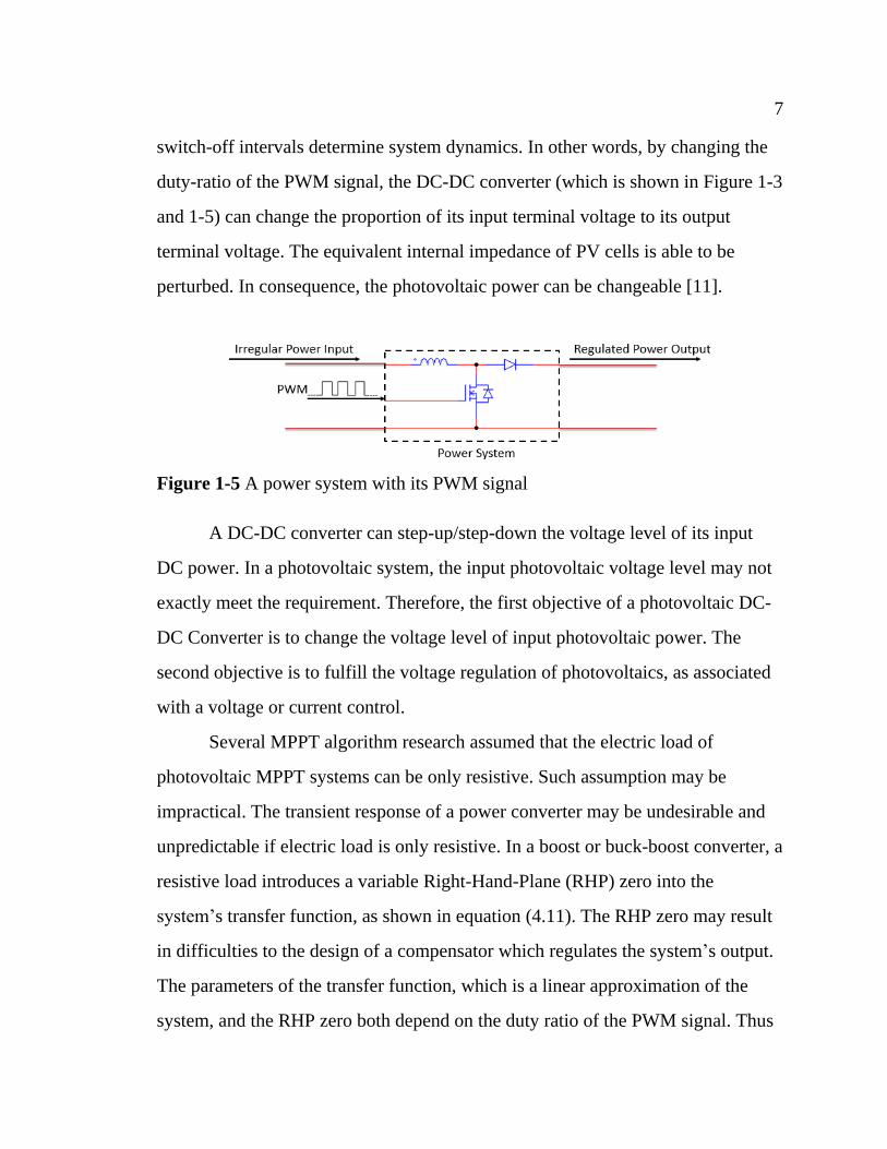
The fundamental control signal of a photovoltaic system is a Pulse-Width-
Modulation (PWM) signal, which can be generated by an analog circuit or by a
microcontroller. In a photovoltaic system, the PWM signal causes the system to
perform two structures in every switching interval. The widths of switch-on and
7 7
switch-off intervals determine system dynamics. In other words, by changing the
duty-ratio of the PWM signal, the DC-DC converter (which is shown in Figure 1-3
and 1-5) can change the proportion of its input terminal voltage to its output
terminal voltage. The equivalent internal impedance of PV cells is able to be
perturbed. In consequence, the photovoltaic power can be changeable [11].
Figure 1-5 A power system with its PWM signal
A DC-DC converter can step-up/step-down the voltage level of its input
DC power. In a photovoltaic system, the input photovoltaic voltage level may not
exactly meet the requirement. Therefore, the first objective of a photovoltaic DC-
DC Converter is to change the voltage level of input photovoltaic power. The
second objective is to fulfill the voltage regulation of photovoltaics, as associated
with a voltage or current control.
Several MPPT algorithm research assumed that the electric load of
photovoltaic MPPT systems can be only resistive. Such assumption may be
impractical. The transient response of a power converter may be undesirable and
unpredictable if electric load is only resistive. In a boost or buck-boost converter, a
resistive load introduces a variable Right-Hand-Plane (RHP) zero into the
system’s transfer function, as shown in equation (4.11). The RHP zero may result
in difficulties to the design of a compensator which regulates the system’s output.
The parameters of the transfer function, which is a linear approximation of the
system, and the RHP zero both depend on the duty ratio of the PWM signal. Thus
8 8
the output voltage regulation of the converter will be further laborious. To avoid
the above issue related to the converter’s output voltage regulation, the appropriate
electric load for a stand-alone photovoltaic system should consist of depth-
recycled batteries and ultra-capacitors. These can absorb the increasing
photovoltaic power, and stabilize the voltage of the output terminal at a relative
fixed level if the load’s capacitance is sufficiently large.
Many photovoltaic systems are designed to supply to AC loads, like motors
or pumps. In such case, a DC-AC Inverter is added into the system topology. A
DC-AC Inverter can be directly cascaded to a DC-DC converter, or can be
connected to the medium energy storage devices, such as ultra-capacitors and
batteries.
1.3 Topology of Grid-Connected Photovoltaics Systems
The fundamental components of a grid-connected photovoltaic system
involve photovoltaic arrays and a DC-AC inverter. The basic topology is shown in
Figure 1-6. To convert the standard AC power (120V/60Hz), the required voltage
level of the input DC power should be greater than 240 volts. However, to meet
this voltage requirement, the size of the input photovoltaics has to be enlarged.
Given the fact that the size of a general 240W solar panel, which has nominal
30V/8A output, is normally 1.35 𝑚2. Throughout calculation, the size of a solar
array with a 240V rated voltage is about 108m2. Such size may cause multiple
issues when the partial shading happens. The partial shading on a photovoltaic
array will cause two typical problems, the reduction in power output and thermal
stress on the photovoltaic array [15]. The photovoltaic current of solar cells
normally diminishes whenever the received irradiation reduces. With the shaded
cascaded connection pattern, the photovoltaic current of the PV cells will reduce

9 9
due to those shaded solar cells. The residual power, which cannot be utilized by
the electric load, because of the shading condition, will be partially transformed to
thermal energy, which may affect the photovoltaics efficiency. Recently, with the
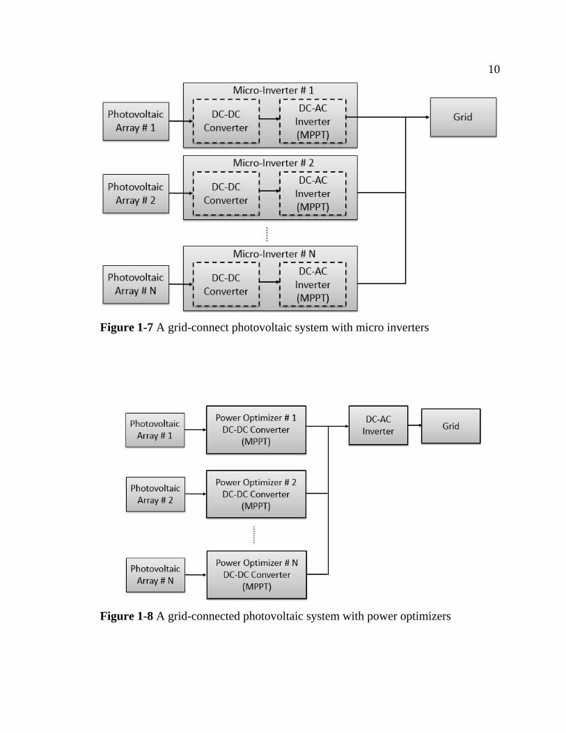
help of micro-inverters, photovoltaic engineers are glad to divide a large-size
photovoltaic array to several small-size arrays, for solving the shading effects. As
shown in Figure 1-7, every micro inverter processes power for one panel, and
consists of a DC-DC converter and a DC-AC inverter. The DC-DC stage is used to
boost the voltage level of the photovoltaic power to about 240 volts for the DC-
AC conversion. The MPPT function for the PV panels is performed centrally at
the inverter stage [29]. Hence, each panel can be isolated from other panels in the
process of the power transmission.
Figure 1-6 The general topology of a grid-connect photovoltaic system
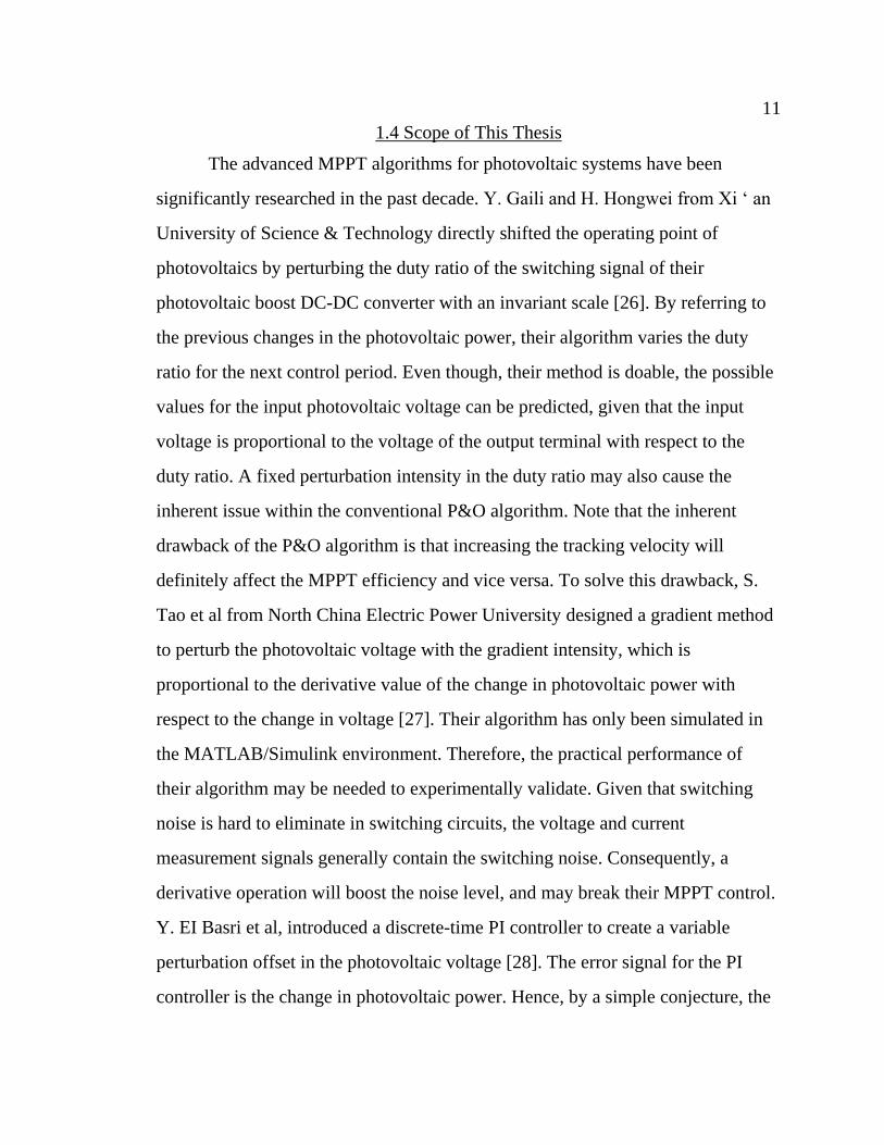
Similar to the micro inverter, alternative applications for optimizing power
of photovoltaic cells are power optimizers. As shown in Figure 1-8, the output of
each DC-DC converter is connected in series prior to the DC-AC inverter. At each
DC-DC state, the MPPT function is fulfilled. Different from the micro inverter,
the objective of this topology is to deliver the maximized photovoltaic power to a
universal DC bus [29].
10 10
Figure 1-7 A grid-connect photovoltaic system with micro inverters
Figure 1-8 A grid-connected photovoltaic system with power optimizers
11 11
1.4 Scope of This Thesis
The advanced MPPT algorithms for photovoltaic systems have been
significantly researched in the past decade. Y. Gaili and H. Hongwei from Xi ‘ an
University of Science & Technology directly shifted the operating point of
photovoltaics by perturbing the duty ratio of the switching signal of their
photovoltaic boost DC-DC converter with an invariant scale [26]. By referring to
the previous changes in the photovoltaic power, their algorithm varies the duty
ratio for the next control period. Even though, their method is doable, the possible
values for the input photovoltaic voltage can be predicted, given that the input
voltage is proportional to the voltage of the output terminal with respect to the
duty ratio. A fixed perturbation intensity in the duty ratio may also cause the
inherent issue within the conventional P&O algorithm. Note that the inherent
drawback of the P&O algorithm is that increasing the tracking velocity will
definitely affect the MPPT efficiency and vice versa. To solve this drawback, S.
Tao et al from North China Electric Power University designed a gradient method
to perturb the photovoltaic voltage with the gradient intensity, which is
proportional to the derivative value of the change in photovoltaic power with
respect to the change in voltage [27]. Their algorithm has only been simulated in
the MATLAB/Simulink environment. Therefore, the practical performance of
their algorithm may be needed to experimentally validate. Given that switching
noise is hard to eliminate in switching circuits, the voltage and current
measurement signals generally contain the switching noise. Consequently, a
derivative operation will boost the noise level, and may break their MPPT control.
Y. EI Basri et al, introduced a discrete-time PI controller to create a variable
perturbation offset in the photovoltaic voltage [28]. The error signal for the PI
controller is the change in photovoltaic power. Hence, by a simple conjecture, the

12 12
operation point may stay on a point, which can result in a zero (0) watts change in
photovoltaic power, and the MPPT control may stop. In practice, the P-V and I-V
curves of a photovoltaic application keep changing with environmental conditions,
and the position of the potential MPP may continuously shift. Therefore, the
MPPT controller should not stop tracking the shifting MPP.
At present, commercialized MPPT controllers for photovoltaic systems are
still based on the conventional Perturb & Observe algorithm due to its easy
implementation and control robustness, though it is not efficient [5]. Therefore,
there are two objectives for this research: 1) to design an advanced MPPT
algorithm with a Fuzzy Logic Controller (FLC) for generating flexible
perturbation intensities, and 2) to validate the proposed algorithm throughout a
designed PV system. In chapter 2, the characteristics of photovoltaics will be
generally reviewed, and the photovoltaic modeling will be introduced in detail via
a single diode model. In chapter 3, the concepts of several fundamental MPPT
algorithms will be discussed. Based on the mechanism of the conventional P&O
algorithm, the derivation of the proposed MPPT algorithm will be addressed.
Chapter 4 will emphasize the modeling of a DC-DC boost converter and the
voltage regulation of photovoltaics. In chapter 5, the implementation of the
proposed MPPT algorithm, and the design of the photovoltaic boost DC-DC
converter will be discussed, along with the related problems.
2 PHOTOVOLTAICS MODELLING
Solar cells are the basic elements of solar panels/solar arrays which provide
renewable electricity without any pollution. Solar cells can convert received light
energy into electricity and generate DC power. In the current solar energy market,
the price per watt of solar panels varies from 0.36 dollars to 1.44 dollars.
Customers only need to pay the cost of solar panels, with no additional charges for
using permanent renewable solar energy. Nevertheless, the cost of solar panels is
still high. For example, the cost of a six kilowatts-per-hour photovoltaic (PV)
system may be about six thousand dollars. Fortunately, photovoltaics generating
their maximum power can reconcile for their high cost. To extract the maximum
power from PVs, their mathematical model, which can predict their nominal
voltage and nominal current, should be investigated. In this chapter, the structure
of photovoltaics is briefly reviewed in section 2.1. Section 2.2 introduces an
approach to model solar panels with a signal diode model. The internal impedance
of photovoltaics is discussed in section 2.3.
2.1 Structure of Photovoltaics
The process of PVs converting received light energy into electricity is
known as the photovoltaic effect. When the light irradiates the surface of a solar
cell, part of the photons of the light may get reflected or consumed immediately
when they impact the surface of the solar cell. This is because the energy that they
carry is too weak to be converted into electricity. Only the photons, which are
absorbed near the P-N junction of the solar cell, can work for the photovoltaic
effect. By absorbing the energy of the photons, the atoms in the P-N junction
generates plentiful hole-electron pairs. Under the force of the electrical field of the
P-N junction, the holes carry the positive charge and shift from the N-type layer to

14 14
the P-type layer. The electrons carrying the negative charge, escape from the P-
type layer, and eventually migrate to the N-type layer [16]. By connecting an
electric load to the P-N junction, such as resistor, the electrons in the N-type layer
flow through the load, and finally enter the P-type layer. The holes in P-type layer
combine with the coming electrons. The P-N junction of a PV cell is shown on
Figure 2-1[16].
Figure 2-1 P-N junction of a solar cell [16]
The size of the surface of a solar cell normally varies from 4𝑐𝑚2 to
225𝑐𝑚2. The nominal power of a solar cell, under standard test condition (STC),
is less than 4 watts. The STC means an irradiation of 1000W/m2 at 25
temperature. The nominal voltage of a silicon solar cell is about 0.5 volts, while
the nominal current is about 8 amperes. Multiple solar cells are generally inter-
connected for enhancing the rated power. Connecting solar cells in parallel can
increase the rated current, while connecting them in series can increase the rated
voltage.
15 15
2.2 PV Modelling and Simulation
2.2.1 Fundamentals of Photovoltaics
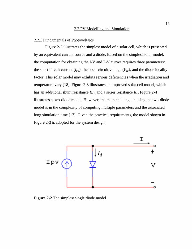
Figure 2-2 illustrates the simplest model of a solar cell, which is presented
by an equivalent current source and a diode. Based on the simplest solar model,
the computation for obtaining the I-V and P-V curves requires three parameters:
the short-circuit current (𝐼𝑠𝑐), the open-circuit voltage (𝑉𝑜𝑐), and the diode ideality
factor. This solar model may exhibits serious deficiencies when the irradiation and
temperature vary [18]. Figure 2-3 illustrates an improved solar cell model, which
has an additional shunt resistance 𝑅𝑠ℎ and a series resistance 𝑅𝑠. Figure 2-4
illustrates a two-diode model. However, the main challenge in using the two-diode
model is in the complexity of computing multiple parameters and the associated
long simulation time [17]. Given the practical requirements, the model shown in
Figure 2-3 is adopted for the system design.
Figure 2-2 The simplest single diode model
16 16
Figure 2-3 The improved signal diode model
Figure 2-4 The double diode model
Equation (2.1) illustrates the mathematical expression related to the
photovoltaic voltage and photovoltaic current of a solar cell model. It involves the
short circuit current, reverse saturation current, temperature, irradiation, diode
ideality factor, electron charge, Boltzmann’s constant, series resistance, and shunt
resistance [1].
I= 𝐼𝑠𝑐 − 𝐼𝑜 (𝑒(𝑞𝑉+𝐼𝑅𝑠𝑎𝐾𝑇
) − 1) − (𝑉+𝐼𝑅𝑠
𝑅𝑝) (2.1)
Where
I is the photovoltaic current (A)
𝐼𝑠𝑐 is the short circuit current (A)
𝐼𝑜 is the reverse saturation current (A)
V is the photovoltaic voltage (V)

17 17
q is the electron charge (1.6 × 10⁻¹⁹𝐶)
k is the Boltzmann’s constant (1.381 × 10⁻²³ 𝐽/𝐾)
T is the junction temperature (K)
𝑎 is the diode ideality factor
𝑅𝑠 is the series resistance (Ω)
𝑅𝑝 is the parallel resistance (Ω)
Figure 2-5 illustrates the condition, which leads a solar cell to generate its
short circuit current. The short circuit current (𝐼𝑠𝑐) is the output current of a solar
cell, when its load impedance is extremely small such as 0.01 ohms and 0.001
ohms.
Figure 2-5 Short circuit current
The short circuit current of a solar cell could be reasonably predicted by
using equations (2.2) and (2.3) [17].
𝐼𝑠𝑐 = (𝐼𝑠𝑐_𝑆𝑇𝐶 + 𝐶𝑖∆𝑇)𝐺
𝐺𝑆𝑇𝐶 (2.2)
∆𝑇= T - 𝑇𝑆𝑇𝐶 (K) (2.3)
Where,
𝐼𝑠𝑐_𝑆𝑇𝐷 is the short-circuit current (STC)
∆𝑇 is the temperature error (K)
𝐶𝑖 is the short circuit coefficient(A/)

18 18
𝐺𝑆𝑇𝐶 is the STC irradiation (1000W/𝑚2)
𝑇𝑆𝑇𝐶 is the STC temperature(25)
T denotes the solar cell’s actual temperature and G denotes the actual
received irradiation on the solar cell. Figure 2-6 illustrates the condition, which
leads a solar cell to generate its open-circuit voltage. The open circuit voltage (𝑉𝑜𝑐)
is the voltage between the positive lead and negative lead of a solar cell when the
current that flows through the connected load is almost zero.
Figure 2-6 Open-circuit voltage
2.2.2 Parameters Calculations
The value of the reverse saturation current, 𝐼𝑜 is rarely provided by the
manufactures. However, it may be approximated by using equation (2.4) [17].
𝐼𝑜 = (𝐼𝑠𝑐𝑆𝑇𝐶+𝐶𝑖∆𝑇)
𝑒(𝑞𝑉𝑆𝐶_𝑆𝑇𝐶+𝐶𝑣∆𝑇
𝑎𝐾𝑇)−1
(2.4)
Where 𝐶𝑣 and 𝑎 are the open-circuit voltage coefficient and the diode
ideality factor, respectively. The value of diode ideality factor generally varies
from 1 to 2.
The unknown parameters in equation (2.1) are 𝑅𝑠 and 𝑅𝑝. The accuracy of
these two parameters determines the similarity between simulated I-V and

19 19
experimentally measured I-V curves provided by manufactures. Fortunately, [18]
provides a reasonable approach to compute 𝑅𝑠 and 𝑅𝑝. The core concept of [18] is
to keep increasing the value for 𝑅𝑠, while simultaneously calculate the value for
𝑅𝑝 to best match the calculated maximum power to the experimental maximum
power provided by manufactures. Equation (2.5) can be used for fulfilling the
above procedures [18].
𝑅𝑝 = 𝑉𝑚𝑝𝑝(𝑉𝑚𝑝𝑝+𝐼𝑚𝑝𝑝𝑅𝑠 )
[𝑉𝑚𝑝𝑝(𝐼𝑠𝑐−𝐼𝑑)]−𝑃𝑚𝑝𝑝 (2.5)
Where
𝑃𝑚𝑝𝑝 is the maximum power point power
𝐼𝑚𝑝𝑝 is the maximum power point current
𝑉𝑚𝑝𝑝 is the maximum power point voltage
The photovoltaic current of the maximum power point is called “Maximum
power point current” and the corresponding photovoltaic voltage is called
“Maximum power point voltage”. In the following discussions the abbreviations,
𝐼𝑚𝑝𝑝 and 𝑉𝑚𝑝𝑝 will denote the maximum power point current and maximum power
point voltage, respectively.
By using equations (2.1) through (2.5), the parameters of a single solar cell
can be reasonably computed. However, those equations may not be sufficient for
solving the parameters of a solar panel or a solar array, which is a matrix of inter-
connected solar cells. Figure 2-7 illustrates the equivalent circuit of a photovoltaic
matrix. The photovoltaic current of a solar panel/array can be calculated by using
equation (2.6).
In equation (2.6), 𝑁𝑝𝑎𝑟𝑎𝑙𝑙𝑒𝑙 is the number of columns shown in Figure 2-7,
while 𝑁𝑠𝑒𝑟𝑖𝑒𝑠 is the number of rows.
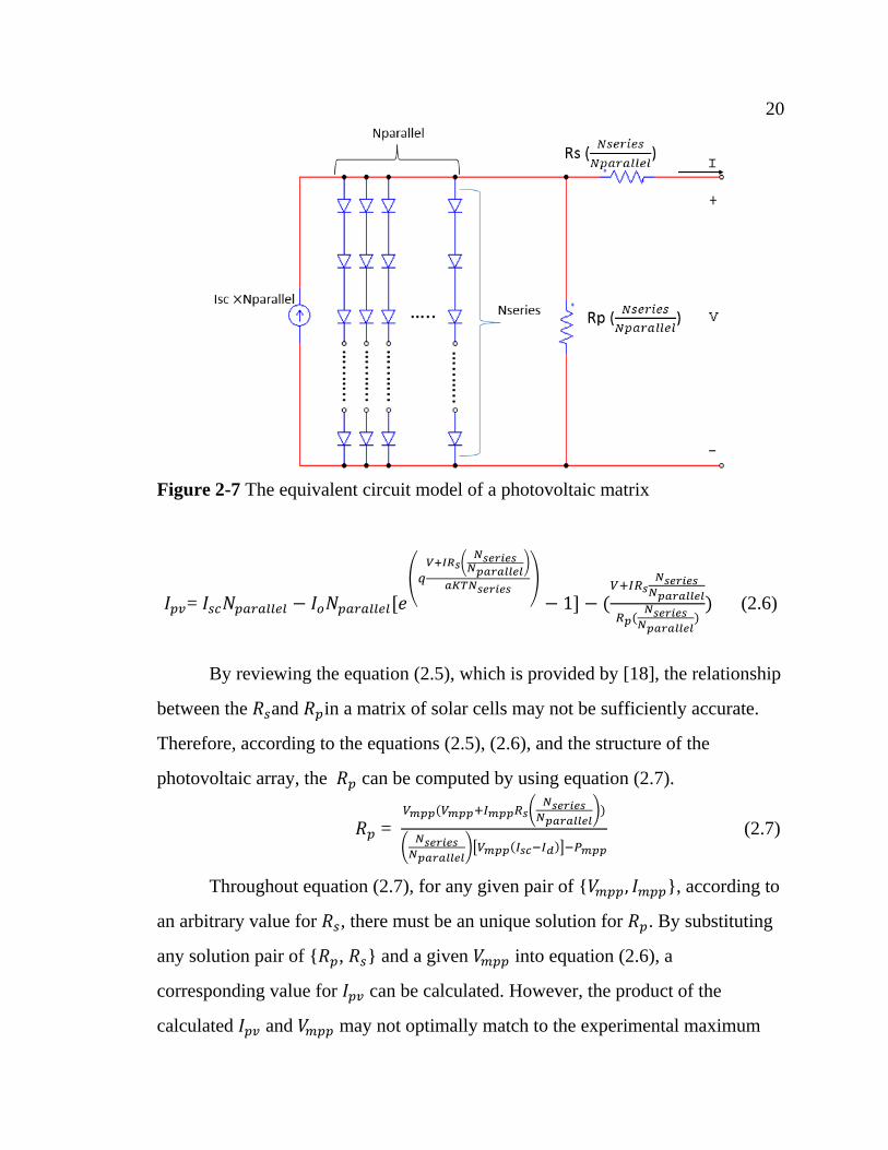
20 20
Figure 2-7 The equivalent circuit model of a photovoltaic matrix
𝐼𝑝𝑣= 𝐼𝑠𝑐𝑁𝑝𝑎𝑟𝑎𝑙𝑙𝑒𝑙 − 𝐼𝑜𝑁𝑝𝑎𝑟𝑎𝑙𝑙𝑒𝑙[𝑒
(𝑞
𝑉+𝐼𝑅𝑠(𝑁𝑠𝑒𝑟𝑖𝑒𝑠𝑁𝑝𝑎𝑟𝑎𝑙𝑙𝑒𝑙
)
𝑎𝐾𝑇𝑁𝑠𝑒𝑟𝑖𝑒𝑠)
− 1] − (𝑉+𝐼𝑅𝑠
𝑁𝑠𝑒𝑟𝑖𝑒𝑠𝑁𝑝𝑎𝑟𝑎𝑙𝑙𝑒𝑙
𝑅𝑝(𝑁𝑠𝑒𝑟𝑖𝑒𝑠𝑁𝑝𝑎𝑟𝑎𝑙𝑙𝑒𝑙
)) (2.6)
By reviewing the equation (2.5), which is provided by [18], the relationship
between the 𝑅𝑠and 𝑅𝑝in a matrix of solar cells may not be sufficiently accurate.
Therefore, according to the equations (2.5), (2.6), and the structure of the
photovoltaic array, the 𝑅𝑝 can be computed by using equation (2.7).
𝑅𝑝 = 𝑉𝑚𝑝𝑝(𝑉𝑚𝑝𝑝+𝐼𝑚𝑝𝑝𝑅𝑠(
𝑁𝑠𝑒𝑟𝑖𝑒𝑠𝑁𝑝𝑎𝑟𝑎𝑙𝑙𝑒𝑙
))
(𝑁𝑠𝑒𝑟𝑖𝑒𝑠𝑁𝑝𝑎𝑟𝑎𝑙𝑙𝑒𝑙
)[𝑉𝑚𝑝𝑝(𝐼𝑠𝑐−𝐼𝑑)]−𝑃𝑚𝑝𝑝
(2.7)
Throughout equation (2.7), for any given pair of 𝑉𝑚𝑝𝑝, 𝐼𝑚𝑝𝑝, according to
an arbitrary value for 𝑅𝑠, there must be an unique solution for 𝑅𝑝. By substituting
any solution pair of 𝑅𝑝, 𝑅𝑠 and a given 𝑉𝑚𝑝𝑝 into equation (2.6), a
corresponding value for 𝐼𝑝𝑣 can be calculated. However, the product of the
calculated 𝐼𝑝𝑣 and 𝑉𝑚𝑝𝑝 may not optimally match to the experimental maximum
21 21
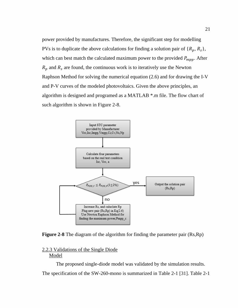
power provided by manufactures. Therefore, the significant step for modelling
PVs is to duplicate the above calculations for finding a solution pair of 𝑅𝑝, 𝑅𝑠,
which can best match the calculated maximum power to the provided 𝑃𝑚𝑝𝑝. After
𝑅𝑝 and 𝑅𝑠 are found, the continuous work is to iteratively use the Newton
Raphson Method for solving the numerical equation (2.6) and for drawing the I-V
and P-V curves of the modeled photovoltaics. Given the above principles, an
algorithm is designed and programed as a MATLAB *.m file. The flow chart of
such algorithm is shown in Figure 2-8.
Figure 2-8 The diagram of the algorithm for finding the parameter pair (Rs,Rp)
2.2.3 Validations of the Single Diode
Model
The proposed single-diode model was validated by the simulation results.
The specification of the SW-260-mono is summarized in Table 2-1 [31]. Table 2-1

22 22
demonstrates two series of parameters that present the characteristics of the SW-
260-mono operating under two different testing conditions. 𝑅𝑠 and 𝑅𝑝 are found
by implementing the algorithm shown in Figure 2-8 via MATLAB. The simulated
parameters of the SW-260-mono are listed in Table 2-2.
Table 2-1 The Specification of SW-260-mono [31]
Parameter
Mono-Crystalline
SW-260-mono-silver
Test condition
1000𝑊/𝑚2, 25
Mono-Crystalline
SW-260-mono-silver
Test condition
800𝑊/𝑚2, 25
𝑃𝑚𝑎𝑥 260W 194.2W
𝑉𝑜𝑐 38.9V 35.6V
𝑉𝑚𝑝𝑝 30.7V 28.1V
𝐼𝑠𝑐 9.18A 7.42A
𝐼𝑚𝑝𝑝 8.47A 6.92A
𝐶𝑖 0.004%/K 0.004%K
𝐶𝑣 -0.3%/K -0.3%K
Table 2-2 Simulated Parameters of the SW-260-mono
Parameter
Mono-Crystalline
SW-260-mono-silver
Test condition
1000𝑊/𝑚2, 25
Mono-Crystalline
SW-260-mono-silver
Test condition
800𝑊/𝑚2, 25
𝑃𝑚𝑎𝑥 260.2W 194W
𝑉𝑜𝑐 38.9V 35.6V
𝑉𝑚𝑝𝑝 30.7V 28.1V
𝐼𝑠𝑐 9.18A 7.42A
𝐼𝑚𝑝𝑝 8.47A 6.91A
𝑅𝑠 0.0038 Ω 0.0038 Ω
𝑅𝑝 5.8737 Ω 5.8737 Ω
𝐼𝑜 4.6618× 10⁻⁷ A 2.8392× 10⁻⁷ A
Figures 2-9 and 2-10 illustrate the simulated I-V curves and P-V curves of
the SW-260-mono operating under the same temperature condition and different
irradiation conditions, respectively. The MATLAB code for the PV modelling can
be found in Appendix A.
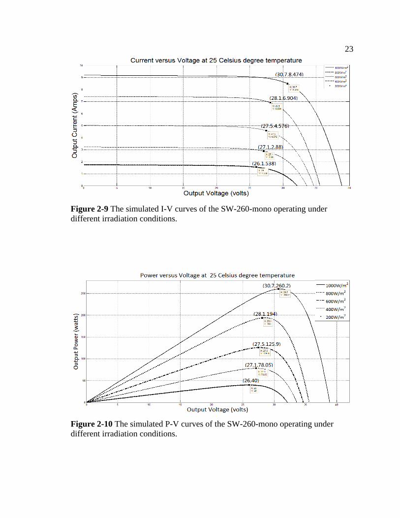
23 23
Figure 2-9 The simulated I-V curves of the SW-260-mono operating under
different irradiation conditions.
Figure 2-10 The simulated P-V curves of the SW-260-mono operating under
different irradiation conditions.
24 24
By observing Figures 2-9 and 2-10, decreasing irradiation obviously leads
𝑉𝑚𝑝𝑝 and 𝐼𝑚𝑝𝑝 to nonlinearly reduce when the temperature condition is invariant.
Besides the irradiation condition, the cell’s temperature can also affect the
characteristics of photovoltaics. Figures 2-11 and 2-12 illustrate I-V and P-V
curves of the SW-260-mono, which operates under different temperature
conditions and a fixed irradiation condition of 1000 W/𝑚2.The various
temperature conditions do not heavily change the 𝐼𝑚𝑝𝑝 of the SW-260-mono,
while they obviously affect the 𝑉𝑚𝑝𝑝 and 𝑃𝑚𝑝𝑝.
Figure 2-11 The simulated I-V curves of the SW-260-mono operating at different
temperature conditions.
25 25
Figure 2-12 The simulated I-V curves of the SW-260-mono operating at different
temperature conditions.
2.3 The Internal Impedance of Photovoltaics
The internal resistance of PV cells is 𝑉𝑝𝑣/𝐼𝑝𝑣. To extract the potential
maximum power from PV cells, the load impedance is supposed to be 𝑉𝑚𝑝𝑝 𝐼𝑚𝑝𝑝⁄ .
Throughout a simple experiment, this concept can be easily validated. As the load
impedance linearly increases from 0 ohms to 𝑉𝑚𝑝𝑝 𝐼𝑚𝑝𝑝⁄ , the photovoltaic voltage
will nonlinearly increase from 0 volts to 𝑉𝑚𝑝𝑝, and the photovoltaic current will
nonlinearly decrease from the short circuit current to 𝐼𝑚𝑝𝑝 while the photovoltaic
power will nonlinearly increase from 0 watts to 𝑃𝑚𝑝𝑝. As the load impedance
increases from 𝑉𝑚𝑝𝑝 𝐼𝑚𝑝𝑝⁄ to a sufficient large value, such as hundreds ohms or
thousands ohms , the photovoltaic current will nonlinearly decrease from 𝐼𝑚𝑝𝑝 to 0
amps, and the photovoltaic voltage will nonlinearly increase from 𝑉𝑚𝑝𝑝to the open
circuit voltage while the photovoltaic power will nonlinearly decrease from 𝑃𝑚𝑝𝑝
to 0 watts. Given the changeable photovoltaic voltage level being sensitive to the
load impedance, photovoltaic cells may not be used to directly supply to the
26 26
electric load which require different input voltage level. Consequently, in a
photovoltaic system, a power converter is needed to successfully deliver the
irregular power with a variable voltage level to a DC-Link or electric grids.
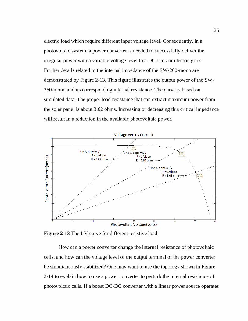
Further details related to the internal impedance of the SW-260-mono are
demonstrated by Figure 2-13. This figure illustrates the output power of the SW-
260-mono and its corresponding internal resistance. The curve is based on
simulated data. The proper load resistance that can extract maximum power from
the solar panel is about 3.62 ohms. Increasing or decreasing this critical impedance
will result in a reduction in the available photovoltaic power.
Figure 2-13 The I-V curve for different resistive load
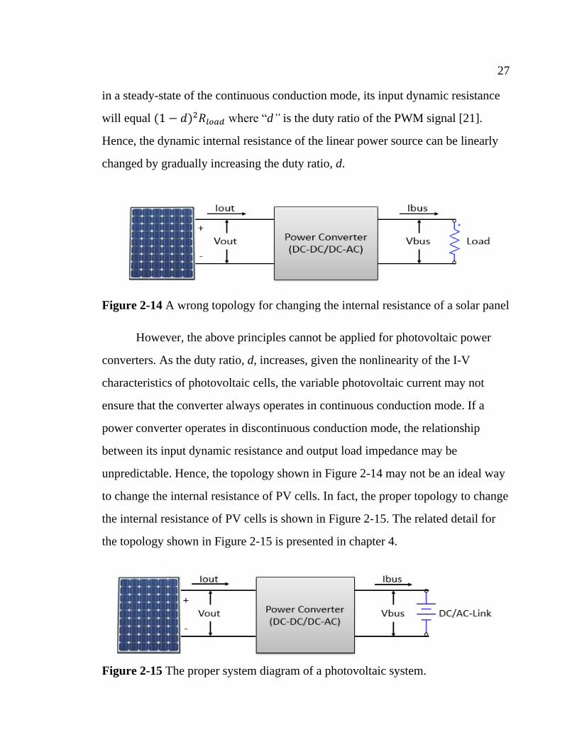
How can a power converter change the internal resistance of photovoltaic
cells, and how can the voltage level of the output terminal of the power converter
be simultaneously stabilized? One may want to use the topology shown in Figure
2-14 to explain how to use a power converter to perturb the internal resistance of
photovoltaic cells. If a boost DC-DC converter with a linear power source operates
27 27
in a steady-state of the continuous conduction mode, its input dynamic resistance
will equal (1 − 𝑑)2𝑅𝑙𝑜𝑎𝑑 where “d” is the duty ratio of the PWM signal [21].
Hence, the dynamic internal resistance of the linear power source can be linearly
changed by gradually increasing the duty ratio, d.
Figure 2-14 A wrong topology for changing the internal resistance of a solar panel
However, the above principles cannot be applied for photovoltaic power
converters. As the duty ratio, d, increases, given the nonlinearity of the I-V
characteristics of photovoltaic cells, the variable photovoltaic current may not
ensure that the converter always operates in continuous conduction mode. If a
power converter operates in discontinuous conduction mode, the relationship
between its input dynamic resistance and output load impedance may be
unpredictable. Hence, the topology shown in Figure 2-14 may not be an ideal way
to change the internal resistance of PV cells. In fact, the proper topology to change
the internal resistance of PV cells is shown in Figure 2-15. The related detail for
the topology shown in Figure 2-15 is presented in chapter 4.
Figure 2-15 The proper system diagram of a photovoltaic system.

28 28
Table 2-3 illustrates the maximum power point internal resistance (𝑅𝑚𝑝𝑝)
of the SW-260-mono, which operates under variable irradiation conditions and the
invariant 25 temperature condition. Table 2-4 illustrates the 𝑅𝑚𝑝𝑝 of the SW-
260-mono, which operates under variable temperature conditions and the invariant
1000 W/𝑚2 irradiation.
Table 2-3 The 𝑅𝑚𝑝𝑝 of the SW-260-mono under Different Irradiation Conditions
Irradiation condition The 𝑅𝑚𝑝𝑝 of the SW-260-mono
1000 W/𝑚2 3.62 Ω
800 W/𝑚2 4.07 Ω
600 W/𝑚2 6.00 Ω
400 W/𝑚2 9.41 Ω
200 W/𝑚2 16.91 Ω
Table 2-4 The 𝑅𝑚𝑝𝑝 of the SW-260-mono under Various Temperature Conditions
Temperature condition Output resistance of the SW-260-mono
at its maximum power point
75 3.08 Ω
50 3.38 Ω
25 3.58 Ω
0 3.98 Ω
According to patterns shown in Tables 2-3 and 2-4, the 𝑅𝑚𝑝𝑝 is sensitive to
the environmental conditions. This is because photovoltaic cells present different
I-V and P-V curves under different environmental conditions. Therefore, to extract
the potential maximum power from PV cells, a photovoltaic MPPT control system
should exhibit the following three significant abilities:
- The ability to change the internal resistance of photovoltaic cells
- The ability to detect migration and transformation of P-V curves
- The ability to predict the location of the potential MPP.

29 29
The next chapter mainly discusses: how to efficiently predict the MPP; how
to increase the PV system’s tracking velocity; how to improve the system’s MPPT
efficiency.

3 MAXIMUM POWER POINT TRACKING ALGORITHM
The MPPT algorithm of a photovoltaic system is used to continuously set
new photovoltaic voltage references in order to sense P-V curves and to perturb
the PV operation point towards the potential maximum power point (MPP). In
section 3.1, several conventional MPPT algorithms are briefly introduced by
analyzing their advantages and disadvantages. In section 3.2, the performance of
the Perturb & Observer (P&O) algorithm is discussed in detail because it provides
fundamental concepts for other MPPT algorithms. Section 3.3 explains concepts
of the proposed tracking algorithm using Fuzzy Logic Controller (FLC) for a PV
system. The objectives of the FLC are to accelerate the MPPT velocity and to
suppress the power oscillation around the maximum power point (MPP). In
section 3.4, MATLAB/Simulink based results are presented and validate the
advantages of the proposed controller in terms of the tracking speed and tracking
accuracy.
3.1 Conventional MPPT Algorithms
3.1.1 The Conventional Perturb & Observe Algorithm
The concepts of the MPPT algorithms are derived from the characteristics
of P-V curves of photovoltaic cells. Therefore, the illustrations of MPPT
algorithms can be rationally conveyed through graphs. In this section, the
simulation results and related discussions are all based on the specified parameters
shown in Table 3-1. Figure 3-1 reminds the shape of a P-V curve.
In Figure 3-1, the region covered by the P-V curve is divided into two
areas. In area A, when the operation point of the photovoltaic cells moves towards
the MPP, the photovoltaic power continuously increases until it reaches the MPP.
31 31
Table 3-1 Parameters of Photovoltaics
Short circuit current (𝐼𝑠𝑐) 4.75 (A)
Open circuit voltage (𝑉𝑜𝑐) 27.03 (V)
Maximum power point (𝑃𝑚𝑝𝑝) 98.23 (W)
Maximum power point voltage (𝑉𝑚𝑝𝑝) 22.37 (V)
Maximum power point current (𝐼𝑚𝑝𝑝) 4.39 (A)
Figure 3-1 The P-V curve of the photovoltaics under STC
In other words, in area A, iteratively increasing photovoltaic voltage leads
the photovoltaic power to increase. On the contrary, in area B, increasing
photovoltaic voltage results in a reduction in photovoltaic power. By concluding
the above phenomenon, several logical cases can be constructed:
Case 1: if the operation point is located within area A, then a positive
perturbation in photovoltaic voltage results in an increase in photovoltaic power.
Case 2: if the operation point is located within area A, then a negative
perturbations in photovoltaic voltage results in a decrease in photovoltaic power.
Case 3: if the operation point is located within area B, then a positive
perturbations in photovoltaic voltage results in a decrease in photovoltaic power.
Case 4: if the operation point is located within area B, then a negative
perturbations in photovoltaic voltage results in an increase in photovoltaic power.

32 32
As the above patterns indicate, the conventional Perturb & Observer (P&O)
algorithm is designed to continuously perturb the photovoltaic voltage with an
invariant intensity, in order to gather the information of the present location of the
operation point and to shift the operation point towards the real MPP. It is
expected that the operation point will keep oscillating around the real MPP with a
fixed scale due to the nature of the conventional P&O algorithm. Thus, some
MPPT algorithms research attempt to prevent the perturbation after the operation
point reaches its MPP, while this may be irrational due to the instability of the
MPP. Note that PV cells will vary their I-V and P-V characteristics after
temperature and irradiation conditions changes so that the position of the real MPP
is variable in practical environments. So to speak, the practical MPPT control is
not a single-time trace. In this thesis, such oscillations around the MPP are
reserved for the sakes of detecting changes in environmental conditions. The
fundamental mechanism of the conventional P&O algorithm can be summarized
as what is shown in Figure 3-2.
Figure 3-2 The general mechanism of the P&O algorithm
In Figure 3-2, the detection function involves the photovoltaic current and
voltage sensing. By reviewing the change in the photovoltaic power and the
previous perturbation in the photovoltaic voltage, the detection function roughly

33 33
concludes the present location of the operation point, while the prediction function
predicts the direction and intensity for the next perturbation. For example, if an
increase in the photovoltaic power is detected and the previous perturbation is
positive, given the case 1, the present operation point should be located within
area A. Hence, the next perturbation is presumed to be positive. On the contrary, if
a decrease in the photovoltaic power is detected and the previous perturbation is
positive, then the location of the operation point should be located within area B.
Therefore, the next perturbation of photovoltaic voltage is presumed to be
negative. By summarizing all the possibilities, the Perturb & Observe algorithm is
derived. The flow chart of P&O is shown in Figure 3-3 [19].
Figure 3-3 The flow chart of the conventional P&O algorithm [19]
It is obvious that the P&O algorithm is easy to implement. Moreover, the
related implementation is not heavily affected by the measurement noise, because
the P&O algorithm does not involve any derivative operation. Currently, the

34 34
conventional P&O algorithm are widely adopted by electronic companies, such as
Texas Instruments and Linear Technology for manufacturing MPPT controllers.
However, due to the nature of the algorithm, the efficiency of MPPT is sacrificed
in order to accelerate the MPPT velocity. In section 3.3, the proposed MPPT
algorithm that can solve the drawback of the conventional P&O algorithm will be
described.
3.1.2 Incremental Conductance Algorithm
The incremental conductance algorithm (InC) is an updated version of the
conventional P&O algorithm. Different from the conventional P&O algorithm, the
InC algorithm uses the slope at the operation point as the position indicator.
𝜕𝑃
𝜕𝑉 =
𝜕(𝑉×𝐼)
𝜕𝑉= 𝐼 + 𝑉 ×
𝜕𝐼
𝜕𝑉 (3.0)
𝐼 = 𝐼𝑠𝑐 − 𝐼𝑜 (𝑒(𝑞
𝑉
𝑎𝐾𝑇) − 1) (3.1)
Equation (3.0) is the derivative of the photovoltaic power with respect to
the photovoltaic voltage. Equation (3.1) is the simplified expression of equation
(2.3), and ignores the series and parallel resistance of the photovoltaic model.
𝜕𝐼
𝜕𝑉 = −𝐼𝑜 ×
𝑞
𝑎𝐾𝑇× 𝑒(𝑞
𝑉
𝑎𝐾𝑇) (3.2)
𝜕𝑃
𝜕𝑉 = 𝐼 + 𝑉 ×
𝜕𝐼
𝜕𝑉= 𝐼𝑠𝑐 − 𝐼𝑜 (𝑒
(𝑞𝑉
𝑎𝐾𝑇) − 1) − 𝐼𝑜 ×
𝑞𝑉
𝑎𝐾𝑇× 𝑒(𝑞
𝑉
𝑎𝐾𝑇) (3.3)
By substituting the equation (3.1) and (3.2) into (3.0), the equation (3.0) is
reformed to equation (3.3), which involves the photovoltaic current, voltage and
short-circuit current.
𝜕2𝑃
𝜕2𝑉= −𝐼𝑜 ×
𝑞
𝑎𝐾𝑇(𝑒(𝑞
𝑉
𝑎𝐾𝑇) − 1) − 𝐼𝑜 ×
𝑞
𝑎𝐾𝑇× 𝑒(𝑞
𝑉
𝑎𝐾𝑇) (3.4)
−𝐼𝑜 × (𝑞
𝑎𝐾𝑇)2 × 𝑉 × 𝑒(𝑞
𝑉
𝑎𝐾𝑇)

35 35
Taking the derivative of equation (3.3) with respect to V yields equation
(3.4) which demonstrates the monotonically decreasing characteristic of (3.3).
In Figure 3-4, the slope of the P-V curve crosses zero at the MPP.
Therefore, on a P-V curve, if the operation point moves along the left hand side
curve of the MPP, it will be greater than zero. Otherwise, the slope is less than
zero. The InC algorithm is derived from the above characteristic. The flow chart of
the InC algorithm is shown in Figure 3-5.
Figure 3-4 Derivative photovoltaic power with respect to photovoltaic voltage
Figure 3-5 The flow chart of the InC algorithm [19]
36 36
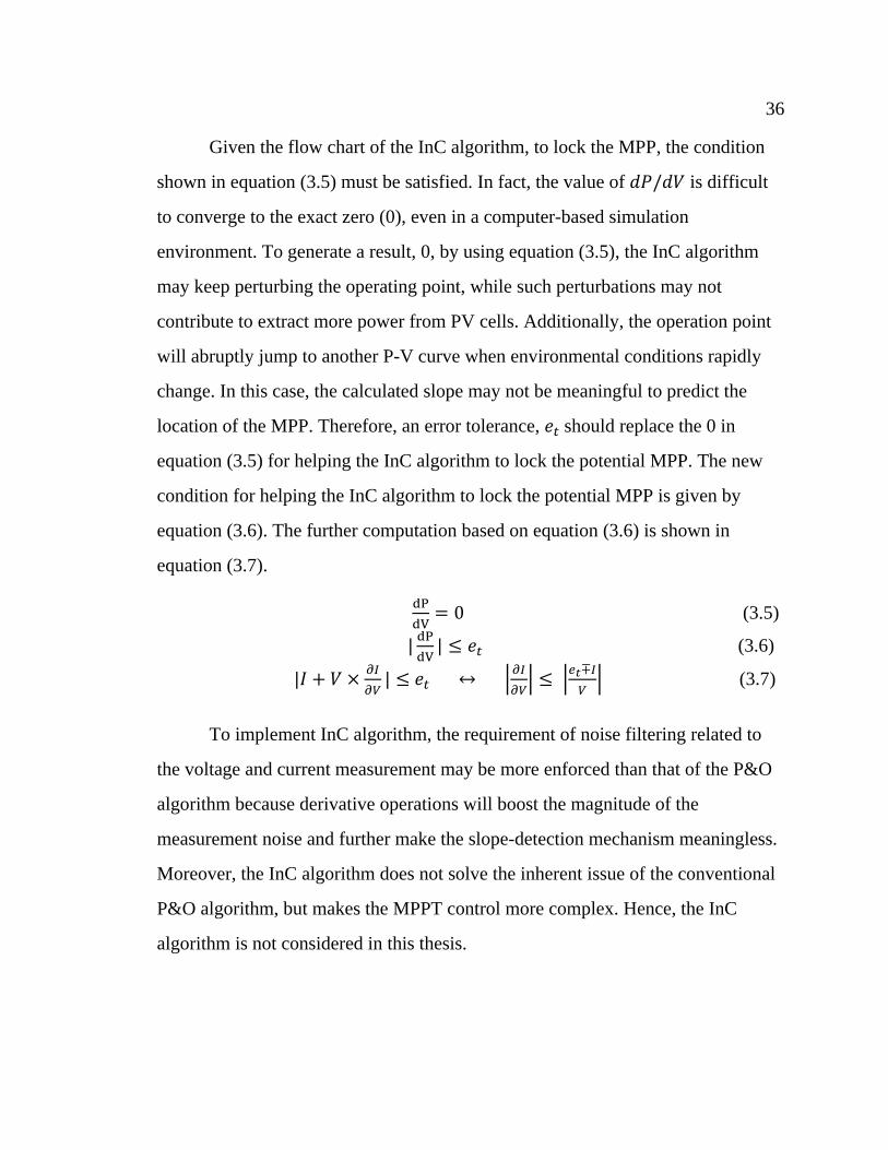
Given the flow chart of the InC algorithm, to lock the MPP, the condition
shown in equation (3.5) must be satisfied. In fact, the value of 𝑑𝑃/𝑑𝑉 is difficult
to converge to the exact zero (0), even in a computer-based simulation
environment. To generate a result, 0, by using equation (3.5), the InC algorithm
may keep perturbing the operating point, while such perturbations may not
contribute to extract more power from PV cells. Additionally, the operation point
will abruptly jump to another P-V curve when environmental conditions rapidly
change. In this case, the calculated slope may not be meaningful to predict the
location of the MPP. Therefore, an error tolerance, 𝑒𝑡 should replace the 0 in
equation (3.5) for helping the InC algorithm to lock the potential MPP. The new
condition for helping the InC algorithm to lock the potential MPP is given by
equation (3.6). The further computation based on equation (3.6) is shown in
equation (3.7).
dP
dV= 0 (3.5)
|dP
dV| ≤ 𝑒𝑡 (3.6)
|𝐼 + 𝑉 ×𝜕𝐼
𝜕𝑉| ≤ 𝑒𝑡 ↔ |
𝜕𝐼
𝜕𝑉| ≤ |
𝑒𝑡∓𝐼
𝑉| (3.7)
To implement InC algorithm, the requirement of noise filtering related to
the voltage and current measurement may be more enforced than that of the P&O
algorithm because derivative operations will boost the magnitude of the
measurement noise and further make the slope-detection mechanism meaningless.
Moreover, the InC algorithm does not solve the inherent issue of the conventional
P&O algorithm, but makes the MPPT control more complex. Hence, the InC
algorithm is not considered in this thesis.
37 37
3.1.3 Constant Voltage Method
Instead of perturbing the photovoltaic voltage, a reasonable PV power can
be obtained by clamping the photovoltaic voltage at a certain level. By
occasionally measuring the open circuit voltage of photovoltaics, an updated
clamped voltage level (𝑉𝑐𝑝) can be obtained by using equation (3.8).
𝑉𝑐𝑝 = 𝛽𝑉𝑜𝑐 (3.8)
The value of 𝛽 is normally selected in range from 70% to 80%.The constant
voltage method is derived from experimental experiences: 𝑉𝑚𝑝𝑝 generally is
located within the range from 70% to 80% of 𝑉𝑜𝑐[16]. This characteristic of
photovoltaics can be validated by Figures 2-9 and 2-10 (p. 23). If the requirement
for the MPPT efficiency is not extremely strict, the constant voltage method may
be a good choice due to its relatively low cost and easy implementation, which
may merely require a simple analog circuit. Under the various test conditions, the
constant voltage method may collect 70% of the potential maximum power from
photovoltaics.
3.2 Performance of the Conventional P&O Algorithm
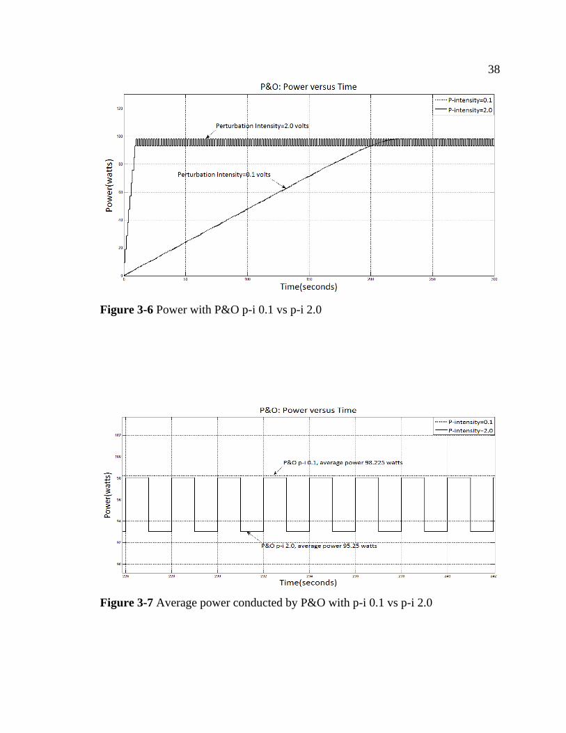
This section discusses the performance of the conventional P&O algorithm.
The conventional P&O algorithm generally exhibits a trade-off between the
tracking velocity and MPPT efficiency. This nature can be seen by simulating
behaviors of the conventional P&O algorithm with two different perturbation
intensities, 0.1 volts and 2.0 volts. In this simulation, the perturbation frequency is
set to 1-Hz. In the following analysis, the term “perturbation intensity” is denoted
by “p-i”. Figure 3-6 illustrates that the P&O algorithm with a larger perturbation
intensity shows a faster tracking velocity, while Figure 3-7 presents that the
algorithm with a weaken perturbation intensity presents a higher MPPT efficiency.
38 38
Figure 3-6 Power with P&O p-i 0.1 vs p-i 2.0
Figure 3-7 Average power conducted by P&O with p-i 0.1 vs p-i 2.0
39 39
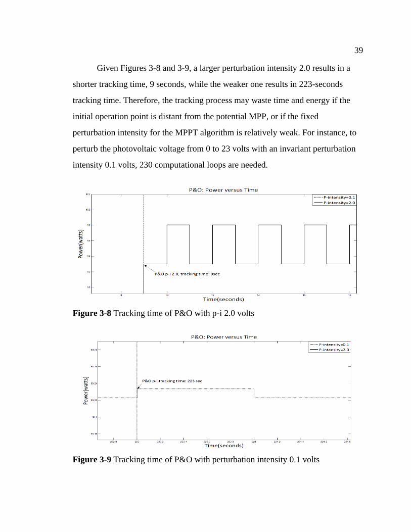
Given Figures 3-8 and 3-9, a larger perturbation intensity 2.0 results in a
shorter tracking time, 9 seconds, while the weaker one results in 223-seconds
tracking time. Therefore, the tracking process may waste time and energy if the
initial operation point is distant from the potential MPP, or if the fixed
perturbation intensity for the MPPT algorithm is relatively weak. For instance, to
perturb the photovoltaic voltage from 0 to 23 volts with an invariant perturbation
intensity 0.1 volts, 230 computational loops are needed.
Figure 3-8 Tracking time of P&O with p-i 2.0 volts
Figure 3-9 Tracking time of P&O with perturbation intensity 0.1 volts
40 40
The MPPT efficiency can be calculated by using equation (3.9) [30].
η𝑀𝑃𝑃𝑇= 𝑎𝑣𝑒𝑟𝑎𝑔𝑒 𝑝𝑜𝑤𝑒𝑟 𝑐𝑜𝑛𝑑𝑢𝑐𝑡𝑒𝑑 𝑏𝑦 𝑎𝑙𝑔𝑜𝑟𝑖𝑡ℎ𝑚
𝑡ℎ𝑒 𝑝𝑜𝑡𝑒𝑛𝑡𝑖𝑎𝑙 𝑀𝑃𝑃 (3.9)
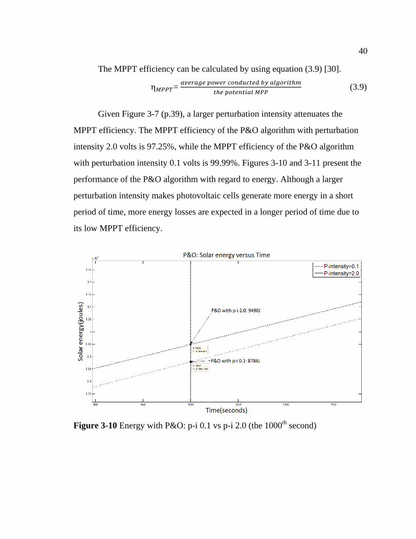
Given Figure 3-7 (p.39), a larger perturbation intensity attenuates the
MPPT efficiency. The MPPT efficiency of the P&O algorithm with perturbation
intensity 2.0 volts is 97.25%, while the MPPT efficiency of the P&O algorithm
with perturbation intensity 0.1 volts is 99.99%. Figures 3-10 and 3-11 present the
performance of the P&O algorithm with regard to energy. Although a larger
perturbation intensity makes photovoltaic cells generate more energy in a short
period of time, more energy losses are expected in a longer period of time due to
its low MPPT efficiency.
Figure 3-10 Energy with P&O: p-i 0.1 vs p-i 2.0 (the 1000th
second)

41 41
Figure 3-11 Energy with P&O: p-i 0.1 vs p-i 2.0 (the 7000th
second)
To accelerate the tracking velocity, a larger perturbation intensity is
required when the operation point is distant to the potential MPP, while to improve
the MPPT efficiency, a weaker one is needed when the operation point is nearby
the MPP. Therefore, the perturbation intensity of an advanced MPPT algorithm
should be adaptive with respect to practical conditions. In fact, the precisely
mathematical expression related to the proposed perturbation intensity and
practical electronic characteristics of photovoltaics may not be easily obtained.
Additionally, given the nonlinear and environment-dependent I-V and P-V curves,
a traditional controller which fulfills a fixed differential equation or single logic
control rule may not be suitable for generating adaptive perturbation intensities.
An ideal controller for the MPPT control should contain multiple control rules. It
is worthy to note that an interesting fact: although the exact mathematical models
of a whole PV system are not available, we may still manually shift the operations
point to the potential maximum power point with very few trials, by trying
different perturbation intensities and by checking the corresponding consequences.
This is because human may approximately predict proper actions with a given

42 42
observation, without knowing the exact model. For instance, note that the MPP
showing in Figure 3-1 (p. 31) is 98.23 watts, we may decrease the perturbation
intensity when the solar panel’s output power exceeds 90 watts, because the
operation point could be “close” to the MPP. On the contrary, we may increase the
perturbation intensity when the operation point is considered as “distant” to the
MPP. Given the change in power, the perturbation intensity may be increased
when it is considered as “small,” or be diminished and vice versa. In the above
processing, the numerical elements such as the perturbation intensity and
photovoltaic power are converted into linguistic variables so that we may easily
make decision by using their logic principles. For example, if the present operation
point is “close” to the MPP, and if the perturbation intensity is “large,” a
reasonable next perturbation is supposed to be “small,” then we make a decision
which is to reduce the perturbation intensity. This is a simple type of Fuzzy Logic
Control which is proceeded in our mind. To improve the performance of the fuzzy
logic control, the advanced Fuzzy Logic Controller is designed in this research. To
make efficient decisions, the proposed Fuzzy Logic Controller not only depends
on the rough considerations such as “large” and “small,” but also considers the
degrees of truth, for example,“50% large,” “90% small,” “40% distant,” “70%
close,” etc.
3.3 Fuzzy Logic Controller (FLC)
Fuzzification, logic judgment and defuzzification are successive three
stages of a FLC [5]. At the stage of fuzzification, the numerical ratio, E (a change
in solar power to a change in solar voltage, ∆P/∆V ) is translated into a linguistic
variable via membership functions, as well as the numerical error, CE, which is
the perturbation intensity, ∆V. E and CE are two input linguistic variables of the

43 43
FLC. The next perturbation intensity, the output variable of the FLC is referring to
the control rules seen in Table 3-2 (p.46). The output membership functions are
used for translating the linguistic output variable, PT to a numerical variable. The
notations of two input variables, E and CE are expressed by equation (3.10) and
(3.11)
E = 𝑃[𝑘]−𝑃[𝑘−1]
𝑉[𝑘]−𝑉[𝑘−1] (3.10)
CE = 𝑉[𝑘] − 𝑉[𝑘 − 1] (3.11)
3.3.1 Fuzzification
Each linguistic variable consists several fuzzy sets [20]. The general
expression of a fuzzy set is given by equation (3.12).
A = (𝑥, 𝜇𝐴(𝑥))|𝑥 ∈ 𝑈 (3.12)
In equation (3.12), 𝜇𝐴(𝑥) is the membership function which represents the
certainty of “x ∈ the fuzzy set A”. 𝑈 is the comprehensive union that contains all
the possible values of x. For example, x varies from -10 to 10, and the set A
denotes the union, (3, 8). Then the point where x equals 6 is belong to the set “A”.
Generally, membership functions are presented graphically. Figure 3-12 illustrates
a sample of membership function, and the mathematical statements are given by
equation (3.13). According to (3.13), the certainty of “x ∈ the fuzzy set A” is 33%.
Figure 3-12 An illustration of the membership function 𝜇𝐴(𝑥)
44 44
𝜇𝐴(𝑥) =
0 𝑖𝑓 𝑥 < 3 1 𝑖𝑓 3 ≤ 𝑥 < 5
𝑥−5
3 𝑖𝑓 5 ≤ 𝑥 ≤ 8
0 𝑖𝑓 𝑥 > 8
(3.13)
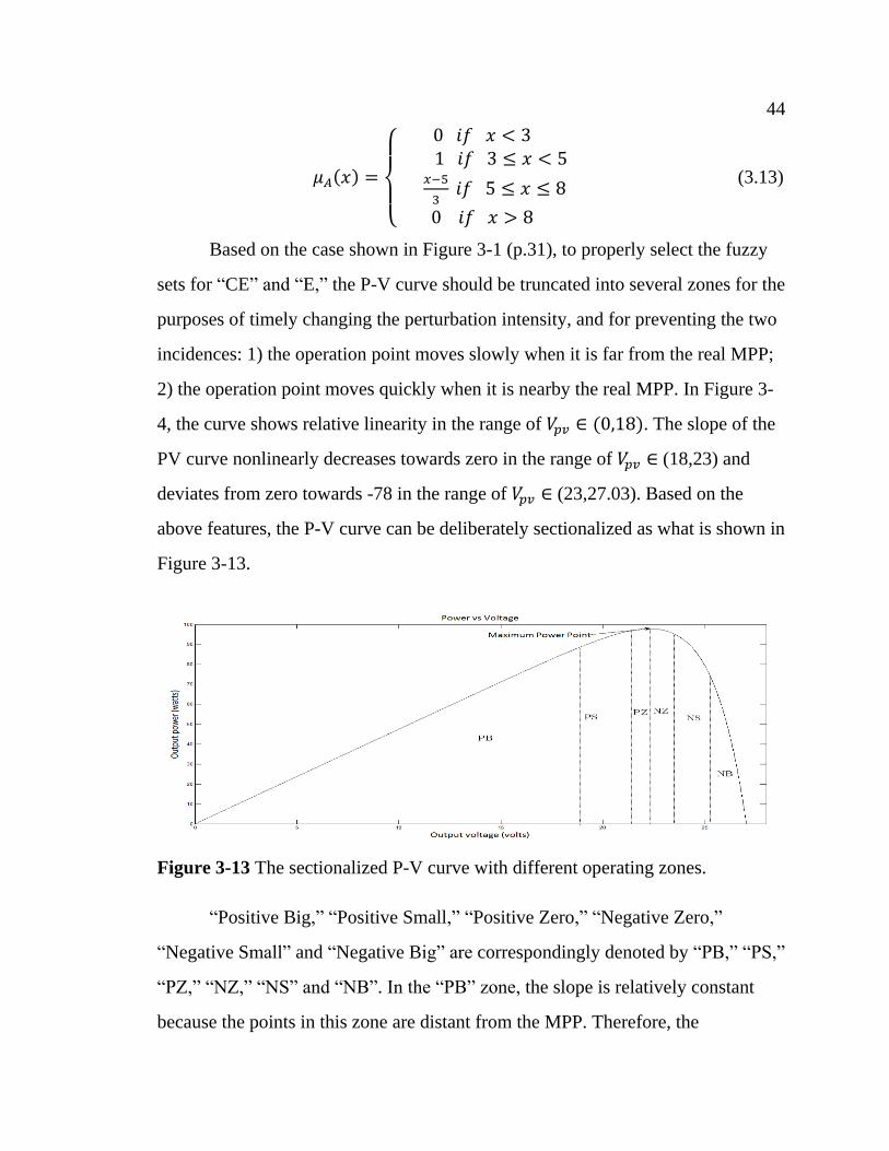
Based on the case shown in Figure 3-1 (p.31), to properly select the fuzzy
sets for “CE” and “E,” the P-V curve should be truncated into several zones for the
purposes of timely changing the perturbation intensity, and for preventing the two
incidences: 1) the operation point moves slowly when it is far from the real MPP;
2) the operation point moves quickly when it is nearby the real MPP. In Figure 3-
4, the curve shows relative linearity in the range of 𝑉𝑝𝑣 ∈ (0,18). The slope of the
PV curve nonlinearly decreases towards zero in the range of 𝑉𝑝𝑣 ∈ (18,23) and
deviates from zero towards -78 in the range of 𝑉𝑝𝑣 ∈ (23,27.03). Based on the
above features, the P-V curve can be deliberately sectionalized as what is shown in
Figure 3-13.
Figure 3-13 The sectionalized P-V curve with different operating zones.
“Positive Big,” “Positive Small,” “Positive Zero,” “Negative Zero,”
“Negative Small” and “Negative Big” are correspondingly denoted by “PB,” “PS,”
“PZ,” “NZ,” “NS” and “NB”. In the “PB” zone, the slope is relatively constant
because the points in this zone are distant from the MPP. Therefore, the

45 45
perturbation intensity is supposed to be enlarged for quickly pushing the operation
point out of this zone. In the “PS” zone, it is obvious that the value of slope
gradually decrease towards zero, but still there is a short distance to the MPP. So,
the perturbation intensity is definitely needed to be diminished but not to be
thoroughly eliminated. If the operation point shifts in the “PZ” and “NZ” zones,
where points within in these zones are “extremely close” to the MPP, the ideal
perturbation intensity is supposed to be very weak for keeping the consequent
oscillation as small as possible. Based on the above considerations, the
membership functions of each fuzzified variable are determined. The Table 3-2
explains the proposed fuzzy sets in greater detail.
Table 3-2 The Numerical Unions Corresponding to the Fuzzy Sets
Fuzzy set CE E PT
NB (-2.0, -0.1) (−∞, -1) (-1.5, -0.5)
NS (-0.1,-0.01) (-1.5,-0.1) (-0.5,-0.01)
NZ (-0.01, 0) (-0.2, 0) (-0.01, 0)
PZ (0, 0.03) (0, 0.5) (0, 0.05)
PS (0.03, 0.3) (0.3, 2.5) (0.05, 1)
PB (0.3, 5.0) (2.5, +∞) (1, 3)
In [5-9], the oscillation around MPP is commonly treated as an undesirable
byproduct of a MPPT algorithm, because the oscillation obviously degrades the
MPPT efficiency. However, without such an oscillation the algorithm cannot
detect the changes of P-V curves due to the changes in environmental conditions.
In this thesis, the objective is to keep operation point oscillating around the MPP
with an extremely small deviation once the operation point goes into the “PZ” and
“NZ” zones. Figures 3-14, 3-15, and 3-16 illustrate the graphical membership
functions, E,CE and PT, respectively.

46 46
Figure 3-14 The membership function E
Figure 3-15 The membership function CE
Figure 3-16 The membership function PT

47 47
3.3.2 Fuzzy Rule Base
A fuzzy logic controller determines its fuzzified output variable by looking
up its fuzzy rule base, which consists of a set of fuzzy IF-THEN rules. The general
format of a fuzzy logic rule is that [20]:
Rule#: IF 𝑥1is 𝐴1and 𝑥2is 𝐴2 and… and 𝑥𝑛is 𝐴𝑛, THEN y is 𝐵𝑗
Where 𝐴𝑖 and 𝐵𝑗 are fuzzy sets in 𝑈𝑖 and V, respectively, and 𝑈𝑖 consists of
any possible value for the input variable, 𝑥𝑖. And the V is the union consisting of
any possible value for the numerical output. The proposed FLC has two input
linguistic variables, E and CE, and one output linguistic variable PT. Therefore,
for example, the rules can be written as:
Rule#: IF CE is “PB” and E is “PB” then PT is “PZ”
When the FLC detects the incoming input pair CE,E, it will apply all
rules for recording any possible logic outputs. This is the outstanding
characteristic of the FLC, compared to other binary logic controller. In the sense
of statistics, multiple logic consequences will improve the accuracy of final
weighted results which are expectation-type solutions. Table 3-3 is the rule base of
the proposed FLC. The output surface of the FLC is illustrated by Figure 3-17,
which is derived from Table 3-3.
Table 3-3 Rules for the Proposed FLC
CE E NB NS NZ PZ PS PB
NB NZ NZ NZ PZ PZ PZ
NS NZ NZ NZ PZ PZ PZ
NZ NB NS NZ PZ PZ PZ
PZ NZ NZ NZ PZ PS PB
PS NZ NZ NZ PZ PZ PZ
PB NZ NZ NZ PZ PZ PZ

48 48
Figure 3-17 The output surface of the proposed FLC
Throughout trials and calibrations, some difficulty has been observed in
Figure 3-18. Occasionally, the operation point may go beyond the maximum
power point, and the value of “E” is still classified into the fuzzy set “PS”. As the
slope shown in Figure 3-18, the undesired logic judgment will happen if the logic
operation follows such a rule as “IF E is PB and CE is PS THEN the PT is PS”. In
this case, such rule can perfectly accelerate the tracking velocity when the
operation point is distant from the MPP. Although the previous operation point has
already been close to the MPP, according to the rule, the operation point will be
forced to keep moving towards a wrong direction, and deviating from the MPP. To
avoid this undesirable situation, as seen in Table 3-3, a self-correction mechanism
is added into our FLC. The strategy is to check the present slope with a smallest
scale perturbation if a large scale shifting of the operation point happened. If the
sign change of “E” is detected by FLC, the direction of perturbation will be
inversed immediately. Moreover, the wrong perturbation direction will be detected
timely.
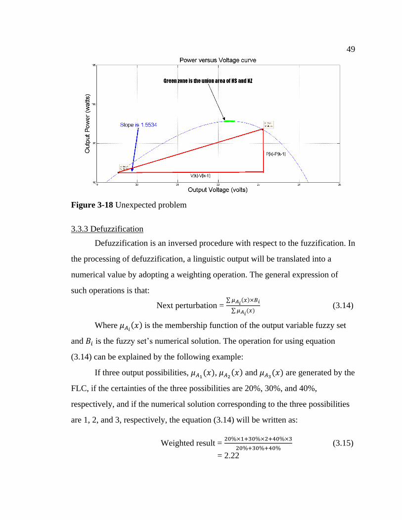
49 49
Figure 3-18 Unexpected problem
3.3.3 Defuzzification
Defuzzification is an inversed procedure with respect to the fuzzification. In
the processing of defuzzification, a linguistic output will be translated into a
numerical value by adopting a weighting operation. The general expression of
such operations is that:
Next perturbation = ∑𝜇𝐴𝑖
(𝑥)×𝐵𝑖
∑𝜇𝐴𝑖(𝑥) (3.14)
Where 𝜇𝐴𝑖(𝑥) is the membership function of the output variable fuzzy set
and 𝐵𝑖 is the fuzzy set’s numerical solution. The operation for using equation
(3.14) can be explained by the following example:
If three output possibilities, 𝜇𝐴1(𝑥), 𝜇𝐴2(𝑥) and 𝜇𝐴3(𝑥) are generated by the
FLC, if the certainties of the three possibilities are 20%, 30%, and 40%,
respectively, and if the numerical solution corresponding to the three possibilities
are 1, 2, and 3, respectively, the equation (3.14) will be written as:
Weighted result = 20%×1+30%×2+40%×3
20%+30%+40% (3.15)
= 2.22
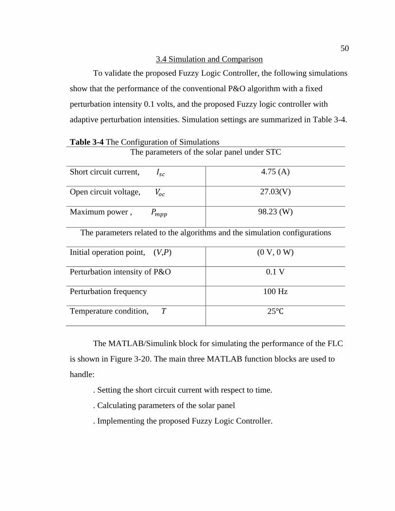
50 50
3.4 Simulation and Comparison
To validate the proposed Fuzzy Logic Controller, the following simulations
show that the performance of the conventional P&O algorithm with a fixed
perturbation intensity 0.1 volts, and the proposed Fuzzy logic controller with
adaptive perturbation intensities. Simulation settings are summarized in Table 3-4.
Table 3-4 The Configuration of Simulations
The parameters of the solar panel under STC
Short circuit current, 𝐼𝑠𝑐 4.75 (A)
Open circuit voltage, 𝑉𝑜𝑐 27.03(V)
Maximum power , 𝑃𝑚𝑝𝑝 98.23 (W)
The parameters related to the algorithms and the simulation configurations
Initial operation point, (V,P) (0 V, 0 W)
Perturbation intensity of P&O 0.1 V
Perturbation frequency 100 Hz
Temperature condition, T 25
The MATLAB/Simulink block for simulating the performance of the FLC
is shown in Figure 3-20. The main three MATLAB function blocks are used to
handle:
. Setting the short circuit current with respect to time.
. Calculating parameters of the solar panel
. Implementing the proposed Fuzzy Logic Controller.

51 51
Figure 3-20 The Simulink block diagram of the Fuzzy Logic Controller
Given the specified membership functions shown in Figures 3-14, 3-15, and
3-16 (p.47), the proposed Fuzzy Logic Controller cannot be implemented via the
Fuzzy Logic Toolbox, which is provided by MATLAB, due to the numerical
unions are extremely close to zero. Therefore, the proposed FLC is realized by
MATLAB/function blocks. For testing the robustness of above MPPT algorithms,
irradiation variations is coded into the simulation. Irradiation variations are
represented by the changing in PV short-circuit current. The time dependent short
circuit current is shown in Figure 3-21.
Figure 3-21 The variable short circuit current of the simulated solar panel.
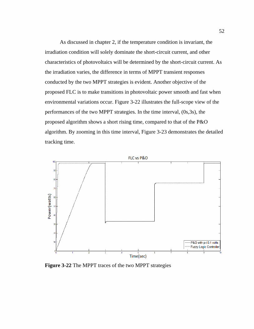
52 52
As discussed in chapter 2, if the temperature condition is invariant, the
irradiation condition will solely dominate the short-circuit current, and other
characteristics of photovoltaics will be determined by the short-circuit current. As
the irradiation varies, the difference in terms of MPPT transient responses
conducted by the two MPPT strategies is evident. Another objective of the
proposed FLC is to make transitions in photovoltaic power smooth and fast when
environmental variations occur. Figure 3-22 illustrates the full-scope view of the
performances of the two MPPT strategies. In the time interval, (0s,3s), the
proposed algorithm shows a short rising time, compared to that of the P&O
algorithm. By zooming in this time interval, Figure 3-23 demonstrates the detailed
tracking time.
Figure 3-22 The MPPT traces of the two MPPT strategies
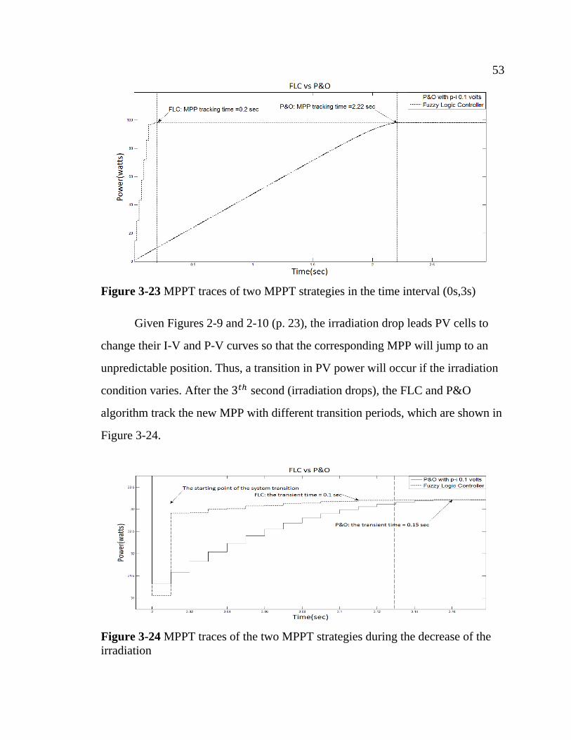
53 53
Figure 3-23 MPPT traces of two MPPT strategies in the time interval (0s,3s)
Given Figures 2-9 and 2-10 (p. 23), the irradiation drop leads PV cells to
change their I-V and P-V curves so that the corresponding MPP will jump to an
unpredictable position. Thus, a transition in PV power will occur if the irradiation
condition varies. After the 3𝑡ℎ second (irradiation drops), the FLC and P&O
algorithm track the new MPP with different transition periods, which are shown in
Figure 3-24.
Figure 3-24 MPPT traces of the two MPPT strategies during the decrease of the
irradiation

54 54
After the FLC detects a large-scale reduction in power due to the rapidly
decreasing irradiation condition, the rule “IF CE is NZ and E is NB, then the PT is
NB” is activated. The decisions of the FLC in the time interval (3.0s, 3.16s) are
shown in Figure 3-25.
Figure 3-25 The decisions of FLC in the transition period (3.0s, 3.16s)
As illustrated in Figure 3-26, after the irradiation increases at the 6th
second,
for tracking the new MPP, the FLC spends 0.08 seconds, while the P&O algorithm
uses 0.13 seconds. Given the above patterns, compared to the performance of the
P&O algorithm with the perturbation intensity of 0.1 volts, the proposed FLC
shows the better performance during the transitions.
In this chapter, the origination of the conventional MPPT algorithm and the
methodology for designing a proper FLC were discussed. The advantages of the
proposed algorithm were validated by the simulation results. Given the practical
requirements, the parameters of the proposed FLC should be tuned. In chapter 4,
the plant of a photovoltaic system, the boost DC-DC converter is discussed.
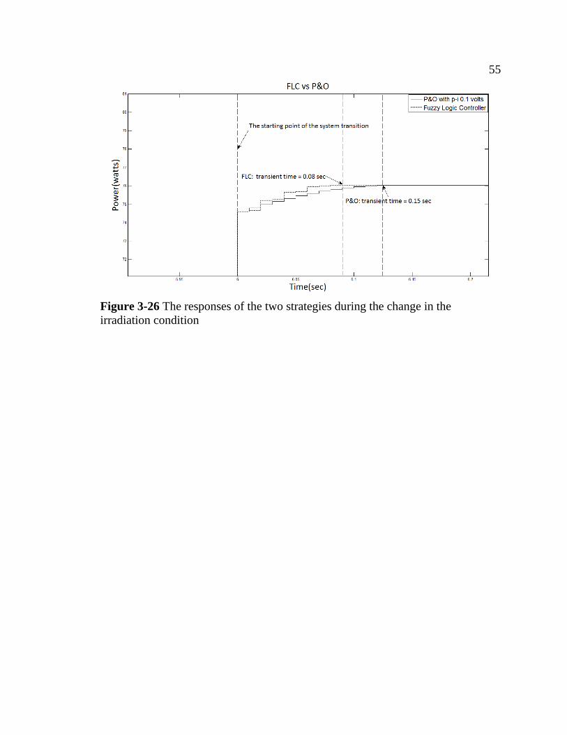
55 55
Figure 3-26 The responses of the two strategies during the change in the
irradiation condition

4 BOOST DC-DC CONVERTER
A DC-DC converter is an essential element in a stand-alone PV tracking
system. Note that the voltage level of PV cells is variable due to the location of the
operation point so that directly supplying the DC photovoltaic power to the
electric load may be inappropriate. In a MPPT system, a DC-DC converter is used
to convert an irregular input power into a regulated one with a desired voltage
level. Switch-mode DC-DC converters are currently popular for their advantages
in terms of small volume-size and high controllability. In a switch-mode DC-DC
converter, the MOSFET/IGBT and inductor performs as a transformer with a
programmable factor. To rebuild the factor between input DC voltage level and
output DC-Link, one only needs to change the duty ratio of the switching signal.
Associating with a digital signal processor, a switch-mode converter can provide
numerous functions. In the first section of this chapter, the basic topology of a
typical boost DC-DC converter is addressed. In section 4.2, the small-signal-
model of the output terminal of a typical DC-DC boost converter, which supplies a
resistive load, is briefly reviewed. The theoretical analysis of the voltage
regulation for photovoltaics and the small signal model related to the input
terminal of a boost converter is presented in section 4.3 in greater detail.
4.1 Topology of the Typical Boost DC-DC Converter
The function of a boost DC-DC converter is used to step-up the voltage
level of the input DC power. As shown in Figure 4-1, a typical boost DC-DC
converter consists of a switching device, an inductor, an input capacitor, a diode,
an output capacitor, and an electric load.
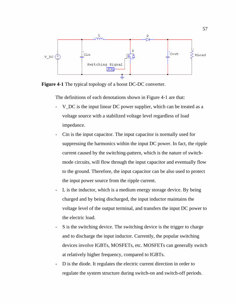
57 57
Figure 4-1 The typical topology of a boost DC-DC converter.
The definitions of each denotations shown in Figure 4-1 are that:
- V_DC is the input linear DC power supplier, which can be treated as a
voltage source with a stabilized voltage level regardless of load
impedance.
- Cin is the input capacitor. The input capacitor is normally used for
suppressing the harmonics within the input DC power. In fact, the ripple
current caused by the switching-pattern, which is the nature of switch-
mode circuits, will flow through the input capacitor and eventually flow
to the ground. Therefore, the input capacitor can be also used to protect
the input power source from the ripple current.
- L is the inductor, which is a medium energy storage device. By being
charged and by being discharged, the input inductor maintains the
voltage level of the output terminal, and transfers the input DC power to
the electric load.
- S is the switching device. The switching device is the trigger to charge
and to discharge the input inductor. Currently, the popular switching
devices involve IGBTs, MOSFETs, etc. MOSFETs can generally switch
at relatively higher frequency, compared to IGBTs.
- D is the diode. It regulates the electric current direction in order to
regulate the system structure during switch-on and switch-off periods.

58 58
- Rload is the electric load. The electric load can be resistive and
capacitive. In this section, the electric load is presumed as a resistor. To
supply a resistive load, a boost DC-DC converter is typically controlled
by a feedback loop for regulating the output voltage level.
4.1.1 Switching States
Given the binary switching states, a typical boost converter shows two
structures in each switching period. As shown in Figure 4-2, the input DC source
charges the inductor when the switch is turned on. As shown in Figure 4-3, in a
switching-on period, the inductor current linearly increases. The electric energy
temporarily accumulates in the inductor. On the contrary, as shown in Figures 4-4
and 4-5, in switching-off periods, the inductor serves as the secondary power
source to supply the load, and compensates the voltage drop between the 𝑉𝑖𝑛 and
𝑉𝑜𝑢𝑡.
Figure 4-2 The equivalent circuit during switching on periods
Figure 4-3 Inductor current and voltage during switching on periods
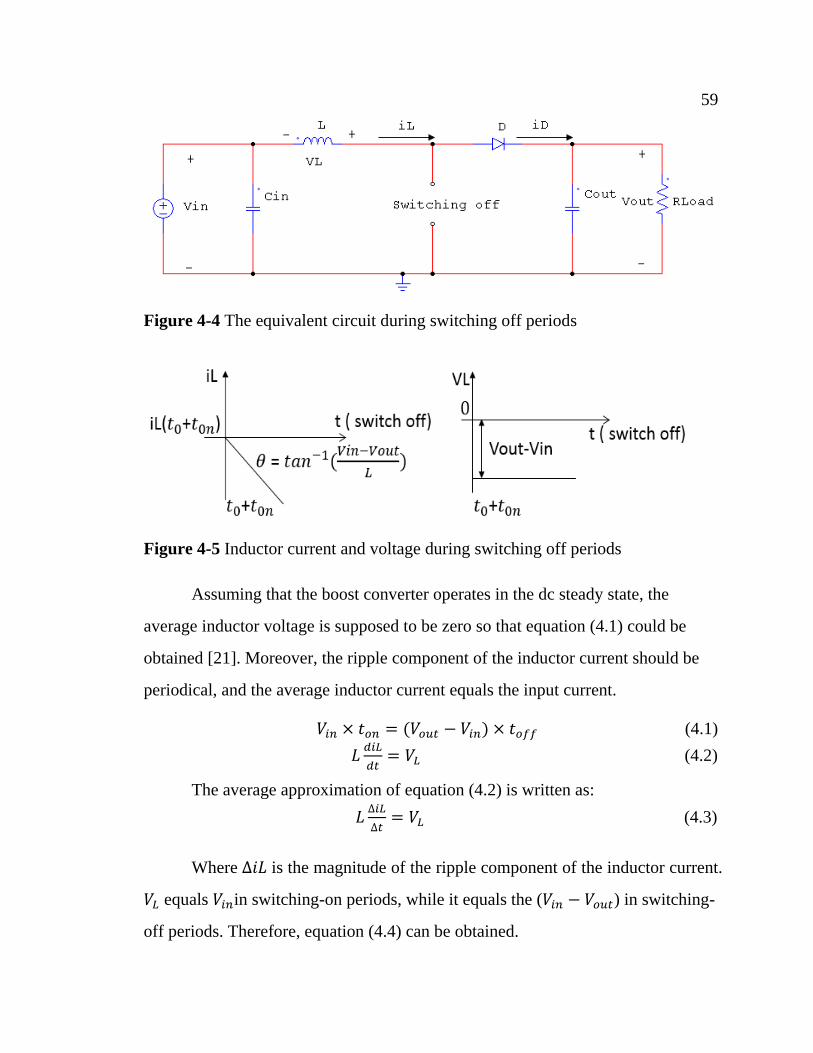
59 59
Figure 4-4 The equivalent circuit during switching off periods
Figure 4-5 Inductor current and voltage during switching off periods
Assuming that the boost converter operates in the dc steady state, the
average inductor voltage is supposed to be zero so that equation (4.1) could be
obtained [21]. Moreover, the ripple component of the inductor current should be
periodical, and the average inductor current equals the input current.
𝑉𝑖𝑛 × 𝑡𝑜𝑛 = (𝑉𝑜𝑢𝑡 − 𝑉𝑖𝑛) × 𝑡𝑜𝑓𝑓 (4.1)
𝐿𝑑𝑖𝐿
𝑑𝑡= 𝑉𝐿 (4.2)
The average approximation of equation (4.2) is written as:
𝐿∆𝑖𝐿
∆𝑡= 𝑉𝐿 (4.3)
Where ∆𝑖𝐿 is the magnitude of the ripple component of the inductor current.
𝑉𝐿 equals 𝑉𝑖𝑛in switching-on periods, while it equals the (𝑉𝑖𝑛 − 𝑉𝑜𝑢𝑡) in switching-
off periods. Therefore, equation (4.4) can be obtained.
60 60
∆𝑖𝐿 = 1
𝐿𝑉𝑖𝑛 × 𝑡𝑜𝑛 =
1
𝐿(𝑉𝑜𝑢𝑡 − 𝑉𝑖𝑛) × 𝑡𝑜𝑓𝑓 (4.4)
Assuming that the boost DC-DC converter operates in Continuous
Conduction Mode (CCM), which means that inductor current is continuous in
every switching period. By introducing the concept of duty ratio, substituting
equations (4.5) and (4.6) into (4.4), the mathematical expression related to the
input voltage and output voltage of a typical boost DC-DC converter is written as
equation (4.7) [21].
𝑡𝑠 = 𝑡𝑜𝑛 + 𝑡𝑜𝑓𝑓 (4.5)
𝑡𝑠 = 𝑑𝑡𝑠 + (1 − 𝑑)𝑡𝑠 (4.6)
𝑉𝑜𝑢𝑡
𝑉𝑖𝑛=
1
1−𝑑 (4.7)
4.1.2 Discontinuous Conduction Mode (DCM)
System dynamics of a boost DC-DC converter can be predicted by using
the above expressions if the converter operates in Continuous Conduction Mode
(CCM). In CCM, the inductor current never falls to zero in any switching period
and there exists no such time intervals where the inductor voltage stays on zero
volts. If the maximum input current of a boost converter is less than the amplitude
of the calculated ripple current, which is derived via equation (4.4), then the boost
DC-DC converter definitely operates in DCM. 𝑉𝑜𝑢𝑡 of a boost DC-DC converter
operating in DCM can be calculated by using equations (4.7) and (4.8) [21]:
𝑉𝑜𝑢𝑡 =𝑉𝑖𝑛
2(1+√1 + 4𝑀) (4.7)
M = (𝑅
2𝐿𝑓𝑠)D2 (4.8)
Where
R is the load impedance of the boost DC-DC converter.
𝑓𝑠 is the switching frequency.
D is the duty ratio of the switching signal.
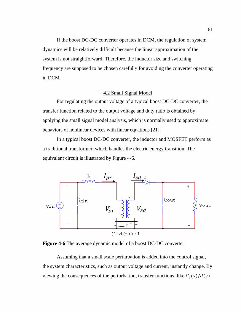
61 61
If the boost DC-DC converter operates in DCM, the regulation of system
dynamics will be relatively difficult because the linear approximation of the
system is not straightforward. Therefore, the inductor size and switching
frequency are supposed to be chosen carefully for avoiding the converter operating
in DCM.
4.2 Small Signal Model
For regulating the output voltage of a typical boost DC-DC converter, the
transfer function related to the output voltage and duty ratio is obtained by
applying the small signal model analysis, which is normally used to approximate
behaviors of nonlinear devices with linear equations [21].
In a typical boost DC-DC converter, the inductor and MOSFET perform as
a traditional transformer, which handles the electric energy transition. The
equivalent circuit is illustrated by Figure 4-6.
Figure 4-6 The average dynamic model of a boost DC-DC converter
Assuming that a small scale perturbation is added into the control signal,
the system characteristics, such as output voltage and current, instantly change. By
viewing the consequences of the perturbation, transfer functions, like 𝐺𝑣(𝑠)/𝑑(𝑠)

62 62
and 𝐺𝑣(𝑠)/𝐺𝑖(𝑠) can be derived. In this thesis, the related control design only
requires the knowledge of 𝐺𝑣(𝑠)/𝑑(𝑠).
4.2.1 Output Terminal Small Signal Modelling
Assume that: an ideal boost DC-DC converter shown in Figure 4-6 operates
in CCM; the efficiency of the power conversion is 100%; the electric load is
resistive; a small scale perturbation, , in swiching signal has been injected to the
boost circuit. Then, equation (4.8) and (4.9) can be satisfied.
𝐼𝑜𝑢𝑡 =𝑉𝑜𝑢𝑡
𝑅 (4.8)
𝑉𝑖𝑛 × 𝐼𝑖𝑛 = 𝑉𝑜𝑢𝑡 × 𝐼𝑜𝑢𝑡 (4.9)
By ignoring the current through the input capacitor, the average inductor
current is assumed to equal the input current.
𝐼𝐿 = 𝐼𝑖𝑛 = 𝑉𝑜𝑢𝑡×𝐼𝑜𝑢𝑡
𝑉𝑖𝑛=
𝑉𝑜𝑢𝑡2
𝑉𝑖𝑛×𝑅 (4.10)
By applying the Norton’s theorem, the procedure of simplifying the
equivalent circuit of the small signal model is illustrated by Figure 4-7, by Figure
4-8, and by Figure 4-9 [21].
Figure 4-7 The equivalent circuit of small signal model (a) [21]
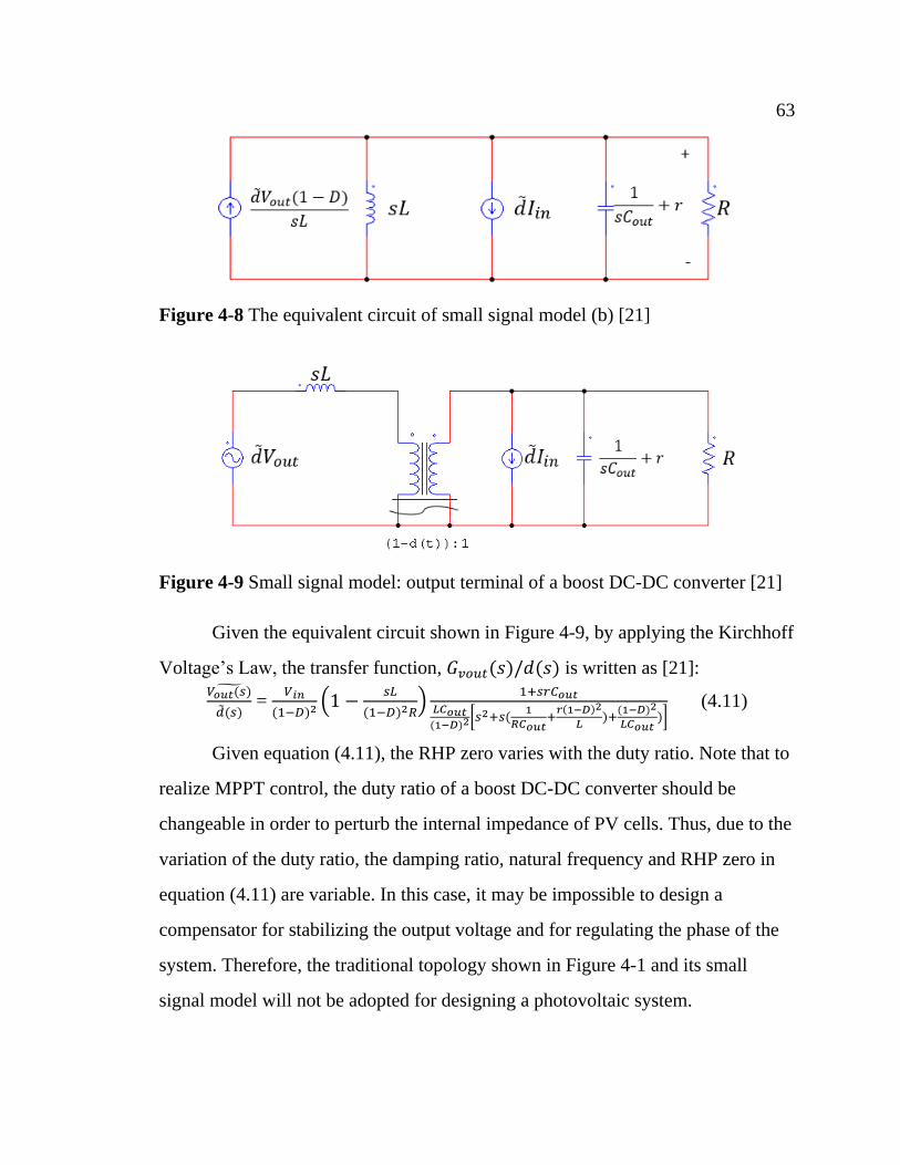
63 63
Figure 4-8 The equivalent circuit of small signal model (b) [21]
Figure 4-9 Small signal model: output terminal of a boost DC-DC converter [21]
Given the equivalent circuit shown in Figure 4-9, by applying the Kirchhoff
Voltage’s Law, the transfer function, 𝐺𝑣𝑜𝑢𝑡(𝑠)/𝑑(𝑠) is written as [21]:
𝑉𝑜𝑢𝑡(𝑠)
(𝑠) =
𝑉𝑖𝑛
(1−𝐷)2(1 −
𝑠𝐿
(1−𝐷)2𝑅)
1+𝑠𝑟𝐶𝑜𝑢𝑡𝐿𝐶𝑜𝑢𝑡(1−𝐷)2
[𝑠2+𝑠(1
𝑅𝐶𝑜𝑢𝑡+𝑟(1−𝐷)2
𝐿)+
(1−𝐷)2
𝐿𝐶𝑜𝑢𝑡)]
(4.11)
Given equation (4.11), the RHP zero varies with the duty ratio. Note that to
realize MPPT control, the duty ratio of a boost DC-DC converter should be
changeable in order to perturb the internal impedance of PV cells. Thus, due to the
variation of the duty ratio, the damping ratio, natural frequency and RHP zero in
equation (4.11) are variable. In this case, it may be impossible to design a
compensator for stabilizing the output voltage and for regulating the phase of the
system. Therefore, the traditional topology shown in Figure 4-1 and its small
signal model will not be adopted for designing a photovoltaic system.
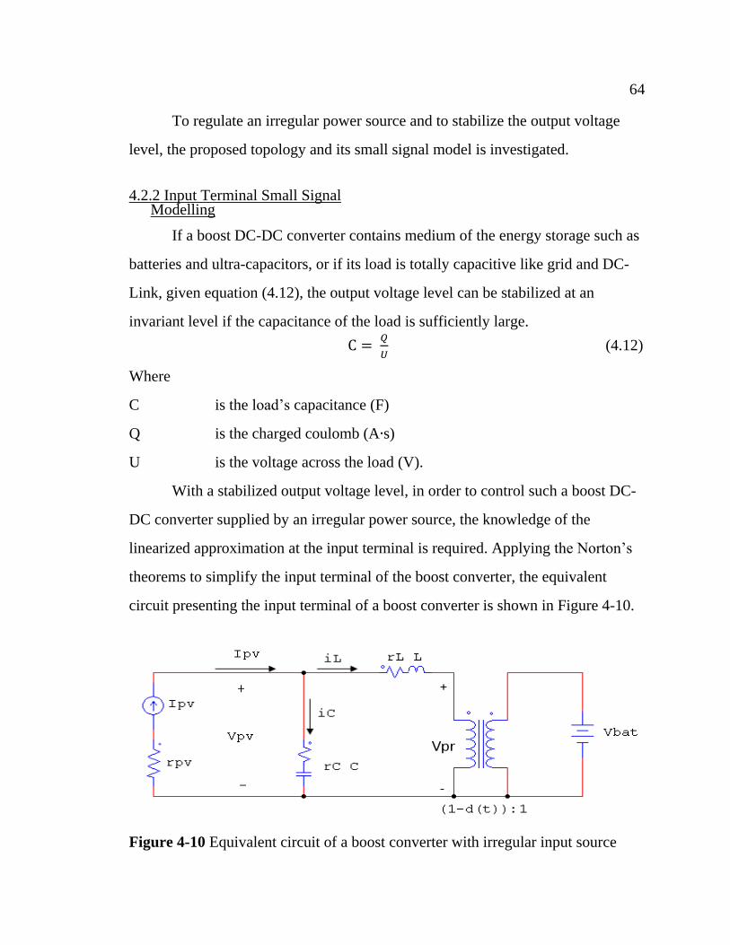
64 64
To regulate an irregular power source and to stabilize the output voltage
level, the proposed topology and its small signal model is investigated.
4.2.2 Input Terminal Small Signal Modelling
If a boost DC-DC converter contains medium of the energy storage such as
batteries and ultra-capacitors, or if its load is totally capacitive like grid and DC-
Link, given equation (4.12), the output voltage level can be stabilized at an
invariant level if the capacitance of the load is sufficiently large.
C = 𝑄
𝑈 (4.12)
Where
C is the load’s capacitance (F)
Q is the charged coulomb (A∙s)
U is the voltage across the load (V).
With a stabilized output voltage level, in order to control such a boost DC-
DC converter supplied by an irregular power source, the knowledge of the
linearized approximation at the input terminal is required. Applying the Norton’s
theorems to simplify the input terminal of the boost converter, the equivalent
circuit presenting the input terminal of a boost converter is shown in Figure 4-10.
Figure 4-10 Equivalent circuit of a boost converter with irregular input source

65 65
The 𝐼𝑝𝑣, 𝑉𝑝𝑣, and 𝑟𝑝𝑣 denote the photovoltaic current, photovoltaic voltage,
and internal resistance, respectively. 𝑖𝐿 and 𝑖𝐶denote the inductor current and
capacitor current, respectively. 𝑟𝐶 and 𝑟𝐿 present parasitic resistance for the input
capacitor and the input inductor. The 𝑉𝑝𝑟is the equivalent voltage on the primary
side of the transformer.
A perturbation, , in the control signal instantly results in a voltage
drop/increase on the primary side of the transformer shown in Figure 4-10. The
voltage variation caused by the duty ratio perturbation is that:
𝑉𝑝𝑟 = × 𝑉𝑏𝑎𝑡 (4.13)
Based on the equivalent circuit shown in Figure 4-10, the linearized state
space equations are derived by considering the parasitic resistance of the input
capacitor and input inductor.
𝑑
𝑑𝑡⌈ 𝐼𝑉𝑝⌉ = ⌈
−𝑅𝐿𝐿
−𝑅𝑝𝑣(1−𝑅𝐿𝑅𝑐)
𝐿𝐶(1−𝑅𝑝𝑣)
1
𝐿
𝐶𝑅𝐿𝑅𝑐−1
𝐿𝐶(1−𝑅𝑝𝑣)
⌉ ⌈ 𝐼𝑉𝑝⌉ + ⌈
−𝑉𝑏𝑎𝑡𝐿
𝑅𝑐𝑅𝑝𝑣𝑉𝑏𝑎𝑡𝐿𝐶(1−𝑅𝑝𝑣)
⌉ (4.14)
= [0 1] ⌈𝐼𝑉𝑝⌉ (4.15)
𝐺𝑣𝑑(𝑠) = 𝐴
𝑠2+𝑁𝑠+𝑀 (4.16)
𝐴 = −𝑉𝑏𝑎𝑡(1
𝐿2+
𝑅𝑐2𝑅𝑝𝑣
2−𝑅𝑐𝑅𝑝𝑣
𝐿2𝐶(1−𝑅𝑝𝑣)2 −
𝑅𝑐𝑅𝑝𝑣
𝐿(1−𝑅𝑝𝑣)𝑠) (4.17)
𝑁= (𝑅𝐿
𝐿−
𝑅𝑐𝑅𝑝𝑣−1
𝐿𝐶(1−𝑅𝑝𝑣)) (4.18)
𝑀= 𝑅𝐿𝑅𝑐𝑅𝑝𝑣−𝑅𝐿+𝑅𝑝𝑣𝐿−𝐶𝑅𝐿
2𝑅𝑐𝑅𝑝𝑣
𝐿2𝐶(1−𝑅𝑝𝑣) (4.19)
The purpose of analyzing the linear approximation is to design a voltage
controller in order to regulate the photovoltaic voltage level. The topology of the
voltage regulation is illustrated by Figure 1-4 (p. 6). Notice that the parameters of

66 66
such a nonlinear system shown in Figure 4-10 change with 𝑅𝑝𝑣, which is the
internal resistance of photovoltaics. Therefore, the presented linear approximation
is only a basic reference for the controller design. The final parameters and
structure of the voltage controller must be tuned by referring to the related
experimental results. The parameters of the system are shown in Table 4-1. The
range of the internal resistance of the adopted solar panel is concluded by the
experimental tests.
Table 4-1 Parameters of the Designed PV System
Components Parameters
𝑉𝑏𝑎𝑡 26(V)
𝑅𝐶𝑖𝑛 0.8(Ω)
𝑅𝐿 0.2(Ω)
L 12(mH)
C 210(uF)
𝑅𝑝𝑣 75~150(Ω)
The only variable parameter in the linear approximation is 𝑅𝑝𝑣 .Therefore,
to analyze the system’s behavior with respect to 𝑅𝑝𝑣, four transfer functions with
four different 𝑅𝑝𝑣 are presented. Four values for 𝑅𝑝𝑣, are 75 Ω,100 Ω,125 Ω and
150 Ω, respectively. The bode plot of four transfer functions are shown in Figure
4-11.
Table 4-2 shows the linear approximations with different values of 𝑅𝑝𝑣.
Given Table 4-2 and Figure 4-9 (p. 64), the variable 𝑅𝑝𝑣 does not heavily
affect the system behaviors. The system shows the over-damped characteristic and
its phase never goes below -90 degree at low frequency. Additionally, due to the
locations of poles and zeros, the system behaves as a first order system. Therefore,
in this case, a PI controller is applicable for compensating the system.

67 67
Figure 4-11 Bode plot of the variable-parameters system
Table 4-2 Linear Approximations with Different values of 𝑅𝑝𝑣
𝑅𝑝𝑣 Linear approximation Damping
ratio
Natural
frequency
75 (Ω) 5.56𝑒8(1 +
𝑠3.165𝑒5
)
3.8𝑠2 + 1.202𝑒6𝑠 + 2.156𝑒5 3.4062 238.19(rad/s)
100 (Ω) 5.546𝑒8(1 +
𝑠3.1676𝑒5
)
3.8𝑠2 + 1.203𝑒6𝑠 + 2.157𝑒5 3.4082 238.25(rad/s)
125 (Ω) 5.5386𝑒8(1 +
𝑠3.1692𝑒5
)
3.8𝑠2 + 1.204𝑒6𝑠 + 2.158𝑒5 3.4103 238.31(rad/s)
150 (Ω) 5.532𝑒8(1 +
𝑠3.1703𝑒5
)
3.8𝑠2 + 1.204𝑒6𝑠 + 2.159𝑒5 3.4095 238.36(rad/s)
Where 𝑒5, 𝑒6 and 𝑒8 denote 105, 106 and 108, respectively.

68 68
4.2.3 Voltage Regulation
𝐺𝑐(𝑠) = 𝐾𝑝 + 𝐾𝑖1
𝑠 (4.20)
The general equation of a PI controller is given by equation (4.20). To
obtain the desired step response of the closed-loop system, tuning parameters can
refer to bode plots of compensated systems. The fundamental tuning principles are
shown in the Table 4-3[22]. The controller design does not involve the derivative
operation. This is because the switching devices inevitably inject plenty of noise to
the voltage and current signals. Additionally, the derivative operation may boost
noise level and affect the performance of the controller.
Table 4-3 Effects of Independently Increasing a Parameter in a PI Controller [22]
Parameter Rise Time Overshoot Settling
time
Steady-state
error Stability
𝐾𝑝 Decrease Increase Small
change Decrease Degrade
𝐾𝑖 Decrease Increase Increase Eliminate Degrade
By observing the step responses of the closed-loop compensated systems,
the proportional gain and the integral gain are selected as 0.1 and 2.2, respectively.
The continuous-time transfer function of the PI controller is that:
𝐺𝑐(𝑠) = 0.1 +2.2
𝑠 (4.21)
The purpose of tuning the PI controller is to thoroughly eliminate the
potential overshoot of the closed-loop compensated system in order to protect the
input power source. In Table 4-4, 𝐺75, 𝐺100, 𝐺125and 𝐺150 denotes the closed-loop
compensated systems with the corresponding values for 𝑅𝑝𝑣. The simulated step
responses of the system operating at different operating points are given by Figure
4-12. Under different operating points, the rising time of the step response of the
closed-loop compensated system is about 60ms. And the system is left with a bit
damping characteristic. The MATLAB code for simulating the system dynamics
can be found in Appendix A.
69 69
Table 4-4 Step Response of the Closed-Loop Compensated System
Models Rise time Settling Time Overshoot
𝐺75 40.8(ms) 61.6 (ms) 0%
𝐺100 40.9(ms) 61.7 (ms) 0%
𝐺125 41.0(ms) 61.8 (ms) 0%
𝐺150 41.0(ms) 61.9 (ms) 0%
Figure 4-12 Step response of the closed-loop compensated system.
In this section, the system behaviors are discussed with numerical
parameters. The internal resistance of the adopted solar panel, does not heavily
affect the damping ratio and natural frequency of the linear approximation so that
the original system behaves as a linear invariant system. In fact, behaviors of
photovoltaic power converters, highly depend on 𝑅𝑝𝑣, 𝑅𝑐𝑖𝑛, and 𝑅𝐿. Hence, given
different internal resistance of PV cells, the switching-mode converter may
become a slightly damped system, which is a difficult control problem. In such
case, the controller design will be challenged in terms of balancing the phase
margin and stability of the compensated system operating at different operating
points. In the next chapter, the hardware and software fulfillment of the proposed
MPPT system will be discussed.

5 PROTOTYPE IMPLEMENTATION
The photovoltaic MPPT system is designed to implement the proposed
algorithm. The system consists of a power electronic system and a signal process
system. The power electronic system is controlled by the signal process system via
a Pulse-Width-Modulation signal. The core element of the power electronic
system is a boost DC-DC converter which deals with energy transmission and
perturbing the PV operation point. A functioning switching-mode converter
generates plenty of noise and ringing, which can be harmful for system control and
system stability. Hence, the practical solutions for the noise and ringing
suppression are presented in this chapter.
The signal process system, which possesses two control layers, is
embedded into a microcontroller, TI F28035. In the top control layer, the proposed
FLC continuously sets new photovoltaic voltage references and send them to the
secondary control layer. Additionally, the top control layer is enhanced by a DCM
detection mechanism to guarantee that the MPPT system always operates in a
controllable region. The proposed PI controller dominates the secondary control
layer. As mentioned in chapter 4, the PI controller continuously perturbs the duty
ratio of the PWM signal to change the system dynamics until the photovoltaic
voltage converges to its reference. To obtain a reasonable internal cooperation, the
two control layers operate with different control intervals, according to the settling
time of the voltage regulation loop and voltage/current measurement loop. In the
first section of this chapter, the main parameters of the photovoltaic boost
converter are explained. In section 5.2, peripheral circuits are introduced. In
section 5.3, the detail of the signal process system is addressed. The practical
71 71
power tracking performance of two MPPT control strategies is provided in the last
section.
5.1 Parameters of the Boost DC-DC Circuit
In this section, how to decide parameters of the boost DC-DC converter is
discussed. The proposed topology of the PV boost DC-DC converter is illustrated
by Figure 5-1. The parameters of the circuit components are listed in Table 5-1.
Figure 5-1 The proposed topology of the PV boost DC-DC circuit
Table 5-1. Parameters of Components of the Boost Circuit
Components Parameters
Solar Panel Boulder 15W
𝐶𝑖𝑛 35V/210uF
𝑅𝐶𝑖𝑛 0.8 Ω
L 12 mH
𝑅𝐿 0.2 Ω
𝐶𝑜𝑢𝑡 100V/1000uF
𝑀𝑂𝑆𝐹𝐸𝑇 IRFP460A
𝐷𝑖𝑜𝑑𝑒 HFA50PA60C
DC bus 26 V
For safety, the solar panel, Boulder 15W is adopted as the input power
source of the MPPT system. The light source for simulating the sun light is two

72 72
250W generic electrical light bulbs. The experimental parameters of the solar
panel irradiated by the two 250W light bulbs are shown in Table 5-2
Table 5-2 Parameters of the Solar Panel under Testing Conditions
Electronic characteristics Parameters
Open circuit voltage 17.5~21.4 (V)
Short circuit current 0.18~0.22 (A)
Nominal maximum power point
voltage 𝑉𝑚𝑝𝑝 12~17 (V)
Nominal maximum power point
current 𝐼𝑚𝑝𝑝 0.166~0.176(A)
Maximum power 2.0~ 3.1 (W)
The parameters shown in Table 5-2 have variation ranges because as the
time increases, the surface temperature of the irradiated solar panel gradually
increases. As discussed in chapter 2, increasing temperature reduces the potential
maximum photovoltaic power. In consequence, variation ranges of photovoltaic
current and voltage are suppressed so that the photovoltaic current may not always
keep system operating in CCM at any operating point. If the boost DC-DC
converter operates in DCM, the linear approximation discussed in chapter 5 will
become invalid. Therefore, the circuit’s parameters are selected for the worst case.
Three factors must be taken into account:
- The switching frequency
- The minimal photovoltaic current
- The voltage level of the DC bus
Assuming that the boost converter operates in CCM, equation (5.1), which
is derived from equation (4.4) and (4.7), shows the amplitude of the ripple current,
𝐴∆𝐼𝐿.
𝐴∆𝐼𝐿 =𝑉𝑖𝑛(𝑉𝑜𝑢𝑡−𝑉𝑖𝑛)
2𝐿𝑉𝑜𝑢𝑡𝑓𝑠 (5.1)

73 73
Notice that the parameter, 𝑉𝑜𝑢𝑡 is supposed to be selected before analyze
the ripple current. 𝑉𝑜𝑢𝑡 is the voltage level of the DC-Link. Given principles of a
typical boost DC-DC converter, the voltage level of the output terminal must be
greater than the open circuit voltage of the Boulder 15W. To avoid EMI issues, the
voltage drop between the input and output of a boost DC-DC converter should be
relatively small. Therefore, the voltage level of the DC bus is selected to 26 volts.
𝑓𝑠 is the switching frequency of the PWM signal. Under an ideal condition,
the switching frequency is supposed to be as high as possible for suppressing the
ripple current. In fact, the practical switching frequency is generally limited by the
following factors:
- The resolution of the duty ratio of the PWM signal
- The bandwidth of the gate driver chip
- The electronic characteristics of the switching device
In this design, the switching frequency is mainly fixed by the bandwidth of
the gate driver chip, IR2110. Under experimental conditions, the IR2110 does not
respond for a PWM signal with a high frequency over 30-kHz. Additionally,
increasing the switching frequency will heavily increase the level of voltage spikes
on the drain-source voltage of the MOSFET. In this design, the gate resistance of
the MOSFET has to be increased to suppress the voltage spikes. In consequence,
the resolution of the switching signal will be decreased such that the linear
approximation may become inaccurate. By considering such three factors, the final
switching frequency is determined as 25-kHz, and equation (5.1) can be written as:
𝐴∆𝐼𝐿 =𝑉𝑖𝑛(26−𝑉𝑖𝑛)
2𝐿∗26∗25000 (5.2)
The last predictable parameter in equation 5.2 is the photovoltaic voltage,
𝑉𝑖𝑛. Given the parameters shown in Table 5-2, the photovoltaic voltage varies
from 0 volts to 21.4 volts. In fact, by taking into account the effect of the MPPT
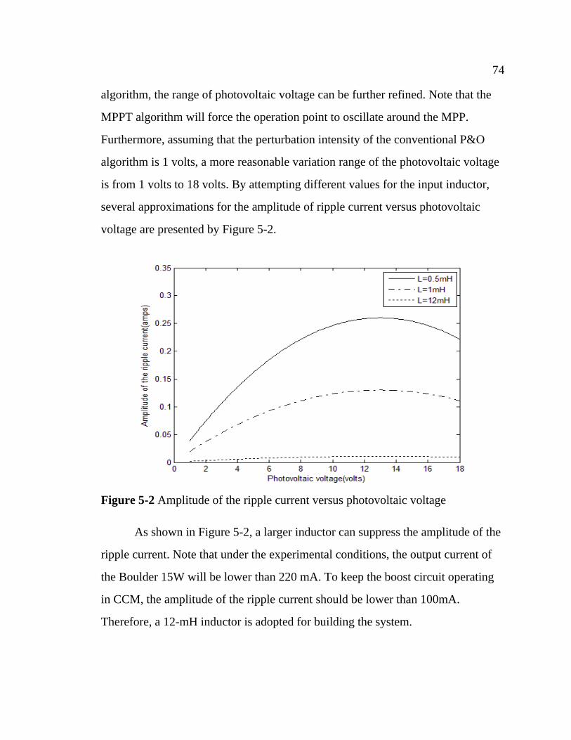
74 74
algorithm, the range of photovoltaic voltage can be further refined. Note that the
MPPT algorithm will force the operation point to oscillate around the MPP.
Furthermore, assuming that the perturbation intensity of the conventional P&O
algorithm is 1 volts, a more reasonable variation range of the photovoltaic voltage
is from 1 volts to 18 volts. By attempting different values for the input inductor,
several approximations for the amplitude of ripple current versus photovoltaic
voltage are presented by Figure 5-2.
Figure 5-2 Amplitude of the ripple current versus photovoltaic voltage
As shown in Figure 5-2, a larger inductor can suppress the amplitude of the
ripple current. Note that under the experimental conditions, the output current of
the Boulder 15W will be lower than 220 mA. To keep the boost circuit operating
in CCM, the amplitude of the ripple current should be lower than 100mA.
Therefore, a 12-mH inductor is adopted for building the system.

75 75
An electrolytic capacitor is placed between the PV module and the boost
DC-DC converter so that this capacitor can protect the input power from the ripple
components. The Figure 5-3 illustrates current waveforms of the photovoltaic
current, input inductor current, and input capacitor current.
Figure 5-3 Current waveforms of the PV model, inductor and input capacitor
The phase error between the input capacitor current and the ripple
component of the inductor current is 180 degree. In an ideal case, the input current
only has a DC component. This will save considerable works related to the noise
filtering for the input current measurement. A 35V/210uF electrolytic capacitor
with 0.8-ohm parasitic resistance is adopted. This is because a larger ESR can
contribute more damping to the system dynamics so that the potential ringing and
overshoot may be suppressed [11].
5.2 Peripheral Circuits
The peripheral circuits consist of the gate driver circuit, analog low pass
filters, voltage dividers and RC-snubbers. The gate driver circuit is used to
enhance the power of the PWM signal generated by the TI F28035 and to protect

76 76
the DSP board from over-current and over-voltage. Two snubber circuits are
considered to suppress the voltage spikes and ringing on the drain-source voltage
of the MOSFET. Given the nature of a switching mode circuit, the switching
devices will inject noise into the circuit. The noise diminishes the accuracy of
signal measurements so that the performance of the controller will be affected.
Therefore, low pass filters are designed to eliminate the noise on the measurement
signals.
5.2.1 Gate Driver Circuit
To drive the MOSFET, a gate driver chip and a digital inverter are used to
build the driver circuit. As the first layer protection for the DSP board, the digital
inverter, CD74HC04E inverts the TTL voltage of the original PWM signal and
sends the inverted PWM signal to the gate driver chip, IR2110. IR2110 will output
the enhanced switching signal to the gate lead of the MOSFET, IRFP460A. The
schematics of the gate driver circuit is shown in Figure 5-4.
Figure 5-4 The gate drive circuit
Given the experimental observations, both of the digital inverter and the
gate driver chip inject the switching noise to the 5-volts DC bus and 15-volts DC

77 77
bus. Figures 5-5 illustrates the peak-peak voltage of the switching noise on 5-volts
DC bus. The peak-peak voltage of the switching noise is 814.5 mV. Figure 5-6
illustrates the fundamental frequency of the switching noise. The fundamental
frequency of the switching noise is around 25-kHz which is the exact frequency of
the PWM signal. With the peak-peak voltage level, the switching noise will
heavily reduce the accuracy of the voltage and current measurement. This is
because the core elements of the voltage and current measurement circuits, i.e.,
OP-Amplifiers are supplied by the noised 5-volts DC bus. To solve this issue,
multiple filtering capacitors (0.1uF, 10uF, and 100uF) are connected between the
5-volts DC bus and ground. The improvement is seen in Figure 5-7. The peak-
peak voltage of the suppressed switching noise on the 5-volts DC bus is less than
145 mV.
Figure 5-5 The peak-peak voltage of the noise on the 5 volts DC bus (without
filtering capacitor)
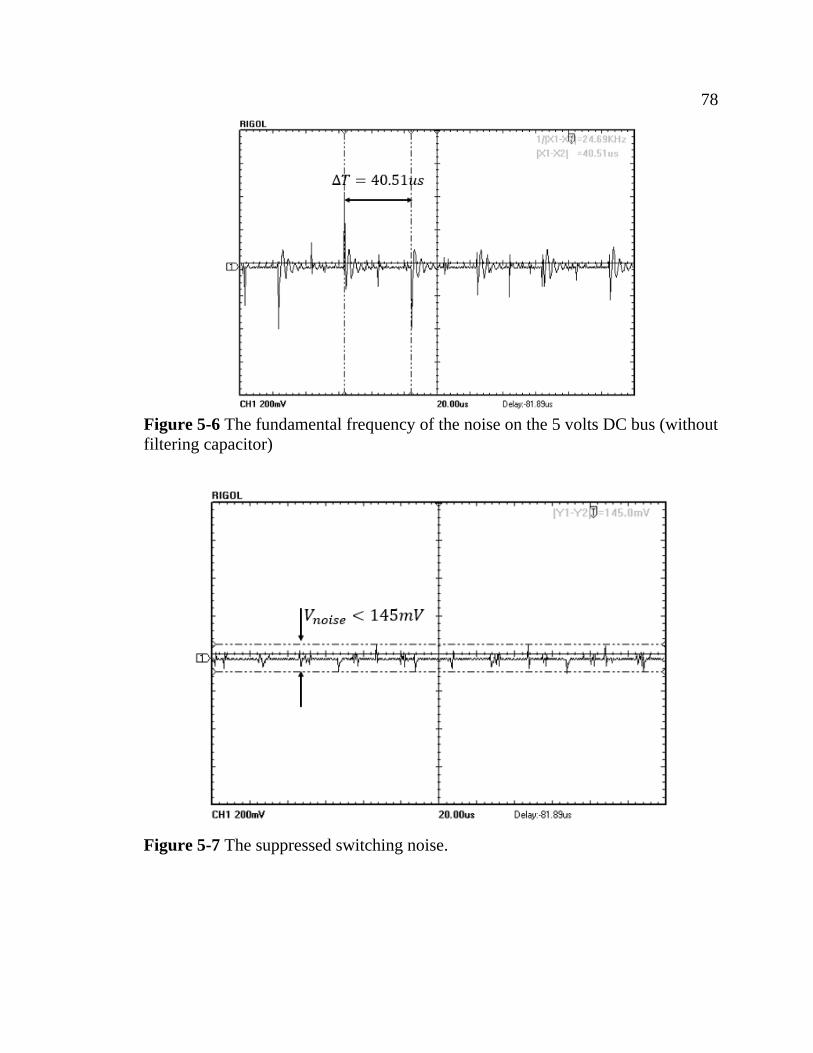
78 78
Figure 5-6 The fundamental frequency of the noise on the 5 volts DC bus (without
filtering capacitor)
Figure 5-7 The suppressed switching noise.

79 79
The switching noise on the 15-volts DC-bus can be suppressed by applying
the same solution, which is shown in Figure 5-4.
5.2.2 Eliminating Voltage Spikes on the Drain-Source Voltage
MOSFET switches have parasitic output capacitance and layout
capacitance. The diode shown in Figure 5-1 (p.72) has a forward recovery time.
When the MOSFET is fully turned off, voltages may accumulate across the gate-
source capacitor while the diode attempts to conduct in the forward direction. If
the forward-conduction time is longer than the turn-off time of the MOSFET,
voltage spikes can be seen at the drain-source voltage of the MOSFET [16].
For suppressing the spikes and ringing on the falling edges of the drain-
source voltage of the MOSFET, a conventional solution is to add a resistor in
series with the MOSFET gate lead for prolonging the turn-on time so that the
drain-source voltage can have a relatively smooth falling-edge. And the falling-
edge ringing can be suppressed. To eliminate the voltage spikes and ringing on the
rising-edge of the drain-source voltage, a conventional approach is to build a RC
snubber circuit to consume the power accumulated at the drain of the MOSFET
before the diode is fully forward-conduction. The general equations for calculating
the parameters of a RC snubber are given by equations (5.3) through (5.6).
𝐶𝑠>> 2𝐶𝑜𝑠𝑠 (5.3)
𝐶𝑠 is the capacitance of a RC snubber. 𝐶𝑜𝑠𝑠 is the output capacitance of the
MOSFET. Referring to the IRFP460A specification, the value of 𝐶𝑜𝑠𝑠 varies
around 6000pF when 𝑉𝐷𝑆 is less than 10 volts. Remind that the photovoltaic
voltage varies from 0 volts to 21.4 volts. Therefore, by selecting 6000pF as the
value for 𝐶𝑜𝑠𝑠, equation (5.3) can be rewritten as (5.4).

80 80
𝐶𝑠>> 2𝐶𝑜𝑠𝑠= 2×6000pF = 1.2 nF (5.4)
The resistance of a RC sunbber is calculated by using equation (5.5), which
considers the worst case. The worst case is that the voltage across the resistor of a
RC snubber may be the exact output voltage of the boost DC-DC circuit. Hence, a
power resistor with a 50V tolerance is adopted in this design. The resistance does
not heavily affect the performance of a RC snubber, as long as it is less than its
theoretical value given by equation (5.5).
𝑅𝑠 ≤ 𝑉𝑜𝑢𝑡
𝐼𝑜𝑢𝑡 =26𝑉
0.2𝐴 = 130 Ω (5.5)
Given the computational and experimental results, a 18.3-nF capacitor and
a 10-ohm resistor are used for building the RC snuber. A 200 ohm resistor is
selected as the gate resistor.
Notice that the maximum photovoltaic power is about 3.1 watts. Therefore
the power dissipation on the designed RC snubber should be considered. The
power dissipated on a RC snubber can be calculated by using equation (5.6).
𝑃𝑑𝑖𝑠𝑠 ≤ 𝐶𝑠𝑉𝑜𝑢𝑡2𝑓𝑠 = 18.3𝑛𝐹 ∗ 26𝑉
2 ∗ 25000𝐻𝑧 = 0.3 watts (5.6)
By applying equation (5.6), the maximum power dissipated on the RC
snubber is less or equal 0.3 watts, which is acceptable. As shown in Figure 5-8, the
drain-source voltage of IRFP460A has a 11.5V voltage spike when the gate
resistor and RC snubber are not connected. Figure 5-9 illustrates the drain-source
voltage of IRFP460A after the gate resistor and RC snubber are connected. The
suppressed voltage spikes reduce to 2.8 Volts.

81 81
Figure 5-8 The drain-source voltage of the IRFP460A (without gate resistor and
RC snubber circuit)
Figure 5-9 The drain-source voltage of the IRFP460A (with gate resistor and RC
snubber circuit)
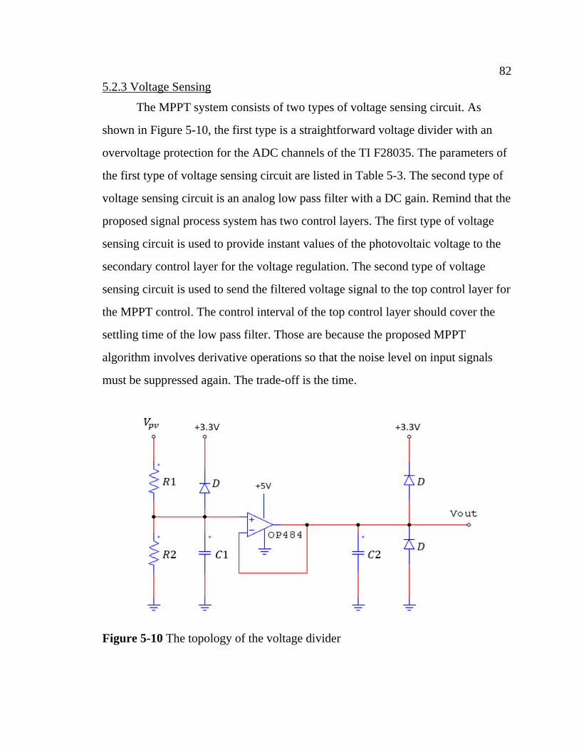
82 82
5.2.3 Voltage Sensing
The MPPT system consists of two types of voltage sensing circuit. As
shown in Figure 5-10, the first type is a straightforward voltage divider with an
overvoltage protection for the ADC channels of the TI F28035. The parameters of
the first type of voltage sensing circuit are listed in Table 5-3. The second type of
voltage sensing circuit is an analog low pass filter with a DC gain. Remind that the
proposed signal process system has two control layers. The first type of voltage
sensing circuit is used to provide instant values of the photovoltaic voltage to the
secondary control layer for the voltage regulation. The second type of voltage
sensing circuit is used to send the filtered voltage signal to the top control layer for
the MPPT control. The control interval of the top control layer should cover the
settling time of the low pass filter. Those are because the proposed MPPT
algorithm involves derivative operations so that the noise level on input signals
must be suppressed again. The trade-off is the time.
Figure 5-10 The topology of the voltage divider

83 83
Table 5-3 Parameters of the Voltage Divider
Components Parameters
R1 20 kΩ
R2 3 kΩ
C1 0.01 uF
D 1N4007
The photovoltaic voltage varies from 0 to 21.4 volts. The input voltage
range of the ADC channels is from 0 to 3.3 volts. Therefore, the proportional gain
is set to 0.13 by adopting a 20 kΩ resistor and a 3 kΩ resistor. The schematics of
the low pass filter can be found in Appendix B.
Given that the fundamental frequency of the switching noise is 25-kHz, the
cut-off frequency of the low pass filter is supposed to be below 25-kHz. In this
design, a first order low pass filter is adopted. The general transfer function of a
first order low pass filter is given by equation (5.7).
𝐺(𝑠) =𝐷𝐶𝑔𝑎𝑖𝑛
1+𝑠
𝑓𝑐𝑢𝑡
(5.7)
The 𝑓𝑐𝑢𝑡 is the cut-off frequency which will mainly determine the
magnitude of the fundamental harmonic of the switching noise. Weighing the
magnitude response against the settling time of the low pass filter, the transfer
function of the voltage sensing circuit is decided as:
𝐺(𝑠) =0.13
1+𝑠
256
(5.8)
The settling time of the low pass filter is around 15.2 ms. The magnitude
response at the 25-kHz frequency is about -57.5 dB as shown in Figure 5-11.
There are two approaches to implement the low pass filter. Equation (5.9)
and (5.10) introduce the z-domain transfer function of (5.8). The digital filter has
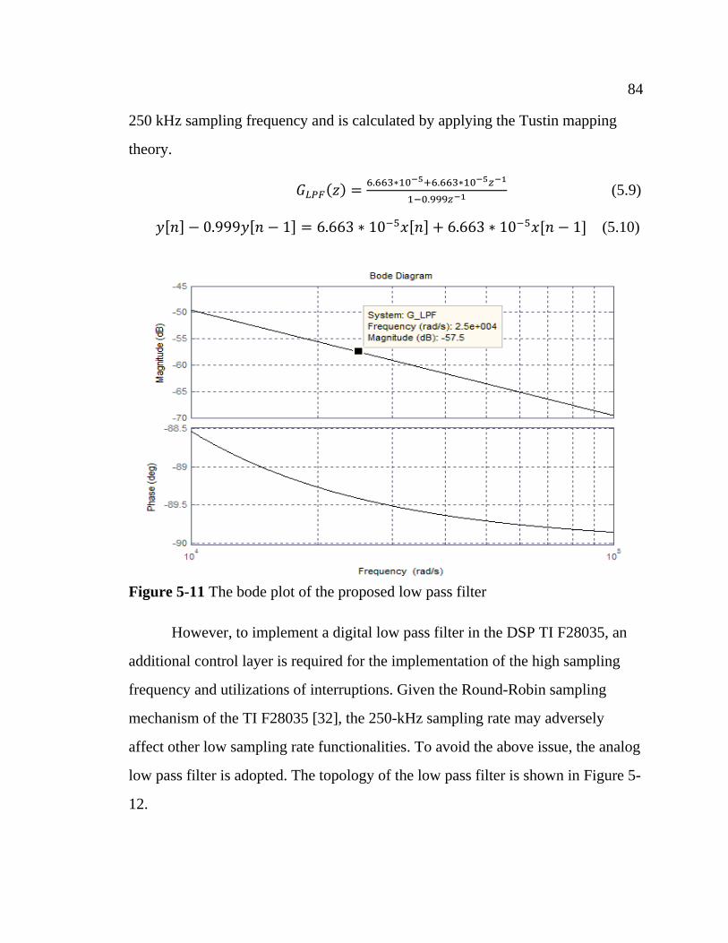
84 84
250 kHz sampling frequency and is calculated by applying the Tustin mapping
theory.
𝐺𝐿𝑃𝐹(𝑧) =6.663∗10−5+6.663∗10−5𝑧−1
1−0.999𝑧−1 (5.9)
𝑦[𝑛] − 0.999𝑦[𝑛 − 1] = 6.663 ∗ 10−5𝑥[𝑛] + 6.663 ∗ 10−5𝑥[𝑛 − 1] (5.10)
Figure 5-11 The bode plot of the proposed low pass filter
However, to implement a digital low pass filter in the DSP TI F28035, an
additional control layer is required for the implementation of the high sampling
frequency and utilizations of interruptions. Given the Round-Robin sampling
mechanism of the TI F28035 [32], the 250-kHz sampling rate may adversely
affect other low sampling rate functionalities. To avoid the above issue, the analog
low pass filter is adopted. The topology of the low pass filter is shown in Figure 5-
12.
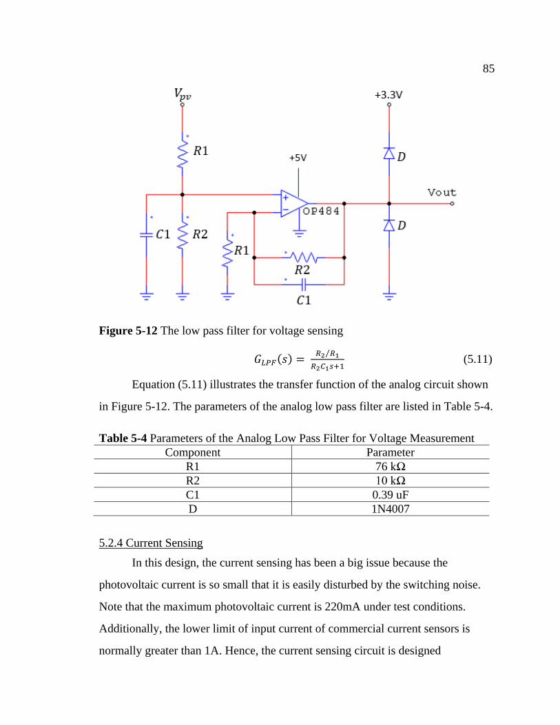
85 85
Figure 5-12 The low pass filter for voltage sensing
𝐺𝐿𝑃𝐹(𝑠) = 𝑅2 𝑅1⁄
𝑅2𝐶1𝑠+1 (5.11)
Equation (5.11) illustrates the transfer function of the analog circuit shown
in Figure 5-12. The parameters of the analog low pass filter are listed in Table 5-4.
Table 5-4 Parameters of the Analog Low Pass Filter for Voltage Measurement
Component Parameter
R1 76 kΩ
R2 10 kΩ
C1 0.39 uF
D 1N4007
5.2.4 Current Sensing
In this design, the current sensing has been a big issue because the
photovoltaic current is so small that it is easily disturbed by the switching noise.
Note that the maximum photovoltaic current is 220mA under test conditions.
Additionally, the lower limit of input current of commercial current sensors is
normally greater than 1A. Hence, the current sensing circuit is designed
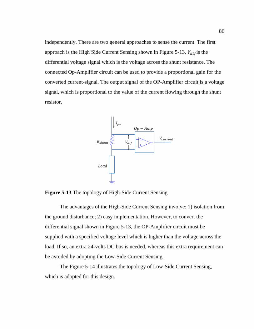
86 86
independently. There are two general approaches to sense the current. The first
approach is the High Side Current Sensing shown in Figure 5-13. 𝑉𝑑𝑖𝑓is the
differential voltage signal which is the voltage across the shunt resistance. The
connected Op-Amplifier circuit can be used to provide a proportional gain for the
converted current-signal. The output signal of the OP-Amplifier circuit is a voltage
signal, which is proportional to the value of the current flowing through the shunt
resistor.
Figure 5-13 The topology of High-Side Current Sensing
The advantages of the High-Side Current Sensing involve: 1) isolation from
the ground disturbance; 2) easy implementation. However, to convert the
differential signal shown in Figure 5-13, the OP-Amplifier circuit must be
supplied with a specified voltage level which is higher than the voltage across the
load. If so, an extra 24-volts DC bus is needed, whereas this extra requirement can
be avoided by adopting the Low-Side Current Sensing.
The Figure 5-14 illustrates the topology of Low-Side Current Sensing,
which is adopted for this design.

87 87
Figure 5-14 The topology of Low-Side Current Sensing
By using this approach, the Op-Amplifier circuit can be supplied by the 5-
volts DC bus. However, the differential signal shown in Figure 5-15 may contain
the ground noise. Therefore, an analog low pass filter should be designed for
filtering the noised current measurement signal. The Figure 5-15 illustrates the
schematics of the current sensing circuit. The parameters are listed in Table 5-5.
Figure 5-15 The Low-Side Current Sensing circuit.

88 88
Table 5-5 Parameters of the Current Sensing Circuit
Component Parameter
𝑅𝑠ℎ𝑢𝑛𝑡 1 Ω
R1 10 kΩ
R2 100 kΩ
C1 0.394 uF
D 1N4007
The transfer function of the current sensing circuit is similar to equation
(5.11). Increasing the value for R2 is to suppress harmonics within the current
signal. This is because the proportional gain of the current sensing circuit is 10,
which will enhance the identification of any DC change in photovoltaic current
and simultaneously boost the noise level. Thus, the cut-off frequency is supposed
to be chosen as low as possible for neutralizing the boosted noise level. The trade-
off of this strategy is the enlarged settling time. Throughout simple calculation, the
settling time of the current sensing circuit is about 152 ms. This is the main reason
why the control interval of the top control layer is set to 200 ms.
5.3 Signal Process System
As mentioned at the beginning of this chapter, the signal process system
has two control layers. The top control layer is designed to realize the MPPT
algorithm. The secondary control layer is designed to realize the voltage regulation
of photovoltaics. The layout of the whole system is illustrated by the Figure 5-16.
The detailed topology of the MPPT system is illustrated by Figure 5-17. The
picture of the MPPT system is shown in Figure 5-18.
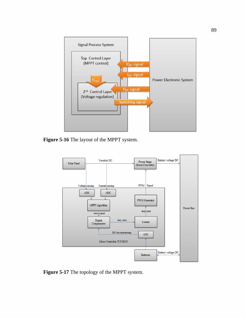
89 89
Figure 5-16 The layout of the MPPT system.
Figure 5-17 The topology of the MPPT system.
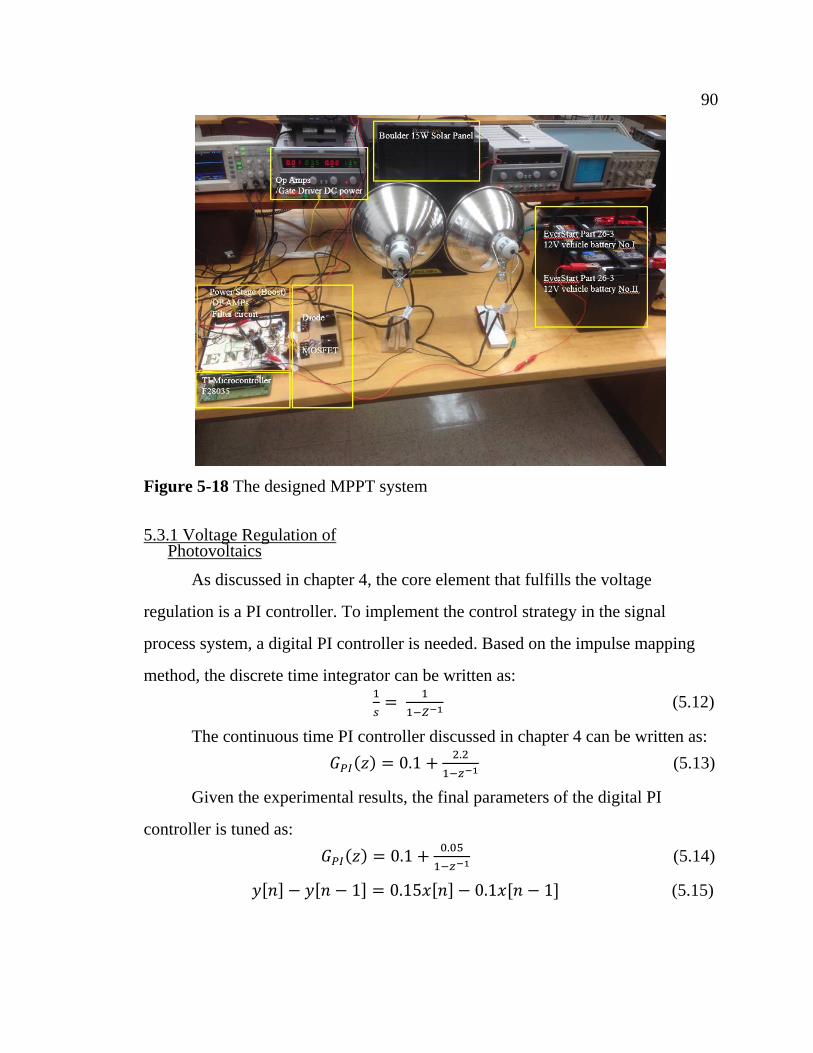
90 90
Figure 5-18 The designed MPPT system
5.3.1 Voltage Regulation of Photovoltaics
As discussed in chapter 4, the core element that fulfills the voltage
regulation is a PI controller. To implement the control strategy in the signal
process system, a digital PI controller is needed. Based on the impulse mapping
method, the discrete time integrator can be written as:
1
𝑠=
1
1−𝑍−1 (5.12)
The continuous time PI controller discussed in chapter 4 can be written as:
𝐺𝑃𝐼(𝑧) = 0.1 +2.2
1−𝑧−1 (5.13)
Given the experimental results, the final parameters of the digital PI
controller is tuned as:
𝐺𝑃𝐼(𝑧) = 0.1 +0.05
1−𝑧−1 (5.14)
𝑦[𝑛] − 𝑦[𝑛 − 1] = 0.15𝑥[𝑛] − 0.1𝑥[𝑛 − 1] (5.15)

91 91
The partial embedded code related to the digital PI controller is generated
by using MATLAB/Simulink Embedded Coder Toolbox. The Simulink diagram is
shown in Figure 5-19.
Figure 5-19 Simulink block of the digital PI controller
Figure 5-20 illustrates the step response of the secondary control layer,
which is designed for the voltage regulation of photovoltaics. The final value of
the input step function is 500 mV. The rising time of the step response of the
secondary control layer is around 55.44ms. The ripple on the voltage waveform
shown in Figure 5-20 is due to the unideal switching device and duty ratio
resolution. In the microcontroller, the duty ratio is represented by a 12-bit Hex
number, which means that the precision of the duty ratio is about 0.024 percentage.
Hence, the practical duty ratio may not exactly converge to its reference value so
that it keeps fluctuating with a small scale offset.

92 92
Figure 5-20 The voltage regulation of photovoltaics
5.3.2 DCM Detection Mechanism
To realize MPPT algorithms, the boost DC-DC converter must operate in
CCM for maintaining the validity of the linear approximation discussed in chapter
4. Therefore, a DCM detection mechanism should be designed and embedded into
the top control layer. Before design the detection mechanism, an indicator that can
indicate the system’s status, should be selected. Figure 5-21 demonstrates that the
inductor voltage waveform of the boost converter after the photovoltaic voltage
reference is set to 14 volts. It is obvious that the boost converter operates in CCM.
The error between the actual photovoltaic voltage and its reference value is about
0.1 volts.
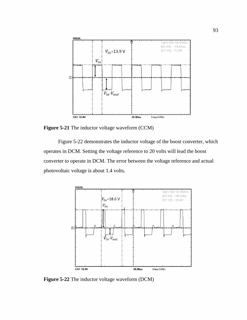
93 93
Figure 5-21 The inductor voltage waveform (CCM)
Figure 5-22 demonstrates the inductor voltage of the boost converter, which
operates in DCM. Setting the voltage reference to 20 volts will lead the boost
converter to operate in DCM. The error between the voltage reference and actual
photovoltaic voltage is about 1.4 volts.
Figure 5-22 The inductor voltage waveform (DCM)
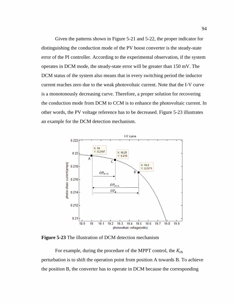
94 94
Given the patterns shown in Figure 5-21 and 5-22, the proper indicator for
distinguishing the conduction mode of the PV boost converter is the steady-state
error of the PI controller. According to the experimental observation, if the system
operates in DCM mode, the steady-state error will be greater than 150 mV. The
DCM status of the system also means that in every switching period the inductor
current reaches zero due to the weak photovoltaic current. Note that the I-V curve
is a monotonously decreasing curve. Therefore, a proper solution for recovering
the conduction mode from DCM to CCM is to enhance the photovoltaic current. In
other words, the PV voltage reference has to be decreased. Figure 5-23 illustrates
an example for the DCM detection mechanism.
Figure 5-23 The illustration of DCM detection mechanism
For example, during the procedure of the MPPT control, the 𝐾𝑡ℎ
perturbation is to shift the operation point from position A towards B. To achieve
the position B, the converter has to operate in DCM because the corresponding
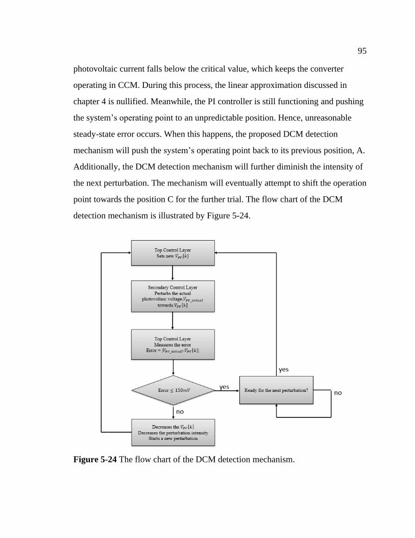
95 95
photovoltaic current falls below the critical value, which keeps the converter
operating in CCM. During this process, the linear approximation discussed in
chapter 4 is nullified. Meanwhile, the PI controller is still functioning and pushing
the system’s operating point to an unpredictable position. Hence, unreasonable
steady-state error occurs. When this happens, the proposed DCM detection
mechanism will push the system’s operating point back to its previous position, A.
Additionally, the DCM detection mechanism will further diminish the intensity of
the next perturbation. The mechanism will eventually attempt to shift the operation
point towards the position C for the further trial. The flow chart of the DCM
detection mechanism is illustrated by Figure 5-24.
Figure 5-24 The flow chart of the DCM detection mechanism.
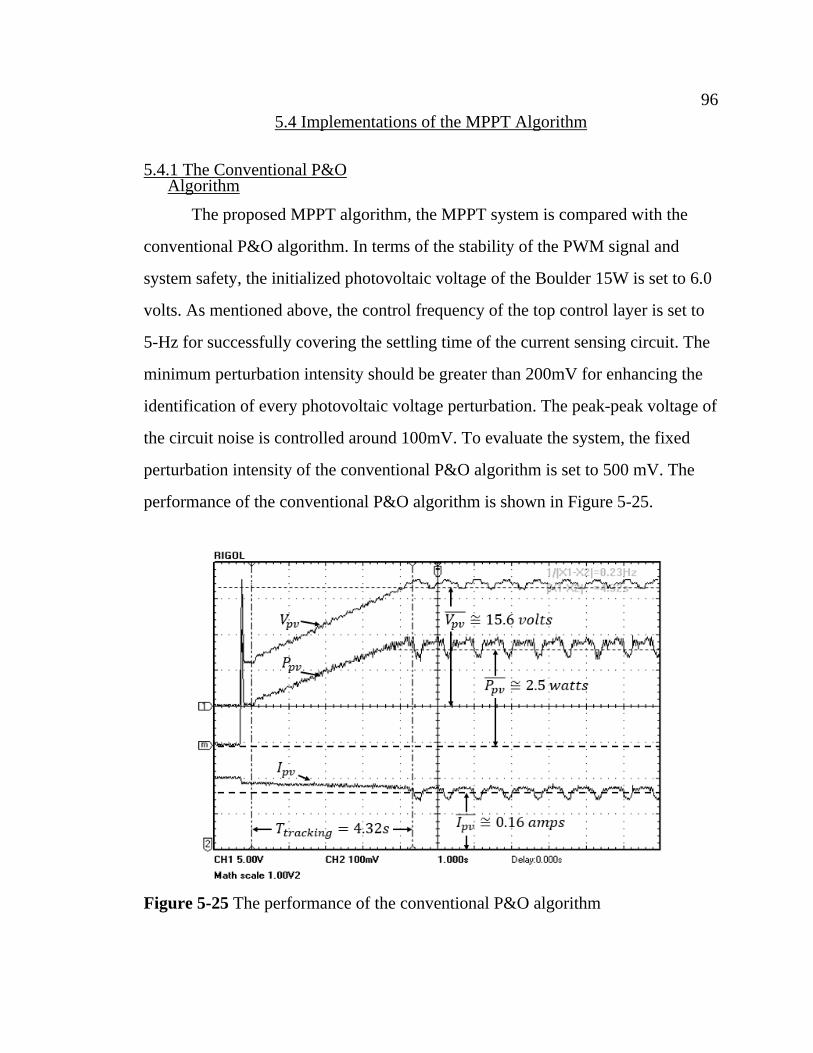
96 96
5.4 Implementations of the MPPT Algorithm
5.4.1 The Conventional P&O Algorithm
The proposed MPPT algorithm, the MPPT system is compared with the
conventional P&O algorithm. In terms of the stability of the PWM signal and
system safety, the initialized photovoltaic voltage of the Boulder 15W is set to 6.0
volts. As mentioned above, the control frequency of the top control layer is set to
5-Hz for successfully covering the settling time of the current sensing circuit. The
minimum perturbation intensity should be greater than 200mV for enhancing the
identification of every photovoltaic voltage perturbation. The peak-peak voltage of
the circuit noise is controlled around 100mV. To evaluate the system, the fixed
perturbation intensity of the conventional P&O algorithm is set to 500 mV. The
performance of the conventional P&O algorithm is shown in Figure 5-25.
Figure 5-25 The performance of the conventional P&O algorithm

97 97
The conventional P&O algorithm with 0.5 volts perturbation intensity can
extract average 2.5 watts power from the solar panel, while the tracking time is
4.32 seconds. Under test conditions, the potential maximum power is 3.1 watts so
that the MPPT efficiency of this P&O algorithm is 80.64%.
5.4.2 The Improved MPPT Algorithm using Fuzzy Logic Controller
Prior to implement the proposed algorithm, the parameters of the
membership functions are to be adjusted a bit by using the same methodology
presented in chapter 3. As the tuning result, the perturbation intensity generated by
the Fuzzy Logic Controller varies from 0.2 volts to 3 volts. Due to the complexity
of the proposed MPPT algorithm, the proposed FLC is directly programed as the
embedded codes. The performance of the proposed FLC is shown in Figure 5-26.
The tracking time of the proposed MPPT algorithm is 1.81seconds, while the
average generated power is about 3.0 watts. Given Table 5-2, the MPPT efficiency
of the improved MPPT algorithm with the Fuzzy Logic Controller is 96.78%,
while that of the conventional P&O algorithm is only 80.64%. Therefore,
throughout the experimental validations, the proposed MPPT algorithm using FLC
shows shorter tracking time and higher MPPT efficiency, compared to that of the
conventional P&O algorithm.

98 98
Figure 5-26 The performance of the improved MPPT algorithm using FLC

6 CONCLUSION
In this thesis, an improved MPPT algorithm using Fuzzy Logic Controller
has been investigated by referring to the mechanisms of the conventional P&O
algorithm and nonlinear characteristics of photovoltaics. The strategy that is to
create adaptive perturbation intensities for accelerating the MPPT velocity and
improving the MPPT efficiency was validated by both of the simulation and
experimental results. In addition, this thesis also emphasizes the hardware
implementation for proving the effectiveness of the proposed MPPT algorithm. To
provide enough theoretical tools for the voltage regulation of photovoltaic cells, a
small signal model of the input terminal of a photovoltaic boost DC-DC converter
was introduced and used for deriving the linear approximations without ignoring
any parasitic resistance of the input capacitor and inductor. The effectiveness of
the linear approximation was confirmed by the experimental results. The concepts
of the presented input terminal small signal modelling may be helpful for further
investigations to be conducted related to the renewable energy applications such as
wind energy and ocean wave energy applications. To improve the overall
performance of the MPPT system, the efforts of noise filtering and noise
suppression were taken in this design, as well as the DCM detection mechanism.
Eventually, the designed PV system successfully implemented the conventional
P&O algorithm and the proposed algorithm using FLC.
In this thesis, a single phase PWM control for a photovoltaic boost DC-DC
converter is presented. To reduce the ripple current, two approaches are mentioned
in chapter 5. The first approach is to enlarge the input inductance, while the circuit
may become bulky. The second method is to increase the switching frequency.
However, due to the limitations of the hardware system, the switching frequency is

100 100
limited to 25 kHz. In fact, there exists another efficient strategy, the Multi-Phase
Sliding Mode Control, which can contribute to suppress the ripple current. In a
geometric sense, the AC components of inductor currents can cancel out each
other, if the phase error between each waveform is properly selected. For instance,
if a photovoltaic converter has two phases, and the duty ratio of each PWM signal
is 50% (where the corresponding inductor current waveform is symmetry), then
keeping a 180 degree phase error between the two inductor currents can cancel
away the ripple component of the input current. In other words, the photovoltaic
current will only contain a DC component, and the ripple currents can be
suppressed at both of the input terminal and output terminal of the system. For the
future research, the multi-phase sliding mode control strategy for PV systems
should be investigated.

REFERENCES

REFERENCES
[1] P. Suskis and I. Galkin, “Enhanced Photovoltaic Panel Model for MATLAB-
Simulink Enviornment Considering Solar Cell Junction Capacitiance,” in
Industrial Electronics Society, IECON 2013 - 39th Annual Conference of the
IEEE, pp. 1613-1618.
[2] S. Fathpour, K.K Tsia and B. Jalali, “Nonlinear Photovoltaic effect,” in
Lasers and Electro-Optics Society, 2007. LEOS 2007. The 20th Annual
Meeting of the IEEE, pp. 892-893.
[3] P. Pichlik and J. Zdenek, “Converter regulation of stand-alone photovoltaic
system at low solar radiation,” Applied Electronics (AE), 2012 International
Conference, pp. 207-210.
[4] Y. Xiong, S. Qian and J. Xun, “Single-Phase Grid-Connected Photovoltaic
System Based on Boost Inverter,” Power and Energy Engineering
Conference (APPEEC), 2012 Asia-Pacific, pp 1-3.
[5] A. Panda, M. K.Pathak and S. P.Srivastava, "Fuzzy Intelligent Controller for
the Maximum PowerPoint Tracking of a Photovoltaic Module at Varying
Atmospheric Conditions," Journal of Energy Technologies and Policy, 2011,
Vol.1, No.2, pp.18-27.
[6] Y. Soufi, M. Bechouat, S. Kahla and K. Bouallegue, "Maximum Power Point
Tracking using Fuzzy Logic Control for Photovoltaic System," Renewable
Energy Research and Application (ICRERA), 2014 International Conference,
pp. 902-906.
[7] K. H. Hussein, I. Muta, T. Hoshino, and M. Osakada, “Maximum
photovoltaic power tracking: An algorithm for rapidly changing atmospheric
conditions,” Proc. Inst. Elect. Eng, vol. 142, no. 1, 1995, pp. 59–64.
[8] C. Hua, J. Lin, and C. shen, “Implementation of a DSP-controlled
photovoltaic system with peak power tracking,” IEEE Trans. Ind. Electron,
vol. 45, no. 1, Feb. 1998, pp. 99–107.
[9] H. Koizumi et al, “A novel microcontroller for grid-connected photovoltaic
systems,” IEEE Trans. Ind. Electron, vol. 53, no. 6, Dec. 2006, pp. 1889–
1897.
103 103
[10] W. Xiao, W. G. Dunford, P. R. Palmer and A. Capel, “Regulation of
Photovoltaic Voltage,” IEEE Trans. Ind. Electron, vol. 54, no. 3, Apr. 2007,
pp. 1365-1374.
[11] M. G. Villalva and E. R. Filho, “Dynamic Analysis of the input-controlled
buck converter fed by a photovoltaic array,” Revista Control &Automatic,
vol. 19, no. 4, Dec. 2008, pp. 463-474.
[12] B. Bryant and M.K. Kazimierczuk, “Voltage Loop of Boost PWM DC–DC
Converters,” IEEE Trans on circuits and systems. Vol. 53, no. 1, Jan. 2006,
pp. 99-105.
[13] R. D. Middlebrook, “Small-signal modeling of pulse-width modulated
switched-mode power converters,” Proc. IEEE, vol. 76, no. 4, Apr. 1988, pp-
343-354.
[14] M. G. Villalva, T.G. de Siqueira and E. Ruppert, “Voltage regulation of
photovoltaic arrays: small-signal analysis and control design,” Power
Electronics, IET, 2008, vol. 3, no. 6, Nov. 2010, pp. 869-880.
[15] R. E. Hanitsch, D. Schulz and U. Siegfried, “Sading Effects on Output Power
of Grid Connected Photovoltaic Generator Systems,” Energ. Ren: Power
Engineering, 2001, pp. 93-99.
[16] S. Rahman, N. S. Oni and Q. A. Ibn Masud, “Design of a Charge Controller
Circuit with Maximum Power Point Tracker for Photovoltaic System,” Dept.
of Electrical & Electronic Engineering, BRAC university, Dec. 2012.
[17] M. G. Villalva, J. R. Gazoli and E. R. Filho, “Comprehensive Approach to
Modeling and Simulation of Photovoltaic Arrays,” IEEE Trans. Power.
Electronics, vol. 24, no. 5, Mar. 2009, pp. 1198-1208.
[18] K. Ishaque, Z. Salam and H. Taheri, “Accurate MATLAB Simulink PV
System Simulator based on a Two-Diode Model,” Journal of Power
Electronics, vol. 11, no. 2, Mar 2011, pp. 179-187.
[19] Akihiro Oi, “Design and simulation of photovoltaic water pumping system,”
M.S thesis, California Polytechnic State University, Sep. 2005.
[20] A. P. Engelbrecht, “Fuzzy Systems” in Computational Intelligence, 2th ed.
University of Pretoria South Africa, 2007, chapter VI, pp. 451-485.
104 104
[21] N. Mohan, “Designing feedback controllers in switch-mode DC power
suppliers,” in Power Electronics A First Course, Oscar A. Schott Professor
of Power Electronics and Systems, Dept. of Electrical and Computer
Engineering, University of Minnesota.
[22] K. Ogata, “PID Controllers and Modified PID Controllers,” in Modern
Control Engineering, 5th
ed., pp. 567-641.
[23] W. Xiao and W. G. Dunford, “A modified adaptive hill climbing MPPT
method for photovoltaic power systems,” in proceeding of 35th
Annual IEEE
Power Electronics Specialists Conference, pp. 1957-1963
[24] C. Hua and J. Lin, “An on-line MPPT algorithm for rapidly changing
illuminations of solar arrays,” Renew Energy 28, pp.1129-1142.
[25] C. Chen-Chi and C. Chieh-Li, “Robust maximum power point tracking
method for photovoltaic cells: A sliding mode control approach,” Solar
Energy 83, 2009, pp. 1370-1378.
[26] Gaili Yue and Hongwei He, “The research of photovoltaic MPPT controller
based on DSPF2812,” Computer, Consumer and Control (IS3C), 2014
International Symposium, Jun 2014, pp. 78-81.
[27] S. Tao et al, “Photovoltaic MPPT algorithm based on hysteresis comparison
and optimal gradient,” Harmonics and Quality of Power (ICHQP), 2012
IEEE 15th
International Conference, Jun 2012, pp. 733-738.
[28] Y.El Basri et al, “Adaptive Digital Synchronous P&O algorithm for
Photovoltaic DC Power Conversion,” Industrial Electronics (ISIE), 2013
IEEE International Symposium, May 2013, pp. 1-6.
[29] Renewable Energy Solution, FAIRCHILD SEMICONDUCTOR, 2012.
[30] M. Valentini et al, “PV inverter test setup for European efficiency, static and
dynamic MPPT efficiency evaluation,” Optimization of Electrical and
Electronic Equipment, 2008. OPTIM 2008. 11th
International Conference,
May 2008, pp. 433-438.
[31] (2013, August). Sunmodule Plus SW 260 mono. Available:
http://www.solarworld-usa.com/technical-downloads/datasheets
[32] (2008, December). TMS320X2802x, 2803x Piccolo Analog-to-Digital
Converter (ADC) and Comparator. Texas Instruments. Available:
http://www.ti.com/lit/ug/spruge5f/spruge5f.pdf

APPENDICES

APPENDIX A: MATLAB CODE

107 107
Functions
The following functions were developed using MATLAB to compute various
functions or logic needed to model the photovoltaics ,to linearize the small signal
model of the input terminal of a boost DC-DC converter, and to find the proposed
parameters for building the hardware system.
Implementation of the Newton Raphson Method % this function is design to solve the nonliear equation related to % the photovoltaic current and photovoltaic voltage, by applying the % Newton Method. function [Iout]=cmp_out_current1000(voltage,R_s,R_p) Ns=60; % setting the number of resistors connected in series Np=1;% setting the number of resistors connected in parallel Voc=38.9;% open-circuit voltage Isc=9.18;% short-circuit current Pmpp=260;% provided maximum power Ci=0.004e-2;%current coefficient Cv=-0.3e-2;%voltage coefficient Cp=-0.45e-2;%power coefficient q=1.6e-19;% constant parameters k=1.381e-23; Vmpp=30.7;% maximum power point voltage Impp=8.56;% maximum power point current Tstc=273.15+25; % for Celsius C= K-273.15 VT=q/k/Tstc;% simplfy the computation a=1.5;% ideal diode factor Io= Isc/(exp(Voc*VT/a/60)-1);% compute the saturation current x0=0.0001;% set the inital guess value for solve the nonlinear x1=0;% equation T=Tstc; for n=1:1:200 fnt= x0-Isc+Io*(exp(q/a/k/T*(voltage+x0*R_s*60)/60)-
1)+(voltage+x0*R_s*60)/R_p/60; fnt_dot=
1+Io*exp(q/a/k/T*(voltage+x0*R_s*60)/60)*q/a/k/T*R_s+R_s/R_p; x1=x0-fnt/fnt_dot; x0=x1; end Iout=x1;%generate the final solution end
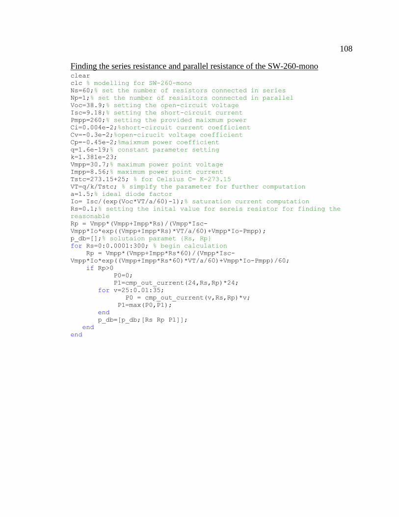
108 108
Finding the series resistance and parallel resistance of the SW-260-mono clear clc % modelling for SW-260-mono Ns=60;% set the number of resistors connected in series Np=1;% set the number of resisitors connected in parallel Voc=38.9;% setting the open-circuit voltage Isc=9.18;% setting the short-circuit current Pmpp=260;% setting the provided maixmum power Ci=0.004e-2;%short-circuit current coefficient Cv=-0.3e-2;%open-cirucit voltage coefficient Cp=-0.45e-2;%maixmum power coefficient q=1.6e-19;% constant parameter setting k=1.381e-23; Vmpp=30.7;% maximum power point voltage Impp=8.56;% maximum power point current Tstc=273.15+25; % for Celsius C= K-273.15 VT=q/k/Tstc; % simplfy the parameter for further computation a=1.5;% ideal diode factor Io= Isc/(exp(Voc*VT/a/60)-1);% saturation current computation Rs=0.1;% setting the inital value for sereis resistor for finding the
reasonable Rp = Vmpp*(Vmpp+Impp*Rs)/(Vmpp*Isc-
Vmpp*Io*exp((Vmpp+Impp*Rs)*VT/a/60)+Vmpp*Io-Pmpp); p_db=[];% solutaion paramet Rs, Rp for Rs=0:0.0001:300; % begin calculation Rp = Vmpp*(Vmpp+Impp*Rs*60)/(Vmpp*Isc-
Vmpp*Io*exp((Vmpp+Impp*Rs*60)*VT/a/60)+Vmpp*Io-Pmpp)/60; if Rp>0 P0=0; P1=cmp_out_current(24,Rs,Rp)*24; for v=25:0.01:35; P0 = cmp_out_current(v,Rs,Rp)*v; P1=max(P0,P1); end p_db=[p_db;[Rs Rp P1]]; end end

109 109
Computation of the linear approximations clear clc close all %% System parameter L=12e-3; %inductance of the input inductor Cin=210e-6; %capacitance of the input capacitor RL=0.2; %parasitic resistance of the input inductor Vbat=26; %DC bus voltage Rc=0.8; %parasitic resistance of the input capacitor %% Transfer function parameter computation area % should be noticed, the gain of the following transfer function is % negative Rpv=75; % the lower limit for internal resisitance of the Boulder 15W num=[-Vbat*Rc*Rpv/L/(1-Rpv) Vbat*((Cin*(1-Rpv)^2+(Rc*Rpv)^2-
Rc*Rpv)/L/L/Cin/(1-Rpv)^2)]; den=[1 RL/L-(Rc*Rpv-1)/L/Cin/(1-Rpv) -(RL*Rc*Rpv-RL+Rpv*L-
RL*Rc*Cin*Rpv)/L/L/Cin/(1-Rpv)]; Converter_sys_Rmpp75=tf(num,den)/3.8;%building linear approximation
with 75 ohm %% Rpv=100 Rpv=100; num=[-Vbat*Rc*Rpv/L/(1-Rpv) Vbat*((Cin*(1-Rpv)^2+(Rc*Rpv)^2-
Rc*Rpv)/L/L/Cin/(1-Rpv)^2)]; den=[1 RL/L-(Rc*Rpv-1)/L/Cin/(1-Rpv) -(RL*Rc*Rpv-RL+Rpv*L-
RL*Rc*Cin*Rpv)/L/L/Cin/(1-Rpv)]; Converter_sys_Rmpp100=tf(num,den)/3.8;%building linear approximation
with 100 ohm %% Rpv=125 Rpv=125; num=[-Vbat*Rc*Rpv/L/(1-Rpv) Vbat*((Cin*(1-Rpv)^2+(Rc*Rpv)^2-
Rc*Rpv)/L/L/Cin/(1-Rpv)^2)]; den=[1 RL/L-(Rc*Rpv-1)/L/Cin/(1-Rpv) -(RL*Rc*Rpv-RL+Rpv*L-
RL*Rc*Cin*Rpv)/L/L/Cin/(1-Rpv)]; Converter_sys_Rmpp125=tf(num,den)/3.8;%building linear approximation
with 125 ohm %% Rpv=150 Rpv=150;% the upper limit for the internal resistance of the Boulder
15W num=[-Vbat*Rc*Rpv/L/(1-Rpv) Vbat*((Cin*(1-Rpv)^2+(Rc*Rpv)^2-
Rc*Rpv)/L/L/Cin/(1-Rpv)^2)]; den=[1 RL/L-(Rc*Rpv-1)/L/Cin/(1-Rpv) -(RL*Rc*Rpv-RL+Rpv*L-
RL*Rc*Cin*Rpv)/L/L/Cin/(1-Rpv)]; Converter_sys_Rmpp150=tf(num,den)/3.8;%building linear approximation
with 150 ohm %% drawing graphs figure(1) %% bode plots of the four transfer functions bode(Converter_sys_Rmpp75,'-k',Converter_sys_Rmpp100,'--
k',Converter_sys_Rmpp125,'-.k',Converter_sys_Rmpp150,':k');grid legend('Rpv=75ohm','Rpv=100ohm','Rpv=125ohm','Rpv=150ohm') figure(2) margin(Converter_sys_Rmpp75)% check the phase margin of the original
system figure(3)

110 110
Gc=tf([0.1 1.9],[1 0]);% building the PI controller Gcl_cs75=feedback(Gc*Converter_sys_Rmpp75,1);%compute the closed-loop
tf Gcl_cs100=feedback(Gc*Converter_sys_Rmpp100,1); Gcl_cs125=feedback(Gc*Converter_sys_Rmpp125,1); Gcl_cs150=feedback(Gc*Converter_sys_Rmpp150,1); t=0:0.001:0.2;% creating the time vector stepinfo(Gcl_cs75)% gethering the information of the step responses stepinfo(Gcl_cs100)% of the four closed-loop compensated system stepinfo(Gcl_cs125) stepinfo(Gcl_cs150) y75=step(t,Gcl_cs75); y100=step(t,Gcl_cs100);%draw the step response y125=step(t,Gcl_cs125); y150=step(t,Gcl_cs150); plot(t,y75,'-k',t,y100,'--k',t,y100,'-.k',t,y125,':k');grid xlabel('time(sec)')% mark the axises and title ylabel('Output') title('Step resonse of closed-loop compensated system'); legend('Rpv=75ohm','Rpv=100ohm','Rpv=125ohm','Rpv=150ohm');
Finding the proper inductor for suppressing the ripple component L1=0.5e-3;%set inductance L2=1e-3; L3=12e-3; ripple1=[];%create vectors for recording data ripple2=[]; ripple3=[]; for n=1:0.1:18 % create for-loop to automatically compute ripple1=[ripple1 0.5*n*(26-n)/26/25000/L1];% the possible amplitude of ripple2=[ripple2 0.5*n*(26-n)/26/25000/L2];% ripple component ripple3=[ripple3 0.5*n*(26-n)/26/25000/L3]; end figure(1) n=1:0.1:18; plot(n,ripple1,'k-',n,ripple2,'k-.',n,ripple3,'k:'); xlabel('Photovoltaic voltage(volts)'); ylabel('Amplitude of the ripple current(amps)'); legend('L=0.5mH','L=1mH','L=12mH');

APPENDIX B: SYSTEM SCHEMATICS

112 112
Schematics of the Hardware System
The following schematics demonstrate the main power electronic circuit,
peripheral circuits, and spots for signal measurements.
Boost DC-DC converter powered by the solar panel, Boulder 15W
Voltage sensing circuit for supporting the secondary control layer
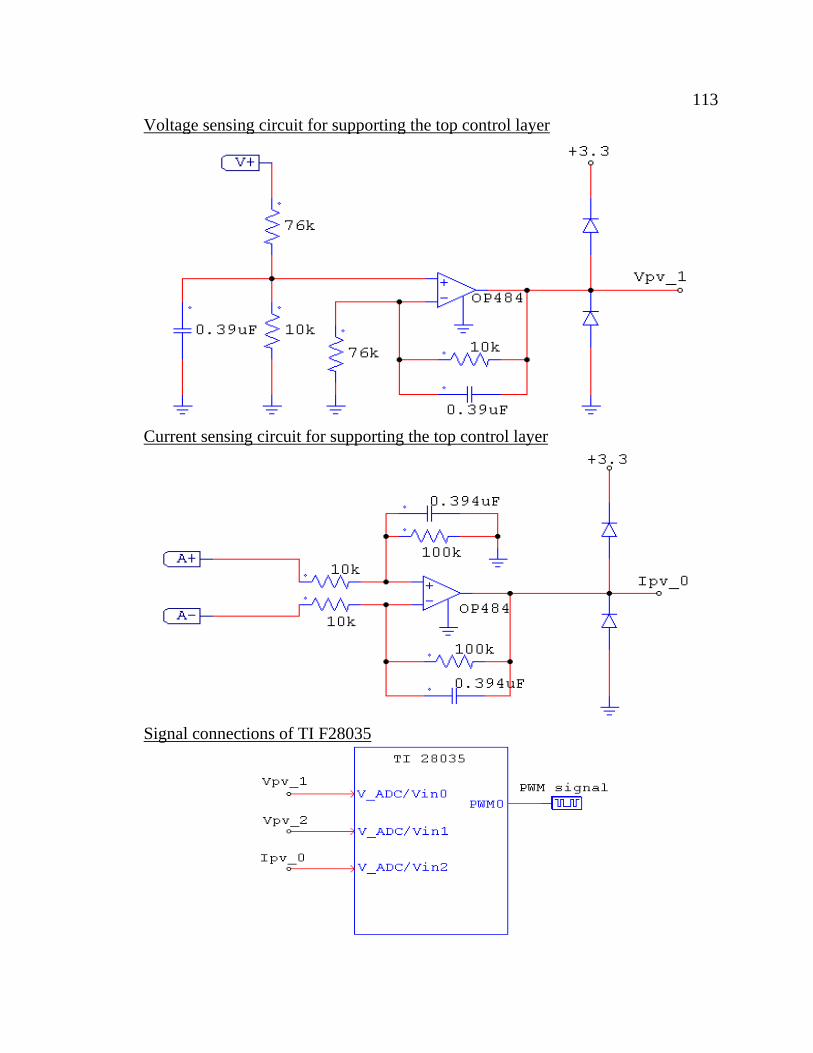
113 113
Voltage sensing circuit for supporting the top control layer
Current sensing circuit for supporting the top control layer
Signal connections of TI F28035
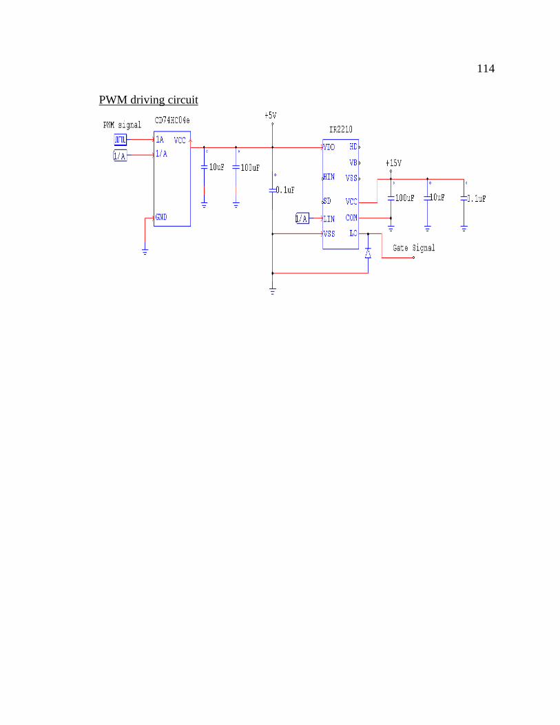
114 114
PWM driving circuit

Fresno State
Non-Exclusive Distribution License
(to archive your thesis/dissertation electronically via the library’s eCollections database)
By submitting this license, you (the author or copyright holder) grant to Fresno State Digital
Scholar the non-exclusive right to reproduce, translate (as defined in the next paragraph), and/or
distribute your submission (including the abstract) worldwide in print and electronic format and
in any medium, including but not limited to audio or video.
You agree that Fresno State may, without changing the content, translate the submission to any
medium or format for the purpose of preservation.
You also agree that the submission is your original work, and that you have the right to grant the
rights contained in this license. You also represent that your submission does not, to the best of
your knowledge, infringe upon anyone’s copyright.
If the submission reproduces material for which you do not hold copyright and that would not be
considered fair use outside the copyright law, you represent that you have obtained the
unrestricted permission of the copyright owner to grant Fresno State the rights required by this
license, and that such third-party material is clearly identified and acknowledged within the text
or content of the submission.
If the submission is based upon work that has been sponsored or supported by an agency or
organization other than Fresno State, you represent that you have fulfilled any right of review or
other obligations required by such contract or agreement.
Fresno State will clearly identify your name as the author or owner of the submission and will not
make any alteration, other than as allowed by this license, to your submission. By typing your
name and date in the fields below, you indicate your agreement to the terms of this
distribution license.
Embargo options (fill box with an X).
Make my thesis or dissertation available to eCollections immediately upon
submission.
Embargo my thesis or dissertation for a period of 2 years from date of graduation.
Embargo my thesis or dissertation for a period of 5 years from date of graduation.
Type full name as it appears on submission
Date
Pengyuan Chen
May 19, 2015
X
Related Documents