University of Windsor University of Windsor Scholarship at UWindsor Scholarship at UWindsor Electronic Theses and Dissertations Theses, Dissertations, and Major Papers 2010 An FPGA-based 77 GHzs RADAR signal processing system for An FPGA-based 77 GHzs RADAR signal processing system for automotive collision avoidance automotive collision avoidance Sundeep Lal University of Windsor Follow this and additional works at: https://scholar.uwindsor.ca/etd Recommended Citation Recommended Citation Lal, Sundeep, "An FPGA-based 77 GHzs RADAR signal processing system for automotive collision avoidance" (2010). Electronic Theses and Dissertations. 7979. https://scholar.uwindsor.ca/etd/7979 This online database contains the full-text of PhD dissertations and Masters’ theses of University of Windsor students from 1954 forward. These documents are made available for personal study and research purposes only, in accordance with the Canadian Copyright Act and the Creative Commons license—CC BY-NC-ND (Attribution, Non-Commercial, No Derivative Works). Under this license, works must always be attributed to the copyright holder (original author), cannot be used for any commercial purposes, and may not be altered. Any other use would require the permission of the copyright holder. Students may inquire about withdrawing their dissertation and/or thesis from this database. For additional inquiries, please contact the repository administrator via email ([email protected]) or by telephone at 519-253-3000ext. 3208.

Welcome message from author
This document is posted to help you gain knowledge. Please leave a comment to let me know what you think about it! Share it to your friends and learn new things together.
Transcript
University of Windsor University of Windsor
Scholarship at UWindsor Scholarship at UWindsor
Electronic Theses and Dissertations Theses, Dissertations, and Major Papers
2010
An FPGA-based 77 GHzs RADAR signal processing system for An FPGA-based 77 GHzs RADAR signal processing system for
automotive collision avoidance automotive collision avoidance
Sundeep Lal University of Windsor
Follow this and additional works at: https://scholar.uwindsor.ca/etd
Recommended Citation Recommended Citation Lal, Sundeep, "An FPGA-based 77 GHzs RADAR signal processing system for automotive collision avoidance" (2010). Electronic Theses and Dissertations. 7979. https://scholar.uwindsor.ca/etd/7979
This online database contains the full-text of PhD dissertations and Masters’ theses of University of Windsor students from 1954 forward. These documents are made available for personal study and research purposes only, in accordance with the Canadian Copyright Act and the Creative Commons license—CC BY-NC-ND (Attribution, Non-Commercial, No Derivative Works). Under this license, works must always be attributed to the copyright holder (original author), cannot be used for any commercial purposes, and may not be altered. Any other use would require the permission of the copyright holder. Students may inquire about withdrawing their dissertation and/or thesis from this database. For additional inquiries, please contact the repository administrator via email ([email protected]) or by telephone at 519-253-3000ext. 3208.
An FPGA-based 77 GHz
RADAR
Signal Processing System for
Automotive Collision Avoidance
By
Sundeep Lai
A Thesis
Submitted to the Faculty of Graduate Studies
Through Electrical and Computer Engineering
In Partial Fulfillment of the Requirements
for the Degree of Master of Applied Science
at the University of Windsor
Windsor, Ontario, Canada
2010
© Sundeep Lai
1*1 Library and Archives Canada
Published Heritage Branch
395 Wellington Street OttawaONK1A0N4 Canada
Bibliotheque et Archives Canada
Direction du Patrimoine de I'edition
395, rue Wellington Ottawa ON K1A 0N4 Canada
Your file Votre reference ISBN: 978-0-494-62749-5 Our file Notre r6f6rence ISBN: 978-0-494-62749-5
NOTICE: AVIS:
The author has granted a nonexclusive license allowing Library and Archives Canada to reproduce, publish, archive, preserve, conserve, communicate to the public by telecommunication or on the Internet, loan, distribute and sell theses worldwide, for commercial or noncommercial purposes, in microform, paper, electronic and/or any other formats.
L'auteur a accorde une licence non exclusive permettant a la Bibliotheque et Archives Canada de reproduire, publier, archiver, sauvegarder, conserver, transmettre au public par telecommunication ou par I'lnternet, preter, distribuer et vendre des theses partout dans le monde, a des fins commerciales ou autres, sur support microforme, papier, electronique et/ou autres formats.
The author retains copyright ownership and moral rights in this thesis. Neither the thesis nor substantial extracts from it may be printed or otherwise reproduced without the author's permission.
L'auteur conserve la propriete du droit d'auteur et des droits moraux qui protege cette these. Ni la these ni des extraits substantiels de celle-ci ne doivent etre imprimes ou autrement reproduits sans son autorisation.
In compliance with the Canadian Privacy Act some supporting forms may have been removed from this thesis.
Conformement a la loi canadienne sur la protection de la vie privee, quelques formulaires secondaires ont ete enleves de cette these.
While these forms may be included in the document page count, their removal does not represent any loss of content from the thesis.
Bien que ces formulaires aient inclus dans la pagination, il n'y aura aucun contenu manquant.
• + •
Canada

Author's Declaration of Originality
I hereby certify that I am the sole author of this thesis and that no part of this thesis
has been published or submitted for publication.
I certify that, to the best of my knowledge, my thesis does not infringe upon
anyone's copyright nor violate any proprietary rights and that any ideas, techniques,
quotations, or any other material from the work of other people included in my thesis,
published or otherwise, are fully acknowledged in accordance with the standard
referencing practices. Furthermore, to the extent that I have included copyrighted
material that surpasses the bounds of fair dealing within the meaning of the Canada
Copyright Act, I certify that I have obtained a written permission from the copyright
owner(s) to include such material(s) in my thesis and have included copies of such
copyright clearances to my appendix.
I declare that this is a true copy of my thesis, including any final revisions, as
approved by my thesis committee and the Graduate Studies office, and that this thesis
has not been submitted for a higher degree to any other University or Institution.
in
Abstract
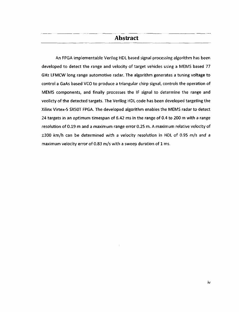
An FPGA implementable Verilog HDL based signal processing algorithm has been
developed to detect the range and velocity of target vehicles using a MEMS based 77
GHz LFMCW long range automotive radar. The algorithm generates a tuning voltage to
control a GaAs based VCO to produce a triangular chirp signal, controls the operation of
MEMS components, and finally processes the IF signal to determine the range and
veolicty of the detected targets. The Verilog HDL code has been developed targeting the
Xilinx Virtex-5 SX50T FPGA. The developed algorithm enables the MEMS radar to detect
24 targets in an optimum timespan of 6.42 ms in the range of 0.4 to 200 m with a range
resolution of 0.19 m and a maximum range error 0.25 m. A maximum relative velocity of
±300 km/h can be determined with a velocity resolution in HDL of 0.95 m/s and a
maximum velocity error of 0.83 m/s with a sweep duration of 1 ms.
IV
A Sincere Dedication
To mom, dad, amma, thaththa, Mannu andSunali with love..
It is your ever-encouraging faith in me that keeps me going.
Om Sai Ram
v

Acknowledgement
Before all I submit my prayers to Almighty God who has always kept His Guiding
Hand upon me and whose bounteous Blessings reveal themselves in the form of all the
lovely people who have made this work possible.
With utmost sincerity I express my gratitude and respect to my advisor Dr. Sazzadur
Chowdhury, who has always inspired me to work with honesty, integrity and discipline.
His timely guidance and reassuring aura have been indispensible boons contributing to
the completion of this thesis.
I am thankful to Mohan Thangarajah, Matt Murawski and Tugrul Zure for their
helpful comments, and extend my note of thanks to Dr. Mosaddequr Rehman for his
encouraging words.
This note would be incomplete without thanking Andria Ballo for always being there
for every engineering soul in distress, her ever-readiness to help, valuable guidance and
the uncanny ability to remember the name of every single student.
Lastly I would like to mention the names of my best friends Jitender and Rishi who
have always been around with their comic and witty remarks that worked well in
lowering my stress level throughout the course of this research.
Table of Contents
Author's Declaration of Originality iii
Abstract iv
A Sincere Dedication v
Acknowledgement vi
List of Figures ix
List of Tables xi
List of Abbreviations xii
Nomenclature xiv
CHAPTER 1: INTRODUCTION 1
1.1 Problem Statement 1
1.2 Hypothesis 6
1.3 Motivation 6
1.4 Research Methodology 7
1.5 Principal Results 8
1.6 Thesis Organization 9
CHAPTER 2: LITERATURE SURVEY 10
2.1 Literature Review 10
2.1.1 Selecting the Type of Radar 13
2.1.2 Beamforming with Phased Array Antennae 15
2.1.3 Direction of Arrival Estimation using Phased Array Antennae 20
2.1.4 Frequency Generation, Tuning and Linearity 21
2.1.5 Selecting the Development Platform 22
2.1.6 State-of-the-Art in Automotive Radar 24
2.1.7 Recent Work Done in FPGA-based LFMCW Digital Signal Processing 28
CHAPTER 3: REQUIREMENTS FOR THE TARGET FMCW SYSTEM 29
3.1 System Requirements Identification.. 29
3.2 Selecting the Required FMCW Waveform 31
3.3 Linear Frequency Modulated Continuous Wave Radar 32
3.3.1 Derivation of Range and Velocity for LFMCW 34
3.3.2 LFMCW Radar Signal Generation using VCO 38
3.3.3 Received Echo Signal Conditioning for LFMCW 39
3.4 Digital Signal Processing Tools 41
3.4.1 Time-domain Window 41
3.4.2 The Fast Fourier Transform 48
3.4.3 Constant False Alarm Rate (CFAR) Processor 49
3.4.4 Miscellaneous Topics 52
CHAPTER 4: RADAR CONTROL AND SIGNAL PROCESSING ALGORITHM 59
4.1 Radar Transmitter Control and MEMS RFSP3T Switch Control 61
vii
4.2 Radar Receiver Flow Control and Signal Processing 63
4.3 Selecting the Radar Sweep Bandwidth 65
4.4 Configuration of System Components 68
4.4.1 ADC 68
4.4.2 FFT 68
4.4.3 CFAR 68
4.4.4 Peak Pairing 69
4.5 Developed Algorithm Summary 69
CHAPTER 5: SOFTWARE IMPLEMENTATION AND SIMULATION 71
5.1 Software Implementation of the Radar Signal Processing Algorithm 71
5.2 Testing Stage 1: Windowing versus No Windowing 74
5.2.1 Results without Windowing 75
5.2.2 Results with Windowing 76
5.3 Testing Stage 2: 3-Lane Highway Scenario with Narrow Beam 77
5.4 Testing Stage 3: Scenario with 7 Targets Detected in a Single Wide Beam 86
5.5 Observations from Software Simulation Results 91
CHAPTER 6: HARDWARE IMPLEMENTATION AND VALIDATION 92
6.1 Hardware Implementation of the Radar Signal Processing Algorithm 92
6.1.1 Radar Signal Processing Algorithm on FPGA 94
6.2 Validation of the HDL Implementation of the Signal Processing Algorithm 115
6.2.1 Test 1: 3-Lane Highway Scenario with Narrow Beam 116
6.2.2 Test 2: Scenario with 7 Targets Detected in a Single Wide Beam 124
6.3 Hardware Synthesis Results for the Developed Algorithm 131
6.4 Observations from HDL Implementation of the Developed Algorithm 133
CHAPTER 7: CONCLUSIONS ; 135
7.1 Discussions and Conclusions 135
7.2 Future Work 136
REFERENCES 138
APPENDIX 142
A l . MATLAB listing for Radar Signal Processing Algorithm testing 143
A2. MATLAB listing for error calculation from 10-bit rounding of Window functions 150
A3. HDL listing for TLC 151
A4. HDL listing for SAMPLER 158
A5. HDL wrapper for Xilinx FFT v7.0 core 162
A6. HDL listing for FDR 163
A7. HDL listing for PSD 168
A8. HDL listing for CFAR 170
A9. HDL listing for PPM 174
VITAAUCTORIS 182
VIII
List of Figures
igure 1.1: Automotive radar system conceptual diagram 4
igure 2.1: Pulsed Doppler radar waveform 12
igure 2.2: Transmit signal frequency for FSK-CW and triangular FMCW 13
igure 2.3: Six patch array antenna of radiating elements 16
igure 2.4: Radiation pattern for 3 patch array and 6 patch array 17
igure2.5: Analog beamformer 18
igure 2.6: Schematic of the intrinsic beamforming capability of the Rotman lens 19
igure 2.7: Non-linear frequency response of a typical RF VCO 22
igure 2.8: Radar applications in the automotive industry 25
Igure 2.9: Distronic Plus by Mercedes-Benz 26
igure 3.1: FMCW waveforms left to right: Sine, Saw-tooth and Triangular 31
igure 3.2: LFMCW Transmit, Receive and Beat frequency 33
igure 3.3: FPGA based tuning voltage generation for VCO to produce LFMCW chirps 38 :igure 3.4: Time-domain RF signal showing up and down frequency chirps 39 :igure 3.5: Conceptual diagram of an RF mixer 40 :igure 3.6: Spectral leakage due to rectangular windowing 42 :igure 3.7: Time and Frequency domain representations of various window functions 43
Igure 3.8: CA-CFAR processor architecture 51
Igure 3.9: Safe distance between two vehicles 58 :igure 4.1: Flowchart for the operation of modulation and transmitter control unit 62
igure 4.2: Radar signal processing algorithm 64 :igure 4.3: Variation of range resolution with LFMCW sweep bandwidth 66 :igure 5.1: Flowchart for MATLAB simulation of the radar signal processing algorithm 73 :igure 5.2: Test case highway scenario 78 :igure 5.3: Time-domain signals for the up and down sweep of Beam 1 80 :igure 5.4: Frequency analysis of return signals in Beams 1, 2 and 3 83 :igure 5.5: Hypothetical scenario with a single wide-angle antenna beam 86 :igure 5.6: Frequency analysis for the wide-angle beam scan 88 :igure 6.1: Xilinx Virtex-5 SX50T mounted on Development Board ML506 93 :igure 6.2: HDL blocks for the radar signal processing algorithm 94 :igure 6.3: Black box view of radar control and signal processing algorithm 95 :igure 6.4: TLC in Xilinx ISERTL viewer 96 :igure 6.5: Xilinx ISE RTL view of SAMPLER unit with sub-modules WINDOW and TDR 100 :igure 6.6: Timing diagram for SAMPLER module 101 :igure 6.7: Xilinx ISE RTL view of FFTv7.0 core 103 :igure 6.8: Timing diagram for Xilinx FFT core v7.0 104 :igure 6.9: Xilinx ISE RTL schematic view of two sub-modules forming the FDR unit 106
ix
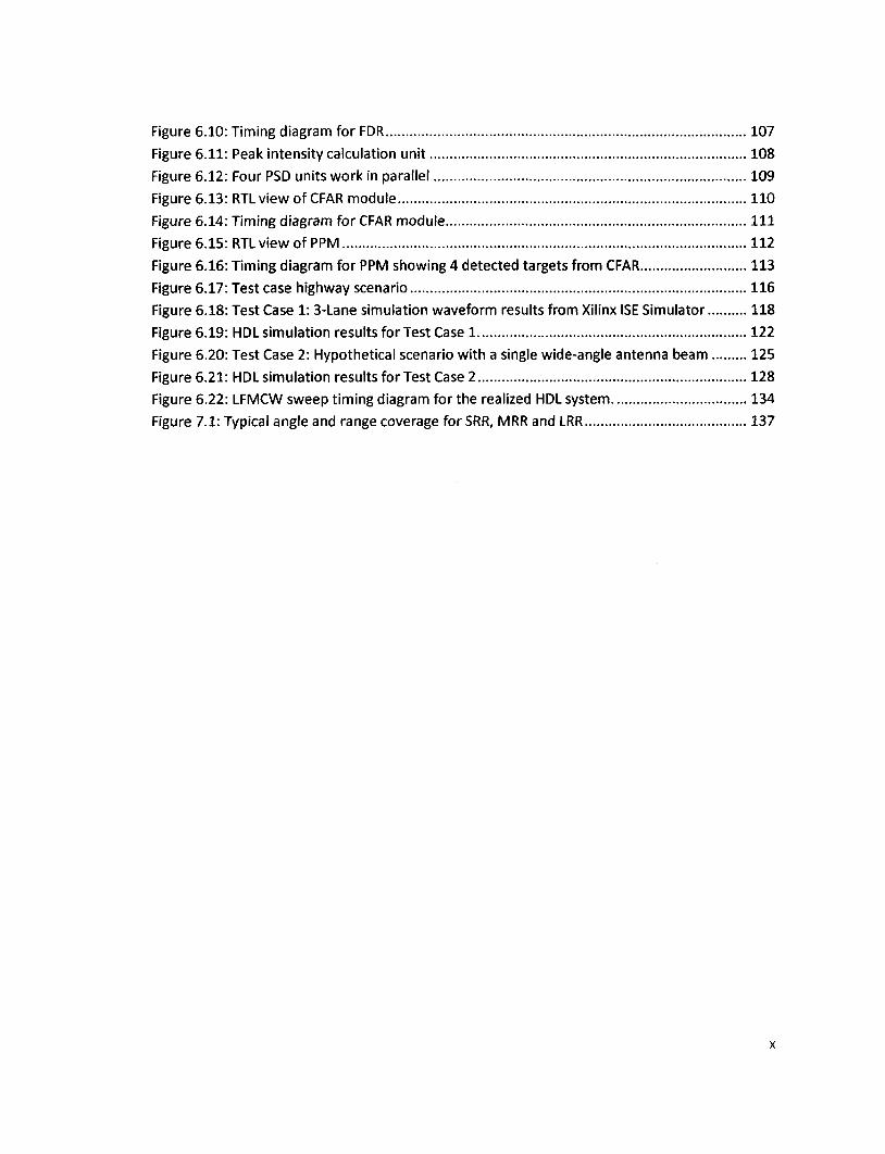
Figure 6.10: Timing diagram for FDR 107
Figure 6.11: Peak intensity calculation unit 108
Figure 6.12: Four PSD units work in parallel 109
Figure 6.13: RTL view of CFAR module 110
Figure 6.14: Timing diagram for CFAR module I l l
Figure 6.15: RTL view of PPM 112
Figure 6.16: Timing diagram for PPM showing 4 detected targets from CFAR 113
Figure 6.17: Test case highway scenario 116
Figure 6.18: Test Case 1: 3-Lane simulation waveform results from Xilinx ISE Simulator 118
Figure 6.19: HDL simulation results for Test Case 1 122
Figure 6.20: Test Case 2: Hypothetical scenario with a single wide-angle antenna beam 125
Figure 6.21: HDL simulation results for Test Case 2 128
Figure 6.22: LFMCW sweep timing diagram for the realized HDL system 134
Figure 7.1: Typical angle and range coverage for SRR, MRR and LRR 137
x
List of Tables
Table 1.1: Fatality count around the globe 3
Table 2.1: Speed Comparison of a typical FPGA 23
Table 2.2: Commercially available new generation of automotive radar systems 27
Table 2.3: Previous generation of automotive radar systems 27
Table 3.1: The next generation of Long Range Radar 30
Table 3.2: Comparison of common Window functions 47
Table 3.3: Atmospheric attenuation at 70-80 GHz 56
Table 4.1: Initially provided System Specifications 60
Table 4.2: Final parameters for the devised signal processing algorithm 70
Table 5.1: Practical Test Case Highway Scenario-Target Description 78
Table 5.2: Results from MATLAB Simulation of 3-Lane Narrow Beam Scenario 84
Table 5.3: Errors from MATLAB Simulations of 3-Lane Narrow Beam Scenario 85
Table 5.4: Hypothetical Test Case - Target Description 87
Table 5.5: Results from MATLAB Simulations of 3-Lane Single Wide Beam Scenario 90
Table 5.6: Errors from MATLAB Simulations of 3-Lane Single Wide Beam Scenario 90
Table 6.1: Xilinx Virtex-5 SX50T features 93
Table 6.2: Port description for TLC 97
Table 6.3: Port description for SAMPLER 101
Table 6.4: Xilinx FFT IP core parameterization 102
Table 6.5: Port description for FFT 103
Table 6.6: Port description for FDR 106
Table 6.7: Port description for PSD 108
Table 6.8: Port description for CFAR 110
Table 6.9: Sensitivity Adjustment for CA-CFAR Processor 112
Table 6.10: Port description for PPM 113
Table 6.11: Results from HDL Simulation of 3-Lane Narrow Beam Scenario 123
Table 6.12: Errors from HDL Simulations of 3-Lane Narrow Beam Scenario 124
Table 6.13: Results from HDL Simulations of 3-Lane Single Wide Beam Scenario 129
Table 6.14: Errors from HDL Simulations of 3-Lane Single Wide Beam Scenario 129
Table 6.15: Comparison of MATLAB and HDL range results for wide beam scenario 130
Table 6.16: Comparison of MATLAB and HDL velocity results for wide beam scenario 131
Table 6.17: Resource Usage for the Radar Signal Processing Algorithm on Virtex-5 SX50T 132
Table 6.18: Timing Achievements of HDL Implementation 132
Table 6.19: Achieved Timing Details for Developed LFMCW Radar System 134
XI
List of Abbreviations
MEMS - Microelectromechanical Systems
Radar - Radio Detection and Ranging
RF - Radio Frequency
SP3T - Single Pole Triple Throw
PRF - Pulse Repetition Frequency
DSP - Digital Signal Processor(-ing)
FPGA- Field Programmable Gate Array
DAC - Digital to Analog Converter
ADC - Analog to Digital Converter
FSK - Frequency Shift Keying
LFMCW - Linear Frequency Modulated Continuous Wave
HDL- Hardware Description Language
ECCM - Electronic Counter-Countermeasures
FFT- Fast Fourier Transform
DFT- Discrete Fourier Transform
DIT- Decimation In Time
DIF - Decimation In Frequency
CA(OS)-CFAR - Constant False(Ordered Statistics) Constant False Alarm Rate
RTL - Register Transfer Level
TLC - Top Level Control
TDR-Time-domain Data RAM
FDR - Frequency-domain DATA RAM
PSD - Power Spectral Density
xii
PPM - Peak Pairing Module
RCS - Radar Cross-Section
CPI -Coherent Processing Interval
VCO-Voltage Controlled Oscillator
LRR - Long Range Radar
MRR - Medium Range Radar
SRR-Short Range Radar
IF - Intermediate Frequency
MSPS - Mega-Samples Per Second
LUT-Look-Up Table
FF-Flip-Flop
BUFG-Global Buffer
BUFGCTLR - Global Clock Buffer
RAM - Random Access Memory
ROM - Read-Only Memory
DSP48E -Xilinx Digital Signal Processing Slice (5th Generation)
DOA - Direction Of Arrival
ISE - Integrated System Environment
LPF - Low Pass Filter
AWGN - Additive White Gaussian Noise
EM - Electro-Magnetic
MMIC - Monolithic Microwave Integrated Circuits
UWB-Ultra-Wide Band
SMD - Surface Mount Device
Nomenclature
r - target range
c = speed of RF waves through air
^two-way = two-way travel time for RF wave from radar sensor to target and back
vrel = relative velocity
vtarget = target velocity
vhost = n o s t vehicle velocity
/ ( j = Doppler frequency shift
X = radio wave wavelength
/b = beat frequency or instantaneous intermediate frequency
/ t = transmit signal frequency
fx = received signal frequency
r0 = travel time for RF wave from radar sensor to target
B = LFMCW sweep bandwidth
T - LFMCW sweep duration
k = rate of change of frequency in LFMCW sweep =BIT
X k = frequency domain sample
xn = time domain sample
Pfa = probability of false alarm
Tc = CFAR dynamic threshold
<T = Radar Cross-Section of a target
Njh = thermal noise
rA = absolute atmospheric temperature
SNRQ = quantization signal-to-noise ratio
fs = sampling frequency
/res = frequency resolution of FFT
xiv
CHAPTER 1: INTRODUCTION
This chapter starts with a clear definition of the issue this research work
addresses, explaining the importance of the work and its outcomes. Facts about road
safety and accident records around the globe are presented and automotive radar
applications are identified as an effective means of enhancing vehicular safety features.
The potential benefits of automotive radar systems in road safety are highlighted, and
the radar being developed at the University of Windsor is presented along with a
concise operating principle. Finally, the principal results of this research work are listed.
1.1 Problem Statement
The objective and goal of this research is to develop an FPGA-implementable signal
processing algorithm for use in a Microelectromechanical Systems (MEMS) based linear
frequency modulated continuous wave (LFMCW) long range auotomotive radar to
determine the range and velocity of targets in the vicinity of a host vehicle.
Loss of lives and property damage due to automotive collisions can be minimized if it
is possible to detect the proximity of other vehicles, pedestrians, and obstacles in real
time using advanced microelectromechanical systems (MEMS) based sensor technology.
The current technology for short and long range proximity detection, such as: stand
alone ultrasonic sensor or sensor arrays, electromagnetic radar units (present in high-
end vehicles only), lasers, and cameras mounted on side view mirrors fall short of
establishing a real-time dynamic safety shell around a vehicle due to their high latency
time associated with microelectronic signal processing and need for mechanical
scanning of the target area in case of radars. Moreover, due to high cost of stand-alone
manufacturing, automakers are reluctant to incorporate these solutions in low-end
1

vehicles. As a result the overall road safety situation remains almost the same even if
some of the vehicles are equipped with advanced collision or pre-crash warning
systems. To put the problem in perspective, less than 1% of vehicles running in Canadian
highways are equipped with advanced radar sensors.
Market research firm Strategy Analytics predicts that over the period 2006 to 2011,
the use of long-range distance warning systems in cars could increase by more than 65
percent annually, with demand reaching 3 mn units in 2011, with 2.3 mn of them using
radar sensors. By 2014, 7 percent of all new cars will include a distance warning system,
primarily in Europe and in Japan [18].
Global auto industries and governments are extensively pursuing radar based
proximity detection systems for (1) ACC support with Stop&Go functionality, (2) collision
warning, (3) pre-crash warning, (4) blind spot monitoring, (5) parking aid (forward and
reverse), (6) lane change assistant and (7) rear crash collision warning. The European
Commission (EC) has set an ambitious target to reduce road deaths by 50% by the end
of 2010. In North America alone the rate of fatalities related to road accidents has been
stagnant at approximately 43,000 per year, which sums to a huge annual loss of life and
property [15]. It has been concluded that the use of Forward Collision Warning long
range radar and Lane Departure Warning camera-based sensor among other security
features will become very effective to reduce road fatality rates. In [15], it has been
mentioned that with the proposed crash prevention technologies equipped in vehicles,
the number of crashes can be reduced by 3.8 mn in North America, and the number of
human lives saved from that amounts close to 17,000 per year. This warrants the use of
long range radar as an indispensable feature to improve highway safety and minimize
loss of lives and property damage.
2
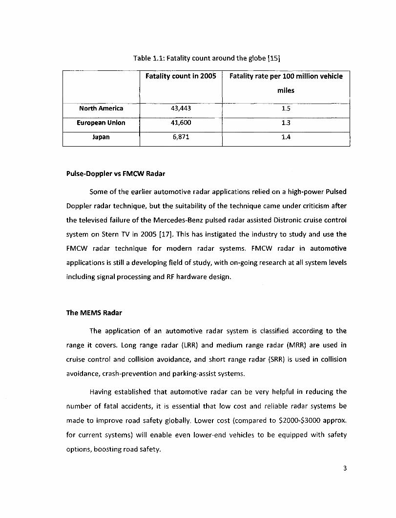
Table 1.1: Fatality count around the globe [15]
North America
European Union
Japan
Fatality count in 2005
43,443
41,600
6,871
Fatality rate per 100 million vehicle
miles
1.5
1.3
1.4
Pulse-Doppler vs FMCW Radar
Some of the earlier automotive radar applications relied on a high-power Pulsed
Doppler radar technique, but the suitability of the technique came under criticism after
the televised failure of the Mercedes-Benz pulsed radar assisted Distronic cruise control
system on Stern TV in 2005 [17]. This has instigated the industry to study and use the
FMCW radar technique for modern radar systems. FMCW radar in automotive
applications is still a developing field of study, with on-going research at all system levels
including signal processing and RF hardware design.
The MEMS Radar
The application of an automotive radar system is classified according to the
range it covers. Long range radar (LRR) and medium range radar (MRR) are used in
cruise control and collision avoidance, and short range radar (SRR) is used in collision
avoidance, crash-prevention and parking-assist systems.
Having established that automotive radar can be very helpful in reducing the
number of fatal accidents, it is essential that low cost and reliable radar systems be
made to improve road safety globally. Lower cost (compared to $2000-$3000 approx.
for current systems) will enable even lower-end vehicles to be equipped with safety
options, boosting road safety.
3
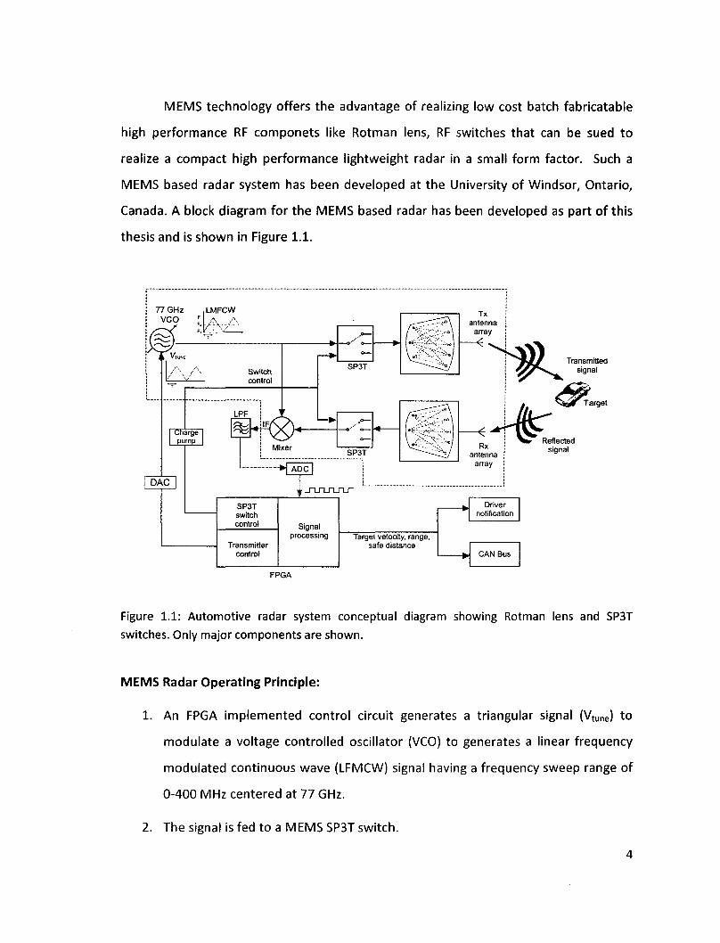
MEMS technology offers the advantage of realizing low cost batch fabricatable
high performance RF componets like Rotman lens, RF switches that can be sued to
realize a compact high performance lightweight radar in a small form factor. Such a
MEMS based radar system has been developed at the University of Windsor, Ontario,
Canada. A block diagram for the MEMS based radar has been developed as part of this
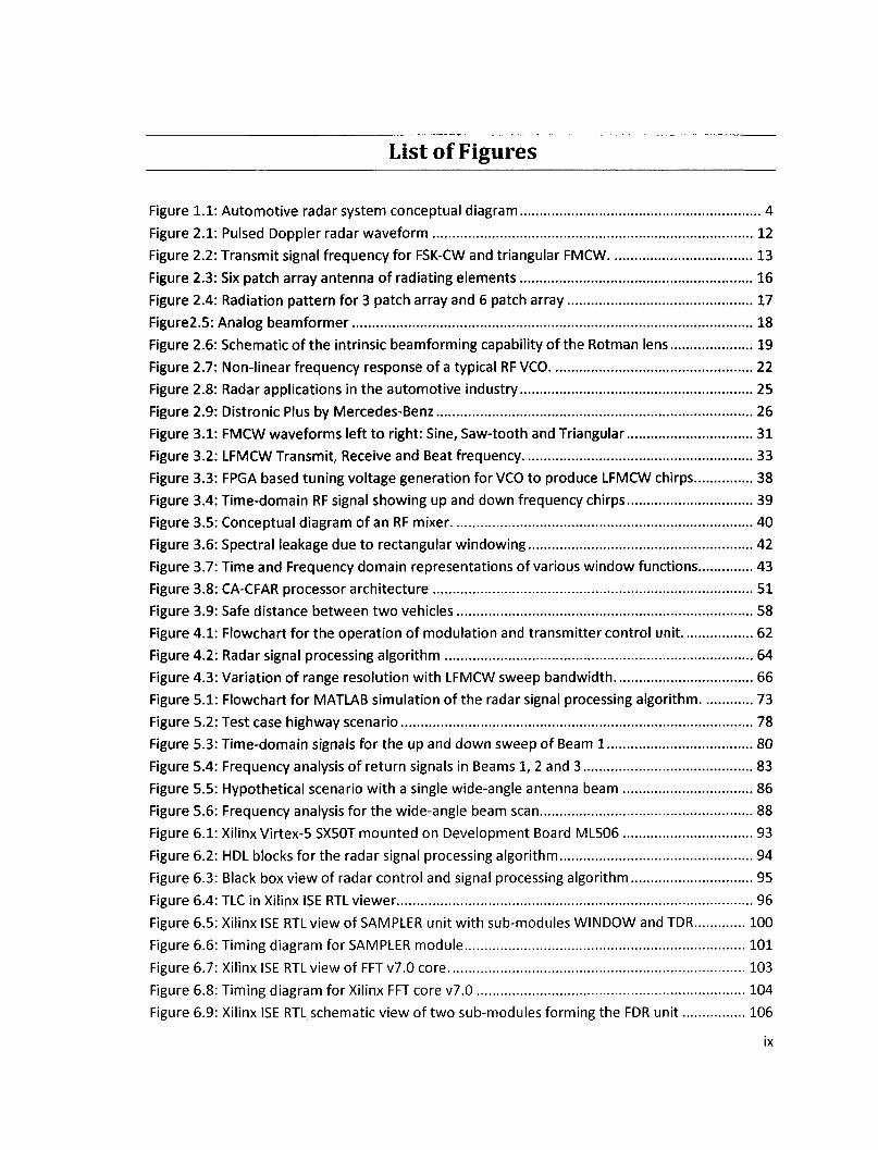
thesis and is shown in Figure 1.1.
Transmitted signal
Target
SP3T switch control
Transmitter control
Signal processing Target velocity, range,
safe distance
Driver notification
CAN Bus
FPGA
Figure 1.1: Automotive radar system conceptual diagram showing Rotman lens and SP3T switches. Only major components are shown.
MEMS Radar Operating Principle:
1. An FPGA implemented control circuit generates a triangular signal (Vtune) to
modulate a voltage controlled oscillator (VCO) to generates a linear frequency
modulated continuous wave (LFMCW) signal having a frequency sweep range of
0-400 MHz centered at 77 GHz.
2. The signal is fed to a MEMS SP3T switch.
3. An FPGA implemented control algorithm controls the SP3T switch to sequentially
switch the LFMCW signal among the three beam ports of a MEMS implemented
Rotman lens.
4. As the LFMCW signal arrives at the array ports of the Rotman lens after traveling
through the Rotman lens cavity, the time-delayed in-phase signals are fed to a
microstrip antenna array that radiates the signal in a specific direction.
5. The sequential switching of the input signal among the beamports of the Rotman
lens enables the beam to be steered across the target area in steps by a pre-
specific angle.
6. On the receiving side, a receiver antenna array receives the signal reflected off a
vehicle or an obstacle and feeds the signal to another SP3T switch through
another Rotman lens.
7. An FPGA based control circuit controls the operation of the receiver SP3T switch
so that the signal output at a specific beamport of the receiver Rotman lens can
be mixed with the corresponding transmit signal.
8. The output of the receiver SP3T switch is passed through a mixer to generate an
IF signal in the range of 0-200 KHz.
9. An Analog-to-digital converter (ADC) samples the received IF signal and converts
it to a digital signal.
10. Finally, an FPGA implemented algorithm processes the digital signal from the
ADC to determine the range and velocity of the detected target.
The goal of this thesis is to develop the FPGA implementable algorithm to realize the
functionality of the MEMS Radar system as described above to detect the distance and
velocity of target vehicle(s) in a pre-specified range to meet the requirements of a long
range automotive radar.
1.2 Hypothesis
Owing to the passive nature of the MEMS Rotman lens, a relatively enhanced
cycle time can be achievable as compared to current state-of-the-art systems. The FPGA
based control and signal processing algorithm can be implemented as a low cost ASIC.
Together with the miniature MEMS components, and appropriate off-the-shelf radar
frontend, the target system would offer a highly compact higher performance small
form factor radar solution for automotive applications.
The efficiency of the FPGA control and signal processing implementation will be
gauged by resource usage, speed and its accuracy compared to floating-point MATLAB
simulations.
1.3 Motivation
The automotive scenario is fast-paced, with every millisecond being precious in
time-critical applications such as collision avoidance and collision mitigation systems.
Existing automotive radar sensors are critical components of the overall safety system of
a vehicle, and their cycle time or refresh time (these terms are used interchangeably
through this thesis) - the time over which the entire field of view is covered - should be
considerably short. At a speed of 200 km/h a vehicle travels 2.78 meters in 50ms, the
refresh time of a typical existing system such as Bosch LRR3. Such latency in the safety
mechanism of the vehicle in response to a potential threat increases the possibility of an
accident.
This thesis aims at exploiting the intrinsic beamforming capability of the Rotman
lens, the fast signal processing and parallel computing on FPGAs, and the reliability of
the LFMCW method in target detection to provide digital signal processing and control
of a lightweight state-of-the-art compact radar sensor for automotive safety systems.
6
1.4 Research Methodology
The course of developing an FPGA-based LFMCW radar signal processing algorithm for
the 77 GHz MEMS radar sensor involves the following steps:
1. Study the initial system specifications provided by the project supervisor based
on the MEMS based radar sensor presented in [1].
2. Survey of literature on radar systems, radar signal processing and target tracking,
radio frequency attenuation, and acceptable parameters for automotive collision
avoidance systems.
3. Development of a robust and fast radar signal processing algorithm and
development of a mathematical model of the same.
4. Decision on system peripherals such as data converters and interfaces according
to target system parameters.
5. Simulation of the algorithm in MATLAB for a typical highway traffic test scenario.
6. Development of HDL code for implementation on FPGA.
7. Verification of the developed HDL code using the same test scenario as in (3) for
a comparison of accuracy between fixed-point HDL signal processing and
floating-point MATLAB processing.
8. Fine-tuning and optimization of the HDL code for implementation on target
FPGA.
7
1.5 Principal Results
1. A reusable and parameterizable ready-to-implement LFMCW radar signal
processing algorithm for FPGA/ASIC with minimal latency of 212 us and a
competitive radar cycle time of 6.78 ms has been created. Major achieved
performance specifications of the developed system are listed below:
• Operating frequency - 77 GHz (within regional radio frequency allocation)
• Bandwidth - 800 MHz (within regional bandwidth limits)
• Maximum (Minimum) distance - 200 (0.4) meters
• Range resolution (in HDL) - 0.19 meters
• Maximum target range error - 0.25 meters
• Worst-case range accuracy - 99.75% (beyond 100 meters)
• Maximum relative velocity - ±300 km/h (receding and approaching target)
• Velocity resolution (in HDL) - 0.95 m/s
• Maximum target velocity error - 0.83 m/s
• Worst-case velocity accuracy - 99.17% (beyond 60 km/h)
• Beam steerability - ±4.5° (beam width 9°) [1]
• Maximum target count for 3-beam Rotman lens radar - 24
2. A superior signal processing time compared to recent FPGA-based
implementations as presented in [28].
8
1.6 Thesis Organization
Developing from the introduction in Chapter 1, Chapter 2 concisely summarizes
the available literature of radar technology and studies state-of-the-art standards in
automotive radar sensors, and their applications, in order to produce a list of target
specifications for the MEMS radar sensor developed at the University of Windsor.
Chapter 3 of this thesis propounds a thorough background and mathematical
conceptualization of radar topics, focusing on LFMCW radar theory. The underlying
concept of radio detection and ranging systems is presented considering different issues
affecting performance, such as noise, attenuation and non-linearity all with reference to
the design of an automotive radar sensor. Essential signal conditioning and processing
approaches are discussed with focus on frequency analysis of the radar signal.
Chapter 4 builds on the foundations laid in Chapter 2, and presents the developed
radar signal processing algorithm. The different components in the algorithm are
discussed in further detail.
Chapter 5 shows a MATLAB implementation and simulation of the radar signal
processing algorithm. Effects of different signal processing methods such as time-
domain windowing and Fourier transform on a noisy signal are studied. Simulation
results are presented to validate the accuracy of the developed algorithm.
Hardware implementation of the conceived algorithm is laid out in the form of
FPGA modules in Chapter 6. Realization of the modules is carried out in Verilog HDL
(Verilog 2005 - IEEE Standard 1364-2005) using Xilinx development software, where
fixed-point and resource usage considerations for the signal processing, sampling and
control algorithm are presented. Code validation is done using Xilinx ISE ISim simulator
with the same real-valued time-domain data samples as used in MATLAB code
verification. Chapter 7 furnishes the concluding remarks on the research work, shedding
light on achieved system specifications, future amendments and possible expansions to
the work presented herein.
9
CHAPTER 2:
LITERATURE SURVEY
This chapter covers a review of the existing literature on radar systems,
identifying the types of radars available. The advantages of frequency modulated
continuous wave (FMCW) radar over pulsed and frequency shifting radars are
recognized, based on which the decision of using FMCW radar is selected as the right
match for the target automotive radar. Important radar concepts are described,
especially beamforming and beam steering for solid-state phased array antenna radars.
The Rotman lens' role in this radar system is described, and a platform for the radar
signal processing algorithm is selected. The latter part of this chapter presents state-of-
the-art automotive radar systems, highlighting the Bosch LRR3 as a guideline for the
specifications of the system developed in this thesis.
2.1 Literature Review
Radar technology has long been used in military, aerospace, marine, geographical,
weather monitoring and global positioning applications [9]. The first conceptualization
of RF radar was made in 1920 by Bells Labs and in 1922 by Guglielmo Marconi [10]. It
has recently found increasing popularity in the automotive arena with automobile
manufacturers incorporating radars for adaptive cruise control (ACC), parking aid, pre-
crash warning, and collision avoidance systems.
Radar systems can be classified by two major types: Pulsed and Continuous Wave
[2]. Both implementations have distinct operating principle, transmit signal generation,
receive signal conditioning and processing, control and synchronization issues, and
power requirements.
10
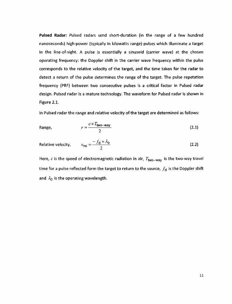
Pulsed Radar: Pulsed radars send short-duration (in the range of a few hundred
nanoseconds) high-power (typically in kilowatts range) pulses which illuminate a target
in the line-of-sight. A pulse is essentially a sinusoid (carrier wave) at the chosen
operating frequency: the Doppler shift in the carrier wave frequency within the pulse
corresponds to the relative velocity of the target, and the time taken for the radar to
detect a return of the pulse determines the range of the target. The pulse repetation
frequency (PRF) between two consecutive pulses is a critical factor in Pulsed radar
design. Pulsed radar is a mature technology. The waveform for Pulsed radar is shown in
Figure 2.1.
In Pulsed radar the range and relative velocity of the target are determined as follows:
c x^two-way ,~ ... Range, r = (2.1)
— f x A Relative velocity, vre, = - ^ - (2.2)
Here, c is the speed of electromagnetic radiation in air, 77tw0_way is the two-way travel
time for a pulse reflected form the target to return to the source, / d is the Doppler shift
and AQ is the operating wavelength.
11
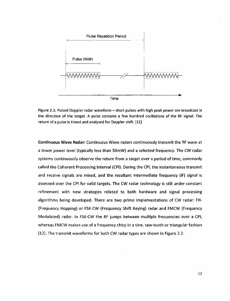
; Pulse Repetition Period < >
Pulse Width j
Time
Figure 2.1: Pulsed Doppler radar waveform - short pulses with high peak power are broadcast in the direction of the target. A pulse contains a few hundred oscillations of the RF signal. The return of a pulse is timed and analysed for Doppler shift. [11]
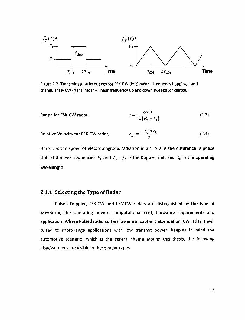
Continuous Wave Radar: Continuous Wave radars continuously transmit the RF wave at
a lower power level (typically less than 50mW) and a selected frequency. The CW radar
systems continuously observe the return from a target over a period of time, commonly
called the Coherent Processing Interval (CPI). During the CPI, the instantaneous transmit
and receive signals are mixed, and the resultant intermediate frequency (IF) signal is
assessed over the CPI for valid targets. The CW radar technology is still under constant
refinement with new strategies related to both hardware and signal processing
algorithms being developed. There are two prime implementations of CW radar: FH-
(Frequency Hopping) or FSK-CW (Frequency Shift Keying) radar and FMCW (Frequency
Modulated) radar. In FSK-CW the RF jumps between multiple frequencies over a CPI,
whereas FMCW makes use of a frequency chirp in a sine, saw-tooth or triangular fashion
[12]. The transmit waveforms for both CW radar types are shown in Figure 2.2.
12
frit) F2+
•step
Tc?\ 2 r C P I Time 'CPI z i CPI Time
Figure 2.2: Transmit signal frequency for FSK-CW (left) radar - frequency hopping - and triangular FMCW (right) radar - linear frequency up and down sweeps (or chirps).
Range for FSK-CW radar,
Relative Velocity for FSK-CW radar,
r =
rel
cAd>
4*(F2-F,) (2.3)
(2.4)
Here, c is the speed of electromagnetic radiation in air, AO is the difference in phase
shift at the two frequencies Fx and F2, fd is the Doppler shift and XQ is the operating
wavelength.
2.1.1 Selecting the Type of Radar
Pulsed Doppler, FSK-CW and LFMCW radars are distinguished by the type of
waveform, the operating power, computational cost, hardware requirements and
application. Where Pulsed radar suffers lower atmospheric attenuation, CW radar is well
suited to short-range applications with low transmit power. Keeping in mind the
automotive scenario, which is the central theme around this thesis, the following
disadvantages are visible in these radar types.
13
Pulsed Doppler disadvantages:
- Velocity measurement limited by blind speed when fd is a multiple of the PRF.
Maximum measurable Doppler shift has to be less than PRF to avoid ISI among
different pulses and target returns.
- To reduce the above velocity ambiguity the PRF can be increased, however
increasing the PRF creates range ambiguity.
Relatively high power requirements in the automotive scenario.
Greater risk of jamming or confusion due to high-power pulses from other
Pulsed radars.
FSK-CW disadvantages:
Invisible targets in the direct path of the radar.
- Target range is computed based on the difference in phase shift for two
consecutive frequency hops. This makes the system subject to phase noise.
The CPI needs to be large enough to avoid range ambiguity.
The disadvantages posed by both Pulsed Doppler and FSK-CW radars mandate a
type of radar which does not suffer the same, and is apropos in the automotive
scenario. LFMCW radar overcomes these disadvantages with:
No theoretical limit to range resolution and better short range detection.
Reduced effects of clutter and atmospheric noise.
Lower power rating than Pulsed radar.
Less effects of phase noise.
More resistance to interference from other similar radars in the vicinity.
14
No theoretical blind spots.
Resistance to jamming (frequency modulation is a common tool in ECCM -
Electronic Counter-Countermeasures - to overcome jamming effects)
This qualitative comparison warrants the use of LFMCW for the MEMS radar sensor
under development, especially for long range radar (LRR) application.
Apart from the distinction in operating principles of different radar types, there are
design issues common to all types in general. These are:
Beamforming technique
Frequency generation, tuning and linearity
Platform for implementation of radar signal processing algorithm
2.1.2 Beamforming with Phased Array Antennae
2.1.2.1 Microelectronic Beamforming
The primitive approach in communications to rotate a scanning beam over an
azimuthal angle was to physically rotate a directional antenna mounted on a gyrating
platform. To reduce the delay and power usage inherent to this mechanically rotating
part, solid-state antennae with microelectronic beamforming were developed.
Beamforming is an aspect of wireless systems where directional signal transmission
and/or reception are desired. In other words, beamforming can be referred to as a form
of spatial filtering [7]. It is a technique applied in both transmission and reception,
depending on the application. In communications, high directivity is desired in the
direction of the signal source for a low-noise high-fidelity link to be established. In radar
15
systems, beamforming allows a means of electronic steering of a narrow scanning beam
to detect targets with higher angular resolution.
Essentially, beamforming with phased array antennae - which is the type of
antenna used in the radar system under development - is the ability to simulate a large
directional radiation pattern using a set of smaller non-directional radiating antennae
[4]. A beamformer does this by adjusting the amplitude and phase of the radiation at
every radiating element and forming a pattern of constructive interference in the
desired direction and destructive interference elsewhere.
RF Source
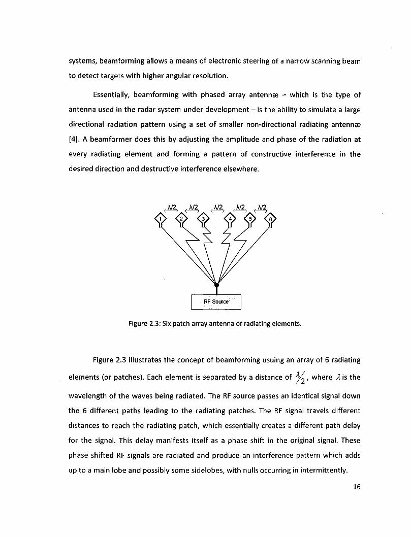
Figure 2.3: Six patch array antenna of radiating elements.
Figure 2.3 illustrates the concept of beamforming usuing an array of 6 radiating
elements (or patches). Each element is separated by a distance of y~ , where l i s the
wavelength of the waves being radiated. The RF source passes an identical signal down
the 6 different paths leading to the radiating patches. The RF signal travels different
distances to reach the radiating patch, which essentially creates a different path delay
for the signal. This delay manifests itself as a phase shift in the original signal. These
phase shifted RF signals are radiated and produce an interference pattern which adds
up to a main lobe and possibly some sidelobes, with nulls occurring in intermittently.
16
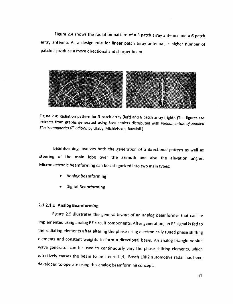
Figure 2.4 shows the radiation pattern of a 3 patch array antenna and a 6 patch
array antenna. As a design rule for linear patch array antennae, a higher number of
patches produce a more directional and sharper beam.
W W t * -f%r •#•• fc«i m- * i : " i s - : a. •• so" t * : ^
Figure 2.4: Radiation pattern for 3 patch array (left) and 6 patch array (right). (The figures are extracts from graphs generated using Java applets distributed with Fundamentals of Applied Electromagnetics 6th Edition by Ulaby, Michielsson, Ravaioli.)
Beamforming involves both the generation of a directional pattern as well as
steering of the main lobe over the azimuth and also the elevation angles.
Microelectronic beamforming can be categorized into two main types:
• Analog Beamforming
• Digital Beamforming
2.1.2.1.1 Analog Beamforming
Figure 2.5 illustrates the general layout of an analog beamformer that can be
implemented using analog RF circuit components. After generation, an RF signal is fed to
the radiating elements after altering the phase using electronically tuned phase shifting
elements and constant weights to form a directional beam. An analog triangle or sine
wave generator can be used to continuously vary the phase shifting elements, which
effectively causes the beam to be steered [4]. Bosch LRR2 automotive radar has been
developed to operate using this analog beamforming concept.
17
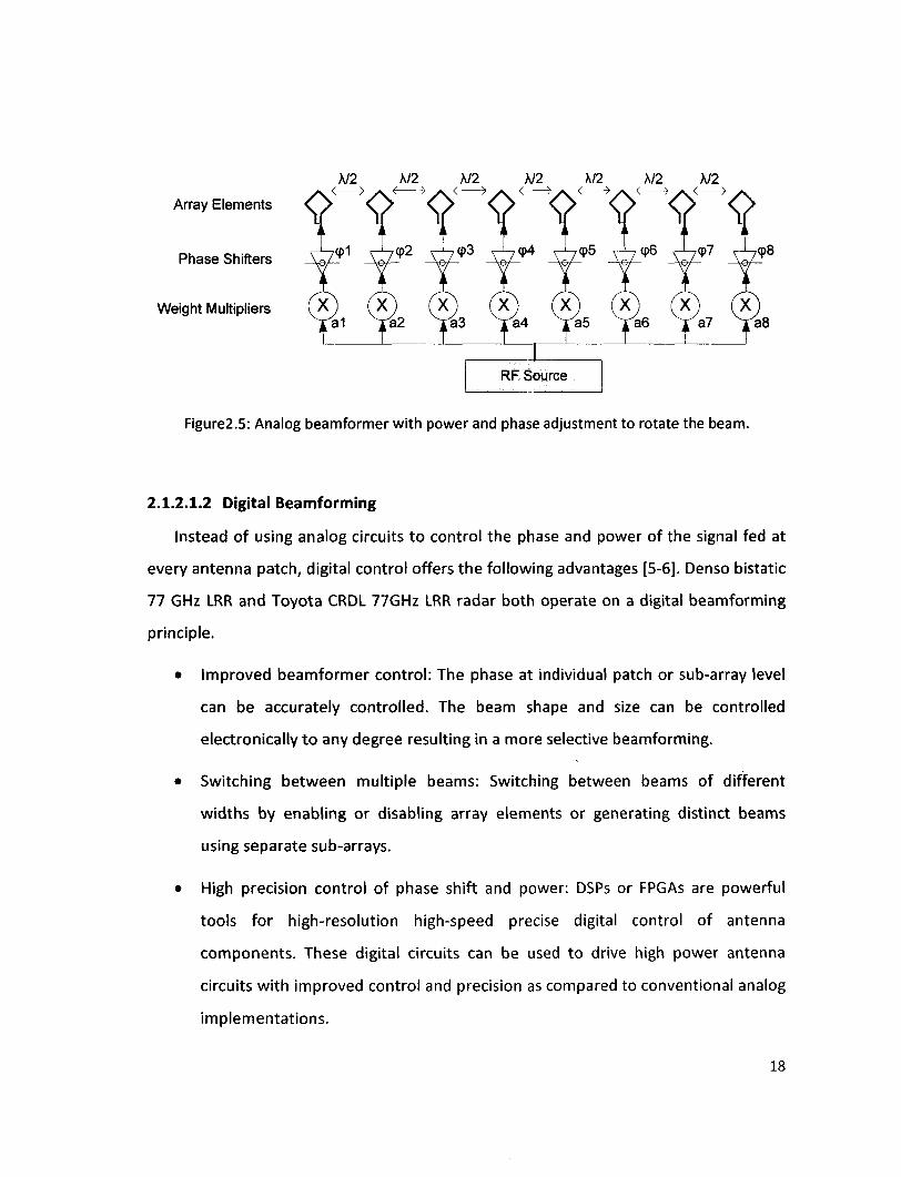
Array Elements
Phase Shifters
Weight Multipliers
I RF Source I
Figure2.5: Analog beamformer with power and phase adjustment to rotate the beam.
2.1.2.1.2 Digital Beamforming
Instead of using analog circuits to control the phase and power of the signal fed at
every antenna patch, digital control offers the following advantages [5-6]. Denso bistatic
77 GHz LRR and Toyota CRDL 77GHz LRR radar both operate on a digital beamforming
principle.
• Improved beamformer control: The phase at individual patch or sub-array level
can be accurately controlled. The beam shape and size can be controlled
electronically to any degree resulting in a more selective beamforming.
• Switching between multiple beams: Switching between beams of different
widths by enabling or disabling array elements or generating distinct beams
using separate sub-arrays.
• High precision control of phase shift and power: DSPs or FPGAs are powerful
tools for high-resolution high-speed precise digital control of antenna
components. These digital circuits can be used to drive high power antenna
circuits with improved control and precision as compared to conventional analog
implementations.
18
A/2 A/2 A/2 A/2 A/2 A/2 A/2
Digital beamformers require memory blocks, adders and multipliers as system
building blocks. These digital components are available in high-speed on-chip resources
in FPGAs which typically operate at clock frequencies of 550 MHz (e.g. Virtex 6 FPGA by
Xilinx). This makes digital beamforming techniques more feasible and efficient. Digital
beamforming does require more signal conditioning prior to digital processing. If the
signal frequency is too high (greater than 100 MHz, say) direct sampling is not possible.
To overcome this issue, the signal needs to be down-converted to an intermediate
frequency (IF) using an RF mixer which can be sampled. Various beamformer
architectures are available in [3-4].
2.1.2.2 Rotman Lens Beamformer
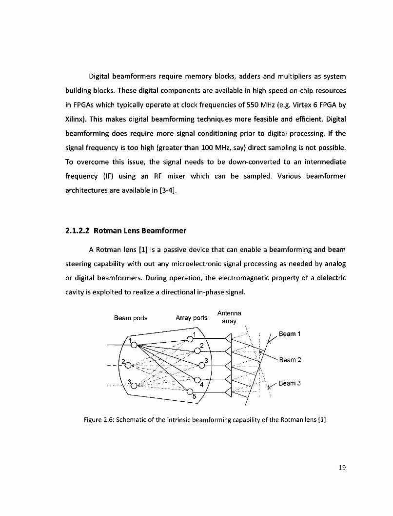
A Rotman lens [1] is a passive device that can enable a beamforming and beam
steering capability with out any microelectronic signal processing as needed by analog
or digital beamformers. During operation, the electromagnetic property of a dielectric
cavity is exploited to realize a directional in-phase signal.
Figure 2.6: Schematic of the intrinsic beamforming capability of the Rotman lens [1].
19
The body of the Rotman lens has beam ports on one side and array ports on the
opposite side. The central beam (beam port 2 in Figure 2.6) guides the input signal
through channels of equal length to the array elements, creating a forward-facing beam.
On beam ports 1 and 3 the input signal travels through different path lengths to the
antenna patches, thus undergoing phase shift leading to the beam being steered as
shown [8]. Typical Rotman lenses are large and are realized using microstrip substrates
like Duroid 5880 or dielectric material filled waveguides. Figure 2.6 illustrates the
schematic representation of a Rotman lens. Recently a novel MEMS based air-filled
waveguide type Rotman lens has been reported [1].
2.1.3 Direction of Arrival Estimation using Phased Array Antennae
Direction of Arrival estimation or DOA using classical approach required a
gyrating radar antenna that would pin-point the exact angle of a target. However, with
solid-state antennae and beamforming, DOA estimation requires digital processing. With
higher clock speeds and parallel processing capability of FPGAs and multi-core DSPs, this
digital processing does not pose any limitations. Two techniques have been compared in
literature [30]: DOA estimation by spatial frequency and DOA estimation by phase
difference.
DOA by the spatial frequency: this method is limited by the number of array antenna
elements. A larger number of array elements are required for better accuracy and
precision. It is shown in [30] that with 10 elements the DOA estimation can be unreliable
using this method. For reliable and accurate measurement of target angle a 128
element array is then used, which in real-life applications is impractical and would
increase hardware.
DOA by phase difference: this method is proposed as a superior method to the spatial
frequency method, and requires fewer antenna elements for good precision DOA
measurement. The technique is described as follows:
20
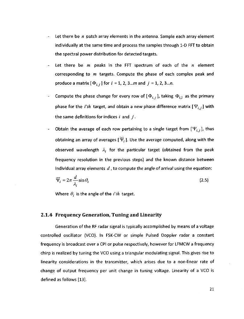
Let there be n patch array elements in the antenna. Sample each array element
individually at the same time and process the samples through 1-D FFT to obtain
the spectral power distribution for detected targets.
Let there be m peaks in the FFT spectrum of each of the n element
corresponding to m targets. Compute the phase of each complex peak and
produce a matrix [ O, y ] for i = 1, 2, 3...m and j = 1, 2, 3.../1.
Compute the phase change for every row of [Q>ij], taking O ^ as the primary
phase for the Vth target, and obtain a new phase difference matrix V^ij] with
the same definitions for indices i and j .
Obtain the average of each row pertaining to a single target from V^ij], thus
obtaining an array of averages [xVi ]. Use the average computed, along with the
observed wavelength A, for the particular target (obtained from the peak
frequency resolution in the previous steps) and the known distance between
individual array elements d, to compute the angle of arrival using the equation:
% =2n—sin0, (2.5)
Where 9t is the angle of the Vth target.
2.1.4 Frequency Generation, Tuning and Linearity
Generation of the RF radar signal is typically accomplished by means of a voltage
controlled oscillator (VCO). In FSK-CW or simple Pulsed Doppler radar a constant
frequency is broadcast over a CPI or pulse respectively, however for LFMCW a frequency
chirp is realized by tuning the VCO using a triangular modulating signal. This gives rise to
linearity considerations in the transmitter, which arises due to a non-linear rate of
change of output frequency per unit change in tuning voltage. Linearity of a VCO is
defined as follows [13].
21
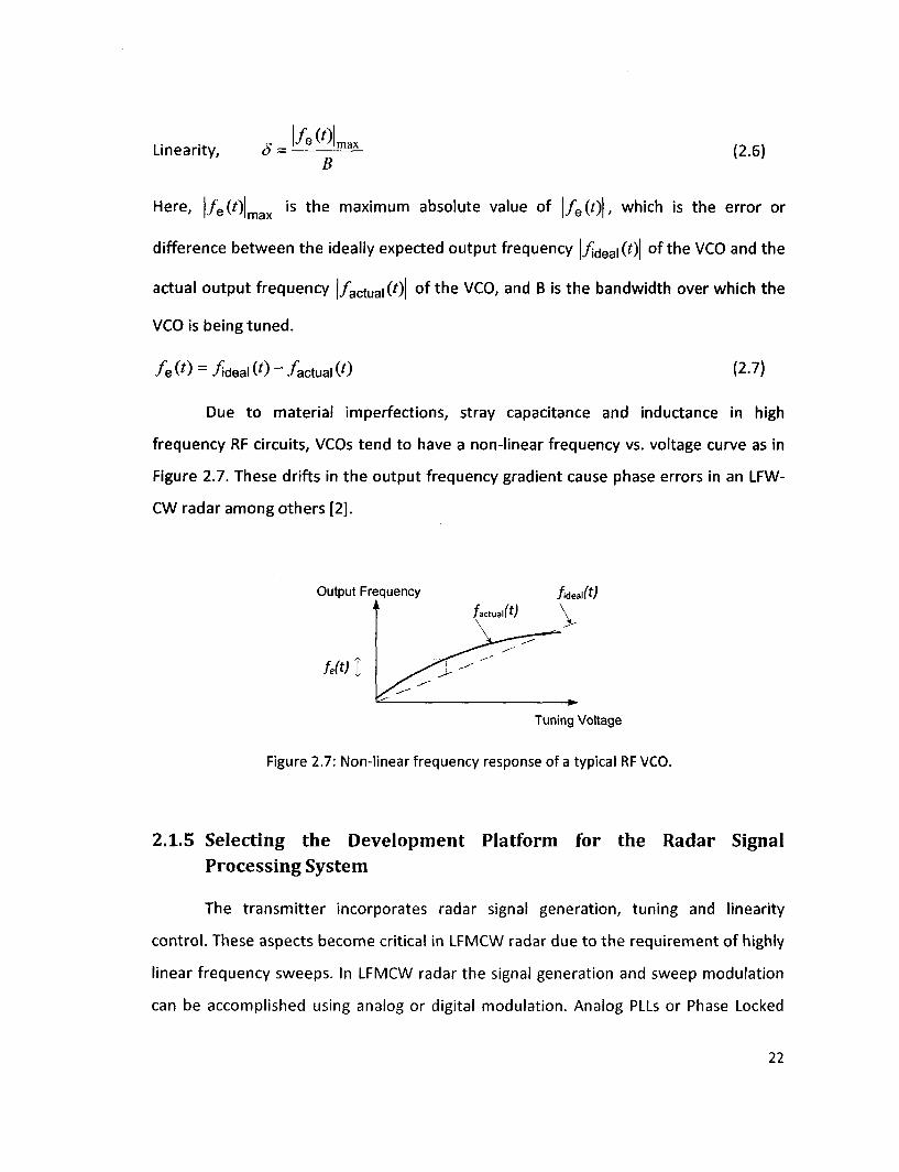
Linearity, S = * 'max (2.6) B
Here, | / e ( 0 | m a 's t n e maximum absolute value of | / e (0 | / which is the error or
difference between the ideally expected output frequency |/jdeal(0| of the VCO and the
actual output frequency |/ac tua i (0| of the VCO, and B is the bandwidth over which the
VCO is being tuned.
fe ( 0 = /ideal ( 0 ~ /actual ( 0 (2-7)
Due to material imperfections, stray capacitance and inductance in high
frequency RF circuits, VCOs tend to have a non-linear frequency vs. voltage curve as in
Figure 2.7. These drifts in the output frequency gradient cause phase errors in an LFW-
CW radar among others [2].
Output Frequency fideJt) ,
fe(t) J
/actualftJ
^t^f^"^ ' ' """
>
— * -Tuning Voltage
Figure 2.7: Non-linear frequency response of a typical RF VCO.
2.1.5 Selecting the Development Platform for the Radar Signal Processing System
The transmitter incorporates radar signal generation, tuning and linearity
control. These aspects become critical in LFMCW radar due to the requirement of highly
linear frequency sweeps. In LFMCW radar the signal generation and sweep modulation
can be accomplished using analog or digital modulation. Analog PLLs or Phase Locked
22
Loops containing a VCO were used in early CW systems, however were overtaken by
digital systems with better frequency response, excellent linearity, easier design and
improved performance in noise [2].
In digital implementation of a radar transmitter the control and modulation
algorithm can be based on a Digital Signal Processor (DSP) or a Field Programmable Gate
Array (FPGA). Due to their highly parallel nature, ability to run several tasks
simultaneously without stalling other tasks, and on-chip resources (such as RAM blocks,
LUTs, fast DSP multipliers) FPGAs are the preferred solution for digital signal processing.
The use of FPGAs for DSP has been boosted by the wide availability of fully customizable
IP cores from various providers spanning many application areas such as DSP,
automotive, communications, computer networking and bus interfaces among others
[14]. According to benchmark results presented in [21], [22] and [28], the latencies for a
2048-point FFT on a 32-bit Intel Core 2 Duo @ 3 GHz, an Analog Devices ADSP-BF53x
and a Texas Instruments TMS320C67xx are tabulated in Table 2.1. Comparison of these
with an FPGA at a much lower clock frequency demonstrates the power of FPGAs as
modern-day high-bandwidth DSP solutions.
Table 2.1: Speed Comparison of a typical FPGA versus a general purpose Dual Core
Processor and a Digital Signal Processor
Manufacturer
Intel
Analog Devices
Texas Instruments
Xilinx
Part Name
32-bit Core 2 Duo
ADSP-BF53X
TMS320C67xx
Virtex-5 FFT Core
Clock
Frequency
(MHz)
3000
600
600
200
2048-point
FFT Latency
(Us)
37.55
32.40
34.20
39.60
Number of
Clock
Cycles
112650
19440
20520
7920
23
Even with a low clock frequency of 200 MHz the FPGA has comparable speed
performance compared to the other processors at higher clock rates. Power
consumption of a digital circuit is proportional to the total gate-level switching required
to compute a particular result: the higher the clock frequency and required clock cycles,
the greater the amount of switching, and thus the higher the power consumption. Given
the automotive scenario, FPGAs offer a desirable combination of speed and power
efficiency.
Furthermore, to deal with possible VCO non-linearity FPGAs can be used to
implement a DDS or Direct Digital Synthesis algorithm. DDS is a method of creating
arbitrary yet repetitive waveforms using a RAM or LUT, a counter, and a DAC,
components that are readily available on FPGA platforms. DDS promises optimal
linearity in frequency sweeps, precise frequency tuning, and excellent phase error
recovery [2].
Based on the analyses presented here, the development platform of choice for
this thesis is FPGA technology. A successful implementation of a radar sensor
transmitter and receiver based on FPGA technology is the Radar Digital Unit (RDU) of
South African Synthetic Aperture Radar II (SASAR II) in May 2004, by the University of
Cape Town [22].
2.1.6 State-of-the-Art in Automotive Radar
Research on automotive radar began as early as the 1950s, although
commercialization only became possible in the late 1990s with the launch of various
manufacturers introducing the early versions of collision warning, parking assist and
adaptive cruise control radars [23]. Daimler-Chrysler launched their first "autonomous
cruise control" radar in 1999 with Mercedes S-class models, marketed as "Distronic".
Further developments of 77 GHz LRR and 24 GHz UWB SRR were launched as a
combination of cruise control, parking assist and collision warning systems, marketed in
24
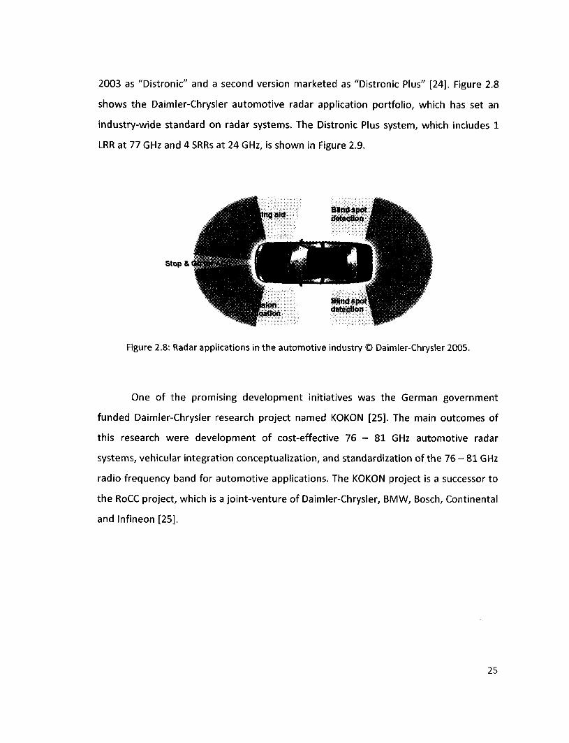
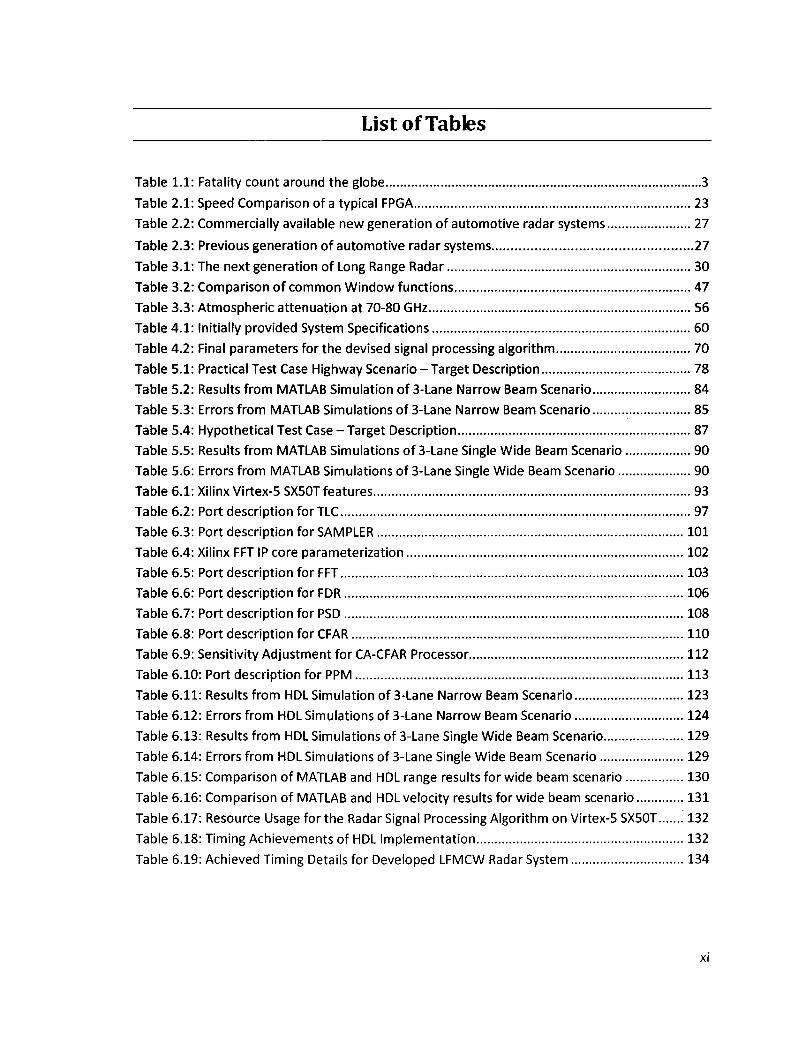
2003 as "Distronic" and a second version marketed as "Distronic Plus" [24]. Figure 2.8
shows the Daimler-Chrysler automotive radar application portfolio, which has set an
industry-wide standard on radar systems. The Distronic Plus system, which includes 1
LRR at 77 GHz and 4 SRRs at 24 GHz, is shown in Figure 2.9.
.. Blind spot ^ ^ ^ ^ n n g a i a detection
stop & tSBKKi ^ ^ ^ ^ _ _ _ ^ ^ _
iMa Blind spot 1 l i l detection
Figure 2.8: Radar applications in the automotive industry © Daimler-Chrysler 2005.
One of the promising development initiatives was the German government
funded Daimler-Chrysler research project named KOKON [25]. The main outcomes of
this research were development of cost-effective 76 - 81 GHz automotive radar
systems, vehicular integration conceptualization, and standardization of the 7 6 - 8 1 GHz
radio frequency band for automotive applications. The KOKON project is a successor to
the RoCC project, which is a joint-venture of Daimler-Chrysler, BMW, Bosch, Continental
and Infineon [25].
25
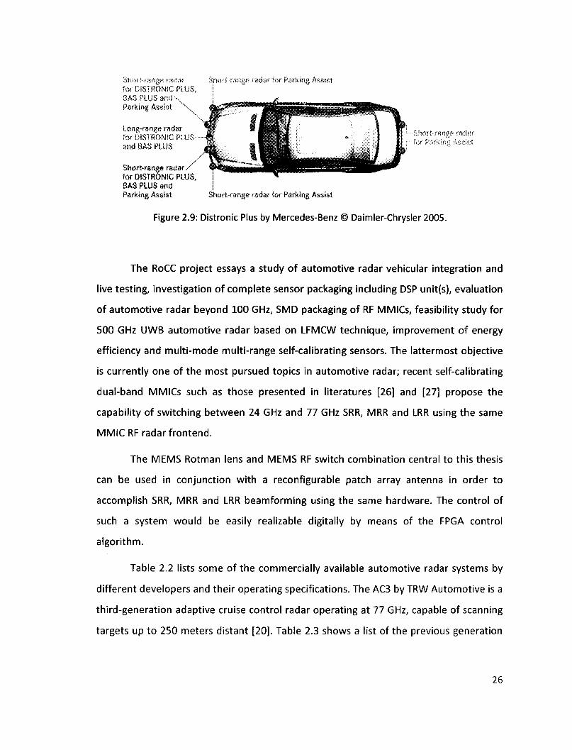
Short range radar Short:-range radar for Parking Assist: for DISTRONIC PLUS, DAS PLUS ami % Parking Assist \
Long-range radar for DISTROWIC PLUS -and BAS PLUS
Short-range radar/ for DISTRONIC PLUS, BAS PLUS and Parking Assist Short-range radar for Parking Assist
Figure 2.9: Distronic Plus by Mercedes-Benz © Daimler-Chrysler 2005.
The RoCC project essays a study of automotive radar vehicular integration and
live testing, investigation of complete sensor packaging including DSP unit(s), evaluation
of automotive radar beyond 100 GHz, SMD packaging of RF MMICs, feasibility study for
500 GHz UWB automotive radar based on LFMCW technique, improvement of energy
efficiency and multi-mode multi-range self-calibrating sensors. The lattermost objective
is currently one of the most pursued topics in automotive radar; recent self-calibrating
dual-band MMICs such as those presented in literatures [26] and [27] propose the
capability of switching between 24 GHz and 77 GHz SRR, MRR and LRR using the same
MMIC RF radar frontend.
The MEMS Rotman lens and MEMS RF switch combination central to this thesis
can be used in conjunction with a reconfigurable patch array antenna in order to
accomplish SRR, MRR and LRR beamforming using the same hardware. The control of
such a system would be easily realizable digitally by means of the FPGA control
algorithm.
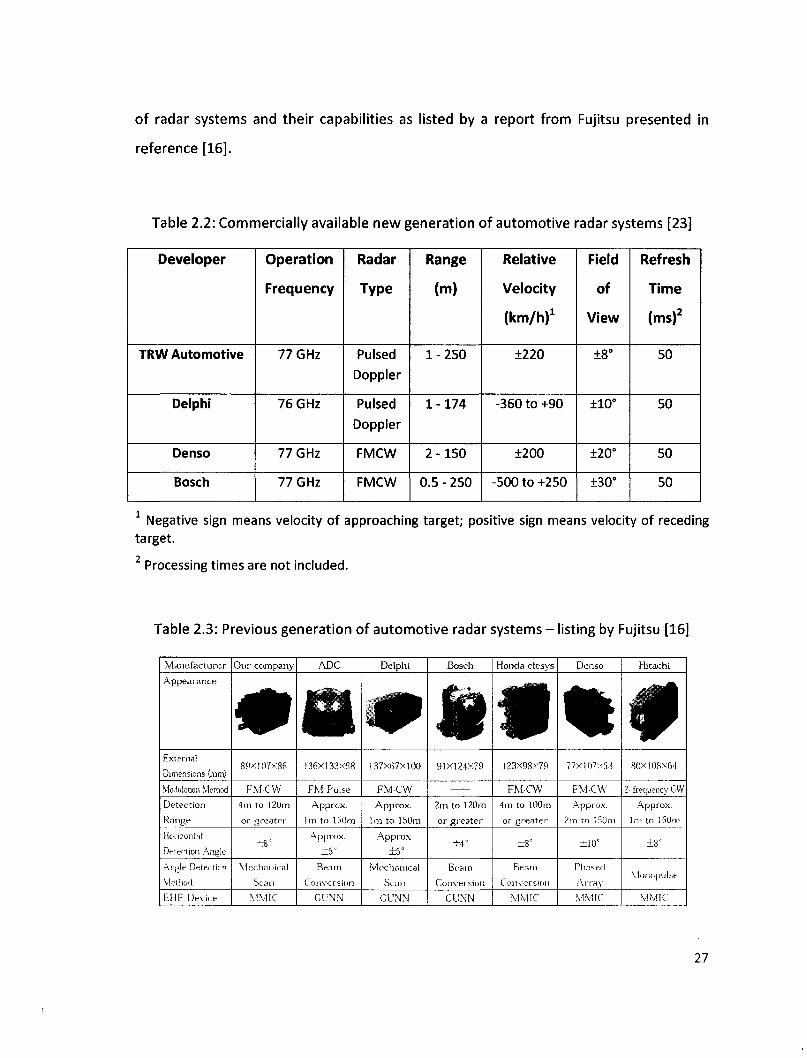
Table 2.2 lists some of the commercially available automotive radar systems by
different developers and their operating specifications. The AC3 by TRW Automotive is a
third-generation adaptive cruise control radar operating at 77 GHz, capable of scanning
targets up to 250 meters distant [20]. Table 2.3 shows a list of the previous generation
26
of radar systems and their capabilities as listed by a report from Fujitsu presented in
reference [16].
Table 2.2: Commercially available new generation of automotive radar systems [23]
Developer
TRW Automotive
Delphi
Denso
Bosch
Operation
Frequency
77 GHz
76 GHz
77 GHz
77 GHz
Radar
Type
Pulsed
Doppler
Pulsed
Doppler
FMCW
FMCW
Range
(m)
1-250
1-174
2-150
0.5 - 250
Relative
Velocity
(km/h)1
±220
-360 to +90
±200
-500 to +250
Field
of
View
±8°
±10°
±20°
±30°
Refresh
Time
(ms)2
50
50
50
50
Negative sign means velocity of approaching target; positive sign means velocity of receding target.
Processing times are not included.
Table 2.3: Previous generation of automotive radar systems - listing by Fujitsu [16]
Manufacturer
Appearance
Externa!
Dimensions (mm)
Modulation Method
Detection
Range
Horizontal
Detection Angie
Alible Detection
Method
EHF Device
Our company
m 89X107X86
F M C W
4 m to 120m
or greater
±8""
Mechanical
Scan
MMIC
ADC
a 136X133X68
FM Pulse
Approx.
1 m to 150m
Approx.
Ream
Conversion
CUNN
Delphi
m 137X67X100
F M C W
Approx.
Ira to 150m
Approx.
±5°
Mechanical
Scan
CUNN
Bosch
91X124X79
2m to 120m
or greater
±4"'
Beam
Conversion
CUNN
Honda elesvs
9 123X98X79
F M C W
4 m to 100 m
or greater
± 8 '
Beam
Conversion
MMIC
Denso
%
77X107X53
FM-CW
Approx.
2m to 150m
±10''
Phased
Array
MMIC
Hitachi
#
80X108X64
2- frequency CVV
Approx,
lm to 150m
±8'
Monopulse
MMIC
27
One of the most recent systems from Table 2.2 is the Bosch LRR3 (as marketed)
which was launched in September 2009 on the Porsche Panamera 2010 model. One of
the claims of Bosch LRR3 is being the world's smallest radar sensor package at 74mm x
77mm x 58mm. The MEMS radar system being developed at the University of Windsor
has close to half the dimensions at 30mm x 40mm x 10mm owing to the compact MEMS
Rotman lens beamformer and antenna design.
These state-of-the-art automotive radar systems provide a target for this thesis
and help set the aims for the speed and efficiency of the radar signal processing
algorithm presented in this thesis.
2.1.7 Recent Work Done in FPGA-based LFMCW Digital Signal Processing
A recent study, in 2009, on FPGA-based LFMCW radar signal processing
algorithm has been presented in [28], where a Xilinx Virtex-ll Pro FPGA at 50 MHz has
been employed. For a radar cycle (or refresh) time of 60ms the developers have used a
sampling time of 1240us and a processing time of 1250p.s per frequency sweep. The
spectral analysis is first done using an FFT core, after which the software processing for
peak detection and range-velocity computations has been done using a soft-processor
MicroBlaze core by Xilinx. The developers quote a usage of 4100 DSP48 slices and 35%
of on-chip Block RAM usage, and several Xilinx IP cores to optimize timing requirements.
This work is given due consideration in light of the aims of this project, and a faster
signal processing algorithm would be a key outcome of this thesis.
28
CHAPTER 3: REQUIREMENTS FOR THE TARGET FMCW SYSTEM
This chapter reviews the relevant mathamtical models associated with FMCW
radar to process the reflected radar signal to determine the range and the velocity of
the targets. The range and velocity equations are reviewed for the automotive radar
algorithm for both relatively stationary and moving targets. Necesssary mathematical
process blocks have been identified and their characteristics are studied to determine
the operating parameters. Several other issues such as atmospheric attenuation, effects
of temperature, false alarm rate, removal of clutter, types of radar targets, and have
also been reviewed. The gathered knowledge has been used in the next chapter to
develop a robust highly accurate control and signal processing algorithm for the MEMS
Rotman lens based radar.
3.1 System Requirements Identification
In [19], the requirements for state-of-the-art automotive long range radar have
been identified in Table 3.1. Daimler-Chrysler has specified the operating parameters of
the next generation of long range radar for automotive applications. The parameters
key to the work presented in this thesis are range coverage, range accuracy, relative
velocity coverage, velocity accuracy, and cycle time.
29
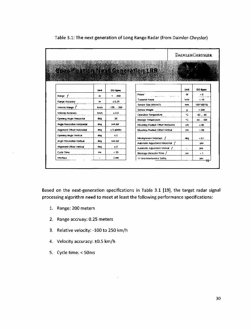
Table 3.1: The next generation of Long Range Radar (from Daimler-Chrysler)
Specifi ration LRR
Range /
Range Accuracy
Velocity Range /
Velocity Accuracy
Opening Angje Horizontal
Angle Resolution Horizontal
Alignment Offset Horizontal
Opening Angle Vertical
Angle Resolution Vertical
Alignment Offset Vertical
Cycle Time
Interface
Unit
m
m
km/h
km/h
deg
deg
deg
deg
deg
deg
ms
-
DC-Spec
1 .200
±0,25
-100. .260
±0,5
20
not del .
±3addittv
4.5
notder.
± 2
<50
CAN
DAIMUERCHRYSLER
Power
Transma Power
Sensor Size (WxHxD)
Sensor Weight
Operation Temperature
Storage Temperature
Mounting Position Offset Horizontal
Mounting Position Offset Vertical
Misalignment Detection /
Automatic Adjustment Horizontal /
Automatic Adjustment Vertical /
Blockage Detection Time /
77 GHz Interference Safety
Unit
w
rrfW
mm
9
•c
*c
cm
cm
deg
-sec
-
DC-Sp*C
<S
< 10
10Cr*100-50
<500
-40 ...B5
-40... 105
±80
>50
<0,1
yes
yes
<1
yes 1 10 '
Based on the next-generation specifications in Table 3.1 [19], the target radar signal
processing algorithm need to meet at least the following performance specifications:
1. Range: 200 meters
2. Range accruay: 0.25 meters
3. Relative velocity: -100 to 250 km/h
4. Velocity accuracy: ±0.5 km/h
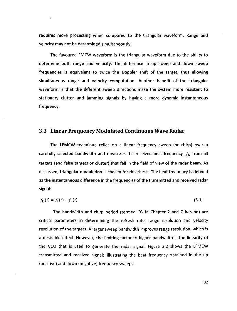
5. Cycle time: < 50ms
30
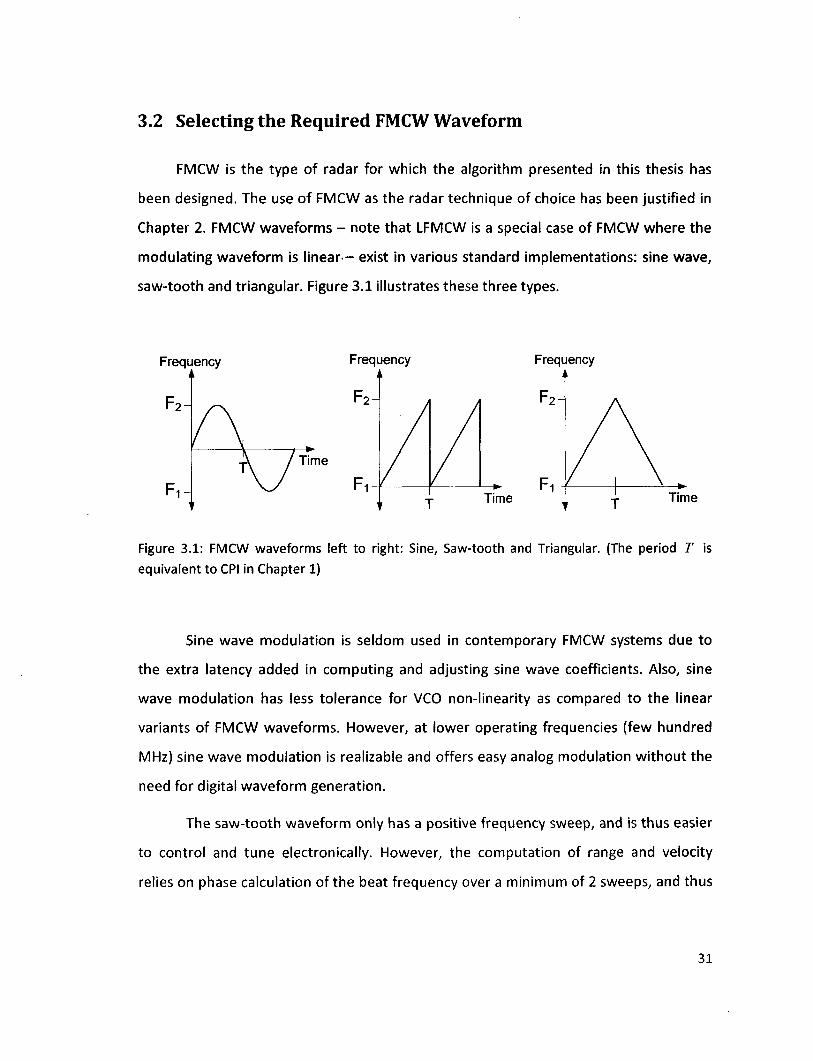
3.2 Selecting the Required FMCW Waveform
FMCW is the type of radar for which the algorithm presented in this thesis has
been designed. The use of FMCW as the radar technique of choice has been justified in
Chapter 2. FMCW waveforms - note that LFMCW is a special case of FMCW where the
modulating waveform is linear — exist in various standard implementations: sine wave,
saw-tooth and triangular. Figure 3.1 illustrates these three types.
Frequency
"2H
F i
Frequency A
Frequency A
Time Time
Figure 3.1: FMCW waveforms left to right: Sine, Saw-tooth and Triangular. (The period T is
equivalent to CPI in Chapter 1)
Sine wave modulation is seldom used in contemporary FMCW systems due to
the extra latency added in computing and adjusting sine wave coefficients. Also, sine
wave modulation has less tolerance for VCO non-linearity as compared to the linear
variants of FMCW waveforms. However, at lower operating frequencies (few hundred
MHz) sine wave modulation is realizable and offers easy analog modulation without the
need for digital waveform generation.
The saw-tooth waveform only has a positive frequency sweep, and is thus easier
to control and tune electronically. However, the computation of range and velocity
relies on phase calculation of the beat frequency over a minimum of 2 sweeps, and thus
31
requires more processing when compared to the triangular waveform. Range and
velocity may not be determined simultaneously.
The favoured FMCW waveform is the triangular waveform due to the ability to
determine both range and velocity. The difference in up sweep and down sweep
frequencies is equivalent to twice the Doppler shift of the target, thus allowing
simultaneous range and velocity computation. Another benefit of the triangular
waveform is that the different sweep directions make the system more resistant to
stationary clutter and jamming signals by having a more dynamic instantaneous
frequency.
3.3 Linear Frequency Modulated Continuous Wave Radar
The LFMCW technique relies on a linear frequency sweep (or chirp) over a
carefully selected bandwidth and measures the received beat frequency / b from all
targets (and false targets or clutter) that fall in the field of view of the radar beam. As
discussed, triangular modulation is chosen for this thesis. The beat frequency is defined
as the instantaneous difference in the frequencies of the transmitted and received radar
signal:
/b(0 = / t (0"/r (0 (3-D
The bandwidth and chirp period (termed CPI in Chapter 2 and T hereon) are
critical parameters in determining the refresh rate, range resolution and velocity
resolution of the targets. A larger sweep bandwidth improves range resolution, which is
a desirable effect. However, the limiting factor to higher bandwidth is the linearity of
the VCO that is used to generate the radar signal. Figure 3.2 shows the LFMCW
transmitted and received signals illustrating the beat frequency obtained in the up
(positive) and down (negative) frequency sweeps.
32
FREQUENCY Transmitted
Wave
Received Wave (Target Echo)
BEAT FREQUENCY
/ , up
f&> own
Figure 3.2: LFMCW Transmit, Receive and Beat frequency.
TIME
TIME
Here, r0 = round trip delay t ime for the signal to be received from the target
fd= Doppler shift due to relative target velocity
/ 0 = starting frequency for operation bandwidth
B = operation bandwidth
T = sweep duration (same for both up and down sweeps in this thesis)
fb= beat frequency or intermediate frequency
/ u p = up sweep beat frequency
/down = down sweep beat frequency
33
3.3.1 Derivation of Range and Velocity for LFMCW
The following is a concise step-wise derivation of the range and velocity equations for
LFMCW radar:
Let ft(t) = transmitted radar signal
fT(t)= received target echo signal
k = — = rate of change of frequency over a single sweep
3.3.1.1 First case: Relatively Stationary Target
A relatively stationary target is a target with zero relative velocity compared to
the radar sensor or host vehicle, and as such does not contribute to any Doppler shift of
the received echo signal. The transmitted radar signal can be defined as a complex
sinusoid with a base frequency of f0 modulated over a bandwidth of B Hz [29].
f ( 1 2 / t l (0 = exp jln f0t + -ktz (3.2)
The modulation of the transmit signal is evident from the frequency term in equation
1 2
(3.2) above. The term —kt adds a fraction of the total sweep bandwidth depending on
the instantaneous time t.
The received echo signal can be defined as a complex sinusoid delayed by a round trip
delay time r0.
( ( 1 2 / r l ( 0 = exp j2n f0(t-T0) + -k(t-T0)
V V 2
(3.3) / ;
34
Multiplying in time (or mixing) the transmitted and received signals, and ignoring
the high frequency component in the mixer output, produces the beat or intermediate
frequency of interest. In the case of a relatively stationary target, beat frequencies for
both up and down sweep are identical and can be expressed as:
krt' /bi (0 = /ti (0 ® / n (0 = expf y 2 ; / / 0 r 0 + ktr0 - hrl \ | (3.4)
Differentiating the phase of the beat signal in (3.4) w.r.t. time t gives the instantaneous
beat frequency that is directly proportional to the range of the target.
4foTo+ktT0-~kr$
/upl = ~ Jt l = kr0 (3.5)
Therefore, both up and down sweep beat frequencies are defined for a stationary
target.
2r /upl = /downl =kT0=k— (3.6)
c
Here, r is the range of the target and c is the speed of EM waves in air. Thus for a
relatively stationary target the range is computed by taking the average of the up and
down sweep instantaneous beat frequencies as follows [29]:
r = /upl + /downl
J
x — (3.7) 2k
3.3.1.2 Second case: Moving Target
Consider a moving target with velocity vr relative to the radar sensor or host vehicle.
This velocity introduces an additional term in the transmitted and received signals due
to the Doppler shift. This Doppler shift is approximated by f^vjc [29]. The following
transmitted signal is generated for the up sweep.
35
/ t 2 ( 0 = exp H /0t+-kt2 (3.8)
The received signal for the up sweep is affected by twice the amount of Doppler shift
due to two-way travel of the radar wave, as well as round trip delay as in the case of the
stationary target.
/ r 2 ( 0 = exp j2df0(t-T0) + ^k(t-T0)2+2f0^-(t-T0) (3.9)
Multiplying the transmitted and received signals in time we obtain the beat frequency
for the up sweep as given in equation (3.9).
/b uP(0 = exp jln
f ( v v ^ f0r0 +\kT0+ 2 / 0 -^ - 2kr0 -£•
V c c j
t--kr2
2 °
\ \
• ( \
+ 2-
(3.10)
The constant and second order terms in the above equation can be ignored for a stable
computation of the instantaneous up sweep frequency by differentiating w.r.t time t.
/ up2
fr v v U kr0+2f0^-2kT0^ t
c c ) , dt
kr0 + 2 / 0 ^ - 2kr0 ^*kr0+ fd (3.11) c c
v 2v v v The above approximation is possible as 2kr0-
L = 2k L = 4ftr—^-«1 for c c c c
bandwidths under 1 GHz. Larger bandwidths in tens of GHz also produce negligible
frequency values for this term, and thus this term can be safely neglected.
During the down sweep, the Doppler shift manifests as a negative entity due to
the negative slope of the modulating wave. Note that fA<B. This gives rise to the
following beat frequency signal at the receiver of the radar sensor:
36

/ b d o w n ( 0 = exp jln
( ( v v ^ /orO + kTQ-lfQ^-lkTQ-t
V c c)
t--kxl 2 °
+ 2-. 2 ^ (3.12)
J)
Differentiating (3.12) w.r.t. time t we get the down sweep frequency for a moving
target with relative velocity v r .
/ d lown2
(f v v ^ kr0-2f0-^-2kT0-t t
vv c c ) ) dt
= krQ - 2 / 0 ^ - 2kr0 ^ * k r 0 - fd (3.13) c c
From this analysis, the range and velocity of any target for the LFMCW technique can be
determined. Adding (3.11) and (3.13) we get
/uP2 + /down2 = kTo + fd + kr0 -fd= 2kr0 = 2k (2r)
Hence, range r C/up2 + / d o w n 2 ) C
2k (3.14)
This is similar to the range expression derived earlier for a stationary target.
The relative velocity of the target can be derived by subtracting (3.13) from (3.11) to
extract the Doppler shift caused by the target.
/uP2 ~ /down2 = kr0 +fd- (kt0 -fd) = 2fd= 4 / 0 — F c
Hence, relative velocity, v r = v/up2 /down2) C
X
4 /o (3.15)
Given equation (3.15), the actual target velocity can be computed based on knowledge
about the host vehicle velocity.
(3.16) Actual target velocity, "'target ~ vhost • v r
37
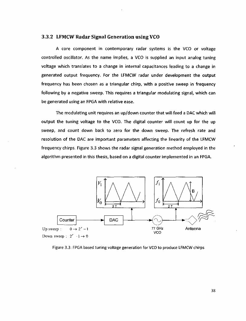
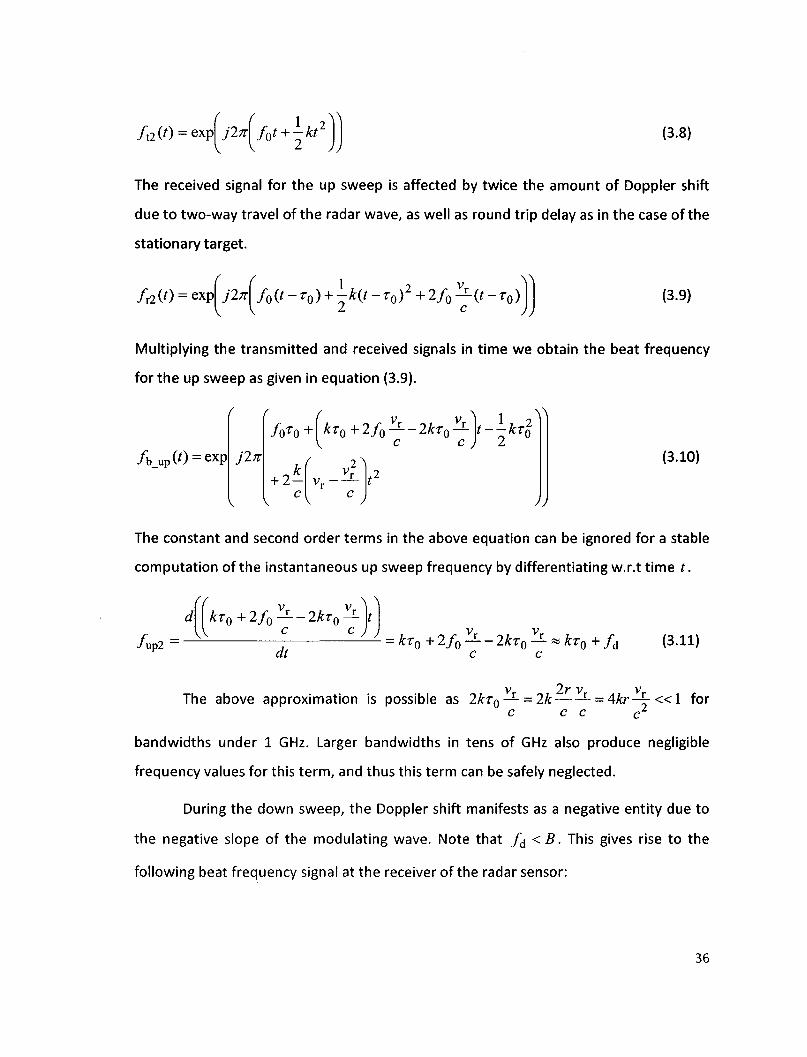
3.3.2 LFMCW Radar Signal Generation using VCO
A core component in contemporary radar systems is the VCO or voltage
controlled oscillator. As the name implies, a VCO is supplied an input analog tuning
voltage which translates to a change in internal capacitances leading to a change in
generated output frequency. For the LFMCW radar under development the output
frequency has been chosen as a triangular chirp, with a positive sweep in frequency
following by a negative sweep. This requires a triangular modulating signal, which can
be generated using an FPGA with relative ease.
The modulating unit requires an up/down counter that will feed a DAC which will
output the tuning voltage to the VCO. The digital counter will count up for the up
sweep, and count down back to zero for the down sweep. The refresh rate and
resolution of the DAC are important parameters affecting the linearity of the LFMCW
frequency chirps. Figure 3.3 shows the radar signal generation method employed in the
algorithm presented in this thesis, based on a digital counter implemented in an FPGA.
Up sweep : 0 -» 2r - 1
Down sweep : 2r - 1 -> 0
77 GHz VCO
Antenna
Figure 3.3: FPGA based tuning voltage generation for VCO to produce LFMCW chirps
38
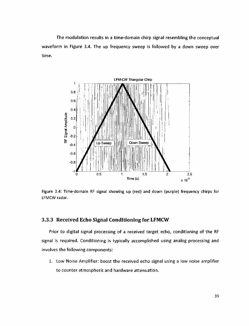
The modulation results in a time-domain chirp signal resembling the conceptual
waveform in Figure 3.4. The up frequency sweep is followed by a down sweep over
time.
LFM-CW Triangular Chirp
0 0.5 1 1.5 2 2.5 Time (s) x 1 Q -3
Figure 3.4: Time-domain RF signal showing up (red) and down (purple) frequency chirps for LFMCW radar.
3.3.3 Received Echo Signal Conditioning for LFMCW
Prior to digital signal processing of a received target echo, conditioning of the RF
signal is required. Conditioning is typically accomplished using analog processing and
involves the following components:
1. Low Noise Amplifier: boost the received echo signal using a low noise amplifier
to counter atmospheric and hardware attenuation.
39
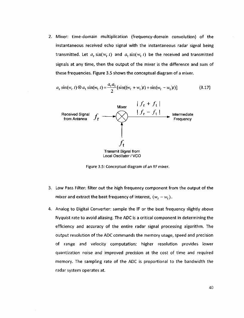
2. Mixer: time-domain multiplication (frequency-domain convolution) of the
instantaneous received echo signal with the instantaneous radar signal being
transmitted. Let ar sin(wr / ) and at sin(w t /) be the received and transmitted
signals at any t ime, then the output of the mixer is the difference and sum of
these frequencies. Figure 3.5 shows the conceptual diagram of a mixer.
axax ar sin(wr t) <S> a t sin(wt t) = -LJ-[sin((wr + wt )t) + sin(wr - wt )t)] (3.17)
Mixer I f< + f< I
Received Signal r ^ \ \ / \ Intermediate from Antenna Jx \^\^ Frequency
A Transmit Signal from Local Oscillator / VCO
Figure 3.5: Conceptual diagram of an RF mixer.
3. Low Pass Filter: filter out the high frequency component from the output of the
mixer and extract the beat frequency of interest, (w r -wt).
4. Analog to Digital Converter: sample the IF or the beat frequency slightly above
Nyquist rate to avoid aliasing. The ADC is a critical component in determining the
efficiency and accuracy of the entire radar signal processing algorithm. The
output resolution of the ADC commands the memory usage, speed and precision
of range and velocity computation: higher resolution provides lower
quantization noise and improved precision at the cost of t ime and required
memory. The sampling rate of the ADC is proportional to the bandwidth the
radar system operates at.
40
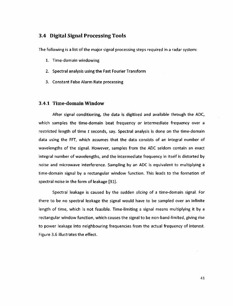
3.4 Digital Signal Processing Tools
The following is a list of the major signal processing steps required in a radar system:
1. Time-domain windowing
2. Spectral analysis using the Fast Fourier Transform
3. Constant False Alarm Rate processing
3.4.1 Time-domain Window
After signal conditioning, the data is digitized and available through the ADC,
which samples the time-domain beat frequency or intermediate frequency over a
restricted length of time t seconds, say. Spectral analysis is done on the time-domain
data using the FFT, which assumes that the data consists of an integral number of
wavelengths of the signal. However, samples from the ADC seldom contain an exact
integral number of wavelengths, and the intermediate frequency in itself is distorted by
noise and microwave interference. Sampling by an ADC is equivalent to multiplying a
time-domain signal by a rectangular window function. This leads to the formation of
spectral noise in the form of leakage [31].
Spectral leakage is caused by the sudden slicing of a time-domain signal. For
there to be no spectral leakage the signal would have to be sampled over an infinite
length of time, which is not feasible. Time-limiting a signal means multiplying it by a
rectangular window function, which causes the signal to be non-band-limited, giving rise
to power leakage into neighbouring frequencies from the actual frequency of interest.
Figure 3.6 illustrates the effect.
41
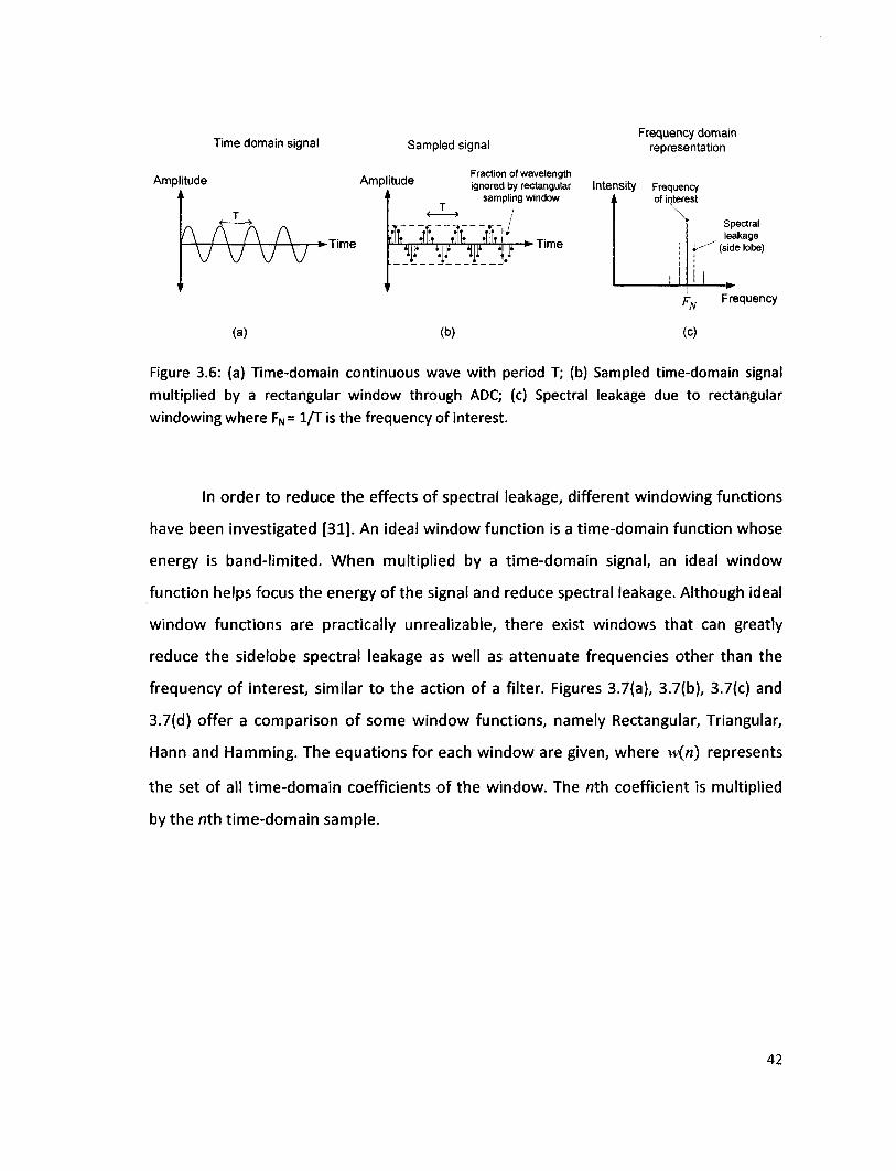
Time domain signal Sampled signal Frequency domain
representation
. . . . . . ... , Fraction of wavelength A m P ' l t u d e Ampl i tude ignored by rectangular Intensity Frequency
T i i.
(a)
-•Time
T < >
CWL f i[t f
sampling window
Time
of interest
(b)
Spectral leakage
(side lobe)
f Frequency
(c)
Figure 3.6: (a) Time-domain continuous wave with period T; (b) Sampled time-domain signal multiplied by a rectangular window through ADC; (c) Spectral leakage due to rectangular windowing where FN = 1/T is the frequency of interest.
In order to reduce the effects of spectral leakage, different windowing functions
have been investigated [31]. An ideal window function is a time-domain function whose
energy is band-limited. When multiplied by a time-domain signal, an ideal window
function helps focus the energy of the signal and reduce spectral leakage. Although ideal
window functions are practically unrealizable, there exist windows that can greatly
reduce the sidelobe spectral leakage as well as attenuate frequencies other than the
frequency of interest, similar to the action of a filter. Figures 3.7(a), 3.7(b), 3.7(c) and
3.7(d) offer a comparison of some window functions, namely Rectangular, Triangular,
Hann and Hamming. The equations for each window are given, where w(n) represents
the set of all time-domain coefficients of the window. The nth coefficient is multiplied
by the nth time-domain sample.
42
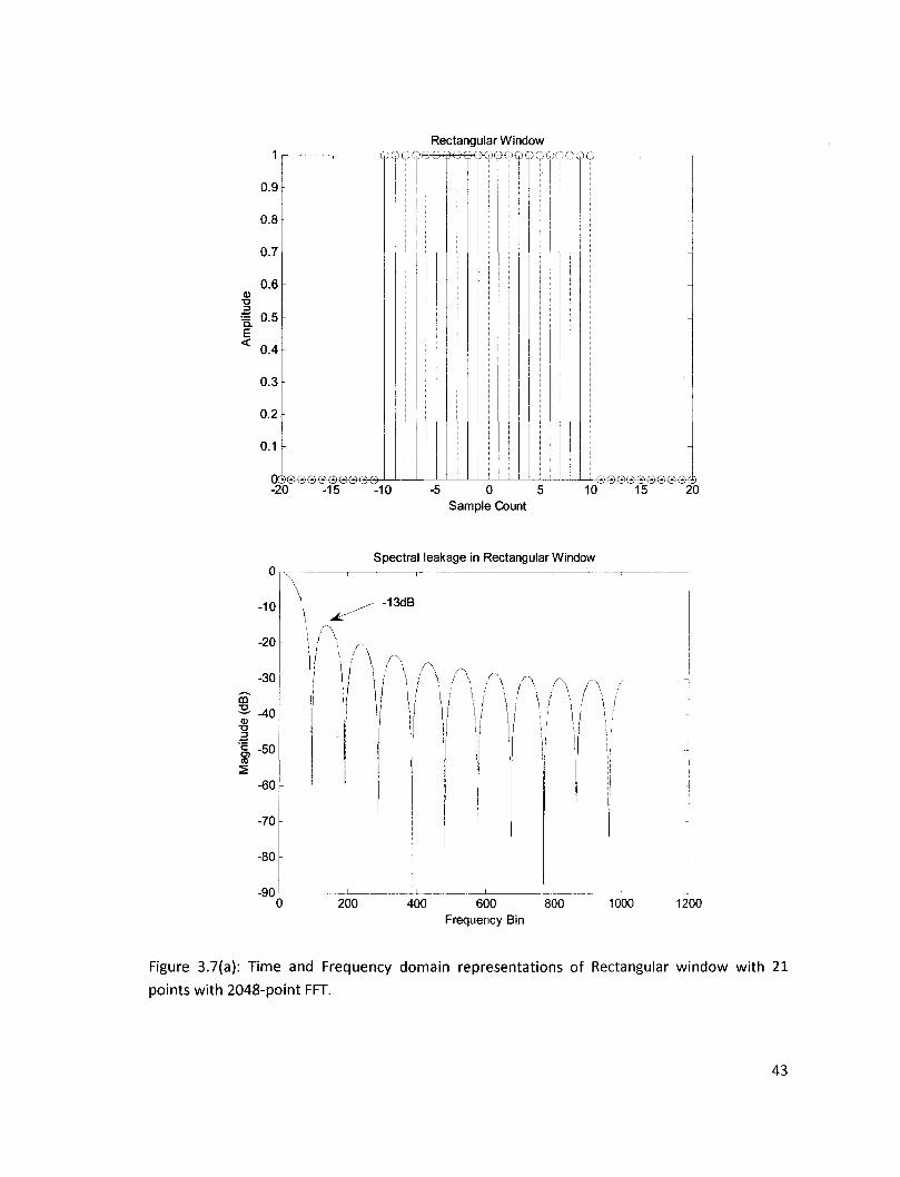
1
0.9
0.8
0.7
0.6
I 0.5
< 0.4
0.3
0.2
0.1
O®e®®®0®@0® -20 -15 -1
Rectangular Window trr-Ot^1 '4) Cp Q (p Ci)^>(r>t:>Q G) Q Gt rK r ) - ^
-5 0 5 Sample Count
® ® @ ® ® 0 0 0 0 ® 10 15 20
Spectral leakage in Rectangular Window V
-10
-20
-30
ST S - 4 0 T3 3
! -50 CD
2 -60
-70
-80
-90
\ \ \ \ \ \ ;
. I / \j
' ' ^ -13dB
\ A r. i I / \ A A
I
Ij \ I I • I i : s
j
1
A 1 1
1
' >
-
-
A /A r\ •' \ 1 \ / \ /
1 ' W 1 1 1
' i 1 / !
!i 11
1 11
1
-
200 400 600 800 1000 Frequency Bin
1200
Figure 3.7(a): Time and Frequency domain representations of Rectangular window
points with 2048-point FFT.
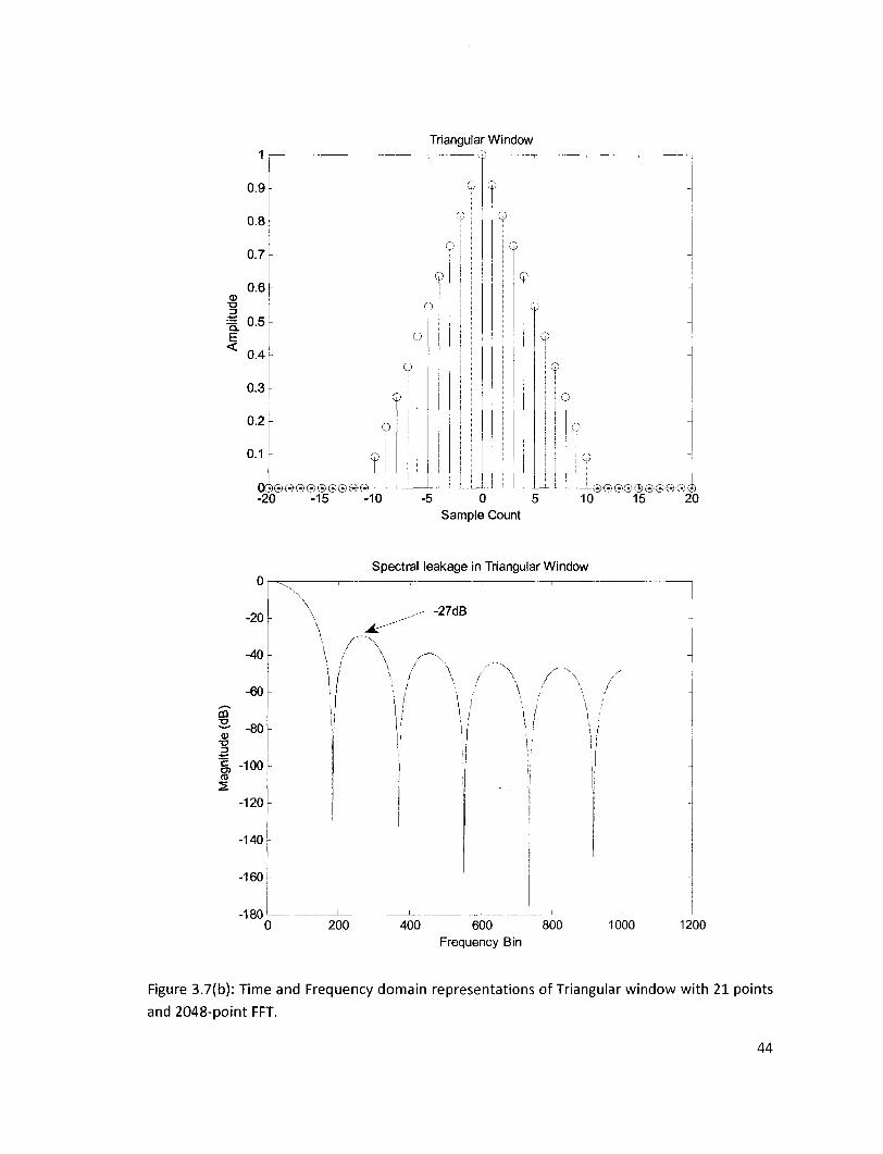
1
0.9
0.8
0.7
0.6 CD
T3
I 0.5 E
< 0.4
0.3
0.2
0.1
-20
Triangular Window
9
Q
-15 -10
O
-5 0 5 10 Sample Count
15 20
0
-20
-40
Spectral leakage in Triangular Window
CD 2 , a> •a 3
•** (0 2
-80
-100
-120
-140
-160
-180 200 400
\ /
600 800 Frequency Bin
\ i
1000 1200
Figure 3.7(b): Time and Frequency domain representations of Triangular window with 21 points
and 2048-point FFT.
44
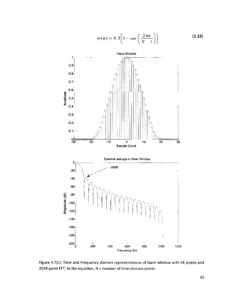
w(n) = 0.5 1 - cos V
Inn
N - 1 (3.18)
Hann Window -filter
-10 0 Sample Count
30
Spectral leakage in Hann Window 0
-20
-40
-60
ST -80
0) 1 -100 'c J -120
-140
-160
-180
-200
\
-
-
\ I
A \
1
) \ (
-39dB
I f\ A II 1/ '•
i [ |
j . . . .
1
l i
i i it'
'
v 1 !
-
-
-
h 1 !
i
..... - I - - -
200 400 600 800 Frequency Bin
1000 1200
Figure 3.7(c): Time and Frequency domain representations of Hann window with 41 points and
2048-point FFT. In the equation, N - number of time-domain points.
45
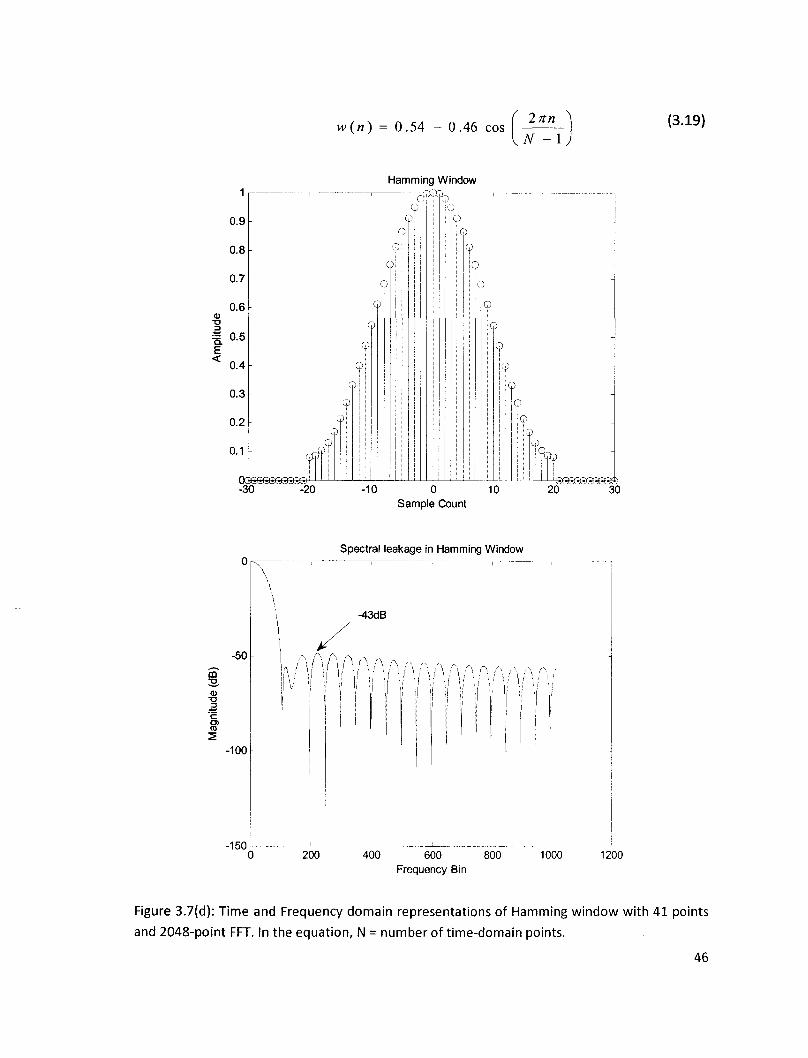
W ( H ) = 0.54 - 0.46 cos Inn
N - 1 (3.19)
1
0.9
0.8
0.7
0.6
I 0.5
0.4
0.3
0.2
0.1
0__. -30
Hamming Window ^fifcfe
qfi
Q
Q
A?
-20 -10 0 Sample Count
10 20 seeseeeee®
30
-50
a
f -100
-150
Spectral leakage in Hamming Window
-43dB
A A A A p.. r, ^ A / / \ / \i \ \ A A A A A A A
i i \/ \i ]> ' y
\ A A A A f
200 400 600 800 Frequency Bin
1000 1200
Figure 3.7(d): Time and Frequency domain representations of Hamming window with 41 points
and 2048-point FFT. In the equation, N = number of time-domain points.
46
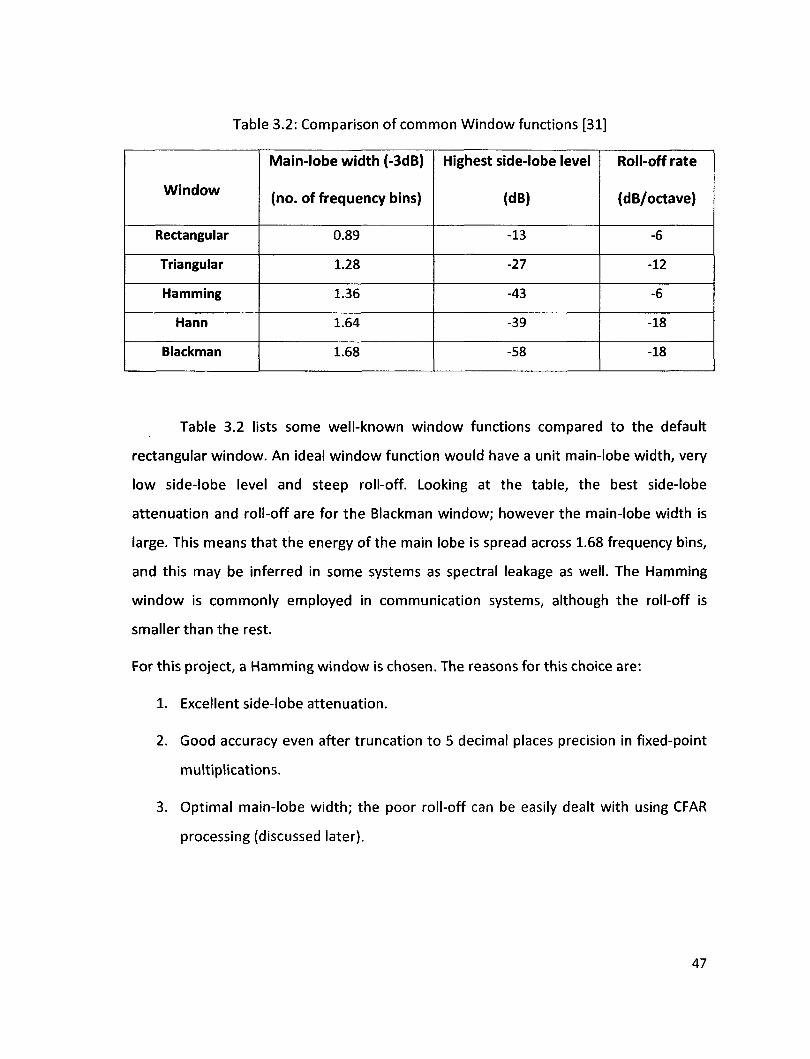
Table 3.2: Comparison of common Window functions [31]
Window
Rectangular
Triangular
Hamming
Hann
Blackman
Main-lobe width (-3dB)
(no. of frequency bins)
0.89
1.28
1.36
1.64
1.68
Highest side-lobe level
(dB)
-13
-27
-43
-39
-58
Roll-off rate
(dB/octave)
-6
-12
-6
-18
-18
Table 3.2 lists some well-known window functions compared to the default
rectangular window. An ideal window function would have a unit main-lobe width, very
low side-lobe level and steep roll-off. Looking at the table, the best side-lobe
attenuation and roll-off are for the Blackman window; however the main-lobe width is
large. This means that the energy of the main lobe is spread across 1.68 frequency bins,
and this may be inferred in some systems as spectral leakage as well. The Hamming
window is commonly employed in communication systems, although the roll-off is
smaller than the rest.
For this project, a Hamming window is chosen. The reasons for this choice are:
1. Excellent side-lobe attenuation.
2. Good accuracy even after truncation to 5 decimal places precision in fixed-point
multiplications.
3. Optimal main-lobe width; the poor roll-off can be easily dealt with using CFAR
processing (discussed later).
47
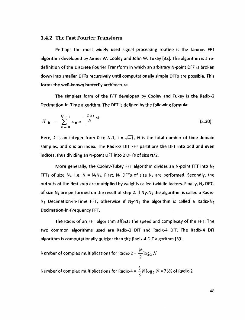
3.4.2 The Fast Fourier Transform
Perhaps the most widely used signal processing routine is the famous FFT
algorithm developed by James W. Cooley and John W. Tukey [32]. The algorithm is a re
definition of the Discrete Fourier Transform in which an arbitrary N-point DFT is broken
down into smaller DFTs recursively until computationally simple DFTs are possible. This
forms the well-known butterfly architecture.
The simplest form of the FFT developed by Cooley and Tukey is the Radix-2
Decimation-in-Time algorithm. The DFT is defined by the following formula:
N - \ _ 2 n i nk
* k = £ *ne N (3.20) n = 0
Here, k is an integer from 0 to N~l, i = V ^ L N is the total number of time-domain
samples, and n is an index. The Radix-2 DIT FFT partitions the DFT into odd and even
indices, thus dividing an N-point DFT into 2 DFTs of size N/2.
More generally, the Cooley-Tukey FFT algorithm divides an N-point FFT into Ni
FFTs of size N2, i.e. N = NiN2. First, Ni DFTs of size N2 are performed. Secondly, the
outputs of the first step are multiplied by weights called twiddle factors. Finally, N2 DFTs
of size Ni are performed on the result of step 2. If Ni<N2 the algorithm is called a Radix-
Ni Decimation-in-Time FFT, otherwise if N2<Ni the algorithm is called a Radix-N2
Decimation-in-Frequency FFT.
The Radix of an FFT algorithm affects the speed and complexity of the FFT. The
two common algorithms used are Radix-2 DIT and Radix-4 DIT. The Radix-4 DIT
algorithm is computationally quicker than the Radix-4 DIT algorithm [33].
N Number of complex multiplications for Radix-2 = —log2 N
3 Number of complex multiplications for Radix-4 = -7Vlog2 N = 75% of Radix-2
48
Number of complex additions for Radix-2 = iVlog2 N
Number of complex additions for Radix-4 = Nlog2N= same as Radix-2
Radix-4 thus requires 25% less complex multiplications than Radix-2 DIT
algorithm, making it a faster FFT. In this project a Radix-4 FFT is used, the details of
which are mentioned in Chapter 4 of this thesis.
3.4.3 Constant False Alarm Rate (CFAR) Processor
The CFAR unit makes it possible for radar systems to operate despite
contamination of received signal with noise, interference, clutter and effects of
attenuation. The CFAR unit runs an adaptive algorithm responsible for filtering out all
spurious spectral peaks in the FFT output and extracts only those peaks that have a high
probability of being real targets. The adaptive nature of CFAR processors enables them
to identify real target returns in the presence of changing noise and clutter from
surrounding false targets. In contrast, non-adaptive detection systems, called
clairvoyant detectors in [34], use a static threshold to detect valid targets.
After the spectral intensity of a signal is received from the FFT unit, the CFAR unit
detects valid targets. For non-adaptive detectors a constant threshold, Tc, is used. Each
frequency bin (frequency-domain sample from the FFT) is compared in absolute value to
f Tc. If | X[ri\ \> Tc then there exists a valid target at frequency n x — , where X[n] is the
discrete frequency domain representation of the received radar IF, n is an integer
between 0 to (N-l)/2, N is the FFT size, and fs is the rate at which the IF is sampled.
However, since noise and interference are stochastic and random processes this static
threshold can produce high number of false alarms.
CFAR algorithms overcome the short-coming of non-adaptive systems by
dynamically changing the threshold Tc according to the amount of noise and clutter
49
present in the surrounding frequency bins of that target. There are various CFAR
algorithms constantly being developed and refined, however two methods have seen
widespread application in radar systems: OS-CFAR (Ordered Statistic CFAR) and CA-CFAR
(Cell Averaging CFAR) [35-36]. There have been several variations to these basic two
CFAR types; however, the details are beyond the scope of this thesis.
A typical CA-CFAR architecture is shown in Figure 3.8 [37-38]. This is the CFAR
architecture employed for the system developed in this thesis. The principle of
operation of the CA-CFAR unit can be summarized in the following steps:
1. Square law detector removes any possible negative values from the FFT output,
in essence computing the absolute value or intensity of each frequency bin.
2. G number of guard bands are left on either side of the CUT (cell-under-test),
which help overcome spectral leakage effects.
3. M12 number of cells (or frequency bins) are averaged on either side of the
guard bands. Let avgL be the average of the left hand side Ml2 cells, and
avgR be the average of the right hand side M12 cells. The index k ranges from
l t o M / 2 .
4. The average of avgL and avgR is computed and multiplied by a predetermined
constant K to obtain the dynamic threshold Tc. The value of the CFAR
parameter K is determined by the following equation:
K = Pia M - 1 (3.21)
Here, Pfa is the acceptable preselected probability of false alarm and M is the
depth of the CFAR averaging [40].
5. The CUT is compared with Tc obtained from step 4. If CUT > Tc then a valid
target detection is declared [39].
50
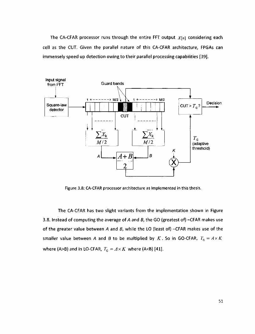
The CA-CFAR processor runs through the entire FFT output x[ri\ considering each
cell as the CUT. Given the parallel nature of this CA-CFAR architecture, FPGAs can
immensely speed up detection owing to their parallel processing capabilities [39].
Input signal from FFT
Square-law detector
Guard bands
CUT>TC? Decision
(adaptive threshold)
Figure 3.8: CA-CFAR processor architecture as implemented in this thesis.
The CA-CFAR has two slight variants from the implementation shown in Figure
3.8. Instead of computing the average of A and B, the GO (greatest of) -CFAR makes use
of the greater value between A and B, while the LO (least of) -CFAR makes use of the
smaller value between A and B to be multiplied by K. So in GO-CFAR, Tc =AxK
where (A>B) and in LO-CFAR, Tc=AxK where (A<B) [41].
51
3.4.4 Miscellaneous Topics
3.4.4.1 Radar Targets
In the 1950s, Peter Swerling of RAND Corporation developed mathematical models
to classify radar targets into 5 types based on the RCS or radar cross-section they display
[43]. These are known as the Swerling I, II, III, IV and V models for radar targets, and
present a mathematical model to determine the RCS of a radar target [42]. The
classification is modeled using the chi-squared distribution, which is beyond the scope of
this thesis. In simple terms, the parameters that affect the type of Swerling model are:
- Shape of the target.
Degree of freedom for the target.
Maximum and average RCS viewable from the target.
Variation pattern in the RCS of the target with time and space.
The RCS of a target is determined by the following relation:
a = lim Anr1 [ ^ s { (3.22) r ->co | E . |2
Here, Es = Scattered field intensity at distance r
E\ = Incident EM intensity on object
The radar cross-section of a vehicle is one of the factors which determine the maximum
unambiguous range the radar can cover.
Swerling I targets:
Consist of 5 or more scattering surfaces equally contributing to the overall RCS.
Have a constant RCS throughout a CPI or scanning interval, but independently
varying RCS in different radar beam scans.
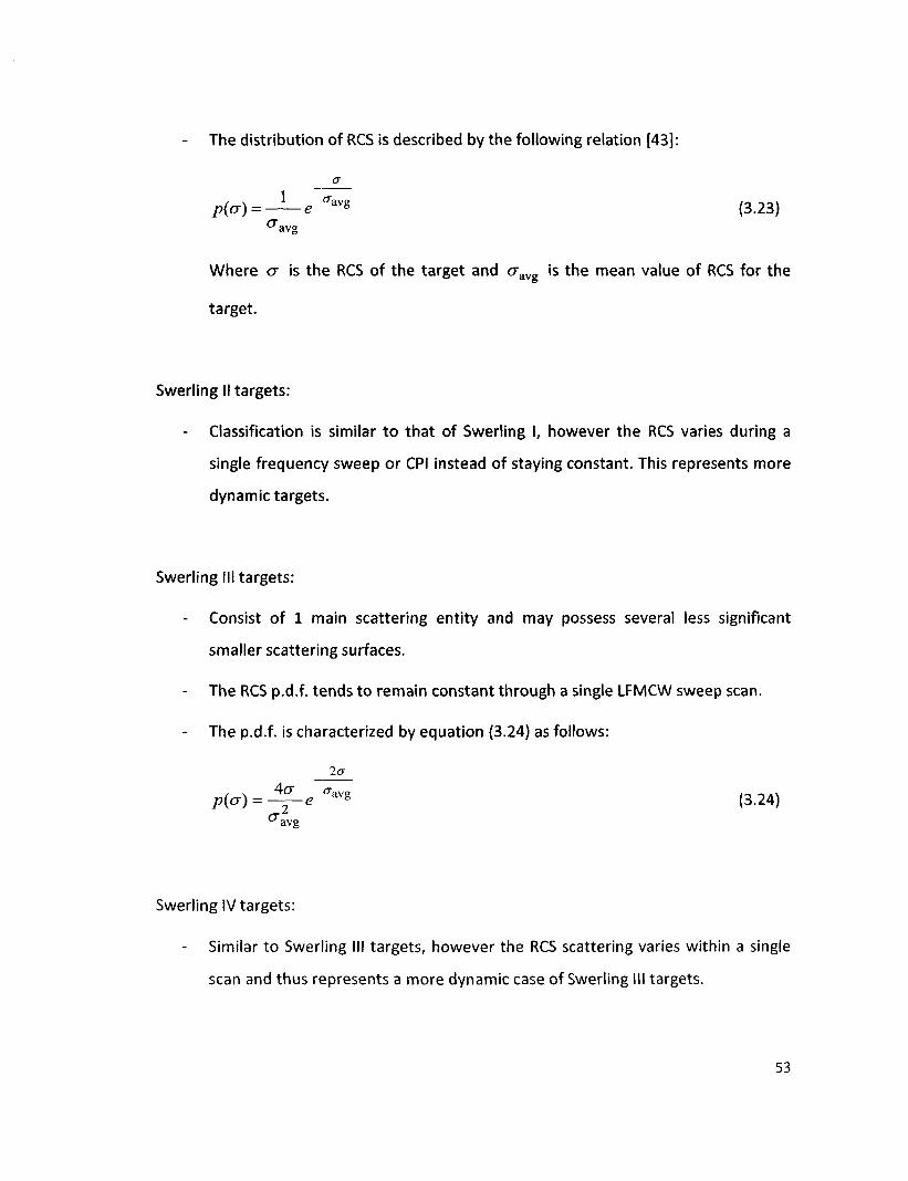
The distribution of RCS is described by the following relation [43]:
p(a) = — e "av« (3.23) " a v g
Where a is the RCS of the target and cravg is the mean value of RCS for the
target.
Swerling II targets:
Classification is similar to that of Swerling I, however the RCS varies during a
single frequency sweep or CPI instead of staying constant. This represents more
dynamic targets.
Swerling III targets:
Consist of 1 main scattering entity and may possess several less significant
smaller scattering surfaces.
- The RCS p.d.f. tends to remain constant through a single LFMCW sweep scan.
- The p.d.f. is characterized by equation (3.24) as follows:
2a
p(a) = ^ - e *""* (3.24) ^"avg
Swerling IV targets:
Similar to Swerling III targets, however the RCS scattering varies within a single
scan and thus represents a more dynamic case of Swerling III targets.
53
Swerling V targets:
Characterized by a constant RCS independent of time. These targets are easiest
to detect as there is ideally no spectral deviation during or over consecutive
frequency sweeps.
Typically, Swerling II and IV targets are harder to track due to variation in RCS, and
hence reflected power, over a single CPI or sampling interval.
3.4.4.2 Noise
Contemporary radar systems are affected by various types of noise sources. Noise
may originate from the signal conditioning analog components, the RF circuitry and
antennae, and the digital processing of the signal. Major sources of noise are listed:
1. Background noise - cosmic radiation, atmospheric absorption of EM radiation
and noise temperature of the Earth contribute to background noise which
manifests as white noise in all communication systems. This noise gets amplified
throughout the system and can be accounted for by adequate signal processing.
2. Thermal noise - generated due to thermal motion of semiconductor charge
carriers contributing to increased resistance in electronic and RF circuit
components [5].
Thermal noise, NTh = kTAB (3.25)
Where k is Boltzmann's constant, TA is the average absolute temperature
around the circuit components and B is the system bandwidth.
3. 1/f noise - pink noise power is inversely proportional to frequency. High
frequency systems such as radars suffer less effects of 1/f noise [44].
54
4. Quantization noise - when sampling the intermediate frequency of the radar
return using an ADC all continuous samples are rounded to the nearest
quantization level available. For instance, for a 10-bit ADC with an input range of
1V-5V, an input of 0.22V would mean 1024 * (0.22V / 4V) = 56.32 levels.
However, since the number of levels in the ADC is an integer from 1 to 1024, this
voltage would be quantized to level 56 corresponding to 0.21875V, hence an
error of 0.125% is induced.
The SNRQ or signal-to-quantization-noise ratio for an ADC is defined as follows
[45]:
SNRQ (dB) = 6.027V + 4.77 + 20 log, 0(LF) (3.26)
Here, LF is the RMS input voltage divided by the maximum acceptable voltage
for the ADC.
3.4.4.3 Attenuation
Atmospheric attenuation is a necessary evil in radar systems. Attenuation varies
with weather and the moisture level in the air. Table 3.3 lists attenuation under
different weather conditions [46]. For this research work, an attenuation of 0.8 dB/km
has been considered, which falls between light rain and medium rain conditions,
resulting in an SNR of 4.73 dB.
55
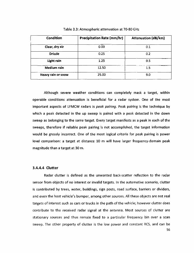
Table 3.3: Atmospheric attenuation at 70-80 GHz
Condition
Clear, dry air
Drizzle
Light rain
Medium rain
Heavy rain or snow
Precipitation Rate (mm/hr)
0.00
0.25
1.25
12.50
25.00
Attenuation (dB/km)
0.1
0.2
0.5
1.5
9.0
Although severe weather conditions can completely mask a target, within
operable conditions attenuation is beneficial for a radar system. One of the most
important aspects of LFMCW radars is peak pairing. Peak pairing is the technique by
which a peak detected in the up sweep is paired with a peak detected in the down
sweep as belonging to the same target. Every target manifests as a peak in each of the
sweeps, therefore if reliable peak pairing is not accomplished, the target information
would be grossly incorrect. One of the most logical criteria for peak pairing is power
level comparison: a target at distance 10 m will have larger frequency-domain peak
magnitude than a target at 30 m.
3.4.4.4 Clutter
Radar clutter is defined as the unwanted back-scatter reflection to the radar
sensor from objects of no interest or invalid targets. In the automotive scenario, clutter
is contributed by trees, water, buildings, sign posts, road surface, barriers or dividers,
and even the host vehicle's bumper, among other sources. All these objects are not real
targets of interest such as cars or trucks in the path of the vehicle; however clutter does
contribute to the received radar signal at the antenna. Most sources of clutter are
stationary sources and thus remain fixed to a particular frequency bin over a scan
sweep. The other property of clutter is the low power and constant RCS, and can be
56
classified as Sterling V type targets. Except ground clutter, most low-intensity spurious
spikes in the output of a frequency analyzer can be effectively removed by means of
CFAR processing, owing to the fact that all clutter sources exhibit very little or no
Doppler shift over LFMCW frequency chirps. Ground clutter infests the lower
frequencies due to its close proximity to the host vehicle, and can thus be handled by
filtering out those frequencies. In digital signal processing, ground clutter is removed by
ignoring high-power returns in the lower frequency bins of the FFT output, and is a valid
method assuming that the probability of a target existing within 30 cm of the radar
sensor is very low.
Albeit the general attempt at removal of clutter from the target return spectrum,
a recent literature in [47] illustrates the idea of making use of clutter as valuable
information in mapping the surrounding scenario. Literature [47] propounds the
estimation of road curvature and detection of road dividers and partitions based on
common clutter received in automotive radar applications. Such information can prove
useful in determining advanced security aspects of the trajectory of the host vehicle,
and act as a smarter adaptive cruise control system.
3.4.4.5 Radar Jamming
Jamming occurs when high-power microwave signals occupy the entire
bandwidth of operation of a radar sensor and render it incapable of distinguishing
between false and true targets. Although typically jamming has been an intentional ploy
by security agencies [48], in the automotive radar scenario jamming may occur due to
interference from nearby radar systems operating at the same instant frequency at the
very same time, or from broadband pulsed Doppler radars that generate high-power
pulses.
Frequency hopping is a well-known ECCM or Electronic Counter Countermeaures
solution. This allows FSK radars with several frequency hops better resistance to
57
jamming, although complete resistance is not guaranteed. Likewise, LFMCW radars
suffer less effects of jamming due to the constant frequency chirps.
3.4.4.6 Safe Distance Determination
A concise formula for safe distance calculation has been presented in literature
[55]. Consider the scenario in Figure 3.9, where the host vehicle with the radar sensor is
moving at velocity v2 following a vehicle at velocity vj .
< >
Figure 3.9: Safe distance between two vehicles.
Let the deceleration rate of the host vehicle be ax and the deceleration rate of
the radar target vehicle be a2 • Finally, let Tr be the reaction time of the driver of the
host vehicle. Then, the safe distance that should be maintained by the host vehicle from
the leading vehicle is given by
rsafe = T7~A - — V , 2 + V2Tr (3.27) 2b2 26]
The value of 6i and b2 is dependent on the braking performance of the vehicles in
different road conditions. On a dry road, K ~ 6.5 m/s2 and b ~ 6.0 m/s2 assuming Tr
= 1.0 s. On a surface covered with ice, K -2.6 m/s2 and t,2 ~ 2.0 m/s2 [55].
58
CHAPTER 4: RADAR CONTROL AND SIGNAL PROCESSING
ALGORITHM
This chapter presents the developed algorithm and where it fits into the whole
automotive radar system. The long rage automotive radar system being developed at
the University of Windsor has three primary requirements: target range measurement,
target velocity measurement and target angle measurement. This thesis develops a
system to measure target range and velocity based on the LFMCW approach using a
MEMS Rotman lens, MEMS RF switches and phased array antennae for transmission and
reception. The signal processing algorithm controls the modulation of the linear
frequency chirps in the transmission side and also processes the received echo signal
after it has been conditioned. Signal conditioning and common noise and attenuation
issues faced by radar developers, have been detailed in Chapter 3.
This chapter lists the decisions made while designing the radar signal processing
algorithm, and describes the operation of individual blocks with reference to the initial
system specifications described in Table 4.1.
59
Table 4.1: Initially provided System Specifications
Parameter
Radar type
Operating frequency
VCO used
Target model(s) considered
Beamformer
Number of beams
Processing duration per beam
Beam width
Antenna type
Radar processing unit (RPU) platform
Value
LFMCW
77 GHz
TLC77XS1
Reliability guaranteed with Swerling 1, III and V
type targets
Rotman lens
3 beams2
2 ms
±4.5°
Phased array antenna
FPGA
176.5 GHz MMIC VCO by TLC Precision Wafer Technology
2 Reference [1]
Figure 1.1 shows the conceptual diagram of the entire radar system, showing the
major components of the MEMS based radar system including the MEMS Rotman lens,
MEMS RF switches, and the FPGA for signal processing. As shown, the tuning voltage is
obtained from the DAC, and as described in Chapter 3 this translates to the triangular
frequency chirp which is broadcast through the SP3T switch and Rotman lens
combination into the phased array antenna.
60
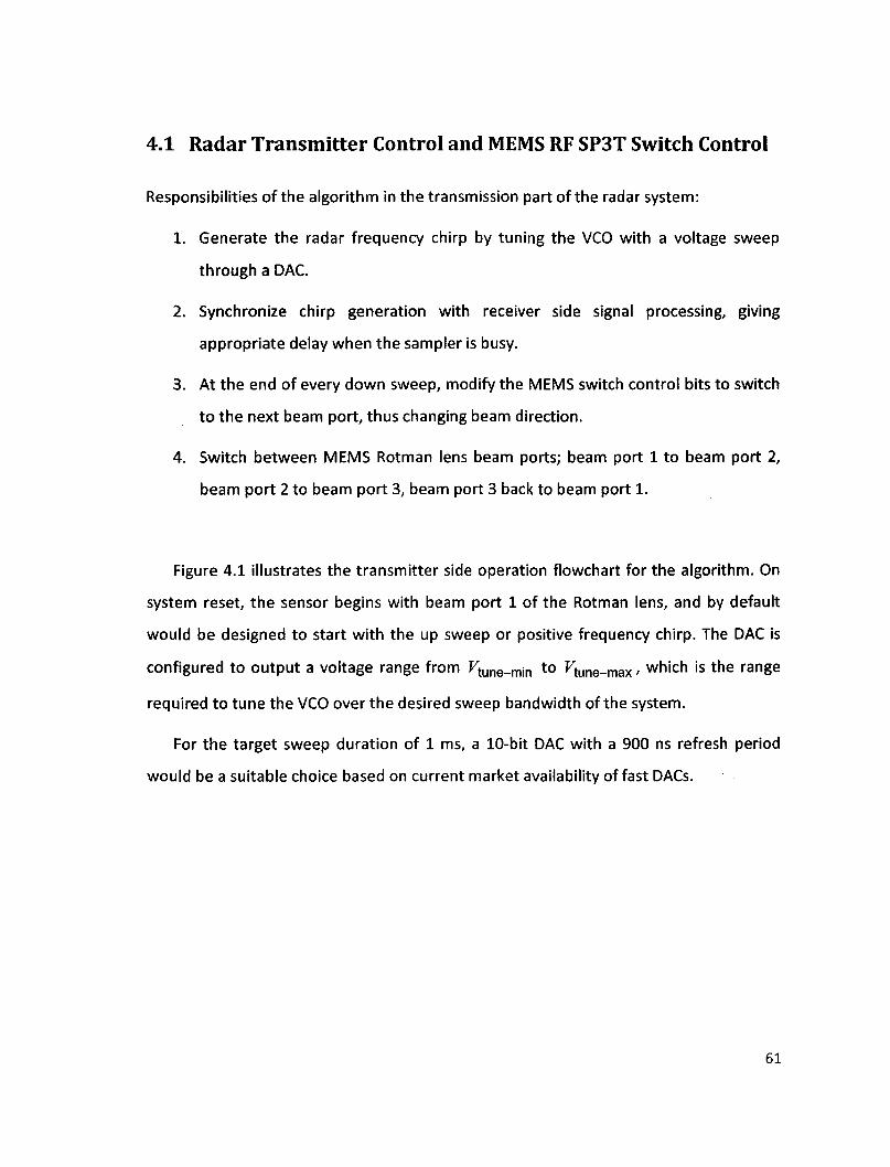
4.1 Radar Transmitter Control and MEMS RF SP3T Switch Control
Responsibilities of the algorithm in the transmission part of the radar system:
1. Generate the radar frequency chirp by tuning the VCO with a voltage sweep
through a DAC.
2. Synchronize chirp generation with receiver side signal processing, giving
appropriate delay when the sampler is busy.
3. At the end of every down sweep, modify the MEMS switch control bits to switch
to the next beam port, thus changing beam direction.
4. Switch between MEMS Rotman lens beam ports; beam port 1 to beam port 2,
beam port 2 to beam port 3, beam port 3 back to beam port 1.
Figure 4.1 illustrates the transmitter side operation flowchart for the algorithm. On
system reset, the sensor begins with beam port 1 of the Rotman lens, and by default
would be designed to start with the up sweep or positive frequency chirp. The DAC is
configured to output a voltage range from tune-min t 0 tune-max > which is the range
required to tune the VCO over the desired sweep bandwidth of the system.
For the target sweep duration of 1 ms, a 10-bit DAC with a 900 ns refresh period
would be a suitable choice based on current market availability of fast DACs.
61
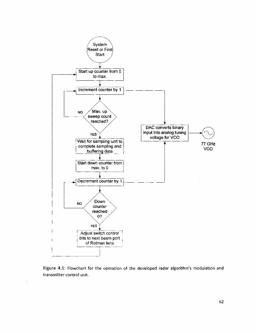
* •
/ System \ Reset or First V Start /
Start up counter from 0 to max.
i r
Increment counter by 1
NO ^ ^ Max. u p \
\ r eached? / ^
YES I
Wait for sampling unit to complete sampling and
buffering data
i ' Start down counter from
max. to 0
\ ' Decrement counter by 1
NO A / cou
\ ^ reac
\ ° YES
wn \ nter \ hed / ? /
Adjust switch control bits to next beam port
of Rotman lens
' r
DAC converts binary input into analog tuning
voltage for VCO , ,
*R\ Ky 77 GHz
VCO
Figure 4 .1 : Flowchart for the operation of the developed radar algorithm's modulation and
transmitter control unit.
62
4.2 Radar Receiver Flow Control and Signal Processing
The main part of the radar algorithm is its signal processing routine, the input to
which are the time-domain ADC samples and the output from which is target
information. The signal processing algorithm is responsible for the following internal
tasks:
1. Apply the Hamming window to the time-domain samples acquired from the ADC.
2. Fast Fourier Transform of the windowed time-domain samples.
3. Peak intensity calculation for every frequency bin of the FFT output.
4. Run a CFAR algorithm and detect valid target peaks, neglecting noise and clutter,
for both up and down sweeps.
5. Once both up and down sweeps have been processed by the CFAR unit, carry out
peak pairing to calculate the target information.
The developed signal processing algorithm discussed above is defined in Figure 4.2.
The superimposed graphs are generated from MATLAB and depict the time-domain
samples as it passes through the radar signal processing system.
63
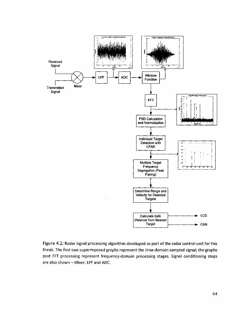
Received Signal
Transmitted Signal
Mixer
Individual Target Detection with
CFAR
Multiple Target Frequency
Segregation (Peak Pairing)
Determine Range and Velocity for Detected
Targets
Calculate Safe Distance from Nearest
Target
LCD
CAN
Figure 4.2: Radar signal processing algorithm developed as part of the radar control unit for this
thesis. The first two superimposed graphs represent the time-domain sampled signal; the graphs
post FFT processing represent frequency-domain processing stages. Signal conditioning steps
are also shown - Mixer, LPF and ADC.
64
4.3 Selecting the Radar Sweep Bandwidth
The choice of components for the system is vital in determining the efficiency of
the algorithm. One of the system parameters affecting the system components is the
bandwidth of the system over which the frequency sweeps are made. The bandwidth
selection involves a major trade-off: a higher bandwidth improves range resolution for
the radar system (refer to equation 4.1), but also suffers non-linearity effects of the
VCO. Following this trade-off, sweep bandwidths of 200 MHz, 400 MHz, 600 MHz, 800
MHz and 1 GHz were tested in MATLAB for the developed algorithm. Due to frequency
spectrum allocation policies bandwidths are currently restricted to 77.5 GHz.
Range resolution for LFMCW radar, AR
Velocity resolution for LFMCW radar, Avr
Here, c is the speed of the EM radar wave in air, B is the LFMCW sweep bandwidth, A
is the wavelength of the radar wave, and T is the up or down sweep duration [49].
The graph in Figure 4.3 shows the results for maximum intermediate frequency
and range resolution from the tests on different bandwidths. The target radar
specifications for maximum range and maximum relative velocity were selected as 200
meters and ±300 km/h in line with the state-of-the-art Bosch LRR3 radar presented in
Chapter 1.
c 25
A IT
(4.1)
(4.2)
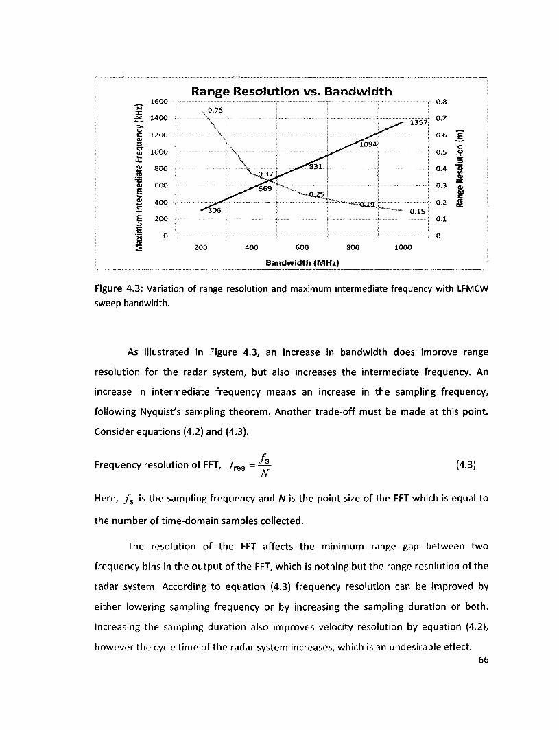
1600 X -S£
>• c <u 3
I k .
u. Si w
T 3 0»
£ w <U
c £ 3 E X ro
z
1400
1200
1000
800
600
400
200
0
Range Resolution vs. Bandwidth % 0.7S I
200 400 600 800
Bandwidth (MHz)
1000
0.8
0.7
0.6
0.5
0.4
0 3
0.2
0.1
0
£ tr o ** 3
o « 0 £ 01 0 0 £
Figure 4.3: Variation of range resolution and maximum intermediate frequency with LFMCW sweep bandwidth.
As illustrated in Figure 4.3, an increase in bandwidth does improve range
resolution for the radar system, but also increases the intermediate frequency. An
increase in intermediate frequency means an increase in the sampling frequency,
following Nyquist's sampling theorem. Another trade-off must be made at this point.
Consider equations (4.2) and (4.3).
f Frequency resolution of FFT, / r e s = — (4.3)
Here, / s is the sampling frequency and N is the point size of the FFT which is equal to
the number of time-domain samples collected.
The resolution of the FFT affects the minimum range gap between two
frequency bins in the output of the FFT, which is nothing but the range resolution of the
radar system. According to equation (4.3) frequency resolution can be improved by
either lowering sampling frequency or by increasing the sampling duration or both.
Increasing the sampling duration also improves velocity resolution by equation (4.2),
however the cycle time of the radar system increases, which is an undesirable effect. 66
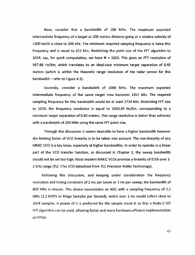
Now, consider first a bandwidth of 200 MHz. The maximum expected
intermediate frequency of a target at 200 meters distance going at a relative velocity of
+300 km/h is close to 306 kHz. The minimum required sampling frequency is twice this
frequency and is equal to 612 kHz. Restricting the point size of the FFT algorithm to
1024, say, for quick computation, we have N = 1024. This gives an FFT resolution of
597.66 Hz/bin, which translates to an ideal-case minimum target separation of 0.45
meters (which is within the theoretic range resolution of the radar sensor for this
bandwidth - refer to Figure 4.3).
Secondly, consider a bandwidth of 1000 MHz. The maximum expected
intermediate frequency of the same target now becomes 1357 kHz. The required
sampling frequency for this bandwidth would be at least 2714 kHz. Restricting FFT size
to 1024, the frequency resolution is equal to 2650.39 Hz/bin, corresponding to a
minimum target separation of 0.40 meters. This range resolution is better than achieved
with a bandwidth of 200 MHz using the same FFT point size.
Through this discussion it seems desirable to have a higher bandwidth however
the limiting factor of VCO linearity is to be taken into account. The non-linearity of any
MMIC VCO is a key issue, especially at higher bandwidths. In order to operate in a linear
part of the VCO transfer function, as discussed in Chapter 2, the sweep bandwidth
should not be set too high. Most modern MMIC VCOs promise a linearity of 0.5% over 1-
2 GHz range (TLC 77xs VCO datasheet from TLC Precision Wafer Technology).
Following this discussion, and keeping under consideration the frequency
resolution and timing constraint of 2 ms per beam or 1 ms per sweep, the bandwidth of
800 MHz is chosen. This choice necessitates an ADC with a sampling frequency of 2.2
MHz (2.2 MSPS or Mega Samples per Second), which over 1 ms would collect close to
2048 samples. A power of 2 is preferred for the sample count N so that a Radix-2 DIT
FFT algorithm can be used, allowing faster and more hardware-efficient implementation
on FPGA.
67
4.4 Configuration of System Components
4.4.1 ADC
As discussed above, with a bandwidth of 800 MHz a respectable range resolution
is achievable. For this bandwidth, an ADC with sampling frequency of 2.2 MHz is
required. Or alternately, a sampling frequency of 2 MHz can be used over 1.024 ms for
an exact total of 2048 samples.
4.4.2 FFT
Over 1 ms (or 1.024ms), close to 2048 samples will be collected using the chosen
ADC rate. This would be the size of the FFT required for the signal processing algorithm.
4.4.3 CFAR
The CA-CFAR was chosen as the CFAR processor architecture for this thesis.
Results have been presented in Chapter 4 of this thesis supporting the validity of this
choice. The CA-CFAR processes a total of 1024 frequency-domain peaks (only half of the
FFT output is considered as the FFT is a symmetric algorithm) to identify valid targets
from clutter and noise. The probability of false alarm Pfa is selected as 10"6 for the
algorithm, with an averaging depth M of 4 cells on either side of the CUT and 2 guard
bands on either side of the CUT. This generates the following value of scaling constant
K:
K = P^~m -1 = (10~6) 2x8-1*1.3714
Using 2 guard bands on either side of the CUT allows for enhanced noise
handling capability and increased immunity to spectral leakage as a secondary line of
defense after the Hamming window.
68
4.4.4 Peak Pairing
Two criteria for peak pairing are used in the proposed radar signal processing
algorithm [48], assuming Swerling I, III and V targets. These are:
1. Spectral proximity: With the chosen system bandwidth, a relative velocity of 300
km/h corresponds to a maximum frequency bin shift of 84 bins between up
sweep and down sweep peaks belonging to the same target. This frequency shift
is due to Doppler shift. Therefore, a peak detected in the up sweep will only be
paired with a detected peak in the down sweep if they are within 84 frequency
bins of each other.
2. Power level: The peak intensity of the FFT output is indicative of the power level
in the return of a given target. A distant target would produce a larger beat
frequency but at lower power compared to a nearer target. This relation has
high probability of occurrence and can therefore be used as a pairing criterion,
by which a peak in the up sweep would be paired with a peak in the down sweep
if the difference in their power levels is small.
4.5 Developed Algorithm Summary
The decisions presented in this chapter set the ground for the software (MATLAB) and
hardware (HDL on FPGA) testing of the devised radar signal processing algorithm. The
subsequent chapters show simulation results and a comparison in performance of
floating-point software (MATLAB) and fixed-point (HDL) systems. Table 4.2 lists the final
parameters for this thesis.
69
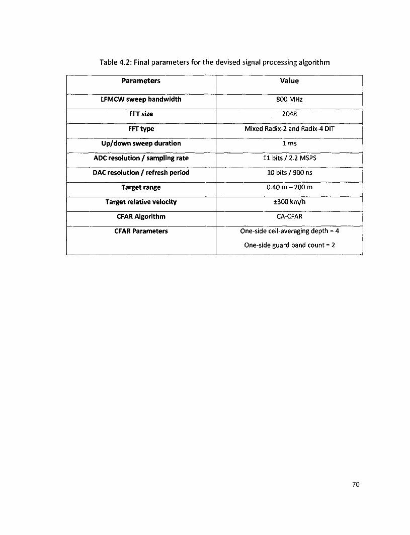
Table 4.2: Final parameters for the devised signal processing algorithm
Parameters
LFMCW sweep bandwidth
FFT size
FFTtype
Up/down sweep duration
ADC resolution / sampling rate
DAC resolution / refresh period
Target range
Target relative velocity
CFAR Algorithm
CFAR Parameters
Value
800 MHz
2048
Mixed Radix-2 and Radix-4 DIT
l m s
l lb i ts /2.2MSPS
10 bits / 900 ns
0.40 m - 200 m
±300 km/h
CA-CFAR
One-side cell-averaging depth = 4
One-side guard band count = 2
70
CHAPTER 5: SOFTWARE IMPLEMENTATION AND SIMULATION
MATLAB simulations of the developed radar signal processing algorithm are
carried out in this chapter, and the results presented. Based on the target specifications,
the mathematical theory, and the component configurations the signal processing
algorithm is tested for two different cases. The first case simulates targets detected in a
3-beam MEMS radar, and the second case assumes a large wide-angle beam with a large
number of targets. The results from the MATLAB simulation validate the developed
algorithm and form the basis for the HDL implementation of the same.
5.1 Software Implementation of the Radar Signal Processing Algorithm
Following the Research Methodology stated in Chapter 1, after the development
of the algorithm and decision on peripherals' configurations, the next step is a detailed
MATLAB simulation of the proposed algorithm. MATLAB R2006b Version 7.3 has been
used to develop the code for and verify the radar signal processing algorithm.
There are three stages to testing the algorithm in MATLAB:
1. Test the algorithm with and without a window function to validate the need for
the extra processing produced by windowing.
2. Test the algorithm with a test case for a practical 3-lane highway scenario with 3
narrow beams between 3°-6° width each.
3. Test the algorithm for a hypothetical scenario with a large number of targets in a
single wide-angle beam between 15°-30° in order to see the effect of saturating
the radar sensor.
71
Before the results are analyzed, we must revisit the chosen algorithm parameters as
presented in Chapter 4. With these system settings, one can proceed testing the
algorithm. The flowchart in Figure 5.1 shows a flowchart of the sequential MATLAB
program used to simulate the radar signal processing algorithm (see Appendix A l for
complete code listing).
Frequency sweep bandwidth = 800 MHz
Sampling frequency = 2 MHz
Sampling duration (up/down sweep duration) = 1.024 ms
Number of time-domain samples = 2048
FFT size = 2048
FFT frequency resolution = 2 MHz / 2048 = 976.5625 Hz/bin
72
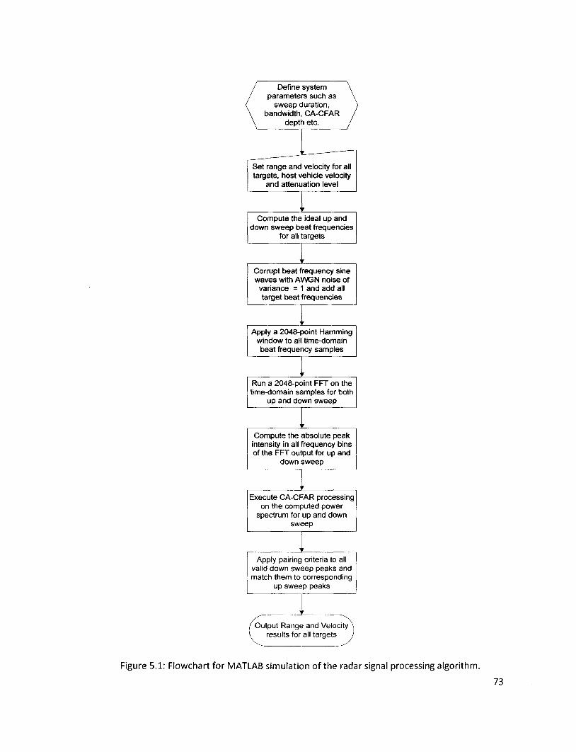
Define system parameters such as
sweep duration, bandwidth, CA-CFAR
depth etc.
Set range and velocity for all targets, host vehicle velocity
and attenuation level
r Compute the ideal up and
down sweep beat frequencies for all targets
Corrupt beat frequency sine waves with AWGN noise of
variance = 1 and add all target beat frequencies
Apply a 2048-point Hamming window to all time-domain beat frequency samples
Run a 2048-point FFT on the time-domain samples for both
up and down sweep
Compute the absolute peak intensity in all frequency bins of the FFT output for up and
down sweep
Execute CA-CFAR processing on the computed power
spectrum for up and down sweep
Apply pairing criteria to all valid down sweep peaks and match them to corresponding
up sweep peaks
Output Range and Velocity results for all targets
Figure 5.1: Flowchart for MATLAB simulation of the radar signal processing algorithm.
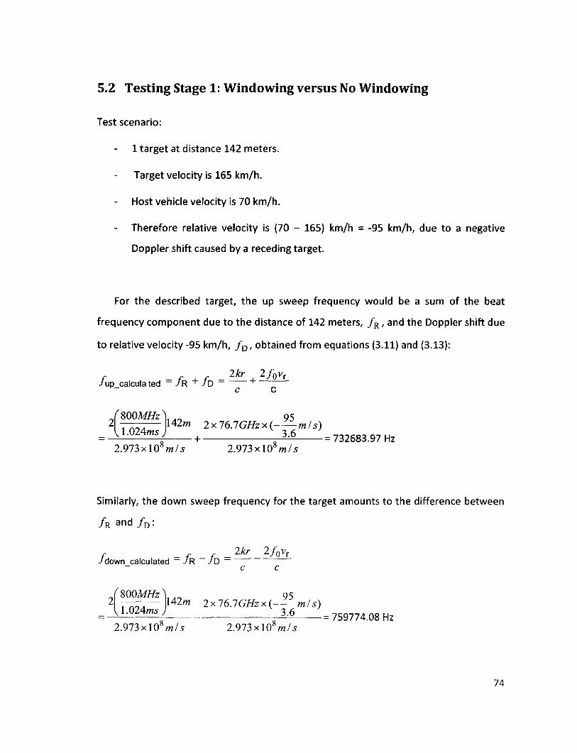
5.2 Testing Stage 1: Windowing versus No Windowing
Test scenario:
1 target at distance 142 meters.
Target velocity is 165 km/h.
Host vehicle velocity is 70 km/h.
- Therefore relative velocity is (70 - 165) km/h = -95 km/h, due to a negative
Doppler shift caused by a receding target.
For the described target, the up sweep frequency would be a sum of the beat
frequency component due to the distance of 142 meters, / R , and the Doppler shift due
to relative velocity -95 km/h, fD, obtained from equations (3.11) and (3.13):
r f f 2kr 2f0vr / u p calculated - JR + JD ~ h ~
c C
JSOOMHzX.- 95 2 \T~^TA l42m 2x76JGHzx(- — m/s)
1 ! m4mS ] + - ^ = 732683.97 Hz
2.973xl08m/5 2.973xl08m/5
Similarly, the down sweep frequency for the target amounts to the difference between
/ R and / D :
f - f - f - 2kr 2fvVr J down calculated ~ JR JD ~
2 ^S0OMHz\ Ars 95
\A2m 2x76JGHzx(- — m/s) 3-6 -=759774.08 Hz
\1.024ms;
2.973x\0Sm/s 2.973x\08m/s
74
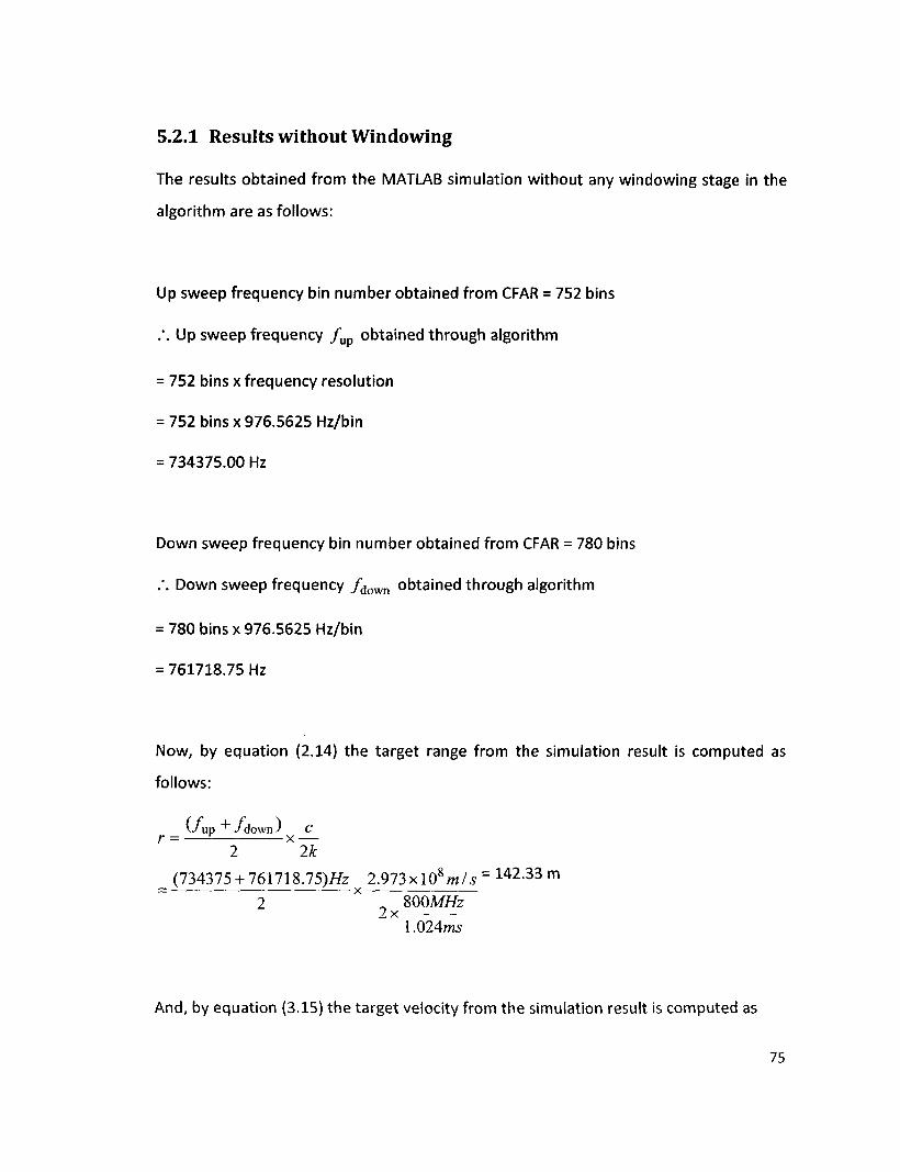
5.2.1 Results without Windowing
The results obtained from the MATLAB simulation without any windowing stage in the
algorithm are as follows:
Up sweep frequency bin number obtained from CFAR = 752 bins
.*. Up sweep frequency / u p obtained through algorithm
= 752 bins x frequency resolution
= 752 bins x 976.5625 Hz/bin
= 734375.00 Hz
Down sweep frequency bin number obtained from CFAR = 780 bins
.'. Down sweep frequency /down obtained through algorithm
= 780 bins x 976.5625 Hz/bin
= 761718.75 Hz
Now, by equation (2.14) the target range from the simulation result is computed as
follows:
(/up + /down ) C
r = — x — 2 2k
^(734375 + 76171 SJS)Hz 2.973xl08m/s = 1 4 2 - 3 3 m
2 „ SOOMHz 2x
1.024ms
And, by equation (3.15) the target velocity from the simulation result is computed as 75
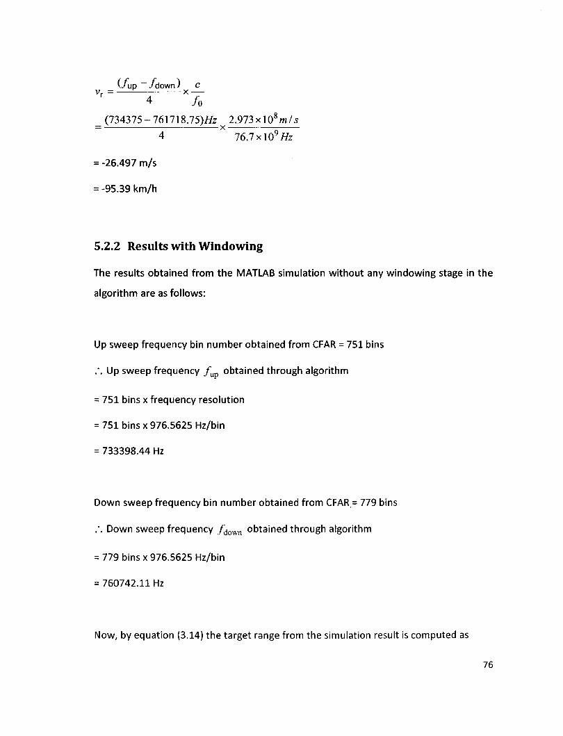
C/up /down) c vr = x —
4 / 0
_ (734375-761718.75)/fe 2.973xlQ8yw/^
4 76.7 x\09 Hz
= -26.497 m/s
= -95.39 km/h
5.2.2 Results with Windowing
The results obtained from the MATLAB simulation without any windowing stage in the
algorithm are as follows:
Up sweep frequency bin number obtained from CFAR = 751 bins
.*. Up sweep frequency / u p obtained through algorithm
= 751 bins x frequency resolution
= 751 bins x 976.5625 Hz/bin
= 733398.44 Hz
Down sweep frequency bin number obtained from CFAR = 779 bins
.". Down sweep frequency /<]own obtained through algorithm
= 779 bins x 976.5625 Hz/bin
= 760742.11 Hz
Now, by equation (3.14) the target range from the simulation result is computed as
76
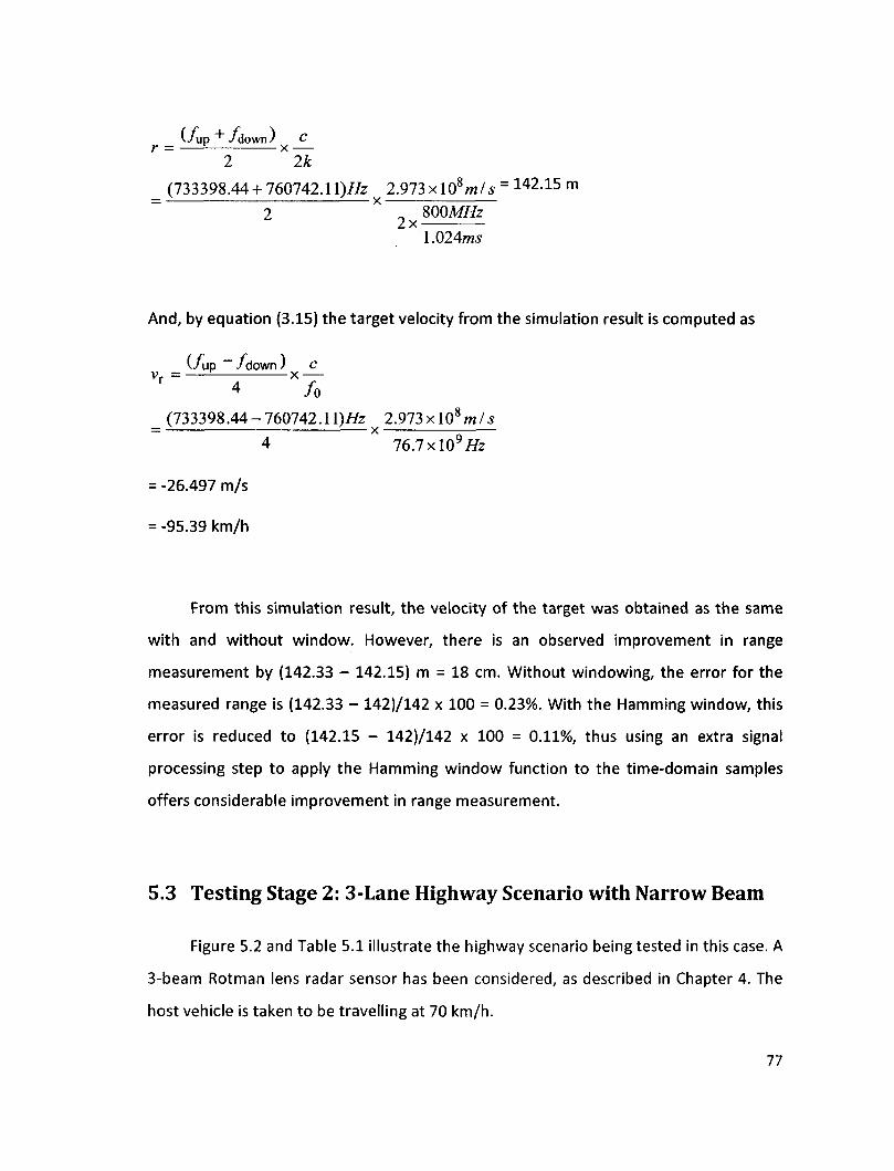
v/up ~*~ /down / C r = x — 2 2k
_ (733398.44 +760742. ll)/fe 2.973 x \0sm/s = 1 4 2 1 5 m
2 X 800M//Z
1.024ms
And, by equation (3.15) the target velocity from the simulation result is computed as
(/up — /down ) c V ' ~ 4
(733398.44-
= -26.497 m/s
= -95.39 km/h
x — /o
-760742.1 4
l)//z 2.973> x
76.7 >
:108
clO9
m/s
' /&
From this simulation result, the velocity of the target was obtained as the same
with and without window. However, there is an observed improvement in range
measurement by (142.33 - 142.15) m = 18 cm. Without windowing, the error for the
measured range is (142.33 - 142)/142 x 100 = 0.23%. With the Hamming window, this
error is reduced to (142.15 - 142)/142 x 100 = 0.11%, thus using an extra signal
processing step to apply the Hamming window function to the time-domain samples
offers considerable improvement in range measurement.
5.3 Testing Stage 2: 3-Lane Highway Scenario with Narrow Beam
Figure 5.2 and Table 5.1 illustrate the highway scenario being tested in this case. A
3-beam Rotman lens radar sensor has been considered, as described in Chapter 4. The
host vehicle is taken to be travelling at 70 km/h.
77
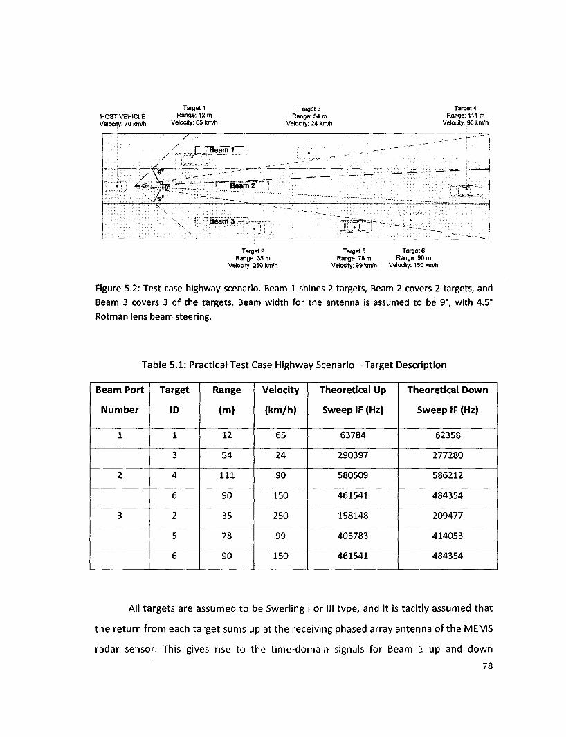
Target 2 Target 5 Target 6 Range: 35 m Range: 78 m Range: 90 m
Velocity: 250 km/h Velocity: 99 km/h Velocity: 150 km/h
Figure 5.2: Test case highway scenario. Beam 1 shines 2 targets, Beam 2 covers 2 targets, and
Beam 3 covers 3 of the targets. Beam width for the antenna is assumed to be 9°, with 4.5°
Rotman lens beam steering.
Table 5.1: Practical Test Case Highway Scenario - Target Description
Beam Port
Number
1
2
3
Target
ID
1
3
4
6
2
5
6
Range
(m)
12
54
111
90
35
78
90
Velocity
(km/h)
65
24
90
150
250
99
150
Theoretical Up
Sweep IF (Hz)
63784
290397
580509
461541
158148
405783
461541
Theoretical Down
Sweep IF (Hz)
62358
277280
586212
484354
209477
414053
484354
All targets are assumed to be Swerling I or III type, and it is tacitly assumed that
the return f rom each target sums up at the receiving phased array antenna of the MEMS
radar sensor. This gives rise to the time-domain signals for Beam 1 up and down
78
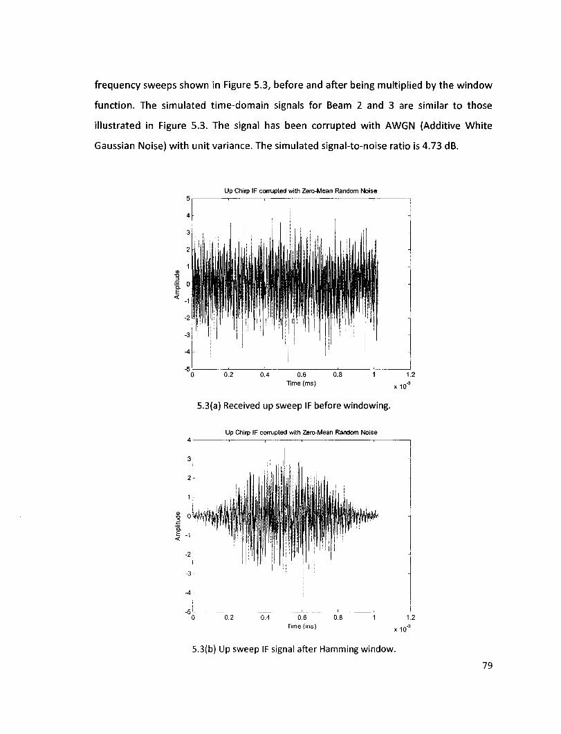
frequency sweeps shown in Figure 5.3, before and after being multiplied by the window
function. The simulated time-domain signals for Beam 2 and 3 are similar to those
illustrated in Figure 5.3. The signal has been corrupted with AWGN (Additive White
Gaussian Noise) with unit variance. The simulated signal-to-noise ratio is 4.73 dB.
Up Chirp IF corrupted with Zero-Mean Random Noise
0.4 0.6 0.8 Time (ms)
x 10
1.2 3
5.3(a) Received up sweep IF before windowing.
Up Chirp IF corrupted with Zero-Mean Random Noise
! - ' ^ f l l l
0.2 0.4 0.6 Time (ms)
0.8 1.2
x10
5.3(b) Up sweep IF signal after Hamming window.
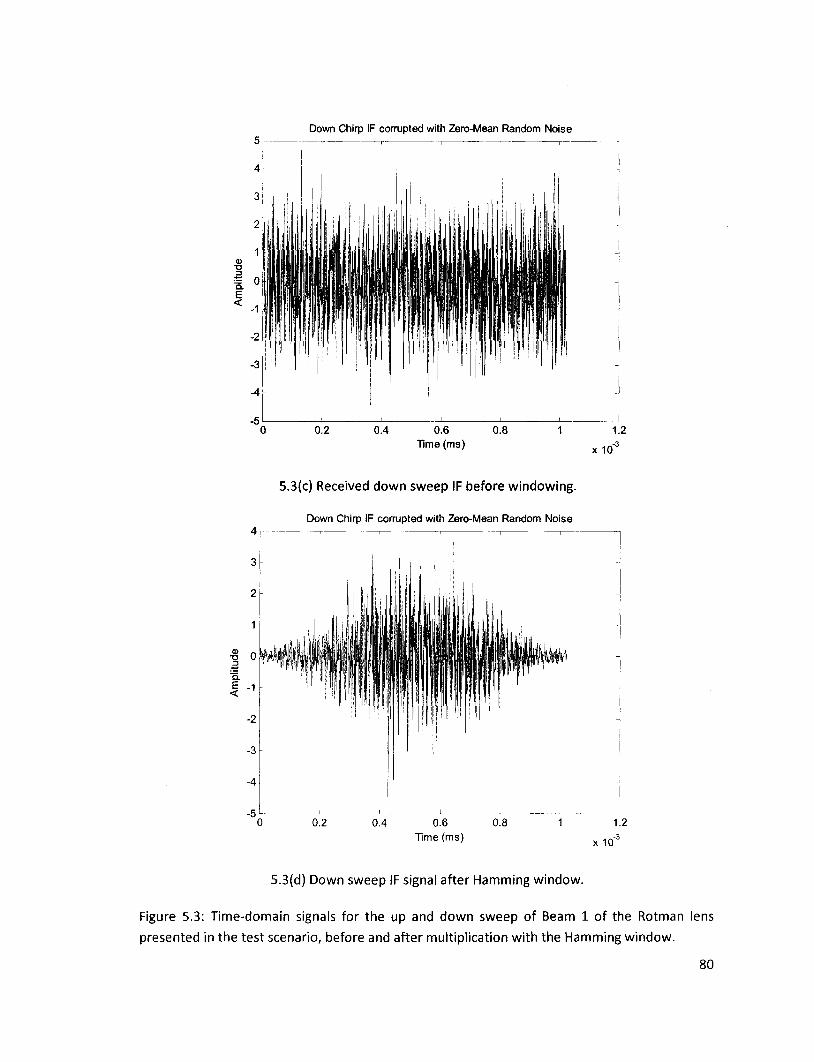
Down Chirp IF corrupted with Zero-Mean Random Noise
0.4 0.6 0.8 Time (ms) x 10
1.2 •3
5.3(c) Received down sweep IF before windowing.
Down Chirp IF corrupted with Zero-Mean Random Noise
0.6 Time (ms) x 10"
5.3(d) Down sweep IF signal after Hamming window.
Figure 5.3: Time-domain signals for the up and down sweep of Beam 1 of the Rotman
presented in the test scenario, before and after multiplication with the Hamming window.
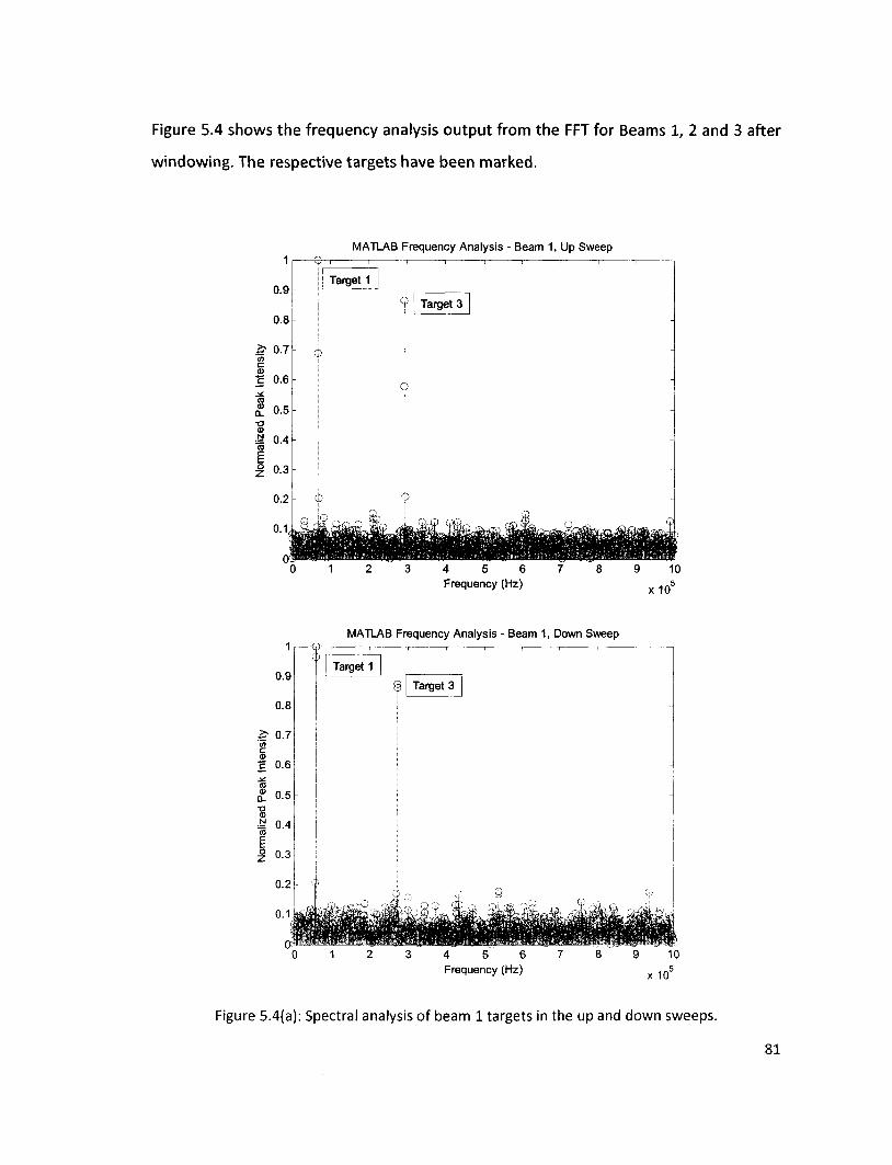
Figure 5.4 shows the frequency analysis output from the FFT for Beams 1, 2 and
windowing. The respective targets have been marked.
1
0.9
0.8
f 0.7
I 0.6
Z 0 3
MATLAB Frequency Analysis - Beam 1, Up Sweep
Target 1
Target 3
4 5 6 Frequency (Hz)
x 10
1
0.9
0.8
0.7
0.6
0.5
0.4
0.3
0.2
0.1
MATLAB Frequency Analysis - Beam 1, Down Sweep
Target 1
Target 3
4 5 6 Frequency (Hz) x 10
Figure 5.4(a): Spectral analysis of beam 1 targets in the up and down sweeps.
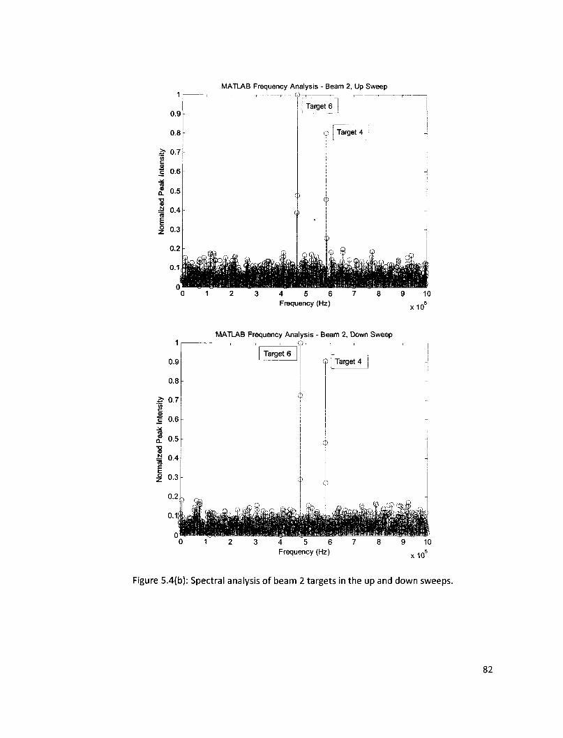
1
0.9
0.8
£• 0.7 S c ID c 0.6
J *
a i? 0.5 •g
75 ° ' 4
g £ 0.3
0.2
0.1, A
MATLAB Frequency Analysis - Beam 2, Up Sweep {•<
-
-
Target 6
V
o
Target 4
Q
C)
-
i=Q r> CiD ^ O ^K «L^ O ^£l ~ i &£
9 Q Q Q
Q HH Q ftiCfflc A , ^
1
-
-
-
-
-
-
a € p CfaiSliEvi^
4 5 6 Frequency (Hz)
x10
1
0.9
0.8
& 0.7
1 0.6
rf 0.5
75 0 4
% 0.3
0.2,
°1
MATLAB Frequency Analysis - Beam 2, Down Sweep
~ Target 6
-
^
-
.
\Mm&2Mk Cih£jj|i$f>)
)
1 (
P&L,
Target 4 -
-
-
• \
-
-
Jtoojk © Cg) f&M
Frequency (Hz) 8 9 10
x105
Figure 5.4(b): Spectral analysis of beam 2 targets in the up and down sweeps.
82
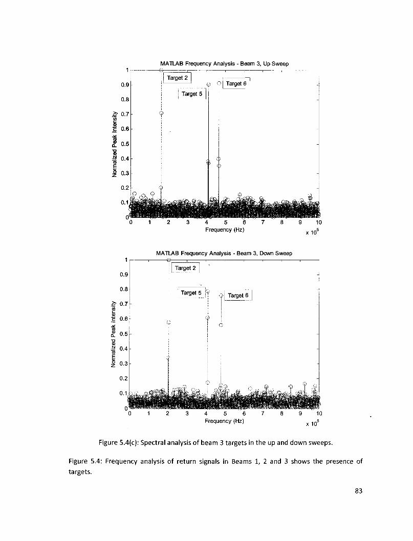
1
0.9
0.8
0.7
0.6
0.5
0.4
0.3
0.2
0.1
Cf
MATLAB Frequency Analysis - Beam 3, Up Sweep
Target 2
Target 5
0)
Target 6
4 5 6 Frequency (Hz) x 10'
10 5
MATLAB Frequency Analysis - Beam 3, Down Sweep
x 10
Figure 5.4(c): Spectral analysis of beam 3 targets in the up and down sweeps.
Figure 5.4: Frequency analysis of return signals in Beams 1, 2 and 3 shows the presence of
83
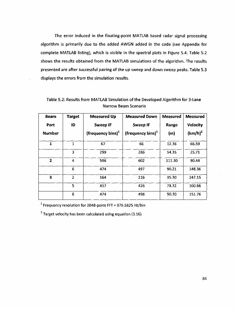
The error induced in the floating-point MATLAB based radar signal processing
algorithm is primarily due to the added AWGN added in the code (see Appendix for
complete MATLAB listing), which is visible in the spectral plots in Figure 5.4. Table 5.2
shows the results obtained from the MATLAB simulations of the algorithm. The results
presented are after successful pairing of the up sweep and down sweep peaks. Table 5.3
displays the errors from the simulation results.
Table 5.2: Results from MATLAB Simulation of the Developed Algorithm for 3-Lane
Narrow Beam Scenario
Beam
Port
Number
1
2
3
Target
ID
1
3
4
6
2
5
6
Measured Up
Sweep IF
(frequency bins)1
67
299
596
474
164
417
474
Measured Down
Sweep IF
(frequency bins)1
66
286
602
497
216
426
498
Measured
Range
(m)
12.36
54.35
111.30
90.21
35.30
78.32
90.30
Measured
Velocity
(km/h)2
66.59
25.71
90.44
148.36
247.15
100.66
151.76
1 Frequency resolution for 2048-point FFT = 976.5625 Hz/bin
Target velocity has been calculated using equation (3.16)
84
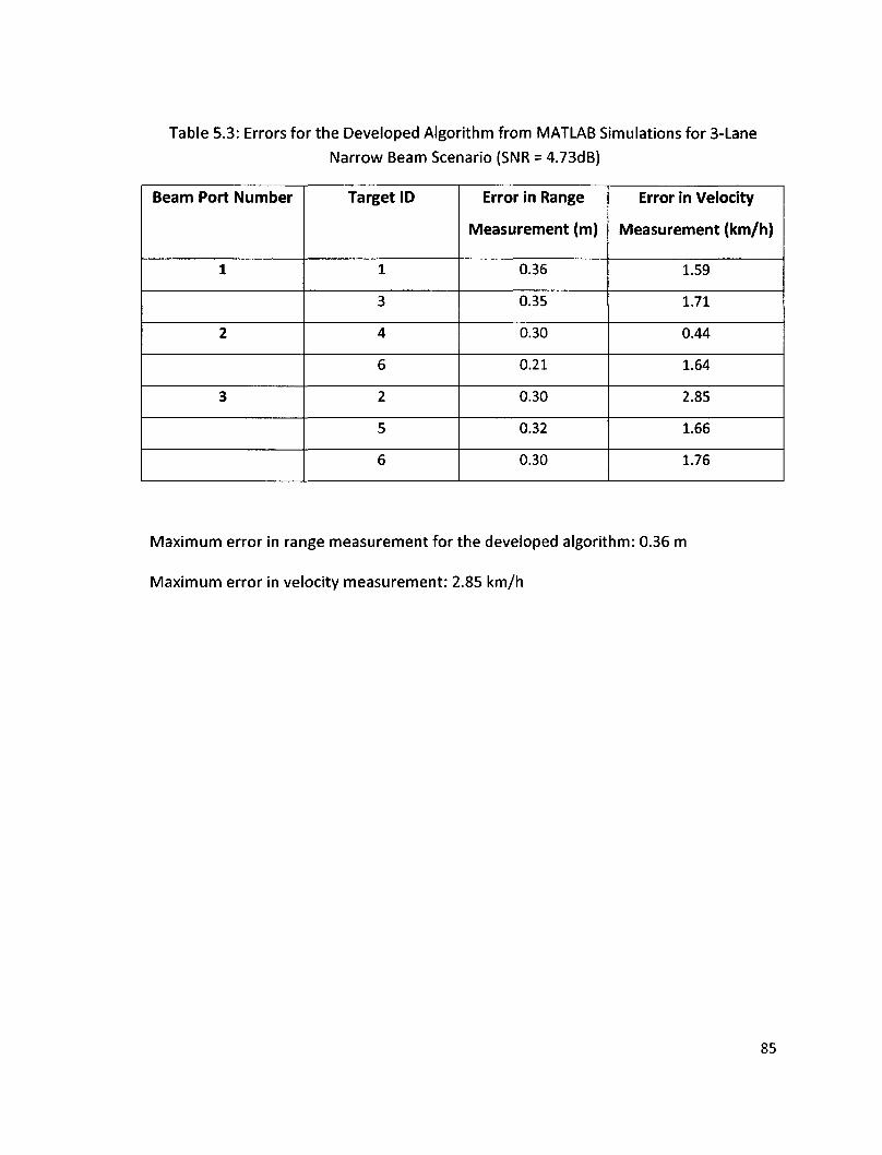
Table 5.3: Errors for the Developed Algorithm from MATLAB Simulations for 3-Lane
Narrow Beam Scenario (SNR = 4.73dB)
Beam Port Number
1
2
3
Target ID
1
3
4
6
2
5
6
Error in Range
Measurement (m)
0.36
0.35
0.30
0.21
0.30
0.32
0.30
Error in Velocity
Measurement (km/h)
1.59
1.71
0.44
1.64
2.85
1.66
1.76
Maximum error in range measurement for the developed algorithm: 0.36 m
Maximum error in velocity measurement: 2.85 km/h
85
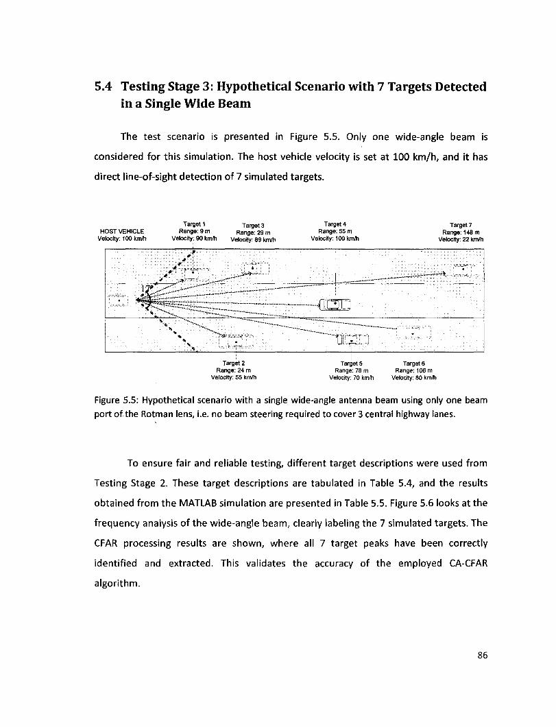
5.4 Testing Stage 3: Hypothetical Scenario with 7 Targets Detected in a Single Wide Beam
The test scenario is presented in Figure 5.5. Only one wide-angle beam is
considered for this simulation. The host vehicle velocity is set at 100 km/h, and it has
direct line-of-sight detection of 7 simulated targets.
HOST VEHICLE Velocity: 100 km/h
Target 1 target 3 Range: 9 m Range: 29 m
Velocity: 90 km/h Velocity: 89 km/h
Target 4 Range: 55 m
Velocity: 100 km/h
Target 7 Range: 148 m
Velocity: 22 km/h
0 * * *
*
% '""••-.. * " ' • • - .
* % % %
— = -
ir jr.;
u t . . . ""
> ';'
Target 2 Range: 24 m
Velocity: 55 km/h
Target 5 Range: 78 m
Velocity: 70 km/h
Target 6 Range: 106 m
Velocity: 80 km/h
Figure 5.5: Hypothetical scenario with a single wide-angle antenna beam using only one beam port of the Rotman lens, i.e. no beam steering required to cover 3 central highway lanes.
To ensure fair and reliable testing, different target descriptions were used from
Testing Stage 2. These target descriptions are tabulated in Table 5.4, and the results
obtained from the MATLAB simulation are presented in Table 5.5. Figure 5.6 looks at the
frequency analysis of the wide-angle beam, clearly labeling the 7 simulated targets. The
CFAR processing results are shown, where all 7 target peaks have been correctly
identified and extracted. This validates the accuracy of the employed CA-CFAR
algorithm.
86
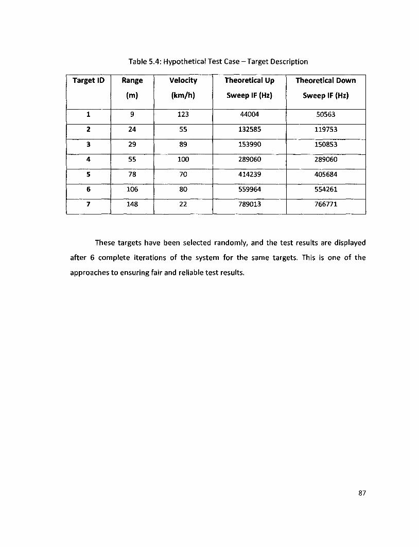
Table 5.4: Hypothetical Test Case -Target Description
Target ID
1
2
3
4
5
6
7
Range
(m)
9
24
29
55
78
106
148
Velocity
(km/h)
123
55
89
100
70
80
22
Theoretical Up
Sweep IF (Hz)
44004
132585
153990
289060
414239
559964
789013
Theoretical Down
Sweep IF (Hz)
50563
119753
150853
289060
405684
554261
766771
These targets have been selected randomly, and the test results are displayed
after 6 complete iterations of the system for the same targets. This is one of the
approaches to ensuring fair and reliable test results.
87
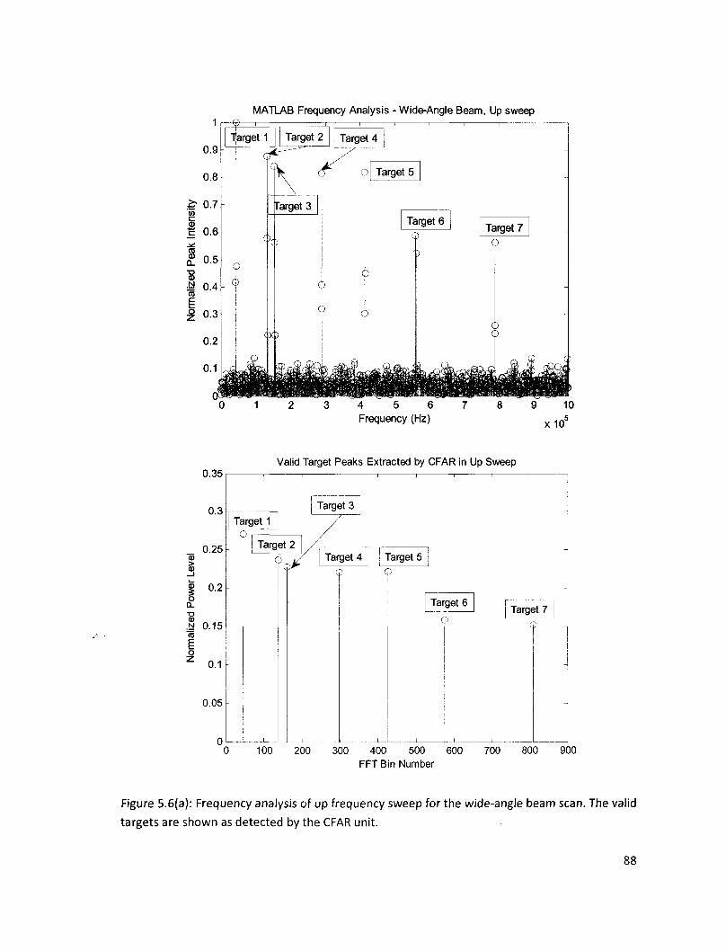
MATLAB Frequency Analysis - Wide-Angle Beam, Up sweep
Frequency (Hz) x1(f
0.35
0.3
0.25
5 | 0.2 o a.
TD <D N 0.15
0.1
0.05
0
Valid Target Peaks Extracted by CFAR in Up Sweep
Target 6 Target 7
0 100 200 300 400 500 600 700 800 900 FFT Bin Number
Figure 5.6(a): Frequency analysis of up frequency sweep for the wide-angle beam scan. The valid
targets are shown as detected by the CFAR unit.
88
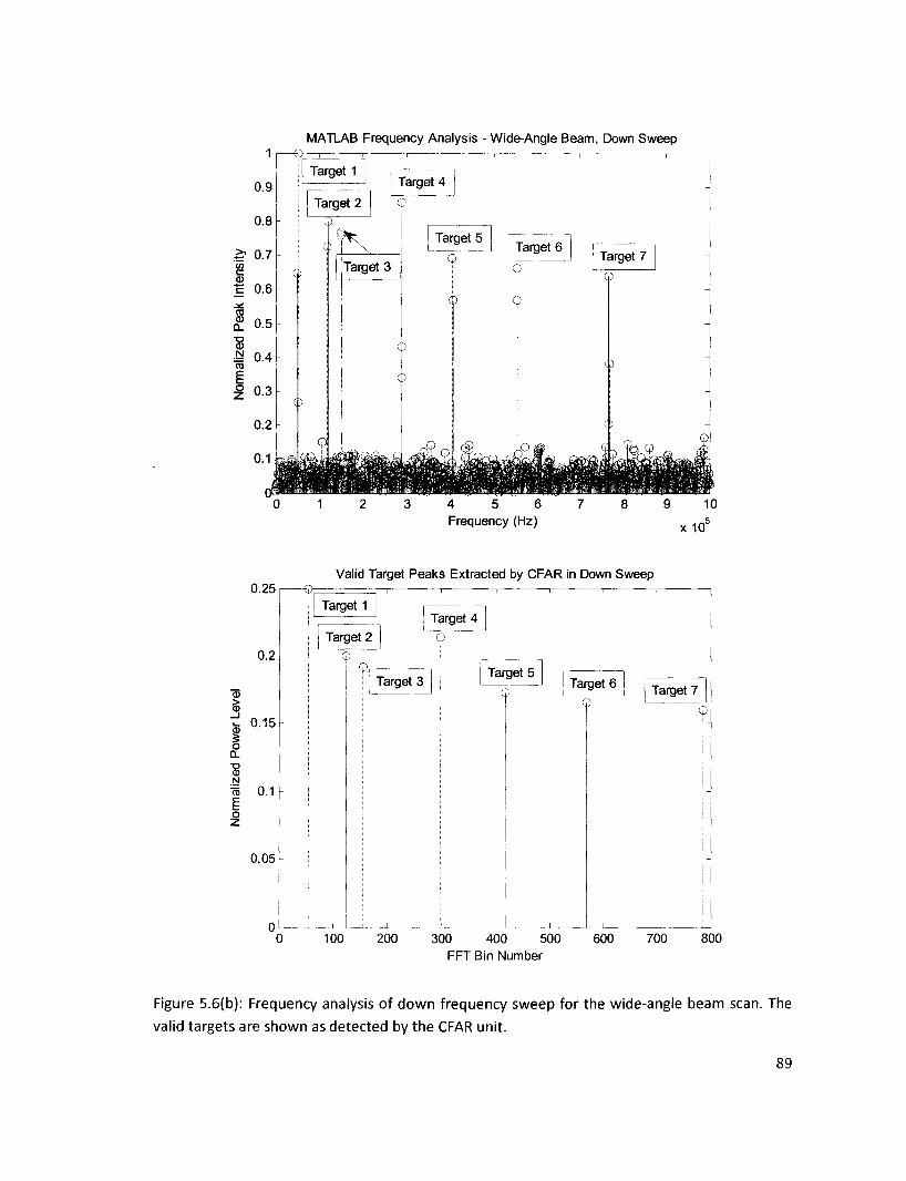
MATLAB Frequency Analysis - Wide-Angle Beam, Down Sweep
3 4 5 6 7 Frequency (Hz)
8 9 10
x 105
0.25
0.2
CD
I 0.15
N 'To 0.1
o
0.05
0
Valid Target Peaks Extracted by CFAR in Down Sweep -9;
Target 1
Target 2 Target 4
9
Q,
Target 3 Target 5
Target 6 Target 7
Q
0 100 200 300 400 500 600 700 800 FFT Bin Number
Figure 5.6(b): Frequency analysis of down frequency sweep for the wide-angle beam scan
valid targets are shown as detected by the CFAR unit.
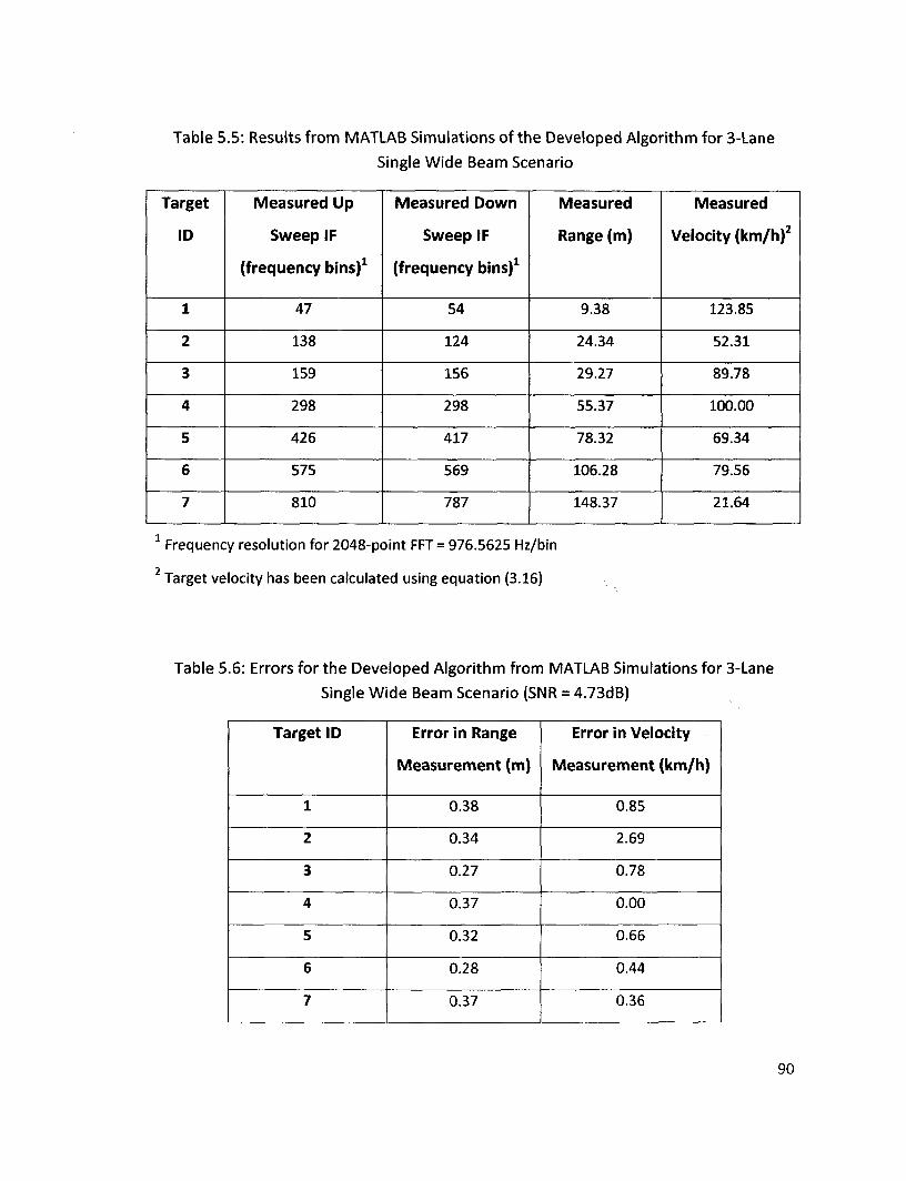
Table 5.5: Results from MATLAB Simulations of the Developed Algorithm for 3-Lane
Single Wide Beam Scenario
Target
ID
l
2
3
4
5
6
7
Measured Up
Sweep IF
(frequency bins)1
47
138
159
298
426
575
810
Measured Down
Sweep IF
(frequency bins)1
54
124
156
298
417
569
787
Measured
Range(m)
9.38
24.34
29.27
55.37
78.32
106.28
148.37
Measured
Velocity (km/h)2
123.85
52.31
89.78
100.00
69.34
79.56
21.64
Frequency resolution for 2048-point FFT= 976.5625 Hz/bin
2 Target velocity has been calculated using equation (3.16)
Table 5.6: Errors for the Developed Algorithm from MATLAB Simulations for 3-Lane
Single Wide Beam Scenario (SNR = 4.73dB)
Target ID
l
2
3
4
5
6
7
Error in Range
Measurement (m)
0.38
0.34
0.27
0.37
0.32
0.28
0.37
Error in Velocity
Measurement (km/h)
0.85
2.69
0.78
0.00
0.66
0.44
0.36
90
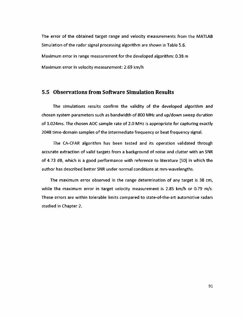
The error of the obtained target range and velocity measurements from the MATLAB
Simulation of the radar signal processing algorithm are shown in Table 5.6.
Maximum error in range measurement for the developed algorithm: 0.38 m
Maximum error in velocity measurement: 2.69 km/h
5.5 Observations from Software Simulation Results
The simulations results confirm the validity of the developed algorithm and
chosen system parameters such as bandwidth of 800 MHz and up/down sweep duration
of 1.024ms. The chosen ADC sample rate of 2.0 MHz is appropriate for capturing exactly
2048 time-domain samples of the intermediate frequency or beat frequency signal.
The CA-CFAR algorithm has been tested and its operation validated through
accurate extraction of valid targets from a background of noise and clutter with an SNR
of 4.73 dB, which is a good performance with reference to literature [50] in which the
author has described better SNR under normal conditions at mm-wavelengths.
The maximum error observed in the range determination of any target is 38 cm,
while the maximum error in target velocity measurement is 2.85 km/h or 0.79 m/s.
These errors are within tolerable limits compared to state-of-the-art automotive radars
studied in Chapter 2.
91
CHAPTER 6: HARDWARE IMPLEMENTATION AND VALIDATION
The signal processing algorithm is coded in Verilog HDL and the modular design
has been shown in this chapter. The data flow through individual modules is described,
and an overview of the entire HDL implementation is produced. A few alterations and
fine-tuning of the FFT and CFAR modules have been done to improve noise tolerance
and accommodate short range, medium range and long range target return attenuation
and power variation. The coded system is simulated using Xilinx ISim and the waveforms
have been illustrated. The results are promising and show lower error than the MATLAB
simulations, primariliy due to the fixed-point rounding of data as it propagates through
the digital logic.
6.1 Hardware Implementation of the Radar Signal Processing Algorithm
The advantages of modern FPGAs over DSPs in running signal processing tasks
have been highlighted in Chapter 2. The state-of-the-art Bosch LRR3 has a cycle time of
50 ms. An FPGA implementation presented in [28] displays a signal processing latency of
1250 p.s for a single LFMCW sweep using with a 1024-point FFT using a Xilinx Virtex-ll
Pro FPGA clocked at 50 MHz. To achieve a smaller computation latency per sweep, and
hence a smaller cycle time for the MEMS based automotive radar, the target FPGA for
this thesis is selected as Virtex-5 SX50T.
Figure 6.1 shows an annotated snapshot of the Virtex-5 development board and
Table 6.1 highlights the main aspects of this FPGA. One of the advantages of using the
Virtex-5 FPGA from Xilinx is the high integration capacity of the design, and the higher
operating clock frequency, owing to the improved gate-level performance with 65 nm
92
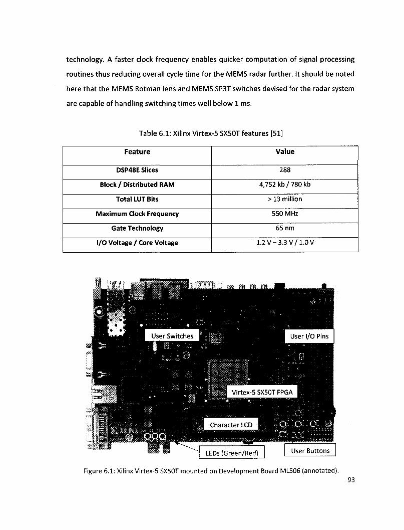
technology. A faster clock frequency enables quicker computation of signal processing
routines thus reducing overall cycle time for the MEMS radar further. It should be noted
here that the MEMS Rotman lens and MEMS SP3T switches devised for the radar system
are capable of handling switching times well below 1 ms.
Table 6.1: Xilinx Virtex-5 SX50T features [51]
Feature
DSP48E Slices
Block/ Distributed RAM
Total LUT Bits
Maximum Clock Frequency
Gate Technology
I/O Voltage / Core Voltage
Value
288
4,752 kb / 780 kb
> 13 million
550 MHz
65 nm
1.2V-3.3V/1 .0V
LEDs(Green/Red) User Buttons
Figure 6.1: Xilinx Virtex-5 SX50T mounted on Development Board ML506 (annotated). 93
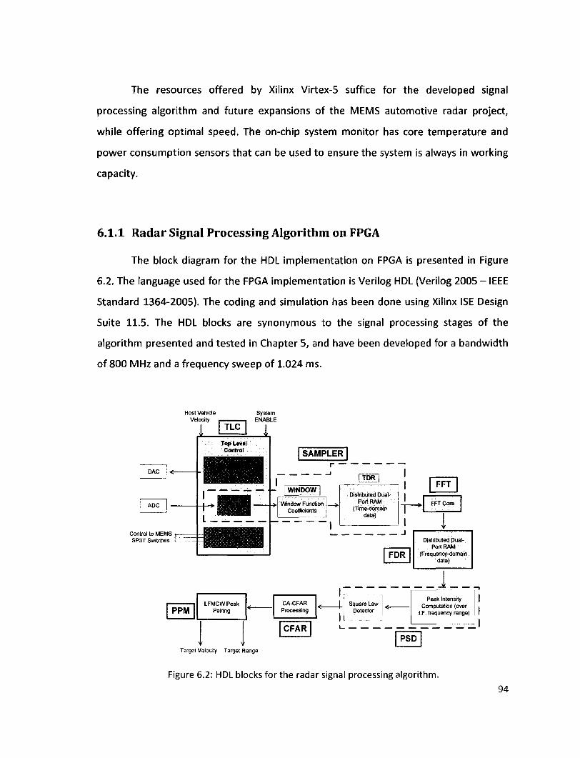
The resources offered by Xilinx Virtex-5 suffice for the developed signal
processing algorithm and future expansions of the MEMS automotive radar project,
while offering optimal speed. The on-chip system monitor has core temperature and
power consumption sensors that can be used to ensure the system is always in working
capacity.
6.1.1 Radar Signal Processing Algorithm on FPGA
The block diagram for the HDL implementation on FPGA is presented in Figure
6.2. The language used for the FPGA implementation is Verilog HDL (Verilog 2005 - IEEE
Standard 1364-2005). The coding and simulation has been done using Xilinx ISE Design
Suite 11.5. The HDL blocks are synonymous to the signal processing stages of the
algorithm presented and tested in Chapter 5, and have been developed for a bandwidth
of 800 MHz and a frequency sweep of 1.024 ms.
Control to MEMS SP3T Switches
Host Vehicle Velocity
System ENABLE oaiy I | eiN«E
PPM LFMCW Peak
Pairing CA-CFAR Processing
CFAR
TDRI
Distributed Dual-Port RAM
(Time-domain data)
FDR
FFT
FFTCore
Distributed Dual-Port RAM
(Frequency-domain data)
1 Square Law
Detector
Peak Intensity Computation (over
I.F. frequency range)
PSD Target Velocity Target Range
Figure 6.2: HDL blocks for the radar signal processing algorithm. 94
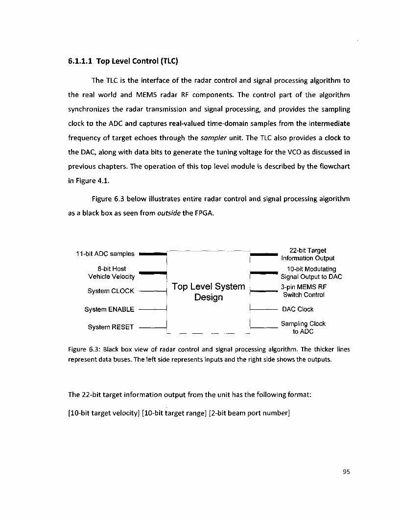
6.1.1.1 Top Level Control (TLC)
The TLC is the interface of the radar control and signal processing algorithm to
the real world and MEMS radar RF components. The control part of the algorithm
synchronizes the radar transmission and signal processing, and provides the sampling
clock to the ADC and captures real-valued time-domain samples from the intermediate
frequency of target echoes through the sampler unit. The TLC also provides a clock to
the DAC, along with data bits to generate the tuning voltage for the VCO as discussed in
previous chapters. The operation of this top level module is described by the flowchart
in Figure 4.1.
Figure 6.3 below illustrates entire radar control and signal processing algorithm
as a black box as seen from outside the FPGA.
11-bit ADC samples
8-bit Host Vehicle Velocity
System CLOCK
System ENABLE
System RESET
22-bit Target Information Output
10-bit Modulating Signal Output to DAC 3-pin MEMS RF Switch Control
DAC Clock
Sampling Clock to ADC
Figure 6.3: Black box view of radar control and signal processing algorithm. The thicker lines represent data buses. The left side represents inputs and the right side shows the outputs.
The 22-bit target information output from the unit has the following format:
[10-bit target velocity] [10-bit target range] [2-bit beam port number]
95
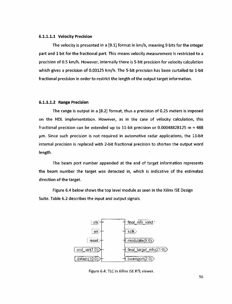
6.1.1.1.1 Velocity Precision
The velocity is presented in a [9.1] format in km/h, meaning 9 bits for the integer
part and 1 bit for the fractional part. This means velocity measurement is restricted to a
precision of 0.5 km/h. However, internally there is 5-bit precision for velocity calculation
which gives a precision of 0.03125 km/h. The 5-bit precision has been curtailed to 1-bit
fractional precision in order to restrict the length of the output target information.
6.1.1.1.2 Range Precision
The range is output in a [8.2] format, thus a precision of 0.25 meters is imposed
on the HDL implementation. However, as in the case of velocity calculation, this
fractional precision can be extended up to 11-bit precision or 0.00048828125 m = 488
u,m. Since such precision is not required in automotive radar applications, the 11-bit
internal precision is replaced with 2-bit fractional precision to shorten the output word
length.
The beam port number appended at the end of target information represents
the beam number the target was detected in, which is indicative of the estimated
direction of the target.
Figure 6.4 below shows the top level module as seen in the Xilinx ISE Design
Suite. Table 6.2 describes the input and output signals.
iik>f
en.>f~
reset/j-
umt_vel(7:0)>f-
datain{10:0)>f-
final info valid)
sclk>
modulate(9:0)>
final_targetJnfo(21:0)>
beamport(2:0))>
Figure 6.4: TLC in Xilinx ISE RTL viewer.
96
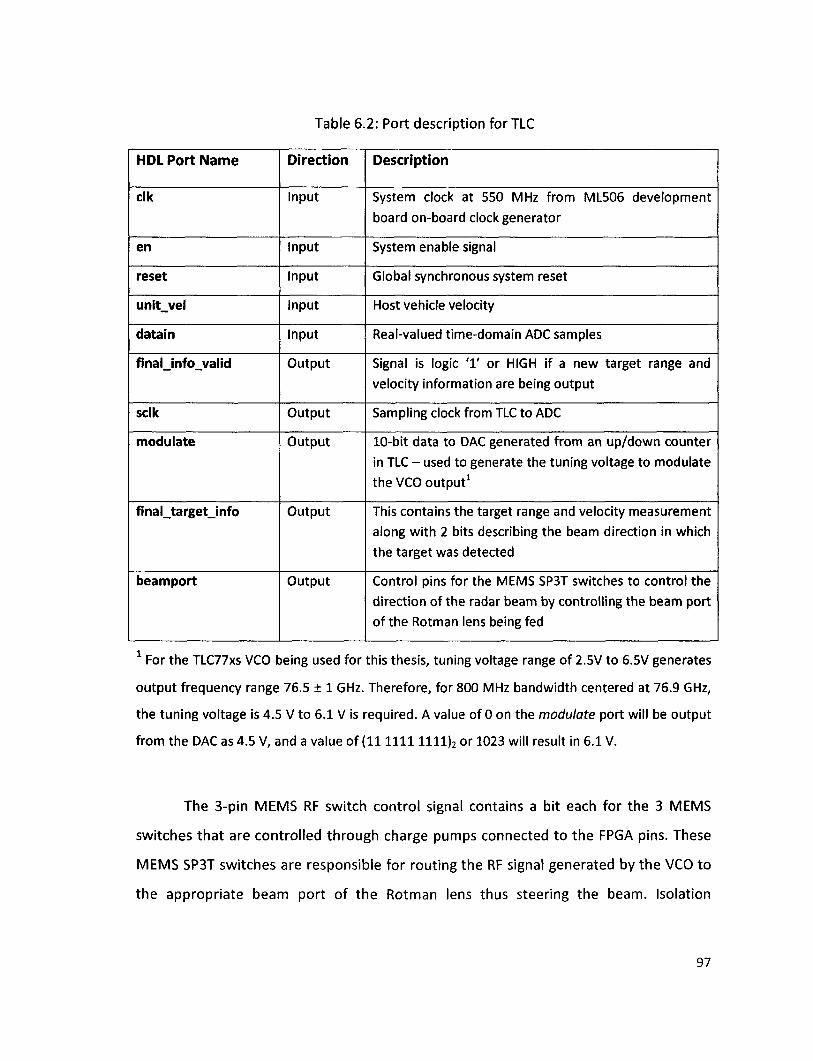
Table 6.2: Port description for TLC
HDL Port Name
elk
en
reset
unit_vel
datain
final_info_valid
sclk
modulate
final_target_info
beam port
Direction
Input
Input
Input
Input
Input
Output
Output
Output
Output
Output
Description
System clock at 550 MHz from ML506 development
board on-board clock generator
System enable signal
Global synchronous system reset
Host vehicle velocity
Real-valued time-domain ADC samples
Signal is logic ' 1 ' or HIGH if a new target range and
velocity information are being output
Sampling clock from TLC to ADC
10-bit data to DAC generated from an up/down counter
in TLC - used to generate the tuning voltage to modulate
the VCO output1
This contains the target range and velocity measurement
along with 2 bits describing the beam direction in which
the target was detected
Control pins for the MEMS SP3T switches to control the
direction of the radar beam by controlling the beam port
of the Rotman lens being fed
1 For the TLC77xs VCO being used for this thesis, tuning voltage range of 2.5V to 6.5V generates
output frequency range 76.5 ± 1 GHz. Therefore, for 800 MHz bandwidth centered at 76.9 GHz,
the tuning voltage is 4.5 V to 6.1 V is required. A value of 0 on the modulate port will be output
from the DAC as 4.5 V, and a value of (1111111111)2 or 1023 will result in 6.1 V.
The 3-pin MEMS RF switch control signal contains a bit each for the 3 MEMS
switches that are controlled through charge pumps connected to the FPGA pins. These
MEMS SP3T switches are responsible for routing the RF signal generated by the VCO to
the appropriate beam port of the Rotman lens thus steering the beam. Isolation
97
between the supply voltage of the MEMS switches and the RF signal travelling through
them is done using a bias-tee for each switch.
The system clock input for Virtex-5 is 550 MHz, obtained from the ML506
development kit from Xilinx. This clock signal is divided internally to an operating clock
of 100 MHz, which is the target operating frequency for the radar algorithm.
Time-domain samples from the ADC are obtained in 11-bit format as per the
decided resolution of the ADC (Chapter 3).
6.1.1.2 Sampling Unit (SAMPLER): sub-module Window Function (WINDOW)
This is a sub-module of the sampler module and contains a ROM storing 1024
coefficients of a 2048-point Hamming window. Since the Hamming window is
symmetric, storing the first 1024 values is memory efficient. This sub-module contains a
simple 10-bit up/down counter that extracts the coefficient depending on the index of
the time-domain sample.
The Hamming window coefficients are floating point numbers, thus representing
them in digital hardware requires rounding off. The precision of the coefficients is
chosen to be 10 bits, with the maximum of (11 1111 1111)2 representing the maximum
coefficient value of 1. The rounded off Hamming coefficients are thus stored as integers
ranging from (0.08 x 10²³) to (1 x 10²³). The coefficients are obtained from MATLAB
code which carries out the following steps (refer to Appendix for MATLAB listing):
1. Create a Hamming window of size 2048.
2. Multiply the window coefficients by 1023 to scale them to a 10-bit range.
3. Round off the scaled coefficients to the nearest integer.
4. Save the first 1024 coefficients in sampler ROM.
98
Although this rounding does introduce a secondary quantization error after the ADC,
the results from simulation of the algorithm in HDL show desired accuracy and
precision. The percentage error produced by from rounding the Hamming coefficients is
0.084%, which has negligible effects on the signal processing. A similar approach has
been presented and validated by Hampson in [56].
The scaling an x-bit time-domain sample by multiplication with a window coefficient
returns a scaled x-bit number; there is no change in the word length of the samples. This
is done by retrieving only the most significant x bits from the result of the multiplication.
Thus:
x-bit time-domain sample -> WINDOW -> x-bit scaled time-domain sample
This method of scaling has a maximum error of 0.1% per sample which is
negligible. The preservation of word length proves efficient later on in the signal
processing by limiting the memory sizes and reducing processing speed while retaining
adequate accuracy.
6.1.1.3 Sampling Unit (SAMPLER): sub-module Time-Domain Data RAM (TDR)
This is a sub-model of the sampler module which is a dual-port Block RAM. This
sub-module stores the windowed time-domain samples collected from the ADC. The
width of the data RAM is 12 bits, and the depth is 2048 - 2 MHz ADC sampling over
1.024 ms. An important note to make is that although the ADC output is 11 bits long, the
TDR module stores 12-bit samples. The extra bit is merely a '0' added to the front of
every sample. This is done as the FFT core used in this project works with 2's
complement input and output data, so appending a '0' at the beginning of every time-
domain sample converts all samples to positive values. The only effect of this method is
a high DC component being detected in the first frequency bin of the FFT, which is safely
ignored as it represents a negligible target range of 0.186 m or 18.6 cm. The first few 99
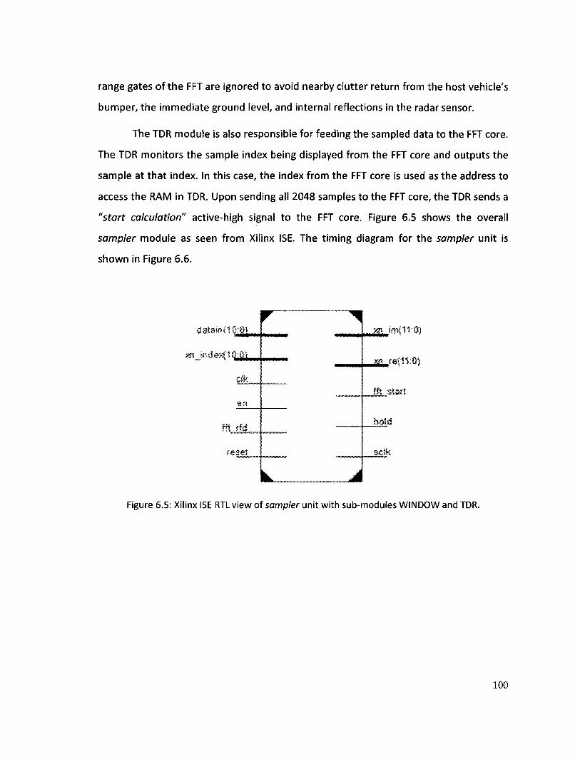
range gates of the FFT are ignored to avoid nearby clutter return from the host vehicle's
bumper, the immediate ground level, and internal reflections in the radar sensor.
The TDR module is also responsible for feeding the sampled data to the FFT core.
The TDR monitors the sample index being displayed from the FFT core and outputs the
sample at that index. In this case, the index from the FFT core is used as the address to
access the RAM in TDR. Upon sending all 2048 samples to the FFT core, the TDR sends a
"start calculation" active-high signal to the FFT core. Figure 6.5 shows the overall
sampler module as seen from Xilinx ISE. The timing diagram for the sampler unit is
shown in Figure 6.6.
<Jatairif10;Ql
m indexftQ:fl) mmmmmm
elk
en
fft r f d
reset
r
k
^
A
j j ^ i m d
[ m mitt
...JJLslart
hold
sclk
Figure 6.5: Xilinx ISE RTL view of sampler unit with sub-modules WINDOW and TDR.
100
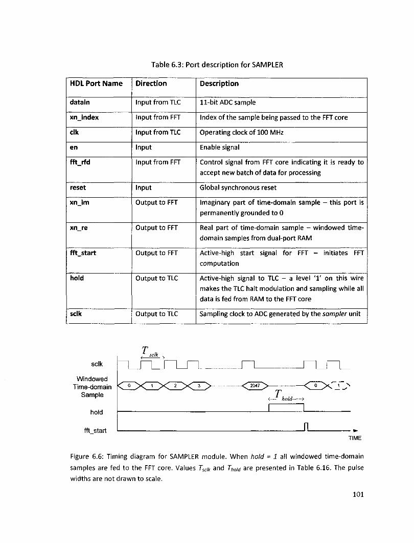
Table 6.3: Port description for SAMPLER
HDL Port Name
datain
xnjndex
elk
en
fft_rfd
reset
xn_im
xn_re
fft_start
hold
sclk
Direction
Input from TLC
Input from FFT
Input from TLC
Input
Input from FFT
Input
Output to FFT
Output to FFT
Output to FFT
Output to TLC
Output to TLC
Description
11-bit ADC sample
Index of the sample being passed to the FFT core
Operating clock of 100 MHz
Enable signal
Control signal from FFT core indicating it is ready to
accept new batch of data for processing
Global synchronous reset
Imaginary part of time-domain sample - this port is
permanently grounded to 0
Real part of time-domain sample - windowed time-
domain samples from dual-port RAM
Active-high start signal for FFT - initiates FFT
computation
Active-high signal to TLC - a level 'V on this wire
makes the TLC halt modulation and sampling while all
data is fed from RAM to the FFT core
Sampling clock to ADC generated by the sampler unit
T sclk
Windowed Time-domain
Sample
hold
fft_start TIME
Figure 6.6: Timing diagram for SAMPLER module. When hold = 1 all windowed time-domain
samples are fed to the FFT core. Values Tscik and 7/,oW are presented in Table 6.16. The pulse
widths are not drawn to scale.
101
< = — — — >
T <ZX~i~
hold-
JL
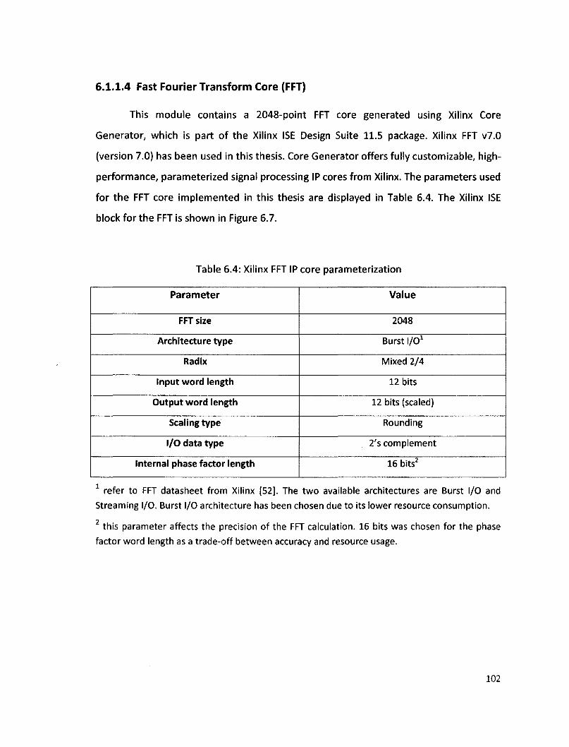
6.1.1.4 Fast Fourier Transform Core (FFT)
This module contains a 2048-point FFT core generated using Xilinx Core
Generator, which is part of the Xilinx ISE Design Suite 11.5 package. Xilinx FFT v7.0
(version 7.0) has been used in this thesis. Core Generator offers fully customizable, high-
performance, parameterized signal processing IP cores from Xilinx. The parameters used
for the FFT core implemented in this thesis are displayed in Table 6.4. The Xilinx ISE
block for the FFT is shown in Figure 6.7.
Table 6.4: Xilinx FFT IP core parameterization
Parameter
FFT size
Architecture type
Radix
Input word length
Output word length
Scaling type
I/O data type
Internal phase factor length
Value
2048
Burst I/O1
Mixed 2/4
12 bits
12 bits (scaled)
Rounding
2's complement
16 bits2
1 refer to FFT datasheet from Xilinx [52]. The two available architectures are Burst I/O and Streaming I/O. Burst I/O architecture has been chosen due to its lower resource consumption.
2 this parameter affects the precision of the FFT calculation. 16 bits was chosen for the phase factor word length as a trade-off between accuracy and resource usage.
102
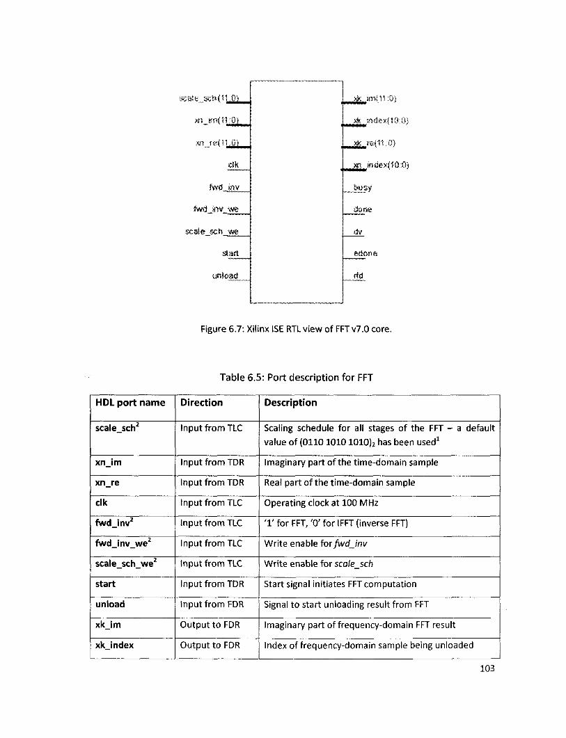
scale $ch<11,0)
xn... »TI(11;.J).
m rei'lt 0)
elk
fwd tnv
fwd ww we
scale a h we
start
unload
?4c §nflt;0s
>k index{10:0)
| * refit.0)
xn index(10:.Q)
_bysy
done
dy
edone
m
Figure 6.7: Xilinx ISE RTL view of FFT v7.0 core.
Table 6.5: Port description for FFT
HDL port name
scale_sch2
xn_im
xn_re
elk
fwd_inv2
fwd_inv_we2
scale_sch_we2
start
unload
xk_im
xk_index
Direction
Input from TLC
Input from TDR
Input from TDR
Input from TLC
Input from TLC
Input from TLC
Input from TLC
Input from TDR
Input from FDR
Output to FDR
Output to FDR
Description
Scaling schedule for all stages of the FFT - a default
value of (0110 1010 1010)2 has been used1
Imaginary part of the time-domain sample
Real part of the time-domain sample
Operating clock at 100 MHz
' 1 ' for FFT, '0' for IFFT (inverse FFT)
Write enable for fwdjnv
Write enable for scale_sch
Start signal initiates FFT computation
Signal to start unloading result from FFT
Imaginary part of frequency-domain FFT result
Index of frequency-domain sample being unloaded
103
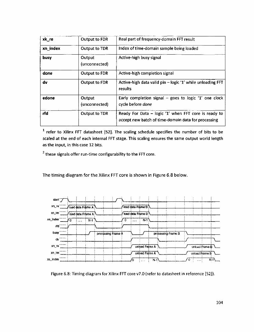
xk_re
xn_index
busy
done
dv
edone
rfd
Output to FDR
Output to TDR
Output
(unconnected)
Output to FDR
Output to FDR
Output
(unconnected)
Output to TDR
Real part of frequency-domain FFT result
Index of time-domain sample being loaded
Active-high busy signal
Active-high completion signal
Active-high data valid pin - logic T while unloading FFT
results
Early completion signal - goes to logic T one clock
cycle before done
Ready For Data - logic T when FFT core is ready to
accept new batch of t ime-domain data for processing
1 refer to Xilinx FFT datasheet [52]. The scaling schedule specifies the number of bits to be
scaled at the end of each internal FFT stage. This scaling ensures the same output world length
as the input, in this case 12 bits.
these signals offer run-time configurability to the FFT core.
The t iming diagram for the Xilinx FFT core is shown in Figure 6.8 below.
start-y-i 1 i
x n - r e j load ^ata Fr$me A
xnjm „ '/tosd ifata Frime f
xnjndax </Q < i ^-1 f I i
ttd y \ \
busy i ; ; f~
dv I i
xn_re ; ; :
xn im 1 :
xnjreJex i ;
^ i i i
N !
: processing
L/~\_
4 i
« i t
! ! ! (toad data Rime B \_
/toad data Frama B i\_
f° r~
Frame A
i . . . : N-IN i i i
i i \ ! 1 i
\ ! / t : i i
F ™ T ~ ™ T "
| j
prqcesstnb Frame 8
'/ urtttedFra'nwA
'/ unload Frame A
Jo ;... ! N-1
\ !
^ i ^ :
\ !
i
: /
\t i / 0
'•• i i
I I \
upload frame % \
HiMnftrt Prarrw R \
~r—-~~~ipi\__
Figure 6.8: Timing diagram for Xilinx FFT core v7.0 (refer to datasheet in reference [52]).
104
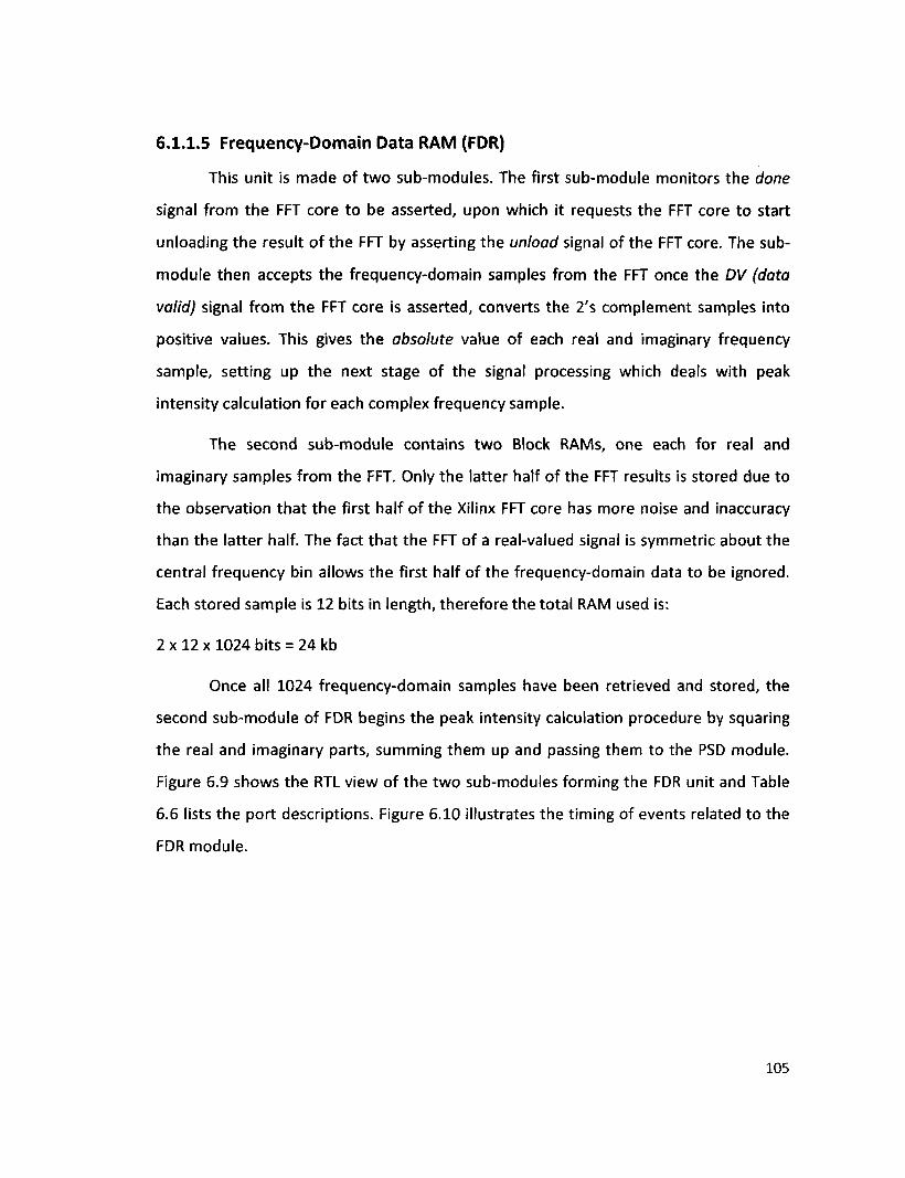
6.1.1.5 Frequency-Domain Data RAM (FDR)
This unit is made of two sub-modules. The first sub-module monitors the done
signal from the FFT core to be asserted, upon which it requests the FFT core to start
unloading the result of the FFT by asserting the unload signal of the FFT core. The sub-
module then accepts the frequency-domain samples from the FFT once the DV (data
valid) signal from the FFT core is asserted, converts the 2's complement samples into
positive values. This gives the absolute value of each real and imaginary frequency
sample, setting up the next stage of the signal processing which deals with peak
intensity calculation for each complex frequency sample.
The second sub-module contains two Block RAMs, one each for real and
imaginary samples from the FFT. Only the latter half of the FFT results is stored due to
the observation that the first half of the Xilinx FFT core has more noise and inaccuracy
than the latter half. The fact that the FFT of a real-valued signal is symmetric about the
central frequency bin allows the first half of the frequency-domain data to be ignored.
Each stored sample is 12 bits in length, therefore the total RAM used is:
2 x 12 x 1024 bits = 24 kb
Once all 1024 frequency-domain samples have been retrieved and stored, the
second sub-module of FDR begins the peak intensity calculation procedure by squaring
the real and imaginary parts, summing them up and passing them to the PSD module.
Figure 6.9 shows the RTL view of the two sub-modules forming the FDR unit and Table
6.6 lists the port descriptions. Figure 6.10 illustrates the timing of events related to the
FDR module.
105
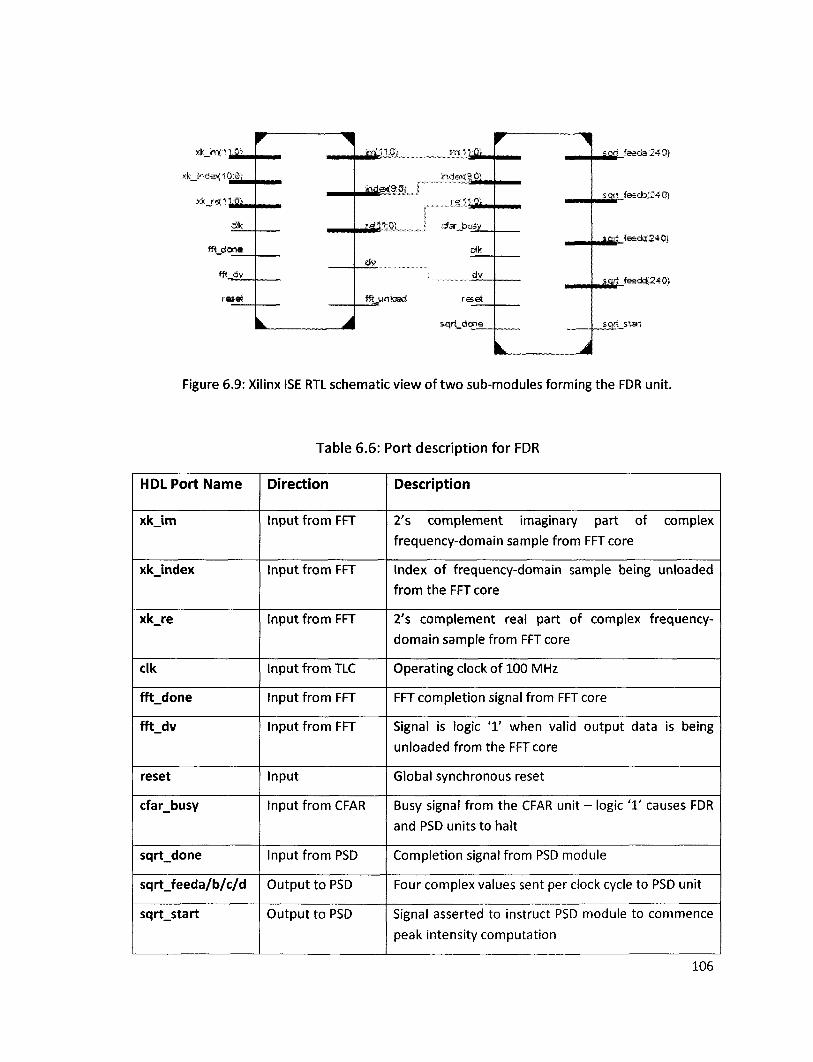
y.k i m ' i y g ^
>;k «r.ds^10:0'i
xk re l ^ g j ^ |
dk
ift dona
ffS dv
rase;
r 1
A
mj^nm
rafH-iR
dv
ft! ynisad
r ndes9C.
(a 1 1 J ^ ^
afar bjsy
eft
dv
l e d
sqrt done
L
1
A
m£j£ fe&ds24Qi
sqrt fe=d»!24Q'i
mj^jg ?e=ckJ24:G'i
m^fi feeddt240>
sqrt start
Figure 6.9: Xilinx ISE RTL schematic view of two sub-modules forming the FDR unit.
Table 6.6: Port description for FDR
HDL Port Name
xk_im
xk_index
xk_re
elk
fft_done
fft_dv
reset
cfar_busy
sqrt_done
sqrt_feeda/b/c/d
sqrt_start
Direction
Input from FFT
Input from FFT
Input from FFT
Input from TLC
Input from FFT
Input from FFT
Input
Input from CFAR
Input from PSD
Output to PSD
Output to PSD
Description
2's complement imaginary part of complex
frequency-domain sample from FFT core
Index of frequency-domain sample being unloaded
from the FFT core
2's complement real part of complex frequency-
domain sample from FFT core
Operating clock of 100 MHz
FFT completion signal from FFT core
Signal is logic T when valid output data is being
unloaded from the FFT core
Global synchronous reset
Busy signal from the CFAR unit - logic T causes FDR
and PSD units to halt
Completion signal from PSD module
Four complex values sent per clock cycle to PSD unit
Signal asserted to instruct PSD module to commence
peak intensity computation
106
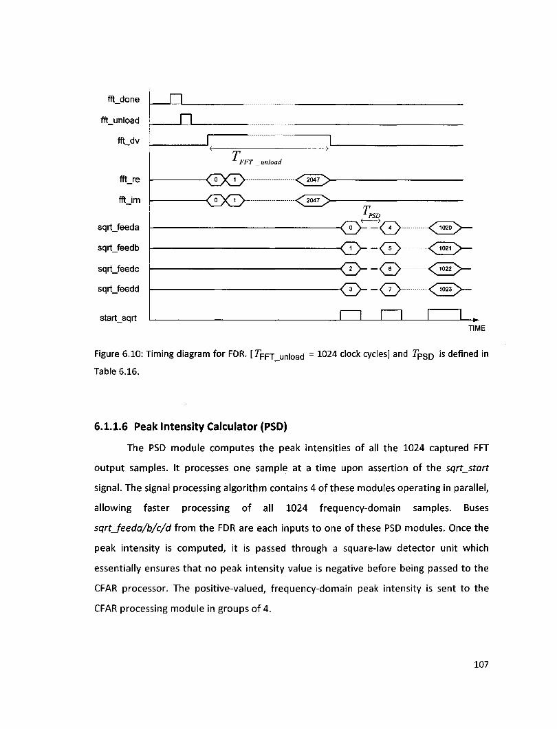
fft_done
fft_unload
fft_dv
fft_re
fft_im
sqrt_feeda
sqrt_feedb
sqrt_feedc
sqrt_feedd
start_sqrt TIME
Figure 6.10: Timing diagram for FDR. [7p F j un|oacj = 1024 clock cycles] and 7pSD is defined in
Table 6.16.
6.1.1.6 Peak Intensity Calculator (PSD)
The PSD module computes the peak intensities of all the 1024 captured FFT
output samples. It processes one sample at a time upon assertion of the sqrt_start
signal. The signal processing algorithm contains 4 of these modules operating in parallel,
allowing faster processing of all 1024 frequency-domain samples. Buses
sqrt_feeda/b/c/d from the FDR are each inputs to one of these PSD modules. Once the
peak intensity is computed, it is passed through a square-law detector unit which
essentially ensures that no peak intensity value is negative before being passed to the
CFAR processor. The positive-valued, frequency-domain peak intensity is sent to the
CFAR processing module in groups of 4.
107
n
T FFT _ unload
<ZXZ> <204?
-(ixiy <zo47 LPSD
O-<I>
value (24:01
elk
reset
start
rooti 12:01
done
Figure 6.11: Peak intensity calculation unit.
Table 6.7: Port description for PSD
HDL Port Name
value
elk
reset
start
root
done
Direction
Input from PSD units
Input from TLC
Input
Input from FDR
Output to CFAR
Output to FDR
Description
Mapped to sqrt_feeda/b/c/d from FDR
Operating clock at 100 MHz
Global synchronous reset
Start peak intensity computation signal from FDR
Peak intensity computation result to CFAR unit
Completion of peak intensity calculation
6.1.1.7 Constant False Alarm Rate Processor (CFAR)
The CA-CFAR algorithm has been detailed in previous chapters of this thesis. The
HDL implementation of the CA-CFAR algorithm is a vital component of the radar signal
processing algorithm. It is solely responsible for removal of unwanted clutter and noise
while detecting valid targets from an unknown attenuation pattern arising from
different weather conditions.
The CFAR processor receives frequency-domain peak intensity values in batches
of 4 from the 4 PSD units working in parallel, as shown in Figure 6.12. These 4 values are
stored in a Block RAM in the following order: 108
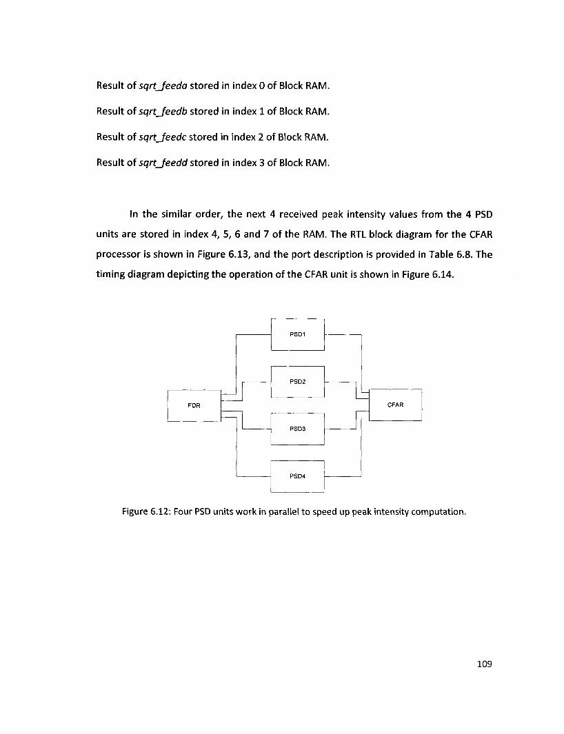
Result of sqrt_feeda stored in index 0 of Block RAM.
Result of sqrt_feedb stored in index 1 of Block RAM.
Result of sqrt_feedc stored in index 2 of Block RAM.
Result of sqrt_feedd stored in index 3 of Block RAM.
In the similar order, the next 4 received peak intensity values from the 4 PSD
units are stored in index 4, 5, 6 and 7 of the RAM. The RTL block diagram for the CFAR
processor is shown in Figure 6.13, and the port description is provided in Table 6.8. The
timing diagram depicting the operation of the CFAR unit is shown in Figure 6.14.
FDR
PSD1
PSD2
PSD3
PSD4
CFAR
Figure 6.12: Four PSD units work in parallel to speed up peak intensity computation.
109
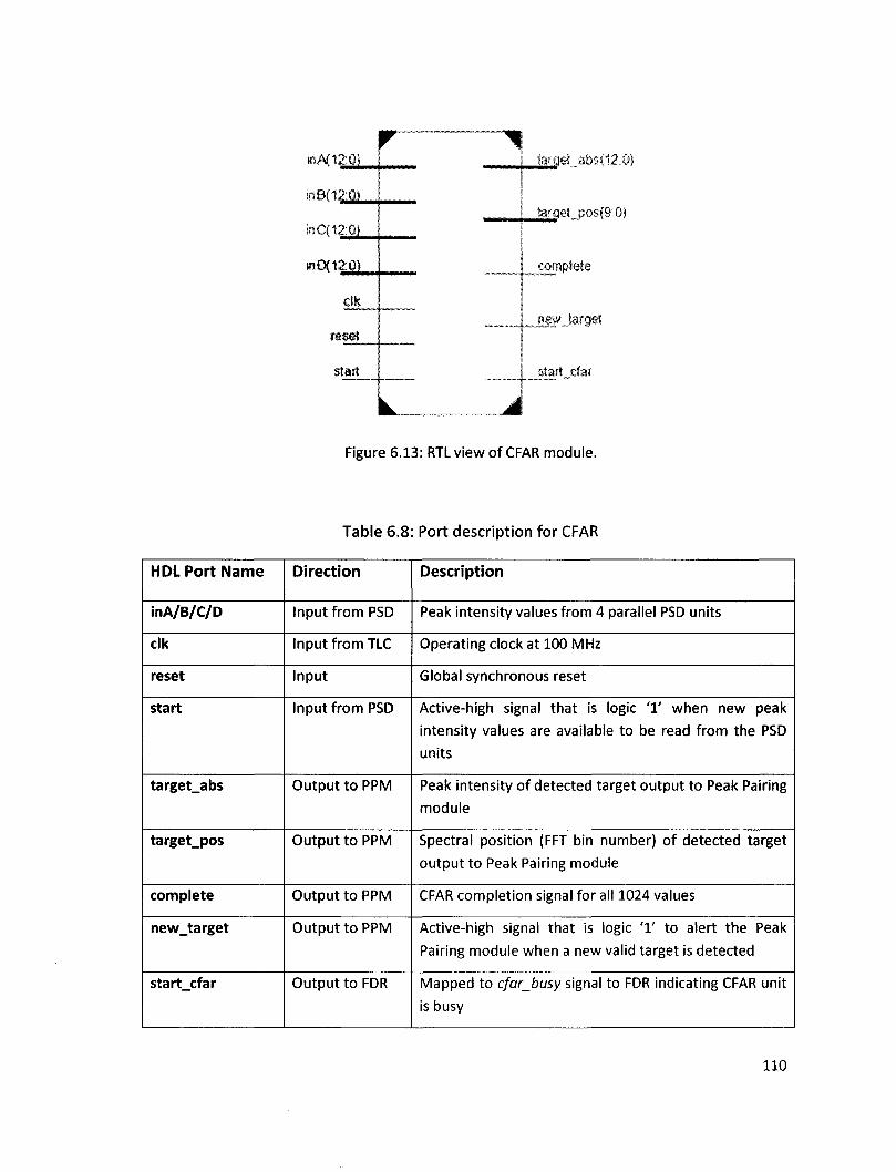
iftAf120i
inB{1£ja
in 0(12.0).
«0(120)
elk
reset
start
targe? abs(120:i
target posfSOl
complete
jnewjargel
start cfar
Figure 6.13: RTL view of CFAR module.
Table 6.8: Port description for CFAR
HDL Port Name
inA/B/C/D
elk
reset
start
target_abs
target_pos
complete
new_target
start_cfar
Direction
Input from PSD
Input from TLC
Input
Input from PSD
Output to PPM
Output to PPM
Output to PPM
Output to PPM
Output to FDR
Description
Peak intensity values from 4 parallel PSD units
Operating clock at 100 MHz
Global synchronous reset
Active-high signal that is logic T when new peak
intensity values are available to be read from the PSD
units
Peak intensity of detected target output to Peak Pairing
module
Spectral position (FFT bin number) of detected target
output to Peak Pairing module
CFAR completion signal for all 1024 values
Active-high signal that is logic ' 1 ' to alert the Peak
Pairing module when a new valid target is detected
Mapped to cfar_busy signal to FDR indicating CFAR unit
is busy
110
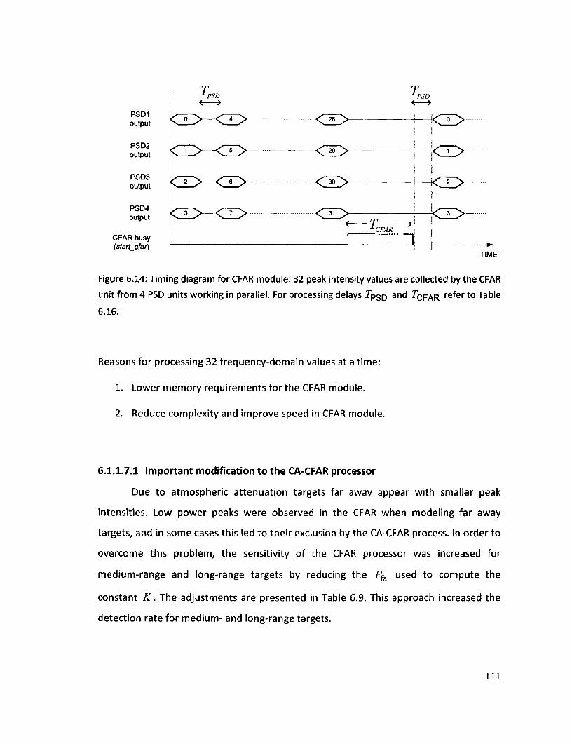
PSD1 output
PSD2 output
PSD3 output
PSD4 output
CFAR busy (start_cfa?)
<!>-<Z>-
PSD PSD
< T >
<I
TIME
Figure 6.14: Timing diagram for CFAR module: 32 peak intensity values are collected by the CFAR
unit from 4 PSD units working in parallel. For processing delays 7pSD ar|d ^CFAR re^er t 0 Table
6.16.
Reasons for processing 32 frequency-domain values at a time:
1. Lower memory requirements for the CFAR module.
2. Reduce complexity and improve speed in CFAR module.
6.1.1.7.1 Important modification to the CA-CFAR processor
Due to atmospheric attenuation targets far away appear with smaller peak
intensities. Low power peaks were observed in the CFAR when modeling far away
targets, and in some cases this led to their exclusion by the CA-CFAR process. In order to
overcome this problem, the sensitivity of the CFAR processor was increased for
medium-range and long-range targets by reducing the Pfa used to compute the
constant K. The adjustments are presented in Table 6.9. This approach increased the
detection rate for medium- and long-range targets.
I l l
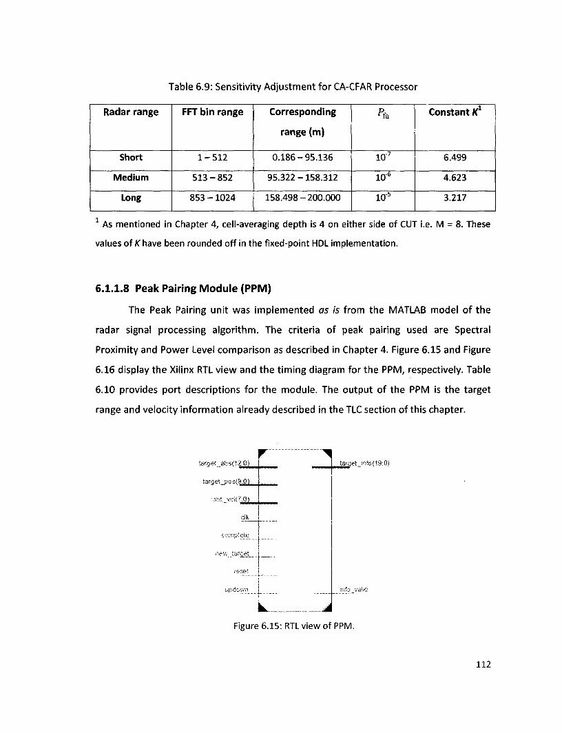
Table 6.9: Sensitivity Adjustment for CA-CFAR Processor
Radar range
Short
Medium
Long
FFT bin range
1-512
513-852
853 -1024
Corresponding
range (m)
0.186-95.136
95.322-158.312
158.498-200.000
Pf*
10"7
10'6
10"5
Constant K1
6.499
4.623
3.217
1 As mentioned in Chapter 4, cell-averaging depth is 4 on either side of CUT i.e. M = 8. These
values of K have been rounded off in the fixed-point HDL implementation.
6.1.1.8 Peak Pairing Module (PPM)
The Peak Pairing unit was implemented as is from the MATLAB model of the
radar signal processing algorithm. The criteria of peak pairing used are Spectral
Proximity and Power Level comparison as described in Chapter 4. Figure 6.15 and Figure
6.16 display the Xilinx RTL view and the timing diagram for the PPM, respectively. Table
6.10 provides port descriptions for the module. The output of the PPM is the target
range and velocity information already described in the TLC section of this chapter.
target absf12:0)
target pos(9;0)
uns; vel(7:0)
dk
comctcte
new targe!
upclown
target info(19:0)
info valid
Figure 6.15: RTL view of PPM.
112
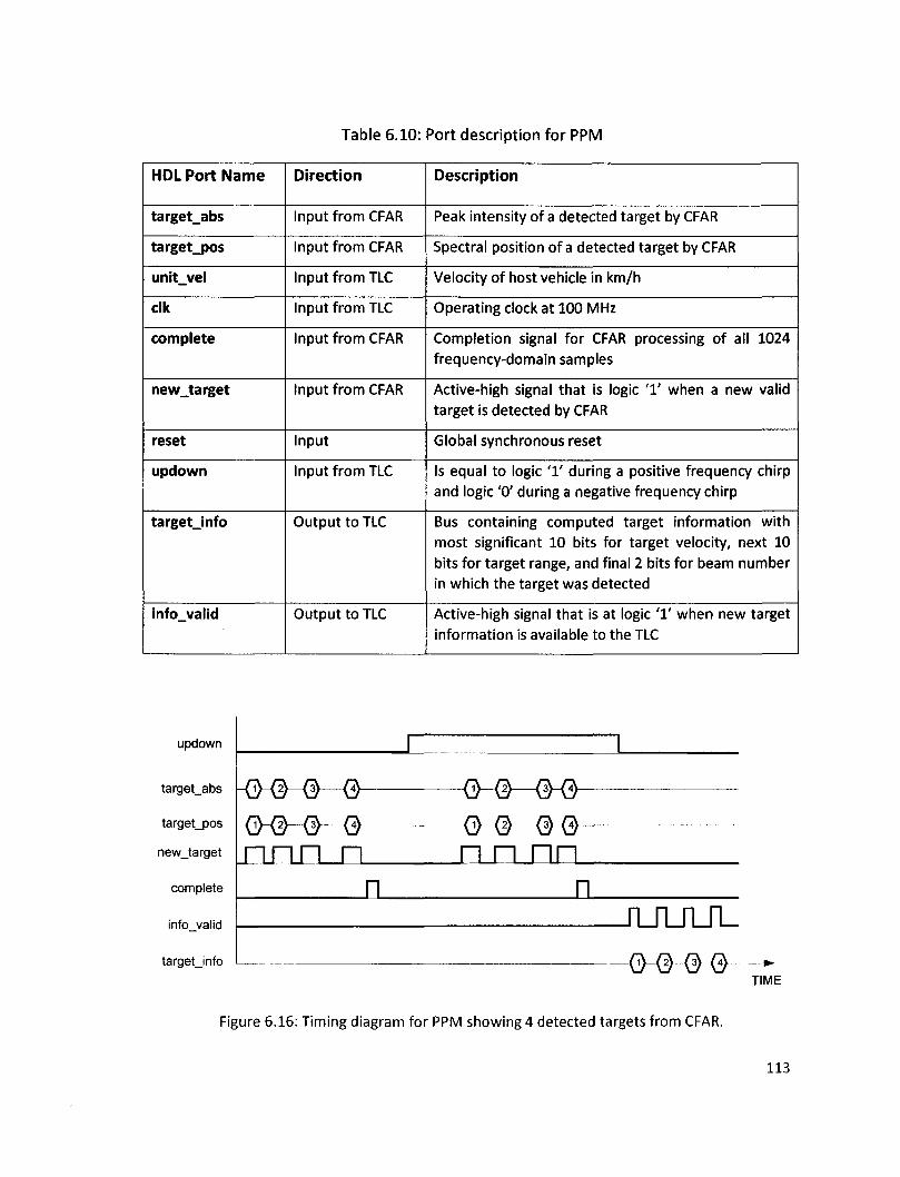
Table 6.10: Port description for PPM
HDL Port Name
target_abs
target_pos
unit_vel
elk
complete
new_target
reset
updown
target_info
info_valid
Direction
Input from CFAR
Input from CFAR
Input from TLC
Input from TLC
Input from CFAR
Input from CFAR
Input
Input from TLC
Output to TLC
Output to TLC
Description
Peak intensity of a detected target by CFAR
Spectral position of a detected target by CFAR
Velocity of host vehicle in km/h
Operating clock at 100 MHz
Completion signal for CFAR processing of all 1024 frequency-domain samples
Active-high signal that is logic ' 1 ' when a new valid target is detected by CFAR
Global synchronous reset
Is equal to logic ' 1 ' during a positive frequency chirp and logic '0' during a negative frequency chirp
Bus containing computed target information with most significant 10 bits for target velocity, next 10 bits for target range, and final 2 bits for beam number in which the target was detected
Active-high signal that is at logic ' 1 ' when new target information is available to the TLC
updown
target_abs
targetjDos
new_target
complete
info_valid
targetjnfo
TIME
Figure 6.16: Timing diagram for PPM showing 4 detected targets from CFAR.
113
I 1
-0~©-@—{<> 0-^—0-© -Q-@-0-~Q o_@_0^) nnn n nnnn
n • n_n_JL_n_
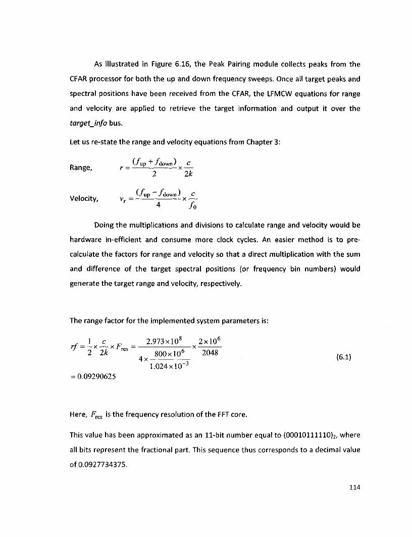
As illustrated in Figure 6.16, the Peak Pairing module collects peaks from the
CFAR processor for both the up and down frequency sweeps. Once all target peaks and
spectral positions have been received from the CFAR, the LFMCW equations for range
and velocity are applied to retrieve the target information and output it over the
targetjnfo bus.
Let us re-state the range and velocity equations from Chapter 3:
_ v/up + /down / C Range, r = — x —
2 2k
. . . .. v/up "~ /down) C Velocity, v = — x —
4 /o
Doing the multiplications and divisions to calculate range and velocity would be
hardware in-efficient and consume more clock cycles. An easier method is to pre-
calculate the factors for range and velocity so that a direct multiplication with the sum
and difference of the target spectral positions (or frequency bin numbers) would
generate the target range and velocity, respectively.
The range factor for the implemented system parameters is:
J- 1 C r< U =—X x ^ r e s
2 2k
2.973 xlO8 2x10° = x
„ 800 xlO6 2048 4x -
1.024 xlO"3 (6.1)
= 0.09290625
Here, Fres is the frequency resolution of the FFT core.
This value has been approximated as an 11-bit number equal to (00010111110)2, where
all bits represent the fractional part. This sequence thus corresponds to a decimal value
of 0.0927734375.
114
Similarly, the velocity factor is:
„ 1 c 1 2.973xl08 2x l0 6
vf = — x — xF r e sx3.6 = - x — x x3.6 4 / 0
res 4 76.9 xlO9 2048 (6.2) = 3.39790414
Here, the value of 3.6 has been multiplied here to convert the calculated velocity from
m/s into km/h. The central frequency for the LFMCW chirps has been set to 76.9 GHz, as
the TLC VCO permits a sweep range of 76.5 GHz - 77.3 GHz to form a bandwidth of 800
MHz.
This value has been approximated by a 7-bit binary number equal to (1101101)2
where the first 2 bits represent the integer part and the last 5 bits represent the
fractional part, corresponding to a decimal value of 3.40625.
6.2 Simulation and Validation of the HDL Implementation of the Signal Processing Algorithm
To accomplish simulation and validation of the entire HDL implementation and ensure
readiness of the Verilog HDL code for downloading to the Virtex-5 FPGA, the following
steps were followed:
1. All individual modules are assembled to form the top level control module TLC.
2. A Verilog test-bench is coded to run tests on the TLC module.
3. Time-domain samples of the intermediate frequency generated from the traffic
scenarios presented in Chapter 5 are extracted in hexadecimal format from
MATLAB. A total of 2048 samples are extracted.
4. The time-domain samples are passed to the TLC through the test-bench, thus
imitating the external ADC at 2 MSPS sampling rate.
115
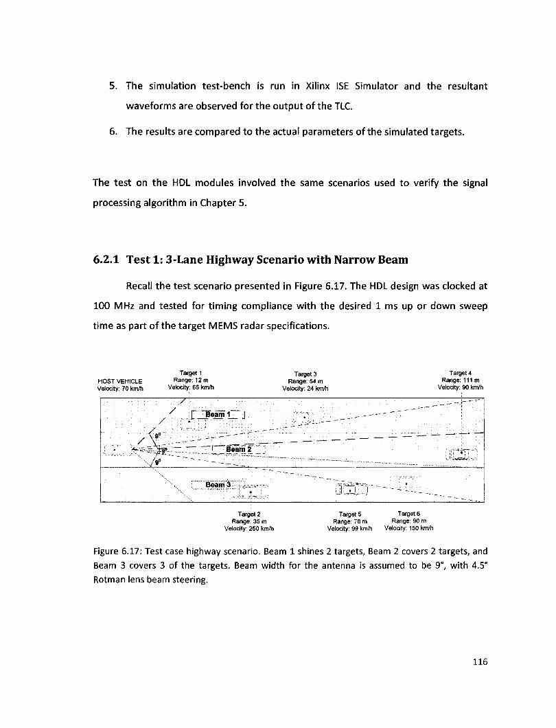
5. The simulation test-bench is run in Xilinx ISE Simulator and the resultant
waveforms are observed for the output of the TLC.
6. The results are compared to the actual parameters of the simulated targets.
The test on the HDL modules involved the same scenarios used to verify the signal
processing algorithm in Chapter 5.
6.2.1 Test 1: 3-Lane Highway Scenario with Narrow Beam
Recall the test scenario presented in Figure 6.17. The HDL design was clocked at
100 MHz and tested for timing compliance with the desired 1 ms up or down sweep
time as part of the target MEMS radar specifications.
Target 1 Target 3 Target 4 HOST VEHICLE Range: 12 m Range: 54 m Range: 111m Velocity: 70 km/h Velocity: 65 km/h Velocity: 24 km/h Velocity: 90 km/h
Target 2 Target 5 Target 6 Range: 35 m Range: 78 m Range: 90 m
Velocity: 250 km/h Velocity: 99 km/h Velocity: 150 km/h
Figure 6.17: Test case highway scenario. Beam 1 shines 2 targets, Beam 2 covers 2 targets, and Beam 3 covers 3 of the targets. Beam width for the antenna is assumed to be 9°, with 4.5° Rotman lens beam steering.
116
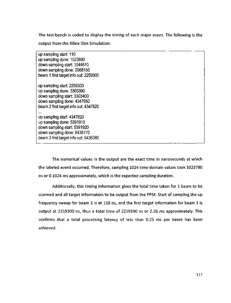
The test-bench is coded to display the timing of each major event. The following is the
output from the Xilinx ISim Simulation:
up sampling start: 110 up sampling done: 1023890 down sampling start: 1044610 down sampling done: 2068150 beam 1 first target info out: 2259300
up sampling start: 2259300 up sampling done: 3303390 down sampling start: 3303400 down sampling done: 4347650 beam 2 first target info out: 4347820
up sampling start: 4347820 up sampling done: 5391910 down sampling start: 5391920 down sampling done: 6436170 beam 3 first target info out: 6436380
The numerical values in the output are the exact time in nanoseconds at which
the labeled event occurred. Therefore, sampling 1024 time-domain values took 1023780
ns or 0.1024 ms approximately, which is the expected sampling duration.
Additionally, this timing information gives the total time taken for 1 beam to be
scanned and all target information to be output from the PPM. Start of sampling the up
frequency sweep for beam 1 is at 110 ns, and the first target information for beam 1 is
output at 2259300 ns, thus a total time of 2259190 ns or 2.26 ms approximately. This
confirms that a total processing latency of less than 0.25 ms per beam has been
achieved.
117
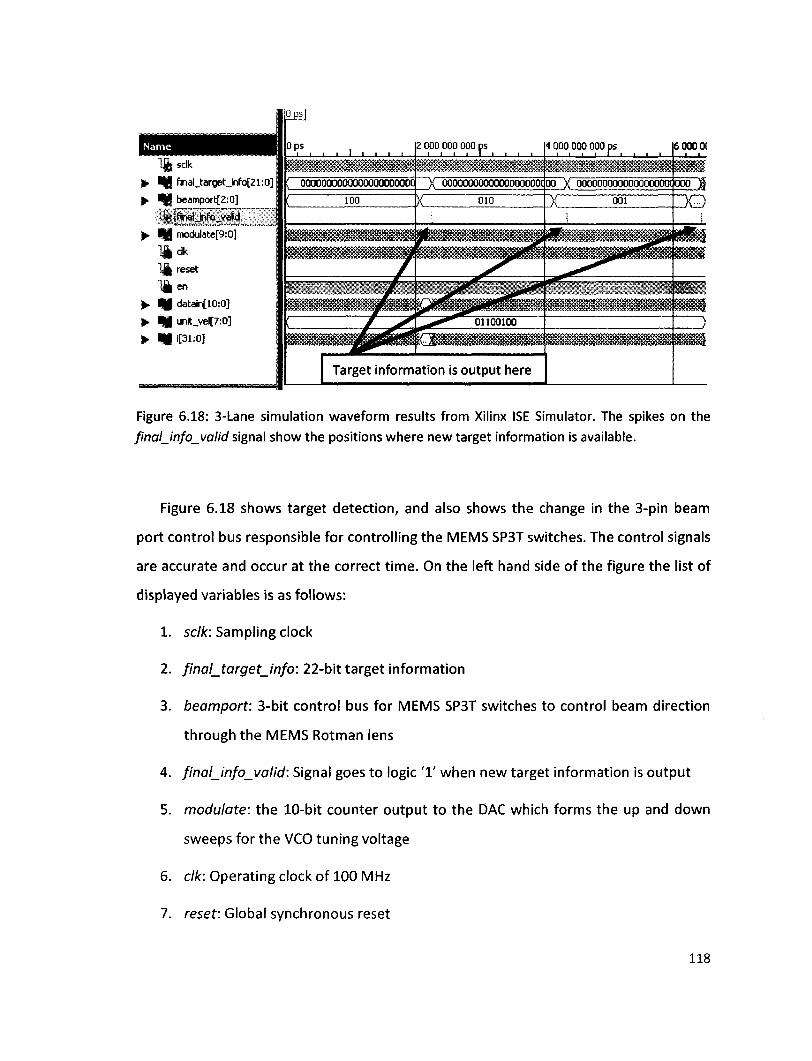
1ft s* |» ^ g finalJarget_info[21:0]
p. ^ j | bearnport[2:0]
i^|finaljnfo_yalic
)». I H modulate[9:0]
1 | | elk 1J| reset
I f en I*, m datain[10:0]
». m unit_vel[7:0]
• M i[31=0]
Figure 6.18: 3-Lane simulation waveform results from Xilinx ISE Simulator. The spikes on the final_info_valid signal show the positions where new target information is available.
Figure 6.18 shows target detection, and also shows the change in the 3-pin beam
port control bus responsible for controlling the MEMS SP3T switches. The control signals
are accurate and occur at the correct time. On the left hand side of the figure the list of
displayed variables is as follows:
1. sclk: Sampling clock
2. final_target_info: 22-bit target information
3. beamport: 3-bit control bus for MEMS SP3T switches to control beam direction
through the MEMS Rotman lens
4. final_info_valid: Signal goes to logic ' 1 ' when new target information is output
5. modulate: the 10-bit counter output to the DAC which forms the up and down
sweeps for the VCO tuning voltage
6. elk: Operating clock of 100 MHz
7. reset: Global synchronous reset
118
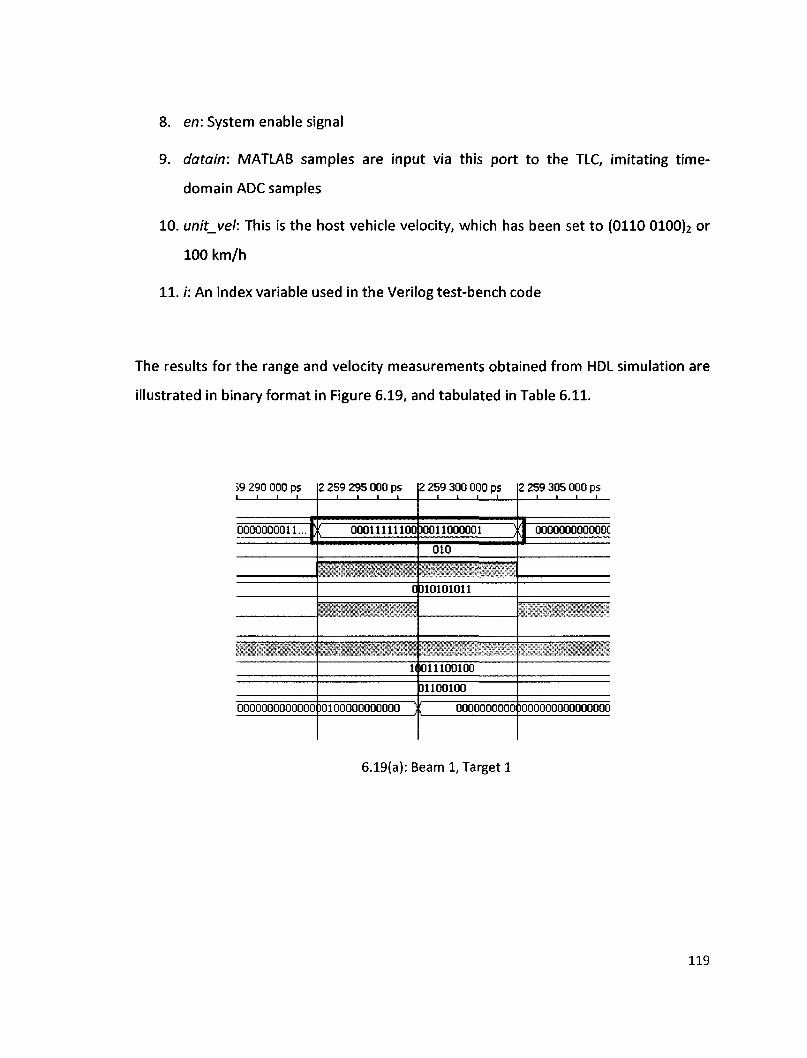
8. en: System enable signal
9. datain: MATLAB samples are input via this port to the TLC, imitating time-
domain ADC samples
10. unit_veh This is the host vehicle velocity, which has been set to (0110 0100)2 or
100 km/h
11. /': An index variable used in the Verilog test-bench code
The results for the range and velocity measurements obtained from HDL simulation are
illustrated in binary format in Figure 6.19, and tabulated in Table 6.11.
59 290 000 ps i i i i _
2 259 295 000 ps _ i i i _
12 259 300 000 ps _ J i i t _
12 259 305 000 ps
I 0000000011. 00011 111 lOODOOl 1000001 ooooooooooooc 010
omoioion
10011100100
piIOOIOO
000000000000000100000000000 X 00000000000000000000000000
6.19(a): Beam 1, Target 1
119
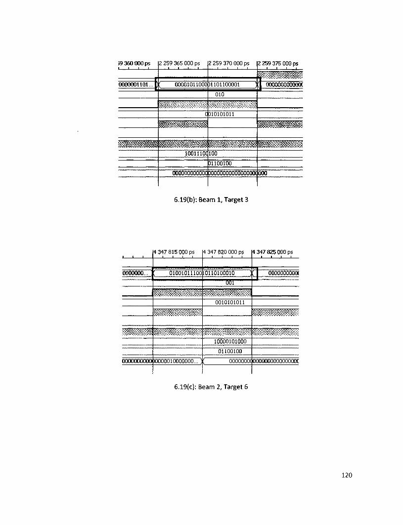
59 360 000 ps i i i i
f 0000001101... |)
2 259 365 000 ps > < i i
( 00001011000
2 259 370 000 ps i i i i
2 259 375 000 ps i i i i
Jl101100001 X| OOOOOOOOOOOOC
010
CD10101011
1001 HOC 100
31100100
m
'itzM'y-f^^W'y
f;i,:;f-:s;;:
OOOOOOOOOOOC DOOOOOOOOOOOOOOOI 000
6.19(b): Beam 1, Target 3
1 1 1
0000000...
0000000000
4 347 815 000 ps
; oiooioinoo
JOOOOOIOOOOOOO... J
4 347 820 000 ps
10110100010 \
Ml
0010101011
10000101000
01100100
( OOOOOOOC
4 347 825 000 ps • i i i
oooooooooot
oooooooooooooooc
6.19(c): Beam 2, Target 6
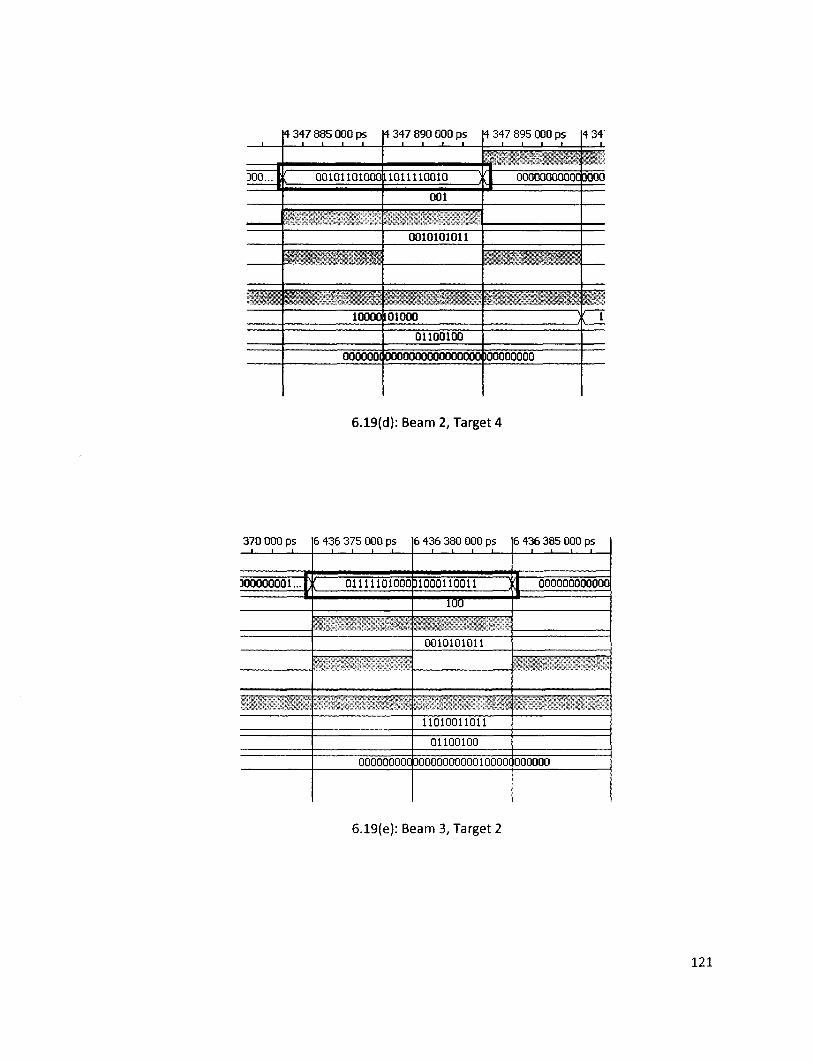
,
300... 1
4 347 885 OOO ps 1 ' i i
L ooionoiooo
gf :," "-.- "S^S
mi 1 '••-'-?••
4 347 890 000 ps • i i i
4 347 895 000 ps • i i i
4 34'
11011110010 j[| OOOOOOOOOOC DOOO
001
0010101011
'__- ' _ - »*__ •
10000101000
01100100
," •••*3s - f * ; N
: - • • - % : =
•0? '
X i
0000001 0000000000000000 (00000000
6.19(d): Beam 2, Target 4
370 000 ps 1 1 1
D00000001...
6 436 375 000 ps
{ oiiinoiooo
ooooooooc
6 436 380 000 ps
D1000110011 )
100
0010101011
11010011011
01100100
oooooooooooiooooi;
6 436 385 000 ps
I oooooooooooo
000000
6.19(e): Beam 3, Target 2
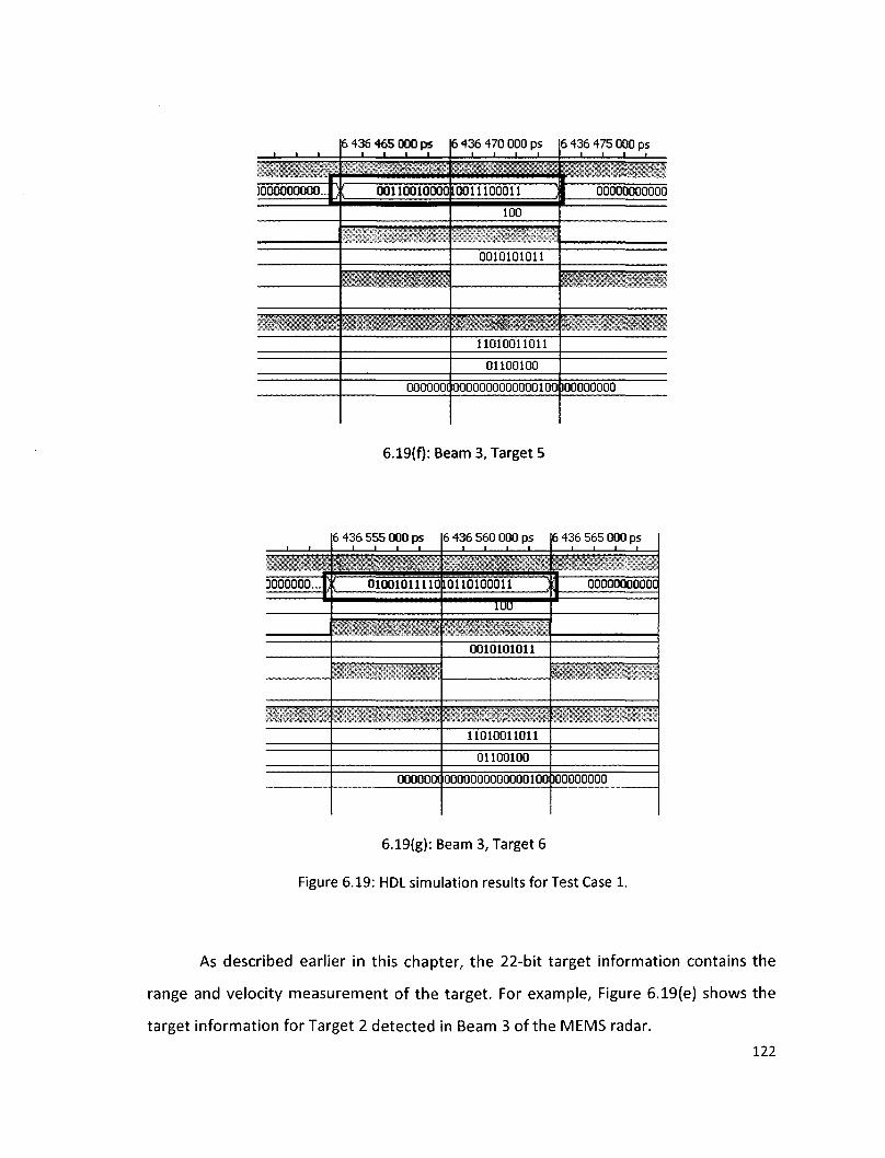
1 1 1
.5"
6 436 465 OOO ps • i i i
•--<- - *
6 436 470 000 ps i i i i
)ooooooooo..r: ooiiooiooooiooiuooon )
5.-' >V.'V-H'
100
0010101011
;* ':> y^'M^'f'ik 11010011011
01100100
000000( 0000000000000100
6 436 475 000 ps • i i i
t 1 00000000000 p
•*,£* - .• "
•:
100000000
6.19(f): Beam 3, Target 5
1 1
D000000...|) 1
6 436 555 000 ps i i i i
t, •*. •:.-:;' ! oiooioimo
_
0000001
6 436 560 000 ps i i i i
-'" '*: V" '
10110100011 )
1UU
"•""r.
0010101011
11010011011
01100100
0000000000000100
6 436 565 000 ps i i i i
._ 1 OOOOOOOOOOG
J
•
100000000
6.19(g): Beam 3, Target 6
Figure 6.19: HDL simulation results for Test Case 1.
As described earlier in this chapter, the 22-bit target information contains the
range and velocity measurement of the target. For example, Figure 6.19(e) shows the
target information for Target 2 detected in Beam 3 of the MEMS radar.
122
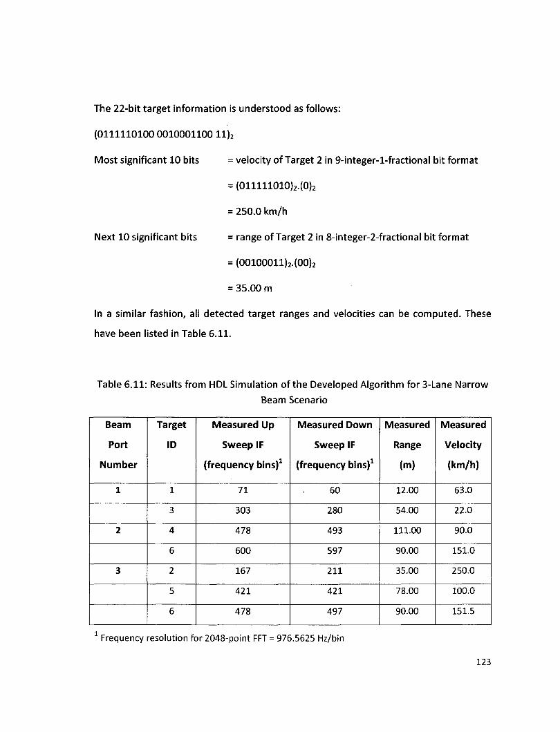
The 22-bit target information is understood as follows:
(0111110100 0010001100 11)2
Most significant 10 bits = velocity of Target 2 in 9-integer-l-fractional bit format
= (011111010)2.(0)2
= 250.0 km/h
Next 10 significant bits = range of Target 2 in 8-integer-2-fractional bit format
= (00100011)2.(00)2
= 35.00 m
In a similar fashion, all detected target ranges and velocities can be computed. These
have been listed in Table 6.11.
Table 6.11: Results from HDL Simulation of the Developed Algorithm for 3-Lane Narrow
Beam Scenario
Beam
Port
Number
1
2
3
Target
ID
1
3
4
6
2
5
6
Measured Up
Sweep IF
(frequency bins)1
71
303
478
600
167
421
478
Measured Down
Sweep IF
(frequency bins)1
60
280
493
597
211
421
497
Measured
Range
(m)
12.00
54.00
111.00
90.00
35.00
78.00
90.00
Measured
Velocity
(km/h)
63.0
22.0
90.0
151.0
250.0
100.0
151.5
1 Frequency resolution for 2048-point FFT = 976.5625 Hz/bin
123
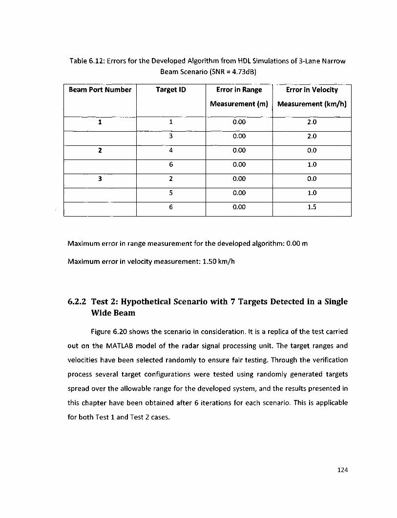
Table 6.12: Errors for the Developed Algorithm from HDL Simulations of 3-Lane Narrow
Beam Scenario (SNR = 4.73dB)
Beam Port Number
1
2
3
Target ID
1
3
4
6
2
5
6
Error in Range
Measurement (m)
0.00
0.00
0.00
0.00
0.00
0.00
0.00
Error in Velocity
Measurement (km/h)
2.0
2.0
0.0
1.0
0.0
1.0
1.5
Maximum error in range measurement for the developed algorithm: 0.00 m
Maximum error in velocity measurement: 1.50 km/h
6.2.2 Test 2: Hypothetical Scenario with 7 Targets Detected in a Single Wide Beam
Figure 6.20 shows the scenario in consideration. It is a replica of the test carried
out on the MATLAB model of the radar signal processing unit. The target ranges and
velocities have been selected randomly to ensure fair testing. Through the verification
process several target configurations were tested using randomly generated targets
spread over the allowable range for the developed system, and the results presented in
this chapter have been obtained after 6 iterations for each scenario. This is applicable
for both Test 1 and Test 2 cases.
124
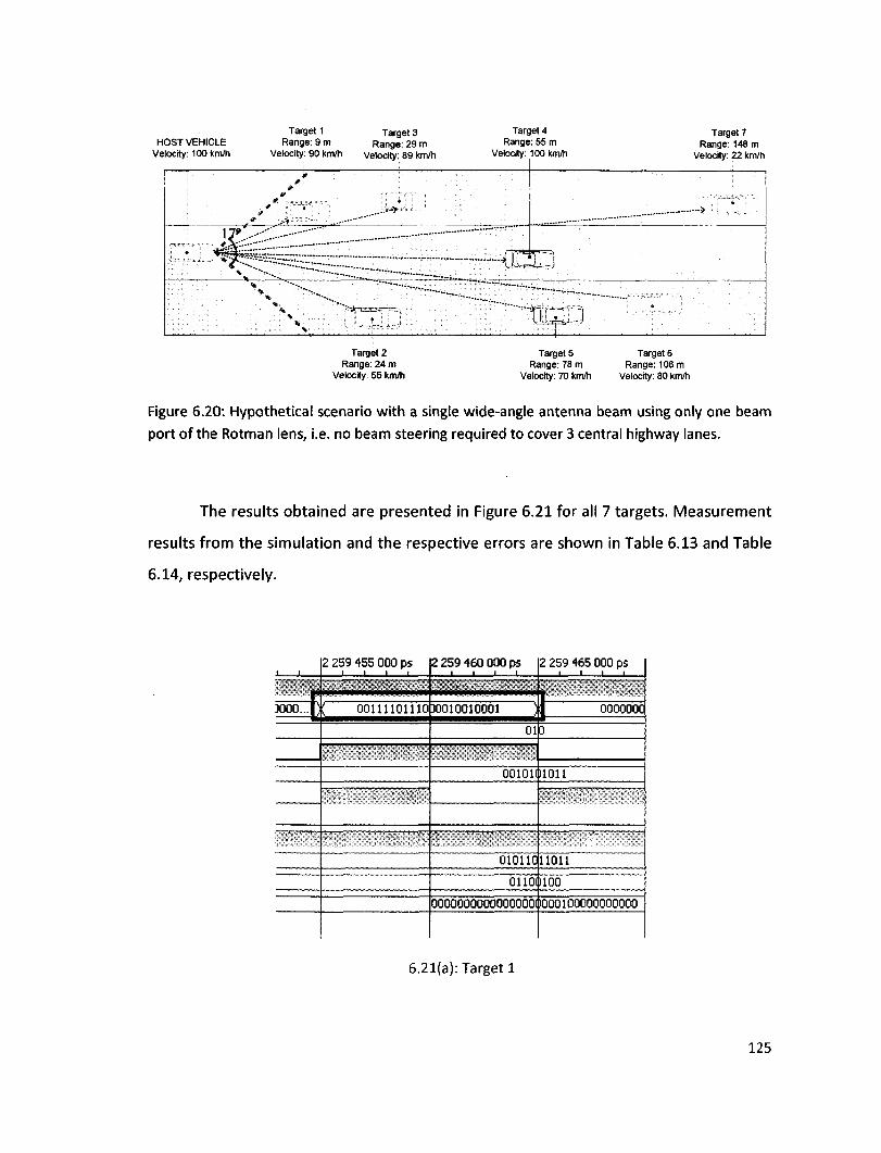
HOST VEHICLE Velocity: 100km/h
Target 1 Range: 9 m
Velocity: 90 km/h
Target 3 Range: 29 m
Velocity: 89 km/h
Target 4 Range: 55 m
Velocity: 100 km/h
Target 7 Range: 148 m
Velocity: 22 km/h
,* :.*?:" .12
a A i t
Target 2 Range: 24 m
Velocity: 55 km/h
Target 5 Target 6 Range: 78 m Range: 106 m
Velocity: 70 km/h Velocity: 80 km/h
Figure 6.20: Hypothetical scenario with a single wide-angle antenna beam using only one beam port of the Rotman lens, i.e. no beam steering required to cover 3 central highway lanes.
The results obtained are presented in Figure 6.21 for all 7 targets. Measurement
results from the simulation and the respective errors are shown in Table 6.13 and Table
6.14, respectively.
I >
r M00...|J
2 259 455 000 ps i i i i
•••' ; '
! ooi i i io i i io
2 259 460 000 ps i i i i
" , • " •
30010010001 J
01
00101^
010110
0110(
oooooooooooooooot
2 259 465 000 ps i i i i
I ] ooooooc D
11011
11011
1100
1000100000000000
6.21(a): Target 1
125
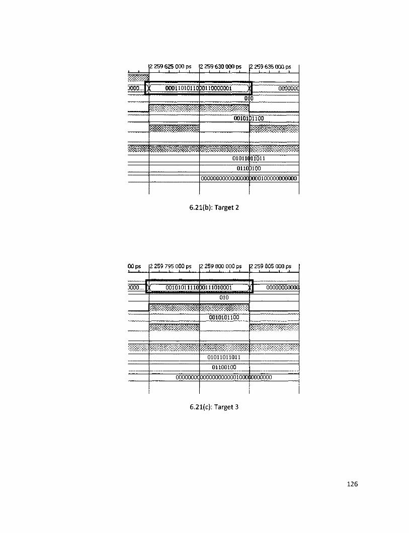
1 1 2 259 625 000 ps
i i i i
2 259 630 000 ps • i i i
2 259 635 000 ps i i i i
DOOO... )( OOOl 1010110 JOl 1OOOO0O1 )! OOOOOOC
sf
"*~ i - - * ' < v r ^
!f <" <
010
0010111100
.v
_ -,
01011(11011
0110)100
0000000000000000 3000100000000000
6.21(b): Target 2
00 ps
r DOOO... B
2 259 795 000 ps t i l l
( 00101011110
•*':"'
oooooooc
2 259 800 000 ps i i i i
Ml 11010001 )
010
<-
0010101100
01011011011
01100100
00000000000010001
2 259 805 000 ps l i l t
; ooooooooooc
10000000
6.21(c): Target 3
126
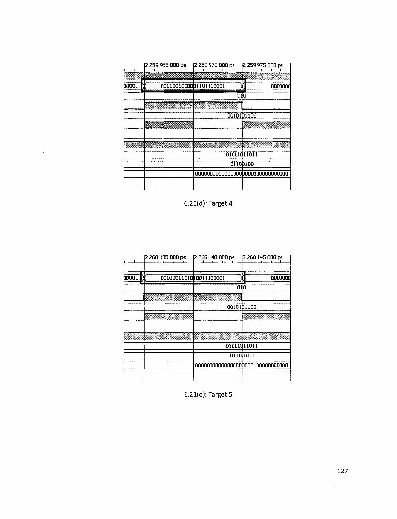
1 ,1 2 259 965 000 ps
i i i i
-,>- 'iiw.: i -z„s
2 259 970 000 ps i 1 i.. i
•> \ •-
2 259 975 000 ps i i i i
DOOO...K; 00110010000)1101110001 3(1 0OO0O0C
-"": "~
mw'f^ *"•?< •
£??-!*
o: - ' x
00101
"™* . J • " " " " ' " l
0
31100
01011(11011
0110)100
0000000000000000)000100000000000
6.21(d): Target 4
)000...
2 260 135 000 ps i i i i
; ooiooonoio
2 260 140 000 ps • i i i
10011100001 J
01
00101
01011C
0110
0000000000000000
2 260 145 000 ps
] 000000C
0
)1100
11011
)100
)000100000000000
6.21(e): Target 5
127
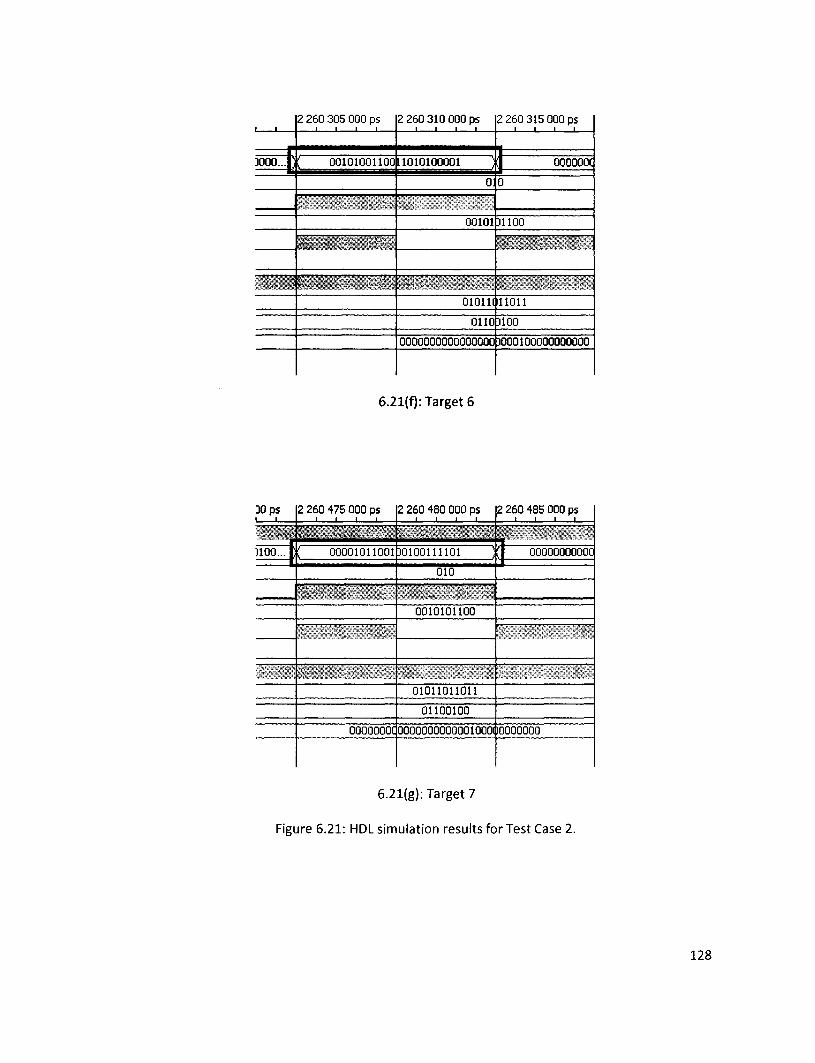
1 1
r
2 260 305 000 ps l i l t
D000...I;; ooioioonoo
<*.. i;
- —
&• , - j ; - : . - • '
f. . • - - • > •
2 260 310 000 ps • i i i
I1010100001 )
2 260 315 000 ps
1 1 ooooooc
o:o
00101
-- -
moo C' '
01011(11011
0110 D 1 0 0
0000000000000000]000100000000000
6.21(f): Target 6
DOps i i
)100... 1
2 260 475 000 ps • i i i
*&•** " • s >_*,
; ooooionooi
.
, ; , •
ooooooot
2 260 480 000 ps • i i i
raiooimoi ;
010
-' 0010101100
01011011011
01100100
00000000000010001
2 260 485 000 ps
-
( ooooooooooc
10000000
6.21(g): Target 7
Figure 6.21: HDL simulation results for Test Case 2.
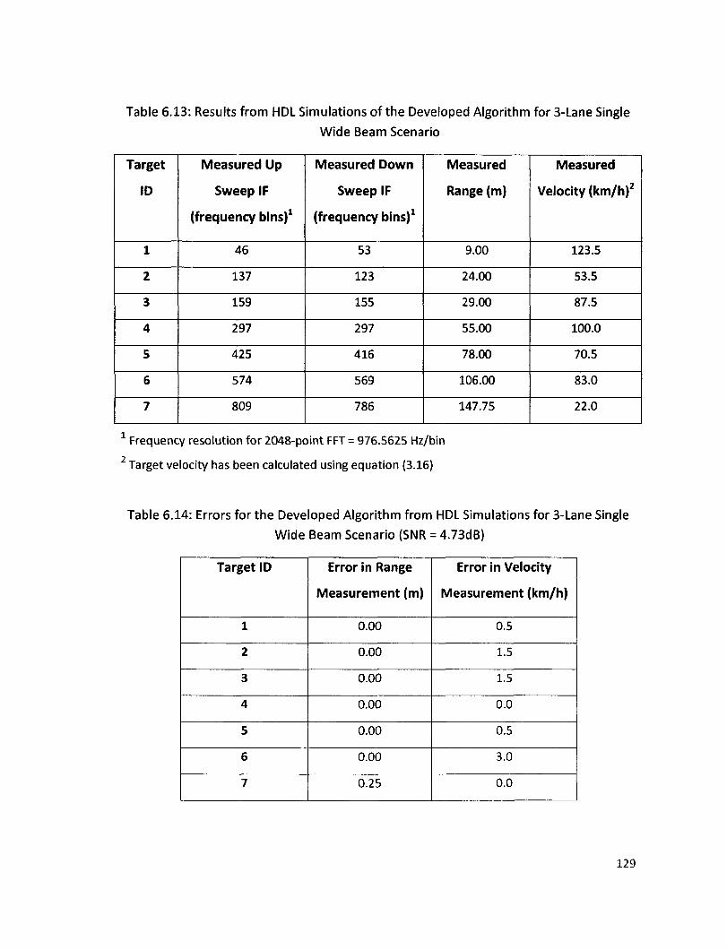
Table 6.13: Results from HDL Simulations of the Developed Algorithm for 3-Lane Single
Wide Beam Scenario
Target
ID
1
2
3
4
5
6
7
Measured Up
Sweep IF
(frequency bins)1
46
137
159
297
425
574
809
Measured Down
Sweep IF
(frequency bins)1
53
123
155
297
416
569
786
Measured
Range (m)
9.00
24.00
29.00
55.00
78.00
106.00
147.75
Measured
Velocity (km/h)2
123.5
53.5
87.5
100.0
70.5
83.0
22.0
1 Frequency resolution for 2048-point FFT = 976.5625 Hz/bin
Target velocity has been calculated using equation (3.16)
Table 6.14: Errors for the Developed Algorithm from HDL Simulations for 3-Lane Single
Wide Beam Scenario (SNR = 4.73dB)
Target ID
1
2
3
4
5
6
7
Error in Range
Measurement (m)
0.00
0.00
0.00
0.00
0.00
0.00
0.25
Error in Velocity
Measurement (km/h)
0.5
1.5
1.5
0.0
0.5
3.0
0.0
129
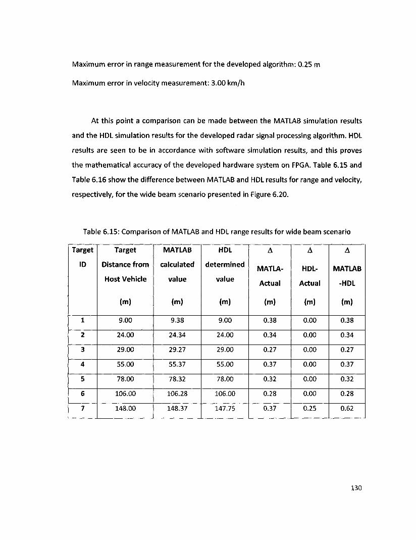
Maximum error in range measurement for the developed algorithm: 0.25 m
Maximum error in velocity measurement: 3.00 km/h
At this point a comparison can be made between the MATLAB simulation results
and the HDL simulation results for the developed radar signal processing algorithm. HDL
results are seen to be in accordance with software simulation results, and this proves
the mathematical accuracy of the developed hardware system on FPGA. Table 6.15 and
Table 6.16 show the difference between MATLAB and HDL results for range and velocity,
respectively, for the wide beam scenario presented in Figure 6.20.
Table 6.15: Comparison of MATLAB and HDL range results for wide beam scenario
Target
ID
1
2
3
4
5
6
7
Target
Distance f rom
Host Vehicle
(m)
9.00
24.00
29.00
55.00
78.00
106.00
148.00
MATLAB
calculated
value
(m)
9.38
24.34
29.27
55.37
78.32
106.28
148.37
HDL
determined
value
(m)
9.00
24.00
29.00
55.00
78.00
106.00
147.75
A
MATLA-
Actual
(m)
0.38
0.34
0.27
0.37
0.32
0.28
0.37
A
HDL-
Actual
(m)
0.00
0.00
0.00
0.00
0.00
0.00
0.25
A
MATLAB
-HDL
(m)
0.38
0.34
0.27
0.37
0.32
0.28
0.62
130
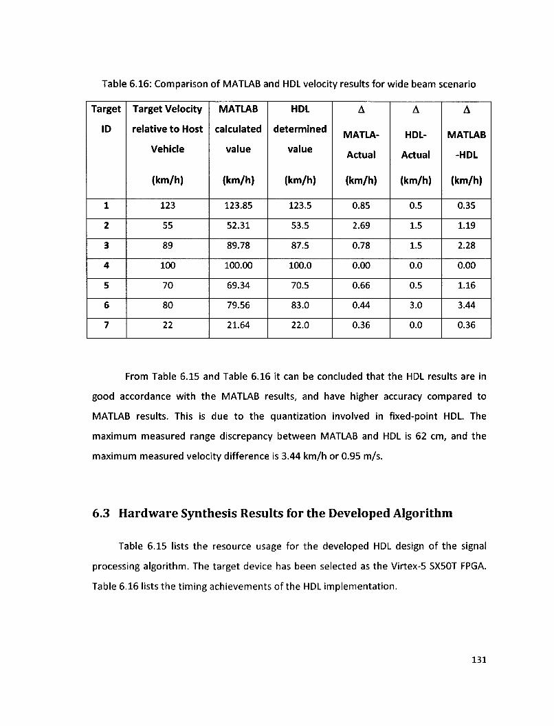
Table 6.16: Comparison of MATLAB and HDL velocity results for wide beam scenario
Target
ID
1
2
3
4
5
6
7
Target Velocity
relative to Host
Vehicle
(km/h)
123
55
89
100
70
80
22
MATLAB
calculated
value
(km/h)
123.85
52.31
89.78
100.00
69.34
79.56
21.64
HDL
determined
value
(km/h)
123.5
53.5
87.5
100.0
70.5
83.0
22.0
A
MATLA-
Actual
(km/h)
0.85
2.69
0.78
0.00
0.66
0.44
0.36
A
HDL-
Actual
(km/h)
0.5
1.5
1.5
0.0
0.5
3.0
0.0
A
MATLAB
-HDL
(km/h)
0.35
1.19
2.28
0.00
1.16
3.44
0.36
From Table 6.15 and Table 6.16 it can be concluded that the HDL results are in
good accordance with the MATLAB results, and have higher accuracy compared to
MATLAB results. This is due to the quantization involved in fixed-point HDL. The
maximum measured range discrepancy between MATLAB and HDL is 62 cm, and the
maximum measured velocity difference is 3.44 km/h or 0.95 m/s.
6.3 Hardware Synthesis Results for the Developed Algorithm
Table 6.15 lists the resource usage for the developed HDL design of the signal
processing algorithm. The target device has been selected as the Virtex-5 SX50T FPGA.
Table 6.16 lists the timing achievements of the HDL implementation.
131
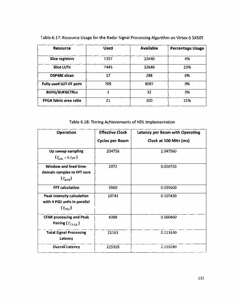
Table 6.17: Resource Usage for the Radar Signal Processing Algorithm on Virtex-5 SX50T
Resource
Slice registers
Slice LUTs
DSP48E slices
Fully used LUT-FF pairs
BUFG/BUFGCTRLs
FPGA fabric area ratio
Used
1357
7445
17
705
1
21
Available
32640
32640
288
8097
32
100
Percentage Usage
4%
23%
6%
9%
3%
21%
Table 6.18: Timing Achievements of HDL Implementation
Operation
Up sweep sampling
(rsclk = o.5/tf)
Window and feed time-
domain samples to FFT core
FFT calculation
Peak intensity calculation
with 4 PSD units in parallel
CFAR processing and Peak
Pairing (rC F A R)
Total Signal Processing
Latency
Overall Latency
Effective Clock
Cycles per Beam
204756
2072
3960
10743
4388
21163
225928
Latency per Beam with Operating
Clock at 100 MHz (ms)
2.047560
0.020720
0.039600
0.107430
0.060460
0.211630
2.259280
132
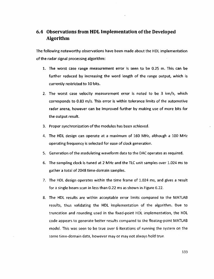
6.4 Observations from HDL Implementation of the Developed Algorithm
The following noteworthy observations have been made about the HDL implementation
of the radar signal processing algorithm:
1. The worst case range measurement error is seen to be 0.25 m. This can be
further reduced by increasing the word length of the range output, which is
currently restricted to 10 bits.
2. The worst case velocity measurement error is noted to be 3 km/h, which
corresponds to 0.83 m/s. This error is within tolerance limits of the automotive
radar arena, however can be improved further by making use of more bits for
the output result.
3. Proper synchronization of the modules has been achieved.
4. The HDL design can operate at a maximum of 160 MHz, although a 100 MHz
operating frequency is selected for ease of clock generation.
5. Generation of the modulating waveform data to the DAC operates as required.
6. The sampling clock is tuned at 2 MHz and the TLC unit samples over 1.024 ms to
gather a total of 2048 time-domain samples.
7. The HDL design operates within the time frame of 1.024 ms, and gives a result
for a single beam scan in less than 0.22 ms as shown in Figure 6.22.
8. The HDL results are within acceptable error limits compared to the MATLAB
results, thus validating the HDL implementation of the algorithm. Due to
truncation and rounding used in the fixed-point HDL implementation, the HDL
code appears to generate better results compared to the floating-point MATLAB
model. This was seen to be true over 6 iterations of running the system on the
same time-domain data, however may or may not always hold true.
133
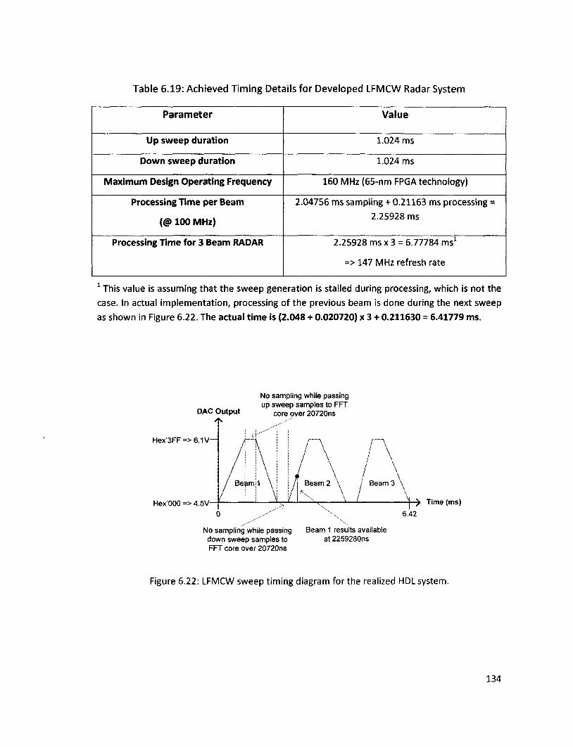
Table 6.19: Achieved Timing Details for Developed LFMCW Radar System
Parameter
Up sweep duration
Down sweep duration
Maximum Design Operating Frequency
Processing Time per Beam
«S> 100 MHz)
Processing Time for 3 Beam RADAR
Value
1.024 ms
1.024 ms
160 MHz (65-nm FPGA technology)
2.04756 ms sampling + 0.21163 ms processing =
2.25928 ms
2.25928 ms x 3 = 6.77784 ms1
=> 147 MHz refresh rate
1 This value is assuming that the sweep generation is stalled during processing, which is not the
case. In actual implementation, processing of the previous beam is done during the next sweep
as shown in Figure 6.22. The actual time is (2.048 + 0.020720) x 3 + 0.211630 = 6.41779 ms.
DAC Output
No sampling while passing up sweep samples to FFT
core over 20720ns
Hex'3FF=>6.1V-H
Hex'000 => 4.5V - j — ^ Time (ms)
No sampling while passing Beam 1 results available down sweep samples to at 2259280ns FFT core over 20720ns
Figure 6.22: LFMCW sweep timing diagram for the realized HDL system.
134
CHAPTER 7: CONCLUSIONS
7.1 Discussions and Conclusions
A Xilinx Virtex-5 SX50T FPGA platform targeted Verilog HDL based signal
processing algorithm has been developed to process the drive, control and decision
making signal processing tasks associated with a MEMS implemented Rotman lens
based LFMCW long range radar to detect the velocity and range of target vehicles in
typical highway condtions. Necessary building blocks of the complete system have been
developed and implemented to realize a fast radar control and signal processing
algorithm in hardware. Excellent agreement between the MATLAB implemented
mathematical models and Verilog HDL code generated results verify the accuracy of the
HDL modules. The devloped Verilog HDL codes can be used to fabricate an ASIC that can
be incorporated in a 3-D integrated complete radar system to realize a small form-factor
low-cost automotive radar. A hardware latency time as low as 211.63 ps clocked at 100
MHz has been achieved which is superior to state-of-the-art commercially reported
radar systems. This is almost 3 times faster than a recent FPGA implementation
presented in [28], where an LFMCW signal processing system has been implemented on
a Xilinx Virtex-ll Pro FPGA with a latency of 1250 ps clocked at 50 MHz. The results for
range and velocity calculations are promising and accurate with 100% detection in a
tested SNR of 4.73 dB under an atmospheric attenuation of 0.8 dB/km corresponding to
light or medium rain conditions. Swerling I, III and V type targets have been simulated.
The maximum error in range measurement is 25 cm, and the maximum error in velocity
measurement is 3 km/h or 0.83 m/s. The bandwidth of the LFMCW radar waveform is
set to 800 MHz, and the radar algorithm is capable of covering a range of 200 meters
with a maximum relative target velocity of ±300 km/h (receding and approaching
targets).
135
The excellent speed performance of the algorithm validates the use of FPGAs in
radar signal processing and allows the MEMS radar sensor to operate with a cycle time
of 6.78 ms for a 3-beam sensor, which is at least 7 times faster than the Bosch LRR3 [23].
Beam direction control by means of MEMS SP3T RF switches and a MEMS Rotman lens
has been implemented in the radar algorithm and found to operate in coherence with
the radar system specifications.
7.2 Future Work
This thesis opens the path to many additional features that can be added to the MEMS
radar sensor system. The following are some of the exciting possible future
developments to the field of automotive radar systems with regard to this thesis:
1. Accurate target angle measurement using an FPGA-based implementation of
Direction-of-Arrival or DOA algorithms, such as Phase-Difference DOA estimation
using double 1-D FFT [30], MUSIC [53], or ESPRIT [54].
2. Higher resolution of ADC input and target information output to improve range
precision from 25 cm down to 5 cm and velocity precision from 0.5 km/h down
to 0.125 km/h provided the sweep bandwidth is increased to 2 GHz and the
sweep duration is increased to at least 6 ms.
3. Inculcate the ability to gather road clutter and create a virtual map of the road
by smartly using clutter information to detect side fences and dividers along with
vehicles, as presented in literature [47].
4. Use alternating frequency bands and bandwidths to increase chances of target
detection and improve detection accuracy by comparing results from both
bands.
5. Decrease the sweep duration to 0.5 ms and study the effect on signal processing
accuracy and precision.
136
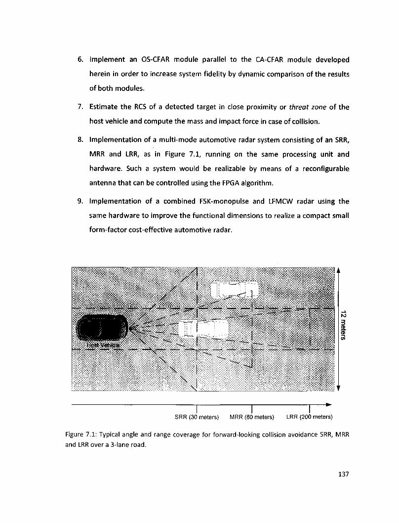
6. Implement an OS-CFAR module parallel to the CA-CFAR module developed
herein in order to increase system fidelity by dynamic comparison of the results
of both modules.
7. Estimate the RCS of a detected target in close proximity or threat zone of the
host vehicle and compute the mass and impact force in case of collision.
8. Implementation of a multi-mode automotive radar system consisting of an SRR,
MRR and LRR, as in Figure 7.1, running on the same processing unit and
hardware. Such a system would be realizable by means of a reconfigurable
antenna that can be controlled using the FPGA algorithm.
9. Implementation of a combined FSK-monopulse and LFMCW radar using the
same hardware to improve the functional dimensions to realize a compact small
form-factor cost-effective automotive radar.
SRR (30 meters) MRR (80 meters) LRR (200 meters)
Figure 7.1: Typical angle and range coverage for forward-looking collision avoidance SRR, MRR
and LRR over a 3-lane road.
137
REFERENCES
1. A. Sinjari, S. Chowdhury, "MEMS Automotive Collision Avoidance Radar Beamformer," in
Proc. IEEE ISCAS2008, Seattle, WA, 2008, pp. 2086-2089.
2. Y. K. Chan, S. Y. Lim, "Synthetic Aperture Radar (SAR) Signal Generation," Progress in
Electromagnetics Research B, Vol. 1, pp. 269-290, 2008.
3. R. A. Mucci, "A Comparison of Efficient Beamforming Algorithms," IEEE Trans. Acoustics,
Speech, and Signal Processing, Vol. ASSP-32, No. 3, pp. 548-558, Jun. 1984.
4. T. Haynes. (1998, March 26). A Primer on Digital Beamforming, Spectrum Signal
Processing. White paper [Online]. Available: http://www.spectrumsignal.com
/publications/beamform_primer.pdf
5. C. Wolff. (2008). Digital Beamforming [Online]. Available: http://www.radartutorial.eu
/06.antennas/an51.en.html
6. J. Bass, E. Rodriguez, J. Finnigan, C. McPheeters. (2005, July). Beamforming Basics
[Online]. Available: http://cnx.org/content/ml2563/latest/
7. S. Chowdhury, M. Ahmadi, G. A. Jullien, W. C. Miller, "A Surface Mountable MEMS
Beamforming Microphone Array and Associated MEMS Socket Structure," in Symp.
Microelectronics Research and Development in Canada (MR&DCAN 2001), Ottawa, ON,
2001.
8. L. Hall, H. Hansen, D. Abbott, "Rotman Lens for mm-wavelengths," in Proc. IEEE Smart
Structures, Devices and Systems (SPIE2002), Vol. 4935, pp. 215-221, 2002.
9. M. I. Skolnik, Radar Handbook, 2nd ed., New York: McGraw-Hill, 1970.
10. BBC h2g2. (2003, July). The History of Radar [Online]. Available: http://www.bbc.co.uk
/dna/h2g2/A591545
11. "Fundamentals of Radar", Encyclopaedia Britannica Online, [2010 April 29]. Available:
http://www.britannica.com/EBchecked/topic/488278/radar
12. H. Rohling, Some Radar Topics: Waveform Design, Range CFAR and Target Recognition,
Advances in Sensing with Security Applications. [NATO Security Through Science Book
Series, Vol. 2]. Netherlands: Springer Netherlands, 2006. (ISBN: 978-1-4020-4284-3)
13. S. Hu, X. Wang, Q. Si, "Effects of FM Linearity of Linear FM Signals on Pulse-compression
Performance," in Proc. IEEE Conf. Radar, Verona, NY, 2006.
14. T. Curtis, M. Curtis (2004). High Performance Digital Signal Processing, Curtis Technology
(UK) Ltd. [Online]. Available: http://www.curtistech.co.uk/
15. D. Hoetzer, D. Freundt, "Driver Assist & Crash Avoidance Technologies: Radar and Video
Systems", Robert Bosch GmbH, presented at Telematics Detroit, Detroit, Ml, 2008.
138
16. S. Yamano et ai, "76GHz Millimeter Wave Automobile Radar using Single Chip MMIC",
Fujitsu Ten Technical Journal No. 23, Fujitsu Ten Corp., Plymouth, Ml, 2004.
17. A. Anderson. (November 2005). Mercedes-Benz Sudden Acceleration Incidents [Online].
Available: http://www.antony-anderson.eom/Cruise/9.5%20SA%20Links/Mercedes%20
Benz.html
18. R. Lachner, "Development Status of Next Generation Automotive Radar in EU - Infineon
Radar Technology," presented at ITS Forum 2009, Tokyo (Japan), 2009.
19. J. Wenger, "RF-Applications in Vehicles - Today and Tomorrow - DaimlerChrysler,"
presented at DaimlerChrysler AG, Ulm (Germany), 2006.
20. TRW Automotive (2009). Adaptive Cruise Control (ACC) [Online]. Available:
http://www.trw.com/sites/default/files/DAS_ACC_Eng09_0.pdf
21. Xilinx Corporation (2010). ISE Design Suite: Intellectual Property. [Online]. Available:
http://www.xilinx.com/ipcenter/
22. J. M. Webster, "The Development of a Radar Digital Unit for the SASAR II Project," M.S.
Thesis, Dept. Elect. Eng., Univ. Cape Town, Cape Town, South Africa, 2004.
23. M. Schneider, "Automotive Radar - Status and Trends," in German Microwave Conf.
(GeMiC2005), Ulm (Germany), 2005, pp. 144-147.
24. J. Wenger, "Automotive Radar - Status and Perspectives," in IEEE CSIC 2005 Dig., 2005,
Sitges (Spain), 2005, pp. 21-24.
25. H.-L. Bloecher, A. Sailer, G. Rollmann, J. Dickmann, "79 GHz UWB Automotive Short
Range Radar - Spectrum Allocation and Technology Trends," Adv. Radio Sc, Vol. 7,
2009, pp. 61-65. Available: www.adv-radio-sci.net/7/61/2009/ars-7-61-2009.html
26. V. Jain, B. Javid, P. Heydari, "A 24/77GHz Dual-Band BiCMOS Frequency Synthesizer," in
IEEE 2008 Conf. Custom Integrated Circuits Conference (CICC), San Jose, CA, 2008, pp.
487-490.
27. V. Jain, B. Javid, P. Heydari, "A BiCMOS Dual-Band Millimeter-Wave Frequency
Synthesizer for Automotive Radars," IEEE J. Solid-State Circuits, Vol. 44, No. 8, pp. 2100-
2113, Aug. 2009.
28. J. Saad, A. Baghdadi, "FPGA-based Radar Signal Processing for Automotive Driver
Assistance System," in IEEE/IFIP Intl. Symp. Rapid System Prototyping, Fairfax, VA, 2009,
pp. 196-199.
29. D. E. Barrick, "FM/CW Radar Signals and Digital Processing," NOAA Technical Report ERL
283-WPL26, U.S. Department of Commerce, Boulder (Colo.), Jul. 1973.
30. X. Bo, L. G.-lin, L C.-hua, "DOA Estimation Based on Phase-difference," in Proc. IEEE
ICSP2006, Beijing (China), 2006, pp. 1-4.
139
31. F. J. Harris, "On the Use of Windows for Harmonic Analysis with the Discrete Fourier
Transform," Proc. IEEE, Vol. 66, No. 1, pp. 51-83, Jan. 1978.
32. J. W. Cooley, J. W. Tukey, "An Algorithm for the Machine Calculation of Complex Fourier
Series," Math. Comput, Vol. 19, No. 90, pp. 297-301,1965.
33. H. V. Sorensen, D. L Jones, M. T. Heideman, C. Sidney Burrus, "Real-Valued Fast Fourier
Transform Algorithms," IEEE Trans. Acoustics, Speech, and Signal Processing, Vol. ASSP-
35, No. 6, pp. 849-863, Jun. 1987.
34. F. Gini, M. Greco, A. Farina, "Clairvoyant and Adaptive Signal Detection in Non-Gaussian
Clutter: A Data-dependent Threshold Interpretation," IEEE Trans. Signal Processing, Vol.
47, No. 6, pp. 1522-1531, Jun. 1999.
35. L. Abdou, F. Soltani, "OS-CFAR and CMLD Threshold Optimization in Distributed Systems
Using Evolutionary Strategies," J. Signal, Image and Video Processing (SIVip), 2008, No.
2, pp. 155-167, Dec. 2008.
36. V. Kyovtorov et al., "Parallel FPGA Design of CA CFAR Algorithm," Comp. Eng. Lab, TU-
Delft, October 15, 2009.
37. R. S. Raghavan, "Analysis of CA-CFAR Processors for Linear-Law Detection," IEEE Trans.
Aerospace and Electronic Systems, Vol. 28, No. 3, pp. 661-665, Jul. 1992.
38. T. R. Saed, J. K. Ali, Z. T. Yassen, "An FPGA Based Implementation of CA-CFAR Processor,"
Asian Journal of Information Technology, Vol. 6, No. 4, pp. 511-514, 2007.
39. R. Cumplido, C. Torres, S. Lopez, "On the Implementation of an Efficient FPGA-based
CFAR Processor for Target Detection," in Proc. IEEE ICEEE and CEI, Acapulco (Mexico),
2004, pp. 214-218.
40. G. Galati (Ed.), Advanced Radar Techniques and Systems, IEEE Radar, Sonar, Navigation
and Avionics Series 4, Exeter (UK): Short Run Press Ltd, 1993.
41. L. L. Scharf, Statistical Signal Processing: Detection, Estimation, and Time Series Analysis,
New York: Addison Wesley, 1991. (ISBN: 0-201-19038-9).
42. M. I. Skolnik, Introduction to Radar Systems, 3rd ed., New York: McGraw-Hill, 2001.
43. P. Swerling, "Probability of Detection for Fluctuating Targets," The RAND Corp., Santa
Monica, CA, Mar. 17,1954.
44. P. Bak, C. Tang, K. Wiesenfeld, "Self-Organized Criticality: An Explanation of 1/f Noise,"
Physical Review Letters, Vol. 59, pp. 381-384,1987.
45. R. Lyons, R. Yates. (2005, June). Reducing ADC Quantization Noise [Online]. Available:
http://www.mwrf.com/Articles/lndex.cfm?Ad=l&Ad=l&ArticlelD=10586
46. P. W. Gorham, "RF Atmosphere Absorption/Ducting," Antarctic Impulsive Transient
Antenna Project (ANITA), Univ. Hawaii (Manoa), April 21, 2003.
140
47. C. Lundquist, U. Orguner, T. B. Schon, "Tracking Stationary Extended Objects for Road
Mapping using Radar Measurements," IEEE Symp. Intelligent Vehicles IV'09, Xi'an
(China), 2009.
48. BBC h2g2. (2003, July). Radar Countermeasures: Range Gate Pull-off [Online]. Available:
http://www.bbc.co.uk/dna/h2g2/A637535
49. D. Kok, J. S. Fu, "Signal Processing for Automotive Radar," in IEEE Radar
Conf.(EURAD2005), Arlington, VA, June 2005, pp. 842-846.
50. K. Estmer, "Noise Model of an FMCW Radar System," M.S. Thesis, Dept. Elect. Eng.,
Royal Inst, of Tech., Stockholm (Sweden), May 2002.
51. Xilinx Corporation (2010). Virtex-5 Family/Virtex-5/ML506 Development Board
Datasheets [Online]. Available: http://www.xilinx.com/support/documentation/ml506.htm
52. Xilinx Corporation (2010). Xilinx FFT v7.0 Datasheet [Online]. Available:
http://www.xilinx.com/support/documentation/ip_documentation/xfft_ds260.pdf
53. J. Qumar, B. Mazhari, "Spectral Estimation Using a MUSIC Algorithm - Altera Nios II
Embedded Processor Design Contest," Altera Corporation, San Jose, CA, 2005. Available:
http://www.altera.eom/literature/dc/l.6-2005_lndia_3rd_IITKanpur-web.pdf
54. R. Roy, T. Kailath, "ESPRIT - Estimation of Signal Parameters Via Rotational Invariance
Technique", IEEE Trans. Acoustics, Speech, and Signal Processing, Vol. 37, No. 7, pp. 984-
995, Jul. 1989.
55. M. Huang, Vehicle Crash Dynamics, Michigan: CRC Press, 2002. (ISBN: 0-8493-0104-1)
56. G. Hampson, "Implementation Results of a Windowed FFT", Sys. Eng. Div., Ohio State
Univ., Columbus, OH, July 12, 2002. Available: http://esl.eng.ohio-state.edu
/~rstheory/iip/window.pdf
141
APPENDIX
Contents:
1. MATLAB listing for Radar Echo Signal Generation and Radar Signal Processing
Algorithm testing
2. MATLAB listing for percentage error calculation from 10-bit rounding of Window
functions
3. HDL listing for TLC
4. HDL listing for SAMPLER
5. HDL wrapper for Xilinx FFT v7.0 core
6. HDL listing for FDR
7. HDL listing for PSD
8. HDL listing for CFAR
9. HDL listing for PPM
142
Al. MATLAB listing for Radar Echo Signal Generation and Radar Signal Processing Algorithm testing
%%%%%%%%%%%%%%%%%%%%%%%%%%%%%%%%%%%%%%%%%%%%%%%%%%%%%%%%%%%%%%%%%%%%%%%%%%% % ABOUT THIS CODE 9-9-&S9-9-9-9-9-9-9-&&9-9-^3:&^&&&9-9-a9-9-9-&9-9-&9-S.a49.&e.aaQ.9.Q.ag,Q.aaoQaQ.o,a o o "6 o ~o *o ?> o'D o o o o o o o T> o 15 o o o o o o o o o o o o"5 o "5 "5 o o "5 "So "5 o o "5 o "5 o f i o ' 5 ? 5 o ? ? ? ' 6 ? S 6 ' 5 ' 5 6 S S o o o'o'O'o'o'o'o o
% % The code generates a set of intermediate frequencies for a long range % radar, for both the up and down sweeps. The cell-averaging cfar algorithm % is then employed, followed by removal of spectral copies, and a final % loop to remove any,left-over noise components from the target map. This % leaves a final cfar matrix with all valid targets, which are plotted. % ^ % The target echo power is attenuated by 0.4dB/km as the factor of % attenuation of RF radiation in clear air. This factor can be changed % once a more appropriate/practical value is obtained. % % The algorithm eliminates any targets which are within +-1 frequency bin % of another target. This puts an upper limit to the number of targets the % system can detect: % Maximum number of simultaneously detectable targets = (NFFT/2)/3 % where NFFT is the length of the Fourier transform. % Due to leakage and noise effects, this number can be practically as low % as (NFFT/2)/5. The noise and leakage effects persist to an extent despite % windowing. % % The original ca-cfar algorithm has poorer performance with higher number % of targets. To overcome this problem, a duplicate or ghost target removal % scheme is employed, followed by a secondary threshold. This enables % operation at a deteriorated probability of false alarm. Originally using % Pfa = 10A-9, and finally using Pfa = 10^-6. This allows multiple targets % to be detected with a resolution of 2.7 metres at same velocities. a o
% The Pfa can be lowered further, which results in more false targets but % at low power. These can be removed by using a tertiary threshold scheme. % % Increasing the sweep bandwidth from 200MHz to 500MHz, and sampling rate % from lMSps to 3MSps can help improve the resolution to a certain extent, % such that the range resolution drops to 1 metre. % % The FMCW LRR simulated here can only detect the maximum relative velocity % of 300KMPH reliably at a minimum distance of 10 meters. % % Windowing is NOT included in this code. % % Finally, the code uses the frequency information from the up sweep and % the down sweep to compute the range and velocity of each detected target. % O O O O O 'O O O O O O O O O O O O O O O O O O O O O O O O O O "6 "5 O ' O ' O ' O ' O ' O ' O ' D ' O ' O ' O ' O ' O ' O ^ ' O ' O ' O ' O ^ 0 ~ 5 0 0 " 5 " 6 O " 6 " 6 ' O O O O O O O "5 O O O O O
% DEVELOPER: SUNDEEP LAL (MEMS LAB) 9-9-9-9-° 9-9-° ° 0-9-9-9-0-9-9-9-Q-9-9-9-9-9-0--9-9-9-9-9-9-9-9-9.9-0 9-0-Q-&9-^9-0-Q-9-9.9.9-9-0-9-9-9-£9-9-9-9-9-°-9-9-9-9-0-O O'O'O'O'O'O'O'O'O O O O O O O O O O O O O O O O O O O^^^^^^^^^^IS^'O'O'O^'O'O'O'O'O'O'O'O'O'O'O'O'O'O'O'O'O'O'O'O'O O O O O O 'O "0 "O O O
clear all clc
Tsweep = 1.024*10^-3; % Chirp duration in seconds Fsweep = 800 * 10~6; % Chirp bandwidth in Hz
% Largely affects the range resolution of the system % A larger sweep bandwidth increases the spectral
143
% gap between targets, giving better cfar detection, c = 2.973 * 1CT8; % Speed of EM waves in m/s Ft = 76.9 * 10^9; % Central transmission frequency
% Frequency sweep rate in s^-2 k = Fsweep/Tsweep;
% Target ranges in m rangesUp = [9 24 29 55 78 106 148]; % hypothetical scenario %rangesUp = [12 54]; % practical road scenario beaml %rangesUp = [111 90]; % practical road scenario beam2 %rangesUp = [35 78 90]; % practical road scenario beam3
% Target velocities in km/h % (all targets assumed to travel in same direction) % (all targets assumed to have zero acceleration during frequency chirp) velocities = [123 55 89 100 70 80 22]; % hypothetical scenario %velocities = [65 24]; % practical road scenario beaml %velocities = [90 150]; % practical road scenario beam2 %velocities = [250 99 150]; % practical road scenario beam3
% Host vehicle velocity in km/h velocity = 100;
% Target echo received power factors assuming worst case scenario of % 0.8dB/km attenuation in light rain for i=l:length(rangesUp)
loss = -2*0.8*rangesUp(i)/1000; % Two-way atmospheric absortion loss (dB) of 77GHz
atten(i) = lO^loss; % Attenuation factor end
% Relative velocities in m/s for i=l:length(rangesUp)
relativeVelocity(i) = (velocity - velocities(i))/3.6; end
% Change in ranges after up sweep for i=l:length(rangesUp)
rangesDown(i) = rangesUp(i) + relativeVelocity(i)*Tsweep; end
% Up and Down sweep frequencies in Hz for i=l:length(rangesUp)
upIF(i) = k*2*rangesUp(i)/c + 2*Ft*relativeVelocity(i)/c; downlF(i) = k*2*rangesDown(i)/c - 2*Ft*relativeVelocity(i)/c;
end
1 5 ' o o o o o ' D o o o o o o o
% Up c h i r p I F % Q . O O O Q . O O Q . O O O O Q . O . O
' S ' 5 ' 5 o o o o ' 6 o o o " 6 o o o
Fs = 2*10~6; % Sampling frequency T = 1/Fs; % Sample time L = Fs * Tsweep; % Length of signal t = (0:L-1)*T; % Time vector for up chirp
xUp = 0; % Sum of all target frequencies in the up chirp for i=l:length(rangesUp)
xUp = xUp + attend) *sin (2*pi*upIF (i) *t) ; end
144
yUp = xUp + randn(size(t)); % Sinusoids plus
%%%%%%%%%%%%%%%%% % Down chirp IF %
xDown = 0; % Sum of all target frequencies in the down ch for i=l:length(rangesUp)
xDown = xDown + atten(i)*sin(2*pi*downIF(i end
system noise
irp
)*t);
yDown = xDown + randn(size(t)); % Sinusoids plus system noise
%%%%%%%%%%%%%%%%%%%%%%%%%%%%%%%%%%%%%%%%%%%%%% % Make hex time-domain data for HDL simulation %%%%%%%%%%%%%%%%%%%%%%%%%%%%%%%%%%%%%%%%%%%%%% uu = yUp; uu = uu - min(uu); uu = uu./max(uu); uu = uu.*2047; uu = round(uu); uuhex = dec2hex(uu); dd = yDown; dd = dd - min(dd); dd = dd./max(dd); dd = dd.*2047; dd = round(dd); ddhex = dec2hex(dd);
%%%%%%%%%%%%%%%%%%%%%%%%%%%%%%%%%%%%%%%%%%%% % Apply Window to time-domain samples % %%%%%%%%%%%%%%%%%%%%%%%%%%%%%%%%%%%%%%%%%%%% window = hamming(2048); for i=l:2048
yUp(i) = yUp(i) * window(i); yDown(i) = yDown(i) * window(i);
end
%%%%%%%%%%%%%%%%%%%%%%%%%%%%%%%% % Plot time-domain received IF % 9-&9-9.'iQ.9-&a-4Q-Q-Q-<3-'l.Q.Q-9.aQ.3.9.Q.9.9.Q.9-S.Q.Q-Q.Q-"5 o o "5 o "6 o o o^^'5'6'0"0'0'0^"0"5'5t>15"6t>"5"5"5t)T>"O"0
figure(1) Isubplot(2,1,1) plot(t(l:L),yUp(l:L))
%% % %%
title('Up Chirp IF corrupted with Zero-Mean Random Noise') xlabel('Time (ms)') ylabel('Amplitude') figure(2) %subplot(2,1,1) plot(t(1:L),yDown(1:L)) title('Down Chirp IF corrupted with Zero-Mean xlabel('Time (ms)') ylabel('Amplitude')
9-9-9-9-9-9-9-&-&-0 0-9-9.9-9-9-9-9-9-9-9-0-9-°-9-9-9-0 ° Q- 9- 9- Q. o Q.o.0 O O O O O 0 O O O'O'D'O'O'O'O'O'O'OO'O 0 O O O O OO'O'5'O'O'O'O'O'O'O'O
% Plot frequency-domain received IF % 9-9-9-0-9-9-9-8-9-° ° ° ° ° S-9-9-9-9-9-9-9-9-9-9-9-9-0 o O Q.Q.O g,o o o O O O O O O O O O O O O O O O O O O O O O O O O ' O O ' O O ' O ' O ' O ' 5 ' O ' D ' O ' O ' O
NFFT = 2^nextpow2(L); % Next power of 2 from Yup = fft(yUp,NFFT)/L; Ydown = fft(yDown,NFFT)/L; f = Fs/2*linspace(0,l,NFFT/2+l);
Random Noise')
length of y
145
% Plot single-sided amplitude spectrum figure(3) %subplot(2,1,2) stem(f,abs(Yup(1:NFFT/2+l))./max(abs(Yup(1:NFFT/2+l)))) title('Single-Sided Amplitude Spectrum of yUp(t)') xlabel('Frequency (Hz)') ylabel ('|Yup(f) | •) figure(4) %subplot(2,1,2) stem(f,abs(Ydown(1:NFFT/2+l)) title ('Single-Sided Amplitude xlabel('Frequency (Hz)') ylabel('IYdown(f)|')
/max(abs(Ydown(1:NFFT/2+l)))) Spectrum of yDown(t)')
%%%%%%%%%%%%%%%%%%%%%%%%%%%%%%%%%%%%%%%%%%%%%%%%%%%%%%%%%%%%%%%%%%%%%%%%%%%
%%%%%%%%%%%%%%%%%%%%%%%%%% %%%%%%%%%%%%%%%%%%%%%%%%%% % CA-CFAR detection % K = PfaA(-l/(2*M)) - 1 %%%%%%%%%%%%%%%%%%%%%%%%%%
I-% I UP SWEEP | % I I Pfa = 1CT-6; M = 4; % Depth of cell averaging on one side of CUT GB = 2; % Number of guard bands around Cell-Under-Test K = PfaA(-1/(2*M)) - 1; % Cell averaging factor tmpcfar = [ 0 0 0 0 ] ' ; % Initiate the cfar matrix countup = 1; countupfinal = 0;
for CUT=2:NFFT/2
avgL = 0; avgR = 0;
% Start from index 2 to avoid DC component caused by % system and channel noise. Stop at (NFFT/2-30) to % limit maximum target range, relative velocity at % 150m,300kmph
% Average on left side of Cell-Under-Test % Average on right side of Cell-Under-Test
% Compute the averages if (CUT<=M+GB)
for i=l:M avgR = avgR + abs(Yup(CUT+i+GB));
end avgR = avgR/M;
elseif(CUT>=NFFT/2-M-GB) for i=l:M
avgL = avgL + abs(Yup(CUT-i-GB)); end avgL = avgL/M;
else for i=l:M
avgL = avgL + abs(Yup (CUT-i-GB)); avgR = avgR + abs(Yup(CUT+i+GB));
end avgR = avgR/M; avgL = avgL/M;
end
146
% Compute threshold T = (avgR+avgL)/2 * K; % Decision if(abs(Yup(CUT))>T)
countup = countup + tmpcfar(1,countup) = tmpcfar(2,countup) =
end end tmpcfar(1,countup+1) = 0; tmpcfar(2,countup+1) = 0;
1; = abs(Yup(CUT)) ; = CUT;
% REMOVE ALL SPECTRAL COPIES HERE -i — 1 •
for i=2:length(tmpcfar(1,:) -1 if((tmpcfar(2,i)~=tmpcfar(2,i+1)-1)&&(tmpcfar(2,i)~=tmpcfar(2, i+1) ) )
if((tmpcfar(2,i)==tmpcfar(2,i-l)+l) 1 | (tmpcfar(2,i)==tmpcfar(2, i-1) ) ) tmplcfar(1,j) = tmplcfar(2,j) = j = j + 1;
else tmplcfar(1,j) = tmplcfar(2, j) = j = j + 1;
end end
end
max(tmpcfar(1,i-1),tmpcfar(1,i)); tmpcfar(2,i);
tmpcfar(1,i); tmpcfar(2,i);
% Eliminate any residual false alarms ST = 0.6 * mean(tmplcfar(1,
j = l; for i=l:length(tmplcfar(1,:
if(tmplcfar(l,i)>ST)
) ) ; % Secondary Threshold computed from % mean of all detected target powers
)
cfar(l,j) = tmplcfar(1,i); cfar(2,j) = tmplcfar(2,i);% * Fs/NFFT; j = j + 1; countupfinal = countupfinal + 1;
end end
% Plot detected targets figure(5) %subplot(2,1,1) title('CFAR-detected targets for yUp(t)') xlabel('Frequency (Hz)') ylabelC |Yup(f) | ') stem(cfar(2,:),cfar(1,:));
a i i * 1 1 % | DOWN SWEEP | % i I * 1 1 countdown = 1 ; countdownfinal = 0;
for CUT=2:NFFT/2 % Start from index 2 to avoid DC component caused by % system and channel noise. Stop at (NFFT/2-30) to % limit maximum target range, relative velocity at % 150m
avgL = 0 ; % Average on avgR = 0 ; % Average on
300kmph left side of Cell-Under-Test right side of Cell-Under-Test
147
% Compute the averages if(CUT<=M+GB)
for i=l:M avgR = avgR + abs(Ydown(CUT+i+GB));
end avgR = avgR/M;
elseif(CUT>=NFFT/2-M-GB) for i=l:M
avgL = avgL + abs(Ydown(CUT-i-GB)); end avgL = avgL/M;
else for i=l:M
avgL = avgL + abs(Ydown(CUT-i-GB)) ; avgR = avgR + abs(Ydown(CUT+i+GB));
end avgR = avgR/M; avgL = avgL/M;
end
% Compute threshold T = (avgR+avgL)/2 * K; % Decision if(abs(Ydown(CUT))>T)
countdown = countdown + 1; tmpcfar(3,countdown) = abs(Ydown(CUT)); tmpcfar(4,countdown) = CUT;
end end tmpcfar(3,countdown+1) = 0; tmpcfar(4,countdown+1) = 0;
% REMOVE ALL SPECTRAL COPIES HERE J = 1 ; for i=2:length(tmpcfar(1,:))-1
if((tmpcfar(4,i)~=tmpcfar(4,i+1)-1)&& (tmpcfar(4,i)~=tmpcfar(4, i+1) ) ) if((tmpcfar(4,i)==tmpcfar(4,i-l)+l) | | (tmpcfar(4,i)==tmpcfar(4, i-1)) )
tmplcfar(3,j) = max(tmpcfar(3,i-1),tmpcfar(3,i)); tmplcfar(4,j) = tmpcfar(4,i); j = j + 1;
else tmplcfar(3,j) = tmpcfar(3,i); tmplcfar(4,j) = tmpcfar(4,i);
end end
end
% Eliminate any residual false alarms ST = 0.6 * mean(tmplcfar(3,:)); % Secondary Threshold computed from
% mean of all detected target powers j = l; for i=l:length(tmplcfar(3,:))
if(tmplcfar(3,i)>ST) cfar(3,j) = tmplcfar(3,i); cfar(4,j) = tmplcfar(4,i);% * Fs/NFFT; j = j + 1; countdownfinal = countdownfinal + 1;
end end
148
% Plot detected targets figure(6); %subplot(2,1,2) title('CFAR-detected targets for yDown(t) xlabel('Frequency (Hz)') ylabelC |Ydown(f) | ') stem(cfar(4,:),cfar(3,: ) ) ;
%%%%%%%%%%%%%%%%%%%%%%%%%% % Plot target IF phase %
for i=l:length(cfar(1,:)) phaseup(i) = 180 * atan( imag ( Yup(cfar(2,i)) ) / real( Yup(cfar(2,i)) ) phasedown(i) = 180 * atan( imag( Ydown(cfar(4,i)) ) / real(
Ydown(cfar(4,i)) ) ); end
i=l:length(cfar(1,:)) ; figure(7); subplot(2,1,1) ; stem(i,(phaseup)); subplot(2,1,2); stem(i,(phasedown));
%%%%%%%%%%%%%%%%%%%%%%%%%%%%%%%%%%%%%%%%%%%%%%%%%%%%%%%%%%%%%%%%%%%%%%%%%%%
% Pairing % %%%%%%%%%%%
% PAIRING IS DONE BASED ON TWO STAGES: % 1) the up sweep and down sweep intermediate frequencies of the same target % will be within 22 cells of each other. % 2) if there are multiple down sweep intermediate frequencies that fall in % the criteria in (1) for a given frequency in the up sweep, then peak power % comparison is done.
149
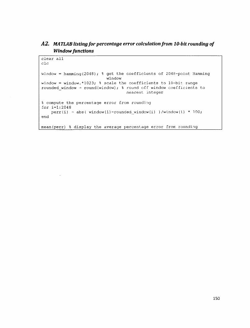
A2. MATLAB listing for percentage error calculation from 10-bit rounding of Window functions
clear all clc
window = hamming(2048); % get the coefficients of 2048-point Hamming window
window = window.*1023; % scale the coefficients to 10-bit range rounded_window = round(window); % round off window coefficients to
nearest integer
% compute the percentage error from rounding for i=l:2048
perr(i) = abs ( window(i)-rounded_window(i) )/window(i) * 100; end
mean(perr) % display the average percentage error from rounding
150
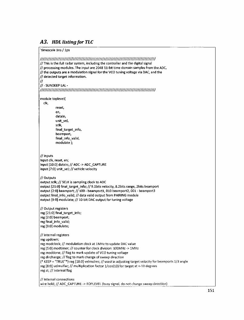
A3. HDL listing for TLC 'timescale Ins / lps
llllllllllllllllllllllllllllilllllllllllllllllllllllllllllllllllllllllllllllllllll II This is the full radar system, including the controller and the digital signal / / processing modules. The input are 2048 11-bit time domain samples from the ADC, / / the outputs are a modulation signal for the VCO tuning voltage via DAC, and the / / detected target information.
// / / - SUNDEEP LAL -//////////////////////////////////////////////////////////////////////////////////
module toplevel( elk,
reset, en, data in, unit_vel, sclk, final_target_info, beamport, final_info_valid, modulate);
/ / Inputs input elk, reset, en; input [10:0] datain; / / ADC -> ADC_CAPTURE input [7:0] unit_vel;//vehicle velocity
/ / Outputs output sclk; / / SCLK is sampling clock to ADC output [21:0] final_target_info; / / 9.1bits velocity, 8.2bits range, 2bits beamport output [2:0] beamport; / / 100 - beamportl, 010 beamport2, 001 - beamport3 output final_info_valid; / / data valid output from PAIRING module output [9:0] modulate; / / 10-bit DAC output for tuning voltage
/ / Output registers reg [21:0] final_target_info; reg [2:0] beamport; reg final_info_valid; reg [9:0] modulate;
/ / Internal registers reg updown; reg modclock; / / modulation clock at 1MHz to update DAC value reg [5:0] modtimer; / / counter for clock division: 100MHz -> 1MHz reg moddone; / / flag to mark update of VCO tuning voltage reg dirchange; / / flag to mark change of sweep direction (* KEEP = "TRUE"*) reg [18:0] velmulres; / / used in adjusting target velocity for beamports 1/3 angle reg [8:0] velmulfac; / / multiplication factor l/cos(10) for target at +-10 degrees reg st; / / internal flag
/ / Internal connections wire hold; / / ADC_CAPTURE -> TOPLEVEL (busy signal, do not change sweep direction)
151
wire fwd_inv_we, fwd jnv ; assign fwd_inv_we = 1; assign fwd jnv = 1; / / forward FFT
wire scale_sch_we; assign scale_sch_we = 0;
wire [11:0] scale_sch; assign scale_sch = 12'dO; / / use default scaling schedule for FFT stages
wire fft_start; / / ADC_CAPTURE -> FFT wire [11:0] xn_re, x n j m ; / / ADC_CAPTURE -> FFT wire [10:0] xn_index; / / FFT-> ADC.CAPTURE wire [10:0] xkjndex; / / FFT -> UNLOAD_FFT wire [11:0] xk_re, xk_im; / / FFT -> UNLOAD_FFT wire fft_busy, fft_edone; / / FFT -> ?toplevel? wire fft_rfd, fft_dv, fft_done; / / FFT -> UNLOAD_FFT wire [9:0] index; / / UNLOAD_FFT -> FFT_CAPTURE wire [11:0] re, im; / / UNLOAD_FFT -> FFT_CAPTURE wire dv; / / UNLOAD_FFT -> FFT_CAPTURE wire sqrt_done; / / TOPLEVEL -> FFT_CAPTURE wire donea, doneb, donee, doned; / / SQRT -> TOPLEVEL
assign sqrt_done = donea & doneb & donee & doned; wire [24:0] sqrt_feeda, sqrt jeedb, sqrt jeedc, sqrt jeedd; / / FFT_CAPTURE -> SQRT wire sqrt_start; / / FFTjCAPTURE -> SQRT wire [12:0] roota, rootb, rootc, rootd; / / SQRT -> CFAR wire [12:0] target_abs; / / CFAR -> PAIRING wire [9:0] target_pos; / / CFAR -> PAIRING wire new_target, complete; / / CFAR -> PAIRING wire start_cfar; / / CFAR -> FFT_CAPTURE wire [19:0] target jnfo; / / PAIRING -> TOPLEVEL wire info_valid; / / PAIRING -> TOPLEVEL
till lMhz clock generator from 100MHz system clock / / - used to update VCO tuning voltage via DAC //_ always @ ( posedge elk) begin
if( reset == 1) / / synchronous reset begin
modtimer <= 6'd0; modclock <= 1'bO;
end
else if( modtimer == 49 ) begin
modclock <= ~modclock; / / invert modulation clock modtimer <= 6'd0; / / clear counter
end
else modtimer <= modtimer + 1;
end
// / / Beamport, tuning voltage and sweep control //
152
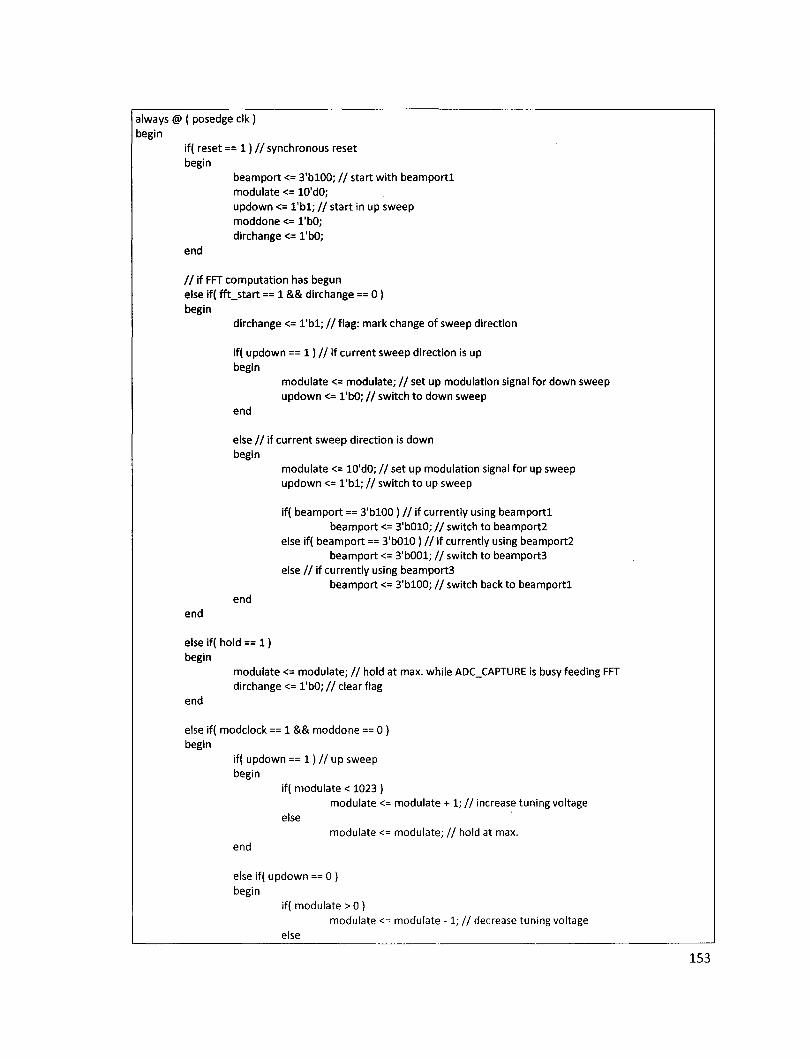
always @ ( posedge elk) begin
if( reset ==1)17 synchronous reset begin
beamport <= 3'bl00; / / start with beamportl modulate <= 10'dO; updown <= l ' b l ; / / start in up sweep moddone <= 1'bO; dirchange <= 1'bO;
end
/ / if FFT computation has begun else if( fft_start == 1 && dirchange == 0) begin
dirchange <= l ' b l ; / / flag: mark change of sweep direction
if( updown == 1) / / if current sweep direction is up begin
modulate <= modulate; / / set up modulation signal for down sweep updown <= 1'bO; / / switch to down sweep
end
else / / if current sweep direction is down begin
modulate <= 10'dO; / / set up modulation signal for up sweep updown <= l ' b l ; / / switch to up sweep
if( beamport == 3'bl00) / / if currently using beamportl beamport <= 3'b010; / / switch to beamport2
else if( beamport == 3'b010 ) / / if currently using beamport2 beamport <= 3'b001; / / switch to beamport3
else / / if currently using beamport3 beamport <= 3'blOO; / / switch back to beamportl
end end
else if( hold == 1) begin
modulate <= modulate; / / hold at max. while ADC_CAPTURE is busy feeding FFT dirchange <= 1'bO; / / clear flag
end
else if( modclock == 1 && moddone == 0 ) begin
if( updown == 1) / / up sweep begin
if( modulate < 1023 ) modulate <= modulate + 1; / / increase tuning voltage
else modulate <= modulate; / / hold at max.
end
else if( updown ==0 ) begin
iff modulate > 0 ) modulate <= modulate - 1 ; / / decrease tuning voltage
else
153
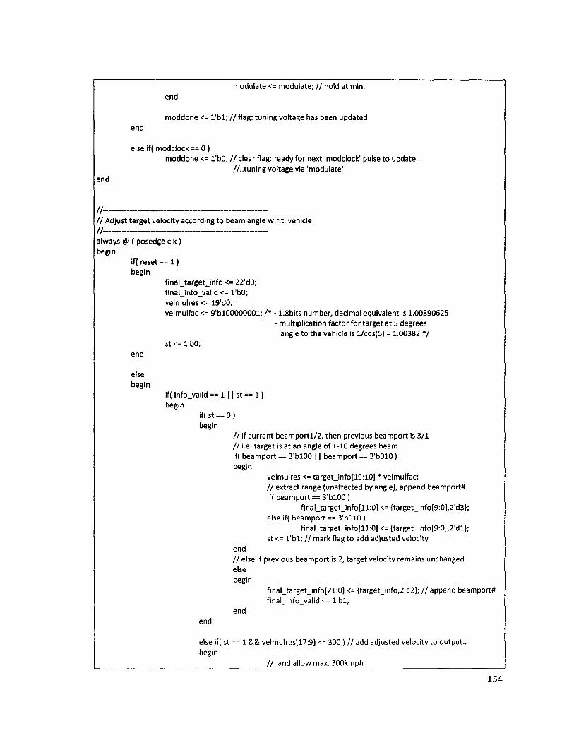
modulate <= modulate; / / hold at min. end
moddone <= l ' b l ; / / f lag : tuning voltage has been updated end
else if( modclock == 0 ) moddone <= 1'bO; / / clear flag: ready for next 'modclock' pulse to update.,
//..tuning voltage via 'modulate' end
//-II Adjust target velocity according to beam angle w.r.t. vehicle
always @ ( posedge elk) begin
if( reset == 1) begin
final_target_info <= 22'dO; final_info_valid <= 1'bO; velmulres <= 19'dO; velmulfac <= 9'bl00000001; / * - 1.8bits number, decimal equivalent is 1.00390625
- multiplication factor for target at 5 degrees angle to the vehicle is l/cos(5) = 1.00382 * /
st <= 1'bO; end
else begin
if( info_valid == 1 11 st == 1) begin
if( st == 0 ) begin
/ / if current beamportl/2, then previous beamport is 3/1 / / i.e. target is at an angle of +-10 degrees beam iff beamport == 3'blOO 11 beamport == 3'bOlO) begin
velmulres <= target_info[19:10] * velmulfac; / / extract range (unaffected by angle), append beamport# if( beamport == 3'blOO )
final_target_info[ll:0] <= {target_info[9:0],2'd3}; else if( beamport == 3'b010)
final_target_info[ll:0] <= {target_info[9:0],2'dl}; st <= l ' b l ; / / mark flag to add adjusted velocity
end / / else if previous beamport is 2, target velocity remains unchanged else begin
final_target_info[21:0] <= {target_info,2'd2}; / / append beamport# final_info_valid <= l ' b l ;
end end
else if( st == 1 && velmulres[17:9] <= 300 ) / / add adjusted velocity to output-begin
//..and allow max. 300kmph
154
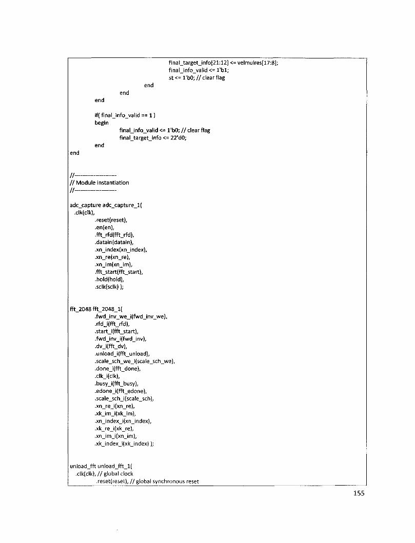
final_target_info[21:12] <= velmulres[17:8]; final_info_valid <= l ' b l ; st <=l 'bO;//clear flag
end end
end
if( final_info_valid == 1) begin
final_info_valid <= 1'bO; / / clear flag final_target_info <= 22'dO;
end
// / / Module instantiation
adc_capture adc_capture_l( .clk(clk),
.reset( reset),
.en(en),
.fft_rfd(fft_rfd),
.datain(datain),
.xn_index(xn_index),
.xn_re(xn_re),
.xn_im(xn_im),
.fft_start(fft_start),
.hold(hold),
.sclk(sclk));
fft_2048 fft_2048_l( .fwd_inv_we_i(fwd_inv_we), .rfd_i(fft_rfd), .start_i(fft_start), .fwd_inv_i(fwd_inv), .dv_i(fft_dv), .unload_i(fft_unload), .scale_sch_we_i(scale_sch_we), .done_i(fft_done), .clk_i(clk), .busy_i(fft_busy), .edone_i(fft_edone), .scale_sch_i(scale_sch), .xn_re_i(xn_re), .xk_im_i(xk_im), .xn_index_i(xn_index), .xk_re_i(xk_re), .xn_im_i(xn_im), .xk_index_i(xk_index) );
unload_fft unload_fft_l( .clk(clk),//global clock
.reset(reset), / / global synchronous reset
155
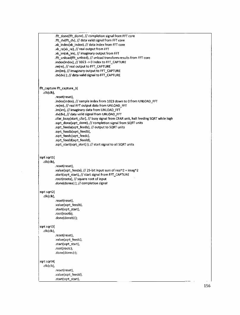
.fft_done(fft_done), / / completion signal from FFT core
.fft_dv(fft_dv), / / data valid signal from FFT core
.xk_index(xk_index), / / data index from FFT core
.xk_re(xk_re), / / real output from FFT
.xk_im(xk_im), / / imaginary output from FFT
.fft_unload(fft_unload), / / unload transform results from FFT core
.index(index), / / 1023 -> 0 index to FFT_CAPTURE
.re(re), / / real output to FFT_CAPTURE
.im(im), / / imaginary output to FFT_CAPTURE •dv(dv)); / / data valid signal to FFT_CAPTURE
fft_capture fft_capture_l( .clk(clk),
.reset(reset),
.index(index), / / sample index from 1023 down to 0 from UNLOAD_FFT
.re(re), / / real FFT output data from UNLOAD_FFT
.im(im), / / imaginary data from UNLOAD_FFT
.dv(dv), / / data valid signal from UNLOAD_FFT
.cfar_busy(start_cfar), / / busy signal from CFAR unit, halt feeding SQRT while high
.sqrt_done(sqrt_done), / / completion signal from SQRT units
.sqrt_feeda(sqrt_feeda), / / output to SQRT units
.sqrt_feedb(sqrt_feedb),
.sqrt_feedc(sqrt_feedc),
.sqrt_feedd(sqrt_feedd),
.sqrt_start(sqrt_start)); / / start signal to all SQRT units
sqrtsqrtl( xlk(clk),
.reset( reset),
.value(sqrt_feeda), / / 25-bit input sum of realA2 + imagA2
.start(sqrt_start), / / start signal from FFT_CAPTURE
.root(roota), / / square root of input
.done(donea)); / / completion signal
sqrt sqrt2( .clk(clk),
.reset(reset),
.value(sqrt_feedb),
.start(sqrt_start),
.root(rootb),
.done(doneb));
sqrtsqrt3( .clk(clk),
.reset( reset),
.value(sqrt_feedc),
.start(sqrt_start),
.root(rootc),
.done(donec));
sqrt sqrt4( .clk(clk),
.reset(reset),
.value(sqrt_feedd),
.start(sqrt start),
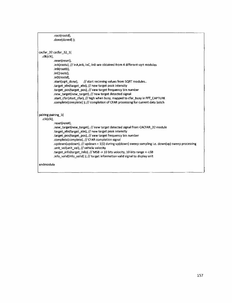
.root(rootd),
.done(doned));
cacfar_32 cacfar_32_l( xlk(clk),
.reset( reset),
.inA(roota), / / inA,inB, inC, inD are obtained from 4 different sqrt modules
.inB(rootb),
.inC(rootc),
.inD(rootd),
.start(sqrt_done), / / start recieving values from SQRT modules..
.target_abs(target_abs), / / new target peak intensity
.target_pos(target_pos), / / new target frequency bin number
.new_target(new_target), / / new target detected signal
.start_cfar(start_cfar), / / high when busy, mapped to cfar_busy in FFT_CAPTURE
.complete(complete)); / / completion of CFAR processing for current data batch
pairing pairing_l( xlk(clk),
.reset(reset),
.new_target(new_target), / / new target detected signal from CACFAR_32 module
.target_abs(target_abs), / / new target peak intensity
.target_pos(target_pos), / / new target frequency bin number
.complete(complete), / / CFAR completion signal
.updown(updown), / / updown = 1(0) during up(down) sweep sampling i.e. down(up) sweep processing
.unit_vel(unit_vel), / / vehicle velocity
.target_info(target_info), / / MSB -> 10 bits velocity, 10 bits range <- LSB
.info_valid(info_valid)); / / target information valid signal to display unit
endmodule
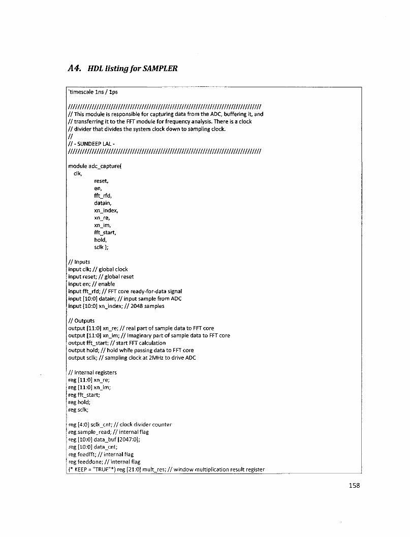
A4. HDL listing for SAMPLER
'timescale Ins / lps
IIIIIIIIIIIIIIIIIIIIIIIIIIIIIIIIIIIIIIIIIIIIIIIIIIIIIIIIIIIIIIIIIIIIIIIIIIIIIIIIII II This module is responsible for capturing data from the ADC, buffering it, and / / transferring it to the FFT module for frequency analysis. There is a clock / / divider that divides the system clock down to sampling clock.
// //-SUNDEEPLAL-
ll/l/l/llllllll/llllllll/lllllllllllll/ll/lll/lllllllllllllllll/lllll/llllllllllll
module adc_capture( elk,
reset, en, fft_rfd, datain, xn_index, xn_re, xn_im, fft_start, hold, sclk );
/ / Inputs input elk; / / global clock input reset; / / global reset input en;/ /enable input fft_rfd; / / FFT core ready-for-data signal input [10:0] datain; / / input sample from ADC input (10:0] xnjndex; / / 2048 samples
/ / Outputs output [11:0] xn_re; / / real part of sample data to FFT core output [11:0] xn_im; / / imaginary part of sample data to FFT core output fft_start; / / start FFT calculation output hold; / / hold while passing data to FFT core output sclk; / / sampling clock at 2MHz to drive ADC
/ / Internal registers reg [11:0] xn_re; reg [11:0] xn_im; regfft_start; reg hold; reg sclk;
reg [4:0] sclk_cnt; / / clock divider counter reg sample_read; / / internal flag reg [10:0] data_buf [2047:0]; reg [10:0] data_cnt; reg feedfft; / / internal flag reg feeddone; / / internal flag (* KEEP = "TRUE"*) reg [21:0] mult_res; / / window multiplication result register
158
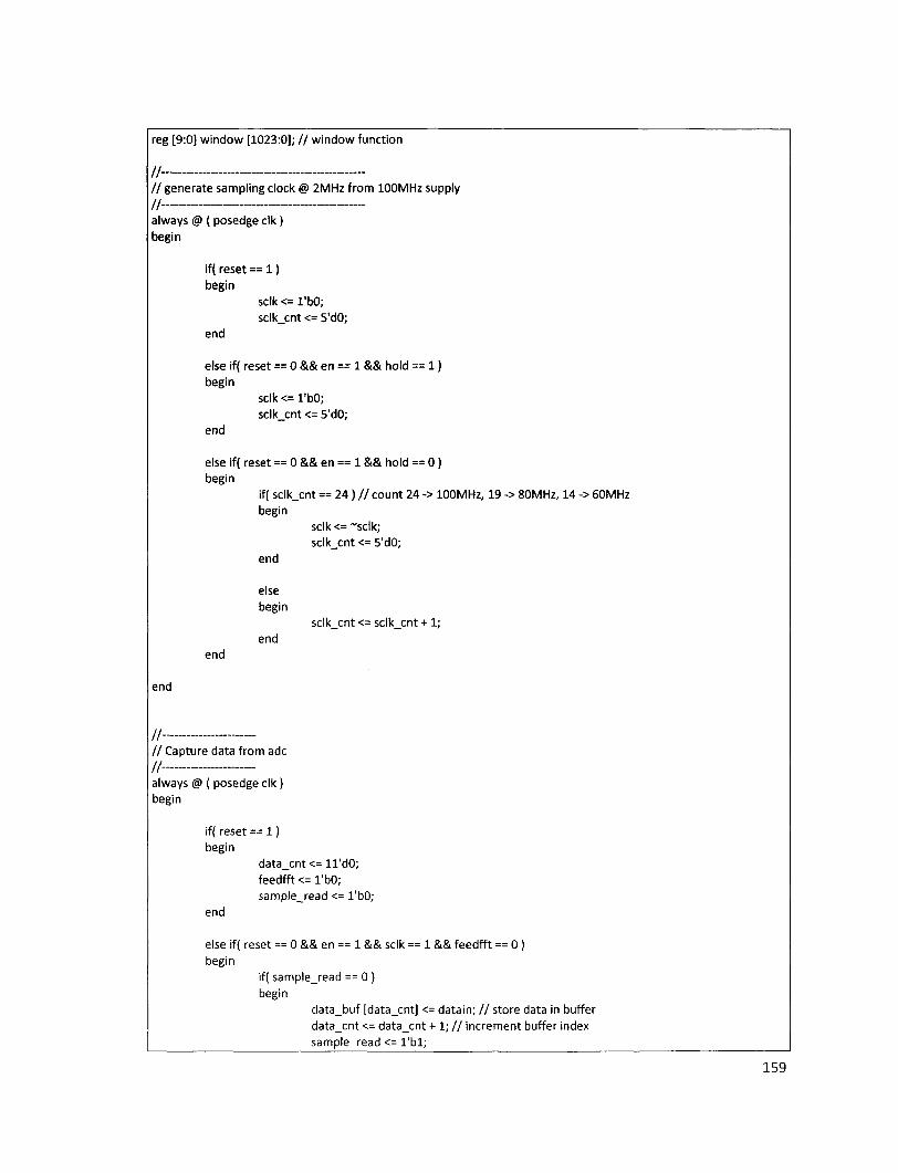
reg [9:0] window [1023:0]; / / window function
// / / generate sampling clock @ 2MHz from 100MHz supply // always @ ( posedge elk) begin
if( reset == 1) begin
sclk<=l'bO; sclk_cnt <= 5'dO;
end
else if( reset == 0 && en == 1 && hold == 1) begin
sclk <= 1'bO; sclk_cnt <= 5'dO;
end
else if( reset == 0 && en == 1 && hold == 0 ) begin
if( sclk_cnt == 24 ) / / count 24 -> 100MHz, 19 -> 80MHz, 14 -> 60MHz begin
sclk <= ~sclk; sclk_cnt <= 5'dO;
end
else begin
sclk_cnt <= sclk_cnt + 1; end
end
end
// / / Capture data from adc // always @ ( posedge elk ) begin
if( reset == 1) begin
data_cnt <= 11'dO; feedfft <= 1'bO; sample_read <= 1'bO;
end
else if( reset == 0 && en == 1 && sclk == 1 && feedfft == 0 ) begin
if( sample_read == 0 ) begin
data_buf [data_cnt] <= datain; / / store data in buffer data_cnt <= data_cnt + 1; / / increment buffer index sample_read <= l ' b l ;
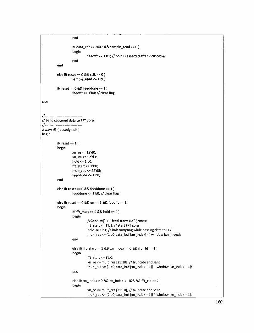
end
iff data_cnt == 2047 && sample_read == 0) begin
feedfft <= l ' b l ; / / hold is asserted after 2 elk cycles end
end
else if( reset == 0 && sclk == 0 ) sample_read <= 1'bO;
iff reset == 0 && feeddone == 1) feedfft <= l 'bO; / / clear flag
// / / Send captured data to FFT core //. always @ ( posedge elk) begin
iff reset == 1) begin
xn_re <= 12'dO; xn_im <= 12'dO; hold <= 1'bO; fft_start <= 1'bO; mult_res <= 22'dO; feeddone <= 1'bO;
else iff reset == 0 && feeddone == 1) feeddone <= 1'bO; / / clear flag
else iff reset == 0 && en == 1 && feedfft == 1) begin
iff fft_start == 0 && hold == 0) begin
//$display("FFTfeed start: %d",$time); fft_start <= l ' b l ; / / start FFT core hold <= l ' b l ; / / halt sampling while passing data to FFT mult_res <= {l'bO,data_buf [xnjndex]} * window [xnjndex];
end
else iff fft_start == 1 && xnjndex == 0 && fft_rfd == 1) begin
fft_start <= 1'bO; xn_re <= mult_res [21:10]; / / truncate and send mult_res <= {l'bO,data_buf [xnjndex + 1]} * window [xnjndex + 1];
end
else iff xnjndex > 0 && xnjndex < 1023 && f f t j f d == 1) begin
x n j e <= multj-es [21:10]; / / truncate and send mult res <= {l'bO,data buf [xn index + 1]} * window [xnjndex + 1];
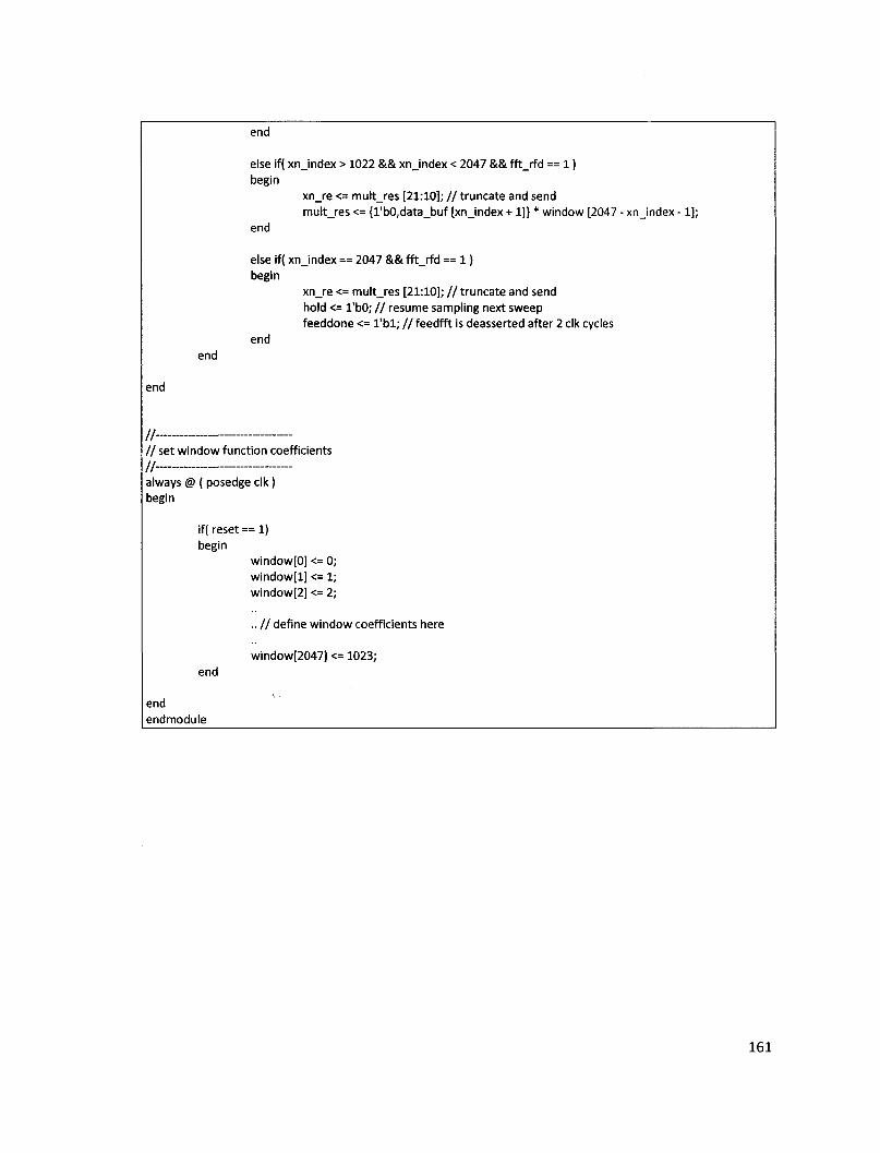
end
else if( xnjndex > 1022 && xnjndex < 2047 && fft_rfd == 1) begin
xn_re <= mult_res [21:10]; / / truncate and send mult_res <= {l'bO,datajDuf [xnjndex + 1]} * window [2047 - xnjndex -1 ] ;
end
else if( xnjndex == 2047 && fft_rfd == 1) begin
x n j e <= multj-es [21:10]; / / truncate and send hold <= 1'bO; / / resume sampling next sweep feeddone <= l ' b l ; / / feedfft is deasserted after 2 elk cycles
end end
end
till set window function coefficients // always @ ( posedge elk) begin
if( reset == 1) begin
window[0] <= 0; window[l] <= 1; window[2] <= 2;
.. / / define window coefficients here
window[2047] <= 1023; end
end endmodule
161
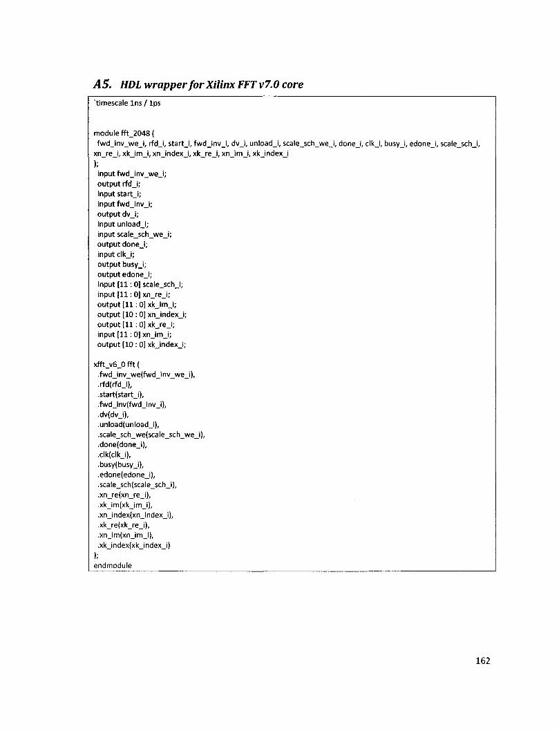
AS. HDL wrapper for Xilinx FFT v7.0 core
'timescale l n s / l p s
module fft_2048 ( fwd_inv_we_i, rfd_i, start_i, fwd_inv_i, dv_i, unload_i, scale_sch_we_i, done_i, elk i, busy_i, edonej , scale_sch_i,
xn_re_i, xk_im_j, x n j n d e x j , xk_re_i, xn_im_i, xk index_i
); input fwd_inv_we_i; output rfd_i; input start_i; input fwd_inv_i; output dv_i; input un loadj ; input scale_sch_we_i; output done_i; input e l k j ; output busy_i; output edone j ; input [11:0] scale_sch_i; input [ 1 1 : 0] x n j e j ; output [11:0] xk_im_i; output [10 :0] xn_index_i; output [11:0] xk_re_i; input [ 1 1 : 0] xn_im_i; output [10 : 0] xk_index_i;
xfft_v6_0 fft ( .fwd_inv_we(fwd_inv_we_i), •rfd(rfd_i), .start(startj'), .fwd_inv(fwd_inv_i), .dv(dv_i), .unload(unloadj'), .scale_sch_we(scale_sch_we_i), .done(donej), .clk(clk_i), .busy(busy_i), .edone(edone_i), .scale_sch(scale_sch_i), .xn_re(xn_re_i), .xkj 'm(xkjmj ' ) , .xnjndex(xnj'ndexj'), .xk_re(xk_re_i), .xn_im(xn_im_i), .xk_index(xk_index_i)
); endmodule
162
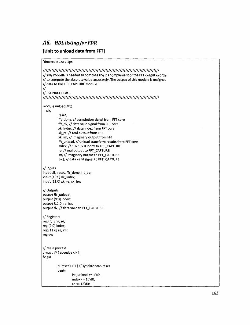
A6. HDL listing for FDR
[Unit to unload data from FFT]
'timescale I n s / lps
llllllllllllllllllllllllllllllllllllllllllllllllllllllllllllllllllllllllllllllllll II This module is needed to compute the 2's complement of the FFT output in order / / to compute the absolute value accurately. The output of this module is unsigned / / data to the FFT_CAPTURE module.
// //-SUNDEEPLAL-llllllllllllllllllllllllllllllllllllllllllllllllllllllllllllllllllllllllllllllllll
module unload_fft( elk,
reset, fft_done, / / completion signal from FFT core fft_dv, / / data valid signal from FFT core xkjndex, / / data index from FFT core xk_re, / / real output from FFT xk_im, / / imaginary output from FFT fft_unload, / / unload transform results from FFT core index, / / 1023 -> 0 index to FFT_CAPTURE re, / / real output to FFT_CAPTURE im, / / imaginary output to FFT_CAPTURE dv ); / / data valid signal to FFT_CAPTURE
/ / Inputs input elk, reset, fft_done, fft_dv; input [10:0] xkjndex; input [11:0] xk_re, xk_im;
/ / Outputs output fft_unload; output [9:0] index; output [11:0] re, im; output dv; / / data valid to FFT_CAPTURE
/ / Registers regff t j jn load; reg [9:0] index; reg [11:0] re, im; reg dv;
/ / Main process always @ ( posedge elk) begin
if( reset == 1) / / synchronous reset begin
f f t j jn load <= l'bO; index <= 10'd0; re <= 12'd0;
163
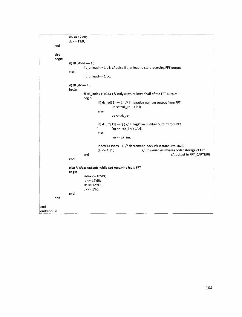
end
else begin
im <= 12'dO; dv <= 1'bO;
end
if( fft_done == 1) fft_unload <= l ' b l ; / / pulse fft_unload to start receiving FFT output
else fft_unload <= 1'bO;
if( fft_dv == 1) begin
if( xk_index > 1023) / / only capture lower half of the FFT output begin
if( xk_re[ l l ] == 1) / / if negative number output from FFT re <= ~xk_re + l ' b l ;
else re <= xk_re;
iff xk_im[l l ] == 1) / / if negative number output from FFT im <= ~xk_im + l ' b l ;
else im <= xk_im;
index <= index - 1 ; / / decrement index (first state 0 to 1023).. dv <= l ' b l ; //..this enables reverse order storage of FFT..
end //..output in FFT_CAPTURE end
else / / clear outputs while not receiving from FFT begin
index <= 10'dO; re <= 12'd0; im <= 12'dO; dv <= 1'bO;
end
end endmodule
164
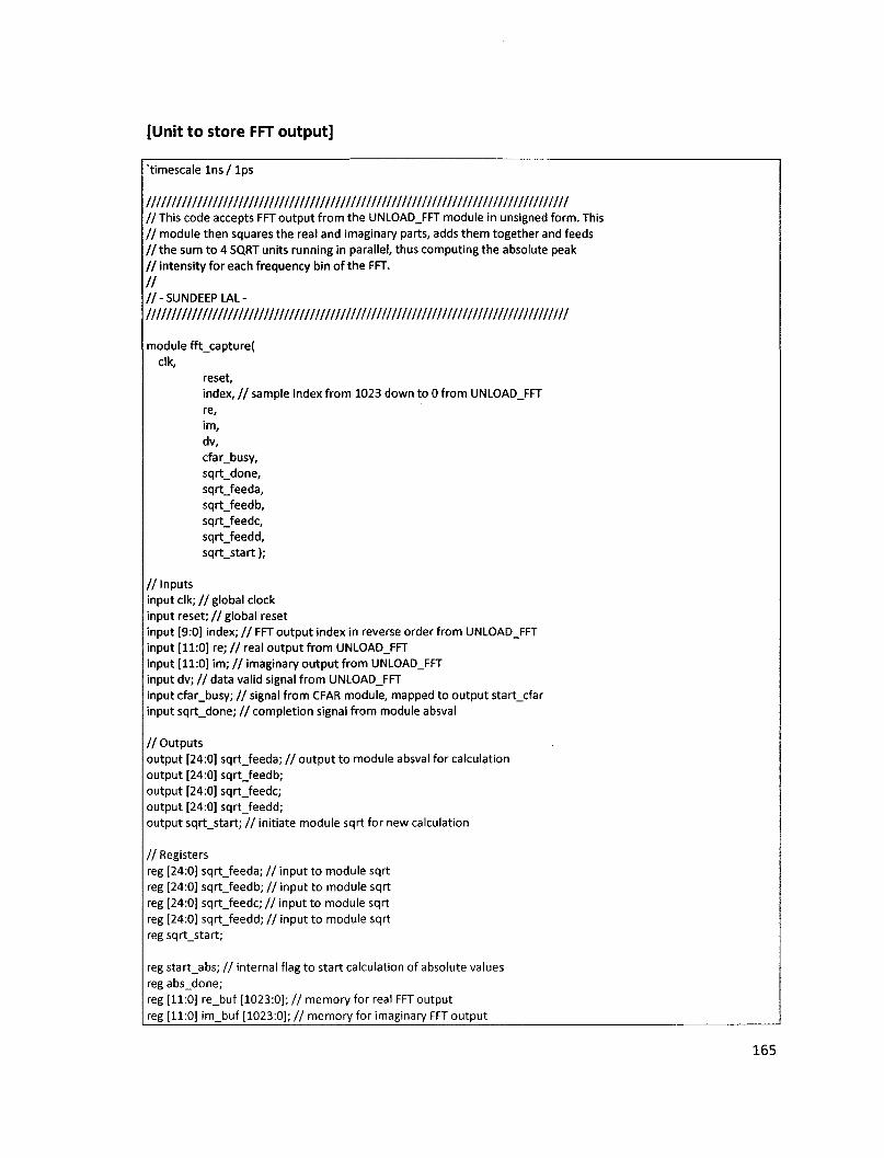
[Unit to store FFT output]
'timescale Ins / lps
////////7/////////////////////////////7/////7////////////7///////////////////////// / / This code accepts FFT output from the UNLOAD_FFT module in unsigned form. This / / module then squares the real and imaginary parts, adds them together and feeds / / the sum to 4 SQRT units running in parallel, thus computing the absolute peak / / intensity for each frequency bin of the FFT.
// //-SUNDEEPLAL-
lllllllllllllllllllllllllllllllllllllllllllllllllllllllllllllllllllllllllllllllllll
module fft_capture( elk,
reset, index, / / sample index from 1023 down to 0 from UNLOAD_FFT re, im, dv, cfar_busy, sqrt_done, sqrt_feeda, sqrt_feedb, sqrt_feedc, sqrt_feedd, sqrt_start);
/ / Inputs input elk; / / global clock input reset; / / global reset input [9:0] index; / / FFT output index in reverse order from UNLOAD_FFT input [11:0] re; / / real output from UNLOAD_FFT input [11:0] im; / / imaginary output from UNLOAD_FFT input dv; / / data valid signal from UNLOAD_FFT input cfar_busy; / / signal from CFAR module, mapped to output start_cfar input sqrt_done; / / completion signal from module absval
/ / Outputs output [24:0] sqrt_feeda; / / output to module absval for calculation output [24:0] sqrt_feedb; output [24:0] sqrt_feedc; output [24:0] sqrt_feedd; output sqrt_start; / / initiate module sqrt for new calculation
/ / Registers reg [24:0] sqrt_feeda; / / input to module sqrt reg [24:0] sqrt_feedb; / / input to module sqrt reg [24:0] sqrt_feedc; / / input to module sqrt reg [24:0] sqrt_feedd; / / input to module sqrt regsqrt_start;
reg start_abs; / / internal flag to start calculation of absolute values reg abs_done; reg [11:0] re_buf [1023:0]; / / memory for real FFT output reg [11:0] im_buf [1023:0]; / / memory for imaginary FFT output
165
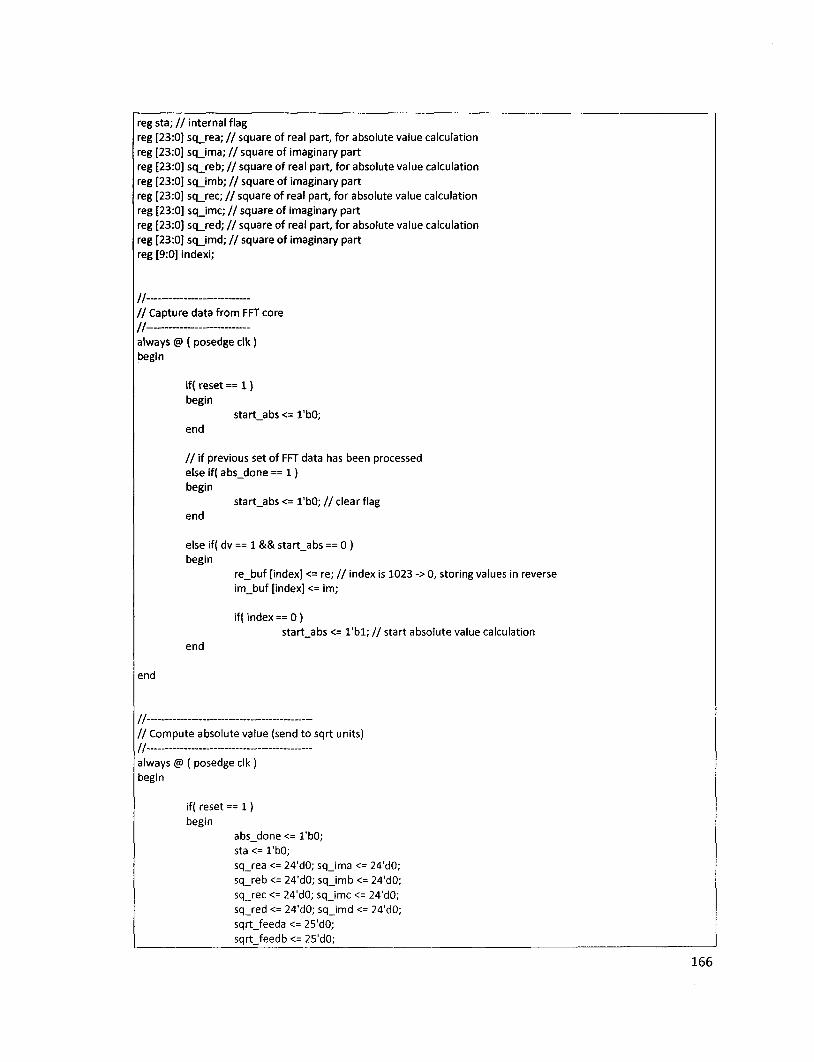
reg sta; / / internal flag reg [23:0] sq_rea; / / square of real part, for absolute value calculation reg [23:0] sq jma; / / square of imaginary part reg [23:0] sq_reb; / / square of real part, for absolute value calculation reg [23:0] sq_imb; / / square of imaginary part reg [23:0] sq_rec; / / square of real part, for absolute value calculation reg [23:0] sq_imc; / / square of imaginary part reg [23:0] sq_red; / / square of real part, for absolute value calculation reg [23:0] sq_imd; / / square of imaginary part reg [9:0] indexi;
till Capture data from FFT core // always @ ( posedge elk) begin
if( reset == 1) begin
start_abs <= 1'bO; end
/ / if previous set of FFT data has been processed else if( abs_done == 1) begin
start_abs <= 1'bO; / / clear flag end
else if( dv == 1 && start_abs == 0 ) begin
re_buf [index] <= re; / / index is 1023 -> 0, storing values in reverse im_buf [index] <= im;
if( index == 0 ) start_abs <= 1'bl; / / start absolute value calculation
end
end
// / / Compute absolute value (send to sqrt units) // always @ ( posedge elk ) begin
if( reset == 1) begin
abs_done <= 1'bO; sta <= 1'bO; sq_rea <= 24'dO; sq_ima <= 24'dO; sq_reb <= 24'dO; sq_imb <= 24'dO; sq_rec <= 24'dO; sq_imc <= 24'dO; sq_red <= 24'dO; sq_imd <= 24'dO; sqrt_feeda <= 25'd0; sqrt jeedb <= 25'dO;
166
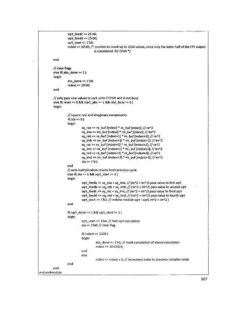
sqrtjeedc <= 25'dO; sqrt jeedd <= 25'dO; sqrt_start <= 1'bO; indexi <= 10'dO; / * counter to count up to 1024 values, since only the latter half of the FFT output
is considered for CFAR * /
end
/ / clear flags else if( abs_done == 1) begin
abs_done <= 1'bO; indexi <= 10'dO;
end
/ / only pass new values to sqrt units if CFAR unit is not busy else if( reset == 0 && start_abs == 1 && cfar_busy == 0) begin
/ / square real and imaginary components if( sta == 0 ) begin
sqjrea <= re_buf [indexi] * re_buf [indexi]; / / reA2 sq_ima <= im_buf [indexi] * im_buf [indexi]; / / imA2 sq_reb <= re_buf [indexi+1] * re_buf [indexi+1]; / / reA2 sq_imb <= im_buf [indexi+1] * im_buf [indexi+1]; / / imA2 sq_rec <= re_buf [indexi+2] * re_buf [indexi+2]; / / reA2 sq jmc <= im_buf [indexi+2] * im_buf [indexi+2]; / / imA2 sq_red <= re_buf [indexi+3] * re_buf [indexi+3]; / / reA2 sq_imd <= im_buf [indexi+3] * im_buf [indexi+3]; / / imA2 sta <= l ' b l ;
end / / sum multiplication results from previous cycle else if( sta == 1 && sqrt_start == 0 ) begin
sqrt_feeda <= sq_rea + sq_ima; / / (reA2 + imA2) pass value to first sqrt sqrt_feedb <= sq_reb + sq jmb; / / (reA2 + imA2) pass value to second sqrt sqrt_feedc <= sq_rec + sq_imc; / / (reA2 + imA2) pass value to third sqrt sqrt_feedd <= sq_red + sq jmd ; / / (reA2 + imA2) pass value to fourth sqrt sqrt_start <= l ' b l ; / / initiate module sqrt - sqrt( reA2 + imA2 )
end
if( sqrt_done == 1 && sqrt_start == 1) begin
sqrt_start <= 1'bO; / / halt sqrt calculation sta<= 1'bO;//clear flag
if( indexi == 1020 ) begin
abs_done <= l ' b l ; / / mark completion of absval calculation indexi <= 10'dl023;
end else
indexi <= indexi + 4; / / increment index to previous complex value end
end end endmodule
167
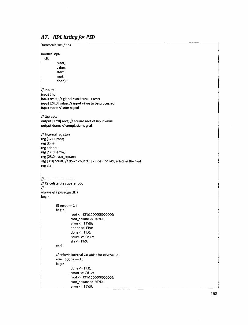
A7. HDL listing for PSD "timescale l n s / l p s
module sqrt( elk,
reset, value, start, root, done);
/ / Inputs input elk; input reset; / / global synchronous reset input [24:0] value; / / input value to be processed input start; / / start signal
/ / Outputs output [12:0] root; / / square root of input value output done; / / completion signal
/ / Internal registers reg [12:0] root; reg done; reg edone; reg [12:0] error; reg [25:0] root_square; reg [3:0] count; / / down counter to index individual bits in the root reg sta;
// / / Calculate the square root
II always @ ( posedge elk) begin
if( reset == 1) begin
root <= 13'b 1000000000000; root_square <= 26'dO; error <= 13'd0; edone <= 1'bO; done <= 1'bO; count <=4'dl2; sta <= 1'bO;
end
/ / refresh internal variables for new value else if( done == 1) begin
done <= 1'bO; count <=4'dl2; root <= 13'bl000000000000; root_square <= 26'd0; error <= 13'd0;
168
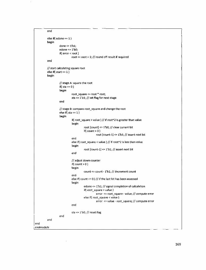
end
else if( edone == 1) begin
done <= l ' b l ; edone <= 1'bO; if( error < root)
root <= root + 1; / / round off result if required end
/ / start calculating square root else if( start == 1) begin
/ / stage A: square the root if( sta == 0) begin
root_square <= root * root; sta <= l ' b l ; / / set flag for next stage
end
/ / stage B: compare root_square and change the root else iff sta == 1) begin
if( root_square > value ) / / if rootA2 is greater than value begin
root [count] <= 1'bO; / / clear current bit iff count > 0)
root [count-1] <= l ' b l ; / / assert next bit end else iff root_square < value ) / / if rootA2 is less than value begin
root [count-1] <= l ' b l ; / / assert next bit end
/ / adjust down counter iff count > 0 ) begin
count <= count - l ' b l ; / / decrement count end else iff count == 0 ) / / if the last bit has been assessed begin
edone <= l ' b l ; / / signal completion of calculation iff root_square > value )
error <= root_square - value; / / compute error else iff root_square < value )
error <= value - root_square; / / compute error end
end
sta <=l 'bO;/ / reset flag end
end endmodule
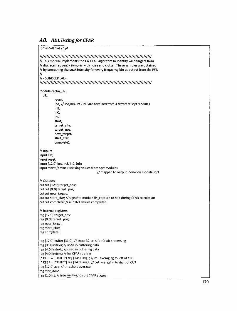
A8. HDL listing for CFAR
'timescale Ins / lps
llllllllllllllllllllllllllllllllllllllllllllllllllllllllllllllllllllllllllllllllll II This module implements the CA-CFAR algorithm to identify valid targets from / / discrete frequency samples with noise and clutter. These samples are obtained / / by computing the peak intensity for every frequency bin as output from the FFT. // //-SUNDEEPLAL-llllllllllllllllllllllllllllllllllllllllllllllllllllllllllllllllllllllllllllllllll
module cacfar_32( elk,
reset, inA, / / inA,inB, inC, inD are obtained from 4 different sqrt modules inB, inC, inD, start, target_abs, target_pos, new_target, start_cfar, complete);
/ / Inputs input elk; input reset; input [12:0] inA, inB, inC, inD; input start; / / start recieving values from sqrt modules
/ / mapped to output 'done' on module sqrt
/ / Outputs output [12:0] target_abs; output [9:0] target_pos; output new_target; output start_cfar; / / signal to module fft_capture to halt during CFAR calculation output complete; / / all 1024 values completed
/ / Internal registers reg [12:0] target_abs; reg [9:0] target_pos; reg new_target; reg start_cfar; reg complete;
reg [12:0] buffer [31:0]; / / store 32 cells for CFAR processing reg [9:0] indexa; / / used in buffering data reg [4:0] indexb; / / used in buffering data reg [4:0] indexc; / / for CFAR routine (* KEEP = "TRUE"*) reg [14:0] avgL; / / cell averaging to left of CUT (* KEEP = "TRUE"*) reg [14:0] avgR; / / cell averaging to right of CUT reg [12:0] avg; / / threshold average regcfar_done; reg [1:0] st; / / internal flag to sort CFAR stages
170
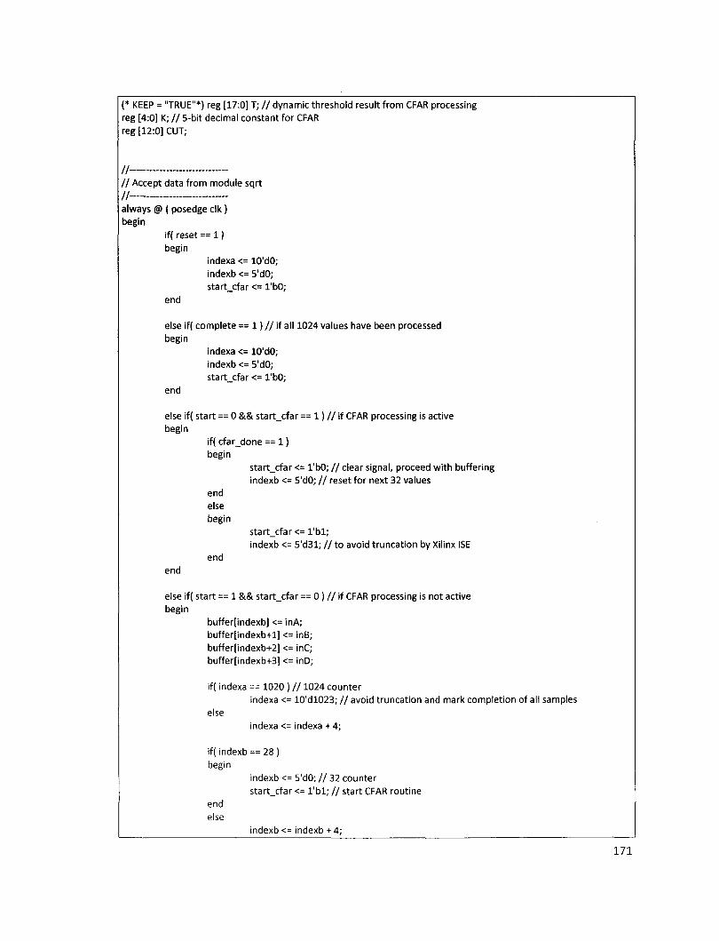
(* KEEP = "TRUE"*) reg [17:0] T; / / dynamic threshold result from CFAR processing reg [4:0] K; / / 5-bit decimal constant for CFAR reg [12:0] CUT;
// / / Accept data from module sqrt // always @ ( posedge elk) begin
if( reset == 1) begin
indexa <= 10'dO; indexb <= 5'd0; start_cfar <= 1'bO;
end
else if( complete == 1) / / if all 1024 values have been processed begin
indexa <= 10'dO; indexb <= 5'dO; start_cfar<=l'bO;
end
else if( start == 0 && start_cfar == 1) / / if CFAR processing is active begin
if( cfar_done == 1) begin
start_cfar <= 1'bO; / / clear signal, proceed with buffering indexb <= 5'dO; / / reset for next 32 values
end else begin
start_cfar <= l ' b l ; indexb <= 5'd31; / / to avoid truncation by Xilinx ISE
end end
else if( start == 1 && start_cfar == 0 ) / / if CFAR processing is not active begin
buffer[indexb] <= inA; buffer[indexb+l] <= inB; buffer[indexb+2] <= inC; buffer[indexb+3] <= inD;
iff indexa == 1020 ) / / 1024 counter indexa <= 10'dl023; / / avoid truncation and mark completion of all samples
else indexa <= indexa + 4;
if( indexb == 28 ) begin
indexb <= 5'dO; / / 32 counter start_cfar <= l ' b l ; / / start CFAR routine
end else
indexb <= indexb + 4;
171
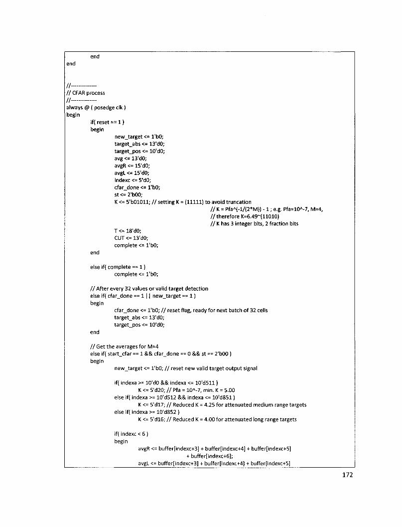
end end
// / / CFAR process // always @ ( posedge elk) begin
if( reset == 1) begin
new_target <= 1'bO; target_abs <= 13'dO; target_pos <= 10'dO; avg <= 13'dO; avgR <= 15'dO; avgL <= 15'dO; indexc <= 5'dO; cfar_done <= 1'bO; st <= 2'bOO; K <= 5'bOlOll; / / setting K = (11111) to avoid truncation
/ / K = PfaA(-l/(2*M)) - 1 ; e.g. Pfa=10A-7, M=4, //therefore K=6.49~(11010) / / K has 3 integer bits, 2 fraction bits
T <= 18'dO; CUT <= 13'dO; complete <= 1'bO;
end
else if( complete == 1) complete <= 1'bO;
/ / After every 32 values or valid target detection else if( cfar_done == 1 11 new_target == 1) begin
cfar_done <= 1'bO; / / reset flag, ready for next batch of 32 cells target_abs <= 13'dO; target_pos <= 10'dO;
end
/ / Get the averages for M=4 else if( start_cfar == 1 && cfar_done == 0 && st == 2'bOO) begin
new_target <= 1'bO; / / reset new valid target output signal
iff indexa >= 10'dO && indexa <= 10'd511) K <= 5'd20; / / Pfa = 10A-7, min. K = 5.00
else iff indexa >= 10'd512 && indexa <= 10'd851) K <= 5'dl7; / / Reduced K = 4.25 for attenuated medium range targets
else if( indexa >= 10'd852 ) K <= 5'dl6; / / Reduced K = 4.00 for attenuated long range targets
if( indexc < 6 ) begin
avgR <= buffer[indexc+3] + buffer[indexc+4] + buffer[indexc+5] + buffer[indexc+6];
avgL <= buffer[indexc+3] + buffer[indexc+4] + buffer[indexc+5]
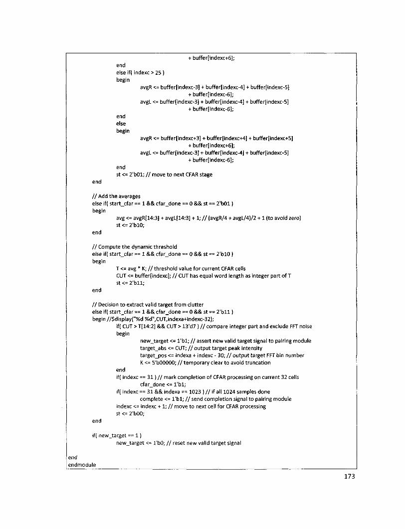
+ buffer[indexc+6]; end else if( indexc > 25 ) begin
avgR <= buffer[indexc-3] + buffer[indexc-4] + buffer[indexc-5] + buffer[indexc-6];
avgL <= buffer[indexc-3] + buffer[indexc-4] + buffer[indexc-5] + buffer[indexc-6];
end else begin
avgR <= buffer[indexc+3] + buffer[indexc+4] + buffer[indexc+5] + buffer[indexc+6];
avgL <= buffer[indexc-3] + buffer[indexc-4] + buffer[indexc-5] + buffer[indexc-6];
end st <= 2'bOl; / / move to next CFAR stage
end
/ / Add the averages else if( start_cfar == 1 && cfar_done == 0 && st == 2'bOl) begin
avg <= avgR[14:3] + avgL[14:3] + 1; / / (avgR/4 + avgL/4)/2 + 1 (to avoid zero) st <= 2'blO;
end
/ / Compute the dynamic threshold else if( start_cfar == 1 && cfar_done == 0 && st == 2'blO ) begin
T <= avg * K; / / threshold value for current CFAR cells CUT <= bufferfindexc]; / / CUT has equal word length as integer part of T st <= 2'bll;
end
/ / Decision to extract valid target from clutter else iff start_cfar == 1 && cfar_done == 0 && st == 2 ' b l l ) begin //$display("%d %d",CUT,indexa+indexc-32);
iff CUT > T[14:2] && CUT > 13'd7 ) / / compare integer part and exclude FFT noise begin
new_target <= l ' b l ; / / assert new valid target signal to pairing module target_abs <= CUT; / / output target peak intensity target_pos <= indexa + indexc - 30; / / output target FFT bin number K <= 5'b00000; / / temporary clear to avoid truncation
end if( indexc == 31) / / mark completion of CFAR processing on current 32 cells
cfar_done <= l ' b l ; if( indexc == 31 && indexa == 1023 ) / / if all 1024 samples done
complete <= l ' b l ; / / send completion signal to pairing module indexc <= indexc + 1; / / move to next cell for CFAR processing st <= 2'b00;
end
iff new_target == 1) new_target <= 1'bO; / / reset new valid target signal
end endmodule
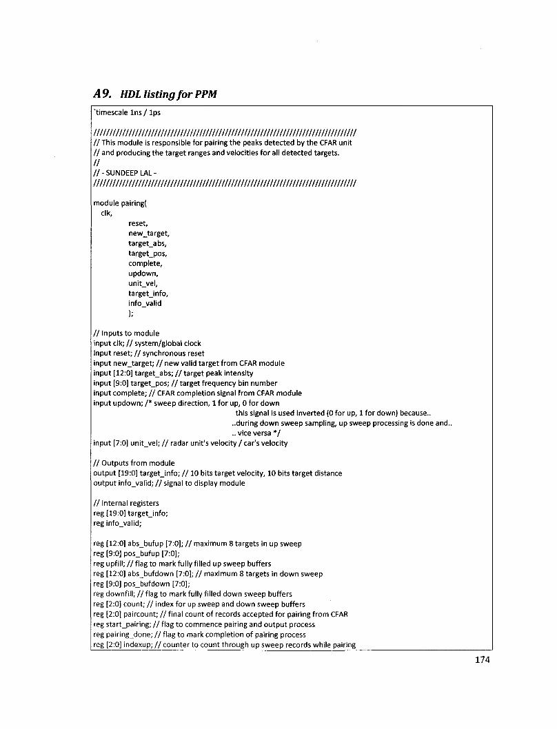
A9. HDL listing for PPM
"timescale Ins / lps
llllllllllllllllllllllllllllllllllllllllllllllllllllllllllllllllllllllllllllllllll II This module is responsible for pairing the peaks detected by the CFAR unit / / and producing the target ranges and velocities for all detected targets.
// / / - SUNDEEP LAL -//////////////////////////////////////////////////////////////////////////////////
module pairing! elk,
reset, new_target, target_abs, target_pos, complete, updown, unit_vel, target jnfo, info_valid
);
/ / Inputs to module input elk; / / system/global clock input reset; / / synchronous reset input new_target; / / new valid target from CFAR module input [12:0] target_abs; / / target peak intensity input [9:0] target_pos; / / target frequency bin number input complete; / / CFAR completion signal from CFAR module input updown; / * sweep direction, 1 for up, 0 for down
this signal is used inverted (0 for up, 1 for down) because.. ..during down sweep sampling, up sweep processing is done and.. .. vice versa * /
input [7:0] unit_vel; / / radar unit's velocity / car's velocity
/ / Outputs from module output [19:0] target jnfo; / / 10 bits target velocity, 10 bits target distance output info_valid; / / signal to display module
/ / Internal registers reg [19:0] target jnfo; reg infoj/al id;
reg [12:0] absjbufup [7:0]; / / maximum 8 targets in up sweep reg [9:0] pos_bufup [7:0]; reg upf ill; / / flag to mark fully filled up sweep buffers reg [12:0] absjbufdown [7:0]; / / maximum 8 targets in down sweep reg [9:0] posjDufdown [7:0]; reg downfill; / / flag to mark fully filled down sweep buffers reg [2:0] count; / / index for up sweep and down sweep buffers reg [2:0] paircount; / / final count of records accepted for pairing from CFAR reg startjpairing; / / flag to commence pairing and output process reg pairingdone; / / flag to mark completion of pairing process reg [2:0] indexup; / / counter to count through up sweep records while pairing
174
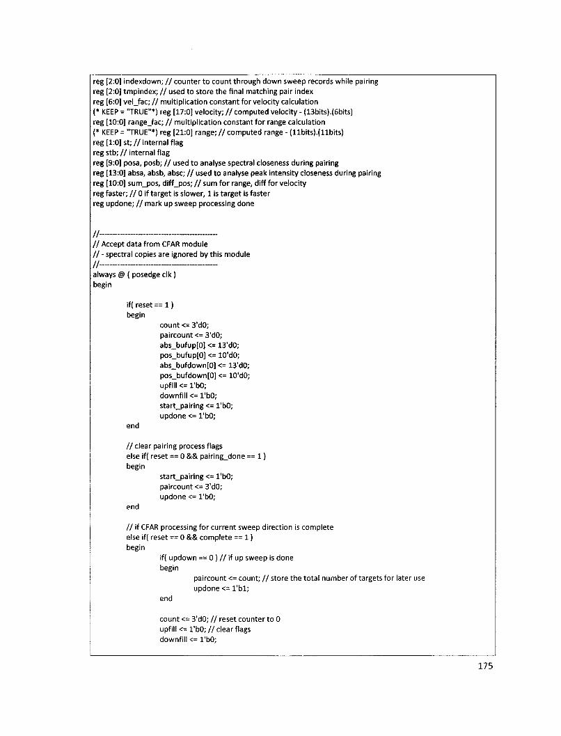
reg [2:0] indexdown; / / counter to count through down sweep records while pairing reg [2:0] tmpindex; / / used to store the final matching pair index reg [6:0] vel_fac; / / multiplication constant for velocity calculation (* KEEP = "TRUE"*) reg [17:0] velocity; / / computed velocity - (13bits).(6bits) reg [10:0] range_fac; / / multiplication constant for range calculation (* KEEP = "TRUE"*) reg [21:0] range; / / computed range - ( l lb i ts).( l lb i ts) reg [1:0] st; / / internal flag reg stb; / / internal flag reg [9:0] posa, posb; / / used to analyse spectral closeness during pairing reg [13:0] absa, absb, absc; / / used to analyse peak intensity closeness during pairing reg [10:0] sum_pos, diff_pos; / / sum for range, diff for velocity reg faster; / / 0 if target is slower, 1 is target is faster reg updone; / / mark up sweep processing done
// / / Accept data from CFAR module / / - spectral copies are ignored by this module // always @ ( posedge elk) begin
if( reset == 1) begin
count <= 3'dO; paircount <= 3'd0; abs_bufup[0] <= 13'dO; pos_bufup[0] <= 10'dO; abs_bufdown[0] <= 13'd0; pos_bufdown[0] <= 10'd0; upfill <= 1'bO; downfill <= 1'bO; start_pairing <= 1'bO; updone <= 1'bO;
end
/ / clear pairing process flags else if( reset == 0 && pairing_done == 1) begin
start_pairing <= 1'bO; paircount <= 3'dO; updone <= 1'bO;
end
/ / if CFAR processing for current sweep direction is complete else if( reset == 0 && complete == 1) begin
iff updown == 0 ) / / if up sweep is done begin
paircount <= count; / / store the total number of targets for later use updone <= l ' b l ;
end
count <= 3'dO; / / reset counter to 0 upfill <= 1'bO; / / clear flags downfill <= 1'bO;
175
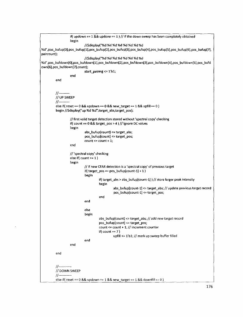
if( updown == 1 && updone == 1) / / if the down sweep has been completely obtained begin
//$display("%d %d %d %d %d %d %d %d %d",pos_bufup[0],pos_bufup[l],pos_bufup[2],pos_bufup[3];pos_bufup[4],pos_bufup[5],pos_bufup[6],pos_bufup[7], paircount);
//$display("%d %d %d %d %d %d %d %d %d",pos_bufdown[0],pos_bufdown[l],pos_bufdown[2],pos_bufdown[3],pos_bufdown[4],pos_bufdown[5],pos_bufd own[6],pos_bufdown[7],count);
start_pairing <= l ' b l ; end
end
// / / UP SWEEP // else if( reset == 0 && updown == 0 && new_target == 1 && upfill == 0) begin //$display("up %d %d",target_abs,target_pos);
/ / first valid target detection stored without 'spectral copy' checking if( count == 0 && target_pos > 4 ) / / ignore DC values begin
abs_bufup[count] <= target_abs; pos_bufup[count] <= target_pos; count <= count + 1;
end
/ / 'spectral copy' checking else if( count >= 1) begin
/ / if new CFAR detection is a 'spectral copy' of previous target if( target_pos == pos_bufup[count-l] + 1) begin
if( target_abs > abs_bufup[count-l]) / / store larger peak intensity begin
abs_bufup[count-l] <= target_abs; / / update previous target record pos_bufup[count-l] <= target_pos;
end end
else begin
abs_bufup[count] <= target_abs; / / add new target record pos_bufup[count] <= target_pos; count <= count + 1; / / increment counter if( count == 7)
upfill <= l ' b l ; / / mark up sweep buffer filled end
end
end
// / / DOWN SWEEP // else if( reset == 0 && updown == 1 && new_target == 1 && downfill == 0 )
176
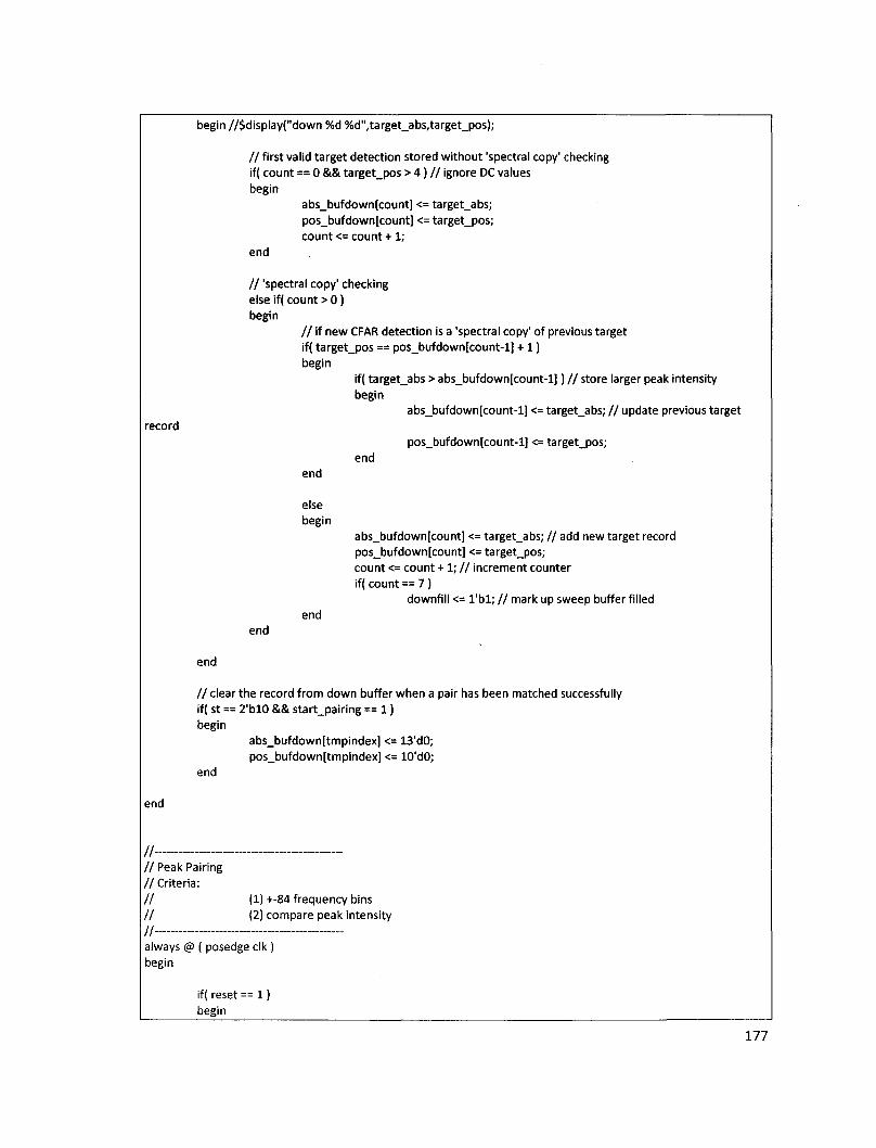
begin //$display("down %d %d",target_abs,target_pos);
/ / first valid target detection stored without 'spectral copy' checking iff count == 0 && target_pos > 4) / / ignore DC values begin
abs_bufdown[count] <= target_abs; pos_bufdown[count] <= target_pos; count <= count + 1;
end
/ / 'spectral copy' checking else if( count > 0 ) begin
/ / if new CFAR detection is a 'spectral copy' of previous target if( target_pos == pos_bufdown[count-l] + 1) begin
if( target_abs > abs_bufdown[count-l]) / / store larger peak intensity begin
abs_bufdown[count-l] <= target_abs; / / update previous target record
pos_bufdown[count-l] <= target_pos; end
end
else begin
a bs_buf down [count] <= target_abs; / / add new target record pos_bufdown[count] <= target_pos; count <= count + 1; / / increment counter iff count == 7 )
downfill <= l ' b l ; / / mark up sweep buffer filled end
end
end
/ / clear the record from down buffer when a pair has been matched successfully if( st == 2'blO && start_pairing == 1) begin
abs_bufdown[tmpindex] <= 13'dO; pos_bufdown[tmpindex] <= 10'dO;
end
end
// / / Peak Pairing //Criteria: / / (1) +-84 frequency bins / / (2) compare peak intensity
// always @ ( posedge elk ) begin
iff reset == 1) begin
177
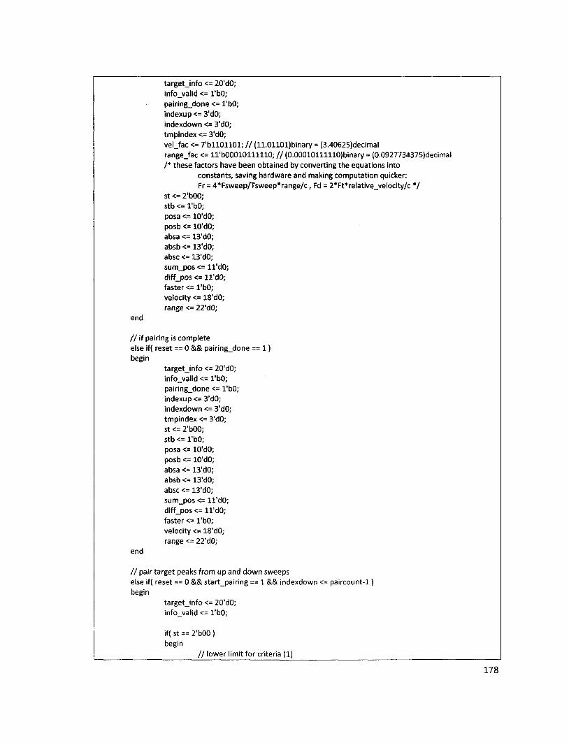
target_info <= 20'dO; info_valid <= 1'bO; pairing_done <= 1'bO; indexup <= 3'dO; indexdown <= 3'dO; tmpindex <= 3'dO; ve l jac <= 7 ' b l lO l lO l ; / / (l l.OHOl)binary = (3.40625)decimal rangejac <= 11'bOOOlOlll l lO; / / (O.OOOlOlllllO)binary = (0.0927734375)decimal / * these factors have been obtained by converting the equations into
constants, saving hardware and making computation quicker: Fr = 4*Fsweep/Tsweep*range/c, Fd = 2*Ft*relative_velocity/c * /
st <= 2'bOO; stb <= 1'bO; posa <= 10'dO; posb <= 10'dO; absa <= 13'dO; absb <= 13'dO; absc <= 13'dO; sum_pos <= 11'dO; diff_pos <= 11'dO; faster <= 1'bO; velocity <= 18'dO; range <= 22'dO;
end
/ / if pairing is complete else if( reset == 0 && pairing_done == 1) begin
target_info <= 20'dO; info_valid <= 1'bO; pairing_done <= 1'bO; indexup <= 3'dO; indexdown <= 3'dO; tmpindex <= 3'dO; st <= 2'bOO; stb <= 1'bO; posa <= 10'dO; posb <= 10'dO; absa <= 13'dO; absb <= 13'dO; absc <= 13'dO; sum_pos <= 11'dO; diff_pos <= 11'dO; faster <= 1'bO; velocity <= 18'dO; range <= 22'dO;
end
/ / pair target peaks from up and down sweeps else iff reset == 0 && start_pairing == 1 && indexdown <= paircount-1 ] begin
target jnfo <= 20'dO; info_valid <= 1'bO;
if( st == 2'bOO ) begin
/ / lower limit for criteria (1)
178
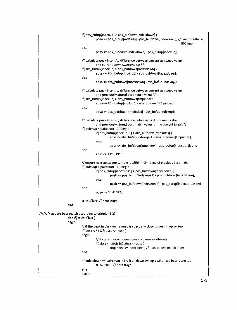
if( pos_bufup[indexup] > pos_bufdown[indexdown]) posa <= pos_bufup[indexup] - pos_bufdown[indexdown]; / / limit to +-84 i.e.
300kmph else
posa <= pos_bufdown[indexdown] - pos_bufup[indexup];
/ * calculate peak intensity difference between current up sweep value and current down sweep value * /
if( abs_bufup[indexup] > abs_bufdown[indexdown]) absa <= abs_bufup[indexup] - abs_bufdown[indexdown];
else absa <= abs_bufdown[indexdown] - abs_bufup[indexup];
/ * calculate peak intensity difference between current up sweep value and previously stored best match value * /
if( abs_bufup[indexup] > abs_bufdown[tmpindex]) absb <= abs_bufup[indexup] - abs_bufdown[tmpindex];
else absb <= abs_bufdown[tmpindex] - abs_bufup[indexup];
/ * calculate peak intensity difference between next up sweep value and previously stored best match value for the current target * /
if( indexup < paircount - 1 ) begin iff abs_bufup[indexup+l] > abs_bufdown[tmpindex])
absc <= abs_bufup[indexup+l] - abs_bufdown[tmpindex]; else
absc <= abs_bufdown[tmpindex] - abs_bufup[indexup-l]; end else
absc <= 13'd8191;
/ / ensure next up sweep sample is within +-84 range of previous best match if( indexup < paircount - 1 ) begin
if( pos_bufup[indexup+l] > pos_bufdown[indexdown]) posb <= pos_bufup[indexup+l] - pos_bufdown[indexdown];
else posb <= pos_bufdown[indexdown] - pos_bufup[indexup+l]; end
else posb <= 10'dl023;
st <= 2'bOl; / / next stage
III Illll update best match according to criteria (1,2) else iff st == 2'bOl) begin
/ / if the peak in the down sweep is spectrally close to peak in up sweep if( posa < 84 && posa <= posb ) begin
/ / if current down sweep peak is closer in intensity iff absa <= absb && absa <= absc )
tmpindex <= indexdown; / / update best match index end
if( indexdown == paircount-1) / / if all down sweep peaks have been assessed st <= 2'blO; / / next stage
else begin
179
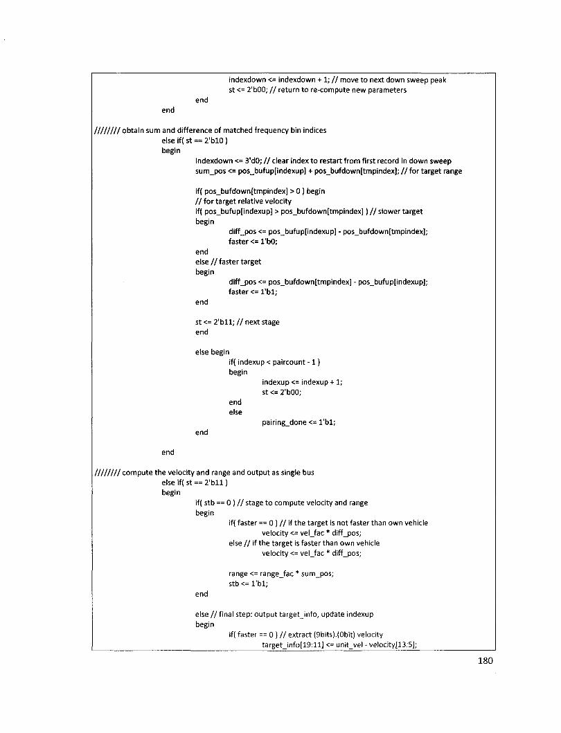
indexdown <= indexdown + 1; / / move to next down sweep peak st <= 2'b00; / / return to re-compute new parameters
end end
IIIllllI obtain sum and difference of matched frequency bin indices else if( st == 2'blO) begin
indexdown <= 3'dO; / / clear index to restart from first record in down sweep sum_pos <= pos_bufup[indexup] + pos_bufdown[tmpindex]; / / for target range
if( pos_bufdown[tmpindex] > 0 ) begin / / for target relative velocity if( pos_bufup(indexup] > pos_bufdown[tmpindex])//slower target begin
diff_pos <= pos_bufup[indexup] - pos_bufdown[tmpindex]; faster <= 1'bO;
end else//faster target begin
diff_pos <= pos_bufdown[tmpindex] - pos_bufup[indexup]; faster <= l ' b l ;
end
st <= 2 ' b l l ; / / next stage end
else begin if( indexup < paircount - 1 ) begin
indexup <= indexup + 1; st <= 2'bOO;
end else
pairing_done <= l ' b l ; end
end
IIIIIIII compute the velocity and range and output as single bus else if( st == 2 ' b l l ) begin
if( stb ==0)1/ stage to compute velocity and range begin
if( faster == 0 ) / / if the target is not faster than own vehicle velocity <= vel_fac * diff_pos;
else / / if the target is faster than own vehicle velocity <= vel_fac * diff_pos;
range <= range_fac * sum_pos; stb <= l ' b l ;
end
else / / final step: output targetjnfo, update indexup begin
if( faster ==0)1/ extract (9bits).(0bit) velocity target info[19:l l ] <= unit_vel - velocity[13:5];
else
target_info[19:ll] <= unit_vel + velocity[13:5];
target_info[10] <= velocity[4]; / / attach the fraction bit
target_info[9:0] <= range[18:9]; / / extract (8bits).(2bits) range info_valid <= l 'b l ; / / alert display unit of valid target information tmpindex <= 3'dO; posa <= 10'dO; posb <= 10'dO; absa <= 13'dO; absb <= 13'dO; stb <= 1'bO; st <= 2'b00; / / reset to first state indexup <= indexup + 1; / / move to next record in up sweep buffer if( indexup == paircount) / / if all records have been assessed
pairing done <= l 'b l ;
VITAAUCTORIS
Sundeep Lai was born in 1984 in New Delhi, India. He completed his first degree in
engineering titled M. Eng. (Hons.) in Electronic and Computer Engineering from the
University of Nottingham (UK) in 2007, during which he underwent industrial training at
Philips Semiconductors SDN. BHD. (Petaling Jaya, Malaysia). His research interests
include Processor Architecture, Digital Signal Processing on FPGAs, Neurofuzzy Control
and Optimization Algorithms, and Microelectromechanical Systems (MEMS). At the time
of writing this thesis Sundeep is a member of the MEMS Lab, and a candidate for the
degree of M. A. Sc. in Electrical and Computer Engineering, at the University of Windsor
(Ontario, Canada).
Related Documents