An Experimental Study of Metastability-Induced Glitching Behavior ¤ Thomas Polzer Department Electronic Engineering UAS Technikum Wien, H€ ochst € adtplatz 6, A-1200, Vienna, Austria [email protected] Florian Huemer † and Andreas Steininger ‡ Institute of Computer Engineering, TU Wien, Karlsplatz 13, A-1040 Vienna, Austria † [email protected] ‡ [email protected] Received 15 October 2018 Accepted 27 March 2019 Published 9 May 2019 The increasing number of clock domain crossings in modern systems-on-chip makes the careful consideration of metastability paramount. However, the manifestation of metastability at a °ip- °op output is often unduly reduced to late transitions only, while glitches are hardly ever accounted for. In this paper we study the occurrence of glitches resulting from metastability in detail. To this end we propose a measurement circuit whose principle substantially di®ers from the conventional approach, and by that allows to reliably detect glitches. By means of exper- imental measurements on an FPGA target we can clearly identify late transitions, single glit- ches and double glitches as possible manifestations of metastability. Some of these behaviors are unexpected as they do not follow from the traditional modeling theory. We also study the dependence of metastable behavior on supply voltage. Beyond con¯rming that, as reported in previous literature, the metastable decay constant ( is voltage-dependent, we also produce strong evidence that the relative occurrence of glitches is not voltage-dependent. Keywords: Metastability; time-to-digital converter; TDC; late transition detection; carry chain. *This paper was recommended by Regional Editor Zoran Stamenkovic. ‡ Corresponding author. This is an Open Access article published by World Scienti¯c Publishing Company. It is distributed under the terms of the Creative Commons Attribution 4.0 (CC-BY) License. Further distribution of this work is permitted, provided the original work is properly cited. Journal of Circuits, Systems, and Computers Vol. 28, Suppl. 1 (2019) 1940006 (21 pages) # . c The Author(s) DOI: 10.1142/S0218126619400061 1940006-1 J CIRCUIT SYST COMP Downloaded from www.worldscientific.com by VIENNA UNIVERSITY OF TECHNOLOGY on 07/02/19. Re-use and distribution is strictly not permitted, except for Open Access articles.

Welcome message from author
This document is posted to help you gain knowledge. Please leave a comment to let me know what you think about it! Share it to your friends and learn new things together.
Transcript

An Experimental Study of Metastability-Induced
Glitching Behavior¤
Thomas Polzer
Department Electronic Engineering
UAS Technikum Wien, H€ochst€adtplatz 6, A-1200, Vienna, [email protected]
Florian Huemer† and Andreas Steininger‡
Institute of Computer Engineering, TU Wien,
Karlsplatz 13, A-1040 Vienna, Austria†[email protected]‡[email protected]
Received 15 October 2018Accepted 27 March 2019
Published 9 May 2019
The increasing number of clock domain crossings in modern systems-on-chip makes the carefulconsideration of metastability paramount. However, the manifestation of metastability at a °ip-
°op output is often unduly reduced to late transitions only, while glitches are hardly ever
accounted for. In this paper we study the occurrence of glitches resulting from metastability in
detail. To this end we propose a measurement circuit whose principle substantially di®ers fromthe conventional approach, and by that allows to reliably detect glitches. By means of exper-
imental measurements on an FPGA target we can clearly identify late transitions, single glit-
ches and double glitches as possible manifestations of metastability. Some of these behaviors are
unexpected as they do not follow from the traditional modeling theory. We also study thedependence of metastable behavior on supply voltage. Beyond con¯rming that, as reported in
previous literature, the metastable decay constant � is voltage-dependent, we also produce
strong evidence that the relative occurrence of glitches is not voltage-dependent.
Keywords: Metastability; time-to-digital converter; TDC; late transition detection; carry chain.
*This paper was recommended by Regional Editor Zoran Stamenkovic.‡Corresponding author.
This is an Open Access article published by World Scienti¯c Publishing Company. It is distributed under
the terms of the Creative Commons Attribution 4.0 (CC-BY) License. Further distribution of this work ispermitted, provided the original work is properly cited.
Journal of Circuits, Systems, and ComputersVol. 28, Suppl. 1 (2019) 1940006 (21 pages)
#.c The Author(s)
DOI: 10.1142/S0218126619400061
1940006-1
J C
IRC
UIT
SY
ST C
OM
P D
ownl
oade
d fr
om w
ww
.wor
ldsc
ient
ific
.com
by V
IEN
NA
UN
IVE
RSI
TY
OF
TE
CH
NO
LO
GY
on
07/0
2/19
. Re-
use
and
dist
ribu
tion
is s
tric
tly n
ot p
erm
itted
, exc
ept f
or O
pen
Acc
ess
artic
les.
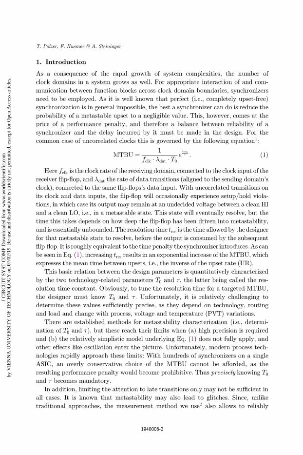
1. Introduction
As a consequence of the rapid growth of system complexities, the number of
clock domains in a system grows as well. For appropriate interaction of and com-
munication between function blocks across clock domain boundaries, synchronizers
need to be employed. As it is well known that perfect (i.e., completely upset-free)
synchronization is in general impossible, the best a synchronizer can do is reduce the
probability of a metastable upset to a negligible value. This, however, comes at the
price of a performance penalty, and therefore a balance between reliability of a
synchronizer and the delay incurred by it must be made in the design. For the
common case of uncorrelated clocks this is governed by the following equation1:
MTBU ¼ 1
fclk � �dat � T0
etres� : ð1Þ
Here fclk is the clock rate of the receiving domain, connected to the clock input of the
receiver °ip-°op, and �dat the rate of data transitions (aligned to the sending domain's
clock), connected to the same °ip-°ops's data input. With uncorrelated transitions on
its clock and data inputs, the °ip-°op will occasionally experience setup/hold viola-
tions, in which case its output may remain at an undecided voltage between a clean HI
and a clean LO, i.e., in a metastable state. This state will eventually resolve, but the
time this takes depends on how deep the °ip-°op has been driven into metastability,
and is essentially unbounded. The resolution time tres is the time allowed by the designer
for that metastable state to resolve, before the output is consumed by the subsequent
°ip-°op. It is roughly equivalent to the time penalty the synchronizer introduces. As can
be seen in Eq. (1), increasing tres results in an exponential increase of the MTBU, which
expresses the mean time between upsets, i.e., the inverse of the upset rate (UR).
This basic relation between the design parameters is quantitatively characterized
by the two technology-related parameters T0 and � , the latter being called the res-
olution time constant. Obviously, to tune the resolution time for a targeted MTBU,
the designer must know T0 and � . Unfortunately, it is relatively challenging to
determine these values su±ciently precise, as they depend on technology, routing
and load and change with process, voltage and temperature (PVT) variations.
There are established methods for metastability characterization (i.e., determi-
nation of T0 and �), but these reach their limits when (a) high precision is required
and (b) the relatively simplistic model underlying Eq. (1) does not fully apply, and
other e®ects like oscillation enter the picture. Unfortunately, modern process tech-
nologies rapidly approach these limits: With hundreds of synchronizers on a single
ASIC, an overly conservative choice of the MTBU cannot be a®orded, as the
resulting performance penalty would become prohibitive. Thus precisely knowing T0
and � becomes mandatory.
In addition, limiting the attention to late transitions only may not be su±cient in
all cases. It is known that metastability may also lead to glitches. Since, unlike
traditional approaches, the measurement method we use2 also allows to reliably
T. Polzer, F. Huemer & A. Steininger
1940006-2
J C
IRC
UIT
SY
ST C
OM
P D
ownl
oade
d fr
om w
ww
.wor
ldsc
ient
ific
.com
by V
IEN
NA
UN
IVE
RSI
TY
OF
TE
CH
NO
LO
GY
on
07/0
2/19
. Re-
use
and
dist
ribu
tion
is s
tric
tly n
ot p
erm
itted
, exc
ept f
or O
pen
Acc
ess
artic
les.
capture single and double pulses, we will put a focus to the study of glitches in this
paper. We will give an experimental evidence for the occurrence of single pulses in
both directions, as well as double pulses. Furthermore we will study the supply
voltage dependence in metastability resolution, again with a focus on glitches.
The rest of the paper is structured as follows: In Sec. 2 we will brie°y sketch the
problem of metastability characterization and introduce the conventional charac-
terization method, as well as related works and the concept of the measurement
method we employ. Next, in Sec. 3 we will present our measurement setup in detail.
Section 4 will then report on the results we have obtained for glitching behavior and
supply voltage dependence. The paper will be concluded with Sec. 5.
2. Background and Related Works
2.1. Metastability manifestation
In the analog domain a metastable storage element exhibits an \intermediate" output
voltage Vmeta that lingers between the thresholds for the well-de¯ned HI and LO logic
values.a However, this only applies for the output voltage Vloop of the actual storage
primitive (cross-coupled inverter pair, for example), which is always followed by a bu®er
primitive (actually an inverter, but here we use a bu®er to simplify the explanation) for
decoupling, before being provided as a (°ip-°op or latch) cell output Q.
The intermediate voltage Vmeta might, in principle, be conveyed as such by the
bu®er if Vmeta is very close to the bu®er's own threshold Vth. However, in practice this
is quite unlikely, and consequently the bu®er rather produces some type of \digital"
output in reaction to an intermediate input voltage, where the exact behavior
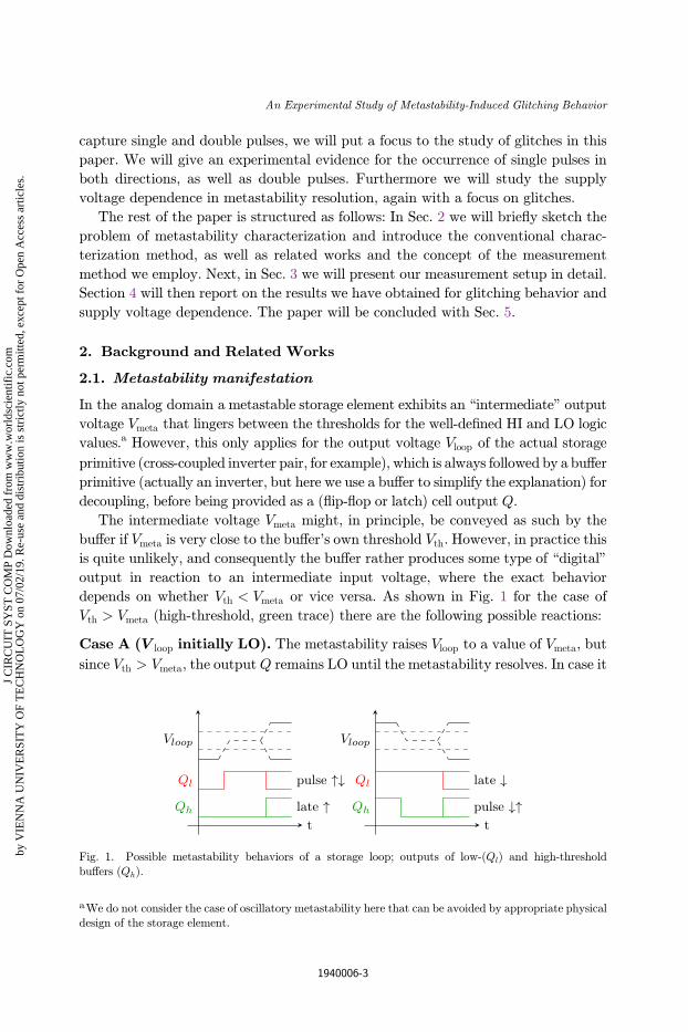
depends on whether Vth < Vmeta or vice versa. As shown in Fig. 1 for the case of
Vth > Vmeta (high-threshold, green trace) there are the following possible reactions:
Case A (V loop initially LO). The metastability raises Vloop to a value of Vmeta, but
since Vth > Vmeta, the outputQ remains LO until the metastability resolves. In case it
aWe do not consider the case of oscillatory metastability here that can be avoided by appropriate physicaldesign of the storage element.
Fig. 1. Possible metastability behaviors of a storage loop; outputs of low-(Ql) and high-threshold
bu®ers (Qh).
An Experimental Study of Metastability-Induced Glitching Behavior
1940006-3
J C
IRC
UIT
SY
ST C
OM
P D
ownl
oade
d fr
om w
ww
.wor
ldsc
ient
ific
.com
by V
IEN
NA
UN
IVE
RSI
TY
OF
TE
CH
NO
LO
GY
on
07/0
2/19
. Re-
use
and
dist
ribu
tion
is s
tric
tly n
ot p
erm
itted
, exc
ept f
or O
pen
Acc
ess
artic
les.
¯nally resolves to LO, we do not see any reaction at Q, the metastability has been
masked. Should it resolve to HI we see a clean transition, which is late, as it occurs
only after the metastability has resolved.
Case B (V loop initially HI). When going down from HI to Vmeta, Vloop crosses Vth
and immediately causes a falling transition at Q. In case the metastability ¯nally
resolves to LO, Vloop continues to fall without any further threshold crossing, so
overall we see a clean transition with nominal delay. However, should the metasta-
bility resolve to HI, we see another transition atQ. This means we have experienced a
negative glitch whose width equals the duration of the metastable state.
In a similar fashion, the possible behaviors of a low-threshold bu®er (Vth < Vmeta)
can be deduced: no transition, regular transition, late transition or positive glitch.
As will be outlined in more detail below, the late transition is the only e®ect
observed by traditional measurement techniques, while the glitches often go unde-
tected, even though they may have a detrimental e®ect on the subsequent logic, like
being processed by some of the gates and at the same time ignored by others, thus
causing inconsistent behavior.
2.2. Basic options for metastability measurement
Probably, the most intuitive way of observing and investigating metastability is by
means of an oscilloscope. Accordingly, the ¯rst systematic observations of metastable
behavior have been documented by oscilloscope screenshots,4,5 and over the years
several approaches involving an oscilloscope for analysis of metastable behavior have
been proposed.6–9 Their key bene¯t is being able to show the individual waveforms in
all detail, including the actual intermediate voltage during the undecided phase
(unless converted by the bu®er, as outlined above). However, the extraction of
metastability parameters is quite intricate, and the collection of a statistically rele-
vant number of measurements (to mitigate jitter and noise e®ects) su®ers from the
di±culty of automating the approach.
Circuit-level simulators, such as SPICE, have been successfully employed to ob-
serve the metastable behavior of an element.10–12 While they allow convenient access
without probing e®ects, they use idealized models that may not appropriately re°ect
the actual circuit parameters, and they tend to su®er from numerical problems and
high sensitivity to even small changes in the chosen parameters and models.13
Consequently, by far the most popular method for assessing metastability char-
acteristics is based on the following observation:
When plotting ln(MTBU) versus tres, Eq. (1) becomes a straight line, whose
gradient and o®set are determined by � and T0, respectively. The same holds true for
the upset rate which is the inverse of the mean time between upsets: UR ¼ 1=MTBU.
This suggests the following approach for experimentally determining the metasta-
bility characteristics: For given ¯xed clock and data rates the upset rate is measured
for di®erent settings of the resolution time. From these points the graph URðtresÞ can
T. Polzer, F. Huemer & A. Steininger
1940006-4
J C
IRC
UIT
SY
ST C
OM
P D
ownl
oade
d fr
om w
ww
.wor
ldsc
ient
ific
.com
by V
IEN
NA
UN
IVE
RSI
TY
OF
TE
CH
NO
LO
GY
on
07/0
2/19
. Re-
use
and
dist
ribu
tion
is s
tric
tly n
ot p
erm
itted
, exc
ept f
or O
pen
Acc
ess
artic
les.
be plotted and the characteristics can be extracted. In fact this is the preferred
principle of the measurement approaches for � and T0 in the literature. Note that
here metastability is measured indirectly by observing the delay in the output
transition it causes, and \upset" is de¯ned as a delay that exceeds the available
resolution time. As a consequence of that, this approach implicitly limits metasta-
bility measurement to the case of late transitions only.
2.3. Implementation of late transition detection
Its practical implementation is performed as follows: The unit under test is provided
with uncorrelated periodic transitions on data and clock, which will occasionally
drive it into metastability. Its output is observed with a given delay � after the clock
edge and checked for late transitions by comparing the observed logic value with a
reference that is obtained after a much larger delay (i.e., in the resolved state). In
case of a mismatch, a metastable upset is assumed and a counter increased. After a
certain measurement interval Tm the count is read and related to Tm, thus obtaining
the MTBU. Then the experiment is repeated for a di®erent setting of � — which
obviously corresponds to the resolution time tres — and again the MTBU determined.
By collecting several such points the desired function MTBUðtresÞ can be obtained,
and � be determined from the slope, while the o®set depends on T0.
Concerning the practical realization of the experiment, providing clock and data
is fairly easy. The only important thing here is to take care that these are uncorre-
lated, such that from time to time metastable upsets actually occur as a consequence
of the uniformly distributed phase di®erence,6 and hence the assumptions made by
Veendrick in the derivation of Eq. (1) hold.
Alternatively, the phase shift between clock and data can be carefully controlled
to produce a maximum number of metastable upsets. Due to the in°uence of jitter,
noise, voltage and parameter variations, etc. this is a very delicate task that requires
special provisions like, e.g., using a delay-locked loop.7,14 The obvious advantage of
this method is to generate a relatively high yield of (even deep) metastable upsets,
which allows their detailed study. The correlation between clock and data transitions
established by the phase control, however, rules out a characterization based on the
application of Eq. (1). So this approach is not useful for our purpose.
Measuring the upset rate is also fairly easy; it just takes a counter and a time
measurement. A more di±cult question is what to actually count, i.e., how to
identify an upset? This is usually done by sampling the output of the °ip-°op under
test once after tres and once much later (when it can be safely assumed that meta-
stability has resolved already), and comparing these samples: A mismatch indicates
that the ¯nal output state (de¯ned by the reference provided through the second
sample) had not been reached after tres, hence the °ip-°op under test (further
abbreviated as UUT for \unit under test") must have been metastable then.
Note that this is actually a conjecture that follows from the assumption that there
is only one transition leading from the initial state to the ¯nal one. Should there,
An Experimental Study of Metastability-Induced Glitching Behavior
1940006-5
J C
IRC
UIT
SY
ST C
OM
P D
ownl
oade
d fr
om w
ww
.wor
ldsc
ient
ific
.com
by V
IEN
NA
UN
IVE
RSI
TY
OF
TE
CH
NO
LO
GY
on
07/0
2/19
. Re-
use
and
dist
ribu
tion
is s
tric
tly n
ot p
erm
itted
, exc
ept f
or O
pen
Acc
ess
artic
les.
however, be multiple transitions, then this conjecture may be invalid. It is precisely
this inability to handle multiple transitions correctly that constitutes a severe de¯-
ciency of the conventional approach.
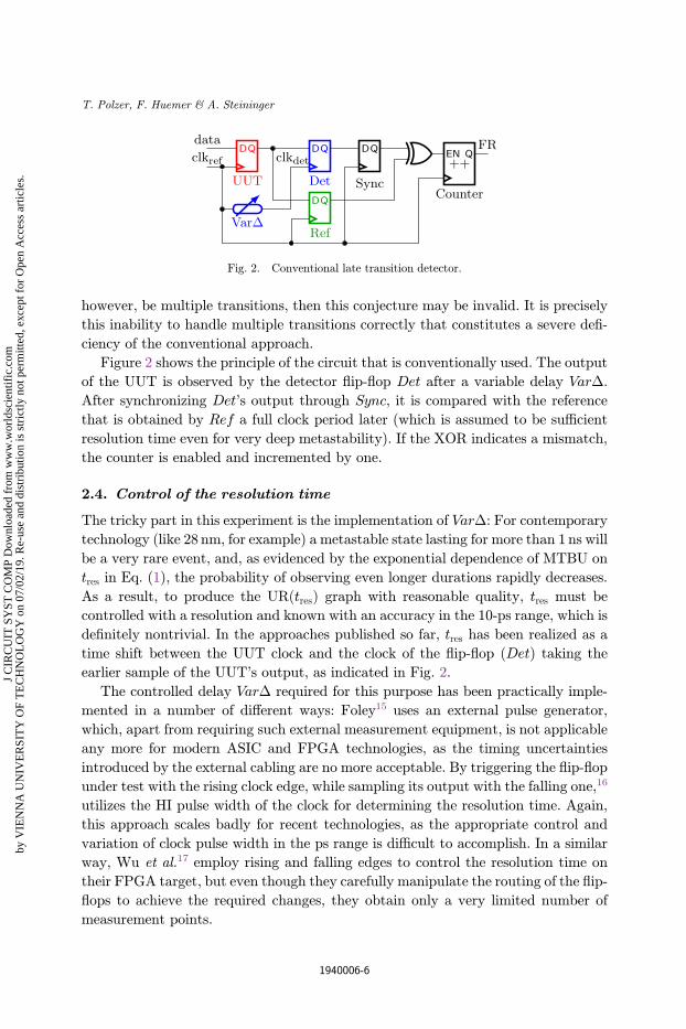
Figure 2 shows the principle of the circuit that is conventionally used. The output
of the UUT is observed by the detector °ip-°op Det after a variable delay Var�.
After synchronizing Det's output through Sync, it is compared with the reference
that is obtained by Ref a full clock period later (which is assumed to be su±cient
resolution time even for very deep metastability). If the XOR indicates a mismatch,
the counter is enabled and incremented by one.
2.4. Control of the resolution time
The tricky part in this experiment is the implementation of Var�: For contemporary
technology (like 28 nm, for example) a metastable state lasting for more than 1 ns will
be a very rare event, and, as evidenced by the exponential dependence of MTBU on
tres in Eq. (1), the probability of observing even longer durations rapidly decreases.
As a result, to produce the URðtresÞ graph with reasonable quality, tres must be
controlled with a resolution and known with an accuracy in the 10-ps range, which is
de¯nitely nontrivial. In the approaches published so far, tres has been realized as a
time shift between the UUT clock and the clock of the °ip-°op (Det) taking the
earlier sample of the UUT's output, as indicated in Fig. 2.
The controlled delay Var� required for this purpose has been practically imple-
mented in a number of di®erent ways: Foley15 uses an external pulse generator,
which, apart from requiring such external measurement equipment, is not applicable
any more for modern ASIC and FPGA technologies, as the timing uncertainties
introduced by the external cabling are no more acceptable. By triggering the °ip-°op
under test with the rising clock edge, while sampling its output with the falling one,16
utilizes the HI pulse width of the clock for determining the resolution time. Again,
this approach scales badly for recent technologies, as the appropriate control and
variation of clock pulse width in the ps range is di±cult to accomplish. In a similar
way, Wu et al.17 employ rising and falling edges to control the resolution time on
their FPGA target, but even though they carefully manipulate the routing of the °ip-
°ops to achieve the required changes, they obtain only a very limited number of
measurement points.
Fig. 2. Conventional late transition detector.
T. Polzer, F. Huemer & A. Steininger
1940006-6
J C
IRC
UIT
SY
ST C
OM
P D
ownl
oade
d fr
om w
ww
.wor
ldsc
ient
ific
.com
by V
IEN
NA
UN
IVE
RSI
TY
OF
TE
CH
NO
LO
GY
on
07/0
2/19
. Re-
use
and
dist
ribu
tion
is s
tric
tly n
ot p
erm
itted
, exc
ept f
or O
pen
Acc
ess
artic
les.

The starved bu®er proposed by Zhou et al.14 allows precise tuning of a single
(uncalibrated) delay, which was very useful in the context of a closed control loop for
driving the °ip-°op into deep metastability, where the exact knowledge of the delay
was not required. On an FPGA platform, however, starved bu®ers are not available.
Moreover we would need to use multiple of these bu®ers, calibrate them and coor-
dinate their control, which is a signi¯cant e®ort.
Kalisz and Jachna18 propose the use of an inverter chain with ¯xed delay, and
they vary the clock frequency to obtain di®erent resolution times. This, however, also
changes fclk in addition to tres in Eq. (1), which makes the extraction of � more
cumbersome. The same is true for other approaches16,19 where rising and falling
edges are utilized to determine the resolution time, but with a ¯xed duty cycle and a
variable clock frequency.
The tapped chain of logic functions,20 the tapped inverter chain,12 and apparently
also the \delay line" mentioned by Beer et al.21 are very close in nature to our
proposed approach. As will be outlined in more detail in the next subsection, we
propose the use of a carry chain instead. Speci¯cally in an FPGA environment the
carry chain is superior due to (a) its better temporal resolution (recall that the carry
logic is speci¯cally optimized for high speed) and (b) its low dependence on the
routing (recall that routing has dominant in°uence on the timing in an FPGA). We
had already introduced the idea of using a tapped carry chain,22 but in context with
the traditional late transition detector.
Another approach that is viable on an FPGA is the use of a digital clock man-
ager.23 or PLL21 In conjunction with careful routing this yields a useful late transi-
tion detector with decent temporal resolution. However, taking an appreciable
number of samples from a signal trace is not possible (typically only four phase-
related clocks can be generated), so this method is not applicable for our envisioned
approach either.
Note that for the determination of � , which is the most relevant metastability
parameter, it is not necessary to know the absolute value of a given tres; for deter-
mining the slope of the graph, just the di®erence between two points, i.e., the step
size needs to be precisely known. Still this is a notorious problem in the experimental
settings, and even with the digital clock manager a considerable di®erential non-
linearity has been reported,22 which ultimately limits the precision of the measure-
ment. In general, calibration of the delay elements (step size) is a fundamental
prerequisite in all solutions, in order to attain decent accuracy in spite of PVT
variations in the delay elements (whichever these may be), as well as in the wiring.
In a somewhat reversed approach,24 another uncorrelated clock is used for sam-
pling the metastable output. Here, rather than controlling the resolution time
in advance, it is measured a posteriori (or, to be more precise, predicted by
an estimator). This maps the problem of precisely controlling a delay to the
(somewhat simpler) one of precisely measuring one, which can be accomplished with
high resolution by means of an \equivalent time" sampling. The latter, however, is
An Experimental Study of Metastability-Induced Glitching Behavior
1940006-7
J C
IRC
UIT
SY
ST C
OM
P D
ownl
oade
d fr
om w
ww
.wor
ldsc
ient
ific
.com
by V
IEN
NA
UN
IVE
RSI
TY
OF
TE
CH
NO
LO
GY
on
07/0
2/19
. Re-
use
and
dist
ribu
tion
is s
tric
tly n
ot p
erm
itted
, exc
ept f
or O
pen
Acc
ess
artic
les.
based on stable and strictly periodic clocks, buys its higher resolution by increasing
the measurement time and entails comprehensive data processing e®orts.
The key idea of the approach we will employ here is based on a fundamentally
di®erent principle that we already presented in our previous work.2
Recall that in the conventional approach a variable delay is applied to the clock of
the °ip-°op (Det) that samples the UUT output. In this way a \borderline resolution
time" is de¯ned, and the actual measurement consists in determining whether
the observed metastability lasted longer or not. Accordingly, the result is a binary
decision per measurement.
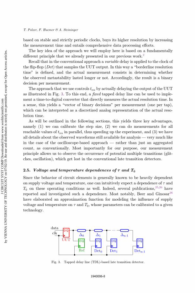
The approach that we use controls tres by actually delaying the output of the UUT
as illustrated in Fig. 3. To this end, a ¯xed tapped delay line can be used to imple-
ment a time-to-digital converter that directly measures the actual resolution time. In
a sense, this yields a \vector of binary decisions" per measurement (one per tap),
which can be interpreted as a discretized analog representation of the actual reso-
lution time.
As will be outlined in the following sections, this yields three key advantages,
namely (1) we can calibrate the step size, (2) we can do measurements for all
reachable values of tres in parallel, thus speeding up the experiment, and (3) we have
all details about the observed waveforms still available for analysis— very much like
in the case of the oscilloscope-based approach — rather than just an aggregated
count, as conventionally. Most importantly for our purpose, our measurement
principle allows us to observe the occurrence of potential multiple transitions (glit-
ches, oscillation), which get lost in the conventional late transition detectors.
2.5. Voltage and temperature dependences of ¿ and T0
Since the behavior of circuit elements is generally known to be heavily dependent
on supply voltage and temperature, one can intuitively expect a dependence of � and
T0 on these operating conditions as well. Indeed, several publications,25,26 have
reported and investigated such a dependence. Most notably, Beer and Ginosar26
have elaborated an approximation function for modeling the in°uence of supply
voltage and temperature on � and T0, whose parameters can be calibrated to a given
technology.
Fig. 3. Tapped delay line (TDL)-based late transition detector.
T. Polzer, F. Huemer & A. Steininger
1940006-8
J C
IRC
UIT
SY
ST C
OM
P D
ownl
oade
d fr
om w
ww
.wor
ldsc
ient
ific
.com
by V
IEN
NA
UN
IVE
RSI
TY
OF
TE
CH
NO
LO
GY
on
07/0
2/19
. Re-
use
and
dist
ribu
tion
is s
tric
tly n
ot p
erm
itted
, exc
ept f
or O
pen
Acc
ess
artic
les.
To the best of our knowledge, however, no systematic analysis has been performed
with respect to metastability-induced glitches. Our measurement approach facil-
itates the reliable observation of glitches, and therefore a contribution of this paper
will be to present a ¯rst measurement-based analysis on how their occurrence is
in°uenced by the operating conditions.
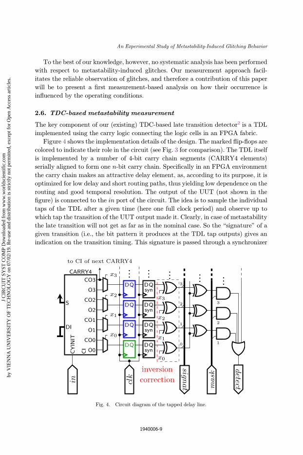
2.6. TDC-based metastability measurement
The key component of our (existing) TDC-based late transition detector2 is a TDL
implemented using the carry logic connecting the logic cells in an FPGA fabric.
Figure 4 shows the implementation details of the design. The marked °ip-°ops are
colored to indicate their role in the circuit (see Fig. 3 for comparison). The TDL itself
is implemented by a number of 4-bit carry chain segments (CARRY4 elements)
serially aligned to form one n-bit carry chain. Speci¯cally in an FPGA environment
the carry chain makes an attractive delay element, as, according to its purpose, it is
optimized for low delay and short routing paths, thus yielding low dependence on the
routing and good temporal resolution. The output of the UUT (not shown in the
¯gure) is connected to the in port of the circuit. The idea is to sample the individual
taps of the TDL after a given time (here one full clock period) and observe up to
which tap the transition of the UUT output made it. Clearly, in case of metastability
the late transition will not get as far as in the nominal case. So the \signature" of a
given transition (i.e., the bit pattern it produces at the TDL tap outputs) gives an
indication on the transition timing. This signature is passed through a synchronizer
Fig. 4. Circuit diagram of the tapped delay line.
An Experimental Study of Metastability-Induced Glitching Behavior
1940006-9
J C
IRC
UIT
SY
ST C
OM
P D
ownl
oade
d fr
om w
ww
.wor
ldsc
ient
ific
.com
by V
IEN
NA
UN
IVE
RSI
TY
OF
TE
CH
NO
LO
GY
on
07/0
2/19
. Re-
use
and
dist
ribu
tion
is s
tric
tly n
ot p
erm
itted
, exc
ept f
or O
pen
Acc
ess
artic
les.
array to remove potential metastable values it might contain (note that at this point
one is only interested in a clean digital signature indicating the delay imposed by
metastability of the UUT, rather than observing a potential metastability in one of
the TDL's output °ip-°ops). The available CARRY4 elements provide two types of
output, namely O and CO, selectable by the con¯guration bit vector x0 . . .xn�1
(in the design's bitstream). In our previous work2 we used an alternating pattern for
the selection of the O and CO outputs to ensure that the taps are more evenly
spaced.27 For the taps where the O output has been selected an additional inversion
is required to correct a previous inversion caused by the internal structure of the
CARRY4 element. This is accomplished in the box termed inversion correction.
Tap 0 of the TDL (the green one at the bottom of the chain) has the lowest delay
(measured from the output of the UUT), thus allowing for the longest resolution
time. So it is used as a reference for the desired ¯nal output, allowing to check for the
occurrence of metastability: If the signature contains any bit that does not match the
reference, it is representing a metastability event (e.g., a late transition) and for-
warded to the analysis (output signat). This is triggered by the signal detect that is
derived from an array of XOR gates (doing the comparison with tap 0) and an array
of AND gates controlled by the signal mask (allowing to reduce the sensitivity of the
detector). Additionally, a counter is used to generate timestamps that allow to
monitor the temporal spacing of detection events.
A key advantage of the TDC-based approach is that it provides way more de-
tailed information about the UUT behavior: Recall that in the conventional ap-
proach the only available information is the number of occurrences for which the
UUT's output delay was larger than the selected resolution time. In contrast to other
approaches, here no choice for the resolution time must be made. For every meta-
stable event, the measurement circuit returns the actual output delay in conjunction
with a timestamp for the event. With this information available on a host PC, one
can, among other things, study the e®ect of di®erent choices for the resolution time,
or investigate the temporal distribution of upsets. This comes at the price of high
demands on the communication interface between measurement platform (FPGA
board) and host PC. To alleviate this issue a number of provisions to reduce the
bandwidth requirements have been proposed,2 which include masking of extremely
frequent events to allow the targeted collection of rare ones, or special encoding of the
transmitted data.
3. Measurement Setup
The existing TDC-based measurement circuit discussed in the previous section has
some shortcomings. Due to di®erent propagation speeds for rising and falling edges,
some (short) pulses can get \¯ltered" by the delay line (i.e., one edge overtakes the
other, annihilating the pulse). In previous results2 this manifested itself in a °at
region in the upset rate plot. To address this issue our improved measurement circuit
T. Polzer, F. Huemer & A. Steininger
1940006-10
J C
IRC
UIT
SY
ST C
OM
P D
ownl
oade
d fr
om w
ww
.wor
ldsc
ient
ific
.com
by V
IEN
NA
UN
IVE
RSI
TY
OF
TE
CH
NO
LO
GY
on
07/0
2/19
. Re-
use
and
dist
ribu
tion
is s
tric
tly n
ot p
erm
itted
, exc
ept f
or O
pen
Acc
ess
artic
les.
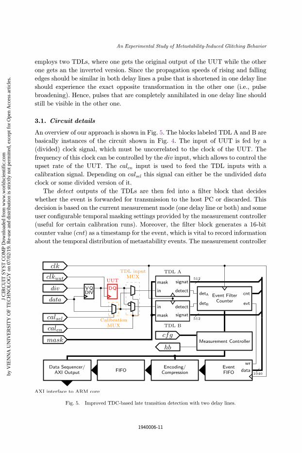
employs two TDLs, where one gets the original output of the UUT while the other
one gets an the inverted version. Since the propagation speeds of rising and falling
edges should be similar in both delay lines a pulse that is shortened in one delay line
should experience the exact opposite transformation in the other one (i.e., pulse
broadening). Hence, pulses that are completely annihilated in one delay line should
still be visible in the other one.
3.1. Circuit details
An overview of our approach is shown in Fig. 5. The blocks labeled TDL A and B are
basically instances of the circuit shown in Fig. 4. The input of UUT is fed by a
(divided) clock signal, which must be uncorrelated to the clock of the UUT. The
frequency of this clock can be controlled by the div input, which allows to control the
upset rate of the UUT. The calen input is used to feed the TDL inputs with a
calibration signal. Depending on calsel this signal can either be the undivided data
clock or some divided version of it.
The detect outputs of the TDLs are then fed into a ¯lter block that decides
whether the event is forwarded for transmission to the host PC or discarded. This
decision is based on the current measurement mode (one delay line or both) and some
user con¯gurable temporal masking settings provided by the measurement controller
(useful for certain calibration runs). Moreover, the ¯lter block generates a 16-bit
counter value (cnt) as a timestamp for the event, which is vital to record information
about the temporal distribution of metastability events. The measurement controller
Fig. 5. Improved TDC-based late transition detection with two delay lines.
An Experimental Study of Metastability-Induced Glitching Behavior
1940006-11
J C
IRC
UIT
SY
ST C
OM
P D
ownl
oade
d fr
om w
ww
.wor
ldsc
ient
ific
.com
by V
IEN
NA
UN
IVE
RSI
TY
OF
TE
CH
NO
LO
GY
on
07/0
2/19
. Re-
use
and
dist
ribu
tion
is s
tric
tly n
ot p
erm
itted
, exc
ept f
or O
pen
Acc
ess
artic
les.

also generates a (con¯gurable) PWM signal routed to an output of the FPGA, that is
only enabled when a measurement is active. This measurement heartbeat signal hb
allows to trigger external auxiliary devices (e.g., a voltmeter) in a way that their
results can be synchronized to the measurement time (acquired through the time-
stamp counter). Similar to previous work2 we also use 512 taps for our delay lines.
Hence, for each detected event 1,040 bits are written to the Event FIFO. In the
following processing steps (lower part of the ¯gure) this data is ¯rst compressed to
256 bits per event using a special run-length encoding and then transferred to the
processor core of the SoC via an AXI streaming interface. Subsequently a Gigabit
Ethernet link is used to transfer the data to a host PC.
A crucial aspect of the implementation of this circuit is the placement of the delay
lines relative to the UUT and the multiplexers at their inputs, which makes manual
placement of these components essential. To reduce the delay between UUT and
TDL inputs, the UUT and the TDL input multiplexers are placed in close proximity
to the inputs of the delay lines. Both TDL input multiplexers can be placed into the
same LUT to exactly control the point where the input signal is forked (in this FPGA
technology an LUT can have up to two outputs). Still, di®erent synthesis runs may
yield slightly di®erent routing paths and hence delays. These uncertainties must be
taken into account during measurement and calibration.
Notice that the UUT has a dedicated clock input (clkUUT ). To be able to trigger a
su±ciently large number of upsets in the slave latch of the UUT in a reasonable
amount of time, it must be possible to reduce the high time of its clock signal. For our
measurements we use a PLL to generate a clock with 8:3% duty cycle out of the 125-
MHz clk input. For the data input, we use a (uncorrelated) 200-MHz signal, which is
divided for the actual measurements.
3.2. Calibration
The calibration of the TDLs used in the the measurement circuit is essential because
the delays of the individual taps are usually subject to signi¯cant variations.20 The
main sources for this are routing asymmetries (inside and between CARRY4 ele-
ments), process variations as well as the temperature and voltage dependences of
gate and routing delays. As already mentioned above, in addition rising and falling
edges have di®erent propagation speeds along the delay line. We even observed
nonmonotonic behavior, i.e., considering two taps in the TDL it is possible that an
edge appears earlier at a tap that is actually further down the delay line relative to
the other one.2
In principle, the static e®ects can be eliminated by a calibration run, while the
dynamic ones are more di±cult to handle. Similar to previous work,2 a calibration
run is performed before and after each actual measurement run. These have shown
relatively small discrepancies, which gives evidence that the dynamic variations are
not too signi¯cant.
T. Polzer, F. Huemer & A. Steininger
1940006-12
J C
IRC
UIT
SY
ST C
OM
P D
ownl
oade
d fr
om w
ww
.wor
ldsc
ient
ific
.com
by V
IEN
NA
UN
IVE
RSI
TY
OF
TE
CH
NO
LO
GY
on
07/0
2/19
. Re-
use
and
dist
ribu
tion
is s
tric
tly n
ot p
erm
itted
, exc
ept f
or O
pen
Acc
ess
artic
les.
The calibration is a two step process that is performed separately for each delay
line. In a ¯rst phase, the TDL is fed by a divided version of the data clock (using the
calibration multiplexer in Fig. 5), and the signatures produced of the TDL are
recorded. This allows to establish a global relative tap order, wherein some taps may
be grouped into a single logical tap, if they showed inconsistent behavior in the
recorded calibration data. The relative bin size is then determined from the number
of times each tap was hit during the calibration run.
The absolute bin size is calibrated using a higher-frequency calibration signal
that always yields two transitions (in the same direction) in each TDL signature.
Clearly, the sum of bin sizes enclosed between these two transitions must equal the
known period of this calibration signal, which allows to map the relative bin sizes to
absolute time. For further details, we refer to an in-depth explanation of this
process.2
3.3. Used hardware and supply voltage regulation
Like some of the previous works2,28,29 we are using the Xilinx Zynq-7000 SoC on a
ZedBoard development kitb as target device for our measurements. The nominal
internal core voltage VCCINT for the programmable logic (i.e., the FPGA fabric)
of this chip is 1V with �0:5V and 1.1V absolute maximum ratings.30 The ZedBoard
uses a MAX15021 step-down DC–DC voltage regulator31 to generate this voltage.
The actual output voltage level of this device is essentially con¯gured through
a voltage divider comprising two resistors. Since, for our experiments, we want
to be able to change VCCINT, we replaced one of the resistors with a trimmer
potentiometer.
In order to monitor the the supply voltage over the course of a measurement we
use a 34410A Digital Multimeter, which is triggered by the hb signal generated by the
FPGA.
4. Results
4.1. Validating the measurement setup
In several aspects our measurement setup approaches the limits of what is feasible
with the given technology. Therefore, in a ¯rst step, we need to verify that it pro-
duces sound results. We do that by performing measurements whose results are
already known from the literature. Speci¯cally, we performed a measurement with
nominal supply voltage (Vdd ¼ 1V) and calculated the upset rate for all cases. The
results are depicted in Fig. 6(b). These results match the values from Refs. 2 and 29,
which gives good evidence that our setup works as expected.
bhttp://zedboard.org/product/zedboard.
An Experimental Study of Metastability-Induced Glitching Behavior
1940006-13
J C
IRC
UIT
SY
ST C
OM
P D
ownl
oade
d fr
om w
ww
.wor
ldsc
ient
ific
.com
by V
IEN
NA
UN
IVE
RSI
TY
OF
TE
CH
NO
LO
GY
on
07/0
2/19
. Re-
use
and
dist
ribu
tion
is s
tric
tly n
ot p
erm
itted
, exc
ept f
or O
pen
Acc
ess
artic
les.

4.2. Speci¯c analysis of pulses
Figure 6(b) shows the upset rates separated by the type of metastable behavior. As
can be seen, the master latch is generating late transitions of both directions (01 for
rising and 10 for falling). Upon handing over data to the slave latch (falling edge of
the clock signal), however, pulses are observed (010 for positive and 101 for negative
pulses). When giving the slave latches additional resolution time, the 010 pulses
subside and are replaced by double pulses (0101). The cause of this e®ect is not fully
analyzed yet, but our preliminary hypothesis is that the handover between master
and slave latches creates a transient voltage shift within the slave latch, resulting in
an additional pulse at the output of the °ip-°op.
Note that with the traditional LTD-based measurement approach, all metastable
occurrences would be interpreted as late transitions, yielding the plot shown in
Fig. 7. While the di®erent resolution constants of master and slave latches are al-
ready visible in the ¯gure, the occurrence of pulses cannot be observed. Introducing a
case separation on top of the LTD measurement 23 can make single pulses visible, but
Fig. 7. Upset rate (sum).
(a) Vdd ¼ 0:98V. (b) Vdd ¼ 1:00V. (c) Vdd ¼ 1:02V.
Fig. 6. Upset rate overview.
T. Polzer, F. Huemer & A. Steininger
1940006-14
J C
IRC
UIT
SY
ST C
OM
P D
ownl
oade
d fr
om w
ww
.wor
ldsc
ient
ific
.com
by V
IEN
NA
UN
IVE
RSI
TY
OF
TE
CH
NO
LO
GY
on
07/0
2/19
. Re-
use
and
dist
ribu
tion
is s
tric
tly n
ot p
erm
itted
, exc
ept f
or O
pen
Acc
ess
artic
les.

the identi¯cation of double pulses ¯nally becomes possible only with our novel
measurement approach.
As a further measure to enhance the analysis of pulse behavior, we have chosen a
very asymmetric duty cycle for the clock (8.3%). As known from the literature,3 this
moves the handover from master to slave towards an earlier point in time, leaving the
master with less resolution time and thus pronouncing the metastable behavior of the
slave. By this it was possible to obtain a reasonable number of pulses within our
measurement duration of 110 h.
To motivate the speci¯c focus we give to the slave latch behavior, we want to
stress here that solely using the master's resolution constant � (which is much easier
to obtain by measurement) for the MTBU calculation can, lead to an optimistic view
of the °ip-°op's resolution capability, as this ignores the fact that during the low
phase of the clock the slave's � becomes relevant which is much worse. As already
mentioned in Sec. 1, in addition to this optimistic � selection, the occurrence of pulses
may introduce adverse e®ects into the circuit that are overlooked when considering
late transitions only.
4.3. Voltage dependence of the delay lines
To gather further insight into the pulse generation behavior of the °ip-°op, we
studied the supply voltage (Vdd) dependence. To this end, we varied Vdd between
0.98V and 1.02V in 10mV steps. The measurement duration was kept constant at
110 h. During the whole experiment the actual operating voltage at the FPGA's
supply pin was monitored with an external multimeter. The box plots in Fig. 8
visualize the distribution of deviation from the respective supply voltage set point
during the measurement. The plot whiskers extend to the most extreme data point
Fig. 8. Distribution of Vdd variation.
An Experimental Study of Metastability-Induced Glitching Behavior
1940006-15
J C
IRC
UIT
SY
ST C
OM
P D
ownl
oade
d fr
om w
ww
.wor
ldsc
ient
ific
.com
by V
IEN
NA
UN
IVE
RSI
TY
OF
TE
CH
NO
LO
GY
on
07/0
2/19
. Re-
use
and
dist
ribu
tion
is s
tric
tly n
ot p
erm
itted
, exc
ept f
or O
pen
Acc
ess
artic
les.

that still lies in the range of three times the interquartile range. The voltage °uc-
tuations thus observed remained around 100�V, which is signi¯cantly smaller than
the 10mV stepping between measurement runs.
As supply voltage changes are known to cause changes in the delay of logic
elements, the delay line had to be calibrated for each supply voltage value separately.
Figure 10 illustrates how the observed length of the whole delay line (for both, delay
lines A and B, as well as for rising and falling transitions) depends on the supply
voltage. These results con¯rm the expected speedup of the delay line for rising Vdd.
Interestingly, the delay di®erences between rising and falling edges of the same delay
line are much more signi¯cant than those between the delay lines A and B for
matching transitions.
4.4. Supply voltage dependence of ¿
The impact of the supply voltage changes on the metastability behavior is shown in
Fig. 6. When using the relevant slopes for determining the metastability resolution
constants for master and slave latch, we arrive at Fig. 9. We observe that � decreases
signi¯cantly with increasing supply voltage. This is not unexpected, as higher voltage
(a) Master. (b) Slave.
Fig. 9. Metastability resolution constant � .
Fig. 10. Delayline length.
T. Polzer, F. Huemer & A. Steininger
1940006-16
J C
IRC
UIT
SY
ST C
OM
P D
ownl
oade
d fr
om w
ww
.wor
ldsc
ient
ific
.com
by V
IEN
NA
UN
IVE
RSI
TY
OF
TE
CH
NO
LO
GY
on
07/0
2/19
. Re-
use
and
dist
ribu
tion
is s
tric
tly n
ot p
erm
itted
, exc
ept f
or O
pen
Acc
ess
artic
les.

(a) 01. (b) 10.
(c) 010. (d) 101.
(e) 0101. (f) all.
Fig. 11. Upset rate comparison for di®erent values of Vdd.
An Experimental Study of Metastability-Induced Glitching Behavior
1940006-17
J C
IRC
UIT
SY
ST C
OM
P D
ownl
oade
d fr
om w
ww
.wor
ldsc
ient
ific
.com
by V
IEN
NA
UN
IVE
RSI
TY
OF
TE
CH
NO
LO
GY
on
07/0
2/19
. Re-
use
and
dist
ribu
tion
is s
tric
tly n
ot p
erm
itted
, exc
ept f
or O
pen
Acc
ess
artic
les.
usually implies better dynamic behavior, and these results are in line with reports
from related works.
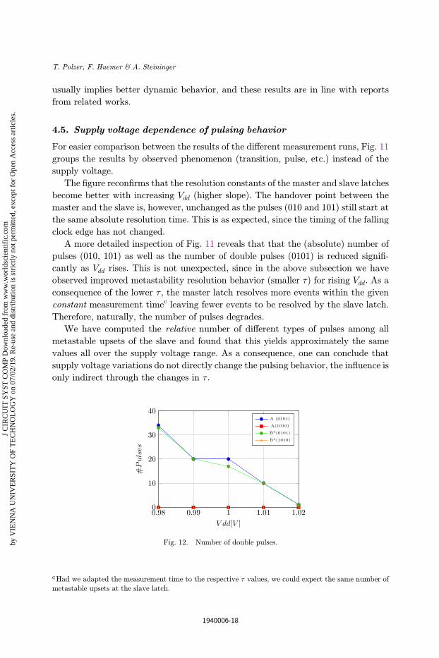
4.5. Supply voltage dependence of pulsing behavior
For easier comparison between the results of the di®erent measurement runs, Fig. 11
groups the results by observed phenomenon (transition, pulse, etc.) instead of the
supply voltage.
The ¯gure recon¯rms that the resolution constants of the master and slave latches
become better with increasing Vdd (higher slope). The handover point between the
master and the slave is, however, unchanged as the pulses (010 and 101) still start at
the same absolute resolution time. This is as expected, since the timing of the falling
clock edge has not changed.
A more detailed inspection of Fig. 11 reveals that that the (absolute) number of
pulses (010, 101) as well as the number of double pulses (0101) is reduced signi¯-
cantly as Vdd rises. This is not unexpected, since in the above subsection we have
observed improved metastability resolution behavior (smaller �) for rising Vdd. As a
consequence of the lower � , the master latch resolves more events within the given
constant measurement timec leaving fewer events to be resolved by the slave latch.
Therefore, naturally, the number of pulses degrades.
We have computed the relative number of di®erent types of pulses among all
metastable upsets of the slave and found that this yields approximately the same
values all over the supply voltage range. As a consequence, one can conclude that
supply voltage variations do not directly change the pulsing behavior, the in°uence is
only indirect through the changes in � .
cHad we adapted the measurement time to the respective � values, we could expect the same number ofmetastable upsets at the slave latch.
Fig. 12. Number of double pulses.
T. Polzer, F. Huemer & A. Steininger
1940006-18
J C
IRC
UIT
SY
ST C
OM
P D
ownl
oade
d fr
om w
ww
.wor
ldsc
ient
ific
.com
by V
IEN
NA
UN
IVE
RSI
TY
OF
TE
CH
NO
LO
GY
on
07/0
2/19
. Re-
use
and
dist
ribu
tion
is s
tric
tly n
ot p
erm
itted
, exc
ept f
or O
pen
Acc
ess
artic
les.

To further highlight this e®ect of the supply voltage on the double pulse count,
Fig. 12 shows the number of observed double pulses for both delay lines.d
5. Conclusion
The key aim of this paper was to investigate the pulsing behavior of a °ip-°op that
may be caused by metastability. While late transitions are the more dominant e®ect,
pulses may be more dangerous to the subsequent logic stages, as they may cause
inconsistent behavior, therefore it is important to understand their generation and
the involved dependences.
Since pulsing behavior is much more di±cult to assess by measurement than late
transitions, we had to employ a measurement setup that is substantially improved
over the traditional approach. It is based on using two carefully interleaved time-to-
digital converters in parallel, in conjunction with several calibration steps. This setup
has allowed us to successfully record pulses and establish several ¯ndings:
First of all, we have given clear evidence for the occurrence of pulses in context
with metastability. While the occurrence of single pulses in one direction directly
follows from a simplistic model of the interaction between metastable storage loop
and subsequent decoupling element, pulses in the other direction, as well as double
pulses, were unexpected observations. As a consequence of our analysis we can
summarize the types of metastable behavior as follows: late transitions in both
directions, pulses in both directions and double pulses in one direction (i.e., all with
the same starting edge). We did not observe any pulses of higher multiplicity
throughout our very comprehensive experiments, so we may conclude that the ob-
served pulses are not due to ringing or oscillation.
Furthermore, we have analyzed the dependence of metastable behavior on the
supply voltage. Through that, we could recon¯rm the dependence of � on Vdd that
has been reported in the literature already. When applying our quantitative results
to the observations made in Ref. 28, where three di®erent FPGA boards of the same
type were investigated with very di®erent results concerning their metastable be-
havior, one can conclude that the variations in the � values observed there cannot be
due to supply variations alone. Consequently, there must be a nonnegligible process
variation as well.
Our detailed study of pulsing behavior has yielded a relatively constant propor-
tion of all pulse types all over the supply voltage range. This suggests that pulse
behavior is not directly voltage-dependent, and the only relevant voltage dependence
is in � . As a consequence, the di®erent types of pulse behavior reported in previous
work28 are not likely to be a consequence of supply voltage mismatches among the
di®erent boards. They rather seem to be rooted in process variations through which
the relation between metastable voltage of the latch and threshold voltage of the
dPlease note that the results for delay line B where inverted to compensate for its inverting implemen-tation and are therefore denoted as B�.
An Experimental Study of Metastability-Induced Glitching Behavior
1940006-19
J C
IRC
UIT
SY
ST C
OM
P D
ownl
oade
d fr
om w
ww
.wor
ldsc
ient
ific
.com
by V
IEN
NA
UN
IVE
RSI
TY
OF
TE
CH
NO
LO
GY
on
07/0
2/19
. Re-
use
and
dist
ribu
tion
is s
tric
tly n
ot p
erm
itted
, exc
ept f
or O
pen
Acc
ess
artic
les.

subsequent bu®er di®ers on the individual FPGAs. This hypothesis, however,
requires further con¯rmation.
More generally, further research is required to ¯nd a conclusive explanation for
the occurrence of double pulses and of single pulses in both directions. Here, an
extensive experimental study must be accompanied by appropriate circuit modeling
that embraces both latches that constitute a °ip-°op, rather than just one.
Acknowledgments
This research was partially supported by the Austrian Science Fund (FWF) Project
SIC (Grant P26436-N30).
References
1. H. J. Veendrick, The behaviour of °ip-°ops used as synchronizers and prediction of theirfailure rate, IEEE J. Solid-State Circuits 15 (1980) 169–176.
2. T. Polzer, F. Huemer and A. Steininger, Re¯ned metastability characterization using atime-to-digital converter, Microelectron. Reliab. 80 (2018) 91–99.
3. D. J. Kinniment, Synchronization and Arbitration in Digital Systems (Wiley, 2007).4. D. Kinniment and D. Edwards, Circuit technology in a large computer system, Proc.
Conf. Computers-Systems and Technology (Institution of Electronic and RadioEngineers, 1972), pp. 441–450.
5. T. J. Chaney and C. E. Molnar, Anomalous behavior of synchronizer and arbiter circuits,IEEE Trans, Comput. C-22 (1973) 421–422.
6. Y. Semiat and R. Ginosar, Timing measurements of synchronization circuits, Proc. IEEENinth Int. Symp. Asynchronous Circuits and Systems (IEEE, 2003), pp. 68–77.
7. D. J. Kinniment, K. Heron and G. Russell, Measuring deep metastability, Proc. IEEE Int.Symp. Asynchronous Circuits and Systems (IEEE, 2006), pp. 2–11.
8. M. Bhushan, M. B. Ketchen and K. K. Das, CMOS latch metastability characterizationat the 65-nm-technology node, Proc. IEEE Int. Conf. Microelectronic Test Structures(IEEE, 2008), pp. 147–151.
9. B. M. Rogina, P. Skoda, K. Skala, I. Michieli, M. Vlah and S. Marijan, Metastabilitytesting at FPGA circuit design using propagation time characterization, Proc. 2010 East-West Design and Test Symp. (IEEE, 2010), pp. 80–85.
10. T. Kacprzak and A. Albicki, Analysis of metastable operation in RS CMOS °ip-°ops,IEEE J. Solid-State Circuits 22 (1987) 57–64.
11. I. W. Jones, S. Yang and M. R. Greenstreet, Synchronizer behavior and analysis, Proc.2009 15th IEEE Int. Symp. Asynchronous Circuits and Systems (IEEE, 2009), pp. 117–126.
12. S. Beer and R. Ginosar, A new 65nm LP metastability measurement test circuit, Proc.2012 IEEE 27th Convention of Electrical and Electronics Engineers in Israel (IEEE,2012), pp. 1–4.
13. S. Yang and M. R. Greenstreet, Simulating improbable events, Proc. 2007 44th ACM/IEEE Design Automation Conf. (IEEE, 2007), pp. 154–157.
14. J. Zhou, D. J. Kinniment, C. E. Dike, G. Russell and A. V. Yakovlev, On-chip mea-surement of deep metastability in synchronizers, IEEE J. Solid-State Circuits 43 (2008)550–557.
T. Polzer, F. Huemer & A. Steininger
1940006-20
J C
IRC
UIT
SY
ST C
OM
P D
ownl
oade
d fr
om w
ww
.wor
ldsc
ient
ific
.com
by V
IEN
NA
UN
IVE
RSI
TY
OF
TE
CH
NO
LO
GY
on
07/0
2/19
. Re-
use
and
dist
ribu
tion
is s
tric
tly n
ot p
erm
itted
, exc
ept f
or O
pen
Acc
ess
artic
les.
15. C. Foley, Characterizing metastability, Proc. Second Int. Symp. Advanced Research inAsynchronous Circuits and Systems (IEEE, 1996), pp. 175–184.
16. P. Alfke, Metastable recovery in Virtex-II Pro FPGAs (2005), Application Note:Virtex-II Pro Family XAPP094, https://www.xilinx.com/support/documentation/application notes/xapp094.pdf.
17. J. Wu, Y. Ma, J. Zhang, Y. Kong, H. Song and X. Han, Research on metastability basedon FPGA, Proc. 2009 9th Int. Conf. Electronic Measurement & Instruments (IEEE,2009), p. 4.
18. J. Kalisz and Z. Jachna, Dual-edge late-transition detector for testing the metastabilitye®ect in °ip-°ops, Proc. 16th Int. Conf. Microelectronics (IEEE, 2004), pp. 780–782.
19. D. Chen, D. Singh, J. Chromczak, D. Lewis, R. Fung, D. Neto and V. Betz, A compre-hensive approach to modeling, characterizing and optimizing for metastability in FPGAs,Proc. 18th Annu. ACM/SIGDA Int. Symp. Field Programmable Gate Arrays (ACM,2010), pp. 167–176.
20. F. Rosenberger and T. J. Chaney, Flip-°op resolving time test circuit, IEEE J. Solid-StateCircuits 17 (1982) 731–738.
21. S. Beer, R. Ginosar, M. Priel, R. Dobkin and A. Kolodny, The devolution of synchroni-zers, Proc. 2010 26th Convention of Electrical and Electronics Engineers in Israel (IEEE,2010), pp. 94–103.
22. T. Polzer, F. Huemer and A. Steininger, A programmable delay line for metastabilitycharacterization in FPGAs, Proc. 2016 Austrochip Workshop on Microelectronics(IEEE, 2016), pp. 51–56.
23. T. Polzer and A. Steininger, An approach for e±cient metastability characterization ofFPGAs through the designer, Proc. 2013 IEEE 19th Int. Symp. Asynchronous Circuitsand Systems (IEEE, 2013), pp. 174–182.
24. R. Najvirt, T. Polzer and A. Steininger, Measuring metastability with free-running clocks,Proc. 2017 23rd IEEE Int. Symp. Asynchronous Circuits and Systems (IEEE, 2017),pp. 18–24.
25. J. Zhou, D. Kinniment, G. Russell and A. Yakovlev, Adapting synchronizers to the e®ectsof on chip variability, Proc. 2008 14th IEEE Int. Symp. Asynchronous Circuits andSystems (IEEE, 2008), pp. 39–47.
26. S. Beer and R. Ginosar, A model for supply voltage and temperature variation e®ects onsynchronizer performance, IEEE Trans. Very Large Scale Integr. (VLSI) Syst. 23 (2015)2461–2472.
27. J. Y. Won and J. S. Lee, Time-to-digital converter using a tuned-delay line evaluated in28-, 40-, and 45-nm FPGAs, IEEE Trans. Instrum. Meas. 65 (2016) 1678–1689.
28. F. Huemer, T. Polzer and A. Steininger, Using a duplex time-to-digital converter formetastability characterization of an FPGA, Proc. 2018 IEEE 21st Int. Symp. Design andDiagnostics of Electronic Circuits & Systems (IEEE, 2018), pp. 141–146.
29. T. Polzer, F. Huemer and A. Steininger, Measuring metastability using a time-to-digitalconverter, Proc. 2017 IEEE 20th Int. Symp. Design and Diagnostics of ElectronicCircuits Systems (IEEE, 2017), pp. 116–121.
30. Xilinx, Zynq-7000 SoC (Z-7007S, Z-7012S, Z-7014S, Z-7010, Z-7015, and Z-7020): DC andAC switching characteristics (2018), Product Speci¯cation, Version 1.20.1, https://www.xilinx.com/Support/documentation/data sheets/ds187-xc7z010-xc7z020-Data-Sheet.pdf.
31. Maxim Integrated, MAX15021: Dual, 4A/2A, 4MHz, step-down DC-DC regulatorwith tracking/sequencing capability, (2015), Data Sheet, Rev.2, https://datasheets.maximintegrated.com/en/ds/MAX15021.pdf.
An Experimental Study of Metastability-Induced Glitching Behavior
1940006-21
J C
IRC
UIT
SY
ST C
OM
P D
ownl
oade
d fr
om w
ww
.wor
ldsc
ient
ific
.com
by V
IEN
NA
UN
IVE
RSI
TY
OF
TE
CH
NO
LO
GY
on
07/0
2/19
. Re-
use
and
dist
ribu
tion
is s
tric
tly n
ot p
erm
itted
, exc
ept f
or O
pen
Acc
ess
artic
les.
Related Documents