SSRG International Journal of Electronics and Communication Engineering (SSRG-IJECE) – Volume 3 Issue 8 – August 2016 ISSN: 2348 – 8549 www.internationaljournalssrg.org Page 87 An Analysis of Device Characteristics of Strained N-Channel MOSFET Shivam Sharma M. Tech Scholar, Department of Electronics & Communication Engineering, Jaipur National University, Jaipur India Aditya Pundir Associate prof., Department of Electronics & Communication Engineering, Jaipur National University, Jaipur India Rahul Pandey Asst. prof., Department of Electronics & Communication Engineering, Poornima Institute of Engineering & Technology, Jaipur, India Vijendra Kumar Patel Asst. prof., Department of Electronics & Communication Engineering, Poornima college of Engineering, Jaipur, India Nishant Kumar Agrawal B. Tech scholar, Department of Electronics & Communication Engineering, Poornima Institute of Engineering & Technology, Jaipur, India Abstract – Large effects of strain on the electrical resistance of silicon were exposed not long after the recognition of silicon as the material for the growth of solid state electronics. As we are approaching to Nano scale, the CMOS applications, device dimensions are getting their scaling limit and it is affecting the gate leakage current, drain induced barrier lowering (DIBL) etc. to a rise. It also worsening the required characteristics and performance of the devices. To overcome this some significant changes in device structures and materials will be needed for continued transistor miniaturization and equivalent performance improvements. This paper is a comparison of performances of unstrained MOSFET with performances of n-channel planer MOSFET with introduction of strain into it, for different channel lengths and its simulation with ATLAS, a 2D device simulator from Silvaco Inc. Keywords – Nano scale strained-Si/SiGe MOSFET, short channeleffects, simulation, threshold voltage, DIBL, CMOS etc. I. INTRODUCTION Strained-silicon devices have been receiving enormous attention owing to their potential for achieving higher channel mobility and drive current enhancement and compatibility with conventional silicon processing. Strain improves MOSFET drive currents by fundamentally altering the band structure of the channel and can therefore enhance performance even at aggressively scaled channel lengths. Here, the variation in device characteristics of n-channel strained MOSFET is provided, while changing the parameter like channel length and Ge content. The results of the simulation verifies the enhanced drain current after introducing strain and by decreasing channel length. The presence of strain is due to presence of silicon-germanium layer placed just below the channel region of MOSFET. With this underlying layer of silicon germanium in a strained n-channel MOSFET, its comparison is done with unstrained MOSFET, with the I d -V g curves. Along with comparison of curves, comparative analysis of strained planner MOSFET with varying channel length is also done. Effect of strain is analysed by varying the mole fraction of Ge in relaxed Si 1-x Ge x layer from 0.0 to 0.4, with respective change in material property like mobility, energy gap, density of states, changes in I d -V g curve and the shift in threshold voltage from the curve is calculated. II. STRAIN To maintain a lower junction electric field in horizontal path between drain and source in the channel region, and non-overlap of the source and drain depletion in the channel need of high doping develops authoritative. But a serious effect of mobility deprivation due to the impurity scattering arises in picture with higher amount of channel doping. The mobility of the charge carriers is enhanced through a concept known as the strain technology. A. Physics of Strain When a layer of a crystal is grown over another layer, a strain is settled in the upper layer due to the mismatch of the lattice constants of the two layers. This is used to accomplish the high speeds without scaling down the devices. In order to achieve the biaxial strain in the Si channel a Si 1-x Ge x virtual substrate is castoff. Here is germanium is elected because of its compatibility with the Si technology

Welcome message from author
This document is posted to help you gain knowledge. Please leave a comment to let me know what you think about it! Share it to your friends and learn new things together.
Transcript
SSRG International Journal of Electronics and Communication Engineering (SSRG-IJECE) – Volume 3 Issue 8 – August 2016
ISSN: 2348 – 8549 www.internationaljournalssrg.org Page 87
An Analysis of Device Characteristics of
Strained N-Channel MOSFET
Shivam Sharma
M. Tech Scholar, Department of Electronics &
Communication Engineering,
Jaipur National University, Jaipur India
Aditya Pundir
Associate prof., Department of Electronics &
Communication Engineering,
Jaipur National University, Jaipur India
Rahul Pandey
Asst. prof., Department of Electronics &
Communication Engineering,
Poornima Institute of Engineering & Technology,
Jaipur, India
Vijendra Kumar Patel
Asst. prof., Department of Electronics &
Communication Engineering,
Poornima college of Engineering, Jaipur, India
Nishant Kumar Agrawal
B. Tech scholar, Department of Electronics & Communication Engineering,
Poornima Institute of Engineering & Technology, Jaipur, India
Abstract – Large effects of strain on the electrical
resistance of silicon were exposed not long after the
recognition of silicon as the material for the growth of solid
state electronics. As we are approaching to Nano scale, the
CMOS applications, device dimensions are getting their
scaling limit and it is affecting the gate leakage current,
drain induced barrier lowering (DIBL) etc. to a rise. It also
worsening the required characteristics and performance of
the devices. To overcome this some significant changes in
device structures and materials will be needed for continued
transistor miniaturization and equivalent performance
improvements. This paper is a comparison of performances
of unstrained MOSFET with performances of n-channel
planer MOSFET with introduction of strain into it, for
different channel lengths and its simulation with ATLAS, a
2D device simulator from Silvaco Inc.
Keywords – Nano scale strained-Si/SiGe MOSFET,
short channeleffects, simulation, threshold voltage, DIBL,
CMOS etc.
I. INTRODUCTION
Strained-silicon devices have been receiving
enormous attention owing to their potential for
achieving higher channel mobility and drive current
enhancement and compatibility with conventional
silicon processing. Strain improves MOSFET drive
currents by fundamentally altering the band structure
of the channel and can therefore enhance performance
even at aggressively scaled channel lengths. Here, the
variation in device characteristics of n-channel
strained MOSFET is provided, while changing the
parameter like channel length and Ge content. The
results of the simulation verifies the enhanced drain
current after introducing strain and by decreasing
channel length. The presence of strain is due to
presence of silicon-germanium layer placed just below
the channel region of MOSFET. With this underlying
layer of silicon germanium in a strained n-channel
MOSFET, its comparison is done with unstrained
MOSFET, with the Id-Vg curves. Along with
comparison of curves, comparative analysis of
strained planner MOSFET with varying channel
length is also done. Effect of strain is analysed by
varying the mole fraction of Ge in relaxed Si1-xGex
layer from 0.0 to 0.4, with respective change in
material property like mobility, energy gap, density of
states, changes in Id-Vg curve and the shift in threshold
voltage from the curve is calculated.
II. STRAIN
To maintain a lower junction electric field in
horizontal path between drain and source in the
channel region, and non-overlap of the source and
drain depletion in the channel need of high doping
develops authoritative. But a serious effect of mobility
deprivation due to the impurity scattering arises in
picture with higher amount of channel doping. The
mobility of the charge carriers is enhanced through a
concept known as the strain technology.
A. Physics of Strain
When a layer of a crystal is grown over another
layer, a strain is settled in the upper layer due to the
mismatch of the lattice constants of the two layers.
This is used to accomplish the high speeds without
scaling down the devices. In order to achieve the
biaxial strain in the Si channel a Si1-xGex virtual
substrate is castoff. Here is germanium is elected
because of its compatibility with the Si technology
lalitha
Text Box
14
SSRG International Journal of Electronics and Communication Engineering (SSRG-IJECE) – Volume 3 Issue 8 – August 2016
ISSN: 2348 – 8549 www.internationaljournalssrg.org Page 88
and its somewhat larger lattice constant. The lattice
constant of both material is given below:
Silicon = 5.431 Å
Germanium = 5.657 Å
Epitaxial growth of Si on relaxed SiGe substrate
fallouts in strained-Si layers due to the larger lattice
constants of Ge. When a layer of Si1-xGex is placed by
epitaxial growth on top of a bulk Si wafer. The atoms
of Si Ge substrate will firstly line up with the Si wafer
and be under compressive strain and as the depth of
the Si1-xGex layer increases it will begin to relax.
B. Effect of Strain
A silicon thin film developed pseudo-morphically
over a calm Si1−xGexsubstrate understandings biaxial
tension foremost to changes in band structure [9],
[13]. Owed to strain, the electron fellow feeling
(affinity) of silicon rises and the band gap drops. Also,
the effective mass of carriers drops. The effect of
strain on Si band structure can be displayed as [9],
[11], [13]
(1)
Where x is the Ge mole part in Si1−xGexsubstrate,
(ΔEC)s−Si is the rise in electron fellow feeling of
silicon due to strain, (ΔEg)s−Si is the reduction in band
gap of silicon due to strain, VT is the thermal voltage,
NV,Si and NV,s−Si are the density of states (DOS) in the
valence band in normal and strained silicon, singly,
and are the hole DOS effective masses in
normal and strained silicon, respectively. The band
structure parameters for relaxed Si1−xGex substrate can
also be estimated as [9],[11] ,[14]
Where (ΔEg)SiGeis the fall in band gap of
Si1−xGexfrom that of Si, NV,SiGe is the DOS in the
valence band in relaxed Si1−xGex, and SiGe is the
permittivity of Si1−xGex. The flatband voltage of a
MOSFET is thus altered due to strain as [9]
(3)
Where
(4)
(5)
In the beyond dealings, φMis the gate work
function, φSi is the unstrained Si work function, φF,Si
is the Fermi potential in unstrained Si, χSi is the
electron fellow feeling in unstrained Si, Eg,Si is the
band gap in unstrained Si, q is the electronic charge,
NA is the body doping concentration and ni,Si is the
intrinsic carrier concentration in unstrained Si. The
built-in voltage across the source-body and drain-body
junctions in the strained-Si thin film is also
exaggerated by strain as
(6)
Where,
(7)
The built-in voltage across the source-body and
drain-body junctions in the relaxed Si1−xGexsubstrate
can be inscribed as
(8)
Where,
(9)
III. MODEL FOR THE OUTPUT CURRENT-
VOLTAGE CHARACTERISTICS
Current at any point x along the channel is given
by eqn.
(10)
Where W is device width. So,
(11)
lalitha
Text Box
15
SSRG International Journal of Electronics and Communication Engineering (SSRG-IJECE) – Volume 3 Issue 8 – August 2016
ISSN: 2348 – 8549 www.internationaljournalssrg.org Page 89
By using, Analytical expression of drain current
and (11) and , we get:
(12)
For
(13)
Where, is the drain voltage
for the carriers at the drain gets velocity saturation [8].
When VDS is greater than VDS,sat, the velocity
saturation or pinch off point moves toward the source
of MOSFET, by a distance ld.
(14)
Where, , , , and
xdvis the vertical depletion region depth due to gate
bias, is given as,
and,
Where is the minimum surface potential required
for inversion [7].
IV. RESULTS
The device characteristics of strained n-channel
MOSFET can be explained by Watt surface mobility
model, the model is used to model the traverse-field
dependent low field mobility [10],[12]. The device
parameters used in our simulation are given in Table
1.
Parameter Value
Ge mole fraction of SiGe substrate, x 0 – 0.4 (0 – 40%)
Source/Drain doping 2x10²⁰
cm-3
Body Doping, NA 1018
cm-3
Gate Length, L 50 nm
ate Oxide Thickness, tf 2.0 nm – 6.0 nm
Work function of gate material, 4.35 eV (n+ poly Si)
Strained-Silicon film thickness, ts-Si 15 nm
Source/Drain junction depth, rj 50 nm
Substrate bias, Vsub 0 Volts (Gnd)
Drain bias, VDS 0.0 – 1.0 Volts
Gate bias, VGS 0.4 – 1.0 Volts
( Table 1: Device parameters used in the simulation for the output
characteristics of s-Si/SiGe MOSFET [14]
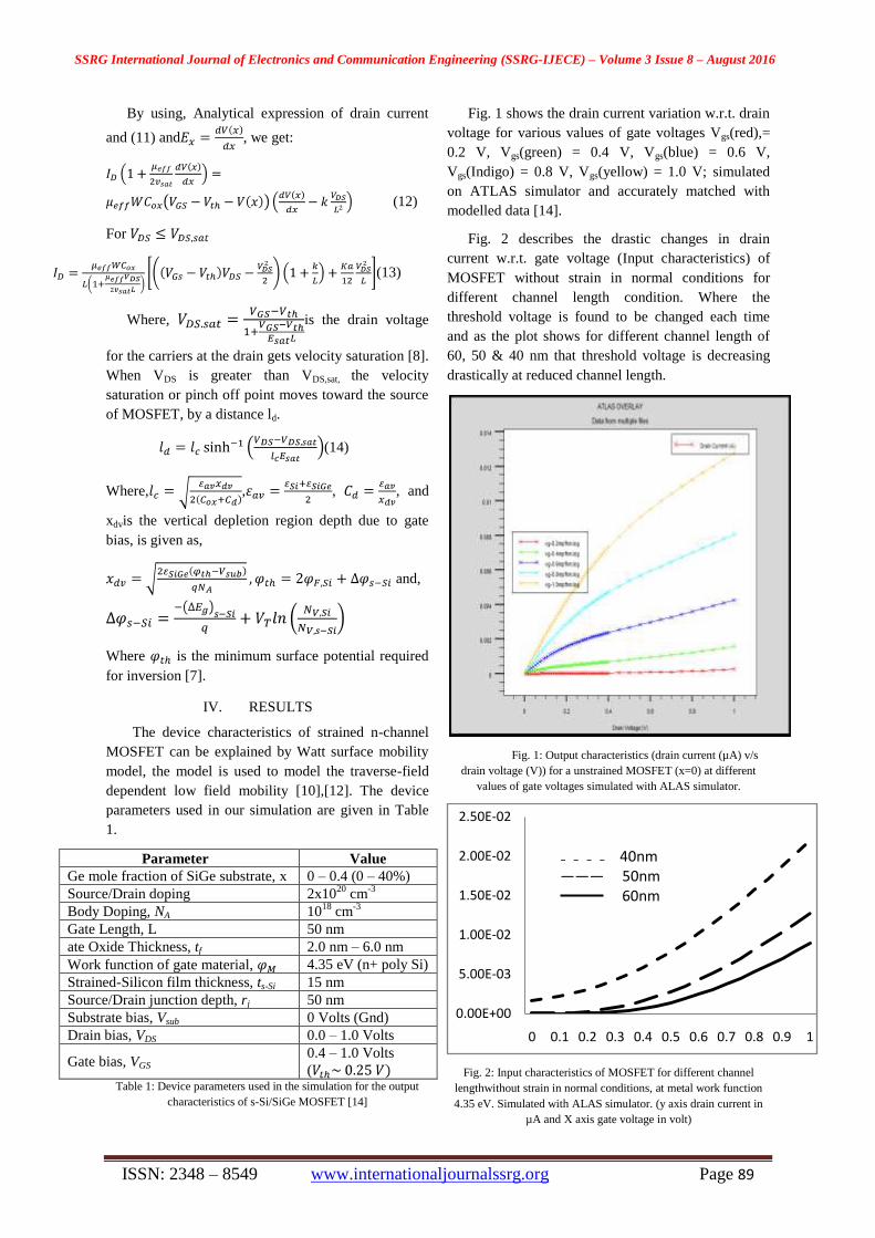
Fig. 1 shows the drain current variation w.r.t. drain
voltage for various values of gate voltages Vgs(red),=
0.2 V, Vgs(green) = 0.4 V, Vgs(blue) = 0.6 V,
Vgs(Indigo) = 0.8 V, Vgs(yellow) = 1.0 V; simulated
on ATLAS simulator and accurately matched with
modelled data [14].
Fig. 2 describes the drastic changes in drain
current w.r.t. gate voltage (Input characteristics) of
MOSFET without strain in normal conditions for
different channel length condition. Where the
threshold voltage is found to be changed each time
and as the plot shows for different channel length of
60, 50 & 40 nm that threshold voltage is decreasing
drastically at reduced channel length.
Fig. 1: Output characteristics (drain current (µA) v/s
drain voltage (V)) for a unstrained MOSFET (x=0) at different
values of gate voltages simulated with ALAS simulator.
Fig. 2: Input characteristics of MOSFET for different channel
lengthwithout strain in normal conditions, at metal work function
4.35 eV. Simulated with ALAS simulator. (y axis drain current in
µA and X axis gate voltage in volt)
0.00E+00
5.00E-03
1.00E-02
1.50E-02
2.00E-02
2.50E-02
0 0.1 0.2 0.3 0.4 0.5 0.6 0.7 0.8 0.9 1
₋ ₋ ₋ ₋ 40nm ——— 50nm
60nm
lalitha
Text Box
16
SSRG International Journal of Electronics and Communication Engineering (SSRG-IJECE) – Volume 3 Issue 8 – August 2016
ISSN: 2348 – 8549 www.internationaljournalssrg.org Page 90
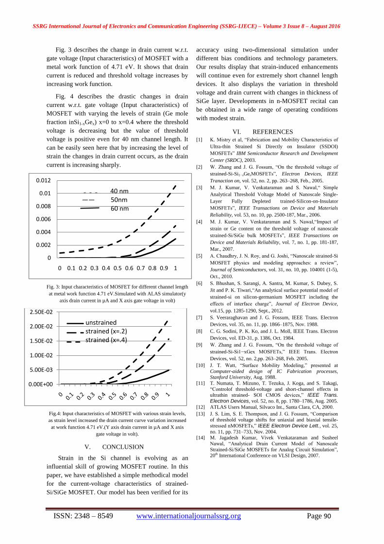
Fig. 3 describes the change in drain current w.r.t.
gate voltage (Input characteristics) of MOSFET with a
metal work function of 4.71 eV. It shows that drain
current is reduced and threshold voltage increases by
increasing work function.
Fig. 4 describes the drastic changes in drain
current w.r.t. gate voltage (Input characteristics) of
MOSFET with varying the levels of strain (Ge mole
fraction inSi1-xGex) x=0 to x=0.4 where the threshold
voltage is decreasing but the value of threshold
voltage is positive even for 40 nm channel length. It
can be easily seen here that by increasing the level of
strain the changes in drain current occurs, as the drain
current is increasing sharply.
Fig. 3: Input characteristics of MOSFET for different channel length
at metal work function 4.71 eV.Simulated with ALAS simulator(y
axis drain current in µA and X axis gate voltage in volt)
Fig.4: Input characteristics of MOSFET with various strain levels,
as strain level increased the drain current curve variation increased
at work function 4.71 eV.(Y axis drain current in µA and X axis
gate voltage in volt).
V. CONCLUSION
Strain in the Si channel is evolving as an
influential skill of growing MOSFET routine. In this
paper, we have established a simple methodical model
for the current-voltage characteristics of strained-
Si/SiGe MOSFET. Our model has been verified for its
accuracy using two-dimensional simulation under
different bias conditions and technology parameters.
Our results display that strain-induced enhancements
will continue even for extremely short channel length
devices. It also displays the variation in threshold
voltage and drain current with changes in thickness of
SiGe layer. Developments in n-MOSFET recital can
be obtained in a wide range of operating conditions
with modest strain.
VI. REFERENCES
[1] K. Mistry et al, “Fabrication and Mobility Characteristics of
Ultra-thin Strained Si Directly on Insulator (SSDOI)
MOSFETs” IBM Semiconductor Research and Development
Center (SRDC), 2003.
[2] W. Zhang and J. G. Fossum, “On the threshold voltage of
strained-Si-Si1−xGexMOSFETs”, Electron Devices, IEEE
Tranaction on, vol. 52, no. 2, pp. 263–268, Feb., 2005.
[3] M. J. Kumar, V. Venkataraman and S. Nawal,“ Simple
Analytical Threshold Voltage Model of Nanoscale Single-
Layer Fully Depleted trained-Silicon-on-Insulator
MOSFETs”, IEEE Transactions on Device and Materials
Reliability, vol. 53, no. 10, pp. 2500-187, Mar., 2006.
[4] M. J. Kumar, V. Venkataraman and S. Nawal,“Impact of
strain or Ge content on the threshold voltage of nanoscale
strained-Si/SiGe bulk MOSFETs”, IEEE Transactions on
Device and Materials Reliability, vol. 7, no. 1, pp. 181-187,
Mar., 2007.
[5] A. Chaudhry, J. N. Roy, and G. Joshi, “Nanoscale strained-Si
MOSFET physics and modeling approaches: a review”,
Journal of Semiconductors, vol. 31, no. 10, pp. 104001 (1-5),
Oct., 2010.
[6] S. Bhushan, S. Sarangi, A. Santra, M. Kumar, S. Dubey, S.
Jit and P. K. Tiwari,“An analytical surface potential model of
strained-si on silicon-germanium MOSFET including the
effects of interface charge”, Journal of Electron Device,
vol.15, pp. 1285-1290, Sept., 2012.
[7] S. Veeraraghavan and J. G. Fossum, IEEE Trans. Electron
Devices, vol. 35, no. 11, pp. 1866–1875, Nov. 1988.
[8] C. G. Sodini, P. K. Ko, and J. L. Moll, IEEE Trans. Electron
Devices, vol. ED-31, p. 1386, Oct. 1984.
[9] W. Zhang and J. G. Fossum, “On the threshold voltage of
strained-Si-Si1−xGex MOSFETs,” IEEE Trans. Electron
Devices, vol. 52, no. 2,pp. 263–268, Feb. 2005.
[10] J. T. Watt, “Surface Mobility Modeling,” presented at
Computer-aided design of IC Fabrication processes, Stanford University, Aug. 1988.
[11] T. Numata, T. Mizuno, T. Tezuka, J. Koga, and S. Takagi,
“Controlof threshold-voltage and short-channel effects in ultrathin strained- SOI CMOS devices,” IEEE Trans. Electron Devices, vol. 52, no. 8, pp. 1780–1786, Aug. 2005.
[12] ATLAS Users Manual, Silvaco Int., Santa Clara, CA, 2000.
[13] J. S. Lim, S. E. Thompson, and J. G. Fossum, “Comparison
of threshold voltage shifts for uniaxial and biaxial tensile-
stressed nMOSFETs,” IEEE Electron Device Lett., vol. 25,
no. 11, pp. 731–733, Nov. 2004. [14] M. Jagadesh Kumar, Vivek Venkataraman and Susheel
Nawal, “Analytical Drain Current Model of Nanoscale
Strained-Si/SiGe MOSFETs for Analog Circuit Simulation”, 20th International Conference on VLSI Design, 2007.
0
0.002
0.004
0.006
0.008
0.01
0.012
0 0.1 0.2 0.3 0.4 0.5 0.6 0.7 0.8 0.9 1
₋ ₋ ₋ 40 nm—— 50nm
60 nm
0.00E+00
5.00E-03
1.00E-02
1.50E-02
2.00E-02
2.50E-02
unstrainedstrained (x=.2)strained (x=.4)
lalitha
Text Box
17
Related Documents