An Alternative approach to Buffer Insertion for Delay and Power Reduction in VLSI Interconnects Sandeep Saini, A Mahesh Kumar, Sreehari Veeramachaneni Center for VLSI and Embedded Systems Technologies, International Institute of Information Technology-Hyderabad Hyderabad – India 500032 M.B. Srinivas Electronics and Communication Engineering, Birla Institute of Technology and Science, Hyderabad Campus, Hyderabad – India 500078 Abstract In VLSI interconnect buffers are used to restore the signal level affected by the parasitics. However buffers have a certain switching time that contributes to overall signal delay. Further the transitions that occur in interconnects also contribute to crosstalk delay. Thus the overall delay in interconnects is due to combined effect of both buffer and crosstalk delay. In this work a replacement of buffers with Schmitt trigger is proposed for the same purpose of signal restoration. Due to lower threshold voltage of Schmitt trigger signal can rise early and the large noise margin of schmitt trigger helps in reducing the noise glitches as well. Simulation results shows that thethe Schmitt trigger approach gives 20% delay reduction as compared to 10.4% in case of buffers. 1. Introduction It is well known [1,2] that in modern integrated circuits, interconnect delay has become the primary performance bottleneck contributing an increasingly significant portion to total cycle delay. Since the RC- delay of an unbuffered interconnect grows quadratically with wire length, buffers have traditionally been used to linearize the dependence of delay on interconnect length. In an optimally buffered interconnect; the delay of any given stage is approximately equally divided between the buffer and the wire. But this balance gets disturbed due to the wire delay degradation due to process scaling which leads to an increase in the proportion of the wire delay in a buffered interconnect whose geometries are optically shrunk (without any redesign) to the next technology node. Thus buffer insertion has become a critical step in deep sub-micron design of modern integrated circuits. The insertion of buffers, while has certain advantages, also leads to increased area and power dissipation thus affecting the overall system performance. In this work, Schmitt trigger as an alternative to buffer insertion is explored. Schmitt trigger, a widely used element in electronic circuits, has a special property of responding to slowly changing input waveforms with a fast transition at the output. It also exhibits hysteresis indicating that it has different switching thresholds for positive and negative going input signals. 2. Background VLSI circuit interconnect delay has always been handled with the help of buffer insertion. Various buffer insertion techniques have been proposed for one-line interconnects and tree structures. Ismail et al. [3] observed and showed the effects of inductance on the propagation delay and repeater insertion in VLSI circuits. Dhar et. al. [4] proposed optimum insertion of buffers in long interconnects to reduce the El-More delay, while Cong et al [5] proposed performance optimization algorithm for VLSI interconnects. Alpert et. al. [6] first proposed a methodology for buffer and wire resource allocation and Alpert and Devgan [7] later proposed a technique for optimum wire segmentation for buffer insertion. However interconnects are not always linear in shape and handling the delays in tree structure is also a problem. This is attributed to the crosstalk effects due to the 2010 23rd International Conference on VLSI Design 1063-9667/10 $26.00 © 2010 IEEE DOI 10.1109/VLSI.Design.2010.53 411

Welcome message from author
This document is posted to help you gain knowledge. Please leave a comment to let me know what you think about it! Share it to your friends and learn new things together.
Transcript
An Alternative approach to Buffer Insertion for Delay and Power Reduction in VLSI Interconnects
Sandeep Saini, A Mahesh Kumar, Sreehari Veeramachaneni
Center for VLSI and Embedded Systems Technologies, International Institute of Information Technology-Hyderabad
Hyderabad – India 500032
M.B. Srinivas Electronics and Communication Engineering,
Birla Institute of Technology and Science, Hyderabad Campus,
Hyderabad – India 500078
Abstract
In VLSI interconnect buffers are used to restore the signal level affected by the parasitics. However buffers have a certain switching time that contributes to overall signal delay. Further the transitions that occur in interconnects also contribute to crosstalk delay. Thus the overall delay in interconnects is due to combined effect of both buffer and crosstalk delay. In this work a replacement of buffers with Schmitt trigger is proposed for the same purpose of signal restoration. Due to lower threshold voltage of Schmitt trigger signal can rise early and the large noise margin of schmitt trigger helps in reducing the noise glitches as well. Simulation results shows that thethe Schmitt trigger approach gives 20% delay reduction as compared to 10.4% in case of buffers. 1. Introduction
It is well known [1,2] that in modern integrated circuits, interconnect delay has become the primary performance bottleneck contributing an increasingly significant portion to total cycle delay. Since the RC-delay of an unbuffered interconnect grows quadratically with wire length, buffers have traditionally been used to linearize the dependence of delay on interconnect length. In an optimally buffered interconnect; the delay of any given stage is approximately equally divided between the buffer and the wire. But this balance gets disturbed due to the wire delay degradation due to process scaling which leads to an increase in the proportion of the wire delay in a buffered interconnect whose geometries are optically shrunk (without any redesign) to the next technology
node. Thus buffer insertion has become a critical step in deep sub-micron design of modern integrated circuits. The insertion of buffers, while has certain advantages, also leads to increased area and power dissipation thus affecting the overall system performance.
In this work, Schmitt trigger as an alternative to
buffer insertion is explored. Schmitt trigger, a widely used element in electronic circuits, has a special property of responding to slowly changing input waveforms with a fast transition at the output. It also exhibits hysteresis indicating that it has different switching thresholds for positive and negative going input signals. 2. Background
VLSI circuit interconnect delay has always been handled with the help of buffer insertion. Various buffer insertion techniques have been proposed for one-line interconnects and tree structures. Ismail et al. [3] observed and showed the effects of inductance on the propagation delay and repeater insertion in VLSI circuits. Dhar et. al. [4] proposed optimum insertion of buffers in long interconnects to reduce the El-More delay, while Cong et al [5] proposed performance optimization algorithm for VLSI interconnects. Alpert et. al. [6] first proposed a methodology for buffer and wire resource allocation and Alpert and Devgan [7] later proposed a technique for optimum wire segmentation for buffer insertion. However interconnects are not always linear in shape and handling the delays in tree structure is also a problem. This is attributed to the crosstalk effects due to the
2010 23rd International Conference on VLSI Design
1063-9667/10 $26.00 © 2010 IEEE
DOI 10.1109/VLSI.Design.2010.53
411
neighboring branches. Alpert et al [8] proposed a Steiner tree construction for buffers, blockages, and bays and a modified Buffered Steiner tree [9] to handle more difficult geometries. Lukas [9] proposed an algorithm for choosing the buffer positions for a wiring tree such that the "Elmore delay" is minimal. However, no effort appears to have been made so far to examine Schmitt trigger in place of a buffer for interconnects.
3. Proposed Work
In this paper, Schmitt trigger as an alternative to buffer insertion is examined in buses. The motivation for this approach is that while a buffer responds to an input signal only after it exceeds a voltage of Vdd/2, Schmitt trigger can be designed to have a threshold voltage less than Vdd/2 and thus can be made to respond faster.
Let us consider an input signal with a fast rising
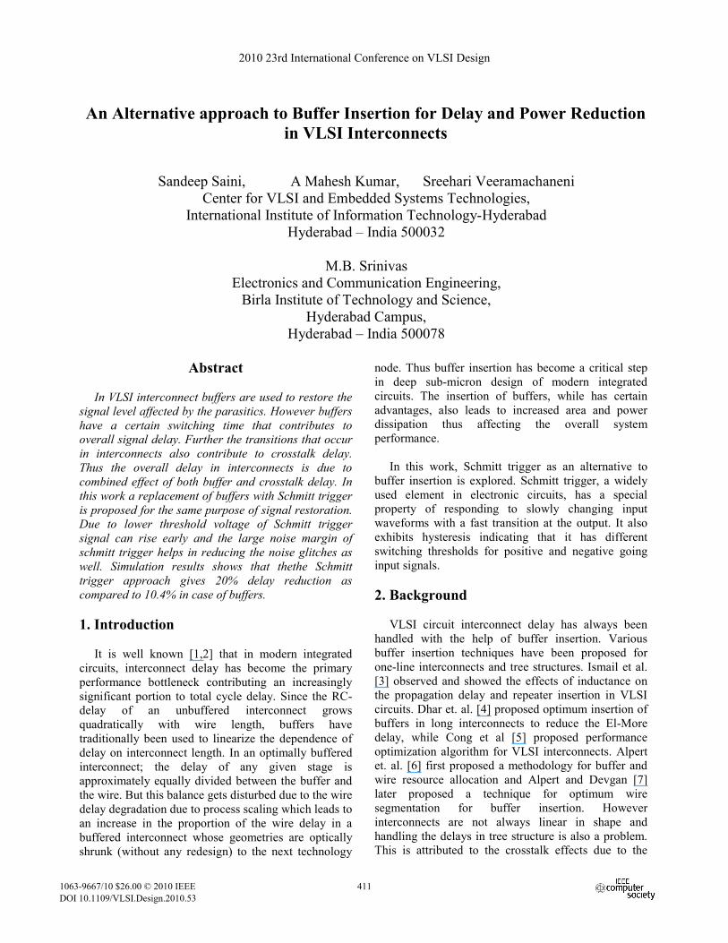
edge fed to an interconnect. Ideally, the signal at the far-end of the interconnect should be in the same shape but the interconnect delay, due to parasitic capacitance, leads to far-end signal being obtained only after certain time has elapsed. This value can be as high as a few nanoseconds depending on the values of resistance, parasitic capacitance. While a buffer is conventionally used to restore the signal, its output is obtained only after the input signal voltage crosses Vdd/2. However, a Schmitt trigger can be designed to have a lower threshold voltage so that it can respond faster than a buffer. Figure 1 compares the response of a buffer and a Schmitt trigger to a slowly varying input.
For the above result, buffer is designed with 2
CMOS inverters placed back to back (figure 2). Buffer is designed with minimal lambda parameters for 65nm technology by keeping Wp = 3Wn to ensure equal rise and fall time. Schmitt trigger used for this approach has 6 CMOS [1] which are comparable is size with the transistors used in buffer. The area of Schmitt trigger comes out to be 20% extra than the regular buffer for same technology parameters. This is a trade-off between delay and area and we can justify that adding some extra cells into area will reduce the delay significantly.
Figure 1: Output waveform with Schmitt trigger and Buffer at output end
Figure 2: CMOS Buffer
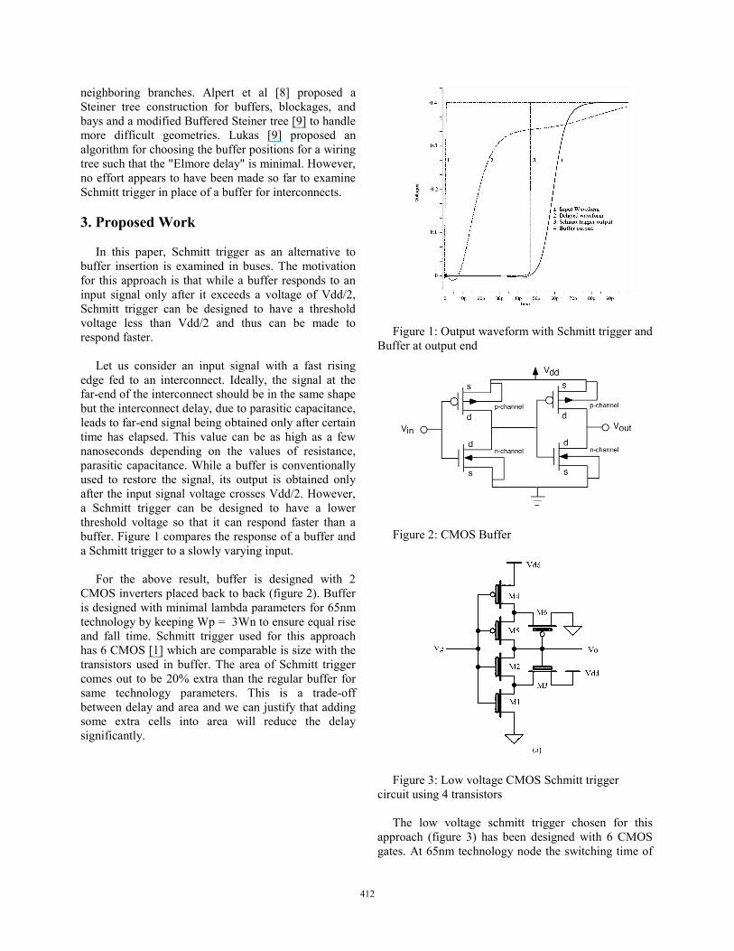
Figure 3: Low voltage CMOS Schmitt trigger circuit using 4 transistors
The low voltage schmitt trigger chosen for this
approach (figure 3) has been designed with 6 CMOS gates. At 65nm technology node the switching time of
412
both buffer as well as Schmitt trigger is almost same i.e. 30ps. But we observe less delay in Schmitt trigger output (figure 1) as compared to buffer output. This is due to early switching of signal at Vdd/3 instead of Vdd/2.
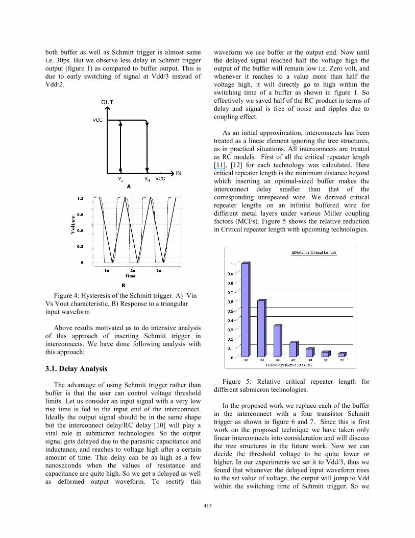
Figure 4: Hysteresis of the Schmitt trigger. A) Vin
Vs Vout characteristic, B) Response to a triangular input waveform
Above results motivated us to do intensive analysis
of this approach of inserting Schmitt trigger in interconnects. We have done following analysis with this approach:
3.1. Delay Analysis
The advantage of using Schmitt trigger rather than
buffer is that the user can control voltage threshold limits. Let us consider an input signal with a very low rise time is fed to the input end of the interconnect. Ideally the output signal should be in the same shape but the interconnect delay/RC delay [10] will play a vital role in submicron technologies. So the output signal gets delayed due to the parasitic capacitance and inductance, and reaches to voltage high after a certain amount of time. This delay can be as high as a few nanoseconds when the values of resistance and capacitance are quite high. So we get a delayed as well as deformed output waveform. To rectify this
waveform we use buffer at the output end. Now until the delayed signal reached half the voltage high the output of the buffer will remain low i.e. Zero volt, and whenever it reaches to a value more than half the voltage high, it will directly go to high within the switching time of a buffer as shown in figure 1. So effectively we saved half of the RC product in terms of delay and signal is free of noise and ripples due to coupling effect.
As an initial approximation, interconnects has been
treated as a linear element ignoring the tree structures, as in practical situations. All interconnects are treated as RC models. First of all the critical repeater length [11], [12] for each technology was calculated. Here critical repeater length is the minimum distance beyond which inserting an optimal-sized buffer makes the interconnect delay smaller than that of the corresponding unrepeated wire. We derived critical repeater lengths on an infinite buffered wire for different metal layers under various Miller coupling factors (MCFs). Figure 5 shows the relative reduction in Critical repeater length with upcoming technologies.
Figure 5: Relative critical repeater length for
different submicron technologies. In the proposed work we replace each of the buffer
in the interconnect with a four transistor Schmitt trigger as shown in figure 6 and 7. Since this is first work on the proposed technique we have taken only linear interconnects into consideration and will discuss the tree structures in the future work. Now we can decide the threshold voltage to be quite lower or higher. In our experiments we set it to Vdd/3, thus we found that whenever the delayed input waveform rises to the set value of voltage, the output will jump to Vdd within the switching time of Schmitt trigger. So we
413
save the time difference between the rise time of output pulse in case of buffer and Schmitt trigger. Figure 1 shows the output waveform with both methods for same interconnect.
Figure 6: Buffers inserted in an RC interconnect model.
Figure 7: Schmitt trigger at the output end of RC interconnect model. 3.2. Power Analysis
The dynamic (short circuit) power of the circuit is
very much lesser than a buffer as the device is predominantly in the off or on mode. Due to very early switching to the opposite logic level, either the transistors are in off or on mode. Unlike buffer where at Vdd/2 all the transistors are in saturation mode and hence resulting in more power consumption. Buffer consumes 19.2mW power per cycle while its counterpart Schmitt trigger consumes 16.8 mW per cycle. Hence we save 12.5% power with each element replaced. Also as we have discussed in Area analysis that we can save around 10% devices too, so a further saving in power is possible.
4. Simulation Results
The circuit was simulated with H-Spice for the
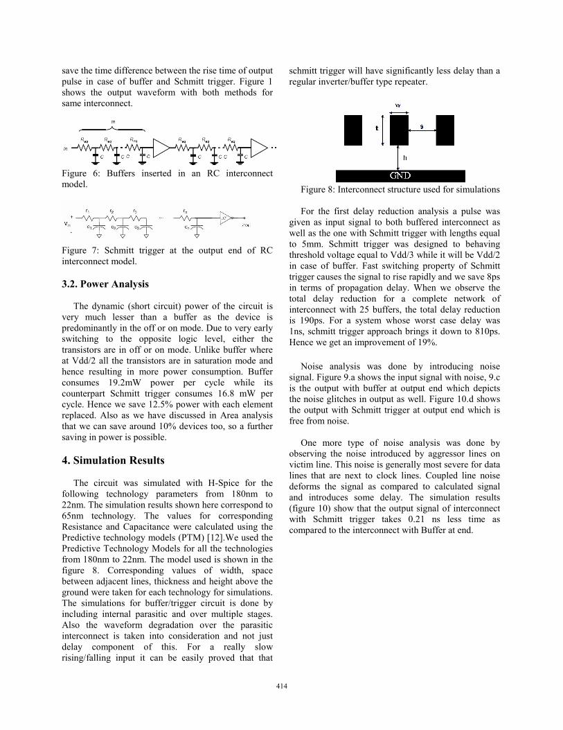
following technology parameters from 180nm to 22nm. The simulation results shown here correspond to 65nm technology. The values for corresponding Resistance and Capacitance were calculated using the Predictive technology models (PTM) [12].We used the Predictive Technology Models for all the technologies from 180nm to 22nm. The model used is shown in the figure 8. Corresponding values of width, space between adjacent lines, thickness and height above the ground were taken for each technology for simulations. The simulations for buffer/trigger circuit is done by including internal parasitic and over multiple stages. Also the waveform degradation over the parasitic interconnect is taken into consideration and not just delay component of this. For a really slow rising/falling input it can be easily proved that that
schmitt trigger will have significantly less delay than a regular inverter/buffer type repeater.
Figure 8: Interconnect structure used for simulations For the first delay reduction analysis a pulse was
given as input signal to both buffered interconnect as well as the one with Schmitt trigger with lengths equal to 5mm. Schmitt trigger was designed to behaving threshold voltage equal to Vdd/3 while it will be Vdd/2 in case of buffer. Fast switching property of Schmitt trigger causes the signal to rise rapidly and we save 8ps in terms of propagation delay. When we observe the total delay reduction for a complete network of interconnect with 25 buffers, the total delay reduction is 190ps. For a system whose worst case delay was 1ns, schmitt trigger approach brings it down to 810ps. Hence we get an improvement of 19%.
Noise analysis was done by introducing noise signal. Figure 9.a shows the input signal with noise, 9.c is the output with buffer at output end which depicts the noise glitches in output as well. Figure 10.d shows the output with Schmitt trigger at output end which is free from noise.
One more type of noise analysis was done by
observing the noise introduced by aggressor lines on victim line. This noise is generally most severe for data lines that are next to clock lines. Coupled line noise deforms the signal as compared to calculated signal and introduces some delay. The simulation results (figure 10) show that the output signal of interconnect with Schmitt trigger takes 0.21 ns less time as compared to the interconnect with Buffer at end.
414
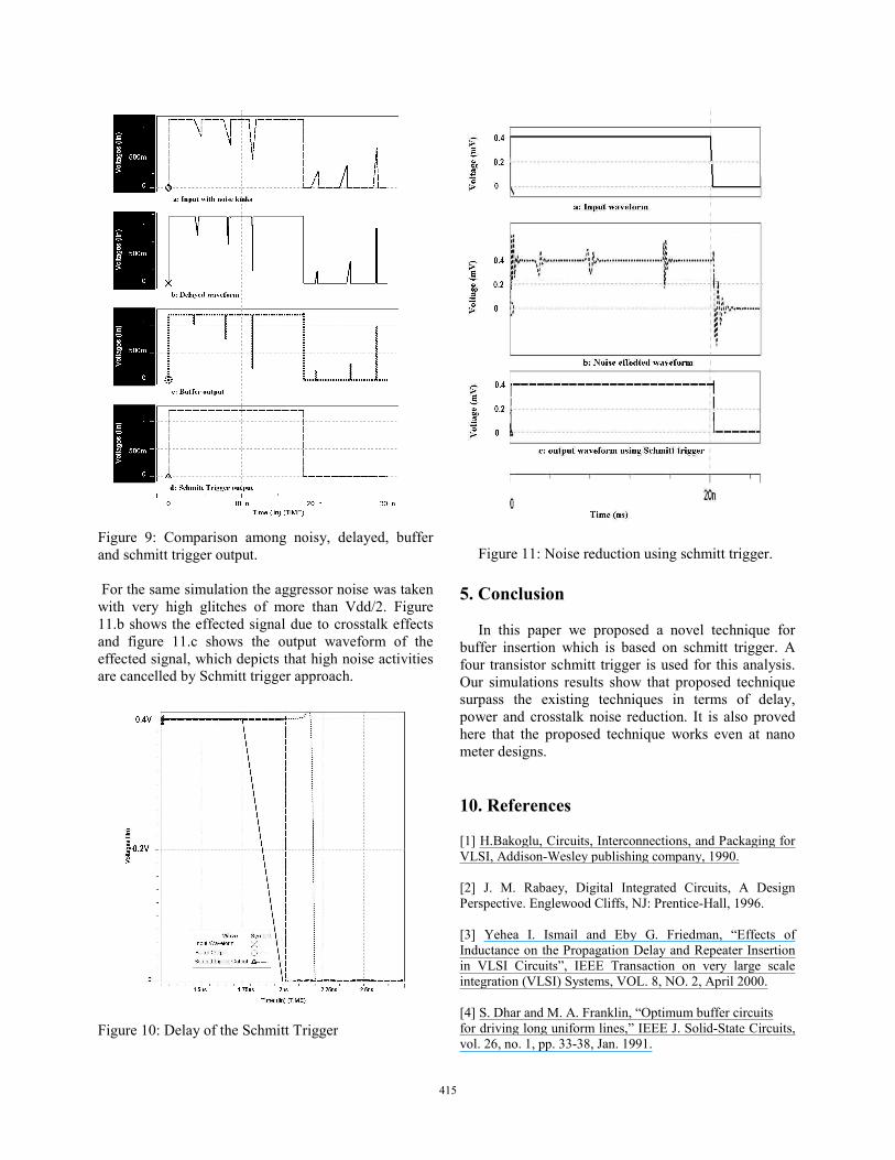
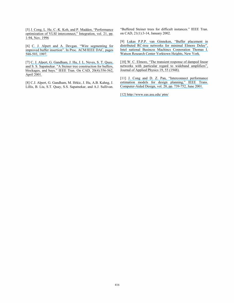
Figure 9: Comparison among noisy, delayed, buffer and schmitt trigger output. For the same simulation the aggressor noise was taken with very high glitches of more than Vdd/2. Figure 11.b shows the effected signal due to crosstalk effects and figure 11.c shows the output waveform of the effected signal, which depicts that high noise activities are cancelled by Schmitt trigger approach.
Figure 10: Delay of the Schmitt Trigger
Figure 11: Noise reduction using schmitt trigger.
5. Conclusion
In this paper we proposed a novel technique for
buffer insertion which is based on schmitt trigger. A four transistor schmitt trigger is used for this analysis. Our simulations results show that proposed technique surpass the existing techniques in terms of delay, power and crosstalk noise reduction. It is also proved here that the proposed technique works even at nano meter designs. 10. References [1] H.Bakoglu, Circuits, Interconnections, and Packaging for VLSI, Addison-Wesley publishing company, 1990. [2] J. M. Rabaey, Digital Integrated Circuits, A Design Perspective. Englewood Cliffs, NJ: Prentice-Hall, 1996. [3] Yehea I. Ismail and Eby G. Friedman, “Effects of Inductance on the Propagation Delay and Repeater Insertion in VLSI Circuits”, IEEE Transaction on very large scale integration (VLSI) Systems, VOL. 8, NO. 2, April 2000. [4] S. Dhar and M. A. Franklin, “Optimum buffer circuits for driving long uniform lines,” IEEE J. Solid-State Circuits, vol. 26, no. 1, pp. 33-38, Jan. 1991.
415
[5] J. Cong, L. He, C.-K. Koh, and P. Madden, “Performance optimization of VLSI interconnect,” Integration, vol. 21, pp. 1-94, Nov. 1996 [6] C. J. Alpert and A. Devgan. “Wire segmenting for improved buffer insertion”. In Proc. ACM/IEEE DAC, pages 588-593, 1997. [7] C. J. Alpert, G. Gandham, J. Hu, J. L. Neves, S. T. Quay, and S. S. Sapatnekar. “A Steiner tree construction for buffers, blockages, and bays.” IEEE Tran. On CAD, 20(4):556-562, April 2001. [8] C.J. Alpert, G. Gandham, M. Hrkic, J. Hu, A.B. Kahng, J. Lillis, B. Liu, S.T. Quay, S.S. Sapatnekar, and A.J. Sullivan.
“Buffered Steiner trees for difficult instances.” IEEE Tran. on CAD, 21(1):3-14, January 2002. [9] Lukas P.P.P. van Ginneken, “Buffer placement in distributed RC-tree networks for minimal Elmore Delay”, Intel national Busincss Machincs Corporation Thomas I. Watson Research Center Yorktown Heights, New York. [10] W. C. Elmore, “The transient response of damped linear networks with particular regard to wideband amplifiers”, Journal of Applied Physics 19, 55 (1948). [11] J. Cong and D. Z. Pan, “Interconnect performance estimation models for design planning,” IEEE Trans. Computer-Aided Design, vol. 20, pp. 739-752, June 2001. [12] http://www.eas.asu.edu/ ptm/
416
Related Documents