Altera Corporation 1 AN-315-1.1 Preliminary Application Note Guidelines for Designing High-Speed FPGA PCBs Introduction Over the past five years, the development of true analog CMOS processes has led to the use of high-speed analog devices in the digital arena. System speeds of 150 MHz and higher have become common for digital logic. Systems that were considered high end and high speed a few years ago are now cheaply and easily implemented. However, this integration of fast system speeds brings with it the challenges of analog system design to a digital world. This document is a guideline for printed circuit board (PCB) layouts and designs associated with high-speed systems. “High speed” does not just mean faster communication rates (e.g., faster than 1 gigabit per second (Gbps)). A transistor-transistor logic (TTL) signal with a 600-ps rise time is also considered a high-speed signal. This opens up the entire PCB to careful and targeted board simulation and design. The designer must consider any discontinuities on the board. The “Time-Domain Reflectometry” and “Discontinuity” sections explain how to eliminate discontinuities on a PCB. Some sources of discontinuities are vias, right angled bends, and passive connectors. The “Termination” section explains about terminations for signals on PCBs. The placement and selection of termination resistors are critical in order to avoid reflections. As systems require higher speeds, they use differential signals instead of single-ended signals because of better noise margins and immunity. Differential signals require special attention from PCB designers with regards to trace layout. The “Trace Layout” section addresses differential traces in terms of trace layout. Crosstalk, which can adversely affect single ended and differential signals alike, is also addressed in this section. All the dense, high-speed switching (i.e., hundreds of I/O pins switching at rates faster than 500-ps rise and fall times) produces powerful transient changes in power supply voltage. These transient changes occur because a signal switching at higher frequency consumes a proportionally greater amount of power than a signal switching at a lower frequency. As a result, a device does not have a stable power reference that both analog and digital circuits can derive their power from. This phenomenon is called simultaneous switching noise (SSN). The “Dielectric Material” section discusses how to eliminate some of these SSN problems through careful board design. February 2004, ver. 1.1

Welcome message from author
This document is posted to help you gain knowledge. Please leave a comment to let me know what you think about it! Share it to your friends and learn new things together.
Transcript
Altera Corporation AN-315-1.1
February 2004, ver. 1.1
Guidelines for DesigningHigh-Speed FPGA PCBs
Application Note
Introduction Over the past five years, the development of true analog CMOS processes has led to the use of high-speed analog devices in the digital arena. System speeds of 150 MHz and higher have become common for digital logic. Systems that were considered high end and high speed a few years ago are now cheaply and easily implemented. However, this integration of fast system speeds brings with it the challenges of analog system design to a digital world. This document is a guideline for printed circuit board (PCB) layouts and designs associated with high-speed systems.
“High speed” does not just mean faster communication rates (e.g., faster than 1 gigabit per second (Gbps)). A transistor-transistor logic (TTL) signal with a 600-ps rise time is also considered a high-speed signal. This opens up the entire PCB to careful and targeted board simulation and design. The designer must consider any discontinuities on the board. The “Time-Domain Reflectometry” and “Discontinuity” sections explain how to eliminate discontinuities on a PCB. Some sources of discontinuities are vias, right angled bends, and passive connectors.
The “Termination” section explains about terminations for signals on PCBs. The placement and selection of termination resistors are critical in order to avoid reflections.
As systems require higher speeds, they use differential signals instead of single-ended signals because of better noise margins and immunity. Differential signals require special attention from PCB designers with regards to trace layout. The “Trace Layout” section addresses differential traces in terms of trace layout. Crosstalk, which can adversely affect single ended and differential signals alike, is also addressed in this section.
All the dense, high-speed switching (i.e., hundreds of I/O pins switching at rates faster than 500-ps rise and fall times) produces powerful transient changes in power supply voltage. These transient changes occur because a signal switching at higher frequency consumes a proportionally greater amount of power than a signal switching at a lower frequency. As a result, a device does not have a stable power reference that both analog and digital circuits can derive their power from. This phenomenon is called simultaneous switching noise (SSN). The “Dielectric Material” section discusses how to eliminate some of these SSN problems through careful board design.
1Preliminary
Guidelines for Designing High-Speed FPGA PCBs Time-Domain Reflectometry
The “Simultaneous Switching Noise” and “Decoupling” sections cover power supply decoupling and PCB layer stackup. The document discusses how to select the method and amount of decoupling as well as the theory behind capacitive decoupling. These sections also present a real life example of troubleshooting a decoupling problem. The “Layer Stackup” section discusses layer stackup.
It is critical to follow the best practices described in this document to ensure the best performance from your system. The content of this document is based on the results of Altera's experiments with high-speed PCBs. The simulations were done with Hspice, an analog circuit simulator. Ansoft 2D and 3D field solvers were used to extract RLGC parameters for different structures. Sigrity Speed2000 tool was used for SSN simulation.
This document should be used in conjunction with the board layout example provided on the Altera web site (www.altera.com). You can also contact Altera Applications for this example. The board layout example is a set of specific guidelines used when designing the Stratix GX development kit board. It includes schematics, a board specific layout guideline, and board layout and stackup information.
You should also use the characterization report for the Altera FPGA you are designing for with this document. This document will assist with design guidelines required for the board design, and the characterization report will give a picture of the device performance.
Contact Altera Applications for further assistance or questions with regards to this document or any other issues associated with high-speed board design.
Time-Domain Reflectometry
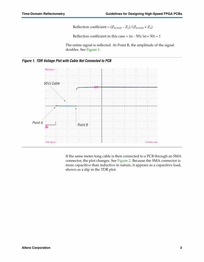
Time domain reflectometry (TDR) is a way to observe discontinuities on a transmission path. The time domain reflectometer sends a pulse through the transmission medium. Reflections occur when the pulse of energy reaches either the end of the transmission path or a discontinuity within the transmission path. From these reflections, the designer can determine the size and location of the discontinuity. Many examples in this handbook use TDR, and this section provides an understanding of TDR.
Figure 1 shows a TDR voltage plot for a cable that is not connected to a PCB. The middle line is a 50-Ω cable one meter long. At Point A, a pulse starts (Zo = 50 Ω) and transmits through the cable, stopping at the end of the transmission line (i.e., Point B). Because the end of the transmission line is open, there is infinite impedance, ZLOAD = α. Therefore, the reflection coefficient at the load is determined with the equation:
2 Altera CorporationPreliminary
Time-Domain Reflectometry Guidelines for Designing High-Speed FPGA PCBs
Reflection coefficient = (ZLOAD – Zo)/(ZLOAD + Zo)
Reflection coefficient in this case = (α – 50)/(α + 50) = 1
The entire signal is reflected. At Point B, the amplitude of the signal doubles. See Figure 1.
Figure 1. TDR Voltage Plot with Cable Not Connected to PCB
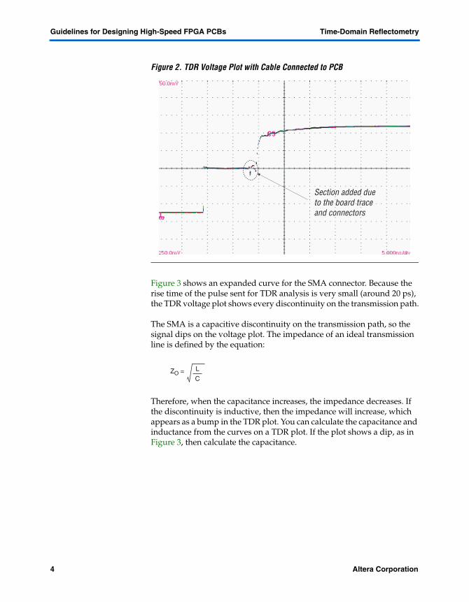
If the same meter-long cable is then connected to a PCB through an SMA connector, the plot changes. See Figure 2. Because the SMA connector is more capacitive than inductive in nature, it appears as a capacitive load, shown as a dip in the TDR plot.
50 Ω Cable
Point BPoint A
Altera Corporation 3Preliminary
Guidelines for Designing High-Speed FPGA PCBs Time-Domain Reflectometry
Figure 2. TDR Voltage Plot with Cable Connected to PCB
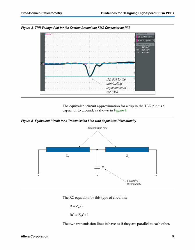
Figure 3 shows an expanded curve for the SMA connector. Because the rise time of the pulse sent for TDR analysis is very small (around 20 ps), the TDR voltage plot shows every discontinuity on the transmission path.
The SMA is a capacitive discontinuity on the transmission path, so the signal dips on the voltage plot. The impedance of an ideal transmission line is defined by the equation:
Therefore, when the capacitance increases, the impedance decreases. If the discontinuity is inductive, then the impedance will increase, which appears as a bump in the TDR plot. You can calculate the capacitance and inductance from the curves on a TDR plot. If the plot shows a dip, as in Figure 3, then calculate the capacitance.
Section added dueto the board traceand connectors
ZO = L
C
4 Altera CorporationPreliminary
Time-Domain Reflectometry Guidelines for Designing High-Speed FPGA PCBs
Figure 3. TDR Voltage Plot for the Section Around the SMA Connector on PCB
The equivalent circuit approximation for a dip in the TDR plot is a capacitor to ground, as shown in Figure 4.
Figure 4. Equivalent Circuit for a Transmission Line with Capacitive Discontinuity
The RC equation for this type of circuit is:
R = Zo/2
RC = ZoC/2
The two transmission lines behave as if they are parallel to each other.
Dip due to thedominatingcapacitance of the SMA
C
Z0 Z0
Transmission Line
CapacitiveDiscontinuity
Altera Corporation 5Preliminary
Guidelines for Designing High-Speed FPGA PCBs Time-Domain Reflectometry
You can determine the change in voltage ( V) and rise time (Tr) from the curve. Then, you can enter the values into the equation (i.e., Zo = 50 Ω):
( V/250 mV) = 1 − (Tr /2RC)
Use this equation to determine the RC time constant. You can also use the curve to approximate the RC time constant. Between 0 to 63% of the rise is RC. Once the RC is found, you can use it to determine the capacitance (discontinuity, as seen by the signal).
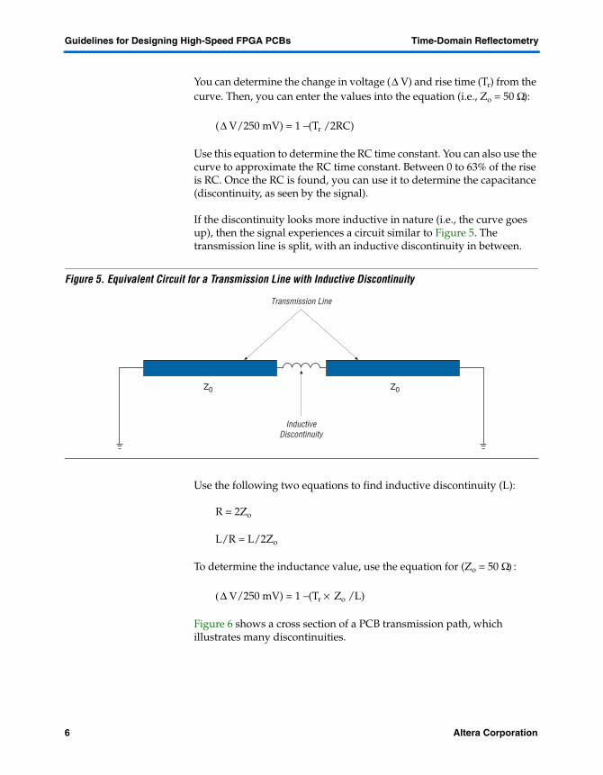
If the discontinuity looks more inductive in nature (i.e., the curve goes up), then the signal experiences a circuit similar to Figure 5. The transmission line is split, with an inductive discontinuity in between.
Figure 5. Equivalent Circuit for a Transmission Line with Inductive Discontinuity
Use the following two equations to find inductive discontinuity (L):
R = 2Zo
L/R = L/2Zo
To determine the inductance value, use the equation for (Zo = 50 Ω) :
( V/250 mV) = 1 − (Tr × Zo /L)
Figure 6 shows a cross section of a PCB transmission path, which illustrates many discontinuities.
∆
∆
Z0 Z0
Transmission Line
InductiveDiscontinuity
∆
6 Altera CorporationPreliminary
Time-Domain Reflectometry Guidelines for Designing High-Speed FPGA PCBs
Figure 6. Example TDR Voltage Plot for a Cross Section of a PCB
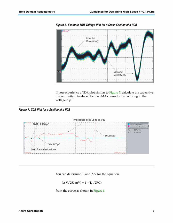
If you experience a TDR plot similar to Figure 7, calculate the capacitive discontinuity introduced by the SMA connector by factoring in the voltage dip.
Figure 7. TDR Plot for a Section of a PCB
You can determine Tr and V for the equation
( V/250 mV) = 1 − (Tr /2RC)
from the curve as shown in Figure 8.
InductiveDiscontinuity
CapacitiveDiscontinuity
50 Ω Transmission Line
Via, 0.7 pF
Driver Side
Impedance goes up to 55.9 Ω
SMA, 1.196 pF
∆
∆
Altera Corporation 7Preliminary
Guidelines for Designing High-Speed FPGA PCBs Discontinuity
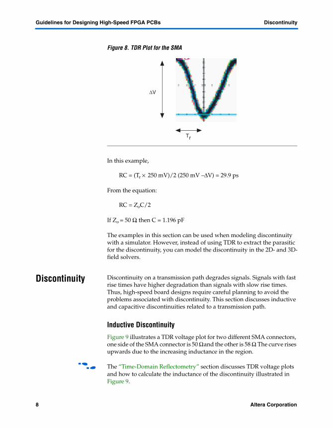
Figure 8. TDR Plot for the SMA
In this example,
RC = (Tr × 250 mV)/2 (250 mV − ∆V) = 29.9 ps
From the equation:
RC = ZoC/2
If Zo = 50 Ω, then C = 1.196 pF
The examples in this section can be used when modeling discontinuity with a simulator. However, instead of using TDR to extract the parasitic for the discontinuity, you can model the discontinuity in the 2D- and 3D-field solvers.
Discontinuity Discontinuity on a transmission path degrades signals. Signals with fast rise times have higher degradation than signals with slow rise times. Thus, high-speed board designs require careful planning to avoid the problems associated with discontinuity. This section discusses inductive and capacitive discontinuities related to a transmission path.
Inductive Discontinuity
Figure 9 illustrates a TDR voltage plot for two different SMA connectors, one side of the SMA connector is 50 Ω and the other is 58 Ω. The curve rises upwards due to the increasing inductance in the region.
f The “Time-Domain Reflectometry” section discusses TDR voltage plots and how to calculate the inductance of the discontinuity illustrated in Figure 9.
Tr
∆V
8 Altera CorporationPreliminary
Discontinuity Guidelines for Designing High-Speed FPGA PCBs
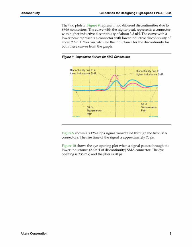
The two plots in Figure 9 represent two different discontinuities due to SMA connectors. The curve with the higher peak represents a connector with higher inductive discontinuity of about 3.8 nH. The curve with a lower peak represents a connector with lower inductive discontinuity of about 2.6 nH. You can calculate the inductance for the discontinuity for both these curves from the graph.
Figure 9. Impedance Curves for SMA Connectors
Figure 9 shows a 3.125-Gbps signal transmitted through the two SMA connectors. The rise time of the signal is approximately 70 ps.
Figure 10 shows the eye opening plot when a signal passes through the lower-inductance (2.6 nH of discontinuity) SMA connector. The eye opening is 336 mV, and the jitter is 20 ps.
Discontinuity due tohigher inductance SMA
Discontinuity due to alower inductance SMA
58 Ω
TransmissionPath
50 Ω
TransmissionPath
Altera Corporation 9Preliminary
Guidelines for Designing High-Speed FPGA PCBs Discontinuity
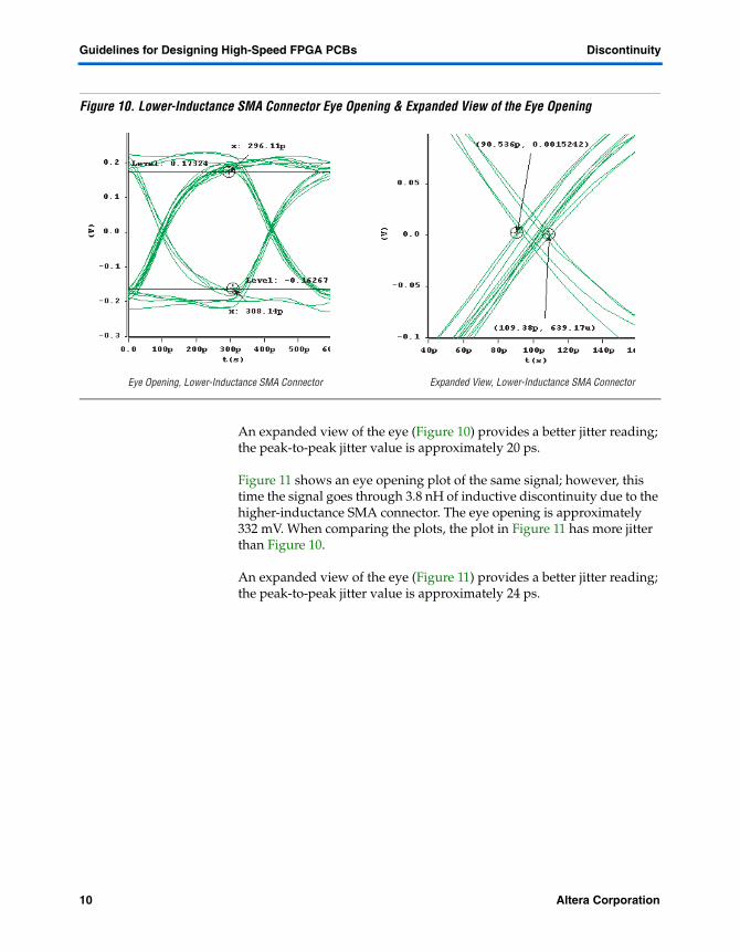
Figure 10. Lower-Inductance SMA Connector Eye Opening & Expanded View of the Eye Opening
An expanded view of the eye (Figure 10) provides a better jitter reading; the peak-to-peak jitter value is approximately 20 ps.
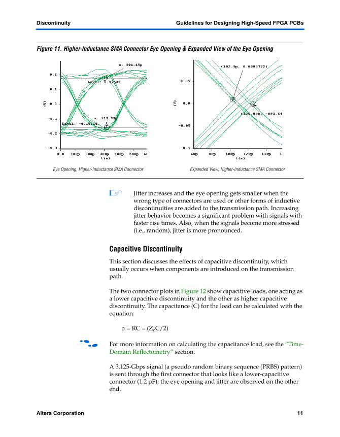
Figure 11 shows an eye opening plot of the same signal; however, this time the signal goes through 3.8 nH of inductive discontinuity due to the higher-inductance SMA connector. The eye opening is approximately 332 mV. When comparing the plots, the plot in Figure 11 has more jitter than Figure 10.
An expanded view of the eye (Figure 11) provides a better jitter reading; the peak-to-peak jitter value is approximately 24 ps.
Expanded View, Lower-Inductance SMA ConnectorEye Opening, Lower-Inductance SMA Connector
10 Altera CorporationPreliminary
Discontinuity Guidelines for Designing High-Speed FPGA PCBs
Figure 11. Higher-Inductance SMA Connector Eye Opening & Expanded View of the Eye Opening
1 Jitter increases and the eye opening gets smaller when the wrong type of connectors are used or other forms of inductive discontinuities are added to the transmission path. Increasing jitter behavior becomes a significant problem with signals with faster rise times. Also, when the signals become more stressed (i.e., random), jitter is more pronounced.
Capacitive Discontinuity
This section discusses the effects of capacitive discontinuity, which usually occurs when components are introduced on the transmission path.
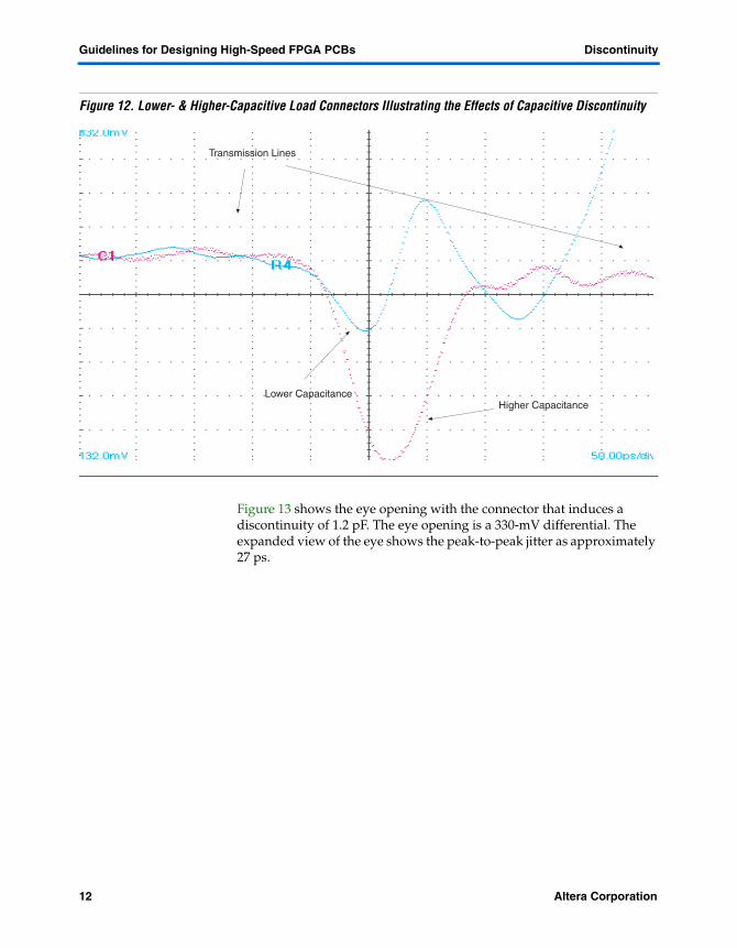
The two connector plots in Figure 12 show capacitive loads, one acting as a lower capacitive discontinuity and the other as higher capacitive discontinuity. The capacitance (C) for the load can be calculated with the equation:
ρ = RC = (ZoC/2)
f For more information on calculating the capacitance load, see the “Time-Domain Reflectometry” section.
A 3.125-Gbps signal (a pseudo random binary sequence (PRBS) pattern) is sent through the first connector that looks like a lower-capacitive connector (1.2 pF); the eye opening and jitter are observed on the other end.
Expanded View, Higher-Inductance SMA ConnectorEye Opening, Higher-Inductance SMA Connector
Altera Corporation 11Preliminary
Guidelines for Designing High-Speed FPGA PCBs Discontinuity
Figure 12. Lower- & Higher-Capacitive Load Connectors Illustrating the Effects of Capacitive Discontinuity
Figure 13 shows the eye opening with the connector that induces a discontinuity of 1.2 pF. The eye opening is a 330-mV differential. The expanded view of the eye shows the peak-to-peak jitter as approximately 27 ps.
Higher CapacitanceLower Capacitance
Transmission Lines
12 Altera CorporationPreliminary
Discontinuity Guidelines for Designing High-Speed FPGA PCBs
Figure 13. Lower-Capacitance Connector Eye Opening & Expanded View of the Eye Opening
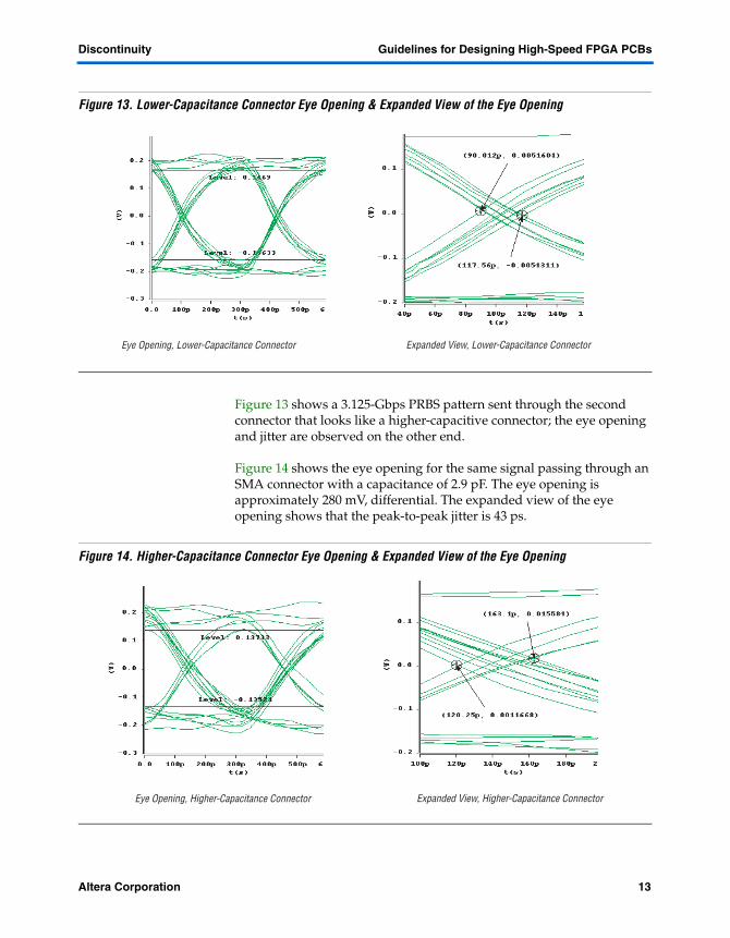
Figure 13 shows a 3.125-Gbps PRBS pattern sent through the second connector that looks like a higher-capacitive connector; the eye opening and jitter are observed on the other end.
Figure 14 shows the eye opening for the same signal passing through an SMA connector with a capacitance of 2.9 pF. The eye opening is approximately 280 mV, differential. The expanded view of the eye opening shows that the peak-to-peak jitter is 43 ps.
Figure 14. Higher-Capacitance Connector Eye Opening & Expanded View of the Eye Opening
Expanded View, Lower-Capacitance ConnectorEye Opening, Lower-Capacitance Connector
Expanded View, Higher-Capacitance ConnectorEye Opening, Higher-Capacitance Connector
Altera Corporation 13Preliminary
Guidelines for Designing High-Speed FPGA PCBs Discontinuity
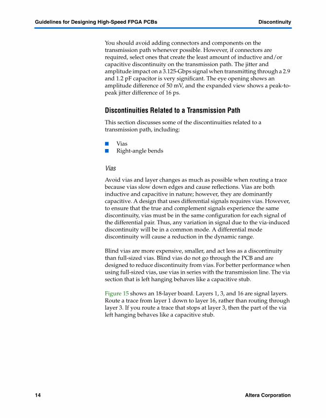
You should avoid adding connectors and components on the transmission path whenever possible. However, if connectors are required, select ones that create the least amount of inductive and/or capacitive discontinuity on the transmission path. The jitter and amplitude impact on a 3.125-Gbps signal when transmitting through a 2.9 and 1.2 pF capacitor is very significant. The eye opening shows an amplitude difference of 50 mV, and the expanded view shows a peak-to-peak jitter difference of 16 ps.
Discontinuities Related to a Transmission Path
This section discusses some of the discontinuities related to a transmission path, including:
Vias Right-angle bends
Vias
Avoid vias and layer changes as much as possible when routing a trace because vias slow down edges and cause reflections. Vias are both inductive and capacitive in nature; however, they are dominantly capacitive. A design that uses differential signals requires vias. However, to ensure that the true and complement signals experience the same discontinuity, vias must be in the same configuration for each signal of the differential pair. Thus, any variation in signal due to the via-induced discontinuity will be in a common mode. A differential mode discontinuity will cause a reduction in the dynamic range.
Blind vias are more expensive, smaller, and act less as a discontinuity than full-sized vias. Blind vias do not go through the PCB and are designed to reduce discontinuity from vias. For better performance when using full-sized vias, use vias in series with the transmission line. The via section that is left hanging behaves like a capacitive stub.
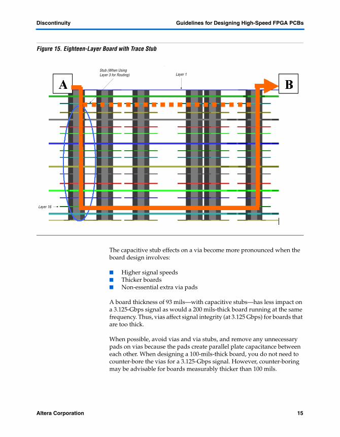
Figure 15 shows an 18-layer board. Layers 1, 3, and 16 are signal layers. Route a trace from layer 1 down to layer 16, rather than routing through layer 3. If you route a trace that stops at layer 3, then the part of the via left hanging behaves like a capacitive stub.
14 Altera CorporationPreliminary
Discontinuity Guidelines for Designing High-Speed FPGA PCBs
Figure 15. Eighteen-Layer Board with Trace Stub
The capacitive stub effects on a via become more pronounced when the board design involves:
Higher signal speeds Thicker boards Non-essential extra via pads
A board thickness of 93 mils—with capacitive stubs—has less impact on a 3.125-Gbps signal as would a 200 mils-thick board running at the same frequency. Thus, vias affect signal integrity (at 3.125 Gbps) for boards that are too thick.
When possible, avoid vias and via stubs, and remove any unnecessary pads on vias because the pads create parallel plate capacitance between each other. When designing a 100-mils-thick board, you do not need to counter-bore the vias for a 3.125-Gbps signal. However, counter-boring may be advisable for boards measurably thicker than 100 mils.
Stub (When Using Layer 3 for Routing) Layer 1
Layer 16
Altera Corporation 15Preliminary
Guidelines for Designing High-Speed FPGA PCBs Discontinuity
A current flow on a transmission line creates a magnetic field. The flux lines induce a return current on the reference structure. When a transmission line has its broadside facing reference planes, most of the return current travels underneath the transmission line at a skin depth on the reference plane. The value of skin depth can be calculated with the following equation:
skin depth = 1/
Where:
f = frequencyµo = magnetic permeability of airµr = relative magnetic permeabilityσ = χονδυ χτ ι ϖι τ ψ οφ µατ ερι αλ
You can calculate the current density at any point x in the reference plane with the following equation:
Ix = Io e-x/do
Where:
Ix = current density at xIo = current density on skin depthx = distance from surfacedo = skin depth
You should provide a good path for return currents. Figure 16 shows a layer change (from layer 1 to 13) for a pair of differential signals (i.e., red and green structures). The signal starts at Point A (in Figure 16) and transmits to Point B (Figure 18).
Figures 16 through 18 show that solid reference planes (i.e., light blue structures) are provided for the signal lines.
1 Create GND islands when necessary. When creating islands of GND, ensure that other signals referencing the plane do not pass over the split. If a signal does pass over the split, its loop will increase, also increasing the inductance in the region.
πfµo µr σ( )
16 Altera CorporationPreliminary
Discontinuity Guidelines for Designing High-Speed FPGA PCBs
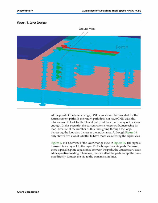
Figure 16. Layer Changes
At the point of the layer change, GND vias should be provided for the return current paths. If the return path does not have GND vias, the return currents look for the closest path, but these paths may not be close enough. In this scenario, the current takes a longer path, increasing its loop. Because of the number of flux lines going through the loop, increasing the loop also increases the inductance. Although Figure 16 only shows two vias, it is better to have more vias circling the signal vias.
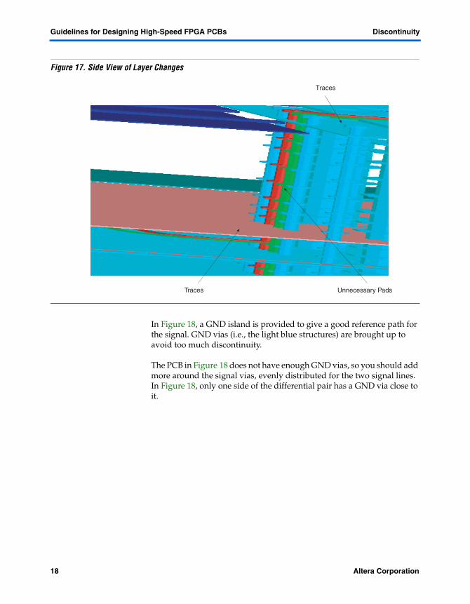
Figure 17 is a side view of the layer change view in Figure 16. The signals transmit from layer 1 to the layer 13. Each layer has via pads. Because there is parallel plate capacitance between the pads, the unnecessary pads add capacitive loading. Therefore, remove all of the pads except the ones that directly connect the via to the transmission lines.
Ground Vias
Point A
Altera Corporation 17Preliminary
Guidelines for Designing High-Speed FPGA PCBs Discontinuity
Figure 17. Side View of Layer Changes
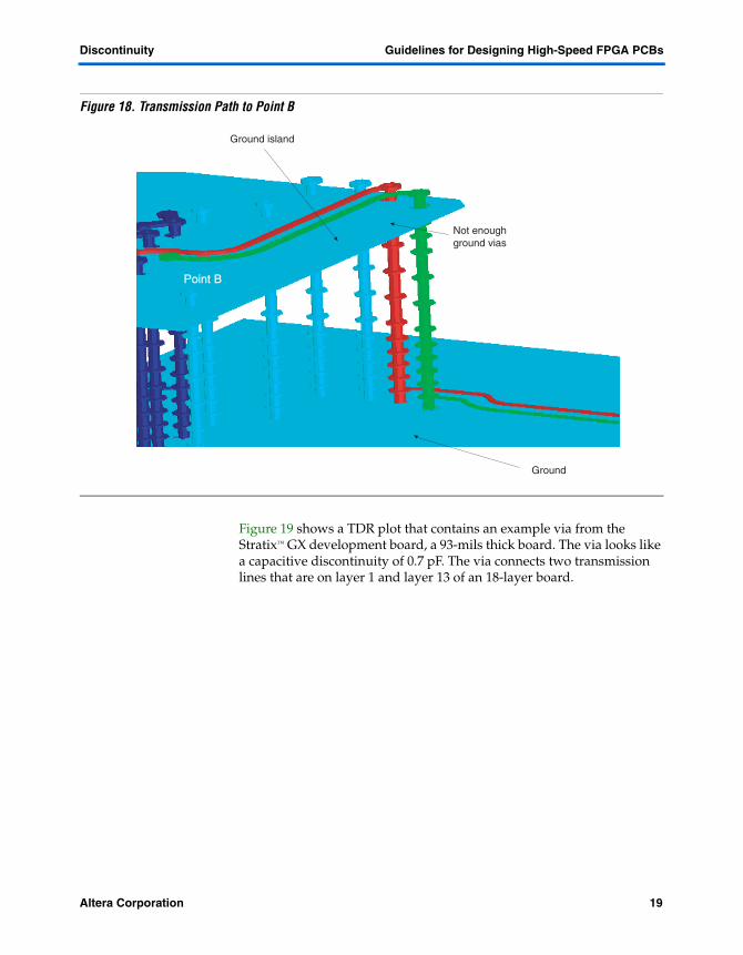
In Figure 18, a GND island is provided to give a good reference path for the signal. GND vias (i.e., the light blue structures) are brought up to avoid too much discontinuity.
The PCB in Figure 18 does not have enough GND vias, so you should add more around the signal vias, evenly distributed for the two signal lines. In Figure 18, only one side of the differential pair has a GND via close to it.
Traces
Traces Unnecessary Pads
18 Altera CorporationPreliminary
Discontinuity Guidelines for Designing High-Speed FPGA PCBs
Figure 18. Transmission Path to Point B
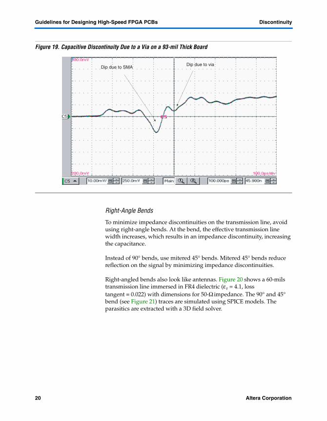
Figure 19 shows a TDR plot that contains an example via from the Stratix™ GX development board, a 93-mils thick board. The via looks like a capacitive discontinuity of 0.7 pF. The via connects two transmission lines that are on layer 1 and layer 13 of an 18-layer board.
Ground island
Point B
Not enoughground vias
Ground
Altera Corporation 19Preliminary
Guidelines for Designing High-Speed FPGA PCBs Discontinuity
Figure 19. Capacitive Discontinuity Due to a Via on a 93-mil Thick Board
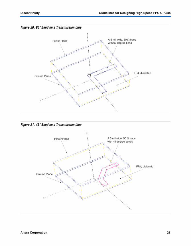
Right-Angle Bends
To minimize impedance discontinuities on the transmission line, avoid using right-angle bends. At the bend, the effective transmission line width increases, which results in an impedance discontinuity, increasing the capacitance.
Instead of 90° bends, use mitered 45° bends. Mitered 45° bends reduce reflection on the signal by minimizing impedance discontinuities.
Right-angled bends also look like antennas. Figure 20 shows a 60-mils transmission line immersed in FR4 dielectric (εr = 4.1, loss tangent = 0.022) with dimensions for 50-Ω impedance. The 90° and 45° bend (see Figure 21) traces are simulated using SPICE models. The parasitics are extracted with a 3D field solver.
Dip due to SMA Dip due to via
20 Altera CorporationPreliminary
Discontinuity Guidelines for Designing High-Speed FPGA PCBs
Figure 20. 90° Bend on a Transmission Line
Figure 21. 45° Bend on a Transmission Line
Power Plane
Ground Plane
A 5 mil wide, 50 Ω tracewith 90 degree bend
FR4, dielectric
Power Plane
Ground Plane
A 5 mil wide, 50 Ω tracewith 45 degree bends
FR4, dielectric
Altera Corporation 21Preliminary
Guidelines for Designing High-Speed FPGA PCBs Discontinuity
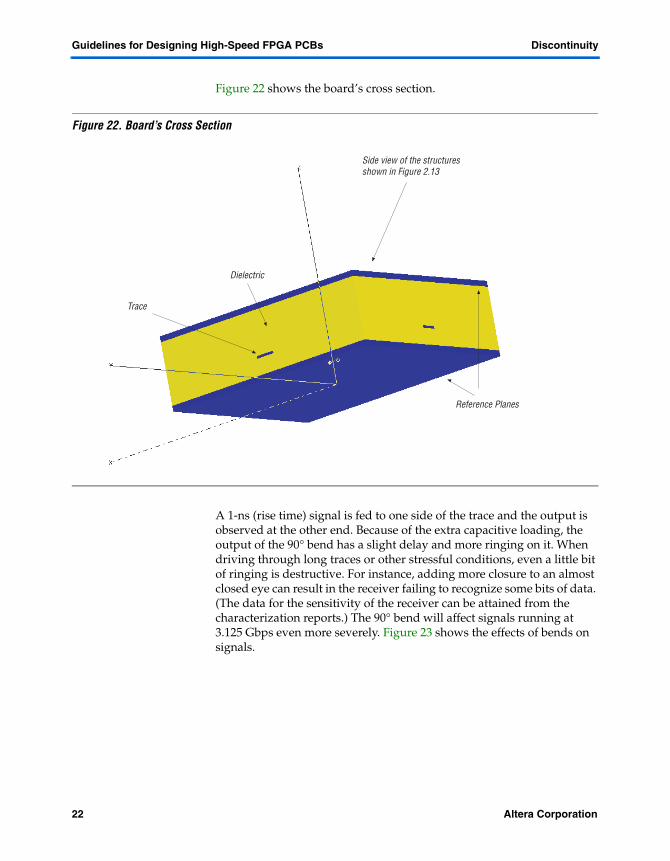
Figure 22 shows the board’s cross section.
Figure 22. Board’s Cross Section
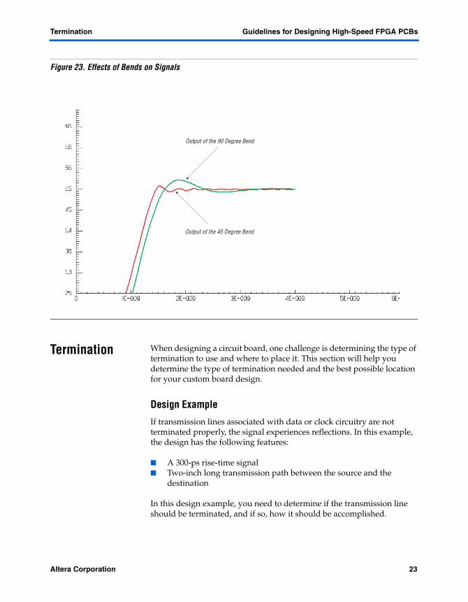
A 1-ns (rise time) signal is fed to one side of the trace and the output is observed at the other end. Because of the extra capacitive loading, the output of the 90° bend has a slight delay and more ringing on it. When driving through long traces or other stressful conditions, even a little bit of ringing is destructive. For instance, adding more closure to an almost closed eye can result in the receiver failing to recognize some bits of data. (The data for the sensitivity of the receiver can be attained from the characterization reports.) The 90° bend will affect signals running at 3.125 Gbps even more severely. Figure 23 shows the effects of bends on signals.
Dielectric
Trace
Side view of the structuresshown in Figure 2.13
Reference Planes
22 Altera CorporationPreliminary
Termination Guidelines for Designing High-Speed FPGA PCBs
Figure 23. Effects of Bends on Signals
Termination When designing a circuit board, one challenge is determining the type of termination to use and where to place it. This section will help you determine the type of termination needed and the best possible location for your custom board design.
Design Example
If transmission lines associated with data or clock circuitry are not terminated properly, the signal experiences reflections. In this example, the design has the following features:
A 300-ps rise-time signal Two-inch long transmission path between the source and the
destination
In this design example, you need to determine if the transmission line should be terminated, and if so, how it should be accomplished.
Output of the 90 Degree Bend
Output of the 45 Degree Bend
Altera Corporation 23Preliminary
Guidelines for Designing High-Speed FPGA PCBs Termination
Determine the Delay
Use the following equations to determine the delay for a 300-ps rise-time signal traveling through a transmission line embedded in a dielectric with an electrical permittivity of εr.
For stripline configuration:
For microstrip configuration:
In FR4, a transmission line with a stripline configuration induces approximately 180 ps per inch of delay on the signal. Therefore, the velocity of the signal through the transmission line becomes the inverse of the delay, which is 5.5 giga inches per second.
Determine the Bandwidth
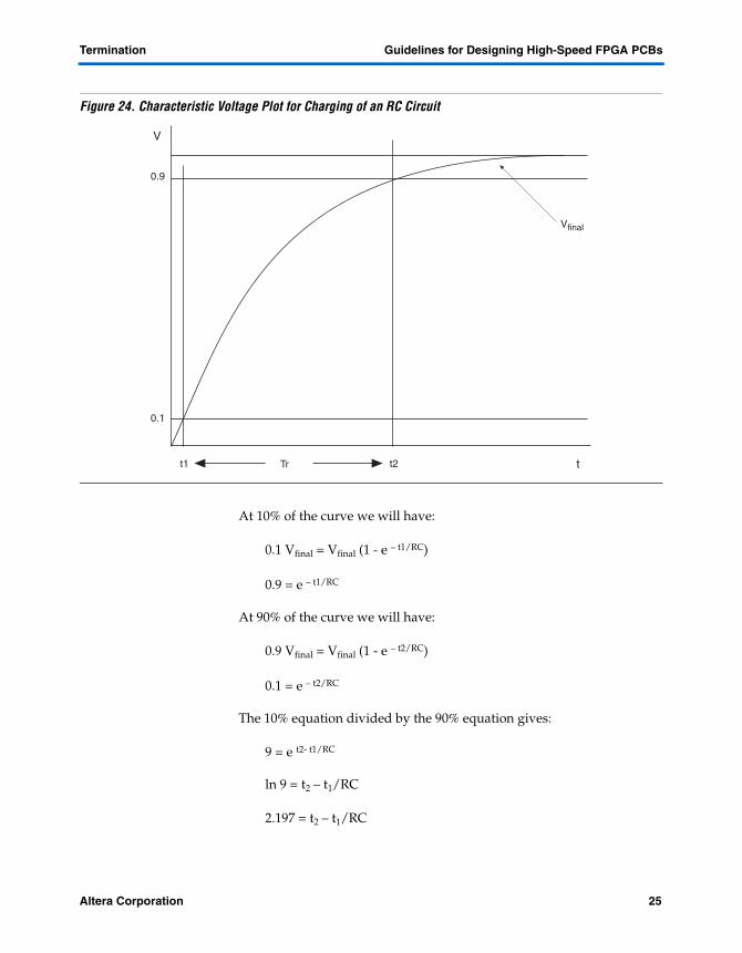
Figure 24 shows that the voltage at any instant t is,
V = Vfinal (1 - e – t/RC)
εrdelay = 85 ps per inch
0.475 εr + 0.67delay = 85 ps per inch
24 Altera CorporationPreliminary
Termination Guidelines for Designing High-Speed FPGA PCBs
Figure 24. Characteristic Voltage Plot for Charging of an RC Circuit
At 10% of the curve we will have:
0.1 Vfinal = Vfinal (1 - e – t1/RC)
0.9 = e – t1/RC
At 90% of the curve we will have:
0.9 Vfinal = Vfinal (1 - e – t2/RC)
0.1 = e – t2/RC
The 10% equation divided by the 90% equation gives:
9 = e t2- t1/RC
ln 9 = t2 – t1/RC
2.197 = t2 – t1/RC
V
t
Vfinal
0.9
0.1
t1 t2Tr
Altera Corporation 25Preliminary
Guidelines for Designing High-Speed FPGA PCBs Termination
Where:
t2 – t1 = Rise time of the signal (Tr) and RC = time constant = ґ
The time constant variable is related to the 3-dB frequency by the equation:
Frequency = 1/2 πr
From the previous equation, we can determine the equation for the time constant, r.
r = RC = 1/2 πf
Plug the time constant into the voltage equation to get:
2.197 = 2 π f Tr
f = 0.35 / Tr
Use the following equation to determine the bandwidth.
bandwidth = 0.35 / Tr
The highest frequency component for a signal with a rise time of Tr will have a frequency given by this equation.
The signal previously discussed had a rise time of 300 ps, which means that the highest frequency component present in the signal will be:
Bandwidth = 0.35/300 ps = 1.16 GHz
Using the equation
speed = frequency × wavelength
with the bandwidth and speed numbers, we can determine that:
5.5 Giga inches per second = 1.16 GHz × wavelength
wavelength = 4.74 in.
wavelength/10 = 0.474 in.
If the transmission line is longer than wavelength/10, then termination is required. In this design example, the transmission line is two inches long, so termination is required.
26 Altera CorporationPreliminary
Termination Guidelines for Designing High-Speed FPGA PCBs
Using Series Termination
When using series termination, only near-end termination can be applied. Series termination should only be used with clock signals.
With the near-end series termination (Zo) and the transmission line following, the circuit looks like a voltage divider circuit to the driver, reducing the amplitude V at the driver to V/2 after the series termination. Because there is no termination at the end of the transmission line, when the signal reaches the end, the entire signal reflects being restored to V. The reflection coefficient is calculated using the following equation:
Reflection coefficient = (Zload – Zo)/(Zload + Zo)
Using Parallel Termination
You can place parallel terminations on both ends or only the far end of the transmission line. You should place terminations as close to the source or destination as possible. Any transmission line between the termination and the end of the transmission line appears as a capacitive load to the signal. If you cannot place terminations close to the integrated circuit (IC), place them after the pin (i.e., fly-by configuration).
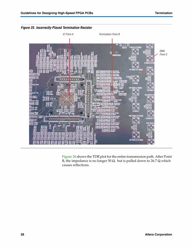
Figure 25 shows a board with an incorrectly-placed termination resistor. There are two inches of trace between the SMA connector (Point A in Figure 25) and the termination resistor (Point B in Figure 25), and another two inches of trace between the resistor and the IC (Point C in Figure 25). The entire section after the termination and before the IC looks like a capacitive load, which is why the termination should be placed as close as possible to the IC.
Altera Corporation 27Preliminary
Guidelines for Designing High-Speed FPGA PCBs Termination
Figure 25. Incorrectly-Placed Termination Resistor
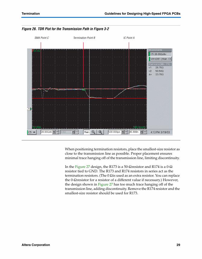
Figure 26 shows the TDR plot for the entire transmission path. After Point B, the impedance is no longer 50 Ω, but is pulled down to 26.7 Ω, which causes reflections.
IC Point A Termination Point B
SMAPoint C
28 Altera CorporationPreliminary
Termination Guidelines for Designing High-Speed FPGA PCBs
Figure 26. TDR Plot for the Transmission Path in Figure 3-2
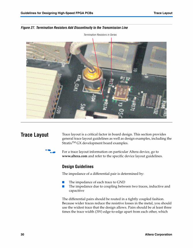
When positioning termination resistors, place the smallest-size resistor as close to the transmission line as possible. Proper placement ensures minimal trace hanging off of the transmission line, limiting discontinuity.
In the Figure 27 design, the R173 is a 50-Ω resistor and R174 is a 0-Ω resistor tied to GND. The R173 and R174 resistors in series act as the termination resistors. (The 0 Ω is used as an extra resistor. You can replace the 0-Ω resistor for a resistor of a different value if necessary.) However, the design shown in Figure 27 has too much trace hanging off of the transmission line, adding discontinuity. Remove the R174 resistor and the smallest-size resistor should be used for R173.
SMA Point C Termination Point B IC Point A
Altera Corporation 29Preliminary
Guidelines for Designing High-Speed FPGA PCBs Trace Layout
Figure 27. Termination Resistors Add Discontinuity to the Transmission Line
Trace Layout Trace layout is a critical factor in board design. This section provides general trace layout guidelines as well as design examples, including the StratixTM GX development board examples.
f For a trace layout information on particular Altera device, go to www.altera.com and refer to the specific device layout guidelines.
Design Guidelines
The impedance of a differential pair is determined by:
The impedance of each trace to GND The impedance due to coupling between two traces, inductive and
capacitive
The differential pairs should be routed in a tightly coupled fashion. Because wider traces reduce the resistive losses in the metal, you should use the widest trace that the design allows. Pairs should be at least three times the trace width (3W) edge-to-edge apart from each other, which
Termination Resistors in Series
30 Altera CorporationPreliminary
Trace Layout Guidelines for Designing High-Speed FPGA PCBs
prevents crosstalk. For best results, the layout should be verified with a 2-D field solver and the fields should be analyzed. Altera Applications can assist with the simulations.
Design Example 1
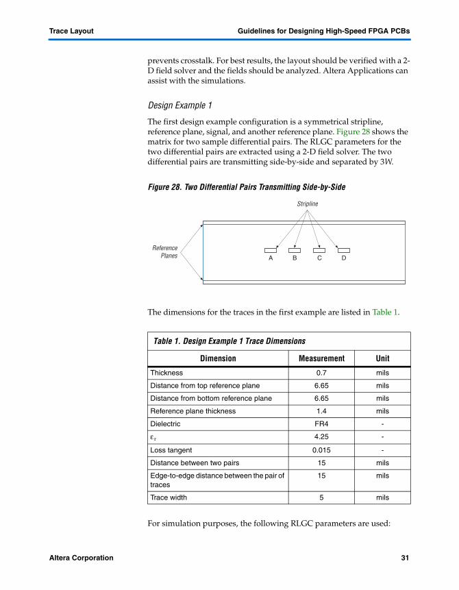
The first design example configuration is a symmetrical stripline, reference plane, signal, and another reference plane. Figure 28 shows the matrix for two sample differential pairs. The RLGC parameters for the two differential pairs are extracted using a 2-D field solver. The two differential pairs are transmitting side-by-side and separated by 3W.
Figure 28. Two Differential Pairs Transmitting Side-by-Side
The dimensions for the traces in the first example are listed in Table 1.
For simulation purposes, the following RLGC parameters are used:
Table 1. Design Example 1 Trace Dimensions
Dimension Measurement Unit
Thickness 0.7 mils
Distance from top reference plane 6.65 mils
Distance from bottom reference plane 6.65 mils
Reference plane thickness 1.4 mils
Dielectric FR4 -
εr 4.25 -
Loss tangent 0.015 -
Distance between two pairs 15 mils
Edge-to-edge distance between the pair of traces
15 mils
Trace width 5 mils
A B C D
ReferencePlanes
Stripline
Altera Corporation 31Preliminary
Guidelines for Designing High-Speed FPGA PCBs Trace Layout
+ Lo = 3.56013914223368e-007 5.36184274667006e-009 3.563779234163063e-007
+ Co = 1.339953702128462e-010 -2.02513540100207e-012 1.339283788059507e-010
+ Ro = 7.71501953506781 0.07953628386667984 7.71501953506804 + Rs = 0.001551635604701119 1.982986965540932e-005
0.001501872172761996 + Gd = 1.266487562542408e-011 -1.886481164851002e-013
1.264473093423482e-011
Where:
Lo = Characteristic inductance Co = Characteristic capacitance Ro = Characteristic resistance Rs = Skin effect resistance Gd = Shunt conductance
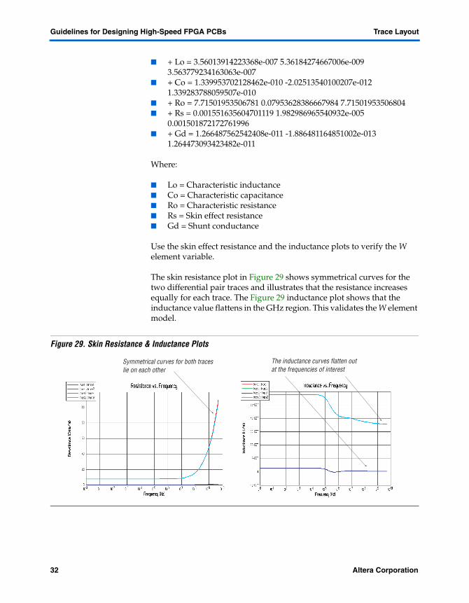
Use the skin effect resistance and the inductance plots to verify the W element variable.
The skin resistance plot in Figure 29 shows symmetrical curves for the two differential pair traces and illustrates that the resistance increases equally for each trace. The Figure 29 inductance plot shows that the inductance value flattens in the GHz region. This validates the W element model.
Figure 29. Skin Resistance & Inductance Plots
Symmetrical curves for both traceslie on each other
The inductance curves flatten out at the frequencies of interest
32 Altera CorporationPreliminary
Trace Layout Guidelines for Designing High-Speed FPGA PCBs
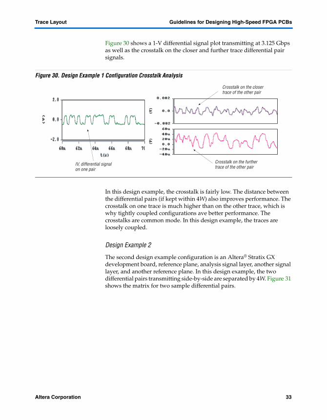
Figure 30 shows a 1-V differential signal plot transmitting at 3.125 Gbps as well as the crosstalk on the closer and further trace differential pair signals.
Figure 30. Design Example 1 Configuration Crosstalk Analysis
In this design example, the crosstalk is fairly low. The distance between the differential pairs (if kept within 4W) also improves performance. The crosstalk on one trace is much higher than on the other trace, which is why tightly coupled configurations ave better performance. The crosstalks are common mode. In this design example, the traces are loosely coupled.
Design Example 2
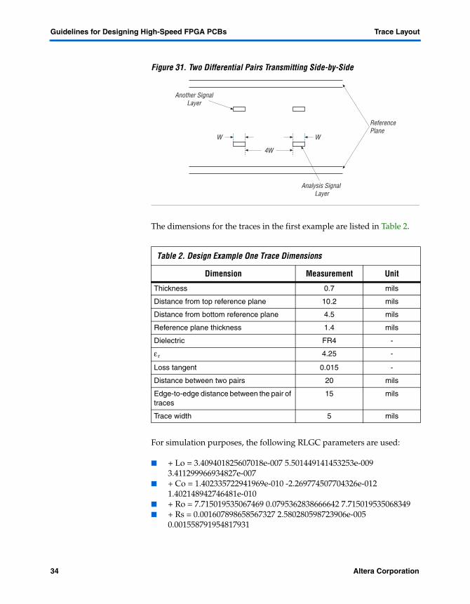
The second design example configuration is an Altera® Stratix GX development board, reference plane, analysis signal layer, another signal layer, and another reference plane. In this design example, the two differential pairs transmitting side-by-side are separated by 4W. Figure 31 shows the matrix for two sample differential pairs.
Crosstalk on the furthertrace of the other pair
IV, differential signalon one pair
Crosstalk on the closertrace of the other pair
Altera Corporation 33Preliminary
Guidelines for Designing High-Speed FPGA PCBs Trace Layout
Figure 31. Two Differential Pairs Transmitting Side-by-Side
The dimensions for the traces in the first example are listed in Table 2.
For simulation purposes, the following RLGC parameters are used:
+ Lo = 3.409401825607018e-007 5.501449141453253e-009 3.411299966934827e-007
+ Co = 1.402335722941969e-010 -2.269774507704326e-012 1.402148942746481e-010
+ Ro = 7.715019535067469 0.0795362838666642 7.715019535068349 + Rs = 0.001607898658567327 2.580280598723906e-005
0.001558791954817931
Table 2. Design Example One Trace Dimensions
Dimension Measurement Unit
Thickness 0.7 mils
Distance from top reference plane 10.2 mils
Distance from bottom reference plane 4.5 mils
Reference plane thickness 1.4 mils
Dielectric FR4 -
εr 4.25 -
Loss tangent 0.015 -
Distance between two pairs 20 mils
Edge-to-edge distance between the pair of traces
15 mils
Trace width 5 mils
W W
4W
Analysis Signal Layer
Another SignalLayer
ReferencePlane
34 Altera CorporationPreliminary
Trace Layout Guidelines for Designing High-Speed FPGA PCBs
+ Gd = 1.327358599905988e-011 -2.15902867236468e-013 1.329113742424896e-011
Where:
Lo = Characteristic inductance Co = Characteristic capacitance Ro = Characteristic resistance Rs = Skin effect resistance Gd = Shunt conductance
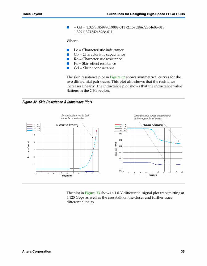
The skin resistance plot in Figure 32 shows symmetrical curves for the two differential pair traces. This plot also shows that the resistance increases linearly. The inductance plot shows that the inductance value flattens in the GHz region.
Figure 32. Skin Resistance & Inductance Plots
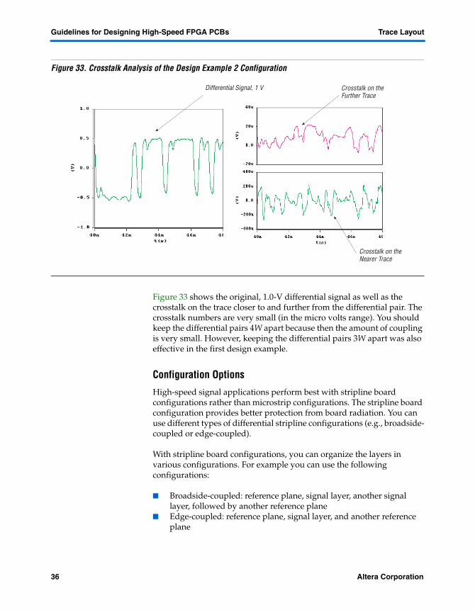
The plot in Figure 33 shows a 1.0-V differential signal plot transmitting at 3.125 Gbps as well as the crosstalk on the closer and further trace differential pairs.
Symmetrical curves for bothtraces lie on each other
The inductance curves smoothen outat the frequencies of interest
Altera Corporation 35Preliminary
Guidelines for Designing High-Speed FPGA PCBs Trace Layout
Figure 33. Crosstalk Analysis of the Design Example 2 Configuration
Figure 33 shows the original, 1.0-V differential signal as well as the crosstalk on the trace closer to and further from the differential pair. The crosstalk numbers are very small (in the micro volts range). You should keep the differential pairs 4W apart because then the amount of coupling is very small. However, keeping the differential pairs 3W apart was also effective in the first design example.
Configuration Options
High-speed signal applications perform best with stripline board configurations rather than microstrip configurations. The stripline board configuration provides better protection from board radiation. You can use different types of differential stripline configurations (e.g., broadside-coupled or edge-coupled).
With stripline board configurations, you can organize the layers in various configurations. For example you can use the following configurations:
Broadside-coupled: reference plane, signal layer, another signal layer, followed by another reference plane
Edge-coupled: reference plane, signal layer, and another reference plane
Crosstalk on theNearer Trace
Crosstalk on theFurther Trace
Differential Signal, 1 V
36 Altera CorporationPreliminary
Trace Layout Guidelines for Designing High-Speed FPGA PCBs
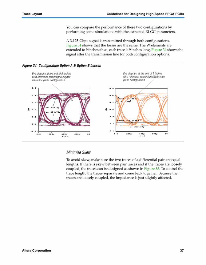
You can compare the performance of these two configurations by performing some simulations with the extracted RLGC parameters.
A 3.125-Gbps signal is transmitted through both configurations. Figure 34 shows that the losses are the same. The W elements are extended to 9 inches; thus, each trace is 9 inches long. Figure 34 shows the signal after the transmission line for both configuration options.
Figure 34. Configuration Option A & Option B Losses
Minimize Skew
To avoid skew, make sure the two traces of a differential pair are equal lengths. If there is skew between pair traces and if the traces are loosely coupled, the traces can be designed as shown in Figure 35. To control the trace length, the traces separate and come back together. Because the traces are loosely coupled, the impedance is just slightly affected.
Eye diagram at the end of 9 incheswith reference plane/signal/referenceplane configuration
Eye diagram at the end of 9 incheswith reference plane/signal/signal/reference plane configuration
Altera Corporation 37Preliminary
Guidelines for Designing High-Speed FPGA PCBs Trace Layout
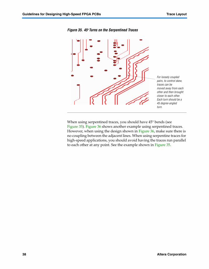
Figure 35. 45°Turns on the Serpentined Traces
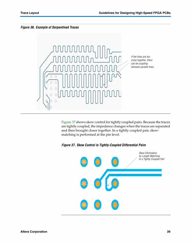
When using serpentined traces, you should have 45° bends (see Figure 35). Figure 36 shows another example using serpentined traces. However, when using the design shown in Figure 36, make sure there is no coupling between the adjacent lines. When using serpentine traces for high-speed applications, you should avoid having the traces run parallel to each other at any point. See the example shown in Figure 35.
For loosely coupledpairs, to control skew,traces can bemoved away from eachother and then broughtcloser to each other.Each turn should be a45 degree-angledturn.
38 Altera CorporationPreliminary
Trace Layout Guidelines for Designing High-Speed FPGA PCBs
Figure 36. Example of Serpentined Traces
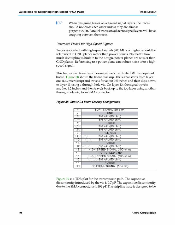
Figure 37 shows skew control for tightly coupled pairs. Because the traces are tightly coupled, the impedance changes when the traces are separated and then brought closer together. In a tightly coupled pair, skew-matching is performed at the pin level.
Figure 37. Skew Control in Tightly-Coupled Differential Pairs
If the lines are tooclose together, therecan be couplingbetween parallel lines.
Skew Eliminationby Length Matchingin a Tightly Coupled Pair
Altera Corporation 39Preliminary
Guidelines for Designing High-Speed FPGA PCBs Trace Layout
1 When designing traces on adjacent signal layers, the traces should not cross each other unless they are almost perpendicular. Parallel traces on adjacent signal layers will have coupling between the traces.
Reference Planes for High-Speed Signals
Traces associated with high-speed signals (200 MHz or higher) should be referenced to GND planes rather than power planes. No matter how much decoupling is built in to the design, power planes are noisier than GND planes. Referencing to a power plane can induce noise onto a high-speed signal.
This high-speed trace layout example uses the Stratix GX development board. Figure 38 shows the board stackup. The signal starts from layer one (i.e., microstrip) and travels for about 0.5 inches and then dips down to layer 13 using a through-hole via. On layer 13, the signal travels another 1.5 inches and then travels back up to the top layer using another through-hole via, to an SMA connector.
Figure 38. Stratix GX Board Stackup Configuration
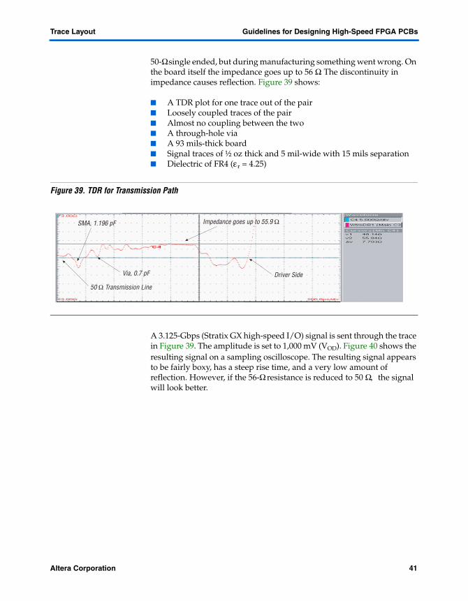
Figure 39 is a TDR plot for the transmission path. The capacitive discontinuity introduced by the via is 0.7 pF. The capacitive discontinuity due to the SMA connector is 1.196 pF. The stripline trace is designed to be
40 Altera CorporationPreliminary
Trace Layout Guidelines for Designing High-Speed FPGA PCBs
50-Ω single ended, but during manufacturing something went wrong. On the board itself the impedance goes up to 56 Ω. The discontinuity in impedance causes reflection. Figure 39 shows:
A TDR plot for one trace out of the pair Loosely coupled traces of the pair Almost no coupling between the two A through-hole via A 93 mils-thick board Signal traces of ½ oz thick and 5 mil-wide with 15 mils separation Dielectric of FR4 (εr = 4.25)
Figure 39. TDR for Transmission Path
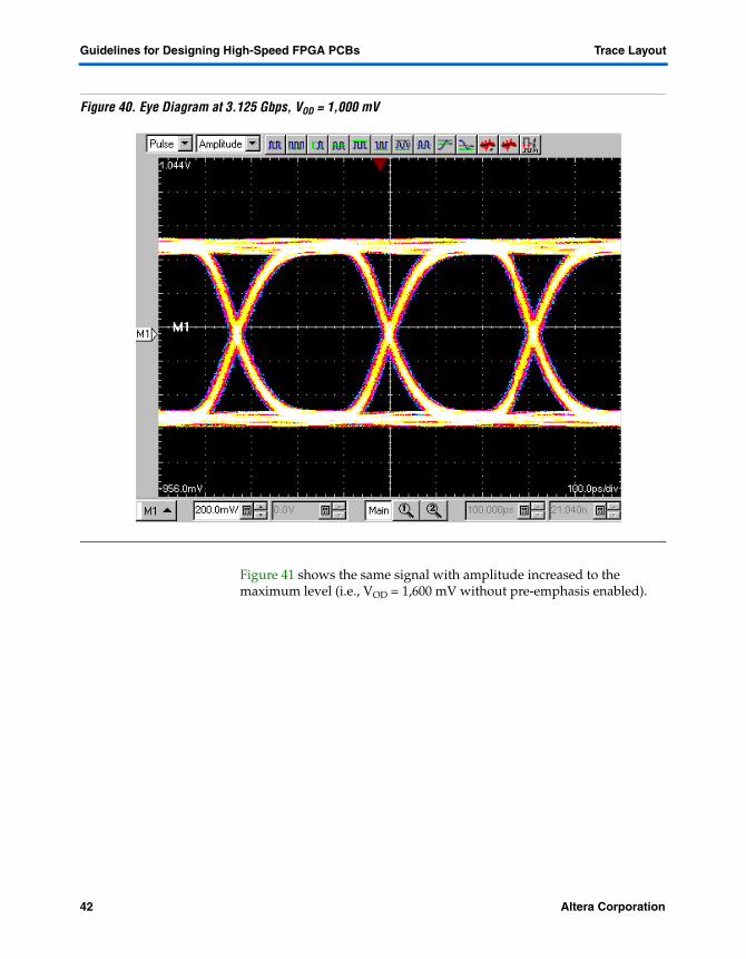
A 3.125-Gbps (Stratix GX high-speed I/O) signal is sent through the trace in Figure 39. The amplitude is set to 1,000 mV (VOD). Figure 40 shows the resulting signal on a sampling oscilloscope. The resulting signal appears to be fairly boxy, has a steep rise time, and a very low amount of reflection. However, if the 56-Ω resistance is reduced to 50 Ω, the signal will look better.
50 Ω Transmission Line
Via, 0.7 pF Driver Side
Impedance goes up to 55.9 ΩSMA, 1.196 pF
Altera Corporation 41Preliminary
Guidelines for Designing High-Speed FPGA PCBs Trace Layout
Figure 40. Eye Diagram at 3.125 Gbps, VOD = 1,000 mV
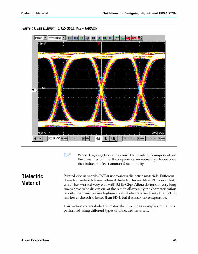
Figure 41 shows the same signal with amplitude increased to the maximum level (i.e., VOD = 1,600 mV without pre-emphasis enabled).
42 Altera CorporationPreliminary
Dielectric Material Guidelines for Designing High-Speed FPGA PCBs
Figure 41. Eye Diagram, 3.125 Gbps, VOD = 1600 mV
1 When designing traces, minimize the number of components on the transmission line. If components are necessary, choose ones that induce the least amount discontinuity.
Dielectric Material
Printed circuit boards (PCBs) use various dielectric materials. Different dielectric materials have different dielectric losses. Most PCBs use FR-4, which has worked very well with 3.125-Gbps Altera designs. If very long traces have to be driven out of the region allowed by the characterization reports, then you can use higher-quality dielectrics, such as GTEK. GTEK has lower dielectric losses than FR-4, but it is also more expensive.
This section covers dielectric materials. It includes example simulations performed using different types of dielectric materials.
Altera Corporation 43Preliminary
Guidelines for Designing High-Speed FPGA PCBs Dielectric Material
RLGC Parameters
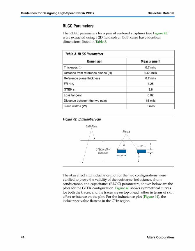
The RLGC parameters for a pair of centered striplines (see Figure 42) were extracted using a 2D field solver. Both cases have identical dimensions, listed in Table 3.
Figure 42. Differential Pair
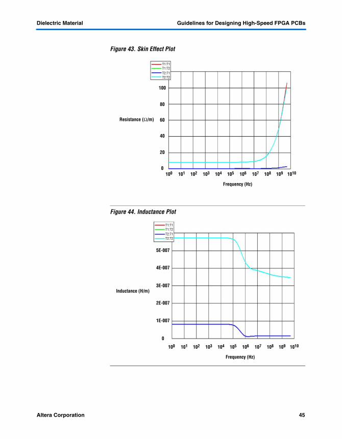
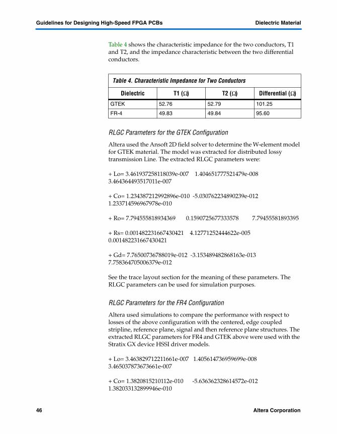
The skin effect and inductance plot for the two configurations were verified to prove the validity of the resistance, inductance, shunt conductance, and capacitance (RLGC) parameters, shown below are the plots for the GTEK configuration. Figure 43 shows symmetrical curves for both the traces, and the traces are on top of each other in terms of skin effect resistance on the plot. For the inductance plot (Figure 44), the inductance value flattens in the GHz region.
Table 3. RLGC Parameters
Dimension Measurement
Thickness (t) 0.7 mils
Distance from reference planes (H) 6.65 mils
Reference plane thickness 0.7 mils
FR-4 ε r 4.25
GTEK ε r 3.8
Loss tangent 0.02
Distance between the two pairs 15 mils
Trace widths (W) 5 mils
GTEK or FR-4Dielectric
H
H
t
W
W
GND Plane
Signals
44 Altera CorporationPreliminary
Dielectric Material Guidelines for Designing High-Speed FPGA PCBs
Figure 43. Skin Effect Plot
Figure 44. Inductance Plot
Frequency (Hz)
100 101 102 103 104 105 106 107 108 109 1010
T1:T1T1:T2T2:T1T2:T2
Resistance (Ω/m)
100
80
60
40
20
0
Inductance (H/m)
Frequency (Hz)
5E-007
4E-007
3E-007
2E-007
1E-007
0
100 101 102 103 104 105 106 107 108 109 1010
T1:T1T1:T2T2:T1T2:T2
Altera Corporation 45Preliminary
Guidelines for Designing High-Speed FPGA PCBs Dielectric Material
Table 4 shows the characteristic impedance for the two conductors, T1 and T2, and the impedance characteristic between the two differential conductors.
RLGC Parameters for the GTEK Configuration
Altera used the Ansoft 2D field solver to determine the W-element model for GTEK material. The model was extracted for distributed lossy transmission Line. The extracted RLGC parameters were:
+ Lo= 3.461937258118039e-007 1.404651777521479e-008 3.464364493517011e-007
+ Co= 1.234387212992896e-010 -5.030762234890239e-012 1.233714596967978e-010
+ Ro= 7.794555818934369 0.1590725677333578 7.79455581893395
+ Rs= 0.001482231667430421 4.12771252444622e-005 0.001482231667430421
+ Gd= 7.76500736788019e-012 -3.153489482868163e-013 7.758364705006379e-012
See the trace layout section for the meaning of these parameters. The RLGC parameters can be used for simulation purposes.
RLGC Parameters for the FR4 Configuration
Altera used simulations to compare the performance with respect to losses of the above configuration with the centered, edge coupled stripline, reference plane, signal and then reference plane structures. The extracted RLGC parameters for FR4 and GTEK above were used with the Stratix GX device HSSI driver models.
+ Lo= 3.463829712211661e-007 1.405614736959699e-008 3.465037873673661e-007
+ Co= 1.3820815210112e-010 -5.636362328614572e-012 1.382033132899946e-010
Table 4. Characteristic Impedance for Two Conductors
Dielectric T1 (Ω) T2 (Ω) Differential (Ω)
GTEK 52.76 52.79 101.25
FR-4 49.83 49.84 95.60
46 Altera CorporationPreliminary
Dielectric Material Guidelines for Designing High-Speed FPGA PCBs
+ Ro= 7.794555818935226 0.1590725677333466 7.794555818934586
+ Rs= 0.001399740310578771 3.829952571676754e-005 0.001399740310578771
+ Gd= 1.73401101269376e-011 -7.064220383669639e-013 1.73342000154418e-011
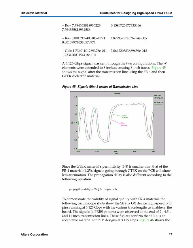
A 3.125-Gbps signal was sent through the two configurations. The W elements were extended to 8 inches, creating 8-inch traces. Figure 45 shows the signal after the transmission line using the FR-4 and then GTEK dielectric material.
Figure 45. Signals After 8 inches of Transmission Line
Since the GTEK material's permittivity (3.8) is smaller than that of the FR-4 material (4.25), signals going through GTEK on the PCB will show less attenuation. The propagation delay is also different according to the following equation.
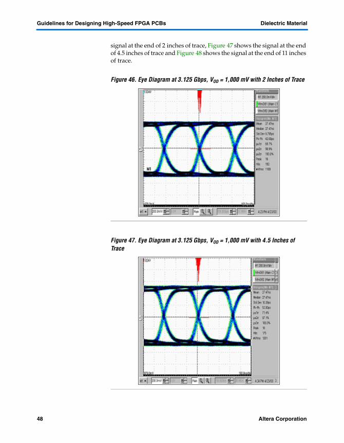
To demonstrate the validity of signal quality with FR-4 material, the following oscilloscope shots show the Stratix GX device high-speed I/O pins running at 3.125 Gbps with the various trace lengths available on the board. The signals (a PRBS pattern) were observed at the end of 2-, 4.5-, and 11-inch transmission lines. These figures confirm that FR-4 is an acceptable material for PCB designs at 3.125 Gbps. Figure 46 shows the
εrpropagation delay = 85 ps per inch
Altera Corporation 47Preliminary
Guidelines for Designing High-Speed FPGA PCBs Dielectric Material
signal at the end of 2 inches of trace, Figure 47 shows the signal at the end of 4.5 inches of trace and Figure 48 shows the signal at the end of 11 inches of trace.
Figure 46. Eye Diagram at 3.125 Gbps, VOD = 1,000 mV with 2 Inches of Trace
Figure 47. Eye Diagram at 3.125 Gbps, VOD = 1,000 mV with 4.5 Inches of Trace
48 Altera CorporationPreliminary
Simultaneous Switching Noise Guidelines for Designing High-Speed FPGA PCBs
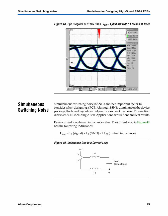
Figure 48. Eye Diagram at 3.125 Gbps, VOD = 1,000 mV with 11 Inches of Trace
Simultaneous Switching Noise
Simultaneous switching noise (SSN) is another important factor to consider when designing a PCB. Although SSN is dominant on the device package, the board layout can help reduce some of the noise. This section discusses SSN, including Altera Applications simulations and test results.
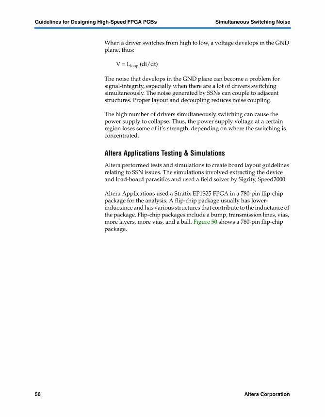
Every current loop has an inductance value. The current loop in Figure 49 has the following inductance:
Lloop = L1 (signal) + L2 (GND) – 2 LM (mutual inductance)
Figure 49. Inductance Due to a Current Loop
L1
VCC
L2
LoadCapacitance
Altera Corporation 49Preliminary
Guidelines for Designing High-Speed FPGA PCBs Simultaneous Switching Noise
When a driver switches from high to low, a voltage develops in the GND plane, thus:
V = Lloop (di/dt)
The noise that develops in the GND plane can become a problem for signal-integrity, especially when there are a lot of drivers switching simultaneously. The noise generated by SSNs can couple to adjacent structures. Proper layout and decoupling reduces noise coupling.
The high number of drivers simultaneously switching can cause the power supply to collapse. Thus, the power supply voltage at a certain region loses some of it’s strength, depending on where the switching is concentrated.
Altera Applications Testing & Simulations
Altera performed tests and simulations to create board layout guidelines relating to SSN issues. The simulations involved extracting the device and load-board parasitics and used a field solver by Sigrity, Speed2000.
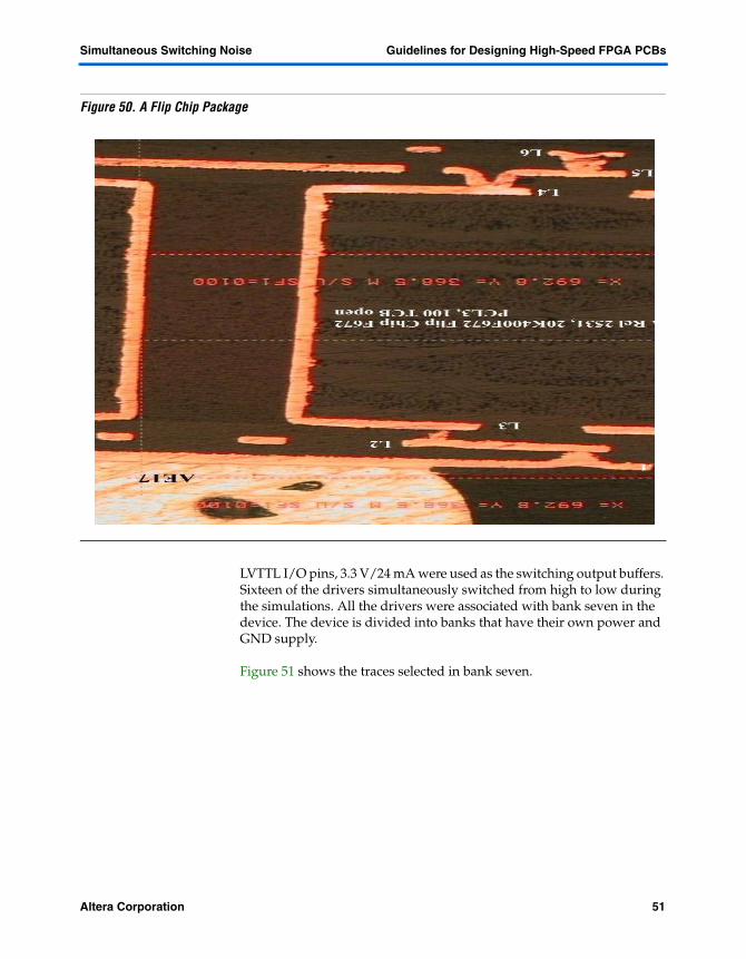
Altera Applications used a Stratix EP1S25 FPGA in a 780-pin flip-chip package for the analysis. A flip-chip package usually has lower-inductance and has various structures that contribute to the inductance of the package. Flip-chip packages include a bump, transmission lines, vias, more layers, more vias, and a ball. Figure 50 shows a 780-pin flip-chip package.
50 Altera CorporationPreliminary
Simultaneous Switching Noise Guidelines for Designing High-Speed FPGA PCBs
Figure 50. A Flip Chip Package
LVTTL I/O pins, 3.3 V/24 mA were used as the switching output buffers. Sixteen of the drivers simultaneously switched from high to low during the simulations. All the drivers were associated with bank seven in the device. The device is divided into banks that have their own power and GND supply.
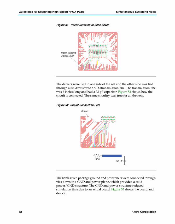
Figure 51 shows the traces selected in bank seven.
Altera Corporation 51Preliminary
Guidelines for Designing High-Speed FPGA PCBs Simultaneous Switching Noise
Figure 51. Traces Selected in Bank Seven
The drivers were tied to one side of the net and the other side was tied through a 50-Ω resistor to a 50-Ω transmission line. The transmission line was 6 inches long and had a 33 pF capacitor. Figure 52 shows how the circuit is connected. The same circuitry was true for all the nets.
Figure 52. Circuit Connection Path
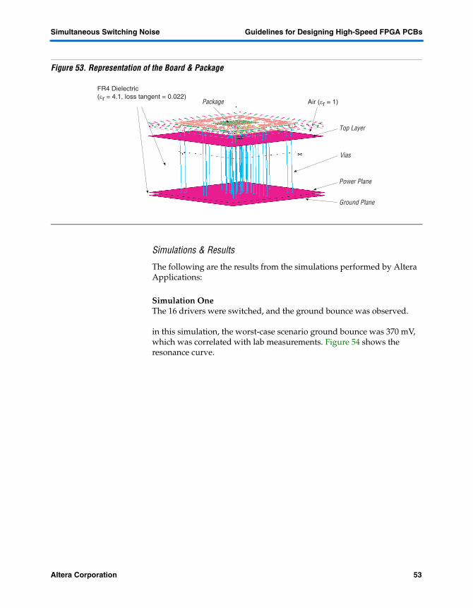
The bank seven package ground and power nets were connected through vias down to a GND and power plane, which provided a solid power/GND structure. The GND and power structure reduced simulation time due to an actual board. Figure 53 shows the board and device.
Traces Selectedin Bank Seven
33 pF50Ω
Drivers
52 Altera CorporationPreliminary
Simultaneous Switching Noise Guidelines for Designing High-Speed FPGA PCBs
Figure 53. Representation of the Board & Package
Simulations & Results
The following are the results from the simulations performed by Altera Applications:
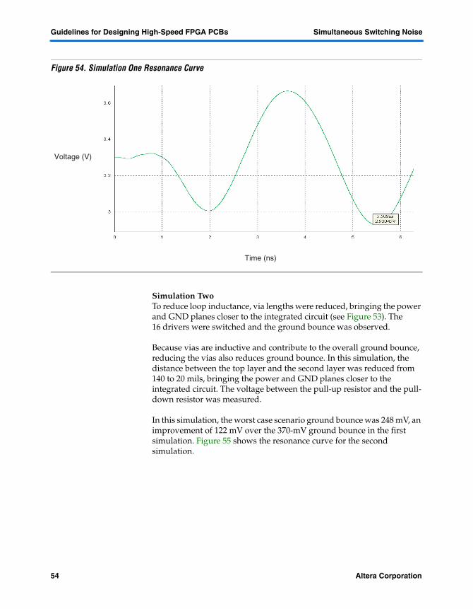
Simulation OneThe 16 drivers were switched, and the ground bounce was observed.
in this simulation, the worst-case scenario ground bounce was 370 mV, which was correlated with lab measurements. Figure 54 shows the resonance curve.
Package
Top Layer
Power Plane
Ground Plane
Vias
Air (εr = 1)
FR4 Dielectric(εr = 4.1, loss tangent = 0.022)
Altera Corporation 53Preliminary
Guidelines for Designing High-Speed FPGA PCBs Simultaneous Switching Noise
Figure 54. Simulation One Resonance Curve
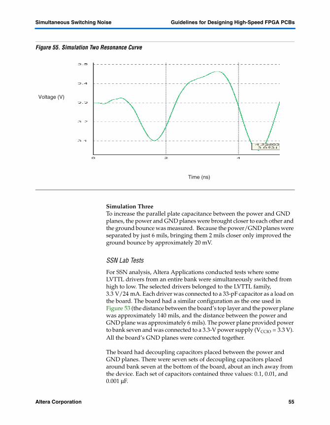
Simulation TwoTo reduce loop inductance, via lengths were reduced, bringing the power and GND planes closer to the integrated circuit (see Figure 53). The 16 drivers were switched and the ground bounce was observed.
Because vias are inductive and contribute to the overall ground bounce, reducing the vias also reduces ground bounce. In this simulation, the distance between the top layer and the second layer was reduced from 140 to 20 mils, bringing the power and GND planes closer to the integrated circuit. The voltage between the pull-up resistor and the pull-down resistor was measured.
In this simulation, the worst case scenario ground bounce was 248 mV, an improvement of 122 mV over the 370-mV ground bounce in the first simulation. Figure 55 shows the resonance curve for the second simulation.
Time (ns)
Voltage (V)
54 Altera CorporationPreliminary
Simultaneous Switching Noise Guidelines for Designing High-Speed FPGA PCBs
Figure 55. Simulation Two Resonance Curve
Simulation ThreeTo increase the parallel plate capacitance between the power and GND planes, the power and GND planes were brought closer to each other and the ground bounce was measured. Because the power/GND planes were separated by just 6 mils, bringing them 2 mils closer only improved the ground bounce by approximately 20 mV.
SSN Lab Tests
For SSN analysis, Altera Applications conducted tests where some LVTTL drivers from an entire bank were simultaneously switched from high to low. The selected drivers belonged to the LVTTL family, 3.3 V/24 mA. Each driver was connected to a 33-pF capacitor as a load on the board. The board had a similar configuration as the one used in Figure 53 (the distance between the board’s top layer and the power plane was approximately 140 mils, and the distance between the power and GND plane was approximately 6 mils). The power plane provided power to bank seven and was connected to a 3.3-V power supply (VCCIO = 3.3 V). All the board’s GND planes were connected together.
The board had decoupling capacitors placed between the power and GND planes. There were seven sets of decoupling capacitors placed around bank seven at the bottom of the board, about an inch away from the device. Each set of capacitors contained three values: 0.1, 0.01, and 0.001 µF.
Time (ns)Voltage (V)
Time (ns)
Voltage (V)
Altera Corporation 55Preliminary
Guidelines for Designing High-Speed FPGA PCBs Simultaneous Switching Noise
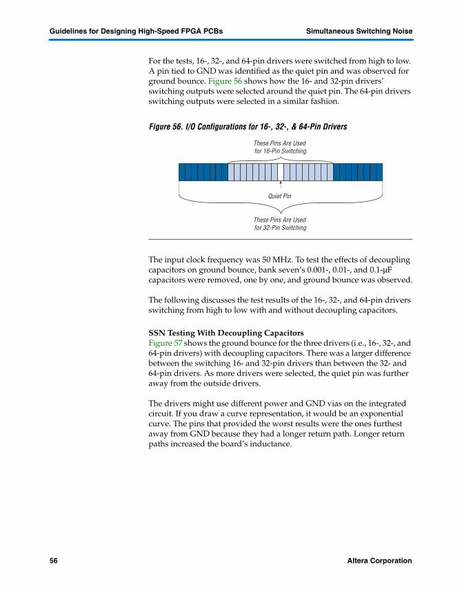
For the tests, 16-, 32-, and 64-pin drivers were switched from high to low. A pin tied to GND was identified as the quiet pin and was observed for ground bounce. Figure 56 shows how the 16- and 32-pin drivers’ switching outputs were selected around the quiet pin. The 64-pin drivers switching outputs were selected in a similar fashion.
Figure 56. I/O Configurations for 16-, 32-, & 64-Pin Drivers
The input clock frequency was 50 MHz. To test the effects of decoupling capacitors on ground bounce, bank seven’s 0.001-, 0.01-, and 0.1-µF capacitors were removed, one by one, and ground bounce was observed.
The following discusses the test results of the 16-, 32-, and 64-pin drivers switching from high to low with and without decoupling capacitors.
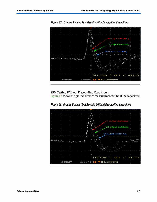
SSN Testing With Decoupling Capacitors Figure 57 shows the ground bounce for the three drivers (i.e., 16-, 32-, and 64-pin drivers) with decoupling capacitors. There was a larger difference between the switching 16- and 32-pin drivers than between the 32- and 64-pin drivers. As more drivers were selected, the quiet pin was further away from the outside drivers.
The drivers might use different power and GND vias on the integrated circuit. If you draw a curve representation, it would be an exponential curve. The pins that provided the worst results were the ones furthest away from GND because they had a longer return path. Longer return paths increased the board’s inductance.
Quiet Pin
These Pins Are Used for 16-Pin Switching
These Pins Are Used for 32-Pin Switching
56 Altera CorporationPreliminary
Simultaneous Switching Noise Guidelines for Designing High-Speed FPGA PCBs
Figure 57. Ground Bounce Test Results With Decoupling Capacitors
SSN Testing Without Decoupling CapacitorsFigure 58 shows the ground bounce measurement without the capacitors.
Figure 58. Ground Bounce Test Results Without Decoupling Capacitors
Altera Corporation 57Preliminary

Guidelines for Designing High-Speed FPGA PCBs Simultaneous Switching Noise
Table 5 compares the ground bounce results when testing with and without the decoupling capacitors.
The decoupling capacitors did not effect the ground bounce. After removing the capacitors, the ground bounce only dipped slightly. Additionally, the ground bounce dip may be the result of some resonance induced by the capacitor and via parasitics.
The capacitors were located approximately one inch from the integrated circuit. There is a good-sized via between the power plane and the integrated circuit. In this example, the board is not designed well, which is why the paths have very high inductance, rendering the decoupling capacitors useless. The power and ground structures are not close to each other and are not close to the IC.
Slew RateThe following section discusses the effects of varying slew rates on SSN. Table 6 lists the results of the quiet pin tested with a varying number of I/O drivers switching; four configurations of LVTTL drivers are used in the experiments. You can see the loading on the supply with the different strengths of drivers. (The quiet pin is tied to the power pin.)
Table 5. Ground Bounce Results with & without Decoupling Capacitors
Test Scenario Drivers Ground Bounce (mV)
With capacitor 16 640
32 820
64 860
Without capacitor 16 620
32 780
64 840
Table 6. Effects of Varying Slew Rates on SSN (Part 1 of 2)
Number of I/O Pins
LVTTL 24 mA, Fast Slew Rate
LVTTL 2 mA, Fast Slew Rate
LVTTL 24 mA, Slow Slew Rate
LVTTL 2 mA, Slow Slew Rate
0 3.3 3.3 3.3 3.3
2 2.95 2.92 2.96 2.92
4 2.9 3.06 3.15 2.96
8 2.74 3 2.91 2.92
16 2.38 2.8 2.52 2.94
58 Altera CorporationPreliminary
Simultaneous Switching Noise Guidelines for Designing High-Speed FPGA PCBs
Table 6 shows that the driver’s slew rate (di/dt) makes a big difference in the amount of voltage collapse introduced. Because the ground bounce is nothing but an introduction of voltage in the ground of magnitude = (L × di/dt), the slower-slew-rate drivers cause less ground bounce. Thus, if your design does not require the maximum slew rate, using a slower-slew rate driver will help with SSN.
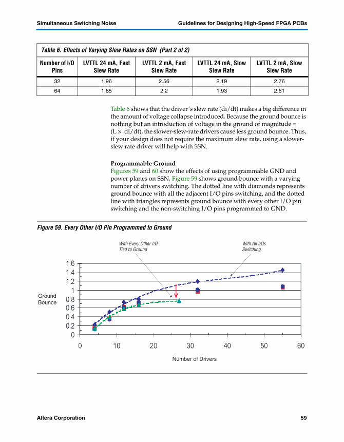
Programmable GroundFigures 59 and 60 show the effects of using programmable GND and power planes on SSN. Figure 59 shows ground bounce with a varying number of drivers switching. The dotted line with diamonds represents ground bounce with all the adjacent I/O pins switching, and the dotted line with triangles represents ground bounce with every other I/O pin switching and the non-switching I/O pins programmed to GND.
Figure 59. Every Other I/O Pin Programmed to Ground
32 1.96 2.56 2.19 2.76
64 1.65 2.2 1.93 2.61
Table 6. Effects of Varying Slew Rates on SSN (Part 2 of 2)
Number of I/O Pins
LVTTL 24 mA, Fast Slew Rate
LVTTL 2 mA, Fast Slew Rate
LVTTL 24 mA, Slow Slew Rate
LVTTL 2 mA, Slow Slew Rate
Number of Drivers
GroundBounce
With Every Other I/OTied to Ground
With All I/OsSwitching
Altera Corporation 59Preliminary
Guidelines for Designing High-Speed FPGA PCBs Simultaneous Switching Noise
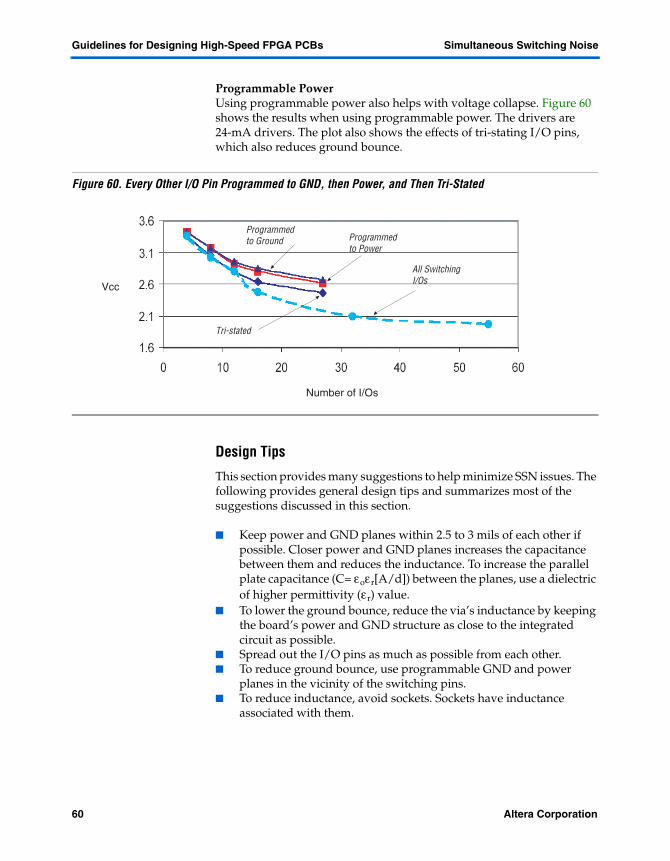
Programmable PowerUsing programmable power also helps with voltage collapse. Figure 60 shows the results when using programmable power. The drivers are 24-mA drivers. The plot also shows the effects of tri-stating I/O pins, which also reduces ground bounce.
Figure 60. Every Other I/O Pin Programmed to GND, then Power, and Then Tri-Stated
Design Tips
This section provides many suggestions to help minimize SSN issues. The following provides general design tips and summarizes most of the suggestions discussed in this section.
Keep power and GND planes within 2.5 to 3 mils of each other if possible. Closer power and GND planes increases the capacitance between them and reduces the inductance. To increase the parallel plate capacitance (C= εoεr[A/d]) between the planes, use a dielectric of higher permittivity (εr) value.
To lower the ground bounce, reduce the via’s inductance by keeping the board’s power and GND structure as close to the integrated circuit as possible.
Spread out the I/O pins as much as possible from each other. To reduce ground bounce, use programmable GND and power
planes in the vicinity of the switching pins. To reduce inductance, avoid sockets. Sockets have inductance
associated with them.
Number of I/Os
Vcc
Programmedto Ground Programmed
to Power
All SwitchingI/Os
Tri-stated
60 Altera CorporationPreliminary
Decoupling Guidelines for Designing High-Speed FPGA PCBs
Decoupling capacitors only marginally affect ground bounce when the board has proper ground or power planes. Ground bounce is more of a device-level issue. If your design uses decoupling capacitors, place them as close to the pins as possible. In lab experiments, capacitors an inch or further away from the pins did not help with ground bounce.
On-chip termination helps with SSN. Keep differential signals tightly coupled to cancel return currents
introduced in the ground plane. Slowing down the drivers reduces SSN. If the maximum slew-rate is
not required, use slower slew-rate drivers. Use short (efficient) return paths for return currents (loops) to reduce
inductance. Longer loops increase inductance.
Decoupling Proper decoupling is critical in high-speed board designs. Select the right decoupling capacitors, power and ground plane stack up, and voltage regulators to minimize noise. Decoupling is one of the most important aspects of board design. It is critical to have a proper decoupling mechanism in place. With the right combination of power and GND planes, decoupling capacitors and voltage-regulator modules will provide decoupling over all frequencies.
1 Because high-speed I/O standard rise times are as low as 70 ps, the signals are very sensitive to any discontinuities on the transmission path. Make sure to design a power distribution system that is clean and adds very little jitter to the board.
Capacitor Impedance
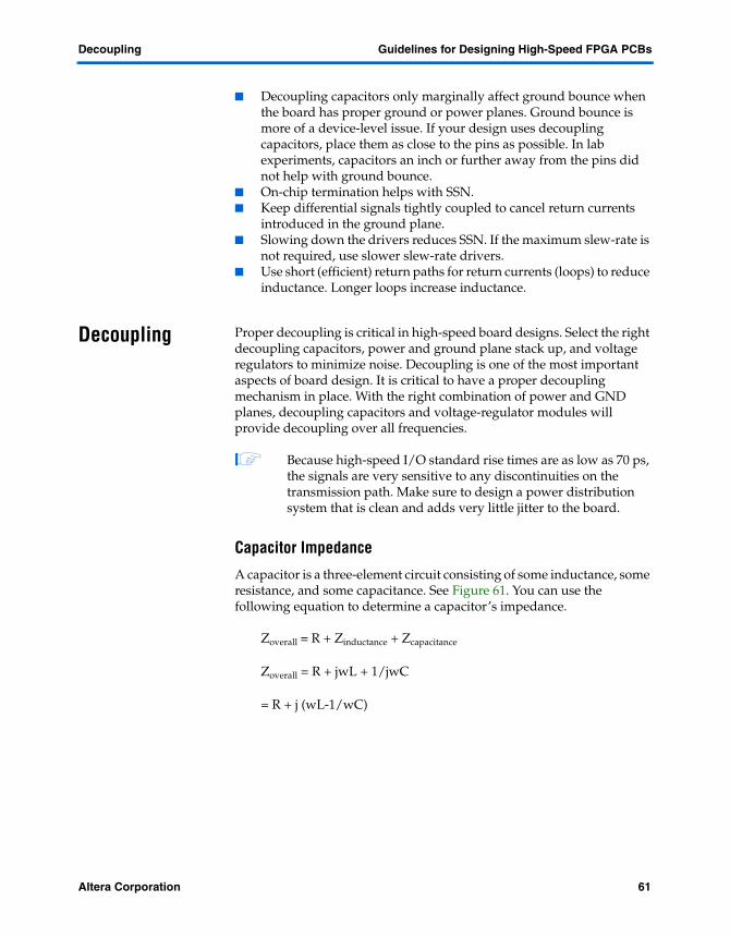
A capacitor is a three-element circuit consisting of some inductance, some resistance, and some capacitance. See Figure 61. You can use the following equation to determine a capacitor’s impedance.
Zoverall = R + Zinductance + Zcapacitance
Zoverall = R + jwL + 1/jwC
= R + j (wL-1/wC)
Altera Corporation 61Preliminary
Guidelines for Designing High-Speed FPGA PCBs Decoupling
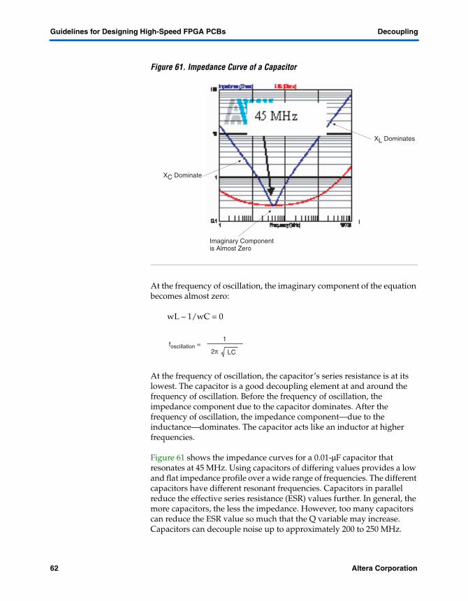
Figure 61. Impedance Curve of a Capacitor
At the frequency of oscillation, the imaginary component of the equation becomes almost zero:
wL – 1/wC = 0
At the frequency of oscillation, the capacitor’s series resistance is at its lowest. The capacitor is a good decoupling element at and around the frequency of oscillation. Before the frequency of oscillation, the impedance component due to the capacitor dominates. After the frequency of oscillation, the impedance component—due to the inductance—dominates. The capacitor acts like an inductor at higher frequencies.
Figure 61 shows the impedance curves for a 0.01-µF capacitor that resonates at 45 MHz. Using capacitors of differing values provides a low and flat impedance profile over a wide range of frequencies. The different capacitors have different resonant frequencies. Capacitors in parallel reduce the effective series resistance (ESR) values further. In general, the more capacitors, the less the impedance. However, too many capacitors can reduce the ESR value so much that the Q variable may increase. Capacitors can decouple noise up to approximately 200 to 250 MHz.
XL Dominates
XC Dominates
Imaginary Componentis Almost Zero
LC2π
1foscillation =
62 Altera CorporationPreliminary
Decoupling Guidelines for Designing High-Speed FPGA PCBs
The power and GND planes have capacitance and inductance associated with them. The power and GND structures look like a parallel plate capacitor. The capacitance can be derived using the following equation.
C = εo εr (A/d)
Where
εo = permittivity of free space = 8.85 exp(-12) Fm-1 εr = relative permittivity of dielectric A = area of the planes facing each other d = distance between the planes
The capacitance value can be plugged into the following equation to calculate the inductance value.
Improving Board Decoupling
This section provides tips and design examples to improve board decoupling. As a general rule for the power and ground structure, the higher the capacitance, the lower the inductance and the better the decoupling.
Keep the power plane as close to the GND plane as possible to decrease power plane noise, this provides a great decoupling source for a wide range of frequencies, specifically at higher frequencies. At the frequency of oscillation for the power and GND structure, the impedance curve remains close to zero over a wide range of frequencies.
General Design Examples
This section provides two board design examples. Using the same conditions, the power plane noise is analyzed on both boards.
The power plane (1.5V_XCVR) is located approximately 17 mils away from the GND plane (HSSI).
The power plane is located approximately 4 mils away from the GND plane, and an island of GND is added under the power plane.
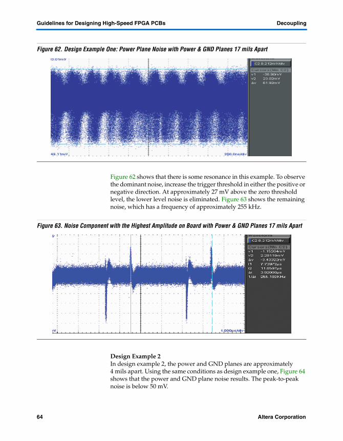
Design Example 1In design example 1, the power plane is used as the trigger and the signal input on the sampling oscilloscope. The peak-to-peak noise is about 70 mV. The power and GND planes are approximately 17-mils apart. See Figure 62.
εrdelay (stripline) = 85 ~ 200 ps per inch in FR4LC=
Altera Corporation 63Preliminary
Guidelines for Designing High-Speed FPGA PCBs Decoupling
Figure 62. Design Example One: Power Plane Noise with Power & GND Planes 17 mils Apart
Figure 62 shows that there is some resonance in this example. To observe the dominant noise, increase the trigger threshold in either the positive or negative direction. At approximately 27 mV above the zero threshold level, the lower level noise is eliminated. Figure 63 shows the remaining noise, which has a frequency of approximately 255 kHz.
Figure 63. Noise Component with the Highest Amplitude on Board with Power & GND Planes 17 mils Apart
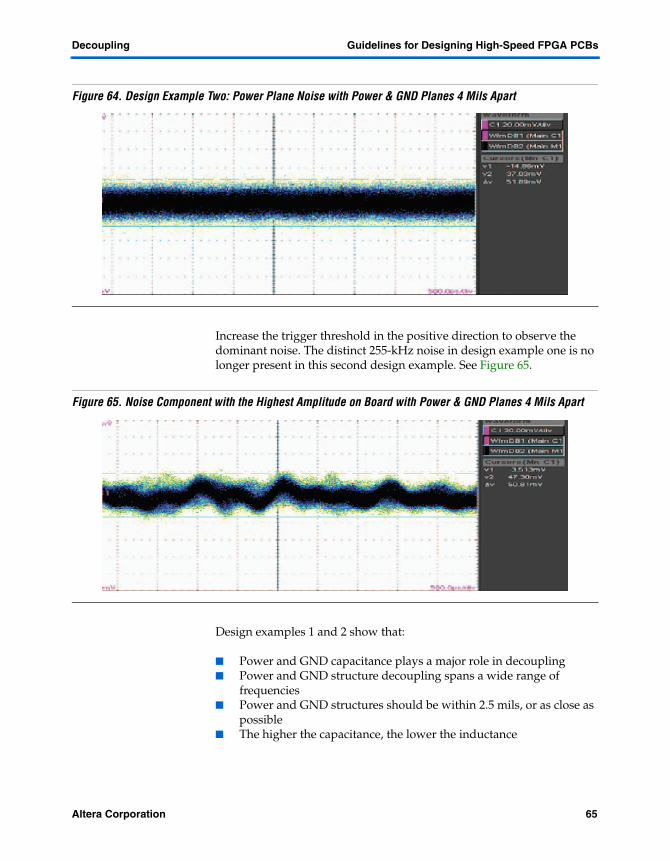
Design Example 2In design example 2, the power and GND planes are approximately 4 mils apart. Using the same conditions as design example one, Figure 64 shows that the power and GND plane noise results. The peak-to-peak noise is below 50 mV.
64 Altera CorporationPreliminary
Decoupling Guidelines for Designing High-Speed FPGA PCBs
Figure 64. Design Example Two: Power Plane Noise with Power & GND Planes 4 Mils Apart
Increase the trigger threshold in the positive direction to observe the dominant noise. The distinct 255-kHz noise in design example one is no longer present in this second design example. See Figure 65.
Figure 65. Noise Component with the Highest Amplitude on Board with Power & GND Planes 4 Mils Apart
Design examples 1 and 2 show that:
Power and GND capacitance plays a major role in decoupling Power and GND structure decoupling spans a wide range of
frequencies Power and GND structures should be within 2.5 mils, or as close as
possible The higher the capacitance, the lower the inductance
Altera Corporation 65Preliminary
Guidelines for Designing High-Speed FPGA PCBs Decoupling
Stratix GX Development Board Design Example
The following design example uses a Stratix GX development board.
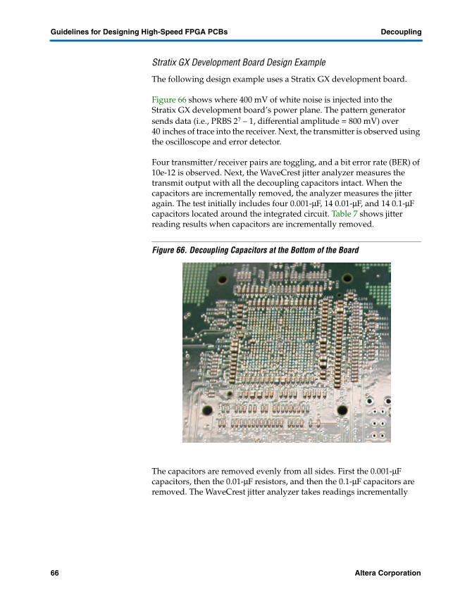
Figure 66 shows where 400 mV of white noise is injected into the Stratix GX development board’s power plane. The pattern generator sends data (i.e., PRBS 27 – 1, differential amplitude = 800 mV) over 40 inches of trace into the receiver. Next, the transmitter is observed using the oscilloscope and error detector.
Four transmitter/receiver pairs are toggling, and a bit error rate (BER) of 10e-12 is observed. Next, the WaveCrest jitter analyzer measures the transmit output with all the decoupling capacitors intact. When the capacitors are incrementally removed, the analyzer measures the jitter again. The test initially includes four 0.001-µF, 14 0.01-µF, and 14 0.1-µF capacitors located around the integrated circuit. Table 7 shows jitter reading results when capacitors are incrementally removed.
Figure 66. Decoupling Capacitors at the Bottom of the Board
The capacitors are removed evenly from all sides. First the 0.001-µF capacitors, then the 0.01-µF resistors, and then the 0.1-µF capacitors are removed. The WaveCrest jitter analyzer takes readings incrementally
66 Altera CorporationPreliminary
Decoupling Guidelines for Designing High-Speed FPGA PCBs
throughout the removal process, including when all the capacitors are intact and removed. Table 7 shows the jitter reading results during each phase in the removal process.
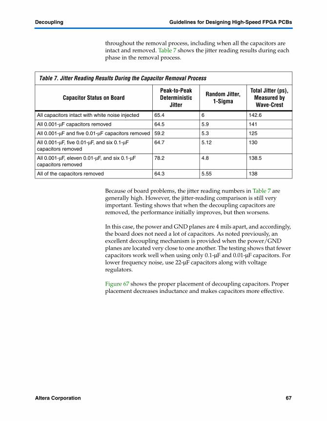
Because of board problems, the jitter reading numbers in Table 7 are generally high. However, the jitter-reading comparison is still very important. Testing shows that when the decoupling capacitors are removed, the performance initially improves, but then worsens.
In this case, the power and GND planes are 4 mils apart, and accordingly, the board does not need a lot of capacitors. As noted previously, an excellent decoupling mechanism is provided when the power/GND planes are located very close to one another. The testing shows that fewer capacitors work well when using only 0.1-µF and 0.01-µF capacitors. For lower frequency noise, use 22-µF capacitors along with voltage regulators.
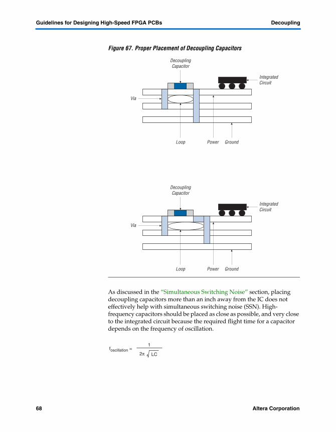
Figure 67 shows the proper placement of decoupling capacitors. Proper placement decreases inductance and makes capacitors more effective.
Table 7. Jitter Reading Results During the Capacitor Removal Process
Capacitor Status on BoardPeak-to-Peak Deterministic
Jitter
Random Jitter,1-Sigma
Total Jitter (ps), Measured by Wave-Crest
All capacitors intact with white noise injected 65.4 6 142.6
All 0.001-µF capacitors removed 64.5 5.9 141
All 0.001-µF and five 0.01-µF capacitors removed 59.2 5.3 125
All 0.001-µF, five 0.01-µF, and six 0.1-µF capacitors removed
64.7 5.12 130
All 0.001-µF, eleven 0.01-µF, and six 0.1-µF capacitors removed
78.2 4.8 138.5
All of the capacitors removed 64.3 5.55 138
Altera Corporation 67Preliminary
Guidelines for Designing High-Speed FPGA PCBs Decoupling
Figure 67. Proper Placement of Decoupling Capacitors
As discussed in the “Simultaneous Switching Noise” section, placing decoupling capacitors more than an inch away from the IC does not effectively help with simultaneous switching noise (SSN). High-frequency capacitors should be placed as close as possible, and very close to the integrated circuit because the required flight time for a capacitor depends on the frequency of oscillation.
Via
Loop Power
DecouplingCapacitor
Ground
IntegratedCircuit
Via
Loop Power
DecouplingCapacitor
Ground
IntegratedCircuit
LC2π
1foscillation =
68 Altera CorporationPreliminary
Layer Stackup Guidelines for Designing High-Speed FPGA PCBs
The 0.01-µF capacitors should be closer than the 0.1-µF capacitors. You can use the equation:
frequency = speed × wavelength
to determine the wavelength (speed = 1/delay ~ 1/200 ps/inch in FR4 = 5G inch/second). The placement of the capacitor should be a good fraction of the wavelength. Altera provides specific guidelines for each FPGA. For more information, contact Altera Applications.
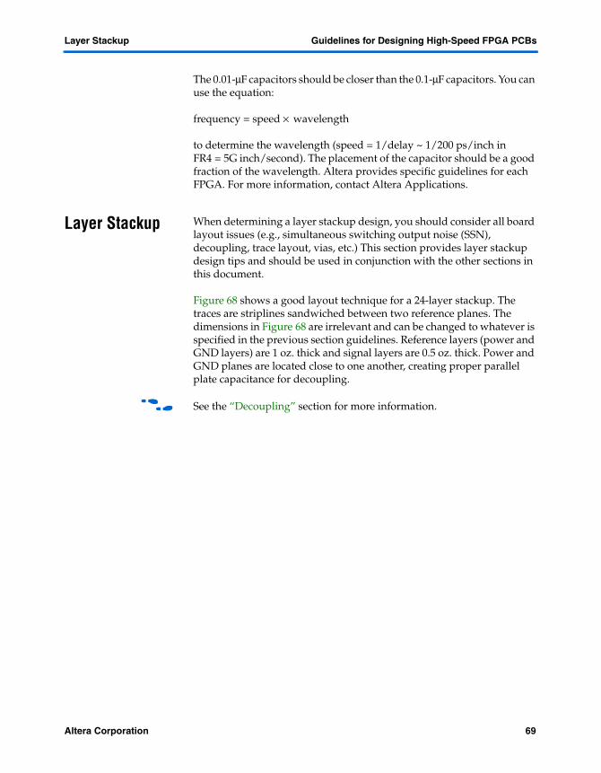
Layer Stackup When determining a layer stackup design, you should consider all board layout issues (e.g., simultaneous switching output noise (SSN), decoupling, trace layout, vias, etc.) This section provides layer stackup design tips and should be used in conjunction with the other sections in this document.
Figure 68 shows a good layout technique for a 24-layer stackup. The traces are striplines sandwiched between two reference planes. The dimensions in Figure 68 are irrelevant and can be changed to whatever is specified in the previous section guidelines. Reference layers (power and GND layers) are 1 oz. thick and signal layers are 0.5 oz. thick. Power and GND planes are located close to one another, creating proper parallel plate capacitance for decoupling.
f See the “Decoupling” section for more information.
Altera Corporation 69Preliminary
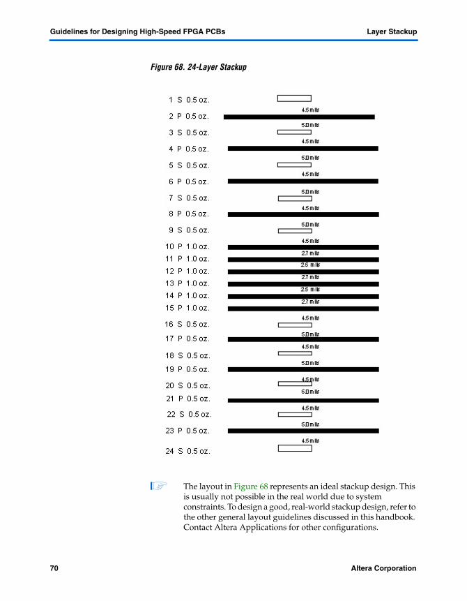
Guidelines for Designing High-Speed FPGA PCBs Layer Stackup
Figure 68. 24-Layer Stackup
1 The layout in Figure 68 represents an ideal stackup design. This is usually not possible in the real world due to system constraints. To design a good, real-world stackup design, refer to the other general layout guidelines discussed in this handbook. Contact Altera Applications for other configurations.
70 Altera CorporationPreliminary

Revision History Guidelines for Designing High-Speed FPGA PCBs
You should avoid split planes as much as possible. However, if split planes are necessary, make sure that the trace referencing the plane does not travel over the split. If the trace does travel over the split, the loop inductance will increase on the transmission path. The return currents are forced to take less efficient paths, increasing the loop. Sometimes ground islands are required to provide solid return paths for high-speed signals.
Revision History The information contained in version 1.1 of AN 315: Guidelines for Designing High-Speed FPGA PCBs supersedes information published in previous versions.
Version 1.1
The following changes were made to AN 315: Guidelines for Designing High-Speed FPGA PCBs version 1.1: minor textual updates.
Altera Corporation 71Preliminary
Guidelines for Designing High-Speed FPGA PCBs Revision History
72 Altera CorporationPreliminary
101 Innovation DriveSan Jose, CA 95134(408) 544-7000www.altera.comApplications Hotline:(800) 800-EPLDLiterature Services:[email protected]
Copyright © 2004 Altera Corporation. All rights reserved. Altera, The Programmable Solutions Company,the stylized Altera logo, specific device designations, and all other words and logos that are identified astrademarks and/or service marks are, unless noted otherwise, the trademarks and service marks of AlteraCorporation in the U.S. and other countries. All other product or service names are the property of their re-spective holders. Altera products are protected under numerous U.S. and foreign patents and pendingapplications, maskwork rights, and copyrights. Altera warrants performance of its semiconductor productsto current specifications in accordance with Altera's standard warranty, but reserves the right to make chang-es to any products and services at any time without notice. Altera assumes no responsibility or liabilityarising out of the application or use of any information, product, or service describedherein except as expressly agreed to in writing by Altera Corporation. Altera customersare advised to obtain the latest version of device specifications before relying on any pub-lished information and before placing orders for products or services.
Related Documents