PVIN AVIN EN AGND PGND FB SW LM2854 V IN V OUT SS C IN L O C O R FB1 R COMP C COMP R FB2 C SS User's Guide SNVA323B – March 2008 – Revised May 2013 AN-1786 LM2854 500 kHz Buck Regulator Evaluation Board 1 Introduction The LM2854 PowerWise ® SIMPLE SWITCHER ® buck regulator evaluation board is a 500 kHz step-down voltage regulator capable of driving up 0A to 4A load current with excellent power conversion efficiency. A typical schematic of an LM2854 application is given in Figure 1. The LM2854 pin-out and pin description are given in Figure 2 and Table 1, respectively. The LM2854 evaluation board is designed to accept an input voltage rail between 2.95V and 5.5V and deliver a fixed and highly accurate output voltage of 1.2V. The output voltage level can be changed by modification of the one feedback resistor value. Externally established soft-start with a small value capacitance facilitates a controlled, well-defined and monotonic start-up output voltage characteristic. In addition, the LM2854 is capable of starting monotonically and glitch free into a pre-biased load. With some of the required voltage loop compensation components integrated in the regulator, the number of external passive components and PC board area typically necessary in a voltage mode buck converter application are reduced. An LM2854 based regulator design with type III loop compensation can be implemented with as few as eight external components. Only two small size external compensation components are required, similar to that commonly involved with current mode control compensation. Unlike a compensation solution where all the compensation components are integrated, the LM2854 has the flexibility to deal with ceramic and/or electrolytic based load capacitance spanning a wide range of capacitor values. Lossless cycle-by-cycle peak current limit is used to protect the load from an overcurrent or short-circuit fault, and an enable comparator permits system sequencing or increase of the input UVLO above the nominal 2.7V level. The device is available in a power enhanced HTSSOP-16 package featuring an exposed die attach pad that improves the thermal performance of the regulator. Figure 1. Typical System Application using LM2854 Synchronous Buck Regulator All trademarks are the property of their respective owners. 1 SNVA323B – March 2008 – Revised May 2013 AN-1786 LM2854 500 kHz Buck Regulator Evaluation Board Submit Documentation Feedback Copyright © 2008–2013, Texas Instruments Incorporated

Welcome message from author
This document is posted to help you gain knowledge. Please leave a comment to let me know what you think about it! Share it to your friends and learn new things together.
Transcript
PVIN
AVIN
EN
AGND PGND
FB
SWLM2854
VIN VOUT
SSCIN
LO
CO
RFB1
RCOMP CCOMPRFB2
CSS
User's GuideSNVA323B–March 2008–Revised May 2013
AN-1786 LM2854 500 kHz Buck Regulator EvaluationBoard
1 Introduction
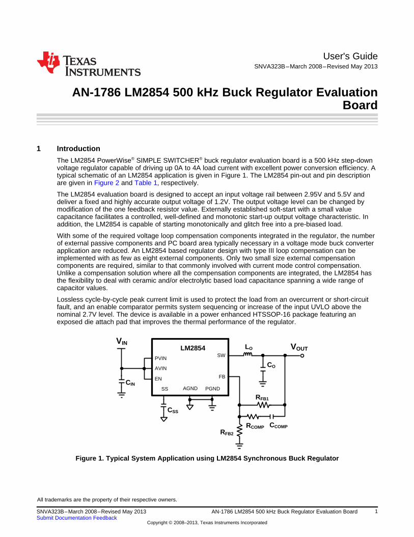
The LM2854 PowerWise® SIMPLE SWITCHER® buck regulator evaluation board is a 500 kHz step-downvoltage regulator capable of driving up 0A to 4A load current with excellent power conversion efficiency. Atypical schematic of an LM2854 application is given in Figure 1. The LM2854 pin-out and pin descriptionare given in Figure 2 and Table 1, respectively.
The LM2854 evaluation board is designed to accept an input voltage rail between 2.95V and 5.5V anddeliver a fixed and highly accurate output voltage of 1.2V. The output voltage level can be changed bymodification of the one feedback resistor value. Externally established soft-start with a small valuecapacitance facilitates a controlled, well-defined and monotonic start-up output voltage characteristic. Inaddition, the LM2854 is capable of starting monotonically and glitch free into a pre-biased load.
With some of the required voltage loop compensation components integrated in the regulator, the numberof external passive components and PC board area typically necessary in a voltage mode buck converterapplication are reduced. An LM2854 based regulator design with type III loop compensation can beimplemented with as few as eight external components. Only two small size external compensationcomponents are required, similar to that commonly involved with current mode control compensation.Unlike a compensation solution where all the compensation components are integrated, the LM2854 hasthe flexibility to deal with ceramic and/or electrolytic based load capacitance spanning a wide range ofcapacitor values.
Lossless cycle-by-cycle peak current limit is used to protect the load from an overcurrent or short-circuitfault, and an enable comparator permits system sequencing or increase of the input UVLO above thenominal 2.7V level. The device is available in a power enhanced HTSSOP-16 package featuring anexposed die attach pad that improves the thermal performance of the regulator.
Figure 1. Typical System Application using LM2854 Synchronous Buck Regulator
All trademarks are the property of their respective owners.
1SNVA323B–March 2008–Revised May 2013 AN-1786 LM2854 500 kHz Buck Regulator Evaluation BoardSubmit Documentation Feedback
Copyright © 2008–2013, Texas Instruments Incorporated

1
2
3
4
5
6
7
8
16
15
14
13
12
11
10
9
NC
PGND
PGND
PGND
PVIN
PVIN
PVIN
NC NC
AVIN
EN
SW
SW
SS
AGND
FB
EXP
LM2854 Pin-Out www.ti.com
2 LM2854 Pin-Out
Figure 2. LM2854 Pin-Out
3 LM2854 Pin Descriptions
Table 1. LM2854 Pin Descriptions
Pin Number Name Description
1 NC Reserved for factory use, this pin should be connected to GND to ensure proper operation.
2,3,4 PGND Power ground pins for the internal power switches. These pins should be connected together locally atthe device and tied to the PC board ground plane.
5,6,7 PVIN Input voltage to the power switches inside the device. These pins should be connected together at thedevice. A low ESR input capacitance should be located as close as possible to these pins.
8,9 NC Reserved for factory use, these pins should be connected to GND to ensure proper operation.
10 AVIN Analog input voltage supply that generates the internal bias. The UVLO circuit derives its input fromthis pin also. Thus, if the voltage on AVIN falls below the UVLO threshold, both internal FETs areturned off. It is recommended to connect PVIN to AVIN through a low pass RC filter to minimize theinfluence of input rail ripple and noise on the analog control circuitry. The series resistor should be 1Ωand the bypass capacitor should be a X7R ceramic type 0.1 µF to 1.0 µF.
11 EN Active high enable input for the device. Typically, turn-on threshold is 1.23V with 0.15V hysteresis. Anexternal resistor divider from PVIN can be used to effectively increase the UVLO turn-on threshold. Ifnot used, the EN pin should be connected to PVIN.
12,13 SW Switch node pins. This is the PWM output of the internal MOSFET power switches. These pins shouldbe tied together locally and connected to the filter inductor.
14 SS Soft-start control pin. An internal 2 µA current source charges an external capacitor connected betweenthis pin and AGND to set the output voltage ramp rate during startup. This pin can also be used toconfigure the tracking feature.
15 AGND Quiet analog ground for the internal bias circuitry.
16 FB Feedback pin is connected to the inverting input of the voltage loop error amplifier. A 0.8V bandgapreference is connected to the non-inverting input of the error amplifier.
EXP Exposed Exposed metal pad on the underside of the package with a weak electrical connection to PGND. It isPad recommended to connect this pad to the PC board ground plane in order to improve thermal
dissipation.
2 AN-1786 LM2854 500 kHz Buck Regulator Evaluation Board SNVA323B–March 2008–Revised May 2013Submit Documentation Feedback
Copyright © 2008–2013, Texas Instruments Incorporated
PVIN
AVIN
EN
AGND PGND
FB
SW
LM2854MHX-500
VINVOUT
SS
Cin1
Lf
Co1
Rfb1
Rc1 Cc1Rfb2
Css
Cf
Rf U1Cin2
Rtrk
Ra
Ren1
Ren2
SS / TRK
EN
VTEST
VREF
GND GND
+Co2+
1.2V, 4A2.95V ± 5.5V
12,13
16
1514 1,2,3,4,8,9
10
11
5,6,7
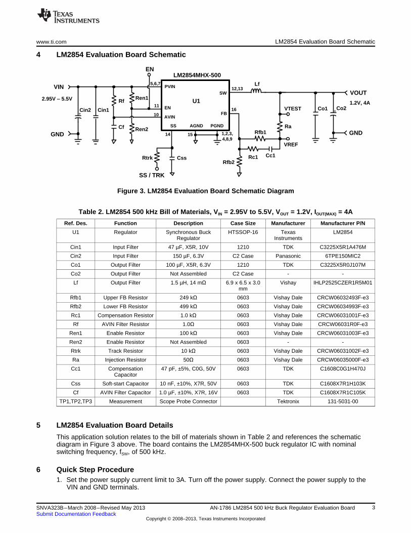
www.ti.com LM2854 Evaluation Board Schematic
4 LM2854 Evaluation Board Schematic
Figure 3. LM2854 Evaluation Board Schematic Diagram
Table 2. LM2854 500 kHz Bill of Materials, VIN = 2.95V to 5.5V, VOUT = 1.2V, IOUT(MAX) = 4A
Ref. Des. Function Description Case Size Manufacturer Manufacturer P/N
U1 Regulator Synchronous Buck HTSSOP-16 Texas LM2854Regulator Instruments
Cin1 Input Filter 47 µF, X5R, 10V 1210 TDK C3225X5R1A476M
Cin2 Input Filter 150 µF, 6.3V C2 Case Panasonic 6TPE150MIC2
Co1 Output Filter 100 µF, X5R, 6.3V 1210 TDK C3225X5R0J107M
Co2 Output Filter Not Assembled C2 Case - -
Lf Output Filter 1.5 µH, 14 mΩ 6.9 x 6.5 x 3.0 Vishay IHLP2525CZER1R5M01mm
Rfb1 Upper FB Resistor 249 kΩ 0603 Vishay Dale CRCW06032493F-e3
Rfb2 Lower FB Resistor 499 kΩ 0603 Vishay Dale CRCW06034993F-e3
Rc1 Compensation Resistor 1.0 kΩ 0603 Vishay Dale CRCW06031001F-e3
Rf AVIN Filter Resistor 1.0Ω 0603 Vishay Dale CRCW06031R0F-e3
Ren1 Enable Resistor 100 kΩ 0603 Vishay Dale CRCW06031003F-e3
Ren2 Enable Resistor Not Assembled 0603 - -
Rtrk Track Resistor 10 kΩ 0603 Vishay Dale CRCW06031002F-e3
Ra Injection Resistor 50Ω 0603 Vishay Dale CRCW06035000F-e3
Cc1 Compensation 47 pF, ±5%, C0G, 50V 0603 TDK C1608C0G1H470JCapacitor
Css Soft-start Capacitor 10 nF, ±10%, X7R, 50V 0603 TDK C1608X7R1H103K
Cf AVIN Filter Capacitor 1.0 µF, ±10%, X7R, 16V 0603 TDK C1608X7R1C105K
TP1,TP2,TP3 Measurement Scope Probe Connector Tektronix 131-5031-00
5 LM2854 Evaluation Board Details
This application solution relates to the bill of materials shown in Table 2 and references the schematicdiagram in Figure 3 above. The board contains the LM2854MHX-500 buck regulator IC with nominalswitching frequency, fSW, of 500 kHz.
6 Quick Step Procedure1. Set the power supply current limit to 3A. Turn off the power supply. Connect the power supply to the
VIN and GND terminals.
3SNVA323B–March 2008–Revised May 2013 AN-1786 LM2854 500 kHz Buck Regulator Evaluation BoardSubmit Documentation Feedback
Copyright © 2008–2013, Texas Instruments Incorporated
diLdt
diL=
(VIN - VOUT)dt Lf
DOWN=
VOUT
Lf
UP
ILpk = IOUT + = 4A + = 4.63A'iL2 2
1.25A
'iL =1.5 PH x 500 kHz
1.2V 1 -1.2V5.5V
= 1.25A
D =VOUT
VIN
Lf ='iLfSW
VOUT(1-D)
'iLfSW=
VOUT 1 -VOUT
VIN
Component Selection www.ti.com
2. Connect the load with a 4A capability to the VOUT and GND terminals
3. The EN terminal can be left open for normal operation as there is an on-board pull-up resistor.
4. Set VIN to 3.0V with no load applied. VOUT should be in regulation with a nominal 1.2V output.
5. Slowly increase the load while monitoring the output voltage. VOUT should remain in regulation with anominal 1.2V output as the load is increased up to 4A.
6. Slowly sweep the input voltage from 2.95V to 5.5V. VOUT should remain in regulation with a nominal1.2V output.
7. Temporarily short the EN terminal to GND to check the shutdown function.
8. Increase the load beyond the normal range to check current limit. The output current should limit atapproximately 5.6A. Short the VOUT and GND terminals to verify short circuit protection.
7 Component Selection
7.1 Filter Inductor
The selection of the output filter components, Lf and Co1, are intrinsically linked as both of theseparameters affect the stability of the system and various characteristics of the output voltage.
First, a 1.5 µH inductor is chosen to allow stable operation (per datasheet recommendations) over theentire input voltage range from 2.95V to 5.5V. The inductance also directly affects the amplitude of theinductor current ripple which flows in the output capacitor. The filter inductance is given by
(1)
where the variable D refers to the duty cycle and can be approximated by
(2)
From this, it follows that the inductor ripple current, ΔiL, reaches a maximum when duty cycle is minimumor input voltage is maximum, i.e. VIN = 5.5V. Under these conditions, the inductor peak to peak ripplecurrent is given by
(3)
or approximately 31% of full load current. It follows that the peak inductor current at full load is
(4)
and this level is adequately below the peak inductor current associated with current limit. This implies thatan inductor must be selected with a saturation current higher than 4.63A to ensure that the inductor willnever saturate during normal operating conditions.
Another concern related to the inductance value is that it governs the maximum inductor current slew rateduring a load on or off transient respectively as follows
(5)
Thus, a smaller inductance value allows the control loop to slew the inductor current more rapidly.
This evaluation board uses the Vishay IHLP2525 series 1.5 µH inductor to provide the necessary currenthandling capability with low DC resistance in a relatively small footprint and profile .
4 AN-1786 LM2854 500 kHz Buck Regulator Evaluation Board SNVA323B–March 2008–Revised May 2013Submit Documentation Feedback
Copyright © 2008–2013, Texas Instruments Incorporated

'VIN =fSWCin1
IOUTD(1-D)
500 kHz 24 PF=
4A 0.41 (1 - 0.41)= 80 mV
ICin(RMS) = 4A 0.41 (1 - 0.41) = 1.97A
ICin(RMS) = IOUT D(1-D)
'VOUT = 1.25A1
(3 m:)2 + 8 500 kHz 60 PF
2
= 6.4 mV
'VOUT = 'iL1
RESR2 +
8fSWCO1
2
www.ti.com Component Selection
7.2 Output Capacitor
The output capacitance and its equivalent series resistance (ESR) affect both the ripple voltage at theoutput and the overall stability of the loop. The output capacitor provides a low impedance path for theinductor ripple current and presents a source of charge for transient loading conditions.
In this example, one 100 µF 1210 multi-layer ceramic capacitor (MLCC) was selected. Ceramic capacitorsprovide very low ESR but can exhibit a significant reduction in capacitance with applied DC bias. Usingmanufacturer’s data, the ESR at 500 kHz is 3 mΩ and there is approximately 40% reduction incapacitance at 1.2V. This is verified by measuring the output ripple voltage and frequency response of thecircuit. The fundamental component of the output ripple voltage amplitude is calculated as
(6)
and with typical values from this example
(7)
Because the load could transition quickly from no load to full load, it is sometimes common to add outputbulk capacitance in the form of aluminum electrolytic (Al-E), tantalum (Ta), solid aluminum, organicpolymer, and niobium (Nb) capacitors. This is largely unnecessary with the LM2854 as the loop crossoverfrequency can be made sufficiently large to accommodate high di/dt load transients.
7.3 Input Filter
The necessary RMS current rating of the input capacitor can be estimated by the following equation
(8)
From this equation, it follows that the maximum RMS current will occur at full 4A load current with thesystem operating at 50% duty cycle.
However, with the specified output voltage, the worst case occurs at minimum input voltage of 2.95V.Hence, the relevant duty cycle is 0.41 and the maximum RMS current is given by
(9)
Ceramic capacitors feature a very large RMS current rating in a small footprint making them ideal for thisapplication. Choosing a 47 µF 10V ceramic capacitor to provide the necessary input capacitance andassuming 50% capacitance voltage coefficient, the input AC ripple amplitude, neglecting ESR, is
(10)
When operating near the minimum input voltage, an electrolytic input capacitor is helpful to damp the inputfor a typical bench test setup. Essentially, a resonant circuit is formed by the line impedance and inputcapacitance. To this end, a second input capacitor, Cin2, is provided on the evaluation board toaccommodate such electrolytic capacitance. The 6TPE150MIC2 by Sanyo has 150 µF capacitance and anESR of 18 mΩ. The associated ESR is stable relative to temperature, and capacitance change is relativelyimmune to bias voltage. The ripple current will split between the ceramic and electrolytic capacitors basedon the relative impedance at the switching frequency.
For improved performance, an 0603 1 µF ceramic AVIN filter capacitor is placed adjacent to the AVIN pinand referenced to AGND. Together with a 1Ω series resistor from PVIN (optional), this small capacitorhelps to filter high frequency noise spikes on the supply rail and prevent these pulses from disturbing theanalog control circuitry of the chip.
7.4 Soft-Start Capacitor
A 10 nF soft-start capacitor has been chosen to provide a soft-start time of roughly 4 ms. This will allowthe LM2854 to start up gracefully without triggering over-current protection irrespective of operatingconditions.
5SNVA323B–March 2008–Revised May 2013 AN-1786 LM2854 500 kHz Buck Regulator Evaluation BoardSubmit Documentation Feedback
Copyright © 2008–2013, Texas Instruments Incorporated
Rfb2 =Rfb1 =
- 1VOUT
0.8V
249 k:
- 11.2V0.8V
= 499 k:
Rfb1 =1
2SCc1fLC=
1
2S47 pF 16.8 kHz= 200 k:
Rc1 =1
2SCc1fESR=
1
2S47 pF 885 kHz= 3.8 k:
Cc1(pF) = DLf(PH)Co1(PF)
VIN (V)floop (kHz)
Cc1 = 0.038 1.5 605.5
75 = 47 pF
fLC #LfCo1
12S
=1.5 PH 60 PF
12S
= 16.8 kHz
fESR #1
2SRESRCo1=
12S3 m: 60 PF
= 885 kHz
Rtrk1 =
10 k:
(VTRACK - 1.0V), Simultaneous Tracking
0.8V
(VOUT ± 0.8V), Ratiometric Tracking10 k:
Component Selection www.ti.com
7.5 Tracking Resistors
If simultaneous (equal voltage ramp rates) or ratiometric (equal soft-start times) tracking to an externalsupply voltage, VTRACK, is required, the user can remove the soft-start capacitor and replace with theappropriate value lower tracking resistor. The upper resistor, Rtrk, is 10 kΩ. Thus, the lower trackingresistor value, designated Rtrk1, is governed by
(11)
7.6 Enable Resistors
The LM2854 has an enable pin with an on-board 100 kΩ pull-up resistor, designated Ren1. Thus, theassociated PCB terminal, labeled EN, can be left open circuit if desired. Alternatively, the enable functioncan be configured to increase the input UVLO level by setting up a resistor divider from VIN usingresistors Ren1 and Ren2. The board is supplied with Ren2 not assembled.
7.7 Feedback and Compensation Components
The voltage loop crossover frequency, floop, is usually selected between one tenth and one fifth of theswitching frequency
0.1 fSW ≤ floop ≤ 0.2 fSW (12)
The complex double pole related to the LC output filter and zero due to the output capacitor ESR are asfollows
(13)
A simple solution for the required external compensation capacitor, CCOMP, with type III voltage modecontrol can be expressed as follows where the constant is nominally 0.038 for the 500 kHz option.
(14)
The upper feedback resistor, Rfb1, is selected to provide adequate mid-band gain and to locate a zero ator below the LC pole frequency. The series resistor, Rc1, is selected to locate a pole at the ESR zerofrequency. Thus
(15)
Rfb1 and Rc1 are chosen as 249 kΩ and 1 kΩ in the evaluation board. With Rfb1 defined based on thevoltage loop requirements, Rfb2, the lower feedback resistor, is then selected for the desired outputvoltage by
(16)
Note that Rfb2 has no impact on the control loop from an AC standpoint since the FB pin is the input to anop-amp type error amplifier and effectively at AC ground. Hence, the control loop can be designedirrespective of output voltage level. The only caveat here is the necessary derating of the outputcapacitance with applied voltage.
6 AN-1786 LM2854 500 kHz Buck Regulator Evaluation Board SNVA323B–March 2008–Revised May 2013Submit Documentation Feedback
Copyright © 2008–2013, Texas Instruments Incorporated

0.0 0.5 1.0 1.5 2.0 2.5 3.0 3.5 4.0
IOUT (A)
70
95
EF
FIC
IEN
CY
(%
)
75
80
85
90VIN = 3.3V
VIN = 5.0V
www.ti.com Performance Characteristics
The compensation was optimized to work over the full input voltage range. Many applications have a fixedinput voltage rail. It is possible to modify the compensation to obtain a faster transient response for agiven input voltage operating point .
8 Performance Characteristics
Figure 4. LM2854 Evaluation Board EfficiencyVOUT = 1.2V
Figure 5. LM2854 Transient ResponseIOUT = 0.4A - 4.0A - 0.4A
7SNVA323B–March 2008–Revised May 2013 AN-1786 LM2854 500 kHz Buck Regulator Evaluation BoardSubmit Documentation Feedback
Copyright © 2008–2013, Texas Instruments Incorporated

Performance Characteristics www.ti.com
Figure 6. LM2854 Startup Characteristic
Figure 7. LM2854 Turn On via Enable
Figure 8. LM2854 Turn Off via Enable
8 AN-1786 LM2854 500 kHz Buck Regulator Evaluation Board SNVA323B–March 2008–Revised May 2013Submit Documentation Feedback
Copyright © 2008–2013, Texas Instruments Incorporated
www.ti.com LM2854 PC Board Layout
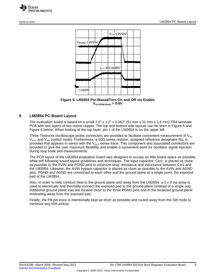
Figure 9. LM2854 Pre-BiasedTurn On and Off via EnableVOUT(PRE-BIAS) = 0.6V
9 LM2854 PC Board Layout
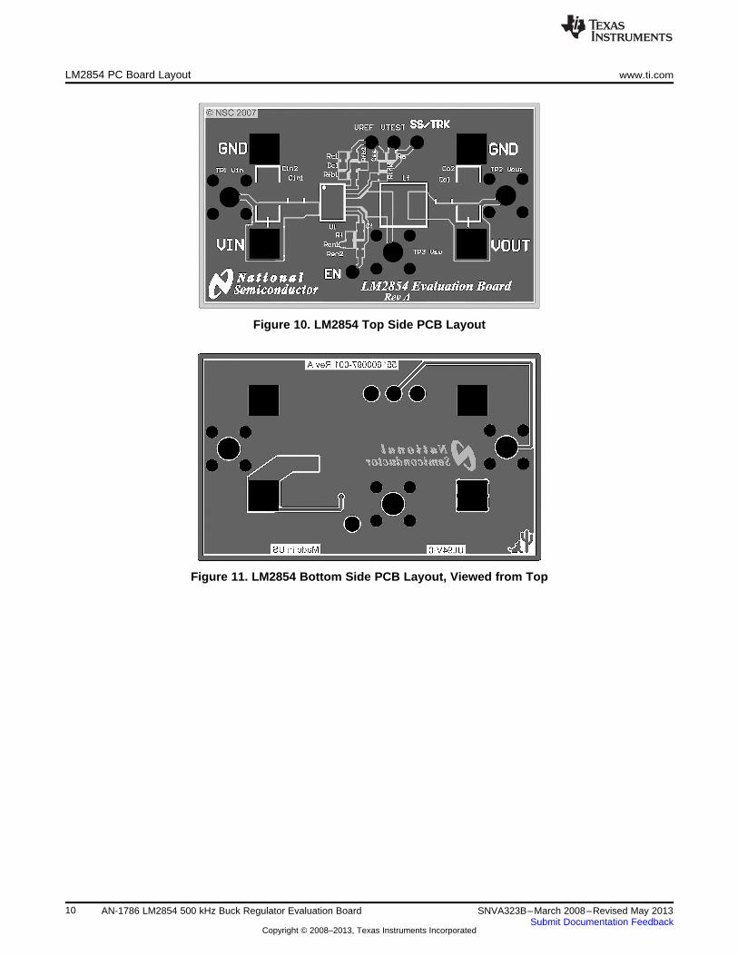
The evaluation board is based on a small 2.0” x 1.2” x 0.062” (51 mm x 31 mm x 1.6 mm) FR4 laminatePCB with two layers of two ounce copper. The top and bottom side layouts can be seen in Figure 5 andFigure 6 below. When looking at the top layer, pin 1 of the LM2854 is on the upper left.
Three Textronix oscilloscope probe connectors are provided to facilitate convenient measurement of VIN,VOUT and VSW (switch node). Furthermore, a 50Ω series resistor, assigned reference designator Ra, isprovided that appears in series with the VOUT sense trace. This component and associated connectors areprovided to give the user maximum flexibility and enable a convenient point for oscillator signal injectionduring loop bode plot measurements.
The PCB layout of the LM2854 evaluation board was designed to occupy as little board space as possible,while still following sound layout guidelines and techniques. The input capacitor, Cin1, is placed as closeas possible to the PVIN and PGND pins to minimize stray resistance and inductance between Cin1 andthe LM2854. Likewise, the AVIN bypass capacitor is placed as close as possible to the AVIN and AGNDpins. PGND and AGND are connected to each other and the ground plane at a single point, the exposedpad of the LM2854.
Also, in order to help conduct heat to the ground plane and away from the LM2854, a 3 x 3 via array isused to electrically and thermally connect the exposed pad to the ground plane (instead of a single via).Additional ground plane vias are located close to the three PGND pins and in the localized ground planeemanating away from the exposed pad.
Finally, the FB pin trace is intentionally kept as short as possible and routed away from the SW node tominimize any EMI pickup.
9SNVA323B–March 2008–Revised May 2013 AN-1786 LM2854 500 kHz Buck Regulator Evaluation BoardSubmit Documentation Feedback
Copyright © 2008–2013, Texas Instruments Incorporated
LM2854 PC Board Layout www.ti.com
Figure 10. LM2854 Top Side PCB Layout
Figure 11. LM2854 Bottom Side PCB Layout, Viewed from Top
10 AN-1786 LM2854 500 kHz Buck Regulator Evaluation Board SNVA323B–March 2008–Revised May 2013Submit Documentation Feedback
Copyright © 2008–2013, Texas Instruments Incorporated

IMPORTANT NOTICE
Texas Instruments Incorporated and its subsidiaries (TI) reserve the right to make corrections, enhancements, improvements and otherchanges to its semiconductor products and services per JESD46, latest issue, and to discontinue any product or service per JESD48, latestissue. Buyers should obtain the latest relevant information before placing orders and should verify that such information is current andcomplete. All semiconductor products (also referred to herein as “components”) are sold subject to TI’s terms and conditions of salesupplied at the time of order acknowledgment.
TI warrants performance of its components to the specifications applicable at the time of sale, in accordance with the warranty in TI’s termsand conditions of sale of semiconductor products. Testing and other quality control techniques are used to the extent TI deems necessaryto support this warranty. Except where mandated by applicable law, testing of all parameters of each component is not necessarilyperformed.
TI assumes no liability for applications assistance or the design of Buyers’ products. Buyers are responsible for their products andapplications using TI components. To minimize the risks associated with Buyers’ products and applications, Buyers should provideadequate design and operating safeguards.
TI does not warrant or represent that any license, either express or implied, is granted under any patent right, copyright, mask work right, orother intellectual property right relating to any combination, machine, or process in which TI components or services are used. Informationpublished by TI regarding third-party products or services does not constitute a license to use such products or services or a warranty orendorsement thereof. Use of such information may require a license from a third party under the patents or other intellectual property of thethird party, or a license from TI under the patents or other intellectual property of TI.
Reproduction of significant portions of TI information in TI data books or data sheets is permissible only if reproduction is without alterationand is accompanied by all associated warranties, conditions, limitations, and notices. TI is not responsible or liable for such altereddocumentation. Information of third parties may be subject to additional restrictions.
Resale of TI components or services with statements different from or beyond the parameters stated by TI for that component or servicevoids all express and any implied warranties for the associated TI component or service and is an unfair and deceptive business practice.TI is not responsible or liable for any such statements.
Buyer acknowledges and agrees that it is solely responsible for compliance with all legal, regulatory and safety-related requirementsconcerning its products, and any use of TI components in its applications, notwithstanding any applications-related information or supportthat may be provided by TI. Buyer represents and agrees that it has all the necessary expertise to create and implement safeguards whichanticipate dangerous consequences of failures, monitor failures and their consequences, lessen the likelihood of failures that might causeharm and take appropriate remedial actions. Buyer will fully indemnify TI and its representatives against any damages arising out of the useof any TI components in safety-critical applications.
In some cases, TI components may be promoted specifically to facilitate safety-related applications. With such components, TI’s goal is tohelp enable customers to design and create their own end-product solutions that meet applicable functional safety standards andrequirements. Nonetheless, such components are subject to these terms.
No TI components are authorized for use in FDA Class III (or similar life-critical medical equipment) unless authorized officers of the partieshave executed a special agreement specifically governing such use.
Only those TI components which TI has specifically designated as military grade or “enhanced plastic” are designed and intended for use inmilitary/aerospace applications or environments. Buyer acknowledges and agrees that any military or aerospace use of TI componentswhich have not been so designated is solely at the Buyer's risk, and that Buyer is solely responsible for compliance with all legal andregulatory requirements in connection with such use.
TI has specifically designated certain components as meeting ISO/TS16949 requirements, mainly for automotive use. In any case of use ofnon-designated products, TI will not be responsible for any failure to meet ISO/TS16949.
Products Applications
Audio www.ti.com/audio Automotive and Transportation www.ti.com/automotive
Amplifiers amplifier.ti.com Communications and Telecom www.ti.com/communications
Data Converters dataconverter.ti.com Computers and Peripherals www.ti.com/computers
DLP® Products www.dlp.com Consumer Electronics www.ti.com/consumer-apps
DSP dsp.ti.com Energy and Lighting www.ti.com/energy
Clocks and Timers www.ti.com/clocks Industrial www.ti.com/industrial
Interface interface.ti.com Medical www.ti.com/medical
Logic logic.ti.com Security www.ti.com/security
Power Mgmt power.ti.com Space, Avionics and Defense www.ti.com/space-avionics-defense
Microcontrollers microcontroller.ti.com Video and Imaging www.ti.com/video
RFID www.ti-rfid.com
OMAP Applications Processors www.ti.com/omap TI E2E Community e2e.ti.com
Wireless Connectivity www.ti.com/wirelessconnectivity
Mailing Address: Texas Instruments, Post Office Box 655303, Dallas, Texas 75265Copyright © 2013, Texas Instruments Incorporated
Related Documents