Applied Surlace Science 56-58 (1992) 577-588 :!i :: !::ii?iii!i: ii:ii;i!~!:i~:ii!i!ii::il !::;iii:: i ~:~ i:ii North-Holland a~,~ surface science Amorphous-crystal silicon interfaces: structure and movement under ion beam irradiation Anna Battaglia, Francesco Priolo and Emanuele Rimini Dipartimento di Fi.siea dell" Unicer~it¢i, Corso Italia 57, 1.951~9 Catania, Italy Received g May 19")1; i:ccepted for publication 18 June 1991 Our recent wurk on the kinetics of the cw.stal Si/amorpbous Si (c-Si/a-Si) interface motion induced by energetic ion beam irradiation is tcl~)rted. Ion beam irradiation may result in either epitaxial crystallization or planar layer-by-layer amorphization depending on the substrate temperature. In both ca~.s the interface motion has been characterized by in situ reflectivity measurements and by ex situ Rutherford back.scanering and channeling. At temperature.~ _> 150~C crystallization occurs. In this tcgim~ the interface motion depends linearly on the energy deposited into elastic coni.sions by the impinging ions, is ~ 4 times faster onto (100) than onto ( I I l) oricntod sub.strafe:"and is influenced by the presence of impurities at the c-a interface. As soon as the temperature is lowered below 150°C the interface motion is reversed and amorphization occurs. In this regime both suhs',t;,;.; uricnlalilm and impazilie~ have a w~cgli~ihl¢ effec" ,-~. the k~neticsof the process. The data will be discus~d and analyzed in terms of a phenomenological model in which competitive processes between defect generahon =od a=aib.i!ation at the c-a interface determine the evolution of the transition. !. Introduction The motion of crystal-amorphous (c-a) silicon interfaces under ion beam irradiation has been a subject of great iaterest in the last years [i-3]. pre-extsting planar c-a interface submitted to ion irradiation can move either towards the amor- phous side (crystallization regime) or towards the crystalline side (amorphization regime) depend- ing on the substrate temperatu,c, the irradiating beam, the dose rate, the substrate orientation and the impurity content in the layer. The pro- cess represents a quite remarkable example of reversible phase transitions occurring in condi- tions far from the thermodynamical equilibrium. As a matter of fact, in the temperature range investigated in these experiments (~ 100-400°C) amorphous silicon (a-Sit is a metastable phase and its transition to the thermodynamically fa- vored crystallille phase is kinetically inhibited. This transition will occur only at temperature > 500°C and is characterized by a single activa- tion energy of 2.7 eV [41. Ion beam irradiation removes the main activated process which usually prevents low temperature crystallization and the amorphous to crystal transition can be observed at temperatures as low as 200°C. The transforma- tion occurs by a planar motion of the c-a inter- face from the interior towards the surface over distances of the order of a few thousands of ~mgstr~ims. It is certainly surprising that an ion beam can be used to promote epitaxial crystal- lization instead of destroying the crystalline or- der. This dynamical annealing is an effect of increased interfacia! mobility determined by the ion generated defects. However, as soon as the temperature is lowered below ~ 150"(2 the mo- tion of the c-a interface is reversed and a planar layer-by-layer amorphization is observed. This progressive amorphization from a pre-existing seed represents clear evidence that a-Si grows at the expense of the crystal only in those regions where the amorphous phase has beer. previously nucleated. in the present 0aper our recent work on the ion-assisted crystallization and amorphization of 0169-4332/92/$05.00 '~ 1992 - El~vier Science Publishers B.V. All rights reserved

Welcome message from author
This document is posted to help you gain knowledge. Please leave a comment to let me know what you think about it! Share it to your friends and learn new things together.
Transcript
Applied Surlace Science 56-58 (1992) 577-588 :! i :: !::ii?iii!i: ii :ii;i!~!:i~:ii!i!ii::il !::;iii:: i ~:~ i:ii
North-Holland a ~ , ~ surface science
Amorphous-crystal silicon interfaces: structure and movement under ion beam irradiation
A n n a B a t t a g l i a , F r a n c e s c o P r i o l o a n d E m a n u e l e R i m i n i Dipartimento di Fi.siea dell" Unicer~it¢i, Corso Italia 57, 1.951~9 Catania, Italy
Received g May 19")1; i:ccepted for publication 18 June 1991
Our recent wurk on the kinetics of the cw.stal Si/amorpbous Si (c-Si/a-Si) interface motion induced by energetic ion beam irradiation is tcl~)rted. Ion beam irradiation may result in either epitaxial crystallization or planar layer-by-layer amorphization depending on the substrate temperature. In both ca~.s the interface motion has been characterized by in situ reflectivity measurements and by ex situ Rutherford back.scanering and channeling. At temperature.~ _> 150~C crystallization occurs. In this tcgim~ the interface motion depends linearly on the energy deposited into elastic coni.sions by the impinging ions, is ~ 4 times faster onto (100) than onto ( I I l) oricntod sub.strafe:" and is influenced by the presence of impurities at the c-a interface. As soon as the temperature is lowered below 150°C the interface motion is reversed and amorphization occurs. In this regime both suhs',t;,;.; uricnlalilm and impazilie~ have a w~cgli~ihl¢ effec" ,-~. the k~netics of the process. The data will be discus~d and analyzed in terms of a phenomenological model in which competitive processes between defect generahon =od a=aib.i!ation at the c-a interface determine the evolution of the transition.
!. Introduction
T h e mot ion of c r y s t a l - a m o r p h o u s ( c - a ) sil icon in te r faces unde r ion b e a m i r rad ia t ion has been a subject of g rea t i a te res t in the last years [ i -3 ] . pre-exts t ing p lana r c - a in terface submi t t ed to ion i r radia t ion can move e i the r towards the amor- phous side (crystal l izat ion regime) or towards the crystal l ine s ide (amorph iza t ion reg ime) depend- ing on the subs t ra te t e m p e r a t u , c , the i r rad ia t ing beam, the dose rate , the subs t ra te o r i en ta t ion and the impur i ty con ten t in the layer. The pro- cess r ep resen t s a qu i te r emarkab l e example of revers ible phase t rans i t ions occurr ing in condi- t ions far from the the rmodynamica l equi l ibr ium. As a ma t t e r of fact, in the t e m p e r a t u r e range inves t iga ted in these expe r imen t s ( ~ 100-400°C) a m o r p h o u s sil icon (a-Sit is a me tas t ab le phase and its t rans i t ion to the the rmodynamica l ly fa- vored crystal l i l le phase is k inet ica l ly inhibi ted. This t rans i t ion will occur only at t e m p e r a t u r e > 500°C and is charac te r ized by a s ingle activa- t ion energy of 2.7 eV [41. Ion b e a m i r radia t ion
removes the main ac t iva ted process which usual ly prevents low t e m p e r a t u r e crystal l izat ion and the a m o r p h o u s to crystal t rans i t ion can be observed at t e m p e r a t u r e s as low as 200°C. The t ransforma- t ion occurs by a p lanar mot ion of the c - a inter- face from the in ter ior towards the surface over d i s tances of the o rde r of a few thousands of ~mgstr~ims. It is cer ta inly surpr is ing tha t an ion b e a m can be used to p romote epi taxial crystal- l izat ion ins tead of des t roying the crystal l ine or- der. Th is dynamical annea l ing is an effect of increased interfacia! mobil i ty d e t e r m i n e d by the ion g e n e r a t e d defects. However , as soon as the t e m p e r a t u r e is lowered below ~ 150"(2 the mo- t ion of the c - a interface is reversed and a p l ana r layer-by-layer amorph iza t ion is observed. This progress ive amorph iza t ion from a pre-exis t ing seed represen t s c lear ev idence tha t a-Si grows at the expense of the crystal only in those regions where the amorphous phase has beer. previously nuclea ted .
in the p resen t 0 a p e r our recent work on the ion-assis ted crystal l izat ion and amorph iza t ion of
0169-4332/92/$05.00 '~ 1992 - El~vier Science Publishers B.V. All rights reserved
silicon will be reviewed. Emphasis will be given both to the kinetics of the transformation and to the structure of the moving interface, in particu- lar, the planar motion of the e -a interface, both in lilt: crystallization and in the amorphization regimes, will be characterized by in situ reflectiv- ity measurements and by ex situ structural analy- ses. These data are discussed and explained on the basis of a phenomenologieal model,
2. Experimental
,q. Battagliu et al. / Amorpho,s-co'shd silico~ hm,r[ace~ Phot oc~e',ec terx. y
'" • ';o- ,No LGC~r
,@/ Heat.~r •
Thermocouple
E.';,periments were performed as follows. Sili- con samples, (IIR)) and (11 I) in orientation, were amorphized by Ge or Xe implantations at different energies (20-500 keV) in order to ob- tain amorphous layers with c-a interfaces placed at different depths. In order to study the effect of doping some of the samples were also implanted with B ions. Multiple energy implants (15-40 keV) were used to obtain an almost flat impurity profile with a constant B concentration of ~ 1 × 10-'t'/cm 3 extending from ~ 50 to 150 nm from the free surface.
Ion-assisted epitaxial crystallization or planar layer-by-layer amorphization were induced by ir- radiation with 600-680 kcV Xe, Kr or Ar ions at ion fluxes of i × 1012-6 × l0 t. ions/cm z. s. Dur- ing irradiations the samples were mounted onto a resistively heated copper block whose tempera- ture, controlled by a thermocouple, was varied in the range 100-450 ° C.
During i.radiations in situ transient reflectivity measurements were also performed. The experi- mental apparatus is schematically shown in fig. !. A o-polarized He-Ne laser beam was focussed onto the ion-irradiated sample surface. A small mirror, placed close to the sample, reflects the laser light back to the wafer surface and then to the detector. The photodiode is eomlected to an X - Y recorder whose X-axis is driven by a signal proportional to the ion dose, Because of the double reflection at the sample surface the squared reflectivity is actually measured.
After irradiations the samples were analyzed ex situ by 2,0 MeV He + Rutherford backscatter- ing in combination with the channeling tech-
Fig. I- Experimental set-up.
niqne. A grazing-angle geometry was also used to enhance the depth resolution of the analyses.
3. Ion-assisted crystallization
3. I. In s i tu m e a s u r e m e n t s
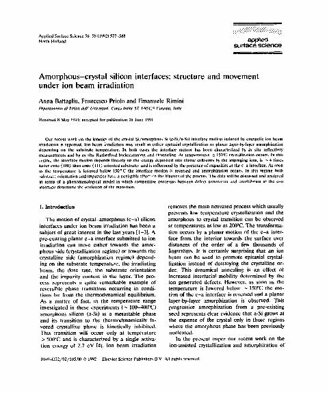
To study the ion-beam-induced epilaxial crys- tallization (IBIEC) we have used the sample con- figuration schematically shown in fig. 2. A surface amorphous layer, ~ 150 nm thick, was formed by 15(1 keV Ge + implantation at room temperature. St, hsequent irradiation in the temperature range
, / laser
• J
Dose(a u )
Fig. 2. Schcmatlc representation of lhe crystallizalion experi- ments. Ion irradiation induces the motion of lhe c-a interface towards the surface. As soon as the interface moves the reflectivity oscillates due to constructive and destructive inter- ferences between the light reflected from the surface and from the advancing interface. Peak to peak corresponds to a
66 nm shift of the interface.
.4. Battaglia et aL / Amorphous-crystal silicon interfaces
200-400°C can induce a t~lanar motion of the c -a interface towards the surface, in this case the use of transient reflectivity measurements is particu- !arly powerful for studying the kinetics of crystal- lization. In fact, as the interface moves, the re- flectivity of the sample will oscillate due to con- structive and destructive interferences occurring between the light reflected from the surface and from the advancing c-a, interface. In the adopted experimental set-up, passing from a peak to a consecutive valley in Ute reflectivity signal c , rre- sponds to an advance of the c -a interface by ~ 33 nm. It should be noted, besides, that de- creasing the distance from the surface, the ampli- tude of the oscillations increases due to a re- duced absorption in the amorpho,s layer.
By co,re, paring the experimental refleclivity trace as a function of the irradiation dose with the trend theoretically ce, lculated as a function of depth we ca , obtain directly the c -a interface position as a function of the dose. From a deriva- tive of this curve the ion-induced growth rate as a function of deDth can then be extracted.
3.Z D e p e n d e n c e on energy, loss
The process of layer-by-layer crystallization has been induced by using different ions in order to
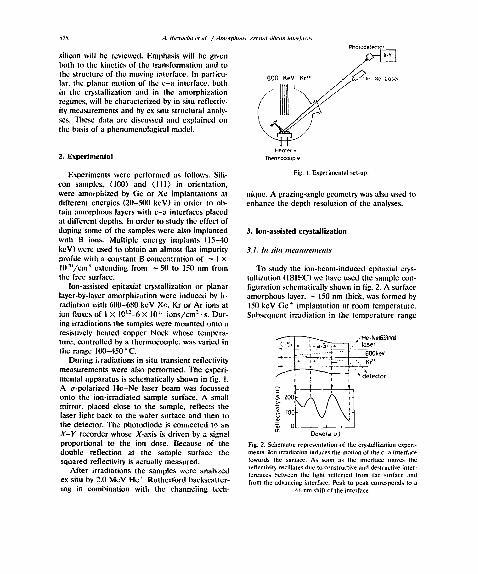
3°°i 080kov At.. i
t 6 k : I I ~00
T = 350 °C 1
i00 ~ , . , . . . . , . . . . , . . . i
0 100 200 300 400
Dose (x1014/ern 2)
Fig. 3. Refleetivity signals versus dose for irradiations of a ~ 160 nm thick a-layer with 680 keV Ar and with 600 keV Kr
at 350 ° C.
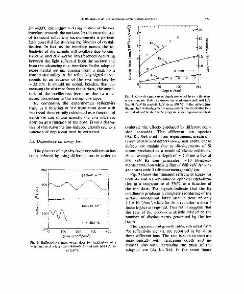
i xo__ ° o 2g ~
-:,
Kr 1
50 I00 150 Depth (nm)
Fig. 4. Growth rates versus depth extracted from reflectivity measurements. Da~a :'re shown fi~r irradiations with 680 keV Xe. 61111 keV Kr and 680 keV Ar at 350°C. la the same figure the number of displacements generated by the irradiating ions and calculated by Ihe TRIM program is also reported (circles).
evalutate the effects produced by different colli- sion cascades. The different ion species (Ar, Kr, Xe), used in our experiments, create dif- ferent densities of defects along lheir paths. These defects are mainly due to displacements of Si atoms produced as a result of elastic collisions. As an example, at a depth.of ~ !00 nm a flux of 6(10 keV Kr ions generates ~ 13 (displace- m e n t s / n m ) / i o n while a flux of 680 keV Ar ions generates only 3 (displacements/nm)/ion.
Fig. 3 shows the transient reflectivity traces for both Ar and Kr ion-induced epitaxial crys,~alliza- tion at a temperature of 350°C as a function of the ion dose. The signals indicate that the Kr irradiation produces a complete reordering of the surface amorphous layer after a dose of only 1.1 × 10:6/cm 2, while for Ar irradiation a dose 4 times higher is required. This result suggests that the rate of tile process is strictly rel:~ted to the number of displacements generated by the ior beam.
The experimental growth rates, extracted from 'he reflectivity signals, are reported in fig. 4 ~or three different ions. The rate is seen to increase monotonically with increasing depth and in- creases also with increasing lhe mass o~ the adopted ion (Ar, Kr, Xe). In the same figure
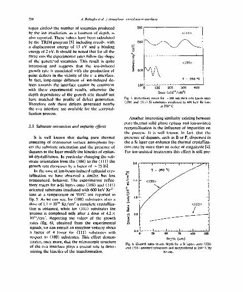
581) .4. Battagha et aL / AmorphOUSlCO'smlsi,'icmt inwrhwes
(open circleO the number of vacancies produced by the ion irradiation, as a function of depth, is also reported. These values have been calculated by the TRIM program [5], including recoils, with a displacement energy of 13 eV and a binding energy of 2 cV. it should be noted that for all the three tons the experimental rates follow the shape of the gcnera 'cd vacancies. This result is quite interesting and suggests that the ion-induced growth rate is associated with the production of point defects in the vicinity of the c - a interface. In fact, long-range diffusion of ion-induced de- fects towards the interface cannot be consistent with these experimental results, otherwise the depth dependence of the growth rate should not have matched the profite of defect generation. Therefore only those defects generated nearby the c - a interface are avaihtble for the ~ecrystal- lization process.
3.3. Substrate orientation and impurity effects
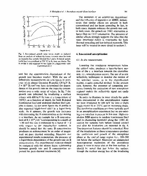
It [s well known that during pure thermal annealing of continuous surface amorphous lay- ers the substrate orientation and the presence of dopants in tile layer modify the kinetics of epitax- ial crystallization. In particular changing the sub- strate orientation from the (100) to the ( ! 11) the growth rate decreases by a factor of ~ 25 [6].
in the case of ion-beam-induced epitaxial crys- tallization we have observed a similar~ bm less pronounced, behavior. The experimental reflec- tivtty traces for a-Si layers onto ( !00) and ( i i 1) oriented substrates irradiated with 600 keV Kr '÷ ions at a temperature of 350°C are reported in fig. 5. As we can see, for (100) substrates after a dose of 1.1 × 10 I~' Kr/cm-" a complete crystalliza- tion is obtained, while lor ( I t l ) substrates the process is completed only after a dose of 4.2 × 10¹⁶/cm-'. Reporting the values of the growth rates (fig. 6), obtained from the experimental signals, we can extract an interface velocity about a factor of 4 lower for (111) substrates with respect to (100) substrates. This effect demon- strates, once more, that the micr~3scopic structure of the e - a interface plays a crucial role in deter- mining the kinetics of the transformation.
300
E
300
< l i t>
, , , , , , i , , , , , . .
< 100>
w\ T = 350 *C
100 200 300 400 D o s e ( x t t ~ l ~ / e m 2 )
Fig. 5. Refleetivity traces for ~ 160 am thick a-Si layers onto { I(X)) and (Il l) Si substrales irradiated by 60(; keV Kr ions
at 350 ° C.
Another interesting similarity existing between pure thermal solid phase epitaxy and ion-assisted recrystallization is the influence of impurities on the process. It is well known, in fact, that the presence of dopants, such as B or P, dispersed in the a-Si layer can enhance the thermal crystalliza- tion rate by more than an order of magnitude [4]. For ion-assisted t reatments this effect is still pre-
~ o t . . . . , . . . . , . . . . , . . . . , > ~ , ! f
~ t.o
< l i t >
,~ o.,5
o . o ~ . . . . :l 5 . . . . 5 ; . . . . "1~ . . . . . tO0-- ' ' i / 5 I
Depth (rim)
Fig. 6. Growth rates versus depth for a-Si layers unto (100) and (111) oriented substrates and recrystallized at 350 °C by
Kr ions.
A. Battaglia et aL / Amorphous-crystal silicon bm'rfaces
1020 ~
, + / ~ . \ i , o ~
OL • _d I I I / 0 25 50 75 100 125 150
Oepth (nm)
Fig. 7. Ion-induced growth rates versus depth as deduced from an analysis of refleetivity traces. Growth rates for both an impurity-free sample (dashed line) and a B-doped sample (solid line) recrystallized at 350 °C by Kr ions are shown. The B profile is also reported in the figure in a logarithmic scale
(right-hand side).
sent but the concentration dependence of the growth rate becomes weaker. With the use of reflectivity measurements on a-St layers in pres- ence of an almost Gaussian B profile (20 keV B, 5 X 10¹⁴ B / c m 2) we have determined the depen- dence of the growth rate on the impurity concen- tration over a wide range of values. In fig. 7 the growth rate (obtained by irradiating a surface a-layer with 600 keV Kr ions at a temperature of 350°C), as a function of depth, for both B-doped (continuous line) and undoped (dashed line) sam- ples is shown. In the same figure the B profile is also reported (rigth-hand side) in a logarithmic scale. As it appears, the growth rate increases with increasing the B concentration at the moving c - a interface. As an example for a B concentra- tion of 8 × 10~9/cm 3 (corresponding to a depth of ~ 80 nm) the rate is enhanced by a factor of ~ 2 with respect to the impurity-free material. It should be noted that the same B concentration produces an enhancement by an order of magni- tude on pure thermal annealing. Moreover our experimental results demonstrate the presence of a logarithmic dependence of the growth rate on B concentration. This experimental evidence should be compared with the almost linear relationship between growth rate and B concentration re- ported for pure thermal t reatments [4].
The existence of an orienta,tion dependence and the iufluence of impurities on IBIEC demon- strate that similar effects are present in both conventional and ion beam annealing, in fact, in both cases, dopants enhance the growth rate and, in both cases, the growth on (100) orientation is faster than on (111) orientation. The presence of similar effects strongly supports the idea that the same interracial defect is responsible for both thermal annealing and ion-induced regrowth. This issue will be treated in more detail in section 5.
4. Ion.assisted amorphization
4.1. In situ measurements
Lowering the irradiation temperature below the critical value produces a layer-by-layer mo- tion of the c - a interface towards the crystalline side, i.e., amorphization occurs. The use of in situ reflectivity techniques to monitor the motion of the interface seems, as in the crystallization regime, a quite powerful method. In the present case, however, the presence of competing pro- cesses (namely. the nucleation of new amorphous regions) makes the reflectivity signal not easily interpreted.
In order to illustrate in more details the prob- lems encountered in the amorphization regime we have irradiated by 600 keV Kr ions a virgin single crystal Si at 135°C and at increasing doses. The irradiation conditions are those typically used in an amorphization experiment but no pre-exist- ing c - a interface is present in this case. High-res- olution RBS spectra in random (continuous line) and in channeling (symbols) along the (100) di- rection for samples both before (closed circles) and after Kr irradiation are reported in fig. 8. Two important features should be remarked. First all the irradiations at these temperatures produce the nucleation and growth of the amorphous phase at the end of range region (i.e., 200-300 nm below the surface). Moreover an unexpected heterogeneous nucleation of the amorphous phase is seen to occur also at the free surface. It should be noted that just below the surface, though the nuclear energy loss of the irradiating
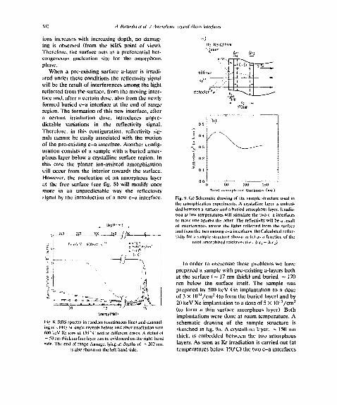
582 A. Battuglia et al. / Amorphous-crystal silicon interfaces
ions increases with increas ing depth , no damag- ing is observed (from the RBS point of view). Therefore , the surface acts as a p re fe ren t ia l het- e rogeneous nuclea t ion si te for the amorphous phase.
When a pre-exis t ing surface a- layer is irradi- a ted under these condi t ions the reflectivity signal will be the result of in te r fe rences a m o n g the l ight ref lec ted from the surface, from the moving inter- face and, af ter a ce r ta in dose, a lso from the newly formed bur ied c - a in terface at the end of range region. The format ion of this new interface, a f ter a cer ta in i r radia t ion dose, in t roduces unpre- d ic table var ia t ions in the reflectivity signal. Therefore , in this conf igurat ion, rcflectivity :+ig- nals cannot be easi ly associa ted with the mot ion of the pre-exis t ing c - a interface. A n o t h e r config- ura t ion consis ts of a sample with a bur ied amor- pl :ous layer below a crystal l ine surface region. In this case the p lana r ion-ass is ted amorph iza t ion will occur from the in ter ior towards the surface. However , the nuc lea t ion of an amorphous layer at the free surface (see fig. 8) will modify once more in an unpred ic tab le way the reflectivity ignal by the in t roduc t ion of a new c - a interface.
~ i , : . s ° c 60o . . . . . " " "~'.?;:~,/~, 1 • ~.io ,s
t ......... o~ .................. "Td ...... ~}~ ...... ;, "
EnergylMeV}
Fig. 8. RBS spectra in random {continuous line) and channel- ing of (100) Si single crystals before and after irradiation with 6110 keV Kr ions at 135+C and at different doses. A detail of
~ 50 nm thick surface layer can be evidenced on the right-hand side. The end of range damage, lying at depths of ~ 2{]0 nm,
is also shown on the left-hand side.
a)
He-NeI63]nm) . laser
• Axl L~x z
, ,a-SI ~+ '~
K~'" ..".. :"|--L!- ,J
05 A
O4
O3
~o~ Ol
i~ x2 _ ,,.4 17Ohm
b)
Total amorphized thickness (nm)
Fig. 9. (a) Schematic drawing of the sample structure used in the amorphization experiments. A crystalline layer is embed- ded between u surface and a buried amorphous layer. Irradia- tion at tow temperatures will stimulate the two c-a interfaces to move one against the other. The reflectivity will be a result of interferences among the lights reflected from the surface and from the two moving e-a interfaces. (b) Calculated reflec- tivity for a sample structure silown in (a) as a function of the
total amorphized thickness ti.e, "~xz + AXz).
In o rde r to overcome these p rob lems we have p repa red a sample with pre-exis t ing a- layers both at the surface ( ~ 17 nm thick) and bur ied ~ 170 nm below the surface itself. The sample was p r e p a r e d by 500 keV Ge implan ta t ion to a dose of 3 × 101~/cm2 (to form the bur ied layer) and by 20 keV Xe implan ta t ion to a dose of 5 × 10¹³/cm2 (to form a thin surface amorphous layer). Both impiantat; ,ons were done at room t empera tu re . A schemat ic d rawing of the sample s t ruc ture is ske tched in fig. 9a. A crystal l ine l~yer, ~ 150 nm thick, is e m b e d d e d be tween the two a m o r p h o u s layers. As soon as Kr i r radia t ion is ca r r ied out (at t e m p e r a t u r e s below 150°C) the two c - a in ter faces
A. Battaglia el aL / Amorphous-crystal silicon inlt,rf~lces
will move one against the other and the crys- talline layer will shrink until it disappears. !n the present case, however, all the c - a interfaces are pre-existing in the initial sample structure and the amorphization process is solely due to the planar motion of these interfaces. The reflectivity signal of this sample is due to the interferences between the light reflected from the surface and from the two moving e - a interfaces. This configu- ration is more complex than that used in the crystallization experiments but, known the initial positions of the c - a interfaces, the outcoming refleet!vity as a function of the irradiation dose can be calculated and predicted. In fig. 9b the calculated squared reflectivity (to account for the experimental conditions of fig. I) is reported ver- sus the total amorphized thickm;ss (i.e., Ax~ + ~x2). A large oscillation, with a maximum and a minimum is present. A comparison of this calcu- lated signal as a function of the amorphized thickness with the experimental signal as a func- tion of the irradiation dose will directly yield the amorphization rate in amorphous thickness per unit dose (taking into account that two different interfaces are contributing to the process).
4.Z Experimental results
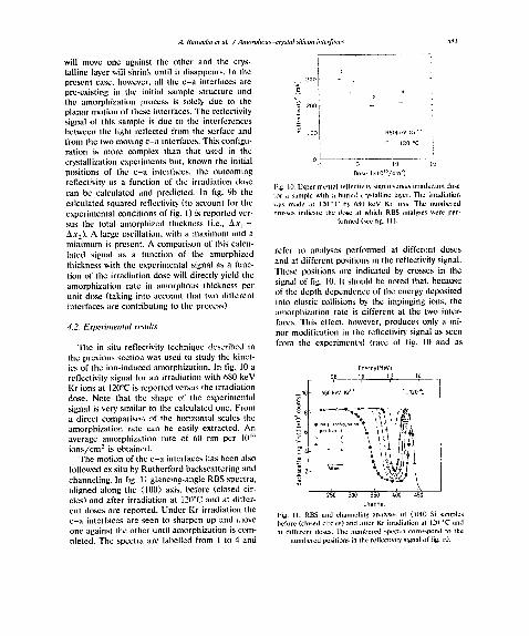
The in situ reflectivity technique described in the previous section was used to study the kinet- ics of the ion-induced amorphization. In fig. 10 a reflectivity signal for an irradiation with 680 keV Kr ions at 120°C is reported versus the irradiation dose. Note that the shape of the experimental signal is very similar to the calculated one. From a direct comparison of !he horizontal scales the amorphization rate can be easily extracted. An average amorphization rate of 60 nm per liP" ions/cm-" is obtained.
The motion of the c - a interfaces has been also followed ex situ by Rutherford backscattering and channeling, in fig. 11 glancing-angle RBS spectra, aligned along the (100) axis, before (closed cir- cles) and after irradiation at 120°C and at differ- ent doses are reported. Under Kr irradiation the c - a interfaces are seen to sharpen up and lilOVe one against the other until amorphization is com- pleted. The spectra are labelled from 1 to 4 and
i
i 1 30O [ +
+ ,~
200
I t ~ l z 0 o c i
o 5 10 15 Dose (xlOt~/cm z)
Fig. 10. Experimental reflec:tivity signal versus irradiation dose tor a sample: with a buried ~:rystalline layer. The ~rradiatitm ~vas made at 121)°C by 681) keV Kr ions. The numbered c:rossc:s indic:ale the dose al which RBS analyses were per-
formcd (see fig. I I ).
refer "~o analyses performed at different doses and at different positions in the reflectivity signal. These positions are indicated by crosses in the signal of fig. 10. It should be noted that, because of the depth dependence of the energy deposited into elastic collisions by the impinging ions, the amorphization rate is different at the two inter- faces. This effect, however, produces only a mi- nor modification in the reflcctivity signal as seen from the experimental trace of fig. 10 and as
Energy(MeV) 08 10 12 1/+
~10 660 keV Kr*+ T= 120°C
250 300 350 400 t+50
Channel
Fig. I1. RBS and channeling analyses of (100) Si samples bc:fl)re (closed circles) and after Kr irradiation at 120"C and at different doses. The: numbered spec:tra correspond to the
numbered positions in the reflectivity sigmd of fig. 10.
calculated by imposing different velocities z~t the two interfaces.
As extensively made in the crystallization regime, we have investigated the effects of sub- strate orientation and dopants on the layer-by- layer amorphization. In particular, for studying the impurity effect on the amorphization rate, we have used a sample configuration similar to the one shown in fig. 9a with an almost flat B profile of ~ I x I():"/cm 3 extending from ~ 50 to 15(1 nm from the free surface. Irradiating with 681) keV Kr ions both the doped and the undopcd samples, in the same experimental conditions, we have observed no significant difference in the two respective reflectivity signals. This demonstrates that in the amorphization regime (in particular far from the transition temperature) no doping effect is present. Moreover, the substrate orienta- tion has no effect on thc rate of amorphization as seen lot (100) and <111) oriented substrates. These results evidence that a different type of interface .~tructurc fl~rms during the crystalliza- tion and the amorphization regimes
A. Battaglia et al. / Amorphotts -(O'.stal .si&'ol intcr]~tces
T ( ° C ) 500 300 200
103
"~ lo I !
5. Balance between crystallization and amor- phization
5. I. T e m p e r a t , r e d e p e n d e n c e
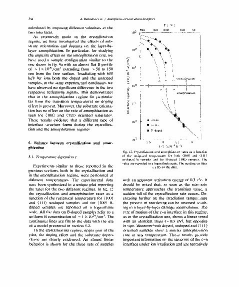
Experiments similar to those reported in the previous sections, both in the crystallization and in the amorphization regime, were performed at different temperatures. The experimental data iaavc been synthesized in a unique plot reporting the rates for the two different regimes. In fig. 12 the crystallization and amorphization rates as a function of the reciprocal temperature for (100) and (111) undoped samples and for (100) B- doped samples are reported on a logarithmic scale. All the data on B-doped samples refer to a uniform 13 concentration of ~ 1 × 10"-"/cm 3. The continuous lines are fits to the data with the use of a model presented in section 5.2.
In the crystallization regime, upper part of the plot, the doping effect and the substrate depen- dence are clearly evidenced. An almost linear behavior is shown for the three sets of samples
!00 ...... 5 0 !
3. ~ - crystalhzatlon
- 1 0 0 . . . . b . . . . ; . 'l ' ] .
_~ , I I . . . . p,,z,t,on
i ~cl i
!!!!!. 1o a . . . . . . . . . ~
15 2 25 3 1/T {,xlO 3 K l)
Fig. 12. Crystallization and amorphizalion rates as a function of the reciprocal temperature for bolh (10(I) and (111) undopcd 5i samples and fi~r B-doped (101}) samplc~,. The rates llr¢ reported in a logarithmic ~,eale. I~he continuou~ lines
are fits to the d;llil.
with an apparent activation energy of 0.3 cV. it should be noted that, as soon as the sub, irate temperature approaches the transition value, a sudden fall of the crystaltization rate occurs. De- creasing further on the irradiation temper~.ture the process of reordering can be reversed result- ing in a layer-by-layer damage accumulation. The rate of motion of the c-a interface in this regime, as in the crystallization one, shows a linear trend with an identical slope ( ~ 0.3 eV), but opposite in sign. Moreover both doped, undoped and ( 111 ) oriented samples show a similar amorphization rate at any temperature. These results provide important information on the structure of the c-a interface under ion irradiation and are tentatively
A. Battaglia et aL / Amorphous-co'.~tal silicon huerfaces
explained by means of a phenomenological model described below.
5.Z Modelling
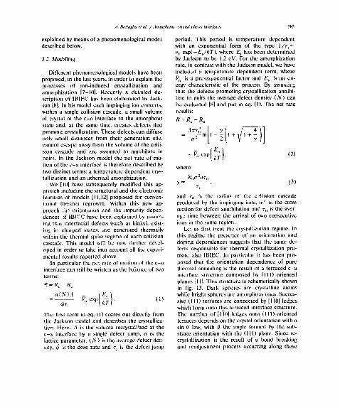
Different phenomenological models have been proposed, in the last years, in order to explain the processes of ion-induced crystallization and amorphization [7-10]. Recently a detailed de- scription of IBIEC has been elaborated by Jack- son [8]. In his model each impinging ion converts, within a single collision cascade, a small volume of crystal at the c -a interlace to the amorphous state and, at the same time, creates defects that promote crystallization. These defects can diffuse only small distances from their generation site, cannot escape away from the volume of the colli- sion cascade and are assumed to annihilate in pairs, in the Jackson model the net rate of mo- tion of the c-a interface is therefore described by two distinct terms: a temperature dependent crys- tallization and an athermal amorphization.
We [10] have subsequently modified this ap- proach including the structural and the electronic features of models [11,12] p~oposed for conven- tional therm~:i regrowth. Within this new ap- proach ~h," orientation and the impurity depen- dences of IBIUC have been e×plained by assum- inr, that interracial defects (such as kinks), exist- ing in charged states, are generated thermally within the thermal spike regime of each collision cascade. This model will be now further devel- oped in order to take into account all the experi- mental results reported above.
In particular the net rate of motion of the c-a interi'ace can still be written as the balance of two terms:
R=R~.-R~,
4;, The first term in eq. (1) comes out directly from the Jackson model and describes the crystalliza- tion. Here, A is the volume recrystalFzed at the c -a interface by a single defect jump, a is the lattice parameter, ( N ) is the average defect den- sity, 4; is the dose rate and ri is the defect jump
585
period. This period is temperature dependent with an exponential form of the type l /~ ' j= v, exp( - E J k T ) , where Ej has been determined by Jackson to be 1.2 eV. For the amorphization rate, in contrast with the Jackson model, we have includ~.d a temperature dependent term, where V,,, is a pre-exponential factor and E,, is an en- erb-y' characteristic of the process. By assuming that the defects promoting crystallization annihi- late in pairs the average defect density ( N ) can be evaluated [8] and put in eq. (1). The net rate results:
R = R~ - R,,
- ~ h111+ 7 1+
where
Niio-2a% "r = - - (3)
71
and rf~ is the radius of tl',e c.:~llision cascade produced by the impinging ions, tr 2 Is the cross section for defect annihilation and r o is the aver. age time between the arrival of two consecutive ions in the same region.
Let us first treat the crystallization regime. In this regime the presence of an orientation and doping dependences suggests that the same de- fects responsible for thermal crystallization pro- mole also IBIEC. In particular it has been pro- posed that the orientation dependence of pure thermal annealing is the result of a terraced c -a interface structure composed by (111) oriented planes [11]. This structure is schematically shown in fig. 13. Dark :;pl~eres are crystalline atoms while bright spheres are amorphous ones. Succes- sive (l l l) terraces are connected by [170] ledges which form onto this terraced interface structure. The number of [1"i0] ledges onto (111) oriented tenaces depends on the crystal orientation with a sin 0 law, with 0 the angle formed by the sub- strate orientation with the (11 I) plane. Since re- crystallization is the result of a bond breaking and readjustment process occurring along these
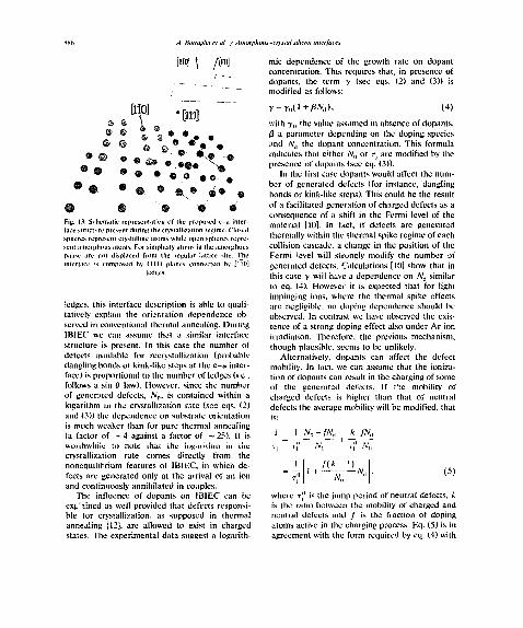
A. Buttaglia el aL / Ao orphoux-t'~'.;ial .q/icon it tt,tfitt'(,s
[~Io] I /'I.~l / .......
/ . . . . . . . . ,
/
[~0] • [m]
® ~ ° o ~do e e
® @ ® ® e o o e o . o
® e ® e * ~ ® , , . O @ • O • Fig. 13. Schematic representation of the proposed e-a inter- face structure present during the e~'stallization regime. ("losed spheres represent el3'stallinc atoms while open spheres repre- sent amorphous alo~ns. For simplicity atorn~ in the amorphot, s pdase are riot disphleed from the regular lattice site. The interface is composed by 1111) planes connected by l l]l)]
ledges.
;edges, this interlace description is able to quali- tatively explain the orientation dependence ob- served in conventional thermal annealing. During IBIEC we can assume that a similar interlace structure is present. In this case the number of defects available for rccrystallization (probably dangling bonds or kink-like steps at the c -a inter- face) is proportional to the number of ledges (i.e.. follows a sin 0 law). However, since the number of generated defects, N., is contained within a logarithm i . the crystallization rate *,see eqs. (2) and (3)) the dependence on substrate orientation is much weaker than for pure thermal annealing Ca factor of ~ 4 against a factor of ~ 25). It is worthwhile to note that the log~ttilhm in the crystallization rate comes directly from the nonequilibrium features of IBIEC, in which de- fects arc generated only at the arrival of an ion and continuoasly annihilated in co~tplcs.
The influence of dopants on h31EC can be exlZained as well provided that defects responsi- ble tar crystallization, as supposed in thermal annealing [12], are allowed to exist in charged states. The experimental data suggest a Iogarith-
mic dependence of the growth rate on dopant concentration. This requires thaL in presence of dopants, the term y (see eqs. (2) anti (3)) is modified as follows:
)' : y,,(l +fiNd), (4)
with ,/. the value assamed in absence of dopants, 13 a parameter depending on the doping species and N a the dopant concentration. This formula indicates that either N. or rj are modified by the presence of dopants (see eq. (3)).
In the first case dopants would affect the num- ber of generated defects (for instance, dangling bonds or kink-like steps). This could be the result of a facilitated generation of charged defects as a consequence of a shift in the Fermi level of the material [10]. in fact, if defects are generated thermally within the thermal spike regime of each collision cascade, a change in the position of the Fermi level will strongly modit~ the number of generated defects. Calculations [10] show that in this case y will have a dependence on N d similar to cq. (4). However it is expected that for light impinging ions, where the thermal spike effects are negligible, no doping dependence should be observed. In contrast wc have observed the exis- tence of a strong doping effect also under Ar ion irradiation. Therefore, the previous mechanism, though plausible, seems to be unlikely.
Alternatively, dopants can affect the defect mobility. In fact, we can assume that the ioniza- tion of dopants can result in the charging of some of the generated defects, if the mobility of charged defects is higher than that of neutral defects the average mobility will be modified, that is:
l I N,,-fN,, k .IN,, ri rl' ?¢u + ' ~' -rj I lV(i
1 [ f ( k - ' ) Nll =V ~ ÷ - - ~ , , - ' l ' (5)
where r~ ~ L,: the jump period of neutral defects, k is the ratio between the mobility of charged and neutral defects and f is the fraction of doping atoms active in the charging pt'ocess. Eq. (5) is in agreement with the form required by eq. (4) with
A. Battaglia ¢'t al. / Amorphous-crystal silicwn h~terfact'.~
[3 = f ( / " - I ) / N , . At the moment we cannot deft- nitcly discriminate between the two proposed possibilities, both of them can account for the experimental data, but the latter seems more plausible.
We now consider the amorphization regime in which the second term of eq. (2) prevails. In contrast to thc Jackson model our experimental data are not consistent with a constant amor- phization rate and an exponential form must be used to fit the data. The mechanism of layer-by- layer amorphization is not yet known. We how- ever suggest that defects produced in the amor- phous side of the c-a interfacc (such as dangling bonds) ;ire responsible for crystallization, while defects produced in the crystalline side (such as interstitial-vacancy pairs) promote amorphiza- tion. As a matter of fact, ion-generated intcrsti- tials may agglomerate at the pre-existing c-a in- tcrface producing a prcfcrcnt!ai amorphization. Wc propose that this process is inversely propor- tional to the recombination rate of Frcnkel pairs. Therefore, decreasing the temperature the con- densation probability increases with an exponen- tial law, where E,, may represent the activatkm energy for ',he recombination of vacancy-intersti- tial pairs. This picture is consistent with the ex- perimental data in which E,, is found to bc ~ 0.3 cV.
The absence of an orientation dependence suggests that the terraced interface structure pre- sent during crystallization is probably lost when the interface motion is reversed. Therefore the c -a interface does not contain preferential amor- phization sites and has a similar structure regard- les~; of the substrate orientation. Moreover, the absence of doping effects demonstrates that the growth process of the amorphous layer is purely collisional and charged defects play no significant role. In contrast, the presence of a doping effect has been reported for the nucleation phase [13]. This difference suggests that different defects arc responsible for the two processes.
Using the ideas exposed above we have fitted the experimental data by means of eqs. (2), (3) and (4). The fits are reported in fig. 12 (continu- ous lines) together with the data. The parameters used in the fits are reported in table I. The
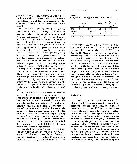
Table 1 Numerical values of the paramelers used in this work
(x't l(,": y ''' E, E,, V,,, (eV) (eV) t x 10-25 cm '~) cm 3)
(l(lll) 4.4 195 1.2 (1.3 1.2 B-d,~ped 4.4 3.q× Ill s 1.2 11.3 1.2 ( I I I ) 4.4 2 1.2 0.3 1.2
'*) Values calculated at 350°C.
agrccment between the caicuiated curves and the experimental results is Lxcellent in both regimes and for all the sets of data ((1001, (111), B- doped). The three different curves in the crystal- lization regime fall down to a null rate at differ- ent transition temperatures and then converge into a unique amorphization rate at low tempera- tures. The different transition temperatures are an effect of the balance between an orientation and dopant dependent crystallization rate and a simpl) temperature dependent amorphization rate. As soon as the crystallization term becomes negligible (T < 140°C) the net rate coincides with the amorphization term and doping and substrate effects become negligible too. This two-defects description provides therefore a unifying and consistent picture ot all the observed phenomena.
6. Summary
In summary, in the present paper the motion of the c-a Si interface under ion beam bom- bardement has been investigated in details. At temperatures above ~ 150°C the interface moves towards the amorphous side, i.e., a recrystalliza- tion occurs. The process depends linearly an the energy deposited into elastic collisions, is faster on (1001 substrates than on ( l 11 ) substrates and is affected by the presence of dopants. At tem- peratures below ~ 150°C the interface motion is reversed and amorphization takes place. In this regime no orientation dependence or impurity effects have been observed. The amorphization rate increases however exponentially as the tem- perature is decreased. These data have been in- terpreted by assuming that the impinging ions
A. Batt~aglia et al. / Amorphous-crystal silicon i , terfaces
genera te defects in the a m o r p h o u s side of the interhsce (such as dang l ing bonds) p romot ing crystal l izat ion and defects in the crystal l ine side of the interface (such as vacancy- in te r s t i t i a l pairs) p roduc ing amorphiza t ion . The ba lance be tween these two opposi te processes gives the net ra te of mot ion of the c - a interface. In the crysta l l izat ion reg ime the in terface is p roposed to have a ter- raced s t ruc ture in which reorder ing occurs ot:ly at p re fe ren t ia l sites. This o rde red in terracia l struc- ture is however lost dur ing amorph iza t ion . This picture can account for the d e p e n d e n c e of the growth rate on the subs t ra te o r i en ta t ion and for the absence of such a d e p e n d e n c e in the amor- phiza t ion rate. Moreover , this two-defects model can account also for the dop ing effects, provided tha t the defects p romot ing crystal l izat ion arc al- lowed to exist in cha rged states.
We th ink that the p resen t descriptio.1 gives a consis tent in te rp re ta t ion of both crystal l izat ion and amorph iza t ion p h e n o m e n a occurr ing at pre- exist ing c - a sil icon interfaces. However , much work should be done to def ini te ly identify the exact microscopic mechan i sms lead ing to interfa- cial r eorder ing and interfacial d a m a g e accumula- t ion induced by ion bombardemen t .
Acknowledgements
We wish to t hank Mar io Saggio for col labora- tion in some of the expe r imen t s repor ted in this
paper , Salvo Coffa for the many in te res t ing dis- cussions on the crystal l izat ion mechan i sms and Oraz io Parasole for his unvaluable technica l as- sistance. This work was suppor t ed in par t by Proget to Fina l izza to Mater ia l i e Disposit ivi per I 'E le t t roniea a Stato So!ido, CNR.
References
[I] F. Priolo and E. Rimini, Mater. Sci. Rep. 5 (19901 319, and references therein.
[2] J.S. Williams, R.G. Elliman, W.L. Brown and T.E. Sei- dcl, Phys. Rev. Left. 55 (1985) 1482.
131 J. Linnros. G. llolmen and B. Svenssnn, Phys. Rev. B 32 ( 19851 27711.
141 G.L. Olson and J.A. Roth, Mater. Set. Rep. 3 (19881 I. [5] J.P. 13iersack and L.G. ]lnggmark. Nucl. Instr. Meth. 174
(19811) 257, [61 L. Csepregi, E.F. Kennedy, J.W. Mayer and T.W. Sig-
mon, J. Appl. Phys. 49 (19781 3906. [7] J. Linnros, R.G. Elliman and W.L. Brown. J. Mater. Res.
3 (19881 12118. iS] H.A, Jackson, J. Mater. Res. 3 (19881 1218. [9] H.A. Atwater, C.V. Thompson and H.I. Smith, Mater.
Res. $oc. Symp. Proe. 1(]11 (19881 345. [1(11 F. Ptiolo, C. Spinella and E. Rimini, Phys. Roy. B 41
( 19901 5235. [11] F. Spaepen and D. Turnbull, in: Laser Annealing of
Semiconductors, Eds. J.M. Poate and J.W. Mayer (Academic Press. New York. 19821 p. 15.
[12] J.S. Williams anti R.G. Elliman, Phys. Rev. Lett. 51 (1983) 1069.
[13] A.Y. Dvurechenskii, R. Groctzschel and P. Poppy, Phys. Loll. A 116 (19861 ~99.
Related Documents