A D V A N C E D M I C R O D E V I C E S Am8530H/Am85C30 Serial Communications Controller 1992 Technical Manual

Welcome message from author
This document is posted to help you gain knowledge. Please leave a comment to let me know what you think about it! Share it to your friends and learn new things together.
Transcript

A D V A N C E D M I C R O D E V I C E S
Am8530H/Am85C30Serial Communications Controller
1992 Technical Manual
ii
1992 Advanced Micro Devices, Inc.
Advanced Micro Devices reserves the right to make changes in its products without notice in order to improve design or performance characteristics.
This publication neither states nor implies any warranty of any kind, including but not limited to implied warrants of merchan-tability or fitness for a particular application. AMD assumes no responsibility for the use of any circuitry other than the circuitryin an AMD product.
The information in this publication is believed to be accurate in all respects at the time of publication, but is subject to changewithout notice. AMD assumes no responsibility for any errors or omissions, and disclaims responsibility for any consequencesresulting from the use of the information included herein. Additionally, AMD assumes no responsibility for the functioning ofundescribed features or parameters.
Product names used in this publication are for identification purposes only and may be trademarks of their respective companies.
Trademarks
Z80 and ZBus are registered trademarks of Zilog, Inc.
Z8000, Z8030, and Z8530 are trademarks of Zilog, Inc.
MULTIBUS is a registered trademark of Intel Corporation
PAL is a registered trademark of Advanced Micro Devices, Inc.

PREFACE
Thank you for your interest in the SCC, one of the most popular Serial Data ICs availabletoday. This manual is intended to provide answers to technical questions about theAm8530H and Am85C30.
If you have already used the Am8530H and are familiar with the previous editions of thisTechnical Manual, you will find that some chapters are virtually unchanged. TheAm8030’s functionality, however, has been omitted from this revision since a CMOSAm8030 was not developed. You can, however, consult the previous Am8030/8530 Tech-nical Manual revision for information pertaining to Am8030 operation.
Functional descriptions of enhancements added to the Am85C30 have been included inthis Technical Manual revision. These enhancements improve the Am85C30’s functional-ity and allow it to be used more effectively in high-speed applications. These enhance-ments include:
a 10 x 19-bit SDLC/HDLC frame status FIFO array
a 14-bit SDLC/HDLC frame byte counter
automatic SDLC/HDLC opening flag transmission
automatic SDLC/HDLC Tx Underrun/EOM flag resetting
automatic SDLC/HDLC Tx CRC generator presetting
RTS pin synchronization to closing SDLC/HDLC flag
DTR/REQ deactivation delay significantly reduced
external PCLK to RxC or TxC synchronization requirement eliminated for PCLK divide-by-four operation
complete SDLC/HDLC CRC character reception
reduced INT response time
Write data setup time to rising edge of WR requirement eliminated
Write Registers WR3, WR4, WR5, and WR10 made readable
Most users read only chapters that are of interest to them. If you are designing the micro-computer hardware using the SCC as a peripheral, you will want to read the ApplicationsSection in Chapter 7. Application notes covering the interfacing of the Am8530H (pre H-step and CMOS versions only) to the 8086/80186, 68000 processors and Am7960 DataCoded Transceiver have been included.
As was the case with the NMOS SCC, some points to look out for when using theAm85C30 are:
Follow the worksheet for initialization (Chapter 7). Unexplainable operations may occur ifthis procedure is not followed.
Watch out for the Write Recovery time violation. The specification for this (Trc) waschanged on both the H-step and CMOS version. It is now referenced from falling edge tofalling edge of the Read/Write pulse. Trc is spec’d at 4 PCLKs for the NMOS H-step and 3PCLKs (best case)/3.5 PCLKs for the Am85C30.
Ensure Mode bits are not changed when writing commands. Each Mode bit affects onlyone function and a Command bit entry requires a rewrite of the entire register; therefore,care must be taken to insure the integrity of the Mode bits whenever a new command isissued.
Any unused input pins should be tied high.

TABLE OF CONTENTS
Chapter 1 General Information
1.1 Introduction 1–3. . . . . . . . . . . . . . . . . . . . . . . . . . . . . . . . . . . . . . 1.2 Capabilities 1–3. . . . . . . . . . . . . . . . . . . . . . . . . . . . . . . . . . . . . . 1.3 Block Diagram 1–5. . . . . . . . . . . . . . . . . . . . . . . . . . . . . . . . . . . . 1.4 Pin Functions 1–6. . . . . . . . . . . . . . . . . . . . . . . . . . . . . . . . . . . . . 1.5 Pin Descriptions 1–8. . . . . . . . . . . . . . . . . . . . . . . . . . . . . . . . . .
1.5.1 System Interface Pin Descriptions 1–8. . . . . . . . . . . . . . . 1.5.2 Serial Channel Pin Descriptions 1–9. . . . . . . . . . . . . . . .
Chapter 2 System Interface
2.1 Introduction 2–3. . . . . . . . . . . . . . . . . . . . . . . . . . . . . . . . . . . . . . 2.2 Registers 2–3. . . . . . . . . . . . . . . . . . . . . . . . . . . . . . . . . . . . . . . . 2.3 System Timings 2–5. . . . . . . . . . . . . . . . . . . . . . . . . . . . . . . . . . .
2.3.1 Read Cycle 2–5. . . . . . . . . . . . . . . . . . . . . . . . . . . . . . . . 2.3.2 Write Cycle 2–5. . . . . . . . . . . . . . . . . . . . . . . . . . . . . . . . 2.3.3 Interrupt Acknowledge Cycle 2–5. . . . . . . . . . . . . . . . . . .
2.4 Register Access 2–6. . . . . . . . . . . . . . . . . . . . . . . . . . . . . . . . . . 2.5 Am85C30 Enhancement Register Access 2–7. . . . . . . . . . . . . . 2.6 Reset 2–12. . . . . . . . . . . . . . . . . . . . . . . . . . . . . . . . . . . . . . . . . . .
Chapter 3 I/O Programming Functional Description
3.1 Introduction 3–3. . . . . . . . . . . . . . . . . . . . . . . . . . . . . . . . . . . . . . 3.2 Polling 3–3. . . . . . . . . . . . . . . . . . . . . . . . . . . . . . . . . . . . . . . . . . 3.3 Interrupt Sources 3–3. . . . . . . . . . . . . . . . . . . . . . . . . . . . . . . . . . 3.4 Interrupt Control 3–4. . . . . . . . . . . . . . . . . . . . . . . . . . . . . . . . . .
3.4.1 Interrupt Enable Bit 3–4. . . . . . . . . . . . . . . . . . . . . . . . . . 3.4.2 Interrupt Pending Bit 3–5. . . . . . . . . . . . . . . . . . . . . . . . . 3.4.3 Interrupt Under Service Bit 3–5. . . . . . . . . . . . . . . . . . . . 3.4.4 Disable Lower Chain Bit 3–5. . . . . . . . . . . . . . . . . . . . . .
3.5 Interrupt Operations 3–6. . . . . . . . . . . . . . . . . . . . . . . . . . . . . . . 3.5.1 Multiple Interrupt Priority Resolution 3–6. . . . . . . . . . . . . 3.5.2 Interrupt Without Acknowledge 3–8. . . . . . . . . . . . . . . . . 3.5.3 Interrupt With Acknowledge With Vector 3–8. . . . . . . . . . 3.5.4 Interrupt With Acknowledge Without Vector 3–10. . . . . . . 3.5.5 Lower Priority Interrupt Masking 3–10. . . . . . . . . . . . . . . .
3.6 Receive Interrupts 3–10. . . . . . . . . . . . . . . . . . . . . . . . . . . . . . . . . 3.6.1 Receive Interrupts Disabled 3–10. . . . . . . . . . . . . . . . . . . . 3.6.2 Receive Interrupt on First Character or
Special Condition 3–10. . . . . . . . . . . . . . . . . . . . . . . . . . . . 3.6.3 Receive Interrupt on All Receive Characters or
Special Conditions 3–11. . . . . . . . . . . . . . . . . . . . . . . . . . . 3.6.4 Receive Interrupt on Special Conditions 3–11. . . . . . . . . .
3.7 Transmit Interrupts 3–12. . . . . . . . . . . . . . . . . . . . . . . . . . . . . . . . 3.8 External/Status Interrupts 3–13. . . . . . . . . . . . . . . . . . . . . . . . . . .
3.8.1 Sync/Hunt 3–13. . . . . . . . . . . . . . . . . . . . . . . . . . . . . . . . . 3.8.2 Break/Abort 3–14. . . . . . . . . . . . . . . . . . . . . . . . . . . . . . . . 3.8.3 Zero Count 3–14. . . . . . . . . . . . . . . . . . . . . . . . . . . . . . . . . 3.8.4 Tx Underrun/EOM 3–15. . . . . . . . . . . . . . . . . . . . . . . . . . . 3.8.5 Clear To Send 3–15. . . . . . . . . . . . . . . . . . . . . . . . . . . . . . 3.8.6 Data Carrier Detect 3–15. . . . . . . . . . . . . . . . . . . . . . . . . .

Table of Contents AMD
3.9 Block Transfers 3–15. . . . . . . . . . . . . . . . . . . . . . . . . . . . . . . . . . . 3.9.1 Wait on Transmit 3–16. . . . . . . . . . . . . . . . . . . . . . . . . . . . 3.9.2 Wait on Receive 3–16. . . . . . . . . . . . . . . . . . . . . . . . . . . . 3.9.3 DMA Requests 3–17. . . . . . . . . . . . . . . . . . . . . . . . . . . . . .
3.9.3.1 DMA Request on Transmit (using W/REQ) 3–17. . . . . . . . . . . . . . . . . . . . . .
3.9.3.2 DMA Request on Transmit(using DTR/REQ) 3–18. . . . . . . . . . . . . . . . . . . .
3.9.3.3 DTR/REQ Deactivation Timing 3–19. . . . . . . . . . 3.9.3.4 DMA Request on Receive (using W/REQ) 3–20.
Chapter 4 Data Communication Modes Functional Description
4.1 Introduction 4–3. . . . . . . . . . . . . . . . . . . . . . . . . . . . . . . . . . . . . . 4.2 Protocols 4–3. . . . . . . . . . . . . . . . . . . . . . . . . . . . . . . . . . . . . . . .
4.2.1 Asynchronous 4–3. . . . . . . . . . . . . . . . . . . . . . . . . . . . . . 4.2.2 Synchronous Transmission 4–4. . . . . . . . . . . . . . . . . . . .
4.2.2.1 Synchronous Character-Oriented Protocol 4–4. . . . . . . . . . . . . . . . . . . . . . . . . . . .
4.2.2.2 Synchronous Bit-Oriented 4–4. . . . . . . . . . . . . . 4.3 Mode Selection 4–5. . . . . . . . . . . . . . . . . . . . . . . . . . . . . . . . . . . 4.4 Receiver Overview 4–6. . . . . . . . . . . . . . . . . . . . . . . . . . . . . . . .
4.4.1 Rx Character Length 4–7. . . . . . . . . . . . . . . . . . . . . . . . . 4.4.2 Rx Parity 4–8. . . . . . . . . . . . . . . . . . . . . . . . . . . . . . . . . . 4.4.3 Rx Modem Control 4–9. . . . . . . . . . . . . . . . . . . . . . . . . . .
4.5 Transmitter Overview 4–9. . . . . . . . . . . . . . . . . . . . . . . . . . . . . . 4.5.1 Tx Character Length 4–9. . . . . . . . . . . . . . . . . . . . . . . . . 4.5.2 Tx Parity 4–11. . . . . . . . . . . . . . . . . . . . . . . . . . . . . . . . . . 4.5.3 Break Generation 4–11. . . . . . . . . . . . . . . . . . . . . . . . . . . . 4.5.4 Transmit Modem Control 4–11. . . . . . . . . . . . . . . . . . . . . . 4.5.5 Auto RTS Reset 4–11. . . . . . . . . . . . . . . . . . . . . . . . . . . . .
4.6 Asynchronous Mode Operation 4–12. . . . . . . . . . . . . . . . . . . . . . . 4.6.1 Receiver Operation 4–12. . . . . . . . . . . . . . . . . . . . . . . . . .
4.6.1.1 Receiver Initialization 4–12. . . . . . . . . . . . . . . . . 4.6.1.2 Framing Error 4–12. . . . . . . . . . . . . . . . . . . . . . . 4.6.1.3 Break Detection 4–13. . . . . . . . . . . . . . . . . . . . . . 4.6.1.4 Clock Selection 4–13. . . . . . . . . . . . . . . . . . . . . .
4.6.2 Transmitter Operation 4–13. . . . . . . . . . . . . . . . . . . . . . . . 4.6.2.1 Transmitter Initialization 4–13. . . . . . . . . . . . . . . 4.6.2.2 Stop Bit Selection 4–13. . . . . . . . . . . . . . . . . . . .
4.7 SDLC Mode Operation 4–14. . . . . . . . . . . . . . . . . . . . . . . . . . . . . 4.7.1 Receiver Operation 4–14. . . . . . . . . . . . . . . . . . . . . . . . . .
4.7.1.1 Flag Detect Output 4–14. . . . . . . . . . . . . . . . . . . 4.7.1.2 Receiver Initialization 4–14. . . . . . . . . . . . . . . . . 4.7.1.3 10x19-Bit Frame Status FIFO 4–14. . . . . . . . . . .
4.7.1.3.1 FIFO Enabling/Disabling 4–15. . . . . . . . 4.7.1.3.2 FIFO Read Operation 4–15. . . . . . . . . . 4.7.1.3.3 FIFO Write Operation 4–15. . . . . . . . . . 4.7.1.3.4 14-Bit Byte Counter 4–15. . . . . . . . . . . 4.7.1.3.5 Am85C30 Frame Status FIFO Operation Clarification 4–18. . . . . 4.7.1.3.6 Am85C30 Aborted Frame Handling When Using the 10x19 Frame Status FIFO 4–19. . . . . . . . . . . .
4.7.1.4 Address Search Mode 4–19. . . . . . . . . . . . . . . . . 4.7.1.5 Abort Detection 4–20. . . . . . . . . . . . . . . . . . . . . . 4.7.1.6 Residue Bits 4–21. . . . . . . . . . . . . . . . . . . . . . . .
4.7.2 SDLC Mode CRC Polynomial Selection 4–21. . . . . . . . . . 4.7.2.1 Rx CRC Initialization 4–22. . . . . . . . . . . . . . . . . . 4.7.2.2 Rx CRC Enabling 4–22. . . . . . . . . . . . . . . . . . . .

AMD Table of Contents
4.7.2.3 CRC Error 4–22. . . . . . . . . . . . . . . . . . . . . . . . . . 4.7.2.4 CRC Character Reception 4–22. . . . . . . . . . . . . .
4.7.3 End of Frame (EOF) 4–26. . . . . . . . . . . . . . . . . . . . . . . . . 4.8 Transmitter Operation 4–27. . . . . . . . . . . . . . . . . . . . . . . . . . . . . .
4.8.1 Transmitter Initialization 4–27. . . . . . . . . . . . . . . . . . . . . . . 4.8.2 Mark/Flag Idle Generation 4–27. . . . . . . . . . . . . . . . . . . . . 4.8.3 Auto Flag Mode 4–27. . . . . . . . . . . . . . . . . . . . . . . . . . . . . 4.8.4 Abort Generation 4–28. . . . . . . . . . . . . . . . . . . . . . . . . . . . 4.8.5 Auto Transmit CRC Generator Preset 4–28. . . . . . . . . . . . 4.8.6 CRC Transmission 4–28. . . . . . . . . . . . . . . . . . . . . . . . . . . 4.8.7 Auto Tx Underrun/EOM Latch Reset 4–29. . . . . . . . . . . . . 4.8.8 Transmitter Disabling 4–29. . . . . . . . . . . . . . . . . . . . . . . . . 4.8.9 NRZI Mode Transmitter Disabling 4–29. . . . . . . . . . . . . . .
4.9 SDLC Loop Mode 4–30. . . . . . . . . . . . . . . . . . . . . . . . . . . . . . . . . 4.9.1 Going on Loop 4–30. . . . . . . . . . . . . . . . . . . . . . . . . . . . . .
4.9.1.1 On Loop Program Sequence 4–31. . . . . . . . . . . . 4.9.1.2 On Loop Message Transmission 4–31. . . . . . . . . 4.9.1.3 On Loop Transmit Message
Programming Sequence 4–31. . . . . . . . . . . . . . . 4.9.2 Going off Loop 4–31. . . . . . . . . . . . . . . . . . . . . . . . . . . . . .
4.9.2.1 Off Loop Programming Sequence 4–32. . . . . . . . 4.9.3 SDLC Loop Initialization 4–32. . . . . . . . . . . . . . . . . . . . . . 4.9.4 SDLC Loop NRZI Encoding Enabled 4–32. . . . . . . . . . . . .
4.10 Synchronous Mode Operation 4–32. . . . . . . . . . . . . . . . . . . . . . . . 4.10.1 Receiver Operation 4–32. . . . . . . . . . . . . . . . . . . . . . . . . .
4.10.1.1 SYNC Detect Output 4–33. . . . . . . . . . . . . . . . . . 4.10.1.1.1 MONOSYNC Mode 4–33. . . . . . . . .
4.11.1.2 BISYNC Mode 4–33. . . . . . . . . . . . . . . . . . . . . . . 4.10.1.2 SYNC Character Length 4–34. . . . . . . . . . . . . . . 4.10.1.3 Receiver Initialization 4–34. . . . . . . . . . . . . . . . . 4.10.1.4 Sync Character Removal 4–34. . . . . . . . . . . . . . . 4.10.1.5 CRC Polynomial Selection 4–36. . . . . . . . . . . . .
4.10.1.5.1 Rx CRC Initialization 4–36. . . . . . . . 4.10.1.5.2 Rx CRC Enabling 4–36. . . . . . . . . . . 4.10.1.5.3 Rx CRC Character Exclusion 4–36. . 4.10.1.5.4 CRC Error 4–37. . . . . . . . . . . . . . . . .
4.10.2 Transmitter Operation 4–37. . . . . . . . . . . . . . . . . . . . . . . . 4.10.2.1 Transmitter Initialization 4–38. . . . . . . . . . . . . . . 4.10.2.2 CRC Polynomial Selection 4–38. . . . . . . . . . . . .
4.10.2.2.1 Tx CRC Initialization 4–38. . . . . . . . . 4.10.2.2.2 Tx CRC Enabling 4–38. . . . . . . . . . . 4.10.2.2.3 CRC Transmission 4–38. . . . . . . . . . 4.10.2.2.4 Tx CRC Character Exclusion 4–39. .
4.10.2.3 Transparent Transmission 4–39. . . . . . . . . . . . . . 4.10.2.4 Transmitter to Receiver Synchronization 4–39. . .
4.10.2.4.1 Transmitter Disabling 4–40. . . . . . . . 4.10.2.5 External SYNC Mode 4–40. . . . . . . . . . . . . . . . .
4.10.2.5.1 SDLC External SYNC Mode 4–41. . . 4.10.2.5.2 Synchronous External Sync Mode 4–41. . . . . . . . . . . . . . . .
Chapter 5 Support Circuitry Programming
5.1 Introduction 5–3. . . . . . . . . . . . . . . . . . . . . . . . . . . . . . . . . . . . . . 5.2 Clock Options 5–3. . . . . . . . . . . . . . . . . . . . . . . . . . . . . . . . . . . .
5.2.1 Crystal Oscillator 5–3. . . . . . . . . . . . . . . . . . . . . . . . . . . . 5.2.2 Receive Clock Source 5–4. . . . . . . . . . . . . . . . . . . . . . . . 5.2.3 Transmit Clock Source 5–4. . . . . . . . . . . . . . . . . . . . . . . 5.2.4 Clock Programming 5–5. . . . . . . . . . . . . . . . . . . . . . . . . .
5.3 Baud Rate Generator (BRG) 5–6. . . . . . . . . . . . . . . . . . . . . . . . .

Table of Contents AMD
5.3.1 BRG Clock Source 5–8. . . . . . . . . . . . . . . . . . . . . . . . . . . 5.3.2 BRG Enabling/Disabling 5–8. . . . . . . . . . . . . . . . . . . . . . 5.3.3 BRG Initialization 5–9. . . . . . . . . . . . . . . . . . . . . . . . . . . .
5.4 Data Encoding/Decoding 5–9. . . . . . . . . . . . . . . . . . . . . . . . . . . . 5.4.1 NRZ (Non-Return to Zero) 5–9. . . . . . . . . . . . . . . . . . . . . 5.4.2 NRZI (Non-Return to Zero Inverted) 5–9. . . . . . . . . . . . . 5.4.3 FM1 (Biphase Mark) 5–10. . . . . . . . . . . . . . . . . . . . . . . . . 5.4.4 FM0 (Biphase Space) 5–10. . . . . . . . . . . . . . . . . . . . . . . . 5.4.5 Manchester Decoding 5–10. . . . . . . . . . . . . . . . . . . . . . . . 5.4.6 Data Encoding Programming 5–10. . . . . . . . . . . . . . . . . . .
5.5 Digital Phase-Locked Loop (DPLL) 5–10. . . . . . . . . . . . . . . . . . . . 5.5.1 DPLL Clock Source 5–11. . . . . . . . . . . . . . . . . . . . . . . . . . 5.5.2 DPLL Enabling 5–11. . . . . . . . . . . . . . . . . . . . . . . . . . . . . . 5.5.3 DPLL Modes 5–11. . . . . . . . . . . . . . . . . . . . . . . . . . . . . . .
5.5.3.1 NRZI Mode 5–11. . . . . . . . . . . . . . . . . . . . . . . . . 5.5.3.2 FM Mode 5–12. . . . . . . . . . . . . . . . . . . . . . . . . . . 5.5.3.3 Manchester Decoding Mode 5–13. . . . . . . . . . . . 5.5.3.4 FM Mode DPLL Receive Status 5–13. . . . . . . . .
5.5.4 DPLL Initialization 5–15. . . . . . . . . . . . . . . . . . . . . . . . . . . 5.5.5 Am85C30-16 DPLL Operation at 32 MHz 5–15. . . . . . . . .
5.5.5.1 Introduction 5–15. . . . . . . . . . . . . . . . . . . . . . . . . 5.5.5.2 Benefit 5–15. . . . . . . . . . . . . . . . . . . . . . . . . . . . . 5.5.5.3 Applications 5–15. . . . . . . . . . . . . . . . . . . . . . . . . 5.5.5.4 Description 5–15. . . . . . . . . . . . . . . . . . . . . . . . . 5.5.5.5 Competition 5–15. . . . . . . . . . . . . . . . . . . . . . . . .
5.6 Diagnostic Modes 5–15. . . . . . . . . . . . . . . . . . . . . . . . . . . . . . . . . 5.6.1 Local Loopback 5–16. . . . . . . . . . . . . . . . . . . . . . . . . . . . . 5.6.2 Auto Echo 5–16. . . . . . . . . . . . . . . . . . . . . . . . . . . . . . . . .
Chapter 6 Register Description
6.1 Introduction 6–3. . . . . . . . . . . . . . . . . . . . . . . . . . . . . . . . . . . . . . 6.2 Write Registers 6–5. . . . . . . . . . . . . . . . . . . . . . . . . . . . . . . . . . .
6.2.1 Write Register 0 (Command Register) 6–5. . . . . . . . . . . . 6.2.2 Write Register 1 (Transmit/Receive Interrupt
and Data Transfer Mode Definition) 6–7. . . . . . . . . . . . . . 6.2.3 Write Register 2 (Interrupt Vector) 6–9. . . . . . . . . . . . . . . 6.2.4 Write Register 3 (Receive Parameters
and Control) 6–10. . . . . . . . . . . . . . . . . . . . . . . . . . . . . . . . 6.2.5 Write Register 4 (Transmit/Receiver
Miscellaneous Parameters and Modes) 6–11. . . . . . . . . . 6.2.6 Write Register 5 (Transmit Parameter
and Controls) 6–13. . . . . . . . . . . . . . . . . . . . . . . . . . . . . . . 6.2.7 Write Register 6 (SYNC Characters or
SDLC Address Field) 6–15. . . . . . . . . . . . . . . . . . . . . . . . . 6.2.8 Write Register 7 (SYNC Character or SDLC
FLAG/SDLC Option Register) 6–17. . . . . . . . . . . . . . . . . . 6.2.9 Write Register 8 (Transmit Buffer) 6–18. . . . . . . . . . . . . . . 6.2.10 Write Register 9 (Master Interrupt Control) 6–18. . . . . . . . 6.2.11 Write Register 10 (Miscellaneous Transmitter/
Receiver Control Bits) 6–20. . . . . . . . . . . . . . . . . . . . . . . . 6.2.12 Write Register 11 (Clock Mode Control) 6–23. . . . . . . . . . 6.2.13 Write Register 12 (Lower Byte of Baud
Rate Generator Time Constant) 6–26. . . . . . . . . . . . . . . . 6.2.14 Write Register 13 (Upper Byte of Baud
Rate Generator Time Constant) 6–26. . . . . . . . . . . . . . . . 6.2.15 Write Register 14 (Miscellaneous Control Bits) 6–27. . . . . 6.2.16 Write Register 15 (External/Status
Interrupt Control) 6–29. . . . . . . . . . . . . . . . . . . . . . . . . . . . 6.3 Read Registers 6–30. . . . . . . . . . . . . . . . . . . . . . . . . . . . . . . . . . .

AMD Table of Contents
6.3.1 Read Register 0 (Transmit/Receive Buffer Status and External Status) 6–30. . . . . . . . . . . . . . . . . . . .
6.3.2 Read Register 1 6–33. . . . . . . . . . . . . . . . . . . . . . . . . . . . . 6.3.3 Read Register 2 6–35. . . . . . . . . . . . . . . . . . . . . . . . . . . . . 6.3.4 Read Register 3 6–35. . . . . . . . . . . . . . . . . . . . . . . . . . . . . 6.3.5 Read Register 6 6–36. . . . . . . . . . . . . . . . . . . . . . . . . . . . . 6.3.6 Read Register 7 6–36. . . . . . . . . . . . . . . . . . . . . . . . . . . . . 6.3.7 Read Register 8 6–37. . . . . . . . . . . . . . . . . . . . . . . . . . . . . 6.3.8 Read Register 10 6–37. . . . . . . . . . . . . . . . . . . . . . . . . . . . 6.3.9 Read Register 12 6–38. . . . . . . . . . . . . . . . . . . . . . . . . . . . 6.3.10 Read Register 13 6–38. . . . . . . . . . . . . . . . . . . . . . . . . . . . 6.3.11 Read Register 15 6–39. . . . . . . . . . . . . . . . . . . . . . . . . . . .
Chapter 7 SCC Application Notes
7.1 Am8530H Initialization 7–3. . . . . . . . . . . . . . . . . . . . . . . . . . . . . . 7.1.1 Introduction 7–3. . . . . . . . . . . . . . . . . . . . . . . . . . . . . . . .
7.1.1.1 Register Overview 7–3. . . . . . . . . . . . . . . . . . . . 7.1.1.2 Initialization Procedure 7–4. . . . . . . . . . . . . . . . 7.1.1.3 Initialization Table Generation 7–6. . . . . . . . . . . 7.1.1.4 Reset Conditions 7–6. . . . . . . . . . . . . . . . . . . . .
7.2 Polled Asynchronous Mode 7–7. . . . . . . . . . . . . . . . . . . . . . . . . . 7.2.1 Introduction 7–7. . . . . . . . . . . . . . . . . . . . . . . . . . . . . . . . 7.2.2 SCC Interface 7–8. . . . . . . . . . . . . . . . . . . . . . . . . . . . . . 7.2.3 SCC Initialization 7–8. . . . . . . . . . . . . . . . . . . . . . . . . . . .
7.2.3.1 SCC Operating Mode Programming 7–9. . . . . . 7.2.3.2 SCC Operating Mode Enables 7–10. . . . . . . . . .
7.2.4 Transmit and Receive Routines 7–10. . . . . . . . . . . . . . . . . 7.3 Interrupt Without Intack Asynchronous Mode 7–11. . . . . . . . . . . .
7.3.1 Introduction 7–11. . . . . . . . . . . . . . . . . . . . . . . . . . . . . . . . 7.3.2 SCC Interface 7–11. . . . . . . . . . . . . . . . . . . . . . . . . . . . . . 7.3.3 SCC Initialization 7–11. . . . . . . . . . . . . . . . . . . . . . . . . . . .
7.3.3.1 SCC Operating Modes Programming 7–12. . . . . 7.3.3.2 SCC Operating Mode Enables 7–13. . . . . . . . . . 7.3.3.3 SCC Operating Mode Interrupts 7–13. . . . . . . . .
7.3.4 Interrupt Routine 7–14. . . . . . . . . . . . . . . . . . . . . . . . . . . . 7.4 Interfacing to the 8086/80186 7–15. . . . . . . . . . . . . . . . . . . . . . . .
7.4.1 8086 (Also Called iAPX86) Overview 7–15. . . . . . . . . . . . 7.4.1.1 The 8086 and Am8530H Interface 7–15. . . . . . . 7.4.1.2 Initialization Routines 7–18. . . . . . . . . . . . . . . . .
7.5 Interfacing to the 68000 7–20. . . . . . . . . . . . . . . . . . . . . . . . . . . . . 7.5.1 68000 Overview 7–20. . . . . . . . . . . . . . . . . . . . . . . . . . . . . 7.5.2 The 68000 and Am8530H Without Interrupts 7–21. . . . . . 7.5.3 The 68000 and Am8530H With Interrupts 7–23. . . . . . . . . 7.5.4 The 68000 and Am8530H With Interrupts
via a PAL Device 7–25. . . . . . . . . . . . . . . . . . . . . . . . . . . . 7.6 Am7960 and Am8530H Application 7–26. . . . . . . . . . . . . . . . . . . .
7.6.1 Distributed Data Processing Overview 7–26. . . . . . . . . . . 7.6.2 Data Communications at the Physical Layer 7–27. . . . . . . 7.6.3 Hardware Considerations 7–28. . . . . . . . . . . . . . . . . . . . . 7.6.4 Software Considerations 7–32. . . . . . . . . . . . . . . . . . . . . .

1–1
CHAPTER 1General Information
1.1 Introduction 1–3. . . . . . . . . . . . . . . . . . . . . . . . . . . . . . . . . . . . . . . . . . . . . . . . . . . 1.2 Capabilities 1–3. . . . . . . . . . . . . . . . . . . . . . . . . . . . . . . . . . . . . . . . . . . . . . . . . . . 1.3 Block Diagram 1–5. . . . . . . . . . . . . . . . . . . . . . . . . . . . . . . . . . . . . . . . . . . . . . . . . 1.4 Pin Functions 1–6. . . . . . . . . . . . . . . . . . . . . . . . . . . . . . . . . . . . . . . . . . . . . . . . . 1.5 Pin Descriptions 1–8. . . . . . . . . . . . . . . . . . . . . . . . . . . . . . . . . . . . . . . . . . . . . . .
1.5.1 System Interface Pin Descriptions 1–8. . . . . . . . . . . . . . . . . . . . . . . . . . . . 1.5.2 Serial Channel Pin Descriptions 1–9. . . . . . . . . . . . . . . . . . . . . . . . . . . . .

General InformationAMD
1–2

1–3
General Information
CHAPTER 1
1.1 INTRODUCTIONThe Am85C30 and Am8530H SCCs (Serial Communications Controller) are dual chan-nel, multiprotocol data communications peripherals designed for use with 8- and 16-bitmicroprocessors. The SCC functions as a serial-to-parallel, parallel-to-serial converter/controller. The SCC can be software configured to satisfy a wide variety of serial commu-nications applications, including: Bus Architectures (full- and half-duplex), Token PassingRing (SDLC Loop mode), and Star configurations (similar to SLAN).
The SCC contains a variety of internal functions including on-chip baud rate generators,digital phase-lock loops, and crystal oscillators, which dramatically reduce the need forexternal logic. In addition, SDLC/HDLC enhancements have been added to the Am85C30that allow it to be used more effectively in high speed applications.
The SCC handles asynchronous formats, synchronous character-oriented protocols suchas IBM BISYNC, and Synchronous bit-oriented protocols such HDLC and IBM SDLC.This versatile device supports virtually any serial data transfer application (telecommuni-cations, cassette, diskette, tape drivers, etc.).
The device can generate and check CRC codes in any Synchronous mode. The SCCalso has facilities for Modem controls in both channels. In applications where these con-trols are not needed, the Modem controls can be used for general purpose I/O.
With access to the Write registers and Read registers in each channel, the user can con-figure the SCC so that it can handle all asynchronous formats regardless of data size,number of stop bits, or parity requirements. The SCC also accommodates all synchro-nous formats including character, byte, and bit-oriented protocols.
Within each operating mode, the SCC also allows for protocol variations by handling oddor even parity bits, character insertion or deletion, CRC generation and checking, break/abort generation and detection, and many other protocol-dependent features.
Unless otherwise stated, the functional description in this Technical Manual applies toboth the NMOS Am8530H and CMOS Am85C30. When the enhancements in theAm85C30 are disabled, it is completely downward compatible with the Am8530H.
1.2 CAPABILITIES Two independent full-duplex channels
Synchronous data rates:
– Up to 1/4 of the PCLK (i.e., 4 Mbit/sec. maximum data rate with 16 MHz PCLK Am85C30)
– Up to 1Mbit/second with a 16 MHz clock rate (FM encoding using DPLL inAm85C30)
– Up to 500 Kbit/second with 16 MHz clock rate (NRZI encoding using DPLL inAm85C30)

General InformationAMD
1–4
Asynchronous capabilities:
– 5, 6, 7, or 8 bits per character
– 1, 1-1/2, or 2 stop bits
– Odd or Even Parity
– x1, 16, 32, or 64 clock modes
– Break generation and detection
– Parity, Overrun and Framing Error detection
Character-Oriented synchronous capabilities:
– Internal or external character synchronization
– 1 or 2 sync characters in separate registers
– Automatic CRC generation/detection
SDLC/HLDC capabilities:
– Abort sequence generation and checking
– Automatic zero bit insertion and deletion
– Automatic flag insertion between messages
– Address field recognition
– I-Field residue handling
– CRC generation/detection
– SDLC Loop mode with EOP recognition/loop entry and exit
Receiver data registers quadruply buffered. Transmitter data register doubly buffered
NRZ, NRZI, or FM encoding/decoding and Manchester decoding
Baud-rate generator in each channel
A DPLL in each channel for clock recovery
Crystal oscillator in each channel
Local Loopback and Auto Echo modes
In addition, the Am85C30 provides enhancements which allow it to be used more effec-tively in high speed SDLC/HDLC applications. These enhancements include:
– 10 x 19-bit SDLC/HDLC frame status FIFO
– 14-bit SDLC/HDLC frame byte counter
– Automatic SDLC/HDLC opening Flag transmission
– Automatic SDLC/HDLC Tx Underrun/EOM Flag reset
– Automatic SDLC/HDLC CRC generator preset
– TxD forced High in SDLC NRZI mode when in mark idle
– RTS synchronization to closing SDLC/HDLC Flag
– DTR/REQ DMA request deactivation delay reduced
– External PCLK to RTxC or TRxC synchronization requirement removed for one fourth PCLK operation
– Reduced Interrupt response time
– Reduced Read/Write access recovery time (Trc) to 3 PCLK best case (3 1/2 PCLK worst case)
– Improved WAIT timing
Other enhancements which make the Am85C30 more user friendly include:
– Write data valid setup time to negative edge of write strobe requirement eliminated
– Write Registers WR3, WR4, WR5, WR10 and WR7′ are readable
– Complete reception of SDLC/HDLC CRC characters
– Lower priority interrupt masking without INTACK generation

General Information AMD
1–5
1.3 BLOCK DIAGRAMFigure 1–1 depicts the block diagram of the Am8530H and Figure 1–2 the block diagramof the Am85C30. Data being received enters the receive data pins and follows one ofseveral data paths, depending on the state of the control logic. The contents of the regis-ters and the state of the external control pins establish the internal control logic. Transmit-ted data follows a similar pattern of control, register, and external pin definition.
Baud Rate Gen
A Channel A
Ch A Reg
Int Cont Logic Discrete
Control and Status A
Discrete Control and
Status B
Channel B
CP Bus I/O
Ch B Reg
Int Cont Logic
Baud Rate Gen
B
Serial Data
Wait / Request SYNC
Channel Clocks
Modem, DMA, or Other Controls
Modem, DMA, or Other Controls
Serial Data
Wait / Request SYNC
Channel Clocks
5
8 Internal Bus
Int Cont Lines
Cont
Data
07513C-001A
Figure 1–1. Am8530H Block Diagram
CPU Bus I/O
Internal Control Logic
Interrupt Control Logic
Channel A Registers
Channel B Registers
Baud Rate
Generator
10 x 19-Bit Frame Status FIFO
Transmitter/ Receiver
Control Logic
TxDA
RxDA
RTxCA
TRxCA
SYNCA
RTSA CTSA DCDA
Channel B
TxDB RxDB
RTxCB
SYNCB
RTSB
CTSB DCDB
TRxCB
Channel A
Data
Control 5
8
Interrupt Control
Lines
Internal Bus
+5 V GND PCLK
10216A-001A
Figure 1–2. Am85C30 Block Diagram

General InformationAMD
1–6
1.4 Pin FunctionsThe SCC pins are divided into seven functional groups: Address/Data, Bus Timing andReset, Device Control, Interrupt, Serial Data (both channels), Peripheral Control (bothchannels), and Clocks (both Channels). Figures 1–3 and 1–4 show the pins in each func-tional group for the 40- and 44-pin SCC versions.
The Address/Data group consists of the bidirectional lines used to transfer data betweenthe CPU and the SCC. The direction of these lines depends on whether the SCC is se-lected and whether the operation is a Read or a Write.
The Timing and Control groups designate the type of transaction to occur and when thistransaction will occur. The Interrupt group provides inputs and outputs to conform to theZ-Bus specifications for handling and prioritizing interrupts. The remaining groups are di-vided into Channel A and Channel B groups for serial data (transmit or receive), peripher-al control (such as DMA or Modem), and the input and output lines for the receive andtransmit clocks.
10216A-004A
IEO
RxDA
TxDA
INT
INTACK
W/REQA
SYNCA
RTxCA
TRxCA
RTSA
CTSA
DCDA
RxDB
TxDB
RD
WR
A/ B
CE
D/ C
W / REQB
SYNCB
DTR / REQB
RTSB
CTSB
DCDB
IEI
+5 V PCLK GND
8
Bus Timing
and Reset
Control
Interrupt
Channel Clocks
Channel Controls for Modem, DMA, or Other
Serial Data
Serial Data
Channel Clocks
RTxCB
TRxCB
DTR / REQA
Channel Controls for Modem, DMA, or Other
Am85C30/ Am8530H
SCC
Data Bus
D 0 - D 7
Figure 1–3. SCC Pin Functions

General Information AMD
1–7
10216A-003A
4 3 2 1
28 27 26 25 24 23 22 21 20 19 18
17
16
15
14
13
12
11
10
9
8
7
6 5
29
30
31
32
33
34
35
36
37
38
39
40 41 42 43 44
D 1
D 3
D 5
D 7
IEI
+5 V
RxDA
PC
LK
TxDA
INT
INTACK
W/REQA
SYNCA
RTxCA
TRxCA
DTR
/ RE
QA
RTS
A
CTS
A
DC
DA
D 0
D 2
D 4
D 6
NC
RxDB
TxDB
RD
WR
A/ B
CE
D/ C
W / REQB
SYNCB
RTxCB
TRxCB
DTR
/ RE
QB
RTS
B
CTS
B
DC
DB
IEO
NC
GND
NC
NC
Am85C30
1 2 3 4 5 6 7
14
12 11 10 9 8
15
17 18
20 19
21 22 23 24 25 26 27 28 13
16
29 30 31 32 33 34 35 36 37 38 39 40 D 1
D 3 D 5 D 7 INT IEO IEI
INTACK +5 V
W / REQA SYNCA RTxCA RxDA
DTR / REQA RTSA CTSA DCDA PCLK
TxDA TRxCA
D 0 D 2 D 4 D 6 RD WR A/ B CE D/ C GND W / REQB SYNCB RTxCB RxDB TRxCB TxDB DTR / REQB RTSB CTSB DCDB
Am8530H Am85C30
Figure 1–4. Pin Designation for 40- and 44-Pin SCC
General InformationAMD
1–8
1.5 PIN DESCRIPTIONSFigure 1–4 designates the pin locations and signal names for the 40- and 44-pin SCCversions.
1.5.1 System Interface Pin DescriptionsA/B — Channel A/Channel B Select (input, Channel A active High)
This signal selects the channel in which the Read or Write operation occurs and must bevalid prior to the read or write strobe.
CE — Chip Enable (input, active Low)
This signal selects the SCC for operation. It must remain active throughout the bustransaction.
D0–D7 — Data Lines (bidirectional, 3-state)
These I/O lines carry data or control information to and from the SCC.
D/C — Data/Control (input, data active High)
This signal defines the type of information transfer performed by the SCC: data or control.The state of this signal must be valid prior to the read or write strobe.
RD — Read (input, active Low)
This signal indicates a Read operation and, when the SCC is selected, enables the SCCbus drivers. During the interrupt acknowledge cycle, this signal gates the interrupt vectoronto the bus provided that the SCC is the highest priority device requesting an interrupt.
WR — Write (input, active Low)
When the SCC is selected, this signal indicates a Write operation. On the NMOSAm8530H data must be valid prior to the rising edge of write strobe. The Am85C30 doesnot share this requirement. The coincidence of RD and WR is interpreted as a Reset.
IEI* — Interrupt Enable In (input, active High)
IEI is used with IEO to form an interrupt daisy chain when there is more than one inter-rupt-driven device. A High on IEI indicates that no other higher priority device has an In-terrupt Under Service (IUS) or is requesting an interrupt.
IEO — Interrupt Enable Out (output, active High)
IEO is High only if IEI is High and the CPU is not servicing an SCC or SCC interrupt orthe controller is not requesting an interrupt (interrupt acknowledge cycle only). IEO is con-nected to the next lower priority device’s IEI input and thus inhibits interrupts from lowerpriority devices.
INTACK* — Interrupt Acknowledge (input, active Low)
This signal indicates an active interrupt acknowledge cycle. During this cycle, the interruptdaisy chain settles. When RD becomes active, the SCC places an interrupt vector on thedata bus (if IEI is High). INTACK is latched by the rising edge of PCLK.
INT — Interrupt Request (output, open-drain, active Low)
This signal is activated when the SCC is requesting an interrupt.
Note: *Pull-up resistors are needed on INTACK and IEI inputs if they are not driven by the system and for the INT output. If INTACK or IEI are left floating, the Am85C30 will malfunction. INT is an open drain output and must be pulled up to keep a logical high level.
General Information AMD
1–9
1.5.2 Serial Channel Pin DescriptionsCTSA, CTSB — Clear to Send (inputs, active Low)
If the Auto Enable bit in WR3 (D5) is set, a Low on these inputs enables the respectivetransmitter; otherwise they may be used as general-purpose inputs. Both inputs areSchmitt-trigger buffered to accommodate slow rise-time inputs. The SCC detects transi-tions on these inputs and, depending on whether or not other External/Status Interruptsare pending, can interrupt the processor on either logic level transitions.
DCDA, DCDB — Data Carrier Detect (inputs, active Low)
These pins function as receiver enables if the Auto Enable bit in WR3 (D5) is set; other-wise they may be used as general-purpose input pins. Both pins are Schmitt-trigger buff-ered to accommodate slow rise-time signals. The SCC detects transitions on these inputsand, depending on whether or not other External/Status Interrupts are pending, can inter-rupt the processor on either logic level transitions.
DTR/REQA, DTR/REQB — Data Terminal Ready/Request (outputs, active Low)
These pins function as DMA requests for the transmitter if bit D2 of WR14 is set; other-wise they may be used as general-purpose outputs following the state programmed intothe DTR bit.
PCLK — Clock (input)
This is the master clock used to synchronize internal signals. PCLK is not required tohave any phase relationship with the master system clock.
RTSA, RTSB — Request to Send (outputs, active Low)
When the Request to Send (RTS) bit in WR5 is set, the RTS pin goes Low. When theRTS bit is reset in the Asynchronous mode and the Auto Enable bit in WR3 (D5) is set,the signal goes High after the transmitter is empty. In Synchronous mode or Asynchro-nous mode with the Auto Enable bit reset, the RTS pins strictly follow the state of the RTSbits. Both pins can be used as general-purpose outputs. Request to send outputs are notaffected by the state of the Auto Enable (D5) bit in WR3 in synchronous mode.
RTxCA, RTxCB — Receive/Transmit Clocks (inputs, active Low)
The functions of these pins are under program control. In each channel, RTxC may sup-ply the receive clock, the transmit clock, the clock for the baud rate generator, or the clockfor the digital phase-locked loop. These pins can also be programmed for use with therespective SYNC pins as a crystal oscillator. The receive clock may be 1, 16, 32, or 64times the data rate in Asynchronous mode.
If a clock is supplied on these pins in NRZI or NRZ mode serial data on the RxD pin willbe sampled on the rising edge of these pins. In FM mode, RxD is sampled on both clockedges.
RxDA, RxDB — Receive Data (inputs, active High)
Serial data is received through these pins.
SYNCA, SYNCB — Synchronization (inputs/outputs, active Low)
These pins can act as either inputs, outputs, or as part of the crystal oscillator circuit. Inthe Asynchronous mode (crystal oscillator option not selected), these pins are inputs simi-lar to CTS and DCD. In this mode, transitions on these lines affect the state of the SYNC/HUNT status bit in Read Register 0, but have no other function.
In External Synchronization mode, with the crystal oscillator not selected, these lines alsoact as inputs. In this mode, SYNC must be driven Low two receive clock cycles after thelast bit of the sync character is received. Character assembly begins on the rising edge ofthe receive clock immediately following the activation of SYNC.
In the Internal Synchronization mode (Monosync and Bisync), with the crystal oscillatornot selected, these pins act as outputs and are active only during the part of the receiveclock cycle in which sync characters are recognized. The sync condition is not latched, so

General InformationAMD
1–10
these outputs are active each time a sync character is recognized (regardless of charac-ter boundaries). In SDLC mode, these pins act as outputs and are valid on receipt of aflag.
TRxCA, TRxCB — Transmit/Receive Clocks (inputs or outputs, active Low)
The functions of these pins are under program control. TRxC may supply the receiveclock or the transmit clock in the Input mode or supply the output of the digital phase-locked loop, the crystal oscillator, the baud rate generator, or the transmit clock in the out-put mode. If a clock is supplied on these pins in NRZI or NRZ mode serial data on theTxD pin will be clocked out on the negative edge of these pins. In FM mode, TxD isclocked on both clock edges.
TxDA, TxDB — Transmit Data (outputs, active High)
Serial data from the SCC is sent out these pins.
W/REQA, W/REQB — Wait/Request (outputs, open drain and switches from floatingto Low when programmed for Wait function, driven from High to Low when pro-grammed for a Request function)
These dual-purpose outputs can be programmed as either transmit or receive requestlines for a DMA controller, or as Wait lines to synchronize the CPU to the SCC data rate.The reset state is Wait.

2–1
CHAPTER 2System Interface
2.1 Introduction 2–3. . . . . . . . . . . . . . . . . . . . . . . . . . . . . . . . . . . . . . . . . . . . . . . . . . . 2.2 Registers 2–3. . . . . . . . . . . . . . . . . . . . . . . . . . . . . . . . . . . . . . . . . . . . . . . . . . . . . 2.3 System Timings 2–5. . . . . . . . . . . . . . . . . . . . . . . . . . . . . . . . . . . . . . . . . . . . . . . .
2.3.1 Read Cycle 2–5. . . . . . . . . . . . . . . . . . . . . . . . . . . . . . . . . . . . . . . . . . . . . 2.3.2 Write Cycle 2–5. . . . . . . . . . . . . . . . . . . . . . . . . . . . . . . . . . . . . . . . . . . . . 2.3.3 Interrupt Acknowledge Cycle 2–5. . . . . . . . . . . . . . . . . . . . . . . . . . . . . . . .
2.4 Register Access 2–6. . . . . . . . . . . . . . . . . . . . . . . . . . . . . . . . . . . . . . . . . . . . . . . 2.5 Am85C30 Enhancement Register Access 2–7. . . . . . . . . . . . . . . . . . . . . . . . . . . 2.6 Reset 2–12. . . . . . . . . . . . . . . . . . . . . . . . . . . . . . . . . . . . . . . . . . . . . . . . . . . . . . . .

System InterfaceAMD
2–2

2–3
System Interface
CHAPTER 2
2.1 INTRODUCTIONThe SCC internal structure provides all the interrupt and control logic necessary to inter-face with non-multiplexed buses. Interface logic is also provided to monitor modem orperipheral control inputs or outputs. All of the control signals are general-purpose and canbe applied to various peripheral devices as well as used for modem control.
The center for data activity revolves around the internal read and write registers. The pro-gramming of these registers provides the SCC with functional “personality;” i.e. registervalues can be assigned before or during program sequencing to determine how the SCCwill establish a given communication protocol.
This chapter covers the details of interfacing the SCC to a system. The general timingrequirements are described but the respective data sheets must be referred to for specificA.C. numbers.
2.2 REGISTERSAll modes of communication are established by the bit values of the write registers. Asdata are received or transmitted, read register values may change. These changed val-ues can promote software action or internal hardware action for further register changes.
The register set for each channel includes several write and read registers. Ten write reg-isters are used for control, two for sync character generation, and two for the on-chipbaud rate generator. Two additional write registers are shared by both channels; one isused as the interrupt vector and one as the master interrupt control. Both registers areaccessed and shared by either channel.
Six read registers indicate status functions; two are used by the baud rate generator, andone by the receiver buffer. The remaining two read registers are shared by both channels;one for interrupt pending bits and one for the interrupt vector. On the Am85C30 three ad-ditional registers are available. Refer to Chapter 4 and Chapter 6 for further details onthese registers.
Table 2–1 summarizes the assigned functions for each read and write register. Chapter 6provides a detailed bit legend and description of each register.

System InterfaceAMD
2–4
Table 2–1. Register Set
Read Register Functions
RR0 Transmit/Receive buffer status, and External status
RR1 Special Receive Condition status, residue codes, error conditions
RR2 Modified (Channel B only) interrupt vector and Unmodified interrupt vector (Channel A only)
RR3 Interrupt Pending bits (Channel A only)
*RR6 14-bit frame byte count (LSB)
*RR7 14-bit frame byte count (MSB), frame status
RR8 Receive buffer
RR10 Miscellaneous XMTR, RCVR status parameters
RR12 Lower byte of baud rate generator time constant
RR13 Upper byte of baud rate generator time constant
RR15 External/Status interrupt control information
* Available only when Am85C30 is programmed in enhanced mode.
Write Register Functions
WR0 Command Register, (Register Pointers), CRC initialization, resets for various modes
WR1 Interrupt conditions, Wait/DMA request control
WR2 Interrupt vector (access through either channel)
WR3 Receive/Control parameters, number of bits per character, Rx CRC enable
WR4 Transmit/Receive miscellaneous parameters and codes, clock rate, number of sync characters, stop bits, parity
WR5 Transmit parameters and control, number of Tx bits per character, Tx CRC enable
WR6 Sync character (1st byte) or SDLC address
WR7 SYNC character (2nd byte) or SDLC flag
**WR7′ SDLC options; auto flag, RTS, EOM reset, extended read, etc.
WR8 Transmit buffer
WR9 Master interrupt control and reset (accessed through either channel), reset bits, control interrupt daisy chain
WR10 Miscellaneous transmitter/receiver control bits, NRZI, NRZ, FM encoding, CRC reset
WR11 Clock mode control, source of Rx and Tx clocks
WR12 Lower byte of baud rate generator time constant
WR13 Upper byte of baud rate generator time constant
WR14 Miscellaneous control bits: baud rate generator, Phase-Locked Loop control, auto echo, local loopback
WR15 External/Status interrupt control information-control external conditions causing interrupts
** Only available in Am85C30.

System Interface AMD
2–5
2.3 SYSTEM TIMINGSTwo control signals, RD and WR, are used by the SCC to time bus transactions. In addi-tion, four other control signals, CE, D/C, A/B and INTACK are used to control the type ofbus transaction that will occur.
A bus transaction starts when the D/C and A/B pins are asserted prior to the negativeedge of the RD or WR signal. The coincidence of CE and RD or CE and WR latches thestate of D/C and A/B and starts the internal operation. The INTACK signal must havebeen previously sampled High by a rising edge of PCLK for a read or write cycle to occur.In addition to sampling INTACK, PCLK is used by the interrupt section to set the InterruptPending (IP) bits.
The SCC generates internal control signals in response to a register access. Since RDand WR have no phase relationship with PCLK, the circuitry generating these internalcontrol signals provide time for metastable conditions to disappear. This results in a re-covery time related to PCLK. This recovery time applies only between transactions involv-ing the Am8530H/Am85C30, and any intervening transactions are ignored. This recoverytime is four PCLK cycles, measured from the falling edge of RD or WR for a read or writecycle of any SCC register on the Am8530H-step and 3 or 3.5 PCLK cycles for theAm85C30.
Note that RD and the WR inputs are ignored until CE is activated. The falling edge of RDand WR can be substituted for the falling edge of CE or vice versa for calculating properpulse width for RD or WR low. In other words, if CE goes active after RD or WR havegone active for a read or a write cycle, respectively, CE must stay active as long as theminimum pulse width for RD and WR.
2.3.1 Read CycleThe Read cycle timing for the SCC is shown in Figure 2–1. The A/B and D/C pins arelatched by the coincidence of RD and CE active. CE must remain Low and INTACK mustremain High throughout the cycle. The SCC bus drivers are enabled while CE and RD areboth Low. A read with D/C High does not disturb the state of the pointers and a read cyclewith D/C Low resets the pointers to zero after the internal operation is complete.
2.3.2 Write CycleThe Write cycle timing for the SCC is shown in Figure 2–2. The A/B and D/C pins arelatched by the coincidence of WR and CE active. CE must remain Low and INTACK mustremain High throughout the cycle. A write cycle with D/C High does not disturb the stateof the pointers and a write cycle with D/C Low resets the pointers to zero after the internaloperation is complete.
2.3.3 Interrupt Acknowledge CycleThe Interrupt Acknowledge cycle timing for the SCC is shown in Figure 2–3. The state ofINTACK is latched by the rising edge of PCLK. While INTACK is Low, the state of theA/B, D/C, and WR pins is ignored by the SCC. Between the time INTACK is first sampledLow and the time RD falls, the internal and external IEI/IEO daisy chains settle; this isA.C. parameter #38 TdlAi (RD).
If there is an interrupt pending in the SCC, and IEI is High when RD falls, the InterruptAcknowledge cycle is intended for the SCC. This being the case, the SCC sets the appro-priate Interrupt Under Service (IUS) latch, and places an interrupt vector on D0–D7. If thefalling edge of RD sets an IUS bit in the SCC, the INT pin goes inactive in response to thefalling edge. Note that there should be only one RD per Acknowledge cycle.
Another important fact is that the IP bits in the SCC are updated by a clock half the fre-quency of PCLK, and this clock is stopped while the pointers point to RR2 and RR3; thusthe interrupt requests will be delayed if the pointers are left pointing at these registers.

System InterfaceAMD
2–6
2.4 REGISTER ACCESSThe registers in the SCC are accessed in a two-step process, using a Register Pointer toperform the addressing. To access a particular register, the pointer bits must be set bywriting to WR0. The pointer bits may be written in either channel because only one setexists in the SCC. After the pointer bits are set, the next read or write cycle of the SCChaving D/C Low will access the desired register. At the conclusion of this read or writecycle, the pointer bits are automatically reset to ‘0’, so that the next control write will be tothe pointers in WR0.
A read from RR8 (the Receive Buffer) or a write to WR8 (Transmit Buffer) may either bedone in this fashion or by accessing the SCC having the D/C pin High. A read or writewith D/C High accesses the receive or transmit buffers directly, and independently, of thestate of the pointer bits. This allows single-cycle access to the receive or transmit buffersand does not disturb the pointer bits. The fact that the pointer bits are reset to ‘0’, unlessexplicitly set otherwise, means that WR0 and RR0 may also be accessed in a single cy-cle. That is, it is not necessary to write the pointer bits with ‘0’ before accessing WR0 orRR0. There are three pointer bits in WR0, and these allow access to the registers withaddresses 0 through 7. Note that a command may be written to WR0 at the same timethat the pointer bits are written. To access the registers with addresses 8 through 15, aspecial command (point high in WR0) must accompany the pointer bits. This precludesconcurrently issuing a command (point high in WR0) when pointing to these registers.The SCC register map is shown in Table 2–2. PNT2, PNT1 and PNT0 are bits D2, D1 andD0 in WR0, respectively.
If for some reason the state of the pointer bits is unknown, they may be reset to ‘0’ by per-forming a read cycle with the D/C pin held Low. Once the pointer bits have been set, thedesired channel is selected by the state of the A/B pin during the actual read or write ofthe desired register.
A/B, D/C
I NTACK
CE
RD
Address Valid
Data Valid D 0 - D 7
10216A-009A
Figure 2–1. SCC Read Cycle

System Interface AMD
2–7
A/B, D/C
INTACK
CE
WR
Address Valid
Data Valid D 0 - D 7
10216A-010A
Figure 2–2. SCC Write Cycle
PCLK
D0 – D7
RD
INTACK
IEI
IEO
INT
Vector
Figure 2–3. Interrupt Acknowledge Cycle
2.5 Am85C30 Enhancement Register AccessSDLC/HDLC enhancements on the Am85C30 are enabled or disabled via bits D2 and D0in WR15. Bit D2 determines whether or not the 10x19-bit SDLC/HDLC frame status FIFOis enabled while bit D0 determines whether or not other SDLC/HDLC mode enhance-ments are enabled via WR7’. Table 2–3 shows what functions on the Am85C30 are en-abled when these bits are set.
When bit D2 of WR15 is set to ‘1’, two additional registers (RR6 and RR7) per channelspecific to the 10x19-bit frame status FIFO are made available. The Am85C30 registermap when this function is enabled is shown in Table 2–4.

System InterfaceAMD
2–8
Table 2–2. SCC Register Map
A/B PNT2 PNT1 PNT0 WRITE READ
0 0 0 0 WR0B RR0B
0 0 0 1 WR1B RR1B
0 0 1 0 WR2 RR2B
0 0 1 1 WR3B RR3B
0 1 0 0 WR4B (RR0B)
0 1 0 1 WR5B (RR1B)
0 1 1 0 WR6B (RR2B)
0 1 1 1 WR7B (RR3B)
1 0 0 0 WR0A RR0A
1 0 0 1 WR1A RR1A
1 0 1 0 WR2 RR2A
1 0 1 1 WR3A RR3A
1 1 0 0 WR4A (RR0A)
1 1 0 1 WR5A (RR1A)
1 1 1 0 WR6A (RR2A)
1 1 1 1 WR7A (RR3A)
Table 2–2. SCC Register Map (Continued)
A/B PNT2 PNT1 PNT0 WRITE READ
With the Point High command: [D5–3 (WR0) = 001]
0 0 0 0 WR8B RR8B
0 0 0 1 WR9 (RR13B)
0 0 1 0 WR10B RR10B
0 0 1 1 WR11B (RR15B)
0 1 0 0 WR12B RR12B
0 1 0 1 WR13B RR13B
0 1 1 0 WR14B (RR10B)
0 1 1 1 WR15B RR15B
1 0 0 0 WR8A RR8A
1 0 0 1 WR9 (RR13A)
1 0 1 0 WR10A RR10A
1 0 1 1 WR11A (RR15A)
1 1 0 0 WR12A RR12A
1 1 0 1 WR13A RR13A
1 1 1 0 WR14A (RR10A)
1 1 1 1 WR15A RR15A

System Interface AMD
2–9
Table 2–3. Enhancement Options
WR15 bit D2 WR15 D0 WR7 ′ bit D610x19-bit SDLC/HDLC Extended
FIFO Enabled Enhance Enabled Read Enable Functions Enabled
1 0 x 10x19-bit FIFO enhancement enabled only
0 1 0 SDLC/HDLC enhancements enabled only
0 1 1 SDLC/HDLC enhancements enabled with extended read enabled
1 1 0 10x19-bit FIFO and SDLC/HDLC enhancements enabled
1 1 1 10x19-bit FIFO and SDLC/HDLC enhancements with extended read enabled
Bit D0 of WR15 determines whether or not other enhancements pertinent only to SDLC/HDLC Mode operation are available for programming via WR7′ as shown below. WriteRegister 7 prime (WR7′ ) can be written to when bit D0 of WR15 is set to ‘1’. When thisbit is set, writing to WR7 (flag register) actually writes to WR7′. If bit D6 of this register isset to ‘1’, previously unreadable registers WR3, WR4, WR5, WR10 are readable by theprocessor. In addition, WR7′ is also readable by having this bit set. WR3 is read when abogus RR9 register is accessed during a read cycle, WR10 is read by accessing RR11,and WR7′ is accessed by executing a read to RR14. The Am85C30 register map with bitD0 of WR15 and bit D6 of WR7′ set is shown in Table 2–5.

System InterfaceAMD
2–10
Table 2–4. 10 x 19-Bit FIFO Enabled
A/B PNT2 PNT1 PNT0 WRITE READ
0 0 0 0 WR0B RR0B
0 0 0 1 WR1B RR1B
0 0 1 0 WR2 RR2B
0 0 1 1 WR3B RR3B
0 1 0 0 WR4B (RR0B)
0 1 0 1 WR5B (RR1B)
0 1 1 0 WR6B RR6B
0 1 1 1 WR7B RR7B
1 0 0 0 WR0A RR0A
1 0 0 1 WR1A RR1A
1 0 1 0 WR2 RR2A
1 0 1 1 WR3A RR3A
1 1 0 0 WR4A (RR0A)
1 1 0 1 WR5A (RR1A)
1 1 1 0 WR6A RR6A
1 1 1 1 WR7A RR7A
With the Point High command:
0 0 0 0 WR8B RR8B
0 0 0 1 WR9 (RR13B)
0 0 1 0 WR10B RR10B
0 0 1 1 WR11B (RR15B)
0 1 0 0 WR12B RR12B
0 1 0 1 WR13B RR13B
0 1 1 0 WR14B (RR10B)
0 1 1 1 WR15B RR15B
1 0 0 0 WR8A RR8A
1 0 0 1 WR9 (RR13A)
1 0 1 0 WR10A RR10A
1 0 1 1 WR11A (RR15A)
1 1 0 0 WR12A RR12A
1 1 0 1 WR13A RR13A
1 1 1 0 WR14A (RR10A)
1 1 1 1 WR15A RR15A

System Interface AMD
2–11
Table 2–5. SDLC/HDLC Enhancements Enabled
A/B PNT2 PNT1 PNT0 WRITE READ
0 0 0 0 WR0B RR0B
0 0 0 1 WR1B RR1B
0 0 1 0 WR2 RR2B
0 0 1 1 WR3B RR3B
0 1 0 0 WR4B RR4B(WR4B)
0 1 0 1 WR5B RR5B(WR5B)
0 1 1 0 WR6B (RR6B)
0 1 1 1 WR7B (RR7B)
1 0 0 0 WR0A RR0A
1 0 0 1 WR1A RR1A
1 0 1 0 WR2 RR2A
1 0 1 1 WR3A RR3A
1 1 0 0 WR4A RR4A(WR4A)
1 1 0 1 WR5B RR5A(WR5A)
1 1 1 0 WR6A (RR2A)
1 1 1 1 WR7A (RR3A)
With the Point High command:
0 0 0 0 WR8B RR8B
0 0 0 1 WR9 RR9(WR3B)
0 0 1 0 WR10B RR10B
0 0 1 1 WR11B RR11B(WR10B)
0 1 0 0 WR12B RR12B
0 1 0 1 WR13B RR13B
0 1 1 0 WR14B RR14B(WR7’B)
0 1 1 1 WR15B RR15B
1 0 0 0 WR8A RR8A
1 0 0 1 WR9 RR9A(WR3A)
1 0 1 0 WR10A RR10A
1 0 1 1 WR11A RR11A(WR10A)
1 1 0 0 WR12A RR12A
1 1 0 1 WR13A RR13A
1 1 1 0 WR14A RR14A(WR7’A)
1 1 1 1 WR15A RR15A
0 Ext.
Read Enable
Rx comp. CRC
DTR/REQ Fast
Mode
Force Txd High
Auto RTS
Turnoff
Auto EOM Reset
Auto Tx
Flag
D0 D1 D2 D3 D4 D5 D6 D7
WR7′—SDLC/HDLC Enhancement

System InterfaceAMD
2–12
If both bits D0 and D2 of WR15 are set to ‘1’ then the Am85C30 register map is as shownin Table 2–6.
Table 2–6. Register Set—All Enhancements Enabled
A/B PNT2 PNT1 PNT0 WRITE READ
0 0 0 0 WR0B RR0B
0 0 0 1 WR1B RR1B
0 0 1 0 WR2 RR2B
0 0 1 1 WR3B RR3B
0 1 0 0 WR4B RR4B(WR4B)
0 1 0 1 WR5B RR5B(WR5B)
0 1 1 0 WR6B RR6B
0 1 1 1 WR7B RR7B
1 0 0 0 WR0A RR0A
1 0 0 1 WR1A RR1A
1 0 1 0 WR2 RR2A
1 0 1 1 WR3A RR3A
1 1 0 0 WR4A RR4A(WR4A)
1 1 0 1 WR5B RR5A(WR5A)
1 1 1 0 WR6A RR6A
1 1 1 1 WR7A RR7A
With the Point High command:
0 0 0 0 WR8B RR8B
0 0 0 1 WR9 RR9B(WR3B)
0 0 1 0 WR10B RR10B
0 0 1 1 WR11B RR11B(WR10B)
0 1 0 0 WR12B RR12B
0 1 0 1 WR13B RR13B
0 1 1 0 WR14B RR14B(WR7’B)
0 1 1 1 WR15B RR15B
1 0 0 0 WR8A RR8A
1 0 0 1 WR9 RR9A(WR3A)
1 0 1 0 WR10A RR10A
1 0 1 1 WR11A RR11A(WR10A)
1 1 0 0 WR12A RR12A
1 1 0 1 WR13A RR13A
1 1 1 0 WR14A RR14A(WR7’A)
1 1 1 1 WR15A RR15A
2.6 RESETThe SCC may be reset by either hardware or software. A hardware reset occurs whenRD and WR are both Low, simultaneously regardless of the state of the CE input, whichis normally an illegal condition. As long as both RD and WR are Low, the SCC recognizesthe reset condition. Once this condition is removed, however, the reset condition is as-serted internally for an additional four to five PCLK cycles. During this time, any attemptto access the SCC will be ignored. However a hardware reset does not clear the receiveFIFO, therefore it may be necessary to perform a few dummy reads immediately after a

System Interface AMD
2–13
hardware reset to ensure that the FIFO is completely flushed before the new data can bereceived reliably.
The SCC has three software resets encoded into command bits in WR9. There are twochannel resets, which affect only one channel in the device and some of the bits in thewrite registers. The third command forces the same result as a hardware reset. As in thecase of a hardware reset, the SCC stretches the reset signal an additional four to fivePCLK cycles beyond the ordinary valid access recovery time. When the SCC is first pow-ered up, performing a read with the D/C pin held Low will guarantee that the pointers arereset to ‘0’; then a reset command can be issued by selecting WR9 and writing to it. Thebits in WR9 may be written at the same time as the reset command because these bitsare affected only by a hardware reset. The reset values of the various registers areshown in Figure 2–4.
0 0 0 0 0 0 0 0
7 6 5 4 3 2 1 0
0 0 0 0 0 0 0 0
7 6 5 4 3 2 1 0
0 0 . 0 0 . 0 0 0 0 . 0 0 . 0 0
. . . . . . . .
0 0
1 1
0 . . 0 0 0 0 . 0 . . 0 0 0 0 .
.
1 1 0 0 0 0 . . . . 0
0 0 0 0 0 0 0 0 0 . . 0 0 0 0 0
0 0 0 0 1 0 0 0
. . 1 0 0 0 0 0 . . 1 0 0 0 . .
1 1 1 1 1 0 0 0 1 1 1 1 1 0 0 0
0 1 . . . 1 0 0 0 1 . . . 1 0 0
0 0 0 0 0 1 1 0 0 0 0 0 0 1 1 0
0 0 0 0 0 0 0 0 0 0 0 0 0 0 0 0
0 0 0 0 0 0 0 0 0 0 0 0 0 0 0 0
Hardware Reset Channel Reset
WR0
WR1
WR2
WR3
WR4
WR5
WR6
WR7
WR9
WR10
WR11
WR12
WR13
WR14
WR15
RR0
RR1
RR3
RR10
. . . . . . .
. . . . . . .
. . . . . . .
. . . . . . . .
. . . . . . .
. . . . . . .
. . . . . . . .
. . . . . . . . . . . . . . . .
. . . . .
. . . . . . . .
. . . . . . . . . . . . . . . .
. . . . . . . . . . . . . . . .
Figure 2–4. SCC Register Reset Values

3–1
CHAPTER 3I/O Programming Functional Description
3.1 Introduction 3–3. . . . . . . . . . . . . . . . . . . . . . . . . . . . . . . . . . . . . . . . . . . . . . . . . . 3.2 Polling 3–3. . . . . . . . . . . . . . . . . . . . . . . . . . . . . . . . . . . . . . . . . . . . . . . . . . . . . . . 3.3 Interrupt Sources 3–3. . . . . . . . . . . . . . . . . . . . . . . . . . . . . . . . . . . . . . . . . . . . . . . 3.4 Interrupt Control 3–4. . . . . . . . . . . . . . . . . . . . . . . . . . . . . . . . . . . . . . . . . . . . . . .
3.4.1 Interrupt Enable Bit 3–4. . . . . . . . . . . . . . . . . . . . . . . . . . . . . . . . . . . . . . . 3.4.2 Interrupt Pending Bit 3–5. . . . . . . . . . . . . . . . . . . . . . . . . . . . . . . . . . . . . . 3.4.3 Interrupt Under Service Bit 3–5. . . . . . . . . . . . . . . . . . . . . . . . . . . . . . . . . 3.4.4 Disable Lower Chain Bit 3–5. . . . . . . . . . . . . . . . . . . . . . . . . . . . . . . . . . .
3.5 Interrupt Operations 3–6. . . . . . . . . . . . . . . . . . . . . . . . . . . . . . . . . . . . . . . . . . . . 3.5.1 Multiple Interrupt Priority Resolution 3–6. . . . . . . . . . . . . . . . . . . . . . . . . . 3.5.2 Interrupt Without Acknowledge 3–8. . . . . . . . . . . . . . . . . . . . . . . . . . . . . . 3.5.3 Interrupt With Acknowledge With Vector 3–8. . . . . . . . . . . . . . . . . . . . . . . 3.5.4 Interrupt With Acknowledge Without Vector 3–10. . . . . . . . . . . . . . . . . . . . 3.5.5 Lower Priority Interrupt Masking 3–10. . . . . . . . . . . . . . . . . . . . . . . . . . . . .
3.6 Receive Interrupts 3–10. . . . . . . . . . . . . . . . . . . . . . . . . . . . . . . . . . . . . . . . . . . . . . 3.6.1 Receive Interrupts Disabled 3–10. . . . . . . . . . . . . . . . . . . . . . . . . . . . . . . . 3.6.2 Receive Interrupt on First Character or
Special Condition 3–10. . . . . . . . . . . . . . . . . . . . . . . . . . . . . . . . . . . . . . . . . 3.6.3 Receive Interrupt on All Receive Characters or
Special Conditions 3–11. . . . . . . . . . . . . . . . . . . . . . . . . . . . . . . . . . . . . . . . 3.6.4 Receive Interrupt on Special Conditions 3–11. . . . . . . . . . . . . . . . . . . . . . .
3.7 Transmit Interrupts 3–12. . . . . . . . . . . . . . . . . . . . . . . . . . . . . . . . . . . . . . . . . . . . . 3.8 External/Status Interrupts 3–13. . . . . . . . . . . . . . . . . . . . . . . . . . . . . . . . . . . . . . . .
3.8.1 Sync/Hunt 3–13. . . . . . . . . . . . . . . . . . . . . . . . . . . . . . . . . . . . . . . . . . . . . . 3.8.2 Break/Abort 3–14. . . . . . . . . . . . . . . . . . . . . . . . . . . . . . . . . . . . . . . . . . . . . 3.8.3 Zero Count 3–14. . . . . . . . . . . . . . . . . . . . . . . . . . . . . . . . . . . . . . . . . . . . . . 3.8.4 Tx Underrun/EOM 3–15. . . . . . . . . . . . . . . . . . . . . . . . . . . . . . . . . . . . . . . . 3.8.5 Clear To Send 3–15. . . . . . . . . . . . . . . . . . . . . . . . . . . . . . . . . . . . . . . . . . . 3.8.6 Data Carrier Detect 3–15. . . . . . . . . . . . . . . . . . . . . . . . . . . . . . . . . . . . . . .
3.9 Block Transfers 3–15. . . . . . . . . . . . . . . . . . . . . . . . . . . . . . . . . . . . . . . . . . . . . . . . 3.9.1 Wait on Transmit 3–16. . . . . . . . . . . . . . . . . . . . . . . . . . . . . . . . . . . . . . . . . 3.9.2 Wait on Receive 3–16. . . . . . . . . . . . . . . . . . . . . . . . . . . . . . . . . . . . . . . . . 3.9.3 DMA Requests 3–17. . . . . . . . . . . . . . . . . . . . . . . . . . . . . . . . . . . . . . . . . .
3.9.3.1 DMA Request on Transmit (using W/REQ) 3–17. . . . . . . . . . . . . . . . . . . . . . . . . . . . . . . . . . .
3.9.3.2 DMA Request on Transmit(using DTR/REQ) 3–18. . . . . . . . . . . . . . . . . . . . . . . . . . . . . . . . .
3.9.3.3 DTR/REQ Deactivation Timing 3–19. . . . . . . . . . . . . . . . . . . . . . . 3.9.3.4 DMA Request on Receive (using W/REQ) 3–20. . . . . . . . . . . . . .

I/O Programming Functional Description AMD
3–2

3–3
I/O Programming FunctionalDescription
CHAPTER 3
3.1 INTRODUCTIONThe SCC can work under one of the following three modes of I/O operations: Polling,Interrupts, and Block transfer. All three modes involve register manipulation during initiali-zation and data transfer. Regardless of the communication mode selected, all three I/Ooperating modes are available for use and must be programmed in the initializationroutine.
3.2 POLLINGPolling avoids interrupts and is the simplest mode to implement. In this mode, the soft-ware must poll the SCC to determine when data are to be written or read from the SCC.This mode is enabled when the Master Interrupt Enable (MIE) bit in WR9 (D3) and theWait/DMA Request Enable bit in WR1 (D7) are both set to ‘0’.
In this mode the software must poll RR0 to determine the status of the Receive Buffer,Transmit Buffer and External/Status before jumping to the appropriate interrupt routine.
3.3 INTERRUPT SOURCESWhen the MIE bit in WR9 (D3) is set to ‘1’ interrupts will be enabled and, the SCC as amicroprocessor peripheral, will request an interrupt by asserting the INT pin Low from itsopen-drain state only when it needs servicing.
Each channel in the SCC contains three sources of interrupts making a total of six.These three sources of interrupts are: 1) Receiver, 2) Transmitter, and 3) External/Statusconditions as shown in Figure 3–1. In addition, there are several conditions that maycause these interrupts. Each interrupt source is enabled under program control, withChannel A having a higher priority than Channel B and with Receive, Transmit, and Ex-ternal/Status interrupts prioritized respectively within each channel as shown in Table 3–1.

I/O Programming Functional DescriptionAMD
3–4
INT on 1st Rx Char. or Special Condition INT on All Rx Char. or Special Condition Rx Int on Special Condition only Parity
Transmit Buffer Empty
Zero Count DCD SYNC/HUNT CTS Tx Underrun/EOM Break/Abort
SCC Interrupt
External/Status Interrupt Sources
Transmitter Interrupt Source
Receiver Interrupt Sources
Figure 3–1. SCC Interrupts
Table 3–1. Interrupt Source Priority
Receiver Channel A High
Transmit Channel A
External/Status Channel A ↓Receiver Channel B ↓Transmit Channel B
External/Status Channel B Low
3.4 INTERRUPT CONTROLIn addition to the MIE bit that enables or disables all SCC interrupts, three control/statusbits are associated with each interrupt source internal to the SCC. These are the InterruptEnable (IE), the Interrupt Pending (IP), and the Interrupt Under Service (IUS) bits. Simi-larly, lower-priority devices on the external daisy chain can be prevented from requestinginterrupts via the Disable Lower Chain bit in WR9 (D2).
3.4.1 Interrupt Enable BitThe Interrupt Enable (IE) bits are written by the processor and serve to control interruptrequests from each interrupt source on the SCC. If the IE bit is set to ‘1’ for an interruptsource, then that source may cause an interrupt request providing all of the necessaryconditions are met. If the IE bit is reset, no interrupt request will be generated by thatsource. The IE bits are write-only and are programmed in WR1 as follows.

I/O Programming Functional Description AMD
3–5
D7
W/DMA REQ
Enable
D6
W/DMA REQ
Funct.
D5
W/DMA REQ on Rx/Tx
D4 D3 D2
Parity INT
Enable
D1
Tx INT
Enable
D0
Ext/Sta INT
Enable
0 0 1 1
0 1 0 1
— Rx INT Disable — Rx INT on 1st Char. or Special Condition — INT on All Rx Char. or Special Condition — Rx INT on Special Only
WR1—Interrupt Source IE
3.4.2 Interrupt Pending BitThe Interrupt Pending (IP) bit for a given source of interrupt may be set by the presenceof an interrupt condition in the SCC and is reset directly by the processor, or indirectly bysome action that the processor may take. If the corresponding IE bit is not set, the IP forthat source of interrupt will never be set. The IP bits in the SCC are read-only via RR3 asshown above.
D7
0
D6
0
D5
Ch. A Rx IP
D4
Ch. A Tx IP
D3
Ch. A Ext/Sta
IP
D2
Ch. B Rx IP
D1
Ch. B Tx IP
D0
Ch. B Ext/Sta
IP
RR3—Interrupt Pending
3.4.3 Interrupt Under Service BitThe Interrupt Under Service (IUS) bits are not observable by the processor. An IUS bit isset during an Interrupt Acknowledge cycle for the highest-priority IP. The IUS bit is usedto control the operation of internal and external daisy chain interrupts. The internal daisychain links the six sources of interrupt in a fixed order, chaining the IUS bits for eachsource. While an internal IUS bit is set, all lower-priority interrupt requests are maskedoff; during an Interrupt Acknowledge cycle the IP bits are also gated into the daisy chain.This insures that the highest-priority IP selected will have its IUS bit set. At the end of aninterrupt service routine, the processor must issue a Reset Highest IUS Command inWR0 to re-enable lower-priority interrupts. This is the only way, short of a software orhardware reset, that an IUS bit may be reset.
3.4.4 Disable Lower Chain BitThe Disable Lower Chain (DLC) bit in WR9 (D2) is used to disable all SCCs in a lowerposition on the external daisy chain. If this bit is set to ‘1’, the IEO pin is driven Low andprevents lower-priority devices from generating an interrupt request. Note that the IUS bit,when set, will have the same effect but is not controllable through software, and the pointwhere lower-priority interrupts are masked off may not correspond to the chip boundary.

I/O Programming Functional DescriptionAMD
3–6
3.5 INTERRUPT OPERATIONSInterrupts from the SCC may be acknowledged with a vector, acknowledged without avector, or not acknowledged at all. WR2 is used to hold the interrupt vector returned dur-ing an interrupt acknowledge cycle. This vector register can be shared among multipleinterrupt sources; some bits of the vector can be encoded with information that identifiesthe interrupt source.
Three bits in WR9 determine whether or not a vector is placed on the bus and whether ornot status is included. The Vector Includes Status (VIS) bit (D0) enables status informa-tion to be included in the vector, the Status High/Status Low bit (D4) determines whichbits of the vector are encoded as shown in Figure 3–2, and the No Vector (NV) bit (D1)enables or disables placing the vector on the bus in response to an interrupt acknowledgecycle.
V3 V2 V1 Status High/Status Low = 0
V4 V5 V6 Status High/Status Low = 1
0 0 0 Ch B Transmit Buffer Empty
0 0 1 Ch B External/Status Change
0 1 0 Ch B Receive Character Available
0 1 1 Ch B Special Receive Condition
1 0 0 Ch A Transmit Buffer Empty
1 0 1 Ch A External/Status Change
1 1 0 Ch A Receive Character Available
1 1 1 Ch A Special Receive Condition
Figure 3–2. Interrupt Vector Modification
In addition, the SCC can share a common interrupt request line to the processor. An ex-ternal interrupt priority daisy chain, constructed using IEI and IEO on each SCC, is usedto resolve contention when multiple SCC devices share an interrupt request line. This ca-pability eliminates the need for separate interrupt controllers. An interrupt acknowledgecycle that includes the generation of an explicit Interrupt Acknowledge signal (INTACK) isused to select the highest priority SCC asserting INT. Figure 3–3 shows a typical arrange-ment for four SCCs, labeled A through D, on the daisy chain, where A has the highestpriority and D has the lowest priority.
3.5.1 Multiple Interrupt Priority ResolutionThe SCC has an internal priority resolution method to allow the highest priority interrupt tobe serviced first. It uses a daisy chain technique of priority interrupt control whereby otherSCC devices are connected together via an external interrupt daisy chain formed withtheir Interrupt Enable Input (IEI) and Interrupt Enable Output (IEO) pins. The six interruptsources within each SCC are similarly chained together as shown in Figure 3–4 withChannel A interrupts being higher-priority than any Channel B interrupts, and with the Re-ceiver, Transmitter, and External/Status interrupts prioritized in that order within eachchannel. The overall effect is a daisy chain connecting all internal and external interruptsources that allows higher priority interrupt sources to pre-empt lower priority sourcesand, in the case of simultaneous interrupt requests, determines which request will be ac-knowledged.

I/O Programming Functional Description AMD
3–7
IEI IEO
INT INTACK
IEI IEO
INT INTACK
IEI IEO
INT INTACK
IEI IEO
INT INTACK
5 V SCC A
SCC B
SCC C
SCC D
Figure 3–3. External Daisy Chain
INTERRUPT VECTOR
RECEIVER CHANNEL A INTERRUPT
IEI INTACK INT IEO
TRANSMIT CHANNEL A INTERRUPT
IEI INTACK INT IEO
EXTERNAL/STATUS CHANNEL B INTERRUPT
IEI INTACK INT IEO
INTACK
IP IE IUS IP IE IUS IP IE IUS
NV
DLC
MIE VIS
Figure 3–4. Internal Daisy Chain
Each SCC on the daisy chain uses PCLK to latch the state of the Interrupt Acknowledgesignal, INTACK. If a Low INTACK is latched, then the present cycle is an interrupt ac-knowledge cycle and the daisy chain determines which interrupt source is being acknowl-edged in the following way. Any interrupt source that has an interrupt pending and is notmasked from the chain will hold its IEO line low. Similarly, sources that are currently un-der service will also hold their IEO lines low.
All other interrupt sources make IEO follow IEI. The result is that only the highest priority,unmasked source with an interrupt pending will have a high IEI input. This SCC will beallowed to transfer its vector to the system bus when the RD strobe is issued during theinterrupt acknowledge cycle.
To ensure that the daisy chain has settled by the time RD gates the vector onto the bus,the SCC requires a delay between falling edge of INTACK and the falling edge of RD (ACtiming parameter #38, TdlAi(RD)). The internal daisy chain may be controlled by the MIEbit in WR9. This bit, when reset, has the same effect as pulling the IEI Low, thus disablingall interrupt requests.
I/O Programming Functional DescriptionAMD
3–8
The interrupt protocol is diagrammed in Figure 3–5. In the quiescent state (i.e. no inter-rupts pending or under service) each SCC on the daisy chain passes its IEI input throughto its IEO output. An interrupt source that requires servicing requests an interrupt by pull-ing the INT pin Low if the following conditions exist: 1) interrupt source is enabled (i.e., IEand MIE bits are set to ‘1’), 2) interrupt source is not already under service (i.e., internalIUS bit set to ‘0’), 3) no higher priority interrupt is under service (i.e., internal IUS bit set to‘1’), and 4) an interrupt acknowledge cycle is not currently being executed (i.e., INTACKis High).
When the processor responds with an Interrupt Acknowledge cycle all SCCs that haveenabled interrupt sources with an interrupt pending or already under service, hold theirIEO outputs lines Low. When RD goes Low, only the highest priority SCC with an inter-rupt pending will have a high IEI input; this is the interrupt being acknowledged, and thatsource’s internal IUS bit will be set to ‘1’.
When servicing of the SCC has completed, the Reset Highest IUS Command in WR0must be issued to unlock the daisy chain, reset the IUS bit, and enable lower-priority in-terrupt requests.
3.5.2 Interrupt Without AcknowledgeIn this mode, INTACK does not have to be generated, and the INTACK input pin must betied High. This allows a simpler hardware design that does not have to meet the InterruptAcknowledge timing (AC timing parameter #38,TdlAi(RD)). Soon after the SCC’s INT pingoes active, an external interrupt controller will jump to the interrupt routine. In the inter-rupt routine, the code must read RR2 from Channel B to read the vector including status.When the vector is read from Channel B, it always includes the status regardless of theVIS bit in WR9 (D0). The status given will decode the highest priority interrupt pending atthe time RR2 is read. Note that the vector is not latched in RR2 so that the next read ofRR2 could produce a different vector if another interrupt occurs; however, accessing RR2disables it from change during the read operation to prevent an error if a higher interruptoccurs exactly during the read operation.
Once RR2 is read, the interrupt routine must decode the interrupt pending, and clear thecondition. For example, writing a character to the Transmit Buffer will clear the TransmitBuffer Empty IP. Removing the interrupt condition clears the IP bit and deactivatesINT, but only if there are no other IP bits set. When the interrupt IP is cleared, RR2can be read again. This allows the interrupt routine to clear all IPs with one interrupt re-quest to the processor.
3.5.3 Interrupt With Acknowledge With VectorIn this mode of operation, the processor must respond to the activation of INT by activat-ing INTACK. After enough time has elapsed to allow the daisy chain to settle (AC timingparameter #38,TdlAi(RD)), the SCC sets the IUS bit for the highest priority IP. If the NoVector bit in WR9 (D1) is reset to ‘0’, the SCC will then place the interrupt vector on thedata bus during the read strobe.
To speed the interrupt response time, the SCC can also modify 3 bits in the vector to indi-cate status. If it is programmed to include status information in the vector, this status maybe encoded and placed in either bits 1–3 or in bits 4–6 as programmed by the StatusHigh/Status Low bit in WR9. To include status, the VIS bit in WR9 (D0) must be set to ‘1’.The service routine must then clear the interrupting condition. For example, writing acharacter to the Transmit Buffer will clear the Transmit Buffer empty IP. After the inter-rupting condition is cleared, the routine can read RR3 to determine if any other IP bits areset and clear them. At the end of the interrupt routine, a Reset IUS command must thenbe issued via WR0 to unlock the daisy chain and enable lower-priority interrupt requests.This is the only way, short of a software or hardware reset, that an IUS bit may be reset.

I/O Programming Functional Description AMD
3–9
Start
ConditionExits
?
Interrupt
Interrupt Enable(IEx = 1)
?
Specific
Interrupt PendingSet (IP = 1)
Interrupt Enables(MIE = 1)
?
Master
PeripheralEnable Pin Active
(IEI = H)
IS
Peripheral Requests
Interrupt (INT = L)
CPU Initiates StatusDecode (INTACK = L)
IEI/IEO Daisy Chain
Settles (Wait for DS)
Priority PeripheralDisabled Unit?
Has HigherUnit Selected for
CPU Service (IUS = 1)
RoutineComplete
?
Service
(Option) Check OtherInternal IP, Bits,
Still Pending(IP = 1)
?
Interrupt
CPU Services HigherPriority Peripheral
ServiceComplete
?
Priority
Yes
No
No
Yes
Yes
No
Yes
No
No
Yes
Yes
?
(IEI = L)
No
No
Yes
Yes
No
Reset IUS and EXIT
Figure 3–5. Interrupt Protocol
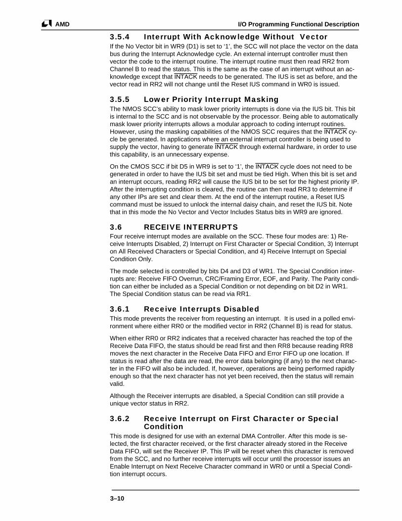
I/O Programming Functional DescriptionAMD
3–10
3.5.4 Interrupt With Acknowledge Without VectorIf the No Vector bit in WR9 (D1) is set to ‘1’, the SCC will not place the vector on the databus during the Interrupt Acknowledge cycle. An external interrupt controller must thenvector the code to the interrupt routine. The interrupt routine must then read RR2 fromChannel B to read the status. This is the same as the case of an interrupt without an ac-knowledge except that INTACK needs to be generated. The IUS is set as before, and thevector read in RR2 will not change until the Reset IUS command in WR0 is issued.
3.5.5 Lower Priority Interrupt MaskingThe NMOS SCC’s ability to mask lower priority interrupts is done via the IUS bit. This bitis internal to the SCC and is not observable by the processor. Being able to automaticallymask lower priority interrupts allows a modular approach to coding interrupt routines.However, using the masking capabilities of the NMOS SCC requires that the INTACK cy-cle be generated. In applications where an external interrupt controller is being used tosupply the vector, having to generate INTACK through external hardware, in order to usethis capability, is an unnecessary expense.
On the CMOS SCC if bit D5 in WR9 is set to ‘1’, the INTACK cycle does not need to begenerated in order to have the IUS bit set and must be tied High. When this bit is set andan interrupt occurs, reading RR2 will cause the IUS bit to be set for the highest priority IP.After the interrupting condition is cleared, the routine can then read RR3 to determine ifany other IPs are set and clear them. At the end of the interrupt routine, a Reset IUScommand must be issued to unlock the internal daisy chain, and reset the IUS bit. Notethat in this mode the No Vector and Vector Includes Status bits in WR9 are ignored.
3.6 RECEIVE INTERRUPTSFour receive interrupt modes are available on the SCC. These four modes are: 1) Re-ceive Interrupts Disabled, 2) Interrupt on First Character or Special Condition, 3) Interrupton All Received Characters or Special Condition, and 4) Receive Interrupt on SpecialCondition Only.
The mode selected is controlled by bits D4 and D3 of WR1. The Special Condition inter-rupts are: Receive FIFO Overrun, CRC/Framing Error, EOF, and Parity. The Parity condi-tion can either be included as a Special Condition or not depending on bit D2 in WR1.The Special Condition status can be read via RR1.
3.6.1 Receive Interrupts DisabledThis mode prevents the receiver from requesting an interrupt. It is used in a polled envi-ronment where either RR0 or the modified vector in RR2 (Channel B) is read for status.
When either RR0 or RR2 indicates that a received character has reached the top of theReceive Data FIFO, the status should be read first and then RR8 because reading RR8moves the next character in the Receive Data FIFO and Error FIFO up one location. Ifstatus is read after the data are read, the error data belonging (if any) to the next charac-ter in the FIFO will also be included. If, however, operations are being performed rapidlyenough so that the next character has not yet been received, then the status will remainvalid.
Although the Receiver interrupts are disabled, a Special Condition can still provide aunique vector status in RR2.
3.6.2 Receive Interrupt on First Character or Special Condition
This mode is designed for use with an external DMA Controller. After this mode is se-lected, the first character received, or the first character already stored in the ReceiveData FIFO, will set the Receiver IP. This IP will be reset when this character is removedfrom the SCC, and no further receive interrupts will occur until the processor issues anEnable Interrupt on Next Receive Character command in WR0 or until a Special Condi-tion interrupt occurs.

I/O Programming Functional Description AMD
3–11
The SCC recognizes several Special Conditions during data reception. A Receiver Over-run, where a character in the Data FIFO is overwritten, is a Special Condition, as is aFraming Error in Asynchronous mode, or the EOF condition in SDLC mode. In addition, ifbit D2 of WR1 is set to ‘1’, any character with a Parity Error will generate a Special Condi-tion interrupt.
The correct sequence of events when using this mode is to first select the mode and waitfor the receive character available interrupt. When the interrupt occurs, the processorshould read the character and then enable the DMA to transfer the remaining characters.
A Special Condition interrupt may occur at any time after the first character is receivedbut is guaranteed to occur after the character having the Special Condition has been readfrom the Receive Data FIFO. The status is not lost in this case, however, because theData FIFO will be locked by the Special Condition preventing further data from becomingavailable in the Receive Data FIFO until the Error Reset command is issued. In the serv-ice routine the processor should read RR1 to obtain the status and may read the dataagain if necessary before unlocking the FIFO by issuing an Error Reset command inWR0. If the Special Condition detected was EOF, the processor should then issue theEnable Interrupt on Next Receive Character command to prepare for the next frame. Thefirst character and Special Condition interrupt are distinguished by the status included inthe interrupt vector. In all other respects they are identical, including sharing the IP andIUS bits.
In the Am85C30, if the 10x19 Frame Status FIFO is enabled, the 3 byte receive (Rx)FIFO never locks. However, the DMA is disabled (only on overrun special condition), i.e.overruns do not lock the Rx FIFO, but do disable DMA. Interrupts are generated and re-main active until the RESET ERROR COMMAND is issued.
3.6.3 Receive Interrupt on All Receive Characters or Special Conditions
This mode is designed for an interrupt-driven system. In this mode, the SCC will set theReceiver IP on every received character, whether or not it has a Special Condition. Thisincludes characters already in the FIFO when this mode is selected. In this mode of op-eration, the Receiver IP is reset when the character is removed from the FIFO, so if theprocessor requires status for any character, this status must be read before the data isremoved from the FIFO.
The Special Conditions are identical to those previously mentioned, and as before, theonly difference between a “receive character available” interrupt and a “Special Condition”interrupt is the status encoded in the vector. In this mode, a Special Condition does notlock the Receive Data FIFO so that the service routine must read the status in RR1 be-fore reading the data. At moderate to high data rates, where the interrupt overhead is sig-nificant, time can usually be saved by checking for another received character before exit-ing the service routine. This technique eliminates the Interrupt Acknowledge and the proc-essor-state-saving time, but care must be exercised because this receive character mustbe checked for special receive conditions before it is removed from the SCC.
3.6.4 Receive Interrupt on Special ConditionsThis mode is designed for use with DMA transfers of the receive characters. In this mode,only receive characters with Special Conditions will cause the Receive IP to be set. Allother characters are assumed to be transferred via DMA. No special initialization se-quence is needed in this mode. Usually the DMA is initialized and enabled, and then thismode is selected in the SCC. A Special Condition interrupt may occur at any time afterthis mode is selected, but the logic guarantees that the interrupt will not occur until afterthe character with the Special Condition has been read from the SCC. The Special Condi-tion locks the FIFO so that the status will be valid when read in the interrupt service rou-tine, and it guarantees that the DMA will not transfer any characters until the Special Con-dition has been serviced. In the service routine, the processor should read RR1 to obtain
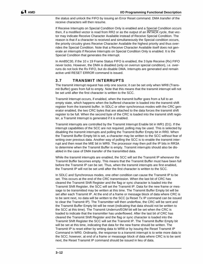
I/O Programming Functional DescriptionAMD
3–12
the status and unlock the FIFO by issuing an Error Reset command. DMA transfer of thereceive characters will then resume.
If Receive Interrupts on Special Condition Only is enabled and a Special Condition occursthen, if a modified vector is read from RR2 or as the output of an INTACK cycle, that vec-tor may indicate Receive Character Available instead of Receive Special Condition. Thereason is that if a character is received and simultaneously the Special condition occurs,the priority circuitry gives Receive Character Available the highest priority and thus over-rides the Special Condition. Note that a Receive Character Available itself does not gen-erate an interrupts if Receive Interrupts on Special Condition Only is enabled. It is theSpecial Condition that generates the interrupt.
In Am85C30, if the 10 x 19 Frame Status FIFO is enabled, the 3 byte Receive (Rx) FIFOnever locks. However, the DMA is disabled (only on overrun special condition), i.e. over-runs do not lock the Rx FIFO, but do disable DMA. Interrupts are generated and remainactive until RESET ERROR command is issued.
3.7 TRANSMIT INTERRUPTSThe transmit interrupt request has only one source; it can be set only when WR8 (Trans-mit Buffer) goes from full to empty. Note that this means that the transmit interrupt will notbe set until after the first character is written to the SCC.
Transmit Interrupt occurs, if enabled, when the transmit buffer goes from a full to anempty state, which happens when the buffered character is loaded into the transmit shiftregister from the transmit buffer. In SDLC or other synchronous modes with the CRC gen-erator enabled, the two CRC bytes that are attached to the data forces the transmit shiftregister to be full. When the second byte of the CRC is loaded into the transmit shift regis-ter, a Transmit Interrupt is generated if it is enabled.
Transmit interrupts are controlled by the Transmit Interrupt Enable bit in WR1 (D1). If theinterrupt capabilities of the SCC are not required, polling may be used. This is selected bydisabling the transmit interrupts and polling the Transmit Buffer Empty bit in RR0. Whenthe Transmit Buffer Empty bit is set, a character may be written to the SCC without fear ofwriting over previous data. Another way of polling the SCC is to enable the transmit inter-rupt and then reset the MIE bit in WR9. The processor may then poll the IP bits in RR3Ato determine when the Transmit Buffer is empty. Transmit interrupts should also be dis-abled in the case of DMA transfer of the transmitted data.
While the transmit interrupts are enabled, the SCC will set the Transmit IP whenever theTransmit Buffer becomes empty. This means that the Transmit Buffer must have been fullbefore the Transmit IP can be set. Thus, when the transmit interrupts are first enabled,the Transmit IP will not be set until after the first character is written to the SCC.
In SDLC and Synchronous modes, one other condition can cause the Transmit IP to beset. This occurs at the end of the CRC transmission. When the last bit of CRC hascleared the Transmit Shift Register and the flag or sync character is loaded into theTransmit Shift Register, the SCC will set the Transmit IP. Data for the new frame or mes-sage to be transmitted may be written at this time. The Transmit Buffer Empty bit will beset after each Transmit IP. At the end of a frame or message block of data where CRC isto be sent next, no data will be written to the SCC (a Reset Tx IP command can be issuedto clear the Transmit IP). The Transmitter will then underflow, the CRC will be sent andthe Transmit Buffer Empty bit will be reset (indicating that data should not be written tothe SCC at this time). The Transmit Underrun/EOM bit will be set when the CRC isloaded to indicate that the transmitter has underflowed. After the last bit of CRC hascleared the Transmit Shift Register and the flag or sync character is loaded into theTransmit Shift Register the SCC will set the Transmit IP. The Transmit Buffer Empty bitwill be set at this time, indicating that data for the new frame should be written. TheTransmit IP is reset either by writing data to WR8 or by issuing the Reset Transmit IPCommand in WR0. Ordinarily, the response to a transmit interrupt is to write more data tothe SCC; however, at end of a frame or meassage block of data where CRC is to be sentnext, the Reset Transmit IP command should be issued in lieu of data.

I/O Programming Functional Description AMD
3–13
3.8 EXTERNAL/STATUS INTERRUPTSThe External/Status Interrupts are globally enabled via WR1 and may be individually en-abled via WR15 as shown below. The External/Status interrupt sources are: 1) ZeroCount, 2) DCD, 3) SYNC/HUNT, 4) CTS, 5) Tx Underrun/EOM, and 6) BREAK/ABORT.
D7
BREAK/ ABORT
IE
D6
Tx Undr/
EOM IE
D5
CTS IE
D4
SYNC/ HUNT
IE
D3
DCD IE
D2 D1
Zero Count
IE
D0
D7 D6 D5 D4 D3 D2 D1 D0
Ext/ Status MIE
WR15 and WR1—Register Layout
The individual External/Status Interrupt enable bits in WR15 control whether or notlatches will be present in the path from the source of interrupt to the status bit in RR0. Ifan individual enable bit in WR15 is set to ‘0’, the latches are not present in the signal pathand the value read in RR0 reflects the current status. An interrupt source whose individ-ual enable bit in WR15 is set to ‘0’ is not a source of External/Status interrupts eventhough the External/Status Master Interrupt Enable bit is set to ‘1’ in WR1 (D0). When anindividual enable bit in WR15 is set to ‘1’, the latch is present in the signal path.
The latches for the sources of External/Status interrupts are not independent. Rather,they all close at the same time as a result of a state change by one of the sources of in-terrupt. Thus, a read of RR0 returns the current status for any bits whose individual en-able bit in WR15 is set to ‘0’, and either the current state or the latched state of the re-mainder of the bits. To guarantee the current status, the processor should issue a ResetExternal/Status Interrupts Command in WR0 to open the latches.
The External/Status IP in RR3 is set by the closing of the latches and remains set for aslong as they are closed. If the master External/Status Interrupt enable bit is not set, the IPwill never be set, even though the latches may be present in the signal paths and workingas described. Because the latches close on the current status but give no indication ofchange, the processor must maintain a copy of RR0 in memory. When the SCC gener-ates an External/Status interrupt, the processor should read RR0 and determine whichcondition changed state and take the appropriate action. The copy of RR0 in memorymust then be updated and the Reset External/Status Interrupt Command issued.
Care must be taken in writing the interrupt service routine for the External/Status inter-rupts because it is possible for more than one status condition to change state at thesame time. All of the latched bits in RR0 should be compared to the copy of RR0 in mem-ory. If none have changed and the ZC interrupt is enabled, the Zero Count conditioncaused the interrupt.
3.8.1 Sync/Hunt The SYNC/HUNT status bit reports the Hunt state of the receiver in SDLC and Synchro-nous modes. This bit is set to ‘1’ when the processor issues the Enter Hunt Command,and is reset to ‘0’ when character synchronization is established by the receiver. If theSYNC/HUNT IE bit in WR15 is set to ‘1’, the External/Status latches close, and an Exter-nal/Status interrupt will be generated on both the Low-to-High and High-to-Low transitionsof the SYNC/HUNT status bit.

I/O Programming Functional DescriptionAMD
3–14
In External Sync Mode, the SYNC/HUNT status bit, as in Asynchronous mode, reportsthe state of the SYNC pin. If there are no other External/Status interrupts pending, thenany transition on the SYNC pin will cause the latches to close and generate an External/Status interrupt. However, only an odd number of transitions on SYNC, while another Ex-ternal/Status interrupt is pending, will close the latches and generate an External/StatusInterrupt.
3.8.2 Break/AbortThe BREAK/ABORT status bit is used in Asynchronous and SDLC modes but is alwaysset to ‘0’ in Synchronous modes. Both a Low-to-High and High-to-Low transition are guar-anteed to cause the External/Status latches to close, and if the BREAK/ABORT IE bit inWR15 is set to ‘1’, generate an External/Status interrupt regardless of whether anotherExternal/Status interrupt is pending at the time the transitions occur. If BREAK/ABORT isdetected while the latches are closed, the status will be saved and generate an interruptfor BREAK/ABORT detection upon issuing the Reset External/Status Interrupts. A secondinterrupt is generated for End of BREAK/ABORT after issuig the next Reset External/Status Interrupts. In the first case, the BREAK/ABORT bit will be set to ‘1’, and in the sec-ond case to ‘0’. This will guarantee that the BREAK/ABORT sequence is detected cor-rectly. A BREAK/ABORT occurrence will clear an End of BREAK/ABORT that is waitingto generate an interrupt. Therefore, multiple Break/Abort sequences while the latches areclosed will generate only two interrupts, one for BREAK/ABORT detection, and one forEnd of BREAK/ABORT.
In Asynchronous mode, this bit will be set to ‘1’ when a break sequence (null characterplus Framing Error) is detected (i.e., RxD is Low for more than one full character time) inthe receive data stream, and remains set for as long as ‘0’s continue to be received. It isreset when a ‘1’ is received. Note that a single null character is left in the Receive DataFIFO each time a break condition is terminated. This character should be read and dis-carded.
In SDLC mode, this status bit is set to ‘1’ when an abort sequence is detected in the re-ceive data stream and is reset when a ‘0’ is received. Note that the receiver detects anabort pattern whether it is “in frame” or “out of frame,” so to avoid confusion, the BREAK/ABORT IE bit in WR15 should be set to ‘1’ in the SYNC/HUNT interrupt routine when theSYNC/HUNT status bit indicates that the receiver is “in frame” (i.e., SYNC/HUNT statusbit transitions from High-to-Low), and should be reset to ‘0’ early in the EOF interrupt rou-tine.
3.8.3 Zero CountThe Zero Count (ZC) status bit reflects when the Baud Rate Generator counter reaches acount of ‘0’. The ZC status bit will be set to ‘1’ when the zero count is reached and will bereset to ‘0’ when the counter is re-loaded. The External/Status latches will close only onthe Low-to-High transition of this bit and, if the Zero Count IE bit is set in WR15, generatean External/Status interrupt. This status bit is not latched in RR0 even though the Exter-nal/Status latches close as a result of the transition.
If there are no other External/Status interrupt conditions pending at the time the ZC statusbit is set, an External/Status interrupt will be generated. However, if there is another Ex-ternal/Status interrupt pending at the time ZC is set, no interrupt will be generated untilthe current interrupt service is complete. If the zero count condition does not persist be-yond the end of the current interrupt service routine no interrupt will be generated. Theinterrupt service routine should check the other External/Status conditions for changes. Ifnone changed, the ZC was the source of interrupt. In polled applications, the IP bits inRR3A should be checked for a status change before proceeding as in the interrupt serv-ice routine.
Note that while the Zero Count IE bit in WR15 is reset, the ZC status bit will always read‘0’.

I/O Programming Functional Description AMD
3–15
3.8.4 Tx Underrun/EOMThe Tx Underrun/EOM status bit is used in SDLC and Synchronous modes of operationto control the transmission of CRC characters. This bit is set to ‘1’ when the TransmitBuffer and Transmit Shift Register go empty and is reset to ‘0’ by issuing the ResetTransmit Underrun/EOM command in WR0. Only the Low-to-High transition of this bit willcause the latches to close and, if the Tx Underrun/EOM IE bit in WR15 (D6) is set to ‘1’,cause an External/Status Interrupt to be generated.
This status bit is always set to ‘1’ in Asynchronous mode unless a Reset Transmit Under-run/EOM command is erroneously issued. In this case, the Send Abort Command can beused to set this bit to ‘1’ and, at the same time, cause an External/Status Interrupt.
Note that this bit will be set to ‘1’ when either of the following occurs; 1) a Send Abortcommand is issued, 2) the transmitter is disabled, or 3) a Channel or Hardware Reset isexecuted.
3.8.5 Clear to SendThe CTS Status bit reports the state of the CTS input pin the last time any of the enabledExternal/Status bits changed. Any transition on the CTS pin, while no other interrupts arepending, latches the state of the CTS pin and generates an External/Status interrupt if theCTS IE bit in WR15 is set to ‘1’. However, only an odd number of transitions on the CTSpin while another External/Status is pending will cause an External/Status interrupt afterthe Reset External/Status Interrupt command is issued.
If the CTS IE bit is reset, the CTS status merely reports the current inverted unlatchedstate of the CTS pin; that is, if the CTS pin is Low, the CTS status bit will be High.
Note that after the Reset External/Status Interrupt command is issued, if the latches wereclosed, they will close again if there was an odd number of transitions on the CTS pin;they will remain open if there was an even number of transitions on the input pin.
3.8.6 Data Carrier DetectThe DCD Status bit reports the state of the DCD input pin the last time any of the enabledExternal/Status bits changed. Any transition on the DCD pin, while no other interrupts arepending, latches the state of the DCD pin and generates an External/Status interrupt ifthe DCD IE bit in WR15 is set to ‘1’. However, only an odd number of transitions on theDCD pin while another External/Status is pending will cause an External/Status interruptafter the Reset External/Status Interrupt command is issued.
If the DCD IE bit is reset, the DCD status merely reports the current inverted unlatchedstate of the DCD pin; that is, if the DCD pin is Low, the DCD status bit will be High.
Note that after the Reset External/Status Interrupt command is issued, if the latches wereclosed, they will close again if there was an odd number of transitions on the DCD pin;they will remain open if there was an even number of transitions on the input pin.
If careful attention is paid to details, the interrupt service routine for External/Status inter-rupts is straightforward. To determine which bit or bits changed state, the routine shouldfirst read RR0 and compare it to a copy from memory. For each changed bit, the appro-priate action should be taken and the copy in memory updated. The service routineshould close with a Reset External/Status Interrupts command to re-open the latches.The copy of RR0 in memory should always have the Zero Count bit set to ‘0’, since thiswill be the state of the bit after the Reset External/Status Interrupts command at the endof the service routine.
3.9 BLOCK TRANSFERSThe SCC offers several alternatives for the block transfer of data. The various options areselected via WR1 and WR14 as follows.
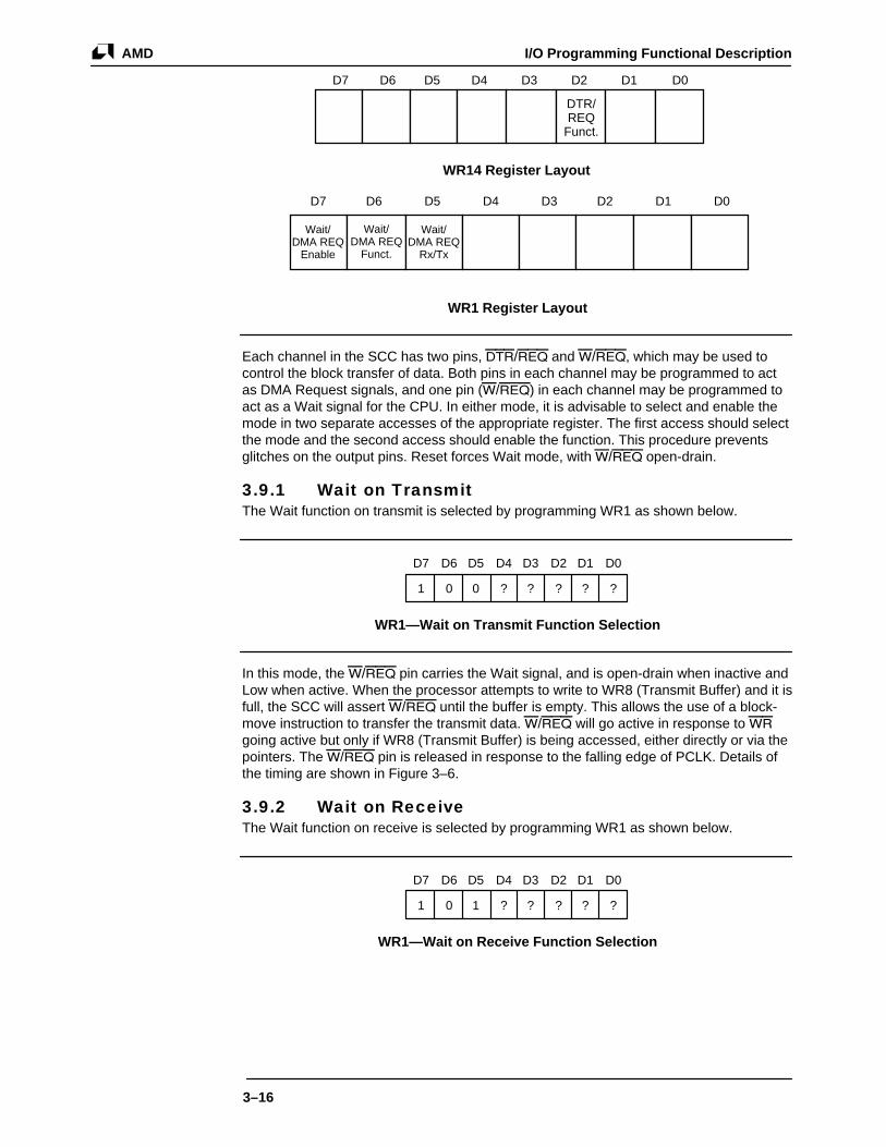
I/O Programming Functional DescriptionAMD
3–16
D7 D6 D5 D4 D3 D2 D1
DTR/ REQ
Funct.
D0
Wait/ DMA REQ
Funct.
Wait/ DMA REQ
Enable
Wait/ DMA REQ
Rx/Tx
D7 D6 D5 D4 D3 D2 D1 D0
WR14 Register Layout
WR1 Register Layout
Each channel in the SCC has two pins, DTR/REQ and W/REQ, which may be used tocontrol the block transfer of data. Both pins in each channel may be programmed to actas DMA Request signals, and one pin (W/REQ) in each channel may be programmed toact as a Wait signal for the CPU. In either mode, it is advisable to select and enable themode in two separate accesses of the appropriate register. The first access should selectthe mode and the second access should enable the function. This procedure preventsglitches on the output pins. Reset forces Wait mode, with W/REQ open-drain.
3.9.1 Wait on TransmitThe Wait function on transmit is selected by programming WR1 as shown below.
1 0 0 ? ? ? ? ?
D7 D6 D5 D4 D3 D2 D1 D0
WR1—Wait on Transmit Function Selection
In this mode, the W/REQ pin carries the Wait signal, and is open-drain when inactive andLow when active. When the processor attempts to write to WR8 (Transmit Buffer) and it isfull, the SCC will assert W/REQ until the buffer is empty. This allows the use of a block-move instruction to transfer the transmit data. W/REQ will go active in response to WRgoing active but only if WR8 (Transmit Buffer) is being accessed, either directly or via thepointers. The W/REQ pin is released in response to the falling edge of PCLK. Details ofthe timing are shown in Figure 3–6.
3.9.2 Wait on ReceiveThe Wait function on receive is selected by programming WR1 as shown below.
1 0 1 ? ? ? ? ?
D7 D6 D5 D4 D3 D2 D1 D0
WR1—Wait on Receive Function Selection
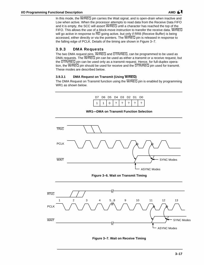
I/O Programming Functional Description AMD
3–17
In this mode, the W/REQ pin carries the Wait signal, and is open-drain when inactive andLow when active. When the processor attempts to read data from the Receive Data FIFOand it is empty, the SCC will assert W/REQ until a character has reached the top of theFIFO. This allows the use of a block-move instruction to transfer the receive data. W/REQwill go active in response to RD going active, but only if RR8 (Receive Buffer) is beingaccessed, either directly or via the pointers. The W/REQ pin is released in response tothe falling edge of PCLK. Details of the timing are shown in Figure 3–7.
3.9.3 DMA RequestsThe two DMA request pins, W/REQ and DTR/REQ, can be programmed to be used asDMA requests. The W/REQ pin can be used as either a transmit or a receive request, butthe DTR/REQ pin can be used only as a transmit request. Hence, for full-duplex opera-tion, the W/REQ pin should be used for receive and the DTR/REQ pin used for transmit.These modes are described below.
3.9.3.1 DMA Request on Transmit (Using W/REQ)The DMA Request on Transmit function using the W/REQ pin is enabled by programmingWR1 as shown below.
1 1 0 ? ? ? ? ?
D7 D6 D5 D4 D3 D2 D1 D0
WR1—DMA on Transmit Function Selection
ASYNC Modes
SYNC Modes
TRxC
PCLK
WAIT
Figure 3–6. Wait on Transmit Timing
ASYNC Modes
SYNC Modes
RTxC
PCLK
WAIT
1 2 3 4 5...8 9 10 11 12 13
Figure 3–7. Wait on Receive Timing

I/O Programming Functional DescriptionAMD
3–18
In this mode the W/REQ pin carries the DMA Request signal, which is active Low. Whenthis mode is selected, but not yet enabled, the W/REQ pin is driven High. When the en-able bit is set, W/REQ will go Low if WR8 is empty at the time or will remain High untilWR8 becomes empty. Note that the W/REQ pin will follow the state of WR8 even thoughthe transmitter is disabled. Thus, if bit D7 of WR1 is set to ‘1’ (i.e., W/REQ pin is enabled)before the transmitter is enabled, the DMA may write data to the SCC prematurely. Thiswill not cause a problem in Asynchronous mode but may cause problems in SDLC andSynchronous modes, because on enabling the transmitter the SCC will send data in pref-erence to flags or sync characters. It also may complicate the CRC initialization, whichcannot be done until after the transmitter is enabled.
With only one exception, the W/REQ pin directly follows the state of WR8 in this mode.W/REQ goes Low when WR8 goes empty and remains Low until the WR8 is filled. TheSCC generates only one falling edge on the W/REQ pin per character requested. Thetiming for this is shown in Figure 3–8.
The one exception occurs at the end of CRC transmission when the SCC is programmedin either SDLC or Synchronous Modes. At the end of CRC transmission, when the closingflag or sync character is loaded into the Transmit Shift Register, the W/REQ pin is pulsedHigh for one PCLK cycle. The DMA may use this falling edge on W/REQ to write the firstcharacter of the next frame or block to the SCC. W/REQ will go High in response to thefalling edge of WR, but only when the appropriate WR8 in the SCC is accessed. This isshown in Figure 3–9.
3.9.3.2 DMA Request on Transmit (Using DTR/REQ)A second Request on Transmit function is available on the DTR/REQ pin. This mode isselected by programming WR14 as shown below.
? ? ? ? ? 1 ? ?
D7 D6 D5 D4 D3 D2 D1 D0
WR14—DMA Request on Transmit Using DTR/REQ
When this bit is set to ‘1’, the DTR/REQ pin will go Low if WR8 is empty at the time, or willgo High until WR8 becomes empty. While bit D2 of WR14 is set to ‘0’, the DTR/REQ pinis used as a general-purpose output pin and follows the inverted state of bit D7 in WR5.This pin will be High after a channel or hardware reset and in the DTR mode.
In the DMA Request mode, DTR/REQ will follow the empty/non-empty state of WR8 eventhough the transmitter is disabled. Thus, if the DMA Request function is enabled beforethe transmitter is enabled, the DMA may write data to the SCC prematurely. This will notcause a problem in Asynchronous mode but may cause problems in SDLC and Synchro-nous modes because the SCC will send data in preference to flags or sync characters. Italso may complicate the CRC initialization, which cannot be done until after the transmit-ter is enabled and idling. With only one exception, the DTR/REQ pin directly follows thestate of WR8 in SDLC and Synchronous modes. DTR/REQ goes Low when WR8 be-comes empty and remains Low until WR8 is filled. The SCC generates only one fallingedge on the DTR/REQ pin per character requested and the timing for this is shown inFigure 3–8.
The one exception occurs in SDLC and Synchronous modes at the end of CRC transmis-sion. At the end of CRC transmission, when the closing flag or sync character is loadedinto the Transmit Shift Register, DTR/REQ is pulsed High for one PCLK cycle. The DMAmay use this falling edge on DTR/REQ to write the first character of the next frame orblock to the SCC.

I/O Programming Functional Description AMD
3–19
3.3.9.3 DTR/REQ Deactivation TimingOn the NMOS SCC, the DMA Request function on DTR/REQ differs from the one onW/REQ in that it does not go High immediately in response to the access which writes toWR8. This is because the registers in the SCC are not written during the actual access,but are delayed by some number of PCLK cycles. The DMA Request signal on DTR/REQfollows the state of WR8 exactly while the Request signal on W/REQ goes inactive in an-ticipation of WR8 becoming full. The timing of the Request signal on both pins is shown inFigure 3–9.
This deactivation delay of DTR/REQ is unacceptable in applications where slower datarates are involved relative to the processor. This delay can result in overwriting the Trans-mit Buffer because the DMA Controller may recognize the continued active state ofDTR/REQ as a request for more data. On the CMOS SCC an option is provided that en-ables the deactivation delay of DTR/REQ to be identical to that of the W/REQ pin. IfSDLC mode operation is selected and bit D0 of WR15 is set to ‘1’, then bit D4 of WR7’can be used to alter the deactivation delay. While bit D4 of WR7’ is set to ‘1’, the deacti-vation of DTR/REQ will be identical to W/REQ.
ASYNC Modes
SYNC Modes
TRxC
PCLK
REQ (DTR/REQ)
REQ (W/REQ)
Figure 3–8. DMA Request on Transmit Activation
WR
D0 – D7
PCLK
REQ (DTR/REQ)
REQ (W/REQ)
Figure 3–9. DMA Request on Transmit Deactivation
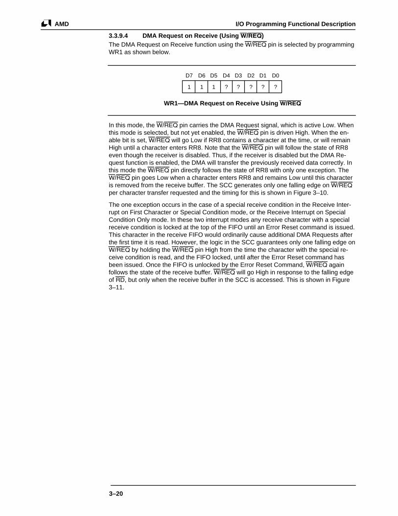
I/O Programming Functional DescriptionAMD
3–20
3.3.9.4 DMA Request on Receive (Using W/REQ)The DMA Request on Receive function using the W/REQ pin is selected by programmingWR1 as shown below.
1 1 1 ? ? ? ? ?
D7 D6 D5 D4 D3 D2 D1 D0
WR1—DMA Request on Receive Using W/REQ
In this mode, the W/REQ pin carries the DMA Request signal, which is active Low. Whenthis mode is selected, but not yet enabled, the W/REQ pin is driven High. When the en-able bit is set, W/REQ will go Low if RR8 contains a character at the time, or will remainHigh until a character enters RR8. Note that the W/REQ pin will follow the state of RR8even though the receiver is disabled. Thus, if the receiver is disabled but the DMA Re-quest function is enabled, the DMA will transfer the previously received data correctly. Inthis mode the W/REQ pin directly follows the state of RR8 with only one exception. TheW/REQ pin goes Low when a character enters RR8 and remains Low until this characteris removed from the receive buffer. The SCC generates only one falling edge on W/REQper character transfer requested and the timing for this is shown in Figure 3–10.
The one exception occurs in the case of a special receive condition in the Receive Inter-rupt on First Character or Special Condition mode, or the Receive Interrupt on SpecialCondition Only mode. In these two interrupt modes any receive character with a specialreceive condition is locked at the top of the FIFO until an Error Reset command is issued.This character in the receive FIFO would ordinarily cause additional DMA Requests afterthe first time it is read. However, the logic in the SCC guarantees only one falling edge onW/REQ by holding the W/REQ pin High from the time the character with the special re-ceive condition is read, and the FIFO locked, until after the Error Reset command hasbeen issued. Once the FIFO is unlocked by the Error Reset Command, W/REQ againfollows the state of the receive buffer. W/REQ will go High in response to the falling edgeof RD, but only when the receive buffer in the SCC is accessed. This is shown in Figure3–11.

I/O Programming Functional Description AMD
3–21
ASYNC Modes
SYNC Modes
RTxC
PCLK
WAIT
1 2 3 4 5...8 9 10 11 12 13
Figure 3–10. DTR/REQ Activation
WR
D0 – D7
PCLK
REQ
Receive Data
Figure 3–11. DTR/REQ Deactivation
4–1
CHAPTER 4Data Communication Modes Functional Description
4.1 Introduction 4–3. . . . . . . . . . . . . . . . . . . . . . . . . . . . . . . . . . . . . . . . . . . . . . . . . . . 4.2 Protocols 4–3. . . . . . . . . . . . . . . . . . . . . . . . . . . . . . . . . . . . . . . . . . . . . . . . . . . . .
4.2.1 Asynchronous 4–3. . . . . . . . . . . . . . . . . . . . . . . . . . . . . . . . . . . . . . . . . . . 4.2.2 Synchronous Transmission 4–4. . . . . . . . . . . . . . . . . . . . . . . . . . . . . . . . .
4.2.2.1 Synchronous Character-Oriented Protocol 4–4. . . . . . . . . . . . . . 4.2.2.2 Synchronous Bit-Oriented 4–4. . . . . . . . . . . . . . . . . . . . . . . . . . .
4.3 Mode Selection 4–5. . . . . . . . . . . . . . . . . . . . . . . . . . . . . . . . . . . . . . . . . . . . . . . . 4.4 Receiver Overview 4–6. . . . . . . . . . . . . . . . . . . . . . . . . . . . . . . . . . . . . . . . . . . . .
4.4.1 Rx Character Length 4–7. . . . . . . . . . . . . . . . . . . . . . . . . . . . . . . . . . . . . . 4.4.2 Rx Parity 4–8. . . . . . . . . . . . . . . . . . . . . . . . . . . . . . . . . . . . . . . . . . . . . . . 4.4.3 Rx Modem Control 4–9. . . . . . . . . . . . . . . . . . . . . . . . . . . . . . . . . . . . . . . .
4.5 Transmitter Overview 4–9. . . . . . . . . . . . . . . . . . . . . . . . . . . . . . . . . . . . . . . . . . . 4.5.1 Tx Character Length 4–9. . . . . . . . . . . . . . . . . . . . . . . . . . . . . . . . . . . . . . 4.5.2 Tx Parity 4–11. . . . . . . . . . . . . . . . . . . . . . . . . . . . . . . . . . . . . . . . . . . . . . . 4.5.3 Break Generation 4–11. . . . . . . . . . . . . . . . . . . . . . . . . . . . . . . . . . . . . . . . 4.5.4 Transmit Modem Control 4–11. . . . . . . . . . . . . . . . . . . . . . . . . . . . . . . . . . . 4.5.5 Auto RTS Reset 4–11. . . . . . . . . . . . . . . . . . . . . . . . . . . . . . . . . . . . . . . . . .
4.6 Asynchronous Mode Operation 4–12. . . . . . . . . . . . . . . . . . . . . . . . . . . . . . . . . . . . 4.6.1 Receiver Operation 4–12. . . . . . . . . . . . . . . . . . . . . . . . . . . . . . . . . . . . . . .
4.6.1.1 Receiver Initialization 4–12. . . . . . . . . . . . . . . . . . . . . . . . . . . . . . 4.6.1.2 Framing Error 4–12. . . . . . . . . . . . . . . . . . . . . . . . . . . . . . . . . . . . 4.6.1.3 Break Detection 4–13. . . . . . . . . . . . . . . . . . . . . . . . . . . . . . . . . . . 4.6.1.4 Clock Selection 4–13. . . . . . . . . . . . . . . . . . . . . . . . . . . . . . . . . . .
4.6.2 Transmitter Operation 4–13. . . . . . . . . . . . . . . . . . . . . . . . . . . . . . . . . . . . . 4.6.2.1 Transmitter Initialization 4–13. . . . . . . . . . . . . . . . . . . . . . . . . . . . 4.6.2.2 Stop Bit Selection 4–13. . . . . . . . . . . . . . . . . . . . . . . . . . . . . . . . .
4.7 SDLC Mode Operation 4–14. . . . . . . . . . . . . . . . . . . . . . . . . . . . . . . . . . . . . . . . . . 4.7.1 Receiver Operation 4–14. . . . . . . . . . . . . . . . . . . . . . . . . . . . . . . . . . . . . . .
4.7.1.1 Flag Detect Output 4–14. . . . . . . . . . . . . . . . . . . . . . . . . . . . . . . . 4.7.1.2 Receiver Initialization 4–14. . . . . . . . . . . . . . . . . . . . . . . . . . . . . . 4.7.1.3 10x19-Bit Frame Status FIFO 4–14. . . . . . . . . . . . . . . . . . . . . . . .
4.7.1.3.1 FIFO Enabling/Disabling 4–15. . . . . . . . . . . . . . . . . . . . 4.7.1.3.2 FIFO Read Operation 4–15. . . . . . . . . . . . . . . . . . . . . . . 4.7.1.3.3 FIFO Write Operation 4–15. . . . . . . . . . . . . . . . . . . . . . . 4.7.1.3.4 14-Bit Byte Counter 4–15. . . . . . . . . . . . . . . . . . . . . . . . 4.7.1.3.5 Am85C30 Frame Status FIFO Operation Clarification 4–18. . . . . . . . . . . . . . . . . 4.7.1.3.6 Am85C30 Aborted Frame Handling When Using the 10x19 Frame Status FIFO 4–19. . . . . . . . . . . . . . . . . . . . . . . .
4.7.1.4 Address Search Mode 4–19. . . . . . . . . . . . . . . . . . . . . . . . . . . . . . 4.7.1.5 Abort Detection 4–20. . . . . . . . . . . . . . . . . . . . . . . . . . . . . . . . . . . 4.7.1.6 Residue Bits 4–21. . . . . . . . . . . . . . . . . . . . . . . . . . . . . . . . . . . . .
4.7.2 SDLC Mode CRC Polynomial Selection 4–21. . . . . . . . . . . . . . . . . . . . . . . 4.7.2.1 Rx CRC Initialization 4–22. . . . . . . . . . . . . . . . . . . . . . . . . . . . . . . 4.7.2.2 Rx CRC Enabling 4–22. . . . . . . . . . . . . . . . . . . . . . . . . . . . . . . . . 4.7.2.3 CRC Error 4–22. . . . . . . . . . . . . . . . . . . . . . . . . . . . . . . . . . . . . . . 4.7.2.4 CRC Character Reception 4–22. . . . . . . . . . . . . . . . . . . . . . . . . . .
4.7.3 End of Frame (EOF) 4–26. . . . . . . . . . . . . . . . . . . . . . . . . . . . . . . . . . . . . .

Data Communication Modes Functional DescriptionAMD
4–2
4.8 Transmitter Operation 4–27. . . . . . . . . . . . . . . . . . . . . . . . . . . . . . . . . . . . . . . . . . . 4.8.1 Transmitter Initialization 4–27. . . . . . . . . . . . . . . . . . . . . . . . . . . . . . . . . . . . 4.8.2 Mark/Flag Idle Generation 4–27. . . . . . . . . . . . . . . . . . . . . . . . . . . . . . . . . . 4.8.3 Auto Flag Mode 4–27. . . . . . . . . . . . . . . . . . . . . . . . . . . . . . . . . . . . . . . . . . 4.8.4 Abort Generation 4–28. . . . . . . . . . . . . . . . . . . . . . . . . . . . . . . . . . . . . . . . . 4.8.5 Auto Transmit CRC Generator Preset 4–28. . . . . . . . . . . . . . . . . . . . . . . . . 4.8.6 CRC Transmission 4–28. . . . . . . . . . . . . . . . . . . . . . . . . . . . . . . . . . . . . . . 4.8.7 Auto Tx Underrun/EOM Latch Reset 4–29. . . . . . . . . . . . . . . . . . . . . . . . . . 4.8.8 Transmitter Disabling 4–29. . . . . . . . . . . . . . . . . . . . . . . . . . . . . . . . . . . . . . 4.8.9 NRZI Mode Transmitter Disabling 4–29. . . . . . . . . . . . . . . . . . . . . . . . . . . .
4.9 SDLC Loop Mode 4–30. . . . . . . . . . . . . . . . . . . . . . . . . . . . . . . . . . . . . . . . . . . . . . 4.9.1 Going on Loop 4–30. . . . . . . . . . . . . . . . . . . . . . . . . . . . . . . . . . . . . . . . . . .
4.9.1.1 On Loop Program Sequence 4–31. . . . . . . . . . . . . . . . . . . . . . . . . 4.9.1.2 On Loop Message Transmission 4–31. . . . . . . . . . . . . . . . . . . . . . 4.9.1.3 On Loop Transmit Message
Programming Sequence 4–31. . . . . . . . . . . . . . . . . . . . . . . . . . . . 4.9.2 Going off Loop 4–31. . . . . . . . . . . . . . . . . . . . . . . . . . . . . . . . . . . . . . . . . . .
4.9.2.1 Off Loop Programming Sequence 4–32. . . . . . . . . . . . . . . . . . . . . 4.9.3 SDLC Loop Initialization 4–32. . . . . . . . . . . . . . . . . . . . . . . . . . . . . . . . . . . 4.9.4 SDLC Loop NRZI Encoding Enabled 4–32. . . . . . . . . . . . . . . . . . . . . . . . . .
4.10 Synchronous Mode Operation 4–32. . . . . . . . . . . . . . . . . . . . . . . . . . . . . . . . . . . . . 4.10.1 Receiver Operation 4–32. . . . . . . . . . . . . . . . . . . . . . . . . . . . . . . . . . . . . . .
4.10.1.1 SYNC Detect Output 4–33. . . . . . . . . . . . . . . . . . . . . . . . . . . . . . . 4.10.1.1.1 MONOSYNC Mode 4–33. . . . . . . . . . . . . . . . . . . . . .
4.11.1.2 BISYNC Mode 4–33. . . . . . . . . . . . . . . . . . . . . . . . . . . . . . . . . . . . 4.10.1.2 SYNC Character Length 4–34. . . . . . . . . . . . . . . . . . . . . . . . . . . . 4.10.1.3 Receiver Initialization 4–34. . . . . . . . . . . . . . . . . . . . . . . . . . . . . . 4.10.1.4 Sync Character Removal 4–34. . . . . . . . . . . . . . . . . . . . . . . . . . . 4.10.1.5 CRC Polynomial Selection 4–36. . . . . . . . . . . . . . . . . . . . . . . . . .
4.10.1.5.1 Rx CRC Initialization 4–36. . . . . . . . . . . . . . . . . . . . . 4.10.1.5.2 Rx CRC Enabling 4–36. . . . . . . . . . . . . . . . . . . . . . . . 4.10.1.5.3 Rx CRC Character Exclusion 4–36. . . . . . . . . . . . . . . 4.10.1.5.4 CRC Error 4–37. . . . . . . . . . . . . . . . . . . . . . . . . . . . . .
4.10.2 Transmitter Operation 4–37. . . . . . . . . . . . . . . . . . . . . . . . . . . . . . . . . . . . . 4.10.2.1 Transmitter Initialization 4–38. . . . . . . . . . . . . . . . . . . . . . . . . . . . 4.10.2.2 CRC Polynomial Selection 4–38. . . . . . . . . . . . . . . . . . . . . . . . . .
4.10.2.2.1 Tx CRC Initialization 4–38. . . . . . . . . . . . . . . . . . . . . . 4.10.2.2.2 Tx CRC Enabling 4–38. . . . . . . . . . . . . . . . . . . . . . . . 4.10.2.2.3 CRC Transmission 4–38. . . . . . . . . . . . . . . . . . . . . . . 4.10.2.2.4 Tx CRC Character Exclusion 4–39. . . . . . . . . . . . . . .
4.10.2.3 Transparent Transmission 4–39. . . . . . . . . . . . . . . . . . . . . . . . . . . 4.10.2.4 Transmitter to Receiver Synchronization 4–39. . . . . . . . . . . . . . .
4.10.2.4.1 Transmitter Disabling 4–40. . . . . . . . . . . . . . . . . . . . . 4.10.2.5 External SYNC Mode 4–40. . . . . . . . . . . . . . . . . . . . . . . . . . . . . .
4.10.2.5.1 SDLC External SYNC Mode 4–41. . . . . . . . . . . . . . . . 4.10.2.5.2 Synchronous External Sync Mode 4–41. . . . . . . . . . . . . . . . . . . . . . . . . . . . .

4–3
Data Communication ModesFunctional Description
CHAPTER 4
4.1 INTRODUCTIONThe SCC provides two independent full-duplex channels programmable for use in anycommon asynchronous or synchronous data communication protocol. This includes:Asynchronous, Synchronous MONOSYNC (8-bit sync character), Synchronous BISYNC(16-bit sync character), normal SDLC, and SDLC Loop Mode.
4.2 PROTOCOLSA communication protocol defines a set of rules for the orderly transfer of information be-tween two communicating devices. All communication line protocols in the industry todayexchange data in either an asynchronous or synchronous manner. Asynchronous trans-mission is used in several protocols including the TTY protocol while synchronous trans-mission is used in protocols which include: IBM BISYNC, Synchronous Data Link Control(SDLC), High-Level Data Link Control (HDLC), and Advance Data Communication Con-trol Procedures (ADCCP).
This section provides a brief overview of these protocols; however, if further information isdesired the book titled “Technical Aspects of Data Communications” by John E.McNamara, published by Digital Press (DEC) 1982, is a good reference.
4.2.1 AsynchronousIn Asynchronous transmission, as the name implies, each character is transmitted as anindependent entity; that is, the time between the last bit of one character and the first bitof another character can be variable.
Since the receiver must be able to detect the beginning of each character transmitted,this mode requires that at least one bit be added at the start and end of each characterfor synchronization purposes.
Synchronization at the receiver is accomplished by sensing the transition of the Start-bitfor each character transmitted. The first data bit of the character is typically sampled oneand one-half bit times after the High-to-Low transition of the Start-bit, and each subse-quent bit is sampled one bit time thereafter. The sampling of the bit occurs near the cen-ter of each bit to allow correct data recovery and typically occurs at some multiple of thedata rate. Larger multiples allow a closer approximation to the middle sampling.
Figure 4–1 depicts a typical Asynchronous 11-bit format. Each 8-bit character is precededby a Start-bit and followed by a Parity check bit and one Stop-bit. The Start-bit of the nextcharacter can occur anytime after the first character’s Stop-bit. The idle state of the trans-mission line between characters is always in a mark idle condition (i.e., TxD pulled High).
Asynchronous communication channels are found in most distributed computer systemsfor terminal-to-computer comunications. The common “serial port” found on personalcomputers is an asynchronous port. It is used to attach external modems and printers,and to interface the personal computer to a minicomputer for use as a terminal.
D7
X
D6
X
D5
X
D4
X
D3
X
D2
X
D1
X
D0
X
P
X
Stop Start D7
X
D6
X
D5
X
D4
X
D3
X
D2
X
D1
X
D0
X
P
X
Stop Start
X = High or Low
Figure 4–1. Asynchronous Format

Data Communication Modes Functional DescriptionAMD
4–4
4.2.2 Synchronous TransmissionSynchronous transmission requires that clocking information be transmitted along withthe data, either by a method of encoding data that contains clocking information, or by amodem that encodes clock information in the modulation process. In either case, data aresent at a defined rate which is controlled by a timing source at the transmitter.
Synchronous communication channels send data faster with less overhead than asyn-chronous channels but are more expensive to design than asynchronous channels. Insynchronous communication, a timing reference, or “clock”, is used to control the transferof information. This clock specifies to the receiver when to sample the data (bit synchroni-zation) in order to ascertain which data value (‘0’ or ‘1’) was transmitted. The optimumsample times usually correspond to the middle of the bit cell to minimize error. This clocksignal is encoded along with the data sent so the receiver must be able to decode theFigure 4–1. Asynchronous Format incoming clock signal. A circuit called a “phase-lockedloop” is typically used for this purpose.
In addition, since data rates are usually higher and data are typically sent with no gapsbetween characters, synchronous communication requires some level of buffering at boththe transmitter and receiver.
Once bit synchronization has been established, the next phase for the receiver is to knowwhat group of bits constitute a character (character synchronization). This requires thatthe receiver search the receive bit stream on a bit-by-bit basis for a character synchroniz-ing pattern in order to determine which set of bits in the bit stream defines the first char-acter transmitted.
Synchronous communication channels are found in many mainframe data networks. Thegreater throughput of the synchronous channel is required in mainframe environmentswhere many terminals are connected to the computer and multiplexed onto one channel.The synchronous protocols used may be either character-oriented or bit-oriented.
4.2.2.1 Synchronous Character-Oriented ProtocolIn a Character-Oriented Protocol (COP) data are transmitted in message blocks and re-quire that each block be preceded by either an 8- or 16-bit predefined “sync character”.In addition, COPs are typically restricted to half-duplex operation and depend heavily onspecial control characters or character sequences, such as SOH or DLE STX and ETX, todetermine the start and end of a particular field within a message block. IBM BISYNC isan example of a COP. MONOSYNC, on the other hand, is a character count protocolwhere both ends of the communication link keep track of the number of characters sentand received. This solves the problem of having to use special control characters for fielddelineation as used in the BISYNC protocol. The DDCMP (Digital Data CommunicationMessage Protocol) from DEC is another example of a character count protocol in use to-day. MONOSYNC and BISYNC message formats are shown in Figures 4–2 and 4–3, re-spectively.
Since sync characters are only appended to the start of a message block, additional synccharacters may be inserted within a transmission at distinct time intervals or during apause in order to maintain synchronization.
4.2.2.2 Synchronous Bit-OrientedBit-Oriented Protocols (BOP) may be used in half- or full-duplex operation and are lessdependent on special control characters. BOPs rely instead on the position of bits withinspecific fields.
The most common BOPs in use today are High-Level Data Link Control (HDLC) and Syn-chronous Data Link Control (SDLC). These two protocols are nearly identical except forminor differences in the use of the Address and Control fields.
All SDLC information is sent in frames and follow a standard format as shown in Figure4–4. SDLC frames begin and end with the 8-bit flag sequence, “01111110.” All stationson the link search continuously for this flag sequence which indicates the start of a frame

Data Communication Modes Functional Description AMD
4–5
and provides the mechanism by which character synchronization is established at a re-ceiver. Since data between flags may contain the flag pattern, the sequence of six con-secutive one bits is prevented from occurring through a process called zero-bit insertion,in which the transmitter inserts a zero bit after any five consecutive one bits. Likewise, thereceiver deletes any zero bit that follows five consecutive one bits in the bit stream be-tween the opening and closing flag of a frame.
SYNC DATA CRC
Figure 4–2. MONOSYNC Format
SYN HEADER TEXT EXT OR ETB
BCC SYN SOH STX
DIRECTION OF SERIAL DATA FLOW
BCC = Block Checking Calculation
Figure 4–3. BISYNC Format
BEGINNING FLAG
01111110 8 BITS
ADDRESS 8 BITS
FRAME CHECK 16 BITS
CONTROL 8 BITS
INFORMATION ANY NUMBER
OF BITS
FRAME
ENDING FLAG
01111110 8 BITS
Figure 4–4. SDLC/HDLC Frame Format
The Frame Check Sequence (FCS) is 16 bits long and contains the generated CRC forthe frame. All data transmitted between the opening and closing flags (excluding insertedzeros) are included in the CRC calculation. The generator polynomial used in SDLC is theCCITT polynomial, X16 + X12 + X5 + 1.
Since the information field may contain any number of bits and not necessarily an integralnumber of 8-bit characters, the end of a frame is determined by counting back 16 bitsfrom the closing flag of a frame.
In the sections that follow, the term “Synchronous mode(s)” will be used to refer to eitherBISYNC and/or MONOSYNC modes, and SDLC mode will be used when referring to nor-mal SDLC operation. SDLC Loop mode will be referred to as either Loop mode or SDLCLoop mode.
4.3 MODE SELECTIONThe mode that an SCC channel operates in is selected by programming WR4 as shownbelow. Note that the ‘x’s indicate a don’t care condition (i.e., bit setting are ignored bySCC) and ‘?’s indicate programmable settings.
Note that bits D7 and D6 of WR4 are ignored in SDLC and Synchronous modes becausethe x1 clock is forced internally.

Data Communication Modes Functional DescriptionAMD
4–6
D7
X
D6
X
D5
1
D4
0
D3
0
D2
0
D1
?
D0
?
SDLC Mode
D7
X
D6
X
D5
0
D4
0
D3
0
D2
0
D1
?
D0
?
MONOSYNC Mode
D7
X
D6
X
D5
0
D4
1
D3
0
D2
0
D1
?
D0
?
BISYNC Mode
D7
?
D6
?
D5
X
D4
X
D3 D2 D1
?
D0
?
ASYNC Mode
0 1 1
1 0 1
— 1 Stop Bit — 1 1/2 Stop Bits — 2 Stop Bits
WR4
WR4
WR4
WR4
WR4—Mode Settings
4.4 RECEIVER OVERVIEWThe receiver performs all the functions necessary to convert serial data back to parallelfor the processor. The receiver block diagram is shown in Figure 4–5.
Serial data on the RxD pin is sampled on the rising edge of RTxC and passes through aone bit delay before either passing to the NRZI decode logic, or, depending on the mode,the Receive SYNC Register, 3-bit delay, or Receive Shift Register. Once a character hasbeen assembled in the Receive Shift Register it is transferred to the 3 x 8-bit ReceiveData FIFO, and the Receive Character Available status bit in RR0 (D0) is set to alert theprocessor that a character is available. This arrangement creates a 3-byte delay timewhich allows the CPU time to service an interrupt at the beginning of a block of high-speed data.
Every character transferred to the Receive Data FIFO is checked for errors, or SpecialConditions, by the Receive Error Logic. This status is loaded into the Receive Error FIFOso that the status associated with each character can be read with that character throughRR1. If receive interrupts are disabled then reading a character from the Receive DataFIFO moves the next character and its status to the top of the FIFO; so if status is neededfor a character received, RR1 must be read prior to reading RR8 (Receive Buffer). Ifstatus is read after the data is read, the error data, if any, for the next character in the Er-ror FIFO will be included also. If, however, operations are being performed rapidlyenough before the next character is received, then the status will be valid. However, ifcertain receive interrupts are enabled, the interrupt will not be generated until the charac-
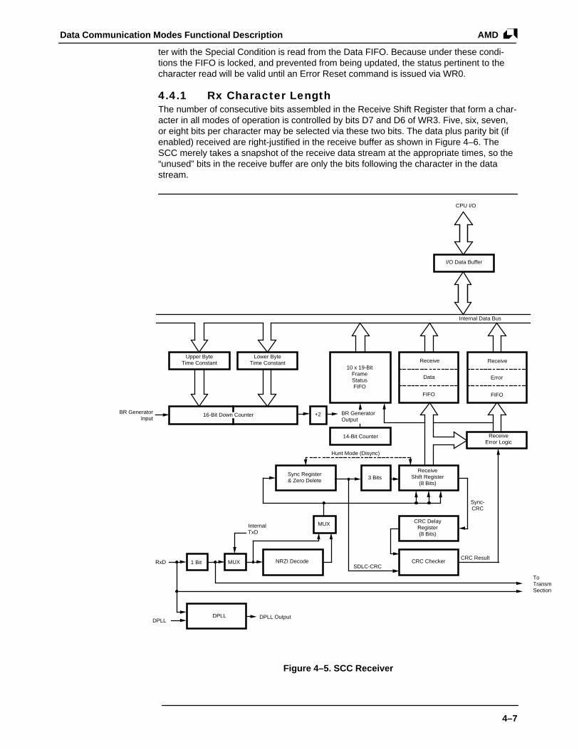
Data Communication Modes Functional Description AMD
4–7
ter with the Special Condition is read from the Data FIFO. Because under these condi-tions the FIFO is locked, and prevented from being updated, the status pertinent to thecharacter read will be valid until an Error Reset command is issued via WR0.
4.4.1 Rx Character LengthThe number of consecutive bits assembled in the Receive Shift Register that form a char-acter in all modes of operation is controlled by bits D7 and D6 of WR3. Five, six, seven,or eight bits per character may be selected via these two bits. The data plus parity bit (ifenabled) received are right-justified in the receive buffer as shown in Figure 4–6. TheSCC merely takes a snapshot of the receive data stream at the appropriate times, so the“unused” bits in the receive buffer are only the bits following the character in the datastream.
Upper Byte Time Constant
Lower Byte Time Constant
16-Bit Down Counter BR Generator Input
+2
10 x 19-Bit Frame Status FIFO
Receive
Data
FIFO
Receive
Error
FIFO
BR Generator Output
Receive Error Logic
Receive Shift Register
(8 Bits)
14-Bit Counter
3 Bits Sync Register & Zero Delete
Hunt Mode (Disync)
CRC Delay Register (8 Bits)
CRC Checker CRC Result
Sync- CRC
SDLC-CRC
MUX
NRZI Decode
Internal TxD
MUX 1 Bit RxD
DPLL DPLL
DPLL Output
I/O Data Buffer
CPU I/O
Internal Data Bus
To TransmiSection
Figure 4–5. SCC Receiver
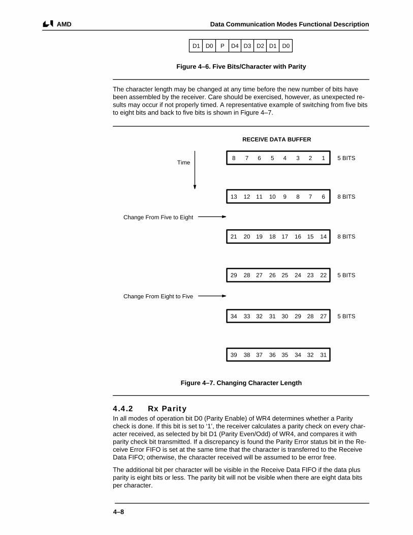
Data Communication Modes Functional DescriptionAMD
4–8
D1 D0 P D4 D3 D2 D1 D0
Figure 4–6. Five Bits/Character with Parity
The character length may be changed at any time before the new number of bits havebeen assembled by the receiver. Care should be exercised, however, as unexpected re-sults may occur if not properly timed. A representative example of switching from five bitsto eight bits and back to five bits is shown in Figure 4–7.
8 7 6 5 4 3 2 1
13 12 11 10 9 8 7 6
21 20 19 18 17 16 15 14
29 28 27 26 25 24 23 22
34 33 32 31 30 29 28 27
39 38 37 36 35 34 32 31
5 BITS
8 BITS
8 BITS
5 BITS
5 BITS
RECEIVE DATA BUFFER
Time
Change From Five to Eight
Change From Eight to Five
Figure 4–7. Changing Character Length
4.4.2 Rx ParityIn all modes of operation bit D0 (Parity Enable) of WR4 determines whether a Paritycheck is done. If this bit is set to ‘1’, the receiver calculates a parity check on every char-acter received, as selected by bit D1 (Parity Even/Odd) of WR4, and compares it withparity check bit transmitted. If a discrepancy is found the Parity Error status bit in the Re-ceive Error FIFO is set at the same time that the character is transferred to the ReceiveData FIFO; otherwise, the character received will be assumed to be error free.
The additional bit per character will be visible in the Receive Data FIFO if the data plusparity is eight bits or less. The parity bit will not be visible when there are eight data bitsper character.

Data Communication Modes Functional Description AMD
4–9
The Parity Error bit in the Receive Error FIFO may be programmed to cause a SpecialCondition interrupt by setting bit D2 of WR1 to ‘1’. If this interrupt mode is programmed,and a Parity Error is detected, an interrupt will not be generated until the character asso-ciated with the Parity Error is read from the Receive Data FIFO. This, or any, SpecialCondition interrupt locks up the Data FIFO, and the Parity Error bit remains latched untilan Error Reset command is issued by the processor via WR0.
If interrupts are not being used to transfer data (i.e., Receive Interrupts Disabled mode)an interrupt will not be generated and any error status must be obtained by polling RR0,or reading RR2 (channel B). In this case, if status is to be checked, it must be done be-fore the data are read, because the act of reading the data moves the next character andstatus to the top of the Data and Error FIFOs. Note that Parity is normally not used inSDLC modes.
4.4.3 Rx Modem ControlThe SCC provides up to three Modem control signals associated with the receiver inAsynchronous mode, and two in SDLC and Synchronous modes.
In Asynchronous Mode, the SYNC pin is a general-purpose input whose state is reportedvia the SYNC/HUNT status bit in RR0; however, if the crystal oscillator is enabled, this pinis not available and the SYNC/HUNT status bit is forced to ‘0’. Otherwise, the SYNC pinmay be used to carry the Ring Indicator signal. In SDLC and Synchronous modes, exceptfor External SYNC mode, the SYNC pin is configured as an output.
The DTR/REQ pin carries the inverted state of the DTR bit in WR5 (D7) unless this pinhas been programmed to carry a DMA Request signal. The DCD pin is ordinarily a gen-eral purpose input to the DCD status bit in RR0. However, if the Auto Enables mode isselected (by setting D5 of WR3 to ‘1’), this pin becomes an enable for the receiver. Thatis, if Auto Enables is on and the DCD pin is HIGH the receiver will be disabled; while theDCD pin is LOW the receiver will be enabled. Note, however, that in all modes of opera-tion, the Receiver Enable bit must be set before the DCD pin can be used in this manner.
4.5 TRANSMITTER OVERVIEWThe transmitter performs all the necessary functions to convert parallel data from theprocessor into the appropriate serial bit streams. The transmit data path is shown in Fig-ure 4–8.
The transmitter has an 8-bit Transmit Data register (WR8) which is loaded from the inter-nal data bus, and a Transmit Shift Register which is loaded from either WR6, WR7, or theTransmit Data Register (WR8).
Serial data transitions on the falling edge of TRxC begin when data written to WR8 aretransferred to the Transmit Shift Register. Each time a character is transferred from WR8into the Transmit Shift Register a Transmit Buffer Empty indication is given via bit D2 ofRR0. This double buffering allows the processor one full character time to respond withthe next character without interrupting data transmission.
In all modes of operation, data will be sent low-order bits first (i.e. D0 before D1, etc.) foras many bits as programmed. This requires that data written to the Transmit Buffer beright-justified if character length is less than eight bits.
4.5.1 Tx Character LengthThe number of bits transmitted per character and the way the data are formatted withinthe transmit buffer is controlled by bits D6 and D5 of WR5. These bits provide the optionof five, six, seven, or eight bits per character. Being able to transmit less than five bits percharacter is possible on the SCC if the five bits per character length is programmed andthe data are formatted before being written to the transmit buffer, as shown in Table 4–1,to inform the SCC of the actual number of bits to be transmitted.
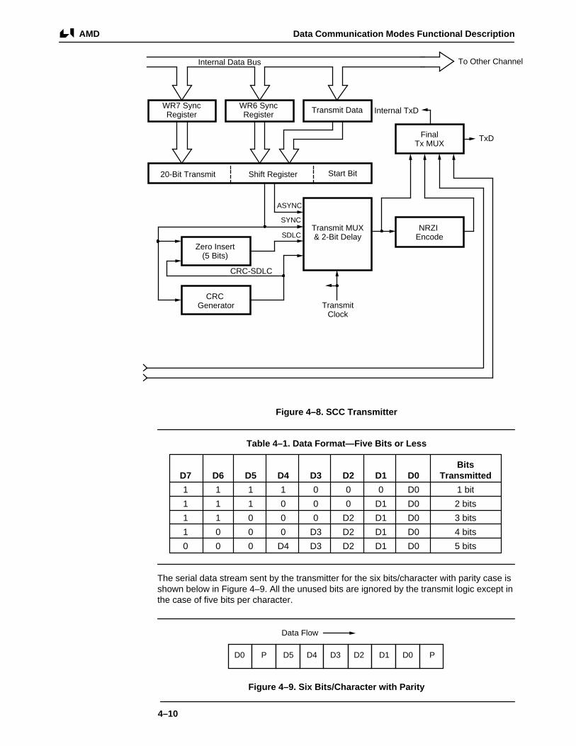
Data Communication Modes Functional DescriptionAMD
4–10
WR7 Sync Register
WR6 Sync Register Transmit Data
20-Bit Transmit Shift Register Start Bit
Transmit MUX & 2-Bit Delay
Zero Insert (5 Bits)
CRC Generator
NRZI Encode
Final Tx MUX
TxD
Internal TxD
Transmit Clock
To Other Channel
ASYNC
SYNC
SDLC
CRC-SDLC
Internal Data Bus
Figure 4–8. SCC Transmitter
Table 4–1. Data Format—Five Bits or Less
BitsD7 D6 D5 D4 D3 D2 D1 D0 Transmitted
1 1 1 1 0 0 0 D0 1 bit
1 1 1 0 0 0 D1 D0 2 bits
1 1 0 0 0 D2 D1 D0 3 bits
1 0 0 0 D3 D2 D1 D0 4 bits
0 0 0 D4 D3 D2 D1 D0 5 bits
The serial data stream sent by the transmitter for the six bits/character with parity case isshown below in Figure 4–9. All the unused bits are ignored by the transmit logic except inthe case of five bits per character.
D0 P D5 D4 D3 D2 D1 D0 P
Data Flow
Figure 4–9. Six Bits/Character with Parity

Data Communication Modes Functional Description AMD
4–11
The character length may be changed at any time, but the desired length must be se-lected before the character in the transmit buffer is transferred to the the Transmit ShiftRegister. The easiest way to ensure this is to write to WR5 to change the character lengthbefore writing the data to the transmit buffer.
4.5.2 Tx ParityIn all modes of operation bit D0 (Parity Enable) of WR4 determines whether an additionalbit will be appended to each character sent as an indication of the “oddness” or “even-ness” of the number of ‘1’ bits transmitted in the character. If this bit is set to ‘1’ an addi-tional bit will be sent in addition to the number of bits specified in WR4, or by the data for-mat used when transmitting less than five bits per character.
Bit D1 of WR4 determines the even/odd sense of this additional bit when Parity is en-abled. If this bit is set to ‘1’, the transmitter adds a bit that makes the total number of ‘1’bits in the character being transmitted even; if set to ‘0’, a bit will be added to make thesum of ‘1’ bits in the character being transmitted odd.
4.5.3 Break GenerationThe transmitter may be programmed to send a break condition (i.e., the TxD pin is pulledLow) in all modes of operation via bit D4 of WR5. When this bit is set to ‘1’, the transmit-ter suspends any data being transmitted at the time and sends continuous ‘0’s from thefirst transmit clock edge after this command is issued, until the first transmit clock edgeafter this bit is reset, at which point the transmitter continues to send the contents of theTransmit Shift Register. The transmit clock edges referred to here are those that definetransmitted bit cell boundaries. Note that the TxD pin will be pulled Low whether or notthe transmitter is enabled.
4.5.4 Transmit Modem ControlThere are two modem control signals associated with the transmitter on the SCC. TheRTS pin is a general-purpose output that carries the inverted state of the RTS bit in WR5(D1), and the CTS pin is a general-purpose input to the CTS status bit in RR0 (D5). How-ever, if the Auto Enables Mode is selected (by setting D5 of WR3 to ‘1’), CTS becomesan enable for the transmitter. That is, if Auto Enables is on and the CTS pin is HIGH thetransmitter will be disabled; while the CTS pin is LOW the transmitter will be enabled.Note, however, that in all modes of operation, the Transmitter Enable bit must be set be-fore the CTS pin can be used in this manner.
If the SCC channel is programmed in Asynchronous mode, and the Auto Enable bit is setto ‘1’, RTS will remain Low until the transmitter is completely empty and the last stop bithas left the TxD pin. In SDLC and Synchronous modes, the RTS pin is just a general-purpose output.
4.5.5 Auto RTS ResetOn the CMOS SCC, if bits D0 of WR15 and D2 of WR7’ are set to ‘1’ and the channel isin SDLC Mode, the RTS pin may be reset early in the Tx Underrun routine and the RTSpin will remain active until the last zero bit of the closing flag leaves the TxD pin as shownin Figure 4–10.
Note that in order for this to function properly, bits D3 and D2 of WR10 must be set to ‘1’and ‘0’, respectively.
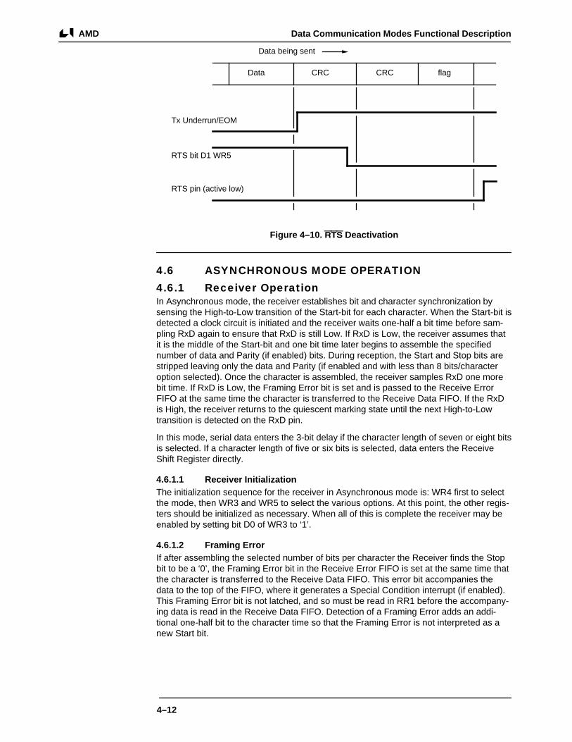
Data Communication Modes Functional DescriptionAMD
4–12
CRC CRC flag
Data being sent
Tx Underrun/EOM
RTS bit D1 WR5
RTS pin (active low)
Data
Figure 4–10. RTS Deactivation
4.6 ASYNCHRONOUS MODE OPERATION
4.6.1 Receiver OperationIn Asynchronous mode, the receiver establishes bit and character synchronization bysensing the High-to-Low transition of the Start-bit for each character. When the Start-bit isdetected a clock circuit is initiated and the receiver waits one-half a bit time before sam-pling RxD again to ensure that RxD is still Low. If RxD is Low, the receiver assumes thatit is the middle of the Start-bit and one bit time later begins to assemble the specifiednumber of data and Parity (if enabled) bits. During reception, the Start and Stop bits arestripped leaving only the data and Parity (if enabled and with less than 8 bits/characteroption selected). Once the character is assembled, the receiver samples RxD one morebit time. If RxD is Low, the Framing Error bit is set and is passed to the Receive ErrorFIFO at the same time the character is transferred to the Receive Data FIFO. If the RxDis High, the receiver returns to the quiescent marking state until the next High-to-Lowtransition is detected on the RxD pin.
In this mode, serial data enters the 3-bit delay if the character length of seven or eight bitsis selected. If a character length of five or six bits is selected, data enters the ReceiveShift Register directly.
4.6.1.1 Receiver InitializationThe initialization sequence for the receiver in Asynchronous mode is: WR4 first to selectthe mode, then WR3 and WR5 to select the various options. At this point, the other regis-ters should be initialized as necessary. When all of this is complete the receiver may beenabled by setting bit D0 of WR3 to ‘1’.
4.6.1.2 Framing ErrorIf after assembling the selected number of bits per character the Receiver finds the Stopbit to be a ‘0’, the Framing Error bit in the Receive Error FIFO is set at the same time thatthe character is transferred to the Receive Data FIFO. This error bit accompanies thedata to the top of the FIFO, where it generates a Special Condition interrupt (if enabled).This Framing Error bit is not latched, and so must be read in RR1 before the accompany-ing data is read in the Receive Data FIFO. Detection of a Framing Error adds an addi-tional one-half bit to the character time so that the Framing Error is not interpreted as anew Start bit.

Data Communication Modes Functional Description AMD
4–13
4.6.1.3 Break DetectionA break condition is recognized when a null character (all ‘0’s) plus a Framing Error isdetected by the receiver. Upon recognizing this sequence, the BREAK/ABORT status bitin RR0 will be set and remains set until a ‘1’ is received indicating that a break conditionis no longer present. Note that at the termination of a break, the Receive Data FIFO con-tains a single null character, which should be read and discarded. The Framing Error bitwill not be set for this null character, but if odd parity has been selected, the Parity Errorbit will be set. Caution should be exercised if the receive data line contains a switch thatis not debounced to generate breaks. Switch bounce may cause multiple breaks, recog-nized by the receiver to be additional characters assembled in the Receive Data FIFO. Itmay also cause a Receiver Overrun condition to be latched.
4.6.1.4 Clock SelectionWhen an SCC channel is programmed in Asynchronous mode it may be programmed toaccept a transmit/receive clock that is 1, 16, 32, or 64 times the data rate. This is selectedby bits D7 and D6 in WR4. The clock factor chosen will be common to both the transmit-ter and receiver.
The x1 mode in Asynchronous mode is a combination of both synchronous and asynchro-nous transmission. The data are clocked by a common timing base, but characters arestill framed with Start and Stop bits. Because the receiver waits for one clock period afterdetecting the first High-to-Low transition before beginning to assemble characters, thedata and clock must be synchronized externally. The x1 mode is the only mode in which adata encoding method other than NRZ may be used.
In SDLC and Synchronous modes bits D7 and D6 of WR4 are ignored because the x1clock is forced internally.
4.6.2 Transmitter OperationIn Asynchronous mode, WR6 and WR7 are not used and the Transmit Shift Register isformatted with Start and Stop bits before data are shifted out to the transmit multiplexer atthe selected clock rate. Asynchronous data leaves the Transmit Shift Register and goesdirectly to the Transmit Multiplexer. CRC generation is not supported in this mode.
4.6.2.1 Transmitter InitializationThe initialization sequence for the transmitter in Asynchronous mode is: WR4 first to se-lect the mode, then WR3 and WR5 to select the various options. At this point the otherregisters should be initialized as necessary. When all of this is complete, the transmittermay be enabled by setting bit D3 of WR5 to ‘1’.
At this point, the transmitter is enabled and the TxD pin will remain in the marking (High)state. When the first character is written to WR8, it is transferred to the Transmit ShiftRegister and the Transmit Buffer Empty bit is set to ‘1’. A Parity bit (if enabled), Start-bit,and the selected number of Stop bits are then appended to the character. After the char-acter has been completely sent, the next character is transferred to the Transmit ShiftRegister and the process continues. When no more characters are to be transmitted (i.e.,the transmitter is completely empty), the All Sent status bit in RR1 (D0) will be set whenthe last Stop bit reaches the TxD pin. This bit can be used by the processor as an indica-tion that the transmitter may be safely disabled. The TxD pin then remains in the markingstate until the next character is written to WR8.
4.6.2.2 Stop Bit SelectionThe SCC provides three Stop-bit options via bits D3 and D2 in WR4. The options avail-able are one, one-and-a-half, or two stop bits per character. These two bits in WR4 selectonly the number of Stop bits for the transmitter, as the receiver always checks for oneStop bit. Note that the selected clock factor may restrict the number of Stop bits that maybe transmitted. In particular, when the clock rate and data rate are the same (i.e., x1mode), one-and-a-half Stop bits are not allowed. If any length other than one Stop bit isdesired in the x1 mode, only two Stop bits can be used.

Data Communication Modes Functional DescriptionAMD
4–14
4.7 SDLC MODE OPERATION
4.7.1 Receiver OperationReceiver operation in SDLC mode begins in a Hunt mode where the communications lineis monitored for a synchronizing pattern on a bit-by-bit basis. The receiver may be placedin Hunt mode by having the processor issue the Enter Hunt Mode command via bit D4 inWR3, but will always start out in Hunt mode when it is enabled. The Enter Hunt Mode bitin WR3 is a command so writing a ‘0’ to it has no effect.
The Hunt status of the receiver is reported by the SYNC/HUNT status bit in RR0. In SDLCmode, this status bit will be set to ‘1’ when either; 1) the processor issues the Enter HuntMode command, 2) the processor disables the receiver, or 3) an abort is detected. It willbe reset to ‘0’ when the receiver leaves Hunt mode, or when the abort condition goesaway. Unlike BISYNC or MONOSYNC mode, once the SYNC/HUNT status bit is reset itdoes not need to be set again in between frames because the Receiver always maintainssynchronization.
This SYNC/HUNT status bit is one of the possible sources of External/Status interrupts,with both transitions causing an interrupt. This is true even if the SYNC/HUNT bit is set asa result of the processor issuing the Enter Hunt Mode command.
While in Hunt mode the Receive SYNC Register and WR7 are used in establishing char-acter synchronization. As data are received, the receiver searches for the bit pattern,‘01111110’, programmed in WR7. This sequence of six consecutive ‘1’ bits is preventedfrom occurring randomly elsewhere in the frame through a process called zero-bit inser-tion in which the transmitter inserts a ‘0’ bit after five consecutive ‘1’ bits, irrespective ofcharacter boundaries. In turn, the receiver always searches the receive data stream on abit-by-bit basis for five consecutive ‘1’s. When the receiver detects a ‘0’ bit followed byfive ‘1’ bits, it inspects the following bit. If it is a ‘0’, the one bits are passed as data andthe zero bit is deleted. If the sixth bit is a ‘1’, the receiver inspects the seventh bit. If it is a‘0’, a flag has been encountered and the receiver is synchronized to that flag; if it is a ‘1’an abort or an EOP (End of Poll) has been encountered.
When a flag is detected and Address Search mode is not enabled, the receiver leavesHunt mode and character assembly begins with the first non-flag character. Once charac-ter assembly begins characters are assembled according to the number of bits per char-acter specified until: 1) an end of frame flag is detected, 2) an abort pattern is detected, 3)the receiver is disabled, or 4) a channel or hardware reset is executed.
All data passes through the Receive Sync Register and the 3-bit delay before entering theReceive Shift Register once synchronization is achieved. Ordinarily, the receiver transfersall data between flags to the Receive Data FIFO, but while it is in Hunt mode no flags willbe transferred.
4.7.1.1 Flag Detect OutputIn SDLC mode, if bit D7 of WR11 is set to ‘0’, the SYNC pin will be configured as an out-put and the SCC will drive it Low every time a flag pattern is detected in the data stream.The timing for the SYNC signal is shown in Figure 4–11.
4.7.1.2 Receiver InitializationThe initialization sequence for the receiver in SDLC mode is: WR4 first, to select themode, then WR10 to modify it if necessary, WR6 to program the address, WR7 to pro-gram the flag and WR3 and WR5 to select the various options. At this point the other reg-isters should be initialized as necessary. When all of this is complete, the receiver may beenabled by setting bit D0 of WR3 to ‘1’.
4.7.1.3 10x19-Bit Frame Status FIFOIn addition to the 8-bit Receive Data and Error FIFO’s, the CMOS SCC Receiver incorpo-rates a 14-bit receive byte counter and a 10x19-bit FIFO array for storing frame status forup to ten frames. This FIFO enhances the SCC’s ability to receive high speed back-to-

Data Communication Modes Functional Description AMD
4–15
back SDLC frames by minimizing frame overruns due to CPU latencies in responding tointerrupts. The block diagram of the 10x19-bit FIFO is shown in Figure 4–12.
4.7.1.3.1 FIFO Enabling/DisablingThis Frame Status FIFO is enabled through WR15 bit D2 but only when the SCC is pro-grammed in SDLC mode. Since each channel incorporates this FIFO, each can be en-abled and disabled independently.
Resetting bit D2 of WR15 disables and resets the FIFO. Table 4–2 tabulates the ena-bling/disabling of channel FIFOs. Note that the FIFO pointer logic is reset when D2 ofWR15 is reset or after a power-on reset.
When the Frame Status FIFO is disabled, the CMOS SCC is completely downward com-patible with the NMOS SCC, and the status register contents bypass the FIFO and godirectly to the bus interface as shown in Figure 4–12.
The status of the FIFO Enable signal can be obtained by reading bits D2 of RR15 throughtheir respective channels. If the FIFO is enabled, this bit will be set to ‘1’; otherwise, it willbe set to ‘0’.
4.7.1.3.2 FIFO Read OperationTo facilitate the use of these FIFOs, two new registers were added. These registers, RR6and RR7, are accessible only when bit D2 of WR15 is set to ‘1’, and the SCC is pro-grammed in SDLC mode.
Table 4–2. Frame Status FIFO Enabling
WR15A(D2) WR15B(D2) Operation
0 0 Ch.A and Ch.B FIFOs disabled and reset
1 0 Ch.A and Ch.B FIFOs enabled but not independent (resetting D2 or WR15A resets both FIFOs simultaneously)
1 1 Ch.A and Ch.B FIFOs enabled and independent (resetting D2 in either channel resets only pertinentFIFO)
0 1 Ch.B FIFO enabled only
RTxC
RxD
SYNC
FLAGLAST–1 FLAGLAST DATA0 DATA1 DATA2
Figure 4–11. Flag Detect Timing
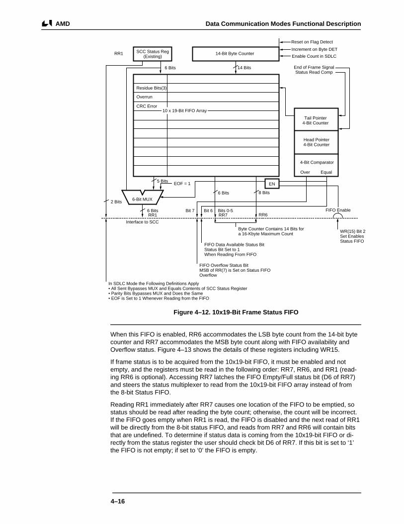
Data Communication Modes Functional DescriptionAMD
4–16
SCC Status Reg (Existing)
14-Bit Byte Counter
Residue Bits(3)
Overrun
CRC Error
14 Bits 6 Bits
10 x 19-Bit FIFO Array
5 Bits EOF = 1 EN
6 Bits RR1
2 Bits
Interface to SCC
6-Bit MUX
Bit 7 Bit 6
6 Bits
Bits 0-5 RR7 RR6
8 Bits
Byte Counter Contains 14 Bits for a 16-Kbyte Maximum Count
FIFO Data Available Status Bit Status Bit Set to 1 When Reading From FIFO
FIFO Overflow Status Bit MSB of RR(7) is Set on Status FIFO Overflow
In SDLC Mode the Following Definitions Apply • All Sent Bypasses MUX and Equals Contents of SCC Status Register • Parity Bits Bypasses MUX and Does the Same • EOF is Set to 1 Whenever Reading from the FIFO
Reset on Flag Detect
Increment on Byte DET
Enable Count in SDLC
Tail Pointer 4-Bit Counter
Head Pointer 4-Bit Counter
4-Bit Comparator
Over Equal
WR(15) Bit 2 Set Enables Status FIFO
FIFO Enable
End of Frame Signal Status Read Comp
RR1
Figure 4–12. 10x19-Bit Frame Status FIFO
When this FIFO is enabled, RR6 accommodates the LSB byte count from the 14-bit bytecounter and RR7 accommodates the MSB byte count along with FIFO availability andOverflow status. Figure 4–13 shows the details of these registers including WR15.
If frame status is to be acquired from the 10x19-bit FIFO, it must be enabled and notempty, and the registers must be read in the following order: RR7, RR6, and RR1 (read-ing RR6 is optional). Accessing RR7 latches the FIFO Empty/Full status bit (D6 of RR7)and steers the status multiplexer to read from the 10x19-bit FIFO array instead of fromthe 8-bit Status FIFO.
Reading RR1 immediately after RR7 causes one location of the FIFO to be emptied, sostatus should be read after reading the byte count; otherwise, the count will be incorrect.If the FIFO goes empty when RR1 is read, the FIFO is disabled and the next read of RR1will be directly from the 8-bit status FIFO, and reads from RR7 and RR6 will contain bitsthat are undefined. To determine if status data is coming from the 10x19-bit FIFO or di-rectly from the status register the user should check bit D6 of RR7. If this bit is set to ‘1’the FIFO is not empty; if set to ‘0’ the FIFO is empty.

Data Communication Modes Functional Description AMD
4–17
Since not all status bits of RR1 are stored in the Frame Status FIFO, the All Sent, Parity,and EOF bits bypass the FIFO and are stored in the 8-bit Status FIFO. The status bitsstored in the 10x19-bit FIFO will be the Residue, Overrun, and CRC status bits. Note thatthe EOF interrupt is generated the same way as before.
4.7.1.3.3 FIFO Write OperationWhen an EOF is detected, and the FIFO is enabled, the five status bits and byte-countare loaded into the FIFO, and the FIFO pointer is incremented. If the FIFO overflows, bitD7 of RR7 (FIFO Overflow) is set to indicate the overflow. This bit and the FIFO controllogic is reset by disabling and re-enabling the FIFO control bit (WR15 bit D2). For detailsof FIFO control timing during an SDLC frame, refer to Figure 4–14.
When a packet is completely received, then a Receive Interrupt on Special Condition isgenerated upon receipt of the End of Frame Flag. If the clock is temporarily stopped afterthe receipt of the flag, the Frame Status FIFO may not be updated even though the inter-rupt was generated. At least two receive clocks are needed to update the Frame StatusFIFO. The Frame Status information is not lost and will be put into the Frame Status FIFOwhen the clock is enabled again.
4.7.1.3.4 14-Bit Byte CounterThe 14-bit byte counter allows for data frames of up to 16K bytes to be received. It is en-abled when bit D2 of WR15 is set to ‘1’ and the SCC is in SDLC mode. It is reset when-ever an SDLC flag character is received. The reset is timed so that the contents of thebyte counter are successfully written into the FIFO.
The byte counter is incremented by writes to the 8-bit receive Data FIFO. The counterrepresents the number of bytes received by the SCC, rather than the number of bytestransferred from the SCC. (These counts may differ by up to the number of bytes in thereceive data FIFO contained in the SCC.)
FOY FDA BC 13
6 5 7
FIFO Data Available Status 1 = Status Reads Will Come From FIFO 0 = Status Reads Will Come From SCC
FIFO Overflow Status 1 = FIFO Overflowed During Operation 0 = Normal
RR7
0
BC 0
Read From FIFO LSB Byte Count RR6
4
BC 12
3
BC 11
2
BC 10
1
BC 9
0
BC 8
7
BC 7
6
BC 6
5
BC 5
4
BC 4
3
BC 3
2
BC 2
1
BC 1
0
*
Status FIFO Enable Control Bit 1 =
WR16
7
*
6
*
5
*
4
*
3
*
2
FEN
1
*
Status and Byte Count Will be Held in the Status FIFO Until Read
0 = Status Will Not be Held (SCC)t (Emulation Mode)
* = No Change From NMOS SCC DFN
10216A-013A
Figure 4–13. Frame Status FIFO Registers

Data Communication Modes Functional DescriptionAMD
4–18
F A D D D D C C F
0 1 2 3 4 5 6 7
F A D D D D C C F
0 1 2 3 4 5 6 7 0
Internal Byte Strobe Increments Counter Internal Byte Strobe
Increments Counter Don't Load Counter On 1st Flag Reset Byte Counter Here
Reset Byte Counter Load Counter Into FIFO and Increment PTR
Reset Byte Counter
Reset Byte Counter Load Counter Into FIFO and Increment PTR
10216A-012A
Figure 4–14. Frame Status FIFO Control Timing
4.7.1.3.5 Am85C30 Frame Status FIFO Operation ClarificationIn an effort to make the 10x19 Frame Status FIFO (FSF) useful for high-speed receptionof packets, the lock on the 3-byte receive FIFO that occurs after special conditions in twoof the receive interrupt modes was removed. The benefit of this operation is that the usercan receive multiple frames of SDLC data before having to service the interrupt. Competi-tion 85C30 freezes the Rx FIFO after every frame, so the user could lose frames of databetween the end of the first frames and Reset Error command. In this case the user mustservice interrupts for every frame of data on the competition 85C30, defeating the pur-pose of the FIFO. AMD allows the user to receive up to 10 frames of data before havingto service the interrupt, thus obtaining the maximum (desired) utilization of the FSF.
A clarification of the enhanced operation is given below. the removal of the lock on theReceive Data 3-byte FIFO affects the device when it is programmed in the “Interrupt onFirst Receive Character of Special Condition” or “Interrupt on Special Condition Only”modes.
1. When the 10x19 Frame Status FIFO (FSF) is not enabled, the 3-byte Receive FIFO (Rx FIFO) locks when a special condition is received until the Reset Error command isissued. DMA is disabled when the Rx FIFO locks until the Reset Error command is issued (same as old operation).
2. When the FSF is enabled:
a. The 3-byte Receive FIFO never locks.b. DMA is disabled only on overrun (i.e. overruns do not lock the Rx FIFO, but do
disable DMA).
To reenable DMA after an overrun, the following sequence must be used:
i. Read and discard ALL entries in the Receive Data 3-byte FIFO.
ii. Issue the Error Reset command.
iii. Note that if an additional byte of data is received between the time that the Receive Data FIFO is emptied and the ERROR RESET command is issued. DMA will NOT unlock. This signals the user that corrupt data remains in the Receive Data FIFO. The user must read and discard all entries in the Receive Data 3-byte before DMA will reenable. Note that an additional ERROR RESET is not required.
c. Interrupts are generated and remain active until the RESET ERROR command is issued.
d. Interrupt vectors (in Read Register 2B) are modified as follows. There are twobit patterns for Receiver Interrupts, x11-Special Receive condition, and x10 Receive Character Available. Refer to Figure 3–2 (page 3–6) and Table 6–4 (page 6–19) of this manual.

Data Communication Modes Functional Description AMD
4–19
i. The Status x11 will be reported when the first special conditions is received.
ii. As more data is received, the status will switch to x10 to reflect that a Receiver interrupt has been received, but that the present data in the Receive Data 3-byte FIFO does not contain a special condition.
iii. when a special condition resides at the top of the Receive Data FIFO, the status x11 will be reported.
4.7.1.3.6 Am85C30 Aborted Frame Handling When Using The 10x19 Frame Status FIFO
Field feedback on the Am85C30 Frame Status FIFO has revealed that neither AMD norcompetition create an entry in the Frame Status FIFO when a frame being received isaborted (seven or more consecutive 1s appear in the receive Data stream). An abortedframe indicates to the receiver that synchronization has been lost. the receiver then en-ters “Hunt Mode” where it monitors the input data stream until a SDLC flag is recognized.After an SDLC flag is received, the receiver is capable of receiving additional dataframes.
Because of the lack of an entry in the Frame Status FIFO for aborted frames, the receivercannot look only at the Frame Status FIFO to determine the exact nature of all data re-ceived. To properly recognized and recover from aborted frames, the following practice isrecommended:
1. The receiver must enable an external/status interrupt on ABORT.
2. When an interrupt due to an ABORT is received, all frames contained in the Frame Status FIFO should be considered to be corrupted and discarded. The processor should request re-transmission of these frames.
3. Note that an external/status interrupt will be generated both when an ABORT is received and when the ABORT condition disappears. Either transition of the ABORT status will cause the ABORT bit in Read Register 0 to latch until a “Reset External/Status Interrupt” command is issued through Write Register 0.
This behavior is identical on both competition and AMD product and is not revision de-pendent.
4.7.1.4 Address Search ModeThe first 8-bit non-flag character following the opening flag of a frame is assumed by theSCC to be the address of the station for which the frame is intended. The SCC providesseveral options for handling this address via bits D2 (Address Search mode) and D1(SYNC Character Load Inhibit) of WR3.
If the Address Search mode is enabled, the receiver’s address recognition logic will beenabled and the receiver will compare the first 8-bit non-flag character with the contentsof WR6. If these two characters match, or if the received character is the global address(all ‘1’s), data are passed to the Receive Shift Register and character assembly begins. Ifno match is detected the receiver remains in Hunt mode and no data are passed to theReceive Shift Register. The global address is used in applications where a specific stationaddress is not known, as might be the case in a switched connection, or when a broad-cast frame is sent to all stations. Address Search mode will be enabled when WR3 is pro-grammed as shown below.
? ? ? ? X 1 0 ?
D7 D6 D5 D4 D3 D2 D1 D0
WR3—Register Layout

Data Communication Modes Functional DescriptionAMD
4–20
The address comparison will be across all eight bits of WR6 when the Sync CharacterLoad Inhibit bit (D1 in WR3) is set to ‘0’. This comparison may be modified so that onlythe four most significant bits of WR6 must match the received address. This mode is se-lected by programming WR3 as shown below.
? ? ? ? X 1 1 ?
D7 D6 D5 D4 D3 D2 D1 D0
WR3—Register Layout
In this mode, however, the address field is still eight bits wide. Regardless of the modeenabled, the address field is not treated differently than data and is always transferred tothe Receive Data FIFO in the same manner as data. Note that Address Search mode isavailable only in SDLC mode.
SDLC address search mode (bit D2 in Write Register 3 is set) and Receive Full CRCmode (bit D5 of Write Register 7′) should not be used in conjunction with each other. Ifthese modes are used together, the Am85C30 will accept all packets with addresses thatmatch the address programmed into Register 6 and will accept only the address byte ofthe packet with addresses that do not match the Register 6 address. Proper operation ofaddress search mode calls for the complete rejection of packets with addresses that donot match the Register 6 address.
4.7.1.5 Abort DetectionIn addition to monitoring the data stream for flags, the receiver also monitors the line foran abort pattern. An abort is detected when seven consecutive ‘1’s are found in the datastream. This is usually an indication sent by the transmitter alerting the receiver that theframe currently being received has been aborted and should be discarded.
The detection of an abort is reported in the BREAK/ABORT status bit in RR0 (D7). Thisstatus bit is one source of External/Status interrupts, so transitions of this status bit maybe programmed to cause interrupts.
An abort automatically forces the receiver into Hunt mode and sets the SYNC/HUNTstatus bit in RR0 (D4) to ‘1’. Because this status bit is also a possible External/Status con-dition, its transition may also be programmed to cause an interrupt. Thus transitions onboth the BREAK/ABORT and SYNC/HUNT status bits may occur very close together, andeither one or two External/Status interrupts may result.
The BREAK/ABORT status bit will be reset when a ‘0’ is received, either by the abort it-self going away or as the leading ‘0’ of a flag. In either case, the SYNC/HUNT status bitwill remain set until the receiver leaves Hunt mode. Because both transitions on theBREAK/ABORT status bit are guaranteed to cause an interrupt, two discrete External/Status Interrupts will occur; one when the abort is detected and one when the abort goesaway.
Note that the SCC does not discriminate between an in-frame (between opening andclosing flags) and an out-of-frame (after EOF) abort. An abort detected while the receiveris In-Frame terminates frame reception, but not in an orderly manner, because the char-acter being assembled is lost and the Receive Data FIFO is not flushed. An out-of-frameabort interrupt will be generated approximately seven bit times after EOF has been de-tected if the transmitter mark idles. If an ABORT is detected by the receiver after the clos-ing flag and eight 1s have been received, the ABORT will persist until another flag is de-tected at which time the receiver exits from Hunt Mode. If an out-of-frame interrupt is tobe avoided it should be disabled early in the EOF interrupt routine. Because the BREAK/ABORT status bit is not latched in RR0, it may happen that this status bit will be reset bythe time the software responds to the interrupt, causing yet another interrupt. In this case,unless the DCD pin has been programmed as the receiver Auto Enable, the SYNC/HUNT

Data Communication Modes Functional Description AMD
4–21
status bit may be able to provide the indication that an abort pattern was received, sincean abort condition places the receiver in Hunt mode.
4.7.1.6 Residue BitsSince the information field of an SDLC/HDLC frame can contain any number of bits andnot necessarily an integral number of 8-bit characters, the end of data is determined bycounting back 16 bits from the closing flag of a frame. The SCC provides three Residuebits that can be used to indicate the boundary between the data and CRC characters inthe last few bytes read from the Receive Data FIFO. The meaning of these Residue bitswith each character length option is shown in Table 4–3. In this table “previous byte” re-fers to the character received prior to the end of frame flag being detected.
The Residue Code bits are not loaded through the top of the Receive Error FIFO. Theychange in RR1 when the last character of the frame is loaded into the Receive DataFIFO. If there are any characters already in the Data FIFO, the Residue Code will not bevalid until the EOF status bit is set in RR1.
4.7.2 SDLC Mode CRC Polynomial SelectionCRC error checking is done with a 16-bit CRC character inserted between the end of thedata field and the end of frame flag. In Synchronous modes, a control character is usuallyused to signify when an end of message has been received (i.e., ETX, EOT, etc.). Thiscontrol character comes before the CRC characters; so on reception, the CRC calculationcan be stopped and the transmitted CRC characters are compared with the CRC charac-ters generated by the receiver. This cannot be done in SDLC mode, since the end offrame flag is after the CRC characters. In order to use the same core hardware configura-tion already used in Synchronous modes, SDLC mode requires that the transmit CRCgenerator be preset to all ‘1’s, and the complement of the CRC result be transmitted. Onreception, the receive CRC generator must also be preset to all ‘1’s and, when the end offrame flag is detected, the result is checked against the bit pattern ‘0001110100001111’to ascertain frame integrity. This is consistent with other bit-oriented protocols, such asHDLC and ADCCP.
Table 4–3. Residue Codes
0 1 2 8B/C 7B/C 6B/C 5B/C 8B/C 7B/C 6B/C 5B/C 8B/C 7B/C 6B/C 5B/C
1 0 0 0 0 0 0 3 1 0 2 8 8 5 7
0 1 0 0 0 0 0 4 2 0 0 8 8 6 3
1 1 0 0 0 0 0 5 3 1 0 8 8 7 4
0 0 1 0 0 0 0 6 4 2 0 8 8 8 5
1 0 1 0 0 0 0 7 5 3 1 8 8 8 6
0 1 1 0 0 0 – 0 6 4 – 8 8 8 –
1 1 1 0 0 – – 1 0 – – 8 7 – –
0 0 0 0 – – – 2 – – – 8 – – –
Residuecode
Data Bits in PreviousByte
Data Bits in SecondByte
Data Bits in ThirdByte

Data Communication Modes Functional DescriptionAMD
4–22
Because the bit pattern used by the receiver for CRC error checking is based on an in-dustry standard polynomial, only the CRC-CCITT polynomial (X16+X12+X5+1) can beused in SDLC mode.
The CRC transmission and CRC-CCITT polynomial are enabled by programming WR5 asshown below.
? ? ? ? ? 0 ? 1
D7 D6 D5 D4 D3 D2 D1 D0
WR3—Register Layout
4.7.2.1 Rx CRC InitializationBit D7 of WR10 controls the initial state of both the transmit and receive CRC generators.Although the transmit and receive generators may be preset to either all ‘0’s or all ‘1’s,SDLC operation requires that this bit be set to ‘1’ for proper error detection.
The receive CRC generator will be automatically preset whenever the receiver is in Huntmode, or a flag is detected so a Reset CRC Checker command should not be necessary.It may, however, be preset whenever necessary by issuing this command in WR0.
4.7.2.2 Rx CRC EnablingIn SDLC Mode, the SCC always calculates CRC on all bits, except inserted zeros, be-tween the opening and closing flags of a frame, so the Rx CRC Enable bit in WR3 (D3) isignored.
4.7.2.3 CRC ErrorWhen the end of frame flag is detected, the CRC Error bit is loaded into the Receive ErrorFIFO at the same time the character in the Receive Shift Register is transferred to theReceive Data FIFO. Since this CRC Error status bit is not latched internally, it will usuallyalways be set to ‘1’ in RR1, since most bit combinations, except for a correctly completedframe, result in a non-zero CRC. Hence, the CRC Error bit should not be considered validuntil the EOF status bit is set to ‘1’ in RR1, and should be ignored at all other times.
4.7.2.4 CRC Character ReceptionOn the NMOS SCC, when the end of frame flag is detected the contents of the ReceiveShift Register are transferred to the Receive Data FIFO regardless of the number of bitsaccumulated. Because of the 3-bit delay between the Receive SYNC Register and Re-ceive Shift Register, the last two bits of the CRC check character received are nevertransferred to the Receive Data FIFO. Thus, the received CRC characters are unavailablefor use.
On the CMOS SCC, the option of being able to receive the complete CRC charactersgenerated by the transmitter is provided when both bits D0 of WR15 and bit D5 of WR7’are set to ‘1’. When these two bits are set and an end of frame flag is detected, the lasttwo bits of the CRC will be clocked into the Receive Shift Register before its contents aretransferred to the Receive Data FIFO. The data-CRC boundary and CRC character bitformats for each Residue Code provided are shown in Figures 4–15 through 4–18 foreach character length selected.
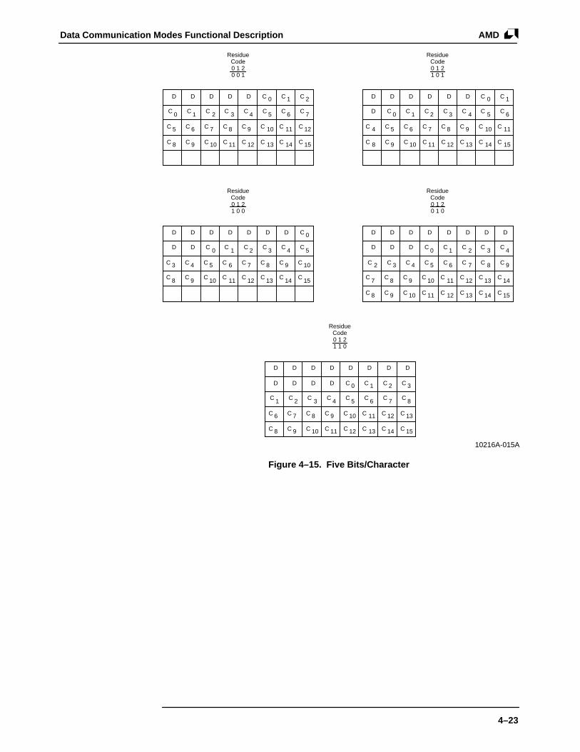
Data Communication Modes Functional Description AMD
4–23
D
C 0
D D D D C 0 C 1 C 2
C 1 C 2 C 3 C 4 C 5 C 6 C 7
C 5 C 6 C 7 C 8 C 9 C 10 C 11 C 12
C 8 C 9 C 10 C 11 C 12 C 13 C 14 C 15
Residue Code 0 1 2 0 0 1
D D D D D C 0 C 1
C 0 C 1 C 2 C 3 C 4 C 5 C 6
C 4 C 5 C 6 C 7 C 8 C 9 C 10 C 11
C 8 C 9 C 10 C 11 C 12 C 13 C 14 C 15
Residue Code 0 1 2 1 0 1
D
D D D D D C 0
C 0 C 1 C 2 C 3 C 4 C 5
C 3 C 4 C 5 C 6 C 7 C 8 C 9 C 10
C 8 C 9 C 10 C 11 C 12 C 13 C 14 C 15
Residue Code 0 1 2 1 0 0
D D D D D
C 0 C 1 C 2 C 3 C 4
C 2 C 3 C 4 C 5 C 6 C 7 C 8 C 9
C 7 C 8 C 9 C 10 C 11 C 12 C 13 C 14
Residue Code 0 1 2 0 1 0
D D D D D
C C C C C C C C 8 9 10 11 12 13 14 15
D D D D D
C 0 C 1 C 2 C 3
C 1 C 2 C 3 C 4 C 5 C 6 C 7 C 8
C 6 C 7 C 8 C 9 C 10 C 11 C 12 C 13
Residue Code 0 1 2 1 1 0
D D D
C C C C C C C C 8 9 10 11 12 13 14 15
D
D D D D D
D D D
D
10216A-015A
Figure 4–15. Five Bits/Character

Data Communication Modes Functional DescriptionAMD
4–24
D
C 0
D D D D C 0 C 1
C 1 C 2 C 3 C 4 C 5 C 6 C 7
C 6 C 7 C 8 C 9 C 10 C 11 C 12 C 13
C 8 C 9 C 10 C 11 C 12 C 13 C 14 C 15
Residue Code 0 1 2 0 1 0
D D D D D C 0
C 0 C 1 C 2 C 3 C 4 C 5 C 6
C 5 C 6 C 7 C 8 C 9 C 10 C 11 C 12
C 8 C 9 C 10 C 11 C 12 C 13 C 14 C 15
Residue Code 0 1 2 1 1 0
D
D D D D D
C 0 C 1 C 2 C 3 C 4 C 5
C 4 C 5 C 6 C 7 C 8 C 9 C 10 C 11
C 8 C 9 C 10 C 11 C 12 C 13 C 14 C 15
Residue Code 0 1 2 0 0 1
D D D D D
C 0 C 1 C 2 C 3 C 4
C 3 C 4 C 5 C 6 C 7 C 8 C 9 C 10
C 8 C 9 C 10 C 11 C 12 C 13 C 14 C 15
Residue Code 0 1 2 1 0 1
D D D D D
D D D D D
C 0 C 1 C 2 C 3
C 2 C 3 C 4 C 5 C 6 C 7 C 8 C 9
Residue Code 0 1 2 0 1 1
D D D
C C C C C C C C 8 9 10 11 12 13 14 15
D
D D D D D
D D D
D D D
D
D D D D D
C 0 C 1 C 2
C 1 C 2 C 3 C 4 C 5 C 6 C 7 C 8
Residue Code 0 1 2 1 0 0
D D D
C C C C C C C C 7 8 9 10 11 12 13 14
D
D D D
D
C C C C C C C C 8 9 10 11 12 13 14 15
10216A-016A
Figure 4–16. Six Bits/Character

Data Communication Modes Functional Description AMD
4–25
D
C 0
D D D D C 0 C 1 C 2 C 3 C 4 C 5 C 6 C 7
C 7 C 8 C 9 C 10 C 11 C 12 C 13 C 14
C 8 C 9 C 10 C 11 C 12 C 13 C 14 C 15
Residue Code 0 1 2 1 1 1
D D D D D
C 0 C 1 C 2 C 3 C 4 C 5 C 6
C 6 C 7 C 8 C 9 C 10 C 11 C 12 C 13
C 8 C 9 C 10 C 11 C 12 C 13 C 14 C 15
Residue Code 0 1 2 1 0 0
D
D D D D D
C 0 C 1 C 2 C 3 C 4 C 5
C 5 C 6 C 7 C 8 C 9 C 10 C 11 C 12
C 8 C 9 C 10 C 11 C 12 C 13 C 14 C 15
Residue Code 0 1 2 0 1 0
D D D D D
C 0 C 1 C 2 C 3 C 4
C 4 C 5 C 6 C 7 C 8 C 9 C 10 C 11
C 8 C 9 C 10 C 11 C 12 C 13 C 14 C 15
Residue Code 0 1 2 1 1 0
D D D D D
D D D D D
C 0 C 1 C 2 C 3 C 3 C 4 C 5 C 6 C 7 C 8 C 9 C 10
Residue Code 0 1 2 0 0 1
D D D
C C C C C C C C 8 9 10 11 12 13 14 15
D
D D D D D
D D D
D D D
D
D D D D D
C 0 C 1 C 2 C 2 C 3 C 4 C 5 C 6 C 7 C 8 C 9
Residue Code 0 1 2 1 0 1
D D D
C C C C C C C C 8 9 10 11 12 13 14 15
D
D D D
D
D D
D D D D D
C 0 C 1
C 1 C 2 C 3 C 4 C 5 C 6 C 7 C 8
Residue Code 0 1 2 0 1 1
D D D
C C C C C C C C 8 9 10 11 12 13 14 15
D
D D D
D D
10216A-017A
Figure 4–17. Seven Bits/Character

Data Communication Modes Functional DescriptionAMD
4–26
10216A-018A
D
C 0
D D D D
C 1 C 2 C 3 C 4 C 5 C 6 C 7 C 8 C 9 C 10 C 11 C 12 C 13 C 14 C 15
Residue Code 0 1 2 0 1 1
D D D D D
C 0 C 1 C 2 C 3 C 4 C 5 C 6 C 7 C 8 C 9 C 10 C 11 C 12 C 13 C 14 C 8 C 9 C 10 C 11 C 12 C 13 C 14 C 15
Residue Code 0 1 2 1 1 1
D
D D D D D
C 0 C 1 C 2 C 3 C 4 C 5 C 6 C 7 C 8 C 9 C 10 C 11 C 12 C 13 C 8 C 9 C 10 C 11 C 12 C 13 C 14 C 15
Residue Code 0 1 2 0 0 0
D D D D D
C 0 C 1 C 2 C 3 C 4 C 5 C 6 C 7 C 8 C 9 C 10 C 11 C 12 C 8 C 9 C 10 C 11 C 12 C 13 C 14 C 15
Residue Code 0 1 2 1 0 0
D D D D D
D D D D D
C 0 C 1 C 2 C 3 C 4 C 5 C 6 C 7 C 8 C 9 C 10 C 11
Residue Code 0 1 2 0 1 0
D D D
C C C C C C C C 8 9 10 11 12 13 14 15
D
D D D D D
D D D
D D D
D
D D D D D
C 0 C 1 C 2 C 3 C 4 C 5 C 6 C 7 C 8 C 9 C 10
Residue Code 0 1 2 1 1 0
D D D
C C C C C C C C 8 9 10 11 12 13 14 15
D
D D D
D
D D
D D D D D
C 0 C 1
C 2 C 3 C 4 C 5 C 6 C 7 C 8 C 9
Residue Code 0 1 2 0 0 1
D D D
C C C C C C C C 8 9 10 11 12 13 14 15
D
D D D
D D
D
(No Residue) (One Residue Bit)
(Two Residue Bits) (3 Residue Bits)
(4 Residue Bits) (5 Residue Bits)
(6 Residue Bits)
D D D D D
C 0 C 1 C 2 C 3 C 4 C 5 C 6 C 7 C 8
Residue Code 0 1 2 1 0 1
D D D
C C C C C C C C 8 9 10 11 12 13 14 15
D
D D D
D D
(7 Residue Bits)
D
Figure 4–18. Eight Bits/Character
4.7.3 End of Frame (EOF)Once character assembly begins characters are assembled according to the number ofbits per character specified until an end of frame flag is detected. When this condition isdetected, the receiver transfers the contents of the Receive Shift Register into the Re-ceive Data FIFO regardless of the number of bits assembled, and the Residue Code, theCRC Error bit, and EOF Status bit are latched in the Receive Error FIFO.
If either the Rx Interrupt on Special Condition Only or Rx Interrupt on First Character orSpecial Condition mode is selected, an interrupt will be generated when the EOF Statusbit reaches the top of the Error FIFO, but only after its associated character is read fromthe Receive Data FIFO. When the character is read the FIFO will be locked, that is, theEOF Status bit remains set for all subsequent characters received until reset by the ErrorReset Command. The processor may then read RR1 to determine the CRC status andResidue Code of the frame and issue an Error Reset command in WR0 to unlock the Re-ceive Data FIFO.

Data Communication Modes Functional Description AMD
4–27
4.8 TRANSMITTER OPERATIONIn SDLC Modes, the transmitter automatically envelopes the data written to the TransmitBuffer Register (WR8) with the flag character in WR7. Because the SCC transfers the flagcharacter eight bits at a time, zero-suppressed flags (i.e., where the ending zero bit ofone flag is the beginning zero bit of the succeeding flag) are not supported. The receiver,however, can receive either zero-suppressed or fully-formed flags. While flags are trans-mitted the zero insertion logic is inhibited.
When transmitting data in SDLC modes, note that all data passes through the zero inser-ter, which adds an extra five bit times of delay between the Transmit Shift Register andthe Transmit Data (TxD) pin.
4.8.1 Transmitter InitializationThe initialization sequence for the transmitter in SDLC modes is: WR4 first, to select themode, then WR10 to modify it if necessary, WR7 and WR6 to program the flag and ad-dress field (if used), and then WR3 and WR5 to select the various options. At this point,the other registers should be initialized as necessary. Once all of this is complete thetransmitter will be idle with the TxD pin pulled high until the transmitter is enabled via bitD3 in WR5. When this bit is set to ‘1’, the transmitter starts mark idling (i.e., a pattern ofall one bits are sent eight bits at a time), and continues to mark idle until the MARK/FLAGIdle bit in WR10 (D3) is set to ‘0’. When this bit is reset to ‘0’ and the current mark idlepattern has left the Transmit Shift Register, the transmitter will begin sending flag charac-ters and will continue to send flag characters until a character is written to the TransmitBuffer. During this flag idle time the CRC generator may be initialized by issuing the Re-set Tx CRC Generator Command in WR0.
When a character is written to WR8 and the current flag character has been sent, thetransmitter starts sending data and continues to send data until an underrun conditionoccurs. The Tx Buffer Empty status bit in RR0 (D2) will be set to ‘1’ each time the con-tents of WR8 are transferred to the Transmit Shift Register. It will be reset to ‘0’ each timethe Transmit Buffer is written to, and while the CRC is being sent in SDLC and Synchro-nous modes. If the Transmitter Interrupt Enable bit in WR1 is set to ‘1’ then the Low-to-High transition of the Tx Buffer Empty status bit will generate an interrupt.
4.8.2 MARK/FLAG Idle GenerationThe Transmitter may be programmed to either mark or flag idle when no data are beingtransmitted. If the MARK/FLAG idle bit in WR10 (D3) is set to ‘1’, the transmitter will markidle by transmitting continuous ‘1’s; otherwise, it will flag idle by transmitting continuousflags. The state of this bit determines the idle pattern transmitted after the closing flag ofthe frame is sent and not before.
On the NMOS SCC, if the transmitter is actively mark idling, and a frame of data is readyto be transmitted, the MARK/FLAG idle bit must be set to ‘0’ before data are written toWR8; otherwise, the opening flag will not be sent properly. However, care must be exer-cised in doing this because the mark idle pattern (eight ‘1’ bits) is transmitted eight bits ata time, and all eight bits must have transferred from the Transmit Shift Register before aflag may be loaded and sent. If data are written into the Transmit Buffer (WR8) before theflag is loaded into the Transmit Shift Register, the data character written to WR8 will su-persede flag transmission and the opening flag will not be transmitted.
4.8.3 Auto Flag ModeOn the CMOS SCC, if bit D0 of WR15 is set to ‘1’, and the SCC is programmed for SDLCoperation, an option is provided via bit D0 of WR7’ that eliminates this requirement. If bitD0 of WR7’ is set to ‘1’ and a character is written to the Transmit Buffer while the Trans-mitter is mark idling, the Mark/Flag Idle bit in WR10 need not be reset to ‘0’ in order tohave the opening flag sent because the transmitter will automatically send it before com-mencing to send data.
In addition, as long as bit D0 of WR15 and bit D1 of WR7’ are set to ‘1’, the CRC transmitgenerator will be automatically preset to the initial state programmed by bit D7 of WR10

Data Communication Modes Functional DescriptionAMD
4–28
(so the Reset Tx CRC Generator command is also not necessary), and the Tx Underrun/EOM latch will be reset automatically on every new frame sent. This ensures that anopening flag and proper CRC generation and transmission will always be sent withoutprocessor intervention under varying bus latency conditions.
4.8.4 Abort GenerationThe premature termination of a frame is called an “abort”. A properly transmitted SDLCframe will be terminated by appending the CRC characters and a closing flag, but theSCC may be programmed to terminate the frame by sending an abort and a flag instead.This option allows the SCC to abort the transmission of a frame in progress and at thesame time signify to the receiver that another frame will follow.
This is controlled by the ABORT/FLAG on Underrun bit in WR10 (D2). When this bit isset to ‘1’, and an underrun occurs, the transmitter will transmit an abort immediately fol-lowed by a flag instead of the normal CRC. If this bit is set to ‘0’, the frame will be termi-nated normally.
The processor is also able to send an abort by issuing the Send Abort command viaWR0. This command, when issued, will send eight consecutive ‘1’s. After this pattern istransmitted, the transmitter will idle as programmed via bit D3 of WR10. Since up to fiveconsecutive ‘1’s may have been sent prior to the command being issued, a Send Abortmay cause a sequence of from eight to thirteen ‘1’s to be transmitted. The Send Abortcommand also empties the transmit buffer register and sets the Tx Underrun/EOM bit inRR0.
4.8.5 Auto Transmit CRC Generator PresetThe NMOS SCC does not automatically preset the CRC generator prior to frame trans-mission. This must be done in software, usually during the initialization routine. This isaccomplished by issuing the Reset Tx CRC Generator Command via WR0. For properresults, this command must be issued while the transmitter is enabled and idling and be-fore any data are written to the Transmit Buffer.
In addition, if CRC is to be used, the transmit CRC generator must be enabled by settingbit D0 of WR5 to ‘1’. CRC is normally calculated on all characters between opening andclosing flags, so this bit should be set to ‘1’ at initialization and never changed. Note thata Channel Reset will not initialize the CRC generator so a Reset Tx CRC Generator com-mand must be issued some time after a Channel Reset is executed.
On the CMOS SCC, setting bit D0 of WR15 ‘1’ will cause the transmit CRC generator tobe preset automatically every time an opening flag is sent, so the Reset Tx CRC Genera-tor command is not necessary.
4.8.6 CRC TransmissionThe transmission of the CRC check characters is controlled by the Transmit CRC Enablebit in WR5 (D0) and the Tx Underrun/EOM bit in RR0 (D6). However, if the Transmit CRCEnable bit is set to ‘0’ when a transmit underrun (i.e., both the Transmit Buffer and Trans-mit Shift Register go empty) occurs, the CRC check characters will not be sent regardlessof the state of the Tx Underrun/EOM bit.
If the Transmit CRC Enable bit is set to ‘1’ when an underrun occurs, then the state of theTx Underrun/EOM bit and the Abort/Flag on Underrun bit in WR10 (D2) determine theaction taken by the transmitter. The Abort/Flag on Underrun bit may be set or reset by theprocessor, whereas, the Tx Underrun/EOM bit is set by the transmitter and can be resetonly by the processor via the Reset Tx Underrun/EOM command in WR0.
If the Tx Underrun/EOM bit is set to ‘1’ when an underrun occurs, the transmitter willclose the frame by sending a flag; however, if this bit is set to ‘0’, the frame data will beappended with either the accumulated CRC characters followed by a flag or an abort pat-tern followed by a flag, depending on the state of the Abort/Flag on Underrun bit in theWR10 (D2). In either case, after the closing flag is sent, the Transmitter will idle the trans-mission line as specified by the Mark/Flag Idle bit D3 in WR10.

Data Communication Modes Functional Description AMD
4–29
The Tx Underrun/EOM status bit in RR0 will be set to ‘1’ by the SCC to indicate that anunderrun has occurred, and that either the CRC, or abort character, has been loaded intothe Transmit Shift Register for transmission. The Low-to-High transition of this bit may beprogrammed to generate an External/Status interrupt or, if interrupts are disabled, may bepolled in RR0.
Hence, if the CRC check characters are to be properly appended to a frame, the Abort/Flag on Underrun bit must be set to ‘0’, and the Reset Tx Underrun/EOM Command mustbe issued after the first but before the last character is written to the Transmit Buffer. Thiswill ensure that either an abort or the CRC will be transmitted if an underrun occurs. Nor-mally, the Abort/Flag on Underrun bit in WR10 should be set to ‘1’ around the same timethat the Tx Underrun/EOM bit is reset so that an abort will be sent if the transmitter acci-dentally underruns, and then set to ‘0’ near the end of the frame to allow the correct trans-mission of CRC.
Note that the Reset Tx Underrun/EOM command will not reset the status bit latch if thetransmitter is disabled. However, if no External/Status interrupts are pending, or if a ResetExternal/Status Interrupt command accompanies this command while the transmitter isdisabled, an External/Status interrupt will be generated with the Tx Underrun/EOM bitreset in RR0.
4.8.7 Auto Tx Underrun/EOM Latch ResetOn the CMOS SCC, if bit D0 of WR15 is set to ‘1’, the option of having the Tx Underrun/EOM bit be reset automatically at the start of every frame is provided via bit D1 of WR7’.This helps alleviate the software burden of having to respond within one character timewhen high speed data are being sent.
4.8.8 Transmitter DisablingThe transmitter is enabled/disabled via bit D3 of WR5. Data transmission from the SCCdoes not begin until this bit is set to ‘1’. Disabling the transmitter can be done at any time,but if disabled during transmission of a character, that character will be “completely sent.”This applies to both data and flags. However, if the transmitter is disabled during thetransmission of CRC, the 16-bit transmission will not be completed and the remaining bitswill be from WR7 (flag character).
In the paragraph above, the term “completely sent” means shifted out the Transmit ShiftRegister, not shifted out the zero-bit Inserter which adds an additional 5-bit delay.
On the NMOS SCC, if NRZI encoding is being used and the Transmitter is disabled thestate of the TxD pin will depend on the last bit sent. That is, the TxD pin may either idle ina Low or High state as shown below in Figure 4–19. Although, in full-duplex applicationsthis may not be a problem, in half-duplex applications the TxD pin must be pulled high inorder to allow proper reception of data.
4.8.9 NRZI Mode Transmitter DisablingOn the CMOS SCC, an option is provided that allows setting the TxD pin High when oper-ating in SDLC Mode with NRZI encoding enabled. If bit D0 of WR15 is set to ‘1’, then bitD3 of WR7’ can be used to set the TxD pin High. Note that the operation of this bit is in-dependent of the Tx Enable bit in WR5. The Tx Enable bit in WR5 is used to disable andenable the transmitter, whereas bit D3 of WR7’ acts as a pseudo transmitter disable andenable by just forcing the TxD pin High when set even though the transmitter may actu-ally be mark or flag idling. Care must be used when setting this bit because any characterbeing transmitted at the time this bit is set will be “chopped off,” and data written to thetransmit buffer while this bit is set will be lost.
When the transmit underrun occurs and the CRC and closing flag have been sent, bit D3can be set to pull TxD High. When ready to start sending data again this bit must be resetto ‘0’ before the first character is written to the transmit buffer. Note that resetting this bitcauses the TxD pin to take whatever state the NRZI encoder is in at the time so synchro-

Data Communication Modes Functional DescriptionAMD
4–30
nization at the receiver may take longer because the first transition seen on the TxD pinmay not coincide with a bit boundary.
Note that in order for this to function properly, bits D3 and D2 of WR10 must be set to ‘1’and ‘0’ respectively.
4.9 SDLC LOOP MODEThe SCC supports SDLC Loop mode in addition to normal SDLC. SDLC Loop mode isvery similar to normal SDLC. It is usually used in applications where a point-to-point net-work is not appropriate (for example, point-of-sale terminals).
In an SDLC Loop there is a primary station, called the controller, that manages the mes-sage traffic flow on the loop. SDLC Loop is a special type of configuration in which one ormore stations are connected in a serial fashion; each station is a repeater of the up-loopdata to the next down-loop station.
SDLC loop operation requires the transmission link operate in a half-duplex, one directiononly, mode. Data transmitted on the loop by the primary station are relayed from stationto station.
4.9.1 Going On LoopThere are certain restrictions as to when and how a secondary station physically be-comes part of the loop. A secondary station that has just powered up must monitor theloop, without the one-bit-time delay, until it recognizes an EOP. While waiting for an EOP,the SCC ties TxD to RxD with only the internal gate delays in the signal path. When thefirst EOP is recognized by the SCC, the BREAK/ABORT status bit is set in RR0, generat-ing an External/Status interrupt (if so enabled). At the same time, the On-Loop bit inRR10 (D4) is set to indicate that the SCC is indeed on-loop, and a one-bit time delay isinserted in the TxD to the RxD patch. This does not disturb the loop because the line ismarking idle between the time that the controller sends the EOP and the time that it re-ceives the EOP back. The secondary station that has gone on-loop cannot transmit amessage until a flag and the next EOP are received. The requirement that a flag be re-ceived ensures that the SCC cannot erroneously send messages until the controller endsthe current polling sequence and starts another one. A secondary station goes off\loop ina similar manner.
1 1 0 0 1 1 1 1 1 1 0 0
Transmitter Disabled Here
TxD Pin Output (NRZI Encoded)
High
Low
10216A-019A
Figure 4–19. Transmitter Disabling with NRZI Encoding
A secondary station in an SDLC Loop is always listening to the messages being sentaround the loop and must pass these messages to the rest of the loop by re-transmittingthem with a one-bit-time delay. When given a command to go off-loop, the secondary sta-tion waits until the next EOP to remove the one-bit-time delay.
Data Communication Modes Functional Description AMD
4–31
4.9.1.1 On-Loop Program SequenceSDLC Loop mode is similar to SDLC mode except that two additional control bits areused. They are the Loop mode bit (D1) and the Go Active on Poll bit (D4) in WR10. Inaddition to these two extra control bits, there are also two status bits in RR10. They arethe On Loop bit (D1) and the Loop Sending bit (D4). Before Loop mode is selected, boththe receiver and transmitter must be completely initialized for SDLC operation. Once thisis done, Loop mode is selected by setting bit D1 of WR10 to ‘1’. At this point the SCCconnects TxD to RxD with only gate delays in the path. At the same time a flag is loadedinto the Transmit Shift register and is shifted to the end of the zero-bit inserter, ready fortransmission. The SCC will remain in this state until the Go Active On Poll bit (D4) inWR10 is set to ‘1’. When this bit is set to ‘1’, the receiver begins looking for a sequence ofseven consecutive ‘1’s, indicating either an EOP or an idle line. When the receiver de-tects this condition, the BREAK/ABORT status bit in RR0 is set to ‘1’ and a one-bit timedelay is inserted in the path from RxD to TxD. The On Loop bit in RR10 is also set to ‘1’at this time, and the receiver enters Hunt Mode. The SCC cannot transmit on the loopuntil a flag is received, causing the receiver to leave Hunt mode, and another EOP (bitpattern ‘11111110’) is received. The SCC is now on the loop and capable of transmittingon the loop. As soon as this status is recognized by the processor, the Go Active On Pollbit in WR10 should be set to ‘1’ to prevent the SCC from transmitting on the loop withoutthe consent of the processor.
4.9.1.2 On-Loop Message TransmissionWhen a secondary station has a message to transmit and it recognizes an EOP on theline, the first thing that it does is to change the last ‘1’ of the EOP pattern to a ‘0’ beforetransmitting it. This turns the EOP into a Flag sequence. The secondary station nowplaces its message on the loop and terminates its message with an EOP. Any secondarystations further down the loop with messages to transmit can then append its message tothe message of the first secondary station by the same process. All secondary stationswithout messages to send merely echo the incoming messages and are prohibited fromplacing messages on the loop, except upon recognizing an EOP.
4.9.1.3 On-Loop Transmit Message Programming SequenceTo transmit a message on the loop, the Go Active On Poll bit WR10 must be set to ‘1’.Once this is done, the SCC will change the next received EOP into a Flag and begintransmitting on the loop. At this point the processor may either write the first character tothe transmit buffer and wait for a transmit buffer empty condition or wait for the Break/Abort and Hunt Status bits to be set to ‘1’ in RR0 and the Loop Sending bit to be set to ‘1’in RR10 before writing the first data to the transmitter. Note that the Break/Abort and Huntbits in RR0 will be set to ‘1’ when the EOP is received. If the data is written immediatelyafter the Go Active On Poll bit has been set, the SCC will insert only one flag after theEOP is changed into a flag. If the data is not written until after the receiver enters theHunt mode, flags will be transmitted until the data is written. If only one frame is to betransmitted on the loop in response to an EOP, the processor must set the Go Active onPoll bit to ‘0’ before the last data is written to the transmitter. In this case the transmitterwill close the frame with a single flag and then revert to the one-bit delay. The Loop Send-ing bit in RR10 is set to ‘0’ when the closing Flag has been sent. If more than one frameis to be transmitted, the Go Active On Poll bit should not be set to ‘0’ until the last frame isbeing sent. If this bit is not set to ‘0’ before the end of a frame, the transmitter will sendFlags until either more data is written to the transmitter, or until the Go Active On Poll bitis set to ‘0’. Note that the state of the Abort/Flag on Underrun and Mark/Flag idle bits inWR10 are ignored by the SCC in SDLC Loop mode.
4.9.2 Going Off LoopIf SDLC Loop Mode is de-selected, the SCC is designed to exit from the loop gracefully.When SDLC Loop mode is de-selected by writing to WR10, the SCC waits until the nextpolling cycle to remove the on-bit time delay. If a polling cycle is in progress at the timethe command is written, the SCC finishes sending any message that it Figure 4–19.Transmitter Disabling with NRZI Encoding may be transmitting, ends with an EOP, anddisconnects TxD from RxD. If no message was in progress, the SCC immediately discon-

Data Communication Modes Functional DescriptionAMD
4–32
nects TxD from RxD. To ensure proper loop operation after the SCC goes off the loop,and until the external relays take the SCC completely out of the loop, the SCC should beprogrammed for mark idle instead of Flag idle. When the SCC goes off the loop, the On–Loop bit is reset.
4.9.2.1 Off Loop Programming SequenceTo go off the loop in an orderly manner requires actions similar to those taken to go onthe loop. First, the Go Active On Poll bit must be set to ‘0’ and any transmission in pro-gress completed, if the SCC is currently sending on the loop. This will be indicated by theLoop Sending bit in RR10 being set to ‘0’. Once the SCC is not sending on the loop, exitfrom the loop is accomplished by setting the Loop Mode bit in WR10 to ‘0’, and at thesame time writing the Abort/Flag on Underrun and Mark/Flag idle bits with the desiredvalues. The SCC will revert to normal SDLC operation as soon as an EOP is received, orimmediately, if the receiver is already in Hunt mode because of the receipt of an EOP.Note that the Break/Abort and Hunt bits in RR0 will be set to ‘1’ and the On Loop bit inRR10 will be set to ‘0’ when EOP is detected.
If SDLC loop mode is enabled by the Go Active on Poll bit (D4) in WR10 and the stationreceives an EOP, the receiver will enter Hunt Mode. When the receiver is in Hunt Mode itis not possible to take the station off the loop unless data has been transmitted; i.e., a flaghas been detected.
4.9.3 SDLC Loop InitializationThe initialization sequence for the SCC in SDLC Loop mode is similar to the sequenceused in SDLC mode, except that it is somewhat longer. The processor should programWR4 first, to select SDLC mode, and the WR10 to select the CRC preset value, and pro-gram the Mark/Flag Idle bit. The Loop Mode and Go Active On Poll bits in WR10 shouldnot be set to ‘1’ yet. The flag is written in WR7 and the various options are selected inWR3 and WR5. At this point the other registers should be initialized as necessary, thenthe Loop Mode bit (D1) in WR10 should be set to ‘1’. When all of this is complete, thetransmitter may be enabled by setting bit D3 of WR5 to ‘1’. Now that the transmitter isenabled, the CRC generator may be initialized by issuing the Reset Tx CRC Generatorcommand in WR0. The receiver is enabled by setting the Go Active on Poll bit (D4) inWR10 to ‘1’.
4.9.4 SDLC Loop NRZI Encoding EnabledThe SCC allows the user the option of using NRZI in SDLC Loop mode by programmingWR10 appropriately. With NRZI encoding, the outputs of secondary stations in the loopmay be inverted from their inputs because of messages that they have transmitted. Re-moving the stations from the loop (removing the one-bit time delay) may cause problemsfurther down the loop because of extraneous transitions on the line. The SCC avoids thisproblem by making transparent adjustments at the end of each frame it sends in re-sponse to an EOP.
A response frame from the SCC is terminated by a flag and an EOP. Normally, the flagand the EOP share a zero, but if such sharing would cause the RxD and TxD pins to beof opposite polarity after the EOP, the SCC adds another zero between the flag and theEOP. This causes an extra line transition so that RxD and TxD are identical after the EOPis sent. This extra zero is completely transparent because it means only that the flag andthe EOP no longer share a zero. All that a proper loop exit needs, therefore, is the re-moval of the one-bit time delay.
4.10 SYNCHRONOUS MODE OPERATION
4.10.1 Receiver OperationReceiver operation in Synchronous modes begin in a Hunt mode where the communica-tions line is monitored for a synchronizing pattern on a bit-by-bit basis. The receiver maybe placed in Hunt mode by having the processor issue the Enter Hunt Mode command
Data Communication Modes Functional Description AMD
4–33
via bit D4 in WR3. The Enter Hunt Mode bit in WR3 is a command so writing a ‘0’ to it hasno effect.
In Synchronous modes, once character synchronization has been established, Huntmode is terminated and must remain so until the end of message has been received. Atthis point, the Enter Hunt Mode command can be re-issued for the next message. Issuingthis command prematurely can lead to false character synchronization. Thus, the SYNC/HUNT status bit in RR0 will be set only when the Enter Hunt Mode command is issued.
The Hunt status of the Receiver is reported in the SYNC/HUNT status bit in RR0 (D4).This status bit is one of the possible sources of External/Status interrupts, with both tran-sitions causing an interrupt. This is true even if the SYNC/HUNT bit is set as a result ofthe processor issuing the Enter Hunt Mode command.
While in Hunt mode, the receiver path used in establishing character synchronization willdepend on the mode selected. In either case, however, synchronization will be estab-lished at the beginning of each transmission either through a two character (BISYNC) or asingle character (MONOSYNC) synchronizing pattern. When character synchronization isestablished Hunt mode is terminated and the receiver stops scanning the communicationline for the synchronizing pattern. At this point data passes to the Receive Shift Registerand characters are formed by assembling the proper number of consecutive bits followingthe synchronizing pattern before being transferred into the Receive Data FIFO.
4.10.1.1 SYNC Detect OutputIn Synchronous modes, except External SYNC mode, if bit D7 of WR11 is set to ‘0’, theSYNC pin will be configured as an output and the SCC will drive it Low every time a synccharacter is detected in the data stream. Note, however, that the SYNC pin is activatedregardless of character boundaries so any external circuitry using it in Synchronousmodes should respond only to the SYNC pulse that occurs while the receiver is in Huntmode. The timing for the SYNC signal is shown in Figure 4–20.
4.10.1.1.1 MONOSYNC ModeThe message format for MONOSYNC is shown in Figure 4–21. In this mode, the incom-ing data are clocked into the Receive Sync Register and compared with the contents ofWR7 on a bit-by-bit basis until a sync character is found. When a sync character is found,character synchronization is established and data passes to the Receive Shift Register.
In this mode, WR6 is always used to open a message being transmitted, and as time fillwhen the transmitter has nothing to send.
4.10.1.1.2 BISYNC ModeThe BISYNC message format is shown in Figure 4–22. In this mode, the synchronizationprocedure is similar to that of MONOSYNC except that two sync characters are used forcharacter synchronization instead of one. In this mode, incoming data are shifted into theReceive Shift Register while the next eight bits are assembled in the Receive Sync Regis-ter. If these two characters match the programmed characters in WR6 and WR7, respec-tively, synchronization is established and the incoming data bypasses the Receive SyncRegister and enters the 3-bit delay directly.
In this mode, the concatenation of WR6 with WR7 is always used during transmit and re-ceive operations.

Data Communication Modes Functional DescriptionAMD
4–34
RTxC
PCLK
SYNC
Figure 4–20. SYNC as an Output
SYNC DATA CRC
Figure 4–21. MONOSYNC Message Format
SYN SYN SOH STXETXor
ETBBCCTEXTHEADER
DIRECTION OF SERIAL DATA FLOW
Figure 4–22. BISYNC Message Format
4.10.1.2 SYNC Character LengthIn Synchronous modes, the sync character length that is used during transmit and receiveoperations is programmable via bit D0 of WR10.
If this bit is set to ‘0’ in MONOSYNC mode an 8-bit sync character will be used duringtransmit and receive operations; however, if set to ‘1’ the 6-bit sync character option willbe selected, and only the least significant six bits of WR6 will be used during transmis-sion, and the six high-order bits in WR7 will be used during receive.
In BISYNC mode, this bit selects between a 12- or 16-bit sync character length; however,because the receiver requires that sync characters be left-justified in the registers, whilethe transmitter requires them to be right-justified, only the receiver will work properly witha 12-bit sync character. So if bit D0 of WR10 is set to ‘1’, the receiver will be configured torecognize a 12-bit sync character, but the transmitter will remain configured for a 16-bitsync character. The arrangement of the sync character in WR6 and WR7 is shown in Fig-ure 4–23.
4.10.1.3 Receiver InitializationThe initialization sequence for the receiver in Synchronous modes is to write to WR4 first,to select the mode, then WR10 to modify it if necessary, WR6 and WR7 to program thesync characters and then WR3 and WR5 to select the various options. At this point theother registers should be initialized as necessary. When all of this is complete the re-ceiver is enabled by setting bit D0 of WR3 to ‘1’.
4.10.1.4 SYNC Character RemovalIn Synchronous modes, a sync character that is not part of the data is transmitted beforedata to establish character synchronization at the receiver. Once data transmission be-gins all characters are sent continuously and in phase with each other. Since this syn-chronizing information is only present at the beginning of a message it may happen thatduring message transmission the combination of data characters may not provide suffi-

Data Communication Modes Functional Description AMD
4–35
cient transitions to allow self-clocking devices to remain in sync. Under these conditionsthe equipment in use today will send sync characters in order to maintain characterphase.
In this case the receiver may want to recognize these characters and delete them fromthe receive data. This function is available in the SCC by setting the Sync Character LoadInhibit bit (D1) in WR3 to ‘1’. While this bit is set to ‘1’, the character about to be loadedinto the receive Data FIFO will be compared with the contents of WR6. If all eight bitsmatch the character, it is not loaded into the FIFO. Because the comparison is acrosseight bits, this function works correctly only when the number of bits per character is thesame as the sync character length. Thus it cannot be used with 12- or 16-bit sync char-acters.
Both leading sync characters and sync characters embedded in the data will be properlyremoved in the case of an 8-bit sync character, but only the leading sync characters maybe properly removed in the case of a 6-bit sync character. Care must be exercised in us-ing this feature because sync characters not transferred to the receive Data FIFO willautomatically be excluded from CRC calculation. This works properly only in the 8-bitcase.
D7 D6 D5 D4 D3 D2 D1 D0
SYNC7
SYNC1
SYNC7
SYNC3
ADR7
ADR7
SYNC6
SYNC0
SYNC6
SYNC2
ADR6
ADR6
SYNC5
SYNC5
SYNC5
SYNC1
ADR5
ADR5
SYNC4
SYNC4
SYNC4
SYNC0
ADR4
ADR4
SYNC3
SYNC3
SYNC3
1ADR3
X
SYNC2
SYNC2
SYNC2
1ADR2
X
SYNC1
SYNC1
SYNC1
1ADR1
X
SYNC0
SYNC0
SYNC0
1ADR0
X
MONOSYNC, 8 BITSMONOSYNC, 6 BITSBISYNC, 16 BITSBISYNC, 12 BITSSDLCSDLC (ADDRESS RANGE)
D7 D6 D5 D4 D3 D2 D1 D0
SYNC7
SYNC5
SYNC15
SYNC11
0
SYNC6
SYNC4
SYNC14
SYNC10
1
SYNC5
SYNC3
SYNC13
SYNC9
1
SYNC4
SYNC2
SYNC12
SYNC8
1
SYNC3
SYNC1
SYNC11
SYNC7
1
SYNC2
SYNC0
SYNC10
SYNC6
1
SYNC1
XSYNC9
SYNC5
1
SYNC0
XSYNC8
SYNC4
0
MONOSYNC, 8 BITSMONOSYNC, 6 BITSBISYNC, 16 BITSBISYNC, 12 BITSSDLC
Figure 4–23. SYNC Character Programming
Data Communication Modes Functional DescriptionAMD
4–36
4.10.1.5 CRC Polynomial SelectionEither of two CRC polynomials may be used in Synchronous modes. The polynomial thatwill be used by both the transmitter and receiver is selected by bit D2 in WR5. If this bit isset to ‘1’, the CRC-16 polynomial (X16+X15+X2+1) will be used; if this bit is set to ‘0’, theCRC-CCITT polynomial (X16+X12+X5+1) will be used.
4.10.1.5.1 Rx CRC InitializationThe initial state of both transmit and receive CRC generators is controlled by bit D7 ofWR10. When this bit is set to ‘1’, both transmit and receive CRC generators will be presetto an initial value of all ‘1’s; if this bit is set to ‘0’, they will be preset to an initial value of all‘0’s.
The SCC presets the receive CRC generator whenever the receiver is in Hunt Mode so aCRC reset command is not strictly necessary. However, it may be preset by issuing theReset CRC Checker command in WR0. The Reset CRC Checker command is necessaryin Synchronous modes if the Enter Hunt Mode command in WR3 is not issued betweenreceived messages. Note that any action that disables the receiver in Synchronousmodes (including External Sync mode) initializes the CRC circuitry.
4.10.1.5.2 Rx CRC EnablingIf CRC is to be used on receive data the receive CRC generator must be enabled by set-ting bit D0 of WR3 to ‘1’. If sync characters are being stripped (i.e., WR3 bit D1 set to ‘1’)from the data stream, enabling the CRC may be done at any time before the first non-sync character is received. If the sync strip feature is not being used, the CRC generatormust not be enabled until after the first data character has been transferred to the Re-ceive Data FIFO. As previously mentioned, 8-bit sync characters stripped from the datastream are automatically excluded from CRC calculation. The receive CRC generatormay be enabled and disabled as many times for a given calculation.
4.10.1.5.3 Rx CRC Character ExclusionBeing able to exclude characters from CRC calculation is possible in the SCC becauseCRC calculation may be enabled and disabled on the fly. To give the processor sufficienttime to decide whether or not a particular character should be included in the CRC calcu-lation, the SCC contains an 8-bit time delay between the Receive Shift Register and thereceive CRC generator. The logic also guarantees that the calculation will start or stoponly on a character boundary by delaying the enable or disable until the next character isloaded into the Receive Data FIFO. To understand how this works refer to the followingexplanation and Figure 4–24.
Consider a case where the SCC receives a sequence of eight bytes, called A, B, C, D, E,F, G and H with A received first. Now suppose that A is the sync character, that CRC is tobe calculated on B, C, E, and F, and that F is the last byte of this message. Before A isreceived the receiver is in Hunt mode and the CRC is disabled. When A is in the receiveshift register it is compared with the contents of WR7. Since A is the sync character, thebit patterns match and receiver leaves Hunt mode, but character A is not transferred tothe receive data FIFO. The CRC remains disabled even though somewhere during thenext eight bit times the processor reads B and enables CRC. At the end of the eight-bit-time, B is in the 8-bit delay and C is in the receive shift register. Character C is loadedinto the receive data FIFO and at the same time the CRC checker is enabled. During thenext eight-bit-time, the processor reads C and leaves the CRC enabled. At the end ofthese eight-bit-times the SCC has calculated CRC on B, character C is the 8-bit delayand D is in the Receive Shift register. D is then loaded into the receive data buffer and atsome point during the next eight-bit-time the processor reads D and disables CRC. At theend of these eight-bit-times CRC has been calculated on C, character D is in the 8-bitdelay and E is in the Receive Shift register.
Now E is loaded into the receive Data FIFO and, at the same time, the CRC is disabled.During the next eight-bit-times the processor reads E and enables the CRC. During thistime E shifts into the 8-bit delay, F enters the Receive Shift register and CRC is not beingcalculated on D. After these eight-bit-times have elapsed, E is in the 8-bit delay, and F is

Data Communication Modes Functional Description AMD
4–37
in the Receive Shift register. Now F is transferred to the receive data FIFO and CRC isenabled. During the next eight-bit-times the processor reads F and leaves the CRC en-abled. The processor is usually aware that this is the last character in the message andso prepares to check the result of the CRC computation. However, another sixteen bit-times are required before CRC has been calculated on all of character F. At the end ofeight-bit-times F is in the 8-bit delay and G is in the Receive Shift register. At this time Gis transferred to the Figure 4–23. SYNC Character Programming Figure 4–24. ReceiveCRC Data Path for Synchronous Modes receive data FIFO. Character G must be readand discarded by the processor. Eight bit times later H is transferred to the receive dataFIFO also. The result of a CRC calculation is latched in the receive error FIFO at thesame time as data is written to the receive data FIFO. Thus the CRC result through char-acter F accompanies character H in the FIFO and will be valid in RR1 until character H isread from the receive data FIFO. The CRC checker may be disabled and reset at anytime after character H is transferred to the receive data FIFO. Recall, however, that inter-nally CRC will not be disabled until a character is loaded into the receive data FIFO sothe reset command should not be issued until after this occurs. A better alternative is toplace the receiver in Hunt mode, which automatically disables and resets the CRCchecker.
4.10.1.5.4 CRC ErrorBecause there is an eight bit delay between the Receive Shift Register and receive CRCgenerator in Synchronous Modes, the CRC Error status bit in RR1 will not be valid until16 bit times after the last CRC character has been loaded from the Receive Shift Registerto the Receive Data FIFO.
4.10.2 Transmitter OperationIn Synchronous modes, the sync character in WR6 or the sync characters in WR6 andWR7 are used to open a message transmission. Depending on the mode the transmitteris in either one or two sync characters will be loaded into the Transmit Shift Register atthe beginning of a message. All data are shifted simultaneously out the transmit multi-plexer and into the transmit CRC Generator. The result of the transmit CRC generator issent out the transmit multiplex when enabled.
4.10.2.1 Transmitter InitializationThe initialization sequence for the transmitter in Synchronous modes is: WR4 FIrst, toselect the mode, then WR10 to modify it if necessary, WR6 and WR7 to program the synccharacters, and then WR3 and WR5 to select the various options. At this point, the otherregisters should be initialized as necessary. Once all of this is complete the transmittermark idles (i.e., TxD pin High) until the transmitter is enabled via bit D5 in WR5.
When the transmitter is enabled, it starts sending sync characters and continues to sendsync characters until a character is written to the Transmit Buffer (WR8). During this syncidle time the CRC generator may be initialized by issuing the Reset Tx CRC Generatorcommand in WR0. When a character is written into WR8 and the current sync characterhas been sent, the transmitter starts transmitting data. It will then set the Transmit BufferEmpty bit each time the contents of WR8 are transferred into the Transmit Shift Registerto indicate that another character can be loaded into WR8.
4.10.2.2 CRC Polynomial SelectionEither of two CRC polynomials may be used for error detection purposes. The selectionfor both the transmitter and receive is done via bit D2 of WR5. Setting this bit to ‘1’ se-lects the CRC-16 polynomial, while setting it to ‘0’ selects the CRC-CCITT polynomial.

Data Communication Modes Functional DescriptionAMD
4–38
Receive Data FIFO
Receive Shift Register
Eight Bit Time Delay
CRC Checker
Receive Data
Figure 4–24. Receive CRC Data Path for Synchronous Mode
4.10.2.2.1 Tx CRC InitializationThe initial state of the transmit and receive CRC generators is controlled by bit D7 ofWR10. When this bit is set to ‘1’, both generators will be preset to an initial value of all‘1’s, if this bit is set to ‘0’, both generators will be reset to ‘0’s. The SCC does not auto-matically preset the transmit CRC generator, so this must be done in software. This isaccomplished by issuing the Reset Tx CRC Generator command, which is encoded inbits D7 and D6 of WR0. For proper results this command must be issued while the trans-mitter is enabled and sending sync characters.
4.10.2.2.2 Tx CRC EnablingIf CRC is to be used, the transmit CRC generator must be enabled by setting bit D0 ofWR5 to ‘1’. This bit may also be used to exclude certain characters from the CRC calcula-tion in Synchronous modes.
4.10.2.2.3 CRC TransmissionAs in SDLC mode, the transmission of the CRC check characters in Synchronous modesis controlled by the Transmit CRC Enable bit in WR5 (D0) and Tx Underrun/EOM bit inRR0 (D6). If the Transmit Enable bit is set to ‘0’ when a transmit underrun occurs, theCRC check characters will not be sent regardless of the state of the Tx Underrun/EOMbit. If the Transmit Enable bit is set to ‘1’ when a transmit underrun occurs then the stateof the Tx Underrun/EOM bit determines the action taken by the transmitter. The Tx Un-derrun/EOM bit is set by the transmitter and only reset by the processor via the Reset TxUnderrun/EOM command in WR0.
If the Tx Underrun/EOM bit is set to ‘1’ when an underrun occurs, the transmitter willclose the message just sent by sending sync characters; however, if this bit is set to ‘0’,the transmitter will close the message by sending the accumulated CRC followed by synccharacters. The transmitter will idle the transmission line by sending sync characters untileither more data are written to the Transmit Buffer or the transmitter is disabled.

Data Communication Modes Functional Description AMD
4–39
The Tx Underrun/EOM status bit in RR0 will be set to ‘1’ to indicate that an underrun hasoccurred, and that the CRC, or sync characters, have been loaded into the Transmit ShiftRegister for transmission. The Low-to-High transition of this bit may be programmed togenerate an External/Status interrupt or, if interrupts are disabled, may be polled in RR0.
Hence, if the CRC check characters are to be properly appended to the end of a mes-sage, the Reset Tx Underrun/EOM Command must be issued after the first, but beforethe last, character is written to the Transmit Buffer.
Note that the Reset Tx Underrun/EOM command will not reset the status bit latch if theTransmitter is disabled. However, if no External/Status interrupts are pending, or if a Re-set External/Status Interrupt command accompanies this command while the transmitteris disabled, an External/Status interrupt will be generated with the Tx Underrun/EOM bitreset in RR0.
4.10.2.2.4 Tx CRC Character ExclusionOn the SCC, leading sync characters are automatically excluded from CRC calculation,but it will be calculated on any sync characters sent as data unless the transmit CRC gen-erator is disabled via bit D0 of WR5 when that character is loaded in the Transmit ShiftRegister from the Transmit Buffer.
Internally, the CRC is enabled or disabled for a particular character at the same time asthe character is loaded from the Transmit Buffer to the Transmit Shift Register. Thus, toexclude a character from CRC calculation, bit D0 of WR5 should be set to ‘0’ before thecharacter is written to the transmit buffer. This guarantees that the internal disable willoccur when the character moves from the buffer to the shift register. Once the buffer be-comes empty, the Tx CRC Enable bit may be set for the next character.
4.10.2.3 Transparent TransmissionThe SCC can be used in applications where data are sent without enveloping them in anyspecific protocol or Parity. This can be done by programming WR4 for the channel in Ex-ternal SYNC mode as shown below.
In this mode of operation, the transmitter will be configured for MONOSYNC operationand the SYNC pin will be used to signal when to start reception of data. The transmitter isinitialized as before except that the first character to be sent must be written to WR6 be-fore enabling the transmitter. Once the transmitter is enabled and transmission of thecharacter in WR6 has started, the Transmit Buffer can be written to with the next charac-ter. From that point on, data from the Transmit Buffer will continue to be sent until thetransmitter is disabled. To prevent any unwanted data in WR6 from being sent when atransmitter underrun occurs, the transmitter must be disabled during the transmission ofthe last character. The same procedure is followed if another data block is to be sent.
0 0 1 1 0 0 X 0
WR4—Register Layout
Data reception in this mode of operation requires that the SYNC pin be used to signalwhen character accumulation should commence at the receiver. As long as SYNC re-mains Low data will continue to be received and transferred.
4.10.2.4 Transmitter to Receiver SynchronizationThe SCC contains a transmitter-to-receiver synchronization function that may be used toguarantee that the character boundaries for the received and transmitted data are thesame. In this mode the receiver is in Hunt and the transmitter is idle, sending either all‘1’s or all ‘0’s. When the receiver recognizes a sync character, it leaves Hunt mode andone character time later the transmitter is enabled and begins sending sync characters.

Data Communication Modes Functional DescriptionAMD
4–40
Beyond this point the receiver and transmitter are again completely independent, exceptthat the character boundaries are now aligned. This is shown in Figure 4–25.
There are several restrictions on the use of this feature. First, it will work only with 6-bit,8-bit or 16-bit sync characters, and the data character length for both the receiver and thetransmitter must be six bits with a 6-bit sync character or eight bits with an 8-bit or 16-bitsync character. Of course, the receive and transmit clocks must have the same rate aswell as the proper phase relationship.
A specific sequence of operations must be followed to synchronize the transmitter to thereceiver. Both the receiver and transmitter must have been initialized for operation in Syn-chronous mode sometime in the past, although this initialization need not be redone eachtime the transmitter is synchronized to receiver. The transmitter is disabled by setting bitD3 of WR5 to ‘0’. At this point the transmitter will send continous ‘1’s. If it is desired thatcontinous ‘0’s be transmitted, the Send Break bit (D4) in WR5 should be set to ‘1’. Thetransmitter is now idling but must still be placed in the Transmitter to Receiver Synchroni-zation mode. This is accomplished by setting the Loop Mode bit (D1) in WR10 and thenenabling the transmitter by setting bit D3 of WR5 to ‘1’. At this point the processor shouldset the Go Active On Poll bit (D4) in WR10. The final step is to force the receiver tosearch for sync characters. If the receiver is currently disabled the receiver will enter Huntmode when it is enabled by setting bit D0 of WR3 to ‘1’. If the receiver is already enabledit may be placed in Hunt mode by setting bit D4 of WR3 to ‘1’. Once the receiver leaveshunt mode the transmitter is activated on the following character boundary.
4.10.2.4.1 Transmitter DisablingIn Synchronous modes, if the transmitter is disabled during transmission of a character,that character will be completely sent before mark idling the line. This applies to both dataand sync characters. However, if the transmitter is disabled during the transmission ofCRC, CRC transmission will be terminated and the remaining bits will be from WR6 and/or WR7 (sync registers) before mark idling the line.
4.10.2.5 External SYNC ModeFor those applications that may want to use external logic for receiver sychronization, theSCC makes provisions for an external circuit to signal character synchronization on theSYNC pin. This mode expects the SYNC pin to be available for use; this means that bitD7 of WR11 should be set to ‘0’. The External SYNC message format is shown in Figure4–26.
In this mode, the SYNC/HUNT status bit in RR0 reports the state of the SYNC pin but thereceiver must be placed in Hunt mode when the external logic is searching for a synccharacter match. When the receiver is in Hunt mode and the SYNC pin is driven Low, tworeceive clocks after the last bit of the sync character is received, character assembly willbegin on the rising edge of the receive clock immediately following the activation ofSYNC. This is shown in Figure 4–27. Both transitions on the SYNC pin will cause an Ex-ternal/Status interrupt if the SYNC/HUNT IE bit is set to ‘1’.
SYNC SYNC
SYNC
SYNC
RxD
TxD
Direction of Message Flow
Receiver Leaves Hunt
Figure 4–25. Transmitter to Receiver Synchronization

Data Communication Modes Functional Description AMD
4–41
DATA DATA CRC1 CRC2
EXTERNAL SYNC
SIGNAL
Figure 4–26. External SYNC Message Format
The SYNC input falling edge (synchronized through some internal circuitry) essentiallyremoves the Receiver from “Hunt Mode” in which it is waiting for synchronization beforeaccepting Receive Data. Upon exiting “Hunt Mode”, the Receiver will begin accepting allincoming Receive Data. To cause the Am85C30 to discontinue accepting data (i.e. notifythe Am85C30 that there is an end of frame), the “Enter Hunt Mode” command must beissued. The SYNC line should remain low for at least the TwSY (SYNC* Pulse Width)specification value, and may be kept low for a longer duration of time if desired.
4.10.2.5.1 SDLC External SYNC ModeBy programming WR4 as shown below both the receiver and transmitter will be placed inSDLC mode. The only variation from normal SDLC operation will be that the SYNC pinwill be used to start or stop the reception of a frame by forcing the receiver to act asthough a flag had been received.
1 1 1 1 0 0 ? ?
D7 D6 D5 D4 D3 D2 D1 D0
WR4—Register Layout
4.10.2.5.2 Synchronous External SYNC ModeBy programming WR4 as shown below the transmitter will be configured for MONOSYNCoperation and the SYNC pin will be used to start the reception of a message.
D7
?
D6
?
D5
1
D4
1
D3
0
D2
0
D1
?
D0
?
0
0 programming either of these bit patterns specifies that only the SYNC pin can be used for character sync
either the SYNC pin or a match with the character stored in WR7 will signal character sync
1 0
1 0
WR4—Register Layout

Data Communication Modes Functional DescriptionAMD
4–42
RTxC
RxD
SYNC
SYNCLAST–1 SYNCLAST DATA0 DATA1 DATA2
Figure 4–27. External SYNC Receiver Synchronization

5–1
CHAPTER 5Support Circuitry Programming
5.1 Introduction 5–3. . . . . . . . . . . . . . . . . . . . . . . . . . . . . . . . . . . . . . . . . . . . . . . . . . . 5.2 Clock Options 5–3. . . . . . . . . . . . . . . . . . . . . . . . . . . . . . . . . . . . . . . . . . . . . . . . .
5.2.1 Crystal Oscillator 5–3. . . . . . . . . . . . . . . . . . . . . . . . . . . . . . . . . . . . . . . . . 5.2.2 Receive Clock Source 5–4. . . . . . . . . . . . . . . . . . . . . . . . . . . . . . . . . . . . . 5.2.3 Transmit Clock Source 5–4. . . . . . . . . . . . . . . . . . . . . . . . . . . . . . . . . . . . 5.2.4 Clock Programming 5–5. . . . . . . . . . . . . . . . . . . . . . . . . . . . . . . . . . . . . . .
5.3 Baud Rate Generator (BRG) 5–6. . . . . . . . . . . . . . . . . . . . . . . . . . . . . . . . . . . . . . 5.3.1 BRG Clock Source 5–8. . . . . . . . . . . . . . . . . . . . . . . . . . . . . . . . . . . . . . . 5.3.2 BRG Enabling/Disabling 5–8. . . . . . . . . . . . . . . . . . . . . . . . . . . . . . . . . . . 5.3.3 BRG Initialization 5–9. . . . . . . . . . . . . . . . . . . . . . . . . . . . . . . . . . . . . . . . .
5.4 Data Encoding/Decoding 5–9. . . . . . . . . . . . . . . . . . . . . . . . . . . . . . . . . . . . . . . . . 5.4.1 NRZ (Non-Return to Zero) 5–9. . . . . . . . . . . . . . . . . . . . . . . . . . . . . . . . . . 5.4.2 NRZI (Non-Return to Zero Inverted) 5–9. . . . . . . . . . . . . . . . . . . . . . . . . . 5.4.3 FM1 (Biphase Mark) 5–10. . . . . . . . . . . . . . . . . . . . . . . . . . . . . . . . . . . . . . 5.4.4 FM0 (Biphase Space) 5–10. . . . . . . . . . . . . . . . . . . . . . . . . . . . . . . . . . . . . 5.4.5 Manchester Decoding 5–10. . . . . . . . . . . . . . . . . . . . . . . . . . . . . . . . . . . . . 5.4.6 Data Encoding Programming 5–10. . . . . . . . . . . . . . . . . . . . . . . . . . . . . . .
5.5 Digital Phase-Locked Loop (DPLL) 5–10. . . . . . . . . . . . . . . . . . . . . . . . . . . . . . . . . 5.5.1 DPLL Clock Source 5–11. . . . . . . . . . . . . . . . . . . . . . . . . . . . . . . . . . . . . . . 5.5.2 DPLL Enabling 5–11. . . . . . . . . . . . . . . . . . . . . . . . . . . . . . . . . . . . . . . . . . . 5.5.3 DPLL Modes 5–11. . . . . . . . . . . . . . . . . . . . . . . . . . . . . . . . . . . . . . . . . . . .
5.5.3.1 NRZI Mode 5–11. . . . . . . . . . . . . . . . . . . . . . . . . . . . . . . . . . . . . . 5.5.3.2 FM Mode 5–12. . . . . . . . . . . . . . . . . . . . . . . . . . . . . . . . . . . . . . . . 5.5.3.3 Manchester Decoding Mode 5–13. . . . . . . . . . . . . . . . . . . . . . . . . 5.5.3.4 FM Mode DPLL Receive Status 5–13. . . . . . . . . . . . . . . . . . . . . .
5.5.4 DPLL Initialization 5–15. . . . . . . . . . . . . . . . . . . . . . . . . . . . . . . . . . . . . . . . 5.5.5 Am85C30-16 DPLL Operation at 32 MHz 5–15. . . . . . . . . . . . . . . . . . . . . .
5.5.5.1 Introduction 5–15. . . . . . . . . . . . . . . . . . . . . . . . . . . . . . . . . . . . . . 5.5.5.2 Benefit 5–15. . . . . . . . . . . . . . . . . . . . . . . . . . . . . . . . . . . . . . . . . . 5.5.5.3 Applications 5–15. . . . . . . . . . . . . . . . . . . . . . . . . . . . . . . . . . . . . . 5.5.5.4 Description 5–15. . . . . . . . . . . . . . . . . . . . . . . . . . . . . . . . . . . . . . 5.5.5.5 Competition 5–15. . . . . . . . . . . . . . . . . . . . . . . . . . . . . . . . . . . . . .
5.6 Diagnostic Modes 5–15. . . . . . . . . . . . . . . . . . . . . . . . . . . . . . . . . . . . . . . . . . . . . . 5.6.1 Local Loopback 5–16. . . . . . . . . . . . . . . . . . . . . . . . . . . . . . . . . . . . . . . . . . 5.6.2 Auto Echo 5–16. . . . . . . . . . . . . . . . . . . . . . . . . . . . . . . . . . . . . . . . . . . . . .

Support Circuitry ProgrammingAMD
5–2

5–3
Support Circuitry Programming
CHAPTER 5
5.1 INTRODUCTIONThe SCC incorporates additional logic on-chip which dramatically reduces the need forexternal hardware. This includes clocking options, baud rate generators, clock recoverylogic, on-chip oscillators, and internal loopback modes. This chapter discusses how toprogram these functions.
5.2 CLOCK OPTIONSThe SCC may be programmed to select one of several sources to provide the transmitand receive clocks. In addition, the SCC contains a crystal oscillator in each channel, aswell as the ability to echo one of several internal clock sources off chip. These options arecontrolled by the bits in WR11 as shown below.
WR11 is the Clock Mode Control register for both the receive and transmit clocks. It de-termines the type of signal on the SYNC and RTxC pins and the direction of the TRxCpin. This register also controls the output of the baud rate generator, the DPLL output,and the selection of either an input clock or XTAL output for the RTxC pin.
5.2.1 Crystal OscillatorThe crystal oscillator option is controlled by bit D7 in WR11. When this bit is set to ‘0’, thecrystal oscillator is disabled and all pins function normally. When this bit is set to ‘1’, thecrystal oscillator is enabled and a high-gain amplifier is connected between the RTxC pinand the SYNC pin. While the crystal oscillator is enabled, anything that has RTxC se-lected as its clock source will automatically be connected to the output of the crystal oscil-lator.
While the crystal oscillator is enabled, the SYNC pin is unavailable for other use. In Syn-chronous modes no sync pulse is output, and the External Sync mode cannot be se-lected. In Asynchronous mode, the state of the SYNC/HUNT bit in RR0 is no longer con-trolled by the SYNC pin. Instead, the SYNC/HUNT bit is forced to ‘0’. Note that the crystaloscillator requires some finite time to stabilize (20 ms) and so must be allowed to stabilizebefore being used as a clock.
For best results, a crystal oscillator with the following specifications should be used;
30 ppm @ 25°C <50 ppm over temperature range of –20 to 70°C <5 ppm/yr aging
5 mw drive level
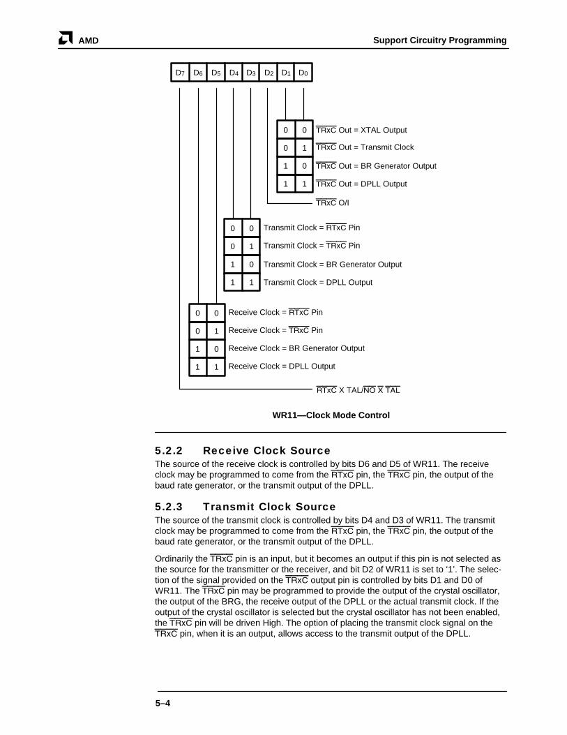
Support Circuitry ProgrammingAMD
5–4
D7 D6 D5 D4 D3 D2 D1 D0
0 0
0 1
1 0
1 1
0 0
0 1
1 0
1 1
0 0
0 1
1 0
1 1
TRxC Out = XTAL Output
TRxC Out = Transmit Clock
TRxC Out = BR Generator Output
TRxC Out = DPLL Output
TRxC O/I
Transmit Clock = RTxC Pin
Transmit Clock = TRxC Pin
Transmit Clock = BR Generator Output
Transmit Clock = DPLL Output
Receive Clock = RTxC Pin
Receive Clock = TRxC Pin
Receive Clock = BR Generator Output
Receive Clock = DPLL Output
RTxC X TAL/NO X TAL
WR11—Clock Mode Control
5.2.2 Receive Clock SourceThe source of the receive clock is controlled by bits D6 and D5 of WR11. The receiveclock may be programmed to come from the RTxC pin, the TRxC pin, the output of thebaud rate generator, or the transmit output of the DPLL.
5.2.3 Transmit Clock SourceThe source of the transmit clock is controlled by bits D4 and D3 of WR11. The transmitclock may be programmed to come from the RTxC pin, the TRxC pin, the output of thebaud rate generator, or the transmit output of the DPLL.
Ordinarily the TRxC pin is an input, but it becomes an output if this pin is not selected asthe source for the transmitter or the receiver, and bit D2 of WR11 is set to ‘1’. The selec-tion of the signal provided on the TRxC output pin is controlled by bits D1 and D0 ofWR11. The TRxC pin may be programmed to provide the output of the crystal oscillator,the output of the BRG, the receive output of the DPLL or the actual transmit clock. If theoutput of the crystal oscillator is selected but the crystal oscillator has not been enabled,the TRxC pin will be driven High. The option of placing the transmit clock signal on theTRxC pin, when it is an output, allows access to the transmit output of the DPLL.

Support Circuitry Programming AMD
5–5
Figure 5–1 shows a simplified schematic diagram of the circuitry used in the clock multi-plexing. It shows the inputs to the multiplexer section as well as the various signal inver-sions that occur in the paths to the outputs. Also shown are the edges used by the re-ceiver, transmitter, BRG, and DPLL to sample or send data or otherwise change state.For example, the receiver samples data on the falling edge, but since there is an inver-sion in the clock path between the RTxC pin and the receiver, a rising edge of the RTxCpin samples the data for the receiver.
5.2.4 Clock ProgrammingSelection of the clock options may be done anywhere in the initialization sequence, butthe final values must be selected before the receiver, transmitter, BRG, or DPLL are en-abled to prevent problems from arbitrarily narrow clock signals out of the multiplexers.The same is true of the crystal oscillator, in that the output should be allowed to stabilizebefore it is used as a clock source.
SYNC
OSC
OSC
RTxC
DPLL
TX
RX
Receiver
TransmitterTRxC
BRG
ECHO
ECHO
DPLL
Baud Rate
Baud RateGenerator Out
TX DPLL Out
RX DPLL Out
PCLK Generator
Figure 5–1. Clock Multiplexer
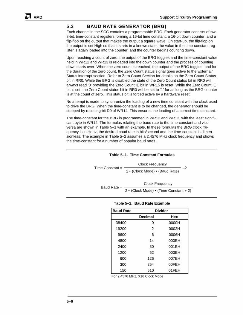
Support Circuitry ProgrammingAMD
5–6
5.3 BAUD RATE GENERATOR (BRG)Each channel in the SCC contains a programmable BRG. Each generator consists of two8-bit, time-constant registers forming a 16-bit time constant, a 16-bit down counter, and aflip-flop on the output that makes the output a square wave. On start-up, the flip-flop onthe output is set High so that it starts in a known state, the value in the time-constant reg-ister is again loaded into the counter, and the counter begins counting down.
Upon reaching a count of zero, the output of the BRG toggles and the time-constant valueheld in WR12 and WR13 is reloaded into the down counter and the process of countingdown starts over. When the zero count is reached, the output of the BRG toggles, and forthe duration of the zero count, the Zero Count status signal goes active to the External/Status interrupt section. Refer to Zero Count Section for details on the Zero Count Statusbit in RR0. While the BRG is disabled the state of the Zero Count status bit in RR0 willalways read ‘0’ providing the Zero Count IE bit in WR15 is reset. While the Zero Count IEbit is set, the Zero Count status bit in RR0 will be set to ‘1’ for as long as the BRG counteris at the count of zero. This status bit is forced active by a hardware reset.
No attempt is made to synchronize the loading of a new time constant with the clock usedto drive the BRG. When the time-constant is to be changed, the generator should bestopped by resetting bit D0 of WR14. This ensures the loading of a correct time constant.
The time-constant for the BRG is programmed in WR12 and WR13, with the least signifi-cant byte in WR12. The formulas relating the baud rate to the time-constant and viceversa are shown in Table 5–1 with an example. In these formulas the BRG clock fre-quency is in Hertz, the desired baud rate in bits/second and the time-constant is dimen-sionless. The example in Table 5–2 assumes a 2.4576 MHz clock frequency and showsthe time-constant for a number of popular baud rates.
Table 5–1. Time Constant Formulas
Time Constant =Clock Frequency
–22 • (Clock Mode) • (Baud Rate)
Baud Rate =Clock Frequency
2 • (Clock Mode) • (Time Constant + 2)
Table 5–2. Baud Rate Example
Baud Rate Divider
Decimal Hex
38400 0 0000H
19200 2 0002H
9600 6 0006H
4800 14 000EH
2400 30 001EH
1200 62 003EH
600 126 007EH
300 254 00FEH
150 510 01FEH
For 2.4576 MHz, X16 Clock Mode

Support Circuitry Programming AMD
5–7
If neither the transmit clock nor the receive clock is programmed to come from the TRxCpin, the output of the BRG may be made available for external use on the TRxC pin.
Figure 5–2 shows a block diagram of the BRG. The BRG input comes from the output ofa two-input multiplexer, and the zero count condition is outputed to the External/StatusInterrupt section. The BRG may be disabled and enabled by command and is disabled bya hardware reset.
Zero Count
÷2Baud RateGeneratorClock
RTxC Pin
PCLK Pin
Select
Output
WR13 WR12
16 Bit Down Counter
Figure 5–2. Baud Rate Generator
Write toWR14
ClockSource
CounterClock
Counter First Decremented(After Hardware Reset)
Counter First Decremented(After Previous Disable)
End of Write to WR14 with Enable
Figure 5–3. BRG Startup
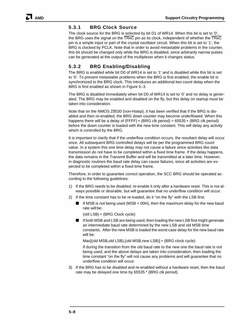
Support Circuitry ProgrammingAMD
5–8
5.3.1 BRG Clock SourceThe clock source for the BRG is selected by bit D1 of WR14. When this bit is set to ‘0’,the BRG uses the signal on the TRxC pin as its clock, independent of whether the TRxCpin is a simple input or part of the crystal oscillator circuit. When this bit is set to ‘1’, theBRG is clocked by PCLK. Note that in order to avoid metastable problems in the counter,this bit should be changed only while the BRG is disabled, since arbitrarily narrow pulsescan be generated at the output of the multiplexer when it changes status.
5.3.2 BRG Enabling/DisablingThe BRG is enabled while bit D0 of WR14 is set to ‘1’ and is disabled while this bit is setto ‘0’. To prevent metastable problems when the BRG is first enabled, the enable bit issynchronized to the BRG clock. This introduces an additional two count delay when theBRG is first enabled as shown in Figure 5–3.
The BRG is disabled immediately when bit D0 of WR14 is set to ‘0’ and no delay is gener-ated. The BRG may be enabled and disabled on the fly, but this delay on startup must betaken into consideration.
Note that on the NMOS Z8530 (non-Hstep), it has been verified that if the BRG is dis-abled and then re-enabled, the BRG down counter may become underflowed. When thishappens there will be a delay of (FFFF) • (BRG clk period) = 65535 • (BRG clk period)before the down counter is loaded with the new time constant. This will delay any activitywhich is controlled by the BRG.
It is important to clarify that if the underflow condition occurs, the resultant delay will occuronce. All subsequent BRG controlled delays will be per the programmed BRG countvalue. In a system this one time delay may not cause a failure since activities like datatransmission do not have to be completed within a fixed time frame. If the delay happens,the data remains in the Transmit Buffer and will be transmitted at a later time. However,in diagnostic routines the baud rate delay can cause failures, since all activities are ex-pected to be completed within a fixed time frame.
Therefore, in order to guarantee correct operation, the SCC BRG should be operated ac-cording to the following guidelines:
1) If the BRG needs to be disabled, re-enable it only after a hardware reset. This is not al-ways possible or desirable, but will guarantee that no underflow condition will occur.
2) If the time constant has to be re-loaded, do it “on the fly” with the LSB first.
If MSB is not being used (MSB = 00H), then the maximum delay for the new baud rate will be:
(old LSB) • (BRG Clock cycle)
If both MSB and LSB are being used, then loading the new LSB first might generate an intermediate baud rate determined by the new LSB and old MSB time constants. After the new MSB is loaded the worst case delay for the new baud rate will be:
Max[(old MSB,old LSB),(old MSB,new LSB)] • (BRG clock cycle)
If during the transition from the old baud rate to the new one the baud rate is not being used, and the above delays are taken into consideration, then loading the time constant “on the fly” will not cause any problems and will guarantee that no underflow condition will occur.
3) If the BRG has to be disabled and re-enabled without a hardware reset, then the baudrate may be delayed one time by 65535 * (BRG clk period).

Support Circuitry Programming AMD
5–9
5.3.3 BRG InitializationInitializing the BRG is done in four steps. First, the time-constant is determined andloaded into WR12 and WR13. Next, the processor must select the clock source for theBRG by writing to bit D1 of WR14. Finally, the BRG is enabled by setting bit D0 of WR14to ‘1’. Note that the first write to WR14 is not necessary after a hardware reset if the clocksource is to be the RTxC pin. This is because a hardware reset automatically selects theRTxC pin as the BRG clock source.
5.4 DATA ENCODING/DECODINGThe SCC provides four data encoding methods, selected by bits D6 and D5 in WR10. Anexample of these four methods is shown in Figure 5–4. Encoding may be used for asyn-chronous or synchronous data as long as the clock mode is x1. Note that the data encod-ing method selected is active even though the transmitter or receiver may be idling or dis-abled.
1 1 0 0 1 0Data
NRZ
NRZI
FM1(BiPhase Mark)
FM0(BiPhase Space)
Bit Cell Level:
High = 1Low = 0
No Change = 1Change = 0
Bit Center Transition:Transition = 1No Transition = 0
Manchester
No Transition = 1Transition = 0
High→Low = 1Low→High = 0
Figure 5–4. Data Encoding
5.4.1 NRZ (Non-Return to Zero)In NRZ encoding a ‘1’ is represented by a High level and a ‘0’ is represented by a Lowlevel. In this encoding method only a minimal amount of clocking information is availablein the data stream in the form of transitions on bit-cell boundaries. In an arbitrary datapattern this may not be sufficient to generate a clock for the data from the data itself.
5.4.2 NRZI (Non-Return to Zero Inverted)In NRZI encoding a ‘1’ is represented by no change in the level and a ‘0’ is representedby a change in the level. As in NRZ only a minimal amount of clocking information isavailable in the data stream, in the form of transitions on bit cell boundaries. In an arbi-trary data pattern this may not be sufficient to generate a clock for the data from the dataitself. In the case of SDLC Mode operation, where the number of consecutive ‘1’s in thedata stream is limited, a minimum number of transitions to generate a clock are guar-anteed.

Support Circuitry ProgrammingAMD
5–10
5.4.3 FM1 (Biphase Mark)In FM1 encoding, also known as biphase mark, a transition is present on every bit cellboundary, and an additional transition may be present in the middle of the bit cell. In FM1,a ‘0’ is sent as no transition in the center of the bit cell and a ‘1’ is sent as a transition inthe center of the bit cell. FM1 encoded data contains sufficient information to recover aclock from the data.
5.4.4 FM0 (Biphase Space)In FM0 encoding, also known as biphase space, a transition is present on every bit cellboundary and an additional transition may be present in the middle of the bit cell. In FM0a ‘1’ is sent as no transition in the center of the bit cell and a ‘0’ is sent as a transition inthe center of the bit cell. FM0 encoded data contains sufficient information to recover aclock from the data.
5.4.5 Manchester DecodingIn addition to these four methods, the SCC can be used to decode Manchester (biphaselevel) data using the DPLL in the FM mode and programming the receiver for NRZ data.Manchester encoding always produces a transition at the center of the bit cell. If the tran-sition is High-to-Low, the bit is a ‘1’; if the transition is Low-to-High, the bit is a ‘0’.
5.4.6 Data Encoding ProgrammingThe data encoding method to be used should be selected in the initialization procedurebefore the transmitter and receiver are enabled but no other restrictions apply. Note, inFigure 5–4, that in NRZ and NRZI the receiver samples the data only on one edge. How-ever, in FM1 and FM0, the receiver samples the data on both edges. Also, as shown inFigure 5–4, the transmitter defines bit cell boundaries by one edge in all cases and usesthe other edge in FM1 and FM0 to create the mid-bit transition.
5.5 DIGITAL PHASE-LOCKED LOOP (DPLL)The SCC contains a DPLL that can be used to recover clock information from a datastream with NRZI or FM coding. The DPLL is driven by a clock that is nominally 32(NRZI) or 16 (FM) times the data rate. The DPLL uses this clock, along with the datastream, to construct a receive clock for the data. This clock can then be used as the re-ceive clock, the transmit clock, or both.
Figure 5–5 shows a block diagram of the DPLL. It consists of a 5-bit counter, an edgedetector, and a pair of output decoders. The clock for the DPLL comes from the output ofa two-input multiplexer, and the two outputs go to the transmitter and receive clock multi-plexers. The DPLL is controlled by seven commands that are encoded in bits D7, D6, andD5 of WR14.
Edge DetectorRxD ReceiveClock
DecodeCount Modifier
5-Bit CounterTransmitClock
Decode
Figure 5–5. DPLL
Support Circuitry Programming AMD
5–11
5.5.1 DPLL Clock SourceThe clock for the DPLL is selected by two of the commands in WR14. One command se-lects the output of the BRG as the clock source, and the other command selects theRTxC pin as the clock source, independent of whether the RTxC pin is a simple input orpart of the crystal oscillator circuit. Note that in order to avoid metastable problems in thecounter, the clock source selection should be made only while the DPLL is disabled, sincearbitrarily narrow pulses can be generated at the output of the multiplexer when itchanges status.
5.5.2 DPLL EnablingThe DPLL is enabled by issuing the Enter Search Mode command in WR14. This com-mand is also used to reset the DPLL to a known state if it is suspected that synchroniza-tion has been lost. When used to enable the DPLL, the Enter Search Mode commandunlocks the counter, which is held while the DPLL is disabled, and enables the edge de-tector. If the DPLL is already enabled when this command is issued, the DPLL also entersSearch mode.
While in Search mode, the counter is held at a specific count and no outputs are pro-vided. The DPLL remains in this status until an edge is detected in the receive datastream. This first edge is assumed to occur on a bit cell boundary, and the DPLL will be-gin providing an output to the receiver that will properly sample the data. As long as noother edges are detected, the DPLL output clock will free run at a frequency equal to theDPLL clock source divided by 32 without any phase jitter. Upon detecting another edgethe DPLL will adjust the output clock to remain in phase with the received data by addingor subtracting a count of one. This will result in a phase jitter of ±5.63° on the DPLL out-put. Because the DPLL uses both edges of the incoming data to compare with its clocksource, a mark-space deviation of no greater than ±1.5% (from 50%) should be main-tained at the interface. If the first edge that the DPLL sees does not occur on a bit cellboundary, the DPLL will eventually lock on to the receive data but it will take longer to doso.
5.5.3 DPLL ModesThe DPLL may be programmed to operate in either NRZI or FM modes, as selected by acommand in WR14. Note that as in the case of the DPLL clock source selection, themode of operation should only be changed while the DPLL is disabled to prevent unpre-dictable results.
5.5.3.1 NRZI ModeIn NRZI mode, the clock supplied to the DPLL must be 32 times the data rate. In thismode the transmit and receive clock outputs of the DPLL are identical, and the clocks arephased so that the receiver samples the data in the middle of the bit cell. In NRZI mode,the DPLL does not require a transition in every bit cell, so this is useful for recovering theclocking information from NRZ and NRZI data streams.
The DPLL uses the x32 clock along with the receive data, to construct receive and trans-mit clock outputs that are phased to properly receive and transmit data.
To do this, the DPLL divides each bit cell into two regions, and makes an adjustment tothe count cycle of the 5-bit counter dependent upon in which region a transition on thereceive data input occurred. This is shown in Figure 5–6. Ordinarily, a bit cell boundarywill occur between count 15 and count 16, and the DPLL output will cause the data to besampled in the middle of the bit cell. The DPLL actually allows the transition marking a bitcell boundary to occur anywhere during the second half of count 15 or the first half ofcount 16 without making a correction to its count cycle.

Support Circuitry ProgrammingAMD
5–12
Bit Cell
17Count 16 1918 2120 2322 2524 2726 28 3029 31 10 32 54 76 98 1110 12 1413 15
Correction Add One Count Subtract One Count
No Change No Change
DPLL Out
Figure 5–6. DPLL in NRZI Mode
However, if the transition marking a bit cell boundary occurs between the middle of count16 and count 31 the DPLL is sampling the data too early in the bit cell. In response to thisthe DPLL extends its count by one during the next 0 to 31 counting cycle, which effec-tively moves the edge of the clock that samples the receive data closer to the center ofthe bit cell. In a similar manner, if the transition occurs between count 0 and the middle ofcount 15, the output of the DPLL is sampling the data to late in the bit cell. To correct this,the DPLL shortens its count by one during the next 0 to 31 counting cycle, which effec-tively moves the edge of the clock that samples the receive data closer to the center ofthe bit cell.
In NRZI mode, if the DPLL does not see any transition during a counting cycle, no adjust-ment is made in the following counting cycle. If an adjustment to the counting cycle isnecessary the DPLL modifies count five, either deleting it or doubling it. Thus only theLow time of the DPLL output will be lengthened or shortened. While the DPLL is in searchmode, the counter remains at count 16, where the DPLL outputs are both High. An exam-ple of the DPLL in operation is shown in Figure 5–7.
5.5.3.2 FM ModeIn FM mode, the clock supplied to the DPLL must be 16 times the data rate. In this modethe transmit clock output of the DPLL lags the receive clock output by 90 degrees. This isnecessary to make the transmit and receive bit cell boundaries coincide, since the receiveclock must sample the data one-fourth and three-fourths of the way through the bit cell. InFM mode the DPLL requires a transition in every bit cell, and if this transition is not pre-sent in two consecutive sampled bit cells, the DPLL automatically enters search mode.
The DPLL uses the clock supplied, along with the receive data, to construct receive andtransmit clock outputs that are phased to receive and transmit data properly. In FM modethe counter in the DPLL still counts from 0 to 31 but now each cycle corresponds to 2 bitcells. In order to make adjustments and remain in phase with the receive data, the DPLLdivides a pair of bit cells into five regions, making the adjustment to the counter depend-ent upon which region the transition on the receive data input occurred. This is shown inFigure 5–8.
Ordinarily, a bit cell boundary will occur between count 15 or count 16, and the DPLL re-ceive output will cause the data to be sampled at one-fourth and three-fourths of the waythrough the bit cell. The DPLL actually allows the transition marking a bit cell boundary tooccur anywhere during the second half of count 15 or the first half of count 16 withoutmaking a correction to its count cycle.

Support Circuitry Programming AMD
5–13
However, if the transition marking a bit cell boundary occurs between the middle of count16 and the middle of count 19 the DPLL is sampling the data too early in the bit cell. Inresponse to this the DPLL extends its count by one during the next 0 to 31 counting cycle,which effectively moves the receive clock edges closer to to where they should be. In FMmode any transitions occurring between the middle of count 19 in one cycle and the mid-dle of count 12 during the next cycle are ignored by the DPLL. This is necessary to guar-antee that any data transitions in the bit cells will not cause an adjustment to the countingcycle.
As in NRZI mode, if an adjustment to the counting cycle is necessary, the DPLL modifiescount 5, either deleting it or doubling it. If no adjustment is necessary, the count sequenceproceeds normally. While the DPLL is in Search mode, the counter remains at count 16,where the receive output is Low and the transmit output is Low. This fact can be used toprovide a transmit clock under software control since the DPLL is in Search mode while itis disabled. Note that while the DPLL is disabled the transmit clock output of the DPLLmay be toggled by alternately selecting FM and NRZI mode in the DPLL. The same istrue of the receive clock.
+1 –1 +1 –1 +1 –1 +1 –1 +1 –1 +1 –1 +1 –1 +1 –1 +1
3232 32 31 31 31 33 33 33
ReceiveData
DPLLOutput
CorrectionWindows
CountLength
Figure 5–7. DPLL in FM Mode
5.5.3.3 Manchester Decoding ModeIn addition to FM and NRZI encoded data, the DPLL may also be used to recover theclock from Manchester encoded data, which contains a transition at the center of every bitcell. Here it is the direction of the transition that distinguishes a ‘1’ from a ‘0’. Anotherway of looking at Manchester encoding is to realize that, during the first half of the bit cellthe data are sent; during the second half of the bit cell the complement of the data aresent. This is shown in Figure 5–9, along with the DPLL output if it thinks that the mid-bittransitions are really bit cell boundaries. As is obvious from the figure, if the receiver sam-ples the data on the falling edge of the DPLL receive clock output, the Manchester datawill be properly decoded. This occurs if the receiver is programmed to accept NRZ data.
5.5.3.4 FM Mode DPLL Receive StatusFrom the above discussion together with an examination of FM0 and FM1 data encoding,it should be obvious that only clock transitions should exist on the receive data pin whenthe DPLL is programmed to enter Search mode. If this is not the case the DPLL may at-tempt to lock on to the data transitions. With FM0 encoding this requires continuous ‘1’sreceived when leaving Search mode. In FM1 encoding it is continuous ‘0’s; withManchester encoded data this means alternating ‘1’s and ‘0’s.

Support Circuitry ProgrammingAMD
5–14
With all three of these data encoding methods there will be at least one transition in everybit cell, and in FM mode the DPLL is designed to expect this transition. In particular, if notransition occurs between the middle of count 12 and the middle of count 19, the DPLL isprobably not locked onto the data properly. When the DPLL misses an edge the OneClock Missing bit in RR10 is set to ‘1’ and latched. It will hold this value until a ResetMissing Clock command is issued in WR14 or until the DPLL is disabled or programmedto enter the Search mode.
Upon missing this one edge the DPLL takes no other action and does not modify its countduring the next counting cycle. However, if the DPLL does not see an edge between themiddle of count 12 and the middle of count 19 in two successive 0 to 31 count cycles, aline Figure 5–7. DPLL Operating Example error condition is assumed. If this occurs, thetwo Clocks Missing bits in RR10 are set to ‘1’ and latched. At the same time the DPLLenters the Search mode. The DPLL makes the decision to enter Search mode duringcount 2, where both the receive and transmit clock outputs are Low. This prevents anyglitches on the clock outputs when Search mode is entered. While in Search mode noclock outputs are provided by the DPLL. The two Clocks Missing bit in RR10 is latcheduntil a Reset Missing Clock command is issued in WR14, or until the DPLL is disabled orprogrammed to enter the Search mode.
In NRZI Mode of operation and while the DPLL is disabled, the One and Two Clock Miss-ing bits in RR10 will be reset to ‘0’.
Bit Cell
17Count 16 1918 2120 2322 2524 2726 28 3029 31 10 32 54 76 98 1110 12 1413 15
Correction Ignored
No Change No Change
RX DPLL Out
+1 –1
TX DPLL Out
Figure 5–8. DPLL in FM Mode
1 1 0 0 1 0Data
Manchester
RX DPLL Out
TX DPLL Out
Figure 5–9. Manchester Clock Recovery

Support Circuitry Programming AMD
5–15
5.5.4 DPLL InitializationInitialization of the DPLL may be done at any time during the initialization sequence, butshould probably be done after the clock modes have been selected in WR11, and beforethe receiver and transmitter are enabled.
When initializing the DPLL the clock source should be selected first, followed by the se-lection of the operating mode. At this point the DPLL, may be enabled by issuing the En-ter Search Mode command in WR14. Note that a channel or hardware reset disables theDPLL, selects the RTxC pin as the clock source for the DPLL, and places it in the NRZImode.
Note that the DPLL is not free running if it is in search mode. Unless the DPLL receives acontinuous stream of data, it will lose synchronization and enter search mode. It is there-fore recommended that the clock input of the transmitter is fed from a continuous clocksource other than the DPLL unless it can be guaranteed the DPLL always receivesenough data to stay synchronized.
5.5.5 Am85C30-16 DPLL OPERATION AT 32 MHz5.5.5.1 IntroductionThe Digital Phase-Locked Loop (DPLL) for the Am85C30-16 can operate at twice thedata sheet frequency (32 MHz). The DPLL is used to recover clock information from a FMdata stream. This enhancement is available for commercial product only.
All Am85C30-16 devices are tested to guarantee 32 MHz DPLL capability.
5.5.5.2 BenefitThe customer can transmit and receive serial data at 2 mb/s in FM mode. This is twicethe data rate specified in the data sheet. This is over three times what the competitioncan do. As specified in the competition’s data sheet, 10 MHz part can only handle a10 MHz clock for the DPLL. The Am85C30-16 DPLL can run at 32 MHz for both synchro-nous (SDLC) and asynchronous modes with FM encoding. This eliminates the need foran external DPLL and allows the user to utilize FM encoding at higher data rates.
5.5.5.3 ApplicationsThe increased data rate of 2 mb/s is ideal for both factory and office automation applica-tions including Local Area Networks as well as other RS485 and RS422 applications.
5.5.5.4 DescriptionAn external 32 MHz, 50% duty cycle, TTL compatible signal to the RTxC pin provides theclock for the DPLL. The PCLK remains at 16 MHz. The rest of the setup is described indetail in the previous section of this technical manual.
5.5.5.5 CompetitionThe competition’s data sheet for their 85C30 limits the clock for the DPLL to less than10 MHz. This translates to only 0.625 mb/s for FM transmission and reception. TheAm85C30-16 transmits and receives FM data at 2.0 mb/s—over three times faster thanthe competition’s part.
5.6 DIAGNOSTIC MODESThe SCC contains two other features useful for diagnostic purposes controlled by bits inWR14. These are Local Loopback and Auto Echo.
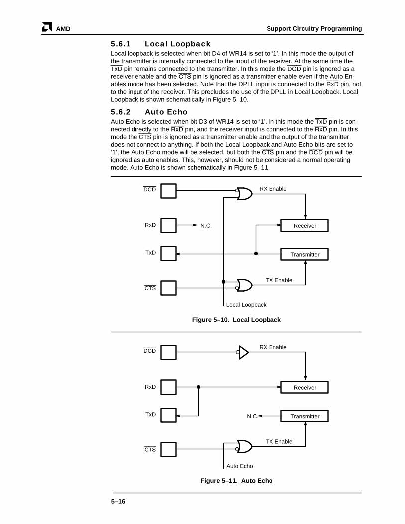
Support Circuitry ProgrammingAMD
5–16
5.6.1 Local LoopbackLocal loopback is selected when bit D4 of WR14 is set to ‘1’. In this mode the output ofthe transmitter is internally connected to the input of the receiver. At the same time theTxD pin remains connected to the transmitter. In this mode the DCD pin is ignored as areceiver enable and the CTS pin is ignored as a transmitter enable even if the Auto En-ables mode has been selected. Note that the DPLL input is connected to the RxD pin, notto the input of the receiver. This precludes the use of the DPLL in Local Loopback. LocalLoopback is shown schematically in Figure 5–10.
5.6.2 Auto EchoAuto Echo is selected when bit D3 of WR14 is set to ‘1’. In this mode the TxD pin is con-nected directly to the RxD pin, and the receiver input is connected to the RxD pin. In thismode the CTS pin is ignored as a transmitter enable and the output of the transmitterdoes not connect to anything. If both the Local Loopback and Auto Echo bits are set to‘1’, the Auto Echo mode will be selected, but both the CTS pin and the DCD pin will beignored as auto enables. This, however, should not be considered a normal operatingmode. Auto Echo is shown schematically in Figure 5–11.
Receiver
Transmitter
TX Enable
RX EnableDCD
CTS
RxD
TxD
N.C.
Local Loopback
Figure 5–10. Local Loopback
Receiver
Transmitter
TX Enable
RX EnableDCD
CTS
RxD
TxD
Auto Echo
N.C.
Figure 5–11. Auto Echo

6–1
CHAPTER 6Register Description
6.1 Introduction 6–3. . . . . . . . . . . . . . . . . . . . . . . . . . . . . . . . . . . . . . . . . . . . . . . . . . . 6.2 Write Registers 6–5. . . . . . . . . . . . . . . . . . . . . . . . . . . . . . . . . . . . . . . . . . . . . . . .
6.2.1 Write Register 0 (Command Register) 6–5. . . . . . . . . . . . . . . . . . . . . . . . 6.2.2 Write Register 1 (Transmit/Receive Interrupt
and Data Transfer Mode Definition) 6–7. . . . . . . . . . . . . . . . . . . . . . . . . . 6.2.3 Write Register 2 (Interrupt Vector) 6–9. . . . . . . . . . . . . . . . . . . . . . . . . . . . 6.2.4 Write Register 3 (Receive Parameters
and Control) 6–10. . . . . . . . . . . . . . . . . . . . . . . . . . . . . . . . . . . . . . . . . . . . . 6.2.5 Write Register 4 (Transmit/Receiver
Miscellaneous Parameters and Modes) 6–11. . . . . . . . . . . . . . . . . . . . . . . 6.2.6 Write Register 5 (Transmit Parameter
and Controls) 6–13. . . . . . . . . . . . . . . . . . . . . . . . . . . . . . . . . . . . . . . . . . . . 6.2.7 Write Register 6 (SYNC Characters or
SDLC Address Field) 6–15. . . . . . . . . . . . . . . . . . . . . . . . . . . . . . . . . . . . . . 6.2.8 Write Register 7 (SYNC Character or SDLC
FLAG/SDLC Option Register) 6–17. . . . . . . . . . . . . . . . . . . . . . . . . . . . . . . 6.2.9 Write Register 8 (Transmit Buffer) 6–18. . . . . . . . . . . . . . . . . . . . . . . . . . . . 6.2.10 Write Register 9 (Master Interrupt Control) 6–18. . . . . . . . . . . . . . . . . . . . . 6.2.11 Write Register 10 (Miscellaneous Transmitter/
Receiver Control Bits) 6–20. . . . . . . . . . . . . . . . . . . . . . . . . . . . . . . . . . . . . 6.2.12 Write Register 11 (Clock Mode Control) 6–23. . . . . . . . . . . . . . . . . . . . . . . 6.2.13 Write Register 12 (Lower Byte of Baud
Rate Generator Time Constant) 6–26. . . . . . . . . . . . . . . . . . . . . . . . . . . . . 6.2.14 Write Register 13 (Upper Byte of Baud
Rate Generator Time Constant) 6–26. . . . . . . . . . . . . . . . . . . . . . . . . . . . . 6.2.15 Write Register 14 (Miscellaneous Control Bits) 6–27. . . . . . . . . . . . . . . . . . 6.2.16 Write Register 15 (External/Status
Interrupt Control) 6–29. . . . . . . . . . . . . . . . . . . . . . . . . . . . . . . . . . . . . . . . . 6.3 Read Registers 6–30. . . . . . . . . . . . . . . . . . . . . . . . . . . . . . . . . . . . . . . . . . . . . . . .
6.3.1 Read Register 0 (Transmit/Receive Buffer Status and External Status) 6–30. . . . . . . . . . . . . . . . . . . . . . . . . . . . . . . . .
6.3.2 Read Register 1 6–33. . . . . . . . . . . . . . . . . . . . . . . . . . . . . . . . . . . . . . . . . . 6.3.3 Read Register 2 6–35. . . . . . . . . . . . . . . . . . . . . . . . . . . . . . . . . . . . . . . . . . 6.3.4 Read Register 3 6–35. . . . . . . . . . . . . . . . . . . . . . . . . . . . . . . . . . . . . . . . . . 6.3.5 Read Register 6 6–36. . . . . . . . . . . . . . . . . . . . . . . . . . . . . . . . . . . . . . . . . . 6.3.6 Read Register 7 6–36. . . . . . . . . . . . . . . . . . . . . . . . . . . . . . . . . . . . . . . . . . 6.3.7 Read Register 8 6–37. . . . . . . . . . . . . . . . . . . . . . . . . . . . . . . . . . . . . . . . . . 6.3.8 Read Register 10 6–37. . . . . . . . . . . . . . . . . . . . . . . . . . . . . . . . . . . . . . . . . 6.3.9 Read Register 12 6–38. . . . . . . . . . . . . . . . . . . . . . . . . . . . . . . . . . . . . . . . . 6.3.10 Read Register 13 6–38. . . . . . . . . . . . . . . . . . . . . . . . . . . . . . . . . . . . . . . . . 6.3.11 Read Register 15 6–39. . . . . . . . . . . . . . . . . . . . . . . . . . . . . . . . . . . . . . . . .

Register DescriptionAMD
6–2

6–3
Register Description
CHAPTER 6
6.1 INTRODUCTIONThe following sections describe the SCC registers. Each register is detailed in terms ofbit configuration, the active states (See Table 6–1) of each bit, their definitions, their func-tions, and their effects upon the internal hardware and external pins.

Register DescriptionAMD
6–4
Table 6–1. SCC Register Description
Read Register Functions
RR0 Transmit/Receive buffer status, and External status
RR1 Special Receive Condition status, residue codes, error conditions
RR2 Modified (Channel B only) interrupt vector and Unmodified interrupt vector (Channel A only)
RR3 Interrupt Pending bits (Channel A only)
*RR6 14-bit frame byte count (LSB)
*RR7 14-bit frame byte count (MSB), frame status
RR8 Receive buffer
RR10 Miscellaneous XMTR, RCVR status parameters
RR12 Lower byte of baud rate generator time constant
RR13 Upper byte of baud rate generator time constant
RR15 External/Status interrupt control information
* Available only when Am85C30 is programmed in enhanced mode.
Write Register Functions
WR0 Command Register, (Register Pointers), CRC initialization, resets for various modes
WR1 Interrupt conditions, Wait/DMA request control
WR2 Interrupt vector (access through either channel)
WR3 Receive/Control parameters, number of bits per character, Rx CRC enable
WR4 Transmit/Receive miscellaneous parameters and codes, clock rate, number of sync characters, stop bits, parity
WR5 Transmit parameters and control, number of Tx bits per character, Tx CRC enable
WR6 Sync character (1st byte) or SDLC address
WR7 SYNC character (2nd byte) or SDLC flag
**WR7′ SDLC options; auto flag, RTS, EOM reset, extended read, etc.
WR8 Transmit buffer
WR9 Master interrupt control and reset (accessed through either channel), reset bits, control interrupt daisy chain
WR10 Miscellaneous transmitter/receiver control bits, NRZI, NRZ, FM encoding, CRC reset
WR11 Clock mode control, source of Rx and Tx clocks
WR12 Lower byte of baud rate generator time constant
WR13 Upper byte of baud rate generator time constant
WR14 Miscellaneous control bits: baud rate generator, Phase-Locked Loop control, auto echo, local loopback
WR15 External/Status interrupt control information-control external conditions causing interrupts
** Only available in Am85C30.
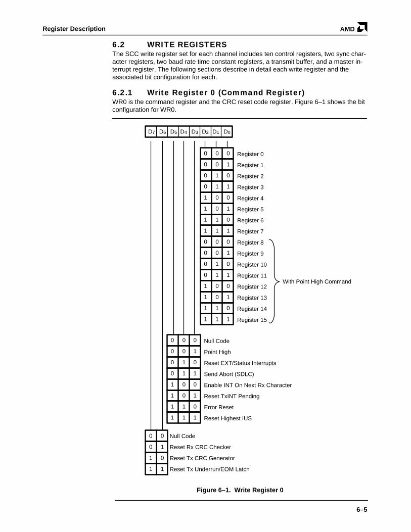
Register Description AMD
6–5
6.2 WRITE REGISTERSThe SCC write register set for each channel includes ten control registers, two sync char-acter registers, two baud rate time constant registers, a transmit buffer, and a master in-terrupt register. The following sections describe in detail each write register and theassociated bit configuration for each.
6.2.1 Write Register 0 (Command Register)WR0 is the command register and the CRC reset code register. Figure 6–1 shows the bitconfiguration for WR0.
D7 D6 D5 D4 D3 D2 D1 D0
0 0
0 0
0 1
0 1
0 0
0 1
1 0
1 1
Null Code
Reset Rx CRC Checker
Reset Tx CRC Generator
Reset Tx Underrun/EOM Latch
0
1
0
1
Register 0
Register 1
Register 2
Register 3
1 0
1 0
1 1
1 1
0
1
0
1
Register 4
Register 5
Register 6
Register 7
0 0
0 0
0 1
0 1
0
1
0
1
Register 8
Register 9
Register 10
Register 11
1 0
1 0
1 1
1 1
0
1
0
1
Register 12
Register 13
Register 14
Register 15
0 0
0 0
0 1
0
1
0
0 1
1 0
1 0
1 1
1
0
1
0
1 1 1
Null Code
Point High
Reset EXT/Status Interrupts
Send Abort (SDLC)
Enable INT On Next Rx Character
Reset TxINT Pending
Error Reset
Reset Highest IUS
With Point High Command
Figure 6–1. Write Register 0
Register DescriptionAMD
6–6
Bits D7 and D6: CRC Reset Codes 0 and 1
Null code (00) . This command has no effect on the SCC and is used when a write toWR0 is necessary for some reason other than a CRC Reset command.
Reset Receive CRC Checker (01) . This command is used to initialize the receive CRCcircuitry. It is necessary in synchronous modes (except SDLC) if the Enter Hunt Modecommand in Write Register 3 is not issued between received messages. Any action thatdisables the receiver initializes the CRC circuitry. Also, whenever the receiver is in Huntmode, or whenever a flag is received, the CRC checker will be automatically reset inSDLC mode.
Reset Transmit CRC Generator (10) . This command initializes the CRC generator. It isusually issued in the initialization routine and after the CRC has been transmitted. AChannel Reset will not initialize the generator and this command should not be issueduntil after the transmitter has been enabled in the initialization routine.
Reset Transmit Underrun/EOM Latch (11) . This command controls the transmission ofCRC at the end of transmission (EOM). If this latch has been reset, and a transmit under-run occurs, the SCC automatically appends CRC to the message. In SDLC mode withAbort on Underrun selected, the SCC sends an abort, and Flag on underrun if the TX Un-derrun/EOM latch has been reset.
At the start of the CRC transmission the Tx Underrun/EOM latch is set. The Reset com-mand can be issued at any time during a message. If the transmitter is disabled this com-mand will not reset the latch. However, if no External Status interrupt is pending, or if aReset External Status Interrupt command accompanies this command while the transmit-ter is disabled, an External/Status interrupt is generated with the Tx Underrun/EOM bitreset in RRO.
Bits D5–D3: Command Codes
Null Code (000) . The Null command has no effect on the SCC.
Point High (001) . This command effectively adds eight to the Register Pointer (D2–D0)by allowing WR8 through WR15 to be accessed. The Point High command and the Reg-ister Pointer bits are written simultaneously.
Reset External/Status Interrupts (010) . After an External/Status interrupt (a change ona modem line or a break condition, for example), the status bits in RR0 are latched. Thiscommand enables the bits and allows interrupts to occur again as a result of a statuschange. Latching the status bits captures short pulses until the CPU has time to read thechange. The SCC contains simple queuing logic associated with most of the externalstatus bits in RR0. If another External/Status condition changes while a previous condi-tion is still pending (Reset External/Status Interrupts has not yet been issued) and thiscondition persists until after the command is issued, this second change causes anotherExternal/Status interrupt. However, if this second status change does not persist (thereare two transitions), another interrupt is not generated. Exceptions to this rule are detailedin the RR0 description.
Send Abort (011) . This command is used in SDLC mode to transmit a sequence of eightto thirteen ‘1s.’ This command always empties the transmit buffer and sets Tx Underrun/EOM bit in Read Register 0.
Enable Interrupt on Next RX Character (100) . If the interrupt on the First ReceivedCharacter mode is selected, this command is used to reactivate that mode after eachmessage is received. The next character to enter the receive FIFO causes a Receiveinterrupt. Alternatively, the first previously stored character in the FIFO will cause a Re-ceive interrupt.
Reset Tx Interrupt Pending (101) . This command is used in cases where there are nomore characters to be sent; e.g., at the end of a message. This command prevents fur-ther transmit interrupts until after the next character has been loaded into the transmit

Register Description AMD
6–7
buffer or until CRC has been completely sent. This command is necessary to prevent thetransmitter from requesting an interrupt when the transmit buffer becomes empty again,(with Transmit Interrupt Enabled) on the last data character transmitted.
Error Reset (110) . This command resets the error bits in RR1. If Interrupt on First RxCharacter or Interrupt on Special Condition modes are selected and a special conditionexists, the data with the special condition is held in the receive FIFO until this command isissued. If either of these modes is selected and this command is issued before the datahave been read from the Receive FIFO, the data are lost.
Reset Highest IUS (111) . This command resets the highest priority Interrupt UnderService (IUS) bit, allowing lower priority conditions to request interrupts. This commandallows the use of the internal daisy chain (even in systems without an external daisychain) and should be the last operation in an interrupt service routine.
Bits 2 through 0: Resister Selection Code
These three bits select Registers 0 through 7. With the Point High command, Registers 8through 15 are selected.
6.2.2 Write Register 1 (Transmit/Receive Interrupt and Data Transfer Mode Definition)
Write Register 1 is the control register for the various SCC interrupt and Wait/Requestmodes. Figure 6–2 shows the bit assignments for WR1.
Bit 7: WAIT/DMA Request Enable
This bit enables the Wait/Request function in conjunction with the Request/Wait FunctionSelect bit (D6). If bit 7 is set to ‘1’, the state of bit 6 determines the activity of the WAIT/REQUEST pin (Wait or Request). If bit 7 is set to ‘0’, the selected function (bit 6) forcesthe WAIT/REQUEST pin to the appropriate inactive state (High for Request, floating forWait).
Bit 6: WAIT/DMA Request Function
The request function is selected by setting this bit to ‘1’. In the DMA Request mode, theWAIT/REQUEST pin switches from High to Low when the SCC is ready to transfer data.When this bit is ‘0’, the wait function is selected. In the Wait mode, the WAIT/REQUESTpin switches from floating to Low when the CPU attempts to transfer data before the SCCis ready.
Bit 5: WAIT/DMA Request On Receive Transmit
This bit determines whether the WAIT/REQUEST pin operates in the Transmit mode orthe Receive mode. When set to ‘1’, this bit allows the wait/request function to follow thestate of the receive buffer; i.e., depending on the state of bit 6, the WAIT/REQUEST pin isactive or inactive in relation to the empty or full state of the receive buffer. Conversely, ifthis bit is set to ‘0’, the state of the WAIT/REQUEST pin is determined by bit 6 and thestate of the transmit buffer. (Note that a transmit request function is available on the DTR/REQUEST pin. This allows full-duplex operation under DMA control for both channels.)
The request function may occur only when the SCC is not selected; e.g., if the internalrequest becomes active while the SCC is in the middle of a read or write cycle, the exter-nal request will not become active until the cycle is complete. An active request outputcauses a DMA controller to initiate a read or write operation. If the request on Transmitmode is selected in either SDLC or Synchronous mode, the Request pin is pulsed Low forone PCLK cycle at the end of CRC transmission of another block of data.
In the Wait On Receive mode, the WAIT pin is active if the CPU attempts to read SCCdata that have not yet been received. In the Wait On Transmit mode, the WAIT pin is ac-tive if the CPU attempts to write data when the transmit buffer is still full. Both situationscan occur frequently when block transfer instructions are used.

Register DescriptionAMD
6–8
Bits 4 and 3: Receive Interrupt Modes
These two bits specify the various character-available conditions that may cause interruptrequests.
Receive Interrupts Disabled (00) . This mode prevents the receiver from requesting aninterrupt and is normally used in a polled environment where either the status bits in RR0or the modified vector in RR2 (Channel B) can be monitored to initiate a service routine.Although the receiver interrupts are disabled, a special condition can still provide a uniquevector status in RR2.
D7 D6 D5 D4 D3 D2 D1 D0
0 0
0 1
1 0
1 1
Rx INT Disable
Rx INT on First Character or Special Condition
INT on All Rx Characters or Special Condition
Rx INT on Special Condition Only
EXT INT Enable
Tx INT Enable
Parity is Special Condition
WAIT/DMA Request on RECEIVE/TRANSMIT
WAIT/DMA Request Function
WAIT/DMA Request Enable
Figure 6–2. Write Register 1
Receive Interrupt on First Character or Special Condition (01) . The receiver requestsan interrupt in this mode on the first available character (or stored FIFO character) or on aspecial condition. Sync characters to be stripped from the message stream do not causeinterrupts.
Special receive conditions are: receiver overrun, framing error, end of frame, or parityerror (if selected). If a special receive condition occurs, the data containing the error arestored in the receive FIFO until an Error Reset command is issued by the CPU.
This mode is usually selected when a Block Transfer mode is used. In this interruptmode, a pending special receive condition remains set until either an Error Reset com-mand, a channel or hardware reset, or until receive interrupts are disabled.
The Receive Interrupt on First Character or Special Condition mode can be re-enabled bythe Enable Rx Interrupt on Next Character command in WR0.
Interrupt on All Receive Characters or Special Condition (10) . This mode allows aninterrupt for every character received (or character in the receive FIFO) and provides aunique vector when a special condition exists. The Receiver Overrun bit and the ParityError bit in RR1 are two special conditions that are latched. These two bits must be resetby the Error Reset command. Receiver overrun is always a special receive condition, andparity can be programmed to be a special condition.
Data characters with special receive conditions are not held in the receive FIFO in theInterrupt On All Receive Characters or Special Conditions mode as they are in other re-ceive interrupt modes.

Register Description AMD
6–9
Receive Interrupt on Special Condition (11) . This mode allows the receiver to interruptonly on characters with a special receive condition. When an interrupt occurs, the datacontaining the error are held in the receive FIFO until an Error Reset command is issued.When using this mode in conjunction with a DMA, the DMA can be initialized and enabledbefore any characters have been received by the SCC. This eliminates the time-criticalsection of code required in the Receive Interrupt on First Character or Special Conditionmode; i.e., all data can be transferred via the DMA so that the CPU need not handle thefirst received character as a special case.
Bit 2: Parity Is Special Condition
If this bit is set to ‘1’, any received characters with parity not matching the sense pro-grammed in WR4 give rise to a Special Receive Condition. If parity is disabled (WR4),this bit is ignored. A special condition modifies the status of the interrupt vector stored inWR2. During an interrupt acknowledge cycle, this vector can be placed on the data bus.
Bit 1: Transmitter Interrupt Enable
If this bit is set to “1’, the transmitter requests an interrupt whenever the transmit bufferbecomes empty.
Bit 0: External/Status Master Interrupt Enable
This bit is the master enable for External/Status interrupts including DCD, CTS, SYNCpins, break/abort, the beginning of CRC transmission when the Transmit/Underrun/EOMlatch is set, or when the counter in the baud rate generator reaches ‘0’. Write Register 15contains the individual enable bits for each of these sources of External/Status interrupts.This bit is reset by a channel or hardware reset.
6.2.3 Write Register 2 (Interrupt Vector)WR2 is the interrupt vector register. Only one vector register exists in the SCC, but it canbe accessed through either channel. The interrupt vector can be modified by status infor-mation. This is controlled by the Vector Includes Status (VIS) and the Status High/StatusLow bits in WR9. When the register is accessed in Channel A, the vector returned is thevector actually stored in WR2. When this register is accessed in Channel B, the vectorreturned includes status information in bits 1, 2, and 3 or in bits 6, 5, and 4, depending onthe state of the Status High/Status Low bit in WR9 and independent of the state of VIS bitin WR9. The bit positions for WR2 are shown in Figure 6–3.
D7 D6 D5 D4 D3 D2 D1 D0
V3
V4
V5
V6
V0
V1
V2
V7
Figure 6–3. Write Register 2

Register DescriptionAMD
6–10
6.2.4 Write Register 3 (Receive Parameters and Control)This register contains the control bits and parameters for the receiver logic as illustratedin Figure 6–4. This register is readable by executing a Read to RR9 when D0 of WR15and D6 of WR7’ are set to ‘1’.
Bits 7 and 6: Receiver Bits/Character
The state of these two bits determines the number of bits to be assembled as a characterin the received serial data stream. Table 6–2 lists the number of bits per character in theassembled character format. The number of bits per character can be changed while acharacter is being assembled, but only before the number of bits currently programmed isreached. Unused bits in the Received Data Register (RR8) are set to ‘1’ in asynchronousmodes. In synchronous modes and SDLC modes, the SCC transfers an 8-bit section ofthe serial data stream to the receive FIFO at the appropriate time.
Table 6–2. Receive Bits/Character
D7 D6 Character Length
0 0 5 Bits/Character
0 1 7 Bits/Character
1 0 6 Bits/Character
1 1 8 Bits/Character
Bit 5: Auto Enables
This bit programs the function for both DCD and CTS pins. CTS becomes the transmitterenable and DCD becomes the receiver enable when this bit is set to ‘1’. However, theReceiver Enable and Transmit Enable bits must be set before the DCD and CTS pins canbe used in this manner. When the Auto Enables bit is set to ‘0’, the DCD and CTS pinsare merely inputs to the corresponding status bits in Read Register 0. The state of DCD isignored in the Local Loopback mode. The state of CTS is ignored in both Auto Echo andLocal Loopback modes. If CTS disables the transmitter during a byte transmission, theSCC will still complete the byte transfer.
Bit 4: Enter Hunt Mode
This command forces the comparison of sync characters or flags for the purpose of syn-chronization. After reset, the SCC automatically enters the Hunt mode (except asynchro-nous). Whenever a flag or sync character is matched, the Sync/Hunt bit in Read Register0 is reset and, if External/Status Interrupt Enable is set, an interrupt sequence is initiated.The SCC automatically enters the Hunt mode when an abort condition is received orwhen the receiver is disabled.
Bit 3: Receiver CRC Enable
This bit is used to initiate CRC calculation at the beginning of the last byte transferredfrom the Receiver Shift register to the receive FIFO. This operation occurs independentlyof the number of bytes in the receive FIFO. When a particular byte is to be excluded fromCRC calculation, this bit should be reset before the next byte is transferred to the receiveFIFO. If this feature is used, care must be taken to ensure that eight bits per character isselected in the receiver because of an inherent delay from the Receive Shift register tothe CRC checker.
This bit is internally set to ‘1’ in SDLC mode and the SCC calculates CRC on all bits ex-cept inserted zeros between the opening and closing character flags. This bit is ignored inasynchronous modes.
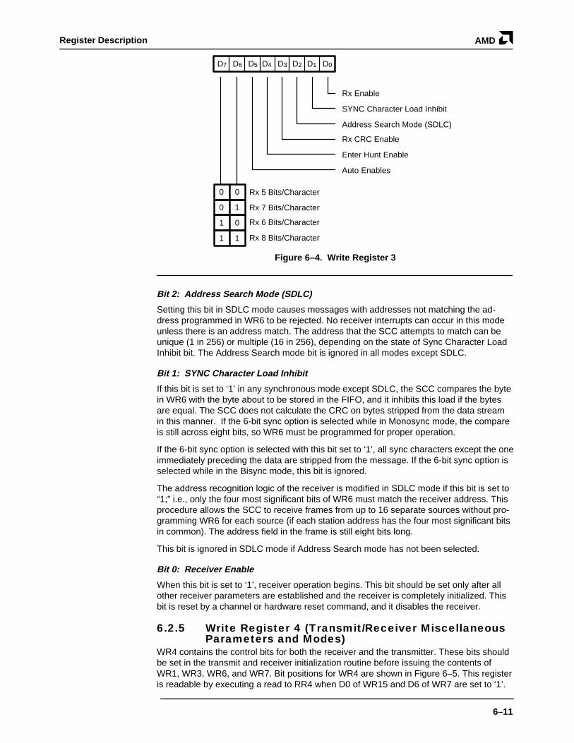
Register Description AMD
6–11
D7 D6 D5 D4 D3 D2 D1 D0
0 0
0 1
1 0
1 1
Rx 5 Bits/Character
Rx 7 Bits/Character
Rx Enable
SYNC Character Load Inhibit
Address Search Mode (SDLC)
Rx CRC Enable
Enter Hunt Enable
Auto Enables
Rx 6 Bits/Character
Rx 8 Bits/Character
Figure 6–4. Write Register 3
Bit 2: Address Search Mode (SDLC)
Setting this bit in SDLC mode causes messages with addresses not matching the ad-dress programmed in WR6 to be rejected. No receiver interrupts can occur in this modeunless there is an address match. The address that the SCC attempts to match can beunique (1 in 256) or multiple (16 in 256), depending on the state of Sync Character LoadInhibit bit. The Address Search mode bit is ignored in all modes except SDLC.
Bit 1: SYNC Character Load Inhibit
If this bit is set to ‘1’ in any synchronous mode except SDLC, the SCC compares the bytein WR6 with the byte about to be stored in the FIFO, and it inhibits this load if the bytesare equal. The SCC does not calculate the CRC on bytes stripped from the data streamin this manner. If the 6-bit sync option is selected while in Monosync mode, the compareis still across eight bits, so WR6 must be programmed for proper operation.
If the 6-bit sync option is selected with this bit set to ‘1’, all sync characters except the oneimmediately preceding the data are stripped from the message. If the 6-bit sync option isselected while in the Bisync mode, this bit is ignored.
The address recognition logic of the receiver is modified in SDLC mode if this bit is set to“1;” i.e., only the four most significant bits of WR6 must match the receiver address. Thisprocedure allows the SCC to receive frames from up to 16 separate sources without pro-gramming WR6 for each source (if each station address has the four most significant bitsin common). The address field in the frame is still eight bits long.
This bit is ignored in SDLC mode if Address Search mode has not been selected.
Bit 0: Receiver Enable
When this bit is set to ‘1’, receiver operation begins. This bit should be set only after allother receiver parameters are established and the receiver is completely initialized. Thisbit is reset by a channel or hardware reset command, and it disables the receiver.
6.2.5 Write Register 4 (Transmit/Receiver Miscellaneous Parameters and Modes)
WR4 contains the control bits for both the receiver and the transmitter. These bits shouldbe set in the transmit and receiver initialization routine before issuing the contents ofWR1, WR3, WR6, and WR7. Bit positions for WR4 are shown in Figure 6–5. This registeris readable by executing a read to RR4 when D0 of WR15 and D6 of WR7 are set to ‘1’.

Register DescriptionAMD
6–12
D7 D6 D5 D4 D3 D2 D1 D0
0 0
0 1
1 0
1 1
X1 Clock Mode
X16 Clock Mode
X32 Clock Mode
X64 Clock Mode
Parity Enable
Parity Even/Odd
SYNC Modes Enable
1 Stop Bit/Character
11/2 Stop Bits/Character
2 Stop Bits/Character
0 0
0 1
1 0
1 1
0 0
0 1
1 0
1 1
8 Bit SYNC Character
16 Bit SYNC Character
SDLC Mode (01111110 Flag)
External SYNC Mode
Figure 6–5. Write Register 4
Bits 7 and 6: Clock Rate 1 And 0
These bits specify the multiplier between the clock and data rates. In synchronousmodes, the 1X mode is forced internally and these bits are ignored unless External Syncmode has been selected.
1X Mode (00) . The clock rate and data rate are the same. In External Sync mode, this bitcombination specifies that only the SYNC pin can be used to achieve character synchro-nization.
16X Mode (01) . The clock rate is 16 times the data rate. In External Sync mode, this bitcombination specifies that only the SYNC pin can be used to achieve character synchro-nization.
32X Mode (10) . The clock rate is 32 times the data rate. In External Sync mode, this bitcombination specifies that either the SYNC pin or a match with the character stored inWR7 will signal character synchronization. The sync character can be either six or eightbits long as specified by the 6-bit/8-bit Sync bit in WR10.
64X Mode (11) . The clock rate is 64 times the data rate. With this bit combination in Ex-ternal Sync mode, both the receiver and transmitter are placed in SDLC mode. The onlyvariation from normal SDLC operation is that the SYNC pin is used to start or stop thereception of a frame by forcing the receiver to act as though a flag had been received.
Bits 5 and 4: SYNC Modes 1 And 0
These two bits select the various options for character synchronization. They are ignoredunless synchronous modes are selected in the stop bits field of this register.
Monosync (00) . In this mode, the receiver achieves character synchronization by match-ing the character stored in WR7 with an identical character in the received data stream.

Register Description AMD
6–13
The transmitter uses the character stored in WR6 as a time fill. The sync character canbe either six or eight bits, depending on the state of the 6-bit/8-bit Sync bit in WR10. If theSync Character Load Inhibit bit is set, the receiver strips the contents of WR6 from thedata stream if received within character boundaries.
Bisync (01) . The concatenation of WR7 with WR6 is used for receiver synchronizationand as time fill by the transmitter. The sync character can be 12 or 16 bits in the receiver,depending on the state of the 6-bit/8-bit Sync bit in WR10. The transmitted character isalways 16 bits.
SDLC Mode (10) . In this mode, SDLC is selected and requires a flag (01111110) to bewritten to WR7. The receiver address field should be written to WR6. The SDLC CRCpolynomial must also be selected (WR5) in SDLC mode.
External Sync Mode (11) . In this mode, the SCC expects external logic to signal charac-ter synchronization via the SYNC pin. If the crystal oscillator option is selected (inWR11), the internal SYNC signal is forced to ‘0’. Also in this mode, bits D7–D6 of thisregister select a special version of External Sync mode. Refer to Synchronous ExternalSYNC Mode on page 4–41. The transmitter is in Monosync mode using the contents ofWR6 as the time fill with the sync character length specified by the 6-bit/8-bit Sync bit inWR10.
Bits 3 and 2: Stop Bits 1 and 0
These bits determine the number of stop bits added to each asynchronous character thatis transmitted. The receiver always checks for one stop bit in Asynchronous mode. ASpecial mode specifies that a Synchronous mode is to be selected. D2 is always set to‘1’, by a channel or hardware reset to ensure that the SYNC pin is in a known state after areset.
Synchronous Modes Enable (00) . This bit combination selects one of the synchronousmodes specified by bits D4, D5, D6, and D7 of this register and forces the 1X Clock modeinternally.
1 Stop Bit/Character (1) . This bit selects Asynchronous mode with one stop bit per char-acter.
11/2 Stop Bits/Character (10) . These bits select Asynchronous mode with 1-1/2 stop bitsper character. This mode cannot be used with the 1X clock mode.
2 Stop Bits/Character (11) . These bits select Asynchronous mode with two stop bits pertransmitted character and check for one received stop bit.
Bit 1: Parity Even/ Odd
This bit determines whether parity is checked as even or odd. A ‘1’ programmed hereselects even parity, and a ‘0’ selects odd parity. This bit is ignored if the Parity Enable bitis not set.
Bit 0: Parity Enable
When this bit is set, an additional bit position beyond those specified in the bits/charactercontrol is added to the transmitted data and is expected in the receive data. The Re-ceived Parity bit is transferred to the CPU as part of the data unless eight bits per charac-ter is selected in the receiver.
6.2.6 Write Register 5 (Transmit Parameter and Controls)WR5 contains control bits that affect the operation of the transmitter. D2 affects both thetransmitter and the receiver. Bit positions for WR5 are shown in Figure 6–6. This registeris readable by executing a read to RR5 when D0 of WR15 and D6 of WR7’ are set to ‘1’.

Register DescriptionAMD
6–14
D7 D6 D5 D4 D3 D2 D1 D0
Tx CRC Enable
RTS
SDLC/CRC-16
Send Break
0 0
0 1
1 0
1 1
Tx 5 Bits (or less)/Character
Tx 7 Bits/Character
Tx 6 Bits/Character
Tx 8 Bits/Character
Tx Enable
DTR
Figure 6–6. Write Register 5
Bit 7: Data Terminal Ready
This is the control bit for the DTR/REQ pin while the pin is in the DTR mode (selected inWR14). When set, DTR is Low; when reset, DTR is High. This bit is ignored when DTR/REQ is programmed to act as a Request pin. This bit is reset by a channel or hardwarereset.
Bits 6 and 5: TX Bits/Character 1 and 0
These bits control the number of bits in each byte transferred to the transmit buffer. Bitssent must be right justified with least significant bits first.
The Five Or Less mode allows transmission of one to five bits per character; however, theCPU should format the data character as shown below in Table 6–3. In the Six or SevenBits/Character modes, unused data bits are ignored.
Bit 4: Send Break
When set, this bit forces the TxD output to send continuous ‘0’s beginning with the follow-ing transmit clock, regardless of any data being transmitted at the time. This bit functionswhether or not the transmitter is enabled. When reset, TxD continues to send the con-tents of the Transmit Shift register, which might be syncs, data, or all ‘1’s. If this bit is setwhile in the X21 mode (Monosync and Loop mode selected) and character synchroniza-tion is achieved in the receiver, this bit is automatically reset and the transmitter beginssending syncs or data. This bit can also be reset by a channel or hardware reset.
Table 6–3. Transmit Bits/Character
D6 D5 Character Length0 0 5 or less bits/character0 1 7 bits/character1 0 6 bits/character1 1 8 bits/character
D7 D6 D5 D4 D3 D2 D1 D0 Transmitter1 1 1 1 0 0 0 D0 Sends one data bit1 1 1 0 0 0 D1 D0 Sends two data bits1 1 0 0 0 D2 D1 D0 Sends three data bits1 0 0 0 D3 D2 D1 D0 Sends four data bits0 0 0 D4 D3 D2 D1 D0 Sends five data bits

Register Description AMD
6–15
Bit 3: Transmit Enable
Data is not transmitted until this bit is set, and the TxD output sends continuous ‘1’s un-less Auto Echo mode or SDLC Loop mode is selected. If this bit is reset after transmis-sion has started, the transmission of data or sync characters is completed. If thetransmitter is disabled during the transmission of a CRC character, sync or flag charac-ters are sent instead of CRC. This bit is reset by a channel or hardware reset.
Bit 2: SDLC/CRC-16
This bit selects the CRC polynomial used by both the transmitter and receiver. When set,the CRC-16 polynomial is used; when reset, the SDLC polynomial is used. The SDLC/CRC polynomial must be selected when SDLC mode is selected. The CRC generator andchecker can be preset to all ‘0’s or all ‘1’s, depending on the state of the Preset 1/Preset0 bit in WR10.
Bit 1: Request To Send
This is the control bit for the RTS pin. When the RTS bit is set, the RTS pin goes Low;when reset RTS goes High. In the Asynchronous mode with the Auto Enables bit set,RTS goes High only after all bits of the character have been sent and the transmit bufferis empty. In synchronous modes or the Asynchronous mode with auto enables off, the pindirectly follows the state of this bit. This bit is reset by a channel or hardware reset.
Bit 0: Transmit CRC Enable
This bit determines whether or not CRC is calculated on a transmit character. If this bit isset at the time the character is loaded from the transmit buffer to the Transmit Shift regis-ter, CRC is calculated on that character. CRC is not automatically sent unless this bit isset when the transmit underrun exists.
6.2.7 Write Register 6 (Sync Characters or SDLC Address Field)
WR 6 is programmed to contain the transmit sync character in the Monosync mode. Thefirst byte of a 16-bit sync character in the External Sync mode. WR6 is not used in asyn-chronous modes. In the SDLC modes, it is programmed to contain the secondary addressfield used to compare against the address field of the SDLC Frame. In SDLC mode, theSCC does not automatically transmit the station address at the beginning of a responseframe. Bit positions for WR6 are shown in Figure 6–7.

Register DescriptionAMD
6–16
D7 D6 D5 D4 D3 D2 D1 D0
SYNC7
SYNC1
SYNC7
SYNC3
ADR7
ADR7
SYNC6
SYNC0
SYNC6
SYNC2
ADR6
ADR6
SYNC5
SYNC5
SYNC5
SYNC1
ADR5
ADR5
SYNC4
SYNC4
SYNC4
SYNC0
ADR4
ADR4
SYNC3
SYNC3
SYNC3
1ADR3
X
SYNC2
SYNC2
SYNC2
1ADR2
X
SYNC1
SYNC1
SYNC1
1ADR1
X
SYNC0
SYNC0
SYNC0
1ADR0
X
MONOSYNC, 8 BITSMONOSYNC, 6 BITSBISYNC, 16 BITSBISYNC, 12 BITSSDLCSDLC (ADDRESS RANGE)
Figure 6–7. Write Register 6
D7 D6 D5 D4 D3 D2 D1 D0
SYNC7
SYNC5
SYNC15
SYNC11
0
SYNC6
SYNC4
SYNC14
SYNC10
1
SYNC5
SYNC3
SYNC13
SYNC9
1
SYNC4
SYNC2
SYNC12
SYNC8
1
SYNC3
SYNC1
SYNC11
SYNC7
1
SYNC2
SYNC0
SYNC10
SYNC6
1
SYNC1
XSYNC9
SYNC5
1
SYNC0
XSYNC8
SYNC4
0
MONOSYNC, 8 BITSMONOSYNC, 6 BITSBISYNC, 16 BITSBISYNC, 12 BITSSDLC (Flag)
Figure 6–8. Write Register 7

Register Description AMD
6–17
6.2.8 Write Register 7 (Sync Character or SDLCFlag/SDLCOption Register) Note SDLC option register is available only in CMOS version.
In the Nmos Am8530H, the use of this register differs depending on the mode the SCC isprogrammed in. In Monosync mode, WR7 is programmed with the receive sync charac-ter; in BISYNC, it is programmed with the second byte (the last 8 bits) of the 16-bit synccharacter. In SDLC modes, WR7 is programmed with the flag character (01111110).
Note, however, that WR7 may hold the receive sync character or flag if one of the specialversions of the External Sync mode is selected.
Write Register 7′ (Special SDLC Enhancement Register)In the CMOS Am8530, special SDLC options are provided that enable the user to moreeffectively interface to the Am85C30. These options are available to the user if the previ-ously unused bit, D0 of WR15, is set to ‘1’. When this bit is set, and the SCC is pro-grammed for SDLC operation, an access to WR7 accesses a different register whichallows the programming of these options. This register is referred to as WR7’ (WR7prime). Resetting this bit (D0 of WR15) disables the options and the next access to WR7is to the flag register. Therefore, the user should always program the flag character firstbefore setting bit D0 of WR15 to ‘1’. This register is readable by executing a read to RR14when D0 of WR15 and D6 of WR7’ are set to ‘1’.
Note that WR7 is not used in Asynchronous mode. Bit positions for WR7 are shown inFigure 6–8. Bit positions for WR7’ are shown in Figure 6–9 with bit descriptions givenbelow.
D7 D6 D5 D4 D3 D2 D1 D0
TxD forced high in SDLC NRZI Mode
DTR/REQ Timing Mode
Receive CRC
Extended Read Enable
Auto Tx Flag
Auto EOM Reset
Auto RTS Deactivation
This bit must always be programmed with a ‘0’
Figure 6–9. Write Register 7 ′
Bit 7: Not used. This bit must be programmed with ‘0’.
Bit 6: Extended Read Enable
If this bit is set to ‘1’ the user is able to read the following previously unreadable registers;WR3, WR4, WR5 and WR10 in the CMOS SCC in each channel. These registers areread by addressing bogus read registers RR9, RR4, RR5 and RR11, respectively.
WR7’ is updated or modified by writing to WR7 while this bit is set and is read by execut-ing a read cycle to WR14 (RR14).
Bit 5: Receive CRC
If this bit is set to ‘1’, the last two bits of the received CRC are properly clocked into thereceive shift register and are available to the user.

Register DescriptionAMD
6–18
Bit 4: DTR/REQ Timing Mode
This bit controls the timing of the DTR/REQ pin. If this bit is set to ‘1’, the deactivation tim-ing of the DTR/REQ pin is made identical to the WAIT/REQ pin.
Bit 3: TxD Forced High in SDLC NRZI Mode
If this bit is set to ‘1’, and the transmitter is disabled while the SCC is programmed inSDLC mode with NRZI encoding, the TxD pin will be pulled to a high physical state.
Bit 2: Auto RTS Deactivation
This bit synchronizes the deactivation of RTS with the closing flag of an SDLC frame. Ifthis bit is set to ‘1’ and the user deactivates RTS while the CRC characters are beingtransmitted, the SCC assures that the last bit of the flag character is transmitted beforedeactivating RTS.
Bit 1: Auto EOM Reset
This bit removes the requirement of having to reset the Tx Underrun/EOM latch duringthe transmission of a frame. If this bit is set to ‘1’, the Tx Underrun/EOM latch will beautomatically reset by the SCC after the first byte is transmitted.
Bit 0: Auto Tx Flag
This bit removes the requirement of having to wait for the mark idle and flag characters tobe sent before the first data character of a new frame is written to the transmit buffer reg-ister (WR8). If this bit is set to ‘1’, the user need only write the first character to the trans-mit buffer. The SCC will then transmit the opening flag followed by data.
6.2.9 Write Register 8 (Transmit Buffer)WR8 is the transmit buffer register.
6.2.10 Write Register 9 (Master Interrupt Control)WR9 is the Master Interrupt Control register and contains the Reset command bits. Onlyone WR9 exists in the SCC and can be accessed from either channel. The interrupt con-trol bits can be programmed at the same time as the Reset command because these bitsare reset only by a hardware reset. Bit positions for WR9 are shown in Figure 6–10.
D7 D6 D5 D4 D3 D2 D1 D0
0 0
0 1
1 0
1 1
No Reset
Channel Reset B
Channel Reset A
Force Hardware Reset
VIS
NV
DLC
MIE
STATUS HIGH/STATUS LOW
Interrupt Masking without INTACK
Figure 6–10. Write Register 9

Register Description AMD
6–19
Bits 7 and 6: Reset Command Bits
Together, these bits select one of the reset commands for the SCC. Setting either ofthese bits to ‘1’ disables both the receiver and the transmitter in the corresponding chan-nel, forces TxD for that channel marking, forces the modem control signals High in thatchannel, resets all IPs and IUSs and disables all interrupts in that channel. Five extraPCLK cycles must be allowed beyond the usual cycle time before any additional com-mand or controls are written to the SCC.
No Reset (00) . This command has no effect. It is used when a write to WR9 is necessaryfor some reason other than an SCC Reset command.
Channel Reset B (01) . Issuing this command causes a channel reset to be performed onChannel B.
Channel Reset A (10) . Issuing this command causes a channel reset to be performed onChannel A.
Force Hardware Reset (11) . The effects of this command are identical to those of ahardware reset except that the MIE, Status High/Status Low and DLC bits take the pro-grammed values that accompany this command.
Bit 5: Interrupt Masking Without INTACK
If this bit is set to ‘1’, the INTACK cycle is ignored by the SCC and should be tied High.This allows users to mask lower priority interrupts in applications where INTACK is nei-ther necessary nor used.
Bit 4: Status High/ Status Low
This bit controls which vector bits the SCC will modify to indicate status. When set to ‘1’,the SCC modifies bits V6, V5, and V4 according to Table 6–4. When set to ‘0’, the SCCmodifies bits V1, V2, and V3 according to Table 6–1–3. This bit controls status in boththe vector returned during an interrupt acknowledge cycle and the status in RR2B. Thisbit is reset by a hardware reset.
Bit 3: Master Interrupt Enable
The Master Interrupt Enable bit is used to globally inhibit SCC interrupts. When set to ‘1’,interrupts for channel A and channel B are enabled. When this bit is set to ‘0’, IEO is notforced low but follows the state of IEI unless there is an IUS set in the SCC. No IUS canbe set after the MIE bit is set to ‘0’. This bit is reset by a hardware reset.
Table 6–4. Interrupt Vector Modification
V3 V2 V1 Status High/Status Low=0V4 V5 V6 Status High/Status Low=1
0 0 0 Ch B Transmit Buffer Empty
0 0 1 Ch B External/Status Change
0 1 0 Ch B Receive Character Available
0 1 1 Ch B Special Receive Condition
1 0 0 Ch A Transmit Buffer Empty
1 0 1 Ch A External/Status Change
1 1 0 Ch A Receive Character Available
1 1 1 Ch A Special Receive Condition

Register DescriptionAMD
6–20
Bit 2: Disable Lower Chain
The Disable Lower Chain can be used by the CPU to control the interrupt daisy chain.Setting this bit to ‘1’ forces the IEO pin Low, preventing lower-priority devices on the daisychain from requesting interrupts. This bit is reset by a hardware reset.
Bit 1: No Vector
The No Vector bit controls whether or not the SCC will respond to an interrupt acknowl-edge cycle by placing a vector on the data bus if the SCC is the highest-priority devicerequesting an interrupt. If this bit is set, no vector is returned; i.e., D0–D7 remain three-stated during an interrupt acknowledge cycle, even if the SCC is the highest-priority de-vice requesting an interrupt.
Bit 0: Vector Includes Status
The Vector Includes Status bit controls whether or not the Z-SCC will include status infor-mation in the vector it places on the bus in response to an interrupt acknowledge cycle. Ifthis bit is set, the vector returned is variable, with the variable field depending on the high-est-priority IP that is set. Table 6–4 shows the encoding of the status information. This bitis ignored if the No Vector (NV) bit is set and does not apply if RR2 is read from Chan-nel B.
6.2.11 Write Register 10 (Miscellaneous Transmitter/Receiver Control Bits)
WR10 contains miscellaneous control bits for both the receiver and the transmitter. Bitpositions for WR10 are shown in Figure 6–11. This register is readable by executing aread to RR11 when D0 of WR15 and D6 of WR7’ are set to ‘1’.
D7 D6 D5 D4 D3 D2 D1 D0
6 Bit/8Bit SYNC
Loop Mode
Abort/Flag on Underrun
Go Active on Poll
0 0
0 1
1 0
1 1
NRZ
NRZI
FM1 (Transition = 1)
FM0 (Transition = 0)
Mark/Flag Idle
CRC Preset ‘1’ or ‘0”
Figure 6–11. Write Register 10
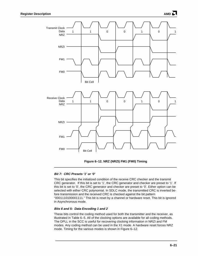
Register Description AMD
6–21
1 1 0 0 1 0 1Transmit Clock
DataNRZ
NRZI
FM1
FM0
Receive Clock
NRZ1 1 0 0 1 0 1Data
NRZI
FM1
FM0
Bit Cell
Bit Cell
Figure 6–12. NRZ (NRZI) FM1 (FM0) Timing
Bit 7: CRC Presets ‘1’ or ‘0’
This bit specifies the initialized condition of the receive CRC checker and the transmitCRC generator. If this bit is set to ‘1’, the CRC generator and checker are preset to ‘1’. Ifthis bit is set to ‘0’, the CRC generator and checker are preset to ‘0’. Either option can beselected with either CRC polynomial. In SDLC mode, the transmitted CRC is inverted be-fore transmission and the received CRC is checked against the bit pattern“0001110100001111.” This bit is reset by a channel or hardware reset. This bit is ignoredin Asynchronous mode.
Bits 6 and 5: Data Encoding 1 and 2
These bits control the coding method used for both the transmitter and the receiver, asillustrated in Table 6–5. All of the clocking options are available for all coding methods.The DPLL in the SCC is useful for recovering clocking information in NRZI and FMmodes. Any coding method can be used in the X1 mode. A hardware reset forces NRZmode. Timing for the various modes is shown in Figure 6–12.

Register DescriptionAMD
6–22
Table 6–5. Data Encoding
D6 D5 Encoding
0 0 NRZ
0 1 NRZI
1 0 FM1 (transition = 1)
1 1 FM0 (transition = 0)
Bit 4: Go Active On Poll
When Loop mode is first selected during SDLC operation, the SCC connects RxD to TxDwith only gate delays in the path. The SCC does not go on-loop and insert the 1-bit delaybetween RxD and TxD until this bit has been set and an EOP received. When the SCC ison-loop, the transmitter is active in SDLC Loop mode and is sending a flag. If this bit isset at the time the flag is leaving the Transmit Shift register, another flag or data byte (ifthe transmit buffer is full) is transmitted. If the Go Active On Poll bit is not set at this time,the transmitter finishes sending the flag and reverts to the 1-Bit Delay mode. Thus, totransmit only one response frame, this bit should be reset after the first data byte is sentto the SCC but before CRC has been transmitted. If the bit is not reset before CRC istransmitted, extra flags are sent, slowing down response time on the loop. If this bit is re-set before the first data is written, the SCC completes the transmission of the present flagand reverts to the 1-Bit Delay mode. After gaining control of the loop, the SCC is not ableto transmit again until a flag and another EOP have been received. Though not strictlynecessary, it is good practice to set this bit only upon receipt of a poll frame to ensure thatthe SCC does not go on-loop without the CPU noticing it.
In synchronous modes other than SDLC with the Loop Mode bit set, this bit must be setbefore the transmitter can go active in response to a received sync character.
This bit is always ignored in Asynchronous mode and Synchronous modes unless theLoop Mode bit is set. This bit is reset by a channel or hardware reset.
Bit 3: Mark/ Flag Idle
This bit affects only SDLC operation and is used to control the idle line condition. If thisbit is set to ‘0’, the transmitter sends flags as an idle line. If this bit is set to ‘1’, the trans-mitter sends continuous ‘1’s after the closing flag of a frame. The idle line condition is se-lected byte by byte; i.e., either a flag or eight ‘1’s are transmitted. The primary station inan SDLC loop should be programmed for Mark Idle to create the EOP sequence. MarkIdle must be deselected at the beginning of a frame before the first data are written to theSCC, so that an opening flag can be transmitted. This bit is ignored in Loop mode, but theprogrammed value takes effect upon exiting the Loop mode. This bit is reset by a channelor hardware reset.

Register Description AMD
6–23
Bit 2: Abort/ Flag On Underrun
This bit affects only SDLC operation and is used to control how the SCC responds to atransmit underrun condition. If this bit is set to ‘1’ and a transmit underrun occurs, theSCC sends an abort and a flag instead of CRC. If the bit is reset, the SCC sends CRC ona transmit underrun. At the beginning of this 16-bit transmission, the Transmit Underrun/EOM bit is set, causing an External/Status interrupt. The CPU uses this status, along withthe byte count from memory or the DMA, to determine whether the frame must beretransmitted. A transmit buffer Empty interrupt occurs at the end of this 16-bit transmis-sion to start the next frame. If both this bit and the Mark/Flag Idle bit are set to ‘1’, all ‘1’sare transmitted after the transmit underrun. This bit should be set after the first byte ofdata is sent to the SCC and reset immediately after the last byte of data so that the framewill be terminated properly with CRC and a flag. This bit is ignored in Loop mode, but theprogrammed value is active upon exiting Loop mode. This bit is reset by a channel orhardware reset.
Bit 1: Loop Mode
In SDLC mode, the initial set condition of this bit forces the SCC to connect TxD to TxDand to begin searching the incoming data stream so that it can go on-loop. All bits perti-nent to SDLC mode operation in other registers must be set before this mode is selected.The transmitter and receiver should not be enabled until after this mode has been se-lected. As soon as the Go Active On Poll bit is set and an EOP is received, the SCC goeson-loop. If this bit is reset after the SCC is on-loop, the SCC waits for the next EOP to gooff-loop.
In synchronous modes, the SCC uses this bit, along with the Go Active On Poll bit, tosynchronize the transmitter to the receiver. The receiver should not be enabled until afterthis mode is selected. The TxD pin is held marking when this mode is selected unless abreak condition is programmed. The receiver waits for a sync character to be receivedand then enables the transmitter on a character boundary. The break condition, if pro-grammed, is removed. This mode works properly with sync characters of 6, 8, or 16 bits.This bit is ignored in Asynchronous mode and is reset by a channel or hardware reset.
Bit 0: 6 Bit/ 8 Bit Sync
This bit is used to select a special case of synchronous modes. If this bit is set to ‘1’ inMonosync mode, the receiver and transmitter sync characters are six bits long instead ofthe usual eight. If this bit is set to ‘1’ in Bisync mode, the received sync will be 12 bits andthe transmitter sync character will remain 16 bits long. This bit is ignored in SDLC andAsynchronous modes but still has effect in the special external sync modes. This bit isreset by a channel or hardware reset.
6.2.12 Write Register 11 (Clock Mode Control)WR11 is the Clock Mode Control register. The bits in this register control the sources ofboth the receive and transmit clocks, the type of signal on the Sync and RTxC pins, andthe direction of the TRxC pin. Bit positions for WR11 are shown in Figure 6–13.

Register DescriptionAMD
6–24
D7 D6 D5 D4 D3 D2 D1 D0
0 0
0 1
1 0
1 1
Receive Clock = RTxC Pin
Receive Clock = TRxC Pin
Receive Clock = BR Generator Output
Receive Clock = DPLL Output
TRxC Out = XTAL Output
TRxC Out = Transmit Clock
TRxC Out = BR Generator Output
TRxC Out = DPLL Output
0 0
0 1
1 0
1 1
0 0
0 1
1 0
1 1
Transmit Clock = RTxC Pin
Transmit Clock = TRxC Pin
Transmit Clock = BR Generator Output
Transmit Clock = DPLL Output
TRxC O/I
RTxC XTAL/NO XTAL
Figure 6–13. Write Register 11
Bit 7: RTxC—XTAL/ NO XTAL
This bit controls the type of input signal the SCC expects to see on the RTxC pin. If thisbit is set to ‘0’, the SCC expects a TTL-compatible signal as an input to this pin. If this bitis set to ‘1’, the SCC connects a high-gain amplifier between the RTxC and SYNC pins inexpectation of a quartz crystal being placed across the pins.
The output of this oscillator is available for use as a clocking source. In this mode of op-eration, the Sync pin is unavailable for other use. The Sync signal is forced to ‘0’ inter-nally. A hardware reset forces No XTAL. (At least 20 ms should be allowed after this bit isset to allow the oscillator to stabilize.)
Bits 6 and 5: Receiver Clock 1 And 0
These bits determine the source of the receive clock as shown in Table 6–6. They do notinterfere with any of the modes of operation in the SCC but simply control a multiplexerjust before the internal receive clock input. A hardware reset forces the receive clock tocome from the TRxC pin.
Table 6–6. Receive Clock Source
D6 D5
0 0 Receive Clock = RTxC pin
0 1 Receive Clock = TRxC pin
1 0 Receive Clock = BRG output
1 1 Receive Clock = DPLL output
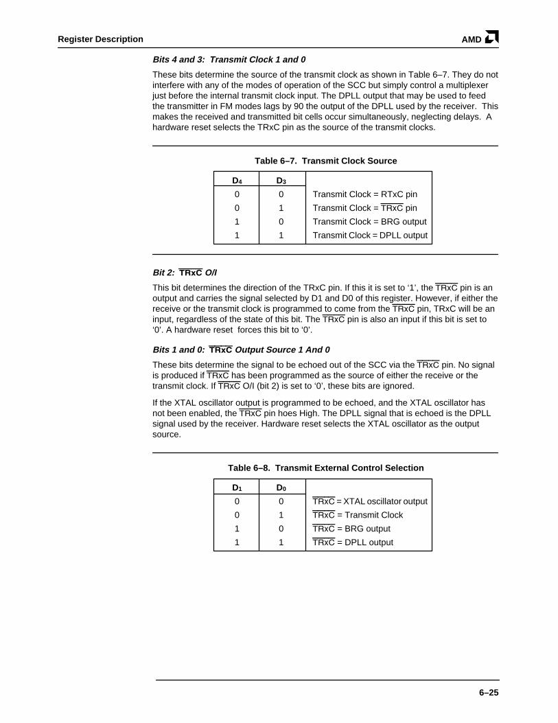
Register Description AMD
6–25
Bits 4 and 3: Transmit Clock 1 and 0
These bits determine the source of the transmit clock as shown in Table 6–7. They do notinterfere with any of the modes of operation of the SCC but simply control a multiplexerjust before the internal transmit clock input. The DPLL output that may be used to feedthe transmitter in FM modes lags by 90 the output of the DPLL used by the receiver. Thismakes the received and transmitted bit cells occur simultaneously, neglecting delays. Ahardware reset selects the TRxC pin as the source of the transmit clocks.
Table 6–7. Transmit Clock Source
D4 D3
0 0 Transmit Clock = RTxC pin
0 1 Transmit Clock = TRxC pin
1 0 Transmit Clock = BRG output
1 1 Transmit Clock = DPLL output
Bit 2: TRxC O/I
This bit determines the direction of the TRxC pin. If this it is set to ‘1’, the TRxC pin is anoutput and carries the signal selected by D1 and D0 of this register. However, if either thereceive or the transmit clock is programmed to come from the TRxC pin, TRxC will be aninput, regardless of the state of this bit. The TRxC pin is also an input if this bit is set to‘0’. A hardware reset forces this bit to ‘0’.
Bits 1 and 0: TRxC Output Source 1 And 0
These bits determine the signal to be echoed out of the SCC via the TRxC pin. No signalis produced if TRxC has been programmed as the source of either the receive or thetransmit clock. If TRxC O/I (bit 2) is set to ‘0’, these bits are ignored.
If the XTAL oscillator output is programmed to be echoed, and the XTAL oscillator hasnot been enabled, the TRxC pin hoes High. The DPLL signal that is echoed is the DPLLsignal used by the receiver. Hardware reset selects the XTAL oscillator as the outputsource.
Table 6–8. Transmit External Control Selection
D1 D0
0 0 TRxC = XTAL oscillator output
0 1 TRxC = Transmit Clock
1 0 TRxC = BRG output
1 1 TRxC = DPLL output

Register DescriptionAMD
6–26
6.2.13 Write Register 12 (Lower Byte of Baud Rate Generator Time Constant)
WR12 contains the lower byte of the time constant for the baud rate generator. The timeconstant can be changed at any time, but the new value does not take effect until the nexttime the time constant is loaded into the down counter. No attempt is made to synchro-nize the loading of the time constant into WR12 and WR13 with the clock driving thedown counter. For this reason, it is advisable to disable the baud rate generator while thenew time constant is loaded into WR12 and WR13. Ordinarily, this is done anyway to pre-vent a load of the down counter between the writing of the upper and lower bytes of thetime constant.
The formula for determining the appropriate time constant for a given baud is shown be-low with the desired rate in bits per second and the BR clock period in seconds. This for-mula is derived because the counter decrements from N down to ‘0’-plus-one-cycle forreloading the time constant and is then fed to a toggle flip-flop to make the output asquare wave. Bit positions for WR12 are shown in Figure 6–14.
Time Constant =1
2 • (Desired Rate) • (Baud Rate)–2
D7 D6 D5 D4 D3 D2 D1 D0
TC3
TC4
TC5
TC6
TC0
TC1
TC2
TC7
Lower Byte ofTime Constant
Figure 6–14. Write Register 12
6.2.14 Write Register 13 (Upper Byte of Baud Rate Generator Time Constant)
WR13 contains the upper byte of the time constant for the baud rate generator. Bit posi-tions for WR13 are shown in Figure 6–15.
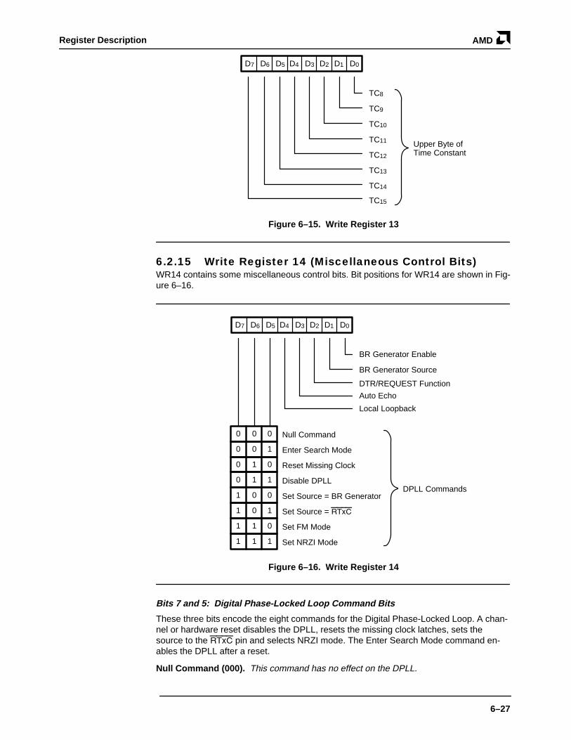
Register Description AMD
6–27
D7 D6 D5 D4 D3 D2 D1 D0
TC11
TC12
TC13
TC14
TC8
TC9
TC10
TC15
Upper Byte ofTime Constant
Figure 6–15. Write Register 13
6.2.15 Write Register 14 (Miscellaneous Control Bits)WR14 contains some miscellaneous control bits. Bit positions for WR14 are shown in Fig-ure 6–16.
D7 D6 D5 D4 D3 D2 D1 D0
BR Generator Enable
BR Generator Source
DTR/REQUEST Function
Local Loopback
Auto Echo
0 0
0 0
0 1
0
1
0
0 1
1 0
1 0
1 1
1
0
1
0
1 1 1
Null Command
Enter Search Mode
Reset Missing Clock
Disable DPLL
Set Source = BR Generator
Set Source = RTxC
Set FM Mode
Set NRZI Mode
DPLL Commands
Figure 6–16. Write Register 14
Bits 7 and 5: Digital Phase-Locked Loop Command Bits
These three bits encode the eight commands for the Digital Phase-Locked Loop. A chan-nel or hardware reset disables the DPLL, resets the missing clock latches, sets thesource to the RTxC pin and selects NRZI mode. The Enter Search Mode command en-ables the DPLL after a reset.
Null Command (000). This command has no effect on the DPLL.
Register DescriptionAMD
6–28
Enter Search Mode (001) . Issuing this command causes the DPLL to enter the Searchmode, where the DPLL searches for a locking edge in the incoming data stream. The ac-tion taken by the DPLL upon receipt of this command depends on the operating mode ofthe DPLL.
In NRZI mode, the output of the DPLL is High while the DPLL is waiting for an edge in theincoming data stream. After the Search mode is entered, the first edge the DPLL sees isassumed to be a valid data edge, and the DPLL begins the clock recovery operation fromthat point. The DPLL clock rate must be 32 times the data rate in NRZI mode. Upon leav-ing the Search mode, the first sampling edge of the DPLL occurs 16 of these 32X clocksafter the first data edge and the second sampling edge occurs 48 of these 32X clocksafter the first data edge. Beyond this point, the DPLL begins normal operation, adjustingthe output to remain in sync with the incoming data.
In FM mode, the output of the DPLL is Low while the DPLL is waiting for an edge in theincoming data stream. The first edge the DPLL detects is assumed to be a valid clockedge. For this to be the case, the line must contain only clock edges; i.e., with FM1 en-coding, the line must be continuous ‘0’s. With FM0 encoding the line must be continuous‘1’s, whereas Manchester encoding requires alternating ‘1’s and ‘0’s on the line. TheDPLL clock rate must be 16 times the data rate in FM mode. The DPLL output causes thereceiver to sample the data stream in the nominal center of the two halves of the bit cellto decide whether the data was a ‘1’ or a ‘0’. After this command is issued, as in NRZImode, the DPLL starts sampling immediately after the first edge is detected. (In FMmode, the DPLL examines the clock edge of every other bit cell to decide what correctionmust be made to remain in sync.) If the DPLL does not see an edge during the expectedwindow, the one clock missing bit in RR10 is set. If the DPLL does not see an edge aftertwo successive attempts, the two clocks missing bit in RR10 is set and the DPLL auto-matically enters the Search mode. This command resets both clock missing latches.
Reset Clock Missing (010) . Issuing this command disables the DPLL, resets the clockmissing latches in RR10, and forces a continuous Search mode state.
Disable DPLL (011) . Issuing this command disables the DPLL, resets the clock missinglatches in RR10, and forces a continuous Search mode state.
Set Source = BR Gen (100) . Issuing this command forces the clock for the DPLL tocome from the output of the baud rate generator.
Set Source = RTxC (101). Issuing this command forces the clock for the DPLL to comefrom the RTxC pin or the crystal oscillator, depending on the state of the XTAL/no XTALbit in WR11. This mode is selected by a channel or hardware reset.
Set FM Mode (110) . This command forces the DPLL to operate in the FM mode and isused to recover the clock from FM or Manchester-encoded data. (Manchester is decodedby placing the receiver in NRZ mode while the DPLL is in FM mode.)
Set NRZI Mode (111) . Issuing this command forces the DPLL to operate in the NRZImode. This mode is also selected by a hardware or channel reset.
Bit 4: Local Loopback
Setting this bit to ‘1’ selects the Local Loopback mode of operation In this mode, the in-ternal transmitted data are routed back to the receiver, as well as to the TxD pin. TheCTS and DCD inputs are ignored as enables in Local Loopback mode, even if Auto En-ables is selected. (if so programmed, transitions on these inputs still cause interrupts.)This mode works with any Transmit/Receive mode except Loop mode. For meaningfulresults, the frequency of the transmit and receive clocks must be the same. This bit is re-set by a channel or hardware reset.
Bit 3: Auto Echo
Setting this bit to ‘1’ selects the Auto Enable mode of operation. In this mode, the TxDpin is connected to RxD, as in Local Loopback mode, but the receiver still listens to the
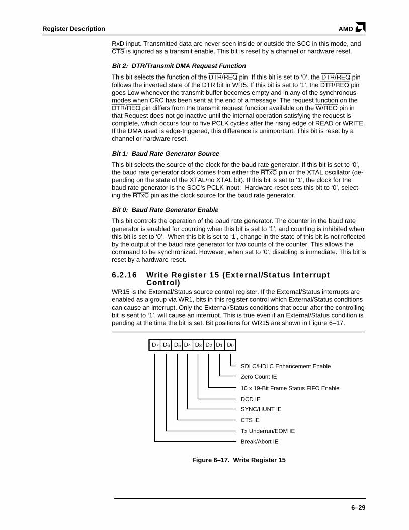
Register Description AMD
6–29
RxD input. Transmitted data are never seen inside or outside the SCC in this mode, andCTS is ignored as a transmit enable. This bit is reset by a channel or hardware reset.
Bit 2: DTR/Transmit DMA Request Function
This bit selects the function of the DTR/REQ pin. If this bit is set to ‘0’, the DTR/REQ pinfollows the inverted state of the DTR bit in WR5. If this bit is set to ‘1’, the DTR/REQ pingoes Low whenever the transmit buffer becomes empty and in any of the synchronousmodes when CRC has been sent at the end of a message. The request function on theDTR/REQ pin differs from the transmit request function available on the W/REQ pin inthat Request does not go inactive until the internal operation satisfying the request iscomplete, which occurs four to five PCLK cycles after the rising edge of READ or WRITE.If the DMA used is edge-triggered, this difference is unimportant. This bit is reset by achannel or hardware reset.
Bit 1: Baud Rate Generator Source
This bit selects the source of the clock for the baud rate generator. If this bit is set to ‘0’,the baud rate generator clock comes from either the RTxC pin or the XTAL oscillator (de-pending on the state of the XTAL/no XTAL bit). If this bit is set to ‘1’, the clock for thebaud rate generator is the SCC’s PCLK input. Hardware reset sets this bit to ‘0’, select-ing the RTxC pin as the clock source for the baud rate generator.
Bit 0: Baud Rate Generator Enable
This bit controls the operation of the baud rate generator. The counter in the baud rategenerator is enabled for counting when this bit is set to ‘1’, and counting is inhibited whenthis bit is set to ‘0’. When this bit is set to ‘1’, change in the state of this bit is not reflectedby the output of the baud rate generator for two counts of the counter. This allows thecommand to be synchronized. However, when set to ‘0’, disabling is immediate. This bit isreset by a hardware reset.
6.2.16 Write Register 15 (External/Status Interrupt Control)
WR15 is the External/Status source control register. If the External/Status interrupts areenabled as a group via WR1, bits in this register control which External/Status conditionscan cause an interrupt. Only the External/Status conditions that occur after the controllingbit is sent to ‘1’, will cause an interrupt. This is true even if an External/Status condition ispending at the time the bit is set. Bit positions for WR15 are shown in Figure 6–17.
D7 D6 D5 D4 D3 D2 D1 D0
DCD IE
SYNC/HUNT IE
CTS IE
Tx Underrun/EOM IE
SDLC/HDLC Enhancement Enable
Zero Count IE
10 x 19-Bit Frame Status FIFO Enable
Break/Abort IE
Figure 6–17. Write Register 15

Register DescriptionAMD
6–30
Bit 7: Break/Abort IE
If this bit is set to ‘1’, a change in the Break/Abort status of the receiver causes an Exter-nal/Status interrupt. This bit is set by a channel or hardware reset.
Bit 6: Tx Underrun/EOM
If this bit is set to ‘1’, a change of state by the Tx Underrun/EOM latch in the transmittercauses an External/Status interrupt. This bit is set to ‘1’ by a channel or hardware reset.
Bit 5: CTS IE
If this bit is set ‘1’, a change of state on the CTS pin causes an External/Status interrupt.This bit is set by a channel or hardware reset.
Bit 4: SYNC/Hunt IE
If this bit is set to ‘1’, a change of state on the SYNC pin causes an External/Status inter-rupt in Asynchronous mode, and a change of state in the Hunt bit in the receiver causesan External/Status interrupt in synchronous modes. This bit is set by a channel or hard-ware reset.
Bit 3: DCD IE
If this bit is set to ‘1’, a change of state on the DCD pin causes an External/Status inter-rupt. This bit is set by a channel or hardware reset.
Bit 2 10x19–Bit Frame Status FIFO Enable
If this bit is set to ‘1’, the 10X19-bit FIFO array and 14-bit counter are available for use butonly if the SCC is programmed in SDLC mode.
Bit 1: Zero Count IE
If this bit is set to ‘1’, an External/Status interrupt is generated whenever the counter inthe baud rate generator reaches ‘0’. This bit is set to ‘0’ by a channel or hardware reset.
Bit 0: SDLC/HDLC Enhancement Enable
If this bit is set to ‘1’, WR7′ can be accessed as WR7′ to allow the use of special SDLC/HDLC options. Refer to WR7′ for details.
6.3 READ REGISTERSThe SCC contains nine read registers in each channel. The status of these registers iscontinually changing and depends on the mode of communication, received and transmit-ted data, and the manner in which this data is transferred to and from the CPU. The fol-lowing description details the bit assignments for each register.
6.3.1 Read Register 0 (Transmit/Receive Buffer Status and External Status)
Read Register 0 contains the status of the receive and transmit buffers. RR0 also con-tains the status bits for the six sources of External/Status interrupts. The bit configurationis illustrated in Figure 6–18.

Register Description AMD
6–31
D7 D6 D5 D4 D3 D2 D1 D0
DCD
SYNC/HUNT
CTS
Tx Underrun/EOM
Rx Character Available
Zero Count
Tx Buffer Empty
Break/Abort
Figure 6–18. Read Register 0
Bit 7: Break/Abort
In the Asynchronous mode, this bit is set when a Break sequence (null character plusframing error) is detected in the receive data stream. This bit is reset when the sequenceis terminated, leaving a single null character in the receive FIFO. This character shouldbe read and discarded. In SDLC mode, this bit is set by the detection of an Abort se-quence (seven or more ‘1’s), then reset automatically at the termination of the Abort se-quence. In either case, if the Break/Abort IE bit is set, an External/Status interrupt isinitiated. Unlike the remainder of the External/Status bits, both transitions are guaranteedto cause an External/Status interrupt, even if another External/Status interrupt is pendingat the time these transitions occur. This procedure is necessary because Abort or Breakconditions may not persist.
Bit 6: TX Underrun/EOM
This bit is set by a channel or hardware reset and when the transmitter is disabled or aSend Abort command is issued. This bit can be reset only by the reset Tx Underrun/EOMLatch command in WR0. When the Transmit Underrun occurs, this bit is set and causesan External/Status interrupt (if the Tx Underrun/EOM IE bit is set).
Only the 0-to-1 transition of this bit causes an interrupt. This bit is always ‘1’ in Asynchro-nous mode, unless a reset Tx Underrun/EOM Latch command has been erroneously is-sued. In this case, the Send Abort command can be issued to set the bit to ‘1’ and at thesame time cause an External/Status interrupt.
Bit 5: Clear to Send
If the CTS IE bit in WR15 is set, this bit indicates the state of the CTS pin the last timeany of the enabled External/Status bits changed. Any transition on the CTS pin while noother interrupt is pending latches the state of the CTS pin and generates an External/Status interrupt. Any odd number of transitions on the CTS pin while another External/Status interrupt is pending also causes an External/Status interrupt condition. If the CTSIE bit is reset, it merely reports the current unlatched state of the CTS pin (i.e., if CTS pinis Low, this bit will be High).
Bit 4: SYNC/Hunt
The operation of this bit is similar to that of the CTS bit, except that the condition moni-tored by the bit varies depending on the mode in which the SCC is operating.
When the XTAL oscillator option is selected in asynchronous modes, this bit is forced to‘0’ (no External/Status interrupt is generated). Selecting the XTAL oscillator in synchro-nous or SDLC modes has no effect on the operation of this bit.

Register DescriptionAMD
6–32
The XTAL oscillator should not be selected in External Sync mode.
In Asynchronous mode, the operation of this bit is identical to that of the CTS status bit,except that this bit reports the state of the SYNC pin.
In External sync mode the SYNC pin is used by external logic to signal character syn-chronization. When the Enter Hunt Mode command is issued in External Sync mode, theSYNC pin must be held High by external sync logic until character synchronization isachieved. A High on the SYNC pin holds the Sync/Hunt bit in the reset condition.
When external synchronization is achieved, SYNC must be driven Low on the secondrising edge of the Receive Clock after the last rising edge of the Receive Clock on whichthe last bit of the receive character was received. Once SYNC is forced Low, it is goodpractice to keep it Low until the CPU informs the external sync logic that synchronizationhas been lost or that a new message is about to start. Both transitions on the SYNC pincase External/Status interrupts if the Sync/Hunt IE bit is set to ‘1’.
The Enter Hunt Mode command should be issued whenever character synchronization islost. At the same time, the CPU should inform the external logic that character synchroni-zation has been lost and that the SCC is waiting for SYNC to become active.
In the Monosync and Bisync Receive modes, the Sync/Hunt status bit is initially set to ‘1’by the Enter Hunt Mode command. The Sync/Hunt bit is reset when the SCC establishescharacter synchronization. Both transitions cause External/Status interrupts if the Sync/Hunt IE bit is set when the CPU detects the end of message or the loss of character syn-chronization. When the CPU detects the end of message of the loss of charactersynchronization, the Enter Hunt Mode command should be issued to set the Sync/Huntbit and cause an External/Status interrupt. In this mode, the SYNC pin is an output, whichgoes Low every time a sync pattern is detected in the data stream.
In the SDLC modes, the Sync/Hunt bit is initially set by the Enter Hunt Mode command orwhen the receiver is disabled. It is reset when the opening flag of the first frame is de-tected by the SCC. An External/Status interrupt is also generated if the Sync/Hunt IE bit isset. Unlike the Monosync and Bisync modes, once the Sync/Hunt bit is reset in SDLCmode, it does not need to be set when the end of the frame is detected. The SCC auto-matically maintains synchronization. The only way the Sync/Hunt bit can be set again isby the Enter Hunt Mode command or by disabling the receiver.
Bit 3: Data Carrier Detect
If the DCD IE bit in WR 15 is set, this bit indicates the state of the DCD pin the last timethe Enabled External/Status bits changed. Any transition on the DCD pin while no inter-rupt is pending latches the state of the DCD pin and generates an External/Status inter-rupt. Any odd number of transitions on the DCD pin while another External/Statusinterrupt is pending also causes an External/Status interrupt condition. If the DCD IE isreset, this bit merely reports the current, unlatched state of the DCD pin.
Bit 2: TX Buffer Empty
This bit is set to ‘1’ when the transmit buffer is empty. It is reset while CRC is sent in asynchronous or SDLC mode and while the transmit buffer is full. The bit is reset when acharacter is loaded into the transmit buffer. This bit is always in the set condition after ahardware or channel reset.
Bit 1: Zero Count
If the Zero Count Interrupt Enable bit is set in WR15, this bit is set to one while thecounter in the baud rate generator is at the count zero. If there is no other External/Statusinterrupt condition pending at the time this bit is set, an External/Status interrupt is gener-ated. However, if there is another External/Status interrupt pending at this time, no inter-rupt is initiated until interrupt service is complete. If the Zero Count condition does notpersist beyond the end of the interrupt service routine, no interrupt will be generated. Thisbit is not latched High, even though the other External/Status latches close as a result of

Register Description AMD
6–33
the Low-to-High transition on ZC. The interrupt service routing should check the otherExternal/Status conditions for changes. If none changed, ZC was the source. In polledapplications, check the IP bit in RR3A for a status change and then proceed as in the in-terrupt service routine.
Bit 0: RX Character Available
This bit is set to ‘1’ when at least one character is available in the receive FIFO and isreset when the receive FIFO is completely empty. A channel or hardware reset emptiesthe receive FIFO.
6.3.2 Read Register 1RR1 contains the Special Receive Condition status bits and the residue codes for the I-Field in SDLC mode. Figure 6–19 shows the bit positions for RR1.
D7 D6 D5 D4 D3 D2 D1 D0
Residue Code 0
Parity Error
Rx Overrun Error
CRC/Framing Error
All Sent
Residue Code 2
Residue Code 1
End of Frame (SDLC)
* Modified in B Channel.
Figure 6–19. Read Register 1
Bit 7: End of Frame (SDLC)
This bit is used only in SDLC mode and indicates that a valid closing flag has been re-ceived and that the CRC Error bit and residue codes are valid. This bit can be reset byissuing the Error Reset command. It is also updated by the first character of the followingframe. This bit is reset in any mode other than SDLC.
Bit 6: CRC/Framing Error
If a framing error occurs (in Asynchronous mode), this bit is set (and not latched) for thereceive character in which the framing error occurred. Detection of a framing error addsan additional one-half bit to the character time so that the framing error is not interpretedas a new Start bit. In Synchronous and SDLC modes, this bit indicates the result of com-paring the CRC checker to the appropriate check value. This bit is reset by issuing anError Reset command, but the bit is never latched. Therefore, it is always updated whenthe next character is received. When used for CRC error status in Synchronous or SDLCmodes, this bit is usually set since most bit combinations, except for a correctly com-pleted message, result in a non-zero CRC.
The CRC bit is valid only if CRC is enabled and if the second byte of the CRC is at thetop of the receive data FIFO. IF the Frame Status FIFO is enabled and contains at leastone frame of data, then the CRC bit of the Frame Status FIFO (note that this register isphysically different from the standard RR1) will be valid. Note that the CRC bytes could
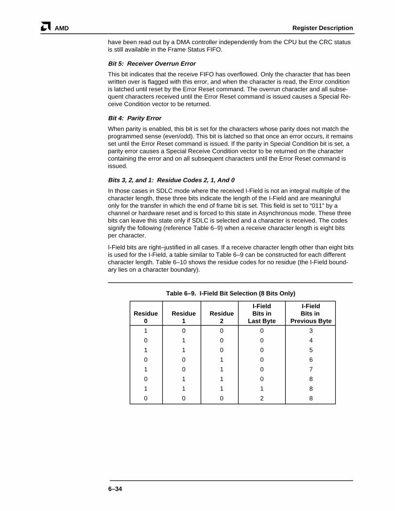
Register DescriptionAMD
6–34
have been read out by a DMA controller independently from the CPU but the CRC statusis still available in the Frame Status FIFO.
Bit 5: Receiver Overrun Error
This bit indicates that the receive FIFO has overflowed. Only the character that has beenwritten over is flagged with this error, and when the character is read, the Error conditionis latched until reset by the Error Reset command. The overrun character and all subse-quent characters received until the Error Reset command is issued causes a Special Re-ceive Condition vector to be returned.
Bit 4: Parity Error
When parity is enabled, this bit is set for the characters whose parity does not match theprogrammed sense (even/odd). This bit is latched so that once an error occurs, it remainsset until the Error Reset command is issued. If the parity in Special Condition bit is set, aparity error causes a Special Receive Condition vector to be returned on the charactercontaining the error and on all subsequent characters until the Error Reset command isissued.
Bits 3, 2, and 1: Residue Codes 2, 1, And 0
In those cases in SDLC mode where the received I-Field is not an integral multiple of thecharacter length, these three bits indicate the length of the I-Field and are meaningfulonly for the transfer in which the end of frame bit is set. This field is set to “011” by achannel or hardware reset and is forced to this state in Asynchronous mode. These threebits can leave this state only if SDLC is selected and a character is received. The codessignify the following (reference Table 6–9) when a receive character length is eight bitsper character.
I-Field bits are right–justified in all cases. If a receive character length other than eight bitsis used for the I-Field, a table similar to Table 6–9 can be constructed for each differentcharacter length. Table 6–10 shows the residue codes for no residue (the I-Field bound-ary lies on a character boundary).
Table 6–9. I-Field Bit Selection (8 Bits Only)
I-Field I-FieldResidue Residue Residue Bits in Bits in
0 1 2 Last Byte Previous Byte
1 0 0 0 3
0 1 0 0 4
1 1 0 0 5
0 0 1 0 6
1 0 1 0 7
0 1 1 0 8
1 1 1 1 8
0 0 0 2 8
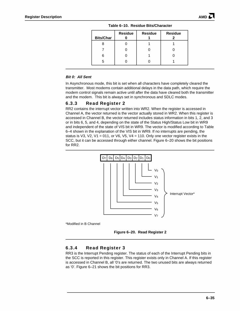
Register Description AMD
6–35
Table 6–10. Residue Bits/Character
Residue Residue ResidueBits/Char 0 1 2
8 0 1 1
7 0 0 0
6 0 1 0
5 0 0 1
Bit 0: All Sent
In Asynchronous mode, this bit is set when all characters have completely cleared thetransmitter. Most modems contain additional delays in the data path, which require themodem control signals remain active until after the data have cleared both the transmitterand the modem. This bit is always set in synchronous and SDLC modes.
6.3.3 Read Register 2RR2 contains the interrupt vector written into WR2. When the register is accessed inChannel A, the vector returned is the vector actually stored in WR2. When this register isaccessed in Channel B, the vector returned includes status information in bits 1, 2, and 3or in bits 6, 5, and 4, depending on the state of the Status High/Status Low bit in WR9and independent of the state of VIS bit in WR9. The vector is modified according to Table6–4 shown in the explanation of the VIS bit in WR9. If no interrupts are pending, thestatus is V3, V2, V1 = 011, or V6, V5, V4 = 110. Only one vector register exists in theSCC, but it can be accessed through either channel. Figure 6–20 shows the bit positionsfor RR2.
D7 D6 D5 D4 D3 D2 D1 D0
V3
V4
V5
V6
V0
V1
V2
V7
Interrupt Vector*
*Modified in B Channel
Figure 6–20. Read Register 2
6.3.4 Read Register 3RR3 is the Interrupt Pending register. The status of each of the Interrupt Pending bits inthe SCC is reported in this register. This register exists only in Channel A. If this registeris accessed in Channel B, all ‘0’s are returned. The two unused bits are always returnedas ‘0’. Figure 6–21 shows the bit positions for RR3.

Register DescriptionAMD
6–36
D7 D6 D5 D4 D3 D2 D1 D0
Channel A EXT/STAT IP
Channel A Tx IP
Channel A Rx IP
0
Channel B EXT/STAT IP
Channel B Tx IP
Channel B Rx IP
0
Always 0 in B Channel
Figure 6–21. Read Register 3
6.3.5 Read Register 6When the SCC is programmed for SDLC operation and bit D2 of WR15 is set to ‘1’, RR6contains the LSB of a frame byte count stored in the 10x19-bit FIFO array as shown inFigure 6–22.
D7 D6 D5 D4 D3 D2 D1 D0
Figure 6–22. Read Register 6
6.3.6 Read Register 7When the SCC is programmed for SDLC operation and bit D2 of WR15 is set to ‘1’, RR7contains the MSB of a frame byte count stored in the 10x19-bit FIFO array, and providesFIFO status via bits D7 and D6 as shown in Figure 6–23. Bit D7 is set to ‘1’ when the10x19-bit FIFO overflows; otherwise it is set to ‘0’. Bit D6 is used to determine if statusdata will be from the FIFO or directly from the 8-bit Status FIFO (RR1). This bit is set to‘1’ whenever the 10x19-bit FIFO is not empty; otherwise it is ‘0’.
D7 D6 D5 D4 D3 D2 D1 D0
FIFO Data Available Status1 = Status Reads Come From 10 x 9 Bit FIFO0 = Status Reads Come From SCC
MSB Byte Count
FIFO Overflow Status1 = FIFO Overflowed During Operation0 = Normal
Figure 6–23. Read Register 7

Register Description AMD
6–37
6.3.7 Read Register 8RR8 is the Receive Data register.
6.3.8 Read Register 10RR10 contains some miscellaneous status bits. Unused bits are always ‘0’. Bit positionsfor RR10 are shown in Figure 6–24.
D7 D6 D5 D4 D3 D2 D1 D0
0
Loop Sending
0
Two Clocks Missing
0
On Loop
0
One Clock Missing
Figure 6–24. Read Register 10
Bit 7: One Clock Missing
While operating in the FM mode, the DPLL sets this bit to ‘1’ when it does not see a clockedge on the incoming lines in the window where it expects one. This bit is latched untilreset by a Reset Missing Clock or Enter Search Mode command in WR14. In the NRZImode of operation and while the DPLL is disabled, this bit is always ‘0’.
Bit 6: Two Clocks Missing
While operating in the FM mode, the DPLL sets this bit to ‘1’ when it does not see a clockedge in two successive tries. At the same time the DPLL enters the Search mode. This bitis latched until reset by a Reset Missing Clock or Enter Search Mode command in WR14.In the NRZI mode of operation and while the DPLL is disabled, this bit is always ‘0’.
Bit 4: Loop Sending
This bit is set to ‘1’ in SDLC Loop mode while the transmitter is in control of the Loop, thatis, while the SCC is actively transmitting on the loop. This bit is reset at all other times.
This bit can be polled in SDLC mode to determine when the closing flag has been sent.
Bit 1: On Loop
This bit is set to ‘1’ while the SCC is actually on-loop in SDLC Loop mode. This bit is setto ‘1’ in the X21 mode (Loop mode selected while in monosync) when the transmittergoes active. This bit is ‘0’ at all other times. This bit can also be polled in SDLC mode todetermine when the closing flag has been sent.
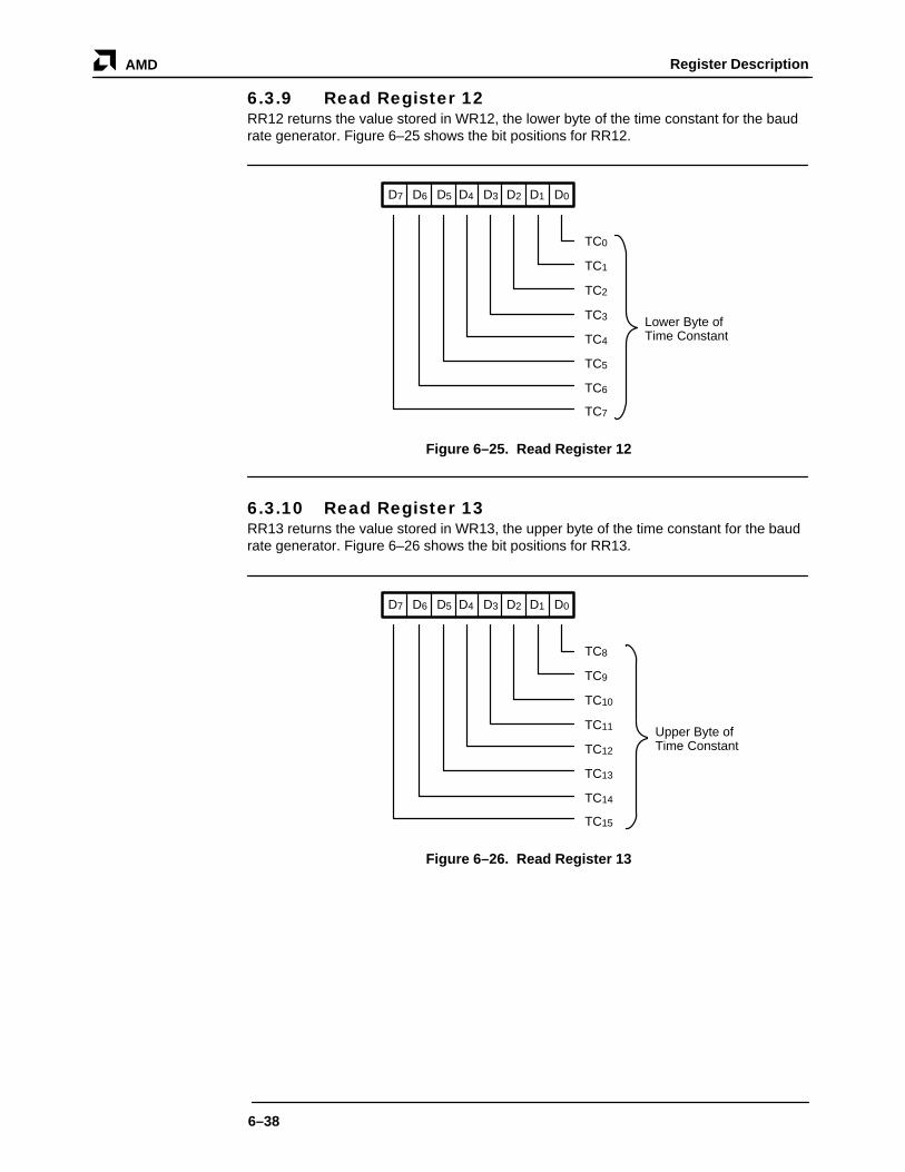
Register DescriptionAMD
6–38
6.3.9 Read Register 12RR12 returns the value stored in WR12, the lower byte of the time constant for the baudrate generator. Figure 6–25 shows the bit positions for RR12.
D7 D6 D5 D4 D3 D2 D1 D0
TC3
TC4
TC5
TC6
TC0
TC1
TC2
TC7
Lower Byte ofTime Constant
Figure 6–25. Read Register 12
6.3.10 Read Register 13RR13 returns the value stored in WR13, the upper byte of the time constant for the baudrate generator. Figure 6–26 shows the bit positions for RR13.
D7 D6 D5 D4 D3 D2 D1 D0
TC11
TC12
TC13
TC14
TC8
TC9
TC10
TC15
Upper Byte ofTime Constant
Figure 6–26. Read Register 13

Register Description AMD
6–39
6.3.11 Read Register 15RR15 reflects the value stored in WR15, the External/Status IE bits. The unused bit isalways returned as ‘0’ unless the corresponding bits in WR15 have been set to ‘1’. In theNMOS SCC, bits D0 and D2 always read 0. Figure 6–27 shows the bit positions for RR15.
D7 D6 D5 D4 D3 D2 D1 D0
DCD IE
SYNC/HUNT IE
CTS IE
Tx Underrun/EOM IE
SDLC/HDLC Enhancement Status
Zero Count IE
10 x 19-Bit Frame Status FIFO Enable Status
Break/Abort IE
Figure 6–27. Read Register 15

7–1
CHAPTER 7SCC Application Notes
7.1 Am8530H Initialization 7–3. . . . . . . . . . . . . . . . . . . . . . . . . . . . . . . . . . . . . . . . . . 7.1.1 Introduction 7–3. . . . . . . . . . . . . . . . . . . . . . . . . . . . . . . . . . . . . . . . . . . . .
7.1.1.1 Register Overview 7–3. . . . . . . . . . . . . . . . . . . . . . . . . . . . . . . . . 7.1.1.2 Initialization Procedure 7–4. . . . . . . . . . . . . . . . . . . . . . . . . . . . . 7.1.1.3 Initialization Table Generation 7–6. . . . . . . . . . . . . . . . . . . . . . . . 7.1.1.4 Reset Conditions 7–6. . . . . . . . . . . . . . . . . . . . . . . . . . . . . . . . . .
7.2 Polled Asynchronous Mode 7–7. . . . . . . . . . . . . . . . . . . . . . . . . . . . . . . . . . . . . . . 7.2.1 Introduction 7–7. . . . . . . . . . . . . . . . . . . . . . . . . . . . . . . . . . . . . . . . . . . . . 7.2.2 SCC Interface 7–8. . . . . . . . . . . . . . . . . . . . . . . . . . . . . . . . . . . . . . . . . . . 7.2.3 SCC Initialization 7–8. . . . . . . . . . . . . . . . . . . . . . . . . . . . . . . . . . . . . . . . .
7.2.3.1 SCC Operating Mode Programming 7–9. . . . . . . . . . . . . . . . . . . 7.2.3.2 SCC Operating Mode Enables 7–10. . . . . . . . . . . . . . . . . . . . . . .
7.2.4 Transmit and Receive Routines 7–10. . . . . . . . . . . . . . . . . . . . . . . . . . . . . . 7.3 Interrupt Without Intack Asynchronous Mode 7–11. . . . . . . . . . . . . . . . . . . . . . . . .
7.3.1 Introduction 7–11. . . . . . . . . . . . . . . . . . . . . . . . . . . . . . . . . . . . . . . . . . . . . 7.3.2 SCC Interface 7–11. . . . . . . . . . . . . . . . . . . . . . . . . . . . . . . . . . . . . . . . . . . 7.3.3 SCC Initialization 7–11. . . . . . . . . . . . . . . . . . . . . . . . . . . . . . . . . . . . . . . . .
7.3.3.1 SCC Operating Modes Programming 7–12. . . . . . . . . . . . . . . . . . 7.3.3.2 SCC Operating Mode Enables 7–13. . . . . . . . . . . . . . . . . . . . . . . 7.3.3.3 SCC Operating Mode Interrupts 7–13. . . . . . . . . . . . . . . . . . . . . .
7.3.4 Interrupt Routine 7–14. . . . . . . . . . . . . . . . . . . . . . . . . . . . . . . . . . . . . . . . . 7.4 Interfacing to the 8086/80186 7–15. . . . . . . . . . . . . . . . . . . . . . . . . . . . . . . . . . . . .
7.4.1 8086 (Also Called iAPX86) Overview 7–15. . . . . . . . . . . . . . . . . . . . . . . . . 7.4.1.1 The 8086 and Am8530H Interface 7–15. . . . . . . . . . . . . . . . . . . . 7.4.1.2 Initialization Routines 7–18. . . . . . . . . . . . . . . . . . . . . . . . . . . . . .
7.5 Interfacing to the 68000 7–20. . . . . . . . . . . . . . . . . . . . . . . . . . . . . . . . . . . . . . . . . 7.5.1 68000 Overview 7–20. . . . . . . . . . . . . . . . . . . . . . . . . . . . . . . . . . . . . . . . . . 7.5.2 The 68000 and Am8530H Without Interrupts 7–21. . . . . . . . . . . . . . . . . . . 7.5.3 The 68000 and Am8530H With Interrupts 7–23. . . . . . . . . . . . . . . . . . . . . . 7.5.4 The 68000 and Am8530H With Interrupts
via a PAL Device 7–25. . . . . . . . . . . . . . . . . . . . . . . . . . . . . . . . . . . . . . . . . 7.6 Am7960 and Am8530H Application 7–26. . . . . . . . . . . . . . . . . . . . . . . . . . . . . . . .
7.6.1 Distributed Data Processing Overview 7–26. . . . . . . . . . . . . . . . . . . . . . . . 7.6.2 Data Communications at the Physical Layer 7–27. . . . . . . . . . . . . . . . . . . . 7.6.3 Hardware Considerations 7–28. . . . . . . . . . . . . . . . . . . . . . . . . . . . . . . . . . 7.6.4 Software Considerations 7–32. . . . . . . . . . . . . . . . . . . . . . . . . . . . . . . . . . .

SCC Application NotesAMD
7–2

7–3
SCC Application Notes
CHAPTER 7
7.1 Am8530H INITIALIZATION
7.1.1 IntroductionThis application note describes the software initialization procedure for the Am8530 SerialCommunications Controller (SCC).
Table 7–1 provides a worksheet that can be used as an aid when initializing the SCC.Since all SCC operation modes are initialized in a similar manner, the worksheet can beused to tailor the SCC device to the user’s individual need. Specific examples are given inthe following chapters.
7.1.1.1 Register OverviewEach of the SCC’s two channels has its own separate Write registers that are pro-grammed to initialize different operating modes. There are two types of bits in the Writeregisters: Command bits and Mode bits. An example of a register that contains bothtypes of bits is Write Register 9 (WR9), and is shown in Figure 7–1.
WR9 is the Master Interrupt Control register and contains the Reset command bits. Com-mand bits are denoted by having boxes drawn around them in register diagrams. Bit D5in this register is not used in this register and must be 0 at all times.
D7 D6 D5 D4 D3 D2 D1 D0
0 0
0 1
1 0
1 1
No Reset
Channel Reset B
Channel Reset A
Force Hardware Reset
VIS
NV
DLC
0
MIE
STATUS HIGH/STATUS LOW
Figure 7–1. Write Register 9
The Command bits, D7 and D6, select one of the reset commands for the SCC. Settingeither of these bits to 1 disables both the receiver and the transmitter in the correspond-ing channel, forces TxD for the channel marking, forces the modem control signals Highin that channel, resets all IPs and IUSs, and disables all interrupts in that channel. Func-tions controlled by the Command bits can be enabled or disabled only; they cannot betoggled.

SCC Application NotesAMD
7–4
Bits D4–D0 are Mode bits that can be enabled or disabled either by being set to ‘1’ or re-set to ‘0’. Each Mode bit affects only one function. For example, Bit D1 is the No Vectormode bit; it controls whether or not the SCC will respond to an interrupt acknowledge cy-cle by placing a vector on the data bus. If this bit is set, no vector is returned. In Com-mand bits entry, each new command requires a separate rewrite of the entire register.Care must be taken when issuing a command so that the Mode bits are not changed acci-dentally.
7.1.1.2 Initialization ProcedureThe SCC initialization procedure is divided into three parts. The first part consists of pro-gramming the operation modes (e.g., bits-per-character, parity) and loading the constants(e.g., interrupt vector, time constants). The second part enables the hardware functions(e.g., transmitter, receiver, baud-rate generator). It is important that the operating modesare programmed before the hardware functions are enabled. The third part, if required,consists of enabling the different interrupts.
Table 7–2 shows the order (from top to bottom) in which the SCC registers are to be pro-grammed. Those registers that need not be programmed are listed as optional in thecomments column. The bits in the registers that are marked with an ‘X’ are to be pro-grammed by the user. The bits marked with an ‘S’ are to be set to their previous pro-grammed value. For example, in part 2, Write Register 3, bits D1–D7 are shown with an‘S’ because they have been programmed in part 1 and must remain set to the samevalue.

SCC Application Notes AMD
7–5
Table 7–1. SCC Initialization Worksheet
1 1 0 0 0 0 0 0
7 6 5 4 3 2 1 00CWR9
Register HEX Binary Comments
Software Reset
Modes
0 0 0 0 0 00WR0
WR4
0 0 0 0 0WR1
WR2
0WR3
0WR5
WR6
WR7
0 0 0 0WR9
WR10
WR11
WR12
WR13
0WR14
0WR14
WR14
WR3
WR5
0WR0
WR1
WR15
WR0
WR0
WR1
WR9
Enables
Interrupt
08
01
01
0 0 0 1
1
1
1 0 0 0 0 0 1
00 0 0 1 0 0 0
Reset TxCRC
Reset Ext/Status
Reset Ext/Status00 0 0 1 0 0 0
0 0 0
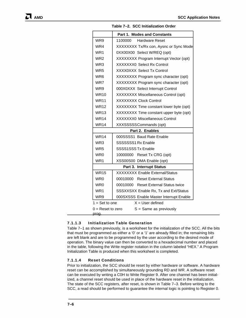
SCC Application NotesAMD
7–6
Table 7–2. SCC Initialization Order
Part 1. Modes and Constants
WR9 1100000 Hardware Reset
WR4 XXXXXXXX Tx/Rx con, Aysnc or Sync Mode
WR1 0XX00X00 Select W/REQ (opt)
WR2 XXXXXXXX Program Interrupt Vector (opt)
WR3 XXXXXXX0 Select Rx Control
WR5 XXXX0XXX Select Tx Control
WR6 XXXXXXXX Program sync character (opt)
WR7 XXXXXXXX Program sync character (opt)
WR9 000X0XXX Select Interrupt Control
WR10 XXXXXXXX Miscellaneous Control (opt)
WR11 XXXXXXXX Clock Control
WR12 XXXXXXXX Time constant lower byte (opt)
WR13 XXXXXXXX Time constant upper byte (opt)
WR14 XXXXXXX0 Miscellaneous Control
WR14 XXXSSSSSCommands (opt)
Part 2. Enables
WR14 000SSSS1 Baud Rate Enable
WR3 SSSSSSS1 Rx Enable
WR5 SSSS1SSS Tx Enable
WR0 10000000 Reset Tx CRG (opt)
WR1 XSS00S00 DMA Enable (opt)
Part 3. Interrupt Status
WR15 XXXXXXXX Enable External/Status
WR0 00010000 Reset External Status
WR0 00010000 Reset External Status twice
WR1 SSSXXSXX Enable Rx, Tx and Ext/Status
WR9 000SXSSS Enable Master Interrupt Enable
1 = Set to one X = User defined
0 = Reset to zero S = Same as previouslyprog.
7.1.1.3 Initialization Table GenerationTable 7–1 as shown previously, is a worksheet for the initialization of the SCC. All the bitsthat must be programmed as either a ‘0’ or a ‘1’ are already filled in; the remaining bitsare left blank and are to be programmed by the user according to the desired mode ofoperation. The binary value can then be converted to a hexadecimal number and placedin the table, following the Write register notation in the column labeled “HEX.” A ProgramInitialization Table is produced when this worksheet is completed.
7.1.1.4 Reset ConditionsPrior to initialization, the SCC should be reset by either hardware or software. A hardwarereset can be accomplished by simultaneously grounding RD and WR. A software resetcan be executed by writing a C0H to Write Register 9. After one channel has been initial-ized, a channel reset should be used in place of the hardware reset in the initialization.The state of the SCC registers, after reset, is shown in Table 7–3. Before writing to theSCC, a read should be performed to guarantee the internal logic is pointing to Register 0.

SCC Application Notes AMD
7–7
7.2 POLLED ASYNCHRONOUS MODE
7.2.1 IntroductionThis section describes the use of the SCC in polled Asynchronous mode. The device canbe set with 5 to 8 bits per character, 1, 1-1/2, or 2 stop bits, and a wide range of baudrates. In this particular example, 8 bits per character, 2 stop bits and 9600 baud rate areused. An external 2.4576 MHz, crystal oscillator is used for baud-rate generation. TheSCC can be programmed for local loopback for on-board diagnostics. The user can makeuse of this feature to test-program the part without additional hardware to simulate an ac-tual transmit and receive environment.
Table 7–3. SCC Register Reset Values
0 0 0 0 0 0 0 0
7 6 5 4 3 2 1 0
WR0
Register Hardware Reset
0 0 0 0WR1
WR2
0WR3
WR4
0WR5
WR6
WR7
1 1 0 0WR9
WR10
WR11
WR12
WR13
0WR14
0WR15
RR0
RR1
RR3
0RR10
0 1 0
0
0 0 0 0 0 0 0
0 0 0 0 0 0 0 0
7 6 5 4 3 2 1 0
Channel Reset
0 0 0 0 0 0
0
0
0
0
0 1 0
0
0
0 0 0 0 0 0 0
0 0
1
0 0 0 0
0 0 0 0 0 0
0 0
0 0
0 0 0 0 1 0 0 0
1 0 0 0 0
1 0
1 1 1 1 1 0 0
0 1 0 0 0 1 1
0 0 0 0 0 0 0 0 00 0 0 0 0 0
00 0 0 0 1 1
1 0
11 1 1 1 0 0
01 0 0
000 0 0 0
0 0 0 0 0
1
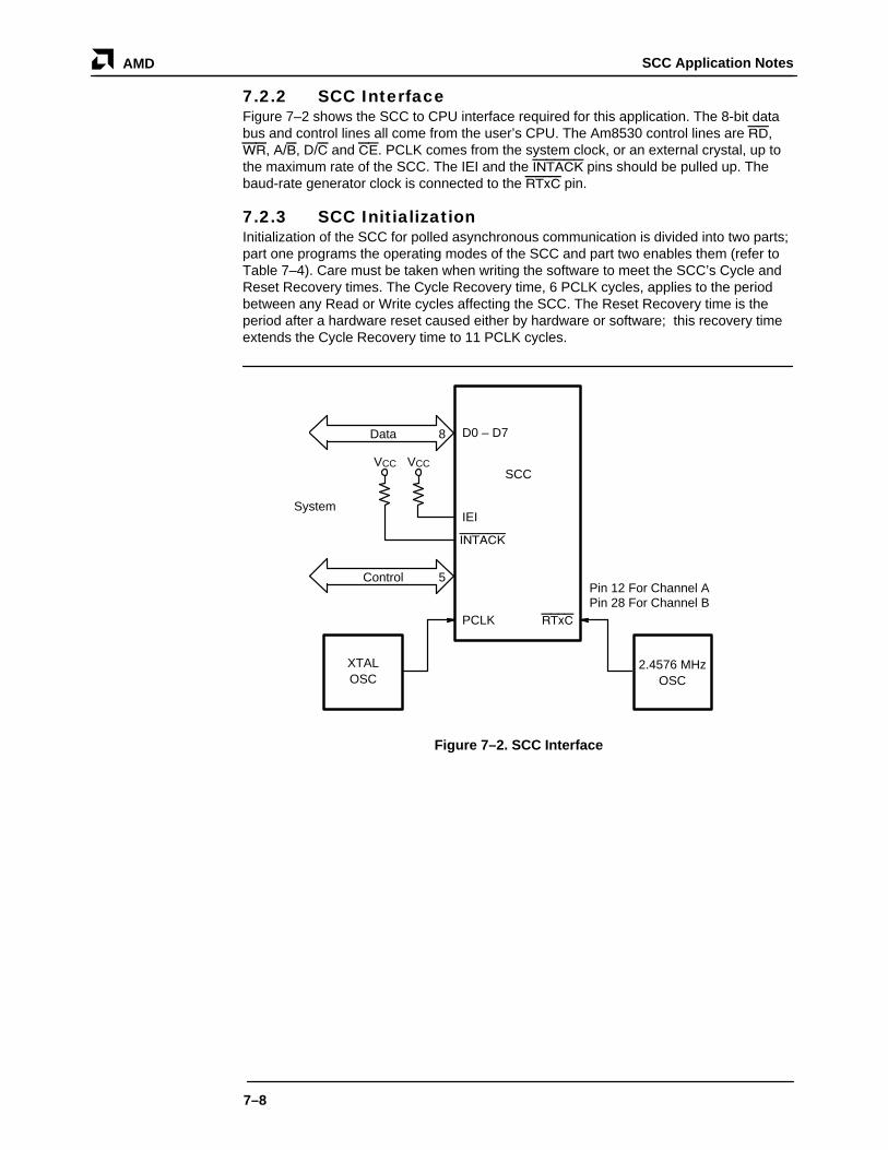
SCC Application NotesAMD
7–8
7.2.2 SCC InterfaceFigure 7–2 shows the SCC to CPU interface required for this application. The 8-bit databus and control lines all come from the user’s CPU. The Am8530 control lines are RD,WR, A/B, D/C and CE. PCLK comes from the system clock, or an external crystal, up tothe maximum rate of the SCC. The IEI and the INTACK pins should be pulled up. Thebaud-rate generator clock is connected to the RTxC pin.
7.2.3 SCC InitializationInitialization of the SCC for polled asynchronous communication is divided into two parts;part one programs the operating modes of the SCC and part two enables them (refer toTable 7–4). Care must be taken when writing the software to meet the SCC’s Cycle andReset Recovery times. The Cycle Recovery time, 6 PCLK cycles, applies to the periodbetween any Read or Write cycles affecting the SCC. The Reset Recovery time is theperiod after a hardware reset caused either by hardware or software; this recovery timeextends the Cycle Recovery time to 11 PCLK cycles.
Data 8
Control 5
System
VCC VCC
XTALOSC
2.4576 MHzOSC
PCLK RTxC
INTACK
IEI
D0 – D7
SCC
Pin 12 For Channel APin 28 For Channel B
Figure 7–2. SCC Interface

SCC Application Notes AMD
7–9
Table 7–4. Polled Asynchronous Initialization Procedure
Register Value Comments
WR9 C0H Force Hardware Reset
WR4 4CH x16 clock, 2 stop bits, no parity
WR3 C0H Rx 8 bits, Rx disabled
WR5 60H Tx 8 bits, DTR, RTS, Tx off
WR9 00H Int. Disabled
WR10 00H NRZ
WR11 56H Tx & Rx = BRG out, TRxC = BRG out
WR12 06H Time constant = 6
WR13 00H Time constant high = 0
WR14 10H BRG in = RTxC, BRG off, loopback
Enables
WR14 11H BRG enable
WR3 C1H Rx enable
WR5 68H Tx enable
7.2.3.1 SCC Operating Mode ProgrammingWR9 resets the SCC to a known state by writing a C0 hex. The Force Hardware Resetcommand is identical to a hardware reset. It will reset both channels.
WR4 selects the Asynchronous, x 16 mode, with 2 stop bits and no parity. The x 16 modemeans that clock rate is 16 times the data rate.
WR3 selects 8 bits per character and does not enable the receive. The 8 bits per charac-ter allows 8 bits to be assembled from the data stream. The receiver is not enabled at thistime because the SCC has not been initialized.
WR5 selects 8 bits per character and does not enable the transmitter. The 8 bits per char-acter allows 8 bits to be sent, as data, with the least significant bit first. The transmitter isnot enabled at this time because the SCC has not been initialized.
WR9 selects that there are no interrupts enabled. This inhibits the SCC from requestingan interrupt from the CPU.
WR10 selects NRZ encoding. This NRZ coding is used on the transmitter as well as thereceiver.
WR11 selects the RTxC pin to TTL clock; the baud-rate generator is the transmit and re-ceive clocks source, and the TRxC pin is used as a baud-rate generator output.
WR12 & WR13 select the baud-rate generator’s time constant. The WR13 time constantis determined by the equation:
Time Constant =Clock Frequency
2 x Baud Rate x clock mode–2
In this example, the clock frequency is 2.4576 MHz, the baud rate is 9600, the clockmode is 16. The time constant is, therefore, 6; expressed as a 16-bit, hexadecimal num-ber, it is 0006H. The time constant Low (WR12) is, therefore 06H and the time constantHigh (WR13) is 00H. The baud rate for this example can be varied, as long as the datarate is less than 1/4 of the PCLK rate. Table 7–5 shows the time constants for other com-mon baud rates.
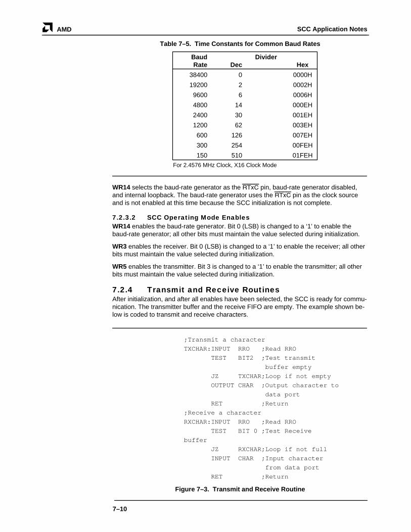
SCC Application NotesAMD
7–10
Table 7–5. Time Constants for Common Baud Rates
Baud DividerRate Dec Hex
38400 0 0000H
19200 2 0002H
9600 6 0006H
4800 14 000EH
2400 30 001EH
1200 62 003EH
600 126 007EH
300 254 00FEH
150 510 01FEH
For 2.4576 MHz Clock, X16 Clock Mode
WR14 selects the baud-rate generator as the RTxC pin, baud-rate generator disabled,and internal loopback. The baud-rate generator uses the RTxC pin as the clock sourceand is not enabled at this time because the SCC initialization is not complete.
7.2.3.2 SCC Operating Mode EnablesWR14 enables the baud-rate generator. Bit 0 (LSB) is changed to a ‘1’ to enable thebaud-rate generator; all other bits must maintain the value selected during initialization.
WR3 enables the receiver. Bit 0 (LSB) is changed to a ‘1’ to enable the receiver; all otherbits must maintain the value selected during initialization.
WR5 enables the transmitter. Bit 3 is changed to a ‘1’ to enable the transmitter; all otherbits must maintain the value selected during initialization.
7.2.4 Transmit and Receive RoutinesAfter initialization, and after all enables have been selected, the SCC is ready for commu-nication. The transmitter buffer and the receive FIFO are empty. The example shown be-low is coded to transmit and receive characters.
;Transmit a character
TXCHAR:INPUT RRO ;Read RRO
TEST BIT2 ;Test transmit
buffer empty
JZ TXCHAR;Loop if not empty
OUTPUT CHAR ;Output character to
data port
RET ;Return
;Receive a character
RXCHAR:INPUT RRO ;Read RRO
TEST BIT 0 ;Test Receive
buffer
JZ RXCHAR;Loop if not full
INPUT CHAR ;Input character
from data port
RET ;Return
Figure 7–3. Transmit and Receive Routine

SCC Application Notes AMD
7–11
7.3 INTERRUPT WITHOUT INTACK ASYNCHRONOUS MODE
7.3.1 IntroductionThis section describes the use of the SCC for interrupt-driven Asynchronous mode. Aswith the example in the previous chapter, the SCC is set with 8 bits per character, 2 stopbits, at 9600 baud rate. An external 2.4576 MHz, crystal oscillator is used for baud-rategeneration. Interrupt acknowledge is not generated because of the extra hardware re-quired to produce this signal. In this chapter, the SCC is also programmed for local loop-back so that no external loop between the transmit and the receive data lines is neededfor on-board diagnostics. This feature allows the user to test-program the part withoutadditional hardware to simulate an actual transmit and receive environment.
7.3.2 SCC InterfaceFigure 7–4 shows the SCC to CPU interface required for this application. The 8-bit databus and control lines all come from the user’s CPU. The control lines are RD, WR, A/B,D/C and CE. The INT signal goes to an interrupt controller which must produce the inter-rupt vector to the CPU. The PCLK comes from the system clock, or an external crystaloscillator, up to the maximum rate of the SCC (e.g., 6 MHz for the Am8530A). The IEIand the INTACK pins should be pulled up. The baud-rate generator clock is connected tothe RTxC pin.
7.3.3 SCC InitializationThe initialization of the SCC for interrupt-driven asynchronous communication is dividedinto three parts as shown in Table 7–6. Part one programs the operating modes of theSCC, part two and three enable them. Care must be taken when writing the code to meetthe SCC’s Cycle and Reset Recovery times. The Cycle Recovery time applies to the pe-riod between any Read or Write cycles to the SCC, and is 6 PCLK cycles. The Reset Re-covery time applies to a hardware reset caused either by hardware or software; thisrecovery time extends the Cycle Recovery time to 11 PCLK cycles.
Data 8
Control 5
System
VCC VCC
XTALOSC
2.4576 MHzOSC
PCLK RTxC
INTACK
IEI
D0 – D7
SCC
Pin 12 For Channel APin 28 For Channel B
InterruptController
INT
Figure 7–4. SCC Interface

SCC Application NotesAMD
7–12
Table 7–6. SCC Initialization Order for Interrupt Driven Asynchronous Mode
Register Value Comments
WR9 C0H Force Hardware Reset
WR4 4CH x 16 clock, 2 stop bits, no parity
WR2 00H Interrupt Vector 00
WR3 C0H Rx 8 bits, Rx disabled
WR5 60H Tx 8 bits, DTR, RTS, Tx off
WR9 00H Int Disabled
WR10 00H NRZ
WR11 56H Tx & Rx = BRG out, TRxC = BRG out
WR12 06H Time constant = 6
WR13 00H Time constant high = 0
WR14 10H BRG in = RTxC, BRG of, loopback
Enables
WR14 11H BRG enable
WR3 C1H Rx enable
WR5 68H Tx enable
Enable Interrupts
WR1 12H Rx Int on all char and Tx Int enables
WR9 08H MIE
7.3.3.1 SCC Operating Modes ProgrammingWR9 resets SCC to a known state by writing a C0 hex. This command, Force HardwareReset, is identical to a hardware reset. It will reset both channels.
WR4 selects asynchronous mode, x16 mode, 2 stop bits and no parity. The x16 modemeans that the clock rate is 16 times the data rate.
WR2 is the interrupt vector of the SCC. Even though a vector is not placed in the bus inthis mode the vector including status is read from RR2. By writing 00H to this register thestatus read will be the only bits set in RR2.
WR3 selects 8 bits per character and does not enable the receiver. The 8 bits per charac-ter allows 8 bits to be assembled from the data stream. The receiver is not enabled at thistime because the SCC is not completely initialized.
WR5 selects 8 bits per character and does not enable the transmitter. The 8 bits per char-acter allows 8 bits to be sent as data with the least significant bit first. The transmitter isnot enabled at this time because the SCC is not completely initialized.
WR9 selects that there are no interrupts enabled. This will inhibit the SCC from request-ing an interrupt from the CPU.
WR10 selects NRZ encoding. This selects NRZ coding that is to be used on the transmit-ter and the receiver.
WR11 selects the RTxC pin to TTL clock, the transmit and receive clocks source as thebaud-rate generator and the TRxC pin as a baud-rate generator output.

SCC Application Notes AMD
7–13
WR12 & WR13 select the baud-rate generator time constant. The time constant is deter-mined by the equation:
Time Constant =Clock Frequency
2 x Baud Rate x clock mode–2
In this example, the clock frequency is 2.4576 MHz, the baud rate is 9600, and the clockmode is 16; the time constant is 6. Converting this time constant to a 16-bit hexadecimalnumber, it becomes 0006H. The time constant Low (WR12) is 06H and the time constantHigh (WR13) is 00H. The baud rate for this example can be varied for as long as the datarate is less than 1/4 of the PCLK rate. Table 7–7 gives the time constants for other com-mon baud rates.
Table 7–7. Time Constants for Common Baud Rates
Baud DividerRate Dec Hex
38400 0 0000H
19200 2 0002H
9600 6 0006H
4800 14 000EH
2400 30 001EH
1200 62 003EH
600 126 007EH
300 254 00FEH
150 510 01FEH
For 2.4576 MHz Clock, X16 Clock Mode
WR14 selects the baud rate source as the RTxC pin, baud rate generator disabled, andinternal loopback. The baud-rate generator will use the RTxC pin as the clock source forthe baud-rate generator. The baud-rate generator is not enabled at this time because theSCC initialization is not complete.
7.3.3.2 SCC Operating Mode EnablesWR14 enables the baud-rate generator. Bit 0 (LSB) is changed to a 1 to enable the baud-rate generator; all other bits must maintain the value selected during initialization.
WR3 enables the receiver. Bit 0 (LSB) is changed to a 1 to enable the receiver; all otherbits must maintain the value selected during initialization.
WR5 enables the transmitter. Bit 3 is changed to a 1 to enable the transmitter; all otherbits must maintain the value selected during initialization.
7.3.3.3 SCC Operating Mode InterruptsWR1 enables the Tx and the Rx interrupts. The Rx interrupt is programmed to generatean interrupt on all received characters or special conditions. This provides an interrupt onevery character received by the SCC. The external/status interrupts are not enabled inthis application.
WR9 sets the master interrupt enable (MIE) bit 3. Setting this bit enables the interruptspending to generate and interrupt on the INT pin.
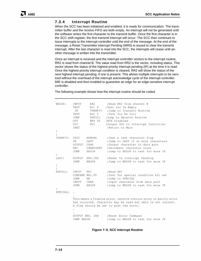
SCC Application NotesAMD
7–14
7.3.4 Interrupt RoutineWhen the SCC has been initialized and enabled, it is ready for communication. The trans-mitter buffer and the receive FIFO are both empty. An interrupt will not be generated untilthe software writes the first character to the transmit buffer. Once the first character is inthe SCC shift register, the first transmit interrupt will occur. The SCC then continues toissue interrupts to the interrupt controller until the end of the message. At the end of themessage, a Reset Transmitter Interrupt Pending (WR0) is issued to clear the transmitinterrupt. After the last character is read into the SCC, the interrupts will cease until an-other message is written into the transmitter.
Once an interrupt is received and the interrupt controller vectors to the interrupt routine,RR2 is read from channel B. The value read from RR2 is the vector, including status. Thisvector shows the status of the highest priority interrupt pending (IP) at the time it is read.Once the highest priority interrupt condition is cleared, RR2 will show the status of thenext highest interrupt pending, if one is present. This allows multiple interrupts to be serv-iced without the overhead of the interrupt acknowledge cycle of the interrupt controller.MIE is disabled and then enabled to guarantee an edge for an edge-sensitive interruptcontroller.
The following example shows how the interrupt routine should be coded.
BEGIN: INPUT RR2 ;Read RR2 from channel B TEST Bit 4 ;Test for Tx Empty JE TXEMPTY ;Jump to Transmit Routine TEST Bit 5 ;Test for Rx full JUMP RXFULL ;Jump to Receive Routine OUT WR9 00 ;MIE Disabled OUT EOI ;Output EOI to Interrupt Controller IRET ;Return to Main;;TXEMPTY: TEST NOMORE ;Test a last character flag JE LAST ;Jump to LAST if no more characters OUTPUT CHAR ;Output character to data port DEC CHARCOUNT ;Decrement character count JUMP BEGIN ;Jump to BEGIN to test for more IP;LAST: OUTPUT RR0,28H ;Reset Tx Interrupt Pending JUMP BEGIN ;Jump to BEGIN to test for more IP;;RXFULL: INPUT RR1 ;Read RR1 COMPARE RR1,00 ;Test for special condition bit set JUMP NE ;Jump to SPECIAL INPUT CHAR ;Input charcater from data port JUMP BEGIN ;Jump to BEGIN to test for more IP;SPECIAL; . . This means a framing error, receive overrun error or parity error
has occurred. Character may be read but data is not correct. A flag should be set to post the error.
. .
OUTPUT RR0, 30H ;Reset Error Command JUMP BEGIN ;Jump to BEGIN to test for more IP
Figure 7–5. SCC Interrupt Routine

SCC Application Notes AMD
7–15
7.4 INTERFACING TO THE 8086/80186
7.4.1 8086 (Also Called iAPX 86) OverviewThe 8086 is a general purpose 16-bit microprocessor CPU. The CPU has a 16 bit databus multiplexed with sixteen address outputs. There are four additional address lines(segment addresses which are multiplexed with STATUS) that increase the memoryrange to 1 Mbyte. The 8086 addresses are specified as bytes. In a 16 bit word, the leastsignificant byte has the higher address. This is compatible with 8080, 8085, Z80 andPDP11 addressing schemes but differs from the Z8000 and 68000 addressing.
The data bus is “asynchronous;” i.e, the CPU machine cycle can be stretched withoutclock manipulation by inserting Wait states between T2 and T3 of a read or write cycle toaccommodate slower memory or peripherals. Unlike the 68000, the 8086 has separateaddress spaces for I/O (64 kBytes).
The 8086 can operate in MIN. or MAX. mode. Maximum mode offloads certain bus con-trol functions to a peripheral device and allows the CPU to operate efficiently in a co-proc-essor environment. A brief discussion on both the MIN. and the MAX. modes follows.
MIN. mode : I/O addressing is define by a High or the IO/M output, and activated by the RD output for reading from memory, or I/O or activated by the WR output for writing to memory or I/O.
DMA: The Bus is requested by activating the HOLD input to the 8086. Bus Grant is confirmed by the HLDA output from the 8086.
MAX. mode : I/O operation is controlled by two outputs from the 8288.
(8086 plus IORC: active during Read from I/O
8288) IOWC: active during Write to I/O
MRDC: active during Read from memory
MWTC: active during Write to memory
DMA: The Bus is requested and Bus Grant is acknowledged on the same pin (RQ/GT0 OR RQ/GT1) through a pulsed handshake.
Interrupts In MIN. and MAX. Modes:Interrupt is requested by activating the INTR or NMI inputs to the 8086.
Interrupt is acknowledged by the INTA pin on a MIN. mode 8086 or by the INTA pin onthe 8288 in MAX. mode.
Note: There is no RD or IORC during the interrupt acknowledge sequence.
7.4.1.1 The 8086 and Am8530H InterfaceMost common systems demultiplex address and data. The Am8530H is compatible withthese systems.
Interface between the 8086 and the Am8530H peripheral device shows how to take ad-vantage of its interrupt structure as shown in Figure 7–6. INTACK is generated by the8086’s first INTA pulse. This allows about 800 nsec for the interrupt daisy chain to settle.The second INTA pulse is then gated to the RD pin which places the vector on the bus. At8 MHz, two Wait States must be inserted. This design is the same when interfacing to the186. It requires no additional Wait States. Diagrams in Figure 7–7 show the connectionsfor 74LS74 in both 5 MHz and 8 MHz operations of the 8086. Figure 7–8 is an alternateimplementation which can be used in place of the logic in the dotted area in Figure 7–6.
Note that the falling edge of WR must be delayed to meet data setup time requirements.A Wait State must be inserted (not shown) to meet pulse width requirements during awrite.
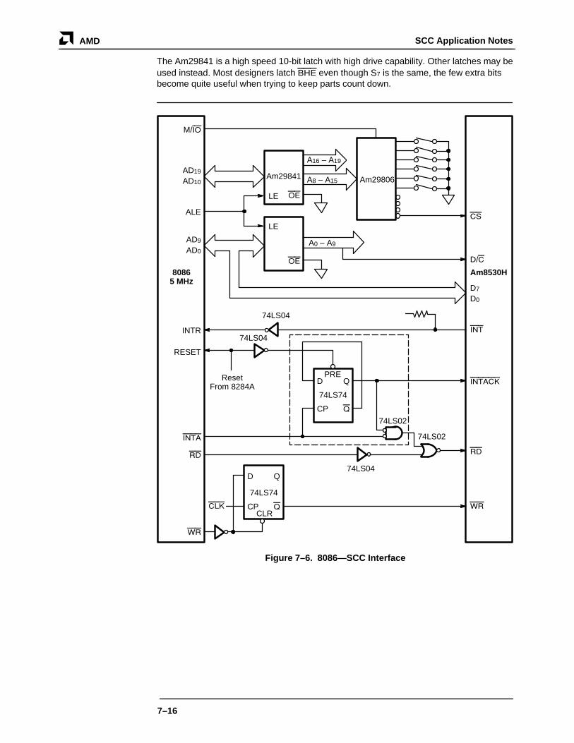
SCC Application NotesAMD
7–16
The Am29841 is a high speed 10-bit latch with high drive capability. Other latches may beused instead. Most designers latch BHE even though S7 is the same, the few extra bitsbecome quite useful when trying to keep parts count down.
A0 – A9
A8 – A15
A16 – A19
M/IO
AD19
AD10
ALE
AD9
AD0
INTR
RESET
INTA
RD
WR
CLK
CS
D/C
D7
D0
INT
INTACK
RD
WR
Am8530H80865 MHz
Am29841
LE OE
OE
LE
Am29806
74LS04
74LS04
ResetFrom 8284A
74LS04
74LS02
74LS02
PRED
CP
Q
Q
74LS74
D
CP
Q
QCLR
74LS74
Figure 7–6. 8086—SCC Interface

SCC Application Notes AMD
7–17
T1 T2 T3 T4 T1 T1 T1 T2 T3 T4
125 ns
186 186
8 x 125 = 1000 ns 8 MHz 8086
6 x 200 = 1200 ns 5 MHz 8086
8 MHz = 325
INTA
INTA1
INTA2
PRED
CP
Q
Q
74LS74
INTA1
INTA
RESET
PRED
CP
Q
Q
74LS74
INTA2
INTA
RESET
8 MHz 8086Figure A
5 MHz 8086Figure B
Figure 7–7. Interrupt Acknowledge Timing
INTA
RESET
INTACK
RD
D
CP
Q1
Q1
CLR CLR
D
CP
Q2PR
INTA
Q1
Q2 = INTACK
RD
Figure 7–8. Interrupt Acknowledge Timing Implementation

SCC Application NotesAMD
7-18
7.5.1.2 Initialization Routines
The sample assembly initialization routine, Figure 7-9 takes into account the READ/ WRITErecovery time and has been tested in an 8 MHz system. The interrupt service routines forChannel B are for testing only and are not intended as realistic examples. Also, Figure 7-10 shows a sample initialization sequence written in "C."
AMC AMDOS 8/8 64K, Version 2.00 - 9/26/80
type int8530.a86; THIS ROUTINE WRITTEN FOR THE 8086; INITIALIZES THE 8530 SCC FOR ASYNCHRONOUS; OPERATION AT 9600 BAUD.
; REGISTER USAGE; AX INPUT AND OUTPUT DATA; BX COUNTER; DX ADDRESS OF PORT; BP POINTER TO MEMORY
CMD EQU 0F902H ;COMMAND/STATUS PORTDATA EQU 0F900H ;DATA PORTTAB EQU OFFSET TABLEET EQU OFFSET ETB
ORG 0100H
START: MOV DX,CMD ;GET ADDRESS OF CMD PORTIN AL,DX ;READ STATUS TO SET STATEMOV BX,ET-TAB ;GET TABLE LENGTHMOV BP,TAB ;POINT TO TABLE
RPT: MOV AL,[BP] ;GET DATA FROM TABLEOUT DX,AL ;OUTPUT ADDRESS OF REGISTERINC BP ;INCREMENT TABLE POINTERMOV AL,[BP] ;GET DATAOUT DX,AL ;OUTPUT DATA TO REGISTERINC BP ;INCREMENT TABLE POINTERDEC BX ;COUNT-1JZ RPT ;REPEAT IF NOT DONE
;PROGRAM CONTINUES AS DESIRED
TABLE DB 009H ;ADDRESS WR9DB 0C0H ;RESET COMMANDDB 003H ;ADDRESS WR3DB 041H ;# OF BITS ETC.DB 004H ;ADDRESS WR4DB 04CH ;DATADB 005H ;ADDRESS WR5DB 028H ;BITS/CHAR AND TXENDB 00BH ;ADDRESS WR11DB 056H ;SELECT BAUD GENDB 00CH ;ADDRESS WR12DB 00CH ;UPPER TCDB 00DH ;ADDRESS WR13DB 000H ;LOWER TCDB 00EH ;ADDRESS WR14DB 007H ;SET DTR AND ENABLE BAUD GEN
ETB:END
Figure 7-9. SCC Initialization

SCC Application Notes
7-19
AMD
/*********************************************************************/* Initializing the Z8530 asynchronuously/* (using pointer referring to memory map I/O device)/**************************************************************************
#include "stdio.h"#define spaddress 0x22FS5 /* status port address */#define dpaddress 0x22F87 /* dataport address */#define rxbit 2 /* receive ready bit */#define txbit 1 /* transmit ready bit */#define tablesize 16
main ()
unsigned char table[tablesize]; unsigned long *ptspa, *ptdpa; unsigned char value;int i;
/* data table for initialization */
table[0]=0x9; /* address WR9 */table[l]=0xC0; /* hardware reset SCC */table[2]=0x3; /* address WR3 */table[3]=0x41; /* set # of bits etc. */table[4]=0x4; /* address WR4 */table[5]=0x4C; /* misc mode */table[6]=0x5; /* address WR5 */table[7]=0x28; /* bits/char and TXEN */table[8]=0xB. /* address WRIi */table[9]=0x56; /* select baud generator */table[l0]=0xC; /* address WR12 */table[ll]=0xC; /* upper TC */table[l2]=0xD; /* address WR13 */table[13]=0; /* lower TC */table[l4]=0xE; /* address WR14 */table[l5]=0x7; /* set DTR/REQ enable baud generator */
/* output data from table to perfore initialization */
ptspa=spaddress; /* pointer to status port address */ptdpa=dpaddress; /* pointer to data port address */value=*ptspa; /* read status to set the set state machine */for (i--0; i<tablesize; i++) /* perform initialization */
*ptspa=table[i];
/* receive and echo character routine */
for ( ;;) while (((*ptspa) & rxbit) == 0); /* wait for receive ready bit */
value=*ptdpa; /* receive character */while (((*ptspa) & txbit) == 0); /* wait for transmit ready bit */*ptdpa--value' /* transmit character */
Figure 7-10. SCC Initialization - Memory Mapped

SCC Application NotesAMD
7–20
7.5 INTERFACING TO THE 68000
7.5.1 68000 OverviewThe 68000 has an asynchronous, 16-bit, bidirectional, data bus. Data types supported bythe 68000 are: bit data, integer data of 8-, 16- or 32-bit addresses and binary coded deci-mal data. It can transfer and accept data in either words or bytes. The DTACK input indi-cates the completion of a data transfer. When the processor recognizes DTACK during aread cycle, the data is latched and the bus cycle terminates. When DTACK is recognizedduring a write cycle, the bus cycle also terminates. An active transition of DTACK indi-cates the termination of data transfer on the bus. All control and data lines are sampledduring the 68000’s clock high time. The clock is internally buffered, which results in someslight differences in the sampling and recognition of various signals. The 68000 mask setsprior to CC1 and allows DTACK to be recognized as early as S2, and all devices allowBERR or DTACK to be recognized in S4, S6, etc., which terminates the cycle. If the re-quired setup time is met during S4, DTACK will be recognized during S5 and S6, anddata will be captured during S6. DTACK signal is internally synchronized to allow for validoperation in an asynchronous system. If an asynchronous control signal does not meetthe required setup time, it is possible that it may not be recognized during that cycle. Be-cause of this, synchronous systems must not allow DTACK to precede data by more than40 to 240 nanoseconds, depending on the speed of the particular processor. I/O is mem-ory-mapped, i.e., there are no special I/O control signals. Any peripheral is treated as amemory location.
DMA: This Bus is requested by activating the BR input of the 68000. Bus Arbitration isstarted by the BG output going active. The Bus is available when AS becomes inactive.The requesting device must acknowledge bus mastership by activating the BGACK inputto the CPU.
The 23-bit address (A1…A23) is on an unidirectional, three-state bus and can address 8Mwords (16 Mbytes) of memory or I/O. It provides the address for bus operation during allcycles, except the interrupt cycles. During interrupt cycles, address lines A1, A2 and A3provide information about the level of interrupt being serviced. Instead of A0 and BYTE/WORD, there are two separate data strobe lines for the two bytes in a word. A note ofcaution here, the 68000 treats the MSB of the lower byte as an even byte, or word ad-dress. The same goes with processors such as the Z8000. Processors such as the 8086treat the lower byte as the odd byte.
Interrupt is requested by activating any combination of the interrupt inputs to the 68000(IPL0…2), indicating the encoded priority level of the interrupt requester (inputs at or be-low the current processor priority are ignored). The 68000 automatically saves the statusregister, switches to supervisor mode, fetches a vector number from the interrupting de-vice, and displays the interrupt level on the address bus. For interfacing with old 68000peripherals, the 68000 issues an Enable signal at one-tenth of the processor clock fre-quency. There are a number of AMD proprietary third generation peripherals that can beinterfaced to the 68000 CPU, to improve system performance. This chapter deals mainlywith the interfacing of the 68000 and the Am8530H.

SCC Application Notes AMD
7–21
7.5.2 The 68000 and Am8530H without InterruptsImplementation of an interface without interrupt is straightforward. INTACK must be tiedHigh when not in use and the shift register provides a means for inserting Wait States.
Figure 7–11 shows the interface between the 68000 and the Am8530H. The Am8530HSCC. It supports all advanced protocols and has a number of user programmable fea-tures that provide design flexibility.
QC QB
A23
WR
RD
A/B
D/C
CS
Am8530H
CLK CLR
B
A QA QD
74LS04
C
ANYE
XACK
Am29006
Am29006
A16 A11
A10 A3
A1
A2
DTACK
LDS
R/W
74LS74
CP
D Q
CLK
74LS32
74LS32
74LS164
74LS04
74LS32
68000
74LS04
Figure 7–11. SCC—68000 Interfacing
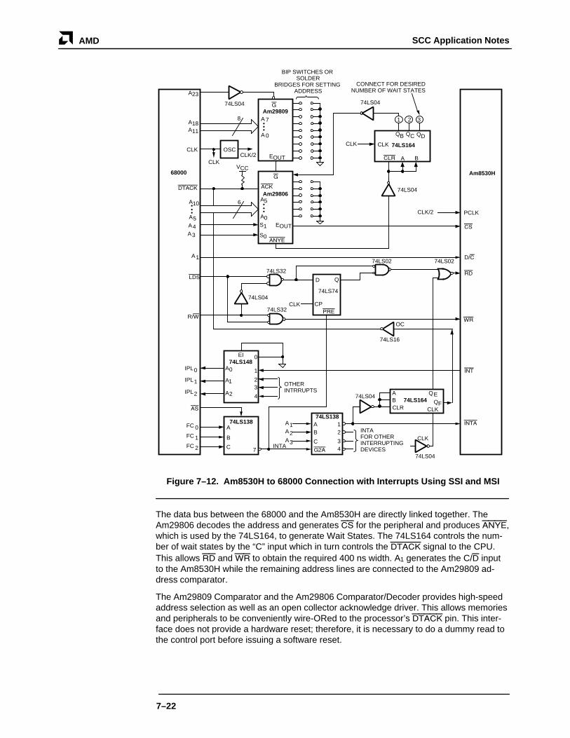
SCC Application NotesAMD
7–22
QCQB
A23
CS
Am8530H
CLK
CLR BA
QD
Am29809
A18A11
A1
A4
LDS
R/W
INT
RD
D/C
74LS74
CP
D Q
CLK
74LS32
74LS32
74LS04
74LS02
ANYE
ACKAm29806
CLK
DTACK
68000
74LS04
CLK
EI 0
1
23
4
A0
A1
A2
A1A2A3
A
B
C
12
34INTA
AB
CG2A
ABCLR CLK
7
74LS138
QEQF
OC
74LS16
CLK
INTA
WR
74LS138
PCLKCLK/2
1 2 3
74LS04G
A 7
A 0
CLKEOUTCLK/2
VCC
G
EOUT
•••
A0
•••
S1
S0
PRE
8
6
A5
•••
A10
A3
IPL0
IPL1
IPL2
FC 1FC 2
FC 0
AS
OTHER INTRRUPTS
INTA FOR OTHER INTERRUPTING DEVICES
74LS164
BIP SWITCHES OR SOLDER
BRIDGES FOR SETTING ADDRESS
74LS04
CONNECT FOR DESIRED NUMBER OF WAIT STATES
74LS164
74LS02
74LS04
74LS04
74LS148
A5
OSC
Figure 7–12. Am8530H to 68000 Connection with Interrupts Using SSI and MSI
The data bus between the 68000 and the Am8530H are directly linked together. TheAm29806 decodes the address and generates CS for the peripheral and produces ANYE,which is used by the 74LS164, to generate Wait States. The 74LS164 controls the num-ber of wait states by the “C” input which in turn controls the DTACK signal to the CPU.This allows RD and WR to obtain the required 400 ns width. A1 generates the C/D inputto the Am8530H while the remaining address lines are connected to the Am29809 ad-dress comparator.
The Am29809 Comparator and the Am29806 Comparator/Decoder provides high-speedaddress selection as well as an open collector acknowledge driver. This allows memoriesand peripherals to be conveniently wire-ORed to the processor’s DTACK pin. This inter-face does not provide a hardware reset; therefore, it is necessary to do a dummy read tothe control port before issuing a software reset.
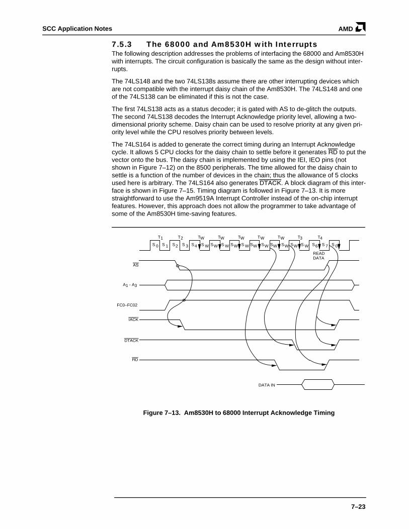
SCC Application Notes AMD
7–23
7.5.3 The 68000 and Am8530H with InterruptsThe following description addresses the problems of interfacing the 68000 and Am8530Hwith interrupts. The circuit configuration is basically the same as the design without inter-rupts.
The 74LS148 and the two 74LS138s assume there are other interrupting devices whichare not compatible with the interrupt daisy chain of the Am8530H. The 74LS148 and oneof the 74LS138 can be eliminated if this is not the case.
The first 74LS138 acts as a status decoder; it is gated with AS to de-glitch the outputs.The second 74LS138 decodes the Interrupt Acknowledge priority level, allowing a two-dimensional priority scheme. Daisy chain can be used to resolve priority at any given pri-ority level while the CPU resolves priority between levels.
The 74LS164 is added to generate the correct timing during an Interrupt Acknowledgecycle. It allows 5 CPU clocks for the daisy chain to settle before it generates RD to put thevector onto the bus. The daisy chain is implemented by using the IEI, IEO pins (notshown in Figure 7–12) on the 8500 peripherals. The time allowed for the daisy chain tosettle is a function of the number of devices in the chain; thus the allowance of 5 clocksused here is arbitrary. The 74LS164 also generates DTACK. A block diagram of this inter-face is shown in Figure 7–15. Timing diagram is followed in Figure 7–13. It is morestraightforward to use the Am9519A Interrupt Controller instead of the on-chip interruptfeatures. However, this approach does not allow the programmer to take advantage ofsome of the Am8530H time-saving features.
S 0 S 1 S 2 S 3 S 4 S W S W S W S W S W S W S W S W S W S W S 6 S 7 S 0 S W
T 1 T 2 T W T W T W T W T W T 3 T 4
AS
FC0–FC02
IACK
DTACK
RD
DATA IN
A1 - A3
READ DATA
Figure 7–13. Am8530H to 68000 Interrupt Acknowledge Timing

SCC Application NotesAMD
7–24
8
1 FC
FC 2
A 23
CE
Am8530H
Am29809
A 1
A 4
INT
RD
ANYE C
DTACK
74LS04
ACK
WR
G
E OUT
G
E O
A 7
A 0
• • •
A 5
A 0
• • •
S 1 S 0
8
A 5
• • •
A 10
A 3
IPL 2
IPL 1 IPL 0
VCC
A 11
• • •
A 18
OSC
ACK
RD CLOCK
FC 1 FC 0
FC 2
LDS
RW
AS
CLOCK
FC 0
LDS
R/W
AS
D 7
D 0
• • •
V CC
INTA
D 7
D 0
• • •
D/C
8
68000
Am29809
AmPAL 16R4
68K85XX
WR
WO
OE
INTA
VCC
VCC
Figure 7–14. 68000 to Am8530 Connection using a PAL

SCC Application Notes AMD
7–25
AS
DS
RD
DTACK
A
B
C
PAL OUTPUTS:
Figure 7–15. PAL Timing
7.5.4 The 68000 and Am8530H with Interrupts via a PAL Device
This example shows how a Programmable Array Logic (PAL) device simplifies the task ofinterrupt generation compared to the MSI implementation. The block diagram for the in-terface via a PAL device is shown in Figure 7–14. The timing diagram (Figure 7–15) illus-trates the Interrupt Acknowledge cycle. As in the other designs, RD is generated duringInterrupt Acknowledge to place the vector on the bus.
The timing during register programming is not shown. The PAL device allows selection ofone or two Wait States by making W0 High or Low respectively. The table below showsthe appropriate number of Wait Sates as a function of CPU speed.
CPU Speed Wait States
4 MHz 1
6 MHz 2
8 MHz 2
10 MHz 2
PAL device equations are shown in Figure 7–16.
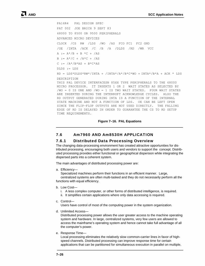
SCC Application NotesAMD
7–26
PA16R4 PAL DESIGN SPEC
PAT 002 JOE BRICH 9 SEPT 83
68000 TO 8500 OR 9500 PERIPHERALS
ADVANCED MICRO DEVICES
CLOCK /CS RW /LDS /WO /AS FCO FC1 FC2 GND
/OE /INTA /ACK /C /B /A /DLDS /RD /WR VCC
A := A*/B + B *C + /AS
B := A*/C + /A*C + /AS
C := /A*/B*AS + B*C*AS
DLDS := LDS
RD = LDS*DLDS*RW*/INTA + /INTA*/A*/B*C*WO + INTA*/B*A + ACK * LDS
DESCRIPTIONTHIS PAL DEVICE INTERFACESN 85XX TYPE PERIPHERALS TO THE 68000MICRO PROCESSOR. IT INSERTS 1 OR 2 WAIT STATES AS SELECTED BY/WO = 0 IS ONE AND /WO = 1 IS TWO WAIT STATES. FOUR WAIT STATESARE INSERTED DURING THE INTERRUPT ACKNOWLEDGE CYCLES. ALSO THERD OUTPUT GENERATED DURING INTA IS A FUNCTION OF THE INTERNALSTATE MACHINE AND NOT A FUNCTION OF LDS. OE CAN BE LEFT OPENSINCE THE FLIP–FLOP OUTPUTS ARE NOT USED DIRECTLY. THE FALLINGEDGE OF RD IS DELAYED IN ORDER TO GUARANTEE THE CS TO RD SETUPTIME REQUIREMENTS.
Figure 7–16. PAL Equations
7.6 Am7960 AND Am8530H APPLICATION
7.6.1 Distributed Data Processing OverviewThe changing data-processing environment has created attractive opportunities for dis-tributed processing, encouraging both users and vendors to support the concept. Distrib-uted processing provides either functional or geographical dispersion while integrating thedispersed parts into a coherent system.
The main advantages of distributed processing power are:
a. Efficiency—Specialized machines perform their functions in an efficient manner. Large, centralized systems are often multi-tasked and they do not necessarily perform all the
functions with equal efficiency.
b. Low Cost—i. A less complex computer, or other forms of distributed intelligence, is required.ii. It simplifies certain applications where only data accessing is required.
c. Control—Users have control of most of the computing power in the system organization.
d. Unlimited Access—Distributed processing power allows the user greater access to the machine operating system and hardware. In large, centralized systems, very few users are allowed to access the mainframe’s operating system and hence cannot take full advantage of all the computer’s power.
e. Response Time—Local processing eliminates the relatively slow common-carrier lines in favor of high-speed channels. Distributed processing can improve response time for certain applications that can be partitioned for simultaneous execution in parallel on multiple,

SCC Application Notes AMD
7–27
functionally distributed computers. Lengthy delays are often encountered in a centralizedsystem due to overloaded CPUs and slow communication lines.
f. Resource Sharing—Remote sites in a distributed system can use each other’s facilities such as sharing expensive peripheral devices in the system.
The advantages of distributed processing, therefore, point mainly to two important facts:
1. LANs make distributed intelligence practical.
2. Methods must be devised in order to allow large amount of data to be transported, at high speeds, between centers of intelligence.
This discussion addresses the second factor.
7.6.2 Data Communications at the Physical LayerToday’s data communications market can be segmented in terms of speed.
i. Low speed (300 baud–56 kbaud)
ii. Medium speed (0.5 Mb/s–3 Mb/s)
iii. High speed (10 Mb/s–60 Mb/s)
iv. Very high speed (100 Mb/s and up)
On medium speed applications data rate is assumed at 1 Mb/s. At this rate, the physicalinterface requires a highly sophisticated transceiver. The following is a list of the require-ments:
a. The transceivers must have good but inexpensive isolation from the cabling system (large common-mode voltages and surge voltages are common phenomenons in any network). Pulse transformers can provide the required isolation.
b. The transceiver must be able to support a good collision avoidance scheme, since all devices have equal access to the network (in a CSMA type architecture). If a collision does occur, the transceiver must detect the collision and flag the communications controller.
c. The receiver must be able to inhibit false starts due to noise in the surrounding environment.
d. The transmitter must control the slew rate of the output signal to reduce EMI/RFI to surrounding electronic equipment. This is a very important criterion if the network is to meet FCC/VDE regulations on radiation.
e. If an isolation transformer is used, some form of data encoding must also beimplemented so that a series of ‘1’s or ‘0’s do not saturate the transformer by charging it to either voltage level.
Why the Am7960The Am7960 Coded Data Transceiver is designated to meet all the requirements of themedium-speed network. It is frequency agile for data rates between 0.5 Mb/s to 3 Mb/s.
Electro–Magnetic InterferenceThe Am7960 has an external resistor connected from the slew rate control pin (TSRC) toground to control the transmit slew rate. If the rise and fall times of the output signal areeach 30% of the transmit clock period, the output waveform looks approximately like asine wave (Figure 7–17). This has a smoothing effect on the transmitted signal, reducing3rd, 5th and higher order harmonics. This in turn reduces energy radiating from the cableand minimizes the effects of electro-magnetic interference and radio frequency inter-ference.
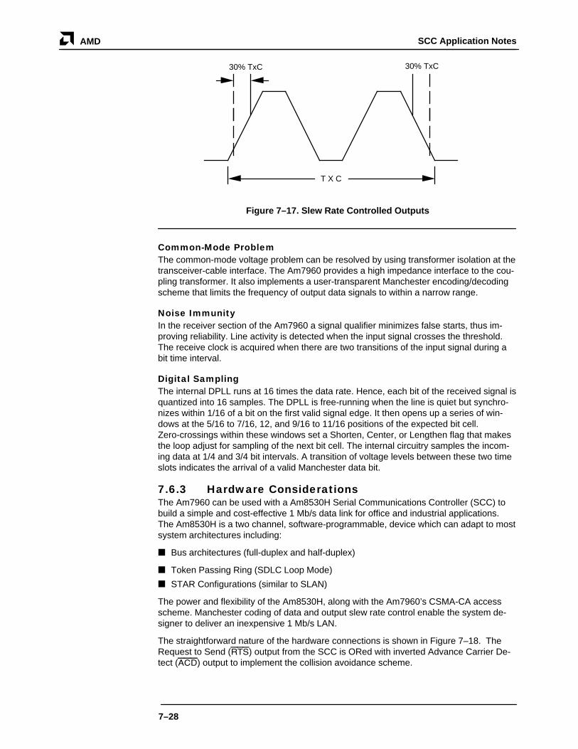
SCC Application NotesAMD
7–28
T X C
30% TxC 30% TxC
Figure 7–17. Slew Rate Controlled Outputs
Common-Mode ProblemThe common-mode voltage problem can be resolved by using transformer isolation at thetransceiver-cable interface. The Am7960 provides a high impedance interface to the cou-pling transformer. It also implements a user-transparent Manchester encoding/decodingscheme that limits the frequency of output data signals to within a narrow range.
Noise ImmunityIn the receiver section of the Am7960 a signal qualifier minimizes false starts, thus im-proving reliability. Line activity is detected when the input signal crosses the threshold.The receive clock is acquired when there are two transitions of the input signal during abit time interval.
Digital SamplingThe internal DPLL runs at 16 times the data rate. Hence, each bit of the received signal isquantized into 16 samples. The DPLL is free-running when the line is quiet but synchro-nizes within 1/16 of a bit on the first valid signal edge. It then opens up a series of win-dows at the 5/16 to 7/16, 12, and 9/16 to 11/16 positions of the expected bit cell.Zero-crossings within these windows set a Shorten, Center, or Lengthen flag that makesthe loop adjust for sampling of the next bit cell. The internal circuitry samples the incom-ing data at 1/4 and 3/4 bit intervals. A transition of voltage levels between these two timeslots indicates the arrival of a valid Manchester data bit.
7.6.3 Hardware ConsiderationsThe Am7960 can be used with a Am8530H Serial Communications Controller (SCC) tobuild a simple and cost-effective 1 Mb/s data link for office and industrial applications.The Am8530H is a two channel, software-programmable, device which can adapt to mostsystem architectures including:
Bus architectures (full-duplex and half-duplex)
Token Passing Ring (SDLC Loop Mode)
STAR Configurations (similar to SLAN)
The power and flexibility of the Am8530H, along with the Am7960’s CSMA-CA accessscheme. Manchester coding of data and output slew rate control enable the system de-signer to deliver an inexpensive 1 Mb/s LAN.
The straightforward nature of the hardware connections is shown in Figure 7–18. TheRequest to Send (RTS) output from the SCC is ORed with inverted Advance Carrier De-tect (ACD) output to implement the collision avoidance scheme.
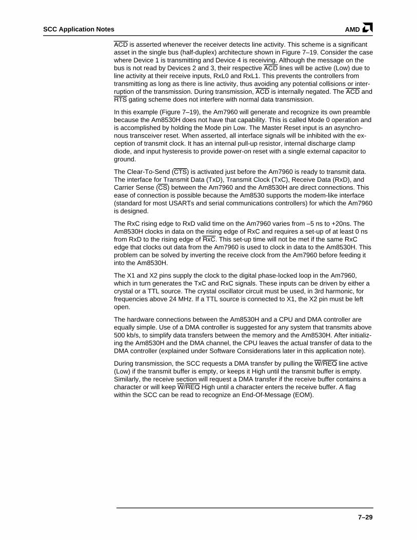
SCC Application Notes AMD
7–29
ACD is asserted whenever the receiver detects line activity. This scheme is a significantasset in the single bus (half-duplex) architecture shown in Figure 7–19. Consider the casewhere Device 1 is transmitting and Device 4 is receiving. Although the message on thebus is not read by Devices 2 and 3, their respective ACD lines will be active (Low) due toline activity at their receive inputs, RxL0 and RxL1. This prevents the controllers fromtransmitting as long as there is line activity, thus avoiding any potential collisions or inter-ruption of the transmission. During transmission, ACD is internally negated. The ACD andRTS gating scheme does not interfere with normal data transmission.
In this example (Figure 7–19), the Am7960 will generate and recognize its own preamblebecause the Am8530H does not have that capability. This is called Mode 0 operation andis accomplished by holding the Mode pin Low. The Master Reset input is an asynchro-nous transceiver reset. When asserted, all interface signals will be inhibited with the ex-ception of transmit clock. It has an internal pull-up resistor, internal discharge clampdiode, and input hysteresis to provide power-on reset with a single external capacitor toground.
The Clear-To-Send (CTS) is activated just before the Am7960 is ready to transmit data.The interface for Transmit Data (TxD), Transmit Clock (TxC), Receive Data (RxD), andCarrier Sense (CS) between the Am7960 and the Am8530H are direct connections. Thisease of connection is possible because the Am8530 supports the modem-like interface(standard for most USARTs and serial communications controllers) for which the Am7960is designed.
The RxC rising edge to RxD valid time on the Am7960 varies from –5 ns to +20ns. TheAm8530H clocks in data on the rising edge of RxC and requires a set-up of at least 0 nsfrom RxD to the rising edge of RxC. This set-up time will not be met if the same RxCedge that clocks out data from the Am7960 is used to clock in data to the Am8530H. Thisproblem can be solved by inverting the receive clock from the Am7960 before feeding itinto the Am8530H.
The X1 and X2 pins supply the clock to the digital phase-locked loop in the Am7960,which in turn generates the TxC and RxC signals. These inputs can be driven by either acrystal or a TTL source. The crystal oscillator circuit must be used, in 3rd harmonic, forfrequencies above 24 MHz. If a TTL source is connected to X1, the X2 pin must be leftopen.
The hardware connections between the Am8530H and a CPU and DMA controller areequally simple. Use of a DMA controller is suggested for any system that transmits above500 kb/s, to simplify data transfers between the memory and the Am8530H. After initializ-ing the Am8530H and the DMA channel, the CPU leaves the actual transfer of data to theDMA controller (explained under Software Considerations later in this application note).
During transmission, the SCC requests a DMA transfer by pulling the W/REQ line active(Low) if the transmit buffer is empty, or keeps it High until the transmit buffer is empty.Similarly, the receive section will request a DMA transfer if the receive buffer contains acharacter or will keep W/REQ High until a character enters the receive buffer. A flagwithin the SCC can be read to recognize an End-Of-Message (EOM).
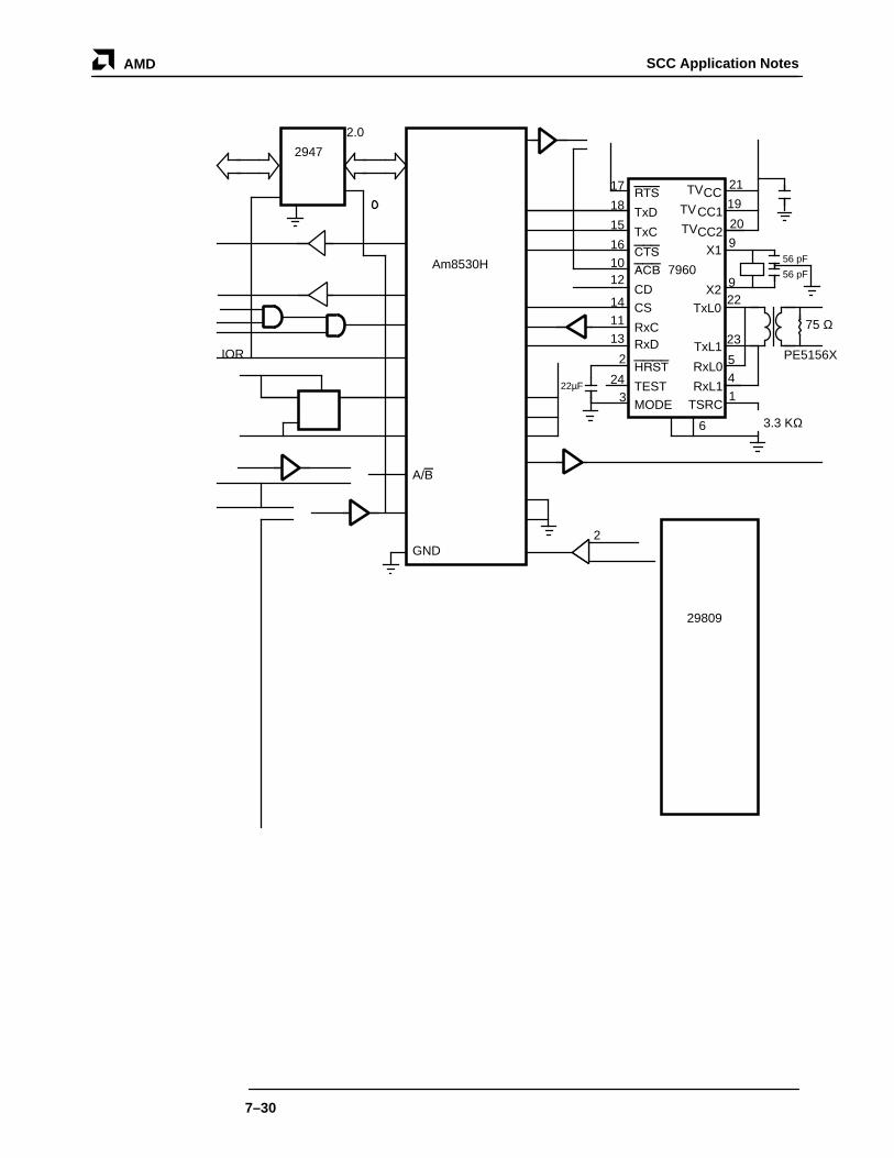
SCC Application NotesAMD
7–30
2.0
IOR
2
A/B
GND
5
9
9
20
19
21
23
22
17
2947
Am8530H 7960
29809
18
15
16 10 12
14 11
2
24 3
RTS
TxD
TxC
CTS ACB
CD CS
RxC
HRST
TEST MODE
13 RxD
TV CC TV CC1 TV CC2
X1
X2 TxL0
TxL1
RxL0 4 1
RxL1 TSRC
22µF
6
56 pF
56 pF
75 Ω
PE5156X
3.3 KΩ 7
16
23
17 18
19 24
20
22
15
12
21
14
13
B7
B0
B6
B5
B4
B3
B1
GND
B2 11
1
ACK
G
AD3 — AD11 C
E OUT
A1-A0 B1-B0 D0-D7 1- 8
V CC
+5 V
12-19
+5 V
1KΩ
11 I/R
5
10
32
36
35
20
34
33
31
+5 V
INT
W/REQA
D/C
WR
PCLK
CE
TxDA TRxCA
TxDB
CTSA
DCDA
RTxCA
RxDA
INTACK 101
CTSB
DCDB
RxDB
15
14
25
18
19 12
13
8 7
9
22
21
17
RTSA
V CC
+5 V
3 1
2
26LS32
26LS29 15
100 Ω
2 – 10 A0 – A8
INT
DRQ1 AD0
PR D Q
PLCK
AD1
DACK1
.01 µF
V CC
ACM
12
4
RD
CD
D0-D7 9
IOW
Figure 7–18. 7960-Am8530H Hardware Interface Diagram
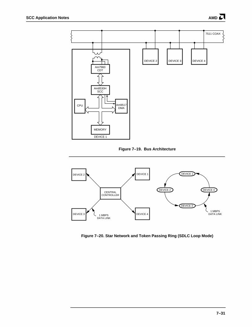
SCC Application Notes AMD
7–31
Am8530H SCC
Am7960 CDT
MEMORY
CPU Am9517 DMA
DEVICE 2 DEVICE 3 DEVICE 4
7511 COAX
DEVICE 1
Figure 7–19. Bus Architecture
CENTRAL CONTROLLER
DEVICE 2
DEVICE 3 DEVICE 4 1 MBPS DATA LINK
DEVICE 1
DEVICE 4 DEVICE 2
DEVICE 3
1 MBPS DATA LINK
DEVICE 1
Figure 7–20. Star Network and Token Passing Ring (SDLC Loop Mode)
SCC Application NotesAMD
7–32
The Am8530H can also be configured to make the entire system interrupt-driven. Thechip can be set up to interrupt the CPU on external conditions (i.e., a change on a modemline or a break condition). It can also be set up to cause receive interrupt on first charac-ter, on all characters, or on one of many special receive conditions (e.g., receiver overrun,framing error, or end of frame).
The Am7960 can also support a full-duplex operation (point-to-point between two de-vices). In this case, no collision avoidance scheme needs to be implemented becauseonly one device can talk on one line at a time. Such a set-up would be very practical forSTAR configurations, or Token Passing Ring, or Loop configurations (shown in Figure7–20).
In addition to this 1Mb/s LAN using the Am7960, channel B of the Am8530H is configuredto operate a low speed RS-423/RS-232C asynchronous link. The Am26LS29 driver andthe Am26LS32 receiver were added, as shown in Figure 7–18, to provide proper signalconditioning for the cable.
7.6.4 Software ConsiderationsTwo programs have been written for the hardware described and are listed at the end ofthis application note. The program for the transmitter is listed under “Software to TransmitData At 1Mb/s Using DMA.” The program for the receiver is listed under “Software to Re-ceive Data At 1Mb/s Using DMA.” These programs enable a file to be read off a disk onone IBM* PC (XT or AT), transmit it over a shielded coaxial cable to another similar PC**,and save it onto a disk on the receiving PC. The collision avoidance scheme is imple-mented in hardware. The software implementation demonstrates that the Am8530H andAm7960 can be simply configured for a 1Mb/s data communications network. An actualoperating network may need a slightly greater degree of software sophistication.
The file from disk (hard or floppy) is first copied into memory. The length of the file andstarting address is then determined. The Am8530H Serial Communications Controllermust now be initialized for an SDLC mode of operation with DMA request on transmit orreceive.
The initialization scheme for the Am8530H involves setting up the various modes of op-eration followed by enabling the transmitter, the receiver, and DMA request. The CRCscheme of the Am8530H is used to ensure data integrity at the receive end. Finally, theinterrupts are enabled if the Interrupt Mode of data transfer is to be used.
It is important to follow the data initialization sequence as shown in the software routinefor correct operation of the SCC. The DMA controller of the PC can then be loaded withthe starting address of the data and the length of file (number of bytes to be transmitted).The DMA channel must be enabled upon completion of initialization. Data transmissionstarts as soon as DMA is enabled. The transmit-underrun latch must be reset by writing aC0H to WR0 of the Am8530H. This command controls the transmission of CRC at theend of transmission.
At the receiving station, the address (first byte after flags) of the incoming data is com-pared with the device address in WR6 of the Am8530H. The remaining data are receivedonly if an address match occurs. This process does not involve any CPU interaction. TheEOM and CRC errors are indicated in RR0 of the Am8530H.
The length of the message is transmitted first, and then the entire message is transmitted.Between these two transmissions, flags (7EH) are sent on the line.
In this program, CPU polls the Am8530H to determine End-Of-Message (EOM). Usingthe same hardware connections, the SCC can be programmed to interrupt on special re-ceive conditions to indicate an EOM to the CPU.
Channel B of the Am8530H is initialized for asynchronous communication at 19.2 kbaud.The asynchronous transmit routine polls bit D2 of Read Register 0 to determine a trans-mit buffer empty condition. Writing a byte of data to the transmit buffer resets this bit.Address line AD0 differentiates between a command and data access to the Am8530H.

SCC Application Notes AMD
7–33
Similarly, on the receive side, bit D0 of Read Register 0 is monitored to determine a re-ceive character available condition. This bit is reset if the receive FIFO is completelyempty. Address line AD1 selects either synchronous or asynchronous data transfers.Hence, before transmission, the user can select whether the data transfer is over a 1 Mb/s-network to similar PCs, or over a slower link to a printer.
SUMMARYThe Am8530H can be software-manipulated to perform at a higher degree of sophistica-tion without any change in hardware connections.
Changing or adding to the software does not affect the Am7960 operation. Hence, theAm7960 provides an easy upgrade (high-speed, greater distance, common-mode isola-tion) for most modern modem circuits that use RS-422 drivers and receivers.

SCC Application NotesAMD
7–34
SOFTWARE ROUTINES
Software to Transmit Data at 1 Mb/s Using DMA#include “stdio.h”#define arraysize 40 /*size of array for the 8530 sync. init*/#define port 0x0382 /*I/O port address for the SCC channel A*/#define aport 0x0380 /*I/O port address for 8530 channel B*/#define aportd 0x0381 /*I/O data address for 8530 channel B*/#define arraysiz 18 /*size of array for the 8530 async. init*/unsigned char *ptr;unsigned int segread();struct(int scs, sss, sds, ses; ) rv;unsigned long int data_segment;unsigned long int data_seg;unsigned int num;unsigned long int adrr;
/*TRANSMIT ROUTINE*/main()
unsigned char var_nam, string1[8], N, n;unsigned int result, res;
do/*This routine chooses between synchronous and asynchronous data transfers*/printf(“Do you want to print a file(Y/N)? “);var_nam = scanf(“%s”, string1);result + strcmp(string1,”N”);res = strcmp(string1,”n”);
if(result != 0 && res != 0)/*Main routine for asynchronous data transfer*/printf(“Asynch transmit\n”);opnfile(); /*Read file from disk into system memory*/asccinit(); /*Initialize the 8530 for asynchronous trans-
mit*/trnum(); /*Transmit length of file*/cont();atrans(); /*Transmit the entire file*/
else/*Main routine for synchronous data transfer*/printf(“Synchronous transmit\n” );opnfile();sccinit();dmainit();cont();dminit();/*This allows the user to continue transmission of nextfile*/printf(“Do you want to transmit another file(Y/N)? “);var_nam = scanf(“%s”, string1);result = strcmp(string1,”N”);res = strcmp(string1,”n”);
while(result != 0 && != 0);

SCC Application Notes AMD
7–35
/*THIS ROUTINE LOADS THE FILE FROM DISK TO BUFFER MEMORY*/opnfile()char var_nam, name[16],*ptrr;extern char *alloc( );unsigned int fd, endpos, begpos, count, numd;unsigned int;int num_read, i, numr;printf(“Enter name of file to be transferred: “);var_nam = scanf(“%s”, name);
fd = fopen(name, “rb”);endpos = fseek(fd,OL,2); /*looks for end of file*/fclose(fd);fd = open(name, BREAD); /*opens the file as binary
file*/if(fd<0) fputs(“file not opened”, stdout); return;
ptr = alloc(endpos+1); /*allocates memory space for file beginning at ptr*/
for(i=0;i<endpos;i++) *(ptr+i)=’\0’;ptrr = ptr;num = 0;num_read = 1;
while(num_read!=0)/*This reads the file from disk starting at location ptrr*/num_read = read(fed,ptrr,endpos);num = num + num_read; /*calculates length of file*/ptrr = ptrr + num_read:
ptr = ptr – 2;num = num + 2;*ptr = num; /*appends lower byte of length to beginning of
file*/ptr++;numd = num >> 0x08;*ptr = 0x02; /*address of receiving device is attached*/
adrr = 01;segread(&rv);data_segment = rv.sds;data_seg = data_segment << 4;addr = data_seg + (long int) ptr; /*absolute 20–bit address
is calculated/*this is required by the DMA controller*//*num_read contains:
if –1 errorif 0 EOFif >0 number of characters put in buffer*/
close(fd);return;
/*THIS ROUTINE INITIALIZES THE 8530 FOR TRANSMIT*/sccinit()
unsigned char array[arraysize]; /array to initialize SCC
registers*/unsigned int i+0;
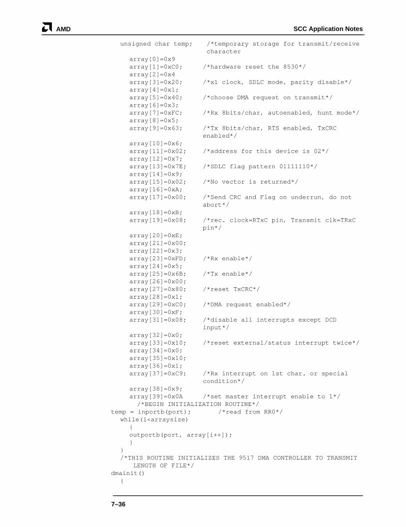
SCC Application NotesAMD
7–36
unsigned char temp; /*temporary storage for transmit/receive character
array[0]=0x9array[1]=0xC0; /*hardware reset the 8530*/array[2]=0x4array[3]=0x20; /*x1 clock, SDLC mode, parity disable*/array[4]=0x1;array[5]=0x40; /*choose DMA request on transmit*/array[6]=0x3;array[7]=0xFC; /*Rx 8bits/char, autoenabled, hunt mode*/array[8]=0x5;array[9]=0x63; /*Tx 8bits/char, RTS enabled, TxCRC
enabled*/array[10]=0x6;array[11]=0x02; /*address for this device is 02*/array[12]=0x7;array[13]=0x7E; /*SDLC flag pattern 01111110*/array[14]=0x9;array[15]=0x02; /*No vector is returned*/array[16]=0xA;array[17]=0x00; /*Send CRC and Flag on underrun, do not
abort*/array[18]=0xB;array[19]=0x08; /*rec. clock=RTxC pin, Transmit clk=TRxC
pin*/array[20]=0xE;array[21]=0x00;array[22]=0x3;array[23]=0xFD; /*Rx enable*/array[24]=0x5;array[25]=0x6B; /*Tx enable*/array[26]=0x00;array[27]=0x80; /*reset TxCRC*/array[28]=0x1;array[29]=0xC0; /*DMA request enabled*/array[30]=0xF;array[31]=0x08; /*disable all interrupts except DCD
input*/array[32]=0x0;array[33]=0x10; /*reset external/status interrupt twice*/array[34]=0x0;array[35]=0x10;array[36]=0x1;array[37]=0xC9; /*Rx interrupt on 1st char. or special
condition*/array[38]=0x9;array[39]=0x0A /*set master interrupt enable to 1*/ /*BEGIN INITIALIZATION ROUTINE*/
temp = inportb(port); /*read from RR0*/while(i<arraysize)
outportb(port, array[i++]);
/*THIS ROUTINE INITIALIZES THE 9517 DMA CONTROLLER TO TRANSMIT
LENGTH OF FILE*/dmainit()

SCC Application Notes AMD
7–37
unsigned int lsb, temp, msb, latch, wrdh, wrdl, tmp1, start;unsigned int bytn, byt, tmp2;outportb(0x09, 0x01); /*clear all DMA requests on channel 1*/outportb(0x0A, 0x05); /*mask channel 1 DMA request*/outportb(0x0B, 0x49); /*mode register for single transfer mode,
read, auto init, address increment*/lsb = adrr & 0xFF;temp = adrr >> 0x08; /*rotate ptr 8 bits to get msb*/msb = temp & 0xFF;temp = temp >> 0x08; /*rotate 8 bits to get sector address*/latch = temp & 0x0F;outportb(0x81, latch);/*load sector address into DMA page reg-
ister*/outportb(0x02, lsb); /*lower byte of starting address*/outportb90x0B, msb); /*upper byte of starting address*/start = adrr & 0xFFFF;bytn = 0x03: /*address and 2 bytes for length are
transmit*/wrdl = bytn & 0xFF /*lower order byte of wordcount*/tmp1 = bytn >> 0x08; /*rotate wordcount 8 bits for msb*/wrdh = tmp1 & 0xFF: /*upper byte of wordcount*/outportb(0x03, wrd1); /*this is the lower byte of # of bytes
that fit within the first sector*/outportb(0x03, wrdh); /*upper byte of wordcount*/outportb(0x0A, 0x01); /*enable DMA*/outportb(port, 0x00);outportb(port, 0xC0); /*reset transmit underrun latch*/
/*THIS ROUTINE INITIALIZES THE 9517 DMA CONTROLLER TO TRANSMIT
ENTIRE/dminit()
unsigned int lsb, temp, msb, latch, wrdh, wrd1, tmp1, start;unsigned int bytn, byt, tmp2;outportb(0x09, 0x01); /*clear all DMA requests on channel 1*/outportb(0x0A, 0x05); /*mask channel 1 DMA request*/outportb(0x0B, 0x49); /*mode register for single transfer mode,
read, auto init, address increment*/lsb = adrr & 0xFF;temp = adrr >> 0x08; /*rotate ptr 8 bits to get msb*/latch = temp & 0x0F;outportb(0x81, latch);/*load sector address into dma page reg-
ister*/outportb(0x02, lsb); /*lower byte of starting address*/outportb(0x02, msb); /*upper byte of starting address*/start = adrr & 0xFFFF;bytn = num;wrd1 = bytn & 0xFF; /*lower order byte of wordcount*/tmp1 = bytn >> 0x08; /*rotate wordcount 8 bits for msb*/wrdh = tmp1 & 0xFF; /*upper byte of wordcount*/outportb(0x03, wrd1); /*this is the lower byte of # that fit
within the first sector*/outportb(0x03, wrdh); /*upper byte of wordcount*/outportb(0x04, 0x01); /*enable DMA*/outportb(port, 0x00);outportb(port, 0xC0); /*reset transmit underrun latch*/
cont() /*arbitrary time delay routine*/

SCC Application NotesAMD
7–38
unsigned long int count;count = 0;while(count<35550)
count++;
/*THIS ROUTINE INITIALIZES THE 8530 FOR ASYN-
CHRONOUS TRANSMIT*/asccinit()
unsigned char array[arraysiz], temp;unsigned int i=0;array[0]=0x09;array[1]=0xC0; /*hardware reset*/array[2]=0x4;array[3]=0x44; /*X16 clock, 1 stop bits*/array[4]=0x3;array[5]=0xC0; /*8 bits/char.*/array[6]=0x5;array[7]=0x60; /*8 bits/char.*/array[8]=0xB;array[9]=0x56; /*RxC=BR gen, TxC=BR, TRxCout=BR*/array[10]=0xC;array[11]=0x06; /*set BR gen for 19.2 kBaud*/array[12]=0xD;array[13]=0x00;array[14]=0xE;array[15]=0x07; /*set DTR/REQ, enable BR gen, PCLK = BR
source*/array[16]=0x5;array[17]=0x68; /*Enable transmitter*/
/*BEGIN ASYNCHRONOUS ROUTINE*/temp = inportb(aport);/*read from RR0 to set up state machine*/while(i<arraysiz)
outportb)aport, array[i++]);
/*TRANSMIT FILE ASYNCHRONOUSLY AT 19.2 kBaud*/
atrans()unsigned int temp, tmp, tx;unsigned int i, count;temp = 0;num = num + 1;for (i=0; i<num; i++) /*process the loop until all chars. are
transmitted*/
tx = 0;while(tx==0)
temp = inportb(aport); /*load RR0
to check Tx buffer empty bit*/tx = temp & 0x04;

SCC Application Notes AMD
7–39
outportb(aportd, *ptr++); /*output a character to transmit buffer*/
/*TRANSMIT LENGTH OF FILE ASYNCHRONOUSLY AT 19.2 kBaud*/
trnum()unsigned char tmp, temp, tx;unsigned int i, count;for (i=0; i<0x03; i++) /*process the loop until
length of file is transmitted*/
tx = 0;while(tx==0)
temp = 0;temp = inportb(aport);/*load RR0 to check Tx buffer empty bit*/tx = temp & 0x04;
outportb(aport, *ptr++);/*output a character to transmit buffer*/
ptr = ptr – 3;
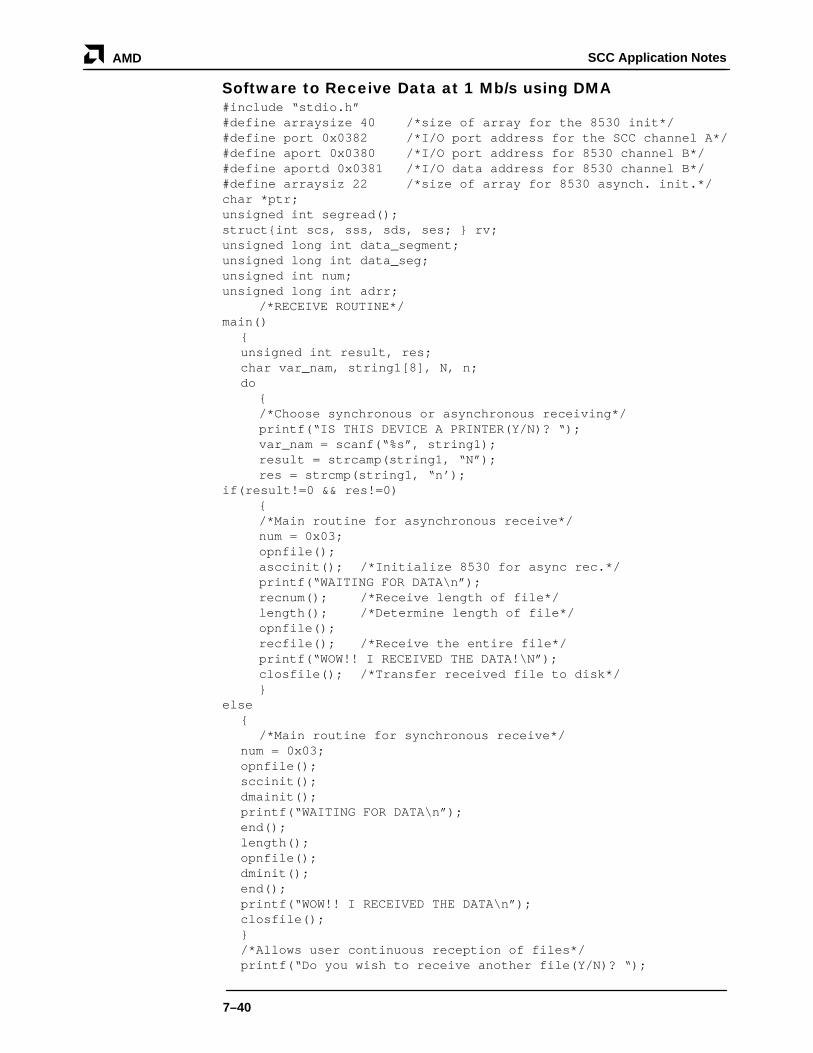
SCC Application NotesAMD
7–40
Software to Receive Data at 1 Mb/s using DMA#include “stdio.h”#define arraysize 40 /*size of array for the 8530 init*/#define port 0x0382 /*I/O port address for the SCC channel A*/#define aport 0x0380 /*I/O port address for 8530 channel B*/#define aportd 0x0381 /*I/O data address for 8530 channel B*/#define arraysiz 22 /*size of array for 8530 asynch. init.*/char *ptr;unsigned int segread();structint scs, sss, sds, ses; rv;unsigned long int data_segment;unsigned long int data_seg;unsigned int num;unsigned long int adrr;
/*RECEIVE ROUTINE*/main()
unsigned int result, res;char var_nam, string1[8], N, n;do
/*Choose synchronous or asynchronous receiving*/printf(“IS THIS DEVICE A PRINTER(Y/N)? “);var_nam = scanf(“%s”, string1);result = strcamp(string1, “N”);res = strcmp(string1, “n’);
if(result!=0 && res!=0)/*Main routine for asynchronous receive*/num = 0x03;opnfile();asccinit(); /*Initialize 8530 for async rec.*/printf(“WAITING FOR DATA\n”);recnum(); /*Receive length of file*/length(); /*Determine length of file*/opnfile();recfile(); /*Receive the entire file*/printf(“WOW!! I RECEIVED THE DATA!\N”);closfile(); /*Transfer received file to disk*/
else
/*Main routine for synchronous receive*/num = 0x03;opnfile();sccinit();dmainit();printf(“WAITING FOR DATA\n”);end();length();opnfile();dminit();end();printf(“WOW!! I RECEIVED THE DATA\n”);closfile();/*Allows user continuous reception of files*/printf(“Do you wish to receive another file(Y/N)? “);

SCC Application Notes AMD
7–41
var_nam = scanf(“%s”, string1);result = strcmp(string1,”N”);res = strcmp(string1,”n”);while(result!=0 && res!=0);/*THIS ROUTINE SETS A VALUE FOR THE STARTING ADDRESS AND ALLO-
CATES SPACE IN MEMORY TO ACCOMMODATE ENTIRE LENGTH OF FILE*/
opnfile()extern char *alloc( );unsigned int i;ptr = alloc(num);
for(i=0; i<num; i++) *(ptr+i)=’\0’;ptr—;num = num + 1;adrr = 01;segread(&rv);data_segment = rv.sds;data_seg = data_segment << 4;adrr = data_seg + (long int) ptr;
/*THIS ROUTINE INITIALIZES THE 8530 FOR RECEIVE*/
sccinit()unsigned char array[arraysize]; /*array to initialize SCC reg-
isters*/unsigned int i=0;unsigned char temp; /*temporary storage for
transmit/receive characters*/array[0]=0x9;array[1]=0xC0; /*hardware reset the 8530*/array[2]=0x4;array[3]=0x20; /*x1 clock, SDLC mode, parity disable*/array[4]=0x1;array[5]=0x40; /*choose DMA request on receive*/array[6]=0x3;array[7]=0xFC; /*Rx 8 bits/char, autoenabled, hunt mode,
receive crc enable*/array[8]=0x5;array[9]=0x63; /*Tx 8 bits/char, RTS enabled, TxCRC
enabled*/array[10]=0x6;array[11]=0x02; /*address for this device is 01*/array[12]=0x7;array[13]=0x7E; /*SDLC flag pattern 01111110*/array[14]=0x9;array[15]=0x02; /*No vector is returned*/array[16]=0xA;array[17]=0x00; /*Send CRC and Flag on underrun, do not
abort*/array[18]=0xB;array[19]=0x08; /*rec. clock=RTxC pin, Transmit clk=TRxC
pin*/array[20]=0xE;array[21]=0x00;array[22]=0x3;

SCC Application NotesAMD
7–42
array[23]=0xFD; /*Rx enable*/array[24]=0x5;array[25]=0x6B; /*Tx enable*/array[26]=0x00;array[27]=0x80; /*reset TxCRC*/array[28]=0x1;array[29]=0xE0; /*DMA request enabled*/array[30]=0xF;array[31]=0x00; /*disable all interrupts*/array[32]=0x0;array[33]=0x10; /*reset external/status interrupt twice*/array[34]=0x0;array[35]=0x10;array[36]=0x1;array[37]=0xE0; /*Rx interrupt on special condition*/array[38]=0x9;array[39]=0x02; /*set master interrupt enable to 1*/
/*BEGIN INITIALIZATION ROUTINE*//*The following dummy read statement is used to ensure that SCChas initialized properly*/temp = inportb(port); /*read from RR0*/
while(i<arraysize)outportb(port, array[i++]);
/*THIS ROUTINE INITIALIZES THE 9517 DMA CONTROLLER*/
dmainit()unsigned int lsb, temp, msb, latch, wrdh, wrd1, tmp1, start;unsigned int bytn, byt, tmp2;outportb(0x09, 0x01); /*clear all DMA requests on channel 1*/outportb(0x0A, 0x05); /*mask channel 1 DMA request*/outportb(0x0B, 0x45); /*mode register for single transfer mode,
read, auto init, address increment*/lsb = adrr & 0xFF;temp = adrr >> 0x08; /*rotate ptr 8 bits to get msb*/msb = tem[ & 0xFF;temp = temp >> 0x08; /*rotate 8 bits to get sector address*/latch = temp & 0x0F;outportb(0x81, latch);/*load sector address into DMA page reg-
ister*/outportb(0x02, lsb); /*lower byte of starting address*/outportb(0x02, msb); /*upper byte of starting address*/start = adrr & 0xFFFF;bytn = 0x03;wrd1 = bytn & 0xFF; /*lower order byte of wordcount*/tmp1 = bytn >> 0x08; /*rotate wordcount 8 bits for msb*/wrdh = tmp1 & 0xFF; /*upper byte of wordcount*/outportb(0x03, wrd1); /*this is the lower byte of # of bytes
that fit within the first sectoroutportb(0x03, wrdh); /*upper byte of wordcount*/outportb(0x0A, 0x01); /*enable DMA*/
/*THIS ROUTINE WRITES THE MEMORY BUFFER ON TO THE DISK*/closfile()char var_nam, name[10];

SCC Application Notes AMD
7–43
unsigned int fd;int num_wr;ptr = ptr + 3; /*deletes device address and length of
file before writing onto the disk*/num = num – 3;printf(“What shall I name the received file?”);var_nam = scanf(“%s”, name);fd = creat(name, BWRITE);
if(fd<0) abort(“\ncreat error occured\n”);num_wr = write(fd, ptr, num);printf(“Number of bytes written to file rec.dat =
%d\n”,num_wr);close(fd);
/*THIS ROUTINE INITIALIZES THE DMA CONTROLLER FOR RECEIVE*/dminit()
unsigned int lsb, temp, msb, latch, wrdh, wrd1, tmp1, start;unsigned int bytn, byt, tmp2;outportb(0x09, 0x01); /*clear all DMA requests on channel 1*/outportb(0x0A, 0x05); /*mask channel 1 DMA request*/outportb(0x0B, 0x45); /*mode register for single transfer mode,
read, auto init, address increment*/lsb = adrr & 0xFF;temp = adrr >> 0x08; /*rotate ptr 8 bits to get msb*/msb = temp & 0xFF;temp = temp >> 0x08; /*rotate 8 bits to get sector address*/latch = temp & 0x0F;outportb(0x81, latch);/*load sector address into DMA page
register*/outportb(0x02, lsb); /*lower byte of starting address*/outportb(0x02, msb); /*upper byte of starting address*/
start = adrr & 0xFFFF;bytn = num;wrd1 = bytn & 0xFF; /*lower order byte of wordcount*/tmp1 = bytn >> 0x08; /*rotate wordcount 8 bits for masb*/wrdh = tmp1 & 0xFF; /*upper byte of wordcount*/outportb(0x03, wrd1); /*this is the lower byte of # of bytes
that fit within the first sector*/outportb(0x03, wrdh); /*upper byte of wordcount*/outportb(0x0A, 0x01); /*enable DMA*/outportb(port, 0x00);outportb(port, 0x00); /*reset transmit underrun latch*/
/*THIS ROUTINE POLLS BIT D7 IN RR1 TO DETECT AN END–OF–MES-
SAGE*/end()
unsigned char temp, ef;unsigned int count;ef = 0;temp = 0inportb(port);outportb(port, 0x00);outportb(port, 0x30);
while(ef==0)
count = 0;

SCC Application NotesAMD
7–44
inportb(port);outportb(port, 0x01);temp = inportb(port);while(count<300)
count++;
ef = temp & 0x80;
/*THIS ROUTINE LOADS THE LENGTH OF THE FILE TO BE RECEIVED*/
length()unsigned int *iptr;ptr++;iptr = ptr; /*assigns iptr as an address of a 16–bit
integer*/num = *iptr;/*THIS ROUTINE INITIALIZES THE 8530 FOR ASYNC. RECEIVE*/
asccinit()unsigned char array[arraysiz], temp;unsigned int =i=0;array[0]=0x9;array[1]=0xC0; /*hardware reset*/array[2]=0x4;array[3]=0x44; /*X16 clock, 1 stop bits*/array[4]=0x3;array[5]=0xE0; /*8 bits/character*/array[6]=0x5;array[7]=0x60; /*8 bits/character*/array[8]=0xB;array[9]=0x56; /*RxC = BR gen, TxC = BR gen, TRxCout =
BR*/array[10]=0xC;array[11]=0x06; /*set BR gen for 19.2 kBaud*/array[12]=0xD;array[13]=0x00;array[14]=0xE;array[15]=0x03; /*set DTR/REQ, enable BR gen, PCLK = BR
source*/array[16]=0x3;array[17]=0xE1; /*enable receiver*/
temp = inportb(aport); /*Read from RR0 toset up state machine*/
while(i<arraysiz)outportb(aport, array[i++]);
/*RECEIVE FILE ASYNCHRONOUSLY AT 19.2 kBaud*/recfile()
unsigned char temp, rx;unsigned int i, count;rx = 0;temp = 0;
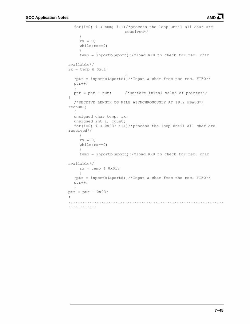
SCC Application Notes AMD
7–45
for(i=0; i < num; i++)/*process the loop until all char are received*/
rx = 0;while(rx==0)temp = inportb(aport);/*load RR0 to check for rec. char
available*/rx = temp & 0x01;
*ptr = inportb(aportd);/*Input a char from the rec. FIFO*/ptr++;ptr = ptr – num; /*Restore inital value of pointer*/
/*RECEIVE LENGTH OG FILE ASYNCHRONOUSLY AT 19.2 kBaud*/
recnum()unsigned char temp, rx;unsigned int i, count;for(i=0; i < 0x03; i++)/*process the loop until all char are
received*/rx = 0;while(rx==0)temp = inportb(aport);/*load RR0 to check for rec. char
available*/rx = temp & 0x01;
*ptr = inportb(aportd);/*Input a char from the rec. FIFO*/ptr++;
ptr = ptr – 0x03;;..............................................................................
Related Documents