Elías Urrejola Davanzo Aluminum-Silicon Contact Formation Through Narrow Dielectric Openings Application To Industrial High Efficiency Rear Passivated Solar Cells

Welcome message from author
This document is posted to help you gain knowledge. Please leave a comment to let me know what you think about it! Share it to your friends and learn new things together.
Transcript
Elías Urrejola Davanzo
Aluminum-Silicon Contact FormationThrough Narrow Dielectric Openings
Application To Industrial High Efficiency RearPassivated Solar Cells

Aluminum-Silicon Contact FormationThrough Narrow Dielectric Openings
Application To Industrial High Efficiency RearPassivated Solar Cells
Dissertation
zur Erlangung des akademischen Grades
eines Doktors der Naturwissenschaften (Dr. rer. nat.)
an der Universität Konstanz
Mathematisch-Naturwissenschaftliche Sektion
Fachbereich Physik
vorgelegt von
Elías Urrejola Davanzo
geboren am 21.02.1981 in Santiago, Chile
1. Referent: Prof. Dr. Ernst Bucher
2. Referent: Apl. Prof. Dr. Johannes Boneberg
Tag der mündlichen Prüfung: 23.05.2012


a mis padres,inspiradores de toda luz,
Manuel y Susi,con amor
"Renewable energies are inexhaustible. They do not destroy theenvironment. They are available everywhere. Their use facilitates
solidarity with future generations. They secure the future ofhumankind."
–Hermann Scheer, winner of the Right Livelihood Award(The ’Alternative Nobel Prize’)

CONTENTS
1 Introduction 11.1 Abstract . . . . . . . . . . . . . . . . . . . . . . . . . . . . . . . . . . . . 11.2 Motivation: Contact Formation for Rear Passivated Solar Cells . . 21.3 Outline of the Thesis . . . . . . . . . . . . . . . . . . . . . . . . . . . 5
I Basic Principles and Processing of Silicon Solar Cells 7
2 Processing of an Industrial Solar Cell 92.1 Introduction . . . . . . . . . . . . . . . . . . . . . . . . . . . . . . . . . 92.2 Preparation of the Surfaces (Cleaning) . . . . . . . . . . . . . . . . 102.3 Texturing and Polishing . . . . . . . . . . . . . . . . . . . . . . . . . . . 112.4 POCl3 Diffusion . . . . . . . . . . . . . . . . . . . . . . . . . . . . . . 122.5 Antireflection Coating . . . . . . . . . . . . . . . . . . . . . . . . . . . 12
2.5.1 Plasma Silicon Nitride Deposition . . . . . . . . . . . . . . . . 142.6 Thermal Oxidation . . . . . . . . . . . . . . . . . . . . . . . . . . . . . . 142.7 Screen-printing Metallization and Sintering of Contacts . . . . . . . 152.8 Edge Isolation . . . . . . . . . . . . . . . . . . . . . . . . . . . . . . . 152.9 Dielectric Ablations . . . . . . . . . . . . . . . . . . . . . . . . . . . . 15
2.9.1 Etching Paste . . . . . . . . . . . . . . . . . . . . . . . . . . . 162.9.2 Some Etchants of Dielectrics . . . . . . . . . . . . . . . . . . . 17
3 Basic Principles of Solar Cells 193.1 Characterization of Solar Cells . . . . . . . . . . . . . . . . . . . . . 20
3.1.1 I -V -Characteristic . . . . . . . . . . . . . . . . . . . . . . . . . 203.1.2 Spectral Response . . . . . . . . . . . . . . . . . . . . . . . . . 213.1.3 Short-Circuit Current Density . . . . . . . . . . . . . . . . . . 233.1.4 A few Characterization Tools . . . . . . . . . . . . . . . . . . . 24
3.2 Loss Mechanisms of Solar Cells . . . . . . . . . . . . . . . . . . . . 253.2.1 Series Resistance Losses . . . . . . . . . . . . . . . . . . . . 253.2.2 Recombination in Solar Cells . . . . . . . . . . . . . . . . . . 30
3.3 Light Absorption of the Silicon Material . . . . . . . . . . . . . . . . 333.4 The Two Diode Model . . . . . . . . . . . . . . . . . . . . . . . . . . . . 34
4 Selective Emitter Solar Cells 374.1 The Selective Emitter Concept . . . . . . . . . . . . . . . . . . . . . 384.2 Experimental Part . . . . . . . . . . . . . . . . . . . . . . . . . . . . . 384.3 Screen Printing Approach: Etching of Dielectric Barriers . . . . . . 40
4.3.1 Fiducial Alignment . . . . . . . . . . . . . . . . . . . . . . . . 404.3.2 Etching Paste and Alignment Approach . . . . . . . . . . . . 40
4.4 Solar Cell Results . . . . . . . . . . . . . . . . . . . . . . . . . . . . . 424.4.1 I -V Characterization . . . . . . . . . . . . . . . . . . . . . . . 42
vii
viii Contents
4.4.2 Spectral Response Characterization . . . . . . . . . . . . . 424.5 Conclusions and Discussion . . . . . . . . . . . . . . . . . . . . . . . 43
II Aluminum-Silicon Contact Formation 45
5 Contact Formation, State of the Art 475.1 The High-Low Junction as a Back Surface Field . . . . . . . . . . . . 475.2 Effect of the BSF on VOC . . . . . . . . . . . . . . . . . . . . . . . . . 495.3 Gettering Properties of Al . . . . . . . . . . . . . . . . . . . . . . . . 505.4 Fundamental Mechanisms of Al-Si Contact Formation . . . . . . . . 515.5 Al-Si Lamellas . . . . . . . . . . . . . . . . . . . . . . . . . . . . . . . 555.6 Screen Printing and Drying of Aluminum Lines . . . . . . . . . . . . 56
6 Aluminum-Silicon Contact Formation through Narrow DielectricOpenings 596.1 Introduction . . . . . . . . . . . . . . . . . . . . . . . . . . . . . . . . . 606.2 Preparation of the Surfaces . . . . . . . . . . . . . . . . . . . . . . . . 616.3 Study 1: Local Al-Si Alloy Formation . . . . . . . . . . . . . . . . . . 62
6.3.1 Experimental Design . . . . . . . . . . . . . . . . . . . . . . . 626.3.2 Impact of Al amount on Contact Formation . . . . . . . . . . 636.3.3 Impact of Contact Width on Alloy Formation . . . . . . . . . 666.3.4 Cross-sectional SEM/EDX Analysis of the Alloy Junction . . 676.3.5 On the Variation of the Contact Resistivity . . . . . . . . . . 706.3.6 Experimental Evidence of the Influence of Al Amount on
Mass Transport . . . . . . . . . . . . . . . . . . . . . . . . . . 726.3.7 Conclusions . . . . . . . . . . . . . . . . . . . . . . . . . . . . 72
6.4 Study 2: Diffusion of Silicon into Aluminum . . . . . . . . . . . . . . . 746.4.1 Experimental Design . . . . . . . . . . . . . . . . . . . . . . . . 746.4.2 On the Spread of Si in Al and the Formation of Voids . . . 756.4.3 Discussion . . . . . . . . . . . . . . . . . . . . . . . . . . . . . 786.4.4 Model of Local Contact Formation . . . . . . . . . . . . . . . 796.4.5 Summary and Conclusions . . . . . . . . . . . . . . . . . . . 80
6.5 Study 3: Distribution of Silicon in Aluminum . . . . . . . . . . . . . . 826.5.1 Experimental Design . . . . . . . . . . . . . . . . . . . . . . . 826.5.2 Influence of Contact Pattern on Contact Formation . . . . . 836.5.3 Distribution of Si in Al Paste . . . . . . . . . . . . . . . . . . . 866.5.4 Phenomenon of Lateral Solidification . . . . . . . . . . . . . 866.5.5 Summary and Conclusions . . . . . . . . . . . . . . . . . . . 88
6.6 Study 4: Effect of Gravity on the Microstructure of Al-Si Alloy . . . 896.6.1 Experimental Design . . . . . . . . . . . . . . . . . . . . . . . 896.6.2 Cross-sectional SEM Analysis . . . . . . . . . . . . . . . . . 906.6.3 Summary and Conclusions . . . . . . . . . . . . . . . . . . . 92
6.7 Understanding and Avoiding the Formation of Voids . . . . . . . . . 936.7.1 Formation of Voids with and without Back Surface Field . . 936.7.2 How to Reduce the Void Formation for Rear Passivated
Solar Cells . . . . . . . . . . . . . . . . . . . . . . . . . . . . . . 946.7.3 Summary and Conclusions . . . . . . . . . . . . . . . . . . . 95
Contents ix
III Analysis of Industrial Rear Passivated Solar Cells 97
7 Processing of Rear Passivated Solar Cells 997.1 Introduction . . . . . . . . . . . . . . . . . . . . . . . . . . . . . . . . . 1007.2 Material . . . . . . . . . . . . . . . . . . . . . . . . . . . . . . . . . . . 1007.3 Inline Phosphorous Gettering on As-Cut mc-Si . . . . . . . . . . . . . 1017.4 Surface Roughness of Polished mc-Si . . . . . . . . . . . . . . . . . 1027.5 Reflectivity of Studied Si Surfaces . . . . . . . . . . . . . . . . . . . . 1047.6 Homogeneity of the Phosphorus Emitter Layer . . . . . . . . . . . . 1067.7 Silver Pad Metallization for Module Assembly . . . . . . . . . . . . . . 1077.8 Study 1: Single Side Polishing before POCl3 Diffusion . . . . . . . . 111
7.8.1 Introduction . . . . . . . . . . . . . . . . . . . . . . . . . . . . . 1117.8.2 Preparation of the Samples . . . . . . . . . . . . . . . . . . . . 1117.8.3 I-V Results and Discussions . . . . . . . . . . . . . . . . . . 1137.8.4 Analysis of Dislocations in mc-Si . . . . . . . . . . . . . . . . 1167.8.5 Summary and Conclusions . . . . . . . . . . . . . . . . . . . 118
7.9 Study 2: Front Side Emitter Masking Approach . . . . . . . . . . . . 1197.9.1 Introduction . . . . . . . . . . . . . . . . . . . . . . . . . . . . 1197.9.2 Preparation of the Samples . . . . . . . . . . . . . . . . . . . 1197.9.3 I-V Measurements and Discussions . . . . . . . . . . . . . . . 1217.9.4 Characterization of Solar Cells through FF . . . . . . . . . . 1237.9.5 Spectral Response Characterization . . . . . . . . . . . . . . 1247.9.6 Summary and Conclusions . . . . . . . . . . . . . . . . . . . 126
7.10 High Efficiency Industrial Solar Cell with PECVD-Based Rear Sur-face Passivation . . . . . . . . . . . . . . . . . . . . . . . . . . . . . . . 1277.10.1 Introduction . . . . . . . . . . . . . . . . . . . . . . . . . . . . . 1277.10.2 Preparation of the Samples . . . . . . . . . . . . . . . . . . . . 1277.10.3 Results and Discussions . . . . . . . . . . . . . . . . . . . . . 1287.10.4 Electroluminescence Analysis . . . . . . . . . . . . . . . . . 1297.10.5 Summary and Conclusions . . . . . . . . . . . . . . . . . . . 130
Thesis Summary and Outlook 131
Zusammenfassung (German Summary) 133
Bibliography 135
List of Figures 149
Lists of Acronyms and Symbols 151
List of Publications 155
Acknowledgments 157
Curriculum 159

CH
AP
TE
R
1INTRODUCTION
1.1 Abstract
Throughout the last century - the oil era - the normal climate fluctuationsof planet Earth have been strongly affected by anthropogenic carbon dioxideemissions [1]. Convincing evidence has been given lately by several scientificstudies on climate change by anthropogenic global warming [2,3]. The severeimpact of this phenomenon on wild animals, plants and ecosystems has beenextensively studied [4]. The projected impact on the environment as meltingglaciers, decreasing drinking water supplies, sea-level rising, and extreme tem-peratures will not only affect nature but us - human beings [5], far less adaptablethan nature. However, it will be the future generations that will have to deal withthe consequences. Changes in the ecosystem may be irreversible, however, it iswell-known that a complete change to renewable energies will strongly reduce theanthropogenic emission of greenhouse gases [9].
The potential of renewable energies (specially solar energy) to be used as aclean and powerful source of energy is striking (see for instance references [7,8]),and already many applications are found today working flawlessly. Renewableenergies, however, still need to convince many governments to be the best andonly alternative to the still most common energy sources as coal, oil, gas, andnuclear power.
Most of all countries in South America, with high potential for renewable en-ergies, have not yet started to understand this point. Although it is well-knownthat self-sufficient countries avoid conflicts over resources [6], Chile, for example,depends on other countries to satisfy its need for energy with strong politicalproblems. Its potential for renewable energy, however, is enormous, as in thenorth, the driest place on Earth, the Atacama desert, is found - one of the most
1
2 Chapter 1: Introduction
suitable regions on Earth for solar energy [10].
One of the most promising technologies to produce electricity from solar en-ergy is the use of photovoltaics (PV) for power generation by silicon solar cellpanels. Today many scientist are working on the PV field to improve the efficiencyof state-of-the-art industrial silicon solar cells. Novel solar cell concepts shouldfulfil the compromise between high efficiency and low production costs, to makesolar energy a competitive source of clean electricity. Thinner silicon solar cellswith rear passivation will surely help to achieve this goal [11].
This chapter introduces the motivation of the present work based on the nextgeneration industrial solar cell, with a rear passivation layer and local rear contactformation. By the end of the chapter, the state-of-the-art rear passivated solar cellis introduced, ending with an outline of the thesis.
1.2 Motivation: Contact Formation for Rear Passivated SolarCells
In advanced solar cell concepts, where the reduction of the silicon materialthickness and the increase of cell efficiency necessitates the improvement ofthe rear surface design, the rear side incorporates a passivation layer that isinterrupted by small-area local aluminum contacts. The potential of this cellstructure is discussed in several publications [11–16].
The industry shows strong interest in these solar cell concepts with a passi-vated, locally contacted rear side, due to their higher efficiency on thinner wafersas a key requirement for the next generation of solar cells, in order to decreasethe costs per power output. The use of thinner wafers means an importantsaving potential for silicon in the industry, since more wafers per ingot can beproduced [17].
The main results presented in this thesis are based on the rear passivatedsolar cell concept. New experimental observations on the contact formation at therear side of this device will be presented.
For this work, screen-printed aluminum pastes and p-type crystalline siliconsurfaces were tested. The contact between aluminum and silicon is formed locallythrough the openings of a rear passivation layer (dielectric). The application ofthese physical observations gave rise to high efficiency rear passivated solar cellsin laboratory. Since conventional processes can be used for fabrication, this solar
1.2. Motivation: Contact Formation for Rear Passivated Solar Cells 3
cell device presents a high potential for industrial application in the nearby future.Important contributions to rear surface passivation techniques have come up
recently. They have been motivated by the improvement of solar cell efficiency inindustrial production [18–20]. The dielectrically coated rear surface enables animprovement of the internal light reflection compared to a fully covered aluminumarea. Another advantage is the minimization of the rear surface recombinationvelocity by a reduced Al metallization. As a consequence, the open circuit voltageincreases by reducing the recombination at the rear side. Another aspect is that adecrease of metallized area reduces the mechanical bow of the wafer due to thedifferent thermal expansion coefficients of Si and Al-Si alloys [21]. The spectralresponse in the long wavelength is strongly enhanced for this type of solar celldevice, resulting in a gain in short circuit current and therefore, in an increase ofsolar cell efficiency.
There are still open questions, however, regarding the understanding of thelocal Al-Si contact formation and its influence on the local back surface fieldformation for industrial screen printed aluminum pastes. The main experimentalwork presented in this thesis is based on the local contact formation betweenaluminum and silicon (see Chapter 6).
Blakers et al. [12] were the first to present a high efficiency rear side passivatedsolar cell. This device, called the passivated emitter and rear cell (PERC) showedan increase of the rear internal reflection up to 97 %. A SiO2 barrier together witha locally alloyed Al/Si interface formed the rear structure. Although the result wasnot obtained on industrial large area silicon material, the p-type float zone waferof 4 cm2 size showed an impressive energy conversion efficiency of 22.8 %. Withhigh quality bulk material an open circuit voltage of 696 mV was achieved. Dueto the high rear internal reflectivity, the short circuit current was increased up to40.3 mA/cm2, with a fill factor of 81.4 %.
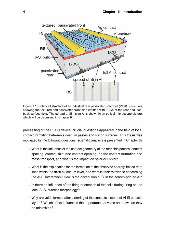
Figure 1.1 shows a schematic model of the industrial PERC structure (afterreference [14]). This solar cell has a passivated n+-layer (P-diffused emitter) atthe front side and a dielectrically passivated p-type silicon layer with local contactopenings (LCOs) at the rear. The interaction between Al and Si occurs locally, and,as a result, sharply delimited dark lines in the thick aluminum layer appear. Thus,the Al-Si alloy and the p+-doped Al layer (also known as back surface field, BSF)are formed in the LCOs at the back contact area. Contrary to that, state-of-the-artsolar cells present a fully covered Al-BSF layer at the back, which gives the nameof Al-BSF solar cells.
The analysis of several solar cell structures with rear passivation (for industrialapplication) is presented in the last chapter of this thesis (Chapter 7). During the
4 Chapter 1: Introduction
Figure 1.1: Solar cell structure of an industrial rear passivated solar cell (PERC structure),showing the textured and passivated front side emitter, with LCOs at the rear and localback surface field. The spread of Si inside Al is shown in an optical microscope picture,which will be discussed in Chapter 6.
processing of the PERC device, crucial questions appeared in the field of localcontact formation between aluminum pastes and silicon surfaces. This thesis wasmotivated by the following questions (scientific analysis is presented in Chapter 6):
• What is the influence of the contact geometry of the rear side pattern (contactspacing, contact size, and contact opening) on the contact formation andmass transport, and what is the impact on solar cell level?
• What is the explanation for the formation of the observed sharply limited darklines within the thick aluminum layer, and what is their relevance concerningthe Al-Si interaction? How is the distribution of Si in the screen-printed Al?
• Is there an influence of the firing orientation of the cells during firing on thelocal Al-Si eutectic morphology?
• Why are voids formed after sintering of the contacts instead of Al-Si eutecticlayers? Which effect influences the appearance of voids and how can theybe minimized?
1.3. Outline of the Thesis 5
1.3 Outline of the Thesis
Three main parts and six chapters give this work its structure:
Part I, Basic Principles and Processing of Silicon Solar Cells
This part is divided in three main chapters and gives an introduction to theprocessing and physics of silicon solar cells.
• Chapter 2 introduces the processing of an industrial state-of-the-art siliconsolar cell, showing the typical processes and their development. Thisclassical device is compared with more advanced concepts as the selectiveemitter solar cell and the rear passivated solar cell. All this devices will beprocessed, characterized and analyzed in this thesis.
• Chapter 3 introduces the basic principles and fundamental physical con-cepts of solar cell devices, as applied throughout this thesis. Basic defini-tions are clarified, giving an introduction into the loss mechanisms of solarcells that diminish the performance, mainly due to recombination centersand optical and electrical losses within the device.
• Chapter 4 introduces an application of an innovative selective emitter con-cept, as a starting point into the understanding of solar cell processing.
Part II, Aluminum-Silicon Contact Formation
This part is divided in two main chapters and contains the main work of thisthesis: the understanding and optimization of the local contact formation betweenaluminum and silicon.
• Chapter 5 presents a complete overview of the contact formation betweenscreen printed aluminum pastes and silicon surfaces.
• Chapter 6 presents the main result of this work on the local contact for-mation between the p-type crystalline silicon and screen printed aluminumpastes at the rear side, giving answers based on experimental observa-tions and physical explanations for the questions introduced in the previoussection.

6 Chapter 1: Introduction
Part III, Analysis of Industrial Rear Passivated Solar Cell Devices
After the optimization of the contact formation between aluminum and silicon,high-efficiency solar cells were developed.
• Chapter 7 shows different device concepts for rear passivated solar cells,analyzing the impact of each processing step. The findings about Al-Sicontact formation as presented in previous chapter will be applied in the rearpassivated devices presented here. Finally, high efficiency achievementsare presented, showing the strong potential of the concepts developedthroughout this thesis for industrial application.
In the end, the highlights of the thesis are summarized and the work is con-cluded with an outlook on further work.
Part I
Basic Principles and Processing ofSilicon Solar Cells

CH
AP
TE
R
2PROCESSING OF AN INDUSTRIAL SOLAR
CELL
Abstract
The process of a solar cell contains wet chemical steps, as cleaning andtexturing, and high temperature steps, as phosphorous diffusion and firing ofcontacts. This chapter explores the preparation of surfaces and the fundamentalexperimental procedure for creating an industrial silicon solar cell.
2.1 Introduction
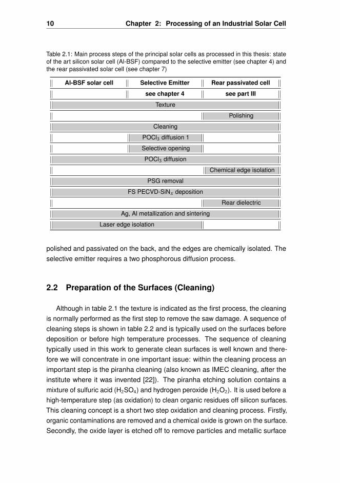
In this part the principal processing sequence for the development of a state ofthe art industrial silicon solar cell is discussed, as an introduction for the followingwork. In table 2.1 three solar cell processes are compared: a state of the artindustrial solar cell (Al-BSF solar cell) as discussed in the present chapter, theselective emitter solar cell, studied in chapter 4, and the rear passivated solar cell,main focus of this thesis, which results are presented in chapter 7.
The process sequence of an industrial solar cell starts with the removal of thesaw damage from the surface. Secondly, the surface is textured to increase lighttrapping. Next, the surface is cleaned and a phosphorous diffusion is performed tocreate the emitter. After removal of the phosphorous silicate glass from the surfaceand cleaning, the surface is passivated by an antireflection coating. Afterwards,the contacts are screen-printed on the front and rear and sintered. In the end, theedges are isolated and the solar cell is characterized. A few steps differentiate theindustrial solar cell from the other two concepts. The rear passivated solar cell is
9
10 Chapter 2: Processing of an Industrial Solar Cell
Table 2.1: Main process steps of the principal solar cells as processed in this thesis: stateof the art silicon solar cell (Al-BSF) compared to the selective emitter (see chapter 4) andthe rear passivated solar cell (see chapter 7)
Al-BSF solar cell Selective Emitter Rear passivated cell
see chapter 4 see part III
Texture
Polishing
Cleaning
POCl3 diffusion 1
Selective opening
POCl3 diffusion
Chemical edge isolation
PSG removal
FS PECVD-SiNx deposition
Rear dielectric
Ag, Al metallization and sintering
Laser edge isolation
polished and passivated on the back, and the edges are chemically isolated. Theselective emitter requires a two phosphorous diffusion process.
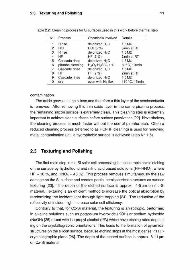
2.2 Preparation of the Surfaces (Cleaning)
Although in table 2.1 the texture is indicated as the first process, the cleaningis normally performed as the first step to remove the saw damage. A sequence ofcleaning steps is shown in table 2.2 and is typically used on the surfaces beforedeposition or before high temperature processes. The sequence of cleaningtypically used in this work to generate clean surfaces is well known and there-fore we will concentrate in one important issue: within the cleaning process animportant step is the piranha cleaning (also known as IMEC cleaning, after theinstitute where it was invented [22]). The piranha etching solution contains amixture of sulfuric acid (H2SO4) and hydrogen peroxide (H2O2). It is used before ahigh-temperature step (as oxidation) to clean organic residues off silicon surfaces.This cleaning concept is a short two step oxidation and cleaning process. Firstly,organic contaminations are removed and a chemical oxide is grown on the surface.Secondly, the oxide layer is etched off to remove particles and metallic surface
2.3. Texturing and Polishing 11
Table 2.2: Cleaning process for Si surfaces used in this work before thermal step.
N Process Chemicals involved Details
1 Rinse deionized H2O 1.5 MΩ2 HCl HCl (5 %) 5 min at RT3 Rinse deionized H2O 1.5 MΩ4 HF HF (2 %) 2 min at RT5 Cascade rinse deionized H2O 1.5 MΩ6 piranha cleaning H2O2:H2SO4 1:4 80 C, 10 min7 Cascade rinse deionized H2O 1.5 MΩ8 HF HF (2 %) 2 min at RT9 Cascade rinse deionized H2O 1.5 MΩ
10 dry oven with N2 flux 110 C, 15 min
contamination.The oxide grows into the silicon and therefore a thin layer of the semiconductor
is removed. After removing this thin oxide layer in the same piranha process,the remaining silicon surface is extremely clean. This cleaning step is extremelyimportant to achieve clean surfaces before surface passivation [22]. Nevertheless,the cleaning process is much faster without the use of piranha etch. Often areduced cleaning process (referred to as HCl-HF cleaning) is used for removingmetal contamination until a hydrophobic surface is achieved (step N 1-5).
2.3 Texturing and Polishing
The first main step in mc-Si solar cell processing is the isotropic acidic etchingof the surface by hydrofluoric and nitric acid based solutions (HF-HNO3, whereHF ∼ 10 %, and HNO3 ∼ 45 %). This process removes simultaneously the sawdamage on the Si surface and creates partial hemispherical structures as surfacetexturing [23]. The depth of the etched surface is approx. 4-5 µm on mc-Simaterial. Texturing is an efficient method to increase the optical absorption byrandomizing the incident light through light trapping [24]. The reduction of thereflectivity of incident light increase solar cell efficiency.
Contrary to that, for Cz-Si material, the texturing is anisotropic, performedin alkaline solutions such as potassium hydroxide (KOH) or sodium hydroxide(NaOH) [25] mixed with iso-propyl-alcohol (IPA) which have etching rates depend-ing on the crystallographic orientations. This leads to the formation of pyramidalstructures on the silicon surface, because etching stops at the most dense < 111 >crystallographic plane [26]. The depth of the etched surface is approx. 8-11 µmon Cz-Si material.
12 Chapter 2: Processing of an Industrial Solar Cell
Although in the process sequence of a standard industrial silicon solar cell therear side is not polished, this approach has many applications for high-efficiencyrear passivated solar cells. Important insights into its impact on the smoothnessof the surface and influence on the bulk lifetime will be given in chapter 7. Thepolishing of the surface is isotropic and normally found in two chemical forms: theacidic polishing for mc-Si material is normally achieved by HF−HNO3 concentratedetching solutions, and the alkaline polishing for Cz-Si substrates is performed byhigh concentrations of KOH or NaOH etching solutions.
2.4 POCl3 Diffusion
The main step in the creation of a solar cell from a p-type silicon substrate isthe diffusion of n-type dopants into the silicon bulk to generate the p-n junction.In this thesis p-type silicon substrates have been used and the formation of then+-type emitter is performed by the diffusion of phosphorous atoms into p-Si ina tube furnace at temperatures above 800 C. The doping profile of the emittercan be characterized by secondary ion mass spectroscopy (SIMS). It has beenshown that a standard phosphorous emitter (sheet resistance of 66Ω/) presentsa doping profile with a peak density of 1.6x1021 cm−3, and a depth of approx.0.27 µm into the silicon [27].
It is well known that, during the phosphorus oxychloride (POCl3) diffusion,a phosphorous silicate glass (PSG) growths on the silicon surface and a phos-phorous diffused emitter forms underneath the glass [28] (for more details aboutthe phosphorous diffusion processes in the photovoltaic see references [29,30]).An application of the POCl3 diffusion with in-situ thermal oxidation is given inchapter 4.
2.5 Antireflection Coating
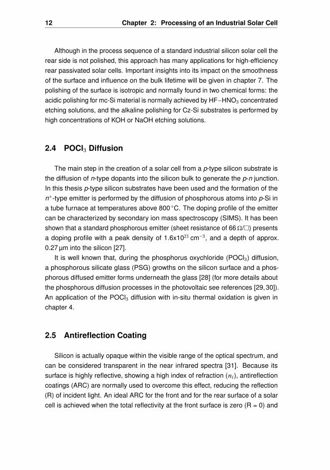
Silicon is actually opaque within the visible range of the optical spectrum, andcan be considered transparent in the near infrared spectra [31]. Because itssurface is highly reflective, showing a high index of refraction (ni ), antireflectioncoatings (ARC) are normally used to overcome this effect, reducing the reflection(R) of incident light. An ideal ARC for the front and for the rear surface of a solarcell is achieved when the total reflectivity at the front surface is zero (R = 0) and
2.5. Antireflection Coating 13
Figure 2.1: Principle of a quarter wavelength antireflection coating: incident light from air,through the ARC and into the Si interface.
at the rear surface is maximum (R = 1) [24]*. Hence, every incident photon isabsorbed and generates a new electron-hole pair. The absorbance of the deviceis increased through dielectrics with index of refraction higher than 1 (ni >1) [24].The index of refraction is a function of the wavelength [32]. Nevertheless, for asilicon cell measured under air, the refractive index is normally approximate tonopt ≈ 3.8 [33] (see Table 2.3). A work on this topic is found in reference [34].Following the principle of a quarter wavelength ARC [33] (see Figure 2.1), theminimum for the reflection is found when
n1d1 = λ0
4(2.1)
and reads (see Figure 2.1):
Rmi n =(
n21 −n0n2
n21 +n0n2
)2
(2.2)
This relation means that for one dielectric layer the zero reflectance is achieved,when the film thickness is equal to one quarter of the wavelength. Total absorptionof light is found at zero reflection, when the square root of the index of silicon isequal to the index of ARC n1 ≈ 1.95 (which approximates to the index of a siliconnitride film as shown in Table 2.3, and normally used in PV). It means that forsilicon, the optimal dielectric layer might have an index of refraction of 1.95. Usingequation 2.1 the optimal thickness for the ARC in order to have zero reflection at600 nm (maximum of the solar spectrum) is:
d1 = λ0
4n1≈ 76.95nm (2.3)
*Specially on mc-Si surfaces, a darker grain boundary implies a lower reflectivity region [26].†The refractive index strongly depend on the wavelength. These values are normally determined
by a wavelength of 632 nm, which represents a red laser diode as implemented in Ellipsometry. This
14 Chapter 2: Processing of an Industrial Solar Cell
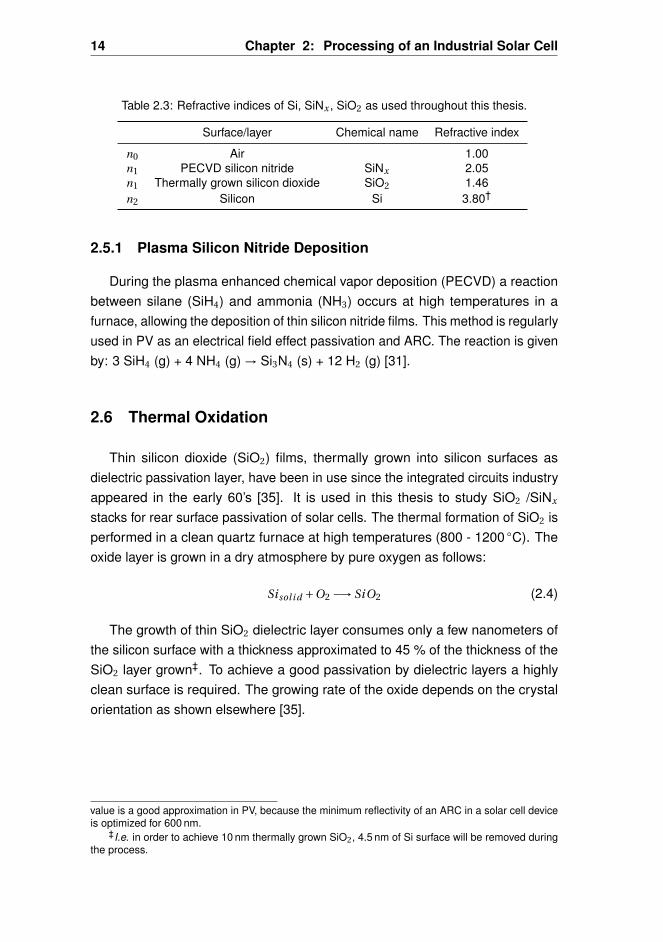
Table 2.3: Refractive indices of Si, SiNx , SiO2 as used throughout this thesis.
Surface/layer Chemical name Refractive index
n0 Air 1.00n1 PECVD silicon nitride SiNx 2.05n1 Thermally grown silicon dioxide SiO2 1.46n2 Silicon Si 3.80†
2.5.1 Plasma Silicon Nitride Deposition
During the plasma enhanced chemical vapor deposition (PECVD) a reactionbetween silane (SiH4) and ammonia (NH3) occurs at high temperatures in afurnace, allowing the deposition of thin silicon nitride films. This method is regularlyused in PV as an electrical field effect passivation and ARC. The reaction is givenby: 3 SiH4 (g) + 4 NH4 (g) → Si3N4 (s) + 12 H2 (g) [31].
2.6 Thermal Oxidation
Thin silicon dioxide (SiO2) films, thermally grown into silicon surfaces asdielectric passivation layer, have been in use since the integrated circuits industryappeared in the early 60’s [35]. It is used in this thesis to study SiO2 /SiNx
stacks for rear surface passivation of solar cells. The thermal formation of SiO2 isperformed in a clean quartz furnace at high temperatures (800 - 1200 C). Theoxide layer is grown in a dry atmosphere by pure oxygen as follows:
Sisol i d +O2 −→ SiO2 (2.4)
The growth of thin SiO2 dielectric layer consumes only a few nanometers ofthe silicon surface with a thickness approximated to 45 % of the thickness of theSiO2 layer grown‡. To achieve a good passivation by dielectric layers a highlyclean surface is required. The growing rate of the oxide depends on the crystalorientation as shown elsewhere [35].
value is a good approximation in PV, because the minimum reflectivity of an ARC in a solar cell deviceis optimized for 600 nm.
‡I.e. in order to achieve 10 nm thermally grown SiO2, 4.5 nm of Si surface will be removed duringthe process.
2.7. Screen-printing Metallization and Sintering of Contacts 15
2.7 Screen-printing Metallization and Sintering of Contacts
The metallization of solar cells in the industry is still mostly performed bymeans of a screen-printing technique. On the illuminated side silver pastes areused to perform the characteristic H-pattern design with three busbars for moduleassembly and fine lines. However, the continuous increase in the price of silverhas shown that other materials, as copper paste, and new printing techniques arerequired for the future solar cells [36].
The rear surface is fully covered by aluminium pastes, and silver pads areincorporated for module assembly. The contact is formed during firing the samplesin a lamp heated conveyor belt furnace. On the front, the glass content in liquidstate fires through the ARC to contact the emitter [37]. On the rear, a fully coveredAl-Si alloy is formed and the Si interface is highly-p+-doped by Al atoms, formingthe well known back-surface-field (BSF, see part II). Therefore, state of the artsolar cells are well-known as Al-BSF solar cells.
2.8 Edge Isolation
After the phosphorous diffusion, a n+-doped layer fully covers the Si substrate(if no back-to-back process is used [38]). During the metallization, the alloyingprocess between Al and Si overcompensates the shallow P-doped layer on theback (the emitter is few microns deep compared to the 10 µm deep Al-Si eutecticlayer). At this point, the front and rear form a short circuit through the edges of thesubstrate. The electrons in the emitter region can easily move through the emitterat the edges to the back, shunting the solar cell. Two types of edge isolation arenormally used: laser edge isolation at the front (see for instance reference [39])where laser lines that are a few microns deep separate the front side emitter fromthe rear (laser damage may reduce cell performance); and an inline chemicaledge isolation which etches the back emitter layer completely before metallization(no damage of the front side is performed).
2.9 Dielectric Ablations
Dielectric layers can be used as barriers against thermal processes, as dif-fusion or thermal oxidation. Selectivity can be easily achieved by ablation ofdielectrics. The ablation of dielectrics is performed in this work by etching pastes.
16 Chapter 2: Processing of an Industrial Solar Cell
The pastes used are environmentally friendly and provide excellent screen printingbehavior. Some etchants of dielectrics are also addressed in this section.
2.9.1 Etching Paste
The etching of the dielectric is performed using the screen-printable isishapeSolarEtchT M etching pastes from Merck KGaA [40]. Two products are presented:
The BRS Etching Paste: Is a fluoride containing paste, designed to etch SiO2
layers at room temperature. The pink color of the BRS paste makes it easy todifferentiate from BES which is black. The etching rate of a thermal SiO2 layer istypically 3-4 nm/s at room temperature. For the screen printing process, standardstainless steel screens of 250-280 mesh count and 20-25 µm wire diameter wereused. The emulsion of the screens has a thickness of about 20-25 µm. Thesqueegee speed of the screen printing machine is 15 cm/s. For the best etchingperformance of this paste resulting in a continuously etched line through thedielectric layer, it is necessary to use a continuous process flow. To clean thescreens from the paste they are rinsed in water, leaving a low organic and fluorideconcentration in the volume of water used.
The BES Etching Paste: The BES etching paste is a HF and Chloride freepaste, designed to etch SiNx or SiO2 dielectric layers. It contains phosphoric acid,a useful etchant of dielectric films [41]. Almost all of the dielectric layers presentedin the publications and throughout this thesis were selectively opened by screenprinting this phosphorus containing etching paste. This paste requires highertemperatures than BRS. The activation of the etching properties is done by dryingthe wafers slowly (4 min.) in a 6 zones infrared conveyor belt furnace at 330 C.The etching rate of a thermal SiO2 layer is typically 1.5-2 nm/s, and 3-4 nm/s forPECVD SiNx , during the drying. Immediately after the drying step the waferswere placed in carriers and put into an ultrasonic bath for cleaning. The cleaningof the etching paste is completed after a few seconds in an ultrasonic bath withdeionized water and 0.2 % potassium hydroxide (KOH), at 40 C. For texturedwafers the opening of dielectrics may be improved by increasing the KOH contentin the deionized water in the bath. This paste will be used in the present work.
Some authors applied these etching techniques for selective emitter solar cellconcepts, showing differences in the performance between these two commercialpastes (see reference [42]).
2.9. Dielectric Ablations 17
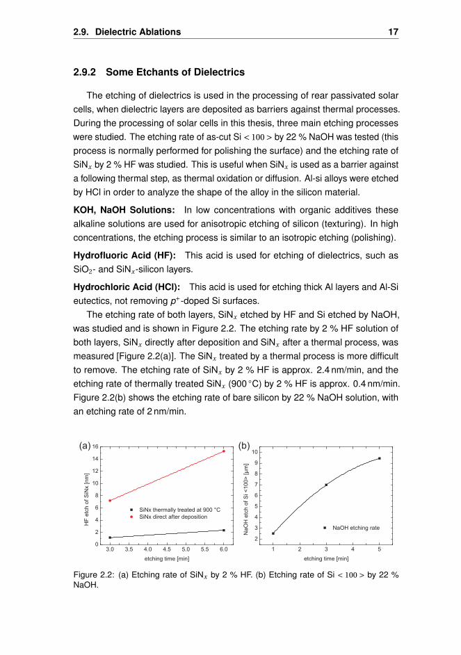
2.9.2 Some Etchants of Dielectrics
The etching of dielectrics is used in the processing of rear passivated solarcells, when dielectric layers are deposited as barriers against thermal processes.During the processing of solar cells in this thesis, three main etching processeswere studied. The etching rate of as-cut Si < 100 > by 22 % NaOH was tested (thisprocess is normally performed for polishing the surface) and the etching rate ofSiNx by 2 % HF was studied. This is useful when SiNx is used as a barrier againsta following thermal step, as thermal oxidation or diffusion. Al-si alloys were etchedby HCl in order to analyze the shape of the alloy in the silicon material.
KOH, NaOH Solutions: In low concentrations with organic additives thesealkaline solutions are used for anisotropic etching of silicon (texturing). In highconcentrations, the etching process is similar to an isotropic etching (polishing).
Hydrofluoric Acid (HF): This acid is used for etching of dielectrics, such asSiO2- and SiNx-silicon layers.
Hydrochloric Acid (HCl): This acid is used for etching thick Al layers and Al-Sieutectics, not removing p+-doped Si surfaces.
The etching rate of both layers, SiNx etched by HF and Si etched by NaOH,was studied and is shown in Figure 2.2. The etching rate by 2 % HF solution ofboth layers, SiNx directly after deposition and SiNx after a thermal process, wasmeasured [Figure 2.2(a)]. The SiNx treated by a thermal process is more difficultto remove. The etching rate of SiNx by 2 % HF is approx. 2.4 nm/min, and theetching rate of thermally treated SiNx (900 C) by 2 % HF is approx. 0.4 nm/min.Figure 2.2(b) shows the etching rate of bare silicon by 22 % NaOH solution, withan etching rate of 2 nm/min.
Figure 2.2: (a) Etching rate of SiNx by 2 % HF. (b) Etching rate of Si < 100 > by 22 %NaOH.

CH
AP
TE
R
3BASIC PRINCIPLES OF SOLAR CELLS
Abstract
The photovoltaic effect was discovered by A. E. Becquerel in 1839 [43]. G. W.Pickard invented the crystal detector in 1906 [44,45] with strong radio receivingproperties, using for the first time the semiconductor properties of silicon*.
The first p-n junction silicon light-sensitive electric device was invented by R. S.Ohl [46]. This was the first time that a photovoltaic effect in elementary materialwas found [44]. Ohl found segregation of impurities in a metallurgical silicon ingot.He found that boron and aluminum created gaps in the crystal structure of silicon,changing the conductivity of the material to p-type, and phosphorus contributedwith excess of electrons, changing the conductivity of the material to n-type [44].
Today the three impurities found by Ohl are still widely used in the photovoltaicsindustry of crystalline silicon (c-Si) solar cells with different approaches: forcreating emitters (phosphorus or boron diffusion, or sintering of screen-printingaluminum), for doping the bulk material (phosphorus or boron doping duringcrystallization), and for creating front surface field (FSF) or back surface fields(BSF).
This chapter explores the fundamental physical concepts of solar cells. Theprincipal characteristics and characterization methods of solar cell devices willbe presented and the basic definitions of loss mechanisms in solar cell areintroduced.
*Si is one of the most abundant elements on earth.
19
20 Chapter 3: Basic Principles of Solar Cells
3.1 Characterization of Solar Cells
Industrial solar cells require high efficiency at low cost (high reproducibility,simple processes, good reliability). Nevertheless, there are some fundamentallimits to the maximum power conversion efficiency of the solar cell. In this section,typical characterization methods are shown.
3.1.1 I -V -Characteristic
Solar Cell Efficiency Limit
The solar cell efficiency (η) is defined as the ratio of maximum output power(Pmp ) to a load to the incident solar power (Popt ) on the cell (see equation 3.1).The bandgap of silicon is 1.12 eV, and therefore, only incident light with photonenergy (hν) equal or above the bandgap can be used for photogeneration ofcharge carriers within the solar cell (see section 3.3, light absorption of Si).The excess energy above the bandgap increases the device temperature bythermalization of the excited electrons. Thus, only the bandgap energy canbe transferred into electrical energy. The solar cell efficiency is measurablein terrestrial applications at a temperature of 25 C by considering the energyspectrum, which penetrates the atmosphere, as quantified by the Air Mass, AM1.5.Based on radiative recombination the detailed balance limit of solar cell efficiencyhas been first published by Shockley and Queisser [47] to be 30 %. Nevertheless,an extended model including Auger recombination, free carrier absorption, andradiative recombination has shown an efficiency limit of 29.8 % [48] under AM1.5,for c-Si solar cells.
η≡ Pmp
Pl i g ht= JSC VOC F F
Pl i g ht(3.1)
Open-Circuit Voltage Limit
The upper open-circuit voltage (VOC ) limit achievable in a silicon solar cell devicewas shown to be 750 mV for an accessible silicon bulk material of 300 µm thick-ness [49], measured with AM0 (space applications) at 25 C. This value is muchsmaller than the band gap of Si (E g = 1.12 V), because in heavily excited siliconnormally quasi-Fermi levels are located within the bandgap, forming fundamentalupper limits for photogenerated carriers which are trapped there until they recom-bine [49]. The VOC can be obtained from the simplified first diode model by setting
3.1. Characterization of Solar Cells 21
the current in equation 3.19 to zero (I = 0), obtaining:
VOC = kT
qln
(1+ ISC
I01
)(3.2)
VOC strongly depends on the dark-saturation current I0, which should beminimal (i.e. the recombination should be minimal for an optimal VOC of thedevice).
Fill Factor Limit
The fill factor (FF) characterizes the quality of the solar cell, giving the maximumoutput power point, Pmp , with the coordinates (Vmp , Jmp ) in the fourth quadrant ofthe I -V characteristics of a solar cell under illumination. Generally, FF is given bythe following equation:
F F ≡ JmpVmp
JSC VOC·100 % (3.3)
The FF achieves its maximum (FF = 100 %) when Pmp = JSC ∗VOC . It will beshown in this thesis that good solar cells can achieve 80 % FF. The higher itsvalue, the higher the quality of the solar cell device. The FF, however, depends onmany parameters and is therefore only expressed as an approximation in somedefined ranges in terms of other cell parameters [50]. Several publications haveshown empirical approximations for the FF of solar cells, showing for the idealcase (without losses) that FF is depending only on VOC [50,51]. Generally, theFF is mainly affected by series resistance and shunt resistance losses in the cell,and by the second diode (ideality factor 2) of the device.
3.1.2 Spectral Response
The solar spectrum on earth is approximated to the AM1.5 standard. Thespectrum defines different photon wavelengths, with their respective photonenergies, which produce photocurrent in the solar cell device from the absorbedincident light. The response of the solar cell device to the incident light is definedby the spectral response (SR). To characterize the spectral response of a solarcell and in order to determine the generated photocurrent, one measures thecharge carriers collected in the solar cell device per flux of incident photons,known as the quantum efficiency (QE). Two forms of QE can be defined: forexternally observed response, known as the external quantum efficiency (EQE),and for internal response, known as the internal quantum efficiency (IQE). In theideal case, no recombination mechanisms, no absorption losses, and no reflectionlosses limit the device. In this case, QE is unity [52].
22 Chapter 3: Basic Principles of Solar Cells
The ratio of generated charge to incident photons as observed externally, isgiven by:
EQE(λ) = Iph/q
Popt /Eph= Iph/q
Φi n(λ)(3.4)
In equation 3.4, the ratio of the photocurrent Iph to the incident photon powerPopt is known as the spectral response (SR), or responsivity [52] of the device,where Iph gives the flow of electrons moving from the valence band to the con-duction band and Popt is the optical power [53]. Thus, Iph should me maximized,by maximizing the absorption in the bulk†.
Representing the spectral response mathematically, one gets:
SR(λ) = Iph
Popt= q
hνEQE(λ) = qλ
hcEQE(λ) (3.5)
In equation 3.5, q/hν=V −1g , with Vg defined by Shockley [47] as the voltage at
which each incident photon with energy greater than the bandgap of Si (hν≥ E g ),will produce one charge (q). The SR is enhanced at specific wavelengths, throughdifferent processing steps in the device. For instance, the blue light response ofthe solar cell is enhanced by lowly doped emitters and high surface passivationqualities (see for instance the selective emitter concept in section 4.1). In thesame way, the infrared response is enhanced by better rear passivation qualitiesand light trapping (see for instance the rear passivated solar cell in chapter 7).At the same time, the ratio of generated charge to incident photons as observedinternally, is given by:
IQE(λ) = Iph/q
Popt /Eph[1−R(λ)]= EQE(λ)
[1−R(λ)](3.6)
Thus, the internal quantum efficiency IQE is the ratio between absorbedphotons and collected electrons [55]. In equation 3.6 the quantum efficiencyconsiders the total reflectance (R) which is the sum of the front reflectance ofincident light, and the escape reflectance outside the device [56]‡.
The escape reflectance considers the internal reflection at the rear of thedevice, which is appreciable in the infrared spectral response of the device.Normally, the rear surface reflectivity is ignored in approximate modeling of solarcell devices [57]. Fischer showed that the effective diffusion length, Le f f , can berelated to the internal quantum efficiency, IQE, and the absorption length α−1 in
†It has to be mentioned that the photoelectric sensitivity is a result of the temperature effect onthe distribution of the electrons in different levels [54].
‡The reflection is measured in the UV-Vis-NIR spectrometer.
3.1. Characterization of Solar Cells 23
the following simplified expression, for moderately absorbed light [55]:
Le f f =α−1(
1
IQE−1
)−1
(3.7)
This expression for the effective diffusion length is often used as an importantparameter to determine the short wavelength current collection and the currentinjection in the dark [55].
3.1.3 Short-Circuit Current Density
The short-circuit current density (JSC ) depends on the device structure, qualityof the bulk material, and operating conditions. Its value is given by the convolutionof the external quantum efficiency, EQE, and the number of penetrated photons,Φi n , along the light spectrum:
JSC = q∫
EQE(λ)Φi n(λ)dλ (3.8)
JSC is strongly limited by optical and recombination losses. It will be shown laterthat the reduction of the reflectivity of bare silicon by deposition of an antireflectioncoating (ARC) increases the trapping of light in the device and thus enhances JSC .Also the absorption is enhanced by reducing shadowing losses of metal contactsat the front of the solar cell, as in the case of the interdigitated back contact solarcell (IBC) [58].
As shown by the absorption coefficient of intrinsic silicon, long light wave-lengths need a minimum material thickness or a good light trapping at the rear inorder to be effectively coupled into the cell and to generate charge carriers in thebulk§. These requirements are fulfilled by the dielectrically coated rear surface ofthin Si solar cells, as studied throughout this thesis.
Electron-hole pairs generated far away from the p-n-junction present highprobability of recombination at bulk defects or at the surfaces, reducing JSC . Therear surface passivation quality plays an important role in the electric and opticalperformance of the solar cell. This thesis shows that the rear dielectric coatingimproves JSC due to the higher internal reflectivity of the coating compared to afully covered Al back surface field (BSF). Also better passivation qualities than theAl-BSF are demonstrated by means of the rear dielectric coating to reduce thesurface recombination velocity.
§A light wavelength of 1000 nm has a penetration depth of 100 µm in the bulk material.
24 Chapter 3: Basic Principles of Solar Cells
3.1.4 A few Characterization Tools
Scanning Electron Microscopy
In this thesis the Al-Si alloy junction is characterized by scanning electron mi-croscopy (SEM) and energy dispersive X-ray spectrometry (EDS/EDX). The cross-sectional analysis is performed after laser cutting of the samples. High-qualitySEM micrographs can be achieved with the respective selection of parametersand no extra cleaning step. The parameters to be used are as follows: acceler-ation voltage 10 kV, specimen current 780 pA, scanning speed 5.4 µs/pxl, andelectron beam focused to 660 nm in diameter. Counts at the SiKα line were takenfor 300 s, with a line scan width of 10 µm. Highly doped regions are visible tothe eye (i.e. p+-doped areas by Al), because the emission intensity from dopedstructures is logarithmically proportional to the active dopant concentration [59].The EDS/EDX analysis is hence a strong characterizing technique, which turnsimaging into a quantitative analysis tool [59].
Light Beam Induced Current and Electroluminescence
The light beam induced current (LBIC) is a topographical measurement techniqueusually applied to detect losses within the solar cell. This method is also calledmapping technique, due to the point to point scan across the wafer surface. Itcombines the high spatial resolution of a probe beam with electrical signals fromthe recombination of excess electron-hole pairs [60, 61]. This method gives adetailed understanding of parameters that may be responsible for the reductionof the solar cell efficiency. The efficiency of a multicrystalline (mc) silicon solarcell is well known to be limited by defects where strong recombination places aresited for minority carriers, normally localized within dislocations. LBIC makes theareas with low minority carrier lifetime visible. The mapping method is a strongtechnique, nevertheless one of the large disadvantages is the rather long timetaken to cover a large surface mapping¶. A laser beam scans along the surface,reading out the current on each measured point. The different light wavelengthsof the laser allow to analyze different layers within the solar cell. For instance, at400 nm the emitter surface is dominating the cell performance, at 800 nm the bulkis characterized; and above 900 nm the rear surface of the device is visible foranalysis.
The measurements presented in this work were performed by a Semilab WT-
¶For example a 156x156 cm2 cell with a LBIC resolution of 125 µm needs up to 16 h to be fullyinspected by 4 laser wavelengths.
3.2. Loss Mechanisms of Solar Cells 25
2000 system. The measuring method presents a spot size of 100 µm with fourvariable light sources. The LBIC method is performed on sintered solar cellswith contacts. Also the reflection is measurable for each four light wavelengths,allowing to calculate the IQE response. Bulk and rear recombination properties ofthe solar cell are indirectly determined as Le f f , which is obtained from the LBICmethod. The Le f f and IQE results allow to characterize the performance of thefinished solar cell, indicating the quality of the cell process. Through the LBICmethod it is also possible to determine the IQE response from the EQE and Rdata.
The Electroluminescence (EL) analysis is based on an optical phenomenonwhich makes a semiconductor to emit light by passing a current through thematerial rather than by the absorption of photons [62]. Its mechanism is theopposite of generation, here the injected carriers recombine within the bulkemitting light. This approach allows to recognize the regions within the solarcell where losses in recombination and series resistance are present. It is astrong tool for the analysis of dislocations within mc-Si material which are visibleas dark regions on the EL-picture.
3.2 Loss Mechanisms of Solar Cells
The power conversion efficiency of the solar cell is limited by loss mechanisms,predominantly by series resistance losses and recombination mechanisms. Bothmechanisms are described in the present section.
3.2.1 Series Resistance Losses
The series resistance losses, RS [Ωcm2] can be dominant for the reduced solarcell performance by limiting the output power of the solar cell device. The total RS
is given by all parasitic ohmic losses as found throughout the solar device, whichincrease the resistance of the current transport, as shown in Figure 3.1 [63]. Itsvalue is given by:
RS =6∑
i=1Ri (3.9)
where Ri represents each component of resistance. R1 is the contact resistancebetween the fully covered Al rear layer and the p-Si bulk. Due to the high seriesresistance of the bulk material and the large covered area, its value has a non-measurable influence on the total current-voltage characteristic and is generally
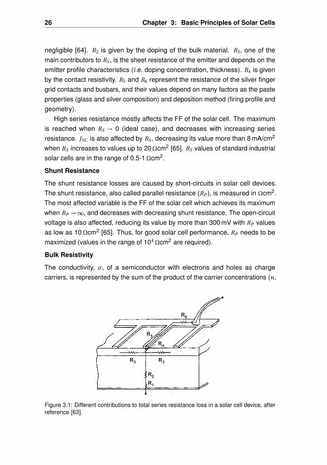
26 Chapter 3: Basic Principles of Solar Cells
negligible [64]. R2 is given by the doping of the bulk material. R3, one of themain contributors to RS , is the sheet resistance of the emitter and depends on theemitter profile characteristics (i.e. doping concentration, thickness). R4 is givenby the contact resistivity. R5 and R6 represent the resistance of the silver fingergrid contacts and busbars, and their values depend on many factors as the pasteproperties (glass and silver composition) and deposition method (firing profile andgeometry).
High series resistance mostly affects the FF of the solar cell. The maximumis reached when RS → 0 (ideal case), and decreases with increasing seriesresistance. JSC is also affected by RS , decreasing its value more than 8 mA/cm2
when RS increases to values up to 20Ωcm2 [65]. RS values of standard industrialsolar cells are in the range of 0.5-1Ωcm2.
Shunt Resistance
The shunt resistance losses are caused by short-circuits in solar cell devices.The shunt resistance, also called parallel resistance (RP ), is measured in Ωcm2.The most affected variable is the FF of the solar cell which achieves its maximumwhen RP →∞, and decreases with decreasing shunt resistance. The open-circuitvoltage is also affected, reducing its value by more than 300 mV with RP valuesas low as 10Ωcm2 [65]. Thus, for good solar cell performance, RP needs to bemaximized (values in the range of 104 Ωcm2 are required).
Bulk Resistivity
The conductivity, σ, of a semiconductor with electrons and holes as chargecarriers, is represented by the sum of the product of the carrier concentrations (n,
Figure 3.1: Different contributions to total series resistance loss in a solar cell device, afterreference [63].
3.2. Loss Mechanisms of Solar Cells 27
p) with their mobilities (µn , µp ), and is given by:
σ= q(µnn +µp p) = 1
ρ(3.10)
Its value increases by several orders of magnitude when the doping concentra-tion in the bulk material is increased, and under illumination due to the increaseof free net charge carriers [52]. ρ [Ω-cm] is the resistivity of the material. Themobility of charge carriers is variable and depends on the diffusion coefficient inpresence of a concentration gradient of defects [52,66])||, and can therefore alsoaffect the material resistivity.
Ohmic Contact
Contact losses are supposed to only faintly disturb the device performance.Therefore, in order to transport the photocurrent out of the semiconductor withminimal losses, a negligible metal-semiconductor contact resistance, which showsohmic behavior, is required [64, 67]. Ohmic contacts obey the fundamentalrequirements of Ohm’s law within a large voltage range [64].
Ohmic contacts are achieved by high doping concentrations of the silicon and,according to the Schottky theory (see reference [68]), by low barrier heights orsmall barrier widths to the metal. In a solar cell device this is an important topicsince two metal-semiconductor junctions are found in direct contact to the cellstructure: at the front, crystalline silver particles contact the emitter, and at therear, an aluminum-silicon (Al-Si) eutectic is found. Therefore the most practicaltechnique in photovoltaics to achieve high performance contacts is to depositthe metal onto a highly doped semiconductor, as already shown by Cabrera etal. [69].
Low-resistance ohmic contacts at the rear side of industrial solar cell structuresare a result of the interdiffusion between Al and Si, which takes place at thelocal contact interface [70]. However, the interaction between Al and Si (theirinterdiffusion), is not homogeneously distributed at the interface over the contactarea [71]. This phenomenon will be discussed in more details in chapter 6.
The total contact resistance, RC , can be obtained by dividing the contactresistivity value, ρc , by the contact area A. It has the unit Ohm (Ω) and is given bythe following equation [52]:
RC = ρc
A(3.11)
||The mobility is proportional to the diffusivity, D, divided by the thermal voltage, kT /q (Einsteinrelationships).
28 Chapter 3: Basic Principles of Solar Cells
Contact Resistivity
As defined by Schroder [72], the specific contact resistance, ρc , is a theoreticalquantity which refers to the metal-semiconductor interface only. It is defined as thereciprocal of the derivative of current density with respect to voltage (see equation3.12). It has the unit mΩcm2, and characterizes the contact independent of itsarea [63]**.
ρc ≡(
d J
dV
)−1
V =0(3.12)
The solution of equation 3.12 is approximated by physical regimes, dependingon doping and temperature, known as: thermionic emission (TE) for lowly dopedbulk material, thermionic field/emission (TFE) for intermediate range, and tun-neling for higher doping concentrations. Due to these effects this parameter isactually not measurable [72].
For solar cells, this parameter is approximately determined by the TransmissionLine Model (TLM, see next section). It is important to mention that the TLM methodhas been widely used for measuring the contact resistance of Ag lines alloyed onhomogeneously n+-doped emitter layer (sheet resistance of the emitter constant).Thus, there exists no generalization of the TLM method for measuring Al contact,where the sheet resistance is not constant due to the presence of the highlyp+-doped layer (local BSF) underneath the Al lines. Nevertheless, results will beshown for the contact resistivity by TLM approach of aluminum lines on a dielectriclayer and forming an ohmic contact to a p-type Si polished surface, assuming thatthe entire contact length contributes to current transfer [63].
For solar cell devices the interpretation of ρc is of strong importance to under-stand the performance of real contacts. It is very useful when comparing contactsof different sizes, to give information about the quality of the metal-semiconductorcontact. Berger [73] and later also Schroder and Meier [63] have given usefuldefinitions and explanations of many methods to determine the contact resistivity.They have shown significant measurement techniques for contact resistivity ofAl-Si contacts depending on surface doping concentration. Also a spatial variationof the contact resistivity was presented and explained by taking into account theinhomogeneity of the contacts. A variation of the contact resistivity was found fromthe middle to the edges of the contact area. This is also valid for the investigationpresented in this thesis: it will be shown that the contact resistivity depends onthe homogeneity of the Al-Si alloy formation.
**The contact resistance is normalized by the area.
3.2. Loss Mechanisms of Solar Cells 29
Transmission Line Model
One method to determine the contact resistivity and the sheet resistance of thesemiconductor beneath the contact from the geometry of planar contacts, is calledthe Transmission Line Model (TLM). For deep details about the measuring method,examples and results, see for instance reference [63,73,74].
According to Schroder [63], the current transfer from semiconductor to metaltakes place on the transfer length, LT . It is clear from the equation 3.13 that LT
decreases with increasing sheet resistance (RSH ) of the diffused layer, normallythe phosphorous emitter. The two extremes are: (a) when ρc is too low, thecurrent transfer will be located near the edge of the metal [63] (LT is small); and(b) when ρc is high or RSH low (LT is large, but not larger than the contact width).Nevertheless, it will be shown in this thesis that real contacts present uniformitieson the metal-semiconductor interface, where the effective area may vary from theactual area [63].
LT =√(
ρc /RSH)
(3.13)
Sheet Resistance
Thin layers as the phosphorus-diffused emitter on the top of the solar cell, arecharacterized by their sheet resistance RSH [Ω/]. Its value is normally charac-terized by the four-point-probe method that has been used since the 50’s [75].Generally, the sheet resistance can be obtained by integrating the emitter profileof the phosphorous diffused layer. For a non-uniformly doped layer of thicknessW , its value is given by:
RSH = 1
q∫ W
x1
ρ(x) d x(3.14)
Equation 3.14 shows that the sheet resistance is actually determined by theresistivity profile of the diffused layer, moving along the x coordinate from thesurface (at x = 0) into the thin layer, and can be characterized by removingthin layers one by one and measuring the resistivity of the bulk, ρ [72]. Thismeasuring technique is based on the electrochemical capacitance-voltage (ECV)measurement, which allows the determination of the doping concentration peakclose to the surface of the thin doped layer. The higher the concentration NA ofphosphorus (P) dopant atoms is, the lower will be the sheet resistance, RSH , ofthe P-diffused emitter.
30 Chapter 3: Basic Principles of Solar Cells
3.2.2 Recombination in Solar Cells
Generally, the recombination process of charge carriers is defined as thereverse process of their generation. The thermal-equilibrium condition of a semi-conductor (in the dark) can be disturbed by illuminating the device, increasingthe charge carrier concentration by generation of electron-hole pairs [35]. Af-ter generation, the carriers tend to return to their original state of equilibriumthrough the event of recombination. Thus, the two mechanisms to disturb theequilibrium-condition are [52]: the recombination process of the electron-holepairs (undesirable) and the thermal generation through photon illumination (re-quired). Both mechanisms must fulfill the principle of conservation of energy††.
In solar cells the recombination leads to an undesirable reduction of solarcell efficiency due to the losses of generated carriers. The generation increasesby optimizing the absorption of photons from the incident light on the solar celldevice, increasing η. The event of generation is the most important process in asolar cell, for converting the incident sunlight into electrical energy.
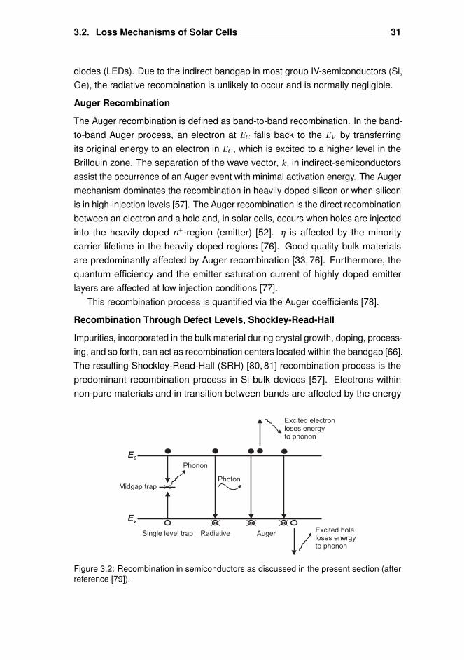
In semiconductors there are three fundamental recombination possibilities [35,76], which are the band-to-band radiative recombination, the band-to-band Augerrecombination (non-phononic mechanism) and the recombination through defectlevels or traps (phononic mechanism) (see Figure 3.2).
The last two events dominate in Si solar cells.
Band-to-band Radiative Recombination
The radiative recombination is the reverse of the absorption and occurs whenan electron jump from the conduction band, EC , into the valence band, EV , andthis event is therefore faster in a direct-bandgap (Eg ) semiconductors than inan indirect one. Direct-bandgap semiconductors (as GaAs) have the minimumof EC and the maximum of EV at the same wave vector, k [66]. An electronwith the necessary energy to jump from the valence band into the conductionband becomes free to move in the crystal. By the transition of the electron tothe conduction band, a hole is created, which is as well free to move in thevalence band (generation, see reference [66]). An electron, however, can alsolose energy and fall back into the valence band, recombining with a free hole (seereference [66]). The energy by this recombination event is released in the form of aphoton. Hence, this is a 3-particle process [35]. Their energy is near to the visiblerange and therefore this process is exploited in devices such as light-emitting
††The energy of an electron in transition is conserved by emitting a photon (radiative recombination)or by transferring the energy to another electron or hole, exciting its state to a higher level instead ofemitting light (Auger recombination) [35,52].
3.2. Loss Mechanisms of Solar Cells 31
diodes (LEDs). Due to the indirect bandgap in most group IV-semiconductors (Si,Ge), the radiative recombination is unlikely to occur and is normally negligible.
Auger Recombination
The Auger recombination is defined as band-to-band recombination. In the band-to-band Auger process, an electron at EC falls back to the EV by transferringits original energy to an electron in EC , which is excited to a higher level in theBrillouin zone. The separation of the wave vector, k, in indirect-semiconductorsassist the occurrence of an Auger event with minimal activation energy. The Augermechanism dominates the recombination in heavily doped silicon or when siliconis in high-injection levels [57]. The Auger recombination is the direct recombinationbetween an electron and a hole and, in solar cells, occurs when holes are injectedinto the heavily doped n+-region (emitter) [52]. η is affected by the minoritycarrier lifetime in the heavily doped regions [76]. Good quality bulk materialsare predominantly affected by Auger recombination [33, 76]. Furthermore, thequantum efficiency and the emitter saturation current of highly doped emitterlayers are affected at low injection conditions [77].
This recombination process is quantified via the Auger coefficients [78].
Recombination Through Defect Levels, Shockley-Read-Hall
Impurities, incorporated in the bulk material during crystal growth, doping, process-ing, and so forth, can act as recombination centers located within the bandgap [66].The resulting Shockley-Read-Hall (SRH) [80, 81] recombination process is thepredominant recombination process in Si bulk devices [57]. Electrons withinnon-pure materials and in transition between bands are affected by the energy
EV
EC
Single level trap Radiative
Phonon
Midgap trap
Auger
Photon
Excited holeloses energyto phonon
Excited electronloses energyto phonon
Figure 3.2: Recombination in semiconductors as discussed in the present section (afterreference [79]).
32 Chapter 3: Basic Principles of Solar Cells
states created within the band gap (impurity in the lattice).
Excess Carrier Lifetime
Lifetime can be understood as the average time between the generation eventof a free carrier and its recombination. It depends on many parameters as thetemperature, carrier concentration, energy gap, and others. It was defined byBeattie and Landsberg [82] as the ratio of the non-equilibrium number of electron-hole pairs (N ) to the total recombination rate (R). When neglecting the effect ofdefect traps, the lifetime is obtained by:
τ≡ N
R(3.15)
The total bulk recombination rate is the sum of the individual rates of eachrecombination event [35]. Thus, the total bulk carrier lifetime is given by:
1
τb= 1
τr adi ati ve+ 1
τAug er+ 1
τde f ect(3.16)
As shown by Equation 3.16, the total bulk carrier lifetime is limited via severalrecombination processes, which occur in the semiconductor at different dopingconcentrations. The lifetime decreases with increasing dopant concentration:at high doping concentrations (NA > 2x1018 cm−3 or ND > 6x1018 cm−3) lifetimeis Auger-limited and decreases quadratically with increasing dopant concentra-tion [78]. In moderately and low doped regions, recombination via defect levelsdominates [76], where lifetime is SRH-limited and decreases quadratically withincreasing temperature [78].
Diffusion Length
The mean distance travelled by a charge carrier, immediately after its generationand until annihilation, is given by the square root of the lifetime τ, as:
L =p
Dτ (3.17)
In equation 3.17, D is the diffusivity depending on the temperature, dopingconcentration, and mobility [83]. Thus, the diffusion length (L) is a function oftemperature and lifetime. Equation 3.17 is normally used to calculate the diffusionlength of charge carriers in the semiconductor bulk. Both the bulk diffusion lengthand the bulk lifetime are limited by recombination.
When L << W , the dark saturation current, I0, which summarizes recombi-nation events in the solar cell, is independent of the rear surface passivationqualities. In the desirable case, L >>W , the charge carriers come in contact with
3.3. Light Absorption of the Silicon Material 33
the high-p+-doped layer at the back of the device, being repelled back into thebulk, reducing the recombination at the rear surface.
Surface Recombination Velocity
The surface recombination velocity characterizes the surface quality of the device.It depends on the properties of the surface states, on the injection level and on thedoping [35]. Rear surface passivation will enhance the spectral response of thesolar cell at long wavelengths (λ) and increase JSC due to the reduction of the rearsurface recombination velocity (Se f f ). Passivating layers as thermal oxide [35] andaluminum oxide Al2O3 deposition (created by atomic layer deposition [84]) haveshown low surface recombination rates (70 and 80 cm/s, respectively), comparedto fully covered Al-BSF (450 cm/s) as recently published by Gatz et al. [85].
3.3 Light Absorption of the Silicon Material
The photons with an energy equal or above the band gap (hν > E g ) areabsorbed in the Si bulk and generate electron-hole pairs. This process is theinverse radiative recombination event. The photons with an energy lower than thebandgap (hν< E g ) do not electrically affect the Si material, due to its transparencyto their wavelengths.
The absorption coefficient, α [cm−1], measures the distance a wave of lighttravels into the material [66]. In the case of ion-implanted particles, the absorptioncoefficient measures the distance a wave of light travels into the material before itis completely absorbed. α and the absorption depth for Si at RT are determinedby λ, as shown in Figure 3.3, and is defined by equation 3.18 (see reference [86]).α varies with the temperature, therefore here only the equilibrium conditions at RTare considered. α is related to the extinction coefficient, k, and λ by the followingformula:
α= 4πk
λ(3.18)
Formula 3.18 represents the strong dependence of α on λ, as also shown inFigure 3.3. Photons of short λ are captured within a few microns from the surfaceof impact. Photons with higher λ are absorbed deeper in the cell. For opticalproperties of the rear side surface, long λ should be take into account.
As shown in Figure 3.3, above λ = 1000 nm the absorption depth for incidentphotons is approximately 150 µm. Thus, at this wavelength, the characterizationand understanding of the optical properties of the rear side of the solar cell arepossible. The analysis of the spectral response of the rear passivated solar cell
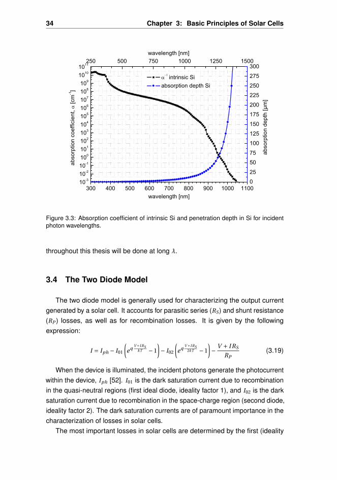
34 Chapter 3: Basic Principles of Solar Cells
10-310-210-110010110210310410510610710810910101011
250 500 750 1000 1250 1500
intrinsic Si a
bsor
ptio
n co
effic
ient
, [c
m-1]
300 400 500 600 700 800 900 1000 11000
25
50
75
100
125
150
175
200
225
250
275
300
wavelength [nm]
wavelength [nm]
absorption depth Si
abs
orpt
ion
dept
h [µ
m]
Figure 3.3: Absorption coefficient of intrinsic Si and penetration depth in Si for incidentphoton wavelengths.
throughout this thesis will be done at long λ.
3.4 The Two Diode Model
The two diode model is generally used for characterizing the output currentgenerated by a solar cell. It accounts for parasitic series (RS) and shunt resistance(RP ) losses, as well as for recombination losses. It is given by the followingexpression:
I = Iph − I01
(eq
V +I RSkT −1
)− I02
(eq
V +I RS2kT −1
)− V + I RS
RP(3.19)
When the device is illuminated, the incident photons generate the photocurrentwithin the device, Iph [52]. I01 is the dark saturation current due to recombinationin the quasi-neutral regions (first ideal diode, ideality factor 1), and I02 is the darksaturation current due to recombination in the space-charge region (second diode,ideality factor 2). The dark saturation currents are of paramount importance in thecharacterization of losses in solar cells.
The most important losses in solar cells are determined by the first (ideality

3.4. The Two Diode Model 35
factor 1) and second term (ideality factor 2) in the two diode model. The first terminfluences the reduction of VOC and the second term the reduction of both, FFand VOC . In short, the most important losses are: recombination in the depletionregion, low front surface and rear surface passivation, low quality of the bulkmaterial, low blue response due to bad emitter qualities, low infrared responsedue to bad rear side surface qualities (normally determined by the first diode, thus,by I01), losses in series resistance, shunts in the p-n junction, and spiking of metalcontacts (normally determined by the second diode, thus, by I02).

CH
AP
TE
R
4SELECTIVE EMITTER SOLAR CELLS
Abstract
The first solar cell device studied in this thesis is the well known selectiveemitter concept. Different processes to reduce the front surface recombinationvelocity, to minimize the contact resistance, and to improve the blue spectralresponse of the solar cell were recently developed and presented in the litera-ture. For example: single deep diffusion [87,88], double diffusion process withmask [89], selectively printing of a doping paste, auto doping of the surface orselective application of diffusion barriers [42].
For selective emitters highly n+-doped regions are required beneath the Agfingers at the front side. As the highly phosphorus doped regions deliver a lowcell response in the blue region of the spectrum, these areas must be as small aspossible and should be located below the Ag metallic contact fingers. Betweenthe fingers a shallow doped emitter is required which can be well passivatedto keep the surface recombination as low as possible and to obtain a high VOC
accordingly. A novel process for the formation of a selective emitter is presentedby introducing a thermally grown SiO2 barrier, immediately grown after the shallowPOCl3 diffusion in the same process tube. The diffusion process leads to theformation of both a thick PSG and an oxidized emitter underneath. The oxideis used as a barrier for the second diffusion after selective opening of the fingercontact areas, by screen printing and drying of a SiO2 etching paste.
37
38 Chapter 4: Selective Emitter Solar Cells
4.1 The Selective Emitter Concept
An innovative process for the formation of a selective emitter is presented,by using an advanced phosphorus glass as a barrier layer against a subsequentsecond POCl3 diffusion. The advanced barrier glass was achieved by the for-mation of a standard phosphorus glass treated with additional thermal oxidationimmediately after deposition in the same process tube. The resistant layer is usedas a barrier for the second diffusion after selective opening of the finger contactareas by screen printing of a SiO2 etching paste. The process was applied formulticrystalline Elkem solar grade silicon (SoG-Si) wafers (ESS) as well as forreferences from standard electronic-grade silicon (EG-Si) feedstock. The achievedcell parameters were compared with cell results from a homogeneous emitterprocess. The efficiency decreases due to the relatively high shadowing loss ofthe selective emitter solar cells and material limitations. Nevertheless, the VOC
was increased by up to 9 mV, and the short wavelength spectral response wasincreased slightly with this selective emitter. The aim of this work was to combinethe SiO2 barrier with the shallow POCl3 diffusion in one process step and theoptimization of the screen printing process for selective emitter solar cells.
4.2 Experimental Part
The experiments were carried out on solar grade silicon feedstock providedby Elkem Solar*. Crystallization and wafering of the p-type boron doped mul-ticrystalline wafers, with an area of 156x156 mm2, a thickness of 200 µm and aresistivity of about 1Ωcm was done by Q-Cells†.
For the selective emitter the following process sequence was applied (asshown in the flow diagram in Figure 4.1). First of all, small holes (; 80-100 µm)were drilled by laser at two different edges of the wafer, to enable the opticalalignment of the screen printing cameras based on these two fiducial marks. Thismethod uses artificial vision to find the fiducial points on the wafer, without theneed of imprecise alignment on the substrate edges. The laser holes were drilledbefore the isotropic texturing to avoid any laser damage on the wafer surface.
Isotropic texturing of the multicrystalline wafers was carried out by HF-HNO3
acid solution‡ to remove the laser damage and saw damage on the surface of the
*http://www.elkem.no†http://www.q-cells.com/‡i.e. Rena approach.
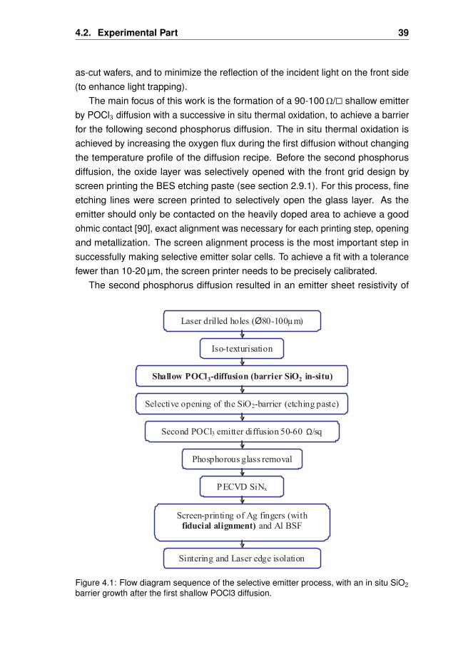
4.2. Experimental Part 39
as-cut wafers, and to minimize the reflection of the incident light on the front side(to enhance light trapping).
The main focus of this work is the formation of a 90-100Ω/ä shallow emitterby POCl3 diffusion with a successive in situ thermal oxidation, to achieve a barrierfor the following second phosphorus diffusion. The in situ thermal oxidation isachieved by increasing the oxygen flux during the first diffusion without changingthe temperature profile of the diffusion recipe. Before the second phosphorusdiffusion, the oxide layer was selectively opened with the front grid design byscreen printing the BES etching paste (see section 2.9.1). For this process, fineetching lines were screen printed to selectively open the glass layer. As theemitter should only be contacted on the heavily doped area to achieve a goodohmic contact [90], exact alignment was necessary for each printing step, openingand metallization. The screen alignment process is the most important step insuccessfully making selective emitter solar cells. To achieve a fit with a tolerancefewer than 10-20 µm, the screen printer needs to be precisely calibrated.
The second phosphorus diffusion resulted in an emitter sheet resistivity of
Figure 4.1: Flow diagram sequence of the selective emitter process, with an in situ SiO2barrier growth after the first shallow POCl3 diffusion.
40 Chapter 4: Selective Emitter Solar Cells
60-65Ω/ä in the openings (below the Ag contact fingers), and still 90-100Ω/äbetween the fingers, below the passivated area§. Thus, the in-situ created oxidelayer acts well as a barrier for the second diffusion. Afterwards, the PSG wasremoved by HF-dip to enable the passivation of the solar cell. The passivation iscarried out by the deposition of a PECVD SiNx layer on the front side (this coatingaims to be also an antireflection layer for the incident light).
The metallic contacts were made by a screen printing process adjusted withthe help of laser drilled holes as fiducial marks on the edges of the wafer. On thefront the same grid was used for the etching paste, as for the Ag fingers. On therear the contact was formed by a full area of screen printed aluminum to form theBSF layer. Before the sintering of the contacts the inks were dried. The contactswere sintered by an infrared furnace. Later on, the front and the rear side wereisolated by laser grooving, obtaining a high shunt resistance. The solar cells werecharacterized by I -V measurement.
4.3 Screen Printing Approach: Etching of Dielectric Barriers
4.3.1 Fiducial Alignment
For the optical alignment it was found that fiducial marks (e.g. as a via madeby laser drilling) lead to a more accurate alignment between the screen and thesubstrate than the alignment at the edges of the wafer.
These fiducial marks enabled an accurate optical detection by the screenprinter cameras due to the high contrast between the substrate and the back lightcoming through the via. For the fiducial alignment two points were required atthe edges of the wafer (illustrated in Figure 4.2). For the Baccini screen printerused in this experiments point 1 was on the upper center part of the wafer withcoordinates in mm (x, y) = (0,78) and point 2 was on the lower right edge of thewafer with coordinates in mm (x, y) = (78,−78).
4.3.2 Etching Paste and Alignment Approach
To open the oxide layer a front grid of 150 µm fine lines was screen printedby using the BES etching paste of Merck. After 1 to 2 min cleaning time somewafers still showed problems with the removal of the etching paste because of the
§It has been shown elsewhere that a lightly doped passivated emitter ensures good collectionproperties and low emitter dark saturation currents [91]
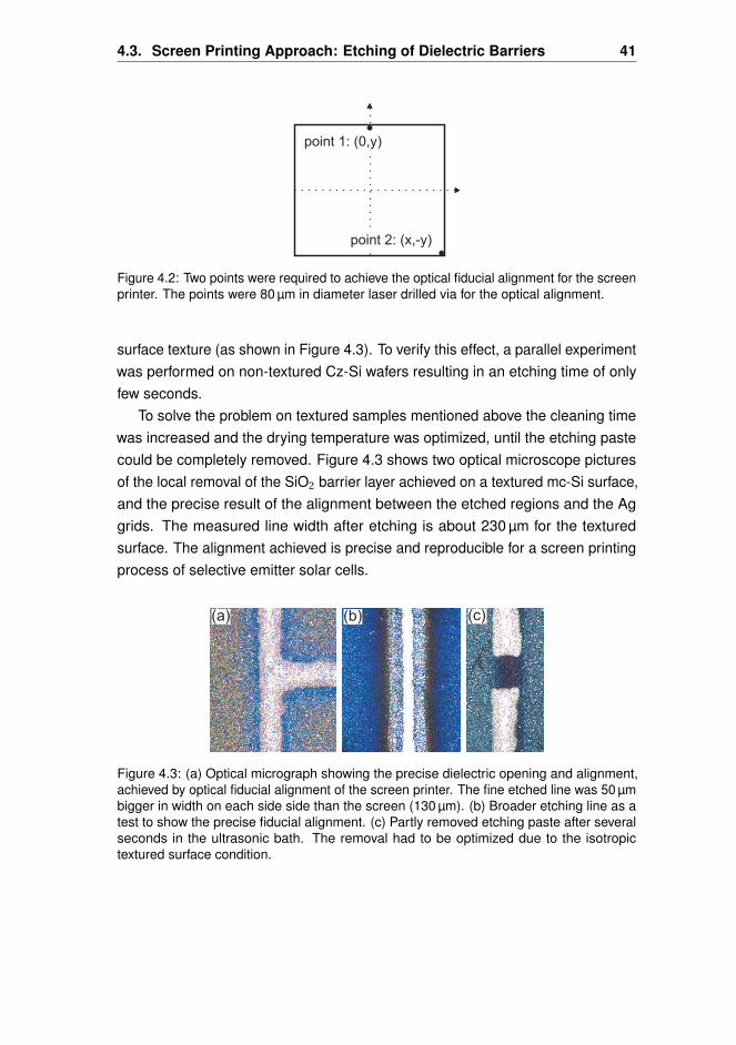
4.3. Screen Printing Approach: Etching of Dielectric Barriers 41
Figure 4.2: Two points were required to achieve the optical fiducial alignment for the screenprinter. The points were 80 µm in diameter laser drilled via for the optical alignment.
surface texture (as shown in Figure 4.3). To verify this effect, a parallel experimentwas performed on non-textured Cz-Si wafers resulting in an etching time of onlyfew seconds.
To solve the problem on textured samples mentioned above the cleaning timewas increased and the drying temperature was optimized, until the etching pastecould be completely removed. Figure 4.3 shows two optical microscope picturesof the local removal of the SiO2 barrier layer achieved on a textured mc-Si surface,and the precise result of the alignment between the etched regions and the Aggrids. The measured line width after etching is about 230 µm for the texturedsurface. The alignment achieved is precise and reproducible for a screen printingprocess of selective emitter solar cells.
Figure 4.3: (a) Optical micrograph showing the precise dielectric opening and alignment,achieved by optical fiducial alignment of the screen printer. The fine etched line was 50 µmbigger in width on each side side than the screen (130 µm). (b) Broader etching line as atest to show the precise fiducial alignment. (c) Partly removed etching paste after severalseconds in the ultrasonic bath. The removal had to be optimized due to the isotropictextured surface condition.
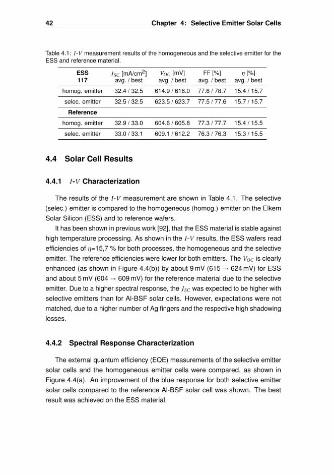
42 Chapter 4: Selective Emitter Solar Cells
Table 4.1: I -V measurement results of the homogeneous and the selective emitter for theESS and reference material.
ESS JSC [mA/cm2] VOC [mV] FF [%] η [%]117 avg. / best avg. / best avg. / best avg. / best
homog. emitter 32.4 / 32.5 614.9 / 616.0 77.6 / 78.7 15.4 / 15.7
selec. emitter 32.5 / 32.5 623.5 / 623.7 77.5 / 77.6 15.7 / 15.7
Reference
homog. emitter 32.9 / 33.0 604.6 / 605.8 77.3 / 77.7 15.4 / 15.5
selec. emitter 33.0 / 33.1 609.1 / 612.2 76.3 / 76.3 15.3 / 15.5
4.4 Solar Cell Results
4.4.1 I -V Characterization
The results of the I -V measurement are shown in Table 4.1. The selective(selec.) emitter is compared to the homogeneous (homog.) emitter on the ElkemSolar Silicon (ESS) and to reference wafers.
It has been shown in previous work [92], that the ESS material is stable againsthigh temperature processing. As shown in the I -V results, the ESS wafers readefficiencies of η=15,7 % for both processes, the homogeneous and the selectiveemitter. The reference efficiencies were lower for both emitters. The VOC is clearlyenhanced (as shown in Figure 4.4(b)) by about 9 mV (615 → 624 mV) for ESSand about 5 mV (604 → 609 mV) for the reference material due to the selectiveemitter. Due to a higher spectral response, the JSC was expected to be higher withselective emitters than for Al-BSF solar cells. However, expectations were notmatched, due to a higher number of Ag fingers and the respective high shadowinglosses.
4.4.2 Spectral Response Characterization
The external quantum efficiency (EQE) measurements of the selective emittersolar cells and the homogeneous emitter cells were compared, as shown inFigure 4.4(a). An improvement of the blue response for both selective emittersolar cells compared to the reference Al-BSF solar cell was shown. The bestresult was achieved on the ESS material.
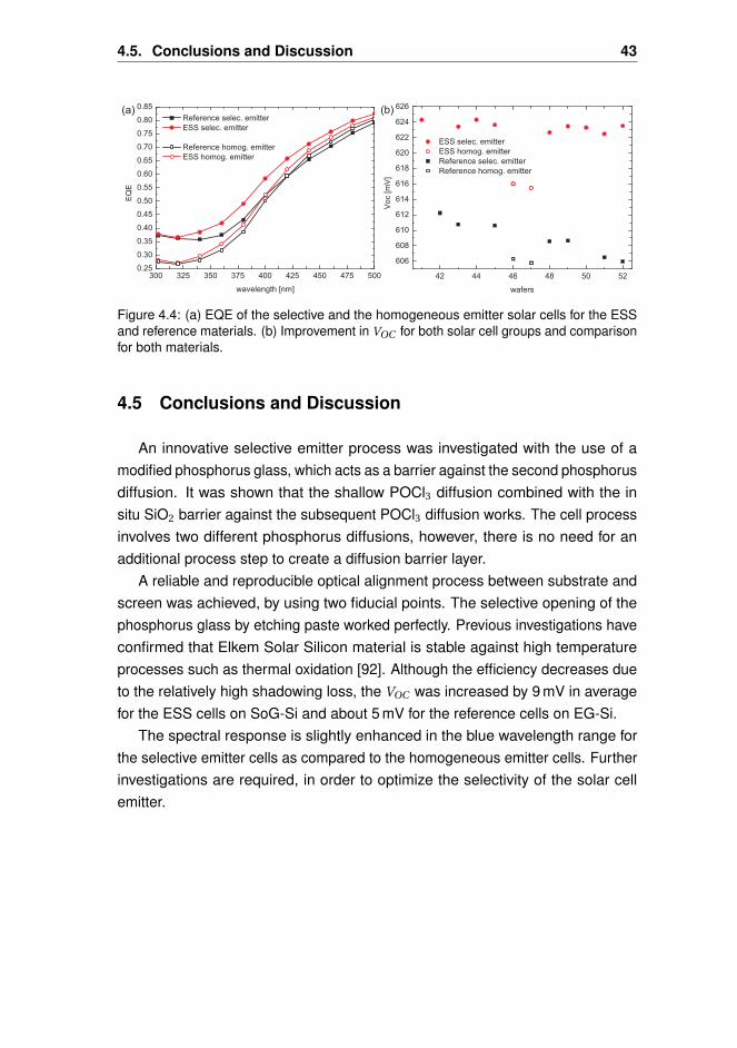
4.5. Conclusions and Discussion 43
Figure 4.4: (a) EQE of the selective and the homogeneous emitter solar cells for the ESSand reference materials. (b) Improvement in VOC for both solar cell groups and comparisonfor both materials.
4.5 Conclusions and Discussion
An innovative selective emitter process was investigated with the use of amodified phosphorus glass, which acts as a barrier against the second phosphorusdiffusion. It was shown that the shallow POCl3 diffusion combined with the insitu SiO2 barrier against the subsequent POCl3 diffusion works. The cell processinvolves two different phosphorus diffusions, however, there is no need for anadditional process step to create a diffusion barrier layer.
A reliable and reproducible optical alignment process between substrate andscreen was achieved, by using two fiducial points. The selective opening of thephosphorus glass by etching paste worked perfectly. Previous investigations haveconfirmed that Elkem Solar Silicon material is stable against high temperatureprocesses such as thermal oxidation [92]. Although the efficiency decreases dueto the relatively high shadowing loss, the VOC was increased by 9 mV in averagefor the ESS cells on SoG-Si and about 5 mV for the reference cells on EG-Si.
The spectral response is slightly enhanced in the blue wavelength range forthe selective emitter cells as compared to the homogeneous emitter cells. Furtherinvestigations are required, in order to optimize the selectivity of the solar cellemitter.

Part II
Aluminum-Silicon ContactFormation


CH
AP
TE
R
5CONTACT FORMATION, STATE OF THE ART
Abstract
The main results presented in this thesis deal with the local contact formationbetween Al metal pastes and Si semiconductor materials. This chapter gives anoverview of the contact formation models between Al and Si for standard and rearpassivated Si solar cells. In the end, the important applications of an Al layer inphotovoltaics must be clarified.
5.1 The High-Low Junction as a Back Surface Field
Aluminum layers on the back of Si solar cells have been in use since the early70’s. The back contact was achieved without the need of the phosphorus backlayer removal and a the incorporation of Al produced thin electric field (high-lowjunction), highly increasing the open circuit voltages. This electric field was namedthe back surface field (BSF, already introduced in this thesis) by Mandelkornet al. [93]. Actually, this electric field effect at the back of solar cells was firsttreated by the double layer model of Wolf [94] in his study about the drift fields inphotovoltaics solar energy converter cells. Nevertheless, Wolf’s theory ignored theinfluence of the BSF on the increased VOC . The BSF electric properties enhancethe majority carrier density of the p-type Si bulk as shown in Figure 5.1, where onthe top a schematic model explains the influence of the BSF effect on the chargecarriers. In the middle, the schematic energy band diagram of n+-p-p+ (Al-BSF)
47
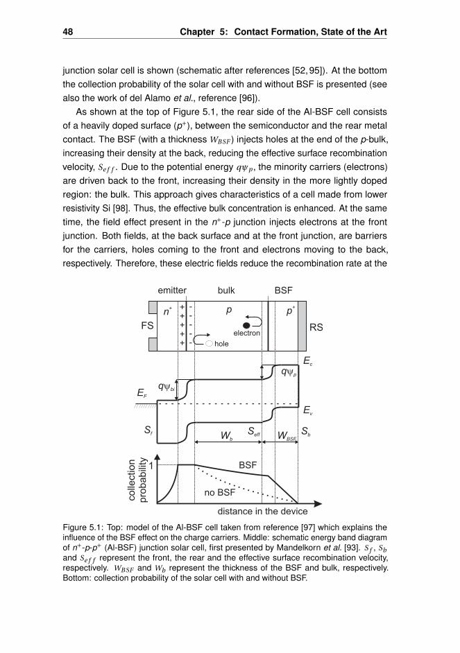
48 Chapter 5: Contact Formation, State of the Art
junction solar cell is shown (schematic after references [52,95]). At the bottomthe collection probability of the solar cell with and without BSF is presented (seealso the work of del Alamo et al., reference [96]).
As shown at the top of Figure 5.1, the rear side of the Al-BSF cell consistsof a heavily doped surface (p+), between the semiconductor and the rear metalcontact. The BSF (with a thickness WBSF ) injects holes at the end of the p-bulk,increasing their density at the back, reducing the effective surface recombinationvelocity, Se f f . Due to the potential energy qψp , the minority carriers (electrons)are driven back to the front, increasing their density in the more lightly dopedregion: the bulk. This approach gives characteristics of a cell made from lowerresistivity Si [98]. Thus, the effective bulk concentration is enhanced. At the sametime, the field effect present in the n+-p junction injects electrons at the frontjunction. Both fields, at the back surface and at the front junction, are barriersfor the carriers, holes coming to the front and electrons moving to the back,respectively. Therefore, these electric fields reduce the recombination rate at the
Figure 5.1: Top: model of the Al-BSF cell taken from reference [97] which explains theinfluence of the BSF effect on the charge carriers. Middle: schematic energy band diagramof n+-p-p+ (Al-BSF) junction solar cell, first presented by Mandelkorn et al. [93]. S f , Sband Se f f represent the front, the rear and the effective surface recombination velocity,respectively. WBSF and Wb represent the thickness of the BSF and bulk, respectively.Bottom: collection probability of the solar cell with and without BSF.
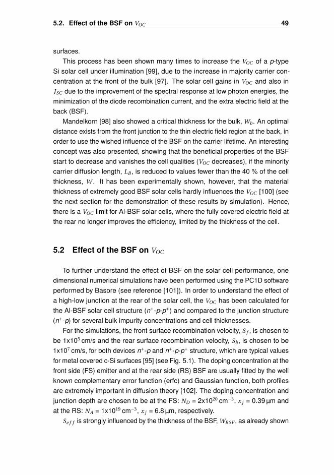
5.2. Effect of the BSF on VOC 49
surfaces.This process has been shown many times to increase the VOC of a p-type
Si solar cell under illumination [99], due to the increase in majority carrier con-centration at the front of the bulk [97]. The solar cell gains in VOC and also inJSC due to the improvement of the spectral response at low photon energies, theminimization of the diode recombination current, and the extra electric field at theback (BSF).
Mandelkorn [98] also showed a critical thickness for the bulk, Wb . An optimaldistance exists from the front junction to the thin electric field region at the back, inorder to use the wished influence of the BSF on the carrier lifetime. An interestingconcept was also presented, showing that the beneficial properties of the BSFstart to decrease and vanishes the cell qualities (VOC decreases), if the minoritycarrier diffusion length, LB , is reduced to values fewer than the 40 % of the cellthickness, W . It has been experimentally shown, however, that the materialthickness of extremely good BSF solar cells hardly influences the VOC [100] (seethe next section for the demonstration of these results by simulation). Hence,there is a VOC limit for Al-BSF solar cells, where the fully covered electric field atthe rear no longer improves the efficiency, limited by the thickness of the cell.
5.2 Effect of the BSF on VOC
To further understand the effect of BSF on the solar cell performance, onedimensional numerical simulations have been performed using the PC1D softwareperformed by Basore (see reference [101]). In order to understand the effect ofa high-low junction at the rear of the solar cell, the VOC has been calculated forthe Al-BSF solar cell structure (n+-p-p+) and compared to the junction structure(n+-p) for several bulk impurity concentrations and cell thicknesses.
For the simulations, the front surface recombination velocity, S f , is chosen tobe 1x105 cm/s and the rear surface recombination velocity, Sb , is chosen to be1x107 cm/s, for both devices n+-p and n+-p-p+ structure, which are typical valuesfor metal covered c-Si surfaces [95] (see Fig. 5.1). The doping concentration at thefront side (FS) emitter and at the rear side (RS) BSF are usually fitted by the wellknown complementary error function (erfc) and Gaussian function, both profilesare extremely important in diffusion theory [102]. The doping concentration andjunction depth are chosen to be at the FS: ND = 2x1020 cm−3, x j = 0.39 µm andat the RS: NA = 1x1019 cm−3, x j = 6.8 µm, respectively.
Se f f is strongly influenced by the thickness of the BSF, WBSF , as already shown
50 Chapter 5: Contact Formation, State of the Art
Figure 5.2: PC1D numerical simulations of the BSF effect and thickness influence on VOC ,for several bulk doping concentrations. For a good BSF solar cell VOC slightly depends onthe wafer thickness. The huge difference in VOC between the n+-p and n+-p-p+ solar cellspresent for low doped materials strongly decreases with the wafer thickness.
by Lölgen [95]. For a standard n+-p-p+ structure, WBSF is approximately 5 µmdeep (at standard firing conditions and using industrial Al pastes), reducing theSe f f to approximately 300 cm/s.
Figure 5.2 summarizes the results of the simulations. The simulation wasperformed under AM1.5 illumination and at 25 C. The results for VOC are compa-rable with the Al-BSF solar cell results found in literature [103–105,107,108]. Asalready shown elsewhere [111], the VOC of a good BSF solar cell slightly dependson the wafer thickness, and decreases with the thickness for lightly doped basematerials. The positive effect of the BSF shows a limit, where the VOC reachesa maximum for Al-BSF solar cell structures of 640 mV. When the maximum VOC
is achieved the thickness of a solar cell can be ignored [112]. 4VOC (with BSFminus without BSF) decreases with increasing base thickness. The improvementof the VOC by the p-p+ junction at the rear of the cell (taken from reference [111])is given by equation 5.1.
4VOC =VOC (n+pp+)−VOC (n+p) ' kT
qln
[Dn
NAW
∫ W
W −x j b
NA
Dnd x
](5.1)
5.3 Gettering Properties of Al
Alloying the thick Al layer after the phosphorus diffusion has an importantapplication: the n+-phosphorus doped rear surface gets positively doped due tothe overcompensation of phosphorus by Al during the alloying process. Also thebeneficial effects of the gettering of impurities at the back of the solar cell by firing
5.4. Fundamental Mechanisms of Al-Si Contact Formation 51
Al has been shown elsewhere [108,109].
5.4 Fundamental Mechanisms of Al-Si Contact Formation
The alloy formation between the Al metal and the Si semiconductor is achievedby an interdiffusion between Si and Al atoms at the interface (contact area). Themost important issue in the formation of the alloy is the recrystallization from theAl-Si melt of a highly p+-doped region, growing epitaxially into the Si bulk.
The thermodynamic behavior that occurs at the Al-Si interface at equilibrium,is described by the phase diagram as illustrated in Figure 5.3. Many authors untilknow (see references [21,110]) have explained the contact formation betweenscreen-printed Al pastes and Si based on the phase diagram which applies only forconditions close to equilibrium during the alloying process. This state is difficult toachieve during the fast temperature ramp-up and cooling in industrial processing ofsolar cells. As an introduction into this topic, I will suppose that the thermodynamicconditions of equilibrium are fulfilled during the whole alloying process betweenAl and Si, and that it can be described by the simple binary phase diagram, asshown in Figure 5.3 (after Murray and McAlister, see reference [113]).
The boarders of different states of matter are separated by specific lines. Thetriple point where three different phases coexist at equilibrium is called the eutecticpoint*. The different lines found in the phase diagram are the liquidus line, showingthe temperature limit above which the Al-Si system is stable in the liquid state,and the solidus line below which the Al-Si system is stable in its solid state. α andβ represent the solid solubility of Si into Al and Al into Si, respectively [113]. Thus,the composition of the eutectic formation is described within a range of alloyingtemperatures determined by the solid and liquid state of matter. Therefore, ananalysis of the solidification is accessible. Figure 5.3 shows also the enlargementof important regions within the Al-Si alloying process (after reference [113], seealso references [114, 115]): Si-rich solidus (β-Si, top right), Al-rich solidus andsolvus (α-Al, bottom left), and Al-liquidus (L+α-Al, bottom right).
Two regions are found in the phase diagram. Firstly, Si contents lower than1.65 %, where the solubility of Si in Al achieves its maximum at the eutectictemperature (577 C) and decreases with the temperature [114]. In this alloy Siprecipitates in the α-Al solid solution [114]. Secondly, Si contents higher than1.65 %, where the two-phase alloys solidify at the eutectic temperature, showinga lamellar structure (eutectic alloy, c(Si) = 12.6 % [114]). For hypereutectic
*From the Greek "to melt well".
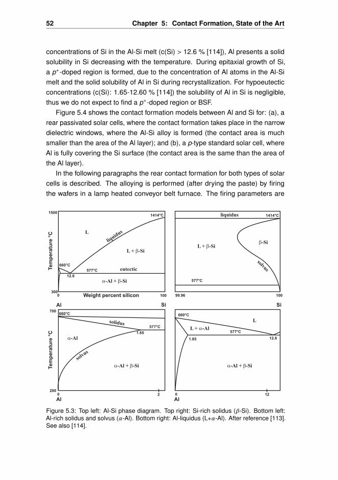
52 Chapter 5: Contact Formation, State of the Art
concentrations of Si in the Al-Si melt (c(Si) > 12.6 % [114]), Al presents a solidsolubility in Si decreasing with the temperature. During epitaxial growth of Si,a p+-doped region is formed, due to the concentration of Al atoms in the Al-Simelt and the solid solubility of Al in Si during recrystallization. For hypoeutecticconcentrations (c(Si): 1.65-12.60 % [114]) the solubility of Al in Si is negligible,thus we do not expect to find a p+-doped region or BSF.
Figure 5.4 shows the contact formation models between Al and Si for: (a), arear passivated solar cells, where the contact formation takes place in the narrowdielectric windows, where the Al-Si alloy is formed (the contact area is muchsmaller than the area of the Al layer); and (b), a p-type standard solar cell, whereAl is fully covering the Si surface (the contact area is the same than the area ofthe Al layer).
In the following paragraphs the rear contact formation for both types of solarcells is described. The alloying is performed (after drying the paste) by firingthe wafers in a lamp heated conveyor belt furnace. The firing parameters are
b-Si
L
Al Si
660°C
1414°C
12.6
1.65
660°C
577°C
577°C
1.65
577°C
660°C
12.6a-Al
L
577°C
1414°C
10099.96
Si
1000
Al20
Al120
Weight percent silicon
liquid
us
eutectic
solv
us
solidus
solvus
liquidus1500
300
Tem
pera
ture
°C
Tem
pera
ture
°C
200
700
L + -SibL + -Sib
a-Al + -Sib
L + a-Al
a-Al + -Sib a-Al + -Sib
Figure 5.3: Top left: Al-Si phase diagram. Top right: Si-rich solidus (β-Si). Bottom left:Al-rich solidus and solvus (α-Al). Bottom right: Al-liquidus (L+α-Al). After reference [113].See also [114].
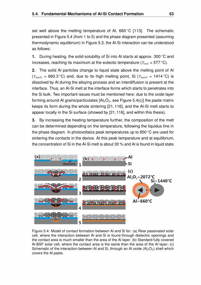
5.4. Fundamental Mechanisms of Al-Si Contact Formation 53
set well above the melting temperature of Al, 660 C [113]. The schematicpresented in Figure 5.4 (from 1 to 5) and the phase diagram presented (assumingthermodynamic equilibrium) in Figure 5.3, the Al-Si interaction can be understoodas follows:
1. During heating, the solid solubility of Si into Al starts at approx. 300 C andincreases, reaching its maximum at the eutectic temperature (Teut = 577 C).
2. The solid Al particles change to liquid state above the melting point of Al(Tmel t = 660.3 C) and, due to its high melting point, Si (Tmel t = 1414 C) isdissolved by Al during the alloying process and an interdiffusion is present at theinterface. Thus, an Al-Si melt at the interface forms which starts to penetrates intothe Si bulk. Two important issues must be mentioned here: due to the oxide layerforming around Al grains/particulates [Al2O3, see Figure 5.4(c)] the paste matrixkeeps its form during the whole sintering [21, 116], and the Al-Si melt starts toappear locally in the Si surface (showed by [21,116], and within this thesis).
3. By increasing the heating temperature further, the composition of the meltcan be determined depending on the temperature, following the liquidus line inthe phase diagram. In photovoltaics peak temperatures up to 850 C are used forsintering the contacts in the device. At this peak temperature and at equilibrium,the concentration of Si in the Al-Si melt is about 30 % and Al is found in liquid state.
Al O ~2072°C2 3
Al~660°C
Si~1440°C
(c)
(a)(b)
1
2
3
4
5
dielectric
Al
Si
Figure 5.4: Model of contact formation between Al and Si for: (a) Rear passivated solarcell, where the interaction between Al and Si is found through dielectric openings andthe contact area is much smaller than the area of the Al layer. (b) Standard fully coveredAl-BSF solar cell, where the contact area is the same than the area of the Al layer; (c)Schematic of the interaction between Al and Si, through an Al oxide (Al2O3) shell whichcovers the Al paste.
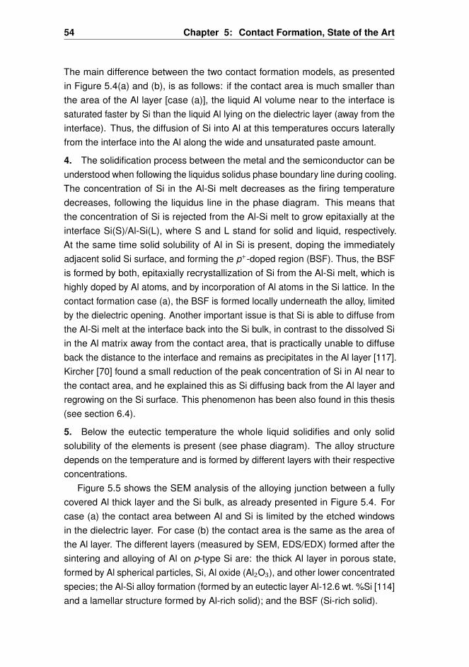
54 Chapter 5: Contact Formation, State of the Art
The main difference between the two contact formation models, as presentedin Figure 5.4(a) and (b), is as follows: if the contact area is much smaller thanthe area of the Al layer [case (a)], the liquid Al volume near to the interface issaturated faster by Si than the liquid Al lying on the dielectric layer (away from theinterface). Thus, the diffusion of Si into Al at this temperatures occurs laterallyfrom the interface into the Al along the wide and unsaturated paste amount.
4. The solidification process between the metal and the semiconductor can beunderstood when following the liquidus solidus phase boundary line during cooling.The concentration of Si in the Al-Si melt decreases as the firing temperaturedecreases, following the liquidus line in the phase diagram. This means thatthe concentration of Si is rejected from the Al-Si melt to grow epitaxially at theinterface Si(S)/Al-Si(L), where S and L stand for solid and liquid, respectively.At the same time solid solubility of Al in Si is present, doping the immediatelyadjacent solid Si surface, and forming the p+-doped region (BSF). Thus, the BSFis formed by both, epitaxially recrystallization of Si from the Al-Si melt, which ishighly doped by Al atoms, and by incorporation of Al atoms in the Si lattice. In thecontact formation case (a), the BSF is formed locally underneath the alloy, limitedby the dielectric opening. Another important issue is that Si is able to diffuse fromthe Al-Si melt at the interface back into the Si bulk, in contrast to the dissolved Siin the Al matrix away from the contact area, that is practically unable to diffuseback the distance to the interface and remains as precipitates in the Al layer [117].Kircher [70] found a small reduction of the peak concentration of Si in Al near tothe contact area, and he explained this as Si diffusing back from the Al layer andregrowing on the Si surface. This phenomenon has been also found in this thesis(see section 6.4).
5. Below the eutectic temperature the whole liquid solidifies and only solidsolubility of the elements is present (see phase diagram). The alloy structuredepends on the temperature and is formed by different layers with their respectiveconcentrations.
Figure 5.5 shows the SEM analysis of the alloying junction between a fullycovered Al thick layer and the Si bulk, as already presented in Figure 5.4. Forcase (a) the contact area between Al and Si is limited by the etched windowsin the dielectric layer. For case (b) the contact area is the same as the area ofthe Al layer. The different layers (measured by SEM, EDS/EDX) formed after thesintering and alloying of Al on p-type Si are: the thick Al layer in porous state,formed by Al spherical particles, Si, Al oxide (Al2O3), and other lower concentratedspecies; the Al-Si alloy formation (formed by an eutectic layer Al-12.6 wt. %Si [114]and a lamellar structure formed by Al-rich solid); and the BSF (Si-rich solid).
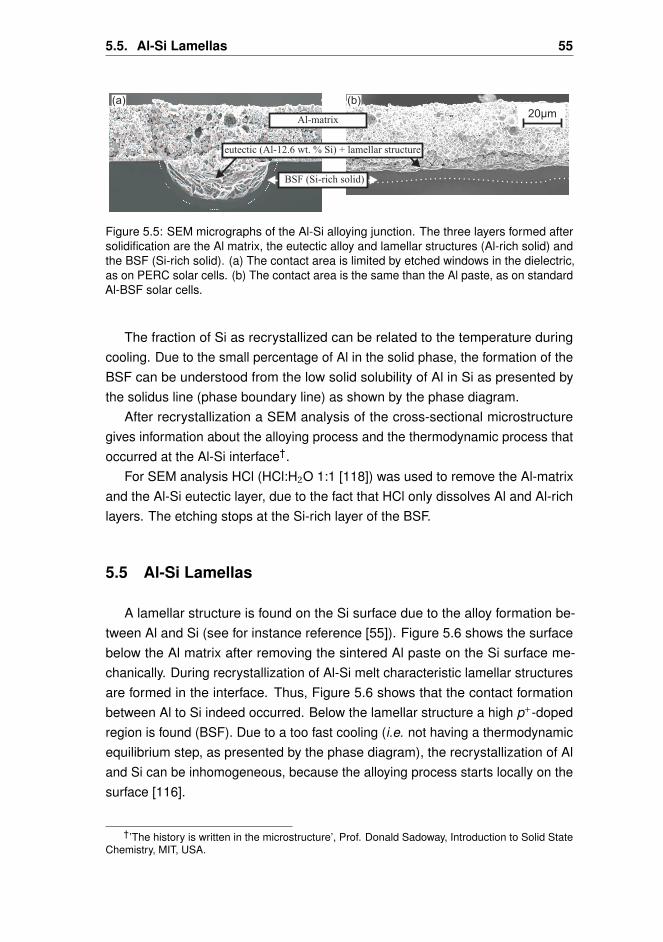
5.5. Al-Si Lamellas 55
20µm
(b)
Al-matrix
eutectic (Al-12.6 % Si) + lamellar structurewt.
(a)
BSF (Si-rich solid)
Figure 5.5: SEM micrographs of the Al-Si alloying junction. The three layers formed aftersolidification are the Al matrix, the eutectic alloy and lamellar structures (Al-rich solid) andthe BSF (Si-rich solid). (a) The contact area is limited by etched windows in the dielectric,as on PERC solar cells. (b) The contact area is the same than the Al paste, as on standardAl-BSF solar cells.
The fraction of Si as recrystallized can be related to the temperature duringcooling. Due to the small percentage of Al in the solid phase, the formation of theBSF can be understood from the low solid solubility of Al in Si as presented bythe solidus line (phase boundary line) as shown by the phase diagram.
After recrystallization a SEM analysis of the cross-sectional microstructuregives information about the alloying process and the thermodynamic process thatoccurred at the Al-Si interface†.
For SEM analysis HCl (HCl:H2O 1:1 [118]) was used to remove the Al-matrixand the Al-Si eutectic layer, due to the fact that HCl only dissolves Al and Al-richlayers. The etching stops at the Si-rich layer of the BSF.
5.5 Al-Si Lamellas
A lamellar structure is found on the Si surface due to the alloy formation be-tween Al and Si (see for instance reference [55]). Figure 5.6 shows the surfacebelow the Al matrix after removing the sintered Al paste on the Si surface me-chanically. During recrystallization of Al-Si melt characteristic lamellar structuresare formed in the interface. Thus, Figure 5.6 shows that the contact formationbetween Al to Si indeed occurred. Below the lamellar structure a high p+-dopedregion is found (BSF). Due to a too fast cooling (i.e. not having a thermodynamicequilibrium step, as presented by the phase diagram), the recrystallization of Aland Si can be inhomogeneous, because the alloying process starts locally on thesurface [116].
†’The history is written in the microstructure’, Prof. Donald Sadoway, Introduction to Solid StateChemistry, MIT, USA.

56 Chapter 5: Contact Formation, State of the Art
Figure 5.6: The lamellar structure is found after mechanical removal of the Al matrix. (a)Removed Al finger alloyed on SiNx layer. (b) Part marked by the rectangle on (a), showingthe Al-Si lamellar structure.
5.6 Screen Printing and Drying of Aluminum Lines
An amount of Al paste of 7 to 8 mg/cm2 is normally deposited fully coveringthe rear of standard solar cells. At the beginning of this work, the adhesion ofAl fingers was analyzed for screen printed Al pastes on Si polished surfaces. Itwas found that the Al paste printed in form of thin lines is susceptible to peelingoff from the Si surface after normal drying and firing conditions. Therefore, anoptimization of drying and sintering temperatures was performed.
Figure 5.7 shows the adhesion problem of fine Al lines, (a), and the optimaladhesion after the performed drying parameters optimization, (b). After dryingthe sample in a four zones paternoster (vertically stacked) furnace, at a standarddrying profile of 130/150/180/200 C and a delay time of 10 s‡, the Al paste lossesamount to 1.6 mg/cm2. This loss of weight represents the content of solventswithin the paste.
The adhesion after firing was improved by keeping the firing profile of theconveyor belt furnace constant and drying the wafers at different drying profiles.This experiment showed that, for the standard Al paste printed as thin fingers,the drying profile has an essential influence on the remaining amount of solventswithin the Al matrix. It has been shown, that lower drying temperatures andshorter delay time improved the adhesion of fingers after firing. This is due to thesmall amount of Al paste below the heat lamps in the drying furnace. On sampleswith small amount of Al mass, as screen printed Al fingers, non-optimal drying
‡The delay time of the drying furnace differs from the complete drying time of the samples insidethe furnace, and corresponds to the time that one pallet stops for the load or unload of wafers until itmoves to the next position. The furnace contents 60 pallets. The minimum delay time is about 7 s forone pallet to move to the next position. With a drying time of 10 s, the total time that one wafer is driedin the furnace is represented by 60 ∗ (7 + 10) s = 17 min.
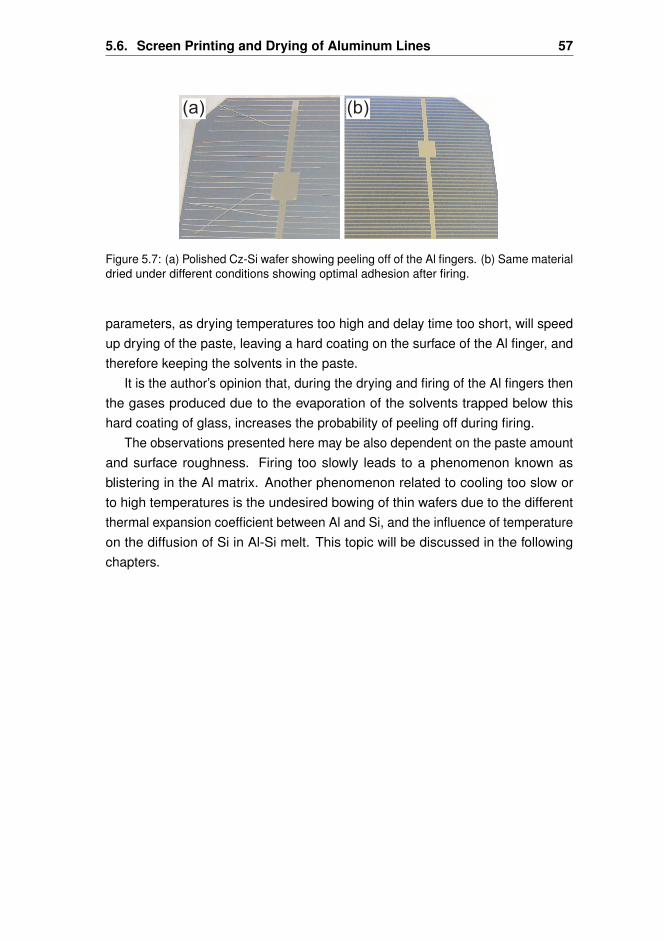
5.6. Screen Printing and Drying of Aluminum Lines 57
Figure 5.7: (a) Polished Cz-Si wafer showing peeling off of the Al fingers. (b) Same materialdried under different conditions showing optimal adhesion after firing.
parameters, as drying temperatures too high and delay time too short, will speedup drying of the paste, leaving a hard coating on the surface of the Al finger, andtherefore keeping the solvents in the paste.
It is the author’s opinion that, during the drying and firing of the Al fingers thenthe gases produced due to the evaporation of the solvents trapped below thishard coating of glass, increases the probability of peeling off during firing.
The observations presented here may be also dependent on the paste amountand surface roughness. Firing too slowly leads to a phenomenon known asblistering in the Al matrix. Another phenomenon related to cooling too slow orto high temperatures is the undesired bowing of thin wafers due to the differentthermal expansion coefficient between Al and Si, and the influence of temperatureon the diffusion of Si in Al-Si melt. This topic will be discussed in the followingchapters.

CH
AP
TE
R
6ALUMINUM-SILICON CONTACT FORMATION
THROUGH NARROW DIELECTRIC OPENINGS
Abstract
The study of the local contact formation between the p-type Si bulk and screenprinted Al pastes motivated the presented work. Although the contact formation byscreen printing is the most frequently used technique in a solar cell line productiontoday, there is still room for investigation regarding effective formation of localcontacts between Al and Si. Because the solar cell structure studied in thisthesis presents a laterally structured, electronically passivated rear side, theinteraction between metal and semiconductor occurs locally through openings inthe rear side passivation layer (see chapter 1). In the following chapter, furtherinsight into the contact formation and alloying between Al and Si is given. It isfound that the geometry of the rear side pattern of rear passivated solar cellscan influence not only series resistance losses within the solar cell, but also theprocess of contact formation itself. SEM and EDS/EDX analysis of the Al-Sialloy geometry is performed, leading to new insight into the understanding of itsinfluence on contact formation. The impact of the Si diffusion in Al on the contactformation is investigated, which strongly depends on the firing temperature, butless on the contact size (the spread of Si in the Al matrix was optically measured).Inhomogeneous eutectic formations were found for wider contact areas due tothe lateral diffusion of Si in Al. It is found, that an increase in the contact spacingenhances the formation of voids instead of an Al-Si eutectic layer. An explanation
59
60 Chapter 6: Aluminum-Silicon Contact Formation
is given for the void formations found in the Al-Si alloying junctions, based onthe Kirkendall effect, and on the distribution of Si in the Al matrix. In this work,two types of voids were defined: firstly, voids formed during the heating (withoutback-surface-field), and secondly, voids formed during the cooling (with back-surface-field). The influence of gravity on the microstructure of Al-Si alloy isstudied, showing crucial trends for partially avoid the formation of voids. Theanalysis presented in this chapter is applicable to industrial production of rearpassivated solar cells and Al-Si alloying processes.
6.1 Introduction
The optimization of the local contacts between screen printed Al pastes and Siis crucial for the performance of solar cells and still requires deeper understandingof the interaction between metal and semiconductor. Indeed, a compromisebetween the contact area and contact spacing is an essential issue when reducingseries resistance losses [119–121]. Also an inadequate heat treatment maycause high series resistance losses, due to inadequate pinhole contacting [122].Furthermore, the local formation of a high-quality p+-doped layer (local BSF) toimprove the cell performance [123–125], is still a challenge.
A high quality local BSF has to be homogeneously formed in the pre-definedcontact area, with a recrystallized layer depth of usually 4-5 µm, in order tominimize the surface recombination velocity [95]. Parameters as an optimalsintering temperature [126], optimal contact geometry, oxidation of the Si surfaces,homogeneity of the metal layer [85], and Si precipitates in the Al film grainboundary [116] are responsible for a well formed local BSF.
As shown by Beaucarne et al. [127], the formation of localized contacts fromscreen printed Al pastes largely depends on the contact geometry. It has beendemonstrated, that up to 60 µm deep pyramidally shaped spikes of Al-Si alloyform below point like openings of 30 µm diameter. The dissolution of Si into Alhas been found preferentially along the <100> plane [128]. Recently, interestingwork has been published about local Al point and line contacts on the rear sidepassivation of solar cells. The contact formation has been studied for applicationson laser firing of rear contacts [11, 121, 129]. The contact spacing has also aninfluence on the increase of the solar cell efficiency [130]. Differences in surfaceconcentration were found, due to Al inclusions beneath the Si surface of islandsand line networks, remaining at the surface even after removal of the Al layer inHCl [131].
6.2. Preparation of the Surfaces 61
This chapter addresses several insights into a deeper understanding of localcontact formation during sintering of screen printed Al pastes with p-type Sisubstrates, for solar cell application. It is divided into four sections. Firstly, section6.3 studies the geometry of the Al-Si alloy formation and analyzes the impactof both Al amount and contact width on contact formation and series resistancelosses. Secondly, section 6.4 provides a deeper understanding on the contactformation based on the diffusion of Si in the Al matrix and the formation of voidsis analyzed. Afterwards, section 6.5 shows the influence of the contact pattern onthe local BSF and void formation. Section 6.6 addresses the effect of gravity onthe microstructure of Al-Si alloys. And finally, in section 6.7, two types of voidsare defined and crucial trends are given in order to avoid the formation of voidsinstead of an eutectic layer. The structure of the rear passivated solar cell hasbeen introduced in chapter 1.
6.2 Preparation of the Surfaces
For the analysis of the Al-Si interaction the Si surface is polished before screenprinting and alloying the Al paste with the semiconductor, to diminish the influenceof the textured surface (saw damage and texturing of the surface is removed).The process continues with the HCl-HF cleaning of the surface, removing themetal impurities until a hydrophobic surface is achieved. For the study on thelocal chemical interaction between Al and Si, the contact area must be controlled.Since the Al paste used does not fire through a dielectric layer, the samples arefully covered with a dielectric insulation layer deposited by the PECVD method.
The contact area is limited by the selective openings in this layer. The lo-cal contact openings (LCOs) are achieved by screen printing the BES etchingpaste (more details about the etching process of dielectric layers are found insection 2.9.1). Hence, the alloying of the Al paste to the Si bulk is prevented bythe presence of the dielectric barrier everywhere except at the LCOs.
Afterwards, the surface is covered with a screen printed Al layer*. The alloy isformed after drying and sintering the samples following a standard firing furnaceprofile, varying in special cases the peak firing temperature.
*Some experiments were performed using thin Al lines and others using fully covered thick Allayers.
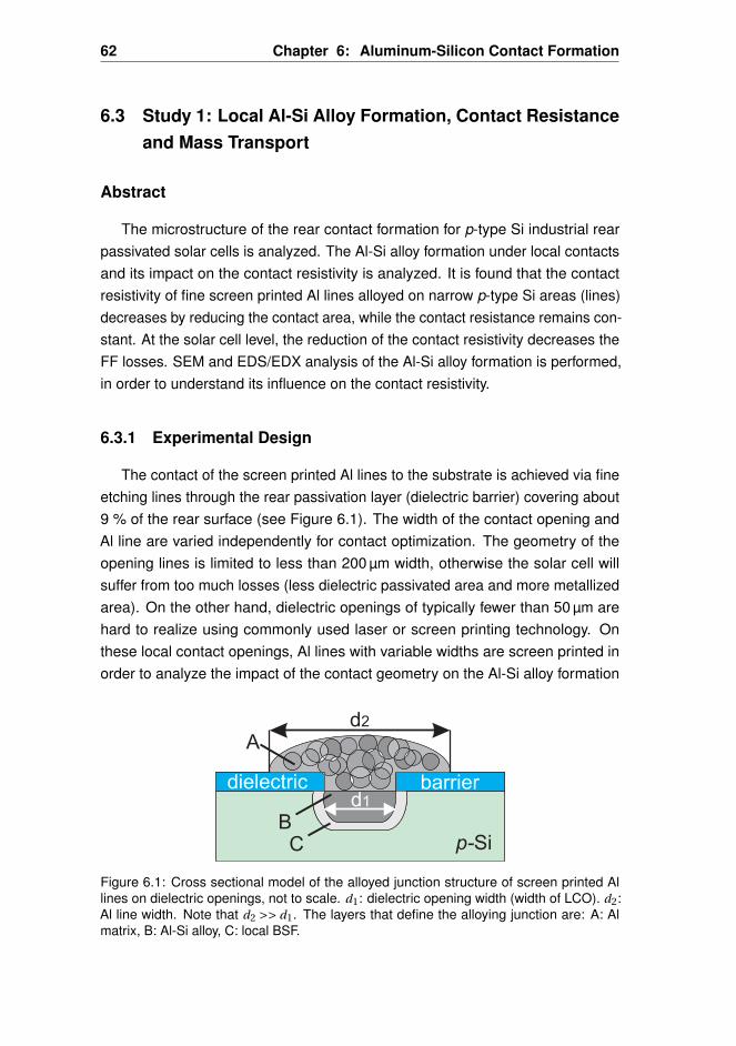
62 Chapter 6: Aluminum-Silicon Contact Formation
6.3 Study 1: Local Al-Si Alloy Formation, Contact Resistanceand Mass Transport
Abstract
The microstructure of the rear contact formation for p-type Si industrial rearpassivated solar cells is analyzed. The Al-Si alloy formation under local contactsand its impact on the contact resistivity is analyzed. It is found that the contactresistivity of fine screen printed Al lines alloyed on narrow p-type Si areas (lines)decreases by reducing the contact area, while the contact resistance remains con-stant. At the solar cell level, the reduction of the contact resistivity decreases theFF losses. SEM and EDS/EDX analysis of the Al-Si alloy formation is performed,in order to understand its influence on the contact resistivity.
6.3.1 Experimental Design
The contact of the screen printed Al lines to the substrate is achieved via fineetching lines through the rear passivation layer (dielectric barrier) covering about9 % of the rear surface (see Figure 6.1). The width of the contact opening andAl line are varied independently for contact optimization. The geometry of theopening lines is limited to less than 200 µm width, otherwise the solar cell willsuffer from too much losses (less dielectric passivated area and more metallizedarea). On the other hand, dielectric openings of typically fewer than 50 µm arehard to realize using commonly used laser or screen printing technology. Onthese local contact openings, Al lines with variable widths are screen printed inorder to analyze the impact of the contact geometry on the Al-Si alloy formation
Figure 6.1: Cross sectional model of the alloyed junction structure of screen printed Allines on dielectric openings, not to scale. d1: dielectric opening width (width of LCO). d2:Al line width. Note that d2 >> d1. The layers that define the alloying junction are: A: Almatrix, B: Al-Si alloy, C: local BSF.
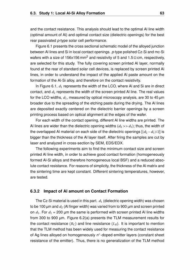
6.3. Study 1: Local Al-Si Alloy Formation 63
and the contact resistance. This analysis should lead to the optimal Al line width(optimal amount of Al) and optimal contact size (dielectric openings) for the bestrear passivated p-type solar cell performance.
Figure 6.1 presents the cross sectional schematic model of the alloyed junctionbetween Al lines and Si in local contact openings. p-type polished Cz-Si and mc-Siwafers with a size of 156x156 mm2 and resistivity of 5 and 1.5Ω cm, respectively,are selected for this study. The fully covering screen printed Al layer, normallyfound at the rear of standard solar cell devices, is replaced by screen printed Allines, in order to understand the impact of the applied Al paste amount on theformation of the Al-Si alloy, and therefore on the contact resistivity.
In Figure 6.1, d1 represents the width of the LCO, where Al and Si are in directcontact, and d2 represents the width of the screen printed Al line. The real valuesfor the LCO widths, d1, measured by optical microscopy analysis, are 30 to 45 µmbroader due to the spreading of the etching paste during the drying. The Al linesare deposited exactly centered on the dielectric barrier openings by a screenprinting process based on optical alignment at the edges of the wafer.
For each width of the contact opening, different Al line widths are printed. TheAl lines are wider than the dielectric opening widths (d2 >> d1); thus, the width ofthe overlapped Al material on each side of the dielectric openings [(d2 −d1)/2] isbigger than the thickness of the Al layer itself. After firing the samples are cut bylaser and analyzed in cross-section by SEM, EDS/EDX.
The following experiments aim to find the minimum contact size and screenprinted Al line width, in order to achieve good contact formation (homogeneouslyformed Al-Si alloys and therefore homogeneous local BSF) and a reduced abso-lute contact resistance. For reasons of simplicity, the thickness of the Al matrix andthe sintering time are kept constant. Different sintering temperatures, however,are tested.
6.3.2 Impact of Al amount on Contact Formation
The Cz-Si material is used in this part. d1 (dielectric opening width) was chosento be 100 µm and d2 (Al finger width) was varied from to 900 µm and screen printedon d1. For d1 = 200 µm the same is performed with screen printed Al line widthsfrom 300 to 900 µm. Figure 6.2(a) presents the TLM measurement results forthe contact resistance (RC ) and line resistance (LR ). It is important to mentionthat the TLM method has been widely used for measuring the contact resistanceof Ag lines alloyed on homogeneously n+-doped emitter layers (constant sheetresistance of the emitter). Thus, there is no generalization of the TLM method
64 Chapter 6: Aluminum-Silicon Contact Formation
(i)
200 µm
d : 200 µm2 d : 500 µm2 d : 900 µm2
100 µm
d:
20
0 µ
m1
d:
10
0 µ
m1
(a)
(b)
(ii) (iii)
i ii iii
(iv) (v) (vi)d : 300 µm2
iv v vi
Figure 6.2: (a) TLM result of the contact and line resistance for different Al line widthsalloyed on two dielectric openings. Y-axis left: total contact resistance Rc , decreasing forincreased Al line width, d2. Y-axis right: line resistance LR, decreasing for increased Alline width. X-axis top: dielectric opening, d1. X-axis bottom: Al line widths, d2. (b) SEMcross sectional micrographs of the contact shape (after HCl etching of the Al matrix andAl-Si eutectic layer) of six samples measured in Figure 6.2 (a). Three Al line widths, d2,were analyzed for each contact size, d1.
for measuring Al contacts, where the sheet resistance is not constant due to thepresence of the highly p+-doped layer (local BSF) underneath the Al lines.
Many configurations are shown in order to analyze the impact of the contactgeometry on the contact resistance losses. On the left y-axis, the total contactresistance RC is plotted, decreasing for increased Al line width, d2. On the righty-axis, the line resistance LR is shown, decreasing also with d2. On the top x-axis,the width of the LCOs is shown (d1 = 100 and 200 µm). And finally, on the bottomx-axis, the Al line widths, d2, are shown for each contact opening width. The same
6.3. Study 1: Local Al-Si Alloy Formation 65
experiment is repeated for four different peak firing temperatures, where T2 is thepeak firing temperature recommended by the paste developer (T1<T2<T3<T4).
The results suggest a strong dependence of the contact and line resistance onthe Al line width, as well as a small dependence on the peak firing temperature andon the opening widths. Similar results were found on mc-Si and will be discussedlater. From the theory we expected that RC should be linearly dependent on thecontact area, d1, but independent on the Al amount, d2 (supposing very low andconstant resistivity of Al [63]). Our measurements, however, are in contradiction tothe expected results. To analyze this difference SEM analysis on cross-sectionalAl-Si micrographs are performed. One optimum can already be found for an Alline width d2 = 800 µm, where RC reaches its minimum at 6Ω and LR reaches itsminimum at 0.15Ω/cm.
Figure 6.2(b) shows the cross sectional SEM analysis of the Al-Si contactinterface, for a choice of samples from Figure 6.2(a). After etching the Al matrixand the Al-Si eutectic layer by the HCl etching method, the shape of the contactinterface became visible. Six configurations are shown, from (i) to (vi): For d1
= 100 µm the shape of the alloy is shown for Al lines of (i) 200, (ii) 500, and (iii)900 µm width. For d1 = 200 µm barrier opening, the shape of the alloy is shown forAl lines of (iv) 300, (v) 500, and (vi) 900 µm width. From the SEM micrographs isevident that the penetration of the alloy into the Si material is strongly increased byproviding a larger amount of Al, showing the strong influence of the overlapping ofAl on each side of the opening on the contact formation. Remarkable is the case(vi) (d1 = 200 µm), where a strong planar surface (plateau) is present between thecontact opening edges. Case (i) and (iv) in Fig. 6.2 (overlap of Al on each sideof the interface: 50 µm) show no alloy formation and no local BSF, but rather afew local alloy spikes. This shows that the amount of Al, which is found locallyin some points on the Si surface, is extremely important for contact formation.Actually Kircher [70] suggested that the diffusion of Si into Al starts locally at somefavourable weak spots and diffuses further into the Al, by reducing the drivingforce for diffusion to occur at other places.
From the experimental point of view, there is a minimum for the Al line width,d2, required to obtain a strongly formed Al-Si alloy (and local BSF). As shownin Figure 6.2(b), on d1 = 100 µm, 500 µm Al line width is required, in order tohave a better contact formation (homogeneously formed alloy and deeper BSF).Thus, the first conclusion is that the Al amount limits the interdiffusion between Aland Si. For small Al line widths (d2 < = 500 µm) an appreciable increase of thecontact resistance is visible due to the low amount of Al overlap, and therefore,non-optimal Al-Si contact formation.
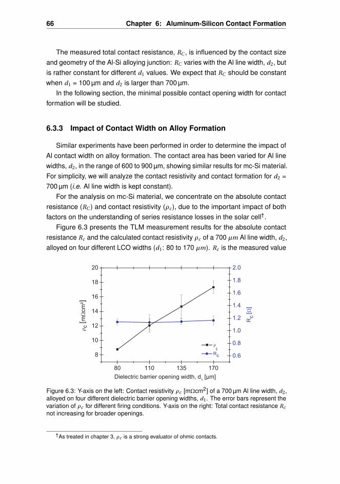
66 Chapter 6: Aluminum-Silicon Contact Formation
The measured total contact resistance, RC , is influenced by the contact sizeand geometry of the Al-Si alloying junction: RC varies with the Al line width, d2, butis rather constant for different d1 values. We expect that RC should be constantwhen d1 = 100 µm and d2 is larger than 700 µm.
In the following section, the minimal possible contact opening width for contactformation will be studied.
6.3.3 Impact of Contact Width on Alloy Formation
Similar experiments have been performed in order to determine the impact ofAl contact width on alloy formation. The contact area has been varied for Al linewidths, d2, in the range of 600 to 900 µm, showing similar results for mc-Si material.For simplicity, we will analyze the contact resistivity and contact formation for d2 =700 µm (i.e. Al line width is kept constant).
For the analysis on mc-Si material, we concentrate on the absolute contactresistance (RC ) and contact resistivity (ρc ), due to the important impact of bothfactors on the understanding of series resistance losses in the solar cell†.
Figure 6.3 presents the TLM measurement results for the absolute contactresistance Rc and the calculated contact resistivity ρc of a 700 µm Al line width, d2,alloyed on four different LCO widths (d1: 80 to 170 µm). Rc is the measured value
Figure 6.3: Y-axis on the left: Contact resistivity ρc [mΩcm2] of a 700 µm Al line width, d2,alloyed on four different dielectric barrier opening widths, d1. The error bars represent thevariation of ρc for different firing conditions. Y-axis on the right: Total contact resistance Rcnot increasing for broader openings.
†As treated in chapter 3, ρc is a strong evaluator of ohmic contacts.
6.3. Study 1: Local Al-Si Alloy Formation 67
in the experiment and ρc is calculated from Rc after the TLM method [63,67,132].The error bars show the variation of ρc for the different firing conditions. Novariation was measured for the total contact resistance Rc . The results show adependence of the contact resistivity on the dielectric barrier openings, but lesson the firing temperature. From the TLM method this would be the case if thetransmission length, LT , is small and the current transfer is only located at theedges of the contact.
The contact resistivity depends on the doping and temperature [63,67,132].Thus, our measurements are in contradiction to the expected results. Melczarskyet al. [133] found a variation in the contact resistance of screen-printed Ag lines,and discussed the findings as a result of the inefficiency of the TLM method. Theyexplained this variation by means of SEM analysis on etched samples. Theyfound that the variation in the contact resistance is due to the fact that the contactis more strongly applied over the outer boundaries. Finetti et al. [134] as wellas Kircher [70] explained that the diffusion of Si into Al starts locally at somefavourable weak spots at the interface. It means that Si can diffuse and enter intoAl, by reducing the driving force for diffusion to occur at other places [70].
6.3.4 Cross-sectional SEM/EDX Analysis of the Alloy Junction
To gain an understanding of our results and based on the literature mentionedabove, part of the extended SEM analysis performed in cross-sectional micro-graphs is illustrated in Figure 6.4 (the interdiffusion between Al and Si will bediscussed further in section 6.4). As already presented in the previous chapter,during the alloying process of Al on Si, the solid Al particles change to liquidstate above the melting point of Al, starting to alloy locally on the Si surface. Thereduction of the dielectric barrier opening width causes a higher flow of Al materialinto the Si wafer, as shown in Figure 6.4(a). Since the applied Al-paste does notfire through the dielectric barrier, the offered Al material overlap alongside thedielectric opening may be strongly attracted into the Si substrate (similar resultswere observed by other authors, see reference [128]).
Consequently, the liquid Al-Si lake penetrates into the openings, increasing thepenetration depth in the c-Si substrate with temperature. This explains why, aftercooling of the material, a strong Al-Si alloy formation is found in the bulk and belowthe contacts, compared to a fully covered Al back surface for standard solar cellsprocessing. This strong Al-Si alloy formation is present below narrow dielectricopening areas for Al line widths wider than 500 µm, and 25 µm thickness.
Figure 6.3 shows an increase of the contact resistivity of approx. 8 to
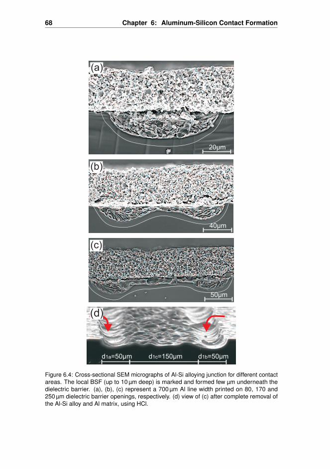
68 Chapter 6: Aluminum-Silicon Contact Formation
Figure 6.4: Cross-sectional SEM micrographs of Al-Si alloying junction for different contactareas. The local BSF (up to 10 µm deep) is marked and formed few µm underneath thedielectric barrier. (a), (b), (c) represent a 700 µm Al line width printed on 80, 170 and250 µm dielectric barrier openings, respectively. (d) view of (c) after complete removal ofthe Al-Si alloy and Al matrix, using HCl.
6.3. Study 1: Local Al-Si Alloy Formation 69
16 mΩcm2, after increasing the dielectric barrier opening widths, d1, from 80to 170 µm, respectively. As a direct consequence of this result, the cross-sectionof the alloyed junction structure presented differences in the geometry of the alloy,as shown in Figure 6.4(a) and (b), respectively. Since the same screen printed Almass, the same Si material and firing conditions were used for this experiment,the reduction of the contact resistivity may be caused by the geometry of the Al-Sialloy formation. In conclusion, by increasing the ratio of the printed Al line widthto the dielectric barrier opening width, the alloying of Al into the Si material isincreased (penetrates deeper into Si), and the contact resistivity is reduced.
For a narrow dielectric opening, a homogeneous Al-Si alloy and local BSF aredeeply formed in the barrier opening. The local BSF layer is found 5 to 8 µm
deep below the eutectic form, and extends underneath the dielectric layer. Fora wider dielectric opening, with the same firing and Al finger geometry, the alloypresents an inhomogeneous geometry formed by two strong alloy formations atthe edges and a planar surface in between. By further increasing the dielectricbarrier opening width, the Al-Si alloy starts to separate into two identical forms atthe open edges. After etching away the Al matrix and Al-Si alloy of Figure 6.4(c)by HCl, the shape of the alloy formation in the Si substrate is found, as shown inFigure 6.4(d). Two strong Al-Si alloy formations are deeply formed at the edgesof the dielectric barrier opening, and depend on the offered material overlap ofAl-paste alongside the dielectric opening. The width of these two Al-Si alloyformations remains constant (d1a = d1b ' 50 µm) and does not change for widerdielectric openings (if the overlap of Al lying on the dielectric remains). Betweenthese two formations a planar surface appears and its width varies proportional tothe dielectric opening width (d1c ).
This shallow alloyed area (Figure 6.4(c), middle part) is normally found at therear of a standard solar cell process after the alloying of a fully covered Al surfaceon the Si substrate (eutectic layer, 10 µm deep‡).
As presented by the arrows in Figure 6.4(d), the Al-Si alloy appears aftercooling and recrystallization of the Al-Si in liquid phase. The thickness of the Alline mass (20 µm for Al lines wider than 500 µm), overlapped on the left and onthe right of the dielectric opening, is responsible for the width (d1a , d1b) of thehomogeneous Al-Si alloy formation.
Therefore, if the dielectric barrier opening formed by etching paste is widerthan the optimum need for a lower contact resistivity (d1 ≥ 100 µm), two deeply
‡For Al-BSF cells, the area of the thick Al layer is equal to the Si area, showing a higher verticalAl-Si interdiffusion, than a horizontal one. Due to the large Al-Si interface the melt saturates fasterthan in the case of LCOs, where only a narrow Si area interacts with the fully covered Al layer. This isconsidered in the following studies.
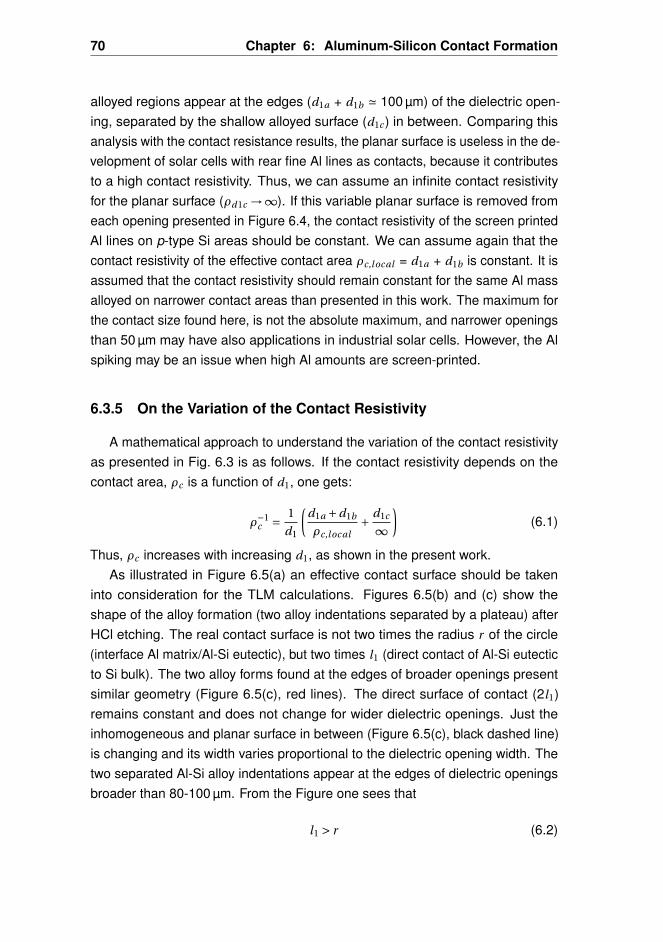
70 Chapter 6: Aluminum-Silicon Contact Formation
alloyed regions appear at the edges (d1a + d1b ' 100 µm) of the dielectric open-ing, separated by the shallow alloyed surface (d1c ) in between. Comparing thisanalysis with the contact resistance results, the planar surface is useless in the de-velopment of solar cells with rear fine Al lines as contacts, because it contributesto a high contact resistivity. Thus, we can assume an infinite contact resistivityfor the planar surface (ρd1c →∞). If this variable planar surface is removed fromeach opening presented in Figure 6.4, the contact resistivity of the screen printedAl lines on p-type Si areas should be constant. We can assume again that thecontact resistivity of the effective contact area ρc,local = d1a + d1b is constant. It isassumed that the contact resistivity should remain constant for the same Al massalloyed on narrower contact areas than presented in this work. The maximum forthe contact size found here, is not the absolute maximum, and narrower openingsthan 50 µm may have also applications in industrial solar cells. However, the Alspiking may be an issue when high Al amounts are screen-printed.
6.3.5 On the Variation of the Contact Resistivity
A mathematical approach to understand the variation of the contact resistivityas presented in Fig. 6.3 is as follows. If the contact resistivity depends on thecontact area, ρc is a function of d1, one gets:
ρ−1c = 1
d1
(d1a +d1b
ρc,local+ d1c
∞)
(6.1)
Thus, ρc increases with increasing d1, as shown in the present work.As illustrated in Figure 6.5(a) an effective contact surface should be taken
into consideration for the TLM calculations. Figures 6.5(b) and (c) show theshape of the alloy formation (two alloy indentations separated by a plateau) afterHCl etching. The real contact surface is not two times the radius r of the circle(interface Al matrix/Al-Si eutectic), but two times l1 (direct contact of Al-Si eutecticto Si bulk). The two alloy forms found at the edges of broader openings presentsimilar geometry (Figure 6.5(c), red lines). The direct surface of contact (2l1)remains constant and does not change for wider dielectric openings. Just theinhomogeneous and planar surface in between (Figure 6.5(c), black dashed line)is changing and its width varies proportional to the dielectric opening width. Thetwo separated Al-Si alloy indentations appear at the edges of dielectric openingsbroader than 80-100 µm. From the Figure one sees that
l1 > r (6.2)
6.3. Study 1: Local Al-Si Alloy Formation 71
Experimentally we have found that,
l1 ≈ 1.3r (6.3)
During the TLM measurement, the surface 2r should be replaced by 2l1 for thecalculation of the contact resistivity, where 2l1 is the surface of contact for theAl-Si alloy to the p-type Si bulk. Now the real contact surface for a narrow openingof 80 µm (r = 40 µm) is:
2l1 = 2(1.3r ) = 104µm (6.4)
Assuming that the entire contact length 2l1 contributes to current transfer [63],one gets:
ρc,local = Rc Ac = 1.1[Ω ]1[cm ]2l1[µm] = 11.4 mΩcm2 (6.5)
with a sample width of 1 cm. The contact resistivity of a 700 µm Al line contactedon an 80 µm dielectric barrier opening is hence 11 mΩcm2, where the effective
Figure 6.5: (a) Model to calculate the real contact surface 2l1. (b) For broader openings aplateau appears between the two deep indentations at the edges. Its width increases withthe dielectric opening width. (c) Direct contact surface (red). Inhomogeneous surface ofcontact (black), increasing the contact resistivity.
72 Chapter 6: Aluminum-Silicon Contact Formation
contact surface is 104 µm of width. This value is independent of the contact area(ρd1c →∞).
Our analysis compared with the contact resistance result leads to the con-clusion that the planar surface (dotted line in Figure 6.5(c)) does not contributeto the reduction of the contact resistance. If we just take the effective contactsurface 2l1 into consideration, and remove the variable planar surface from thecalculations, the contact resistivity of screen printed Al lines on p-type Si areasshould be constant. Additionally, we assume that the contact resistivity remainsconstant when the same Al amount is printed on even narrower contact openingsthan the ones presented in this work.
6.3.6 Experimental Evidence of the Influence of Al Amount on MassTransport
Additional experiments were performed, in order to corroborate the fact that theAl-Si alloy formation depends on the ratio of printed Al line width to the dielectricbarrier opening width. A wide Al line (width d2) was screen printed on a narrowdielectric opening width d1, with intentional misalignment for the screen printingprocess, as shown in Figure 6.6(a). More Al-paste is present overlapping theright side of the opening than to left. A stronger Al-Si alloy formation is found atthe edge on the right side, where more Al mass has penetrated during the firingprocess, proving that the formation of the Al-Si alloy is improved by higher ratiosof printed Al line width to dielectric barrier opening width.
Figure 6.6(b), summarizes the experiments performed. In the top, the optimalstructure for a rear passivated solar cell device with screen-printed Al lines on p-type Si material is presented (50 to 80 µm dielectric opening width, 700 µm Al linewidth). The higher the ratio d2/d1 (Al line width to dielectric barrier opening width),the deeper the Al-Si alloy formation and the lower the contact resistivity. Middle:wider opening areas lead to a planar surface between two Al-Si alloy formations,generating a high contact resistivity, as already shown by the TLM results. Bottom:the Al-Si alloy formation depends strongly on the Al mass overlapped on thedielectric.
6.3.7 Conclusions
The following dependencies of the contact resistivity have been shown: First,by increasing the ratio of the printed Al line width to the contact opening width, thealloying of Al into the Si material is increased. The contact resistivity is reduced
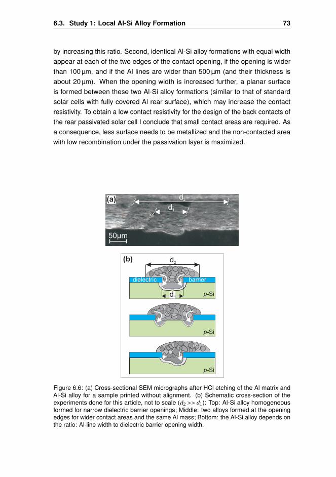
6.3. Study 1: Local Al-Si Alloy Formation 73
by increasing this ratio. Second, identical Al-Si alloy formations with equal widthappear at each of the two edges of the contact opening, if the opening is widerthan 100 µm, and if the Al lines are wider than 500 µm (and their thickness isabout 20 µm). When the opening width is increased further, a planar surfaceis formed between these two Al-Si alloy formations (similar to that of standardsolar cells with fully covered Al rear surface), which may increase the contactresistivity. To obtain a low contact resistivity for the design of the back contacts ofthe rear passivated solar cell I conclude that small contact areas are required. Asa consequence, less surface needs to be metallized and the non-contacted areawith low recombination under the passivation layer is maximized.
Figure 6.6: (a) Cross-sectional SEM micrographs after HCl etching of the Al matrix andAl-Si alloy for a sample printed without alignment. (b) Schematic cross-section of theexperiments done for this article, not to scale (d2 >> d1): Top: Al-Si alloy homogeneousformed for narrow dielectric barrier openings; Middle: two alloys formed at the openingedges for wider contact areas and the same Al mass; Bottom: the Al-Si alloy depends onthe ratio: Al-line width to dielectric barrier opening width.
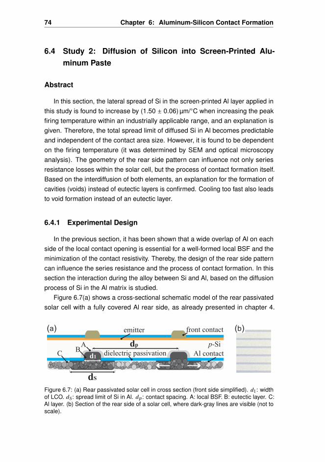
74 Chapter 6: Aluminum-Silicon Contact Formation
6.4 Study 2: Diffusion of Silicon into Screen-Printed Alu-minum Paste
Abstract
In this section, the lateral spread of Si in the screen-printed Al layer applied inthis study is found to increase by (1.50 ± 0.06) µm/C when increasing the peakfiring temperature within an industrially applicable range, and an explanation isgiven. Therefore, the total spread limit of diffused Si in Al becomes predictableand independent of the contact area size. However, it is found to be dependenton the firing temperature (it was determined by SEM and optical microscopyanalysis). The geometry of the rear side pattern can influence not only seriesresistance losses within the solar cell, but the process of contact formation itself.Based on the interdiffusion of both elements, an explanation for the formation ofcavities (voids) instead of eutectic layers is confirmed. Cooling too fast also leadsto void formation instead of an eutectic layer.
6.4.1 Experimental Design
In the previous section, it has been shown that a wide overlap of Al on eachside of the local contact opening is essential for a well-formed local BSF and theminimization of the contact resistivity. Thereby, the design of the rear side patterncan influence the series resistance and the process of contact formation. In thissection the interaction during the alloy between Si and Al, based on the diffusionprocess of Si in the Al matrix is studied.
Figure 6.7(a) shows a cross-sectional schematic model of the rear passivatedsolar cell with a fully covered Al rear side, as already presented in chapter 4.
dS
Figure 6.7: (a) Rear passivated solar cell in cross section (front side simplified). d1: widthof LCO. dS : spread limit of Si in Al. dp : contact spacing. A: local BSF. B: eutectic layer. C:Al layer. (b) Section of the rear side of a solar cell, where dark-gray lines are visible (not toscale).
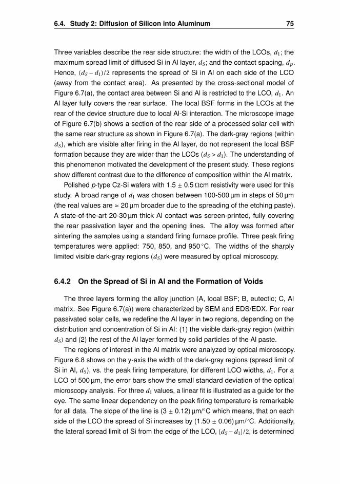
6.4. Study 2: Diffusion of Silicon into Aluminum 75
Three variables describe the rear side structure: the width of the LCOs, d1; themaximum spread limit of diffused Si in Al layer, dS ; and the contact spacing, dp .Hence, (dS −d1)/2 represents the spread of Si in Al on each side of the LCO(away from the contact area). As presented by the cross-sectional model ofFigure 6.7(a), the contact area between Si and Al is restricted to the LCO, d1. AnAl layer fully covers the rear surface. The local BSF forms in the LCOs at therear of the device structure due to local Al-Si interaction. The microscope imageof Figure 6.7(b) shows a section of the rear side of a processed solar cell withthe same rear structure as shown in Figure 6.7(a). The dark-gray regions (withindS), which are visible after firing in the Al layer, do not represent the local BSFformation because they are wider than the LCOs (dS > d1). The understanding ofthis phenomenon motivated the development of the present study. These regionsshow different contrast due to the difference of composition within the Al matrix.
Polished p-type Cz-Si wafers with 1.5 ± 0.5Ωcm resistivity were used for thisstudy. A broad range of d1 was chosen between 100-500 µm in steps of 50 µm(the real values are ≈ 20 µm broader due to the spreading of the etching paste).A state-of-the-art 20-30 µm thick Al contact was screen-printed, fully coveringthe rear passivation layer and the opening lines. The alloy was formed aftersintering the samples using a standard firing furnace profile. Three peak firingtemperatures were applied: 750, 850, and 950 C. The widths of the sharplylimited visible dark-gray regions (dS) were measured by optical microscopy.
6.4.2 On the Spread of Si in Al and the Formation of Voids
The three layers forming the alloy junction (A, local BSF; B, eutectic; C, Almatrix. See Figure 6.7(a)) were characterized by SEM and EDS/EDX. For rearpassivated solar cells, we redefine the Al layer in two regions, depending on thedistribution and concentration of Si in Al: (1) the visible dark-gray region (withindS ) and (2) the rest of the Al layer formed by solid particles of the Al paste.
The regions of interest in the Al matrix were analyzed by optical microscopy.Figure 6.8 shows on the y-axis the width of the dark-gray regions (spread limit ofSi in Al, dS), vs. the peak firing temperature, for different LCO widths, d1. For aLCO of 500 µm, the error bars show the small standard deviation of the opticalmicroscopy analysis. For three d1 values, a linear fit is illustrated as a guide for theeye. The same linear dependency on the peak firing temperature is remarkablefor all data. The slope of the line is (3 ± 0.12) µm/C which means, that on eachside of the LCO the spread of Si increases by (1.50 ± 0.06) µm/C. Additionally,the lateral spread limit of Si from the edge of the LCO, [dS −d1]/2, is determined
76 Chapter 6: Aluminum-Silicon Contact Formation
as follows: (75 ± 9) µm at 750 C, (225 ± 30) µm at 850 C, and (375 ± 90) µm at950 C. These results show that for a certain firing temperature the spread limit ofSi in the Al layer is constant and independent of the width of the LCO. Therefore,the maximum spread limit of diffused Si in Al is predictable.
To gain an understanding of the distribution of Si in the Al layer a furtheranalysis is required. A line scan was performed by EDX in the Al-Si alloyingstructure for two samples fired at the high temperature of 950 C. The SEMcross-sectional micrographs and the EDS/EDX results are shown in Figure 6.9for two samples fired at the same peak temperature and using the same amountof Al paste. The difference lies in the LCO of (a) 80 and (c) 125 µm, respectively.Although the formation of voids was randomly present for all device structures, forthe purpose of discussion a sample with alloy formation at the Al-Si interface waschosen for d1 = 80 µm [Fig. 6.9(a)] and a sample with a void was chosen for d1 =125 µm [Fig. 6.9(b)].
The Si content was measured from the center of the LCO, 200 µm to theleft and right. Although the results of this method are influenced by structuralinhomogeneities of the Al layer [135], we see that the Si concentration in theAl decreases with increasing distance from the center of the interface (centerof LCO), as already published elsewhere [136, 137] [see Figure 6.9(b)]. The
S
Figure 6.8: Temperature linear dependency of the spread limit of Si in the screen-printedAl layer. Error bars shown for d1 = 500 µm.
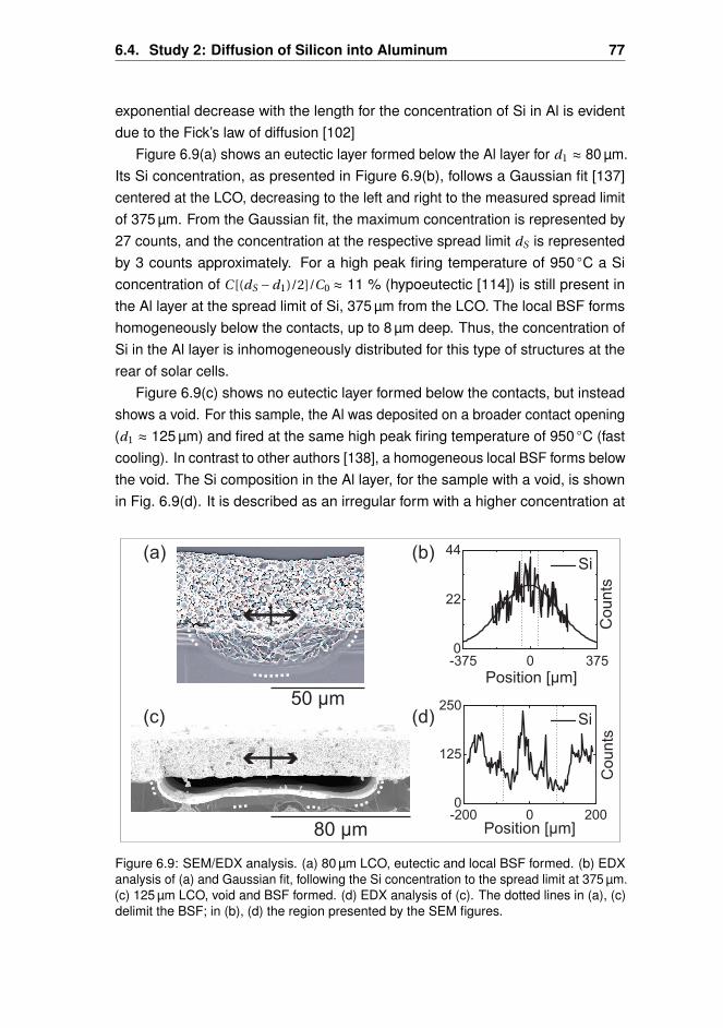
6.4. Study 2: Diffusion of Silicon into Aluminum 77
exponential decrease with the length for the concentration of Si in Al is evidentdue to the Fick’s law of diffusion [102]
Figure 6.9(a) shows an eutectic layer formed below the Al layer for d1 ≈ 80 µm.Its Si concentration, as presented in Figure 6.9(b), follows a Gaussian fit [137]centered at the LCO, decreasing to the left and right to the measured spread limitof 375 µm. From the Gaussian fit, the maximum concentration is represented by27 counts, and the concentration at the respective spread limit dS is representedby 3 counts approximately. For a high peak firing temperature of 950 C a Siconcentration of C [(dS −d1)/2]/C0 ≈ 11 % (hypoeutectic [114]) is still present inthe Al layer at the spread limit of Si, 375 µm from the LCO. The local BSF formshomogeneously below the contacts, up to 8 µm deep. Thus, the concentration ofSi in the Al layer is inhomogeneously distributed for this type of structures at therear of solar cells.
Figure 6.9(c) shows no eutectic layer formed below the contacts, but insteadshows a void. For this sample, the Al was deposited on a broader contact opening(d1 ≈ 125 µm) and fired at the same high peak firing temperature of 950 C (fastcooling). In contrast to other authors [138], a homogeneous local BSF forms belowthe void. The Si composition in the Al layer, for the sample with a void, is shownin Fig. 6.9(d). It is described as an irregular form with a higher concentration at
Figure 6.9: SEM/EDX analysis. (a) 80 µm LCO, eutectic and local BSF formed. (b) EDXanalysis of (a) and Gaussian fit, following the Si concentration to the spread limit at 375 µm.(c) 125 µm LCO, void and BSF formed. (d) EDX analysis of (c). The dotted lines in (a), (c)delimit the BSF; in (b), (d) the region presented by the SEM figures.
78 Chapter 6: Aluminum-Silicon Contact Formation
the center of the opening and two maxima located more than 150 µm away fromthe center of the opening, to the left and right.
6.4.3 Discussion
Similar conclusions as presented in this chapter were drawn by Kircher [70],and by McCaldin and Sankur [137] for the diffusion of Si on evaporated Al thinlayer (20 times thinner than a screen-printed layer). They also found a reduction ofthe Si concentration in the thin Al layer adjacent to the dielectric opening (similarto the two maxima for the concentration of Si as shown in Fig. 6.9(d)). Theyexplained this phenomenon to be related to the Si diffusing back during coolingand regrowing epitaxially on the Si surface, during a relatively slow cooling.
The liquid Al wets the Si surface in the dielectric openings, and then Si dis-solves in the Al layer. It is well known that the depth of penetration of Al-Si meltinto the Si wafer is a function of the temperature and of the spherical diameter ofthe Al particles [139]. However, the penetration of the liquid Al-Si also dependson the diffusion of Si in Al. Thus, for a large initial concentration of Si in Al, thepenetration of the melt will be reduced [140].
In our case for a peak firing temperature of 950 C, the depth of penetrationis 20 µm, as illustrated in Figure 6.9(a), (c). Due to the higher solubility of Si inAl than that of Al in Si [137,141], a higher volume of Si atoms diffuse into the Althan Al atoms into the Si. If the peak firing temperature is high, the diffusion isenhanced and Si spreads faster into the Al layer. At the interface, the Al in directcontact with the Si bulk saturates first, as the Si diffusion proceeds from the edgesof the interface in both lateral directions into the liquid Al (not yet saturated by Si).After a few seconds, a large amount of Si atoms is found in the Al layer, morethan 370 µm from the contact area. In the case of a standard solar cell where theeffective contact area of Si is equal to the area of the deposited Al contact, theinterdiffusion achieves an equilibrium at the peak temperature where no more Sidiffusion into Al is present (saturation). Thus, following the Al-Si phase diagram,the concentration of Si in the melt is constant at the peak temperature. By coolingthe sample, the composition of Si in the liquid-phase has to decrease followingthe liquid curve of the binary system [113] (segregation).
However, this may not be the case in our experiment, were a large Al contactlying on dielectric barrier is forming contact only with a narrow Si surface. Inthis case, if no saturation of Al by Si is present, then Si keeps diffusing into Alfor a few seconds at the peak temperature. As shown by some authors, a highelastic stress field may occur in the melt during the alloying [142] between two
6.4. Study 2: Diffusion of Silicon into Aluminum 79
elements with different diffusivities (this is the case between Al and Si: Si hashigher diffusivity in Al, than Al in Si [141]). The high generation of vacanciesduring interdiffusion of two elements with different diffusivities may coalesce in themelt, causing the nucleation and formation of Kirkendall [143] voids [142] (cavitiesbetween two elements in direct contact).
As shown in Figure 6.9(c), a local BSF is formed below the void which repre-sents the epitaxial growth of Si on the bulk surface during cooling. Thus, this resultexplains that the void forms during the cooling of a hypereutectic melt, during theepitaxially recrystallization of Si at the interface.
Immediately after the formation of the void (during cooling), only the edgesof the LCO are still in direct contact with the Al layer. Thus, at this point there isalmost no contact surface between Al and Si for the segregation of the diffused Si.By reaching the eutectic temperature, the whole remaining liquid solidifies andthe Si is trapped in the Al matrix, thus, a high concentration of Si is present in Al,away from the surface of contact [shown by the two maxima of Figure 6.9(d)].
If the interaction between Al and Si takes place only within dS , where a visibledark-gray region is sharply delimited, the spread of Si in the Al layer is diffusion-limited. Thereby, an exponential decrease with the distance from the center of theinterface is evident due to the Fick’s law of diffusion [102].
Since the diffusion of Si in the liquid Al proceeds laterally within the Al layer, adetermined amount of Al (d2 > 500 µm, see section 6.3) should overlap each sideof the dielectric opening to achieve an optimal metal-semiconductor interaction.This overlap of Al on narrow dielectric openings is evident due to the reductionof the contact resistivity and the homogeneous formation of the local BSF. Wesuggest that the maximum spread limit of diffused Si, dS , should be consideredduring the optimization of the Al metallization in order to achieve an optimalcontact and full local BSF formation. Thus, the effective Al mass interaction withSi during the alloying is determined by dS . However it has been shown herethat an amount too large of unsaturated Al may enhance the formation of voidsinstead of Al-Si alloy layers. Thus, another parameter to analyze the local contactformation between Al and Si is the contact spacing, dp , which may be related to dS .Another application of the Al overlap may be found on interdigitated back contactn-type Si solar cells to obtain high-quality screen-printed Al-alloyed emitters.
6.4.4 Model of Local Contact Formation
Figure 6.10 aims to explain the contact formation when the contact area isreduced (variation of dielectric opening width). A Si wafer [Si(S)] is coated by a
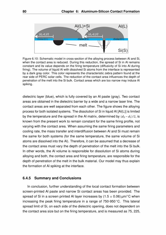
80 Chapter 6: Aluminum-Silicon Contact Formation
Al(L)
Si(S)
(d -d )/2S 1 (d -d )/2S 1
melt
Al(L)+Si
dielectric dielectricdielectric
Figure 6.10: Schematic model in cross-section of the alloying process between Al and Si,when the contact area is reduced. During this reduction, the spread of Si in Al remainsconstant and its value depends on the firing temperature (diffusivity of Si into Al duringfiring). The volume of liquid Al with dissolved Si atoms from the interface is representedby a dark gray color. This color represents the characteristic zebra pattern found at therear side of PERC solar cells. The reduction of the contact area influences the depth ofpenetration of the melt into the Si bulk. Contact areas which are too narrow may induce Alspiking.
dielectric layer (blue), which is fully covered by an Al paste (gray). Two contactareas are obtained in the dielectric barrier by a wide and a narrow laser line. Thecontact areas are well separated from each other. The figure shows the alloyingprocess for both isolated systems. The dissolution of Si in liquid Al [Al(L)] is limitedby the temperature and the spread in the Al matrix, determined by (dS −d1)/2, isknown from the present work to remain constant for the same firing profile, notvarying with the contact area. When assuming the same firing parameters andcooling rate, the mass transfer and interdiffusion between Al and Si must remainthe same for both systems (for the same temperature, the same volume of Siatoms are dissolved into the Al). Therefore, it can be assumed that a decrease ofthe contact area must vary the depth of penetration of the melt into the Si bulk.In other words, the Al volume is responsible for dissolution of Si atoms duringalloying and both, the contact area and firing temperature, are responsible for thedepth of penetration of the melt in the bulk material. Our model may thus explainthe formation of Al spiking at the interface.
6.4.5 Summary and Conclusions
In conclusion, further understanding of the local contact formation betweenscreen-printed Al paste and narrow Si contact areas has been provided. Thespread of Si in a screen printed Al layer increases by (1.5 ± 0.06) µm/C whenincreasing the peak firing temperature in a range of 750-950 C. This lateralspread limit of Si, on each side of the dielectric opening, does not dependent onthe contact area size but on the firing temperature, and is measured as 75, 225,

6.4. Study 2: Diffusion of Silicon into Aluminum 81
and 375 µm for 750, 850, and 950 C, respectively. Thus, the optimum width of theAl contact may be determined by the maximum spread limit of diffused Si in an Allayer. The impact of this result on the contact spacing will be analyzed in the nextsection. It is not clear yet whether the contact spacing should be smaller or largerthan the maximum spread limit of diffused Si in Al. Additionally, an explanation isgiven for the voids formed instead of Al-Si eutectic layers, based on the differenceof diffusivities between Al and Si, and it has been mentioned that the voids maybe formed during cooling.
82 Chapter 6: Aluminum-Silicon Contact Formation
6.5 Study 3: Distribution of Silicon in Aluminum and the In-fluence of Contact Pattern on Contact Formation
Abstract
In this section the influence of the geometry of the rear pattern (contact sizeand contact spacing) on the Al-Si interaction in the local contact openings isstudied. In the previous section, it has been demonstrated that Si diffuses into theAl through narrow dielectric barrier openings and spreads laterally to a determinedlimit given by the firing temperature. The purpose of this section is to show thatthe contact spacing can affect the tendency of formation of voids below the Al-Sicontacts instead of an eutectic layer. When decreasing the contact spacing andtherefore the overlap of Al on each side of the local opening, the melt saturatesfaster and the formation of a high-quality local BSF is increased, also minimizingthe presence of voids. This physical observation can enhance the design of therear pattern for rear passivated solar cells and give further understanding of theAl-Si interaction during the firing process. The minimum contact spacing allowedfor an optimal rear side pattern may be based on the interdiffusion between liquidAl and Si, during the sintering process.
6.5.1 Experimental Design
The local contact formation between Al and Si is strongly influenced by thedistribution of Si in the Al matrix. It has been shown in literature, that rearpassivated solar cells fired with non-optimal parameters suffer from large lossesin FF compared to reference Al-BSF solar cells, using industrial screen-printingAl pastes [18, 85]. The formation of voids during the sintering between screen-printing Al pastes and Si may be the answer for those FF losses.
The influence of the contact spacing on the formation of eutectic layer andlocal BSF was analyzed. Contact spacings, dp , were chosen from 0.1 to 2 mm,keeping the opening size, d1, constant at 70 µm [following the model presentedin Figure 6.7(a)]. The variation of dp is achieved by laser ablating lines in thedielectric layer. The samples are fully covered by Al in order to analyze thediffusion of Si in the Al matrix. Different peak firing temperatures are used forcontact sintering. Both, the thickness of the Al matrix and the alloying time arekept constant. Their influence on the contact formation is not studied here, but itmay be interesting for further work and understanding.
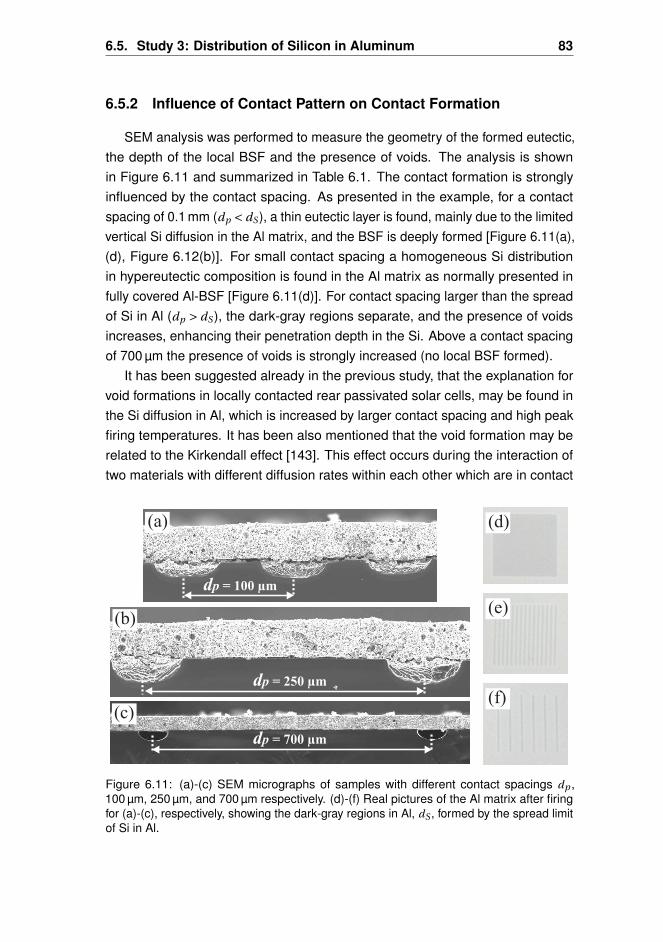
6.5. Study 3: Distribution of Silicon in Aluminum 83
6.5.2 Influence of Contact Pattern on Contact Formation
SEM analysis was performed to measure the geometry of the formed eutectic,the depth of the local BSF and the presence of voids. The analysis is shownin Figure 6.11 and summarized in Table 6.1. The contact formation is stronglyinfluenced by the contact spacing. As presented in the example, for a contactspacing of 0.1 mm (dp < dS), a thin eutectic layer is found, mainly due to the limitedvertical Si diffusion in the Al matrix, and the BSF is deeply formed [Figure 6.11(a),(d), Figure 6.12(b)]. For small contact spacing a homogeneous Si distributionin hypereutectic composition is found in the Al matrix as normally presented infully covered Al-BSF [Figure 6.11(d)]. For contact spacing larger than the spreadof Si in Al (dp > dS), the dark-gray regions separate, and the presence of voidsincreases, enhancing their penetration depth in the Si. Above a contact spacingof 700 µm the presence of voids is strongly increased (no local BSF formed).
It has been suggested already in the previous study, that the explanation forvoid formations in locally contacted rear passivated solar cells, may be found inthe Si diffusion in Al, which is increased by larger contact spacing and high peakfiring temperatures. It has been also mentioned that the void formation may berelated to the Kirkendall effect [143]. This effect occurs during the interaction oftwo materials with different diffusion rates within each other which are in contact
dp = 100 µm
dp = 250 µm
dp = 700 µm
Figure 6.11: (a)-(c) SEM micrographs of samples with different contact spacings dp ,100 µm, 250 µm, and 700 µm respectively. (d)-(f) Real pictures of the Al matrix after firingfor (a)-(c), respectively, showing the dark-gray regions in Al, dS , formed by the spread limitof Si in Al.
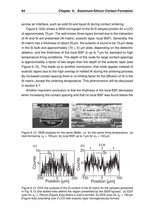
84 Chapter 6: Aluminum-Silicon Contact Formation
across an interface, such as solid Si and liquid Al during contact sintering.Figure 6.12(b) shows a SEM micrograph of the Al-Si alloyed junction for a LCO
of approximately 70 µm. The well-known three layers formed due to the interactionof Al and Si are presented (Al-matrix, eutectic layer, local BSF). Generally, theAl-matrix has a thickness of about 20 µm, the eutectic is found to be 15 µm deepin the Si bulk and approximately (70 ± 5) µm wide, depending on the dielectricablation, and the thickness of the local BSF is up to 7 µm for standard to hightemperature firing conditions. The depth of the voids for large contact spacingsis approximately a factor of two larger than the depth of the eutectic layer [seeFigure 6.12]. This leads us to another conclusion, that voids appear instead ofeutectic layers due to the high overlap of melted Al during the sintering process.By increased contact spacing there is no limiting factor for the diffusion of Si in theAl matrix, except the sintering temperature. This phenomenon will be discussedin section 6.7.
Another important conclusion is that the thickness of the local BSF decreaseswhen increasing the contact spacing and that no local BSF was found below the
dp = 700 µm dp = 100 µm
15 µm
Figure 6.12: SEM analysis for the same Wafer, i.e. for the same firing temperature. (a)Void formed by dp ≥ 700 µm; (b) local BSF up to 7 µm for dp = 100 µm.
LCO
1 2 3
Figure 6.13: EDX line analysis of the Si content in the Al matrix for the samples presentedin Fig. 6.12 (the dotted lines delimit the region presented by the SEM figures). (a) EDXscan for dp ≥ 700 µm [Figure 4(a)] where a void is formed; (b) EDX scan for dp = 100 µm[Figure 4(b)] extending over 3 LCO with eutectic layer homogeneously formed.
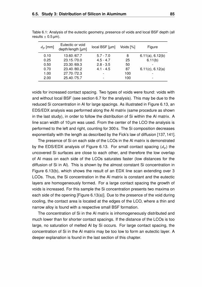
6.5. Study 3: Distribution of Silicon in Aluminum 85
Table 6.1: Analysis of the eutectic geometry, presence of voids and local BSF depth (allresults ± 0.5 µm).
dp [mm] Eutectic or void local BSF [µm] Voids [%] Figuredepth/length [µm]
0.10 13.60 /67.7 5.7 - 7.0 8 6.11(a), 6.12(b)0.25 23.15 /70.0 4.5 - 4.7 25 6.11(b)0.50 23.30 /69.3 2.8 - 3.5 50 -0.70 23.40 /80.2 4.1 - 4.5 87 6.11(c), 6.12(a)1.00 27.70 /72.3 - 100 -2.00 25.40 /75.7 - 100 -
voids for increased contact spacing. Two types of voids were found: voids withand without local BSF (see section 6.7 for the analysis). This may be due to thereduced Si concentration in Al for large spacings. As illustrated in Figure 6.13, anEDS/EDX analysis was performed along the Al matrix (same procedure as shownin the last study), in order to follow the distribution of Si within the Al matrix. Aline scan width of 10 µm was used. From the center of the LCO the analysis isperformed to the left and right, counting for 300 s. The Si composition decreasesexponentially with the length as described by the Fick’s law of diffusion [137,141].
The presence of Si on each side of the LCOs in the Al matrix is demonstratedby the EDS/EDX analysis of Figure 6.13. For small contact spacing (dp ) theuncovered Si surfaces are close to each other, and therefore the low overlapof Al mass on each side of the LCOs saturates faster (low distances for thediffusion of Si in Al). This is shown by the almost constant Si concentration inFigure 6.13(b), which shows the result of an EDX line scan extending over 3LCOs. Thus, the Si concentration in the Al matrix is constant and the eutecticlayers are homogeneously formed. For a large contact spacing the growth ofvoids is increased. For this sample the Si concentration presents two maxima oneach side of the opening [Figure 6.13(a)]. Due to the presence of the void duringcooling, the contact area is located at the edges of the LCO, where a thin andnarrow alloy is found with a respective small BSF formation.
The concentration of Si in the Al matrix is inhomogeneously distributed andmuch lower than for shorter contact spacings. If the distance of the LCOs is toolarge, no saturation of melted Al by Si occurs. For large contact spacing, theconcentration of Si in the Al matrix may be too low to form an eutectic layer. Adeeper explanation is found in the last section of this chapter.
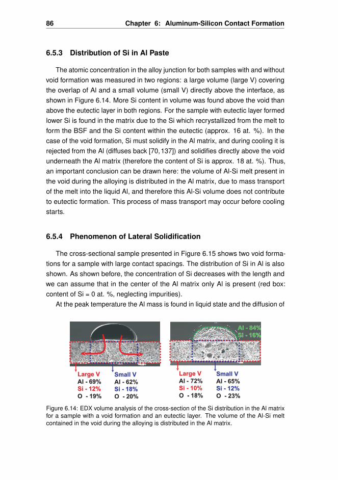
86 Chapter 6: Aluminum-Silicon Contact Formation
6.5.3 Distribution of Si in Al Paste
The atomic concentration in the alloy junction for both samples with and withoutvoid formation was measured in two regions: a large volume (large V) coveringthe overlap of Al and a small volume (small V) directly above the interface, asshown in Figure 6.14. More Si content in volume was found above the void thanabove the eutectic layer in both regions. For the sample with eutectic layer formedlower Si is found in the matrix due to the Si which recrystallized from the melt toform the BSF and the Si content within the eutectic (approx. 16 at. %). In thecase of the void formation, Si must solidify in the Al matrix, and during cooling it isrejected from the Al (diffuses back [70,137]) and solidifies directly above the voidunderneath the Al matrix (therefore the content of Si is approx. 18 at. %). Thus,an important conclusion can be drawn here: the volume of Al-Si melt present inthe void during the alloying is distributed in the Al matrix, due to mass transportof the melt into the liquid Al, and therefore this Al-Si volume does not contributeto eutectic formation. This process of mass transport may occur before coolingstarts.
6.5.4 Phenomenon of Lateral Solidification
The cross-sectional sample presented in Figure 6.15 shows two void forma-tions for a sample with large contact spacings. The distribution of Si in Al is alsoshown. As shown before, the concentration of Si decreases with the length andwe can assume that in the center of the Al matrix only Al is present (red box:content of Si = 0 at. %, neglecting impurities).
At the peak temperature the Al mass is found in liquid state and the diffusion of
Large VLarge V
AlAl -- 69%69%
SiSi -- 12%12%
OO -- 19%19%
Small VSmall V
AlAl -- 62%62%
SiSi -- 18%18%
OO -- 20%20%
Large VLarge V
AlAl -- 72%72%
SiSi -- 10%10%
OO -- 18%18%
Small VSmall V
AlAl -- 65%65%
SiSi -- 12%12%
OO -- 23%23%
AlAl -- 84%84%
SiSi -- 16%16%
Figure 6.14: EDX volume analysis of the cross-section of the Si distribution in the Al matrixfor a sample with a void formation and an eutectic layer. The volume of the Al-Si meltcontained in the void during the alloying is distributed in the Al matrix.
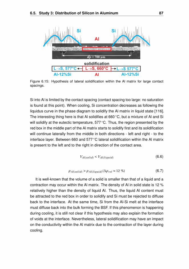
6.5. Study 3: Distribution of Silicon in Aluminum 87
dp = 700 µm
Si Si
Al
AlAl-12%Si Al-12%Si
solidification
L S, 660°C®L S, 577°C® L S 577°C®
Figure 6.15: Hypothesis of lateral solidification within the Al matrix for large contactspacings.
Si into Al is limited by the contact spacing (contact spacing too large: no saturationis found at this point). When cooling, Si concentration decreases as following theliquidus curve in the phase diagram to solidify the Al matrix in liquid state [116].The interesting thing here is that Al solidifies at 660 C, but a mixture of Al and Siwill solidify at the eutectic temperature, 577 C. Thus, the region presented by thered box in the middle part of the Al matrix starts to solidify first and its solidificationwill continue laterally from the middle in both directions - left and right - to theinterface layer. Between 660 and 577 C lateral solidification within the Al matrixis present to the left and to the right in direction of the contact area.
VAl (sol i d) <VAl (l i qui d) (6.6)
ρAl (sol i d) > ρAl (l i qui d)(∆ρr el ≈ 12 %) (6.7)
It is well-known that the volume of a solid is smaller than that of a liquid and acontraction may occur within the Al matrix. The density of Al in solid state is 12 %relatively higher than the density of liquid Al. Thus, the liquid Al content mustbe attracted to the red box in order to solidify and Si must be rejected to diffuseback to the interface. At the same time, Si from the Al-Si melt at the interfacemust diffuse back into the bulk forming the BSF. If this phenomenon is happeningduring cooling, it is still not clear if this hypothesis may also explain the formationof voids at the interface. Nevertheless, lateral solidification may have an impacton the conductivity within the Al matrix due to the contraction of the layer duringcooling.
88 Chapter 6: Aluminum-Silicon Contact Formation
6.5.5 Summary and Conclusions
In conclusion, we have shown that the geometry of the rear pattern for rearpassivated, locally contacted solar cells influences not only series resistancelosses, but also the process of local contact formation between Al and Si. Theformation of a high quality BSF is extremely dependent on the Si diffusion inAl and on the overlap of Al on each side of the dielectric opening. The earlysaturation of the Al-Si melt for small contact spacings may allow the formation ofa deep p+-doped layer. A unlimited diffusion of Si atoms in Al may explain voidformation instead of eutectic layers. The Si diffusion in Al is limited not only by thefiring temperature, but also by the contact spacing, determined by the amount ofAl mass overlap on each side of the dielectric openings. The Al-Si volume in liquidstate present in void during the alloying was found distributed in the Al matrix.This Al-Si volume transported from void to the Al matrix does not contribute toeutectic formation, explaining the process of mass transport and void formation.Furthermore, we believe that the enhanced Si diffusion in the Al matrix could bereduced by introducing Si in the Al paste before the sintering.
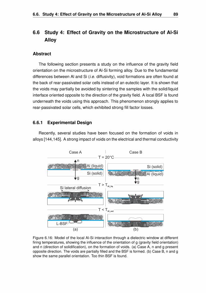
6.6. Study 4: Effect of Gravity on the Microstructure of Al-Si Alloy 89
6.6 Study 4: Effect of Gravity on the Microstructure of Al-SiAlloy
Abstract
The following section presents a study on the influence of the gravity fieldorientation on the microstructure of Al-Si forming alloy. Due to the fundamentaldifferences between Al and Si (i.e. diffusivity), void formations are often found atthe back of rear-passivated solar cells instead of an eutectic layer. It is shown thatthe voids may partially be avoided by sintering the samples with the solid/liquidinterface oriented opposite to the direction of the gravity field. A local BSF is foundunderneath the voids using this approach. This phenomenon strongly applies torear-passivated solar cells, which exhibited strong fill factor losses.
6.6.1 Experimental Design
Recently, several studies have been focused on the formation of voids inalloys [144,145]. A strong impact of voids on the electrical and thermal conductivity
Figure 6.16: Model of the local Al-Si interaction through a dielectric window at differentfiring temperatures, showing the influence of the orientation of g (gravity field orientation)and n (direction of solidification), on the formation of voids. (a) Case A, n and g presentopposite direction. The voids are partially filled and the BSF is formed. (b) Case B, n and gshow the same parallel orientation. Too thin BSF is found.
90 Chapter 6: Aluminum-Silicon Contact Formation
has been shown. It has been mentioned, that the void formation is a result of asystem of variables and that each paste is different in its voiding behavior [146].
In this section the microstructure during the transformation from liquid to solidphase is analyzed for both cases, gravity field oriented opposite and parallel tothe solid/liquid (S/L) interface (Figure 6.16) and their effect on the formation ofvoids is analyzed. As in a standard solar cell process, the samples are alkalinetextured in order to achieve a pyramidal structure on the surface. An optimizedrear side passivation by PECVD technique can be used on the pyramidal structurefor high-efficiency solar cell processes (see section 7.10).
Figure 6.16 illustrates the model of the local interaction between Al and Si forthree temperatures during sintering. At room temperature (20 C) the system isat equilibrium. When Al is liquid (above its melting temperature), the interactionstarts (Al diffusion into Si, Si diffusion into Al) and a spot of liquid Al-Si is found.In the same place but after cooling (to below the eutectic temperature), the Al-Sieutectic is formed by recrystallization. A parallel orientation is assumed for both,the gravity field, g, and the normal direction of the S/L interface (direction ofsolidification), n. In case A, n and g are antiparallel and in case B, n and g areparallel. The diffusion of Si into Al is represented by the white arrows: firstly, Sidiffusion from the Al-Si melt into the Al matrix and secondly, lateral diffusion ofSi into Al along the matrix, as marked by the dark-gray region within the Al layer.This region has been defined as the spread limit of Si in the screen-printing Alafter cooling (see section 6.4). The epitaxial recrystallization of the melt duringcooling is represented by the black arrows (with the normal n, as the direction ofsolidification).
6.6.2 Cross-sectional SEM Analysis
Figure 6.17 shows the SEM cross-sectional analysis. The eutectic layer andvoid formations were found in more than 20 samples, fired at different peak firingtemperatures, for the two cases of firing presented in the model of Figure 6.16.
In case A, the normal direction of the solid/liquid interface, n, is in oppositedirection to the gravity field orientation, g (n and g are antiparallel). The microstruc-ture of the Al-Si eutectic is shown in Figure 6.17(a), (c). In the opposite caseB, n and g are parallel. The microstructure of the Al-Si eutectic is presented inFigure 6.17(b), (d). In the Al-Si interface, Si-rich structures along the < 111 >planes are still found after cooling, due to the phenomenon of extrusion whichmay diminish open-circuit voltage at the solar cell level [107].
Voids were found in every sample, which leads to the conclusion that the void
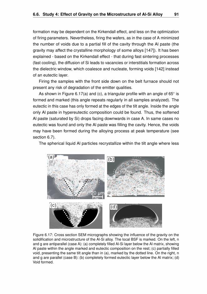
6.6. Study 4: Effect of Gravity on the Microstructure of Al-Si Alloy 91
formation may be dependent on the Kirkendall effect, and less on the optimizationof firing parameters. Nevertheless, firing the wafers, as in the case of A minimizedthe number of voids due to a partial fill of the cavity through the Al paste (thegravity may affect the crystalline morphology of some alloys [147]). It has beenexplained - based on the Kirkendall effect - that during fast sintering processes(fast cooling), the diffusion of Si leads to vacancies or interstitials formation acrossthe dielectric window, which coalesce and nucleate, forming voids [142] insteadof an eutectic layer.
Firing the samples with the front side down on the belt furnace should notpresent any risk of degradation of the emitter qualities.
As shown in Figure 6.17(a) and (c), a triangular profile with an angle of 65 isformed and marked (this angle repeats regularly in all samples analyzed). Theeutectic in this case has only formed at the edges of the tilt angle. Inside the angleonly Al paste in hypereutectic composition could be found. Thus, the softenedAl paste (saturated by Si) drops facing downwards in case A. In same cases noeutectic was found and only the Al paste was filling the cavity. Hence, the voidsmay have been formed during the alloying process at peak temperature (seesection 6.7).
The spherical liquid Al particles recrystallize within the tilt angle where less
Figure 6.17: Cross section SEM micrographs showing the influence of the gravity on thesolidification and microstructure of the Al-Si alloy. The local BSF is marked. On the left, nand g are antiparallel (case A): (a) completely filled Al-Si layer below the Al matrix, showingAl paste within the angle marked and eutectic composition on the rest; (c) partially filledvoid, presenting the same tilt angle than in (a), marked by the dotted line. On the right, nand g are parallel (case B): (b) completely formed eutectic layer below the Al matrix; (d)Void formed.
92 Chapter 6: Aluminum-Silicon Contact Formation
contact to the Si bulk is found than at the edges. The void formation process maybe the same in both cases (A and B), however no paste fills the void in case B. Inour case, melting and cooling could not be observed in real time and therefore itis extremely difficult to completely understand the process of void formation.
An important benefit of this phenomenon is that the Al paste can partially fillthe voids, reducing their effect, improving the Al-Si contact, and increasing theformation of a BSF beneath the LCO. Because the solid Al spheres are visiblewithin the void it can be concluded that the softened Al paste fills part of the voidduring cooling due to the impact of gravity.
6.6.3 Summary and Conclusions
It could be shown that the gravity field orientation has an important effect onthe local Al-Si alloy morphology during sintering. The formation of voids can becompletely or partially prevented when the gravity field orientation is antiparallelto the normal solidification direction of the solid/liquid phase. The formation of thelocal BSF is improved underneath the void. This approach may reduce seriesresistance losses normally found in these device structures. This discovery offersapplications to the formation of local contacts for rear-passivated Si solar cells bylocal alloying of full-area, screen-printed Al pastes.
6.7. Understanding and Avoiding the Formation of Voids 93
6.7 Understanding and Avoiding the Formation of Voids §
Abstract
So far, several conclusions have been drawn within this study: the Al massis responsible for mass transport during alloying; the diffusion of Si in Al withinthe Al matrix is limited by the contact spacing; two types of voids have beenobserved: voids with and without p+-doped Si region (BSF) formation underneath.So far, it has been mentioned that the void formation may depend on the fastdiffusion of Si in Al, the Kirkendall effect, the fast cooling, the contact spacing,lateral solidification within the Al. In the first part of the following section, the twotypes of voids formations are analyzed and a schematic model is presented todescribe their formation. In the second part several issues to avoid void formation-as the presented in this work and in the literature- are reviewed.
6.7.1 Formation of Voids with and without Back Surface Field
So far, the formation of voids has been explained by the following effects:
a. Due to the higher diffusivity of Si in Al than the diffusivity of Al in Si in Al-Sialloys, a high current of vacancies or interstitials across the dielectric windowmay occur (as explained by the Kirkendall effect). When increasing the firingtemperature, the diffusivity of Si in Al increases and the process is accelerated.
b. The concentration of Si in the Al matrix can be too low and the diffusion of Siback through the interface is not enough to form the eutectic and the BSF. This ismainly due to the spread of Si in Al due to large contact spacings.
c. The volume of Al is too high and responsible for strong mass transport of theAl-Si melt during the alloying.
d. The cooling process does not occur at equilibrium, as stated by the Al-Siphase diagram.
Figure 6.18 shows a simple scheme to explain the formation of voids with andwithout BSF, during the contact formation in narrow dielectric openings betweenscreen-printed Al pastes to Si.
1. Reaching the peak temperature the Al-Si melt has deeply penetrated theinterface in both cases. At this point no void formation is assumed.
§The main results of this section have been presented at the 3r d Workshop on Metallization forCrystalline Silicon Solar Cells, Charleroi (Belgium), 26.10.2011.
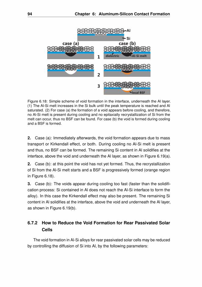
94 Chapter 6: Aluminum-Silicon Contact Formation
1
2
case (a) case (b)
3
Al
Si
dielectric
local BSF
Al-Si melt
Figure 6.18: Simple scheme of void formation in the interface, underneath the Al layer.(1) The Al-Si melt increases in the Si bulk until the peak temperature is reached and Alsaturated. (2) For case (a) the formation of a void appears before cooling, and therefore,no Al-Si melt is present during cooling and no epitaxially recrystallization of Si from themelt can occur, thus no BSF can be found. For case (b) the void is formed during coolingand a BSF is formed.
2. Case (a): Immediately afterwards, the void formation appears due to masstransport or Kirkendall effect, or both. During cooling no Al-Si melt is presentand thus, no BSF can be formed. The remaining Si content in Al solidifies at theinterface, above the void and underneath the Al layer, as shown in Figure 6.19(a).
2. Case (b): at this point the void has not yet formed. Thus, the recrystallizationof Si from the Al-Si melt starts and a BSF is progressively formed (orange regionin Figure 6.18).
3. Case (b): The voids appear during cooling too fast (faster than the solidifi-cation process: Si contained in Al does not reach the Al-Si interface to form thealloy). In this case the Kirkendall effect may also be present. The remaining Sicontent in Al solidifies at the interface, above the void and underneath the Al layer,as shown in Figure 6.19(b).
6.7.2 How to Reduce the Void Formation for Rear Passivated SolarCells
The void formation in Al-Si alloys for rear passivated solar cells may be reducedby controlling the diffusion of Si into Al, by the following parameters:
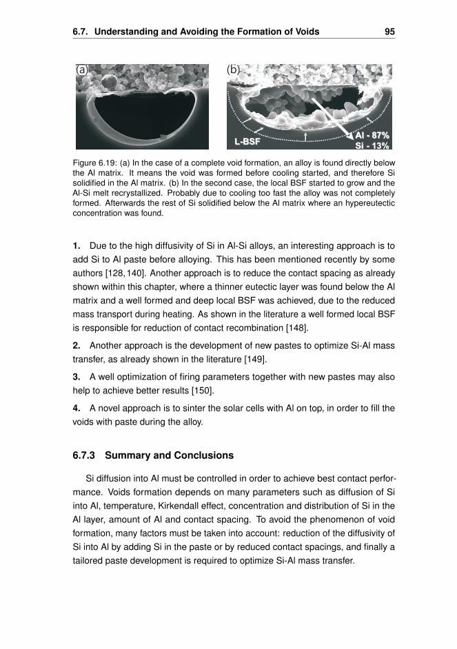
6.7. Understanding and Avoiding the Formation of Voids 95
AlAl -- 87%87%
SiSi -- 13%13%LL--BSFBSF
(a) (b)
Figure 6.19: (a) In the case of a complete void formation, an alloy is found directly belowthe Al matrix. It means the void was formed before cooling started, and therefore Sisolidified in the Al matrix. (b) In the second case, the local BSF started to grow and theAl-Si melt recrystallized. Probably due to cooling too fast the alloy was not completelyformed. Afterwards the rest of Si solidified below the Al matrix where an hypereutecticconcentration was found.
1. Due to the high diffusivity of Si in Al-Si alloys, an interesting approach is toadd Si to Al paste before alloying. This has been mentioned recently by someauthors [128,140]. Another approach is to reduce the contact spacing as alreadyshown within this chapter, where a thinner eutectic layer was found below the Almatrix and a well formed and deep local BSF was achieved, due to the reducedmass transport during heating. As shown in the literature a well formed local BSFis responsible for reduction of contact recombination [148].
2. Another approach is the development of new pastes to optimize Si-Al masstransfer, as already shown in the literature [149].
3. A well optimization of firing parameters together with new pastes may alsohelp to achieve better results [150].
4. A novel approach is to sinter the solar cells with Al on top, in order to fill thevoids with paste during the alloy.
6.7.3 Summary and Conclusions
Si diffusion into Al must be controlled in order to achieve best contact perfor-mance. Voids formation depends on many parameters such as diffusion of Siinto Al, temperature, Kirkendall effect, concentration and distribution of Si in theAl layer, amount of Al and contact spacing. To avoid the phenomenon of voidformation, many factors must be taken into account: reduction of the diffusivity ofSi into Al by adding Si in the paste or by reduced contact spacings, and finally atailored paste development is required to optimize Si-Al mass transfer.

Part III
Analysis of Industrial RearPassivated Solar Cells

CH
AP
TE
R
7PROCESSING OF REAR PASSIVATED SOLAR
CELLS: ANALYSIS OF DEVICE STRUCTURES
AND RESULTS
Abstract
After the introduction of the rear passivated solar cell device (chapter 1) andthe analysis of the local Al-Si contact formation (chapter 6), the goal of this chapteris to present the development of an industrially applicable process sequences forrear passivated solar cells on multicrystalline silicon substrates. The optimizationsdone in the previous chapter on the rear side contact formation between Al andSi will be applied in all the devices presented in this chapter. The improvementof the solar cell concepts and efficiency over the time spam of this thesis ispresented. Several passivation layers for the rear side are deposited and tested.Different reference structures were made in order to analyze the impact of severalthermal budgets on the solar cell performance and their potential for increasingthe efficiency of each device concept. The main difference between the batchesis the preparation of the rear side before dielectric passivation. The single sidepolishing process was studied, in order to select the optimal etching procedure.Also, a chemical edge isolation approach is analyzed. A masking approach forprotecting the front side emitter from the single side polishing is also presented.By the end of the chapter, the developed high efficiency solar cells on high qualitymc-Si and Cz-Si material are presented.
99
100 Chapter 7: Processing of Rear Passivated Solar Cells
7.1 Introduction
Many concepts for rear passivated solar cells have been developed throughoutthis thesis. In this chapter the main results, which may have the highest impact onthe industrial production are summarized, and discussed. The main topic of rearpassivated p-Si solar cell structures is the fabrication of a single side emitter*.
Thus, the succession of rear side polishing and edge isolation is a criticalstep within the process. In order to further understand this topic, two studies arepresented (on mc-Si), which are of paramount importance for the high efficiencysolar cell presented here. Cz-Si material is incorporated in the batch, by the endof the chapter, in order to further analyze the impact of the approaches on highquality material.
The first study concentrates on the influence of an extra rear single sidepolishing step before phosphorus diffusion. The roughness of the rear side isshown to be related to the effective carrier lifetime of the bulk material. Theinfluence of the roughness on the increase of the internal rear reflection and JSC
of the device will be shown in the spectral response of the solar cell. A chemicaledge isolation step, however, is performed to achieve the single side emitterstructure.
Therefore, a second process sequence is introduced which contains a maskingof the front side phosphorus diffused emitter during the rear side polishing step,acting, at the same time, as a chemical edge isolation. Hence, the processsequence of the first study is simplified. Although the process cost are alsoreduced, this extra masking step might incorporate a new challenge for industrialapplication, which is the removal of the masking and of the phosphorous silicateglass (PSG), after single side polishing. After optimizing the process, the bestconcept is tested also on Cz-Si material, resulting in an innovative high efficiencysolar cell concept.
7.2 Material
The different processing steps were carried out firstly on mc-Si feedstock withthe properties shown in Table 7.1. Thin p-type boron doped large area mc-Siwafers were used. Special selection of the substrates from the middle part ofsilicon ingots delivered sister wafers for the process presented in this chapter.
*The rear surface phosphorus doping should be removed before the deposition of a rear passiva-tion layer, otherwise the p-type solar cell will be shunted.
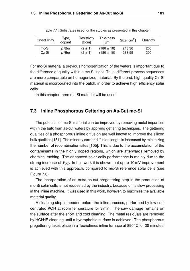
7.3. Inline Phosphorous Gettering on As-Cut mc-Si 101
Table 7.1: Substrates used for the studies as presented in this chapter.
Crystallinity Type,dopant
Resistivity[Ωcm]
Thickness[µm] Size [cm2] Quantity
mc-Si p /Bor (2 ± 1) (180 ± 10) 243.36 200Cz-Si p /Bor (2 ± 1) (180 ± 10) 238.95 200
For mc-Si material a previous homogenization of the wafers is important due tothe difference of quality within a mc-Si ingot. Thus, different process sequencesare more comparable on homogenized material. By the end, high quality Cz-Simaterial is incorporated into the batch, in order to achieve high efficiency solarcells.
In this chapter three mc-Si material will be used.
7.3 Inline Phosphorous Gettering on As-Cut mc-Si
The potential of mc-Si material can be improved by removing metal impuritieswithin the bulk from as-cut wafers by applying gettering techniques. The getteringqualities of a phosphorous inline diffusion are well known to improve the siliconbulk qualities [151]. The minority carrier diffusion length is increased by minimizingthe number of recombination sites [105]. This is due to the accumulation of thecontaminants in the highly doped regions, which are afterwards removed bychemical etching. The enhanced solar cells performance is mainly due to thestrong increase of VOC . In this work it is shown that up to 10 mV improvementis achieved with this approach, compared to mc-Si reference solar cells (seeFigure 7.6).
The incorporation of an extra as-cut pregettering step in the production ofmc-Si solar cells is not requested by the industry, because of its slow processingin the inline machine. It was used in this work, however, to maximize the availablematerial quality.
A cleaning step is needed before the inline process, performed by low con-centrated KOH at room temperature for 3 min. The saw damage remains onthe surface after the short and cold cleaning. The metal residuals are removedby HCl/HF cleaning until a hydrophobic surface is achieved. The phosphorouspregettering takes place in a Tecnofimes inline furnace at 890 C for 20 minutes.
102 Chapter 7: Processing of Rear Passivated Solar Cells
7.4 Surface Roughness of Polished mc-Si Surfaces†
The improvement of polishing techniques for increasing surface quality is stilla goal in the industry. It has been shown that the surface roughness highly influ-ences the device qualities [152]. Lower costs in the industry line require moreefficient processes which imply the use of thinner materials and rear side passi-vation techniques [11]. Furthermore, special requirements on surface treatmentare also necessary, in order to further increase the light trapping [153,154]. Forthis propose the surface is normally textured on the front side, randomizing theinternal light reflection and increasing the internal front reflection [57]. By chemi-cally polishing the rear side the surface qualities for dielectric layer deposition isenhanced, by minimizing surface recombination velocity [155], and increasing theinternal rear reflection. The main results of the work conducted by the experts atthe ISC-Konstanz on chemical etching of silicon surfaces are presented in thissection. The aim of this work is to compare (on mc-Si) the alkaline with the acidpolishing using roughness characterization.
This work has been performed on neighboring mc-Si wafers, which where splitinto two groups. The first group receives an isotropic texture (HF-HNO3) on bothsides, and the second group material is left as-cut (saw damage remains on thesurface). After HCl-HF cleaning, both groups receive a phosphorus inline getteringstep. Each group is split again into two subgroups: one receives alkaline polishing(KOH, anisotropic etching) and the other acidic polishing (HF-HNO3, isotropicetching). The differences are shown by laser scanning microscopy analysispresented in Figure 7.1(a). The results in terms of reflectivity are presented in thenext section. The influence of the etching depth, d , is analyzed on three grainsof the mc-Si material, varying the etching time in order to achieve a depth rangefrom d to 3d . The lifetime of the samples is also characterized. For this purpose,the surfaces are specially cleaned and both sides passivated.
The lifetime is measured (after firing the samples under standard tempera-ture profiles) by the quasi-steady-state photoconductance (QSSPC) techniqueintroduced by Sinton (see reference [156]). This is a well-known technique tocharacterize surface passivation, by determining the bulk minority carrier lifetimein semiconductors, and also allows to predict the open-circuit voltage of solar cellbefore metallization (an important parameter for characterizing solar cells).
†Results reprinted with authorization of Dr. E. Wefringhaus, ISC-Konstanz e.V., and Dr. G.Schubert, Sunways AG.
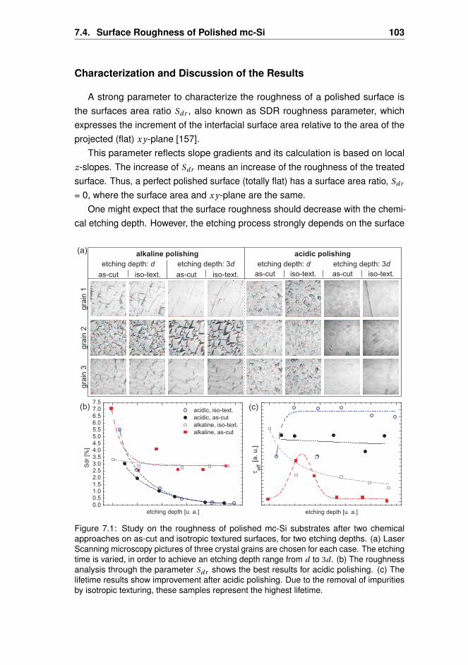
7.4. Surface Roughness of Polished mc-Si 103
Characterization and Discussion of the Results
A strong parameter to characterize the roughness of a polished surface isthe surfaces area ratio Sdr , also known as SDR roughness parameter, whichexpresses the increment of the interfacial surface area relative to the area of theprojected (flat) x y-plane [157].
This parameter reflects slope gradients and its calculation is based on localz-slopes. The increase of Sdr means an increase of the roughness of the treatedsurface. Thus, a perfect polished surface (totally flat) has a surface area ratio, Sdr
= 0, where the surface area and x y-plane are the same.One might expect that the surface roughness should decrease with the chemi-
cal etching depth. However, the etching process strongly depends on the surface
Figure 7.1: Study on the roughness of polished mc-Si substrates after two chemicalapproaches on as-cut and isotropic textured surfaces, for two etching depths. (a) LaserScanning microscopy pictures of three crystal grains are chosen for each case. The etchingtime is varied, in order to achieve an etching depth range from d to 3d . (b) The roughnessanalysis through the parameter Sdr shows the best results for acidic polishing. (c) Thelifetime results show improvement after acidic polishing. Due to the removal of impuritiesby isotropic texturing, these samples represent the highest lifetime.
104 Chapter 7: Processing of Rear Passivated Solar Cells
crystal orientation. As shown in Figure 7.1(b), the surface roughness steadilydecreases with the etching depth for those samples treated with chemical acidicpolishing, as this process is independent on the preceding state of the mc-Sisurface (as-cut or isotropic textured). In a few minutes time, the acidic polishingeasily achieves the minimum roughness Sdr = 0, where all gradients in z-axis areequal [the surface is perfectly smooth as shown in Figure 7.1(a)].
For alkaline polishing the result is peculiar on mc-Si surfaces, where a furtherincrease of etching depth shows no influence on the smoothness of the surface,resulting in a constant value for the roughness (Sdr = 3 %). This is due to theunwanted steps and crevasses caused by alkaline solutions between the grainsof mc-Si surfaces [25]. Therefore, acidic etching solutions are to be used whenpolishing mc-Si surfaces, in order to achieve a near perfect smooth surface.This conclusion is corroborated by the carrier lifetime, which rapidly increaseswhen using isotropic textured surfaces after an acidic etching step, as shown inFigure 7.1(c). The alkaline solutions diminish the lifetime of mc-Si surfaces, whichdecreases further with increasing etching depth. As-cut samples are normallytreated with alkaline solutions for removing saw damage, and Figure 7.1(c) showsan optimal etching depth for this purpose, after which the lifetime is not furtherincreased.
7.5 Reflectivity of Studied Si Surfaces
The reflectivity was measured on different surfaces as shown in Figure 7.2 (allmeasurements under air). Cz-Si material was used for this purpose, generalizingthe reflectivity for one crystal orientation. The reflectivity of intrinsic Si is presentedfirst: the experimental data (polished Si) goes in line with the data of intrinsicSi. The total reflectivity of intrinsic Si shows its minimum at 0.33 at 960 nm. Thetheoretical data for the intrinsic Si obviously assumes a transparent ingot for largewavelengths (λ> 1000 nm), where the improvement of the rear internal reflectionis ignored, which is contrary to the experimental measurement. The improvementby texturing the surface is paramount: the reflection is decreased by 22 % from areflectivity of 0.33 for intrinsic Si to a reflectivity of 0.10 for textured samples, at960 nm. As shown in the same Figure, when polishing the rear side of a texturedsample, the specular internal rear reflection for long wavelengths is increased(compare red circle with black square in Figure 7.2)‡.
‡Remember that the absorption of Si shows that, above 1000 nm, the rear side of a 150 µm devicecan be characterized.
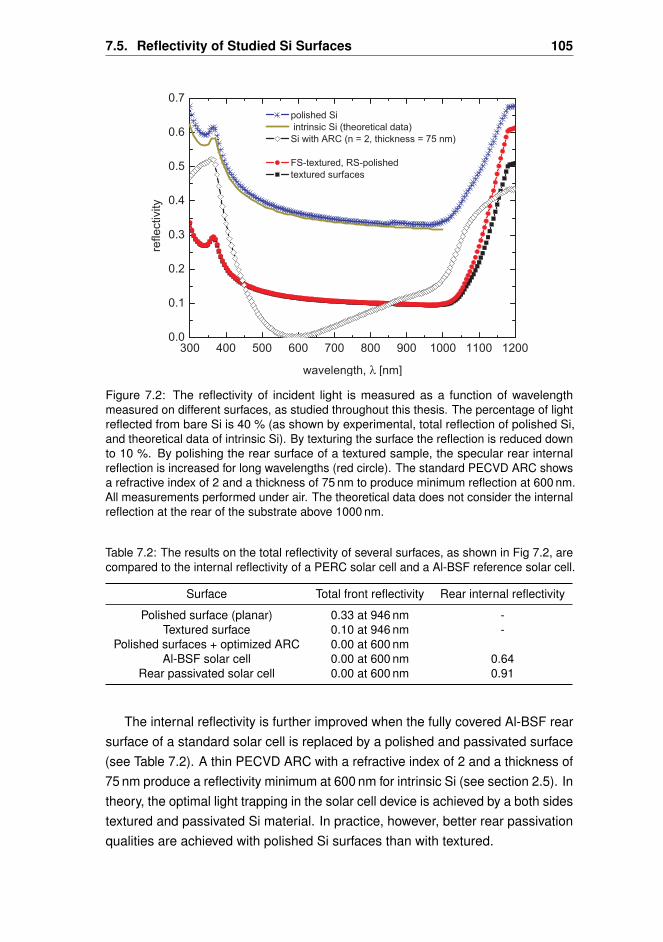
7.5. Reflectivity of Studied Si Surfaces 105
Figure 7.2: The reflectivity of incident light is measured as a function of wavelengthmeasured on different surfaces, as studied throughout this thesis. The percentage of lightreflected from bare Si is 40 % (as shown by experimental, total reflection of polished Si,and theoretical data of intrinsic Si). By texturing the surface the reflection is reduced downto 10 %. By polishing the rear surface of a textured sample, the specular rear internalreflection is increased for long wavelengths (red circle). The standard PECVD ARC showsa refractive index of 2 and a thickness of 75 nm to produce minimum reflection at 600 nm.All measurements performed under air. The theoretical data does not consider the internalreflection at the rear of the substrate above 1000 nm.
Table 7.2: The results on the total reflectivity of several surfaces, as shown in Fig 7.2, arecompared to the internal reflectivity of a PERC solar cell and a Al-BSF reference solar cell.
Surface Total front reflectivity Rear internal reflectivity
Polished surface (planar) 0.33 at 946 nm -Textured surface 0.10 at 946 nm -
Polished surfaces + optimized ARC 0.00 at 600 nmAl-BSF solar cell 0.00 at 600 nm 0.64
Rear passivated solar cell 0.00 at 600 nm 0.91
The internal reflectivity is further improved when the fully covered Al-BSF rearsurface of a standard solar cell is replaced by a polished and passivated surface(see Table 7.2). A thin PECVD ARC with a refractive index of 2 and a thickness of75 nm produce a reflectivity minimum at 600 nm for intrinsic Si (see section 2.5). Intheory, the optimal light trapping in the solar cell device is achieved by a both sidestextured and passivated Si material. In practice, however, better rear passivationqualities are achieved with polished Si surfaces than with textured.
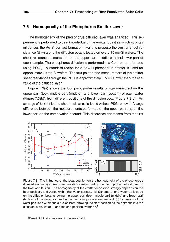
106 Chapter 7: Processing of Rear Passivated Solar Cells
7.6 Homogeneity of the Phosphorus Emitter Layer
The homogeneity of the phosphorus diffused layer was analyzed. This ex-periment is performed to gain knowledge of the emitter qualities which stronglyinfluences the Ag-Si contact formation. For this propose the emitter sheet re-sistance (RSH ) along the diffusion boat is tested on every 10 mc-Si wafers. Thesheet resistance is measured on the upper part, middle part and lower part ofeach sample. The phosphorus diffusion is performed in a Centrotherm furnaceusing POCl3. A standard recipe for a 65Ω/ä phosphorus emitter is used forapproximate 70 mc-Si wafers. The four point probe measurement of the emittersheet resistance through the PSG is approximately ± 5 Ω/ä lower than the realvalue of the diffused layer.
Figure 7.3(a) shows the four point probe results of RSH measured on theupper part (top), middle part (middle), and lower part (bottom) of each wafer(Figure 7.3(b)), from different positions of the diffusion boat (Figure 7.3(c)). Anaverage of 64Ω/ä for the sheet resistance is found without PSG removal. A largedifference between the measurements performed on the upper part and on thelower part on the same wafer is found. This difference decreases from the first
Figure 7.3: The influence of the boat position on the homogeneity of the phosphorousdiffused emitter layer. (a) Sheet resistance measured by four point probe method throughthe boat of diffusion. The homogeneity of the emitter deposition strongly depends on theboat position, and varies within the wafer surface. (b) Schema of one wafer as locatedon the diffusion boat, showing the upper part (top), middle part (middle) and lower part(bottom) of the wafer, as used in the four point probe measurement. (c) Schematic of thewafer positions within the diffusion boat, showing the start position as the entrance into thediffusion oven, wafer 1, and the end position, wafer 67.¶
¶Result of 13 cells processed in the same batch.
7.7. Silver Pad Metallization for Module Assembly 107
wafer to the last one in almost 25 %.The inhomogeneity of the sheet resistance is also remarkable along the boat.
Absolut values vary from (64.79 ± 1.52) Ω/ä on the lower part, (62.31 ± 1.51) Ω/äin the middle part, and (59.95 ± 1.06) Ω/ä on the upper part. A stronger diffusionis found on the upper part of the wafers than on the lower part, because the boataffects the flow of gas.
In conclusion, the sheet resistance of the deposited emitter used in this studymight vary with a difference of ± 5 Ω/ä from the lower part to the upper part of thewafer. This difference needs to be taken into account when the contact formationof Ag pastes on the front side emitter is studied. It also influences the quality ofthe front side passivation, bulk gettering, and lifetime.
In order to overcome such inhomogeneities, another boat could be used or thewafers could be positioned more separately on the boat, allowing the gasses toreach the middle and lower part. This inhomogeneity could also be overcome byselective emitter concepts, using a second diffusion through oxide barriers withorientation dependent growth [158] Nevertheless, a variation of ± 5Ω/ä throughthe front surface of the wafer can be tolerated (within the tolerance of the deviceused).
7.7 Silver Pad Metallization for Module Assembly
In order to facilitate module assembly in industrial applications, solder padshave to be incorporated on the Al rear contact, parallel to the busbars on the front(see for instance references [159,160]). For rear passivated solar cells, the padsshould be screen printed directly on the passivation layer, and incorporated in themetallization process before the printing of the thick Al layer. The Al layer fullycovers the entire rear surface except the Ag pads. The Ag pads should not firethrough the dielectric layer, and therefore, the Ag paste should be low aggressiveagainst the dielectric.
The goal of this section is to study the impact of the Ag pads on the rear surfacepassivation. An Ag paste is used which shows small tendency to fire through therear PECVD stack. Three tests are performed: (a) the peel off test, (b) the impactof the Ag pads on the lifetime, and (c) the analysis of the penetration of the Agpads into the dielectric. Due to the high density of the paste [Figure 7.4(left)] andmaybe due to the homogeneous distribution of the glass content, the Ag padsremain on the dielectric layer, after sintering.
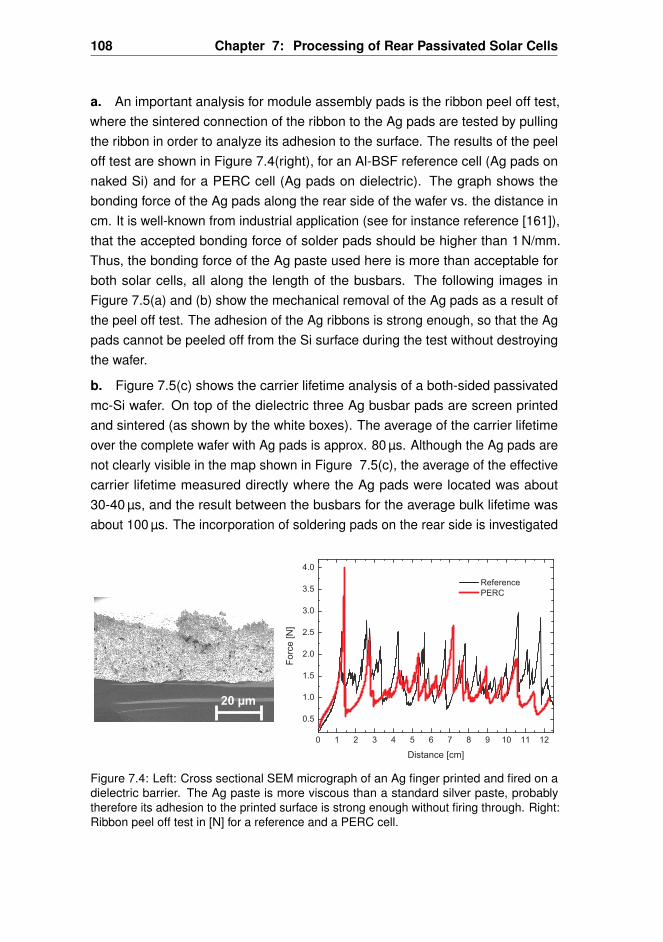
108 Chapter 7: Processing of Rear Passivated Solar Cells
a. An important analysis for module assembly pads is the ribbon peel off test,where the sintered connection of the ribbon to the Ag pads are tested by pullingthe ribbon in order to analyze its adhesion to the surface. The results of the peeloff test are shown in Figure 7.4(right), for an Al-BSF reference cell (Ag pads onnaked Si) and for a PERC cell (Ag pads on dielectric). The graph shows thebonding force of the Ag pads along the rear side of the wafer vs. the distance incm. It is well-known from industrial application (see for instance reference [161]),that the accepted bonding force of solder pads should be higher than 1 N/mm.Thus, the bonding force of the Ag paste used here is more than acceptable forboth solar cells, all along the length of the busbars. The following images inFigure 7.5(a) and (b) show the mechanical removal of the Ag pads as a result ofthe peel off test. The adhesion of the Ag ribbons is strong enough, so that the Agpads cannot be peeled off from the Si surface during the test without destroyingthe wafer.
b. Figure 7.5(c) shows the carrier lifetime analysis of a both-sided passivatedmc-Si wafer. On top of the dielectric three Ag busbar pads are screen printedand sintered (as shown by the white boxes). The average of the carrier lifetimeover the complete wafer with Ag pads is approx. 80 µs. Although the Ag pads arenot clearly visible in the map shown in Figure 7.5(c), the average of the effectivecarrier lifetime measured directly where the Ag pads were located was about30-40 µs, and the result between the busbars for the average bulk lifetime wasabout 100 µs. The incorporation of soldering pads on the rear side is investigated
Figure 7.4: Left: Cross sectional SEM micrograph of an Ag finger printed and fired on adielectric barrier. The Ag paste is more viscous than a standard silver paste, probablytherefore its adhesion to the printed surface is strong enough without firing through. Right:Ribbon peel off test in [N] for a reference and a PERC cell.
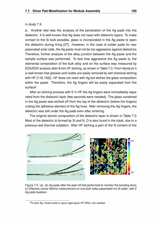
7.7. Silver Pad Metallization for Module Assembly 109
in study 7.9.
c. Another test was the analysis of the penetration of the Ag pads into thedielectric. It is well-known that Ag does not react with dielectric layers. To makecontact to the Si bulk possible, glass is incorporated in the Ag paste to openthe dielectric during firing [37]. However, in the case of solder pads for rearpassivated solar cells, the Ag paste must not be too aggressive against dielectrics.Therefore, further analysis of the alloy junction between the Ag paste and thesample surface was performed. To test how aggressive the Ag paste is, theelemental composition of the bulk alloy and on the surface was measured byEDS/EDX analysis after 8 min HF etching, as shown in Table 7.3. From literature itis well-known that glasses and oxides are easily removed by wet chemical etchingwith HF [118,162]). HF does not react with Ag but etches the glass compositionwithin the paste. Therefore, the Ag fingers will be easily separated from thesurface||.
After an etching process with 5 % HF the Ag fingers were immediately sepa-rated from the dielectric layer (few seconds were needed). The glass containedin the Ag paste was etched off from the top of the dielectric (below the fingers)cutting the adhesive element of the Ag lines. After removing the Ag fingers, thedielectric was still under the Ag pads even after sintering.
The original atomic composition of the dielectric layer is shown in Table 7.3.Most of the dielectric is formed by Si and N. O is also found in the stack, due to aprevious wet thermal oxidation. After HF etching a part of the N content of the
Figure 7.5: (a), (b) Ag pads after the peel off test performed to monitor the bonding force.(c) Effective carrier lifetime measurement on one both sides passivated mc-Si wafer, with 2Ag pads busbars.
||To etch Ag, mixed acids or aqua regia types HF:HNO3 are needed.
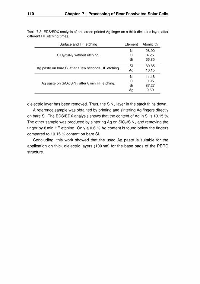
110 Chapter 7: Processing of Rear Passivated Solar Cells
Table 7.3: EDS/EDX analysis of an screen printed Ag finger on a thick dielectric layer, afterdifferent HF etching times.
Surface and HF etching Element Atomic %
SiO2/SiNx without etching.N 28.90O 4.25Si 66.85
Ag paste on bare Si after a few seconds HF etching. Si 89.85Ag 10.15
Ag paste on SiO2/SiNx after 8 min HF etching.
N 11.18O 0.95Si 87.27Ag 0.60
dielectric layer has been removed. Thus, the SiNx layer in the stack thins down.A reference sample was obtained by printing and sintering Ag fingers directly
on bare Si. The EDS/EDX analysis shows that the content of Ag in Si is 10.15 %.The other sample was produced by sintering Ag on SiO2/SiNx and removing thefinger by 8 min HF etching. Only a 0.6 % Ag content is found below the fingerscompared to 10.15 % content on bare Si.
Concluding, this work showed that the used Ag paste is suitable for theapplication on thick dielectric layers (100 nm) for the base pads of the PERCstructure.
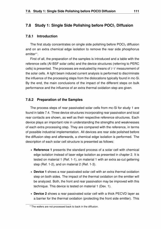
7.8. Study 1: Single Side Polishing before POCl3 Diffusion 111
7.8 Study 1: Single Side Polishing before POCl3 Diffusion
7.8.1 Introduction
The first study concentrates on single side polishing before POCl3 diffusionand on an extra chemical edge isolation to remove the rear side phosphorusemitter**.
First of all, the preparation of the samples is introduced and a table with thereference cells (Al-BSF solar cells) and the device structures (referring to PERCcells) is presented. The processes are evaluated by means of I -V measurement ofthe solar cells. A light beam induced current analysis is performed to discriminatethe influence of the processing steps from the dislocations typically found in mc-Si.By the end, the main conclusions of the impact of the different steps on bulkperformance and the influence of an extra thermal oxidation step are given.
7.8.2 Preparation of the Samples
The process steps of rear passivated solar cells from mc-Si for study 1 arefound in table 7.4. Three device structures incorporating rear passivation and localrear contacts are shown, as well as their respective reference structures. Eachdevice plays an important role in understanding the strengths and weaknessesof each extra processing step. They are compared with the reference, in termsof possible industrial implementation. All devices are rear side polished beforethe diffusion step and afterwards, a chemical edge isolation is performed. Thedescription of each solar cell structure is presented as follows:
• Reference 1 presents the standard process of a solar cell with chemicaledge isolation instead of laser edge isolation as presented in chapter 2. It istested on material 1 (Ref. 1-1), on material 1 with an extra as-cut getteringstep (Ref. 1-2), and on material 2 (Ref. 1-3).
• Device 1 shows a rear passivated solar cell with an extra thermal oxidationstep on both sides. The impact of the thermal oxidation on the emitter willbe analyzed. Both, the front and rear passivation may be improved with thistechnique. This device is tested on material 1 (Dev. 1).
• Device 2 shows a rear passivated solar cell with a thick PECVD layer asa barrier for the thermal oxidation (protecting the front side emitter). This
**The wafers are not processed back to back in the diffusion.
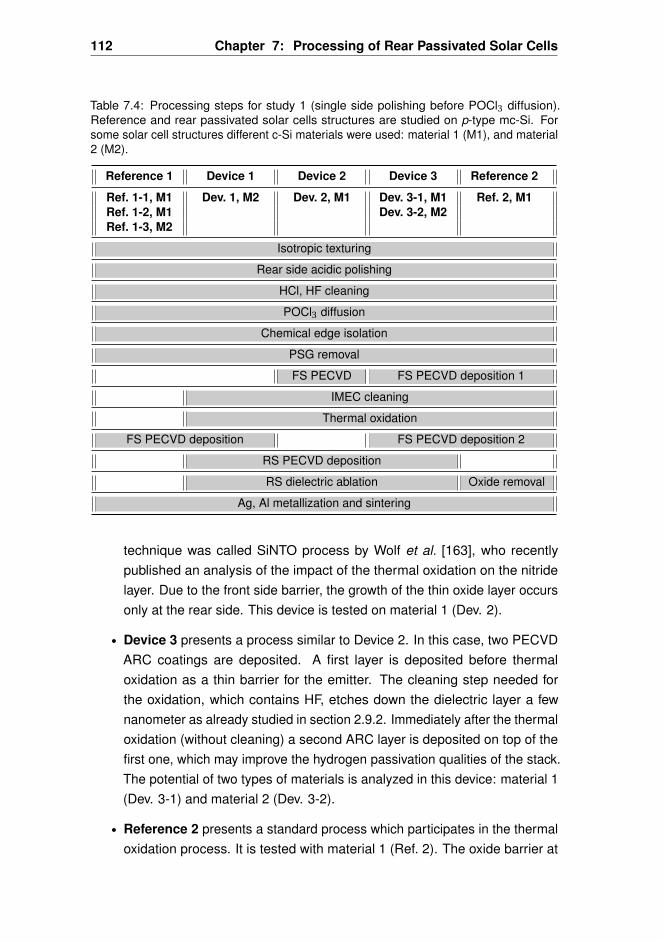
112 Chapter 7: Processing of Rear Passivated Solar Cells
Table 7.4: Processing steps for study 1 (single side polishing before POCl3 diffusion).Reference and rear passivated solar cells structures are studied on p-type mc-Si. Forsome solar cell structures different c-Si materials were used: material 1 (M1), and material2 (M2).
Reference 1 Device 1 Device 2 Device 3 Reference 2
Ref. 1-1, M1 Dev. 1, M2 Dev. 2, M1 Dev. 3-1, M1 Ref. 2, M1Ref. 1-2, M1 Dev. 3-2, M2Ref. 1-3, M2
Isotropic texturing
Rear side acidic polishing
HCl, HF cleaning
POCl3 diffusion
Chemical edge isolation
PSG removal
FS PECVD FS PECVD deposition 1
IMEC cleaning
Thermal oxidation
FS PECVD deposition FS PECVD deposition 2
RS PECVD deposition
RS dielectric ablation Oxide removal
Ag, Al metallization and sintering
technique was called SiNTO process by Wolf et al. [163], who recentlypublished an analysis of the impact of the thermal oxidation on the nitridelayer. Due to the front side barrier, the growth of the thin oxide layer occursonly at the rear side. This device is tested on material 1 (Dev. 2).
• Device 3 presents a process similar to Device 2. In this case, two PECVDARC coatings are deposited. A first layer is deposited before thermaloxidation as a thin barrier for the emitter. The cleaning step needed forthe oxidation, which contains HF, etches down the dielectric layer a fewnanometer as already studied in section 2.9.2. Immediately after the thermaloxidation (without cleaning) a second ARC layer is deposited on top of thefirst one, which may improve the hydrogen passivation qualities of the stack.The potential of two types of materials is analyzed in this device: material 1(Dev. 3-1) and material 2 (Dev. 3-2).
• Reference 2 presents a standard process which participates in the thermaloxidation process. It is tested with material 1 (Ref. 2). The oxide barrier at
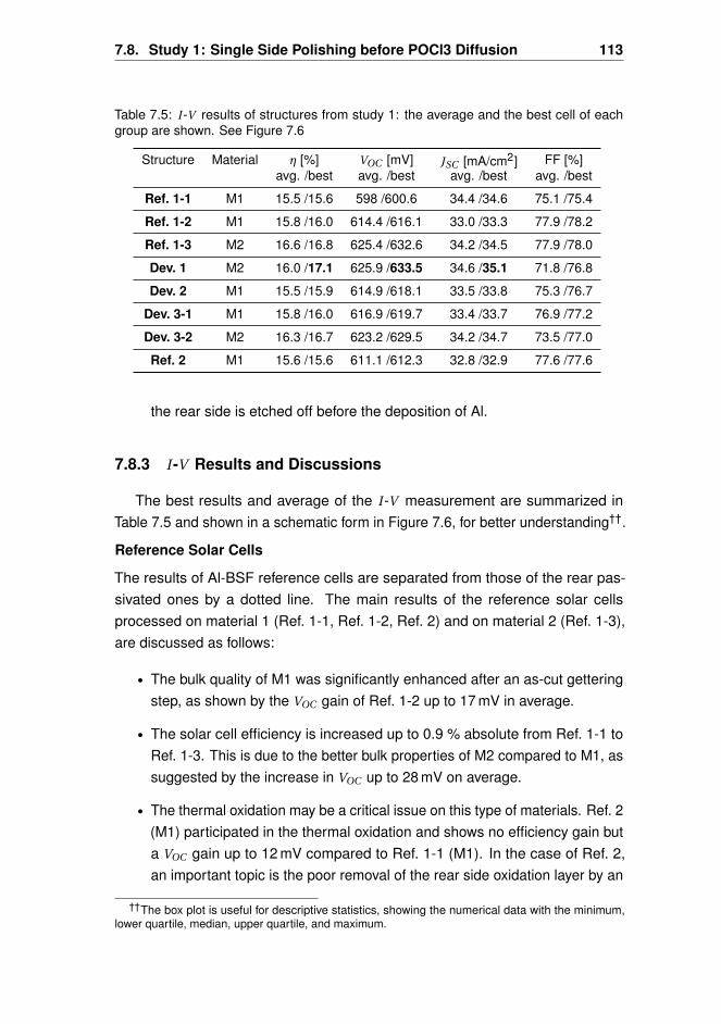
7.8. Study 1: Single Side Polishing before POCl3 Diffusion 113
Table 7.5: I -V results of structures from study 1: the average and the best cell of eachgroup are shown. See Figure 7.6
Structure Material η [%] VOC [mV] JSC [mA/cm2] FF [%]avg. /best avg. /best avg. /best avg. /best
Ref. 1-1 M1 15.5 /15.6 598 /600.6 34.4 /34.6 75.1 /75.4
Ref. 1-2 M1 15.8 /16.0 614.4 /616.1 33.0 /33.3 77.9 /78.2
Ref. 1-3 M2 16.6 /16.8 625.4 /632.6 34.2 /34.5 77.9 /78.0
Dev. 1 M2 16.0 /17.1 625.9 /633.5 34.6 /35.1 71.8 /76.8
Dev. 2 M1 15.5 /15.9 614.9 /618.1 33.5 /33.8 75.3 /76.7
Dev. 3-1 M1 15.8 /16.0 616.9 /619.7 33.4 /33.7 76.9 /77.2
Dev. 3-2 M2 16.3 /16.7 623.2 /629.5 34.2 /34.7 73.5 /77.0
Ref. 2 M1 15.6 /15.6 611.1 /612.3 32.8 /32.9 77.6 /77.6
the rear side is etched off before the deposition of Al.
7.8.3 I -V Results and Discussions
The best results and average of the I -V measurement are summarized inTable 7.5 and shown in a schematic form in Figure 7.6, for better understanding††.
Reference Solar Cells
The results of Al-BSF reference cells are separated from those of the rear pas-sivated ones by a dotted line. The main results of the reference solar cellsprocessed on material 1 (Ref. 1-1, Ref. 1-2, Ref. 2) and on material 2 (Ref. 1-3),are discussed as follows:
• The bulk quality of M1 was significantly enhanced after an as-cut getteringstep, as shown by the VOC gain of Ref. 1-2 up to 17 mV in average.
• The solar cell efficiency is increased up to 0.9 % absolute from Ref. 1-1 toRef. 1-3. This is due to the better bulk properties of M2 compared to M1, assuggested by the increase in VOC up to 28 mV on average.
• The thermal oxidation may be a critical issue on this type of materials. Ref. 2(M1) participated in the thermal oxidation and shows no efficiency gain buta VOC gain up to 12 mV compared to Ref. 1-1 (M1). In the case of Ref. 2,an important topic is the poor removal of the rear side oxidation layer by an
††The box plot is useful for descriptive statistics, showing the numerical data with the minimum,lower quartile, median, upper quartile, and maximum.
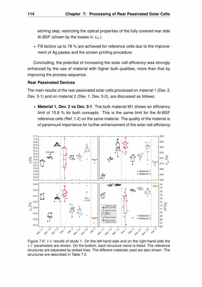
114 Chapter 7: Processing of Rear Passivated Solar Cells
etching step, restricting the optical properties of the fully covered rear sideAl-BSF (shown by the losses in JSC ).
• Fill factors up to 78 % are achieved for reference cells due to the improve-ment of Ag pastes and the screen printing procedure.
Concluding, the potential of increasing the solar cell efficiency was stronglyenhanced by the use of material with higher bulk qualities, more than that byimproving the process sequence.
Rear Passivated Devices
The main results of the rear passivated solar cells processed on material 1 (Dev. 2,Dev. 3-1) and on material 2 (Dev. 1, Dev. 3-2), are discussed as follows:
• Material 1, Dev. 2 vs Dev. 3-1. The bulk material M1 shows an efficiencylimit of 15.8 % for both concepts. This is the same limit for the Al-BSFreference cells (Ref. 1-2) on the same material. The quality of the material isof paramount importance for further enhancement of the solar cell efficiency.
Figure 7.6: I -V results of study 1. On the left-hand side and on the right-hand side theI -V parameters are shown. On the bottom, each structure name is listed. The referencestructures are separated by dotted lines. The different materials used are also shown. Thestructures are described in Table 7.5.
7.8. Study 1: Single Side Polishing before POCl3 Diffusion 115
It seems that the properties of the SiNx layer are diminished by a thermalbudget, and that a second deposition after the oxidation may improve itsqualities. This difference, however, is not clear with M1.
• Material 2, Dev. 1 vs Dev. 3-2. Although the incorporation of a PECVD bar-rier on the front side to protect the emitter from the thermal oxidation meansan extra processing step, nevertheless, a more homogeneous process isachieved, as shown by Dev. 3-2 compared to Dev. 1. Both structures, Dev. 1and Dev. 3-2, show the highest JSC and VOC results, with promising high FF.The properties of M2 are beyond the potential limit of M1. Nevertheless, nolarge improvement is found compared to the reference Ref. 1-3 on the samematerial.
• Record cell of Dev. 1. Although a remarkable inhomogeneity in terms ofthe efficiency is found within the process of Dev. 1, a high efficiency upto 17.1 % on rear passivated p-type mc-Si solar cell was achieved withthis process, using standard screen printing metallization pastes and bulkmaterial M2. This result presents the record of the whole batch of study1, mainly due to the high JSC up to 35.1 mA/cm2 and VOC up to 633.5 mV.Nevertheless, a large variation in the FF result is remarkable, due to thedifference within the metallization process and bulk material of the mc-Siingot used (this difference is fully studied in section 7.9.4).
• The main result when comparing the references and the rear passivateddevices is the improvement of JSC up to 0.4 mA/cm2 for Dev. 1 comparedwith Ref. 1-3, mainly due to the thermal oxidation on both sides.
• The losses in FF for the rear passivated cells compared to the referencesare remarkable. This can be explained by the series resistance losses fromthe local contact at the rear side.
To draw a conclusion it has to be stated, that the best cell concept for rearpassivated solar cells within this study is achieved by both processes: firstly, by athermal oxidation on both sides of the material (directly on the front side emitterand on the polished rear surface); and secondly, by a deposition only on therear side, protecting the emitter with a PECVD barrier and adding an extra frontPECVD layer after thermal oxidation.
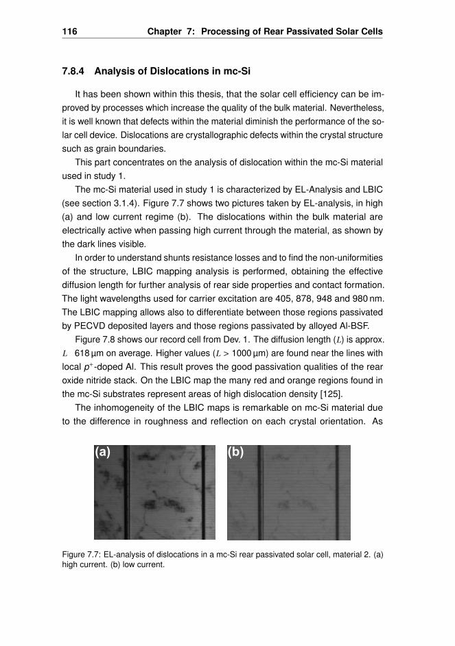
116 Chapter 7: Processing of Rear Passivated Solar Cells
7.8.4 Analysis of Dislocations in mc-Si
It has been shown within this thesis, that the solar cell efficiency can be im-proved by processes which increase the quality of the bulk material. Nevertheless,it is well known that defects within the material diminish the performance of the so-lar cell device. Dislocations are crystallographic defects within the crystal structuresuch as grain boundaries.
This part concentrates on the analysis of dislocation within the mc-Si materialused in study 1.
The mc-Si material used in study 1 is characterized by EL-Analysis and LBIC(see section 3.1.4). Figure 7.7 shows two pictures taken by EL-analysis, in high(a) and low current regime (b). The dislocations within the bulk material areelectrically active when passing high current through the material, as shown bythe dark lines visible.
In order to understand shunts resistance losses and to find the non-uniformitiesof the structure, LBIC mapping analysis is performed, obtaining the effectivediffusion length for further analysis of rear side properties and contact formation.The light wavelengths used for carrier excitation are 405, 878, 948 and 980 nm.The LBIC mapping allows also to differentiate between those regions passivatedby PECVD deposited layers and those regions passivated by alloyed Al-BSF.
Figure 7.8 shows our record cell from Dev. 1. The diffusion length (L) is approx.L 618 µm on average. Higher values (L > 1000 µm) are found near the lines withlocal p+-doped Al. This result proves the good passivation qualities of the rearoxide nitride stack. On the LBIC map the many red and orange regions found inthe mc-Si substrates represent areas of high dislocation density [125].
The inhomogeneity of the LBIC maps is remarkable on mc-Si material dueto the difference in roughness and reflection on each crystal orientation. As
(a) (b)
Figure 7.7: EL-analysis of dislocations in a mc-Si rear passivated solar cell, material 2. (a)high current. (b) low current.
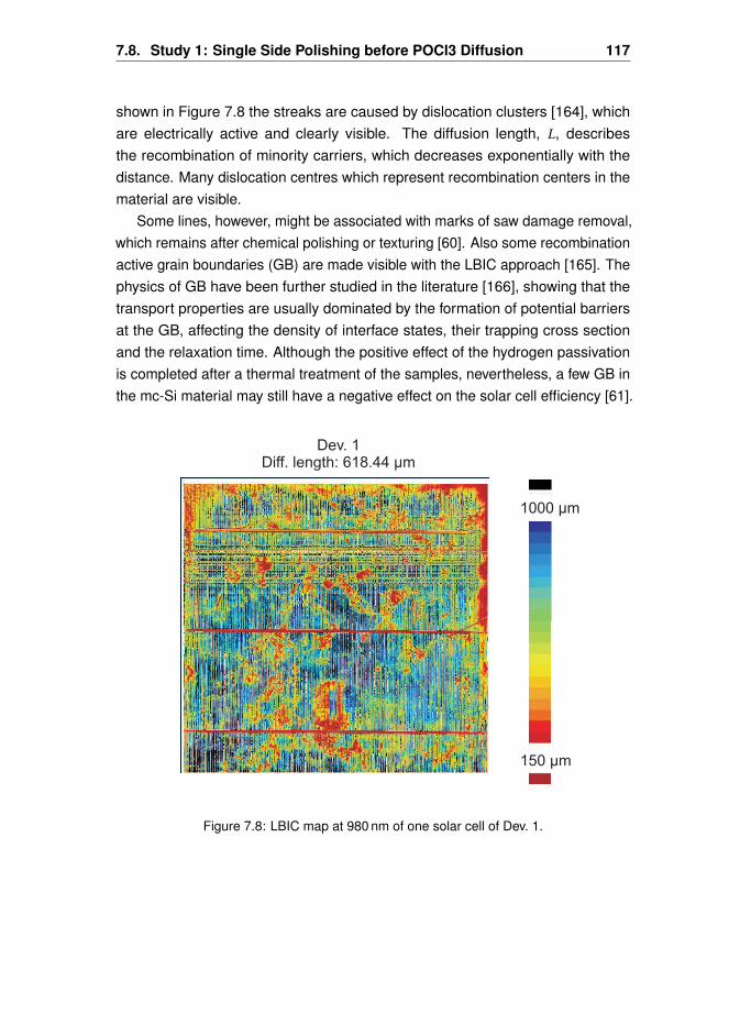
7.8. Study 1: Single Side Polishing before POCl3 Diffusion 117
shown in Figure 7.8 the streaks are caused by dislocation clusters [164], whichare electrically active and clearly visible. The diffusion length, L, describesthe recombination of minority carriers, which decreases exponentially with thedistance. Many dislocation centres which represent recombination centers in thematerial are visible.
Some lines, however, might be associated with marks of saw damage removal,which remains after chemical polishing or texturing [60]. Also some recombinationactive grain boundaries (GB) are made visible with the LBIC approach [165]. Thephysics of GB have been further studied in the literature [166], showing that thetransport properties are usually dominated by the formation of potential barriersat the GB, affecting the density of interface states, their trapping cross sectionand the relaxation time. Although the positive effect of the hydrogen passivationis completed after a thermal treatment of the samples, nevertheless, a few GB inthe mc-Si material may still have a negative effect on the solar cell efficiency [61].
Dev. 1Diff. length: 618.44 µm
150 µm
1000 µm
Figure 7.8: LBIC map at 980 nm of one solar cell of Dev. 1.

118 Chapter 7: Processing of Rear Passivated Solar Cells
7.8.5 Summary and Conclusions
A promising average efficiency up to 16.8 % was achieved with Al-BSF solarcells on mc-Si material 2. The phosphorous gettering increases the bulk qualitiesof the mc-Si material. The record cell 17.1 % was achieved with oxide on bothsides, emitter and rear, and obtained with mc-Si material 2. The rear was singleside polished. Nevertheless, high inhomogeneities are found within this process,maybe due to the impact of the thermal oxidation on the mc-Si material qualities.The achievement of high efficiency on mc-Si material is not obvious and the PERCconcepts still have a large potential and they need further optimization.
7.9. Study 2: Front Side Emitter Masking Approach 119
7.9 Study 2: Front Side Emitter Masking Approach
7.9.1 Introduction
Another process sequence for solar cells with polished and passivated rearside is presented and discussed. The front side phosphorus diffused layer (stillwith PSG) is masked by a special screen printable paste, in order to protect itfrom chemical etching.
This approach allows two processes at the same time: the polishing of thesurface and the isolation of the rear side emitter. It has been shown in this thesis,that an acidic polishing of isotropic textured surface provides the highest effectivecarrier lifetime for mc-Si material (etching depth 3d , see section 7.4). Thus, thesmoothness of the surface is an important factor for the deposition of the dielectriclayer. When etching the unprotected rear the phosphorous layer is removed,saving the chemical edge isolation as presented in section 7.8.
In the following section also a thermal oxidation is used. Although no mod-ules were made, the impact of Ag pads for module assembly within the rearmetallization layer on the cell efficiency is studied.
7.9.2 Preparation of the Samples
The processing of rear passivated solar cells from mc-Si for the study 2 issummarized in table 7.6. Two device structures with rear passivation and localrear contacts are shown, as well as their respective Al-BSF reference cells.
• Reference 3 presents a reference for Device 4. It receives the same basetreatment, with the exception of a fully covered Al rear side. The front sideemitter is protected from a single side polishing by a masking approach.The rear side is fully covered by an Al rear side. Its performance is testedon two base materials: Ref. 3-1 (on material 2), and Ref. 3-2 (on material 3).
• Device 4 presents a rear passivated solar cell with a thermal oxide nitridestack on both sides for passivation. Its performance is tested on two basematerials: Dev. 4-1 on material 3, and Dev. 4-2 on material 2. Dev. 4-1was also tested on thinner material with a single side polishing depth of 3d .However, due to the un-optimized firing parameters for thinner materials theperformance was low, and, therefore, the results are not shown here (seethe FF analysis in 7.9.4). For Dev. 4-1 Ag pads were incorporated on the

120 Chapter 7: Processing of Rear Passivated Solar Cells
Table 7.6: Processing steps for study 2 (front side emitter masking approach). Referenceand rear passivated solar cells structures are studied on p-type mc-Si. For some solar cellstructures different c-Si materials were used: material 2 (M2), and material 3 (M3).
Reference 3 Device 4 Reference 4
Ref. 3-1, M2 Dev. 4-1, M3 Ref. 4, M2Ref. 3-2, M3 Dev. 4-2, M2
Texture ∼ 10 µm
HCl, HF cleaning
POCl3 diffusion
FS mask deposition
Rear side polishing ∼ 10 µm
FS mask removal
PSG removal
FS PECVD deposition
IMEC cleaning
Thermal oxidation
FS PECVD deposition
RS PECVD deposition
RS dielectric ablation
Ag, Al metallization and sintering
Table 7.7: I -V results of structures from study 2. See Figure 7.9
Structure Material JSC [mA/cm2] VOC [mV] FF [%] η [%]avg. /best avg. /best avg. /best avg. /best
Ref. 3-1 M2 33.6 /33.8 619.3 /619.9 78.0 /78.6 16.3 /16.5
Ref. 3-2 M3 34.5 /34.6 624.8 /626.4 77.7 /78.3 16.7 /17.0
Dev. 4-1 M3 33.5 /34.2 612.0 /619.5 77.4 /77.8 15.9 /16.5
Dev. 4-2 M2 33.7 /34.6 620.5 /627.7 78.1 /78.9 16.3 /17.0
Ref. 4 M2 34.5 /34.5 622.1 /625.0 76.8 /78.7 16.5 /17.0
rear for module assembly. As discussed in study 1, the Ag paste used forpads has no diminishing effect on the performance of the solar cell device.
• Reference 4. All structures are front side masked except Reference 4 whichpresents actually an industrial standard process for mc-Si.
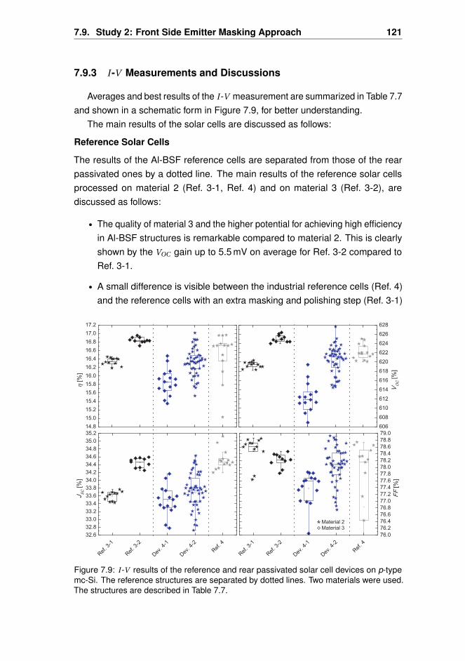
7.9. Study 2: Front Side Emitter Masking Approach 121
7.9.3 I -V Measurements and Discussions
Averages and best results of the I -V measurement are summarized in Table 7.7and shown in a schematic form in Figure 7.9, for better understanding.
The main results of the solar cells are discussed as follows:
Reference Solar Cells
The results of the Al-BSF reference cells are separated from those of the rearpassivated ones by a dotted line. The main results of the reference solar cellsprocessed on material 2 (Ref. 3-1, Ref. 4) and on material 3 (Ref. 3-2), arediscussed as follows:
• The quality of material 3 and the higher potential for achieving high efficiencyin Al-BSF structures is remarkable compared to material 2. This is clearlyshown by the VOC gain up to 5.5 mV on average for Ref. 3-2 compared toRef. 3-1.
• A small difference is visible between the industrial reference cells (Ref. 4)and the reference cells with an extra masking and polishing step (Ref. 3-1)
Figure 7.9: I -V results of the reference and rear passivated solar cell devices on p-typemc-Si. The reference structures are separated by dotted lines. Two materials were used.The structures are described in Table 7.7.
122 Chapter 7: Processing of Rear Passivated Solar Cells
on material 2, mainly, due to a gain in JSC and VOC . Thus, the extra maskingand polishing step does improve the Al-BSF solar cell concept of this study.
Rear Passivated Devices
The main results of the rear passivated solar cells processed on material 2(Dev. 4-2) and on material 3 (Dev. 4-1), are discussed as follows:
• In this study, a record efficiency up to 17.0 % was achieved by both, theAl-BSF solar cells of Ref. 3-2 and Ref. 4, and by the rear passivated solarcell of Dev. 4-2. Hence, no improvement of the solar cell performance bythe rear passivated solar cell concept can be detected.
• The rear passivated solar cells do not show an increase in efficiency, whentested on material 3. On the contrary, better results are achieved withmaterial 2, as shown by Dev. 4-2 compared to Dev. 4-1. Most likely thethermal oxidation had a strong impact on material 3, diminishing its materialquality.
• Generally, in Device 4 a larger inhomogeneity of JSC is visible, comparedto Al-BSF structures. This may be due to the non-optimized rear surfacepassivation as a possible source of shunt at the rear side. Therefore, astudy on the bias dependence for Dev. 4-1 will be performed in the followingsection, for a deeper understanding of the loss properties by shunt on therear side passivation.
• A promising result is shown by Dev. 4-2 where Ag pads were incorporated onthe rear. High efficiency and FF were achieved what shows that the impactof Ag pads on the rear dielectric surface does not diminish the performanceof the solar cell structure.
• An extremely high variation in FF is found for Dev. 4-1, Dev. 4-2 and Ref. 4,however. The lowest FF results are found for Dev. 4-1, with an averageof 77.4 %, compared to 78.1 % for Dev. 4-2. In the following section, acloser look at the FF variation for Dev. 4-1 will be taken, comparing it to thereference Ref. 3-2 which was processed in the same batch. It is extremelyimportant to understand the losses in FF in this type of solar cells, wherethe potential to achieve high efficiency is not yet visible in study 2.
In conclusion, all devices produced on material 3 were limited by materialquality. The Ag pads did not diminish the performance of the rear passivatedsolar cell. Masking the front side emitter before the rear side polishing is an
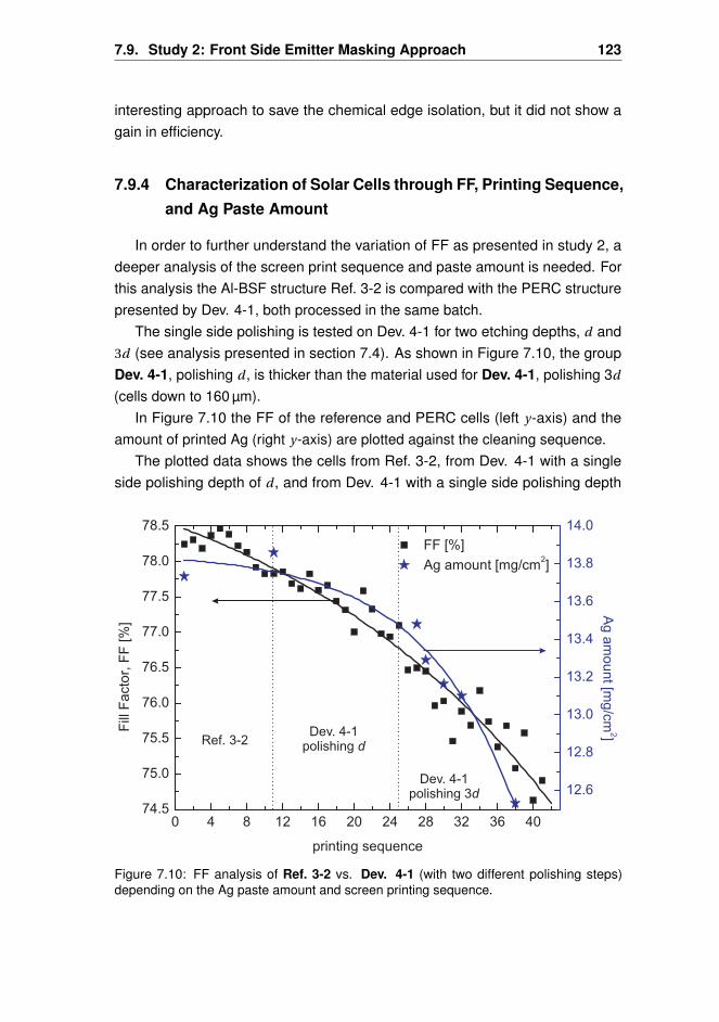
7.9. Study 2: Front Side Emitter Masking Approach 123
interesting approach to save the chemical edge isolation, but it did not show again in efficiency.
7.9.4 Characterization of Solar Cells through FF, Printing Sequence,and Ag Paste Amount
In order to further understand the variation of FF as presented in study 2, adeeper analysis of the screen print sequence and paste amount is needed. Forthis analysis the Al-BSF structure Ref. 3-2 is compared with the PERC structurepresented by Dev. 4-1, both processed in the same batch.
The single side polishing is tested on Dev. 4-1 for two etching depths, d and3d (see analysis presented in section 7.4). As shown in Figure 7.10, the groupDev. 4-1, polishing d , is thicker than the material used for Dev. 4-1, polishing 3d
(cells down to 160 µm).In Figure 7.10 the FF of the reference and PERC cells (left y-axis) and the
amount of printed Ag (right y-axis) are plotted against the cleaning sequence.The plotted data shows the cells from Ref. 3-2, from Dev. 4-1 with a single
side polishing depth of d , and from Dev. 4-1 with a single side polishing depth
Figure 7.10: FF analysis of Ref. 3-2 vs. Dev. 4-1 (with two different polishing steps)depending on the Ag paste amount and screen printing sequence.
124 Chapter 7: Processing of Rear Passivated Solar Cells
of 3d . As mentioned in the last section, the I -V characteristic of Dev. 4-1 with apolishing depth of 3d were not shown in Figure 7.9.
The Ag paste is applied on a grid area of approx. 15.8 cm2‡‡ formed byfine lines and three busbars. The amount of Ag paste printed on the wafer wasmeasured during the process sequence, immediately after printing and beforedrying. The FF is measured after sintering the contacts in the firing furnace.The paste amount of printed Ag decreases with the printing sequence due tothe non-optimal printing conditions, its variation along the printing is approx.1.5 mg/cm2
The constant decrease of the FF value along the printing sequence is remark-able. The contact resistivity, ρc ∼ 3 mΩcm2, is acceptable and its value remainsconstant along the printing sequence, as expected. The emitter is well contactedand no shunt is found in the thin phosphorous layer. The screen printed Al amountremains constant and close to 10 mg/cm2.
The reduction of the volume of printed Ag by more than 11 % is high enough toinfluence the line resistance and to strongly decrease the FF of the device. Evenhigher FF losses are found on much thinner materials, as shown by Dev. 4-1, withan etching depth 3d , mainly due to the non-optimized sintering parameters. Twoissues reduce the performance of the device: first, the volume of Ag decreasesdue to non-optimal screen-printing, and second, the firing temperature are non-optimal for the thin material that is used.
In conclusion, to understand FF losses it is extremely necessary to analyzelosses in line and contact resistance. Therefore, it is necessary to follow thescreen-printing sequence to understand variations within the same batch duringprocess. Furthermore it was shown that thinner material needs optimization offiring conditions.
7.9.5 Spectral Response Characterization
The spectral response of three cells is compared in the following section. Allstructures present similar front side emitter and passivation, and therefore, thespectral response is only shown for the infrared spectrum.
The record PERC solar cell from Dev. 1 (η = 17.1 %, JSC = 35.1 mA/cm2, study1, material 2, with polishing before diffusion) is compared with the best PERCsolar cell from Dev. 4-1 (η = 16.5 %, JSC = 34.2 mA/cm2, study 2, material 3, withpolishing after diffusion), and with the best reference solar cell from Ref. 3-2 (η =17.0 %, JSC = 34.6 mA/cm2, study 2, material 3, with polishing after diffusion).
‡‡Front side screen.
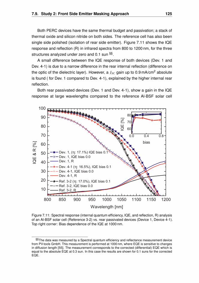
7.9. Study 2: Front Side Emitter Masking Approach 125
Both PERC devices have the same thermal budget and passivation; a stack ofthermal oxide and silicon nitride on both sides. The reference cell has also beensingle side polished (isolation of rear side emitter). Figure 7.11 shows the IQEresponse and reflection (R) in infrared spectra from 800 to 1200 nm, for the threestructures analyzed under zero and 0.1 sun §§.
A small difference between the IQE response of both devices (Dev. 1 andDev. 4-1) is due to a narrow difference in the rear internal reflection (difference onthe optic of the dielectric layer). However, a JSC gain up to 0.9 mA/cm2 absoluteis found ( for Dev. 1 compared to Dev. 4-1), explained by the higher internal rearreflection.
Both rear passivated devices (Dev. 1 and Dev. 4-1), show a gain in the IQEresponse at large wavelengths compared to the reference Al-BSF solar cell
Figure 7.11: Spectral response (internal quantum efficiency, IQE, and reflection, R) analysisof an Al-BSF solar cell (Reference 3-2) vs. rear passivated devices (Device 1, Device 4-1).Top right corner: Bias dependence of the IQE at 1000 nm.
§§The data was measured by a Spectral quantum efficiency and reflectance measurement devicefrom PV-tools GmbH. This measurement is performed at 1000 nm, where EQE is sensitive to changesin diffusion length [55]. The measurement corresponds to the corrected (differential) EQE which isequal to the absolute EQE at 0.3 sun. In this case the results are shown for 0.1 suns for the correctedEQE.
126 Chapter 7: Processing of Rear Passivated Solar Cells
(Ref. 3-2)¶¶.The top right corner shows the IQE response at 1000 nm for the three struc-
tures plotted against the bias light***. For the reference Al-BSF cell of Ref. 3-2and for the PERC cell of Dev. 1 the EQE at 1000 nm is observed to be stable atthe low bias light regime applied. Nevertheless, the PERC cell of Dev. 4-1 showsinstability all over the bias light regime.
It is well known from literature [167] that SiNx applied directly on p-typesurfaces causes shunting of the cell due to the inversion layer induced at therear surface [167]. In the same paper it has been mentioned that the shunting isvisible when the EQE decreases in the long-wavelength regime under low biasillumination.
The PERC cell of Dev. 4-1 may be strongly affected by parasitic shunting atthe rear (maybe due to the presence of a too thin oxide layer below the nitride).
The IQE response for both PERC cells at long wavelengths strongly dependson the bias light variation as compared to the Al-BSF. Accordingly, our devicesshow the behavior of inverse layer shunting. In other words, the rear side stackSiO2/SiNx still needs further improvement (optic and passivation).
The maximum IQE at 1000 nm reaches approx. 83 % for the record cell ofDev. 1. This value is not achieved with Dev. 4-1. This could be also due to the lowquality of the rear surface passivation.
7.9.6 Summary and Conclusions
It is shown, that the rear surface coating improves the internal reflectivityof the rear side, compared to a standard fully covered Al area, increasing thedensity of charge carriers in the cell, resulting in a gain on JSC . The acidicpolishing is of paramount importance before the deposition of a dielectric layer foroptimal smoothness of the surface and maximal lifetime achievements. Differentstructures have been studied. An extra thermal oxidation is highly applicable onthermally stable mc-Si material, with the result of an improved passivation of thefront side emitter and rear surface. Furthermore, a front side masking approachshows an innovative approach for industrial implementation.
¶¶The internal reflection with a dielectric layer is approximately 91 % compared to 64 % with anAl-BSF layer [15]. Thus, the absorption by the Al-layer should be considered here.
***At 1000 nm the absorption depth of light in the Si material bulk is deeper than 150 µm.
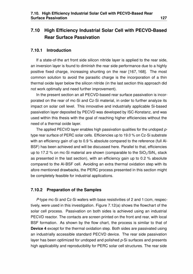
7.10. High Efficiency Industrial Solar Cell with PECVD-Based RearSurface Passivation 127
7.10 High Efficiency Industrial Solar Cell with PECVD-BasedRear Surface Passivation
7.10.1 Introduction
If a state-of-the art front side silicon nitride layer is applied to the rear side,an inversion layer is found to diminish the rear side performance due to a highlypositive fixed charge, increasing shunting on the rear [167, 168]. The mostcommon solution to avoid the parasitic charge is the incorporation of a thinthermal oxide layer below the silicon nitride (in the last section this approach didnot work optimally and need further improvement).
In the present section an all PECVD-based rear surface passivation is incor-porated on the rear of mc-Si and Cz-Si material, in order to further analyze itsimpact on solar cell level. This innovative and industrially applicable Si-basedpassivation layer deposited by PECVD was developed by ISC-Konstanz, and wasused within this thesis with the goal of reaching higher efficiencies without theneed of a thermal oxide layer.
The applied PECVD layer enables high passivation qualities for the undoped p-type rear surface of PERC solar cells. Efficiencies up to 19.0 % on Cz-Si substratewith an efficiency gain of up to 0.9 % absolute compared to the reference (full Al-BSF) has been achieved and will be discussed here. Parallel to that, efficienciesup to 17.2 % on mc-Si material are shown (comparable to the SiO2/SiNx stackas presented in the last section), with an efficiency gain up to 0.2 % absolutecompared to the Al-BSF cell. Avoiding an extra thermal oxidation step with itsafore mentioned drawbacks, the PERC process presented in this section mightbe completely feasible for industrial applications.
7.10.2 Preparation of the Samples
P-type mc-Si and Cz-Si wafers with base resistivities of 2 and 1Ωcm, respec-tively, were used in this investigation. Figure 7.12(a) shows the flowchart of thesolar cell process. Passivation on both sides is achieved using an industrialPECVD reactor. The contacts are screen printed on the front and rear, with localBSF formation. As shown by the flow chart, the process is similar to that ofDevice 4 except for the thermal oxidation step. Both sides are passivated usingan industrially accessible standard PECVD device. The rear side passivationlayer has been optimized for undoped and polished p-Si surfaces and presentshigh applicability and reproducibility for PERC solar cell structures. The rear side
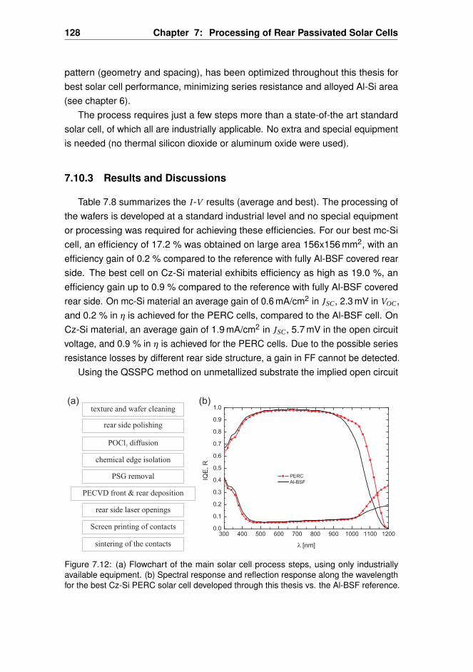
128 Chapter 7: Processing of Rear Passivated Solar Cells
pattern (geometry and spacing), has been optimized throughout this thesis forbest solar cell performance, minimizing series resistance and alloyed Al-Si area(see chapter 6).
The process requires just a few steps more than a state-of-the art standardsolar cell, of which all are industrially applicable. No extra and special equipmentis needed (no thermal silicon dioxide or aluminum oxide were used).
7.10.3 Results and Discussions
Table 7.8 summarizes the I -V results (average and best). The processing ofthe wafers is developed at a standard industrial level and no special equipmentor processing was required for achieving these efficiencies. For our best mc-Sicell, an efficiency of 17.2 % was obtained on large area 156x156 mm2, with anefficiency gain of 0.2 % compared to the reference with fully Al-BSF covered rearside. The best cell on Cz-Si material exhibits efficiency as high as 19.0 %, anefficiency gain up to 0.9 % compared to the reference with fully Al-BSF coveredrear side. On mc-Si material an average gain of 0.6 mA/cm2 in JSC , 2.3 mV in VOC ,and 0.2 % in η is achieved for the PERC cells, compared to the Al-BSF cell. OnCz-Si material, an average gain of 1.9 mA/cm2 in JSC , 5.7 mV in the open circuitvoltage, and 0.9 % in η is achieved for the PERC cells. Due to the possible seriesresistance losses by different rear side structure, a gain in FF cannot be detected.
Using the QSSPC method on unmetallized substrate the implied open circuit
Figure 7.12: (a) Flowchart of the main solar cell process steps, using only industriallyavailable equipment. (b) Spectral response and reflection response along the wavelengthfor the best Cz-Si PERC solar cell developed through this thesis vs. the Al-BSF reference.
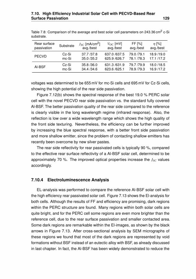
7.10. High Efficiency Industrial Solar Cell with PECVD-Based RearSurface Passivation 129
Table 7.8: Comparison of the average and best solar cell parameters on 243.36 cm2 c-Sisubstrate.
Rear surface Substrate JSC [mA/cm2] VOC [mV] FF [%] η [%]passivation avg./best avg./best avg./best avg./best
PECVD Cz-Si 37.7 /37.8 637.0 /637.5 79.0 /79.1 18.9 /19.0mc-Si 35.0 /35.2 625.9 /626.7 78.1 /78.3 17.1 /17.2
Al-BSF Cz-Si 35.8 /36.0 631.3 /631.9 79.7 /79.9 18.0 /18.5mc-Si 34.4 /34.6 623.6 /625.1 78.9 /79.3 16.9 /17.2
voltages was determined to be 655 mV for mc-Si cells and 695 mV for Cz-Si cells,showing the high potential of the rear side passivation.
Figure 7.12(b) shows the spectral response of the best 19.0 % PERC solarcell with the novel PECVD rear side passivation vs. the standard fully coveredAl-BSF. The better passivation quality of the rear side compared to the referenceis clearly visible in the long wavelength regime (infrared response). Also, thereflection is low over a wide wavelength range which shows the high quality ofthe front side texturing. Nevertheless, the efficiency can be further improvedby increasing the blue spectral response, with a better front side passivationand more shallow emitter, since the problem of contacting shallow emitters hasrecently been overcome by new silver pastes.
The rear side reflectivity for rear passivated cells is typically 90 %, comparedto the effective rear surface reflectivity of a Al-BSF solar cell, determined to beapproximately 70 %. The improved optical properties increase the JSC valuesaccordingly.
7.10.4 Electroluminescence Analysis
EL-analysis was performed to compare the reference Al-BSF solar cell withthe high efficiency rear passivated solar cell. Figure 7.13 shows the El-analysis forboth cells. Although the results of FF and efficiency are promising, dark regionswithin the PERC structure are found. Many regions within both solar cells arequite bright, and for the PERC cell some regions are even more brighter than thereference cell, due to the rear surface passivation and smaller contacted area.Some dark regions are remarkable within the El-images, as shown by the blackarrows in Figure 7.13. After cross-sectional analysis by SEM micrographs ofthese regions we found that most of the dark regions are represented by voidformations without BSF instead of an eutectic alloy with BSF, as already discussedin last chapter. In fact, the Al-BSF has been widely demonstrated to reduce the
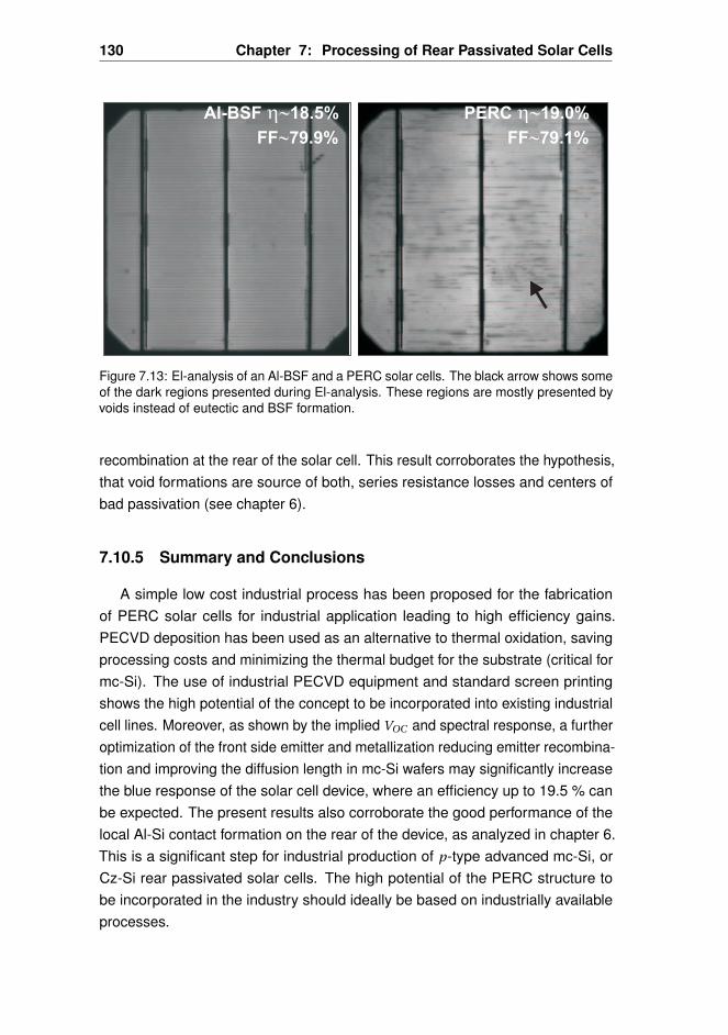
130 Chapter 7: Processing of Rear Passivated Solar Cells
Al-BSF 18.5%
FF 79.9%
h~
~
PERC 19.0%
FF 79.1%
h~
~
Figure 7.13: El-analysis of an Al-BSF and a PERC solar cells. The black arrow shows someof the dark regions presented during El-analysis. These regions are mostly presented byvoids instead of eutectic and BSF formation.
recombination at the rear of the solar cell. This result corroborates the hypothesis,that void formations are source of both, series resistance losses and centers ofbad passivation (see chapter 6).
7.10.5 Summary and Conclusions
A simple low cost industrial process has been proposed for the fabricationof PERC solar cells for industrial application leading to high efficiency gains.PECVD deposition has been used as an alternative to thermal oxidation, savingprocessing costs and minimizing the thermal budget for the substrate (critical formc-Si). The use of industrial PECVD equipment and standard screen printingshows the high potential of the concept to be incorporated into existing industrialcell lines. Moreover, as shown by the implied VOC and spectral response, a furtheroptimization of the front side emitter and metallization reducing emitter recombina-tion and improving the diffusion length in mc-Si wafers may significantly increasethe blue response of the solar cell device, where an efficiency up to 19.5 % canbe expected. The present results also corroborate the good performance of thelocal Al-Si contact formation on the rear of the device, as analyzed in chapter 6.This is a significant step for industrial production of p-type advanced mc-Si, orCz-Si rear passivated solar cells. The high potential of the PERC structure tobe incorporated in the industry should ideally be based on industrially availableprocesses.
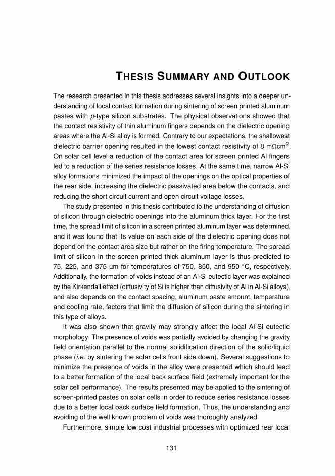
THESIS SUMMARY AND OUTLOOK
The research presented in this thesis addresses several insights into a deeper un-derstanding of local contact formation during sintering of screen printed aluminumpastes with p-type silicon substrates. The physical observations showed thatthe contact resistivity of thin aluminum fingers depends on the dielectric openingareas where the Al-Si alloy is formed. Contrary to our expectations, the shallowestdielectric barrier opening resulted in the lowest contact resistivity of 8 mΩcm2.On solar cell level a reduction of the contact area for screen printed Al fingersled to a reduction of the series resistance losses. At the same time, narrow Al-Sialloy formations minimized the impact of the openings on the optical properties ofthe rear side, increasing the dielectric passivated area below the contacts, andreducing the short circuit current and open circuit voltage losses.
The study presented in this thesis contributed to the understanding of diffusionof silicon through dielectric openings into the aluminum thick layer. For the firsttime, the spread limit of silicon in a screen printed aluminum layer was determined,and it was found that its value on each side of the dielectric opening does notdepend on the contact area size but rather on the firing temperature. The spreadlimit of silicon in the screen printed thick aluminum layer is thus predicted to75, 225, and 375 µm for temperatures of 750, 850, and 950 C, respectively.Additionally, the formation of voids instead of an Al-Si eutectic layer was explainedby the Kirkendall effect (diffusivity of Si is higher than diffusivity of Al in Al-Si alloys),and also depends on the contact spacing, aluminum paste amount, temperatureand cooling rate, factors that limit the diffusion of silicon during the sintering inthis type of alloys.
It was also shown that gravity may strongly affect the local Al-Si eutecticmorphology. The presence of voids was partially avoided by changing the gravityfield orientation parallel to the normal solidification direction of the solid/liquidphase (i.e. by sintering the solar cells front side down). Several suggestions tominimize the presence of voids in the alloy were presented which should leadto a better formation of the local back surface field (extremely important for thesolar cell performance). The results presented may be applied to the sintering ofscreen-printed pastes on solar cells in order to reduce series resistance lossesdue to a better local back surface field formation. Thus, the understanding andavoiding of the well known problem of voids was thoroughly analyzed.
Furthermore, simple low cost industrial processes with optimized rear local
131
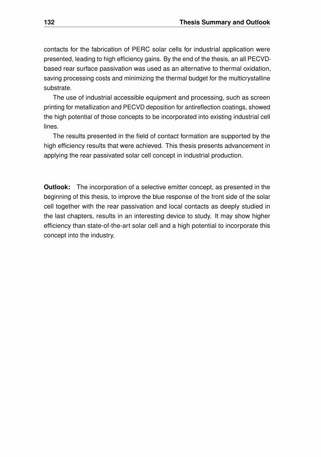
132 Thesis Summary and Outlook
contacts for the fabrication of PERC solar cells for industrial application werepresented, leading to high efficiency gains. By the end of the thesis, an all PECVD-based rear surface passivation was used as an alternative to thermal oxidation,saving processing costs and minimizing the thermal budget for the multicrystallinesubstrate.
The use of industrial accessible equipment and processing, such as screenprinting for metallization and PECVD deposition for antireflection coatings, showedthe high potential of those concepts to be incorporated into existing industrial celllines.
The results presented in the field of contact formation are supported by thehigh efficiency results that were achieved. This thesis presents advancement inapplying the rear passivated solar cell concept in industrial production.
Outlook: The incorporation of a selective emitter concept, as presented in thebeginning of this thesis, to improve the blue response of the front side of the solarcell together with the rear passivation and local contacts as deeply studied inthe last chapters, results in an interesting device to study. It may show higherefficiency than state-of-the-art solar cell and a high potential to incorporate thisconcept into the industry.
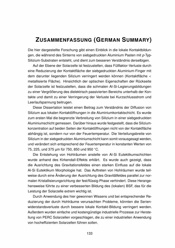
ZUSAMMENFASSUNG (GERMAN SUMMARY)Die hier dargestellte Forschung gibt einen Einblick in die lokale Kontaktbildun-gen, die während des Sinterns von siebgedruckten Aluminium Pasten mit p-Typ-Silizium-Substraten entsteht, und dient zum besseren Verständnis derselbigen.
Auf der Ebene der Solarzelle ist festzustellen, dass Füllfaktor-Verluste durcheine Reduzierung der Kontaktfläche der siebgedruckten Aluminium-Finger mitdem darunter liegenden Silizium verringert werden können (Kontaktfläche <metallisierte Fläche). Hinsichtlich der optischen Eigenschaften der Rückseiteder Solarzelle ist festzustellen, dass die schmalen Al-Si-Legierungsbildungenzu einer Vergrößerung des dielektrisch passivierten Bereichs unterhalb der Kon-takte und damit zu einer Verringerung der Verluste bei Kurzschlussstrom undLeerlaufspannung beitrugen.
Diese Dissertation leistet einen Beitrag zum Verständnis der Diffusion vonSilizium aus lokalen Kontaktöffnungen in die Aluminiumkontaktschicht. Es wurdezum ersten Mal die begrenzte Verbreitung von Silizium in einer siebgedrucktenAluminiumschicht gemessen. Darüber hinaus wurde festgestellt, dass die Silizium-konzentration auf beiden Seiten der Kontaktöffnungen nicht von der Kontaktflächeabhängig ist, sondern nur von der Feuertemperatur. Die Verteilungsbreite vonSilizium in der siebgedruckten Aluminiumschicht kann somit vorausgesagt werden,und verändert sich entsprechend der Feuertemperatur in konstanten Werten von75, 225, und 375 µm für 750, 850 und 950 C.
Die Entstehung von Hohlräumen anstelle von Al-Si Eutektikumschichtenwurde anhand des Kirkendall-Effekts erklärt. Es wurde auch gezeigt, dassdie Ausrichtung des Gravitationsfeldes einen starken Einfluss auf die lokaleAl-Si Eutektikum Morphologie hat. Das Auftreten von Hohlräumen wurde teil-weise durch eine Änderung der Ausrichtung des Gravitätfeldes parallel zur nor-malen Kristallisierungsrichtung der fest/flüssig-Phase verhindert. Diese Herange-hensweise führte zu einer verbesserten Bildung des (lokalen) BSF, das für dieLeistung der Solarzelle extrem wichtig ist.
Durch Anwendung des hier gewonnen Wissens und bei entsprechender Re-duzierung der durch Hohlräume verursachten Probleme, könnten die Serien-widerstandsverluste durch bessere lokale Kontakt-Bildung verringert werden.Außerdem wurden einfache und kostengünstige industrielle Prozesse zur Herste-llung von PERC Solarzellen vorgeschlagen, die zu einer industriellen Anwendungvon hocheffizienten Solarzellen führen sollen.
133
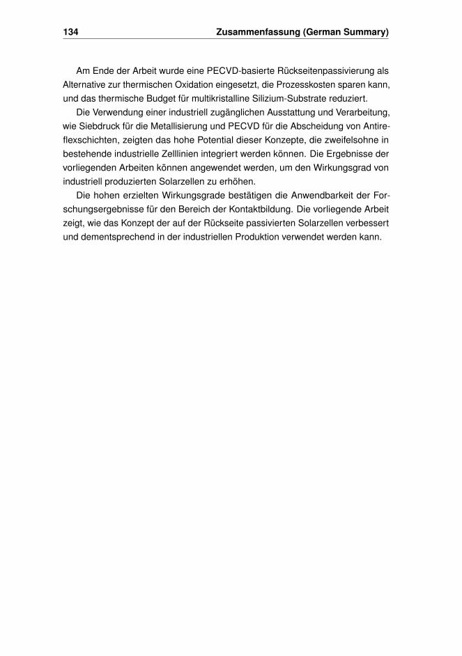
134 Zusammenfassung (German Summary)
Am Ende der Arbeit wurde eine PECVD-basierte Rückseitenpassivierung alsAlternative zur thermischen Oxidation eingesetzt, die Prozesskosten sparen kann,und das thermische Budget für multikristalline Silizium-Substrate reduziert.
Die Verwendung einer industriell zugänglichen Ausstattung und Verarbeitung,wie Siebdruck für die Metallisierung und PECVD für die Abscheidung von Antire-flexschichten, zeigten das hohe Potential dieser Konzepte, die zweifelsohne inbestehende industrielle Zelllinien integriert werden können. Die Ergebnisse dervorliegenden Arbeiten können angewendet werden, um den Wirkungsgrad vonindustriell produzierten Solarzellen zu erhöhen.
Die hohen erzielten Wirkungsgrade bestätigen die Anwendbarkeit der For-schungsergebnisse für den Bereich der Kontaktbildung. Die vorliegende Arbeitzeigt, wie das Konzept der auf der Rückseite passivierten Solarzellen verbessertund dementsprechend in der industriellen Produktion verwendet werden kann.
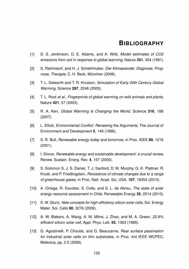
BIBLIOGRAPHY
[1] D. S. Jenkinson, D. E. Adams, and A. Wild, Model estimates of CO2emissions from soil in response to global warming, Nature 351, 304 (1991).
[2] S. Rahmstorf, and H. J. Schellnhuber, Der Klimawandel. Diagnose, Prog-nose, Therapie, C. H. Beck, München (2006).
[3] T. L. Delworth and T. R. Knutson, Simulation of Early 20th Century GlobalWarming, Science 287, 2246 (2000).
[4] T. L. Root et al., Fingerprints of global warming on wild animals and plants,Nature 421, 57 (2003).
[5] R. A. Kerr, Global Warming Is Changing the World, Science 316, 188(2007).
[6] L. Elliott, Environmental Conflict: Reviewing the Arguments, The Journal ofEnvironment and Development 5, 149 (1996).
[7] S. R. Bull, Renewable energy today and tomorrow, in Proc. IEEE 89, 1216(2001).
[8] I. Dincer, Renewable energy and sustainable development: a crucial review,Renew. Sustain. Energ. Rev. 4, 157 (2000).
[9] S. Solomon S, J. S. Daniel, T. J. Sanford, D. M. Murphy, G. K. Plattner, R.Knutti, and P. Friedlingstein, Persistence of climate changes due to a rangeof greenhouse gases, in Proc. Natl. Acad. Sci, USA. 107, 18354 (2010).
[10] A. Ortega, R. Escobar, S. Colle, and S. L. de Abreu, The state of solarenergy resource assessment in Chile, Renewable Energy 35, 2514 (2010).
[11] S. W. Glunz, New concepts for high-efficiency silicon solar cells, Sol. EnergyMater. Sol. Cells 90, 3276 (2006).
[12] A. W. Blakers, A. Wang, A. M. Milne, J. Zhao, and M. A. Green, 22.8%efficient silicon solar cell, Appl. Phys. Lett. 55, 1363 (1989).
[13] G. Agostinelli, P. Choulat, and G. Beaucarne, Rear surface passivationfor industrial solar cells on thin substrates, in Proc. 4rd IEEE WCPEC,Waikoloa, pp. 2-5 (2006).
135
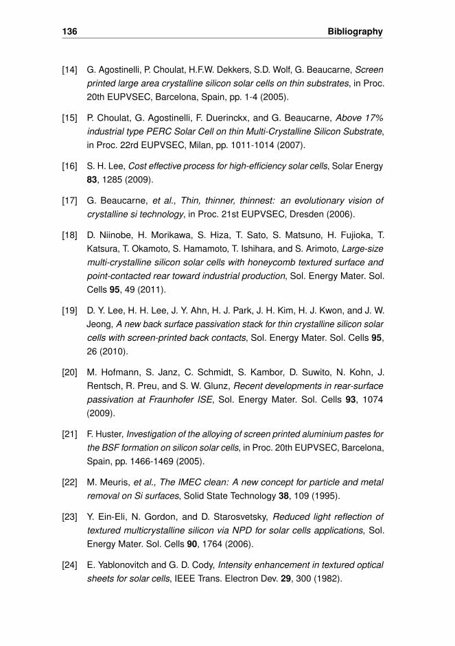
136 Bibliography
[14] G. Agostinelli, P. Choulat, H.F.W. Dekkers, S.D. Wolf, G. Beaucarne, Screenprinted large area crystalline silicon solar cells on thin substrates, in Proc.20th EUPVSEC, Barcelona, Spain, pp. 1-4 (2005).
[15] P. Choulat, G. Agostinelli, F. Duerinckx, and G. Beaucarne, Above 17%industrial type PERC Solar Cell on thin Multi-Crystalline Silicon Substrate,in Proc. 22rd EUPVSEC, Milan, pp. 1011-1014 (2007).
[16] S. H. Lee, Cost effective process for high-efficiency solar cells, Solar Energy83, 1285 (2009).
[17] G. Beaucarne, et al., Thin, thinner, thinnest: an evolutionary vision ofcrystalline si technology, in Proc. 21st EUPVSEC, Dresden (2006).
[18] D. Niinobe, H. Morikawa, S. Hiza, T. Sato, S. Matsuno, H. Fujioka, T.Katsura, T. Okamoto, S. Hamamoto, T. Ishihara, and S. Arimoto, Large-sizemulti-crystalline silicon solar cells with honeycomb textured surface andpoint-contacted rear toward industrial production, Sol. Energy Mater. Sol.Cells 95, 49 (2011).
[19] D. Y. Lee, H. H. Lee, J. Y. Ahn, H. J. Park, J. H. Kim, H. J. Kwon, and J. W.Jeong, A new back surface passivation stack for thin crystalline silicon solarcells with screen-printed back contacts, Sol. Energy Mater. Sol. Cells 95,26 (2010).
[20] M. Hofmann, S. Janz, C. Schmidt, S. Kambor, D. Suwito, N. Kohn, J.Rentsch, R. Preu, and S. W. Glunz, Recent developments in rear-surfacepassivation at Fraunhofer ISE, Sol. Energy Mater. Sol. Cells 93, 1074(2009).
[21] F. Huster, Investigation of the alloying of screen printed aluminium pastes forthe BSF formation on silicon solar cells, in Proc. 20th EUPVSEC, Barcelona,Spain, pp. 1466-1469 (2005).
[22] M. Meuris, et al., The IMEC clean: A new concept for particle and metalremoval on Si surfaces, Solid State Technology 38, 109 (1995).
[23] Y. Ein-Eli, N. Gordon, and D. Starosvetsky, Reduced light reflection oftextured multicrystalline silicon via NPD for solar cells applications, Sol.Energy Mater. Sol. Cells 90, 1764 (2006).
[24] E. Yablonovitch and G. D. Cody, Intensity enhancement in textured opticalsheets for solar cells, IEEE Trans. Electron Dev. 29, 300 (1982).
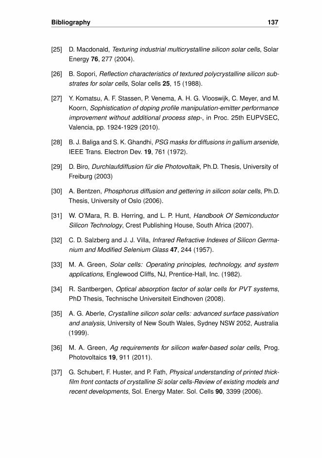
Bibliography 137
[25] D. Macdonald, Texturing industrial multicrystalline silicon solar cells, SolarEnergy 76, 277 (2004).
[26] B. Sopori, Reflection characteristics of textured polycrystalline silicon sub-strates for solar cells, Solar cells 25, 15 (1988).
[27] Y. Komatsu, A. F. Stassen, P. Venema, A. H. G. Vlooswijk, C. Meyer, and M.Koorn, Sophistication of doping profile manipulation-emitter performanceimprovement without additional process step-, in Proc. 25th EUPVSEC,Valencia, pp. 1924-1929 (2010).
[28] B. J. Baliga and S. K. Ghandhi, PSG masks for diffusions in gallium arsenide,IEEE Trans. Electron Dev. 19, 761 (1972).
[29] D. Biro, Durchlaufdiffusion für die Photovoltaik, Ph.D. Thesis, University ofFreiburg (2003)
[30] A. Bentzen, Phosphorus diffusion and gettering in silicon solar cells, Ph.D.Thesis, University of Oslo (2006).
[31] W. O’Mara, R. B. Herring, and L. P. Hunt, Handbook Of SemiconductorSilicon Technology, Crest Publishing House, South Africa (2007).
[32] C. D. Salzberg and J. J. Villa, Infrared Refractive Indexes of Silicon Germa-nium and Modified Selenium Glass 47, 244 (1957).
[33] M. A. Green, Solar cells: Operating principles, technology, and systemapplications, Englewood Cliffs, NJ, Prentice-Hall, Inc. (1982).
[34] R. Santbergen, Optical absorption factor of solar cells for PVT systems,PhD Thesis, Technische Universiteit Eindhoven (2008).
[35] A. G. Aberle, Crystalline silicon solar cells: advanced surface passivationand analysis, University of New South Wales, Sydney NSW 2052, Australia(1999).
[36] M. A. Green, Ag requirements for silicon wafer-based solar cells, Prog.Photovoltaics 19, 911 (2011).
[37] G. Schubert, F. Huster, and P. Fath, Physical understanding of printed thick-film front contacts of crystalline Si solar cells-Review of existing models andrecent developments, Sol. Energy Mater. Sol. Cells 90, 3399 (2006).
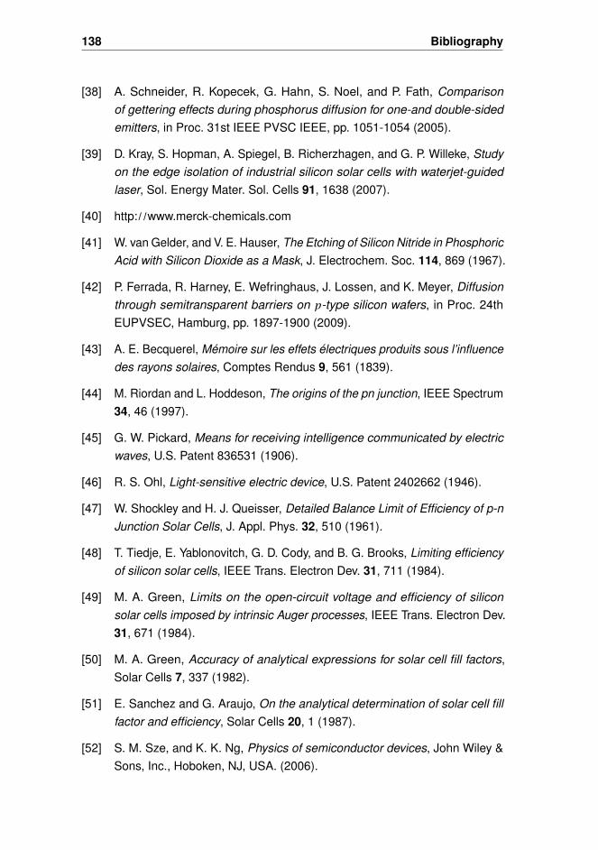
138 Bibliography
[38] A. Schneider, R. Kopecek, G. Hahn, S. Noel, and P. Fath, Comparisonof gettering effects during phosphorus diffusion for one-and double-sidedemitters, in Proc. 31st IEEE PVSC IEEE, pp. 1051-1054 (2005).
[39] D. Kray, S. Hopman, A. Spiegel, B. Richerzhagen, and G. P. Willeke, Studyon the edge isolation of industrial silicon solar cells with waterjet-guidedlaser, Sol. Energy Mater. Sol. Cells 91, 1638 (2007).
[40] http://www.merck-chemicals.com
[41] W. van Gelder, and V. E. Hauser, The Etching of Silicon Nitride in PhosphoricAcid with Silicon Dioxide as a Mask, J. Electrochem. Soc. 114, 869 (1967).
[42] P. Ferrada, R. Harney, E. Wefringhaus, J. Lossen, and K. Meyer, Diffusionthrough semitransparent barriers on p-type silicon wafers, in Proc. 24thEUPVSEC, Hamburg, pp. 1897-1900 (2009).
[43] A. E. Becquerel, Mémoire sur les effets électriques produits sous l’influencedes rayons solaires, Comptes Rendus 9, 561 (1839).
[44] M. Riordan and L. Hoddeson, The origins of the pn junction, IEEE Spectrum34, 46 (1997).
[45] G. W. Pickard, Means for receiving intelligence communicated by electricwaves, U.S. Patent 836531 (1906).
[46] R. S. Ohl, Light-sensitive electric device, U.S. Patent 2402662 (1946).
[47] W. Shockley and H. J. Queisser, Detailed Balance Limit of Efficiency of p-nJunction Solar Cells, J. Appl. Phys. 32, 510 (1961).
[48] T. Tiedje, E. Yablonovitch, G. D. Cody, and B. G. Brooks, Limiting efficiencyof silicon solar cells, IEEE Trans. Electron Dev. 31, 711 (1984).
[49] M. A. Green, Limits on the open-circuit voltage and efficiency of siliconsolar cells imposed by intrinsic Auger processes, IEEE Trans. Electron Dev.31, 671 (1984).
[50] M. A. Green, Accuracy of analytical expressions for solar cell fill factors,Solar Cells 7, 337 (1982).
[51] E. Sanchez and G. Araujo, On the analytical determination of solar cell fillfactor and efficiency, Solar Cells 20, 1 (1987).
[52] S. M. Sze, and K. K. Ng, Physics of semiconductor devices, John Wiley &Sons, Inc., Hoboken, NJ, USA. (2006).
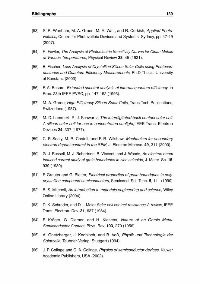
Bibliography 139
[53] S. R. Wenham, M. A. Green, M. E. Watt, and R. Corkish, Applied Photo-voltaics, Centre for Photovoltaic Devices and Systems, Sydney, pp. 47-49(2007).
[54] R. Fowler, The Analysis of Photoelectric Sensitivity Curves for Clean Metalsat Various Temperatures, Physical Review 38, 45 (1931).
[55] B. Fischer, Loss Analysis of Crystalline Silicon Solar Cells using Photocon-ductance and Quantum Efficiency Measurements, Ph.D Thesis, Universityof Konstanz (2003).
[56] P. A. Basore, Extended spectral analysis of internal quantum efficiency, inProc. 23th IEEE PVSC, pp. 147-152 (1993).
[57] M. A. Green, High Efficiency Silicon Solar Cells, Trans Tech Publications,Switzerland (1987).
[58] M. D. Lammert, R. J. Schwartz, The interdigitated back contact solar cell:A silicon solar cell for use in concentrated sunlight, IEEE Trans. ElectronDevices 24, 337 (1977).
[59] C. P. Sealy, M. R. Castell, and P. R. Wilshaw, Mechanism for secondaryelectron dopant contrast in the SEM, J. Electron Microsc. 49, 311 (2000).
[60] G. J. Russell, M. J. Robertson, B. Vincent, and J. Woods, An electron beaminduced current study of grain boundaries in zinc selenide, J. Mater. Sc. 15,939 (1980).
[61] F. Greuter and G. Blatter, Electrical properties of grain boundaries in poly-crystalline compound semiconductors, Semicond. Sci. Tech. 5, 111 (1990).
[62] B. S. Mitchell, An introduction to materials engineering and science, WileyOnline Library (2004).
[63] D. K. Schroder, and D.L. Meier,Solar cell contact resistance-A review, IEEETrans. Electron. Dev. 31, 637 (1984).
[64] F. Kröger, G. Diemer, and H. Klasens, Nature of an Ohmic Metal-Semiconductor Contact, Phys. Rev. 103, 279 (1956).
[65] A. Goetzberger, J. Knobloch, and B. Voß, Physik und Technologie derSolarzelle, Teubner-Verlag, Stuttgart (1994).
[66] J. P. Colinge and C. A. Colinge, Physics of semiconductor devices, KluwerAcademic Publishers, USA (2002).
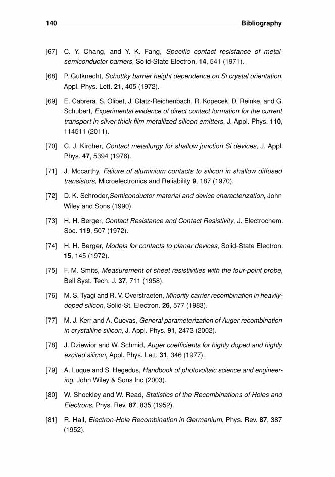
140 Bibliography
[67] C. Y. Chang, and Y. K. Fang, Specific contact resistance of metal-semiconductor barriers, Solid-State Electron. 14, 541 (1971).
[68] P. Gutknecht, Schottky barrier height dependence on Si crystal orientation,Appl. Phys. Lett. 21, 405 (1972).
[69] E. Cabrera, S. Olibet, J. Glatz-Reichenbach, R. Kopecek, D. Reinke, and G.Schubert, Experimental evidence of direct contact formation for the currenttransport in silver thick film metallized silicon emitters, J. Appl. Phys. 110,114511 (2011).
[70] C. J. Kircher, Contact metallurgy for shallow junction Si devices, J. Appl.Phys. 47, 5394 (1976).
[71] J. Mccarthy, Failure of aluminium contacts to silicon in shallow diffusedtransistors, Microelectronics and Reliability 9, 187 (1970).
[72] D. K. Schroder,Semiconductor material and device characterization, JohnWiley and Sons (1990).
[73] H. H. Berger, Contact Resistance and Contact Resistivity, J. Electrochem.Soc. 119, 507 (1972).
[74] H. H. Berger, Models for contacts to planar devices, Solid-State Electron.15, 145 (1972).
[75] F. M. Smits, Measurement of sheet resistivities with the four-point probe,Bell Syst. Tech. J. 37, 711 (1958).
[76] M. S. Tyagi and R. V. Overstraeten, Minority carrier recombination in heavily-doped silicon, Solid-St. Electron. 26, 577 (1983).
[77] M. J. Kerr and A. Cuevas, General parameterization of Auger recombinationin crystalline silicon, J. Appl. Phys. 91, 2473 (2002).
[78] J. Dziewior and W. Schmid, Auger coefficients for highly doped and highlyexcited silicon, Appl. Phys. Lett. 31, 346 (1977).
[79] A. Luque and S. Hegedus, Handbook of photovoltaic science and engineer-ing, John Wiley & Sons Inc (2003).
[80] W. Shockley and W. Read, Statistics of the Recombinations of Holes andElectrons, Phys. Rev. 87, 835 (1952).
[81] R. Hall, Electron-Hole Recombination in Germanium, Phys. Rev. 87, 387(1952).
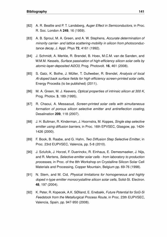
Bibliography 141
[82] A. R. Beattie and P. T. Landsberg, Auger Effect in Semiconductors, in Proc.R. Soc. London A 249, 16 (1959).
[83] A. B. Sproul, M. A. Green, and A. W. Stephens, Accurate determination ofminority carrier- and lattice scattering-mobility in silicon from photoconduc-tance decay, J. Appl. Phys 72, 4161 (1992).
[84] J. Schmidt, A. Merkle, R. Brendel, B. Hoex, M.C.M. van de Sanden, andW.M.M. Kessels, Surface passivation of high-efficiency silicon solar cells byatomic-layer-deposited Al2O3, Prog. Photovolt. 16, 461 (2008).
[85] S. Gatz, K. Bothe, J. Müller, T. Dullweber, R. Brendel, Analysis of localAl-doped back surface fields for high efficiency screen-printed solar cells,Energy Procedia (to be published) (2011).
[86] M. A. Green, M. J. Keevers, Optical properties of intrinsic silicon at 300 K,Prog. Photov. 3, 189 (1995).
[87] R. Chaoui, A. Messaoud, Screen-printed solar cells with simultaneousformation of porous silicon selective emitter and antireflection coating,Desalination 209, 118 (2007).
[88] J. H. Bultman, R. Kinderman, J. Hoornstra, M. Koppes, Single step selectiveemitter using diffusion barriers, in Proc. 16th EPVSEC, Glasgow, pp. 1424-1426 (2000).
[89] F. Book, B. Raabe, and G. Hahn, Two Diffusion Step Selective Emitter, inProc. 23rd EUPVSEC, Valencia, pp. 5-8 (2010).
[90] J. Szlufcik, J. Horzel, F. Duerinckx, R. Einhaus, E. Demesmaeker, J. Nijs,and R. Mertens, Selective-emitter solar cells - from laboratory to productionprocesses, in Proc. of the 8th Workshop on Crystalline Silicon Solar CellMaterials and Processing, Copper Mountain, Belgium pp. 69-76 (1998).
[91] N. Stem, and M. Cid, Physical limitations for homogeneous and highlydoped n-type emitter monocrystalline silicon solar cells, Solid-St. Electron.48, 197 (2004).
[92] K. Peter, R. Kopecek, A.K. SØiland, E. Enebakk, Future Potential for SoG-SiFeedstock from the Metallurgical Process Route, in Proc. 23th EUPVSEC,Valencia, Spain, pp. 947-950 (2008).
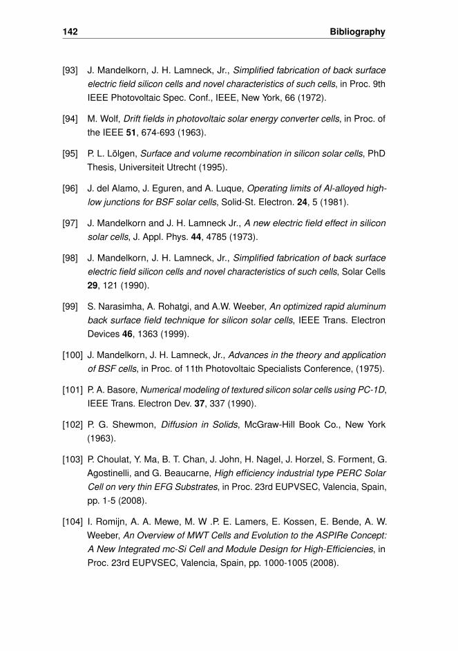
142 Bibliography
[93] J. Mandelkorn, J. H. Lamneck, Jr., Simplified fabrication of back surfaceelectric field silicon cells and novel characteristics of such cells, in Proc. 9thIEEE Photovoltaic Spec. Conf., IEEE, New York, 66 (1972).
[94] M. Wolf, Drift fields in photovoltaic solar energy converter cells, in Proc. ofthe IEEE 51, 674-693 (1963).
[95] P. L. Lölgen, Surface and volume recombination in silicon solar cells, PhDThesis, Universiteit Utrecht (1995).
[96] J. del Alamo, J. Eguren, and A. Luque, Operating limits of Al-alloyed high-low junctions for BSF solar cells, Solid-St. Electron. 24, 5 (1981).
[97] J. Mandelkorn and J. H. Lamneck Jr., A new electric field effect in siliconsolar cells, J. Appl. Phys. 44, 4785 (1973).
[98] J. Mandelkorn, J. H. Lamneck, Jr., Simplified fabrication of back surfaceelectric field silicon cells and novel characteristics of such cells, Solar Cells29, 121 (1990).
[99] S. Narasimha, A. Rohatgi, and A.W. Weeber, An optimized rapid aluminumback surface field technique for silicon solar cells, IEEE Trans. ElectronDevices 46, 1363 (1999).
[100] J. Mandelkorn, J. H. Lamneck, Jr., Advances in the theory and applicationof BSF cells, in Proc. of 11th Photovoltaic Specialists Conference, (1975).
[101] P. A. Basore, Numerical modeling of textured silicon solar cells using PC-1D,IEEE Trans. Electron Dev. 37, 337 (1990).
[102] P. G. Shewmon, Diffusion in Solids, McGraw-Hill Book Co., New York(1963).
[103] P. Choulat, Y. Ma, B. T. Chan, J. John, H. Nagel, J. Horzel, S. Forment, G.Agostinelli, and G. Beaucarne, High efficiency industrial type PERC SolarCell on very thin EFG Substrates, in Proc. 23rd EUPVSEC, Valencia, Spain,pp. 1-5 (2008).
[104] I. Romijn, A. A. Mewe, M. W .P. E. Lamers, E. Kossen, E. Bende, A. W.Weeber, An Overview of MWT Cells and Evolution to the ASPIRe Concept:A New Integrated mc-Si Cell and Module Design for High-Efficiencies, inProc. 23rd EUPVSEC, Valencia, Spain, pp. 1000-1005 (2008).
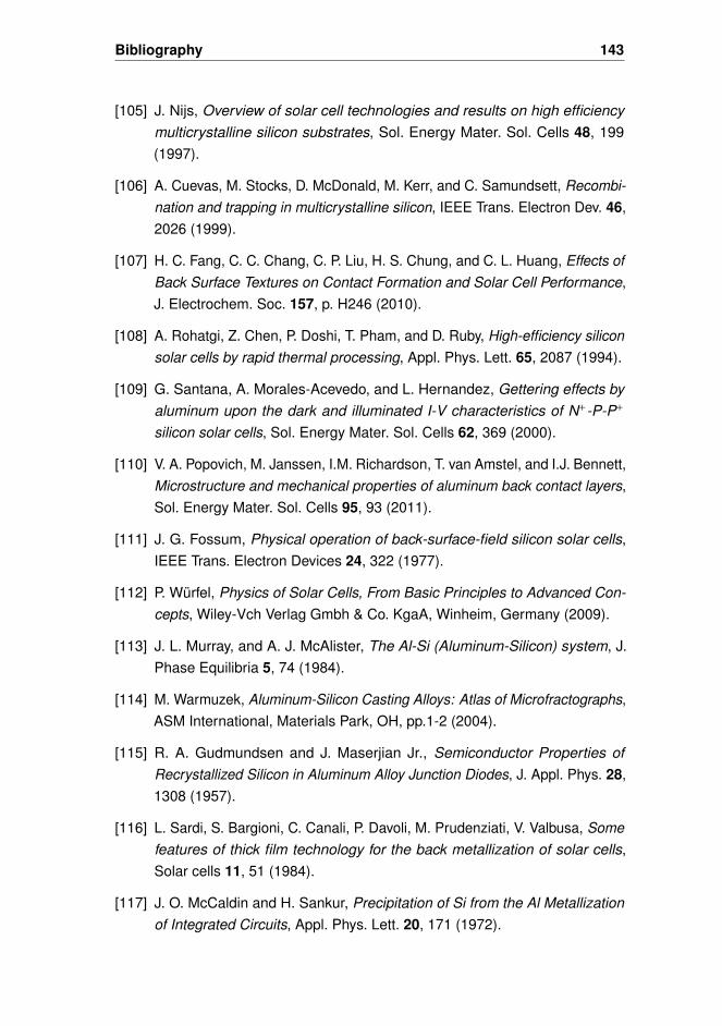
Bibliography 143
[105] J. Nijs, Overview of solar cell technologies and results on high efficiencymulticrystalline silicon substrates, Sol. Energy Mater. Sol. Cells 48, 199(1997).
[106] A. Cuevas, M. Stocks, D. McDonald, M. Kerr, and C. Samundsett, Recombi-nation and trapping in multicrystalline silicon, IEEE Trans. Electron Dev. 46,2026 (1999).
[107] H. C. Fang, C. C. Chang, C. P. Liu, H. S. Chung, and C. L. Huang, Effects ofBack Surface Textures on Contact Formation and Solar Cell Performance,J. Electrochem. Soc. 157, p. H246 (2010).
[108] A. Rohatgi, Z. Chen, P. Doshi, T. Pham, and D. Ruby, High-efficiency siliconsolar cells by rapid thermal processing, Appl. Phys. Lett. 65, 2087 (1994).
[109] G. Santana, A. Morales-Acevedo, and L. Hernandez, Gettering effects byaluminum upon the dark and illuminated I-V characteristics of N+-P-P+
silicon solar cells, Sol. Energy Mater. Sol. Cells 62, 369 (2000).
[110] V. A. Popovich, M. Janssen, I.M. Richardson, T. van Amstel, and I.J. Bennett,Microstructure and mechanical properties of aluminum back contact layers,Sol. Energy Mater. Sol. Cells 95, 93 (2011).
[111] J. G. Fossum, Physical operation of back-surface-field silicon solar cells,IEEE Trans. Electron Devices 24, 322 (1977).
[112] P. Würfel, Physics of Solar Cells, From Basic Principles to Advanced Con-cepts, Wiley-Vch Verlag Gmbh & Co. KgaA, Winheim, Germany (2009).
[113] J. L. Murray, and A. J. McAlister, The Al-Si (Aluminum-Silicon) system, J.Phase Equilibria 5, 74 (1984).
[114] M. Warmuzek, Aluminum-Silicon Casting Alloys: Atlas of Microfractographs,ASM International, Materials Park, OH, pp.1-2 (2004).
[115] R. A. Gudmundsen and J. Maserjian Jr., Semiconductor Properties ofRecrystallized Silicon in Aluminum Alloy Junction Diodes, J. Appl. Phys. 28,1308 (1957).
[116] L. Sardi, S. Bargioni, C. Canali, P. Davoli, M. Prudenziati, V. Valbusa, Somefeatures of thick film technology for the back metallization of solar cells,Solar cells 11, 51 (1984).
[117] J. O. McCaldin and H. Sankur, Precipitation of Si from the Al Metallizationof Integrated Circuits, Appl. Phys. Lett. 20, 171 (1972).
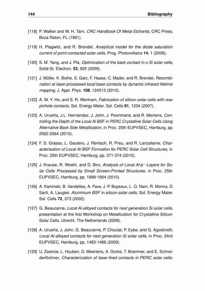
144 Bibliography
[118] P. Walker and W. H. Tarn, CRC Handbook Of Metal Etchants, CRC Press,Boca Raton, FL (1991).
[119] H. Plagwitz, and R. Brendel, Analytical model for the diode saturationcurrent of point-contacted solar cells, Prog. Photovoltaics 14, 1 (2006).
[120] S. M. Yang, and J. Plá, Optimization of the back contact in c-Si solar cells,Solid-St. Electron. 53, 925 (2009).
[121] J. Müller, K. Bothe, S. Gatz, F. Haase, C. Mader, and R. Brendel, Recombi-nation at laser-processed local base contacts by dynamic infrared lifetimemapping, J. Appl. Phys. 108, 124513 (2010).
[122] A. W. Y. Ho, and S. R. Wenham, Fabrication of silicon solar cells with rearpinhole contacts, Sol. Energy Mater. Sol. Cells 91, 1234 (2007).
[123] A. Urueña, J.L. Hernández, J. John, J. Poortmans, and R. Mertens, Con-trolling the Depth of the Local Al BSF in PERC Crystalline Solar Cells UsingAlternative Back Side Metallization, in Proc. 25th EUPVSEC, Hamburg, pp.2562-2564 (2010).
[124] F. S. Grasso, L. Gautero, J. Rentsch, R. Preu, and R. Lanzafame, Char-acterisation of Local Al-BSF Formation for PERC Solar Cell Structures, inProc. 25th EUPVSEC, Hamburg, pp. 371-374 (2010).
[125] J. Krause, R. Woehl, and D. Biro, Analysis of Local Al-p+-Layers for So-lar Cells Processed by Small Screen-Printed Structures, in Proc. 25thEUPVSEC, Hamburg, pp. 1899-1904 (2010).
[126] A. Kaminski, B. Vandellea, A. Fave, J. P. Boyeaux, L. Q. Nam, R. Monna, D.Sarti, A. Laugier, Aluminium BSF in silicon solar cells, Sol. Energy Mater.Sol. Cells 72, 373 (2002).
[127] G. Beaucarne, Local Al-alloyed contacts for next generation Si solar cells,presentation at the first Workshop on Metallization for Crystalline SiliconSolar Cells, Utrecht, The Netherlands (2008).
[128] A. Urueña, J. John, G. Beaucarne, P. Choulat, P. Eybe, and G. Agostinelli,Local Al-alloyed contacts for next generation Si solar cells, in Proc. 24rdEUPVSEC, Hamburg, pp. 1483-1486 (2009).
[129] U. Zastrow, L. Houben, D. Meertens, A. Grohe, T. Brammer, and E. Schnei-derlöchner, Characterization of laser-fired contacts in PERC solar cells:
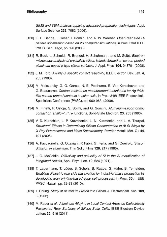
Bibliography 145
SIMS and TEM analysis applying advanced preparation techniques, Appl.Surface Science 252, 7082 (2006).
[130] E. E. Bende, I. Cesar, I. Romijn, and A. W. Weeber, Open-rear side H-pattern optimization based on 2D computer simulations, in Proc. 33rd IEEEPVSC, San Diego, pp. 1-6 (2008).
[131] R. Bock, J. Schmidt, R. Brendel, H. Schuhmann, and M. Seibt, Electronmicroscopy analysis of crystalline silicon islands formed on screen-printedaluminum-doped p-type silicon surfaces, J. Appl. Phys. 104, 043701 (2008).
[132] J. M. Ford, Al/Poly Si specific contact resistivity, IEEE Electron Dev. Lett. 4,255 (1983).
[133] M. Melczarsky, G. G. Garcia, N. E. Posthuma, E. Van Kerschaver, andG. Beaucarne, Contact resistance measurement techniques for Ag thick-film screen-printed contacts to solar cells, in Proc. 34th IEEE PhotovoltaicSpecialists Conference (PVSC), pp. 960-963, (2009).
[134] M. Finetti, P. Ostoja, S. Solmi, and G. Soncini, Aluminum-silicon ohmiccontact on ’shallow’ n+/p junctions, Solid-State Electron. 23, 255 (1980).
[135] V. D. Kurochkin, L. P. Kravchenko, L. N. Kuzmenko, and L. A. Tsurpal,Structural Effects in Determining Silicon Concentration in Al-Si Alloys byX-Ray Fluorescence and Mass Spectrometry, Powder Metall. Met. C+ 44,191 (2005).
[136] A. Paccagnella, G. Ottaviani, P. Fabri, G. Ferla, and G. Queirolo, Silicondiffusion in aluminium, Thin Solid Films 128, 217 (1985).
[137] J. O. McCaldin, Diffusivity and solubility of Si in the Al metallization ofintegrated circuits, Appl. Phys. Lett. 19, 524 (1971).
[138] T. Lauermann, T. Lüder, S. Scholz, B. Raabe, G. Hahn, B. Terheiden,Enabling dielectric rear side passivation for industrial mass production bydeveloping lean printing-based solar cell processes, in Proc. 35th IEEEPVSC, Hawaii, pp. 28-33 (2010).
[139] T. Chung, Study of Aluminum Fusion into Silicon, J. Electrochem. Soc. 109,3 (1962).
[140] M. Rauer et al., Aluminum Alloying in Local Contact Areas on DielectricallyPassivated Rear Surfaces of Silicon Solar Cells, IEEE Electron DeviceLetters 32, 916 (2011).
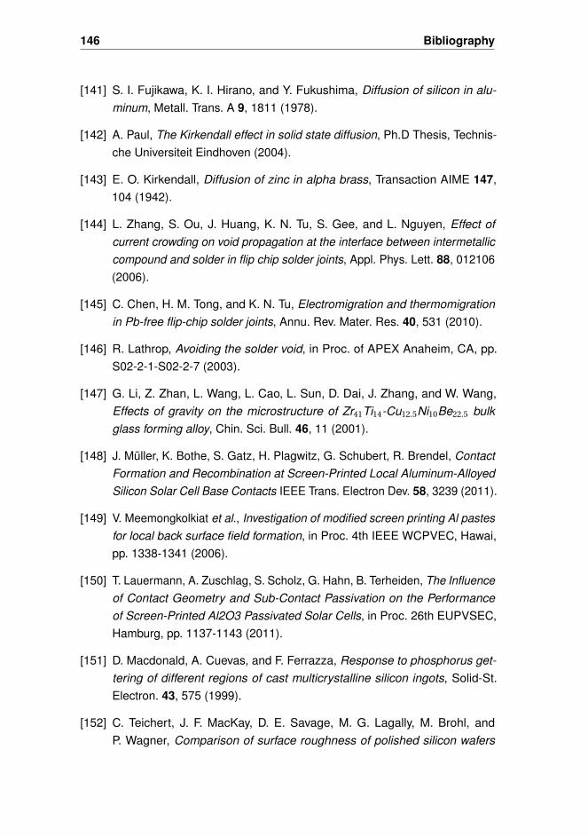
146 Bibliography
[141] S. I. Fujikawa, K. I. Hirano, and Y. Fukushima, Diffusion of silicon in alu-minum, Metall. Trans. A 9, 1811 (1978).
[142] A. Paul, The Kirkendall effect in solid state diffusion, Ph.D Thesis, Technis-che Universiteit Eindhoven (2004).
[143] E. O. Kirkendall, Diffusion of zinc in alpha brass, Transaction AIME 147,104 (1942).
[144] L. Zhang, S. Ou, J. Huang, K. N. Tu, S. Gee, and L. Nguyen, Effect ofcurrent crowding on void propagation at the interface between intermetalliccompound and solder in flip chip solder joints, Appl. Phys. Lett. 88, 012106(2006).
[145] C. Chen, H. M. Tong, and K. N. Tu, Electromigration and thermomigrationin Pb-free flip-chip solder joints, Annu. Rev. Mater. Res. 40, 531 (2010).
[146] R. Lathrop, Avoiding the solder void, in Proc. of APEX Anaheim, CA, pp.S02-2-1-S02-2-7 (2003).
[147] G. Li, Z. Zhan, L. Wang, L. Cao, L. Sun, D. Dai, J. Zhang, and W. Wang,Effects of gravity on the microstructure of Zr41Ti14-Cu12.5Ni10Be22.5 bulkglass forming alloy, Chin. Sci. Bull. 46, 11 (2001).
[148] J. Müller, K. Bothe, S. Gatz, H. Plagwitz, G. Schubert, R. Brendel, ContactFormation and Recombination at Screen-Printed Local Aluminum-AlloyedSilicon Solar Cell Base Contacts IEEE Trans. Electron Dev. 58, 3239 (2011).
[149] V. Meemongkolkiat et al., Investigation of modified screen printing Al pastesfor local back surface field formation, in Proc. 4th IEEE WCPVEC, Hawai,pp. 1338-1341 (2006).
[150] T. Lauermann, A. Zuschlag, S. Scholz, G. Hahn, B. Terheiden, The Influenceof Contact Geometry and Sub-Contact Passivation on the Performanceof Screen-Printed Al2O3 Passivated Solar Cells, in Proc. 26th EUPVSEC,Hamburg, pp. 1137-1143 (2011).
[151] D. Macdonald, A. Cuevas, and F. Ferrazza, Response to phosphorus get-tering of different regions of cast multicrystalline silicon ingots, Solid-St.Electron. 43, 575 (1999).
[152] C. Teichert, J. F. MacKay, D. E. Savage, M. G. Lagally, M. Brohl, andP. Wagner, Comparison of surface roughness of polished silicon wafers
Bibliography 147
measured by light scattering topography, soft-x-ray scattering, and atomic-force microscopy, Appl. Phys. Lett. 66, 2346 (1995).
[153] J. D. Hylton, Light coupling and light trapping in alkaline etched multicrys-talline silicon wafers for solar cells, PhD Thesis, Utrecht University (2006).
[154] M. Hofmann, C. Schmidt, N. Kohn, J. Rentsch, S. Glunz, and R. Preu, Stacksystem of PECVD amorphous silicon and PECVD silicon oxide for siliconsolar cell rear side passivation, Prog. Photovoltaics 16, 509 (2008).
[155] S. Kontermann, A. Wolf, D. Reinwand, A. Grohe, D. Biro, and R. Preu,Optimizing Annealing Steps for Crystalline Silicon Solar Cells with ScreenPrinted Front Side Metallization and an Oxide - Passivated Rear Surfacewith Local Contacts, Prog. Photovoltaics 17, 554 (2009).
[156] R. A. Sinton and A. Cuevas, Contactless determination of current-voltagecharacteristics and minority-carrier lifetimes in semiconductors from quasi-steady-state photoconductance data, Appl. Phys. Lett. 69, 17 (1996).
[157] S. Su, F. Chen, and D. Dutta, Surface Textured Implants, US Patent20100114303 (2009).
[158] P. Ferrada, PhD Thesis, Universität Konstanz (to be published).
[159] A. Halm, L. M. Popescu, J. Theobald, K. Peter, R. Kopecek, Low Tempera-ture Pads on Al-Emitter or Al-BSF, in Proc. 24th EUPVSEC, Hamburg, pp.1462-1464 (2009).
[160] R. Kopecek, A. Halm, L. Popescu, K. Peter, M. A. Vázquez, Industrial largearea n-type solar cells with aluminium rear emitter with stable efficiencies,in Proc. 35th IEEE PVSC, Honolulu, HI, pp. 001423-001426 (2010).
[161] P. Grunow, Soldering of Crystalline Silicon Modules: Losses, Reliabilityand Improvements, in Proc. 2nd Workshop on Metallization, Konstanz, pp.59-62 (2010).
[162] S. Wenham and M. A. Green, Dry Phosphorus Silicate Glass Etching forMulticrystalline Silicon Solar Cells, Prog. Photovoltaics 11, 445 (1996).
[163] A. Wolf, et al., The SiNTO process: Utilizing a SiNx anti-reflection layerfor emitter masking during Thermal Oxidation, in Proc. 34th IEEE PVSC,Philadelphia, pp. 534-539.
148 Bibliography
[164] M. Rinio, H. J. Möller, and M. Werner, LBIC Investigations of the LifetimeDegradation by Extended Defects in Multicrystalline Solar Silicon, SolidState Phenomena 63-64, 115 (1998).
[165] L. Mittelstädt, S. Dauwe, A. Metz, R. Hezel, and C. Häßler, Front and rearsilicon-nitride-passivated multicrystalline silicon solar cells with an efficiencyof 18.1%, Prog. Photovoltaics 10, 35 (2002).
[166] G. Blatter and F. Greuter, Carrier transport through grain boundaries insemiconductors, Phys. Rev. B 33, 3952 (1986).
[167] S. Dauwe, L. Mittelstädt, A. Metz, and R. Hezel, Experimental evidence ofparasitic shunting in silicon nitride rear surface passivated solar cells, Prog.Photovoltaics 10, 271 (2002).
[168] I. Cesar, E. E. Bende, G. Galbiati, L. Janßen, A. A. Mewe, P. Manshanden,A. W. Weeber, and J. H. Bultman, Parasitic shunt losses in all-side SiNxpassivated mc-Si solar cells, in Proc. 24th EUPVSEC, Hamburg, pp. 21-25(2009).
LIST OF FIGURES
1.1 Rear passivated solar cell structure and aluminum rear side . . . . . . . 4
2.1 Principle of a quarter wavelength antireflection coating . . . . . . . . . 132.2 Etching rate of SiNx by HF and of Si by NaOH . . . . . . . . . . . . . . . 17
3.1 Total series resistance losses . . . . . . . . . . . . . . . . . . . . . . . . 263.2 Recombination in semiconductors . . . . . . . . . . . . . . . . . . . . . . 313.3 Absorption coefficient of Si and penetration depth . . . . . . . . . . . . . 34
4.1 Flow diagram sequence of the selective emitter process . . . . . . . . 394.2 Optical fiducial alignment . . . . . . . . . . . . . . . . . . . . . . . . . . . . 414.3 Dielectric ablation and screen printer alignment . . . . . . . . . . . . . . 414.4 EQE and Voc gain for the selective emitter process . . . . . . . . . . . 43
5.1 Influence of the BSF effect on the charge carriers . . . . . . . . . . . . 485.2 PC1D numerical simulations of the BSF effect on Voc . . . . . . . . . 505.3 Al-Si equilibrium diagram . . . . . . . . . . . . . . . . . . . . . . . . . . . 525.4 Model of contact formation between Al and Si . . . . . . . . . . . . . . 535.5 SEM micrographs of the Al-Si alloying junction . . . . . . . . . . . . . . 555.6 Lamellar structure of Al-Si alloy . . . . . . . . . . . . . . . . . . . . . . . 565.7 Peeling off of the Al fingers . . . . . . . . . . . . . . . . . . . . . . . . . . . 57
6.1 Model of the alloyed junction of Al lines on dielectric openings . . . . 626.2 TLM result of the contact and line resistance for different Al line widths 646.3 Contact resistivity variation . . . . . . . . . . . . . . . . . . . . . . . . . . 666.4 SEM micrographs of Al-Si alloying junction for different contact areas 686.5 Model to calculate the real Al-Si contact surface . . . . . . . . . . . . . . 716.6 SEM micrographs of the contact area after HCl etching . . . . . . . . . 736.7 Rear passivated solar cell in cross section . . . . . . . . . . . . . . . . . 746.8 Temperature linear dependency of the spread limit of Si . . . . . . . . 766.9 SEM/EDX analysis of Si distribution in Al . . . . . . . . . . . . . . . . . . 776.10 Schematic model of contact formation for narrow contact areas . . . . 806.11 SEM micrographs of samples with different contact spacings . . . . . 836.12 SEM micrographs of eutectic and void . . . . . . . . . . . . . . . . . . . . 846.13 EDX line analysis of the Si content in the Al matrix . . . . . . . . . . . . 84
149
150 List of Figures
6.14 EDX volume analysis of distribution of Si in the thick Al layer . . . . . 866.15 Hypothesis of lateral solidification . . . . . . . . . . . . . . . . . . . . . . . 876.16 Model of the local Al-Si contact and influence of gravity . . . . . . . . . 896.17 SEM micrographs of the influence of gravity on solidification . . . . . . . 916.18 Simple scheme of void formation . . . . . . . . . . . . . . . . . . . . . . . 946.19 SEM micrographs of two types of voids found . . . . . . . . . . . . . . 95
7.1 Study on the roughness of polishing surfaces . . . . . . . . . . . . . . . 1037.2 Reflectivity measurements for different surfaces . . . . . . . . . . . . . 1057.3 The influence of the boat position on the homogeneity of the emitter . 1067.4 SEM micrograph of Ag pads and ribbon peel off test . . . . . . . . . . 1087.5 Ag pads after the peel off test performed to monitor the bonding force 1097.6 I-V characteristic results for study 1 . . . . . . . . . . . . . . . . . . . . . . 1147.7 EL-analysis of dislocations in rear passivated mc-Si solar cell . . . . . 1167.8 LBIC map of rear passivated solar cell . . . . . . . . . . . . . . . . . . . . 1177.9 I-V results for reference and device structures for study 2 . . . . . . . . 1217.10 FF analysis depending on Ag paste amount and printing sequence . 1237.11 Spectral response analysis . . . . . . . . . . . . . . . . . . . . . . . . . . 1257.12 High efficiency solar cell process and spectral response . . . . . . . . 1287.13 El-analysis of an Al-BSF and a PERC solar cell . . . . . . . . . . . . . 130
LISTS OF ACRONYMS AND SYMBOLS
The following list aims to help the reader, resuming the acronyms, symbols andsome definitions used throughout this thesis.
Acronym Description
Ag SilverAl AluminumAM1.5 Air mass 1.5ARC Anti-reflection coatingBSF Back-surface-fieldc-Si Crystalline siliconCz-Si Czochralski crystalline silicon materialDev. DeviceEDS/EDX Energy dispersive X-ray spectrometryEG-Si Electronic-grade siliconEL ElectroluminescenceEQE External quantum efficiencyFS Front side of deviceFSF Front surface fieldGaAs Gallium arsenideGB Grain boundariesGe GermaniumIQE Internal quantum efficiencyISC-Konstanz International Solar Energy Research Center KonstanzI -V Current-voltage characteristicLBIC Light beam induced currentmc-Si Multicrystalline silicon materialN NitrideNH3 AmmoniaO OxygenP PhosphorusPECVD Plasma-enhanced chemical vapor depositionPERC Passivated emitter and rear cell
151
152 Lists of Acronyms and Symbols
Acronym Description
POCl3 Phosphorous oxychloridePSG Phosphorous silicate glassPV PhotovoltaicsQE Quantum efficiencyQSSPC Quasi steady state photoconductanceR ReflectivityRmi n Minimum of ReflectionRef. ReferenceRS Rear side of deviceRT Room temperature at 300 KSEM Scanning electron microscopySi SiliconSiH4 SilaneSiNx Silicon nitrideSoG-Si Solar grade siliconSR Spectral response (responsivity)TLM Transmission line method
Symbol Description Unit
A Area [cm2]α Absorption coefficient [cm−1]c Speed of light in vacuum [cm/s]D Diffusion coefficient or diffusivity [cm2/s]d Etching depth [µm]di Thickness, length [µm]dp Contact spacing [µm]d1 Contact size (dielectric window) [µm]d2 Spread of Si in Al, or Al finger width [µm]E g Energy bandgap [eV]EC Conduction band [eV]EV Valence band [eV]EF Fermi level [eV]F F Fill factor [%]Iph Photocurrent [A]I0 Dark saturation current [A]
Lists of Acronyms and Symbols 153
Symbol Description Unit
JSC Short-circuit current [mA/cm2]JO Reverse saturation current [mA/cm2]k Wave vector [cm−1]L Diffusion length [µm]g Gravity field orientationLe f f Effective carrier diffusion length [µm]LR Line resistance [Ω/cm]N Excess carrier concentration [cm−3]n Concentration of free electron [cm−3]n Normal direction of solidificationni Refractive indexnopt Refractive index of SiNA Ionized acceptor impurity concentration [cm−3]ND Ionized donor impurity concentration [cm−3]p Concentration of free hole [cm−3]Popt Optical power (Popt =Φi nhν) [W]Pmp Maximum output power point [W]RS Series resistance [Ωcm2]RP Shunt resistance [Ωcm2]RSH Sheet resistance [Ω/ä]RC Contact resistance [Ω]R Total recombination rate [cm−3-s−1]Sdr Surfaces area ratio [nm]Se f f Back surface recombination velocity [cm/s]S f Front surface recombination velocity [cm/s]S/L Solid/liquid interfaceT Absolute temperature [C]Teut Eutectic temperature [C]Tmel t Melting temperature [C]VOC Open-circuit voltage [mV]W Solar cell base thickness [µm]x j Junction depth [µm]η Conversion efficiency [%]ρc Contact resistivity [mΩcm2]Φi n Photon flux [s−1]
154 Lists of Acronyms and Symbols
Symbol Description Unit
λ Wavelength [nm]hν Photon energy [eV]ν Frequency of light [Hz]ρ Resistivity [Ω-cm]σ Conductivity [S-cm−1]µn Electron mobility [cm2/V-s]µp Hole mobility [cm2/V-s]τ Lifetime [µs]
Constants Quantity Value
h Planck constant 4.1357x10⁻¹⁵ eV-sk Boltzmann constant 8.6174x10⁻⁵ eV/Kq Elementary charge 1.60218x10⁻¹⁹ C
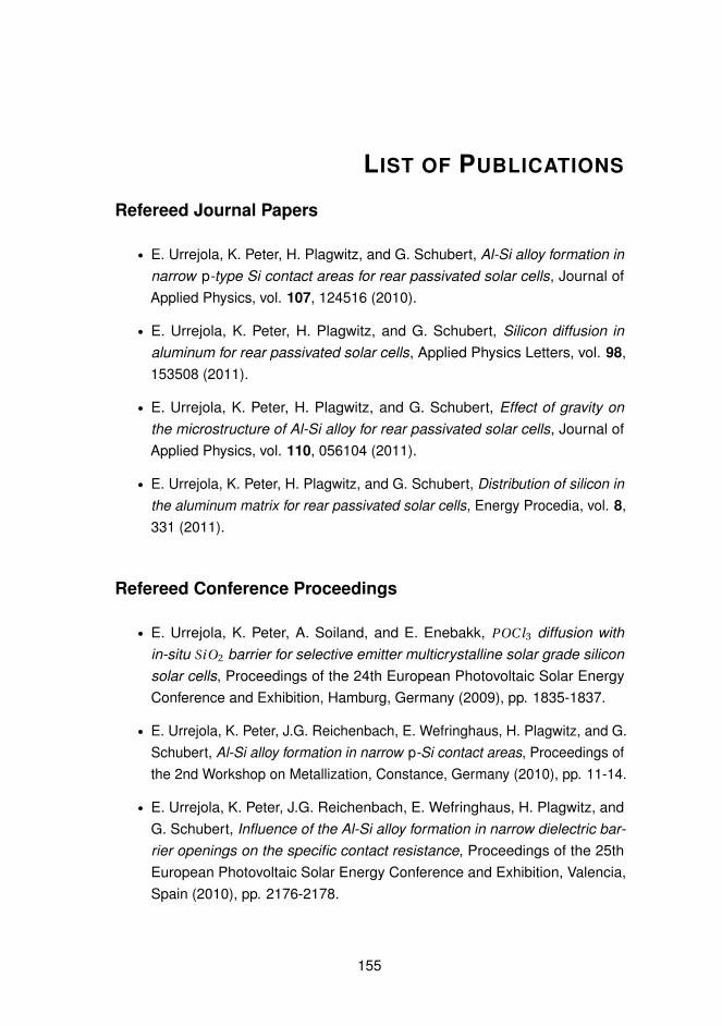
LIST OF PUBLICATIONS
Refereed Journal Papers
• E. Urrejola, K. Peter, H. Plagwitz, and G. Schubert, Al-Si alloy formation innarrow p-type Si contact areas for rear passivated solar cells, Journal ofApplied Physics, vol. 107, 124516 (2010).
• E. Urrejola, K. Peter, H. Plagwitz, and G. Schubert, Silicon diffusion inaluminum for rear passivated solar cells, Applied Physics Letters, vol. 98,153508 (2011).
• E. Urrejola, K. Peter, H. Plagwitz, and G. Schubert, Effect of gravity onthe microstructure of Al-Si alloy for rear passivated solar cells, Journal ofApplied Physics, vol. 110, 056104 (2011).
• E. Urrejola, K. Peter, H. Plagwitz, and G. Schubert, Distribution of silicon inthe aluminum matrix for rear passivated solar cells, Energy Procedia, vol. 8,331 (2011).
Refereed Conference Proceedings
• E. Urrejola, K. Peter, A. Soiland, and E. Enebakk, POC l3 diffusion within-situ SiO2 barrier for selective emitter multicrystalline solar grade siliconsolar cells, Proceedings of the 24th European Photovoltaic Solar EnergyConference and Exhibition, Hamburg, Germany (2009), pp. 1835-1837.
• E. Urrejola, K. Peter, J.G. Reichenbach, E. Wefringhaus, H. Plagwitz, and G.Schubert, Al-Si alloy formation in narrow p-Si contact areas, Proceedings ofthe 2nd Workshop on Metallization, Constance, Germany (2010), pp. 11-14.
• E. Urrejola, K. Peter, J.G. Reichenbach, E. Wefringhaus, H. Plagwitz, andG. Schubert, Influence of the Al-Si alloy formation in narrow dielectric bar-rier openings on the specific contact resistance, Proceedings of the 25thEuropean Photovoltaic Solar Energy Conference and Exhibition, Valencia,Spain (2010), pp. 2176-2178.
155
156 List of Publications
• E. Urrejola, R. Petres, J. Glatz-Reichenbach, K. Peter, H. Plagwitz, G.Schubert, High efficiency industrial PERC solar cells with all PECVD-basedrear surface passivation, Proceedings of the 26th European PhotovoltaicSolar Energy Conference and Exhibition, Hamburg, Germany (2011), pp.2233-2235.
Oral Presentations
• Silicon Solar Cells, by E. Urrejola et al., "Encuentros: 3rd Conference ofYoung Chilean Scientists in Europe", Göttingen (Germany), 11.02.2009.
• Al-Si alloy formation in narrow p-Si contact areas, by E. Urrejola, 2nd Work-shop on Metallization for Crystalline Silicon Solar Cells, Constance (Ger-many), 14.04.2010.
• Distribution of silicon in the aluminum matrix for rear passivated solar cells,by E. Urrejola, 1st Silicon PV Conference, Freiburg (Germany), 17.04.2011.
• Understanding and avoiding the formation of voids for rear passivated siliconsolar cells, by E. Urrejola, 3r d Workshop on Metallization for CrystallineSilicon Solar Cells, Charleroi (Belgium), 26.10.2011.
Visual Presentations
• POCl3 Diffusion with in-situ SiO2 barrier for Selective Emitter MulticrystallineSolar Grade Silicon Solar Cells, by E. Urrejola, 24th European PhotovoltaicSolar Energy Conference and Exhibition, Hamburg (Germany), 23.09.2009.Session code: 2CV.5.35.
• Influence of the Al-Si Alloy formation in narrow dielectric barrier openings onthe specific contact resistance, by E. Urrejola, 25th European PhotovoltaicSolar Energy Conference and Exhibition, Valencia (Spain), 08.09.2010.Session code: 2CV.3.31.
• High efficiency industrial PERC solar cells with all PECVD-based rearsurface passivation, by E. Urrejola, 26th European Photovoltaic Solar EnergyConference and Exhibition, Hamburg (Germany), 07.09.2011, Session code:2CV.4.34.
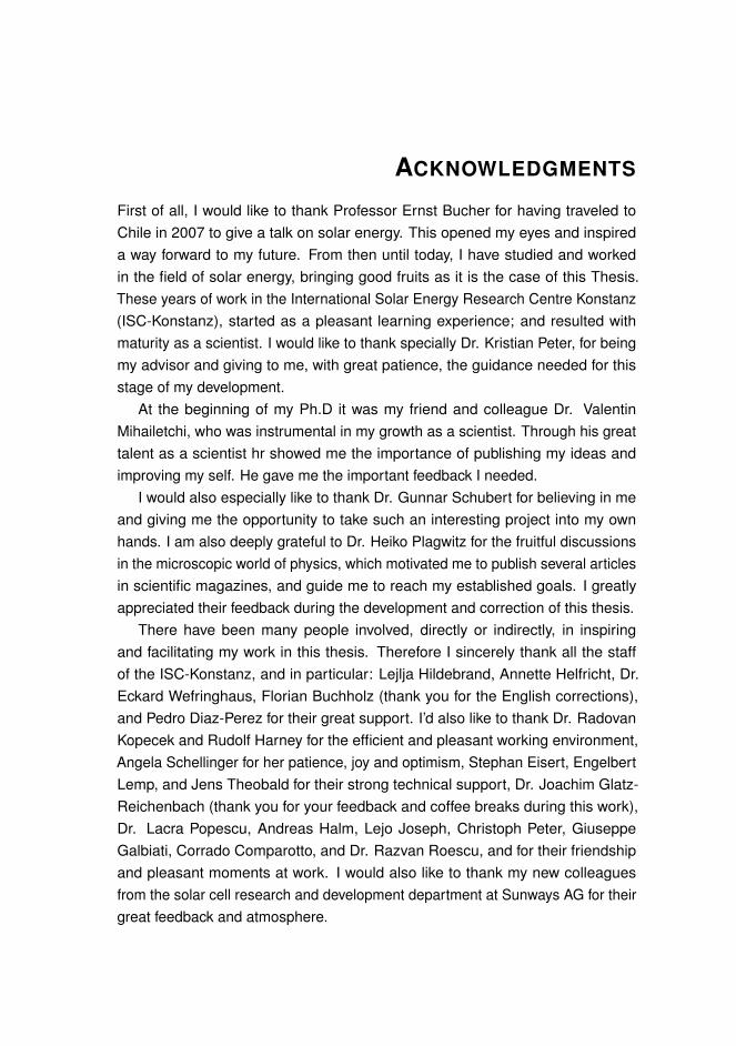
ACKNOWLEDGMENTS
First of all, I would like to thank Professor Ernst Bucher for having traveled toChile in 2007 to give a talk on solar energy. This opened my eyes and inspireda way forward to my future. From then until today, I have studied and workedin the field of solar energy, bringing good fruits as it is the case of this Thesis.These years of work in the International Solar Energy Research Centre Konstanz(ISC-Konstanz), started as a pleasant learning experience; and resulted withmaturity as a scientist. I would like to thank specially Dr. Kristian Peter, for beingmy advisor and giving to me, with great patience, the guidance needed for thisstage of my development.
At the beginning of my Ph.D it was my friend and colleague Dr. ValentinMihailetchi, who was instrumental in my growth as a scientist. Through his greattalent as a scientist hr showed me the importance of publishing my ideas andimproving my self. He gave me the important feedback I needed.
I would also especially like to thank Dr. Gunnar Schubert for believing in meand giving me the opportunity to take such an interesting project into my ownhands. I am also deeply grateful to Dr. Heiko Plagwitz for the fruitful discussionsin the microscopic world of physics, which motivated me to publish several articlesin scientific magazines, and guide me to reach my established goals. I greatlyappreciated their feedback during the development and correction of this thesis.
There have been many people involved, directly or indirectly, in inspiringand facilitating my work in this thesis. Therefore I sincerely thank all the staffof the ISC-Konstanz, and in particular: Lejlja Hildebrand, Annette Helfricht, Dr.Eckard Wefringhaus, Florian Buchholz (thank you for the English corrections),and Pedro Diaz-Perez for their great support. I’d also like to thank Dr. RadovanKopecek and Rudolf Harney for the efficient and pleasant working environment,Angela Schellinger for her patience, joy and optimism, Stephan Eisert, EngelbertLemp, and Jens Theobald for their strong technical support, Dr. Joachim Glatz-Reichenbach (thank you for your feedback and coffee breaks during this work),Dr. Lacra Popescu, Andreas Halm, Lejo Joseph, Christoph Peter, GiuseppeGalbiati, Corrado Comparotto, and Dr. Razvan Roescu, and for their friendshipand pleasant moments at work. I would also like to thank my new colleaguesfrom the solar cell research and development department at Sunways AG for theirgreat feedback and atmosphere.
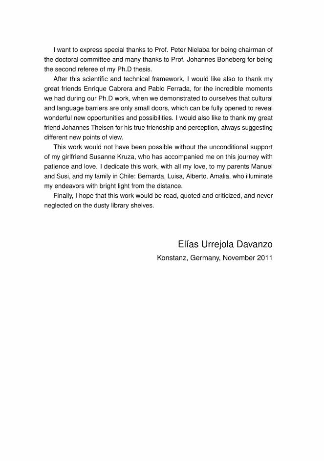
I want to express special thanks to Prof. Peter Nielaba for being chairman ofthe doctoral committee and many thanks to Prof. Johannes Boneberg for beingthe second referee of my Ph.D thesis.
After this scientific and technical framework, I would like also to thank mygreat friends Enrique Cabrera and Pablo Ferrada, for the incredible momentswe had during our Ph.D work, when we demonstrated to ourselves that culturaland language barriers are only small doors, which can be fully opened to revealwonderful new opportunities and possibilities. I would also like to thank my greatfriend Johannes Theisen for his true friendship and perception, always suggestingdifferent new points of view.
This work would not have been possible without the unconditional supportof my girlfriend Susanne Kruza, who has accompanied me on this journey withpatience and love. I dedicate this work, with all my love, to my parents Manueland Susi, and my family in Chile: Bernarda, Luisa, Alberto, Amalia, who illuminatemy endeavors with bright light from the distance.
Finally, I hope that this work would be read, quoted and criticized, and neverneglected on the dusty library shelves.
Elías Urrejola DavanzoKonstanz, Germany, November 2011
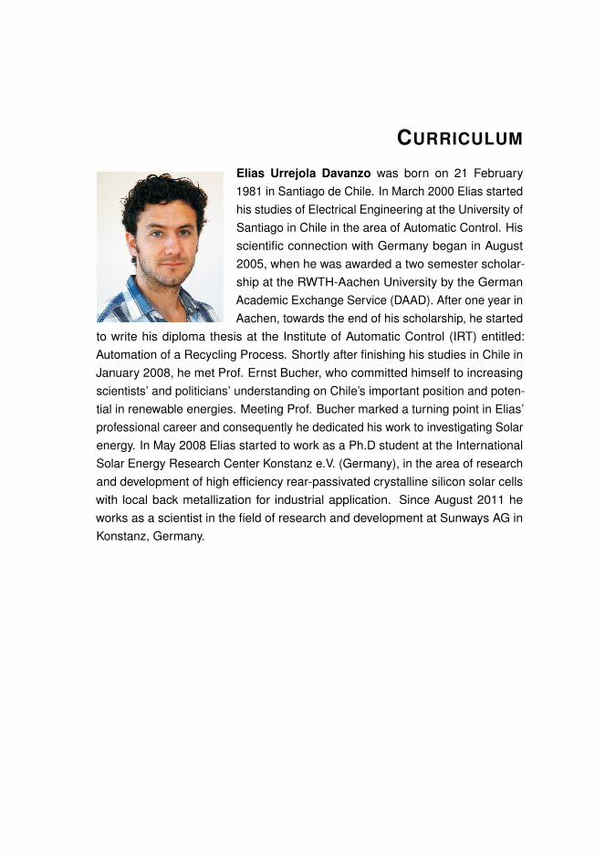
CURRICULUM
Elias Urrejola Davanzo was born on 21 February1981 in Santiago de Chile. In March 2000 Elias startedhis studies of Electrical Engineering at the University ofSantiago in Chile in the area of Automatic Control. Hisscientific connection with Germany began in August2005, when he was awarded a two semester scholar-ship at the RWTH-Aachen University by the GermanAcademic Exchange Service (DAAD). After one year inAachen, towards the end of his scholarship, he started
to write his diploma thesis at the Institute of Automatic Control (IRT) entitled:Automation of a Recycling Process. Shortly after finishing his studies in Chile inJanuary 2008, he met Prof. Ernst Bucher, who committed himself to increasingscientists’ and politicians’ understanding on Chile’s important position and poten-tial in renewable energies. Meeting Prof. Bucher marked a turning point in Elias’professional career and consequently he dedicated his work to investigating Solarenergy. In May 2008 Elias started to work as a Ph.D student at the InternationalSolar Energy Research Center Konstanz e.V. (Germany), in the area of researchand development of high efficiency rear-passivated crystalline silicon solar cellswith local back metallization for industrial application. Since August 2011 heworks as a scientist in the field of research and development at Sunways AG inKonstanz, Germany.
Related Documents


