ARTICLE All WSe 2 1T1R resistive RAM cell for future monolithic 3D embedded memory integration Maheswari Sivan 1 , Yida Li 1 *, Hasita Veluri 1 , Yunshan Zhao 1 , Baoshan Tang 1 , Xinghua Wang 1 , Evgeny Zamburg 1 , Jin Feng Leong 1 , Jessie Xuhua Niu 1 , Umesh Chand 1 & Aaron Voon-Yew Thean 1 * 3D monolithic integration of logic and memory has been the most sought after solution to surpass the Von Neumann bottleneck, for which a low-temperature processed material system becomes inevitable. Two-dimensional materials, with their excellent electrical prop- erties and low thermal budget are potential candidates. Here, we demonstrate a low- temperature hybrid co-integration of one-transistor-one-resistor memory cell, comprising a surface functionalized 2D WSe 2 p-FET, with a solution-processed WSe 2 Resistive Random Access Memory. The employed plasma oxidation technique results in a low Schottky barrier height of 25 meV with a mobility of 230 cm 2 V -1 s -1 , leading to a 100x performance enhanced WSe 2 p-FET, while the defective WSe 2 Resistive Random Access Memory exhibits a switching energy of 2.6 pJ per bit. Furthermore, guided by our device-circuit modelling, we propose vertically stacked channel FETs for high-density sub-0.01 μm 2 memory cells, offering a new beyond-Si solution to enable 3-D embedded memories for future computing systems. https://doi.org/10.1038/s41467-019-13176-4 OPEN 1 Department of Electrical and Computer Engineering, National University of Singapore, 4 Engineering Drive 3, Singapore 117583, Singapore. *email: [email protected]; [email protected] NATURE COMMUNICATIONS | (2019)10:5201 | https://doi.org/10.1038/s41467-019-13176-4 | www.nature.com/naturecommunications 1 1234567890():,;

Welcome message from author
This document is posted to help you gain knowledge. Please leave a comment to let me know what you think about it! Share it to your friends and learn new things together.
Transcript
ARTICLE
All WSe2 1T1R resistive RAM cell for futuremonolithic 3D embedded memory integrationMaheswari Sivan1, Yida Li1*, Hasita Veluri1, Yunshan Zhao1, Baoshan Tang1, Xinghua Wang1,
Evgeny Zamburg 1, Jin Feng Leong1, Jessie Xuhua Niu1, Umesh Chand1 & Aaron Voon-Yew Thean 1*
3D monolithic integration of logic and memory has been the most sought after solution to
surpass the Von Neumann bottleneck, for which a low-temperature processed material
system becomes inevitable. Two-dimensional materials, with their excellent electrical prop-
erties and low thermal budget are potential candidates. Here, we demonstrate a low-
temperature hybrid co-integration of one-transistor-one-resistor memory cell, comprising a
surface functionalized 2D WSe2 p-FET, with a solution-processed WSe2 Resistive Random
Access Memory. The employed plasma oxidation technique results in a low Schottky barrier
height of 25 meV with a mobility of 230 cm2 V−1 s−1, leading to a 100x performance
enhanced WSe2 p-FET, while the defective WSe2 Resistive Random Access Memory exhibits
a switching energy of 2.6 pJ per bit. Furthermore, guided by our device-circuit modelling, we
propose vertically stacked channel FETs for high-density sub-0.01 μm2 memory cells, offering
a new beyond-Si solution to enable 3-D embedded memories for future computing systems.
https://doi.org/10.1038/s41467-019-13176-4 OPEN
1 Department of Electrical and Computer Engineering, National University of Singapore, 4 Engineering Drive 3, Singapore 117583, Singapore.*email: [email protected]; [email protected]
NATURE COMMUNICATIONS | (2019) 10:5201 | https://doi.org/10.1038/s41467-019-13176-4 | www.nature.com/naturecommunications 1
1234
5678
90():,;
Emerging non-von Neumann architectures with intensivein-memory computing like next-generation deep learningand neuromorphic chips will demand high-density inte-
gration of embedded memory. Three-dimensional monolithic(sequential) multilayer stacking of transistors and memoryamong interconnects may allow us to expand the on-chipmemory density. Such architectures will not only overcome thetwo-dimensional (2D) die limitations but also enable newthree-dimensional (3D) computation systems, where logic andmemory elements are intimately co-located, to significantlyimprove the memory access bandwidth and energy1. However,to fully realize such 3D systems, there are fundamental tech-nology challenges to overcome. Among which, transistor-interconnect thermal budget incompatibility poses a majorroad block. Advanced low-resistivity copper interconnect withlow-k dielectric interlayer cannot tolerate thermal exposureabove 400 °C2. Since the thermal activation of dopants in Si-based devices are typically between 600 and 1000 °C, Si tran-sistor formation below such temperature results in deviceperformance and reliability degradations3. This low thermalbudget technology barrier calls for both material and processintegration breakthroughs, to enable new platforms for 3Dintegration.
Carbon nanotubes (CNTs) field-effect transistor (FETs) and2D semiconducting van der Waal-layered crystals (2DMat) havedrawn immense attention as transistor channel material, due totheir intrinsic performance that rivals silicon, as well asupcoming successors like germanium, silicon germanium,and III–V compound semiconductors at sub-nanometerchannel thickness regime4. More importantly, the potential ofsuch nanomaterials for low-temperature, large-area transferand integration, independent of their material synthesis5,6,puts them in an advantageous position to be co-integratedadditively with metal interconnects on CMOS (complementarymetal–oxide–semiconductor) chips (Supplementary Table 1).The feasibility of 3D integration with CNTs has already beendemonstrated by Shulaker et al.1, but that of 2DMat has onlystarted to gain traction7. 2DMat, with their intrinsic nanolayerstructures and variety of electronic structures are expected toadd more functionalities for process temperature-limited tech-nologies like sequential/monolithic 3D chips8 and high-performance flexible electronics9.
In this work, we demonstrate the feasibility of hybrid co-integration of a surface-engineered WSe2-based thin filmtransistor (TFT) and resistive random access memories(ReRAM) to realize a 1 transistor–1 resistor (1T1R) memorycell. This is done through integrating WSe2 of differentmorphologies (single crystalline for TFT, and polycrystallinefor ReRAM) processed through different synthesis technique, toaddress the conflicting charge transport attributes required forlogic and memory. As TFT should be optimized for high per-formance and low leakage, the high-quality mechanicallyexfoliated WSe2 is utilized as the transistor channel. On theother hand, ReRAM should be optimized for low-voltagedefect-enabled switch ability, for which solution-processedWSe2 is employed. Despite WSe2 2DMat being well investi-gated for future logic application, its application for 1T1Rmemory cell by hybrid co-integration is yet to be investigated.Moreover, our proposed processes are room temperature based,offering compelling compatibility with temperature-limited 3Dmonolithic process integration and flexible electronics proces-sing. Furthermore, we propose through calibrated compactdevice modeling and circuit simulations that sub-0.01 µm2
1T1R cells with good read/write margins are feasible bystacking 2D nanosheets to realize a multiple-stacked 2D TFTsto drive the 2D ReRAMs.
ResultsWSe2 select transistor material. With a large bandgap, a rea-sonably high intrinsic thin-channel carrier mobility10, and n–ppolarity that can be easily modulated by contact Schottky barriermetal11, WSe2 offers great potential for low leakage and perfor-mant CMOS logic gates12. The low on-state resistance and off-state leakage potential of the WSe2 transistor also makes them agood select transistor candidate for 1T1R memories, which callsfor minimization of voltage loss across the transistor duringmemory cell set/reset and the off-state sneak current in the array,respectively. Despite the favorable intrinsic attributes, WSe2transistors are still challenged by extrinsic degradations inmobility and high contact resistance. The reports of WSe2 exhi-biting high mobility at low temperatures13 suggest the detri-mental role played by various scattering sources, such asphonons, Coulomb impurities (CI), and intrinsic defects inmobility degradation. Although passivation methods based ondielectric deposition, including atomic layer-deposited high-kencapsulation14, have been pursued, the process uniformityremains challenging due to undesired grain boundary nuclea-tion15. Thus, it becomes necessary to investigate other strategiesincluding uniform native oxide passivation solution as well.
In addition, minimizing transistor access resistance is essentialto translate the performance gains from channel carrier mobility.While heavy source/drain (S/D) doping is the most preferredmethod for improving contact resistance in conventional Sidevices, such substitutional doping in 2DMat comes at theexpense of increased defect density16. For 2DMat, severalapproaches ranging from material modification to the co-integration of graphene electrodes17 have been proposed.However, they present new challenges in stability and work-function limitations. For example, the semiconducting 2H phaseto metallic 1T phase modification18 can improve contactresistance significantly, but the low-temperature stability andFermi level to conduction band alignment limits its utilization forp-FETs14. Graphene contacts, due to its Fermi level alignmentclose to the conduction band, would also lead to undesirableelectron injection for p-FETs17. In this work, we concurrentlyaddress strategies for hole carrier doping, mobility enhancement,Schottky barrier, and contact resistance reduction througha single-step process that overcomes the issues of stabilityand p-contact work-function alignment. We developed a self-limiting single-step, low-temperature WO3 formation on channelsurface and under the S/D contacts by post-contact remoteplasma oxidation. This process simultaneously enhances theWSe2 TFT mobility by almost 76 times and reduces the contactresistance by a hundred-fold. By implementing Ag-WO3-WSe2metal–insulator–semiconductor (MIS) contact, we achieved anultra-low Schottky barrier height (SBH) of 25 meV with respect tothe WSe2 valence band, significantly enhancing hole injection.
Low-temperature surface layer plasma oxidation for WSe2 FET.For 2D transition metal dichalcogenides (TMDs), the thickness isa critical parameter influencing their electronic and opticalproperties. Although mechanical exfoliation results in high-quality WSe2 flakes, the approach does not allow for precisethickness control. Considerable amount of research has beendevoted to realizing a thickness reduction strategy, such as the useof focused ion beam19, ozone treatment20,21, XeF2 vapors22,plasma oxidation23, thermal oxidation24, and so on. However,these approaches can induce minor22 as well as major damage tothe crystallinity of the WSe2 material with resultant negativeimpact to its electrical performance. While the above-mentionedreports focus on oxidation as a thickness reduction strategy formechanically exfoliated samples, we introduce a low-temperature
ARTICLE NATURE COMMUNICATIONS | https://doi.org/10.1038/s41467-019-13176-4
2 NATURE COMMUNICATIONS | (2019) 10:5201 | https://doi.org/10.1038/s41467-019-13176-4 | www.nature.com/naturecommunications

remote plasma oxidation process (Methods section) and study theutility of the formed oxide as a MIS contact and encapsulationlayer using detailed material and electrical characterization. Weshow that gentle plasma oxidation can create a layer of surfaceWOx, which do not damage the underlying WSe2 structure.Figure 1a shows the cross-sectional transmission electronmicroscope (xTEM) image of the WSe2 flake before and after theremote plasma oxidation, from which the presence of WOx andthe quality of exposed WSe2 are confirmed. The thickness of theformed WOx is ~2.2 nm for a consumption of three layers ofWSe2, as confirmed by xTEM. Irrespective of oxidation time, theWOx formation is found to be self-limiting as well (Supplemen-tary Fig. 1). The same oxide thickness has been validated forWSe2 of different starting area and thicknesses under the sameoxidation condition.
Raman spectroscopy and X-ray photoelectron spectroscopy(XPS) analysis were done to determine the nature of WOx
formed by this process. As the vibrational and optical propertiesstrongly vary with thickness, a comparison of “oxidized WSe2”and “oxide-removed WSe2” has been performed. The oxideremoval process, which is selective to WSe2, is done usingKOH solution (Methods section). From the Raman spectrumin Fig. 1b, we observe the typical out-of-plane A1g mode, inplane E2g mode and the bulk, B2g mode for two prepared four-layer WSe2 samples; one with WOx (after oxidation) and one
without WOx (after oxide removal). No apparent Raman peakshift is detected between the two samples—ruling out thepresence of any plasma oxidation induced stress in WSe2. Theresultant WOx appears to be amorphous due to the absence ofthe 800 cm−1 signature peak, indicating crystalline WOx
25
(Supplementary Fig. 2). The amorphous WOx structure isfurther corroborated by the xTEM images (Fig. 1a), which didnot reveal any crystalline order in the WOx layer. Since thereexists reports of crystalline WO3 formed through air heating athigher temperature of 400 °C25, the amorphous WOx is likelydue to our low-temperature plasma oxidation process. From theXPS analysis in Fig. 1c, we confirm the stoichiometry ofamorphous WOx to be native WO3. Specifically, peaks at 35.5and 37.7 eV after plasma oxidation correspond to the bindingenergies of W6+, indicating the presence of WO3
25. Further-more, we observe charge transfer mediated by WO3 from theXPS spectrum after plasma oxidation. The observed decrease inbinding energy of W 4f core levels (0.18 eV reduction in W4+
4f7/2 and 0.26 eV reduction in W4+ 4f5/2) (Fig. 1d) suggests thatthere is electron transfer from WSe2 to WO3. This is attributedto the high work function of WO3 consistent with otherreported studies22. We show here that low-temperature plasmaoxidation, capable of self-limiting to ~2.2 nm amorphous WO3,produces an ultra-thin hole donor layer that is also gentleto WSe2.
240 270 300 330
0.2
0.4
0.6
0.8
1.0
B2g
After oxidation
After oxide removal
Raman shift (cm–1)
E2g1
A1g
b
35 34 33 32 31Binding energy (eV)
As flaked
After plasma oxidation
–0.18 eV –0.26 eV
W 4fd
40 38 36 34 320.0
0.5
1.0
1.5
WO3
W6+ W6+
4f7/24f5/2
W6+
4f5/2
W4+
4f5/2
4f5/2
W4+
4f7/24f7/2
Nor
mal
ized
inte
nsity
(a.
u)
Nor
mal
ized
inte
nsity
(a.
u)
0.0
0.5
1.0
1.5
Nor
mal
ized
inte
nsity
(a.
u)
Binding energy (eV)
As flaked
After plasma oxidation
WSe2c
SiO2/p + Si SiO2/p + Si
N (nm)WSe2 (N–t )
nm WSe2
t (nm) WOx
As flaked WSe2
a
After plasma oxidation
WSe2WSe2
2.2 nm
SiO2SiO2
WO3
2 nm2 nm
Fig. 1 Remote plasma oxidation process and characterization. a Schematic representation of surface plasma oxidation and the corresponding cross-sectional transmission electron microscope (xTEM) images. The xTEM image of oxidized WSe2 shows 2.2 nm of WO3 upon oxidation, which is aconsumption of three layers of WSe2. b Raman spectroscopy comparison before oxidation and after oxide removal, in order to have comparison betweenWSe2 of same thickness. No apparent change in peak position is observed, implying no crystalline damage due to plasma oxidation. c X-ray photoelectronspectroscopy (XPS) comparison of as flaked WSe2 and plasma-oxidized WSe2. The appearance of two additional peaks after oxidation corresponds to an xfactor of 3 in WOx. d W 4f core level XPS spectrum comparison of pristine WSe2 and plasma-oxidized WSe2. The observed shift to lower binding energyimplies electron transfer from WSe2 to WO3
NATURE COMMUNICATIONS | https://doi.org/10.1038/s41467-019-13176-4 ARTICLE
NATURE COMMUNICATIONS | (2019) 10:5201 | https://doi.org/10.1038/s41467-019-13176-4 | www.nature.com/naturecommunications 3

Figure 2a shows the schematic of the fabricated deviceconsisting of a four-layer WSe2 and three-layer WO3. Thedetailed fabrication procedure can be found in the Methodssection. In order to realize a thinner WO3 layer under the Ag S/Dcontacts to minimize tunneling resistance, we chose to performpost-contact plasma oxidation. The key advantage of this strategyis that the WO3 growth rate under the S/D region would bemoderated by the metal contact. The TEM image (Fig. 2b)confirms thinner (1.7 nm) WO3 layer under the contact asopposed to the thicker (2.2 nm) oxide formation for the exposedchannel, despite the common plasma oxidation process. Due tolimited diffusion of O radicals at the Ag-WSe2 terminations onboth ends of the electrodes, the O radicals can only propagatelaterally under the Ag contacts, resulting in a reduced thinning ofWSe2 layer24 under the contact metal as opposed to the exposedchannel regions.
We characterized the resultant TFT performance by measuringthe transfer and output characteristics (Fig. 2c, d). Figure 2ccompares the transfer characteristics with and without post-contact plasma oxidation. The devices without WO3 is unremark-able, showing ambipolar conduction, with slightly stronger n-type(Vg >−5 V) than p-type conduction (Vg <−5 V). Upon plasmaoxidation, the device exhibits strong p-type conduction. Mostremarkably, a 100× enhancement in the hole current isaccompanied by a strong polarity change, where n-typeconduction is completely suppressed. To further investigate theTFT performance improvement, we carefully characterized theinfluence of WO3 on mobility and contact resistance.
We measured the gate inversion capacitance of the oxidizeddevice and found it to have increased by 2× compared to thegeometrical value (77 vs. 38 nF cm−2). Details of inversioncapacitance extraction are found in Supplementary Fig. 3 and
–20 –10 0 10 2010–12
10–10
10–8
10–6
10–4
With WO3
Without WO3
I d (
A/μ
m)
I d (
μA/μ
m)
I on
(A/μ
m)
Ioff(min) (A/μm)
Vg (V)
φSB ~ 140 meV
Vd = –0.5 V
100×0.4 V/decade
pFET
Ambipolar
c
–1.2 –1.0 –0.8 –0.6 –0.4 –0.2 0.0
0
50
100
150–40 V
–30 V
–20 V
Vg = 0 V
Vd (V)
–10 V
d
0 –4 –8 –24 –28 –32 –36
0
20
40
60
Vg (V)
EA
(meV
)
EA
(meV
)
e
At flat band conditionφSB ~ 25 meV
100
150
200
10–7
10–6
10–5
10–4
10–3
10–16 10–13 10–10 10–7
WSe2
(Nb doped)[16]
WSe2(ozonetreatment)[20]
This work (WSe2 + WOx)(Rc = 4.3 kΩμm)
This work (without WOx)(Rc = 419 kΩμm)
WSe2(graphenecontacts)[17]
> 100×
f
Ag
SiO2
WSe2
WO3
With WO3
ba
10 nm
1.7 nmD
Vg
Four-layerWSe2
90 nm SiO2
p + Si
WO3 S
Vd
With WO3
Without WO3
Fig. 2 Surface plasma-oxidized WSe2 TFT and electrical characterization. a Device schematic showing a four-layer WSe2 and 2.2 nm WO3 on SiO2/p+ Silayer with gate length (Lg)= 1.80 µm and width (W)= 2.05 µm. b Transmission electron microscopy image of the device contact region, after post-contactplasma oxidation, revealing the presence of WO3 underneath the metal contacts. c Id–Vg plots for four-layer thick device with and without WO3. d Id–Vd
characteristics after plasma oxidation for different gate voltages. e Effective Schottky barrier height extraction from low-temperature transfercharacteristics and Arrhenius plot. At flat band condition, the curve deviates from linearity and the corresponding activation energy becomes the Schottkybarrier. f Benchmark plot showing the performance of plasma-oxidized p-FET versus other reported data. Ion is determined at Vd=−0.5 V
ARTICLE NATURE COMMUNICATIONS | https://doi.org/10.1038/s41467-019-13176-4
4 NATURE COMMUNICATIONS | (2019) 10:5201 | https://doi.org/10.1038/s41467-019-13176-4 | www.nature.com/naturecommunications
Supplementary Note 1. Since we do not observe CV frequencydispersion (Supplementary Figure 3e) that indicates significantfast or slow charge trapping/de-trapping processes, we excludethe possibility of spurious charges and disorder at WSe2 bottom-gate dielectric interface as reported by Pradhan et al. 13. Instead,we believe the interfacial charge transfer at the WSe2-WO3
heterostructure contributed towards the capacitance increase. Toensure accurate mobility extraction, we emphasize here the needfor CV measurements, instead of making capacitance assump-tions based on geometry. From Fig. 2c and the measuredinversion capacitance, we extracted a dramatic 76× hole field-effect mobility (µFE) increase from 3 cm2 V−1 s−1 (non-oxidized)to 230 cm2 V−1 s−1 and observed a significant 100× reduction ofcontact resistance (Rc) to 4.3 kΩµm from our control with 420kΩµm, which is extracted using the well-reported Rtotal–Vg
method26. The details of field-effect mobility and contactresistance extraction can be found in the Supplementaryinformation (Supplementary Figs. 4 and 5). The Rc reductioncorrelates to a considerable lowering of the contact’s SBH to 25meV with respect to the SBH of 140 meV of our control samplewithout WO3 as shown in Fig. 2e. It appears that the thin WO3
under the Ag contact unpinned the contact Fermi level withrespect to WSe2, closer to the valence band minimum of WSe2,owing to the high work function of WO3
27. This would alsoexplain the observed suppression of electron current, as the SBHfor electrons would be large. Our room temperature, low-powerremote plasma oxidation treatment allows a gentler process toachieve less damage to the underlying WSe2 flake, as evident bythe non-reduction of the PL signal23 (Supplementary Fig. 6) ascompared to other reported methods28. In addition, the plasmaprocess allows the formation of a uniform thin layer of WO3
beneath the contact, which has not been reported. The argumentis supported by the observed SBH to be 10× lower than thebarrier height reported from other work involving similar surfacefunctionalization with WO3
20.
Furthermore, we conducted an experiment, where the plasmaoxidation was performed prior to contact formation, leading to auniform thicker (2.2 nm) WO3 under S/D contacts and over thechannel (Supplementary Fig. 7). While the drive current slightlyimproved compared to non-oxidized device, the performance isweaker than the post-contact-oxidized sample due to highercontact resistance, which is comparable to the device withoutoxidation (Supplementary Fig. 5). This suggests the importance ofcontrolling WO3 thickness, as a tunneling layer—the thickerWO3 with pre-contact oxidation actually degrades the contactresistance due to increased tunneling resistance29. Figure 2fbenchmarks selected top-performing WSe2 devices from variousreports. Our work shows the strongest Ion performance fordevices with sub-nA µm−1-level Ioff_min, showing an extraordin-ary 100× drive current enhancement with respect to our non-WO3 control (Supplementary Table 2).
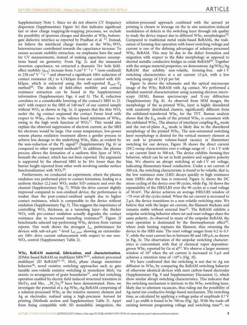
WSe2 ReRAM material, fabrication, and characterization.2DMat-based ReRAM on multilayer hBN30,31, solution-processedmultilayer 2D ReRAM32–35, MoS2 phase change memristorbehavior36, novel resistive switching approaches such as gatetunable non-volatile resistive switching in monolayer MoS2 viaatomic re-arrangement of grain boundaries37, and fast switchingoperation enabled by electric field-induced structural transition inMoTe2 and Mo1− xWxTe238 have been demonstrated. Here, weinvestigate the potential of a Ag-WSe2-Ag ReRAM comprising ofa solution-processed WSe2 as the resistive memory element andAg as electrodes, realized using a high-precision Aerosol Jetprinting (Methods section and Supplementary Table 3). Apartfrom being compatible with 3D monolithic integration, the
solution-processed approach combined with the aerosol jetprinting is chosen to leverage on the in situ sonication-inducedmodulation of defects in the switching layer through ink qualityto study the device impact due to different WSe2 morphologies39.Compared to traditional metal oxide-based ReRAMs, the reali-zation of forming-free operation with lower switching voltage andcurrent is one of the defining advantages of solution-processedWSe2 ReRAM. This may be due to the defect formation andmigration with respect to the flake morphology as opposed toshorted metallic conductive bridges in oxide ReRAM40. Togetherwith the unique material properties, we demonstrate Ag/WSe2/AgReRAM that exhibits non-volatile, forming-free, sub-1 Vswitching characteristics at a set current ≤5 µA, with a lowswitching energy of 2.9 pJ per bit.
Figure 3a shows the schematic and the optical microscopeimage of the WSe2 ReRAM with Ag contact. We performed adetailed material characterization using scanning electron micro-scopy (SEM), Raman spectroscopy and X-ray diffraction(Supplementary Fig. 8). As observed from SEM images, themorphology of the as-printed WSe2 layer is highly disorderedwith randomly distributed clusters, significantly different fromthe exfoliated-transferred WSe2 for the TFT. Raman analysisshows that the E2g mode of the printed WSe2 is consistent withthe exfoliated WSe2. The absence of interlayer coupling-B2g modeand the out-of-plane A1g mode is likely due to the disorderedmorphology of the printed WSe2. The non-orientated switchinglayer morphology is desired for the vertical memory element aswe seek to promote volume-based vacancy or filamentaryswitching for our devices. Figure 3b shows the direct current(DC) sweep characteristics over a voltage range of −1 to 1 V witha set current limit to 500 nA. The device exhibits forming-freebehavior, which can be set in both positive and negative polaritybias. We observe an abrupt switching at sub-1 V set voltage,indicating filamentary-based conduction. Under a set current of500 nA, the switching characteristic is found to be volatile, that is,the low resistance state (LRS) decays quickly to high resistancestate (HRS) after the bias is removed. Figure 3c shows the DCstress cycling of the device over 90 cycles, while Fig. 3d shows therepeatability of the HRS/LRS over the 90 cycles at a read voltageof 50 mV. The device achieves an average HRS/LRS window of~70 over all the cycles tested. When the set current is increased to2 µA, the device transitions to a non-volatile switching state. Webelieve that with the larger set current, the filament thickens andremains stable without external bias41. The ReRAM exhibits aunipolar switching behavior where set and reset voltages share thesame polarity. As observed in many of the unipolar ReRAM, thereset operation is dominated by the thermophoresis effect42,where joule heating ruptures the filament, thus returning thedevice to the HRS state. The reset voltage ranges from 0.2 to 0.3V, while the reset current lies in between 80 and 100 μA, as shownin Fig. 3e. The observation of the unipolar switching character-istics is concomitant with that of chemical vapor deposition-grown WSe2 reported by Ge et al43. We observe a larger memorywindow of 103 when the set current is increased to 5 µA andachieves a retention time of >104 s (Fig. 3f).
We have confirmed that the switching is not due to Ag iondiffusion in WSe2 by comparing the ReRAM switching behaviorof otherwise identical devices with inert carbon-based electrodes(Supplementary Fig. 9 and Supplementary Discussion 1), whichshow similar abrupt switching characteristics. This indicates thatthe switching mechanism is intrinsic to the WSe2 switching layer,likely due to selenium vacancies, thus ruling out the possibility ofAg metal ion conductive-bridge-based mechanism. The switchingtime, as calculated by applying a voltage pulse of amplitude 0.7 Vand 1 μs width is found to be 700 ns (Fig. 3g). With the trade-offexisting between programing voltage and switching time44, we
NATURE COMMUNICATIONS | https://doi.org/10.1038/s41467-019-13176-4 ARTICLE
NATURE COMMUNICATIONS | (2019) 10:5201 | https://doi.org/10.1038/s41467-019-13176-4 | www.nature.com/naturecommunications 5

–1.0 –0.5 0.0 0.5 1.0
–500
–250
0
250
500
Set for positive V Set for negative V
I (nA
)
I (A
)I (
A)
V (V)
bSet current = 500 nA
0.0 0.2 0.4 0.6 0.8 1.010–9
10–8
10–5
10–7
10–9
10–11
10–7
10–6108
107
106
105
104
108
107
106
105
103
104
V (V)
cSet current = 500 nA
Volatile switching
0 20 40 60 80 100R
esis
tanc
e (Ω
)R
esis
tanc
e (Ω
)
Number of cycles
LRS
HRS
~70
d
0.0 0.2 0.4 0.6 0.8 1.0 1.2
Set
Reset
V (V)
Set current = 2 μA
Non volatile switching
e
100 101 102 103 104
Time (s)
HRS
LRS
f
0.0 500.0n 1.0� 1.5�
0.0
0.2
0.4
0.6
0.8
Time (s)
Vol
tage
(V
)
Pulse width = 1 μs
V_max = 0.7 V
0
2
4
6
Cur
rent
(μA
)
Switchingtime = 700 ns
g
101 102 103 104 10510–14
10–12
10–10
10–8
10–6
10–4
Sw
itch
ener
gy (
J/bi
t)
Memory window (R_HRS/R_LRS)
h
This work
MoS2/MoOx[35]
Ti/HfO2/W[46]
SiO2[53]
Nanoporegraphene/HfO2
[52]
AlOx /WOx[54]
MoTe2[38]
Zr0.5Hf0.5O2/graphene oxide[49]
HfO2[51]
Graphene/HfOx /TiN[50]
Ta2O5 (CRS)[47]
HfOx /AlOy[48]
a Cell size = 70 × 70 μm2Printed
multilayer WSe2
Printed Ag bottom electrode (BE)
Top electrode (TE)
Kapton
BE
TEPrinted multilayer WSe2
Fig. 3 Printed WSe2 ReRAM electrical characterization. a Schematic of printed WSe2 ReRAM with Ag contacts along with microscope image of printedReRAM. b The device sets from HRS to LRS for both positive and negative voltages. c Stress cycling data for 90 cycles at a smaller set current of 500 nA,where volatile behavior is observed. d Endurance properties of ReRAM at read voltage of 50mV and a set current of 500 nA. e Set and reset operation witha larger set current of 2 µA, exhibiting non-volatile behavior. f Retention plot showing LRS and HRS stability till 104 s at a read voltage of 50mV and setcurrent of 5 µA. g Switching time characterization with an AC pulse of 0.7 V amplitude and 1 µs pulse width. h Benchmark plot of switching energy per bitvs. memory window of printed WSe2 ReRAM with other representative non-volatile resistive switching publications
ARTICLE NATURE COMMUNICATIONS | https://doi.org/10.1038/s41467-019-13176-4
6 NATURE COMMUNICATIONS | (2019) 10:5201 | https://doi.org/10.1038/s41467-019-13176-4 | www.nature.com/naturecommunications

have chosen to limit the programming voltage to achieve low setpower, which results in slower switching time of 700 ns. From thematerial/structural point of view, controlling the flake size andthickness of the switching layer would be areas that couldpotentially offer improvement in switching speed45. Our devicesshow one of the lowest reported switching energy (SupplementaryFig. 10, Supplementary Table 4, and Supplementary Note 2)relative to other 2DMat35,38 and other oxide-based ReRAMs46–54,as illustrated in the Fig. 3h with endurance comparable to otherreported 2DMat ReRAMs (Supplementary Table 5). We suspectthat the low switching energy is promoted by the excess defectsand grain boundaries in our printed WSe2 layer. We performedrepeatability check for ReRAM devices fabricated across severalbatches at different times, where we observed consistent switchingcharacteristics, as shown in the cumulative probability distribu-tion plot for set voltage, reset voltage, and ReRAM resistance(Supplementary Fig. 11). We believe that there is still significantopportunity for improvement with respect to ReRAM enduranceand other metrics by engineering the flake sizes with the solution-processed approach.
Although Aerosol jet printing technique allows additivedeposition of inks with a wide range of viscosities to realizequick prototyping of devices at relaxed dimensions (down to10 μm feature size), it is not a suitable method for industrial-scaleproduction because of the low throughput and large feature sizeachievable. Except for the low thermal budget of our process, wedo not believe that our additive approach would significantlychange the device conclusions for the solution-deposited andsubtractive methods like solution spin coating, compatible withlarge-scale dense circuit integration.
All WSe2 1T1R memory cell integration and characterization.The approaches of in-memory and neuromorphic computingbased on embedded memory have recently garnered greatmomentum, with growing interests to apply ReRAM55. However,high-density cross-bar ReRAM array suffers from current cross-talk interference due to sneak currents56, resulting in misreading
and unintended disturbance of memory states as well as unde-sirable increase in memory standby power consumption. Byemploying a select transistor to isolate the selected ReRAM cellfrom unselected cells, a 1T1R architecture can be implemented tocircumvent these problems57,58. Since the 1T1R cell leakage isgated by the select transistor off-state leakage, it is necessary forthe select transistor bandgap to be appropriately wide to limit S/Dband-to-band leakage current due to the memory operatingvoltage. WSe2 possess suitable bandgap in the range of 1.2 eV(bulk) to 1.6 eV (monolayer), limiting the transistor minimumoff-state leakage to be in the order of pA μm−1 for operatingvoltages in the range of 0.8–1.5 V. On the other hand, the max-imum on-state drive current of the select transistor should sup-port the set voltage and reset current of the ReRAM. However,the low intrinsic drive current of 2D TMD-based TFT makes itdifficult to drive the ReRAM. Therefore, we propose to utilize theperformance enhancement in plasma-oxidized WSe2 to mitigatethis issue.
We integrated the TFT and the ReRAM on the same chip tostudy the co-integration and its functionality (Fig. 4a), where theWSe2 ReRAM is printed after the WSe2 TFT fabrication. Themeasured 1T1R circuit configuration is as depicted in Fig. 4a.Figure 4b shows the successful switching of the WSe2 ReRAM bythe WSe2 TFT. As expected, the TFT’s on-state resistanceincreased the memory cell switching voltage to 1.7 V, which isalmost 3× larger than that of the ReRAM alone. This clearlyhighlights the gating impact of the select transistor performancefor the memory cell. It is necessary to decrease the TFT on-stateresistance while maintaining low off-state leakage to limit sneakcurrent. This becomes increasingly challenging with decreasingcell size where TFT area is constrained. In the next section, weinvestigate the cell design with the use of material-calibratedcompact models and circuit simulations, which would allow us toproject for scaled-up memory array implementation.
Material-device-circuit co-design of 1T1R memory cell. Inorder to evaluate the memory cell for scaled technologies and to
0.0 0.5 1.0 1.5 2.0 2.5 3.0
10–10
10–9
10–8
10–7
10–6
10–5
1T1R1R
I (A
)
V (V)
Set current limited by WSe2
FET
bSet current = 1 μA
3×
a
Vs
Vg
WO3
PrintedmultilayerWSe2
CL
BL
TFTTFT
Top Ag electrode with pads
PrintedRRAMs
RRAM-Flaked four-layer WSe2
1T
S D BE
TE90 nm SiO2
p + Si
1R
Fig. 4 1T1R configuration and characterization. a 3D schematic view of 1T1R structure with flaked WSe2 transistor and printed WSe2 ReRAM and thecorresponding circuit representation. The photo image of 3× WSe2 ReRAMs printed using low-temperature aerosol jet printing method, which is linked upto the fabricated WSe2 TFT on a single chip is also shown. b I–V switching plot for 1T1R configuration, where the switching current is limited by thetransistor drive current
NATURE COMMUNICATIONS | https://doi.org/10.1038/s41467-019-13176-4 ARTICLE
NATURE COMMUNICATIONS | (2019) 10:5201 | https://doi.org/10.1038/s41467-019-13176-4 | www.nature.com/naturecommunications 7

project for future 1T1R technology, we investigate the material-system co-design using detailed circuit modeling and study thedisruptive impact of material properties on the system designconsiderations. A BSIM-IMG compact circuit model59 descrip-tion of the TFT has been calibrated to experiment-based long-channel devices and known WSe2 material parameters. Short-channel effects such as velocity saturation, GISL (gate-inducedsource leakage) and GIDL (gate-induced drain leakage) has beentaken into account for the scaled devices through modeling. Ahysteron-based compact model, as reported by Garcia-Redondoet al.60, has been calibrated to the WSe2 ReRAM. Guided byexperimental data, we applied these models largely behaviorally,given that the physics of these devices are not well described yet.Despite this, we expect these models to be accurate for our SPICEcircuit analysis. Figure 5a, b show the compact model behaviorfor WSe2 TFT and ReRAM, respectively, which correlates wellwith the experimental data.
We project scaled technology performance by calibrating ourdevice and circuit models with intrinsic long-channel mobilityand contact resistance enhancement salient to our 2D WSe2approach. Our aim is to provide a first-order comparison betweendifferent material systems and their potential system impact,without the distraction of subjective details specific to scaleddevice design (such as interface trap density, S/D tunneling, etc.as explained in Supplementary Fig. 12 and SupplementaryDiscussion 2) and other more complex technology factors. Werecognize that detailed technology factors related to scaledtransistor/memory device behavior, interconnect properties,physical layout, and process integration approaches would beuseful to refine the system view in the future. Here, we analyze the1T1R cell scaling using λ-based design rule description, where
F= 4λ=minimum metal ½ pitch and 1T1R cell size is limited bythe select transistor size (min. cell area= 112λ2)61. The layout ofsuch a shared-source 1T1R cell is shown in Fig. 5c. As the 1T1Rmemory cell is scaled down, the selector drive current degradeswith the linear reduction of width (W= 4λ), whereas the ReRAMswitching current is largely insensitive to the cell size due tofilamentary switching43. This would raise concern over the abilityof the select transistor to set and reset the ReRAM, for smallercells. For shorter channel length, as the drive currentscales with width (W) and Cox as per the relation, Isd,sat=VsatWCox(Vsg− |Vtp|−Vsd,sat), increasing TFT gate capacitance(Cox), with thinner high-k gate dielectrics (to increase carriercharge density) may compensate for the current degradation dueto width scaling62. However, our analysis shows that, even withaggressive scaling of high-k gate oxide as per industry standardsfor low-power devices62,63, we would still suffer a 2.2× drop incurrent as the width is reduced 5× (from gate length of 65 to 13nm in Fig. 6b).
One way to address the issue of weak select transistor would beto rely on smaller ReRAM set current, but at the expense ofreduced HRS/LRS ratio (Supplementary Fig. 13). Hence, tomitigate the drive current degradation, without compromising onthe memory window, we propose increasing the effective widthby vertical stacking of 2DMat nanosheet TFT channels. Thiswould allow for TFT drive current recovery, without sacrificingthe 1T1R cell footprint. The conceptual representation of such a3D monolithic stacking of CMOS logic and 2D multiple-stackedWSe2 TFTs is shown in Fig. 6a. While thin WO3 is still utilized ashole doping layer, an additional gate dielectric with a metal gatewrapped around the nanosheet could be employed, to realize theproposed gate all around (GAA) vertically stacked WSe2 TFT.
–20
Bit line Bit line BL RRAM RRAM
1T1R cellsize = 112�2
4� (metalspacing)
TFT TFT2�
4�
4�
10�Shared source (SL)
WSe2 ReRAMswitching layer
WSe2 TFT channel
SL (source line)
BL (bit line)
WL (world line)Gate/source/drainelectrodes
(Metal spacing)4�
4�
4�
Gate(WL)Gate
(WL)
2�
Source line(shared source)
WordlineRRAM RRAM
p-FET p-FET
–15 –10 –5 0
0
50
100
Measured dataSimulated data
I d (
μA)
Vg (V)
Vds = –0.5 V
W/L = 2.2 μm/1.8 μm
a
0.0 0.2 0.4 0.6 0.8 1.010–9
10–8
10–7
10–6
10–5
10–4
I (A
)
V (V)
Set (experiment)Reset (experiment)Set (model)Reset (model)
Set current = 2 μA
b
c
Fig. 5 Compact modeling and circuit simulations. a Id–Vg of SPICE TFT model vs. measured WSe2 p-FET. b I–V of SPICE ReRAMmodel vs. measured for SETand RESET process. c Circuit representation and layout of shared SL 1T1R structure, with the 1T1R cell size indicated (BL—bit line; WL—word line; SL—shared-source line)
ARTICLE NATURE COMMUNICATIONS | https://doi.org/10.1038/s41467-019-13176-4
8 NATURE COMMUNICATIONS | (2019) 10:5201 | https://doi.org/10.1038/s41467-019-13176-4 | www.nature.com/naturecommunications
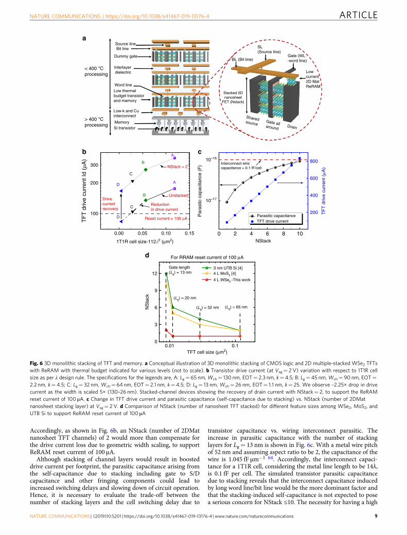
Accordingly, as shown in Fig. 6b, an NStack (number of 2DMatnanosheet TFT channels) of 2 would more than compensate forthe drive current loss due to geometric width scaling, to supportReRAM reset current of 100 µA.
Although stacking of channel layers would result in boosteddrive current per footprint, the parasitic capacitance arising fromthe self-capacitance due to stacking including gate to S/Dcapacitance and other fringing components could lead toincreased switching delays and slowing down of circuit operation.Hence, it is necessary to evaluate the trade-off between thenumber of stacking layers and the cell switching delay due to
transistor capacitance vs. wiring interconnect parasitic. Theincrease in parasitic capacitance with the number of stackinglayers for Lg= 13 nm is shown in Fig. 6c. With a metal wire pitchof 52 nm and assuming aspect ratio to be 2, the capacitance of thewire is 1.045 fF µm−1 64. Accordingly, the interconnect capaci-tance for a 1T1R cell, considering the metal line length to be 14λ,is 0.1 fF per cell. The simulated transistor parasitic capacitancedue to stacking reveals that the interconnect capacitance inducedby long word line/bit line would be the more dominant factor andthat the stacking-induced self-capacitance is not expected to posea serious concern for NStack ≤10. The necessity for having a high
0.00 0.05 0.10 0.15
100
200
300
Source lineBit line
Dummy gate
< 400 °Cprocessing
> 400 °Cprocessing
Interlayerdielectric
Word lineLow thermalbudget transistorand memory
Low-k and Cuinterconnect
MemorySi transistor
D
C
B
A
Unstacked
NStack = 2
D
TF
T d
rive
curr
ent I
d (μ
A)
1T1R cell size-112�2 (μm2)
b
Reset current = 100 μA
Drive current recovery
Reduction in drive current
A
B
C
0 2 4 6 8 10
10–17
10–16
Parasitic capacitanceTFT drive current
NStack
Par
astic
cap
acita
nce
(F)
c
Interconnect wirecapacitance = 0.1 fF/cell
200
400
600
800
TF
T d
rive
curr
ent (
μA)
0.01 0.10
3
6
9
12Gate length (Lg) = 13 nm
(Lg) = 65 nm
3 nm UTB Si [4]4 L MoS2 [4]
4 L WSe2 -This work
NS
tack
TFT cell size (μm2)
d
(Lg) = 20 nm
(Lg) = 32 nm
For RRAM reset current of 100 μA
a
BL (Bit line)
Sharedsource
Gate allaround Drain
Stacked 2Dnanosheet
FET (Nstack)
SL (Source line)
Gate (WL-word line)
Lowcurrent2D MatReRAM
Fig. 6 3D monolithic stacking of TFT and memory. a Conceptual illustration of 3D monolithic stacking of CMOS logic and 2D multiple-stacked WSe2 TFTswith ReRAM with thermal budget indicated for various levels (not to scale). b Transistor drive current (at Vsg= 2 V) variation with respect to 1T1R cellsize as per λ design rule. The specifications for the legends are, A: Lg= 65 nm, Wch= 130 nm, EOT= 2.3 nm, k= 4.5; B: Lg= 45 nm, Wch= 90 nm, EOT=2.2 nm, k= 4.5; C: Lg= 32 nm, Wch= 64 nm, EOT= 2.1 nm, k= 4.5; D: Lg= 13 nm, Wch= 26 nm, EOT= 1.1 nm, k= 25. We observe ~2.25× drop in drivecurrent as the width is scaled 5× (130–26 nm). Stacked-channel devices showing the recovery of drain current with NStack= 2, to support the ReRAMreset current of 100 µA. c Change in TFT drive current and parasitic capacitance (self-capacitance due to stacking) vs. NStack (number of 2DMatnanosheet stacking layer) at Vsg= 2 V. d Comparison of NStack (number of nanosheet TFT stacked) for different feature sizes among WSe2, MoS2, andUTB Si to support ReRAM reset current of 100 µA
NATURE COMMUNICATIONS | https://doi.org/10.1038/s41467-019-13176-4 ARTICLE
NATURE COMMUNICATIONS | (2019) 10:5201 | https://doi.org/10.1038/s41467-019-13176-4 | www.nature.com/naturecommunications 9
performant stacking channel layer becomes even more critical, torestrict the NStack below 10. With GAA nanosheet FETs beingregarded as a potential candidate for sub-3 nm technology node,the key research areas that require improvements are fine-tuningof nanosheet width optimization with extreme ultravioletlithography65, optimization of inner spacers66, advancement inmetrology, and inspection to measure the buried channel, processcontrol, and other fabrication challenges in gate stack integration.
Furthermore, we have compared the number of stackinglayers that would be required for other 2D materials such asMoS2 as well as conventional ultrathin Si from other reportedworks with respect to the WSe2 device reported in this work.Our analysis shows that the enhanced WSe2 device requires afewer number of channel stacking layers as compared to othermaterials, to support the maximum reset current of 100 µA ofour low-voltage ReRAM (Fig. 6d). This is due to WSe2’s highermobility at sub-5 nm channel thickness, compared to MoS2 andultrathin Si. Specifically, only two 2D WSe2 TFT channel stacks(NStack= 2) are required for cell sizes below 0.01 µm2. Thesefindings imply that, apart from thermal budget limitation, thelarge number of stacking layers required for ultrathin Sitransistors and MoS2 at sub-5 nm channel thickness increasesthe complexity of fabrication and the stacking-induced parasiticcapacitance.
While smaller effective mass (m*) of WSe2 allows for highermobility and high performance in sub-10 nm gate length (Lg), theenhanced S/D tunneling due to lower m* is the down side67,68.Hence, to further reduce the footprint of each device, werecommend greater width scaling rather than Lg scaling, withoutincreasing the standby power. However, the width scaling willcome at the expense of lower drive current per TFT. In this case,channel stacking of TFT becomes even more necessary to recoverthe required drive current and is an essential control knob toenable dense 1T1R cell.
DiscussionIn this work, a low-thermal-budget hybrid (solution-processed-exfoliated) integration of 2D material-based 1T1R is demon-strated for the first time. We highlight the importance of differentmaterial morphology for logic and memory operation. The selecttransistor needs to be single crystalline with enhanced drive forscaled 1T1R cells, while it is desired for the memory device to bepolycrystalline with defects that enable low-voltage switching. Weshow by post-contact plasma oxidation, a simple low-thermal-budget method to enhance the multilayer WSe2 transistor for thispurpose; achieving significant hole mobility (230 cm2 V−1 s−1),reduction of contact resistance (to 4.3 kΩµm) and Schottky bar-rier (to 25 meV). This culminates in a 100× drive enhancementwith respect to our control devices. In addition, we report an all-printed WSe2-based ReRAM using a low-temperature, aerosol jetprocess. The ReRAM exhibits sub-1 V non-volatile unipolarswitching with a low switching energy of 2.9 pJ per bit. Wedemonstrated the TFT-ReRAM 1T1R hybrid co-integration,which guided our accurate device-circuit models and enabled usto investigate material-system memory cell co-design for scaledtechnologies. This led us to the proposed stacked TFT channelsfor the memory cell to achieve high-density 1T1R memory arrayfor future dense monolithic 3D memory systems.
MethodsRemote plasma oxidation. The plasma chamber source to sampledistance is limited to 10 cm. The oxidation is performed at roomtemperature with a plasma power of 11W and chamber pressureof 20 mTorr (100 sccm of O2 and 20 sccm of Ar) for 2 min to
form 2.2 nm WO3. For some of the material characterization, theWO3 is removed by dipping in 1M KOH solution for 30 s.
TFT device fabrication and characterization. WSe2 flakes weremechanically exfoliated on p+ Si with 90 nm SiO2 layer, followedby electrode patterning using electron beam lithography. Thelength and width of the device are characterized and validated byAFM. Ag (10 nm) contacts capped with Au (90 nm) was depos-ited by electron beam evaporator followed by lift off to formsource and drain contacts. The device is then subjected to anannealing procedure (200 °C for 1 h in N2-H2 ambient, followedby vacuum annealing at 250 °C for 0.5 h), to remove the photo-resist residue and other gaseous adsorbates. After which, theplasma oxidation, as explained in the previous step is performedto form WO3 above the channel and also underneath the S/Dcontacts. The electrical measurements were collected by Agilentparameter analyzer B1500A.
Aerosol ink printing method for WSe2 ReRAM. WSe2 flakes sus-pended in ethanol forms the ink (concentration 0.1 mg/ml, from2D semiconductor) that is ultrasonically atomized and depositedby the Optomec AJ5X Aerosol Jet 5-axis Printer69. The bottomand top Ag electrodes are printed via the pneumatic atomizerfollowed by an 830 nm laser sintering process (Kapton) or a 150 °C, 30 min baking process (SiO2/Si substrate). Due to the lowconcentration of WSe2 in the ink, the ReRAM WSe2 layer has tobe deposited over multiple passes. We deposited ~400 nm averagethickness of WSe2 (printed over 30 passes) for our ReRAMdevices, with more details provided in the Supplementary Infor-mation (Supplementary Table 3 and Supplementary Fig. 8a). Afinal step of baking the entire sample at a temperature of 100 °Cfor 30 min is done to ensure conductivity of the printed Agelectrodes.
Data availabilityAll data supporting the findings of this study are available from the corresponding authoron request.
Received: 18 April 2019; Accepted: 11 October 2019;
References1. Shulaker, M. M. et al. Monolithic 3D integration: a path from concept to
reality. In Proc. 2015 Design, Automation & Test in Europe Conference &Exhibition 1197–1202 (EDA Consortium, 2015).
2. Fox, R. et al. High performance k= 2.5 ULK backend solution using animproved TFHM architecture, extendible to the 45nm technology node. InElectron Devices Meeting, 2005. IEDM Technical Digest. IEEE International81–84 (IEEE, 2005).
3. Batude, P. et al. 3D sequential integration opportunities and technologyoptimization. In IEEE International Interconnect Technology Conference373–376 (IEEE, 2014).
4. Iannaccone, G., Bonaccorso, F., Colombo, L. & Fiori, G. Quantum engineeringof transistors based on 2D materials heterostructures. Nat. Nanotechnol. 13,183 (2018).
5. Fu, Y., Qin, Y., Wang, T., Chen, S. & Liu, J. Ultrafast transfer of metal-enhanced carbon nanotubes at low temperature for large-scale electronicsassembly. Adv. Mater. 22, 5039–5042 (2010).
6. Castellanos-Gomez, A. et al. Deterministic transfer of two-dimensionalmaterials by all-dry viscoelastic stamping. 2D Mater. 1, 11002 (2014).
7. Wang, C.-H. et al. 3D monolithic stacked 1T1R cells using monolayer MoS2FET and hBN RRAM fabricated at low (150 °C) temperature. In 2018 IEEEInternational Electron Devices Meeting (IEDM) 22–25 (IEEE, 2018).
8. Batude, P. et al. 3D sequential integration: application-driven technologicalachievements and guidelines. In 2017 IEEE International Electron DevicesMeeting (IEDM) 1–3 (IEEE, 2017).
9. Akinwande, D., Petrone, N. & Hone, J. Two-dimensional flexiblenanoelectronics. Nat. Commun. 5, 5678 (2014).
ARTICLE NATURE COMMUNICATIONS | https://doi.org/10.1038/s41467-019-13176-4
10 NATURE COMMUNICATIONS | (2019) 10:5201 | https://doi.org/10.1038/s41467-019-13176-4 | www.nature.com/naturecommunications

10. Fang, H. et al. High-performance single layered WSe2 p-FETs with chemicallydoped contacts. Nano Lett. 12, 3788–3792 (2012).
11. Resta, G. V. et al. Polarity control in WSe2 double-gate transistors. Sci. Rep. 6,29448 (2016).
12. Das, S., Dubey, M. & Roelofs, A. High gain, low noise, fully complementarylogic inverter based on bi-layer WSe2 field effect transistors. Appl. Phys. Lett.105, 83511 (2014).
13. Pradhan, N. R. et al. Hall and field-effect mobilities in few layered p-WSe2field-effect transistors. Sci. Rep. 5, 8979 (2015).
14. Liu, W. et al. Role of metal contacts in designing high-performance monolayern-type WSe2 field effect transistors. Nano Lett. 13, 1983–1990 (2013).
15. Shokouh, S. H. H. et al. High-performance, air-stable, top-gate, p-channelWSe2 field-effect transistor with fluoropolymer buffer layer. Adv. Funct.Mater. 25, 7208–7214 (2015).
16. Chuang, H.-J. et al. Low-resistance 2D/2D ohmic contacts: a universalapproach to high-performance WSe2, MoS2, and MoSe2 transistors. Nano Lett.16, 1896–1902 (2016).
17. Chuang, H.-J. et al. High mobility WSe2 p- and n-type field-effect transistorscontacted by highly doped graphene for low-resistance contacts. Nano Lett.14, 3594–3601 (2014).
18. Kappera, R. et al. Phase-engineered low-resistance contacts for ultrathin MoS2transistors. Nat. Mater. 13, 1128 (2014).
19. Castellanos-Gomez, A. et al. Laser-thinning of MoS2: on demand generationof a single-layer semiconductor. Nano Lett. 12, 3187–3192 (2012).
20. Yamamoto, M., Nakaharai, S., Ueno, K. & Tsukagoshi, K. Self-limiting oxideson WSe2 as controlled surface acceptors and low-resistance hole contacts.Nano Lett. 16, 2720–2727 (2016).
21. Pudasaini, P. R. et al. High-performance multilayer WSe2 field-effecttransistors with carrier type control. Nano Res. 11, 722–730 (2018).
22. Zhang, R., Drysdale, D., Koutsos, V. & Cheung, R. Controlled layer thinningand p‐type doping of WSe2 by vapor XeF2. Adv. Funct. Mater. 27, 1702455(2017).
23. Li, Z. et al. Layer control of WSe2 via selective surface layer oxidation. ACSNano 10, 6836–6842 (2016).
24. Liu, Y. et al. Thermal oxidation of WSe2 nanosheets adhered on SiO2/Sisubstrates. Nano Lett. 15, 4979–4984 (2015).
25. Liu, B. et al. High-performance WSe2 field-effect transistors via controlledformation of in-plane heterojunctions. ACS Nano 10, 5153–5160 (2016).
26. Roy, T. et al. Field-effect transistors built from all two-dimensional materialcomponents. ACS Nano 8, 6259–6264 (2014).
27. Meyer, J. et al. Transition metal oxides for organic electronics: energetics,device physics and applications. Adv. Mater. 24, 5408–5427 (2012).
28. Yamamoto, M. et al. Self-limiting layer-by-layer oxidation of atomically thinWSe2. Nano Lett. 15, 2067–2073 (2015).
29. Lee, S., Tang, A., Aloni, S. & Philip Wong, H.-S. Statistical study on theSchottky barrier reduction of tunneling contacts to CVD synthesized MoS2.Nano Lett. 16, 276–281 (2015).
30. Pan, C. et al. Coexistence of grain-boundaries-assisted bipolar and thresholdresistive switching in multilayer hexagonal boron nitride. Adv. Funct. Mater.27, 1604811 (2017).
31. Qian, K. et al. Hexagonal boron nitride thin film for flexible resistive memoryapplications. Adv. Funct. Mater. 26, 2176–2184 (2016).
32. Hao, C. et al. Liquid-exfoliated black phosphorous nanosheet thin films forflexible resistive random access memory applications. Adv. Funct. Mater. 26,2016–2024 (2016).
33. Son, D. et al. Colloidal synthesis of uniform-sized molybdenum disulfidenanosheets for wafer-scale flexible nonvolatile memory. Adv. Mater. 28,9326–9332 (2016).
34. Tan, C., Liu, Z., Huang, W. & Zhang, H. Non-volatile resistive memorydevices based on solution-processed ultrathin two-dimensional nanomaterials.Chem. Soc. Rev. 44, 2615–2628 (2015).
35. Bessonov, A. A. et al. Layered memristive and memcapacitive switches forprintable electronics. Nat. Mater. 14, 199 (2015).
36. Cheng, P., Sun, K. & Hu, Y. H. Memristive behavior and ideal memristor of1T phase MoS2 nanosheets. Nano Lett. 16, 572–576 (2015).
37. Sangwan, V. K. et al. Gate-tunable memristive phenomena mediated by grainboundaries in single-layer MoS2. Nat. Nanotechnol. 10, 403 (2015).
38. Zhang, F. et al. Electric-field induced structural transition in verticalMoTe2 and Mo1–xWxTe2-based resistive memories. Nat. Mater. 18, 55(2019).
39. Tao, H. et al. Scalable exfoliation and dispersion of two-dimensional materials—an update. Phys. Chem. Chem. Phys. 19, 921–960 (2017).
40. Tsai, T.-L., Chang, H.-Y., Jiang, F.-S. & Tseng, T.-Y. Impact of post-oxidedeposition annealing on resistive switching in HfO2-based oxide RRAM andconductive-bridge RAM devices. IEEE Electron Device Lett. 36, 1146–1148(2015).
41. Wang, M. et al. Robust memristors based on layered two-dimensionalmaterials. Nat. Electron. 1, 130 (2018).
42. Strukov, D. B., Alibart, F. & Williams, R. S. Thermophoresis/diffusion as aplausible mechanism for unipolar resistive switching in metal–oxide–metalmemristors. Appl. Phys. A 107, 509–518 (2012).
43. Ge, R. et al. Atomristor: nonvolatile resistance switching in atomic sheets oftransition metal dichalcogenides. Nano Lett. 18, 434–441 (2017).
44. Luo, Q. et al. Super non-linear RRAM with ultra-low power for 3D verticalnano-crossbar arrays. Nanoscale 8, 15629–15636 (2016).
45. Raghavan, N. Performance and reliability trade-offs for high-κ RRAM.Microelectron. Reliab. 54, 2253–2257 (2014).
46. Cheng, L. et al. Reprogrammable logic in memristive crossbar for in-memorycomputing. J. Phys. D 50, 505102 (2017).
47. Breuer, T. et al. Realization of minimum and maximum gate function inTa2O5-based memristive devices. Sci. Rep. 6, 23967 (2016).
48. Huang, P. et al. Reconfigurable nonvolatile logic operations in resistanceswitching crossbar array for large-scale circuits. Adv. Mater. 28, 9758–9764(2016).
49. Yan, X. et al. Highly improved performance in Zr0.5Hf0.5O2 films inserted withgraphene oxide quantum dots layer for resistive switching non-volatilememory. J. Mater. Chem. C 5, 11046–11052 (2017).
50. Lee, S., Sohn, J., Jiang, Z., Chen, H.-Y. & Wong, H.-S. P. Metal oxide-resistive memory using graphene-edge electrodes. Nat. Commun. 6, 8407(2015).
51. Govoreanu, B. et al. 10 × 10 nm2 Hf/HfOx crossbar resistive RAMwith excellent performance, reliability and low-energy operation. InElectron Devices Meeting (IEDM), 2011 IEEE International 31–36 (IEEE,2011).
52. Zhao, X. et al. Confining cation injection to enhance CBRAM performance bynanopore graphene layer. Small 13, 1603948 (2017).
53. Shih, C.-C. et al. Ultra-low switching voltage induced by inserting SiO2 layerin indium–tin–oxide-based resistance random access memory. IEEE ElectronDev. Lett. 37, 1276–1279 (2016).
54. Song, Y. L. et al. Low reset current in stacked AlOx/WOx resistive switchingmemory. IEEE Electron Dev. Lett. 32, 1439–1441 (2011).
55. Ielmini, D. & Wong, H.-S. P. In-memory computing with resistive switchingdevices. Nat. Electron. 1, 333 (2018).
56. Zhou, J., Kim, K.-H. & Lu, W. Crossbar RRAM arrays: selector devicerequirements during read operation. IEEE Trans. Electron Dev. 61, 1369–1376(2014).
57. Wang, X. P. et al. Highly compact 1T-1R architecture (4F2 footprint)involving fully CMOS compatible vertical GAA nano-pillar transistors andoxide-based RRAM cells exhibiting excellent NVM properties and ultra-lowpower operation. In Electron Devices Meeting (IEDM), 2012 IEEEInternational 20–26 (IEEE, 2012).
58. Chen, P.-Y. & Yu, S. Compact modeling of RRAM devices and its applicationsin 1T1R and 1S1R array design. IEEE Trans. Electron Dev. 62, 4022–4028(2015).
59. Chauhan, Y. S. et al. BSIM compact MOSFET models for SPICE simulation.In Mixed Design of Integrated Circuits and Systems (MIXDES), 2013Proceedings of the 20th International Conference 23–28 (IEEE, 2013).
60. Garcia-Redondo, F., Gowers, R. P., Crespo-Yepes, A., López-Vallejo, M. &Jiang, L. SPICE compact modeling of bipolar/unipolar memristor switchinggoverned by electrical thresholds. IEEE Trans. Circuits Syst. I 63, 1255–1264(2016).
61. Yeh, C.-W. S. & Wong, S. S. Compact one-transistor-N-RRAM arrayarchitecture for advanced CMOS technology. IEEE J. Solid-State Circuits 50,1299–1309 (2015).
62. Robertson, J. High dielectric constant gate oxides for metal oxide Sitransistors. Rep. Prog. Phys. 69, 327 (2005).
63. Lee, B. H., Oh, J., Tseng, H. H., Jammy, R. & Huff, H. Gate stack technologyfor nanoscale devices. Mater. Today 9, 32–40 (2006).
64. Li, H. et al. Device and circuit interaction analysis of stochastic behaviorsin cross-point RRAM aArrays. IEEE Trans. Electron Dev. 64, 4928–4936(2017).
65. Barraud, S. et al. Performance and design considerations for gate-all-aroundstacked-nanowires FETs. In 2017 IEEE International Electron Devices Meeting(IEDM) 22–29 (IEEE, 2017).
66. Huang, Y.-C., Chiang, M.-H. & Wang, S.-J. Speed optimization of verticallystacked gate-all-around MOSFETs with inner spacers for low power and ultra-low power applications. In 20th International Symposium on QualityElectronic Design (ISQED) 231–234 (IEEE, 2019).
67. Majumdar, K., Hobbs, C. & Kirsch, P. D. Benchmarking transition metaldichalcogenide MOSFET in the ultimate physical scaling limit. IEEE ElectronDev. Lett. 35, 402–404 (2014).
68. Cao, W., Kang, J., Sarkar, D., Liu, W. & Banerjee, K. 2D semiconductor FETs—projections and design for sub-10 nm VLSI. IEEE Trans. Electron Dev. 62,3459–3469 (2015).
69. Secor, E. Principles of aerosol jet printing. Flex. Print. Electron. 3, 035002(2018).
NATURE COMMUNICATIONS | https://doi.org/10.1038/s41467-019-13176-4 ARTICLE
NATURE COMMUNICATIONS | (2019) 10:5201 | https://doi.org/10.1038/s41467-019-13176-4 | www.nature.com/naturecommunications 11

AcknowledgementsThis work has been supported in part by Singapore’s National Research Foundationgrant NRF-RSS2015-003, Hybrid Integrated Flexible Electronic Systems (HiFES)Prog. (hifes.nus.edu.sg), E6Nanofab, and the Center for Advanced 2D Materials at theNational University of Singapore. Many thanks to Ms. Zhang Yang for TEM samplepreparation, and to Dr. Gong Xiao and his team for assisting us on the low-temperature measurement.
Author contributionsA.V.-Y.T., Y.L., and M.S. conceived the project and designed the experiments. M.S.and Y.L. performed the device fabrication, electrical measurements, and analysis. H.V.performed the modeling and circuit simulations. Y.Z. carried out the TEM experiments.B.T. prepared the ink for solution processing. X.W performed XRD. E.Z., J.F.L., U.C., andJ.X.N. contributed towards discussion and data interpretation. M.S, Y.L, and A.V.-Y.T.co-wrote the paper, and all authors are involved in the discussions and preparation of themanuscript.
Competing interestsThe authors declare no competing interests.
Additional informationSupplementary information is available for this paper at https://doi.org/10.1038/s41467-019-13176-4.
Correspondence and requests for materials should be addressed to Y.L. or A.-Y.T.
Peer review information Nature Communications thanks Giovanni Resta and theanonymous reviewer/s for their contribution to the peer review of this work.
Reprints and permission information is available at http://www.nature.com/reprints
Publisher’s note Springer Nature remains neutral with regard to jurisdictional claims inpublished maps and institutional affiliations.
Open Access This article is licensed under a Creative Commons Attri-bution 4.0 International License, which permits use, sharing, adaptation,
distribution and reproduction in any medium or format, as long as you give appropriatecredit to the original author(s) and the source, provide a link to the Creative Commonslicense, and indicate if changes were made. The images or other third party material in thisarticle are included in the article’s Creative Commons license, unless indicated otherwise ina credit line to the material. If material is not included in the article’s Creative Commonslicense and your intended use is not permitted by statutory regulation or exceeds thepermitted use, you will need to obtain permission directly from the copyright holder. Toview a copy of this license, visit http://creativecommons.org/licenses/by/4.0/.
© The Author(s) 2019
ARTICLE NATURE COMMUNICATIONS | https://doi.org/10.1038/s41467-019-13176-4
12 NATURE COMMUNICATIONS | (2019) 10:5201 | https://doi.org/10.1038/s41467-019-13176-4 | www.nature.com/naturecommunications
Related Documents