ALL-OPTICAL PROCESSES IN INTEGRATED OPTICAL DEVICES USING MATERIALS WITH LARGE THIRD-ORDER NONLINEARITIES AND GAIN Ronald Dekker

Welcome message from author
This document is posted to help you gain knowledge. Please leave a comment to let me know what you think about it! Share it to your friends and learn new things together.
Transcript

ALL-OPTICAL PROCESSES IN INTEGRATED OPTICAL DEVICES USING MATERIALS
WITH LARGE THIRD-ORDER NONLINEARITIES AND GAIN
Ronald Dekker
Promotiecommissie: Promotor: Prof. Dr. A. Driessen Universiteit Twente Leden: Prof. Dr. K.J. Boller Universiteit Twente
Prof. Dr. P.V. Lambeck Universiteit Twente/OptiSense B.V. Prof. Dr. D. Lenstra Vrije Universiteit Amsterdam Dr. H.J.W.M. Hoekstra Universiteit Twente
The research described in this thesis was carried out at the Integrated Optical Microsystems (IOMS) Group, Faculty of Electrical Engineering, Mathematics and Computer Science, MESA+ Research Institute for Nanotechnology, University of Twente, P.O. Box 217, 7500 AE Enschede, The Netherlands. This work was financially supported by the Freeband Impulse technology program of the Ministry of Economic Affairs of the Netherlands and the European Network of Excellence on Photonic Integrated Components and Circuits (ePIXnet FAA5/WP11). Cover design: The illustration on the cover represents an artist impression of a bit stream which is propagating through a microring resonator. Furthermore, a low intensity signal photon is escaping via the microring resonator while being chased by a high intensity pump photon. ISBN-10: 90-9021436-4 ISBN-13: 978-90-9021436-8 Printed by Wöhrmann Print Service, Zutphen, The Netherlands. Copyright © 2006 by Ronald Dekker, Amersfoort, The Netherlands.
ALL-OPTICAL PROCESSES IN INTEGRATED OPTICAL DEVICES USING MATERIALS
WITH LARGE THIRD-ORDER NONLINEARITIES AND GAIN
PROEFSCHRIFT
ter verkrijging van de graad van doctor aan de Universiteit Twente,
op gezag van rector magnificus, prof. dr. W. H. M. Zijm,
volgens besluit van het College voor Promoties in het openbaar te verdedigen
op 22 december 2006 om 15.00 uur
door
Ronald Dekker geboren op 4 juli 1974
te Apeldoorn

Dit proefschrift is goedgekeurd door: de promotor: Prof. Dr. A. Driessen

To my father, Willem...

I
Data transport rates have increased tremendously over the last couple of years, because of the rapid growth of the internet, HD-television, digital communication, triple-play, etc. The amount of internet traffic, for instance, has doubled each year. Optical glass fibers, which are known for their high and practically unlimited bandwith, have experienced a huge growth as a replacement for the copper wires in the networks of the telecommunication operators. Switching speeds should increase in order to transport the rapid growing amount of optical data from end users and suppliers using these fiber networks. At this moment the switching of data signals is being performed in the electrical domain, but in the future the switching will take place completely in the optical domain: ‘all-optical switching’. This way of switching will eliminate the need of slow conversions from the optical domain to the electrical domain (and vice versa), resulting in switching speeds that are many times faster than nowadays physically possible in the electrical domain. Integrated optics is a logical choice for the realization of optical switches. Integrated optics is the field which explores and develops methods and devices for the propagation and processing of optical signals in lightwave structures. One could think of switching or filtering of wavelengths, but also amplification or modulation of such optical signals. This thesis presents various methods, both theoretically as well as experimentally, to amplify, modulate or switch optical signals in an integrated optical circuit, without the intervention of slowing electronics. In the first chapter an overview is given of the properties of integrated optical devices and the qualifications that such devices should satisfy. Subsequently, in chapter 2, two optically resonant structures will be presented, namely a microring resonator and an optical waveguide with an integrated grating structure. These optical structures can be applied as filtering elements or as a components in which the light energy is being stored to obtain the high energy densities that are needed for utrafast nonlinear optical processes. The working principle and properties of both resonators will be explained using experimental data which has been obtained from passive integrated optical chips that have been fabricated using silicon nitride technology. The fabrication of the microring resonator appeared to be more straightforward and has therefore been chosen as the basic building block for the rest of the research presented in this thesis.
II
Various material systems, like aluminum oxide, polymers and silicon, have been investigated for their feasibility to achieve active optical functions like optical amplification and all-optical switching. The variety of optical properties of these broad range of optical materials is described in chapter 3. The measurement setups needed to characterize the materials and integrated optical devices are presented in this chapter as well. Chapter 4 describes the deposition and properties of erbium doped aluminum oxide. The drawbacks of the deposition method used (DC-sputtering) are described and an overview of the etching techniques for the fabrication of microring resonators is presented, followed by experimental etching results. A prediction on the achievable gain in this type of material has been made, based on the optical properties of the deposited thin films. The second material system that has been investigated is presented in chapter 5. This chapter describes a low-cost technology based on materials which can be synthesized and deposited from the liquid phase using low-cost starting materials. The synthesis of photosensitive polymers and sol-gel glasses and their application in integrated optics will be discussed. These two types of materials can be made optically active by incorporation of rare-earth materials and nanoparticles. Results with respect to optical amplification in neodymium doped lanthanumfluoride nanoparticles in polymer waveguides is presented. Furthermore, the improved optical properties of erbium doped nanoparticles in a sol-gel matrix will be compared with conventional erbium doped sol-gel materials. The properties of noble metal nanoparticles, having an extremely high optical nonlinearity, are discussed and some experimental results of gold nanoparticles with a diameter of 14nm in various sol-gel matrices will be presented. The third material system is the semiconductor silicon, and is discussed in chapter 6. First, some nonlinear properties will be presented which are of importance when optical pulses with a duration of a few hundred femtoseconds are propagating through silicon waveguides. Next, a couple of methods are described to model pulse propagation through this class of nonlinear optical waveguides. Finally, experimental results are discussed in which the working principle of ultra-fast all-optical switching is demonstrated, making use of wavelength conversion in combination with passive microring resonators. In chapter 7, being the last chapter, conclusions will be drawn based on the results presented in this thesis.
III
Door de opkomst van het internet, HD-televisie, digitale telefonie, triple-play, enzovoorts, zijn de datahoeveelheden die getransporteerd moeten worden enorm gegroeid gedurende de laatste jaren. Het internet verkeer heeft bijvoorbeeld ieder jaar een verdubbeling ondergaan. Glasvezels staan bekend om hun nagenoeg onbegrensde bandbreedte en hebben de laatste jaren een enorme groei doorgemaakt als vervanging van de koperleidingen in de netwerken van de telecom aanbieders. Om deze sterk groeiende hoeveelheid optische data door glasvezelsnetwerken te transporteren tussen gebruikers en leveranciers zal er steeds sneller geschakeld moeten kunnen worden. Momenteel gebeurt dit schakelen nog in het electrische domein, maar in de toekomst zal dit schakelen van signalen volledig optisch plaats gaan vinden: ‘all-optical switching’. Deze manier van switchen maakt trage conversies vanuit het optische domein naar het electrische domein (en vice versa) overbodig, waardoor veel hogere schakelsnelheden behaald kunnen worden dan fysisch in het electrische domein mogelijk is. Het is een logische keuze om deze optische schakelaars te realiseren met geintegreerde optica. Geintegreerde optica is een vakgebied waarin men zich bezighoud met het geleiden en bewerken van optische signalen in lichtgeleidende structuren. Men kan bijvoorbeeld denken aan het schakelen of filteren van lichtsignalen met verschillende golflengte, maar ook het versterken of moduleren van dergelijke optische signalen. In dit proefschrift worden verschillende methoden gepresenteerd, zowel theoretisch als experimenteel, om lichtsignalen in een geintegreerd optische chip te versterken, te moduleren of te schakelen, zonder tussenkomst van vertragende electronica. In het eerste hoofdstuk zal er een overzicht gegeven worden van de eigenschappen van geintegreerd optische schakelingen en de eisen waaraan deze dienen te voldoen. Vervolgens worden in hoofdstuk 2 een tweetal optische resonante structuren gepresenteerd, namelijk een microring resonator en een golfgeleider met een geintegreerd optisch tralie. Deze structuren kunnen worden aangewend als filter elementen of als componenten waarin de lichtenergie opgeslagen kan worden om desgewenst hoge energiedichtheden te genereren, welke nodig zijn voor bepaalde ultrasnelle niet lineaire optische processen. De werking en eigenschappen van beide resonatoren zal mede worden beschreven aan de hand van experimentele data afkomstig van gerealiseerde chips welke gefabriceerd zijn in siliciumnitride
IV
technologie. De lateraal gekoppelde microring resonator is verreweg het meest simpel gebleken qua fabricage en zal als uitgangspunt genomen worden voor het verdere onderzoek dat gepresenteerd wordt in dit proefschrift. Diverse materiaalsystemen, zoals aluminiumoxide, polymeren en silicium, zijn onderzocht op haalbaarheid voor het vervullen van actieve optische functies zoals optische versterking en volledig optisch schakelen. De verschillende optische kenmerken van deze uiteenlopende optische materialen worden beschreven in hoofdstuk 3. In dit hoofdstuk worden tevens een aantal meetopstellingen gepresenteerd waarmee de materialen en de geintegreerd optiche schakelingen te karakteriseren zijn. Hoofdstuk 4 beschrijft de depositie en de eigenschappen van erbium gedoteerd aluminiumoxide. De nadelen van de gebruikte depositiemethode (DC-sputteren) komen aan de orde en een overzicht van etstechnieken voor de fabricage van micro ring resonatoren zal worden gepresenteerd, gevolgd door enkele experimentele ets resultaten. Aan de hand van de optische eigenschappen van de dunne films zal er een voorspelling worden gedaan wat betreft de haalbare versterking in dit type materiaal. Het tweede materiaalsysteem dat wordt behandeld in dit proefschrift staat beschreven in hoofdstuk 5. Het betreft hier een zeer goedkope technologie gebaseerd op materialen die volledig zijn te synthetiseren vanuit de vloeibare fase met goedkope grondstoffen. De synthese en toepassing van fotogevoelige polymeren en zogenaamde sol-gel glas materialen als optische golfgeleiders zal worden behandeld. Deze twee verschillende materialen kunnen optisch actief gemaakt worden door ze te doteren met zeldzame aarden en nanodeeltjes. Resultaten met betrekking tot optische versterking van neodymium gedoteerde lanthaanfluoride nanodeeltjes in polymeren golfgeleiders worden gepresenteerd. Verder zullen de verbeterde eigenschappen van erbium gedoteerde nanodeeltjes in een sol-gel glas matrix worden vergeleken met conventionele erbium gedoteerde sol-gel materialen. Er wordt tevens een kleine zijsprong gemaakt naar nanodeeltjes bestaande uit edele metalen, welke een zeer hoge optische niet lineariteit hebben, gevolgd door enkele experimentele resultaten van gouden nanodeeltjes met een diameter van 14 nanometer in diverse sol-gel matrices Het derde materiaalsysteem betreft het halfgeleidermateriaal silicium welke wordt besproken in hoofdstuk 6. Allereerst zullen een aantal niet lineaire eigenschappen worden gepresenteerd welke van belang zijn wanneer optische pulsen met een duur van enkele honderden femtoseconden door silicium golfgeleiders propageren. Vervolgens worden er een aantal methoden gepresenteerd voor het modeleren van de puls propagatie in deze niet lineaire golfgeleiders. Vervolgens worden experimenten besproken waarin de werking van ultra snelle volledig optische schakelingen worden aangetoond, gebruik makend van golflengte conversie in combinatie met passieve microring resonatoren. In hoofdstuk 7, het laatste hoofdstuk, zullen er conclusies worden getrokken aan de hand van de gepresenteerde resultaten.

V
Summary ISamenvatting IIIContents V 1 Introduction and outline.........................................................................................1
1.1 Introduction....................................................................................................2 1.2 Planar optical waveguides..............................................................................3 1.3 Wavelengths of interest..................................................................................5 1.4 Nonlinear optical phenomena for all-optical processing ...............................6 1.5 Outline of this thesis ......................................................................................7
2 Micro resonators ....................................................................................................9 2.1 Microring resonators....................................................................................10
2.1.1 Theory and design................................................................................10 2.1.1.a Geometry..........................................................................................10 2.1.1.b Spectral resonances..........................................................................11 2.1.1.c The coupling constant ......................................................................14 2.1.1.d Modal overlap between straight and bend .......................................17 2.1.1.e Resonance tuning .............................................................................19 2.1.1.f Energy buildup time.........................................................................21
2.1.2 Microring resonator fabrication ...........................................................22 2.1.3 Microring resonator characterization...................................................25
2.2 Waveguide gratings .....................................................................................27 2.2.1 Theory and design................................................................................27
2.2.1.a The Transfer Matrix Method ...........................................................27 2.2.1.b Bandgap tuning using a top cladding...............................................31
2.2.2 Fabrication of straight and apodized waveguide gratings....................32 2.2.3 Characterization of waveguide gratings...............................................34
2.2.3.a Bandgap tuning ................................................................................34 2.2.3.b Number of periods and the Quality factor .......................................35 2.2.3.c Stopband oscillations .......................................................................36 2.2.3.d Field enhancement and out of plane scattering................................37
2.3 Conclusions..................................................................................................39
VI
3 Optical properties.................................................................................................41 3.1 Optical attenuation .......................................................................................42
3.1.1 General description of optical attenuation ...........................................42 3.1.2 UV absorption......................................................................................43 3.1.3 IR absorption........................................................................................43 3.1.4 Scattering .............................................................................................44 3.1.5 Two Photon Absorption.......................................................................46 3.1.6 Free Carrier Absorption .......................................................................47 3.1.7 Impurities .............................................................................................49
3.2 Optical gain..................................................................................................49 3.2.1 Absorption, emission and amplification of light by rare earth ions.....49
3.2.1.a Einstein coefficients and gain ..........................................................49 3.2.1.b Füchtbauer-Ladenburg.....................................................................53 3.2.1.c McCumber theory ............................................................................55 3.2.1.d Judd-Ofelt theory .............................................................................57
3.2.2 Erbium..................................................................................................58 3.2.2.a Energy transitions of Erbium...........................................................59 3.2.2.b Erbium rate equations ......................................................................61
3.2.3 Neodymium..........................................................................................65 3.2.3.a Energy transitions of Neodymium...................................................65 3.2.3.b Neodymium rate equations ..............................................................67
3.3 Third order optical non-linearity..................................................................70 3.3.1 Introduction and definitions.................................................................70 3.3.2 Optical materials and their third-order non-linearity ...........................72
3.4 Material and device characterization ...........................................................74 3.4.1 Loss characterization of slab waveguides............................................74
3.4.1.a Camera setup....................................................................................74 3.4.1.b Dual prism coupling setup ...............................................................77
3.4.2 Characterization waveguides and photonic devices ............................79 3.4.2.a End-fire coupling setup with infrared camera .................................79 3.4.2.b Butt-end coupling setup using optical fibers ...................................83 3.4.2.c Pump-probe setup ............................................................................84
3.5 Conclusions..................................................................................................85 4 Materials I: Erbium doped Al2O3.........................................................................87
4.1 Er:Al2O3 Deposition.....................................................................................88 4.1.1 DC Magnetron sputter deposition........................................................88 4.1.2 RF Co-sputtering of erbium.................................................................97
4.2 Patterning of aluminum oxide....................................................................101 4.3 Conclusions................................................................................................105
5 Materials II: Rare-earth and nanoparticle-doped polymers and sol-gels ...........107 5.1 Introduction................................................................................................108 5.2 Low-cost spin coated host materials ..........................................................109
5.2.1 Photo-definable polymers ..................................................................109 5.2.2 Sol-gels ..............................................................................................113
5.3 Optically active dopants.............................................................................116 5.3.1 Rare earth doped nanoparticles..........................................................116 5.3.2 Noble metal nanoparticles..................................................................120
5.4 Experimental results...................................................................................124 5.4.1 Nanoparticle doped polymers ............................................................124
5.4.1.a Multimode polymer waveguides....................................................125
5.4.1.b Singlemode polymer waveguides ..................................................129 5.4.1.c Monomode polymer microring resonators.....................................137
5.4.2 Nanoparticle doped sol-gels...............................................................139 5.4.2.a Er:LaF3 nanoparticles.....................................................................139 5.4.2.b Gold nanoparticles dispersed in water and sol gels. ......................143
5.5 Conclusions................................................................................................146 6 Materials III: Silicon on insulator waveguides ..................................................147
6.1 Introduction................................................................................................148 6.2 Nonlinear phenomena in SOI waveguides.................................................150
6.2.1 Self phase modulation (SPM) due to Kerr-nonlinearities..................150 6.2.2 Cross Phase Modulation (XPM) in pump-probe experiments...........151
6.3 Modeling of pulse propagation in SOI waveguides...................................152 6.3.1 Intensity profile and spectral distribution of a Gaussian pulse ..........152 6.3.2 Dispersion in SOI waveguides...........................................................154 6.3.3 Pulse propagation omitting dispersion...............................................158
6.3.3.a Pump pulses ...................................................................................158 6.3.3.b Pump-probe....................................................................................159
6.3.4 Pulse propagation taking dispersion into account..............................160 6.3.4.a The Nonlinear Schrödinger Equation ............................................160 6.3.4.b The Split Step Fourier Method ......................................................162 6.3.4.c Coupled NLSEs for pump-probe XPM..........................................163
6.4 Experimental results...................................................................................166 6.4.1 Experimental setup.............................................................................166 6.4.2 Two Photon Absorption and Free Carrier Absorption.......................169
6.4.2.a TPA and FCA - Pump pulses.........................................................169 6.4.2.b FCA and TPA - Probe pulses.........................................................170
6.4.3 Phase modulation ...............................................................................172 6.4.3.a Self Phase Modulation – Pump pulses...........................................172 6.4.3.b Cross Phase Modulation – Probe pulses ........................................172
6.4.4 Ultra-fast all-optical switching and modulation ................................174 6.4.4.a Controversial switching scheme ....................................................174 6.4.4.b Results on ultrafast all-optical modulation ....................................176
6.5 Conclusions................................................................................................179 7 Conclusions........................................................................................................181 List of Figures 185List of Tables 197List of Acronyms 199List of Symbols 201Bibliography 203Dankwoord / Acknowledgments 217Publications 221Curriculum Vitae 227


1
1 Introduction and outline
In this chapter the future needs and the challenges that arise in the realization of the next generation telecommunication networks will be explained. The principles and benefits of planar optical waveguides will be discussed. Next, the wavelengths that are of particular interest will be presented, followed by an explanation of ultrafast, third-order, nonlinear optical phenomena. An overview will be given of the physical mechanisms in optical waveguides that can fulfill our needs with respect to extremely high bit rates. Finally, several material systems will be presented, from which some promising candidates for the next generation optical waveguiding components will be selected. This selection of materials will be the backbone of this thesis.
Chapter one
2
1.1 Introduction The fourth generation (4G) telecommunication networks, planned to be active around the year 2010, should have to be capable of routing large amounts of data. Everybody will be surrounded by a virtual shell that takes care of many kinds of digital communication, like telephone calls, internet, streaming video, GPS, weather forecasts, and so forth, customized for ones personal needs. The capacity of optical fibers for transportation of these large amounts of data is not an issue. Bit rates in the order of 1 Terabit/sec (Tera = 1012) are already available, while rates higher than 14Tbit/sec over a distance of 160km through one single glass fiber have been demonstrated in laboratories1. To get an idea about the enormous capacity, i.e. amount of data that can be transported through an optical fiber, consider the following: 14Tbit/sec = 1.4×1013 bits per second. Assume that a voice conversation using a conventional phone needs about 4×103 bits per second. This means that 1.4×10¹³/4×103 = 3.5×109 = 3.5 billion phone calls can take place simultaneously through one single fiber. In other words, one half of the worlds total population can have a conversation with the other half of the population at the same time. Unfortunately, all these people are not located at one of the ends of a single fiber, but spread out over the globe. All data signals have to be directed through network nodes. To accomplish this, the network nodes should be able to process all the information (for instance between cities) with switching speeds in the terahertz (THz) range. These days, telecom networks are operating in the gigahertz range. This means that the processing speeds should be increased several orders of magnitude. Today’s signal processing in the electrical domain is limited to a few tens of gigahertz. Optical signals arrive at a network node, where they are converted into an electrical signal, which is being electrically switched to another channel, converted back into an optical signal, which is being launched into the proper optical fiber. All these conversions to and from and switching into the electrical domain takes time. The whole signal processing can be compared to someone driving at 1000 km per hour on the highway arriving at an intersection, stopping, getting out of the car, walk to another car which is going in another direction, get into that car and proceed with the journey. When thousands of people have to do this at the same intersection there will definitely be congestion. The maximal obtainable speed in this case is not enough for the near future. Therefore, ultra high switching speeds in the optical domain are needed. To increase the speed you should be able to stay in your car without having to decelerate. Just keep driving at the astonishing 1000km/h speed and make your turns into the right direction (gently breaking is allowed, let’s say slowing down to 800km/h) without even feeling the presence of other drivers. On the real world highway this is impossible, but on the optical data highway this is possible. An optical signal can be directed at a network node without having to leave its light guiding structure, while barely feeling the presence of other signals. Steering of the optical signals is being done by local modification of the optical properties of the light guide. When the properties are being controlled electrically, there will be only little improvement with regards to speed. Therefore, the properties of the light guide are being altered with another light signal. This switching of light with light is called all-optical switching. To achieve this, materials are needed that noticeably and
What this thesis is about…
3
instantaneously change their refractive index or absorption when exposed to strong light signals, i.e. materials that do posses strong third-order nonlinearity, absorption or gain.
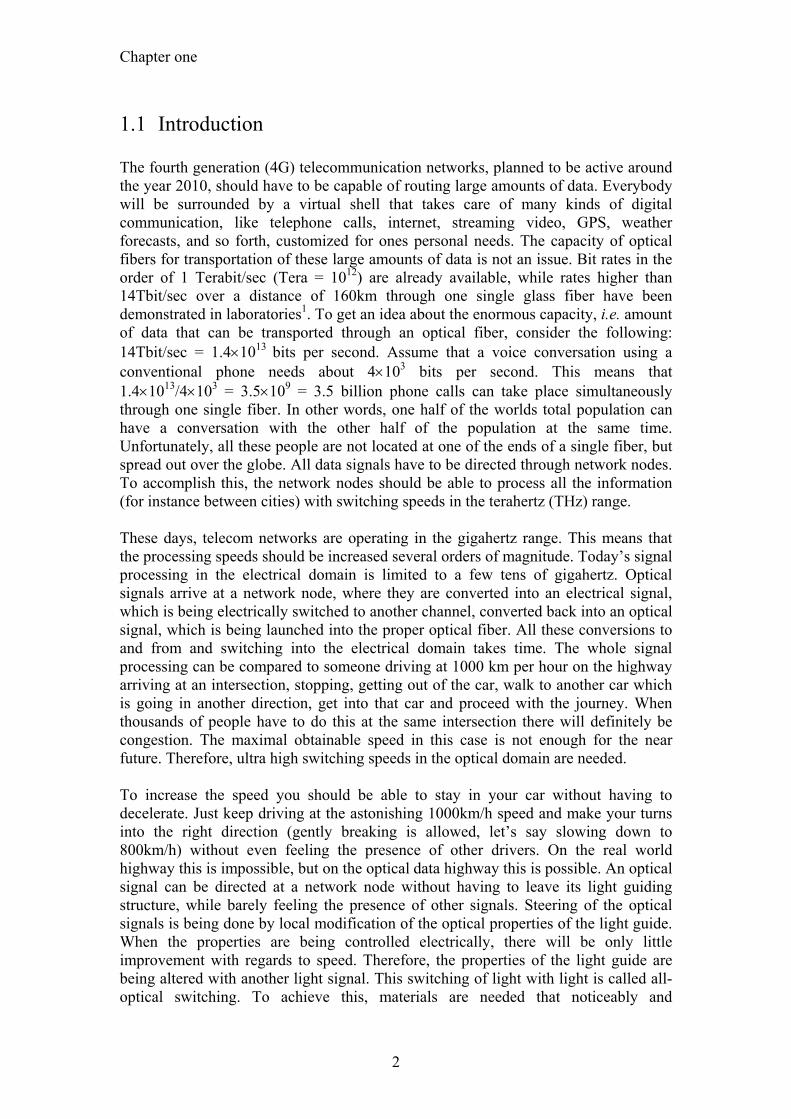
1.2 Planar optical waveguides In a fiber optic network, light signals are being transported through glass fibers. Figure 1.1.a shows a schematic representation of an optical fiber. The core of the fiber has a slightly higher refractive index compared to the surrounding cladding. Light that is coupled in the fiber will propagate along the central axis and this optical guiding can be explained by means of total internal reflection of the light at the core-cladding interface. In contrast to copper wires, this structure is capable of transporting huge amounts of data, since many different wavelengths can be sent through the fiber simultaneously, without feeling each others presence (under certain conditions). However, as pointed out earlier, these signals need to be combined, routed and switched to different end-users. Nowadays, this switching from one fiber to the other is being done in the electrical domain. The signal from one end of the fiber is detected with an optical detector and converted into an electrical signal. This electrical signal is switched and/or amplified in an electrical circuit and subsequently converted back into an optical signal using an LED or a laser diode. The optical signal is in turn coupled back into another optical fiber. All these conversions are disadvantageous with regards to speed and power consumption. Therefore it would be beneficial to perform all the operations in such a way that the signals can stay in the optical domain. For splitting signals or filtering signals this can, for instance, be done by fusing several fibers together or inducing a periodic refractive index variation in the fiber core, respectively. Amplification of the optical signals can be achieved by doping the glass core with rare-earth ions, like erbium. However, for more complicated functions like switching using M×N matrices, tunable switches, lasers, etc. these fiber based components will become utterly complex and take up a lot of space.
(a) (b)
Figure 1.1: (a) Optical fiber. (b) Planar optical waveguide.
Planar optical waveguides are the solution to integrate one or more optical functions on a chip. Planar photonic circuits typically have a small footprint and offer a high degree of flexibility. In contrast to optical fibers, which typically have a core with a radius of 9µm and a refractive index contrast of ∆n=0.003, planar waveguides can have core sizes as small as a few hundreds of nanometers and index contrasts up to
Chapter one
4
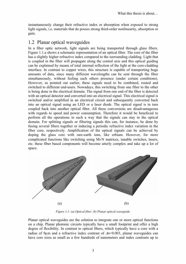
2.5. The refractive index contrast of a waveguide can be compared to the height of the curb of a road. The higher the curb, the smaller the chance to get off the road, even when the road has sharp bends. The higher the index of the waveguide is compared to its surrounding medium, the smaller the cross section of the waveguide can be and the smaller the bend radii. As a consequence, the footprint of the chip can be kept small when smaller bend radii are allowed. Compare this to the difference in footprint of a curved highway with practically no curb and the streets with curbs in a residential area or the track of a bobsleigh. Light travels even slower in high contrast waveguides, just like cars do in a crowded city center. The light paths in Figure 1.1 are depicted as if they were reflecting at the interfaces. However, this is not really the case with optical waveguides. The energy of the light is actually extending outside the high refractive index region. The extending part of the light field is called the evanescent field. The evanescent field is larger in case of low index contrast waveguides and therefore the confinement of the optical field is weaker in this case. Figure 1.2 shows the optical fields of both a weakly and strongly confined mode. It can be seen that the optical peak intensity is almost two orders of magnitudes higher in the high index contrast waveguide (~400GW/m2 compared to ~12,000GW/m2 in Figure 1.2 for both with the same modal power). High peak intensities are beneficial in case of all-optical processes as will be discussed for instance in Chapter 3.3. Therefore, the attractiveness of high index contrast planar optical waveguides is twofold, since they allow for compact structures and typically show higher field intensities.
(a) (b)
Figure 1.2: (a) Large waveguide (2×3µm) with low refractive index contrast (∆n=0.05). (b) Small waveguide (200×600nm)with a high refractive index contrast (∆n=2.00).Field profiles have been
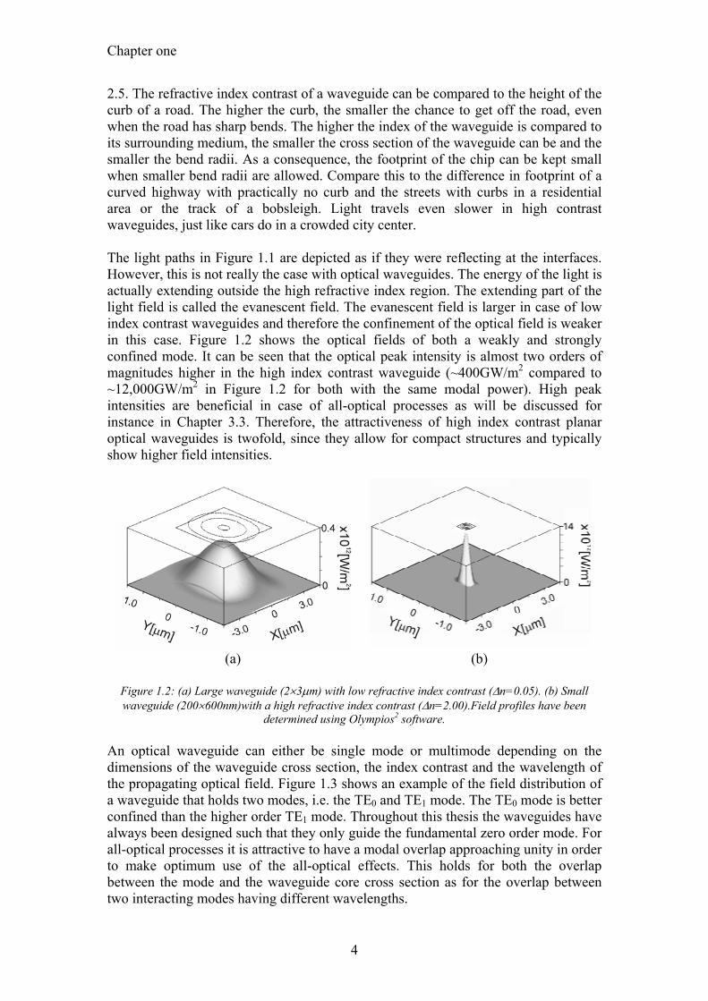
determined using Olympios2 software. An optical waveguide can either be single mode or multimode depending on the dimensions of the waveguide cross section, the index contrast and the wavelength of the propagating optical field. Figure 1.3 shows an example of the field distribution of a waveguide that holds two modes, i.e. the TE0 and TE1 mode. The TE0 mode is better confined than the higher order TE1 mode. Throughout this thesis the waveguides have always been designed such that they only guide the fundamental zero order mode. For all-optical processes it is attractive to have a modal overlap approaching unity in order to make optimum use of the all-optical effects. This holds for both the overlap between the mode and the waveguide core cross section as for the overlap between two interacting modes having different wavelengths.
What this thesis is about…
5
(a) (b)
Figure 1.3: (a) TE0 mode. (b): TE1 mode. Field profiles have been determined using Olympios2 software.
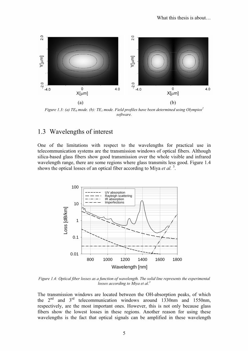
1.3 Wavelengths of interest One of the limitations with respect to the wavelengths for practical use in telecommunication systems are the transmission windows of optical fibers. Although silica-based glass fibers show good transmission over the whole visible and infrared wavelength range, there are some regions where glass transmits less good. Figure 1.4 shows the optical losses of an optical fiber according to Miya et al. 3.
Wavelength [nm]800 1000 1200 1400 1600 1800
Loss
[dB
/km
]
0.01
0.1
1
10
100UV absorption Rayleigh scattering IR absorption Imperfections
Figure 1.4: Optical fiber losses as a function of wavelength. The solid line represents the experimental
losses according to Miya et al.3 The transmission windows are located between the OH-absorption peaks, of which the 2nd and 3rd telecommunication windows around 1330nm and 1550nm, respectively, are the most important ones. However, this is not only because glass fibers show the lowest losses in these regions. Another reason for using these wavelengths is the fact that optical signals can be amplified in these wavelength
Chapter one
6
regions using neodymium4 and erbium5 impurities, as will be discussed later. In this thesis the focus will thus be on material characterization and device operation in the 1330nm and 1550nm region. Other wavelengths of interest are the near infrared pump wavelengths of neodymium and erbium (for instance 795nm and 850nm for the first, 980nm and 1480nm for the latter).
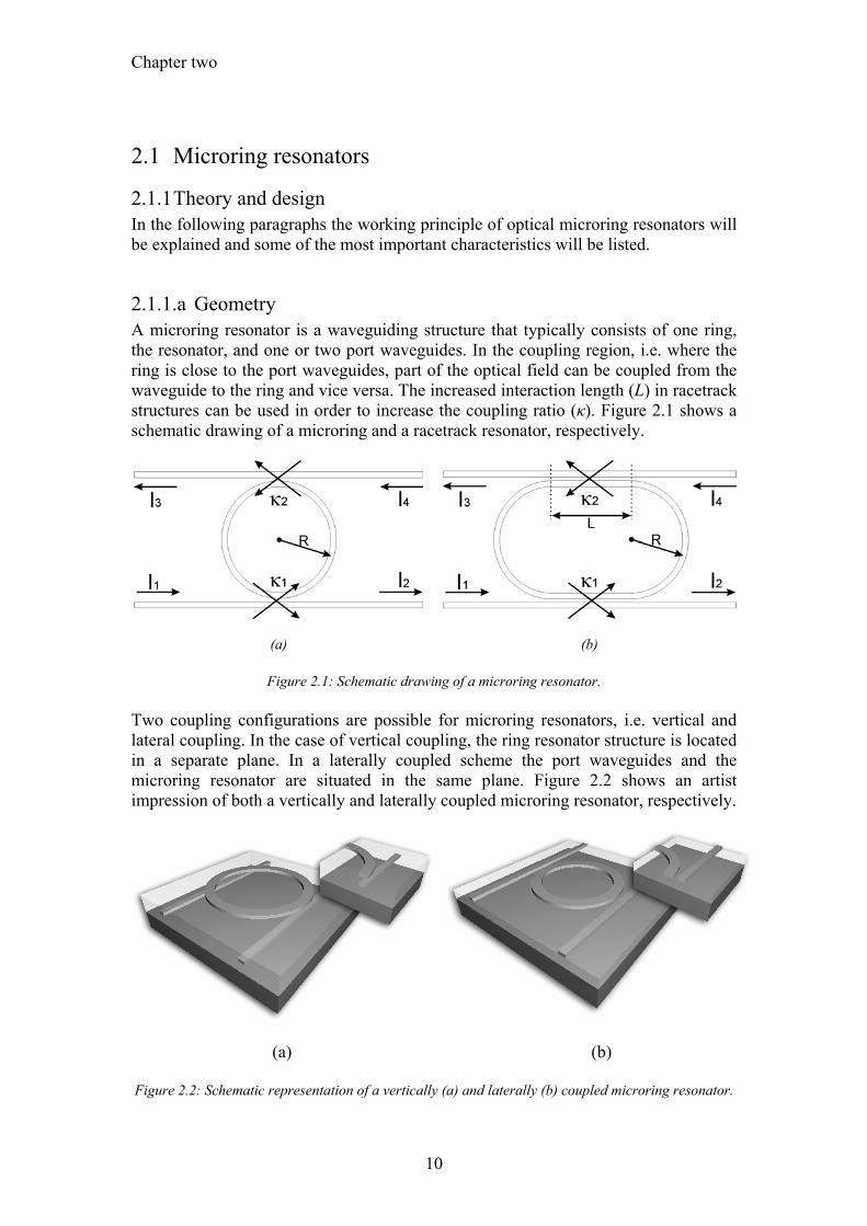
1.4 Nonlinear optical phenomena for all-optical processing For all-optical functionalities, like switching and modulation, a broad range of nonlinear optical processes can be exploited. Especially the third-order nonlinearities are particularly of interest, since many of these nonlinearities respond almost instantaneously to incoming signals and are therefore ideal candidates for ultrafast operation. Table 1.1 lists some of the nonlinear processes that could be used for all-optical data processing.
Table 1.1: Overview of commonly used all-optical processes Process Acronym Mechanism This thesis Four Wave Mixing FWM n2 No Self Phase Modulation SPM n2 Yes Cross Phase Modulation XPM n2 Yes Stimulated Raman Scattering
SRS e.g. crystal structure No
Stimulated Brioullin Scattering
SBS e.g. crystal structure No
Two Photon Absorption TPA absorption Yes Gain - Rare earth ion excitation Yes
It can be seen from Table 1.1 that the parameter n2 is listed as responsible physical mechanism in some of the cases. This parameter represents the Intensity Dependent Refractive Index (IDRI), often referred to as the third order nonlinearity or the optical Kerr effect, and its magnitude depends strongly on the type of material and the wavelength as will be shown in paragraph 3.3.2. The higher the value of n2, the stronger the nonlinear effect will be. A well known material which is being investigated for many decades since the invention of the transistor in 1947 is silicon. Silicon is a semiconductor material showing a moderate optical Kerr nonlinearity. However, the material is stable and its properties are well known. The SPM and XPM effects in silicon waveguides will be discussed in Chapter 6, both theoretically and experimentally. Eventually, ultrafast all-optical modulation will be demonstrated using XPM. Furthermore, Raman and Brioullin scattering are listed. Over the last few years Raman processes have gained much interest in integrated optics, especially in silicon waveguides. However, Raman and Brioullin scattering will not be investigated in this work. Two Photon Absorption is a process where two photons get absorbed simultaneously and is strongly dependent on the intensity of the light. This phenomenon will be
What this thesis is about…
7
explained in paragraph 3.1.5 and can be used for Cross Absorption Modulation (XAM) of which an example will be given in paragraph 6.4.2.b and 6.4.4.b. The last all-optical process listed in Table 1.1 is optical gain. An optical signal can be amplified by means of stimulated emission through excited rare-earth ions, as will be discussed in paragraph 3.2.1. The properties of several material systems that can be used to achieve optical gain are discussed in Chapter 4 and 5. All of the processes mentioned above are driven by the interaction between light and matter. No other external stimuli are exerted on the system and therefore these effects are called all-optical processes.
1.5 Outline of this thesis The structure of this thesis is as follows. In Chapter 2, two different types of planar integrated optical micro resonators, namely microring resonators and grating-based waveguide resonators, will be discussed. The underlying physics, working principles and design considerations will be explained using results of passive devices that were fabricated using Si3N4 technology. The microring resonators device described in this chapter will be used as the basic building block throughout the thesis. Next, in Chapter 3, a broad range of optical properties will be presented like several loss mechanisms, optical gain, optical nonlinearities, and finally some experimental setups that we have developed to determine these optical properties. Chapter 3 serves as a basis for the next three chapters in which our results on three different material systems with completely different properties are discussed. Chapter 4 describes the deposition and waveguide fabrication of erbium doped Al2O3. This is an optically active ceramic material which is highly inert. Several important issues related to the deposition will be presented including an extensive study on the optimization of the waveguide definition of this class of hard to etch materials. Some preliminary results of our best samples will be presented and an estimation will be given on the potential performance of the devices that could be fabricated with this type of erbium doped material. In Chapter 5, the low cost fabrication of erbium, neodymium and nanoparticle doped thin films and waveguides is discussed. The materials in this chapter, photosensitive polymers and sol-gels, are deposited from the liquid phase, which makes this group of materials ideal candidates for rare earth and nanoparticle doping. The resulting films and waveguides can be of an organic, ceramic or a hybrid nature. Although the material systems and their deposition techniques differ considerably, Chapter 4 and 5 are both dealing with rare earth doped material systems, and thus the focus will be on optical gain. Third order nonlinear optical processes in silicon on insulator (SOI) waveguides are discussed in Chapter 6. Although optical gain through the Raman effect is possible in this semiconductor material, the focus will be on Self Phase Modulation of high intensity femtosecond pulses. Furthermore, Cross Phase Modulation has been exploited in pump-probe experiments to demonstrate ultrafast sub-picosecond all-optical modulation and switching . Finally, in Chapter 7, general conclusions based on the work presented in this thesis will be drawn.

9
2 Micro resonators
As pointed out in paragraph 1.2 it is desirable to have high field intensities in the planar optical waveguides in order to investigate all-optical functions based on third-order optical nonlinearities. An efficient way to enhance optical field intensities is to make use of optical micro resonators. Many types of micro resonators could be employed, like for instance microring resonators, Fabry-Perot cavities, waveguide gratings and photonic crystals (PhCs). Each type of resonator has its advantages and disadvantages. In this chapter, microring resonators and waveguide gratings will be discussed with a strong focus on design, fabrication and characterization. As the aim of this chapter is to give an introduction and to explain the various aspects of micro resonators, the results of our passive Si3N4 based technology platform will be used to explain the basics.
Chapter two
10
2.1 Microring resonators
2.1.1 Theory and design In the following paragraphs the working principle of optical microring resonators will be explained and some of the most important characteristics will be listed.
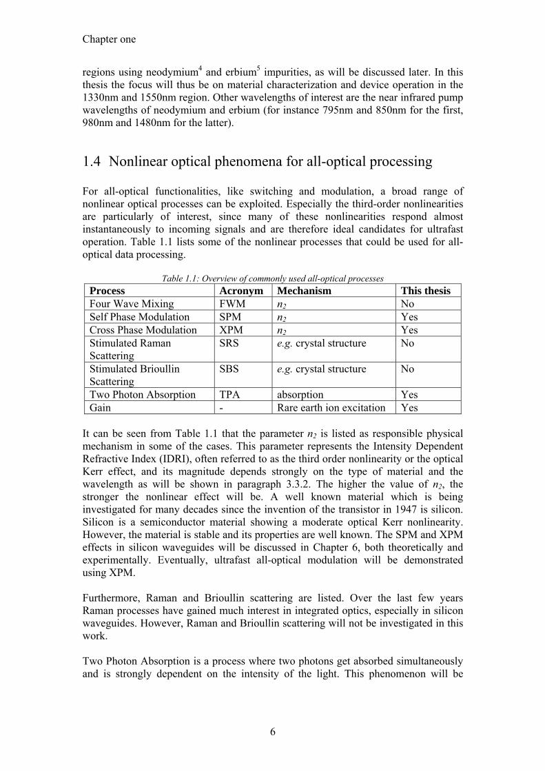
2.1.1.a Geometry A microring resonator is a waveguiding structure that typically consists of one ring, the resonator, and one or two port waveguides. In the coupling region, i.e. where the ring is close to the port waveguides, part of the optical field can be coupled from the waveguide to the ring and vice versa. The increased interaction length (L) in racetrack structures can be used in order to increase the coupling ratio (κ). Figure 2.1 shows a schematic drawing of a microring and a racetrack resonator, respectively.
(a)
(b)
Figure 2.1: Schematic drawing of a microring resonator.
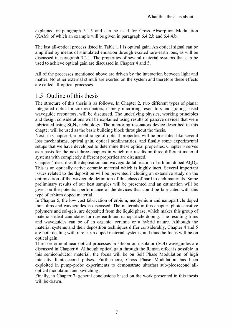
Two coupling configurations are possible for microring resonators, i.e. vertical and lateral coupling. In the case of vertical coupling, the ring resonator structure is located in a separate plane. In a laterally coupled scheme the port waveguides and the microring resonator are situated in the same plane. Figure 2.2 shows an artist impression of both a vertically and laterally coupled microring resonator, respectively.
(a)
(b)
Figure 2.2: Schematic representation of a vertically (a) and laterally (b) coupled microring resonator.
Micro resonators
11
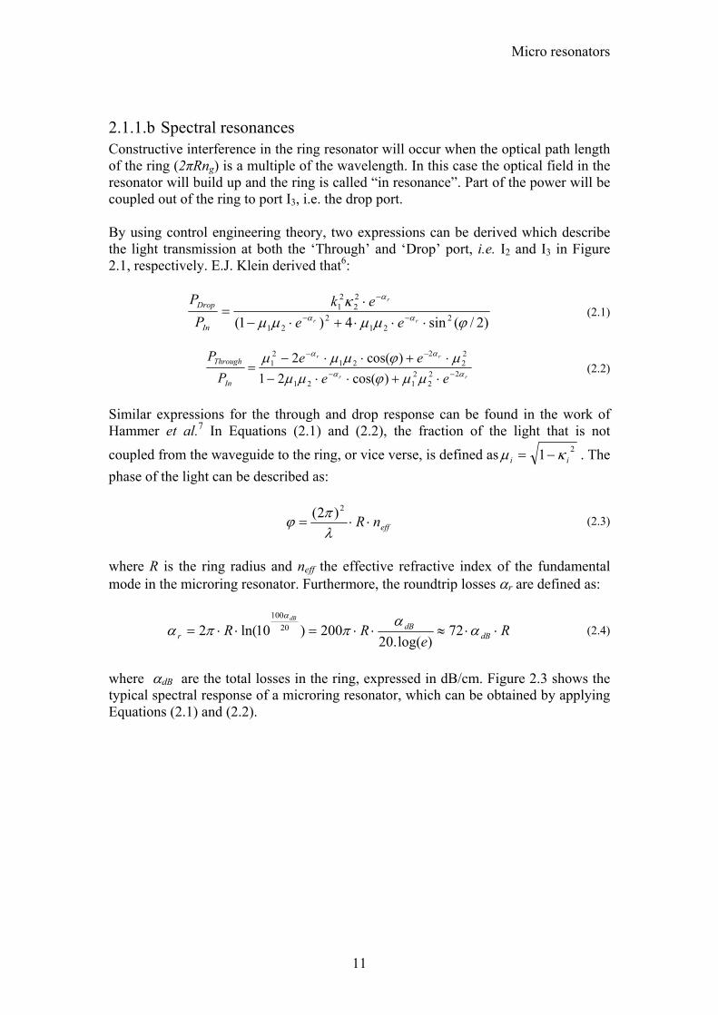
2.1.1.b Spectral resonances Constructive interference in the ring resonator will occur when the optical path length of the ring (2πRng) is a multiple of the wavelength. In this case the optical field in the resonator will build up and the ring is called “in resonance”. Part of the power will be coupled out of the ring to port I3, i.e. the drop port. By using control engineering theory, two expressions can be derived which describe the light transmission at both the ‘Through’ and ‘Drop’ port, i.e. I2 and I3 in Figure 2.1, respectively. E.J. Klein derived that6:
)2/(sin4)1( 221
221
22
21
ϕµµµµκ
αα
α
⋅⋅⋅+⋅−⋅
= −−
−
rr
r
eeek
PP
In
Drop (2.1)
rr
rr
eeee
PP
In
Throughαα
αα
µµϕµµµϕµµµ22
22121
22
221
21
)cos(21)cos(2
−−
−−
⋅+⋅⋅−⋅+⋅⋅−
= (2.2)
Similar expressions for the through and drop response can be found in the work of Hammer et al.7 In Equations (2.1) and (2.2), the fraction of the light that is not
coupled from the waveguide to the ring, or vice verse, is defined as 21 ii κµ −= . The phase of the light can be described as:
effnR ⋅⋅=λπϕ
2)2( (2.3)
where R is the ring radius and neff the effective refractive index of the fundamental mode in the microring resonator. Furthermore, the roundtrip losses αr are defined as:
Re
RR dBdB
r
dB
⋅⋅≈⋅⋅=⋅⋅= αα
ππαα
72)log(.20
200)10ln(2 20100
(2.4)
where αdB are the total losses in the ring, expressed in dB/cm. Figure 2.3 shows the typical spectral response of a microring resonator, which can be obtained by applying Equations (2.1) and (2.2).
Chapter two
12
Wavelength [nm]1530 1531 1532 1533 1534 1535 1536
Tran
smis
sion
[-]
0.0
0.2
0.4
0.6
0.8
1.0
ThroughDrop
FSRλ
FWHM
Figure 2.3: Example of the normalized through and drop port transmission spectra. The free spectral range (FSR) of a ring resonator in the wavelength domain is related to the radius and the group index via:
gnRFSR
πλ
λ 2
20= (2.5)
where ng is the group index defined by Madsen et al.8 as:
0
00 )(λ
λλλ
ddn
nn effeffg −= (2.6)
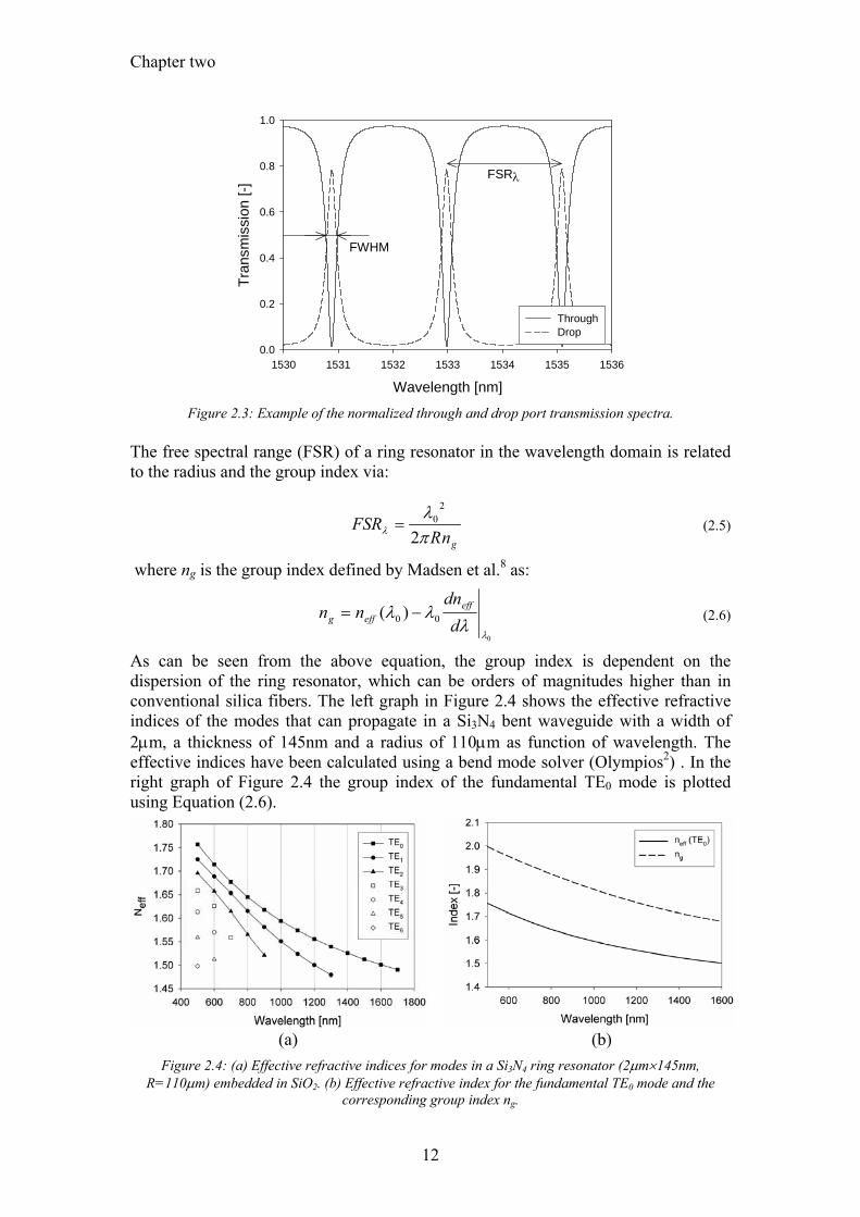
As can be seen from the above equation, the group index is dependent on the dispersion of the ring resonator, which can be orders of magnitudes higher than in conventional silica fibers. The left graph in Figure 2.4 shows the effective refractive indices of the modes that can propagate in a Si3N4 bent waveguide with a width of 2µm, a thickness of 145nm and a radius of 110µm as function of wavelength. The effective indices have been calculated using a bend mode solver (Olympios2) . In the right graph of Figure 2.4 the group index of the fundamental TE0 mode is plotted using Equation (2.6).
(a) (b)
Figure 2.4: (a) Effective refractive indices for modes in a Si3N4 ring resonator (2µm×145nm, R=110µm) embedded in SiO2. (b) Effective refractive index for the fundamental TE0 mode and the
corresponding group index ng.
Micro resonators
13
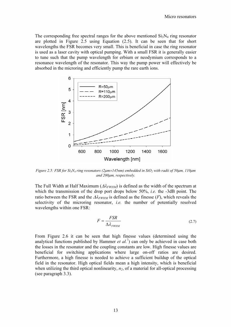
The corresponding free spectral ranges for the above mentioned Si3N4 ring resonator are plotted in Figure 2.5 using Equation (2.5). It can be seen that for short wavelengths the FSR becomes very small. This is beneficial in case the ring resonator is used as a laser cavity with optical pumping. With a small FSR it is generally easier to tune such that the pump wavelength for erbium or neodymium corresponds to a resonance wavelength of the resonator. This way the pump power will effectively be absorbed in the microring and efficiently pump the rare earth ions.
Figure 2.5: FSR for Si3N4 ring resonators (2µm×145nm) embedded in SiO2 with radii of 50µm, 110µm
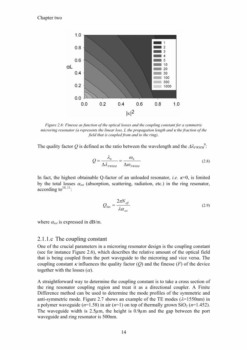
and 200µm, respectively. The Full Width at Half Maximum (∆λFWHM) is defined as the width of the spectrum at which the transmission of the drop port drops below 50%, i.e. the -3dB point. The ratio between the FSR and the ∆λFWHM is defined as the finesse (F), which reveals the selectivity of the microring resonator, i.e. the number of potentially resolved wavelengths within one FSR:
FWHM
FSRFλ∆
= (2.7)
From Figure 2.6 it can be seen that high finesse values (determined using the analytical functions published by Hammer et al.7) can only be achieved in case both the losses in the resonator and the coupling constants are low. High finesse values are beneficial for switching applications where large on-off ratios are desired. Furthermore, a high finesse is needed to achieve a sufficient buildup of the optical field in the resonator. High optical fields mean a high intensity, which is beneficial when utilizing the third optical nonlinearity, n2, of a material for all-optical processing (see paragraph 3.3).
Chapter two
14
Figure 2.6: Finesse as function of the optical losses and the coupling constant for a symmetric microring resonator (a represents the linear loss, L the propagation length and κ the fraction of the
field that is coupled from and to the ring). The quality factor Q is defined as the ratio between the wavelength and the ∆λFWHM
9:
FWHMFWHM
Qωω
λλ
∆=
∆= 00 (2.8)
In fact, the highest obtainable Q-factor of an unloaded resonator, i.e. κ=0, is limited by the total losses αtot (absorption, scattering, radiation, etc.) in the ring resonator, according to10, 11:
tot
effNQ
λαπ2
lim = (2.9)
where αtot is expressed in dB/m.
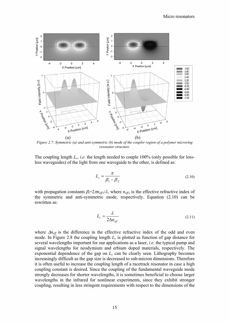
2.1.1.c The coupling constant One of the crucial parameters in a microring resonator design is the coupling constant (see for instance Figure 2.6), which describes the relative amount of the optical field that is being coupled from the port waveguide to the microring and vice versa. The coupling constant κ influences the quality factor (Q) and the finesse (F) of the device together with the losses (α). A straightforward way to determine the coupling constant is to take a cross section of the ring resonator coupling region and treat it as a directional coupler. A Finite Difference method can be used to determine the mode profiles of the symmetric and anti-symmetric mode. Figure 2.7 shows an example of the TE modes (λ=1550nm) in a polymer waveguide (n=1.58) in air (n=1) on top of thermally grown SiO2 (n=1.452). The waveguide width is 2.5µm, the height is 0.9µm and the gap between the port waveguide and ring resonator is 500nm.
Micro resonators
15
(a) (b)
Figure 2.7: Symmetric (a) and anti-symmetric (b) mode of the coupler region of a polymer microring resonator structure.
The coupling length Lc, i.e. the length needed to couple 100% (only possible for loss-less waveguides) of the light from one waveguide to the other, is defined as:
21 ββπ−
=cL (2.10)
with propagation constants βi=2πneff,i/λ, where neff,i is the effective refractive index of the symmetric and anti-symmetric mode, respectively. Equation (2.10) can be rewritten as:
effc n
L∆
=2λ (2.11)
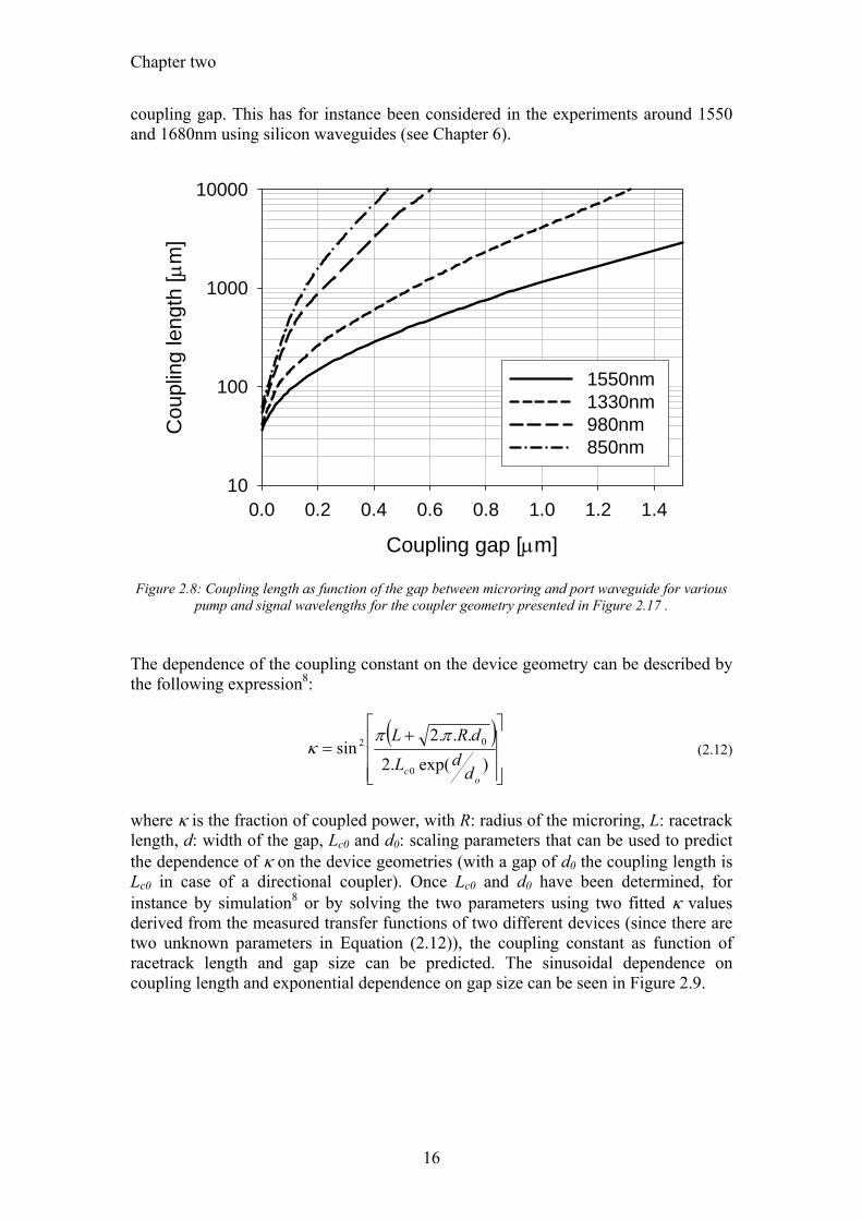
where ∆neff is the difference in the effective refractive index of the odd and even mode. In Figure 2.8 the coupling length Lc is plotted as function of gap distance for several wavelengths important for our applications as a laser, i.e. the typical pump and signal wavelengths for neodymium and erbium doped materials, respectively. The exponential dependence of the gap on Lc can be clearly seen. Lithography becomes increasingly difficult as the gap size is decreased to sub-micron dimensions. Therefore it is often useful to increase the coupling length of a racetrack resonator in case a high coupling constant is desired. Since the coupling of the fundamental waveguide mode strongly decreases for shorter wavelengths, it is sometimes beneficial to choose larger wavelengths in the infrared for nonlinear experiments, since they exhibit stronger coupling, resulting in less stringent requirements with respect to the dimensions of the
Chapter two
16
coupling gap. This has for instance been considered in the experiments around 1550 and 1680nm using silicon waveguides (see Chapter 6).
Coupling gap [µm]
0.0 0.2 0.4 0.6 0.8 1.0 1.2 1.4
Cou
plin
g le
ngth
[µm
]
10
100
1000
10000
1550nm
1330nm 980nm 850nm
Figure 2.8: Coupling length as function of the gap between microring and port waveguide for various
pump and signal wavelengths for the coupler geometry presented in Figure 2.17 . The dependence of the coupling constant on the device geometry can be described by the following expression8:
( )⎥⎥⎥
⎦
⎤
⎢⎢⎢
⎣
⎡+
=)exp(.2
...2sin
0
02
oc d
dL
dRL ππκ (2.12)
where κ is the fraction of coupled power, with R: radius of the microring, L: racetrack length, d: width of the gap, Lc0 and d0: scaling parameters that can be used to predict the dependence of κ on the device geometries (with a gap of d0 the coupling length is Lc0 in case of a directional coupler). Once Lc0 and d0 have been determined, for instance by simulation8 or by solving the two parameters using two fitted κ values derived from the measured transfer functions of two different devices (since there are two unknown parameters in Equation (2.12)), the coupling constant as function of racetrack length and gap size can be predicted. The sinusoidal dependence on coupling length and exponential dependence on gap size can be seen in Figure 2.9.
Micro resonators
17
Racetrack length [µm]
0 100 200 300 400
Cou
plin
g co
nsta
nt κ
[-]
0.0
0.2
0.4
0.6
0.8
1.0
d=1.0µmd=1.1µmd=1.2µmd=1.3µm
Figure 2.9: Coupling constant as function of racetrack length and coupling gap. For this particular example, a coupling gap of 1.9µm results in a coupling length of 9300µm, corresponding to the scaling
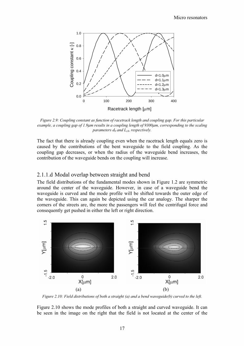
parameters d0 and Lc0, respectively. The fact that there is already coupling even when the racetrack length equals zero is caused by the contributions of the bent waveguide to the field coupling. As the coupling gap decreases, or when the radius of the waveguide bend increases, the contribution of the waveguide bends on the coupling will increase.
2.1.1.d Modal overlap between straight and bend The field distributions of the fundamental modes shown in Figure 1.2 are symmetric around the center of the waveguide. However, in case of a waveguide bend the waveguide is curved and the mode profile will be shifted towards the outer edge of the waveguide. This can again be depicted using the car analogy. The sharper the corners of the streets are, the more the passengers will feel the centrifugal force and consequently get pushed in either the left or right direction.
(a) (b)
Figure 2.10: Field distributions of both a straight (a) and a bend waveguide(b) curved to the left. Figure 2.10 shows the mode profiles of both a straight and curved waveguide. It can be seen in the image on the right that the field is not located at the center of the
Chapter two
18
waveguide. The smaller the radius of the bend, the larger the offset with respect to the center of the waveguide will be. In the case of a racetrack resonator, the racetrack itself consists of two curved waveguides and two straight waveguides, as can be seen in Figure 2.1 b. Transition losses will be introduced when the mode of the bend waveguide is coupled into the straight waveguides, since their mode profiles do not overlap in an optimum way. A straightforward method to compensate for this modal mismatch is to introduce an offset ∆ between the bend and straight waveguide. This way the mode centers will be aligned more or less and thus the modal overlap losses will decrease. A schematic representation of this offset is presented in Figure 2.11.
Figure 2.11: Schematic representation of one of the two coupling regions in a racetrack resonator. An
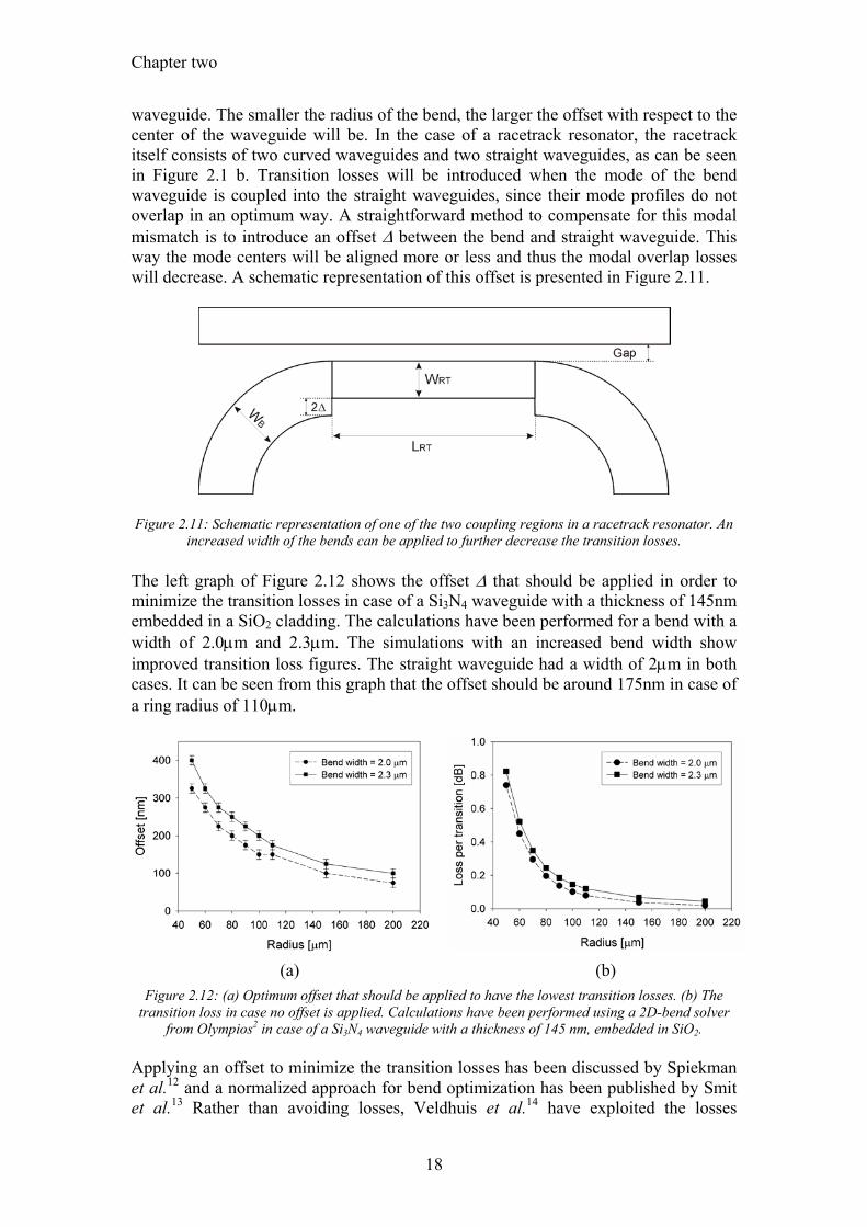
increased width of the bends can be applied to further decrease the transition losses. The left graph of Figure 2.12 shows the offset ∆ that should be applied in order to minimize the transition losses in case of a Si3N4 waveguide with a thickness of 145nm embedded in a SiO2 cladding. The calculations have been performed for a bend with a width of 2.0µm and 2.3µm. The simulations with an increased bend width show improved transition loss figures. The straight waveguide had a width of 2µm in both cases. It can be seen from this graph that the offset should be around 175nm in case of a ring radius of 110µm.
(a) (b)
Figure 2.12: (a) Optimum offset that should be applied to have the lowest transition losses. (b) The transition loss in case no offset is applied. Calculations have been performed using a 2D-bend solver
from Olympios2 in case of a Si3N4 waveguide with a thickness of 145 nm, embedded in SiO2. Applying an offset to minimize the transition losses has been discussed by Spiekman et al.12 and a normalized approach for bend optimization has been published by Smit et al.13 Rather than avoiding losses, Veldhuis et al.14 have exploited the losses
Micro resonators
19
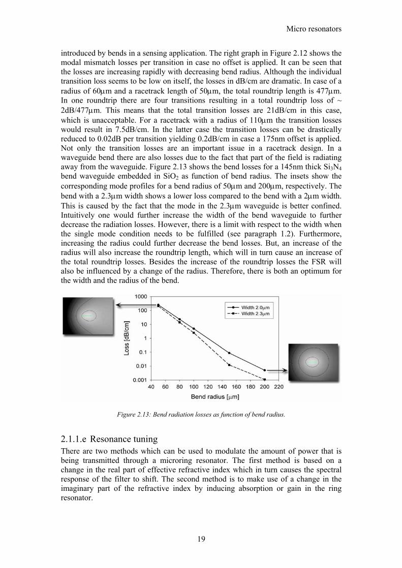
introduced by bends in a sensing application. The right graph in Figure 2.12 shows the modal mismatch losses per transition in case no offset is applied. It can be seen that the losses are increasing rapidly with decreasing bend radius. Although the individual transition loss seems to be low on itself, the losses in dB/cm are dramatic. In case of a radius of 60µm and a racetrack length of 50µm, the total roundtrip length is 477µm. In one roundtrip there are four transitions resulting in a total roundtrip loss of ~ 2dB/477µm. This means that the total transition losses are 21dB/cm in this case, which is unacceptable. For a racetrack with a radius of 110µm the transition losses would result in 7.5dB/cm. In the latter case the transition losses can be drastically reduced to 0.02dB per transition yielding 0.2dB/cm in case a 175nm offset is applied. Not only the transition losses are an important issue in a racetrack design. In a waveguide bend there are also losses due to the fact that part of the field is radiating away from the waveguide. Figure 2.13 shows the bend losses for a 145nm thick Si3N4 bend waveguide embedded in SiO2 as function of bend radius. The insets show the corresponding mode profiles for a bend radius of 50µm and 200µm, respectively. The bend with a 2.3µm width shows a lower loss compared to the bend with a 2µm width. This is caused by the fact that the mode in the 2.3µm waveguide is better confined. Intuitively one would further increase the width of the bend waveguide to further decrease the radiation losses. However, there is a limit with respect to the width when the single mode condition needs to be fulfilled (see paragraph 1.2). Furthermore, increasing the radius could further decrease the bend losses. But, an increase of the radius will also increase the roundtrip length, which will in turn cause an increase of the total roundtrip losses. Besides the increase of the roundtrip losses the FSR will also be influenced by a change of the radius. Therefore, there is both an optimum for the width and the radius of the bend.
Figure 2.13: Bend radiation losses as function of bend radius.
2.1.1.e Resonance tuning There are two methods which can be used to modulate the amount of power that is being transmitted through a microring resonator. The first method is based on a change in the real part of effective refractive index which in turn causes the spectral response of the filter to shift. The second method is to make use of a change in the imaginary part of the refractive index by inducing absorption or gain in the ring resonator.
Chapter two
20
In the case of tuning a microring resonator by changing the real part of the effective refractive index ∆Neff, using for instance the thermo-optic, electro-optic, or Kerr effect, it is possible to derive the ∆Neff that is needed in order to achieve a certain modulation (∆MOD) in the drop port relative to the attenuation in full resonance. The refractive index change needed for achieving a modulation depth ∆MOD (in dB) is derived by E.J. Klein6 and is given by:
R
ee
Nr
rMOD
eff 2
.21
22110
2
4)1(110arcsin
π
µµµµ
λ α
α
⎟⎟
⎠
⎞
⎜⎜
⎝
⎛
⋅⋅−
⋅⎟⎟⎠
⎞⎜⎜⎝
⎛−⋅
=∆
−
−∆
(2.13)
The induced refractive index change ∆Neff is causing the resonance wavelengths of the microring resonator to shift. This wavelength shift ∆λR depends linearly on the refractive index change and can be expressed as follows15:
eff
effR N
N∆=∆λ
λ (2.14)
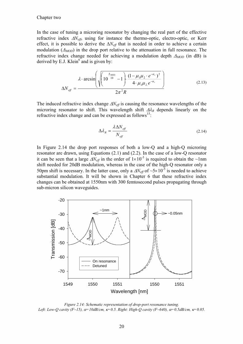
In Figure 2.14 the drop port responses of both a low-Q and a high-Q microring resonator are drawn, using Equations (2.1) and (2.2). In the case of a low-Q resonator it can be seen that a large ∆Neff in the order of 1×10⁻³ is required to obtain the ~1nm shift needed for 20dB modulation, whereas in the case of the high-Q resonator only a 50pm shift is necessary. In the latter case, only a ∆Neff of ~5×10⁻⁵ is needed to achieve substantial modulation. It will be shown in Chapter 6 that these refractive index changes can be obtained at 1550nm with 300 femtosecond pulses propagating through sub-micron silicon waveguides.
Wavelength [nm]1549 1550 1551
Tran
smis
sion
[dB]
-70
-60
-50
-40
-30
-20
1550 1551
On resonanceDetuned
∆ MO
D
∆ MO
D
~1nm~0.05nm
Figure 2.14: Schematic representation of drop-port resonance tuning. Left: Low-Q cavity (F~15), α=10dB/cm, κ=0.5. Right: High-Q cavity (F~640), α=0.5dB/cm, κ=0.05.
Micro resonators
21
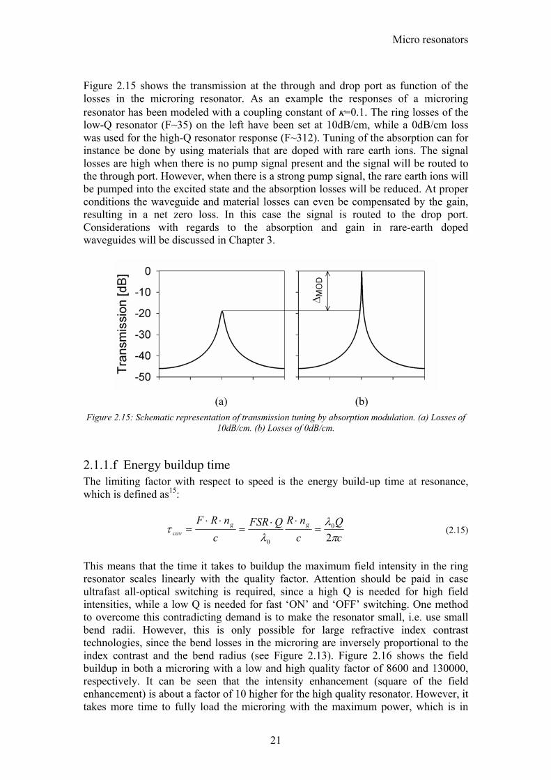
Figure 2.15 shows the transmission at the through and drop port as function of the losses in the microring resonator. As an example the responses of a microring resonator has been modeled with a coupling constant of κ=0.1. The ring losses of the low-Q resonator (F~35) on the left have been set at 10dB/cm, while a 0dB/cm loss was used for the high-Q resonator response (F~312). Tuning of the absorption can for instance be done by using materials that are doped with rare earth ions. The signal losses are high when there is no pump signal present and the signal will be routed to the through port. However, when there is a strong pump signal, the rare earth ions will be pumped into the excited state and the absorption losses will be reduced. At proper conditions the waveguide and material losses can even be compensated by the gain, resulting in a net zero loss. In this case the signal is routed to the drop port. Considerations with regards to the absorption and gain in rare-earth doped waveguides will be discussed in Chapter 3.
(a) (b)
Figure 2.15: Schematic representation of transmission tuning by absorption modulation. (a) Losses of 10dB/cm. (b) Losses of 0dB/cm.
2.1.1.f Energy buildup time The limiting factor with respect to speed is the energy build-up time at resonance, which is defined as15:
cQ
cnRQFSR
cnRF gg
cav πλ
λτ
20
0
=⋅⋅
=⋅⋅
= (2.15)
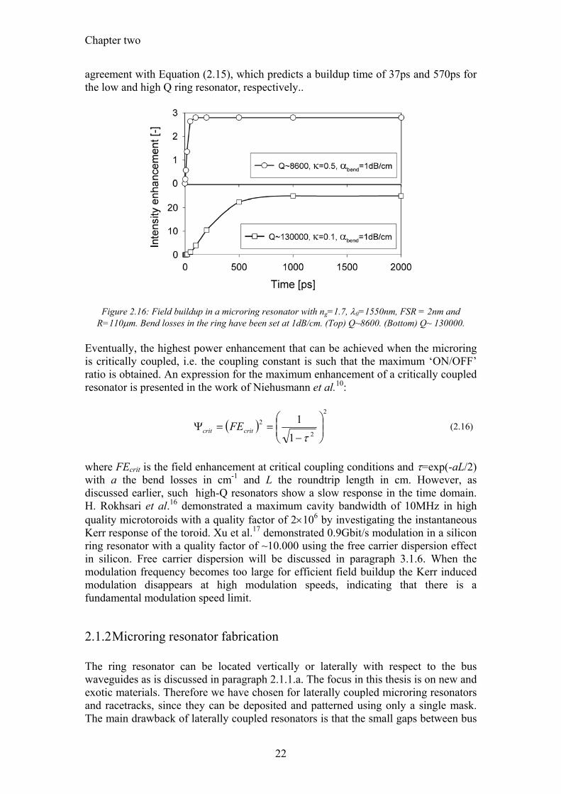
This means that the time it takes to buildup the maximum field intensity in the ring resonator scales linearly with the quality factor. Attention should be paid in case ultrafast all-optical switching is required, since a high Q is needed for high field intensities, while a low Q is needed for fast ‘ON’ and ‘OFF’ switching. One method to overcome this contradicting demand is to make the resonator small, i.e. use small bend radii. However, this is only possible for large refractive index contrast technologies, since the bend losses in the microring are inversely proportional to the index contrast and the bend radius (see Figure 2.13). Figure 2.16 shows the field buildup in both a microring with a low and high quality factor of 8600 and 130000, respectively. It can be seen that the intensity enhancement (square of the field enhancement) is about a factor of 10 higher for the high quality resonator. However, it takes more time to fully load the microring with the maximum power, which is in
Chapter two
22
agreement with Equation (2.15), which predicts a buildup time of 37ps and 570ps for the low and high Q ring resonator, respectively..
Figure 2.16: Field buildup in a microring resonator with ng=1.7, λ0=1550nm, FSR = 2nm and R=110µm. Bend losses in the ring have been set at 1dB/cm. (Top) Q~8600. (Bottom) Q~ 130000.
Eventually, the highest power enhancement that can be achieved when the microring is critically coupled, i.e. the coupling constant is such that the maximum ‘ON/OFF’ ratio is obtained. An expression for the maximum enhancement of a critically coupled resonator is presented in the work of Niehusmann et al.10:
( )2
2
2
11
⎟⎟⎠
⎞⎜⎜⎝
⎛
−==Ψ
τcritcrit FE (2.16)
where FEcrit is the field enhancement at critical coupling conditions and τ=exp(-aL/2) with a the bend losses in cm-1 and L the roundtrip length in cm. However, as discussed earlier, such high-Q resonators show a slow response in the time domain. H. Rokhsari et al.16 demonstrated a maximum cavity bandwidth of 10MHz in high quality microtoroids with a quality factor of 2×10⁶ by investigating the instantaneous Kerr response of the toroid. Xu et al.17 demonstrated 0.9Gbit/s modulation in a silicon ring resonator with a quality factor of ~10.000 using the free carrier dispersion effect in silicon. Free carrier dispersion will be discussed in paragraph 3.1.6. When the modulation frequency becomes too large for efficient field buildup the Kerr induced modulation disappears at high modulation speeds, indicating that there is a fundamental modulation speed limit.
2.1.2 Microring resonator fabrication The ring resonator can be located vertically or laterally with respect to the bus waveguides as is discussed in paragraph 2.1.1.a. The focus in this thesis is on new and exotic materials. Therefore we have chosen for laterally coupled microring resonators and racetracks, since they can be deposited and patterned using only a single mask. The main drawback of laterally coupled resonators is that the small gaps between bus
Micro resonators
23
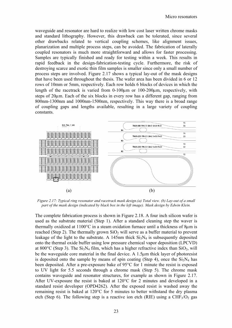
waveguide and resonator are hard to realize with low cost laser written chrome masks and standard lithography. However, this drawback can be tolerated, since several other drawbacks related to vertical coupling schemes, like alignment issues, planarization and multiple process steps, can be avoided. The fabrication of laterally coupled resonators is much more straightforward and allows for faster processing. Samples are typically finished and ready for testing within a week. This results in rapid feedback in the design-fabrication-testing cycle. Furthermore, the risk of destroying scarce and exotic thin film samples is smaller since only a small number of process steps are involved. Figure 2.17 shows a typical lay-out of the mask designs that have been used throughout the thesis. The wafer area has been divided in 6 or 12 rows of 10mm or 5mm, respectively. Each row holds 6 blocks of devices in which the length of the racetrack is varied from 0-100µm or 100-200µm, respectively, with steps of 20µm. Each of the six blocks in every row has a different gap, ranging from 800nm-1300nm and 1000nm-1500nm, respectively. This way there is a broad range of coupling gaps and lengths available, resulting in a large variety of coupling constants.
(a) (b)
Figure 2.17: Typical ring resonator and racetrack mask design.(a) Total view. (b) Lay-out of a small part of the mask design (indicated by black box in the left image). Mask design by Edwin Klein.
The complete fabrication process is shown in Figure 2.18. A four inch silicon wafer is used as the substrate material (Step 1). After a standard cleaning step the waver is thermally oxidized at 1100°C in a steam oxidation furnace until a thickness of 8µm is reached (Step 2). The thermally grown SiO2 will serve as a buffer material to prevent leakage of the light to the substrate. A 145nm thick Si3N4 is subsequently deposited onto the thermal oxide buffer using low pressure chemical vapor deposition (LPCVD) at 800°C (Step 3). The Si3N4 film, which has a higher refractive index than SiO2, will be the waveguide core material in the final device. A 1.5µm thick layer of photoresist is deposited onto the sample by means of spin coating (Step 4), once the Si3N4 has been deposited. After a pre-exposure bake of 95°C for 1 minute the resist is exposed to UV light for 5.5 seconds through a chrome mask (Step 5). The chrome mask contains waveguide and resonator structures, for example as shown in Figure 2.17. After UV-exposure the resist is baked at 120°C for 2 minutes and developed in a standard resist developer (OPD4262). After the exposed resist is washed away the remaining resist is baked at 120°C for 5 minutes to better withstand the dry plasma etch (Step 6). The following step is a reactive ion etch (RIE) using a CHF3/O2 gas
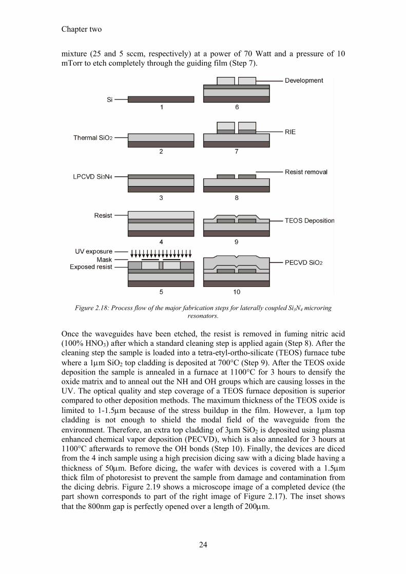
Chapter two
24
mixture (25 and 5 sccm, respectively) at a power of 70 Watt and a pressure of 10 mTorr to etch completely through the guiding film (Step 7).
Figure 2.18: Process flow of the major fabrication steps for laterally coupled Si3N4 microring resonators.
Once the waveguides have been etched, the resist is removed in fuming nitric acid (100% HNO3) after which a standard cleaning step is applied again (Step 8). After the cleaning step the sample is loaded into a tetra-etyl-ortho-silicate (TEOS) furnace tube where a 1µm SiO2 top cladding is deposited at 700°C (Step 9). After the TEOS oxide deposition the sample is annealed in a furnace at 1100°C for 3 hours to densify the oxide matrix and to anneal out the NH and OH groups which are causing losses in the UV. The optical quality and step coverage of a TEOS furnace deposition is superior compared to other deposition methods. The maximum thickness of the TEOS oxide is limited to 1-1.5µm because of the stress buildup in the film. However, a 1µm top cladding is not enough to shield the modal field of the waveguide from the environment. Therefore, an extra top cladding of 3µm SiO2 is deposited using plasma enhanced chemical vapor deposition (PECVD), which is also annealed for 3 hours at 1100°C afterwards to remove the OH bonds (Step 10). Finally, the devices are diced from the 4 inch sample using a high precision dicing saw with a dicing blade having a thickness of 50µm. Before dicing, the wafer with devices is covered with a 1.5µm thick film of photoresist to prevent the sample from damage and contamination from the dicing debris. Figure 2.19 shows a microscope image of a completed device (the part shown corresponds to part of the right image of Figure 2.17). The inset shows that the 800nm gap is perfectly opened over a length of 200µm.
Micro resonators
25
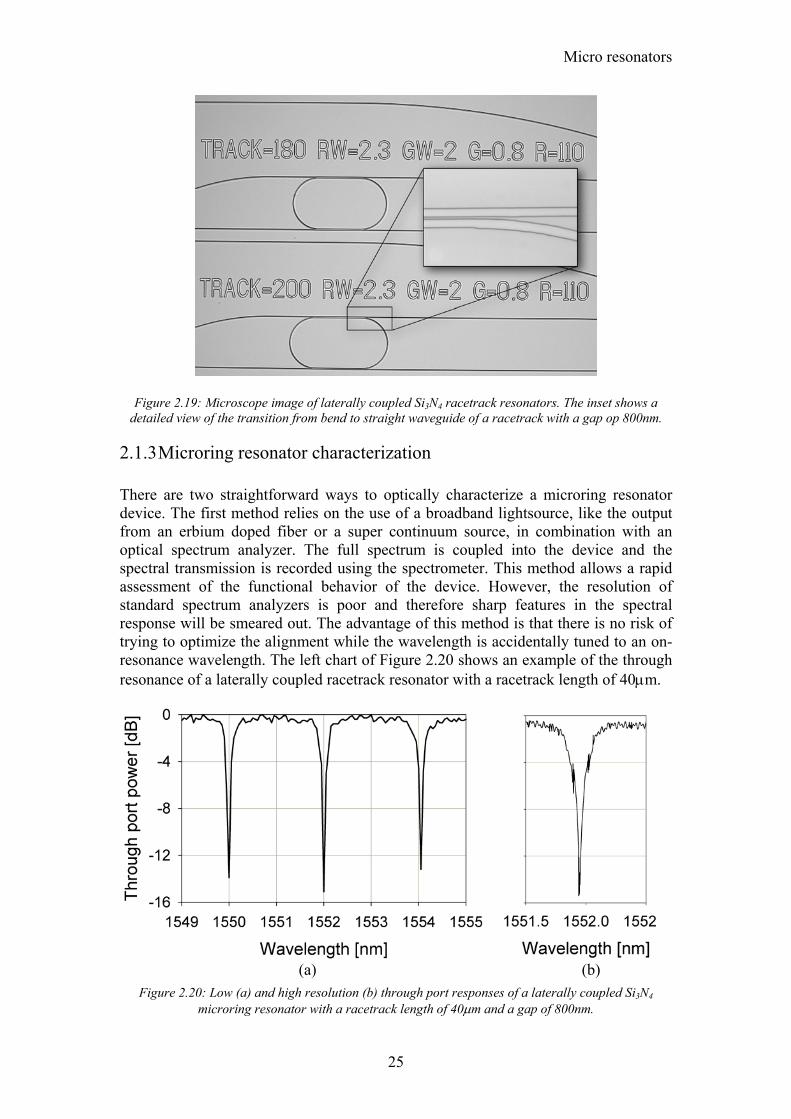
Figure 2.19: Microscope image of laterally coupled Si3N4 racetrack resonators. The inset shows a detailed view of the transition from bend to straight waveguide of a racetrack with a gap op 800nm.
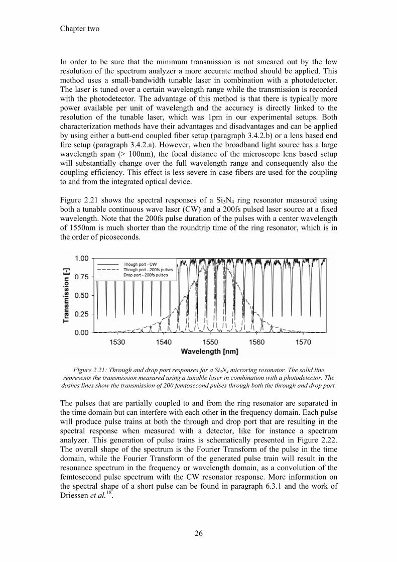
2.1.3 Microring resonator characterization There are two straightforward ways to optically characterize a microring resonator device. The first method relies on the use of a broadband lightsource, like the output from an erbium doped fiber or a super continuum source, in combination with an optical spectrum analyzer. The full spectrum is coupled into the device and the spectral transmission is recorded using the spectrometer. This method allows a rapid assessment of the functional behavior of the device. However, the resolution of standard spectrum analyzers is poor and therefore sharp features in the spectral response will be smeared out. The advantage of this method is that there is no risk of trying to optimize the alignment while the wavelength is accidentally tuned to an on-resonance wavelength. The left chart of Figure 2.20 shows an example of the through resonance of a laterally coupled racetrack resonator with a racetrack length of 40µm.
(a) (b)
Figure 2.20: Low (a) and high resolution (b) through port responses of a laterally coupled Si3N4 microring resonator with a racetrack length of 40µm and a gap of 800nm.
Chapter two
26
In order to be sure that the minimum transmission is not smeared out by the low resolution of the spectrum analyzer a more accurate method should be applied. This method uses a small-bandwidth tunable laser in combination with a photodetector. The laser is tuned over a certain wavelength range while the transmission is recorded with the photodetector. The advantage of this method is that there is typically more power available per unit of wavelength and the accuracy is directly linked to the resolution of the tunable laser, which was 1pm in our experimental setups. Both characterization methods have their advantages and disadvantages and can be applied by using either a butt-end coupled fiber setup (paragraph 3.4.2.b) or a lens based end fire setup (paragraph 3.4.2.a). However, when the broadband light source has a large wavelength span (> 100nm), the focal distance of the microscope lens based setup will substantially change over the full wavelength range and consequently also the coupling efficiency. This effect is less severe in case fibers are used for the coupling to and from the integrated optical device. Figure 2.21 shows the spectral responses of a Si3N4 ring resonator measured using both a tunable continuous wave laser (CW) and a 200fs pulsed laser source at a fixed wavelength. Note that the 200fs pulse duration of the pulses with a center wavelength of 1550nm is much shorter than the roundtrip time of the ring resonator, which is in the order of picoseconds.
Figure 2.21: Through and drop port responses for a Si3N4 microring resonator. The solid line
represents the transmission measured using a tunable laser in combination with a photodetector. The dashes lines show the transmission of 200 femtosecond pulses through both the through and drop port. The pulses that are partially coupled to and from the ring resonator are separated in the time domain but can interfere with each other in the frequency domain. Each pulse will produce pulse trains at both the through and drop port that are resulting in the spectral response when measured with a detector, like for instance a spectrum analyzer. This generation of pulse trains is schematically presented in Figure 2.22. The overall shape of the spectrum is the Fourier Transform of the pulse in the time domain, while the Fourier Transform of the generated pulse train will result in the resonance spectrum in the frequency or wavelength domain, as a convolution of the femtosecond pulse spectrum with the CW resonator response. More information on the spectral shape of a short pulse can be found in paragraph 6.3.1 and the work of Driessen et al.18.
Micro resonators
27
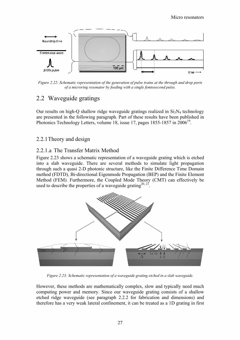
Figure 2.22: Schematic representation of the generation of pulse trains at the through and drop ports
of a microring resonator by feeding with a single femtosecond pulse.
2.2 Waveguide gratings Our results on high-Q shallow ridge waveguide gratings realized in Si3N4 technology are presented in the following paragraph. Part of these results have been published in Photonics Technology Letters, volume 18, issue 17, pages 1855-1857 in 200619.
2.2.1 Theory and design
2.2.1.a The Transfer Matrix Method Figure 2.23 shows a schematic representation of a waveguide grating which is etched into a slab waveguide. There are several methods to simulate light propagation through such a quasi 2-D photonic structure, like the Finite Difference Time Domain method (FDTD), Bi-directional Eigenmode Propagation (BEP) and the Finite Element Method (FEM). Furthermore, the Coupled Mode Theory (CMT) can effectively be used to describe the properties of a waveguide grating20, 21.
Figure 2.23: Schematic representation of a waveguide grating etched in a slab waveguide.
However, these methods are mathematically complex, slow and typically need much computing power and memory. Since our waveguide grating consists of a shallow etched ridge waveguide (see paragraph 2.2.2 for fabrication and dimensions) and therefore has a very weak lateral confinement, it can be treated as a 1D grating in first
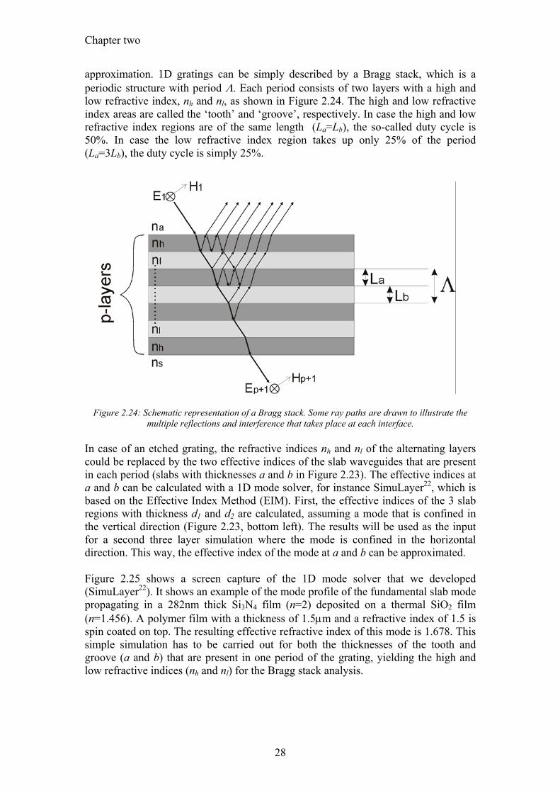
Chapter two
28
approximation. 1D gratings can be simply described by a Bragg stack, which is a periodic structure with period Λ. Each period consists of two layers with a high and low refractive index, nh and nl, as shown in Figure 2.24. The high and low refractive index areas are called the ‘tooth’ and ‘groove’, respectively. In case the high and low refractive index regions are of the same length (La=Lb), the so-called duty cycle is 50%. In case the low refractive index region takes up only 25% of the period (La=3Lb), the duty cycle is simply 25%.
Figure 2.24: Schematic representation of a Bragg stack. Some ray paths are drawn to illustrate the multiple reflections and interference that takes place at each interface.
In case of an etched grating, the refractive indices nh and nl of the alternating layers could be replaced by the two effective indices of the slab waveguides that are present in each period (slabs with thicknesses a and b in Figure 2.23). The effective indices at a and b can be calculated with a 1D mode solver, for instance SimuLayer22, which is based on the Effective Index Method (EIM). First, the effective indices of the 3 slab regions with thickness d1 and d2 are calculated, assuming a mode that is confined in the vertical direction (Figure 2.23, bottom left). The results will be used as the input for a second three layer simulation where the mode is confined in the horizontal direction. This way, the effective index of the mode at a and b can be approximated. Figure 2.25 shows a screen capture of the 1D mode solver that we developed (SimuLayer22). It shows an example of the mode profile of the fundamental slab mode propagating in a 282nm thick Si3N4 film (n=2) deposited on a thermal SiO2 film (n=1.456). A polymer film with a thickness of 1.5µm and a refractive index of 1.5 is spin coated on top. The resulting effective refractive index of this mode is 1.678. This simple simulation has to be carried out for both the thicknesses of the tooth and groove (a and b) that are present in one period of the grating, yielding the high and low refractive indices (nh and nl) for the Bragg stack analysis.
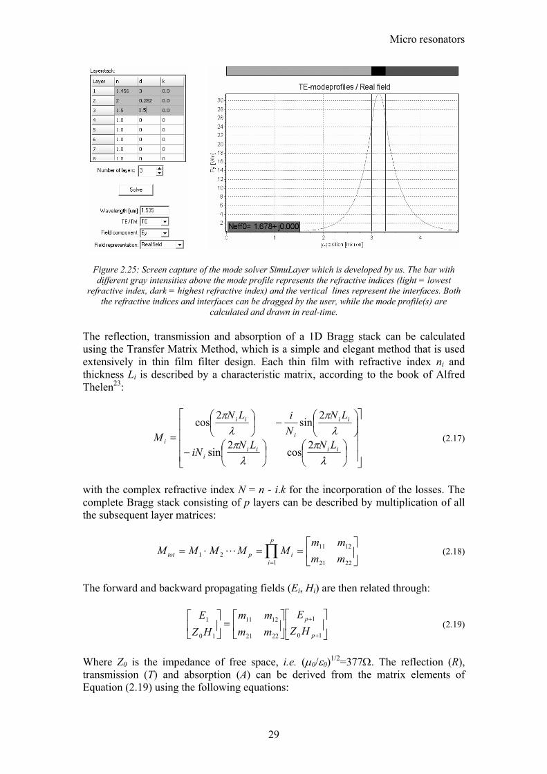
Micro resonators
29
Figure 2.25: Screen capture of the mode solver SimuLayer which is developed by us. The bar with different gray intensities above the mode profile represents the refractive indices (light = lowest
refractive index, dark = highest refractive index) and the vertical lines represent the interfaces. Both the refractive indices and interfaces can be dragged by the user, while the mode profile(s) are
calculated and drawn in real-time. The reflection, transmission and absorption of a 1D Bragg stack can be calculated using the Transfer Matrix Method, which is a simple and elegant method that is used extensively in thin film filter design. Each thin film with refractive index ni and thickness Li is described by a characteristic matrix, according to the book of Alfred Thelen23:
⎥⎥⎥⎥
⎦
⎤
⎢⎢⎢⎢
⎣
⎡
⎟⎠⎞
⎜⎝⎛
⎟⎠⎞
⎜⎝⎛−
⎟⎠⎞
⎜⎝⎛−⎟
⎠⎞
⎜⎝⎛
=
λπ
λπ
λπ
λπ
iiiii
ii
i
ii
i LNLNiN
LNNiLN
M2
cos2
sin
2sin
2cos
(2.17)
with the complex refractive index N = n - i.k for the incorporation of the losses. The complete Bragg stack consisting of p layers can be described by multiplication of all the subsequent layer matrices:
⎥⎦
⎤⎢⎣
⎡==⋅= ∏
= 2221
1211
121 mm
mmMMMMM
p
iiptot L (2.18)
The forward and backward propagating fields (Ei, Hi) are then related through:
⎥⎦
⎤⎢⎣
⎡⎥⎦
⎤⎢⎣
⎡=⎥
⎦
⎤⎢⎣
⎡
+
+
10
1
2221
1211
10
1
p
p
HZE
mmmm
HZE
(2.19)
Where Z0 is the impedance of free space, i.e. (µ0/ε0)1/2=377Ω. The reflection (R), transmission (T) and absorption (A) can be derived from the matrix elements of Equation (2.19) using the following equations:
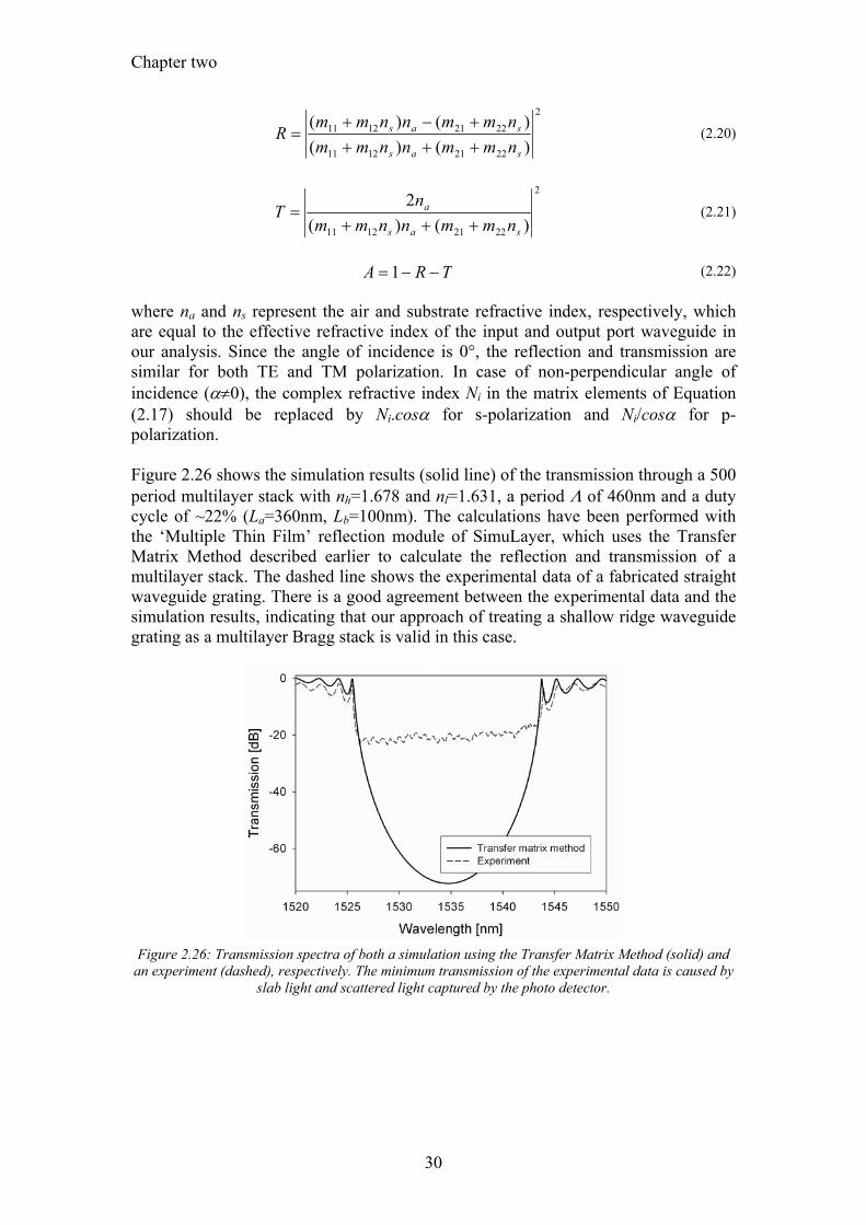
Chapter two
30
2
22211211
22211211
)()()()(
sas
sas
nmmnnmmnmmnnmm
R++++−+
= (2.20)
2
22211211 )()(2
sas
a
nmmnnmmn
T+++
= (2.21)
TRA −−= 1 (2.22)
where na and ns represent the air and substrate refractive index, respectively, which are equal to the effective refractive index of the input and output port waveguide in our analysis. Since the angle of incidence is 0°, the reflection and transmission are similar for both TE and TM polarization. In case of non-perpendicular angle of incidence (α≠0), the complex refractive index Ni in the matrix elements of Equation (2.17) should be replaced by Ni.cosα for s-polarization and Ni/cosα for p- polarization. Figure 2.26 shows the simulation results (solid line) of the transmission through a 500 period multilayer stack with nh=1.678 and nl=1.631, a period Λ of 460nm and a duty cycle of ~22% (La=360nm, Lb=100nm). The calculations have been performed with the ‘Multiple Thin Film’ reflection module of SimuLayer, which uses the Transfer Matrix Method described earlier to calculate the reflection and transmission of a multilayer stack. The dashed line shows the experimental data of a fabricated straight waveguide grating. There is a good agreement between the experimental data and the simulation results, indicating that our approach of treating a shallow ridge waveguide grating as a multilayer Bragg stack is valid in this case.
Figure 2.26: Transmission spectra of both a simulation using the Transfer Matrix Method (solid) and an experiment (dashed), respectively. The minimum transmission of the experimental data is caused by
slab light and scattered light captured by the photo detector.
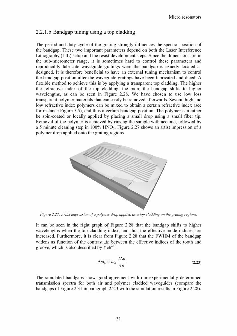
Micro resonators
31
2.2.1.b Bandgap tuning using a top cladding The period and duty cycle of the grating strongly influences the spectral position of the bandgap. These two important parameters depend on both the Laser Interference Lithography (LIL) setup and the resist development steps. Since the dimensions are in the sub-micrometer range, it is sometimes hard to control these parameters and reproducibly fabricate waveguide gratings were the bandgap is exactly located as designed. It is therefore beneficial to have an external tuning mechanism to control the bandgap position after the waveguide gratings have been fabricated and diced. A flexible method to achieve this is by applying a transparent top cladding. The higher the refractive index of the top cladding, the more the bandgap shifts to higher wavelengths, as can be seen in Figure 2.28. We have chosen to use low loss transparent polymer materials that can easily be removed afterwards. Several high and low refractive index polymers can be mixed to obtain a certain refractive index (see for instance Figure 5.5), and thus a certain bandgap position. The polymer can either be spin-coated or locally applied by placing a small drop using a small fiber tip. Removal of the polymer is achieved by rinsing the sample with acetone, followed by a 5 minute cleaning step in 100% HNO3. Figure 2.27 shows an artist impression of a polymer drop applied onto the grating regions.
Figure 2.27: Artist impression of a polymer drop applied as a top cladding on the grating regions. It can be seen in the right graph of Figure 2.28 that the bandgap shifts to higher wavelengths when the top cladding index, and thus the effective mode indices, are increased. Furthermore, it is clear from Figure 2.28 that the FWHM of the bandgap widens as function of the contrast ∆n between the effective indices of the tooth and groove, which is also described by Yeh24:
nn
πωω ∆
≅∆2
00 (2.23)
The simulated bandgaps show good agreement with our experimentally determined transmission spectra for both air and polymer cladded waveguides (compare the bandgaps of Figure 2.31 in paragraph 2.2.3 with the simulation results in Figure 2.28).
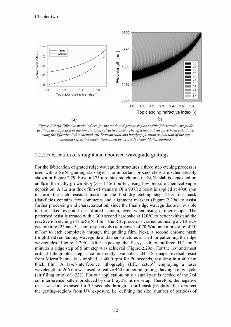
Chapter two
32
(a) (b)
Figure 2.28:(a)Effective mode indices for the tooth and groove regions of the fabricated waveguide gratings as a function of the top cladding refractive index. The effective indices have been calculated
using the Effective Index Method. (b) Transmission and bandgap position as function of the top cladding refractive index determined using the Transfer Matrix Method.
2.2.2 Fabrication of straight and apodized waveguide gratings. For the fabrication of grated ridge waveguide structures a three step etching process is used with a Si3N4 guiding slab layer The important process steps are schematically shown in Figure 2.29. First, a 275 nm thick stoichiometric Si3N4 slab is deposited on an 8µm thermally grown SiO2 (n = 1.456) buffer, using low pressure chemical vapor deposition. A 1.2 µm thick film of standard Olin 907/12 resist is applied at 4000 rpm to form the etch–resistant mask for the first dry etching step. This first mask (darkfield) contains text comments and alignment markers (Figure 2.29a) to assist further processing and characterization, since the final ridge waveguides are invisible to the naked eye and an infrared camera, even when using a microscope. The patterned resist is treated with a 300 second hardbake at 120°C to better withstand the reactive ion etching of the Si3N4 film. The RIE process is carried out using a CHF3/O2 gas mixture (25 and 5 sccm, respectively) at a power of 70 Watt and a pressure of 10 mTorr to etch completely through the guiding film. Next, a second chrome mask (brightfield) containing waveguide and taper structures is used for patterning the ridge waveguides (Figure 2.29b). After exposing the Si3N4 slab to buffered HF for 7 minutes a ridge step of 5 nm step was achieved (Figure 2.29c). For the last and most critical lithographic step, a commercially available Ti04–TX image reversal resist from MicroChemicals is applied at 4000 rpm for 20 seconds, resulting in a 400 nm thick film. A laser-interference lithography (LIL) setup25 employing a laser wavelength of 266 nm was used to realize 460 nm period gratings having a duty cycle (air filling ratio) of ~22%. For our application, only a small part is needed of the 2x4 cm interference pattern produced by our Lloyd’s mirror setup. Therefore, the negative resist was first exposed for 5.5 seconds through a third mask (brightfield), to protect the grating–regions from UV exposure, i.e. defining the size (number of periods) of
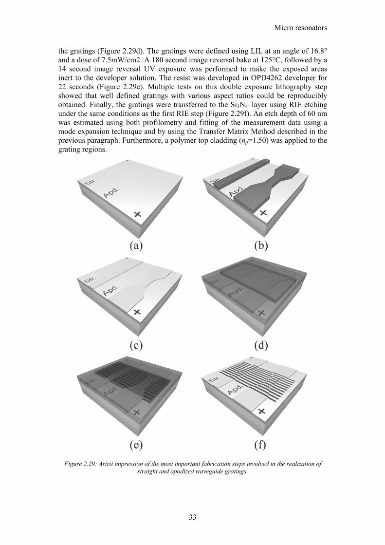
Micro resonators
33
the gratings (Figure 2.29d). The gratings were defined using LIL at an angle of 16.8° and a dose of 7.5mW/cm2. A 180 second image reversal bake at 125°C, followed by a 14 second image reversal UV exposure was performed to make the exposed areas inert to the developer solution. The resist was developed in OPD4262 developer for 22 seconds (Figure 2.29e). Multiple tests on this double exposure lithography step showed that well defined gratings with various aspect ratios could be reproducibly obtained. Finally, the gratings were transferred to the Si3N4–layer using RIE etching under the same conditions as the first RIE step (Figure 2.29f). An etch depth of 60 nm was estimated using both profilometry and fitting of the measurement data using a mode expansion technique and by using the Transfer Matrix Method described in the previous paragraph. Furthermore, a polymer top cladding (np=1.50) was applied to the grating regions.
Figure 2.29: Artist impression of the most important fabrication steps involved in the realization of straight and apodized waveguide gratings.
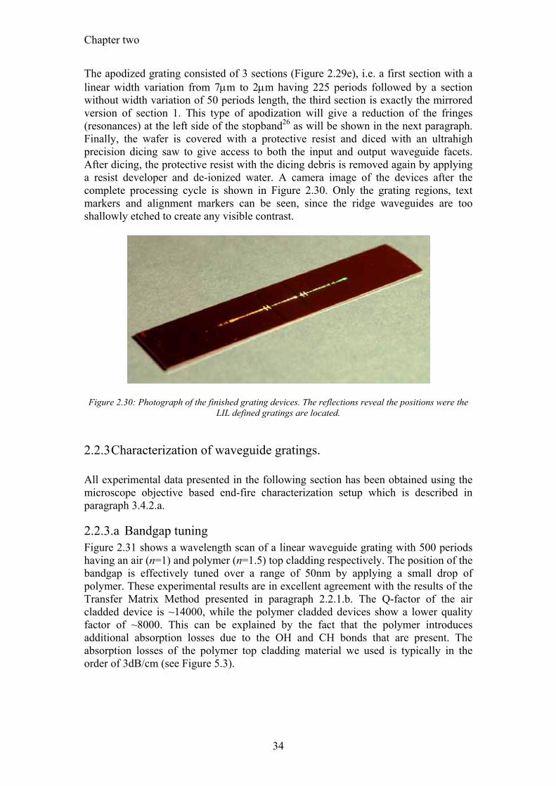
Chapter two
34
The apodized grating consisted of 3 sections (Figure 2.29e), i.e. a first section with a linear width variation from 7µm to 2µm having 225 periods followed by a section without width variation of 50 periods length, the third section is exactly the mirrored version of section 1. This type of apodization will give a reduction of the fringes (resonances) at the left side of the stopband26 as will be shown in the next paragraph. Finally, the wafer is covered with a protective resist and diced with an ultrahigh precision dicing saw to give access to both the input and output waveguide facets. After dicing, the protective resist with the dicing debris is removed again by applying a resist developer and de-ionized water. A camera image of the devices after the complete processing cycle is shown in Figure 2.30. Only the grating regions, text markers and alignment markers can be seen, since the ridge waveguides are too shallowly etched to create any visible contrast.
Figure 2.30: Photograph of the finished grating devices. The reflections reveal the positions were the
LIL defined gratings are located.
2.2.3 Characterization of waveguide gratings. All experimental data presented in the following section has been obtained using the microscope objective based end-fire characterization setup which is described in paragraph 3.4.2.a.
2.2.3.a Bandgap tuning Figure 2.31 shows a wavelength scan of a linear waveguide grating with 500 periods having an air (n=1) and polymer (n=1.5) top cladding respectively. The position of the bandgap is effectively tuned over a range of 50nm by applying a small drop of polymer. These experimental results are in excellent agreement with the results of the Transfer Matrix Method presented in paragraph 2.2.1.b. The Q-factor of the air cladded device is ~14000, while the polymer cladded devices show a lower quality factor of ~8000. This can be explained by the fact that the polymer introduces additional absorption losses due to the OH and CH bonds that are present. The absorption losses of the polymer top cladding material we used is typically in the order of 3dB/cm (see Figure 5.3).
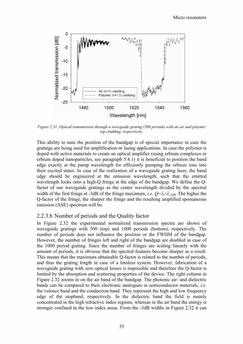
Micro resonators
35
Figure 2.31: Optical transmission through a waveguide grating (500 periods) with an air and polymer
top cladding, respectively. This ability to tune the position of the bandgap is of special importance in case the gratings are being used for amplification or lasing applications. In case the polymer is doped with active materials to create an optical amplifier (using erbium complexes or erbium doped nanoparticles, see paragraph 5.4.1) it is beneficial to position the band edge exactly at the pump wavelength for efficiently pumping the erbium ions into their excited states. In case of the realization of a waveguide grating laser, the band edge should be engineered at the emission wavelength, such that the emitted wavelength locks onto a high-Q fringe at the edge of the bandgap. We define the Q-factor of our waveguide gratings as the center wavelength divided by the spectral width of the first fringe at -3dB of the fringe maximum, i.e. Q=λc/λ-3dB. The higher the Q-factor of the fringe, the sharper the fringe and the resulting amplified spontaneous emission (ASE) spectrum will be.
2.2.3.b Number of periods and the Quality factor In Figure 2.32 the experimental normalized transmission spectra are shown of waveguide gratings with 500 (top) and 1000 periods (bottom), respectively. The number of periods does not influence the position or the FWHM of the bandgap. However, the number of fringes left and right of the bandgap are doubled in case of the 1000 period grating. Since the number of fringes are scaling linearly with the amount of periods, it is obvious that the spectral features become sharper as a result. This means that the maximum obtainable Q-factor is related to the number of periods, and thus the grating length in case of a lossless system. However, fabrication of a waveguide grating with zero optical losses is impossible and therefore the Q-factor is limited by the absorption and scattering properties of the device. The right column in Figure 2.32 zooms in on the air band of the bandgap. The photonic air- and dielectric bands can be compared to their electronic analogues in semiconductor materials, i.e. the valence band and the conduction band. They represent the high and low frequency edge of the stopband, respectively. In the dielectric band the field is mainly concentrated in the high refractive index regions, whereas in the air band the energy is stronger confined in the low index areas. From the -3dB widths in Figure 2.32 it can
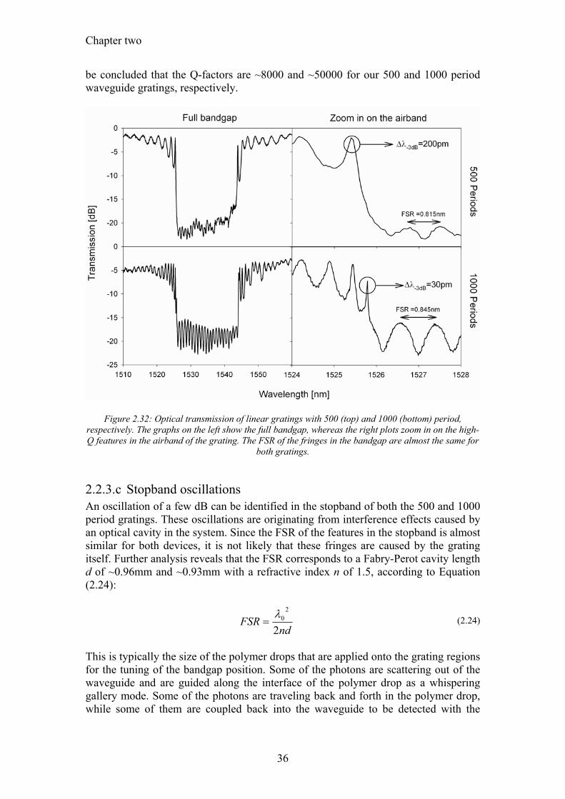
Chapter two
36
be concluded that the Q-factors are ~8000 and ~50000 for our 500 and 1000 period waveguide gratings, respectively.
Figure 2.32: Optical transmission of linear gratings with 500 (top) and 1000 (bottom) period,
respectively. The graphs on the left show the full bandgap, whereas the right plots zoom in on the high-Q features in the airband of the grating. The FSR of the fringes in the bandgap are almost the same for
both gratings.
2.2.3.c Stopband oscillations An oscillation of a few dB can be identified in the stopband of both the 500 and 1000 period gratings. These oscillations are originating from interference effects caused by an optical cavity in the system. Since the FSR of the features in the stopband is almost similar for both devices, it is not likely that these fringes are caused by the grating itself. Further analysis reveals that the FSR corresponds to a Fabry-Perot cavity length d of ~0.96mm and ~0.93mm with a refractive index n of 1.5, according to Equation (2.24):
ndFSR
2
20λ= (2.24)
This is typically the size of the polymer drops that are applied onto the grating regions for the tuning of the bandgap position. Some of the photons are scattering out of the waveguide and are guided along the interface of the polymer drop as a whispering gallery mode. Some of the photons are traveling back and forth in the polymer drop, while some of them are coupled back into the waveguide to be detected with the
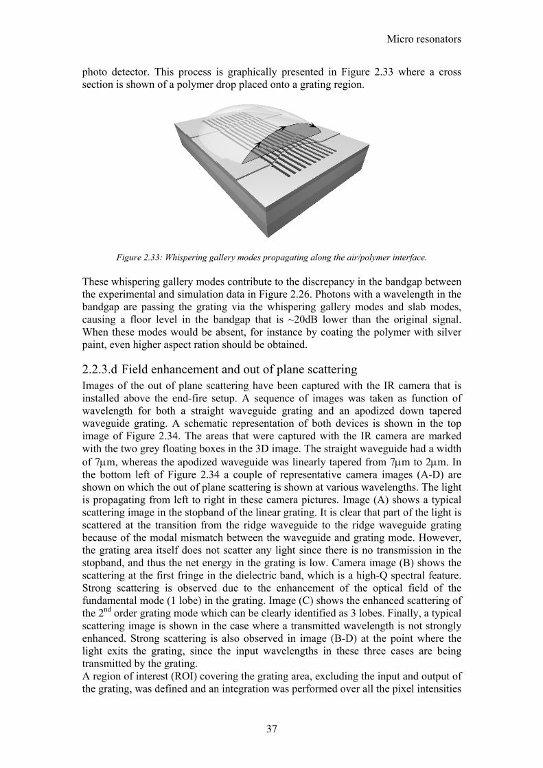
Micro resonators
37
photo detector. This process is graphically presented in Figure 2.33 where a cross section is shown of a polymer drop placed onto a grating region.
Figure 2.33: Whispering gallery modes propagating along the air/polymer interface. These whispering gallery modes contribute to the discrepancy in the bandgap between the experimental and simulation data in Figure 2.26. Photons with a wavelength in the bandgap are passing the grating via the whispering gallery modes and slab modes, causing a floor level in the bandgap that is ~20dB lower than the original signal. When these modes would be absent, for instance by coating the polymer with silver paint, even higher aspect ration should be obtained.
2.2.3.d Field enhancement and out of plane scattering Images of the out of plane scattering have been captured with the IR camera that is installed above the end-fire setup. A sequence of images was taken as function of wavelength for both a straight waveguide grating and an apodized down tapered waveguide grating. A schematic representation of both devices is shown in the top image of Figure 2.34. The areas that were captured with the IR camera are marked with the two grey floating boxes in the 3D image. The straight waveguide had a width of 7µm, whereas the apodized waveguide was linearly tapered from 7µm to 2µm. In the bottom left of Figure 2.34 a couple of representative camera images (A-D) are shown on which the out of plane scattering is shown at various wavelengths. The light is propagating from left to right in these camera pictures. Image (A) shows a typical scattering image in the stopband of the linear grating. It is clear that part of the light is scattered at the transition from the ridge waveguide to the ridge waveguide grating because of the modal mismatch between the waveguide and grating mode. However, the grating area itself does not scatter any light since there is no transmission in the stopband, and thus the net energy in the grating is low. Camera image (B) shows the scattering at the first fringe in the dielectric band, which is a high-Q spectral feature. Strong scattering is observed due to the enhancement of the optical field of the fundamental mode (1 lobe) in the grating. Image (C) shows the enhanced scattering of the 2nd order grating mode which can be clearly identified as 3 lobes. Finally, a typical scattering image is shown in the case where a transmitted wavelength is not strongly enhanced. Strong scattering is also observed in image (B-D) at the point where the light exits the grating, since the input wavelengths in these three cases are being transmitted by the grating. A region of interest (ROI) covering the grating area, excluding the input and output of the grating, was defined and an integration was performed over all the pixel intensities
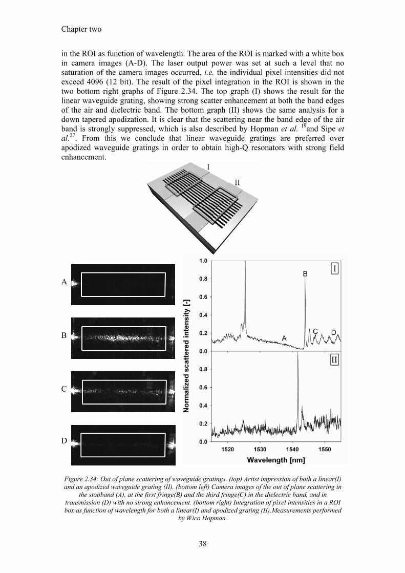
Chapter two
38
in the ROI as function of wavelength. The area of the ROI is marked with a white box in camera images (A-D). The laser output power was set at such a level that no saturation of the camera images occurred, i.e. the individual pixel intensities did not exceed 4096 (12 bit). The result of the pixel integration in the ROI is shown in the two bottom right graphs of Figure 2.34. The top graph (I) shows the result for the linear waveguide grating, showing strong scatter enhancement at both the band edges of the air and dielectric band. The bottom graph (II) shows the same analysis for a down tapered apodization. It is clear that the scattering near the band edge of the air band is strongly suppressed, which is also described by Hopman et al. 19and Sipe et al.27. From this we conclude that linear waveguide gratings are preferred over apodized waveguide gratings in order to obtain high-Q resonators with strong field enhancement.
A
B
C
D
Figure 2.34: Out of plane scattering of waveguide gratings. (top) Artist impression of both a linear(I) and an apodized waveguide grating (II). (bottom left) Camera images of the out of plane scattering in
the stopband (A), at the first fringe(B) and the third fringe(C) in the dielectric band, and in transmission (D) with no strong enhancement. (bottom right) Integration of pixel intensities in a ROI box as function of wavelength for both a linear(I) and apodized grating (II).Measurements performed
by Wico Hopman.
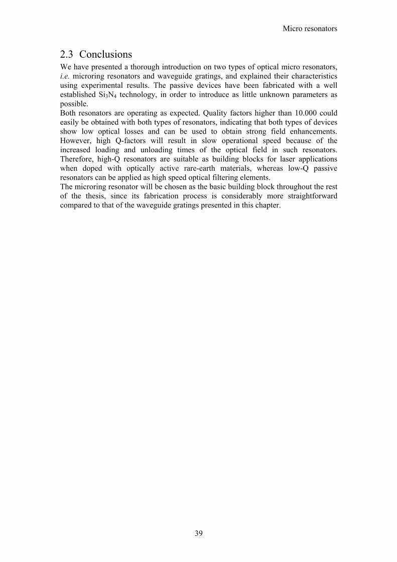
Micro resonators
39
2.3 Conclusions We have presented a thorough introduction on two types of optical micro resonators, i.e. microring resonators and waveguide gratings, and explained their characteristics using experimental results. The passive devices have been fabricated with a well established Si3N4 technology, in order to introduce as little unknown parameters as possible. Both resonators are operating as expected. Quality factors higher than 10.000 could easily be obtained with both types of resonators, indicating that both types of devices show low optical losses and can be used to obtain strong field enhancements. However, high Q-factors will result in slow operational speed because of the increased loading and unloading times of the optical field in such resonators. Therefore, high-Q resonators are suitable as building blocks for laser applications when doped with optically active rare-earth materials, whereas low-Q passive resonators can be applied as high speed optical filtering elements. The microring resonator will be chosen as the basic building block throughout the rest of the thesis, since its fabrication process is considerably more straightforward compared to that of the waveguide gratings presented in this chapter.

41
3 Optical properties
It is important to know the optical performance of a certain material system when it is used for the fabrication of integrated optical devices. In the following chapter a broad range of material properties relevant for the scope of this thesis will be discussed together with some of the characterization methods used. First, a broad range of optical loss mechanisms will be treated, followed by two materials for obtaining optical gain. The third-order nonlinear properties of a broad range of materials will be treated together with some general definitions. Finally, the characterization setups to determine the properties mentioned above will be presented.
Chapter three
42
3.1 Optical attenuation
3.1.1 General description of optical attenuation When light propagates through a medium, its intensity can be attenuated through several mechanisms like scattering or material absorption. In general, the intensity reduction can be described by the Lambert-Beer law, which states that the attenuation of a thin layer of thickness dz is proportional to the intensity I and the path length dz, schematically shown in Figure 3.1:
Figure 3.1: Attenuation according to Lambert-Beer. By introducing the loss coefficient a, we get:
dzIadI ⋅⋅=− (3.1)
Solving this differential equation for a propagation length L (in cm) results in:
LaeII ⋅−⋅= 0 (3.2)
while extraction of the loss coefficient a yields:
⎟⎟⎠
⎞⎜⎜⎝
⎛⋅=
0
ln1II
La (3.3)
This loss coefficient a is expressed in cm-1. In literature several coefficients, like k and α, are being used to describe the optical losses of a material or system. They all describe the amount of intensity reduction per unit length. The parameter k is related to the complex index of refraction:
kinN ⋅−= (3.4) In this case, the relation between a and k is as follows:
λπ ka ⋅⋅
=4 (3.5)
However, in electrical engineering and in the telecommunication community, it is more convenient to express the attenuation in terms of dB/cm with parameter α. The relation then becomes28:
Optical properties
43
aaeL
II
⋅≈⋅⋅=⋅−
= 34.4log10)log(10
0α (3.6)
We will consistently use the parameter α when we discuss optical losses. The total attenuation αtot of a material is the combination of several loss mechanisms, i.e. losses due to the UV tail absorption, the IR tail absorption, scatter losses, free carrier losses, and losses caused by impurities in the system. Each of them will be described in detail in the next paragraphs.
3.1.2 UV absorption In general, materials do exhibit absorption in the ultraviolet, referred to as electronic absorption29, which decays exponentially with increasing wavelength. The mechanism for this type of loss is due to the local field-induced broadening of the excitonic levels, which creates optical absorption for energies close to but below the interband edge30. These exponential absorption edges have been observed in alkali halides, II-IV compounds, III-V semiconductors, organics, and amorphous sytems31. The fundamental optical absorption-edge can be described by an empirical expression, known as Urbach’s rule:
( )Tk
UVBeB
0ωωσ
αhh −
⋅= (3.7)
where kB is Boltzmann’s constant, ħ is Planck’s constant divided by 2π, and B, ω0 and σ are fitting parameters. This wavelength and temperature dependent expression can be simplified (when room temperature is assumed) to:
λλαUVC
UVUV eB ⋅=)( (3.8)
with BUV and CUV as fitting parameters.
3.1.3 IR absorption In the near infrared part of the spectrum, additional losses can be introduced by the overtones of the mid infrared molecular excitations. For polymers, like PMMA for instance, there is a strong contribution of the C-H overtone stretches and combinations of stretch and other deformation overtones. Fluorination, i.e. replacing the hydrogen atoms with fluorine atoms, is often used in polymers to overcome the C-H absorption in polymers. Teflon is a well known example of such a fluorinated-polymer. Absorption peaks in the infrared can be present in both organic as inorganic materials. The absorption of the overtones of the molecular bonds in and inorganic PECVD deposited SiON film and an organic Bisphenol-A based polymer film are shown in Figure 3.2.
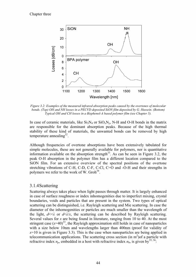
Chapter three
44
Figure 3.2: Examples of the measured infrared absorption peaks caused by the overtones of molecular bonds. (Top) OH and NH losses in a PECVD deposited SiON film deposited by G. Hussein. (Bottom)
Typical OH and CH losses in a Bisphenol-A based polymer film (see Chapter 5). In case of ceramic materials, like Si3N4 or SiOxNy, N-H and O-H bonds in the matrix are responsible for the dominant absorption peaks. Because of the high thermal stability of these kind of materials, the unwanted bonds can be removed by high temperature annealing32. Although frequencies of overtone absorptions have been extensively tabulated for simple molecules, these are not generally available for polymers, nor is quantitative information available on the absorption strength33. As can be seen in Figure 3.2, the peak O-H absorption in the polymer film has a different location compared to the SiON film. For an extensive overview of the spectral positions of the overtone stretching vibrations of C-H, C-D, C-F, C-Cl, C=O and -O-H and their strengths in polymers we refer to the work of W. Groh34.
3.1.4 Scattering Scattering always takes place when light passes through matter. It is largely enhanced in case of surface roughness or index inhomogenities due to imperfect mixing, crystal boundaries, voids and particles that are present in the system. Two types of optical scattering can be distinguished, i.e. Rayleigh scattering and Mie scattering. In case the diameter of the inhomogenities or particles are much smaller than the wavelength of the light, d<<λ or d<λ/x, the scattering can be described by Rayleigh scattering. Several values for x are being found in literature, ranging from 10 to 40. At the most stringent case (x=40)33, the Rayleigh approximation still holds in case of nanoparticles with a size below 10nm and wavelengths larger than 400nm (proof for validity of x=10 is given in Figure 3.3). This is the case when nanoparticles are being applied in telecommunication applications. The scattering cross section (in m2)of a particle with refractive index np, embedded in a host with refractive index nh, is given by35, 36:
Optical properties
45
2
2
2
2
4
2
1.
238 r
nn
nn
rn
h
p
h
p
hRayl π
λπ
σ
⎟⎟⎟⎟⎟
⎠
⎞
⎜⎜⎜⎜⎜
⎝
⎛
+⎟⎟⎠
⎞⎜⎜⎝
⎛
−⎟⎟⎠
⎞⎜⎜⎝
⎛
⎟⎠⎞
⎜⎝⎛= (3.9)
The λ-4 dependency, which is responsible for the blue sky and the red sunset, can be clearly seen. Furthermore, there is an even stronger dependency on the particle radius of ~ r6. Another way to describe scattering is to use Mie theory, which is valid for spheres of any size. Mie scattering calculations are considerably more complicated than Rayleigh scattering calculations, since the Mie scattering cross section is being expressed as the infinite series36:
∑∞
=
++⎟⎟⎠
⎞⎜⎜⎝
⎛=
1
222 )()12(2
nnn
medMie ban
kπσ (3.10)
where kmed=2πnmed/λ0 and the coefficients an and bn are given by:
[ ] [ ]
[ ] [ ]')()(')()(')()(')()(
)1(1
)1(21
2
mxmxjxhxxhmxjmmxmxjxjxxjmxjm
annnn
nnnnn µµ
µµ−−
= (3.11)
[ ] [ ]
[ ] [ ]')()(')()(')()(')()(
)1()1(1
1
mxmxjxhxxhmxjmxmxjxjxxjmxj
bnnnn
nnnnn µµ
µµ−−
= (3.12)
Here, the jn’s are spherical Bessel functions of the first kind, the hn’s are spherical Hankel functions, and µ1 and µ2 are the magnetic permeability of the sphere and the surrounding medium, respectively. The parameter x=(2πnmedr)/λ0 is called the size parameter and the parameter m represents the ratio between the refractive index of the sphere and the surrounding medium. We will only use the Rayleigh approximation, since it is valid for the kind of nanoparticles discussed in this research. Figure 3.3 shows a comparison of rigorous calculations of the Mie and Rayleigh scattering of unpolarised light for LaF3 particles with a radius of 1µm and 10nm in water, respectively. It can be clearly seen that for the large r=1µm particles the above assumption doesn’t hold, while for the r=10nm nanoparticles the Rayleigh scattering perfectly matches with the Mie scattering calculations. From Figure 3.3 it can be seen that the Rayleigh assumption still holds for nanoparticles with a diameter of 20nm up to wavelengths of 200nm. The data in Figure 3.3 was calculated using MiePlot37.
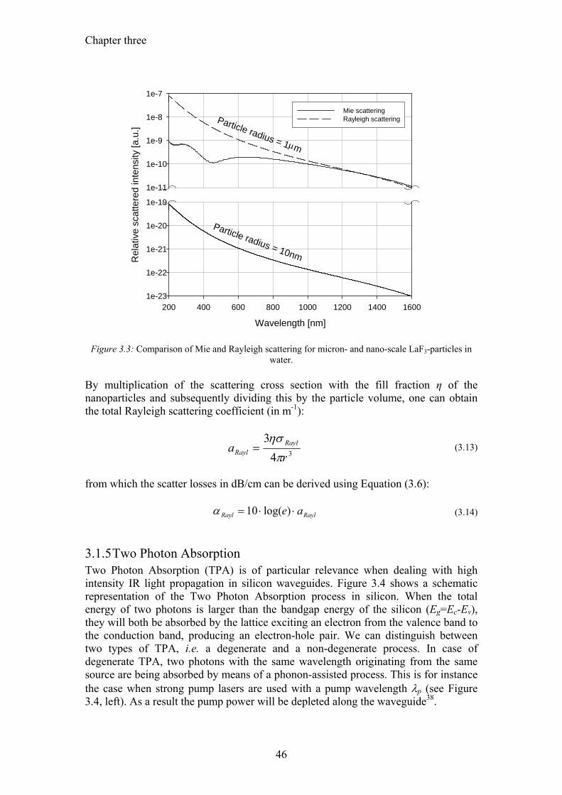
Chapter three
46
Wavelength [nm]
200 400 600 800 1000 1200 1400 1600
Rel
ativ
e sc
atte
red
inte
nsity
[a.u
.]
1e-23
1e-22
1e-21
1e-20
1e-19
1e-11
1e-10
1e-9
1e-8
1e-7
Mie scatteringRayleigh scatteringParticle radius = 1µm
Particle radius = 10nm
Figure 3.3: Comparison of Mie and Rayleigh scattering for micron- and nano-scale LaF3-particles in water.
By multiplication of the scattering cross section with the fill fraction η of the nanoparticles and subsequently dividing this by the particle volume, one can obtain the total Rayleigh scattering coefficient (in m-1):
343
ra Rayl
Rayl πησ
= (3.13)
from which the scatter losses in dB/cm can be derived using Equation (3.6):
RaylRayl ae ⋅⋅= )log(10α (3.14)
3.1.5 Two Photon Absorption Two Photon Absorption (TPA) is of particular relevance when dealing with high intensity IR light propagation in silicon waveguides. Figure 3.4 shows a schematic representation of the Two Photon Absorption process in silicon. When the total energy of two photons is larger than the bandgap energy of the silicon (Eg=Ec-Ev), they will both be absorbed by the lattice exciting an electron from the valence band to the conduction band, producing an electron-hole pair. We can distinguish between two types of TPA, i.e. a degenerate and a non-degenerate process. In case of degenerate TPA, two photons with the same wavelength originating from the same source are being absorbed by means of a phonon-assisted process. This is for instance the case when strong pump lasers are used with a pump wavelength λp (see Figure 3.4, left). As a result the pump power will be depleted along the waveguide38.
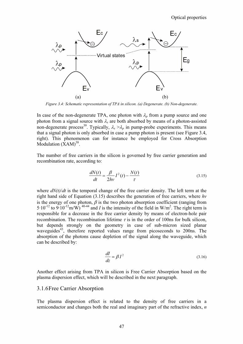
Optical properties
47
(a) (b)
Figure 3.4: Schematic representation of TPA in silicon. (a) Degenerate. (b) Non-degenerate.
In case of the non-degenerate TPA, one photon with λp from a pump source and one photon from a signal source with λs are both absorbed by means of a photon-assisted non-degenerate process39. Typically, λs >λp in pump-probe experiments. This means that a signal photon is only absorbed in case a pump photon is present (see Figure 3.4, right). This phenomenon can for instance be employed for Cross Absorption Modulation (XAM)38. The number of free carriers in the silicon is governed by free carrier generation and recombination rate, according to:
τβ )()(
2)( 2 tNtI
hvdttdN
−= (3.15)
where dN(t)/dt is the temporal change of the free carrier density. The left term at the right hand side of Equation (3.15) describes the generation of free carriers, where hv is the energy of one photon, β is the two photon absorption coefficient (ranging from 5·10-12 to 9·10-12m/W) 40-44 and I is the intensity of the field in W/m2. The right term is responsible for a decrease in the free carrier density by means of electron-hole pair recombination. The recombination lifetime τ is in the order of 100ns for bulk silicon, but depends strongly on the geometry in case of sub-micron sized planar waveguides43, therefore reported values range from picoseconds to 200ns. The absorption of the photons cause depletion of the signal along the waveguide, which can be described by:
2IdzdI β= (3.16)
Another effect arising from TPA in silicon is Free Carrier Absorption based on the plasma dispersion effect, which will be described in the next paragraph.
3.1.6 Free Carrier Absorption The plasma dispersion effect is related to the density of free carriers in a semiconductor and changes both the real and imaginary part of the refractive index, n
Chapter three
48
and k, respectively. These changes are described by the Drude-Lorenz equations that describe how the electron and hole concentrations (Ne and Nh expressed in cm-3) do influence the absorption α and the refractive index n:
⎥⎥⎦
⎤
⎢⎢⎣
⎡ ∆+
∆−=∆
hch
h
ece
e
mN
mN
nce
µµεπλα 22
032
23
4 (3.17)
⎥⎦
⎤⎢⎣
⎡ ∆+
∆−=∆
ch
h
ce
e
mN
mN
ncen
022
22
8 επλ (3.18)
where e is the electron charge, ε0 is the permittivity of free space, n the refractive index of unperturbed crystalline silicon, mce and mch are the conductivity effective masses, and µe and µh the mobility of electrons and holes, respectively. For silicon, the conductivity effective masses are mce= 0.26m0 and mch=0.39m0, with m0 the free electron rest mass, being 9.11×10⁻³¹kg. Soref and Bennett45 derived some very useful empirical expressions that are almost universally used in literature to evaluate the changes caused by injection or depletion of free carriers in silicon at a wavelength of 1550nm46:
[ ]he NN ∆×+∆×−=∆ −− 1818 106105.8α (3.19)
[ ]8.01822 105.8108.8 he NNn ∆×+∆×−=∆ −− (3.20)
which are in good agreement with the classical Drude-Lorenz model described earlier. However, for the influence of holes on the refractive index they noted a Nh
0.8 dependence. From Equation (3.19) the free carrier absorption cross section σFC in m2 for silicon at λ=1.55µm can be derived44:
224
55.11045.1 ⎟
⎠⎞
⎜⎝⎛×= − λσ FC (3.21)
where the constant represents the experimentally determined cross section obtained by Soref et al. The quadratic term is a scaling factor where λ is the wavelength of the incident photon which is expressed in micrometer. The larger the wavelength, the larger the apparent cross section of the photon is. This will increases the change that the photon hits a free carrier, and thus the absorption cross section increases accordingly. The decrease in optical intensity I as function of propagation distance z as a result of the free carrier absorption is:
INdzdI
FCFCσ−= (3.22)
with NFC the free carrier density in m-3.
Optical properties
49
3.1.7 Impurities The last mechanism described responsible for additional losses can be impurities in the material. One can think of the absorption peaks caused by the surface plasmon resonances of noble metal nanoparticles (see paragraph 5.3.2 and 5.4.2.b) or gold nano rings, which are sometimes being used as sensitizers for erbium doped systems47. Rare earth ions like erbium, ytterbium and neodymium which are used to achieve optical gain also cause absorption peaks as will be discussed in the next paragraphs.
3.2 Optical gain There are two mechanisms to achieve optical gain that are relevant for the scope of this thesis. The first will be discussed in this section and in chapter 4 and 5 of the thesis. This first type of gain relies on rare earth ions that are being pumped into an excited state using a strong pump beam. Once a signal photon passes by, the energy of the excited state can be released (stimulated emission) and is used to make an exact copy (wavelength, direction, and phase) of the signal photon. Eleven out of fourteen rare earth ions can be used for amplification of near infrared light. However, our focus will be on neodymium and erbium, since they emit in the 2nd and 3rd telecommunication windows around 1330nm and 1550nm, respectively, which makes them excellent candidates for telecom applications. The properties of 3-level erbium and 4-level neodymium doped systems will be discussed in paragraph 3.2.2 and 3.2.3, respectively. Two sets of rate equations will be presented, from which simplified analytical models for erbium and neodymium doped systems will be derived. It is not the aim of these sections to show extensive numerical modeling in which all energy transfer processes are incorporated. The simplified models will be used in order to obtain a rough estimate on the gain performance of rare earth doped systems. The second optical gain mechanism is of a completely different type and is based on Raman scattering. Pump photons can excite the lattice in a material causing energy to be stored in the form of lattice vibrations, called Raman phonons. These phonons can cause a photon to be emitted at either the Stokes or anti-Stokes frequency, respectively. The emission of such a photon can be spontaneous or can be triggered by a signal photon. In the latter case, this process is called stimulated Raman scattering (SRS) where the signal photon will be copied. This type of optical gain is beyond the scope of this thesis.
3.2.1 Absorption, emission and amplification of light by rare earth ions
3.2.1.a Einstein coefficients and gain When energy is applied to an atom by means of an electrical current or a photon, the atom can be excited to a higher energy state. In this thesis only optical pumping will be considered. This excitation takes place via absorption of the incoming photon and is schematically drawn in Figure 3.5.
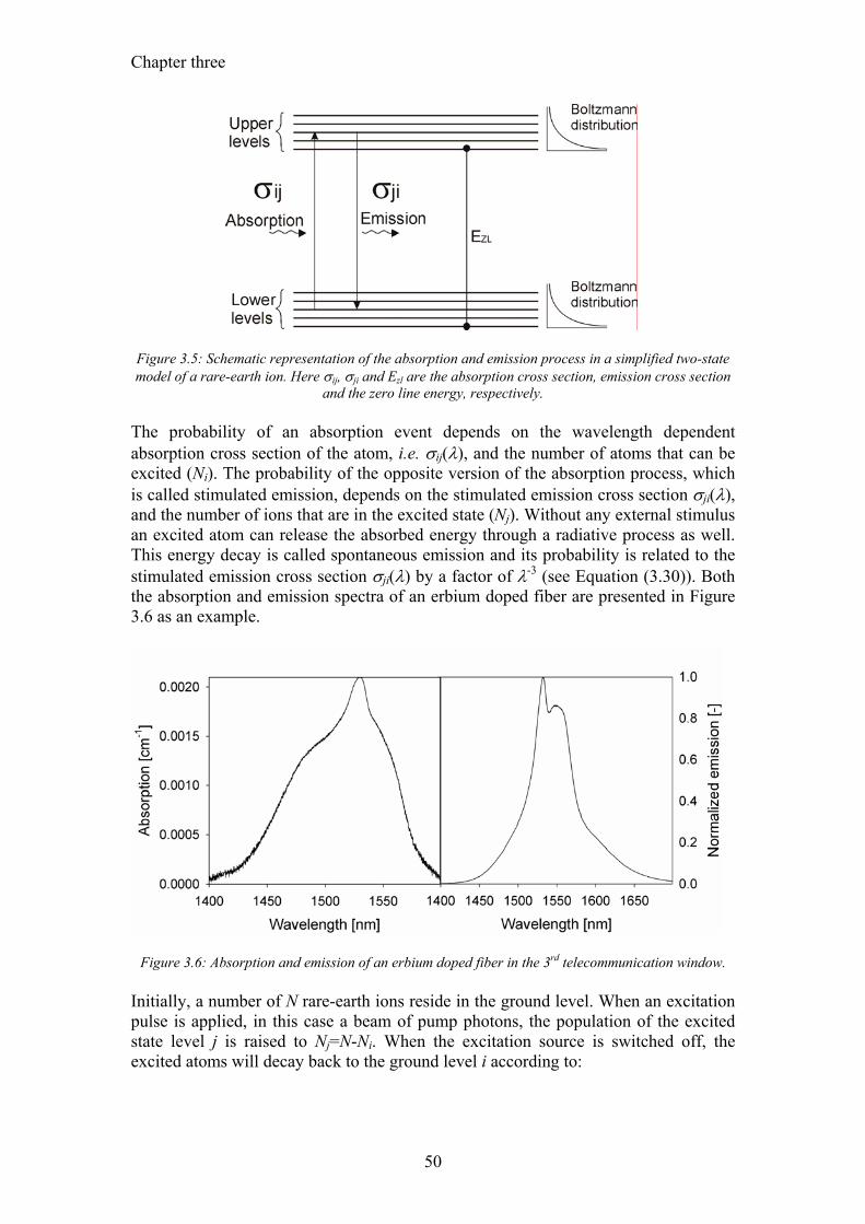
Chapter three
50
Figure 3.5: Schematic representation of the absorption and emission process in a simplified two-state model of a rare-earth ion. Here σij, σji and Ezl are the absorption cross section, emission cross section
and the zero line energy, respectively. The probability of an absorption event depends on the wavelength dependent absorption cross section of the atom, i.e. σij(λ), and the number of atoms that can be excited (Ni). The probability of the opposite version of the absorption process, which is called stimulated emission, depends on the stimulated emission cross section σji(λ), and the number of ions that are in the excited state (Nj). Without any external stimulus an excited atom can release the absorbed energy through a radiative process as well. This energy decay is called spontaneous emission and its probability is related to the stimulated emission cross section σji(λ) by a factor of λ-3 (see Equation (3.30)). Both the absorption and emission spectra of an erbium doped fiber are presented in Figure 3.6 as an example.
Figure 3.6: Absorption and emission of an erbium doped fiber in the 3rd telecommunication window. Initially, a number of N rare-earth ions reside in the ground level. When an excitation pulse is applied, in this case a beam of pump photons, the population of the excited state level j is raised to Nj=N-Ni. When the excitation source is switched off, the excited atoms will decay back to the ground level i according to:
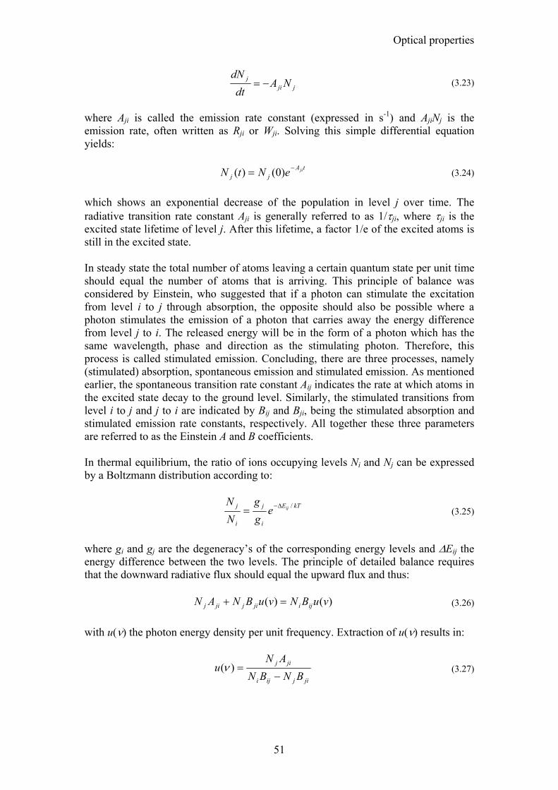
Optical properties
51
jjij NA
dtdN
−= (3.23)
where Aji is called the emission rate constant (expressed in s-1) and AjiNj is the emission rate, often written as Rji or Wji. Solving this simple differential equation yields:
tAjj
jieNtN −= )0()( (3.24)
which shows an exponential decrease of the population in level j over time. The radiative transition rate constant Aji is generally referred to as 1/τji, where τji is the excited state lifetime of level j. After this lifetime, a factor 1/e of the excited atoms is still in the excited state. In steady state the total number of atoms leaving a certain quantum state per unit time should equal the number of atoms that is arriving. This principle of balance was considered by Einstein, who suggested that if a photon can stimulate the excitation from level i to j through absorption, the opposite should also be possible where a photon stimulates the emission of a photon that carries away the energy difference from level j to i. The released energy will be in the form of a photon which has the same wavelength, phase and direction as the stimulating photon. Therefore, this process is called stimulated emission. Concluding, there are three processes, namely (stimulated) absorption, spontaneous emission and stimulated emission. As mentioned earlier, the spontaneous transition rate constant Aij indicates the rate at which atoms in the excited state decay to the ground level. Similarly, the stimulated transitions from level i to j and j to i are indicated by Bij and Bji, being the stimulated absorption and stimulated emission rate constants, respectively. All together these three parameters are referred to as the Einstein A and B coefficients. In thermal equilibrium, the ratio of ions occupying levels Ni and Nj can be expressed by a Boltzmann distribution according to:
kTE
i
j
i
j ijegg
NN /∆−= (3.25)
where gi and gj are the degeneracy’s of the corresponding energy levels and ∆Eij the energy difference between the two levels. The principle of detailed balance requires that the downward radiative flux should equal the upward flux and thus:
)()( vuBNvuBNAN ijijijjij =+ (3.26)
with u(ν) the photon energy density per unit frequency. Extraction of u(ν) results in:
jijiji
jij
BNBNAN
u−
=)(ν (3.27)
Chapter three
52
After substitution of the Boltzmann distribution of Equation (3.25) and ∆Eij=hνji the following relation is obtained:
1
/ 1)(−
⎟⎟⎠
⎞⎜⎜⎝
⎛−
⎥⎥⎦
⎤
⎢⎢⎣
⎡= kTh
jij
iji
ji
ji jieBgBg
BA
u νν (3.28)
which should equal Planck’s law for radiation48:
)1(8)( /3
33
−= kTh jiec
hnu ν
νπν (3.29)
By using Planck’s law a relationship between the stimulated emission and the spontaneous emission can be derived as follows:
3
338c
hnBA
ji
ji νπ= (3.30)
and: jijiji BgBg = (3.31)
Since spontaneous emission only causes depopulation of the lasing level j, and does not significantly contribute to the amplification or absorption of the signal photons in case of an optical amplifier, it can be neglected in case an estimation of the gain performance of a certain material needs to be made. For an estimation on the gain two extreme cases can be considered, i.e. the case of low excitation and full population inversion. In case of low excitation Ni≈N and Nj<<Ni. The absorption process will dominate in this case and the power in the material will be absorbed upon propagation, according to49:
xaeIxI ⋅−⋅= ννν )0,(),( with:
)(ννν gNB
cnha iij ⋅⋅⋅=
and:
)()( νννσ ν gBc
nhNa
iji
ij ⋅⋅==
(3.32)
where I(ν,x) is the intensity at frequency ν and distance x and aν is the absorption. In this equation g(ν) represents the line shape function. Some general properties of the lineshape function will be explained in the next paragraph. In the other extreme case of full population inversion, i.e. Nj>>Ni and Nj≈N, the energy transfer processes are dominated by stimulated emission and the light intensity increases according to:
xGeIxI ⋅⋅= ννν )0,(),( with:
(3.33)
Optical properties
53
)(ννν gNB
cnhG jji ⋅⋅⋅=
and:
)()( νννσ ν gBcnh
NG
jij
ji ⋅⋅==
A more general expression for the gain can be derived by assuming that both stimulated emission and absorption takes place simultaneously, i.e. Ni,j≠N. The gain in this case becomes:
[ ]
[ ]∫
∫
⋅−⋅=
⋅−⋅=
L
ijijij
L
ijijijL
dzzNzN
dzgcnhBzNBzNG
0
0
)()(
)()()(
σσ
νν
(3.34)
Since the emission and absorption cross section are almost equal in case of erbium around a wavelength of 1530nm, more than 50% of the erbium ions must be pumped into the excited state in order to achieve gain in an erbium doped material at that wavelength, as can be concluded from Equation (3.34). In case there is only knowledge about the excited state lifetime, the gain can also be derived from the spontaneous emission rate constant Aji, the degeneracies gi,j and the fluorescence spectrum by combining Equations (3.30), (3.31) and (3.34):
∫
∫
⎥⎦
⎤⎢⎣
⎡−=
⎥⎦
⎤⎢⎣
⎡−=
L
jii
i
jj
L
jiii
jj
L
dzgn
Ngg
N
dzgAncN
gg
NG
02
2
022
2
)(18
)(8
ντπ
λ
ννπ
(3.35)
3.2.1.b Füchtbauer-Ladenburg In this paragraph some useful expressions will be derived that can be used to calculate the emission and absorption cross sections using the spontaneously emitted spectrum. The spontaneous emission spectrum can be decomposed into one or more spectral lineshapes. The spectral lineshape g(ν) has already been introduced in the previous paragraph. Although there are many possible line shapes, it is common to model the spectral line shape function as a Lorentzian distribution:
( ) ( )220 2/2
1)(ννν
νπ
ν∆+−
∆=g (3.36)
where ν is the frequency of the light, ν0 is the center of the spectrum and ∆ν is the FWHM in Hz of the Lorentzian lineshape. Furthermore, the FWHM of the lineshape is related to the excited state lifetime via:
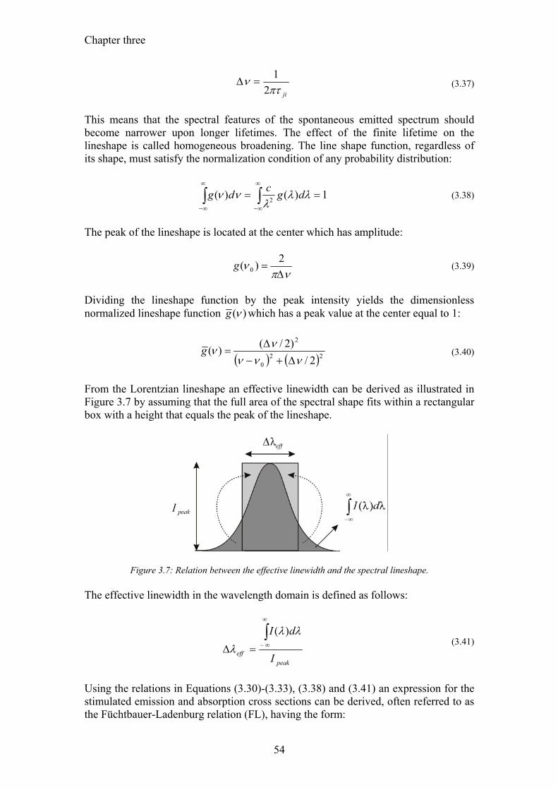
Chapter three
54
jiπτν
21
=∆ (3.37)
This means that the spectral features of the spontaneous emitted spectrum should become narrower upon longer lifetimes. The effect of the finite lifetime on the lineshape is called homogeneous broadening. The line shape function, regardless of its shape, must satisfy the normalization condition of any probability distribution:
1)()( 2 ==∫ ∫∞
∞−
∞
∞−
λλλ
νν dgcdg (3.38)
The peak of the lineshape is located at the center which has amplitude:
νπν
∆=
2)( 0g (3.39)
Dividing the lineshape function by the peak intensity yields the dimensionless normalized lineshape function )(νg which has a peak value at the center equal to 1:
( ) ( )220
2
2/)2/()(ννν
νν∆+−
∆=g (3.40)
From the Lorentzian lineshape an effective linewidth can be derived as illustrated in Figure 3.7 by assuming that the full area of the spectral shape fits within a rectangular box with a height that equals the peak of the lineshape.
Figure 3.7: Relation between the effective linewidth and the spectral lineshape. The effective linewidth in the wavelength domain is defined as follows:
peakeff I
dI∫∞
∞−=∆
λλλ
)(
(3.41)
Using the relations in Equations (3.30)-(3.33), (3.38) and (3.41) an expression for the stimulated emission and absorption cross sections can be derived, often referred to as the Füchtbauer-Ladenburg relation (FL), having the form:
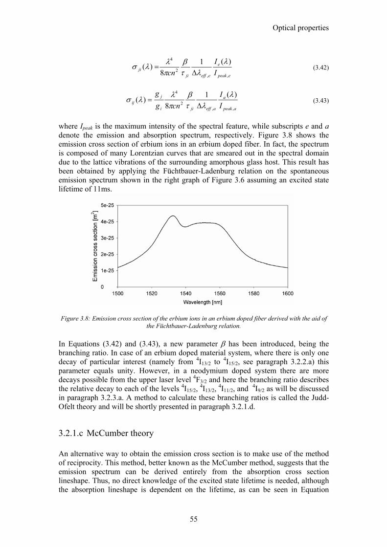
Optical properties
55
epeak
e
eeffjiji I
Icn ,,
2
4 )(18
)(λ
λτβ
πλλσ
∆= (3.42)
apeak
a
aeffjii
jij I
Icng
g
,,2
4 )(18
)(λ
λτβ
πλλσ
∆= (3.43)
where Ipeak is the maximum intensity of the spectral feature, while subscripts e and a denote the emission and absorption spectrum, respectively. Figure 3.8 shows the emission cross section of erbium ions in an erbium doped fiber. In fact, the spectrum is composed of many Lorentzian curves that are smeared out in the spectral domain due to the lattice vibrations of the surrounding amorphous glass host. This result has been obtained by applying the Füchtbauer-Ladenburg relation on the spontaneous emission spectrum shown in the right graph of Figure 3.6 assuming an excited state lifetime of 11ms.
Figure 3.8: Emission cross section of the erbium ions in an erbium doped fiber derived with the aid of
the Füchtbauer-Ladenburg relation. In Equations (3.42) and (3.43), a new parameter β has been introduced, being the branching ratio. In case of an erbium doped material system, where there is only one decay of particular interest (namely from 4I13/2 to 4I15/2, see paragraph 3.2.2.a) this parameter equals unity. However, in a neodymium doped system there are more decays possible from the upper laser level 4F3/2 and here the branching ratio describes the relative decay to each of the levels 4I15/2, 4I13/2, 4I11/2, and 4I9/2 as will be discussed in paragraph 3.2.3.a. A method to calculate these branching ratios is called the Judd-Ofelt theory and will be shortly presented in paragraph 3.2.1.d.
3.2.1.c McCumber theory An alternative way to obtain the emission cross section is to make use of the method of reciprocity. This method, better known as the McCumber method, suggests that the emission spectrum can be derived entirely from the absorption cross section lineshape. Thus, no direct knowledge of the excited state lifetime is needed, although the absorption lineshape is dependent on the lifetime, as can be seen in Equation
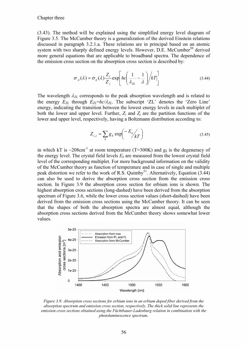
Chapter three
56
(3.43). The method will be explained using the simplified energy level diagram of Figure 3.5. The McCumber theory is a generalization of the derived Einstein relations discussed in paragraph 3.2.1.a. These relations are in principal based on an atomic system with two sharply defined energy levels. However, D.E. McCumber50 derived more general equations that are applicable to broadband spectra. The dependence of the emission cross section on the absorption cross section is described by:
⎥⎦
⎤⎢⎣
⎡⎟⎟⎠
⎞⎜⎜⎝
⎛−= kThc
ZZ
ZLj
iijji λλλσλσ 11exp)()( (3.44)
The wavelength λZL corresponds to the peak absorption wavelength and is related to the energy EZL through EZL=hc/λZL. The subscript ‘ZL’ denotes the ‘Zero Line’ energy, indicating the transition between the lowest energy levels in each multiplet of both the lower and upper level. Further, Zi and Zj are the partition functions of the lower and upper level, respectively, having a Boltzmann distribution according to:
∑ ⎟⎠⎞⎜
⎝⎛−=
k
kkji kT
EgZ exp, (3.45)
in which kT is ~208cm-1 at room temperature (T=300K) and gk is the degeneracy of the energy level. The crystal field levels Ek are measured from the lowest crystal field level of the corresponding multiplet. For more background information on the validity of the McCumber theory as function of temperature and in case of single and multiple peak distortion we refer to the work of R.S. Quimby51. Alternatively, Equation (3.44) can also be used to derive the absorption cross section from the emission cross section. In Figure 3.9 the absorption cross section for erbium ions is shown. The highest absorption cross sections (long-dashed) have been derived from the absorption spectrum of Figure 3.6, while the lower cross section values (short-dashed) have been derived from the emission cross sections using the McCumber theory. It can be seen that the shapes of both the absorption spectra are almost equal, although the absorption cross sections derived from the McCumber theory shows somewhat lower values.
Figure 3.9: Absorption cross sections for erbium ions in an erbium doped fiber derived from the absorption spectrum and emission cross section, respectively. The thick solid line represents the
emission cross sections obtained using the Füchtbauer-Ladenburg relation in combination with the photoluminescence spectrum.
Optical properties
57
3.2.1.d Judd-Ofelt theory The Judd-Ofelt52, 53 theory is a successful method to calculate and model the optical transitions in rare-earth doped materials. It is based on the absorption spectrum of a rare-earth doped material. The method uses the electric dipole line strength which describes the transition between two eigenstates of the rare-earth ion. This line strength S between the initial state J and the final state J’ can be written as follows49,
54:
[ ] [ ] [ ]2)6(6
2)4(4
2)2(2
6,4,2
2)( ')','(),()'(
UUU
JLSUJLSJJSt
ttcalc
⋅Ω+⋅Ω+⋅Ω=
Ω=→ ∑= (3.46)
where the initial states and final states are represented by S,L,J and S’,L’,J’, respectively. Further, Ωt (t=2,4,6) are the so called Judd-Ofelt parameters and U(t) (t=2,4,6) are the doubly reduced matrix elements which solely depend on angular momentum that are independent of the host material. The three Judd-Ofelt parameters are determined by measuring the absorption line strength Smeas and fit the parameters such that the difference between the measured and calculated line strengths are minimal (Smeas=Scalc). The line strength Smeas is described as49, 54:
( )
( ) ∫
∫
⎥⎥⎦
⎤
⎢⎢⎣
⎡
+
+=
⎥⎥⎦
⎤
⎢⎢⎣
⎡
+
+=→
λλσλπ
λλλπ
dne
nJch
danNe
nJchJJS
ij
meas
)(2
98
)12(3
)(2
98
)12(3)'(
2223
2223
(3.47)
where c is the speed of light in vacuum, h is Planck’s constant, e the elementary charge, J the angular momentum, N the rare-earth ion concentration in m-3, λ the mean wavelength, n the refractive index of the host material, a(λ) the absorption coefficient in m-1 and σij(λ) the absorption cross section in m2. After the Judd-Ofelt parameters Ωt (t=2,4,6) have been found, by for instance least square fitting, the line strengths corresponding to the transitions from the upper manifold to the lower manifolds can be calculated. From these line strengths the radiative decay rate constants A(J→J’), the corresponding lifetime τ, and the fluorescence branching ratios β can be found according to49, 54:
)'(9
)2()12(3
64)'(22
3
24
JJSnnJh
eJJA calc →+
+=→
λπ (3.48)
∑ →=
)'(1
JJAτ (3.49)
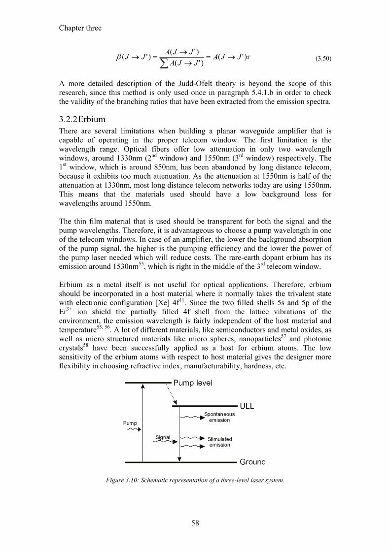
Chapter three
58
τβ )'()'(
)'()'( JJAJJA
JJAJJ →=→
→=→∑
(3.50)
A more detailed description of the Judd-Ofelt theory is beyond the scope of this research, since this method is only used once in paragraph 5.4.1.b in order to check the validity of the branching ratios that have been extracted from the emission spectra.
3.2.2 Erbium There are several limitations when building a planar waveguide amplifier that is capable of operating in the proper telecom window. The first limitation is the wavelength range. Optical fibers offer low attenuation in only two wavelength windows, around 1330nm (2nd window) and 1550nm (3rd window) respectively. The 1st window, which is around 850nm, has been abandoned by long distance telecom, because it exhibits too much attenuation. As the attenuation at 1550nm is half of the attenuation at 1330nm, most long distance telecom networks today are using 1550nm. This means that the materials used should have a low background loss for wavelengths around 1550nm. The thin film material that is used should be transparent for both the signal and the pump wavelengths. Therefore, it is advantageous to choose a pump wavelength in one of the telecom windows. In case of an amplifier, the lower the background absorption of the pump signal, the higher is the pumping efficiency and the lower the power of the pump laser needed which will reduce costs. The rare-earth dopant erbium has its emission around 1530nm55, which is right in the middle of the 3rd telecom window. Erbium as a metal itself is not useful for optical applications. Therefore, erbium should be incorporated in a host material where it normally takes the trivalent state with electronic configuration [Xe] 4f11. Since the two filled shells 5s and 5p of the Er3+ ion shield the partially filled 4f shell from the lattice vibrations of the environment, the emission wavelength is fairly independent of the host material and temperature55, 56. A lot of different materials, like semiconductors and metal oxides, as well as micro structured materials like micro spheres, nanoparticles57 and photonic crystals58 have been successfully applied as a host for erbium atoms. The low sensitivity of the erbium atoms with respect to host material gives the designer more flexibility in choosing refractive index, manufacturability, hardness, etc.
Figure 3.10: Schematic representation of a three-level laser system.
Optical properties
59
In case the optical gain is used for lasing applications, the ionic (or atomic) level schemesl are classed by the number of energy levels involved in the actual lasing process as three- or four-level lasers. In a three-level system, shown in Figure 3.10, energy in the form of pump photons is injected into the gain medium to excite atoms to the pump level above the upper lasing level (ULL). From there, the excited atoms decay fast to the ULL, generating heat and no photons. This upper lasing level often has a long lifetime (τji~10ms in case of erbium), so a large population of that level can be obtained easily. Energy decay occurs between the ULL and the ground state by stimulated (laser light) or spontaneous emission. This system is characterized by the lack of a discrete lower lasing level, since the ground state fulfills that purpose. Erbium doped materials belong to this group of 3-level systems. For broadband amplification purposes the thin films should have an amorphous structure in order to widen up the emission band. The amorphous environment will smear out the Stark levels in the multiplets, resulting in a smooth emission spectrum. Crystalline phases do not substantially smear out the Stark levels causing the emission spectrum to split up in sharp emission peaks. In this way the overall broadband gain efficiency of the device is reduced and sufficiently high gain is only occurring in sharp wavelength bands. Furthermore, a polycrystalline material structure will increase the scatter losses (see for instance paragraph 3.1.4 for a treatment on Rayleigh scattering).
3.2.2.a Energy transitions of Erbium Figure 3.11 shows a schematic representation of a selection of possible energy transitions (denoted A through H) in an erbium doped material based on the simplified energy level diagram of Di Pascale et al.59. Process A describes the absorption of 1480nm pump photons exciting the erbium atom from the 4I15/2 level to the 4I13/2 level. After a rapid non-radiating transition within the 4I13/2 level, the ion stays in the 4I13/2 level that has a lifetime τ21 which is typically in the order of 10ms. During each decay a photon with a longer wavelength is spontaneously emitted. Similar to the pump absorption, energy transition B shows the absorption of a signal photon around 1530nm. For both absorption processes a single wavelength dependent absorption cross-section σ12(λ) is used. The stimulated emission process is schematically shown in C. An excited erbium atom is triggered when a signal photon passed by and releases its energy in the form of a stimulated emitted photon with the same wavelength, phase and direction as the incoming signal photon. The emission cross section σ21 is used to describe the probability of this process. In D, the absorption of 980nm pump photons is shown. The excitation to the 4I11/2 level is rapidly followed by a non-radiative phonon relaxation with a lifetime τ32 which is in the order of 10µs for silica based materials60.
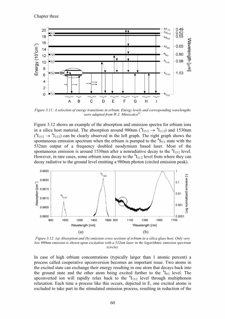
Chapter three
60
Figure 3.11: A selection of energy transitions in erbium. Energy levels and corresponding wavelengths
were adapted from W.J. Miniscalco61. Figure 3.12 shows an example of the absorption and emission spectra for erbium ions in a silica host material. The absorption around 980nm (4I15/2 → 4I11/2) and 1530nm (4I15/2 → 4I13/2) can be clearly observed in the left graph. The right graph shows the spontaneous emission spectrum when the erbium is pumped to the 4S3/2 state with the 532nm output of a frequency doubled neodymium based laser. Most of the spontaneous emission is around 1530nm after a nonradiative decay to the 4I13/2 level. However, in rare cases, some erbium ions decay to the 4I11/2 level from where they can decay radiative to the ground level emitting a 980nm photon (circled emission peak).
(a) (b)
Figure 3.12: (a) Absorption and (b) emission cross sections of erbium in a silica glass host. Only very low 980nm emission is shown upon excitation with a 532nm laser in the logarithmic emission spectrum
(circle). In case of high erbium concentrations (typically larger than 1 atomic percent) a process called cooperative upconversion becomes an important issue. Two atoms in the excited state can exchange their energy resulting in one atom that decays back into the ground state and the other atom being excited further to the 4I9/2 level. The upconverted ion will rapidly relax back to the 4I13/2 level through multiphonon relaxation. Each time a process like this occurs, depicted in E, one excited atoms is excluded to take part in the stimulated emission process, resulting in reduction of the
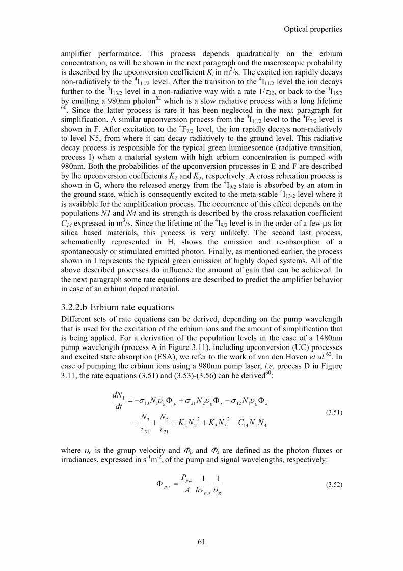
Optical properties
61
amplifier performance. This process depends quadratically on the erbium concentration, as will be shown in the next paragraph and the macroscopic probability is described by the upconversion coefficient Ki in m3/s. The excited ion rapidly decays non-radiatively to the 4I11/2 level. After the transition to the 4I11/2 level the ion decays further to the 4I13/2 level in a non-radiative way with a rate 1/τ32, or back to the 4I15/2 by emitting a 980nm photon62 which is a slow radiative process with a long lifetime 60. Since the latter process is rare it has been neglected in the next paragraph for simplification. A similar upconversion process from the 4I11/2 level to the 4F7/2 level is shown in F. After excitation to the 4F7/2 level, the ion rapidly decays non-radiatively to level N5, from where it can decay radiatively to the ground level. This radiative decay process is responsible for the typical green luminescence (radiative transition, process I) when a material system with high erbium concentration is pumped with 980nm. Both the probabilities of the upconversion processes in E and F are described by the upconversion coefficients K2 and K3, respectively. A cross relaxation process is shown in G, where the released energy from the 4I9/2 state is absorbed by an atom in the ground state, which is consequently excited to the meta-stable 4I13/2 level where it is available for the amplification process. The occurrence of this effect depends on the populations N1 and N4 and its strength is described by the cross relaxation coefficient C14 expressed in m3/s. Since the lifetime of the 4I9/2 level is in the order of a few µs for silica based materials, this process is very unlikely. The second last process, schematically represented in H, shows the emission and re-absorption of a spontaneously or stimulated emitted photon. Finally, as mentioned earlier, the process shown in I represents the typical green emission of highly doped systems. All of the above described processes do influence the amount of gain that can be achieved. In the next paragraph some rate equations are described to predict the amplifier behavior in case of an erbium doped material.
3.2.2.b Erbium rate equations Different sets of rate equations can be derived, depending on the pump wavelength that is used for the excitation of the erbium ions and the amount of simplification that is being applied. For a derivation of the population levels in the case of a 1480nm pump wavelength (process A in Figure 3.11), including upconversion (UC) processes and excited state absorption (ESA), we refer to the work of van den Hoven et al.62. In case of pumping the erbium ions using a 980nm pump laser, i.e. process D in Figure 3.11, the rate equations (3.51) and (3.53)-(3.56) can be derived60:
41142
332
2221
2
31
3
1122211131
NNCNKNKNN
NNNdt
dNsgsgpg
−++++
Φ−Φ+Φ−=
ττ
υσυσυσ (3.51)
where υg is the group velocity and Φp and Φs are defined as the photon fluxes or irradiances, expressed in s-1m-2, of the pump and signal wavelengths, respectively:
gsp
spsp hvA
Pυ11
,
,, =Φ (3.52)
Chapter three
62
where h is Planck’s constant, vp,s is the frequency of the light in s-1, Pp,s is the power in the waveguide in Watt and A is the waveguide cross section. For the excited state levels the change in population can described as follows:
41142
2221
2
32
3112221
2 22 NNCNKNNNN
dtdN
sgsg +−−+Φ+Φ−=ττ
υσυσ (3.53)
2
3343
4
32
3
31
3113
3 2 NKNNNN
dtdN
pg −+−−Φ=τττ
υσ (3.54)
41142
225
5
4
44 NNCNKNN
dtdN
−++−=ττ
(3.55)
2
335
55 NKN
dtdN
+−=τ
(3.56)
The sum of the population levels should be equal to the total erbium concentration Ntot according to:
∑=
=5
1iitot NN (3.57)
It is common to define the pump absorption, signal absorption and signal emission rate constants W13, W12 and W21 , often wrongly referred to as absorption and emission rates, as follows:
gpgp
p AP
hvW υσυ
σΦ== 13
1313
gsgs
s AP
hvW υσυ
σΦ== 12
1212
gsgs
s AP
hvW υσυ
σΦ== 21
2121
(3.58)
The rate equations (3.51) and (3.53)-(3.56) can be simplified when only the upconversion process from level 4I13/2 to 4I9/2 is taken into account and if the cross relaxation process is ignored. Due to the fast non-radiative transitions the upconverted ions are assumed to all relax to the metastable 4I13/2 level. We assume that all ions that are excited by the 980nm pump show a fast relaxation from level 4I11/2 to 4I13/2. Since τ32 << τ21, most of the excited atoms will be in the 4I13/2 level and the rate equations can be described as a quasi two-level system which includes the upconversion through parameter K2:
222
21
2112221113
1 NKNNWNWNWdt
dN++−+−=
τ (3.59)
Optical properties
63
dtdN
dtdN 12 −= (3.60)
totNNN =+ 21 (3.61)
Under steady state conditions dNi/dt equals zero and the population in level N1 and N2 can be described as:
tottot
tot
NNKWc
NKWWWb
Ka
acabb
N
⎟⎟⎠
⎞⎜⎜⎝
⎛++=
−−−−−=
=
−−−=
221
121
221
1221131
21
1
112
111
1
21
,2
4
τ
τ
(3.62)
( ) tot
tot
NWWc
WWWb
Ka
NNa
cabbN
12132
211221132
22
12
222
222
1
24
+=
−−−−=
=
−=−−−
=
τ
(3.63)
In case of an optical amplifier, the dependence of N1 and N2 on the absorption and emission rates can be linked to a propagation model assuming that the pump and signal beams decrease and increase, respectively, along the propagation direction z, according to dIp/dz=-apIp for the pump and dIs/dz=gsIs for the signal. Here, ap and gs are defined as the pump absorption and signal gain coefficients60:
113 Na p σ= (3.64)
112221 NNgs σσ −= (3.65)
In case the pump and signal wavelengths are largely separated, the modal overlap between the mode profiles of both pump and signal beams within the planar waveguide need to be taken into account by defining the overlap parameter Γ. The overlap of the mode profiles and the doping concentration profile can be accounted for in this dimensionless parameter. Furthermore, in case not all of the erbium atoms
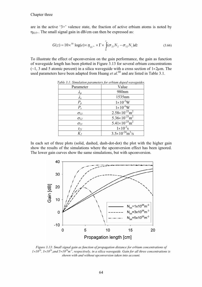
Chapter three
64
are in the active ‘3+’ valence state, the fraction of active erbium atoms is noted by ηEr3+. The small signal gain in dB/cm can then be expressed as:
dzNNezGz
Er ∫ −×Γ×××= +
0112221
10 )()log(10)( 3 σση (3.66)
To illustrate the effect of upconversion on the gain performance, the gain as function of waveguide length has been plotted in Figure 3.13 for several erbium concentrations (~1, 3 and 5 atomic percent) in a silica waveguide with a cross section of 1×2µm. The used parameters have been adapted from Huang et al.60 and are listed in Table 3.1.
Table 3.1: Simulation parameters for erbium doped waveguides. Parameter Value
λp 980nm λs 1535nm Pp 1×10⁻²W Ps 1×10⁻⁶W σ13 2.58×10⁻²⁵m2 σ12 5.36×10⁻²⁵m2 σ21 5.41×10⁻²⁵m2 τ21 1×10⁻²s K2 3.5×10⁻²⁴m3/s
In each set of three plots (solid, dashed, dash-dot-dot) the plot with the higher gain show the results of the simulations where the upconversion effect has been ignored. The lower gain curves show the same simulations, but with upconversion.
Figure 3.13: Small signal gain as function of propagation distance for erbium concentrations of 1×1026, 3×1026,and 5×1026m-3, respectively, in a silica waveguide. Gain for all three concentrations is
shown with and without upconversion taken into account.
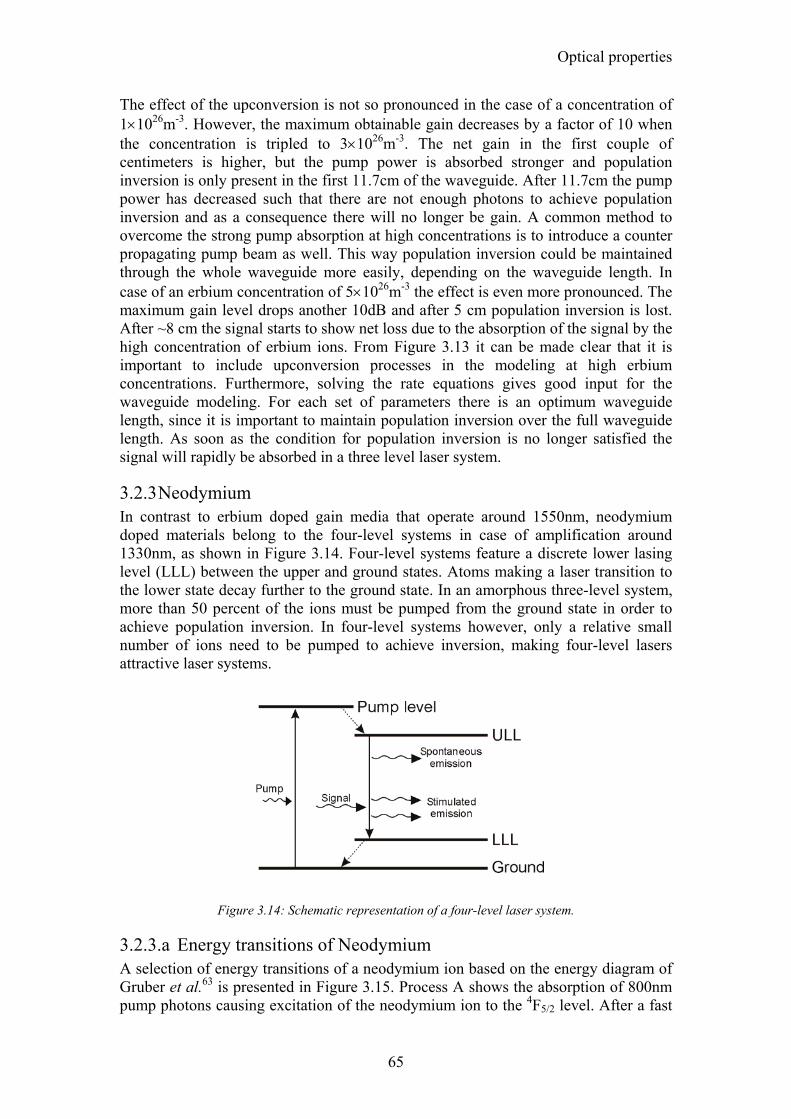
Optical properties
65
The effect of the upconversion is not so pronounced in the case of a concentration of 1×1026m-3. However, the maximum obtainable gain decreases by a factor of 10 when the concentration is tripled to 3×1026m-3. The net gain in the first couple of centimeters is higher, but the pump power is absorbed stronger and population inversion is only present in the first 11.7cm of the waveguide. After 11.7cm the pump power has decreased such that there are not enough photons to achieve population inversion and as a consequence there will no longer be gain. A common method to overcome the strong pump absorption at high concentrations is to introduce a counter propagating pump beam as well. This way population inversion could be maintained through the whole waveguide more easily, depending on the waveguide length. In case of an erbium concentration of 5×1026m-3 the effect is even more pronounced. The maximum gain level drops another 10dB and after 5 cm population inversion is lost. After ~8 cm the signal starts to show net loss due to the absorption of the signal by the high concentration of erbium ions. From Figure 3.13 it can be made clear that it is important to include upconversion processes in the modeling at high erbium concentrations. Furthermore, solving the rate equations gives good input for the waveguide modeling. For each set of parameters there is an optimum waveguide length, since it is important to maintain population inversion over the full waveguide length. As soon as the condition for population inversion is no longer satisfied the signal will rapidly be absorbed in a three level laser system.
3.2.3 Neodymium In contrast to erbium doped gain media that operate around 1550nm, neodymium doped materials belong to the four-level systems in case of amplification around 1330nm, as shown in Figure 3.14. Four-level systems feature a discrete lower lasing level (LLL) between the upper and ground states. Atoms making a laser transition to the lower state decay further to the ground state. In an amorphous three-level system, more than 50 percent of the ions must be pumped from the ground state in order to achieve population inversion. In four-level systems however, only a relative small number of ions need to be pumped to achieve inversion, making four-level lasers attractive laser systems.
Figure 3.14: Schematic representation of a four-level laser system.
3.2.3.a Energy transitions of Neodymium A selection of energy transitions of a neodymium ion based on the energy diagram of Gruber et al.63 is presented in Figure 3.15. Process A shows the absorption of 800nm pump photons causing excitation of the neodymium ion to the 4F5/2 level. After a fast
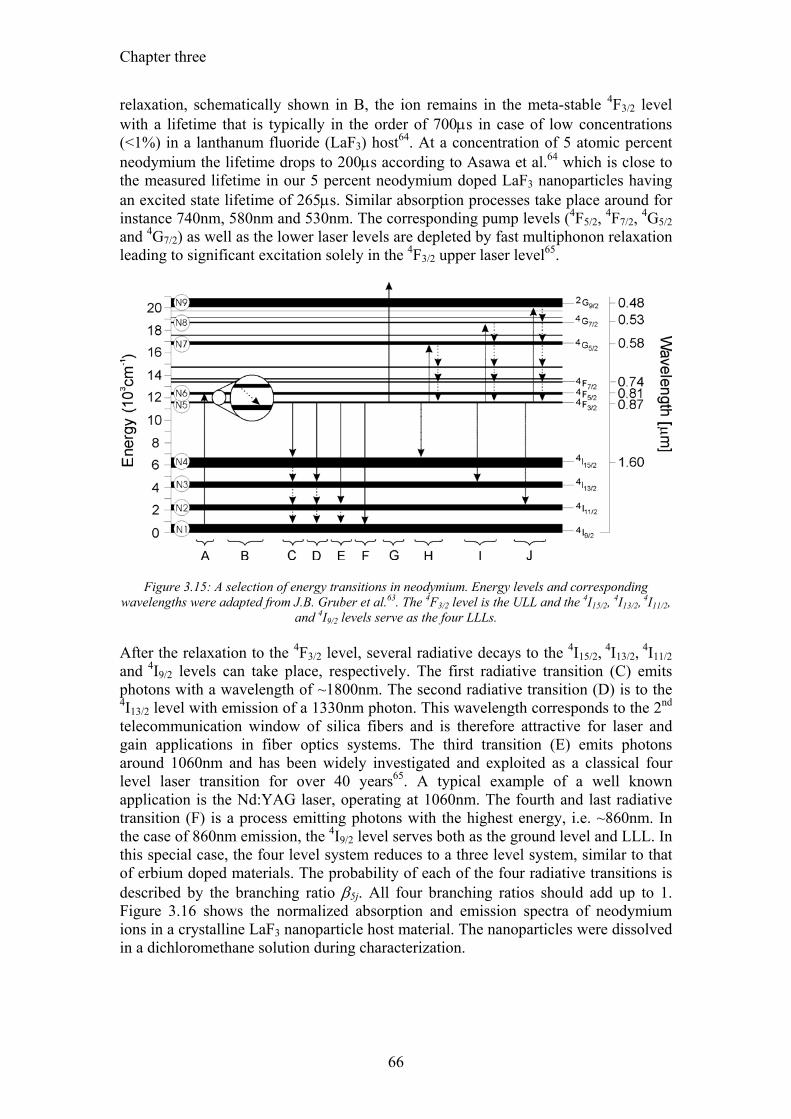
Chapter three
66
relaxation, schematically shown in B, the ion remains in the meta-stable 4F3/2 level with a lifetime that is typically in the order of 700µs in case of low concentrations (<1%) in a lanthanum fluoride (LaF3) host64. At a concentration of 5 atomic percent neodymium the lifetime drops to 200µs according to Asawa et al.64 which is close to the measured lifetime in our 5 percent neodymium doped LaF3 nanoparticles having an excited state lifetime of 265µs. Similar absorption processes take place around for instance 740nm, 580nm and 530nm. The corresponding pump levels (4F5/2, 4F7/2, 4G5/2 and 4G7/2) as well as the lower laser levels are depleted by fast multiphonon relaxation leading to significant excitation solely in the 4F3/2 upper laser level65.
Figure 3.15: A selection of energy transitions in neodymium. Energy levels and corresponding
wavelengths were adapted from J.B. Gruber et al.63. The 4F3/2 level is the ULL and the 4I15/2, 4I13/2, 4I11/2, and 4I9/2 levels serve as the four LLLs.
After the relaxation to the 4F3/2 level, several radiative decays to the 4I15/2, 4I13/2, 4I11/2 and 4I9/2 levels can take place, respectively. The first radiative transition (C) emits photons with a wavelength of ~1800nm. The second radiative transition (D) is to the 4I13/2 level with emission of a 1330nm photon. This wavelength corresponds to the 2nd telecommunication window of silica fibers and is therefore attractive for laser and gain applications in fiber optics systems. The third transition (E) emits photons around 1060nm and has been widely investigated and exploited as a classical four level laser transition for over 40 years65. A typical example of a well known application is the Nd:YAG laser, operating at 1060nm. The fourth and last radiative transition (F) is a process emitting photons with the highest energy, i.e. ~860nm. In the case of 860nm emission, the 4I9/2 level serves both as the ground level and LLL. In this special case, the four level system reduces to a three level system, similar to that of erbium doped materials. The probability of each of the four radiative transitions is described by the branching ratio β5j. All four branching ratios should add up to 1. Figure 3.16 shows the normalized absorption and emission spectra of neodymium ions in a crystalline LaF3 nanoparticle host material. The nanoparticles were dissolved in a dichloromethane solution during characterization.
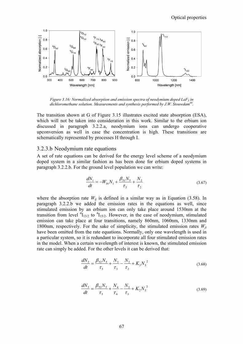
Optical properties
67
Figure 3.16: Normalized absorption and emission spectra of neodymium doped LaF3 in dichloromethane solution. Measurements and synthesis performed by J.W. Stouwdam66.
The transition shown at G of Figure 3.15 illustrates excited state absorption (ESA), which will not be taken into consideration in this work. Similar to the erbium ion discussed in paragraph 3.2.2.a, neodymium ions can undergo cooperative upconversion as well in case the concentration is high. These transitions are schematically represented by processes H through I.
3.2.3.b Neodymium rate equations A set of rate equations can be derived for the energy level scheme of a neodymium doped system in a similar fashion as has been done for erbium doped systems in paragraph 3.2.2.b. For the ground level population we can write:
2
2
5
551116
1
ττβ NNNW
dtdN
++−= (3.67)
where the absorption rate Wij is defined in a similar way as in Equation (3.58). In paragraph 3.2.2.b we added the emission rates in the equations as well, since stimulated emission by an erbium ion can only take place around 1530nm at the transition from level 4I13/2 to 4I15/2. However, in the case of neodymium, stimulated emission can take place at four transitions, namely 860nm, 1060nm, 1330nm and 1800nm, respectively. For the sake of simplicity, the stimulated emission rates Wji have been omitted from the rate equations. Normally, only one wavelength is used in a particular system, so it is redundant to incorporate all four stimulated emission rates in the model. When a certain wavelength of interest is known, the stimulated emission rate can simply be added. For the other levels it can be derived that:
253
2
2
3
3
5
5522 NKNNNdt
dN+−+=
τττβ (3.68)
252
3
3
4
4
5
5533 NKNNNdt
dN+−+=
τττβ (3.69)
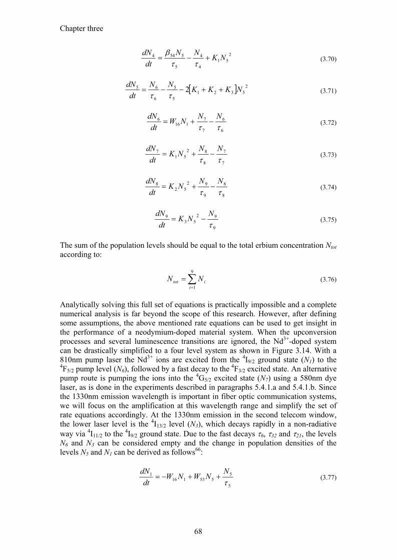
Chapter three
68
251
4
4
5
5544 NKNNdt
dN+−=
ττβ (3.70)
[ ] 25321
5
5
6
65 2 NKKKNNdt
dN++−−=
ττ (3.71)
6
6
7
7116
6
ττNNNW
dtdN
−+= (3.72)
7
7
8
8251
7
ττNN
NKdt
dN−+= (3.73)
8
8
9
9252
8
ττNN
NKdt
dN−+= (3.74)
9
9253
9
τN
NKdt
dN−= (3.75)
The sum of the population levels should be equal to the total erbium concentration Ntot according to:
∑=
=9
1iitot NN (3.76)
Analytically solving this full set of equations is practically impossible and a complete numerical analysis is far beyond the scope of this research. However, after defining some assumptions, the above mentioned rate equations can be used to get insight in the performance of a neodymium-doped material system. When the upconversion processes and several luminescence transitions are ignored, the Nd3+-doped system can be drastically simplified to a four level system as shown in Figure 3.14. With a 810nm pump laser the Nd3+ ions are excited from the 4I9/2 ground state (N1) to the 4F5/2 pump level (N6), followed by a fast decay to the 4F3/2 excited state. An alternative pump route is pumping the ions into the 4G5/2 excited state (N7) using a 580nm dye laser, as is done in the experiments described in paragraphs 5.4.1.a and 5.4.1.b. Since the 1330nm emission wavelength is important in fiber optic communication systems, we will focus on the amplification at this wavelength range and simplify the set of rate equations accordingly. At the 1330nm emission in the second telecom window, the lower laser level is the 4I13/2 level (N3), which decays rapidly in a non-radiative way via 4I11/2 to the 4I9/2 ground state. Due to the fast decays τ6, τ32 and τ21, the levels N6 and N3 can be considered empty and the change in population densities of the levels N5 and N1 can be derived as follows66:
5
5553116
1
τN
NWNWdt
dN++−= (3.77)
Optical properties
69
dtdNN
NWNWdt
dN 1
5
5553116
5 −=−−=τ
(3.78)
totNNN =+ 51 (3.79)
Where the population density N5 of the excited state corresponds to the expression derived by Dakss et al.4 and many others. The spontaneous emission does not contribute to the gain, so all spontaneous emission processes are combined as a whole in Equations (3.77) and (3.78) and is defined as follows:
⎥⎦
⎤⎢⎣
⎡+++=
5
54
5
53
5
52
5
515
5
5
τβ
τβ
τβ
τβ
τN
N (3.80)
At steady state operation dNi/dt equals zero, we can combine Equations (3.77) - (3.79) to solve the steady state population levels in the upper and lower manifolds resulting in:
totNWW
WN
⎟⎟⎟⎟
⎠
⎞
⎜⎜⎜⎜
⎝
⎛
++
+=
165
53
553
1 1
1
τ
τ (3.81)
totNWW
WN
⎟⎟⎟⎟
⎠
⎞
⎜⎜⎜⎜
⎝
⎛
++=
165
53
165 1
τ
(3.82)
The pump absorption and signal emission rates W16 and W53 are defined as follows:
pap
p
a
AP
hvW Φ== σ
σ16 (3.83)
ses
s
e
AP
hvW Φ== σ
σ53 (3.84)
where σa=σ16 is the absorption cross section and σe=σ53 the stimulated emission cross section. The change in photon flux and thus the power change (P=Φ.hv.A) of the signal and pump along the waveguide is given by:
dzNWd s 553=Φ (3.85)
dzNWd p 116=Φ (3.86)
Chapter three
70
Some results of the model are presented in Figure 3.17 for varying waveguide cross sections using the parameters listed in Table 3.2.
Table 3.2: Simulation parameters for neodymium doped waveguides. Parameter Value
λp 578nm λs 1330nm Pp 1×10⁻²W Ps 1×10⁻⁶W σ16 2.76×10⁻²⁴m2 σ53 1.63×10⁻²⁴m2 τ5 2.65×10⁻⁴s N 1.5×1025m-3
Figure 3.17: Small signal gain for neodymium doped waveguides with varying cross sections.The simulation parameters are listed in Table 3.2.
A monomode waveguide with a dimension of 1.3×2.5µm2 shows a gain of more than 1dB/cm at pump powers of only 10mW, while the gain rapidly drops for multimode waveguides with increasing waveguide cross sections. To obtain a similar gain for the 3.3×10.0µm2 waveguide a pump power of 100mW is needed, whereas the 10.0×10.0µm2 waveguide needs to be pumped with 1W to achieve this. From this we conclude that monomode waveguides are beneficial in case of low pump powers. All the pump photons have been absorbed by the neodymium ions at the propagation distance where where the gain stops to increase increase. One way to further improve the gain in this case would be to apply bi-directional pumping.
3.3 Third order optical non-linearity
3.3.1 Introduction and definitions The refractive index of any optical material can be written in the form:
Optical properties
71
InTTdTdnnITn R 2)()(),,( +−+= λλ (3.87)
where n(λ) is the refractive index at room temperature, whereby the wavelength dependence accounts for the chromatic dispersion The temperature derivative dn/dT is the thermo-optical coefficient, T the ambient temperature, TR is room temperature and n2 is the intensity dependent refractive index (IDRI) of the material, a 3rd order nonlinear phenomenon responsible for the Kerr effect. Besides the thermo-optic and Kerr effect, there are other nonlinear optical effects like the electro-optic effect (see e.g. the work of Hoekstra et al.67), but these nonlinear phenomena are beyond the scope of this research. Both the thermo-optic effect and electro-optic effect can be used to actively modify the refractive index of a certain material, but their modulation speeds are limited to the kHz and GHz range, respectively, since the thermo-optic effect is restricted by the thermal conductivity and heat capacity of the material, while the electro-optic effect is mainly limited by the driving electronics. A thermal overshoot can be applied to enhance the thermo-optic modulation, but the maximum obtainable switching speed will not exceed the kHz range68, 69. Although electro-optical modulation is many orders of magnitudes faster than thermo-optical modulation, it is still not sufficient for ultra-fast modulation needed in the next generation data networks. For even higher modulation speeds, in the THz regime, one should make use of ultra-fast all-optical phenomena, like the intensity dependent refractive index n2, which is a 3rd order nonlinear effect and takes place almost instantaneously. This 3rd order nonlinear effect can be used to introduce an intensity induced phase shift:
0
22λ
π effNL LIn=∆Φ (3.88)
where I is the light intensity in W/m2 and Leff is the effective length of the device [m]. This phase shift can effectively be used in resonant structures (like gratings or ring resonators) to modify the resonant condition, i.e. the wavelength for which the device is in resonance, which can in turn be used to switch or modulate an optical signal. Furthermore, the nonlinear phase shift can be strongly enhanced in optical resonators, since the intensity and the effective length increase at the resonance wavelengths. Because the intensity in Equation (3.88) is expressed in W/m2, it is useful to use SI units for n2 as well, i.e. m2/W. Unfortunately, several definitions and units for the nonlinear coefficient are being used in literature (n2’, n2,I, γ, β, χ(3), χRe
(3) and χIm(3),
using both electrostatic units (esu) and SI units). To avoid confusion and facilitate comparison between the IDRI of a broad range of materials, we refer to the definition proposed by Samoc et al.70 and DeSalvo et al.71 to convert between esu and SI units:
)('40)( 20
2 esuncn
SIn π= (3.89)
For the derivation of n2 from χ(3) we used72, 73:
Chapter three
72
200
)3(Re
2 43
)(nc
SInεχ
= (3.90)
The imaginary part of χ(3) is related to the nonlinear absorption coefficient β as73:
200
)3(Im3nc λε
πχβ = (3.91)
where, in Equations (3.89) to (3.91), c is the speed of light, ε0 is the electric permittivity of free space (8.85×10⁻¹² F/m), λ is the wavelength of the light and n0 is the linear refractive index of the material.
3.3.2 Optical materials and their third-order non-linearity Table 3.3 shows a list of common optical materials and their intensity dependent refractive index sorted by magnitude. A certain pattern can be found when looking at the materials and their n2 in Table 3.3. First, there are polymers and standard optical glasses like SiO2 and MgF2 that exhibit relatively low third order nonlinearity in the order of 10-20m2/W. Then there is a wide variety of special glasses with n2~10-18m2/W, closely followed by the III-V and IV semiconductors with n2 around 10-17-10-16m2/W. It is this range where also the standard glassed come into play with enhanced nonlinearity due to nanoparticles that are dispersed in the glass matrix. Nanoparticles dispersed in polymers exhibit an even higher nonlinearity in the order of 10-15 m2/W, which is close to that of erbium doped silica. It is beneficial to use materials with strong third order nonlinearity for all-optical switching. From Table 3.3 it can be seen that semiconductors and nanoparticle and/or erbium doped materials are the most promising candidates for all-optical switching applications. The optical nonlinearity can be enhanced by the dielectric confinement effect, which is a surface polarization effect induced by trapped state and atomic vacancy defects. This effect depends on the dielectric constant ratio (ε1/ε2) of nanoparticles and the host material74. The higher the refractive index contrast, the stronger the effect will be. A high contrast can be reached by dispersing high index nanoparticles in a low index host (for instance TiO2 in PMMA75) or coating the nanoparticles with a low index layer (like stearic acid coated Bi2O3 particles74). However, a high index contrast between the nanoparticles and their host will increase scatter losses which is disadvantageous when used in integrated optical devices as is discussed in paragraph 3.1.4.
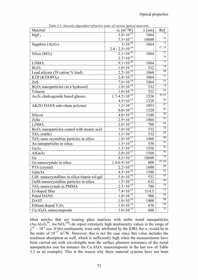
Optical properties
73
Table 3.3: Intensity dependent refractive index of various optical materials. Material n2 [m2/W] λ [nm] Ref.MgF2 5.9×10⁻²¹
7.5×10-211064
10600 71
76
Sapphire (Al2O3) 3×10-20
2.4 - 2.5×10-201064
- 71
77, 78
Silica (SiO2) 2.1×10⁻²⁰
2.7×10-201064
- 71
79
LiNbO3 9.1×10⁻²⁰ 1064 71
Bi2O3 1.0×10⁻¹⁹ 532 74
Lead silicate (39 cation % lead) 2.2×10⁻¹⁹ 1060 80
KTP (KTiOPO4) 2.4×10⁻¹⁹ 1064 71
ZnS 7.6×10⁻¹⁹ 1064 81
Bi2O3 nanoparticles (in a hydrosol) 1.0×10⁻¹⁸ 532 74
Toluene 1.0×10⁻¹⁸ 532 82
As2S3 chalcogenide based glasses 1.7-4.2×10⁻¹⁸
4.5×10-181536 1320
83-85
86
AKZO DANS side-chain polymer 1.2×10⁻¹⁷
8.0×10⁻¹⁸ 1053 1320
87
86
Silicon 4.0×10⁻¹⁸ 1540 40
ZnSe 2.9×10⁻¹⁸ 1064 81
LiNbO3 2.0×10⁻¹⁷ 700 88
Bi2O3 nanoparticles coated with stearic acid 1.0×10⁻¹⁷ 532 74
TiO2 (rutile) 1.1×10⁻¹⁷ 532 89 TiO2 nano crystalline particles in silica 1.0×10⁻¹⁷ 1060 90
Au nanoparticles in silica 1.3×10⁻¹⁷ 530 91
GaAs 1.3×10⁻¹⁷ 1550 92
AlGaAs 2.0×10⁻¹⁷ 1560 86
Ge 4.2×10⁻¹⁷ 10600 76
Ge-nanocrystals in silica 1.4-6.9×10⁻¹⁷ 800 93, 94
PTS (crystal) 2.2×10⁻¹⁶ 1600 86
GaInAs 4.5×10⁻¹⁶ 1500 86
CdS nanocrystallites in silica-titania sol-gel 5.0×10⁻¹⁶ 532 95
GaSb nanocrystalline particles in silica 1.5×10⁻¹⁵ 632 96
TiO2 nanocrystals in PMMA 2.5×10⁻¹⁵ 780 75
Er-doped fiber 7.4×10⁻¹⁵ 514.5 97
Poled DANS 1.0×10⁻¹⁵ 900 88
DAST 1.0×10⁻¹⁴ 1400 88
Erbium doped Y2O3 1.0×10⁻¹⁴ 670 98
Cu:Al2O3 nanocomposite 1.0×10⁻¹³ 600 73
Most articles that are treating glass matrices with noble metal nanoparticles (Au:Al2O3
99, Au:SiO2100) do report extremely high nonlinearity values in the range of
χ(3) ~ 10-6 esu. If this nonlinearity were only attributed by the IDRI, the n2 would be in the order of 10-13 m2/W. However, this is not the case since this value includes the nonlinear absorption as well, which is sufficiently high when the measurements have been carried out with wavelengths near the surface plasmon resonance of the metal nanoparticles (see for instance the Cu:Al2O3 nanocomposite in the last row of Table 3.3 as an example). This is the reason why these material systems have not been
Chapter three
74
extensively listed in Table 3.3, since it is hard to compare between the nonlinear units because the χ(3) value has not been reported specifically as χRe
(3) and χIm(3)
. Because of the relatively high absorption values near plasmon resonance wavelengths, the value n2 would be highly overestimated if straightforward conversions would be used in these cases. In order to even further facilitate the comparison of the nonlinear properties and its use for all-optical functions, a figure of merit (FOM) factor should be defined101, 102, which also takes the nonlinear absorption β, often referred to as TPA, into account. The dimensionless FOM quantifies the ratio between n2 and β:
βλ2n
FOM = (3.92)
A common method for the characterization of the third order nonlinear materials and its coefficients is the Z-scan method 103, 104. Unfortunately, the Z-scan setup that used to be available in our group was not operational during the time of this research. Therefore, when needed, values for n2 and β have been taken from literature. Effective switching can only be achieved with large FOM values, large device lengths (Leff), high optical powers, and ultimately a combination of all three. As mentioned earlier, a large effective length and a high intensity can be achieved by employing high-quality optical resonators operating at their resonant wavelengths. In this thesis, two types of optical micro resonators are discussed in Chapter 2, i.e. microring resonators and the waveguide gratings. The microring resonator has been chosen as the basic building block throughout the rest of this thesis since its fabrication is more straightforward.
3.4 Material and device characterization We used several methods for material and device characterization. These are presented in the next section. First, two different prism coupling setups will be described that allow the determination of thin film losses. The first setup uses a monochromatic light source in combination with a power meter or camera, whereas the second prism coupling setup uses two prisms, a broadband halogen light source and a spectrometer. Next, two measurement setups will be presented that we used for the characterization of waveguides, more specific: photonic devices. Both are based on xyz stages with sub micron positioning accuracy. The first one uses fibers to couple light into the devices, the other uses microscope objectives. Each setup has its advantages and disadvantages. Depending on the type of material or device, one of the presented characterization setups should be chosen accordingly.
3.4.1 Loss characterization of slab waveguides
3.4.1.a Camera setup A straightforward method to analyze the losses in an optical slab waveguide is to make use of a prism coupling setup. A prism is placed onto the slab waveguide and a little bit of pressure is applied in order to create a small air gap between the prism and the waveguide. Evanescent coupling can take place by tunneling of the electro-magnetic field through this air gap. A mode is excited in the film when the following relation is satisfied:
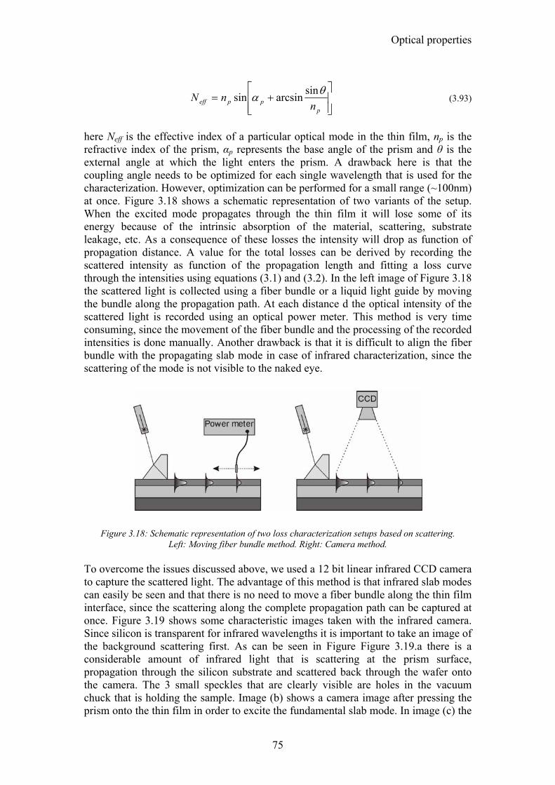
Optical properties
75
⎥⎥⎦
⎤
⎢⎢⎣
⎡+=
pppeff n
nN θα sinarcsinsin (3.93)
here Neff is the effective index of a particular optical mode in the thin film, np is the refractive index of the prism, αp represents the base angle of the prism and θ is the external angle at which the light enters the prism. A drawback here is that the coupling angle needs to be optimized for each single wavelength that is used for the characterization. However, optimization can be performed for a small range (~100nm) at once. Figure 3.18 shows a schematic representation of two variants of the setup. When the excited mode propagates through the thin film it will lose some of its energy because of the intrinsic absorption of the material, scattering, substrate leakage, etc. As a consequence of these losses the intensity will drop as function of propagation distance. A value for the total losses can be derived by recording the scattered intensity as function of the propagation length and fitting a loss curve through the intensities using equations (3.1) and (3.2). In the left image of Figure 3.18 the scattered light is collected using a fiber bundle or a liquid light guide by moving the bundle along the propagation path. At each distance d the optical intensity of the scattered light is recorded using an optical power meter. This method is very time consuming, since the movement of the fiber bundle and the processing of the recorded intensities is done manually. Another drawback is that it is difficult to align the fiber bundle with the propagating slab mode in case of infrared characterization, since the scattering of the mode is not visible to the naked eye.
Figure 3.18: Schematic representation of two loss characterization setups based on scattering. Left: Moving fiber bundle method. Right: Camera method.
To overcome the issues discussed above, we used a 12 bit linear infrared CCD camera to capture the scattered light. The advantage of this method is that infrared slab modes can easily be seen and that there is no need to move a fiber bundle along the thin film interface, since the scattering along the complete propagation path can be captured at once. Figure 3.19 shows some characteristic images taken with the infrared camera. Since silicon is transparent for infrared wavelengths it is important to take an image of the background scattering first. As can be seen in Figure Figure 3.19.a there is a considerable amount of infrared light that is scattering at the prism surface, propagation through the silicon substrate and scattered back through the wafer onto the camera. The 3 small speckles that are clearly visible are holes in the vacuum chuck that is holding the sample. Image (b) shows a camera image after pressing the prism onto the thin film in order to excite the fundamental slab mode. In image (c) the
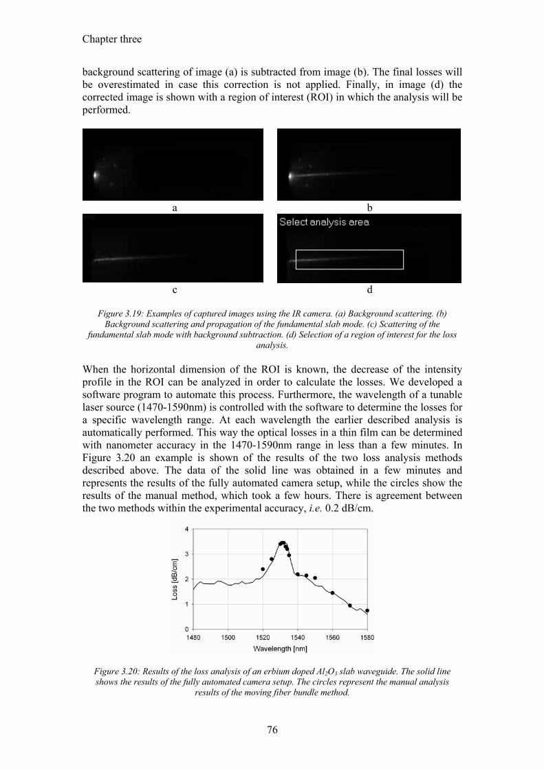
Chapter three
76
background scattering of image (a) is subtracted from image (b). The final losses will be overestimated in case this correction is not applied. Finally, in image (d) the corrected image is shown with a region of interest (ROI) in which the analysis will be performed.
a b
c d
Figure 3.19: Examples of captured images using the IR camera. (a) Background scattering. (b)
Background scattering and propagation of the fundamental slab mode. (c) Scattering of the fundamental slab mode with background subtraction. (d) Selection of a region of interest for the loss
analysis. When the horizontal dimension of the ROI is known, the decrease of the intensity profile in the ROI can be analyzed in order to calculate the losses. We developed a software program to automate this process. Furthermore, the wavelength of a tunable laser source (1470-1590nm) is controlled with the software to determine the losses for a specific wavelength range. At each wavelength the earlier described analysis is automatically performed. This way the optical losses in a thin film can be determined with nanometer accuracy in the 1470-1590nm range in less than a few minutes. In Figure 3.20 an example is shown of the results of the two loss analysis methods described above. The data of the solid line was obtained in a few minutes and represents the results of the fully automated camera setup, while the circles show the results of the manual method, which took a few hours. There is agreement between the two methods within the experimental accuracy, i.e. 0.2 dB/cm.
Figure 3.20: Results of the loss analysis of an erbium doped Al2O3 slab waveguide. The solid line shows the results of the fully automated camera setup. The circles represent the manual analysis
results of the moving fiber bundle method.
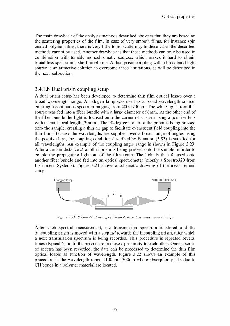
Optical properties
77
The main drawback of the analysis methods described above is that they are based on the scattering properties of the film. In case of very smooth films, for instance spin coated polymer films, there is very little to no scattering. In these cases the described methods cannot be used. Another drawback is that these methods can only be used in combination with tunable monochromatic sources, which makes it hard to obtain broad loss spectra in a short timeframe. A dual prism coupling with a broadband light source is an attractive solution to overcome these limitations, as will be described in the next subsection.
3.4.1.b Dual prism coupling setup A dual prism setup has been developed to determine thin film optical losses over a broad wavelength range. A halogen lamp was used as a broad wavelength source, emitting a continuous spectrum ranging from 400-1700nm. The white light from this source was fed into a fiber bundle with a large diameter of 6mm. At the other end of the fiber bundle the light is focused onto the corner of a prism using a positive lens with a small focal length (20mm). The 90-degree corner of the prism is being pressed onto the sample, creating a thin air gap to facilitate evanescent field coupling into the thin film. Because the wavelengths are supplied over a broad range of angles using the positive lens, the coupling condition described by Equation (3.93) is satisfied for all wavelengths. An example of the coupling angle range is shown in Figure 3.23. After a certain distance d, another prism is being pressed onto the sample in order to couple the propagating light out of the film again. The light is then focused onto another fiber bundle and fed into an optical spectrometer (mostly a Spectro320 from Instrument Systems). Figure 3.21 shows a schematic drawing of the measurement setup.
Figure 3.21: Schematic drawing of the dual prism loss measurement setup. After each spectral measurement, the transmission spectrum is stored and the outcoupling prism is moved with a step ∆d towards the incoupling prism, after which a next transmission spectrum is being recorded. This procedure is repeated several times (typical 5), until the prisms are in closest proximity to each other. Once a series of spectra has been recorded, the data can be processed to determine the thin film optical losses as function of wavelength. Figure 3.22 shows an example of this procedure in the wavelength range 1100nm-1300nm where absorption peaks due to CH bonds in a polymer material are located.
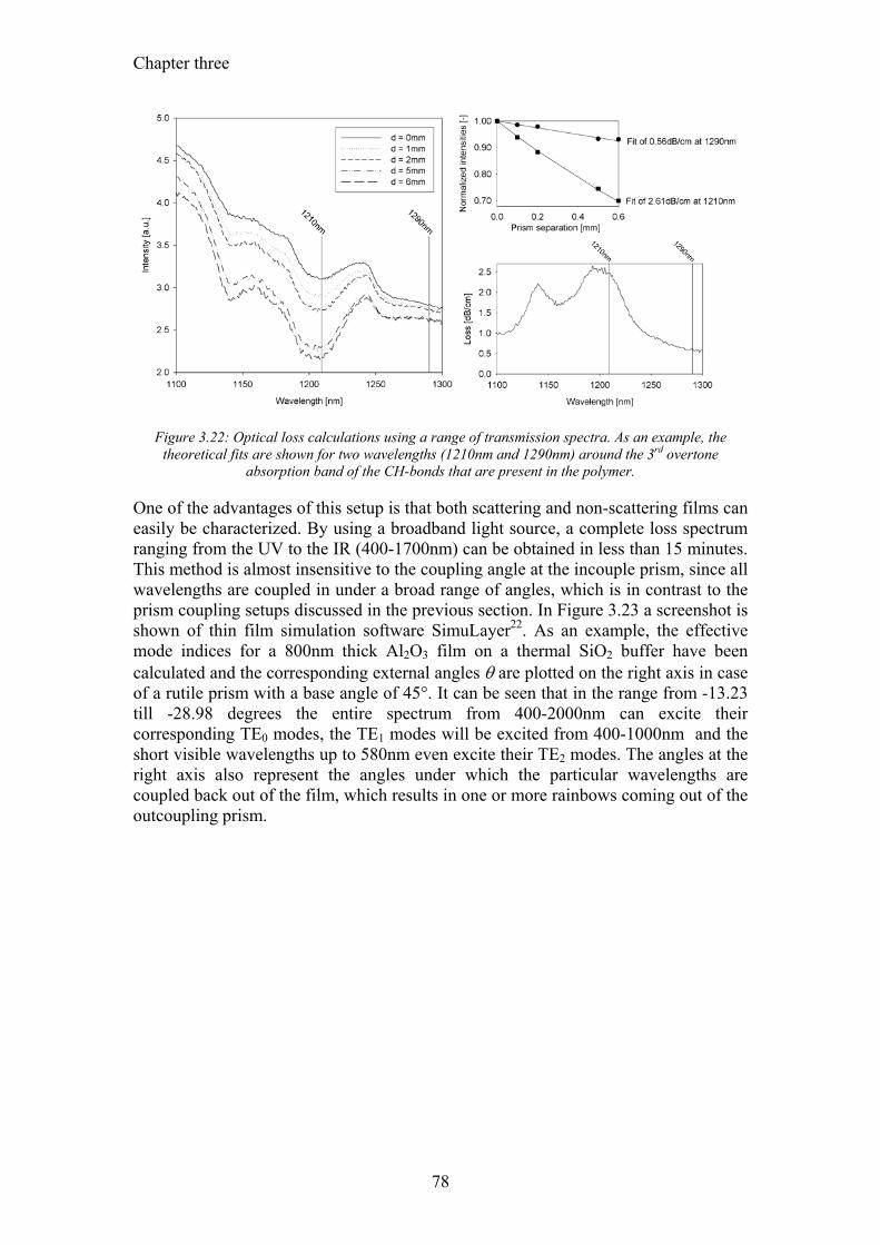
Chapter three
78
Figure 3.22: Optical loss calculations using a range of transmission spectra. As an example, the theoretical fits are shown for two wavelengths (1210nm and 1290nm) around the 3rd overtone
absorption band of the CH-bonds that are present in the polymer.
One of the advantages of this setup is that both scattering and non-scattering films can easily be characterized. By using a broadband light source, a complete loss spectrum ranging from the UV to the IR (400-1700nm) can be obtained in less than 15 minutes. This method is almost insensitive to the coupling angle at the incouple prism, since all wavelengths are coupled in under a broad range of angles, which is in contrast to the prism coupling setups discussed in the previous section. In Figure 3.23 a screenshot is shown of thin film simulation software SimuLayer22. As an example, the effective mode indices for a 800nm thick Al2O3 film on a thermal SiO2 buffer have been calculated and the corresponding external angles θ are plotted on the right axis in case of a rutile prism with a base angle of 45°. It can be seen that in the range from -13.23 till -28.98 degrees the entire spectrum from 400-2000nm can excite their corresponding TE0 modes, the TE1 modes will be excited from 400-1000nm and the short visible wavelengths up to 580nm even excite their TE2 modes. The angles at the right axis also represent the angles under which the particular wavelengths are coupled back out of the film, which results in one or more rainbows coming out of the outcoupling prism.
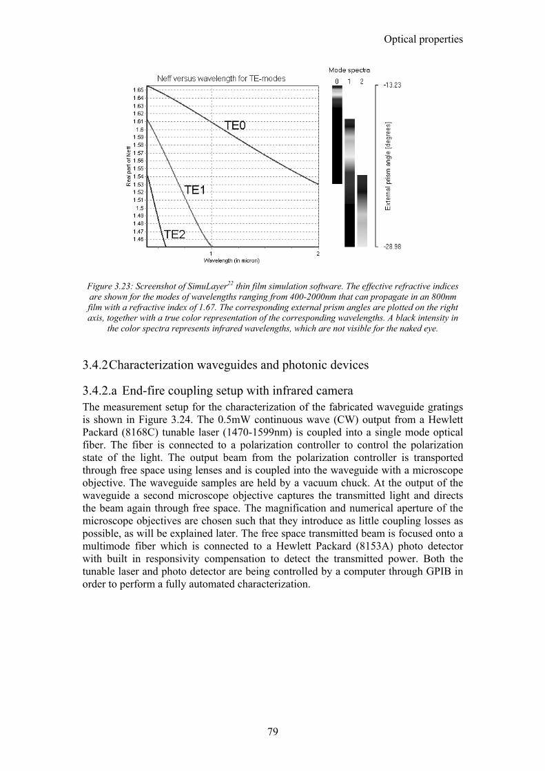
Optical properties
79
Figure 3.23: Screenshot of SimuLayer22 thin film simulation software. The effective refractive indices are shown for the modes of wavelengths ranging from 400-2000nm that can propagate in an 800nm film with a refractive index of 1.67. The corresponding external prism angles are plotted on the right axis, together with a true color representation of the corresponding wavelengths. A black intensity in
the color spectra represents infrared wavelengths, which are not visible for the naked eye.
3.4.2 Characterization waveguides and photonic devices
3.4.2.a End-fire coupling setup with infrared camera The measurement setup for the characterization of the fabricated waveguide gratings is shown in Figure 3.24. The 0.5mW continuous wave (CW) output from a Hewlett Packard (8168C) tunable laser (1470-1599nm) is coupled into a single mode optical fiber. The fiber is connected to a polarization controller to control the polarization state of the light. The output beam from the polarization controller is transported through free space using lenses and is coupled into the waveguide with a microscope objective. The waveguide samples are held by a vacuum chuck. At the output of the waveguide a second microscope objective captures the transmitted light and directs the beam again through free space. The magnification and numerical aperture of the microscope objectives are chosen such that they introduce as little coupling losses as possible, as will be explained later. The free space transmitted beam is focused onto a multimode fiber which is connected to a Hewlett Packard (8153A) photo detector with built in responsivity compensation to detect the transmitted power. Both the tunable laser and photo detector are being controlled by a computer through GPIB in order to perform a fully automated characterization.
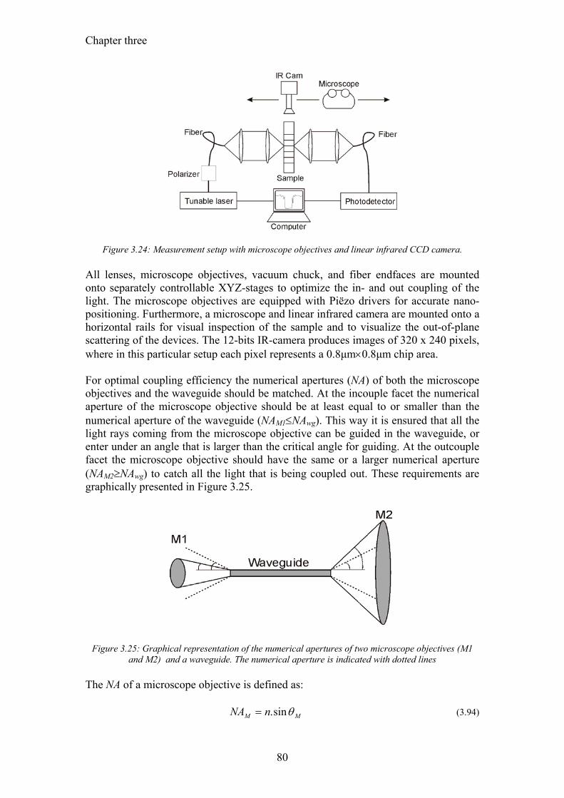
Chapter three
80
Figure 3.24: Measurement setup with microscope objectives and linear infrared CCD camera. All lenses, microscope objectives, vacuum chuck, and fiber endfaces are mounted onto separately controllable XYZ-stages to optimize the in- and out coupling of the light. The microscope objectives are equipped with Piëzo drivers for accurate nano-positioning. Furthermore, a microscope and linear infrared camera are mounted onto a horizontal rails for visual inspection of the sample and to visualize the out-of-plane scattering of the devices. The 12-bits IR-camera produces images of 320 x 240 pixels, where in this particular setup each pixel represents a 0.8µm×0.8µm chip area. For optimal coupling efficiency the numerical apertures (NA) of both the microscope objectives and the waveguide should be matched. At the incouple facet the numerical aperture of the microscope objective should be at least equal to or smaller than the numerical aperture of the waveguide (NAM1≤NAwg). This way it is ensured that all the light rays coming from the microscope objective can be guided in the waveguide, or enter under an angle that is larger than the critical angle for guiding. At the outcouple facet the microscope objective should have the same or a larger numerical aperture (NAM2≥NAwg) to catch all the light that is being coupled out. These requirements are graphically presented in Figure 3.25.
Figure 3.25: Graphical representation of the numerical apertures of two microscope objectives (M1 and M2) and a waveguide. The numerical aperture is indicated with dotted lines
The NA of a microscope objective is defined as:
MM nNA θsin.= (3.94)
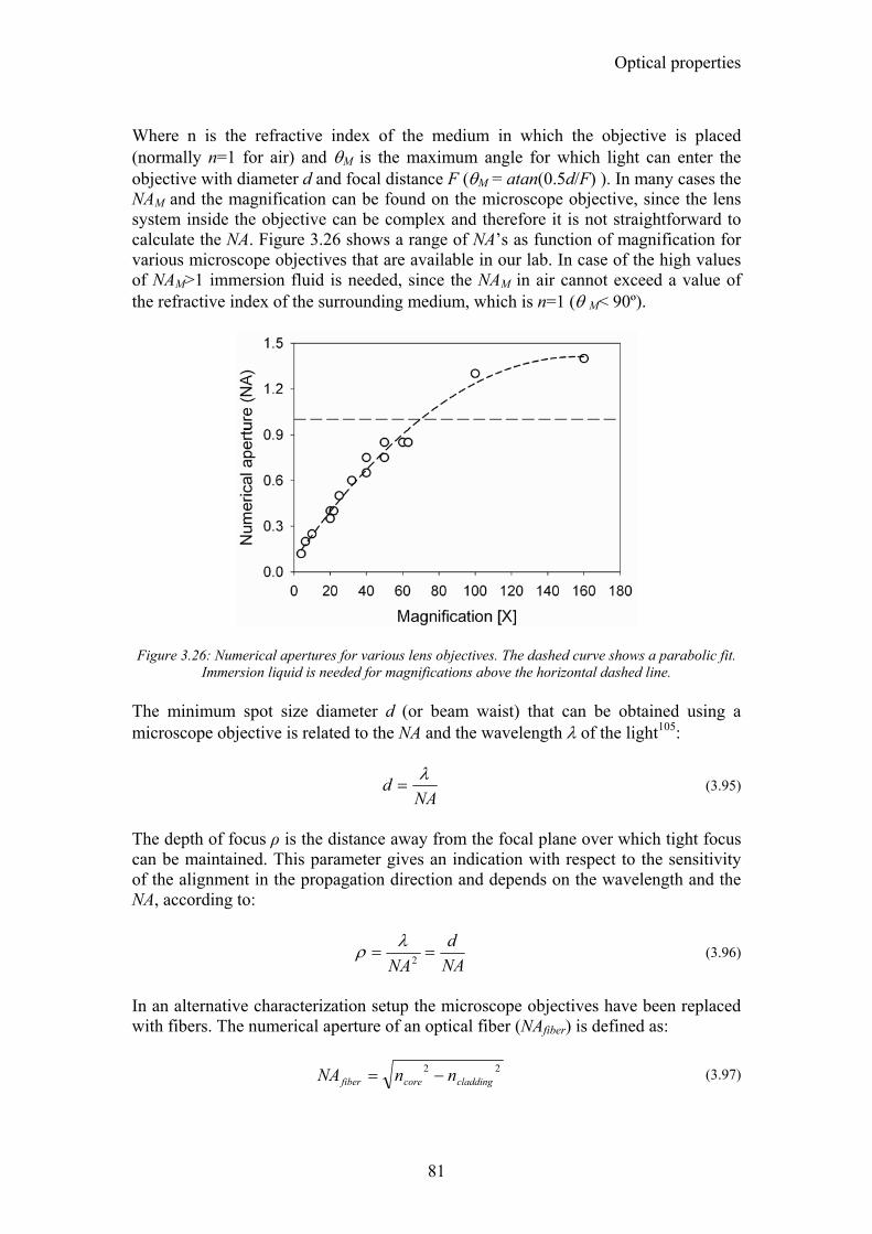
Optical properties
81
Where n is the refractive index of the medium in which the objective is placed (normally n=1 for air) and θM is the maximum angle for which light can enter the objective with diameter d and focal distance F (θM = atan(0.5d/F) ). In many cases the NAM and the magnification can be found on the microscope objective, since the lens system inside the objective can be complex and therefore it is not straightforward to calculate the NA. Figure 3.26 shows a range of NA’s as function of magnification for various microscope objectives that are available in our lab. In case of the high values of NAM>1 immersion fluid is needed, since the NAM in air cannot exceed a value of the refractive index of the surrounding medium, which is n=1 (θ M< 90º).
Figure 3.26: Numerical apertures for various lens objectives. The dashed curve shows a parabolic fit.
Immersion liquid is needed for magnifications above the horizontal dashed line. The minimum spot size diameter d (or beam waist) that can be obtained using a microscope objective is related to the NA and the wavelength λ of the light105:
NAd λ= (3.95)
The depth of focus ρ is the distance away from the focal plane over which tight focus can be maintained. This parameter gives an indication with respect to the sensitivity of the alignment in the propagation direction and depends on the wavelength and the NA, according to:
NAd
NA== 2
λρ (3.96)
In an alternative characterization setup the microscope objectives have been replaced with fibers. The numerical aperture of an optical fiber (NAfiber) is defined as:
22claddingcorefiber nnNA −= (3.97)
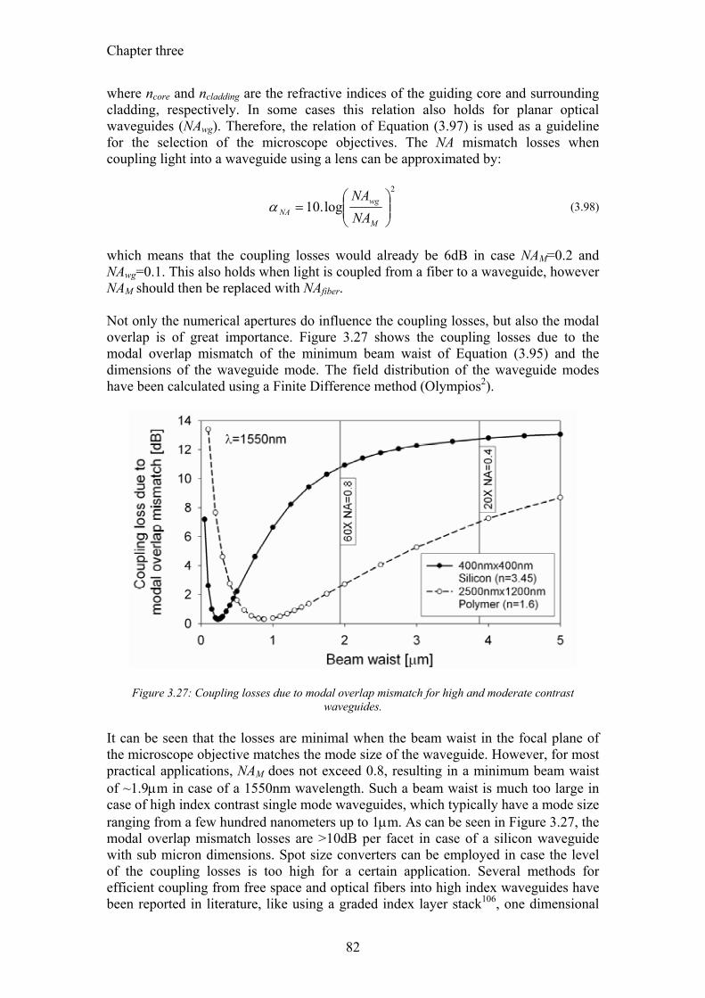
Chapter three
82
where ncore and ncladding are the refractive indices of the guiding core and surrounding cladding, respectively. In some cases this relation also holds for planar optical waveguides (NAwg). Therefore, the relation of Equation (3.97) is used as a guideline for the selection of the microscope objectives. The NA mismatch losses when coupling light into a waveguide using a lens can be approximated by:
2
log.10 ⎟⎟⎠
⎞⎜⎜⎝
⎛=
M
wgNA NA
NAα (3.98)
which means that the coupling losses would already be 6dB in case NAM=0.2 and NAwg=0.1. This also holds when light is coupled from a fiber to a waveguide, however NAM should then be replaced with NAfiber. Not only the numerical apertures do influence the coupling losses, but also the modal overlap is of great importance. Figure 3.27 shows the coupling losses due to the modal overlap mismatch of the minimum beam waist of Equation (3.95) and the dimensions of the waveguide mode. The field distribution of the waveguide modes have been calculated using a Finite Difference method (Olympios2).
Figure 3.27: Coupling losses due to modal overlap mismatch for high and moderate contrast waveguides.
It can be seen that the losses are minimal when the beam waist in the focal plane of the microscope objective matches the mode size of the waveguide. However, for most practical applications, NAM does not exceed 0.8, resulting in a minimum beam waist of ~1.9µm in case of a 1550nm wavelength. Such a beam waist is much too large in case of high index contrast single mode waveguides, which typically have a mode size ranging from a few hundred nanometers up to 1µm. As can be seen in Figure 3.27, the modal overlap mismatch losses are >10dB per facet in case of a silicon waveguide with sub micron dimensions. Spot size converters can be employed in case the level of the coupling losses is too high for a certain application. Several methods for efficient coupling from free space and optical fibers into high index waveguides have been reported in literature, like using a graded index layer stack106, one dimensional
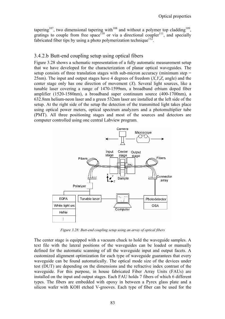
Optical properties
83
tapering107, two dimensional tapering with108 and without a polymer top cladding109, gratings to couple from free space110 or via a directional coupler111, and specially fabricated fiber tips by using a photo polymerization technique112.
3.4.2.b Butt-end coupling setup using optical fibers Figure 3.28 shows a schematic representation of a fully automatic measurement setup that we have developed for the characterization of planar optical waveguides. The setup consists of three translation stages with sub-micron accuracy (minimum step = 25nm). The input and output stages have 4 degrees of freedom (X,Y,Z, angle) and the center stage only has one direction of movement (X). Several light sources, like a tunable laser covering a range of 1470-1599nm, a broadband erbium doped fiber amplifier (1520-1580nm), a broadband super continuum source (400-1700nm), a 632.8nm helium-neon laser and a green 532nm laser are installed at the left side of the setup. At the right side of the setup the detection of the transmitted light takes place using optical power meters, optical spectrum analyzers and a photomultiplier tube (PMT). All three positioning stages and most of the sources and detectors are computer controlled using one central Labview program.
Figure 3.28: Butt-end coupling setup using an array of optical fibers The center stage is equipped with a vacuum chuck to hold the waveguide samples. A text file with the lateral positions of the waveguides can be loaded or manually defined for the automatic scanning of all the waveguide input and output facets. A customized alignment optimization for each type of waveguide guarantees that every waveguide can be found automatically. The optical mode size of the devices under test (DUT) are depending on the dimensions and the refractive index contrast of the waveguide. For this purpose, in house fabricated Fiber Array Units (FAUs) are installed on the input and output stages. Each FAU holds 7 fibers of which 6 different types. The fibers are embedded with epoxy in between a Pyrex glass plate and a silicon wafer with KOH etched V-grooves. Each type of fiber can be used for the
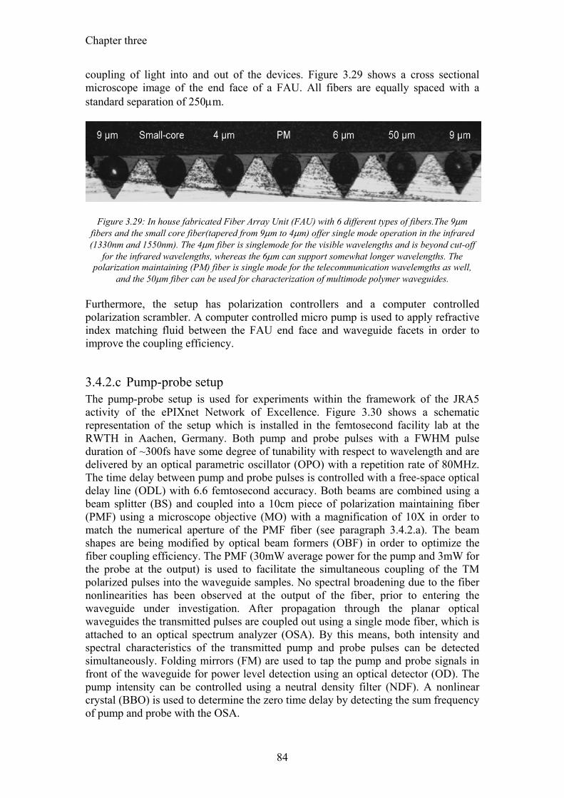
Chapter three
84
coupling of light into and out of the devices. Figure 3.29 shows a cross sectional microscope image of the end face of a FAU. All fibers are equally spaced with a standard separation of 250µm.
Figure 3.29: In house fabricated Fiber Array Unit (FAU) with 6 different types of fibers.The 9µm
fibers and the small core fiber(tapered from 9µm to 4µm) offer single mode operation in the infrared (1330nm and 1550nm). The 4µm fiber is singlemode for the visible wavelengths and is beyond cut-off
for the infrared wavelengths, whereas the 6µm can support somewhat longer wavelengths. The polarization maintaining (PM) fiber is single mode for the telecommunication wavelemgths as well,
and the 50µm fiber can be used for characterization of multimode polymer waveguides. Furthermore, the setup has polarization controllers and a computer controlled polarization scrambler. A computer controlled micro pump is used to apply refractive index matching fluid between the FAU end face and waveguide facets in order to improve the coupling efficiency.
3.4.2.c Pump-probe setup The pump-probe setup is used for experiments within the framework of the JRA5 activity of the ePIXnet Network of Excellence. Figure 3.30 shows a schematic representation of the setup which is installed in the femtosecond facility lab at the RWTH in Aachen, Germany. Both pump and probe pulses with a FWHM pulse duration of ~300fs have some degree of tunability with respect to wavelength and are delivered by an optical parametric oscillator (OPO) with a repetition rate of 80MHz. The time delay between pump and probe pulses is controlled with a free-space optical delay line (ODL) with 6.6 femtosecond accuracy. Both beams are combined using a beam splitter (BS) and coupled into a 10cm piece of polarization maintaining fiber (PMF) using a microscope objective (MO) with a magnification of 10X in order to match the numerical aperture of the PMF fiber (see paragraph 3.4.2.a). The beam shapes are being modified by optical beam formers (OBF) in order to optimize the fiber coupling efficiency. The PMF (30mW average power for the pump and 3mW for the probe at the output) is used to facilitate the simultaneous coupling of the TM polarized pulses into the waveguide samples. No spectral broadening due to the fiber nonlinearities has been observed at the output of the fiber, prior to entering the waveguide under investigation. After propagation through the planar optical waveguides the transmitted pulses are coupled out using a single mode fiber, which is attached to an optical spectrum analyzer (OSA). By this means, both intensity and spectral characteristics of the transmitted pump and probe pulses can be detected simultaneously. Folding mirrors (FM) are used to tap the pump and probe signals in front of the waveguide for power level detection using an optical detector (OD). The pump intensity can be controlled using a neutral density filter (NDF). A nonlinear crystal (BBO) is used to determine the zero time delay by detecting the sum frequency of pump and probe with the OSA.
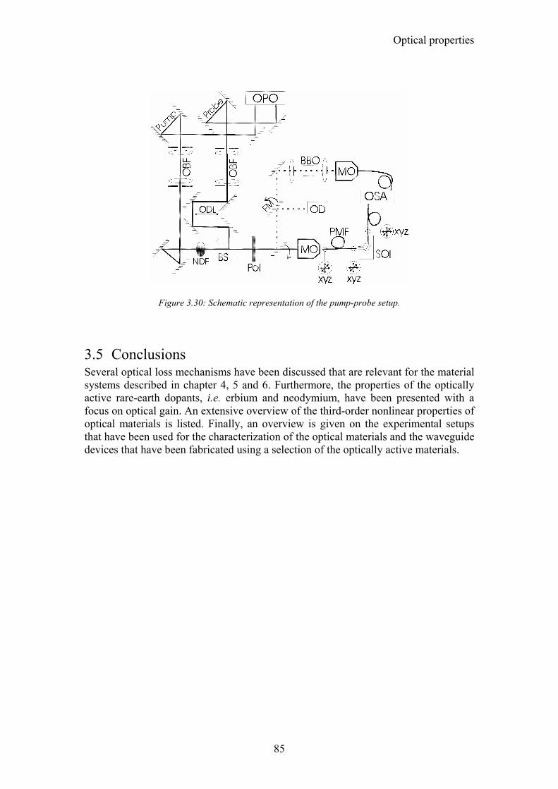
Optical properties
85
Figure 3.30: Schematic representation of the pump-probe setup.
3.5 Conclusions Several optical loss mechanisms have been discussed that are relevant for the material systems described in chapter 4, 5 and 6. Furthermore, the properties of the optically active rare-earth dopants, i.e. erbium and neodymium, have been presented with a focus on optical gain. An extensive overview of the third-order nonlinear properties of optical materials is listed. Finally, an overview is given on the experimental setups that have been used for the characterization of the optical materials and the waveguide devices that have been fabricated using a selection of the optically active materials.

87
4 Materials I: Erbium doped Al2O3
Thin films of Al2O3 are interesting candidates as a host for erbium. High concentrations of erbium can be incorporated in this material since Al2O3 has a high density of octahedral sites113. In this chapter the deposition of Er:Al2O3 films by means of reactive DC sputtering of aluminum and RF co-sputtering of erbium will be discussed. Furthermore, the characterization of the obtained films is discussed and an its performance in future applications will be predicted. Finally, a study on the patterning of this type of highly inert materials is presented.
Chapter four
88
4.1 Er:Al2O3 Deposition. There are several deposition techniques for the deposition of Er3+ doped Al2O3, like pulsed laser deposition114, sputtering115 and ion implantation116, 117. In the latter case, erbium atoms are ionized and accelerated by an electric field (100keV-1MeV range). The accelerated erbium ions are being directed to the substrate where they penetrate the thin film material. The penetration depth is dependent on the acceleration voltage. Ion implanters that can operate at these high acceleration voltages take up lots of valuable cleanroom space and are thus expensive. The available ion implanter in our cleanroom has a maximum acceleration voltage of 500kV, which corresponds to an ion range of ~90nm according to Monte Carlo simulations (SRIM118) for single ionized erbium atoms. The ion distribution is Gaussian shaped with a FWHM concentration profile of ~50nm. This means that in case of a 500nm thick film only a small part of the thin film is doped, resulting in a poor overlap between the implantation profile and the optical mode. In case of triple ionized erbium the effective acceleration energy is 1.5MeV, resulting in an increase of the ion range to 250nm, which is in the center of the thin film. However, the extraction of triple ionized erbium has a very low efficiency, resulting in long implantation times. Furthermore, implantation causes radiation induced defects that will reduce the photoluminescence56. An annealing step would be needed to remove these defects. Another drawback of the available ion implanter is that the maximum field in the selection coil is not high enough to extract the heavy erbium ions from the precursor. Based on cost and availability people at IOMS have chosen to deposit the Er:Al2O3 by means of multi target reactive magnetron sputtering of aluminum and erbium. With this deposition method the erbium atoms will be homogeneously distributed through the film, ensuring an efficient overlap between the erbium dopant and mode profile. In the next paragraph some important issues related to magnetron sputtering of stoichiometric Er3+ doped Al2O3 film are discussed.
4.1.1 DC Magnetron sputter deposition A deposition method that has been utilized extensively in the past by our group is sputter deposition. Ar+ ions from an argon plasma are accelerated towards a sputter target which has a negative potential U. The target material, for instance aluminum, is sputtered off when the Ar+ ion hits the target. Secondary electrons are escaping from the target as well. These electrons can further ionize the low-pressure argon gas and produce a stable plasma. The ionization probability increases with rising pressure. However, when the pressure is increasing, the mean free path for the ions and sputtered material will decrease (λ ~1/p), which is disadvantageous:
2...2.),,(
DpTkDpT
πλ = (4.1)
where, k is Boltzmann’s constant, T the temperature in Kelvin, p the pressure in Pascal and D the molecular diameter of the gas molecules measured in Angstrom. The
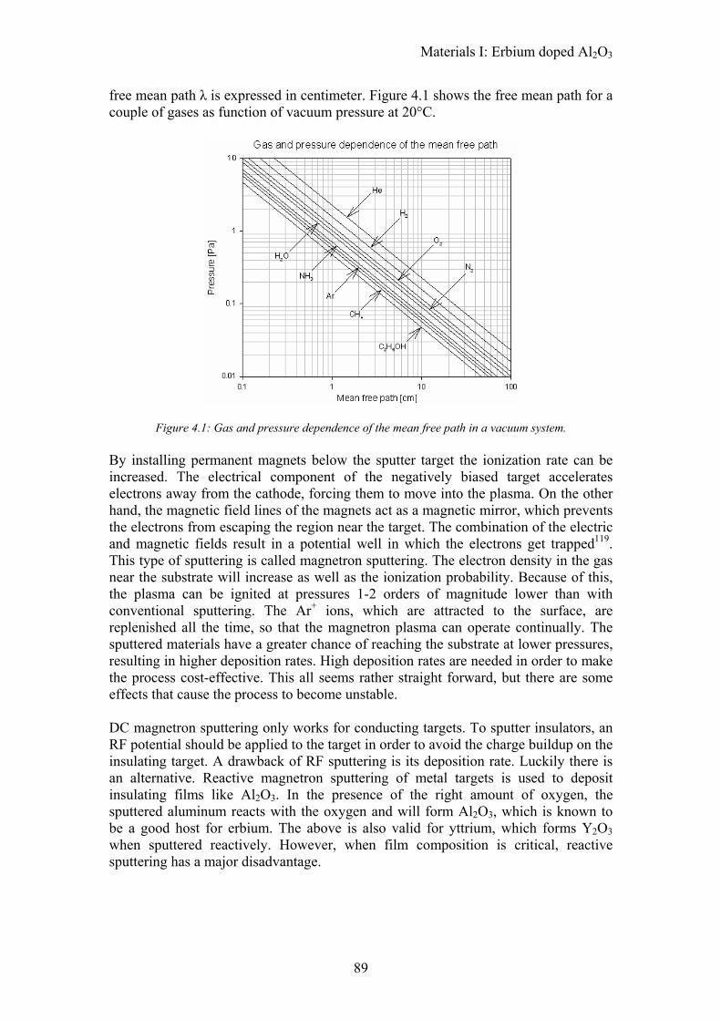
Materials I: Erbium doped Al2O3
89
free mean path λ is expressed in centimeter. Figure 4.1 shows the free mean path for a couple of gases as function of vacuum pressure at 20°C.
Figure 4.1: Gas and pressure dependence of the mean free path in a vacuum system. By installing permanent magnets below the sputter target the ionization rate can be increased. The electrical component of the negatively biased target accelerates electrons away from the cathode, forcing them to move into the plasma. On the other hand, the magnetic field lines of the magnets act as a magnetic mirror, which prevents the electrons from escaping the region near the target. The combination of the electric and magnetic fields result in a potential well in which the electrons get trapped119. This type of sputtering is called magnetron sputtering. The electron density in the gas near the substrate will increase as well as the ionization probability. Because of this, the plasma can be ignited at pressures 1-2 orders of magnitude lower than with conventional sputtering. The Ar+ ions, which are attracted to the surface, are replenished all the time, so that the magnetron plasma can operate continually. The sputtered materials have a greater chance of reaching the substrate at lower pressures, resulting in higher deposition rates. High deposition rates are needed in order to make the process cost-effective. This all seems rather straight forward, but there are some effects that cause the process to become unstable. DC magnetron sputtering only works for conducting targets. To sputter insulators, an RF potential should be applied to the target in order to avoid the charge buildup on the insulating target. A drawback of RF sputtering is its deposition rate. Luckily there is an alternative. Reactive magnetron sputtering of metal targets is used to deposit insulating films like Al2O3. In the presence of the right amount of oxygen, the sputtered aluminum reacts with the oxygen and will form Al2O3, which is known to be a good host for erbium. The above is also valid for yttrium, which forms Y2O3 when sputtered reactively. However, when film composition is critical, reactive sputtering has a major disadvantage.
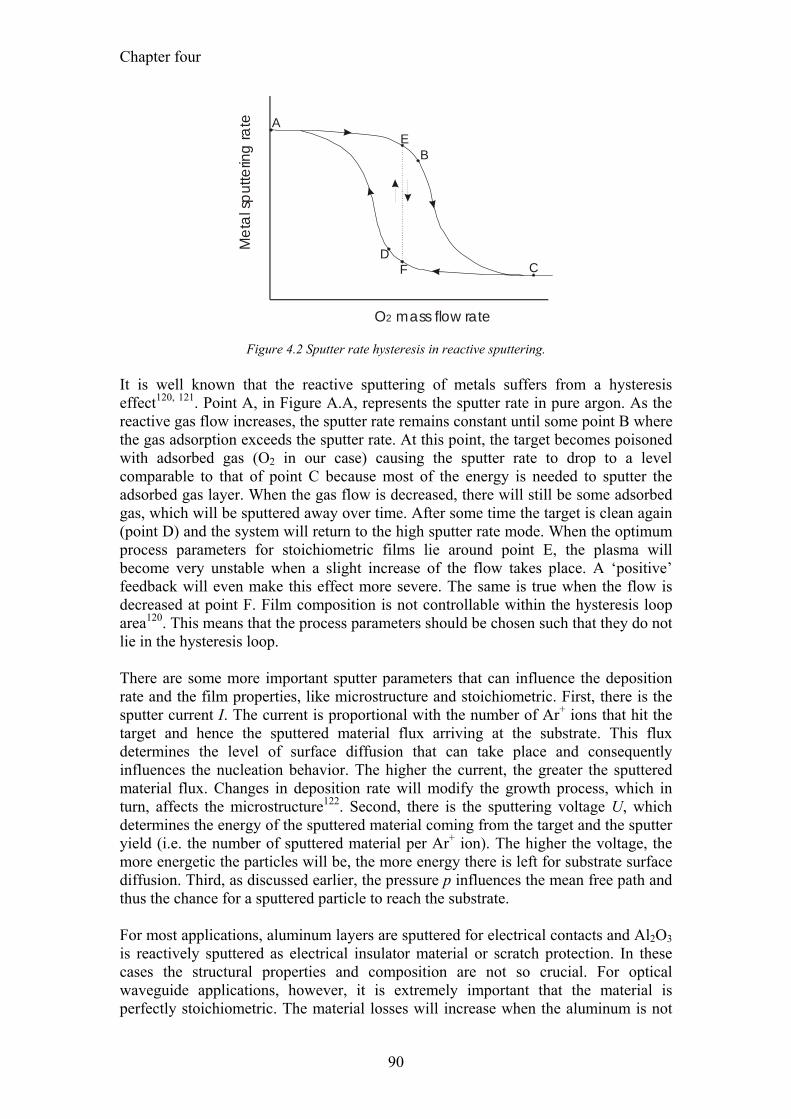
Chapter four
90
Me
tal s
put
terin
g ra
te
O mass flow rate2
A
B
CD
E
F
Figure 4.2 Sputter rate hysteresis in reactive sputtering. It is well known that the reactive sputtering of metals suffers from a hysteresis effect120, 121. Point A, in Figure A.A, represents the sputter rate in pure argon. As the reactive gas flow increases, the sputter rate remains constant until some point B where the gas adsorption exceeds the sputter rate. At this point, the target becomes poisoned with adsorbed gas (O2 in our case) causing the sputter rate to drop to a level comparable to that of point C because most of the energy is needed to sputter the adsorbed gas layer. When the gas flow is decreased, there will still be some adsorbed gas, which will be sputtered away over time. After some time the target is clean again (point D) and the system will return to the high sputter rate mode. When the optimum process parameters for stoichiometric films lie around point E, the plasma will become very unstable when a slight increase of the flow takes place. A ‘positive’ feedback will even make this effect more severe. The same is true when the flow is decreased at point F. Film composition is not controllable within the hysteresis loop area120. This means that the process parameters should be chosen such that they do not lie in the hysteresis loop. There are some more important sputter parameters that can influence the deposition rate and the film properties, like microstructure and stoichiometric. First, there is the sputter current I. The current is proportional with the number of Ar+ ions that hit the target and hence the sputtered material flux arriving at the substrate. This flux determines the level of surface diffusion that can take place and consequently influences the nucleation behavior. The higher the current, the greater the sputtered material flux. Changes in deposition rate will modify the growth process, which in turn, affects the microstructure122. Second, there is the sputtering voltage U, which determines the energy of the sputtered material coming from the target and the sputter yield (i.e. the number of sputtered material per Ar+ ion). The higher the voltage, the more energetic the particles will be, the more energy there is left for substrate surface diffusion. Third, as discussed earlier, the pressure p influences the mean free path and thus the chance for a sputtered particle to reach the substrate. For most applications, aluminum layers are sputtered for electrical contacts and Al2O3 is reactively sputtered as electrical insulator material or scratch protection. In these cases the structural properties and composition are not so crucial. For optical waveguide applications, however, it is extremely important that the material is perfectly stoichiometric. The material losses will increase when the aluminum is not
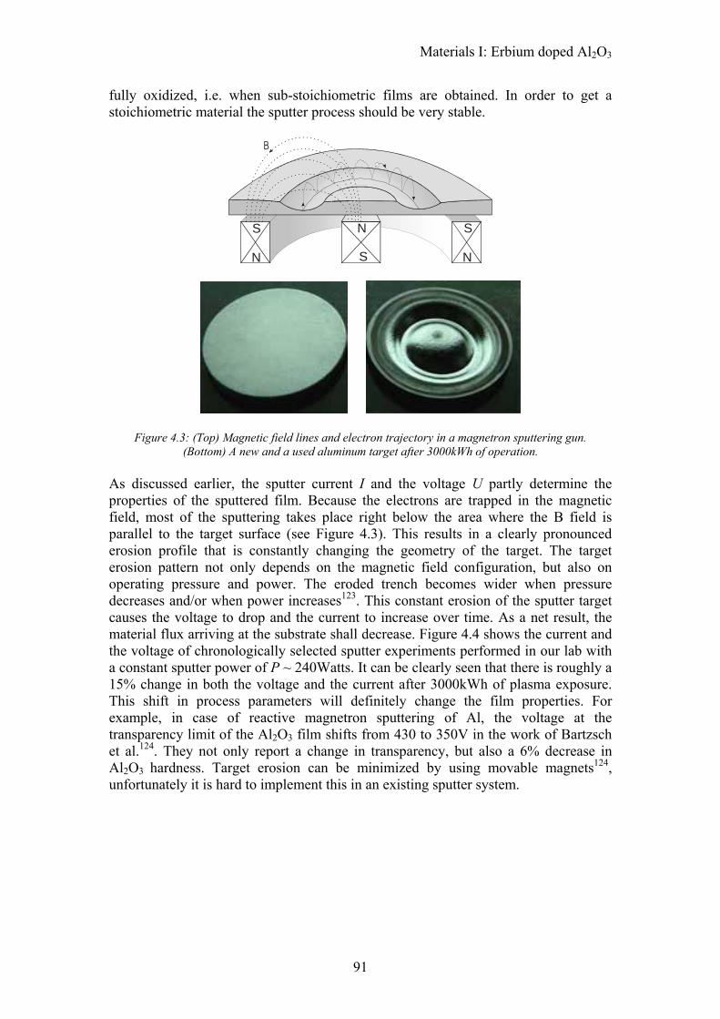
Materials I: Erbium doped Al2O3
91
fully oxidized, i.e. when sub-stoichiometric films are obtained. In order to get a stoichiometric material the sputter process should be very stable.
N
SN
SN
S
Figure 4.3: (Top) Magnetic field lines and electron trajectory in a magnetron sputtering gun. (Bottom) A new and a used aluminum target after 3000kWh of operation.
As discussed earlier, the sputter current I and the voltage U partly determine the properties of the sputtered film. Because the electrons are trapped in the magnetic field, most of the sputtering takes place right below the area where the B field is parallel to the target surface (see Figure 4.3). This results in a clearly pronounced erosion profile that is constantly changing the geometry of the target. The target erosion pattern not only depends on the magnetic field configuration, but also on operating pressure and power. The eroded trench becomes wider when pressure decreases and/or when power increases123. This constant erosion of the sputter target causes the voltage to drop and the current to increase over time. As a net result, the material flux arriving at the substrate shall decrease. Figure 4.4 shows the current and the voltage of chronologically selected sputter experiments performed in our lab with a constant sputter power of P ~ 240Watts. It can be clearly seen that there is roughly a 15% change in both the voltage and the current after 3000kWh of plasma exposure. This shift in process parameters will definitely change the film properties. For example, in case of reactive magnetron sputtering of Al, the voltage at the transparency limit of the Al2O3 film shifts from 430 to 350V in the work of Bartzsch et al.124. They not only report a change in transparency, but also a 6% decrease in Al2O3 hardness. Target erosion can be minimized by using movable magnets124, unfortunately it is hard to implement this in an existing sputter system.
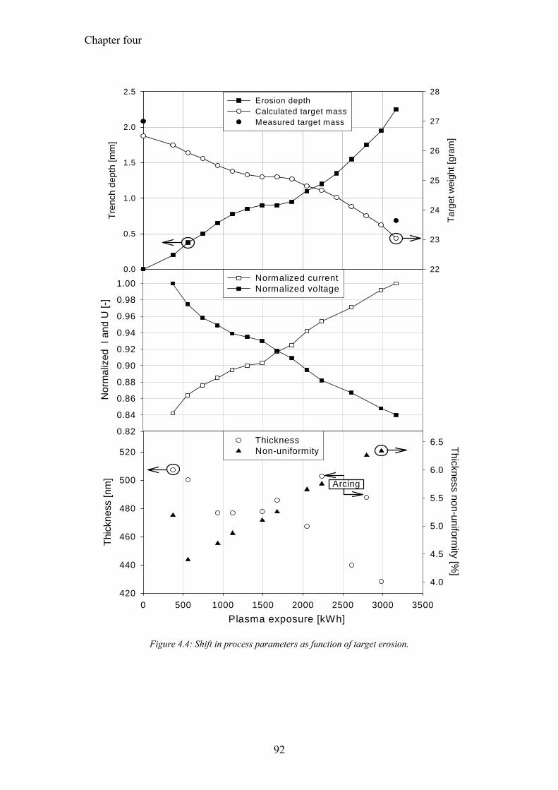
Chapter four
92
Nor
mal
ized
I a
nd U
[-]
0.82
0.84
0.86
0.88
0.90
0.92
0.94
0.96
0.98
1.00 Normalized currentNormalized voltage
0 500 1000 1500 2000 2500 3000 3500
Thic
knes
s [n
m]
420
440
460
480
500
520
Thickness non-uniformity [%
]
4.0
4.5
5.0
5.5
6.0
6.5ThicknessNon-uniformity
Plasma exposure [kWh]
Arcing
Tren
ch d
epth
[mm
]
0.0
0.5
1.0
1.5
2.0
2.5
Targ
et w
eigh
t [gr
am]
22
23
24
25
26
27
28Erosion depthCalculated target massMeasured target mass
Figure 4.4: Shift in process parameters as function of target erosion.
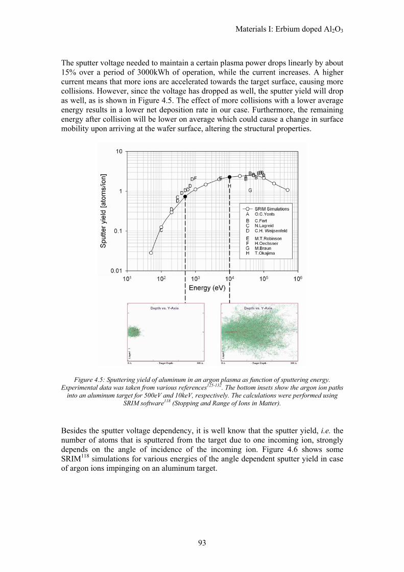
Materials I: Erbium doped Al2O3
93
The sputter voltage needed to maintain a certain plasma power drops linearly by about 15% over a period of 3000kWh of operation, while the current increases. A higher current means that more ions are accelerated towards the target surface, causing more collisions. However, since the voltage has dropped as well, the sputter yield will drop as well, as is shown in Figure 4.5. The effect of more collisions with a lower average energy results in a lower net deposition rate in our case. Furthermore, the remaining energy after collision will be lower on average which could cause a change in surface mobility upon arriving at the wafer surface, altering the structural properties.
Figure 4.5: Sputtering yield of aluminum in an argon plasma as function of sputtering energy. Experimental data was taken from various references125-132. The bottom insets show the argon ion paths
into an aluminum target for 500eV and 10keV, respectively. The calculations were performed using SRIM software118 (Stopping and Range of Ions in Matter).
Besides the sputter voltage dependency, it is well know that the sputter yield, i.e. the number of atoms that is sputtered from the target due to one incoming ion, strongly depends on the angle of incidence of the incoming ion. Figure 4.6 shows some SRIM118 simulations for various energies of the angle dependent sputter yield in case of argon ions impinging on an aluminum target.
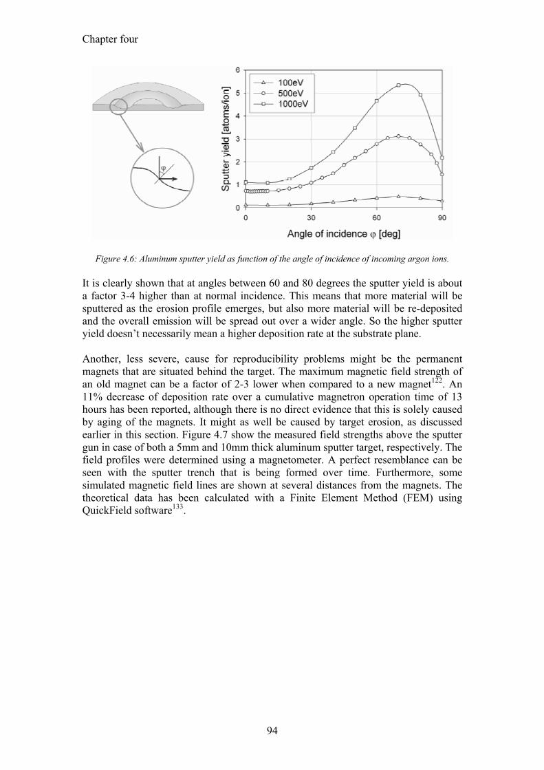
Chapter four
94
Figure 4.6: Aluminum sputter yield as function of the angle of incidence of incoming argon ions. It is clearly shown that at angles between 60 and 80 degrees the sputter yield is about a factor 3-4 higher than at normal incidence. This means that more material will be sputtered as the erosion profile emerges, but also more material will be re-deposited and the overall emission will be spread out over a wider angle. So the higher sputter yield doesn’t necessarily mean a higher deposition rate at the substrate plane. Another, less severe, cause for reproducibility problems might be the permanent magnets that are situated behind the target. The maximum magnetic field strength of an old magnet can be a factor of 2-3 lower when compared to a new magnet122. An 11% decrease of deposition rate over a cumulative magnetron operation time of 13 hours has been reported, although there is no direct evidence that this is solely caused by aging of the magnets. It might as well be caused by target erosion, as discussed earlier in this section. Figure 4.7 show the measured field strengths above the sputter gun in case of both a 5mm and 10mm thick aluminum sputter target, respectively. The field profiles were determined using a magnetometer. A perfect resemblance can be seen with the sputter trench that is being formed over time. Furthermore, some simulated magnetic field lines are shown at several distances from the magnets. The theoretical data has been calculated with a Finite Element Method (FEM) using QuickField software133.
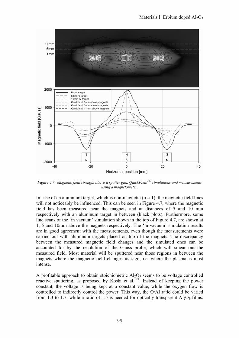
Materials I: Erbium doped Al2O3
95
Figure 4.7: Magnetic field strength above a sputter gun. QuickField133 simulations and measurements
using a magnetometer. In case of an aluminum target, which is non-magnetic (µ ≈ 1), the magnetic field lines will not noticeably be influenced. This can be seen in Figure 4.7, where the magnetic field has been measured near the magnets and at distances of 5 and 10 mm respectively with an aluminum target in between (black plots). Furthermore, some line scans of the ‘in vacuum’ simulation shown in the top of Figure 4.7, are shown at 1, 5 and 10mm above the magnets respectively. The ‘in vacuum’ simulation results are in good agreement with the measurements, even though the measurements were carried out with aluminum targets placed on top of the magnets. The discrepancy between the measured magnetic field changes and the simulated ones can be accounted for by the resolution of the Gauss probe, which will smear out the measured field. Most material will be sputtered near those regions in between the magnets where the magnetic field changes its sign, i.e. where the plasma is most intense. A profitable approach to obtain stoichiometric Al2O3 seems to be voltage controlled reactive sputtering, as proposed by Koski et al.121. Instead of keeping the power constant, the voltage is being kept at a constant value, while the oxygen flow is controlled to indirectly control the power. This way, the O/Al ratio could be varied from 1.3 to 1.7, while a ratio of 1.5 is needed for optically transparent Al2O3 films.
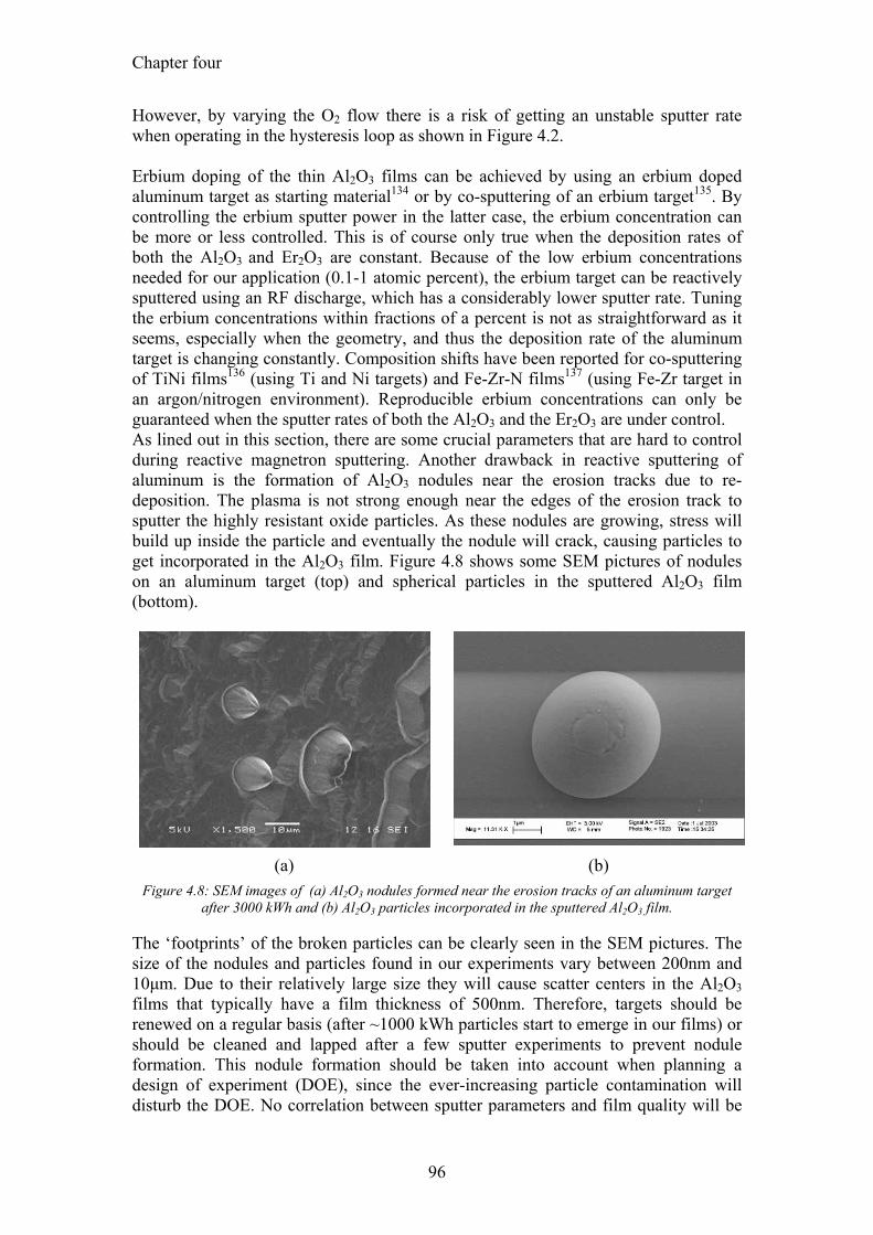
Chapter four
96
However, by varying the O2 flow there is a risk of getting an unstable sputter rate when operating in the hysteresis loop as shown in Figure 4.2. Erbium doping of the thin Al2O3 films can be achieved by using an erbium doped aluminum target as starting material134 or by co-sputtering of an erbium target135. By controlling the erbium sputter power in the latter case, the erbium concentration can be more or less controlled. This is of course only true when the deposition rates of both the Al2O3 and Er2O3 are constant. Because of the low erbium concentrations needed for our application (0.1-1 atomic percent), the erbium target can be reactively sputtered using an RF discharge, which has a considerably lower sputter rate. Tuning the erbium concentrations within fractions of a percent is not as straightforward as it seems, especially when the geometry, and thus the deposition rate of the aluminum target is changing constantly. Composition shifts have been reported for co-sputtering of TiNi films136 (using Ti and Ni targets) and Fe-Zr-N films137 (using Fe-Zr target in an argon/nitrogen environment). Reproducible erbium concentrations can only be guaranteed when the sputter rates of both the Al2O3 and the Er2O3 are under control. As lined out in this section, there are some crucial parameters that are hard to control during reactive magnetron sputtering. Another drawback in reactive sputtering of aluminum is the formation of Al2O3 nodules near the erosion tracks due to re-deposition. The plasma is not strong enough near the edges of the erosion track to sputter the highly resistant oxide particles. As these nodules are growing, stress will build up inside the particle and eventually the nodule will crack, causing particles to get incorporated in the Al2O3 film. Figure 4.8 shows some SEM pictures of nodules on an aluminum target (top) and spherical particles in the sputtered Al2O3 film (bottom).
(a) (b)
Figure 4.8: SEM images of (a) Al2O3 nodules formed near the erosion tracks of an aluminum target after 3000 kWh and (b) Al2O3 particles incorporated in the sputtered Al2O3 film.
The ‘footprints’ of the broken particles can be clearly seen in the SEM pictures. The size of the nodules and particles found in our experiments vary between 200nm and 10µm. Due to their relatively large size they will cause scatter centers in the Al2O3 films that typically have a film thickness of 500nm. Therefore, targets should be renewed on a regular basis (after ~1000 kWh particles start to emerge in our films) or should be cleaned and lapped after a few sputter experiments to prevent nodule formation. This nodule formation should be taken into account when planning a design of experiment (DOE), since the ever-increasing particle contamination will disturb the DOE. No correlation between sputter parameters and film quality will be
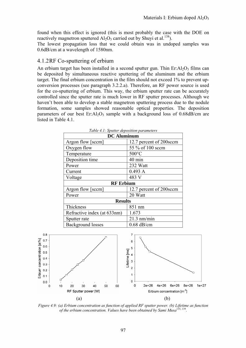
Materials I: Erbium doped Al2O3
97
found when this effect is ignored (this is most probably the case with the DOE on reactively magnetron sputtered Al2O3 carried out by Shuyi et al.138). The lowest propagation loss that we could obtain was in undoped samples was 0.6dB/cm at a wavelength of 1580nm.
4.1.2 RF Co-sputtering of erbium An erbium target has been installed in a second sputter gun. Thin Er:Al2O3 films can be deposited by simultaneous reactive sputtering of the aluminum and the erbium target. The final erbium concentration in the film should not exceed 1% to prevent up-conversion processes (see paragraph 3.2.2.a). Therefore, an RF power source is used for the co-sputtering of erbium. This way, the erbium sputter rate can be accurately controlled since the sputter rate is much lower in RF sputter processes. Although we haven’t been able to develop a stable magnetron sputtering process due to the nodule formation, some samples showed reasonable optical properties. The deposition parameters of our best Er:Al2O3 sample with a background loss of 0.68dB/cm are listed in Table 4.1.
Table 4.1: Sputter deposition parameters DC Aluminum
Argon flow [sccm] 12.7 percent of 200sccm Oxygen flow 55 % of 100 sccm Temperature 500°C Deposition time 40 min Power 232 Watt Current 0.493 A Voltage 483 V
RF Erbium Argon flow [sccm] 12.7 percent of 200sccm Power 20 Watt
Results Thickness 851 nm Refractive index (at 633nm) 1.673 Sputter rate 21.3 nm/min Background losses 0.68 dB/cm
(a) (b)
Figure 4.9: (a) Erbium concentration as function of applied RF sputter power. (b) Lifetime as function of the erbium concentration. Values have been obtained by Sami Musa135, 139.
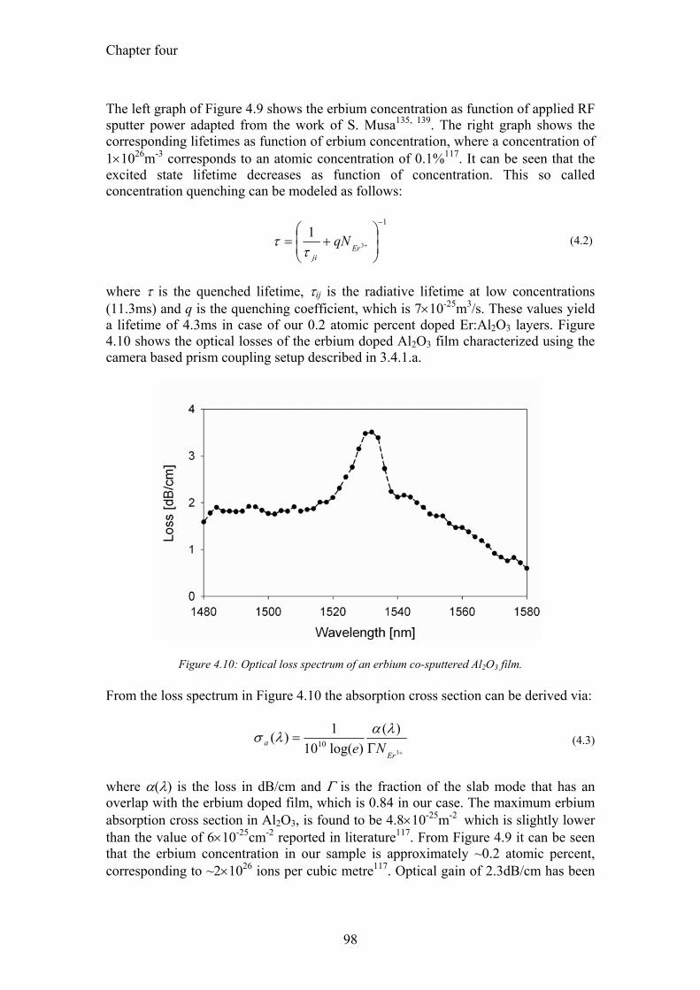
Chapter four
98
The left graph of Figure 4.9 shows the erbium concentration as function of applied RF sputter power adapted from the work of S. Musa135, 139. The right graph shows the corresponding lifetimes as function of erbium concentration, where a concentration of 1×1026m-3 corresponds to an atomic concentration of 0.1%117. It can be seen that the excited state lifetime decreases as function of concentration. This so called concentration quenching can be modeled as follows:
1
3
1−
⎟⎟⎠
⎞⎜⎜⎝
⎛+= +Er
ji
qNτ
τ (4.2)
where τ is the quenched lifetime, τij is the radiative lifetime at low concentrations (11.3ms) and q is the quenching coefficient, which is 7×10-25m3/s. These values yield a lifetime of 4.3ms in case of our 0.2 atomic percent doped Er:Al2O3 layers. Figure 4.10 shows the optical losses of the erbium doped Al2O3 film characterized using the camera based prism coupling setup described in 3.4.1.a.
Figure 4.10: Optical loss spectrum of an erbium co-sputtered Al2O3 film. From the loss spectrum in Figure 4.10 the absorption cross section can be derived via:
+Γ=
3
)()log(10
1)( 10Er
a Neλαλσ (4.3)
where α(λ) is the loss in dB/cm and Γ is the fraction of the slab mode that has an overlap with the erbium doped film, which is 0.84 in our case. The maximum erbium absorption cross section in Al2O3, is found to be 4.8×10⁻²⁵m-2
which is slightly lower than the value of 6×10-25cm-2 reported in literature117. From Figure 4.9 it can be seen that the erbium concentration in our sample is approximately ~0.2 atomic percent, corresponding to ~2×1026 ions per cubic metre117. Optical gain of 2.3dB/cm has been
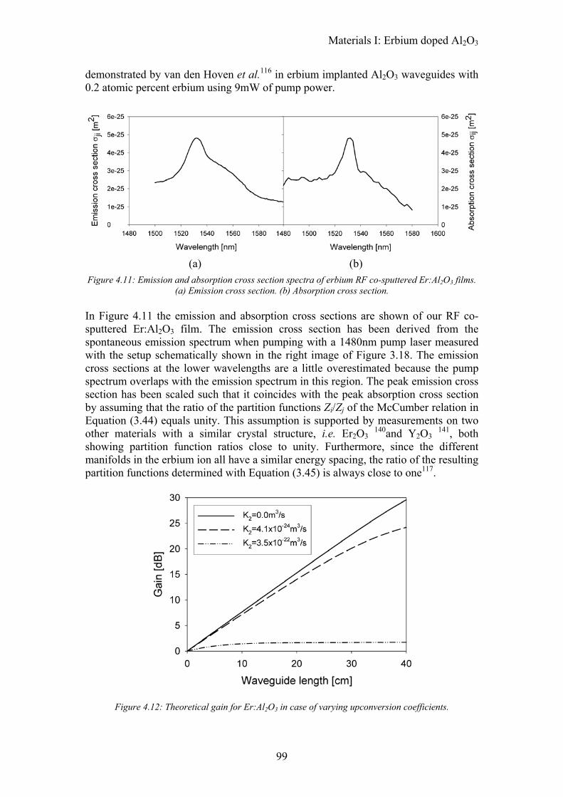
Materials I: Erbium doped Al2O3
99
demonstrated by van den Hoven et al.116 in erbium implanted Al2O3 waveguides with 0.2 atomic percent erbium using 9mW of pump power.
(a) (b)
Figure 4.11: Emission and absorption cross section spectra of erbium RF co-sputtered Er:Al2O3 films. (a) Emission cross section. (b) Absorption cross section.
In Figure 4.11 the emission and absorption cross sections are shown of our RF co-sputtered Er:Al2O3 film. The emission cross section has been derived from the spontaneous emission spectrum when pumping with a 1480nm pump laser measured with the setup schematically shown in the right image of Figure 3.18. The emission cross sections at the lower wavelengths are a little overestimated because the pump spectrum overlaps with the emission spectrum in this region. The peak emission cross section has been scaled such that it coincides with the peak absorption cross section by assuming that the ratio of the partition functions Zi/Zj of the McCumber relation in Equation (3.44) equals unity. This assumption is supported by measurements on two other materials with a similar crystal structure, i.e. Er2O3 140and Y2O3 141, both showing partition function ratios close to unity. Furthermore, since the different manifolds in the erbium ion all have a similar energy spacing, the ratio of the resulting partition functions determined with Equation (3.45) is always close to one117.
Figure 4.12: Theoretical gain for Er:Al2O3 in case of varying upconversion coefficients.
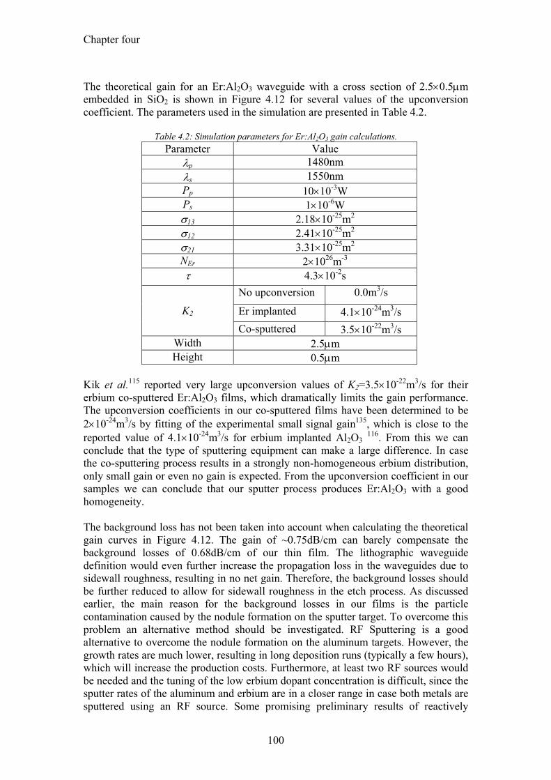
Chapter four
100
The theoretical gain for an Er:Al2O3 waveguide with a cross section of 2.5×0.5µm embedded in SiO2 is shown in Figure 4.12 for several values of the upconversion coefficient. The parameters used in the simulation are presented in Table 4.2.
Table 4.2: Simulation parameters for Er:Al2O3 gain calculations. Parameter Value
λp 1480nm λs 1550nm Pp 10×10-3W Ps 1×10⁻⁶W σ13 2.18×10⁻²⁵m2 σ12 2.41×10⁻²⁵m2 σ21 3.31×10⁻²⁵m2 NEr 2×1026m-3 τ 4.3×10⁻²s
No upconversion 0.0m3/s
Er implanted 4.1×10⁻²⁴m3/s K2 Co-sputtered 3.5×10⁻²²m3/s
Width 2.5µm Height 0.5µm
Kik et al.115 reported very large upconversion values of K2=3.5×10⁻²²m3/s for their erbium co-sputtered Er:Al2O3 films, which dramatically limits the gain performance. The upconversion coefficients in our co-sputtered films have been determined to be 2×10-24m3/s by fitting of the experimental small signal gain135, which is close to the reported value of 4.1×10⁻²⁴m3/s for erbium implanted Al2O3 116. From this we can conclude that the type of sputtering equipment can make a large difference. In case the co-sputtering process results in a strongly non-homogeneous erbium distribution, only small gain or even no gain is expected. From the upconversion coefficient in our samples we can conclude that our sputter process produces Er:Al2O3 with a good homogeneity. The background loss has not been taken into account when calculating the theoretical gain curves in Figure 4.12. The gain of ~0.75dB/cm can barely compensate the background losses of 0.68dB/cm of our thin film. The lithographic waveguide definition would even further increase the propagation loss in the waveguides due to sidewall roughness, resulting in no net gain. Therefore, the background losses should be further reduced to allow for sidewall roughness in the etch process. As discussed earlier, the main reason for the background losses in our films is the particle contamination caused by the nodule formation on the sputter target. To overcome this problem an alternative method should be investigated. RF Sputtering is a good alternative to overcome the nodule formation on the aluminum targets. However, the growth rates are much lower, resulting in long deposition runs (typically a few hours), which will increase the production costs. Furthermore, at least two RF sources would be needed and the tuning of the low erbium dopant concentration is difficult, since the sputter rates of the aluminum and erbium are in a closer range in case both metals are sputtered using an RF source. Some promising preliminary results of reactively
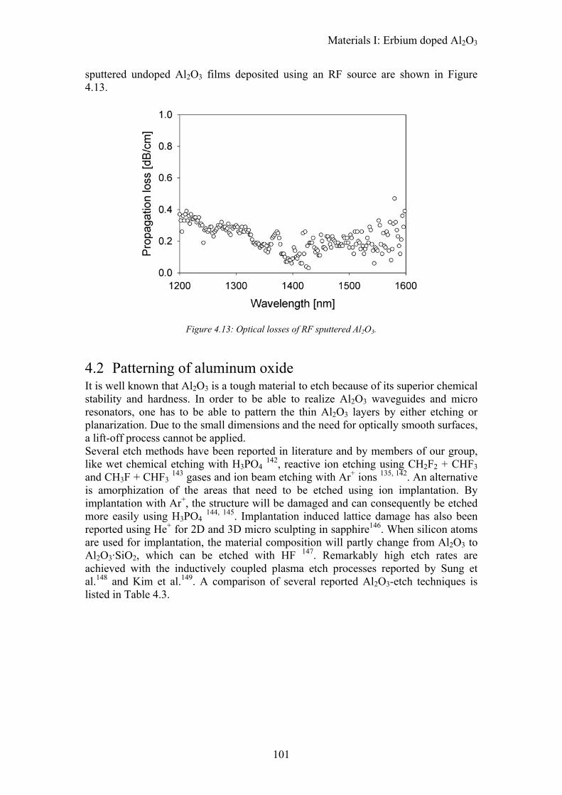
Materials I: Erbium doped Al2O3
101
sputtered undoped Al2O3 films deposited using an RF source are shown in Figure 4.13.
Figure 4.13: Optical losses of RF sputtered Al2O3.
4.2 Patterning of aluminum oxide It is well known that Al2O3 is a tough material to etch because of its superior chemical stability and hardness. In order to be able to realize Al2O3 waveguides and micro resonators, one has to be able to pattern the thin Al2O3 layers by either etching or planarization. Due to the small dimensions and the need for optically smooth surfaces, a lift-off process cannot be applied. Several etch methods have been reported in literature and by members of our group, like wet chemical etching with H3PO4 142, reactive ion etching using CH2F2 + CHF3 and CH3F + CHF3 143 gases and ion beam etching with Ar+ ions 135, 142. An alternative is amorphization of the areas that need to be etched using ion implantation. By implantation with Ar+, the structure will be damaged and can consequently be etched more easily using H3PO4 144, 145. Implantation induced lattice damage has also been reported using He+ for 2D and 3D micro sculpting in sapphire146. When silicon atoms are used for implantation, the material composition will partly change from Al2O3 to Al2O3·SiO2, which can be etched with HF 147. Remarkably high etch rates are achieved with the inductively coupled plasma etch processes reported by Sung et al.148 and Kim et al.149. A comparison of several reported Al2O3-etch techniques is listed in Table 4.3.
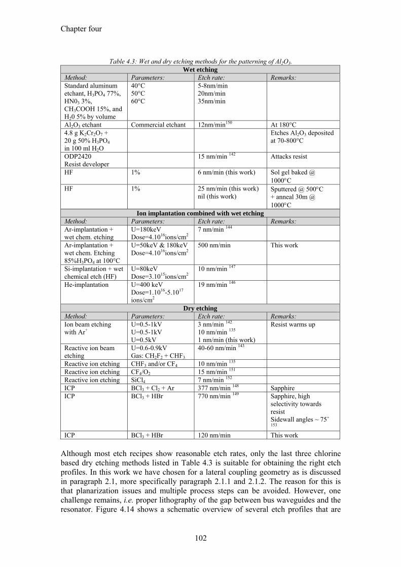
Chapter four
102
Table 4.3: Wet and dry etching methods for the patterning of Al2O3.
Wet etching Method: Parameters: Etch rate: Remarks: Standard aluminum etchant, H3PO4 77%, HN03 3%, CH3COOH 15%, and H20 5% by volume
40°C 50°C 60°C
5-8nm/min 20nm/min 35nm/min
Al2O3 etchant Commercial etchant 12nm/min150 At 180°C 4.8 g K2Cr2O7 + 20 g 50% H3PO4 in 100 ml H2O
Etches Al2O3 deposited at 70-800°C
ODP2420 Resist developer
15 nm/min 142 Attacks resist
HF 1% 6 nm/min (this work) Sol gel baked @ 1000°C
HF 1% 25 nm/min (this work) nil (this work)
Sputtered @ 500°C + anneal 30m @ 1000°C
Ion implantation combined with wet etching Method: Parameters: Etch rate: Remarks: Ar-implantation + wet chem. etching
U=180keV Dose=4.1016ions/cm2
7 nm/min 144
Ar-implantation + wet chem. Etching 85%H3PO4 at 100°C
U=50keV & 180keV Dose=4.1016ions/cm2
500 nm/min This work
Si-implantation + wet chemical etch (HF)
U=80keV Dose=3.1015ions/cm2
10 nm/min 147
He-implantation U=400 keV Dose=1.1016-5.1017 ions/cm2
19 nm/min 146
Dry etching Method: Parameters: Etch rate: Remarks: Ion beam etching with Ar+
U=0.5-1kV U=0.5-1kV U=0.5kV
3 nm/min 142 10 nm/min 135 1 nm/min (this work)
Resist warms up
Reactive ion beam etching
U=0.6-0.9kV Gas: CH2F2 + CHF3
40-60 nm/min 143
Reactive ion etching CHF3 and/or CF4 10 nm/min 135 Reactive ion etching CF4/O2 15 nm/min 151 Reactive ion etching SiCl4 7 nm/min 152 ICP BCl3 + Cl2 + Ar 377 nm/min 148 Sapphire ICP BCl3 + HBr 770 nm/min 149 Sapphire, high
selectivity towards resist Sidewall angles ~ 75˚ 153
ICP BCl3 + HBr 120 nm/min This work Although most etch recipes show reasonable etch rates, only the last three chlorine based dry etching methods listed in Table 4.3 is suitable for obtaining the right etch profiles. In this work we have chosen for a lateral coupling geometry as is discussed in paragraph 2.1, more specifically paragraph 2.1.1 and 2.1.2. The reason for this is that planarization issues and multiple process steps can be avoided. However, one challenge remains, i.e. proper lithography of the gap between bus waveguides and the resonator. Figure 4.14 shows a schematic overview of several etch profiles that are
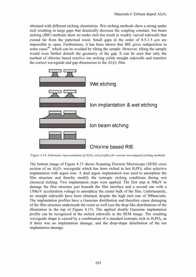
Materials I: Erbium doped Al2O3
103
obtained with different etching chemistries. Wet etching methods show a strong under etch resulting in large gaps that drastically decrease the coupling constant. Ion beam etching (IBE) methods show no under etch but result in weakly curved sidewalls that extend far from the patterned resist. Small gaps in the order of 0.5-1.5 µm are impossible to open. Furthermore, it has been shown that IBE gives redeposition in some cases49, which can be avoided by tilting the sample. However, tilting the sample would even further disturb the geometry of the gap. It can be seen that only the method of chlorine based reactive ion etching yields straight sidewalls and transfers the correct waveguide and gap dimensions to the Al2O3 film.
Figure 4.14: Schematic representation of Al2O3 etch profiles for various investigated etching methods. The bottom image of Figure 4.15 shows Scanning Electron Microscope (SEM) cross section of an Al2O3 waveguide which has been etched in hot H3PO4 after selective implantation with argon ions. A dual argon implantation was used to amorphize the film structure and thereby modify the isotropic etching conditions during wet chemical etching. Two implantation steps were applied. The first step at 50keV to damage the film structure just beneath the film interface and a second one with a 150keV acceleration voltage to amorphize the center bulk of the film. Unfortunately, no straight sidewalls have been obtained, despite the high etch rate of 500nm/min. The implantation profiles have a Gaussian distribution and therefore cause damaging of the film structure underneath the resist as well (see the drop-like distributions of the illustration in the top of Figure 4.15). The applied double Gaussian implantation profile can be recognized at the etched sidewalls in the SEM image. The resulting waveguide shape is caused by a combination of a standard isotropic etch in H3PO4, as if there was no implantation damage, and the drop-shape distribution of the ion implantation damage.
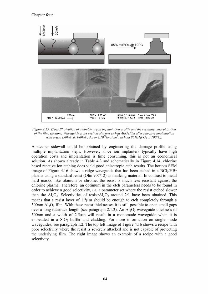
Chapter four
104
Figure 4.15: (Top) Illustration of a double argon implantation profile and the resulting amorphization
of the film. (Bottom) Waveguide cross section of a wet etched Al2O3 film after selective implantation with argon (50keV & 180keV, dose=4.1016ions/cm2, etchant 85%H3PO4 at 100°C).
A steeper sidewall could be obtained by engineering the damage profile using multiple implantation steps. However, since ion implanters typically have high operation costs and implantation is time consuming, this is not an economical solution. As shown already in Table 4.3 and schematically in Figure 4.14, chlorine based reactive ion etching does yield good anisotropic etch results. The bottom SEM image of Figure 4.16 shows a ridge waveguide that has been etched in a BCl3/HBr plasma using a standard resist (Olin 907/12) as masking material. In contrast to metal hard masks, like titanium or chrome, the resist is much less resistant against the chlorine plasma. Therefore, an optimum in the etch parameters needs to be found in order to achieve a good selectivity, i.e. a parameter set where the resist etched slower than the Al2O3. Selectivities of resist:Al2O3 around 2:1 have been obtained. This means that a resist layer of 1.5µm should be enough to etch completely through a 500nm Al2O3 film. With these resist thicknesses it is still possible to open small gaps over a long racetrack length (see paragraph 2.1.2). An Al2O3 waveguide thickness of 500nm and a width of 2.5µm will result in a monomode waveguide when it is embedded in a SiO2 buffer and cladding. For more information on single mode waveguides, see paragraph 1.2. The top left image of Figure 4.16 shows a recipe with poor selectivity where the resist is severely attacked and is not capable of protecting the underlying film. The right image shows an example of a recipe with a good selectivity.
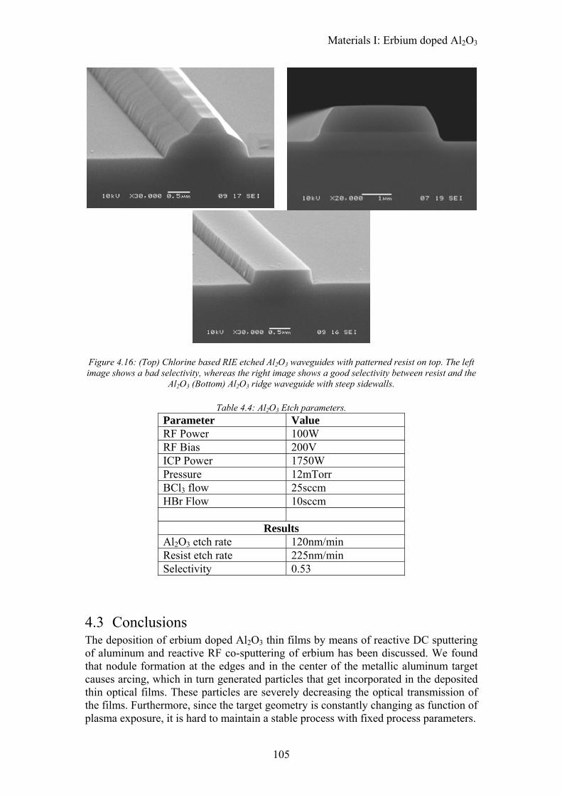
Materials I: Erbium doped Al2O3
105
Figure 4.16: (Top) Chlorine based RIE etched Al2O3 waveguides with patterned resist on top. The left image shows a bad selectivity, whereas the right image shows a good selectivity between resist and the
Al2O3 (Bottom) Al2O3 ridge waveguide with steep sidewalls.
Table 4.4: Al2O3 Etch parameters. Parameter Value RF Power 100W RF Bias 200V ICP Power 1750W Pressure 12mTorr BCl3 flow 25sccm HBr Flow 10sccm
Results Al2O3 etch rate 120nm/min Resist etch rate 225nm/min Selectivity 0.53
4.3 Conclusions The deposition of erbium doped Al2O3 thin films by means of reactive DC sputtering of aluminum and reactive RF co-sputtering of erbium has been discussed. We found that nodule formation at the edges and in the center of the metallic aluminum target causes arcing, which in turn generated particles that get incorporated in the deposited thin optical films. These particles are severely decreasing the optical transmission of the films. Furthermore, since the target geometry is constantly changing as function of plasma exposure, it is hard to maintain a stable process with fixed process parameters.

Chapter four
106
Eventually, we have been able to deposit some Er:Al2O3 films with reasonable optical quality using reactive RF co-sputtering of a metallic erbium target. Our findings on the optical properties of the obtained thin films have been discussed and the gain performance is predicted for use in future waveguide components. We conclude that RF sputtering of both the aluminum and erbium target would be a better but more expensive solution for the deposition of Er:Al2O3 films. Finally, an overview is given on the patterning methods that can be used for waveguide fabrication. In case of the fabrication of laterally coupled microring resonators, for instance for integrated laser applications or all optical switching using absorption modulation (see paragraph 2.1.1.e), chlorine and HBr-based dry etching is the only effective method to open the small gaps needed for evanescent field coupling in a one step etching process.
107
5 Materials II: Rare-earth and nanoparticle-doped polymers and sol-gels
As mentioned in Chapter 3, erbium and neodymium doped materials are interesting candidates for application in optical amplifiers. In this chapter, the preparation and the optical properties of lanthanum fluoride (LaF3) nanoparticles doped with erbium and neodymium will be discussed. Organic and inorganic materials in the form of polymers and sol-gels, respectively, have been developed to serve as the hosts for the inorganic nanoparticles. The organic host material has been synthesized such that it is photo-crosslinkable to facilitate straight forward multimode and monomode waveguide fabrication. Our focus will be on the optical properties of both the inorganic rare-earth doped nanoparticles and the host materials. The importance of the refractive indices of the particles and the host material and particle size on the optical scattering properties will be addressed. The optical transmission windows of the host materials overlap with the absorption peaks of the erbium and neodymium in order to have efficient optical pumping, as well as with the spontaneous emission spectra of the rare earth metals for use as optical amplifiers around 1330nm and 1550nm. Furthermore, the improvement on the excited state lifetimes of the rare earths in the nanoparticles compared to the lifetimes of rare earth ions directly immersed in sol-gels will be presented. Furthermore, the synthesis, application, properties and surface plasmons of noble metal nanoparticles, which is an emerging field, will be briefly discussed.
Chapter five
108
5.1 Introduction The active optical properties of the rare earth ions erbium and neodymium are used to amplify the optical signals used in telecommunication systems around 1550nm55 and 1330nm, respectively. This amplification takes place through a mechanism called stimulated emission as is discussed in paragraph 3.2.1. The trivalent erbium or neodymium ion is pumped with a high power laser into an excited state where it will stay for a relatively long time (millisecond range), until a signal photon passes and triggers the excited ion to fall back to its ground state energy level, emitting a photon with exact the same wavelength, direction and phase as the incoming signal photon. A lot of effort has been put in incorporating erbium and neodymium in integrated optical devices, in order to compensate for the on-chip optical losses or to achieve strong non-linear behavior to facilitate all-optical functions like, for instance, switching or modulation. The efficiency of the rare earth elements depends partly on the excited state lifetime of the ions, which strongly depends on the local environment. A broad range of host materials, like SiO2, Al2O3 and LaF3 have proven to be successful for use in optical amplifiers. However, deposition of these glassy and ceramic materials is time consuming and expensive. Furthermore, etching of micron sized waveguide structures into these, often inert, materials is not straightforward and expensive as well, as has been concluded in paragraph 4.3. The use of low cost photosensitive polymers or sol-gel based materials would enhance the ease of processing and drastically reduce the costs, since the thin films can easily be spin-coated onto a wafer. However, the CH and OH bonds that are always present in these materials are strong energy quenchers of the rare earth ions, resulting in strongly reduced excited state lifetimes, decreasing the probability to generate stimulated emitted photons. We combined the properties of both the inorganic and organic material systems by synthesizing erbium and neodymium doped LaF3 nanoparticles that can be dispersed in photosensitive polymer and sol-gel solutions. In paragraphs 5.2 and 5.3 both the properties of the host materials and nanoparticles will be discussed, whereas in paragraph 5.4 the experimental results of nanoparticle doped polymers and sol-gels will be presented. The developed hybrid polymer materials can be spin-coated onto a sample, followed by a UV-exposure and a development step to fabricate optically active multimode and monomode waveguides154. Furthermore, we investigated the possibilities of incorporation the LaF3 nanoparticles in sol-gels and show improved lifetime properties compared to conventional rare-earth doped sol-gels. Finally, we present some results on gold nanoparticles incorporated into various sol-gels hosts with the aim to synthesize a material with strong third-order non-linearity. Noble metal nanoparticles can also be used as sensitizers to enhance the excitation of the optically active ions in rare-earth doped materials47.
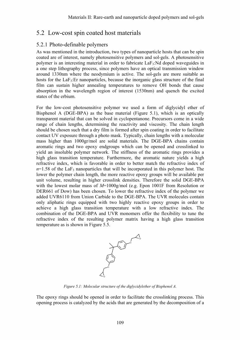
Materials II: Rare-earth and nanoparticle doped polymers and sol-gels
109
5.2 Low-cost spin coated host materials
5.2.1 Photo-definable polymers As was mentioned in the introduction, two types of nanoparticle hosts that can be spin coated are of interest, namely photosensitive polymers and sol-gels. A photosensitive polymer is an interesting material in order to fabricate LaF3:Nd doped waveguides in a one step lithography process, since polymers have an optical transmission window around 1330nm where the neodymium is active. The sol-gels are more suitable as hosts for the LaF3:Er nanoparticles, because the inorganic glass structure of the final film can sustain higher annealing temperatures to remove OH bonds that cause absorption in the wavelength region of interest (1530nm) and quench the excited states of the erbium. For the low-cost photosensitive polymer we used a form of diglycidyl ether of Bisphenol A (DGE-BPA) as the base material (Figure 5.1), which is an optically transparent material that can be solved in cyclopentanone. Precursors come in a wide range of chain lengths, determining the reactivity and viscosity. The chain length should be chosen such that a dry film is formed after spin coating in order to facilitate contact UV exposure through a photo mask. Typically, chain lengths with a molecular mass higher than 1000gr/mol are solid materials. The DGE-BPA chains contain aromatic rings and two epoxy endgroups which can be opened and crosslinked to yield an insoluble polymer network. The stiffness of the aromatic rings provides a high glass transition temperature. Furthermore, the aromatic nature yields a high refractive index, which is favorable in order to better match the refractive index of n=1.58 of the LaF3 nanoparticles that will be incorporated in this polymer host. The lower the polymer chain length, the more reactive epoxy groups will be available per unit volume, resulting in higher crosslink densities. Therefore the solid DGE-BPA with the lowest molar mass of M=1000g/mol (e.g. Epon 1001F from Resolution or DER661 of Dow) has been chosen. To lower the refractive index of the polymer we added UVR6110 from Union Carbide to the DGE-BPA. The UVR molecules contain only aliphatic rings equipped with two highly reactive epoxy groups in order to achieve a high glass transition temperature with a low refractive index. The combination of the DGE-BPA and UVR monomers offer the flexibility to tune the refractive index of the resulting polymer matrix having a high glass transition temperature as is shown in Figure 5.5.
Figure 5.1: Molecular structure of the diglycidylether of Bisphenol A. The epoxy rings should be opened in order to facilitate the crosslinking process. This opening process is catalyzed by the acids that are generated by the decomposition of a
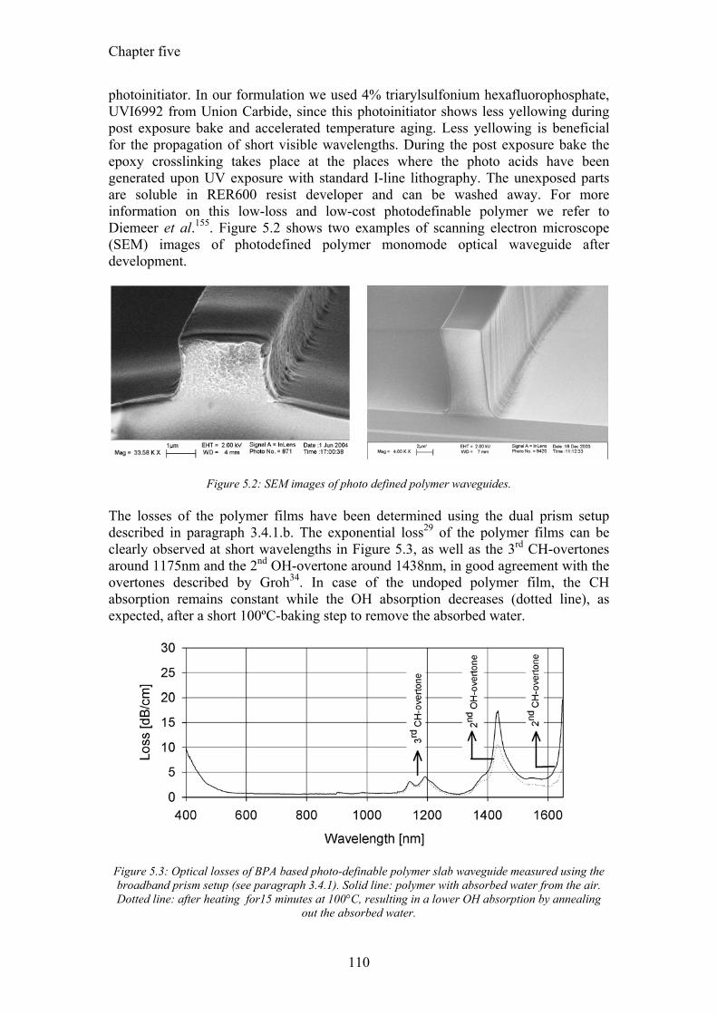
Chapter five
110
photoinitiator. In our formulation we used 4% triarylsulfonium hexafluorophosphate, UVI6992 from Union Carbide, since this photoinitiator shows less yellowing during post exposure bake and accelerated temperature aging. Less yellowing is beneficial for the propagation of short visible wavelengths. During the post exposure bake the epoxy crosslinking takes place at the places where the photo acids have been generated upon UV exposure with standard I-line lithography. The unexposed parts are soluble in RER600 resist developer and can be washed away. For more information on this low-loss and low-cost photodefinable polymer we refer to Diemeer et al.155. Figure 5.2 shows two examples of scanning electron microscope (SEM) images of photodefined polymer monomode optical waveguide after development.
Figure 5.2: SEM images of photo defined polymer waveguides. The losses of the polymer films have been determined using the dual prism setup described in paragraph 3.4.1.b. The exponential loss29 of the polymer films can be clearly observed at short wavelengths in Figure 5.3, as well as the 3rd CH-overtones around 1175nm and the 2nd OH-overtone around 1438nm, in good agreement with the overtones described by Groh34. In case of the undoped polymer film, the CH absorption remains constant while the OH absorption decreases (dotted line), as expected, after a short 100ºC-baking step to remove the absorbed water.
Figure 5.3: Optical losses of BPA based photo-definable polymer slab waveguide measured using the broadband prism setup (see paragraph 3.4.1). Solid line: polymer with absorbed water from the air. Dotted line: after heating for15 minutes at 100°C, resulting in a lower OH absorption by annealing
out the absorbed water.
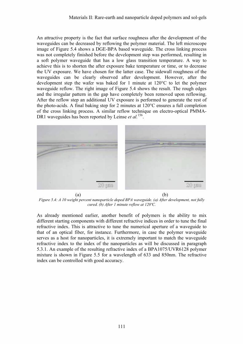
Materials II: Rare-earth and nanoparticle doped polymers and sol-gels
111
An attractive property is the fact that surface roughness after the development of the waveguides can be decreased by reflowing the polymer material. The left microscope image of Figure 5.4 shows a DGE-BPA based waveguide. The cross linking process was not completely finished before the development step was performed, resulting in a soft polymer waveguide that has a low glass transition temperature. A way to achieve this is to shorten the after exposure bake temperature or time, or to decrease the UV exposure. We have chosen for the latter case. The sidewall roughness of the waveguides can be clearly observed after development. However, after the development step the wafer was baked for 1 minute at 120°C to let the polymer waveguide reflow. The right image of Figure 5.4 shows the result. The rough edges and the irregular pattern in the gap have completely been removed upon reflowing. After the reflow step an additional UV exposure is performed to generate the rest of the photo-acids. A final baking step for 2 minutes at 120°C ensures a full completion of the cross linking process. A similar reflow technique on electro-optical PMMA-DR1 waveguides has been reported by Leinse et al.156.
(a) (b) Figure 5.4: A 10 weight percent nanoparticle doped BPA waveguide. (a) After development, not fully
cured. (b) After 1 minute reflow at 120ºC. As already mentioned earlier, another benefit of polymers is the ability to mix different starting components with different refractive indices in order to tune the final refractive index. This is attractive to tune the numerical aperture of a waveguide to that of an optical fiber, for instance. Furthermore, in case the polymer waveguide serves as a host for nanoparticles, it is extremely important to match the waveguide refractive index to the index of the nanoparticles as will be discussed in paragraph 5.3.1. An example of the resulting refractive index of a BPA1075/UVR6128 polymer mixture is shown in Figure 5.5 for a wavelength of 633 and 850nm. The refractive index can be controlled with good accuracy.
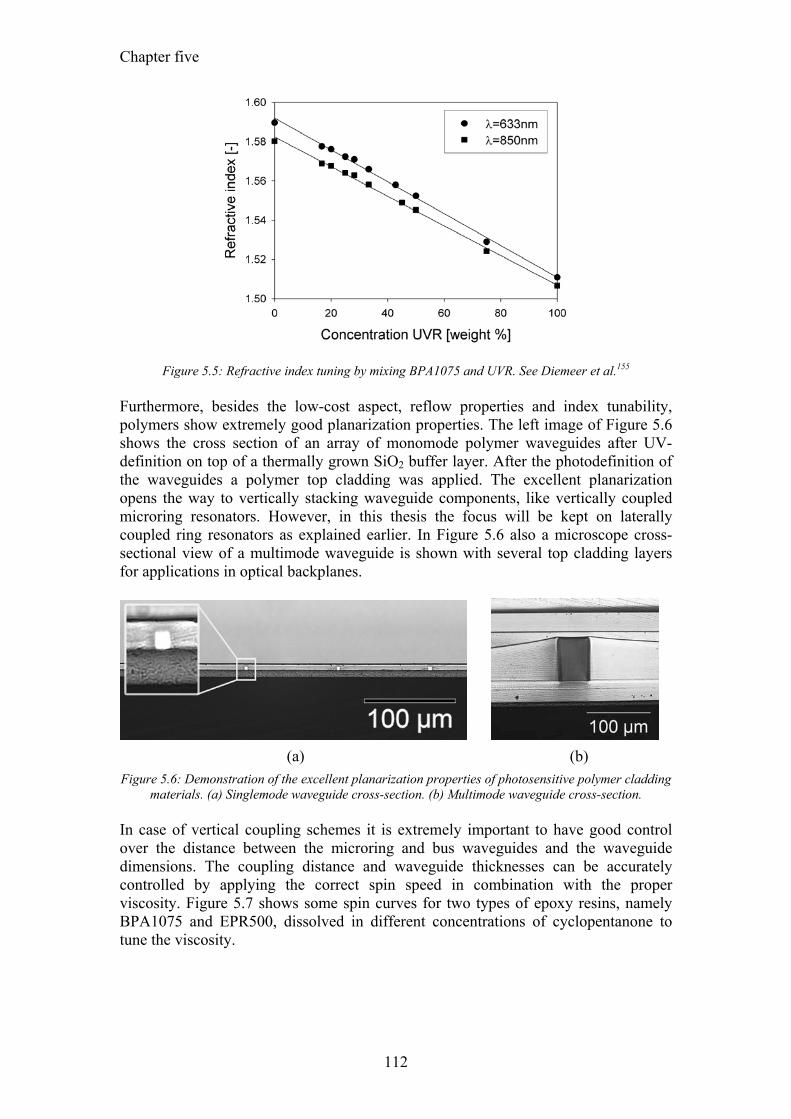
Chapter five
112
Figure 5.5: Refractive index tuning by mixing BPA1075 and UVR. See Diemeer et al.155 Furthermore, besides the low-cost aspect, reflow properties and index tunability, polymers show extremely good planarization properties. The left image of Figure 5.6 shows the cross section of an array of monomode polymer waveguides after UV-definition on top of a thermally grown SiO2 buffer layer. After the photodefinition of the waveguides a polymer top cladding was applied. The excellent planarization opens the way to vertically stacking waveguide components, like vertically coupled microring resonators. However, in this thesis the focus will be kept on laterally coupled ring resonators as explained earlier. In Figure 5.6 also a microscope cross-sectional view of a multimode waveguide is shown with several top cladding layers for applications in optical backplanes.
(a) (b)
Figure 5.6: Demonstration of the excellent planarization properties of photosensitive polymer cladding materials. (a) Singlemode waveguide cross-section. (b) Multimode waveguide cross-section.
In case of vertical coupling schemes it is extremely important to have good control over the distance between the microring and bus waveguides and the waveguide dimensions. The coupling distance and waveguide thicknesses can be accurately controlled by applying the correct spin speed in combination with the proper viscosity. Figure 5.7 shows some spin curves for two types of epoxy resins, namely BPA1075 and EPR500, dissolved in different concentrations of cyclopentanone to tune the viscosity.
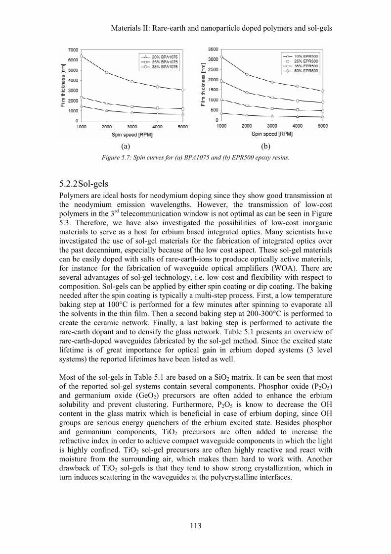
Materials II: Rare-earth and nanoparticle doped polymers and sol-gels
113
(a) (b)
Figure 5.7: Spin curves for (a) BPA1075 and (b) EPR500 epoxy resins.
5.2.2 Sol-gels Polymers are ideal hosts for neodymium doping since they show good transmission at the neodymium emission wavelengths. However, the transmission of low-cost polymers in the 3rd telecommunication window is not optimal as can be seen in Figure 5.3. Therefore, we have also investigated the possibilities of low-cost inorganic materials to serve as a host for erbium based integrated optics. Many scientists have investigated the use of sol-gel materials for the fabrication of integrated optics over the past decennium, especially because of the low cost aspect. These sol-gel materials can be easily doped with salts of rare-earth-ions to produce optically active materials, for instance for the fabrication of waveguide optical amplifiers (WOA). There are several advantages of sol-gel technology, i.e. low cost and flexibility with respect to composition. Sol-gels can be applied by either spin coating or dip coating. The baking needed after the spin coating is typically a multi-step process. First, a low temperature baking step at 100°C is performed for a few minutes after spinning to evaporate all the solvents in the thin film. Then a second baking step at 200-300°C is performed to create the ceramic network. Finally, a last baking step is performed to activate the rare-earth dopant and to densify the glass network. Table 5.1 presents an overview of rare-earth-doped waveguides fabricated by the sol-gel method. Since the excited state lifetime is of great importance for optical gain in erbium doped systems (3 level systems) the reported lifetimes have been listed as well. Most of the sol-gels in Table 5.1 are based on a SiO2 matrix. It can be seen that most of the reported sol-gel systems contain several components. Phosphor oxide (P2O5) and germanium oxide (GeO2) precursors are often added to enhance the erbium solubility and prevent clustering. Furthermore, P2O5 is know to decrease the OH content in the glass matrix which is beneficial in case of erbium doping, since OH groups are serious energy quenchers of the erbium excited state. Besides phosphor and germanium components, TiO2 precursors are often added to increase the refractive index in order to achieve compact waveguide components in which the light is highly confined. TiO2 sol-gel precursors are often highly reactive and react with moisture from the surrounding air, which makes them hard to work with. Another drawback of TiO2 sol-gels is that they tend to show strong crystallization, which in turn induces scattering in the waveguides at the polycrystalline interfaces.
Chapter five
114
Table 5.1: Overview of excited state lifetimes in erbium doped sol-gels materials Host Composition Temp Absorption τ Ref Y2Ti2O7-Er2Ti2O7 (YETO)
Er3+ = 1-2×10²⁰ ions/cm3 (Er3+:Y3+ = 1:75)
600ºC 700ºC 750ºC 800ºC
1.4ms 1.6 ms 4.5 ms 7.0 ms
157
TiO2 Er3+ = 1,3,5,7,10 and 15%
600ºC < 1dB/cm - 158
SiO2-TiO2 TiO2 = 7-12 mol% Er3+ = 1 mol%
900ºC 0.6 dB/cm @ 1550nm 8 ms 159
SiO2-TiO2-Al2O3 Si:Ti:Al = 93:7:10 Er3+ = 1.1×10²⁰ ions/cm3
0.6 dB/cm @ 1330nm (background loss)
8 ms 160,
161
SiO2-TiO2-P2O5 PO2.5 = 10% TiO2 = 20% ErO1.5 = 1%
1000ºC 6 ms 162
SiO2-TiO2-P2O5 P2O5 = 10 mol% Er3+ = 0.25 mol%
900ºC < 4dB/cm @ 1060nm 1.8 ms 163
SiO2-GeO2-Al2O3 GeO2:SiO2 = 80:20 Al2O3 = 10% Er3+ = 0.2 mol%
600ºC 4-6 ms 164,
165
SiO2-GeO2-P2O5 GeO2:SiO2 = 80:20 P2O5 = 10% Er3+ = 0.2 mol%
600ºC 5-6 ms 164,
165
SiO2-GeO2-Al2O3 (Na-Ag ion exchange)
GeO2:SiO2 = 80:20 Al2O3 = 10%
600-700ºC
1.5 dB/cm @ 840nm 6.5 ms 166
SiO2-GeO2-Al2O3 90Si:10Ge:20Al:1Er 1000ºC 1.6-2.2 dB/cm @ 633nm 3.5 ms 167 SiO2-Al2O3 Al/Si = 2
Er3+ = 0.5 at% 900ºC 0.2 dB/cm 3.5 ms 168,
169 SiO2-Al2O3 Er = 2000 ppm
Yb = 4000 ppm Al = 6000 ppm
950ºC 8.7 ms 170
Al2O3 Sm3+ = 0.1 mol% Dy3+ = 0.1 mol%
800ºC 2.0 ms 0.8 ms
171
From the lifetimes in Table 5.1 it can be concluded that Al2O3 doped sol gel glasses show the highest excited state lifetimes. This can be explained by the fact that the solubility is increased and the clustering of erbium ions is decreased by the aluminum in the glass matrix. Incorporation of erbium into a sol gel can be achieved by dissolving erbium(III)nitrate pentahydrate, Er(NO3)3⋅5H2O, into the sol-gel precursors. Optical activation of Er3+ in Al2O3 takes place already at a temperature of 770K, which is 200ºC lower than in silicate glasses56 according to the following chemical reaction158:
2232770
33 3122)(4 ONOOErNOEr K ++⎯⎯ →⎯ We have investigated several sol-gel systems for use in integrated optical applications. The focus has been on high refractive index and high erbium solubility. Therefore the Ta2O5, TiO2 an Al2O3 based sol-gels were the first materials of choice. We only focused on single component precursors. Optimization of a sol-gel host by mixing several sol-gel components is beyond the scope of this work and therefore we refer to the references listed in Table 5.1. In order to correctly tune the erbium concentration, exact knowledge is needed with respect to the solid fraction after baking and annealing of the sol. We found that the Emulsitone C-TiO2 sol-gel with a
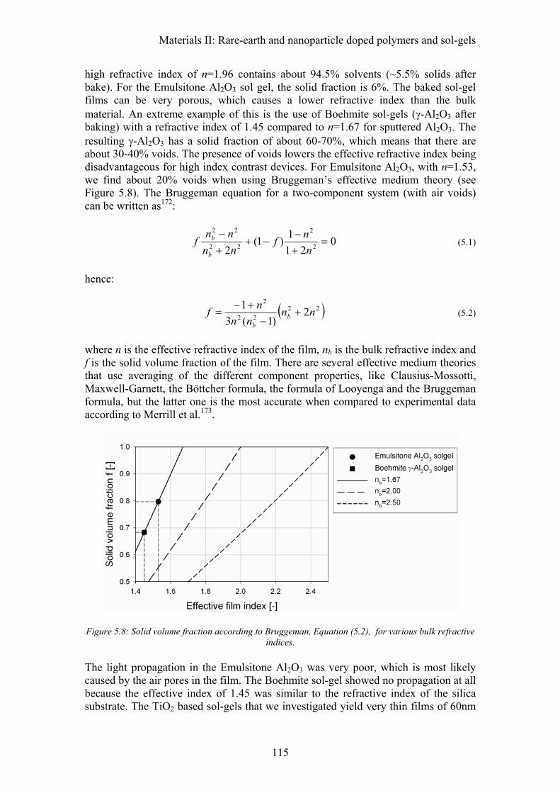
Materials II: Rare-earth and nanoparticle doped polymers and sol-gels
115
high refractive index of n=1.96 contains about 94.5% solvents (~5.5% solids after bake). For the Emulsitone Al2O3 sol gel, the solid fraction is 6%. The baked sol-gel films can be very porous, which causes a lower refractive index than the bulk material. An extreme example of this is the use of Boehmite sol-gels (γ-Al2O3 after baking) with a refractive index of 1.45 compared to n=1.67 for sputtered Al2O3. The resulting γ-Al2O3 has a solid fraction of about 60-70%, which means that there are about 30-40% voids. The presence of voids lowers the effective refractive index being disadvantageous for high index contrast devices. For Emulsitone Al2O3, with n=1.53, we find about 20% voids when using Bruggeman’s effective medium theory (see Figure 5.8). The Bruggeman equation for a two-component system (with air voids) can be written as172:
021
1)1(2 2
2
22
22
=+−
−++−
nnf
nnnn
fb
b (5.1)
hence:
( )2222
2
2)1(3
1 nnnn
nf bb
+−
+−= (5.2)
where n is the effective refractive index of the film, nb is the bulk refractive index and f is the solid volume fraction of the film. There are several effective medium theories that use averaging of the different component properties, like Clausius-Mossotti, Maxwell-Garnett, the Böttcher formula, the formula of Looyenga and the Bruggeman formula, but the latter one is the most accurate when compared to experimental data according to Merrill et al.173.
Figure 5.8: Solid volume fraction according to Bruggeman, Equation (5.2), for various bulk refractive
indices. The light propagation in the Emulsitone Al2O3 was very poor, which is most likely caused by the air pores in the film. The Boehmite sol-gel showed no propagation at all because the effective index of 1.45 was similar to the refractive index of the silica substrate. The TiO2 based sol-gels that we investigated yield very thin films of 60nm
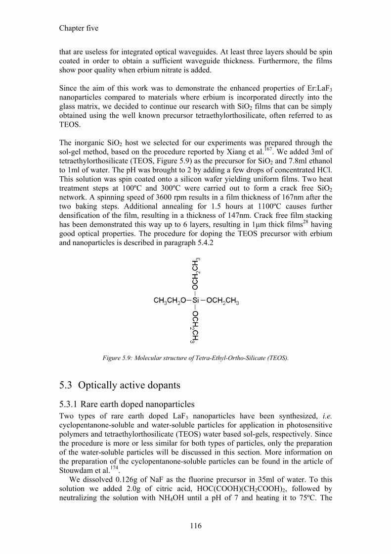
Chapter five
116
that are useless for integrated optical waveguides. At least three layers should be spin coated in order to obtain a sufficient waveguide thickness. Furthermore, the films show poor quality when erbium nitrate is added. Since the aim of this work was to demonstrate the enhanced properties of Er:LaF3 nanoparticles compared to materials where erbium is incorporated directly into the glass matrix, we decided to continue our research with SiO2 films that can be simply obtained using the well known precursor tetraethylorthosilicate, often referred to as TEOS. The inorganic SiO2 host we selected for our experiments was prepared through the sol-gel method, based on the procedure reported by Xiang et al.167. We added 3ml of tetraethylorthosilicate (TEOS, Figure 5.9) as the precursor for SiO2 and 7.8ml ethanol to 1ml of water. The pH was brought to 2 by adding a few drops of concentrated HCl. This solution was spin coated onto a silicon wafer yielding uniform films. Two heat treatment steps at 100ºC and 300ºC were carried out to form a crack free SiO2 network. A spinning speed of 3600 rpm results in a film thickness of 167nm after the two baking steps. Additional annealing for 1.5 hours at 1100ºC causes further densification of the film, resulting in a thickness of 147nm. Crack free film stacking has been demonstrated this way up to 6 layers, resulting in 1µm thick films28 having good optical properties. The procedure for doping the TEOS precursor with erbium and nanoparticles is described in paragraph 5.4.2
Figure 5.9: Molecular structure of Tetra-Ethyl-Ortho-Silicate (TEOS).
5.3 Optically active dopants
5.3.1 Rare earth doped nanoparticles Two types of rare earth doped LaF3 nanoparticles have been synthesized, i.e. cyclopentanone-soluble and water-soluble particles for application in photosensitive polymers and tetraethylorthosilicate (TEOS) water based sol-gels, respectively. Since the procedure is more or less similar for both types of particles, only the preparation of the water-soluble particles will be discussed in this section. More information on the preparation of the cyclopentanone-soluble particles can be found in the article of Stouwdam et al.174. We dissolved 0.126g of NaF as the fluorine precursor in 35ml of water. To this solution we added 2.0g of citric acid, HOC(COOH)(CH2COOH)2, followed by neutralizing the solution with NH4OH until a pH of 7 and heating it to 75ºC. The
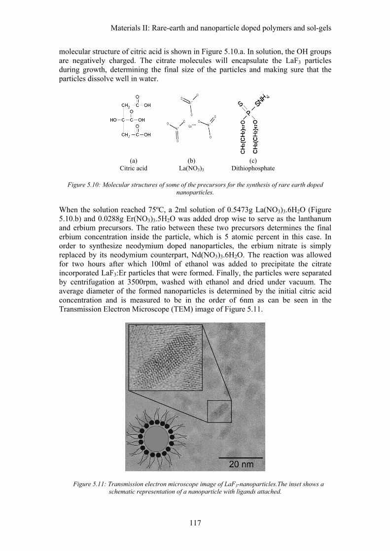
Materials II: Rare-earth and nanoparticle doped polymers and sol-gels
117
molecular structure of citric acid is shown in Figure 5.10.a. In solution, the OH groups are negatively charged. The citrate molecules will encapsulate the LaF3 particles during growth, determining the final size of the particles and making sure that the particles dissolve well in water.
(a)
Citric acid (b)
La(NO3)3 (c)
Dithiophosphate
Figure 5.10: Molecular structures of some of the precursors for the synthesis of rare earth doped nanoparticles.
When the solution reached 75ºC, a 2ml solution of 0.5473g La(NO3)3.6H2O (Figure 5.10.b) and 0.0288g Er(NO3)3.5H2O was added drop wise to serve as the lanthanum and erbium precursors. The ratio between these two precursors determines the final erbium concentration inside the particle, which is 5 atomic percent in this case. In order to synthesize neodymium doped nanoparticles, the erbium nitrate is simply replaced by its neodymium counterpart, Nd(NO3)3.6H2O. The reaction was allowed for two hours after which 100ml of ethanol was added to precipitate the citrate incorporated LaF3:Er particles that were formed. Finally, the particles were separated by centrifugation at 3500rpm, washed with ethanol and dried under vacuum. The average diameter of the formed nanoparticles is determined by the initial citric acid concentration and is measured to be in the order of 6nm as can be seen in the Transmission Electron Microscope (TEM) image of Figure 5.11.
Figure 5.11: Transmission electron microscope image of LaF3-nanoparticles.The inset shows a schematic representation of a nanoparticle with ligands attached.
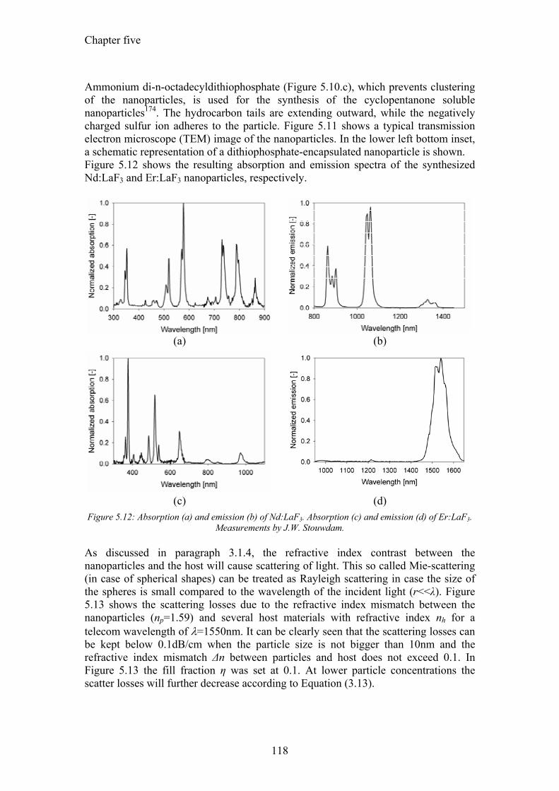
Chapter five
118
Ammonium di-n-octadecyldithiophosphate (Figure 5.10.c), which prevents clustering of the nanoparticles, is used for the synthesis of the cyclopentanone soluble nanoparticles174. The hydrocarbon tails are extending outward, while the negatively charged sulfur ion adheres to the particle. Figure 5.11 shows a typical transmission electron microscope (TEM) image of the nanoparticles. In the lower left bottom inset, a schematic representation of a dithiophosphate-encapsulated nanoparticle is shown. Figure 5.12 shows the resulting absorption and emission spectra of the synthesized Nd:LaF3 and Er:LaF3 nanoparticles, respectively.
(a) (b)
(c) (d)
Figure 5.12: Absorption (a) and emission (b) of Nd:LaF3. Absorption (c) and emission (d) of Er:LaF3. Measurements by J.W. Stouwdam.
As discussed in paragraph 3.1.4, the refractive index contrast between the nanoparticles and the host will cause scattering of light. This so called Mie-scattering (in case of spherical shapes) can be treated as Rayleigh scattering in case the size of the spheres is small compared to the wavelength of the incident light (r<<λ). Figure 5.13 shows the scattering losses due to the refractive index mismatch between the nanoparticles (np=1.59) and several host materials with refractive index nh for a telecom wavelength of λ=1550nm. It can be clearly seen that the scattering losses can be kept below 0.1dB/cm when the particle size is not bigger than 10nm and the refractive index mismatch ∆n between particles and host does not exceed 0.1. In Figure 5.13 the fill fraction η was set at 0.1. At lower particle concentrations the scatter losses will further decrease according to Equation (3.13).
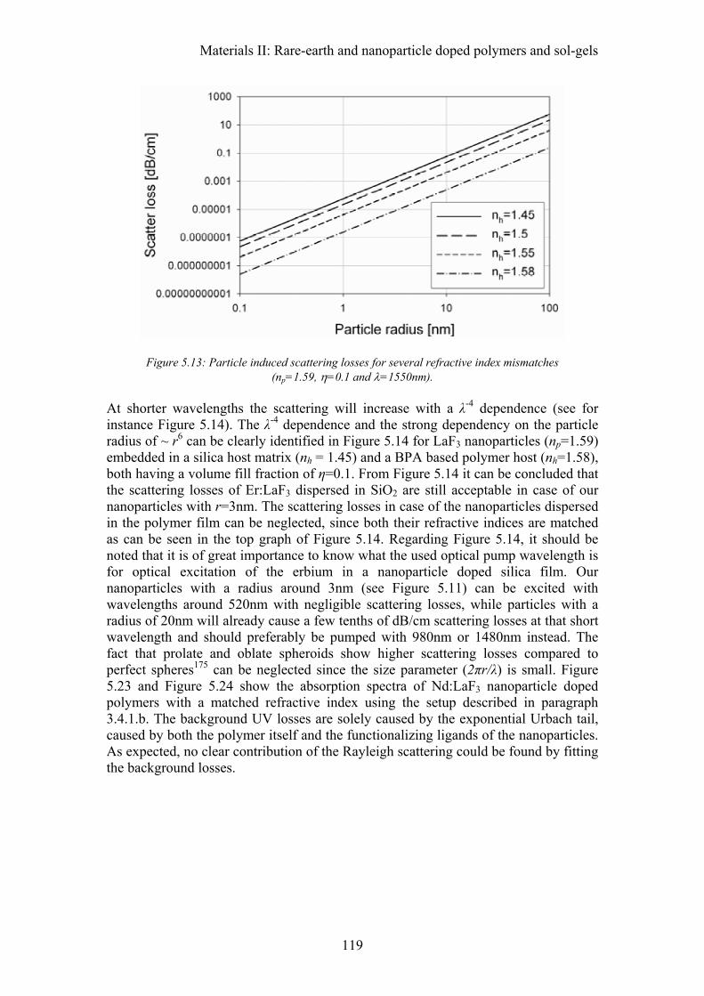
Materials II: Rare-earth and nanoparticle doped polymers and sol-gels
119
Figure 5.13: Particle induced scattering losses for several refractive index mismatches (np=1.59, η=0.1 and λ=1550nm).
At shorter wavelengths the scattering will increase with a λ-4 dependence (see for instance Figure 5.14). The λ-4 dependence and the strong dependency on the particle radius of ~ r6 can be clearly identified in Figure 5.14 for LaF3 nanoparticles (np=1.59) embedded in a silica host matrix (nh = 1.45) and a BPA based polymer host (nh=1.58), both having a volume fill fraction of η=0.1. From Figure 5.14 it can be concluded that the scattering losses of Er:LaF3 dispersed in SiO2 are still acceptable in case of our nanoparticles with r=3nm. The scattering losses in case of the nanoparticles dispersed in the polymer film can be neglected, since both their refractive indices are matched as can be seen in the top graph of Figure 5.14. Regarding Figure 5.14, it should be noted that it is of great importance to know what the used optical pump wavelength is for optical excitation of the erbium in a nanoparticle doped silica film. Our nanoparticles with a radius around 3nm (see Figure 5.11) can be excited with wavelengths around 520nm with negligible scattering losses, while particles with a radius of 20nm will already cause a few tenths of dB/cm scattering losses at that short wavelength and should preferably be pumped with 980nm or 1480nm instead. The fact that prolate and oblate spheroids show higher scattering losses compared to perfect spheres175 can be neglected since the size parameter (2πr/λ) is small. Figure 5.23 and Figure 5.24 show the absorption spectra of Nd:LaF3 nanoparticle doped polymers with a matched refractive index using the setup described in paragraph 3.4.1.b. The background UV losses are solely caused by the exponential Urbach tail, caused by both the polymer itself and the functionalizing ligands of the nanoparticles. As expected, no clear contribution of the Rayleigh scattering could be found by fitting the background losses.
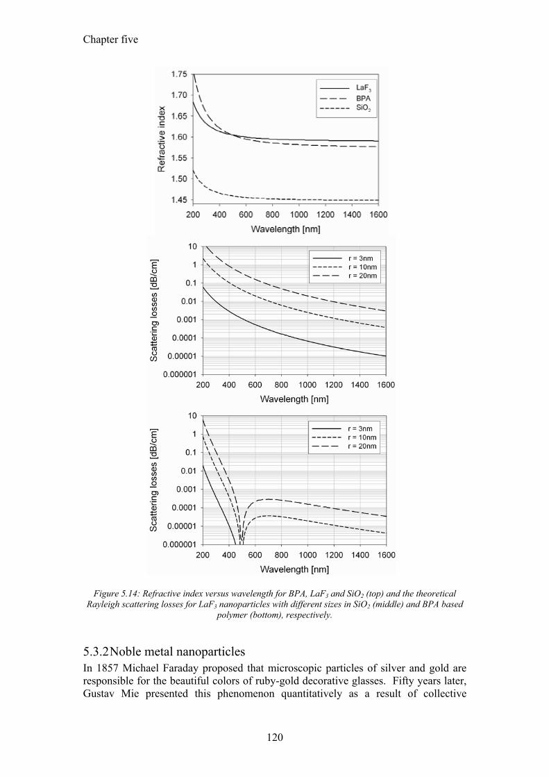
Chapter five
120
Figure 5.14: Refractive index versus wavelength for BPA, LaF3 and SiO2 (top) and the theoretical Rayleigh scattering losses for LaF3 nanoparticles with different sizes in SiO2 (middle) and BPA based
polymer (bottom), respectively.
5.3.2 Noble metal nanoparticles In 1857 Michael Faraday proposed that microscopic particles of silver and gold are responsible for the beautiful colors of ruby-gold decorative glasses. Fifty years later, Gustav Mie presented this phenomenon quantitatively as a result of collective
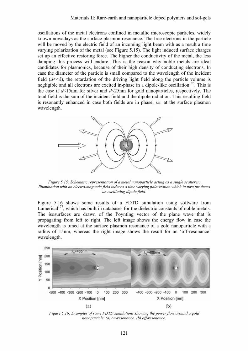
Materials II: Rare-earth and nanoparticle doped polymers and sol-gels
121
oscillations of the metal electrons confined in metallic microscopic particles, widely known nowadays as the surface plasmon resonance. The free electrons in the particle will be moved by the electric field of an incoming light beam with as a result a time varying polarization of the metal (see Figure 5.15). The light induced surface charges set up an effective restoring force. The higher the conductivity of the metal, the less damping this process will endure. This is the reason why noble metals are ideal candidates for plasmonics, because of their high density of conducting electrons. In case the diameter of the particle is small compared to the wavelength of the incident field (d<<λ), the retardation of the driving light field along the particle volume is negligible and all electrons are excited in-phase in a dipole-like oscillation176. This is the case if d<15nm for silver and d<25nm for gold nanoparticles, respectively. The total field is the sum of the incident field and the dipole radiation. This resulting field is resonantly enhanced in case both fields are in phase, i.e. at the surface plasmon wavelength.
Figure 5.15: Schematic representation of a metal nanoparticle acting as a single scatterer. Illumination with an electro-magnetic field induces a time varying polarization which in turn produces
an oscillating dipole field. Figure 5.16 shows some results of a FDTD simulation using software from Lumerical177, which has built in databases for the dielectric constants of noble metals. The isosurfaces are drawn of the Poynting vector of the plane wave that is propagating from left to right. The left image shows the energy flow in case the wavelength is tuned at the surface plasmon resonance of a gold nanoparticle with a radius of 15nm, whereas the right image shows the result for an ‘off-resonance’ wavelength.
(a) (b)
Figure 5.16: Examples of some FDTD simulations showing the power flow around a gold nanoparticle. (a) on-resonance. (b) off-resonance.
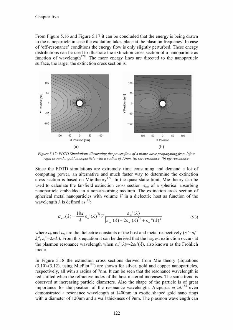
Chapter five
122
From Figure 5.16 and Figure 5.17 it can be concluded that the energy is being drawn to the nanoparticle in case the excitation takes place at the plasmon frequency. In case of ‘off-resonance’ conditions the energy flow is only slightly perturbed. These energy distributions can be used to illustrate the extinction cross section of a nanoparticle as function of wavelength178. The more energy lines are directed to the nanoparticle surface, the larger the extinction cross section is.
(a) (b)
Figure 5.17: FDTD Simulations illustrating the power flow of a plane wave propagating from left to right around a gold nanoparticle with a radius of 15nm. (a) on-resonance, (b) off-resonance.
Since the FDTD simulations are extremely time consuming and demand a lot of computing power, an alternative and much faster way to determine the extinction cross section is based on Mie-theory179. In the quasi-static limit, Mie-theory can be used to calculate the far-field extinction cross section σext of a spherical absorbing nanoparticle embedded in a non-absorbing medium. The extinction cross section of spherical metal nanoparticles with volume V in a dielectric host as function of the wavelength λ is defined as180:
[ ] 222
3
)(")('2)(')('
)('18)(λελελε
λελε
λπλσ
mhm
mhext V
++= (5.3)
where εh and εm are the dielectric constants of the host and metal respectively (εi’=ni
2-ki
2, εi”=2niki). From this equation it can be derived that the largest extinction occurs at the plasmon resonance wavelength when εm’(λ)=-2εh’(λ), also known as the Fröhlich mode. In Figure 5.18 the extinction cross sections derived from Mie theory (Equations (3.10)-(3.12), using MiePlot181) are shown for silver, gold and copper nanoparticles, respectively, all with a radius of 7nm. It can be seen that the resonance wavelength is red shifted when the refractive index of the host material increases. The same trend is observed at increasing particle diameters. Also the shape of the particle is of great importance for the position of the resonance wavelength. Aizpurua et al.182 even demonstrated a resonance wavelength at 1400nm in exotic shaped gold nano rings with a diameter of 120nm and a wall thickness of 9nm. The plasmon wavelength can
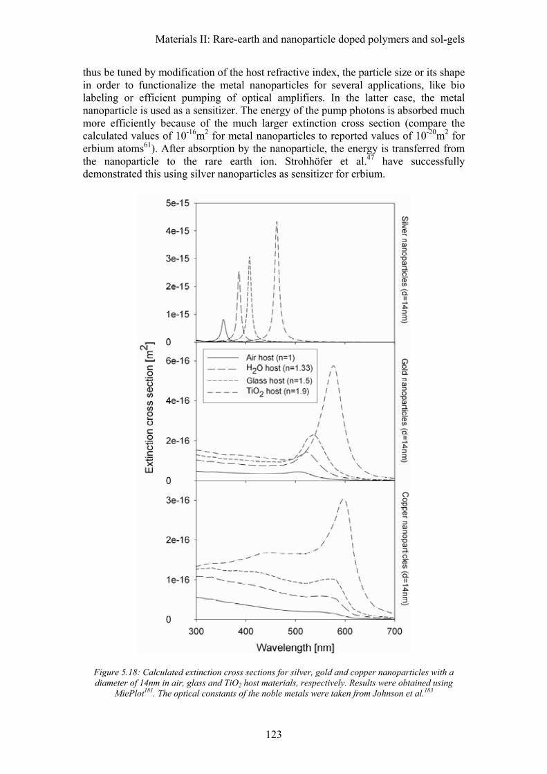
Materials II: Rare-earth and nanoparticle doped polymers and sol-gels
123
thus be tuned by modification of the host refractive index, the particle size or its shape in order to functionalize the metal nanoparticles for several applications, like bio labeling or efficient pumping of optical amplifiers. In the latter case, the metal nanoparticle is used as a sensitizer. The energy of the pump photons is absorbed much more efficiently because of the much larger extinction cross section (compare the calculated values of 10-16m2 for metal nanoparticles to reported values of 10-20m2 for erbium atoms61). After absorption by the nanoparticle, the energy is transferred from the nanoparticle to the rare earth ion. Strohhöfer et al.47 have successfully demonstrated this using silver nanoparticles as sensitizer for erbium.
Figure 5.18: Calculated extinction cross sections for silver, gold and copper nanoparticles with a diameter of 14nm in air, glass and TiO2 host materials, respectively. Results were obtained using
MiePlot181. The optical constants of the noble metals were taken from Johnson et al.183
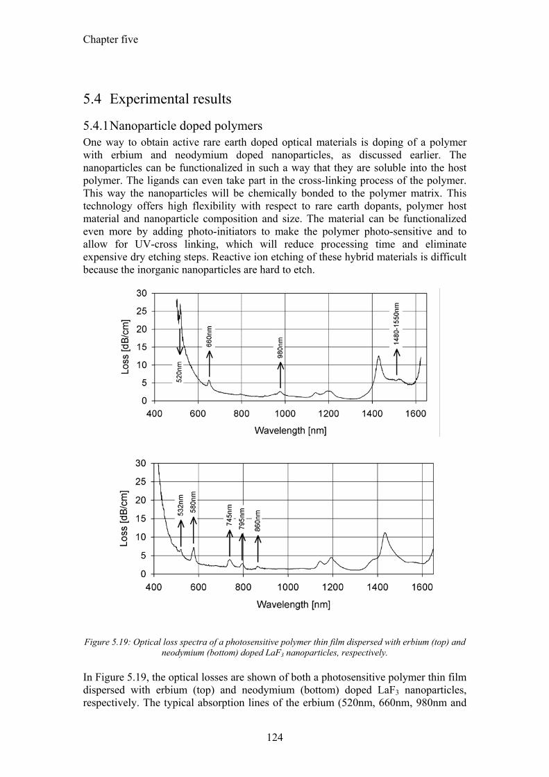
Chapter five
124
5.4 Experimental results
5.4.1 Nanoparticle doped polymers One way to obtain active rare earth doped optical materials is doping of a polymer with erbium and neodymium doped nanoparticles, as discussed earlier. The nanoparticles can be functionalized in such a way that they are soluble into the host polymer. The ligands can even take part in the cross-linking process of the polymer. This way the nanoparticles will be chemically bonded to the polymer matrix. This technology offers high flexibility with respect to rare earth dopants, polymer host material and nanoparticle composition and size. The material can be functionalized even more by adding photo-initiators to make the polymer photo-sensitive and to allow for UV-cross linking, which will reduce processing time and eliminate expensive dry etching steps. Reactive ion etching of these hybrid materials is difficult because the inorganic nanoparticles are hard to etch.
Figure 5.19: Optical loss spectra of a photosensitive polymer thin film dispersed with erbium (top) and
neodymium (bottom) doped LaF3 nanoparticles, respectively. In Figure 5.19, the optical losses are shown of both a photosensitive polymer thin film dispersed with erbium (top) and neodymium (bottom) doped LaF3 nanoparticles, respectively. The typical absorption lines of the erbium (520nm, 660nm, 980nm and
Materials II: Rare-earth and nanoparticle doped polymers and sol-gels
125
1480-1550nm) and the neodymium (532nm, 580nm, 745nm, 795nm, and 860nm) are clearly shown. The loss due to the erbium and neodymium can be used to determine the rare earth concentration, N (in cm-3), of the film by dividing the wavelength dependent loss, a(λ) (in cm-1), by the absorption cross section, σ(λ) (in cm2), of the corresponding rare earth ion. Scattering of the nanoparticles (n=1.59) does not cause the increased absorption at shorter wavelengths, since its refractive index is matched by the polymer (n=1.58). Instead, the yellowing ligands, which are attached to the nanoparticles, are responsible for the UV absorption. This is also indicated by the fact that the absorption tail at short wavelengths has an exponential behavior instead of the λ-4 behavior in case of Rayleigh scattering. Since our low-cost polymer host typically shows losses of 2-3dB/cm in the third telecommunication window it is not attractive to dope the polymers with Er:LaF3 nanoparticles. Therefore, the focus in this paragraph will only be on Nd:LaF3 doped polymers. In paragraph 5.4.1.a the results on multimode polymer waveguides are discussed using polymethylmethacrylate (PMMA) and SU8 as the polymer host materials. Our results on monomode polymer waveguides using our low cost photodefinable BPA polymer are discussed in paragraph 5.4.1.b. To conclude, in paragraph 5.4.1.c which is the last sub-paragraph of paragraph 5.4.1, we present our findings when the photodefinable polymer is used for the fabrication of singlemode microring resonators.
5.4.1.a Multimode polymer waveguides In this paragraph we report experiments which show spontaneous emission at 863nm in hybrid monomode Si3N4 waveguides where LaF3:Nd nanoparticle doped polymethylmethacrylate (PMMA) was used as a top cladding material. Furthermore, optical gain at 1319nm in LaF3:Nd nanoparticle dispersed PMMA (0.1dB/cm) and photo definable epoxy (MicroChem SU-8) multimode waveguides has been observed at pump powers below 10mW. This class of composite materials based on polymers with dispersed nanoparticles shows promising properties for planar optical amplifiers. Simulation shows that optical gain in the order of 10dB can be achieved at 100mW pump power in a 20cm long monomode waveguide. The results presented in this paragraph have been published in Applied Physics Letters184. Over the past few years, more and more new rare earth doped materials are emerging with very promising properties for amplification in active integrated optical devices. Especially the rare earths neodymium and erbium are of great interest, because they emit in the second and third window of optical communication systems, respectively. It has been reported that LaF3 is a very good host for rare earth incorporation and because of its low phonon energy it exhibits a wide transparency band from 0.2 to 11µm185. Laser operation in molecular beam epitaxially grown LaF3:Nd has been reported by several authors185-187,but micro-structuring for planar waveguide applications is hard. Polymer waveguide materials have the advantage of being low-cost and tunable in many ways with respect to their properties and ways of processing. Unfortunately, compared to inorganic materials, it is relatively difficult to dissolve rare earth ions like erbium and neodymium in polymers, because these rare earths come in inorganic salt forms that do not dissolve well in polymers. To overcome the insolubility problem of inorganic rare earth salts in polymers, we developed neodymium doped LaF3 nanoparticles with organic ligands that do dissolve well in polymers. The negatively charged dithiophosphate group of the ligand is
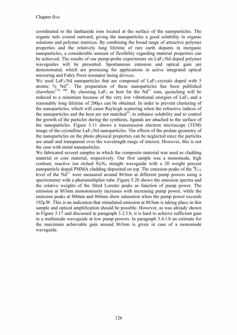
Chapter five
126
coordinated to the lanthanide ions located at the surface of the nanoparticles. The organic tails extend outward, giving the nanoparticles a good solubility in organic solutions and polymer matrices. By combining the broad range of attractive polymer properties and the relatively long lifetime of rare earth dopants in inorganic nanoparticles, a considerable amount of flexibility regarding material properties can be achieved. The results of our pump-probe experiments on LaF3:Nd doped polymer waveguides will be presented. Spontaneous emission and optical gain are demonstrated, which are promising for applications in active integrated optical microring and Fabry Perot resonator lasing devices. We used LaF3:Nd nanoparticles that are composed of LaF3-crystals doped with 5 atomic % Nd3+. The preparation of these nanoparticles has been published elsewhere174, 188. By choosing LaF3 as host for the Nd3+ ions, quenching will be reduced to a minimum because of the very low vibrational energies of LaF3 and a reasonably long lifetime of 200µs can be obtained. In order to prevent clustering of the nanoparticles, which will cause Rayleigh scattering when the refractive indices of the nanoparticles and the host are not matched35, to enhance solubility and to control the growth of the particles during the synthesis, ligands are attached to the surface of the nanoparticles. Figure 5.11 shows a transmission electron microscope (TEM) image of the crystalline LaF3:Nd nanoparticles. The effects of the prolate geometry of the nanoparticles on the photo physical properties can be neglected since the particles are small and transparent over the wavelength range of interest. However, this is not the case with metal nanoparticles. We fabricated several samples in which the composite material was used as cladding material or core material, respectively. Our first sample was a monomode, high contrast, reactive ion etched Si3N4 straight waveguide with a 20 weight percent nanoparticle doped PMMA cladding deposited on top. The emission peaks of the 4F3/2 level of the Nd3+ were measured around 863nm at different pump powers using a spectrometer with a photomultiplier tube. Figure 5.20 shows the emission spectra and the relative weights of the fitted Lorentz peaks as function of pump power. The emission at 863nm monotonously increases with increasing pump power, while the emission peaks at 860nm and 866nm show saturation when the pump power exceeds 192µW. This is an indication that stimulated emission at 863nm is taking place in this sample and optical amplification should be possible. However, as was already shown in Figure 3.17 and discussed in paragraph 3.2.3.b, it is hard to achieve sufficient gain in a multimode waveguide at low pump powers. In paragraph 5.4.1.b an estimate for the maximum achievable gain around 863nm is given in case of a monomode waveguide.
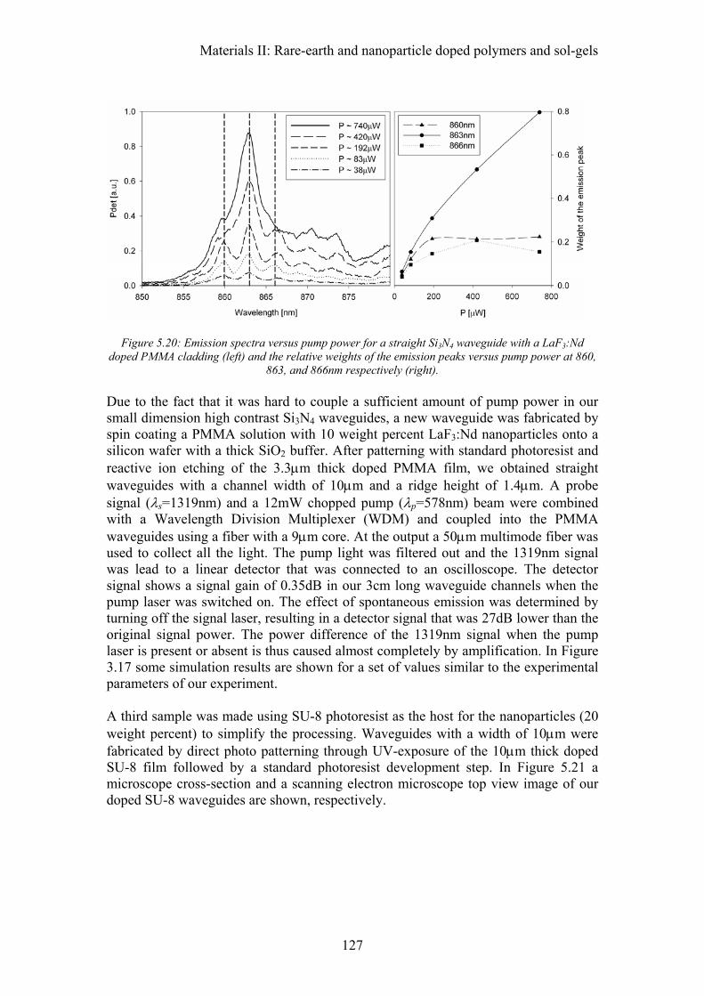
Materials II: Rare-earth and nanoparticle doped polymers and sol-gels
127
Figure 5.20: Emission spectra versus pump power for a straight Si3N4 waveguide with a LaF3:Nd doped PMMA cladding (left) and the relative weights of the emission peaks versus pump power at 860,
863, and 866nm respectively (right). Due to the fact that it was hard to couple a sufficient amount of pump power in our small dimension high contrast Si3N4 waveguides, a new waveguide was fabricated by spin coating a PMMA solution with 10 weight percent LaF3:Nd nanoparticles onto a silicon wafer with a thick SiO2 buffer. After patterning with standard photoresist and reactive ion etching of the 3.3µm thick doped PMMA film, we obtained straight waveguides with a channel width of 10µm and a ridge height of 1.4µm. A probe signal (λs=1319nm) and a 12mW chopped pump (λp=578nm) beam were combined with a Wavelength Division Multiplexer (WDM) and coupled into the PMMA waveguides using a fiber with a 9µm core. At the output a 50µm multimode fiber was used to collect all the light. The pump light was filtered out and the 1319nm signal was lead to a linear detector that was connected to an oscilloscope. The detector signal shows a signal gain of 0.35dB in our 3cm long waveguide channels when the pump laser was switched on. The effect of spontaneous emission was determined by turning off the signal laser, resulting in a detector signal that was 27dB lower than the original signal power. The power difference of the 1319nm signal when the pump laser is present or absent is thus caused almost completely by amplification. In Figure 3.17 some simulation results are shown for a set of values similar to the experimental parameters of our experiment. A third sample was made using SU-8 photoresist as the host for the nanoparticles (20 weight percent) to simplify the processing. Waveguides with a width of 10µm were fabricated by direct photo patterning through UV-exposure of the 10µm thick doped SU-8 film followed by a standard photoresist development step. In Figure 5.21 a microscope cross-section and a scanning electron microscope top view image of our doped SU-8 waveguides are shown, respectively.
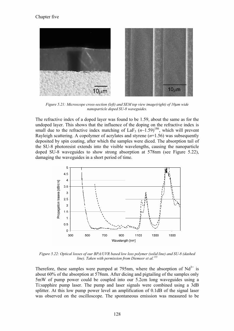
Chapter five
128
Figure 5.21: Microscope cross-section (left) and SEM top view image(right) of 10µm wide nanoparticle doped SU-8 waveguides.
The refractive index of a doped layer was found to be 1.59, about the same as for the undoped layer. This shows that the influence of the doping on the refractive index is small due to the refractive index matching of LaF3 (n~1.59)186, which will prevent Rayleigh scattering. A copolymer of acrylates and styrene (n=1.56) was subsequently deposited by spin coating, after which the samples were diced. The absorption tail of the SU-8 photoresist extends into the visible wavelengths, causing the nanoparticle doped SU-8 waveguides to show strong absorption at 578nm (see Figure 5.22), damaging the waveguides in a short period of time.
Figure 5.22: Optical losses of our BPA/UVR based low loss polymer (solid line) and SU-8 (dashed line). Taken with permission from Diemeer et al.155
Therefore, these samples were pumped at 795nm, where the absorption of Nd3+ is about 60% of the absorption at 578nm. After dicing and pigtailing of the samples only 5mW of pump power could be coupled into our 5.2cm long waveguides using a Ti:sapphire pump laser. The pump and laser signals were combined using a 3dB splitter. At this low pump power level an amplification of 0.1dB of the signal laser was observed on the oscilloscope. The spontaneous emission was measured to be
Materials II: Rare-earth and nanoparticle doped polymers and sol-gels
129
around 30dB lower than the signal power, not interfering with our amplification measurements. Numerically solving the rate equations of the Nd3+ four-level energy system189 (see also paragraph 3.2.3.b) is consistent with the measured amplification at the low pump powers used in our experiments. For an indication on the theoretical gain in this case, simulation results of a 10×10µm waveguide are shown in Figure 3.17. Note that the pump power is twice as high and the concentration twice as low in these simulations. However, it offers a good indication of the maximum achievable gain. In conclusion, these experiments indicate that stimulated emission and amplification is taking place in LaF3:Nd nanoparticle doped polymer materials. Although the observed amplification in these high loss multimode waveguides is still low, the performance should be improved by changing the technology, polymer host material and waveguide design. High index contrast, highly confined LaF3:Nd nanoparticle doped microring resonators in which the power buildup in the ring resonator will further enhance the input pump power would be beneficial in this case. The results of our work on monomode Nd:LaF3 doped polymer ring resonators are presented in the next paragraph.
5.4.1.b Singlemode polymer waveguides As can be seen in Figure 3.17 it is beneficial to have monomode waveguides with a small waveguide cross section in order to obtain higher field intensities, resulting in higher gain figures. For this purpose we have developed a low loss photodefinable polymer with good solubility towards rare-earth doped LaF3 nanoparticles. In Figure 5.23 the absorption spectra are shown of photodefinable BPA based polymer films with 0, 15 and 35 weight percent Nd:LaF3 nanoparticle doping, respectively. A weight concentration of 35 percent corresponds to an overall neodymium doping concentration of 5.2×1025m-3. The measurements have been performed using the dual prism setup discussed in paragraph 3.4.1.b in combination with a halogen light source. The characteristic neodymium absorption peaks around 520, 580, 740, 795 and 860nm can be clearly identified. Furthermore, it can be concluded that the UV absorption increases with nanoparticle concentration, which is caused by the yellowing ligands that are attached to the nanoparticles. The BPA host polymer itself shows low propagation losses in the visible wavelength range, as can be seen in Figure 5.3.
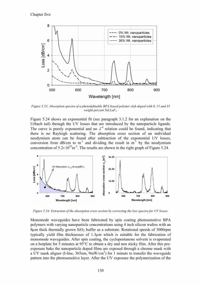
Chapter five
130
Figure 5.23: Absorption spectra of a photodefinable BPA based polymer slab doped with 0, 15 and 35
weight percent Nd:LaF3. Figure 5.24 shows an exponential fit (see paragraph 3.1.2 for an explanation on the Urbach tail) through the UV losses that are introduced by the nanoparticle ligands. The curve is purely exponential and no λ-4 relation could be found, indicating that there is no Rayleigh scattering. The absorption cross section of an individual neodymium atom can be found after subtraction of the exponential UV losses, conversion from dB/cm to m-1 and dividing the result in m-1 by the neodymium concentration of 5.2×1025m-3. The results are shown in the right graph of Figure 5.24.
Figure 5.24: Extraction of the absorption cross section by correcting the loss spectra for UV losses. Monomode waveguides have been fabricated by spin coating photosensitive BPA polymers with varying nanoparticle concentrations using 4 inch silicon wafers with an 8µm thick thermally grown SiO2 buffer as a substrate. Rotational speeds of 3000rpm typically yield film thicknesses of 1.3µm which is suitable for the fabrication of monomode waveguides. After spin coating, the cyclopentanone solvent is evaporated on a hotplate for 5 minutes at 95°C to obtain a dry and non sticky film. After this pre-exposure bake the nanoparticle doped films are exposed through a chrome mask with a UV mask aligner (I-line, 365nm, 9mW/cm2) for 1 minute to transfer the waveguide pattern into the photosensitive layer. After the UV exposure the polymerization of the
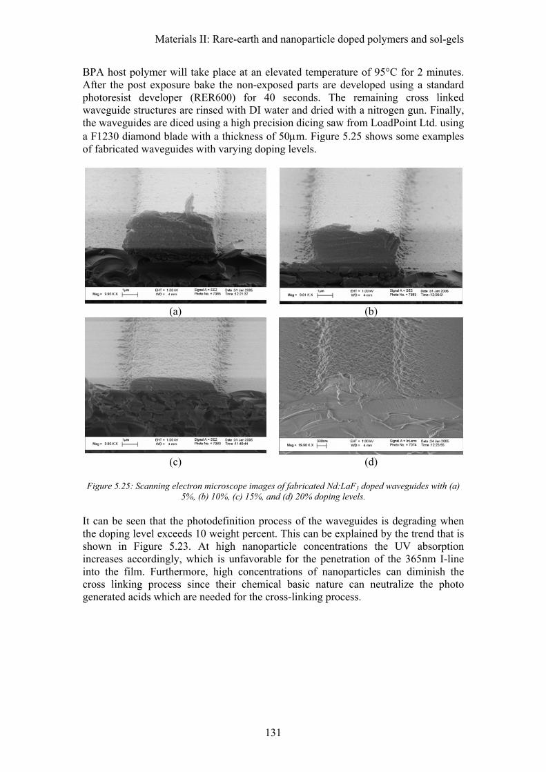
Materials II: Rare-earth and nanoparticle doped polymers and sol-gels
131
BPA host polymer will take place at an elevated temperature of 95°C for 2 minutes. After the post exposure bake the non-exposed parts are developed using a standard photoresist developer (RER600) for 40 seconds. The remaining cross linked waveguide structures are rinsed with DI water and dried with a nitrogen gun. Finally, the waveguides are diced using a high precision dicing saw from LoadPoint Ltd. using a F1230 diamond blade with a thickness of 50µm. Figure 5.25 shows some examples of fabricated waveguides with varying doping levels.
(a) (b)
(c) (d)
Figure 5.25: Scanning electron microscope images of fabricated Nd:LaF3 doped waveguides with (a)
5%, (b) 10%, (c) 15%, and (d) 20% doping levels. It can be seen that the photodefinition process of the waveguides is degrading when the doping level exceeds 10 weight percent. This can be explained by the trend that is shown in Figure 5.23. At high nanoparticle concentrations the UV absorption increases accordingly, which is unfavorable for the penetration of the 365nm I-line into the film. Furthermore, high concentrations of nanoparticles can diminish the cross linking process since their chemical basic nature can neutralize the photo generated acids which are needed for the cross-linking process.
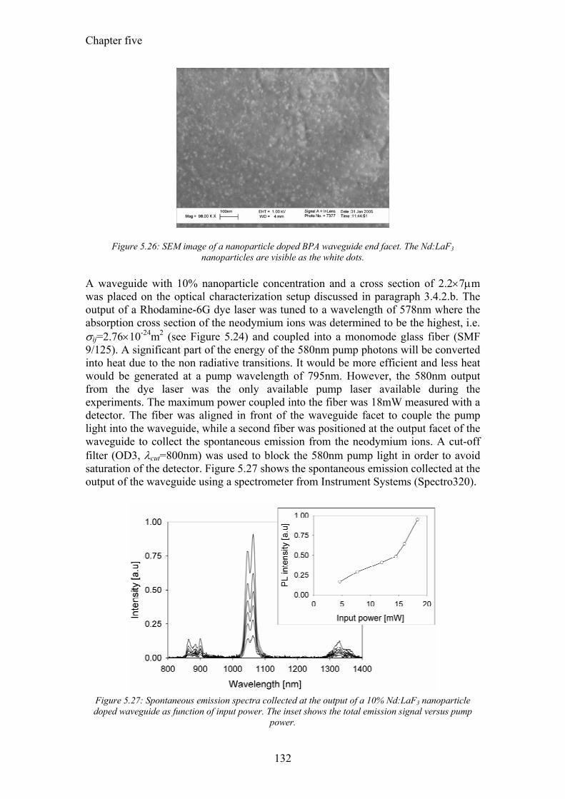
Chapter five
132
Figure 5.26: SEM image of a nanoparticle doped BPA waveguide end facet. The Nd:LaF3 nanoparticles are visible as the white dots.
A waveguide with 10% nanoparticle concentration and a cross section of 2.2×7µm was placed on the optical characterization setup discussed in paragraph 3.4.2.b. The output of a Rhodamine-6G dye laser was tuned to a wavelength of 578nm where the absorption cross section of the neodymium ions was determined to be the highest, i.e. σij=2.76×10⁻²⁴m2 (see Figure 5.24) and coupled into a monomode glass fiber (SMF 9/125). A significant part of the energy of the 580nm pump photons will be converted into heat due to the non radiative transitions. It would be more efficient and less heat would be generated at a pump wavelength of 795nm. However, the 580nm output from the dye laser was the only available pump laser available during the experiments. The maximum power coupled into the fiber was 18mW measured with a detector. The fiber was aligned in front of the waveguide facet to couple the pump light into the waveguide, while a second fiber was positioned at the output facet of the waveguide to collect the spontaneous emission from the neodymium ions. A cut-off filter (OD3, λcut=800nm) was used to block the 580nm pump light in order to avoid saturation of the detector. Figure 5.27 shows the spontaneous emission collected at the output of the waveguide using a spectrometer from Instrument Systems (Spectro320).
Figure 5.27: Spontaneous emission spectra collected at the output of a 10% Nd:LaF3 nanoparticle doped waveguide as function of input power. The inset shows the total emission signal versus pump
power.
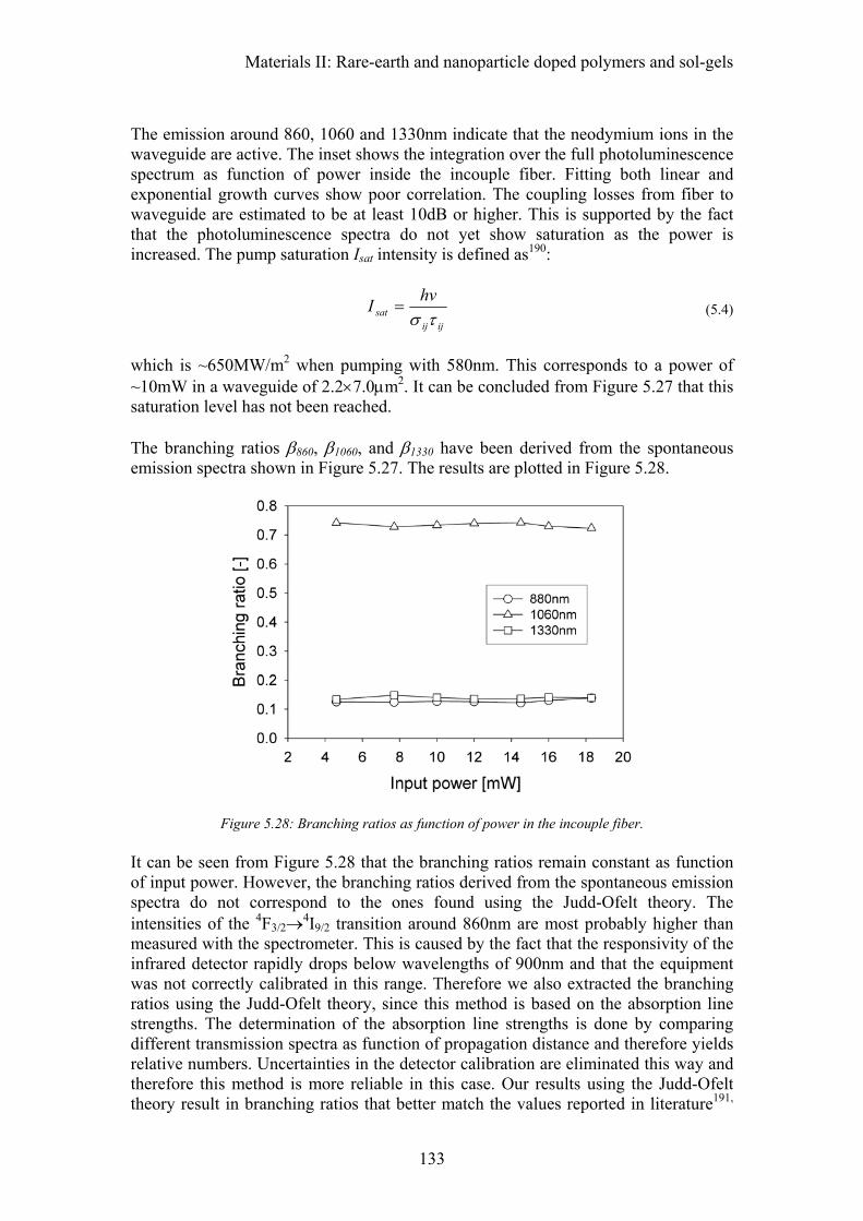
Materials II: Rare-earth and nanoparticle doped polymers and sol-gels
133
The emission around 860, 1060 and 1330nm indicate that the neodymium ions in the waveguide are active. The inset shows the integration over the full photoluminescence spectrum as function of power inside the incouple fiber. Fitting both linear and exponential growth curves show poor correlation. The coupling losses from fiber to waveguide are estimated to be at least 10dB or higher. This is supported by the fact that the photoluminescence spectra do not yet show saturation as the power is increased. The pump saturation Isat intensity is defined as190:
ijijsat
hvIτσ
= (5.4)
which is ~650MW/m2 when pumping with 580nm. This corresponds to a power of ~10mW in a waveguide of 2.2×7.0µm2. It can be concluded from Figure 5.27 that this saturation level has not been reached. The branching ratios β860, β1060, and β1330 have been derived from the spontaneous emission spectra shown in Figure 5.27. The results are plotted in Figure 5.28.
Figure 5.28: Branching ratios as function of power in the incouple fiber. It can be seen from Figure 5.28 that the branching ratios remain constant as function of input power. However, the branching ratios derived from the spontaneous emission spectra do not correspond to the ones found using the Judd-Ofelt theory. The intensities of the 4F3/2→4I9/2 transition around 860nm are most probably higher than measured with the spectrometer. This is caused by the fact that the responsivity of the infrared detector rapidly drops below wavelengths of 900nm and that the equipment was not correctly calibrated in this range. Therefore we also extracted the branching ratios using the Judd-Ofelt theory, since this method is based on the absorption line strengths. The determination of the absorption line strengths is done by comparing different transmission spectra as function of propagation distance and therefore yields relative numbers. Uncertainties in the detector calibration are eliminated this way and therefore this method is more reliable in this case. Our results using the Judd-Ofelt theory result in branching ratios that better match the values reported in literature191,
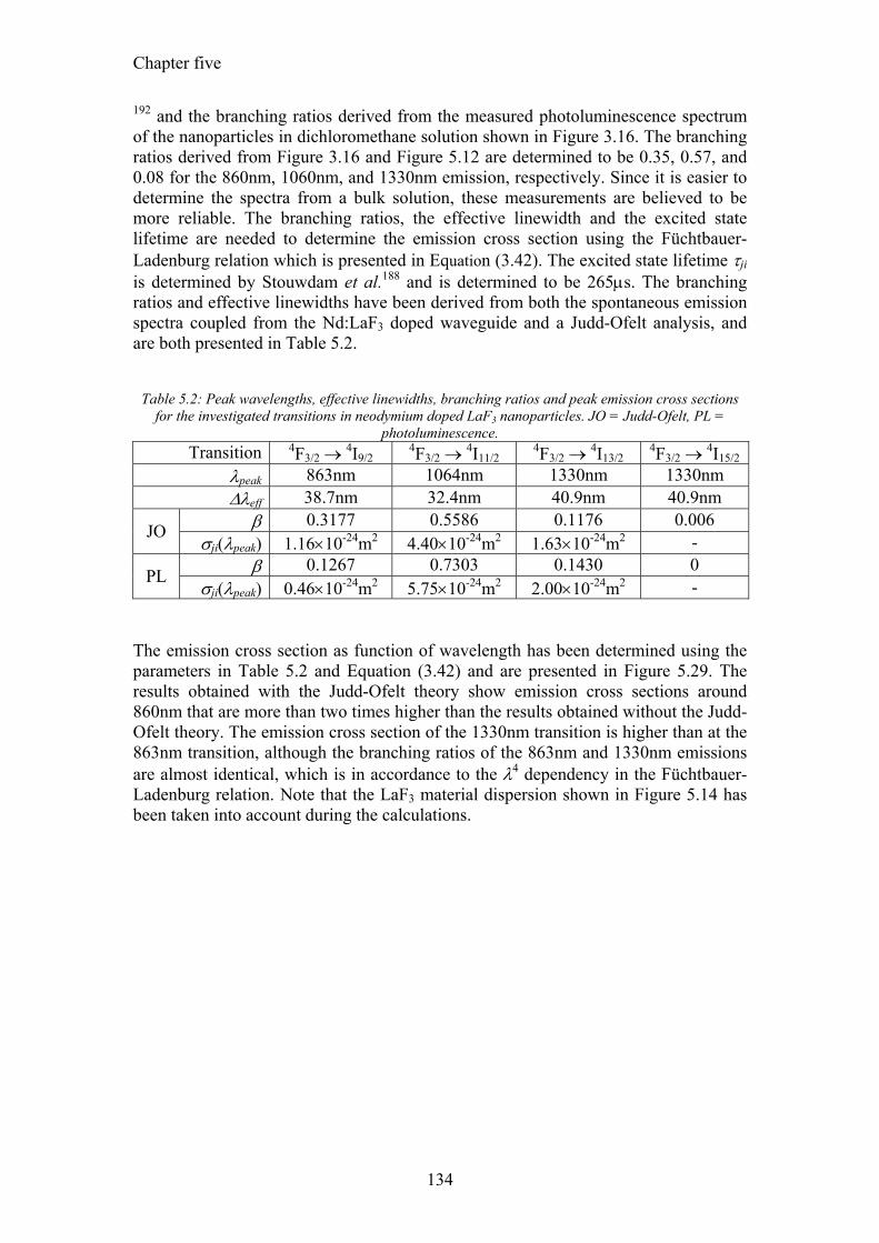
Chapter five
134
192 and the branching ratios derived from the measured photoluminescence spectrum of the nanoparticles in dichloromethane solution shown in Figure 3.16. The branching ratios derived from Figure 3.16 and Figure 5.12 are determined to be 0.35, 0.57, and 0.08 for the 860nm, 1060nm, and 1330nm emission, respectively. Since it is easier to determine the spectra from a bulk solution, these measurements are believed to be more reliable. The branching ratios, the effective linewidth and the excited state lifetime are needed to determine the emission cross section using the Füchtbauer-Ladenburg relation which is presented in Equation (3.42). The excited state lifetime τji is determined by Stouwdam et al.188 and is determined to be 265µs. The branching ratios and effective linewidths have been derived from both the spontaneous emission spectra coupled from the Nd:LaF3 doped waveguide and a Judd-Ofelt analysis, and are both presented in Table 5.2.
Table 5.2: Peak wavelengths, effective linewidths, branching ratios and peak emission cross sections for the investigated transitions in neodymium doped LaF3 nanoparticles. JO = Judd-Ofelt, PL =
photoluminescence. Transition 4F3/2 → 4I9/2 4F3/2 → 4I11/2 4F3/2 → 4I13/2 4F3/2 → 4I15/2
λpeak 863nm 1064nm 1330nm 1330nm ∆λeff 38.7nm 32.4nm 40.9nm 40.9nm
β 0.3177 0.5586 0.1176 0.006 JO σji(λpeak) 1.16×10⁻²⁴m2 4.40×10⁻²⁴m2 1.63×10⁻²⁴m2 -
β 0.1267 0.7303 0.1430 0 PL σji(λpeak) 0.46×10⁻²⁴m2 5.75×10⁻²⁴m2 2.00×10⁻²⁴m2 -
The emission cross section as function of wavelength has been determined using the parameters in Table 5.2 and Equation (3.42) and are presented in Figure 5.29. The results obtained with the Judd-Ofelt theory show emission cross sections around 860nm that are more than two times higher than the results obtained without the Judd-Ofelt theory. The emission cross section of the 1330nm transition is higher than at the 863nm transition, although the branching ratios of the 863nm and 1330nm emissions are almost identical, which is in accordance to the λ4 dependency in the Füchtbauer-Ladenburg relation. Note that the LaF3 material dispersion shown in Figure 5.14 has been taken into account during the calculations.
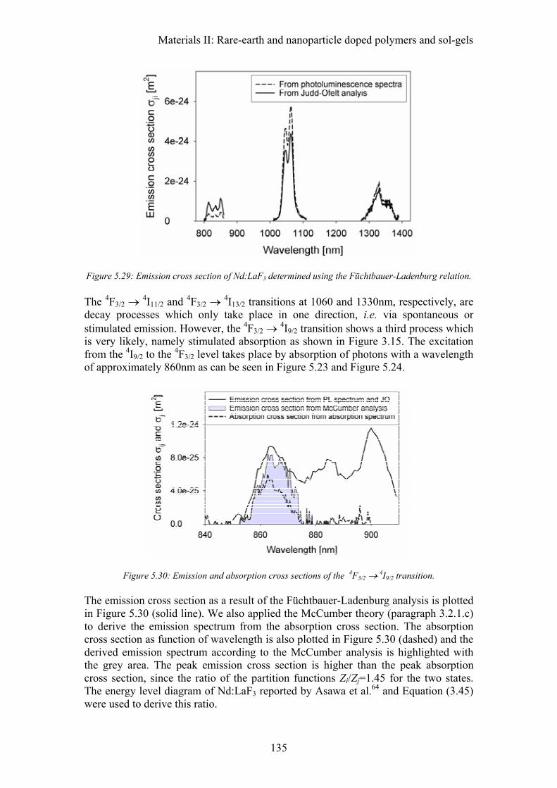
Materials II: Rare-earth and nanoparticle doped polymers and sol-gels
135
Figure 5.29: Emission cross section of Nd:LaF3 determined using the Füchtbauer-Ladenburg relation. The 4F3/2 → 4I11/2 and 4F3/2 → 4I13/2 transitions at 1060 and 1330nm, respectively, are decay processes which only take place in one direction, i.e. via spontaneous or stimulated emission. However, the 4F3/2 → 4I9/2 transition shows a third process which is very likely, namely stimulated absorption as shown in Figure 3.15. The excitation from the 4I9/2 to the 4F3/2 level takes place by absorption of photons with a wavelength of approximately 860nm as can be seen in Figure 5.23 and Figure 5.24.
Figure 5.30: Emission and absorption cross sections of the 4F3/2 → 4I9/2 transition. The emission cross section as a result of the Füchtbauer-Ladenburg analysis is plotted in Figure 5.30 (solid line). We also applied the McCumber theory (paragraph 3.2.1.c) to derive the emission spectrum from the absorption cross section. The absorption cross section as function of wavelength is also plotted in Figure 5.30 (dashed) and the derived emission spectrum according to the McCumber analysis is highlighted with the grey area. The peak emission cross section is higher than the peak absorption cross section, since the ratio of the partition functions Zi/Zj=1.45 for the two states. The energy level diagram of Nd:LaF3 reported by Asawa et al.64 and Equation (3.45) were used to derive this ratio.
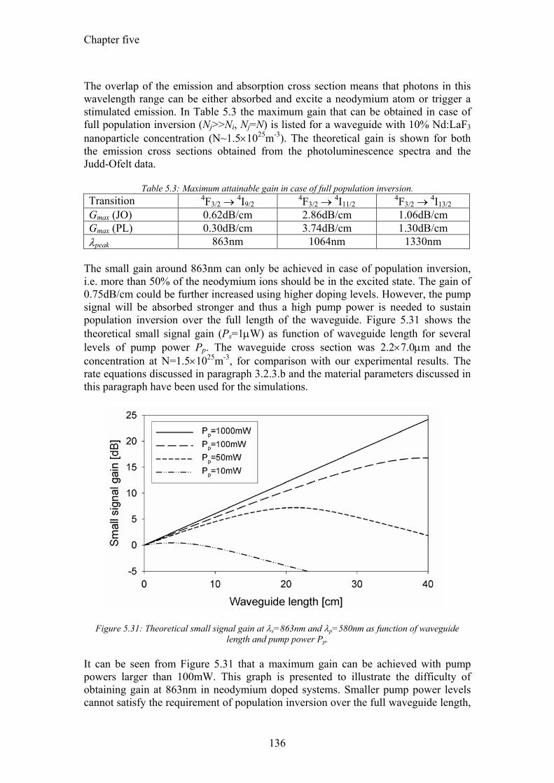
Chapter five
136
The overlap of the emission and absorption cross section means that photons in this wavelength range can be either absorbed and excite a neodymium atom or trigger a stimulated emission. In Table 5.3 the maximum gain that can be obtained in case of full population inversion (Nj>>Ni, Nj=N) is listed for a waveguide with 10% Nd:LaF3 nanoparticle concentration (N~1.5×1025m-3). The theoretical gain is shown for both the emission cross sections obtained from the photoluminescence spectra and the Judd-Ofelt data.
Table 5.3: Maximum attainable gain in case of full population inversion. Transition 4F3/2 → 4I9/2 4F3/2 → 4I11/2 4F3/2 → 4I13/2 Gmax (JO) 0.62dB/cm 2.86dB/cm 1.06dB/cm Gmax (PL) 0.30dB/cm 3.74dB/cm 1.30dB/cm λpeak 863nm 1064nm 1330nm
The small gain around 863nm can only be achieved in case of population inversion, i.e. more than 50% of the neodymium ions should be in the excited state. The gain of 0.75dB/cm could be further increased using higher doping levels. However, the pump signal will be absorbed stronger and thus a high pump power is needed to sustain population inversion over the full length of the waveguide. Figure 5.31 shows the theoretical small signal gain (Ps=1µW) as function of waveguide length for several levels of pump power Pp. The waveguide cross section was 2.2×7.0µm and the concentration at N=1.5×1025m-3, for comparison with our experimental results. The rate equations discussed in paragraph 3.2.3.b and the material parameters discussed in this paragraph have been used for the simulations.
Figure 5.31: Theoretical small signal gain at λs=863nm and λp=580nm as function of waveguide length and pump power Pp.
It can be seen from Figure 5.31 that a maximum gain can be achieved with pump powers larger than 100mW. This graph is presented to illustrate the difficulty of obtaining gain at 863nm in neodymium doped systems. Smaller pump power levels cannot satisfy the requirement of population inversion over the full waveguide length,
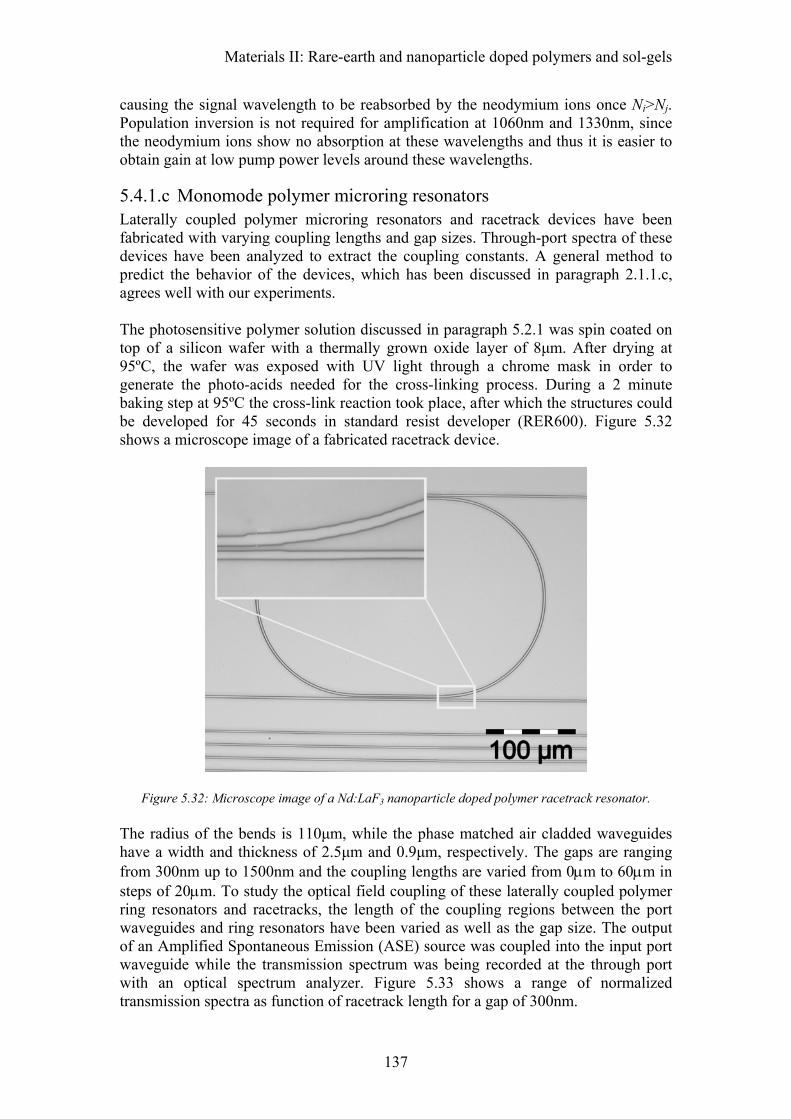
Materials II: Rare-earth and nanoparticle doped polymers and sol-gels
137
causing the signal wavelength to be reabsorbed by the neodymium ions once Ni>Nj. Population inversion is not required for amplification at 1060nm and 1330nm, since the neodymium ions show no absorption at these wavelengths and thus it is easier to obtain gain at low pump power levels around these wavelengths.
5.4.1.c Monomode polymer microring resonators Laterally coupled polymer microring resonators and racetrack devices have been fabricated with varying coupling lengths and gap sizes. Through-port spectra of these devices have been analyzed to extract the coupling constants. A general method to predict the behavior of the devices, which has been discussed in paragraph 2.1.1.c, agrees well with our experiments. The photosensitive polymer solution discussed in paragraph 5.2.1 was spin coated on top of a silicon wafer with a thermally grown oxide layer of 8µm. After drying at 95ºC, the wafer was exposed with UV light through a chrome mask in order to generate the photo-acids needed for the cross-linking process. During a 2 minute baking step at 95ºC the cross-link reaction took place, after which the structures could be developed for 45 seconds in standard resist developer (RER600). Figure 5.32 shows a microscope image of a fabricated racetrack device.
Figure 5.32: Microscope image of a Nd:LaF3 nanoparticle doped polymer racetrack resonator. The radius of the bends is 110µm, while the phase matched air cladded waveguides have a width and thickness of 2.5µm and 0.9µm, respectively. The gaps are ranging from 300nm up to 1500nm and the coupling lengths are varied from 0µm to 60µm in steps of 20µm. To study the optical field coupling of these laterally coupled polymer ring resonators and racetracks, the length of the coupling regions between the port waveguides and ring resonators have been varied as well as the gap size. The output of an Amplified Spontaneous Emission (ASE) source was coupled into the input port waveguide while the transmission spectrum was being recorded at the through port with an optical spectrum analyzer. Figure 5.33 shows a range of normalized transmission spectra as function of racetrack length for a gap of 300nm.
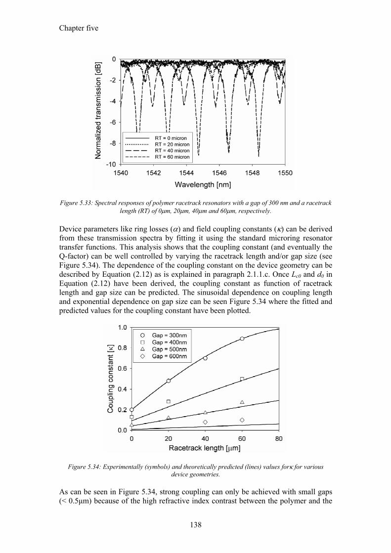
Chapter five
138
Figure 5.33: Spectral responses of polymer racetrack resonators with a gap of 300 nm and a racetrack
length (RT) of 0µm, 20µm, 40µm and 60µm, respectively. Device parameters like ring losses (α) and field coupling constants (κ) can be derived from these transmission spectra by fitting it using the standard microring resonator transfer functions. This analysis shows that the coupling constant (and eventually the Q-factor) can be well controlled by varying the racetrack length and/or gap size (see Figure 5.34). The dependence of the coupling constant on the device geometry can be described by Equation (2.12) as is explained in paragraph 2.1.1.c. Once Lc0 and d0 in Equation (2.12) have been derived, the coupling constant as function of racetrack length and gap size can be predicted. The sinusoidal dependence on coupling length and exponential dependence on gap size can be seen Figure 5.34 where the fitted and predicted values for the coupling constant have been plotted.
Figure 5.34: Experimentally (symbols) and theoretically predicted (lines) values forκ for various device geometries.
As can be seen in Figure 5.34, strong coupling can only be achieved with small gaps (< 0.5µm) because of the high refractive index contrast between the polymer and the
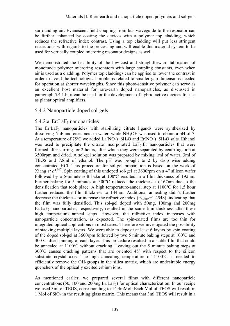
Materials II: Rare-earth and nanoparticle doped polymers and sol-gels
139
surrounding air. Evanescent field coupling from bus waveguide to the resonator can be further enhanced by coating the devices with a polymer top cladding, which reduces the refractive index contrast. Using a top cladding will put less stringent restrictions with regards to the processing and will enable this material system to be used for vertically coupled microring resonator designs as well. We demonstrated the feasibility of the low-cost and straightforward fabrication of monomode polymer microring resonators with large coupling constants, even when air is used as a cladding. Polymer top claddings can be applied to lower the contrast in order to avoid the technological problems related to smaller gap dimensions needed for operation at shorter wavelengths. Since this photo-sensitive polymer can serve as an excellent host material for rare-earth doped nanoparticles, as discussed in paragraph 5.4.1.b, it can be used for the development of hybrid active devices for use as planar optical amplifiers.
5.4.2 Nanoparticle doped sol-gels
5.4.2.a Er:LaF3 nanoparticles The Er:LaF3 nanoparticles with stabilizing citrate ligands were synthesized by dissolving NaF and citric acid in water, while NH4OH was used to obtain a pH of 7. At a temperature of 75ºC we added La(NO3)3.6H2O and Er(NO3)3.5H2O salts. Ethanol was used to precipitate the citrate incorporated LaF3:Er nanoparticles that were formed after stirring for 2 hours, after which they were separated by centrifugation at 3500rpm and dried. A sol-gel solution was prepared by mixing 1ml of water, 3ml of TEOS and 7.8ml of ethanol. The pH was brought to 2 by drop wise adding concentrated HCl. This procedure for sol-gel preparation is based on the work of Xiang et al.167. Spin coating of this undoped sol-gel at 3600rpm on a 4” silicon wafer followed by a 5-minute soft bake at 100ºC resulted in a film thickness of 192nm. Further baking for 5 minutes at 300ºC reduced the thickness to 167nm due to the densification that took place. A high temperature-anneal step at 1100ºC for 1.5 hour further reduced the film thickness to 144nm. Additional annealing didn’t further decrease the thickness or increase the refractive index (n633nm=1.4548), indicating that the film was fully densified. This sol-gel doped with 50mg, 100mg and 200mg Er:LaF3 nanoparticles, respectively, resulted in the same film thickness after these high temperature anneal steps. However, the refractive index increases with nanoparticle concentration, as expected. The spin-coated films are too thin for integrated optical applications in most cases. Therefore we investigated the possibility of stacking multiple layers. We were able to deposit at least 6 layers by spin coating of the doped sol-gel at 3600rpm followed by two 5 minute baking steps at 100ºC and 300ºC after spinning of each layer. This procedure resulted in a stable film that could be annealed at 1100ºC without cracking. Leaving out the 5 minute baking steps at 300ºC causes cracking patterns that are oriented 45º with respect to the silicon substrate crystal axis. The high annealing temperature of 1100ºC is needed to efficiently remove the OH-groups in the silica matrix, which are undesirable energy quenchers of the optically excited erbium ions. As mentioned earlier, we prepared several films with different nanoparticle concentrations (50, 100 and 200mg Er:LaF3) for optical characterization. In our recipe we used 3ml of TEOS, corresponding to 14.4mMol. Each Mol of TEOS will result in 1 Mol of SiO2 in the resulting glass matrix. This means that 3ml TEOS will result in a
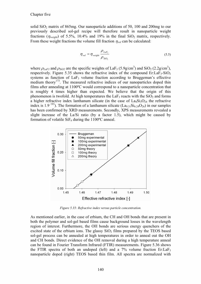
Chapter five
140
solid SiO2 matrix of 865mg. Our nanoparticle additions of 50, 100 and 200mg to our previously described sol-gel recipe will therefore result in nanoparticle weight fractions (ηweight) of 5.5%, 10.4% and 19% in the final SiO2 matrix, respectively. From these weight fractions the volume fill fraction ηvol can be calculated:
2
3
SiO
LaFweightvol ρ
ρηη = (5.5)
where ρLaF3 and ρSiO2 are the specific weights of LaF3 (5.9g/cm3) and SiO2 (2.2g/cm3), respectively. Figure 5.35 shows the refractive index of the compound Er:LaF3-SiO2 systems as function of LaF3 volume fraction according to Bruggeman’s effective medium theory173. The measured refractive indices of our nanoparticles doped thin films after annealing at 1100ºC would correspond to a nanoparticle concentration that is roughly 4 times higher than expected. We believe that the origin of this phenomenon is twofold. At high temperatures the LaF3 reacts with the SiO2 and forms a higher refractive index lanthanum silicate (in the case of La4Si3O24 the refractive index is 1.9 193). The formation of a lanthanum silicate (La9.31Si6.24O26) in our samples has been confirmed by XRD measurements. Secondly, XPS measurements revealed a slight increase of the La/Si ratio (by a factor 1.5), which might be caused by formation of volatile SiF6 during the 1100ºC anneal.
Figure 5.35: Refractive index versus particle concentration. As mentioned earlier, in the case of erbium, the CH and OH bonds that are present in both the polymer and sol-gel based films cause background losses in the wavelength region of interest. Furthermore, the OH bonds are serious energy quenchers of the excited state of the erbium ions. The glassy SiO2 films prepared by the TEOS based sol-gel process can be annealed at high temperatures in order to anneal out the OH and CH bonds. Direct evidence of the OH removal during a high temperature anneal can be found in Fourier Transform Infrared (FTIR) measurements. Figure 5.36 shows the FTIR spectra of both an undoped (left) and a 7% volume fraction Er:LaF3 nanoparticle doped (right) TEOS based thin film. All spectra are normalized with
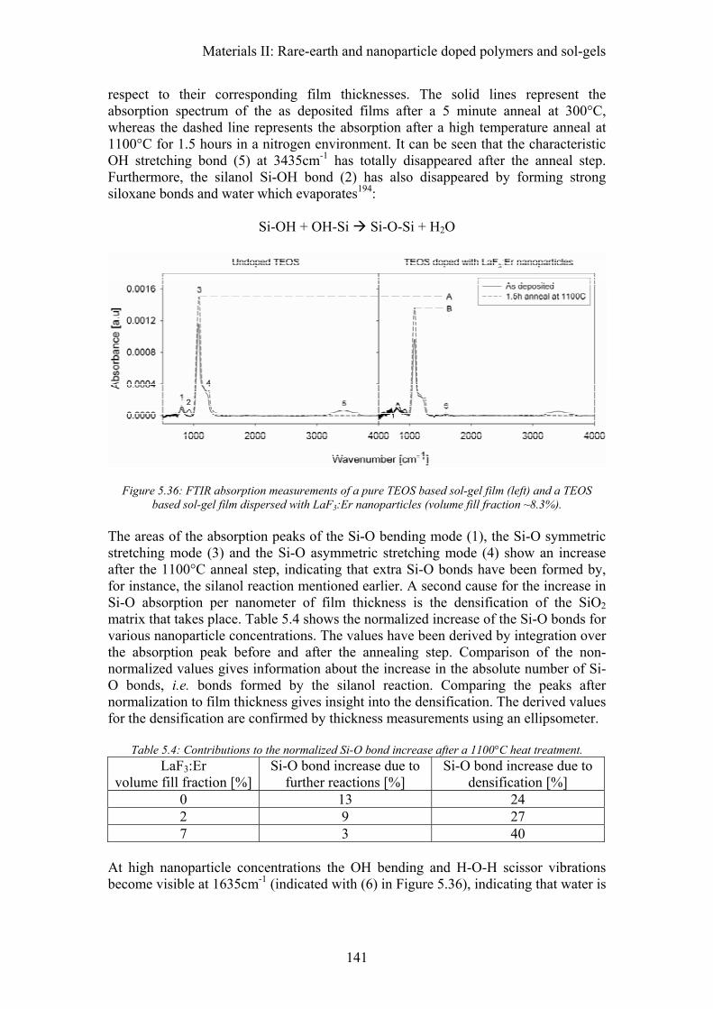
Materials II: Rare-earth and nanoparticle doped polymers and sol-gels
141
respect to their corresponding film thicknesses. The solid lines represent the absorption spectrum of the as deposited films after a 5 minute anneal at 300°C, whereas the dashed line represents the absorption after a high temperature anneal at 1100°C for 1.5 hours in a nitrogen environment. It can be seen that the characteristic OH stretching bond (5) at 3435cm-1 has totally disappeared after the anneal step. Furthermore, the silanol Si-OH bond (2) has also disappeared by forming strong siloxane bonds and water which evaporates194:
Si-OH + OH-Si Si-O-Si + H2O
Figure 5.36: FTIR absorption measurements of a pure TEOS based sol-gel film (left) and a TEOS
based sol-gel film dispersed with LaF3:Er nanoparticles (volume fill fraction ~8.3%). The areas of the absorption peaks of the Si-O bending mode (1), the Si-O symmetric stretching mode (3) and the Si-O asymmetric stretching mode (4) show an increase after the 1100°C anneal step, indicating that extra Si-O bonds have been formed by, for instance, the silanol reaction mentioned earlier. A second cause for the increase in Si-O absorption per nanometer of film thickness is the densification of the SiO2 matrix that takes place. Table 5.4 shows the normalized increase of the Si-O bonds for various nanoparticle concentrations. The values have been derived by integration over the absorption peak before and after the annealing step. Comparison of the non-normalized values gives information about the increase in the absolute number of Si-O bonds, i.e. bonds formed by the silanol reaction. Comparing the peaks after normalization to film thickness gives insight into the densification. The derived values for the densification are confirmed by thickness measurements using an ellipsometer.
Table 5.4: Contributions to the normalized Si-O bond increase after a 1100°C heat treatment. LaF3:Er
volume fill fraction [%] Si-O bond increase due to
further reactions [%] Si-O bond increase due to
densification [%] 0 13 24 2 9 27 7 3 40
At high nanoparticle concentrations the OH bending and H-O-H scissor vibrations become visible at 1635cm-1 (indicated with (6) in Figure 5.36), indicating that water is
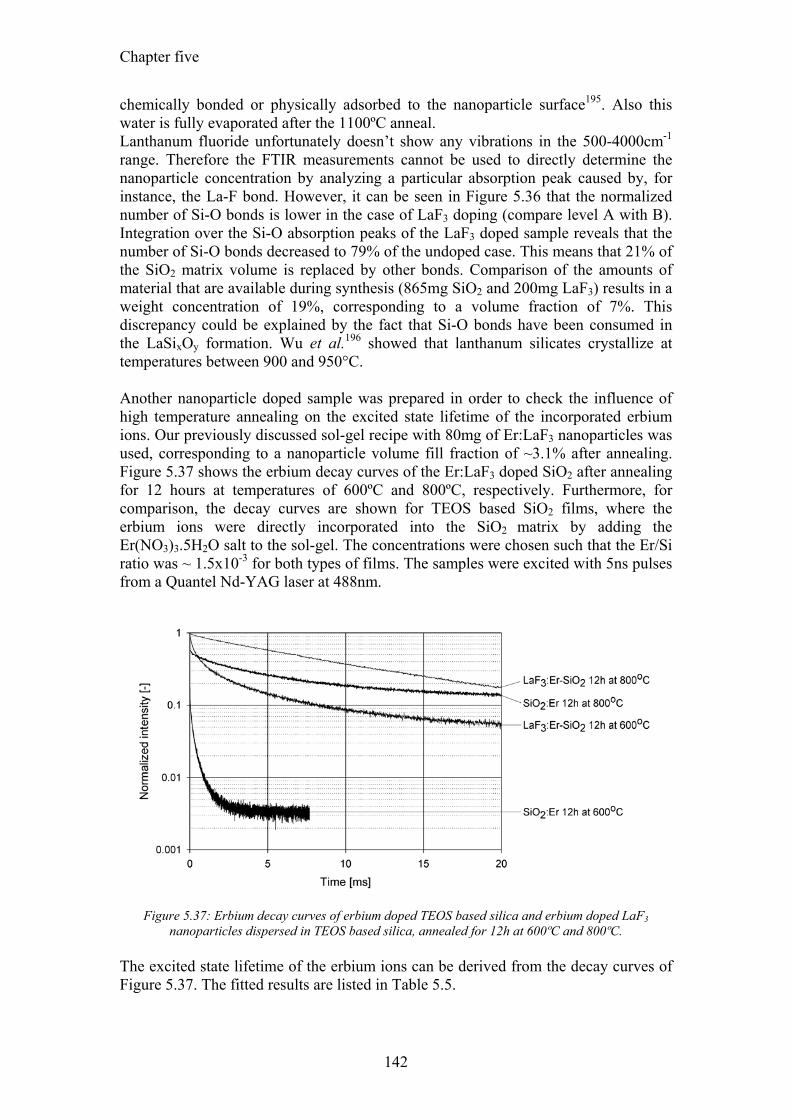
Chapter five
142
chemically bonded or physically adsorbed to the nanoparticle surface195. Also this water is fully evaporated after the 1100ºC anneal. Lanthanum fluoride unfortunately doesn’t show any vibrations in the 500-4000cm-1
range. Therefore the FTIR measurements cannot be used to directly determine the nanoparticle concentration by analyzing a particular absorption peak caused by, for instance, the La-F bond. However, it can be seen in Figure 5.36 that the normalized number of Si-O bonds is lower in the case of LaF3 doping (compare level A with B). Integration over the Si-O absorption peaks of the LaF3 doped sample reveals that the number of Si-O bonds decreased to 79% of the undoped case. This means that 21% of the SiO2 matrix volume is replaced by other bonds. Comparison of the amounts of material that are available during synthesis (865mg SiO2 and 200mg LaF3) results in a weight concentration of 19%, corresponding to a volume fraction of 7%. This discrepancy could be explained by the fact that Si-O bonds have been consumed in the LaSixOy formation. Wu et al.196 showed that lanthanum silicates crystallize at temperatures between 900 and 950°C. Another nanoparticle doped sample was prepared in order to check the influence of high temperature annealing on the excited state lifetime of the incorporated erbium ions. Our previously discussed sol-gel recipe with 80mg of Er:LaF3 nanoparticles was used, corresponding to a nanoparticle volume fill fraction of ~3.1% after annealing. Figure 5.37 shows the erbium decay curves of the Er:LaF3 doped SiO2 after annealing for 12 hours at temperatures of 600ºC and 800ºC, respectively. Furthermore, for comparison, the decay curves are shown for TEOS based SiO2 films, where the erbium ions were directly incorporated into the SiO2 matrix by adding the Er(NO3)3.5H2O salt to the sol-gel. The concentrations were chosen such that the Er/Si ratio was ~ 1.5x10⁻³ for both types of films. The samples were excited with 5ns pulses from a Quantel Nd-YAG laser at 488nm.
Figure 5.37: Erbium decay curves of erbium doped TEOS based silica and erbium doped LaF3 nanoparticles dispersed in TEOS based silica, annealed for 12h at 600ºC and 800ºC.
The excited state lifetime of the erbium ions can be derived from the decay curves of Figure 5.37. The fitted results are listed in Table 5.5.
Materials II: Rare-earth and nanoparticle doped polymers and sol-gels
143
Table 5.5: Lifetime values with the relative percentages of the decay components in brackets. LaF3:Er-SiO2 films SiO2:Er films
Temp τ1 ms (%) τ2 ms (%) τ1 ms (%) τ2 ms (%)
600 °C 7.4 (69%) 0.9 (31%) 0.98 (35%) 0.27 (65%)
800 °C 10.9 (95%) 3.9 (5%) 6.0 (70%) 1.2 (30%) For the bare Er3+-ion incorporated silica films there is a fast decay component present that is characteristic for Er3+ clustering. For both annealing temperatures it can be seen that the lifetimes are higher for the samples where the erbium is surrounded by the LaF3 matrix. This is because the LaF3 matrix is shielding the erbium from the OH-quenching environment of the SiO2 host, which makes it very attractive for amplification in the third telecommunication window. Furthermore, it is clear that the lifetimes for both samples increase at higher annealing temperatures, indicating a reduction in OH concentration and/or a better crystallinity of the surrounding matrix. The long excited state lifetime of the erbium in the LaF3 that we measured does compete well against the lifetimes of other promising erbium doped sol gel materials reported in literature (compare with for instance Table 5.1). Among the highest values which have been reported for erbium in silicate glass hosts are 14.5ms in Silicate L-22 glass61 and 13.5ms in Soda-lime silicate glass197. We showed that a new low-cost compound material system consisting of LaF3:Er nanoparticle doped silica is straight forward to synthesize and has good optical properties. Due to the small particle size the Rayleigh scattering is low, which allows for optical excitation at short wavelengths. Multiple layers could be easily stacked without cracking and the excited state lifetime of the erbium is considerably larger compared to other erbium doped sol-gel based materials, even at anneal temperatures of 800ºC. An unexpected increase of the refractive index at high anneal temperatures of 1100ºC suggest that a reaction between the nanoparticles and the host material takes place that prevents the determination of the nanoparticle concentration from refractive index measurements. However, an indication of the nanoparticle concentration could be obtained from FTIR measurements, which also give much information on the densification process that takes place during annealing.
5.4.2.b Gold nanoparticles dispersed in water and sol gels. The gold nanoparticles used in our experiments were synthesized according to the work of McFarland et al.198. First, a 0.5mmole chloroauric acid solution was prepared by dissolving 0.1 gram of HAuCl4 in 500ml of distilled water. Second, a 38.8mmole sodium citrate solution was made by adding 0.5 grams of Na3C6H5O7 in 50ml of distilled water. To grow the gold nanoparticles, 20ml of the chloroauric acid solution is heated in a beaker on a hotplate using a magnetic stirrer until the boiling point is reached. Subsequently, 2 ml of the citric acid solution is added to the boiling solution.
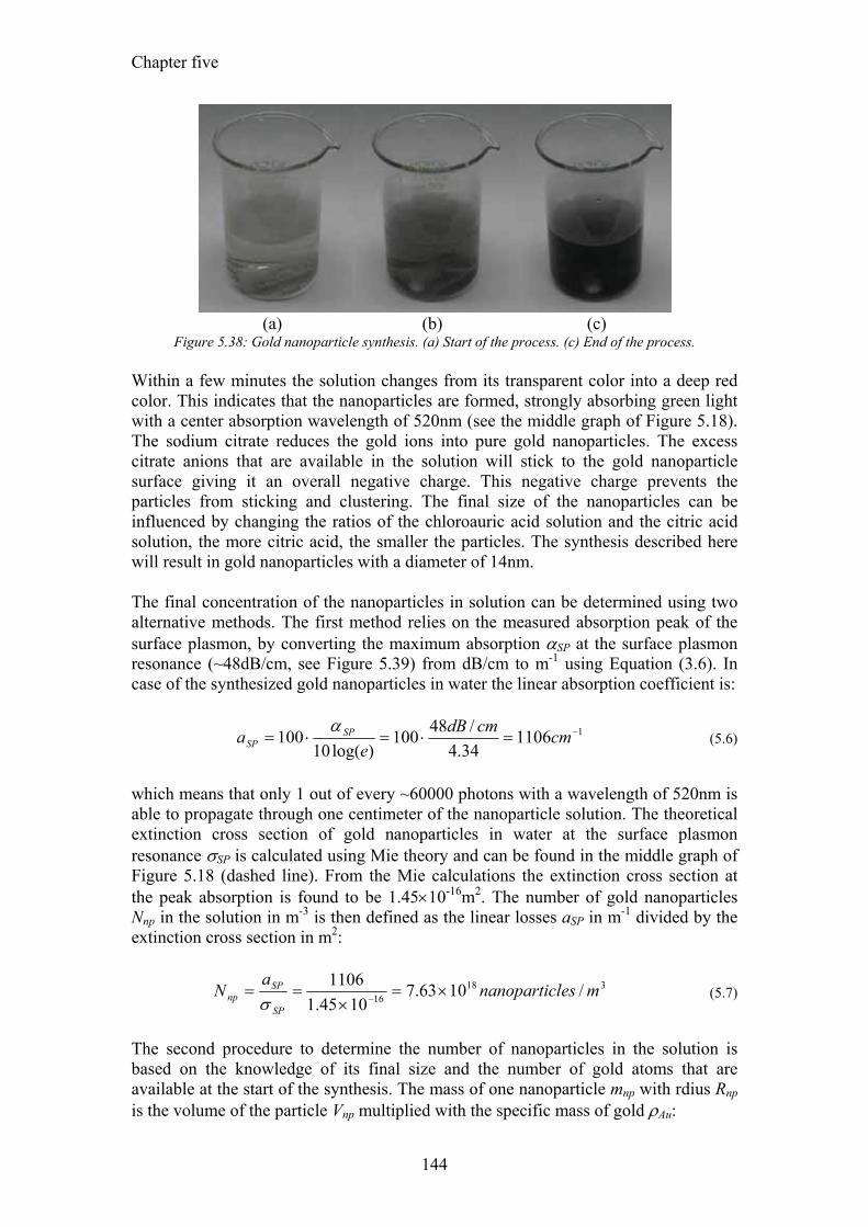
Chapter five
144
(a) (b) (c)
Figure 5.38: Gold nanoparticle synthesis. (a) Start of the process. (c) End of the process. Within a few minutes the solution changes from its transparent color into a deep red color. This indicates that the nanoparticles are formed, strongly absorbing green light with a center absorption wavelength of 520nm (see the middle graph of Figure 5.18). The sodium citrate reduces the gold ions into pure gold nanoparticles. The excess citrate anions that are available in the solution will stick to the gold nanoparticle surface giving it an overall negative charge. This negative charge prevents the particles from sticking and clustering. The final size of the nanoparticles can be influenced by changing the ratios of the chloroauric acid solution and the citric acid solution, the more citric acid, the smaller the particles. The synthesis described here will result in gold nanoparticles with a diameter of 14nm. The final concentration of the nanoparticles in solution can be determined using two alternative methods. The first method relies on the measured absorption peak of the surface plasmon, by converting the maximum absorption αSP at the surface plasmon resonance (~48dB/cm, see Figure 5.39) from dB/cm to m-1 using Equation (3.6). In case of the synthesized gold nanoparticles in water the linear absorption coefficient is:
1110634.4/48100
)log(10100 −=⋅=⋅= cmcmdB
ea SP
SPα
(5.6)
which means that only 1 out of every ~60000 photons with a wavelength of 520nm is able to propagate through one centimeter of the nanoparticle solution. The theoretical extinction cross section of gold nanoparticles in water at the surface plasmon resonance σSP is calculated using Mie theory and can be found in the middle graph of Figure 5.18 (dashed line). From the Mie calculations the extinction cross section at the peak absorption is found to be 1.45×10⁻¹⁶m2. The number of gold nanoparticles Nnp in the solution in m-3 is then defined as the linear losses aSP in m-1 divided by the extinction cross section in m2:
31816 /1063.7
1045.11106 mlesnanopartic
aN
SP
SPnp ×=
×== −σ
(5.7)
The second procedure to determine the number of nanoparticles in the solution is based on the knowledge of its final size and the number of gold atoms that are available at the start of the synthesis. The mass of one nanoparticle mnp with rdius Rnp is the volume of the particle Vnp multiplied with the specific mass of gold ρAu:
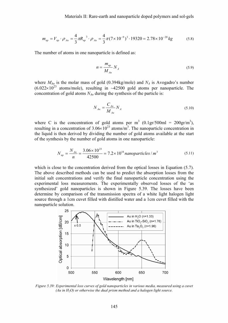
Materials II: Rare-earth and nanoparticle doped polymers and sol-gels
145
kgRVm AunpAunpnp20393 1078.219320)107(
34
34 −− ×=⋅×=⋅=⋅= πρπρ (5.8)
The number of atoms in one nanoparticle is defined as:
AAu
np NMm
n = (5.9)
where MAu is the molar mass of gold (0.394kg/mole) and NA is Avogadro’s number (6.022×10²³ atoms/mole), resulting in ~42500 gold atoms per nanoparticle. The concentration of gold atoms NAu during the synthesis of the particle is:
AAu
AuAu N
MC
N = (5.10)
where C is the concentration of gold atoms per m3 (0.1gr/500ml = 200gr/m3), resulting in a concentration of 3.06×10²³ atoms/m3. The nanoparticle concentration in the liquid is then derived by dividing the number of gold atoms available at the start of the synthesis by the number of gold atoms in one nanoparticle:
31823
/102.742500
1006.3 mlesnanoparticn
NN Au
np ×=×
== (5.11)
which is close to the concentration derived from the optical losses in Equation (5.7). The above described methods can be used to predict the absorption losses from the initial salt concentrations and verify the final nanoparticle concentration using the experimental loss measurements. The experimentally observed losses of the ‘as synthesized’ gold nanoparticles is shown in Figure 5.39. The losses have been determine by comparison of the transmission spectra of a white light halogen light source through a 1cm cuvet filled with distilled water and a 1cm cuvet filled with the nanoparticle solution.
Figure 5.39: Experimental loss curves of gold nanoparticles in various media, measured using a cuvet (Au in H2O) or otherwise the dual prism method and a halogen light source.
Chapter five
146
A few drops of the nanoparticle solution were added to both a TiO2-SiO2 (Titaniumsilicafilm A from Emulsitone) and a Ta2O5 sol gel liquid precursor. The nanoparticle doped sol-gels were spin coated onto a silicon wafer with an 8µm thermally grown SiO2 buffer at 1000rpm. After the spin coating process, the wafer was left on the wafer spinner for 1 minute to let the gelation process take place. Then the wafers were baked for 5 minutes at 100°C to evaporate the solvents, followed by a 5 minute baking step at 300°C to form the ceramic network, yielding thin films ranging from 100-150nm. These thin films are sufficiently thick to support the fundamental slab mode in the visible wavelength range. After the baking steps the optical losses of the thin films were determined using the dual prism setup described in 3.4.1.b. The resulting losses are plotted in Figure 5.39. It can be seen that the refractive index of the ceramic host material strongly influences the position of the surface plasmon resonance, as was previously described in paragraph 5.3.2. Since the resulting thin films are too thin for practical applications and show poor optical quality, we haven’t further studied the properties of this kind of compound films. However, it demonstrates that thin films doped with noble metal nanoparticles can be fabricated at low cost. The spectral position of the surface plasmon mode can be engineered such that it matches the wavelength of low cost pump laser diodes in case the metal nanoparticles are to be used as sensitizer47 to efficiently pump rare earth doped material systems.
5.5 Conclusions Erbium and neodymium doped LaF3 nanoparticles have successfully been synthesized with citrate and dithiophosphate based ligands to make them soluble in water and cyclopentanone, respectively. The dithiophosphate functionalized rare earth doped nanoparticles were dispersed into PMMA, SU8 and an in-house developed photosensitive (UV-cross linkable) BPA polymer from which both multimode and monomode optical waveguides were fabricated using reactive ion etching and standard I-line lithography, respectively. Absorption spectroscopy has been carried out on the undoped and doped polymer thin films, revealing a broad range of material properties, like the presence of CH bonds, water absorption, nanoparticle/rare-earth concentration and the electronic absorption edge at short wavelengths. Rayleigh scattering by the nanoparticles could not be observed because of the fact that the host refractive index was matched to the refractive index of the nanoparticles. Furthermore, TEOS based sol-gels have proven to be good hosts for citrate functionalized Er:LaF3 nanoparticles, since they can be annealed at high temperatures to reduce the OH concentration. The excited state lifetime of the erbium in these samples was increased to 10.9ms, which is high compared to other erbium doped sol-gel based thin films. Both the organic and inorganic host materials in combination with the rare-earth doped LaF3 nanoparticles offer the possibility to deposit optically active thin films at low cost. Expensive and time consuming etch processes can be avoided in case of the neodymium doped nanoparticles in combination with the photosensitive polymer using standard I-line lithography. The inorganic sol-gel based films can be used as active cladding materials on top of passive waveguides.
147
6 Materials III: Silicon on insulator waveguides
In this chapter a third material for use in integrated optical waveguiding devices, i.e. silicon, will be discussed. The focus of this chapter will be on the nonlinear properties of this semiconductor material and its applications. This is in contrast to the two previous chapters where deposition and patterning techniques of rare earth doped materials were discussed, with the aim to develop optically active waveguides and resonators for gain and laser on-a-chip applications. Although many groups reported on erbium doping of silicon for obtaining optically active waveguides, the results presented in this chapter are based on undoped single crystalline sub-micron sized waveguides fabricated from Silicon-on-Insulator (SOI) substrates using direct e-beam lithography. The field intensities in these high contrast waveguides, often referred to as silicon photonic wires, are very high compared to the low index contrast technologies described in the previous two chapters. This is especially true when femtosecond pulses with extremely high peak intensities are being used. The moderate Kerr nonlinearity together with free carrier dispersion in silicon are both becoming extremely important at very high field densities. In this chapter, these nonlinear effects will be exploited for ultrafast all-optical modulation and switching, in combination with passive silicon microring resonators.
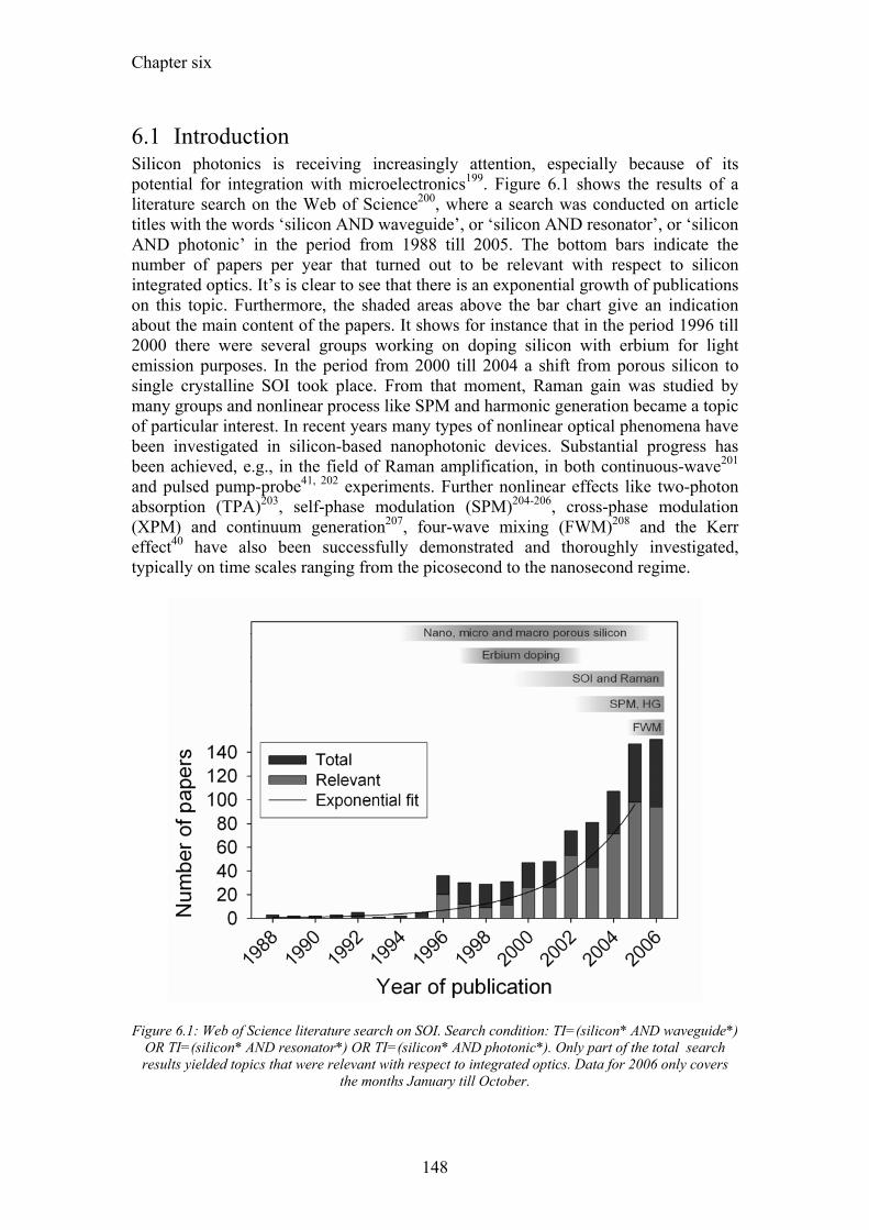
Chapter six
148
6.1 Introduction Silicon photonics is receiving increasingly attention, especially because of its potential for integration with microelectronics199. Figure 6.1 shows the results of a literature search on the Web of Science200, where a search was conducted on article titles with the words ‘silicon AND waveguide’, or ‘silicon AND resonator’, or ‘silicon AND photonic’ in the period from 1988 till 2005. The bottom bars indicate the number of papers per year that turned out to be relevant with respect to silicon integrated optics. It’s is clear to see that there is an exponential growth of publications on this topic. Furthermore, the shaded areas above the bar chart give an indication about the main content of the papers. It shows for instance that in the period 1996 till 2000 there were several groups working on doping silicon with erbium for light emission purposes. In the period from 2000 till 2004 a shift from porous silicon to single crystalline SOI took place. From that moment, Raman gain was studied by many groups and nonlinear process like SPM and harmonic generation became a topic of particular interest. In recent years many types of nonlinear optical phenomena have been investigated in silicon-based nanophotonic devices. Substantial progress has been achieved, e.g., in the field of Raman amplification, in both continuous-wave201 and pulsed pump-probe41, 202 experiments. Further nonlinear effects like two-photon absorption (TPA)203, self-phase modulation (SPM)204-206, cross-phase modulation (XPM) and continuum generation207, four-wave mixing (FWM)208 and the Kerr effect40 have also been successfully demonstrated and thoroughly investigated, typically on time scales ranging from the picosecond to the nanosecond regime.
Figure 6.1: Web of Science literature search on SOI. Search condition: TI=(silicon* AND waveguide*)
OR TI=(silicon* AND resonator*) OR TI=(silicon* AND photonic*). Only part of the total search results yielded topics that were relevant with respect to integrated optics. Data for 2006 only covers
the months January till October.
Materials III: Silicon-on-Insulator
149
A careful analysis of self-phase modulation in submicron silicon waveguides was recently presented by Dulkeith et al.206. They investigated the spectral broadening of picosecond pulses as a function of power and wavelength upon waveguide propagation. Beyond this study of self-phase modulation, Boyraz et al.207 reported all-optical switching based on constructive and destructive interference exploiting cross phase modulation of a CW signal in a Mach Zehnder interferometer. Although the optical pump beam produced sub-picosecond pulses, the off-switching time in their experiments was limited to ~7ns, as a result of the free carrier lifetime. Xu et al.202 reported a 1.6nm wavelength shift of a CW probe signal caused by cross phase modulation using 3.5ps pump pulses. They exploited the wavelength shift to demonstrate all-optical switching by using a tunable grating filter at the output of the waveguide. In this chapter, we present a theoretical and experimental analysis of cross phase modulation induced wavelength conversion in Silicon-on-Insulator (SOI) waveguides on the sub-picosecond timescale. The duration of both the pump and the probe pulses was 300fs and 220fs, respectively. To our best knowledge, this is the first time that large XPM induced wavelength shifts up to 26nm in submicron sized SOI waveguides taking place on a sub-picosecond timescale are being reported. We used femtosecond pulses for this investigation since these typically offer higher peak intensities compared to nanosecond and picosecond pulses, and therefore are very attractive for nonlinear operation. In our case, ultrafast Kerr-induced refractive index changes are predominantly responsible for a temporal variation in phase, causing a wavelength shift of the probe signal. This shift is proportional to the first derivative with respect to time of the pulse envelope, being 1 to 2 orders of magnitude larger than the up to now reported experiments with pulses in the ps regime. The XPM induced frequency shift is not limited in speed by the free carrier lifetime. Instead, the frequency conversion takes place mainly during the leading and trailing edges of the 300fs pulses, i.e. in a sub-picosecond timeframe. Timing becomes of extreme importance on such short timescales. Therefore, the effect of waveguide dispersion on the conversion efficiency using sub-picosecond pulses will be discussed. The temporal shape of the pump pulses is investigated using a theoretical model including TPA and free carrier absorption (FCA). The contributions of both the Kerr nonlinearity and the free carrier dispersion caused by the pump pulses are used to explain the experimentally observed wavelength shift of the probe signal. Based on a simple model, numerical results of femtosecond, picosecond and nanosecond pulse propagation in SOI waveguides are presented and compared to recent experimental data from ourselves and literature. Finally, a novel sub-picosecond all-optical switching scheme based on the observed wavelength shift and a passive microring resonator is proposed. In the following, first, the basics of some interesting nonlinear phenomena like SPM and XPM will be discussed. Next, the temporal and spectral shape of short pulses will be presented. Dispersion will be treated in great detail since silicon waveguides with sub-micron dimension show strong waveguide dispersion. Two modeling methods will be presented of which the first method only considers the pulse shape in the time domain. The dispersion properties of the waveguide are not accounted for in this simple model, which, however, gives good insight in the pulse dynamics at different time scales. In the second model the nonlinear Schrödinger equation (NLSE) is solved using a Split Step Fourier Method (SSFM) and the propagation of the pulses is treated
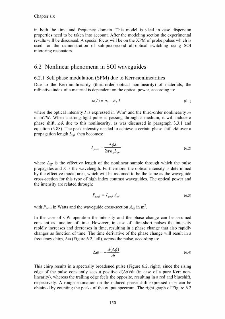
Chapter six
150
in both the time and frequency domain. This model is ideal in case dispersion properties need to be taken into account. After the modeling section the experimental results will be discussed. A special focus will be on the XPM of probe pulses which is used for the demonstration of sub-picosecond all-optical switching using SOI microring resonators.
6.2 Nonlinear phenomena in SOI waveguides
6.2.1 Self phase modulation (SPM) due to Kerr-nonlinearities Due to the Kerr-nonlinearity (third-order optical nonlinearity) of materials, the refractive index of a material is dependent on the optical power, according to:
InnIn .)( 20 += (6.1)
where the optical intensity I is expressed in W/m2 and the third-order nonlinearity n2 in m2/W. When a strong light pulse is passing through a medium, it will induce a phase shift, ∆φ, due to this nonlinearity, as was discussed in paragraph 3.3.1 and equation (3.88). The peak intensity needed to achieve a certain phase shift ∆φ over a propagation length Leff then becomes:
effpeak Ln
I22πφλ∆
= (6.2)
where Leff is the effective length of the nonlinear sample through which the pulse propagates and λ is the wavelength. Furthermore, the optical intensity is determined by the effective modal area, which will be assumed to be the same as the waveguide cross-section for this type of high index contrast waveguides. The optical power and the intensity are related through:
effpeakpeak AIP = (6.3)
with Ppeak in Watts and the waveguide cross-section Aeff in m2. In the case of CW operation the intensity and the phase change can be assumed constant as function of time. However, in case of ultra-short pulses the intensity rapidly increases and decreases in time, resulting in a phase change that also rapidly changes as function of time. The time derivative of the phase change will result in a frequency chirp, ∆ω (Figure 6.2, left), across the pulse, according to:
dtd )( φω ∆
−=∆ (6.4)
This chirp results in a spectrally broadened pulse (Figure 6.2, right), since the rising edge of the pulse constantly sees a positive d(∆φ)/dt (in case of a pure Kerr non-linearity), whereas the trailing edge feels the opposite, resulting in a red and blueshift, respectively. A rough estimation on the induced phase shift expressed in π can be obtained by counting the peaks of the output spectrum. The right graph of Figure 6.2
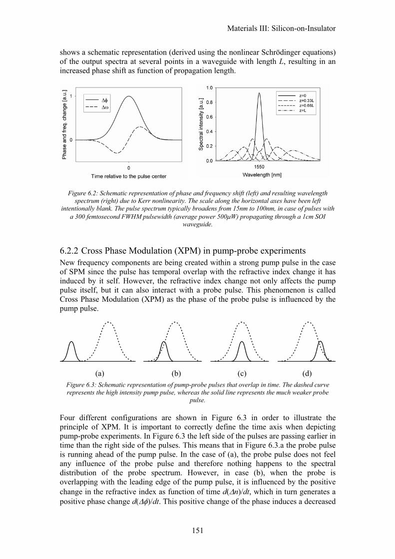
Materials III: Silicon-on-Insulator
151
shows a schematic representation (derived using the nonlinear Schrödinger equations) of the output spectra at several points in a waveguide with length L, resulting in an increased phase shift as function of propagation length.
Figure 6.2: Schematic representation of phase and frequency shift (left) and resulting wavelength spectrum (right) due to Kerr nonlinearity. The scale along the horizontal axes have been left
intentionally blank. The pulse spectrum typically broadens from 15nm to 100nm, in case of pulses with a 300 femtosecond FWHM pulsewidth (average power 500µW) propagating through a 1cm SOI
waveguide.
6.2.2 Cross Phase Modulation (XPM) in pump-probe experiments New frequency components are being created within a strong pump pulse in the case of SPM since the pulse has temporal overlap with the refractive index change it has induced by it self. However, the refractive index change not only affects the pump pulse itself, but it can also interact with a probe pulse. This phenomenon is called Cross Phase Modulation (XPM) as the phase of the probe pulse is influenced by the pump pulse.
(a) (b) (c) (d)
Figure 6.3: Schematic representation of pump-probe pulses that overlap in time. The dashed curve represents the high intensity pump pulse, whereas the solid line represents the much weaker probe
pulse. Four different configurations are shown in Figure 6.3 in order to illustrate the principle of XPM. It is important to correctly define the time axis when depicting pump-probe experiments. In Figure 6.3 the left side of the pulses are passing earlier in time than the right side of the pulses. This means that in Figure 6.3.a the probe pulse is running ahead of the pump pulse. In the case of (a), the probe pulse does not feel any influence of the probe pulse and therefore nothing happens to the spectral distribution of the probe spectrum. However, in case (b), when the probe is overlapping with the leading edge of the pump pulse, it is influenced by the positive change in the refractive index as function of time d(∆n)/dt, which in turn generates a positive phase change d(∆φ)/dt. This positive change of the phase induces a decreased
Chapter six
152
carrier frequency, which results in an increase of the center wavelength of the probe as has been discussed in paragraph 6.2.1. In other words, the probe spectrum gets redshifted. In configuration (c) the probe pulse is exactly centered with the pump pulse and therefore it overlaps with both the leading and trailing edge of the pump pulse. In this case the induces phase changes will more or less compensate each other (depending on the dispersion properties of the waveguide) and the shift of the wavelength will be zero. In Figure 6.3.d the probe does overlap with the trailing edge of the pump, experiencing a negative refractive index change, resulting in a blue shift of the probe carrier wavelength. The effect of SPM scales with the effective propagation length Leff in the waveguide as shown in Equation (6.2). The wavelength shift of the probe in pump-probe experiments depends on the length over which the probe pulse does overlap with the pump pulse. Since sub-micron silicon waveguides show strong dispersion, it is often the case that the probe pulse is traveling faster than the pump pulse, or vice versa. The propagation length over which the pump and probe pulses are overlapping is called the walkoff length Lw. This walkoff length is a linear scaling factor for the magnitude of the XPM induced probe wavelength shift. Its relation to the dispersion of the waveguide will be presented in paragraph 6.3.2.
6.3 Modeling of pulse propagation in SOI waveguides In this paragraph we will discuss two appropriate ways to model the propagation of short pulses through silicon waveguides. The first method, described in paragraph 6.3.3, only describes the pulse propagation in the time domain and therefore holds no direct information on the spectral distribution of the wavelength components within the pulse. However, it gives good insight in the temporal distortion of the pulse under influence of both TPA and FCA. The second method, which is more extensive and described in paragraph 6.3.4, is based on the Nonlinear Schrödinger Equation (NLSE) and also treats the spectral components within the pulse. Therefore, this method is very suitable for incorporating the dispersion effects of the waveguide. For both methods it is important to know the shape of the pulse in the time domain. The spectral distribution of the pulse can be obtained by applying a Fourier transform on the pulse evolution in the time domain. Before the modeling methods are described, the temporal and spectral shape of a short pulse will be discussed.
6.3.1 Intensity profile and spectral distribution of a Gaussian pulse In case of a Gaussian shaped power envelope as function of time, the pulse can be described as follows:
20.5.0
max .)(⎟⎟⎠
⎞⎜⎜⎝
⎛ −−
= δtt
eItI (6.5)
where Imax is the peak power of the pulse (in W/m2), t the time and t0 the center of the pulse (in seconds), and δ the standard deviation. Analogous to the standard deviation in statistics, the spreading of the pulse in time is related to the FWHM pulse length by:
Materials III: Silicon-on-Insulator
153
3548.2)2ln(22FWHMFWHM
≈=δ (6.6)
The area under the pulse represents the total pulse energy Ep, yielding:
2max
5.0
max 2
20
πδδ IAdteIAE eff
tt
effp =⋅= ∫∞+
∞−
⎟⎟⎠
⎞⎜⎜⎝
⎛ −⋅−
(6.7)
The average output power P0 of the laser divided by the pulse repetition rate fr yields the total pulse energy Ep:
rp f
PE 0= (6.8)
Theoretically, a Dirac pulse shape with an infinitesimally short pulse length can be composed of an infinite number of wavelengths that all have the same amplitude, while Gaussian pulses with a finite pulse length are composed of a fixed set of wavelength components that also show a Gaussian frequency or wavelength distribution. The product of the frequency bandwidth and the pulse duration is called the ‘time bandwidth product’ (TBP) and is defined as:
BtTBP p .= (6.9)
where tp is the pulse duration (in seconds and equal to the FWHM of the power envelope) and B is the bandwidth of the frequency components at the FWHM of the individual frequency components. For Gaussian pulses the TBP is 0.441, while for bandwidth limited hyperbolic secant pulses (sech2-shaped) this value is 0.315.
( )[ ] 314833.02
12ln8
4412712.02
)2ln(4
2
2
sec =+
=
==
π
π
h
Gaussian
TPB
TBP (6.10)
For Gaussian shaped pulses it can be derived that:
ctnTBP
p
GaussianFWHM .
..2
0λλλ =∆= (6.11)
in case the spectral width is small compared to the center wavelength, i.e. λmin.λmax≈λ0
2. Thus, the spectral width of the pulse is inversely proportional to the pulse length. A detailed overview of the properties of Gaussian and hyperbolic secant pulses in either the time, frequency and wavelength domain can be found in the work of N.G. Usechak209.
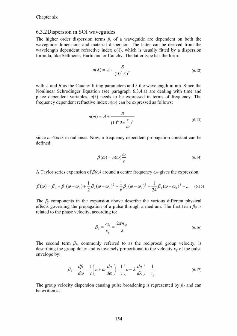
Chapter six
154
6.3.2 Dispersion in SOI waveguides The higher order dispersion terms βj of a waveguide are dependent on both the waveguide dimensions and material dispersion. The latter can be derived from the wavelength dependent refractive index n(λ), which is usually fitted by a dispersion formula, like Sellmeier, Hartmann or Cauchy. The latter type has the form:
26 ).10()(
λλ BAn += (6.12)
with A and B as the Cauchy fitting parameters and λ the wavelength in nm. Since the Nonlinear Schrödinger Equation (see paragraph 6.3.4.a) are dealing with time and place dependent variables, n(λ) needs to be expressed in terms of frequency. The frequency dependent refractive index n(ω) can be expressed as follows:
26 )2.10()(
ωπ
ωc
BAn += (6.13)
since ω=2πc/λ in radians/s. Now, a frequency dependent propagation constant can be defined:
cn ωωωβ )()( = (6.14)
A Taylor series expansion of β(ω) around a centre frequency ω0 gives the expression:
...)(241)(
61)(
21)()( 4
043
032
02010 +−+−+−+−+= ωωβωωβωωβωωββωβ (6.15)
The βj components in the expansion above describe the various different physical effects governing the propagation of a pulse through a medium. The first term β0 is related to the phase velocity, according to:
λπωβ
φ
effnv
200 == (6.16)
The second term β1, commonly referred to as the reciprocal group velocity, is describing the group delay and is inversely proportional to the velocity vg of the pulse envelope by:
gvddnn
cddnn
cdd 111
1 =⎟⎠⎞
⎜⎝⎛ −=⎟
⎠⎞
⎜⎝⎛ +==
λλ
ωω
ωββ (6.17)
The group velocity dispersion causing pulse broadening is represented by β2 and can be written as:
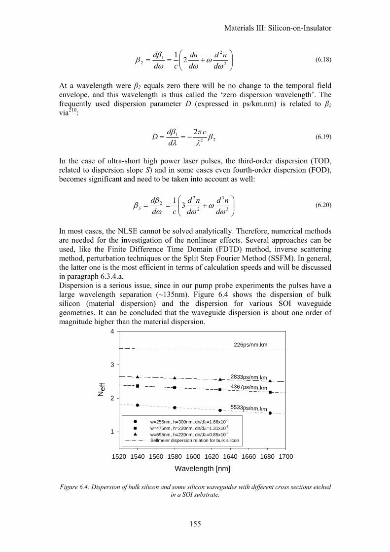
Materials III: Silicon-on-Insulator
155
⎟⎟⎠
⎞⎜⎜⎝
⎛+== 2
21
2 21ω
ωωω
ββ
dnd
ddn
cdd (6.18)
At a wavelength were β2 equals zero there will be no change to the temporal field envelope, and this wavelength is thus called the ‘zero dispersion wavelength’. The frequently used dispersion parameter D (expressed in ps/km.nm) is related to β2 via210:
221 2 β
λπ
λβ c
ddD −== (6.19)
In the case of ultra-short high power laser pulses, the third-order dispersion (TOD, related to dispersion slope S) and in some cases even fourth-order dispersion (FOD), becomes significant and need to be taken into account as well:
⎟⎟⎠
⎞⎜⎜⎝
⎛+== 3
3
2
22
3 31ω
ωωω
ββ
dnd
dnd
cdd (6.20)
In most cases, the NLSE cannot be solved analytically. Therefore, numerical methods are needed for the investigation of the nonlinear effects. Several approaches can be used, like the Finite Difference Time Domain (FDTD) method, inverse scattering method, perturbation techniques or the Split Step Fourier Method (SSFM). In general, the latter one is the most efficient in terms of calculation speeds and will be discussed in paragraph 6.3.4.a. Dispersion is a serious issue, since in our pump probe experiments the pulses have a large wavelength separation (~135nm). Figure 6.4 shows the dispersion of bulk silicon (material dispersion) and the dispersion for various SOI waveguide geometries. It can be concluded that the waveguide dispersion is about one order of magnitude higher than the material dispersion.
Wavelength [nm]1520 1540 1560 1580 1600 1620 1640 1660 1680 1700
Nef
f
1
2
3
4
w=256nm, h=300nm, dn/dλ=1.66x10-3
w=475nm, h=220nm, dn/dλ=1.31x10-3
w=695nm, h=220nm, dn/dλ=0.85x10-3
Sellmeier dispersion relation for bulk silicon
2833ps/nm.km4367ps/nm.km
5533ps/nm.km
226ps/nm.km
Figure 6.4: Dispersion of bulk silicon and some silicon waveguides with different cross sections etched
in a SOI substrate.
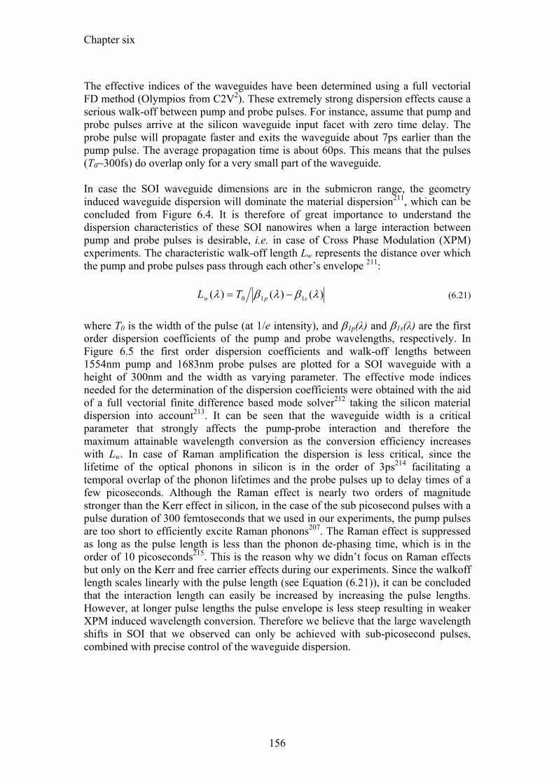
Chapter six
156
The effective indices of the waveguides have been determined using a full vectorial FD method (Olympios from C2V2). These extremely strong dispersion effects cause a serious walk-off between pump and probe pulses. For instance, assume that pump and probe pulses arrive at the silicon waveguide input facet with zero time delay. The probe pulse will propagate faster and exits the waveguide about 7ps earlier than the pump pulse. The average propagation time is about 60ps. This means that the pulses (T0~300fs) do overlap only for a very small part of the waveguide. In case the SOI waveguide dimensions are in the submicron range, the geometry induced waveguide dispersion will dominate the material dispersion211, which can be concluded from Figure 6.4. It is therefore of great importance to understand the dispersion characteristics of these SOI nanowires when a large interaction between pump and probe pulses is desirable, i.e. in case of Cross Phase Modulation (XPM) experiments. The characteristic walk-off length Lw represents the distance over which the pump and probe pulses pass through each other’s envelope 211:
)()()( 110 λβλβλ spw TL −= (6.21)
where T0 is the width of the pulse (at 1/e intensity), and β1p(λ) and β1s(λ) are the first order dispersion coefficients of the pump and probe wavelengths, respectively. In Figure 6.5 the first order dispersion coefficients and walk-off lengths between 1554nm pump and 1683nm probe pulses are plotted for a SOI waveguide with a height of 300nm and the width as varying parameter. The effective mode indices needed for the determination of the dispersion coefficients were obtained with the aid of a full vectorial finite difference based mode solver212 taking the silicon material dispersion into account213. It can be seen that the waveguide width is a critical parameter that strongly affects the pump-probe interaction and therefore the maximum attainable wavelength conversion as the conversion efficiency increases with Lw. In case of Raman amplification the dispersion is less critical, since the lifetime of the optical phonons in silicon is in the order of 3ps214 facilitating a temporal overlap of the phonon lifetimes and the probe pulses up to delay times of a few picoseconds. Although the Raman effect is nearly two orders of magnitude stronger than the Kerr effect in silicon, in the case of the sub picosecond pulses with a pulse duration of 300 femtoseconds that we used in our experiments, the pump pulses are too short to efficiently excite Raman phonons207. The Raman effect is suppressed as long as the pulse length is less than the phonon de-phasing time, which is in the order of 10 picoseconds215. This is the reason why we didn’t focus on Raman effects but only on the Kerr and free carrier effects during our experiments. Since the walkoff length scales linearly with the pulse length (see Equation (6.21)), it can be concluded that the interaction length can easily be increased by increasing the pulse lengths. However, at longer pulse lengths the pulse envelope is less steep resulting in weaker XPM induced wavelength conversion. Therefore we believe that the large wavelength shifts in SOI that we observed can only be achieved with sub-picosecond pulses, combined with precise control of the waveguide dispersion.
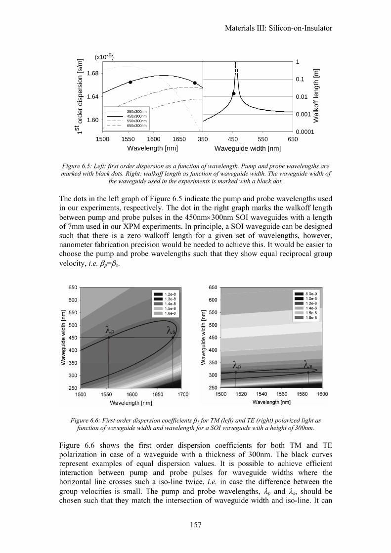
Materials III: Silicon-on-Insulator
157
Waveguide width [nm]350 450 550 650
Wal
koff
leng
th [m
]
0.0001
0.001
0.01
0.1
1
Wavelength [nm]1500 1550 1600 1650
1st o
rder
dis
pers
ion
[s/m
]
1.60
1.64
1.68
350x300nm450x300nm550x300nm650x300nm
(x10-8)
Figure 6.5: Left: first order dispersion as a function of wavelength. Pump and probe wavelengths are marked with black dots. Right: walkoff length as function of waveguide width. The waveguide width of
the waveguide used in the experiments is marked with a black dot. The dots in the left graph of Figure 6.5 indicate the pump and probe wavelengths used in our experiments, respectively. The dot in the right graph marks the walkoff length between pump and probe pulses in the 450nm×300nm SOI waveguides with a length of 7mm used in our XPM experiments. In principle, a SOI waveguide can be designed such that there is a zero walkoff length for a given set of wavelengths, however, nanometer fabrication precision would be needed to achieve this. It would be easier to choose the pump and probe wavelengths such that they show equal reciprocal group velocity, i.e. βp=βs.
Figure 6.6: First order dispersion coefficients β1 for TM (left) and TE (right) polarized light as function of waveguide width and wavelength for a SOI waveguide with a height of 300nm.
Figure 6.6 shows the first order dispersion coefficients for both TM and TE polarization in case of a waveguide with a thickness of 300nm. The black curves represent examples of equal dispersion values. It is possible to achieve efficient interaction between pump and probe pulses for waveguide widths where the horizontal line crosses such a iso-line twice, i.e. in case the difference between the group velocities is small. The pump and probe wavelengths, λp and λs, should be chosen such that they match the intersection of waveguide width and iso-line. It can
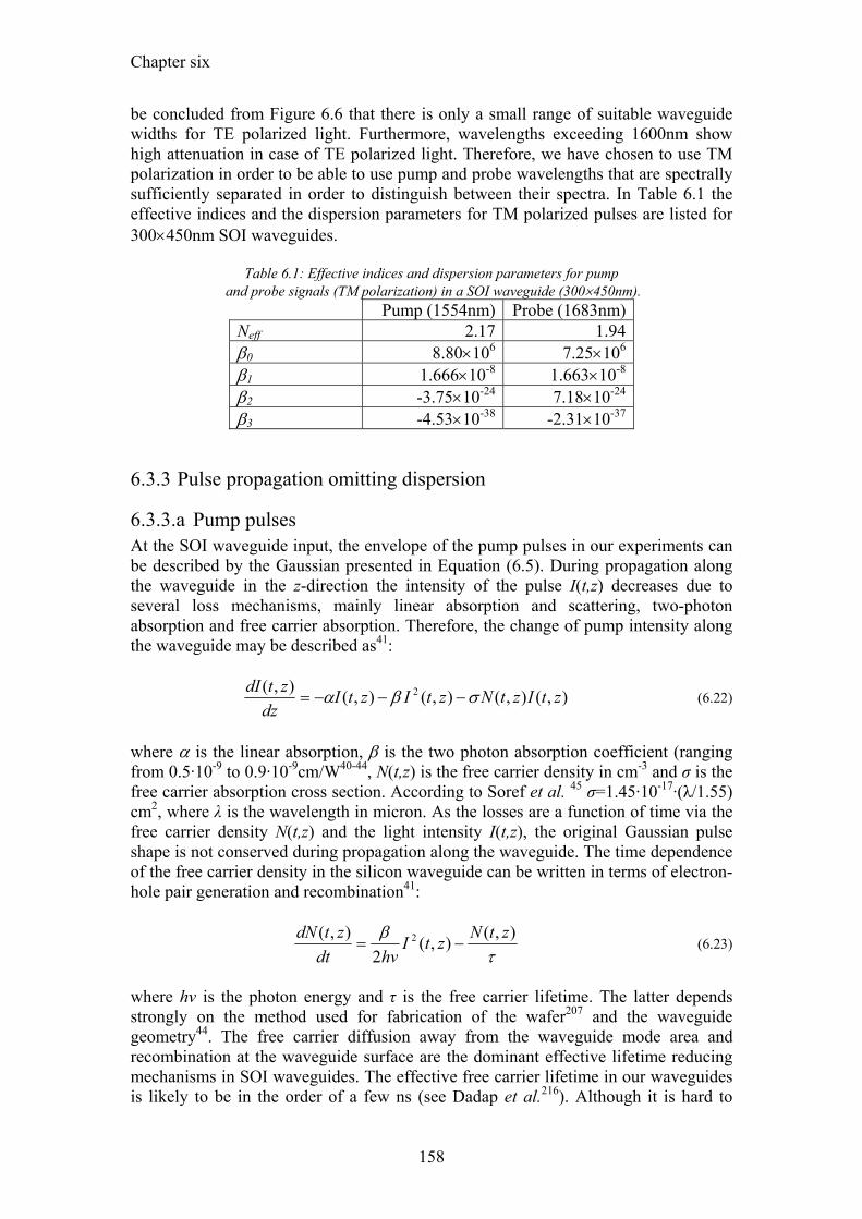
Chapter six
158
be concluded from Figure 6.6 that there is only a small range of suitable waveguide widths for TE polarized light. Furthermore, wavelengths exceeding 1600nm show high attenuation in case of TE polarized light. Therefore, we have chosen to use TM polarization in order to be able to use pump and probe wavelengths that are spectrally sufficiently separated in order to distinguish between their spectra. In Table 6.1 the effective indices and the dispersion parameters for TM polarized pulses are listed for 300×450nm SOI waveguides.
Table 6.1: Effective indices and dispersion parameters for pump and probe signals (TM polarization) in a SOI waveguide (300×450nm).
Pump (1554nm) Probe (1683nm) Neff 2.17 1.94 β0 8.80×10⁶ 7.25×10⁶ β1 1.666×10⁻⁸ 1.663×10⁻⁸ β2 -3.75×10⁻²⁴ 7.18×10⁻²⁴ β3 -4.53×10-38 -2.31×10-37
6.3.3 Pulse propagation omitting dispersion
6.3.3.a Pump pulses At the SOI waveguide input, the envelope of the pump pulses in our experiments can be described by the Gaussian presented in Equation (6.5). During propagation along the waveguide in the z-direction the intensity of the pulse I(t,z) decreases due to several loss mechanisms, mainly linear absorption and scattering, two-photon absorption and free carrier absorption. Therefore, the change of pump intensity along the waveguide may be described as41:
),(),(),(),(),( 2 ztIztNztIztIdz
ztdI σβα −−−= (6.22)
where α is the linear absorption, β is the two photon absorption coefficient (ranging from 0.5·10-9 to 0.9·10-9cm/W40-44, N(t,z) is the free carrier density in cm-3 and σ is the free carrier absorption cross section. According to Soref et al. 45 σ=1.45·10-17·(λ/1.55) cm2, where λ is the wavelength in micron. As the losses are a function of time via the free carrier density N(t,z) and the light intensity I(t,z), the original Gaussian pulse shape is not conserved during propagation along the waveguide. The time dependence of the free carrier density in the silicon waveguide can be written in terms of electron-hole pair generation and recombination41:
τβ ),(),(
2),( 2 ztNztI
hvdtztdN
−= (6.23)
where hv is the photon energy and τ is the free carrier lifetime. The latter depends strongly on the method used for fabrication of the wafer207 and the waveguide geometry44. The free carrier diffusion away from the waveguide mode area and recombination at the waveguide surface are the dominant effective lifetime reducing mechanisms in SOI waveguides. The effective free carrier lifetime in our waveguides is likely to be in the order of a few ns (see Dadap et al.216). Although it is hard to
Materials III: Silicon-on-Insulator
159
compare the lifetimes of different fabrication methods, the results of our model, i.e. the propagation characteristics of 300fs pulses, do not change noticeably, when carrier lifetimes are varied over the range from 100ps to 10ns. The propagation of sub picosecond pulses does not change until the lifetime is decreased to tens of picoseconds. A free carrier lifetime reduction from 100ns to 1.9ns has recently been demonstrated using helium implantation of silicon waveguides217. In this case the recombination does not mainly occur at the waveguide interfaces, but primarily at recombination centers introduced inside the waveguide. Since our waveguides did not experience any implantation damage, we assumed the lifetime to be larger than 1 ns. The set of coupled differential equations, Eq. (2) and (3) have been solved numerically to get insight about the physical effects in our pump-probe experiments. The results are presented in Table 6.3 for several pulse durations.
6.3.3.b Pump-probe Short pulses propagating along the silicon waveguide do not only experience losses, but also refractive index changes caused by the Kerr effect and the generated free carriers. The Kerr induced refractive index change is described by:
),(.),( 2 ztInztnKerr =∆ (6.24)
where n2 ranges from 4·10-14 to 9·10-14 cm2/W40, 208. We have used n2 = 4·10-14 cm2/W in our simulations. The free carrier induced refractive index change has an opposite sign and can be described by the well-known accurate empirical relation presented by Soref et al.45:
)),(105.8),(108.8(),( 8.01822 ztNztNztn heFC−− ⋅+⋅−=∆ (6.25)
where subscripts e and h denote electrons and holes, respectively. Since the number of electrons and holes created by TPA are equal, Ne(t,z) and Nh(t,z) can be replaced by N(t,z) in units of cm-3 in Equation (6.24). Next, consider a pump-probe experiment where the delay time between the pulses is such that the probe signal has a temporal overlap with the pump signal on either the rising or trailing edge. In this case, the probe signal will experience a time dependent phase shift ∆φ(t,z) which is caused by the temporal change in the pump pulse induced index changes 202:
[ ]),(),(2
),( int ztnztnL
zt FCKerr ∆+∆=∆λπ
φ (6.26)
Here Lint is the interaction length, i.e. the length over which the pump and probe pulses feel each others presence. This temporal variation in phase will result in a frequency shift of the probe pulses:
),(),( ztdtdzt φω ∆−=∆ (6.27)
resulting in a shifted center wavelength of the probe pulses:
Chapter six
160
dtztnd
cLs ),(1 int
0
∆⋅−
=λ
λ (6.28)
where λs is the center wavelength of the frequency converted probe pulse, λ0 the center wavelength of the original probe spectrum and c is the speed of light in vacuum.
6.3.4 Pulse propagation taking dispersion into account
6.3.4.a The Nonlinear Schrödinger Equation The propagation of short electromagnetic pulses inside a channel waveguide with Kerr nonlinearities and dispersion can be described by the nonlinear Schrödinger equation218-220:
( ) ( )22
0
220
4
4
43
3
32
2
2
21
2462
ψτ
ψγψψτω
γψψγψψα
ψα
τψβ
τψβ
τψβψ
ddTi
ddi
A
ddi
ddi
ddi
dzd
Reff
TPA ⋅⋅⋅⋅−⋅−⋅+−⋅⋅−
⋅⋅+⋅⋅+⋅⋅−= (6.29)
where ψ(z,τ) is the slowly varying complex envelope of the pulse. A solution for the shape of the electric field envelope as function of propagation distance ψ(z,τ) can be found by solving the NLSE. In this equation γ is the nonlinear parameter, which can be expressed as:
effeffeff Ank
An
cAn 2
02022
⋅=⋅=⋅=ω
λπγ (6.30)
where k0 represents the wave vector. Furthermore, in the NLSE, α0 is the propagation loss, αTPA the two-photon absorption and βj are the higher order dispersion terms. In this section we introduce a new symbol for the TPA coefficient, αTPA instead of β to avoid confusion with the dispersion coefficients βj. Two other interesting nonlinear terms related to n2 are γ/ω0 and γ⋅TR, responsible for self-steepening or shock formation and intrapulse Raman scattering, respectively. All the individual terms are listed in Table 6.2.
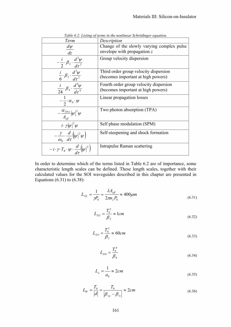
Materials III: Silicon-on-Insulator
161
Table 6.2: Listing of terms in the nonlinear Schrödinger equation. Term Description
dzdψ
Change of the slowly varying complex pulse envelope with propagation z
2
2
22 τψβ
ddi⋅⋅−
Group velocity dispersion
3
3
36 τψβ
ddi⋅⋅
Third order group velocity dispersion (becomes important at high powers)
4
4
424 τψβ
ddi⋅⋅
Fourth order group velocity dispersion (becomes important at high powers)
ψα ⋅⋅− 021
Linear propagation losses
ψψα 2
eff
TPA
A−
Two photon absorption (TPA)
ψψγ 2⋅i Self phase modulation (SPM)
( )ψψτω
γ 2
0 dd
⋅− Self-steepening and shock formation
( )2ψτ
ψγddTi R ⋅⋅⋅⋅−
Intrapulse Raman scattering
In order to determine which of the terms listed in Table 6.2 are of importance, some characteristic length scales can be defined. These length scales, together with their calculated values for the SOI waveguides described in this chapter are presented in Equations (6.31) to (6.38):
mPn
AP
L effNL µ
πλ
γ400
21
020
≈==
(6.31)
cmT
LD 12
20
2 ≈=β
(6.32)
cmT
LD 603
30
3 ≈=β
(6.33)
4
40
4 βT
LD =
(6.34)
cma
La 21
0
≈=
(6.35)
cmT
dT
Lsp
W 211
00 ≈−
==ββ
(6.36)
Chapter six
162
cmLTL NLS 1500 ≈= ω
(6.37)
NLR
IRS LTT
L 0= (6.38)
where LNL is the nonlinear length, LD2, LD3 and LD4 are the second, third and fourth order dispersion lengths, La is the absorption length, Lw the walkoff length, Ls the shock length and LIRS represents the Raman length. By comparing these length scales to each other or the actual device length L, one can obtain a rough estimate of which terms need to bee taken into account in order to accurately model a certain situation. It can be seen from the calculated values that the Kerr nonlinearity, the second order dispersion, the walkoff length and the linear losses are critical parameters, since their characteristic lengths are comparable to the waveguide length L, which is 7mm. Among these effects, the Kerr nonlinearity is the most dominant effect in our SOI waveguides. A value for LD4 is not given, since it is expected that the fourth order dispersion only becomes important at very large propagation distances. Furthermore, a very high degree of accuracy is needed when calculating the dispersion up to this degree, which is elaborate in case of high contrast waveguides. Intrapulse Raman Scattering (IRS) is not present in SOI waveguides, therefore no value is given for LIRS.
6.3.4.b The Split Step Fourier Method In the case of the SSFM, an appropriate discretization of time is needed, leading to a system of ordinary differential equations220 with both higher-order linear terms and nonlinear terms:
)~(~~~~ANAL
zA
+=∂∂ (6.39)
The split step method is based on splitting the equation in a linear part:
ALzA ~~~=
∂∂ (6.40)
and a nonlinear part:
ANzA ~~~=
∂∂ (6.41)
and solving these equations alternatively. It is assumed that the dispersive and nonlinear effects act independently. So in the case of a step in propagation distance of h, Equation (6.41) is solved from z to (z+½h) with initial condition A(z). Then Equation (6.40) is solved from (z+½h) to (z+h) with the solution of Equation (6.41) as the initial condition. The solution over a short propagation interval h will then become:
Materials III: Silicon-on-Insulator
163
),()~2
exp()~2
exp(),( tzANhLhthzA =+ (6.42)
The propagation from z to z+h is a rough approximation, since L~ and N~ do not commute in general. Higher order accuracy can be obtained by applying an appropriate composition of linear and nonlinear steps, which is beyond the scope of this research.
6.3.4.c Coupled NLSEs for pump-probe XPM A system of coupled nonlinear Schrödinger equations has been derived in cooperation with Nick Usechak who was with the group of Govind Agrawal at the University of Rochester. The model includes the effect of the Raman gain spectrum as well. Phase matching terms have been ignored under the assumption that this condition is not satisfied. Furthermore, we have assumed that the pulses are spectrally separated. The equations, which can be solved numerically using the SSFM, follow directly from the work of Headley et al.221 and Lin et al.222.
[ ]
[ ][ ]
')',()',()'(
')',()',()'(
221
21
!
'*
22
22
1
dtettzttztgi
dtttzttztgi
ii
dtd
n
ii
dzd
tispRpR
spRpR
pspTPAe
pFCppn
n
n
nn
p
sp
p
p
∫
∫
∑
∞
∞−
Ω
∞
∞−
∞
=
−−+
−+−+
+⎥⎦⎤
⎢⎣⎡ ++
+−=
ψψγψξ
ψψγψξ
ψψψβγξ
ψααψβψ
(6.43)
[ ]
[ ][ ]
')',()',()'(
')',()',()'(
221
21
!
'*
22
22
1
dtettzttztgi
dtttzttztgi
ii
dtd
ni
idz
d
tipsRsR
spRsR
spsTPAe
sFCssn
n
n
nn
s
sp
s
s
∫
∫
∑
∞
∞−
Ω−
∞
∞−
∞
=
−−+
−+−+
+⎥⎦⎤
⎢⎣⎡ ++
+−=
ψψγψξ
ψψγψξ
ψψψβγξ
ψααψβψ
(6.44)
where the term dψp,s/dz represents the propagation. The terms on the right hand side of Equations (6.43) and (6.44) take into account the dispersive effects to all orders, with βnj = βn(λj) where n= 1,2,3,… and j = p,s, representing pump and signal, respectively. The losses are accounted for in the third term, where the static losses are represented by αj and the free-carrier absorption by αFCj. The free carrier losses are defined as:
Chapter six
164
),(1045.12
17 ztNref
jFC j ⎟
⎟⎠
⎞⎜⎜⎝
⎛×= −
λλ
α (6.45)
where λref is the reference wavelength of 1550nm and λj is the carrier wavelength of the pump and probe fields. For the calculation of the free carrier concentration N(t,z) we can define the electron-hole pair generation and recombination similar to Eq. (6.23), but now in terms of the field:
FCp
TPAe ztNztdt
ztdNτ
ψω
βξ ),(),(2
),( 4−=
h (6.46)
The fourth term is responsible for SPM and XPM, whereas the fifth term takes the intrapulse Raman scattering (IRS) and intrapulse cross Raman scattering (XRS) into account. Finally, the sixth and last term is responsible for Raman amplification. Further, gR(t) is a function needed to incorporate the effects of the Raman process in silicon, defined as223:
)(sinexp)(12
221
22
21 thtttg R ⎟⎟
⎠
⎞⎜⎜⎝
⎛⎟⎟⎠
⎞⎜⎜⎝
⎛−
+=
ττττττ (6.47)
where τ1
-1 is the phonon frequency, τ2-1 is related to the bandwidth of the Lorentzian
lineshape of the Raman spectrum and h(t) is the Heavy-side step function which ensures causality. For silicon these values are τ1=10.2fs and τ2=3.4ps, respectively. Since the NLSE is dealing with the frequency domain as well, it is useful to express the terms in the frequency domain as well:
ΩΓ−Ω−ΩΩΓ
=ΩRR
RRRR i
gg2
)(22 (6.48)
Where gR=2×10⁻¹⁰m/W being the Raman gain coefficient at 1550nm, ΩR/2π=15.6 THz is the Raman shift (520cm-1) and the FWHM of the Raman spectrum is given by ΓR/2π=52.5GHz (~0.9nm). The nonlinear refractive index is accounted for through γ=n2ωj/c and βTPA is the two-photon absorption coefficient. The coefficients ξe and ξR describe the electronic and Raman contributions related to the crystal symmetry of the silicon lattice, its orientation with respect to the waveguide and the excited mode222. For excitation of a TE mode in a [110]×[001] faceted waveguide ξe=5/4 and ξR=1. However, for excitation of the TM mode ξe=1 and ξR=0, indicating that Raman effects are not present when the TM mode is excited. Finally, τFC is the free carrier lifetime and Ωsp=ωs-ωp. The free carriers will change the refractive index, which could change the relative velocities of the pump and signal in the SOI waveguide causing them to walk-off from one another at a different rate than that predicted by the two first-order dispersion terms. This effect will change the pump-probe interaction length in
Materials III: Silicon-on-Insulator
165
general, however, such changes are likely to be small, since the waveguides under investigation are short < 5cm. As a consequence, these effects have been ignored in this model. Nevertheless, we point out that such effects can be incorporated in a straightforward manner by using the Drude model, Eq. (3.18), or the empirical model from Soref, Eq. (3.20), and augmenting the first-order dispersion terms in the above equations. Equations (6.43) and (6.44) can be simplified when it is assumed that the intensity of the pump pulses is much stronger than the intensity of the probe pulses, |ψp|2 >> |ψs|2. Furthermore, it can be assumed that probe SPM and probe induced XPM are negligible in this case and are thus ignored. The same holds for the contribution of the probe pulses to the stimulated Raman scattering. However, the Raman amplification term in the probe equation is kept, since we assume that the small signal of the probe can be amplified by stimulated Raman scattering induced by the pump. Under these assumptions the coupled set of NLSEs can be reduced to:
[ ]
')',()',()'(
')',()'(
21
21
62
'*
2
2
3
33
2
22
dtettzttztgi
dtttztgi
ii
dtd
idt
di
dtd
dzd
tispRpR
pRpR
ppTPAe
pFCppppp
sp
p
pp
∫
∫∞
∞−
Ω
∞
∞−
−−+
−+
⎥⎦⎤
⎢⎣⎡ ++
+−+−∆=
ψψγψξ
ψγψξ
ψψβγξ
ψααψβψβψψ
(6.49)
[ ]
')',()',()'(
')',()'(
212
21
62
'*
2
2
3
33
2
22
dtettzttztgi
dtttztgi
ii
dtd
idt
di
dtd
dzd
tipsRsR
pRsR
spTPAe
sFCsssss
sp
s
ss
∫
∫∞
∞−
Ω−
∞
∞−
−−+
−+
⎥⎦⎤
⎢⎣⎡ ++
+−+−∆=
ψψγψξ
ψγψξ
ψψβγξ
ψααψβψβψψ
(6.50)
A new quantity ∆=(β1s-β1p)/2 has been introduced in Equations (6.49) and (6.50) in order to make sure that both the pump and probe pulses have the same distance from the center of the calculation window. The model presented in this section will be further developed in cooperation with Jiri Ctyroky and Thomas Lauerman of the IREE in Prague and Nick Usechak and will be used in our future research on nonlinear SOI devices.
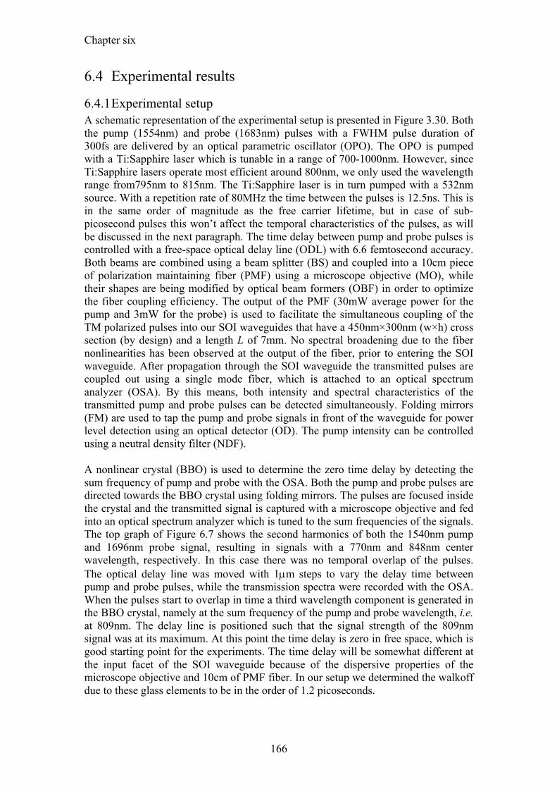
Chapter six
166
6.4 Experimental results
6.4.1 Experimental setup A schematic representation of the experimental setup is presented in Figure 3.30. Both the pump (1554nm) and probe (1683nm) pulses with a FWHM pulse duration of 300fs are delivered by an optical parametric oscillator (OPO). The OPO is pumped with a Ti:Sapphire laser which is tunable in a range of 700-1000nm. However, since Ti:Sapphire lasers operate most efficient around 800nm, we only used the wavelength range from795nm to 815nm. The Ti:Sapphire laser is in turn pumped with a 532nm source. With a repetition rate of 80MHz the time between the pulses is 12.5ns. This is in the same order of magnitude as the free carrier lifetime, but in case of sub-picosecond pulses this won’t affect the temporal characteristics of the pulses, as will be discussed in the next paragraph. The time delay between pump and probe pulses is controlled with a free-space optical delay line (ODL) with 6.6 femtosecond accuracy. Both beams are combined using a beam splitter (BS) and coupled into a 10cm piece of polarization maintaining fiber (PMF) using a microscope objective (MO), while their shapes are being modified by optical beam formers (OBF) in order to optimize the fiber coupling efficiency. The output of the PMF (30mW average power for the pump and 3mW for the probe) is used to facilitate the simultaneous coupling of the TM polarized pulses into our SOI waveguides that have a 450nm×300nm (w×h) cross section (by design) and a length L of 7mm. No spectral broadening due to the fiber nonlinearities has been observed at the output of the fiber, prior to entering the SOI waveguide. After propagation through the SOI waveguide the transmitted pulses are coupled out using a single mode fiber, which is attached to an optical spectrum analyzer (OSA). By this means, both intensity and spectral characteristics of the transmitted pump and probe pulses can be detected simultaneously. Folding mirrors (FM) are used to tap the pump and probe signals in front of the waveguide for power level detection using an optical detector (OD). The pump intensity can be controlled using a neutral density filter (NDF). A nonlinear crystal (BBO) is used to determine the zero time delay by detecting the sum frequency of pump and probe with the OSA. Both the pump and probe pulses are directed towards the BBO crystal using folding mirrors. The pulses are focused inside the crystal and the transmitted signal is captured with a microscope objective and fed into an optical spectrum analyzer which is tuned to the sum frequencies of the signals. The top graph of Figure 6.7 shows the second harmonics of both the 1540nm pump and 1696nm probe signal, resulting in signals with a 770nm and 848nm center wavelength, respectively. In this case there was no temporal overlap of the pulses. The optical delay line was moved with 1µm steps to vary the delay time between pump and probe pulses, while the transmission spectra were recorded with the OSA. When the pulses start to overlap in time a third wavelength component is generated in the BBO crystal, namely at the sum frequency of the pump and probe wavelength, i.e. at 809nm. The delay line is positioned such that the signal strength of the 809nm signal was at its maximum. At this point the time delay is zero in free space, which is good starting point for the experiments. The time delay will be somewhat different at the input facet of the SOI waveguide because of the dispersive properties of the microscope objective and 10cm of PMF fiber. In our setup we determined the walkoff due to these glass elements to be in the order of 1.2 picoseconds.
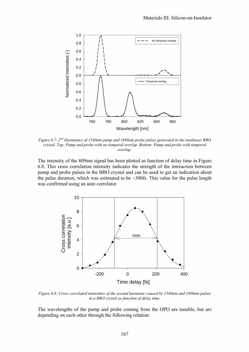
Materials III: Silicon-on-Insulator
167
Wavelength [nm]760 780 800 820 840 860
Nor
mal
ized
inte
nsiti
es [-
]
0.0
0.2
0.4
0.6
0.8
1.0No temporal overlap
Wavelength [nm]760 780 800 820 840 860
0.0
0.2
0.4
0.6
0.8Temporal overlap
Figure 6.7: 2nd Harmonics of 1540nm pump and 1696nm probe pulses generated in the nonlinear BBO
crystal. Top: Pump and probe with no temporal overlap. Bottom: Pump and probe with temporal overlap.
The intensity of the 809nm signal has been plotted as function of delay time in Figure 6.8. This cross correlation intensity indicates the strength of the interaction between pump and probe pulses in the BBO crystal and can be used to get an indication about the pulse duration, which was estimated to be ~300fs. This value for the pulse length was confirmed using an auto correlator.
Time delay [fs]-200 0 200 400
Cro
ss c
orre
latio
n in
tens
ity [a
.u.]
0
2
4
6
8
10
300fs
Figure 6.8: Cross correlated intensities of the second harmonic caused by 1540nm and 1696nm pulses
in a BBO crystal as function of delay time. The wavelengths of the pump and probe coming from the OPO are tunable, but are depending on each other through the following relation:
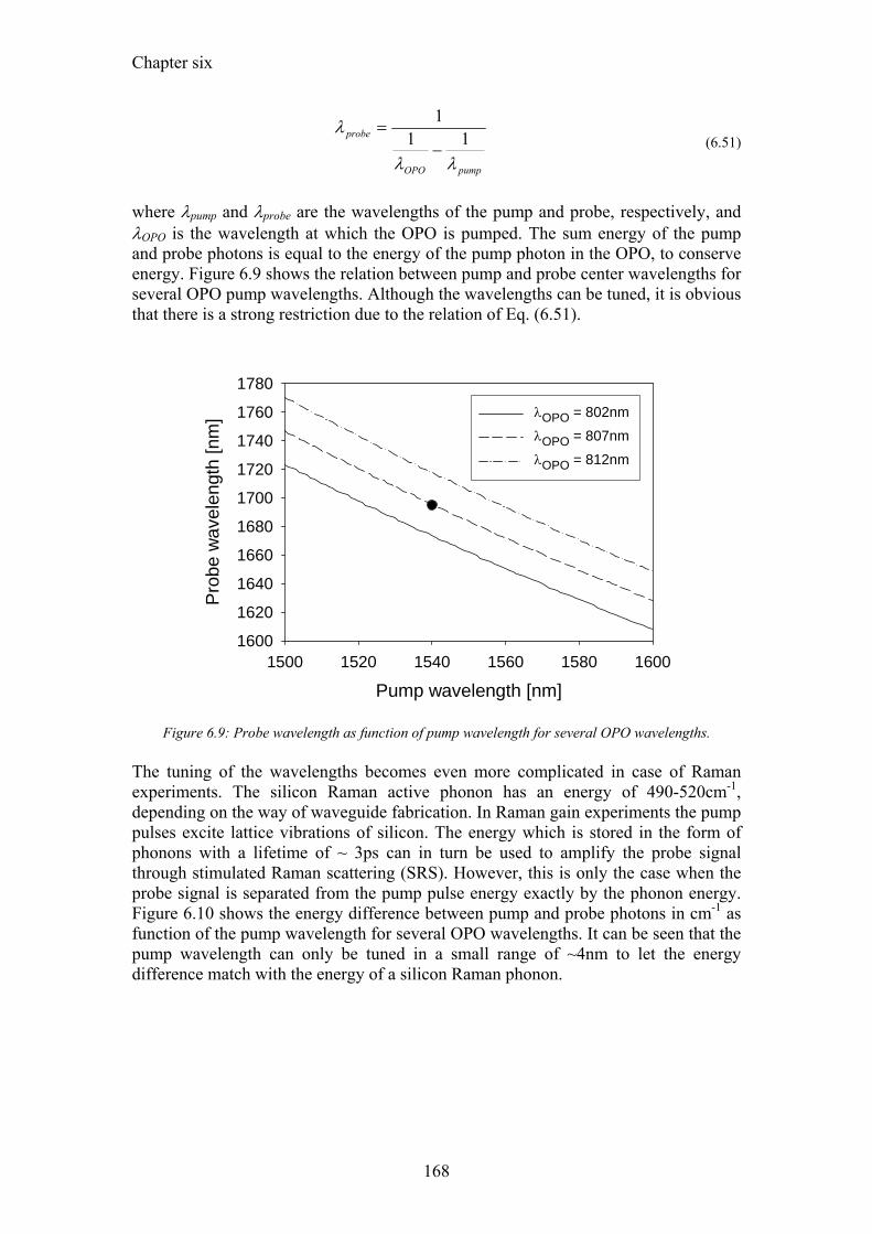
Chapter six
168
pumpOPO
probe
λλ
λ11
1
−=
(6.51)
where λpump and λprobe are the wavelengths of the pump and probe, respectively, and λOPO is the wavelength at which the OPO is pumped. The sum energy of the pump and probe photons is equal to the energy of the pump photon in the OPO, to conserve energy. Figure 6.9 shows the relation between pump and probe center wavelengths for several OPO pump wavelengths. Although the wavelengths can be tuned, it is obvious that there is a strong restriction due to the relation of Eq. (6.51).
Pump wavelength [nm]1500 1520 1540 1560 1580 1600
Pro
be w
avel
engt
h [n
m]
1600
1620
1640
1660
1680
1700
1720
1740
1760
1780
λOPO = 802nm λOPO = 807nm
λOPO = 812nm
Figure 6.9: Probe wavelength as function of pump wavelength for several OPO wavelengths. The tuning of the wavelengths becomes even more complicated in case of Raman experiments. The silicon Raman active phonon has an energy of 490-520cm-1, depending on the way of waveguide fabrication. In Raman gain experiments the pump pulses excite lattice vibrations of silicon. The energy which is stored in the form of phonons with a lifetime of ~ 3ps can in turn be used to amplify the probe signal through stimulated Raman scattering (SRS). However, this is only the case when the probe signal is separated from the pump pulse energy exactly by the phonon energy. Figure 6.10 shows the energy difference between pump and probe photons in cm-1 as function of the pump wavelength for several OPO wavelengths. It can be seen that the pump wavelength can only be tuned in a small range of ~4nm to let the energy difference match with the energy of a silicon Raman phonon.
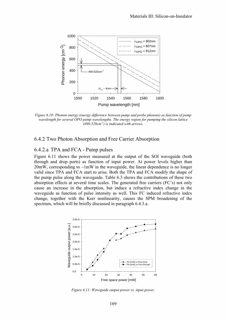
Materials III: Silicon-on-Insulator
169
Pump wavelength [nm]1500 1520 1540 1560 1580 1600
Pho
non
ener
gy [c
m-1
]
0
200
400
600
800
1000λOPO = 802nm λOPO = 807nmλOPO = 812nm
490-520cm-1
∆λp ~ 4nm
Figure 6.10: Phonon energy (energy difference between pump and probe photons) as function of pump
wavelength for several OPO pump wavelengths. The energy region for pumping the silicon lattice (490-520cm-1) is indicated with arrows.
6.4.2 Two Photon Absorption and Free Carrier Absorption
6.4.2.a TPA and FCA - Pump pulses Figure 6.11 shows the power measured at the output of the SOI waveguide (both through and drop ports) as function of input power. At power levels higher than 20mW, corresponding to ~1mW in the waveguide, the linear dependence is no longer valid since TPA and FCA start to arise. Both the TPA and FCA modify the shape of the pump pulse along the waveguide. Table 6.3 shows the contributions of these two absorption effects at several time scales. The generated free carriers (FC’s) not only cause an increase in the absorption, but induce a refractive index change in the waveguide as function of pulse intensity as well. This FC induced refractive index change, together with the Kerr nonlinearity, causes the SPM broadening of the spectrum, which will be briefly discussed in paragraph 6.4.3.a.
Free space power [mW]0 10 20 30 40 50 60
Wav
egui
de o
utpu
t pow
er [a
.u.]
0.0
5.0e-6
1.0e-5
1.5e-5
2.0e-5
2.5e-5
3.0e-5
3.5e-5
Pin [mW] vs Pout drop Pin [mW] vs Pout through
Figure 6.11: Waveguide output power vs. input power.
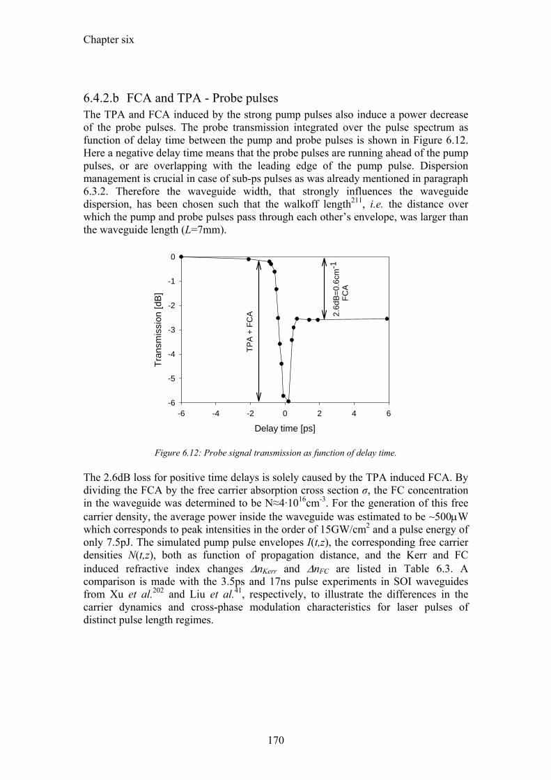
Chapter six
170
6.4.2.b FCA and TPA - Probe pulses The TPA and FCA induced by the strong pump pulses also induce a power decrease of the probe pulses. The probe transmission integrated over the pulse spectrum as function of delay time between the pump and probe pulses is shown in Figure 6.12. Here a negative delay time means that the probe pulses are running ahead of the pump pulses, or are overlapping with the leading edge of the pump pulse. Dispersion management is crucial in case of sub-ps pulses as was already mentioned in paragraph 6.3.2. Therefore the waveguide width, that strongly influences the waveguide dispersion, has been chosen such that the walkoff length211, i.e. the distance over which the pump and probe pulses pass through each other’s envelope, was larger than the waveguide length (L=7mm).
Delay time [ps]-6 -4 -2 0 2 4 6
Tran
smis
sion
[dB]
-6
-5
-4
-3
-2
-1
0
2.6d
B=0.
6cm
-1
F
CA
TPA
+ FC
A
Figure 6.12: Probe signal transmission as function of delay time. The 2.6dB loss for positive time delays is solely caused by the TPA induced FCA. By dividing the FCA by the free carrier absorption cross section σ, the FC concentration in the waveguide was determined to be N≈4·1016cm-3. For the generation of this free carrier density, the average power inside the waveguide was estimated to be ~500µW which corresponds to peak intensities in the order of 15GW/cm2 and a pulse energy of only 7.5pJ. The simulated pump pulse envelopes I(t,z), the corresponding free carrier densities N(t,z), both as function of propagation distance, and the Kerr and FC induced refractive index changes ∆nKerr and ∆nFC are listed in Table 6.3. A comparison is made with the 3.5ps and 17ns pulse experiments in SOI waveguides from Xu et al.202 and Liu et al.41, respectively, to illustrate the differences in the carrier dynamics and cross-phase modulation characteristics for laser pulses of distinct pulse length regimes.
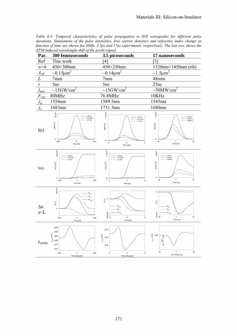
Materials III: Silicon-on-Insulator
171
Table 6.3: Temporal characteristics of pulse propagation in SOI waveguides for different pulse durations. Simulations of the pulse intensities, free carrier densities and refractive index change as function of time are shown for 300fs, 3.5ps and 17ns experiments, respectively. The last row shows the XPM induced wavelength shift of the probe signal. Par. 300 femtoseconds 3.5 picoseconds 17 nanoseconds Ref This work [4] [3] w×h 450×300nm 450×250nm 1520nm×1450nm (rib) Aeff ~0.15µm2 ~0.14µm2 ~1.5µm2 L 7mm 7mm 48mm τ 5ns 5ns 25ns Imax ~15GW/cm2 ~15GW/cm2 ~50MW/cm2 Frep 80MHz 76.8MHz 10KHz λp 1554nm 1589.5nm 1545nm λs 1683nm 1731.5nm 1680nm I(t)
Time [fs]-600 0 600
I [W
/cm
2 ]0
16x1
09
z=0mmz=3.5mmz=7mm
Time [ps]-6 0 6
I [W
/cm
2 ]0
17x1
09
z=0mmz=3.5mmz=7mm
Time [ns]-30 0 30
I [W
/cm
2 ]0
50x1
06
z=0mmz=24mmz=48mm
N(t) Time [fs]
-600 0 600
N [1
/cm
3 ]0
120x
1015
z=0mmz=3.5mmz=7mm
Time [ps]-6 0 6
N [1
/cm
3 ]0.
01.
4x10
18
z=0mmz=3.5mmz=7mm
Time [ns]-30 0 30
N [1
/cm
3 ]0
45x1
015z=0mmz=24mmz=48mm
∆n z=L
Time [fs]-600 0 600
∆n
[-]0
200x
10-6
∆nKerr
∆nFC
∆nTotal
Time [ps]-6 0 6
∆n
[-]
-400
x10-6
0
∆nKerr
∆nFC
∆nTotal
Time [ns]-30 0 30
∆ n [-
]-9
0x10
-60
∆nKerr
∆nFC
∆nTotal
λprobe
Time delay [fs]-600 0 600
λ pro
be [n
m]
1670
1675
1680
1685
1690
1695
Time delay [ps]-6 0 6
λ pro
be [n
m]
1730
1731
1732
Time delay [ns]-30 0 30
λ pro
be [n
m]
1680
1pm
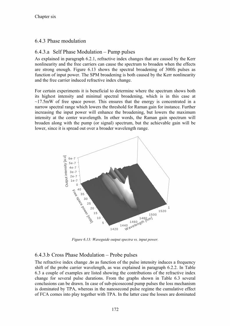
Chapter six
172
6.4.3 Phase modulation
6.4.3.a Self Phase Modulation – Pump pulses As explained in paragraph 6.2.1, refractive index changes that are caused by the Kerr nonlinearity and the free carriers can cause the spectrum to broaden when the effects are strong enough. Figure 6.13 shows the spectral broadening of 300fs pulses as function of input power. The SPM broadening is both caused by the Kerr nonlinearity and the free carrier induced refractive index change. For certain experiments it is beneficial to determine where the spectrum shows both its highest intensity and minimal spectral broadening, which is in this case at ~17.5mW of free space power. This ensures that the energy is concentrated in a narrow spectral range which lowers the threshold for Raman gain for instance. Further increasing the input power will enhance the broadening, but lowers the maximum intensity at the center wavelength. In other words, the Raman gain spectrum will broaden along with the pump (or signal) spectrum, but the achievable gain will be lower, since it is spread out over a broader wavelength range.
01e-72e-73e-74e-75e-76e-7
14201440
14601480
15001520
1
510
1520
2530
3540
Out
put i
nten
sity
[a.u
]
Wavelength [nm]
Free space power [mW
]
Figure 6.13: Waveguide output spectra vs. input power.
6.4.3.b Cross Phase Modulation – Probe pulses The refractive index change ∆n as function of the pulse intensity induces a frequency shift of the probe carrier wavelength, as was explained in paragraph 6.2.2. In Table 6.3 a couple of examples are listed showing the contributions of the refractive index change for several pulse durations. From the graphs shown in Table 6.3 several conclusions can be drawn. In case of sub-picosecond pump pulses the loss mechanism is dominated by TPA, whereas in the nanosecond pulse regime the cumulative effect of FCA comes into play together with TPA. In the latter case the losses are dominated
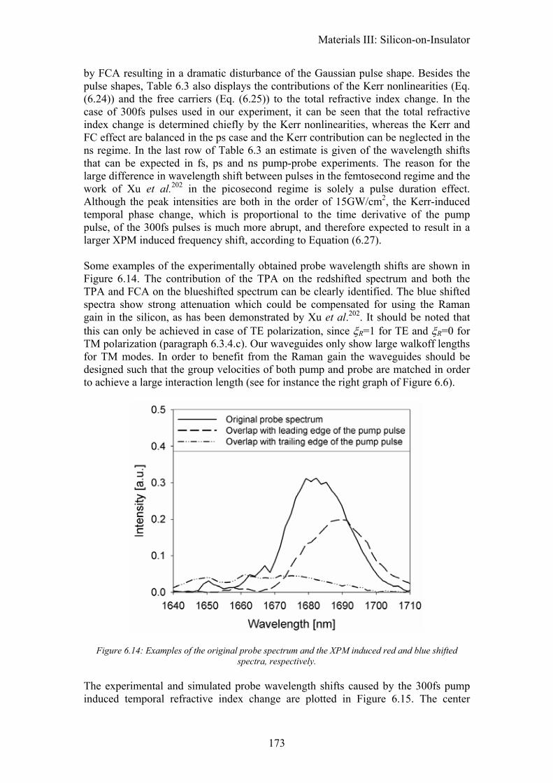
Materials III: Silicon-on-Insulator
173
by FCA resulting in a dramatic disturbance of the Gaussian pulse shape. Besides the pulse shapes, Table 6.3 also displays the contributions of the Kerr nonlinearities (Eq. (6.24)) and the free carriers (Eq. (6.25)) to the total refractive index change. In the case of 300fs pulses used in our experiment, it can be seen that the total refractive index change is determined chiefly by the Kerr nonlinearities, whereas the Kerr and FC effect are balanced in the ps case and the Kerr contribution can be neglected in the ns regime. In the last row of Table 6.3 an estimate is given of the wavelength shifts that can be expected in fs, ps and ns pump-probe experiments. The reason for the large difference in wavelength shift between pulses in the femtosecond regime and the work of Xu et al.202 in the picosecond regime is solely a pulse duration effect. Although the peak intensities are both in the order of 15GW/cm2, the Kerr-induced temporal phase change, which is proportional to the time derivative of the pump pulse, of the 300fs pulses is much more abrupt, and therefore expected to result in a larger XPM induced frequency shift, according to Equation (6.27). Some examples of the experimentally obtained probe wavelength shifts are shown in Figure 6.14. The contribution of the TPA on the redshifted spectrum and both the TPA and FCA on the blueshifted spectrum can be clearly identified. The blue shifted spectra show strong attenuation which could be compensated for using the Raman gain in the silicon, as has been demonstrated by Xu et al.202. It should be noted that this can only be achieved in case of TE polarization, since ξR=1 for TE and ξR=0 for TM polarization (paragraph 6.3.4.c). Our waveguides only show large walkoff lengths for TM modes. In order to benefit from the Raman gain the waveguides should be designed such that the group velocities of both pump and probe are matched in order to achieve a large interaction length (see for instance the right graph of Figure 6.6).
Figure 6.14: Examples of the original probe spectrum and the XPM induced red and blue shifted spectra, respectively.
The experimental and simulated probe wavelength shifts caused by the 300fs pump induced temporal refractive index change are plotted in Figure 6.15. The center
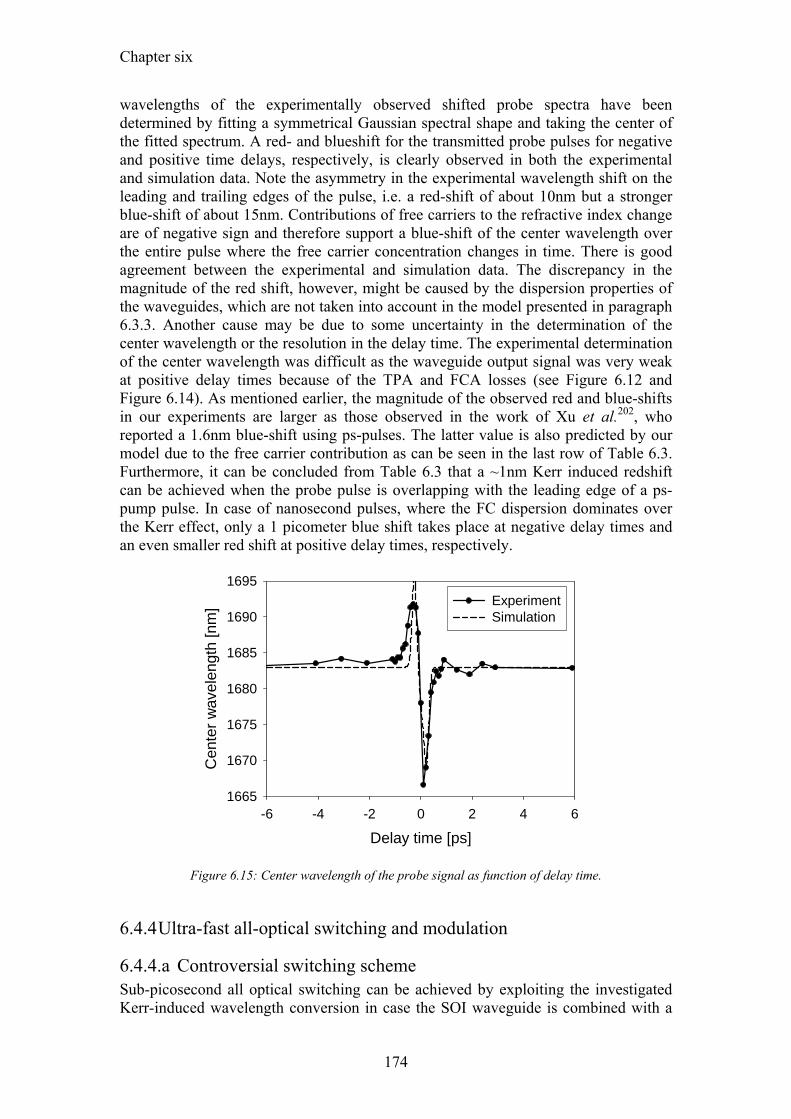
Chapter six
174
wavelengths of the experimentally observed shifted probe spectra have been determined by fitting a symmetrical Gaussian spectral shape and taking the center of the fitted spectrum. A red- and blueshift for the transmitted probe pulses for negative and positive time delays, respectively, is clearly observed in both the experimental and simulation data. Note the asymmetry in the experimental wavelength shift on the leading and trailing edges of the pulse, i.e. a red-shift of about 10nm but a stronger blue-shift of about 15nm. Contributions of free carriers to the refractive index change are of negative sign and therefore support a blue-shift of the center wavelength over the entire pulse where the free carrier concentration changes in time. There is good agreement between the experimental and simulation data. The discrepancy in the magnitude of the red shift, however, might be caused by the dispersion properties of the waveguides, which are not taken into account in the model presented in paragraph 6.3.3. Another cause may be due to some uncertainty in the determination of the center wavelength or the resolution in the delay time. The experimental determination of the center wavelength was difficult as the waveguide output signal was very weak at positive delay times because of the TPA and FCA losses (see Figure 6.12 and Figure 6.14). As mentioned earlier, the magnitude of the observed red and blue-shifts in our experiments are larger as those observed in the work of Xu et al.202, who reported a 1.6nm blue-shift using ps-pulses. The latter value is also predicted by our model due to the free carrier contribution as can be seen in the last row of Table 6.3. Furthermore, it can be concluded from Table 6.3 that a ~1nm Kerr induced redshift can be achieved when the probe pulse is overlapping with the leading edge of a ps-pump pulse. In case of nanosecond pulses, where the FC dispersion dominates over the Kerr effect, only a 1 picometer blue shift takes place at negative delay times and an even smaller red shift at positive delay times, respectively.
Delay time [ps]-6 -4 -2 0 2 4 6
Cen
ter w
avel
engt
h [n
m]
1665
1670
1675
1680
1685
1690
1695ExperimentSimulation
Figure 6.15: Center wavelength of the probe signal as function of delay time.
6.4.4 Ultra-fast all-optical switching and modulation
6.4.4.a Controversial switching scheme Sub-picosecond all optical switching can be achieved by exploiting the investigated Kerr-induced wavelength conversion in case the SOI waveguide is combined with a
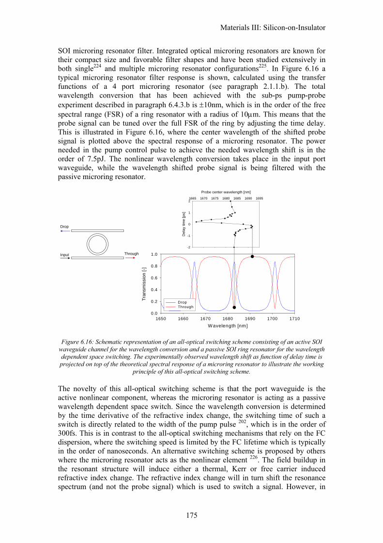
Materials III: Silicon-on-Insulator
175
SOI microring resonator filter. Integrated optical microring resonators are known for their compact size and favorable filter shapes and have been studied extensively in both single224 and multiple microring resonator configurations225. In Figure 6.16 a typical microring resonator filter response is shown, calculated using the transfer functions of a 4 port microring resonator (see paragraph 2.1.1.b). The total wavelength conversion that has been achieved with the sub-ps pump-probe experiment described in paragraph 6.4.3.b is ±10nm, which is in the order of the free spectral range (FSR) of a ring resonator with a radius of 10µm. This means that the probe signal can be tuned over the full FSR of the ring by adjusting the time delay. This is illustrated in Figure 6.16, where the center wavelength of the shifted probe signal is plotted above the spectral response of a microring resonator. The power needed in the pump control pulse to achieve the needed wavelength shift is in the order of 7.5pJ. The nonlinear wavelength conversion takes place in the input port waveguide, while the wavelength shifted probe signal is being filtered with the passive microring resonator.
Wavelength [nm]1650 1660 1670 1680 1690 1700 1710
Tran
smis
sion
[-]
0.0
0.2
0.4
0.6
0.8
1.0
DropThrough
Probe center wavelength [nm]
1665 1670 1675 1680 1685 1690 1695
Del
ay ti
me
[ps]
-2
-1
0
1
2
Input
Drop
Through
Figure 6.16: Schematic representation of an all-optical switching scheme consisting of an active SOI waveguide channel for the wavelength conversion and a passive SOI ring resonator for the wavelength dependent space switching. The experimentally observed wavelength shift as function of delay time is projected on top of the theoretical spectral response of a microring resonator to illustrate the working
principle of this all-optical switching scheme. The novelty of this all-optical switching scheme is that the port waveguide is the active nonlinear component, whereas the microring resonator is acting as a passive wavelength dependent space switch. Since the wavelength conversion is determined by the time derivative of the refractive index change, the switching time of such a switch is directly related to the width of the pump pulse 202, which is in the order of 300fs. This is in contrast to the all-optical switching mechanisms that rely on the FC dispersion, where the switching speed is limited by the FC lifetime which is typically in the order of nanoseconds. An alternative switching scheme is proposed by others where the microring resonator acts as the nonlinear element 226. The field buildup in the resonant structure will induce either a thermal, Kerr or free carrier induced refractive index change. The refractive index change will in turn shift the resonance spectrum (and not the probe signal) which is used to switch a signal. However, in
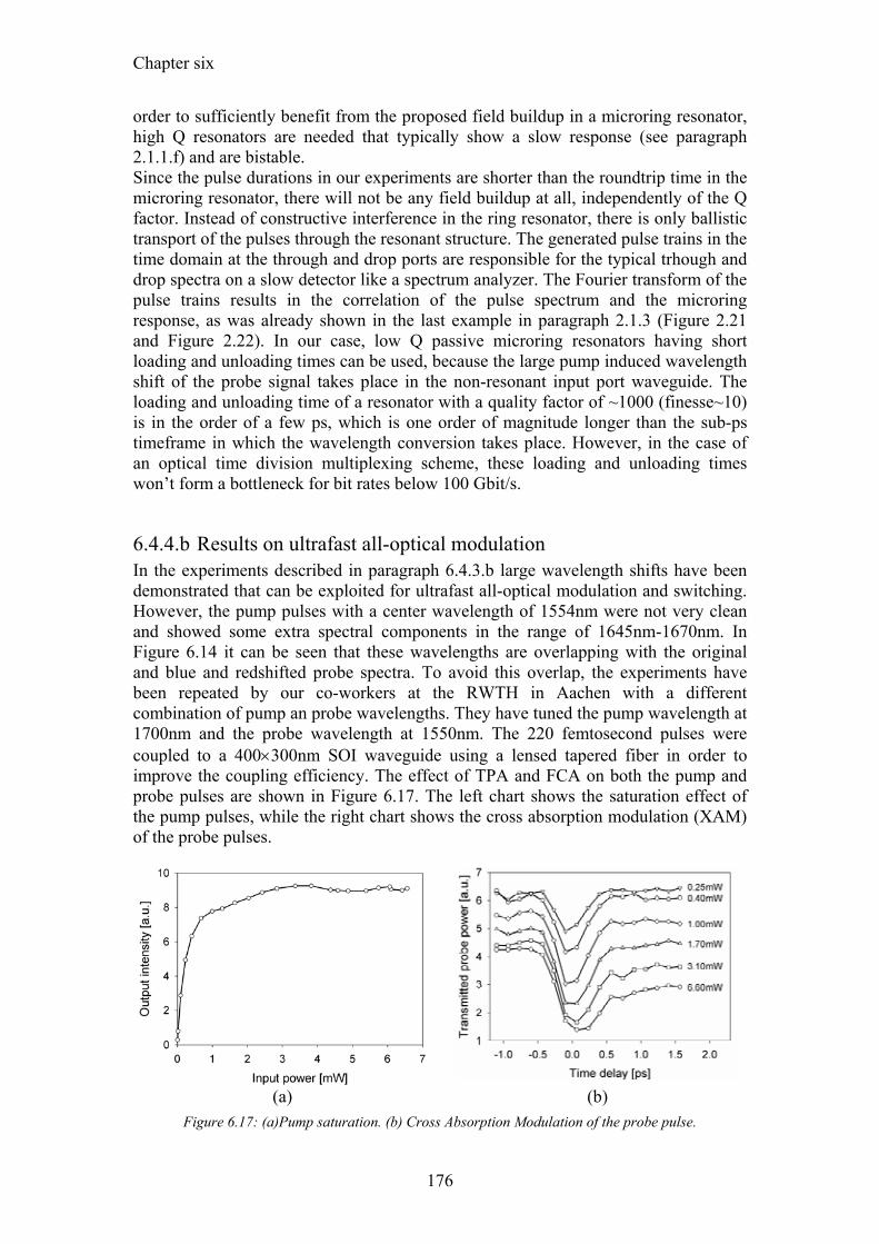
Chapter six
176
order to sufficiently benefit from the proposed field buildup in a microring resonator, high Q resonators are needed that typically show a slow response (see paragraph 2.1.1.f) and are bistable. Since the pulse durations in our experiments are shorter than the roundtrip time in the microring resonator, there will not be any field buildup at all, independently of the Q factor. Instead of constructive interference in the ring resonator, there is only ballistic transport of the pulses through the resonant structure. The generated pulse trains in the time domain at the through and drop ports are responsible for the typical trhough and drop spectra on a slow detector like a spectrum analyzer. The Fourier transform of the pulse trains results in the correlation of the pulse spectrum and the microring response, as was already shown in the last example in paragraph 2.1.3 (Figure 2.21 and Figure 2.22). In our case, low Q passive microring resonators having short loading and unloading times can be used, because the large pump induced wavelength shift of the probe signal takes place in the non-resonant input port waveguide. The loading and unloading time of a resonator with a quality factor of ~1000 (finesse~10) is in the order of a few ps, which is one order of magnitude longer than the sub-ps timeframe in which the wavelength conversion takes place. However, in the case of an optical time division multiplexing scheme, these loading and unloading times won’t form a bottleneck for bit rates below 100 Gbit/s.
6.4.4.b Results on ultrafast all-optical modulation In the experiments described in paragraph 6.4.3.b large wavelength shifts have been demonstrated that can be exploited for ultrafast all-optical modulation and switching. However, the pump pulses with a center wavelength of 1554nm were not very clean and showed some extra spectral components in the range of 1645nm-1670nm. In Figure 6.14 it can be seen that these wavelengths are overlapping with the original and blue and redshifted probe spectra. To avoid this overlap, the experiments have been repeated by our co-workers at the RWTH in Aachen with a different combination of pump an probe wavelengths. They have tuned the pump wavelength at 1700nm and the probe wavelength at 1550nm. The 220 femtosecond pulses were coupled to a 400×300nm SOI waveguide using a lensed tapered fiber in order to improve the coupling efficiency. The effect of TPA and FCA on both the pump and probe pulses are shown in Figure 6.17. The left chart shows the saturation effect of the pump pulses, while the right chart shows the cross absorption modulation (XAM) of the probe pulses.
(a) (b)
Figure 6.17: (a)Pump saturation. (b) Cross Absorption Modulation of the probe pulse.
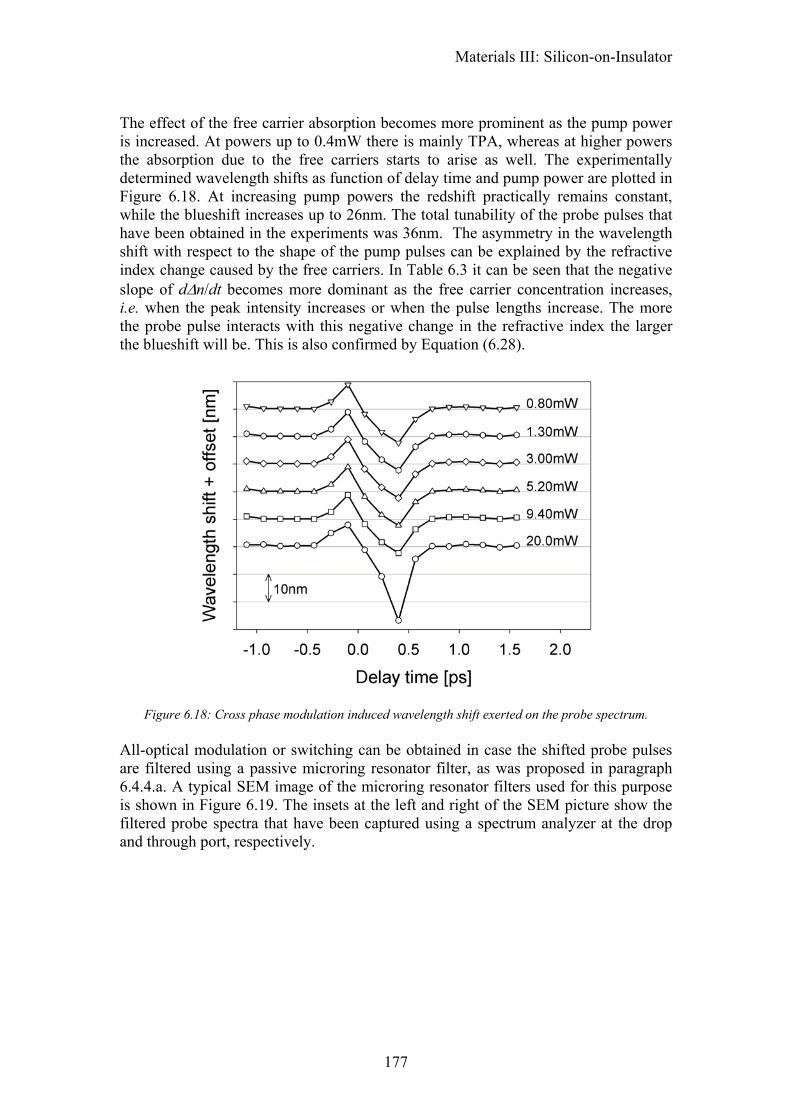
Materials III: Silicon-on-Insulator
177
The effect of the free carrier absorption becomes more prominent as the pump power is increased. At powers up to 0.4mW there is mainly TPA, whereas at higher powers the absorption due to the free carriers starts to arise as well. The experimentally determined wavelength shifts as function of delay time and pump power are plotted in Figure 6.18. At increasing pump powers the redshift practically remains constant, while the blueshift increases up to 26nm. The total tunability of the probe pulses that have been obtained in the experiments was 36nm. The asymmetry in the wavelength shift with respect to the shape of the pump pulses can be explained by the refractive index change caused by the free carriers. In Table 6.3 it can be seen that the negative slope of d∆n/dt becomes more dominant as the free carrier concentration increases, i.e. when the peak intensity increases or when the pulse lengths increase. The more the probe pulse interacts with this negative change in the refractive index the larger the blueshift will be. This is also confirmed by Equation (6.28).
Figure 6.18: Cross phase modulation induced wavelength shift exerted on the probe spectrum. All-optical modulation or switching can be obtained in case the shifted probe pulses are filtered using a passive microring resonator filter, as was proposed in paragraph 6.4.4.a. A typical SEM image of the microring resonator filters used for this purpose is shown in Figure 6.19. The insets at the left and right of the SEM picture show the filtered probe spectra that have been captured using a spectrum analyzer at the drop and through port, respectively.
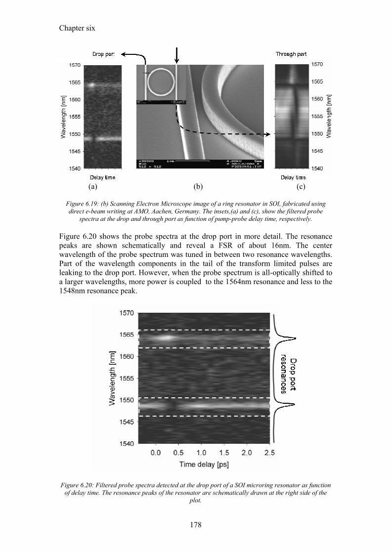
Chapter six
178
(a) (b) (c)
Figure 6.19: (b) Scanning Electron Microscope image of a ring resonator in SOI, fabricated using direct e-beam writing at AMO, Aachen, Germany. The insets,(a) and (c), show the filtered probe
spectra at the drop and through port as function of pump-probe delay time, respectively. Figure 6.20 shows the probe spectra at the drop port in more detail. The resonance peaks are shown schematically and reveal a FSR of about 16nm. The center wavelength of the probe spectrum was tuned in between two resonance wavelengths. Part of the wavelength components in the tail of the transform limited pulses are leaking to the drop port. However, when the probe spectrum is all-optically shifted to a larger wavelengths, more power is coupled to the 1564nm resonance and less to the 1548nm resonance peak.
Figure 6.20: Filtered probe spectra detected at the drop port of a SOI microring resonator as function
of delay time. The resonance peaks of the resonator are schematically drawn at the right side of the plot.
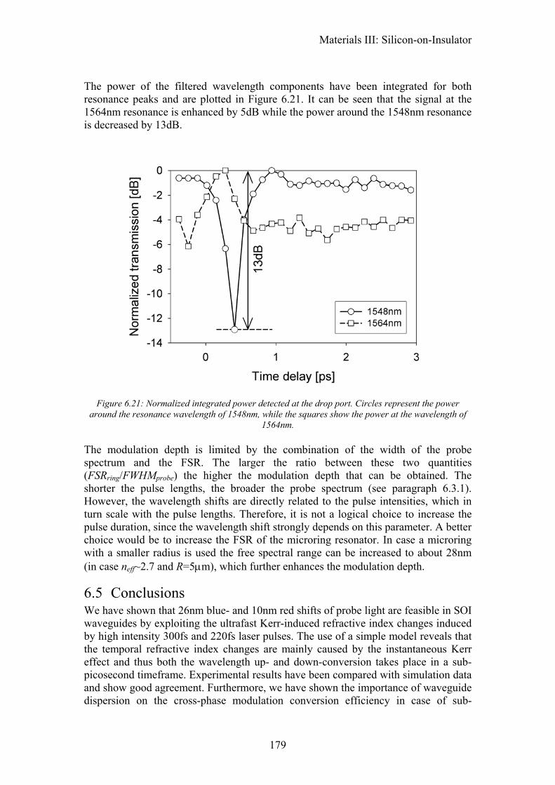
Materials III: Silicon-on-Insulator
179
The power of the filtered wavelength components have been integrated for both resonance peaks and are plotted in Figure 6.21. It can be seen that the signal at the 1564nm resonance is enhanced by 5dB while the power around the 1548nm resonance is decreased by 13dB.
Figure 6.21: Normalized integrated power detected at the drop port. Circles represent the power around the resonance wavelength of 1548nm, while the squares show the power at the wavelength of
1564nm. The modulation depth is limited by the combination of the width of the probe spectrum and the FSR. The larger the ratio between these two quantities (FSRring/FWHMprobe) the higher the modulation depth that can be obtained. The shorter the pulse lengths, the broader the probe spectrum (see paragraph 6.3.1). However, the wavelength shifts are directly related to the pulse intensities, which in turn scale with the pulse lengths. Therefore, it is not a logical choice to increase the pulse duration, since the wavelength shift strongly depends on this parameter. A better choice would be to increase the FSR of the microring resonator. In case a microring with a smaller radius is used the free spectral range can be increased to about 28nm (in case neff~2.7 and R=5µm), which further enhances the modulation depth.
6.5 Conclusions We have shown that 26nm blue- and 10nm red shifts of probe light are feasible in SOI waveguides by exploiting the ultrafast Kerr-induced refractive index changes induced by high intensity 300fs and 220fs laser pulses. The use of a simple model reveals that the temporal refractive index changes are mainly caused by the instantaneous Kerr effect and thus both the wavelength up- and down-conversion takes place in a sub-picosecond timeframe. Experimental results have been compared with simulation data and show good agreement. Furthermore, we have shown the importance of waveguide dispersion on the cross-phase modulation conversion efficiency in case of sub-

Chapter six
180
picosecond pump-probe experiments. We have demonstrated ultrafast all-optical modulation of a probe signal with a modulation depth of 13dB, which can be further improved by employing SOI microring resonators with smaller radii. These results open the way to sub-picosecond all-optical switching using SOI microring resonators or waveguide gratings.
181
7 Conclusions
Three different material systems and their application in optical micro resonators are presented in this thesis. A horizontally coupled microring resonator was chosen as the basic building block throughout the thesis in order to facilitate a straightforward processing scheme. Because of the single lithography step needed for this type of device, a strong focus on the optical processes of the material systems, i.e. Er:Al2O3, nanoparticle doped photosensitive polymers and Silicon-on-Insulator, could be preserved. The overall aim of the research presented in this thesis was to demonstrate ultrafast all-optical switching and modulation using micro resonators by exploiting the nonlinear properties (i.e. optical gain, the optical Kerr effect and free carrier dispersion) of the investigated material systems.
Chapter seven
182
All-optical switching using microring resonators can be achieved in several ways, of which the following three methods have been discussed in this thesis: 1. Shifting the resonance wavelength by all-optically modifying the effective
refractive index (Kerr, free carriers). In this case the microring is used as an active switching element.
2. All-optical modification of the absorption in the microring resonator and herewith switch from a low-Q resonator to a high-Q resonator. This can be done in material systems that exhibit optical gain. The microring is used as an active switching element in this case as well.
3. Shifting the carrier wavelength into or out of resonance by means of Cross Phase Modulation before the signal is coupled to the microring resonator. The microring resonator is used as a passive filtering element in this case.
In the first case the field enhancement of the microring is being exploited. A high quality ring resonator is needed to generate a substantial field enhancement and to benefit from the induced refractive index change. In the second case, the quality factor of the microring resonator is all-optically modulated by the optical gain. However, in both of these cases high quality resonators are needed. High quality resonators typically have large loading and unloading times and are thus slow. This is a contradiction in case ultrafast all-optical switching is required. The third proposed method for all-optical switching is to make use of a low quality ring resonator that acts as a passive filter element. The passive filter element can be used as a wavelength dependent space switch for a signal that is wavelength converted in a non-resonant straight waveguide. Ultrafast all-optical modulation has successfully been demonstrated with Cross Phase Modulation experiments in Silicon-on Insulator waveguides. Several material systems that exhibit optical gain and large optical Kerr nonlinearities have been investigated and the feasibility to achieve all-optical switching by one of the three methods discussed above has been studied. The first material system that is presented in this thesis is erbium doped aluminum oxide. It can be concluded that reactive DC sputtering of aluminum produces optical thin films with bad reproducibility with respect to the propagation losses. The main reason for this is the nodule formation on the sputter target as function of plasma exposure, which causes particles to be incorporated in the deposited films that act as strong scatter centers. Nodule formation can be prevented by an RF sputter process, yielding reproducible optical thin films with low loss. In case of a horizontal ring resonator coupling scheme, waveguide fabrication with straight sidewalls is beneficial. It was found that chlorine and bromine based plasma etching yields the best results with respect to the sidewall angle. In order to achieve net optical gain in Al2O3 waveguides with an erbium content of 0.2 atomic percent, additional propagation losses induced by the sidewall roughness may not exceed ~0.1dB/cm, which imposes a stringent demand on the etching process. However, since the upconversion coefficient is found to be very low in our reactively co-sputtered films, the concentration could be increased in future experiments in order to increase the optical gain. The optical gain can be used to compensate for the losses in the ring resonator and modulate or switch a signal by modifying the quality factor of the ring
Conclusions
183
which strongly depends on the roundtrip losses. Unfortunately, no waveguides and ring resonators have been fabricated because of the non-reproducible thin film deposition and the fact that the proper etching equipment was unavailable. However, the findings are valuable for future research in this field. The second material system that has been developed is based on erbium and neodymium doped lanthanum fluoride nanoparticles which can be dissolved into UV sensitive polymers and sol-gel materials. The neodymium doped nanoparticles show optical gain around 1319nm when applied in multimode waveguides. In order to all-optically modulate or switch an optical signal, absorption modulation in a monomode microring resonator could be exploited. However, no net gain has been observed in case of monomode waveguides, which is believed to be caused by the increased sidewall roughness of the waveguides at high nanoparticle concentrations. Erbium doped LaF3 nanoparticles showed improved excited state lifetimes in TEOS based sol-gels, since the LaF3 host shields the erbium ions from the quenching hydroxyl rich environment. Crystalline silicon has been investigated as the third material for use in integrated optical devices. The optical Kerr nonlinearity and free carrier generation in combination with femtosecond pulses has successfully been exploited to achieve ultrafast wavelength conversion by means of Cross Phase Modulation in a straight SOI waveguide. A passive SOI microring resonator filter has been used to switch the wavelength converted signal. With respect to switching speed, it can be concluded that filtering of an all-optically wavelength converted signal using a passive ring resonator is the most beneficial method, since the passive filtering element can be designed such that it is suitable for high speed operation. This is in contrast to the switching methods that rely on high-Q resonators of which the optical properties are modified all-optically.

185
Figure 1.1: (a) Optical fiber. (b) Planar optical waveguide. ..........................................3
Figure 1.2: (a) Large waveguide (2×3µm) with low refractive index contrast (∆n=0.05). (b) Small waveguide (200×600nm)with a high refractive index contrast (∆n=2.00).Field profiles have been determined using Olympios2 software. .................4
Figure 1.3: (a) TE0 mode. (b): TE1 mode. Field profiles have been determined using Olympios2 software........................................................................................................5
Figure 1.4: Optical fiber losses as a function of wavelength. The solid line represents the experimental losses according to Miya et al.3..........................................................5
Figure 2.1: Schematic drawing of a microring resonator. ...........................................10
Figure 2.2: Schematic representation of a vertically (a) and laterally (b) coupled microring resonator......................................................................................................10
Figure 2.3: Example of the normalized through and drop port transmission spectra. .12
Figure 2.4: (a) Effective refractive indices for modes in a Si3N4 ring resonator (2µm×145nm, R=110µm) embedded in SiO2. (b) Effective refractive index for the fundamental TE0 mode and the corresponding group index ng. ..................................12
Figure 2.5: FSR for Si3N4 ring resonators (2µm×145nm) embedded in SiO2 with radii of 50µm, 110µm and 200µm, respectively..................................................................13
Figure 2.6: Finesse as function of the optical losses and the coupling constant for a symmetric microring resonator (a represents the linear loss, L the propagation length and κ the fraction of the field that is coupled from and to the ring). ...........................14
Figure 2.7: Symmetric (a) and anti-symmetric (b) mode of the coupler region of a polymer microring resonator structure.........................................................................15
List of figures
186
Figure 2.8: Coupling length as function of the gap between microring and port waveguide for various pump and signal wavelengths for the coupler geometry presented in Figure 2.17 ..............................................................................................16
Figure 2.9: Coupling constant as function of racetrack length and coupling gap. For this particular example, a coupling gap of 1.9µm results in a coupling length of 9300µm, corresponding to the scaling parameters d0 and Lc0, respectively. ...............17
Figure 2.10: Field distributions of both a straight (a) and a bend waveguide(b) curved to the left. .....................................................................................................................17
Figure 2.11: Schematic representation of one of the two coupling regions in a racetrack resonator. An increased width of the bends can be applied to further decrease the transition losses. ......................................................................................18
Figure 2.12: (a) Optimum offset that should be applied to have the lowest transition losses. (b) The transition loss in case no offset is applied. Calculations have been performed using a 2D-bend solver from Olympios2 in case of a Si3N4 waveguide with a thickness of 145 nm, embedded in SiO2. ..................................................................18
Figure 2.13: Bend radiation losses as function of bend radius. ...................................19
Figure 2.14: Schematic representation of drop-port resonance tuning. .......................20
Figure 2.15: Schematic representation of transmission tuning by absorption modulation. (a) Losses of 10dB/cm. (b) Losses of 0dB/cm. .......................................21
Figure 2.16: Field buildup in a microring resonator with ng=1.7, λ0=1550nm, FSR = 2nm and R=110µm. Bend losses in the ring have been set at 1dB/cm. (Top) Q~8600. (Bottom) Q~ 130000....................................................................................................22
Figure 2.17: Typical ring resonator and racetrack mask design.(a) Total view. (b) Lay-out of a small part of the mask design (indicated by black box in the left image). Mask design by Edwin Klein.................................................................................................23
Figure 2.18: Process flow of the major fabrication steps for laterally coupled Si3N4 microring resonators. ...................................................................................................24
Figure 2.19: Microscope image of laterally coupled Si3N4 racetrack resonators. The inset shows a detailed view of the transition from bend to straight waveguide of a racetrack with a gap op 800nm. ...................................................................................25
Figure 2.20: Low (a) and high resolution (b) through port responses of a laterally coupled Si3N4 microring resonator with a racetrack length of 40µm and a gap of 800nm. .........................................................................................................................25
Figure 2.21: Through and drop port responses for a Si3N4 microring resonator. The solid line represents the transmission measured using a tunable laser in combination with a photodetector. The dashes lines show the transmission of 200 femtosecond pulses through both the through and drop port. ...........................................................26
List of figures
187
Figure 2.22: Schematic representation of the generation of pulse trains at the through and drop ports of a microring resonator by feeding with a single femtosecond pulse.27
Figure 2.23: Schematic representation of a waveguide grating etched in a slab waveguide. ...................................................................................................................27
Figure 2.24: Schematic representation of a Bragg stack. Some ray paths are drawn to illustrate the multiple reflections and interference that takes place at each interface..28
Figure 2.25: Screen capture of the mode solver SimuLayer which is developed by us. The bar with different gray intensities above the mode profile represents the refractive indices (light = lowest refractive index, dark = highest refractive index) and the vertical lines represent the interfaces. Both the refractive indices and interfaces can be dragged by the user, while the mode profile(s) are calculated and drawn in real-time. .............................................................................................................................29
Figure 2.26: Transmission spectra of both a simulation using the Transfer Matrix Method (solid) and an experiment (dashed), respectively. The minimum transmission of the experimental data is caused by slab light and scattered light captured by the photo detector...............................................................................................................30
Figure 2.27: Artist impression of a polymer drop applied as a top cladding on the grating regions. ............................................................................................................31
Figure 2.28:(a)Effective mode indices for the tooth and groove regions of the fabricated waveguide gratings as a function of the top cladding refractive index. The effective indices have been calculated using the Effective Index Method. (b) Transmission and bandgap position as function of the top cladding refractive index determined using the Transfer Matrix Method. ...........................................................32
Figure 2.29: Artist impression of the most important fabrication steps involved in the realization of straight and apodized waveguide gratings. ............................................33
Figure 2.30: Photograph of the finished grating devices. The reflections reveal the positions were the LIL defined gratings are located. ...................................................34
Figure 2.31: Optical transmission through a waveguide grating (500 periods) with an air and polymer top cladding, respectively. .................................................................35
Figure 2.32: Optical transmission of linear gratings with 500 (top) and 1000 (bottom) period, respectively. The graphs on the left show the full bandgap, whereas the right plots zoom in on the high-Q features in the airband of the grating. The FSR of the fringes in the bandgap are almost the same for both gratings......................................36
Figure 2.33: Whispering gallery modes propagating along the air/polymer interface.37
Figure 2.34: Out of plane scattering of waveguide gratings. (top) Artist impression of both a linear(I) and an apodized waveguide grating (II). (bottom left) Camera images of the out of plane scattering in the stopband (A), at the first fringe(B) and the third fringe(C) in the dielectric band, and in transmission (D) with no strong enhancement. (bottom right) Integration of pixel intensities in a ROI box as function of wavelength
List of figures
188
for both a linear(I) and apodized grating (II).Measurements performed by Wico Hopman........................................................................................................................38
Figure 3.1: Attenuation according to Lambert-Beer....................................................42
Figure 3.2: Examples of the measured infrared absorption peaks caused by the overtones of molecular bonds. (Top) OH and NH losses in a PECVD deposited SiON film deposited by G. Hussein. (Bottom) Typical OH and CH losses in a Bisphenol-A based polymer film (see Chapter 5). ............................................................................44
Figure 3.3: Comparison of Mie and Rayleigh scattering for micron- and nano-scale LaF3-particles in water. ................................................................................................46
Figure 3.4: Schematic representation of TPA in silicon. (a) Degenerate. (b) Non-degenerate. ...................................................................................................................47
Figure 3.5: Schematic representation of the absorption and emission process in a simplified two-state model of a rare-earth ion. Here σij, σji and Ezl are the absorption cross section, emission cross section and the zero line energy, respectively. .............50
Figure 3.6: Absorption and emission of an erbium doped fiber in the 3rd telecommunication window. ........................................................................................50
Figure 3.7: Relation between the effective linewidth and the spectral lineshape........54
Figure 3.8: Emission cross section of the erbium ions in an erbium doped fiber derived with the aid of the Füchtbauer-Ladenburg relation.........................................55
Figure 3.9: Absorption cross sections for erbium ions in an erbium doped fiber derived from the absorption spectrum and emission cross section, respectively. The thick solid line represents the emission cross sections obtained using the Füchtbauer-Ladenburg relation in combination with the photoluminescence spectrum. ...............56
Figure 3.10: Schematic representation of a three-level laser system...........................58
Figure 3.11: A selection of energy transitions in erbium. Energy levels and corresponding wavelengths were adapted from W.J. Miniscalco61. ............................60
Figure 3.12: (a) Absorption and (b) emission cross sections of erbium in a silica glass host. Only very low 980nm emission is shown upon excitation with a 532nm laser in the logarithmic emission spectrum (circle)..................................................................60
Figure 3.13: Small signal gain as function of propagation distance for erbium concentrations of 1×1026, 3×1026,and 5×1026m-3, respectively, in a silica waveguide. Gain for all three concentrations is shown with and without upconversion taken into account. ........................................................................................................................64
Figure 3.14: Schematic representation of a four-level laser system. ...........................65
Figure 3.15: A selection of energy transitions in neodymium. Energy levels and corresponding wavelengths were adapted from J.B. Gruber et al.63. The 4F3/2 level is the ULL and the 4I15/2, 4I13/2, 4I11/2, and 4I9/2 levels serve as the four LLLs. .................66
List of figures
189
Figure 3.16: Normalized absorption and emission spectra of neodymium doped LaF3 in dichloromethane solution. Measurements and synthesis performed by J.W. Stouwdam66..................................................................................................................67
Figure 3.17: Small signal gain for neodymium doped waveguides with varying cross sections.The simulation parameters are listed in Table 3.2. ........................................70
Figure 3.18: Schematic representation of two loss characterization setups based on scattering. .....................................................................................................................75
Figure 3.19: Examples of captured images using the IR camera. (a) Background scattering. (b) Background scattering and propagation of the fundamental slab mode. (c) Scattering of the fundamental slab mode with background subtraction. (d) Selection of a region of interest for the loss analysis...................................................76
Figure 3.20: Results of the loss analysis of an erbium doped Al2O3 slab waveguide. The solid line shows the results of the fully automated camera setup. The circles represent the manual analysis results of the moving fiber bundle method. .................76
Figure 3.21: Schematic drawing of the dual prism loss measurement setup. ..............77
Figure 3.22: Optical loss calculations using a range of transmission spectra. As an example, the theoretical fits are shown for two wavelengths (1210nm and 1290nm) around the 3rd overtone absorption band of the CH-bonds that are present in the polymer. .......................................................................................................................78
Figure 3.23: Screenshot of SimuLayer22 thin film simulation software. The effective refractive indices are shown for the modes of wavelengths ranging from 400-2000nm that can propagate in an 800nm film with a refractive index of 1.67. The corresponding external prism angles are plotted on the right axis, together with a true color representation of the corresponding wavelengths. A black intensity in the color spectra represents infrared wavelengths, which are not visible for the naked eye. .....79
Figure 3.24: Measurement setup with microscope objectives and linear infrared CCD camera. .........................................................................................................................80
Figure 3.25: Graphical representation of the numerical apertures of two microscope objectives (M1 and M2) and a waveguide. The numerical aperture is indicated with dotted lines ...................................................................................................................80
Figure 3.26: Numerical apertures for various lens objectives. The dashed curve shows a parabolic fit. Immersion liquid is needed for magnifications above the horizontal dashed line. ..................................................................................................................81
Figure 3.27: Coupling losses due to modal overlap mismatch for high and moderate contrast waveguides. ....................................................................................................82
Figure 3.28: Butt-end coupling setup using an array of optical fibers.........................83
Figure 3.29: In house fabricated Fiber Array Unit (FAU) with 6 different types of fibers.The 9µm fibers and the small core fiber(tapered from 9µm to 4µm) offer single mode operation in the infrared (1330nm and 1550nm). The 4µm fiber is singlemode
List of figures
190
for the visible wavelengths and is beyond cut-off for the infrared wavelengths, whereas the 6µm can support somewhat longer wavelengths. The polarization maintaining (PM) fiber is single mode for the telecommunication wavelemgths as well, and the 50µm fiber can be used for characterization of multimode polymer waveguides...................................................................................................................84
Figure 3.30: Schematic representation of the pump-probe setup. ...............................85
Figure 4.1: Gas and pressure dependence of the mean free path in a vacuum system.89
Figure 4.2 Sputter rate hysteresis in reactive sputtering. .............................................90
Figure 4.3: (Top) Magnetic field lines and electron trajectory in a magnetron sputtering gun. (Bottom) A new and a used aluminum target after 3000kWh of operation. .....................................................................................................................91
Figure 4.4: Shift in process parameters as function of target erosion..........................92
Figure 4.5: Sputtering yield of aluminum in an argon plasma as function of sputtering energy. Experimental data was taken from various references125-132. The bottom insets show the argon ion paths into an aluminum target for 500eV and 10keV, respectively. The calculations were performed using SRIM software118 (Stopping and Range of Ions in Matter)..............................................................................................................93
Figure 4.6: Aluminum sputter yield as function of the angle of incidence of incoming argon ions.....................................................................................................................94
Figure 4.7: Magnetic field strength above a sputter gun. QuickField133 simulations and measurements using a magnetometer. .........................................................................95
Figure 4.8: SEM images of (a) Al2O3 nodules formed near the erosion tracks of an aluminum target after 3000 kWh and (b) Al2O3 particles incorporated in the sputtered Al2O3 film. ...................................................................................................................96
Figure 4.9: (a) Erbium concentration as function of applied RF sputter power. (b) Lifetime as function of the erbium concentration. Values have been obtained by Sami Musa135, 139. ..................................................................................................................97
Figure 4.10: Optical loss spectrum of an erbium co-sputtered Al2O3 film..................98
Figure 4.11: Emission and absorption cross section spectra of erbium RF co-sputtered Er:Al2O3 films. (a) Emission cross section. (b) Absorption cross section...................99
Figure 4.12: Theoretical gain for Er:Al2O3 in case of varying upconversion coefficients...................................................................................................................99
Figure 4.13: Optical losses of RF sputtered Al2O3. ...................................................101
Figure 4.14: Schematic representation of Al2O3 etch profiles for various investigated etching methods. ........................................................................................................103
List of figures
191
Figure 4.15: (Top) Illustration of a double argon implantation profile and the resulting amorphization of the film. (Bottom) Waveguide cross section of a wet etched Al2O3 film after selective implantation with argon (50keV & 180keV, dose=4.1016ions/cm2, etchant 85%H3PO4 at 100°C). ...................................................................................104
Figure 4.16: (Top) Chlorine based RIE etched Al2O3 waveguides with patterned resist on top. The left image shows a bad selectivity, whereas the right image shows a good selectivity between resist and the Al2O3 (Bottom) Al2O3 ridge waveguide with steep sidewalls.....................................................................................................................105
Figure 5.1: Molecular structure of the diglycidylether of Bisphenol A.....................109
Figure 5.2: SEM images of photo defined polymer waveguides...............................110
Figure 5.3: Optical losses of BPA based photo-definable polymer slab waveguide measured using the broadband prism setup (see paragraph 3.4.1). Solid line: polymer with absorbed water from the air. Dotted line: after heating for15 minutes at 100°C, resulting in a lower OH absorption by annealing out the absorbed water. ................110
Figure 5.4: A 10 weight percent nanoparticle doped BPA waveguide. (a) After development, not fully cured. (b) After 1 minute reflow at 120ºC............................111
Figure 5.5: Refractive index tuning by mixing BPA1075 and UVR. See Diemeer et al.155............................................................................................................................112
Figure 5.6: Demonstration of the excellent planarization properties of photosensitive polymer cladding materials. (a) Singlemode waveguide cross-section. (b) Multimode waveguide cross-section. ...........................................................................................112
Figure 5.7: Spin curves for (a) BPA1075 and (b) EPR500 epoxy resins. .................113
Figure 5.8: Solid volume fraction according to Bruggeman, Equation (5.2), for various bulk refractive indices. ..................................................................................115
Figure 5.9: Molecular structure of Tetra-Ethyl-Ortho-Silicate (TEOS). ...................116
Figure 5.10: Molecular structures of some of the precursors for the synthesis of rare earth doped nanoparticles. .........................................................................................117
Figure 5.11: Transmission electron microscope image of LaF3-nanoparticles.The inset shows a schematic representation of a nanoparticle with ligands attached. ..............117
Figure 5.12: Absorption (a) and emission (b) of Nd:LaF3. Absorption (c) and emission (d) of Er:LaF3. Measurements by J.W. Stouwdam. ...................................................118
Figure 5.13: Particle induced scattering losses for several refractive index mismatches....................................................................................................................................119
Figure 5.14: Refractive index versus wavelength for BPA, LaF3 and SiO2 (top) and the theoretical Rayleigh scattering losses for LaF3 nanoparticles with different sizes in SiO2 (middle) and BPA based polymer (bottom), respectively. ................................120
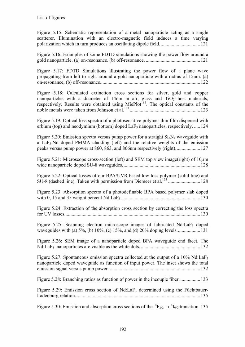
List of figures
192
Figure 5.15: Schematic representation of a metal nanoparticle acting as a single scatterer. Illumination with an electro-magnetic field induces a time varying polarization which in turn produces an oscillating dipole field. ................................121
Figure 5.16: Examples of some FDTD simulations showing the power flow around a gold nanoparticle. (a) on-resonance. (b) off-resonance. ............................................121
Figure 5.17: FDTD Simulations illustrating the power flow of a plane wave propagating from left to right around a gold nanoparticle with a radius of 15nm. (a) on-resonance, (b) off-resonance.................................................................................122
Figure 5.18: Calculated extinction cross sections for silver, gold and copper nanoparticles with a diameter of 14nm in air, glass and TiO2 host materials, respectively. Results were obtained using MiePlot181. The optical constants of the noble metals were taken from Johnson et al.183 .........................................................123
Figure 5.19: Optical loss spectra of a photosensitive polymer thin film dispersed with erbium (top) and neodymium (bottom) doped LaF3 nanoparticles, respectively. .....124
Figure 5.20: Emission spectra versus pump power for a straight Si3N4 waveguide with a LaF3:Nd doped PMMA cladding (left) and the relative weights of the emission peaks versus pump power at 860, 863, and 866nm respectively (right)....................127
Figure 5.21: Microscope cross-section (left) and SEM top view image(right) of 10µm wide nanoparticle doped SU-8 waveguides...............................................................128
Figure 5.22: Optical losses of our BPA/UVR based low loss polymer (solid line) and SU-8 (dashed line). Taken with permission from Diemeer et al.155 ..........................128
Figure 5.23: Absorption spectra of a photodefinable BPA based polymer slab doped with 0, 15 and 35 weight percent Nd:LaF3. ...............................................................130
Figure 5.24: Extraction of the absorption cross section by correcting the loss spectra for UV losses..............................................................................................................130
Figure 5.25: Scanning electron microscope images of fabricated Nd:LaF3 doped waveguides with (a) 5%, (b) 10%, (c) 15%, and (d) 20% doping levels...................131
Figure 5.26: SEM image of a nanoparticle doped BPA waveguide end facet. The Nd:LaF3 nanoparticles are visible as the white dots. ................................................132
Figure 5.27: Spontaneous emission spectra collected at the output of a 10% Nd:LaF3 nanoparticle doped waveguide as function of input power. The inset shows the total emission signal versus pump power. .........................................................................132
Figure 5.28: Branching ratios as function of power in the incouple fiber. ................133
Figure 5.29: Emission cross section of Nd:LaF3 determined using the Füchtbauer-Ladenburg relation. ....................................................................................................135
Figure 5.30: Emission and absorption cross sections of the 4F3/2 → 4I9/2 transition. 135
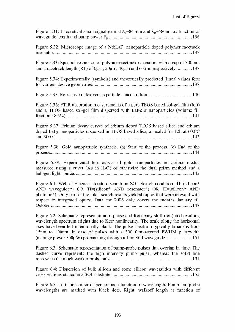
List of figures
193
Figure 5.31: Theoretical small signal gain at λs=863nm and λp=580nm as function of waveguide length and pump power Pp.......................................................................136
Figure 5.32: Microscope image of a Nd:LaF3 nanoparticle doped polymer racetrack resonator.....................................................................................................................137
Figure 5.33: Spectral responses of polymer racetrack resonators with a gap of 300 nm and a racetrack length (RT) of 0µm, 20µm, 40µm and 60µm, respectively. ............138
Figure 5.34: Experimentally (symbols) and theoretically predicted (lines) values forκ for various device geometries. ...................................................................................138
Figure 5.35: Refractive index versus particle concentration. ....................................140
Figure 5.36: FTIR absorption measurements of a pure TEOS based sol-gel film (left) and a TEOS based sol-gel film dispersed with LaF3:Er nanoparticles (volume fill fraction ~8.3%). .........................................................................................................141
Figure 5.37: Erbium decay curves of erbium doped TEOS based silica and erbium doped LaF3 nanoparticles dispersed in TEOS based silica, annealed for 12h at 600ºC and 800ºC...................................................................................................................142
Figure 5.38: Gold nanoparticle synthesis. (a) Start of the process. (c) End of the process........................................................................................................................144
Figure 5.39: Experimental loss curves of gold nanoparticles in various media, measured using a cuvet (Au in H2O) or otherwise the dual prism method and a halogen light source. ..................................................................................................145
Figure 6.1: Web of Science literature search on SOI. Search condition: TI=(silicon* AND waveguide*) OR TI=(silicon* AND resonator*) OR TI=(silicon* AND photonic*). Only part of the total search results yielded topics that were relevant with respect to integrated optics. Data for 2006 only covers the months January till October.......................................................................................................................148
Figure 6.2: Schematic representation of phase and frequency shift (left) and resulting wavelength spectrum (right) due to Kerr nonlinearity. The scale along the horizontal axes have been left intentionally blank. The pulse spectrum typically broadens from 15nm to 100nm, in case of pulses with a 300 femtosecond FWHM pulsewidth (average power 500µW) propagating through a 1cm SOI waveguide. .....................151
Figure 6.3: Schematic representation of pump-probe pulses that overlap in time. The dashed curve represents the high intensity pump pulse, whereas the solid line represents the much weaker probe pulse. ..................................................................151
Figure 6.4: Dispersion of bulk silicon and some silicon waveguides with different cross sections etched in a SOI substrate. ...................................................................155
Figure 6.5: Left: first order dispersion as a function of wavelength. Pump and probe wavelengths are marked with black dots. Right: walkoff length as function of
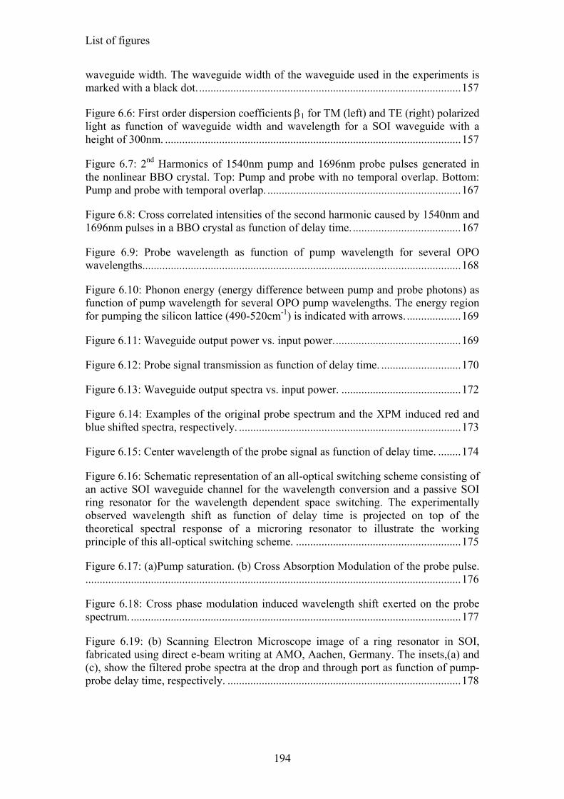
List of figures
194
waveguide width. The waveguide width of the waveguide used in the experiments is marked with a black dot. ............................................................................................157
Figure 6.6: First order dispersion coefficients β1 for TM (left) and TE (right) polarized light as function of waveguide width and wavelength for a SOI waveguide with a height of 300nm. ........................................................................................................157
Figure 6.7: 2nd Harmonics of 1540nm pump and 1696nm probe pulses generated in the nonlinear BBO crystal. Top: Pump and probe with no temporal overlap. Bottom: Pump and probe with temporal overlap. ....................................................................167
Figure 6.8: Cross correlated intensities of the second harmonic caused by 1540nm and 1696nm pulses in a BBO crystal as function of delay time.......................................167
Figure 6.9: Probe wavelength as function of pump wavelength for several OPO wavelengths................................................................................................................168
Figure 6.10: Phonon energy (energy difference between pump and probe photons) as function of pump wavelength for several OPO pump wavelengths. The energy region for pumping the silicon lattice (490-520cm-1) is indicated with arrows....................169
Figure 6.11: Waveguide output power vs. input power.............................................169
Figure 6.12: Probe signal transmission as function of delay time. ............................170
Figure 6.13: Waveguide output spectra vs. input power. ..........................................172
Figure 6.14: Examples of the original probe spectrum and the XPM induced red and blue shifted spectra, respectively. ..............................................................................173
Figure 6.15: Center wavelength of the probe signal as function of delay time. ........174
Figure 6.16: Schematic representation of an all-optical switching scheme consisting of an active SOI waveguide channel for the wavelength conversion and a passive SOI ring resonator for the wavelength dependent space switching. The experimentally observed wavelength shift as function of delay time is projected on top of the theoretical spectral response of a microring resonator to illustrate the working principle of this all-optical switching scheme. ..........................................................175
Figure 6.17: (a)Pump saturation. (b) Cross Absorption Modulation of the probe pulse.....................................................................................................................................176
Figure 6.18: Cross phase modulation induced wavelength shift exerted on the probe spectrum.....................................................................................................................177
Figure 6.19: (b) Scanning Electron Microscope image of a ring resonator in SOI, fabricated using direct e-beam writing at AMO, Aachen, Germany. The insets,(a) and (c), show the filtered probe spectra at the drop and through port as function of pump-probe delay time, respectively. ..................................................................................178

List of figures
195
Figure 6.20: Filtered probe spectra detected at the drop port of a SOI microring resonator as function of delay time. The resonance peaks of the resonator are schematically drawn at the right side of the plot. ......................................................178
Figure 6.21: Normalized integrated power detected at the drop port. Circles represent the power around the resonance wavelength of 1548nm, while the squares show the power at the wavelength of 1564nm..........................................................................179

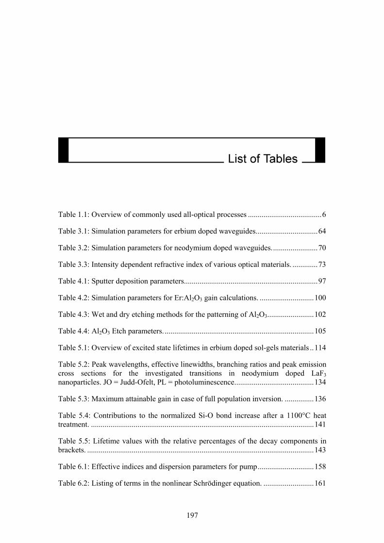
197
Table 1.1: Overview of commonly used all-optical processes ......................................6
Table 3.1: Simulation parameters for erbium doped waveguides................................64
Table 3.2: Simulation parameters for neodymium doped waveguides........................70
Table 3.3: Intensity dependent refractive index of various optical materials. .............73
Table 4.1: Sputter deposition parameters.....................................................................97
Table 4.2: Simulation parameters for Er:Al2O3 gain calculations. ............................100
Table 4.3: Wet and dry etching methods for the patterning of Al2O3........................102
Table 4.4: Al2O3 Etch parameters. .............................................................................105
Table 5.1: Overview of excited state lifetimes in erbium doped sol-gels materials ..114
Table 5.2: Peak wavelengths, effective linewidths, branching ratios and peak emission cross sections for the investigated transitions in neodymium doped LaF3 nanoparticles. JO = Judd-Ofelt, PL = photoluminescence.........................................134
Table 5.3: Maximum attainable gain in case of full population inversion. ...............136
Table 5.4: Contributions to the normalized Si-O bond increase after a 1100°C heat treatment. ...................................................................................................................141
Table 5.5: Lifetime values with the relative percentages of the decay components in brackets. .....................................................................................................................143
Table 6.1: Effective indices and dispersion parameters for pump.............................158
Table 6.2: Listing of terms in the nonlinear Schrödinger equation. ..........................161

List of tables
198
Table 6.3: Temporal characteristics of pulse propagation in SOI waveguides for different pulse durations. Simulations of the pulse intensities, free carrier densities and refractive index change as function of time are shown for 300fs, 3.5ps and 17ns experiments, respectively. The last row shows the XPM induced wavelength shift of the probe signal. .........................................................................................................171

199
ASE Amplified Spontaneous Emission BPA Bisphenol-A DC Direct Current DOE Design of Experiments EDFA Erbium Doped Fiber Amplifier EDWA Erbium Doped Waveguide Amplifier ESA Excited State Absorption FCA Free Carrier Absorption FDTD Finite Difference Time Domain FE Field Enhancement FL Füchtbuaer-Ladenburg FOD Fourth Order Dispersion FOM Figure of merit FSR Free Spectral Range FWHM Full Width at Half Maximum FWM Four Wave Mixing IDRI Intensity Dependent Refractive Index IRS Intrapulse Raman Scattering MRR Microring Resonator NA Numerical Aperture NLSE Nonlinear Schrödinger Equation OSA Optical Spectrum Analyzer PhC Photonic Crystal PL Photoluminescence PMF Polarization Maintaining Fiber PMMA Poly-Methyl-Meta-Acrylate Q Quality Factor RF Radio Frequency RIE Reactive Ion Etching SEM Scanning Electron Microscope SMF Single Mode Fiber SOD Second Order Dispersion SOI Silicon-on-Insulator SPM Self Phase Modulation SRS Stimulated Raman Scattering

List of acronyms
200
SSFM Split Step Fourier Method TBP Time Bandwidth Product TE Transverse Electromagnetic TEM Tunneling Electron Microscope TEOS Tetra-Ethyl-Ortho-Silicate TLA Three Letter Acronym TM Transverse Magnetic TOD Third Order Dispersion TPA Two Photon Absorption UC Upconversion WOA Waveguide Optical Amplifier XAM Cross Absorption Modulation XPM Cross Phase Modulation

201
c speed of light 3.108 [m/s] e elementary charge 1.6×10⁻¹⁹ [C] h Planck’s constant 6.626×10⁻³⁴ [m2kg/s] NA Avogadro’s number 6.022×10²³ [at./mole] ε0 electric permittivity of free space 8.85×10⁻¹² [F/m] Aeff effective cross section [m2] a linear losses [m-1] B frequency bandwidth [Hz] Cij cross relaxation coefficient [m3/s] C concentration [m-3] D molecular diameter [m] D dispersion parameter [ps/km.nm] d coupling gap [m] d spotsize diameter [m] E energy [J] fr pulse repetition rate [Hz] f filling fraction [-] G small signal gain [dB/cm] G degeneracy [-] gs small signal gain [m-1] I intensity [W/m2] Ki upconversion coefficient [m3/s] k imaginary part of the complex index of refraction [-] L length [m] Lc coupling length [m] LRT racetrack length [m] M molar mass [gr/mole] N concentration [m-3] NA numerical aperture [-] n0 linear refractive index [-]

List of symbols
202
n2 nonlinear refractive index [m2/W] neff effective refractive index [-] ng group index [-] Ni complex refractive index [-] P power [W] p pressure [Pa] r radius [m] T temperature [K] T0 pulse duration [s] tp pulse duration [s] V volume [m3] vg group velocity [m/s] WRT racetrack width [m] WB bend width [m] Wij absorption and emission rates [s-1] z propagation distance [m] α losses [dB/cm] βλ branching ration [-] β two photon absorption coefficient [m/W] βj dispersion terms [sj/m] ∆ offset [m] ∆MOD modulation depth [dB] δ standard deviation (pulse duration) [s] ε dielectric constant [-] Φ photon flux [s-1m-2] φ phase [rad] Γ overlap integral [-] η fill fraction [-] η activated rare ion fraction [-] ϕ phase [rad] κ coupling constant [-] Λ grating period [m] λ wavelength [m] v light frequency [s-1] θ angle of incidence [rad] ρ specific mass [kg/m3] ρ depth of focus [m] σ cross section [m2] τ lifetime [s] ω light frequency [rad/s]
203
1. A. Sano, H. Masuda, Y. Kisaka, S. Aisawa, E. Yoshida, Y. Miyamoto, M.
Koga, K. Hagimoto, T. Yamada, T. Furuta, and H. Fukuyama, "14Tb/s (140 x 111-Gb/s PDM/WDM) CSRZ-DQPSK Transmission over 160km Using 7-THz Bandwidth Extended L-band EDFAs", 32nd European Conference on Optical Communication, Cannes, France, Th4.1.1, 2006.
2. OlympIOs, www.c2v.nl. 3. T. Miya, Y. Terunuma, T. Hosaka, and T. Miyoshita, "Ultimate Low-Loss
Singlemode Fiber at 1.55µm", Electron. Lett., Vol 15 pp 106, 1979. 4. M. L. Dakss and W. J. Miniscalco, "Fundamental Limits on Nd3+-Doped Fiber
Amplifier Performance at 1.3µm", IEEE Photon. Technol. Lett., Vol 2 (9), pp 650-652, 1990.
5. E. Desurvire, "Erbium Doped Fiber Amplifiers, Principles and Applications", John Wiley & Sons, ISBN: 0-471-58977-2, 2002.
6. E.J.Klein, PhD Thesis, Faculty of Electrical Engineering, Mathematics and Computer Science, University of Twente, Enschede, The Netherlands, To be printed, 2007.
7. M. Hammer, K. R. Hiremath, and R. Stoffer, "Analytical approaches to the description of optical microresonator devices", Microresonators as building blocks for VLSI photonics, Proceedings of the International School of Quantum Electronics, 39th course, Erice, Sicily, pp 48-71, 2004.
8. C. K. Madsen and J. H. Zhao, "Optical Filter Design and Analysis", Wiley-Interscience, ISBN 0471183733, 1999.
9. J. T. Verdeyen, "Laser Electronics", Prentice-Hall International, 1995. 10. J. Niehusmann, A. Vörckel, P. H. Bolivar, T. Wahlbrink, W. Henschel, and H.
Kurz, "Ultrahigh-quality-factor silicon-on-insulator microring resonator", Opt.Lett., Vol 29 (24), pp 2861-2863, 2004.
11. T. J. A. Kippenberg, PhD Thesis, "Nonlinear Optics in Ultra-high-Q Whispering-Gallery Optical Microcavities", California Institute of Technology, 2004.
12. L. H. Spiekman, Y. S. Oei, E. G. Metaal, F. H. Groen, P. Demeester, and M. K. Smit, "Ultrasmall waveguide bends: the corner mirrors of the future?" IEE Proc.-Optoelectron., Vol 142 (1), pp 61-65, 1995.
Bibliography
204
13. M. K. Smit, E. C. M. Pennings, and H. Blok, "A Normalized Approach to the Design of Low-Loss Optical Waveguide Bends", J. Lightwave Technol., Vol 11 (11), pp 1737-1742, 1993.
14. G. J. Veldhuis, L. E. W. v. d. Veen, and P. V. Lambeck, "Integrated Optical Refractometer Based on Waveguide Bend Loss", J. Lightwave Technol., Vol 17 (5), pp 857-864, 1999.
15. D. H. Geuzebroek, PhD Thesis, "Flexible optical Network components based on densely integrated microring resonators", Electrical Engineering, Mathematics and Computer Science, University of Twente, Enschede, The Netherlands, ISBN Number 90-365-2258-7, 2005.
16. H. Rokhsari and K. Vahala, "Observation of Kerr nonlinearity in microcavities at room temperature", Opt.Lett., Vol 30 (4), pp 427-429, 2005.
17. Q. Xu, V. R. Almeida, and M. Lipson, "Micrometer-scale all-optical wavelength converter on silicon", Optics Letters, Vol 30 (20), pp 2733-2735, 2005.
18. A. Driessen, D. H. Geuzebroek, E. J. Klein, R. Dekker, R. Stoffer, and C. Bornholdt, "Propagation of short lightpulses in microring resonators: Ballistic transport versus interference in the frequency domain", Optics Communications, doi:10.1016/j.optcom.2006.1009.1034 (Article in press), 2006.
19. W. C. L. Hopman, R. Dekker, D. Yudistira, W. F. A. Engbers, H. J. W. M. Hoekstra, and R. M. d. Ridder, "Fabrication and Characterization of High-Quality Uniform and Apodized Si3N4 waveguide Gratings using Laser Interference Lithography", Phot.Techn.Lett, Vol 18 (17), pp 1855-1857, 2006.
20. J. H. Berends, Ph.D. Thesis, "Integrated Optical Bragg Reflectors as Narrowband Wavelength Filters", University of Twente, Enschede, 1997.
21. H. J. W. M. Hoekstra, W. C. L. Hopman, J. Kautz, R. Dekker, and R. M. d. Ridder, "A simple coupled mode model for near band-edge phenomena in grated waveguides", Optical and Quantum Electronics - Special issue on "Optical Waveguide Theory and Numerical Modelling", Article in press, 2006.
22. SimuLayer, www.daglain.com. 23. A. Thelen, "Design of Optical Interference Coatings ", Mcgraw-Hill, ISBN
0070637865, 1989. 24. P. Yeh, "Optical Waves in Layered Media", John Wiley & Sons Inc, ISBN
0471469904, 1998. 25. F. J. v. Soest, H. v. Wolferen, H. Hoekstra, R. M. d. Ridder, K. Worhoff, and
P. V. Lambeck, "Laser interference lithography with highly accurate interferometric alignment", Jpn. J. Appl. Phys., Vol 44, pp 6568-6570, 2005.
26. T. Erdogan, "Fiber Grating Spectra", J.Lightwave Technol., Vol 15 pp 1277, 1997.
27. J. E. Sipe, L. Poladian, and C. M. d. Sterke, "Propagation through nonuniforn grating structures", J.Opt.Soc.Am.A, Vol 11, pp 1307, 1994.
28. R. Dekker, V. Sudarsan, F. C. J. M. v. Veggel, K. Wörhoff, and A. Driessen, "Erbium doped LaF3 nanoparticles incorporated in silicondioxide thin films for active integrated optical applications", Proceedings of the 2004 Annual Symposium IEEE/LEOS Benelux Chapter, Ghent, Belgium, ISBN 9076546061, pp 295-298, 2004.
29. F. Urbach, "The Long-Wavelength Edge of Photographic Sensitivity and of the Electronic Absorption of Solids", Phys.Rev., Vol 92, pp 1324, 1953.
Bibliography
205
30. D. A. Pinnow, T. C. Rich, J. F.W. Ostermayer, and J. M. DiDomenico, "Fundamental optical attenuation limits in the liquid and glassy state with application to fiber optical waveguide materials", Applied Physics Letters, Vol 22 (10), pp 527-529, 1973.
31. J. D. Dow and D. Redfield, "Toward a Unified Theory of Urbach's Rule and Exponential Absorption Edges", Physical Review B, Vol 5 (2), pp 594-610, 1972.
32. K. Wörhoff, A. Driessen, P. V. Lambeck, L. T. H. Hilderink, P. W. C. Linders, and T. J. A. Popma, "Plasma enhanced chemical vapor deposition silicon oxynitride optimized for application in integrated optics", Sensors and Actuators, Vol 74, pp 9-12, 1999.
33. R. M. Glen, "Polymeric optical fibre", Chemtronics, Vol 1 pp 98-106, 1986. 34. W. Groh, "Overtone absorption in macromolecules for polymer optical fibers",
Macromol.Chem., Vol 189, pp 2861-2874, 1988. 35. L. H. Slooff, A. v. Blaaderen, A. Polman, G. A. Hebbink, S. I. Klink, F. C. J.
M. v. Veggel, D. N. Reinhoudt, and J. W. Hofstraat, "Rare-earth doped polymers for planar optical amplifiers", Applied Physics Reviews, Vol 91 (7), pp 3955-3980, 2002.
36. A. J. Cox, A. J. DeWeerd, and J. Linden, "An experiment to measure Mie and Rayleigh total scattering cross sections", Am.J.Phys., Vol 70 (6), pp 620-625, 2002.
37. MiePlot v3.4.01, http://www.philiplaven.com/index1.html. 38. T. K. Liang, L. R. Nunes, T. Sakamoto, K. Sasagawa, T. Kawanishi, M.
Tsuchiya, G. R. A. Priem, D. V. Thourhout, P. Dumon, R. Baets, and H. K. Tsang, "Ultrafast all-optical switching by crossabsorption modulation in silicon wire waveguides", Opt.Express, Vol 13 (19), pp 7298-7203, 1995.
39. C. Rauscher and R. Laenen, "Analysis of picosecond mid-infrared pulses by two-photon absorption in germanium", J.Appl.Phys., Vol 81, pp 2818-2821, 1997.
40. M. Dinu, F. Quochi, and H. Garcia, "Third-order nonlinearities in silicon at telecom wavelengths", Appl.Phys.Lett., Vol 82 (18), pp 2954-2956, 2003.
41. A. Liu, H. Rong, M. Paniccia, O. Cohen, and D. Hak, "Net optical gain in a low loss silicon-on-insulator waveguide by stimulated Raman scattering", Opt.Express, Vol 12 (18), pp 4261-4268, 2004.
42. T. K. Liang and H. K. Tsang, "Nonlinear Absorption and Raman Scattering in Silicon-on-Insulator Optical Waveguides", IEEE.J.Sel.Top.Quant.Electr., Vol 10 (5), pp 1149-1153, 2004.
43. H. Rong, A. Liu, R. Nicolaescu, M. Paniccia, O. Cohen, and D. Hak, "Raman gain and nonlinear optical absorption measurements in a low-loss silicon waveguide", Appl.Phys.Lett., Vol 85 (12), pp 2196-2198, 2004.
44. R. Claps, V. Raghunathan, D. Dimitropoulos, and B. Jalali, "Influence of nonlinear absorption on Raman amplification in Silicon waveguides", Opt.Express, Vol 12 (12), pp 2774-2780, 2004.
45. R. A. Soref and B. R. Bennett, "Electrooptical Effects in Silicon", IEEE.J.Sel.Top.Quant.Electr., Vol QE-23 (1), pp 123-129, 1987.
46. G. T. Reed and C. E. Jason, "Silicon optical modulators", Materials Today, (January), pp 40-50, 2005.
47. C. Strohhöfer and A. Polman, "Silver as sensitizer for erbium", Applied Physics Letters, Vol 81 (8), pp 1414-1416, 2002.
Bibliography
206
48. M. Planck, "On the law of distribution of energy in the normal spectrum", Annalen der Physik, Vol 4, pp 553, 1901.
49. T. H. Hoekstra, PhD thesis, "Erbium-doped Y2O3 Integrated Optical Amplifiers", University of Twente, Enschede, The Netherlands, ISBN 90-9007000-1, 1994.
50. D. E. McCumber, "Einstein relations connecting broadband emission and absorption spectra", Phys.Rev., Vol 136 (4), pp A954-A957, 1964.
51. R. S. Quimby, "Range of validity of McCumber theory in relating absorption and emission cross sections", J.Appl.Phys., Vol 92 (1), pp 180-187, 2002.
52. B. R. Judd, "Optical absorption intesities of rare-earth ions", Phys.Rev., Vol 127, pp 750-761, 1962.
53. G. S. Ofelt, "Intensities of crystal spectra of rare-earth ions", J.Chem.Phys., Vol 37, pp 511-520, 1962.
54. W. F. Krupke, "Induced-emission cross sections in neodymium laser glasses", IEEE J. Quant. Electr., Vol QE-10, pp 450-457, 1974.
55. A. Polman, "Erbium as a probe for everything?" Physica B, Vol 300, pp 78-90, 2001.
56. N. V. Gaponenko, A. V. Mudryi, E. A. Stepanova, A. I. Rat'ko, O. V. Sergeev, and V. E. Borisenko, "Photoluminescence of sol-gel prepared erbium-doped alumina films", Inorganic Materials, Vol 34 (8), pp 795-799, 1998.
57. G. A. Hebbink, J. W. Stouwdam, D. N. Reinhoudt, and F. C. J. M. v. Veggel, "Lanthanide(III)-Doped Nanoparticles That Emit in the Near-Infrared", Advanced Materials, Vol 14 (16), pp 1147-1150, 2002.
58. M. J. A. d. Dood, "Silicon photonic crystals and spontaneous emission", Ph.D. Thesis, FOM Institute for Atomic and Molecular Physics,
59. F. D. Pascale, M. Zoboli, M. Federighi, and I. Massarek, "Finite element modeling of silica waveguide amplifiers with high erbium concentrations", IEEE J. Quant. Electr., Vol 30 (5), pp 1277-1281, 1994.
60. W. Huang and R. R. A. Syms, "Analysis of Folded Erbium-Doped Planar Waveguide Amplifiers by the Method of Lines", J.Lightwave Technol., Vol 17 (12), pp 2658-2664, 1999.
61. W. J. Miniscalco, "Erbium-Doped Glasses for Fiber Amplifiers at 1500nm", J.Lightwave Technol., Vol 9 (2), pp 234-250, 1991.
62. G. N. v. d. Hoven, E. Snoeks, A. Polman, C. v. Dam, J. W. M. v. Uffelen, and M. K. Smit, "Upconversion in Er-implanted Al2O3 waveguides", J.Appl.Phys., Vol 79 (3), pp 1258-1266, 1996.
63. J. B. Gruber, D. K. Sardar, R. M. Yow, T. H. Allik, and B. Zandi, "Energy-level structure and spectral analysis of Nd3+(4 f3) in polycrystalline ceramic garnet Y3Al5O12", J.Appl.Phys., Vol 96 (6), pp 3050-3056, 2004.
64. C. K. Asawa and M. Robinson, "Temperature-Dependent Concentration Quenching of Fluorescence by Cross Relaxation of Nd3+ in LaF3", Phys.Rev., Vol 141 (1), pp 251-258, 1966.
65. M. Pollnau, P. J. Hardman, W. A. Clarkson, and D. C. Hanna, "Upconversion, lifetime quenching, and ground-state bleaching in Nd3+:LiYF4", Optics Communications, Vol 147, pp 203-211, 1997.
66. J. W. Stouwdam, PhD Thesis, "Lanthanide-doped nanoparticles as the active optical medium in polymer-based devices", University of Twente, Enschede, The Netherlands, ISBN: 90-365-2011-8, 2003.
Bibliography
207
67. H. J. W. M. Hoekstra, G. J. M. Krijnen, A. Driessen, P. V. Lambeck, and T. J. A. Popma, "Non-linear optics for transducers: principles and materials", Sensors and Actuators A, Vol 34, pp 179-192, 1992.
68. M. B. J. Diemeer and R. Dekker, "MEMS VOA with polymeric thermal microactuators", Proceedings of the European Conference on Optical Communication (ECOC), Stockholm, Sweden, pp 1.27, 2002.
69. R. Meijerink, D. H. Geuzebroek, E. J. Klein, H. Kelderman, R. Dekker, M. B. J. Diemeer, and A. Driessen, "Optimization of driving signal for thermal modulation of a microring resonator", Proceedings of the 8th Annual Symposium IEEE/LEOS Benelux Chapter, Enschede, The Netherlands, ISBN 90-365-1990-X, pp 85-88, 2003.
70. M. Samoc, A. Samoc, B. Luther-Davies, Z. Bao, L. Yu, B. Hsieh, and U. Scherf, "Femtosecond Z-scan and degenerate four-wave mixing measurements of real and imaginary parts of the third-order nonlinearity of soluble conjugated polymers", J.Opt.Soc.Am. B, Vol 15 (2), pp 817-825, 1998.
71. R. DeSalvo, A. A. Said, D. J. Hagan, E. W. V. Stryland, and M. Sheik-Bahae, "Infrared to ultraviolet measurements of two-photon absorption and n2 in wide bandgap solids", IEEE Journal of Quantum Electronics, Vol 32, pp 1324-1333, 1996.
72. C. Bosshard, R. Spreiter, M. Zgonik, and P. Günter, "Kerr Nonlinearity via Cascaded Optical Rectification and the Linear Electro-optic Effect", Phys.Rev.Lett., Vol 74 (14), pp 2816-2819, 1995.
73. R. d. Coso and J. Solis, "Relation between nonlinear refractive index and third-order susceptibility in absorbing media", J.Opt.Soc.Am.B, Vol 21 (3), pp 640-644, 2004.
74. F. Gan, "Optical Nonlinearity of Hybrid and Nanocomposite Materials Prepared by the Sol-Gel Method", Journal of Sol-Gel Science and Technology, Vol 13, pp 559-563, 1998.
75. A. H. Yuwono, J. Xue, J. Wang, H. I. Elim, W. Ji, Y. Li, and T. J. White, "Transparent nanohybrids of nanocrystalline TiO2 in PMMA with unique nonlinear behavior", J.Mater.Chem., Vol 13, pp 1475-1479, 2003.
76. M. Sheik-Bahae, D. J. Hagan, and E. W. V. Stryland, "Dispersion and Band-Gap Scaling of the Electronic Kerr Effect in Solids Associated with Two-Photon Absorption", Physical Review Letters, Vol 65 (1), pp 96-99, 1990.
77. T. W. Yau, C. H. Lee, and J. Wang, "Uncollapsed self focusing of femtosecond pulses in dielectric media due to the saturation of nonlinear refractive index", CLEO, pp 1-3, 2000.
78. M. J. Weber, D. Milam, and W. L. Smith, "Nonlinear refractive index of glasses and crystals", Opt. Eng., Vol 17, pp 463-469, 1978.
79. D. Milam and M. J. Weber, Journal of Applied Physics, Vol 47, pp 259, 1975. 80. M. A. Newhouse, D. L. Weidman, and D. W. Hall, "Enhanced-nonlinearity
single-mode lead silicate optical fiber", Optics Letters, Vol 15 (21), pp 1185-1187, 1990.
81. M. Sheik-Bahae, J. Wang, and E. W. v. Stryland, "Nondegenerate Optical Kerr Effect in Semiconductors", IEEE J. Quant. Electr., Vol 30 (2), pp 249-255, 1994.
82. C. Yu, Y. Li, Q. Shilang, Y. Nie, and W. Duoyuan, "Third-order optical nonlinearities and optical limiting of octaoctyloxy phthalocyanine free base in toluene", Opt.Eng., Vol 40 (12), pp 2683-2684, 2001.
Bibliography
208
83. M. Asobe, T. Kanamori, and K. Kubodera, "Ultrafast All-Optical Switching Using Highly Nonlinear Chalcogenide Glass Fiber", IEEE Phot. Techn. Lett, Vol 4 (4), pp 362-365, 1992.
84. M. Asobe, K. Suzuki, T. Kanamori, and K. Kubodera, "Nonlinear refractive index measurement in chalcogenide-glass fibers by self-phase modulation", Applied Physics Letters, Vol 60 (10), pp 1153-1154, 1992.
85. M. Asobe, H. Itoh, T. Miyazawa, and T. Kanamori, "Efficient and ultrafast all-optical switching using high ∆n, small core chalcogenide glass fibre", Electronics Letters, Vol 29 (22), pp 1966-1968, 1993.
86. G. I. Stegeman and W. E. Torruellas, "Nonlinear materials for information processing and communications", Phil.Trans.R.Soc.Lond. A, Vol 354, pp 745-756, 1996.
87. A. Driessen, H. J. W. M. Hoekstra, F. C. Blom, F. Horst, G. J. M. Krijnen, J. B. P. v. Schoot, P. V. Lambeck, T. J. A. Popma, and M. B. Diemeer, "Evaluation of polymer based third order nonlinear integrated optics devices", Optical Materials, Vol 9, pp 329-333, 1998.
88. I. C. Khoo, F. Simoni, and C. Umeton, "Novel Optical Materials and Applications", John Wiley & Sons, Inc., ISBN: 0-471-12793-0, 1996.
89. Y. Watanabe, M. Ohnishi, and T. Tsuchiya, "Measurement of nonlinear absorption and refraction in titanium dioxide single crystal by using phase distortion method", Applied Physics Letters, Vol 66 (25), pp 3431-3432, 1995.
90. Q. F. Zhou, Q. Q. Zhang, J. X. Zhang, L. Y. Zhang, and X. Yao, "Preparation and optical properties of TiO2 nanocrystalline particles dispersed in SiO2 nanocomposites", Materials Letters, Vol 31, pp 39-42, 1997.
91. S. T. Selvan, M. Nogami, A. Nakamura, and Y. Hamanaka, "A facile sol-gel method for the encapsulation of gold nanoclusters in silica gels and their optical properties", Journal of Non-Crystalline Solids, Vol 255, pp 254-258, 1999.
92. P. P. Absil, J. V. Hryniewicz, B. E. Little, P. S. Cho, R. A. Wilson, L. G. Joneckis, and P. T. Ho, "Wavelength conversion in GaAs micro-ring resonators", Optics Letters, Vol 25 (8), pp 554-556, 2000.
93. A. Dowd, R. G. Elliman, M. Samoc, and B. Luther-Davies, "Nonlinear optical response of Ge nanocrystals in a silica matrix", Applied Physics Letters, Vol 74 (2), pp 239-241, 1999.
94. A. Dowd, M. Samoc, B. Luther-Davies, and R. G. Elliman, "Nonlinear optical properties of semiconducting nanocrystals in fused silica", Nuclear instruments methods in physics research B, Vol 148, pp 964-968, 1999.
95. M. A. Fardad, E. M. Yeatman, E. J. C. Dawnay, M. Green, J. Fick, M. Guntau, and G. Vintrant, "Fabrication and characterisation of a CdS-doped silica-on-silicon planar waveguide", IEE Proc.-Optoelectron, Vol 143 (5), pp 298-302, 1996.
96. F. M. Liu, L. D. Zhang, P. Cheng, P. Wang, and W. J. Zhang, "Enhancement of third-order nonlinearity of nanocrystalline GaSb embedded in silica film", Materials Science and Engineering B, Vol 76, pp 161-164, 2000.
97. Y. Imai and N. Matsuda, "Nonlinear Refractive Index of Er3+-Doped Fiber and its Application to Nonlinear Fiber Coupler", Optical Review, Vol 1 (1), pp 97-99, 1994.
98. T. H. Hoekstra, B. J. Offrein, P. V. Lambeck, and T. J. A. Popma, "Nonlinear refractive index of erbium-doped Y2O3 integrated-optical waveguides", Optics Letters, Vol 18 (20), pp 1718-1720, 1993.
Bibliography
209
99. H. B. Liao, R. F. Xiao, J. S. Fu, and G. K. L. Wong, "Large third-order nonlinear optical susceptibility of Au-Al2O3 composite films near the resonant frequency", Applied Physics B, Vol 65, pp 673-676, 1997.
100. H. B. Liao, R. F. Xiao, J. S. Fu, P. Yu, G. K. L. Wong, and P. Sheng, Applied Physics Letters, Vol 70 (1), pp 1, 1997.
101. G. I. Stegeman, E. M. Wright, N. Finlayson, R. Zanoni, and C. T. Seaton, "Third Order Nonlinear Integrated Optics", J. Lightwave Technol., Vol 6 (6), pp 953-970, 1988.
102. H. Garcia, H. Krishna, and R. Kalyanaraman, "Compound figure of merit for photonic applications of metal nanocomposites", Appl.Phys.Lett., Vol 89, pp 141109, 2006.
103. F. C. Blom, PhD. thesis, "Linear and non-linear optical properties of cylindrical micro-resonators, from materials to device realisation ", University of Twente, Enschede, The Netherlands, ISBN: 90-3651093-7, 1998.
104. R. Dekker, BSc Thesis, "Realisation and optimisationof a new Z-scan method using charge coupled device image processing", University of Twente, Enschede, The Netherlands, 1996.
105. M. Bass, "Handbook of Optics, Volume I, 2nd edition", McGraw-Hill, Inc., ISBN 0-07-047740-7, 1995.
106. V. Nguyen, T. Montalbo, C. Manolatou, A. Agarwal, C. Hong, J. Yasaitis, L. C. Kimerling, and J. Michel, "Silicon-based highly-efficient fiber-to-waveguide coupler for high index contrast systems", Appl.Phys.Lett., Vol 88 pp 081112, 2006.
107. T. Aalto, K. Solehmainen, M. Harjanne, M. Kapulainen, and P. Heimala, "Low-Loss Converters Between Optical Silicon Waveguides of Different Sizes and Types", IEEE Photon. Technol. Lett., Vol 18 (5), pp 709-711, 2006.
108. T. Shoji, T. Tsuchizawa, T. Watanabe, K. Yamada, and H. Morita, "Low loss mode size converter from 0.3 µm square Si wire waveguides to singlemode fibres", Electron. Lett., Vol 38 (25), pp 1669-1670, 2002.
109. A. N. M. M. Choudhury, T. R. Stanczyk, D. Richardson, A. Donval, R. Oron, and M. Oron, "Method of Improving Light Coupling Efficiency Between Optical Fibers and Silicon Waveguides", IEEE Photon. Technol. Lett., Vol 17 (9), pp 1881-1883, 2005.
110. D. Taillaert, P. Bienstman, and R. Baets, "Compact efficient broadband grating coupler for silicon-on-insulator waveguides", Opt.Lett., Vol 29 (23), pp 2749-2751, 2004.
111. G. Z. Masanovic, G. T. Reed, W. Headley, B. Timotijevic, V. M. N. Passaro, R. Atta, G. Esnell, and A. G. R. Evans, "A high efficiency input/output coupler for small silicon photonic devices", Opt.Express, Vol 13 (19), pp 7374-7379, 2005.
112. R. Bachelot, A. Fares, R. Fikri, D. Barchiesi, G. Lerondel, and P. Royer, "Coupling semiconductor lasers into single-mode optical fibers by use of tips grown by photopolymerization", Opt.Lett., Vol 29 (17), pp 1-3, 2004.
113. G. v. d. Hoven, PhD Thesis, "Erbium-doped photonic materials based on silicon", Universiteit Utrecht, Utrecht, ISBN: 90-393-1282-6, 1996.
114. R. Serna and C. N. Afonso, "In situ growth of optically active erbium doped Al2O3 thin films by pulsed laser deposition", Appl.Phys.Lett., Vol 69 (11), pp 1541-1543, 1996.
Bibliography
210
115. P. G. Kik and A. Polman, "Cooperative upconversion as the gain-limiting factor in Er doped miniature Al2O3 optical waveguide amplifiers", J.Appl.Phys., Vol 93 (9), pp 5008-5012, 2003.
116. G. N. v. d. Hoven, R. J. I. M. Koper, A. Polman, C. v. Dam, J. W. M. v. Uffelen, and M. K. Smit, "Net optical gain at 1.53 mu in Er-doped Al2O3 waveguides on silicon", Appl.Phys.Lett., Vol 68 (14), pp 1886-1888, 1996.
117. G. N. v. d. Hoven, J. A. v. d. Elsken, A. Polman, C. van Dam, K.W. M. van Uffelen, and M. K. Smit, "Absorption and emission cross sections of Er3+ in Al2O3 waveguides", Appl.Optics, Vol 36 (15), pp 3338-3341, 1997.
118. SRIM, www.SRIM.org. 119. T. E. Sheridan, M. J. Goeckner, and J. Goree, "Model of energetic electron
transport in magnetron discharges", Journal of Vacuum Science and Technology, Vol A8 (1), pp 30-37, 1990.
120. D. L. Smith, "Thin-film deposition: principles and practice", McGraw-Hill, Inc., ISBN 0-07-113913-3, 1995.
121. K. Koski, J. Hölsä, and P. Julliet, "Voltage controlled reactive sputtering process for aluminium oxide thin films", Thin Solid Films, Vol 326, pp 189-193, 1998.
122. J. M. Mwabora and R. T. Kivaisi, "Causes of film reproducibility problem in magnetron sputtering", African Journal of Science and Technology, Vol 1 (4), pp 87-90, 2001.
123. T. Fukami and F. Shintani, "Observations on the operation of planar magnetron sputering system by target erosion patterns", Thin Solid Films, Vol 151, pp 373-381, 1987.
124. H. Bartzsch, P. Frach, K. Goedicke, B. Böcher, and C. Gottfried, "Ensuring long-term stability of process and film parameters during target lifetime in reactive magnetron sputtering", Surface and Coatings Technology, Vol 150, pp 88-94, 2002.
125. O. C. Yonts, C. E. Normann, and D. E. Harrison, J.Appl.Phys., Vol 31, pp 447, 1960.
126. C. N. Fert, B. Colombie, B. Fagot, and P. V. Chuong, Ionic Bombardment, Vol pp 67, 1961.
127. N. Lagreid and G. K. Wehner, J.Appl.Phys., Vol 31, pp 365, 1961. 128. C. H. Weijsenfeld, "Philips Research Report, Supplement No. 2", 1967. 129. M. T. Robinson and A. L. Soutern, J.Appl.Phys., Vol 38, pp 2969, 1967. 130. H. Oechsner, Z.Phys., Vol 37, pp 261, 1973. 131. M. Braun, B. Emmoth, and R. Buchta, Radiat.Eff., Vol 77, pp 28, 1976. 132. Y. Okajima, Jpn. J. Appl. Phys., Vol 20, pp 2313, 1981. 133. QuickField, Finite Element Analysis for electromagnetic, thermal, and stress
simulations, www.QuickField.com. 134. Q. Y. Zhang, P. S. Wang, W. J. Zhao, and L. Wang, "Ion beam assisted
deposition of Al2O3 optical waveguides on silicon", Surface and Coatings Technology, Vol 128-129, pp 121-125, 2000.
135. S. Musa, "Towards Er3+-doped Al2O3-Y2O3 broadband integrated optical amplifiers and tunable lasers", TWAIO Report, University of Twente,
136. C. L. Shih, B. K. Lai, H. Kahn, S. M. Phillips, and A. H. Heuer, "A Robust Co-Sputtering Fabrication Procedure for TiNi Shape Memory Alloys for MEMS", IEEE Journal of Microelectromechanical Systems, Vol 10 (1), pp 69-79, 2001.
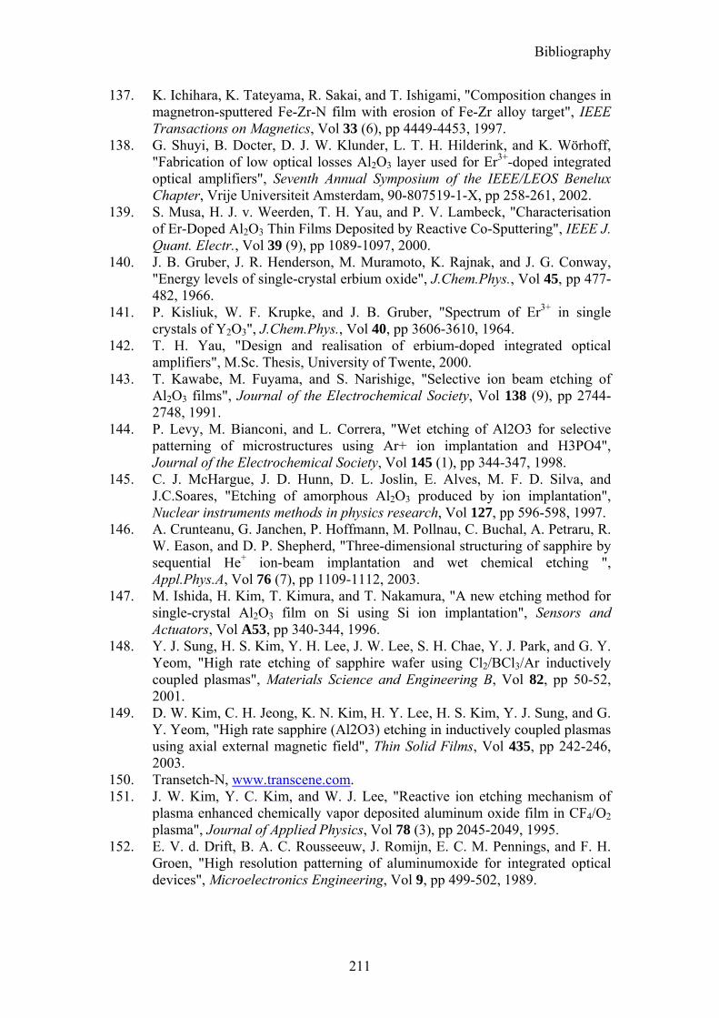
Bibliography
211
137. K. Ichihara, K. Tateyama, R. Sakai, and T. Ishigami, "Composition changes in magnetron-sputtered Fe-Zr-N film with erosion of Fe-Zr alloy target", IEEE Transactions on Magnetics, Vol 33 (6), pp 4449-4453, 1997.
138. G. Shuyi, B. Docter, D. J. W. Klunder, L. T. H. Hilderink, and K. Wörhoff, "Fabrication of low optical losses Al2O3 layer used for Er3+-doped integrated optical amplifiers", Seventh Annual Symposium of the IEEE/LEOS Benelux Chapter, Vrije Universiteit Amsterdam, 90-807519-1-X, pp 258-261, 2002.
139. S. Musa, H. J. v. Weerden, T. H. Yau, and P. V. Lambeck, "Characterisation of Er-Doped Al2O3 Thin Films Deposited by Reactive Co-Sputtering", IEEE J. Quant. Electr., Vol 39 (9), pp 1089-1097, 2000.
140. J. B. Gruber, J. R. Henderson, M. Muramoto, K. Rajnak, and J. G. Conway, "Energy levels of single-crystal erbium oxide", J.Chem.Phys., Vol 45, pp 477-482, 1966.
141. P. Kisliuk, W. F. Krupke, and J. B. Gruber, "Spectrum of Er3+ in single crystals of Y2O3", J.Chem.Phys., Vol 40, pp 3606-3610, 1964.
142. T. H. Yau, "Design and realisation of erbium-doped integrated optical amplifiers", M.Sc. Thesis, University of Twente, 2000.
143. T. Kawabe, M. Fuyama, and S. Narishige, "Selective ion beam etching of Al2O3 films", Journal of the Electrochemical Society, Vol 138 (9), pp 2744-2748, 1991.
144. P. Levy, M. Bianconi, and L. Correra, "Wet etching of Al2O3 for selective patterning of microstructures using Ar+ ion implantation and H3PO4", Journal of the Electrochemical Society, Vol 145 (1), pp 344-347, 1998.
145. C. J. McHargue, J. D. Hunn, D. L. Joslin, E. Alves, M. F. D. Silva, and J.C.Soares, "Etching of amorphous Al2O3 produced by ion implantation", Nuclear instruments methods in physics research, Vol 127, pp 596-598, 1997.
146. A. Crunteanu, G. Janchen, P. Hoffmann, M. Pollnau, C. Buchal, A. Petraru, R. W. Eason, and D. P. Shepherd, "Three-dimensional structuring of sapphire by sequential He+ ion-beam implantation and wet chemical etching ", Appl.Phys.A, Vol 76 (7), pp 1109-1112, 2003.
147. M. Ishida, H. Kim, T. Kimura, and T. Nakamura, "A new etching method for single-crystal Al2O3 film on Si using Si ion implantation", Sensors and Actuators, Vol A53, pp 340-344, 1996.
148. Y. J. Sung, H. S. Kim, Y. H. Lee, J. W. Lee, S. H. Chae, Y. J. Park, and G. Y. Yeom, "High rate etching of sapphire wafer using Cl2/BCl3/Ar inductively coupled plasmas", Materials Science and Engineering B, Vol 82, pp 50-52, 2001.
149. D. W. Kim, C. H. Jeong, K. N. Kim, H. Y. Lee, H. S. Kim, Y. J. Sung, and G. Y. Yeom, "High rate sapphire (Al2O3) etching in inductively coupled plasmas using axial external magnetic field", Thin Solid Films, Vol 435, pp 242-246, 2003.
150. Transetch-N, www.transcene.com. 151. J. W. Kim, Y. C. Kim, and W. J. Lee, "Reactive ion etching mechanism of
plasma enhanced chemically vapor deposited aluminum oxide film in CF4/O2 plasma", Journal of Applied Physics, Vol 78 (3), pp 2045-2049, 1995.
152. E. V. d. Drift, B. A. C. Rousseeuw, J. Romijn, E. C. M. Pennings, and F. H. Groen, "High resolution patterning of aluminumoxide for integrated optical devices", Microelectronics Engineering, Vol 9, pp 499-502, 1989.
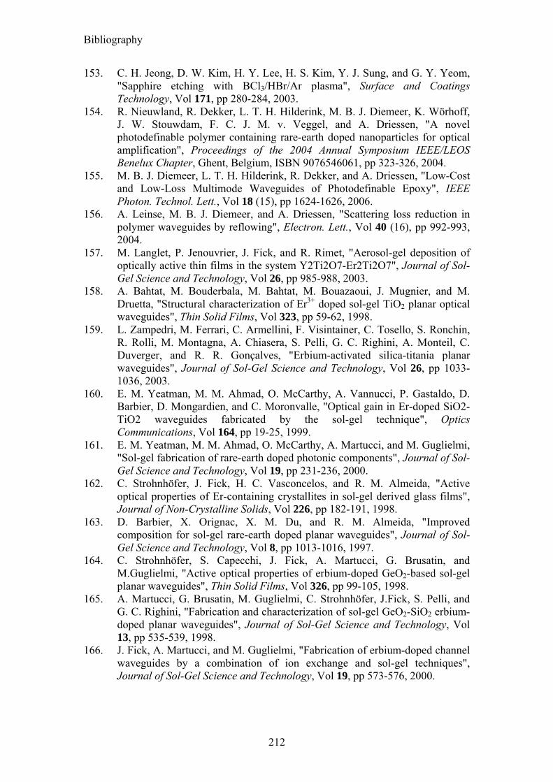
Bibliography
212
153. C. H. Jeong, D. W. Kim, H. Y. Lee, H. S. Kim, Y. J. Sung, and G. Y. Yeom, "Sapphire etching with BCl3/HBr/Ar plasma", Surface and Coatings Technology, Vol 171, pp 280-284, 2003.
154. R. Nieuwland, R. Dekker, L. T. H. Hilderink, M. B. J. Diemeer, K. Wörhoff, J. W. Stouwdam, F. C. J. M. v. Veggel, and A. Driessen, "A novel photodefinable polymer containing rare-earth doped nanoparticles for optical amplification", Proceedings of the 2004 Annual Symposium IEEE/LEOS Benelux Chapter, Ghent, Belgium, ISBN 9076546061, pp 323-326, 2004.
155. M. B. J. Diemeer, L. T. H. Hilderink, R. Dekker, and A. Driessen, "Low-Cost and Low-Loss Multimode Waveguides of Photodefinable Epoxy", IEEE Photon. Technol. Lett., Vol 18 (15), pp 1624-1626, 2006.
156. A. Leinse, M. B. J. Diemeer, and A. Driessen, "Scattering loss reduction in polymer waveguides by reflowing", Electron. Lett., Vol 40 (16), pp 992-993, 2004.
157. M. Langlet, P. Jenouvrier, J. Fick, and R. Rimet, "Aerosol-gel deposition of optically active thin films in the system Y2Ti2O7-Er2Ti2O7", Journal of Sol-Gel Science and Technology, Vol 26, pp 985-988, 2003.
158. A. Bahtat, M. Bouderbala, M. Bahtat, M. Bouazaoui, J. Mugnier, and M. Druetta, "Structural characterization of Er3+ doped sol-gel TiO2 planar optical waveguides", Thin Solid Films, Vol 323, pp 59-62, 1998.
159. L. Zampedri, M. Ferrari, C. Armellini, F. Visintainer, C. Tosello, S. Ronchin, R. Rolli, M. Montagna, A. Chiasera, S. Pelli, G. C. Righini, A. Monteil, C. Duverger, and R. R. Gonçalves, "Erbium-activated silica-titania planar waveguides", Journal of Sol-Gel Science and Technology, Vol 26, pp 1033-1036, 2003.
160. E. M. Yeatman, M. M. Ahmad, O. McCarthy, A. Vannucci, P. Gastaldo, D. Barbier, D. Mongardien, and C. Moronvalle, "Optical gain in Er-doped SiO2-TiO2 waveguides fabricated by the sol-gel technique", Optics Communications, Vol 164, pp 19-25, 1999.
161. E. M. Yeatman, M. M. Ahmad, O. McCarthy, A. Martucci, and M. Guglielmi, "Sol-gel fabrication of rare-earth doped photonic components", Journal of Sol-Gel Science and Technology, Vol 19, pp 231-236, 2000.
162. C. Strohnhöfer, J. Fick, H. C. Vasconcelos, and R. M. Almeida, "Active optical properties of Er-containing crystallites in sol-gel derived glass films", Journal of Non-Crystalline Solids, Vol 226, pp 182-191, 1998.
163. D. Barbier, X. Orignac, X. M. Du, and R. M. Almeida, "Improved composition for sol-gel rare-earth doped planar waveguides", Journal of Sol-Gel Science and Technology, Vol 8, pp 1013-1016, 1997.
164. C. Strohnhöfer, S. Capecchi, J. Fick, A. Martucci, G. Brusatin, and M.Guglielmi, "Active optical properties of erbium-doped GeO2-based sol-gel planar waveguides", Thin Solid Films, Vol 326, pp 99-105, 1998.
165. A. Martucci, G. Brusatin, M. Guglielmi, C. Strohnhöfer, J.Fick, S. Pelli, and G. C. Righini, "Fabrication and characterization of sol-gel GeO2-SiO2 erbium-doped planar waveguides", Journal of Sol-Gel Science and Technology, Vol 13, pp 535-539, 1998.
166. J. Fick, A. Martucci, and M. Guglielmi, "Fabrication of erbium-doped channel waveguides by a combination of ion exchange and sol-gel techniques", Journal of Sol-Gel Science and Technology, Vol 19, pp 573-576, 2000.
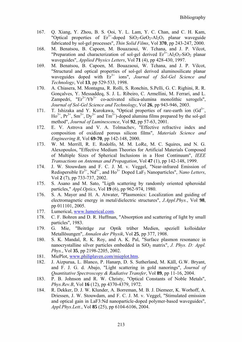
Bibliography
213
167. Q. Xiang, Y. Zhou, B. S. Ooi, Y. L. Lam, Y. C. Chan, and C. H. Kam, "Optical properties of Er3+-doped SiO2-GeO2-Al2O3 planar waveguide fabricated by sol-gel processes", Thin Solid Films, Vol 370, pp 243-247, 2000.
168. M. Benatsou, B. Capoen, M. Bouazaoui, W. Tchana, and J. P. Vilcot, "Preparation and characterization of sol-gel derived Er3+:Al2O3-SiO2 planar waveguides", Applied Physics Letters, Vol 71 (4), pp 428-430, 1997.
169. M. Benatsou, B. Capoen, M. Bouazaoui, W. Tchana, and J. P. Vilcot, "Structural and optical properties of sol-gel derived aluminosilicate planar waveguides doped with Er3+ ions", Journal of Sol-Gel Science and Technology, Vol 13, pp 529-533, 1998.
170. A. Chiasera, M. Montagna, R. Rolli, S. Ronchin, S.Pelli, G. C. Righini, R. R. Gonçalves, Y. Messaddeq, S. J. L. Ribeiro, C. Armellini, M. Ferrari, and L. Zampedri, "Er3+/Yb3+ co-activated silica-alumina monolithic xerogels", Journal of Sol-Gel Science and Technology, Vol 26, pp 943-946, 2003.
171. T. Ishizaka and Y. Kurokawa, "Optical properties of rare-earth ion (Gd3+, Ho3+, Pr3+, Sm3+, Dy3+ and Tm3+)-doped alumina films prepared by the sol-gel method", Journal of Luminescence, Vol 92, pp 57-63, 2001.
172. E. V. Astrova and V. A. Tolmachev, "Effective refractive index and composition of oxidized porous silicon films", Materials Science and Engineering B, Vol 69-70, pp 142-148, 2000.
173. W. M. Merrill, R. E. Rodolfo, M. M. LoRe, M. C. Squires, and N. G. Alexopoulos, "Effective Medium Theories for Artificial Materials Composed of Multiple Sizes of Spherical Inclusions in a Host Continuum", IEEE Transactions on Antennas and Propagation, Vol 47 (1), pp 142-148, 1999.
174. J. W. Stouwdam and F. C. J. M. v. Veggel, "Near-infrared Emission of Redispersible Er3+, Nd3+, and Ho3+ Doped LaF3 Nanoparticles", Nano Letters, Vol 2 (7), pp 733-737, 2002.
175. S. Asano and M. Sato, "Ligth scattering by randomly oriented spheroidal particles," Appl.Optics, Vol 19 (6), pp 962-974, 1980.
176. S. A. Mayer and H. A. Atwater, "Plasmonics: Localization and guiding of electromagnetic energy in metal/dielectric structures", J.Appl.Phys., Vol 98, pp 011101, 2005.
177. Lumerical, www.lumerical.com. 178. C. F. Bohren and D. R. Huffman, "Absorption and scattering of light by small
particles", 1983. 179. G. Mie, "Beiträge zur Optik trüber Medien, speziell kolloidaler
Metallösungen", Annalen der Physik, Vol 25, pp 377, 1908. 180. S. K. Mandal, R. K. Roy, and A. K. Pal, "Surface plasmon resonance in
nanocrystalline silver particles embedded in SiO2 matrix", J. Phys. D: Appl. Phys., Vol 35, pp 2198-2205, 2002.
181. MiePlot, www.philiplaven.com/mieplot.htm. 182. J. Aizpurua, L. Blanco, P. Hanarp, D. S. Sutherland, M. Käll, G.W. Bryant,
and F. J. G. d. Abajo, "Light scattering in gold nanorings", Journal of Quantitative Spectroscopy & Radiative Transfer, Vol 89, pp 11-16, 2004.
183. P. B. Johnson and R. W. Christy, "Optical Constants of Noble Metals", Phys.Rev.B, Vol 16 (12), pp 4370-4379, 1972.
184. R. Dekker, D. J. W. Klunder, A. Borreman, M. B. J. Diemeer, K. Worhoff, A. Driessen, J. W. Stouwdam, and F. C. J. M. v. Veggel, "Stimulated emission and optical gain in LaF3:Nd nanoparticle-doped polymer-based waveguides", Appl.Phys.Lett., Vol 85 (25), pp 6104-6106, 2004.
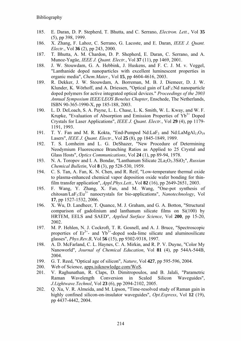
Bibliography
214
185. E. Daran, D. P. Stepherd, T. Bhutta, and C. Serrano, Electron. Lett., Vol 35 (5), pp 398, 1999.
186. X. Zhang, F. Lahoz, C. Serrano, G. Lacoste, and E. Daran, IEEE J. Quant. Electr., Vol 36 (2), pp 243, 2000.
187. T. Bhutta, A. M. Chardon, D. P. Shepherd, E. Daran, C. Serrano, and A. Munoz-Yagüe, IEEE J. Quant. Electr., Vol 37 (11), pp 1469, 2001.
188. J. W. Stouwdam, G. A. Hebbink, J. Huskens, and F. C. J. M. v. Veggel, "Lanthanide doped nanoparticles with excellent luminescent properties in organic media", Chem.Mater., Vol 15, pp 4604-4616, 2003.
189. R. Dekker, J. W. Stouwdam, A. Borreman, M. B. J. Diemeer, D. J. W. Klunder, K. Wörhoff, and A. Driessen, "Optical gain of LaF3:Nd nanoparticle doped polymers for active integrated optical devices." Proceedings of the 2003 Annual Symposium IEEE/LEOS Benelux Chapter, Enschede, The Netherlands, ISBN 90-365-1990-X, pp 185-188, 2003.
190. L. D. DeLoach, S. A. Payne, L. L. Chase, L. K. Smith, W. L. Kway, and W. F. Krupke, "Evaluation of Absorption and Emission Properties of Yb3+ Doped Crystals for Laser Applications", IEEE J. Quant. Electr., Vol 29 (4), pp 1179-1191, 1993.
191. T. Y. Fan and M. R. Kokta, "End-Pumped Nd:LaF3 and Nd:LaMgAl11O19 Lasers", IEEE J. Quant. Electr., Vol 25 (8), pp 1845-1849, 1989.
192. T. S. Lomheim and L. G. DeShazer, "New Procedure of Determining Neodymium Fluorescence Branching Ratios as Applied to 25 Crystal and Glass Hosts", Optics Communications, Vol 24 (1), pp 89-94, 1978.
193. N. A. Toropov and I. A. Bondar, "Lanthanum Silicate 2La2O3.3SiO2", Russian Chemical Bulletin, Vol 8 (3), pp 528-530, 1959.
194. C. S. Tan, A. Fan, K. N. Chen, and R. Reif, "Low-temperature thermal oxide to plasma-enhanced chemical vapor deposition oxide wafer bonding for thin-film transfer application", Appl.Phys.Lett., Vol 82 (16), pp 2649-2651, 2003.
195. F. Wang, Y. Zhang, X. Fan, and M. Wang, "One-pot synthesis of chitosan/LaF3:Eu3+ nanocrystals for bio-applications", Nanotechnology, Vol 17, pp 1527-1532, 2006.
196. X. Wu, D. Landheer, T. Quance, M. J. Graham, and G. A. Botton, "Structural comparison of gadolinium and lanthanum silicate films on Si(100) by HRTEM, EELS and SAED", Applied Surface Science, Vol 200, pp 15-20, 2002.
197. M. P. Hehlen, N. J. Cockroft, T. R. Gosnell, and A. J. Bruce, "Spectroscopic properties of Er3+- and Yb3+-doped soda-lime silicate and aluminosilicate glasses", Phys.Rev.B, Vol 56 (15), pp 9302-9318, 1997.
198. A. D. McFarland, C. L. Haynes, C. A. Mirkin, and R. P. V. Duyne, "Color My Nanoworld", Journal of Chemical Education, Vol 81 (4), pp 544A-544B, 2004.
199. G. T. Reed, "Optical age of silicon", Nature, Vol 427, pp 595-596, 2004. 200. Web of Science, apps.isiknowledge.com/WoS. 201. V. Raghunathan, R. Claps, D. Dimitropoulos, and B. Jalali, "Parametric
Raman Wavelength Conversion in Scaled Silicon Waveguides", J.Lightwave.Technol, Vol 23 (6), pp 2094-2102, 2005.
202. Q. Xu, V. R. Almeida, and M. Lipson, "Time-resolved study of Raman gain in highly confined silicon-on-insulator waveguides", Opt.Express, Vol 12 (19), pp 4437-4442, 2004.
Bibliography
215
203. T. K. Liang, H. K. Tsang, I. E. Day, J. Drake, A. P. Knights, and M. Asghari, "Silicon waveguide two-photon absorption detector at 1.5µm wavelength for autocorrelation measurements", Appl.Phys.Lett., Vol 84 (15), pp 2745-2747, 2002.
204. O. Boyraz, T. Indukuri, and B. Jalali, "Self-phase-modulation induced spectral broadening in silicon waveguides", Opt.Express, Vol 12 (5), pp 829-834, 2004.
205. R. Dekker, E. J. Klein, J. Niehusmann, M. Först, F. Ondracek, J. Ctyroky, N. Usechak, and A. Driessen, "Self Phase Modulation and Stimulated Raman Scattering due to High Power Femtosecond Pulse Propagation in Silicon-on-Insulator Waveguides." Symposium IEEE/LEOS Benelux Chapter, Mons, Belgium, ISBN 2-9600226-4-5, pp 197-200, 2005.
206. E. Dulkeith, Y. A. Vlasov, X. Chen, N. C. Panoiu, and O. R.M. Jr, "Self-phase-modulation in submicron silicon-on-insluator photonic wires", Opt.Express, Vol 14 (12), pp 5524-5534, 2006.
207. O. Boyraz, P. Koonath, V. Raghunathan, and B. Jalali, "All optical switching and continuum generation in silicon waveguides", Opt.Express, Vol 12 (17), pp 4094-4102, 2004.
208. H. Fukuda, K. Yamada, T. Shoji, M. Takahashi, T. Tsuchizawa, T. Watanabe, J. Takahashi, and S. Itabashi, "Four-wave mixing in silicon wire waveguides", Opt.Express, Vol 13 (12), pp 4629-4637, 2005.
209. N. G. Usechak, PhD thesis, "Mode-Locking of Fiber Lasers at High Repetition Rates", The Institute of Optics, The College School of Engineering and Applied Sciences, University of Rochester, Rochester, New York, 2006.
210. G. P. Agrawal, "Fiber-Optic Communications Systems", John Wiley & Sons, Inc., 0-471-21571-6, 2002.
211. X. Chen, N. C. Panoiu, and R.M.Jr.Osgood, "Theory of Raman-Mediated Pulsed Amplification in Silicon-Wire Waveguides", IEEE J. Quant. Electr., Vol 42 (2), pp 160-170, 2006.
212. FieldDesigner, www.phoenixbv.com. 213. E. D. Palik, "Handbook of Optical Constants of Solids", Academic Press,
1998. 214. Q. Xu, V. R. Almeida, and M. Lipson, "Demonstration of high Raman gain in
a submicrometer-size silicon-on-insulator waveguide", Opt.Lett., Vol 30 (1), pp 35-37, 2005.
215. P. Y. Yu and M. Cardona, "Fundamentals of Semiconductors: Physics and Material Properties", Springer, ISBN: 3540254706, 2005.
216. J. I. Dadap, R. L. Espinola, R. M. O. Jr., S. J. McNab, and Y. A. Vlasov, "Spontaneous Raman scattering in ultrasmall silicon waveguides", Opt.Lett., Vol 29 (23), pp 2755-2757, 2004.
217. Y. Liu and H. K. Tsang, "Nonlinear absorption and Raman gain in helium-ion-implanted silicon waveguides", Opt.Lett., Vol 31 (11), pp 1714-1716, 2006.
218. G. P. Agrawal, "Nonlinear Fiber Optics, Optics and Photonics", Academic Press, 1995.
219. J. M. Laniel, N. Hô, and R. Vallée, "Nonlinear-refractive-index measurement in As2S3 channel waveguides by asymmetric self-phase modulation", J.Opt.Soc.Am.B, Vol 22 (2), pp 437-445, 2005.
220. U. Bandelow, A. Demircan, and M. Kesting, "Simulation of Pulse Propagation in Nonlinear Optical Fibers", Weierstrass-Institut für Angewandte Analysis und Stochastik, ISSN 0946-8838, 2003.
Bibliography
216
221. C. HeadleyIII and G. P. Agrawal, "Unified description of ultrafast stimulated Raman scattering in optical fibers", J.Opt.Soc.Am.B, Vol 13 (10), pp 2170-2177, 1996.
222. Q. Lin, J. Zhang, P. M. Fauchet, and G. P. Agrawal, "Ultrabroadband parametric generation and wavelength conversion in silicon waveguides", Opt.Express, Vol 14 (11), pp 4786-4799, 2006.
223. K. J. Blow and D. Wood, "Theoretical description of transient stimulated raman scattering in optical fibers", IEEE J. Quant. Electr., Vol 25, pp 2665–2673, 1989.
224. D. J. W. Klunder, F. S. Tan, T. v. d. Veen, H. F. Bulthuis, G. Sengo, B. Docter, H. J. W. M. Hoekstra, and A. Driessen, "Experimental and Numerical Study of SiON Microresonators With Air and Polymer Cladding", J.Lightwave Technol., Vol 21 (4), pp 1099-1110, 2003.
225. D. H. Geuzebroek, E. J. Klein, H. Kelderman, N. Baker, and A. Driessen, "Compact Wavelength-Selective Switch for Gigabit Filtering in Access Networks", IEEE Photon. Technol. Lett., Vol 17 (2), pp 336-338, 2005.
226. V. R. Almeida and M. Lipson, "Optical bistability on a silicon chip", Opt.Lett., Vol 29 (20), pp 2387-2389, 2004.
217
Over promotie onderzoek wordt vaak gedacht dat het enkel jarenlang solitair ploeteren is in muffe achteraf kamertjes op een universiteit. Dit kan in veel gevallen zo zijn, echter, tijdens de afgelopen vier jaar van mijn onderzoek heb ik het tegendeel ondervonden. De donkere kamertjes en cleanrooms waarin de praktische uitvoering van mijn werk plaatsvond waren allesbehalve muf, vanwege de immer verkwikkende airco’s die me altijd trouw hebben bijgestaan. Het kantoor was immer en altijd fris vanwege de fruitige opmerkingen die over en weer door de kamer vlogen, dankzij mijn collega’s. De negen procent (!!!) van mijn tijd die ik de afgelopen vier jaar op oranje plastic banken in de trein heb doorgebracht waren redelijk uit te houden door zo af en toe eens een raampje open te zetten voor de broodnodige buitenlucht. Tot zo ver de locaties. De locaties waren zeker niet de elementen die mij door de afgelopen jaren heen hebben geleid. Dit is enkel en alleen te danken aan de mensen om mij heen. Ploeteren is het zeker geweest, maar beslist niet solitair. Ik wil dan ook graag mijn dank betuigen aan een grote groep mensen. Ik bied bij voorbaat alvast mijn welgemeende excuses aan voor het geval iemand het idee heeft dat hij of zij onterecht niet is genoemd of juist wel. Helaas wordt aan het meestgelezen gedeelte van een proefschrift nog altijd te weinig tijd besteed. Daar gaat ‘ie dan, in min of meer willekeurige volgorde... Allereerst wil ik mijn promotor Prof. Dr. Alfred Driessen bedanken voor het vertrouwen dat hij in mij stelde om mij als niet-academicus aan te stellen op dit ambitieuze project. Ik ben hem vooral dankbaar voor de vrijheden en verantwoordelijkheden die hij me de afgelopen vier jaar heeft gegeven, waardoor ik in grote lijnen mijn eigen wetenschappelijke pad en ontwikkeling heb kunnen bepalen. Verder wil ik graag de andere vier leden van mijn promotiecommissie, Daan Lenstra, Klaus Boller, Paul Lambeck en Hugo Hoekstra bedanken voor het feit dat zij hun kostbare tijd hebben willen besteden aan het doorlezen van dit proefschrift. Zonder mijn directe collega’s binnen de leerstoel was het behalen van de eindstreep ongetwijfeld met veel meer tegenwind verlopen. De goede sfeer tussen de collega’s en de enorme hoeveelheid aanwezige ervaring op velerlei gebied hebben mij vele malen uit de wind gehouden waardoor ik af en toe weer kon versnellen wanneer ik
Dankwoord / Acknowledgments
218
even naar achteren was gezakt in het onderzoekspeleton. Als eerste wil ik van mijn directe collega’s graag mijn kamergenoten Edwin Klein en Wico Hopman bedanken voor de geweldige tijd die ik samen met hun heb gehad. De discussies met jullie waren altijd zeer enerverend, in de ruimste zin van het woord. Ondanks dat onze onderzoeken niets met elkaar te maken hadden, heb altijd het gevoel gehad dat we een hecht team waren. Verder zijn Anton Hollink en Rita ter Weele-Stokkers van onschatbare waarde voor het algehele reilen en zeilen van de leerstoel. Met vragen kun je altijd bij ze terecht en hun adequate en efficiente optreden heeft me vele malen versteld doen staan. Mart Diemeer heeft enorm sterk bijgedragen aan mijn onderzoek met de ontwikkeling van de fotogevoelige polymeren, maar daarnaast ook aan mijn ontwikkeling bij JDS Uniphase waar ik van hem volledig de vrije hand kreeg om zijn ideeën om te zetten in tastbare producten. Qua polymeeronderzoek heeft Lucie Hilderink voor zover ik weet duizenden oplossingen gemaakt, gekarakteriseerd en gearchiveerd. Uit deze niet te bevatten collectie is de voor mij benodigde ideale combinatie van ingredienten naar boven komen drijven, mede door haar structurele en georganiseerde aanpak. Gabriel Sengo en Meindert Dijkstra, onze andere cleanroom technici, wil ik bedanken voor het feit dat ik altijd bij ze aan kon kloppen voor advies en af en toe eens een sample met hun processen mee kon laten liften. Mijn huidige en ex-collega AIO’s hebben altijd voor een extreem goede sfeer gezord, zowel aan de koffietafel als in menige kroeg in exotische conferentie oorden. Douwe Geuzebroek (Doewie), Arne Leinse (Hmmmm...), Marcel Hoekman (alias Carmel Moekhan), Geert Altena (onderwater wat?), Henry “ik wil los!” Kelderman (officieel geen AIO, maar wel de levensstijl), Dimitri Geskus, Remco Stoffer en Joris van Lith. De overige leden van de vaste staf, Henk van Wolferen, Kerstin Wörhoff en Rene de Ridder wil ik bedanken voor de vruchtbare discussies. En dan zijn er natuurlijk nog vele ex-groepsleden die zo af en toe eens aan komen waaien en voor de nodige vrolijke noten en bruikbare feedback zorgen, zoals Albert Borreman, Robert Wijn, Joris van Nunen, Chris Roeloffzen, Dion Klunder, Sami Musa, Ton Koster en Marcel Klein-Koerkamp. Hans van den Vlekkert en Rene Heideman wil ik graag bedanken voor de mogelijkheden die zij creëren op het gebied van innovatieve start-up bedrijven, zoals bijvoorbeeld XiO Photonics. Furthermore, I would also like to thank my non-Dutch speaking colleagues. Markus Pollnau has been a huge source of information with regards to rare earth doped materials. Thanks for your flexibility and giving me the opportunity to stay a little longer in this group. Gamar was a great and always friendly colleague. Thanks for the RBS and FTIR characterizations and sharing all the troubles with the practicum with me. Jing Yang, thanks for helping me out with the very useful Judd-Ofelt analysis that I never found time for to explore during my PhD period. Jonathan Bradley was of great help developing the Al2O3 etching process and his office mate Feridun Ay did a great job optimizing the dual prism coupler setup. Didit Judistira, Muralidharan Balakrishnan, Henri Uranus, Chaitanya Dongre, Lasse Kauppinen, Cazimir Bostan, Freddy Tan, thanks for the fruitful discussions. Dankzij de onmisbare technische ondersteuning binnen de faculteit van vele vaklui kon ik me volledig storten op het onderzoek. Rindert Nauta, bedankt voor de geweldige PM500 software. Klaas Smit, bedankt voor het vervaardigen van menig tooltje voor onze meetopstellingen. Eddy Ruiter, Hans Mertens, Johnny Sanderink, Peter Linders, Gerard Roelofs, Ite-Jan Hoolsema, Rene Wolf, Huib van Vossen, Samantha Ooyman-Geerdink, Marion Nijhuis-Groen, Dominique Altpeter, bedankt
Dankwoord / Acknowledgments
219
voor jullie know-how, support en het in de lucht houden van de cleanroom. Albert van den Berg en Mark Smithers, jullie bedankt voor de professionele analyse met de XPS en de SEM. Tom Aarnink en Jisk Holleman, jullie wil ik graag bedanken voor het feit dat jullie mij in het verleden hebben weten te interesseren voor de magie van het fabriceren van dingen die met het blote oog niet waarneembaar zijn. Furthermore, I had a really good time as a treasurer in the IEEE/LEOS Benelux Student Chapter. Together we organized many successful scientific and non-scientific events. Douwe Geuzebroek, Jonathan Bradley, Els Kok, Bas Huiszoon, Christophe Caucheteur, Cathy Crunelle, Peter Vandersteegen, Patryck Urbach, Wenfeng Wang, Wouter van Parijs, Philippe Tassin, Katrien de Vos and TOH Kee Chua, thanks for being a great team. Mijn studenten verdienen ook zeker een plaats in dit dankwoord. Allen hebben ze positief bijgedragen aan zowel de onderzoeksresultaten beschreven in dit proefschrift, alsook aan de ontwikkeling van meetopstellingen en fabricageprocessen. Remco Nieuwland, Wouter Engbers, Michiel van den Herberg, Marlies Nijemeisland, Arnold Nijhuis, Tristan Doornebosch en Sipke Witting, bedankt voor jullie inzet! Verder waren er ook nog tientallen studenten die het RIM-practicum met vallen en opstaan bij mij hebben doorlopen. Velen van hun hebben zeer sportief gelatinetaarten, appeltaarten en kwarktaarten gebakken om het eind van het practicum te vieren (en waarschijnlijk om er een puntje bij te bietsen). Verder is er binnen onze groep altijd veel stimulans geweest om samenwerkings-verbanden met onderzoeksgroepen in het buitenland aan te gaan. De bijdragen van verschillende onderzoekers uit buitenlandse instellingen zijn van grote waarde geweest voor mijn onderzoek, waardoor deze personen zeker een plaatsje in dit dankwoord verdienen. Allereerst wil ik de mensen bedanken die vanaf de universiteit van Victoria (Brittish Colombia) in Canada aan de synthese van de kristallijne lanthaanfluoride nanoparticles hebben gewerkt. Wiljan Stouwdam, bedankt voor het vervaardigen van de in polymeer oplosbare erbium en neodymium gedoteerde nanodeeltjes en het altijd bereid zijn om TEM foto’s en spectra beschikbaar te stellen. Next, I would like to thank Sudarsan for the preparation of the sol-gel compatible erbium doped nanoparticles and the willingness to share some of the measurement data with me. Frank van Veggel wil ik graag bedanken voor de goede samenwerking en mijn bewondering betuigen vanwege het feit dat hij toch iedere keer weer de witte nano-poeders via de post vanuit Canada naar Nederland wist te krijgen. Furthermore, I would like to thank Dong Woo Kim who was with the Sungkyunkwan University of South Korea for his high aspect ratio chlorine based etch tests on our aluminum oxide films. Too bad you disappeared from the planet with my best hero-sample. Nevertheless, your experimental setup was a good starting point for us to purchase our own equipment. Next on the list of people from other countries are my co-workers at the Rheinisch Westfälische Technische Hochschule (RWTH) in Aachen where I spent many weeks. I thank Jan Niehusmann for spending many days, even weeks, with me in the femtosecond lab, tweaking lenses and steering invisible laser beams into SOI waveguides. Further, I would like to thank Michael Först for all the fruitful discussions and feedback on my scientific manuscripts. It was a special moment when everybody was celebrating carnaval and you and Jan skipped the beer to spend your time with me in the lab, while the rest of the group was having a great party. All the
Dankwoord / Acknowledgments
220
other group members, like Felix Spöler and Tobias Plötzing, were always helpful ‘mode-knocking’ the titanium sapphire laser for me. Birger Berghoff, thanks for spending many hours in the cleanroom with me depositing and annealing the silicon nano-dot doped glasses on my ring resonators. Special thanks go out to Nick Usechak who worked in Govind Agrawal’s group at The Institute of Optics at the University of Rochester in New York. The Split Step Fourier and Nonlinear Schrödinger code that he developed and shared with us was of great importance to model and understand the nonlinearities in our SOI waveguides. Jiri Ctyroky and Thomas Lauerman are acknowledged for their contributions to the modeling work. I’m looking forward to our future collaboration. Christian Herzog from ETH in Zurich has always been a great help hosting the McDaggah & O’Laughlain website. One couldn’t wish for better and faster support. Furthermore, I would like to thank Karin Nordström-Andersen for letting me use the expensive rutile prisms from the COM institute in Denmark for a very long time. Marco Gnan from the University of Glasgow and Maxim Fadel from the University of Dortmund, thanks for thanking me with bottles of beer and wine. The best presents a thirsty scientist could wish for. Buiten m’n werk hebben mijn vrienden ook altijd interesse getoond in het, voor hen hoogstwaarschijnlijk wazige, werk wat ik in het verre Twente uitvoerde. Alex Verhelst, Karla Verbeeten, Barend en Mascha Lemans, Danny en Tamara Venrooy, Floor Arts, Dennis Mocking, Mieke en Bas Zoon, Maike en Bas Schoorlemmer, Kees en Marlies Kraamer, Vincent en Susan Konijnenberg, Saskia en Eduard, Berry en Marieke van Engeland, Erik en Nicole Telgen, Jan en Sandra Telgen, Marco en Marianne Smallegoor, Giel Linthorst en Irene, Marieke Foekema, Janny van den Berg, Albert van der Harst en Monique Derickx, Erwin van Dijk, Nienke Stern, Stefan Meeldijk en Miranda, Marcel en Daniëlle ter Haar. Allemaal bedankt voor de ontspanning onder het genot van een sapje (...) buiten het werk. Sommige familieleden in het bijzonder, waaronder Misha Gilberts, Annelies Aantjes, Lida Gilberts, Max en Vera Verhoeven en Wim Verhoeven, waren altijd geinteresseerd in de voortgang van m’n promotieonderzoek, waarvoor mijn dank. Als één na laatste groep wil ik graag m’n ouders en schoonouders bedanken voor de steun en de vele pogingen om steeds weer iets te proberen begrijpen van m’n werk. M’n vader Willem, die helaas veel te vroeg is overleden, en m’n moeder Willy verdienen in het bijzonder een plaats in dit dankwoord. Hun relaxte opvoeding heeft er voor gezorgd dat ik een onbezorgde jeugd heb gehad waarin ik (bijna) altijd zelf mocht bepalen welke kant ik uitging. Ondanks het feit dat school voor mij nooit echt leek bedoeld, is het allemaal toch nog redelijk goed gekomen. Pa, ma, Harry, Inez en Jan, bedankt voor jullie trots! Het is een goede gewoonte om het beste altijd tot het laatste te bewaren, zo ook in dit dankwoord. Tamara, al meer dan 12 jaar mijn steun en toeverlaat, bedankt voor al je begrip, warmte en steeds weer je gemeende interesse gedurende de afgelopen jaren. Ik heb grote bewondering voor het feit dat jij als niet technisch onderlegd persoon bijzonder veel snapt van wat er in dit proefschrift staat beschreven. Hopelijk zegt dit meer over jou dan over mijn wetenschappelijke kwaliteiten. Tamara, uiteindelijk ben jij de reden om iedere dag weer ‘op tijd’ naar huis te komen en degene die me laat inzien dat er meer in de wereld is dan alleen werk. Tamara, bedankt voor alles.
221
Peer reviewed journals:
R. Dekker, D.J.W. Klunder, A. Borreman, M.B.J. Diemeer, K. Wörhoff, A. Driessen, J.W. Stouwdam, and F.C.J.M. van Veggel, “Stimulated emission and optical gain in LaF3: Nd nanoparticle-doped polymer-based waveguides”, Applied Physics Letters, Vol. 85, No. 25, pp 6104-6106 , 2004. M. Diemeer, L. Hilderink, R. Dekker, and A. Driessen, “Low-Cost and Low-Loss Multimode Waveguides of Photodefinable Epoxy”, IEEE Photonics Technology Letters 18 (15), pp1624-1626, 2006. W. C. L. Hopman, R. Dekker, D. Yudistira, W. F. A. Engbers, H. J. W. M. Hoekstra, and R. M. d. Ridder, "Fabrication and Characterization of High-Quality Uniform and Apodized Si3N4 waveguide Gratings using Laser Interference Lithography," IEEE Photonics Technology Letters 18 (17), pp1855-1857, 2006.
R. Dekker, A. Driessen, T. Wahlbrink, C. Moormann, J. Niehusmann, and M. Först, “Ultrafast Kerr-induced all-optical wavelength conversion in silicon waveguides using 1.55 µm femtosecond pulses”, Optics Express 14 (18), pp8336-8346, 2006. H.J.W.M. Hoekstra, W.C.L. Hopman, J. Kautz, R. Dekker and R.M. de Ridder, “A simple coupled mode model for near band-edge phenomena in grated Waveguides”, accepted for publication in Optical and Quantum Electronics, 2006. A. Driessen, D.H. Geuzebroek, E.J. Klein, R. Dekker, R. Stoffer and C. Bornholdt, "Propagation of short lightpulses in microring resonators: ballistic transport versus interference in the frequency domain", accepted for publication in Optics Communications, 2006.
Publications
222
J. Niehusmann, M. Först, H. Kurz, R. Dekker, T. Wahlbrink, C. Moormann, “Sub-picosecond all-optical switching via cross-phase modulation in silicon-on-insulator waveguides“, submitted to IEEE Phot. Technol. Lett., 2006.
Topical review (invited): R. Dekker, A. Driessen, “High Speed All-optical Processes in Silicon-on-Insulator Waveguides”, to be published in Journal of Physics D: Applied Physics. 2007.
Book chapters:
R.M. de Ridder, G. Altena, D.H. Geuzebroek, R. Dekker (editors), “Proceedings of the Annual Symposium 2003 IEEE/LEOS 2003 Organized by Integrated Optical MicroSystems (IOMS), University of Twente in association with IEEE/LEOS, November 20-21, 2003, University of Twente, Enschede, The Netherlands, Published by IEE/LEOS Benelux Chapter c/o University of Twente, Faculty of Electrical Engineering, Mathematics and Computer Sciences, Enschede, The Netherlands. 307 pages, ISBN: 90-365-1990-X.
Oral contributions:
Dekker, R., “Rare-earth-doped- nanoparticles dispersed in photo-definable polymers for use in a microring resonator devices”, IEEE LEOS Benelux Annual Workshop “Lasing and amplification in solid state materials”, Eindhoven, The Netherlands, 20 May 2005.
Dekker, R., Wörhoff, K., Stouwdam, W.J., Veggel, F.C.J.M. van, Driessen, A., “Absorption spectroscopy of complex rare earth ion doped hybrid Materials over a broad wavelength range”, Europhysics Conference Abstracts of the 17th International Conference on Photonics in Europe (CLEO Europe 2005), Munich, Germany, 12-17 June 2005, Volume 29B, Paper CE-1175, CD Rom, ISBN number: 0-7803-8974-3. Dekker, R., Diemeer, M.B.J., Klein, E.J., Hilderink, L.T.H., Wörhoff, K., Driessen, A., “Photo-Patternable Polymer Waveguides for microring Resonators”, Proceedings of the 31st European Conference on Optical Communications (ECOC), Glasgow, Scotland, 25-29 September 2005, Vol. 2, Paper Tu 1.6.7, Pp. 187-188, ISBN Number 0-86341-544-X. R. Dekker, J. Niehusmann, M. Först, T. Wahlbrink, C. Moormann and A. Driessen, “Ultrafast All-Optical Wavelength Conversion in Silicon Waveguides using Femtosecond Pump-Probe Pulses.”, Proceedings of the 32nd European Conference on Optical Communications (ECOC), Cannes, France, 24-28 September, Paper Th3.1.3, 2006.
Conference proceedings:
Isai, I.G., Kovalgin, A.Y., Holleman, J., Dekker, R., Woerlee, P.H., & Wallinga, H.(2000, December 19). Low Temperature SiO2 films deposited by Multipolar ECR PECVD., [poster]., Veldhoven
Publications
223
Tosic, N., Merticaru, A.R., Isai, I.G., Nguyen Van Hieu, H., Dekker, R., & Holleman, J. "Simulation, Characterization & Technology of Amorphous and Polysilicon Thin Film Transistors." 1999, October 14, MESA+ day, Enschede, The Netherlands.
Nguyen Van Hieu, H., Merticaru, A.R., Dekker, R., Kranenburg, H. van., Mouthaan, A.J., & Chien, N.D. "Formation of Source and Drain Regions for a-Si:H TFT by Using Ion Implantation Through Metal Technique." 1999, November 24, SAFE'99, Mierlo, The Netherlands.
Kovalgin, A.Y., Isai, I.G., Wang Zhichun, W., Houtsma, V.E., Holleman, J., Dekker, R., Salm, C., Woerlee, P.H., & Mouthaan, A.J. "Growth and properties of IC dielectrics." 1999, October 14, Mesa+ day, Enschede, The Netherlands.
Isai, I.G., Kovalgin, A.Y., Holleman, J., Dekker, R., Woerlee, P.H., & Wallinga, H. "Dielectric thin films deposited by means of ECR PECVD." 1999, December 21, FOM annual meeting, Veldhoven, The Netherlands.
Bystrova, S., Dekker, R., Holleman, J., Kranenburg, H. van., Kuper, F.G., Mouthaan, A.J., Nguyen Hoang, V., Petrescu, V., Rijnsburger, M., Salm, C., & Woerlee, P.H. "Actual Interconnect Issues and Solutions in ULSI Circuits." 1999, October 14, MESA+ day, Enschede, The Netherlands
Kovalgin, A.Y., Isai, I.G., Holleman, J., Dekker, R., Woerlee, P.H., & Wallinga, H. "Characterization of Silicon Oxide films deposited by means of ECR PECVD." 1999, November 24, SAFE'99, Mierlo, The Netherlands, pp. 239-246, ISBN 90-73461-18-9.
M. B. J. Diemeer and R. Dekker, "MEMS VOA with polymeric thermal microactuators," presented at the Proceedings of the European Conference on Optical Communication (ECOC), Stockholm, Sweden, 2002.
R. Meijerink, D.H. Geuzebroek, E.J. Klein, H. Kelderman, R. Dekker, M.B.J. Diemeer, A. Driessen, (2003, November 20-21), “Optimization of driving signal for thermal modulation of a Microring Resonator”, Poster in Proceedings of the 8th Annual Symposium IEEE/LEOS Benelux Chapter, University of Twente, Enschede, The Netherlands, Pp. 85-88, ISBN: 90-365-1990-X.
R. Dekker, J.W. Stouwdam, A. Borreman, M.B.J. Diemeer, D.J.W. Klunder, K. Wörhoff, A. Driessen, (2003, November 20-21), “Optical gain of LaF3:Nd nanoparticle doped polymers for active integrated optical devices”, Poster in Proceedings of the 8th Annual Symposium IEEE/LEOS Benelux Chapter, University of Twente, Enschede, The Netherlands, Pp. 185-188, ISBN: 90-365-1990-X.
Publications
224
Dekker, R., Wörhoff and Driessen, A., “All-optical switching in microring resonators”, Proceedings International School of Quantum Electronics, Erice, Sicily, Volume 709, October 18-25-2003, Pp. 419-420, 2004 ISBN: 0-7354-0184-5, ISSN 0094-243X. Nieuwland, R.A., Dekker, R., Hilderink, L.T.H., Diemeer, M.B.J., Wörhoff, K., Stouwdam, J.W., Veggel, F.CJ.M. van, Driessen, A., “A novel photo definable polymer containing rare-earth doped nanoparticles for optical amplification”, Poster in Proceedings 9th Annual Symposium of the IEEE/LEOS Benelux Chapter, December 2-3 2004, Pp. 323-326, Ghent University, Ghent, Belgium, ISBN Number: 9076546061.
Dekker, R., Sudarsan, V., Veggel, F.C.J.M. van, Wörhoff, K., Driessen, A., “Erbium doped LaF3 nanoparticles incorporated in silicon dioxide thin films for active integrated optical applications”, Poster in Proceedings 9th Annual Symposium of the IEEE/LEOS Benelux Chapter, December 2-3 2004, Pp. 295-298, Ghent University, Ghent, Belgium, ISBN Number: 9076546061.
Dekker, R., Hilderink, L.T.H., Diemeer, M.B.J., Stouwdam, J.W., Sudarsan, V., Veggel, F.C.J.M. van, Wörhoff, K. Driessen, A., “Rare earth doped nanoparticles in organic and inorganic host materials for application in integrated optics”, Second International Symposium on Science and Technology of Dielectrics in Emerging Fields” of the 207th Meeting of the Electrochemical Society, Quebec City, Canada, 15-20 May 2005. Driessen, A., Dekker, R., Diemeer, M.B.J., Geuzebroek, D.H., Hoekstra, H.J.W.M., Klein, E.J., Leinse A., “Microresonators as promising building blocks for VLSI photonics, Invited paper, Proceedings of SPIE, Conference on Integrated Optics: Theory and Applications, Warsaw, Poland, 31 August – 2 September 2005, Vol. 5956, Pp. 59560Q-1 – 59560Q-14, ISBN number: 0-8194-5963-1, ISSN: 0277-786X, Editors: P.V. Lambeck, C. Gorecki. Organized by SPIE Poland Chapter, SPIE Europe and Warsaw University of Technology, Poland.
Diemeer, M.B.J., Dekker, R., Hilderink, L., Leinse (Lionix BV), A., Balakrishnan, M., Faccini, M., Driessen, A., “Polymeric components for telecom and datacom” Invited paper, Proceedings of SPIE, Conference on Integrated Optics: Theory and Applications, Warsaw, Poland, 31 August – 2 September 2005, Vol. 5956, Pp. 59560S-1 – 59560S-10, ISBN number: 0-8194-5963-1, ISSN: 0277-786X, Editors: P.V. Lambeck, C. Gorecki. Organized by SPIE Poland Chapter, SPIE Europe and Warsaw University of Technology, Poland. R. Dekker, J. Niehusmann, F. Ondracek, J. Ctyroky, A. Driessen, C. Moormann and M. Först, “Nonlinear propagation through photonic structures – modeling and experiments”, poster at the ePIXnet Annual Meeting 2005, 12-13 September, Eindhoven, The Netherlands, 2005.
Publications
225
R. Dekker, E. J. Klein, A. Driessen, J. Niehusmann, M. Först, F. Ondracek, J. Ctyroky, “Femtosecond pulse propagation through nanophotonic structures”, Mesa+ Meeting 2005, University of Twente, Enschede, the Netherlands, 29 September 2005. Dekker, R., Klein, E.J., Niehusmann, J., Först, M., Ondracek, F., Ctyroky, J., Usechak, N., Driessen, A., “Self phase modulation and stimulated Raman scattering due to high power femtosecond pulse propagation in silicon-on-insulator waveguides”, Proceedings of the Symposium IEEE LEOS Benelux, Mons, Belgium, 1-2 December 2005, Pp. 197-200, Editors: P. Mégret, M. Wuilpart, S. Bette, N. Staquet, ISBN: 2-9600226-4-5.
Hopman, W.C.L., Yudistira, D., Dekker, R., Engbers, W.F.A., Hoekstra, H.J.W.M., Ridder, R.M. de, “Characterization of slow-light in a LIL-fabricated Si3N4 Waveguide grating’, Proceedings of the Symposium IEEE LEOS Benelux Chapter 2005, Mons, Belgium, 1-2 December 2005, Pp. 109-112, Editors: P. Mégret, M. Wuilpart, S. Bette, N. Staquet, ISBN: 2-9600226-4-5.
Geuzebroek, D.H., Dekker, R., Klein, E.J., Bornholdt, C., Niehusmann, J. and Driessen, A., “Behavior of picosecond and femtosecond pulses in SiO2/Si3N4 microring resonator filters”, Proceedings of the Symposium IEEE LEOS Benelux, Mons, Belgium, 1-2 December 2005, Pp. 51-54, Editors: P. Mégret, M. Wuilpart, S. Bette, N. Staquet, ISBN: 2-9600226-4-5.
R. Dekker, E. J. Klein, J. Niehusmann, M. Först, F. Ondracek, J. Ctyroky, N. Usechak, and A. Driessen, “Self Phase Modulation and Broadband Raman Gain in Silicon-on-Insulator Waveguides”, poster at the ePIXnet Winterschool 2006, 13-17 March, Pontresina, Switzerland, 2006. H.J.W.M. Hoekstra, W.C.L. Hopman, J. Kautz, R. Dekker, R.M. de Ridder, “A simple coupled mode model for near band-edge phenomena in grated waveguides.” In: Fifteenth International Workshop on Optical Waveguide Theory and Numerical Modeling, OWTNM2006, 20-21 Apr 2006, Varese, Italy. 22. Politecnico di Milano. ISBN 88-902405-0-4, 2006. R. Dekker, J. Niehusmann, M. Först, T. Wahlbrink, C. Moormann, T. Lauerman, J. Ctyroky, and A. Driessen, “Nonlinear propagation in SOI waveguides and ring resonators: experiments and modeling”, poster at the ePIXnet Annual Meeting 2006, 7-8 September, Lausanne, Switzerland, 2006. R. Dekker, J. Niehusmann, M. Först, and A. Driessen, "Ultra-Fast All-Optical Wavelength Conversion in Silicon Waveguides using Femtosecond Pulses", ECS Transactions – Cancun, Volume 3, "Science and Technology of Dielectrics for Active and Passive Photonic Devices", Cancun, Mexico, 2006. R. Dekker, J. Niehusmann, M. Först, T. Wahlbrink, C. Moormann, T. Lauerman, J. Ctyroky, and A. Driessen, “Nonlinear propagation in SOI waveguides and ring resonators: experiments and modeling”, Mesa+ Meeting 2006, University of Twente, Enschede, the Netherlands, 28 September 2005.

Publications
226
R. Dekker, J. Niehusmann, M. Först, A. Driessen, “Ultrafast all-optical wavelength conversion in Silicon-on-Insulator waveguides by means of Cross Phase Modulation using 300 femtosecond pulses.”, Proceedings of the Symposium IEEE LEOS Benelux, Eindhoven, The Netherlands, 30 November - 1 December 2006. J. Yang, M.B.J. Diemeer, L.T.H. Hilderink, R. Dekker, and A. Driessen, “Judd-Ofelt Analysis of Nd(TTA)3Phen-doped 6-FDA/Epoxy Planar Waveguides”, Proceedings of the Symposium IEEE LEOS Benelux, Eindhoven, The Netherlands, 30 November – 1 December 2006.
227
Ronald Dekker was born on the 4th of July 1974 in Apeldoorn, The Netherlands. He received his B.Sc. degree at the ‘Technische Hogeschool Rijswijk’ in the Netherlands in the field of Applied Physics, with specialization in Photonics. After receiving his BSc. he has been active in the field of material engineering, micro-fabrication and telecommunication components for over 6 years. He worked for 3 years at The University of Twente as a process engineer developing new clean room processing steps for the IC-industry to improve the quality of flat panel displays. Furthermore, he was employed at JDS Uniphase for 3 years, both in the Netherlands and Canada. At JDS Uniphase in the Netherlands he worked on the development of MEMS based Variable Optical Attenuators (VOAs) and in Canada he developed a new fabrication platform for low cost Dense Wavelength Division Multiplexers (DWDM) systems. As the Quality Engineer, he was also responsible for all reliability and quality issues related to the DWDM systems at JDS Uniphase. After receiving his PhD degree at the research chair Integrated Optical Micro Systems (University of Twente) he starts a post-doc position at the same research group on femtosecond written waveguides and microfluidics for sensing applications. He is co-founder and currently treasurer of the IEEE Laser and Electro-Optical Society (LEOS) Benelux Student Chapter, founded a scientific software company McDaggah & O’Laughlain and is participating in the startup of a high-tech integrated optics based company called XiO Photonics.
Related Documents