I ALL Digital Phase Locked Loop (ADPLL) By Nada Ibrahim Afifiy Sara Salah Abd El Mone’m Sara Sayed Dahy Under the Supervision of Dr. Hassan Mostafa A Graduation Project Report Submitted to the Faculty of Engineering at Cairo University In Partial Fulfillment of the Requirements for the Degree of Bachelor of Science in Electronics and Communications Engineering Faculty of Engineering, Cairo University Giza, Egypt July 2014

Welcome message from author
This document is posted to help you gain knowledge. Please leave a comment to let me know what you think about it! Share it to your friends and learn new things together.
Transcript
I
ALL Digital Phase Locked Loop (ADPLL)
By
Nada Ibrahim Afifiy
Sara Salah Abd El Mone’m
Sara Sayed Dahy
Under the Supervision of
Dr. Hassan Mostafa
A Graduation Project Report Submitted to
the Faculty of Engineering at Cairo University
In Partial Fulfillment of the Requirements for the
Degree of
Bachelor of Science
in
Electronics and Communications Engineering
Faculty of Engineering, Cairo University
Giza, Egypt
July 2014
II
Table of contents
List of tables ................................................................................................................ v
List of figures .............................................................................................................. vi
Abbreviations ...................................................................................................... viii
Abstract ................................................................................................................... ix
Chapter 1 Introduction ............................................................................................. 1
1.1 what is PLL? ............................................................................................. 1
1.2 Types of PLL ............................................................................................ 2
1.3 AAPLL vs. ADPLL ........................................................................................ 2
1.4 Applications of PLL ........................................................................................ 4
1.5 ADPLL approach ........................................................................................ 4
1.5.1 Why ADPLL? ,...................................................................................... 4
1.6 project flow ..................................................................................................... 5
Chapter 2 ADPLL Architecture .................................................................................. 6
2.1 The proposed Architecture ............................................................................... 6
2.2 The DCO ........................................................................................................... 7
2.2.1 The ring oscillator basic idea .................................................................. 7
2.2.1.1 The DCV basic idea .................................................................... 7
2.2.1.2 Ring oscillator and tristate buffer array ...................................... 9
2.2.1.3 Ring oscillator and tristate buffer array (another arrangement) ..... 10
2.2.2 The proposed architecture of the DCO .................................................. 11
2.2.2.1 Coarse block ................................................................................. 12
2.2.2.2 Fine block ..................................................................................... 12
2.2.3 The control blocks of the DCO .............................................................. 12
2.2.3.1 Phase detector ............................................................................... 12
III
2.2.3.1.1 Buffer delay line .................................................................. 12
2.2.3.1.2 Inverter delay line TDC ....................................................... 13
2.2.3.1.3 Synchronization block ......................................................... 13
2.2.3.1.4 SR flip flop and counter PD ................................................ 14
2.2.3.1.5 Phase Frequency Detector (PFD) ......................................... 14
2.2.4 Loop filter (Controller) ............................................................................. 15
2.2.4.1 Successive approximation mechanism ........................................... 15
2.2.4.2 Stepping mechanism ........................................................................15
2.2.4.3 Shift Registers ................................................................................. 16
Chapter 3 Design Flow................................................................................................. 17
3.1 Verification of the DCO function ....................................................................... 17
3.1.1 DCV .......................................................................................................... 17
3.1.2 Coarse tuning block .................................................................................. 18
3.1.3 Fine tuning block ...................................................................................... 20
3.2 Phase Frequency detector ................................................................................... 22
3.3 Controller (Loop Filter) ....................................................................................... 22
Chapter 4 system layout ............................................................................................... 25
4.1 DCO .................................................................................................................... 25
4.1.1 Nand layout ............................................................................................... 25
4.1.2 NOR layout ............................................................................................... 26
4.1.3 AND layout ............................................................................................... 26
4.1.4 One stage INVERTER .............................................................................. 27
4.1.5 Two-stage INVERTER ............................................................................. 27
4.1.6 MUX block ............................................................................................... 28
4.1.7 D-latch ...................................................................................................... 28
IV
4.1.8 Fine segment ............................................................................................. 29
4.1.9 Coarse segment ......................................................................................... 29
4.1.10 fine stage ................................................................................................. 30
4.1.11 the whole DCO layout ............................................................................. 30
4.2 PFD and Controller .................................................................................................... 31
Chapter 5 Simulation Results ...................................................................................... 32
5.1 DCO..................................................................................................................... 33
5.1.1 Coarse Stage .............................................................................................. 33
5.1.1.1 Coarse Delay ................................................................................... 33
5.1.1.2 Coarse frquency .............................................................................. 34
5.1.2 Fine Stage .................................................................................................. 35
5.1.2.1 Fine Delay ....................................................................................... 35
5.1.2.2 Fine frequency ................................................................................. 35
5.2 Lock Time ........................................................................................................... 36
5.3 Jitter simulation result ......................................................................................... 37
5.4 Area calculation .................................................................................................. 38
5.5 Power Calculation ............................................................................................... 38
Reference .......................................................................................................................... 39
Appendix .......................................................................................................................... 41
A1.VHDL AMS tutorial ............................................................................................................... 41
A2.ModelSim Tutorial .................................................................................................................. 49
A3.Cadence Tutorial ..................................................................................................................... 58
A4.Jitter Calculation ..................................................................................................................... 84
A5.Power Calculation ................................................................................................................... 89
A6.Area calculation ...................................................................................................................... 92
A7. Design Compiler Tutorial ...................................................................................................... 93
V
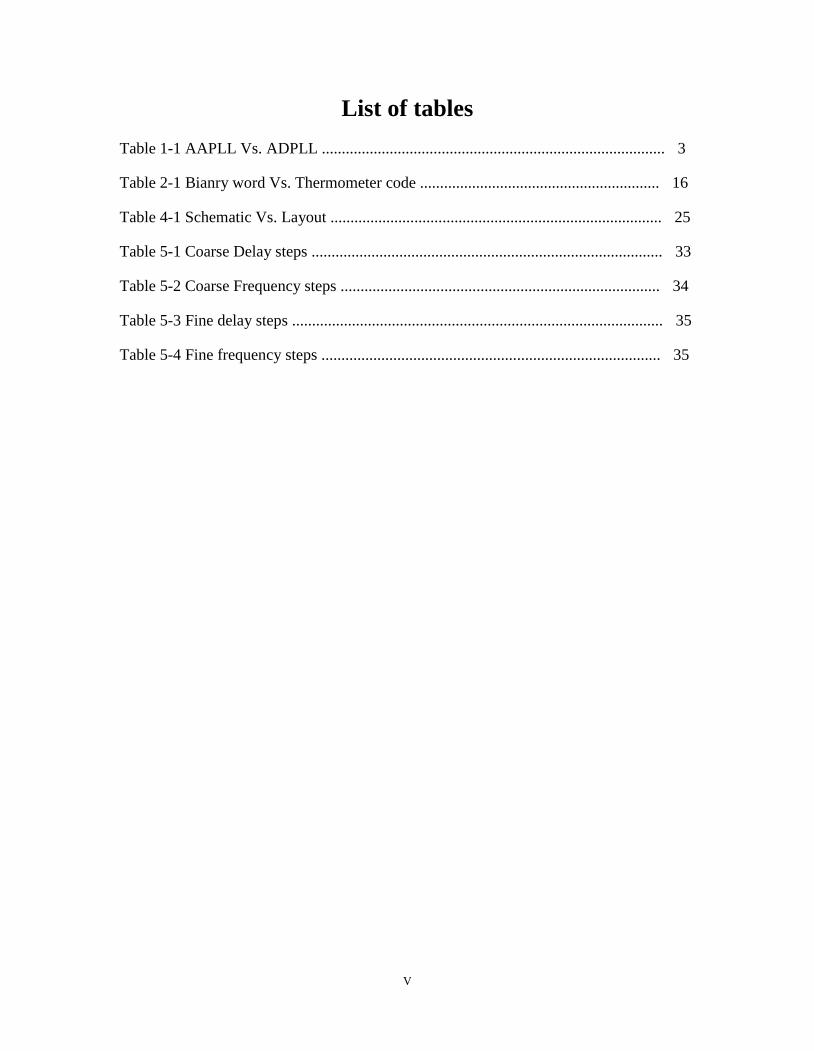
List of tables
Table 1-1 AAPLL Vs. ADPLL ...................................................................................... 3
Table 2-1 Bianry word Vs. Thermometer code ............................................................ 16
Table 4-1 Schematic Vs. Layout ................................................................................... 25
Table 5-1 Coarse Delay steps ........................................................................................ 33
Table 5-2 Coarse Frequency steps ................................................................................ 34
Table 5-3 Fine delay steps ............................................................................................. 35
Table 5-4 Fine frequency steps ..................................................................................... 35
VI
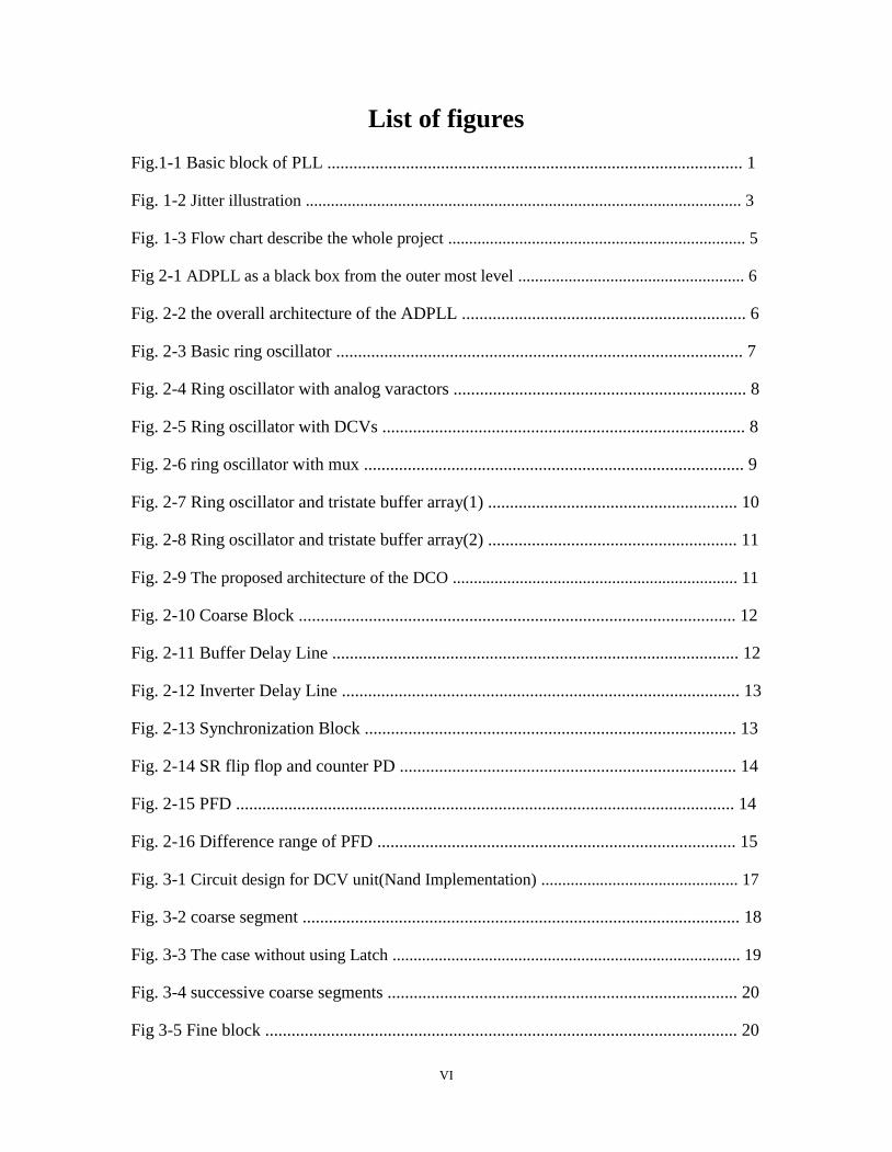
List of figures
Fig.1-1 Basic block of PLL ............................................................................................... 1
Fig. 1-2 Jitter illustration ........................................................................................................ 3
Fig. 1-3 Flow chart describe the whole project ....................................................................... 5
Fig 2-1 ADPLL as a black box from the outer most level ...................................................... 6
Fig. 2-2 the overall architecture of the ADPLL ................................................................. 6
Fig. 2-3 Basic ring oscillator ............................................................................................. 7
Fig. 2-4 Ring oscillator with analog varactors ................................................................... 8
Fig. 2-5 Ring oscillator with DCVs ................................................................................... 8
Fig. 2-6 ring oscillator with mux ....................................................................................... 9
Fig. 2-7 Ring oscillator and tristate buffer array(1) ......................................................... 10
Fig. 2-8 Ring oscillator and tristate buffer array(2) ......................................................... 11
Fig. 2-9 The proposed architecture of the DCO .................................................................... 11
Fig. 2-10 Coarse Block .................................................................................................... 12
Fig. 2-11 Buffer Delay Line ............................................................................................. 12
Fig. 2-12 Inverter Delay Line ........................................................................................... 13
Fig. 2-13 Synchronization Block ..................................................................................... 13
Fig. 2-14 SR flip flop and counter PD ............................................................................. 14
Fig. 2-15 PFD .................................................................................................................. 14
Fig. 2-16 Difference range of PFD .................................................................................. 15
Fig. 3-1 Circuit design for DCV unit(Nand Implementation) ............................................... 17
Fig. 3-2 coarse segment .................................................................................................... 18
Fig. 3-3 The case without using Latch ................................................................................... 19
Fig. 3-4 successive coarse segments ................................................................................ 20
Fig 3-5 Fine block ............................................................................................................ 20
VII
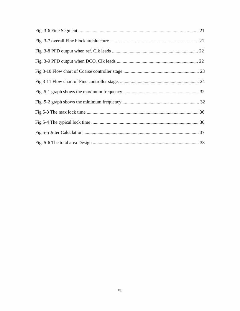
Fig. 3-6 Fine Segment ...................................................................................................... 21
Fig. 3-7 overall Fine block architecture ........................................................................... 21
Fig. 3-8 PFD output when ref. Clk leads ......................................................................... 22
Fig. 3-9 PFD output when DCO. Clk leads ..................................................................... 22
Fig 3-10 Flow chart of Coarse controller stage ................................................................ 23
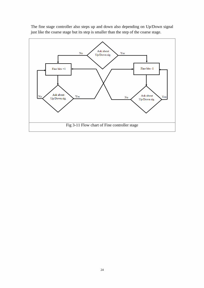
Fig 3-11 Flow chart of Fine controller stage. ................................................................... 24
Fig. 5-1 graph shows the maximum frequency ................................................................ 32
Fig. 5-2 graph shows the minimum frequency ................................................................. 32
Fig 5-3 The max lock time ............................................................................................... 36
Fig 5-4 The typical lock time ........................................................................................... 36
Fig 5-5 Jitter Calculation| ................................................................................................. 37
Fig. 5-6 The total area Design .......................................................................................... 38
VIII
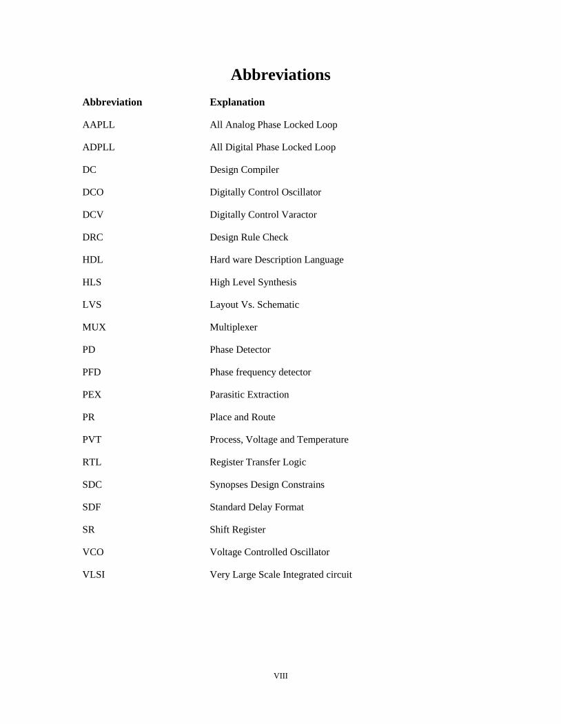
Abbreviations
Abbreviation Explanation
AAPLL All Analog Phase Locked Loop
ADPLL All Digital Phase Locked Loop
DC Design Compiler
DCO Digitally Control Oscillator
DCV Digitally Control Varactor
DRC Design Rule Check
HDL Hard ware Description Language
HLS High Level Synthesis
LVS Layout Vs. Schematic
MUX Multiplexer
PD Phase Detector
PFD Phase frequency detector
PEX Parasitic Extraction
PR Place and Route
PVT Process, Voltage and Temperature
RTL Register Transfer Logic
SDC Synopses Design Constrains
SDF Standard Delay Format
SR Shift Register
VCO Voltage Controlled Oscillator
VLSI Very Large Scale Integrated circuit
IX
Abstract
Phase Locked Loops are used in almost every communication system. Some of its uses
include recovering clock from digital data signals, performing frequency, phase
modulation and demodulation, recovering the carrier from satellite transmission signals
and as a frequency synthesizer.
PLL is generally implemented using analog components, which called analog PLL
(APLL).
APLLs have been widely used for clock generation, and frequency synthesis with good
performance and high frequency range but the main challenge is the high power
consumption, large area, scalability and high noise due to matching, process variations in
the layout.
All digital PLLs (ADPLL) solve the problems of the APLL where the ADPLL have low
power consumption, small area and scalability across different technology nodes.
Fully digital PLLs have better noise immunity and better tolerance to bias drifts and PVT
variations . They also provide the advantage of implementation using automatic CAD tools
which reduces the turnaround time and is also easier to integrate and migrate over various
applications and fabrication processes.
ADPLL uses a phase-frequency detector instead of a phase detector, DCO instead of a
VCO, control circuit imitating the functionality of a loop filter and a fixed frequency
detector. This design is very much suitable for SoC applications and can be automatically
implemented with standard cell libraries.
The proposed ADPLL is implemented on the TSMC 65nm technology with 1.8v operating
voltage, covering frequency range from 100 MHz to 700 MHz, with lock time around 0.2
μs, the total area is 0.01 mm2, power 1mwatt, ,peak-to-peak jitter 6.396 psec, RMS jitter
1.035 psec.
1
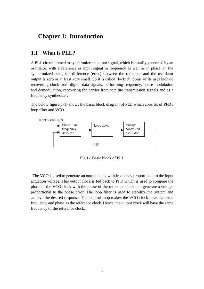
Chapter 1: Introduction
1.1 What is PLL?
A PLL circuit is used to synchronize an output signal, which is usually generated by an
oscillator, with a reference or input signal in frequency as well as in phase. In the
synchronized state, the difference (error) between the reference and the oscillator
output is zero or at least very small. So it is called ‘locked’. Some of its uses include
recovering clock from digital data signals, performing frequency, phase modulation
and demodulation, recovering the carrier from satellite transmission signals and as a
frequency synthesizer.
The below figure(1-1) shows the basic block diagram of PLL which consists of PFD ,
loop filter and VCO.
Fig.1-1Basic block of PLL
The VCO is used to generate an output clock with frequency proportional to the input
actuation voltage. This output clock is fed back to PFD which is used to compare the
phase of the VCO clock with the phase of the reference clock and generate a voltage
proportional to the phase error. The loop filter is used to stabilize the system and
achieve the desired response. This control loop makes the VCO clock have the same
frequency and phase as the reference clock. Hence, the output clock will have the same
frequency of the reference clock.
2
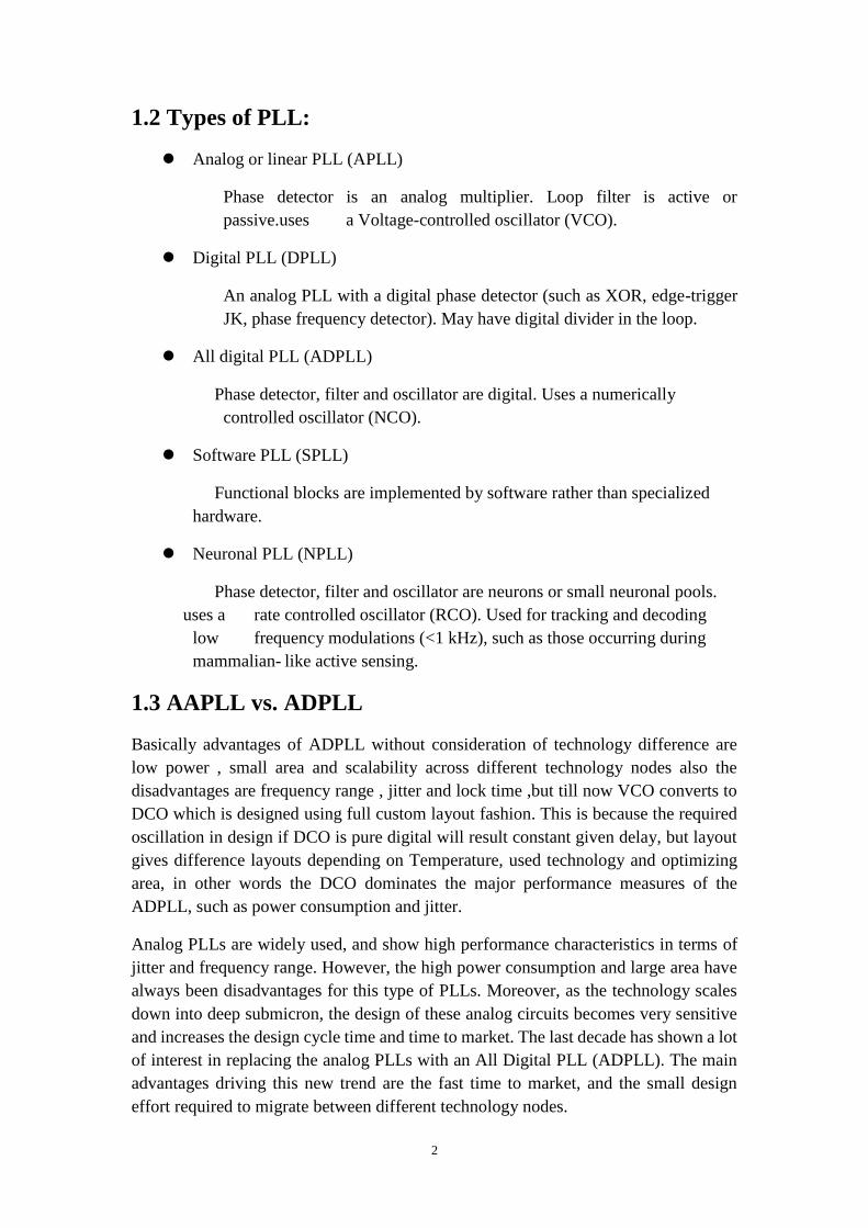
1.2 Types of PLL:
Analog or linear PLL (APLL)
Phase detector is an analog multiplier. Loop filter is active or
passive.uses a Voltage-controlled oscillator (VCO).
Digital PLL (DPLL)
An analog PLL with a digital phase detector (such as XOR, edge-trigger
JK, phase frequency detector). May have digital divider in the loop.
All digital PLL (ADPLL)
Phase detector, filter and oscillator are digital. Uses a numerically
controlled oscillator (NCO).
Software PLL (SPLL)
Functional blocks are implemented by software rather than specialized
hardware.
Neuronal PLL (NPLL)
Phase detector, filter and oscillator are neurons or small neuronal pools.
uses a rate controlled oscillator (RCO). Used for tracking and decoding
low frequency modulations (<1 kHz), such as those occurring during
mammalian- like active sensing.
1.3 AAPLL vs. ADPLL
Basically advantages of ADPLL without consideration of technology difference are
low power , small area and scalability across different technology nodes also the
disadvantages are frequency range , jitter and lock time ,but till now VCO converts to
DCO which is designed using full custom layout fashion. This is because the required
oscillation in design if DCO is pure digital will result constant given delay, but layout
gives difference layouts depending on Temperature, used technology and optimizing
area, in other words the DCO dominates the major performance measures of the
ADPLL, such as power consumption and jitter.
Analog PLLs are widely used, and show high performance characteristics in terms of
jitter and frequency range. However, the high power consumption and large area have
always been disadvantages for this type of PLLs. Moreover, as the technology scales
down into deep submicron, the design of these analog circuits becomes very sensitive
and increases the design cycle time and time to market. The last decade has shown a lot
of interest in replacing the analog PLLs with an All Digital PLL (ADPLL). The main
advantages driving this new trend are the fast time to market, and the small design
effort required to migrate between different technology nodes.
3
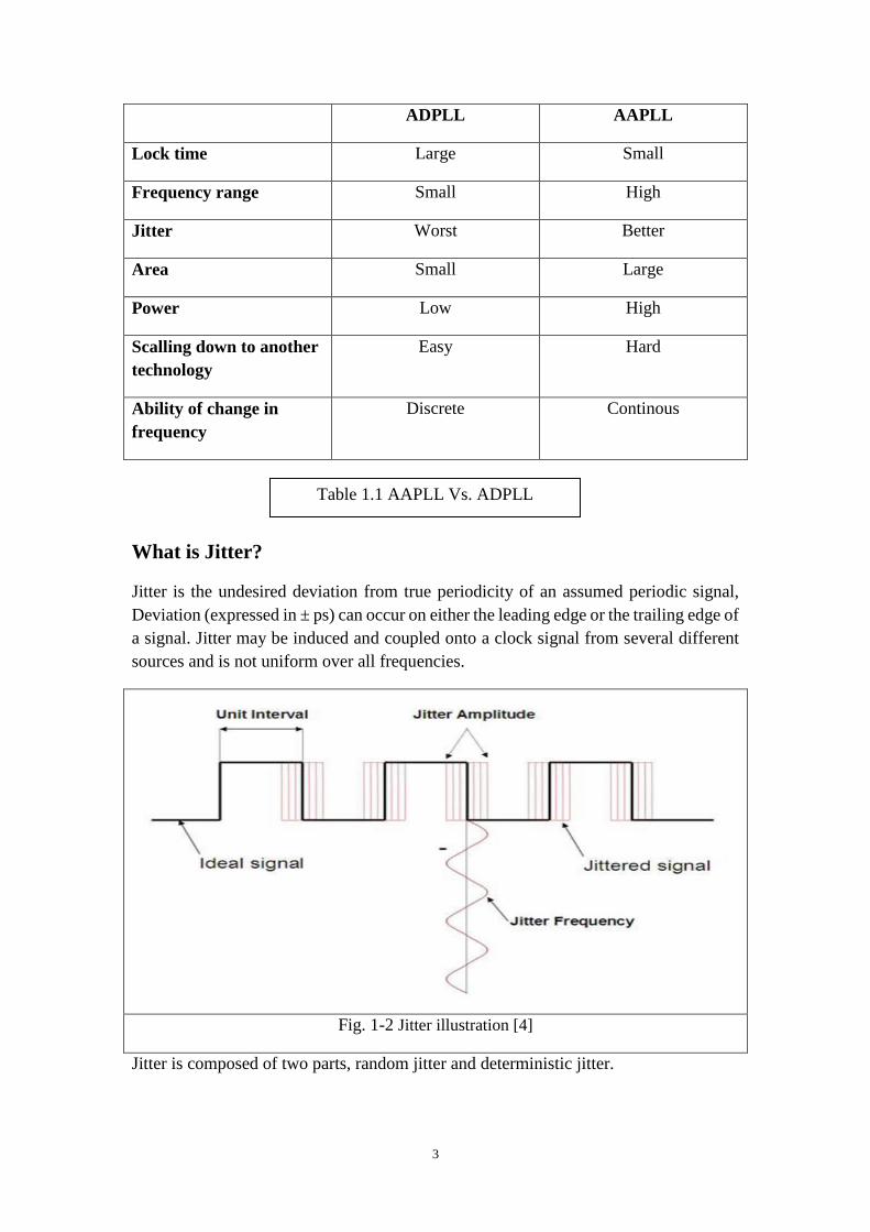
ADPLL AAPLL
Lock time Large Small
Frequency range Small High
Jitter Worst Better
Area Small Large
Power Low High
Scalling down to another
technology
Easy Hard
Ability of change in
frequency
Discrete Continous
What is Jitter?
Jitter is the undesired deviation from true periodicity of an assumed periodic signal,
Deviation (expressed in ± ps) can occur on either the leading edge or the trailing edge of
a signal. Jitter may be induced and coupled onto a clock signal from several different
sources and is not uniform over all frequencies.
Fig. 1-2 Jitter illustration [4]
Jitter is composed of two parts, random jitter and deterministic jitter.
Table 1.1 AAPLL Vs. ADPLL
4
Random jitter
Random Jitter, also called Gaussian jitter, is unpredictable electronic timing noise.
Random jitter typically follows a Gaussian distribution or Normal distribution.
Deterministic jitter
Deterministic jitter is a type of clock timing jitter or data signal jitter that is predictable
and reproducible. The peak-to-peak value of this jitter is bounded, and the bounds can
easily be observed and predicted.
1.4 Applications of PLL:
Phase Locked Loops (PLLs) are widely used for frequency synthesis in many
Applications:
- Microprocessors
- Digital signal processing circuits
- Communication systems as in the high speed serial links
- In the clock and data recovery circuits.
1.5 ADPLL approach
ADPLLs are designed by replacing the analog blocks in the AAPLL by their digital
counterpart the RC LPF is replaced by a digital controller, and the VCO is replaced by a
Digitally Controlled Oscillator (DCO).
1.5.1 Why ADPLL?
Because of its main advantages which are :
- Low power consumption
- Small total area
- Easy way for scale down process to deep submicron technology
- Small lock time.
5
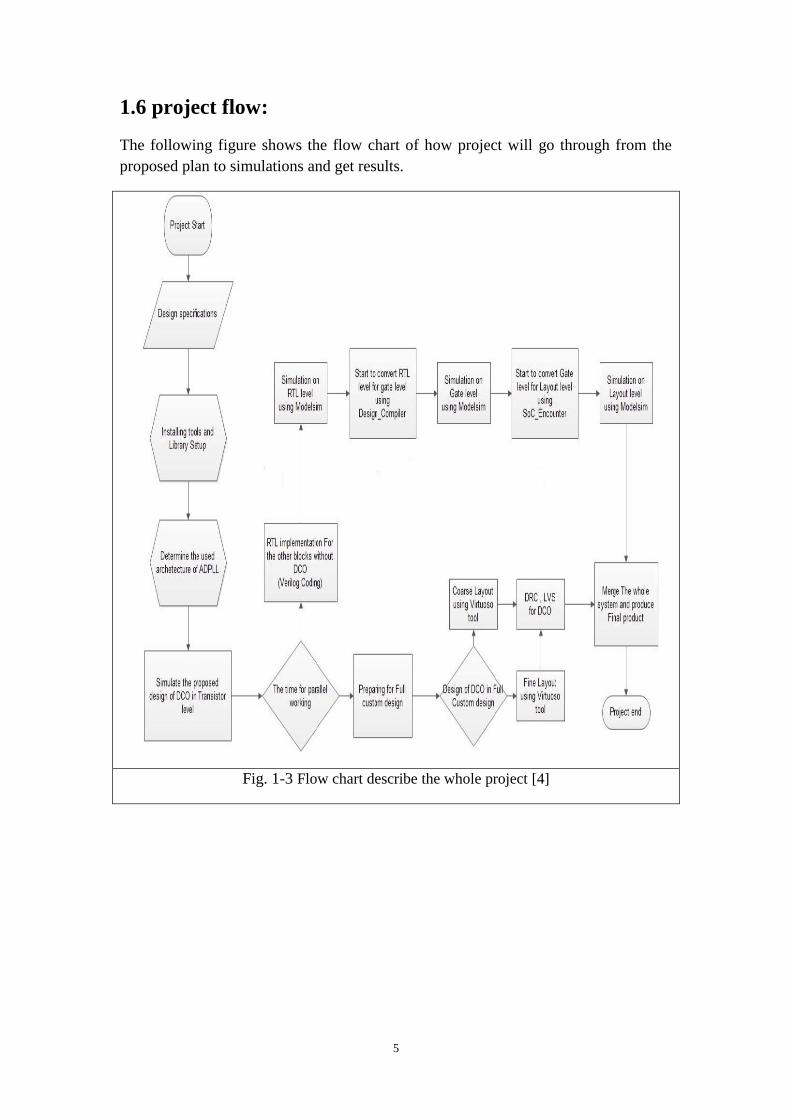
1.6 project flow:
The following figure shows the flow chart of how project will go through from the
proposed plan to simulations and get results.
Fig. 1-3 Flow chart describe the whole project [4]
6
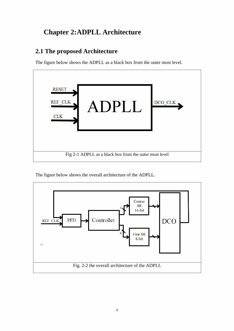
Chapter 2: ADPLL Architecture
2.1 The proposed Architecture
The figure below shows the ADPLL as a black box from the outer most level.
Fig 2-1 ADPLL as a black box from the outer most level
The figure below shows the overall architecture of the ADPLL.
Fig. 2-2 the overall architecture of the ADPLL
7
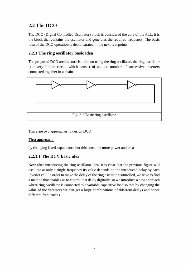
2.2 The DCO
The DCO (Digital Controlled Oscillator) block is considered the core of the PLL, it is
the block that contains the oscillator and generates the required frequency. The basic
idea of the DCO operation is demonstrated in the next few points
2.2.1 The ring oscillator basic idea
The proposed DCO architecture is build on using the ring oscillator, the ring oscillator
is a very simple circuit which consist of an odd number of successive inverters
connected together in a chain
Fig. 2-3 Basic ring oscillator
There are two approaches to design DCO
First approach
by changing fixed capacitance but this consume more power and area
2.2.1.1 The DCV basic idea
Now after introducing the ring oscillator idea, it is clear that the previous figure will
oscillate at only a single frequency its value depends on the introduced delay by each
inverter cell. In order to make the delay of the ring oscillator controlled, we have to find
a method that enables us to control that delay digitally, so we introduce a new approach
where ring oscillator is connected to a variable capacitive load so that by changing the
value of the varactors we can get a large combinations of different delays and hence
different frequencies.
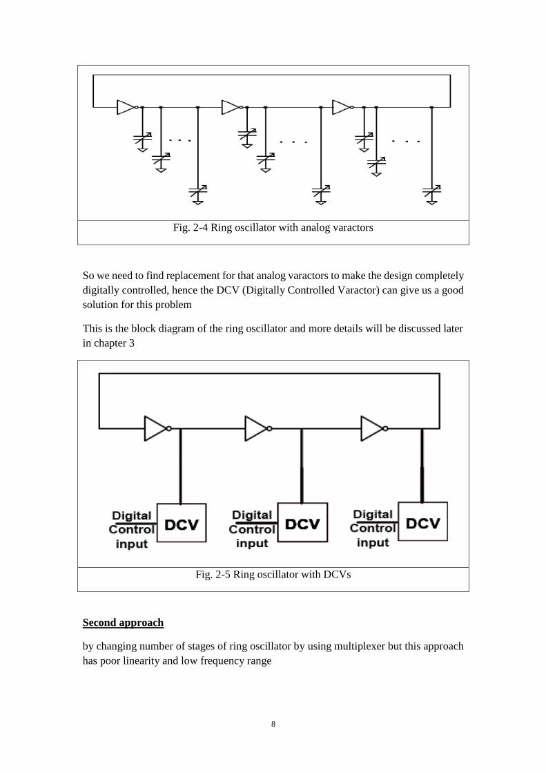
8
Fig. 2-4 Ring oscillator with analog varactors
So we need to find replacement for that analog varactors to make the design completely
digitally controlled, hence the DCV (Digitally Controlled Varactor) can give us a good
solution for this problem
This is the block diagram of the ring oscillator and more details will be discussed later
in chapter 3
Fig. 2-5 Ring oscillator with DCVs
Second approach
by changing number of stages of ring oscillator by using multiplexer but this approach
has poor linearity and low frequency range
9
Fig. 2-6 ring oscillator with mux
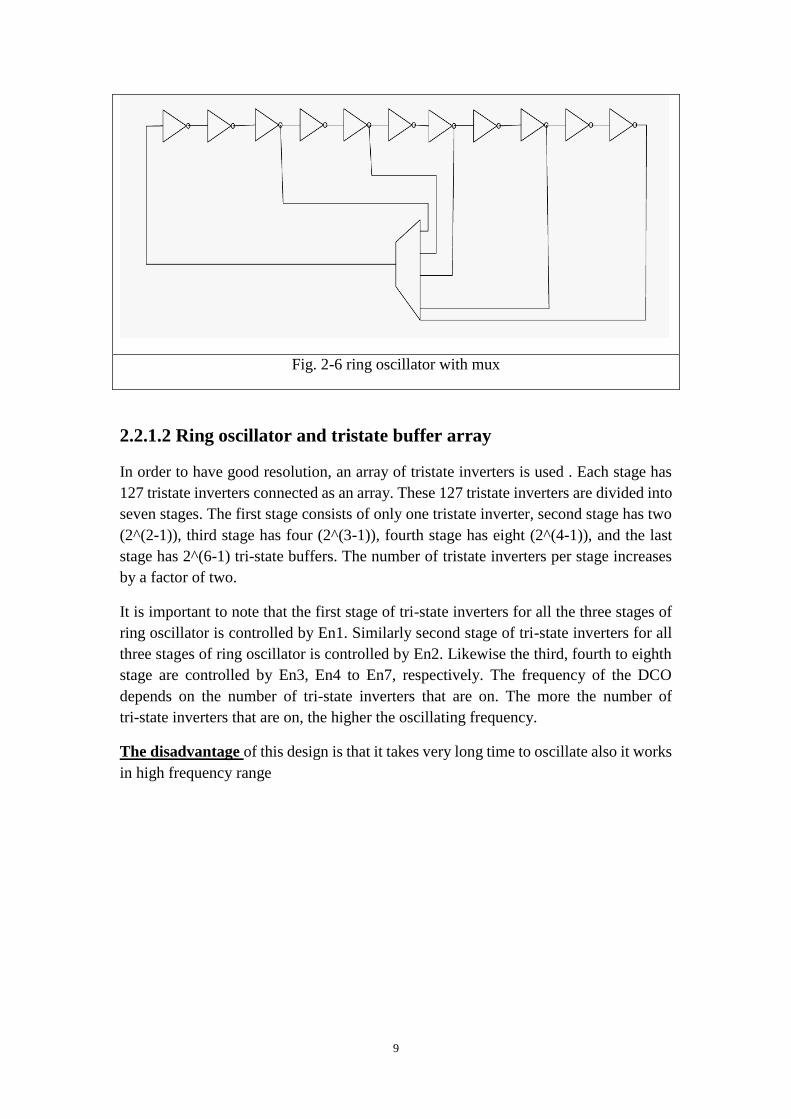
2.2.1.2 Ring oscillator and tristate buffer array
In order to have good resolution, an array of tristate inverters is used . Each stage has
127 tristate inverters connected as an array. These 127 tristate inverters are divided into
seven stages. The first stage consists of only one tristate inverter, second stage has two
(2^(2-1)), third stage has four (2^(3-1)), fourth stage has eight (2^(4-1)), and the last
stage has 2^(6-1) tri-state buffers. The number of tristate inverters per stage increases
by a factor of two.
It is important to note that the first stage of tri-state inverters for all the three stages of
ring oscillator is controlled by En1. Similarly second stage of tri-state inverters for all
three stages of ring oscillator is controlled by En2. Likewise the third, fourth to eighth
stage are controlled by En3, En4 to En7, respectively. The frequency of the DCO
depends on the number of tri-state inverters that are on. The more the number of
tri-state inverters that are on, the higher the oscillating frequency.
The disadvantage of this design is that it takes very long time to oscillate also it works
in high frequency range
10
Fig. 2-7 Ring oscillator and tristate buffer array(1)
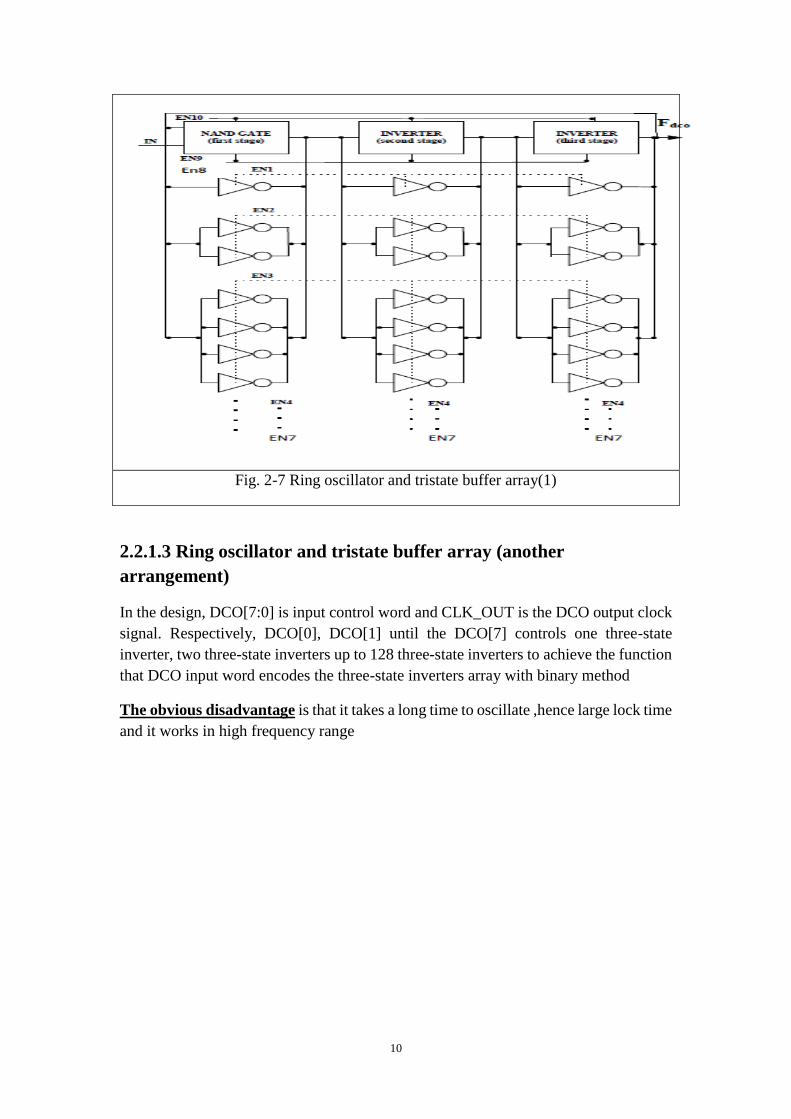
2.2.1.3 Ring oscillator and tristate buffer array (another
arrangement)
In the design, DCO[7:0] is input control word and CLK_OUT is the DCO output clock
signal. Respectively, DCO[0], DCO[1] until the DCO[7] controls one three-state
inverter, two three-state inverters up to 128 three-state inverters to achieve the function
that DCO input word encodes the three-state inverters array with binary method
The obvious disadvantage is that it takes a long time to oscillate ,hence large lock time
and it works in high frequency range
11
Fig. 2-8 Ring oscillator and tristate buffer array(2)
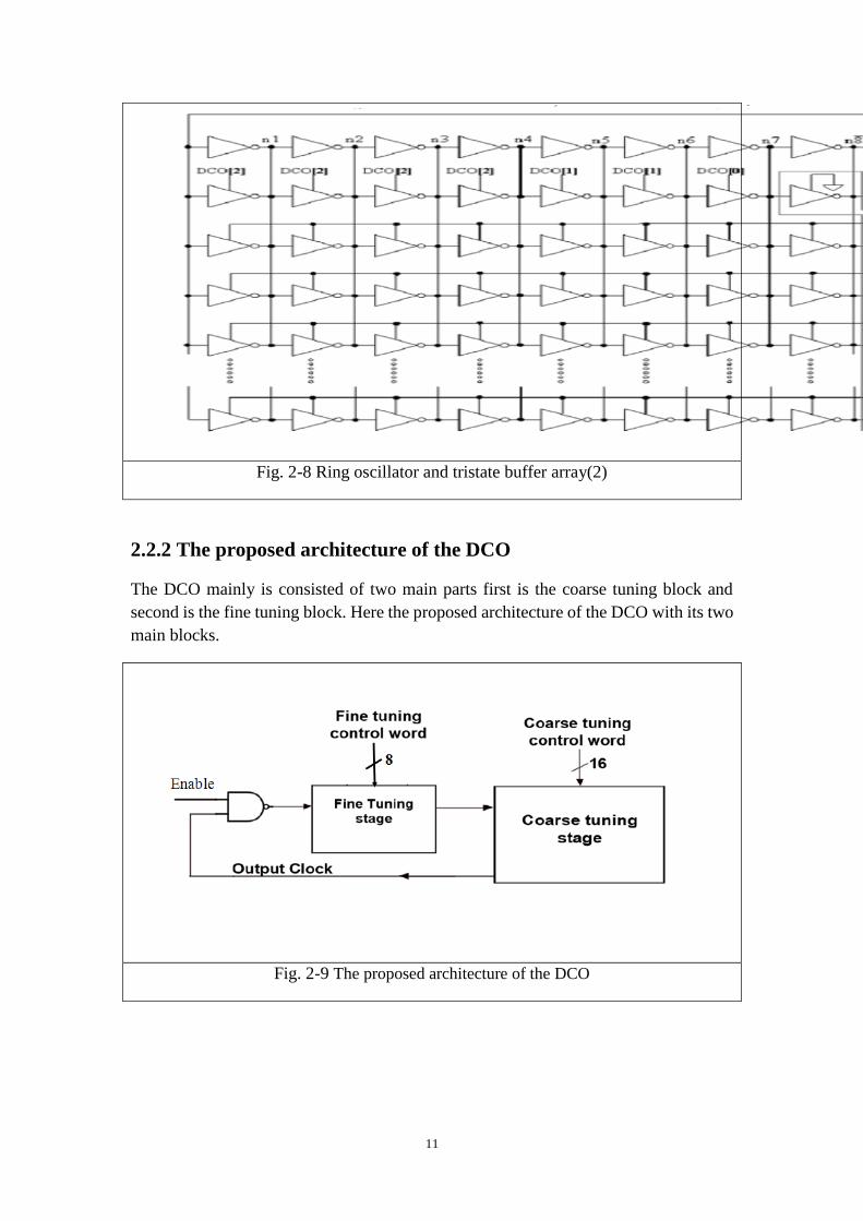
2.2.2 The proposed architecture of the DCO
The DCO mainly is consisted of two main parts first is the coarse tuning block and
second is the fine tuning block. Here the proposed architecture of the DCO with its two
main blocks.
Fig. 2-9 The proposed architecture of the DCO
12
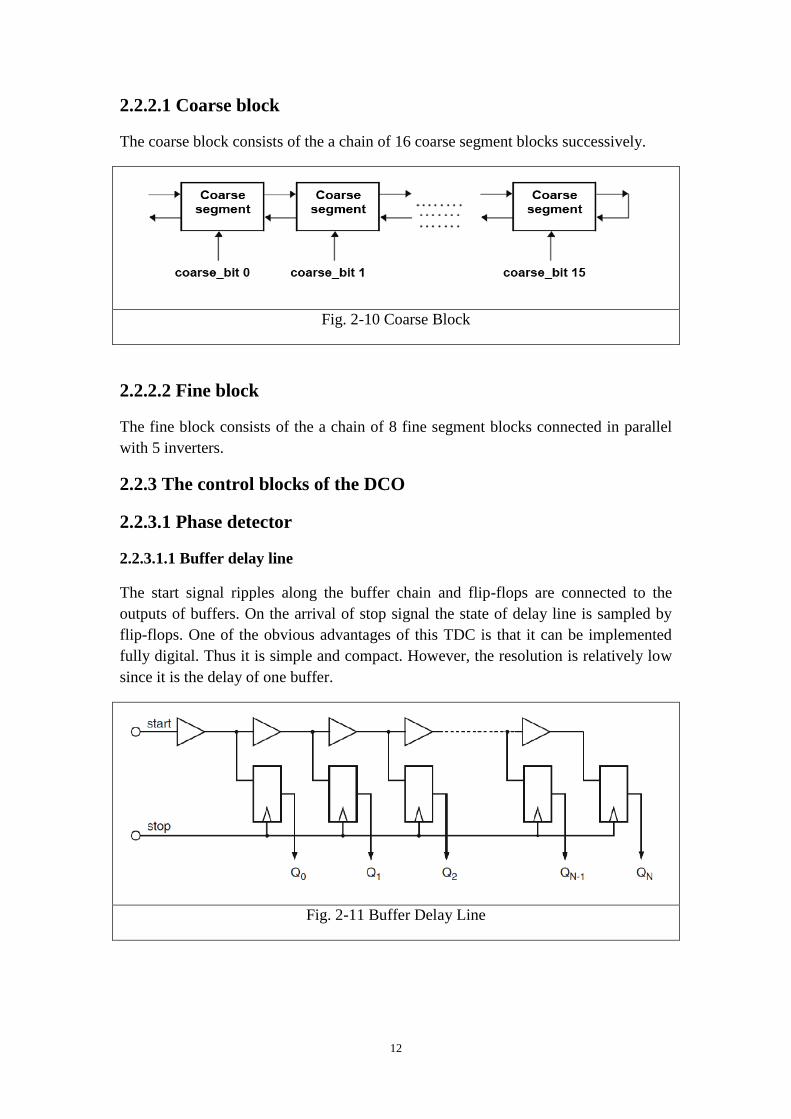
2.2.2.1 Coarse block
The coarse block consists of the a chain of 16 coarse segment blocks successively.
Fig. 2-10 Coarse Block
2.2.2.2 Fine block
The fine block consists of the a chain of 8 fine segment blocks connected in parallel
with 5 inverters.
2.2.3 The control blocks of the DCO
2.2.3.1 Phase detector
2.2.3.1.1 Buffer delay line
The start signal ripples along the buffer chain and flip-flops are connected to the
outputs of buffers. On the arrival of stop signal the state of delay line is sampled by
flip-flops. One of the obvious advantages of this TDC is that it can be implemented
fully digital. Thus it is simple and compact. However, the resolution is relatively low
since it is the delay of one buffer.
Fig. 2-11 Buffer Delay Line
13
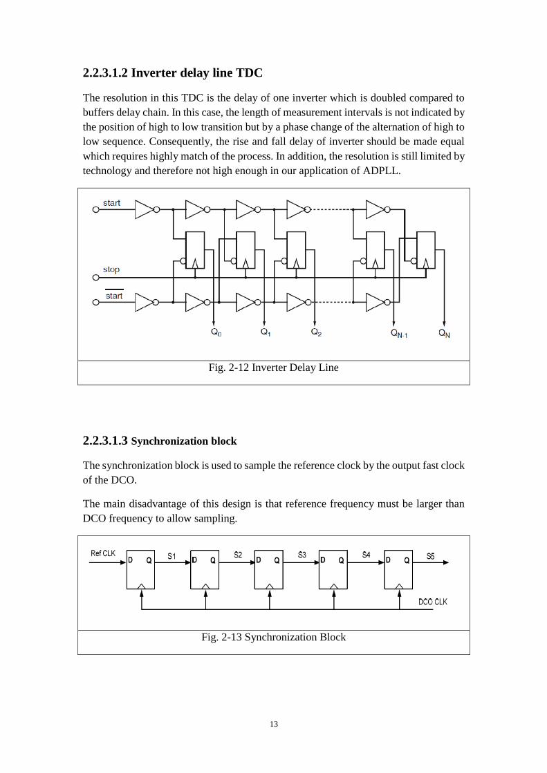
2.2.3.1.2 Inverter delay line TDC
The resolution in this TDC is the delay of one inverter which is doubled compared to
buffers delay chain. In this case, the length of measurement intervals is not indicated by
the position of high to low transition but by a phase change of the alternation of high to
low sequence. Consequently, the rise and fall delay of inverter should be made equal
which requires highly match of the process. In addition, the resolution is still limited by
technology and therefore not high enough in our application of ADPLL.
Fig. 2-12 Inverter Delay Line
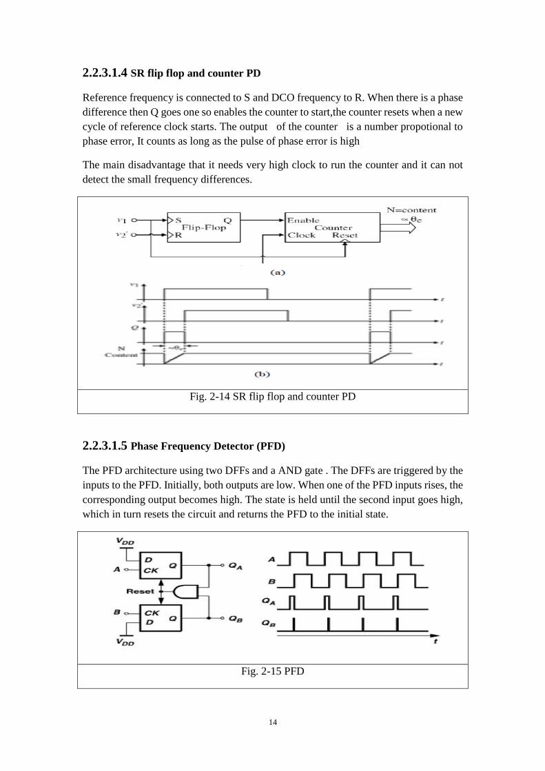
2.2.3.1.3 Synchronization block
The synchronization block is used to sample the reference clock by the output fast clock
of the DCO.
The main disadvantage of this design is that reference frequency must be larger than
DCO frequency to allow sampling.
Fig. 2-13 Synchronization Block
14
2.2.3.1.4 SR flip flop and counter PD
Reference frequency is connected to S and DCO frequency to R. When there is a phase
difference then Q goes one so enables the counter to start,the counter resets when a new
cycle of reference clock starts. The output of the counter is a number propotional to
phase error, It counts as long as the pulse of phase error is high
The main disadvantage that it needs very high clock to run the counter and it can not
detect the small frequency differences.
Fig. 2-14 SR flip flop and counter PD
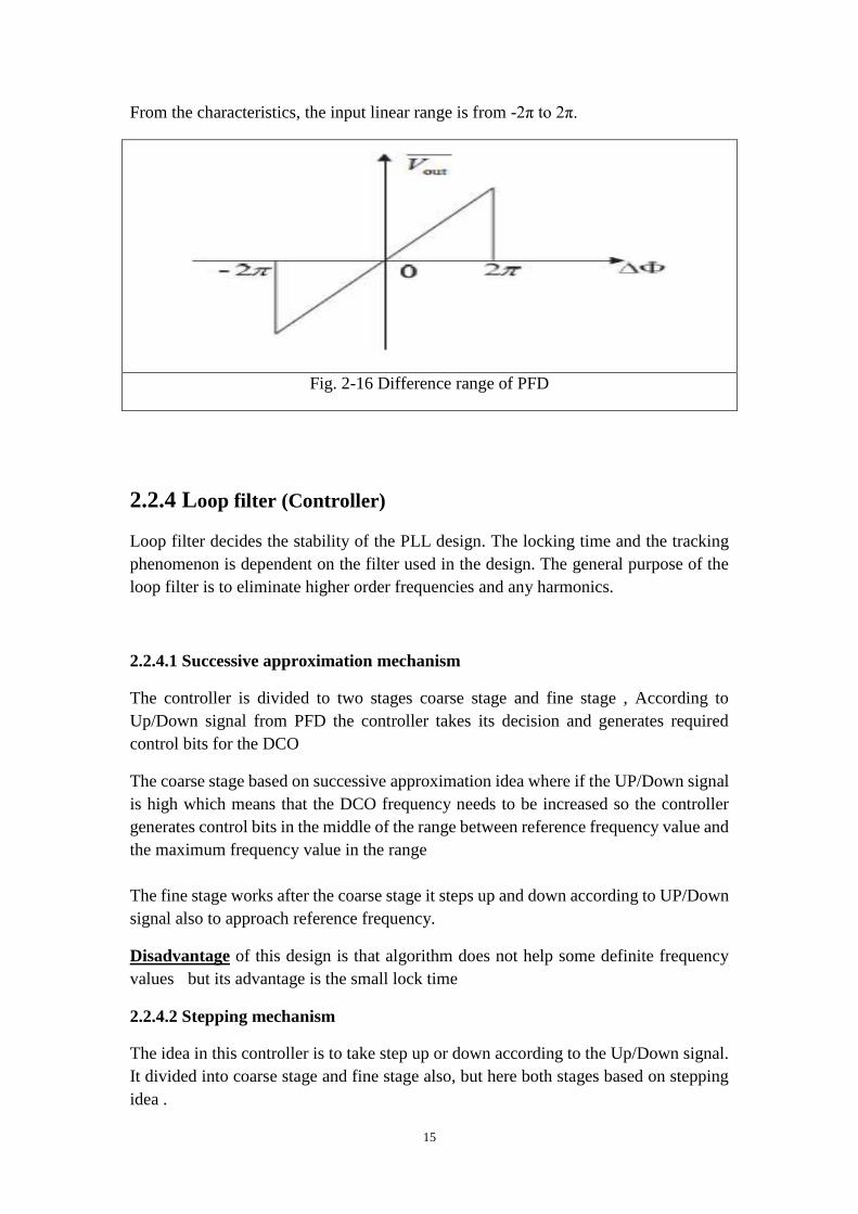
2.2.3.1.5 Phase Frequency Detector (PFD)
The PFD architecture using two DFFs and a AND gate . The DFFs are triggered by the
inputs to the PFD. Initially, both outputs are low. When one of the PFD inputs rises, the
corresponding output becomes high. The state is held until the second input goes high,
which in turn resets the circuit and returns the PFD to the initial state.
Fig. 2-15 PFD
15
From the characteristics, the input linear range is from -2π to 2π.
Fig. 2-16 Difference range of PFD
2.2.4 Loop filter (Controller)
Loop filter decides the stability of the PLL design. The locking time and the tracking
phenomenon is dependent on the filter used in the design. The general purpose of the
loop filter is to eliminate higher order frequencies and any harmonics.
2.2.4.1 Successive approximation mechanism
The controller is divided to two stages coarse stage and fine stage , According to
Up/Down signal from PFD the controller takes its decision and generates required
control bits for the DCO
The coarse stage based on successive approximation idea where if the UP/Down signal
is high which means that the DCO frequency needs to be increased so the controller
generates control bits in the middle of the range between reference frequency value and
the maximum frequency value in the range
The fine stage works after the coarse stage it steps up and down according to UP/Down
signal also to approach reference frequency.
Disadvantage of this design is that algorithm does not help some definite frequency
values but its advantage is the small lock time
2.2.4.2 Stepping mechanism
The idea in this controller is to take step up or down according to the Up/Down signal.
It divided into coarse stage and fine stage also, but here both stages based on stepping
idea .
16
Disadvantage of this controller is that it takes relatively high lock time compared to
successive approximation mechanism but the advantage that no problem in locking on
definite frequency values.
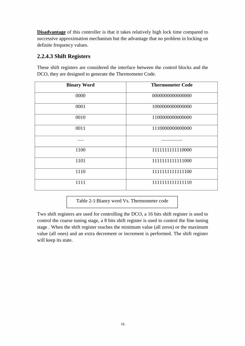
2.2.4.3 Shift Registers
These shift registers are considered the interface between the control blocks and the
DCO, they are designed to generate the Thermometer Code.
Binary Word Thermometer Code
0000 0000000000000000
0001 1000000000000000
0010 1100000000000000
0011 1110000000000000
..... .................
1100 1111111111110000
1101 1111111111111000
1110 1111111111111100
1111 1111111111111110
Two shift registers are used for controlling the DCO, a 16 bits shift register is used to
control the coarse tuning stage, a 8 bits shift register is used to control the fine tuning
stage . When the shift register reaches the minimum value (all zeros) or the maximum
value (all ones) and an extra decrement or increment is performed. The shift register
will keep its state.
Table 2-1:Bianry word Vs. Thermometer code
17
Chapter 3 Design Flow
3.1 Verification of the DCO function
As mentioned before it is considered the CORE of the whole system because it is
responsible for generating the different frequency ranges according to any change in
control bits.
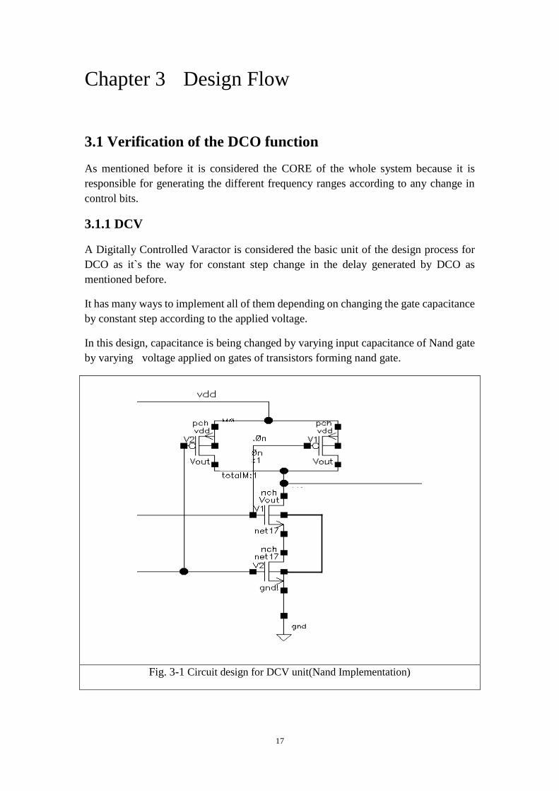
3.1.1 DCV
A Digitally Controlled Varactor is considered the basic unit of the design process for
DCO as it`s the way for constant step change in the delay generated by DCO as
mentioned before.
It has many ways to implement all of them depending on changing the gate capacitance
by constant step according to the applied voltage.
In this design, capacitance is being changed by varying input capacitance of Nand gate
by varying voltage applied on gates of transistors forming nand gate.
Fig. 3-1 Circuit design for DCV unit(Nand Implementation)
18
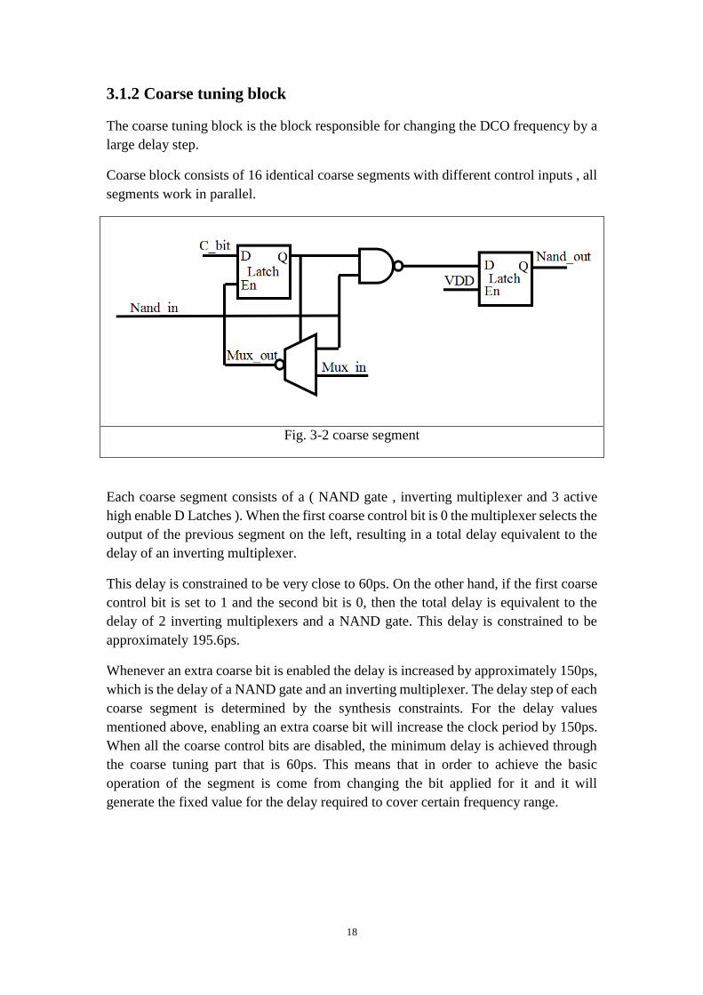
3.1.2 Coarse tuning block
The coarse tuning block is the block responsible for changing the DCO frequency by a
large delay step.
Coarse block consists of 16 identical coarse segments with different control inputs , all
segments work in parallel.
Fig. 3-2 coarse segment
Each coarse segment consists of a ( NAND gate , inverting multiplexer and 3 active
high enable D Latches ). When the first coarse control bit is 0 the multiplexer selects the
output of the previous segment on the left, resulting in a total delay equivalent to the
delay of an inverting multiplexer.
This delay is constrained to be very close to 60ps. On the other hand, if the first coarse
control bit is set to 1 and the second bit is 0, then the total delay is equivalent to the
delay of 2 inverting multiplexers and a NAND gate. This delay is constrained to be
approximately 195.6ps.
Whenever an extra coarse bit is enabled the delay is increased by approximately 150ps,
which is the delay of a NAND gate and an inverting multiplexer. The delay step of each
coarse segment is determined by the synthesis constraints. For the delay values
mentioned above, enabling an extra coarse bit will increase the clock period by 150ps.
When all the coarse control bits are disabled, the minimum delay is achieved through
the coarse tuning part that is 60ps. This means that in order to achieve the basic
operation of the segment is come from changing the bit applied for it and it will
generate the fixed value for the delay required to cover certain frequency range.
19
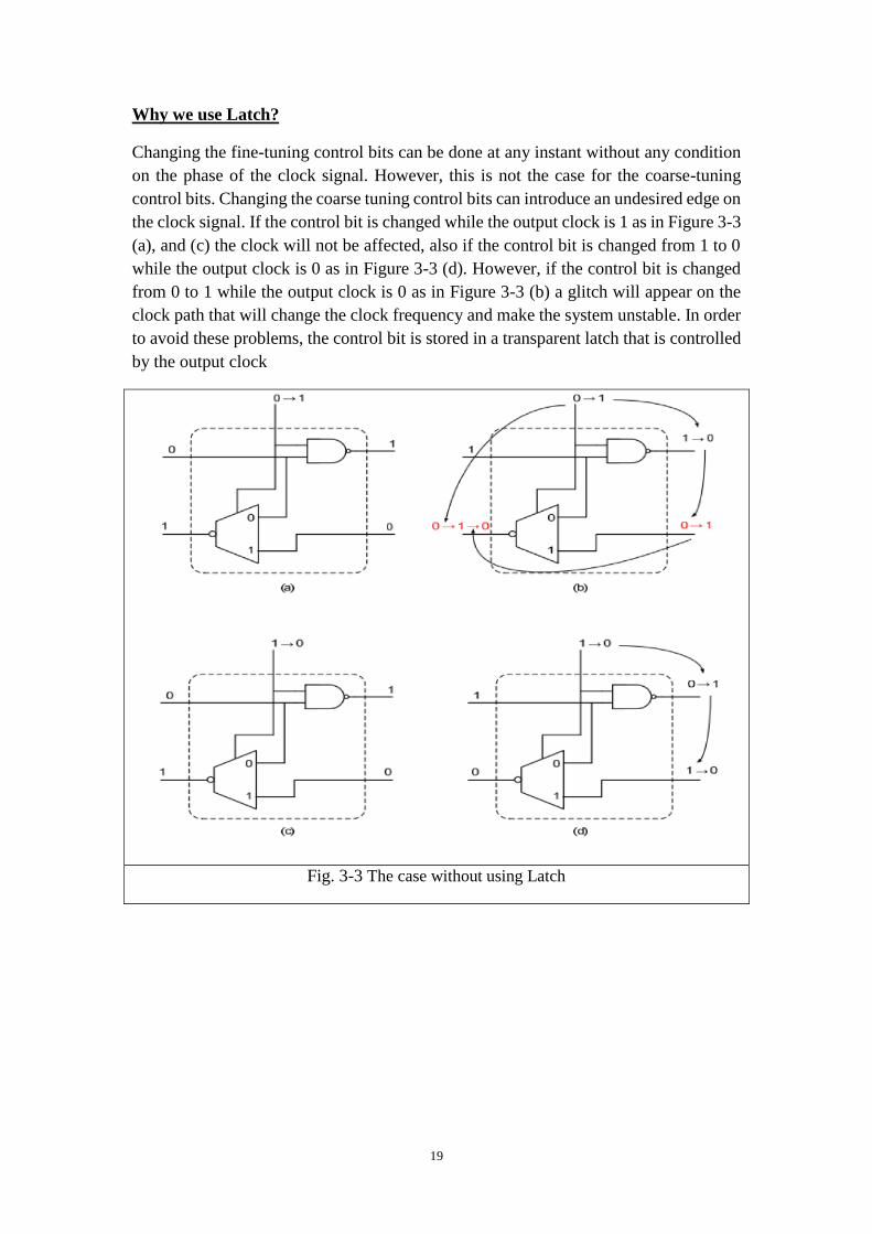
Why we use Latch?
Changing the fine-tuning control bits can be done at any instant without any condition
on the phase of the clock signal. However, this is not the case for the coarse-tuning
control bits. Changing the coarse tuning control bits can introduce an undesired edge on
the clock signal. If the control bit is changed while the output clock is 1 as in Figure 3-3
(a), and (c) the clock will not be affected, also if the control bit is changed from 1 to 0
while the output clock is 0 as in Figure 3-3 (d). However, if the control bit is changed
from 0 to 1 while the output clock is 0 as in Figure 3-3 (b) a glitch will appear on the
clock path that will change the clock frequency and make the system unstable. In order
to avoid these problems, the control bit is stored in a transparent latch that is controlled
by the output clock
Fig. 3-3 The case without using Latch
20
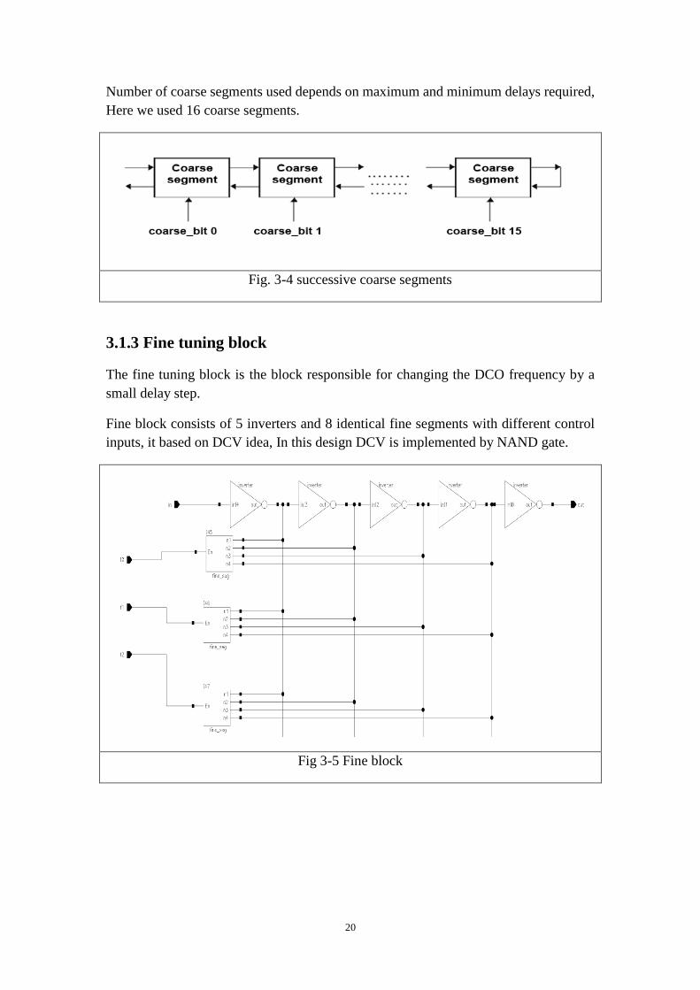
Number of coarse segments used depends on maximum and minimum delays required,
Here we used 16 coarse segments.
Fig. 3-4 successive coarse segments
3.1.3 Fine tuning block
The fine tuning block is the block responsible for changing the DCO frequency by a
small delay step.
Fine block consists of 5 inverters and 8 identical fine segments with different control
inputs, it based on DCV idea, In this design DCV is implemented by NAND gate.
Fig 3-5 Fine block
21
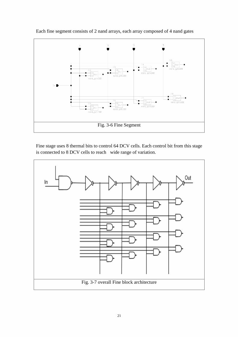
Each fine segment consists of 2 nand arrays, each array composed of 4 nand gates
Fig. 3-6 Fine Segment
Fine stage uses 8 thermal bits to control 64 DCV cells. Each control bit from this stage
is connected to 8 DCV cells to reach wide range of variation.
Fig. 3-7 overall Fine block architecture
22
3.2 Phase Frequency detector
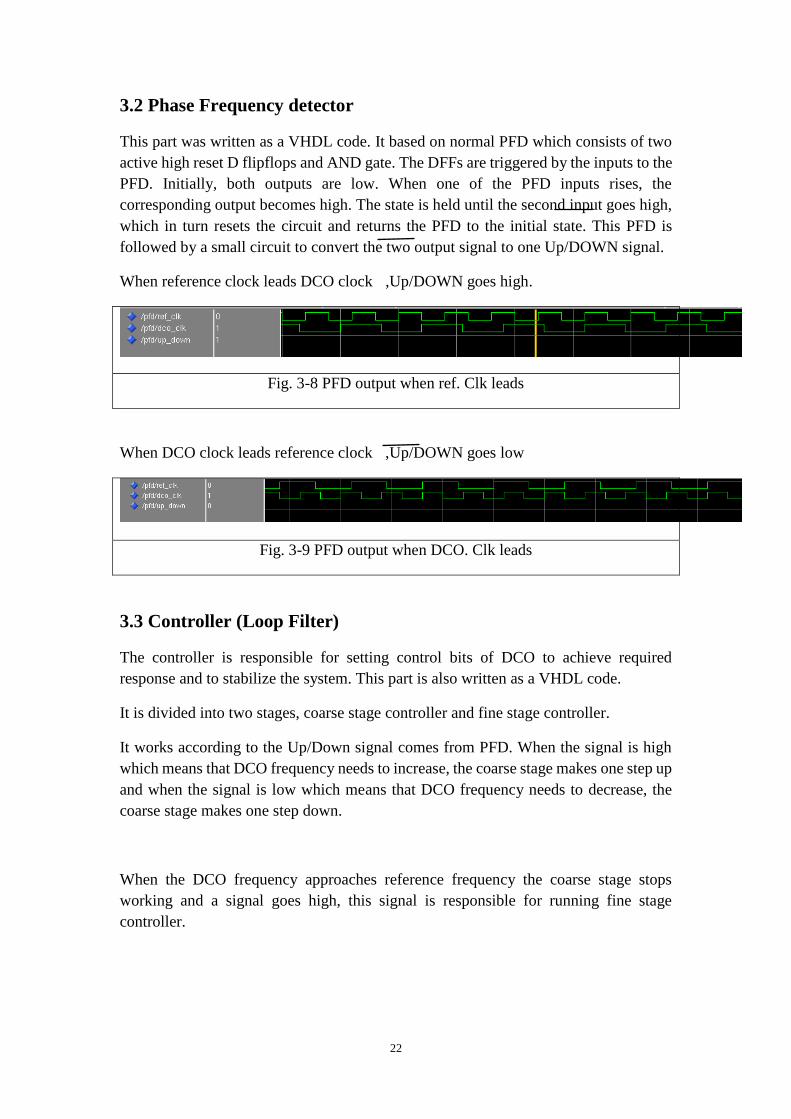
This part was written as a VHDL code. It based on normal PFD which consists of two
active high reset D flipflops and AND gate. The DFFs are triggered by the inputs to the
PFD. Initially, both outputs are low. When one of the PFD inputs rises, the
corresponding output becomes high. The state is held until the second input goes high,
which in turn resets the circuit and returns the PFD to the initial state. This PFD is
followed by a small circuit to convert the two output signal to one Up/DOWN signal.
When reference clock leads DCO clock ,Up/DOWN goes high.
Fig. 3-8 PFD output when ref. Clk leads
When DCO clock leads reference clock ,Up/DOWN goes low
Fig. 3-9 PFD output when DCO. Clk leads
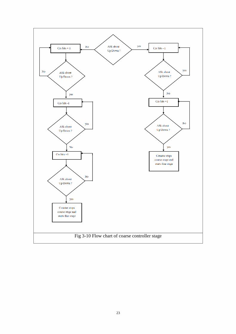
3.3 Controller (Loop Filter)
The controller is responsible for setting control bits of DCO to achieve required
response and to stabilize the system. This part is also written as a VHDL code.
It is divided into two stages, coarse stage controller and fine stage controller.
It works according to the Up/Down signal comes from PFD. When the signal is high
which means that DCO frequency needs to increase, the coarse stage makes one step up
and when the signal is low which means that DCO frequency needs to decrease, the
coarse stage makes one step down.
When the DCO frequency approaches reference frequency the coarse stage stops
working and a signal goes high, this signal is responsible for running fine stage
controller.
23
Fig 3-10 Flow chart of coarse controller stage
24
The fine stage controller also steps up and down also depending on Up/Down signal
just like the coarse stage but its step is smaller than the step of the coarse stage.
Fig 3-11 Flow chart of Fine controller stage
25
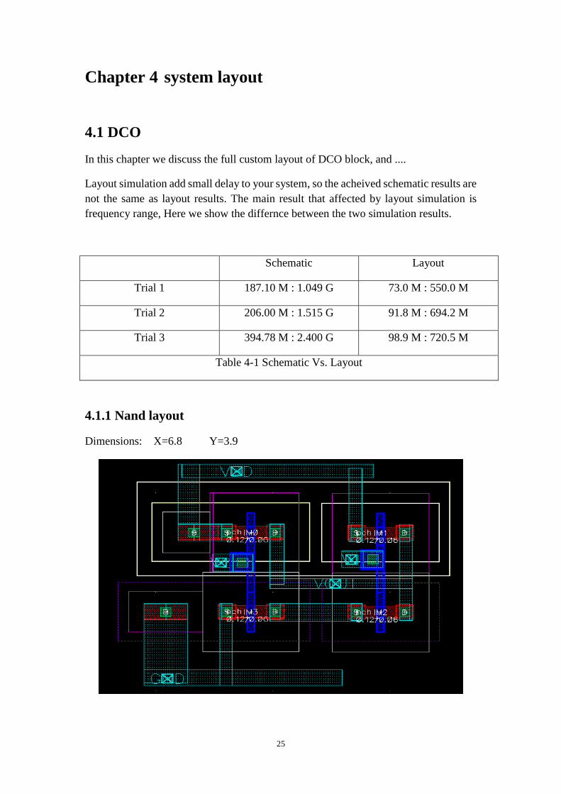
Chapter 4 system layout
4.1 DCO
In this chapter we discuss the full custom layout of DCO block, and ....
Layout simulation add small delay to your system, so the acheived schematic results are
not the same as layout results. The main result that affected by layout simulation is
frequency range, Here we show the differnce between the two simulation results.
Schematic Layout
Trial 1 187.10 M : 1.049 G 73.0 M : 550.0 M
Trial 2 206.00 M : 1.515 G 91.8 M : 694.2 M
Trial 3 394.78 M : 2.400 G 98.9 M : 720.5 M
Table 4-1 Schematic Vs. Layout
4.1.1 Nand layout
Dimensions: X=6.8 Y=3.9
26
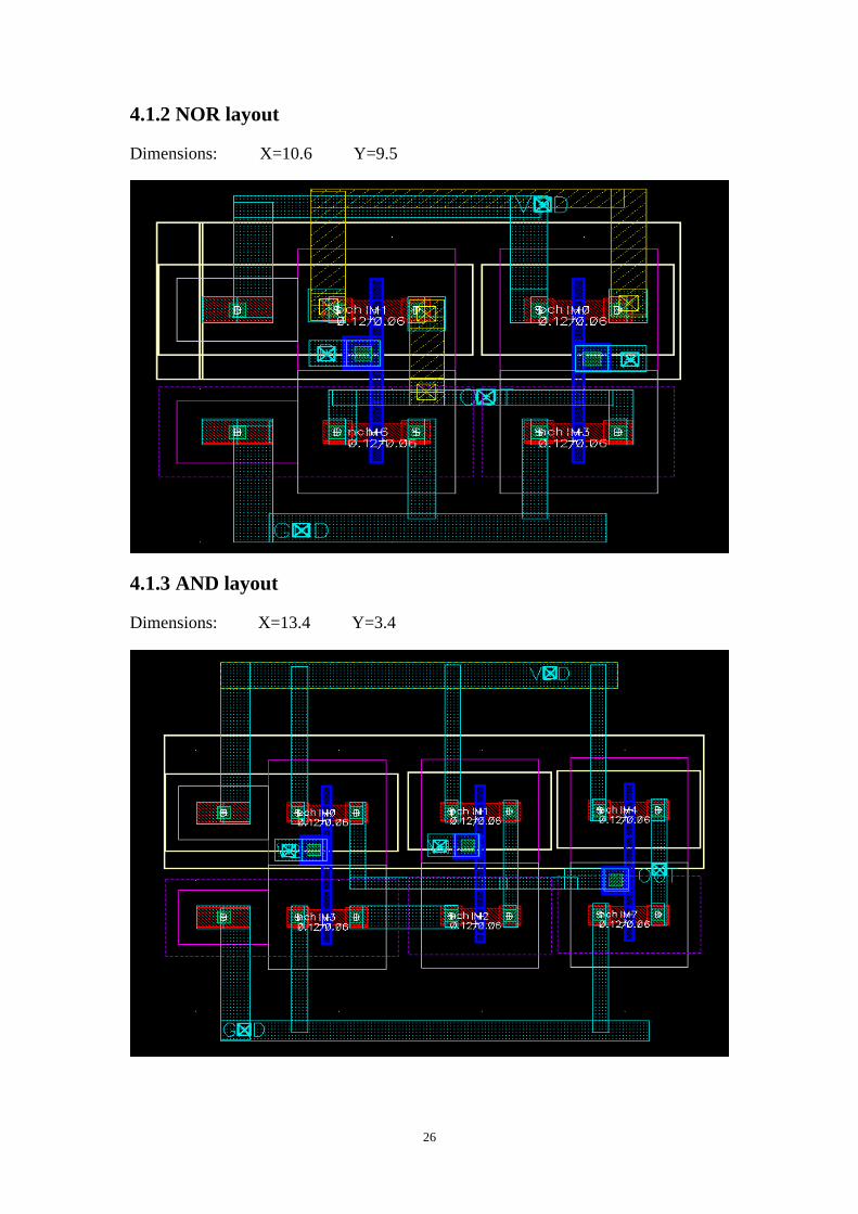
4.1.2 NOR layout
Dimensions: X=10.6 Y=9.5
4.1.3 AND layout
Dimensions: X=13.4 Y=3.4
27
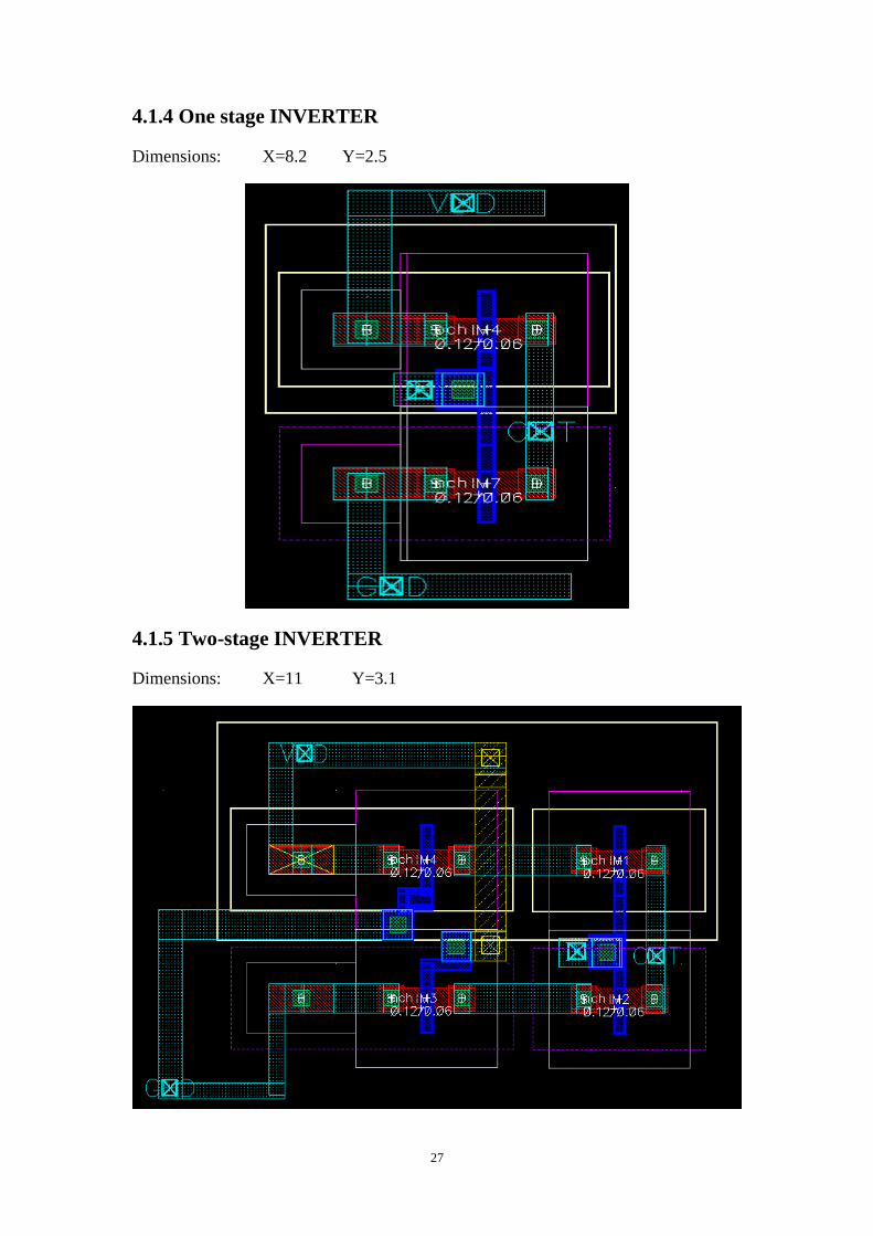
4.1.4 One stage INVERTER
Dimensions: X=8.2 Y=2.5
4.1.5 Two-stage INVERTER
Dimensions: X=11 Y=3.1
28
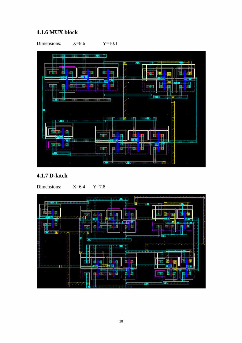
4.1.6 MUX block
Dimensions: X=8.6 Y=10.1
4.1.7 D-latch
Dimensions: X=6.4 Y=7.8
29
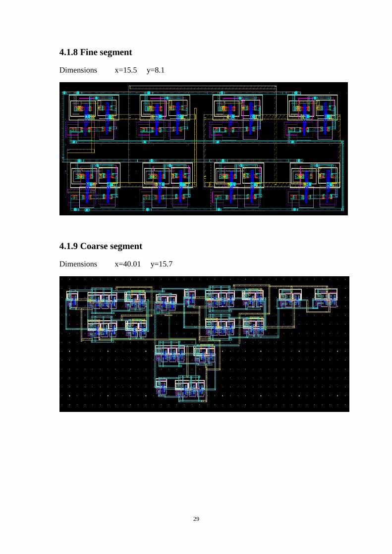
4.1.8 Fine segment
Dimensions x=15.5 y=8.1
4.1.9 Coarse segment
Dimensions x=40.01 y=15.7
30
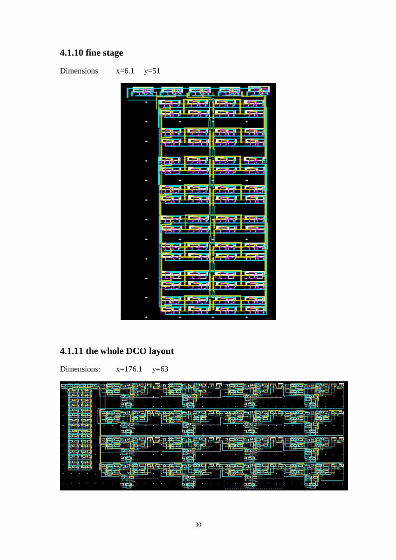
4.1.10 fine stage
Dimensions x=6.1 y=51
4.1.11 the whole DCO layout
Dimensions: x=176.1 y=63
31
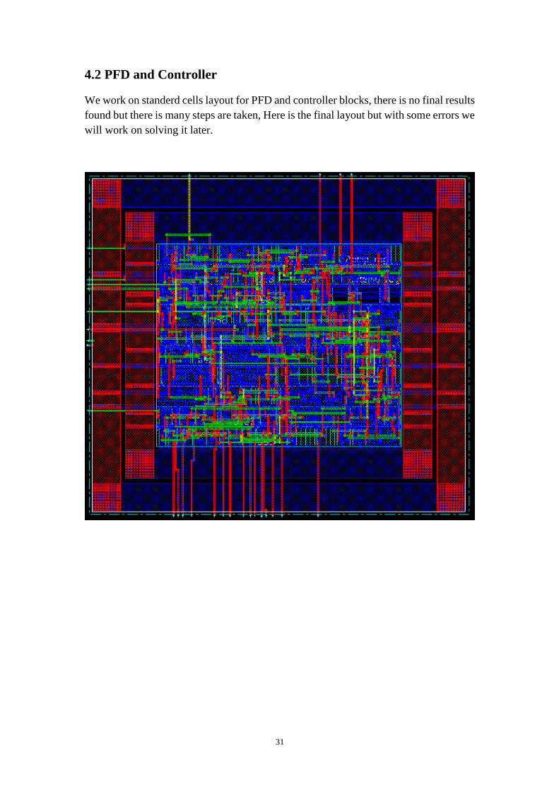
4.2 PFD and Controller
We work on standerd cells layout for PFD and controller blocks, there is no final results
found but there is many steps are taken, Here is the final layout but with some errors we
will work on solving it later.
32
Chapter 5 Simulation Results
In this chapter the simulation results will be discussed in details.
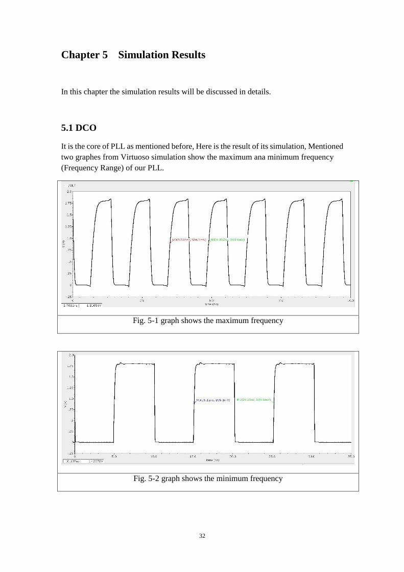
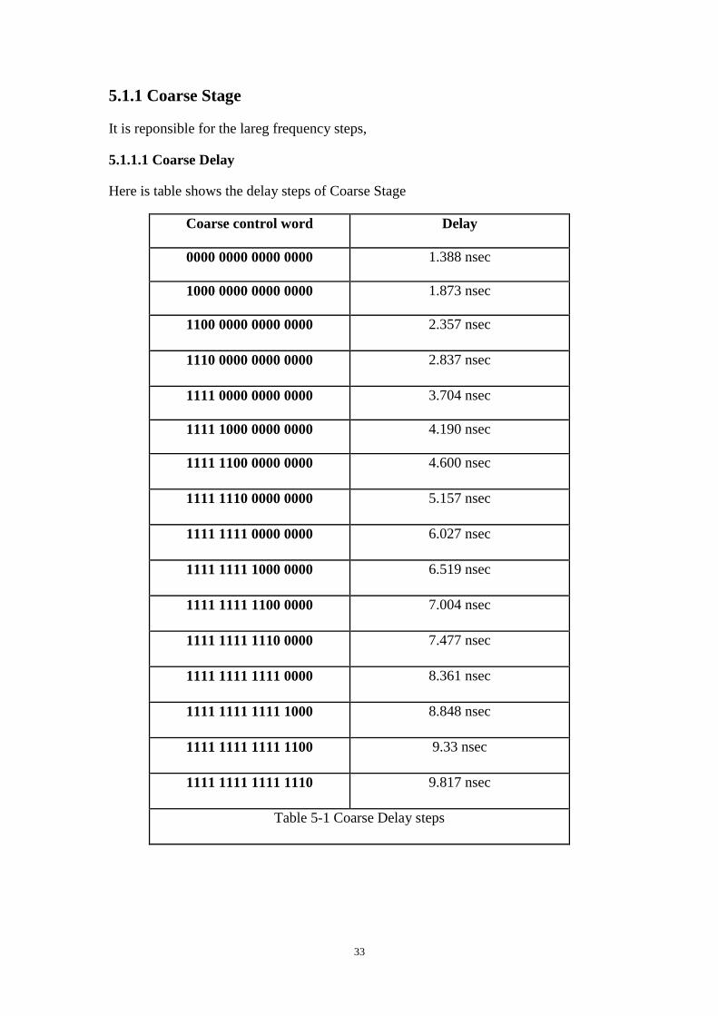
5.1 DCO
It is the core of PLL as mentioned before, Here is the result of its simulation, Mentioned
two graphes from Virtuoso simulation show the maximum ana minimum frequency
(Frequency Range) of our PLL.
Fig. 5-1 graph shows the maximum frequency
Fig. 5-2 graph shows the minimum frequency
33
5.1.1 Coarse Stage
It is reponsible for the lareg frequency steps,
5.1.1.1 Coarse Delay
Here is table shows the delay steps of Coarse Stage
Coarse control word Delay
0000 0000 0000 0000 1.388 nsec
1000 0000 0000 0000 1.873 nsec
1100 0000 0000 0000 2.357 nsec
1110 0000 0000 0000 2.837 nsec
1111 0000 0000 0000 3.704 nsec
1111 1000 0000 0000 4.190 nsec
1111 1100 0000 0000 4.600 nsec
1111 1110 0000 0000 5.157 nsec
1111 1111 0000 0000 6.027 nsec
1111 1111 1000 0000 6.519 nsec
1111 1111 1100 0000 7.004 nsec
1111 1111 1110 0000 7.477 nsec
1111 1111 1111 0000 8.361 nsec
1111 1111 1111 1000 8.848 nsec
1111 1111 1111 1100 9.33 nsec
1111 1111 1111 1110 9.817 nsec
Table 5-1 Coarse Delay steps
34
5.1.1.2 Coarse frquency
Here is table shows the frequency steps of Coarse Stage
Coarse control word Frequency
0000 0000 0000 0000 720.46 MHz
1000 0000 0000 0000 533.90 MHz
1100 0000 0000 0000 424.14 MHz
1110 0000 0000 0000 352.48 MHz
1111 0000 0000 0000 269.97 MHz
1111 1000 0000 0000 238.64 MHz
1111 1100 0000 0000 213.87 MHz
1111 1110 0000 0000 193.89 MHz
1111 1111 0000 0000 165.90 MHz
1111 1111 1000 0000 153.39 MHz
1111 1111 1100 0000 142.77 MHz
1111 1111 1110 0000 133.74 MHz
1111 1111 1111 0000 119.60 MHz
1111 1111 1111 1000 113.02 MHz
1111 1111 1111 1100 107.18 MHz
1111 1111 1111 1110 101.86 MHz
Table 5-2 Coarse Frequency steps
35
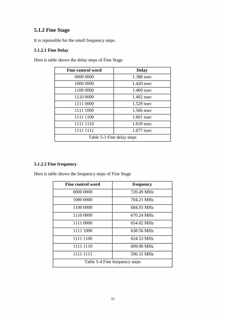
5.1.2 Fine Stage
It is reponsible for the small frequency steps.
5.1.2.1 Fine Delay
Here is table shows the delay steps of Fine Stage
Fine control word Delay
0000 0000 1.388 nsec
1000 0000 1.420 nsec
1100 0000 1.460 nsec
1110 0000 1.492 nsec
1111 0000 1.529 nsec
1111 1000 1.566 nsec
1111 1100 1.601 nsec
1111 1110 1.639 nsec
1111 1111 1.677 nsec
Table 5-3 Fine delay steps
5.1.2.2 Fine frequency
Here is table shows the frequency steps of Fine Stage
Fine control word frequency
0000 0000 720.49 MHz
1000 0000 704.21 MHz
1100 0000 684.93 MHz
1110 0000 670.24 MHz
1111 0000 654.02 MHz
1111 1000 638.56 MHz
1111 1100 624.53 MHz
1111 1110 609.90 MHz
1111 1111 596.31 MHz
Table 5-4 Fine frequency steps
36
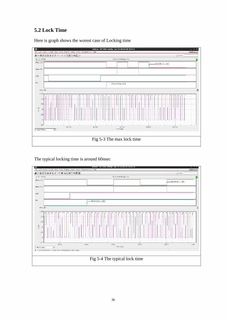
5.2 Lock Time
Here is graph shows the worest case of Locking time
Fig 5-3 The max lock time
The typical locking time is around 60nsec
Fig 5-4 The typical lock time
37
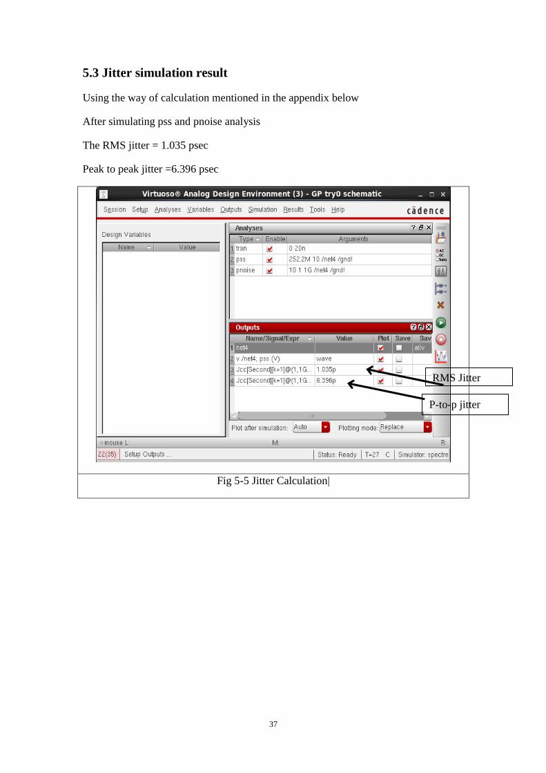
5.3 Jitter simulation result
Using the way of calculation mentioned in the appendix below
After simulating pss and pnoise analysis
The RMS jitter = 1.035 psec
Peak to peak jitter =6.396 psec
Fig 5-5 Jitter Calculation|
RMS Jitter
P-to-p jitter
38
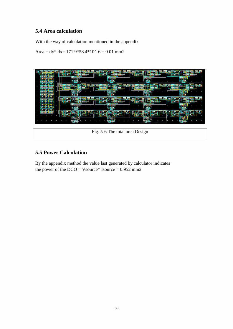
5.4 Area calculation
With the way of calculation mentioned in the appendix
Area = dy* dx= 171.9*58.4*10^-6 = 0.01 mm2
Fig. 5-6 The total area Design
5.5 Power Calculation
By the appendix method the value last generated by calculator indicates
the power of the DCO = Vsource* Isource = 0.952 mm2
39
Refrences
[1] Jayashree Nidagundi, Harish Desai, Shruti A., Gopal Manik “Design and
Implementation of Low Power Phase Frequency Detector (PFD) for PLL”.
[2] Prashanth Muppala B.Tech., Gayatri Vidya Parishad College of Engineering, 2008
“I
HIGH-FREQUENCY WIDE-RANGE ALL DIGITAL PHASE LOCKED LOOP IN
90 NM CMOS”.
[3] Master of Science Thesis In System-on-Chip Design By Chen Yao Stockholm, 08,
2011 “Time to Digital Converter used in ALL digital PLL”.
[4] Graduation project thesis ,Cairo Univeristy ,2013 ,”All Digital Phase Locked Loop
(ADPLL)”.
[5] Anitha Babu, Bhavya Daya, Banu Nagasundaram, Nivetha Veluchamy University
of Florida, Gainesville, FL, 32608, USA “All Digital Phase Locked Loop Design and
Implementation”.
[6] Kusum Lata and Manoj Kumar ,survey ,“ALL Digital Phase-Locked Loop
(ADPLL)”.
[7] José A. Tierno, Alexander V. Rylyakov, Member, IEEE, and Daniel J. Friedman,
Member, IEEE,”A Wide Power Supply Range, Wide Tuning Range,All Static CMOS
All Digital PLL in 65 nm SOI”.
[8] A Thesis Presented by Moon Seok Kim ,”0.18_x0016_m CMOS Low Power
ADPLL with a Novel Local Passive Interpolation Time-to-Digital Converter Based on
Tri-State Inverter”.
[9] Ran Sun1, a, Lijun Zhang1, b, Hao Wu2, c, Jianbin Zheng2, “Design of the High
Speed All Digital PLL for SRAM BIST Based on 55nm Process”.
40
[10] Jingcheng Zhuang, Qingjin Du, Tad Kwasniewski Department of Electronics,
Carleton University Ottawa, Ontario, Canada, “A 4GHz Low Complexity
ADPLL-based Frequency Synthesizer in 90nm CMOS”.
[11] A. V. Rylyakov1, J. A. Tierno1,G. J. English2, D. J. Friedman1,M. Meghelli3,”A
Wide Power-Supply Range (0.5V-to-1.3V) Wide Tuning Range (500 MHz-to-8 GHz)
All-Static CMOS ADPLL in 65nm SOI”.
[12] Gursharan Reehal, M.S. The Ohio State University, 1998 Steve Bibyk, Adviser
Phase,”A Digital Frequency Synthesizer Using Phase Locked Loop Technique”.
[13]ECE 126 – Inverter Tutorial: Identifying Static and Dynamic Power in a CMOS
Inverter
41
Appendix
A1.VHDL AMS tutorial
It used to convert a VHDL code to schematic
After writing the code and save it .vhd apply the following steps to use the code as
symbol in cadence.
Some hints about the code to be successfully imported :
1. Write end “entity name” instead of end “entity”.
example:
Entity mux is
port(….);
End mux;
Instead of
Entity mux is
port(…..);
End entity;
2. In architecture part write “architecture behavioral of entity name is”
The word after architecture should be behavioral
And also to end architecture it should be “ end behavioral”.
In case a component is recalled in the code :
1. Take in consideration hints (1) & (2).
2. Put the code of the component above the code that is recalling it
3. Remove the “is” word when recalling component
Example:
component counter
port(………………);
end component;
4.put the codes of the components with the same arrangement of recalling them
in the total code
42
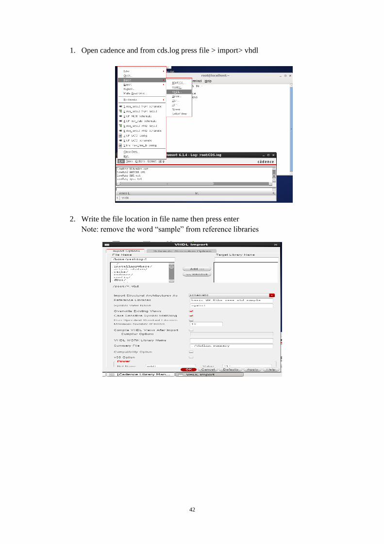
1. Open cadence and from cds.log press file > import> vhdl
2. Write the file location in file name then press enter
Note: remove the word “sample” from reference libraries
43
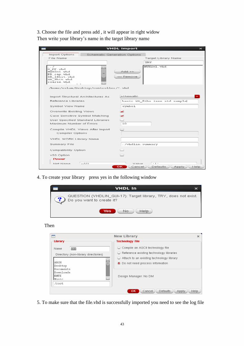
3. Choose the file and press add , it will appear in right widow
Then write your library’s name in the target library name
4. To create your library press yes in the following window
Then
5. To make sure that the file.vhd is successfully imported you need to see the log file
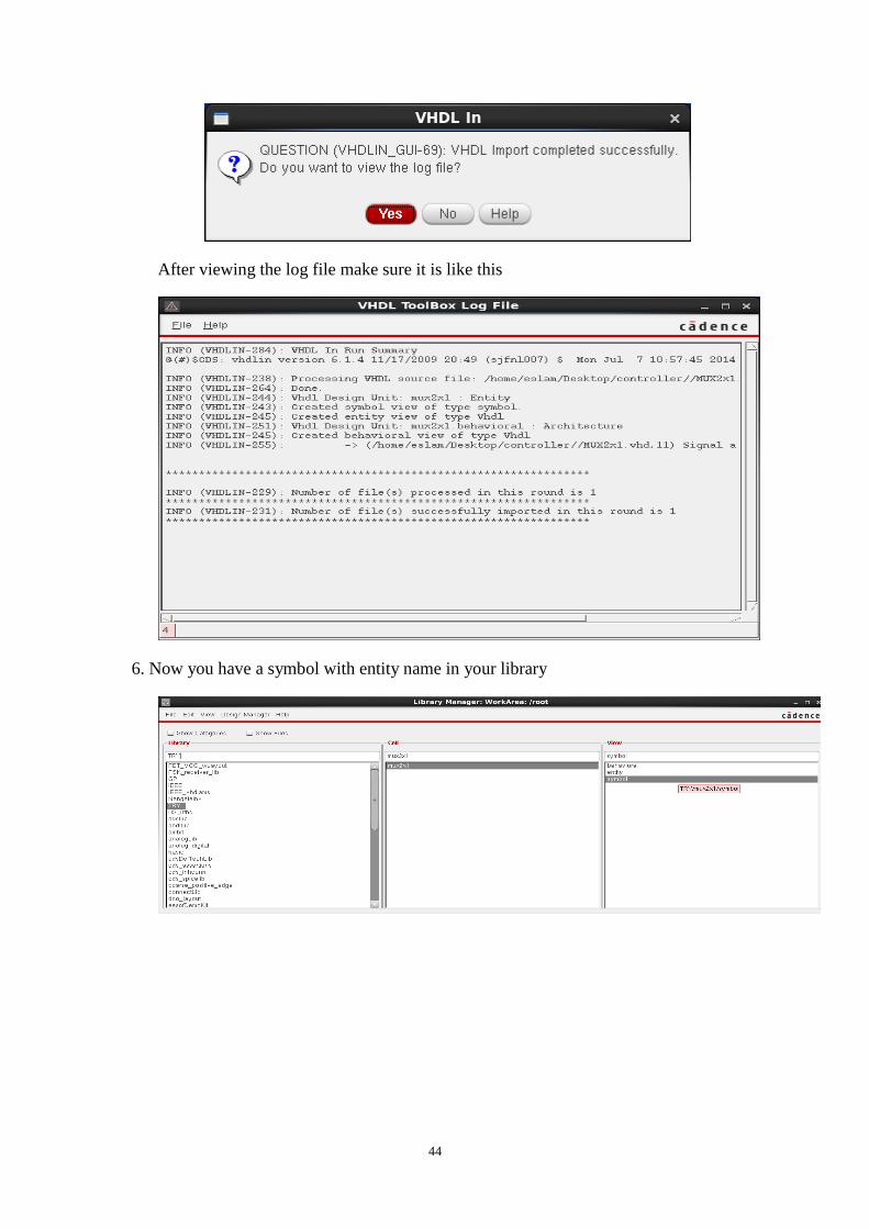
44
After viewing the log file make sure it is like this
6. Now you have a symbol with entity name in your library
45
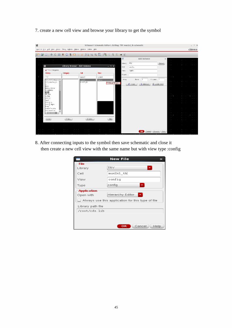
7. create a new cell view and browse your library to get the symbol
8. After connecting inputs to the symbol then save schematic and close it
then create a new cell view with the same name but with view type :config
46
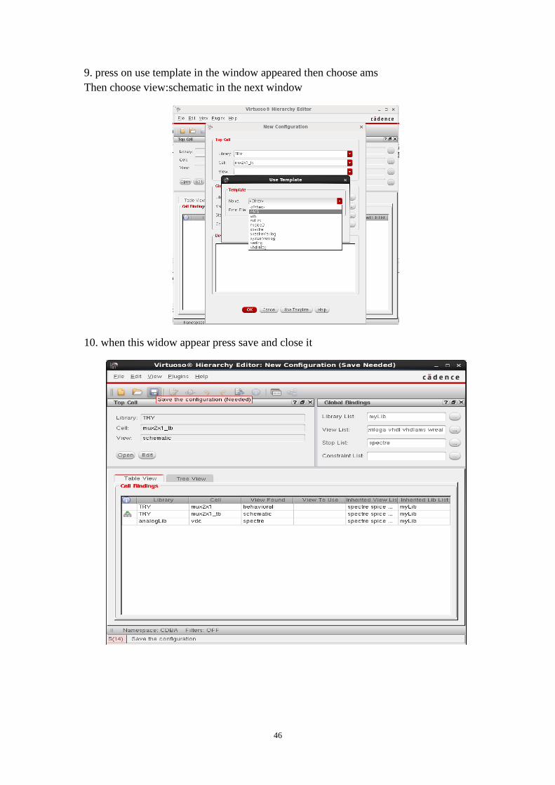
9. press on use template in the window appeared then choose ams
Then choose view:schematic in the next window
10. when this widow appear press save and close it
47
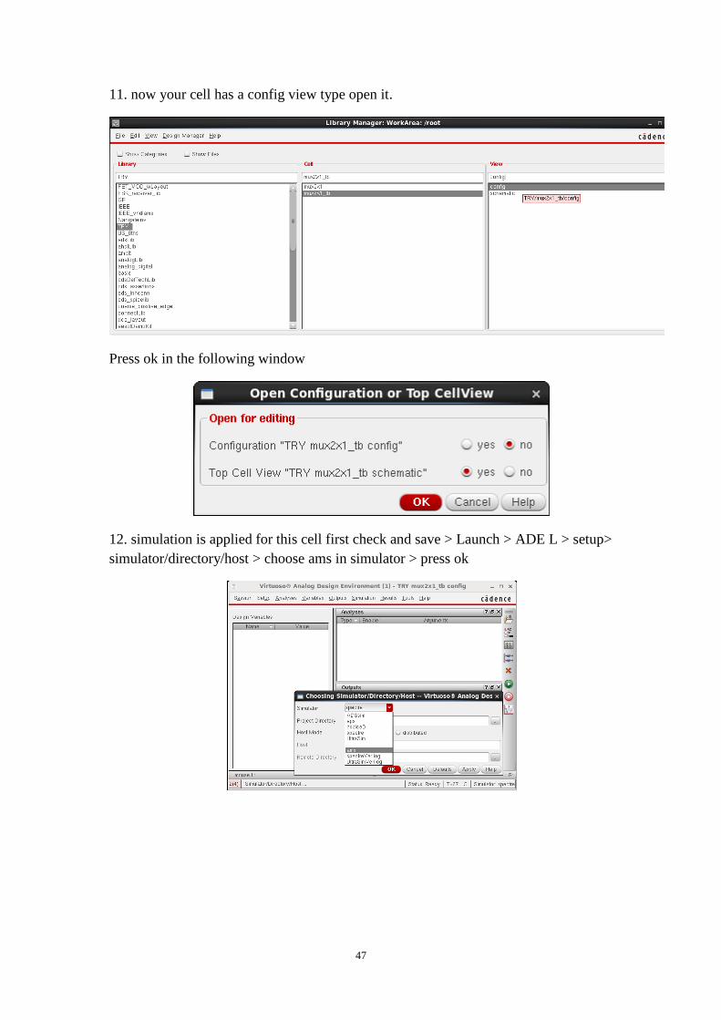
11. now your cell has a config view type open it.
Press ok in the following window
12. simulation is applied for this cell first check and save > Launch > ADE L > setup>
simulator/directory/host > choose ams in simulator > press ok
48
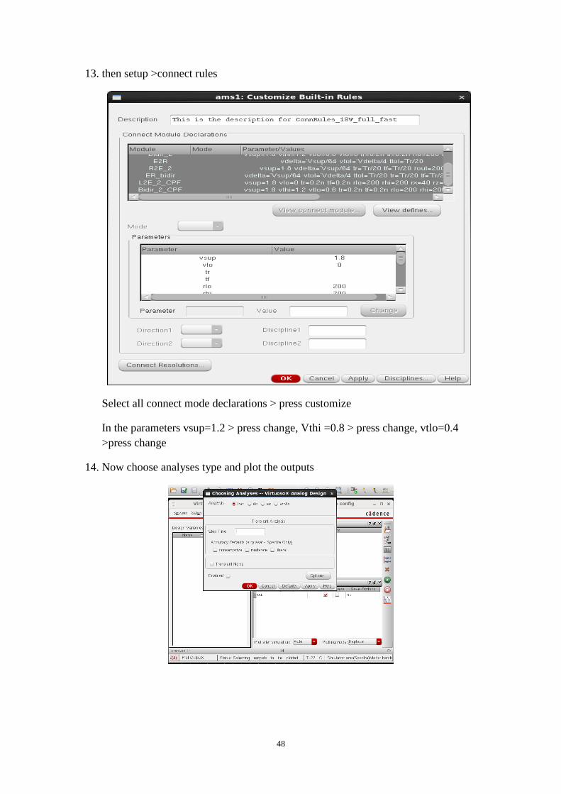
13. then setup >connect rules
Select all connect mode declarations > press customize
In the parameters vsup=1.2 > press change, Vthi =0.8 > press change, vtlo=0.4
>press change
14. Now choose analyses type and plot the outputs
49
A2.ModelSim tutorial
This program to deal with HDL laguagues, we will focus on VHDL.
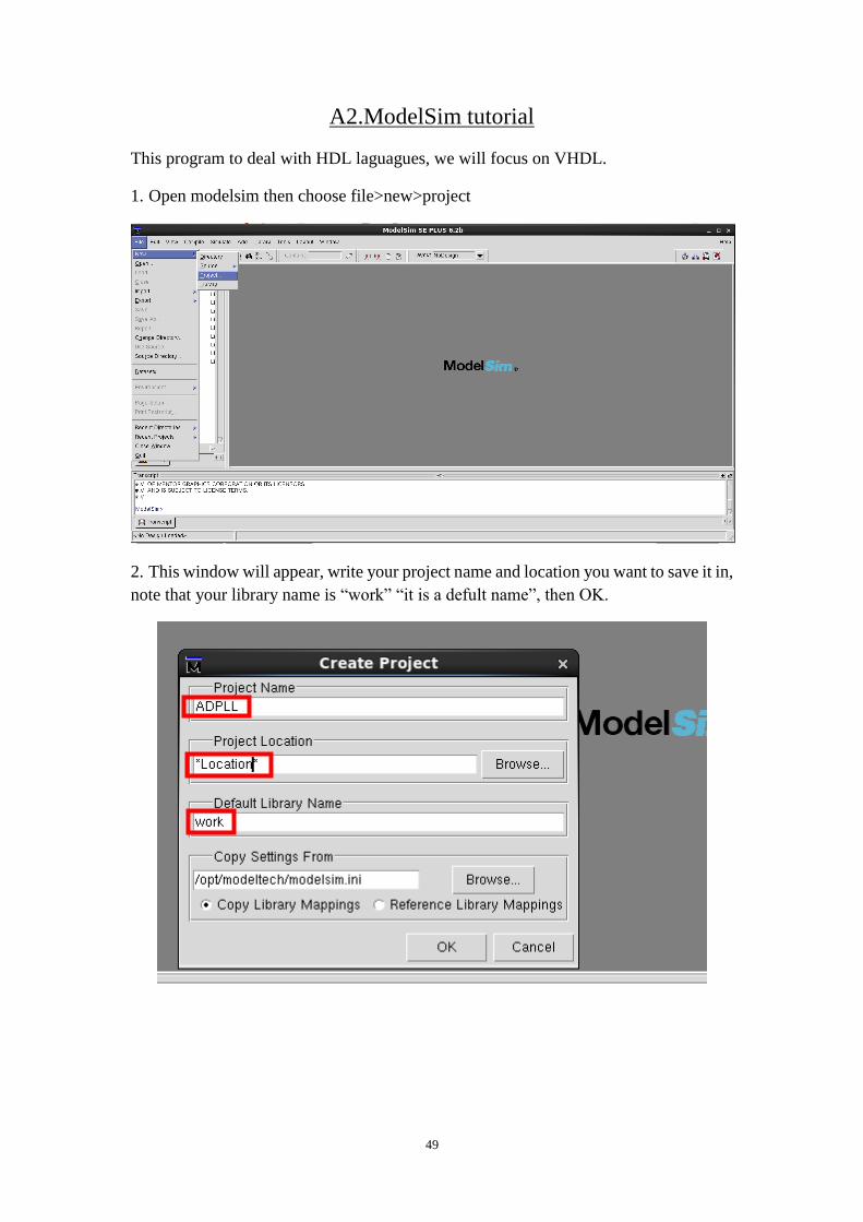
1. Open modelsim then choose file>new>project
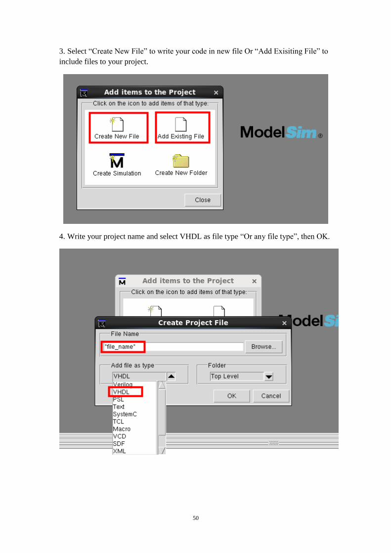
2. This window will appear, write your project name and location you want to save it in,
note that your library name is “work” “it is a defult name”, then OK.
50
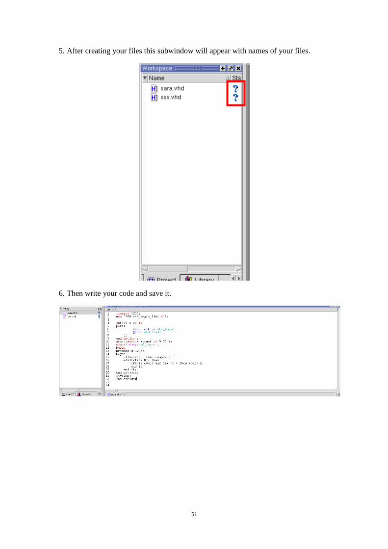
3. Select “Create New File” to write your code in new file Or “Add Exisiting File” to
include files to your project.
4. Write your project name and select VHDL as file type “Or any file type”, then OK.
51
5. After creating your files this subwindow will appear with names of your files.
6. Then write your code and save it.
52
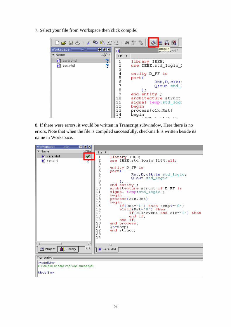
7. Select your file from Workspace then click compile.
8. If there were errors, it would be written in Transcript subwindow, Here there is no
errors, Note that when the file is compiled successfully, checkmark is written beside its
name in Workspace.
53
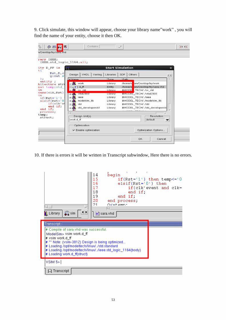
9. Click simulate, this window will appear, choose your library name”work” , you will
find the name of your entity, choose it then OK.
10. If there is errors it will be written in Transcript subwindow, Here there is no errors.
54
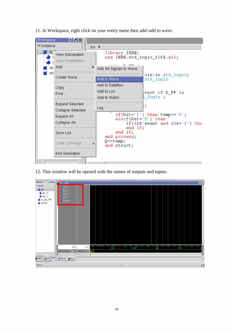
11. In Workspace, right click on your entity name then add>add to wave.
12. This window will be opened with the names of outputs and inputs.
55
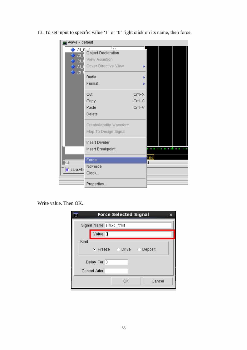
13. To set input to specific value ‘1’ or ‘0’ right click on its name, then force.
Write value. Then OK.
56
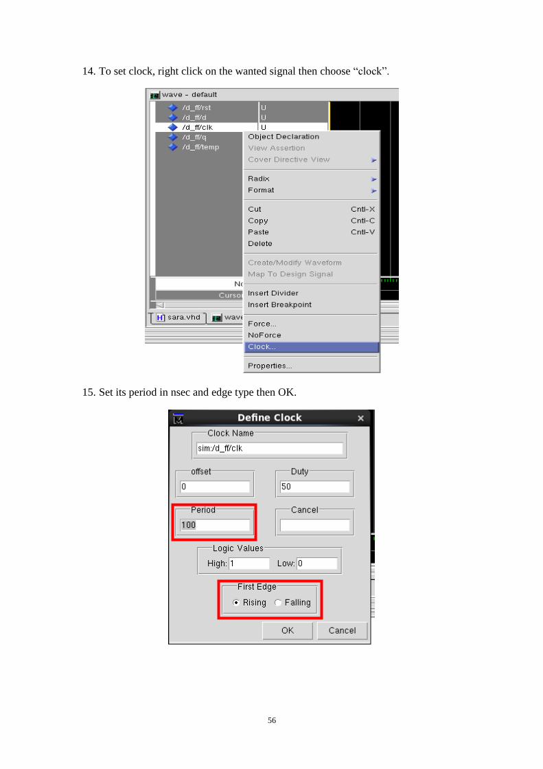
14. To set clock, right click on the wanted signal then choose “clock”.
15. Set its period in nsec and edge type then OK.
57
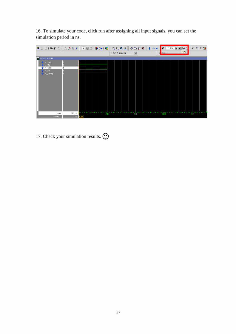
16. To simulate your code, click run after assigning all input signals, you can set the
simulation period in ns.
17. Check your simulation results.
58
A3.Cadence Tutorial
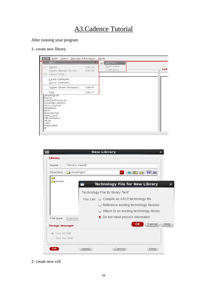
After running your program
1- create new library
2- create new cell
59
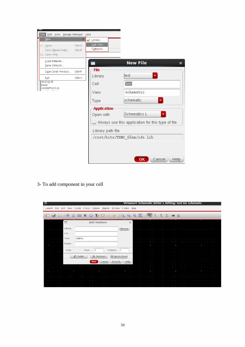
3- To add component in your cell
60
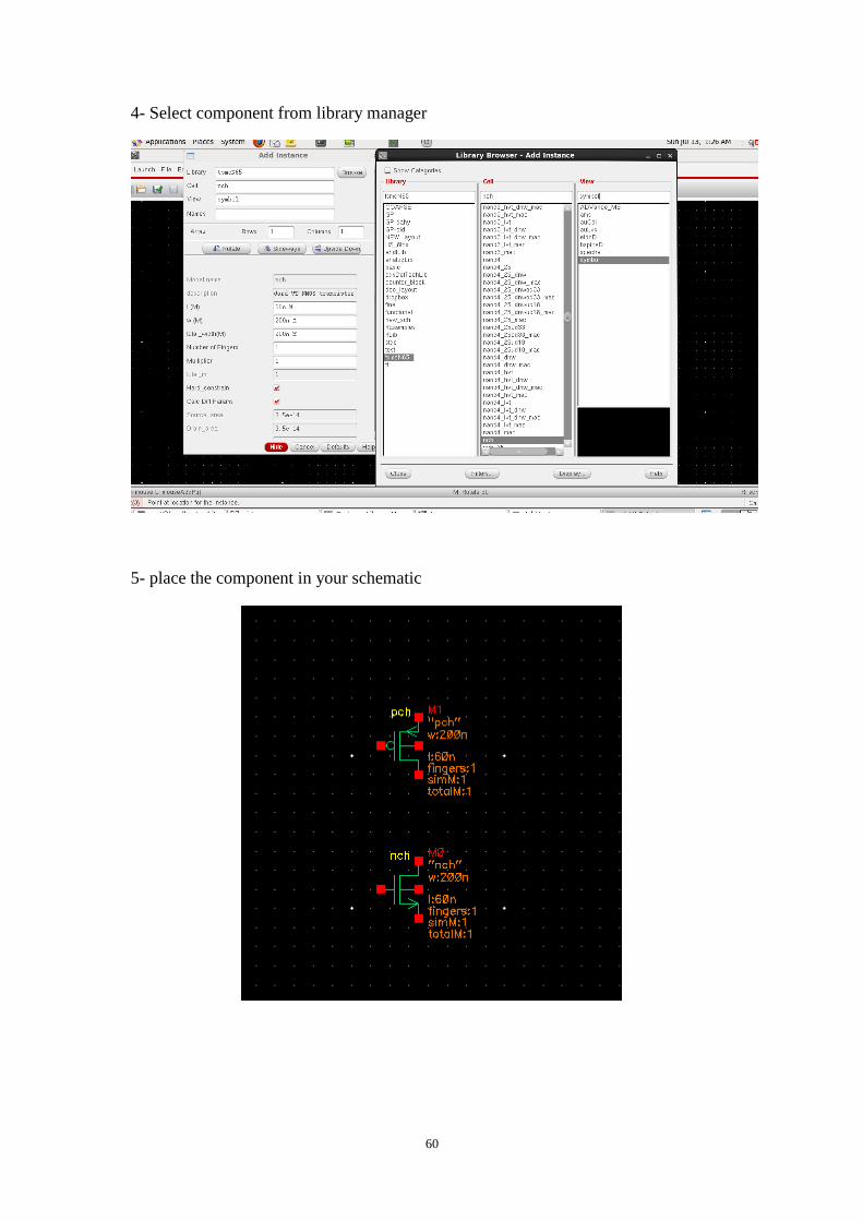
4- Select component from library manager
5- place the component in your schematic
61
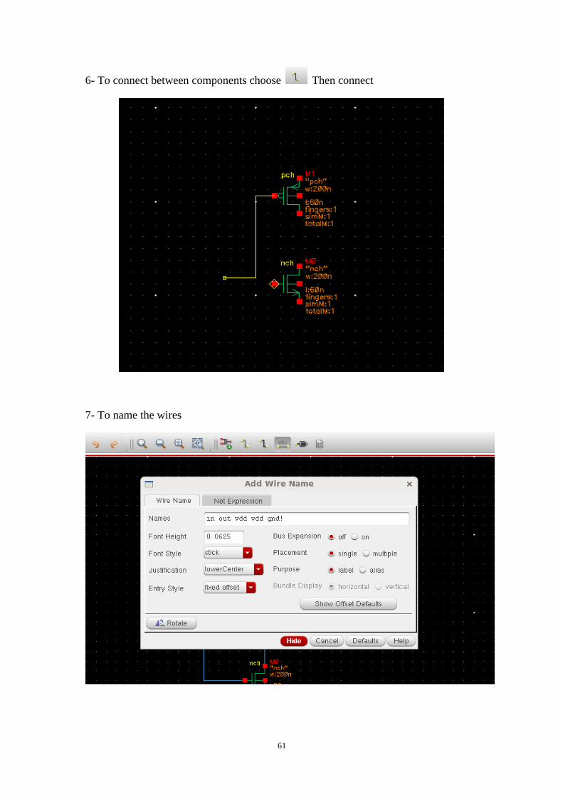
6- To connect between components choose Then connect
7- To name the wires
62
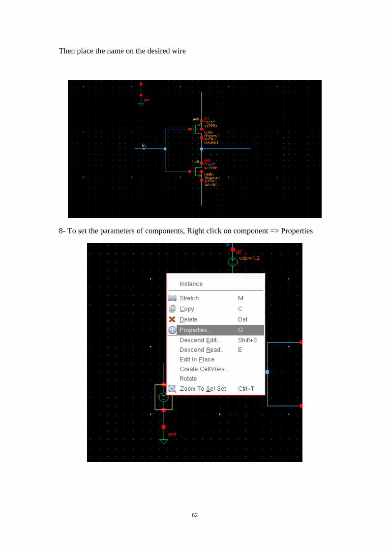
Then place the name on the desired wire
8- To set the parameters of components, Right click on component => Properties
63
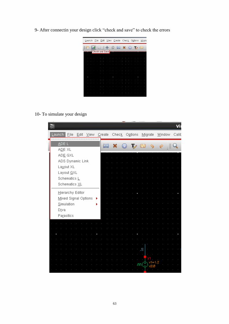
9- After connectin your design click “check and save” to check the errors
10- To simulate your design
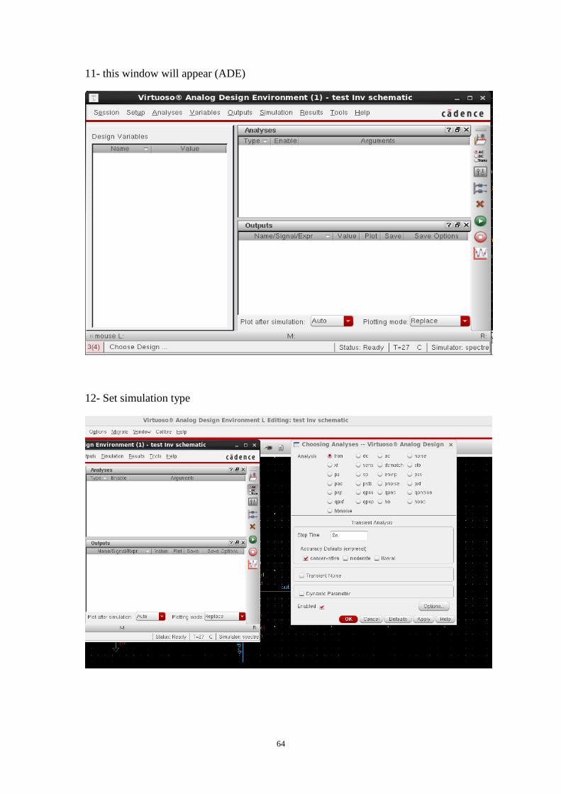
64
11- this window will appear (ADE)
12- Set simulation type
65
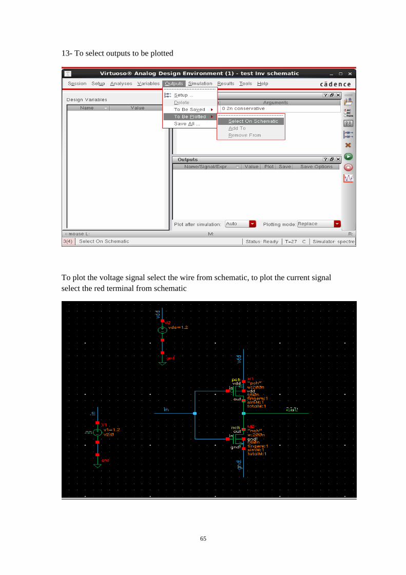
13- To select outputs to be plotted
To plot the voltage signal select the wire from schematic, to plot the current signal
select the red terminal from schematic
66
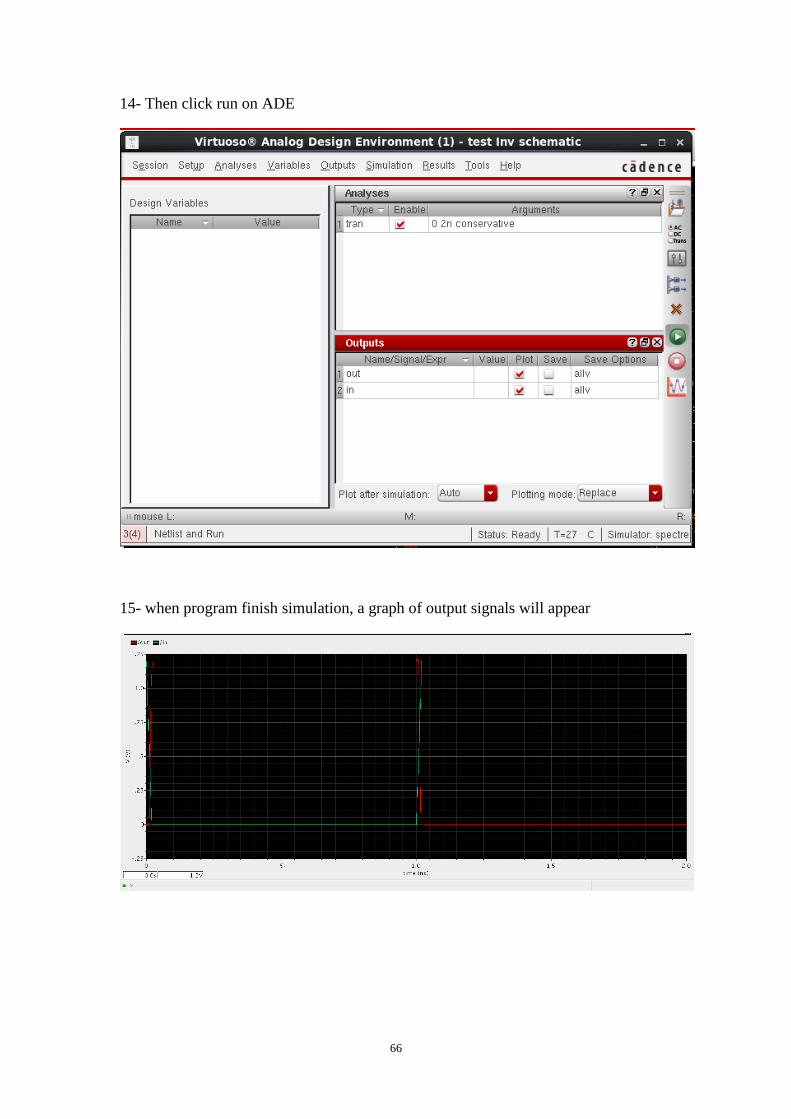
14- Then click run on ADE
15- when program finish simulation, a graph of output signals will appear
67
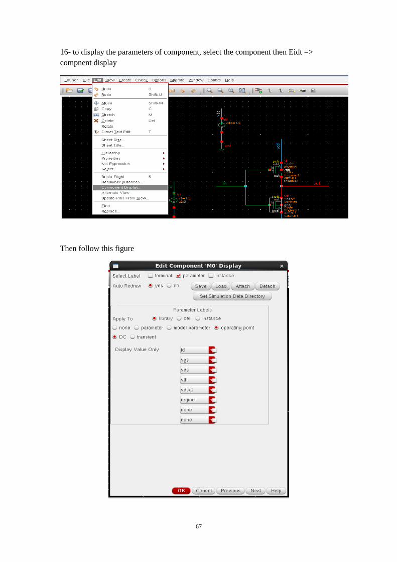
16- to display the parameters of component, select the component then Eidt =>
compnent display
Then follow this figure
68
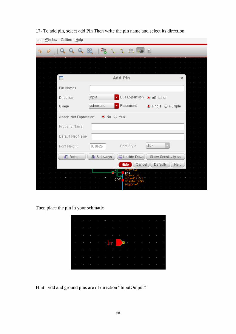
17- To add pin, select add Pin Then write the pin name and select its direction
Then place the pin in your schmatic
Hint : vdd and ground pins are of direction “InputOutput”
69
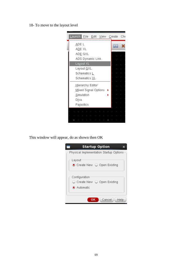
18- To move to the layout level
This window will appear, do as shown then OK
70
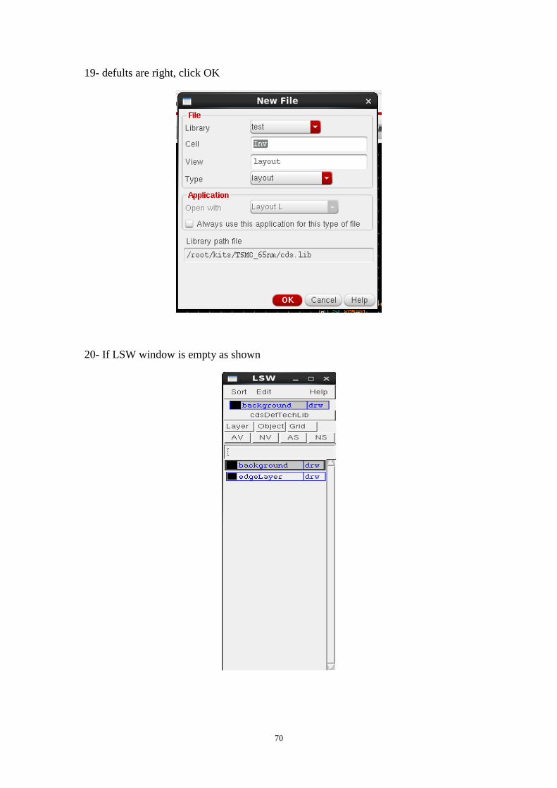
19- defults are right, click OK
20- If LSW window is empty as shown
71
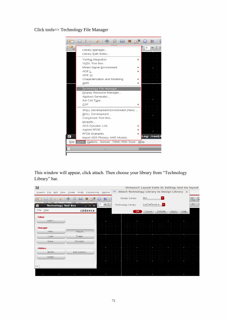
Click tools=> Technology File Manager
This window will appear, click attach. Then choose your library from “Technology
Library” bar.
72
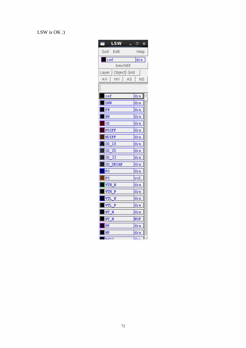
LSW is OK :)
73
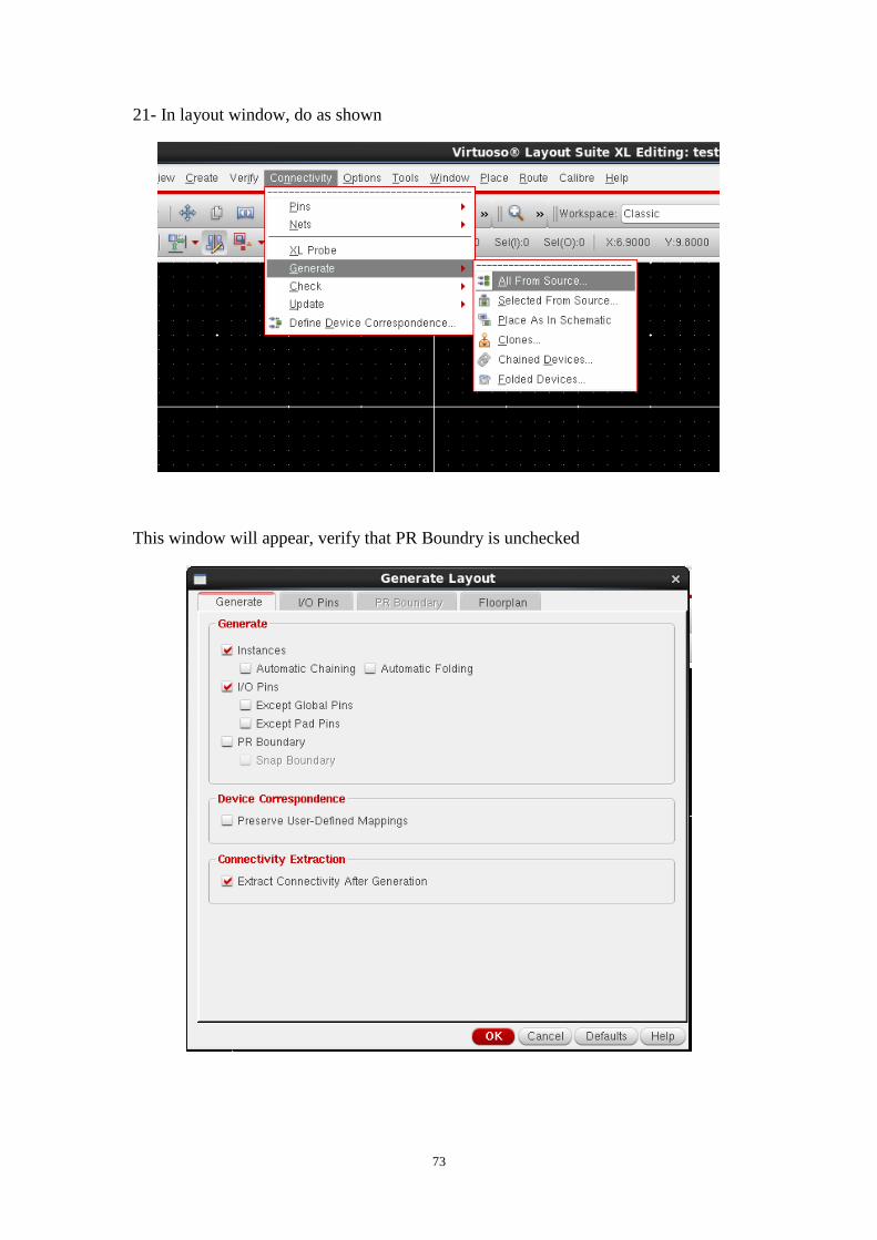
21- In layout window, do as shown
This window will appear, verify that PR Boundry is unchecked
74
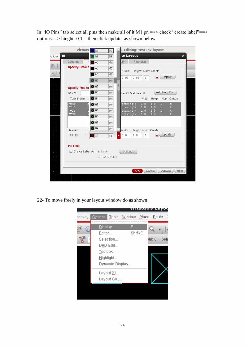
In “IO Pins” tab select all pins then make all of it M1 pn =>> check “create label”==>
options==> hieght=0.1, then click update, as shown below
22- To move freely in your layout window do as shown
75
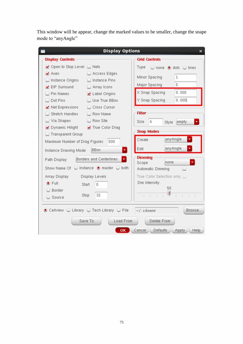
This window will be appear, change the marked values to be smaller, change the snape
mode to “anyAngle”
76
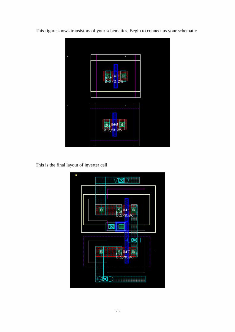
This figure shows transistors of your schematics, Begin to connect as your schematic
This is the final layout of inverter cell
77
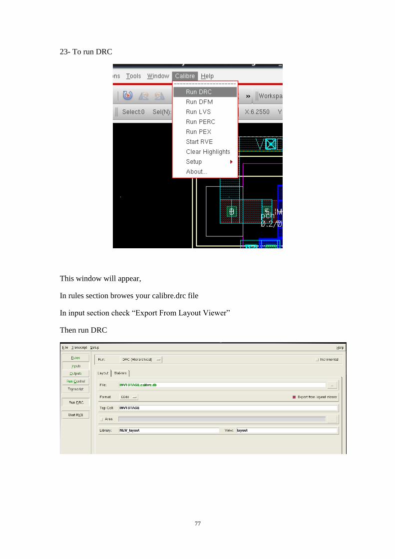
23- To run DRC
This window will appear,
In rules section browes your calibre.drc file
In input section check “Export From Layout Viewer”
Then run DRC
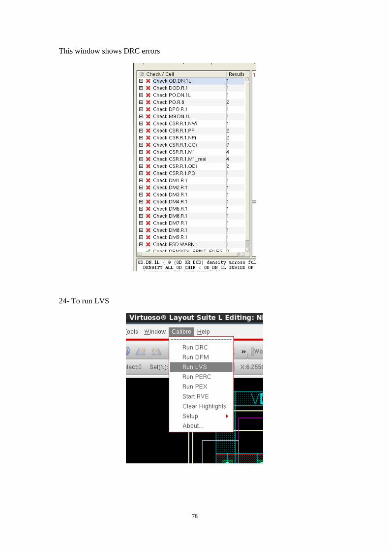
78
This window shows DRC errors
24- To run LVS
79
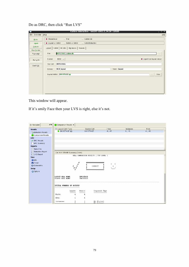
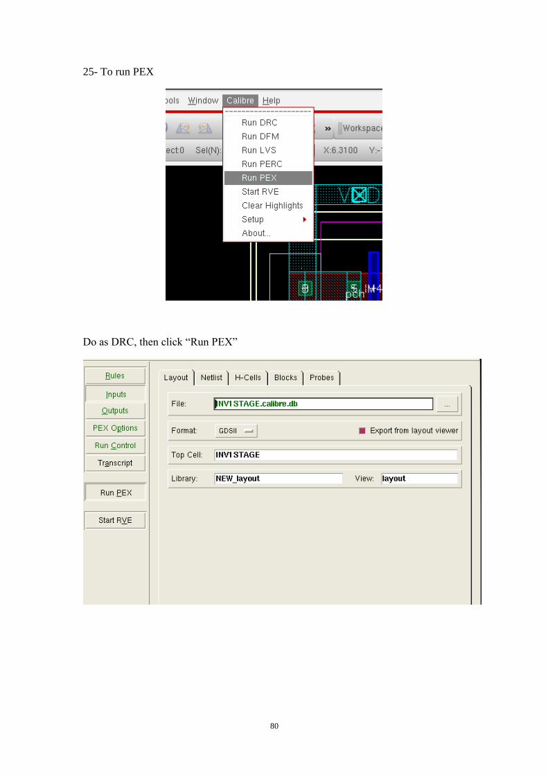
Do as DRC, then click “Run LVS”
This window will appear.
If it’s smily Face then your LVS is right, else it’s not.
80
25- To run PEX
Do as DRC, then click “Run PEX”
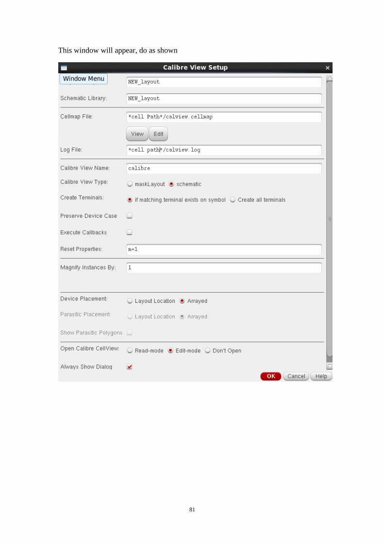
81
This window will appear, do as shown
82
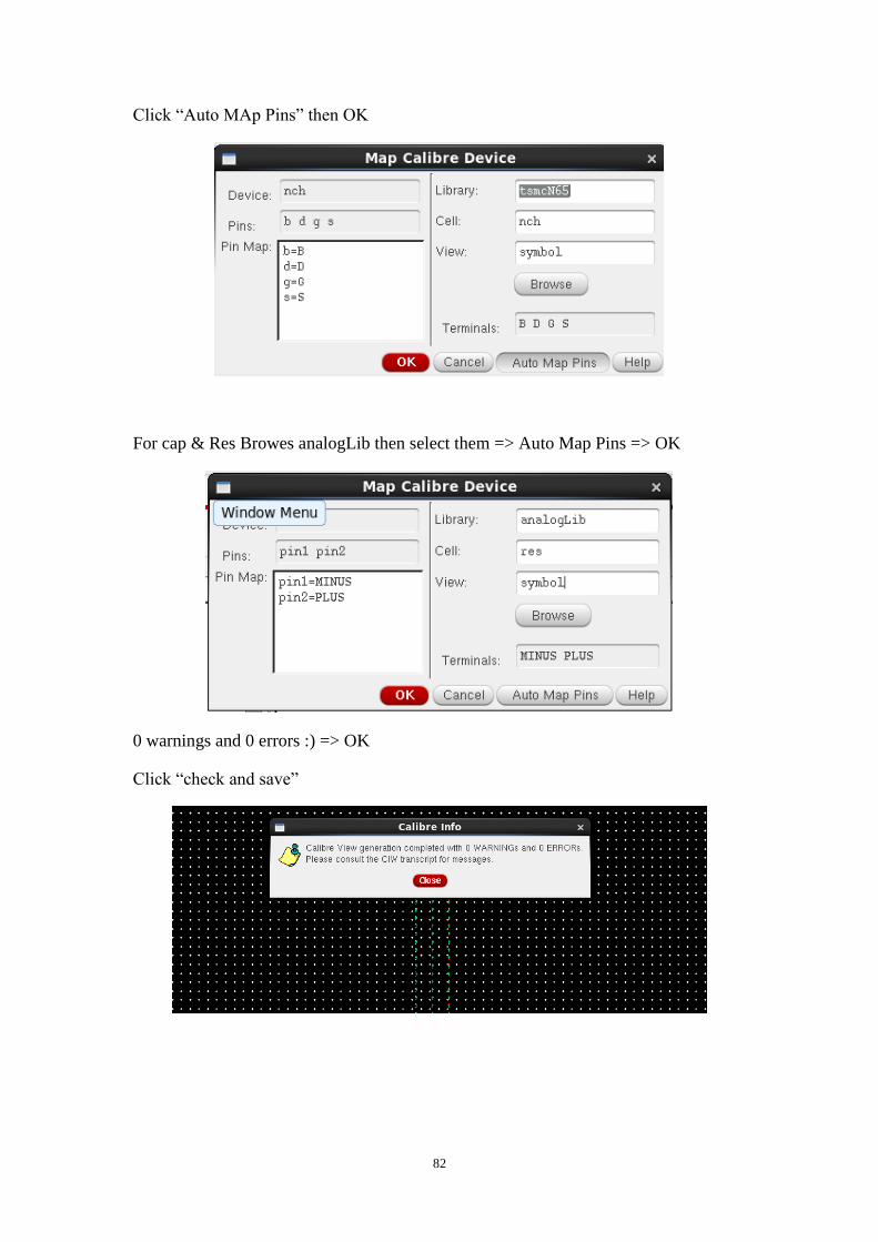
Click “Auto MAp Pins” then OK
For cap & Res Browes analogLib then select them => Auto Map Pins => OK
0 warnings and 0 errors :) => OK
Click “check and save”
83
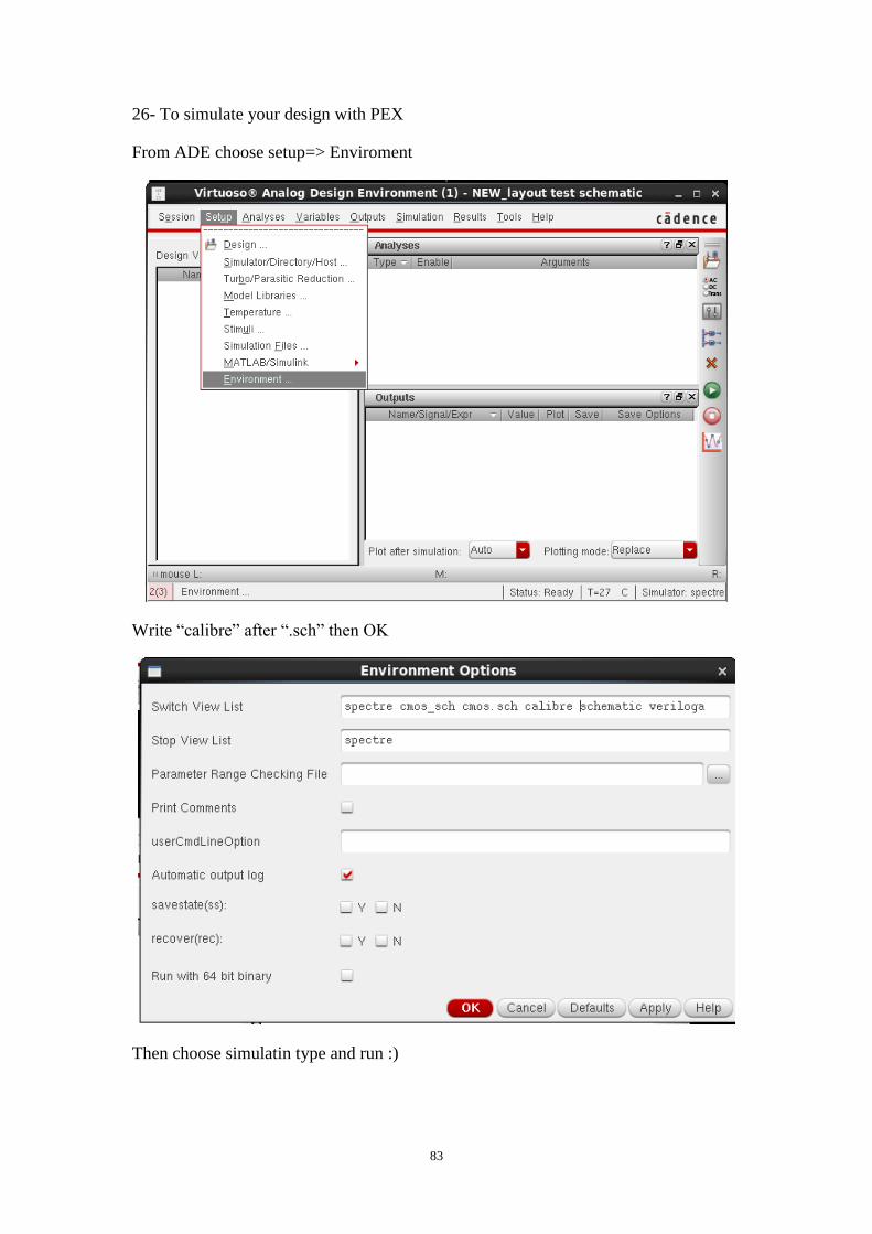
26- To simulate your design with PEX
From ADE choose setup=> Enviroment
Write “calibre” after “.sch” then OK
Then choose simulatin type and run :)
84
A4.Jitter Calculation
To calculate RMS jitter and peak to peak jitter in cadence you have to do the following
steps
1.Run transient simulation to know the definite accurate frequency
2.Choose pss analysis
For beat frequency write the frequency value you got in transient analysis
Choose 10 for number of harmonics
From transient analysis you knew when the system stabilize write this time in
Additional time for stabilization
85
3.In case of oscillator
Check the oscillator box then choose node of the output of the oscillation for
oscillator node and select ground node for the reference node.
Then press ok
4. Now Choose pnoise analysis
Put the parameters as shown below and choose node of the output of the oscillation for
positive output node and select ground node for the negative output node.
86
5.choose none for input source , and jitter fot Noise Type
Then press ok
6.After running the simulation
From ADE results > direct plot > main form
Choose pss and the parameters as shown
87
7. From ADE : results > Direct plot > main form
choose pnoise jitter for analysis and the parameters as shown
To calculate RMS jitter choose rms for Signal level
If peak to peak choose peak to peak for Signal level
Check Add to outputs box select the output from the schematic and press on plot
88
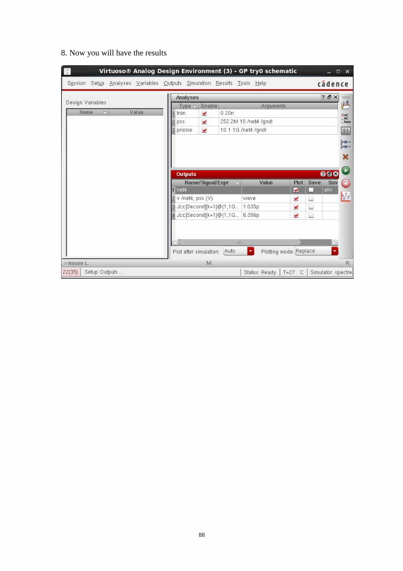
8. Now you will have the results
89
A5.Power Calculation
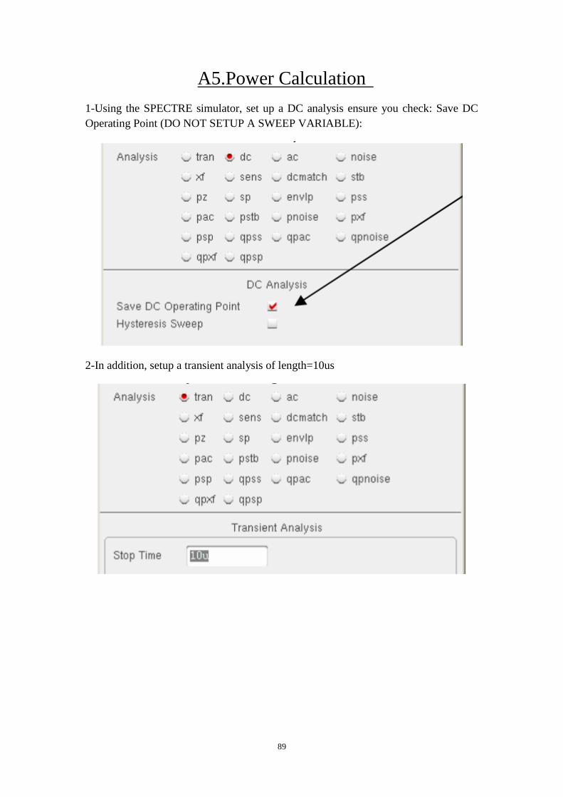
1-Using the SPECTRE simulator, set up a DC analysis ensure you check: Save DC
Operating Point (DO NOT SETUP A SWEEP VARIABLE):
2-In addition, setup a transient analysis of length=10us
90
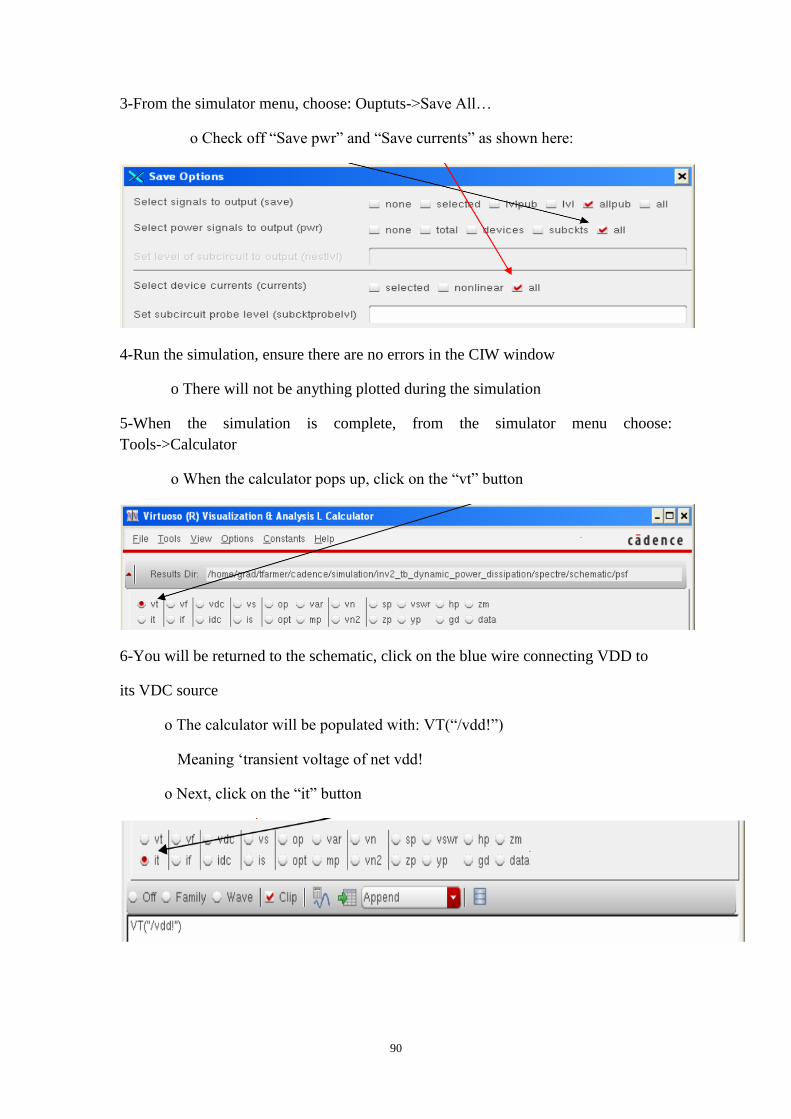
3-From the simulator menu, choose: Ouptuts->Save All…
o Check off “Save pwr” and “Save currents” as shown here:
4-Run the simulation, ensure there are no errors in the CIW window
o There will not be anything plotted during the simulation
5-When the simulation is complete, from the simulator menu choose:
Tools->Calculator
o When the calculator pops up, click on the “vt” button
6-You will be returned to the schematic, click on the blue wire connecting VDD to
its VDC source
o The calculator will be populated with: VT(“/vdd!”)
Meaning ‘transient voltage of net vdd!
o Next, click on the “it” button
91
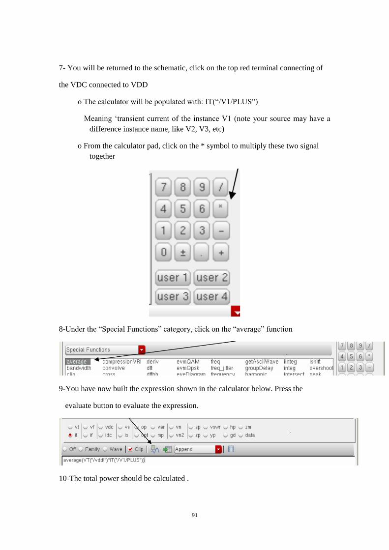
7- You will be returned to the schematic, click on the top red terminal connecting of
the VDC connected to VDD
o The calculator will be populated with: IT(“/V1/PLUS”)
Meaning ‘transient current of the instance V1 (note your source may have a
difference instance name, like V2, V3, etc)
o From the calculator pad, click on the * symbol to multiply these two signal
together
8-Under the “Special Functions” category, click on the “average” function
9-You have now built the expression shown in the calculator below. Press the
evaluate button to evaluate the expression.
10-The total power should be calculated .
92
A6.Area calculation
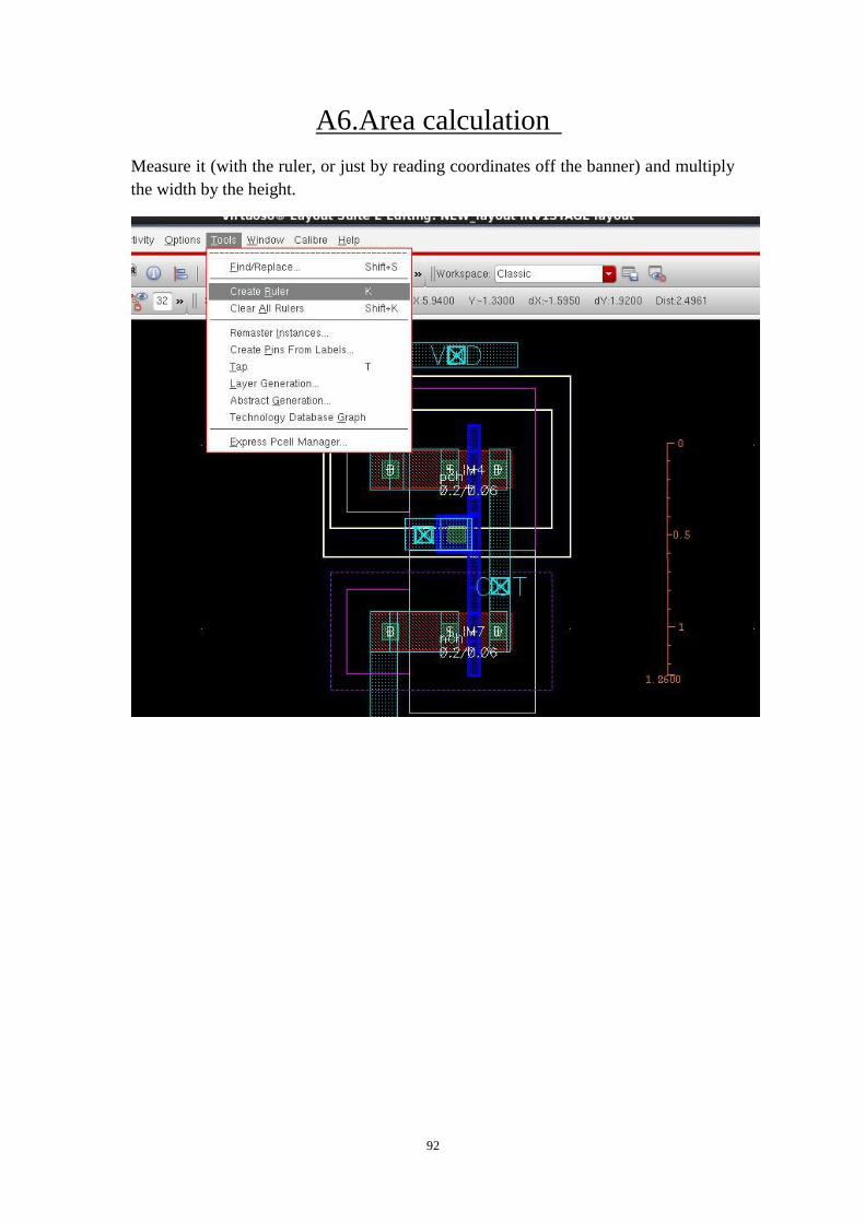
Measure it (with the ruler, or just by reading coordinates off the banner) and multiply
the width by the height.
93
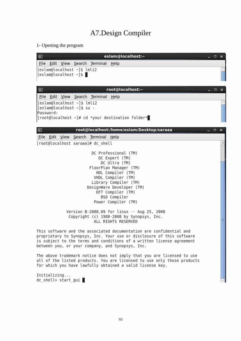
A7.Design Compiler
1- Opening the program
94
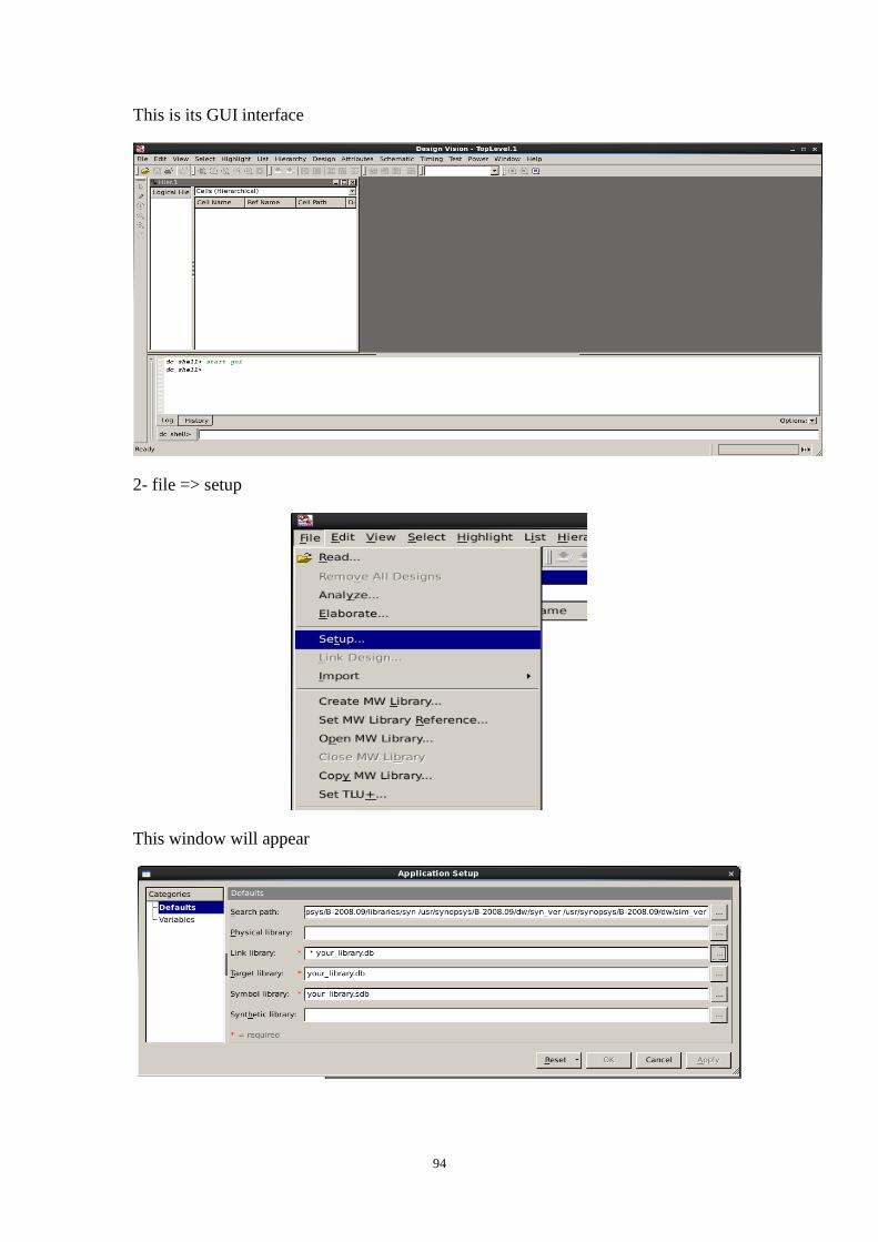
This is its GUI interface
2- file => setup
This window will appear
95
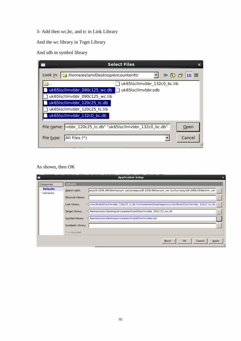
3- Add then wc,bc, and tc in Link Library
And the wc library in Trget Library
And sdb in symbol library
As shown, then OK
96
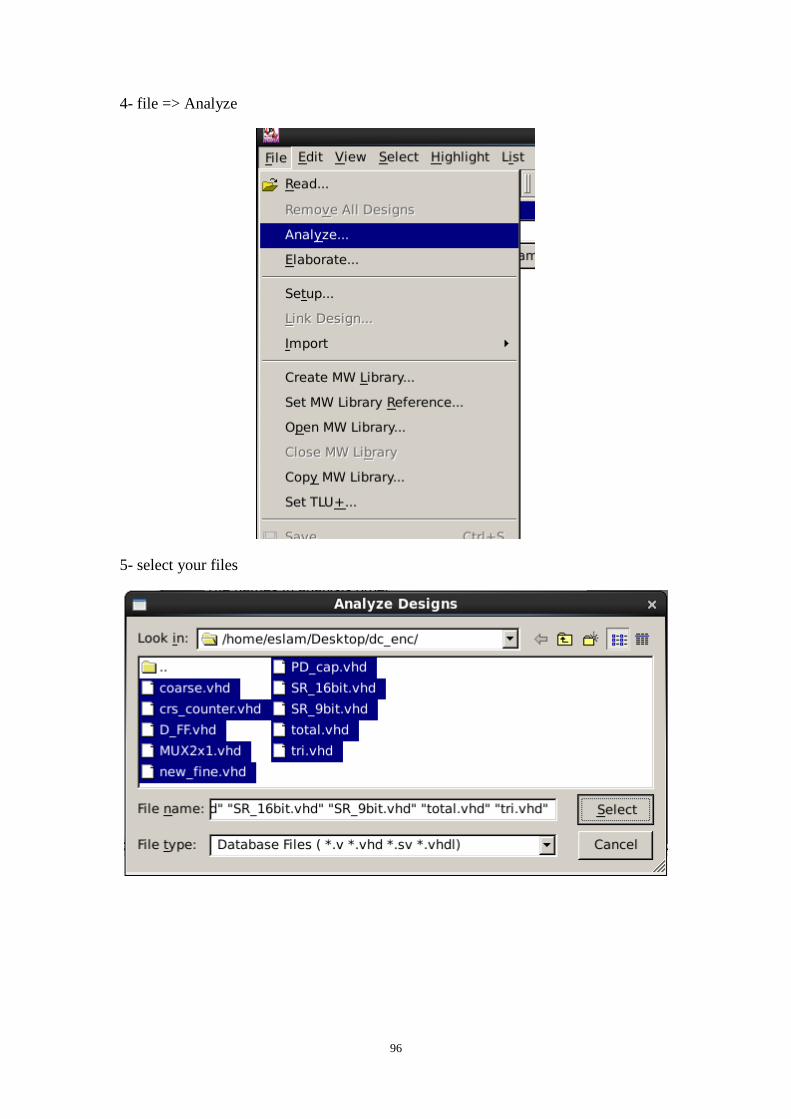
4- file => Analyze
5- select your files
97
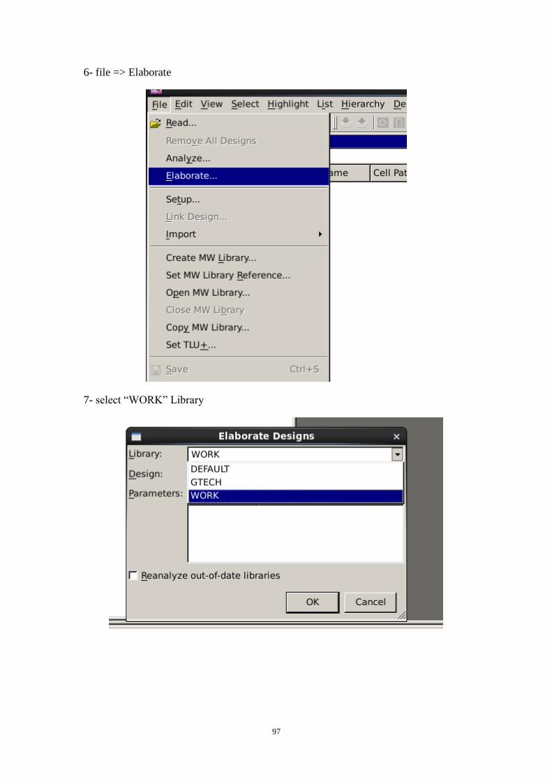
6- file => Elaborate
7- select “WORK” Library
98
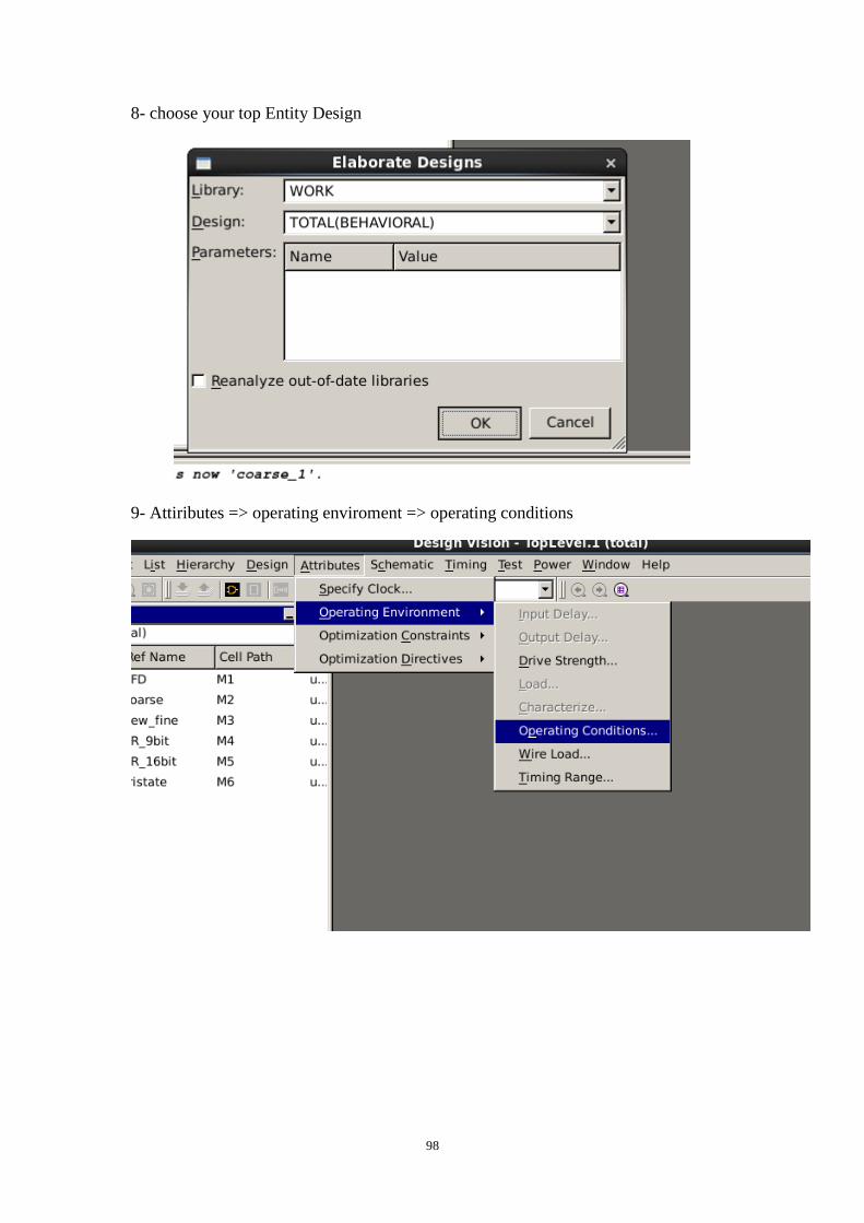
8- choose your top Entity Design
9- Attiributes => operating enviroment => operating conditions
99
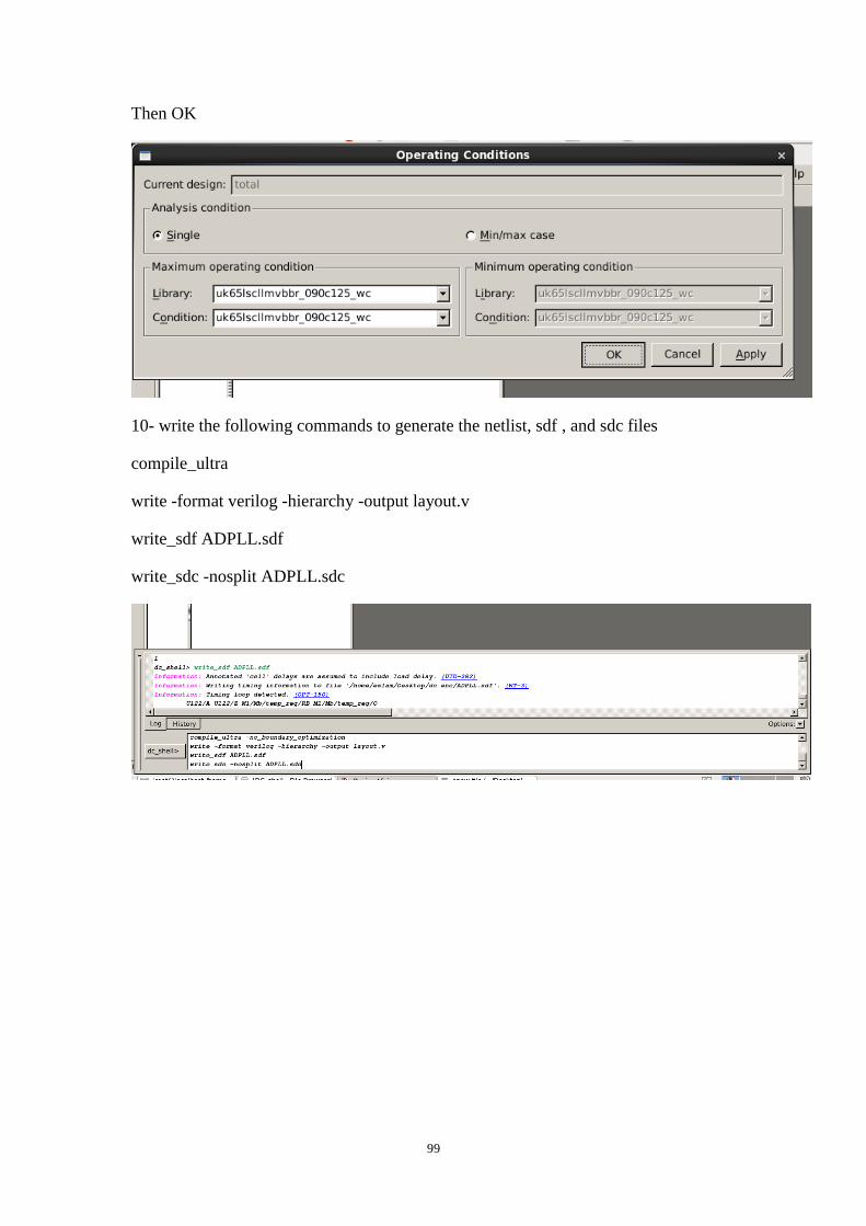
Then OK
10- write the following commands to generate the netlist, sdf , and sdc files
compile_ultra
write -format verilog -hierarchy -output layout.v
write_sdf ADPLL.sdf
write_sdc -nosplit ADPLL.sdc
Related Documents


