AFRL-RQ-WP-TR-2015-0132 SCIENTIFIC RESEARCH PROGRAM FOR POWER, ENERGY, AND THERMAL TECHNOLOGIES Task Order 0001: Power, Thermal and Control Technologies and Processes Experimental Research Bang-Hung Tsao, Evan L. Thomas, Qiuhong Zhang, Serhiy Leontsev, Jamie Ervin, Helen Shen, Street Barnett, Jacob Lawson, and Victor McNier University of Dayton Research Institute AUGUST 2015 Final Report Approved for public release; distribution unlimited. See additional restrictions described on inside pages STINFO COPY AIR FORCE RESEARCH LABORATORY AEROSPACE SYSTEMS DIRECTORATE WRIGHT-PATTERSON AIR FORCE BASE, OH 45433-7541 AIR FORCE MATERIEL COMMAND UNITED STATES AIR FORCE

Welcome message from author
This document is posted to help you gain knowledge. Please leave a comment to let me know what you think about it! Share it to your friends and learn new things together.
Transcript
AFRL-RQ-WP-TR-2015-0132
SCIENTIFIC RESEARCH PROGRAM FOR POWER, ENERGY, AND THERMAL TECHNOLOGIES Task Order 0001: Power, Thermal and Control Technologies and Processes Experimental Research Bang-Hung Tsao, Evan L. Thomas, Qiuhong Zhang, Serhiy Leontsev, Jamie Ervin, Helen Shen, Street Barnett, Jacob Lawson, and Victor McNier University of Dayton Research Institute AUGUST 2015 Final Report
Approved for public release; distribution unlimited.
See additional restrictions described on inside pages
STINFO COPY
AIR FORCE RESEARCH LABORATORY AEROSPACE SYSTEMS DIRECTORATE
WRIGHT-PATTERSON AIR FORCE BASE, OH 45433-7541 AIR FORCE MATERIEL COMMAND
UNITED STATES AIR FORCE

NOTICE AND SIGNATURE PAGE
Using Government drawings, specifications, or other data included in this document for any purpose other than Government procurement does not in any way obligate the U.S. Government. The fact that the Government formulated or supplied the drawings, specifications, or other data does not license the holder or any other person or corporation; or convey any rights or permission to manufacture, use, or sell any patented invention that may relate to them. This report was cleared for public release by the USAF 88th Air Base Wing (88 ABW) Public Affairs Office (PAO) and is available to the general public, including foreign nationals. Copies may be obtained from the Defense Technical Information Center (DTIC) (http://www.dtic.mil). AFRL-RQ-WP-TR-2015-0132 HAS BEEN REVIEWED AND IS APPROVED FOR PUBLICATION IN ACCORDANCE WITH ASSIGNED DISTRIBUTION STATEMENT. *//Signature// //Signature// GREGORY L. RHOADS THOMAS L. REITZ, Technical Advisor Program Manager Mechanical and Thermal Systems Branch Mechanical and Thermal Systems Branch Power and Control Division Power and Control Division Aerospace Systems Directorate //Signature// JOHN G. NAIRUS, Chief Engineer Power and Control Division Aerospace Systems Directorate This report is published in the interest of scientific and technical information exchange, and its publication does not constitute the Government’s approval or disapproval of its ideas or findings. *Disseminated copies will show “//Signature//” stamped or typed above the signature blocks.

REPORT DOCUMENTATION PAGE Form Approved OMB No. 0704-0188
The public reporting burden for this collection of information is estimated to average 1 hour per response, including the time for reviewing instructions, searching existing data sources, searching existing data sources, gathering and maintaining the data needed, and completing and reviewing the collection of information. Send comments regarding this burden estimate or any other aspect of this collection of information, including suggestions for reducing this burden, to Department of Defense, Washington Headquarters Services, Directorate for Information Operations and Reports (0704-0188), 1215 Jefferson Davis Highway, Suite 1204, Arlington, VA 22202-4302. Respondents should be aware that notwithstanding any other provision of law, no person shall be subject to any penalty for failing to comply with a collection of information if it does not display a currently valid OMB control number. PLEASE DO NOT RETURN YOUR FORM TO THE ABOVE ADDRESS.
1. REPORT DATE (DD-MM-YY) 2. REPORT TYPE 3. DATES COVERED (From - To)August 2015 Final 20 July 2012 – 21 August 2015
4. TITLE AND SUBTITLESCIENTIFIC RESEARCH PROGRAM FOR POWER, ENERGY, AND THERMAL TECHNOLOGIES Task Order 0001: Power, Thermal and Control Technologies and Processes Experimental Research
5a. CONTRACT NUMBER FA8650-12-D-2224-0001
5b. GRANT NUMBER
5c. PROGRAM ELEMENT NUMBER 62203F
6. AUTHOR(S)
Bang-Hung Tsao, Evan L. Thomas, Qiuhong Zhang, Serhiy Leontsev, Jamie Ervin, Helen Shen, Street Barnett, Jacob Lawson, and Victor McNier
5d. PROJECT NUMBER 3145
5e. TASK NUMBER N/A
5f. WORK UNIT NUMBER
Q0Z7 7. PERFORMING ORGANIZATION NAME(S) AND ADDRESS(ES) 8. PERFORMING ORGANIZATION
University of Dayton Research Institute Energy Technology and Materials Division 300 College Park Dayton, OH 45469-0170
REPORT NUMBER
9. SPONSORING/MONITORING AGENCY NAME(S) AND ADDRESS(ES) 10. SPONSORING/MONITORINGAir Force Research Laboratory Aerospace Systems Directorate Wright-Patterson Air Force Base, OH 45433-7541 Air Force Materiel Command United States Air Force
AGENCY ACRONYM(S)AFRL/RQQM
11. SPONSORING/MONITORINGAGENCY REPORT NUMBER(S)
AFRL-RQ-WP-TR-2015-0132 12. DISTRIBUTION/AVAILABILITY STATEMENT
Approved for public release; distribution unlimited.13. SUPPLEMENTARY NOTES
PA Case Number: 88ABW-2015-4237; Clearance Date: 04 Sep 2015.See also AFRL-RQ-WP-TR-2015-0130.
14. ABSTRACTThis report includes the details of the subtask technical efforts including superconductivity, thermoelectric, magneticmaterials, carbon nanotube (CNT), silicon carbide (SiC) power module, actuator, battery, thermal management, andINtegrated Vehicle ENergy Technology (INVENT) support.
15. SUBJECT TERMSsuperconductivity, thermoelectric, magnetic materials, CNT power module, actuator, battery, thermal management
16. SECURITY CLASSIFICATION OF: 17. LIMITATIONOF ABSTRACT:
SAR
18. NUMBEROF PAGES
284
19a. NAME OF RESPONSIBLE PERSON (Monitor) a. REPORT Unclassified
b. ABSTRACTUnclassified
c. THIS PAGEUnclassified
Gregory L. Rhoads 19b. TELEPHONE NUMBER (Include Area Code)
N/A Standard Form 298 (Rev. 8-98) Prescribed by ANSI Std. Z39-18
i Approved for public release; distribution unlimited.
Table of Contents Section Page
List of Figures .............................................................................................................................................. iv List of Tables .............................................................................................................................................. xii
Thermal Management ........................................................................................................................... 1 1. Use of Ammonium Carbamate in a Heat Exchanger Reactor as an Endothermic Heat Sink for 1.1
Thermal Management ...................................................................................................................... 1 1.1.1 Introduction .......................................................................................................................... 1 1.1.2 Experimental ........................................................................................................................ 2 1.1.3 Estimate of Endothermic Heat Absorption Rate and Conversion ........................................ 6 1.1.4 Results and Discussion ......................................................................................................... 7 1.1.5 Summary ............................................................................................................................ 16 Control Strategy for Operation of Aircraft Vapor Compression Systems ..................................... 18 1.21.2.1 Introduction ........................................................................................................................ 18 1.2.2 Experimental ...................................................................................................................... 19 1.2.3 Results ................................................................................................................................ 24 1.2.4 Discussion .......................................................................................................................... 29 1.2.5 Summary ............................................................................................................................ 30
Solid-state Electrolyte Lithium-ion Batteries Based on Phthalocyanines ........................................... 32 2. Introduction .................................................................................................................................... 32 2.1 Experimental .................................................................................................................................. 32 2.22.2.1 Phthalocyanine Synthesis ................................................................................................... 33 2.2.2 Thin Film Processing .......................................................................................................... 33 2.2.3 Pc-based Cathode Development ......................................................................................... 33 2.2.4 Anodes ................................................................................................................................ 34 Results and Discussion .................................................................................................................. 34 2.32.3.1 CNTP cathodes ................................................................................................................... 34 2.3.2 TAMe-LiPc ........................................................................................................................ 38 2.3.3 BLLEEPc ............................................................................................................................ 40 Summary ........................................................................................................................................ 45 2.4
Enhancement of Thermoelectric (TE) Materials to Provide Solutions for Power and Thermal 3.Challenges ........................................................................................................................................... 46 Research Objectives ....................................................................................................................... 46 3.1 Introduction .................................................................................................................................... 46 3.23.2.1 TE Materials Challenges .................................................................................................... 48 3.2.2 Nano-structure Engineering to Achieve High TE Performance ......................................... 48 3.2.3 Advantages of Complex Oxide Materials for TE Applications and Current Technology
Barriers for Applications .................................................................................................... 49 Results and Discussion .................................................................................................................. 49 3.33.3.1 Approach 1: Microstructural Self-assembly to Fabricate Nano-dimensional Materials with
Nano-inclusions .................................................................................................................. 49 3.3.2 Approach 2: High-throughput Combinatorial Approach for Rapid Identification of Novel
TE Materials ....................................................................................................................... 66 3.3.3 Thick and Thin Film TE Device Fabricated from Oxide-based Materials: Design and
Synthesis of Textured Ca-Co-O Films ............................................................................... 79 Summary ........................................................................................................................................ 86 3.4
Development of high strength nano-structured composite permanent magnets based on SmCo alloy.4. ............................................................................................................................................................ 88 Development of magnetically hard and soft bulk nano-composite magnetic materials overview 4.1
Research Objectives ....................................................................................................................... 88
ii Approved for public release; distribution unlimited.
4.1.1 Background ........................................................................................................................ 88 4.1.2 Experimental methods discussion ...................................................................................... 89 4.1.3 Projected research work summary ...................................................................................... 89 4.1.4 SmCo5 nano-flake powder preparation via wet milling route using Oleic acid surfactant . 90 4.1.5 SmCo5 nano-flake powder preparation via wet milling route using Valeric acid surfactant
............................................................................................................................................ 92 4.1.6 Surfactant removal study for nano-scale SmCo5 powder prepared by high energy ball
milling ................................................................................................................................ 94 4.1.7 UDRI gas gun target fixture design proposal ................................................................... 101 4.1.8 UDRI gas gun powder compaction experiment ............................................................... 104 4.1.9 Compacted powder sample characterization .................................................................... 109 4.1.10 SmCo5 powder microwave sintering ................................................................................ 111 4.1.11 Effect of heat treatment on bulk FeNi alloy phase ........................................................... 113 4.1.12 Effect of ball milling on FeNi alloy powder morphology ................................................ 115 4.1.13 Effect of ball milling on SmCo5-FeNi composite powder ................................................ 117 4.1.14 SmCo5 Spark Plasma Sintering (SPS) synthesis .............................................................. 119 4.1.15 SmCo5 nano-flake powder Hot Pressing (HP) sintering ................................................... 122 Computer simulation of magnetic inductor components using FEM .......................................... 124 4.24.2.1 Summary of inductor Eddy-current loss simulation using ANSYS Maxwell 3D software
.......................................................................................................................................... 124 4.2.2 Turbine auxiliary generator FE simulation ....................................................................... 128 4.2.3 Turbine auxiliary generator FE simulation (continued) ................................................... 136 4.2.4 Split conductor current proximity effect FE simulation ................................................... 139 4.2.5 Split conductor frequency sweep study, FE simulation ................................................... 142 Nanocrystalline Sm-Co and Sm-Co/Fe magnets ......................................................................... 148 4.34.3.1 Introduction ...................................................................................................................... 148 4.3.2 Experimental .................................................................................................................... 148 4.3.3 Results and Discussion ..................................................................................................... 149 4.3.4 Summary .......................................................................................................................... 171 4.3.5 Measurement of nanocrystalline SmCo5 bulk with high coercivity ................................. 172
Growth and Characterization of Carbon Nanotubes (CNT) for Thermal Management and Electrical 5.Applications ...................................................................................................................................... 174 Research Objectives ..................................................................................................................... 174 5.1 Technical Summary ..................................................................................................................... 174 5.25.2.1 Approaches ....................................................................................................................... 174 Detailed Technical Summary: ...................................................................................................... 176 5.35.3.1 Part1: CNT layer grown on Cu and various metal foil substrates-synthesis, surface
modification, and characterization ................................................................................... 176 5.3.2 Part 2: Growth of CNT on carbon substrates ................................................................... 198
Energy Analysis of Electromechanical Actuator (EMA) under Simulated Aircraft Primary Flight 6.Control Surface Load ........................................................................................................................ 210 Abstract ........................................................................................................................................ 210 6.1 Introduction .................................................................................................................................. 210 6.2 Experimental Setup ...................................................................................................................... 212 6.3 Hardware Characterization .......................................................................................................... 213 6.4 Test Matrix ................................................................................................................................... 214 6.56.5.1 Step Response ................................................................................................................... 214 Dynamic Load Control ................................................................................................................ 221 6.66.6.1 Cascade Control................................................................................................................ 222 6.6.2 Signal Response of the EMA and Hydraulic Press Fixture .............................................. 223 Conclusion ................................................................................................................................... 226 6.7

iii Approved for public release; distribution unlimited.
References ................................................................................................................................................. 227 Appendix ................................................................................................................................................... 232
A-1 Facility Capabilities and System Maintenance for the Power Semiconductor, Microscopy, Deposition Film Growth, High Power Generation and Electrical Characterization Laboratories232
Nomenclature ............................................................................................................................................ 267
iv Approved for public release; distribution unlimited.
List of Figures
Figure Page Figure 1.1. AC Decomposition Curve .......................................................................................................... 1 Figure 1.2. HEX reactor with heat load and reactant loop for ambient pressure studies .............................. 3 Figure 1.3. HEX reactor with heat load and reactant loops for sub ambient pressure studies ...................... 5 Figure 1.4. HEX Reactor water exit temperatures corresponding to water inlet temperatures of 90°C ....... 8 Figure 1.5. Heat absorption rate as a function of water inlet temperature for 70 seconds residence time
and ambient pressure .......................................................................................................... 9 Figure 1.6. Effect of AC mass flow rate and particle size on heat absorption rate ..................................... 10 Figure 1.7. Heat absorption as a function of residence time and water inlet temperature .......................... 12 Figure 1.8. HEX reactor port temperature at 2 kPa reaction pressure and 63°C water inlet temperature .. 13 Figure 1.9. HEX reactor port temperature histories for a 180 s, 29°C experiment ..................................... 14 Figure 1.10. Decomposition based heat absorption rate as functions of water inlet temperature and
reaction pressure ............................................................................................................... 15 Figure 1.11. VCSRF block diagram............................................................................................................ 20 Figure 1.12. R134a pressure-specific enthalpy diagram showing thermodynamic states for both
superheat control (Method A, dashed green) and cycle control (Method B, solid red) approaches for a single evaporator system ....................................................................... 22
Figure 1.13. Hypothetical scaled mission load profile ................................................................................ 24 Figure 1.14. Temperature error summary ................................................................................................... 25 Figure 1.15. COP comparison ..................................................................................................................... 26 Figure 1.16. Method A temperature control performance for ASH values of (a) 2.8 °C, (b) 5.6 °C, (c)
11.1 °C, and (d) 16.7 °C.................................................................................................... 27 Figure 1.17. Method B temperature control performance for dT values of (a) 2.8 °C, (b) 5.6 °C, (c)
8.3°C, and (d) 11.1 °C....................................................................................................... 28 Figure 1.18. Measured ASH of Methods A and B ...................................................................................... 28 Figure 1.19. SSP performance of Method B ............................................................................................... 29 Figure 3.1. Power output dependence on both zT and temperature differential (ΔT) ................................. 48 Figure 3.2. BSO nano-columns (highlighted by arrows) in YBCO matrix grown by PLD ........................ 50 Figure 3.3. Schematic illustration of the crystal structure of Ca3Co4O9 (CCO-349). Adapted from
[18]. ................................................................................................................................... 51 Figure 3.4. XRD patterns for a (a) CCO-349 target and (b) 200 nm CCO-349 thin film on Si (100) ........ 53 Figure 3.5. Temperature-dependent electrical resistivity (ρ) measured using the van der Pauw method
for a film grown on Si (100) ............................................................................................. 54 Figure 3.6. TEM and HR-TEM Images of the Three Ca-Co-O Phases in the Pure CCO-349 Film ........... 55 Figure 3.7. STEM Z-contrast images, EDS spectrum and EDS elemental mapping of CCO-349 (Spec
1) and CCO-225 (Spec 2) ................................................................................................. 56 Figure 3.8. Left panel: Temperature-dependent electrical resistivity (ρ) measured using the van der
Pauw method for films grown on Si (100) ........................................................................ 58 Figure 3.9. BZO-doped CCO film with increased mis-orientation and low angle grain boundaries
perpendicular to the film plane ......................................................................................... 58 Figure 3.10. BZO-doped film with CCO-349 as the main phase and nano-lamellar CCO-225 (B) and
CCO-unknown (C) phases ................................................................................................ 59 Figure 3.11. Zr is uniformly distributed throughout the film, while Ba segregates into Ca-deficient
phases and GBs ................................................................................................................. 59 Figure 3.12. (Top) Ca-Co-O film with interface reaction layer highlighted. (Bottom) Element
distribution at interface reaction layer (note scale) ........................................................... 60 Figure 3.13. HR-TEM micrograph revealing the epitaxial growth of the Ca-Co-O phases on the
interface reaction layer of crystalline Co3O4 (note scale) ................................................. 61
v Approved for public release; distribution unlimited.
Figure 3.14. Nano-layer Co3O4 alternating with Ca-Co-O deposited using a sectored target PLD approach ............................................................................................................................ 62
Figure 3.15. (top) Temperature-dependent Power Factor data for Ca-Co-O-based thin film samples deposited on insulating substrates ..................................................................................... 64
Figure 3.16. zT data for bulk Ca-Co-O-based samples measured using the PPMS/TTO (note temperature range) ............................................................................................................ 64
Figure 3.17 Fully Automated Combinatorial Deposition Process .............................................................. 68 Figure 3.18. (a) Custom Power Factor Screening Instrument (PFSI) and components. (b) Close-up of
sample stage and measurement head. (c) Detail of measurement head components. (d) PFSI wiring diagram ......................................................................................................... 72
Figure 3.19. Custom LabVIEW-generated interface for (a) designing the wafer scan and (b) physical property data collection .................................................................................................... 75
Figure 3.20. (a) Post-deposition processing via standard photolithography techniques (negative resist NR71-3000) followed by 1μm Au sputtering and removal of Au with RR41 photoresist remover to generate discreet composition units in the calibration sample. The same process was followed for the (b) Ni standard sample and the (c) Ca3(Fe,Ni,Co)4O9 combinatorial ternary sample (with HCl etchant). .............................. 76
Figure 3.21. (a) Ca3Co4O9 (Material 1) – CaMnO3 (Material 3) Binary combinatorial sample. (b) Electrical property data collected using PFSI. (c) XRD data from diagonal line scan from Material 1 to Material 2............................................................................................ 77
Figure 3.22. Electrical property data collected using PFSI of a 500 μm Nickel standard film (nonpatterned) ................................................................................................................... 78
Figure 3.23. Overlay of electrical resistivity short scan data from PFSI on optical image of a 3 in dia. Ca3(Ti, Fe, Co)4O9 sample grown on Si/SiO2 ................................................................... 79
Figure 3.24. Textured Ca-Co-O film grown on 2-μm-thick layer of amorphous SiO2 ............................... 80 Figure 3.25. In-plane thin film TE device schematic (not to scale) ............................................................ 81 Figure 3.26. Ordinary design for TE power generation module ................................................................. 81 Figure 3.27. Custom-built water-cooled power generation measurement system. (Right panel) Close-
up of thin film unicouple mounting schematic ................................................................. 83 Figure 3.28. (Left panel) Voltage output and (Right panel) Power generated from a thin film unicouple
as a function of the temperature gradient across the sample ............................................. 83 Figure 3.29. Temperature dependence of electrical resistivity ρ (top) and Seebeck coefficient S
(bottom) for CMO bulk sample ........................................................................................ 85 Figure 3.30. Morphology of clean GBs and nano-domains within the grains of an as-sintered CMO
sample ............................................................................................................................... 85 Figure 4.1. Powder flake thickness dependence on the milling time .......................................................... 90 Figure 4.2. Sample 2-2 (SmCo5, Oleic acid, Milling time: 1 h).................................................................. 91 Figure 4.3. Sample 2-4 (SmCo5, Oleic acid, Milling time: 2 h).................................................................. 91 Figure 4.4. Sample 2-3 (SmCo5, Oleic acid, Milling time: 4 h).................................................................. 91 Figure 4.5. Sample 2-5 (SmCo5, Oleic acid, Milling time: 8 h).................................................................. 92 Figure 4.6. DSC data, Powder flake thickness dependence on the milling time ........................................ 93 Figure 4.7. Sample 3-2a (SmCo5, Valeric Acid, Milling time: 1 h) ............................................................ 93 Figure 4.8. Sample 3-3a (SmCo5, Valeric acid, Milling time: 2h) .............................................................. 93 Figure 4.9. Sample 3-1a (SmCo5, Valeric acid, Milling time: 4h) .............................................................. 94 Figure 4.10. Sample 3-4a (SmCo5, Valeric acid, Milling time: 8h) ............................................................ 94 Figure 4.11. SEM images as a milled (a), heat treated in argon at 200° (b) and 400° (c) SmCo5 nano
flake powders prepared by HEBM using valeric acid, clusters of SmCo5 nano flakes (d) ...................................................................................................................................... 96
Figure 4.12. DSC heat flow (heating) for as milled and heat treated SmCo5 nano-powders ...................... 97 Figure 4.13. Powder x-ray diffraction data for as milled and heat treated SmCo5 nano-scale powder ...... 98 Figure 4.14. Demagnetization data for epoxy bound as milled and heat treated SmCo5 nano-powders .... 99

vi Approved for public release; distribution unlimited.
Figure 4.15. Influence of dynamic densification on nanostructures formation in Ti3Si3 intermetallic alloy and its bulk properties ............................................................................................ 101
Figure 4.16. Synthesis, processing, and deformation of bulk nanophase Fe28Al2Cr intermetallic ........... 102 Figure 4.17. Sketch of the target fixture ................................................................................................... 103 Figure 4.18. Rigid and compressive capsule design ................................................................................. 103 Figure 4.19. Target Assembly ................................................................................................................... 105 Figure 4.20. SmCo5 experimental powder preparation flowchart ............................................................. 105 Figure 4.21. Target fixture drawing .......................................................................................................... 106 Figure 4.22. Machined and welded target fixture with and without the target assembly mounted .......... 106 Figure 4.23. Projectile Drawing ................................................................................................................ 107 Figure 4.24. Set of Four Machined Projectiles ......................................................................................... 107 Figure 4.25. Ballistic Test Report ............................................................................................................. 109 Figure 4.26. SEM imaging of shock compacted SmCo5 nano-scale powder ............................................ 110 Figure 4.27. Magnetic hysteresis data for shock compacted and as milled SmCo5 nano-scale powder ... 111 Figure 4.28. SEM images of CIP compacted as-milled SmCo5 nanopoweder (a) and microwave
sintered sample at 600 °C for 15 min (b) ........................................................................ 112 Figure 4.29. Magnetic hysteresis data for as-milled and microwave sintered nano-scale SmCo5 ............ 112 Figure 4.30. XRD data for SmCo5 samples sintered at 300, 450, and 600 °C .......................................... 113 Figure 4.31. Alloy samples (both as-cast and heat treated) ...................................................................... 115 Figure 4.32. XRD data for ball milled powders prepared at different milling times ................................ 116 Figure 4.33. SEM imaging of FeNi ball milled powders prepared at different milling times .................. 117 Figure 4.34. SEM imaging of FeNi ball milled powders prepared at different milling times. ................. 118 Figure 4.35. XRD data for SmCo5 FeNi ball milled powders prepared at different milling times. .......... 118 Figure 4.36. Sample dimensions and density ............................................................................................ 120 Figure 4.37. Demagnetization and X-ray diffraction data for SmCo5 samples consolidated by SPS. ..... 121 Figure 4.38. Demagnetization and X-ray diffraction data for hot pressed SmCo5 samples. ..................... 123 Figure 4.39. Rendering of a tape core inductor 3D model and a 2D cross section used for accurate
Eddy-current calculation ................................................................................................. 125 Figure 4.40. Simulated Eddy-curent distribution and corresponding mesh discretization in a single
lamination layer .............................................................................................................. 125 Figure 4.41. Eddy power loss as a function of frequency, logarithmic scale. ........................................... 126 Figure 4.42. Eddy power loss as a function of frequency, linear scale ..................................................... 126 Figure 4.43. Eddy power loss as a function of lamination thickness ........................................................ 127 Figure 4.44. Eddy power loss as a function of material resistivity ........................................................... 127 Figure 4.45. Auxiliary generator simplified schematics ........................................................................... 128 Figure 4.46. FEM model 3D view ............................................................................................................ 129 Figure 4.47. Test 1 Magnet array 24, air-core coil.................................................................................... 130 Figure 4.48. Magnet array 24, Fe-core coil ............................................................................................... 130 Figure 4.49. Magnet array 72, Fe-core coil ............................................................................................... 130 Figure 4.50. Magnetic Flux Data .............................................................................................................. 132 Figure 4.51. Induced EMF Data................................................................................................................ 132 Figure 4.52. Induced Current Data ............................................................................................................ 132 Figure 4.53. Power Output Data ............................................................................................................... 132 Figure 4.54. Induced Waveform ............................................................................................................... 133 Figure 4.55. Induced Waveform ............................................................................................................... 133 Figure 4.56. Generated Power Output ...................................................................................................... 133 Figure 4.57. Modified FEM 3D view ....................................................................................................... 136 Figure 4.58. Magnet array 72, Fe-core coil ............................................................................................... 137 Figure 4.59. Bridged magnet array 72, Fe-core coil. ................................................................................ 137 Figure 4.60. Bridged magnet array 72, C-shaped Fe coil core. ................................................................ 137 Figure 4.61. Induced EMF, current and power output waveform for modified model. ............................ 138
vii Approved for public release; distribution unlimited.
Figure 4.62. (a, b). the 3-strand split conductor geometry with 120° (a), 45° (b), 10° (c) and 5° (d) strand separation ............................................................................................................. 139
Figure 4.63. Correspoding electrical circuit schematics ........................................................................... 140 Figure 4.64. Simulated waveform of the current in each branches, as well a total cable current ............. 141 Figure 4.65. Color map of AC current density distribution in a split conductor with 120° (a) and 10°
(b) spaced branches, corresponding to the models shown in Figure 4.60a and 4.60c .... 142 Figure 4.66. 3D model of Seven-strand wire (a); electrical circuit schematics (b) ................................... 143 Figure 4.67. Result Data ........................................................................................................................... 146 Figure 4.68. Probe current % of total ........................................................................................................ 147 Figure 4.69. Morphology of as milled flake powders wet milled with BPR of 0.8, 2, 4, and 10 ............. 150 Figure 4.70. Flake thickness as a function of BPR ................................................................................... 150 Figure 4.71. Demagnetization curves of aligned flake powders samples measured along parallel (∥) and
perpendicular (⊥) to the aligning magnetic field direction with flake thickness: (A) 1000 nm; (B) 500 nm; (C) 200 nm; (D) 100 nm. ............................................................ 151
Figure 4.72. Coercivity of flake powder vs. flake thickness ..................................................................... 151 Figure 4.73. Degree of anisotropy for flake powders as a function of flake thickness ............................. 152 Figure 4.74. XRD patterns of aligned flake powder samples with different thickness, detected surface
perpendicular (⊥) to the aligning magnetic field direction. ............................................ 153 Figure 4.75. XRD patterns of random flake powders with thickness of 1000 and 100 nm ...................... 153 Figure 4.76. Demagnetization curves of WM-HP bulk samples pressed at 600 °C with aligned and un-
aligned flake powders. Flake powders prepared with WM0.8S1h (wet milling 1h with BPR of 0.8 and ball diameter of 2.38 mm), typical thickness 1000 nm. ........................ 154
Figure 4.77. Demagnetization curves of WM-HP bulk samples pressed at the temperature from 600-900 °C with the flake powders milled by WM0.8S1h (typical thickness of 1000 nm). . 155
Figure 4.78. Coercivity, remanence, and density of the bulks as a function of HP temperature .............. 155 Figure 4.79. XRD patterns of WM-HP bulk samples pressed at the temperature from 600-900 °C with
the flake powder milled by WM0.8S1h (typical thickness of 1000 nm). ....................... 156 Figure 4.80. Demagnetization curves of WM-HP bulk samples pressed at 600 °C and 420 MPa with
different thickness flake powders. .................................................................................. 157 Figure 4.81. Bulk coercivity as a function of flake thickness ................................................................... 158 Figure 4.82. Flake thickness dependence of the coercivity for SmCo5 flake powders and bulks ............. 158 Figure 4.83 XRD patterns of 100 nm flake powder sample (Green) and corresponding bulk sample
(Red) prepared by WM-HP process. ............................................................................... 158 Figure 4.84. XRD patterns of WM-HP bulk samples pressed with different thickness flake powders. ... 159 Figure 4.85. Sm2O3 and Co content in SmCo5 bulks vs. flake thickness .................................................. 160 Figure 4.86. Demagnetization curves of SmCo5 bulk samples prepared by DM-HP and MA-HP
processes. ........................................................................................................................ 160 Figure 4.87. Demagnetization curves of Sm-Co/Fe bulk samples prepared by DM-HP process with
different Fe milling time. ................................................................................................ 161 Figure 4.88. Effect of Fe milling time on magnetic properties of Sm-Co/Fe bulks prepared by DM-HP
process. ........................................................................................................................... 162 Figure 4.89 XRD patterns of as-milled powders and bulk samples: a) As-milled SmCo5 powder and
SmCo5 + 15 wt% Fe mixture with different Fe milling time; b) Sm-Co bulk and Sm-Co/Fe composite bulks pressed with the corresponding powders. ................................. 163
Figure 4.90 SEM/BSE images for Sm-Co/Fe bulk samples with Fe milling time of 0, 2, 4, and 6 h. Magnification of 100x (a) and 4000x (b). ....................................................................... 164
Figure 4.91. SEM/BSE image and corresponding EDS patterns for the bulk Sm-Co/Fe sample (DMB4) compacted at 650 °C using Fe blending powder (0 h milling). ...................................... 165
Figure 4.92. SEM/BSE image (left) and secondary electron image (right) and corresponding EDS patterns for the bulk Sm-Co/Fe sample (DMB2) compacted at 650 °C using Fe 2 h milling powder ................................................................................................................ 166
viii Approved for public release; distribution unlimited.
Figure 4.93. Sketch of diffusion layer formation and diffusion area structure. ........................................ 166 Figure 4.94. SEM images and corresponding EDS patterns for the bulk Sm-Co/Fe sample (DMB1)
compacted at 650 °C using Fe 6 h milling powder. ........................................................ 167 Figure 4.95. Flowchart of DM-WM-HP process ...................................................................................... 168 Figure 4.96. SEM images of as-milled powders with different magnification: a) DM, b) DM-WM
(BPR1), and c) DM-WM (BPR5) ................................................................................... 169 Figure 4.97. SEM images of as-milled SmCo5+Fe mixture powder with different magnification. ......... 170 Figure 4.98. Demagnetization curves of Sm-Co/Fe composite and Sm-Co bulk samples prepared by
DM-WM-HP process with different BPR in WM. ......................................................... 171 Figure 4.99. XRD patterns of Sm-Co bulks prepared by DM-WM-HP process with different BPR in
WM ................................................................................................................................. 171 Figure 4.100. Hysteresis loop of nanocrystalline SmCo5 bulk (Sample DMB6) measured by VSM. ...... 172 Figure 4.101. Comparison of KJS and VSM test results .......................................................................... 173 Figure 4.102. Demagnetization curves of nanocrystalline SmCo5 bulk measured by KJS
hysteresisgraph and VSM (corrected curve). .................................................................. 173 Figure 5.1. AFM Image: Roughness of Cu foil before and after Al2O3 coating ....................................... 179 Figure 5.2. SEM images: areal density and alignment (insets) of CNTs .................................................. 180 Figure 5.3. Growth of CNTs on Cu foil with Al2O3 and Al buffer layer ................................................. 182 Figure 5.4. Growth of CNTs on TiN coated Cu foil; the effect of TiN thickness varying on CNT
Length /Density (Sputtering) .......................................................................................... 183 Figure 5.5. Growth of CNTs on Ti coated Cu foil (Sputter) ..................................................................... 183 Figure 5.6. Morphology of CNTs/TiN/Cu interface; the effect of TiN layer thickness on CNT /Cu
interface .......................................................................................................................... 183 Figure 5.7. Raman Spectroscopy of the CNT/Cu sample b (FCCVD) ..................................................... 185 Figure 5.8. The effect of various interface materials on thermal impedance ............................................ 186 Figure 5.9. Sample set up for thermal diffusivity measurement by LFA Group ...................................... 187 Figure 5.10. LFA results -Thermal diffusivity of various samples a) The effect of different coating
materials on thermal diffusivity b) The effect of CNT density and length on thermal diffusivity c) The effect of different interface materials on thermal diffusivity ............. 187
Figure 5.11. Schematic of electrical property testing ............................................................................... 189 Figure 5.12. The electrical resistance of Cu/Cu foil and Cu/CNT/Cu; the electrical resistance vs.
various of interface CNT layers (density/length determined by Al2O3 thickness and deposition technique) ...................................................................................................... 189
Figure 5.13. Schematic of interfacial force testing by a pull of tester ...................................................... 190 Figure 5.14. CNT/Cu (made with various Al2O3 thickness) interface after pull off test; the effect of
CNT layer density/length (determined by Al2O3 thickness) on their interfacial property. .......................................................................................................................... 193
Figure 5.15. SEM image of CNT/Cu (with 5 nm Al2O3) before and after pull off test; CNTs left on the Cu surface: A strong interfacial adhesion between CNT and Cu substrate .................... 194
Figure 5.16. The interfacial adhesive strength of CNT/Cu with different buffer layer ............................ 194 Figure 5.17. SEM images of CNTs of different aluminum thickness post-SEED: (a) 5 nm (b) 15 nm (c)
30 nm Al2O3 .................................................................................................................... 196 Figure 5.18. SEM images of post-SEED CNTs growth on different aluminum thickness: (a) 5 nm; (b)
15 nm (c) 30 nm Al2O3. .................................................................................................. 197 Figure 5.19. SEM images of CNTs under different concentrations post-SEED: (a)+(b) 0.98 mM ; (c)
3.8 mM ; (d) 4.8 mM. All samples have equal buffer layer of 15 nm Al2O3 .................. 197 Figure 5.20. SEM images of CNTs with 15 nm buffer layer under different durations post-SEED: (a) 1
min; (b) 30 sec ............................................................................................................... 197 Figure 5.21. EDX analysis of isolated nanoparticles for sample of 15 nm buffer layer in a solution of
3.8 mM ............................................................................................................................ 198
ix Approved for public release; distribution unlimited.
Figure 5.22. EDX analysis of region morphology for sample of 5 nm buffer layer in a solution of 4.8 mM .................................................................................................................................. 198
Figure 5.23. Schematic of the FCCVD system ......................................................................................... 199 Figure 5.24. SEM image of as-received carbon foam from Ultramet, Inc. ............................................... 200 Figure 5.25. Sparse CNT growth on the surface of the untreated carbon foam ........................................ 200 Figure 5.26. SEM images of CNTs growth on 4 hours and 8 hours nitric acid treated CF ...................... 201 Figure 5.27. SEM images of CNTs grown oxidized CF : The effect of oxidized temperature ................. 201 Figure 5.28. SEM images of CNTs grown on SiO2-coated CF................................................................. 202 Figure 5.29. SEM images of CNTs growth on Al2O3-coated carbon foam: The effect of buffer layer
thickness on CNT growth ............................................................................................... 202 Figure 5.30. Thermal diffusivity of CNT/Carbon substrate ...................................................................... 203 Figure 5.31. a) shows a cross section of the VC sample, b) shows the top-down view of a sample after
1 minute of CNT growth, and c) shows the top-down view of a sample after 20 minutes of attempted CNT growth ................................................................................. 205
Figure 5.32. SEM images taken after 1 min growth, the scale bar is 100 nm and it is the same for all the images ....................................................................................................................... 206
Figure 5.33. a)-d) are SEM images of 20-minute growth samples; the highlighted scale bar is 500 nm; e) the average carpet height determined for each sample; f) the correlation between particle count (value after one minute) and carpet height (value after 20 minute) for all the samples. ..................................................................................................................... 207
Figure 5.34. TEM images that show particle and CNT morphology for SiO2 and Al2O3 buffer layer samples. a) from SiO2/Si sample, b) is a sample with ALD SiO2 buffer, c) is a sample with plasma SiO2 buffer, and d) is a sample with ALD Al2O3 buffer layer. ................... 208
Figure 6.1. EPAD Program’s electromechanical actuator and power control and monitor electronics .... 211 Figure 6.2. Hardware and Test Set-up ...................................................................................................... 212 Figure 6.3. Test Apparatus Flow Diagram ................................................................................................ 213 Figure 6.4. Definition of Overshoot, settling time, and rising time from a Step Response ...................... 215 Figure 6.5. Close up Results of Step Response Test ................................................................................. 215 Figure 6.6. DC bus Voltage and Current Data from Step Response ......................................................... 216 Figure 6.7. DC Bus Electrical Power in Step Response Test .................................................................... 217 Figure 6.8. DC bus Voltage and Regen Resistor Current Data from Step Response ................................ 217 Figure 6.9. Electrical Power in Watts Recorded on the Regen Resistor ................................................... 218 Figure 6.10. DC bus Voltage, Regen Resistor Current and DC bus Power Data from Step Response .... 219 Figure 6.11. Close up of DC bus Voltage, Regen Resistor Current and DC bus Power Data from Step
Response ......................................................................................................................... 219 Figure 6.12. Control of Force and Displacement over a Dynamic Profile ................................................ 222 Figure 6.13. EMA Test System Control Scheme ...................................................................................... 223 Figure 6.14. Cascade Control Command Generation ............................................................................... 223 Figure 6.15. Diagram of Signal Response Test ........................................................................................ 224 Figure 6.16. Segment of a 4 Hz Signal response of EMA ........................................................................ 224 Figure 6.17. Time Delay vs Frequency for Press and EMA ..................................................................... 225 Figure 6.18. System Spring Constant (K) ................................................................................................. 226 Figure A.1. Cleanroom view (a) and (b) ................................................................................................... 232 Figure A.2. Annealing System .................................................................................................................. 232 Figure A.3. Graphite Electrodes and Cooling Shields .............................................................................. 233 Figure A.4. Electron Beam ....................................................................................................................... 233 Figure A.5. Control Systems and Vacuum Chamber ................................................................................ 233 Figure A.6. Second Gun RF Supply Rack ................................................................................................ 234 Figure A.7. RF Sputtering System ............................................................................................................ 234 Figure A.8. Reactive Ion Etcher................................................................................................................ 235 Figure A.9. High Resistivity Water Unit .................................................................................................. 235
x Approved for public release; distribution unlimited.
Figure A.10. Mask Aligner ....................................................................................................................... 236 Figure A.11. Microscope .......................................................................................................................... 236 Figure A.12. Microscopy Lab ................................................................................................................... 237 Figure A.13. SEM ..................................................................................................................................... 237 Figure A.14. Atomic Force Microscope ................................................................................................... 238 Figure A.15. Surface Profiler .................................................................................................................... 238 Figure A.16. Microscope .......................................................................................................................... 239 Figure A.17. Thickness Measurement Unit .............................................................................................. 239 Figure A.18. LFA 457 MicroFlash ........................................................................................................... 240 Figure A.19. X-Ray Diffraction ................................................................................................................ 240 Figure A.20. Electric Resistance Measuring System ................................................................................ 241 Figure A.21. Surface Profilometer ............................................................................................................ 241 Figure A.22. Microscope .......................................................................................................................... 242 Figure A.23. Cleaner Room ...................................................................................................................... 242 Figure A.24. Atomic Layer Deposition (ALD) ......................................................................................... 243 Figure A.25. Control ................................................................................................................................. 243 Figure A.26. Chamber ............................................................................................................................... 244 Figure A.27. Thermal Evaporator ............................................................................................................. 244 Figure A.28. Internal Components ............................................................................................................ 245 Figure A.29. Mask Alignment System...................................................................................................... 245 Figure A.30. Kulicke & Soffa 4524A ....................................................................................................... 246 Figure A.31. Orthodyne Electronics M20B .............................................................................................. 246 Figure A.32. Rapid Annealing Unit .......................................................................................................... 247 Figure A.33. Tube Furnace ....................................................................................................................... 247 Figure A.34. 1.5 kW Diamond Deposition System .................................................................................. 248 Figure A.35. Safety Interlock System ....................................................................................................... 248 Figure A.36. 5 kW Diamond Deposition System ..................................................................................... 248 Figure A.37. Safety Interlock System ....................................................................................................... 249 Figure A.38. High Temperature PCD Deposition ..................................................................................... 249 Figure A.39. Hot Filament ........................................................................................................................ 249 Figure A.40. ECL Lab View A ................................................................................................................. 250 Figure A.41. ECL Lab View B ................................................................................................................. 250 Figure A.42. HP 4284A and HP4285 and HP42841 ................................................................................. 251 Figure A.43. Sample Prober ...................................................................................................................... 251 Figure A.44. Agilent EA4980A ................................................................................................................ 251 Figure A.45. Janis Cryogenic Test System ............................................................................................... 252 Figure A.46. IR/IV/HV Test System ........................................................................................................ 252 Figure A.47. Safety Interlock System ....................................................................................................... 252 Figure A.48. High Voltage Breakdown System........................................................................................ 253 Figure A.49. Safety Interlock System ....................................................................................................... 253 Figure A.50. Curve Tracer Test System ................................................................................................... 254 Figure A.51. Micromainulator MM6000 .................................................................................................. 254 Figure A.52. High Temperature ................................................................................................................ 254 Figure A.53. Control Rack ........................................................................................................................ 255 Figure A.54. Chamber ............................................................................................................................... 255 Figure A.55. Thermal Test Fixture Station ............................................................................................... 255 Figure A.56. HP 370A ............................................................................................................................. 256 Figure A.57. HP371A ............................................................................................................................... 256 Figure A.58. Thermal Cycling Test System ............................................................................................. 257 Figure A.59. Test Chamber ....................................................................................................................... 257 Figure A.60. Ferroelectric Rack / EMI Shield .......................................................................................... 258

xi Approved for public release; distribution unlimited.
Figure A.61. Sample Prober ...................................................................................................................... 258 Figure A.62. Centralized Database ........................................................................................................... 258 Figure A.63. Tenny Environmental Oven ................................................................................................. 259 Figure A.64. DC-DC Converter Load Bank ............................................................................................. 259 Figure A.65. Safety Interlock Controlled Test Fixture ............................................................................. 259 Figure A.66. High Bay (View A) .............................................................................................................. 260 Figure A.67. High Bay (View B) .............................................................................................................. 260 Figure A.68. PSU Bank ............................................................................................................................ 261 Figure A.69. Control ................................................................................................................................. 261 Figure A.70. Switch .................................................................................................................................. 261 Figure A.71. OSU ..................................................................................................................................... 262 Figure A.72. Circuit Diagram ................................................................................................................... 262 Figure A.73. Hipotronics 7150-20CT Dielectric Test System .................................................................. 263 Figure A.74. Control Console ................................................................................................................... 263 Figure A.75. HV Chamber ........................................................................................................................ 264 Figure A.76. Test Fixture .......................................................................................................................... 264 Figure A.77. Signal ................................................................................................................................... 264 Figure A.78. Pneumatic ............................................................................................................................ 265 Figure A.79. SF6 System .......................................................................................................................... 265 Figure A.80. Fiber-optic Receivers ........................................................................................................... 265 Figure A.81. Fiber-optic Battery Transmitters .......................................................................................... 266
xii Approved for public release; distribution unlimited.
List of Tables
Table Page
Table 1.1. Sensor Type, Uncertainty, and Range .......................................................................................... 3 Table 1.2. Experimental Input Parameters for Ambient Pressure Studies .................................................... 4 Table 1.3. Experimental Input Parameters for Sub Ambient Pressure Studies ............................................. 5 Table 1.4. Average Reaction Pressure and Temperature, Decomposition Pressures and Ac Conversion
for 70 s Residence Time....................................................................................................... 10 Table 1.5. Heat Absorption Rate and Conversion as a Function of Water Inlet Temperature and
Reactor Pressure ................................................................................................................... 16 Table 1.6. COP and Useful COP Comparison ............................................................................................ 30 Table 4.1. Parts List .................................................................................................................................. 104 Table 4.2. Alloy Melting Data .................................................................................................................. 114 Table 4.3. Heat Treatment Data ................................................................................................................ 114 Table 4.4. XRD Data ................................................................................................................................ 116 Table 4.5. Values Extracted from the Waveform Data ............................................................................. 131 Table 4.6. Generation parameters as a function of load resistance in terms of r0. .................................... 134 Table 4.7. Generator components weight calculation. .............................................................................. 134 Table 4.8. Values extracted from the waveform data ............................................................................... 139 Table 4.9. Data Summary ......................................................................................................................... 147 Table 4.10. Characteristics of a milled SmCo5 flake powders .................................................................. 153 Table 4.11. Magnetic properties of SmCo5 bulks hot pressed with flake powders. .................................. 155 Table 4.12. Characteristics of Sm-Co flake and bulk samples prepared by WM-HP process .................. 157 Table 4.13. Characteristics of WM-HP bulks prepared with different thickness flakes ........................... 159 Table 4.14. Magnetic properties of Sm-Co/Fe bulks prepared by DM-HP process with different Fe
milling time (Fe addition: 15 wt%). ................................................................................... 161 Table 5.1. CNT synthesis conditions and results (FCCVD) ..................................................................... 177 Table 5.2. CNT synthesis conditions and results using FCCVD .............................................................. 178 Table 5.3. Cu foil surface roughness before/after coated Al2Co3 ............................................................. 179 Table 5.4. EDX results (Elements containing) of CNTs/TiN/Cu interface particles ................................ 183 Table 5.5. The D/G ratio of CNT/Cu with various buffer layer/thickness/deposition .............................. 184 Table 5.6. Impedance testing results (3 tests on each sample) .................................................................. 186 Table 5.7. Electrical Property of CNT/Cu-Measurement ......................................................................... 190 Table 5.8. Interfacial adhesion of CNTs on Al2O3 coated Cu substrate ................................................... 192 Table 5.9. Interfacial adhesion of CNT on Cu substrate .......................................................................... 193 Table 5.10. Comparison chart highlighting some of the characteristics observed in this study ............... 209 Table 6.1. Sensor Inventory and Uncertainty ........................................................................................... 214 Table 6.2. System Spring Constant Results .............................................................................................. 226 Table A.1. Operating Parameters .............................................................................................................. 239 Table A.2. Operating Parameters .............................................................................................................. 246

xiii Approved for public release; distribution unlimited.
FOREWORD
The work documented in this report was performed by the University of Dayton Research Institute (UDRI) between July 2012 and July 2015, for the Aerospace Systems Directorate of the Air Force Research Laboratory, Wright-Patterson Air Force Base, Ohio. The effort was performed as Task Order 0001 on Contract No. FA8650-12-D-2224, Power and Thermal Technologies for Air and Space – Scientific Research Program (SRP).
Technical support and direction of this task order was provided by Greg Rhoads of AFRL/RQQM. Bang Tsao was the task order principal investigator. The authors of the report were Bang Tsao, Evan Thomas, Qiuhong Zhang, Serhiy Leontsev, Jamie Ervin, Helen Shen, Street Barnett, Jacob Lawson, and Victor McNier.
The author would like to thank Greg Rhoads for providing the task order government administration. The author also wishes to acknowledge the assistance of Karoline Hoffman, Annie Brunswick, and Betsy Hart of the UDRI, who provided the administrative support to make this work possible.
1 Approved for public release; distribution unlimited.
Thermal Management 1.
Use of Ammonium Carbamate in a Heat Exchanger Reactor as an Endothermic 1.1Heat Sink for Thermal Management
1.1.1 Introduction Due to increasing heat loads placed on advanced aircraft, there is a need to research new thermal management methods [1]. One potential approach is to use an endothermic reaction in which the products can be consumed by the engine, rejected to the environment, or stored onboard. The use of low temperature (20 to 50 °C) endothermic chemical reactions for aircraft thermal management has been lacking. Recently, Schmidt et al. [2] have proposed the use of ammonium carbamate (AC) as a high energy density heat sink based on its high enthalpy of decomposition and relatively low decomposition temperature range.
Solid AC dissociates endothermically to produce a gaseous mixture of carbon dioxide and ammonia:
[𝑁𝑁𝐻𝐻4][𝐻𝐻2𝑁𝑁𝑁𝑁𝑁𝑁𝑁𝑁] ↔ 𝑁𝑁𝑁𝑁2 + 2𝑁𝑁𝐻𝐻3 (1.1)
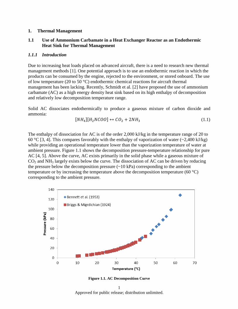
The enthalpy of dissociation for AC is of the order 2,000 kJ/kg in the temperature range of 20 to 60 °C [3, 4]. This compares favorably with the enthalpy of vaporization of water (~2,400 kJ/kg) while providing an operational temperature lower than the vaporization temperature of water at ambient pressure. Figure 1.1 shows the decomposition pressure-temperature relationship for pure AC [4, 5]. Above the curve, AC exists primarily in the solid phase while a gaseous mixture of CO2 and NH3 largely exists below the curve. The dissociation of AC can be driven by reducing the pressure below the decomposition pressure (~10 kPa) corresponding to the ambient temperature or by increasing the temperature above the decomposition temperature (60 °C) corresponding to the ambient pressure.
Figure 1.1. AC Decomposition Curve
2 Approved for public release; distribution unlimited.
The on-demand cooling requirements of actual aircraft thermal management systems require the AC to be continuously replenished after reacting. Thus, a flow reactor which allows continuous AC replenishment is necessary, and we have explored the use of a heat exchanger (HEX)/chemical reactor [6, 7, 8]. A HEX reactor is characterized by chemical reactants flowing through one set of passages in which the reaction occurs, and another heat transfer medium flows through the other set of passages to add or remove heat from the reactor. The decomposition of AC in a HEX reactor as an endothermic heat sink has not been previously explored. Here, we report on our design and characterization results for a HEX reactor using AC.
1.1.2 Experimental
AC dissociation strongly depends on the pressure and temperature. Therefore, experiments were conducted under both ambient and sub-ambient pressures over a range of temperatures. Two different experimental arrangements were used to achieve the different pressure ranges. To better understand the transport behavior, the AC particle size and concentration, and residence time (flow rate) were varied to examine their influence on AC dissociation and cooling rates. The HEX reactor was designed for a 1,500 W endothermic heat absorption rate and 50% AC conversion.
1.1.2.1 Experimental Apparatus
Ambient Pressure Studies
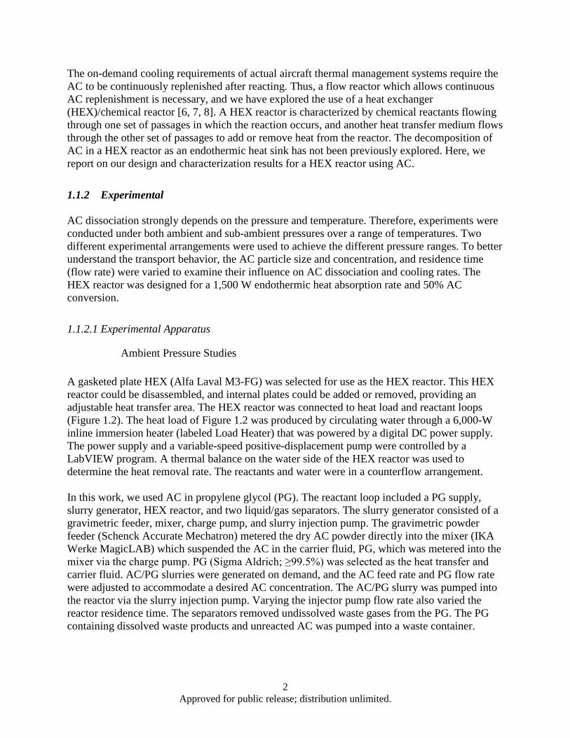
A gasketed plate HEX (Alfa Laval M3-FG) was selected for use as the HEX reactor. This HEX reactor could be disassembled, and internal plates could be added or removed, providing an adjustable heat transfer area. The HEX reactor was connected to heat load and reactant loops (Figure 1.2). The heat load of Figure 1.2 was produced by circulating water through a 6,000-W inline immersion heater (labeled Load Heater) that was powered by a digital DC power supply. The power supply and a variable-speed positive-displacement pump were controlled by a LabVIEW program. A thermal balance on the water side of the HEX reactor was used to determine the heat removal rate. The reactants and water were in a counterflow arrangement.
In this work, we used AC in propylene glycol (PG). The reactant loop included a PG supply, slurry generator, HEX reactor, and two liquid/gas separators. The slurry generator consisted of a gravimetric feeder, mixer, charge pump, and slurry injection pump. The gravimetric powder feeder (Schenck Accurate Mechatron) metered the dry AC powder directly into the mixer (IKA Werke MagicLAB) which suspended the AC in the carrier fluid, PG, which was metered into the mixer via the charge pump. PG (Sigma Aldrich; ≥99.5%) was selected as the heat transfer and carrier fluid. AC/PG slurries were generated on demand, and the AC feed rate and PG flow rate were adjusted to accommodate a desired AC concentration. The AC/PG slurry was pumped into the reactor via the slurry injection pump. Varying the injector pump flow rate also varied the reactor residence time. The separators removed undissolved waste gases from the PG. The PG containing dissolved waste products and unreacted AC was pumped into a waste container.
3 Approved for public release; distribution unlimited.
The PG used to generate the slurry was heated to reduce the amount of heat absorbed sensibly from the water. The reactant-slurry inlet temperature was typically 25-30 °C lower than the water inlet temperature to avoid premature AC decomposition.
Figure 1.2. HEX reactor with heat load and reactant loop for ambient pressure studies
Instrumentation consisted of temperature, flow, and pressure sensors. The uncertainties and ranges of the calibrated sensors used in the experiments are listed in Table 1.1. A National Instruments SCXI signal conditioning unit was used for data acquisition and control. The experiment was designed to permit control of both the heat load and the heat absorption capacity of the system.
Table 1.1. Sensor Type, Uncertainty, and Range
Instrument Type Uncertainty Calibrated Range Pressure Transducers Absolute ± 1.3 kPa 0 to 345 kPa
Thermocouples K, 1.6-mm-diameter probe ± 0.1 °C 5 to 105 °C Heated Water Flow Meter Turbine ± 0.01 L/min 0.5 to 6.7 L/min
Propylene Glycol Flow Meter Turbine ± 0.01 L/min 0.15 to 3.5 L/min
Each experiment was divided into two segments. A single-phase segment, referred to as the baseline, was conducted with PG at the selected flow rate. The baseline segment provided data to compare the single-phase convection heat transfer rate to the reacting flow heat transfer rate under identical conditions. The second part of an experiment, which included the decomposition of AC, was conducted by generating the slurry which flowed into the reactor for decomposition. A typical experiment was conducted for three minutes with at least 30 s each of single-phase and
4 Approved for public release; distribution unlimited.
decomposition heat transfer data. Table 1.2 shows the input parameters for the ambient pressure studies.
Table 1.2. Experimental Input Parameters for Ambient Pressure Studies
Experimental Parameter Range of Values AC feed rate 1.0 to 2.6 g/s
PG-AC mixture flow rate 0.8 L/min, 3.0 L/min Heating load 0 – 4450 W
Residence time 10, 20, 70 s Water Inlet temperature 70, 80, 90 °C Slurry Inlet Temperature 50 – 55 °C
Initial particle size 420 – 840 µm Pressure 99 – 107 kPa
Sub-Ambient Pressure Studies
Figure 1.1 shows that for a given temperature in the range of 20 to 60 °C, the dissociation of AC may be favored by decreasing the pressure below the atmospheric pressure of interest (98 kPa). Therefore, experiments were performed with the incorporation of a vacuum pump to obtain sub-ambient pressures (Figure 1.3). A pair of peristaltic pumps was used as the charge pump and slurry injector pump to meter PG into the mixer and to further isolate the mixer from the HEX reactor, respectively. The use of sub-ambient pressures also required a different way of handling the waste PG (Figure 1.3) compared to that for the ambient pressure studies (Figure 1.2). A vacuum-rated scavenge sump was installed to collect PG from the separator. Pressure in the scavenge sump cycled between sub-ambient and ambient to permit PG removal. Like the ambient-pressure study, the system was operated in an open-loop manner. PG was supplied for slurry generation, pumped through the HEX reactor, and then removed from the system after the AC was reacted. Table 1.3 lists the input parameter ranges used in the sub-ambient pressure studies.
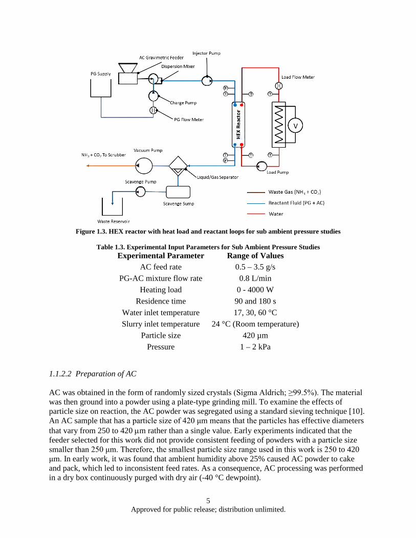
5 Approved for public release; distribution unlimited.
Figure 1.3. HEX reactor with heat load and reactant loops for sub ambient pressure studies
Table 1.3. Experimental Input Parameters for Sub Ambient Pressure Studies
Experimental Parameter Range of Values AC feed rate 0.5 – 3.5 g/s
PG-AC mixture flow rate 0.8 L/min Heating load 0 - 4000 W
Residence time 90 and 180 s Water inlet temperature 17, 30, 60 °C Slurry inlet temperature 24 °C (Room temperature)
Particle size 420 µm Pressure 1 – 2 kPa
1.1.2.2 Preparation of AC AC was obtained in the form of randomly sized crystals (Sigma Aldrich; ≥99.5%). The material was then ground into a powder using a plate-type grinding mill. To examine the effects of particle size on reaction, the AC powder was segregated using a standard sieving technique [10]. An AC sample that has a particle size of 420 μm means that the particles has effective diameters that vary from 250 to 420 µm rather than a single value. Early experiments indicated that the feeder selected for this work did not provide consistent feeding of powders with a particle size smaller than 250 μm. Therefore, the smallest particle size range used in this work is 250 to 420 μm. In early work, it was found that ambient humidity above 25% caused AC powder to cake and pack, which led to inconsistent feed rates. As a consequence, AC processing was performed in a dry box continuously purged with dry air (-40 °C dewpoint).
6 Approved for public release; distribution unlimited.
Since AC decomposition produces ammonia gas, the experiment was required to sequester ammonia for safe disposal. For sequestration, an ammonia scrubber (Advanced Air Technologies Apollo 50) was installed, and the exhaust from the experiment passed through the scrubber [6]. Additionally, laboratory atmospheric ammonia concentration was monitored.
1.1.3 Estimate of Endothermic Heat Absorption Rate and Conversion
The reported enthalpy of decomposition for pure AC in air has a wide range of values. For example, Clark and Hetherington [3] list a range of 1,700 to 1,900 J/g from 38 to 50 °C. Egan et al. [11] report a value of 2017 J/g over a temperature range of 35 °C to 83 °C. Similarly, Schmidt et al. [2] report a value of 2010 J/g from 20 °C to 100 °C. We used a value of 1800 J/g for the decomposition enthalpy over the temperature range investigated which is within the reported range. The chemical kinetics of AC decomposition are poorly understood. Moreover, the presence of a carrier liquid introduces additional complexities. Although desirable, an exact knowledge of the kinetics of AC decomposition in PG was not necessary to accomplish the objectives of the current work.
The heat transfer rate for each side of the HEX reactor was determined by applying heat balance calorimetry for steady flowing fluids during single-phase heat transfer (baseline) and decomposition segments of an experiment:
( )outinp TTcmq −= (1.2)
where steady state is defined as the period in which the water inlet temperature standard deviation was less than 0.5 °C during HEX reactor operation. The decomposition-based heat absorption rate qdecomp was estimated as the difference between the imbalances in the sensible heat transfer rates during decomposition and baseline as represented by: 𝑞𝑞𝑑𝑑𝑑𝑑𝑑𝑑𝑑𝑑𝑑𝑑𝑑𝑑 = 𝑞𝑞𝑤𝑤𝑤𝑤𝑤𝑤𝑑𝑑𝑤𝑤,𝑑𝑑𝑑𝑑𝑑𝑑𝑑𝑑𝑑𝑑𝑑𝑑 − 𝑞𝑞𝑤𝑤𝑑𝑑𝑤𝑤𝑑𝑑𝑤𝑤,𝑑𝑑𝑑𝑑𝑑𝑑𝑑𝑑𝑑𝑑𝑑𝑑 − (𝑞𝑞𝑤𝑤𝑤𝑤𝑤𝑤𝑑𝑑𝑤𝑤,𝑏𝑏𝑤𝑤𝑏𝑏𝑑𝑑𝑏𝑏𝑏𝑏𝑏𝑏𝑑𝑑 − 𝑞𝑞𝑤𝑤𝑑𝑑𝑤𝑤𝑑𝑑𝑤𝑤,𝑏𝑏𝑤𝑤𝑏𝑏𝑑𝑑𝑏𝑏𝑏𝑏𝑏𝑏𝑑𝑑) (1.3)
where qwater, baseline is the sensible heat transfer rate from the water to the PG (no AC decomposition), qreact, baseline the rate at which heat was absorbed sensibly by the PG, qwater,decomp the heat rate from the water to the slurry during AC decomposition, and qreact, decomp the rate at which heat was absorbed by the PG during decomposition. The second quantity in parentheses on the right-hand side of equation 1.3 provides an estimate of heat lost to the environment during the baseline segment of the experiments. It was assumed that heat losses during decomposition were of the same magnitude.
Conversion is generally defined as the mass (or number of moles) of products generated in a reactor relative to the quantity of reactant supplied. In this study, the mass (or moles) of reactant consumed or products evolved could not be determined directly. Thus, an alternate definition was used. Since the decomposition enthalpy is a function of the mass of AC consumed, we assumed that 1800 J of absorbed heat represents 1 g of reacted AC. Thus, conversion ε is expressed as measured heat absorption rate during decomposition divided by the product of the AC mass flow rate ṁAC and the decomposition enthalpy hrxn,

7 Approved for public release; distribution unlimited.
( ) 1−= rxnACdecomp hmq e (1.4) where hrxn is taken to be 1800 J/g. In addition, effective enthalpies are reported, in which the heat absorption rate due to decomposition is divided by the mass flow rate of AC. The effective enthalpy is an important consideration for comparing system cooling methods and for estimating AC supply requirements. For calorimetry and rheology calculations, PG data were taken from Sun and Teja [9] and AC data from reference [13]. Slurry properties were calculated using the method of Thomas [14].
1.1.4 Results and Discussion 1.1.4.1 Ambient Pressure Studies
In the ambient pressure studies, the reaction pressure of the AC/PG slurry was near the ambient while the temperature was varied with the residence time, AC concentration, and AC particle size. For a given experiment, the water inlet temperature was held constant, and heat absorption by endothermic dissociation of AC within the HEX reactor was determined by the reduction in the water outlet temperature (Equation 1.3).
Figure 1.4 shows measured water inlet and outlet temperatures for water inlet temperature held at 90 °C. The corresponding input variables were: AC mass flow rate 2.5 g/s, water mass flow rate 110 g/s; residence time 70 s; and slurry inlet temperature 53 °C. The steady operation period was achieved at 80 s and the steady-state measurement period was considered from 80 to 110 s, in which the average baseline-segment outlet temperature was 86.7 °C whereas the average decomposition-segment outlet temperature was 81.5 °C. The total steady-state, time-averaged heat transfer rate during decomposition, which includes contributions from both convection and the chemical reaction, was 3740 W as measured by heat balance calorimetry of the water flow. The AC decomposition increased the heat transfer rate above the baseline convection heat transfer rate by 2080 W. The total heat transfer rate from the water during AC decomposition was not a figure of merit in this study, but it is important for thermal management. This ability to continuously provide heat transfer demonstrates the feasibility of using the HEX reactor for continuous absorption of heat in a thermal management system.
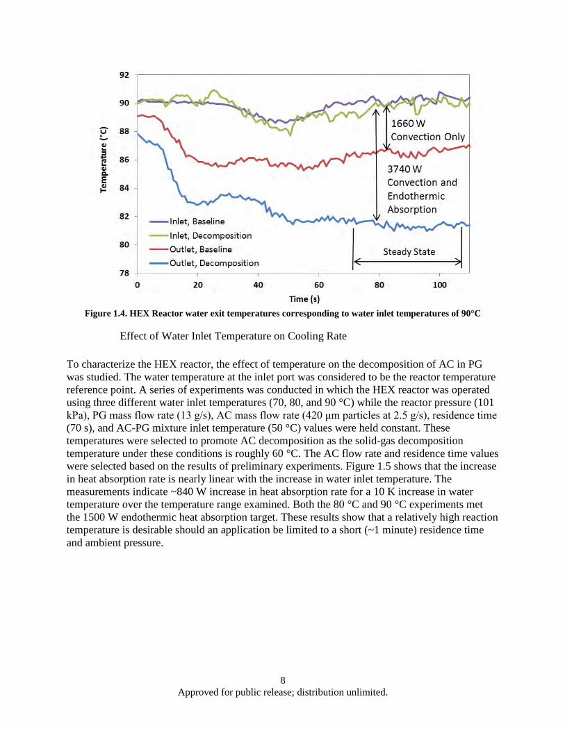
8 Approved for public release; distribution unlimited.
Figure 1.4. HEX Reactor water exit temperatures corresponding to water inlet temperatures of 90°C
Effect of Water Inlet Temperature on Cooling Rate
To characterize the HEX reactor, the effect of temperature on the decomposition of AC in PG was studied. The water temperature at the inlet port was considered to be the reactor temperature reference point. A series of experiments was conducted in which the HEX reactor was operated using three different water inlet temperatures (70, 80, and 90 °C) while the reactor pressure (101 kPa), PG mass flow rate (13 g/s), AC mass flow rate (420 μm particles at 2.5 g/s), residence time (70 s), and AC-PG mixture inlet temperature (50 °C) values were held constant. These temperatures were selected to promote AC decomposition as the solid-gas decomposition temperature under these conditions is roughly 60 °C. The AC flow rate and residence time values were selected based on the results of preliminary experiments. Figure 1.5 shows that the increase in heat absorption rate is nearly linear with the increase in water inlet temperature. The measurements indicate ~840 W increase in heat absorption rate for a 10 K increase in water temperature over the temperature range examined. Both the 80 °C and 90 °C experiments met the 1500 W endothermic heat absorption target. These results show that a relatively high reaction temperature is desirable should an application be limited to a short (~1 minute) residence time and ambient pressure.
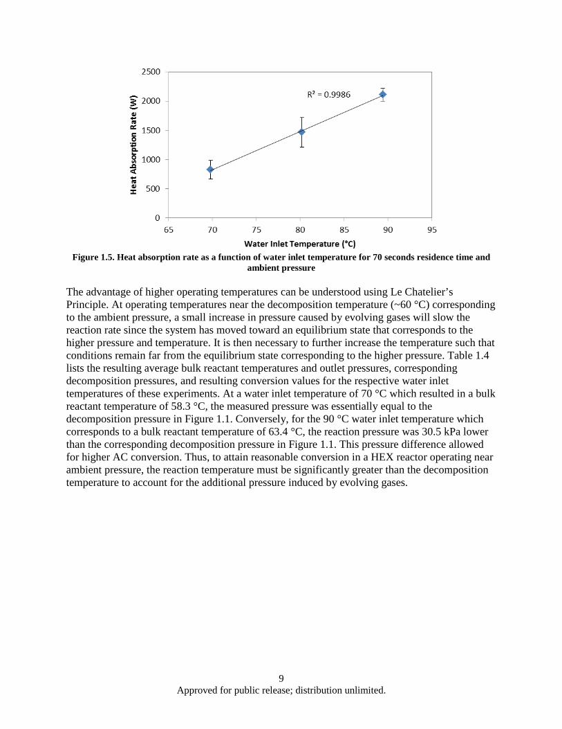
9 Approved for public release; distribution unlimited.
Figure 1.5. Heat absorption rate as a function of water inlet temperature for 70 seconds residence time and
ambient pressure
The advantage of higher operating temperatures can be understood using Le Chatelier’s Principle. At operating temperatures near the decomposition temperature (~60 °C) corresponding to the ambient pressure, a small increase in pressure caused by evolving gases will slow the reaction rate since the system has moved toward an equilibrium state that corresponds to the higher pressure and temperature. It is then necessary to further increase the temperature such that conditions remain far from the equilibrium state corresponding to the higher pressure. Table 1.4 lists the resulting average bulk reactant temperatures and outlet pressures, corresponding decomposition pressures, and resulting conversion values for the respective water inlet temperatures of these experiments. At a water inlet temperature of 70 °C which resulted in a bulk reactant temperature of 58.3 °C, the measured pressure was essentially equal to the decomposition pressure in Figure 1.1. Conversely, for the 90 °C water inlet temperature which corresponds to a bulk reactant temperature of 63.4 °C, the reaction pressure was 30.5 kPa lower than the corresponding decomposition pressure in Figure 1.1. This pressure difference allowed for higher AC conversion. Thus, to attain reasonable conversion in a HEX reactor operating near ambient pressure, the reaction temperature must be significantly greater than the decomposition temperature to account for the additional pressure induced by evolving gases.
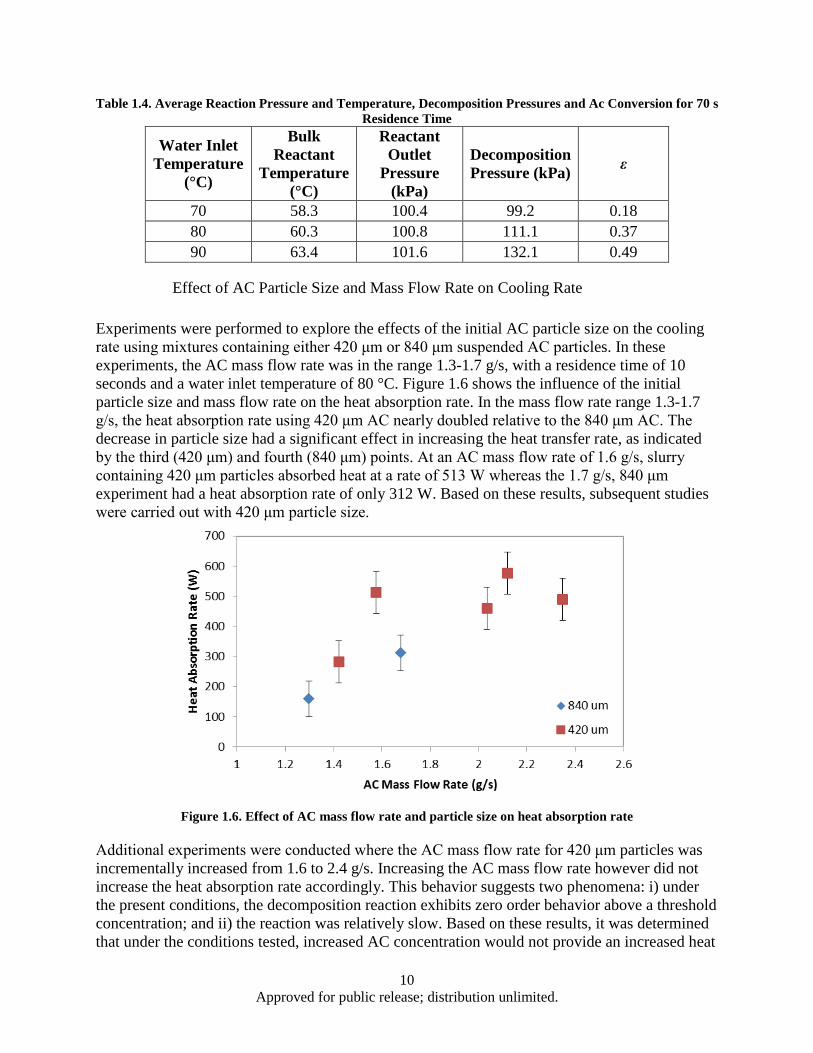
10 Approved for public release; distribution unlimited.
Table 1.4. Average Reaction Pressure and Temperature, Decomposition Pressures and Ac Conversion for 70 s Residence Time
Water Inlet Temperature
(°C)
Bulk Reactant
Temperature (°C)
Reactant Outlet
Pressure (kPa)
Decomposition Pressure (kPa) ε
70 58.3 100.4 99.2 0.18 80 60.3 100.8 111.1 0.37 90 63.4 101.6 132.1 0.49
Effect of AC Particle Size and Mass Flow Rate on Cooling Rate
Experiments were performed to explore the effects of the initial AC particle size on the cooling rate using mixtures containing either 420 μm or 840 μm suspended AC particles. In these experiments, the AC mass flow rate was in the range 1.3-1.7 g/s, with a residence time of 10 seconds and a water inlet temperature of 80 °C. Figure 1.6 shows the influence of the initial particle size and mass flow rate on the heat absorption rate. In the mass flow rate range 1.3-1.7 g/s, the heat absorption rate using 420 μm AC nearly doubled relative to the 840 μm AC. The decrease in particle size had a significant effect in increasing the heat transfer rate, as indicated by the third (420 μm) and fourth (840 μm) points. At an AC mass flow rate of 1.6 g/s, slurry containing 420 μm particles absorbed heat at a rate of 513 W whereas the 1.7 g/s, 840 μm experiment had a heat absorption rate of only 312 W. Based on these results, subsequent studies were carried out with 420 μm particle size.
Figure 1.6. Effect of AC mass flow rate and particle size on heat absorption rate
Additional experiments were conducted where the AC mass flow rate for 420 μm particles was incrementally increased from 1.6 to 2.4 g/s. Increasing the AC mass flow rate however did not increase the heat absorption rate accordingly. This behavior suggests two phenomena: i) under the present conditions, the decomposition reaction exhibits zero order behavior above a threshold concentration; and ii) the reaction was relatively slow. Based on these results, it was determined that under the conditions tested, increased AC concentration would not provide an increased heat

11 Approved for public release; distribution unlimited.
absorption rate, and the residence time needed to be significantly higher than 10 s to achieve the 50% AC conversion target.
Effect of Residence Time on Cooling Rate
The residence time was increased to 20 s and the results were compared with those from 10 s. This increase in residence time was accomplished by doubling the volume of the HEX reactor by adding plates while holding the inlet PG volumetric flow rate at 3 L/min. This change reduced the initial slurry Re from 9 (residence time of 10 s) to 4 at 20 s. For these Re, the flow was laminar. One 20 s experiment used a water inlet temperature of 80 °C, for purposes of comparison to the 10 s residence time experiments. The average heat absorption rate for a residence time of 10 s and AC mass flow rate between 1.5 – 2.4 g/s was 510 W. At 20 s for the same flow conditions, this increased to 668 W. Based on these results, it was clear that increased residence time was a path to increased conversion. However, 20 s was still insufficient to achieve the 50% conversion target (at 20 s, average ε = 0.18). Because the heat absorption rate did not improve sufficiently with 20 s residence time, the residence time was then increased to 70 s. This change was accomplished by reducing the PG flow rate as it was not practical to further increase the number of HEX reactor plates in the ambient-pressure study configuration. With this change, Re was reduced from roughly 4 to 1. The increase in residence time from 20 to 70 s resulted in an effective enthalpy of 666 J/g (average ε = 0.37) at 70 s.
Since increasing the residence time and reaction temperature both improved conversion, it is important to compare the relative effect of these two variables. Four experiments were conducted in which the residence time was either 20 s or 70 s. Also, the water inlet temperature was either 80 °C or 90 °C. Figure 1.7 shows the corresponding steady-state time-averaged endothermic heat absorption rates. Although the water inlet temperature was raised an additional 10 °C from the decomposition temperature for one of the 20 s cases, the resulting endothermic heat absorption rate increased by only 100 W. However, at 70 s residence time, increasing the water inlet temperature by 10 °C increased the heat absorption rate by 895 W. This is double the rate at the 20 s residence time. These results show that a 70 s residence time and 90 °C inlet water temperature lead to an effective decomposition enthalpy of 880 J/g, corresponding to a conversion of 0.49.
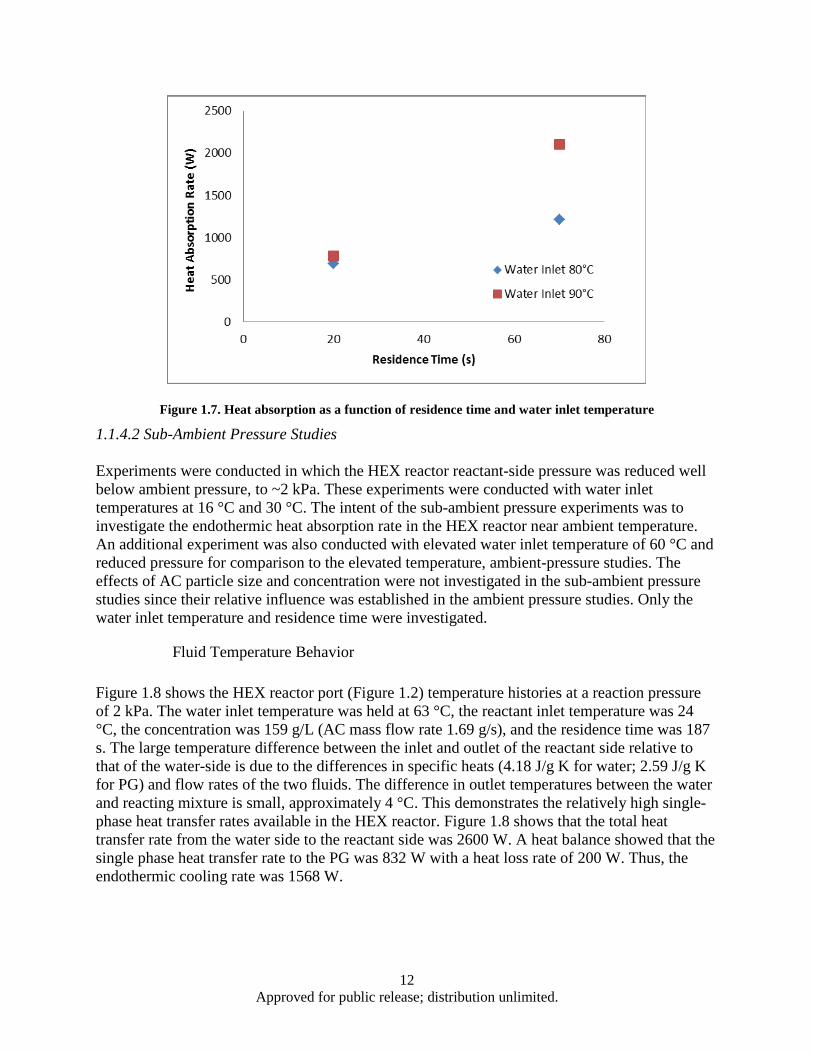
12 Approved for public release; distribution unlimited.
Figure 1.7. Heat absorption as a function of residence time and water inlet temperature
1.1.4.2 Sub-Ambient Pressure Studies
Experiments were conducted in which the HEX reactor reactant-side pressure was reduced well below ambient pressure, to ~2 kPa. These experiments were conducted with water inlet temperatures at 16 °C and 30 °C. The intent of the sub-ambient pressure experiments was to investigate the endothermic heat absorption rate in the HEX reactor near ambient temperature. An additional experiment was also conducted with elevated water inlet temperature of 60 °C and reduced pressure for comparison to the elevated temperature, ambient-pressure studies. The effects of AC particle size and concentration were not investigated in the sub-ambient pressure studies since their relative influence was established in the ambient pressure studies. Only the water inlet temperature and residence time were investigated.
Fluid Temperature Behavior
Figure 1.8 shows the HEX reactor port (Figure 1.2) temperature histories at a reaction pressure of 2 kPa. The water inlet temperature was held at 63 °C, the reactant inlet temperature was 24 °C, the concentration was 159 g/L (AC mass flow rate 1.69 g/s), and the residence time was 187 s. The large temperature difference between the inlet and outlet of the reactant side relative to that of the water-side is due to the differences in specific heats (4.18 J/g K for water; 2.59 J/g K for PG) and flow rates of the two fluids. The difference in outlet temperatures between the water and reacting mixture is small, approximately 4 °C. This demonstrates the relatively high single-phase heat transfer rates available in the HEX reactor. Figure 1.8 shows that the total heat transfer rate from the water side to the reactant side was 2600 W. A heat balance showed that the single phase heat transfer rate to the PG was 832 W with a heat loss rate of 200 W. Thus, the endothermic cooling rate was 1568 W.
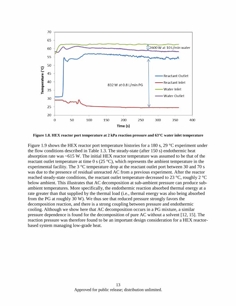
13 Approved for public release; distribution unlimited.
Figure 1.8. HEX reactor port temperature at 2 kPa reaction pressure and 63°C water inlet temperature
Figure 1.9 shows the HEX reactor port temperature histories for a 180 s, 29 °C experiment under the flow conditions described in Table 1.3. The steady-state (after 150 s) endothermic heat absorption rate was ~615 W. The initial HEX reactor temperature was assumed to be that of the reactant outlet temperature at time 0 s (25 °C), which represents the ambient temperature in the experimental facility. The 3 °C temperature drop at the reactant outlet port between 30 and 70 s was due to the presence of residual unreacted AC from a previous experiment. After the reactor reached steady-state conditions, the reactant outlet temperature decreased to 23 °C, roughly 2 °C below ambient. This illustrates that AC decomposition at sub-ambient pressure can produce sub-ambient temperatures. More specifically, the endothermic reaction absorbed thermal energy at a rate greater than that supplied by the thermal load (i.e., thermal energy was also being absorbed from the PG at roughly 30 W). We thus see that reduced pressure strongly favors the decomposition reaction, and there is a strong coupling between pressure and endothermic cooling. Although we show here that AC decomposition occurs in a PG mixture, a similar pressure dependence is found for the decomposition of pure AC without a solvent [12, 15]. The reaction pressure was therefore found to be an important design consideration for a HEX reactor-based system managing low-grade heat.
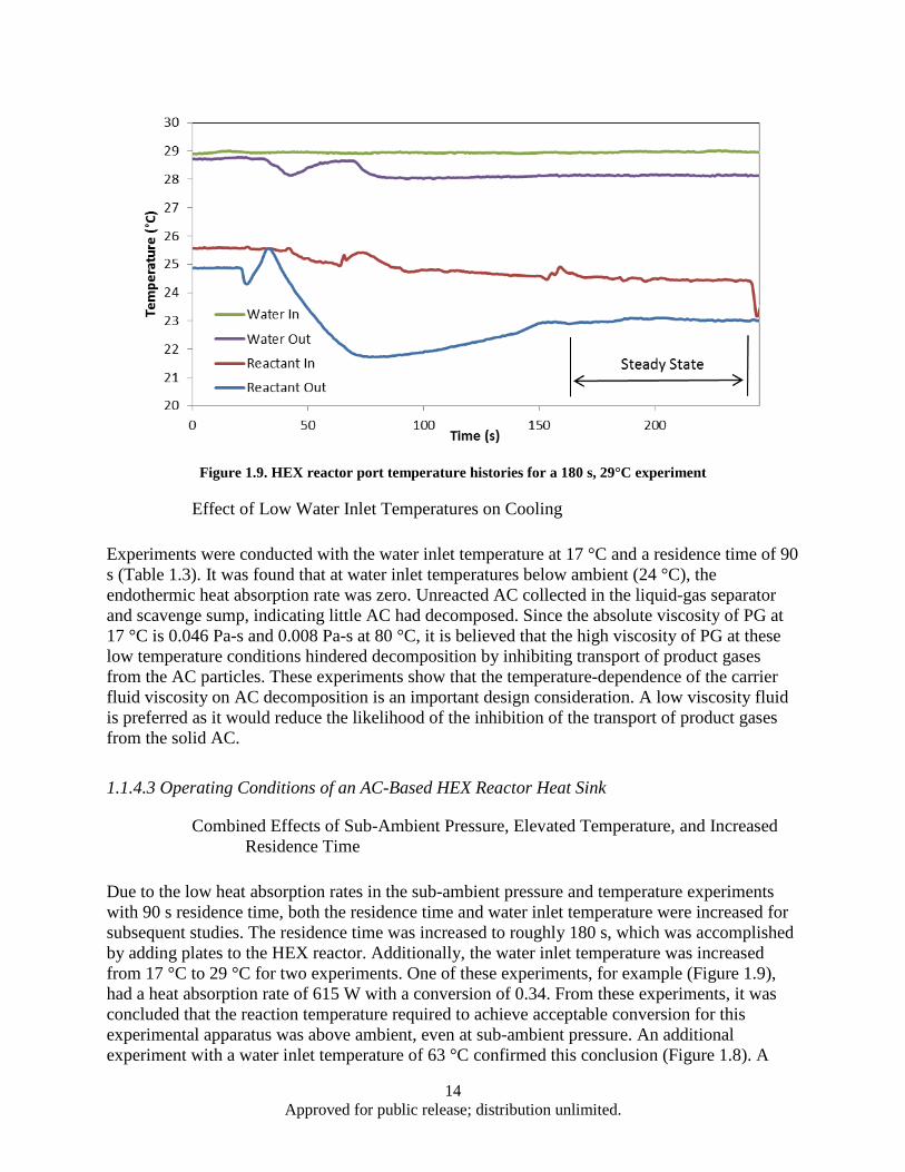
14 Approved for public release; distribution unlimited.
Figure 1.9. HEX reactor port temperature histories for a 180 s, 29°C experiment
Effect of Low Water Inlet Temperatures on Cooling
Experiments were conducted with the water inlet temperature at 17 °C and a residence time of 90 s (Table 1.3). It was found that at water inlet temperatures below ambient (24 °C), the endothermic heat absorption rate was zero. Unreacted AC collected in the liquid-gas separator and scavenge sump, indicating little AC had decomposed. Since the absolute viscosity of PG at 17 °C is 0.046 Pa-s and 0.008 Pa-s at 80 °C, it is believed that the high viscosity of PG at these low temperature conditions hindered decomposition by inhibiting transport of product gases from the AC particles. These experiments show that the temperature-dependence of the carrier fluid viscosity on AC decomposition is an important design consideration. A low viscosity fluid is preferred as it would reduce the likelihood of the inhibition of the transport of product gases from the solid AC.
1.1.4.3 Operating Conditions of an AC-Based HEX Reactor Heat Sink
Combined Effects of Sub-Ambient Pressure, Elevated Temperature, and Increased Residence Time
Due to the low heat absorption rates in the sub-ambient pressure and temperature experiments with 90 s residence time, both the residence time and water inlet temperature were increased for subsequent studies. The residence time was increased to roughly 180 s, which was accomplished by adding plates to the HEX reactor. Additionally, the water inlet temperature was increased from 17 °C to 29 °C for two experiments. One of these experiments, for example (Figure 1.9), had a heat absorption rate of 615 W with a conversion of 0.34. From these experiments, it was concluded that the reaction temperature required to achieve acceptable conversion for this experimental apparatus was above ambient, even at sub-ambient pressure. An additional experiment with a water inlet temperature of 63 °C confirmed this conclusion (Figure 1.8). A
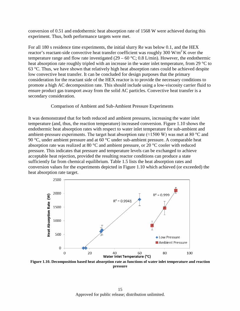
15 Approved for public release; distribution unlimited.
conversion of 0.51 and endothermic heat absorption rate of 1568 W were achieved during this experiment. Thus, both performance targets were met.
For all 180 s residence time experiments, the initial slurry Re was below 0.1, and the HEX reactor’s reactant-side convective heat transfer coefficient was roughly 300 W/m2 K over the temperature range and flow rate investigated (29 – 60 °C; 0.8 L/min). However, the endothermic heat absorption rate roughly tripled with an increase in the water inlet temperature, from 29 °C to 63 °C. Thus, we have shown that relatively high heat absorption rates could be achieved despite low convective heat transfer. It can be concluded for design purposes that the primary consideration for the reactant side of the HEX reactor is to provide the necessary conditions to promote a high AC decomposition rate. This should include using a low-viscosity carrier fluid to ensure product gas transport away from the solid AC particles. Convective heat transfer is a secondary consideration.
Comparison of Ambient and Sub-Ambient Pressure Experiments It was demonstrated that for both reduced and ambient pressures, increasing the water inlet temperature (and, thus, the reaction temperature) increased conversion. Figure 1.10 shows the endothermic heat absorption rates with respect to water inlet temperature for sub-ambient and ambient-pressure experiments. The target heat absorption rate (≈1500 W) was met at 80 °C and 90 °C, under ambient pressure and at 60 °C under sub-ambient pressure. A comparable heat absorption rate was realized at 80 °C and ambient pressure, or 20 °C cooler with reduced pressure. This indicates that pressure and temperature levels can be exchanged to achieve acceptable heat rejection, provided the resulting reactor conditions can produce a state sufficiently far from chemical equilibrium. Table 1.5 lists the heat absorption rates and conversion values for the experiments depicted in Figure 1.10 which achieved (or exceeded) the heat absorption rate target.
Figure 1.10. Decomposition based heat absorption rate as functions of water inlet temperature and reaction
pressure
16 Approved for public release; distribution unlimited.
Table 1.5. Heat Absorption Rate and Conversion as a Function of Water Inlet Temperature and Reactor Pressure
Water Inlet Temperature
(°C)
Reactant Outlet Pressure
(kPa)
Heat Absorption Rate (W)
ε
80 100.7 1464.5 0.4 89 101.6 2107.6 0.49 63 1.8 1567.6 0.51
Figure 1.10 and Table 1.5 show that acceptable conversion can be achieved by applying a sufficient quantity of energy which results in a temperature much higher than the decomposition temperature corresponding to the reactor pressure. It could then be assumed that temperatures well above the ambient-pressure decomposition temperature of 60 °C (e.g., 100 °C) would produce nearly complete conversion without requiring pressure reduction measures. However, high-enthalpy AC decomposition to NH3 and CO2 has an upper temperature limit. AC begins decomposing to urea and water as the temperature approaches 125 °C with significantly reduced decomposition enthalpy [16]. Another limitation exists, particularly for thermal loads which operate near ambient temperature. Vapor-compression system (VCS) temperature lift is typically used to achieve the desired elevated reaction temperature. VCS operating temperatures are limited to about 90 °C due to critical-point limits of common refrigerants. For example, the critical temperature of R134a is 101 °C [17]. Thus, an estimate of an upper temperature limit of 80 °C can be considered reasonable. Because of these limitations, it is desirable to operate an AC-based HEX reactor at or below 80 °C and reduced pressure to achieve acceptable conversion.
1.1.5 Summary It has been shown that the endothermic decomposition of AC in a HEX reactor can be used to remove low-grade heat from a thermal load. Five experimental parameters were investigated: reaction temperature and pressure, AC particle size and mass flow rate, and residence time. Of the five parameters considered, it was demonstrated that the residence time, reaction temperature, and reaction pressure are essential design considerations to achieve 50% conversion. The reaction exhibited zero order behavior at concentrations above 40 g/L, in that increasing AC concentration did not increase the reaction rate at a fixed reactor pressure, residence time, and temperature.
Conditions were selected to promote decomposition by using either high temperature or low pressure relative to an AC decomposition curve. Decomposition-based heat transfer rates up to 2100 W were demonstrated with a conversion of approximately 50%. It was shown that reduced reactor pressures provide more favorable conditions (higher conversion) for a given reaction temperature than do ambient pressures. Increasing pressures due to gas evolution in the reactor inhibited conversion. Thus, the sub-ambient-pressure reactions achieved comparable conversion at lower temperatures. In either case, to achieve acceptable conversion (~0.5) the reactor conditions had to be held far from pressures and temperatures near the decomposition curve. Temperatures or pressures near the decomposition curve produced poor conversion (~0.20).

17 Approved for public release; distribution unlimited.
The HEX reactor operating under conditions for AC reaction was shown to achieve a 58% improvement in heat transfer compared to single-phase convection without increasing the fluid flow rates or the size of the reactor. The demonstrated high heat transfer rates and continuous cooling show the potential for the HEX reactor to be used in aircraft thermal management system. Feasibility of such a system for managing low grade heat will be reported in a future study. Lastly, more details of this work are provided in [18].
18 Approved for public release; distribution unlimited.
Control Strategy for Operation of Aircraft Vapor Compression Systems 1.2
1.2.1 Introduction
Advanced, high-performance military aircraft have many thermal management challenges. One such challenge is the use of stealth technologies which may involve the use of composite radar-absorbing skins which have a low thermal conductivity [19]. Future aircraft may also carry directed energy weapons that could produce waste thermal energy at a rate of 1 MW or more. Another challenge for future advanced aircraft is the need for precise temperature control of multiple dissimilar loads that vary widely and rapidly. Aircraft applications also have sink temperatures which vary widely in a short period. With regard to high-performance aircraft, vapor compression system (VCS) architectures have been shown to offer higher coefficient of performance (COP) values and advantages in weight, cost, and volume relative to those of traditional air cycle systems [20, 21, 22]. However, the few existing airborne VCS primarily operate in a steady-state manner.
One challenge for the design of advanced military aircraft VCS controls is accommodating highly transient loads with large turndown ratios that are required for a rapidly changing environment. Many residential VCS, such as those found in home air conditioners or refrigerators/freezers, operate with an on-off control system where the compressor either runs at a constant speed or is off. Thus, the temperature is controlled by modulating the duty cycle. In these systems, it is desirable to provide peak cooling at the highest efficiency during the on periods, thus minimizing the operating time. Another architecture commonly used by refrigeration systems found in large supermarkets uses multiple parallel compressors, where additional compressors are engaged during peak load periods. Automotive VCS compressors provide capacity control with either variable displacement or variable speed. The majority of these VCS only control to one or two temperature set points.
There is a need for research and development of VCS for advanced aircraft. The INtegrated Vehicle ENergy Technology (INVENT) Program of the U.S. Air Force is developing technologies that will enable an energy optimized aircraft which has an adaptive thermal management system capable of responding to dynamic thermal loads, changing flight regimes, and available heat sinks to achieve the greatest platform-level performance [20, 22]. In support of the INVENT initiative, the Air Force Research Laboratory has constructed the Vapor Cycle System Research Facility (VCSRF) that is dedicated to the study and development of VCS control and operation. There is a desire for tight, precise control of the evaporator outlet superheat to prevent compressor damage while maintaining peak capacity. Precise control at low superheats can be problematic due to nonlinearities inherent in these systems, which can be further confounded by the presence of compressor lubrication oil [23, 24, 25]. Experimental work was performed in the VCSRF to study two control methods that potentially could be implemented on advanced aircraft. A goal was to compare the system performance of a traditional VCS control architecture to one that is cycle-based. Both control methods were tested using the same hypothetical scaled mission profiles and hardware configuration.
19 Approved for public release; distribution unlimited.
1.2.2 Experimental 1.2.2.1 Hardware Figure 1.11 is a schematic of the VCSRF which includes a condenser, two electronic expansion valves (EXVs), two evaporators, and a variable-speed screw compressor (Fairchild Controls Corporation) controlled by a Yaskawa A-1000 motor drive. Screw compressors are appropriate for aircraft because of their small weight and volume, insensitivity to adverse accelerations, ability to accommodate liquid ingestion, and high efficiency over a wide speed range [26]. The plate condenser has a maximum cooling capacity of 70 kW and is cooled by a glycol-water mixture flowing from a chiller (~60 kW maximum cooling capacity). The chiller outlet temperature and flow could be independently varied. The plate-fin counter-flow evaporators were identical, each with a maximum rated capacity of 18 kW. They were individually heated with oil (MIL-F-5606,) from two independently variable 12 kW inline heaters. In this work, two oil types were used: heat load oil and lubrication oil that is combined with the refrigerant. The term, oil, without lubrication in this report refers to the heat load oil. The EXVs (Emerson, EX-4) were independently open-loop controlled via stepper motor controllers (Allmotion EZ-Stepper, EZHR17EN).
Figure 1.11 also shows that liquid refrigerant (R-134a was used for these experiments) was injected upstream of the compressor to maintain the inlet superheat within the manufacturer’s recommended range. Panels 1 through 3 were not important for the present experiments and, thus, are omitted from Figure 1.11. The system charge was experimentally determined to provide adequate subcooling and was maintained at a constant 13.6 kg of R134a.
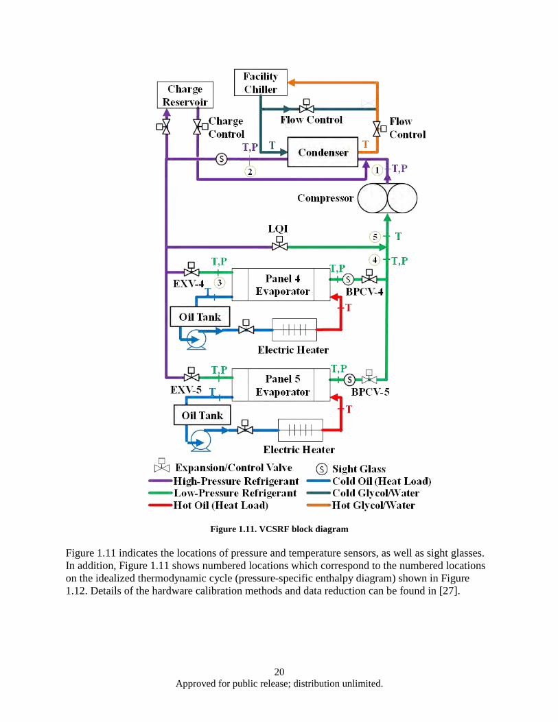
20 Approved for public release; distribution unlimited.
Figure 1.11. VCSRF block diagram Figure 1.11 indicates the locations of pressure and temperature sensors, as well as sight glasses. In addition, Figure 1.11 shows numbered locations which correspond to the numbered locations on the idealized thermodynamic cycle (pressure-specific enthalpy diagram) shown in Figure 1.12. Details of the hardware calibration methods and data reduction can be found in [27].
21 Approved for public release; distribution unlimited.
1.2.2.2 Software The VCSRF control was designed to be reconfigurable by consisting of selectable, independent PID controls for each of the fundamental control loops. LabVIEW .0 was used for all data acquisition and control. The primary goal of the VCS was to control the evaporators’ outlet oil temperatures. A detailed description of the VCSRF data acquisition and control software is given in [27].
1.2.2.3 Control Approach In this paper, Method A denotes the emulation of conventional superheat and capacity control. Method A used the EXVs to independently control the output ASH of each evaporator, emulating the operation of mechanical thermostatic expansion valves. For these experiments, the evaporator refrigerant outlet temperature was measured in the gas path. ASH was then calculated by subtracting the evaporator inlet refrigerant temperature, assuming the evaporator pressure drop was negligible [28]. For reference, the average refrigerant pressure drop across the evaporators was approximately 0.0059 MPa, which corresponds to ~0.4 °C change in the saturation temperature. Method A modulated the compressor speed to control the colder panel’s output oil temperature. This method also used BPCVs (on the evaporator with the greater oil temperature set point) to control that evaporator’s oil output temperature. In the current hardware setup, there were two active evaporators, which required one BPCV. Method A served as a benchmark for comparison.
Method B was a cycle-based control architecture that directly controlled both the high- and low-side pressures. The Method B approach was to maintain a constant head or pressure drop across the EXVs whenever possible. Method B paralleled the earlier work by [29], except PID loops were used here to improve the response to the rapidly changing, high turndown ratio loads. Method B differed from A in that B modulated the compressor speed to control the evaporator refrigerant outlet pressure common to both evaporators (measured at the compressor inlet); for the purposes of this paper this will be referred to as the saturated suction pressure (SSP). To set the desired SSP, the saturated suction temperature (SST) is first determined by subtracting a fixed temperature difference (driving temperature difference, dT) from the coldest evaporator’s set point temperature, To,low.
𝑺𝑺𝑺𝑺𝑺𝑺 = 𝑺𝑺𝒐𝒐,𝒍𝒍𝒐𝒐𝒘𝒘 − 𝒅𝒅𝑺𝑺 (1.5)
The resulting temperature was then translated to the corresponding saturation pressure of pure refrigerant (SSP). This transformation was approximated using REFPROP software [30]. Additionally for Method B, the EXVs were independently modulated to directly control the evaporator outlet oil temperatures. Method B eliminated the need for BPCVs. Method B did not control the value of ASH at the evaporator exit; it was allowed to fluctuate. To our knowledge, this work is the first to describe the implementation and performance of control Method B in an actual VCS hardware configuration.
In both Methods A and B, the condensing temperature/pressure (saturated discharge temperature (SDT)/saturated discharge pressure (SDP)) were controlled by modulating the condenser cooling
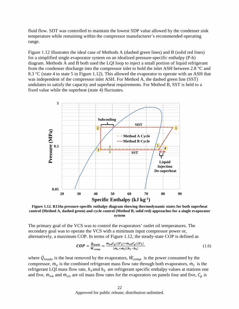
22 Approved for public release; distribution unlimited.
fluid flow. SDT was controlled to maintain the lowest SDP value allowed by the condenser sink temperature while remaining within the compressor manufacturer’s recommended operating range.
Figure 1.12 illustrates the ideal case of Methods A (dashed green lines) and B (solid red lines) for a simplified single evaporator system on an idealized pressure-specific enthalpy (P-h) diagram. Methods A and B both used the LQI loop to inject a small portion of liquid refrigerant from the condenser discharge into the compressor inlet to hold the inlet ASH between 2.8 °C and 8.3 °C (state 4 to state 5 in Figure 1.12). This allowed the evaporator to operate with an ASH that was independent of the compressor inlet ASH. For Method A, the dashed green line (SST) undulates to satisfy the capacity and superheat requirements. For Method B, SST is held to a fixed value while the superheat (state 4) fluctuates.
Figure 1.12. R134a pressure-specific enthalpy diagram showing thermodynamic states for both superheat
control (Method A, dashed green) and cycle control (Method B, solid red) approaches for a single evaporator system
The primary goal of the VCS was to control the evaporators’ outlet oil temperatures. The secondary goal was to operate the VCS with a minimum input compressor power or, alternatively, a maximum COP. In terms of Figure 1.12, the steady-state COP is defined as
𝑪𝑪𝑪𝑪𝑪𝑪 = 𝑸𝒍𝒍𝒐𝒐𝒍𝒍𝒅𝒅𝒍𝒍𝑾𝒄𝒄𝒐𝒐𝒄𝒄𝒄𝒄
= 𝒄𝒐𝒐𝒐𝒐𝑪𝑪𝒄𝒄(∆𝑺𝑺𝒐𝒐)+𝒄𝒐𝒐𝒐𝒐𝑪𝑪𝒄𝒄(∆𝑺𝑺𝒐𝒐) (𝒄𝒆𝒆+𝒄𝒍𝒍)(𝒉𝒉𝟏𝟏−𝒉𝒉𝒐𝒐) (1.6)
where 𝑄𝑏𝑏𝑑𝑑𝑤𝑤𝑑𝑑𝑏𝑏 is the heat removed by the evaporators, 𝑊𝑑𝑑𝑑𝑑𝑑𝑑𝑑𝑑 is the power consumed by the compressor, 𝑚𝑑𝑑 is the combined refrigerant mass flow rate through both evaporators, 𝑚𝑏𝑏 is the refrigerant LQI mass flow rate, ℎ1and ℎ5 are refrigerant specific enthalpy values at stations one and five, 𝑚𝑑𝑑4 and 𝑚𝑑𝑑5 are oil mass flow rates for the evaporators on panels four and five, 𝑁𝑁𝑑𝑑 is
0.05
0.5
5
20 30 40 50 60 70 80 90
Pres
sure
(MPa
)
Specific Enthalpy (kJ kg-1)
Method A CycleMethod B Cycle
1
543
2
Subcooling
Liquid Injection
De-superheat
SDT
SST
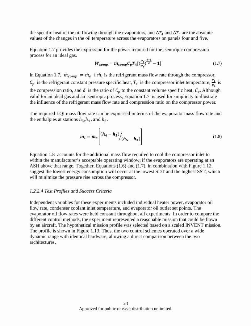
23 Approved for public release; distribution unlimited.
the specific heat of the oil flowing through the evaporators, and ∆𝑇𝑇4 and ∆𝑇𝑇5 are the absolute values of the changes in the oil temperature across the evaporators on panels four and five.
Equation 1.7 provides the expression for the power required for the isentropic compression process for an ideal gas.
𝑾𝒄𝒄𝒐𝒐𝒄𝒄𝒄𝒄 = 𝒄𝒄𝒄𝒐𝒐𝒄𝒄𝒄𝒄𝑪𝑪𝒄𝒄𝑺𝑺𝒐𝒐[(𝑪𝑪𝟏𝟏𝑪𝑪𝒐𝒐
)𝜹𝜹−𝟏𝟏𝜹𝜹 − 𝟏𝟏] (1.7)
In Equation 1.7, 𝑚𝑑𝑑𝑑𝑑𝑑𝑑𝑑𝑑 = 𝑚𝑑𝑑 + 𝑚𝑏𝑏 is the refrigerant mass flow rate through the compressor, 𝑁𝑁𝑑𝑑 is the refrigerant constant pressure specific heat, 𝑇𝑇4 is the compressor inlet temperature, 𝑃𝑃1
𝑃𝑃4 is
the compression ratio, and 𝛿𝛿 is the ratio of 𝑁𝑁𝑑𝑑 to the constant volume specific heat, 𝑁𝑁𝑣𝑣. Although valid for an ideal gas and an isentropic process, Equation 1.7 is used for simplicity to illustrate the influence of the refrigerant mass flow rate and compression ratio on the compressor power.
The required LQI mass flow rate can be expressed in terms of the evaporator mass flow rate and the enthalpies at stations ℎ3,ℎ4 , and ℎ5.
𝒄𝒍𝒍 = 𝒄𝒆𝒆 (𝒉𝒉𝒐𝒐 − 𝒉𝒉𝒐𝒐)
(𝒉𝒉𝒐𝒐 − 𝒉𝒉𝟑𝟑) (1.8)
Equation 1.8 accounts for the additional mass flow required to cool the compressor inlet to within the manufacturer’s acceptable operating window, if the evaporators are operating at an ASH above that range. Together, Equations (1.6) and (1.7), in combination with Figure 1.12, suggest the lowest energy consumption will occur at the lowest SDT and the highest SST, which will minimize the pressure rise across the compressor.
1.2.2.4 Test Profiles and Success Criteria Independent variables for these experiments included individual heater power, evaporator oil flow rate, condenser coolant inlet temperature, and evaporator oil outlet set points. The evaporator oil flow rates were held constant throughout all experiments. In order to compare the different control methods, the experiment represented a reasonable mission that could be flown by an aircraft. The hypothetical mission profile was selected based on a scaled INVENT mission. The profile is shown in Figure 1.13. Thus, the two control schemes operated over a wide dynamic range with identical hardware, allowing a direct comparison between the two architectures.
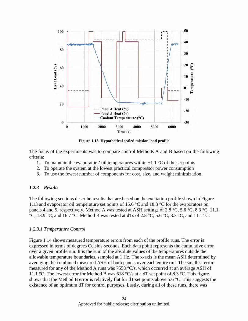
24 Approved for public release; distribution unlimited.
Figure 1.13. Hypothetical scaled mission load profile The focus of the experiments was to compare control Methods A and B based on the following criteria:
1. To maintain the evaporators’ oil temperatures within ±1.1 °C of the set points 2. To operate the system at the lowest practical compressor power consumption 3. To use the fewest number of components for cost, size, and weight minimization
1.2.3 Results The following sections describe results that are based on the excitation profile shown in Figure 1.13 and evaporator oil temperature set points of 15.6 °C and 18.3 °C for the evaporators on panels 4 and 5, respectively. Method A was tested at ASH settings of 2.8 °C, 5.6 °C, 8.3 °C, 11.1 °C, 13.9 °C, and 16.7 °C. Method B was tested at dTs of 2.8 °C, 5.6 °C, 8.3 °C, and 11.1 °C.
1.2.3.1 Temperature Control Figure 1.14 shows measured temperature errors from each of the profile runs. The error is expressed in terms of degrees Celsius-seconds. Each data point represents the cumulative error over a given profile run. It is the sum of the absolute values of the temperatures outside the allowable temperature boundaries, sampled at 1 Hz. The x-axis is the mean ASH determined by averaging the combined measured ASH of both panels over each entire run. The smallest error measured for any of the Method A runs was 7558 °C/s, which occurred at an average ASH of 11.1 °C. The lowest error for Method B was 618 °C/s at a dT set point of 8.3 °C. This figure shows that the Method B error is relatively flat for dT set points above 5.6 °C. This suggests the existence of an optimum dT for control purposes. Lastly, during all of these runs, there was
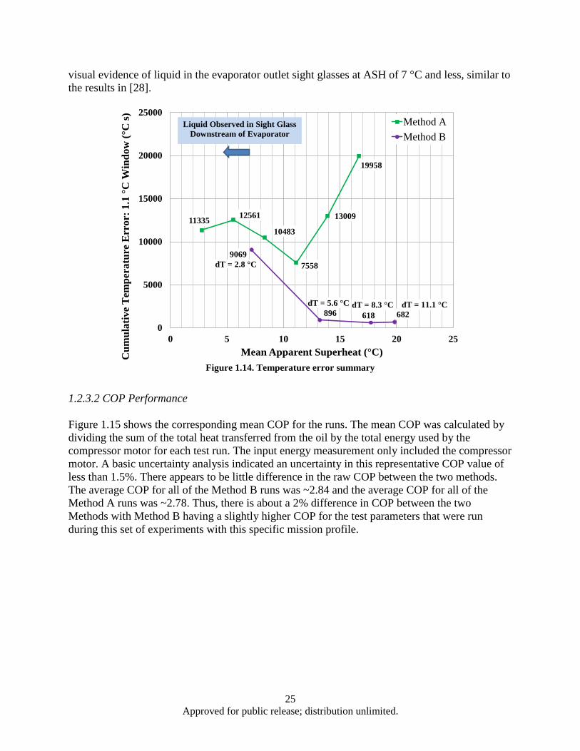
25 Approved for public release; distribution unlimited.
visual evidence of liquid in the evaporator outlet sight glasses at ASH of 7 °C and less, similar to the results in [28].
Figure 1.14. Temperature error summary
1.2.3.2 COP Performance Figure 1.15 shows the corresponding mean COP for the runs. The mean COP was calculated by dividing the sum of the total heat transferred from the oil by the total energy used by the compressor motor for each test run. The input energy measurement only included the compressor motor. A basic uncertainty analysis indicated an uncertainty in this representative COP value of less than 1.5%. There appears to be little difference in the raw COP between the two methods. The average COP for all of the Method B runs was ~2.84 and the average COP for all of the Method A runs was ~2.78. Thus, there is about a 2% difference in COP between the two Methods with Method B having a slightly higher COP for the test parameters that were run during this set of experiments with this specific mission profile.
19958
13009
7558
10483
1256111335
682618896
9069
0
5000
10000
15000
20000
25000
0 5 10 15 20 25Mean Apparent Superheat (°C)
Method AMethod B
dT = 5.6 °C dT = 11.1 °CdT = 8.3 °C
dT = 2.8 °C
Liquid Observed in Sight Glass Downstream of Evaporator
Cum
ulat
ive
Tem
pera
ture
Err
or: 1
.1 °C
Win
dow
(°C
s)
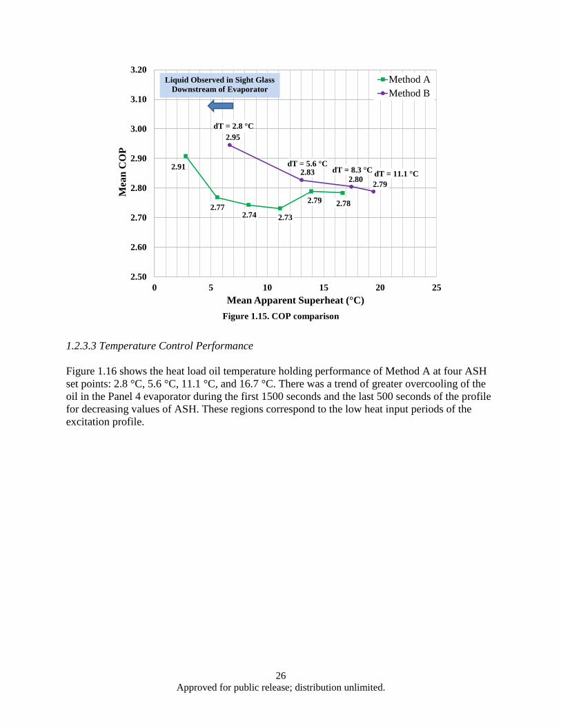
26 Approved for public release; distribution unlimited.
Figure 1.15. COP comparison
1.2.3.3 Temperature Control Performance Figure 1.16 shows the heat load oil temperature holding performance of Method A at four ASH set points: 2.8 °C, 5.6 °C, 11.1 °C, and 16.7 °C. There was a trend of greater overcooling of the oil in the Panel 4 evaporator during the first 1500 seconds and the last 500 seconds of the profile for decreasing values of ASH. These regions correspond to the low heat input periods of the excitation profile.
2.782.79
2.732.742.77
2.91
2.792.802.83
2.95
2.50
2.60
2.70
2.80
2.90
3.00
3.10
3.20
0 5 10 15 20 25
Mea
n C
OP
Mean Apparent Superheat (°C)
Method AMethod B
dT = 11.1 °CdT = 8.3 °CdT = 5.6 °C
dT = 2.8 °C
Liquid Observed in Sight Glass Downstream of Evaporator
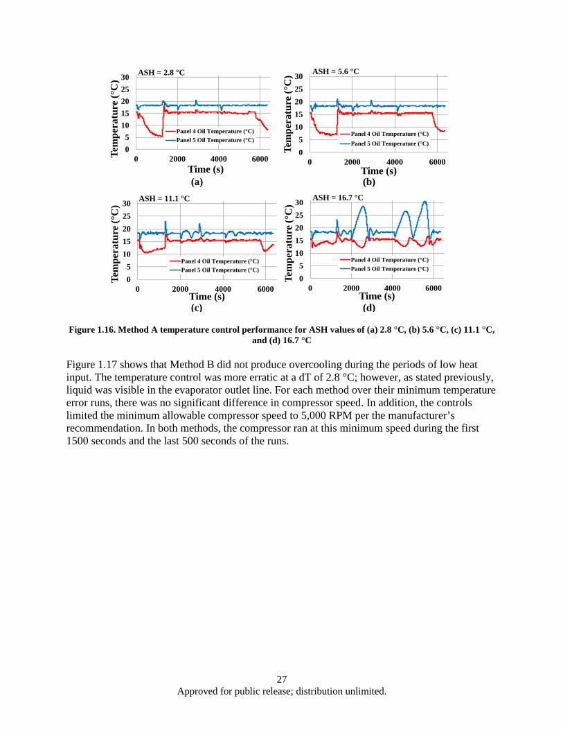
27 Approved for public release; distribution unlimited.
Figure 1.16. Method A temperature control performance for ASH values of (a) 2.8 °C, (b) 5.6 °C, (c) 11.1 °C, and (d) 16.7 °C
Figure 1.17 shows that Method B did not produce overcooling during the periods of low heat input. The temperature control was more erratic at a dT of 2.8 °C; however, as stated previously, liquid was visible in the evaporator outlet line. For each method over their minimum temperature error runs, there was no significant difference in compressor speed. In addition, the controls limited the minimum allowable compressor speed to 5,000 RPM per the manufacturer’s recommendation. In both methods, the compressor ran at this minimum speed during the first 1500 seconds and the last 500 seconds of the runs.
05
1015202530
0 2000 4000 6000
Tem
pera
ture
(°C
)
Time (s)
Panel 4 Oil Temperature (°C)Panel 5 Oil Temperature (°C)
ASH = 11.1 °C
05
1015202530
0 2000 4000 6000Tem
pera
ture
(°C
)
Time (s)
Panel 4 Oil Temperature (°C)Panel 5 Oil Temperature (°C)
ASH = 2.8 °C
05
1015202530
0 2000 4000 6000Te
mpe
ratu
re (°
C)
Time (s)
Panel 4 Oil Temperature (°C)Panel 5 Oil Temperature (°C)
ASH = 16.7 °C
(a) (b)
(c) (d)
05
1015202530
0 2000 4000 6000
Tem
pera
ture
(°C
)
Time (s)
Panel 4 Oil Temperature (°C)Panel 5 Oil Temperature (°C)
ASH = 5.6 °C
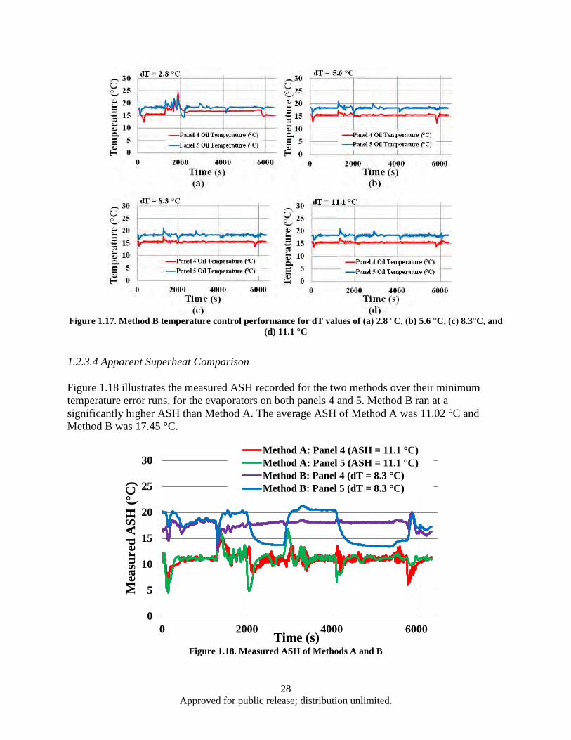
28 Approved for public release; distribution unlimited.
Figure 1.17. Method B temperature control performance for dT values of (a) 2.8 °C, (b) 5.6 °C, (c) 8.3°C, and
(d) 11.1 °C
1.2.3.4 Apparent Superheat Comparison Figure 1.18 illustrates the measured ASH recorded for the two methods over their minimum temperature error runs, for the evaporators on both panels 4 and 5. Method B ran at a significantly higher ASH than Method A. The average ASH of Method A was 11.02 °C and Method B was 17.45 °C.
Figure 1.18. Measured ASH of Methods A and B
0
5
10
15
20
25
30
0 2000 4000 6000Time (s)
Method A: Panel 4 (ASH = 11.1 °C)Method A: Panel 5 (ASH = 11.1 °C)Method B: Panel 4 (dT = 8.3 °C)Method B: Panel 5 (dT = 8.3 °C)
Mea
sure
d A
SH(°
C)
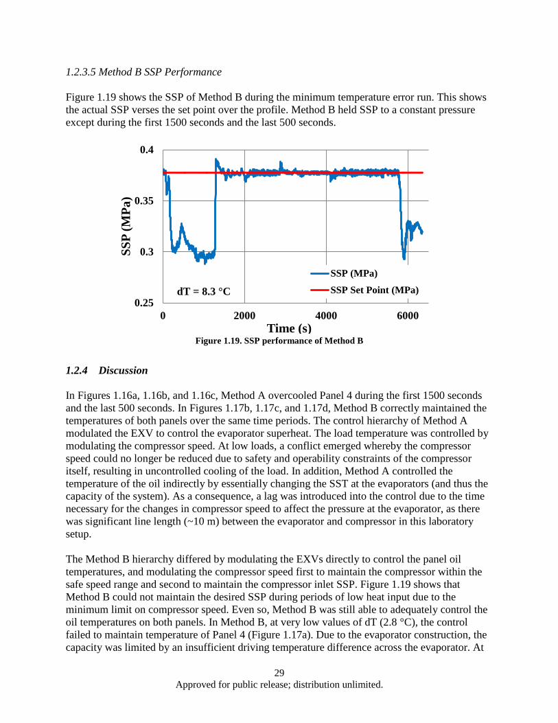
29 Approved for public release; distribution unlimited.
1.2.3.5 Method B SSP Performance Figure 1.19 shows the SSP of Method B during the minimum temperature error run. This shows the actual SSP verses the set point over the profile. Method B held SSP to a constant pressure except during the first 1500 seconds and the last 500 seconds.
Figure 1.19. SSP performance of Method B
1.2.4 Discussion In Figures 1.16a, 1.16b, and 1.16c, Method A overcooled Panel 4 during the first 1500 seconds and the last 500 seconds. In Figures 1.17b, 1.17c, and 1.17d, Method B correctly maintained the temperatures of both panels over the same time periods. The control hierarchy of Method A modulated the EXV to control the evaporator superheat. The load temperature was controlled by modulating the compressor speed. At low loads, a conflict emerged whereby the compressor speed could no longer be reduced due to safety and operability constraints of the compressor itself, resulting in uncontrolled cooling of the load. In addition, Method A controlled the temperature of the oil indirectly by essentially changing the SST at the evaporators (and thus the capacity of the system). As a consequence, a lag was introduced into the control due to the time necessary for the changes in compressor speed to affect the pressure at the evaporator, as there was significant line length (~10 m) between the evaporator and compressor in this laboratory setup. The Method B hierarchy differed by modulating the EXVs directly to control the panel oil temperatures, and modulating the compressor speed first to maintain the compressor within the safe speed range and second to maintain the compressor inlet SSP. Figure 1.19 shows that Method B could not maintain the desired SSP during periods of low heat input due to the minimum limit on compressor speed. Even so, Method B was still able to adequately control the oil temperatures on both panels. In Method B, at very low values of dT (2.8 °C), the control failed to maintain temperature of Panel 4 (Figure 1.17a). Due to the evaporator construction, the capacity was limited by an insufficient driving temperature difference across the evaporator. At
0.25
0.3
0.35
0.4
0 2000 4000 6000
SSP
(MPa
)
Time (s)
SSP (MPa)
SSP Set Point (MPa)dT = 8.3 °C
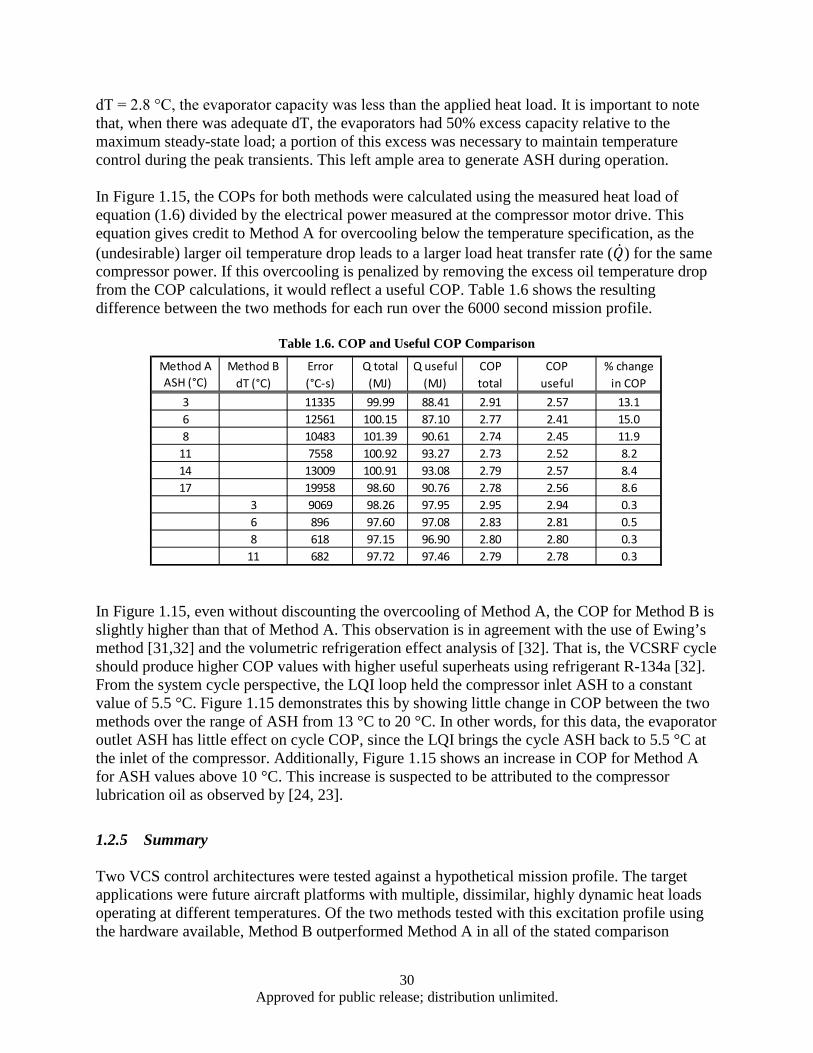
30 Approved for public release; distribution unlimited.
dT = 2.8 °C, the evaporator capacity was less than the applied heat load. It is important to note that, when there was adequate dT, the evaporators had 50% excess capacity relative to the maximum steady-state load; a portion of this excess was necessary to maintain temperature control during the peak transients. This left ample area to generate ASH during operation. In Figure 1.15, the COPs for both methods were calculated using the measured heat load of equation (1.6) divided by the electrical power measured at the compressor motor drive. This equation gives credit to Method A for overcooling below the temperature specification, as the (undesirable) larger oil temperature drop leads to a larger load heat transfer rate (𝑄) for the same compressor power. If this overcooling is penalized by removing the excess oil temperature drop from the COP calculations, it would reflect a useful COP. Table 1.6 shows the resulting difference between the two methods for each run over the 6000 second mission profile.
Table 1.6. COP and Useful COP Comparison
In Figure 1.15, even without discounting the overcooling of Method A, the COP for Method B is slightly higher than that of Method A. This observation is in agreement with the use of Ewing’s method [31,32] and the volumetric refrigeration effect analysis of [32]. That is, the VCSRF cycle should produce higher COP values with higher useful superheats using refrigerant R-134a [32]. From the system cycle perspective, the LQI loop held the compressor inlet ASH to a constant value of 5.5 °C. Figure 1.15 demonstrates this by showing little change in COP between the two methods over the range of ASH from 13 °C to 20 °C. In other words, for this data, the evaporator outlet ASH has little effect on cycle COP, since the LQI brings the cycle ASH back to 5.5 °C at the inlet of the compressor. Additionally, Figure 1.15 shows an increase in COP for Method A for ASH values above 10 °C. This increase is suspected to be attributed to the compressor lubrication oil as observed by [24, 23].
1.2.5 Summary Two VCS control architectures were tested against a hypothetical mission profile. The target applications were future aircraft platforms with multiple, dissimilar, highly dynamic heat loads operating at different temperatures. Of the two methods tested with this excitation profile using the hardware available, Method B outperformed Method A in all of the stated comparison
Method A Method B Error Q total Q useful COP COP % changeASH (°C) dT (°C) (°C-s) (MJ) (MJ) total useful in COP
3 11335 99.99 88.41 2.91 2.57 13.16 12561 100.15 87.10 2.77 2.41 15.08 10483 101.39 90.61 2.74 2.45 11.9
11 7558 100.92 93.27 2.73 2.52 8.214 13009 100.91 93.08 2.79 2.57 8.417 19958 98.60 90.76 2.78 2.56 8.6
3 9069 98.26 97.95 2.95 2.94 0.36 896 97.60 97.08 2.83 2.81 0.58 618 97.15 96.90 2.80 2.80 0.3
11 682 97.72 97.46 2.79 2.78 0.3

31 Approved for public release; distribution unlimited.
metrics. Method B offered significantly better temperature control performance for the profile examined. The COP of Method B was only slightly better than that of Method A. However, if the overcooling produced by Method A is penalized, the useful COP of Method A would be meaningfully lower. Finally, because Method B does not require any BPCVs for controlling the loads to different temperatures (within reason, as the SST of the refrigerant is the same for all loads), the part count for a system controlled by Method B could be smaller than a Method A system. This would improve both the weight and reliability of such a system to be used for aircraft thermal management. Additional details of this work may be found in [33].
32 Approved for public release; distribution unlimited.
Solid-state Electrolyte Lithium-ion Batteries Based on Phthalocyanines 2.
Introduction 2.1
The trend toward energy optimized aircraft and rapid technology advances in space and portable ground-based devices have created a need for higher specific power and higher specific energy density storage systems. The present requirement for energy storage devices is for a specific energy density of 150 Whr/Kg, specific power of 300 W/Kg, and cycle life exceeding 1,000 cycles at 100% depth of discharge. Other considerations for an advanced battery are increased reliability, maintenance-free operation, environmental compatibility and an expanded operating temperature range of –40 to > +60 ºC. Although there is no ideal battery for all applications, the development of a solid-state, single-ion conducting electrolyte for rechargeable lithium-ion batteries has the potential of exceeding the specific energy, specific power, storage/cycle life, and temperature requirements of the Air Force. Several issues must first be addressed, however, in order to successfully utilize a solid-state single-ion conducting electrolyte. The first issue involves determining what form or phase of the material offers the most promising qualities and how to consistently produce it. A second issue is the compatibility of the solid electrolyte with the anode and cathode from an electrochemical and mechanical standpoint. The anode, electrolyte, and cathode, all being solid materials, create a large interfacial resistance or connectivity problem. This problem may be overcome through the development of new free-standing thin-film techniques or improved fabrication techniques that will produce intimate solid-particle contact. A third concern is that the majority of present composite cathodes have been developed and optimized for liquid, gel, or polymer electrolytes; that is, these cathode formulas may not be optimal for solid electrolytes and will require parallel study with a chosen material. Dilithium phthalocyanine (Li2Pc) is a possible candidate for a solid-state single-ion conducting electrolyte. By the process of molecular self-assembly between Li2Pc molecules, an ion conducting channel is formed that creates a low energy of activation pathway for lithium-ion transport [34, 35]. Unfortunately, experimental results suggest that, besides being a lithium-ion conductor, Li2Pc is also an electronic conductor. Thus, in addition to the general concerns mentioned above, in order to successfully utilize the ionic conducting properties of Li2Pc, focus must also be directed toward two options: developing and characterizing insulating films that can be placed adjacent to the Li2Pc in an attempt to block the intrinsic electronic pathway of the material, or modifying the Li2Pc structure itself to make it intrinsically insulating. In recent years, significant progress has been made through modification of the Li2Pc structure. A new class of possible solid-state electrolyte materials was developed which inhibits electronic conduction while still maintaining the high ionic conductivity characteristics of Li2Pc [36]. Critical to the success of these “hybrid” materials will be the development of a process or processes that result in highly-organized thin film molecular structures integrated into lithium-ion battery configurations.
Experimental 2.2
This effort required step-by-step evaluation of each component of an electrochemical cell and understanding interactions at the respective interfaces. Laboratory presses, balances, and other
33 Approved for public release; distribution unlimited.
standard lab equipment were utilized. Due to the reactivity of the materials which were investigated, this study also involved the use of inert and controlled environments such as fume hoods, dry boxes, and dry rooms. Analytical instruments capable of alternative current (AC) impedance measurements, cyclic voltammetry, chronopotentiometry, chronoamperometry, and chronocoulometry were used to characterize and evaluate prospective materials and electrochemical cells. Environmental chambers were used to evaluate the effects of temperature on full cells and individual components. Various casting techniques were employed in an attempt to deposit/form thin films of cell components. Surface morphology of the various layers was monitored with optical microscopy and scanning electron microscopy (SEM). Film composition was monitored with energy-dispersive X-ray spectroscopy (EDX) and X-ray diffraction (XRD). Thermal properties were determined via thermo gravimetric analysis (TGA) and differential scanning calorimetry (DSC).
2.2.1 Phthalocyanine Synthesis
The bulk phthalocyanine (Pc) starting materials used in this study were purchased from Sigma Aldrich or a similar chemical supplier. The Pc derivatives were synthesized, purified, and recrystallized by Wright State University (WSU). In general, upon receipt from WSU, samples of these derivatives were dried through a temperature regime under vacuum to remove any residual solvents from the recrystallization process. After adequate drying, the materials would be ground, placed in a die, compressed via a hydraulic press to form a pellet, and assembled into a symmetrical cell for evaluation/characterization. Test results were compiled and compared to determine which materials and synthesis procedures/conditions produced the best product.
2.2.2 Thin Film Processing
Though pressed pellets are useful for determining bulk electrochemical properties, the impedances tend to be much too high for practical use. Hence, thin film versions of the materials are ideal. Traditional hand casting techniques such as slurry, melt, spin and solution casting were used to with varying degrees of success to form the films. To improve film quality and consistency, a hobbyist level airbrush kit was modified, and a technique was developed to spray cast the various materials onto substrates of interest.
2.2.3 Pc-based Cathode Development
In the process of developing the new class of solid-state electrolyte materials, several Pc-based hybrid materials were created, which failed as electrolytes but instead behaved as cathodes. Since these cathodic Pc derivatives utilize the same low energy of activation pathway for lithium-ion transport as the electrolyte hybrids, the interface between the electrolyte and cathode could essentially become seamless. In order to obtain high capacities and rates; however, it is important to ensure proper electrical conduction through the cathode. This is especially true when using the electrically insulating cathodic hybrid materials. Graphene or some other highly conductive form of carbon needed to be included in the cathode formulation. Hence, focus was also directed toward integrating the cathodic hybrids as well as metallic Pcs such as CuPc, NiPc and FePc into commercially available carbon nanotube paper (CNTP). In general, these Pc:CNTP cathodes would first be tested in coin cell configurations with either ionic liquids, non-aqueous electrolytes, or PEO membranes and Li metal to determine capacities. Testing would then be conducted with Pc-based electrolytes.
34 Approved for public release; distribution unlimited.
2.2.4 Anodes
Lithium metal foil was the anode material of choice for this study. In some cases, however, a lithium composite anode was a more suitable option. The lithium composite anode takes advantage of the inherent reactivity of Li metal and Li2Pc. Namely, the charge carriers are preloaded into the molecular lattice of the material to form a simple anode with the same lithium-ion conductive pathway as the electrolyte and phthalocyanine-based cathode. Furthermore, the composite anode may eliminate the flammability concerns associated with lithium metal, with little reduction in potential difference between the anode and cathode.
Results and Discussion 2.3
2.3.1 CNTP cathodes
As stated above, ensuring adequate electronic conductivity is necessary to obtain meaningful charge/discharge rates and to utilize the inherent capacities of the Pc materials. In-house efforts to include graphene and/or nanotubes into the cathode formulation tended to yield inconsistent results. Contact was made with Inorganic Specialists, Inc., a local company that specializes in the fabrication of CNTP and its use in custom applications. After a CRADA agreement was established, Inorganic Specialists began assisting with the development of Pc-based cathodes.
As a starting point it was suggested that efforts be directed toward integrating Li2Pc into CNTP. Shortly after, a prototype CNTP cathode was received from Inorganic Specialists, Inc., which contained ~25 wt% Li2Pc or ~2 mg. The active material had been wicked out of NMP into the CNTP using a proprietary method. Several coin cells were assembled comprised of sections of the cathode, PyP-14 based ionic liquid electrolyte and Li metal anodes. One was assembled in the argon glove box and one in the dry room. A third cell was later assembled in the dry room, but PyP-14 was pulled into the cathode prior to cell assembly via a custom vacuum fixture. The glove box, dry room, and vacuum cell all had reasonable total impedances of 187, 104, and 85 Ω, respectively. The highest discharge capacity at room temperature was around 65 mAh/g (50 µA), from the glove box cell. The capacities for the other two cells were lower but on the same order of magnitude. Though less than expected, the capacities were roughly double those corresponding to Li2Pc:CNTP cathodes formed using in-house via wicking techniques.
At this point, it was thought that it might be the ionic liquid rather than the cathodes that was limiting the cell capacities. Hence, it was decided to use DME: PC (1:1): 1 M LiBF4 non-aqueous electrolyte in the coin cells instead. As a comparison, another coin cell was assembled with the Inorganic Specialists Li2Pc:CNTP cathode. After allowing it to equilibrate at room temperature (open circuit voltage, OCV, 3.18 V), the cell was discharged at 100 µA down to 1.5 V. The discharge lasted 53,539 seconds, resulting in a capacity of 740 mAh/g. Following the discharge, the cell was charged using a constant current of 100 µA to 3.5 V, which lasted 11,251 seconds. The cell was then discharged once more at 100 µA, and once at 500 µA, yielding capacities of 458 mAh/g and 162.5 mAh/g, respectively. Between discharges, the impedance pattern remained relatively stable. After the discharges, the cell temperature was raised to 75 °C in order to observe any adverse reactions. At elevated temperature overnight, the impedance remained very stable. Finally, cyclic voltammetry was performed from OCV to 3.5 V, to 1.5 V then back to OCV. The impedance pattern before and after the CV were very similar.
35 Approved for public release; distribution unlimited.
A coin cell was assembled comprised of ~18.2 wt% BAI-LiPc (1.2 mg) loaded CNTP from Inorganic Specialists, non-aqueous electrolyte (LiBF4 in DME:gamma-butyrolactone) and Li metal. The OCV upon assembly was 2.85 V. The cell was subjected to multiple charging and discharging cycles at 100 µA constant current. For the first two cycles, a cutoff voltage window of 1.5 V to 3.5 V was chosen. This resulted in discharge times of 14,063 and 8,117 seconds, or specific capacities of 326 and 189 mAh/g, respectively. For cycles three through six, the discharge cut-off voltage was reduced to 1.25 V. This resulted in discharge times of 11,367; 10,521; 10,279 and 9,063 seconds, or specific capacities of 262, 244, 238 and 210 mAh/g, respectively. For the seventh and eighth cycles, the upper cutoff voltage was changed to 4.0 V. This resulted in discharge times of 13,895 and 14,238 seconds, or specific capacities of 322 and 330 mAh/g, respectively. At the conclusion of testing, the cell had been subjected to 26 total cycles. Around this time, however, the capacity calculations were deemed questionable. Namely, it was believed that since the calculations were based on active material loading only and did not factor in the capacity contribution of the nanotubes, then the capacity values were higher than in reality.
A second BAI-LiPc:CNTP coin cell was assembled. In this case, the BAI-LiPc loading was slightly higher at 25 wt%. The cell was discharged at a constant current of 100 µA to a 1.25 V cutoff, which lasted 26,251 seconds. A corresponding blank CNTP nonaqueous electrolyte coin cell was also assembled, which resulted in capacity of ~53 mAh/g to a 1.25 V cutoff. Hence, if the reaction kinetics for lithium intercalation into the CNTP was faster than that into the phthalocyanine lattice, and if it is assumed that the CNTP was intercalated fully prior to intercalation of the BAI-LiPc, then the capacity of the 25 w% BAI-LiPc cathode would be 222 mAh/g.
A coin cell was then assembled comprised of ~13 wt% FePc (0.7 mg) loaded CNTP from Inorganic Specialists, nonaqueous electrolyte and Li metal. Upon assembly, the OCV was ~2.05 V, but it eventually settled at ~2.98 V. The cell was discharged at a constant current of 100 µA to a 1.0 V cutoff, which lasted 40,501 seconds for a specific capacity of 1607 mAh/g based only on FePc loading. After charging, the cell was discharged a second time for 29,451 seconds, corresponding to 1169 mAh/g based only on FePc loading. Again, if the capacity of the CNT-paper is taken into account, then the revised capacity of the ~13 wt% FePc cathode would be ~607 mAh/g.
A FePc:CNTP cathode with a ~28% active material loading was also received from Inorganic Specialists. Upon receipt, a portion of the cathode was dried and placed in a coin cell configuration with non-aqueous electrolyte and a Li metal anode. The initial OCV was 3.41 V. The cell was discharged to 1.0 V at a constant current of 100 µA, which lasted 50,314 seconds. Subtracting the capacity contribution of the CNTP (~118 mAh/g), the capacity of the FePc alone was calculated to be ~934 mAh/g.
A coin cell was assembled comprised of the NiPc loaded CNTP, non-aqueous electrolyte and Li metal. The initial OCV of the cell was ~3.27 V. Since there was only 0.4 mg of active material in the CNTP, it was decided to discharge the cell at 10 µA constant current to a 1.0 V cutoff. For comparison purposes, another CNTP blank cell was assembled and discharged at 10 µA constant current. The CNTP blank cell discharged for 269.12 hours. Since the weight of CNTs in this cell was 6.4 mg, the capacity of the blank was calculated to be ~420.5 mAh/g. The total discharge time for the NiPc cell was 299.53 hours. Given the weight of the NiPc (0.4 mg) and
36 Approved for public release; distribution unlimited.
the weight of the CNTP used in this cell (6 mg), the capacity due to NiPc was calculated to be ~1180 mAh/g.
A second coin cell was assembled comprised of NiPc:CNTP, Gamma-BL DME 1 M LiBF4 electrolyte and 149 µm thick Li foil anode. In this case, the NiPc (25 wt%) had been loaded into the CNTP by sublimating the material. The initial OCV was 3.12 V, with a high frequency intercept (HFI) of ~3.4 Ω and a total impedance of ~60 Ω. The cell was discharged at 100 µA to a 1 V cutoff, followed by OCV monitoring for 1 hour. The cell was then charged at 50 µA to a 4 V cutoff, followed by a two hour constant potential charge and one hour of OCV monitoring. The first discharge lasted 128,112 seconds, which corresponded to a capacity of 1475 mAh/g after taking into account the capacity of the CNTP. The first charge lasted 218,294 seconds. The second discharge only resulted in a capacity of ~905 mAh/g after subtracting out the capacity of the CNTP. The second charge lasted 83,194 seconds, and the third discharge resulted in a capacity of ~342 mAh/g. At this point an impedance measurement was taken, which revealed a HFI of 21.2 Ω and a low frequency intercept (LFI) of 1.21 kΩ. Hence, it was decided to reduce the constant discharge current to 50 µA and continue cycling. After 4 cycles, which showed a further reduction in capacity after each cycle, the cell temperature was raised to 75 °C and two cycles were run with a 400 µA discharge and 100 µA charge. At the conclusion of testing, it was decided that it would be beneficial to assemble another sublimed NiPc cell and a corresponding CNTP blank cell and discharge both at 1 mA constant current for comparison. The total discharge times for the blank and the other NiPc cell were 1460 and 4480 seconds, respectively. This corresponded to capacities of 60.5 mAh/g for the blank and 390 mAh/g for the NiPc. The cells were then charged to 3.5 V using a constant current of 500 µA followed by a constant potential charge for 10 hours. For the NiPc cell, the current at the end of 10 hours was 10.5 µA. A second discharge at 1 mA constant current was then run, which resulted in discharge times of 1025 seconds (42.5 mAh/g ) for the blank and 2938 seconds (247 mAh/g) for the NiPc. A second charge was then run on the cells, which resulted in an OCV of 2.68 V for the NiPc and 3.35 V for the blank. At this point, it was decided that no further testing was necessary.
Another NiPc:CNTP cathode was later received. These cathodes contained ~22% of NiPc wicked into 125 m2/g CNTP and a 4 wt% polymer coating. The polymer was added in hope of improving reversibility. A portion of the cathode was placed in a coin cell configuration with non-aqueous electrolyte and a Li metal anode. The cell was cycled three times between 1.0 and 3.5 V, using a constant current of 100 µA. The first and second discharge times for were 106,156 and 45,064 seconds, respectively. Taking into account an estimate of the contribution of the CNTP (~118 mAh/g), the first discharge time corresponded to a capacity of 1108 mAh/g. The third discharge lasted 23,920 seconds, which represented a decrease in capacity of ~ 47 % when compared to the second discharge. Interestingly, the constant current charge profile for the first charge had two well defined charge plateaus at about 2.7 and 3.2 V and a recharge efficiency of about 78%. Hence, the polymer seemed to have a positive impact on performance. It was suspected that the deep discharges to the 1.0 V cutoff more than likely induced irreversible processes which contributed to a decrease in capacities for these cells.
Based on the results of the previous cell, Inorganic Specialists provided a NiPc:CNTP cathode with a higher polymer loading (12 %). A coin cell containing the newer cathode was cycled three times between 1.0 V and 4.0 V, using a constant current of 100 µA. The first discharge lasted 112,301 seconds, and the discharge pattern showed three separate plateaus. Likewise, the
37 Approved for public release; distribution unlimited.
first charge showed three separate plateaus. The second discharge lasted 73,900 seconds. As expected, the discharge pattern resembled an exponential decay of the voltage as a function of time, versus the distinct discharge plateaus as observed in the first discharge. The third discharge lasted about 49,000 seconds. The cell remained at open circuit after the final charge. A comparison of impedances before and after cycling showed that the diameter of the semicircle increased from ~30 to ~136 Ω. A second cell was then assembled, but it was cycled within a narrower voltage window of 1.4 V and 3.5 V to see if performance could be improved. After equilibrating overnight, the open circuit voltage was 3.478 V. A constant current discharge was performed at 100 µA, which lasted 60,451 seconds. The cell was then charged at 100 µA for 60,451 seconds, followed by a constant potential charge for ten hours at 2.43 V. The constant current charge for the limited time duration never reached the original open circuit; the open circuit voltage after charging was 1.8 V. At this point, it was decided to discharge the cell to 1.4 V using 50 µA constant current, which lasted 11,801 seconds. The open circuit voltage after discharge was 1.9 V. The cell was then charged without a time limit at 50 µA to a cutoff voltage of 3.1 V, followed by a constant potential charge for ten hours. The open circuit voltage after charge was 2.65 V. The cell was then discharged again at 50 µA, which lasted 109,801 seconds. The OCV at this point was 1.547 V. It was then decided to repeat the charging/discharging using the same parameter set from the previous cycle. The constant current charge lasted about 3.3 hours, and the profile did not show any of the voltage plateaus observed in the initial charge step. After a constant potential charge for 10 hours, followed by a two hour delay, the cell was discharged. The discharge lasted only 10 hours, and the profile showed an exponential decay pattern. Testing at this point was aborted.
Samples of CuPc (~1 mg) coated CNTP cathode were received from Inorganic Specialists. Due to concerns about undesirable side reactions causing reversibility problems, it was decided to test the CuPc:CNTP cathode with ionic liquid instead of the non-aqueous electrolyte. Hence, a section of the cathode was placed in a coin cell configuration with an electrolyte comprised of 9 moles of Pyr14TFSI with 1 mole of LiTFSI and a Li metal anode. The cell was allowed to equilibrate overnight at 60 ºC in hope of forming a stable SEI layer. The OCV at this point was ~2.61 V. The cell was discharged at a 100 µA constant current to a cutoff voltage of 1.4 V, which lasted 4978 seconds (3.03 equivalents of Li). After the discharge, the open circuit of the cell was monitored for 4 hours, and then it was charged at 50 µA to 3.4 V. The cell was cycled 10 times with 4 hour equilibrium periods between charge/discharge steps. Two additional cycles were then run, but with cutoff voltages of 3.8 and 1.4 V. With the exception of the first three cycles, the rest were all nearly overlapping. The last two discharges were within 90 seconds of each other. Hence, the SEI layer was stable after the first three cycles. Unfortunately, the capacity of the cell based on just the weight of CuPc was low (~94.2 mAh/g). Hence, it was believed that the cell was electrolyte starved. A second CuPc:CNTP coin cell was then assembled. This time an attempt was made to “pull” the electrolyte into the cathode with the vacuum technique. This coin cell resulted in nearly the same low capacity of the original cell, which suggested that the problem may be more complex than the cathode being electrolyte starved, so testing was concluded.
In response Inorganic Specialists provided at batch of tetrasulfonated CuPc:CNTP cathode material. The sulfonic salt was included to promote better coupling into the cathode. A section of the cathode was dried overnight in the vacuum oven, and then placed in a coin cell with Li metal and the ionic liquid electrolyte (0.9 Molar Pyr14TFSI with 0.1 Molar LiTFSI). Upon
38 Approved for public release; distribution unlimited.
assembly, the cell had an OCV of ~2.88 V at RT. After equilibrating at 60 ºC, the cell was discharged at a constant current of 100 µA. The discharge lasted ~6035 seconds which corresponded to ~2.4 equivalents of lithium. Unlike other cells, the impedance improved after discharge. The cell was then charged at 50 µA to 3.2 V, which lasted 12,070 seconds. After monitoring the cell for 4 hours, the OCV was 2.53 V. The second discharge at 100 µA to a cutoff voltage of 1.4 V lasted 5459 seconds. After the second discharge, the impedance was almost identical to that after the first discharge. The cell was then recharged to 3.2 V or a time cutoff of 100 hundred hours using a constant current of 50 µA. The charging time was 96,574 seconds, with a very shallow slope for the charge profile after an initial steep rise to ~3.0 V. After monitoring for 4 hours, the OCV after charge was 2.62 V. The third discharge at 100 µA was slightly longer at 7171 seconds (2.9 equivalents of Li). Since the impedance of the cell did not change very much after discharge, it was decided to perform a constant potential charge of 3.5 V with a 10 µA cutoff. After charging over a weekend, the current was still ~19 µA, so it was decided to stop the charge and monitor OCV (3.1 V). The cell impedance at this point had increased noticeably. After allowing the OCV to stabilize, the cell was discharged once again at a constant current of 100 µA. The discharge duration was 9297 seconds which equated to ~3.8 equivalents of lithium or 103 mAh/g. The discharge profile had a negative slope to the cutoff voltage of 1.4 V instead of a flat discharge profile. Testing was stopped at this point.
Finally, a second coin cell was assembled using the same tetrasulfonated CuPc:CNTP cathode, except the LiTFSI salt concentration of the ionic liquid was doubled. After equilibrating for ~18 hours at RT, the diameter of the mid-high frequency semicircle was ~328 Ω, and the OCV was ~2.9 V. After equilibrating at 60 ºC, the cell was discharged at 100 µA to a 1.0 V cutoff, which lasted 21,406 seconds or 8.7 equivalents of lithium. The open circuit voltage upon recovery after discharge was only 1.36 V. The cell subjected to 3 more constant current cycles using cutoff voltages of 1 V and 4 V. This resulted in discharge times of 21,037 seconds or 8.6 equivalents of Li; 19,282 or 7.9 equivalents; and 17,194 or 7.0, respectively. The capacity fade may have been due at least in part to the TFSI anion undergoing decomposition at ~1.3 V relative to lithium. Testing at this point was concluded.
2.3.2 TAMe-LiPc
Critical to the progress of this effort was an understanding as to why the majority of the newly developed Pc materials tended to behave as cathodes rather than electrolytes when used in cell configurations. Namely, by modifying the crystal structure of the various Pc hybrid materials so that parallel lithium phthalocyanine anions are offset in at least two dimensions rather than just one, electrolyte behavior is promoted. That is, such an offset between parallel lithium phthalocyanine anions is believed to disrupt cathodic behavior of the Pc complexes, while still providing a suitable solvation sphere for lithium ion conduction via delocalized negative potential field of the Pc anion [36].
With a clearer vision of the crystal structure properties needed for the hybrid Pc materials to work as electrolytes, the collection of hybrid Pc materials that were developed in support of this research was revisited. It was found that 2-(2-methoxyethyoxy)-N,N-bis[2-(2-methoxyethyoxy)ethyl]-N-methylethanaminium lithium phthalocyanine, denoted “TAMe-LiPc,” may be a viable option. Some preliminary testing had been conducted with TAMe-Pc in the past, but the potential in the experimental results was overlooked. Furthermore, the material was
39 Approved for public release; distribution unlimited.
very tacky and difficult to work with, so it had been set aside in favor of other Pc hybrids. Consequently, testing of TAMe-LiPc was resumed.
A pressed pellet of the material (TAMe-LiPc:LiTFSI (1:1)) was placed in a cell configuration between Li metal and Ni foil. A 15 µA discharge was performed in an attempt to plate Li onto the Ni, which seemed to only result in a decrease in impedance. After allowing it to sit for several days, it was decided to test the TAMe-LiPc in a cell configuration with a cathode in place of the Ni foil. Hence, the pressed pellet Argonne cell was carefully taken apart; examination of the Ni foil revealed no obvious signs of Li plating. The anode/pellet portion was placed on top of a portion of a TBA-LiPc cathode (75 wt% TBA-LiPc, 15 wt% AB, and 10 wt% binder with 2.82 mg of LiTFSI) and sealed in new Argonne cell. Upon assembly the OCV was 1.5 V, which suggested that some plating may have occurred on the Ni foil side of the pellet. The cell sat for 1 day at room temperature, and then cyclic voltammetry tests were performed. After the each CV, the cell OCV and overall resistance remained stable. At this point, the cell temperature was raised to 100 °C. Two more CV tests were performed, followed by a 20 µA discharge to 1.0 V, which lasted 5500 seconds. A 20 µA charge was then performed, but it was manually stopped at 1.5 V after 73,000 seconds. The charging current was raised to 100 µA, but the test timed out after 100 hours at 2.93 V. After the charge, the open circuit voltage was steady at 2.68 V, and the total resistance of the cell dropped significantly from 4.7 kΩ upon assembly to 274 Ω. The cell was then discharged/charged for 7 cycles at a constant current of 100 µA/cm2. The discharges tended to last ~30,000 seconds, and the charges lasted ~70,000 seconds. With each cycle, the difference between discharge and corresponding charge time decreased. The cell was cycled several more times at different current levels in hope of achieving higher capacities: 50 µA charges, 100 or 200 µA discharges. After about 40,000 seconds, during one of the 50 µA charges, power was lost in the dry room sometime overnight, and the temperature of the environmental chamber dropped from 100 °C to room temperature. After the unintended thermal cycle, the cell temperature was raised back to 100 °C, where it was discovered that the cell performance was at the same level as before the power outage. Namely, the drastic temperature change did not seem to cause degradation in properties. At this point the cell was cycled four times (1.3 to 3.0 V) with a 50 µA charge and a 100 µA discharge, four times at 100 µA charge/discharge, and four more times with a 50 µA charge and a 100 µA discharge (1.0 to 3.0 V). The results of the final cycles indicated that the capacity of the cell had plummeted to the point were further testing would be meaningless, so the experiment was terminated.
A symmetrical cell was then formed by pressing TAME-LiPc:LiTFSI between stainless steel electrodes in an Argonne cell configuration. In this case, the TAME-LiPc:LiTFSI was dried two times at 110 °C under vacuum prior to cell assembly. Variable temperature impedance testing was conducted at: RT, -41, -20, -1, 25, 50, 85, 100, 25, 23, -21, then back to 25 °C. The cell was allowed to equilibrate for at least 24 hours at each temperature level before measuring impedance. It would seem that melting occurred within cell at the elevated temperatures of 85 and 100 °C, since the resistance was reduced an order of magnitude. Furthermore, heating and allowing the supposed liquid phase of the electrolyte to equilibrate, seemed to facilitate reducing the resistance of the solid-state phase when the cell was brought back to RT. Additionally, there was very little change in ionic conductivity both before and after the melt phase. Interestingly, the impedance at sub-ambient temperatures tended to be lower than the values at RT both before and after the melt.
40 Approved for public release; distribution unlimited.
DSC analysis was performed in order to better understand the thermal behavior of the TAMe-LiPc:LiTFSI mixture. Based on the results, it appeared that “as-received” TAMe-LiPc:LiTFSI yielded two endothermic peaks when heated to 170 °C, one at ~80 °C and one at ~140 °C, likely corresponding to an alpha and beta phase, respectively. If the material was first dried in the vacuum oven multiple times at 110 °C or once at 170 °C, however, the low temperature peak tended to disappear in the DSC plots. Hence, only a single phase remained. It was believed that this beta phase was necessary for stable cell performance, so efforts were directed toward “locking in” the phase either prior to cell assembly or in situ.
Thus, a pressed pellet of TAMe-LiPc:LiTFSI (4:1) was placed between gold electrodes in an Argonne cell configuration and sealed under argon in a glass test vessel. The material used to form the pellet was dried at 140 °C under vacuum before use to eliminate the alpha phase and lock-in the desirable beta phase. The impedance of the pellet was examined at sub-ambient and elevated temperatures to better characterize the ionic conductivity of the material. The cell was allowed to soak for at least 24 hours at each temperature level to ensure equilibrium behavior. At -40 °C, the impedance was high, and the pattern was too scattered to interpret clearly. At -0 °C, the total cell impedance was ~100 kΩ. At 25 °C, the impedance was ~38.9 kΩ. The cell sat at room temperature over a weekend, before being heated to 50 °C. At 50 °C, the impedance was ~7 kΩ. At 75 °C and 100 °C, the impedance was ~1.5 kΩ and ~900 Ω, respectively. When the cell was brought back to room temperature, the total cell impedance had increased to 75 kΩ. When the cell was tightened, the impedance dropped slightly: ~40 kΩ. When the cell was taken apart, it was discovered that the pellet thickness was only 390 µm, as opposed to 440 µm at the start of testing. Furthermore, a green liquid was observed on the gold electrodes. This green liquid is believed to be an alpha phase of the TAMe-LiPc. It was postulated that the pressure used to form the pellet and/or the temperatures/heating-cooling rates encountered during testing may have somehow promoted the reemergence of the alpha phase.
Upon closer examination of test results corresponding to cells in which TAMe-LiPc was used as the electrolyte, it was decided that polymer segmental motion rather than the negative potential field channels was the more likely mechanism for ionic transport. Furthermore, ensuring consistency in test results via thermal processing proved to be a non-trivial endeavor. Hence, though TAMe-LiPc may be an electrolyte, room temperature operation of cells containing the material may not be achievable. Thus, WSU was tasked with synthesizing another material which was similar to TAMe-LiPc but does not allow for polymer segmental motion.
2.3.3 BLLEEPc
To address the shortcomings of TAMe-LiPc, N,N-dibutyl-N-(2-ethyoxyethyl)-1-butanaminium lithium phthalocyanine, denoted “BLLEEPc,” was developed. BLLEEPc only has one oxygen atom on the alkoxy chains of the quaternary ammonium cation, so segmental motion is not probable. Furthermore, the new material proved to be much easier to work with than TAMe-LiPc.
Upon receipt, a portion of the starting material was combined with LiTFSI to yield a 2:1 BLLEEPc:LiTFSI mixture. After drying at 140 °C under vacuum overnight, a portion of the mixture was formed into pressed pellet and placed in a half-cell configuration with Li metal and a Ni foil working electrode. This cell configuration was selected, because an electronic short at the Li/solid-state electrolyte (SSE) interface would indicate that the new material functions as a
41 Approved for public release; distribution unlimited.
cathode rather than an electrolyte. The cell did not short, rather the OCV of the cell was 1.89 V, and it was possible to run variable temperature impedance tests. The temperature range varied from RT, to 55 °C, 85 °C, 100 °C, back to RT, 0 °C, -25 °C, back to RT, 100 °C, and finally back at RT. The initial RT impedance results suggested a rough ionic conductivity estimate of 3.5x10⁻⁵ S/cm and a low energy of activation.
Subsequently, a coin cell was assembled with the following configuration: TBA-LiPc cathode, BLLEEPc:LiTFSI (2:1) pressed pellet electrolyte, and Li metal anode. Again, the pellet material was dried at 140 °C overnight under vacuum prior to cell assembly. The cathode (TBA-LiPc:AB:Kynar, 75:15:10 wt%) in this case was in the form of a thin film on Showa Denko carbon coated aluminum foil and had been fabricated almost a year prior via inkjet deposition. Upon assembly, the cell had an OCV of 1.76 V, but had very high impedance (41.3 kΩ). The cell remained at room temperature for 3 days, and the resistance increased to 175 kΩ with an OCV of 1.62 V. At this point, concerns were raised as to how effectively the Li ions in the LiTFSI were disassociated. After monitoring the impedance at 55 °C and 85 °C, the cell temperature was raised to 100 °C. At elevated temperature, the impedance was lower (28 kΩ with and OCV of 1.61 V), and cyclic voltammetry indicated that the cell was reversible. The cell was cycled four times using a constant current discharge/charge of 25 µA within a voltage cutoff window of 1 V to 4 V. The first, second, and third discharges at 100 °C lasted 9,001, 60,000 and 178,000 seconds, respectively. The reversible capacity after the third cycle was calculated to be around 294 mAh/g based on the weight of active material. It was believed that the cycling at elevated temperature helped to facilitate the ionization of LiTFSI to provide the charge carriers needed for the cell to function. The fourth discharge lasted only 85,500 seconds (141 mAh/g). At this point, the HFI had increased from 92 at the start of testing to 254 Ω, but the LFI decreased slightly from 4.9 kΩ to 4.4 kΩ. Furthermore, the impedance pattern looked different, with a more pronounced larger diameter semicircle. Attempts were later made to cycle the cell at 50 instead of 25 µA, but the performance was limited by the higher cell impedance. The cell was then brought back down to room temperature for a final impedance measurement (HFI of 704 Ω and LFI at 890 kΩ). The final OCV at room temperature was 2.42 V, which suggested that the cell remained ionized.
Hoping to achieve better room temperature performance and to address voltage limit restraints, it was decided to use Li2Pc instead of LiTFSI as a salt in the BLLEEPc electrolyte. A pellet of BLLEEPc:Li2Pc (1:1) was formed by packing the material within a hole punched in a section of glass fiber separator and pressing the powder/separator between gold plated stainless steel spacers in the Carver press. The material was not dried prior to pressing in hope of forming a more robust pellet. After pressing, the entire stack (spacer/pellet/spacer) was placed between stainless steel electrodes in an Argonne cell configuration and sealed under argon in a glass test vessel. At 109 °C, the impedance pattern showed a high frequency intercept of around 850 Ω and straight line behavior which was indicative of an ionic conduction without electronic conduction. When the temperature was raised to 120 °C, the high frequency intercept increased to ~1000 Ω, and the impedance pattern changed to a large depressed semicircle with a low frequency intercept. When the cell was brought back to room temperature, the semicircle was still present. At this point, it was decided to take the cell out of the glass vessel and heat the stack at ~170 °C under dynamic argon flow in hope of bringing back the straight line impedance behavior. After heating, the impedance pattern was scattered, so it was heated a second time, but at ~200 °C. Unfortunately, the impedance pattern remained scattered. At this point, it was
42 Approved for public release; distribution unlimited.
decided to abandon testing of this sample and form another pellet/film symmetrical cell using a slightly modified technique. This time, while under pressure in the Carver press, the material was also heated to ~200 °C. At room temperature, the impedance pattern of this second cell showed a depressed semi-circle with a high frequency intercept at about 308 Ω and a low frequency intercept at 500,000 Ω, rather than the desired straight line behavior as hoped. The results of these two experiments suggest that above ~120 °C the (1:1) BLLEEPc:Li2Pc might be converted into an electronic conductor, likely due to phase separation.
A thin film of BLLEEPc:Li2Pc (1:1) and binder was then formed via solution casting out of DMF onto Al foil. HSV binder was included in the solution in order to enhance the structural integrity of the film. After casting, the film was dried at 75 °C overnight under vacuum. The initial ionic conductivity value at room temperature based on the high frequency intercept of the Nyquist plot was 1.2x10⁻⁴ S/cm. Furthermore, the Nyquist plot showed that the data points in the low frequency region were above the real axis, indicative of no electronic conduction. The cell was then equilibrated at 75 °C for 1 day and 100 °C for 4 days. The ionic conductivity was calculated to be 1.96x10⁻⁴ S/cm and 6.9x10⁻⁵ S/cm at 75 °C and 100 °C, respectively. After allowing the cell to equilibrate back at RT, the conductivity was ~1.6x10⁻⁵ S/cm. The sample was then cooled to 0 °C and equilibrated for 24 hours, which resulted in an ionic conductivity of 1.0x10⁻⁵ S/cm. Back at room temperature, the ionic conductivity was 1.6 x10⁻⁵ S/cm. While taking the cell apart for observation, the film fell apart. Hence, testing was concluded, but the results raised questions as to the role of binder in stabilizing BLLEEPc:Li2Pc.
To further explore this concept, a mixture of 80 wt% BLLEEPc and 20 wt% binder in acetone was allowed to sit in a sealed container overnight. Surprisingly, a solid precipitate fell out of the solution, leaving behind a clear supernatant liquid. In a separate experiment, a mixture of (1:1) BLLEEPc:Li2Pc with 16 wt% binder in acetone was also allowed to set undisturbed in a sealed container. Again, a precipitate fell out of the solution, but a blue supernatant liquid was present. In tandem with these simple experiments, DSC analysis was performed on several mixture combinations of BLLEEPc, Li2Pc and binder. Of particular interest was a high exothermic peak during the first heating cycle of the samples (~230 °C); the peaks were not present in subsequent heating/cooling cycles. These were only noticed for samples containing BLLEEPc, Li2Pc and binder and were independent of solvent system. Namely, a sample of Li2Pc:binder and a sample of binder only were also examined, and the exothermic peak was not present in either case. The exothermic peak suggested the rapid formation of a crystalline phase, and a unique interaction between BLLEEPc and binder which was thought to be key to the formation of a working SSE.
Hence, significant efforts were directed toward fabricating complete cells by casting BLLEEPc:Li2Pc:binder solutions onto/into various CNTP cathode substrates. In general, these cells would result in self-discharges and/or significant increases in impedance as a function of time. The self-discharges were thought to be due to isolated islands of Li2Pc throughout the electrolyte reacting with Li metal. The increases in impedance were believed to be due to residual solvents in the cathodes or surplus binder in the electrolyte reacting with Li.
Frustrated by multiple failed experiments, efforts were refocused on simplifying the electrolyte. Namely, it was decided to examine a simple combination of BLLEEPc and binder or BLLEEPc by itself as the electrolyte. In order to promote the ionization of Li at the anode/electrolyte interface, the concept of the Li-composite anode was revisited. That is, if Li2Pc is used as buffer
43 Approved for public release; distribution unlimited.
layer between the anode and the electrolyte, it may be possible to utilize the reaction between Li2Pc and Li metal as a way to supply charge carriers to the BLLEEPc matrix.
As an initial experiment, a pressed pellet was formed comprised of BLLEEPc with 10 wt% HSV 900 binder. The material had been crystallized out of acetone and dried at 130 ºC under vacuum overnight before being pressed into a pellet. A layer of Li2Pc was sprayed onto both sides of the pellet via an air brush technique, and then the pellet was placed back in the vacuum oven for another round of drying. After drying, the pellet was placed in a symmetrical cell configuration with Li metal (Li/Li2Pc/pellet/Li2Pc/Li). The impedance was very high, and the Nyquist plot was very scattered, suggesting inadequate connection between components. The reason for this behavior was believed to be due to lack of lithium ion charge carriers in the SSE. There was no improvement with time, so it was decided to bias the working electrode with a -0.1 V potential for one hour while monitoring cell current, and then the change the voltage bias to +0.1 V for one hour. If there was conduction through the cell, an increase in current would be expected as a function of cycling. In this case, it was only possible to achieve nano-amps of current. The cell was heated to 100 °C in an attempt to improve performance. After equilibrating, it had a high interfacial resistance (~1 MΩ), and the OCV decreased from 96 to ~4 mV. A 0.1 V constant potential was applied to the cell, but there was no current flow. However, at -0.2 V the average current was 55.5 mA, which lasted 569 seconds. The OCV at this point was -5 mV. Again -0.2 V was applied to the cell, which resulted in a current of ~85 nA for 3500 seconds. The Nyquist plot at this point showed an obvious diffusion tail. A constant current of 10 µA was then applied to the cell, which resulted in a positive OCV of 9.3 mV. The Nyquist plot after chronopoteniometry was consistent with ~900 Ω in the high frequency region, and the diffusion tail was clearly off of the real axis. The current was then increased to 32 µA, which resulted in and OCV of 9.36 mV. After allowing the cell to rest for 3 days, the impedance increased to 4 MΩ. A current of -32 µA was applied, which resulted in an overvoltage of 139 mV. The same -32 µA at 75, room temperature, and 0 ºC, resulted in OCVs of 98, 45.5, and -146 mV, respectively. At -40 ºC, it was not possible to apply -32 µA, but the OCV was -407.6 mV. Back at room temperature, -32 µA resulted in and OCV of -212 mV. At this point, testing was concluded, and the cell was disassembled. It was noticed that the Li and Li2Pc layers seemed to be missing. It was believed that the total number of equivalents of lithium relative to the amount of Li2Pc used in the experiment far exceeded the capacity of the Li2Pc. Hence, it was possible that everything seemingly disappeared into the SSE pellet.
A second symmetrical cell was assembled comprised of Li/Li2Pc/BLLEEPc/Li2Pc/Li. In this case, the Li2Pc and the BLLEEPc were all in the form of pressed pellets, and neither the BLLEEPc nor the Li2Pc pellets contained binder. It should be noted that the Li2Pc material seemed to be darker in color than usual after drying under vacuum, but it was decided to proceed with the experiment anyway. The initial impedance of the cell was very high, but seemed to improve slightly with time. After equilibrating at 100 ºC, the total impedance was ~4.5 MΩ. The high impedance could again be explained by the lack of charge carriers in the BLLEEPc and the fact that the cell was comprised of pellets. Furthermore, the extent of reaction between Li and the questionable Li2Pc may not have been enough, which would result in layers of unreacted Li2Pc between the lithium metal anode and the BLLEEPc. Several cyclic voltammetry measurements were taken from 1.4 V to 3.4 V at a 10 mV/sec scan rate, which resulted in very low currents indicative of high cell resistance. Testing at this point was concluded, and the cell was disassembled. The Li metal was surprisingly easy to remove from the Li2Pc pellets, which
44 Approved for public release; distribution unlimited.
further suggested limited reaction between lithium metal and Li2Pc and helped to explain poor cell performance.
The symmetrical Li metal/Li2Pc/BLLEEPc/Li2Pc/Li metal experiment was repeated, but this time the Li2Pc layers were in the form of films airbrushed onto both sides of the BLLEEPc pellet. Upon assembly, the impedance was high and the patterned was scattered. The OCV was ~1 mV, however, suggesting a more symmetrical cell. The cell was biased at constant potentials of 0.1 V and -0.1 V, which resulted in low (nA) currents. The cell temperature was increased to 100 ºC, but constant potential measurements at elevated temperature yielded the same low currents. The cell was cooled slowly back down to RT and tightened in hope of improving contact within the cell and reducing the total impedance. The impedance pattern was no longer scattered, but total cell resistance was still in the high MΩ range. The cell was then heated again to 100 ºC and the constant potential measurements were repeated. At this point, the total cell resistance was ~ 800 kΩ, so it was decided to stop testing.
Due to the string of experiments where cell performance seemed to be restricted at least in part by possibly contaminated Li2Pc, it was decided revisit to the combination of BLLEEPc and LiTFSI as the solid state electrolyte. Namely, Li charge carriers would be preloaded into the SSE via the LiTFSI, and Li metal would be used as the anode rather than the Li/Li2Pc composite anode. A solution of 4:1 BLLEEPc to LiTFSI in acetone was formed and then airbrushed directly onto a slurry cast TBA-LiPc cathode, ideally before the electrolyte components had time to phase separate. After drying under vacuum, the sample was placed in a cell configuration with Li metal. The initial voltage at room temperature was 2.81 V, and the total cell impedance was ~60 kΩ with a high frequency intercept at 333 Ω. Two cyclic voltammetry cycles were run from 1.4 V to 3.5 V at a 10 mV/sec scan rate. The current during the cycles was low, ~5 µA/cm2 at the highest peaks, but the cycling reduced the total cell resistance to ~ 45 kΩ; the high frequency intercept remained the same. After the cell equilibrated at 100 ºC, the cyclic voltammetry was repeated, resulting in peak currents of 324 µA/cm2 at ~3 V, 184 µA/cm2 at ~2.4 V, and a broad envelope pattern for both the oxidation and reduction portions. The total cell resistance at this point was ~800 Ω. The cell was then discharged at 50 µA to a cutoff voltage of 1.4 V, which only lasted about 1300-1400 seconds. Despite further attempts to cycle the cell, it was not possible to obtain higher capacities. This was believed to be due to a combination of lack of ionized LiTFSI within the SSE and lack of ionized Li at the anode/electrolyte interface. Hence, testing of this cell was concluded.
The results of the experiment above seemed to suggest that the addition of a layer of Li2Pc between the SSE and Li metal may be unavoidable if room temperature cell performance is expected. Namely, despite the amount of charge carriers added to the SSE in the form of a Li salt, ionization that anode/electrolyte interface seemed to be a greater concern. To better understand this concept, a series of experiments was conducted where thin films of either BLLEEPc, BLLEEPc with binder, or BLLEEPc:LiTFSI were formed on Ni foil substrates via airbrushing. After drying at 110 °C under vacuum overnight, the films were placed in cell configurations with PEO:LiBF4 membranes and Li foil. PEO was selected to ensure ionization at the anode and to avoid use of the tainted supply of Li2Pc. The first of these cells to be examined was the thin film (~50 µm) of BLLEEPc with 10 wt% binder. The OCV at RT shortly after assembly was 2.3 V. After equilibrating at 75 °C, the impedance plot showed a high frequency semicircle with a diameter of ~10-12 kΩ. Cyclic voltammetry was performed +/-1 V,

45 Approved for public release; distribution unlimited.
which clearly showed plating and stripping of Ni albeit at peak currents of ~100 µA. The cell was discharged at 10 to 20 µA overnight. The OCV the following morning was ~5 mV versus an OCV of 3.1 V prior to plating. The Nyquist plot after plating showed two semicircles with a small diffusion tail and a total cell resistance of ~12 kΩ. After running two cyclic voltammograms, the Nyquist plot still showed the same profile shape, but the total impedance was less than 10 kΩ, or less than 12.7 kΩ-cm2. The cell was then subjected to ten more consecutive cyclic voltammograms. The results suggested that over the course of two days the impedance increased from 125 kΩ to ~200 MΩ. The high cell impedance was attributed to lithium that was plated onto the Ni substrate reacting with the binder in the SSE while the cell was at 76 °C. The second cell to be examined was the thin film of BLLEEPc only. As with the BLLEEPc:binder cell, repeated cyclic voltammetry suggested plating and stripping of Li. However, the results strongly supported the influence of binder in facilitating lithium metal ionization at the Li/SSE interface. For the third cell in this series of experiments, the thin film on Ni foil was comprised of BLLEEPc:LiTFSI (4:1). Again, repeated cyclic voltammetry suggested plating and stripping of Li. This cell yielded the highest peak currents of the three, and the current seemed to increase with repeated cyclic voltammetry. Peak currents were ~460 µA to 489 µA at +/- 0.5 V.
Summary 2.4
The combinations of Pcs and CNTP have resulted in cathodes with respectable capacities. Cycling issues seemed to be due primarily to use of liquid electrolytes and undesirable side reactions. Namely, these issues can be addressed by replacing the liquid with a Pc-based SSE. The most promising SSE based on the results of this study was BLLEEPc:LiTFSI (4:1). To ensure adequate Li ionization at the Li/SSE interface and to achieve room temperature operation, a Li2Pc buffer layer should be added between the Li metal anode and the SSE. At this point focus should be directed toward optimizing the BLLEEPc to LiTFSI ratio and coupling the SSE to the cathode. Furthermore, future efforts should include minimizing the thicknesses of the SSE and Li2Pc layers in order to lower total cell impedance.
46 Approved for public release; distribution unlimited.
Enhancement of Thermoelectric (TE) Materials to Provide Solutions for Power and 3.Thermal Challenges
Research Objectives 3.1
The goal of this research effort is to optimize and identify highly efficient TE materials that operate in both the high and low temperature regimes through two innovative research approaches. Materials are evaluated at given temperature ranges for electrical conductivity, thermal conductivity, and Seebeck coefficient behavior over a broad temperature range. The electrical conductivity of TE material candidates can be improved via doping of the material, while the thermal conductivity can be lowered by lattice modification, e.g., by restricting electrons to move only in two dimensions as a result of anisotropy and layering, rattling and distortion induced by void-filling effects, and other structural modifications.
The objectives for this effort are to synthesize and characterize promising material candidates with enhanced TE performance, which will lead to efficient modules for mid-to-high temperature power generation applications. To achieve this goal, two major approaches are considered: 1) a microstructural self-assembly approach to fabricate nano-dimensional materials with nano-inclusions, and 2) a high-throughput combinatorial approach for the identification of new materials. The Self-assembly Approach, which was broadened to also include doping effects, takes advantage of the materials’ inherent ability to self-assemble in addition to other microstructurally induced growth mechanisms. The second thrust employs a high-throughput Combinatorial Approach to quickly generate binary and ternary libraries for rapid screening of compositions with optimized TE behavior. Both approaches explore novel chemistries and processes for tailoring TE responses, including the exploration and development of novel and stable doping reagents and processes, advanced combinatorial methods, and most importantly, processes originally designed outside of TEs that can be uniquely applied to this field. In addition to chemical characterization, high-resolution microscopy, along with electronic and thermal property measurements are explored to develop comprehensive processing-structure-composition-property relationships. Furthermore, a thin/thick film module development concept is also explored with a proof-of-concept demonstration.
Introduction 3.2
A fundamental understanding of the thermoelectric (TE) concept is needed for improved TE applications – a necessary strategy as the demand for alternative energy sources and technologies increases. In part, the discovery of new materials and the innovation of novel synthesis techniques, along with the exploitation of the TE concept (i.e., generation of power through the utilization of underused thermal energy) for use in devices have motivated many researchers to invest in the optimization of the properties of known TE materials [37].
Thermoelectricity (TE) can be explained as a result of three reversible effects: 1) the Seebeck effect, or the generation of a voltage in a closed circuit due to temperature variances of the junctions between two different metal conductors/semiconductors; 2) the Peltier effect, induced when an electric current causes a change in temperature at the junction of two different conducting metals; and 3) the Thomson effect, which explains the temperature change in a metal conductor with a temperature gradient due to the flow of electric current. Among other
47 Approved for public release; distribution unlimited.
researchers in this field, this group is most interested in increasing the dimensionless figure of merit, zT, which is a measure for the efficiency of a TE material. zT is defined as (α2σ/κ)T, where α is the Seebeck coefficient, σ is the electrical conductivity, κ is the thermal conductivity, and T is the absolute temperature. Current state-of-the-art (SOA) TE materials are the Bi2-
xSbxTe3-ySey, Bi2Te3, Bi1-xSbx, Si1-xGex and PbTe-based alloys, which reach zT values between ~ 0.8 – 1 at various temperatures, although a zT value of one is not the highest possible value for a material to possess.
The TE properties of materials are interrelated, therefore, altering one property usually results in an adverse effect in the others. Desirable materials are those which possess a large Seebeck coefficient or thermopower (for a maximum conversion of heat to electrical power or electric power to cooling), excellent electrical conductivity (to minimize Joule heating), and poor thermal conductivity – a consequence of both lattice and electronic contributions. The numerator term, α2σ, is considered the power factor (PF); therefore, maximizing the PF while minimizing the thermal conductivity (referred to as the “zT barrier”) increases the zT value. These strict requirements for a good TE material have resulted in a relatively small number of candidates – divided into two types, p- and n-type – which should have a large zT value (≥ 1) at operating temperature.
One benefit for utilizing TE devices for power generation and electronic refrigeration applications is no moving parts, and thus, long device lifetimes. For power generation technologies, as long as a heat differential is maintained, devices fabricated from TE modules will continue to operate. Other benefits include environmental friendliness, ability to function over a wide temperature range, precise temperature control (refrigeration) and silent, maintenance-free operation. TE modules that are currently on the market are designed from materials combined into pairs (p- and n-type) to make unicouples, which are connected electrically in series and thermally in parallel. A TE module’s figure of merit, ZT, is related to the individual materials’ figure of merit, zT, though it is generally lower than the average zT, due to the individual materials’ electrical and thermal property mismatches. Thermal expansion coefficient differences can result in mechanical instability of the modules. Therefore, it is important to ensure that the materials used are compatible. In TE power generators, along with selecting compatible materials, increasing a device’s power output per unit weight or volume is of the utmost importance. As illustrated in Figure 3.1, increasing the temperature gradient has a profound impact on the power output. Matched TE materials with zT values greater than 1 that can operate over a wide temperature range will result in the most useful waste-heat scavenging power generators.
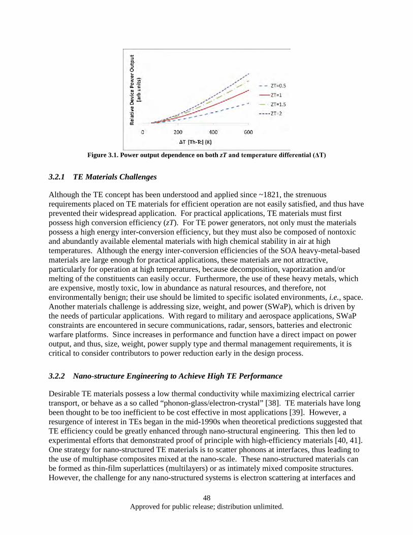
48 Approved for public release; distribution unlimited.
Figure 3.1. Power output dependence on both zT and temperature differential (ΔT)
3.2.1 TE Materials Challenges Although the TE concept has been understood and applied since ~1821, the strenuous requirements placed on TE materials for efficient operation are not easily satisfied, and thus have prevented their widespread application. For practical applications, TE materials must first possess high conversion efficiency (zT). For TE power generators, not only must the materials possess a high energy inter-conversion efficiency, but they must also be composed of nontoxic and abundantly available elemental materials with high chemical stability in air at high temperatures. Although the energy inter-conversion efficiencies of the SOA heavy-metal-based materials are large enough for practical applications, these materials are not attractive, particularly for operation at high temperatures, because decomposition, vaporization and/or melting of the constituents can easily occur. Furthermore, the use of these heavy metals, which are expensive, mostly toxic, low in abundance as natural resources, and therefore, not environmentally benign; their use should be limited to specific isolated environments, i.e., space. Another materials challenge is addressing size, weight, and power (SWaP), which is driven by the needs of particular applications. With regard to military and aerospace applications, SWaP constraints are encountered in secure communications, radar, sensors, batteries and electronic warfare platforms. Since increases in performance and function have a direct impact on power output, and thus, size, weight, power supply type and thermal management requirements, it is critical to consider contributors to power reduction early in the design process. 3.2.2 Nano-structure Engineering to Achieve High TE Performance Desirable TE materials possess a low thermal conductivity while maximizing electrical carrier transport, or behave as a so called “phonon-glass/electron-crystal” [38]. TE materials have long been thought to be too inefficient to be cost effective in most applications [39]. However, a resurgence of interest in TEs began in the mid-1990s when theoretical predictions suggested that TE efficiency could be greatly enhanced through nano-structural engineering. This then led to experimental efforts that demonstrated proof of principle with high-efficiency materials [40, 41]. One strategy for nano-structured TE materials is to scatter phonons at interfaces, thus leading to the use of multiphase composites mixed at the nano-scale. These nano-structured materials can be formed as thin-film superlattices (multilayers) or as intimately mixed composite structures. However, the challenge for any nano-structured systems is electron scattering at interfaces and
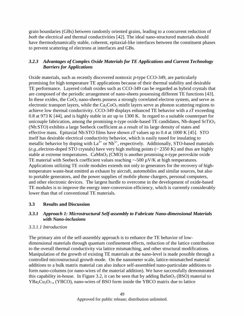
49 Approved for public release; distribution unlimited.
grain boundaries (GBs) between randomly oriented grains, leading to a concurrent reduction of both the electrical and thermal conductivities [42]. The ideal nano-structured materials should have thermodynamically stable, coherent, epitaxial-like interfaces between the constituent phases to prevent scattering of electrons at interfaces and GBs. 3.2.3 Advantages of Complex Oxide Materials for TE Applications and Current Technology
Barriers for Applications Oxide materials, such as recently discovered nontoxic p-type CCO-349, are particularly promising for high temperature TE applications because of their thermal stability and desirable TE performance. Layered cobalt oxides such as CCO-349 can be regarded as hybrid crystals that are composed of the periodic arrangement of nano-sheets possessing different TE functions [43]. In these oxides, the CoO2 nano-sheets possess a strongly correlated electron system, and serve as electronic transport layers, while the Ca2CoO3 misfit layers serve as phonon scattering regions to achieve low thermal conductivity. CCO-349 displays enhanced TE behavior with a zT exceeding 0.8 at 973 K [44], and is highly stable in air up to 1300 K. In regard to a suitable counterpart for unicouple fabrication, among the promising n-type oxide-based TE candidates, Nb-doped SrTiO3 (Nb:STO) exhibits a large Seebeck coefficient as a result of its large density of states and effective mass. Epitaxial Nb:STO films have shown zT values up to 0.4 at 1000 K [45]. STO itself has desirable electrical conductivity behavior, which is easily tuned for insulating to metallic behavior by doping with La3+ or Nb5+, respectively. Additionally, STO-based materials (e.g.,electron-doped STO crystals) have very high melting points (~ 2350 K) and thus are highly stable at extreme temperatures. CaMnO3 (CMO) is another promising n-type perovskite oxide TE material with Seebeck coefficient values reaching ~-500 µV/K at high temperatures. Applications utilizing TE oxide modules extends not only to generators for the recovery of high-temperature waste-heat emitted as exhaust by aircraft, automobiles and similar sources, but also to portable generators, and the power supplies of mobile phone chargers, personal computers, and other electronic devices. The largest hurdle to overcome in the development of oxide-based TE modules is to improve the energy inter-conversion efficiency, which is currently considerably lower than that of conventional TE materials.
Results and Discussion 3.3
3.3.1 Approach 1: Microstructural Self-assembly to Fabricate Nano-dimensional Materials with Nano-inclusions
3.3.1.1 Introduction The primary aim of the self-assembly approach is to enhance the TE behavior of low-dimensional materials through quantum confinement effects, reduction of the lattice contribution to the overall thermal conductivity via lattice mismatching, and other structural modifications. Manipulation of the growth of existing TE materials at the nano-level is made possible through a controlled microstructural growth mode. On the nanometer scale, lattice-mismatched material additions to a bulk matrix material can also induce self-assembled nano-particulate additions to form nano-columns (or nano-wires of the material addition). We have successfully demonstrated this capability in-house. In Figure 3.2, it can be seen that by adding BaSnO3 (BSO) material to YBa2Cu3O7-x (YBCO), nano-wires of BSO form inside the YBCO matrix due to lattice
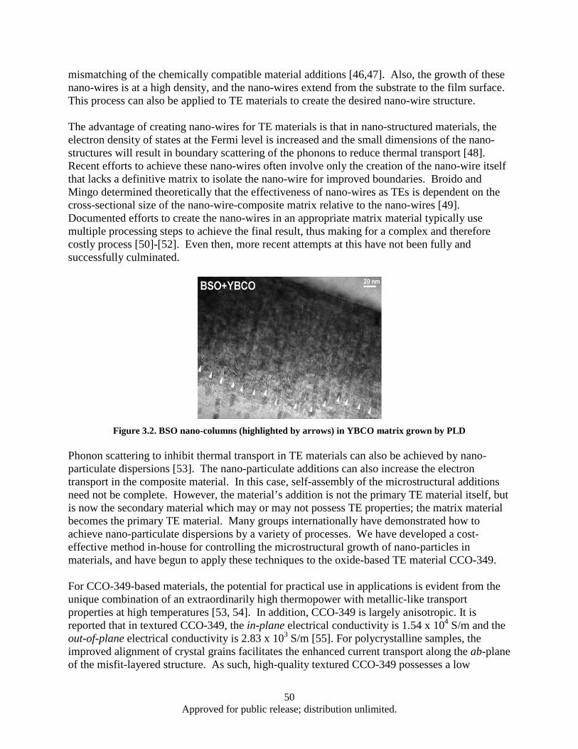
50 Approved for public release; distribution unlimited.
mismatching of the chemically compatible material additions [46,47]. Also, the growth of these nano-wires is at a high density, and the nano-wires extend from the substrate to the film surface. This process can also be applied to TE materials to create the desired nano-wire structure.
The advantage of creating nano-wires for TE materials is that in nano-structured materials, the electron density of states at the Fermi level is increased and the small dimensions of the nano-structures will result in boundary scattering of the phonons to reduce thermal transport [48]. Recent efforts to achieve these nano-wires often involve only the creation of the nano-wire itself that lacks a definitive matrix to isolate the nano-wire for improved boundaries. Broido and Mingo determined theoretically that the effectiveness of nano-wires as TEs is dependent on the cross-sectional size of the nano-wire-composite matrix relative to the nano-wires [49]. Documented efforts to create the nano-wires in an appropriate matrix material typically use multiple processing steps to achieve the final result, thus making for a complex and therefore costly process [50]-[52]. Even then, more recent attempts at this have not been fully and successfully culminated.
Figure 3.2. BSO nano-columns (highlighted by arrows) in YBCO matrix grown by PLD
Phonon scattering to inhibit thermal transport in TE materials can also be achieved by nano-particulate dispersions [53]. The nano-particulate additions can also increase the electron transport in the composite material. In this case, self-assembly of the microstructural additions need not be complete. However, the material’s addition is not the primary TE material itself, but is now the secondary material which may or may not possess TE properties; the matrix material becomes the primary TE material. Many groups internationally have demonstrated how to achieve nano-particulate dispersions by a variety of processes. We have developed a cost-effective method in-house for controlling the microstructural growth of nano-particles in materials, and have begun to apply these techniques to the oxide-based TE material CCO-349.
For CCO-349-based materials, the potential for practical use in applications is evident from the unique combination of an extraordinarily high thermopower with metallic-like transport properties at high temperatures [53, 54]. In addition, CCO-349 is largely anisotropic. It is reported that in textured CCO-349, the in-plane electrical conductivity is 1.54 x 10⁴ S/m and the out-of-plane electrical conductivity is 2.83 x 10³ S/m [55]. For polycrystalline samples, the improved alignment of crystal grains facilitates the enhanced current transport along the ab-plane of the misfit-layered structure. As such, high-quality textured CCO-349 possesses a low
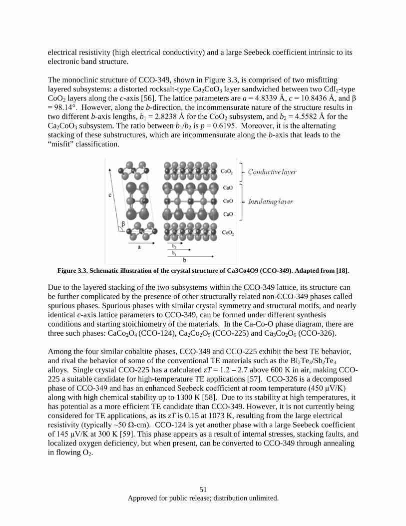
51 Approved for public release; distribution unlimited.
electrical resistivity (high electrical conductivity) and a large Seebeck coefficient intrinsic to its electronic band structure.
The monoclinic structure of CCO-349, shown in Figure 3.3, is comprised of two misfitting layered subsystems: a distorted rocksalt-type Ca2CoO3 layer sandwiched between two CdI2-type CoO2 layers along the c-axis [56]. The lattice parameters are a = 4.8339 Å, c = 10.8436 Å, and β = 98.14°. However, along the b-direction, the incommensurate nature of the structure results in two different b-axis lengths, b1 = 2.8238 Å for the CoO2 subsystem, and b2 = 4.5582 Å for the Ca2CoO3 subsystem. The ratio between b1/b2 is p = 0.6195. Moreover, it is the alternating stacking of these substructures, which are incommensurate along the b-axis that leads to the “misfit” classification.
Figure 3.3. Schematic illustration of the crystal structure of Ca3Co4O9 (CCO-349). Adapted from [18].
Due to the layered stacking of the two subsystems within the CCO-349 lattice, its structure can be further complicated by the presence of other structurally related non-CCO-349 phases called spurious phases. Spurious phases with similar crystal symmetry and structural motifs, and nearly identical c-axis lattice parameters to CCO-349, can be formed under different synthesis conditions and starting stoichiometry of the materials. In the Ca-Co-O phase diagram, there are three such phases: CaCo2O4 (CCO-124), Ca2Co2O5 (CCO-225) and Ca3Co2O6 (CCO-326).
Among the four similar cobaltite phases, CCO-349 and CCO-225 exhibit the best TE behavior, and rival the behavior of some of the conventional TE materials such as the Bi2Te3/Sb2Te3 alloys. Single crystal CCO-225 has a calculated zT = 1.2 – 2.7 above 600 K in air, making CCO-225 a suitable candidate for high-temperature TE applications [57]. CCO-326 is a decomposed phase of CCO-349 and has an enhanced Seebeck coefficient at room temperature (450 μV/K) along with high chemical stability up to 1300 K [58]. Due to its stability at high temperatures, it has potential as a more efficient TE candidate than CCO-349. However, it is not currently being considered for TE applications, as its zT is 0.15 at 1073 K, resulting from the large electrical resistivity (typically ~50 Ω-cm). CCO-124 is yet another phase with a large Seebeck coefficient of 145 μV/K at 300 K [59]. This phase appears as a result of internal stresses, stacking faults, and localized oxygen deficiency, but when present, can be converted to CCO-349 through annealing in flowing O2.
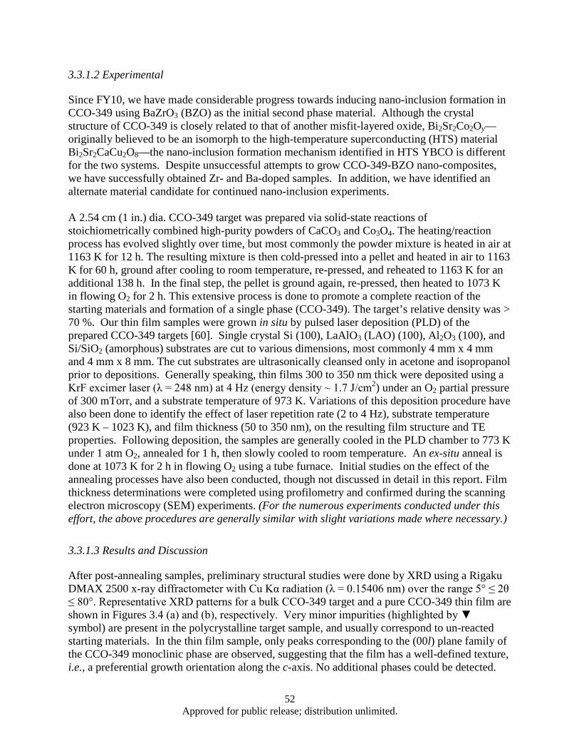
52 Approved for public release; distribution unlimited.
3.3.1.2 Experimental Since FY10, we have made considerable progress towards inducing nano-inclusion formation in CCO-349 using BaZrO3 (BZO) as the initial second phase material. Although the crystal structure of CCO-349 is closely related to that of another misfit-layered oxide, Bi2Sr2Co2Oy—originally believed to be an isomorph to the high-temperature superconducting (HTS) material Bi2Sr2CaCu2O8—the nano-inclusion formation mechanism identified in HTS YBCO is different for the two systems. Despite unsuccessful attempts to grow CCO-349-BZO nano-composites, we have successfully obtained Zr- and Ba-doped samples. In addition, we have identified an alternate material candidate for continued nano-inclusion experiments.
A 2.54 cm (1 in.) dia. CCO-349 target was prepared via solid-state reactions of stoichiometrically combined high-purity powders of CaCO3 and Co3O4. The heating/reaction process has evolved slightly over time, but most commonly the powder mixture is heated in air at 1163 K for 12 h. The resulting mixture is then cold-pressed into a pellet and heated in air to 1163 K for 60 h, ground after cooling to room temperature, re-pressed, and reheated to 1163 K for an additional 138 h. In the final step, the pellet is ground again, re-pressed, then heated to 1073 K in flowing O2 for 2 h. This extensive process is done to promote a complete reaction of the starting materials and formation of a single phase (CCO-349). The target’s relative density was > 70 %. Our thin film samples were grown in situ by pulsed laser deposition (PLD) of the prepared CCO-349 targets [60]. Single crystal Si (100), LaAlO3 (LAO) (100), Al2O3 (100), and Si/SiO2 (amorphous) substrates are cut to various dimensions, most commonly 4 mm x 4 mm and 4 mm x 8 mm. The cut substrates are ultrasonically cleansed only in acetone and isopropanol prior to depositions. Generally speaking, thin films 300 to 350 nm thick were deposited using a KrF excimer laser (λ = 248 nm) at 4 Hz (energy density ~ 1.7 J/cm2) under an O2 partial pressure of 300 mTorr, and a substrate temperature of 973 K. Variations of this deposition procedure have also been done to identify the effect of laser repetition rate (2 to 4 Hz), substrate temperature (923 K – 1023 K), and film thickness (50 to 350 nm), on the resulting film structure and TE properties. Following deposition, the samples are generally cooled in the PLD chamber to 773 K under 1 atm O2, annealed for 1 h, then slowly cooled to room temperature. An ex-situ anneal is done at 1073 K for 2 h in flowing O2 using a tube furnace. Initial studies on the effect of the annealing processes have also been conducted, though not discussed in detail in this report. Film thickness determinations were completed using profilometry and confirmed during the scanning electron microscopy (SEM) experiments. (For the numerous experiments conducted under this effort, the above procedures are generally similar with slight variations made where necessary.) 3.3.1.3 Results and Discussion After post-annealing samples, preliminary structural studies were done by XRD using a Rigaku DMAX 2500 x-ray diffractometer with Cu Kα radiation (λ = 0.15406 nm) over the range 5° ≤ 2θ ≤ 80°. Representative XRD patterns for a bulk CCO-349 target and a pure CCO-349 thin film are shown in Figures 3.4 (a) and (b), respectively. Very minor impurities (highlighted by symbol) are present in the polycrystalline target sample, and usually correspond to un-reacted starting materials. In the thin film sample, only peaks corresponding to the (00l) plane family of the CCO-349 monoclinic phase are observed, suggesting that the film has a well-defined texture, i.e., a preferential growth orientation along the c-axis. No additional phases could be detected.
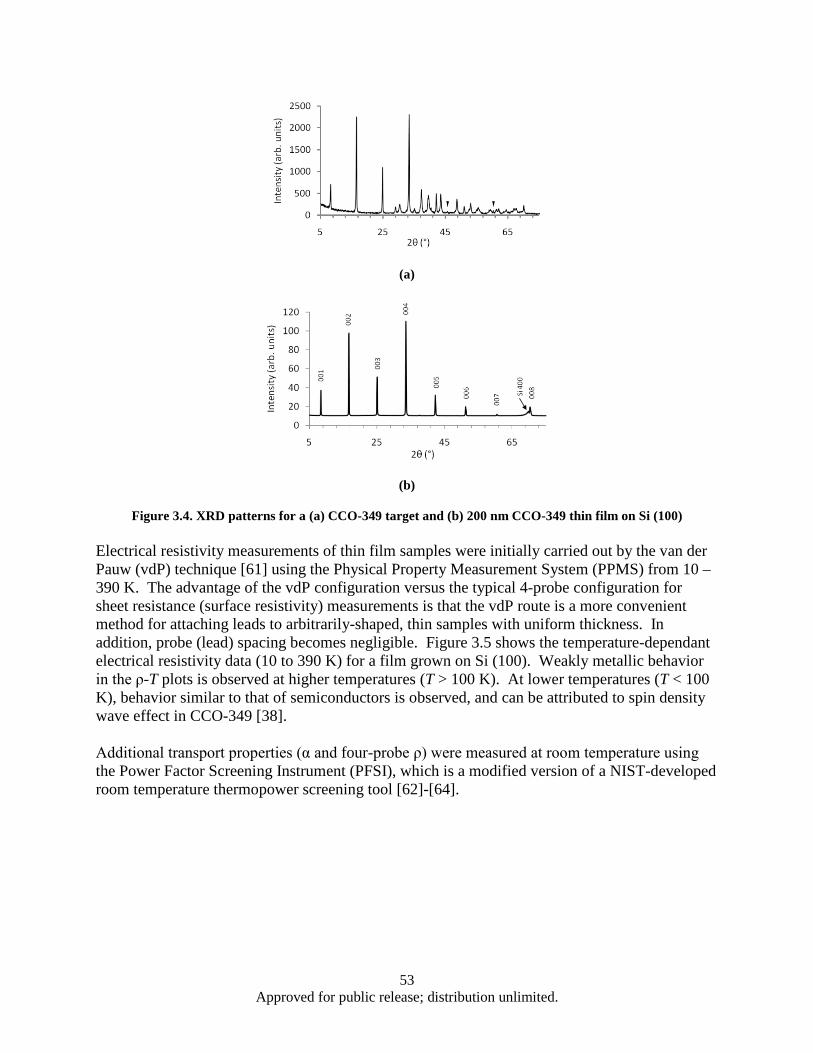
53 Approved for public release; distribution unlimited.
(a)
(b)
Figure 3.4. XRD patterns for a (a) CCO-349 target and (b) 200 nm CCO-349 thin film on Si (100)
Electrical resistivity measurements of thin film samples were initially carried out by the van der Pauw (vdP) technique [61] using the Physical Property Measurement System (PPMS) from 10 – 390 K. The advantage of the vdP configuration versus the typical 4-probe configuration for sheet resistance (surface resistivity) measurements is that the vdP route is a more convenient method for attaching leads to arbitrarily-shaped, thin samples with uniform thickness. In addition, probe (lead) spacing becomes negligible. Figure 3.5 shows the temperature-dependant electrical resistivity data (10 to 390 K) for a film grown on Si (100). Weakly metallic behavior in the ρ-T plots is observed at higher temperatures (T > 100 K). At lower temperatures (T < 100 K), behavior similar to that of semiconductors is observed, and can be attributed to spin density wave effect in CCO-349 [38].
Additional transport properties (α and four-probe ρ) were measured at room temperature using the Power Factor Screening Instrument (PFSI), which is a modified version of a NIST-developed room temperature thermopower screening tool [62]-[64].
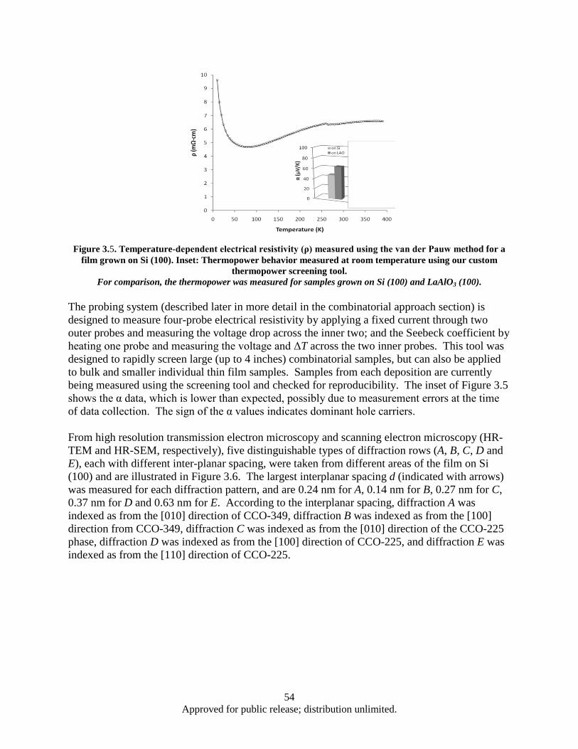
54 Approved for public release; distribution unlimited.
Figure 3.5. Temperature-dependent electrical resistivity (ρ) measured using the van der Pauw method for a
film grown on Si (100). Inset: Thermopower behavior measured at room temperature using our custom thermopower screening tool.
For comparison, the thermopower was measured for samples grown on Si (100) and LaAlO3 (100). The probing system (described later in more detail in the combinatorial approach section) is designed to measure four-probe electrical resistivity by applying a fixed current through two outer probes and measuring the voltage drop across the inner two; and the Seebeck coefficient by heating one probe and measuring the voltage and ΔT across the two inner probes. This tool was designed to rapidly screen large (up to 4 inches) combinatorial samples, but can also be applied to bulk and smaller individual thin film samples. Samples from each deposition are currently being measured using the screening tool and checked for reproducibility. The inset of Figure 3.5 shows the α data, which is lower than expected, possibly due to measurement errors at the time of data collection. The sign of the α values indicates dominant hole carriers.
From high resolution transmission electron microscopy and scanning electron microscopy (HR-TEM and HR-SEM, respectively), five distinguishable types of diffraction rows (A, B, C, D and E), each with different inter-planar spacing, were taken from different areas of the film on Si (100) and are illustrated in Figure 3.6. The largest interplanar spacing d (indicated with arrows) was measured for each diffraction pattern, and are 0.24 nm for A, 0.14 nm for B, 0.27 nm for C, 0.37 nm for D and 0.63 nm for E. According to the interplanar spacing, diffraction A was indexed as from the [010] direction of CCO-349, diffraction B was indexed as from the [100] direction from CCO-349, diffraction C was indexed as from the [010] direction of the CCO-225 phase, diffraction D was indexed as from the [100] direction of CCO-225, and diffraction E was indexed as from the [110] direction of CCO-225.
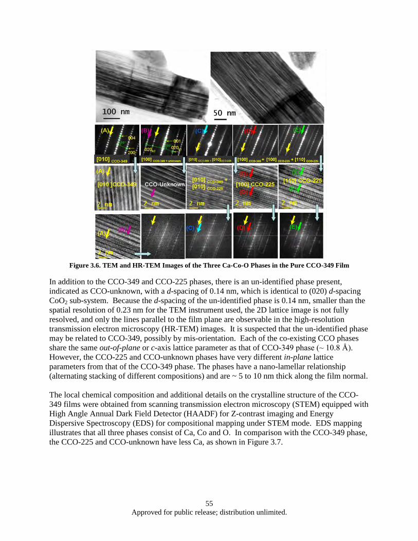
55 Approved for public release; distribution unlimited.
Figure 3.6. TEM and HR-TEM Images of the Three Ca-Co-O Phases in the Pure CCO-349 Film
In addition to the CCO-349 and CCO-225 phases, there is an un-identified phase present, indicated as CCO-unknown, with a d-spacing of 0.14 nm, which is identical to (020) d-spacing CoO2 sub-system. Because the d-spacing of the un-identified phase is 0.14 nm, smaller than the spatial resolution of 0.23 nm for the TEM instrument used, the 2D lattice image is not fully resolved, and only the lines parallel to the film plane are observable in the high-resolution transmission electron microscopy (HR-TEM) images. It is suspected that the un-identified phase may be related to CCO-349, possibly by mis-orientation. Each of the co-existing CCO phases share the same out-of-plane or c-axis lattice parameter as that of CCO-349 phase (~ 10.8 Å). However, the CCO-225 and CCO-unknown phases have very different in-plane lattice parameters from that of the CCO-349 phase. The phases have a nano-lamellar relationship (alternating stacking of different compositions) and are ~ 5 to 10 nm thick along the film normal.
The local chemical composition and additional details on the crystalline structure of the CCO-349 films were obtained from scanning transmission electron microscopy (STEM) equipped with High Angle Annual Dark Field Detector (HAADF) for Z-contrast imaging and Energy Dispersive Spectroscopy (EDS) for compositional mapping under STEM mode. EDS mapping illustrates that all three phases consist of Ca, Co and O. In comparison with the CCO-349 phase, the CCO-225 and CCO-unknown have less Ca, as shown in Figure 3.7.
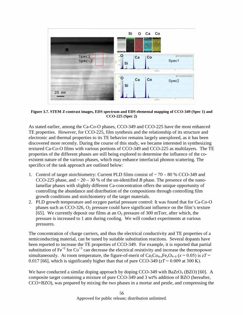
56 Approved for public release; distribution unlimited.
Figure 3.7. STEM Z-contrast images, EDS spectrum and EDS elemental mapping of CCO-349 (Spec 1) and CCO-225 (Spec 2)
As stated earlier, among the Ca-Co-O phases, CCO-349 and CCO-225 have the most enhanced TE properties. However, for CCO-225, film synthesis and the relationship of its structure and electronic and thermal properties to its TE behavior remains largely unexplored, as it has been discovered more recently. During the course of this study, we became interested in synthesizing textured Ca-Co-O films with various portions of CCO-349 and CCO-225 as multilayers. The TE properties of the different phases are still being explored to determine the influence of the co-existent nature of the various phases, which may enhance interfacial phonon scattering. The specifics of the task approach are outlined below:
1. Control of target stoichiometry: Current PLD films consist of ~ 70 – 80 % CCO-349 and CCO-225 phase, and ~ 20 – 30 % of the un-identified B phase. The presence of the nano-lamellar phases with slightly different Ca-concentration offers the unique opportunity of controlling the abundance and distribution of the compositions through controlling film growth conditions and stoichiometry of the target materials.
2. PLD growth temperature and oxygen partial pressure control: It was found that for Ca-Co-O phases such as CCO-326, O2 pressure could have significant influence on the film’s texture [65]. We currently deposit our films at an O2 pressure of 300 mTorr, after which, the pressure is increased to 1 atm during cooling. We will conduct experiments at various pressures.
The concentration of charge carriers, and thus the electrical conductivity and TE properties of a semiconducting material, can be tuned by suitable substitution reactions. Several dopants have been reported to increase the TE properties of CCO-349. For example, it is reported that partial substitution of Fe+2 for Co+3 can decrease the electrical resistivity and increase the thermopower simultaneously. At room temperature, the figure-of-merit of Ca3Co4-xFexO9+δ (x = 0.05) is zT = 0.017 [66], which is significantly higher than that of pure CCO-349 (zT = 0.009 at 300 K).
We have conducted a similar doping approach by doping CCO-349 with BaZrO3 (BZO) [60]. A composite target containing a mixture of pure CCO-349 and 3 wt% addition of BZO (hereafter, CCO+BZO), was prepared by mixing the two phases in a mortar and pestle, and compressing the
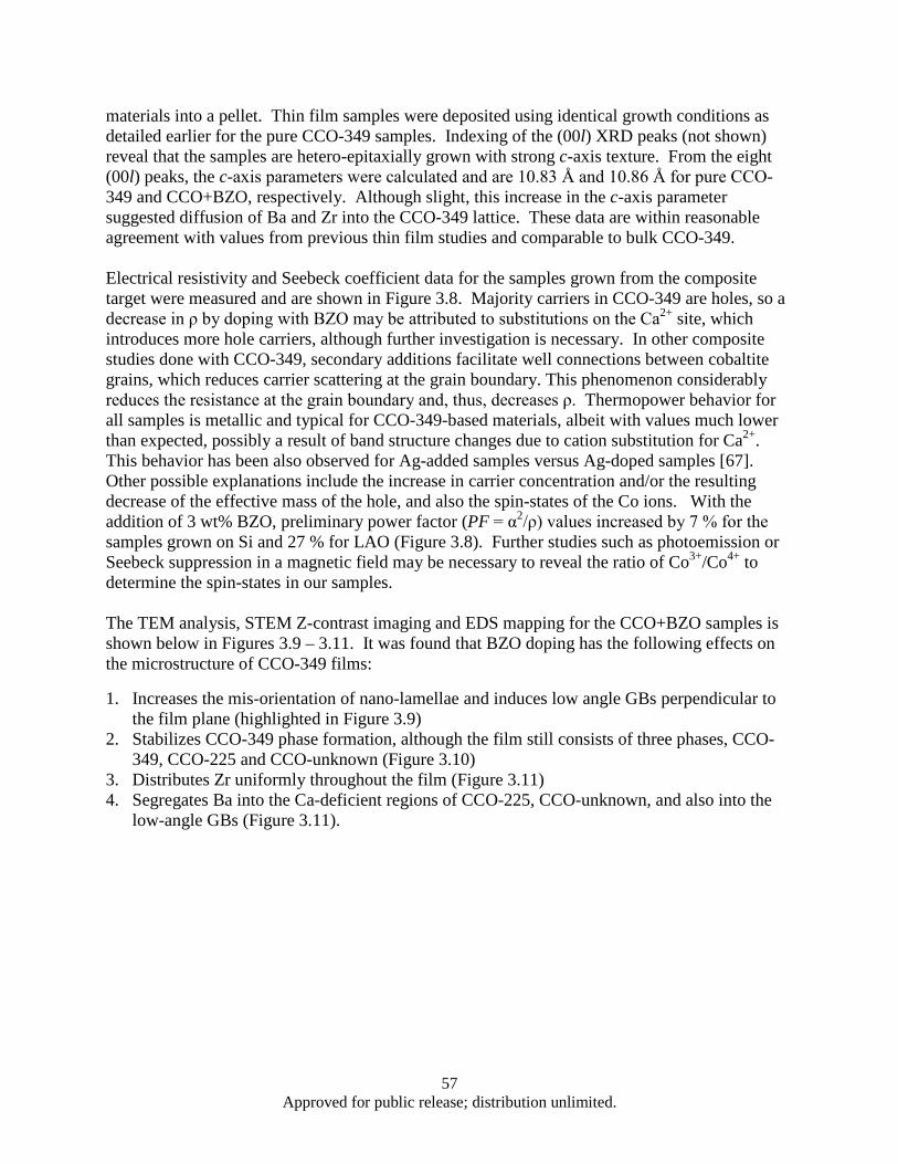
57 Approved for public release; distribution unlimited.
materials into a pellet. Thin film samples were deposited using identical growth conditions as detailed earlier for the pure CCO-349 samples. Indexing of the (00l) XRD peaks (not shown) reveal that the samples are hetero-epitaxially grown with strong c-axis texture. From the eight (00l) peaks, the c-axis parameters were calculated and are 10.83 Å and 10.86 Å for pure CCO-349 and CCO+BZO, respectively. Although slight, this increase in the c-axis parameter suggested diffusion of Ba and Zr into the CCO-349 lattice. These data are within reasonable agreement with values from previous thin film studies and comparable to bulk CCO-349.
Electrical resistivity and Seebeck coefficient data for the samples grown from the composite target were measured and are shown in Figure 3.8. Majority carriers in CCO-349 are holes, so a decrease in ρ by doping with BZO may be attributed to substitutions on the Ca2+ site, which introduces more hole carriers, although further investigation is necessary. In other composite studies done with CCO-349, secondary additions facilitate well connections between cobaltite grains, which reduces carrier scattering at the grain boundary. This phenomenon considerably reduces the resistance at the grain boundary and, thus, decreases ρ. Thermopower behavior for all samples is metallic and typical for CCO-349-based materials, albeit with values much lower than expected, possibly a result of band structure changes due to cation substitution for Ca2+. This behavior has been also observed for Ag-added samples versus Ag-doped samples [67]. Other possible explanations include the increase in carrier concentration and/or the resulting decrease of the effective mass of the hole, and also the spin-states of the Co ions. With the addition of 3 wt% BZO, preliminary power factor (PF = α2/ρ) values increased by 7 % for the samples grown on Si and 27 % for LAO (Figure 3.8). Further studies such as photoemission or Seebeck suppression in a magnetic field may be necessary to reveal the ratio of Co3+/Co4+ to determine the spin-states in our samples.
The TEM analysis, STEM Z-contrast imaging and EDS mapping for the CCO+BZO samples is shown below in Figures 3.9 – 3.11. It was found that BZO doping has the following effects on the microstructure of CCO-349 films:
1. Increases the mis-orientation of nano-lamellae and induces low angle GBs perpendicular to the film plane (highlighted in Figure 3.9)
2. Stabilizes CCO-349 phase formation, although the film still consists of three phases, CCO-349, CCO-225 and CCO-unknown (Figure 3.10)
3. Distributes Zr uniformly throughout the film (Figure 3.11) 4. Segregates Ba into the Ca-deficient regions of CCO-225, CCO-unknown, and also into the
low-angle GBs (Figure 3.11).
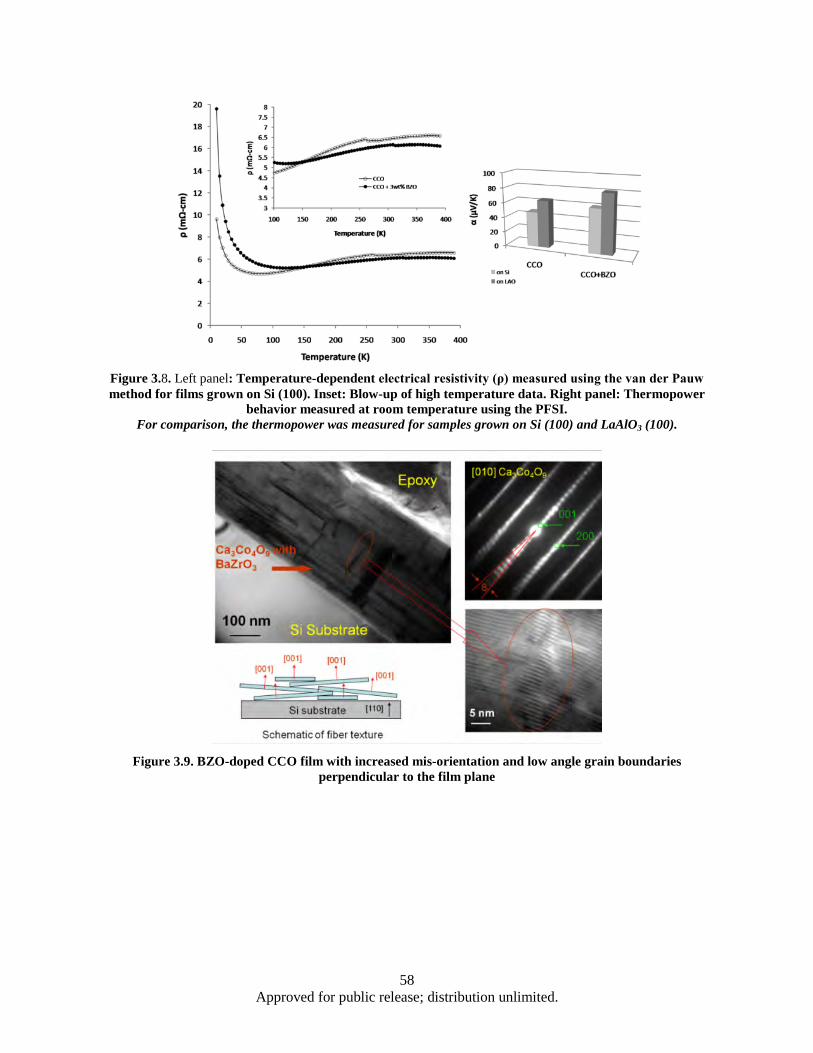
58 Approved for public release; distribution unlimited.
Figure 3.8. Left panel: Temperature-dependent electrical resistivity (ρ) measured using the van der Pauw method for films grown on Si (100). Inset: Blow-up of high temperature data. Right panel: Thermopower
behavior measured at room temperature using the PFSI. For comparison, the thermopower was measured for samples grown on Si (100) and LaAlO3 (100).
Figure 3.9. BZO-doped CCO film with increased mis-orientation and low angle grain boundaries
perpendicular to the film plane
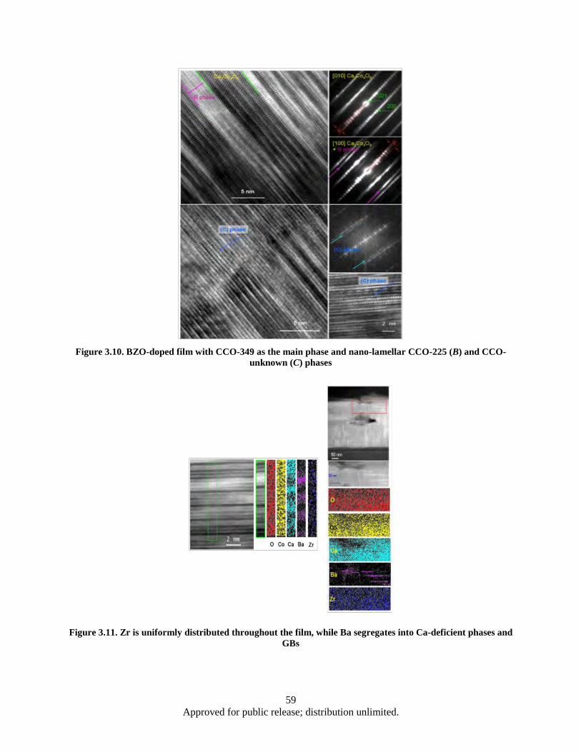
59 Approved for public release; distribution unlimited.
Figure 3.10. BZO-doped film with CCO-349 as the main phase and nano-lamellar CCO-225 (B) and CCO-
unknown (C) phases
Figure 3.11. Zr is uniformly distributed throughout the film, while Ba segregates into Ca-deficient phases and GBs
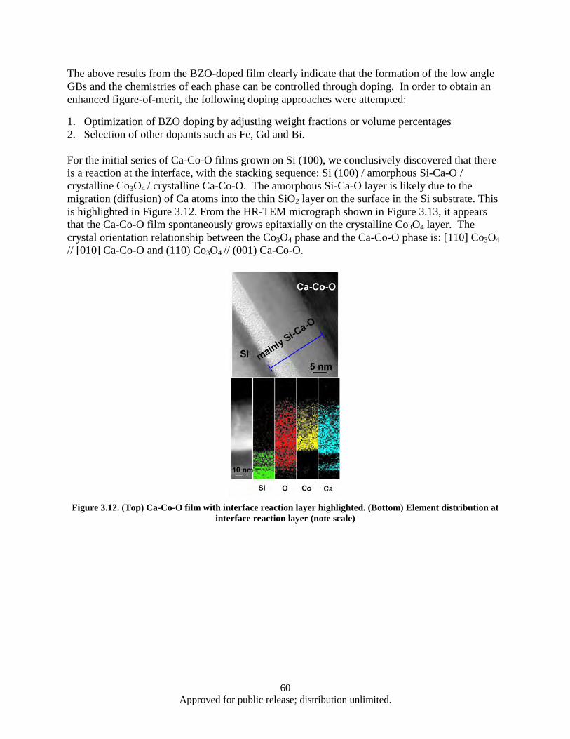
60 Approved for public release; distribution unlimited.
The above results from the BZO-doped film clearly indicate that the formation of the low angle GBs and the chemistries of each phase can be controlled through doping. In order to obtain an enhanced figure-of-merit, the following doping approaches were attempted:
1. Optimization of BZO doping by adjusting weight fractions or volume percentages 2. Selection of other dopants such as Fe, Gd and Bi. For the initial series of Ca-Co-O films grown on Si (100), we conclusively discovered that there is a reaction at the interface, with the stacking sequence: Si (100) / amorphous Si-Ca-O / crystalline Co3O4 / crystalline Ca-Co-O. The amorphous Si-Ca-O layer is likely due to the migration (diffusion) of Ca atoms into the thin SiO2 layer on the surface in the Si substrate. This is highlighted in Figure 3.12. From the HR-TEM micrograph shown in Figure 3.13, it appears that the Ca-Co-O film spontaneously grows epitaxially on the crystalline Co3O4 layer. The crystal orientation relationship between the Co3O4 phase and the Ca-Co-O phase is: [110] Co3O4 // [010] Ca-Co-O and (110) Co3O4 // (001) Ca-Co-O.
Figure 3.12. (Top) Ca-Co-O film with interface reaction layer highlighted. (Bottom) Element distribution at
interface reaction layer (note scale)
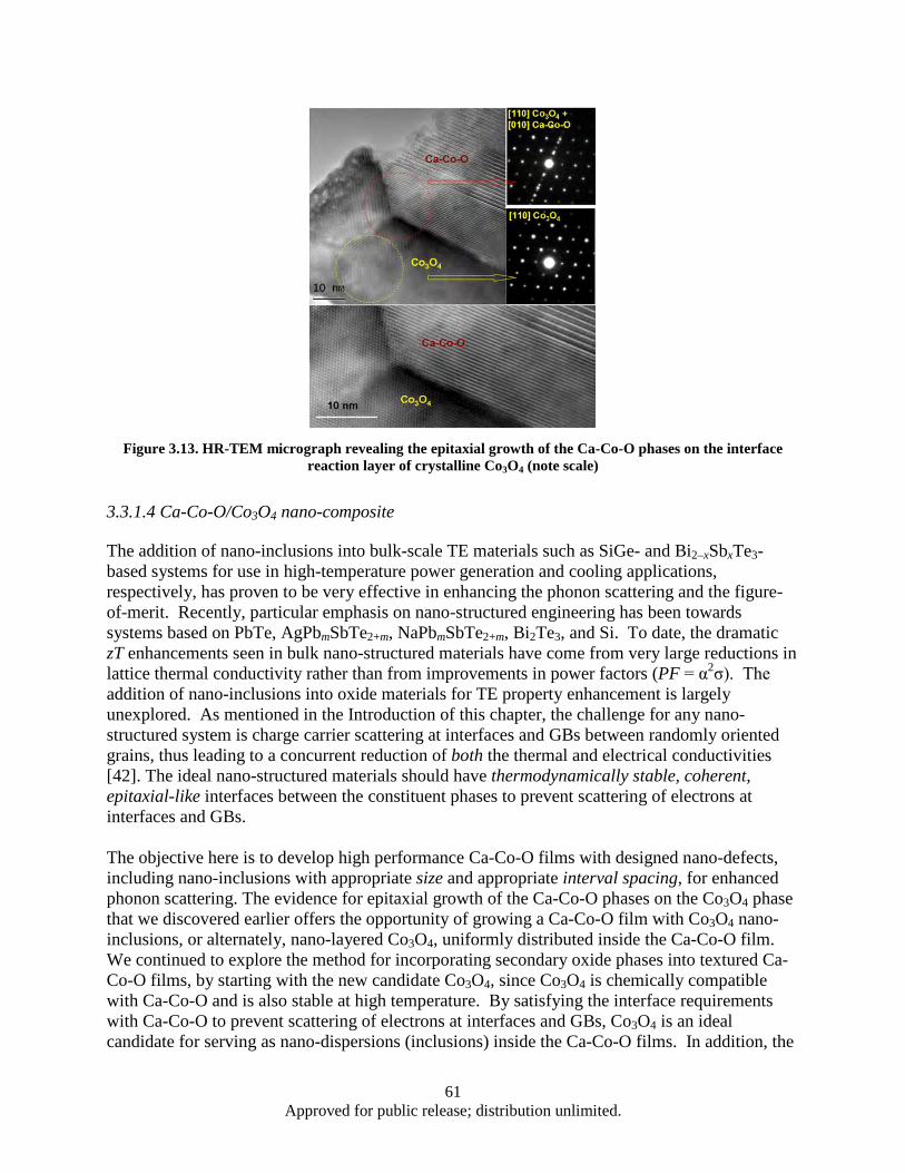
61 Approved for public release; distribution unlimited.
Figure 3.13. HR-TEM micrograph revealing the epitaxial growth of the Ca-Co-O phases on the interface
reaction layer of crystalline Co3O4 (note scale)
3.3.1.4 Ca-Co-O/Co3O4 nano-composite The addition of nano-inclusions into bulk-scale TE materials such as SiGe- and Bi2–xSbxTe3-based systems for use in high-temperature power generation and cooling applications, respectively, has proven to be very effective in enhancing the phonon scattering and the figure-of-merit. Recently, particular emphasis on nano-structured engineering has been towards systems based on PbTe, AgPbmSbTe2+m, NaPbmSbTe2+m, Bi2Te3, and Si. To date, the dramatic zT enhancements seen in bulk nano-structured materials have come from very large reductions in lattice thermal conductivity rather than from improvements in power factors (PF = α2σ). The addition of nano-inclusions into oxide materials for TE property enhancement is largely unexplored. As mentioned in the Introduction of this chapter, the challenge for any nano-structured system is charge carrier scattering at interfaces and GBs between randomly oriented grains, thus leading to a concurrent reduction of both the thermal and electrical conductivities [42]. The ideal nano-structured materials should have thermodynamically stable, coherent, epitaxial-like interfaces between the constituent phases to prevent scattering of electrons at interfaces and GBs.
The objective here is to develop high performance Ca-Co-O films with designed nano-defects, including nano-inclusions with appropriate size and appropriate interval spacing, for enhanced phonon scattering. The evidence for epitaxial growth of the Ca-Co-O phases on the Co3O4 phase that we discovered earlier offers the opportunity of growing a Ca-Co-O film with Co3O4 nano-inclusions, or alternately, nano-layered Co3O4, uniformly distributed inside the Ca-Co-O film. We continued to explore the method for incorporating secondary oxide phases into textured Ca-Co-O films, by starting with the new candidate Co3O4, since Co3O4 is chemically compatible with Ca-Co-O and is also stable at high temperature. By satisfying the interface requirements with Ca-Co-O to prevent scattering of electrons at interfaces and GBs, Co3O4 is an ideal candidate for serving as nano-dispersions (inclusions) inside the Ca-Co-O films. In addition, the
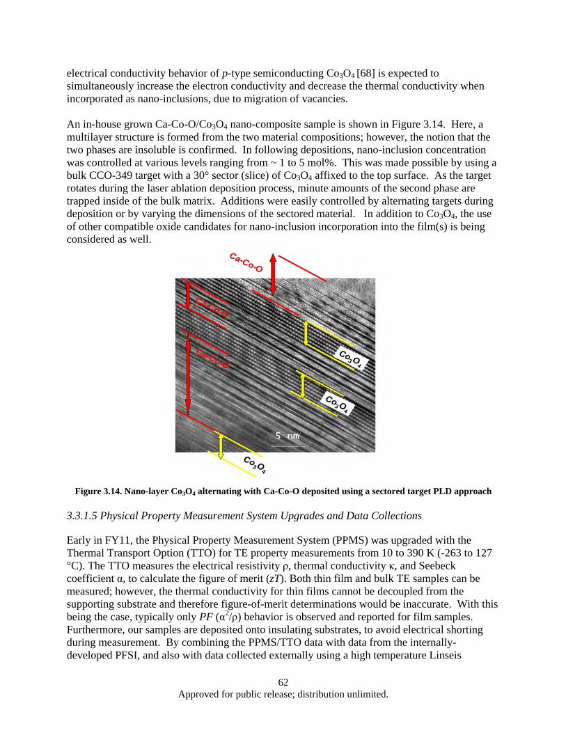
62 Approved for public release; distribution unlimited.
electrical conductivity behavior of p-type semiconducting Co3O4 [68] is expected to simultaneously increase the electron conductivity and decrease the thermal conductivity when incorporated as nano-inclusions, due to migration of vacancies. An in-house grown Ca-Co-O/Co3O4 nano-composite sample is shown in Figure 3.14. Here, a multilayer structure is formed from the two material compositions; however, the notion that the two phases are insoluble is confirmed. In following depositions, nano-inclusion concentration was controlled at various levels ranging from ~ 1 to 5 mol%. This was made possible by using a bulk CCO-349 target with a 30° sector (slice) of Co3O4 affixed to the top surface. As the target rotates during the laser ablation deposition process, minute amounts of the second phase are trapped inside of the bulk matrix. Additions were easily controlled by alternating targets during deposition or by varying the dimensions of the sectored material. In addition to Co3O4, the use of other compatible oxide candidates for nano-inclusion incorporation into the film(s) is being considered as well.
Figure 3.14. Nano-layer Co3O4 alternating with Ca-Co-O deposited using a sectored target PLD approach
3.3.1.5 Physical Property Measurement System Upgrades and Data Collections Early in FY11, the Physical Property Measurement System (PPMS) was upgraded with the Thermal Transport Option (TTO) for TE property measurements from 10 to 390 K (-263 to 127 °C). The TTO measures the electrical resistivity ρ, thermal conductivity κ, and Seebeck coefficient α, to calculate the figure of merit (zT). Both thin film and bulk TE samples can be measured; however, the thermal conductivity for thin films cannot be decoupled from the supporting substrate and therefore figure-of-merit determinations would be inaccurate. With this being the case, typically only PF (α2/ρ) behavior is observed and reported for film samples. Furthermore, our samples are deposited onto insulating substrates, to avoid electrical shorting during measurement. By combining the PPMS/TTO data with data from the internally-developed PFSI, and also with data collected externally using a high temperature Linseis
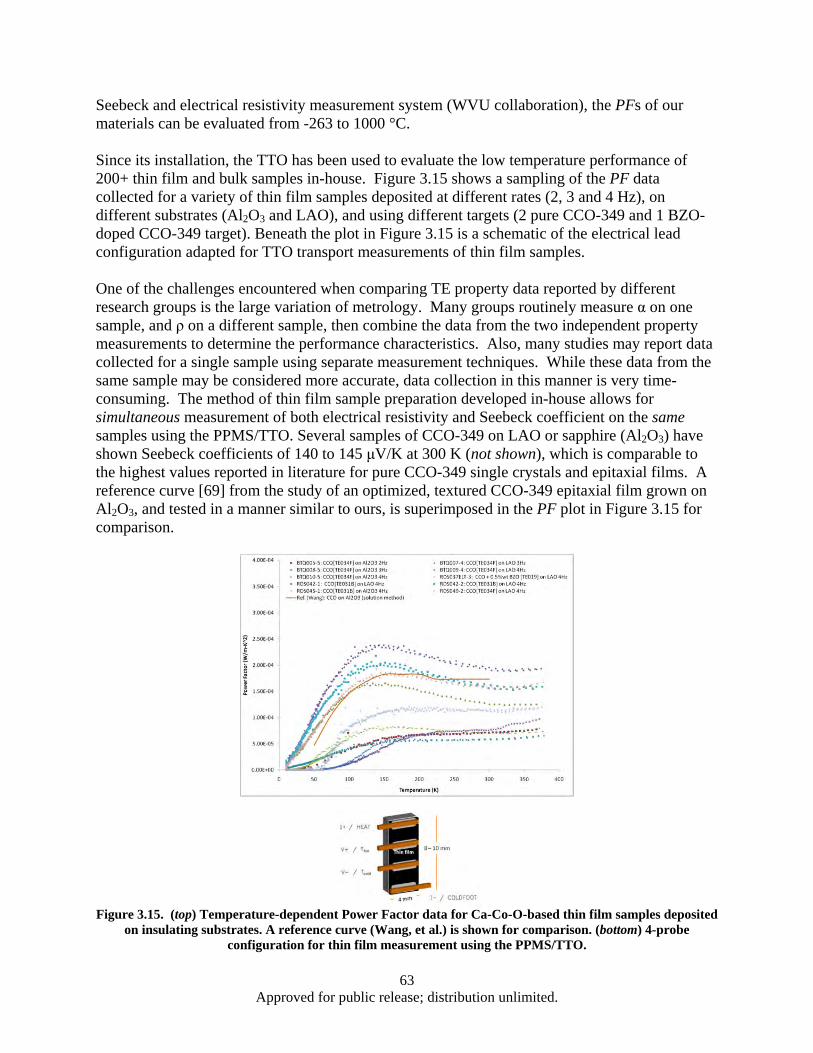
63 Approved for public release; distribution unlimited.
Seebeck and electrical resistivity measurement system (WVU collaboration), the PFs of our materials can be evaluated from -263 to 1000 °C.
Since its installation, the TTO has been used to evaluate the low temperature performance of 200+ thin film and bulk samples in-house. Figure 3.15 shows a sampling of the PF data collected for a variety of thin film samples deposited at different rates (2, 3 and 4 Hz), on different substrates (Al2O3 and LAO), and using different targets (2 pure CCO-349 and 1 BZO-doped CCO-349 target). Beneath the plot in Figure 3.15 is a schematic of the electrical lead configuration adapted for TTO transport measurements of thin film samples.
One of the challenges encountered when comparing TE property data reported by different research groups is the large variation of metrology. Many groups routinely measure α on one sample, and ρ on a different sample, then combine the data from the two independent property measurements to determine the performance characteristics. Also, many studies may report data collected for a single sample using separate measurement techniques. While these data from the same sample may be considered more accurate, data collection in this manner is very time-consuming. The method of thin film sample preparation developed in-house allows for simultaneous measurement of both electrical resistivity and Seebeck coefficient on the same samples using the PPMS/TTO. Several samples of CCO-349 on LAO or sapphire (Al2O3) have shown Seebeck coefficients of 140 to 145 μV/K at 300 K (not shown), which is comparable to the highest values reported in literature for pure CCO-349 single crystals and epitaxial films. A reference curve [69] from the study of an optimized, textured CCO-349 epitaxial film grown on Al2O3, and tested in a manner similar to ours, is superimposed in the PF plot in Figure 3.15 for comparison.
Figure 3.15. (top) Temperature-dependent Power Factor data for Ca-Co-O-based thin film samples deposited
on insulating substrates. A reference curve (Wang, et al.) is shown for comparison. (bottom) 4-probe configuration for thin film measurement using the PPMS/TTO.
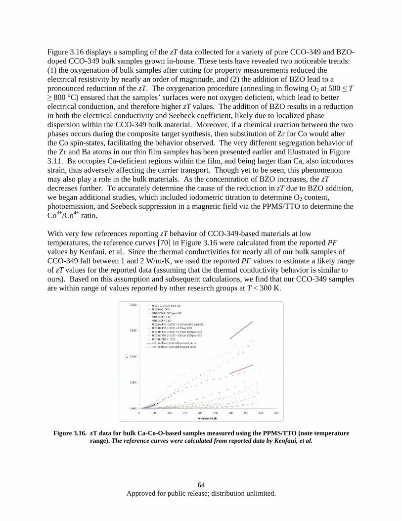
64 Approved for public release; distribution unlimited.
Figure 3.16 displays a sampling of the zT data collected for a variety of pure CCO-349 and BZO-doped CCO-349 bulk samples grown in-house. These tests have revealed two noticeable trends: (1) the oxygenation of bulk samples after cutting for property measurements reduced the electrical resistivity by nearly an order of magnitude, and (2) the addition of BZO lead to a pronounced reduction of the zT. The oxygenation procedure (annealing in flowing O2 at 500 ≤ T ≥ 800 °C) ensured that the samples’ surfaces were not oxygen deficient, which lead to better electrical conduction, and therefore higher zT values. The addition of BZO results in a reduction in both the electrical conductivity and Seebeck coefficient, likely due to localized phase dispersion within the CCO-349 bulk material. Moreover, if a chemical reaction between the two phases occurs during the composite target synthesis, then substitution of Zr for Co would alter the Co spin-states, facilitating the behavior observed. The very different segregation behavior of the Zr and Ba atoms in our thin film samples has been presented earlier and illustrated in Figure 3.11. Ba occupies Ca-deficient regions within the film, and being larger than Ca, also introduces strain, thus adversely affecting the carrier transport. Though yet to be seen, this phenomenon may also play a role in the bulk materials. As the concentration of BZO increases, the zT decreases further. To accurately determine the cause of the reduction in zT due to BZO addition, we began additional studies, which included iodometric titration to determine O2 content, photoemission, and Seebeck suppression in a magnetic field via the PPMS/TTO to determine the Co3+/Co4+ ratio.
With very few references reporting zT behavior of CCO-349-based materials at low temperatures, the reference curves [70] in Figure 3.16 were calculated from the reported PF values by Kenfaui, et al. Since the thermal conductivities for nearly all of our bulk samples of CCO-349 fall between 1 and 2 W/m-K, we used the reported PF values to estimate a likely range of zT values for the reported data (assuming that the thermal conductivity behavior is similar to ours). Based on this assumption and subsequent calculations, we find that our CCO-349 samples are within range of values reported by other research groups at T < 300 K.
Figure 3.16. zT data for bulk Ca-Co-O-based samples measured using the PPMS/TTO (note temperature range). The reference curves were calculated from reported data by Kenfaui, et al.
65 Approved for public release; distribution unlimited.
1.1.1.1 Fe Doping Study Summary
Bulk Fe-doped CCO-349 (Ca3Co4-xFexO9+δ) samples and pulsed laser deposition (PLD) targets were made using standard solid state ceramic processing methods. Stoichiometric amounts of Co3O4, CaCO3 and Fe2O3 were mixed to form samples with various Fe content. The synthesis approach was developed experimentally using the CaO-Co3O4 phase diagram and iterative powder XRD results. These experiments showed that Fe could be used to increase the electrical conductivity and Seebeck coefficient while simultaneously decreasing the thermal conductivity in doped CCO-349 bulk samples.
Thin film samples were deposited on various substrates using PLD. A KrF excimer laser was used (λ = 248 nm) at a repetition rate of 4 Hz and pulse energy of ~348 mJ (~1.7 J/cm). 350 nm thick films were deposited at 973 K (700 °C) in 300 mTorr O2. After deposition, the films were cooled to room temperature in 1atm O2 with a 1 hour in situ anneal at 773 K (500 °C).
Initially, elemental (Ca, Fe, Co) analysis of the Fe-doped CCO-349 bulk samples was done using enrgy dispersive spectroscopy. The actual content of Co and Fe was very close to the expected value throughout the range of Fe contents.
Powder x-ray diffraction of the Fe-doped CCO-349 bulk materials revealed the formation of secondary phases with increasing Fe content. Below x = 0.5, Fe appeared to be incorporated into the CCO-349 crystal structure as the c-axis parameter varies with Fe content. In addition, below x = 0.5 there is no evidence of secondary phases in the diffraction patterns. As the Fe-content increases above x = 0.5, the amount of CCO-349 decreases and two secondary phases begin to appear: an Fe-rich phase (Ca2Fe2O5) and an Fe-poor phase (Co3O4). At x = 2.0, these two phases are the only phases present; there was no evidence of CCO-349.
Several samples have been analyzed via XPS in AFRL’s Materials Directorate. Initially, three thin film samples with varying Fe content were analyzed. These samples were tested both as-received and after sputtering for 60 seconds to probe the composition of sample about 50-100 nm below the initial surface. There was a substantial amount of carbon, C (~35 at%), in the as-received samples. Even after sputtering, the C content of the film was ~20 at%, although it was suggested that this could be due to mixing of the surface contamination with the film during sputtering. Interestingly, the most Fe-rich sample showed evidence of C atoms existing as FeC within the depth of the film, which was not seen in XRD analysis of thin film samples from this target. This lends evidence to the theory that mixing may be occurring during sputtering. For lower loadings (~1.5 at%) of Fe, there was no evidence of Fe in the sample through XPS. There could be several reasons for this. First, the large amount of C contamination reduces the sensitivity of the technique and the low Fe content is near the detection limit for the technique. Also, the peaks for Fe and Co are fairly close together with the Fe 2p doublet overlapping with the Co auger peak making identification more difficult. These results are still under investigation.

66 Approved for public release; distribution unlimited.
The TE properties of our Fe-doped CCO-349 bulk samples have been compared to values found in literature. In all cases, electrical resistivity decreases with small additions of Fe (x ≤ 0.5) as expected. The Seebeck coefficient remains constant for most datasets. Regardless of the magnitude of effect on Seebeck, all of our samples show a notable increase in the Power Factors (combination of electrical resistivity and Seebeck coefficient) at Fe contents below x = 0.5. Our samples show a significantly lower thermal conductivity – three to six times – than reference samples, and suggests a weak relationship to Fe content, unlike that of reference samples. These measurements will be re-evaluated for accuracy.
In our samples, however, overall, zT increases up to 200-300% with increasing Fe content below x = 0.5 have been observed. Similar analyses have been performed on thin film samples. These samples also did not display a strong relationship between Seebeck coefficient and Fe content, with neither improvements nor reductions in Seebeck coefficient. These samples do however show a strong increase in electrical conductivity (significant reduction in electrical resistivity) over bulk samples due to increased density and sample texturing due to structural changes as a result of Fe-doping. The Power Factor of these samples was increased by 300-400% as compared to the bulk samples.
3.3.2 Approach 2: High-throughput Combinatorial Approach for Rapid Identification of Novel TE Materials
3.3.2.1 Overview Combinatorial science was first demonstrated in the medical industry for drug discovery, and with considerable advances in methodology, has now been successfully applied to materials science. For materials research, this approach has been effective in allowing a small number of precursor chemical reagents (solid or solution-based) to be merged into all possible combinations in a given reaction scheme for direct comparisons (crystal structures, performance properties, etc.) [71]. In addition, combinatorial screening methods have allowed for multidimensional chemical composition exploration at an unprecedented level of detail, and have led to the discovery of a wide variety of technologically important materials ranging from high temperature superconductors, magnetic, dielectric, ferroelectric, and structural materials to catalysts, polymeric coatings and advances in thin-films. Although the combinatorial processing and high-throughput screening is readily becoming more accepted in the materials science community, similar capabilities to those at AFRL are restricted to a severely limited number of research facilities, one of which being the National Institute of Standards and Technology (NIST). NIST uses these capabilities primarily for standard certification or for metrology and methodology advances and not for the purposes of materials enhancement. This makes our custom combinatorial deposition and screening apparatus a near one-of-a-kind asset.
3.3.2.2 Introduction A variety of novel synthesis and processing techniques for tailoring TE responses have been employed in the study of new TEs, however, a disadvantage associated with many of these methods is the time-effort involved in the processes. The combinatorial approach has been a prevalent technique in the pharmaceutical and biotechnology industries in which various

67 Approved for public release; distribution unlimited.
combinations of materials are evaluated for specific physical properties. The combinatorial method can eliminate some of the effort associated with the trial-and-error syntheses of inorganic solid-state materials such as intermetallics and ceramics, and can quickly and cost-effectively produce libraries of binaries, ternaries, quaternaries, etc., in the investigation for compounds with interesting electronic, magnetic, optical or mechanical properties [71]. Using this technique, precursors are deposited successively through physical masks to vary the elemental compositions, after which, physical property measurements of the fabricated films may be screened. Since materials previously synthesized by bulk methods may exhibit different electronic behavior than their thin film and nanostructured counterparts, the combinatorial method will likely lead to a facile measurement of the PF, which may be the most valuable property to evaluate for potential TE materials by serving as a preliminary zT. In this regard, however, a reliable identification of materials most suitable for TE applications depends largely upon innovative methods designed to rapidly scan thin films for compositions with enhanced TE properties, which are currently lacking. The combinatorial approach to the research and development of TE materials may further advance and improve the materials needs of the U.S. government and industries. Otani, et al. [62, 63] studied the (Ca1-x-ySrxLay)Co4O9 system and found that substituting La for Ca results in an increase in resistance and Seebeck coefficient, whereas Sr substitution decreases resistance. This effort was instrumental in testing the effectiveness of a high-throughput screening tool, although measurements were limited to room temperature. In order to identify efficient (zT > 1) materials compositions and the effects of doping on TE behavior, it is of key interest to measure performance over a range of operating temperatures.
In FY10, we designed a method in which to rapidly identify novel TE materials and determine compositions with optimized TE behavior by applying a high-throughput Combinatorial Approach. Combinatorial mapping is a state-of-the-art screening technique, and is an effective method for accelerating the selection and introduction of TE materials into the manufacturing process. It allows for rapid identification and characterization of materials as well as for concise descriptions of composition-structure-property relationships. TE property enhancements have been achieved in different materials systems through various approaches, including nano-structuring, texturing, and other structural modifications. Additionally, TE materials can often be further improved through doping and void-filling effects. However, a major disadvantage associated with many of the conventional synthetic techniques that have shown success in improving TEs, is the extensive time and manpower involved in single material processing (synthesis and characterization). The combinatorial method eliminates much of the effort associated with the trial-and-error syntheses of inorganic solid-state materials, such as intermetallics and ceramics, and can quickly and cost-effectively produce libraries of binaries, ternaries, quaternaries, etc., in the search for compounds with enhanced electronic, magnetic, optical or mechanical properties. Using this technique coupled with pulsed laser deposition (PLD) for the fabrication of solid-solution thin-films, precursors are deposited successively either through physical masks to vary the elemental compositions, or by the natural-spread method, after which, physical property measurements of the fabricated films may be screened. Figure 3.17 shows the general combinatorial PLD method
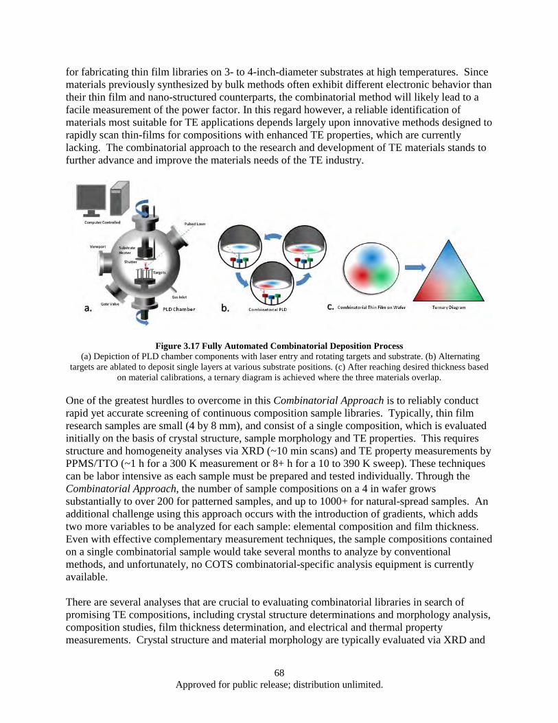
68 Approved for public release; distribution unlimited.
for fabricating thin film libraries on 3- to 4-inch-diameter substrates at high temperatures. Since materials previously synthesized by bulk methods often exhibit different electronic behavior than their thin film and nano-structured counterparts, the combinatorial method will likely lead to a facile measurement of the power factor. In this regard however, a reliable identification of materials most suitable for TE applications depends largely upon innovative methods designed to rapidly scan thin-films for compositions with enhanced TE properties, which are currently lacking. The combinatorial approach to the research and development of TE materials stands to further advance and improve the materials needs of the TE industry.
Figure 3.17 Fully Automated Combinatorial Deposition Process (a) Depiction of PLD chamber components with laser entry and rotating targets and substrate. (b) Alternating
targets are ablated to deposit single layers at various substrate positions. (c) After reaching desired thickness based on material calibrations, a ternary diagram is achieved where the three materials overlap.
One of the greatest hurdles to overcome in this Combinatorial Approach is to reliably conduct rapid yet accurate screening of continuous composition sample libraries. Typically, thin film research samples are small (4 by 8 mm), and consist of a single composition, which is evaluated initially on the basis of crystal structure, sample morphology and TE properties. This requires structure and homogeneity analyses via XRD (~10 min scans) and TE property measurements by PPMS/TTO (~1 h for a 300 K measurement or 8+ h for a 10 to 390 K sweep). These techniques can be labor intensive as each sample must be prepared and tested individually. Through the Combinatorial Approach, the number of sample compositions on a 4 in wafer grows substantially to over 200 for patterned samples, and up to 1000+ for natural-spread samples. An additional challenge using this approach occurs with the introduction of gradients, which adds two more variables to be analyzed for each sample: elemental composition and film thickness. Even with effective complementary measurement techniques, the sample compositions contained on a single combinatorial sample would take several months to analyze by conventional methods, and unfortunately, no COTS combinatorial-specific analysis equipment is currently available.
There are several analyses that are crucial to evaluating combinatorial libraries in search of promising TE compositions, including crystal structure determinations and morphology analysis, composition studies, film thickness determination, and electrical and thermal property measurements. Crystal structure and material morphology are typically evaluated via XRD and
69 Approved for public release; distribution unlimited.
microscopy techniques, respectively. The importance of these techniques is two-fold. First, one is provided an initial glimpse at the multi-phase structure (substitutional dopant, secondary phase, etc.). Second, since individual sample compositions on a substrate may not crystallize at the same temperature, crystallinity mapping allows us to identify crystalline regions of a combinatorial library and observe any deposition/anneal temperature effects for eventual structure-property correlations. (Ideally composition-spread samples are solid-solutions, and, thus, have similar structural properties.) The Division Bruker D8 XRD system allows for fully automated, high precision structure determinations of the different compositions that make up the combinatorial libraries. These analyses ensure a greater accuracy when evaluating various compositions for enhanced TE behavior. Elemental composition analyses ensure that the structures and TE property data is being assigned to the proper compositions, and can be determined via x-ray fluorescence (XRF), x-ray photoelectron spectroscopy (XPS), or wavelength dispersive spectroscopy (WDS).
Electrical resistivity in low-dimensional materials is a function of the materials’ thickness (specifically, inversely proportional), thereby making film thickness measurements vital for accurate TE property measurements. While it would be ideal to assume a constant film thickness gradient following deposition, our large combinatorial film samples typically contain thickness variations depending on each material’s ablation profile. Due to the nanometer scale thickness of our thin film samples, even minor variations in the film thickness could result in large variations of the measured electrical resistivity and could drastically alter the TE property maps if left unaccounted for. We have carefully considered these aspects (discussed later) in our sample processing and analysis procedures, which are designed to be conducted both quickly and cost-effectively. 3.3.2.3 Experimental
Aside from the TE property measurement methods mentioned earlier, in general, reliable means for adequate high temperature measurements of thin-films are still deficient. The methods discussed are sufficient for PF determinations for individual thin film samples, but are impractical for measurements of large, composition-spread samples. We have designed and built a Power Factor Screening Instrument (PFSI), with the capability to measure these large samples. This state-of-the-art tool, shown in Figure 3.18, is a high temperature adaptation of a measurement system developed by our collaborators at the National Institute of Standards and Technology (NIST). It consists of five main parts: the sample stage, the measurement head, the vacuum chamber, the instrumentation rack and the computer. The wiring diagram is provided for completeness in Figure 3.18 -d). This fully automated device is equipped with two linear translation stages and one vertical translation stage from Newport Corp. These control the movement of the sample to the different measurement positions. A water-cooled, 3-inch-diameter heater is mounted on the translation stages and can heat the sample up to 500 °C. The measurement head (highlighted in Figure 3.18 -b)) consists of a ceramic arm on an aluminum vertical support, and attached to the bottom of the ceramic arm are two copper blocks which are designed to measure electrical conductivity (resistivity) and Seebeck coefficient (ΔV/ΔT) using four Au-plated BeCu spring probes as sample contacts. Each Cu block (detailed in Figure 3.18 -c)) has embedded within it a small resistive cartridge heater to establish and maintain a small temperature gradient (ΔT). The heads also contain two Pt resistance temperature detectors

70 Approved for public release; distribution unlimited.
(RTDs) within the Cu blocks, one for feedback to the controller and the other directly on the spring probe to measure the temperature precisely at the location of the ΔV measurements. The spring probes and thermocouples are electrically isolated from the copper blocks and each other by a thin layer of high temperature epoxy. The spring probes are arranged in a straight line and used to make 4 probe resistivity and Seebeck voltage measurements.
By collecting data at a rate of over 150 sample points per hour, it becomes evident that this is an extremely effective method for the rapid identification and characterization of materials, as well as for reliable descriptions of composition-structure-property relationships at different temperatures. Several other screening tools have been reported; however, many can only be used for bulk samples, or up to ten thin film samples, and/or are limited by temperature.
The sample is manually positioned with the center of the sample under the measurement head. The custom-designed software program is then used to input the sample dimensions and the spacing between the sample locations. The program then automatically generates a field of sample locations to be measured. The stages move the sample to those locations and take the measurements. Figure 3.19 illustrates the front panel of the LabVIEW program designed to input data collection parameters. This program employs necessary algorithms and correction factors, and applies them to the measurement process in real-time.
The cartridge heaters are controlled by an Omega CN616 heater controller. Each heater is controlled separately to allow for a large variety of temperatures and temperature gradients (ΔT). The cartridge heaters in the measurement head are controlled to a user specified ΔT. The sample is then moved into contact with the spring probes and a ΔT is allowed to develop across the sample. After a user specified delay time, the Seebeck voltage is measured for a user specified time and the values averaged to yield the thermopower.
𝛼𝛼 = Δ𝑉𝑉
Δ𝑇𝑇 (3.1)
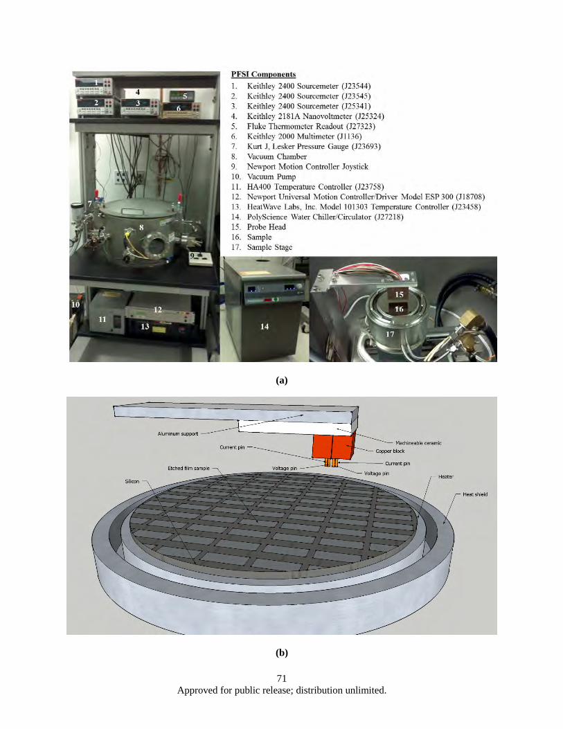
71 Approved for public release; distribution unlimited.
(a)
(b)
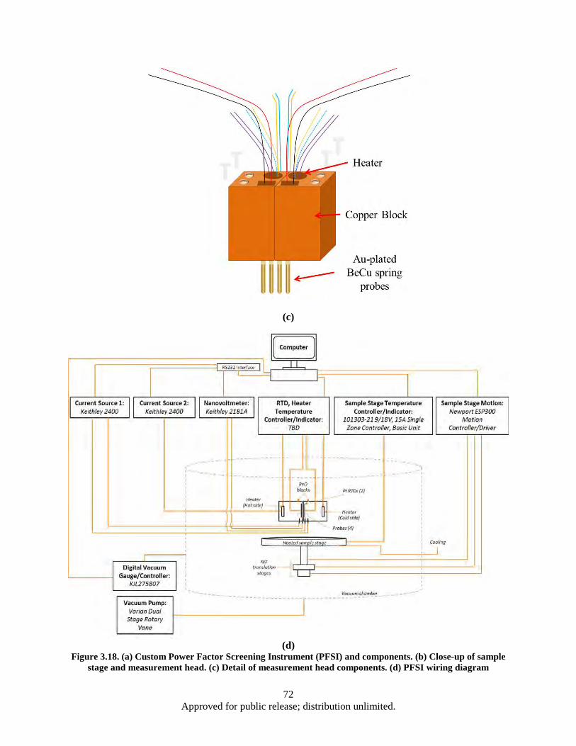
72 Approved for public release; distribution unlimited.
(c)
(d)
Figure 3.18. (a) Custom Power Factor Screening Instrument (PFSI) and components. (b) Close-up of sample stage and measurement head. (c) Detail of measurement head components. (d) PFSI wiring diagram
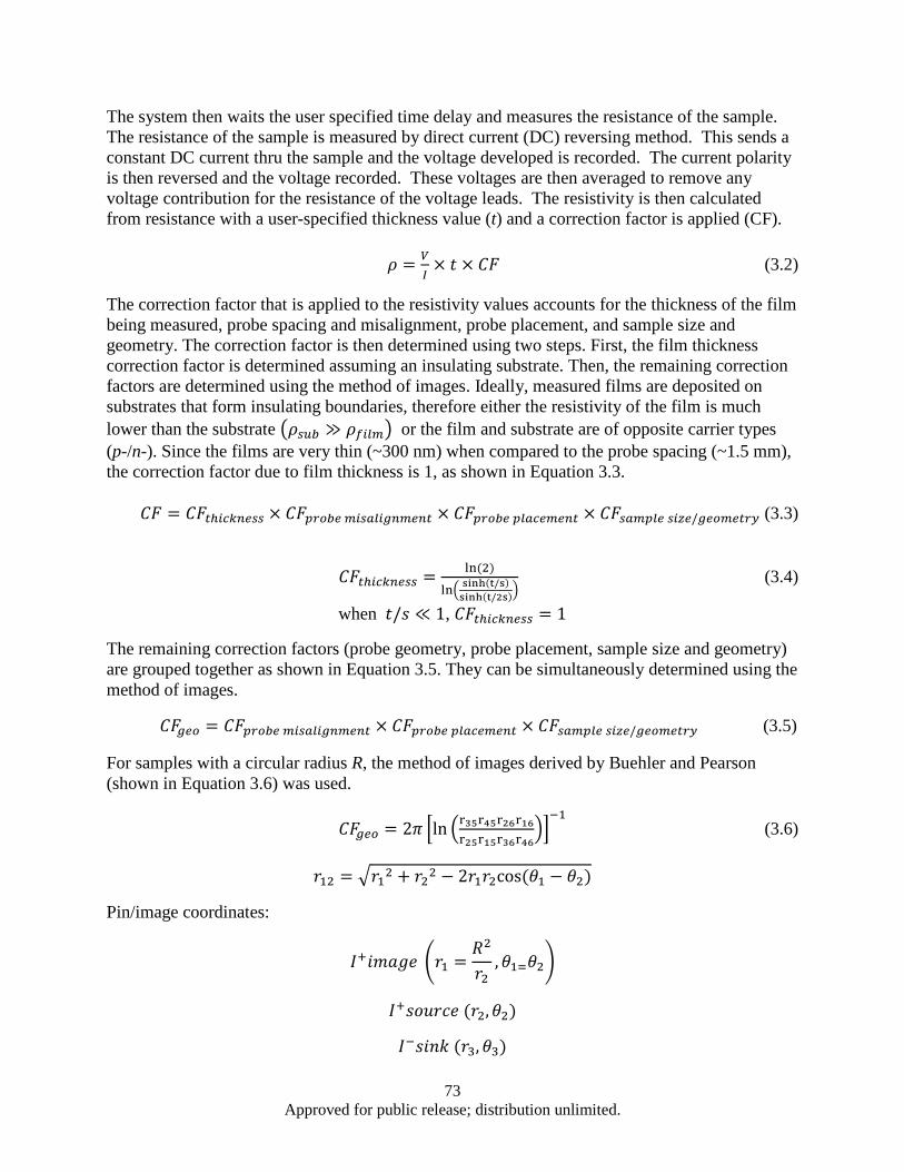
73 Approved for public release; distribution unlimited.
The system then waits the user specified time delay and measures the resistance of the sample. The resistance of the sample is measured by direct current (DC) reversing method. This sends a constant DC current thru the sample and the voltage developed is recorded. The current polarity is then reversed and the voltage recorded. These voltages are then averaged to remove any voltage contribution for the resistance of the voltage leads. The resistivity is then calculated from resistance with a user-specified thickness value (t) and a correction factor is applied (CF).
𝜌𝜌 = 𝑉𝑉
𝐼𝐼× 𝑡𝑡 × 𝑁𝑁𝐶𝐶 (3.2)
The correction factor that is applied to the resistivity values accounts for the thickness of the film being measured, probe spacing and misalignment, probe placement, and sample size and geometry. The correction factor is then determined using two steps. First, the film thickness correction factor is determined assuming an insulating substrate. Then, the remaining correction factors are determined using the method of images. Ideally, measured films are deposited on substrates that form insulating boundaries, therefore either the resistivity of the film is much lower than the substrate 𝜌𝜌𝑏𝑏𝑠𝑠𝑏𝑏 ≫ 𝜌𝜌𝑓𝑓𝑏𝑏𝑏𝑏𝑑𝑑 or the film and substrate are of opposite carrier types (p-/n-). Since the films are very thin (~300 nm) when compared to the probe spacing (~1.5 mm), the correction factor due to film thickness is 1, as shown in Equation 3.3.
𝑁𝑁𝐶𝐶 = 𝑁𝑁𝐶𝐶𝑤𝑤ℎ𝑏𝑏𝑑𝑑𝑖𝑖𝑏𝑏𝑑𝑑𝑏𝑏𝑏𝑏 × 𝑁𝑁𝐶𝐶𝑑𝑑𝑤𝑤𝑑𝑑𝑏𝑏𝑑𝑑 𝑑𝑑𝑏𝑏𝑏𝑏𝑤𝑤𝑏𝑏𝑏𝑏𝑚𝑚𝑏𝑏𝑑𝑑𝑑𝑑𝑏𝑏𝑤𝑤 × 𝑁𝑁𝐶𝐶𝑑𝑑𝑤𝑤𝑑𝑑𝑏𝑏𝑑𝑑 𝑑𝑑𝑏𝑏𝑤𝑤𝑑𝑑𝑑𝑑𝑑𝑑𝑑𝑑𝑏𝑏𝑤𝑤 × 𝑁𝑁𝐶𝐶𝑏𝑏𝑤𝑤𝑑𝑑𝑑𝑑𝑏𝑏𝑑𝑑 𝑏𝑏𝑏𝑏𝑠𝑠𝑑𝑑/𝑚𝑚𝑑𝑑𝑑𝑑𝑑𝑑𝑑𝑑𝑤𝑤𝑤𝑤𝑔𝑔 (3.3)
𝑁𝑁𝐶𝐶𝑤𝑤ℎ𝑏𝑏𝑑𝑑𝑖𝑖𝑏𝑏𝑑𝑑𝑏𝑏𝑏𝑏 = ln (2)
ln sinh(t/s) sinh(t/2s)
(3.4)
when 𝑡𝑡/𝑠𝑠 ≪ 1, 𝑁𝑁𝐶𝐶𝑤𝑤ℎ𝑏𝑏𝑑𝑑𝑖𝑖𝑏𝑏𝑑𝑑𝑏𝑏𝑏𝑏 = 1
The remaining correction factors (probe geometry, probe placement, sample size and geometry) are grouped together as shown in Equation 3.5. They can be simultaneously determined using the method of images.
𝑁𝑁𝐶𝐶𝑚𝑚𝑑𝑑𝑑𝑑 = 𝑁𝑁𝐶𝐶𝑑𝑑𝑤𝑤𝑑𝑑𝑏𝑏𝑑𝑑 𝑑𝑑𝑏𝑏𝑏𝑏𝑤𝑤𝑏𝑏𝑏𝑏𝑚𝑚𝑏𝑏𝑑𝑑𝑑𝑑𝑏𝑏𝑤𝑤 × 𝑁𝑁𝐶𝐶𝑑𝑑𝑤𝑤𝑑𝑑𝑏𝑏𝑑𝑑 𝑑𝑑𝑏𝑏𝑤𝑤𝑑𝑑𝑑𝑑𝑑𝑑𝑑𝑑𝑏𝑏𝑤𝑤 × 𝑁𝑁𝐶𝐶𝑏𝑏𝑤𝑤𝑑𝑑𝑑𝑑𝑏𝑏𝑑𝑑 𝑏𝑏𝑏𝑏𝑠𝑠𝑑𝑑/𝑚𝑚𝑑𝑑𝑑𝑑𝑑𝑑𝑑𝑑𝑤𝑤𝑤𝑤𝑔𝑔 (3.5)
For samples with a circular radius R, the method of images derived by Buehler and Pearson (shown in Equation 3.6) was used.
𝑁𝑁𝐶𝐶𝑚𝑚𝑑𝑑𝑑𝑑 = 2𝜋𝜋 ln r35r45r26r16r25r15r36r46
−1
(3.6)
𝑟𝑟12 = 𝑟𝑟12 + 𝑟𝑟22 − 2𝑟𝑟1𝑟𝑟2cos (𝜃𝜃1 − 𝜃𝜃2)
Pin/image coordinates:
𝐼𝐼+𝑖𝑖𝑚𝑚𝑖𝑖𝑖𝑖𝑖𝑖 𝑟𝑟1 =𝑅𝑅2
𝑟𝑟2,𝜃𝜃1=𝜃𝜃2
𝐼𝐼+𝑠𝑠𝑠𝑠𝑠𝑠𝑟𝑟𝑠𝑠𝑖𝑖 (𝑟𝑟2,𝜃𝜃2)
𝐼𝐼−𝑠𝑠𝑖𝑖𝑠𝑠𝑠𝑠 (𝑟𝑟3,𝜃𝜃3)

74 Approved for public release; distribution unlimited.
𝐼𝐼−𝑖𝑖𝑚𝑚𝑖𝑖𝑖𝑖𝑖𝑖 𝑟𝑟4 =𝑅𝑅2
𝑟𝑟3,𝜃𝜃4=𝜃𝜃3
𝑉𝑉+ (𝑟𝑟5,𝜃𝜃5)
𝑉𝑉− (𝑟𝑟6,𝜃𝜃6)
For samples with rectangular geometry, the method of images derived by Perloff (shown in Equation 3.7) was used in conjunction with elliptical functions found in Abramowitz and Stegun.
𝑁𝑁𝐶𝐶𝑚𝑚𝑑𝑑𝑑𝑑 = 4𝜋𝜋 ln α1α2α3α4
+ ln β1β2β3β4
−1
(3.7)
α1 = (𝑣𝑣2 − 𝑣𝑣4)2 + (𝑠𝑠2 − 𝑠𝑠4)2
α2 = (𝑣𝑣2 + 𝑣𝑣4)2 + (𝑠𝑠2 − 𝑠𝑠4)2
α3 = (𝑣𝑣2 − 𝑣𝑣1)2 + (𝑠𝑠2 − 𝑠𝑠1)2
α4 = (𝑣𝑣2 + 𝑣𝑣1)2 + (𝑠𝑠2 − 𝑠𝑠1)2
β1 = (𝑣𝑣3 − 𝑣𝑣1)2 + (𝑠𝑠3 − 𝑠𝑠1)2
β2 = (𝑣𝑣3 + 𝑣𝑣1)2 + (𝑠𝑠3 − 𝑠𝑠1)2
β3 = (𝑣𝑣3 − 𝑣𝑣4)2 + (𝑠𝑠3 − 𝑠𝑠4)2
β4 = (𝑣𝑣3 + 𝑣𝑣4)2 + (𝑠𝑠3 − 𝑠𝑠4)2
Pin/Images Coordinates:
𝐼𝐼+𝑠𝑠𝑠𝑠𝑠𝑠𝑟𝑟𝑠𝑠𝑖𝑖 (𝑠𝑠1 + 𝑖𝑖𝑣𝑣1)
𝑉𝑉+ (𝑠𝑠2 + 𝑖𝑖𝑣𝑣2)
𝑉𝑉− (𝑠𝑠3 + 𝑖𝑖𝑣𝑣3)
𝐼𝐼−𝑠𝑠𝑖𝑖𝑠𝑠𝑠𝑠 (𝑠𝑠4 + 𝑖𝑖𝑣𝑣4)
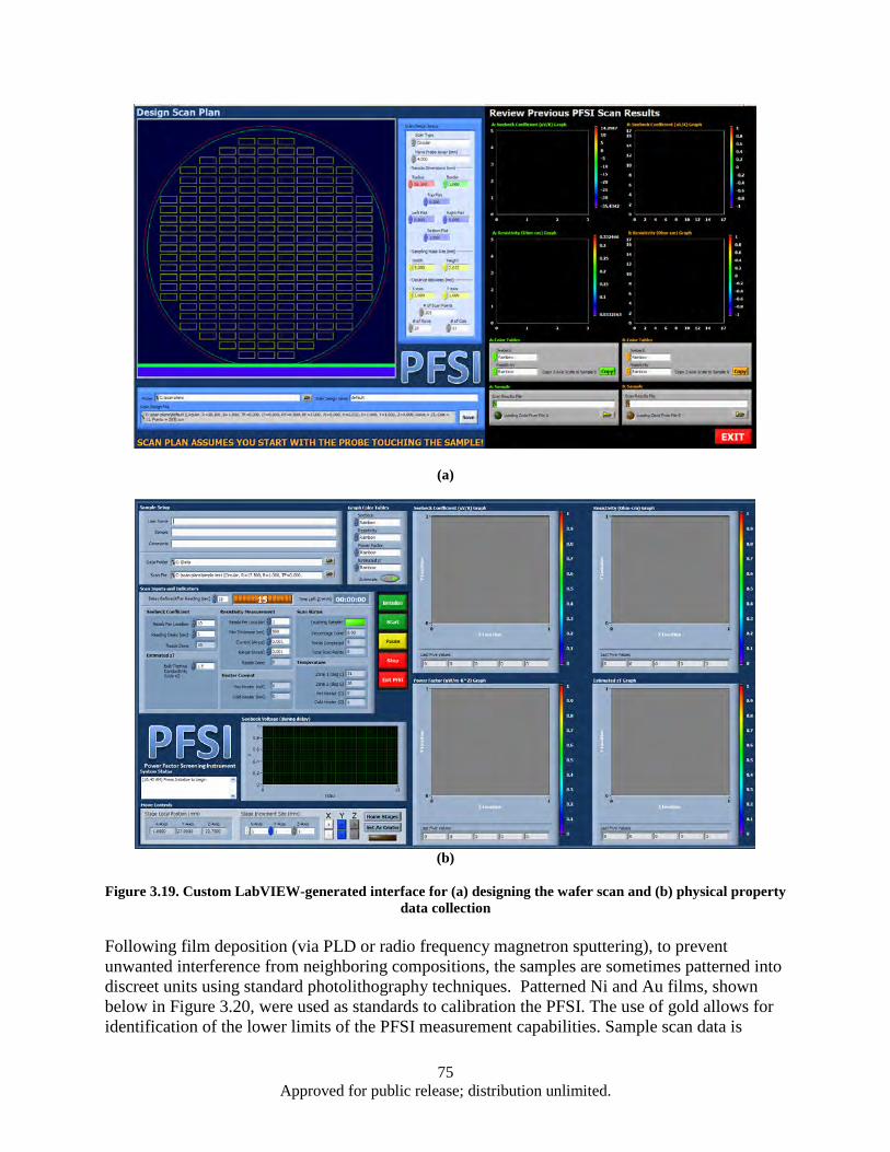
75 Approved for public release; distribution unlimited.
(a)
(b)
Figure 3.19. Custom LabVIEW-generated interface for (a) designing the wafer scan and (b) physical property
data collection Following film deposition (via PLD or radio frequency magnetron sputtering), to prevent unwanted interference from neighboring compositions, the samples are sometimes patterned into discreet units using standard photolithography techniques. Patterned Ni and Au films, shown below in Figure 3.20, were used as standards to calibration the PFSI. The use of gold allows for identification of the lower limits of the PFSI measurement capabilities. Sample scan data is
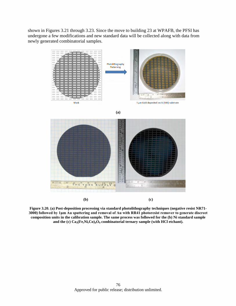
76 Approved for public release; distribution unlimited.
shown in Figures 3.21 through 3.23. Since the move to building 23 at WPAFB, the PFSI has undergone a few modifications and new standard data will be collected along with data from newly generated combinatorial samples.
(a)
(b) (c)
Figure 3.20. (a) Post-deposition processing via standard photolithography techniques (negative resist NR71-3000) followed by 1μm Au sputtering and removal of Au with RR41 photoresist remover to generate discreet
composition units in the calibration sample. The same process was followed for the (b) Ni standard sample and the (c) Ca3(Fe,Ni,Co)4O9 combinatorial ternary sample (with HCl etchant).
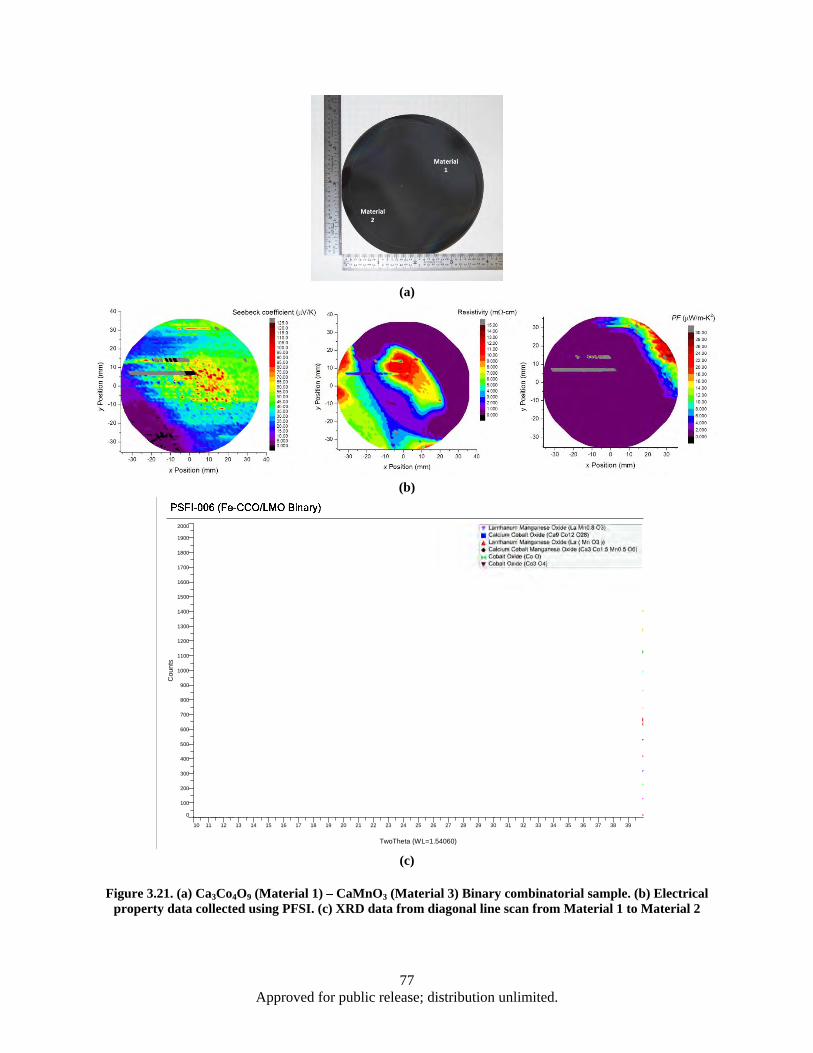
77 Approved for public release; distribution unlimited.
(a)
(b)
(c)
Figure 3.21. (a) Ca3Co4O9 (Material 1) – CaMnO3 (Material 3) Binary combinatorial sample. (b) Electrical
property data collected using PFSI. (c) XRD data from diagonal line scan from Material 1 to Material 2
0
100
200
300
400
500
600
700
800
900
1000
1100
1200
1300
1400
1500
1600
1700
1800
1900
2000
Cou
nts
10 11 12 13 14 15 16 17 18 19 20 21 22 23 24 25 26 27 28 29 30 31 32 33 34 35 36 37 38 39
TwoTheta (WL=1.54060)
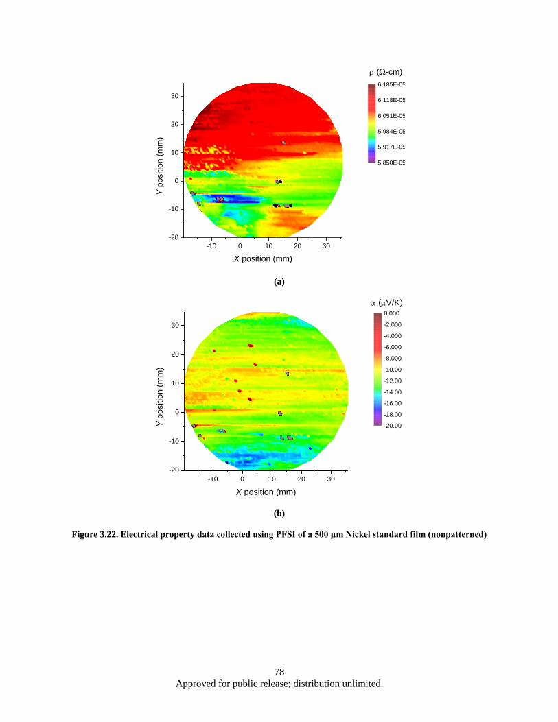
78 Approved for public release; distribution unlimited.
(a)
(b)
Figure 3.22. Electrical property data collected using PFSI of a 500 μm Nickel standard film (nonpatterned)
-10 0 10 20 30-20
-10
0
10
20
30
Y p
ositi
on (m
m)
X position (mm)
5.850E-05
5.917E-05
5.984E-05
6.051E-05
6.118E-05
6.185E-05
ρ (Ω-cm)
-10 0 10 20 30-20
-10
0
10
20
30
Y p
ositi
on (m
m)
X position (mm)
-20.00
-18.00
-16.00
-14.00
-12.00
-10.00
-8.000
-6.000
-4.000
-2.000
0.000α (µV/K)
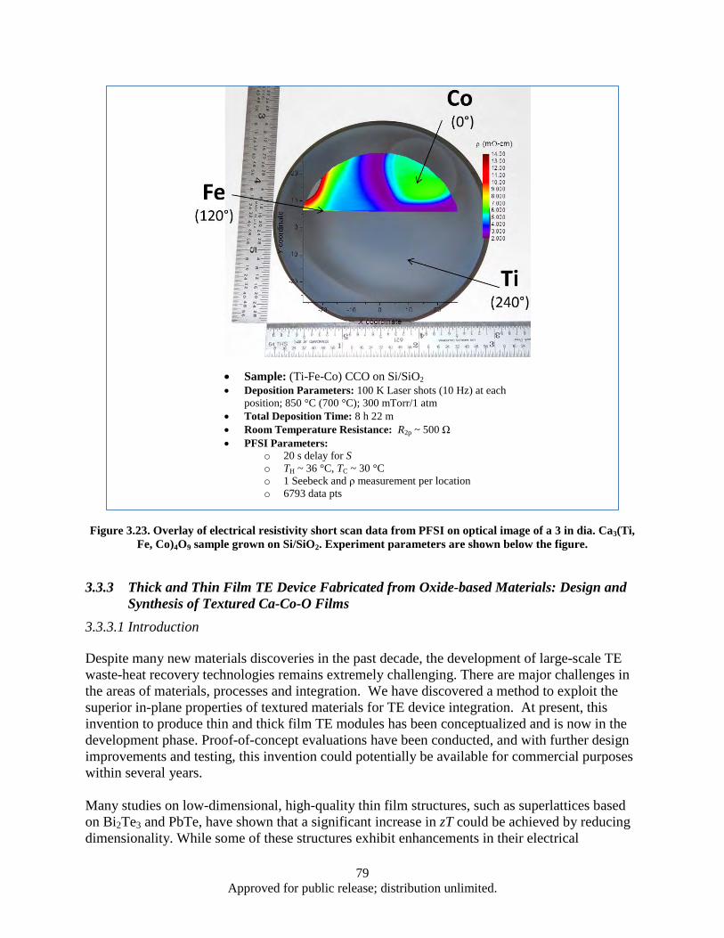
79 Approved for public release; distribution unlimited.
Figure 3.23. Overlay of electrical resistivity short scan data from PFSI on optical image of a 3 in dia. Ca3(Ti, Fe, Co)4O9 sample grown on Si/SiO2. Experiment parameters are shown below the figure.
3.3.3 Thick and Thin Film TE Device Fabricated from Oxide-based Materials: Design and Synthesis of Textured Ca-Co-O Films
3.3.3.1 Introduction Despite many new materials discoveries in the past decade, the development of large-scale TE waste-heat recovery technologies remains extremely challenging. There are major challenges in the areas of materials, processes and integration. We have discovered a method to exploit the superior in-plane properties of textured materials for TE device integration. At present, this invention to produce thin and thick film TE modules has been conceptualized and is now in the development phase. Proof-of-concept evaluations have been conducted, and with further design improvements and testing, this invention could potentially be available for commercial purposes within several years.
Many studies on low-dimensional, high-quality thin film structures, such as superlattices based on Bi2Te3 and PbTe, have shown that a significant increase in zT could be achieved by reducing dimensionality. While some of these structures exhibit enhancements in their electrical
• Sample: (Ti-Fe-Co) CCO on Si/SiO2 • Deposition Parameters: 100 K Laser shots (10 Hz) at each
position; 850 °C (700 °C); 300 mTorr/1 atm • Total Deposition Time: 8 h 22 m • Room Temperature Resistance: R2p ~ 500 Ω • PFSI Parameters:
o 20 s delay for S o TH ~ 36 °C, TC ~ 30 °C o 1 Seebeck and ρ measurement per location o 6793 data pts
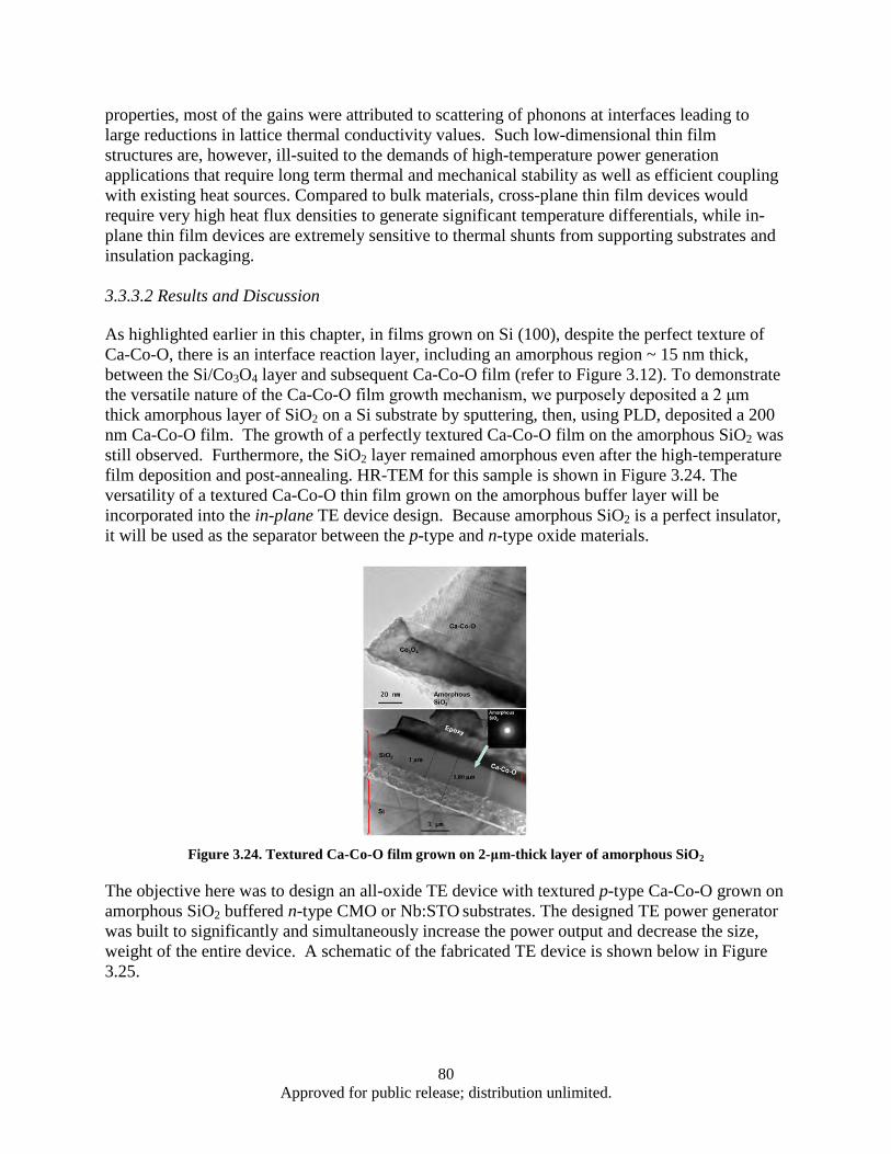
80 Approved for public release; distribution unlimited.
properties, most of the gains were attributed to scattering of phonons at interfaces leading to large reductions in lattice thermal conductivity values. Such low-dimensional thin film structures are, however, ill-suited to the demands of high-temperature power generation applications that require long term thermal and mechanical stability as well as efficient coupling with existing heat sources. Compared to bulk materials, cross-plane thin film devices would require very high heat flux densities to generate significant temperature differentials, while in-plane thin film devices are extremely sensitive to thermal shunts from supporting substrates and insulation packaging. 3.3.3.2 Results and Discussion As highlighted earlier in this chapter, in films grown on Si (100), despite the perfect texture of Ca-Co-O, there is an interface reaction layer, including an amorphous region ~ 15 nm thick, between the Si/Co3O4 layer and subsequent Ca-Co-O film (refer to Figure 3.12). To demonstrate the versatile nature of the Ca-Co-O film growth mechanism, we purposely deposited a 2 μm thick amorphous layer of SiO2 on a Si substrate by sputtering, then, using PLD, deposited a 200 nm Ca-Co-O film. The growth of a perfectly textured Ca-Co-O film on the amorphous SiO2 was still observed. Furthermore, the SiO2 layer remained amorphous even after the high-temperature film deposition and post-annealing. HR-TEM for this sample is shown in Figure 3.24. The versatility of a textured Ca-Co-O thin film grown on the amorphous buffer layer will be incorporated into the in-plane TE device design. Because amorphous SiO2 is a perfect insulator, it will be used as the separator between the p-type and n-type oxide materials.
Figure 3.24. Textured Ca-Co-O film grown on 2-μm-thick layer of amorphous SiO2
The objective here was to design an all-oxide TE device with textured p-type Ca-Co-O grown on amorphous SiO2 buffered n-type CMO or Nb:STO substrates. The designed TE power generator was built to significantly and simultaneously increase the power output and decrease the size, weight of the entire device. A schematic of the fabricated TE device is shown below in Figure 3.25.
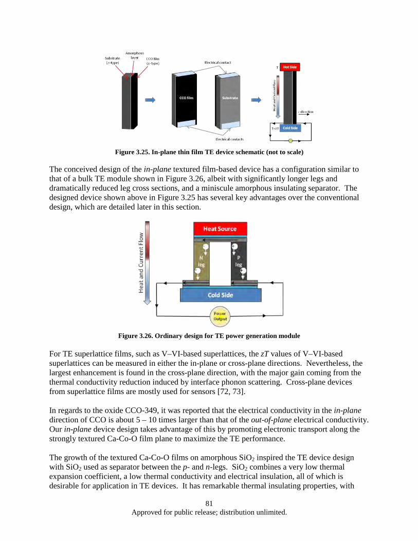
81 Approved for public release; distribution unlimited.
Figure 3.25. In-plane thin film TE device schematic (not to scale)
The conceived design of the in-plane textured film-based device has a configuration similar to that of a bulk TE module shown in Figure 3.26, albeit with significantly longer legs and dramatically reduced leg cross sections, and a miniscule amorphous insulating separator. The designed device shown above in Figure 3.25 has several key advantages over the conventional design, which are detailed later in this section.
Figure 3.26. Ordinary design for TE power generation module
For TE superlattice films, such as V–VI-based superlattices, the zT values of V–VI-based superlattices can be measured in either the in-plane or cross-plane directions. Nevertheless, the largest enhancement is found in the cross-plane direction, with the major gain coming from the thermal conductivity reduction induced by interface phonon scattering. Cross-plane devices from superlattice films are mostly used for sensors [72, 73].
In regards to the oxide CCO-349, it was reported that the electrical conductivity in the in-plane direction of CCO is about 5 – 10 times larger than that of the out-of-plane electrical conductivity. Our in-plane device design takes advantage of this by promoting electronic transport along the strongly textured Ca-Co-O film plane to maximize the TE performance.
The growth of the textured Ca-Co-O films on amorphous SiO2 inspired the TE device design with SiO2 used as separator between the p- and n-legs. SiO2 combines a very low thermal expansion coefficient, a low thermal conductivity and electrical insulation, all of which is desirable for application in TE devices. It has remarkable thermal insulating properties, with
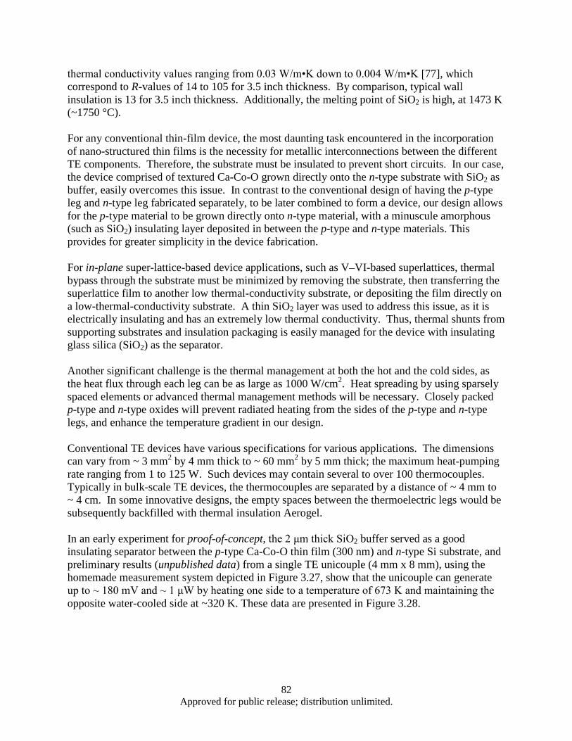
82 Approved for public release; distribution unlimited.
thermal conductivity values ranging from 0.03 W/m•K down to 0.004 W/m•K [77], which correspond to R-values of 14 to 105 for 3.5 inch thickness. By comparison, typical wall insulation is 13 for 3.5 inch thickness. Additionally, the melting point of SiO2 is high, at 1473 K (~1750 °C).
For any conventional thin-film device, the most daunting task encountered in the incorporation of nano-structured thin films is the necessity for metallic interconnections between the different TE components. Therefore, the substrate must be insulated to prevent short circuits. In our case, the device comprised of textured Ca-Co-O grown directly onto the n-type substrate with SiO2 as buffer, easily overcomes this issue. In contrast to the conventional design of having the p-type leg and n-type leg fabricated separately, to be later combined to form a device, our design allows for the p-type material to be grown directly onto n-type material, with a minuscule amorphous (such as SiO2) insulating layer deposited in between the p-type and n-type materials. This provides for greater simplicity in the device fabrication.
For in-plane super-lattice-based device applications, such as V–VI-based superlattices, thermal bypass through the substrate must be minimized by removing the substrate, then transferring the superlattice film to another low thermal-conductivity substrate, or depositing the film directly on a low-thermal-conductivity substrate. A thin SiO2 layer was used to address this issue, as it is electrically insulating and has an extremely low thermal conductivity. Thus, thermal shunts from supporting substrates and insulation packaging is easily managed for the device with insulating glass silica (SiO2) as the separator.
Another significant challenge is the thermal management at both the hot and the cold sides, as the heat flux through each leg can be as large as 1000 W/cm2. Heat spreading by using sparsely spaced elements or advanced thermal management methods will be necessary. Closely packed p-type and n-type oxides will prevent radiated heating from the sides of the p-type and n-type legs, and enhance the temperature gradient in our design.
Conventional TE devices have various specifications for various applications. The dimensions can vary from ~ 3 mm2 by 4 mm thick to ~ 60 mm2 by 5 mm thick; the maximum heat-pumping rate ranging from 1 to 125 W. Such devices may contain several to over 100 thermocouples. Typically in bulk-scale TE devices, the thermocouples are separated by a distance of ~ 4 mm to ~ 4 cm. In some innovative designs, the empty spaces between the thermoelectric legs would be subsequently backfilled with thermal insulation Aerogel.
In an early experiment for proof-of-concept, the 2 μm thick SiO2 buffer served as a good insulating separator between the p-type Ca-Co-O thin film (300 nm) and n-type Si substrate, and preliminary results (unpublished data) from a single TE unicouple (4 mm x 8 mm), using the homemade measurement system depicted in Figure 3.27, show that the unicouple can generate up to ~ 180 mV and ~ 1 μW by heating one side to a temperature of 673 K and maintaining the opposite water-cooled side at ~320 K. These data are presented in Figure 3.28.
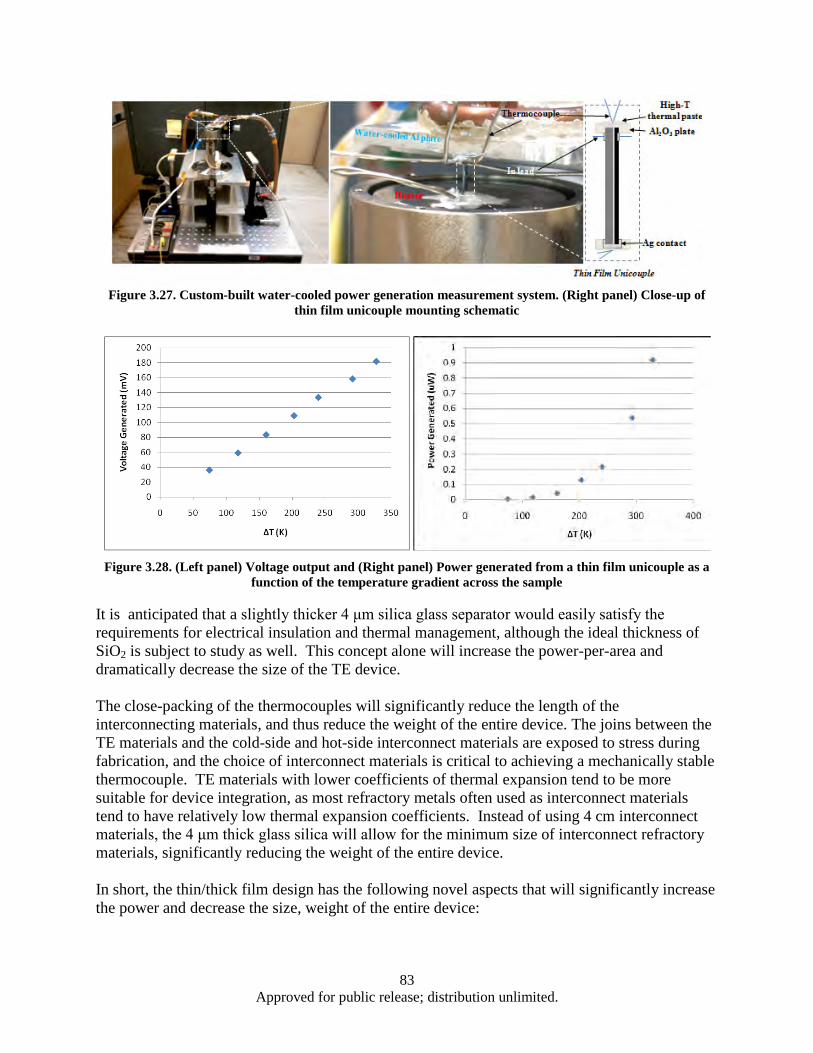
83 Approved for public release; distribution unlimited.
Figure 3.27. Custom-built water-cooled power generation measurement system. (Right panel) Close-up of
thin film unicouple mounting schematic
Figure 3.28. (Left panel) Voltage output and (Right panel) Power generated from a thin film unicouple as a
function of the temperature gradient across the sample
It is anticipated that a slightly thicker 4 μm silica glass separator would easily satisfy the requirements for electrical insulation and thermal management, although the ideal thickness of SiO2 is subject to study as well. This concept alone will increase the power-per-area and dramatically decrease the size of the TE device.
The close-packing of the thermocouples will significantly reduce the length of the interconnecting materials, and thus reduce the weight of the entire device. The joins between the TE materials and the cold-side and hot-side interconnect materials are exposed to stress during fabrication, and the choice of interconnect materials is critical to achieving a mechanically stable thermocouple. TE materials with lower coefficients of thermal expansion tend to be more suitable for device integration, as most refractory metals often used as interconnect materials tend to have relatively low thermal expansion coefficients. Instead of using 4 cm interconnect materials, the 4 μm thick glass silica will allow for the minimum size of interconnect refractory materials, significantly reducing the weight of the entire device.
In short, the thin/thick film design has the following novel aspects that will significantly increase the power and decrease the size, weight of the entire device:
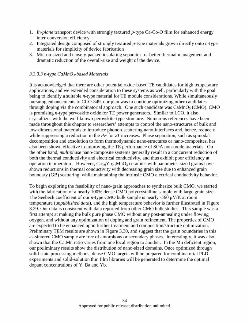
84 Approved for public release; distribution unlimited.
1. In-plane transport device with strongly textured p-type Ca-Co-O film for enhanced energy inter-conversion efficiency
2. Integrated design composed of strongly textured p-type materials grown directly onto n-type materials for simplicity of device fabrication
3. Micron-sized and closely-packed insulating separator for better thermal management and dramatic reduction of the overall-size and weight of the device.
3.3.3.3 n-type CaMnO3-based Materials It is acknowledged that there are other potential oxide-based TE candidates for high temperature applications, and we extended consideration to these systems as well, particularly with the goal being to identify a suitable n-type material for TE module considerations. While simultaneously pursuing enhancements to CCO-349, our plan was to continue optimizing other candidates through doping via the combinatorial approach. One such candidate was CaMnO3 (CMO). CMO is promising n-type pervoskite oxide for TE power generators. Similar to LCO, it also crystallizes with the well-known perovskite-type structure. Numerous references have been made throughout this chapter to researchers’ attempts to control the nano-structures of bulk and low-dimensional materials to introduce phonon-scattering nano-interfaces and, hence, reduce κ while suppressing a reduction in the PF for zT increases. Phase separation, such as spinodal decomposition and exsolution to form thermodynamic nano-structures or nano-composites, has also been shown effective in improving the TE performance of SOA non-oxide materials. On the other hand, multiphase nano-composite systems generally result in a concurrent reduction of both the thermal conductivity and electrical conductivity, and thus exhibit poor efficiency at operation temperature. However, Ca0.9Yb0.1MnO3 ceramics with nanometer-sized grains have shown reductions in thermal conductivity with decreasing grain size due to enhanced grain boundary (GB) scattering, while maintaining the intrinsic CMO electrical conductivity behavior.
To begin exploring the feasibility of nano-grain approaches to synthesize bulk CMO, we started with the fabrication of a nearly 100% dense CMO polycrystalline sample with large grain size. The Seebeck coefficient of our n-type CMO bulk sample is nearly -560 μV/K at room temperature (unpublished data), and the high temperature behavior is further illustrated in Figure 3.29. Our data is consistent with data reported from other CMO bulk studies. This sample was a first attempt at making the bulk pure phase CMO without any post-annealing under flowing oxygen, and without any optimization of doping and grain refinement. The properties of CMO are expected to be enhanced upon further treatment and composition/structure optimization. Preliminary TEM results are shown in Figure 3.30, and suggest that the grain boundaries in this as-sintered CMO sample are free of amorphous or secondary phases. Interestingly, it was also shown that the Ca:Mn ratio varies from one local region to another. In the Mn deficient region, our preliminary results show the distribution of nano-sized domains. Once optimized through solid-state processing methods, dense CMO targets will be prepared for combinatorial PLD experiments and solid-solution thin film libraries will be generated to determine the optimal dopant concentrations of Y, Ba and Yb.
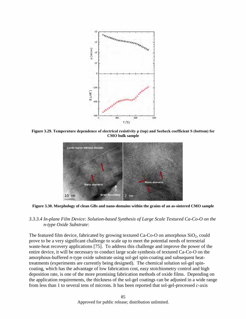
85 Approved for public release; distribution unlimited.
Figure 3.29. Temperature dependence of electrical resistivity ρ (top) and Seebeck coefficient S (bottom) for
CMO bulk sample
Figure 3.30. Morphology of clean GBs and nano-domains within the grains of an as-sintered CMO sample
3.3.3.4 In-plane Film Device: Solution-based Synthesis of Large Scale Textured Ca-Co-O on the n-type Oxide Substrate:
The featured film device, fabricated by growing textured Ca-Co-O on amorphous SiO2, could prove to be a very significant challenge to scale up to meet the potential needs of terrestrial waste-heat recovery applications [75]. To address this challenge and improve the power of the entire device, it will be necessary to conduct large scale synthesis of textured Ca-Co-O on the amorphous-buffered n-type oxide substrate using sol-gel spin-coating and subsequent heat-treatments (experiments are currently being designed). The chemical solution sol-gel spin-coating, which has the advantage of low fabrication cost, easy stoichiometry control and high deposition rate, is one of the more promising fabrication methods of oxide films. Depending on the application requirements, the thickness of the sol-gel coatings can be adjusted in a wide range from less than 1 to several tens of microns. It has been reported that sol-gel-processed c-axis

86 Approved for public release; distribution unlimited.
oriented Ca-Co-O-based thick-films up to 650 nm were successfully grown on sapphire (0001) substrates [76]-[78]. We will coat the n-type oxide with an amorphous SiO2 layer 2 – 4 μm thick. Study of textured thick films on the amorphous-buffered n-type substrate will proceed by considering the following aspects:
1. Effect of the sintering temperature, (ranging from 650 to 800 °C), on the crystal structure, film morphology and TE properties. The nominal composition of the thick-film will be the same as that from the optimized PLD thin film, including pure Ca-Co-O, doped Ca-Co-O and Ca-Co-O with nano-inclusions
2. Synthesis of textured thick sol-gel film with thicknesses up to several tens of microns. Single spin-coating and multiple-step coating processes will be attempted to achieve a thick layer of up to 100 microns. (It is reported that, depending on the solvent content in the coating solution, coating thickness can be varied from 3 μm up to more than 25 μm in a single spin coating step. Thicker layers of up to 100 μm can be realized using the multi-step coating process.)
3. The sol-gel thick films will first be grown on commercial n-type single crystal substrates to optimize the synthesis conditions of Ca-Co-O. The textured thick-films, grown under optimized growth conditions will then be grown on the SiO2-buffered n-type oxide substrate (CMO or Nb:STO) to produce the all-oxide TE device prototype.
Ultimately, evaluations of power generation and durability of the devices and modules fabricated under this effort will be carried out through the use of the custom-designed measurement system recently built for dynamic testing of commercial TE modules. Various leg dimensions and film thicknesses will be considered to determine optimum device dimensions. As it will be of high importance to maintain separation of the p- and n-legs, the outer edges of all devices will be polished prior to measurements to ensure electrical insulation.
We must also at this stage consider additional physical property measurements. Internal resistance measurements will be carried out using the standard 4-probe and van der Pauw testing methods. To minimize contact resistance, Ag and Au will be sputtered and annealed prior to measurements. As our design concept calls for the unicouples to be stood on edge, it may be necessary to determine the mechanical strength by conducting three-point bending tests at room temperature and at maximum operating temperature. Ultimately, the n-type substrate will provide the largest contribution to the device’s mechanical strength. Linear thermal expansion coefficients will also be measured during operation.
Summary 3.4
We have been able to identify the unique dopant segregation behavior in Ca3Co4O9 (CCO-349) and determine film growth initiators and solubility limits as a path to enhancing other oxide-based high-temperature TE materials. With 200+ bulk and film samples synthesized using various processes, we have made considerable progress in elucidating structure-property relationships in Ca-Co-O-based materials, and have substantially improved the TE properties of CCO-349 through doping effects.
We have designed and built a SOA Power Factor Screening Instrument (PFSI), with the capability to measure the Seebeck coefficient and electrical resistivity simultaneously up to ~

87 Approved for public release; distribution unlimited.
500 °C for thin film samples. Useful demonstrations of the effectiveness of the PFSI, have been carried out by first exploring the oxide-based p-Ca3Co4O9/n-CaMnO3 system. Although zT values for alloys and semiconductors are typically higher than those for oxide-based materials, oxides are more desirable for use in high-temperature power generation applications for their high thermal stability in air, low toxicity, affordability and raw material abundance. Perovskite ceramics are appealing functional materials that are utilized in numerous energy conversion processes due to their flexible structure and a variety of properties. The very attractive physical-chemical properties of perovskite-type phases can be modified in a controlled way by changing the composition and crystallographic structure in chemistry synthesis processes.
After discovering the self-assembling behavior of CCO-349 on an amorphous substrate, we exploited this behavior to optimize the energy inter-conversion properties of oxide-based materials by developing and successfully demonstrating an innovative all-oxide TE device for mid-to-high temperature power generation applications. It is intended that this invention generates TE devices, which are easy to fabricate and thus facilitate mass production, with a high potential for use in large-scale operations. We specifically target materials for mid- to high-temperature power generation applications that overcome the traditional barriers faced by low dimensional materials during scale-up productions, and possess the ability to enhance the efficiency of other systems by waste-heat scavenging.
With continued investment in this project, the payoffs remain high. Existing SOA TE material compositions present several issues such as low efficiency, poor stability at high temperatures in air, high reactivity, and are generally comprised of rare and/or costly materials. There is a great need for newer TE material compositions that have higher efficiency and are economical. Success has been realized in low-dimensional material studies, but very few transitional demonstrations with oxide-based TE thin films exist. Through the approaches presented in this report, our team continues to address the obstacles faced in the development of high efficiency TE materials.

88 Approved for public release; distribution unlimited.
Development of high strength nano-structured composite permanent magnets based 4.on SmCo alloy.
Development of magnetically hard and soft bulk nano-composite magnetic materials 4.1overview Research Objectives
4.1.1 Background
Uprising need for higher performance and improved reliability of future air and space vehicles for the AF mission requires development of new more efficient and lightweight mechanical and electrical components able to function well at adverse conditions such as elevated temperatures and high mechanical stresses. Permanent magnets play the key role in design of power conversion and energy generating units used in military aircraft, therefore magnetic materials with superior properties to the current state-of-art magnets are required.
Performance of a permanent magnet is characterized by its maximum energy product (BH)max, which depends on the magnetic coercivity and saturation magnetization of the material. Development of a magnet with higher BHmax product will lead to the increased performance as well as reduced size and weight of the essential aircraft components. Magnetic materials retain their properties within certain temperature range limited by the Curie temperature TC, which is specific for each material composition. Expanding the working temperature range by engineering new materials exhibiting higher TC will result in prolonged lifetime and improved reliability of the magnetic components of the aircraft. In addition, such materials with better temperature stability will require less power and service equipment used for the component cooling.
In the past several decades, the primary materials for permanent magnet manufacturing were Sm2Co17-based and Nd2Fe14B-based alloys owning to their superior magnetic strength originating from intrinsic anisotropy of the crystal lattice. Maximum energy products (BH)max of 31 MgOe and 59 MGOe have been achieved in Sm2Co17 and Nd2Fe14B systems respectively by optimization of the chemical composition and metal grain structure. However, these numbers are approaching the corresponding theoretical energy product limits of 39 and 64 MGOe for Sm2Co17 and Nd2Fe14B, therefore in order to meet the higher performance requirements new classes of permanent magnet materials have to be studied and developed.
A promising new class of permanent magnets is an exchange-coupled nanocomposite material, which consists of two hard (high coercivity) and soft (large saturation moment) magnetic phases suitably dispersed on the scale of tens of nanometers. Such composite material will benefit from both high magnetocrystalline anisotropy of the hard phase and large magnetic saturation of the soft phase leading to significant enhancement of the (BH)max energy product compared to the individual phases. Since the soft phase is usually a FeCo-based composition an additional advantage is the reduces overall amount of rare-earth metal, and therefore cost, needed to prepare the composite material due to smaller volume fraction of the RE-rich hard phase. Theoretical calculations on nanograin exchange-coupled magnets predict values of (BH)max up to 94 MGOe, 75 MGOe and 65 MGOe for Nd2Fe14B/Fe65Co35, Sm2Co17/Fe65Co35 and SmCo5/Fe65Co35 nanocomposite magnets with 40 wt% of the Fe65Co35 soft phase, which indicate a 1.5-2 times increase in (BH)max compared to single phase Nd2Fe14B or Sm-Co alloys.

89 Approved for public release; distribution unlimited.
4.1.2 Experimental methods discussion
In order to obtain high energy product material the bulk magnetically hard/soft nanocomposite magnet should meet a number of requirements: 1) the nanocomposite phases homogenously distributed with the grain size on order of 10 nm; 2) both the hard and soft phases crystallographically coherent as a necessary condition for mutual exchange coupling; 3) anisotropic bulk magnet structure; and 4) full bulk density.
In recent years, magnetic powder with anisotropic flake particle morphology and flake thickness on order of few tens nanometers were made by surfactant-assisted high energy ball milling (HEBM) of magnetic alloys prepared by melt-spinning or arc melting techniques. Flake shape and thickness can be controlled by varying the milling process parameters such as weight ratio between powder, surfactant and ball media, milling time, etc. The main difficulty with this process is the surfactant removal from the milled powder, which requires heat treatment at temperatures above the surfactant boiling point. At elevated temperature, interdiffusion can occur between powder particles leading to larger particle size. Alternative methods such as CO2-assisted leaching can be employed in order to avoid unwanted grain growth during the heat treatment surfactants with lower molecular weight. Furthermore the lower boiling point can be used in this process as well.
Nanoflake appearance of the milled powder is highly beneficial for fabrication of anisotropic bulk magnets using the powder magnetic alignment techniques. High energy ball milling carried out in a constant magnetic field created by permanent magnets placed around the milling jar as well as pulse magnetizing immediately prior to powder compaction will result in better grain alignment and anisotropic properties of the final bulk magnet.
Nanopowder compaction is another challenge since in conventional hot isostatic pressing (HIP) prolonged heat treatments at high temperatures will result in the grain growth and loss of nanoscale microstructure, while compaction at lower temperatures may not produce the full density bulk. An alternative method of shockwave metal powder consolidation resulting in nearly 100% dense bulk and minimum grain growth has been practiced in the past. In this method a powder sample is confined inside a metal capsule, which is impacted by a high-velocity projectile. The impact-generated shockwave delivers energy to the powder plastically deforming the particles and compacting it into a bulk sample. The shockwave propagation time is on order of nanoseconds, which is insufficient for interdiffusion and grain growth to take place; therefore, the nanostructure of the magnetic material is preserved.
4.1.3 Projected research work summary
Exchange-coupled nanocomposite magnetic materials are a promising new class for development of high energy bulk permanent magnets. Nanoscale combination of magnetically hard phase (Nd2Fe14B, SmCo5, Sm2Co17) with high coercivity and magnetically soft phase (Fe, FeCo) with large saturation moment will produce a composite material superior to the current state-of-art magnets in terms of maximum energy product (BH)max.
Fabrication of such material requires preparation of nanoscale powder, its magnetic alignment and subsequent consolidation. Powder preparation will be realized by arc melting of the necessary alloy ingots, crushing the ingots into microscale coarse powder followed by surfactant-
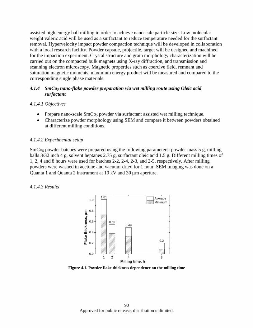
90 Approved for public release; distribution unlimited.
assisted high energy ball milling in order to achieve nanoscale particle size. Low molecular weight valeric acid will be used as a surfactant to reduce temperature needed for the surfactant removal. Hypervelocity impact powder compaction technique will be developed in collaboration with a local research facility. Powder capsule, projectile, target will be designed and machined for the impaction experiment. Crystal structure and grain morphology characterization will be carried out on the compacted bulk magnets using X-ray diffraction, and transmission and scanning electron microscopy. Magnetic properties such as coercive field, remnant and saturation magnetic moments, maximum energy product will be measured and compared to the corresponding single phase materials.
4.1.4 SmCo5 nano-flake powder preparation via wet milling route using Oleic acid surfactant
4.1.4.1 Objectives
• Prepare nano-scale SmCo5 powder via surfactant assisted wet milling technique. • Characterize powder morphology using SEM and compare it between powders obtained
at different milling conditions.
4.1.4.2 Experimental setup
SmCo5 powder batches were prepared using the following parameters: powder mass 5 g, milling balls 3/32 inch 4 g, solvent heptanes 2.75 g, surfactant oleic acid 1.5 g. Different milling times of 1, 2, 4 and 8 hours were used for batches 2-2, 2-4, 2-3, and 2-5, respectively. After milling powders were washed in acetone and vacuum-dried for 1 hour. SEM imaging was done on a Quanta 1 and Quanta 2 instrument at 10 kV and 30 µm aperture.
4.1.4.3 Results
Figure 4.1. Powder flake thickness dependence on the milling time
1.01
0.550.49
0.2
1 2 4 80.0
0.2
0.4
0.6
0.8
1.0
Flak
e th
ickn
ess,
µm
Milling time, h
Average Minimum
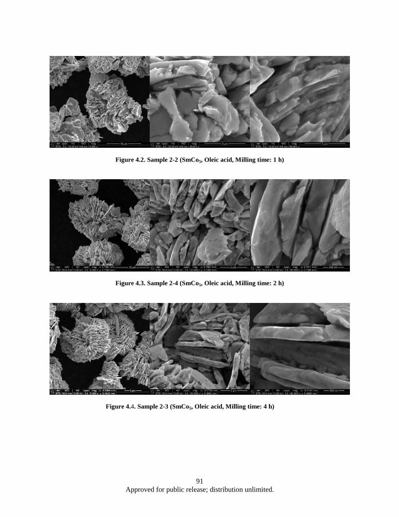
91 Approved for public release; distribution unlimited.
Figure 4.2. Sample 2-2 (SmCo5, Oleic acid, Milling time: 1 h)
Figure 4.3. Sample 2-4 (SmCo5, Oleic acid, Milling time: 2 h)
Figure 4.4. Sample 2-3 (SmCo5, Oleic acid, Milling time: 4 h)
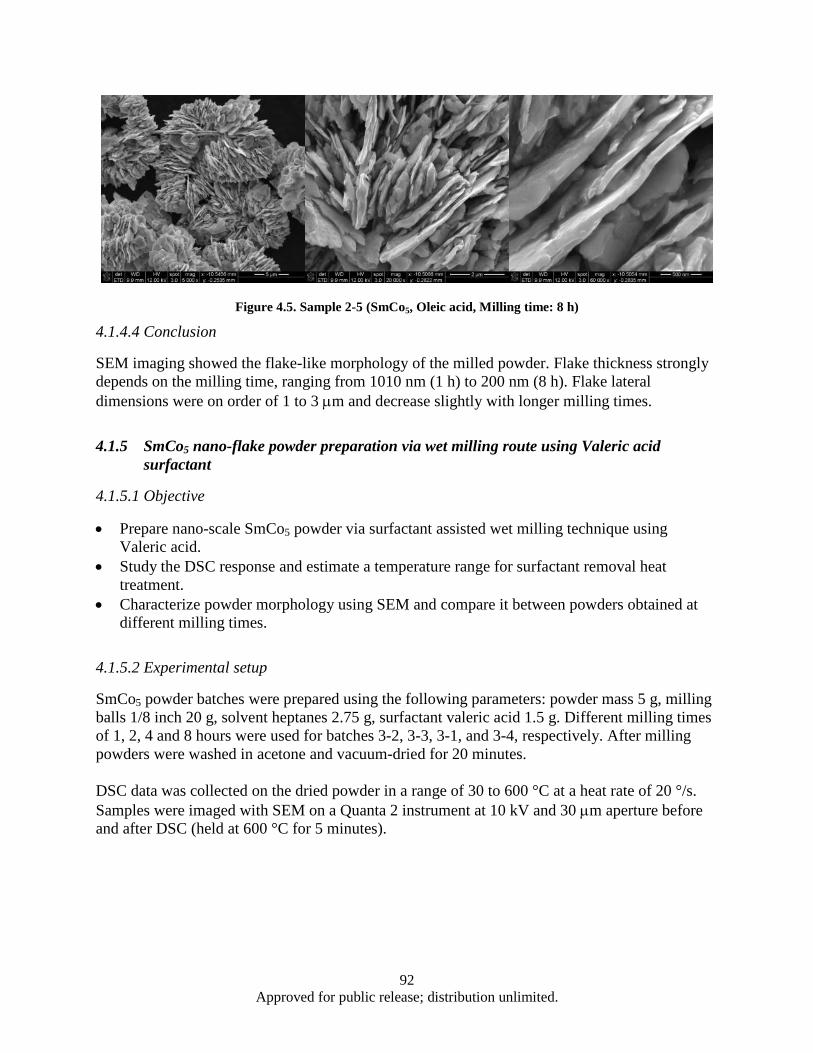
92 Approved for public release; distribution unlimited.
Figure 4.5. Sample 2-5 (SmCo5, Oleic acid, Milling time: 8 h)
4.1.4.4 Conclusion
SEM imaging showed the flake-like morphology of the milled powder. Flake thickness strongly depends on the milling time, ranging from 1010 nm (1 h) to 200 nm (8 h). Flake lateral dimensions were on order of 1 to 3 µm and decrease slightly with longer milling times.
4.1.5 SmCo5 nano-flake powder preparation via wet milling route using Valeric acid surfactant
4.1.5.1 Objective
• Prepare nano-scale SmCo5 powder via surfactant assisted wet milling technique using Valeric acid.
• Study the DSC response and estimate a temperature range for surfactant removal heat treatment.
• Characterize powder morphology using SEM and compare it between powders obtained at different milling times.
4.1.5.2 Experimental setup
SmCo5 powder batches were prepared using the following parameters: powder mass 5 g, milling balls 1/8 inch 20 g, solvent heptanes 2.75 g, surfactant valeric acid 1.5 g. Different milling times of 1, 2, 4 and 8 hours were used for batches 3-2, 3-3, 3-1, and 3-4, respectively. After milling powders were washed in acetone and vacuum-dried for 20 minutes. DSC data was collected on the dried powder in a range of 30 to 600 °C at a heat rate of 20 °/s. Samples were imaged with SEM on a Quanta 2 instrument at 10 kV and 30 µm aperture before and after DSC (held at 600 °C for 5 minutes).
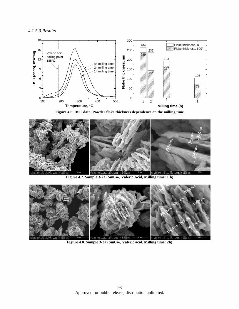
93 Approved for public release; distribution unlimited.
4.1.5.3 Results
Figure 4.6. DSC data, Powder flake thickness dependence on the milling time
Figure 4.7. Sample 3-2a (SmCo5, Valeric Acid, Milling time: 1 h)
Figure 4.8. Sample 3-3a (SmCo5, Valeric acid, Milling time: 2h)
100 200 300 400 5000
3
6
9
12
15
18
D
SC (e
ndo)
, mW
/mg
Temperature, °C
4h milling time2h milling time1h milling time
Valeric acid boiling point 185°C
264
237
193
105
239
144167
73
1 2 4 80
50
100
150
200
250
300
Flak
e th
ickn
ess,
nm
Milling time (h)
Flake thickness, RT Flake thickness, 600°
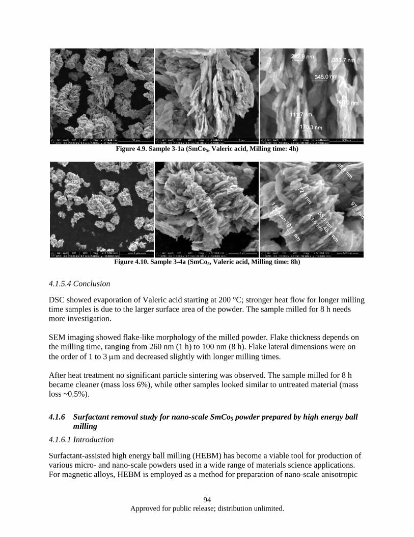
94 Approved for public release; distribution unlimited.
Figure 4.9. Sample 3-1a (SmCo5, Valeric acid, Milling time: 4h)
Figure 4.10. Sample 3-4a (SmCo5, Valeric acid, Milling time: 8h)
4.1.5.4 Conclusion
DSC showed evaporation of Valeric acid starting at 200 °C; stronger heat flow for longer milling time samples is due to the larger surface area of the powder. The sample milled for 8 h needs more investigation.
SEM imaging showed flake-like morphology of the milled powder. Flake thickness depends on the milling time, ranging from 260 nm (1 h) to 100 nm (8 h). Flake lateral dimensions were on the order of 1 to 3 µm and decreased slightly with longer milling times. After heat treatment no significant particle sintering was observed. The sample milled for 8 h became cleaner (mass loss 6%), while other samples looked similar to untreated material (mass loss ~0.5%).
4.1.6 Surfactant removal study for nano-scale SmCo5 powder prepared by high energy ball milling
4.1.6.1 Introduction
Surfactant-assisted high energy ball milling (HEBM) has become a viable tool for production of various micro- and nano-scale powders used in a wide range of materials science applications. For magnetic alloys, HEBM is employed as a method for preparation of nano-scale anisotropic

95 Approved for public release; distribution unlimited.
rare-earth magnetic powders with controlled particle size and morphology. Final powder particle properties depend on the milling process parameters such as milling time, ball-to-powder mass ratio, and, most critically, choice and the relative amount of the surfactant. During the milling process surfactant molecules adhere to the freshly exposed particle surface creating a thin organic layer. This layer protects the particles from mechanical alloying when they come in contact with each other further in the milling process. Organic fatty acids are typically used as surfactants; their molecules contain carboxylic functional components which form carboxylate bonds with the metal surface and long molecular chains which create an electrostatic barrier for the surrounding powder particles. Recently, surfactant-assisted HEBM has been used in preparation of nanostructured SmCo5 magnetic powders with anisotropic flake-like morphology and particle thickness below 100 nm.
Surfactants play an essential role in the HEBM process; however, they often need to be removed after milling and prior to a powder consolidation step. The presence of surfactant during powder sintering or hot pressing may result in organic material decomposition or reaction with the base metal alloy producing impurities in the final product. Typically, surfactant removal is achieved through a vacuum annealing process which requires relatively high temperatures and long dwelling times. Such thermal conditions are undesirable for treatment of nanostructured powders, since exposure to elevated temperatures results in grain growth and oxidation . A recent study has shown that heat treatment temperature depends on surfactant molecular weight (MW) and it can be reduced by using surfactants with shorter molecular chains. Oleic acid (OA) is the most commonly used surfactant reported in the literature for preparation of SmCo5 nano-flake powders. Due to its chemical interaction with the metal, temperatures above 500 °C under atmospheric conditions are required for OA removal (OA boiling point is 360 °C, MW = 282 g/mol). A lower molecular weight surfactant such as valeric acid (VA, boiling point 185 °C, MW = 102 g/mol) would require a less aggressive heat treatment and may be more suitable for SmCo5 alloy powder processing.
In the present work SmCo5 nano-flake magnetic powders were prepared by HEBM using valeric acid. Different annealing conditions for surfactant removal were investigated. The effect of the heat treatment has been evaluated by estimation of residual surfactant content and magnetic property comparison between the as-milled and treated SmCo5.
4.1.6.2 Experimental
Pure Sm and pure Co were combined in a 1:5 atomic ratio and arc melted into a SmCo5 alloy button in Ar atmosphere. The button was mechanically crushed into coarse powder (particle size under 250 µm) which was used as the staring material for high energy ball milling. For HEBM the SmCo5 powder (5 g), milling balls (1/8-inch-diameter, hardened stainless steel, 20 g, 152 balls), vehicle (heptane, 2.75 g, Acros Organics) and surfactant (valeric acid, 1.5 g, Aldrich) were combined and sealed under Ar atmosphere in a stainless steel jar and milled in a SPEX 8000D vibratory mill for 1 hour. After milling the powders were rinsed with acetone, vacuum dried and separated from the ball media.
The as-milled SmCo5 powders were heat treated at two different temperatures: 200 °C and 400 °C. In order to avoid oxidation an argon atmosphere was used at a pressure slightly above atmospheric (800 Torr); treatment in air was also conducted (at pressure ~1 Torr) for comparison. Relative contents of residual surfactant were compared by DSC analysis, Perkin

96 Approved for public release; distribution unlimited.
Elmer DSC 8000, temperature range of 30 to 600 °C, heat rate 20 °/min, in flowing high-purity Ar. The presence of metal oxides and primary SmCo5 phase were evaluated by X-ray diffraction data collected on beamline 33-BM-C at the Advanced Photon Source of Argonne National Laboratory, using x-ray radiation with wavelength λ=0.0589605 nm. Measurements were performed on powder samples mounted in quartz capillaries and using a curved image plate detector in the 2θ angular range 3.5-35.5°; additional procedure details are described in. Powder morphology before and after heat treatment was investigated with SEM, FEI Quanta ESEM. For magnetic property measurements SmCo5 powders were combined with an epoxy resin (80% powder, 20% epoxy by mass), pulse magnetized in a 10 T magnetic field, and set for curing between permanent magnets in a field ~1 T for 24 hours. A KJS Associates closed-loop hysteresisgraph (model MG-700) was used to measure magnetic behavior of the cured samples and determine magnetic coercivity Hci, remanence Br and maximum energy product (BH)max.
4.1.6.3 Results and discussion
SEM imaging of the as-milled and heat treated SmCo5 powders prepared by HEBM using valeric acid (Fig. 4.1) revealed a highly anisotropic flake-like morphology with flake sizes in the range 1 to 5 µm wide and 200 to 600 nm thick. Formation of flake-shaped particles is consistent with previous experiments and is facilitated by the presence of the surfactant during HEBM. A preliminary study has also been conducted to determine effect of milling time on the SmCo5 nano-flake thickness. The selected time of 1h produced 200 to 600 nm flakes which according to results in relatively high energy product (BH)max. The flake dimensions are also in agreement with previous reports using oleic acid as a surfactant. However, no study of relation between milling parameters and final powder morphology for the case of valeric acid has been done.
Comparison between SEM images of the untreated powders and of those treated at 200 °C and 400 °C (both in Ar and Air atmospheres) did not show any visible differences in the powder morphology, even though an onset of particle coagulation was expected after the heat treatment. Presence of the organic surfactant in the as-milled powder was indirectly evidenced by minor charging during SEM raster due to lower powder surface conductivity. TEM imaging would be more suitable for a detailed particle surface analysis and estimation of the surfactant layer thickness.
Figure 4.11. SEM images as a milled (a), heat treated in argon at 200° (b) and 400° (c) SmCo5 nano flake powders prepared by HEBM using valeric acid, clusters of SmCo5 nano flakes (d)
Residual surfactant content was estimated from DSC analysis with the data shown in Figure 4.2. For the as-milled powder a large endothermic peak with an onset near the valeric acid boiling temperature (185 °C) indicated the presence of the surfactant. Powders heat treated in Ar exhibit similar peaks but with the peak area decreasing for higher dwell temperatures, which is evidence
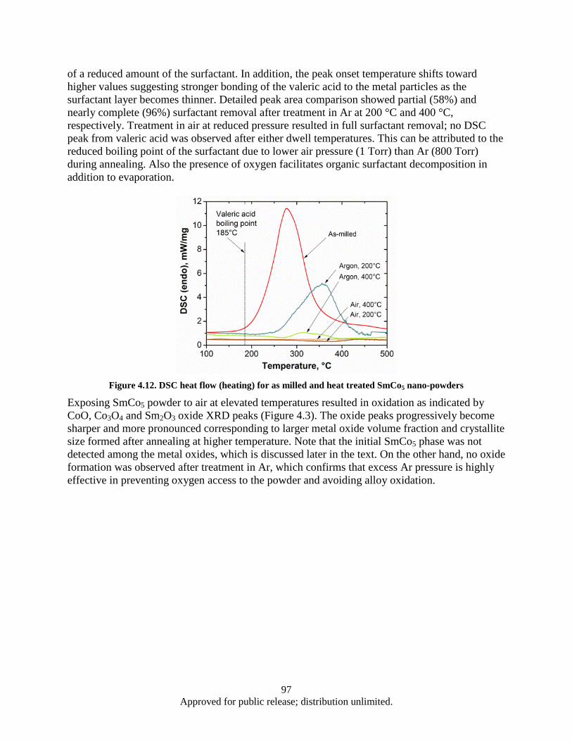
97 Approved for public release; distribution unlimited.
of a reduced amount of the surfactant. In addition, the peak onset temperature shifts toward higher values suggesting stronger bonding of the valeric acid to the metal particles as the surfactant layer becomes thinner. Detailed peak area comparison showed partial (58%) and nearly complete (96%) surfactant removal after treatment in Ar at 200 °C and 400 °C, respectively. Treatment in air at reduced pressure resulted in full surfactant removal; no DSC peak from valeric acid was observed after either dwell temperatures. This can be attributed to the reduced boiling point of the surfactant due to lower air pressure (1 Torr) than Ar (800 Torr) during annealing. Also the presence of oxygen facilitates organic surfactant decomposition in addition to evaporation.
Figure 4.12. DSC heat flow (heating) for as milled and heat treated SmCo5 nano-powders
Exposing SmCo5 powder to air at elevated temperatures resulted in oxidation as indicated by CoO, Co3O4 and Sm2O3 oxide XRD peaks (Figure 4.3). The oxide peaks progressively become sharper and more pronounced corresponding to larger metal oxide volume fraction and crystallite size formed after annealing at higher temperature. Note that the initial SmCo5 phase was not detected among the metal oxides, which is discussed later in the text. On the other hand, no oxide formation was observed after treatment in Ar, which confirms that excess Ar pressure is highly effective in preventing oxygen access to the powder and avoiding alloy oxidation.
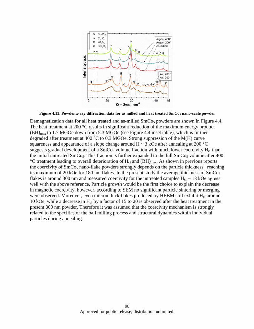
98 Approved for public release; distribution unlimited.
Figure 4.13. Powder x-ray diffraction data for as milled and heat treated SmCo5 nano-scale powder
Demagnetization data for all heat treated and as-milled SmCo5 powders are shown in Figure 4.4. The heat treatment at 200 °C results in significant reduction of the maximum energy product (BH)max to 1.7 MGOe down from 5.3 MGOe (see Figure 4.4 inset table), which is further degraded after treatment at 400 °C to 0.3 MGOe. Strong suppression of the M(H) curve squareness and appearance of a slope change around H ~ 3 kOe after annealing at 200 °C suggests gradual development of a SmCo5 volume fraction with much lower coercivity Hci than the initial untreated SmCo5. This fraction is further expanded to the full SmCo5 volume after 400 °C treatment leading to overall deterioration of Hci and (BH)max. As shown in previous reports the coercivity of SmCo5 nano-flake powders strongly depends on the particle thickness, reaching its maximum of 20 kOe for 180 nm flakes. In the present study the average thickness of SmCo5 flakes is around 300 nm and measured coercivity for the untreated samples Hci = 18 kOe agrees well with the above reference. Particle growth would be the first choice to explain the decrease in magnetic coercivity, however, according to SEM no significant particle sintering or merging were observed. Moreover, even micron thick flakes produced by HEBM still exhibit Hci around 10 kOe, while a decrease in Hci by a factor of 15 to 20 is observed after the heat treatment in the present 300 nm powder. Therefore it was assumed that the coercivity mechanism is strongly related to the specifics of the ball milling process and structural dynamics within individual particles during annealing.
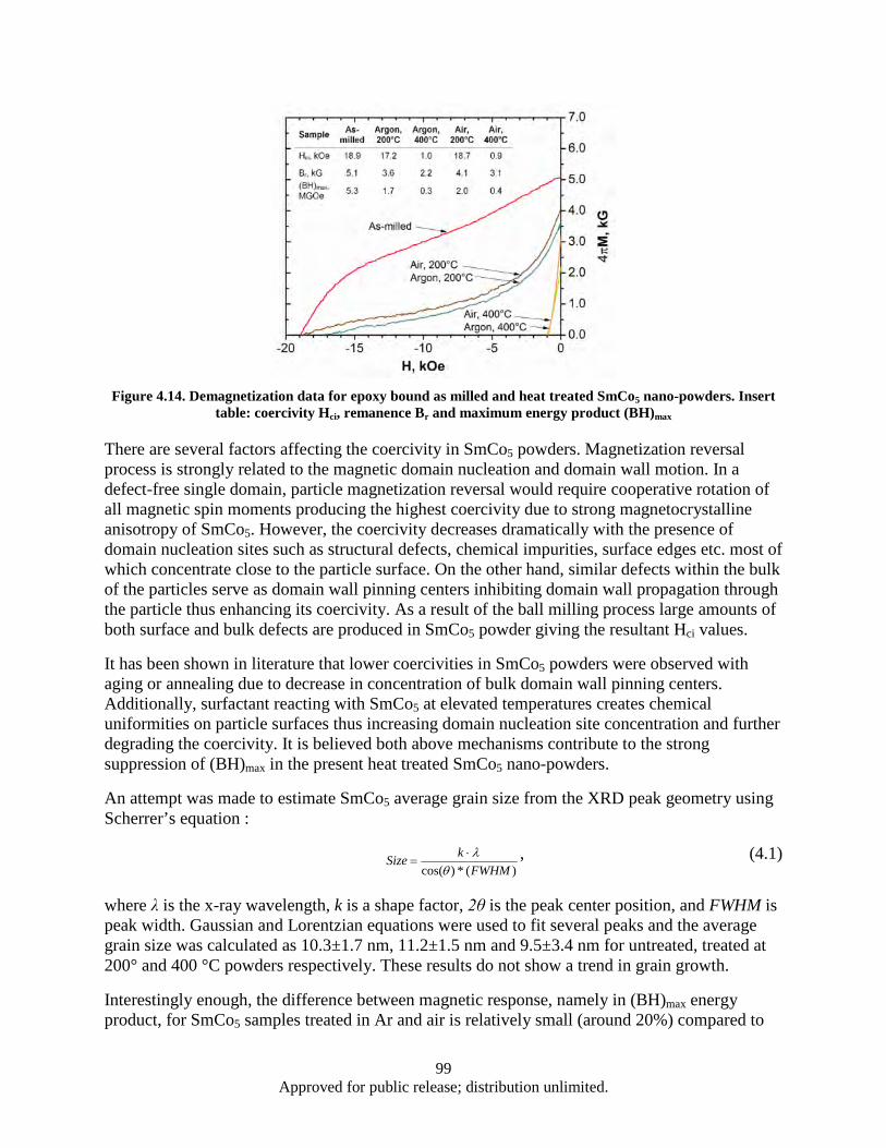
99 Approved for public release; distribution unlimited.
Figure 4.14. Demagnetization data for epoxy bound as milled and heat treated SmCo5 nano-powders. Insert
table: coercivity Hci, remanence Br and maximum energy product (BH)max There are several factors affecting the coercivity in SmCo5 powders. Magnetization reversal process is strongly related to the magnetic domain nucleation and domain wall motion. In a defect-free single domain, particle magnetization reversal would require cooperative rotation of all magnetic spin moments producing the highest coercivity due to strong magnetocrystalline anisotropy of SmCo5. However, the coercivity decreases dramatically with the presence of domain nucleation sites such as structural defects, chemical impurities, surface edges etc. most of which concentrate close to the particle surface. On the other hand, similar defects within the bulk of the particles serve as domain wall pinning centers inhibiting domain wall propagation through the particle thus enhancing its coercivity. As a result of the ball milling process large amounts of both surface and bulk defects are produced in SmCo5 powder giving the resultant Hci values.
It has been shown in literature that lower coercivities in SmCo5 powders were observed with aging or annealing due to decrease in concentration of bulk domain wall pinning centers. Additionally, surfactant reacting with SmCo5 at elevated temperatures creates chemical uniformities on particle surfaces thus increasing domain nucleation site concentration and further degrading the coercivity. It is believed both above mechanisms contribute to the strong suppression of (BH)max in the present heat treated SmCo5 nano-powders.
An attempt was made to estimate SmCo5 average grain size from the XRD peak geometry using Scherrer’s equation :
)(*)cos( FWHMkSize
θλ⋅
= , (4.1)
where λ is the x-ray wavelength, k is a shape factor, 2θ is the peak center position, and FWHM is peak width. Gaussian and Lorentzian equations were used to fit several peaks and the average grain size was calculated as 10.3±1.7 nm, 11.2±1.5 nm and 9.5±3.4 nm for untreated, treated at 200° and 400 °C powders respectively. These results do not show a trend in grain growth.
Interestingly enough, the difference between magnetic response, namely in (BH)max energy product, for SmCo5 samples treated in Ar and air is relatively small (around 20%) compared to

100 Approved for public release; distribution unlimited.
the effect of the annealing temperature (by a factor of 3 to 4) despite heavy oxidation in air-treated SmCo5 (Figure 4.3). Taking into account that slight variation in measured remanence Br and coercivity Hci between samples is expected due to some inconsistency in sample preparation steps we assumed M(H) data (Figure 4.4) for air and Ar-treated SmCo5 are approximately the same with no significant atmosphere effect.
Such a result indicates a contradiction: the SmCo5 phase was not observed in the air-treated powder, but its magnetic response is very close to the unoxidized SmCo5 annealed in Ar at the corresponding temperature. Initially we assumed only an insignificant fraction of SmCo5 transformed into an oxide forming a thin layer on particle surfaces without affecting magnetic response but masking the underlying non-oxidized phase from detection by XRD. The x-ray attenuation length in SmCo5 is under 10 µm for the beamline photon energy (21 keV) and incidence angles (2θ = 3.5-25°) used in this study and the information depth is on the order of several microns. This depth is much larger than average powder flake thickness (~300 nm) and is comparable with the flake lateral dimensions (1 to 5 µm). In this case absence of the initial SmCo5 phase peaks would imply complete particle oxidation without a remaining SmCo5 core, which contradicts the magnetic response data. Alternatively it is suggested that flake agglomeration into clusters (Figure 4.1-d) due to magnetostatic interaction results in a large amount of the SmCo5 protected from exposure to oxygen at the cost of oxidation of a few outer cluster flake layers. For the observed cluster size of 5 to 30 µm this assumption qualitatively agrees with the XRD and demagnetization results; however, additional investigations, such as neutron diffraction and TEM, are needed for better understanding of the metal oxide presence in the heat treated SmCo5 powders.
4.1.6.4 Conclusion
Nano-flake SmCo5 powders were prepared by surfactant-assisted high energy ball milling using a low molecular weight valeric acid surfactant. Final powder morphology showed flake shape and dimensions (width of 1 to 5 µm and thickness of 200 to 600 nm) similar to previously prepared powders using conventional oleic acid. A heat treatment approach for the surfactant removal was investigated. Annealing at 200 °C and 400 °C in argon resulted in partial (58%) and nearly complete (96%) valeric acid removal and avoided powder oxidation. However, the magnetic energy product (BH)max strongly degraded from 5.3 (as-milled) to 1.7 (200 °C) and 0.3 MGOe (400 °C) after the heat treatment, which was attributed to suppressed coercivity due to generation of domain nucleation sites (surface defects) and reduced concentration of domain wall pinning centers (bulk defects) within individual flakes. Annealing in air has led to complete surfactant removal but also thin surface oxide layer formation, which did not significantly affect the magnetic properties.
In summary, the results of the present study indicate that even a modest heat treatment of SmCo5 nano-powder prepared by HEBM severely degrades its magnetic properties regardless of the atmosphere. The heat treatment process is not suitable for surfactant removal and either alternative methods must be considered, or the surfactant must remain during further powder processing.

101 Approved for public release; distribution unlimited.
4.1.7 UDRI gas gun target fixture design proposal
4.1.7.1 Objective
• Design a target assembly for hypervelocity powder compaction experiment at UDRI gas gun facility.
4.1.7.2 Literature review
To assemble a tailored target fixture, a few existing similar designs from other research groups have been first reviewed.
A group at Georgia Tech employed a single-stage gas gun with 80 mm bore diameter to launch a cylindrical sabot with a metal flyer plate at a target containing three sealed powder capsules embedded into a metal disc (Figure 4.15). The capsule disc and the surround ring were backed by a mounted momentum trap plate. As the flyer plate impacts the target surface a plane shockwave propagates through the metal encasement and the sample powder, and with a proper set of initial parameters the delivered shockwave energy will consolidate the powder to nearly 100% density.
The point of such design is the use of three samples at once, which can be allowed with a 80 mm wide flyer plate and is time and cost efficient. Another important aspect is the construction of powder capsules, which are threaded and are sealed by a plug and epoxy. The plug prevents air access to the powder to avoid oxidation and keeps the powder partially compressed. All the metal components in this design are made of general purpose 304 stainless steel.
Figure 4.15. Influence of dynamic densification on nanostructures formation in Ti3Si3 intermetallic alloy and
its bulk properties An alternative setup was used by a group at California Tech, which had a 35-mm-wide sabot and flyer plate impacting a target containing one powder capsule (Figure 4.16). Contrary to the previous design, only the powder sample and not the surround ring is impacted. In this case, less energy is wasted, and the experiment is more cost efficient. The capsule design is also simpler. The powder is contained inside a sleeve (cylindrical tubing) and plugged from both sides by
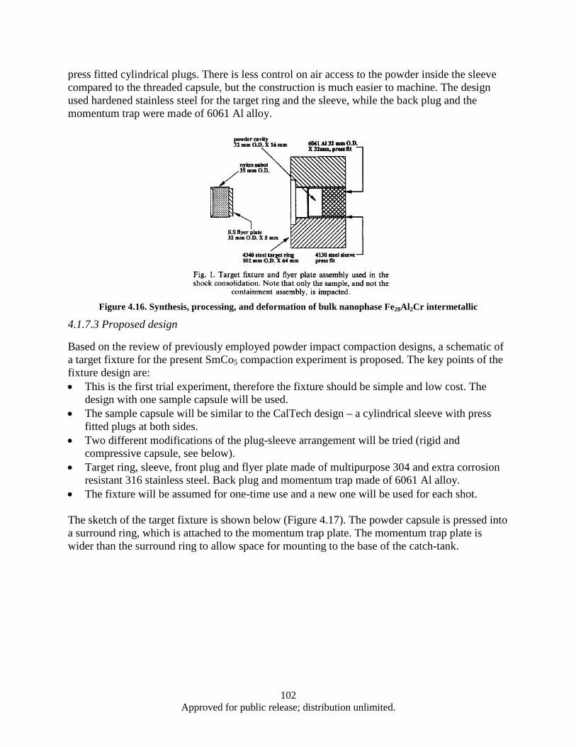
102 Approved for public release; distribution unlimited.
press fitted cylindrical plugs. There is less control on air access to the powder inside the sleeve compared to the threaded capsule, but the construction is much easier to machine. The design used hardened stainless steel for the target ring and the sleeve, while the back plug and the momentum trap were made of 6061 Al alloy.
Figure 4.16. Synthesis, processing, and deformation of bulk nanophase Fe28Al2Cr intermetallic
4.1.7.3 Proposed design
Based on the review of previously employed powder impact compaction designs, a schematic of a target fixture for the present SmCo5 compaction experiment is proposed. The key points of the fixture design are: • This is the first trial experiment, therefore the fixture should be simple and low cost. The
design with one sample capsule will be used. • The sample capsule will be similar to the CalTech design – a cylindrical sleeve with press
fitted plugs at both sides. • Two different modifications of the plug-sleeve arrangement will be tried (rigid and
compressive capsule, see below). • Target ring, sleeve, front plug and flyer plate made of multipurpose 304 and extra corrosion
resistant 316 stainless steel. Back plug and momentum trap made of 6061 Al alloy. • The fixture will be assumed for one-time use and a new one will be used for each shot. The sketch of the target fixture is shown below (Figure 4.17). The powder capsule is pressed into a surround ring, which is attached to the momentum trap plate. The momentum trap plate is wider than the surround ring to allow space for mounting to the base of the catch-tank.
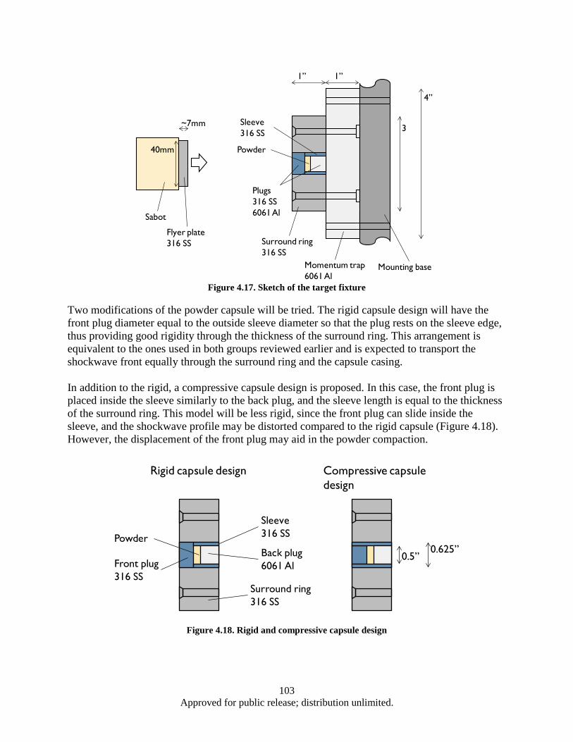
103 Approved for public release; distribution unlimited.
Figure 4.17. Sketch of the target fixture
Two modifications of the powder capsule will be tried. The rigid capsule design will have the front plug diameter equal to the outside sleeve diameter so that the plug rests on the sleeve edge, thus providing good rigidity through the thickness of the surround ring. This arrangement is equivalent to the ones used in both groups reviewed earlier and is expected to transport the shockwave front equally through the surround ring and the capsule casing.
In addition to the rigid, a compressive capsule design is proposed. In this case, the front plug is placed inside the sleeve similarly to the back plug, and the sleeve length is equal to the thickness of the surround ring. This model will be less rigid, since the front plug can slide inside the sleeve, and the shockwave profile may be distorted compared to the rigid capsule (Figure 4.18). However, the displacement of the front plug may aid in the powder compaction.
Figure 4.18. Rigid and compressive capsule design
Surround ring316 SS
Momentum trap 6061 Al
Mounting base
Plugs316 SS6061 Al
Powder
1”1”
4”
3~7mm
Flyer plate316 SS
40mm
Sabot
Sleeve316 SS
Surround ring316 SS
Back plug6061 Al
Powder
Sleeve316 SS
Front plug316 SS
Rigid capsule design Compressive capsule design
0.625”0.5”
104 Approved for public release; distribution unlimited.
Table 4.1. Parts List
Part name Shape Material McMaster # Price Quantity Total price
Surround ring Disc, D=3”, L=1” 304 SS 9208K53 $19.51 5 $97.55 Momentum trap Disc, D=4.5”, L=1” 6061 Al 1610T24 $15.54 5 $77.70
Sleeve Tubing, ID=0.495”, OD =0.625”, wall=0.065”, L=3’
316 SS 89785K156 $49.92 1 $49.92
Front plug 1 Rod, D=0.625”, L=3’ 316 SS 89325K832 $22.84 1 $22.84 Front plug 2 Rod, D=0.5”, L=3’ 316 SS 89325K852 $15.28 1 $15.28 Back plug Rod, D=0.5”, L=3’ 6061 Al 9062K313 $20.42 1 $20.42 $$283.71 The parts listed above (purchased from McMaster Carr, Table 4.1) will be sufficient to make 4 full targets (1 extra piece for the surround ring and the momentum trap plate). The parts will be machined at the machine shop in bldg. 450.
4.1.7.4 Concluding remarks
The proposed target fixture design is relatively simple to implement, the 304 and 316 steels are not hardened and the machining required is boring through holes for the powder capsule and mounting screws, slightly reducing plug rod diameter to fit into the sleeve, cutting tubing and rods to the required length. The sabot, flyer plate and the tank mounting stage parts will be machined at UDRI. For the target to be assembled properly, the powder capsule front and back surfaces should be leveled flat with the surface of the surround ring. This can be achieved by accurate cutting and fine grinding of the sleeve and the front plug. Additionally, since the size of the powder cavity depends on the powder mass, the length of the back plug can be adjusted by fine grinding to make it flat with the outside surface for each target individually.
4.1.8 UDRI gas gun powder compaction experiment
4.1.8.1 Objective
• Sample capsule and target design based on literature review • Design and machining of target fixtures, projectiles and targets • Conduction of the experiment at different impaction speeds • Sample property characterization
4.1.8.2 Targets
Two types of target assemblies were machined in house – rigid and compressive capsule design (Figure 4.19). Two identical targets were made of each type (four targets total).
105 Approved for public release; distribution unlimited.
Figure 4.19. Target Assembly
4.1.8.3 SmCo5 alloy powder
Experimental nano-scale SmCo5 alloy powder was prepared by surfactant-assisted high energy ball milling using Valeric acid surfactant. Preparation steps are summarized in a diagram below (Figure 4.20). Final powder, including remaining surfactant, was loaded into target capsules and pre-compacted in a hydraulic hand press.
Figure 4.20. SmCo5 experimental powder preparation flowchart
Arc melting of Sm and Co metals to obtain SmCo5 button
Mechanically crush and hand sieve the button into coarse powder with ~250 µm particles
High energy ball milling
Milling time 1 h
SmCo5 mass 5 g
Milling ball media 1/8 inch 20 g
Final powder rinsed in acetone, vacuum dried. Obtained flake-like nano-scale powder loaded into capsule and pre-pressed
106 Approved for public release; distribution unlimited.
4.1.8.4 Target fixtures
Cold rolled steel plates were cut to size according to the drawings (Figure 4.21). All fixture parts (front plate, base, and gussets) were welded together. Excessive heat from welding caused the bottom plate to warp, which was fixed later by level milling. Two fixtures were made, and the target assemblies were mounted onto the front plates (Figure 4.22). The same fixtures were planned for use for up to two shot experiments.
Figure 4.21. Target fixture drawing
Figure 4.22. Machined and welded target fixture with and without the target assembly mounted
107 Approved for public release; distribution unlimited.
4.1.8.5 Projectiles
Two sets of projectiles were machined (four pieces for velocity calibration and 4 pieces for the actual powder compaction). The body of a projectile was made from a Lexan plastic cylinder, a flyer stainless steel plate was mounted on the front of the projectile and surrounded by an aluminum ring (Figures 4.23 and 4.24).
Figure 4.23. Projectile Drawing
Figure 4.24. Set of Four Machined Projectiles
4.1.8.6 Powder compaction test performance
The compaction experiment consisted of four shots at two different projectile speeds (300 and 1000 m/s) for each of the two types of powder capsules (rigid and compressive designs). The 300 m/s shots were conducted using compressed Helium as the projectile propulsion medium; the 1000 m/s shots were performed using gun powder charges. In all cases, the sample chamber was evacuated to 17 mmHg pressure to improve the velocity of the projectiles (Figure 4.25).

108 Approved for public release; distribution unlimited.
Shot 1. Velocity: 303 m/s Propulsion: compressed He at 300 psi Target: rigid capsule SmCo5 powder and capsule top plug scattered after the shot, a sample piece was recovered.
Shot 2. Velocity: 304 m/s Propulsion: compressed He at 300 psi Target: compressive capsule SmCo5 powder was contained after the shot (successful)
Shot 3. Velocity: 990 m/s Propulsion: gun powder charge Target: rigid capsule Impact caused too much damage to the target assembly, no samples were recovered
Shot 4. Velocity: 645m/s Propulsion: gun powder charge Target: compressive capsule Impact caused no damage to the target assembly, but no samples were recovered
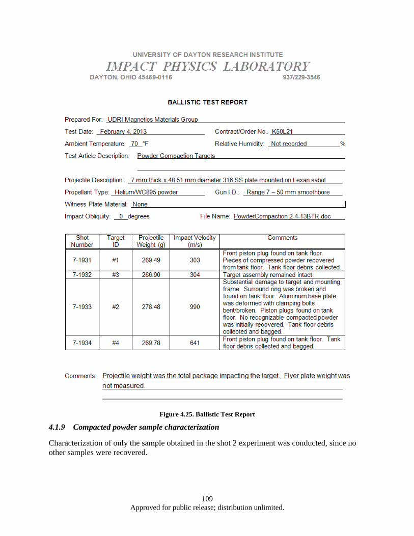
109 Approved for public release; distribution unlimited.
Figure 4.25. Ballistic Test Report
4.1.9 Compacted powder sample characterization
Characterization of only the sample obtained in the shot 2 experiment was conducted, since no other samples were recovered.
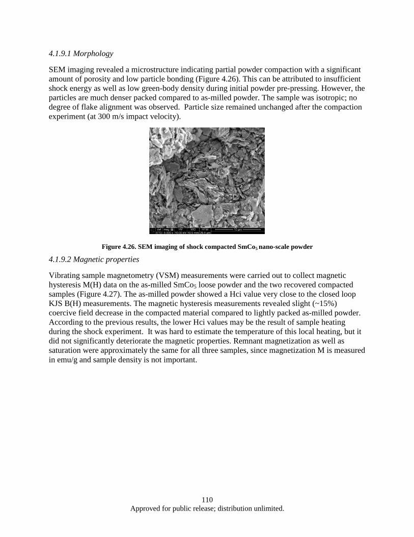
110 Approved for public release; distribution unlimited.
4.1.9.1 Morphology
SEM imaging revealed a microstructure indicating partial powder compaction with a significant amount of porosity and low particle bonding (Figure 4.26). This can be attributed to insufficient shock energy as well as low green-body density during initial powder pre-pressing. However, the particles are much denser packed compared to as-milled powder. The sample was isotropic; no degree of flake alignment was observed. Particle size remained unchanged after the compaction experiment (at 300 m/s impact velocity).
Figure 4.26. SEM imaging of shock compacted SmCo5 nano-scale powder
4.1.9.2 Magnetic properties
Vibrating sample magnetometry (VSM) measurements were carried out to collect magnetic hysteresis M(H) data on the as-milled SmCo5 loose powder and the two recovered compacted samples (Figure 4.27). The as-milled powder showed a Hci value very close to the closed loop KJS B(H) measurements. The magnetic hysteresis measurements revealed slight (~15%) coercive field decrease in the compacted material compared to lightly packed as-milled powder. According to the previous results, the lower Hci values may be the result of sample heating during the shock experiment. It was hard to estimate the temperature of this local heating, but it did not significantly deteriorate the magnetic properties. Remnant magnetization as well as saturation were approximately the same for all three samples, since magnetization M is measured in emu/g and sample density is not important.
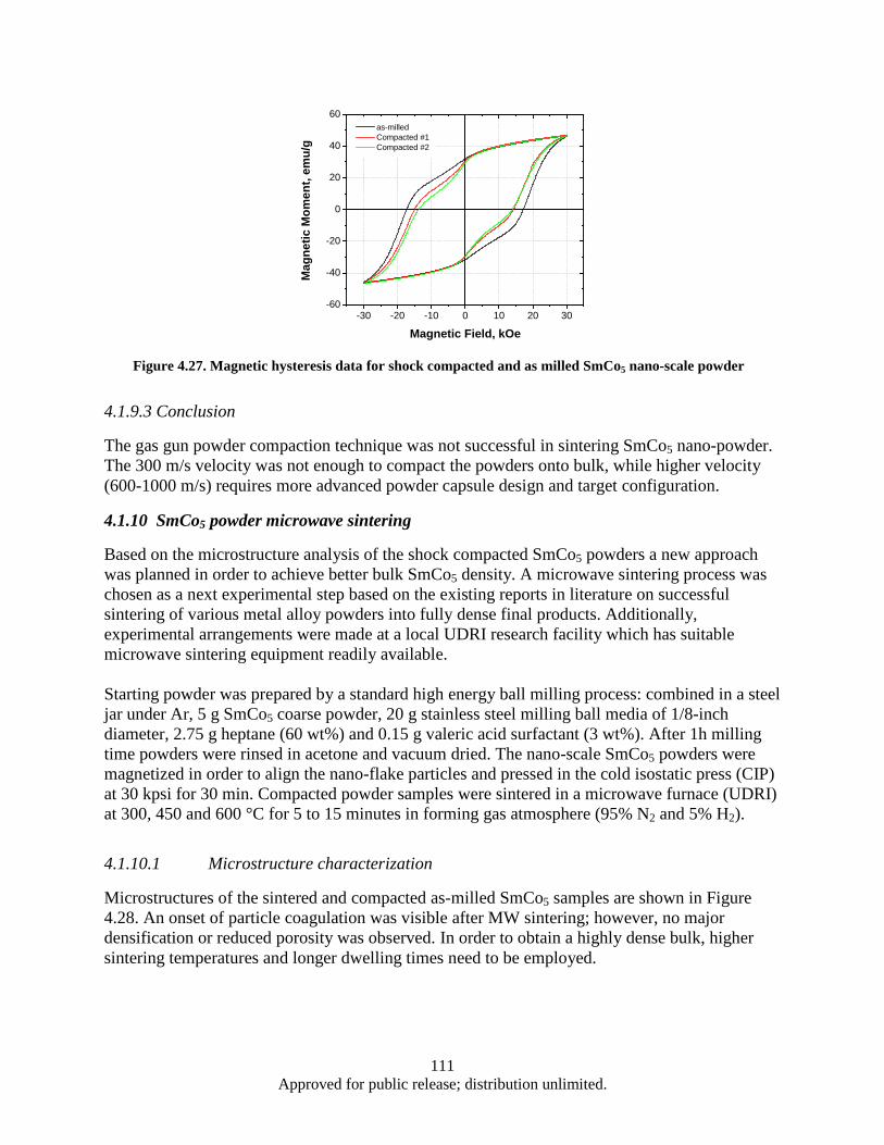
111 Approved for public release; distribution unlimited.
Magnetic Field, kOe
Figure 4.27. Magnetic hysteresis data for shock compacted and as milled SmCo5 nano-scale powder
4.1.9.3 Conclusion
The gas gun powder compaction technique was not successful in sintering SmCo5 nano-powder. The 300 m/s velocity was not enough to compact the powders onto bulk, while higher velocity (600-1000 m/s) requires more advanced powder capsule design and target configuration.
4.1.10 SmCo5 powder microwave sintering
Based on the microstructure analysis of the shock compacted SmCo5 powders a new approach was planned in order to achieve better bulk SmCo5 density. A microwave sintering process was chosen as a next experimental step based on the existing reports in literature on successful sintering of various metal alloy powders into fully dense final products. Additionally, experimental arrangements were made at a local UDRI research facility which has suitable microwave sintering equipment readily available.
Starting powder was prepared by a standard high energy ball milling process: combined in a steel jar under Ar, 5 g SmCo5 coarse powder, 20 g stainless steel milling ball media of 1/8-inch diameter, 2.75 g heptane (60 wt%) and 0.15 g valeric acid surfactant (3 wt%). After 1h milling time powders were rinsed in acetone and vacuum dried. The nano-scale SmCo5 powders were magnetized in order to align the nano-flake particles and pressed in the cold isostatic press (CIP) at 30 kpsi for 30 min. Compacted powder samples were sintered in a microwave furnace (UDRI) at 300, 450 and 600 °C for 5 to 15 minutes in forming gas atmosphere (95% N2 and 5% H2).
4.1.10.1 Microstructure characterization
Microstructures of the sintered and compacted as-milled SmCo5 samples are shown in Figure 4.28. An onset of particle coagulation was visible after MW sintering; however, no major densification or reduced porosity was observed. In order to obtain a highly dense bulk, higher sintering temperatures and longer dwelling times need to be employed.
-30 -20 -10 0 10 20 30-60
-40
-20
0
20
40
60 as-milled Compacted #1 Compacted #2
Mag
netic
Mom
ent,
emu/
g

112 Approved for public release; distribution unlimited.
Figure 4.28. SEM images of CIP compacted as-milled SmCo5 nanopoweder (a) and microwave sintered sample at 600 °C for 15 min (b)
4.1.10.2 Magnetic properties
The as-milled and MW sintered samples were investigated using magnetic hysteresis measurements on a VSM instrument. The magnetic moment as a function of applied magnetic field M(H) data is shown in Fig.4.29. The MR and Hci for the as-milled powder was consistent with previous measurements. The CIP compacted powder had slightly better loop squareness due to higher sample density. Magnetic response of the MW treated SmCo5 was similar for all treatment temperatures showing greatly reduced coercivity and remanence. Such a substantial difference could be attributed to sample structure change due to oxidation or recrystallization, which can be clarified by XRD investigation (already in progress).
Figure 4.29. Magnetic hysteresis data for as-milled and microwave sintered nano-scale SmCo5
4.1.10.3 XRD phase analysis
X-ray diffraction performed out on samples microwave sintered at 300 °C for 5 min, 450 ° C for 10 min and 600 ° C for 15 minutes using Cu Kα radiation. XRD scans in the 2θ range 25-65° are shown in Figure 4.30. Pattern analysis and phase identification with Diffrac.Eva software revealed the presence of the original SmCo5 and secondary phases (Sm oxide and Co) for the 300
-30 -20 -10 0 10 20 30-100
-80
-60
-40
-20
0
20
40
60
80
100 as-milled as-milled CIP MW 300° 5min MW 450° 10min MW 600° 15min
Mag
netic
Mom
ent,
emu/
g
Magnetic Field, kOe
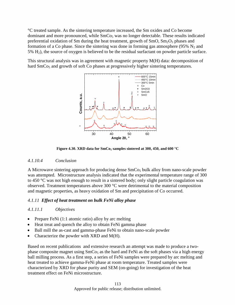
113 Approved for public release; distribution unlimited.
°C treated sample. As the sintering temperature increased, the Sm oxides and Co become dominant and more pronounced, while SmCo5 was no longer detectable. These results indicated preferential oxidation of Sm during the heat treatment, growth of SmO, Sm2O3 phases and formation of a Co phase. Since the sintering was done in forming gas atmosphere (95% N2 and 5% H2), the source of oxygen is believed to be the residual surfactant on powder particle surface.
This structural analysis was in agreement with magnetic property M(H) data: decomposition of hard SmCo5 and growth of soft Co phases at progressively higher sintering temperatures.
Figure 4.30. XRD data for SmCo5 samples sintered at 300, 450, and 600 °C
4.1.10.4 Conclusion
A Microwave sintering approach for producing dense SmCo5 bulk alloy from nano-scale powder was attempted. Microstructure analysis indicated that the experimental temperature range of 300 to 450 °C was not high enough to result in a sintered body; only slight particle coagulation was observed. Treatment temperatures above 300 °C were detrimental to the material composition and magnetic properties, as heavy oxidation of Sm and precipitation of Co occurred.
4.1.11 Effect of heat treatment on bulk FeNi alloy phase
4.1.11.1 Objectives
• Prepare FeNi (1:1 atomic ratio) alloy by arc melting• Heat treat and quench the alloy to obtain FeNi gamma phase• Ball mill the as-cast and gamma-phase FeNi to obtain nano-scale powder• Characterize the powder with XRD and M(H).
Based on recent publications and extensive research an attempt was made to produce a two-phase composite magnet using SmCo5 as the hard and FeNi as the soft phases via a high energy ball milling process. As a first step, a series of FeNi samples were prepared by arc melting and heat treated to achieve gamma-FeNi phase at room temperature. Treated samples were characterized by XRD for phase purity and SEM (on-going) for investigation of the heat treatment effect on FeNi microstructure.
30 40 50 60
600°C 15min 450°C 10min 300°C 5min Co Sm2O3 SmCo5 SmO
Cou
nts,
a.u
.
Angle 2θ, °
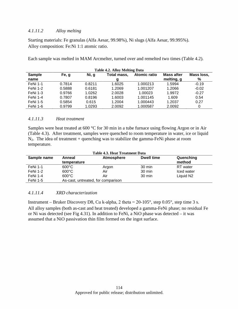
114 Approved for public release; distribution unlimited.
4.1.11.2 Alloy melting
Starting materials: Fe granulas (Alfa Aesar, 99.98%), Ni slugs (Alfa Aesar, 99.995%). Alloy composition: Fe:Ni 1:1 atomic ratio.
Each sample was melted in MAM Arcmelter, turned over and remelted two times (Table 4.2).
Table 4.2. Alloy Melting Data Sample name
Fe, g Ni, g Total mass, g
Atomic ratio Mass after melting, g
Mass loss, %
FeNi 1-1 0.7814 0.8211 1.6025 1.000213 1.5994 -0.19 FeNi 1-2 0.5888 0.6181 1.2069 1.001207 1.2066 -0.02 FeNi 1-3 0.9766 1.0262 2.0028 1.00023 1.9972 -0.27 FeNi 1-4 0.7807 0.8196 1.6003 1.001145 1.609 0.54 FeNi 1-5 0.5854 0.615 1.2004 1.000443 1.2037 0.27 FeNi 1-6 0.9799 1.0293 2.0092 1.000587 2.0092 0
4.1.11.3 Heat treatment
Samples were heat treated at 600 °C for 30 min in a tube furnace using flowing Argon or in Air (Table 4.3). After treatment, samples were quenched to room temperature in water, ice or liquid N2. The idea of treatment + quenching was to stabilize the gamma-FeNi phase at room temperature.
Table 4.3. Heat Treatment Data Sample name Anneal
temperature Atmosphere Dwell time Quenching
method FeNi 1-1 600°C Argon 30 min RT water FeNi 1-2 600°C Air 30 min Iced water FeNi 1-4 600°C Air 30 min Liquid N2 FeNi 1-5 As-cast, untreated, for comparison
4.1.11.4 XRD characterization
Instrument – Bruker Discovery D8, Cu k-alpha, 2 theta = 20-105°, step 0.05°, step time 3 s. All alloy samples (both as-cast and heat treated) developed a gamma-FeNi phase; no residual Fe or Ni was detected (see Fig 4.31). In addition to FeNi, a NiO phase was detected – it was assumed that a NiO passivation thin film formed on the ingot surface.
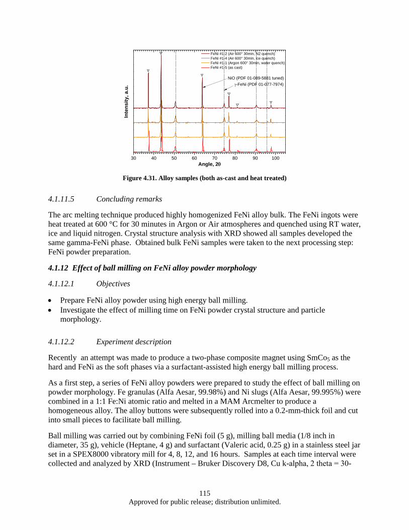
115 Approved for public release; distribution unlimited.
Figure 4.31. Alloy samples (both as-cast and heat treated)
4.1.11.5 Concluding remarks
The arc melting technique produced highly homogenized FeNi alloy bulk. The FeNi ingots were heat treated at 600 °C for 30 minutes in Argon or Air atmospheres and quenched using RT water, ice and liquid nitrogen. Crystal structure analysis with XRD showed all samples developed the same gamma-FeNi phase. Obtained bulk FeNi samples were taken to the next processing step: FeNi powder preparation.
4.1.12 Effect of ball milling on FeNi alloy powder morphology
4.1.12.1 Objectives
• Prepare FeNi alloy powder using high energy ball milling.• Investigate the effect of milling time on FeNi powder crystal structure and particle
morphology.
4.1.12.2 Experiment description
Recently an attempt was made to produce a two-phase composite magnet using SmCo5 as the hard and FeNi as the soft phases via a surfactant-assisted high energy ball milling process.
As a first step, a series of FeNi alloy powders were prepared to study the effect of ball milling on powder morphology. Fe granulas (Alfa Aesar, 99.98%) and Ni slugs (Alfa Aesar, 99.995%) were combined in a 1:1 Fe:Ni atomic ratio and melted in a MAM Arcmelter to produce a homogeneous alloy. The alloy buttons were subsequently rolled into a 0.2-mm-thick foil and cut into small pieces to facilitate ball milling.
Ball milling was carried out by combining FeNi foil (5 g), milling ball media (1/8 inch in diameter, 35 g), vehicle (Heptane, 4 g) and surfactant (Valeric acid, 0.25 g) in a stainless steel jar set in a SPEX8000 vibratory mill for 4, 8, 12, and 16 hours. Samples at each time interval were collected and analyzed by XRD (Instrument – Bruker Discovery D8, Cu k-alpha, 2 theta = 30-
30 40 50 60 70 80 90 100
Inte
nsity
, a.u
.
Angle, 2θ
FeNi #1-2 (Air 600° 30min, N2 quench) FeNi #1-4 (Air 600° 30min, ice quench) FeNi #1-1 (Argon 600° 30min, water quench) FeNi #1-5 (as cast)
γ-FeNi (PDF 01-077-7974)NiO (PDF 01-089-5881 tuned)
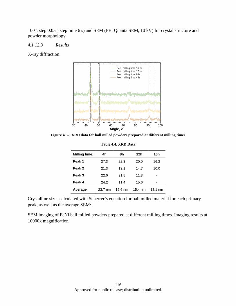
116 Approved for public release; distribution unlimited.
100°, step 0.05°, step time 6 s) and SEM (FEI Quanta SEM, 10 kV) for crystal structure and powder morphology.
4.1.12.3 Results
X-ray diffraction:
Figure 4.32. XRD data for ball milled powders prepared at different milling times
Table 4.4. XRD Data
Crystalline sizes calculated with Scherrer’s equation for ball milled material for each primary peak, as well as the average SEM:
SEM imaging of FeNi ball milled powders prepared at different milling times. Imaging results at 10000x magnification.
30 40 50 60 70 80 90 100
FeNi milling time 16 hr FeNi milling time 12 hr FeNi milling time 8 hr FeNi milling time 4 hr
Angle, 2θ
Milling time: 4h 8h 12h 16h
Peak 1 27.3 22.3 20.0 16.2
Peak 2 21.3 13.1 14.7 10.0
Peak 3 22.0 31.5 11.3 -
Peak 4 24.2 11.4 15.6 -
Average 23.7 nm 19.6 nm 15.4 nm 13.1 nm
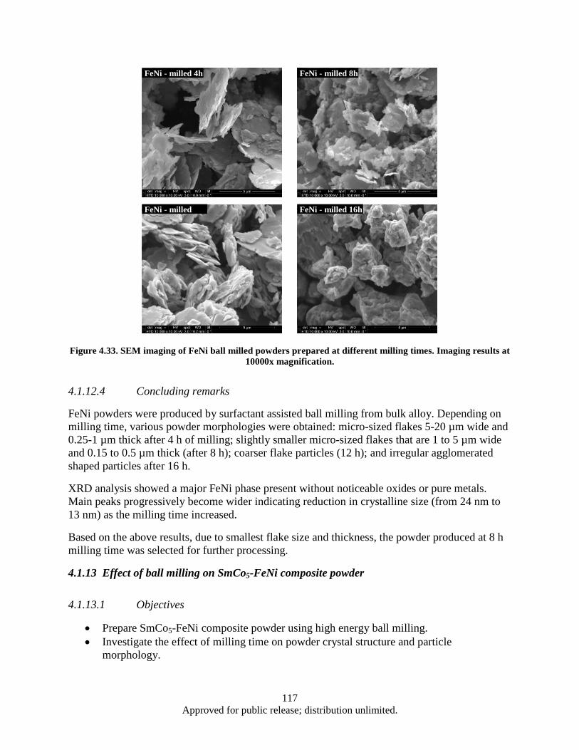
117 Approved for public release; distribution unlimited.
Figure 4.33. SEM imaging of FeNi ball milled powders prepared at different milling times. Imaging results at 10000x magnification.
4.1.12.4 Concluding remarks
FeNi powders were produced by surfactant assisted ball milling from bulk alloy. Depending on milling time, various powder morphologies were obtained: micro-sized flakes 5-20 µm wide and 0.25-1 µm thick after 4 h of milling; slightly smaller micro-sized flakes that are 1 to 5 µm wide and 0.15 to 0.5 µm thick (after 8 h); coarser flake particles (12 h); and irregular agglomerated shaped particles after 16 h.
XRD analysis showed a major FeNi phase present without noticeable oxides or pure metals. Main peaks progressively become wider indicating reduction in crystalline size (from 24 nm to 13 nm) as the milling time increased.
Based on the above results, due to smallest flake size and thickness, the powder produced at 8 h milling time was selected for further processing.
4.1.13 Effect of ball milling on SmCo5-FeNi composite powder
4.1.13.1 Objectives
• Prepare SmCo5-FeNi composite powder using high energy ball milling.• Investigate the effect of milling time on powder crystal structure and particle
morphology.
FeNi - milled 4h FeNi - milled 8h
FeNi - milled
FeNi - milled 16h
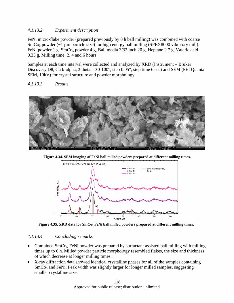
118 Approved for public release; distribution unlimited.
4.1.13.2 Experiment description
FeNi micro-flake powder (prepared previously by 8 h ball milling) was combined with coarse SmCo5 powder (~1 µm particle size) for high energy ball milling (SPEX8000 vibratory mill): FeNi powder 1 g, SmCo5 powder 4 g, Ball media 3/32 inch 20 g, Heptane 2.7 g, Valeric acid 0.25 g, Milling time: 2, 4 and 6 hours
Samples at each time interval were collected and analyzed by XRD (Instrument – Bruker Discovery D8, Cu k-alpha, 2 theta = 30-100°, step 0.05°, step time 6 sec) and SEM (FEI Quanta SEM, 10kV) for crystal structure and powder morphology.
4.1.13.3 Results
Figure 4.34. SEM imaging of FeNi ball milled powders prepared at different milling times.
Figure 4.35. XRD data for SmCo5 FeNi ball milled powders prepared at different milling times.
4.1.13.4 Concluding remarks
• Combined SmCo5-FeNi powder was prepared by surfactant assisted ball milling with millingtimes up to 6 h. Milled powder particle morphology resembled flakes, the size and thicknessof which decrease at longer milling times.
• X-ray diffraction data showed identical crystalline phases for all of the samples containingSmCo5 and FeNi. Peak width was slightly larger for longer milled samples, suggestingsmaller crystalline size.
30 40 50 60 70 80 90 100
Milled 2h Milled 4h Milled 6h
Inte
nsity
, a.u
.
Angle, 2θ
XRD: SmCo5-FeNi (milled 2, 4, 6h) SmCo5 (hexagonal) FeNi
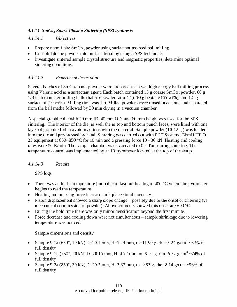
119 Approved for public release; distribution unlimited.
4.1.14 SmCo5 Spark Plasma Sintering (SPS) synthesis 4.1.14.1 Objectives
• Prepare nano-flake SmCo5 powder using surfactant-assisted ball milling.• Consolidate the powder into bulk material by using a SPS technique.• Investigate sintered sample crystal structure and magnetic properties; determine optimal
sintering conditions.
4.1.14.2 Experiment description
Several batches of SmCo5 nano-powder were prepared via a wet high energy ball milling process using Valeric acid as a surfactant agent. Each batch contained 15 g coarse SmCo5 powder, 60 g 1/8 inch diameter milling balls (ball-to-powder ratio 4:1), 10 g heptane (65 wt%), and 1.5 g surfactant (10 wt%). Milling time was 1 h. Milled powders were rinsed in acetone and separated from the ball media followed by 30 min drying in a vacuum chamber.
A special graphite die with 20 mm ID, 40 mm OD, and 60 mm height was used for the SPS sintering. The interior of the die, as well the as top and bottom punch faces, were lined with one layer of graphite foil to avoid reactions with the material. Sample powder (10-12 g ) was loaded into the die and pre-pressed by hand. Sintering was carried out with FCT Systeme GbmH HP D 25 equipment at 650- 850 °C for 10 min and a pressing force 10 - 30 kN. Heating and cooling rates were 50 K/min. The sample chamber was evacuated to 0.2 Torr during sintering. The temperature control was implemented by an IR pyrometer located at the top of the setup.
4.1.14.3 Results
SPS logs
• There was an initial temperature jump due to fast pre-heating to 400 °C where the pyrometerbegins to read the temperature.
• Heating and pressing force increase took place simultaneously.• Piston displacement showed a sharp slope change – possibly due to the onset of sintering (vs
mechanical compression of powder). All experiments showed this onset at ~600 °C.• During the hold time there was only minor densification beyond the first minute.• Force decrease and cooling down were not simultaneous – sample shrinkage due to lowering
temperature was noticed.
Sample dimensions and density
• Sample 9-1a (650°, 10 kN) D=20.1 mm, H=7.14 mm, m=11.90 g, rho=5.24 g/cm3 ~62% offull density
• Sample 9-1b (750°, 20 kN) D=20.15 mm, H=4.77 mm, m=9.91 g, rho=6.52 g/cm3 ~74% offull density
• Sample 9-2a (850°, 30 kN) D=20.2 mm, H=3.82 mm, m=9.93 g, rho=8.14 g/cm3 ~96% offull density
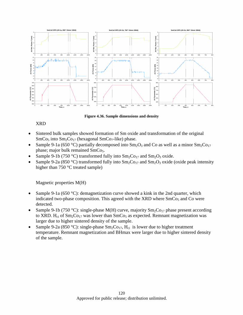
120 Approved for public release; distribution unlimited.
Figure 4.36. Sample dimensions and density
XRD
• Sintered bulk samples showed formation of Sm oxide and transformation of the originalSmCo5 into Sm2Co17 (hexagonal SmCo7-like) phase.
• Sample 9-1a (650 °C) partially decomposed into Sm2O3 and Co as well as a minor Sm2Co17phase; major bulk remained SmCo5.
• Sample 9-1b (750 °C) transformed fully into Sm2Co17 and Sm2O3 oxide.• Sample 9-2a (850 °C) transformed fully into Sm2Co17 and Sm2O3 oxide (oxide peak intensity
higher than 750 °C treated sample)
Magnetic properties M(H)
• Sample 9-1a (650 °C): demagnetization curve showed a kink in the 2nd quarter, whichindicated two-phase composition. This agreed with the XRD where SmCo5 and Co weredetected.
• Sample 9-1b (750 °C): single-phase M(H) curve, majority Sm2Co17 phase present accordingto XRD. Hci of Sm2Co17 was lower than SmCo5 as expected. Remnant magnetization waslarger due to higher sintered density of the sample.
• Sample 9-2a (850 °C): single-phase Sm2Co17, Hci is lower due to higher treatmenttemperature. Remnant magnetization and BHmax were larger due to higher sintered densityof the sample.
0 200 400 600 800 1000 1200 1400 1600350
400
450
500
550
600
650
700
AV
Pyro
met
er (°
C)
Time, s
0 200 400 600 800 1000 1200 1400 1600-4
-2
0
2
4
6
8
10
12
AV
Forc
e (k
N)
0 200 400 600 800 1000 1200 1400 16000
1
2
3
4SmCo5 SPS (#9-1a, 650° 10min 10kN)
AV
Rel
. Pis
ton
T (m
m)
0 200 400 600 800 1000 1200 1400 1600 1800
400
500
600
700
800
AV
Pyro
met
er (°
C)
Time, s
0 200 400 600 800 1000 1200 1400 1600 1800-4
0
4
8
12
16
20
24
AV
Forc
e (k
N)
0 200 400 600 800 1000 1200 1400 1600 18000
1
2
3
4
5
6SmCo5 SPS (#9-1b, 750° 10min 20kN)
AV
Rel
. Pis
ton
T (m
m)
0 100 200 300 400 500 600 700 800
400
500
600
700
800
900
AV
Pyro
met
er (°
C)
Time, s
0 100 200 300 400 500 600 700 800-5
0
5
10
15
20
25
30
35
AV
Forc
e (k
N)
0 100 200 300 400 500 600 700 8000
1
2
3
4
5
6SmCo5 SPS (#9-1b, 850° 10min 30kN)
AV
Rel
. Pis
ton
T (m
m)
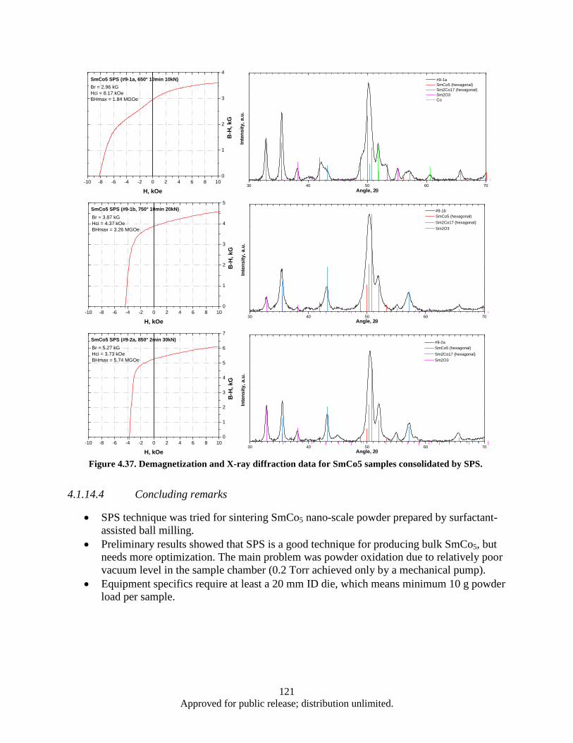
121 Approved for public release; distribution unlimited.
Figure 4.37. Demagnetization and X-ray diffraction data for SmCo5 samples consolidated by SPS.
4.1.14.4 Concluding remarks
• SPS technique was tried for sintering SmCo5 nano-scale powder prepared by surfactant-assisted ball milling.
• Preliminary results showed that SPS is a good technique for producing bulk SmCo5, butneeds more optimization. The main problem was powder oxidation due to relatively poorvacuum level in the sample chamber (0.2 Torr achieved only by a mechanical pump).
• Equipment specifics require at least a 20 mm ID die, which means minimum 10 g powderload per sample.
-10 -8 -6 -4 -2 0 2 4 6 8 100
1
2
3
4
B-H
, kG
H, kOe
SmCo5 SPS (#9-1a, 650° 10min 10kN)Br = 2.96 kGHci = 8.17 kOeBHmax = 1.84 MGOe
30 40 50 60 70
#9-1a SmCo5 (hexagonal) Sm2Co17 (hexagonal) Sm2O3 Co
Inte
nsity
, a.u
.
Angle, 2θ
-10 -8 -6 -4 -2 0 2 4 6 8 100
1
2
3
4
5
Br = 3.87 kGHci = 4.37 kOeBHmax = 3.26 MGOe
B-H
, kG
H, kOe
SmCo5 SPS (#9-1b, 750° 10min 20kN)
30 40 50 60 70
#9-1b
Inte
nsity
, a.u
.
Angle, 2θ
SmCo5 (hexagonal) Sm2Co17 (hexagonal) Sm2O3
-10 -8 -6 -4 -2 0 2 4 6 8 100
1
2
3
4
5
6
7
Br = 5.27 kGHci = 3.73 kOeBHmax = 5.74 MGOe
B-H
, kG
H, kOe
SmCo5 SPS (#9-2a, 850° 2min 30kN)
30 40 50 60 70
#9-2a
Inte
nsity
, a.u
.
Angle, 2θ
SmCo5 (hexagonal) Sm2Co17 (hexagonal) Sm2O3

122 Approved for public release; distribution unlimited.
4.1.15 SmCo5 nano-flake powder Hot Pressing (HP) sintering
4.1.15.1 Objectives
• Prepare nano-flake SmCo5 powder using surfactant-assisted ball milling.• Consolidate the powder into bulk material by using a HP technique.• Investigate sintered sample crystal structure and magnetic properties; determine optimal
sintering conditions.
4.1.15.2 Experiment description
SmCo5 nano-powder preparation
Several batches of SmCo5 nano-powder were prepared via a wet high energy ball milling process using Valeric acid as a surfactant agent. Each batch contained 15 g coarse SmCo5 powder, 60 g 1/8 inch diameter milling balls (ball-to-powder ratio 4:1), 10 g heptane (65 wt%), and 1.5 g surfactant (10 wt%). Milling time was 1 h. Milled powders were rinsed in acetone and separated from the ball media followed by 30 min drying in a vacuum chamber.
Hot press sintering experiment setup
Stainless steel dies (3/8 inch ID) were lined with one layer of graphite foil for protection from reactions with the powder. Die punch faces were also covered with foil. Sample powder was loaded into the dies, approximately 2.5 g each, in an Ar atmosphere. Sintering was carried out using an in-house radio frequency induction hot press under vacuum at ~1 mTorr and temperatures of 650, 750 and 850 °C. Sintering time was 2 minutes in all cases.
4.1.15.3 Results
Sample dimensions and density:
• Sample (650 °C) D=20.1 mm, H=7.14 mm, m=11.90 g, rho=5.24g/cm3 ~62% of fulldensity (8.5g/cm3)
• Sample (750 °C) D=20.15 mm, H=4.77 mm, m=9.91 g, rho=6.52 g/cm3 ~74% of fulldensity
• Sample (850 °C) D=20.15 mm, H=4.77 mm, m=9.91 g, rho=6.52 g/cm3 ~74% of fulldensity
X-ray diffraction • Sintered bulk samples showed formation of Sm oxide and transformation of the original
SmCo5 into a Sm2Co17 (hexagonal SmCo7-like) phase. • Sample sintered at 650 and 750 °C partially decomposed into Sm2O3 and Co as well as
the Sm2Co17 phase; the amount of Sm2Co17 phase was greater after sintering at 750 °C. • Sample 850 °C transformed fully into Sm2Co17 and Sm2O3 oxide.
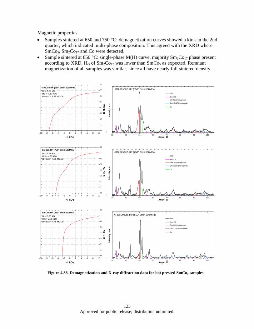
123 Approved for public release; distribution unlimited.
Magnetic properties • Samples sintered at 650 and 750 °C: demagnetization curves showed a kink in the 2nd
quarter, which indicated multi-phase composition. This agreed with the XRD where SmCo5, Sm2Co17 and Co were detected.
• Sample sintered at 850 °C: single-phase M(H) curve, majority Sm2Co17 phase presentaccording to XRD. Hci of Sm2Co17 was lower than SmCo5 as expected. Remnant magnetization of all samples was similar, since all have nearly full sintered density.
Figure 4.38. Demagnetization and X-ray diffraction data for hot pressed SmCo5 samples.
-10 -8 -6 -4 -2 0 2 4 6 8 100
1
2
3
4
5
6
7
8
B-H
, kG
H, kOe
SmCo5 HP (650° 2min 500MPa)Br = 5.34 kGHci = 7.17 kOeBHmax = 4.75 MGOe
30 40 50 60 70 80 90 100
650°
Inte
nsity
, a.u
.
Angle, 2θ
XRD: SmCo5 HP (650° 2min 500MPa)
SmCo5 (hexagonal)
Sm2Co17 (hexagonal)
Sm2O3
Co
-10 -8 -6 -4 -2 0 2 4 6 8 100
1
2
3
4
5
6
7
8
Br = 5.29 kGHci = 4.83 kOeBHmax = 4.06 MGOe
B-H
, kG
H, kOe
SmCo5 HP (750° 2min 500MPa)
30 40 50 60 70 80 90 100
750°
Inte
nsity
, a.u
.
Angle, 2θ
XRD: SmCo5 HP (750° 2min 500MPa)
SmCo5 (hexagonal)
Sm2Co17 (hexagonal)
Sm2O3
Co
-10 -8 -6 -4 -2 0 2 4 6 8 100
1
2
3
4
5
6
7
8
Br = 5.37 kGHci = 2.60 kOeBHmax = 4.48 MGOe
B-H
, kG
H, kOe
SmCo5 HP (850° 2min 500MPa)
30 40 50 60 70 80 90 100
850°
Inte
nsity
, a.u
.
Angle, 2θ
XRD: SmCo5 HP (850° 2min 500MPa)
SmCo5 (hexagonal)
Sm2Co17 (hexagonal)
Sm2O3
Co

124 Approved for public release; distribution unlimited.
4.1.15.4 Concluding remarks
• A hot press sintering technique has been tried for sintering SmCo5 nano-scale powderprepared by surfactant-assisted ball milling.
• Preliminary results showed that hot press is a good technique for producing bulk SmCo5,but needs more optimization. The main problem was powder oxidation, which can beattributed to high residual surfactant content in the samples.
• Further testing will be conducted to optimize the sintering process and minimizeoxidation.
Computer simulation of magnetic inductor components using FEM 4.2
4.2.1 Summary of inductor Eddy-current loss simulation using ANSYS Maxwell 3D software
4.2.1.1 Objective
• Present a general idea of ANSYS Maxwell 3D software capabilities in terms of modelinglaminated inductor core Eddy-current power losses.
• Based on the simulation results, summarize the trends of Eddy losses as a function ofoperating frequency, lamination thickness and core material resistivity for commercialMetglas and homemade FeCoTa alloys as core materials examples.
4.2.1.2 Experimental setup
ANSYS Maxwell 3D software package was used to create a 3-dimensional model of a laminated (tape wound) inductor core with material properties equivalent to Metglas 2605SA1 alloy (µR=45000, σ=770000 1/Ωm) and core shape AMCC20 (C-core, 72x35x30 mm, tape thickness 23 µm, lamination stack thickness 11 mm). Simulated magnetic flux density inside the core was ~0.1 T, and operating frequency was in the 50-150 kHz range.
A rendered view of the 3D core model is shown in Figure 4.37, it consists of concentric lamination layers, the thickness and number of which can be controlled through a built-in Visual Basic script interface. By progressively increasing the number of layers and decreasing their thickness, it was concluded that available computer memory (8 Gb) was not enough to solve for Eddy-current loss in a model with more than 20 layers due to the excessive number of mesh discretization elements. The physical inductor core has ~500 lamination layers and projected PC memory requirements for modeling equivalent object is on order of 106 Gb. Therefore, to simplify the model, a 2-dimensional, a cross section of the core was considered.
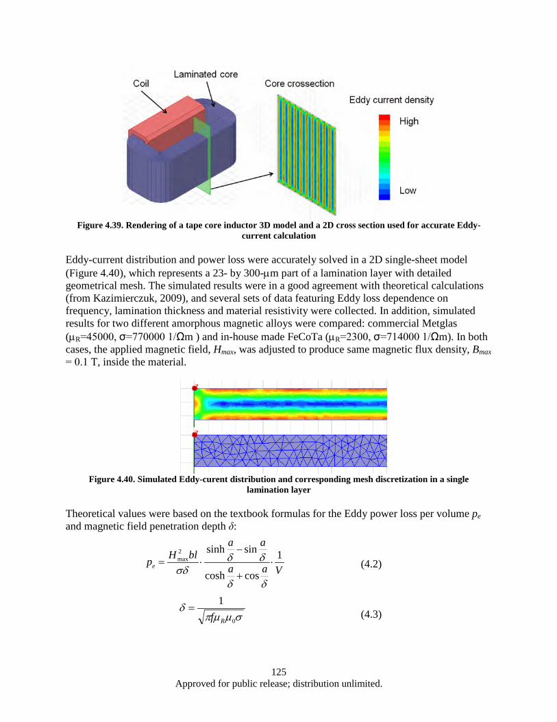
125 Approved for public release; distribution unlimited.
Figure 4.39. Rendering of a tape core inductor 3D model and a 2D cross section used for accurate Eddy-current calculation
Eddy-current distribution and power loss were accurately solved in a 2D single-sheet model (Figure 4.40), which represents a 23- by 300-µm part of a lamination layer with detailed geometrical mesh. The simulated results were in a good agreement with theoretical calculations (from Kazimierczuk, 2009), and several sets of data featuring Eddy loss dependence on frequency, lamination thickness and material resistivity were collected. In addition, simulated results for two different amorphous magnetic alloys were compared: commercial Metglas (µR=45000, σ=770000 1/Ωm ) and in-house made FeCoTa (µR=2300, σ=714000 1/Ωm). In both cases, the applied magnetic field, Hmax, was adjusted to produce same magnetic flux density, Bmax = 0.1 T, inside the material.
Figure 4.40. Simulated Eddy-curent distribution and corresponding mesh discretization in a single lamination layer
Theoretical values were based on the textbook formulas for the Eddy power loss per volume pe and magnetic field penetration depth δ:
(4.2)
(4.3)
Vaa
aablHpe
1
coscosh
sinsinh2max ⋅
+
−⋅=
δδ
δδσδ
σµµπδ
0
1
Rf=
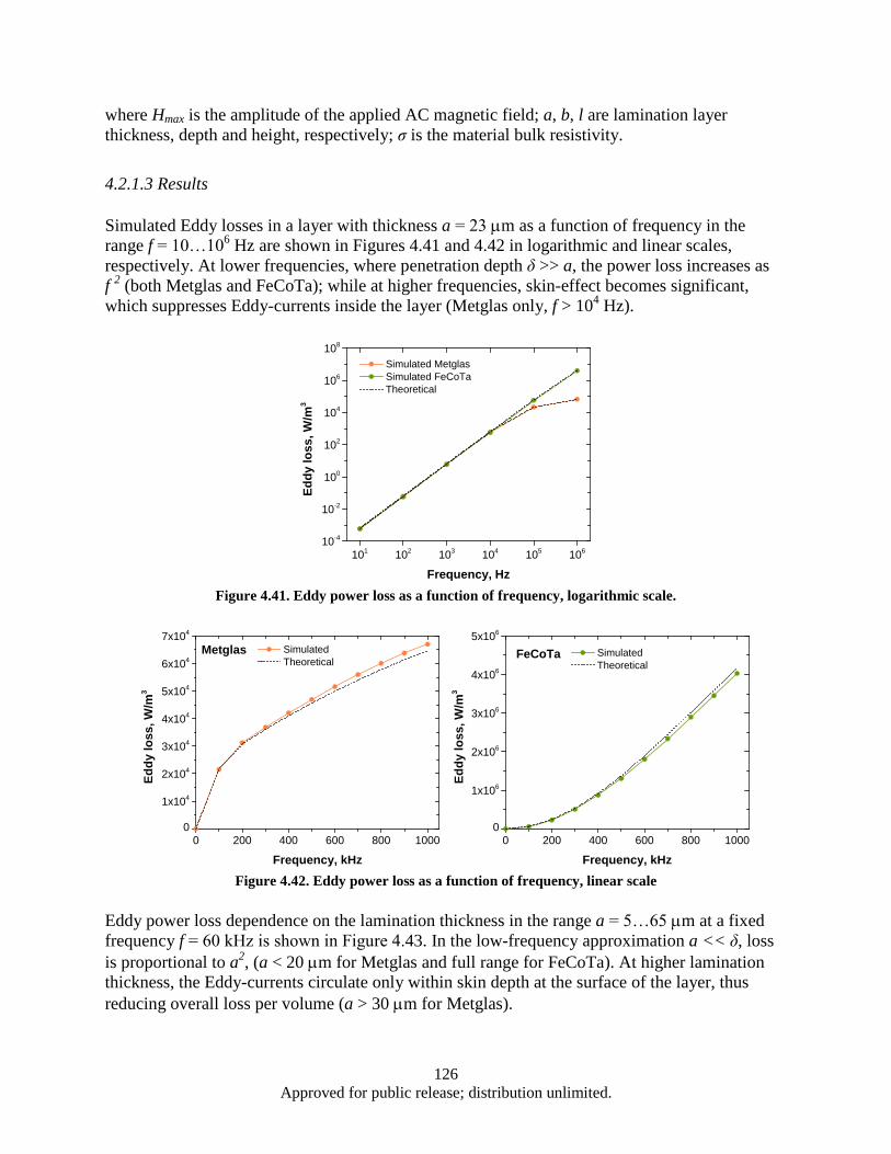
126 Approved for public release; distribution unlimited.
where Hmax is the amplitude of the applied AC magnetic field; a, b, l are lamination layer thickness, depth and height, respectively; σ is the material bulk resistivity.
4.2.1.3 Results
Simulated Eddy losses in a layer with thickness a = 23 µm as a function of frequency in the range f = 10…106 Hz are shown in Figures 4.41 and 4.42 in logarithmic and linear scales, respectively. At lower frequencies, where penetration depth δ >> a, the power loss increases as f 2 (both Metglas and FeCoTa); while at higher frequencies, skin-effect becomes significant, which suppresses Eddy-currents inside the layer (Metglas only, f > 104 Hz).
Figure 4.41. Eddy power loss as a function of frequency, logarithmic scale.
Figure 4.42. Eddy power loss as a function of frequency, linear scale
Eddy power loss dependence on the lamination thickness in the range a = 5…65 µm at a fixed frequency f = 60 kHz is shown in Figure 4.43. In the low-frequency approximation a << δ, loss is proportional to a2, (a < 20 µm for Metglas and full range for FeCoTa). At higher lamination thickness, the Eddy-currents circulate only within skin depth at the surface of the layer, thus reducing overall loss per volume (a > 30 µm for Metglas).
101 102 103 104 105 10610-4
10-2
100
102
104
106
108
Simulated Metglas Simulated FeCoTa Theoretical
Eddy
loss
, W/m
3
Frequency, Hz
0 200 400 600 800 10000
1x10⁴
2x10⁴
3x10⁴
4x10⁴
5x10⁴
6x10⁴
7x10⁴
Metglas Simulated Theoretical
Eddy
loss
, W/m
3
Frequency, kHz0 200 400 600 800 1000
0
1x10⁶
2x10⁶
3x10⁶
4x10⁶
5x10⁶
FeCoTa Simulated Theoretical
Eddy
loss
, W/m
3
Frequency, kHz
127 Approved for public release; distribution unlimited.
Figure 4.43. Eddy power loss as a function of lamination thickness
Calculated Eddy loss for fixed layer thickness a = 23 µm and frequency f = 60 kHz as a function material bulk resistivity ρ = 50…300 µΩ·cm is shown in Figure 4.44. Higher resistivity progressively results in reduced Ohmic losses in case of FeCoTa with weak skin effect. On the other hand, Metglas has much higher permeability leading to stronger skin effect and suppressed Eddy loss in the low resistivity range.
Figure 4.44. Eddy power loss as a function of material resistivity
4.2.1.4 Conclusion
Based on the results of modeling laminated inductor core Eddy-current losses using a conventional PC and ANSYS Maxwell 3D software package, the following points can be outlined: • It is not possible to fully simulate a 3-dimensional laminated core due to extremely high PC
memory requirements; a simplified 2D model of a single lamination layer was used instead. • Eddy power loss was calculated for commercial Metglas and homemade FeCoTa amorphous
magnetic alloys; very good agreement between simulated and theoretical results was achieved.
• In the range of input parameters examined, Metglas alloy exhibits strong skin-effect (fieldpenetration depth much smaller than layer thickness) which reduces Eddy loss per volume of
0 10 20 30 40 50 60 700.0
3.0x10⁴
6.0x10⁴
9.0x10⁴
1.2x10⁵
1.5x10⁵
Simulated Metglas Simulated FeCoTa Theoretical
Eddy
loss
, W/m
3
Layer thickness, µm
50 100 150 200 250 3000
1x10⁴
2x10⁴
3x10⁴
4x10⁴
5x10⁴
6x10⁴ Simulated Metglas Simulated FeCoTa Theoretical
Eddy
loss
, W/m
3
Resistivity, µΩ *cm
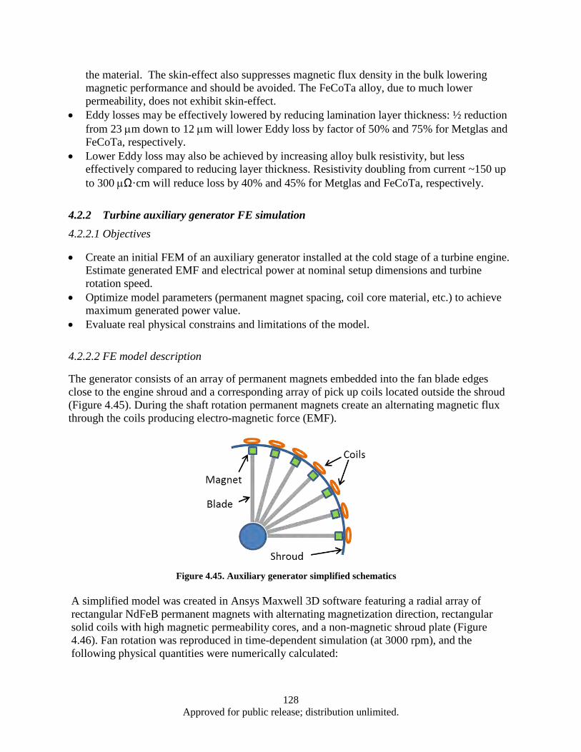
128 Approved for public release; distribution unlimited.
the material. The skin-effect also suppresses magnetic flux density in the bulk lowering magnetic performance and should be avoided. The FeCoTa alloy, due to much lower permeability, does not exhibit skin-effect.
• Eddy losses may be effectively lowered by reducing lamination layer thickness: ½ reductionfrom 23 µm down to 12 µm will lower Eddy loss by factor of 50% and 75% for Metglas and FeCoTa, respectively.
• Lower Eddy loss may also be achieved by increasing alloy bulk resistivity, but lesseffectively compared to reducing layer thickness. Resistivity doubling from current ~150 up to 300 µΩ·cm will reduce loss by 40% and 45% for Metglas and FeCoTa, respectively.
4.2.2 Turbine auxiliary generator FE simulation 4.2.2.1 Objectives
• Create an initial FEM of an auxiliary generator installed at the cold stage of a turbine engine.Estimate generated EMF and electrical power at nominal setup dimensions and turbinerotation speed.
• Optimize model parameters (permanent magnet spacing, coil core material, etc.) to achievemaximum generated power value.
• Evaluate real physical constrains and limitations of the model.
4.2.2.2 FE model description
The generator consists of an array of permanent magnets embedded into the fan blade edges close to the engine shroud and a corresponding array of pick up coils located outside the shroud (Figure 4.45). During the shaft rotation permanent magnets create an alternating magnetic flux through the coils producing electro-magnetic force (EMF).
Figure 4.45. Auxiliary generator simplified schematics
A simplified model was created in Ansys Maxwell 3D software featuring a radial array of rectangular NdFeB permanent magnets with alternating magnetization direction, rectangular solid coils with high magnetic permeability cores, and a non-magnetic shroud plate (Figure 4.46). Fan rotation was reproduced in time-dependent simulation (at 3000 rpm), and the following physical quantities were numerically calculated:
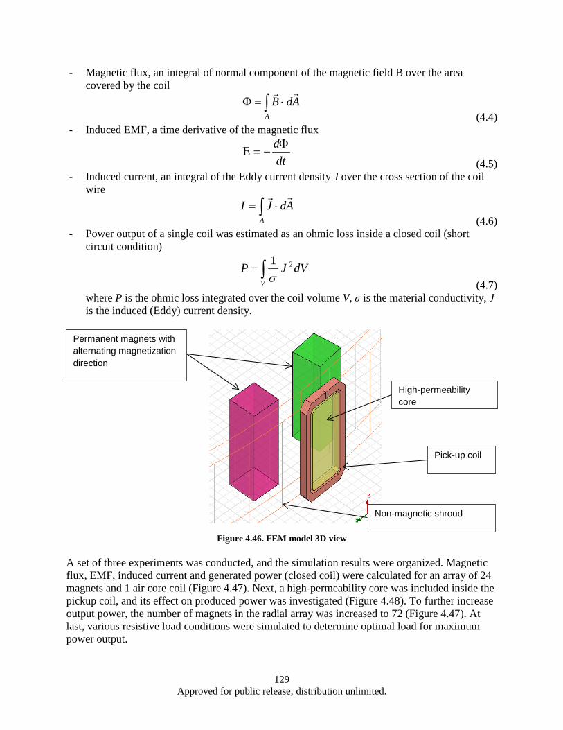
129 Approved for public release; distribution unlimited.
- Magnetic flux, an integral of normal component of the magnetic field B over the area covered by the coil
AdBA
⋅=Φ ∫
(4.4)- Induced EMF, a time derivative of the magnetic flux
dtdΦ
−=Ε(4.5)
- Induced current, an integral of the Eddy current density J over the cross section of the coil wire
AdJIA
⋅= ∫
(4.6)- Power output of a single coil was estimated as an ohmic loss inside a closed coil (short
circuit condition)
dVJPV∫= 21σ (4.7)
where P is the ohmic loss integrated over the coil volume V, σ is the material conductivity, J is the induced (Eddy) current density.
Figure 4.46. FEM model 3D view
A set of three experiments was conducted, and the simulation results were organized. Magnetic flux, EMF, induced current and generated power (closed coil) were calculated for an array of 24 magnets and 1 air core coil (Figure 4.47). Next, a high-permeability core was included inside the pickup coil, and its effect on produced power was investigated (Figure 4.48). To further increase output power, the number of magnets in the radial array was increased to 72 (Figure 4.47). At last, various resistive load conditions were simulated to determine optimal load for maximum power output.
Permanent magnets with alternating magnetization direction
Pick-up coil
Non-magnetic shroud
High-permeability core
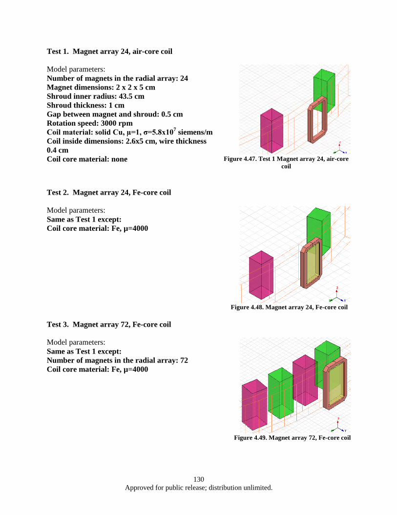
130 Approved for public release; distribution unlimited.
Test 1. Magnet array 24, air-core coil
Model parameters: Number of magnets in the radial array: 24 Magnet dimensions: 2 x 2 x 5 cm Shroud inner radius: 43.5 cm Shroud thickness: 1 cm Gap between magnet and shroud: 0.5 cm Rotation speed: 3000 rpm Coil material: solid Cu, µ=1, σ=5.8x10⁷ siemens/m Coil inside dimensions: 2.6x5 cm, wire thickness 0.4 cm Coil core material: none Figure 4.47. Test 1 Magnet array 24, air-core
coil
Test 2. Magnet array 24, Fe-core coil
Model parameters: Same as Test 1 except: Coil core material: Fe, µ=4000
Figure 4.48. Magnet array 24, Fe-core coil
Test 3. Magnet array 72, Fe-core coil
Model parameters: Same as Test 1 except: Number of magnets in the radial array: 72 Coil core material: Fe, µ=4000
Figure 4.49. Magnet array 72, Fe-core coil
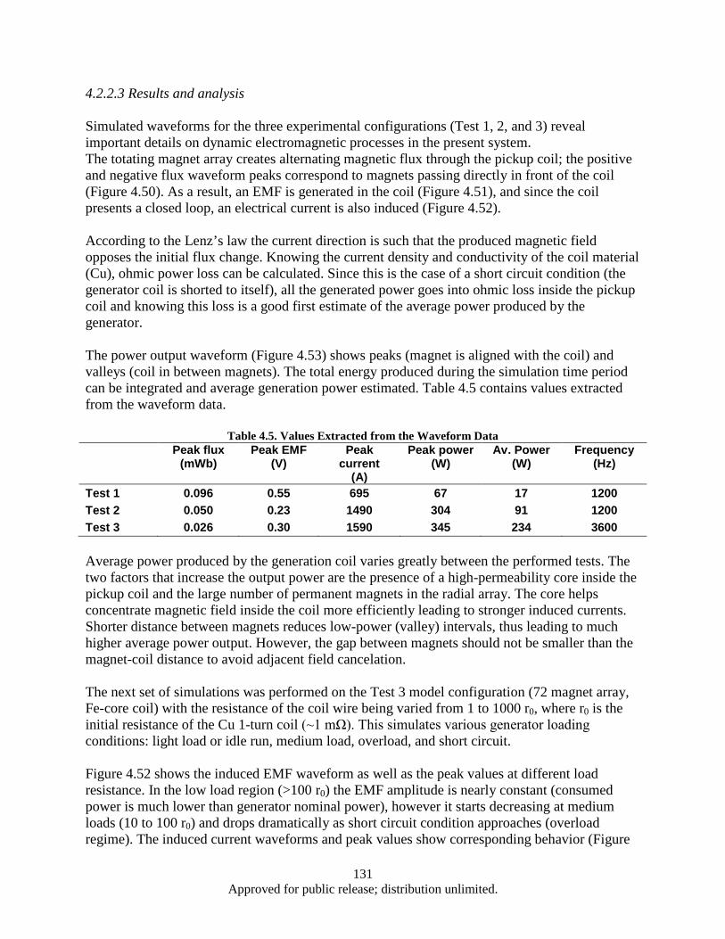
131 Approved for public release; distribution unlimited.
4.2.2.3 Results and analysis
Simulated waveforms for the three experimental configurations (Test 1, 2, and 3) reveal important details on dynamic electromagnetic processes in the present system. The totating magnet array creates alternating magnetic flux through the pickup coil; the positive and negative flux waveform peaks correspond to magnets passing directly in front of the coil (Figure 4.50). As a result, an EMF is generated in the coil (Figure 4.51), and since the coil presents a closed loop, an electrical current is also induced (Figure 4.52).
According to the Lenz’s law the current direction is such that the produced magnetic field opposes the initial flux change. Knowing the current density and conductivity of the coil material (Cu), ohmic power loss can be calculated. Since this is the case of a short circuit condition (the generator coil is shorted to itself), all the generated power goes into ohmic loss inside the pickup coil and knowing this loss is a good first estimate of the average power produced by the generator.
The power output waveform (Figure 4.53) shows peaks (magnet is aligned with the coil) and valleys (coil in between magnets). The total energy produced during the simulation time period can be integrated and average generation power estimated. Table 4.5 contains values extracted from the waveform data.
Table 4.5. Values Extracted from the Waveform Data Peak flux
(mWb) Peak EMF
(V) Peak
current (A)
Peak power (W)
Av. Power (W)
Frequency (Hz)
Test 1 0.096 0.55 695 67 17 1200 Test 2 0.050 0.23 1490 304 91 1200 Test 3 0.026 0.30 1590 345 234 3600
Average power produced by the generation coil varies greatly between the performed tests. The two factors that increase the output power are the presence of a high-permeability core inside the pickup coil and the large number of permanent magnets in the radial array. The core helps concentrate magnetic field inside the coil more efficiently leading to stronger induced currents. Shorter distance between magnets reduces low-power (valley) intervals, thus leading to much higher average power output. However, the gap between magnets should not be smaller than the magnet-coil distance to avoid adjacent field cancelation.
The next set of simulations was performed on the Test 3 model configuration (72 magnet array, Fe-core coil) with the resistance of the coil wire being varied from 1 to 1000 r0, where r0 is the initial resistance of the Cu 1-turn coil (~1 mΩ). This simulates various generator loading conditions: light load or idle run, medium load, overload, and short circuit.
Figure 4.52 shows the induced EMF waveform as well as the peak values at different load resistance. In the low load region (>100 r0) the EMF amplitude is nearly constant (consumed power is much lower than generator nominal power), however it starts decreasing at medium loads (10 to 100 r0) and drops dramatically as short circuit condition approaches (overload regime). The induced current waveforms and peak values show corresponding behavior (Figure
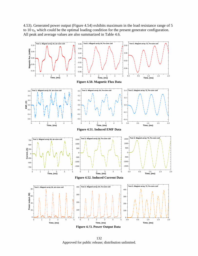
132 Approved for public release; distribution unlimited.
4.53). Generated power output (Figure 4.54) exhibits maximum in the load resistance range of 5 to 10 r0, which could be the optimal loading condition for the present generator configuration. All peak and average values are also summarized in Table 4.6.
Figure 4.50. Magnetic Flux Data
Figure 4.51. Induced EMF Data
Figure 4.52. Induced Current Data
Figure 4.53. Power Output Data
0 1 2 3 4 5
-0.10
-0.05
0.00
0.05
0.10
Mag
netic
flux
, (m
Wb)
Time, (ms)
Test 1. Magnet array 24, air-core coil
0 1 2 3 4 5
-0.06
-0.04
-0.02
0.00
0.02
0.04
0.06 Test 2. Magnet array 24, Fe-core coil
Time, (ms)0.0 0.5 1.0 1.5 2.0
-0.04
-0.02
0.00
0.02Test 3. Magnet array 72, Fe-core coil
Time, (ms)
0 1 2 3 4 5
-0.6
-0.4
-0.2
0.0
0.2
0.4
0.6 Test 1. Magnet array 24, air-core coil
EMF,
(V)
Time, (ms)0 1 2 3 4 5
-0.3
-0.2
-0.1
0.0
0.1
0.2
0.3 Test 2. Magnet array 24, Fe-core coil
Time, (ms)0.0 0.5 1.0 1.5 2.0
-0.4
-0.2
0.0
0.2
0.4 Test 3. Magnet array 72, Fe-core coil
Time, (ms)
0 1 2 3 4 5
-750
-500
-250
0
250
500
750 Test 1. Magnet array 24, air-core coil
Cur
rent
, (A
)
Time, (ms)0 1 2 3 4 5
-1500
-1000
-500
0
500
1000
1500 Test 2. Magnet array 24, Fe-core coil
Time, (ms)0.0 0.5 1.0 1.5 2.0
-1500
-1000
-500
0
500
1000
1500 Test 3. Magnet array 72, Fe-core coil
Time, (ms)
0 1 2 3 4 50
20
40
60
80Test 1. Magnet array 24, air-core coil
Pow
er o
utpu
t, (W
)
Time, (ms)0 1 2 3 4 5
0
100
200
300
400 Test 2. Magnet array 24, Fe-core coil
Time, (ms)0.0 0.5 1.0 1.5 2.0
0
100
200
300
400
Test 3. Magnet array 72, Fe-core coil
Time, (ms)
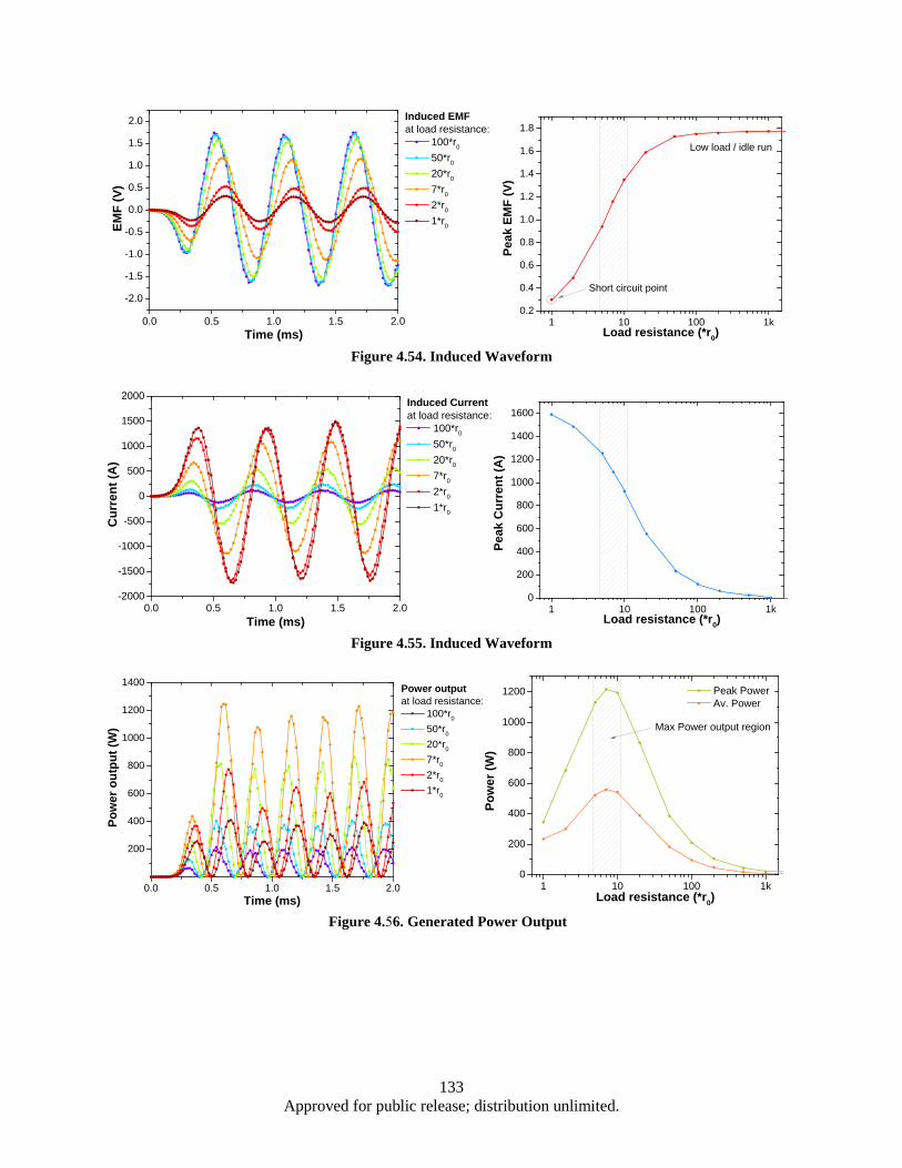
133 Approved for public release; distribution unlimited.
Figure 4.54. Induced Waveform
Figure 4.55. Induced Waveform
Figure 4.56. Generated Power Output
0.0 0.5 1.0 1.5 2.0
-2.0
-1.5
-1.0
-0.5
0.0
0.5
1.0
1.5
2.0 Induced EMF at load resistance:
100*r0
50*r0
20*r0
7*r0
2*r0
1*r0EMF
(V)
Time (ms)1 10 100 1k
0.2
0.4
0.6
0.8
1.0
1.2
1.4
1.6
1.8
Low load / idle run
Short circuit point
Peak
EM
F (V
)
Load resistance (*r0)
0.0 0.5 1.0 1.5 2.0-2000
-1500
-1000
-500
0
500
1000
1500
2000 Induced Current at load resistance:
100*r0
50*r0
20*r0
7*r0
2*r0
1*r0
Cur
rent
(A)
Time (ms)1 10 100 1k
0
200
400
600
800
1000
1200
1400
1600
Peak
Cur
rent
(A)
Load resistance (*r0)
0.0 0.5 1.0 1.5 2.0
200
400
600
800
1000
1200
1400
Pow
er o
utpu
t (W
)
Time (ms)
Power output at load resistance:
100*r0
50*r0
20*r0
7*r0
2*r0
1*r0
1 10 100 1k0
200
400
600
800
1000
1200 Peak Power Av. Power
Pow
er (W
)
Load resistance (*r0)
Max Power output region
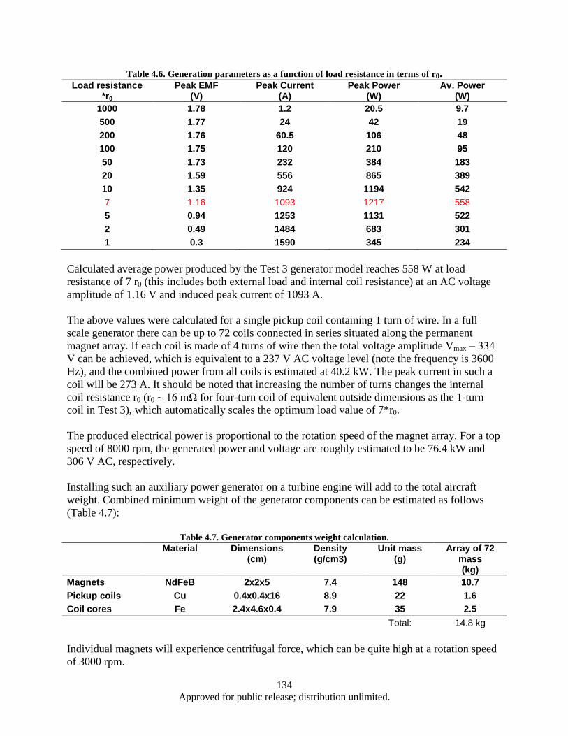
134 Approved for public release; distribution unlimited.
Table 4.6. Generation parameters as a function of load resistance in terms of r0. Load resistance
*r0
Peak EMF (V)
Peak Current (A)
Peak Power (W)
Av. Power (W)
1000 1.78 1.2 20.5 9.7 500 1.77 24 42 19 200 1.76 60.5 106 48 100 1.75 120 210 95 50 1.73 232 384 183 20 1.59 556 865 389 10 1.35 924 1194 542 7 1.16 1093 1217 558 5 0.94 1253 1131 522 2 0.49 1484 683 301 1 0.3 1590 345 234
Calculated average power produced by the Test 3 generator model reaches 558 W at load resistance of 7 r0 (this includes both external load and internal coil resistance) at an AC voltage amplitude of 1.16 V and induced peak current of 1093 A.
The above values were calculated for a single pickup coil containing 1 turn of wire. In a full scale generator there can be up to 72 coils connected in series situated along the permanent magnet array. If each coil is made of 4 turns of wire then the total voltage amplitude Vmax = 334 V can be achieved, which is equivalent to a 237 V AC voltage level (note the frequency is 3600 Hz), and the combined power from all coils is estimated at 40.2 kW. The peak current in such a coil will be 273 A. It should be noted that increasing the number of turns changes the internal coil resistance r0 (r0 ~ 16 mΩ for four-turn coil of equivalent outside dimensions as the 1-turn coil in Test 3), which automatically scales the optimum load value of 7*r0.
The produced electrical power is proportional to the rotation speed of the magnet array. For a top speed of 8000 rpm, the generated power and voltage are roughly estimated to be 76.4 kW and 306 V AC, respectively.
Installing such an auxiliary power generator on a turbine engine will add to the total aircraft weight. Combined minimum weight of the generator components can be estimated as follows (Table 4.7):
Table 4.7. Generator components weight calculation. Material Dimensions
(cm) Density (g/cm3)
Unit mass (g)
Array of 72 mass (kg)
Magnets NdFeB 2x2x5 7.4 148 10.7 Pickup coils Cu 0.4x0.4x16 8.9 22 1.6 Coil cores Fe 2.4x4.6x0.4 7.9 35 2.5
Total: 14.8 kg
Individual magnets will experience centrifugal force, which can be quite high at a rotation speed of 3000 rpm.

135 Approved for public release; distribution unlimited.
(4.8)
Mechanical bonding between magnets and fan blades needs to be strong enough to withstand such force. This force is directly proportional to the magnet mass; therefore it can be lowered by using smaller magnets.
4.2.2.4 Conclusion
A simplified computer model of an auxiliary turbine generator was created in Maxwell 3D software featuring a radial array of permanent magnets and pickup coils with high-permeability cores. Magnet array rotation was simulated in a transient (time-dependent) solution mode, and the generator output power and voltage were calculated.
Produced power depends on the quantity of magnets in the array (magnet spacing), material of the core inside pickup coils and rotation speed. The highest generated power is achieved by optimizing different parameters as well as the resistive load range.
The optimized* model parameters are: • Number of magnets in the radial array: 72 (*)• Magnet dimensions: 2 x 2 x 5 cm• Shroud inner radius: 43.5 cm• Shroud thickness: 1cm• Gap between magnet and shroud: 0.5 cm (*)• Rotation speed: 3000 rpm• Coil material: solid Cu, µ=1, σ=5.8x10⁷ Siemens/m• Coil inside dimensions: 2.6x5 cm, thickness 0.4 cm• Coil core material: Fe, µ=4000• Number of coils: 72 (*)• Number of wire turns per coil: 4 (*)• Total load resistance (including internal coil resistance r0): 7*r0 (*)
The maximum power output from the optimized model was estimated to be 40.2 kW, 237 V AC and a peak current of 273 A at 3000 rpm, and projected 76.4 kW, 306 V AC and a peak current of 350 A at 8000 rpm.
The minimum weight of the modelled generator components would be around 15 kg. The magnetic array parts will require extremely strong bonding with the fan blades to withstand centrifugal forces above 640 kg.
)(640)(64004 222 kgNRmRmF ≈≈⋅== νπω
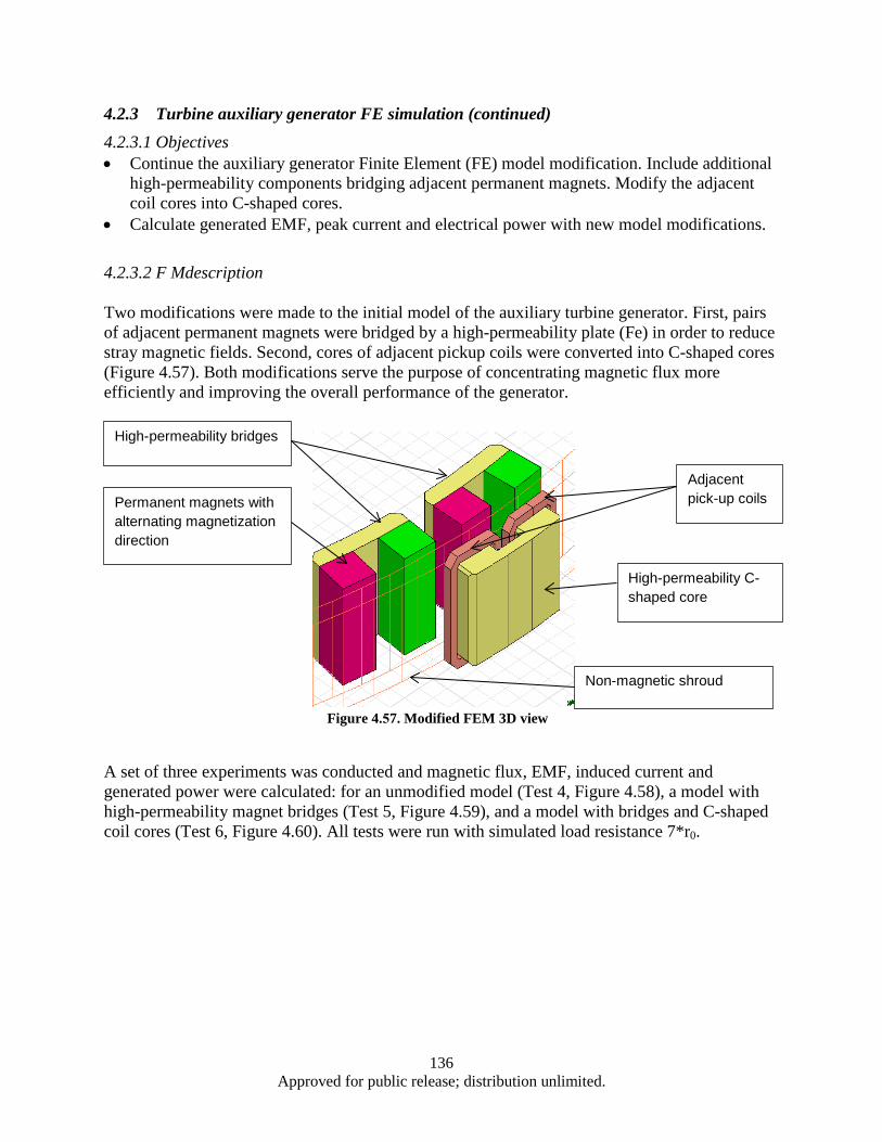
136 Approved for public release; distribution unlimited.
4.2.3 Turbine auxiliary generator FE simulation (continued) 4.2.3.1 Objectives • Continue the auxiliary generator Finite Element (FE) model modification. Include additional
high-permeability components bridging adjacent permanent magnets. Modify the adjacent coil cores into C-shaped cores.
• Calculate generated EMF, peak current and electrical power with new model modifications.
4.2.3.2 F Mdescription
Two modifications were made to the initial model of the auxiliary turbine generator. First, pairs of adjacent permanent magnets were bridged by a high-permeability plate (Fe) in order to reduce stray magnetic fields. Second, cores of adjacent pickup coils were converted into C-shaped cores (Figure 4.57). Both modifications serve the purpose of concentrating magnetic flux more efficiently and improving the overall performance of the generator.
Figure 4.57. Modified FEM 3D view
A set of three experiments was conducted and magnetic flux, EMF, induced current and generated power were calculated: for an unmodified model (Test 4, Figure 4.58), a model with high-permeability magnet bridges (Test 5, Figure 4.59), and a model with bridges and C-shaped coil cores (Test 6, Figure 4.60). All tests were run with simulated load resistance 7*r0.
Permanent magnets with alternating magnetization direction
Adjacent pick-up coils
Non-magnetic shroud
High-permeability C-shaped core
High-permeability bridges
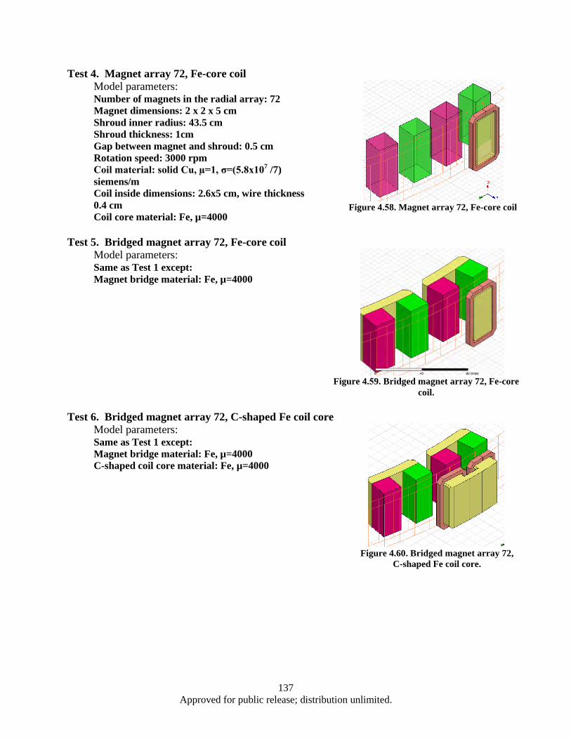
137 Approved for public release; distribution unlimited.
Test 4. Magnet array 72, Fe-core coil Model parameters: Number of magnets in the radial array: 72 Magnet dimensions: 2 x 2 x 5 cm Shroud inner radius: 43.5 cm Shroud thickness: 1cm Gap between magnet and shroud: 0.5 cm Rotation speed: 3000 rpm Coil material: solid Cu, µ=1, σ=(5.8x10⁷ /7) siemens/m Coil inside dimensions: 2.6x5 cm, wire thickness 0.4 cm Coil core material: Fe, µ=4000
Figure 4.58. Magnet array 72, Fe-core coil
Test 5. Bridged magnet array 72, Fe-core coil Model parameters: Same as Test 1 except: Magnet bridge material: Fe, µ=4000
Figure 4.59. Bridged magnet array 72, Fe-core coil.
Test 6. Bridged magnet array 72, C-shaped Fe coil core Model parameters: Same as Test 1 except: Magnet bridge material: Fe, µ=4000 C-shaped coil core material: Fe, µ=4000
Figure 4.60. Bridged magnet array 72, C-shaped Fe coil core.
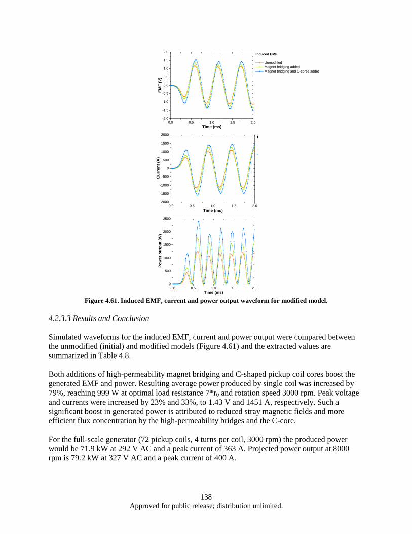
138 Approved for public release; distribution unlimited.
Figure 4.61. Induced EMF, current and power output waveform for modified model.
4.2.3.3 Results and Conclusion
Simulated waveforms for the induced EMF, current and power output were compared between the unmodified (initial) and modified models (Figure 4.61) and the extracted values are summarized in Table 4.8.
Both additions of high-permeability magnet bridging and C-shaped pickup coil cores boost the generated EMF and power. Resulting average power produced by single coil was increased by 79%, reaching 999 W at optimal load resistance 7*r0 and rotation speed 3000 rpm. Peak voltage and currents were increased by 23% and 33%, to 1.43 V and 1451 A, respectively. Such a significant boost in generated power is attributed to reduced stray magnetic fields and more efficient flux concentration by the high-permeability bridges and the C-core.
For the full-scale generator (72 pickup coils, 4 turns per coil, 3000 rpm) the produced power would be 71.9 kW at 292 V AC and a peak current of 363 A. Projected power output at 8000 rpm is 79.2 kW at 327 V AC and a peak current of 400 A.
0.0 0.5 1.0 1.5 2.0-2.0
-1.5
-1.0
-0.5
0.0
0.5
1.0
1.5
2.0 Induced EMF
Unmodified Magnet bridging added Magnet bridging and C-cores added
EMF
(V)
Time (ms)
0.0 0.5 1.0 1.5 2.0-2000
-1500
-1000
-500
0
500
1000
1500
2000 I
Cur
rent
(A)
Time (ms)
0.0 0.5 1.0 1.5 2.00
500
1000
1500
2000
2500
Pow
er o
utpu
t (W
)
Time (ms)
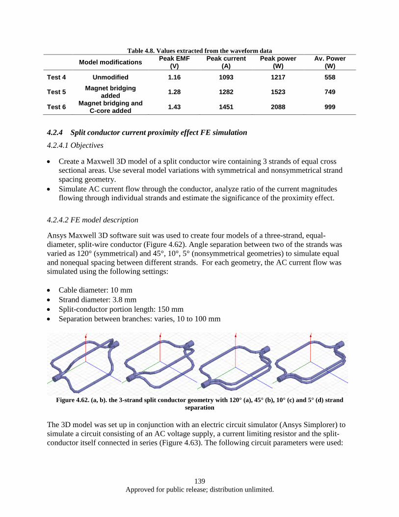
139 Approved for public release; distribution unlimited.
Table 4.8. Values extracted from the waveform data
Model modifications Peak EMF (V)
Peak current (A)
Peak power (W)
Av. Power (W)
Test 4 Unmodified 1.16 1093 1217 558
Test 5 Magnet bridging added 1.28 1282 1523 749
Test 6 Magnet bridging andC-core added 1.43 1451 2088 999
4.2.4 Split conductor current proximity effect FE simulation 4.2.4.1 Objectives
• Create a Maxwell 3D model of a split conductor wire containing 3 strands of equal crosssectional areas. Use several model variations with symmetrical and nonsymmetrical strandspacing geometry.
• Simulate AC current flow through the conductor, analyze ratio of the current magnitudesflowing through individual strands and estimate the significance of the proximity effect.
4.2.4.2 FE model description
Ansys Maxwell 3D software suit was used to create four models of a three-strand, equal-diameter, split-wire conductor (Figure 4.62). Angle separation between two of the strands was varied as 120° (symmetrical) and 45°, 10°, 5° (nonsymmetrical geometries) to simulate equal and nonequal spacing between different strands. For each geometry, the AC current flow was simulated using the following settings:
• Cable diameter: 10 mm• Strand diameter: 3.8 mm• Split-conductor portion length: 150 mm• Separation between branches: varies, 10 to 100 mm
Figure 4.62. (a, b). the 3-strand split conductor geometry with 120° (a), 45° (b), 10° (c) and 5° (d) strand separation
The 3D model was set up in conjunction with an electric circuit simulator (Ansys Simplorer) to simulate a circuit consisting of an AC voltage supply, a current limiting resistor and the split-conductor itself connected in series (Figure 4.63). The following circuit parameters were used:
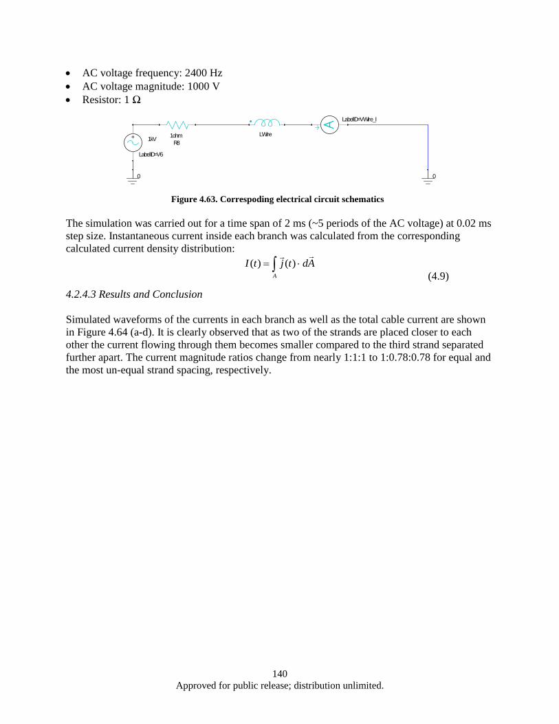
140 Approved for public release; distribution unlimited.
• AC voltage frequency: 2400 Hz• AC voltage magnitude: 1000 V• Resistor: 1 Ω
Figure 4.63. Correspoding electrical circuit schematics
The simulation was carried out for a time span of 2 ms (~5 periods of the AC voltage) at 0.02 ms step size. Instantaneous current inside each branch was calculated from the corresponding calculated current density distribution:
∫ ⋅=A
AdtjtI
)()((4.9)
4.2.4.3 Results and Conclusion
Simulated waveforms of the currents in each branch as well as the total cable current are shown in Figure 4.64 (a-d). It is clearly observed that as two of the strands are placed closer to each other the current flowing through them becomes smaller compared to the third strand separated further apart. The current magnitude ratios change from nearly 1:1:1 to 1:0.78:0.78 for equal and the most un-equal strand spacing, respectively.
00
LWire
LabelID=VWire_I
+ 1kV
LabelID=V6
1ohmR8
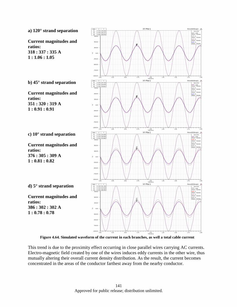
141 Approved for public release; distribution unlimited.
a) 120° strand separation
Current magnitudes and ratios: 318 : 337 : 335 A 1 : 1.06 : 1.05
b) 45° strand separation
Current magnitudes and ratios: 351 : 320 : 319 A 1 : 0.91 : 0.91
c) 10° strand separation
Current magnitudes and ratios: 376 : 305 : 309 A 1 : 0.81 : 0.82
d) 5° strand separation
Current magnitudes and ratios: 386 : 302 : 302 A 1 : 0.78 : 0.78
Figure 4.64. Simulated waveform of the current in each branches, as well a total cable current
This trend is due to the proximity effect occurring in close parallel wires carrying AC currents. Electro-magnetic field created by one of the wires induces eddy currents in the other wire, thus mutually altering their overall current density distribution. As the result, the current becomes concentrated in the areas of the conductor farthest away from the nearby conductor.
0.00 0.25 0.50 0.75 1.00 1.25 1.50 1.75 2.00Time [ms]
-1000.00
-750.00
-500.00
-250.00
0.00
250.00
500.00
750.00
1000.00
Y1
Maxwell3DDesign1XY Plot 1 ANSOFT
m1m2m3
Curve Infoi_total
Setup1 : Transienti1
Setup1 : Transienti2
Setup1 : Transienti3
Setup1 : Transient
Name X Ym1 0.7200 336.6326m2 0.7200 335.1311m3 0.7200 318.2764
0.00 0.25 0.50 0.75 1.00 1.25 1.50 1.75 2.00Time [ms]
-1000.00
-750.00
-500.00
-250.00
0.00
250.00
500.00
750.00
1000.00
Y1
Maxwell3DDesign1XY Plot 1 ANSOFT
m1m2m3
Curve Infoi_total
Setup1 : Transienti1
Setup1 : Transienti2
Setup1 : Transienti3
Setup1 : Transient
Name X Ym1 0.7200 319.7232m2 0.7200 319.4978m3 0.7200 350.8521
0.00 0.25 0.50 0.75 1.00 1.25 1.50 1.75 2.00Time [ms]
-1000.00
-750.00
-500.00
-250.00
0.00
250.00
500.00
750.00
1000.00
Y1
Maxwell3DDesign1XY Plot 1 ANSOFT
m1m2m3
Curve Infoi_total
Setup1 : Transienti1
Setup1 : Transienti2
Setup1 : Transienti3
Setup1 : Transient
Name X Ym1 0.7200 304.6908m2 0.7200 308.5064m3 0.7200 376.9462
0.00 0.25 0.50 0.75 1.00 1.25 1.50 1.75 2.00Time [ms]
-1000.00
-750.00
-500.00
-250.00
0.00
250.00
500.00
750.00
1000.00
Y1
Maxwell3DDesign1XY Plot 1 ANSOFT
m1m2m3
Curve Infoi_total
Setup1 : Transienti1
Setup1 : Transienti2
Setup1 : Transienti3
Setup1 : Transient
Name X Ym1 0.7200 301.7285m2 0.7200 302.0328m3 0.7200 386.4005
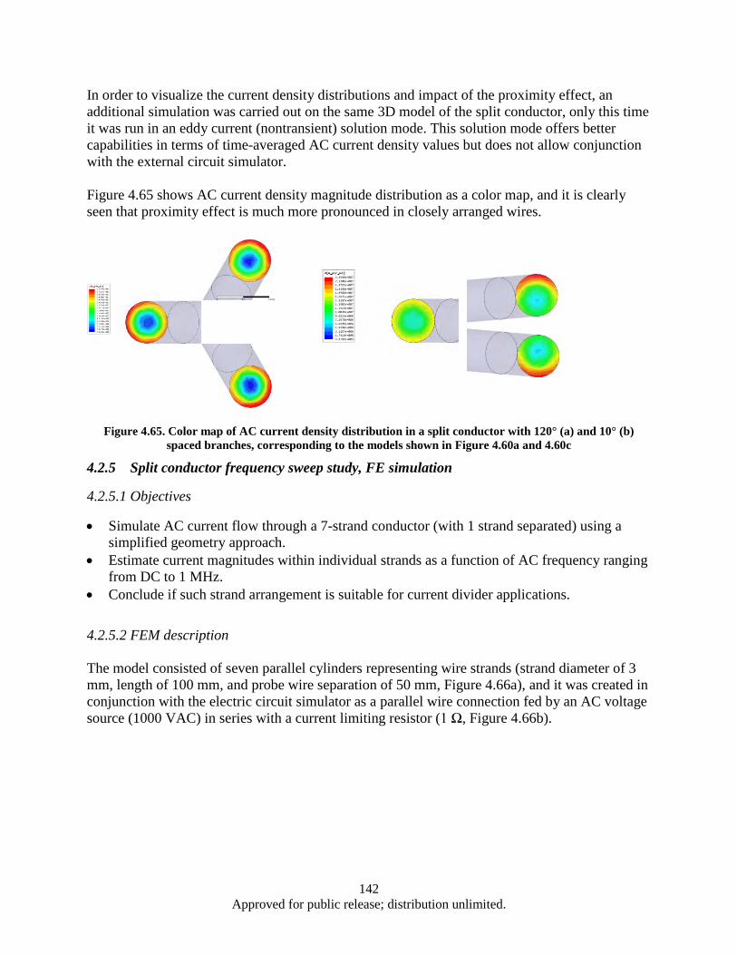
142 Approved for public release; distribution unlimited.
In order to visualize the current density distributions and impact of the proximity effect, an additional simulation was carried out on the same 3D model of the split conductor, only this time it was run in an eddy current (nontransient) solution mode. This solution mode offers better capabilities in terms of time-averaged AC current density values but does not allow conjunction with the external circuit simulator.
Figure 4.65 shows AC current density magnitude distribution as a color map, and it is clearly seen that proximity effect is much more pronounced in closely arranged wires.
Figure 4.65. Color map of AC current density distribution in a split conductor with 120° (a) and 10° (b) spaced branches, corresponding to the models shown in Figure 4.60a and 4.60c
4.2.5 Split conductor frequency sweep study, FE simulation
4.2.5.1 Objectives
• Simulate AC current flow through a 7-strand conductor (with 1 strand separated) using asimplified geometry approach.
• Estimate current magnitudes within individual strands as a function of AC frequency rangingfrom DC to 1 MHz.
• Conclude if such strand arrangement is suitable for current divider applications.
4.2.5.2 FEM description
The model consisted of seven parallel cylinders representing wire strands (strand diameter of 3 mm, length of 100 mm, and probe wire separation of 50 mm, Figure 4.66a), and it was created in conjunction with the electric circuit simulator as a parallel wire connection fed by an AC voltage source (1000 VAC) in series with a current limiting resistor (1 Ω, Figure 4.66b).
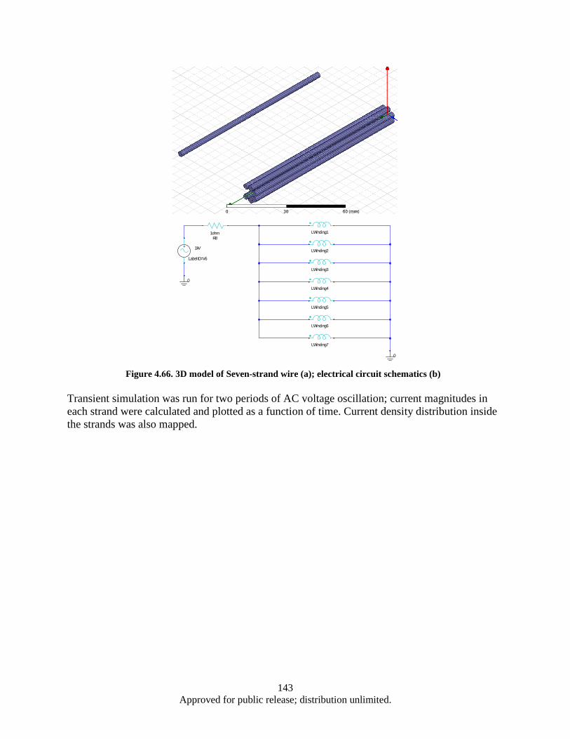
143 Approved for public release; distribution unlimited.
Figure 4.66. 3D model of Seven-strand wire (a); electrical circuit schematics (b)
Transient simulation was run for two periods of AC voltage oscillation; current magnitudes in each strand were calculated and plotted as a function of time. Current density distribution inside the strands was also mapped.
0
0
LWinding1
+ 1kV
LabelID=V6
1ohmR8
LWinding2
LWinding3
LWinding4
LWinding5
LWinding6
LWinding7
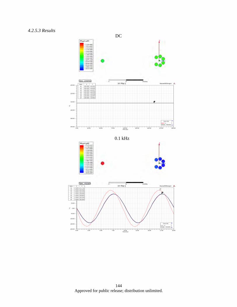
144 Approved for public release; distribution unlimited.
4.2.5.3 Results DC
0.1 kHz
0.00 25.00 50.00 75.00 100.00 125.00 150.00 175.00 200.00Time [us]
-200.00
-180.00
-160.00
-140.00
-120.00
-100.00
Y1
Maxwell3DDesign1XY Plot 1 ANSOFT
m1m2m3m4m5m6m7
Curve Infoi1
Setup1 : Transient
Name X Ym1 160.0000 -142.8422m2 160.0000 -142.8532m3 160.0000 -142.8537m4 160.0000 -142.8538m5 160.0000 -142.8538m6 160.0000 -142.8537m7 160.0000 -142.8531
0.00 2.50 5.00 7.50 10.00 12.50 15.00 17.50 20.00Time [ms]
-200.00
-150.00
-100.00
-50.00
0.00
50.00
100.00
150.00
200.00
Y1
Maxwell3DDesign1XY Plot 1 ANSOFT
m1
m2m3m4m5m6m7
Curve Infoi1
Setup1 : Transient
Name X Ym1 17.2000 172.7731m2 17.6000 140.2342m3 17.6000 139.3108m4 17.6000 138.8596m5 17.6000 138.8604m6 17.6000 139.3149m7 17.6000 140.2403
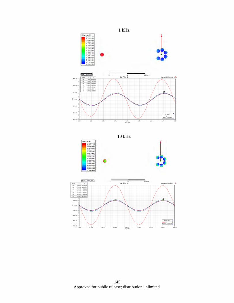
145 Approved for public release; distribution unlimited.
1 kHz
10 kHz
0.00 0.25 0.50 0.75 1.00 1.25 1.50 1.75 2.00Time [ms]
-375.00
-250.00
-125.00
0.00
125.00
250.00
375.00
Y1
Maxwell3DDesign1XY Plot 1 ANSOFTm1
m2m3m4m5m6m7
Curve Infoi1
Setup1 : Transient
Name X Ym1 1.7200 361.2625m2 1.7600 116.5625m3 1.7600 105.2688m4 1.7600 103.0401m5 1.7600 103.0422m6 1.7600 105.3148m7 1.7600 116.6789
0.00 25.00 50.00 75.00 100.00 125.00 150.00 175.00 200.00Time [us]
-400.00
-300.00
-200.00
-100.00
0.00
100.00
200.00
300.00
400.00
Y1
Maxwell3DDesign1XY Plot 1 ANSOFTm1
m2m3m4m5m6m7
Curve Infoi1
Setup1 : Transient
Name X Ym1 176.0000 387.8266m2 176.0000 113.2531m3 176.0000 93.5025m4 176.0000 97.9774m5 176.0000 98.1855m6 176.0000 93.1482m7 176.0000 113.8311
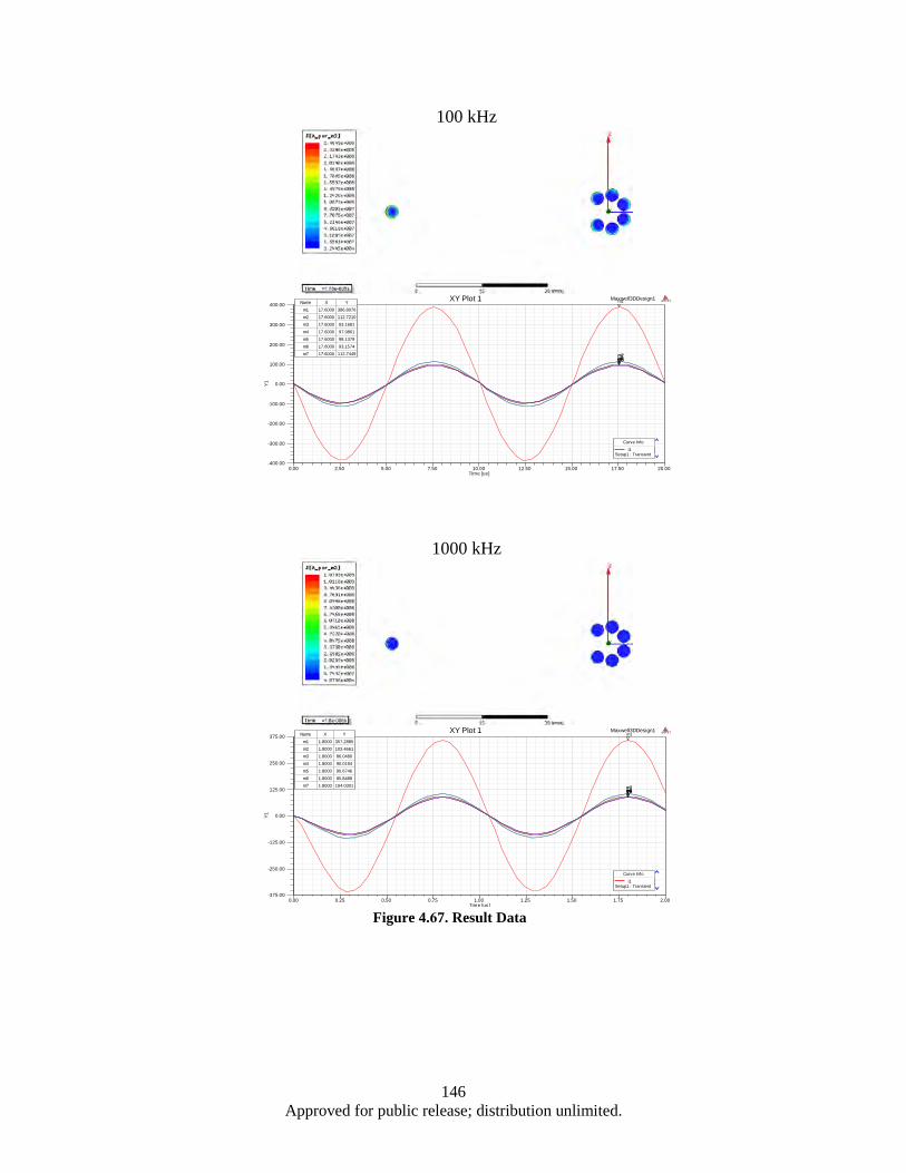
146 Approved for public release; distribution unlimited.
Figure 4.67. Result Data
100 kHz
1000 kHz
0.00 2.50 5.00 7.50 10.00 12.50 15.00 17.50 20.00Time [us]
-400.00
-300.00
-200.00
-100.00
0.00
100.00
200.00
300.00
400.00
Y1
Maxwell3DDesign1XY Plot 1 ANSOFTm1
m2m3m4m5m6m7
Curve Infoi1
Setup1 : Transient
Name X Ym1 17.6000 386.8076m2 17.6000 112.7210m3 17.6000 93.1681m4 17.6000 97.9861m5 17.6000 98.1379m6 17.6000 93.1574m7 17.6000 112.7449
0.00 0.25 0.50 0.75 1.00 1.25 1.50 1.75 2.00Time [us]
-375.00
-250.00
-125.00
0.00
125.00
250.00
375.00
Y1
Maxwell3DDesign1XY Plot 1 ANSOFTm1
m2m3m4m5m6m7
Curve Infoi1
Setup1 : Transient
Name X Ym1 1.8000 357.2885m2 1.8000 103.4661m3 1.8000 86.0480m4 1.8000 90.0194m5 1.8000 90.6746m6 1.8000 85.8488m7 1.8000 104.0301
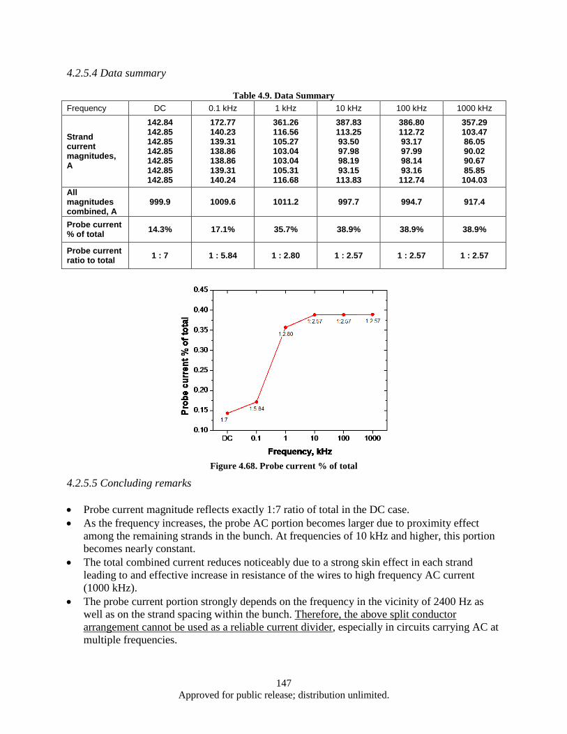
147 Approved for public release; distribution unlimited.
4.2.5.4 Data summary
Table 4.9. Data Summary Frequency DC 0.1 kHz 1 kHz 10 kHz 100 kHz 1000 kHz
Strand current magnitudes, A
142.84 142.85 142.85 142.85 142.85 142.85 142.85
172.77 140.23 139.31 138.86 138.86 139.31 140.24
361.26 116.56 105.27 103.04 103.04 105.31 116.68
387.83 113.25 93.50 97.98 98.19 93.15 113.83
386.80 112.72 93.17 97.99 98.14 93.16 112.74
357.29 103.47 86.05 90.02 90.67 85.85 104.03
All magnitudes combined, A
999.9 1009.6 1011.2 997.7 994.7 917.4
Probe current % of total 14.3% 17.1% 35.7% 38.9% 38.9% 38.9%
Probe current ratio to total 1 : 7 1 : 5.84 1 : 2.80 1 : 2.57 1 : 2.57 1 : 2.57
Figure 4.68. Probe current % of total 4.2.5.5 Concluding remarks
• Probe current magnitude reflects exactly 1:7 ratio of total in the DC case.• As the frequency increases, the probe AC portion becomes larger due to proximity effect
among the remaining strands in the bunch. At frequencies of 10 kHz and higher, this portionbecomes nearly constant.
• The total combined current reduces noticeably due to a strong skin effect in each strandleading to and effective increase in resistance of the wires to high frequency AC current(1000 kHz).
• The probe current portion strongly depends on the frequency in the vicinity of 2400 Hz aswell as on the strand spacing within the bunch. Therefore, the above split conductorarrangement cannot be used as a reliable current divider, especially in circuits carrying AC atmultiple frequencies.
148 Approved for public release; distribution unlimited.
Nanocrystalline Sm-Co and Sm-Co/Fe magnets 4.3
4.3.1 Introduction
Nanocrystalline Sm-Co alloys possess large coercivity due to the pinning of domain walls in the nanograin boundaries [79, 80]. Intensive milling and subsequent annealing have been used to obtain nanocrystalline Sm-Co magnets [81]- [83]. However, the obtained magnets are usually magnetic powders with relative low remanence due to magnetic isotropy. To achieve magnetic anisotropy in nanocrystalline magnets, researches have been focused on hot-deformed magnets [84, 85]. Recently, crystallographically anisotropic SmCo5 nanoflakes with a [001] out-of-plane texture were fabricated by surfactant-assisted high energy ball milling [86, 87]. The SmCo5 nano/submicron-flakes have high magnetic properties of coercivity up to 21 kOe and maximum energy product up to 22 MGOe. Thus, the nanoflake powders possess potential to fabricate anisotropic nanocrystalline SmCo5 bulk magnets. In this study, we prepared SmCo5 nanoflakes by surfactant-assisted high energy ball milling (WM) and nanocrystalline SmCo5 bulks by a WM-HP process. We studied the anisotropic behaviors of SmCo5 flakes and bulks, effect of flake thickness on magnetic properties of flakes and bulks, and pressing temperature dependence of coercivity of bulks.
Nanoscale hard magnetic materials, especially exchange-coupled nanocomposite magnets, have demonstrated new opportunities for development of future generations of permanent magnets [88]. Exchange-coupled nanocomposite magnets consisting of a hard magnetic phase that provides high coercivity and a soft magnetic phase that provides high magnetization have the potential for achieving significant enhancements in energy product. In our past study, bulk Sm-Co/Fe nanocomposite magnets were fabricated by high energy dry ball milling (DM) and subsequent hot pressing (HP) techniques [89, 90]. Powder mixtures of amorphous SmCo5 and crystalline Fe particles were fabricated by dry-milling of micro-crystalline SmCo5 and micro-scale Fe powders. With longer milling times of more than 8 h submicron and nanoscale Fe particles could be obtained, but diffusion occurred and led to some soft phase loss and hard phase transformation. In the current study, the DM process was improved. Sub-micron size Fe powder was used for the starting soft phase, and the varied Fe milling time was investigated.
4.3.2 Experimental
In our study, two techniques were utilized for preparing bulk magnets: WM-HP and DM-HP. WM (Wet-Milling) and DM (Dry-Milling) are processes for powder preparation; HP (Hot-pressing) is the process for powder consolidation. The starting SmCo5 alloy was prepared by arc-melting. The ingots were crushed and ground down to less than 250 µm for starting powders.
The WM process is a wet high energy ball milling technique with surfactant assistant, which produces crystalline SmCo5 nanoflake powders. The starting powder (5 g) was milled for 1 hour in a hardened stainless steel vial with balls using a SPEX 8000M Mill. The milling balls had diameters of 2.38 and 4.76 mm, and the ball to powder weight ratio (BPR) was varied from 0.8 to 10. Heptane was used as the solvent, and oleic acid was used as the surfactant in the wet milling process. The amount of solvent and surfactant used was 55% and 30% of the weight of the starting powders, respectively. After milling, the slurry in the solution was washed with heptane and acetone to remove the surfactant and then dried in vacuum. The dried powders were
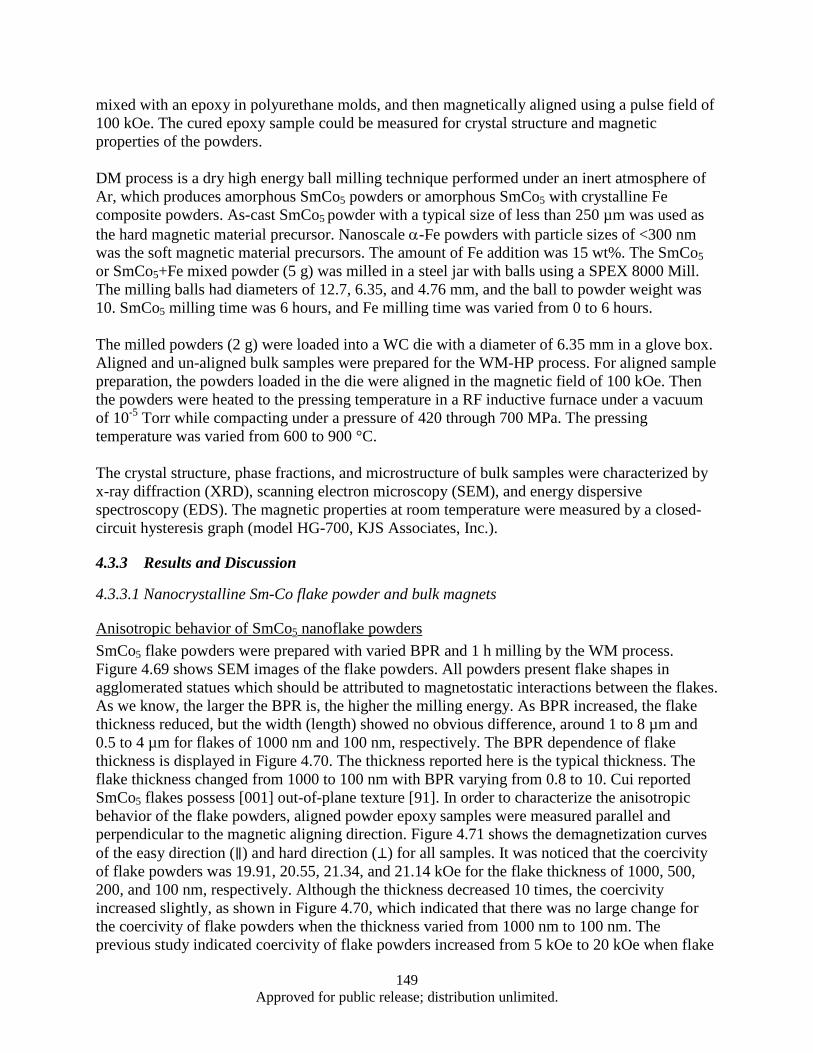
149 Approved for public release; distribution unlimited.
mixed with an epoxy in polyurethane molds, and then magnetically aligned using a pulse field of 100 kOe. The cured epoxy sample could be measured for crystal structure and magnetic properties of the powders.
DM process is a dry high energy ball milling technique performed under an inert atmosphere of Ar, which produces amorphous SmCo5 powders or amorphous SmCo5 with crystalline Fe composite powders. As-cast SmCo5 powder with a typical size of less than 250 µm was used as the hard magnetic material precursor. Nanoscale α-Fe powders with particle sizes of <300 nm was the soft magnetic material precursors. The amount of Fe addition was 15 wt%. The SmCo5 or SmCo5+Fe mixed powder (5 g) was milled in a steel jar with balls using a SPEX 8000 Mill. The milling balls had diameters of 12.7, 6.35, and 4.76 mm, and the ball to powder weight was 10. SmCo5 milling time was 6 hours, and Fe milling time was varied from 0 to 6 hours.
The milled powders (2 g) were loaded into a WC die with a diameter of 6.35 mm in a glove box. Aligned and un-aligned bulk samples were prepared for the WM-HP process. For aligned sample preparation, the powders loaded in the die were aligned in the magnetic field of 100 kOe. Then the powders were heated to the pressing temperature in a RF inductive furnace under a vacuum of 10-5 Torr while compacting under a pressure of 420 through 700 MPa. The pressing temperature was varied from 600 to 900 °C.
The crystal structure, phase fractions, and microstructure of bulk samples were characterized by x-ray diffraction (XRD), scanning electron microscopy (SEM), and energy dispersive spectroscopy (EDS). The magnetic properties at room temperature were measured by a closed-circuit hysteresis graph (model HG-700, KJS Associates, Inc.).
4.3.3 Results and Discussion
4.3.3.1 Nanocrystalline Sm-Co flake powder and bulk magnets
Anisotropic behavior of SmCo5 nanoflake powders SmCo5 flake powders were prepared with varied BPR and 1 h milling by the WM process. Figure 4.69 shows SEM images of the flake powders. All powders present flake shapes in agglomerated statues which should be attributed to magnetostatic interactions between the flakes. As we know, the larger the BPR is, the higher the milling energy. As BPR increased, the flake thickness reduced, but the width (length) showed no obvious difference, around 1 to 8 µm and 0.5 to 4 µm for flakes of 1000 nm and 100 nm, respectively. The BPR dependence of flake thickness is displayed in Figure 4.70. The thickness reported here is the typical thickness. The flake thickness changed from 1000 to 100 nm with BPR varying from 0.8 to 10. Cui reported SmCo5 flakes possess [001] out-of-plane texture [91]. In order to characterize the anisotropic behavior of the flake powders, aligned powder epoxy samples were measured parallel and perpendicular to the magnetic aligning direction. Figure 4.71 shows the demagnetization curves of the easy direction (∥) and hard direction (⊥) for all samples. It was noticed that the coercivity of flake powders was 19.91, 20.55, 21.34, and 21.14 kOe for the flake thickness of 1000, 500, 200, and 100 nm, respectively. Although the thickness decreased 10 times, the coercivity increased slightly, as shown in Figure 4.70, which indicated that there was no large change for the coercivity of flake powders when the thickness varied from 1000 nm to 100 nm. The previous study indicated coercivity of flake powders increased from 5 kOe to 20 kOe when flake
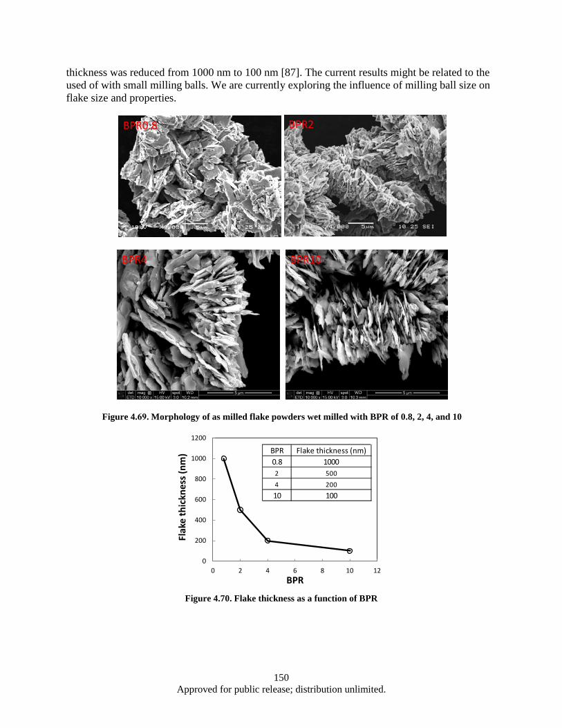
150 Approved for public release; distribution unlimited.
thickness was reduced from 1000 nm to 100 nm [87]. The current results might be related to the used of with small milling balls. We are currently exploring the influence of milling ball size on flake size and properties.
Figure 4.69. Morphology of as milled flake powders wet milled with BPR of 0.8, 2, 4, and 10
Figure 4.70. Flake thickness as a function of BPR
BPR0.8 BPR2
BPR4 BPR10
0
200
400
600
800
1000
1200
0 2 4 6 8 10 12
Flak
e th
ickn
ess (
nm)
BPR
BPR Flake thickness (nm)0.8 10002 5004 20010 100
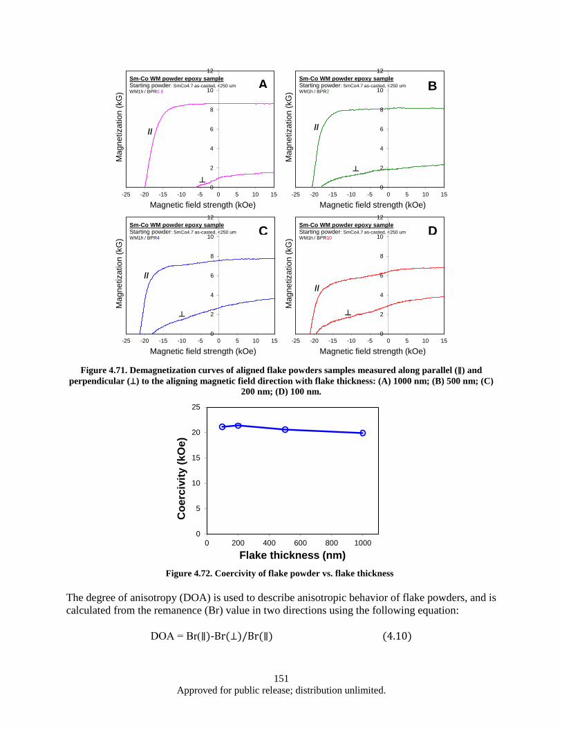
151 Approved for public release; distribution unlimited.
Figure 4.71. Demagnetization curves of aligned flake powders samples measured along parallel (∥) and perpendicular (⊥) to the aligning magnetic field direction with flake thickness: (A) 1000 nm; (B) 500 nm; (C)
200 nm; (D) 100 nm.
Figure 4.72. Coercivity of flake powder vs. flake thickness
The degree of anisotropy (DOA) is used to describe anisotropic behavior of flake powders, and is calculated from the remanence (Br) value in two directions using the following equation:
DOA = Br(∥)-Br(⊥)/Br(∥) (4.10)
0
2
4
6
8
10
12
-25 -20 -15 -10 -5 0 5 10 15
Mag
netiz
atio
n (k
G)
Magnetic field strength (kOe)
//
Sm-Co WM powder epoxy sampleStarting powder: SmCo4.7 as-casted, <250 umWM1h / BPR0.8
0
2
4
6
8
10
12
-25 -20 -15 -10 -5 0 5 10 15
Mag
netiz
atio
n (k
G)
Magnetic field strength (kOe)
Sm-Co WM powder epoxy sampleStarting powder: SmCo4.7 as-casted, <250 umWM1h / BPR2
//
0
2
4
6
8
10
12
-25 -20 -15 -10 -5 0 5 10 15
Mag
netiz
atio
n (k
G)
Magnetic field strength (kOe)
Sm-Co WM powder epoxy sampleStarting powder: SmCo4.7 as-casted, <250 umWM1h / BPR4
//
0
2
4
6
8
10
12
-25 -20 -15 -10 -5 0 5 10 15
Mag
netiz
atio
n (k
G)
Magnetic field strength (kOe)
Sm-Co WM powder epoxy sampleStarting powder: SmCo4.7 as-casted, <250 umWM1h / BPR10
//
0
5
10
15
20
25
0 200 400 600 800 1000
Coe
rciv
ity (k
Oe)
Flake thickness (nm)
A
DC
B
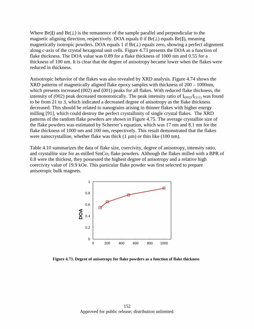
152 Approved for public release; distribution unlimited.
Where Br(∥) and Br(⊥) is the remanence of the sample parallel and perpendicular to the magnetic aligning direction, respectively. DOA equals 0 if Br(⊥) equals Br(∥), meaning magnetically isotropic powders. DOA equals 1 if Br(⊥) equals zero, showing a perfect alignment along c-axis of the crystal hexagonal unit cells. Figure 4.73 presents the DOA as a function of flake thickness. The DOA value was 0.89 for a flake thickness of 1000 nm and 0.55 for a thickness of 100 nm. It is clear that the degree of anisotropy became lower when the flakes were reduced in thickness.
Anisotropic behavior of the flakes was also revealed by XRD analysis. Figure 4.74 shows the XRD patterns of magnetically aligned flake epoxy samples with thickness of 200 – 1000nm, which presents increased (002) and (001) peaks for all flakes. With reduced flake thickness, the intensity of (002) peak decreased monotonically. The peak intensity ratio of I(002)/I(111) was found to be from 21 to 3, which indicated a decreased degree of anisotropy as the flake thickness decreased. This should be related to nanograins arising in thinner flakes with higher energy milling [91], which could destroy the perfect crystallinity of single crystal flakes. The XRD patterns of the random flake powders are shown in Figure 4.75. The average crystallite size of the flake powders was estimated by Scherrer’s equation, which was 17 nm and 8.1 nm for the flake thickness of 1000 nm and 100 nm, respectively. This result demonstrated that the flakes were nanocrystalline, whether flake was thick (1 µm) or thin like (100 nm).
Table 4.10 summarizes the data of flake size, coercivity, degree of anisotropy, intensity ratio, and crystallite size for as-milled SmCo5 flake powders. Although the flakes milled with a BPR of 0.8 were the thickest, they possessed the highest degree of anisotropy and a relative high coercivity value of 19.9 kOe. This particular flake powder was first selected to prepare anisotropic bulk magnets.
Flake thickness (nm)Figure 4.73. Degree of anisotropy for flake powders as a function of flake thickness
0
0.2
0.4
0.6
0.8
1
0 200 400 600 800 1000
DO
A
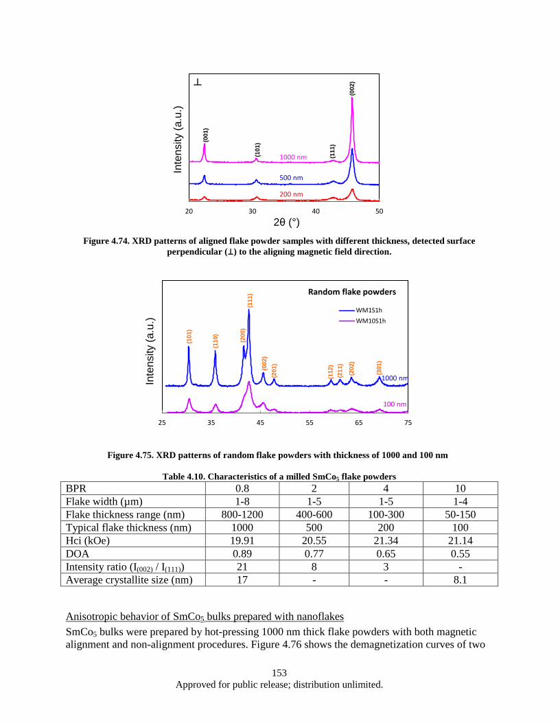
153 Approved for public release; distribution unlimited.
Figure 4.74. XRD patterns of aligned flake powder samples with different thickness, detected surface perpendicular (⊥) to the aligning magnetic field direction.
2θ (°)
Figure 4.75. XRD patterns of random flake powders with thickness of 1000 and 100 nm
Table 4.10. Characteristics of a milled SmCo5 flake powders BPR 0.8 2 4 10 Flake width (µm) 1-8 1-5 1-5 1-4 Flake thickness range (nm) 800-1200 400-600 100-300 50-150 Typical flake thickness (nm) 1000 500 200 100 Hci (kOe) 19.91 20.55 21.34 21.14 DOA 0.89 0.77 0.65 0.55 Intensity ratio (I(002) / I(111)) 21 8 3 - Average crystallite size (nm) 17 - - 8.1
Anisotropic behavior of SmCo5 bulks prepared with nanoflakes SmCo5 bulks were prepared by hot-pressing 1000 nm thick flake powders with both magnetic alignment and non-alignment procedures. Figure 4.76 shows the demagnetization curves of two
20 30 40 50
Inte
nsity
(a.u
.)
2θ (°)
(111
)(001
)
(101
)
(002
)
500 nm
1000 nm
200 nm
25 35 45 55 65 75
Inte
nsity
(a.u
.)
WM1S1hWM10S1h
Random flake powders
(101
)
(201
)
(111
)(2
00)
(110
)
(301
)
(202
)
(211
)(1
12)(002
)
1000 nm
100 nm
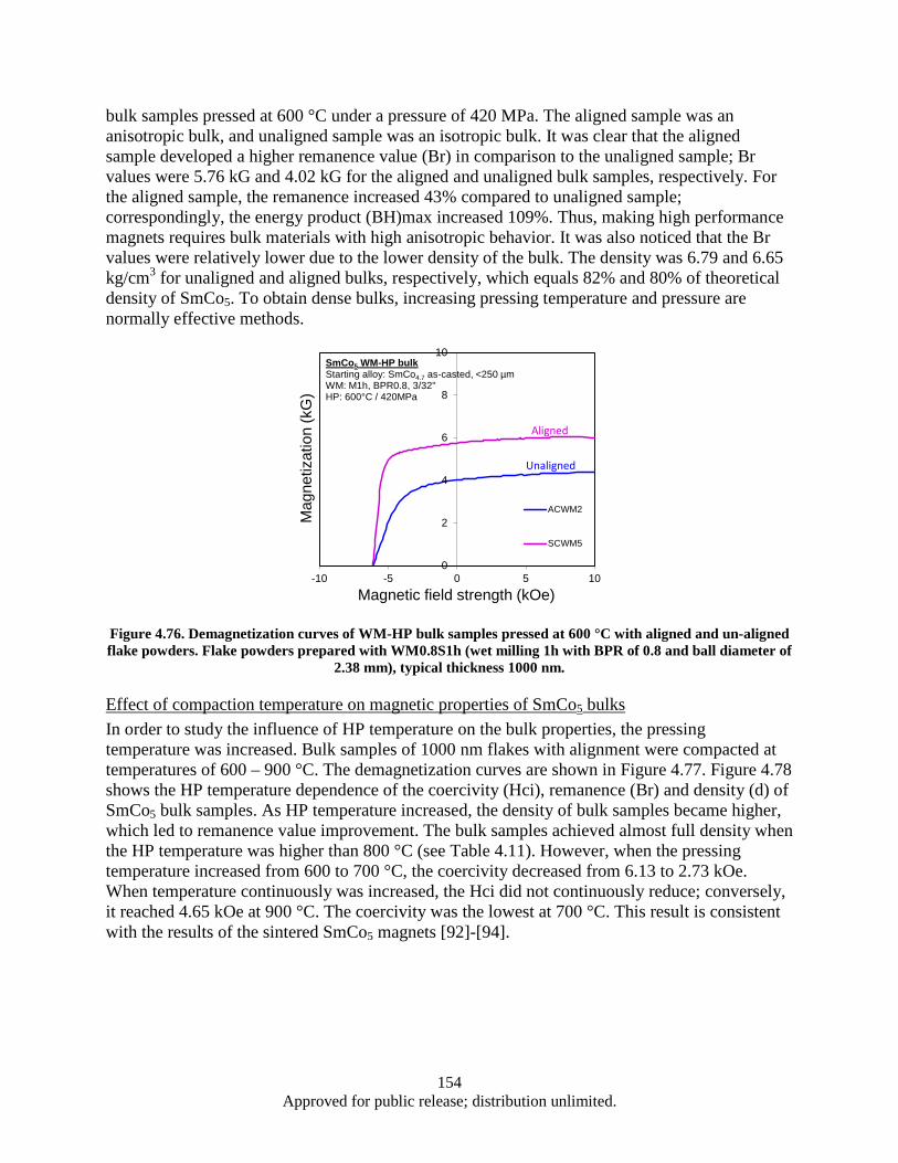
154 Approved for public release; distribution unlimited.
bulk samples pressed at 600 °C under a pressure of 420 MPa. The aligned sample was an anisotropic bulk, and unaligned sample was an isotropic bulk. It was clear that the aligned sample developed a higher remanence value (Br) in comparison to the unaligned sample; Br values were 5.76 kG and 4.02 kG for the aligned and unaligned bulk samples, respectively. For the aligned sample, the remanence increased 43% compared to unaligned sample; correspondingly, the energy product (BH)max increased 109%. Thus, making high performance magnets requires bulk materials with high anisotropic behavior. It was also noticed that the Br values were relatively lower due to the lower density of the bulk. The density was 6.79 and 6.65 kg/cm3 for unaligned and aligned bulks, respectively, which equals 82% and 80% of theoretical density of SmCo5. To obtain dense bulks, increasing pressing temperature and pressure are normally effective methods.
Figure 4.76. Demagnetization curves of WM-HP bulk samples pressed at 600 °C with aligned and un-aligned flake powders. Flake powders prepared with WM0.8S1h (wet milling 1h with BPR of 0.8 and ball diameter of
2.38 mm), typical thickness 1000 nm.
Effect of compaction temperature on magnetic properties of SmCo5 bulks In order to study the influence of HP temperature on the bulk properties, the pressing temperature was increased. Bulk samples of 1000 nm flakes with alignment were compacted at temperatures of 600 – 900 °C. The demagnetization curves are shown in Figure 4.77. Figure 4.78 shows the HP temperature dependence of the coercivity (Hci), remanence (Br) and density (d) of SmCo5 bulk samples. As HP temperature increased, the density of bulk samples became higher, which led to remanence value improvement. The bulk samples achieved almost full density when the HP temperature was higher than 800 °C (see Table 4.11). However, when the pressing temperature increased from 600 to 700 °C, the coercivity decreased from 6.13 to 2.73 kOe. When temperature continuously was increased, the Hci did not continuously reduce; conversely, it reached 4.65 kOe at 900 °C. The coercivity was the lowest at 700 °C. This result is consistent with the results of the sintered SmCo5 magnets [92]-[94].
0
2
4
6
8
10
-10 -5 0 5 10
Mag
netiz
atio
n (k
G)
Magnetic field strength (kOe)
ACWM2
SCWM5
SmCo5 WM-HP bulkStarting alloy: SmCo4.7 as-casted, <250 µmWM: M1h, BPR0.8, 3/32''HP: 600°C / 420MPa
Aligned
Unaligned
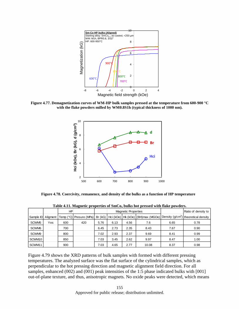
155 Approved for public release; distribution unlimited.
Figure 4.77. Demagnetization curves of WM-HP bulk samples pressed at the temperature from 600-900 °C with the flake powders milled by WM0.8S1h (typical thickness of 1000 nm).
HP Temperature (°C)
Figure 4.78. Coercivity, remanence, and density of the bulks as a function of HP temperature
Table 4.11. Magnetic properties of SmCo5 bulks hot pressed with flake powders.
Figure 4.79 shows the XRD patterns of bulk samples with formed with different pressing temperatures. The analyzed surface was the flat surface of the cylindrical samples, which as perpendicular to the hot pressing direction and magnetic alignment field direction. For all samples, enhanced (002) and (001) peak intensities of the 1:5 phase indicated bulks with [001] out-of-plane texture, and thus, anisotropic magnets. No oxide peaks were detected, which means
0
2
4
6
8
10
-8 -6 -4 -2 0 2 4
Mag
netiz
atio
n (k
G)
Magnetic field strength (kOe)
Sm-Co HP bulks (Aligned)Starting alloy: SmCo4.7 as-casted, <250 µmWM: M1h, BPR0.8, 3/32''HP: 600-950°C
600°C700°C
850°C
800°C
900°C
2
4
6
8
10
500 600 700 800 900 1000
Hci
(kO
e), B
r (kG
), d
(g/c
m3 )
d
Hci
Br
HP Magnetic Properties Ratio of density to
Sample ID Aligment Temp (°C) Presure (MPa) Br (kG) Hci (kOe) Hk (kOe) (BH)max (MGOe) Density (g/cm3) theoretical density
SCWM5 Yes 600 420 5.76 6.13 4.56 7.6 6.65 0.78
SCWM6 700 6.45 2.73 2.35 8.43 7.67 0.90
SCWM9 800 7.02 2.93 2.37 9.69 8.41 0.99
SCWM10 850 7.03 3.45 2.62 9.97 8.47 1.00
SCWM11 900 7.03 4.65 2.77 10.08 8.37 0.98
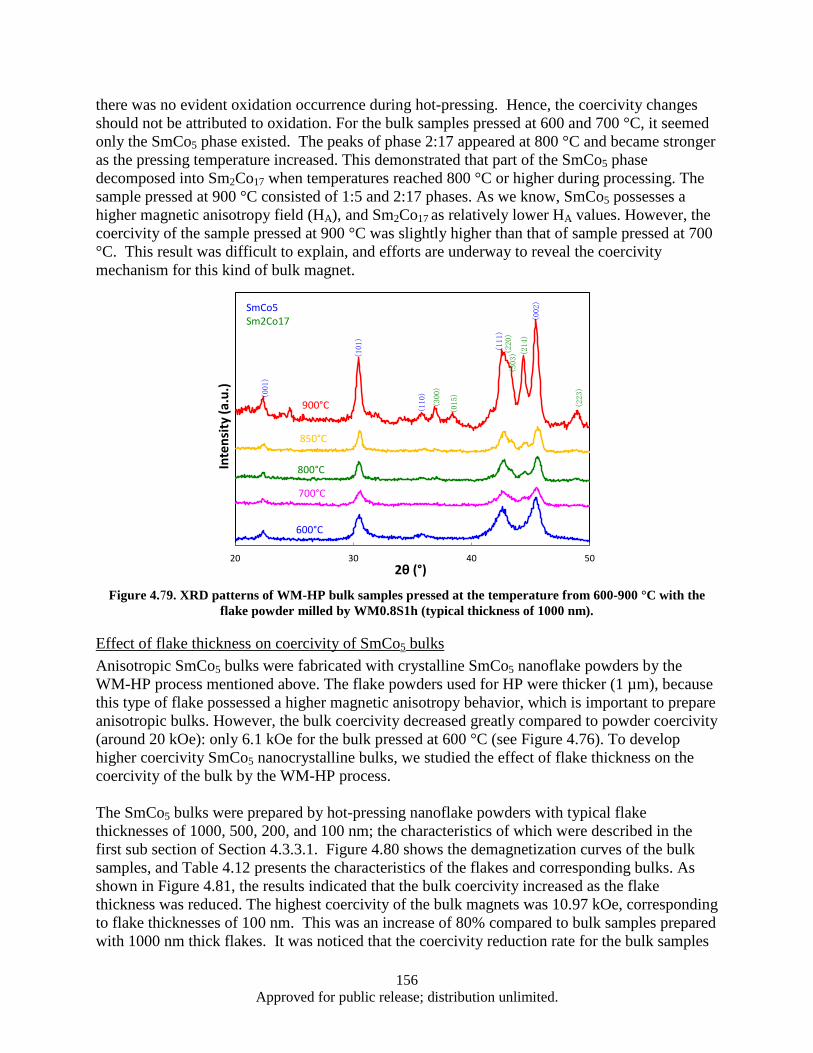
156 Approved for public release; distribution unlimited.
there was no evident oxidation occurrence during hot-pressing. Hence, the coercivity changes should not be attributed to oxidation. For the bulk samples pressed at 600 and 700 °C, it seemed only the SmCo5 phase existed. The peaks of phase 2:17 appeared at 800 °C and became stronger as the pressing temperature increased. This demonstrated that part of the SmCo5 phase decomposed into Sm2Co17 when temperatures reached 800 °C or higher during processing. The sample pressed at 900 °C consisted of 1:5 and 2:17 phases. As we know, SmCo5 possesses a higher magnetic anisotropy field (HA), and Sm2Co17 as relatively lower HA values. However, the coercivity of the sample pressed at 900 °C was slightly higher than that of sample pressed at 700 °C. This result was difficult to explain, and efforts are underway to reveal the coercivity mechanism for this kind of bulk magnet.
Figure 4.79. XRD patterns of WM-HP bulk samples pressed at the temperature from 600-900 °C with the flake powder milled by WM0.8S1h (typical thickness of 1000 nm).
Effect of flake thickness on coercivity of SmCo5 bulks Anisotropic SmCo5 bulks were fabricated with crystalline SmCo5 nanoflake powders by the WM-HP process mentioned above. The flake powders used for HP were thicker (1 µm), because this type of flake possessed a higher magnetic anisotropy behavior, which is important to prepare anisotropic bulks. However, the bulk coercivity decreased greatly compared to powder coercivity (around 20 kOe): only 6.1 kOe for the bulk pressed at 600 °C (see Figure 4.76). To develop higher coercivity SmCo5 nanocrystalline bulks, we studied the effect of flake thickness on the coercivity of the bulk by the WM-HP process.
The SmCo5 bulks were prepared by hot-pressing nanoflake powders with typical flake thicknesses of 1000, 500, 200, and 100 nm; the characteristics of which were described in the first sub section of Section 4.3.3.1. Figure 4.80 shows the demagnetization curves of the bulk samples, and Table 4.12 presents the characteristics of the flakes and corresponding bulks. As shown in Figure 4.81, the results indicated that the bulk coercivity increased as the flake thickness was reduced. The highest coercivity of the bulk magnets was 10.97 kOe, corresponding to flake thicknesses of 100 nm. This was an increase of 80% compared to bulk samples prepared with 1000 nm thick flakes. It was noticed that the coercivity reduction rate for the bulk samples
20 30 40 50
Inte
nsity
(a.u
.)
2θ (°)
(111)
(002)
(101)
(110)(001)
(223)
SmCo5Sm2Co17
(214)
(303)(220)
(300)
(015)
600°C
900°C
850°C
800°C
700°C
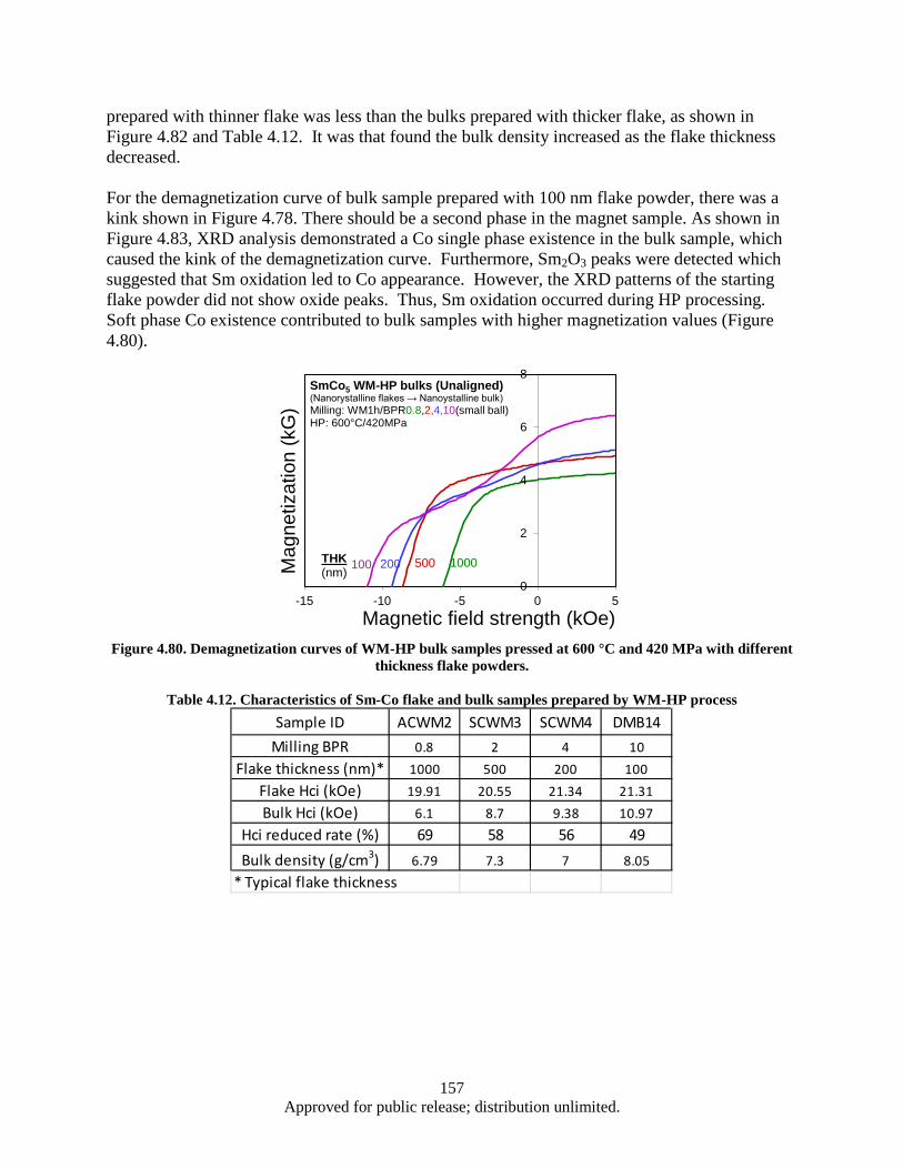
157 Approved for public release; distribution unlimited.
prepared with thinner flake was less than the bulks prepared with thicker flake, as shown in Figure 4.82 and Table 4.12. It was that found the bulk density increased as the flake thickness decreased.
For the demagnetization curve of bulk sample prepared with 100 nm flake powder, there was a kink shown in Figure 4.78. There should be a second phase in the magnet sample. As shown in Figure 4.83, XRD analysis demonstrated a Co single phase existence in the bulk sample, which caused the kink of the demagnetization curve. Furthermore, Sm2O3 peaks were detected which suggested that Sm oxidation led to Co appearance. However, the XRD patterns of the starting flake powder did not show oxide peaks. Thus, Sm oxidation occurred during HP processing. Soft phase Co existence contributed to bulk samples with higher magnetization values (Figure 4.80).
Figure 4.80. Demagnetization curves of WM-HP bulk samples pressed at 600 °C and 420 MPa with different thickness flake powders.
Table 4.12. Characteristics of Sm-Co flake and bulk samples prepared by WM-HP process
0
2
4
6
8
-15 -10 -5 0 5
Mag
netiz
atio
n (k
G)
Magnetic field strength (kOe)
1000 200 500100
SmCo5 WM-HP bulks (Unaligned) (Nanorystalline flakes → Nanoystalline bulk)Milling: WM1h/BPR0.8,2,4,10(small ball)HP: 600°C/420MPa
THK(nm)
Sample ID ACWM2 SCWM3 SCWM4 DMB14Milling BPR 0.8 2 4 10
Flake thickness (nm)* 1000 500 200 100Flake Hci (kOe) 19.91 20.55 21.34 21.31Bulk Hci (kOe) 6.1 8.7 9.38 10.97
Hci reduced rate (%) 69 58 56 49Bulk density (g/cm3) 6.79 7.3 7 8.05
* Typical flake thickness
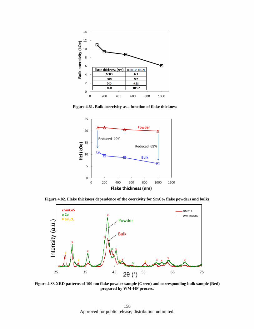
158 Approved for public release; distribution unlimited.
Flake thickness (nm)
Figure 4.81. Bulk coercivity as a function of flake thickness
Figure 4.82. Flake thickness dependence of the coercivity for SmCo5 flake powders and bulks
Figure 4.83 XRD patterns of 100 nm flake powder sample (Green) and corresponding bulk sample (Red) prepared by WM-HP process.
0
2
4
6
8
10
12
14
0 200 400 600 800 1000
Bul
k co
erci
vity
(kO
e)
0
5
10
15
20
25
0 200 400 600 800 1000 1200
Hci (
kOe)
Flake thickness (nm)
Bulk
Powder
Reduced 49%
Reduced 69%
25 35 45 55 65 75
Inte
nsity
(a.u
.)
2θ (°)
DMB14
WM10SB1h
x SmCo5o Co# Sm2O3
xx x xo
o#
## #
Bulk
x
x
x
Powderx
x
x
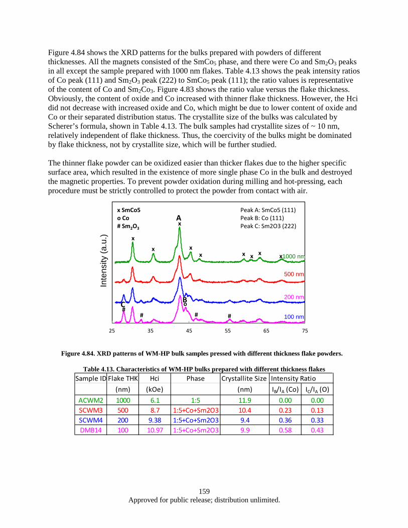
159 Approved for public release; distribution unlimited.
Figure 4.84 shows the XRD patterns for the bulks prepared with powders of different thicknesses. All the magnets consisted of the SmCo5 phase, and there were Co and Sm2O3 peaks in all except the sample prepared with 1000 nm flakes. Table 4.13 shows the peak intensity ratios of Co peak (111) and Sm2O3 peak (222) to SmCo5 peak (111); the ratio values is representative of the content of Co and Sm2Co3. Figure 4.83 shows the ratio value versus the flake thickness. Obviously, the content of oxide and Co increased with thinner flake thickness. However, the Hci did not decrease with increased oxide and Co, which might be due to lower content of oxide and Co or their separated distribution status. The crystallite size of the bulks was calculated by Scherer’s formula, shown in Table 4.13. The bulk samples had crystallite sizes of ~ 10 nm, relatively independent of flake thickness. Thus, the coercivity of the bulks might be dominated by flake thickness, not by crystallite size, which will be further studied.
The thinner flake powder can be oxidized easier than thicker flakes due to the higher specific surface area, which resulted in the existence of more single phase Co in the bulk and destroyed the magnetic properties. To prevent powder oxidation during milling and hot-pressing, each procedure must be strictly controlled to protect the powder from contact with air.
2θ (°)Figure 4.84. XRD patterns of WM-HP bulk samples pressed with different thickness flake powders.
Table 4.13. Characteristics of WM-HP bulks prepared with different thickness flakes
25 35 45 55 65 75
Inte
nsity
(a.u
.)
x SmCo5o Co# Sm2O3
#
x
o
##
xxxxxx
x
x
#
1000 nm
200 nm
500 nm
100 nm
Peak A: SmCo5 (111) Peak B: Co (111) Peak C: Sm2O3 (222)
C B
A
Sample ID Flake THK Hci Phase Crystallite Size k Intensity Ratio(nm) (kOe) (nm) IB/IA (Co) IC/IA (O)
ACWM2 1000 6.1 1:5 11.9 0.00 0.00SCWM3 500 8.7 1:5+Co+Sm2O3 10.4 0.23 0.13SCWM4 200 9.38 1:5+Co+Sm2O3 9.4 0.36 0.33DMB14 100 10.97 1:5+Co+Sm2O3 9.9 0.58 0.43
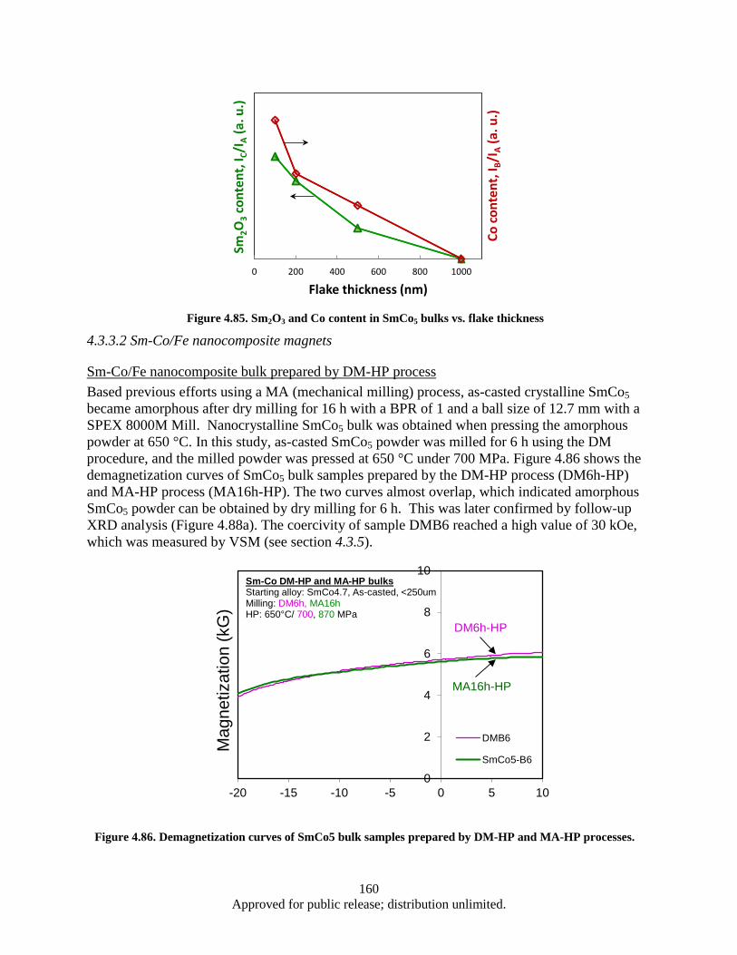
160 Approved for public release; distribution unlimited.
Figure 4.85. Sm2O3 and Co content in SmCo5 bulks vs. flake thickness
4.3.3.2 Sm-Co/Fe nanocomposite magnets
Sm-Co/Fe nanocomposite bulk prepared by DM-HP process Based previous efforts using a MA (mechanical milling) process, as-casted crystalline SmCo5 became amorphous after dry milling for 16 h with a BPR of 1 and a ball size of 12.7 mm with a SPEX 8000M Mill. Nanocrystalline SmCo5 bulk was obtained when pressing the amorphous powder at 650 °C. In this study, as-casted SmCo5 powder was milled for 6 h using the DM procedure, and the milled powder was pressed at 650 °C under 700 MPa. Figure 4.86 shows the demagnetization curves of SmCo5 bulk samples prepared by the DM-HP process (DM6h-HP) and MA-HP process (MA16h-HP). The two curves almost overlap, which indicated amorphous SmCo5 powder can be obtained by dry milling for 6 h. This was later confirmed by follow-up XRD analysis (Figure 4.88a). The coercivity of sample DMB6 reached a high value of 30 kOe, which was measured by VSM (see section 4.3.5).
Magnetic field strength (kOe)Figure 4.86. Demagnetization curves of SmCo5 bulk samples prepared by DM-HP and MA-HP processes.
0 200 400 600 800 1000
Co co
nten
t, I B
/IA
(a. u
.)
Sm2O
3co
nten
t, I C/
I A(a
. u.)
Flake thickness (nm)
0
2
4
6
8
10
-20 -15 -10 -5 0 5 10
Mag
netiz
atio
n (k
G)
DMB6
SmCo5-B6
Sm-Co DM-HP and MA-HP bulksStarting alloy: SmCo4.7, As-casted, <250um Milling: DM6h, MA16h HP: 650°C/ 700, 870 MPa
DM6h-HP
MA16h-HP
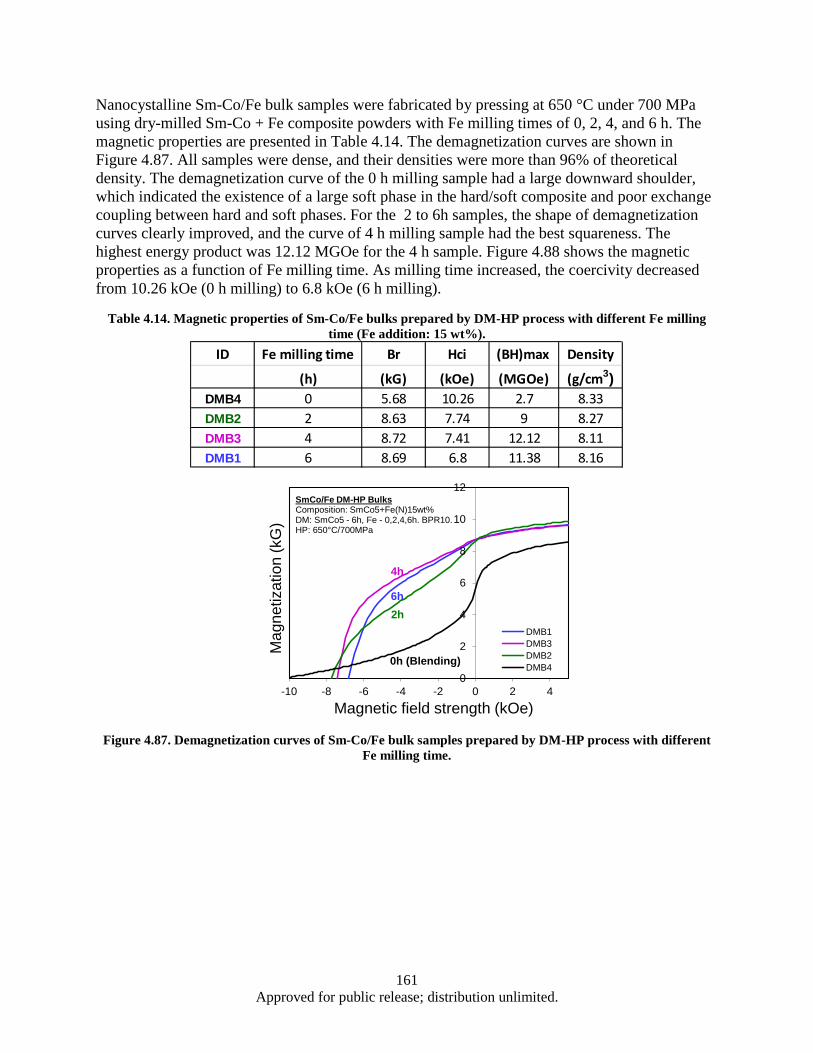
161 Approved for public release; distribution unlimited.
Nanocystalline Sm-Co/Fe bulk samples were fabricated by pressing at 650 °C under 700 MPa using dry-milled Sm-Co + Fe composite powders with Fe milling times of 0, 2, 4, and 6 h. The magnetic properties are presented in Table 4.14. The demagnetization curves are shown in Figure 4.87. All samples were dense, and their densities were more than 96% of theoretical density. The demagnetization curve of the 0 h milling sample had a large downward shoulder, which indicated the existence of a large soft phase in the hard/soft composite and poor exchange coupling between hard and soft phases. For the 2 to 6h samples, the shape of demagnetization curves clearly improved, and the curve of 4 h milling sample had the best squareness. The highest energy product was 12.12 MGOe for the 4 h sample. Figure 4.88 shows the magnetic properties as a function of Fe milling time. As milling time increased, the coercivity decreased from 10.26 kOe (0 h milling) to 6.8 kOe (6 h milling).
Table 4.14. Magnetic properties of Sm-Co/Fe bulks prepared by DM-HP process with different Fe milling time (Fe addition: 15 wt%).
Figure 4.87. Demagnetization curves of Sm-Co/Fe bulk samples prepared by DM-HP process with different Fe milling time.
ID Fe milling time Br Hci (BH)max Density
(h) (kG) (kOe) (MGOe) (g/cm3)DMB4 0 5.68 10.26 2.7 8.33DMB2 2 8.63 7.74 9 8.27DMB3 4 8.72 7.41 12.12 8.11DMB1 6 8.69 6.8 11.38 8.16
0
2
4
6
8
10
12
-10 -8 -6 -4 -2 0 2 4
Mag
netiz
atio
n (k
G)
Magnetic field strength (kOe)
DMB1DMB3DMB2DMB4
SmCo/Fe DM-HP BulksComposition: SmCo5+Fe(N)15wt%DM: SmCo5 - 6h, Fe - 0,2,4,6h. BPR10.HP: 650°C/700MPa
6h
4h
2h
0h (Blending)
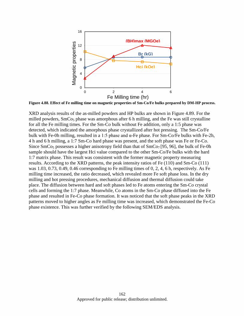
162 Approved for public release; distribution unlimited.
Figure 4.88. Effect of Fe milling time on magnetic properties of Sm-Co/Fe bulks prepared by DM-HP process.
XRD analysis results of the as-milled powders and HP bulks are shown in Figure 4.89. For the milled powders, SmCo5 phase was amorphous after 6 h milling, and the Fe was still crystalline for all the Fe milling times. For the Sm-Co bulk without Fe addition, only a 1:5 phase was detected, which indicated the amorphous phase crystallized after hot pressing. The Sm-Co/Fe bulk with Fe-0h milling, resulted in a 1:5 phase and α-Fe phase. For Sm-Co/Fe bulks with Fe-2h, 4 h and 6 h milling, a 1:7 Sm-Co hard phase was present, and the soft phase was Fe or Fe-Co. Since SmCo5 possesses a higher anisotropy field than that of SmCo7 [95, 96], the bulk of Fe-0h sample should have the largest Hci value compared to the other Sm-Co/Fe bulks with the hard 1:7 matrix phase. This result was consistent with the former magnetic property measuring results. According to the XRD patterns, the peak intensity ratios of Fe (110) and Sm-Co (111) was 1.03, 0.73, 0.49, 0.46 corresponding to Fe milling times of 0, 2, 4, 6 h, respectively. As Fe milling time increased, the ratio decreased, which revealed more Fe soft phase loss. In the dry milling and hot pressing procedures, mechanical diffusion and thermal diffusion could take place. The diffusion between hard and soft phases led to Fe atoms entering the Sm-Co crystal cells and forming the 1:7 phase. Meanwhile, Co atoms in the Sm-Co phase diffused into the Fe phase and resulted in Fe-Co phase formation. It was noticed that the soft phase peaks in the XRD patterns moved to higher angles as Fe milling time was increased, which demonstrated the Fe-Co phase existence. This was further verified by the following SEM/EDS analysis.
0
4
8
12
16
0 2 4 6
Mag
netic
pro
perti
es
Fe Milling time (hr)
Hci (kOe)
(BH)max (MGOe)
Br (kG)
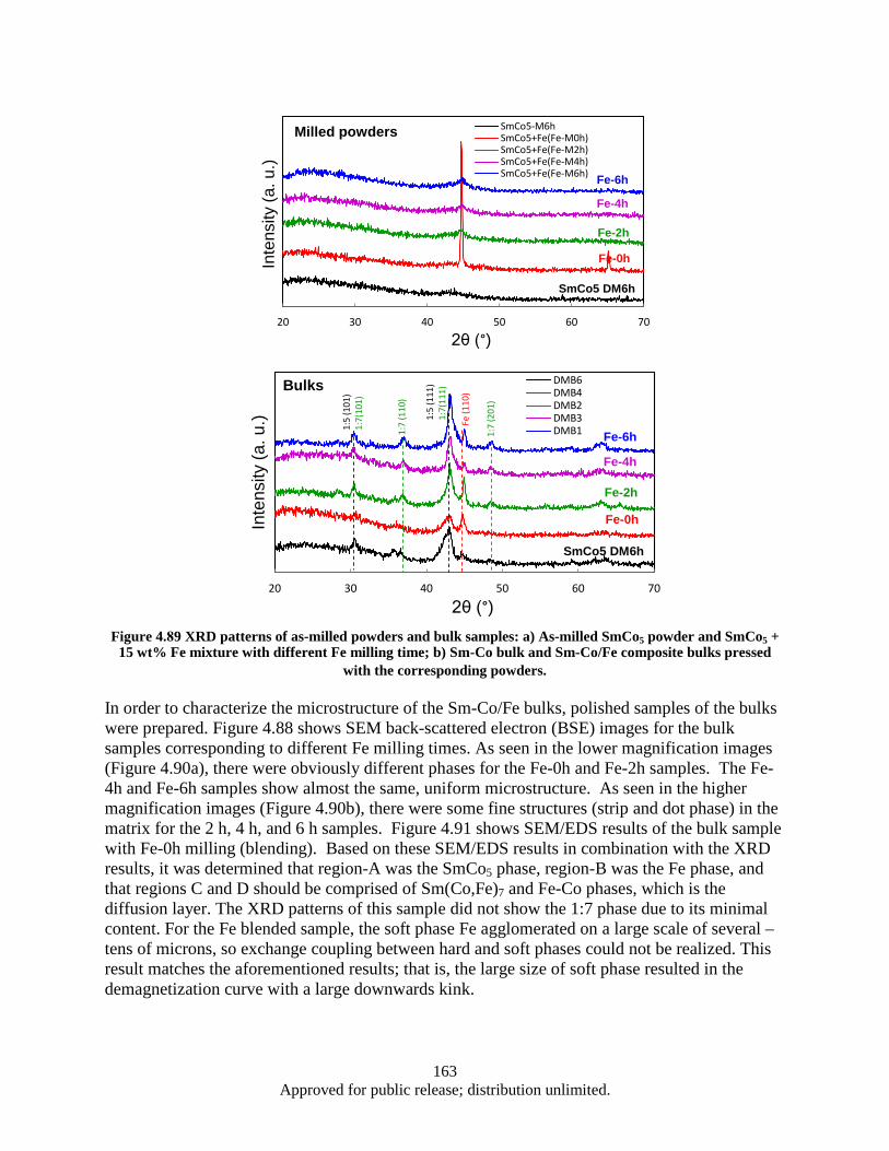
163 Approved for public release; distribution unlimited.
Figure 4.89 XRD patterns of as-milled powders and bulk samples: a) As-milled SmCo5 powder and SmCo5 + 15 wt% Fe mixture with different Fe milling time; b) Sm-Co bulk and Sm-Co/Fe composite bulks pressed
with the corresponding powders.
In order to characterize the microstructure of the Sm-Co/Fe bulks, polished samples of the bulks were prepared. Figure 4.88 shows SEM back-scattered electron (BSE) images for the bulk samples corresponding to different Fe milling times. As seen in the lower magnification images (Figure 4.90a), there were obviously different phases for the Fe-0h and Fe-2h samples. The Fe-4h and Fe-6h samples show almost the same, uniform microstructure. As seen in the higher magnification images (Figure 4.90b), there were some fine structures (strip and dot phase) in the matrix for the 2 h, 4 h, and 6 h samples. Figure 4.91 shows SEM/EDS results of the bulk sample with Fe-0h milling (blending). Based on these SEM/EDS results in combination with the XRD results, it was determined that region-A was the SmCo5 phase, region-B was the Fe phase, and that regions C and D should be comprised of Sm(Co,Fe)7 and Fe-Co phases, which is the diffusion layer. The XRD patterns of this sample did not show the 1:7 phase due to its minimal content. For the Fe blended sample, the soft phase Fe agglomerated on a large scale of several – tens of microns, so exchange coupling between hard and soft phases could not be realized. This result matches the aforementioned results; that is, the large size of soft phase resulted in the demagnetization curve with a large downwards kink.
20 30 40 50 60 70
Inte
nsity
(a. u
.)
2θ (°)
SmCo5-M6hSmCo5+Fe(Fe-M0h)SmCo5+Fe(Fe-M2h)SmCo5+Fe(Fe-M4h)SmCo5+Fe(Fe-M6h)
Milled powders
Fe-6h
SmCo5 DM6h
Fe-0h
Fe-2h
Fe-4h
20 30 40 50 60 70
Inte
nsity
(a. u
.)
2θ (°)
DMB6DMB4DMB2DMB3DMB1
Bulks
Fe-6h
SmCo5 DM6h
Fe-0h
Fe-2h
Fe-4h
1:7
(110
)
1:5
(111
)1:
7(11
1)
Fe (1
10)
1:7
(201
)
1:5
(101
)1:
7(10
1)
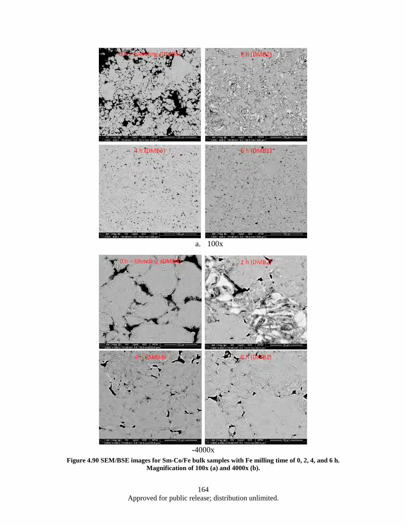
164 Approved for public release; distribution unlimited.
a. 100x
-4000x Figure 4.90 SEM/BSE images for Sm-Co/Fe bulk samples with Fe milling time of 0, 2, 4, and 6 h.
Magnification of 100x (a) and 4000x (b).
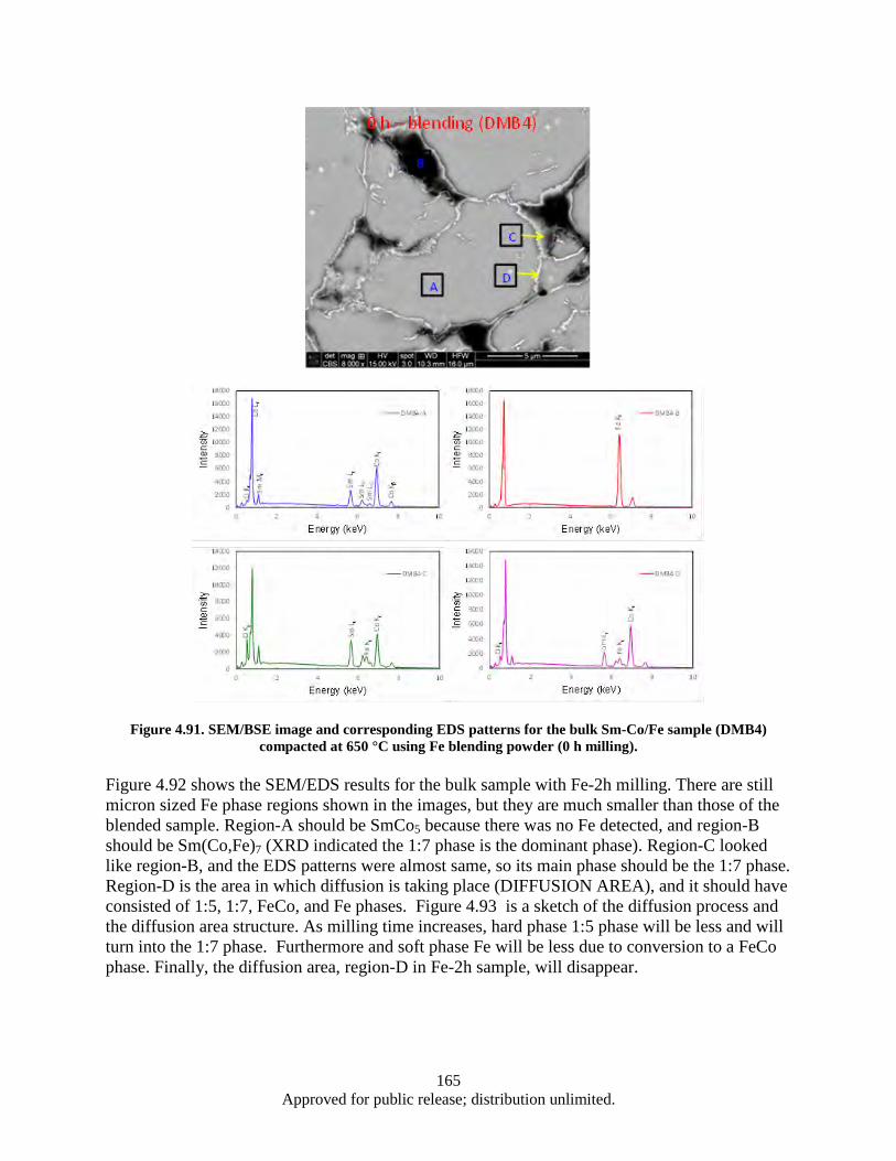
165 Approved for public release; distribution unlimited.
Figure 4.91. SEM/BSE image and corresponding EDS patterns for the bulk Sm-Co/Fe sample (DMB4) compacted at 650 °C using Fe blending powder (0 h milling).
Figure 4.92 shows the SEM/EDS results for the bulk sample with Fe-2h milling. There are still micron sized Fe phase regions shown in the images, but they are much smaller than those of the blended sample. Region-A should be SmCo5 because there was no Fe detected, and region-B should be Sm(Co,Fe)7 (XRD indicated the 1:7 phase is the dominant phase). Region-C looked like region-B, and the EDS patterns were almost same, so its main phase should be the 1:7 phase. Region-D is the area in which diffusion is taking place (DIFFUSION AREA), and it should have consisted of 1:5, 1:7, FeCo, and Fe phases. Figure 4.93 is a sketch of the diffusion process and the diffusion area structure. As milling time increases, hard phase 1:5 phase will be less and will turn into the 1:7 phase. Furthermore and soft phase Fe will be less due to conversion to a FeCo phase. Finally, the diffusion area, region-D in Fe-2h sample, will disappear.
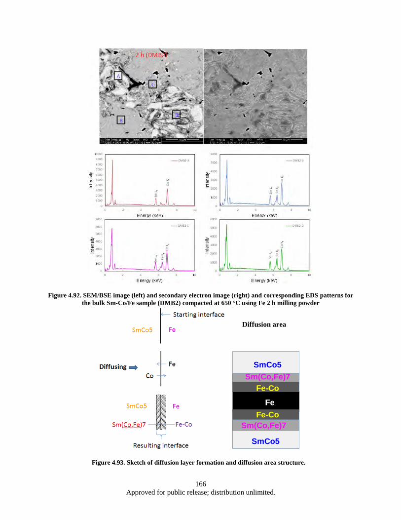
166 Approved for public release; distribution unlimited.
Figure 4.92. SEM/BSE image (left) and secondary electron image (right) and corresponding EDS patterns for the bulk Sm-Co/Fe sample (DMB2) compacted at 650 °C using Fe 2 h milling powder
Figure 4.93. Sketch of diffusion layer formation and diffusion area structure.
SmCo5 Sm(Co,Fe)7
Fe
Fe-Co
SmCo5
Sm(Co,Fe)7Fe-Co
Diffusion area
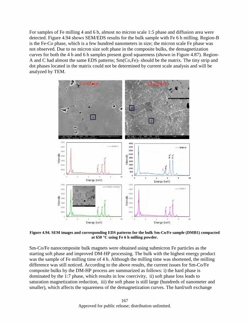
167 Approved for public release; distribution unlimited.
For samples of Fe milling 4 and 6 h, almost no micron scale 1:5 phase and diffusion area were detected. Figure 4.94 shows SEM/EDS results for the bulk sample with Fe 6 h milling. Region-B is the Fe-Co phase, which is a few hundred nanometers in size; the micron scale Fe phase was not observed. Due to no micron size soft phase in the composite bulks, the demagnetization curves for both the 4 h and 6 h samples present good squareness (shown in Figure 4.87). Region-A and C had almost the same EDS patterns; Sm(Co,Fe)7 should be the matrix. The tiny strip and dot phases located in the matrix could not be determined by current scale analysis and will be analyzed by TEM.
Figure 4.94. SEM images and corresponding EDS patterns for the bulk Sm-Co/Fe sample (DMB1) compacted at 650 °C using Fe 6 h milling powder.
Sm-Co/Fe nanocomposite bulk magnets were obtained using submicron Fe particles as the starting soft phase and improved DM-HP processing. The bulk with the highest energy product was the sample of Fe milling time of 4 h. Although the milling time was shortened, the milling difference was still noticed. According to the above results, the current issues for Sm-Co/Fe composite bulks by the DM-HP process are summarized as follows: i) the hard phase is dominated by the 1:7 phase, which results in low coercivity, ii) soft phase loss leads to saturation magnetization reduction, iii) the soft phase is still large (hundreds of nanometer and smaller), which affects the squareness of the demagnetization curves. The hard/soft exchange
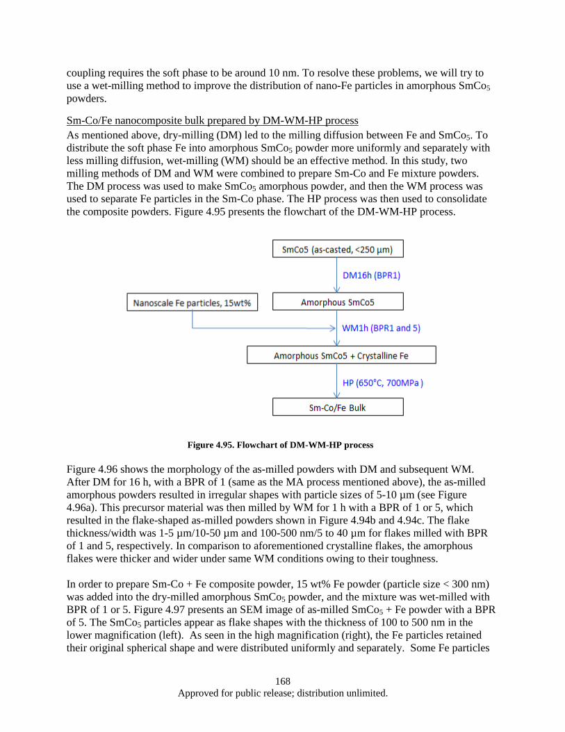
168 Approved for public release; distribution unlimited.
coupling requires the soft phase to be around 10 nm. To resolve these problems, we will try to use a wet-milling method to improve the distribution of nano-Fe particles in amorphous SmCo5 powders.
Sm-Co/Fe nanocomposite bulk prepared by DM-WM-HP process As mentioned above, dry-milling (DM) led to the milling diffusion between Fe and SmCo5. To distribute the soft phase Fe into amorphous SmCo5 powder more uniformly and separately with less milling diffusion, wet-milling (WM) should be an effective method. In this study, two milling methods of DM and WM were combined to prepare Sm-Co and Fe mixture powders. The DM process was used to make SmCo5 amorphous powder, and then the WM process was used to separate Fe particles in the Sm-Co phase. The HP process was then used to consolidate the composite powders. Figure 4.95 presents the flowchart of the DM-WM-HP process.
Figure 4.95. Flowchart of DM-WM-HP process
Figure 4.96 shows the morphology of the as-milled powders with DM and subsequent WM. After DM for 16 h, with a BPR of 1 (same as the MA process mentioned above), the as-milled amorphous powders resulted in irregular shapes with particle sizes of 5-10 µm (see Figure 4.96a). This precursor material was then milled by WM for 1 h with a BPR of 1 or 5, which resulted in the flake-shaped as-milled powders shown in Figure 4.94b and 4.94c. The flake thickness/width was 1-5 µm/10-50 µm and 100-500 nm/5 to 40 µm for flakes milled with BPR of 1 and 5, respectively. In comparison to aforementioned crystalline flakes, the amorphous flakes were thicker and wider under same WM conditions owing to their toughness.
In order to prepare Sm-Co + Fe composite powder, 15 wt% Fe powder (particle size < 300 nm) was added into the dry-milled amorphous SmCo5 powder, and the mixture was wet-milled with BPR of 1 or 5. Figure 4.97 presents an SEM image of as-milled SmCo5 + Fe powder with a BPR of 5. The SmCo5 particles appear as flake shapes with the thickness of 100 to 500 nm in the lower magnification (left). As seen in the high magnification (right), the Fe particles retained their original spherical shape and were distributed uniformly and separately. Some Fe particles
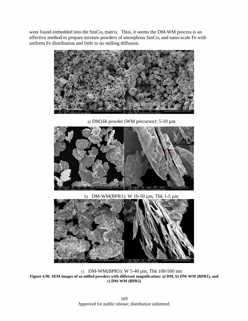
169 Approved for public release; distribution unlimited.
were found embedded into the SmCo5 matrix. Thus, it seems the DM-WM process is an effective method to prepare mixture powders of amorphous SmCo5 and nano-scale Fe with uniform Fe distribution and little to no milling diffusion.
a) DM16h powder (WM precursor): 5-10 µm
b) DM-WM(BPR1): W 10-50 µm, Thk 1-5 µm
c) DM-WM(BPR5): W 5-40 µm, Thk 100-500 nmFigure 4.96. SEM images of as-milled powders with different magnification: a) DM, b) DM-WM (BPR1), and
c) DM-WM (BPR5)
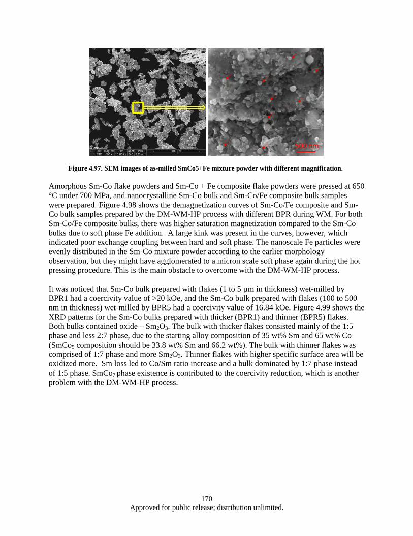
170 Approved for public release; distribution unlimited.
Figure 4.97. SEM images of as-milled SmCo5+Fe mixture powder with different magnification.
Amorphous Sm-Co flake powders and Sm-Co + Fe composite flake powders were pressed at 650 °C under 700 MPa, and nanocrystalline Sm-Co bulk and Sm-Co/Fe composite bulk samples were prepared. Figure 4.98 shows the demagnetization curves of Sm-Co/Fe composite and Sm-Co bulk samples prepared by the DM-WM-HP process with different BPR during WM. For both Sm-Co/Fe composite bulks, there was higher saturation magnetization compared to the Sm-Co bulks due to soft phase Fe addition. A large kink was present in the curves, however, which indicated poor exchange coupling between hard and soft phase. The nanoscale Fe particles were evenly distributed in the Sm-Co mixture powder according to the earlier morphology observation, but they might have agglomerated to a micron scale soft phase again during the hot pressing procedure. This is the main obstacle to overcome with the DM-WM-HP process.
It was noticed that Sm-Co bulk prepared with flakes (1 to 5 µm in thickness) wet-milled by BPR1 had a coercivity value of >20 kOe, and the Sm-Co bulk prepared with flakes (100 to 500 nm in thickness) wet-milled by BPR5 had a coercivity value of 16.84 kOe. Figure 4.99 shows the XRD patterns for the Sm-Co bulks prepared with thicker (BPR1) and thinner (BPR5) flakes. Both bulks contained oxide – Sm2O3. The bulk with thicker flakes consisted mainly of the 1:5 phase and less 2:7 phase, due to the starting alloy composition of 35 wt% Sm and 65 wt% Co (SmCo5 composition should be 33.8 wt% Sm and 66.2 wt%). The bulk with thinner flakes was comprised of 1:7 phase and more Sm2O3. Thinner flakes with higher specific surface area will be oxidized more. Sm loss led to Co/Sm ratio increase and a bulk dominated by 1:7 phase instead of 1:5 phase. SmCo7 phase existence is contributed to the coercivity reduction, which is another problem with the DM-WM-HP process.
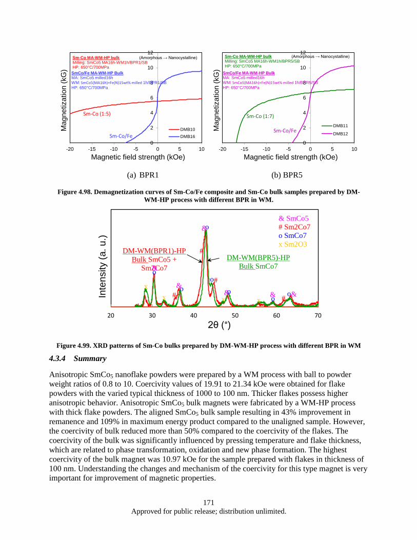
171 Approved for public release; distribution unlimited.
(a) BPR1 (b) BPR5
Figure 4.98. Demagnetization curves of Sm-Co/Fe composite and Sm-Co bulk samples prepared by DM-WM-HP process with different BPR in WM.
Figure 4.99. XRD patterns of Sm-Co bulks prepared by DM-WM-HP process with different BPR in WM
4.3.4 Summary
Anisotropic SmCo5 nanoflake powders were prepared by a WM process with ball to powder weight ratios of 0.8 to 10. Coercivity values of 19.91 to 21.34 kOe were obtained for flake powders with the varied typical thickness of 1000 to 100 nm. Thicker flakes possess higher anisotropic behavior. Anisotropic SmCo5 bulk magnets were fabricated by a WM-HP process with thick flake powders. The aligned SmCo5 bulk sample resulting in 43% improvement in remanence and 109% in maximum energy product compared to the unaligned sample. However, the coercivity of bulk reduced more than 50% compared to the coercivity of the flakes. The coercivity of the bulk was significantly influenced by pressing temperature and flake thickness, which are related to phase transformation, oxidation and new phase formation. The highest coercivity of the bulk magnet was 10.97 kOe for the sample prepared with flakes in thickness of 100 nm. Understanding the changes and mechanism of the coercivity for this type magnet is very important for improvement of magnetic properties.
0
2
4
6
8
10
12
-20 -15 -10 -5 0 5 10
Mag
netiz
atio
n (k
G)
Magnetic field strength (kOe)
DMB10DMB16Sm-Co/Fe
Sm-Co (1:5)
Sm-Co MA-WM-HP bulk (Amorphous → Nanocystalline)Milling: SmCo5 MA16h-WM1h/BPR1/SBHP: 650°C/700MPa
SmCo/Fe MA-WM-HP BulkMA: SmCo5 milled16h WM: SmCo5(MA16h)+Fe(N)15wt% milled 1h/BPR1/SBHP: 650°C/700MPa
0
2
4
6
8
10
12
-20 -15 -10 -5 0 5 10
Mag
netiz
atio
n (k
G)
Magnetic field strength (kOe)
DMB11
DMB12
Sm-Co MA-WM-HP bulk (Amorphous → Nanocystalline)Milling: SmCo5 MA16h-WM1h/BPR5/SBHP: 650°C/700MPa
BPR5
Sm-Co/Fe
SmCo/Fe MA-WM-HP BulkMA: SmCo5 milled16h WM: SmCo5(MA16h)+Fe(N)15wt% milled 1h/BPR5/SBHP: 650°C/700MPa
Sm-Co (1:7)
20 30 40 50 60 70
Inte
nsity
(a. u
.)
2θ (°)
x
x x x
o
o o
o o
o
o
& SmCo5 # Sm2Co7 o SmCo7x Sm2O3
DM-WM(BPR5)-HP Bulk SmCo7
DM-WM(BPR1)-HP Bulk SmCo5 +
Sm2Co7 &
&
&
& & & #
#
#
#
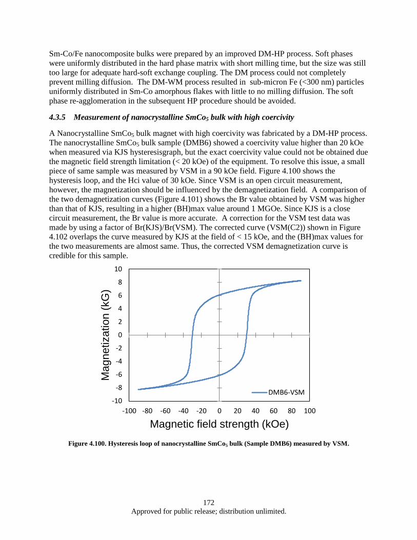
172 Approved for public release; distribution unlimited.
Sm-Co/Fe nanocomposite bulks were prepared by an improved DM-HP process. Soft phases were uniformly distributed in the hard phase matrix with short milling time, but the size was still too large for adequate hard-soft exchange coupling. The DM process could not completely prevent milling diffusion. The DM-WM process resulted in sub-micron Fe (<300 nm) particles uniformly distributed in Sm-Co amorphous flakes with little to no milling diffusion. The soft phase re-agglomeration in the subsequent HP procedure should be avoided.
4.3.5 Measurement of nanocrystalline SmCo5 bulk with high coercivity
A Nanocrystalline SmCo5 bulk magnet with high coercivity was fabricated by a DM-HP process. The nanocrystalline SmCo5 bulk sample (DMB6) showed a coercivity value higher than 20 kOe when measured via KJS hysteresisgraph, but the exact coercivity value could not be obtained due the magnetic field strength limitation (< 20 kOe) of the equipment. To resolve this issue, a small piece of same sample was measured by VSM in a 90 kOe field. Figure 4.100 shows the hysteresis loop, and the Hci value of 30 kOe. Since VSM is an open circuit measurement, however, the magnetization should be influenced by the demagnetization field. A comparison of the two demagnetization curves (Figure 4.101) shows the Br value obtained by VSM was higher than that of KJS, resulting in a higher (BH)max value around 1 MGOe. Since KJS is a close circuit measurement, the Br value is more accurate. A correction for the VSM test data was made by using a factor of Br(KJS)/Br(VSM). The corrected curve (VSM(C2)) shown in Figure 4.102 overlaps the curve measured by KJS at the field of < 15 kOe, and the (BH)max values for the two measurements are almost same. Thus, the corrected VSM demagnetization curve is credible for this sample.
Figure 4.100. Hysteresis loop of nanocrystalline SmCo5 bulk (Sample DMB6) measured by VSM.
-10
-8
-6
-4
-2
0
2
4
6
8
10
-100 -80 -60 -40 -20 0 20 40 60 80 100
Mag
netiz
atio
n (k
G)
Magnetic field strength (kOe)
DMB6-VSM
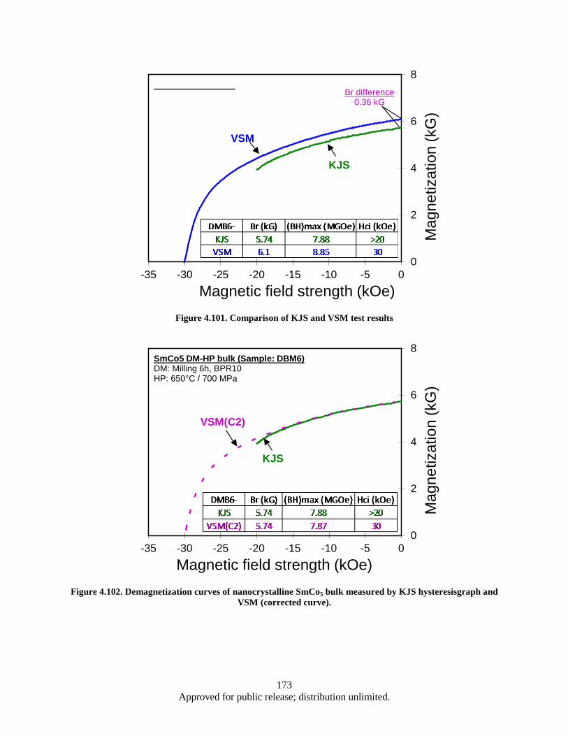
173 Approved for public release; distribution unlimited.
Figure 4.101. Comparison of KJS and VSM test results
Figure 4.102. Demagnetization curves of nanocrystalline SmCo5 bulk measured by KJS hysteresisgraph and VSM (corrected curve).
0
2
4
6
8
-35 -30 -25 -20 -15 -10 -5 0
Mag
netiz
atio
n (k
G)
Magnetic field strength (kOe)
VSM
KJS
Br difference0.36 kG
0
2
4
6
8
-35 -30 -25 -20 -15 -10 -5 0
Mag
netiz
atio
n (k
G)
Magnetic field strength (kOe)
KJS
VSM(C2)
SmCo5 DM-HP bulk (Sample: DBM6)DM: Milling 6h, BPR10 HP: 650°C / 700 MPa
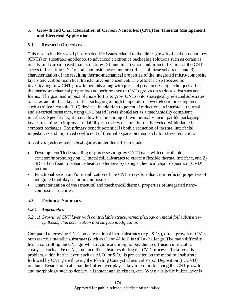
174 Approved for public release; distribution unlimited.
Growth and Characterization of Carbon Nanotubes (CNT) for Thermal Management 5.and Electrical Applications
Research Objectives 5.1
This research addresses 1) basic scientific issues related to the direct growth of carbon nanotubes (CNTs) on substrates applicable to advanced electronics packaging solutions such as ceramics, metals, and carbon based foam structures; 2) functionalization and/or metallization of the CNT arrays to form thin CNT-metal composite layers on the surfaces of these substrates; and 3) characterization of the resulting thermo-mechanical properties of the integrated micro-composite layers and carbon foam heat transfer area enhancement. The effort is also focused on investigating how CNT growth methods along with pre- and post-processing techniques affect the thermo-mechanical properties and performance of CNTs grown on various substrates and foams. The goal and impact of this effort is to grow CNTs onto strategically selected substrates to act as an interface layer in the packaging of high temperature power electronic components such as silicon carbide (SiC) devices. In addition to potential reductions in interfacial thermal and electrical resistance, using CNT based layers should act as a mechanically compliant interface. Specifically, it may allow for the joining of two thermally incompatible packaging layers, resulting in improved reliability of devices that are thermally cycled within lamellar compact packages. The primary benefit potential is both a reduction of thermal interfacial impedances and improved coefficient of thermal expansion mismatch, for stress reduction.
Specific objectives and subcategories under this effort include:
• Development/Understanding of processes to grow CNT layers with controllablestructure/morphology on: 1) metal foil substrates to create a flexible thermal interface, and 2)3D carbon foam to enhance heat transfer area by using a chemical vapor deposition (CVD)method
• Functionalization and/or metallization of the CNT arrays to enhance interfacial properties ofintegrated multilayer micro-composites
• Characterization of the structural and mechanical/thermal properties of integrated nano-composite structures.
Technical Summary 5.2
5.2.1 Approaches 5.2.1.1 Growth of CNT layer with controllable structure/morphology on metal foil substrates-
synthesis, characterization and surface modification
Compared to growing CNTs on conventional inert substrates (e.g., SiO2), direct growth of CNTs onto reactive metallic substrates (such as Cu or Al foil) is still a challenge. The main difficulty lies in controlling the CNT growth structure and morphology due to diffusion of metallic catalysts, such as Fe or Ni, into metallic substrates during the CVD process. To solve this problem, a thin buffer layer, such as Al2O3 or SiO2, is pre-coated on the metal foil substrate, followed by CNT growth using the Floating Catalyst Chemical Vapor Deposition (FCCVD) method. Results indicate that the buffer layer plays a key role in influencing the CNT growth and morphology such as density, alignment and thickness, etc. When a suitable buffer layer is
175 Approved for public release; distribution unlimited.
coated on the metal substrate surface, a highly dense and uniform CNT layer can be grown on it. Therefore, the effect of materials and thickness of buffer layer as well as layer deposition method on CNT growth and quality are investigated in order to gain an understanding of the parametric control required to achieve specific CNT characteristics and properties.
Using a CNT layer as a thermal interface material, the CNT growth on an appropriate substrate is only the first step towards providing a scientific basis. The large thermal contact resistances, due to the low fraction of CNT-substrate contact area, and weak interfacial adhesion because of a lack of a chemical bonding between the CNT and the substrate surface, are two of the most pressing challenges. Although significant research has been done in the area of reactive substrate CNT growth, very little has been done regarding interfacial property enhancement (bond-strength). Therefore, managing the CNT/substrate interface to effectively reduce the thermal contact resistance and simultaneously improve the interfacial adhesion is another beneficial research focus area. This effort will extend the work done previously on nanotube growth, by concentrating on ways to improve the CNT structure/morphology and substrate bonding strength as well as using surface modification treatment to enhance thermal/mechanical attachment. To address these challenges, pre- and post-treatments on the Cu substrate and CNT layer to enhance CNT-substrate interfacial adhesion were investigated during. A variety of pre-treatments were investigated including: buffer layer material variation, and changing buffer layer thickness/deposition method. Plasma etching, substrate enhanced electroless deposition (SEED), and sputter coating techniques were employed as post-treatment on the CNT layer surface. Initial experimental details and results are reported below.
5.2.1.2 Growth of nanotubes on porous cellular (foam) carbon materials-the effect of surface pre-treated method on CNTs growth/structure
Carbon foam (CF) is a low cost, light weight, and thermally conductive material with significant heat transfer area and open pore space. Additionally, CNTs have impressive mechanical, electrical, and thermal properties. Growing CNTs on carbon foam provides an astounding amount of surface area that is ideal for heat transfer or HEX applications. Preliminary experiments are ongoing to determine the best methods to evenly distribute the growth of CNTs throughout the entire depth of the foam to enhance the properties of the foam. To reach this goal, the effort during first year was focused on using different surface treatment methods on carbon foam substrates, followed by CNT growth using a FCCVD method. Five types of surface modifications on carbon foam were used to investigate the effect of CF surface treatment on CNT growth. In comparing the CNT growth results, we found that samples coated with an Al2O3 thin layer by atomic layer deposition (ALD) yielded dense, aligned CNT forest growth.
5.2.1.3 Growth of CNTs on carbon substrate - Influence of oxide as buffer layer for CNT growth
A previous study had demonstrated that coating an alumina (Al2O3) layer on the carbon surface as a buffer layer can significantly improve CNT growth and provide favorable morphology (density, alignment, etc.), which suggests the importance of buffer layer deposition on CNT growth. However, so far, the effect of various buffer layer materials and their physical structure on controlling growth of CNTs on carbon substrates has not been well understood and documented. Therefore, the research efforts during the past year were focused on investigating the influence of different buffer oxide materials and deposition methods on CNT growth and
176 Approved for public release; distribution unlimited.
array structure/morphology. To reach this goal, two materials, alumina (Al2O3) and silica (SiO2), and three different deposition techniques, thermal oxidation, ALD and microwave plasma enhanced chemical vapor deposition (MPE-CVD), were investigated. The substrates in this study were flat sections of silicon wafer coated with a layer of vitreous carbon; generated by pyrolysis from polymeric precursors. The vitreous carbon samples represent the same chemical structure as reticulated vitreous carbon (RVC) foam, but in a simple planar geometry, allowing for much more simplistic quantitative analysis via microscopic and spectroscopic techniques.
5.2.1.4 Characterization of the CNT layer structure, mechanical and thermal properties of the integrated CNTs based nano-composite structure
The CNT structure and attachment quality both play a key role in determining the integrated nano-composite properties. Therefore, characterization of CNT and/or CNT layer (includes buffer layer and any coating applied) structure/morphology is necessary to understand the effect of the buffer layer on CNT growth. The relationship between the CNT structure and the integrated composite performance/properties is another beneficial research focus area. In this study, the primary characterization methods/techniques involved samples generated for high resolution scanning electron microscopy (HR-SEM), transmission electron microscopy (TEM), atomic force measurement (AFM), Raman spectroscopy, laser flash thermal diffusivity measurement, thermal impedance measurement, and mechanical pull-off testing. Details of the testing and characterization will be described in the next section.
Detailed Technical Summary: 5.3
5.3.1 Part1: CNT layer grown on Cu and various metal foil substrates-synthesis, surface modification, and characterization
CNTs with their high thermal conductivity and large surface area, are an attractive candidate for integration into thermal structures and as a flexible thermal interface material. Using CNTs as a thermal interface material has been extensively reported [97]-[103]. However, many of these efforts have not thoroughly investigated direct growth of high quality CNTs on metallic substrates with reproducible and controllable structure/morphology, with an emphasis on thermal/mechanical attachment. Compared to non-active substrates (such as Si), one challenge of growing CNTs on metal substrates is that high temperatures may cause diffusion of the catalysts into the metallic substrate, which will reduce its activity and result in growth of CNTs with uncontrollable structure and quality. To solve this problem, a suitable buffer layer needs to be introduced as the support layer on the metal substrate. When growing CNTs directly on a metallic substrates, most researchers have paid more attention to the CNT growth itself rather than the CNT/substrate interfacial properties. That is, they were more interested in quantification of CNTs as opposed to CNT/substrate bonding strength. This highlights several significant challenges that have led us to begin further investigation including: the growth of CNTs on select substrates with controllable structure and properties as an application requirement, identifying the relationship of CNT structure/morphology with performance of CNT-based nano-composites, as well as increasing interface bonding strength between CNTs and metal substrate by varying catalyst and buffer layer.
The goal of this basic scientific effort is to control growth of CNTs directly on unconventional substrates such as metals and ceramics to create functional micro-carbon composite layers on the
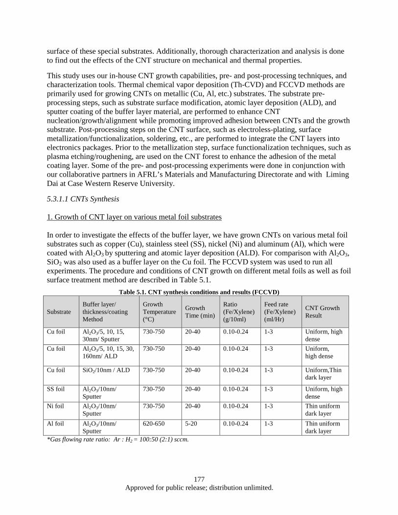
177 Approved for public release; distribution unlimited.
surface of these special substrates. Additionally, thorough characterization and analysis is done to find out the effects of the CNT structure on mechanical and thermal properties.
This study uses our in-house CNT growth capabilities, pre- and post-processing techniques, and characterization tools. Thermal chemical vapor deposition (Th-CVD) and FCCVD methods are primarily used for growing CNTs on metallic (Cu, Al, etc.) substrates. The substrate pre-processing steps, such as substrate surface modification, atomic layer deposition (ALD), and sputter coating of the buffer layer material, are performed to enhance CNT nucleation/growth/alignment while promoting improved adhesion between CNTs and the growth substrate. Post-processing steps on the CNT surface, such as electroless-plating, surface metallization/functionalization, soldering, etc., are performed to integrate the CNT layers into electronics packages. Prior to the metallization step, surface functionalization techniques, such as plasma etching/roughening, are used on the CNT forest to enhance the adhesion of the metal coating layer. Some of the pre- and post-processing experiments were done in conjunction with our collaborative partners in AFRL’s Materials and Manufacturing Directorate and with Liming Dai at Case Western Reserve University.
5.3.1.1 CNTs Synthesis
1. Growth of CNT layer on various metal foil substrates
In order to investigate the effects of the buffer layer, we have grown CNTs on various metal foil substrates such as copper (Cu), stainless steel (SS), nickel (Ni) and aluminum (Al), which were coated with Al2O3 by sputtering and atomic layer deposition (ALD). For comparison with Al2O3, SiO2 was also used as a buffer layer on the Cu foil. The FCCVD system was used to run all experiments. The procedure and conditions of CNT growth on different metal foils as well as foil surface treatment method are described in Table 5.1.
Table 5.1. CNT synthesis conditions and results (FCCVD)
Substrate Buffer layer/ thickness/coating Method
Growth Temperature (°C)
Growth Time (min)
Ratio (Fe/Xylene) (g/10ml)
Feed rate (Fe/Xylene) (ml/Hr)
CNT Growth Result
Cu foil Al2O3/5, 10, 15, 30nm/ Sputter
730-750 20-40 0.10-0.24 1-3 Uniform, high dense
Cu foil Al2O3/5, 10, 15, 30, 160nm/ ALD
730-750 20-40 0.10-0.24 1-3 Uniform, high dense
Cu foil SiO2/10nm / ALD 730-750 20-40 0.10-0.24 1-3 Uniform,Thin dark layer
SS foil Al2O3/10nm/ Sputter
730-750 20-40 0.10-0.24 1-3 Uniform, high dense
Ni foil Al2O3/10nm/ Sputter
730-750 20-40 0.10-0.24 1-3 Thin uniform dark layer
Al foil Al2O3/10nm/ Sputter
620-650 5-20 0.10-0.24 1-3 Thin uniform dark layer
*Gas flowing rate ratio: Ar : H2 = 100:50 (2:1) sccm.
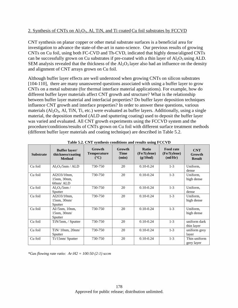
178 Approved for public release; distribution unlimited.
2. Synthesis of CNTs on Al2O3, Al, TiN, and Ti coated Cu foil substrates by FCCVD
CNT synthesis on planar copper or other metal substrate surfaces is a beneficial area for investigation to advance the state-of-the-art in nano-science. Our previous results of growing CNTs on Cu foil, using both FC-CVD and Th-CVD, indicated that highly dense/aligned CNTs can be successfully grown on Cu substrates if pre-coated with a thin layer of Al2O3 using ALD. SEM analysis revealed that the thickness of the Al2O3 layer also had an influence on the density and alignment of CNT arrays grown on Cu foil.
Although buffer layer effects are well understood when growing CNTs on silicon substrates [104-110], there are many unanswered questions associated with using a buffer layer to grow CNTs on a metal substrate (for thermal interface material applications). For example, how do different buffer layer materials affect CNT growth and structure? What is the relationship between buffer layer material and interfacial properties? Do buffer layer deposition techniques influence CNT growth and interface properties? In order to answer these questions, various materials (Al2O3, Al, TiN, Ti, etc.) were evaluated as buffer layers. Additionally, using a single material, the deposition method (ALD and sputtering coating) used to deposit the buffer layer was varied and evaluated. All CNT growth experiments using the FCCVD system and the procedure/conditions/results of CNTs grown on Cu foil with different surface treatment methods (different buffer layer materials and coating technique) are described in Table 5.2.
Table 5.2. CNT synthesis conditions and results using FCCVD
*Gas flowing rate ratio: Ar:H2 = 100:50 (2:1) sccm
Substrate Buffer layer/
thickness/coating Method
Growth Temperature
(°C)
Growth Time (min)
Ratio (Fe/Xylene)
(g/10ml)
Feed rate (Fe/Xylene)
(ml/Hr)
CNT Growth Result
Cu foil Al2O3/5nm / ALD 730-750 20 0.10-0.24 1-3 Uniform, dense
Cu foil Al2O3/10nm, 15nm, 30nm, 60nm/ ALD
730-750 20 0.10-0.24 1-3 Uniform, high dense
Cu foil Al2O3/5nm / Sputter
730-750 20 0.10-0.24 1-3 Uniform, dense
Cu foil Al2O3/10nm, 15nm, 30nm/ Sputter
730-750 20 0.10-0.24 1-3 Uniform, high dense
Cu foil Al//5nm, 10nm, 15nm, 30nm/ Sputter
730-750 20 0.10-0.24 1-3 Uniform, high dense
Cu foil TiN/5nm, / Sputter 730-750 20 0.10-0.24 1-3 uniform dark thin layer
Cu foil TiN/ 10nm, 20nm/ Sputter
730-750 20 0.10-0.24 1-3 uniform grey layer
Cu foil Ti/15nm/ Sputter 730-750 20 0.10-0.24 1-3 Thin uniform grey layer
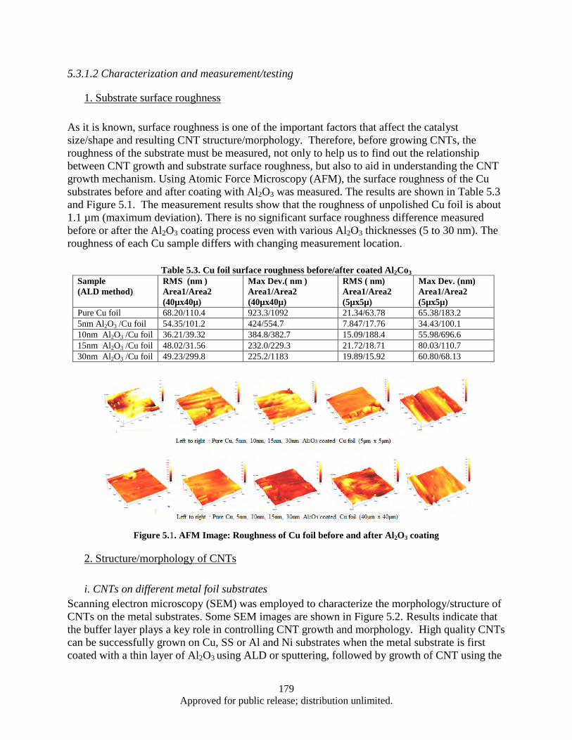
179 Approved for public release; distribution unlimited.
5.3.1.2 Characterization and measurement/testing
1. Substrate surface roughness
As it is known, surface roughness is one of the important factors that affect the catalyst size/shape and resulting CNT structure/morphology. Therefore, before growing CNTs, the roughness of the substrate must be measured, not only to help us to find out the relationship between CNT growth and substrate surface roughness, but also to aid in understanding the CNT growth mechanism. Using Atomic Force Microscopy (AFM), the surface roughness of the Cu substrates before and after coating with Al2O3 was measured. The results are shown in Table 5.3 and Figure 5.1. The measurement results show that the roughness of unpolished Cu foil is about 1.1 µm (maximum deviation). There is no significant surface roughness difference measured before or after the Al2O3 coating process even with various Al2O3 thicknesses (5 to 30 nm). The roughness of each Cu sample differs with changing measurement location.
Table 5.3. Cu foil surface roughness before/after coated Al2Co3
Figure 5.1. AFM Image: Roughness of Cu foil before and after Al2O3 coating
2. Structure/morphology of CNTs
i. CNTs on different metal foil substratesScanning electron microscopy (SEM) was employed to characterize the morphology/structure of CNTs on the metal substrates. Some SEM images are shown in Figure 5.2. Results indicate that the buffer layer plays a key role in controlling CNT growth and morphology. High quality CNTs can be successfully grown on Cu, SS or Al and Ni substrates when the metal substrate is first coated with a thin layer of Al2O3 using ALD or sputtering, followed by growth of CNT using the
Sample (ALD method)
RMS (nm ) Area1/Area2 (40µx40µ)
Max Dev.( nm ) Area1/Area2 (40µx40µ)
RMS ( nm) Area1/Area2 (5µx5µ)
Max Dev. (nm) Area1/Area2 (5µx5µ)
Pure Cu foil 68.20/110.4 923.3/1092 21.34/63.78 65.38/183.2 5nm Al2O3 /Cu foil 54.35/101.2 424/554.7 7.847/17.76 34.43/100.1 10nm Al2O3 /Cu foil 36.21/39.32 384.8/382.7 15.09/188.4 55.98/696.6 15nm Al2O3 /Cu foil 48.02/31.56 232.0/229.3 21.72/18.71 80.03/110.7 30nm Al2O3 /Cu foil 49.23/299.8 225.2/1183 19.89/15.92 60.80/68.13
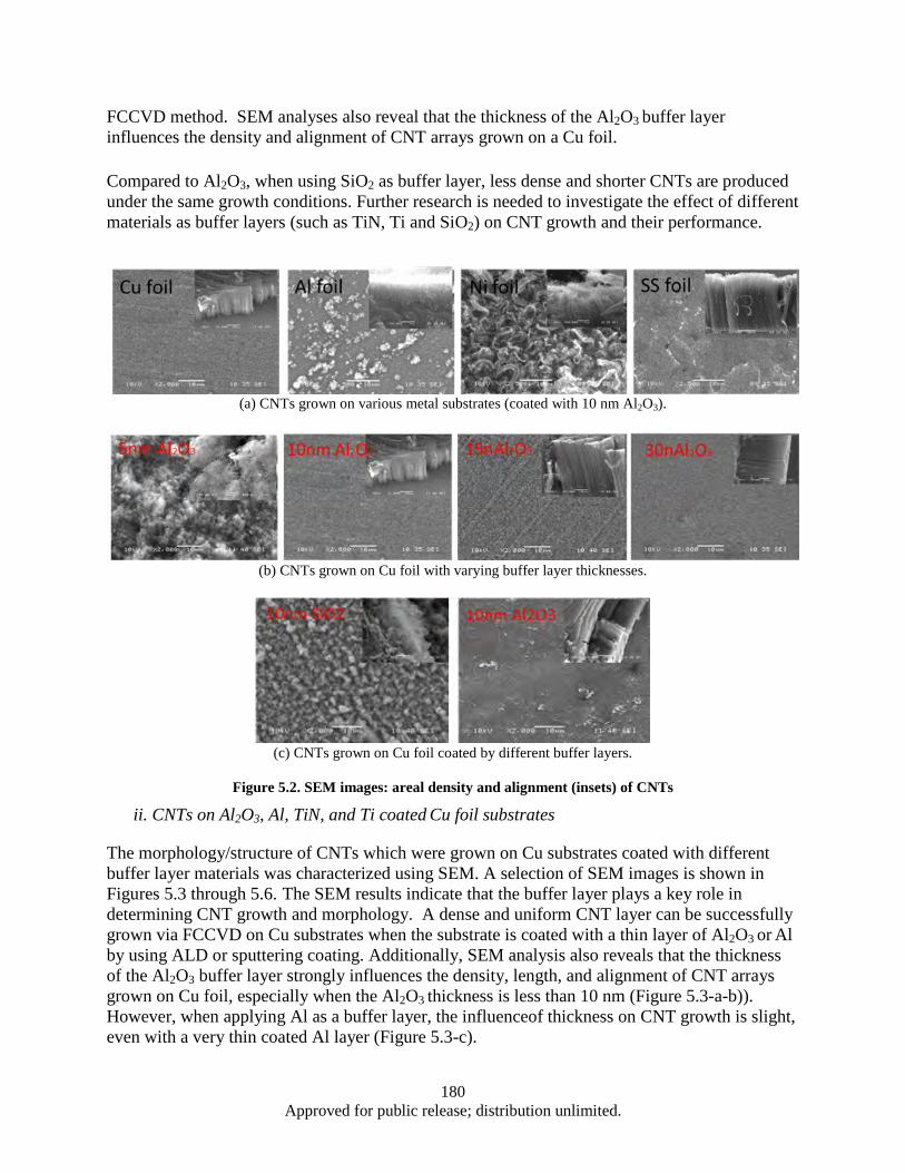
180 Approved for public release; distribution unlimited.
FCCVD method. SEM analyses also reveal that the thickness of the Al2O3 buffer layer influences the density and alignment of CNT arrays grown on a Cu foil.
Compared to Al2O3, when using SiO2 as buffer layer, less dense and shorter CNTs are produced under the same growth conditions. Further research is needed to investigate the effect of different materials as buffer layers (such as TiN, Ti and SiO2) on CNT growth and their performance.
(a) CNTs grown on various metal substrates (coated with 10 nm Al2O3).
(b) CNTs grown on Cu foil with varying buffer layer thicknesses.
(c) CNTs grown on Cu foil coated by different buffer layers.
Figure 5.2. SEM images: areal density and alignment (insets) of CNTs
ii. CNTs on Al2O3, Al, TiN, and Ti coated Cu foil substrates
The morphology/structure of CNTs which were grown on Cu substrates coated with different buffer layer materials was characterized using SEM. A selection of SEM images is shown in Figures 5.3 through 5.6. The SEM results indicate that the buffer layer plays a key role in determining CNT growth and morphology. A dense and uniform CNT layer can be successfully grown via FCCVD on Cu substrates when the substrate is coated with a thin layer of Al2O3 or Alby using ALD or sputtering coating. Additionally, SEM analysis also reveals that the thickness of the Al2O3 buffer layer strongly influences the density, length, and alignment of CNT arrays grown on Cu foil, especially when the Al2O3 thickness is less than 10 nm (Figure 5.3-a-b)). However, when applying Al as a buffer layer, the influenceof thickness on CNT growth is slight, even with a very thin coated Al layer (Figure 5.3-c).

181 Approved for public release; distribution unlimited.
In addition to Al2O3 and Al buffer materials, TiN and Ti were coated on Cu substrates as buffer materials. The morphology of the resulting CNT layers is shown in the SEM images in Figures 5.4 and 5.5. Compared to Al2O3 and Al, when using TiN or Ti as buffer layer, a shorter, uniform, low dense CNT layer is produced on the Cu foil substrate under the same growth conditions. When increasing the TiN layer thickness (5 to10 nm), the length and alignment of the CNT layer is improved, but not as significantly as the thickness change from 10 nm to 20 nm. For the TiN buffer material samples, there are many particles found on the Cu substrate surface when CNTs are scraped away from the Cu foil, as shown in Figure 5.6. The elements contained within these particles were determined by EDX, as shown in Table 5.4. However, it is not yet clear why and how to form these kind particles during CNT growth. Due to the excellent physical properties exhibited by TiN, such as high electrical conductivity, thermal stability, high corrosion resistance and widespread application in electronic devices, more research is needed to investigate TiN as a buffer layer.
To use CNTs as a thermal interface material, the role of structure/morphology and thickness of the CNTs on thermal performance must not be undervalued. Our initial test results indicate that when using CNTs as a thermal interface material, the structure/morphology and thickness of the CNTs play an important role in the thermal performance. Therefore, the significant impact of these controllable growth capabilities is that they allow us determine the optimum CNT layer structure for eliminating resistive junctions and provides improved thermal and electrical transport properties. These improvements can greatly increase the reliability and performance of thermal management of electronic power devices in modern aircraft.
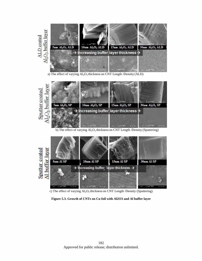
182 Approved for public release; distribution unlimited.
a) The effect of varying Al2O3 thickness on CNT Length /Density (ALD)
b) The effect of varying Al2O3 thickness on CNT Length /Density (Sputtering)
c) The effect of varying Al2O3 thickness on CNT Length /Density (Sputtering)
Figure 5.3. Growth of CNTs on Cu foil with Al2O3 and Al buffer layer
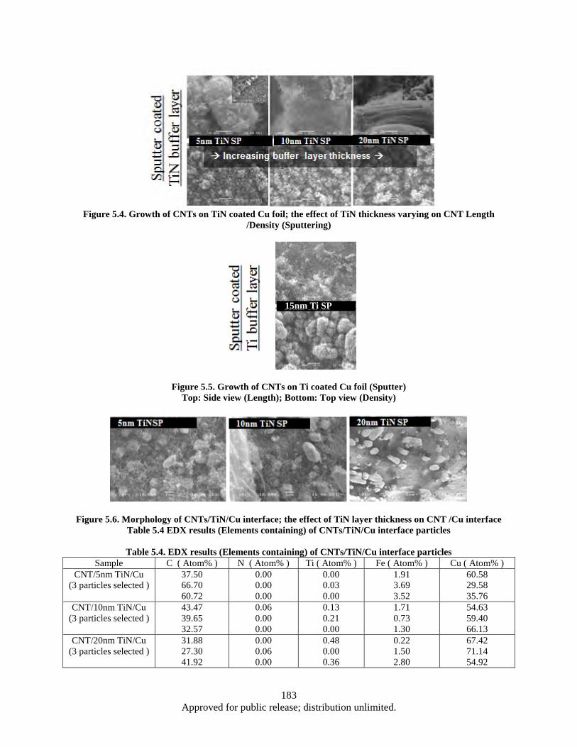
183 Approved for public release; distribution unlimited.
Figure 5.4. Growth of CNTs on TiN coated Cu foil; the effect of TiN thickness varying on CNT Length /Density (Sputtering)
Figure 5.5. Growth of CNTs on Ti coated Cu foil (Sputter) Top: Side view (Length); Bottom: Top view (Density)
Figure 5.6. Morphology of CNTs/TiN/Cu interface; the effect of TiN layer thickness on CNT /Cu interface Table 5.4 EDX results (Elements containing) of CNTs/TiN/Cu interface particles
Table 5.4. EDX results (Elements containing) of CNTs/TiN/Cu interface particles Sample C ( Atom% ) N ( Atom% ) Ti ( Atom% ) Fe ( Atom% ) Cu ( Atom% )
CNT/5nm TiN/Cu (3 particles selected )
37.50 66.70 60.72
0.00 0.00 0.00
0.00 0.03 0.00
1.91 3.69 3.52
60.58 29.58 35.76
CNT/10nm TiN/Cu (3 particles selected )
43.47 39.65 32.57
0.06 0.00 0.00
0.13 0.21 0.00
1.71 0.73 1.30
54.63 59.40 66.13
CNT/20nm TiN/Cu (3 particles selected )
31.88 27.30 41.92
0.00 0.06 0.00
0.48 0.00 0.36
0.22 1.50 2.80
67.42 71.14 54.92
15nm Ti SP
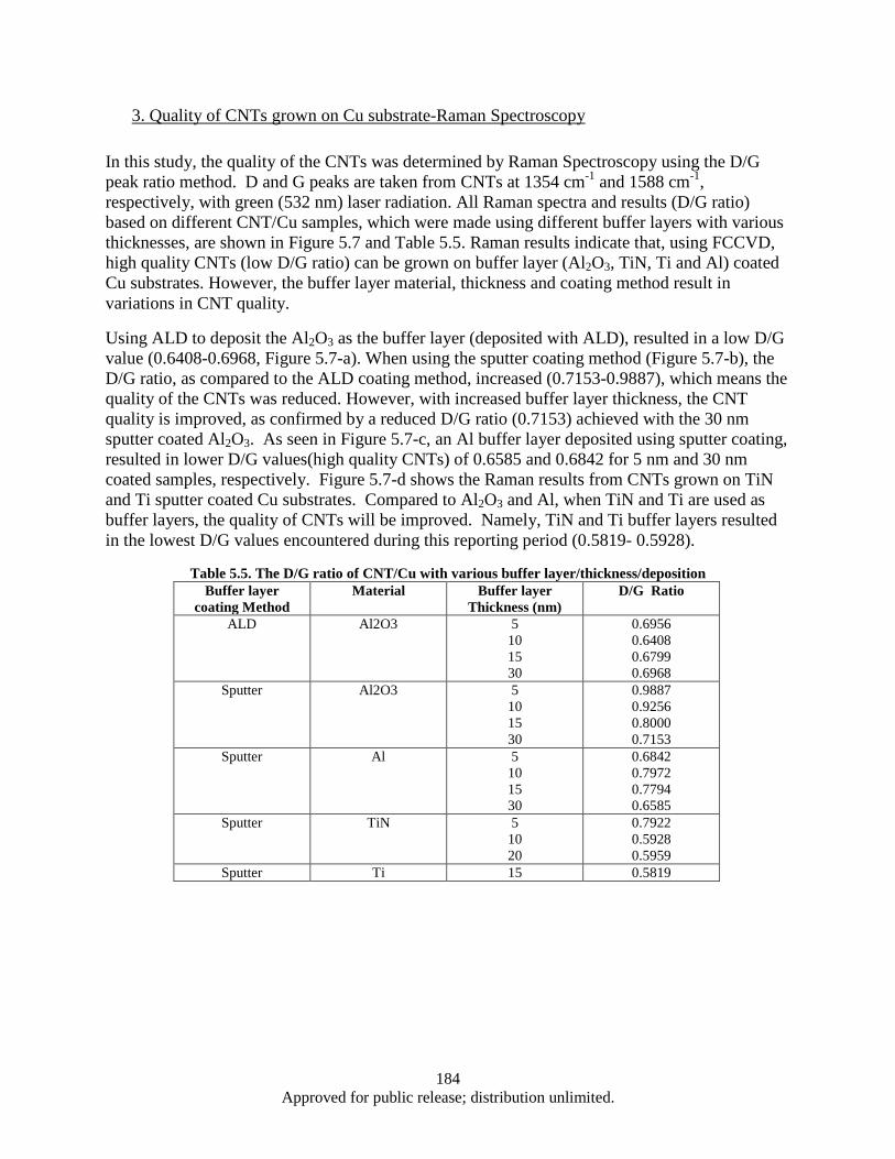
184 Approved for public release; distribution unlimited.
3. Quality of CNTs grown on Cu substrate-Raman Spectroscopy
In this study, the quality of the CNTs was determined by Raman Spectroscopy using the D/G peak ratio method. D and G peaks are taken from CNTs at 1354 cm-1 and 1588 cm-1, respectively, with green (532 nm) laser radiation. All Raman spectra and results (D/G ratio) based on different CNT/Cu samples, which were made using different buffer layers with various thicknesses, are shown in Figure 5.7 and Table 5.5. Raman results indicate that, using FCCVD, high quality CNTs (low D/G ratio) can be grown on buffer layer (Al2O3, TiN, Ti and Al) coated Cu substrates. However, the buffer layer material, thickness and coating method result in variations in CNT quality.
Using ALD to deposit the Al2O3 as the buffer layer (deposited with ALD), resulted in a low D/G value (0.6408-0.6968, Figure 5.7-a). When using the sputter coating method (Figure 5.7-b), the D/G ratio, as compared to the ALD coating method, increased (0.7153-0.9887), which means the quality of the CNTs was reduced. However, with increased buffer layer thickness, the CNT quality is improved, as confirmed by a reduced D/G ratio (0.7153) achieved with the 30 nm sputter coated Al2O3. As seen in Figure 5.7-c, an Al buffer layer deposited using sputter coating, resulted in lower D/G values(high quality CNTs) of 0.6585 and 0.6842 for 5 nm and 30 nm coated samples, respectively. Figure 5.7-d shows the Raman results from CNTs grown on TiN and Ti sputter coated Cu substrates. Compared to Al2O3 and Al, when TiN and Ti are used as buffer layers, the quality of CNTs will be improved. Namely, TiN and Ti buffer layers resulted in the lowest D/G values encountered during this reporting period (0.5819- 0.5928).
Table 5.5. The D/G ratio of CNT/Cu with various buffer layer/thickness/deposition
Buffer layer coating Method
Material Buffer layer Thickness (nm)
D/G Ratio
ALD Al2O3 5 10 15 30
0.6956 0.6408 0.6799 0.6968
Sputter Al2O3 5 10 15 30
0.9887 0.9256 0.8000 0.7153
Sputter Al 5 10 15 30
0.6842 0.7972 0.7794 0.6585
Sputter TiN 5 10 20
0.7922 0.5928 0.5959
Sputter Ti 15 0.5819
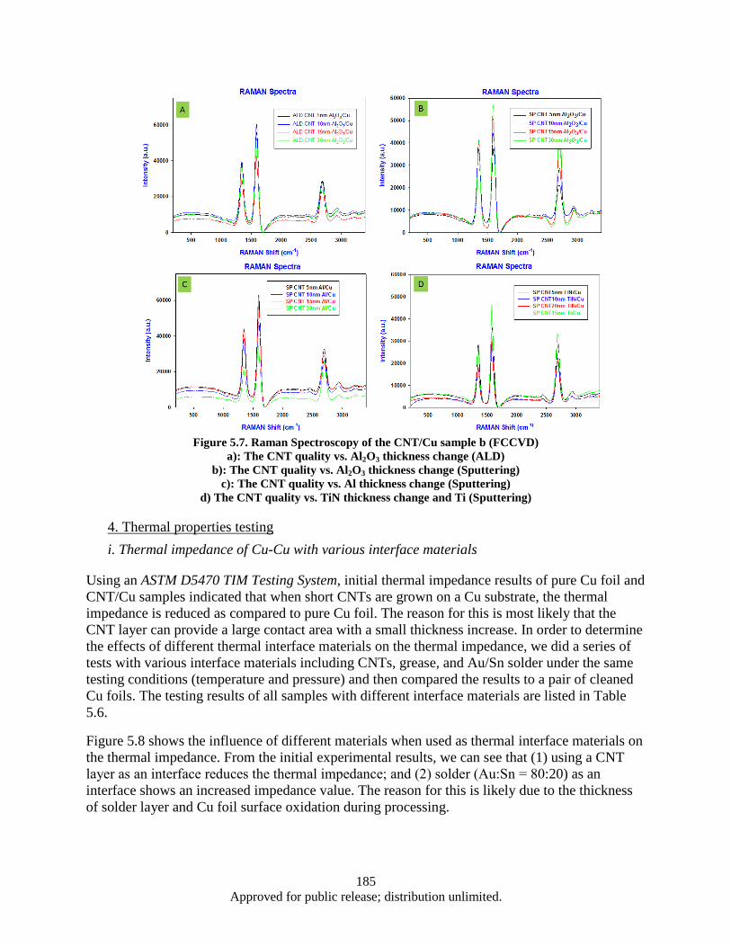
185 Approved for public release; distribution unlimited.
Figure 5.7. Raman Spectroscopy of the CNT/Cu sample b (FCCVD)
a): The CNT quality vs. Al2O3 thickness change (ALD) b): The CNT quality vs. Al2O3 thickness change (Sputtering)
c): The CNT quality vs. Al thickness change (Sputtering) d) The CNT quality vs. TiN thickness change and Ti (Sputtering)
4. Thermal properties testing i. Thermal impedance of Cu-Cu with various interface materials
Using an ASTM D5470 TIM Testing System, initial thermal impedance results of pure Cu foil and CNT/Cu samples indicated that when short CNTs are grown on a Cu substrate, the thermal impedance is reduced as compared to pure Cu foil. The reason for this is most likely that the CNT layer can provide a large contact area with a small thickness increase. In order to determine the effects of different thermal interface materials on the thermal impedance, we did a series of tests with various interface materials including CNTs, grease, and Au/Sn solder under the same testing conditions (temperature and pressure) and then compared the results to a pair of cleaned Cu foils. The testing results of all samples with different interface materials are listed in Table 5.6.
Figure 5.8 shows the influence of different materials when used as thermal interface materials on the thermal impedance. From the initial experimental results, we can see that (1) using a CNT layer as an interface reduces the thermal impedance; and (2) solder (Au:Sn = 80:20) as an interface shows an increased impedance value. The reason for this is likely due to the thickness of solder layer and Cu foil surface oxidation during processing.
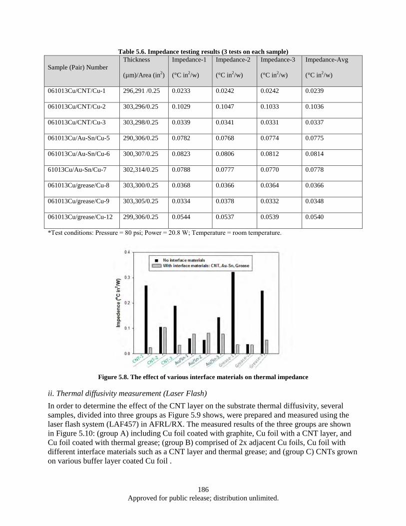
186 Approved for public release; distribution unlimited.
Table 5.6. Impedance testing results (3 tests on each sample)
Sample (Pair) Number Thickness
(µm)/Area (in2)
Impedance-1
(°C in2/w)
Impedance-2
(°C in2/w)
Impedance-3
(°C in2/w)
Impedance-Avg
(°C in2/w)
061013Cu/CNT/Cu-1 296,291 /0.25 0.0233 0.0242 0.0242 0.0239
061013Cu/CNT/Cu-2 303,296/0.25 0.1029 0.1047 0.1033 0.1036
061013Cu/CNT/Cu-3 303,298/0.25 0.0339 0.0341 0.0331 0.0337
061013Cu/Au-Sn/Cu-5 290,306/0.25 0.0782 0.0768 0.0774 0.0775
061013Cu/Au-Sn/Cu-6 300,307/0.25 0.0823 0.0806 0.0812 0.0814
61013Cu/Au-Sn/Cu-7 302,314/0.25 0.0788 0.0777 0.0770 0.0778
061013Cu/grease/Cu-8 303,300/0.25 0.0368 0.0366 0.0364 0.0366
061013Cu/grease/Cu-9 303,305/0.25 0.0334 0.0378 0.0332 0.0348
061013Cu/grease/Cu-12 299,306/0.25 0.0544 0.0537 0.0539 0.0540
*Test conditions: Pressure = 80 psi; Power = 20.8 W; Temperature = room temperature.
Figure 5.8. The effect of various interface materials on thermal impedance
ii. Thermal diffusivity measurement (Laser Flash) In order to determine the effect of the CNT layer on the substrate thermal diffusivity, several samples, divided into three groups as Figure 5.9 shows, were prepared and measured using the laser flash system (LAF457) in AFRL/RX. The measured results of the three groups are shown in Figure 5.10: (group A) including Cu foil coated with graphite, Cu foil with a CNT layer, and Cu foil coated with thermal grease; (group B) comprised of 2x adjacent Cu foils, Cu foil with different interface materials such as a CNT layer and thermal grease; and (group C) CNTs grown on various buffer layer coated Cu foil .
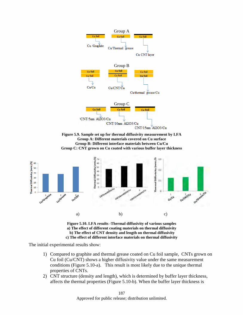
187 Approved for public release; distribution unlimited.
Group A
Group B
Group C
Figure 5.9. Sample set up for thermal diffusivity measurement by LFA
Group A: Different materials covered on Cu surface Group B: Different interface materials between Cu/Cu
Group C: CNT grown on Cu coated with various buffer layer thickness
a) b) c)
Figure 5.10. LFA results -Thermal diffusivity of various samples a) The effect of different coating materials on thermal diffusivity b) The effect of CNT density and length on thermal diffusivity
c) The effect of different interface materials on thermal diffusivity
The initial experimental results show:
1) Compared to graphite and thermal grease coated on Cu foil sample, CNTs grown on Cu foil (Cu/CNT) shows a higher diffusivity value under the same measurement conditions (Figure 5.10-a). This result is most likely due to the unique thermal properties of CNTs.
2) CNT structure (density and length), which is determined by buffer layer thickness, affects the thermal properties (Figure 5.10-b). When the buffer layer thickness is

188 Approved for public release; distribution unlimited.
increased, the CNT layer density and length goes up, which leads to increased contact area and a resulting higher thermal diffusivity.
3) Using CNTs as an interface layer, as compared to grease, shows a reduction in thermal diffusivity (Figure 5.10-c). This is most likely because there is a large thermal contact resistance between the CNT layer surface and the free standing matching substrates (Cu foil) due to the low contact fraction. More experiments/investigation with a more appropriate sample set up to improve interface properties are in progress.
5. Electrical property testing of Cu-CNT/Cu Using a custom designed sample holder, combined with a custom build electrical testing system, the electrical resistance of Cu/Cu and Cu-CNT-Cu (various thickness of CNT layer) samples have been measured. Sample set up is shown in Figure 5.11, and test results are shown in Table 5.7 and Figure 5.12.
The experimental results showed that: 1) When pressure is increased, the resistance is reduced, as expected. 2) Compared to pure Cu-Cu, Cu-CNT-Cu appears to have a higher resistance value. 3) When the CNT layer thickness/density is increased (known from increased Al2O3
buffer thickness), the electrical resistance of the Cu-CNT-Cu composite decreases. These results can be explained according to Ohm’s law for circuit theory:
R = V/I = ρ*L/A (5.1)
R=Resistance; V=Voltage; I=Current; ρ=Resistivity; L=length; A=cross-sectional area
1) When pressure is increased, the microstructure contact area is increased, reducing the resistance. 2) With a free stand matching substrate (Cu), an additional CNT layer between two Cu foils will increase the contact resistance (due to a poor contact area and length), which could cause the electrical resistance increase. 3) compared to a thin and low density CNT layer, under a given pressure (~7 MPa), the thicker/denser CNT layer with nano-sized CNT diameter will have more contact area (A), and this contribution to the electrical resistance is much stronger than that of CNT length (L) change. Therefore, the electrical resistance of the Cu-CNT-Cu composite sample decreases when the CNT layer density is increased.
The result also indicated that when using different methods to coat the same thickness of buffer layer (Al2O3) on the Cu substrate, and subsequently growing CNTs, the sample resistance was different. This is possibly due to variations in CNT growth density resulting from differing deposition techniques. To verify this result, more experimental measurement is required.
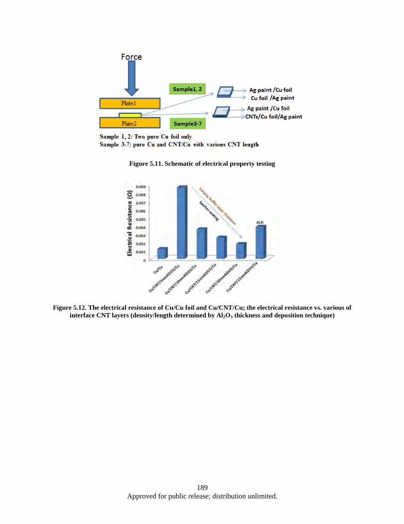
189 Approved for public release; distribution unlimited.
Figure 5.11. Schematic of electrical property testing
Figure 5.12. The electrical resistance of Cu/Cu foil and Cu/CNT/Cu; the electrical resistance vs. various of
interface CNT layers (density/length determined by Al2O3 thickness and deposition technique)
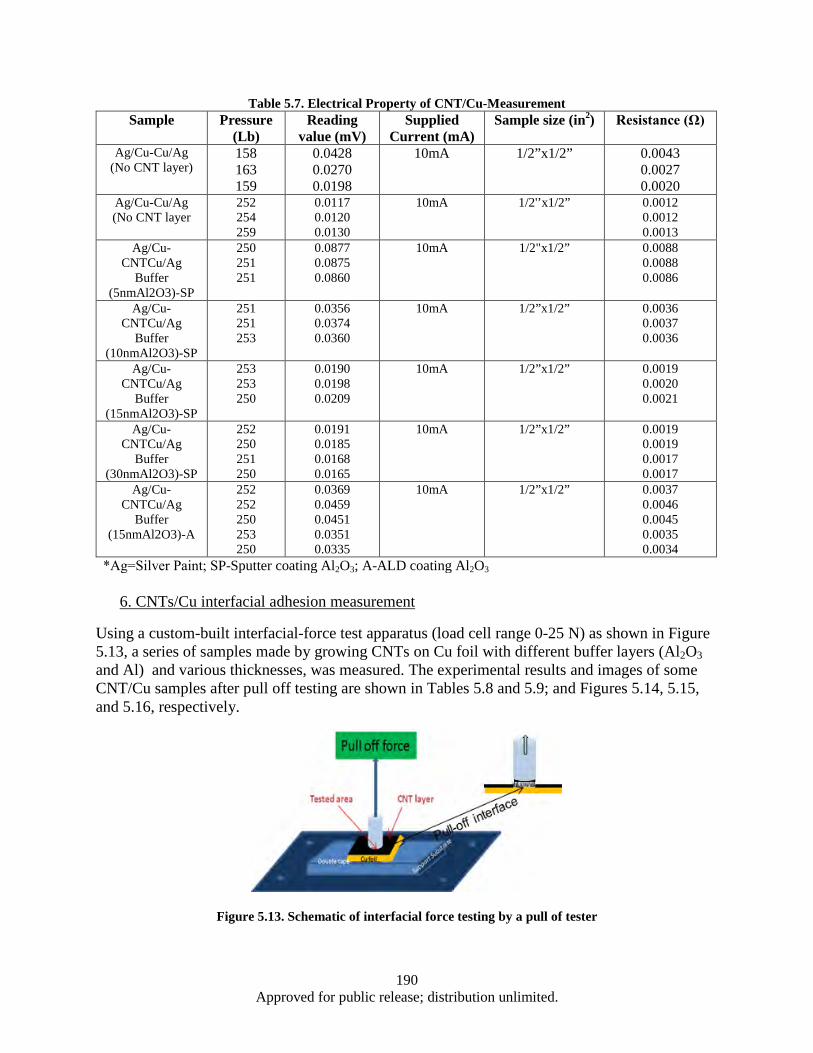
190 Approved for public release; distribution unlimited.
Table 5.7. Electrical Property of CNT/Cu-Measurement
6. CNTs/Cu interfacial adhesion measurement
Using a custom-built interfacial-force test apparatus (load cell range 0-25 N) as shown in Figure 5.13, a series of samples made by growing CNTs on Cu foil with different buffer layers (Al2O3 and Al) and various thicknesses, was measured. The experimental results and images of some CNT/Cu samples after pull off testing are shown in Tables 5.8 and 5.9; and Figures 5.14, 5.15, and 5.16, respectively.
Figure 5.13. Schematic of interfacial force testing by a pull of tester
Sample Pressure (Lb)
Reading value (mV)
Supplied Current (mA)
Sample size (in2) Resistance (Ω)
Ag/Cu-Cu/Ag (No CNT layer)
158 163 159
0.0428 0.0270 0.0198
10mA 1/2”x1/2” 0.0043 0.0027 0.0020
Ag/Cu-Cu/Ag (No CNT layer
252 254 259
0.0117 0.0120 0.0130
10mA 1/2'’x1/2” 0.0012 0.0012 0.0013
Ag/Cu-CNTCu/Ag
Buffer (5nmAl2O3)-SP
250 251 251
0.0877 0.0875 0.0860
10mA 1/2"x1/2” 0.0088 0.0088 0.0086
Ag/Cu-CNTCu/Ag
Buffer (10nmAl2O3)-SP
251 251 253
0.0356 0.0374 0.0360
10mA 1/2”x1/2” 0.0036 0.0037 0.0036
Ag/Cu-CNTCu/Ag
Buffer (15nmAl2O3)-SP
253 253 250
0.0190 0.0198 0.0209
10mA 1/2”x1/2” 0.0019 0.0020 0.0021
Ag/Cu-CNTCu/Ag
Buffer (30nmAl2O3)-SP
252 250 251 250
0.0191 0.0185 0.0168 0.0165
10mA 1/2”x1/2” 0.0019 0.0019 0.0017 0.0017
Ag/Cu-CNTCu/Ag
Buffer (15nmAl2O3)-A
252 252 250 253 250
0.0369 0.0459 0.0451 0.0351 0.0335
10mA 1/2”x1/2” 0.0037 0.0046 0.0045 0.0035 0.0034
*Ag=Silver Paint; SP-Sputter coating Al2O3; A-ALD coating Al2O3

191 Approved for public release; distribution unlimited.
From the experimental results in Table 5.8 and 5.9, the following was determined:
1) Using the same technique to coat the buffer layer on an identical substrate, the interfacial adhesive strength is affected by the choice buffer material. Using the sputter coating method, the mean interfacial adhesion of the CNT/Cu sample coated by Al2O3 is stronger than that coated by Al (Figure 5.16-a).
2) Using the same buffer material (Al2O3), the interfacial adhesive strength is affected by choice of coating technique. Using the sputter coating method, the mean interfacial adhesion of the CNT/Cu sample is stronger than that coated by the ALD method.
3) The interfacial adhesive strength is a function of the buffer layer thickness. CNT/Cu samples made with a 10 nm or 15 nm Al2O3 buffer layer (sputter coating) have a stronger interfacial adhesion compared to those with a 5 nm or 30 nm Al2O3 buffer layer. This result is different than CNT/Cu samples made by ALD coated Al2O3, which showed that the highest interfacial adhesion corresponded to the 5 nm Al2O3 coated CNT/Cu sample, and when the Al2O3 buffer layer thickness was increased, the value of interfacial adhesion was reduced.
4) CNT/Cu samples made with a 10 nm Al buffer layer had a weaker interfacial adhesion compared to those with a 5 nm, 15 or 30 nm Al buffer layer. When the Al buffer layer thickness was increased (from 10 nm to 30 nm), however, the interfacial adhesive strength increases and the stronger interfacial adhesion corresponds to the 30 nm Al buffer layer coated sample Figure 5.16-b).
Images obtained via optical microscopy, shows the actual contact area of each sample during pull off testing and CNT-Cu interface morphology (Figure 5.14). The 30 nm Al2O3 coated CNT/Cu sample, as compared to the other samples, did not show the highest adhesive strength. Yet more CNTs were left on the Cu substrate after pull off testing, likely affecting the result. The CNT/Cu sample with a 5 nm Al2O3 buffer layer showed a low attachment strength value, but the SEM image in Figure 5.15 showed that there are still many CNTs left on the Cu surface; this suggests that there is a strong interfacial adhesion between CNT and Cu substrate. For the 10 nm Al2O3 buffer layer coated sample, the carbon tape was stuck on the CNT layer surface. This result suggests interfacial attachment that is stronger than the tape on the tip used on the pull test apparatus. Further investigation and more experiments are required to confirm and explain/understand the above test results.
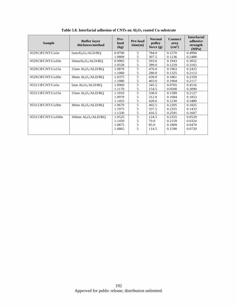
192 Approved for public release; distribution unlimited.
Table 5.8. Interfacial adhesion of CNTs on Al2O3 coated Cu substrate
Sample Buffer layer thickness/method
Pre-load (kg)
Pre-load time(m)
Normal pulley
force (g)
Connect area (cm2)
Interfacial adhesive strength (MPa)
052913FCNT/Cu5n 5nmAl2O3/ALD/RQ 0.9700 1.0809
5 5
784.0 307.5
0.1570 0.1236
0.4994 0.2488
052913FCNT/Cu10n 10nmAl2O3/ALD/RQ 0.9965 1.0558
5 5
593.0 389.0
0.1943 0.1229
0.3052 0.3165
052913FCNT/Cu15n 15nm Al2O3/ALD/RQ 1.0870 1.1060
5 5
476.0 280.0
0.1963 0.1325
0.2425 0.2113
052913FCNT/Cu30n 30nm Al2O3/ALD/RQ 1.0375 1.1080
5 5
439.0 403.0
0.1861 0.1904
0.2359 0.2117
053113FCNT/Cu5n 5nm Al2O3/ALD/RQ 1.0960 1.1170
5 5
345.5 154.5
0.0765 0.0500
0.4516 0.3090
053113FCNT/Cu15n 15nm Al2O3/ALD/RQ 1.1910 1.0970 1.1455
5 5 5
338.0 312.0 428.0
0.1589 0.1684 0.1230
0.2127 0.1853 0.3480
053113FCNT/Cu30n 30nm Al2O3/ALD/RQ 1.0670 1.1975 1.1330
5 5 5
402.5 337.5 416.5
0.2205 0.2355 0.2591
0.1825 0.1433 0.1607
053113FCNT/Cu160n 160nm Al2O3/ALD/RQ 1.0525 1.1450 1.0875 1.0865
5 5 5 5
124.5 70.0 85.0 114.5
0.2355 0.2159 0.1809 0.1590
0.0529 0.0324 0.0470 0.0720
193 Approved for public release; distribution unlimited.
Table 5.9. Interfacial adhesion of CNT on Cu substrate
Figure 5.14. CNT/Cu (made with various Al2O3 thickness) interface after pull off test; the effect of CNT layer density/length (determined by Al2O3 thickness) on their interfacial property.
Sample Buffer layer thickness/method
Pre-load (N)
Pre-load time(min)
Normal pulley
force (N)
Connect area (cm2)
Interfacial adhesive strength (MPa)
011614FCNT/Cu5n 5nmAl2O3/SP/RQ 11.21 11.21 11.26 11.12
3-4 3-4 3-4 3-4
8.05 8.91 8.30 9.60
0.1872 0.1962 0.1766 0.1980
0.43 0.41 0.47 0.48
011614FCNT/Cu10n 10nmAl2O3/SP/RQ 11.43 12.96 11.46 11.39
3-4 3-4 3-4 3-4
>9.75 12.10 >10.28 >11.39
_ 0.1963 _ _
Not p-off 0.62 Not p-off Not p-off
011614FCNT/Cu15n 15nmAl2O3/SP/RQ 11.31 13.43 11.52 11.59
3-4 3-4 3-4 3-4
8.35 8.15 7.71 8.13
0.1413 0.1374 0.1340 0.1413
0.59 0.59 0.58 0.58
011614FCNT/Cu30n 30nmAl2O3/SP/RQ 12.37 11.43 11.59 12.24
3-4 3-4 3-4 3-4
8.30 7.84 7.41 8.42
0.1590 0.1758 0.1570 0.1664
0.52 0.45 0.47 0.51
102414FCNT/Cu5n 102514FCNT/Cu5n
5nm Al /SP/RQ-1 5nm Al /SP/RQ-2
19.8 19.2
3-4 3-4
12.92 5.12
0.3215 0.3215
0.40 0.16
102414FCNT/Cu10n 102514FCNT/Cu10n
10nm Al /SP/RQ-1 10nm Al /SP/RQ-2
18.9 19.6
3-4 3-4
7.78 6.36
0.3215 0.3215
0.24 0.20
102414FCNT/Cu15n 102514FCNT/Cu15n
15nm Al /SP/RQ-1 15nm Al /SP/RQ-2
19.2 19.1
3-4 3-4
12.65 6.23
0.3215 0.3215
0.39 0.19
102414FCNT/Cu30n 102514FCNT/Cu30n
30nm Al /SP/RQ-1 30nm Al /SP/RQ-2
19.8 18.9
3-4 3-4
8.48 15.34
0.3215 0.3215
0.26 0.48
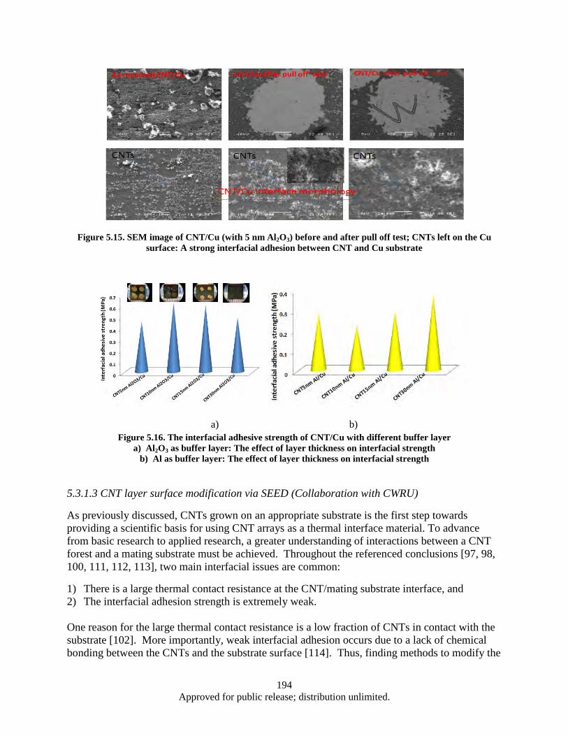
194 Approved for public release; distribution unlimited.
Figure 5.15. SEM image of CNT/Cu (with 5 nm Al2O3) before and after pull off test; CNTs left on the Cu surface: A strong interfacial adhesion between CNT and Cu substrate
a) b) Figure 5.16. The interfacial adhesive strength of CNT/Cu with different buffer layer
a) Al2O3 as buffer layer: The effect of layer thickness on interfacial strength b) Al as buffer layer: The effect of layer thickness on interfacial strength
5.3.1.3 CNT layer surface modification via SEED (Collaboration with CWRU)
As previously discussed, CNTs grown on an appropriate substrate is the first step towards providing a scientific basis for using CNT arrays as a thermal interface material. To advance from basic research to applied research, a greater understanding of interactions between a CNT forest and a mating substrate must be achieved. Throughout the referenced conclusions [97, 98, 100, 111, 112, 113], two main interfacial issues are common:
1) There is a large thermal contact resistance at the CNT/mating substrate interface, and 2) The interfacial adhesion strength is extremely weak. One reason for the large thermal contact resistance is a low fraction of CNTs in contact with the substrate [102]. More importantly, weak interfacial adhesion occurs due to a lack of chemical bonding between the CNTs and the substrate surface [114]. Thus, finding methods to modify the
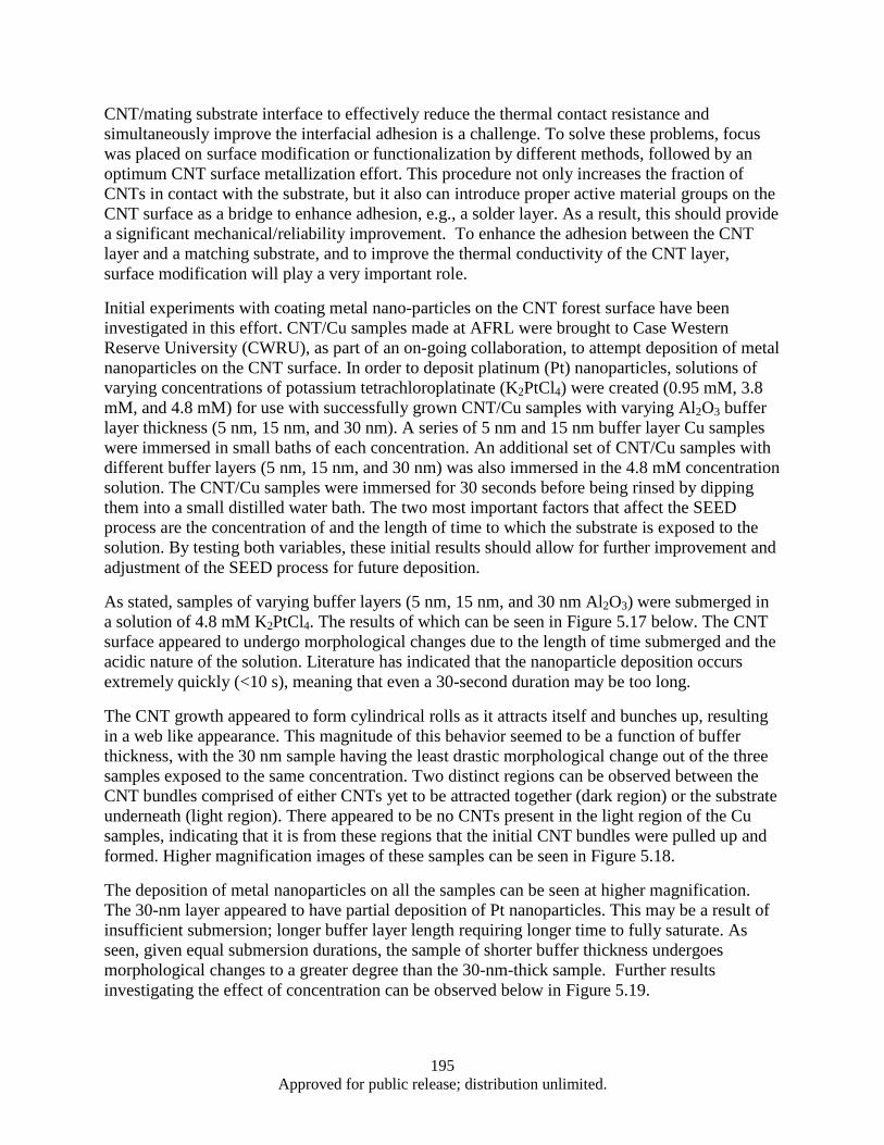
195 Approved for public release; distribution unlimited.
CNT/mating substrate interface to effectively reduce the thermal contact resistance and simultaneously improve the interfacial adhesion is a challenge. To solve these problems, focus was placed on surface modification or functionalization by different methods, followed by an optimum CNT surface metallization effort. This procedure not only increases the fraction of CNTs in contact with the substrate, but it also can introduce proper active material groups on the CNT surface as a bridge to enhance adhesion, e.g., a solder layer. As a result, this should provide a significant mechanical/reliability improvement. To enhance the adhesion between the CNT layer and a matching substrate, and to improve the thermal conductivity of the CNT layer, surface modification will play a very important role.
Initial experiments with coating metal nano-particles on the CNT forest surface have been investigated in this effort. CNT/Cu samples made at AFRL were brought to Case Western Reserve University (CWRU), as part of an on-going collaboration, to attempt deposition of metal nanoparticles on the CNT surface. In order to deposit platinum (Pt) nanoparticles, solutions of varying concentrations of potassium tetrachloroplatinate (K2PtCl4) were created (0.95 mM, 3.8 mM, and 4.8 mM) for use with successfully grown CNT/Cu samples with varying Al2O3 buffer layer thickness (5 nm, 15 nm, and 30 nm). A series of 5 nm and 15 nm buffer layer Cu samples were immersed in small baths of each concentration. An additional set of CNT/Cu samples with different buffer layers (5 nm, 15 nm, and 30 nm) was also immersed in the 4.8 mM concentration solution. The CNT/Cu samples were immersed for 30 seconds before being rinsed by dipping them into a small distilled water bath. The two most important factors that affect the SEED process are the concentration of and the length of time to which the substrate is exposed to the solution. By testing both variables, these initial results should allow for further improvement and adjustment of the SEED process for future deposition.
As stated, samples of varying buffer layers (5 nm, 15 nm, and 30 nm Al2O3) were submerged in a solution of 4.8 mM K2PtCl4. The results of which can be seen in Figure 5.17 below. The CNT surface appeared to undergo morphological changes due to the length of time submerged and the acidic nature of the solution. Literature has indicated that the nanoparticle deposition occurs extremely quickly (<10 s), meaning that even a 30-second duration may be too long.
The CNT growth appeared to form cylindrical rolls as it attracts itself and bunches up, resulting in a web like appearance. This magnitude of this behavior seemed to be a function of buffer thickness, with the 30 nm sample having the least drastic morphological change out of the three samples exposed to the same concentration. Two distinct regions can be observed between the CNT bundles comprised of either CNTs yet to be attracted together (dark region) or the substrate underneath (light region). There appeared to be no CNTs present in the light region of the Cu samples, indicating that it is from these regions that the initial CNT bundles were pulled up and formed. Higher magnification images of these samples can be seen in Figure 5.18.
The deposition of metal nanoparticles on all the samples can be seen at higher magnification. The 30-nm layer appeared to have partial deposition of Pt nanoparticles. This may be a result of insufficient submersion; longer buffer layer length requiring longer time to fully saturate. As seen, given equal submersion durations, the sample of shorter buffer thickness undergoes morphological changes to a greater degree than the 30-nm-thick sample. Further results investigating the effect of concentration can be observed below in Figure 5.19.

196 Approved for public release; distribution unlimited.
If the buffer length is kept constant while the concentration of solutions is varied, we can observe similar effects regarding the morphology of the CNT samples. Figure 5.19 shows a sample that exhibits partial morphological changes that are comparable to the higher concentration solutions. A lower magnification is shown to exhibit the general morphology of the CNT surface. When compared to the other samples at 2000x magnification, it is apparent that the lower concentration was also not as effective at depositing Pt nanoparticles onto the surface, as none can be observed.
Upon placing the samples in the K2PtCl4solution, it was noticed that the CNTs did not uniformly immerse. Sometimes a bubble would appear to become trapped on the CNT surface, due to micro-fluidic properties. This event caused a slight inconsistency regarding the time submerged, as attempts to dislodge the bubble could prolong the submersion time up to 1 minute. Although samples were all submerged for a controlled time of 30sec, the increased time (up to 90 seconds including bubble dislodge time) provided an additional direct comparison between samples of 15 nm buffer length submerged in the same concentration (4.8mM) solution with only time differing between them. The results can be seen in Figure 5.20.
The morphological changes observed in the samples above with first seen in the sample that was submerged the shortest amount of time, i.e., the initial separation of CNT growth. This provides insight as to the mechanism by which the morphological changes observed earlier occur and the effect of time and concentration. EDX analysis was utilized to verify the presence of platinum nanoparticles as well as characterize some of the differing regions seen in the SEM images. The first of which was the verification of platinum nanoparticles, shown in Figure 5.21, which was done by locating and analyzing isolated nanoparticles. By analyzing the isolated nanoparticle region in comparison to the dark region around it, we can identify the nanoparticle and determine that it is indeed Pt. The analysis of the various morphological regions observed can be seen below in Figure 5.22.
Figure 5.22 shows the EDX analysis of the same SEM image from Figure 5.18A showing that the dark regions do not indicate any presence of Pt. This would suggest that during deposition the metal nanoparticles are attracted to the CNTs and become bundled together as the CNTs undergo morphological changes, leaving regions where the CNTs were previously unaffected by the Pt nanoparticles.
Figure 5.17. SEM images of CNTs of different aluminum thickness post-SEED: (a) 5 nm (b) 15 nm (c) 30 nm Al2O3
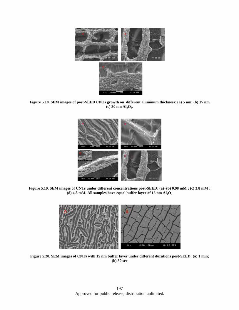
197 Approved for public release; distribution unlimited.
Figure 5.18. SEM images of post-SEED CNTs growth on different aluminum thickness: (a) 5 nm; (b) 15 nm (c) 30 nm Al2O3.
Figure 5.19. SEM images of CNTs under different concentrations post-SEED: (a)+(b) 0.98 mM ; (c) 3.8 mM ; (d) 4.8 mM. All samples have equal buffer layer of 15 nm Al2O3
Figure 5.20. SEM images of CNTs with 15 nm buffer layer under different durations post-SEED: (a) 1 min; (b) 30 sec
C
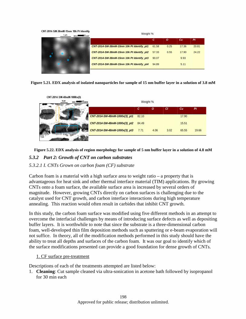
198 Approved for public release; distribution unlimited.
Figure 5.21. EDX analysis of isolated nanoparticles for sample of 15 nm buffer layer in a solution of 3.8 mM
Figure 5.22. EDX analysis of region morphology for sample of 5 nm buffer layer in a solution of 4.8 mM
5.3.2 Part 2: Growth of CNT on carbon substrates 5.3.2.1 I. CNTs Grown on carbon foam (CF) substrate Carbon foam is a material with a high surface area to weight ratio – a property that is advantageous for heat sink and other thermal interface material (TIM) applications. By growing CNTs onto a foam surface, the available surface area is increased by several orders of magnitude. However, growing CNTs directly on carbon surfaces is challenging due to the catalyst used for CNT growth, and carbon interface interactions during high temperature annealing. This reaction would often result in carbides that inhibit CNT growth.
In this study, the carbon foam surface was modified using five different methods in an attempt to overcome the interfacial challenges by means of introducing surface defects as well as depositing buffer layers. It is worthwhile to note that since the substrate is a three-dimensional carbon foam, well-developed thin film deposition methods such as sputtering or e-beam evaporation will not suffice. In theory, all of the modification methods performed in this study should have the ability to treat all depths and surfaces of the carbon foam. It was our goal to identify which of the surface modifications presented can provide a good foundation for dense growth of CNTs.
1. CF surface pre-treatment
Descriptions of each of the treatments attempted are listed below: 1. Cleaning: Cut sample cleaned via ultra-sonication in acetone bath followed by isopropanol
for 30 min each
Weight %
C O Cu Pt
CNT-2014-SM-38mM-15nm 10k Pt Identify_pt1 61.58 0.25 17.36 20.81
CNT-2014-SM-38mM-15nm 10k Pt Identify_pt2 57.33 0.55 17.90 24.22
CNT-2014-SM-38mM-15nm 10k Pt Identify_pt3 90.07 9.93
CNT-2014-SM-38mM-15nm 10k Pt Identify_pt4 94.89 5.11
Weight %
C O Cl Cu Pt
CNT-2014-SM-48mM-1000x(3)_pt1 82.10 17.90
CNT-2014-SM-48mM-1000x(3)_pt2 84.49 15.51
CNT-2014-SM-48mM-1000x(3)_pt3 7.71 4.06 3.02 65.55 19.66
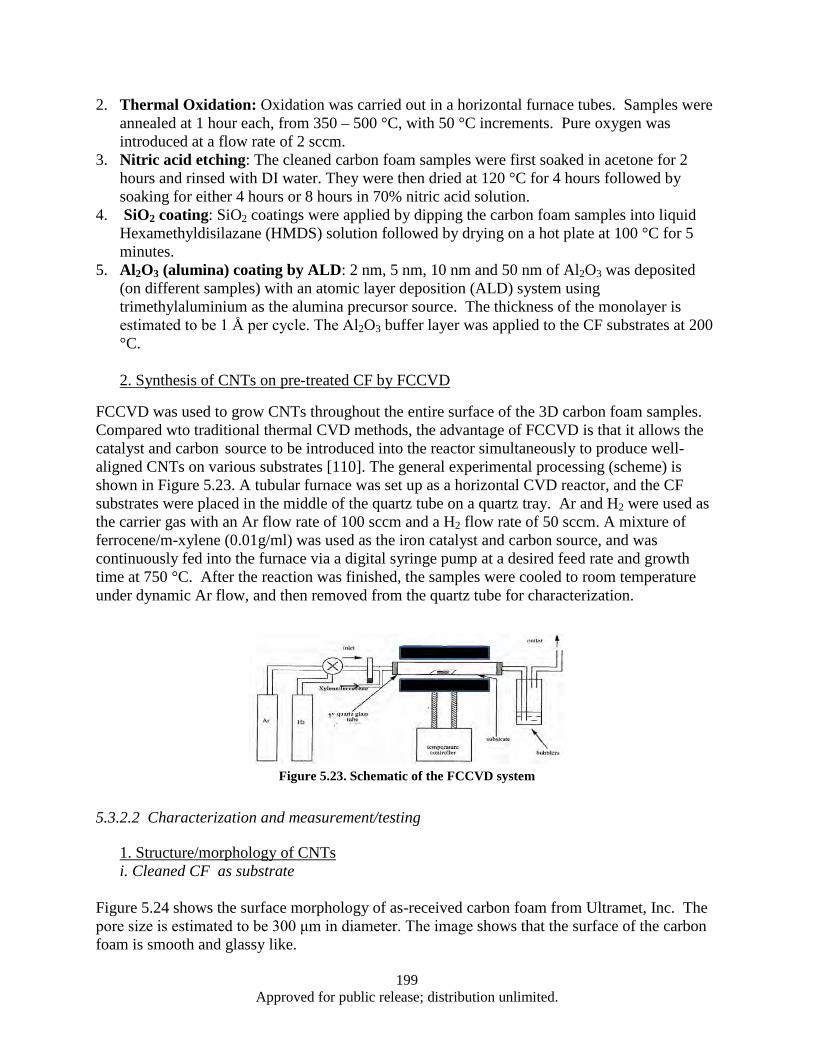
199 Approved for public release; distribution unlimited.
2. Thermal Oxidation: Oxidation was carried out in a horizontal furnace tubes. Samples were annealed at 1 hour each, from 350 – 500 °C, with 50 °C increments. Pure oxygen was introduced at a flow rate of 2 sccm.
3. Nitric acid etching: The cleaned carbon foam samples were first soaked in acetone for 2 hours and rinsed with DI water. They were then dried at 120 °C for 4 hours followed by soaking for either 4 hours or 8 hours in 70% nitric acid solution.
4. SiO2 coating: SiO2 coatings were applied by dipping the carbon foam samples into liquid Hexamethyldisilazane (HMDS) solution followed by drying on a hot plate at 100 °C for 5 minutes.
5. Al2O3 (alumina) coating by ALD: 2 nm, 5 nm, 10 nm and 50 nm of Al2O3 was deposited (on different samples) with an atomic layer deposition (ALD) system using trimethylaluminium as the alumina precursor source. The thickness of the monolayer is estimated to be 1 Å per cycle. The Al2O3 buffer layer was applied to the CF substrates at 200 °C. 2. Synthesis of CNTs on pre-treated CF by FCCVD
FCCVD was used to grow CNTs throughout the entire surface of the 3D carbon foam samples. Compared wto traditional thermal CVD methods, the advantage of FCCVD is that it allows the catalyst and carbon source to be introduced into the reactor simultaneously to produce well-aligned CNTs on various substrates [110]. The general experimental processing (scheme) is shown in Figure 5.23. A tubular furnace was set up as a horizontal CVD reactor, and the CF substrates were placed in the middle of the quartz tube on a quartz tray. Ar and H2 were used as the carrier gas with an Ar flow rate of 100 sccm and a H2 flow rate of 50 sccm. A mixture of ferrocene/m-xylene (0.01g/ml) was used as the iron catalyst and carbon source, and was continuously fed into the furnace via a digital syringe pump at a desired feed rate and growth time at 750 °C. After the reaction was finished, the samples were cooled to room temperature under dynamic Ar flow, and then removed from the quartz tube for characterization.
Figure 5.23. Schematic of the FCCVD system
5.3.2.2 Characterization and measurement/testing
1. Structure/morphology of CNTs i. Cleaned CF as substrate
Figure 5.24 shows the surface morphology of as-received carbon foam from Ultramet, Inc. The pore size is estimated to be 300 μm in diameter. The image shows that the surface of the carbon foam is smooth and glassy like.
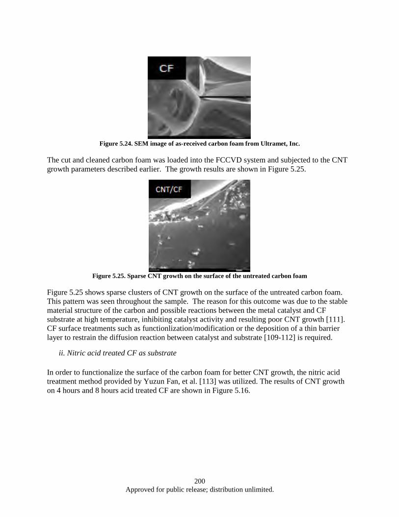
200 Approved for public release; distribution unlimited.
Figure 5.24. SEM image of as-received carbon foam from Ultramet, Inc.
The cut and cleaned carbon foam was loaded into the FCCVD system and subjected to the CNT growth parameters described earlier. The growth results are shown in Figure 5.25.
Figure 5.25. Sparse CNT growth on the surface of the untreated carbon foam
Figure 5.25 shows sparse clusters of CNT growth on the surface of the untreated carbon foam. This pattern was seen throughout the sample. The reason for this outcome was due to the stable material structure of the carbon and possible reactions between the metal catalyst and CF substrate at high temperature, inhibiting catalyst activity and resulting poor CNT growth [111]. CF surface treatments such as functionlization/modification or the deposition of a thin barrier layer to restrain the diffusion reaction between catalyst and substrate [109-112] is required.
ii. Nitric acid treated CF as substrate
In order to functionalize the surface of the carbon foam for better CNT growth, the nitric acid treatment method provided by Yuzun Fan, et al. [113] was utilized. The results of CNT growth on 4 hours and 8 hours acid treated CF are shown in Figure 5.16.
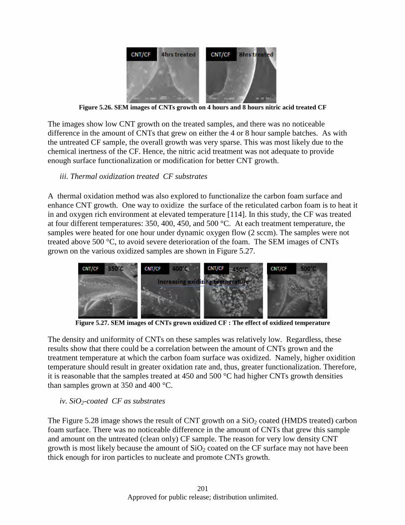
201 Approved for public release; distribution unlimited.
Figure 5.26. SEM images of CNTs growth on 4 hours and 8 hours nitric acid treated CF
The images show low CNT growth on the treated samples, and there was no noticeable difference in the amount of CNTs that grew on either the 4 or 8 hour sample batches. As with the untreated CF sample, the overall growth was very sparse. This was most likely due to the chemical inertness of the CF. Hence, the nitric acid treatment was not adequate to provide enough surface functionalization or modification for better CNT growth.
iii. Thermal oxidization treated CF substrates
A thermal oxidation method was also explored to functionalize the carbon foam surface and enhance CNT growth. One way to oxidize the surface of the reticulated carbon foam is to heat it in and oxygen rich environment at elevated temperature [114]. In this study, the CF was treated at four different temperatures: 350, 400, 450, and 500 °C. At each treatment temperature, the samples were heated for one hour under dynamic oxygen flow (2 sccm). The samples were not treated above 500 °C, to avoid severe deterioration of the foam. The SEM images of CNTs grown on the various oxidized samples are shown in Figure 5.27.
Figure 5.27. SEM images of CNTs grown oxidized CF : The effect of oxidized temperature
The density and uniformity of CNTs on these samples was relatively low. Regardless, these results show that there could be a correlation between the amount of CNTs grown and the treatment temperature at which the carbon foam surface was oxidized. Namely, higher oxidition temperature should result in greater oxidation rate and, thus, greater functionalization. Therefore, it is reasonable that the samples treated at 450 and 500 °C had higher CNTs growth densities than samples grown at 350 and 400 °C.
iv. SiO2-coated CF as substrates
The Figure 5.28 image shows the result of CNT growth on a SiO2 coated (HMDS treated) carbon foam surface. There was no noticeable difference in the amount of CNTs that grew this sample and amount on the untreated (clean only) CF sample. The reason for very low density CNT growth is most likely because the amount of SiO2 coated on the CF surface may not have been thick enough for iron particles to nucleate and promote CNTs growth.
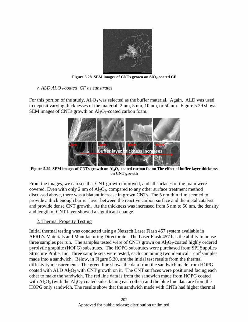
202 Approved for public release; distribution unlimited.
Figure 5.28. SEM images of CNTs grown on SiO2-coated CF
v. ALD Al2O3-coated CF as substrates
For this portion of the study, Al2O3 was selected as the buffer material. Again, ALD was used to deposit varying thicknesses of the material: 2 nm, 5 nm, 10 nm, or 50 nm. Figure 5.29 shows SEM images of CNTs growth on Al2O3-coated carbon foam.
Figure 5.29. SEM images of CNTs growth on Al2O3-coated carbon foam: The effect of buffer layer thickness
on CNT growth From the images, we can see that CNT growth improved, and all surfaces of the foam were covered. Even with only 2 nm of Al2O3, compared to any other surface treatment method discussed above, there was a blatant increase in grown CNTs. The 5 nm thin film seemed to provide a thick enough barrier layer between the reactive carbon surface and the metal catalyst and provide dense CNT growth. As the thickness was increased from 5 nm to 50 nm, the density and length of CNT layer showed a significant change.
2. Thermal Property Testing
Initial thermal testing was conducted using a Netzsch Laser Flash 457 system available in AFRL’s Materials and Manufacturing Directorate. The Laser Flash 457 has the ability to house three samples per run. The samples tested were of CNTs grown on Al2O3-coated highly ordered pyrolytic graphite (HOPG) substrates. The HOPG substrates were purchased from SPI Supplies Structure Probe, Inc. Three sample sets were tested, each containing two identical 1 cm2 samples made into a sandwich. Below, in Figure 5.30, are the initial test results from the thermal diffusivity measurements. The green line shows the data from the sandwich made from HOPG coated with ALD Al2O3 with CNT growth on it. The CNT surfaces were positioned facing each other to make the sandwich. The red line data is from the sandwich made from HOPG coated with Al2O3 (with the Al2O3-coated sides facing each other) and the blue line data are from the HOPG only sandwich. The results show that the sandwich made with CNTs had higher thermal
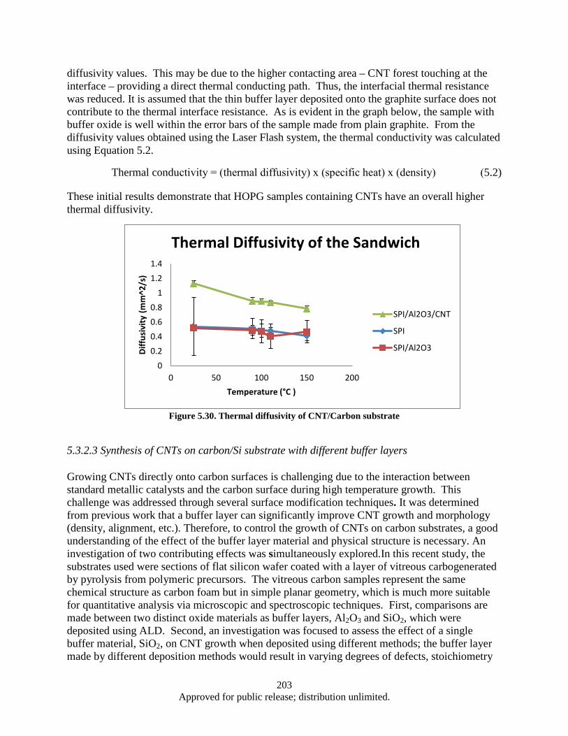
203 Approved for public release; distribution unlimited.
diffusivity values. This may be due to the higher contacting area – CNT forest touching at the interface – providing a direct thermal conducting path. Thus, the interfacial thermal resistance was reduced. It is assumed that the thin buffer layer deposited onto the graphite surface does not contribute to the thermal interface resistance. As is evident in the graph below, the sample with buffer oxide is well within the error bars of the sample made from plain graphite. From the diffusivity values obtained using the Laser Flash system, the thermal conductivity was calculated using Equation 5.2.
Thermal conductivity = (thermal diffusivity) x (specific heat) x (density) (5.2)
These initial results demonstrate that HOPG samples containing CNTs have an overall higher thermal diffusivity.
Figure 5.30. Thermal diffusivity of CNT/Carbon substrate
5.3.2.3 Synthesis of CNTs on carbon/Si substrate with different buffer layers
Growing CNTs directly onto carbon surfaces is challenging due to the interaction between standard metallic catalysts and the carbon surface during high temperature growth. This challenge was addressed through several surface modification techniques. It was determined from previous work that a buffer layer can significantly improve CNT growth and morphology (density, alignment, etc.). Therefore, to control the growth of CNTs on carbon substrates, a good understanding of the effect of the buffer layer material and physical structure is necessary. An investigation of two contributing effects was simultaneously explored.In this recent study, the substrates used were sections of flat silicon wafer coated with a layer of vitreous carbogenerated by pyrolysis from polymeric precursors. The vitreous carbon samples represent the same chemical structure as carbon foam but in simple planar geometry, which is much more suitable for quantitative analysis via microscopic and spectroscopic techniques. First, comparisons are made between two distinct oxide materials as buffer layers, Al2O3 and SiO2, which were deposited using ALD. Second, an investigation was focused to assess the effect of a single buffer material, SiO2, on CNT growth when deposited using different methods; the buffer layer made by different deposition methods would result in varying degrees of defects, stoichiometry
00.20.40.60.8
11.21.4
0 50 100 150 200
Diffu
sivi
ty (m
m^2
/s)
Temperature (°C )
Thermal Diffusivity of the Sandwich
SPI/Al2O3/CNT
SPI
SPI/Al2O3
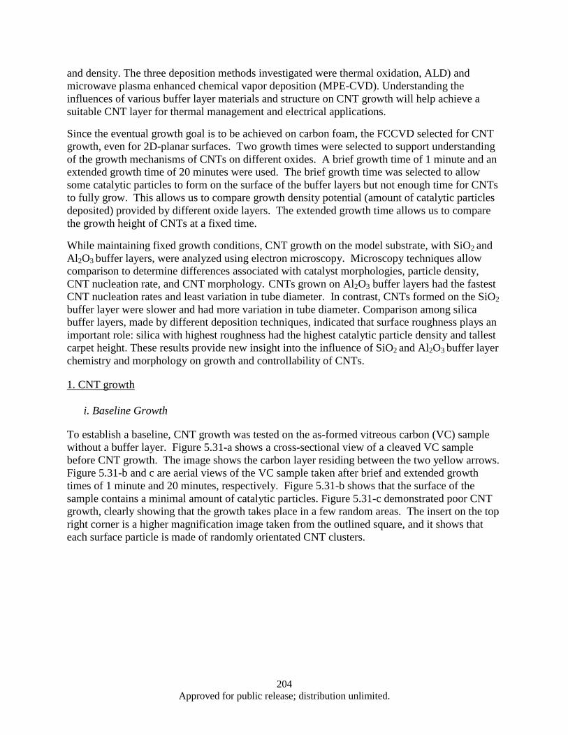
204 Approved for public release; distribution unlimited.
and density. The three deposition methods investigated were thermal oxidation, ALD) and microwave plasma enhanced chemical vapor deposition (MPE-CVD). Understanding the influences of various buffer layer materials and structure on CNT growth will help achieve a suitable CNT layer for thermal management and electrical applications.
Since the eventual growth goal is to be achieved on carbon foam, the FCCVD selected for CNT growth, even for 2D-planar surfaces. Two growth times were selected to support understanding of the growth mechanisms of CNTs on different oxides. A brief growth time of 1 minute and an extended growth time of 20 minutes were used. The brief growth time was selected to allow some catalytic particles to form on the surface of the buffer layers but not enough time for CNTs to fully grow. This allows us to compare growth density potential (amount of catalytic particles deposited) provided by different oxide layers. The extended growth time allows us to compare the growth height of CNTs at a fixed time.
While maintaining fixed growth conditions, CNT growth on the model substrate, with SiO2 and Al2O3 buffer layers, were analyzed using electron microscopy. Microscopy techniques allow comparison to determine differences associated with catalyst morphologies, particle density, CNT nucleation rate, and CNT morphology. CNTs grown on Al2O3 buffer layers had the fastest CNT nucleation rates and least variation in tube diameter. In contrast, CNTs formed on the SiO2 buffer layer were slower and had more variation in tube diameter. Comparison among silica buffer layers, made by different deposition techniques, indicated that surface roughness plays an important role: silica with highest roughness had the highest catalytic particle density and tallest carpet height. These results provide new insight into the influence of SiO2 and Al2O3 buffer layer chemistry and morphology on growth and controllability of CNTs.
1. CNT growth
i. Baseline Growth
To establish a baseline, CNT growth was tested on the as-formed vitreous carbon (VC) sample without a buffer layer. Figure 5.31-a shows a cross-sectional view of a cleaved VC sample before CNT growth. The image shows the carbon layer residing between the two yellow arrows. Figure 5.31-b and c are aerial views of the VC sample taken after brief and extended growth times of 1 minute and 20 minutes, respectively. Figure 5.31-b shows that the surface of the sample contains a minimal amount of catalytic particles. Figure 5.31-c demonstrated poor CNT growth, clearly showing that the growth takes place in a few random areas. The insert on the top right corner is a higher magnification image taken from the outlined square, and it shows that each surface particle is made of randomly orientated CNT clusters.
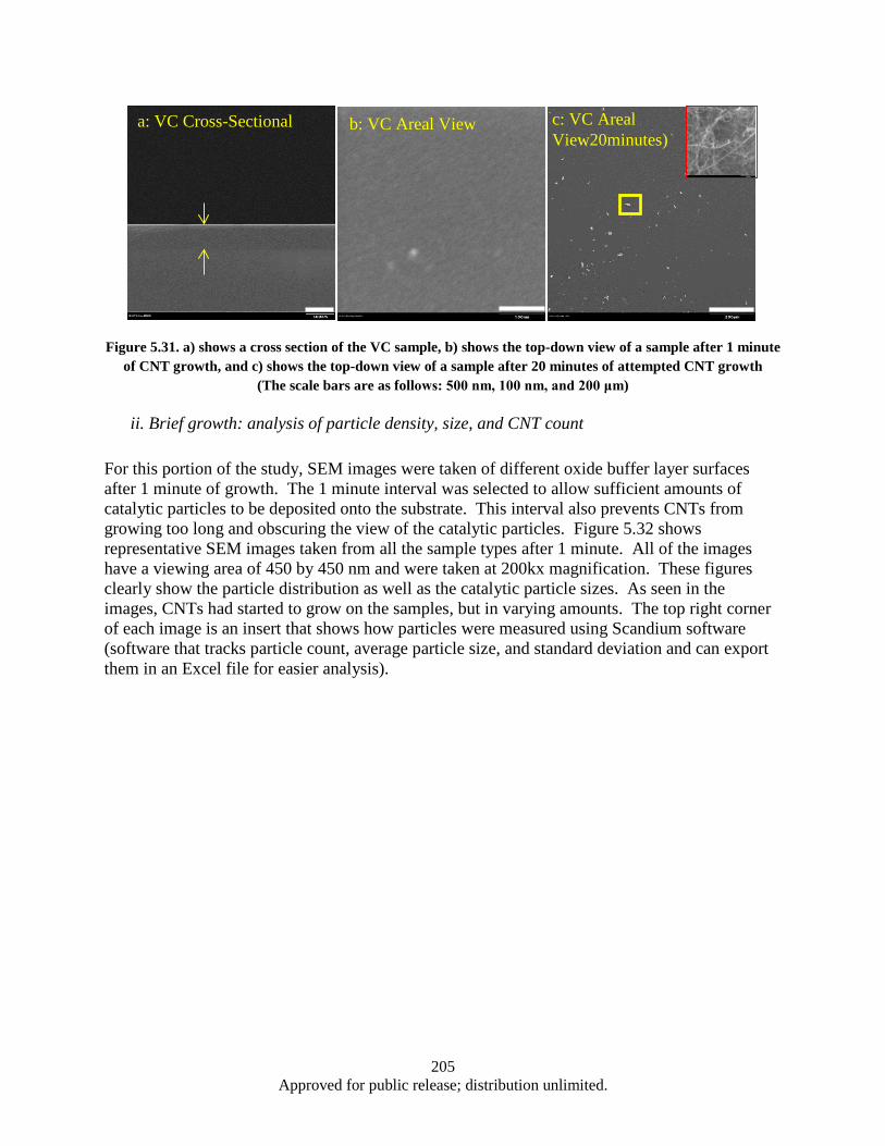
205 Approved for public release; distribution unlimited.
Figure 5.31. a) shows a cross section of the VC sample, b) shows the top-down view of a sample after 1 minute of CNT growth, and c) shows the top-down view of a sample after 20 minutes of attempted CNT growth
(The scale bars are as follows: 500 nm, 100 nm, and 200 μm)
ii. Brief growth: analysis of particle density, size, and CNT count For this portion of the study, SEM images were taken of different oxide buffer layer surfaces after 1 minute of growth. The 1 minute interval was selected to allow sufficient amounts of catalytic particles to be deposited onto the substrate. This interval also prevents CNTs from growing too long and obscuring the view of the catalytic particles. Figure 5.32 shows representative SEM images taken from all the sample types after 1 minute. All of the images have a viewing area of 450 by 450 nm and were taken at 200kx magnification. These figures clearly show the particle distribution as well as the catalytic particle sizes. As seen in the images, CNTs had started to grow on the samples, but in varying amounts. The top right corner of each image is an insert that shows how particles were measured using Scandium software (software that tracks particle count, average particle size, and standard deviation and can export them in an Excel file for easier analysis).
a: VC Cross-Sectional
c: VC Areal View20minutes)
b: VC Areal View
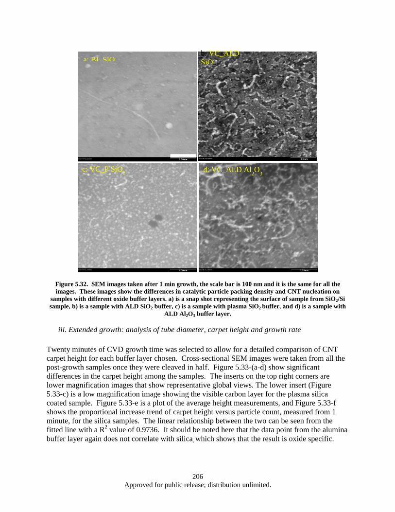
206 Approved for public release; distribution unlimited.
Figure 5.32. SEM images taken after 1 min growth, the scale bar is 100 nm and it is the same for all the images. These images show the differences in catalytic particle packing density and CNT nucleation on
samples with different oxide buffer layers. a) is a snap shot representing the surface of sample from SiO2/Si sample, b) is a sample with ALD SiO2 buffer, c) is a sample with plasma SiO2 buffer, and d) is a sample with
ALD Al2O3 buffer layer.
iii. Extended growth: analysis of tube diameter, carpet height and growth rate Twenty minutes of CVD growth time was selected to allow for a detailed comparison of CNT carpet height for each buffer layer chosen. Cross-sectional SEM images were taken from all the post-growth samples once they were cleaved in half. Figure 5.33-(a-d) show significant differences in the carpet height among the samples. The inserts on the top right corners are lower magnification images that show representative global views. The lower insert (Figure 5.33-c) is a low magnification image showing the visible carbon layer for the plasma silica coated sample. Figure 5.33-e is a plot of the average height measurements, and Figure 5.33-f shows the proportional increase trend of carpet height versus particle count, measured from 1 minute, for the silica samples. The linear relationship between the two can be seen from the fitted line with a R2 value of 0.9736. It should be noted here that the data point from the alumina buffer layer again does not correlate with silica, which shows that the result is oxide specific.
a: BL SiO b: VC_ALD SiO2
d: VC_ALD Al2O3 c: VC_P SiO2
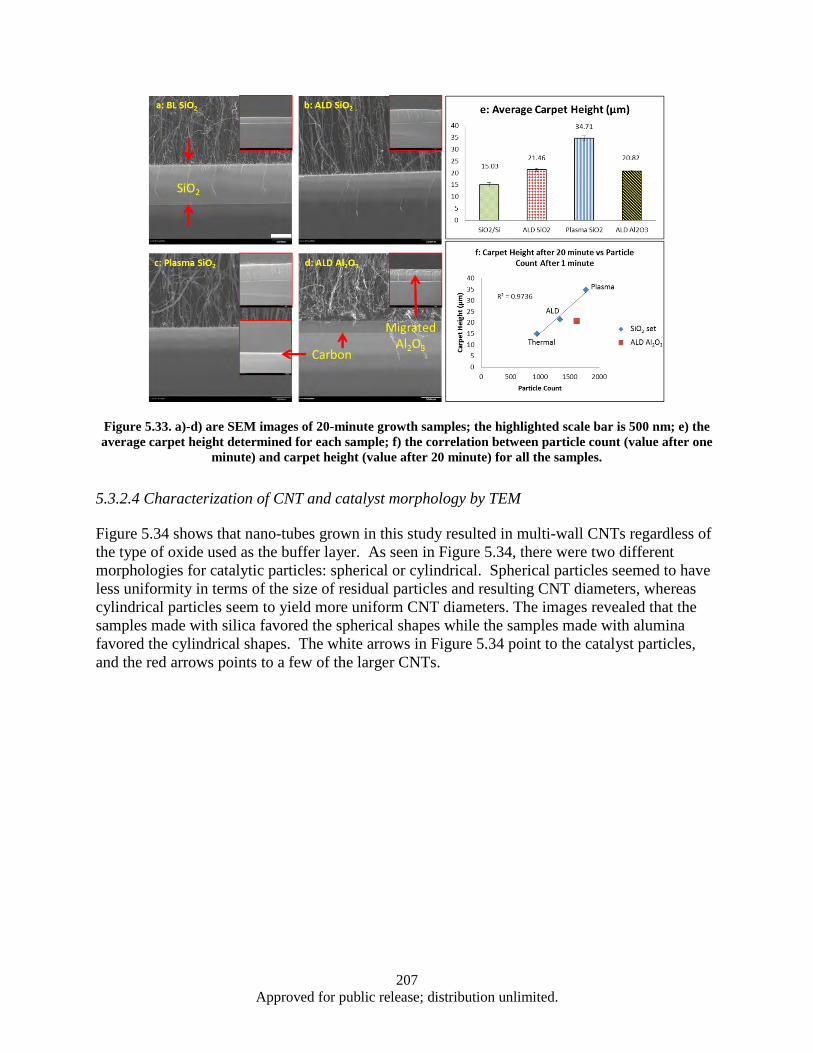
207 Approved for public release; distribution unlimited.
Figure 5.33. a)-d) are SEM images of 20-minute growth samples; the highlighted scale bar is 500 nm; e) the average carpet height determined for each sample; f) the correlation between particle count (value after one
minute) and carpet height (value after 20 minute) for all the samples.
5.3.2.4 Characterization of CNT and catalyst morphology by TEM Figure 5.34 shows that nano-tubes grown in this study resulted in multi-wall CNTs regardless of the type of oxide used as the buffer layer. As seen in Figure 5.34, there were two different morphologies for catalytic particles: spherical or cylindrical. Spherical particles seemed to have less uniformity in terms of the size of residual particles and resulting CNT diameters, whereas cylindrical particles seem to yield more uniform CNT diameters. The images revealed that the samples made with silica favored the spherical shapes while the samples made with alumina favored the cylindrical shapes. The white arrows in Figure 5.34 point to the catalyst particles, and the red arrows points to a few of the larger CNTs.
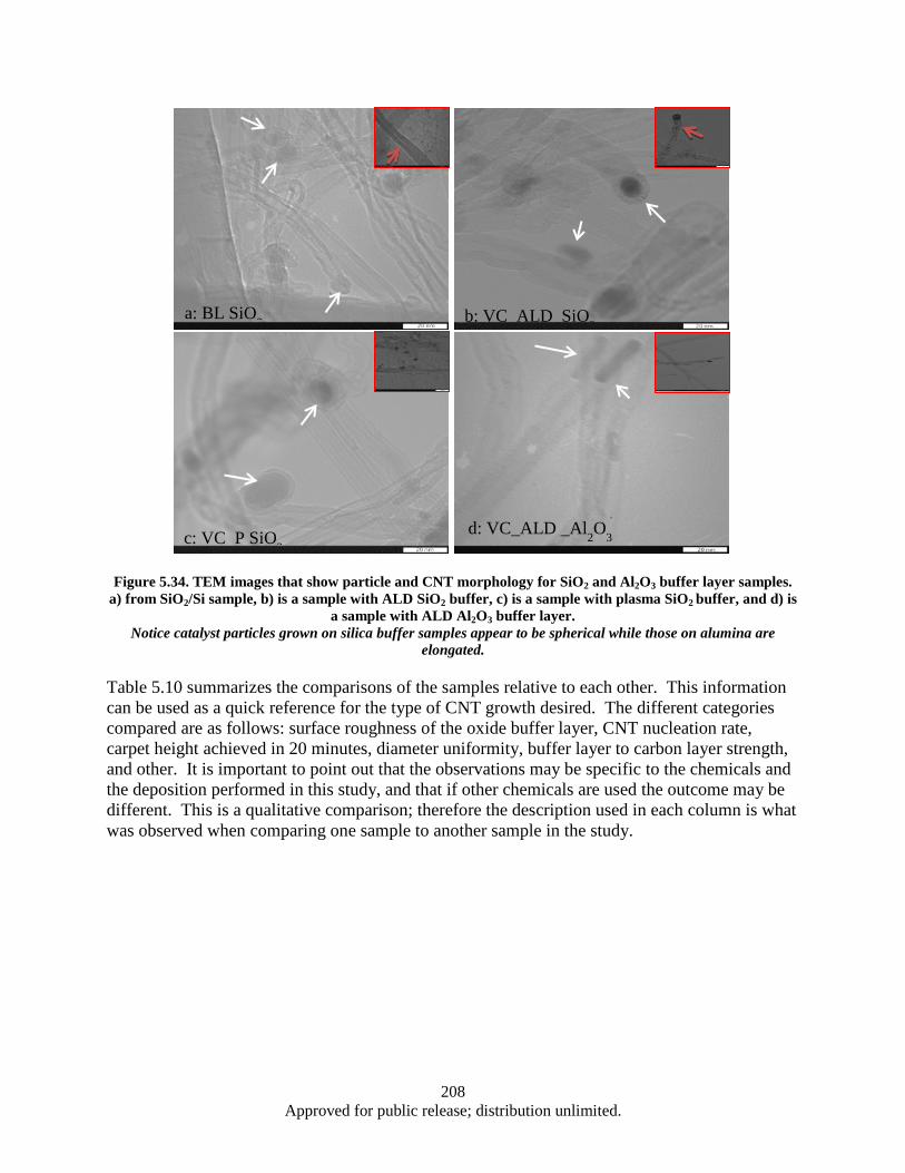
208 Approved for public release; distribution unlimited.
Figure 5.34. TEM images that show particle and CNT morphology for SiO2 and Al2O3 buffer layer samples. a) from SiO2/Si sample, b) is a sample with ALD SiO2 buffer, c) is a sample with plasma SiO2 buffer, and d) is
a sample with ALD Al2O3 buffer layer. Notice catalyst particles grown on silica buffer samples appear to be spherical while those on alumina are
elongated. Table 5.10 summarizes the comparisons of the samples relative to each other. This information can be used as a quick reference for the type of CNT growth desired. The different categories compared are as follows: surface roughness of the oxide buffer layer, CNT nucleation rate, carpet height achieved in 20 minutes, diameter uniformity, buffer layer to carbon layer strength, and other. It is important to point out that the observations may be specific to the chemicals and the deposition performed in this study, and that if other chemicals are used the outcome may be different. This is a qualitative comparison; therefore the description used in each column is what was observed when comparing one sample to another sample in the study.
a: BL SiO2 b: VC ALD SiO2
d: VC_ALD _Al2O3 c: VC P SiO2
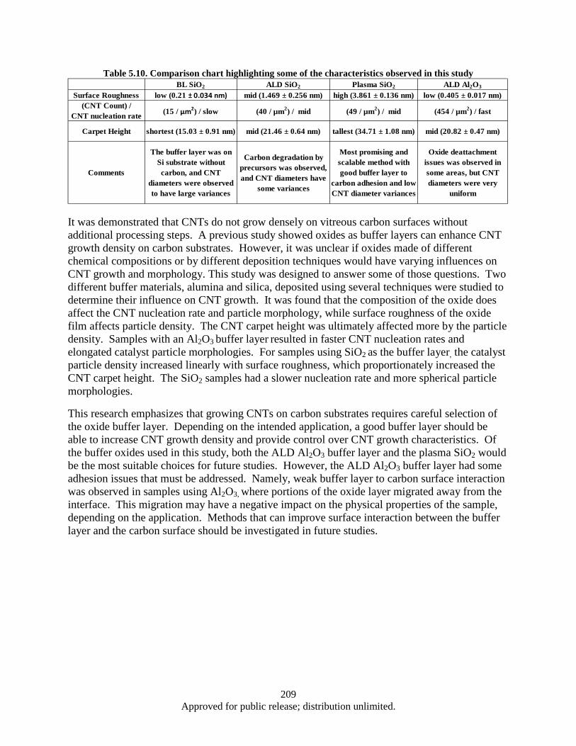
209 Approved for public release; distribution unlimited.
Table 5.10. Comparison chart highlighting some of the characteristics observed in this study
It was demonstrated that CNTs do not grow densely on vitreous carbon surfaces without additional processing steps. A previous study showed oxides as buffer layers can enhance CNT growth density on carbon substrates. However, it was unclear if oxides made of different chemical compositions or by different deposition techniques would have varying influences on CNT growth and morphology. This study was designed to answer some of those questions. Two different buffer materials, alumina and silica, deposited using several techniques were studied to determine their influence on CNT growth. It was found that the composition of the oxide does affect the CNT nucleation rate and particle morphology, while surface roughness of the oxide film affects particle density. The CNT carpet height was ultimately affected more by the particle density. Samples with an Al2O3 buffer layer resulted in faster CNT nucleation rates and elongated catalyst particle morphologies. For samples using SiO2 as the buffer layer, the catalyst particle density increased linearly with surface roughness, which proportionately increased the CNT carpet height. The SiO2 samples had a slower nucleation rate and more spherical particle morphologies.
This research emphasizes that growing CNTs on carbon substrates requires careful selection of the oxide buffer layer. Depending on the intended application, a good buffer layer should be able to increase CNT growth density and provide control over CNT growth characteristics. Of the buffer oxides used in this study, both the ALD Al2O3 buffer layer and the plasma SiO2 would be the most suitable choices for future studies. However, the ALD Al2O3 buffer layer had some adhesion issues that must be addressed. Namely, weak buffer layer to carbon surface interaction was observed in samples using Al2O3, where portions of the oxide layer migrated away from the interface. This migration may have a negative impact on the physical properties of the sample, depending on the application. Methods that can improve surface interaction between the buffer layer and the carbon surface should be investigated in future studies.
BL SiO2 ALD SiO2 Plasma SiO2 ALD Al2O3
Surface Roughness low (0.21 ± 0.034 nm) mid (1.469 ± 0.256 nm) high (3.861 ± 0.136 nm) low (0.405 ± 0.017 nm)(CNT Count) /
CNT nucleation rate (15 / µm2) / slow (40 / µm2) / mid (49 / µm2) / mid (454 / µm2) / fast
Carpet Height shortest (15.03 ± 0.91 nm) mid (21.46 ± 0.64 nm) tallest (34.71 ± 1.08 nm) mid (20.82 ± 0.47 nm)
Comments
The buffer layer was on Si substrate without carbon, and CNT
diameters were observed to have large variances
Carbon degradation by precursors was observed, and CNT diameters have
some variances
Most promising and scalable method with good buffer layer to
carbon adhesion and low CNT diameter variances
Oxide deattachment issues was observed in some areas, but CNT diameters were very
uniform

210 Approved for public release; distribution unlimited.
Energy Analysis of Electromechanical Actuator (EMA) under Simulated Aircraft 6.Primary Flight Control Surface Load
Abstract 6.1
A laboratory apparatus and data acquisition system were constructed for evaluating aircraft flight control actuators under simulated mission profiles. A MTS hydraulic load frame was used to simulate a control surface’s aero load. A NI-based DAQ system was used to record the actuator’s position, load, and temperatures. The motor controller’s DC bus rms voltage, current, and power, and regenerative power were recorded by a Newton’s 4th power analyzer. Key performance characteristics tests such as step response, frequency response, reversal, backlash, and holding with a Danahar EC5 actuator were carried out to verify this laboratory setup.
The step response and reversal test showed that when an EMA reverses direction or suddenly decelerates, a significant spike of regenerative power occurred. This regenerative power could present itself as a thermal challenge to an aircraft flight control EMA system. The frequency response, reversal, backlash, and holding test results can be seen in a thesis done by Street Barnett ‘Laboratory Test Set-up to Evaluate Electromechanical Actuation System for Aircraft Flight Control’[115].
Using the MTS hydraulic load frame to simulate a dynamic aero load of a flight control surface in synchronization with position movement of an actuator proved to be a challenge. A double loop control scheme has been derived which compensates the time delay difference between the load frame and the actuator. It is our hope that this control strategy, once fully implemented, will enable more accurate dynamic load control in simulating an EMA’s mission profile for performance evaluation.
Introduction 6.2
Aircraft Flight control systems have made major advances throughout the years, from wing warping on the Wright’s first glider to modern day fighter jets, whose design is aerodynamically unstable and requires fly-by-wire technology. Modern aircraft employ fly-by-wire and auto stabilization processes executed by an on board flight computer in order to master the principle of flight control [115].
Flight control systems are made up of primary and secondary control surfaces for maneuvering. Primary flight control surfaces are used for pitch, roll, and yaw control. They are comprised of the canard, flaperons (flaps and ailerons), and rudder [116]. Secondary flight surfaces provide increased lift control by increasing wing camber and improving wing aerodynamics. However, increased lift control amplifies drag [117]. Combat aircraft are highly agile, maneuverable during flight, and have high thrust capabilities which can overcome this drag.
Flight control linkage systems connect the pilot with the control surfaces responsible for maneuvering [118]. The linkage evolved from manually operated direct mechanical rods, levers, cables, and pulleys to fully power operated hydraulic control. This, in turn, evolved into ‘Fly-by-wire’, in which direct mechanical linkages between the cockpit controls and the control surfaces were replaced by electrical signaling [119].
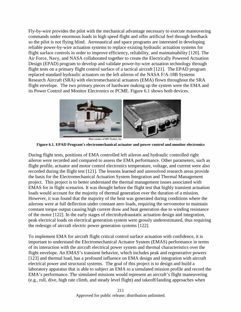
211 Approved for public release; distribution unlimited.
Fly-by-wire provides the pilot with the mechanical advantage necessary to execute maneuvering commands under enormous loads in high speed flight and offer artificial feel through feedback so the pilot is not flying blind. Aeronautical and space programs are interested in developing reliable power-by-wire actuation systems to replace existing hydraulic actuation systems for flight surface controls in order to improve efficiency, reliability, and maintainability [120]. The Air Force, Navy, and NASA collaborated together to create the Electrically Powered Actuation Design (EPAD) program to develop and validate power-by-wire actuation technology through flight tests on a primary flight control surface of a tactical aircraft [121]. The EPAD program replaced standard hydraulic actuators on the left aileron of the NASA F/A-18B Systems Research Aircraft (SRA) with electromechanical actuators (EMA) flown throughout the SRA flight envelope. The two primary pieces of hardware making up the system were the EMA and its Power Control and Monitor Electronics or PCME. Figure 6.1 shows both devices.
Figure 6.1. EPAD Program’s electromechanical actuator and power control and monitor electronics
During flight tests, positions of EMA controlled left aileron and hydraulic controlled right aileron were recorded and compared to assess the EMA performance. Other parameters, such as flight profile, actuator and motor control electronics temperature, voltage, and current were also recorded during the flight test [121]. The lessons learned and unresolved research areas provide the basis for the Electromechanical Actuation System Integration and Thermal Management project. This project is to better understand the thermal management issues associated with EMAS for in flight scenarios. It was thought before the flight test that highly transient actuation loads would account for the majority of thermal generation over the duration of a mission. However, it was found that the majority of the heat was generated during conditions where the ailerons were at full deflection under constant aero loads, requiring the servomotor to maintain constant torque output causing high current draw and heat generation due to winding resistance of the motor [122]. In the early stages of electrohydraustatic actuation design and integration, peak electrical loads on electrical generation system were grossly underestimated, thus requiring the redesign of aircraft electric power generation systems [122]. To implement EMA for aircraft flight critical control surface actuation with confidence, it is important to understand the Electromechanical Actuator System (EMAS) performance in terms of its interaction with the aircraft electrical power system and thermal characteristics over the flight envelope. An EMAS’s transient behavior, which includes peak and regenerative powers [123] and thermal load, has a profound influence on EMA design and integration with aircraft electrical power and structural systems. The goal of this project is to design and build a laboratory apparatus that is able to subject an EMA to a simulated mission profile and record the EMA’s performance. The simulated missions would represent an aircraft’s flight maneuvering (e.g., roll, dive, high rate climb, and steady level flight) and takeoff/landing approaches when
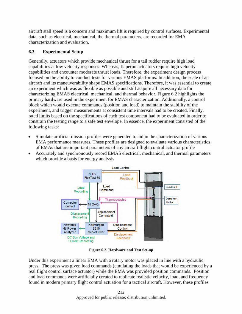
212 Approved for public release; distribution unlimited.
aircraft stall speed is a concern and maximum lift is required by control surfaces. Experimental data, such as electrical, mechanical, the thermal parameters, are recorded for EMA characterization and evaluation.
Experimental Setup 6.3
Generally, actuators which provide mechanical thrust for a tail rudder require high load capabilities at low velocity responses. Whereas, flaperon actuators require high velocity capabilities and encounter moderate thrust loads. Therefore, the experiment design process focused on the ability to conduct tests for various EMAS platforms. In addition, the scale of an aircraft and its maneuverability shape EMAS specifications. Therefore, it was essential to create an experiment which was as flexible as possible and still acquire all necessary data for characterizing EMAS electrical, mechanical, and thermal behavior. Figure 6.2 highlights the primary hardware used in the experiment for EMAS characterization. Additionally, a control block which would execute commands (position and load) to maintain the stability of the experiment, and trigger measurements at consistent time intervals had to be created. Finally, rated limits based on the specifications of each test component had to be evaluated in order to constrain the testing range to a safe test envelope. In essence, the experiment consisted of the following tasks:
• Simulate artificial mission profiles were generated to aid in the characterization of various EMA performance measures. These profiles are designed to evaluate various characteristics of EMAs that are important parameters of any aircraft flight control actuator profile
• Accurately and synchronously record EMAS electrical, mechanical, and thermal parameters which provide a basis for energy analysis
Figure 6.2. Hardware and Test Set-up
Under this experiment a linear EMA with a rotary motor was placed in line with a hydraulic press. The press was given load commands (emulating the loads that would be experienced by a real flight control surface actuator) while the EMA was provided position commands. Position and load commands were artificially created to replicate realistic velocity, load, and frequency found in modern primary flight control actuation for a tactical aircraft. However, these profiles
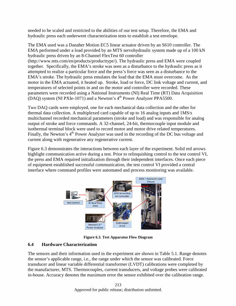
213 Approved for public release; distribution unlimited.
needed to be scaled and restricted to the abilities of our test setup. Therefore, the EMA and hydraulic press each underwent characterization tests to establish a test envelope.
The EMA used was a Danaher Motion EC5 linear actuator driven by an S610 controller. The EMA performed under a load provided by an MTS servohydraulic system made up of a 100 kN hydraulic press driven by an 8-Channel FlexTest 60 controller (http://www.mts.com/en/products/producttype/). The hydraulic press and EMA were coupled together. Specifically, the EMA’s stroke was seen as a disturbance to the hydraulic press as it attempted to realize a particular force and the press’s force was seen as a disturbance to the EMA’s stroke. The hydraulic press emulates the load that the EMA must overcome. As the motor in the EMA actuated, it heated up. Stroke, load or force, DC link voltage and current, and temperatures of selected points in and on the motor and controller were recorded. These parameters were recorded using a National Instruments (NI) Real Time (RT) Data Acquisition (DAQ) system (NI PXIe-1071) and a Newton’s 4th Power Analyzer PPA5500.
Two DAQ cards were employed, one for each mechanical data collection and the other for thermal data collection. A multiplexed card capable of up to 16 analog inputs and 1MS/s multichannel recorded mechanical parameters (stroke and load) and was responsible for analog output of stroke and force commands. A 32-channel, 24-bit, thermocouple input module and isothermal terminal block were used to record motor and motor drive related temperatures. Finally, the Newton’s 4th Power Analyzer was used in the recording of the DC bus voltage and current along with regenerative any regenerative current.
Figure 6.3 demonstrates the interactions between each layer of the experiment. Solid red arrows highlight communication active during a test. Prior to relinquishing control to the test control VI, the press and EMA required initialization through their independent interfaces. Once each piece of equipment established successful communication, the test control VI provided a central interface where command profiles were automated and process monitoring was available.
Figure 6.3. Test Apparatus Flow Diagram Hardware Characterization 6.4
The sensors and their information used in the experiment are shown in Table 5.1. Range denotes the sensor’s applicable range, i.e., the range under which the sensor was calibrated. Force transducer and linear variable differential transformer (LVDT) calibrations were completed by the manufacturer, MTS. Thermocouples, current transducers, and voltage probes were calibrated in-house. Accuracy denotes the maximum error the sensor exhibited over the calibration range.

214 Approved for public release; distribution unlimited.
Resolution is a function of the full scale range of the device and the DAQ card analog-to-digital (A/D) converter resolution. For example, both DAQ cards used in the experiment are 16 bit and support -10 to 10 V analog input signals. Therefore, the smallest voltage resolvable by both cards is 20 / (216) or 0.31 mV. The thermocouple card has 24-bit input channels and therefore can resolve voltage changes of 0.001 mV. An MTS Servohydraulic controller was reconfigured to use a range of ± 20 kN as opposed to ± 100 kN for several reasons. First, reducing the full scale range increased the resolution from 3 N to 0.3 N. Second, the maximum output of the press was effectively scaled from ± 100 kN to ± 20 kN, creating a safer environment for the EMA under test which was limited to 13.35 kN. Lastly, increasing the resolution of the force channel was thought to improve force control with respect to dynamic test profiles made up of higher resolution force data.
Table 6.1. Sensor Inventory and Uncertainty
Test Matrix 6.5
6.5.1 Step Response
The step response test determined the overshoot, settling time, and rising time of the actuator for a given step command input. The overshoot was defined as the difference between the overshoot actuator stroke and the commanded stroke, in percentage of the commanded stroke. The settling time is the time from applied step command to the point where the actuator crosses the user specified percentage error band for the last time. The rising time is defined as the time required for 10% to 90% of the step stroke. Figure 6.4 depicts the definition of those three parameters. The evaluator will flag if the overshoot, settling time, and rising time are greater than user specified values.
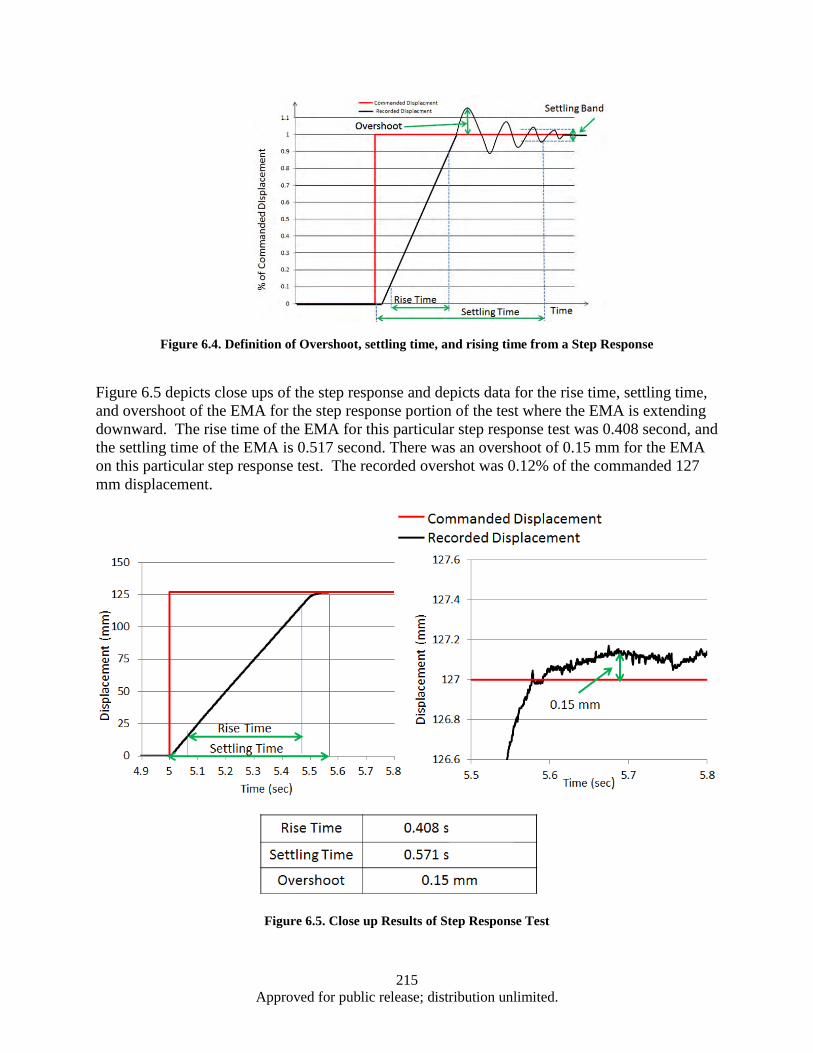
215 Approved for public release; distribution unlimited.
Figure 6.4. Definition of Overshoot, settling time, and rising time from a Step Response
Figure 6.5 depicts close ups of the step response and depicts data for the rise time, settling time, and overshoot of the EMA for the step response portion of the test where the EMA is extending downward. The rise time of the EMA for this particular step response test was 0.408 second, and the settling time of the EMA is 0.517 second. There was an overshoot of 0.15 mm for the EMA on this particular step response test. The recorded overshot was 0.12% of the commanded 127 mm displacement.
Figure 6.5. Close up Results of Step Response Test
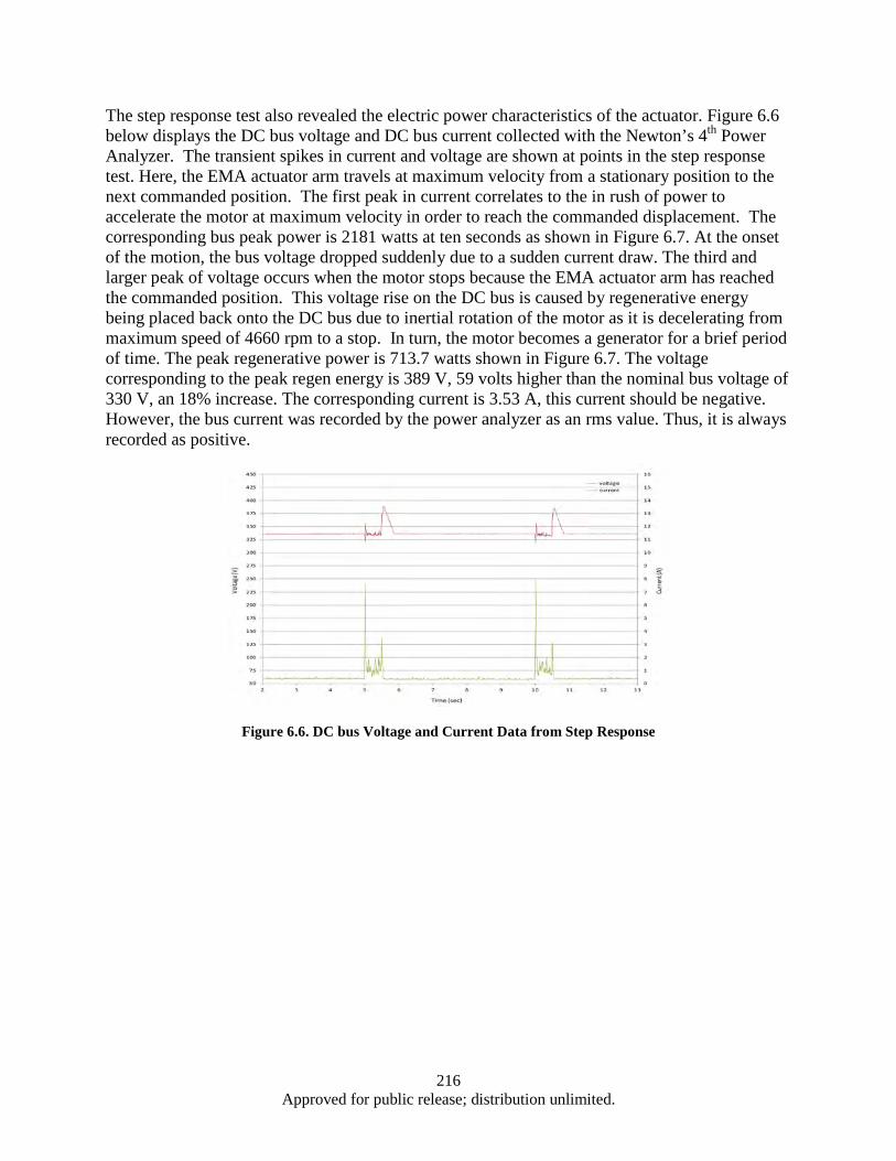
216 Approved for public release; distribution unlimited.
The step response test also revealed the electric power characteristics of the actuator. Figure 6.6 below displays the DC bus voltage and DC bus current collected with the Newton’s 4th Power Analyzer. The transient spikes in current and voltage are shown at points in the step response test. Here, the EMA actuator arm travels at maximum velocity from a stationary position to the next commanded position. The first peak in current correlates to the in rush of power to accelerate the motor at maximum velocity in order to reach the commanded displacement. The corresponding bus peak power is 2181 watts at ten seconds as shown in Figure 6.7. At the onset of the motion, the bus voltage dropped suddenly due to a sudden current draw. The third and larger peak of voltage occurs when the motor stops because the EMA actuator arm has reached the commanded position. This voltage rise on the DC bus is caused by regenerative energy being placed back onto the DC bus due to inertial rotation of the motor as it is decelerating from maximum speed of 4660 rpm to a stop. In turn, the motor becomes a generator for a brief period of time. The peak regenerative power is 713.7 watts shown in Figure 6.7. The voltage corresponding to the peak regen energy is 389 V, 59 volts higher than the nominal bus voltage of 330 V, an 18% increase. The corresponding current is 3.53 A, this current should be negative. However, the bus current was recorded by the power analyzer as an rms value. Thus, it is always recorded as positive.
Figure 6.6. DC bus Voltage and Current Data from Step Response
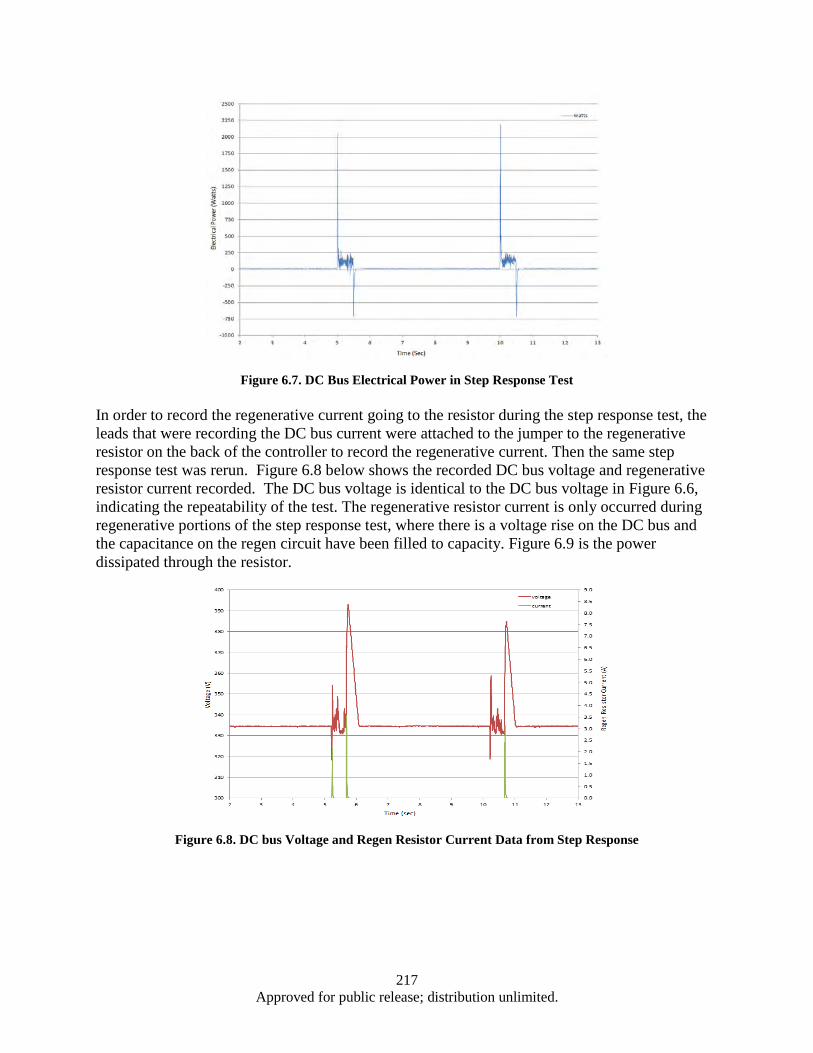
217 Approved for public release; distribution unlimited.
Figure 6.7. DC Bus Electrical Power in Step Response Test
In order to record the regenerative current going to the resistor during the step response test, the leads that were recording the DC bus current were attached to the jumper to the regenerative resistor on the back of the controller to record the regenerative current. Then the same step response test was rerun. Figure 6.8 below shows the recorded DC bus voltage and regenerative resistor current recorded. The DC bus voltage is identical to the DC bus voltage in Figure 6.6, indicating the repeatability of the test. The regenerative resistor current is only occurred during regenerative portions of the step response test, where there is a voltage rise on the DC bus and the capacitance on the regen circuit have been filled to capacity. Figure 6.9 is the power dissipated through the resistor.
Figure 6.8. DC bus Voltage and Regen Resistor Current Data from Step Response
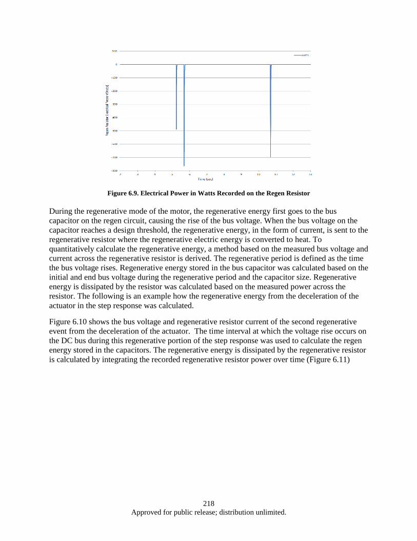
218 Approved for public release; distribution unlimited.
Figure 6.9. Electrical Power in Watts Recorded on the Regen Resistor
During the regenerative mode of the motor, the regenerative energy first goes to the bus capacitor on the regen circuit, causing the rise of the bus voltage. When the bus voltage on the capacitor reaches a design threshold, the regenerative energy, in the form of current, is sent to the regenerative resistor where the regenerative electric energy is converted to heat. To quantitatively calculate the regenerative energy, a method based on the measured bus voltage and current across the regenerative resistor is derived. The regenerative period is defined as the time the bus voltage rises. Regenerative energy stored in the bus capacitor was calculated based on the initial and end bus voltage during the regenerative period and the capacitor size. Regenerative energy is dissipated by the resistor was calculated based on the measured power across the resistor. The following is an example how the regenerative energy from the deceleration of the actuator in the step response was calculated.
Figure 6.10 shows the bus voltage and regenerative resistor current of the second regenerative event from the deceleration of the actuator. The time interval at which the voltage rise occurs on the DC bus during this regenerative portion of the step response was used to calculate the regen energy stored in the capacitors. The regenerative energy is dissipated by the regenerative resistor is calculated by integrating the recorded regenerative resistor power over time (Figure 6.11)
219 Approved for public release; distribution unlimited.
.
Figure 6.10. DC bus Voltage, Regen Resistor Current and DC bus Power Data from Step Response
Figure 6.11. Close up of DC bus Voltage, Regen Resistor Current and DC bus Power Data from Step Response
Calculating the electrical energy stored in the capacitors and the energy dissipated from the regenerative resistor during the voltage rise and comparing it to the calculated mechanical energy of the EMA actuator, the EMA’s electric and mechanical power characteristics were quantified.
First, the energy stored in a capacitor can be estimated:
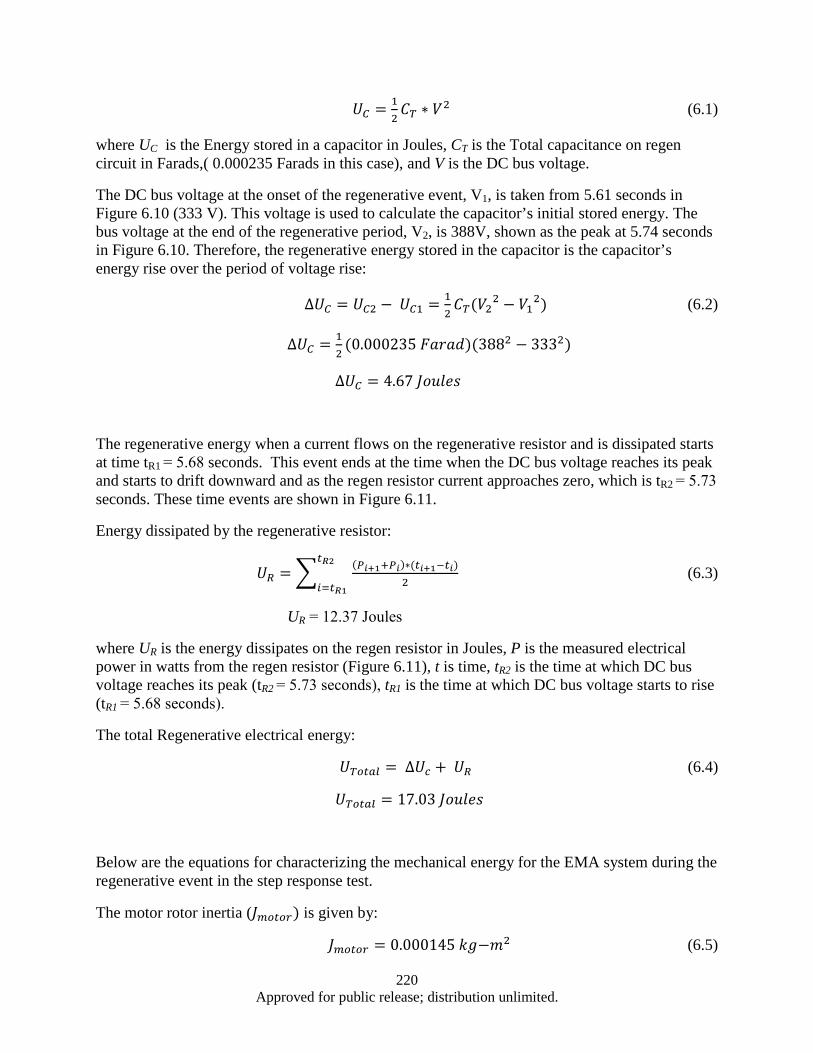
220 Approved for public release; distribution unlimited.
𝑈𝑈𝐶𝐶 = 12𝑁𝑁𝑇𝑇 ∗ 𝑉𝑉2 (6.1)
where UC is the Energy stored in a capacitor in Joules, CT is the Total capacitance on regen circuit in Farads,( 0.000235 Farads in this case), and V is the DC bus voltage.
The DC bus voltage at the onset of the regenerative event, V1, is taken from 5.61 seconds in Figure 6.10 (333 V). This voltage is used to calculate the capacitor’s initial stored energy. The bus voltage at the end of the regenerative period, V2, is 388V, shown as the peak at 5.74 seconds in Figure 6.10. Therefore, the regenerative energy stored in the capacitor is the capacitor’s energy rise over the period of voltage rise:
∆𝑈𝑈𝐶𝐶 = 𝑈𝑈𝐶𝐶2 − 𝑈𝑈𝐶𝐶1 = 12𝑁𝑁𝑇𝑇(𝑉𝑉22 − 𝑉𝑉12) (6.2)
∆𝑈𝑈𝐶𝐶 = 12
(0.000235 𝐶𝐶𝑖𝑖𝑟𝑟𝑖𝑖𝐹𝐹)(3882 − 3332)
∆𝑈𝑈𝐶𝐶 = 4.67 𝐽𝐽𝑠𝑠𝑠𝑠𝐽𝐽𝑖𝑖𝑠𝑠
The regenerative energy when a current flows on the regenerative resistor and is dissipated starts at time tR1 = 5.68 seconds. This event ends at the time when the DC bus voltage reaches its peak and starts to drift downward and as the regen resistor current approaches zero, which is tR2 = 5.73 seconds. These time events are shown in Figure 6.11.
Energy dissipated by the regenerative resistor:
𝑈𝑈𝑅𝑅 = (𝑃𝑃𝑖𝑖+1+𝑃𝑃𝑖𝑖)∗(𝑤𝑤𝑖𝑖+1−𝑤𝑤𝑖𝑖)2
𝑤𝑤𝑅𝑅2
𝑏𝑏=𝑤𝑤𝑅𝑅1
(6.3)
UR = 12.37 Joules
where UR is the energy dissipates on the regen resistor in Joules, P is the measured electrical power in watts from the regen resistor (Figure 6.11), t is time, tR2 is the time at which DC bus voltage reaches its peak (tR2 = 5.73 seconds), tR1 is the time at which DC bus voltage starts to rise (tR1 = 5.68 seconds).
The total Regenerative electrical energy:
𝑈𝑈𝑇𝑇𝑑𝑑𝑤𝑤𝑤𝑤𝑏𝑏 = ∆𝑈𝑈𝑑𝑑 + 𝑈𝑈𝑅𝑅 (6.4)
𝑈𝑈𝑇𝑇𝑑𝑑𝑤𝑤𝑤𝑤𝑏𝑏 = 17.03 𝐽𝐽𝑠𝑠𝑠𝑠𝐽𝐽𝑖𝑖𝑠𝑠
Below are the equations for characterizing the mechanical energy for the EMA system during the regenerative event in the step response test.
The motor rotor inertia (𝐽𝐽𝑑𝑑𝑑𝑑𝑤𝑤𝑑𝑑𝑤𝑤) is given by:
𝐽𝐽𝑑𝑑𝑑𝑑𝑤𝑤𝑑𝑑𝑤𝑤 = 0.000145 𝑠𝑠𝑖𝑖−𝑚𝑚2 (6.5)
221 Approved for public release; distribution unlimited.
The rotation of the motor (𝜔𝜔):
𝜔𝜔 = Max velocity = 485.9 radians/second (6.6)
The energy represented as the motor rotor inertia (𝐸𝐸𝑑𝑑𝑑𝑑𝑤𝑤𝑑𝑑𝑤𝑤) term:
𝐸𝐸𝑑𝑑𝑑𝑑𝑤𝑤𝑑𝑑𝑤𝑤 = 12𝐽𝐽𝑑𝑑𝑑𝑑𝑤𝑤𝑑𝑑𝑤𝑤 ∗ 𝜔𝜔2 (6.7)
𝐸𝐸𝑑𝑑𝑑𝑑𝑤𝑤𝑑𝑑𝑤𝑤 = 17.12 𝐽𝐽𝑠𝑠𝑠𝑠𝐽𝐽𝑖𝑖𝑠𝑠
The calculated mechanical energy is only 0.09 Joules more than the regenerative electrical energy which is plausible because of the mechanical and electrical efficiency losses in the geartrain, motor, and controller.
Dynamic Load Control 6.6
In order to test real time dynamic flight loads an actuator would encounter while in flight and how the actuator being tested can handle such loads, a mission test was run. The stroke and force profile of the mission test was generated using information based the NASA Dryden flight study [121]. The profile was scaled to fit the capabilities of the current industrial EMA on hand that will be used in the test set-up. Where the commanded for to the EMA was 7% of the force from the recorded mission profile and the maximum displacement rate for the EMA was reduced to 57% from the recorded mission profile velocity. For future testing the combat mission profile will not be scaled down because the purpose of the testing is to make sure the EMA can handle similar inflight dynamic loads and displacements. Figure 6.12 below displays the results of a dynamic segment of the mission test run. It can be seen that improvement needs to be done on control of the hydraulic load fixture when running a dynamic stroke and load profile while coupled to the EMA. The hydraulic load fixture control when coupled with the EMA is less than desirable when running a mission test with 50% overshoots of commanded loads when the frequency of the commanded load is higher.
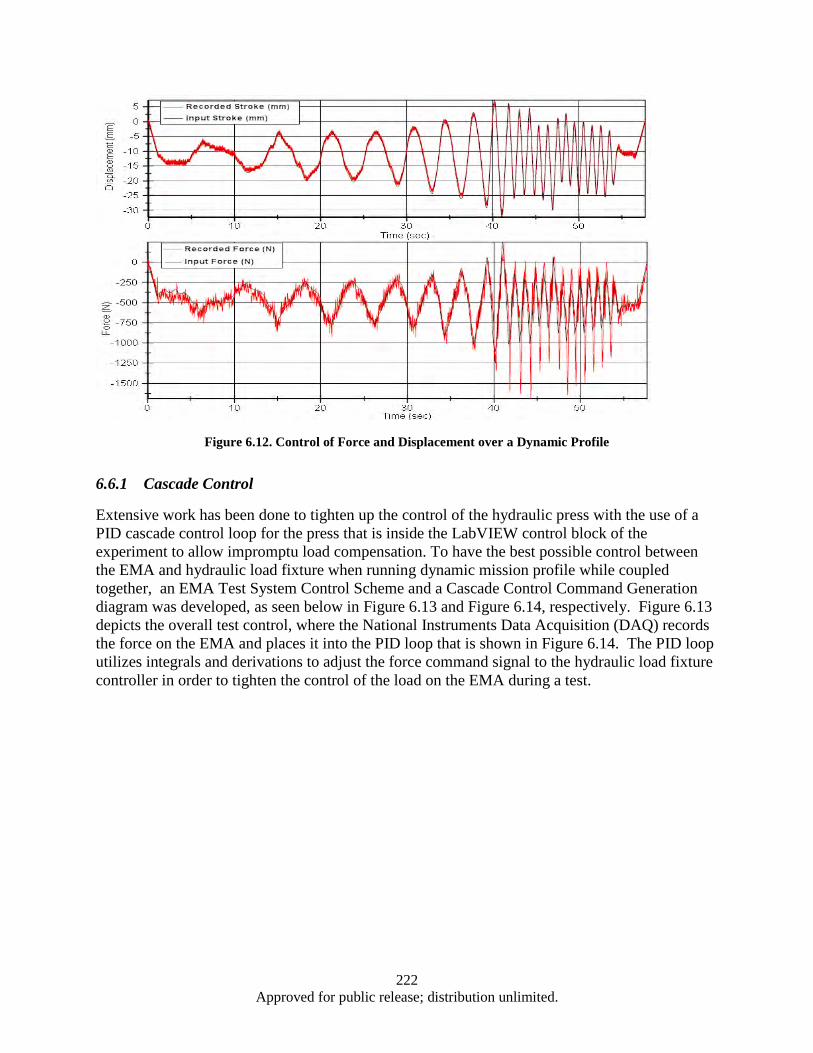
222 Approved for public release; distribution unlimited.
Figure 6.12. Control of Force and Displacement over a Dynamic Profile
6.6.1 Cascade Control
Extensive work has been done to tighten up the control of the hydraulic press with the use of a PID cascade control loop for the press that is inside the LabVIEW control block of the experiment to allow impromptu load compensation. To have the best possible control between the EMA and hydraulic load fixture when running dynamic mission profile while coupled together, an EMA Test System Control Scheme and a Cascade Control Command Generation diagram was developed, as seen below in Figure 6.13 and Figure 6.14, respectively. Figure 6.13 depicts the overall test control, where the National Instruments Data Acquisition (DAQ) records the force on the EMA and places it into the PID loop that is shown in Figure 6.14. The PID loop utilizes integrals and derivations to adjust the force command signal to the hydraulic load fixture controller in order to tighten the control of the load on the EMA during a test.
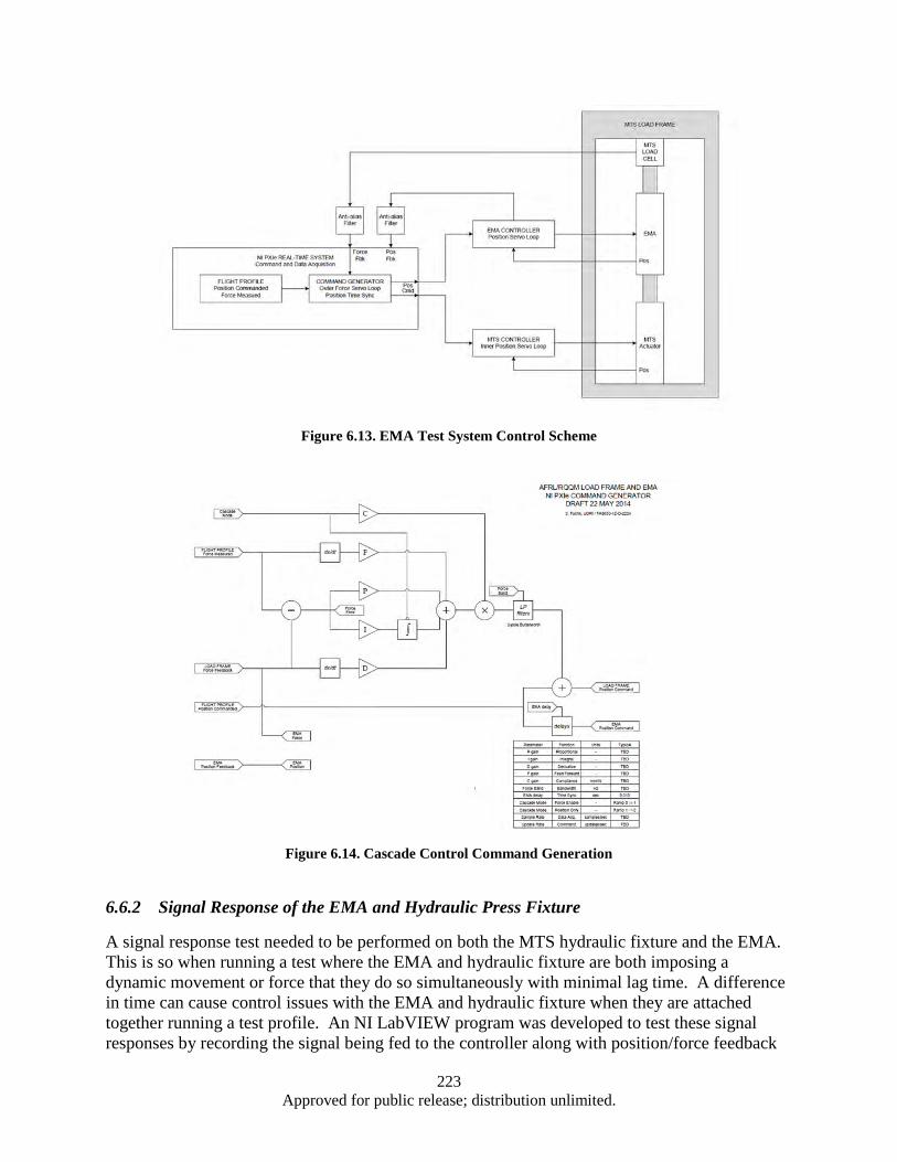
223 Approved for public release; distribution unlimited.
Figure 6.13. EMA Test System Control Scheme
Figure 6.14. Cascade Control Command Generation
6.6.2 Signal Response of the EMA and Hydraulic Press Fixture
A signal response test needed to be performed on both the MTS hydraulic fixture and the EMA. This is so when running a test where the EMA and hydraulic fixture are both imposing a dynamic movement or force that they do so simultaneously with minimal lag time. A difference in time can cause control issues with the EMA and hydraulic fixture when they are attached together running a test profile. An NI LabVIEW program was developed to test these signal responses by recording the signal being fed to the controller along with position/force feedback
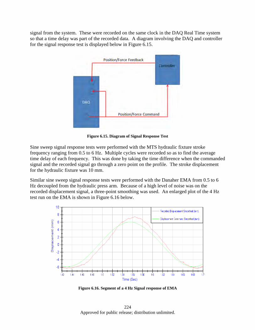
224 Approved for public release; distribution unlimited.
signal from the system. These were recorded on the same clock in the DAQ Real Time system so that a time delay was part of the recorded data. A diagram involving the DAQ and controller for the signal response test is displayed below in Figure 6.15.
Figure 6.15. Diagram of Signal Response Test
Sine sweep signal response tests were performed with the MTS hydraulic fixture stroke frequency ranging from 0.5 to 6 Hz. Multiple cycles were recorded so as to find the average time delay of each frequency. This was done by taking the time difference when the commanded signal and the recorded signal go through a zero point on the profile. The stroke displacement for the hydraulic fixture was 10 mm.
Similar sine sweep signal response tests were performed with the Danaher EMA from 0.5 to 6 Hz decoupled from the hydraulic press arm. Because of a high level of noise was on the recorded displacement signal, a three-point smoothing was used. An enlarged plot of the 4 Hz test run on the EMA is shown in Figure 6.16 below.
Figure 6.16. Segment of a 4 Hz Signal response of EMA
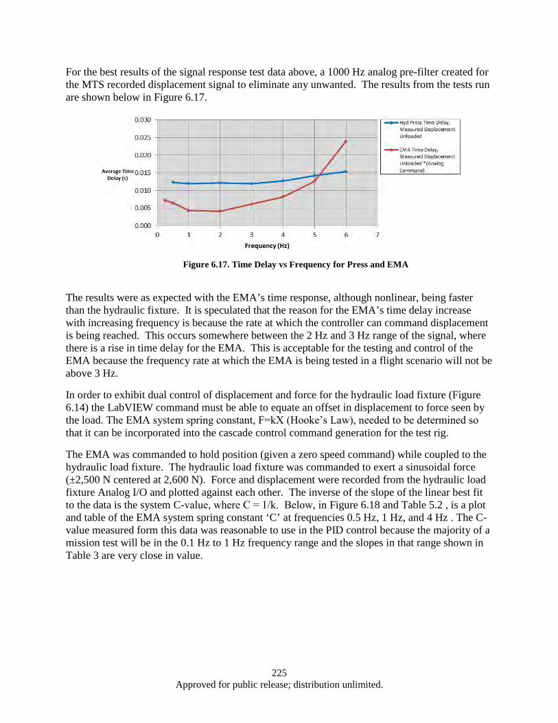
225 Approved for public release; distribution unlimited.
For the best results of the signal response test data above, a 1000 Hz analog pre-filter created for the MTS recorded displacement signal to eliminate any unwanted. The results from the tests run are shown below in Figure 6.17.
Figure 6.17. Time Delay vs Frequency for Press and EMA
The results were as expected with the EMA’s time response, although nonlinear, being faster than the hydraulic fixture. It is speculated that the reason for the EMA’s time delay increase with increasing frequency is because the rate at which the controller can command displacement is being reached. This occurs somewhere between the 2 Hz and 3 Hz range of the signal, where there is a rise in time delay for the EMA. This is acceptable for the testing and control of the EMA because the frequency rate at which the EMA is being tested in a flight scenario will not be above 3 Hz.
In order to exhibit dual control of displacement and force for the hydraulic load fixture (Figure 6.14) the LabVIEW command must be able to equate an offset in displacement to force seen by the load. The EMA system spring constant, F=kX (Hooke’s Law), needed to be determined so that it can be incorporated into the cascade control command generation for the test rig.
The EMA was commanded to hold position (given a zero speed command) while coupled to the hydraulic load fixture. The hydraulic load fixture was commanded to exert a sinusoidal force (±2,500 N centered at 2,600 N). Force and displacement were recorded from the hydraulic load fixture Analog I/O and plotted against each other. The inverse of the slope of the linear best fit to the data is the system C-value, where C = 1/k. Below, in Figure 6.18 and Table 5.2 , is a plot and table of the EMA system spring constant ‘C’ at frequencies 0.5 Hz, 1 Hz, and 4 Hz . The C-value measured form this data was reasonable to use in the PID control because the majority of a mission test will be in the 0.1 Hz to 1 Hz frequency range and the slopes in that range shown in Table 3 are very close in value.
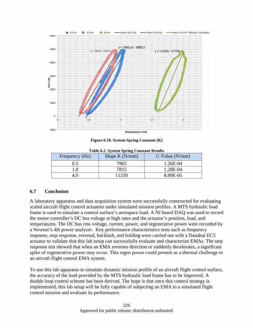
226 Approved for public release; distribution unlimited.
Figure 6.18. System Spring Constant (K)
Table 6.2. System Spring Constant Results
Frequency (Hz) Slope K (N/mm) C-Value (N/mm) 0.5 7965 1.26E-04 1.0 7815 1.28E-04 4.0 11250 8.89E-05
Conclusion 6.7
A laboratory apparatus and data acquisition system were successfully constructed for evaluating scaled aircraft flight control actuators under simulated mission profiles. A MTS hydraulic load frame is used to simulate a control surface’s aerospace load. A NI based DAQ was used to record the motor controller’s DC bus voltage at high rates and the actuator’s position, load, and temperatures. The DC bus rms voltage, current, power, and regenerative power were recorded by a Newton’s 4th power analyzer. Key performance characteristics tests such as frequency response, step response, reversal, backlash, and holding were carried out with a Danahar EC5 actuator to validate that this lab setup can successfully evaluate and characterize EMAs. The step response test showed that when an EMA reverses direction or suddenly decelerates, a significant spike of regenerative power may occur. This regen power could present as a thermal challenge to an aircraft flight control EMA system. To use this lab apparatus to simulate dynamic mission profile of an aircraft flight control surface, the accuracy of the load provided by the MTS hydraulic load frame has to be improved. A double loop control scheme has been derived. The hope is that once this control strategy is implemented, this lab setup will be fully capable of subjecting an EMA to a simulated flight control mission and evaluate its performance.
227 Approved for public release; distribution unlimited.
References
[1] I. Mudawar, Assessment of High-Heat-Flux Thermal Management Schemes, IEEE Trans. Compon. Packag. Technol. 24 (2) (2001) 122-141.
[2] J.E. Schmidt, D.S. Dudis, D.J. Miller, Expendable High Energy Density Thermal Management Material: Ammonium Carbamate, AIAA J. Thermophys. & Heat Trans. 26 (2) (2012) 345-351.
[3] K.G. Clark, H.C. Hetherington, The heat of formation of ammonium carbamate from ammonia and carbon dioxide. J. Am. Chem. Soc. 49 (8) (1927), 1909-1915.
[4] R.N. Bennett, P.D. Ritchie, D. Roxburgh, J. Thomson, The system ammonia carbon dioxide ammonium carbamate. Part I-The equilibrium of thermal dissociation of ammonium carbamate, Trans. Faraday Soc. 49 (1953) 925-929.
[5] T.R. Briggs, V. Migrdichian, The ammonium carbamate equilibrium, J. Phys. Chem. 28 (11) (1924) 1121-1135.
[6] D. Johnson, S. Patnaik, J. Ervin, An Integrated Chemical Reactor-heat Exchanger based on Ammonium Carbamate, Paper 2012-01-2190, SAE Power Systems Conference, Phoenix, AZ, Oct 2012.
[7] N.P. Niedbalski, D. Johnson, S. Patnaik, D. Banerjee, Study of a hybrid heat exchanger-reactor (HEX reactor): Part I- Experimental characterization, Intl. J. Heat & Mass Trans 70 (2014) 1078-1085.
[8] N.P. Niedbalski, D. Johnson, S. Patnaik, D. Banerjee, Study of a hybrid heat exchanger-reactor (HEX reactor): Part II- Numerical prediction of thermal performance, Int. J. Heat & Mass Trans 70 (2014) 1086-1094.
[9] T. Sun, A.S. Teja, Density, viscosity and thermal conductivity of aqueous solutions of propylene glycol, dipropylene glycol, and tripropylene glycol between 290 K and 460 K, J. Chem. Eng. Data 49 (2004) 1311-1317.
[10] A. Jillavenkatesa, S.J. Dapkunas, L.H. Lum, NIST Recommended Practice Guide: Particle Size Characterization, Natl. Inst. Stand. Technol. Spec. Publ. 960-1 (2001).
[11] E.P. Egan, J.E. Potts, G.D. Potts, Dissociation pressure of ammonium carbamate, Indust. & Eng. Chem. 38 (4) (1946) 454-456.
[12] B.R. Ramachandran, A.M. Halpern, E.D. Glendening, Kinetics and mechanism of the reversible dissociation of ammonium carbamate: Involvement of carbamic acid, J. Phys. Chem. A 102 (22) (1998) 3934-3941.
[13] CSID:451267, http://www.chemspider.com/Chemical-Structure.451267.html (accessed 18:50, Sep 12, 2014)
[14] D.G. Thomas, Transport characteristics of suspension: VIII. A note on the viscosity of Newtonian suspensions of uniform spherical particles, J. Colloid Sci. 20 (3) (1965) 267-277.
[15] B. Claudel, L. Boulamri, A new model of gas-solid kinetics: The case of ammonium carbamate formation and decomposition, Thermochimica acta 126 (1988), 129-148.
[16] B. Claudel, E. Brousse, G. Shehadeh, Novel thermodynamic and kinetic investigation of ammonium carbamate decomposition into urea and water, Thermochimica acta 102 (1986) 357-371.
[17] National Refrigerants, Refrigerant Reference Guide Fourth Edition 4.01 (2004). [18] D.J. Johnson, N.P. Niedbalski, J.S. Ervin, S.S. Patnaik, Ammonium carbamate-based heat
exchanger reactor as an endothermic heat sink for thermal management, submitted Int. J. Heat & Mass Trans.
[19] R. Grant, The radar game: understanding stealth and aircraft survivability, Mitchell Institute Press, Air Force Association, 2012.
[20] S. Iden, Integrated vehicle energy technology (INVENT) overview. Presented IEEE 2012 Annual Meeting, Cincinnati.
228 Approved for public release; distribution unlimited.
[21] S. Engelking, H. Kruse, Development of air cycle technology for transport refrigeration. In: Proceedings of the 1996 International Refrigeration and Air Conditioning Conference, West Lafayette, 349-356.
[22] G. Warwick, AFRL’s INVENT program tackles aircraft system efficiency, Aviation Week, November 5, 2012.
[23] A. Al-Rashed, Effect of evaporator temperature on vapor compression refrigeration system, Alexandria Eng. Journal 50 (2011) 283-290.
[24] O. Lottin, Optimum control of the gas overheat in the evaporator of a vapour compression refrigeration system when the refrigerant is polluted, Int. J. Refrigeration 27 (2004) 1003-1006.
[25] W.L. Martz, A.M. Jacobi, Refrigerant-oil mixtures and local composition modeling, Air Conditioning and Refrigeration Center, University of Illinois at Urbana Champaign, Technical Report ACRC TR-68, 1994.
[26] T. Delash, Vapor cycle compressor range expansion for aerospace, SAE Technical Paper 2011-01-2586.
[27] B. Cranston, A. Cole, S. Emo, J. Ervin, V. Tsao, T. Michalak, L. Byrd, Power and thermal technologies for air and space-scientific research program delivery order 0017: description of vapor cycle system research facility, Air Force Research Laboratory. Technical Report AFRL-RQ-WP-TR-2013-0122.
[28] D.W. Hughes, J.T. McMullan, K.A. Mawhinney, R. Morgan, B.L. Sutcliffe, Lubricant related problems with heat-pumps. In: Proceedings of the 1980 International Compressor Engineering Conference, West Lafayette, 156-163.
[29] C. Wu, A. Xingxi, D. Shiming, Development of control method and dynamic model for multi-evaporator air conditioners (MEAC), Energy Conversion Management 46 (2005) 451-465.
[30] E.W. Lemmon, M.L. Huber, M.O. McLinden, National Institute of Standards and Technology Standard Reference Database 23, NIST Reference Fluid Thermodynamic and Transport Properties-REFPROP, Version 9.0 (2010).
[31] A.R. Chandra, Refrigeration and Air Conditioning, PHI Learning Pvt LTD, New Delhi (2010). [32] W.B. Gosney, Principles of Refrigeration, Cambridge University Press, New York (1982). [33] T. Michalak, S. Emo, J. Ervin, Control strategy for aircraft vapor compression system operation,
Int. J. Refrigeration, 48 (2014) 10-18. [34] L. G. Scanlon, L. R. Lucente, W. A. Feld, G. Sandi, P. B. Balbuena, P. R. Alonso and A. Turner,
J. Electrochem. Soc. 151, p A1338 (2004) [35] L. G. Scanlon, L. R. Lucente, M. F. Lawson, J. W. Lawson, J. P. Fellner, W. A. Feld, P. B.
Balbuena, N. Munichandraiah, and H. Xiao, ECS Transactions, 25 (36), pp 163-167 (2010). [36] Patent Number: US 8,974,974 B1; Date of Patent: March 10, 2015; “Class of Solid-State
Electrolytes for Rechargeable Lithium Batteries;” Inventors: Lawrence G. Scanlon Jr., Joseph P. Fellner, William A. Feld, Leah R. Lucente, Jacob W. Lawson.
[37] Tritt, T. M.; Subramanian, M. A. MRS Bull. 2006, 31, 188 (and references therein). [38] Slack, G. A.; CRC Press, Boca Raton, FL, 1995. [39] Rowe, D. M., Ed.; CRC Handbook of Thermoelectrics: Macro to Nano; CRC, Boca Raton, FL,
2005. [40] Chen, G.; Dresselhaus, M. S.; Dresselhaus, G.; Fleurial, J. P.; Caillat, T. Int. Mater. Rev. 2003,
48, 45. [41] Dresselhaus, M. S.; Chen, G.; Tang, M. Y.; Yang, R. G.; Lee, H.; Wang, D. Z.; Ren, Z. F.;
Fleurial, J. P.; Gogna, P. Adv. Mater. 2007, 19, 1043. [42] Bhandari, C. M., Ed., CRC Handbook of Thermoelectrics; CRC, Boca Raton, FL, 2005. [43] Masset, A. C.; Michel, C.; Maignan, A.; Hervieu, M.; Toulemonde, O.; Studer, F.; Raveau, B.;
Hejtmanek, J. Phys. Rev. B 2000, 62, 166. [44] Shikano, M.; Funahashi, R. Appl. Phys. Lett. 2003, 82, 1851. [45] Ohta, S.; Nomura, T.; Ohta, H.; Hirano, M.; Hosono, H.; Koumoto, K. Appl. Phys. Lett. 2005, 87,
092108.
229 Approved for public release; distribution unlimited.
[46] Varanasi, C. V.; Burke, J.; Brunke, L.; Wang, H.; Sumption, M.; Barnes, P. N. J. Appl. Phys. 2007, 102, 063909.
[47] Varanasi, C. V.; Burke, J.; Wang, H.; Lee, J. H.; Barnes, P. N. Appl. Phys. Lett. 2008, 93, 092501.
[48] Rao, A. M.; Ji, X. H.; Tritt, T. M. MRS Bull. 2006, 31, 218. [49] Broido, D. A.; Mingo, N. Phys. Rev. B 2006, 74, 195325. [50] A. R. Abramson, W. C. K., S. T. Huxtable, H. Yan, Y. Wu, A. Majumdar, C.-L. Tien and P. Yang
J. Microelectromech. Sys. 2004, 13, 505. [51] Huber, T. E.; Celestine, K.; Nikolaeva, A.; Gitsu, A.; Konopko, D.; Huang, J.; Graf, M. J. In
Thermoelectrics, 2003 Twenty-Second Int. Conf. Thermoelect. p 359. [52] Lin, Y. M.; Cronin, S. B.; Rabin, O.; Ying, J. Y.; Dresselhaus, M. S. In Thermoelectric Materials
2001-Research and Applications; Nolas, G. S., Johnson, D. C., Mandrus, D. G., Eds. 2001; Vol. 691, p 377.
[53] Zide, J. M.; Klenov, D. O.; Stemmer, S.; Gossard, A. C.; Zeng, G.; Bowers, J. E.; Vashaee, D.; Shakouri, A. Appl. Phys. Lett. 2005, 87, 112102.
[54] Li, S. W.; Funahashi, R.; Matsubara, I.; Ueno, K.; Sodeoka, S.; Yamada, H. Chem. Mater. 2000, 12, 2424.
[55] Itahara, H.; Tani, T. R&D Review of Toyota CRDL 39. [56] Asahi, R.; Sugiyama, J.; Tani, T. Phys. Rev. B 2002, 66, 155103. [57] Li., S., Funahashi, R., Matsubara, I., Ueno, K., Sodeoka, S., Yamada, H. J. Mater. Sci. Lett. 2000,
19, 1339. [58] Mikami, M.; Funahashi, R.; Yoshimura, M.; Mori, Y.; Sasaki, T. J. Appl. Phys. 2003, 94, 6579. [59] Miyazaki, Y.; Huang, X. Y.; Kajiwara, T.; Yamane, H.; Kajitani, T. J. Ceram. Soc. Jpn. 2009,
117, 42. [60] Thomas, E. L.; Song, X.; Yan, Y.; Martin, J.; Wong-Ng, W.; Ratcliff, M.; Barnes, P. N. Mat. Res.
Soc. Symp. Proc. 2010, 1267, 1267. [61] van der Pauw, L. J. Phillips Res. Rep. 1958, 13, 1. [62] Otani, M.; Itaka, K.; Wong-Ng, W.; Schenck, P. K.; Koinuma, H. Appl. Surf. Sci. 2007, 254, 765. [63] Otani, M.; Lowhorn, N. D.; Schenck, P. K.; Wong-Ng, W.; Green, M. L.; Itaka, K.; Koinuma, H.
Appl. Phys. Lett. 2007, 91. [64] Otani, M.; Thomas, E. L.; Wong-Ng, W.; Schenck, P. K.; Chang, K. S.; Lowhorn, N. D.; Green,
M. L.; Ohguchi, H. Jpn. J. Appl. Phys. 2009, 48. [65] Moubah, R.; Colis, S.; Schmerber, G.; Petersen, J.; Dinia, A. Appl. Phys. Lett. 2009, 94. [66] Wang, Y.; Sui, Y.; Ren, P.; Wang, L.; Wang, X. J.; Su, W. H.; Fan, H. J. Chem. Mater. 2010, 22,
1155. [67] Wang, Y.; Sui, Y.; Cheng, J. G.; Wang, X. J.; Su, W. H. J. Alloy. Compd. 2009, 477, 817. [68] Brabers, V. A. M.; Broemme, A. D. D. J. Magn. Magn. Mater. 1992, 104, 405. [69] Wang, S. F.; Chen, M. J.; He, L. P.; Zheng, J.; Yu, W.; Fu, G. S. J. Phys. D Appl. Phys. 2009, 42. [70] Kenfaui, D.; Bonnefont, G.; Chateigner, D.; Fantozzi, G.; Gomina, M.; Noudem, J. G. Mater.Res.
Bull. 2010, 45, 1240. [71] X.-D. Xiang and I. Takeuchi, Combinatorial Materials Synthesis, New York: Marcel Dekker,
Inc., 2003. [72] Nurnus, J.; Bottner, H.; Kunzel, C.; Vetter, U.; Lambrecht, A.; Schumann, J.; Volklein, F.; Ieee, I.
2002Int. Conf. Thermoelect. XXI, p 523. [73] Völklein, F.; Blumers, M.; Schmitt, L. Int. Conf. Thermoelect. 1999, 285. [75] Fleurial, J. P. JOM 2009, 61, 79. [76] Liu, C. J.; Nayak, P. K.; Lin, Z. R.; Jeng, K. Y. Thin Solid Films 2008, 516, 8564. [77] Zhu, X. B.; Chou, S. L.; Wang, L.; Li, Q.; Shi, D. Q.; Wang, J. Z.; Chen, Z. X.; Sun, Y. P.; Liu,
H. K.; Dou, S. X. Electrochem. Solid St. 2009, 12, A176. [78] Zhu, X. B.; Shi, D. Q.; Dou, S. X.; Sun, Y. P.; Li, Q.; Wang, L.; Li, W. X.; Yeoh, W. K.; Zheng,
R. K.; Chen, Z. X.; Kong, C. X. Acta Mater. 2010, 58, 4281.
230 Approved for public release; distribution unlimited.
[79] C. Jiang, M. Venkatesan, K. Gallagher, J.M.D. Coey, J. Magn. Magn. Mater. 236, 49 (2001). [80] Z. Liu, R.J. Chen, D. Lee, A.R. Yan, J. Alloys and Compd. 509, 3967 (2011). [81] N. Tang, Z. Chen, Y. Zhang, G. C. Hadjipanayis, F. Yang, J. Magn. Magn. Mater. 219, 173 (2000). [82] P. J. McGuiness, S. Kobe, J. Alloys and Compd. 281, 23 (1998). [83] J. Zhou, R. Skomski, D. J. Sellmyer, J. Appl. Phys. 93, 6495 (2003). [84] M. Yue, J. H. Zuo, W. Q. Liu, W. C. Lu, D. T. Zhang, J. X. Zhang, Z. H. Guo, W. Li, J. Appl. Phys. 109, 07A700 (2011). [85] A. M. Gabay, M. Marinescu, J. F. Liu, G. C. Hadjipanayis, J. Magn. Magn. Mater. 321, 3318 (2009). [86] B. Z. Cui, A. M. Gabay, W. F. Li, J. F. Liu, G. C. Hadjipanayis, J. Appl. Phys., 107, 09A721
(2010). [87] S. J. Knutson, Y. Shen, J. C. Horwath, P. Barnes, C. H. Chen, J. Appl. Phys., 109, 07A762
(2011). [88] S. D. Bader, Rev. Mod. Phys., 78, 1 (2006). [89] Y. Shen, M. Q. Huang, Z. Turgut, M. S. Lucas, E. Michel, J. C. Horwath, J. Appl. Phys. 111, 07B512 (2012) [90] Y. Shen, S. Leontsev, Z. Turgut, M. S. Lucas, A. O. Sheets, J. C. Horwath, IEEE Trans. Magn., 49, 3244 (2013) [91] B. Z. Cui, W. F. Li, G. C. Hadjipanayis, Acta Mater. 59, 563 (2011). [92] F. F. Westendorp, Solid State Commun. 8, 139 (1970). [93] R. W. lee, J. J. Croat, IEEE trans. Magn. MAG-9, 708 (1974). [94] F.J.A. den Broeder, H. Zijlstra, J. Appl. Phys. 47, 2688 (1976). [95] E. A. Nesbitt and J. H. Wernick, Rear Earth Permanent Magnets (Academic Press, New York, 1973), p. 80. [96] H. Saito, M. Takahashi, T. Wakiyama, G. Kido, H. Nakagawa, J. Magn. Magn. Mater. 82, 322 (1989). [97] Xu J. and Fisher T. S., "Enhancement of thermal interface materials with carbon nanotube
arrays," International Journal of Heat and Mass Transfer, vol. 49 (2006), pp.1658-1666. [98] Tong T., Zhao Y., Delzeit L., Kashani A., Meyyappan M.,and Majumdar A., “Dense, vertically
aligned multiwalled carbon nanotube arrays as thermal interface materials,” IEEE Transactions on Components and Packaging Technologies, vol. 30 (2007), pp. 92-100.
[99] Kordas K., Toth G., Moilanen P., Kumpumaki M., Vahakangas J., Uusimaki A., Vajtai R., and Ajayon P. M., "Chip cooling with integrated carbon nanotube microfin architectures," Applied Physics Letters, vol. 90 (2007).
[100] Cola B. A., Xu J., Cheng C. R., Xu X. F., Fisher T. S., and Hu H. P., "Photoacoustic characterization of carbon nanotube array thermal interfaces," Journal of Applied Physics, vol. 101 (2007).
[101] Huang H., Lui C. H., Wu Y., and Fan S. S., "Aligned carbon nanotube composite films for thermal management," Advanced Materials, vol. 17 (2005), pp. 1652-1653.
[102] Panzer M. A., Zhang G., Mann D., Hu X., Pop E., Dai H., and Goodson K. E., "Thermal properties of metal-coated vertically aligned single-wall nanotube arrays," Journal of Heat Transfer-Transactions of the ASME, vol. 130 (2008).
[103] Sihn S., Ganguli S., Roy A. K., Qu L. T., and Dai L. M., "Enhancement of through-thickness thermal conductivity in adhesively bonded joints using aligned carbon nanotubes," Composites Science and Technology, vol. 68 (2008), pp. 658-665
[104] T. de los Arcos, M. Gunnar Garnier, P. Oelhafen, D. Mathys, J. Won Seo, C. Domingo, J. Vicente Garcıa-Ramos, and S. Sánchez-Cortés, “Strong influence of buffer layer type on carbon nanotube characteristics,” Carbon., vol. 42, pp. 187–190, Jan. 2004.
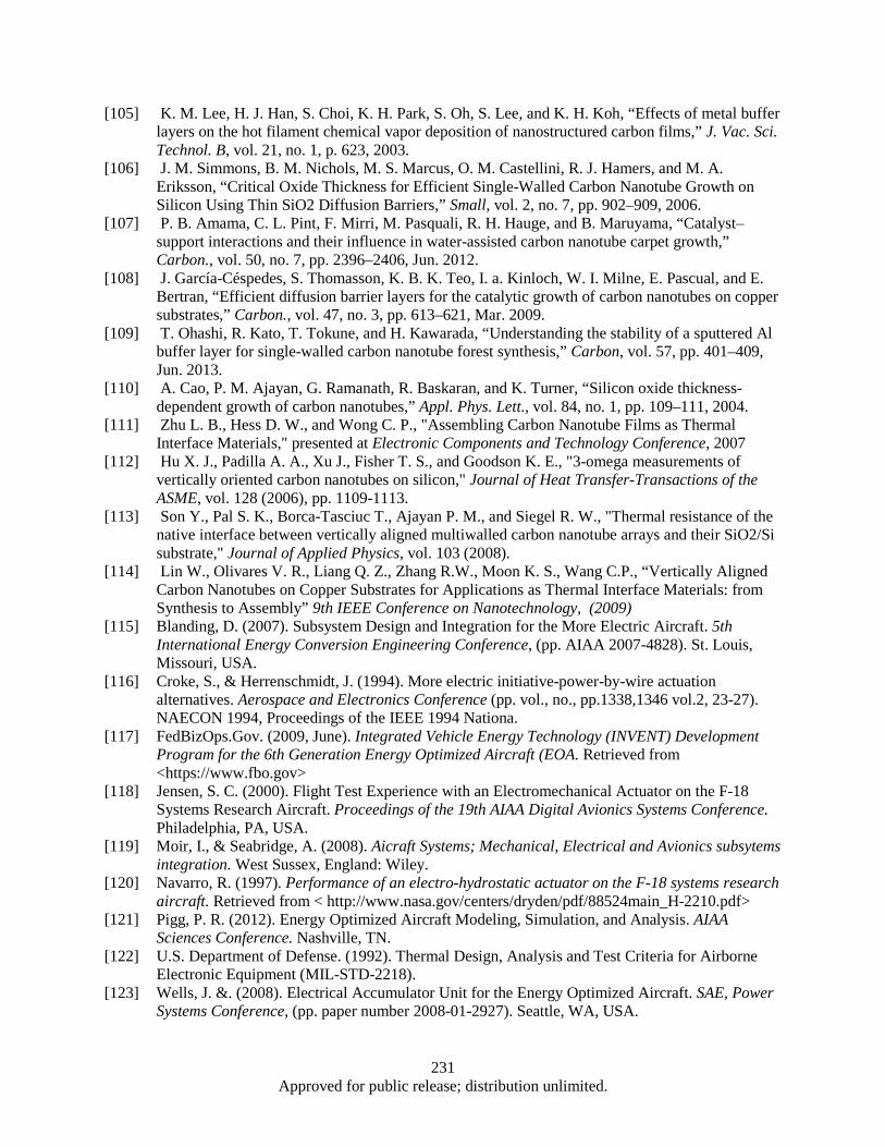
231 Approved for public release; distribution unlimited.
[105] K. M. Lee, H. J. Han, S. Choi, K. H. Park, S. Oh, S. Lee, and K. H. Koh, “Effects of metal buffer layers on the hot filament chemical vapor deposition of nanostructured carbon films,” J. Vac. Sci. Technol. B, vol. 21, no. 1, p. 623, 2003.
[106] J. M. Simmons, B. M. Nichols, M. S. Marcus, O. M. Castellini, R. J. Hamers, and M. A. Eriksson, “Critical Oxide Thickness for Efficient Single-Walled Carbon Nanotube Growth on Silicon Using Thin SiO2 Diffusion Barriers,” Small, vol. 2, no. 7, pp. 902–909, 2006.
[107] P. B. Amama, C. L. Pint, F. Mirri, M. Pasquali, R. H. Hauge, and B. Maruyama, “Catalyst–support interactions and their influence in water-assisted carbon nanotube carpet growth,” Carbon., vol. 50, no. 7, pp. 2396–2406, Jun. 2012.
[108] J. García-Céspedes, S. Thomasson, K. B. K. Teo, I. a. Kinloch, W. I. Milne, E. Pascual, and E. Bertran, “Efficient diffusion barrier layers for the catalytic growth of carbon nanotubes on copper substrates,” Carbon., vol. 47, no. 3, pp. 613–621, Mar. 2009.
[109] T. Ohashi, R. Kato, T. Tokune, and H. Kawarada, “Understanding the stability of a sputtered Al buffer layer for single-walled carbon nanotube forest synthesis,” Carbon, vol. 57, pp. 401–409, Jun. 2013.
[110] A. Cao, P. M. Ajayan, G. Ramanath, R. Baskaran, and K. Turner, “Silicon oxide thickness-dependent growth of carbon nanotubes,” Appl. Phys. Lett., vol. 84, no. 1, pp. 109–111, 2004.
[111] Zhu L. B., Hess D. W., and Wong C. P., "Assembling Carbon Nanotube Films as Thermal Interface Materials," presented at Electronic Components and Technology Conference, 2007
[112] Hu X. J., Padilla A. A., Xu J., Fisher T. S., and Goodson K. E., "3-omega measurements of vertically oriented carbon nanotubes on silicon," Journal of Heat Transfer-Transactions of the ASME, vol. 128 (2006), pp. 1109-1113.
[113] Son Y., Pal S. K., Borca-Tasciuc T., Ajayan P. M., and Siegel R. W., "Thermal resistance of the native interface between vertically aligned multiwalled carbon nanotube arrays and their SiO2/Si substrate," Journal of Applied Physics, vol. 103 (2008).
[114] Lin W., Olivares V. R., Liang Q. Z., Zhang R.W., Moon K. S., Wang C.P., “Vertically Aligned Carbon Nanotubes on Copper Substrates for Applications as Thermal Interface Materials: from Synthesis to Assembly” 9th IEEE Conference on Nanotechnology, (2009)
[115] Blanding, D. (2007). Subsystem Design and Integration for the More Electric Aircraft. 5th International Energy Conversion Engineering Conference, (pp. AIAA 2007-4828). St. Louis, Missouri, USA.
[116] Croke, S., & Herrenschmidt, J. (1994). More electric initiative-power-by-wire actuation alternatives. Aerospace and Electronics Conference (pp. vol., no., pp.1338,1346 vol.2, 23-27). NAECON 1994, Proceedings of the IEEE 1994 Nationa.
[117] FedBizOps.Gov. (2009, June). Integrated Vehicle Energy Technology (INVENT) Development Program for the 6th Generation Energy Optimized Aircraft (EOA. Retrieved from <https://www.fbo.gov>
[118] Jensen, S. C. (2000). Flight Test Experience with an Electromechanical Actuator on the F-18 Systems Research Aircraft. Proceedings of the 19th AIAA Digital Avionics Systems Conference. Philadelphia, PA, USA.
[119] Moir, I., & Seabridge, A. (2008). Aicraft Systems; Mechanical, Electrical and Avionics subsytems integration. West Sussex, England: Wiley.
[120] Navarro, R. (1997). Performance of an electro-hydrostatic actuator on the F-18 systems research aircraft. Retrieved from < http://www.nasa.gov/centers/dryden/pdf/88524main_H-2210.pdf>
[121] Pigg, P. R. (2012). Energy Optimized Aircraft Modeling, Simulation, and Analysis. AIAA Sciences Conference. Nashville, TN.
[122] U.S. Department of Defense. (1992). Thermal Design, Analysis and Test Criteria for Airborne Electronic Equipment (MIL-STD-2218).
[123] Wells, J. &. (2008). Electrical Accumulator Unit for the Energy Optimized Aircraft. SAE, Power Systems Conference, (pp. paper number 2008-01-2927). Seattle, WA, USA.
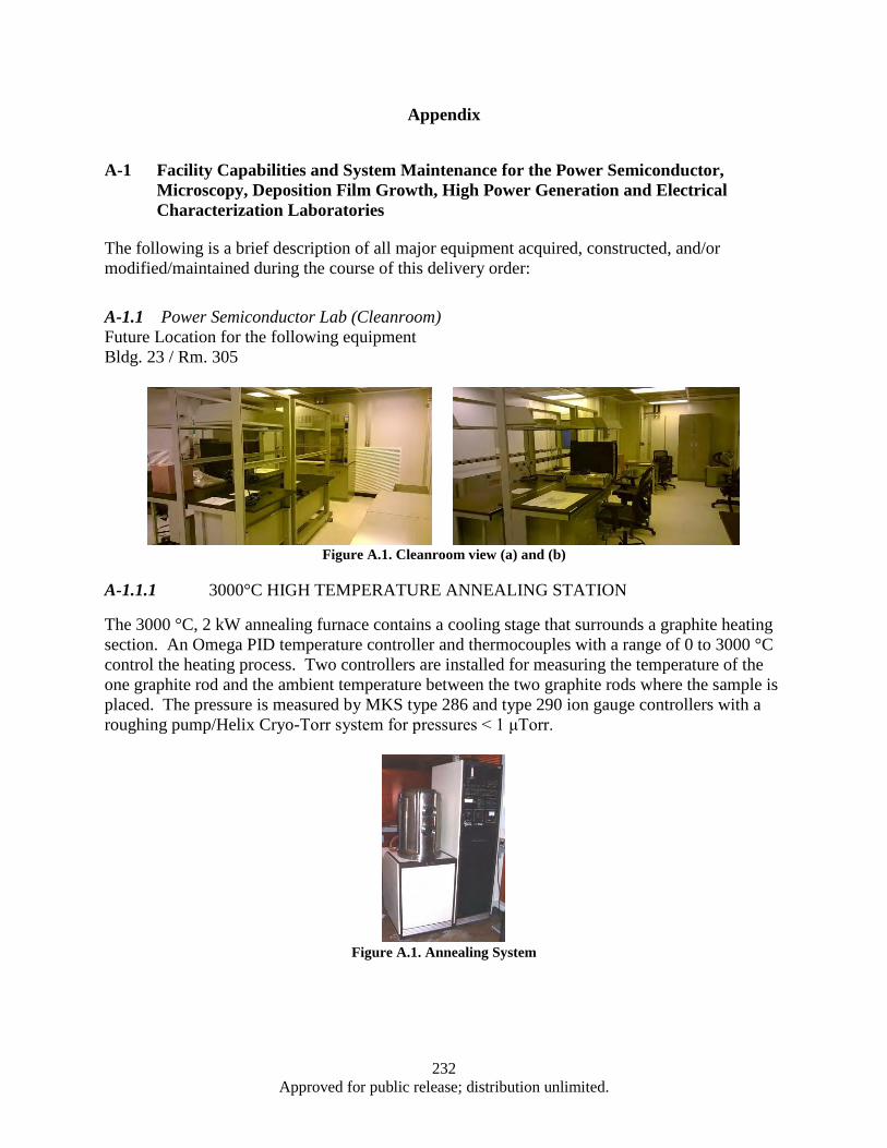
232 Approved for public release; distribution unlimited.
Appendix
A-1 Facility Capabilities and System Maintenance for the Power Semiconductor,
Microscopy, Deposition Film Growth, High Power Generation and Electrical Characterization Laboratories
The following is a brief description of all major equipment acquired, constructed, and/or modified/maintained during the course of this delivery order:
A-1.1 Power Semiconductor Lab (Cleanroom) Future Location for the following equipment Bldg. 23 / Rm. 305
Figure A.1. Cleanroom view (a) and (b)
A-1.1.1 3000°C HIGH TEMPERATURE ANNEALING STATION
The 3000 °C, 2 kW annealing furnace contains a cooling stage that surrounds a graphite heating section. An Omega PID temperature controller and thermocouples with a range of 0 to 3000 °C control the heating process. Two controllers are installed for measuring the temperature of the one graphite rod and the ambient temperature between the two graphite rods where the sample is placed. The pressure is measured by MKS type 286 and type 290 ion gauge controllers with a roughing pump/Helix Cryo-Torr system for pressures < 1 μTorr.
Figure A.1. Annealing System
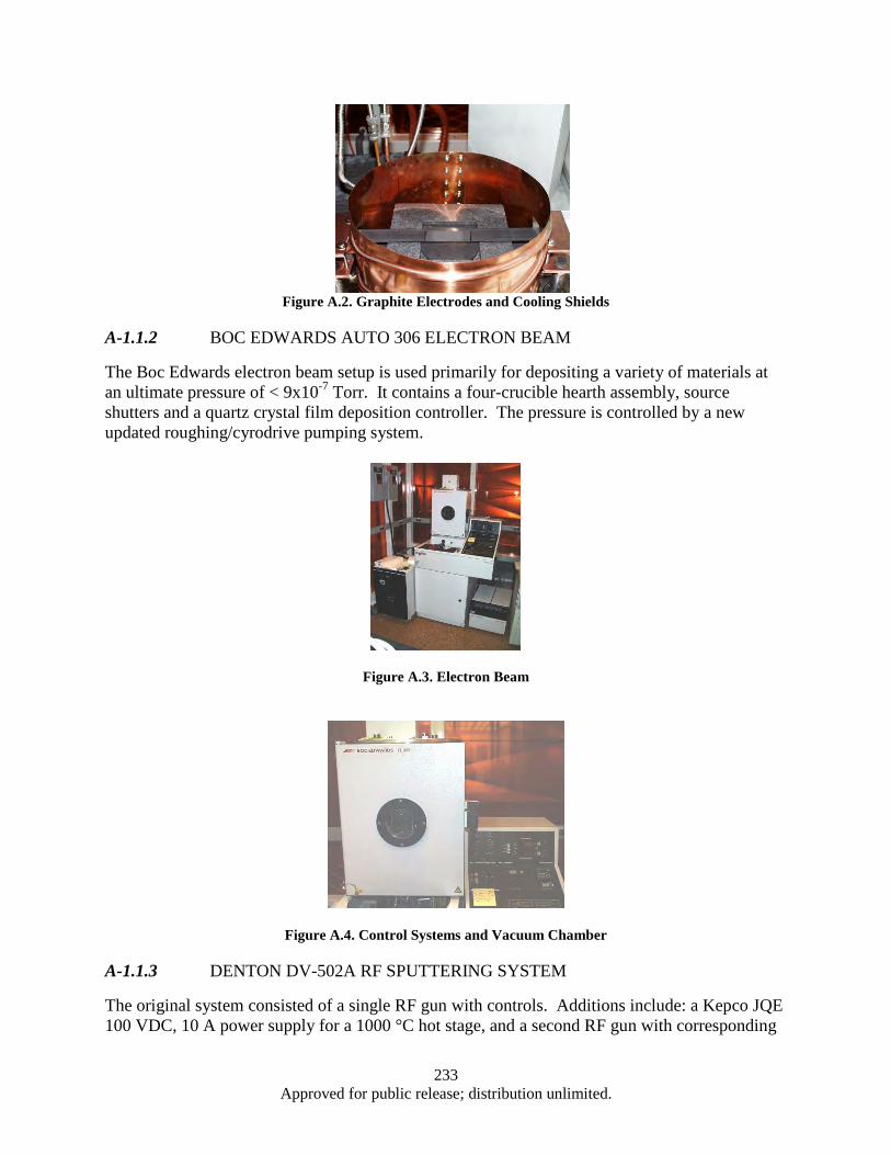
233 Approved for public release; distribution unlimited.
Figure A.2. Graphite Electrodes and Cooling Shields
A-1.1.2 BOC EDWARDS AUTO 306 ELECTRON BEAM
The Boc Edwards electron beam setup is used primarily for depositing a variety of materials at an ultimate pressure of < 9x10⁻⁷ Torr. It contains a four-crucible hearth assembly, source shutters and a quartz crystal film deposition controller. The pressure is controlled by a new updated roughing/cyrodrive pumping system.
Figure A.3. Electron Beam
Figure A.4. Control Systems and Vacuum Chamber
A-1.1.3 DENTON DV-502A RF SPUTTERING SYSTEM
The original system consisted of a single RF gun with controls. Additions include: a Kepco JQE 100 VDC, 10 A power supply for a 1000 °C hot stage, and a second RF gun with corresponding
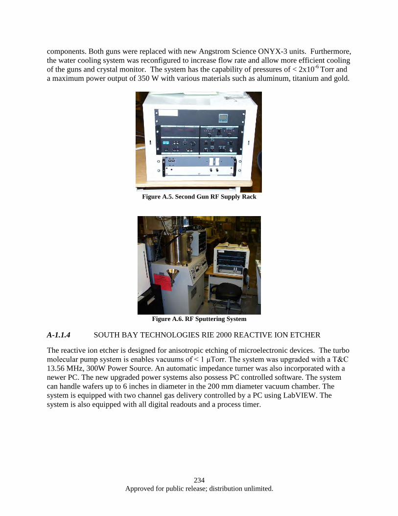
234 Approved for public release; distribution unlimited.
components. Both guns were replaced with new Angstrom Science ONYX-3 units. Furthermore, the water cooling system was reconfigured to increase flow rate and allow more efficient cooling of the guns and crystal monitor. The system has the capability of pressures of < 2x10⁻⁶ Torr and a maximum power output of 350 W with various materials such as aluminum, titanium and gold.
Figure A.5. Second Gun RF Supply Rack
Figure A.6. RF Sputtering System
A-1.1.4 SOUTH BAY TECHNOLOGIES RIE 2000 REACTIVE ION ETCHER
The reactive ion etcher is designed for anisotropic etching of microelectronic devices. The turbo molecular pump system is enables vacuums of < 1 μTorr. The system was upgraded with a T&C 13.56 MHz, 300W Power Source. An automatic impedance turner was also incorporated with a newer PC. The new upgraded power systems also possess PC controlled software. The system can handle wafers up to 6 inches in diameter in the 200 mm diameter vacuum chamber. The system is equipped with two channel gas delivery controlled by a PC using LabVIEW. The system is also equipped with all digital readouts and a process timer.
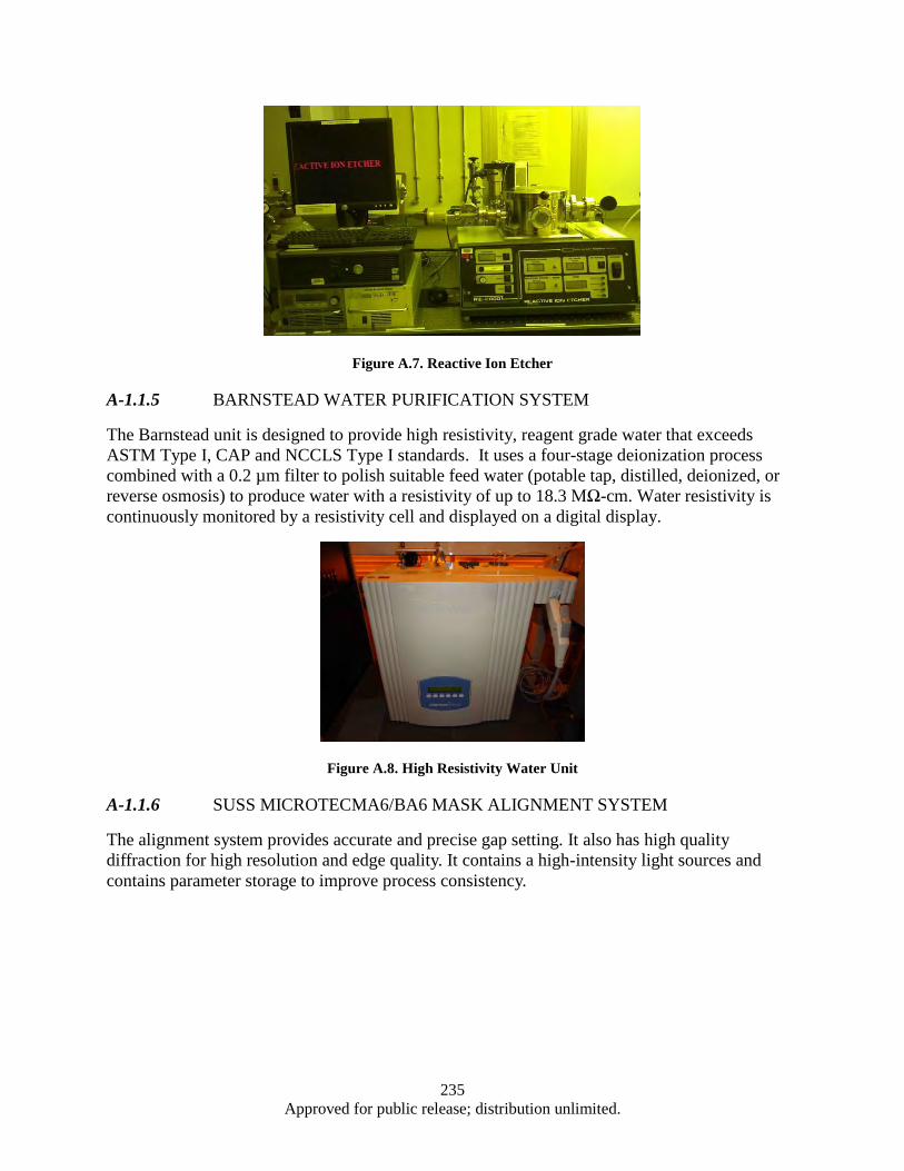
235 Approved for public release; distribution unlimited.
Figure A.7. Reactive Ion Etcher
A-1.1.5 BARNSTEAD WATER PURIFICATION SYSTEM
The Barnstead unit is designed to provide high resistivity, reagent grade water that exceeds ASTM Type I, CAP and NCCLS Type I standards. It uses a four-stage deionization process combined with a 0.2 µm filter to polish suitable feed water (potable tap, distilled, deionized, or reverse osmosis) to produce water with a resistivity of up to 18.3 MΩ-cm. Water resistivity is continuously monitored by a resistivity cell and displayed on a digital display.
Figure A.8. High Resistivity Water Unit
A-1.1.6 SUSS MICROTECMA6/BA6 MASK ALIGNMENT SYSTEM
The alignment system provides accurate and precise gap setting. It also has high quality diffraction for high resolution and edge quality. It contains a high-intensity light sources and contains parameter storage to improve process consistency.
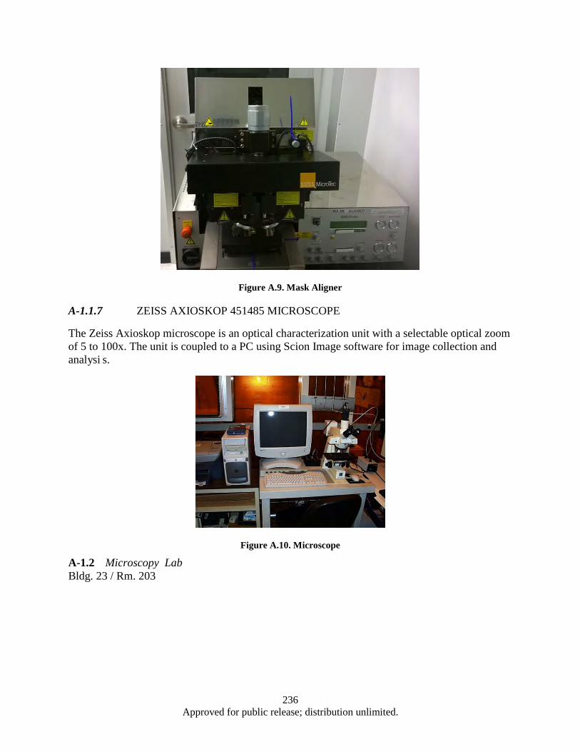
236 Approved for public release; distribution unlimited.
Figure A.9. Mask Aligner
A-1.1.7 ZEISS AXIOSKOP 451485 MICROSCOPE
The Zeiss Axioskop microscope is an optical characterization unit with a selectable optical zoom of 5 to 100x. The unit is coupled to a PC using Scion Image software for image collection and analysi s.
Figure A.10. Microscope
A-1.2 Microscopy Lab Bldg. 23 / Rm. 203
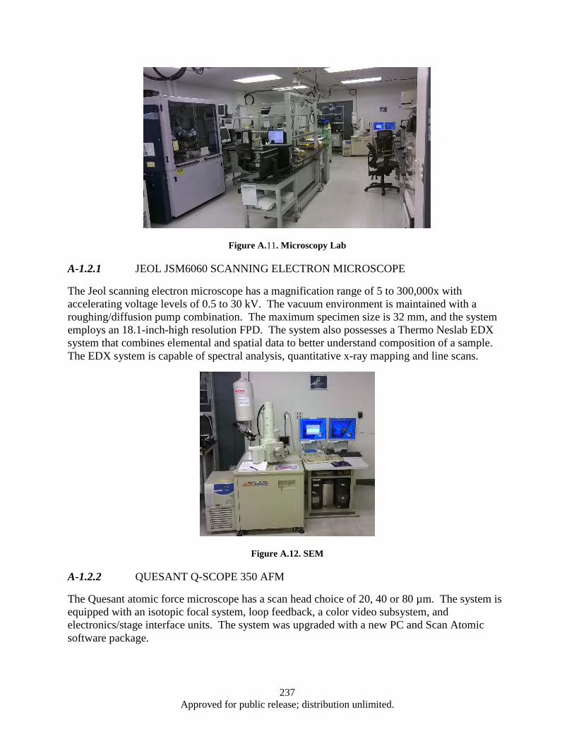
237 Approved for public release; distribution unlimited.
Figure A.11. Microscopy Lab
A-1.2.1 JEOL JSM6060 SCANNING ELECTRON MICROSCOPE
The Jeol scanning electron microscope has a magnification range of 5 to 300,000x with accelerating voltage levels of 0.5 to 30 kV. The vacuum environment is maintained with a roughing/diffusion pump combination. The maximum specimen size is 32 mm, and the system employs an 18.1-inch-high resolution FPD. The system also possesses a Thermo Neslab EDX system that combines elemental and spatial data to better understand composition of a sample. The EDX system is capable of spectral analysis, quantitative x-ray mapping and line scans.
Figure A.12. SEM
A-1.2.2 QUESANT Q-SCOPE 350 AFM
The Quesant atomic force microscope has a scan head choice of 20, 40 or 80 µm. The system is equipped with an isotopic focal system, loop feedback, a color video subsystem, and electronics/stage interface units. The system was upgraded with a new PC and Scan Atomic software package.
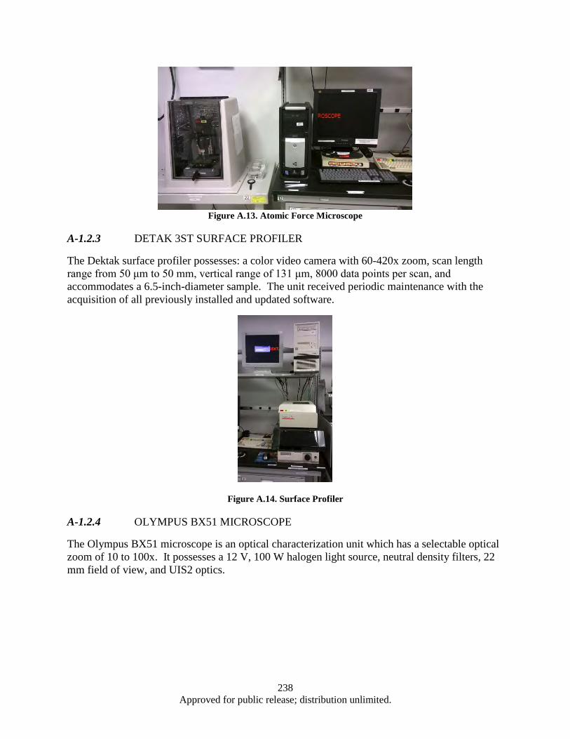
238 Approved for public release; distribution unlimited.
Figure A.13. Atomic Force Microscope
A-1.2.3 DETAK 3ST SURFACE PROFILER
The Dektak surface profiler possesses: a color video camera with 60-420x zoom, scan length range from 50 μm to 50 mm, vertical range of 131 μm, 8000 data points per scan, and accommodates a 6.5-inch-diameter sample. The unit received periodic maintenance with the acquisition of all previously installed and updated software.
Figure A.14. Surface Profiler
A-1.2.4 OLYMPUS BX51 MICROSCOPE
The Olympus BX51 microscope is an optical characterization unit which has a selectable optical zoom of 10 to 100x. It possesses a 12 V, 100 W halogen light source, neutral density filters, 22 mm field of view, and UIS2 optics.
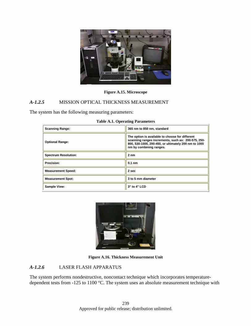
239 Approved for public release; distribution unlimited.
Figure A.15. Microscope
A-1.2.5 MISSION OPTICAL THICKNESS MEASUREMENT
The system has the following measuring parameters:
Table A.1. Operating Parameters
Scanning Range: 365 nm to 850 nm, standard
Optional Range: The option is available to choose for different scanning ranges increments, such as: 200-575, 250-800, 530-1000, 200-450, or ultimately 200 nm to 1000 nm by combining ranges.
Spectrum Resolution: 2 nm Precision: 0.1 nm Measurement Speed: 2 sec Measurement Spot: 3 to 5 mm diameter Sample View: 3" to 4" LCD
Figure A.16. Thickness Measurement Unit
A-1.2.6 LASER FLASH APPARATUS
The system performs nondestructive, noncontact technique which incorporates temperature-dependent tests from -125 to 1100 °C. The system uses an absolute measurement technique with
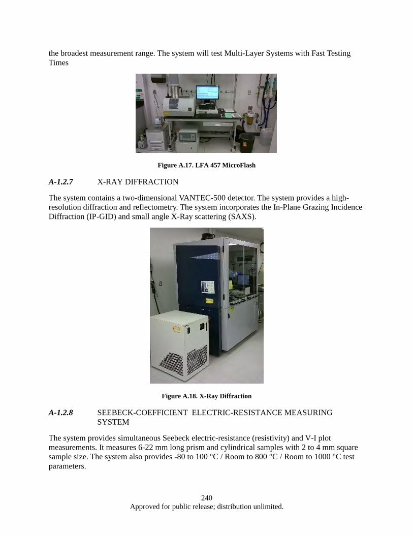
240 Approved for public release; distribution unlimited.
the broadest measurement range. The system will test Multi-Layer Systems with Fast Testing Times
Figure A.17. LFA 457 MicroFlash
A-1.2.7 X-RAY DIFFRACTION
The system contains a two-dimensional VANTEC-500 detector. The system provides a high-resolution diffraction and reflectometry. The system incorporates the In-Plane Grazing Incidence Diffraction (IP-GID) and small angle X-Ray scattering (SAXS).
Figure A.18. X-Ray Diffraction
A-1.2.8 SEEBECK-COEFFICIENT ELECTRIC-RESISTANCE MEASURING SYSTEM
The system provides simultaneous Seebeck electric-resistance (resistivity) and V-I plot measurements. It measures 6-22 mm long prism and cylindrical samples with 2 to 4 mm square sample size. The system also provides -80 to 100 °C / Room to 800 °C / Room to 1000 °C test parameters.
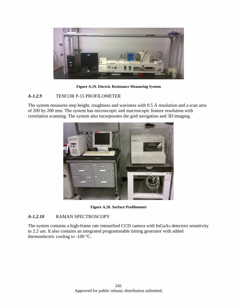
241 Approved for public release; distribution unlimited.
Figure A.19. Electric Resistance Measuring System
A-1.2.9 TENCOR P-15 PROFILOMETER
The system measures step height, roughness and waviness with 0.5 Å resolution and a scan area of 200 by 200 mm. The system has microscopic and macroscopic feature resolution with correlation scanning. The system also incorporates die grid navigation and 3D imaging.
Figure A.20. Surface Profilometer
A-1.2.10 RAMAN SPECTROSCOPY
The system contains a high-frame rate intensified CCD camera with InGaAs detectors sensitivity to 2.2 um. It also contains an integrated programmable timing generator with added thermoelectric cooling to -100 °C.
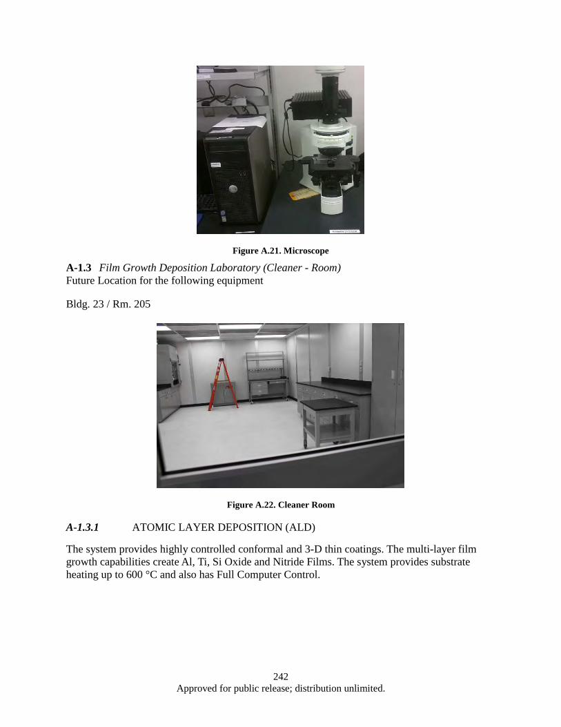
242 Approved for public release; distribution unlimited.
Figure A.21. Microscope A-1.3 Film Growth Deposition Laboratory (Cleaner - Room) Future Location for the following equipment
Bldg. 23 / Rm. 205
Figure A.22. Cleaner Room
A-1.3.1 ATOMIC LAYER DEPOSITION (ALD)
The system provides highly controlled conformal and 3-D thin coatings. The multi-layer film growth capabilities create Al, Ti, Si Oxide and Nitride Films. The system provides substrate heating up to 600 °C and also has Full Computer Control.
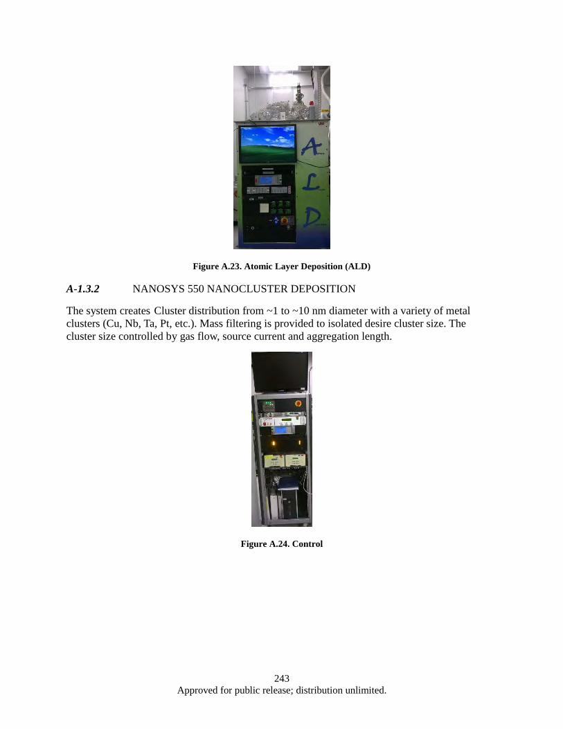
243 Approved for public release; distribution unlimited.
Figure A.23. Atomic Layer Deposition (ALD)
A-1.3.2 NANOSYS 550 NANOCLUSTER DEPOSITION
The system creates Cluster distribution from ~1 to ~10 nm diameter with a variety of metal clusters (Cu, Nb, Ta, Pt, etc.). Mass filtering is provided to isolated desire cluster size. The cluster size controlled by gas flow, source current and aggregation length.
Figure A.24. Control
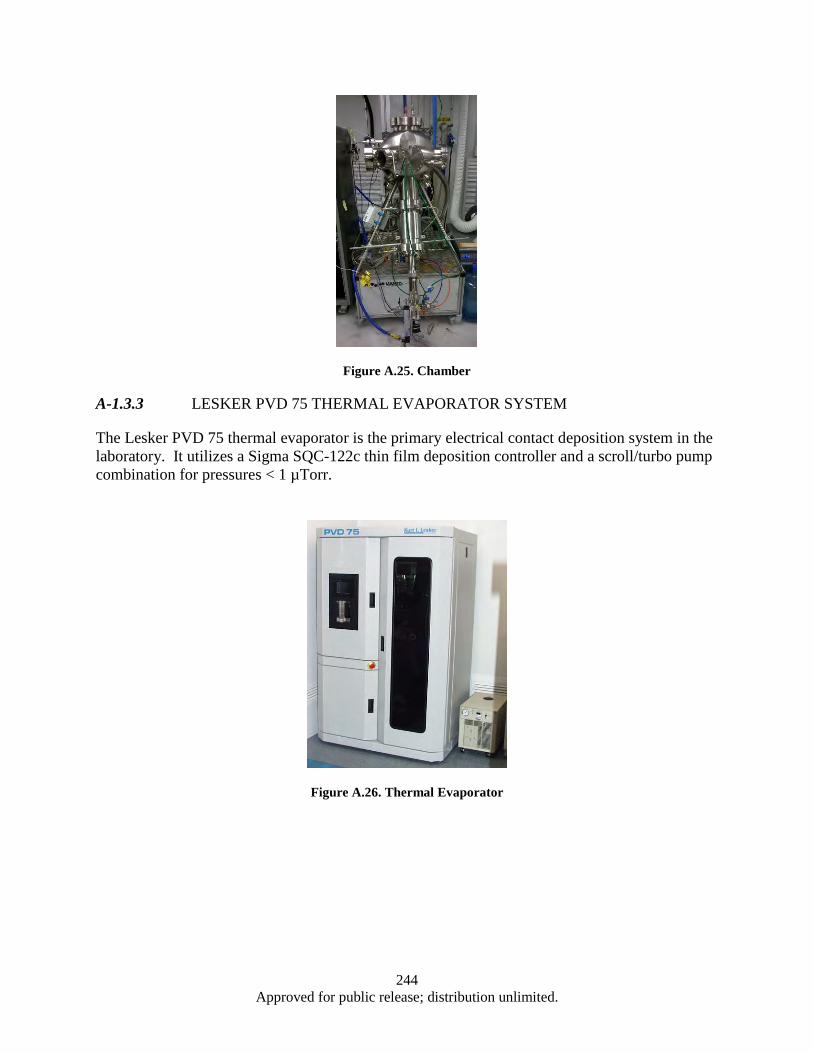
244 Approved for public release; distribution unlimited.
Figure A.25. Chamber
A-1.3.3 LESKER PVD 75 THERMAL EVAPORATOR SYSTEM
The Lesker PVD 75 thermal evaporator is the primary electrical contact deposition system in the laboratory. It utilizes a Sigma SQC-122c thin film deposition controller and a scroll/turbo pump combination for pressures < 1 µTorr.
Figure A.26. Thermal Evaporator
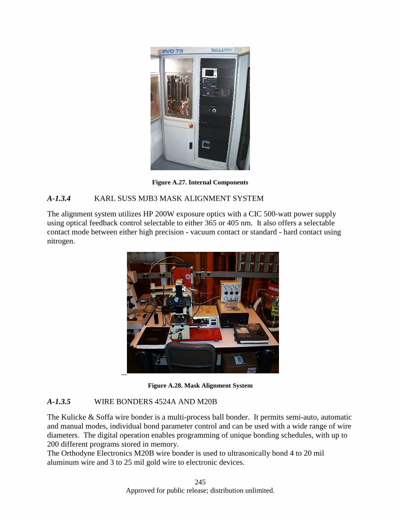
245 Approved for public release; distribution unlimited.
Figure A.27. Internal Components
A-1.3.4 KARL SUSS MJB3 MASK ALIGNMENT SYSTEM
The alignment system utilizes HP 200W exposure optics with a CIC 500-watt power supply using optical feedback control selectable to either 365 or 405 nm. It also offers a selectable contact mode between either high precision - vacuum contact or standard - hard contact using nitrogen.
Figure A.28. Mask Alignment System
A-1.3.5 WIRE BONDERS 4524A AND M20B
The Kulicke & Soffa wire bonder is a multi-process ball bonder. It permits semi-auto, automatic and manual modes, individual bond parameter control and can be used with a wide range of wire diameters. The digital operation enables programming of unique bonding schedules, with up to 200 different programs stored in memory. The Orthodyne Electronics M20B wire bonder is used to ultrasonically bond 4 to 20 mil aluminum wire and 3 to 25 mil gold wire to electronic devices.
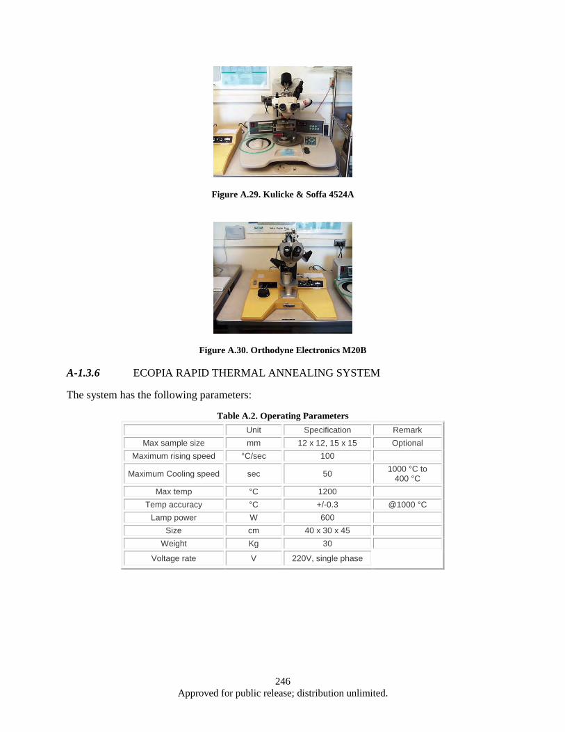
246 Approved for public release; distribution unlimited.
Figure A.29. Kulicke & Soffa 4524A
Figure A.30. Orthodyne Electronics M20B
A-1.3.6 ECOPIA RAPID THERMAL ANNEALING SYSTEM
The system has the following parameters:
Table A.2. Operating Parameters
Unit Specification Remark Max sample size mm 12 x 12, 15 x 15 Optional
Maximum rising speed °C/sec 100 Maximum Cooling speed sec 50 1000 °C to
400 °C Max temp °C 1200
Temp accuracy °C +/-0.3 @1000 °C Lamp power W 600
Size cm 40 x 30 x 45 Weight Kg 30
Voltage rate V 220V, single phase
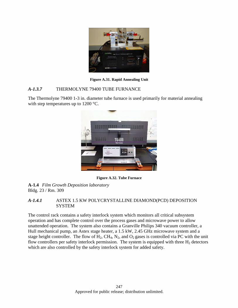
247 Approved for public release; distribution unlimited.
Figure A.31. Rapid Annealing Unit
A-1.3.7 THERMOLYNE 79400 TUBE FURNANCE
The Thermolyne 79400 1-3 in. diameter tube furnace is used primarily for material annealing with step temperatures up to 1200 °C.
Figure A.32. Tube Furnace A-1.4 Film Growth Deposition laboratory Bldg. 23 / Rm. 309
A-1.4.1 ASTEX 1.5 KW POLYCRYSTALLINE DIAMOND(PCD) DEPOSITION SYSTEM
The control rack contains a safety interlock system which monitors all critical subsystem operation and has complete control over the process gases and microwave power to allow unattended operation. The system also contains a Granville Philips 340 vacuum controller, a Hull mechanical pump, an Astex stage heater, a 1.5 kW, 2.45 GHz microwave system and a stage height controller. The flow of H2, CH4, N2, and O2 gases is controlled via PC with the unit flow controllers per safety interlock permission. The system is equipped with three H2 detectors which are also controlled by the safety interlock system for added safety.
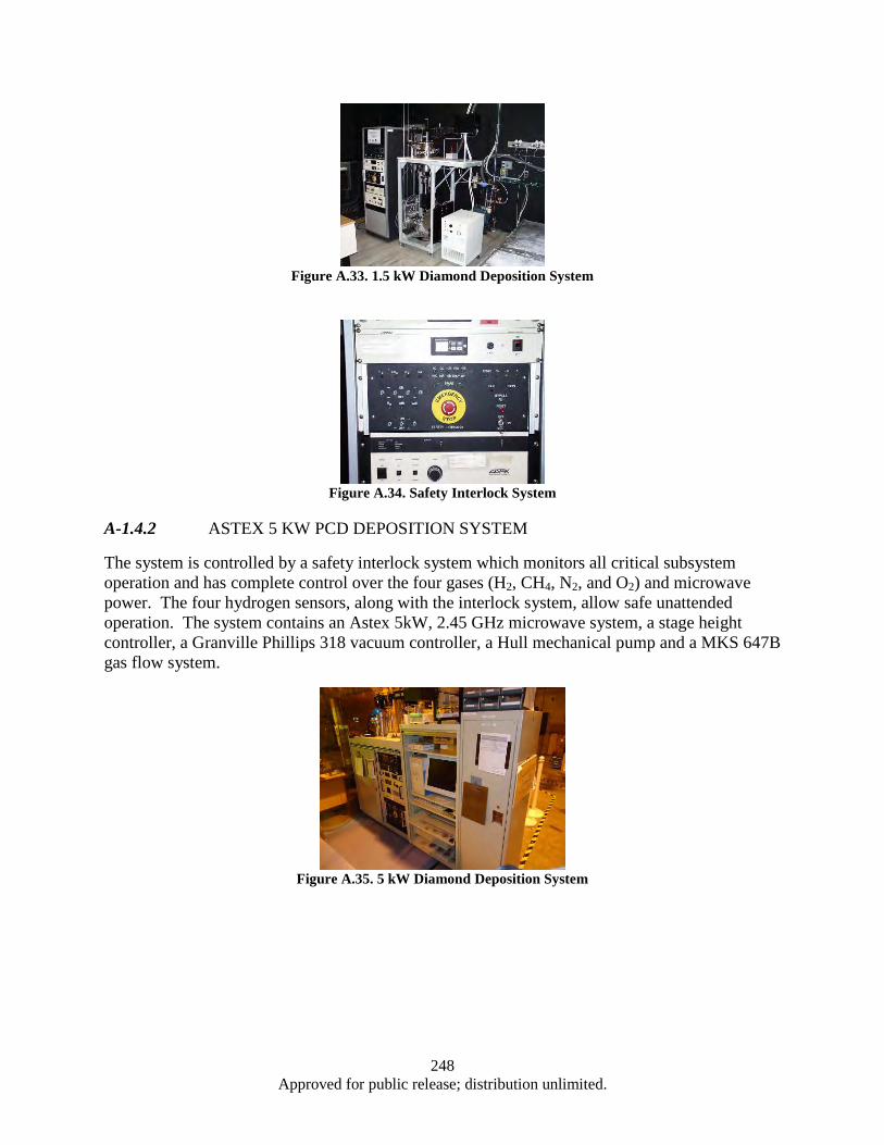
248 Approved for public release; distribution unlimited.
Figure A.33. 1.5 kW Diamond Deposition System
Figure A.34. Safety Interlock System
A-1.4.2 ASTEX 5 KW PCD DEPOSITION SYSTEM
The system is controlled by a safety interlock system which monitors all critical subsystem operation and has complete control over the four gases (H2, CH4, N2, and O2) and microwave power. The four hydrogen sensors, along with the interlock system, allow safe unattended operation. The system contains an Astex 5kW, 2.45 GHz microwave system, a stage height controller, a Granville Phillips 318 vacuum controller, a Hull mechanical pump and a MKS 647B gas flow system.
Figure A.35. 5 kW Diamond Deposition System
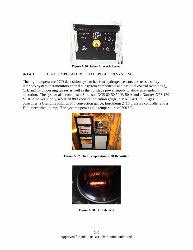
249 Approved for public release; distribution unlimited.
Figure A.36. Safety Interlock System
A-1.4.3 HIGH TEMPERATURE PCD DEPOSITION SYSTEM
The high-temperature PCD deposition system has four hydrogen sensors and uses a safety interlock system that monitors critical subsystem components and has total control over the H2, CH4 and O2 processing gasses as well as the hot stage power supply to allow unattended operation. The system also contains: a Sorenson DCS 60-50 50 V, 50 A and a Xantrex XFS 150 V, 10 A power supply, a Varian 880 vacuum ionization gauge, a MKS 647C multi-gas controller, a Granville Phillips 375 convection gauge, Eurotherm 2416 pressure controller and a Hull mechanical pump. The system operates at a temperature of 500 °C.
Figure A.37. High Temperature PCD Deposition
Figure A.38. Hot Filament
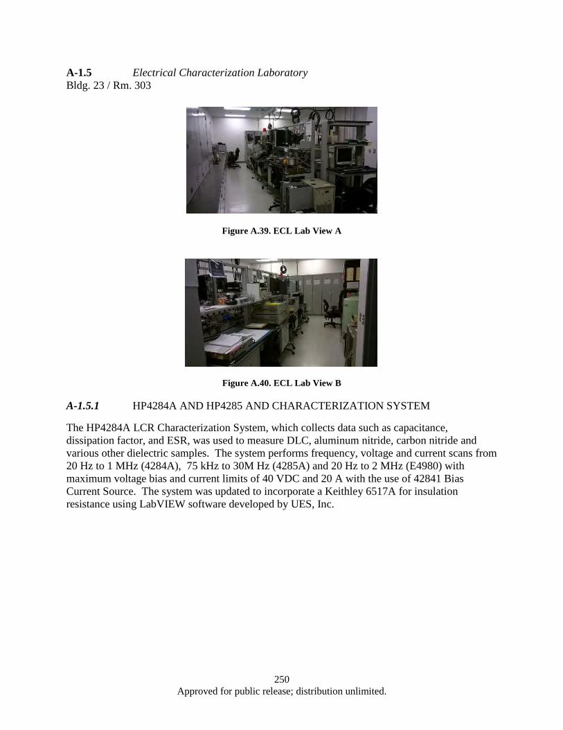
250 Approved for public release; distribution unlimited.
A-1.5 Electrical Characterization Laboratory Bldg. 23 / Rm. 303
Figure A.39. ECL Lab View A
Figure A.40. ECL Lab View B
A-1.5.1 HP4284A AND HP4285 AND CHARACTERIZATION SYSTEM
The HP4284A LCR Characterization System, which collects data such as capacitance, dissipation factor, and ESR, was used to measure DLC, aluminum nitride, carbon nitride and various other dielectric samples. The system performs frequency, voltage and current scans from 20 Hz to 1 MHz (4284A), 75 kHz to 30M Hz (4285A) and 20 Hz to 2 MHz (E4980) with maximum voltage bias and current limits of 40 VDC and 20 A with the use of 42841 Bias Current Source. The system was updated to incorporate a Keithley 6517A for insulation resistance using LabVIEW software developed by UES, Inc.
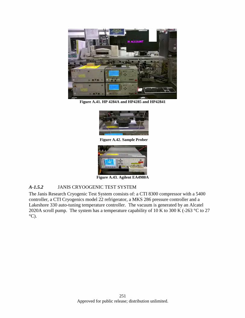
251 Approved for public release; distribution unlimited.
Figure A.41. HP 4284A and HP4285 and HP42841
Figure A.43. Agilent EA4980A
A-1.5.2 JANIS CRYOOGENIC TEST SYSTEM The Janis Research Cryogenic Test System consists of: a CTI 8300 compressor with a 5400 controller, a CTI Cryogenics model 22 refrigerator, a MKS 286 pressure controller and a Lakeshore 330 auto-tuning temperature controller. The vacuum is generated by an Alcatel 2020A scroll pump. The system has a temperature capability of 10 K to 300 K (-263 °C to 27 °C).
Figure A.42. Sample Prober
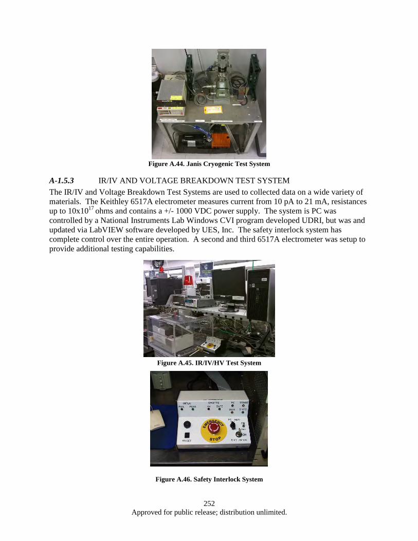
252 Approved for public release; distribution unlimited.
Figure A.44. Janis Cryogenic Test System
A-1.5.3 IR/IV AND VOLTAGE BREAKDOWN TEST SYSTEM The IR/IV and Voltage Breakdown Test Systems are used to collected data on a wide variety of materials. The Keithley 6517A electrometer measures current from 10 pA to 21 mA, resistances up to 10x1017 ohms and contains a +/- 1000 VDC power supply. The system is PC was controlled by a National Instruments Lab Windows CVI program developed UDRI, but was and updated via LabVIEW software developed by UES, Inc. The safety interlock system has complete control over the entire operation. A second and third 6517A electrometer was setup to provide additional testing capabilities.
Figure A.45. IR/IV/HV Test System
Figure A.46. Safety Interlock System
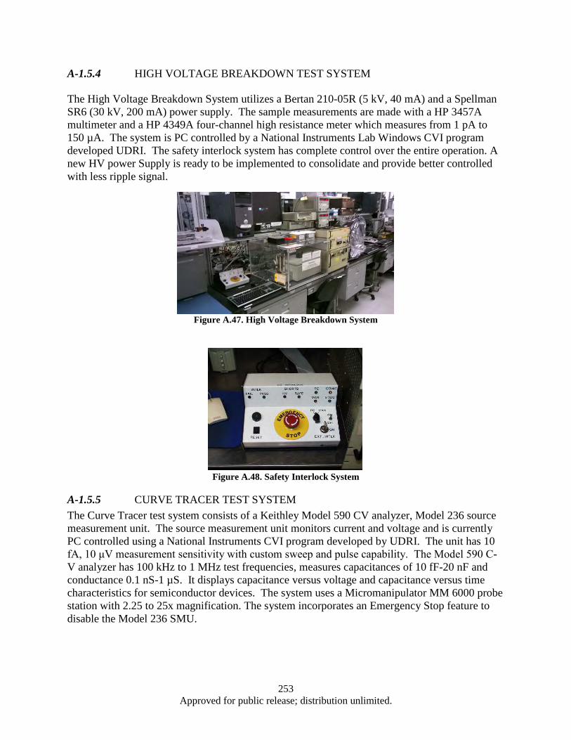
253 Approved for public release; distribution unlimited.
A-1.5.4 HIGH VOLTAGE BREAKDOWN TEST SYSTEM The High Voltage Breakdown System utilizes a Bertan 210-05R (5 kV, 40 mA) and a Spellman SR6 (30 kV, 200 mA) power supply. The sample measurements are made with a HP 3457A multimeter and a HP 4349A four-channel high resistance meter which measures from 1 pA to 150 µA. The system is PC controlled by a National Instruments Lab Windows CVI program developed UDRI. The safety interlock system has complete control over the entire operation. A new HV power Supply is ready to be implemented to consolidate and provide better controlled with less ripple signal.
Figure A.47. High Voltage Breakdown System
Figure A.48. Safety Interlock System
A-1.5.5 CURVE TRACER TEST SYSTEM The Curve Tracer test system consists of a Keithley Model 590 CV analyzer, Model 236 source measurement unit. The source measurement unit monitors current and voltage and is currently PC controlled using a National Instruments CVI program developed by UDRI. The unit has 10 fA, 10 μV measurement sensitivity with custom sweep and pulse capability. The Model 590 C-V analyzer has 100 kHz to 1 MHz test frequencies, measures capacitances of 10 fF-20 nF and conductance 0.1 nS-1 µS. It displays capacitance versus voltage and capacitance versus time characteristics for semiconductor devices. The system uses a Micromanipulator MM 6000 probe station with 2.25 to 25x magnification. The system incorporates an Emergency Stop feature to disable the Model 236 SMU.
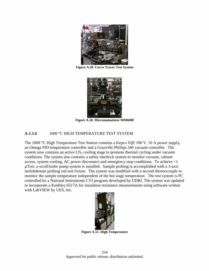
254 Approved for public release; distribution unlimited.
Figure A.49. Curve Tracer Test System
Figure A.50. Micromainulator MM6000
A-1.5.6 1000 °C HIGH TEMPERATURE TEST SYSTEM
The 1000 °C High Temperature Test Station contains a Kepco JQE 100 V, 10 A power supply, an Omega PID temperature controller and a Granville Phillips 340 vacuum controller. The system now contains an active LN2 cooling stage to promote thermal cycling under vacuum conditions. The system also contains a safety interlock system to monitor vacuum, cabinet access, system cooling, AC power disconnect and emergency stop conditions. To achieve <1 µTorr, a scroll/turbo pump system is installed. Sample probing is accomplished with a 3-axis molybdenum probing rod test fixture. The system was modified with a second thermocouple to monitor the sample temperature independent of the hot stage temperature. The test system is PC controlled by a National Instruments CVI program developed by UDRI. The system was updated to incorporate a Keithley 6517A for insulation resistance measurements using software written with LabVIEW by UES, Inc.
Figure A.51. High Temperature
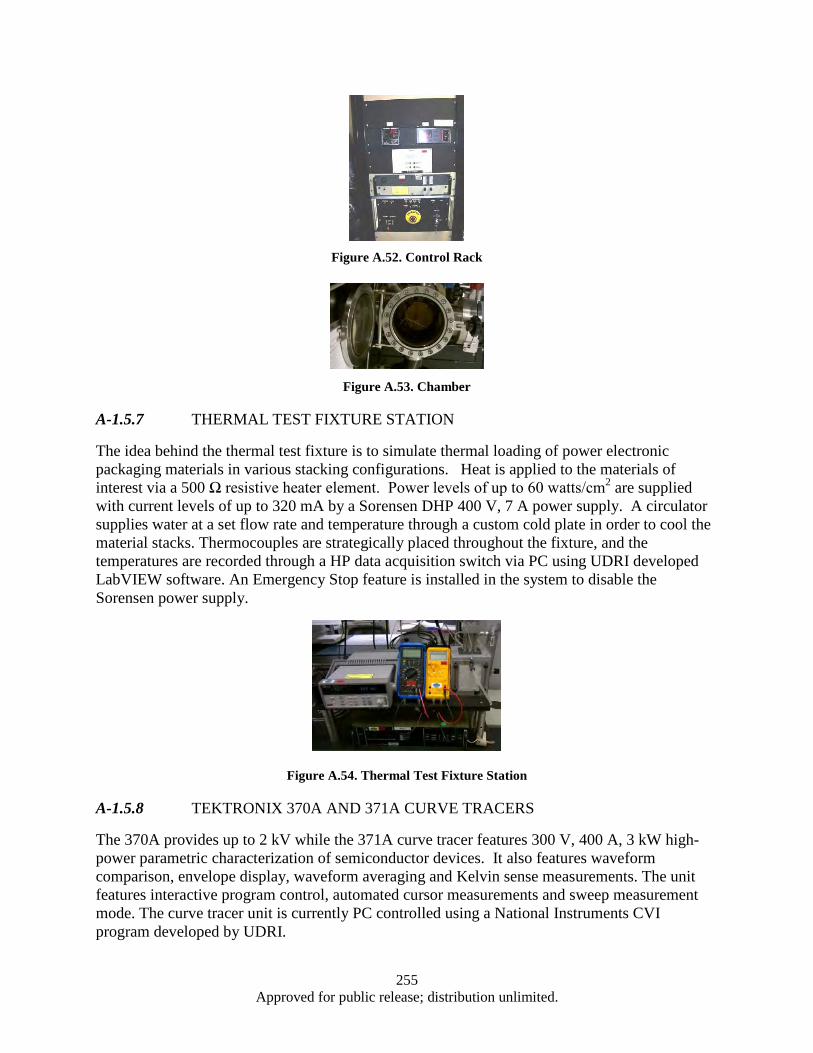
255 Approved for public release; distribution unlimited.
Figure A.52. Control Rack
Figure A.53. Chamber
A-1.5.7 THERMAL TEST FIXTURE STATION
The idea behind the thermal test fixture is to simulate thermal loading of power electronic packaging materials in various stacking configurations. Heat is applied to the materials of interest via a 500 Ω resistive heater element. Power levels of up to 60 watts/cm2 are supplied with current levels of up to 320 mA by a Sorensen DHP 400 V, 7 A power supply. A circulator supplies water at a set flow rate and temperature through a custom cold plate in order to cool the material stacks. Thermocouples are strategically placed throughout the fixture, and the temperatures are recorded through a HP data acquisition switch via PC using UDRI developed LabVIEW software. An Emergency Stop feature is installed in the system to disable the Sorensen power supply.
Figure A.54. Thermal Test Fixture Station
A-1.5.8 TEKTRONIX 370A AND 371A CURVE TRACERS
The 370A provides up to 2 kV while the 371A curve tracer features 300 V, 400 A, 3 kW high-power parametric characterization of semiconductor devices. It also features waveform comparison, envelope display, waveform averaging and Kelvin sense measurements. The unit features interactive program control, automated cursor measurements and sweep measurement mode. The curve tracer unit is currently PC controlled using a National Instruments CVI program developed by UDRI.
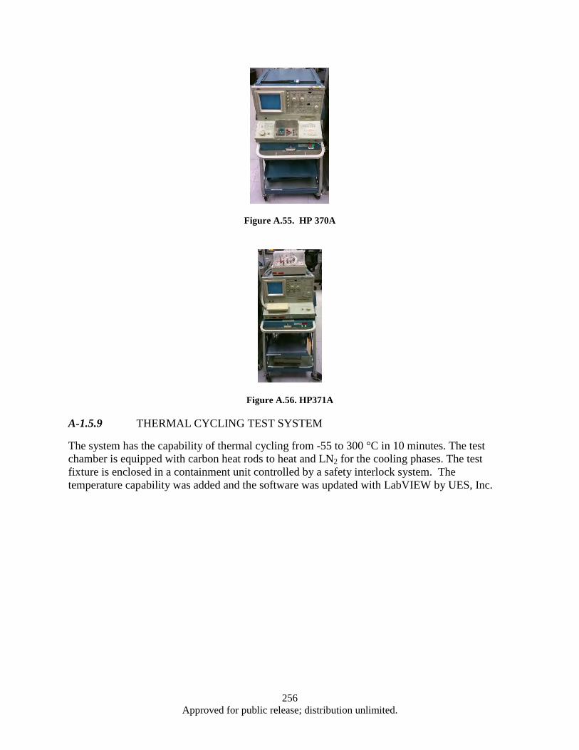
256 Approved for public release; distribution unlimited.
Figure A.55. HP 370A
Figure A.56. HP371A
A-1.5.9 THERMAL CYCLING TEST SYSTEM
The system has the capability of thermal cycling from -55 to 300 °C in 10 minutes. The test chamber is equipped with carbon heat rods to heat and LN2 for the cooling phases. The test fixture is enclosed in a containment unit controlled by a safety interlock system. The temperature capability was added and the software was updated with LabVIEW by UES, Inc.
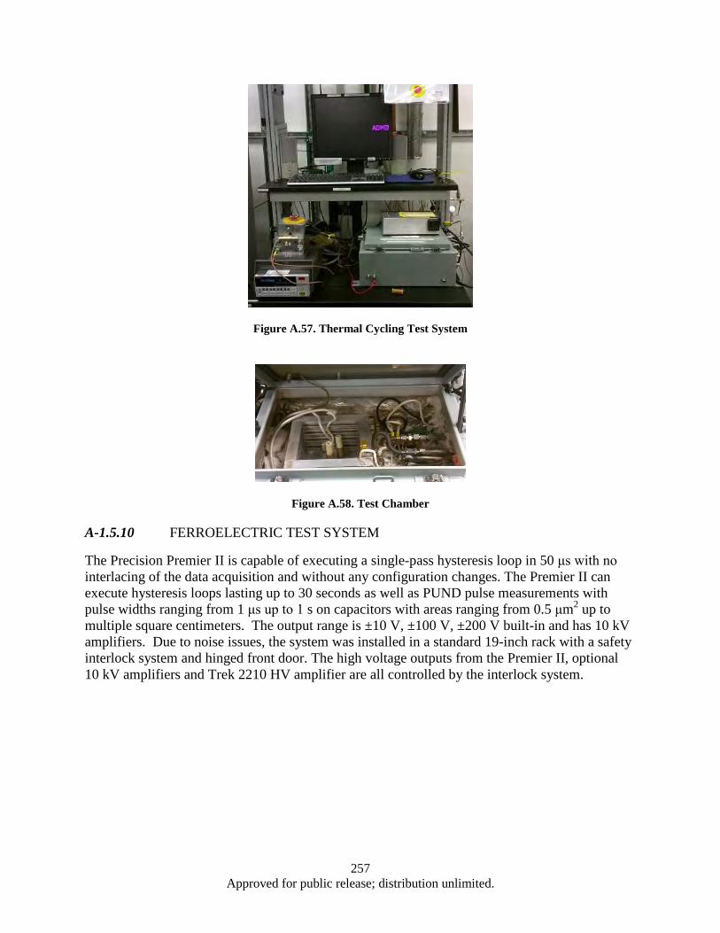
257 Approved for public release; distribution unlimited.
Figure A.57. Thermal Cycling Test System
Figure A.58. Test Chamber
A-1.5.10 FERROELECTRIC TEST SYSTEM
The Precision Premier II is capable of executing a single-pass hysteresis loop in 50 μs with no interlacing of the data acquisition and without any configuration changes. The Premier II can execute hysteresis loops lasting up to 30 seconds as well as PUND pulse measurements with pulse widths ranging from 1 μs up to 1 s on capacitors with areas ranging from 0.5 μm2 up to multiple square centimeters. The output range is ±10 V, ±100 V, ±200 V built-in and has 10 kV amplifiers. Due to noise issues, the system was installed in a standard 19-inch rack with a safety interlock system and hinged front door. The high voltage outputs from the Premier II, optional 10 kV amplifiers and Trek 2210 HV amplifier are all controlled by the interlock system.
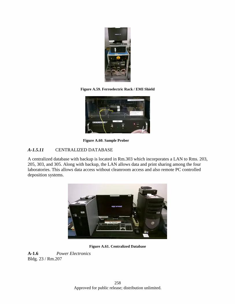
258 Approved for public release; distribution unlimited.
Figure A.59. Ferroelectric Rack / EMI Shield
Figure A.60. Sample Prober
A-1.5.11 CENTRALIZED DATABASE
A centralized database with backup is located in Rm.303 which incorporates a LAN to Rms. 203, 205, 303, and 305. Along with backup, the LAN allows data and print sharing among the four laboratories. This allows data access without cleanroom access and also remote PC controlled deposition systems.
Figure A.61. Centralized Database A-1.6 Power Electronics Bldg. 23 / Rm.207
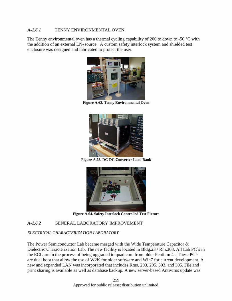
259 Approved for public release; distribution unlimited.
A-1.6.1 TENNY ENVIRONMENTAL OVEN
The Tenny environmental oven has a thermal cycling capability of 200 to down to -50 °C with the addition of an external LN2 source. A custom safety interlock system and shielded test enclosure was designed and fabricated to protect the user.
Figure A.62. Tenny Environmental Oven
Figure A.63. DC-DC Converter Load Bank
Figure A.64. Safety Interlock Controlled Test Fixture
A-1.6.2 GENERAL LABORATORY IMPROVEMENT
ELECTRICAL CHARACTERIZATION LABORATORY The Power Semiconductor Lab became merged with the Wide Temperature Capacitor & Dielectric Characterization Lab. The new facility is located in Bldg.23 / Rm.303. All Lab PC`s in the ECL are in the process of being upgraded to quad core from older Pentium 4s. These PC`s are dual boot that allow the use of W2K for older software and Win7 for current development. A new and expanded LAN was incorporated that includes Rms. 203, 205, 303, and 305. File and print sharing is available as well as database backup. A new server-based Antivirus update was
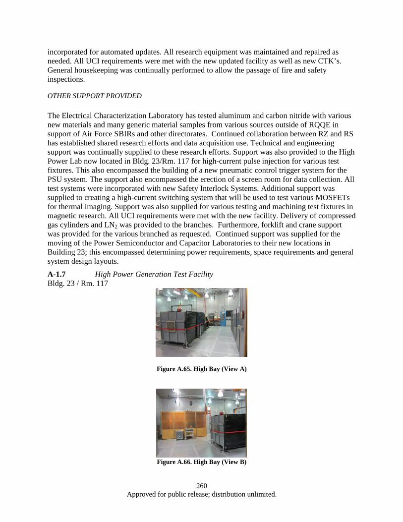
260 Approved for public release; distribution unlimited.
incorporated for automated updates. All research equipment was maintained and repaired as needed. All UCI requirements were met with the new updated facility as well as new CTK’s. General housekeeping was continually performed to allow the passage of fire and safety inspections.
OTHER SUPPORT PROVIDED The Electrical Characterization Laboratory has tested aluminum and carbon nitride with various new materials and many generic material samples from various sources outside of RQQE in support of Air Force SBIRs and other directorates. Continued collaboration between RZ and RS has established shared research efforts and data acquisition use. Technical and engineering support was continually supplied to these research efforts. Support was also provided to the High Power Lab now located in Bldg. 23/Rm. 117 for high-current pulse injection for various test fixtures. This also encompassed the building of a new pneumatic control trigger system for the PSU system. The support also encompassed the erection of a screen room for data collection. All test systems were incorporated with new Safety Interlock Systems. Additional support was supplied to creating a high-current switching system that will be used to test various MOSFETs for thermal imaging. Support was also supplied for various testing and machining test fixtures in magnetic research. All UCI requirements were met with the new facility. Delivery of compressed gas cylinders and LN2 was provided to the branches. Furthermore, forklift and crane support was provided for the various branched as requested. Continued support was supplied for the moving of the Power Semiconductor and Capacitor Laboratories to their new locations in Building 23; this encompassed determining power requirements, space requirements and general system design layouts. A-1.7 High Power Generation Test Facility Bldg. 23 / Rm. 117
Figure A.65. High Bay (View A)
Figure A.66. High Bay (View B)
261 Approved for public release; distribution unlimited.
The entire facility is enclosed in an EMI steel shielded room to contain large induced electromagnetic fields. The facility also has a double wall shielded copper screenroom to provide noise reduction for data acquisition.
A-1.7.1 PULSE SIMULATION UNIT (PSU BANK) LIGHTNING SIMULATION
The Pulse Simulation Unit is a 200 kV/30 kA/80 kikJ critically damp or 100 kA oscillatory pulse output. The critically damped pulse is a 2 microsecond rise time and 50 microsecond tail. The capacitor banks consists of 2 components of eight 50 kV/4uF capacitors. The bank is configured in a series/parallel arrangement. A HV switch is incorporated to allow parallel charging and then isolation during the series discharge as a Marx generator. A pneumatic control system is incorporated to control the HV switch, trigger and shorting system. The system is based on a dead-man principle to ensure safety. The following schematic represents the overall circuit. The System also contains an Emergency Stop to immediately discharge the capacitor bank to ground.
Figure A.67. PSU Bank
Figure A.68. Control
Figure A.69. Switch
262 Approved for public release; distribution unlimited.
Figure A.70. OSU
Drawing B1. Circuit Diagram
Figure A.71. Circuit Diagram
A-1.7.2 HIPOTRONICS AC DIELECTRIC TEST SYSTEM
The system delivers an output up to 150 kV AC at 20 kVA to conduct dielectric testing of insulative materials. The system provides a manual or automated test condition with rate of rise, dwell time and a register to provide the failure time. The System was incorporated with an Emergency Stop feature to disable the HV output.
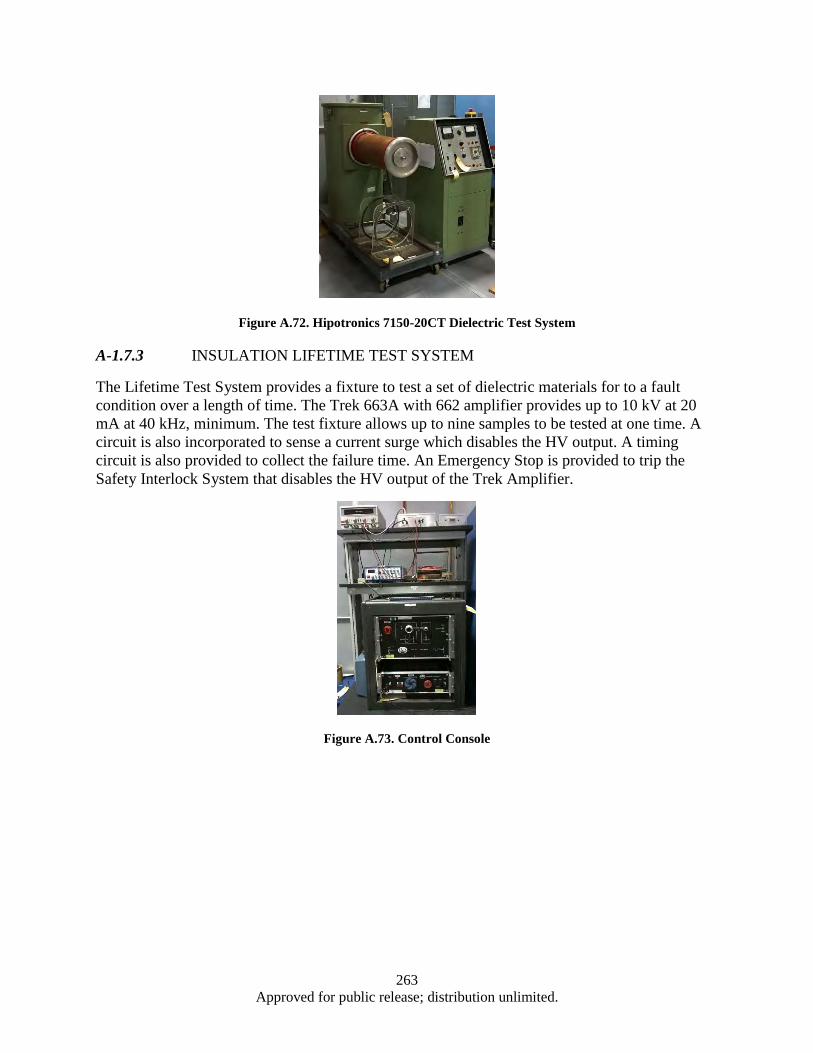
263 Approved for public release; distribution unlimited.
Figure A.72. Hipotronics 7150-20CT Dielectric Test System
A-1.7.3 INSULATION LIFETIME TEST SYSTEM
The Lifetime Test System provides a fixture to test a set of dielectric materials for to a fault condition over a length of time. The Trek 663A with 662 amplifier provides up to 10 kV at 20 mA at 40 kHz, minimum. The test fixture allows up to nine samples to be tested at one time. A circuit is also incorporated to sense a current surge which disables the HV output. A timing circuit is also provided to collect the failure time. An Emergency Stop is provided to trip the Safety Interlock System that disables the HV output of the Trek Amplifier.
Figure A.73. Control Console
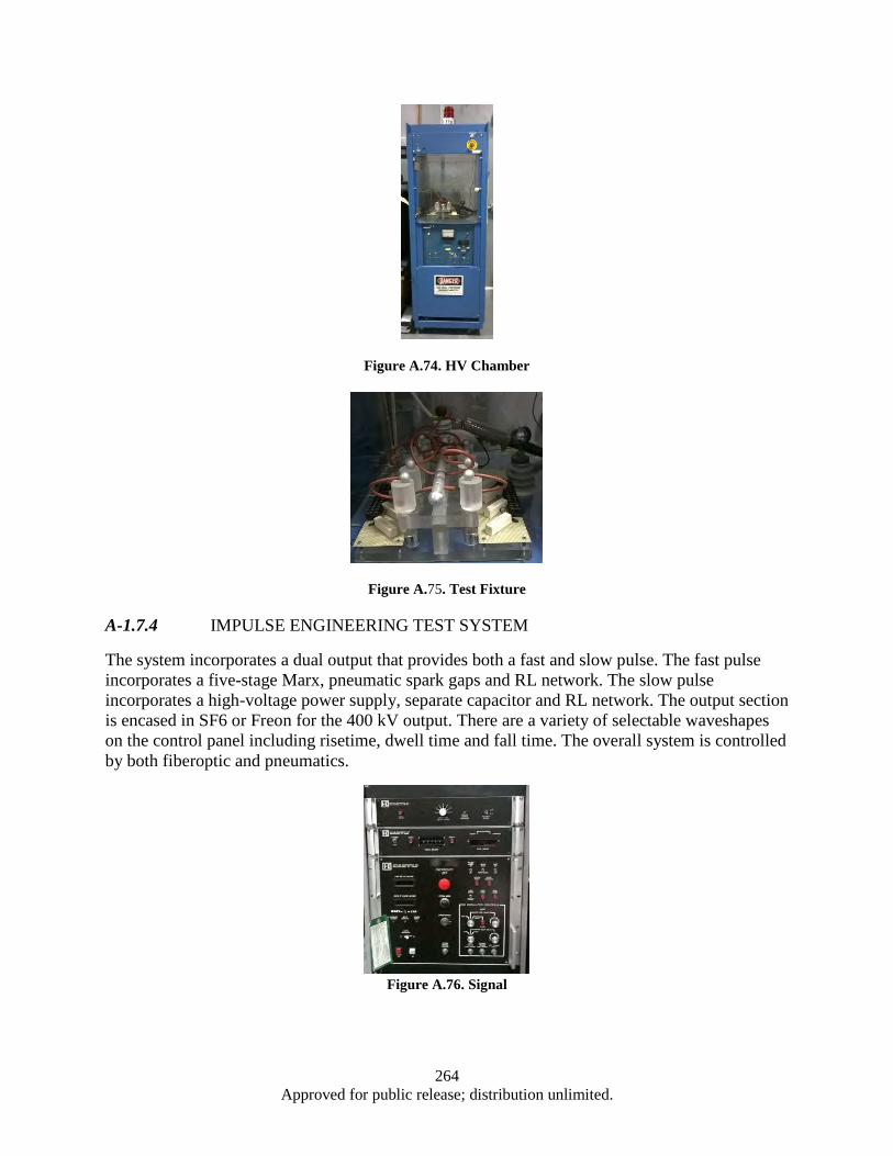
264 Approved for public release; distribution unlimited.
Figure A.74. HV Chamber
Figure A.75. Test Fixture
A-1.7.4 IMPULSE ENGINEERING TEST SYSTEM
The system incorporates a dual output that provides both a fast and slow pulse. The fast pulse incorporates a five-stage Marx, pneumatic spark gaps and RL network. The slow pulse incorporates a high-voltage power supply, separate capacitor and RL network. The output section is encased in SF6 or Freon for the 400 kV output. There are a variety of selectable waveshapes on the control panel including risetime, dwell time and fall time. The overall system is controlled by both fiberoptic and pneumatics.
Figure A.76. Signal
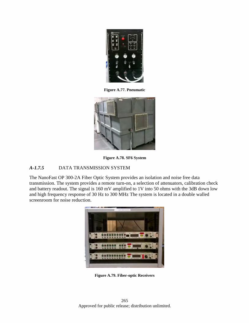
265 Approved for public release; distribution unlimited.
Figure A.77. Pneumatic
Figure A.78. SF6 System
A-1.7.5 DATA TRANSMISSION SYSTEM
The NanoFast OP 300-2A Fiber Optic System provides an isolation and noise free data transmission. The system provides a remote turn-on, a selection of attenuators, calibration check and battery readout. The signal is 160 mV amplified to 1V into 50 ohms with the 3dB down low and high frequency response of 30 Hz to 300 MHz The system is located in a double walled screenroom for noise reduction.
Figure A.79. Fiber-optic Receivers

266 Approved for public release; distribution unlimited.
Figure A.80. Fiber-optic Battery Transmitters

267 Approved for public release; distribution unlimited.
Nomenclature
AC Ammonium carbamate –(Section 1) AC Alternative current cp Specific heat capacity (J/g °C) h Specific enthalpy (J/g) HEX Heat exchanger/chemical reactor ṁ Mass flow rate (g/s) PG Propylene glycol q Heat transfer rate (W) Re Reynolds number T Temperature (°C) M Ω Mega Ohm CRADA Cooperative Research and Development Agreement NMP N-Methyl-2- Pyrrolidone DME Dimethyl Ether BAI 1,3- bis(1-adamantyl) imidazolium lithium phythalocyanine LiTFSI Lithium bis- (trifluoromethylsulfonyl)imide OCV Open Circuit Voltage HFI High Frequency Intercept LFI Low Frequency Intercept TBA Tetrabutylammonium Iodide SSE Solid State Electrolyte PEO Polyethylene Oxide TE Thermoelectric NIST National Industrial Standard Test DC Direct Current RE Rare Earth DSC Differencial Scanning Calorimetry HP Hot Press HIP Hot Isostatic Press WM Wet Milling DM Dry Milling WC Tungsten Carbide HMDS Hexamethyldisilazane VSM Vibration Sample Magnetometer EMA Elecromagnetic Actuator PID Proportional Integral Derivative CNTP Carbon nanotube Paper ASH Apparent superheat [oC] COP Coefficient of Performance BPCV Back pressure control valve 𝑁𝑁𝑑𝑑 Constant pressure specific heat (J kg-1K-1) 𝑁𝑁𝑣𝑣 Constant volume specific heat (J kg-1K-1)
268 Approved for public release; distribution unlimited.
dT Driving temperature difference [oC] EXV Electronic expansion valve h Specific enthalpy (J kg-1) INVENT Integrated vehicle energy technology LQI Liquid injection 𝑚 Mass flow rate (kg s-1) 𝑄 Heat transfer rate (J s-1) Q Heat transfer (MJ) P Pressure (Pa) PID Proportional integral differential REFPROP Reference fluid thermodynamic and transport properties software SDP Saturated discharge pressure [MPa] SDT Saturated discharge temperature [oC] SSP Saturated suction pressure [MPa] SST Saturated suction temperature [oC] ∆𝑇𝑇 Absolute value of heat load oil temperature change across the
evaporator (oC) VCS Vapor compression system VCSRF Vapor compression system research facility 𝑊 Compressor power (J s-1)
Subscripts baseline Single-phase flow (no AC decomposition) rxn Reaction decomp Occurs during decomposition react Reactant side of HEX reactor water Water side of HEX reactor
comp Compressor e Evaporator l loads
Liquid Loads
low Coldest evaporator heat load oil set point o Heat load oil 4 Panel 4 5 Panel 5
Greek Symbols
𝛿𝛿 Ratio of constant pressure specific heat to constant volume specific heat ε Conversion (fraction or percent)
Related Documents