Instruction Manual P7350SMA 5 GHz Differential Probe 071-1264-01 Warning The servicing instructions are for use by qualified personnel only. To avoid personal injury, do not perform any servicing unless you are qualified to do so. Refer to all safety summaries prior to performing service. www.tektronix.com Advanced Test Equipment Rentals www.atecorp.com 800-404-ATEC (2832) ® E s t a blishe d 1 9 8 1

Welcome message from author
This document is posted to help you gain knowledge. Please leave a comment to let me know what you think about it! Share it to your friends and learn new things together.
Transcript
Instruction Manual
P7350SMA
5 GHz Differential Probe
071-1264-01
Warning
The servicing instructions are for use by qualified
personnel only. To avoid personal injury, do not
perform any servicing unless you are qualified to
do so. Refer to all safety summaries prior to
performing service.
www.tektronix.com
Advanced Test Equipment Rentalswww.atecorp.com 800-404-ATEC (2832)
®
Established 1981
Copyright © Tektronix, Inc. All rights reserved.
Tektronix products are covered by U.S. and foreign patents, issued and
pending. Information in this publication supercedes that in all previously
published material. Specifications and price change privileges reserved.
Tektronix, Inc., P.O. Box 500, Beaverton, OR 97077
TEKTRONIX, TEK, and TekConnect are registered trademarks of
Tektronix, Inc.
WARRANTY
Tektronix warrants that the products that it manufactures and sells will be free from defects
in materials and workmanship for a period of one (1) year from the date of shipment. If a
product proves defective during this warranty period, Tektronix, at its option, either will
repair the defective product without charge for parts and labor, or will provide a
replacement in exchange for the defective product.
In order to obtain service under this warranty, Customer must notify Tektronix of the
defect before the expiration of the warranty period and make suitable arrangements for the
performance of service. Customer shall be responsible for packaging and shipping the
defective product to the service center designated by Tektronix, with shipping charges
prepaid. Tektronix shall pay for the return of the product to Customer if the shipment is to
a location within the country in which the Tektronix service center is located. Customer
shall be responsible for paying all shipping charges, duties, taxes, and any other charges for
products returned to any other locations.
This warranty shall not apply to any defect, failure or damage caused by improper use or
improper or inadequate maintenance and care. Tektronix shall not be obligated to furnish
service under this warranty a) to repair damage resulting from attempts by personnel other
than Tektronix representatives to install, repair or service the product; b) to repair damage
resulting from improper use or connection to incompatible equipment; c) to repair any
damage or malfunction caused by the use of non-Tektronix supplies; or d) to service a
product that has been modified or integrated with other products when the effect of such
modification or integration increases the time or difficulty of servicing the product.
THIS WARRANTY IS GIVEN BY TEKTRONIX IN LIEU OF ANY OTHER
WARRANTIES, EXPRESS OR IMPLIED. TEKTRONIX AND ITS VENDORS
DISCLAIM ANY IMPLIED WARRANTIES OF MERCHANTABILITY OR
FITNESS FOR A PARTICULAR PURPOSE. TEKTRONIX’ RESPONSIBILITY
TO REPAIR OR REPLACE DEFECTIVE PRODUCTS IS THE SOLE AND
EXCLUSIVE REMEDY PROVIDED TO THE CUSTOMER FOR BREACH OF
THIS WARRANTY. TEKTRONIX AND ITS VENDORS WILL NOT BE LIABLE
FOR ANY INDIRECT, SPECIAL, INCIDENTAL, OR CONSEQUENTIAL
DAMAGES IRRESPECTIVE OF WHETHER TEKTRONIX OR THE VENDOR
HAS ADVANCE NOTICE OF THE POSSIBILITY OF SUCH DAMAGES.

P7350SMA 5 GHz Differential Probe Instruction Manual i
Table of Contents
Preface v. . . . . . . . . . . . . . . . . . . . . . . . . . . . . . . . . . . . . . . . . . . .
Contacting Tektronix vi. . . . . . . . . . . . . . . . . . . . . . . . . . . . . . . . .
General Safety Summary vii. . . . . . . . . . . . . . . . . . . . . . . . . . . . . .
Service Safety Summary ix. . . . . . . . . . . . . . . . . . . . . . . . . . . . . .
Getting Started 1. . . . . . . . . . . . . . . . . . . . . . . . . . . . . . . . . . . . .
Features and Standard Accessories 2. . . . . . . . . . . . . . . . . . . . . .
Optional Accessories 5. . . . . . . . . . . . . . . . . . . . . . . . . . . . . . . . .
Options 6. . . . . . . . . . . . . . . . . . . . . . . . . . . . . . . . . . . . . . . . . . . .
P7350SMA Probe Head 7. . . . . . . . . . . . . . . . . . . . . . . . . . . . . . .
TekConnect Interface 9. . . . . . . . . . . . . . . . . . . . . . . . . . . . . . . . .
Functional Check 10. . . . . . . . . . . . . . . . . . . . . . . . . . . . . . . . . . . .
Signal Check 10. . . . . . . . . . . . . . . . . . . . . . . . . . . . . . . . . . . . . . .
DC Termination Check 11. . . . . . . . . . . . . . . . . . . . . . . . . . . . . . .
Probe Calibration 13. . . . . . . . . . . . . . . . . . . . . . . . . . . . . . . . . . . .
Probe Applications 14. . . . . . . . . . . . . . . . . . . . . . . . . . . . . . . . . . .
Operating Basics 15. . . . . . . . . . . . . . . . . . . . . . . . . . . . . . . . . . .
Input Circuitry 15. . . . . . . . . . . . . . . . . . . . . . . . . . . . . . . . . . . . . .
Probe Termination Network 16. . . . . . . . . . . . . . . . . . . . . . . . . . .
Differential Signals 16. . . . . . . . . . . . . . . . . . . . . . . . . . . . . . . . . .
Single-Ended Signals 17. . . . . . . . . . . . . . . . . . . . . . . . . . . . . . . . .
Matched-Delay Cables 19. . . . . . . . . . . . . . . . . . . . . . . . . . . . . . .
DC Termination Voltage Input 21. . . . . . . . . . . . . . . . . . . . . . . . .
Calculating DC Termination Resistor Power 22. . . . . . . . . . . . . .
DC Voltage Applied to SMA Inputs with the
DC Termination Voltage Input Grounded 23. . . . . . . . . . . . . .
Complementary Input Signal with the
DC Termination Voltage Input Open 24. . . . . . . . . . . . . . . . . .
Complementary Input Signal with the
DC Termination Voltage Input Shorted (Grounded) 26. . . . . .
Equations and Definitions 28. . . . . . . . . . . . . . . . . . . . . . . . . . . . .
Internal Probe Amplifier 29. . . . . . . . . . . . . . . . . . . . . . . . . . . . . .
Maximum Input Voltage 29. . . . . . . . . . . . . . . . . . . . . . . . . . . . . .
Common-Mode Signal Range 29. . . . . . . . . . . . . . . . . . . . . . . . . .
Differential-Mode Signal Range 29. . . . . . . . . . . . . . . . . . . . . . . .
Differential Offset Range 30. . . . . . . . . . . . . . . . . . . . . . . . . . . . .
Common-Mode Rejection 31. . . . . . . . . . . . . . . . . . . . . . . . . . . . .
Input Impedance and Probe Loading 31. . . . . . . . . . . . . . . . . . . . .
Table of Contents
ii P7350SMA 5 GHz Differential Probe Instruction Manual
Checking the Skew Between Inputs 32. . . . . . . . . . . . . . . . . . . . .
Adjusting Cable Skew 33. . . . . . . . . . . . . . . . . . . . . . . . . . . . . . . .
Deskewing Probes 35. . . . . . . . . . . . . . . . . . . . . . . . . . . . . . . . . . .
Reference 39. . . . . . . . . . . . . . . . . . . . . . . . . . . . . . . . . . . . . . . . .
Differential Measurements 39. . . . . . . . . . . . . . . . . . . . . . . . . . . .
Common-Mode Rejection Ratio 40. . . . . . . . . . . . . . . . . . . . . . . .
Extending the Input Connections 41. . . . . . . . . . . . . . . . . . . . . . .
InfiniBand 42. . . . . . . . . . . . . . . . . . . . . . . . . . . . . . . . . . . . . . . . .
Appendix A: Specifications 43. . . . . . . . . . . . . . . . . . . . . . . . . . .
Warranted Characteristics 43. . . . . . . . . . . . . . . . . . . . . . . . . . . . .
Typical Characteristics 44. . . . . . . . . . . . . . . . . . . . . . . . . . . . . . .
Nominal Characteristics 48. . . . . . . . . . . . . . . . . . . . . . . . . . . . . .
Mechanical Characteristics 48. . . . . . . . . . . . . . . . . . . . . . . . . . . .
Appendix B: Performance Verification 51. . . . . . . . . . . . . . . . .
Equipment Required 51. . . . . . . . . . . . . . . . . . . . . . . . . . . . . . . . .
Special Adapters Required 53. . . . . . . . . . . . . . . . . . . . . . . . . . . .
TekConnect-to-SMA Adapter 53. . . . . . . . . . . . . . . . . . . . . . . . . .
TekConnect Interface Calibration Adapter 54. . . . . . . . . . . . . . . .
Equipment Setup 55. . . . . . . . . . . . . . . . . . . . . . . . . . . . . . . . . . . .
Input Resistance 56. . . . . . . . . . . . . . . . . . . . . . . . . . . . . . . . . . . . .
Output Offset Zero 57. . . . . . . . . . . . . . . . . . . . . . . . . . . . . . . . . . .
DC Gain Accuracy 58. . . . . . . . . . . . . . . . . . . . . . . . . . . . . . . . . . .
Rise Time 60. . . . . . . . . . . . . . . . . . . . . . . . . . . . . . . . . . . . . . . . . .
Appendix C: Maintenance 67. . . . . . . . . . . . . . . . . . . . . . . . . . .
Inspection and Cleaning 67. . . . . . . . . . . . . . . . . . . . . . . . . . . . . .
Replacement Parts 68. . . . . . . . . . . . . . . . . . . . . . . . . . . . . . . . . . .
Preparation for Shipment 68. . . . . . . . . . . . . . . . . . . . . . . . . . . . . .
Appendix D: Replaceable Parts 69. . . . . . . . . . . . . . . . . . . . . . .
Parts Ordering Information 69. . . . . . . . . . . . . . . . . . . . . . . . . . . .
Using the Replaceable Parts List 70. . . . . . . . . . . . . . . . . . . . . . . .
Item Names 70. . . . . . . . . . . . . . . . . . . . . . . . . . . . . . . . . . . . . . . .
Indentation System 70. . . . . . . . . . . . . . . . . . . . . . . . . . . . . . . . . .
Abbreviations 70. . . . . . . . . . . . . . . . . . . . . . . . . . . . . . . . . . . . . . .
Table of Contents
P7350SMA 5 GHz Differential Probe Instruction Manual iii
List of Figures
Figure 1: P7350SMA differential probe 1. . . . . . . . . . . . . . . . . .
Figure 2: Probe head connections 8. . . . . . . . . . . . . . . . . . . . . . .
Figure 3: Connecting and disconnecting the probe 9. . . . . . . . . .
Figure 4: Probe signal check setup 10. . . . . . . . . . . . . . . . . . . . . .
Figure 5: Probe DC termination check 12. . . . . . . . . . . . . . . . . . .
Figure 6: Typical probe applications and configurations 14. . . . .
Figure 7: Simplified probe schematic 15. . . . . . . . . . . . . . . . . . . .
Figure 8: Single-ended drive 17. . . . . . . . . . . . . . . . . . . . . . . . . . .
Figure 9: Resultant waveform from an unterminated input 18. . .
Figure 10: Distorted pulse edge 20. . . . . . . . . . . . . . . . . . . . . . . . .
Figure 11: Worst-case power dissipation example 23. . . . . . . . . .
Figure 12: Example of probe with DC input open 24. . . . . . . . . .
Figure 13: Example of probe with DC input shorted to ground 26
Figure 14: Probe amplifier and offset circuit 30. . . . . . . . . . . . . .
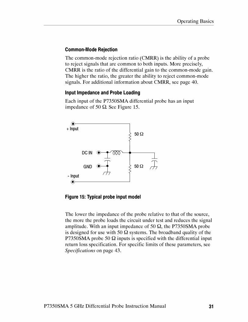
Figure 15: Typical probe input model 31. . . . . . . . . . . . . . . . . . . .
Figure 16: Checking skew between inputs 33. . . . . . . . . . . . . . . .
Figure 17: Using the phase adjuster 34. . . . . . . . . . . . . . . . . . . . .
Figure 18: Deskewing two P7350SMA probes 36. . . . . . . . . . . . .
Figure 19: Simplified model of a differential amplifier 39. . . . . .
Figure 20: InfiniBand signals 42. . . . . . . . . . . . . . . . . . . . . . . . . .
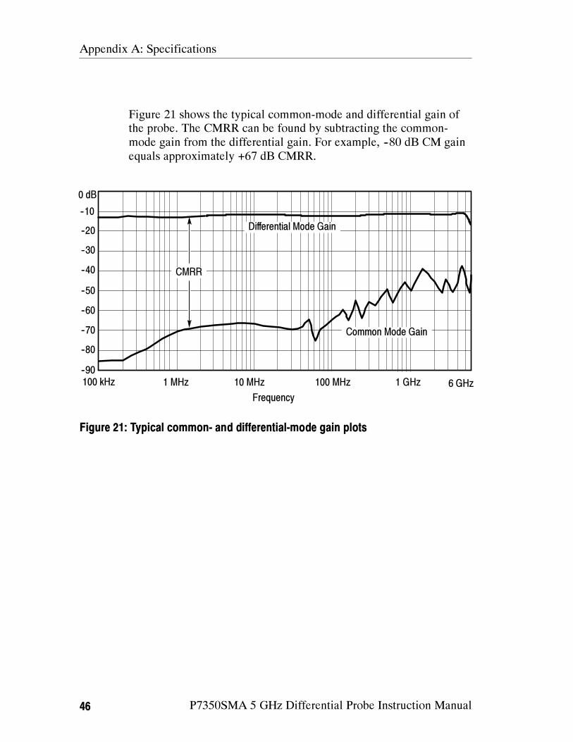
Figure 21: Typical common- and differential-mode gain plots 46
Figure 22: Typical differential input return loss 47. . . . . . . . . . . .
Figure 23: Typical differential-mode bandwidth 47. . . . . . . . . . . .
Figure 24: Probe head and compensation box dimensions 49. . . .
Figure 25: TekConnect-to-SMA Adapter 53. . . . . . . . . . . . . . . . .
Figure 26: TekConnect Interface Calibration Adapter 54. . . . . . .
Figure 27: Checking differential mode input resistance 56. . . . . .
Figure 28: Setup for the output offset zero test 57. . . . . . . . . . . . .
Figure 29: DC Gain Accuracy setup 58. . . . . . . . . . . . . . . . . . . . .
Figure 30: Reverse the power supply polarity
on the probe inputs 59. . . . . . . . . . . . . . . . . . . . . . . . . . . . . . . .
Figure 31: Test system rise time setup 61. . . . . . . . . . . . . . . . . . .
Figure 32: Setting the TDR parameters 62. . . . . . . . . . . . . . . . . . .
Figure 33: Test system rise time setup with probe 64. . . . . . . . . .
Figure 34: Replaceable parts 71. . . . . . . . . . . . . . . . . . . . . . . . . . .
Figure 35: Standard accessories 72. . . . . . . . . . . . . . . . . . . . . . . .
Figure 36: Optional accessories 74. . . . . . . . . . . . . . . . . . . . . . . . .
Table of Contents
iv P7350SMA 5 GHz Differential Probe Instruction Manual
P7350SMA 5 GHz Differential Probe Instruction Manual v
Preface
This is the Instruction Manual for the P7350SMA differential probe.
This manual provides operating information, specifications,
performance verification procedures, and a replaceable parts list.
Preface
vi P7350SMA 5 GHz Differential Probe Instruction Manual
Contacting Tektronix
Phone 1-800-833-9200*
Address Tektronix, Inc.
Department or name (if known)
14200 SW Karl Braun Drive
P.O. Box 500
Beaverton, OR 97077
USA
Web site www.tektronix.com
Sales
support
1-800-833-9200, select option 1*
Service
support
1-800-833-9200, select option 2*
Technical
support
www.tektronix.com/support
1-800-833-9200, select option 3*
6:00 a.m. -- 5:00 p.m. Pacific Standard Time
* This phone number is toll free in North America. After office hours, please
leave a voice mail message.
Outside North America, contact a Tektronix sales office or distributor; see
the Tektronix web site for a list of offices.
P7350SMA 5 GHz Differential Probe Instruction Manual vii
General Safety Summary
Review the following safety precautions to avoid injury and prevent
damage to this product or any products connected to it. To avoid
potential hazards, use this product only as specified.
To Avoid Fire or Personal Injury
Connect and Disconnect Properly. Connect the probe output to the
measurement instrument before connecting the probe to the circuit
under test. Disconnect the probe input from the circuit under test
before disconnecting the probe from the measurement instrument.
Observe All Terminal Ratings. To avoid fire or shock hazard, observe all
ratings and markings on the product. Consult the product manual for
further ratings information before making connections to the product.
The common terminal is at ground potential. Do not connect the
common terminal to elevated voltages.
Do Not Operate Without Covers. Do not operate this product with
covers or panels removed.
Do Not Operate With Suspected Failures. If you suspect there is damage
to this product, have it inspected by qualified service personnel.
Do Not Operate in Wet/Damp Conditions.
Do Not Operate in an Explosive Atmosphere.
Keep Product Surfaces Clean and Dry.
General Safety Summary
viii P7350SMA 5 GHz Differential Probe Instruction Manual
Safety Terms and Symbols
Terms in This Manual. These terms may appear in this manual:
WARNING. Warning statements identify conditions or practices that
could result in injury or loss of life.
CAUTION. Caution statements identify conditions or practices that
could result in damage to this product or other property.
Terms on the Product. These terms may appear on the product:
DANGER indicates an injury hazard immediately accessible as you
read the marking.
WARNING indicates an injury hazard not immediately accessible as
you read the marking.
CAUTION indicates a hazard to property including the product.
Symbols on the Product. These symbols may appear on the product:
CAUTION
Refer to Manual
P7350SMA 5 GHz Differential Probe Instruction Manual ix
Service Safety Summary
Only qualified personnel should perform service procedures. Read
this Service Safety Summary and the General Safety Summary before
performing any service procedures.
Do Not Service Alone. Do not perform internal service or adjustments
of this product unless another person capable of rendering first aid
and resuscitation is present.

Service Safety Summary
x P7350SMA 5 GHz Differential Probe Instruction Manual
P7350SMA 5 GHz Differential Probe Instruction Manual 1
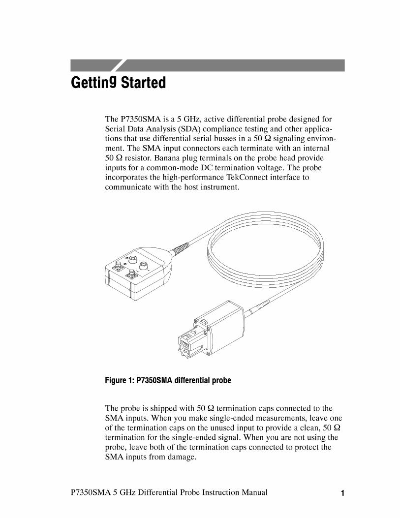
Getting Started
The P7350SMA is a 5 GHz, active differential probe designed for
Serial Data Analysis (SDA) compliance testing and other applica-
tions that use differential serial busses in a 50 Ω signaling environ-
ment. The SMA input connectors each terminate with an internal
50 Ω resistor. Banana plug terminals on the probe head provide
inputs for a common-mode DC termination voltage. The probe
incorporates the high-performance TekConnect interface to
communicate with the host instrument.
Figure 1: P7350SMA differential probe
The probe is shipped with 50 Ω termination caps connected to the
SMA inputs. When you make single-ended measurements, leave one
of the termination caps on the unused input to provide a clean, 50 Ω
termination for the single-ended signal. When you are not using the
probe, leave both of the termination caps connected to protect the
SMA inputs from damage.
Getting Started
2 P7350SMA 5 GHz Differential Probe Instruction Manual
Features and Standard Accessories
Table 1 shows the features and standard accessories of the
P7350SMA differential probe.
Table 1: P7350SMA features and standard accessories
Feature/Accessory Description
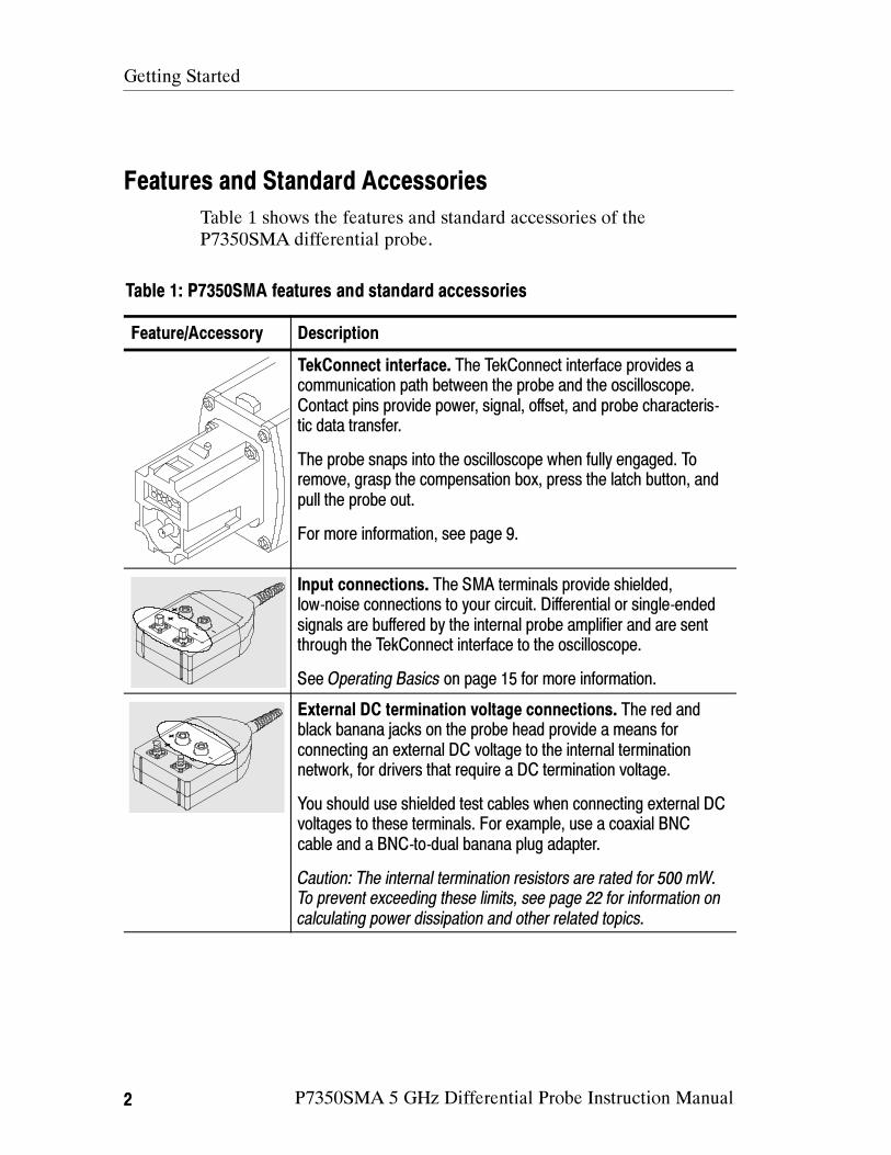
TekConnect interface. The TekConnect interface provides a
communication path between the probe and the oscilloscope.
Contact pins provide power, signal, offset, and probe characteris-
tic data transfer.
The probe snaps into the oscilloscope when fully engaged. To
remove, grasp the compensation box, press the latch button, and
pull the probe out.
For more information, see page 9.
Input connections. The SMA terminals provide shielded,
low-noise connections to your circuit. Differential or single-ended
signals are buffered by the internal probe amplifier and are sent
through the TekConnect interface to the oscilloscope.
See Operating Basics on page 15 for more information.
External DC termination voltage connections. The red and
black banana jacks on the probe head provide a means for
connecting an external DC voltage to the internal termination
network, for drivers that require a DC termination voltage.
You should use shielded test cables when connecting external DC
voltages to these terminals. For example, use a coaxial BNC
cable and a BNC-to-dual banana plug adapter.
Caution: The internal termination resistors are rated for 500 mW.
To prevent exceeding these limits, see page 22 for information on
calculating power dissipation and other related topics.
Getting Started
P7350SMA 5 GHz Differential Probe Instruction Manual 3
Table 1: P7350SMA features and standard accessories (Cont.)
Feature/Accessory Description
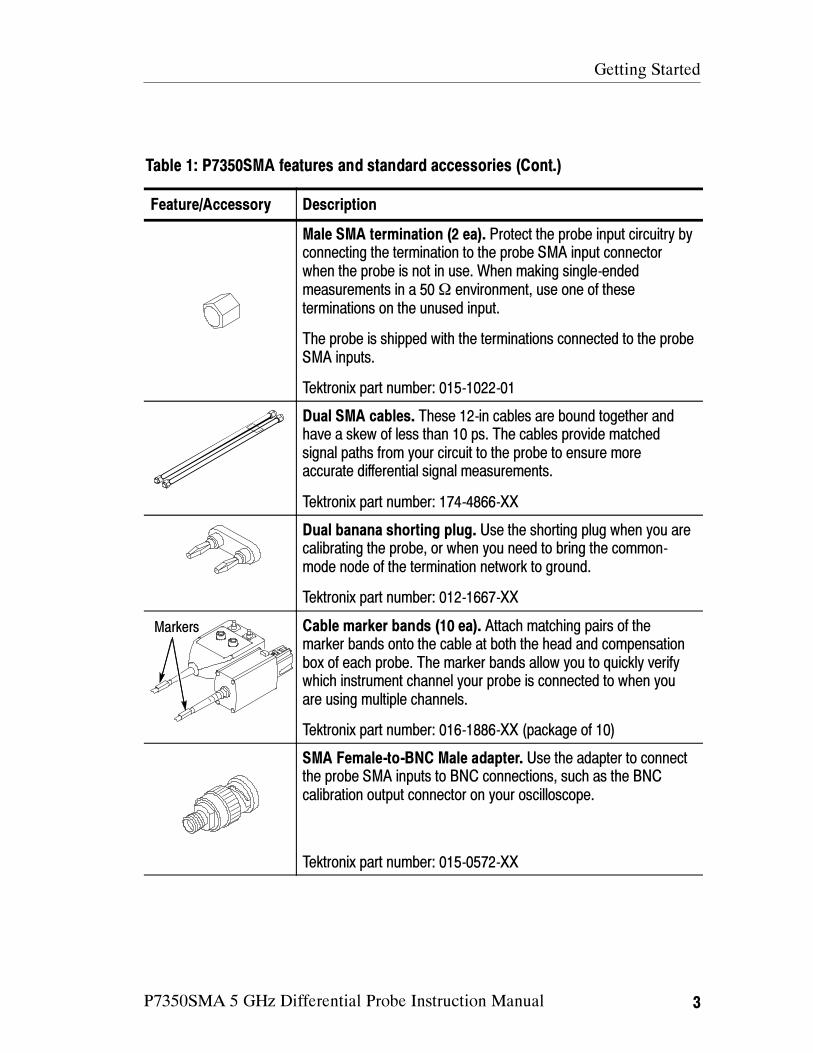
Male SMA termination (2 ea). Protect the probe input circuitry by
connecting the termination to the probe SMA input connector
when the probe is not in use. When making single-ended
measurements in a 50Ω environment, use one of these
terminations on the unused input.
The probe is shipped with the terminations connected to the probe
SMA inputs.
Tektronix part number: 015-1022-01
Dual SMA cables. These 12-in cables are bound together and
have a skew of less than 10 ps. The cables provide matched
signal paths from your circuit to the probe to ensure more
accurate differential signal measurements.
Tektronix part number: 174-4866-XX
Dual banana shorting plug. Use the shorting plug when you are
calibrating the probe, or when you need to bring the common-
mode node of the termination network to ground.
Tektronix part number: 012-1667-XX
Markers Cable marker bands (10 ea). Attach matching pairs of the
marker bands onto the cable at both the head and compensation
box of each probe. The marker bands allow you to quickly verify
which instrument channel your probe is connected to when you
are using multiple channels.
Tektronix part number: 016-1886-XX (package of 10)
SMA Female-to-BNC Male adapter. Use the adapter to connect
the probe SMA inputs to BNC connections, such as the BNC
calibration output connector on your oscilloscope.
Tektronix part number: 015-0572-XX
Getting Started
4 P7350SMA 5 GHz Differential Probe Instruction Manual
Table 1: P7350SMA features and standard accessories (Cont.)
Feature/Accessory Description
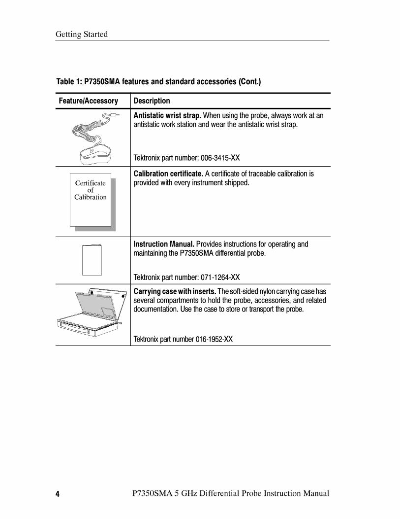
Antistatic wrist strap.When using the probe, always work at an
antistatic work station and wear the antistatic wrist strap.
Tektronix part number: 006-3415-XX
Calibration certificate. A certificate of traceable calibration is
provided with every instrument shipped.
Instruction Manual. Provides instructions for operating and
maintaining the P7350SMA differential probe.
Tektronix part number: 071-1264-XX
Carrying casewith inserts. Thesoft-sided nylon carrying casehas
several compartments to hold the probe, accessories, and related
documentation. Use the case to store or transport the probe.
Tektronix part number 016-1952-XX
Getting Started
P7350SMA 5 GHz Differential Probe Instruction Manual 5
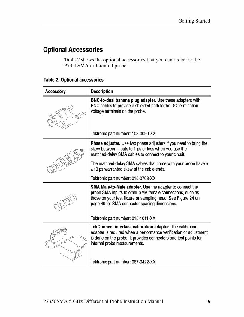
Optional Accessories
Table 2 shows the optional accessories that you can order for the
P7350SMA differential probe.
Table 2: Optional accessories
Accessory Description
BNC-to-dual banana plug adapter. Use these adapters with
BNC cables to provide a shielded path to the DC termination
voltage terminals on the probe.
Tektronix part number: 103-0090-XX
Phase adjuster. Use two phase adjusters if you need to bring the
skew between inputs to 1 ps or less when you use the
matched-delay SMA cables to connect to your circuit.
The matched-delay SMA cables that come with your probe have a
≤10 ps warranted skew at the cable ends.
Tektronix part number: 015-0708-XX
SMA Male-to-Male adapter. Use the adapter to connect the
probe SMA inputs to other SMA female connections, such as
those on your test fixture or sampling head. See Figure 24 on
page 49 for SMA connector spacing dimensions.
Tektronix part number: 015-1011-XX
TekConnect interface calibration adapter. The calibration
adapter is required when a performance verification or adjustment
is done on the probe. It provides connectors and test points for
internal probe measurements.
Tektronix part number: 067-0422-XX
Getting Started
6 P7350SMA 5 GHz Differential Probe Instruction Manual
Options
The following options are available when ordering the P7350SMA
probe:
Option D1--Calibration Data Report
Option D3--Calibration Data Report, 3 years (with Option C3)
Option C3--Calibration Service 3 years
Option D5--Calibration Data Report, 5 years (with Option C5)
Option C5--Calibration Service 5 years
Option R3--Repair Service 3 years
Option R5--Repair Service 5 years
Getting Started
P7350SMA 5 GHz Differential Probe Instruction Manual 7
P7350SMA Probe Head
The P7350SMA probe has two pairs of inputs, shown in Figure 2 on
page 8:
The SMA connectors provide a signal path through the internal
50 Ω termination network to the oscilloscope.
Use the matched-delay SMA cables that are supplied with the
probe to connect the probe to your circuit.
You can mate the probe directly to your circuit if your connector
layout matches those on the probe. See Specifications on page 43
for the dimensions, and use the optional SMA Male-to-Male
adapters.
Leave the 50 Ω termination caps on the unused inputs.
Banana jacks are provided for external DC termination voltages,
which expand the measurement capabilities of your probe. The
center-tap (common-mode node) of the internal 50 Ω termination
network is connected to the red banana-jack terminal on the
probe head. The black banana-jack terminal is connected to
system ground.
CAUTION. The input termination resistors have a thermal power
rating of 0.5 W and are subject to damage if an excessive DC plus
AC rms signal is applied. To prevent damaging the probe, see
page 22 for instructions on calculating the termination resistor
power.
Generally, if you are taking differential measurements on
complementary signals, you should leave the DC terminals open.
Short the DC terminals together with the banana-plug shorting
strap when you are making lower speed, single-ended measure-
ments. A low impedance connection from the DC termination
voltage input to ground is required when measuring single-ended
signals with frequency content below 7 MHz.
If the signal driver requires you to sink or source DC current, use
the DC terminals to bring in an external termination voltage.

Getting Started
8 P7350SMA 5 GHz Differential Probe Instruction Manual
SMA input options
DC termination input options
(Leave open)
To power
supply Shorting strap
Cables
SMA couplers
(optional)
50Ω
Termination
caps
BNC-to-Dual
Banana Adapter
(optional)
BNC cable
(optional)
Figure 2: Probe head connections
Mounting holes are provided on the bottom of the probe head to
secure the probe to your test fixture or device under test. See
Specifications on page 43 for the mounting hole dimensions and
locations.
Getting Started
P7350SMA 5 GHz Differential Probe Instruction Manual 9
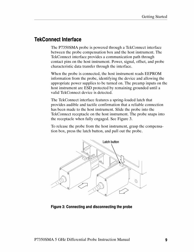
TekConnect Interface
The P7350SMA probe is powered through a TekConnect interface
between the probe compensation box and the host instrument. The
TekConnect interface provides a communication path through
contact pins on the host instrument. Power, signal, offset, and probe
characteristic data transfer through the interface.
When the probe is connected, the host instrument reads EEPROM
information from the probe, identifying the device and allowing the
appropriate power supplies to be turned on. The preamp inputs on the
host instrument are ESD protected by remaining grounded until a
valid TekConnect device is detected.
The TekConnect interface features a spring-loaded latch that
provides audible and tactile confirmation that a reliable connection
has been made to the host instrument. Slide the probe into the
TekConnect receptacle on the host instrument. The probe snaps into
the receptacle when fully engaged. See Figure 3.
To release the probe from the host instrument, grasp the compensa-
tion box, press the latch button, and pull out the probe.
Latch button
Figure 3: Connecting and disconnecting the probe
Getting Started
10 P7350SMA 5 GHz Differential Probe Instruction Manual
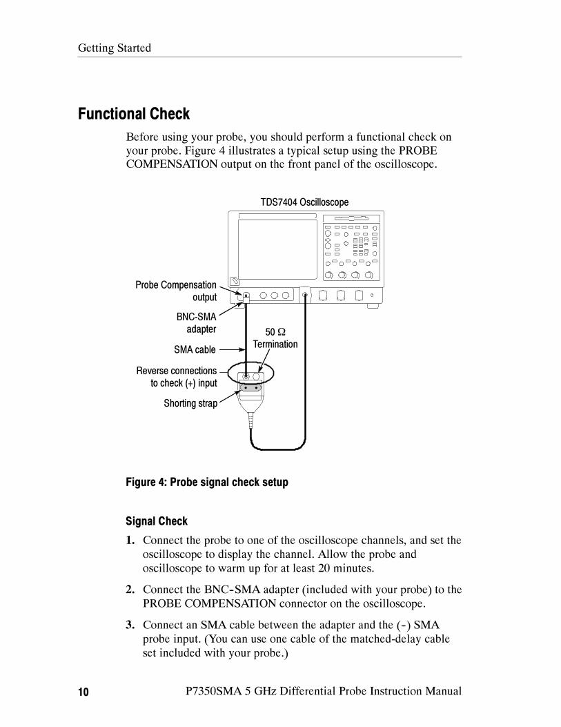
Functional Check
Before using your probe, you should perform a functional check on
your probe. Figure 4 illustrates a typical setup using the PROBE
COMPENSATION output on the front panel of the oscilloscope.
TDS7404 Oscilloscope
50Ω
Termination
BNC-SMA
adapter
SMA cable
Shorting strap
Probe Compensation
output
Reverse connections
to check (+) input
Figure 4: Probe signal check setup
Signal Check
1. Connect the probe to one of the oscilloscope channels, and set the
oscilloscope to display the channel. Allow the probe and
oscilloscope to warm up for at least 20 minutes.
2. Connect the BNC--SMA adapter (included with your probe) to the
PROBE COMPENSATION connector on the oscilloscope.
3. Connect an SMA cable between the adapter and the (--) SMA
probe input. (You can use one cable of the matched-delay cable
set included with your probe.)
Getting Started
P7350SMA 5 GHz Differential Probe Instruction Manual 11
4. Connect a 50 Ω SMA termination to the (+) SMA probe input.
5. Connect a shorting strap or test lead between the two DC
termination inputs on the probe. (Due to the low repetition rate of
the oscilloscope calibration signal, the shorting strap is needed to
provide a broadband 50 Ω termination to ground.)
6. Press Autoset or adjust the oscilloscope to display a stable
calibration waveform. A stable square wave indicates that the
probe input that you are using is functional. Signal amplitude is
dependent on oscilloscope model.
7. Reverse the probe SMA connections, and repeat step 6 to check
the (+) input.
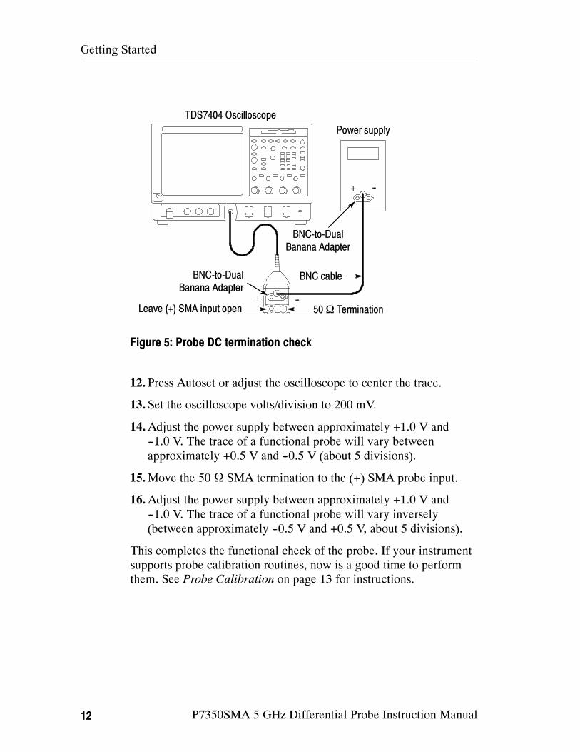
DC Termination Check
8. Disconnect the SMA cable from the (+) input of the probe. Leave
the 50 Ω SMA termination connected to the (--) probe input.
9. Disconnect the shorting strap or test lead from the two DC
termination inputs on the probe.
10.Turn on the power supply, and set it to 0 volts.
11. Connect the power supply to the probe with a BNC cable and two
BNC-to-dual banana adapters. The test setup is shown in Figure 5
on page 12.
Getting Started
12 P7350SMA 5 GHz Differential Probe Instruction Manual
TDS7404 Oscilloscope
--+
Power supply
50Ω Termination
--+
Leave (+) SMA input open
BNC-to-Dual
Banana Adapter
BNC-to-Dual
Banana Adapter
BNC cable
Figure 5: Probe DC termination check
12. Press Autoset or adjust the oscilloscope to center the trace.
13. Set the oscilloscope volts/division to 200 mV.
14.Adjust the power supply between approximately +1.0 V and
--1.0 V. The trace of a functional probe will vary between
approximately +0.5 V and --0.5 V (about 5 divisions).
15.Move the 50 Ω SMA termination to the (+) SMA probe input.
16.Adjust the power supply between approximately +1.0 V and
--1.0 V. The trace of a functional probe will vary inversely
(between approximately --0.5 V and +0.5 V, about 5 divisions).
This completes the functional check of the probe. If your instrument
supports probe calibration routines, now is a good time to perform
them. See Probe Calibration on page 13 for instructions.
Getting Started
P7350SMA 5 GHz Differential Probe Instruction Manual 13
Probe Calibration
After you perform a functional check of the probe, you should run a
probe calibration routine. The Calibration Status of the instrument
Signal Path Compensation test must be pass for the probe calibration
routine to run:
1. From the Utilities menu, select Instrument Calibration.
2. In the Calibration box, check that the Status field is pass. If it is
not, disconnect all probes and signal sources from the oscillo-
scope, and run the Signal Path Compensation routine.
When the Signal Path Compensation test status is pass, run the probe
calibration routine:
3. Connect the probe to one of the oscilloscope channels, and set the
oscilloscope to display the channel. Allow the probe to warm up
for 20 minutes.
4. Connect the SMA cable from the PROBE COMPENSATION
connector on the oscilloscope to the (+) SMA probe input. Leave
a 50 Ω termination on the (--) SMA probe input. The test setup is
shown in Figure 4 on page 10, except the SMA inputs are
reversed.
5. Connect the shorting strap or test lead to the two DC termination
inputs on the probe. The DC termination voltage banana plug
input must be shorted to the banana plug ground input because
the single-ended Probe Compensation signal is a variable DC
voltage.
6. From the Vertical menu, select Probe Cal.
7. Press or click Calibrate probe.
After the probe passes the functional checks and probe calibration
routine, you can use the probe in your measurement system.
You should read the Operating Basics section to familiarize yourself
with related probe functions and capabilities. Important topics
include the Probe Termination Network, Matched-Delay Cables, and
the DC Termination Voltage Terminals.
Getting Started
14 P7350SMA 5 GHz Differential Probe Instruction Manual
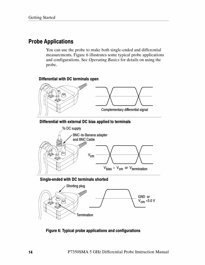
Probe Applications
You can use the probe to make both single-ended and differential
measurements. Figure 6 illustrates some typical probe applications
and configurations. See Operating Basics for details on using the
probe.
Single-ended with DC terminals shorted
Differential with DC terminals open
To DC supply
Differential with external DC bias applied to terminals
Termination
Shorting plug
BNC--to-Banana adapter
and BNC Cable
Complementary differential signal
cmV
biasV =
cmV or
terminationV
GND or
cmV <5.0 V
Figure 6: Typical probe applications and configurations
P7350SMA 5 GHz Differential Probe Instruction Manual 15
Operating Basics
This section discusses the probe architecture and operating
considerations. For more detailed information about differential
measurements and common-mode rejection ratio (CMRR), see the
Reference section on page 39.
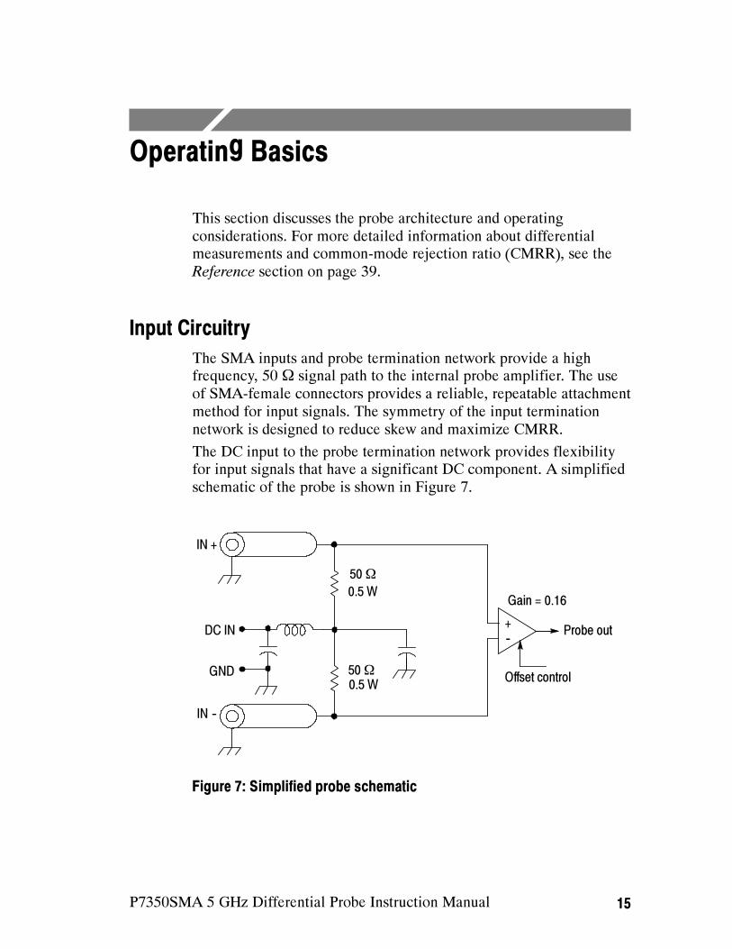
Input Circuitry
The SMA inputs and probe termination network provide a high
frequency, 50 Ω signal path to the internal probe amplifier. The use
of SMA-female connectors provides a reliable, repeatable attachment
method for input signals. The symmetry of the input termination
network is designed to reduce skew and maximize CMRR.
The DC input to the probe termination network provides flexibility
for input signals that have a significant DC component. A simplified
schematic of the probe is shown in Figure 7.
+
--
50Ω
DC IN
0.5 W
50Ω
0.5 W
GND
Probe out
Offset control
IN +
IN --
Gain = 0.16
Figure 7: Simplified probe schematic
Operating Basics
16 P7350SMA 5 GHz Differential Probe Instruction Manual
Probe Termination Network
The P7350SMA probe can be used to make both differential and
common mode measurements, taking into consideration the
characteristics of the probe termination network. A discussion of the
probe termination network follows.
Differential Signals
For a differential input signal with a purely complementary drive
(like the differential signals shown in Figure 6 on page 14), the AC
components of the signal effectively terminate at the common mode
node of the probe termination network. Due to symmetry of the
termination network, the common mode node between the 50 Ω
termination resistors acts like a virtual ground for broadband signals
with a complementary drive and matched source impedance.
Any DC common mode component of the input signal will result in a
DC voltage at the common mode node of the termination network,
which will generally not be seen in the probe output display due to
the large DC CMRR of the probe amplifier. The DC input connection
to the probe termination network can be set using an external DC
power supply. The DC input can be set to match the input common
mode node voltage or to some other value if the input signal drive
circuitry requires a DC termination voltage for correct operation.
Imbalance in either the signal drive or the signal connection path
generates an AC common mode component in the differential input
signal. The probe termination network provides capacitance at the
common mode node to terminate high-frequency common mode
signals. The common mode capacitance of approximately 0.022 µF
holds the common mode node impedance below one ohm, down to a
breakpoint frequency of about 7 MHz.
If the DC input connector of the probe is also driven from a low
impedance DC source, this common mode node impedance can be
kept small all the way down to DC.
The AC common mode component of the input signal will also be
significantly reduced in the displayed probe output signal due to the
AC CMRR of the probe amplifier, which varies with frequency. See
Figure 21 on page 46.

Operating Basics
P7350SMA 5 GHz Differential Probe Instruction Manual 17
Single-Ended Signals
For a single-ended input signal, or where common mode measure-
ments are required for each side of a differential input signal, the
single-ended input should be connected to the IN+ connector of the
probe. For single-ended measurements, the unused IN-- connector of
the probe should be terminated with an impedance that matches the
single-ended source impedance. In the case of high-speed serial data
signals, for which the P7350SMA probe has been optimized, the
source impedance will generally be 50 Ω, so a 50 Ω termination
resistor should be attached to the unused IN-- connector.
With a 50 Ω single-ended drive signal on the IN+ connector, and a
50 Ω termination on the IN-- connector, the probe termination
network provides a broadband termination to the single-ended input
and has flat pulse response, even with the probe DC input port not
connected. This topology, shown in Figure 8, looks similar to the
previous differential input configuration, but with one side of the
complementary drive signal set to zero. The resulting AC output
signal should have one half the amplitude of a similar differential
measurement. This single--ended topology also results in a
measurable DC common mode component, since the DC common
mode signal is converted to a differential mode signal by the input
termination network topology.
+
--
50Ω
DC IN
50Ω
V out
Offset control
IN +
IN --
Gain = 0.16V in
50Ω
50Ω
V+ = 3/4 Vin
V-- = 1/4 Vin
Vout = (0.16) [3/4Vin--1/4Vin]
V+
V--
= (0.16) Vin/2
Figure 8: Single-ended drive
Operating Basics
18 P7350SMA 5 GHz Differential Probe Instruction Manual
If a single-ended measurement is attempted with both the IN--
connector and the DC input connector open, an erroneous output
signal may result. In the case of a high data rate, single-ended pulse
source with a 50 Ω output impedance, the resulting probe output will
appear correctly because the common mode capacitance terminates a
high data rate signal.
For lower data rate signals, however, the common mode capacitance
has time to charge through the source and termination resistors and
produces a waveshape as shown in Figure 9. The data rate deter-
mines the actual waveshape. Note that charging of the common
mode capacitance results in a differentiated output waveshape. For
this reason, the unused SMA input should always be terminated with
a matched source termination for single-ended measurements.
O
pV
O
O
pV
/ 2
V
V+
VIn
pV
/ 2
pV
pV
V--
Displayed
Vout
Figure 9: Resultant waveform from an unterminated input
Operating Basics
P7350SMA 5 GHz Differential Probe Instruction Manual 19
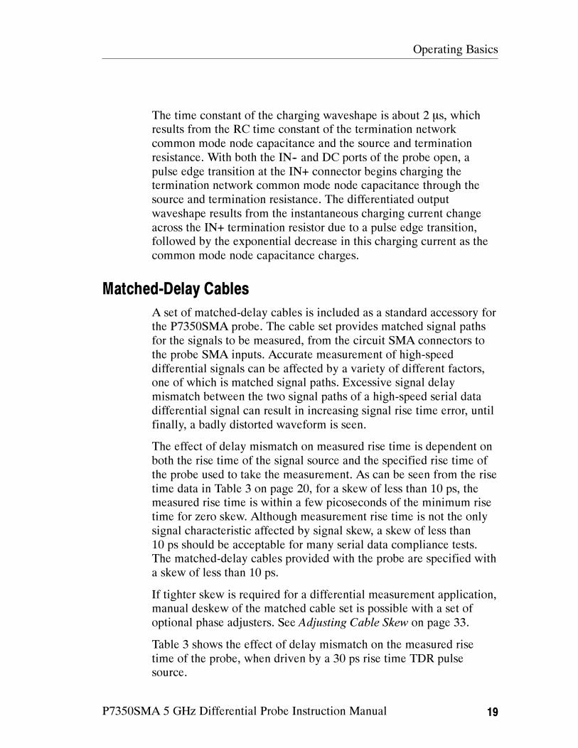
The time constant of the charging waveshape is about 2 s, which
results from the RC time constant of the termination network
common mode node capacitance and the source and termination
resistance. With both the IN-- and DC ports of the probe open, a
pulse edge transition at the IN+ connector begins charging the
termination network common mode node capacitance through the
source and termination resistance. The differentiated output
waveshape results from the instantaneous charging current change
across the IN+ termination resistor due to a pulse edge transition,
followed by the exponential decrease in this charging current as the
common mode node capacitance charges.
Matched-Delay Cables
A set of matched-delay cables is included as a standard accessory for
the P7350SMA probe. The cable set provides matched signal paths
for the signals to be measured, from the circuit SMA connectors to
the probe SMA inputs. Accurate measurement of high-speed
differential signals can be affected by a variety of different factors,
one of which is matched signal paths. Excessive signal delay
mismatch between the two signal paths of a high-speed serial data
differential signal can result in increasing signal rise time error, until
finally, a badly distorted waveform is seen.
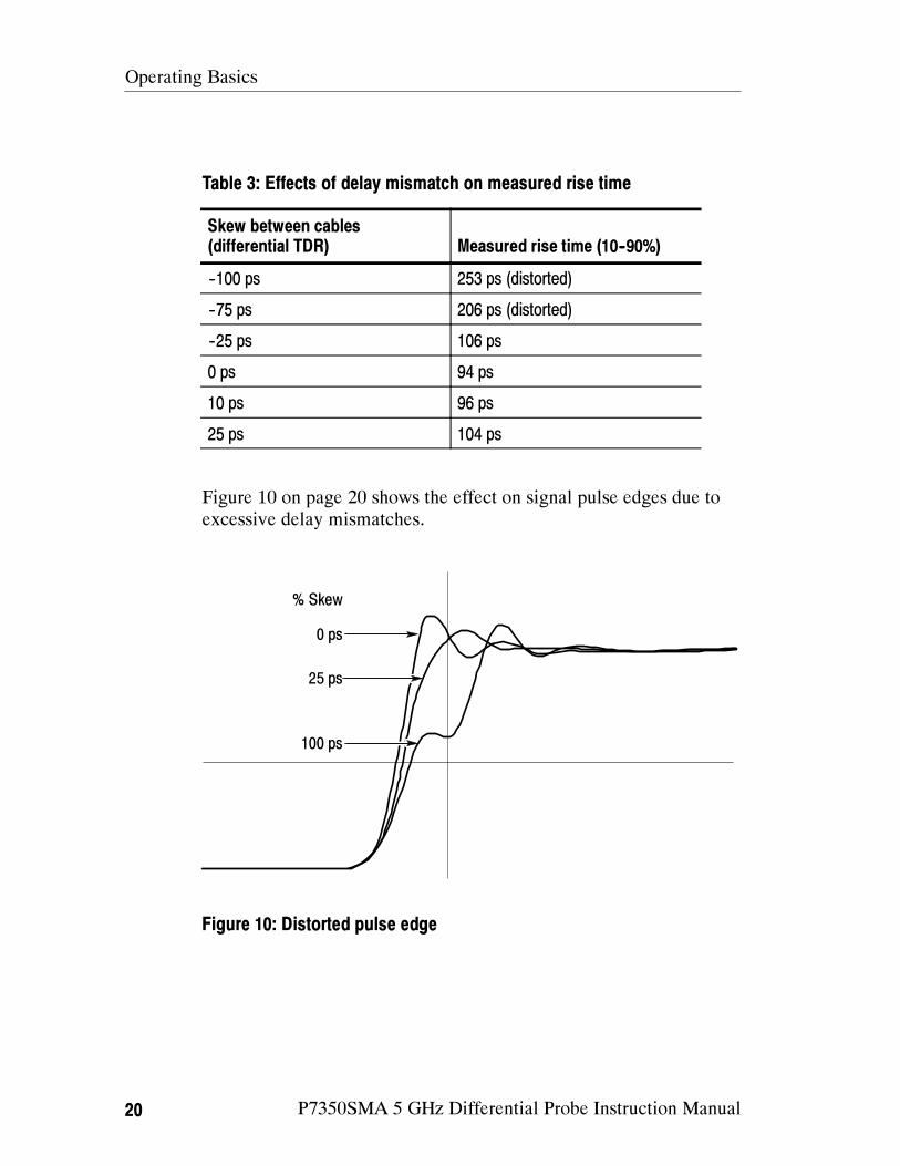
The effect of delay mismatch on measured rise time is dependent on
both the rise time of the signal source and the specified rise time of
the probe used to take the measurement. As can be seen from the rise
time data in Table 3 on page 20, for a skew of less than 10 ps, the
measured rise time is within a few picoseconds of the minimum rise
time for zero skew. Although measurement rise time is not the only
signal characteristic affected by signal skew, a skew of less than
10 ps should be acceptable for many serial data compliance tests.
The matched-delay cables provided with the probe are specified with
a skew of less than 10 ps.
If tighter skew is required for a differential measurement application,
manual deskew of the matched cable set is possible with a set of
optional phase adjusters. See Adjusting Cable Skew on page 33.
Table 3 shows the effect of delay mismatch on the measured rise
time of the probe, when driven by a 30 ps rise time TDR pulse
source.
Operating Basics
20 P7350SMA 5 GHz Differential Probe Instruction Manual
Table 3: Effects of delay mismatch on measured rise time
Skew between cables
(differential TDR) Measured rise time (10--90%)
--100 ps 253 ps (distorted)
--75 ps 206 ps (distorted)
--25 ps 106 ps
0 ps 94 ps
10 ps 96 ps
25 ps 104 ps
Figure 10 on page 20 shows the effect on signal pulse edges due to
excessive delay mismatches.
0 ps
25 ps
100 ps
% Skew
Figure 10: Distorted pulse edge
Operating Basics
P7350SMA 5 GHz Differential Probe Instruction Manual 21
DC Termination Voltage Input
The P7350SMA probe provides a common mode DC voltage input to
the termination network, which includes internal filtering to reduce
noise. You can adjust your DC termination voltage within ±5 volts of
either signal input.
The P7350SMA probe has been designed for compliance testing of
high-speed, serial data standards such as PCI Express, InfiniBand,
SerialATA, XAUI, Gigabit Ethernet, Fibre Channel, and others. All
of these high--speed, differential data signals have both common
mode and differential mode voltages less than 2 volts. Signal
voltages this small will result in termination resistor power
dissipation much less than the 0.5 W limit specified for the
P7350SMA probe.
CAUTION. The input termination resistors have a thermal power
rating of 0.5 W and are subject to damage if an excessive DC plus
AC rms signal is applied. To prevent damaging the probe, see
page 22 for instructions on calculating the termination resistor
power if you intend to measure signals that exceed the voltage levels
of the data standards discussed above.
The P7350SMA probe can be used to measure differential and
single-ended signals with the DC termination voltage input open as
long as the SMA inputs are driven or terminated with matched
source impedances. Operating the P7350SMA probe with the DC
termination voltage input open will, in general, reduce the termina-
tion resistor power dissipation.
The DC termination voltage input has been included for flexibility in
applications where a common mode pullup or pulldown voltage is
required, such as ECL or CML logic signals. The termination resistor
power dissipation warning and power dissipation equations are
provided for use in exceptional applications where higher voltages
are present and may cause damage if misapplied.
If you intend to measure signals that exceed the voltage levels of the
data standards discussed above, see Calculating DC Termination
Operating Basics
22 P7350SMA 5 GHz Differential Probe Instruction Manual
Resistor Power and Equations to calculate the power that you will
apply to the termination resistors.
NOTE. For many high-speed serial data applications, the probe can
be operated with the VTterminal open.
The red (+) and black (--) terminals on the probe head accept
standard banana plugs on 0.75-inch centers. It is recommended that
all cabling to these banana plugs be made with shielded cables to
help prevent noise from affecting your measurement. Dual banana
plug-to-BNC adapters and coaxial BNC cables make shielded DC
port connections simple. The black terminal is ground and is
connected to the outer case of the shielded module that holds the
SMA input terminals.
Depending on the measurement application, the DC port can be
driven with an externally applied DC voltage, shorted to ground with
the banana plug shorting strap that is included with the probe, or left
open and unconnected.
If the DC port is not needed to supply a DC termination voltage, it
can be used to measure the common mode voltage of an input
differential signal with a DMM.
Calculating DC Termination Resistor Power
The maximum power that the termination resistors in the probe can
dissipate is 0.5 watt each. To avoid exceeding these limits, before
you take measurements, you should consider the power that your
system will impose on the termination network. The power that the
termination resistors see may be comprised of not only the AC
signal, but also any DC component of the waveform.
The power also depends on how you use the DC termination inputs.
The DC termination inputs may be left open, shorted together, or an
external DC voltage may be applied. If the DC termination input is
left open, then there is no DC power dissipated in the termination
resistors. When the DC termination input is shorted to ground or
driven by an external DC power supply, the DC power dissipation is
Operating Basics
P7350SMA 5 GHz Differential Probe Instruction Manual 23
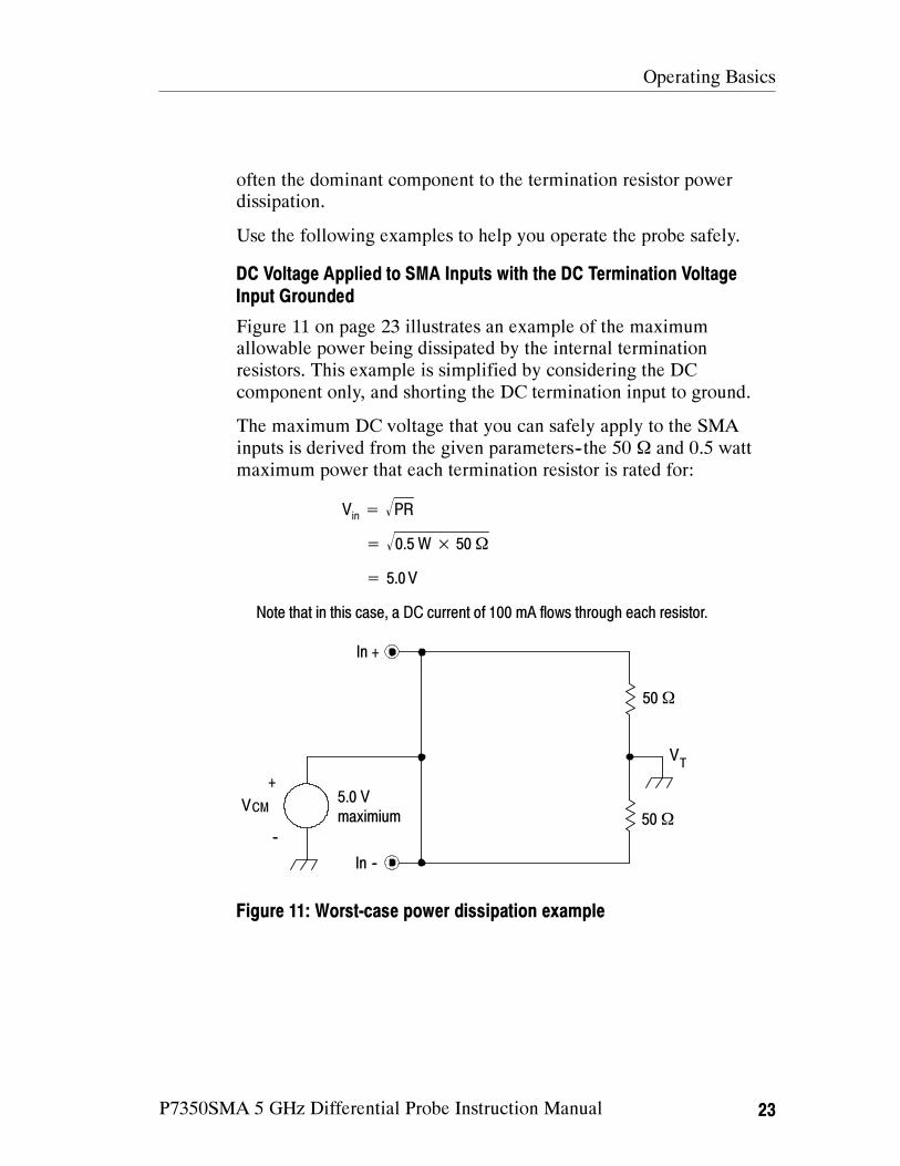
often the dominant component to the termination resistor power
dissipation.
Use the following examples to help you operate the probe safely.
DC Voltage Applied to SMA Inputs with the DC Termination Voltage
Input Grounded
Figure 11 on page 23 illustrates an example of the maximum
allowable power being dissipated by the internal termination
resistors. This example is simplified by considering the DC
component only, and shorting the DC termination input to ground.
The maximum DC voltage that you can safely apply to the SMA
inputs is derived from the given parameters--the 50 Ω and 0.5 watt
maximum power that each termination resistor is rated for:
Vin= PR
= 0.5 W × 50Ω
= 5.0V
Note that in this case, a DC current of 100 mA flows through each resistor.
50Ω
50Ω
CM
+
--
V
TV
5.0 V
maximium
In +
In --
Figure 11: Worst-case power dissipation example
Operating Basics
24 P7350SMA 5 GHz Differential Probe Instruction Manual
Complementary Input Signal with the DC Termination Voltage Input
Open
Consider the single-ended signals shown in Figure 12a on page 24.
Each signal is varying by 0.5 volt symmetrically around 0.75 volt.
These signals are applied to the probe model as shown in Figure 12b.
It should be noted that the input signal model has been simplified by
removing any source impedance. A more realistic input signal model
would typically include a 50 Ω source impedance and would require
adjustment of the voltage sources to give the equivalent signal at the
(In+) and (In--) probe inputs.
1.00 V
0.75 V
0.50 V
+ In
-- In
a) Single-ended signals (into a 50Ω load)
(V+)
(V--)
DM
+
--
50Ω
50Ω
V
DM
+
--
V
TV
b) Probe model
1.00 V to 0.50 V
0.50 V to 1.00 V
0.75 V
In --
In +
CM
+
--
V
0.75 V
Figure 12: Example of probe with DC input open
Operating Basics
P7350SMA 5 GHz Differential Probe Instruction Manual 25
The terms used in this discussion are defined as follows:
VCM
=V++ V
−
2
VDM
= V+− V
−
Termination terminal voltageVT=
Using these terms, the measured peak-to-peak differential voltage,
(VDiff
), = 2 VDM
, since the differential output voltage swings positive
and negative about ground with an amplitude of VDM
.
For this example,
VCM
=
1.00V+ 0.50V
2
VDM
= 1.00V− 0.50V
VT= 0.75V
= 0.50V
= 0.75V
(The DC termination terminal is open in this example,
so this node is at the common mode voltage.)
The switching signal potential across the two termination
resistors (100 Ω in series) is the differential mode voltage,
0.5 volt, which equates to 5 mA of current flow. This differential
mode current flows alternately one direction and then the other,
around the termination network loop as the differential mode
voltage switches polarity. Common-mode current only flows
initially as the capacitance at the VTnode charges to the common
mode voltage.
The total power dissipated is the product of the 5 mA of circuit
current and the 0.5 volt drop across both resistors. The result is
2.5 mW of total AC power, or 1.25 mW for each resistor. In this
example, with the DC termination terminal open, there is no DC
power dissipated by the termination network.
Operating Basics
26 P7350SMA 5 GHz Differential Probe Instruction Manual
Complementary Input Signal with the DC Termination Voltage Input
Shorted (Grounded)
In Figure 13, the same signals as in the previous example are used,
but here, the DC termination input is shorted to ground. Each signal
is still varying by 0.5 volt symmetrically around 0.75 volt, but now
the signals have a path for DC current flow through the two
termination resistors to ground.
1.00 V
0.75 V
0.50 V
+ In
-- In
a) Single-ended signals
(V+)
(V--)
DM
+
--
50Ω
50Ω
V
DM
+
--
V
TV
b) Probe model
1.00 V to 0.50 V
0.50 V to 1.00 V
0 V
CM
+
--
V
0.75 V
Figure 13: Example of probe with DC input shorted to ground
In this example,
VCM
=1.00V+ 0.50
2
VDM
= 1.00V− 0.50V
VT= 0V
= 0.50V = 0.75V
(The DC termination terminal is grounded.)
Operating Basics
P7350SMA 5 GHz Differential Probe Instruction Manual 27
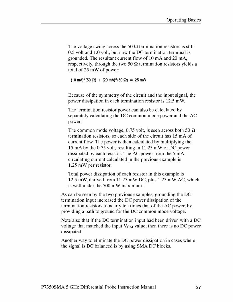
The voltage swing across the 50 Ω termination resistors is still
0.5 volt and 1.0 volt, but now the DC termination terminal is
grounded. The resultant current flow of 10 mA and 20 mA,
respectively, through the two 50 Ω termination resistors yields a
total of 25 mW of power:
(10 mA)2(50Ω)+ (20 mA)
2(50Ω) = 25 mW
Because of the symmetry of the circuit and the input signal, the
power dissipation in each termination resistor is 12.5 mW.
The termination resistor power can also be calculated by
separately calculating the DC common mode power and the AC
power.
The common mode voltage, 0.75 volt, is seen across both 50 Ω
termination resistors, so each side of the circuit has 15 mA of
current flow. The power is then calculated by multiplying the
15 mA by the 0.75 volt, resulting in 11.25 mW of DC power
dissipated by each resistor. The AC power from the 5 mA
circulating current calculated in the previous example is
1.25 mW per resistor.
Total power dissipation of each resistor in this example is
12.5 mW, derived from 11.25 mW DC, plus 1.25 mW AC, which
is well under the 500 mW maximum.
As can be seen by the two previous examples, grounding the DC
termination input increased the DC power dissipation of the
termination resistors to nearly ten times that of the AC power, by
providing a path to ground for the DC common mode voltage.
Note also that if the DC termination input had been driven with a DC
voltage that matched the input VCM
value, then there is no DC power
dissipated.
Another way to eliminate the DC power dissipation in cases where
the signal is DC balanced is by using SMA DC blocks.
Operating Basics
28 P7350SMA 5 GHz Differential Probe Instruction Manual
Equations and Definitions
The formulas for calculating the power dissipation of the 50 Ω
termination resistors with a DC-balanced signal like that modeled in
the previous two examples follows:
DC power = VCM
− VT
50
(VCM
− VT) per side
AC power = VDM(p−p)
100
VDM(p−p)
2
per side
The signal source model defined for these equations is as follows:
V+and V
−=
V−= V
CM− V
DMV+= V
CM+ V
DM
Single-ended signals into a 50Ω load
This results in the terms to be used in the power equations above:
VCM
=V++ V
−
2
VT= Termination input voltage
VDM
=V+− V
−
2
Note: With a balanced DC signal, in the equations above,
VDM
is half of the value of a conventional differential signal.
Vdiff
= V+− V
−= 2V
DM
Operating Basics
P7350SMA 5 GHz Differential Probe Instruction Manual 29
Internal Probe Amplifier
The P7350SMA differential probe is designed to measure high
frequency, low-voltage circuits. Before connecting the probe to your
circuit, take into account the limits for maximum input voltage, the
common-mode signal range, and the differential-mode signal range.
For specific limits of these parameters, see Specifications on
page 43.
Maximum Input Voltage
The maximum input voltage is the maximum voltage to ground that
the inputs can withstand without damaging the probe input circuitry.
CAUTION. To avoid damaging the inputs of the P7350SMA differen-
tial probe, do not apply more than ±15 V (DC + peak AC) between
each input and ground.
Note that the 0.5 W power dissipation of the termination resistor
must also be considered when the DC termination input is driven and
may further limit the maximum allowable signal input voltage.
Common-Mode Signal Range
The common-mode signal range is the maximum voltage that you
can apply to each input, with respect to earth ground, without
saturating the input circuitry of the probe. A common-mode voltage
that exceeds the common-mode signal range may produce an
erroneous output waveform even when the differential-mode
specification is met.
Differential-Mode Signal Range
The differential-mode signal range is the maximum voltage
difference between the plus and minus inputs that the probe can
accept without distorting the signal. The distortion from a voltage
that is too large can result in a clipped or otherwise distorted and
inaccurate measurement.
Operating Basics
30 P7350SMA 5 GHz Differential Probe Instruction Manual
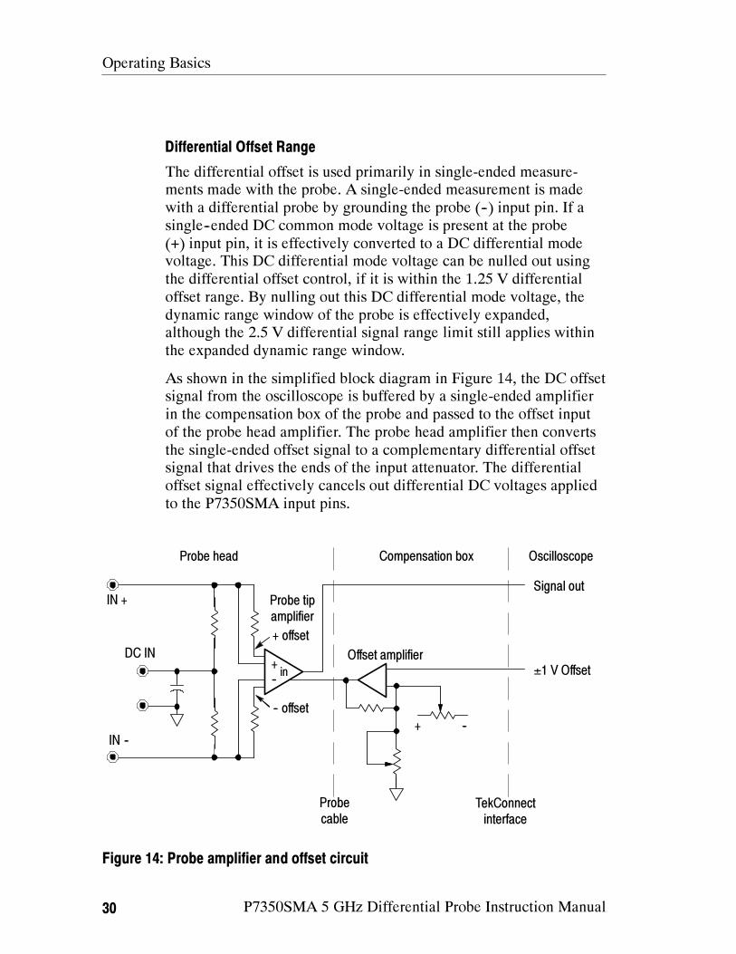
Differential Offset Range
The differential offset is used primarily in single-ended measure-
ments made with the probe. A single-ended measurement is made
with a differential probe by grounding the probe (--) input pin. If a
single--ended DC common mode voltage is present at the probe
(+) input pin, it is effectively converted to a DC differential mode
voltage. This DC differential mode voltage can be nulled out using
the differential offset control, if it is within the 1.25 V differential
offset range. By nulling out this DC differential mode voltage, the
dynamic range window of the probe is effectively expanded,
although the 2.5 V differential signal range limit still applies within
the expanded dynamic range window.
As shown in the simplified block diagram in Figure 14, the DC offset
signal from the oscilloscope is buffered by a single-ended amplifier
in the compensation box of the probe and passed to the offset input
of the probe head amplifier. The probe head amplifier then converts
the single-ended offset signal to a complementary differential offset
signal that drives the ends of the input attenuator. The differential
offset signal effectively cancels out differential DC voltages applied
to the P7350SMA input pins.
Offset amplifier
Probe tip
amplifier
Signal out
±1 V Offset
Probe
cable
TekConnect
interface
Probe head Compensation box Oscilloscope
+ --
IN +
IN --
+
--in
-- offset
+ offset
DC IN
Figure 14: Probe amplifier and offset circuit
Operating Basics
P7350SMA 5 GHz Differential Probe Instruction Manual 31
Common-Mode Rejection
The common-mode rejection ratio (CMRR) is the ability of a probe
to reject signals that are common to both inputs. More precisely,
CMRR is the ratio of the differential gain to the common-mode gain.
The higher the ratio, the greater the ability to reject common-mode
signals. For additional information about CMRR, see page 40.
Input Impedance and Probe Loading
Each input of the P7350SMA differential probe has an input
impedance of 50 Ω. See Figure 15.
50Ω
50Ω
DC IN
GND
+ Input
-- Input
Figure 15: Typical probe input model
The lower the impedance of the probe relative to that of the source,
the more the probe loads the circuit under test and reduces the signal
amplitude. With an input impedance of 50 Ω, the P7350SMA probe
is designed for use with 50 Ω systems. The broadband quality of the
P7350SMA probe 50 Ω inputs is specified with the differential input
return loss specification. For specific limits of these parameters, see
Specifications on page 43.
Operating Basics
32 P7350SMA 5 GHz Differential Probe Instruction Manual
Checking the Skew Between Inputs
The time-delay difference (skew) between the two SMA input
terminals of the probe is typically less than 1 ps. If you use the
matched-delay SMA cable pair supplied with the probe, the
guaranteed skew between the cable pair is 10 ps or less. You can
bring the skew to within 1 ps with the cables by using a pair of phase
adjusters (see Optional Accessories on page 5).
The skew specification of the probe is guaranteed by design and
somewhat difficult to measure. The skew of the matched-delay cable
pair is guaranteed to be 10 ps or less, but may be much better than
the guaranteed limit.
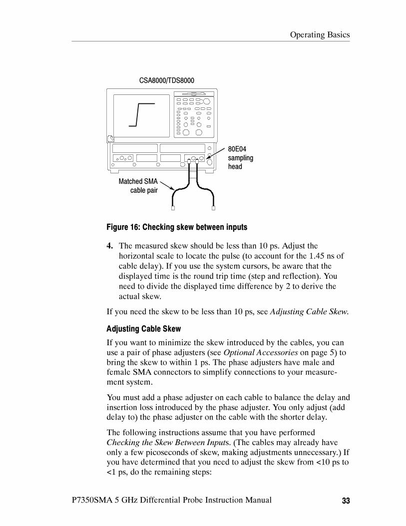
You can measure the skew of the cable pair by connecting the cables
to a Tektronix 80E04 Sampling Head, configured for a TDR output.
Figure 16 on page 33 shows a setup for checking the skew.
1. Turn on the equipment and let it warm up for 20 minutes. Do not
connect the cables to the sampling head yet.
2. Do a system compensation for the TDR module, and then verify
the skew of the two outputs with the TDR outputs open, using a
common-mode TDR drive.
Skew between the two outputs can be compensated with the TDR
module deskew control. Refer to your sampling head or
oscilloscope manual for instructions.
3. Connect the matched cable pair to the TDR outputs, as shown in
Figure 16 on page 33.
Operating Basics
P7350SMA 5 GHz Differential Probe Instruction Manual 33
80E04
sampling
head
CSA8000/TDS8000
Matched SMA
cable pair
Figure 16: Checking skew between inputs
4. The measured skew should be less than 10 ps. Adjust the
horizontal scale to locate the pulse (to account for the 1.45 ns of
cable delay). If you use the system cursors, be aware that the
displayed time is the round trip time (step and reflection). You
need to divide the displayed time difference by 2 to derive the
actual skew.
If you need the skew to be less than 10 ps, see Adjusting Cable Skew.
Adjusting Cable Skew
If you want to minimize the skew introduced by the cables, you can
use a pair of phase adjusters (see Optional Accessories on page 5) to
bring the skew to within 1 ps. The phase adjusters have male and
female SMA connectors to simplify connections to your measure-
ment system.
You must add a phase adjuster on each cable to balance the delay and
insertion loss introduced by the phase adjuster. You only adjust (add
delay to) the phase adjuster on the cable with the shorter delay.
The following instructions assume that you have performed
Checking the Skew Between Inputs. (The cables may already have
only a few picoseconds of skew, making adjustments unnecessary.) If
you have determined that you need to adjust the skew from <10 ps to
<1 ps, do the remaining steps:
Operating Basics
34 P7350SMA 5 GHz Differential Probe Instruction Manual
5. Connect the phase adjusters to the cables.
6. On the cable with the longer delay, loosen the phase adjuster
locking nuts, set the phase adjuster to minimum delay (shortest
length), and secure the locking nuts. See Figure 17 on page 34.
Adjustment collar
Loosen the
locking nuts
Locking nuts
Collar
1
Turn adjustment collar while
observing oscilloscope display
2
Increase
Decrease
Figure 17: Using the phase adjuster
7. Loosen the locking nuts on the adjuster connected to the other
cable (with the shorter delay).
8. While observing the oscilloscope display, turn the collar on the
phase adjuster counterclockwise to increase the delay.
9. When the displayed skew on screen is less than 1 ps, tighten the
locking nuts.
10.Confirm that the skew is acceptable after you tighten the locking
nuts, as the adjustment may change slightly during tightening.
11. Disconnect the cables from the sampling head, and connect them
to the P7350SMA probe head.

Operating Basics
P7350SMA 5 GHz Differential Probe Instruction Manual 35
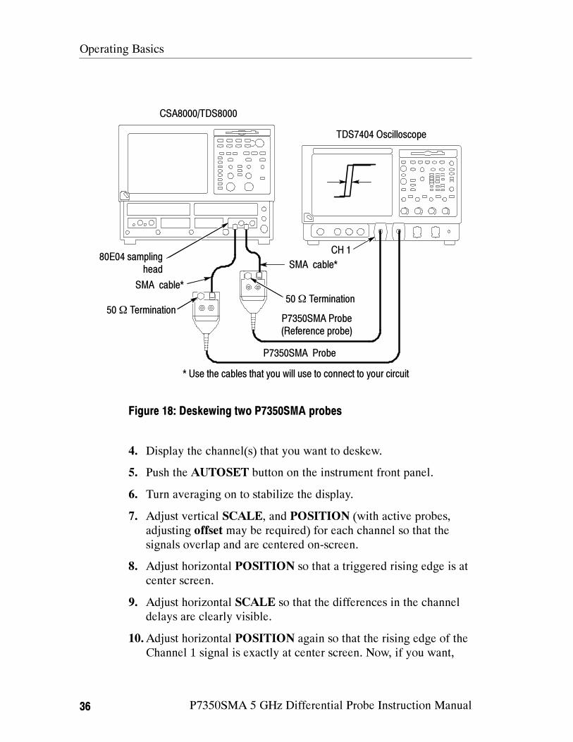
Deskewing Probes
You can measure the skew between two P7350SMA probes by using
a Tektronix 80E04 Sampling Head configured for a TDR output.
Because the skew of the P7350SMA probe inputs is less than 1 ps,
two P7350SMA probes can be deskewed using single-ended drive
signals from a dual-channel TDR source. The TDR output provides a
pair of time-aligned pulses that you can use to compare probe
response times, and if necessary, adjust them to match (deskew).
Figure 18 on page 36 shows a setup for checking and deskewing two
probes. Deskewing aligns the time delay of the signal path through
the oscilloscope channel and probe connected to that channel, to the
time delay of other channel/probe pairs of the oscilloscope.
If you need to deskew more than two probes, keep one deskewed
probe connected to the sampling head as a reference (after
deskewing two probes), and deskew additional probes to that probe.
In this procedure, Channel 1 is used as the reference channel.
1. Set up the equipment as shown in Figure 18 and let it warm up
for 20 minutes, but don’t make any connections to the TDR
outputs yet.
2. Do a system compensation for the TDR module, and then verify
the skew of the two outputs with the TDR outputs open, using a
common-mode TDR drive.
Skew between the two outputs can be compensated with the
deskew control. Refer to your sampling head or oscilloscope
manual for instructions.
3. Attach the probes to the TDR outputs as shown in Figure 18.
Operating Basics
36 P7350SMA 5 GHz Differential Probe Instruction Manual
80E04 sampling
headSMA cable*
P7350SMA Probe
TDS7404 Oscilloscope
CSA8000/TDS8000
P7350SMA Probe
(Reference probe)
* Use the cables that you will use to connect to your circuit
50Ω Termination
SMA cable*
50Ω Termination
CH 1
Figure 18: Deskewing two P7350SMA probes
4. Display the channel(s) that you want to deskew.
5. Push the AUTOSET button on the instrument front panel.
6. Turn averaging on to stabilize the display.
7. Adjust vertical SCALE, and POSITION (with active probes,
adjusting offset may be required) for each channel so that the
signals overlap and are centered on-screen.
8. Adjust horizontal POSITION so that a triggered rising edge is at
center screen.
9. Adjust horizontal SCALE so that the differences in the channel
delays are clearly visible.
10.Adjust horizontal POSITION again so that the rising edge of the
Channel 1 signal is exactly at center screen. Now, if you want,

Operating Basics
P7350SMA 5 GHz Differential Probe Instruction Manual 37
you can use the measurement cursors to display the channel--
channel skew, and input this value in step 14.
11. Touch the VERT button or use the Vertical menu to display the
vertical control window.
12.Touch the Probe Deskew button to display the channel-deskew
control window.
13. In the Channel box, select the channel that you want to deskew
to Channel 1.
NOTE. If possible, do the next step at a signal amplitude within the
same attenuator range (vertical scale) as your planned signal
measurements. Any change to the vertical scale after deskew is
complete may introduce a new attenuation level (you can generally
hear attenuator settings change) and, therefore, a slightly different
signal path. This different path may cause up to a 200 ps variation in
timing accuracy between channels.
14.Adjust the deskew time for that channel so that the signal aligns
with that of Channel 1. You can do this several ways: Click on
the Deskew field and input the time value you measured with the
cursors in step 10, or you can use the front-panel or on-screen
controls to position the signal.
15.Repeat steps 3 through 14 for each additional channel that you
want to deskew.
Operating Basics
38 P7350SMA 5 GHz Differential Probe Instruction Manual
P7350SMA 5 GHz Differential Probe Instruction Manual 39
Reference
This section contains important reference information about
differential measurements and how to increase the accuracy of your
measurements.
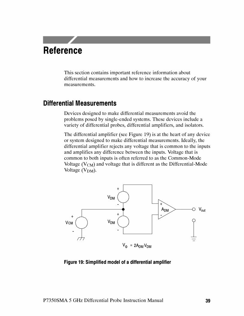
Differential Measurements
Devices designed to make differential measurements avoid the
problems posed by single-ended systems. These devices include a
variety of differential probes, differential amplifiers, and isolators.
The differential amplifier (see Figure 19) is at the heart of any device
or system designed to make differential measurements. Ideally, the
differential amplifier rejects any voltage that is common to the inputs
and amplifies any difference between the inputs. Voltage that is
common to both inputs is often referred to as the Common-Mode
Voltage (VCM
) and voltage that is different as the Differential-Mode
Voltage (VDM
).
Vout
VDM
VDM
+
--
+
--
+
--
+
--
oV = 2A
DMVDM
ADM
CMV
Figure 19: Simplified model of a differential amplifier
Reference
40 P7350SMA 5 GHz Differential Probe Instruction Manual
Common-Mode Rejection Ratio
In reality, differential amplifiers cannot reject all of the common-
mode signal. The ability of a differential amplifier to reject the
common-mode signal is expressed as the Common-Mode Rejection
Ratio (CMRR). The CMRR is the differential-mode gain (ADM
)
divided by the common-mode gain (ACM
). It is expressed either as a
ratio or in dB.
CMRR =
ADM
ACM
dB = 20 log
ADM
ACM
CMRR generally is highest (best) at DC and degrades with
increasing frequency.
Figure 21 on page 46 shows the CMRR of the P7350SMA differen-
tial probe. This derating chart assumes a common-mode signal that is
sinusoidal. The lower the input impedance of the probe relative to
the source impedance, the lower the CMRR. Significant differences
in the source impedance driving the two inputs will also lower the
CMRR.
Reference
P7350SMA 5 GHz Differential Probe Instruction Manual 41
Extending the Input Connections
At times it may be necessary to extend the probe inputs with cables
that are longer than the standard 12 inch cables. The 12 inch cables
are precision-matched to minimize time-delay differences (skew). If
you substitute cables, you should use low-loss, flexible cables and
keep the lengths matched and as short as possible to minimize skew
and optimize common-mode rejection. Check the skew between the
cables, and if necessary, use the optional phase adjusters to minimize
the skew.
Extending the input leads will also increase the skin loss and
dielectric loss, which may result in distorted high-frequency pulse
edges. You should take into account any effects caused by the
extended leads when you take a measurement.
Reference
42 P7350SMA 5 GHz Differential Probe Instruction Manual
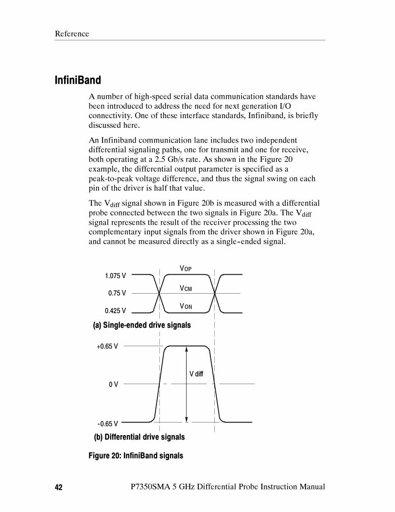
InfiniBand
A number of high-speed serial data communication standards have
been introduced to address the need for next generation I/O
connectivity. One of these interface standards, Infiniband, is briefly
discussed here.
An Infiniband communication lane includes two independent
differential signaling paths, one for transmit and one for receive,
both operating at a 2.5 Gb/s rate. As shown in the Figure 20
example, the differential output parameter is specified as a
peak-to-peak voltage difference, and thus the signal swing on each
pin of the driver is half that value.
The Vdiff
signal shown in Figure 20b is measured with a differential
probe connected between the two signals in Figure 20a. The Vdiff
signal represents the result of the receiver processing the two
complementary input signals from the driver shown in Figure 20a,
and cannot be measured directly as a single--ended signal.
--0.65 V
0 V
+0.65 V
V diff
1.075 V
0.75 V
0.425 VONV
CMV
OPV
(a) Single-ended drive signals
(b) Differential drive signals
Figure 20: InfiniBand signals
P7350SMA 5 GHz Differential Probe Instruction Manual 43
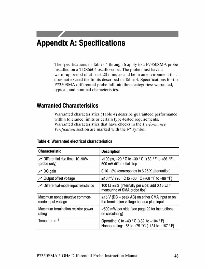
Appendix A: Specifications
The specifications in Tables 4 through 6 apply to a P7350SMA probe
installed on a TDS6604 oscilloscope. The probe must have a
warm-up period of at least 20 minutes and be in an environment that
does not exceed the limits described in Table 4. Specifications for the
P7350SMA differential probe fall into three categories: warranted,
typical, and nominal characteristics.
Warranted Characteristics
Warranted characteristics (Table 4) describe guaranteed performance
within tolerance limits or certain type-tested requirements.
Warranted characteristics that have checks in the Performance
Verification section are marked with the symbol.
Table 4: Warranted electrical characteristics
Characteristic Description
Differential rise time, 10--90%
(probe only)
≤100 ps, +20 C to +30 C (+68 F to +86 F),
500 mV differential step
DC gain 0.16 ±2% (corresponds to 6.25 X attenuation)
Output offset voltage ±10 mV +20 C to +30 C (+68 F to +86 F)
Differential-mode input resistance 100Ω ±2% (internally per side; add 0.15Ω if
measuring at SMA probe tips)
Maximum nondestructive common-
mode input voltage
±15 V (DC + peak AC) on either SMA input or on
the termination voltage banana plug input
Maximum termination resistor power
rating
<500 mW per side (see page 22 for instructions
on calculating)
Temperature1
Operating: 0 to +40 C (+32 to +104 F)
Nonoperating: --55 to +75 C (--131 to +167 F)
Appendix A: Specifications
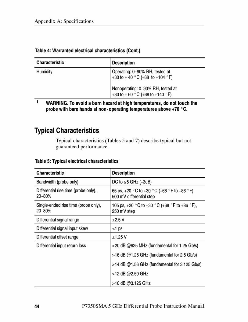
44 P7350SMA 5 GHz Differential Probe Instruction Manual
Table 4: Warranted electrical characteristics (Cont.)
Characteristic Description
Humidity Operating: 0--90% RH, tested at
+30 to + 40 C (+68 to +104 F)
Nonoperating: 0--90% RH, tested at
+30 to + 60 C (+68 to +140 F)
1WARNING. To avoid a burn hazard at high temperatures, do not touch the
probe with bare hands at non-operating temperatures above +70 C.
Typical Characteristics
Typical characteristics (Tables 5 and 7) describe typical but not
guaranteed performance.
Table 5: Typical electrical characteristics
Characteristic Description
Bandwidth (probe only) DC to ≥5 GHz (--3dB)
Differential rise time (probe only),
20--80%
65 ps, +20 C to +30 C (+68 F to +86 F),
500 mV differential step
Single-ended rise time (probe only),
20--80%
105 ps, +20 C to +30 C (+68 F to +86 F),
250 mV step
Differential signal range ±2.5 V
Differential signal input skew <1 ps
Differential offset range ±1.25 V
Differential input return loss >20 dB @625 MHz (fundamental for 1.25 Gb/s)
>16 dB @1.25 GHz (fundamental for 2.5 Gb/s)
>14 dB @1.56 GHz (fundamental for 3.125 Gb/s)
>12 dB @2.50 GHz
>10 dB @3.125 GHz
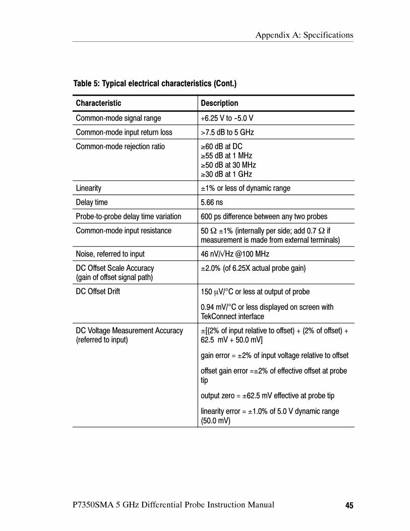
Appendix A: Specifications
P7350SMA 5 GHz Differential Probe Instruction Manual 45
Table 5: Typical electrical characteristics (Cont.)
Characteristic Description
Common-mode signal range +6.25 V to --5.0 V
Common-mode input return loss >7.5 dB to 5 GHz
Common-mode rejection ratio ≥60 dB at DC
≥55 dB at 1 MHz
≥50 dB at 30 MHz
≥30 dB at 1 GHz
Linearity ±1% or less of dynamic range
Delay time 5.66 ns
Probe-to-probe delay time variation 600 ps difference between any two probes
Common-mode input resistance 50Ω ±1% (internally per side; add 0.7 Ω if
measurement is made from external terminals)
Noise, referred to input 46 nV/√Hz @100 MHz
DC Offset Scale Accuracy
(gain of offset signal path)
±2.0% (of 6.25X actual probe gain)
DC Offset Drift 150 V/°C or less at output of probe
0.94 mV/°C or less displayed on screen with
TekConnect interface
DC Voltage Measurement Accuracy
(referred to input)
±[(2% of input relative to offset) + (2% of offset) +
62.5 mV + 50.0 mV]
gain error = ±2% of input voltage relative to offset
offset gain error =±2% of effective offset at probe
tip
output zero = ±62.5 mV effective at probe tip
linearity error = ±1.0% of 5.0 V dynamic range
(50.0 mV)
Appendix A: Specifications
46 P7350SMA 5 GHz Differential Probe Instruction Manual
Figure 21 shows the typical common-mode and differential gain of
the probe. The CMRR can be found by subtracting the common-
mode gain from the differential gain. For example, --80 dB CM gain
equals approximately +67 dB CMRR.
--10
--20
--30
--40
--50
--60
--70
--80
1 GHz
Frequency
--90
10 MHz100 kHz 1 MHz 100 MHz 6 GHz
Differential Mode Gain
Common Mode Gain
CMRR
0 dB
Figure 21: Typical common- and differential-mode gain plots
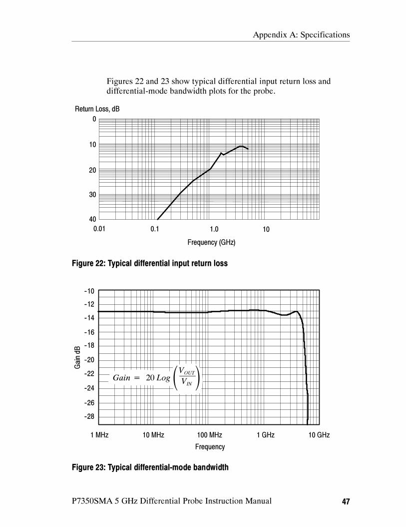
Appendix A: Specifications
P7350SMA 5 GHz Differential Probe Instruction Manual 47
Figures 22 and 23 show typical differential input return loss and
differential-mode bandwidth plots for the probe.
Frequency (GHz)
0.1
Return Loss, dB
20
30
40
1.0 100.01
10
0
Figure 22: Typical differential input return loss
--10
Frequency
10 MHz1 MHz 100 MHz 10 GHz
--12
--14
--16
--18
--20
--22
--24
--26
--28
1 GHz
Gain = 20 Log V
OUT
VIN
GaindB
Figure 23: Typical differential-mode bandwidth
Appendix A: Specifications
48 P7350SMA 5 GHz Differential Probe Instruction Manual
Nominal Characteristics
Nominal characteristics (Table 6) describe guaranteed traits, but the
traits do not have tolerance limits.
Table 6: Nominal electrical characteristics
Signal input configuration Differential (two SMA inputs, + and -- )
Termination voltage input configuration DC (two banana jack inputs, + and -- )
Attenuation 6.25 X2
Input coupling DC
Output coupling and termination DC, terminate output into 50Ω
Common-mode termination capaci-
tance
0.022 µF ±10%
2All TekConnect host instruments recognize this gain setting and adjust the
Volts/Div setting to correspond to a normal 1- 2- 5 sequence of gains.
Mechanical Characteristics
The mechanical characteristics of the probe are listed in Table 7, and
the dimensions are shown in Figure 24 on page 49.
Table 7: Typical mechanical characteristics
Dimensions, control box 43.8 mm × 31.8 mm × 91.5 mm
(1.72 in × 1.25 in × 3.60 in)
Dimensions, probe head 35.6 mm × 55.9 mm × 48.3 mm
(1.40 in × 2.20 in × 3.40 in)
Dimensions, output cable 1.2 m (47 in)
Unit weight (probe head only)
(probe and comp box)
150 g (5.3 oz)
290 g (10.2 oz)
Shipping weight (includes shipping
materials)
1.38 kg (3.1 lb)
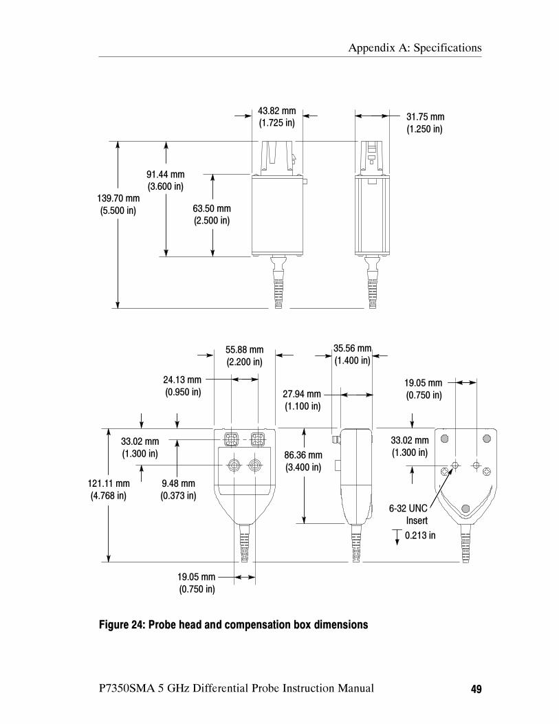
Appendix A: Specifications
P7350SMA 5 GHz Differential Probe Instruction Manual 49
139.70 mm
(5.500 in)
43.82 mm
(1.725 in)31.75 mm
(1.250 in)
63.50 mm
(2.500 in)
91.44 mm
(3.600 in)
121.11 mm
(4.768 in)
33.02 mm
(1.300 in)
9.48 mm
(0.373 in)
55.88 mm
(2.200 in)
35.56 mm
(1.400 in)
24.13 mm
(0.950 in)
19.05 mm
(0.750 in)
19.05 mm
(0.750 in)
33.02 mm
(1.300 in)
27.94 mm
(1.100 in)
6-32 UNC
Insert
86.36 mm
(3.400 in)
0.213 in
Figure 24: Probe head and compensation box dimensions
Appendix A: Specifications
50 P7350SMA 5 GHz Differential Probe Instruction Manual
P7350SMA 5 GHz Differential Probe Instruction Manual 51
Appendix B: Performance Verification
Use the following procedures to verify specifications of the probe.
Before beginning these procedures, refer to page 65 and photocopy
the test record, and use it to record the performance test results. The
recommended calibration interval is one year.
These procedures test the following specifications:
Differential mode input resistance
Output offset zero
DC gain accuracy
Rise time--differential mode
Equipment Required
Refer to Table 8 for a list of the equipment required to verify the
performance of your probe.
Table 8: Equipment required for performance verification
Item description Performance requirement Recommended example1
Oscilloscope TekConnect interface Tektronix TDS7404
Sampling Oscilloscope Tektronix TDS8000
Sampling Module 20 GHz bandwidth Tektronix 80E04
Sampling Module 12 GHz bandwidth Tektronix 80E02
DMM (2), with leads 0.1 mV and 0.01Ω
resolution
Fluke 187 or equivalent
Dual Power Supply 5.0 VDC at 1 mA Tektronix PS280
TekConnect Interface
Calibration Adapter
See page 54 067-0422-00
Feedthrough Termination BNC, 50Ω ±0.05Ω 011-0129-00
Appendix B: Performance Verification
52 P7350SMA 5 GHz Differential Probe Instruction Manual
Table 8: Equipment required for performance verification (Cont.)
Item description Recommended example1
Performance requirement
Coaxial cable Male-to-Male SMA 012-0649-00
Coaxial cable Dual, matched-delay
Male-to-Male SMA
174-4866-002
Coaxial cables (3) Male-to-Male BNC, 50Ω 012-0057-01
Test leads (2) Banana plug ends, red 012-0031-00
Test leads (2) Banana plug ends, black 012-0039-00
Shorting strap Banana plug ends 012-1667-xx2
Adapter TekConnect-to-SMA TCA-SMA
Adapters (3) SMA Male-to-BNC Female 015-1018-00
Adapter BNC Male-to-SMA Female 015-0572-002
Adapters (3) BNC Female-to-Dual
Banana
103-0090-00
SMA torque wrench 5/16-in, 7 in-lb.
1Nine-digit part numbers (XXX-XXXX-XX) are Tektronix part numbers.
2Standard accessory included with probe
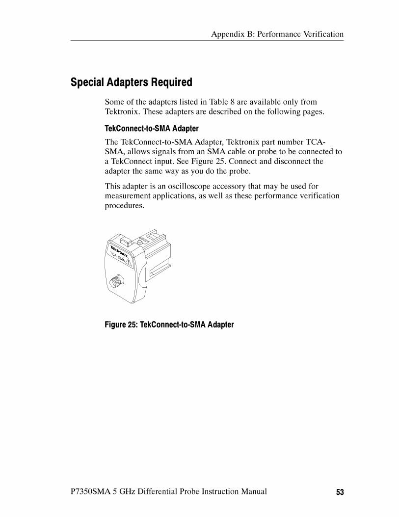
Appendix B: Performance Verification
P7350SMA 5 GHz Differential Probe Instruction Manual 53
Special Adapters Required
Some of the adapters listed in Table 8 are available only from
Tektronix. These adapters are described on the following pages.
TekConnect-to-SMA Adapter
The TekConnect-to-SMA Adapter, Tektronix part number TCA-
SMA, allows signals from an SMA cable or probe to be connected to
a TekConnect input. See Figure 25. Connect and disconnect the
adapter the same way as you do the probe.
This adapter is an oscilloscope accessory that may be used for
measurement applications, as well as these performance verification
procedures.
Figure 25: TekConnect-to-SMA Adapter
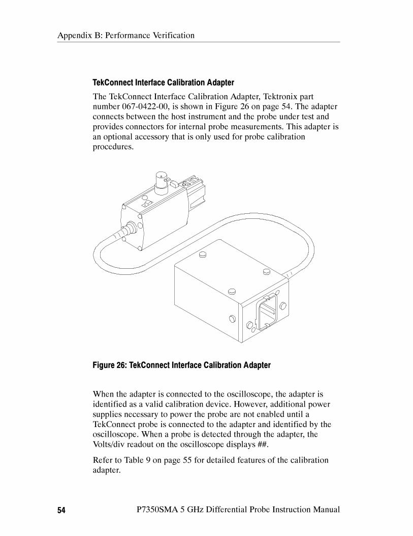
Appendix B: Performance Verification
54 P7350SMA 5 GHz Differential Probe Instruction Manual
TekConnect Interface Calibration Adapter
The TekConnect Interface Calibration Adapter, Tektronix part
number 067-0422-00, is shown in Figure 26 on page 54. The adapter
connects between the host instrument and the probe under test and
provides connectors for internal probe measurements. This adapter is
an optional accessory that is only used for probe calibration
procedures.
Figure 26: TekConnect Interface Calibration Adapter
When the adapter is connected to the oscilloscope, the adapter is
identified as a valid calibration device. However, additional power
supplies necessary to power the probe are not enabled until a
TekConnect probe is connected to the adapter and identified by the
oscilloscope. When a probe is detected through the adapter, the
Volts/div readout on the oscilloscope displays ##.
Refer to Table 9 on page 55 for detailed features of the calibration
adapter.
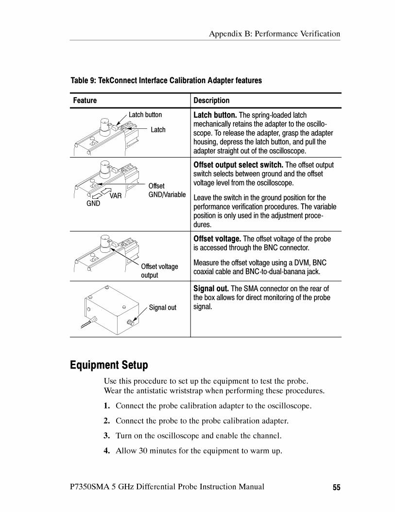
Appendix B: Performance Verification
P7350SMA 5 GHz Differential Probe Instruction Manual 55
Table 9: TekConnect Interface Calibration Adapter features
Feature Description
Latch button
Latch
Latch button. The spring-loaded latch
mechanically retains the adapter to the oscillo-
scope. To release the adapter, grasp the adapter
housing, depress the latch button, and pull the
adapter straight out of the oscilloscope.
Offset
GND/Variable
GND
VAR
Offset output select switch. The offset output
switch selects between ground and the offset
voltage level from the oscilloscope.
Leave the switch in the ground position for the
performance verification procedures. The variable
position is only used in the adjustment proce-
dures.
Offset voltage
output
Offset voltage. The offset voltage of the probe
is accessed through the BNC connector.
Measure the offset voltage using a DVM, BNC
coaxial cable and BNC-to-dual-banana jack.
Signal out
Signal out. The SMA connector on the rear of
the box allows for direct monitoring of the probe
signal.
Equipment Setup
Use this procedure to set up the equipment to test the probe.
Wear the antistatic wriststrap when performing these procedures.
1. Connect the probe calibration adapter to the oscilloscope.
2. Connect the probe to the probe calibration adapter.
3. Turn on the oscilloscope and enable the channel.
4. Allow 30 minutes for the equipment to warm up.

Appendix B: Performance Verification
56 P7350SMA 5 GHz Differential Probe Instruction Manual
Input Resistance
This test checks the differential mode input resistance--the resistance
between each SMA input. The test is performed with the probe
disconnected from the calibration adapter. After you complete this
test, reconnect the probe to the calibration adapter to keep the probe
at operating temperature.
1. Zero the DMM on the lowest scale that can measure 100 Ω.
2. Probe the center contacts of the SMA input connectors as shown
in Figure 27.
3. Measure the resistance and write down the value.
4. Reverse the DMM connections and repeat the measurement.
Write down the value.
5. Add the two measurements from steps 3 and 4, and divide the
total by two. Subtract 0.15 Ω from the result to account for the
internal path resistance, and record the result in the test record.
6. Connect the probe to the calibration adapter so that the probe
warms up to operating temperature for the remaining tests.
Black (--)
Red (+)
DMM
--
+
P7350SMA probe
Gently touch the center
conductor on each
connector, enough to
get a measurement.
Don’t touch the outer
edge of the connector.
Figure 27: Checking differential mode input resistance
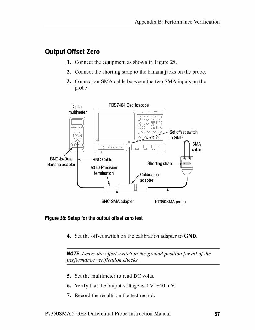
Appendix B: Performance Verification
P7350SMA 5 GHz Differential Probe Instruction Manual 57
Output Offset Zero
1. Connect the equipment as shown in Figure 28.
2. Connect the shorting strap to the banana jacks on the probe.
3. Connect an SMA cable between the two SMA inputs on the
probe.
TDS7404 Oscilloscope
BNC-to-Dual
Banana adapter
50Ω Precision
termination
Digital
multimeter
Set offset switch
to GND
BNC-SMA adapter
Calibration
adapter
BNC Cable
P7350SMA probe
Shorting strap
SMA
cable
Figure 28: Setup for the output offset zero test
4. Set the offset switch on the calibration adapter to GND.
NOTE. Leave the offset switch in the ground position for all of the
performance verification checks.
5. Set the multimeter to read DC volts.
6. Verify that the output voltage is 0 V, ±10 mV.
7. Record the results on the test record.
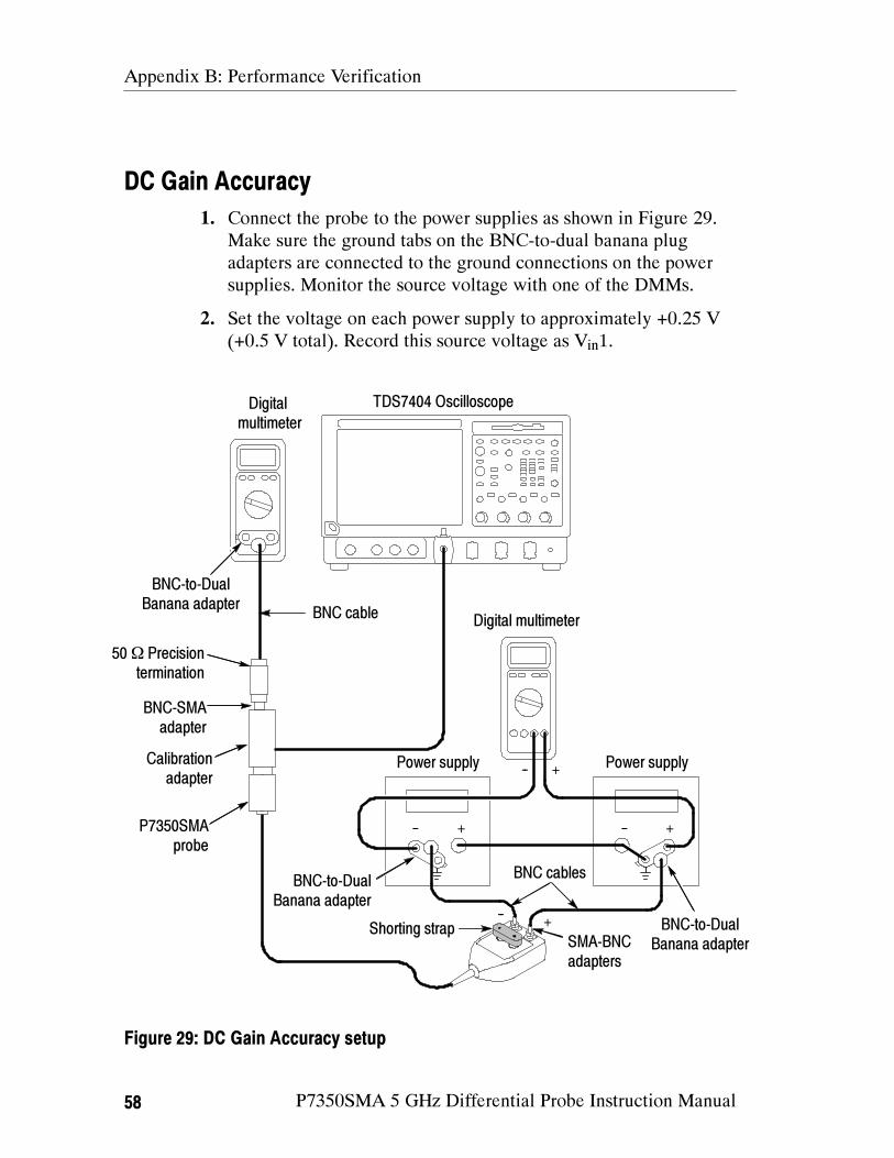
Appendix B: Performance Verification
58 P7350SMA 5 GHz Differential Probe Instruction Manual
DC Gain Accuracy
1. Connect the probe to the power supplies as shown in Figure 29.
Make sure the ground tabs on the BNC-to-dual banana plug
adapters are connected to the ground connections on the power
supplies. Monitor the source voltage with one of the DMMs.
2. Set the voltage on each power supply to approximately +0.25 V
(+0.5 V total). Record this source voltage as Vin1.
-- +
Power supply
TDS7404 Oscilloscope
50Ω Precision
termination
Digital
multimeter
Calibration
adapter
BNC-SMA
adapter
-- +
Power supply
Digital multimeterBNC cable
SMA-BNC
adapters
Shorting strap
P7350SMA
probe
--+
BNC cablesBNC-to-Dual
Banana adapter
BNC-to-Dual
Banana adapter
BNC-to-Dual
Banana adapter
-- +
Figure 29: DC Gain Accuracy setup
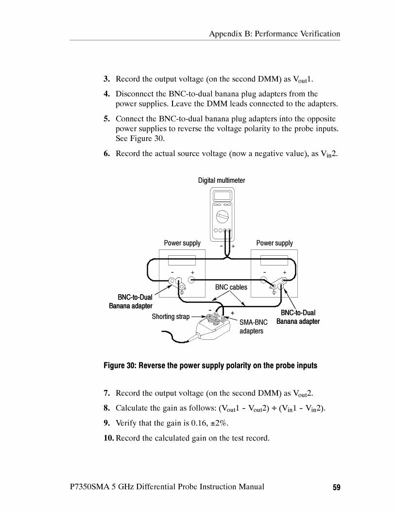
Appendix B: Performance Verification
P7350SMA 5 GHz Differential Probe Instruction Manual 59
3. Record the output voltage (on the second DMM) as Vout
1.
4. Disconnect the BNC-to-dual banana plug adapters from the
power supplies. Leave the DMM leads connected to the adapters.
5. Connect the BNC-to-dual banana plug adapters into the opposite
power supplies to reverse the voltage polarity to the probe inputs.
See Figure 30.
6. Record the actual source voltage (now a negative value), as Vin2.
-- +
Power supply
-- +
Power supply
Digital multimeter
SMA-BNC
adapters
Shorting strap
--+
BNC cables
BNC-to-Dual
Banana adapter
BNC-to-Dual
Banana adapter
BNC-to-Dual
Banana adapter
BNC-to-Dual
Banana adapter--
+
+--
Figure 30: Reverse the power supply polarity on the probe inputs
7. Record the output voltage (on the second DMM) as Vout
2.
8. Calculate the gain as follows: (Vout
1 -- Vout
2) ÷ (Vin1 -- V
in2).
9. Verify that the gain is 0.16, ±2%.
10.Record the calculated gain on the test record.
Appendix B: Performance Verification
60 P7350SMA 5 GHz Differential Probe Instruction Manual
Rise Time
This procedure verifies that the probe meets the differential rise time
specification. Two rise times are measured; the test system alone,
and the test system with the probe included. The probe rise time is
calculated using the two measurements.
This test uses the TDR function of the 80E04 sampling head as a fast
rise time signal source. A second 80E0X sampling head is used to
take the measurements. Although the following procedure assigns the
TDR and measurement functions to specific oscilloscope channels,
any channels can be used. However, the TDR function is only
available on 80E04 sampling heads.
1. Remove the probe from the test setup.
2. Connect the test equipment as shown in Figure 31 on page 61.
Connect the TekConnect-to-SMA adapter to Channel 8.
CAUTION. To prevent mechanical strain on the connectors, use care
when working with SMA connectors: Support equipment and use a
torque wrench to tighten connections to 7 in-lbs.
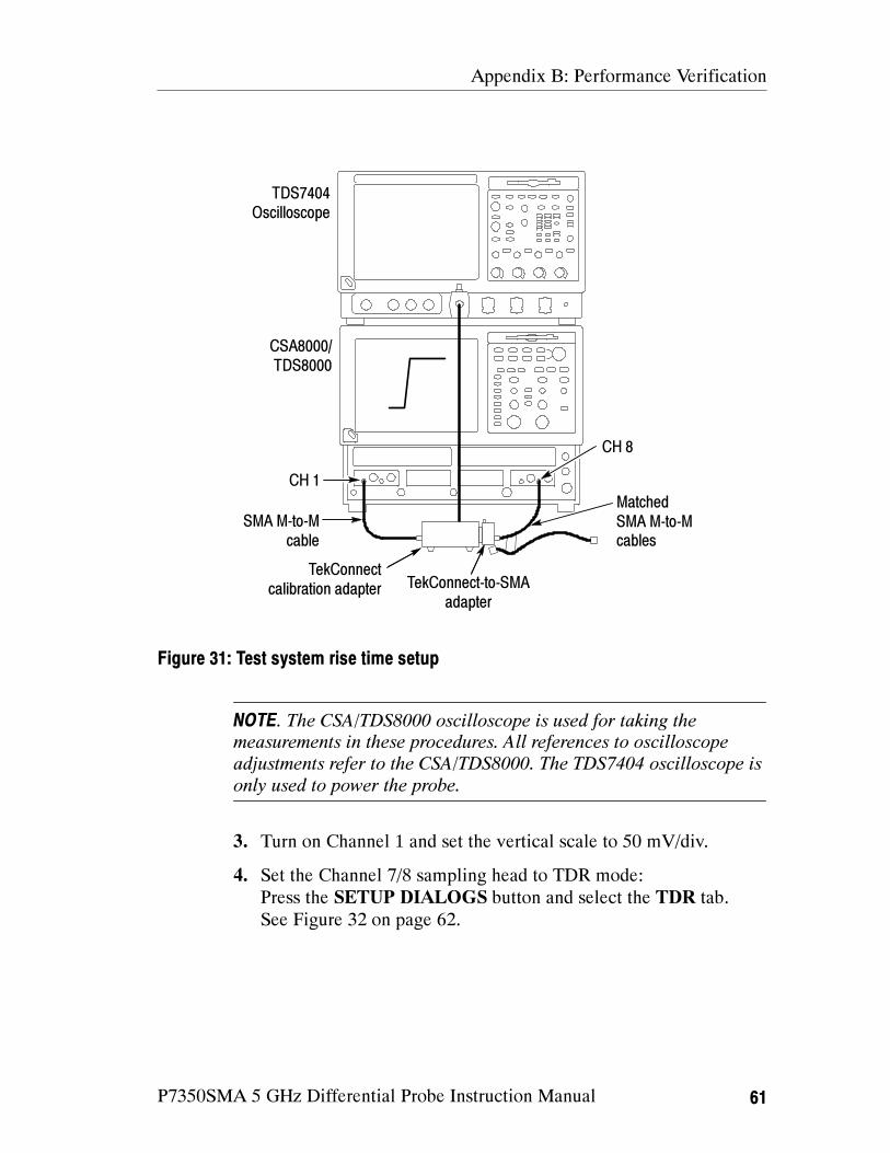
Appendix B: Performance Verification
P7350SMA 5 GHz Differential Probe Instruction Manual 61
TekConnect
calibration adapter
Matched
SMA M-to-M
cables
CH 1
SMA M-to-M
cable
CSA8000/
TDS8000
TDS7404
Oscilloscope
CH 8
TekConnect-to-SMA
adapter
Figure 31: Test system rise time setup
NOTE. The CSA/TDS8000 oscilloscope is used for taking the
measurements in these procedures. All references to oscilloscope
adjustments refer to the CSA/TDS8000. The TDS7404 oscilloscope is
only used to power the probe.
3. Turn on Channel 1 and set the vertical scale to 50 mV/div.
4. Set the Channel 7/8 sampling head to TDR mode:
Press the SETUP DIALOGS button and select the TDR tab.
See Figure 32 on page 62.
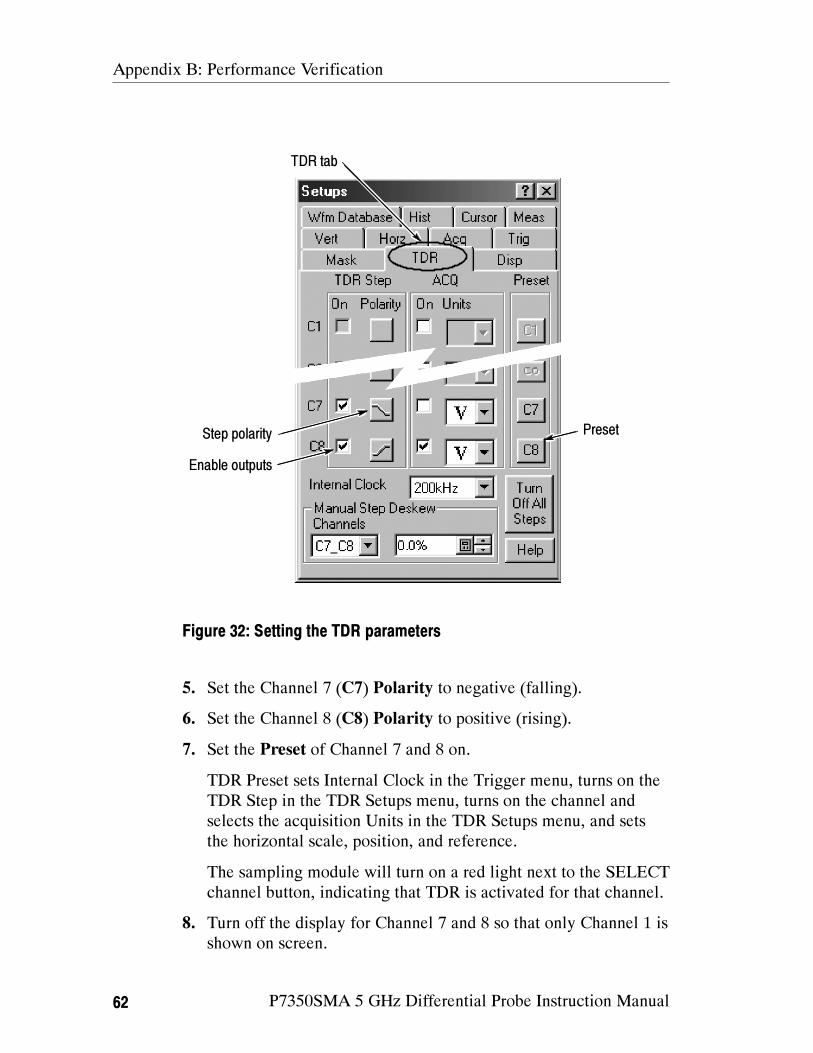
Appendix B: Performance Verification
62 P7350SMA 5 GHz Differential Probe Instruction Manual
TDR tab
Enable outputs
PresetStep polarity
Figure 32: Setting the TDR parameters
5. Set the Channel 7 (C7) Polarity to negative (falling).
6. Set the Channel 8 (C8) Polarity to positive (rising).
7. Set the Preset of Channel 7 and 8 on.
TDR Preset sets Internal Clock in the Trigger menu, turns on the
TDR Step in the TDR Setups menu, turns on the channel and
selects the acquisition Units in the TDR Setups menu, and sets
the horizontal scale, position, and reference.
The sampling module will turn on a red light next to the SELECT
channel button, indicating that TDR is activated for that channel.
8. Turn off the display for Channel 7 and 8 so that only Channel 1 is
shown on screen.
Appendix B: Performance Verification
P7350SMA 5 GHz Differential Probe Instruction Manual 63
9. Adjust the oscilloscope horizontal and vertical position controls
to display a signal similar to that shown in Figure 31.
10. Set the oscilloscope horizontal scale to 50 ps/div and center the
waveform.
11. Use the oscilloscope measurement capability to display rise time.
Increase the stability of the pulse edge measurement by using
averaging, if available. Rise time is determined from the 10% and
90% amplitude points on the waveform. Record the rise time
as ts.
The following steps instruct you to assemble the test setup that
includes the probe, as shown in Figure 33 on page 64. The system
and probe rise time (ts+p
) that you measure in step 18 is used to
calculate the probe rise time (tp) in step 19.
12.Remove the TekConnect-SMA adapter from the test setup.
13.Connect the probe to the TekConnect calibration adapter.
14.Connect the matched SMA cables to the probe SMA inputs and
the sampling head (Channels 7 and 8).
The test setup should now be connected as shown in Figure 33 on
page 64.
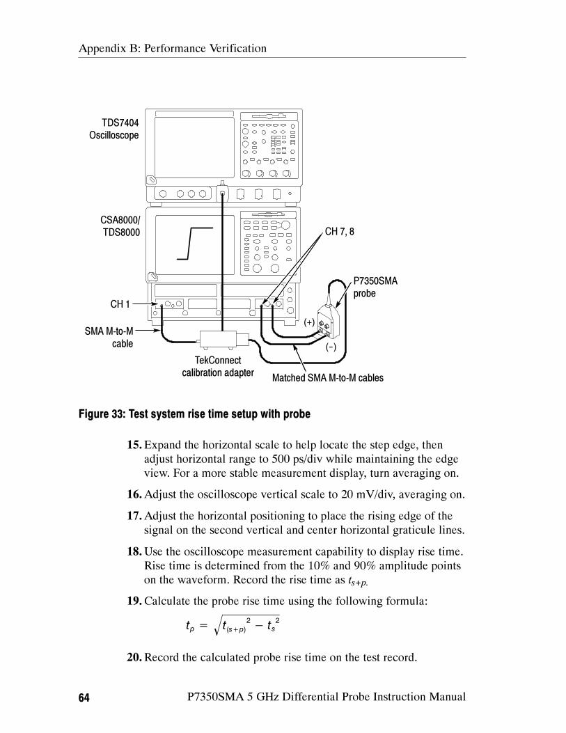
Appendix B: Performance Verification
64 P7350SMA 5 GHz Differential Probe Instruction Manual
TekConnect
calibration adapterMatched SMA M-to-M cables
CH 1
P7350SMA
probe
(--)
(+)
SMA M-to-M
cable
CH 7, 8
CSA8000/
TDS8000
TDS7404
Oscilloscope
Figure 33: Test system rise time setup with probe
15.Expand the horizontal scale to help locate the step edge, then
adjust horizontal range to 500 ps/div while maintaining the edge
view. For a more stable measurement display, turn averaging on.
16.Adjust the oscilloscope vertical scale to 20 mV/div, averaging on.
17.Adjust the horizontal positioning to place the rising edge of the
signal on the second vertical and center horizontal graticule lines.
18.Use the oscilloscope measurement capability to display rise time.
Rise time is determined from the 10% and 90% amplitude points
on the waveform. Record the rise time as ts+p.
19.Calculate the probe rise time using the following formula:
tp= t
(s+p)
2
− ts
2
20.Record the calculated probe rise time on the test record.
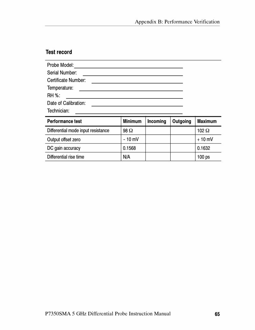
Appendix B: Performance Verification
P7350SMA 5 GHz Differential Probe Instruction Manual 65
Test record
Probe Model:
Serial Number:
Certificate Number:
Temperature:
RH %:
Date of Calibration:
Technician:
Performance test Minimum Incoming Outgoing Maximum
Differential mode input resistance 98Ω 102Ω
Output offset zero -- 10 mV + 10 mV
DC gain accuracy 0.1568 0.1632
Differential rise time N/A 100 ps
Appendix B: Performance Verification
66 P7350SMA 5 GHz Differential Probe Instruction Manual
P7350SMA 5 GHz Differential Probe Instruction Manual 67
Appendix C: Maintenance
This section details the maintenance for the P7350SMA differential
probe.
Inspection and Cleaning
Protect the probe from adverse weather conditions. The probe is not
waterproof.
CAUTION. To prevent damage to the probe, do not expose it to sprays,
liquids, or solvents. Do not use chemical cleaning agents; they may
damage the probe. Avoid using chemicals that contain benzine,
benzene, toluene, xylene, acetone, or similar solvents.
Clean the exterior surfaces of the probe with a dry, lint-free cloth or a
soft-bristle brush. If dirt remains, use a soft cloth or swab dampened
with a 75% isopropyl alcohol solution. A swab is useful for cleaning
narrow spaces on the probe. Do not use abrasive compounds on any
part of the probe.
CAUTION. To prevent damage to the probe, avoid getting moisture
inside the probe during exterior cleaning, and use only enough
solution to dampen the swab or cloth. Use a 75% isopropyl alcohol
solution as a cleanser, and rinse with deionized water.
Appendix C: Maintenance
68 P7350SMA 5 GHz Differential Probe Instruction Manual
Replacement Parts
Refer to the Replaceable Parts section for a list of customer
replacement parts. Due to the sophisticated design of the P7350SMA
differential probe, there are no user replaceable parts within the
probe.
Preparation for Shipment
If the original packaging is unfit for use or not available, use the
following packaging guidelines:
1. Use a corrugated cardboard shipping carton having inside
dimensions at least one inch greater than the probe dimensions.
The box should have a carton test strength of at least 200 pounds.
2. Put the probe into an antistatic bag or wrap to protect it from
dampness.
3. Place the probe into the box and stabilize it with light packing
material.
4. Seal the carton with shipping tape.
P7350SMA 5 GHz Differential Probe Instruction Manual 69
Appendix D: Replaceable Parts
This section contains a list of replaceable parts for the P7350SMA
differential probe. Use this list to identify and order replacement
parts.
Parts Ordering Information
Replacement parts are available from or through your local
Tektronix, Inc. service center or representative.
Changes to Tektronix instruments are sometimes made to accommo-
date improved components as they become available and to give you
the benefit of the latest circuit improvements. Therefore, when
ordering parts, it is important to include the following information in
your order:
Part number
Instrument type or model number
Instrument serial number
Instrument modification number, if applicable
If a part you order has been replaced with a different or improved
part, your local Tektronix service center or representative will
contact you concerning any change in the part number.
Appendix D: Replaceable Parts
70 P7350SMA 5 GHz Differential Probe Instruction Manual
Using the Replaceable Parts List
The tabular information in the Replaceable Parts List is arranged for
quick retrieval. Understanding the structure and features of the list
will help you find the information you need for ordering replacement
parts.
Item Names
In the Replaceable Parts List, an Item Name is separated from the
description by a colon (:). Because of space limitations, an Item
Name may sometimes appear as incomplete. For further Item Name
identification, U.S. Federal Cataloging Handbook H6-1 can be used
where possible.
Indentation System
This parts list is indented to show the relationship between items.
The following example is of the indentation system used in the
Description column:
1 2 3 4 5 Name & Description
Assembly and/or Component
Attaching parts for Assembly and/or Component
(END ATTACHING PARTS)
Detail Part of Assembly and/or Component
Attaching parts for Detail Part
(END ATTACHING PARTS)
Parts of Detail Part
Attaching parts for Parts of Detail Part
(END ATTACHING PARTS)
Attaching parts always appear at the same indentation as the item it
mounts, while the detail parts are indented to the right. Indented
items are part of, and included with, the next higher indentation.
Attaching parts must be purchased separately, unless otherwise
specified.
Abbreviations
Abbreviations conform to American National Standards Institute
(ANSI) standard Y1.1
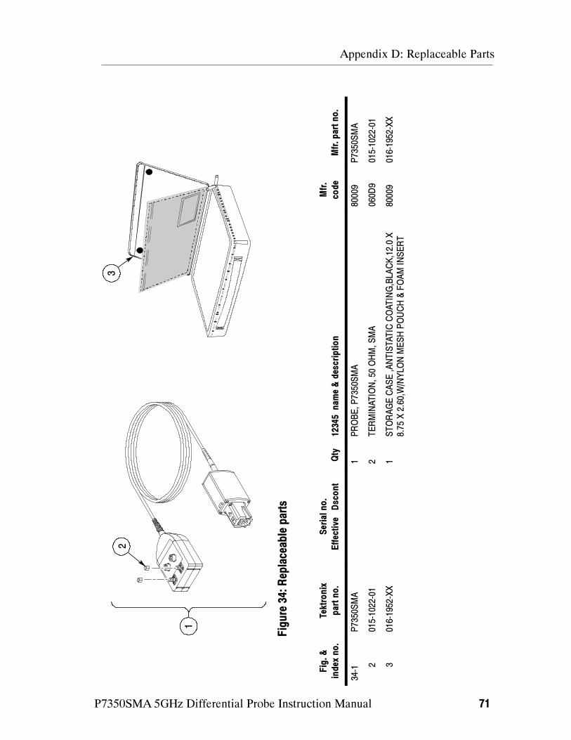
Appendix D: Replaceable Parts
P7350SMA 5GHz Differential Probe Instruction Manual 71
1
2
3
Figure34:Replaceableparts
Fig.&
indexno.
Tektronix
partno.
Serialno.
Effective
Dscont
Qty
12345name&description
Mfr.
code
Mfr.partno.
34-1
P7350SMA
1PROBE,P7350SMA
80009
P7350SMA
2015-1022-01
2TERMINATION,50OHM,SMA
060D9
015-1022-01
3016-1952-XX
1STORAGECASE,ANTISTATICCOATING,BLACK,12.0X
8.75X2.60,W/NYLONMESHPOUCH&FOAMINSERT
80009
016-1952-XX
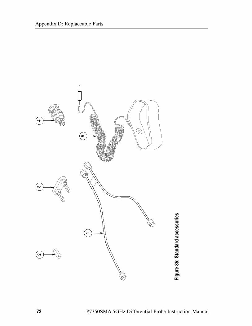
Appendix D: Replaceable Parts
P7350SMA 5GHz Differential Probe Instruction Manual72
1
23
4
5
Figure35:Standardaccessories
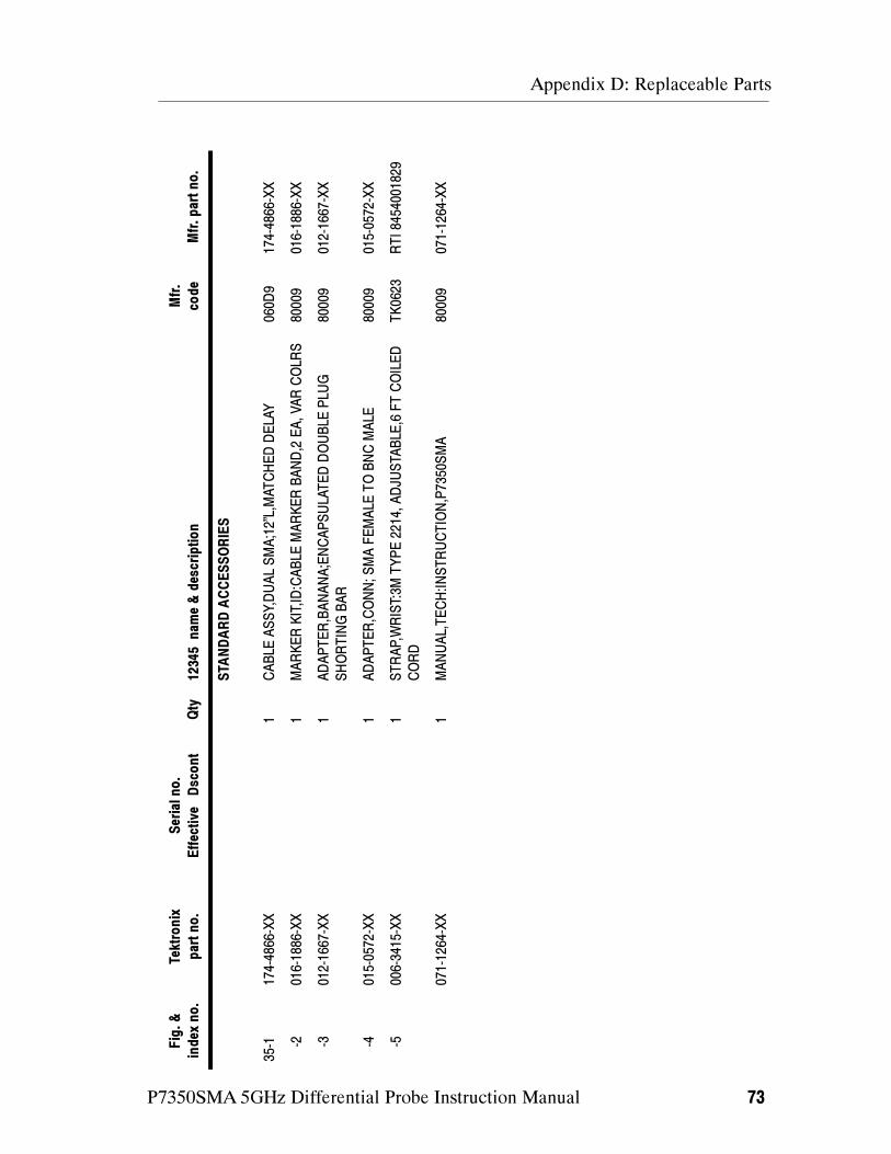
Appendix D: Replaceable Parts
P7350SMA 5GHz Differential Probe Instruction Manual 73
Fig.&
indexno.
Tektronix
partno.
Serialno.
Effective
Dscont
Qty
12345name&description
Mfr.
code
Mfr.partno.
STANDARDACCESSORIES
35-1
174-4866-XX
1CABLEASSY,DUALSMA;12”L,MATCHEDDELAY
060D9
174-4866-XX
-2
016-1886-XX
1MARKERKIT,ID:CABLEMARKERBAND,2EA,VARCOLRS
80009
016-1886-XX
-3
012-1667-XX
1ADAPTER,BANANA;ENCAPSULATEDDOUBLEPLUG
SHORTINGBAR
80009
012-1667-XX
-4
015-0572-XX
1ADAPTER,CONN;SMAFEMALETOBNCMALE
80009
015-0572-XX
-5
006-3415-XX
1STRAP,WRIST:3MTYPE2214,ADJUSTABLE,6FTCOILED
CORD
TK0623
RTI8454001829
071-1264-XX
1MANUAL,TECH:INSTRUCTION,P7350SMA
80009
071-1264-XX
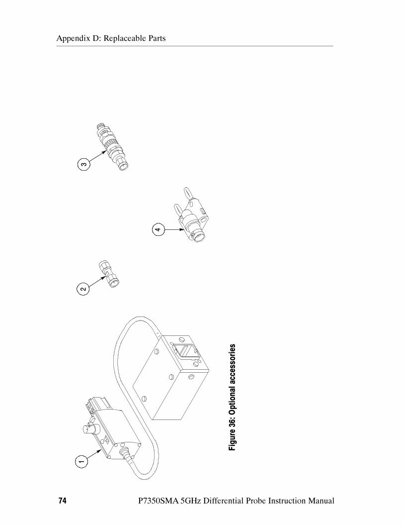
Appendix D: Replaceable Parts
P7350SMA 5GHz Differential Probe Instruction Manual74
12
3
4
Figure36:Optionalaccessories
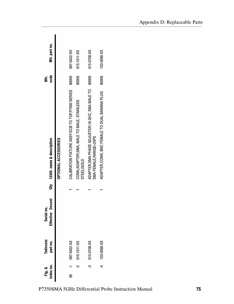
Appendix D: Replaceable Parts
P7350SMA 5GHz Differential Probe Instruction Manual 75
Fig.&
indexno.
Tektronix
partno.
Serialno.
Effective
Dscont
Qty
12345name&description
Mfr.
code
Mfr.partno.
OPTIONALACCESSORIES
36
-1
067-0422-XX
1CALIBRATIONFIXTUREASSY:ECBTOTOP,P7000SERIES
80009
067-0422-XX
-2
015-1011-XX
1CONN,ADAPTER;SMA,MALETOMALE,STAINLESS
STEEL/GOLD
80009
015-1011-XX
-3
015-0708-XX
1ADAPTER,SMAPHASEADJUSTER;18GHZ,SMAMALETO
SMAFEMALE,RANGE>25PS
80009
015-0708-XX
-4
103-0090-XX
1ADAPTER,CONN;BNCFEMALETODUALBANANAPLUG
80009
103-0090-XX
Appendix D: Replaceable Parts
P7350SMA 5GHz Differential Probe Instruction Manual76
CROSSINDEX-MFR.CODENUMBERTOMANUFACTURER
Mfr.code
Manufacturer
Address
City,state,zipcode
060D9
TENSOLITECORPORATION
3000COLUMBIAHOUSEBLVD,SUITE120
VANCOUVER,WA98661
80009
TEKTRONIXINC
14150SW
KARLBRAUNDR
POBOX500
BEAVERTON,OR97077-0001
TK0623
GENERALTOOL&SUPPLYCO
2705NW
NICOLAIST
PORTLAND,OR97210
Related Documents