. . NASA Contractor Report 185 149 CTD-90/022 Advanced Modulation Technology Development for Earth Station Demodulator Applications Coded Modulation System Development Susan P. Miller, J. Mark Kappes, David H. Layer, and Peter N . Johnson COMSA T Laboratories Clarksburg, Maryland April 1990 Prepared for Lewis Research Center Under Contract NAS3-24680 https://ntrs.nasa.gov/search.jsp?R=19900010954 2018-09-07T08:28:47+00:00Z

Welcome message from author
This document is posted to help you gain knowledge. Please leave a comment to let me know what you think about it! Share it to your friends and learn new things together.
Transcript
.
.
NASA Contractor Report 185 149 CTD-90/022
Advanced Modulation Technology Development for Earth Station Demodulator Applications Coded Modulation System Development
Susan P. Miller, J . Mark Kappes, David H. Layer, and Peter N. Johnson COMSA T Laboratories Clarksburg, Maryland
April 1990
Prepared for Lewis Research Center Under Contract NAS3-24680
https://ntrs.nasa.gov/search.jsp?R=19900010954 2018-09-07T08:28:47+00:00Z

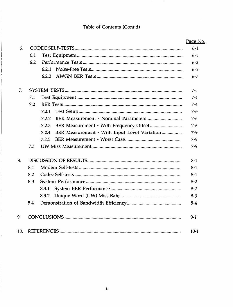
Table of Contents
Page No . 1 . SUMMARY ...........................................................................................................
2 . INTRODUCTION ................................................................................................
3 . SYSTEM DESCRIPTION AND ESTIMATED PERFORMANCE ................ 3.1 Characteristics of Coded Modulation System ...................................... 3.2 Performance of Coded Modulation System .........................................
4 . MODEM/CODEC CONCEPTUAL DESIGN .................................................... 4.1 Modem Design ...........................................................................................
4.1.1 Modulator ....................................................................................... 4.1.2 Demodulator .................................................................................. 4.1.3 Unique Word Detector .................................................................
4.2 Codec Design ............................................................................................... 4.2.1 Encoder ............................................................................................ 4.2.2 Decoder ............................................................................................
4.3 Advanced Component Technology Design ......................................... 4.3.1 Add-Compare-Select Gate Array ................................................ 4.3.2 ACS Microwire Subsystem .......................................................... 4.3.3 Implementation Technology Comparison ..............................
5 . MODEM SELF-TESTS ......................................................................................... 5.1 Test Equipment .......................................................................................... 5.2 BER Tests .....................................................................................................
BER Measurement - Continuous Mode ................................... 5.2.1 5.2.2 BER Measurement - Burst Mode, Long and Short Bursts .... Carrier Cycle Slip Measurement ............................................................ 5.3
1-1
2-1
3-1 3-1 3-5
4-1 4-1 4-1 4-7 4-14 4-16 4-16 4-17 4-34 4-35 4-37 4-38
5-1 5-1 5-3 5-5 5-5 5-5
1
6 .
7 .
8 .
9 .
10 .
Table of Contents (Cont'd)
Pape No . CODEC SELF-TESTS ............................................................................................ 6.1 Test Equipment .......................................................................................... 6.2 Performance Tests .....................................................................................
6.2.1 Noise-Free Tests ............................................................................. 6.2.2 AWGN BER Tests .........................................................................
SYSTEM TESTS .................................................................................................... 7.1 Test Equipment .......................................................................................... 7.2 BER Tests .....................................................................................................
7.2.1 TestSetup ........................................................................................ 7.2.2 BER Measurement - Nominal Parameters .............................. 7.2.3 7.2.4
7.2.5 BER Measurement . Worst Case ................................................ 7.3 UW Miss Measurement ...........................................................................
BER Measurement - With Frequency Offset ........................... BER Measurement - With Input Level Variation .................
DISCUSSION OF RESULTS ............................................................................... 8.1 Modem Self-tests ....................................................................................... 8.2 Codec Self-tests ........................................................................................... 8.3 System Performance .................................................................................
8.3.1 System BER Performance ............................................................ 8.3.2 Unique Word (UW) Miss Rate ................................................... Demonstration of Bandwidth Efficiency .............................................. 8.4
CONCLUSIONS ...................................................................................................
REFERENCES .......................................................................................................
6-1 6-1 6-2 6-5 6-7
7-1 7-1 7-4 7-6 7-6 7-6 7-9
7-9 7-9
8-1 8-1 8-1 8-2 8-2 8-3 8-4
9-1
10-1
ii
1. SUMMARY
. The purpose of NASA's Advanced Modulation Technology
Development (AMTD) program was to develop a system with high bandwidth and power efficiency which operated at high bit rates in burst mode. The intended application is for satellite sys tems employing on-board demodulation and remodulation, with the current development intended for the downlink segment. The desired bandwidth efficiency was 2 bits/sec/Hz where the bandwidth is defined as the spacing between adjacent carriers, leading to the most stringent definition of bandwidth efficiency. The desired data rate was 200 Mbit/s. Bit error rate (BER) performance was to be no more than 2 dB from theoretical at an error rate of 5 x Under the NASA AMTD contract, COMSAT has developed and tested a modem system designed to meet these requirements.
To meet these goals, a jointly optimized modulation coding scheme was selected using 8-PSK modulation a t a transmission bit rate of 225 Mbit/s with rate 8/9 convolutional encoder and Viterbi decoder. Basic parameters for the modem and codec subsystem such as preamble length and data filtering characteristics were determined during the study phase. Analysis of estimated performance in both linear and nonlinear channels was also conducted.
Using these results, the codec and modem were designed, built and tested. The codec was tested at the 200 Mbit/s information rate using a specially designed test set for adding noise digitally. The performance of the c o d a matched the simulated data exactly. The 8-PSK modem was implemented at a data rate of 180 Mbit/s and combined with the codec to perform system measurements at an information rate of 160 Mbit/s. The performance of this system met the original BER performance goal.
also developed which replaced two complex hybrid chips. This gate array performs the function of add-compare-select in the codec which is the most time critical operation. The new chip is capable of higher operating speeds, consumes 80 '36 less power and is considerably easier to manufacture than the hybrid ACS chip.
As part of an effort to advance the codec design, a gate array chip was
1-1

The hardware developed under this task demonstrates the feasibility of obtaining improved bandwidth efficiency while maintaining good BER performance at very high bit rates.
1-2
2. INTRODUCTION
1
NASA and other users of satellite communications are continuing to expand their needs for rapid data transfer. This has led to an effort to find ways of improving the efficiency of data transfer via satellite by more efficient use of the satellite bandwidth.
The most efficient form of digital transmission currently in use for satellite systems is quadrature phase shift keying (QPSK) which has a bandwidth efficiency of approximately 1.5 bit/s/Hz. Other system such as bi-phase shift keying (BPSK) and minimum shift keying (MSK) exhibit lower efficiencies, but have advantages in simplicity of receiver structure or nonlinear channel performance. Terrestrial microwave links are employing modulation formats with higher number alphabets such as 16-quadrature amplitude modulation (16-QAM) which give excellent bandwidth efficiency, but require large carrier to noise ratios which are not available in satellite systems.
objectives of this development effort were to develop a system capable of obtaining a bandwidth efficiency of at least 2 bits/s/Hz of allocated bandwidth while simultaneously incurring an implementation loss of less than 2 dB from theoretical at a BER of 5 x 10⁻⁷. The system must operate at an information bit rate of 200 Mbit/s and be capable of burst mode operation. The preamble for burst mode operation was constrained to be quite short with only 100 information bits allowed. The unique word was constrained to 20 information bits in length.
The successful development of such a system would allow current and future users of satellite systems to significantly increase their data throughput. To enable the system to be more generally useful, a further requirement was that the system be cost effective to build and maintain.
modulation coding system utilizing an 8-PSK demodulator followed by a rate 8/9 time varying Viterbi decoder. The codec which operates on a coded bit stream of 225 Mbit/s outputs data at 200 Mbit/s. The 8-PSK modem was to be designed, built and tested by the Electronic Systems Group of TRW, Inc. The 8-PSK modem would
The original objectives of this contract are listed in Table 2-1. The key
To satisfy these requirements, COMSAT proposed a combined
2-1
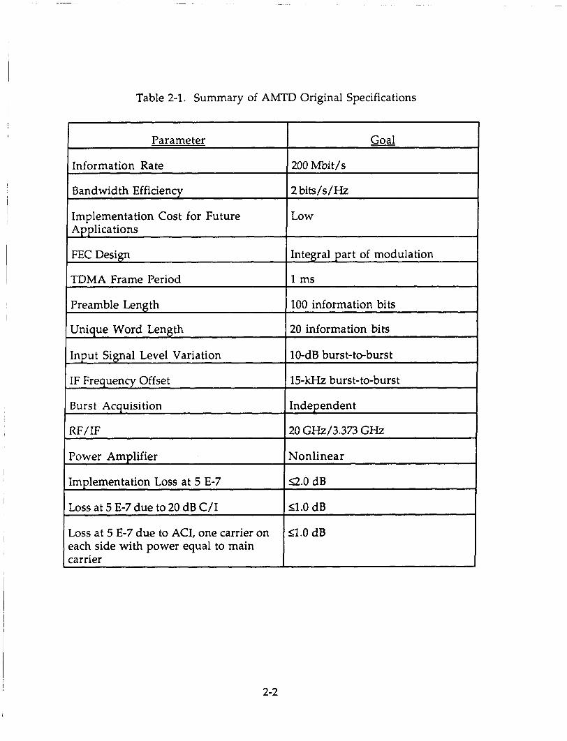
Table 2-1. Summary of AMTD Original Specifications
Parameter
Information Rate
Bandwidth Efficiency
Implementation Cost for Future Applications
FEC Design
TDMA Frame Period
Preamble Length
Unique Word Length
Input Signal Level Variation
IF Frequency Offset
Burst Acquisition
RF/ IF
Power Amplifier
[mplementation Loss at 5 E-7
Loss at 5 E-7 due to 20 dB C/I
Loss at 5 E-7 due to ACI, one carrier on ?ach side with power equal to main :arrier
Goal
200 Mbit/s
2 bits/s/Hz
Low
Integral part of modulation
1 ms
100 information bits
20 information bits
IO-dB burs t-to-burs t ~~~
15-kHz burst-to-burst
Independent
20 GHz/3.373 GHz
Nonlinear
Q.0 dB
51.0 dB
2-2
operate at a symbol rate of 75 Msymbol/s. This would result in a spectral occupancy which would allow carriers to be placed at 100 M H z intervals, thus meeting the 2 bits/s/Hz requirement. Preliminary system studies indicated that all requirements of the contract would be met.
system design and to determine the basic parameters for modem and codec subsystems. After a careful analysis of the effects of phase jitter and phase uncertainty on the BER performance of the coded system and an estimate of these quantities at the end of the preamble for various preamble lengths, it was recommended that the preamble length be extended to 88 8-PSK symbols or 235 information bits. This was the only modification made to the system requirements as a result of these more detailed studies. Further characterizations of the system using the union bound technique were carried out which indicated that all system specifications could be met with the selected approach.
information rate of 200 Mbit/s using the COMSAT codec self test equipment. The measured performance was very close to the results obtained from the initial computer simulations of this equipment.
then integrate and test the complete system for compliance with the specification. However, the modem delivery was delayed on several occasions, and an evaluation was undertaken to estimate the cost to complete the program. The results of this evaluation were presented to NASA along with an alternate, lower risk, lower cost option using an existing 8-PSK modem design developed by COMSAT for operation at 180 Mbit/s. With this option, it would be possible to demonstrate the major objectives of this program, i.e. bandwidth and power efficiency. This approach was selected by NASA and a summary of the program objectives as modified by this option are shown in Table 2-2. Also shown are the measured performance of the completed system. As can be seen from this table, COMSAT has met or exceeded all of the goals for the system as modified by the option.
In addition to the modem/codec system, COMSAT has also developed the special test equipment (STE) necessary to test the coded system performance.
More detailed studies were conducted to further refine the downlink
The rate 8/9 Viterbi decoder was successfully built and tested at an
After codec self test, the next step was to test the 8-PSK modem and
2-3

.- Y
(d ?
4 w In 3
2-4

The STE is capable of generating the necessary preambles and timing signals required to test and control the codec and modem. Bit error rate (BER) is measured using off-the-shelf BER test equipment which is controlled by the COMSAT STE.
To meet the goal of cost effective reproduction of the overall unit, a gate array was designed for the add-compare-select function in the codec. This function had previously been implemented using a hybrid approach.
original requirement. It has thus been demonstrated that a system can be economically constructed which will offer satellite users the ability to transfer higher data rates using less bandwidth than was previously possible, with power efficiency similar to QPSK.
Testing indicates that the completed unit meets the goals of the
2-5

3. SYSTEM DESCRIPTION AND ESTIMATED PERFORMANCE
During the design refinement phase of the downlink system concept, a1
number of modulation methods were investigated including M-ary phase shift keying (MPSK), M-ary quadrature amplitude modulation (MQAM), and con tinuous-phase frequency shift keying (CPFSK). Based on performance simulations and analysis in both linear and nonlinear channels, and taking implementation complexity into consideration, rate-8/9 coded 8-PSK was selected as the best system candidate to meet NASA's requirements. The performance of this system was analyzed using both time domain simulation and the union bound technique. This section will describe, in more detail, the selected approach and present predicted performance.
3.1 CHARACTERISTICS OF CODED MODULATION SYSTEM
A general block diagram of the selected coded modulation system is shown in Figure 3-1. The system consists of a 16-state rate 8/9 FEC encoder, an octal mapper, 8-PSK modulator, 8-PSK demodulator, and Viterbi algorithm processor. The code trellis and modulation mapping are jointly optimized to maximize the minimum free Euclidean distance among the trellis paths. The 16-state rate 8/9 code allows moderate coding gain with moderate codec complexity while the symbol rate is sufficiently low that filter design and ACI are not critical factors.
The decoder performs three main functions: branch metric calculation, state metric calculation, and path memory traceback. For high-speed implementation, the state metric calculation is the most critical because it is a closely connected feedback loop that cannot be easily pipelined or partitioned. The time required for state metric calculation, which involves adding the branch metric to the state metric, comparing the results, and selecting the most likely path, sometimes known as add-compare-select (ACS), usually determines the speed of the new decoder operation.
3- 1

THERMAL
la-
. m
(a) Block Diagram of Coded Modulation System
111
. IN
0
I .
8-Phase Signal Space with Natural Binary Mapping
(c) Trellis of the 16-State Rate 8/9 Periodically Time Varying Code
Figure 3-1. General Block Diagram of Selected Coded Modulation System
3-2
Conventional codes with rates greater than 2/3 are not readily implemented at 200-Mbit/s information rates because of the large number of branches per state. For this reason, the selected system uses a unique periodically time varying trellis code. Figure 3-2 is a functional block diagram of a periodically time-varying encoder of rate (2P + i)/3P. The information bits are input to the encoder two bits at a time (in parallel) through lines x i and x3, with the input to x2 set to a logical zero and the outputs taken from lines y1, y2, and y3. The process is repeated for P - i consecutive clock periods, during which it is assumed that the encoder remains fixed. During the P - i + I, P - i + 2, . . . Pth clock periods, three information bits are input to the encoder through lines xi, x2, and x3; the outputs are taken from y ~ , 22, and 23. Again, it is assumed that the encoder of rate 3/3 code is fixed. The above encoding process is continued periodically with period P. Finally, the selected 3-tuple encoder output block is mapped to an 8-phase channel symbol. Optimum codes of rate 5/6 and 8/9 with 4,8, and 16 states have been constructed at COMSAT Laboratories using an exhaustive search method. The encoder for the optimum 16-state time-varying code of rate 8/9 is shown in Figure 3- 2b; the trellis structure of the 16-state code is shown in Figure 3-lc. The encoder outputs are mapped into an 8-PSK signal set using a natural binary mapping, as shown in Figure 3-lb.
Note that four double branches terminate on each state at trellis steps with a rate 3/3 trellis structure. Note also that the branches in the rate 2/3 structure form a subset of those in the 3/3 structure. These properties greatly simplify decoder complexity. The number of branches per trellis state is 8 rather than 28 = 256 required by a conventional rate 8/9 code. The critical ACS circuits for the decoder need to perform only on 8 rather than 256 branches per state. Therefore, the VA decoder speed can be tremendously increased. The double branches from one state to another lend themselves to path metric comparison before entering the ACS loop. Therefore, the speed of the VA decoder can be further increased.
The trellis structure shown in Figure 3-lc offers several advantages.
3-3

U U
(a) Rate R = (2P + i)/3P Periodically Time Varying Encoder
(b) Encoder for the Optimum 16-State Time Varying Code
Figure 3-2. Functional Block Diagram of a Periodically Time-Varying Encoder of Rate (2P + i)/3P
3-4
I -
i 1 -
The double branches stemming from one state and terminating on another would reduce the achievable normalized minimum free Euclidean distance (MFED) of the code to two at most. However, this is not a limiting factor because, for a trellis with a practical number of states, codes with normalized MFED greater than two are not expected to exist. Moreover, because double branches reduce the trellis connectivity, a code with higher MFED, but still less than two, can be generated.
metrics for every branch terminating on a particular state are computed according to the usual procedure, and the path with the largest metric value is selected as the surviving path at this state. For double branch transitions, the branch metric increment is computed, and then the path metric value of the branch whose corresponding signal symbol has the shorter Euclidean distance to the received point is determined.
terminating on it, it is sufficient to compute the metric increment corresponding to only the four branches closest to the received vector, in the sense of Euclidean distance. The 2-channel symbols corresponding to the double branches are separated by a normalized distance of two. Therefore, only one of them can be in the set of 4- channel symbols that are closest to the received point. The number of path metric comparisons for each state is reduced from eight to four by this procedure, which not only reduces the decoder complexity, but also lends itself more readily to high- speed implementation.
In the standard Viterbi algorithm for decoding trellis codes, the path
To update the metric value of a state with four double branches
3.2 PERFORMANCE OF CODED MODULATION SYSTEM
Predictions of the performance of the coded system were made using two techniques, time domain simulations and the union bound. Time domain simulations are useful to obtain results down to the 10-4 BER region. At lower values of BER, large amounts of time are required to obtain results due to the
3-5

relatively infrequent occurrence of error events. The union bound is capable of providing a bound on the BER for even low values of BER.
results for the coded transmission over the linear channel are compared in Figure 3-3. The two methods show reasonable agreement of approximately 0.3 dB. The two results should converge around 10-4 BER where the union bound upper bound typically becomes very tight. The slight disagreement in this BER region may be due to the statistical inaccuracy of the time domain simulation resulting from the relatively low number of error events. The time domain simulation results and the union bound calculation results for the coded transmission over the nonlinear channel are compared in Figure 3-4. The time domain simulation result for 9 dB is again of questionable accuracy due to the short simulation time for this point. With this provision, the two methods show good agreement and form a basis for estimating the performance of the coded 8-PSK system.
The time domain simulation results and the union bound calculation
3-6

I \ I I 0 \ I I
1 I \I I I I
I
I 1 I 1 1 I i I
1 1 l o o 2 1 I I \ I I I I I 1 I
D . 1
I I I 1 1 I I I I I 1 1 I I \ I I 1 1 I 1 I I I I \ I I I I I 1 I 1 I I I I I 1 i I
x I I I I \ I I I 1 I - - -- - =
I 1 0 ’x I I I I I I I I \ I 1 I I I I I I I \ I 1 I I 1 I I I I \ I I I . I 1
5 6 7 8 12 13 1 4
Time Domain Simulation
Figure 3-3. Comparison of Time Domain Simulation and Union Bound Calculation for Linear Channel
3-7

10-1
I . Y I I 1
I m I 1 I I \ I 1 I
- =
I I \ I I I I I I I I
1 1 \ I I I 1 I I I 1
I I I 1 I 1
I I I 1 I L I I 1 I
I 1 \ I I r I I I I i 1 I 1 1 I I 1 I
I r- R I I I 1 I I I I *\ I I I I \ ! I I
l o o s
I .- .- I 1 I I 1 I \ I 1 I
5 6 7 8 9 10 11
0 T h Domain Simulation
12 13 1 4
Figure 3-4. Comparison of Time Domain Simulation and Union Bound Calculation for Nonlinear Channel
3-8
4. MODEM/CODEC CONCEPTUAL DESIGN
The following sections detail the design of the 8-PSK modem and the codec. A description of the advanced component technology subsystem development is also included in this section.
4.1 MODEM DESIGN
The following subsections describe the design of the 8-PSK 180-Mbit/s modem. The structure as well as determination of various parameters such as loop bandwidths will be discussed. When appropriate, special design considerations required for burst mode operation are also discussed. The specifications for the 8-PSK modem are listed in Table 4-1. Many of the specifications were determined in the Task 1 study effort.
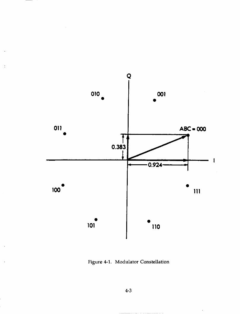
4.1.1 MODULATOR
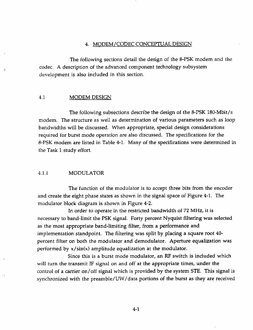
The function of the modulator is to accept three bits from the encoder and create the eight phase states as shown in the signal space of Figure 4-1. The modulator block diagram is shown in Figure 4-2.
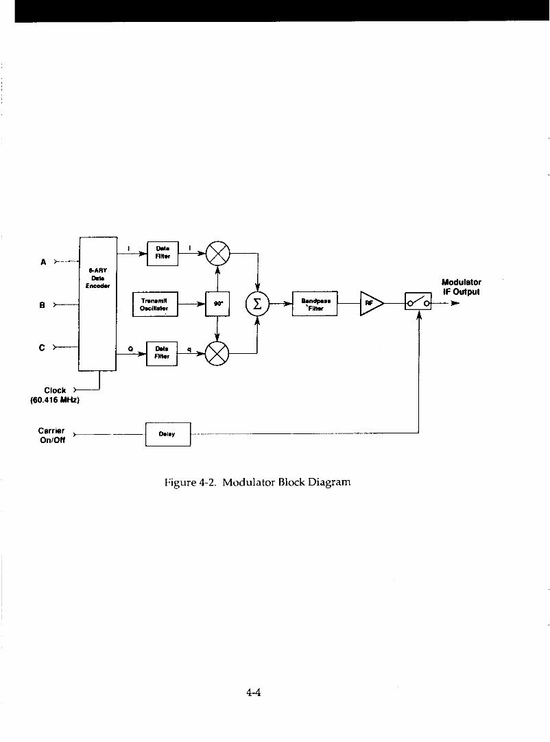
necessary to band-limit the PSK signal. Forty percent Nyquist filtering was selected as the most appropriate band-limiting filter, from a performance and implementation standpoint. The filtering was split by placing a square root 40- percent filter on both the modulator and demodulator. Aperture equalization was performed by x/sin(x) amplitude equalization at the modulator.
Since this is a burst mode modulator, an RF switch is included which will turn the transmit IF signal on and off at the appropriate times, under the control of a carrier on/off signal which is provided by the system STE. This signal is synchronized with the preamble/LJW/data portions of the burst as they are received
In order to operate in the restricted bandwidth of 72 MHz, it is
4-1

Table 4-1. 8-PSK Modem Specifications and Characteristics
Modulator
Nominal Symbol Rate
Mode of Operation
Data Filtering*
Modulation
Phase Accuracy
Amplitude Accuracy (relative)
Attenuation at 42.5 MHz from IF Center Frequency ~ ~~~ ~~
Carrier On-Off Ratio
60 Msymbol/s
Burst
Square Root 40% Nyquist with x/sin(x) equalization
8-PSK
~~~ ~
20.1 dB
24 dB
40 dB
*Amplitude and group delay masks for the modulator filters are shown in Figure 4-3 (ref. 1).
Demodulator ~~
Demodulation
Data Filtering** ~
IF Center Frequency ~ ~~~~~ ~~
IF Carrier Offset
Nominal Input Signal Level
Input Signal Level Range
Carrier Cycle Slip Rate
BER (Modem Hard Decision)
Coherent
Square Root 40% Nyquist
140 MHz
k25 kHz
-21 dBm
12 dB (+2 dB to -10 dB relative to no mi nal)
I 1 x 10⁻⁴ slips/s at C/No = 87.8 dB-Hz
I c1.4 dB from 8 PSK AWGN ideal at BER = 1 10-3
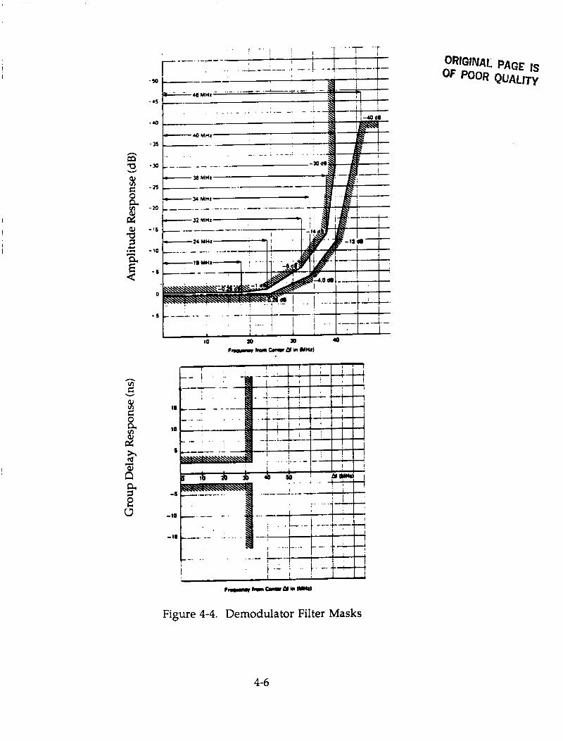
**Amplitude and group delay masks for the demodulator filters are shown in Figure 4-4 (ref. 1).
4-2
0 010
01 1 0
Q
ABC= OOO
I - 0.924
0.383 1
0 100
0
101
001 0
0 111
0 110
Figure 4-1. Modulator Constellation
4-3
Clock (60.416 MHz)
Figure 4-2. Modulator Block Diagram
4-4
_ - I
,
n
2 W
x ld CI
0” a 7
5
..t 10 . . -
I .’ ---.- -. . . .
Figure 4-3. Modulator Filter Masks
4-5
n fo a W
. IS
-30
- 25
-m
- 15
- 10
0
Figure 4-4. Demodulator Filter Masks
4-6

at the modulator input, and must be delayed before being provided to the RF switch, to account for the data processing delays associated with the modulator.
4.1.2 DEMODULATOR
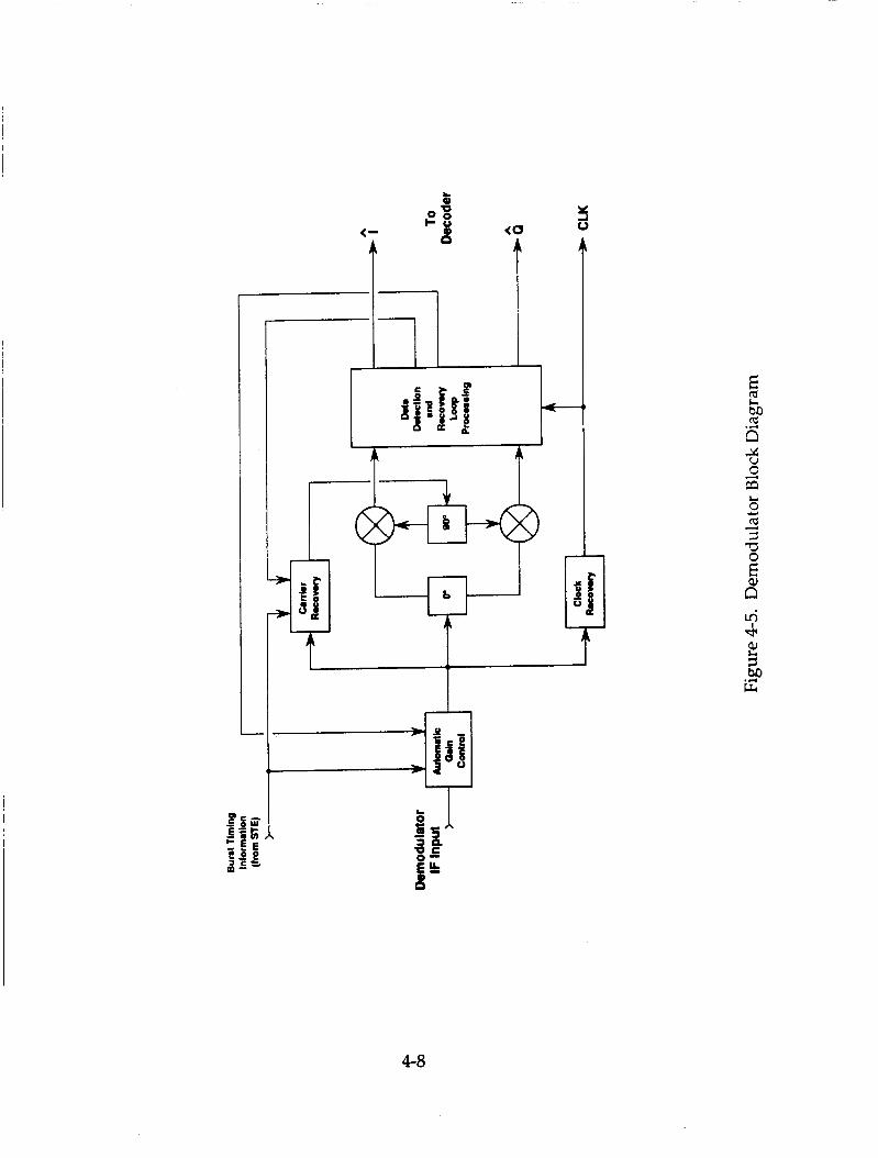
The demodulator must receive the incoming IF signal, make gain adjustments to the signal path to maintain a constant level to the detection circuits, recover the transmitted carrier by removing the modulation, recover the symbol timing, and demodulate the data into two soft-decision quadrature baseband data streams for application to the Viterbi decoder. A block diagram of the demodulator is shown in Figure 4-5.
4.1.2.1 Automatic Gain Control (AGC)
Gain control is especially critical for 8-PSK demodulation due to the multilevel nature of the baseband analog waveforms. Data detection for BPSK and QPSK is accomplished by determining if the signal is greater or less than zero,whereas for 8-PSK, the actual level must be taken into consideration. This requires accurate knowledge of the analog baseband signal levels which must be held constant with changing IF input levels. This modem was designed to operate over a 12 dB (+2 dB, -10 dB) input signal level range.
Referring to the signal constellation of Figure 4-1, the signal points are on a circle of radius r; that is
where ri is the received I channel signal and rq is the received Q signal. By computing the indicated squared sum and comparing this to the expected value, a control signal is obtained to control a variable gain element at the demodulator
’ input.
4-7
<-
i
<o
t
T
4-8

To allow for rapid and accurate gain control in burst mode, a track and hold circuit is used which holds the gain setting constant during the time between bursts, while allowing for automatic gain adjustment (tracking) during the burst. Without such a hold circuit the gain would tend to increase during the inter-burst interval, due to the absence of an IF input to the demodulator. When the input signal returned, there would be a settling transient associated with the gain control signal while the proper value of gain was reestablished. The time duration of this transient would be a function of the bandwidth of the control signal circuitry and the elapsed time since the previous burst. This transient must be kept short for good burst mode performance, and is effectively eliminated by the track and hold circuit.
As previously mentioned, the gain control setting is very critical for 8-PSK demodulation. This implies that a relatively narrow bandwidth be used in the AGC circuit, to minimize the effect of noise and pattern fluctuations on the AGC. Normally, a narrow bandwidth would imply a long settling time, which would not be suitable for burst mode operation. In the AMTD system, where level fluctuations between bursts are small, holding the control signal constant between bursts solves the settling time problem since in this manner the proper gain setting is nearly established at the time the burst is received. With fast settling time assured by this hold operation, the AGC circuitry bandwidth may be kept narrow.
4.1.2.2 Carrier Recovery
To perform coherent detection of the 8-PSK signal, an unmodulated carrier reference must be obtained from the incoming signal. There are two choices of modulation removal for 8-PSK modulation, an 8th order multiplication or the use of decision- directed feedback (DFB). The technique employed in this demodulator is a modified DFB approach shown in Figure 4-6.
4-9

4.1.2.2.1 Modulation Removal
Two reasons lead to the choice of DFB. First, there is an irrecoverable loss in S/N at low Es/No that results from cross products of signal and noise when the 8th-order multiplication is used. 8-PSK demodulation requires a coherent reference with a high S/N in order to have efficient demodulation, because of the close 45" spacing of the modulation vectors. Thus, any unnecessary loss in S/N should be avoided.
Second, there is a problem of frequency acquisition being extremely slow if the initial frequency error is not small compared to the noise bandwidth BN of the carrier synchronizer. A BN value of approximately 200 kHz is required from S/N considerations. An initial frequency error of 25 kHz would be multiplied to a 200-kHz value in the x8 method of modulation removal which put the signal out of the pass band of the carrier recovery filter. Use of DFB does not cause any magnification of the frequency error. Therefore, DFB is the preferred method of modulation removal.
Whereas, DFB multipliers for QPsK modulation removal take on only +1 values, those for 8-PSK are not as convenient. For instance, one configuration of the 8-PSK constellation (Figure 4-1) results in DFB multipliers of k0.383 and f0.924. This approach would require four quadrant multipliers which are quite difficult to implement at the speeds required in this system.
In order to simplify the decision feedback implementation, a modified DFB technique is employed. The incoming IF signal at center frequency fc with 8 phase states is first passed through a frequency doubler. The resulting signal is
rotated beyond 360° and fall on top of the other four (multiplied) states. The resulting signal can be treated identically to DFB remodulation for QPSK with values of f 1 for the multiplication vectors U and V. These vectors are easily obtained from the hard decision data bits A, B, and C.
I
I centered at 2 fc and has only 4 phase states since four of the original eight states are
I
4-10

ORIGINAL PAGE IS OF POOR QUALITY
4-1 1

4.1.2.2.2 Narrowband Filtering and Automatic Frequency Control (AFC)
After modulation removal, a carrier reference is available at 2 fc which is corrupted with both thermal and pattern noise. This signal must be filtered by a relatively narrowband filter to improve the carrier S/N. This is necessary to first decrease the probability of a carrier cycle slip and secondly to decrease the phase jitter of the recovered carrier to an acceptable level, the latter of these two requirements being the determining factor due to the low phase jitter being required for 8-PSK demodulation. In addition, due to the burst nature of this system, and the need to maintain low overhead and thus a relatively short preamble, a compromise bandwidth of 240 kHz was chosen for the carrier recovery bandwidth.
Due to the frequency doubler, the incoming carrier offset of f25 kHz is doubled to f50 kHz. This is well within the passband of the band-limiting filter, however, this frequency offset, if left uncorrected, would lead to unacceptable phase shifts in the recovered carrier.
signal is down-converted, filtered and up-converted back to 2 fc. Frequency offset is detected by measuring the phase shift through the 240-kHz BW carrier recovery bandpass filter. The filter and phase detector form a frequency discriminator from which an error voltage proportional to the frequency offset is derived. This error voltage is then used to control the oscillator used for the down-conversion, thereby centering the signal in the filter passband and minimizing carrier phase error.
voltage is processed using a track and hold circuit, so that fast AFC settling time may be assured without compromising the narrow bandwidth circuitry required for good tracking. This track and hold circuit keeps the frequency error voltage constant between bursts, while allowing for frequency tracking when the burst is present. In the AMTD System, where the frequency offset between bursts is small, this procedure ensures that when a burst is received, the error voltage will be nearly correct and therefore the AFC settling time will be short, as is required for burst mode operation.
To remedy this, AFC is employed in the following manner. The carrier
To optimize AFC performance for burst mode operation, the error
4-12

After filtering and up-conversion to 2 fc, the carrier signal must undergo frequency division by two in order to obtain the proper frequency of fc.
4.1.2.2.3 Automatic Phase Control
Due to the sensitivity of 8-PSK to phase offsets and the open loop nature of the remodulation recovery technique, it is desirable to detect and correct phase offsets in the recovered carrier.
Costas loop demodulator structure. A voltage proportional to the phase error is given by
Phase offset can be detected in a manner similar to that employed in a
v = ri Q - rq I
where ri and rq are the received quadrature multilevel analog data streams and I and Q are the hard decisions on these data streams. This voltage is applied to a phase shifter in series with the recovered carrier to zero the phase error.
and hold circuit to optimize the burst mode performance. As with the AGC and AFC, the APC error signal is processed by a track
4.1.2.3 Clock Recoverv
Due to band-limiting of the 8-PSK signal, envelope fluctuations occur at the symbol boundaries in the IF signal. Squaring of this signal results in a component at the clock frequency. This signal is filtered to improve the S/N and used as the recovered clock. A bandwidth of 1.5 M H z was chosen for this filter. This selection was based on minimizing the recovered clock phase jitter while allowing for burst mode acquisition in the required preamble period. This filter achieves these objectives.
4-13
4.1.2.4 Demodulation and Data Detection
Figure 4-7 shows the block diagram of the demodulation and data detection section. The received IF is translated to baseband using the coherent recovered carrier from the carrier recovery section. The quadrature signal components are filtered by the receive data filters and then sampled using the recovered clock from the clock recovery section. Detected data is then used to generate the control signals for DFB carrier recovery, AGC and APC.
4.1.3 UNIQUE WORD DETECTOR
The unique word detector is designed to detect the correlation of a 7-bit pattern in the digital data stream from the 8-PSK demodulator. This pattern is used both for the timing reference of the Viterbi decoder and for demodulator ambiguity resolution. The correlation is done digitally by use of a programmable array logic (PAL) device.
analog I and Q channel of the demodulator. The unique word detector circuitry first performs a conversion of this quantized data from offset binary to 2’s complement format.
defined window of the burst, a unique word signal is sent to the Viterbi decoder. The quantized signals are present at all times and the unique word hit signal denotes the beginning of the valid encoded data for the Viterbi decoder.
allowed, and clock removal signals which originate in the special test equipment. Additional outputs from the unique word detector are raw hit, upright, and missed signals which are used by the special test equipment for monitoring.
The clock signal for the Viterbi decoder is sent through a programmable 1 ns delay so that the clock/data relationship can be adjusted for proper decoder operation.
The digital data consists of the two 5-bit quantized outputs of the
Upon detection of the first correlation of the sequence within the
Additional inputs to the unique word detector are window, errors
4-14

I - I .
I- I 1
ORIGINAL PAGE IS OF POOR QUALITY
.
4-15

The PAL is programmed with the bit sequence of the unique word both in the upright and inverted cases. All of the combinations of 1 error are also programmed so that a valid detection can be given. In conjunction with an external errors allowed signal the PAL can detect the unique word with zero errors or one error within the 7-bit pattern.
A windowing signal is supplied from the special test equipment for the detection of the unique word only during a pre- determined part of the data burst. It is clocked into the unique word detector board to eliminate the possible metastable state problems that could occur with any differences between the special test equipment clock and the demodulator clock.
4.2 CODEC DESIGN
The codec consists of the convolutional encoder and the rate 8/9 Viterbi decoder. The encoder is a rather straightforward design requiring only a small amount of hardware. The decoder is much more complex and required advanced techniques in certain areas for implementation at 200 Mbit/s.
4.2.1 ENCODER
A convolutional encoder can be considered to be a finite state sequential state machine. The encoder accepts some number of bits as input, and produces an output symbol depending on the input bits and present state. The next state of the encoder is dependent on the present state and the input bits.
known techniques for implementing finite state sequential machines. In addition, convolutional codes are linear, and so can be implemented with shift registers and adders. For codes over GF(2), the adders are just exclusive-OR gates.
The convolutional encoder is easily implemented with any of the
4-16
I -
4.2.2 DECODER
A maximum likelihood decoder for convolutional codes will perform decoding over sequences of symbols. Conceptually, decoding is performed by comparing the received sequence to all possible transmit sequences, and the most probable transmit sequence is selected. The most likely sequence maximizes the log of the probability of the sequence. If the symbols are statistically independent, maximizing the log of the probability of the sequence is equivalent to maximizing the sum of the logs of the symbol probabilities.
calculation, add-compare-select (ACS), and traceback.
probabilities that the received symbol corresponds to each of the possible transmit symbols are computed. These branch metrics are linearly related to the log of the probability, so the probability over a sequence is related to the sum of the branch me tr ics.
The basic decoding operation consists of three steps: branch metric
At each decoding step, measures (called branch metrics) of the
In the next operation, ACS, the received sequence is compared to all possible transmitted sequences. While it might seem that the hardware needed to compare all possible sequences would grow exponentially with the length of the sequence, this is not the case. Since there are only a finite number of states, at each step different sequences (paths) will merge into the same state. Since all information needed for decoding is characterized by the state of the encoder, when two paths merge into a single state, the decoder selects the better path and discards the other.
are used to derive the most likely transmitted sequence.
varying code. The trellis diagram for this code is shown in Figure 4-9.
In the traceback operation, the path selections from the ACS operations
Figure 4-8 gives a block diagram for the decoder used with the time
4-17

I I I
I I
n
n
0 s w
4-18
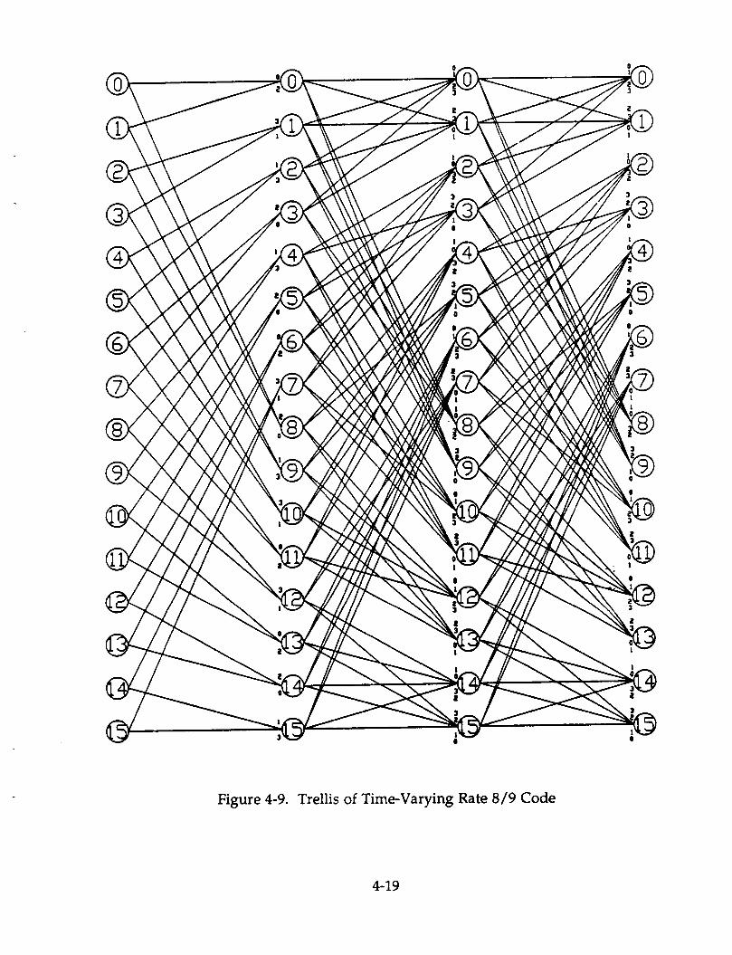
Figure 4-9. Trellis of Time-Varying Rate 8/9 Code
4-19
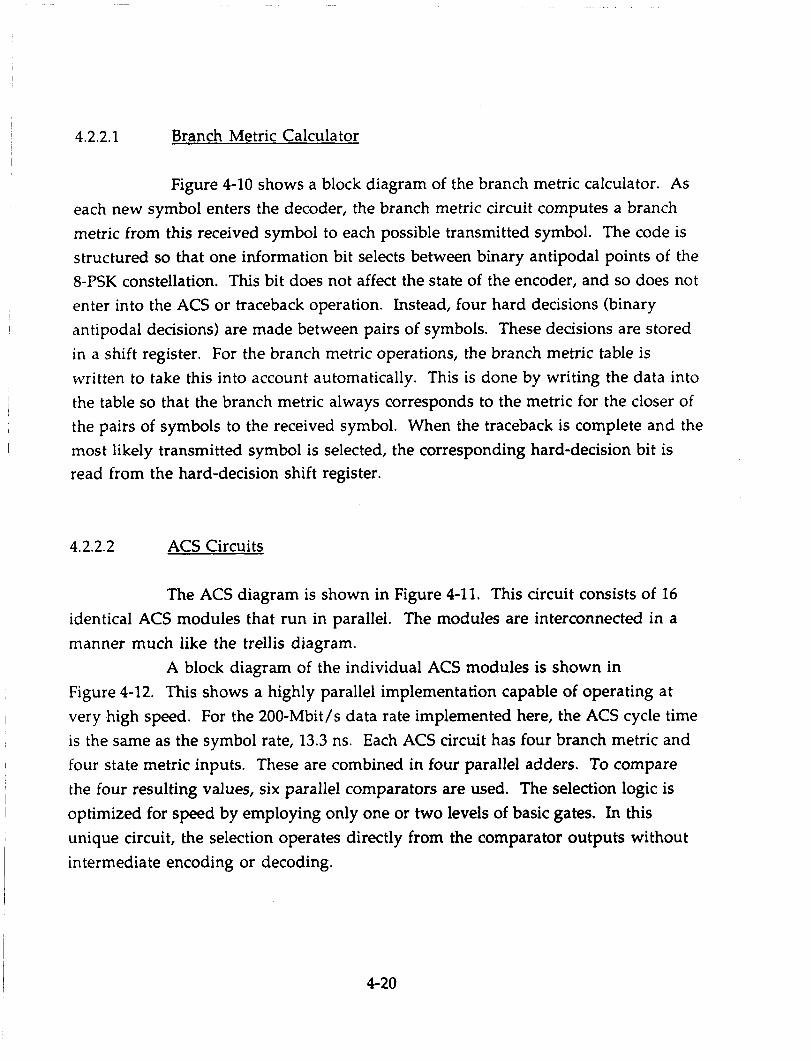
4.2.2.1
optimized for speed by employing only one or two levels of basic gates. In this unique circuit, the selection operates directly from the comparator outputs without intermediate encoding or decoding.
Branch Metric Calculator
Figure 4-10 shows a block diagram of the branch metric calculator. As each new symbol enters the decoder, the branch metric circuit computes a branch metric from this received symbol to each possible transmitted symbol. The code is structured so that one information bit selects between binary antipodal points of the 8-PSK constellation. This bit does not affect the state of the encoder, and so does not enter into the ACS or traceback operation. Instead, four hard decisions (binary antipodal decisions) are made between pairs of symbols. These decisions are stored in a shift register. For the branch metric operations, the branch metric table is written to take this into account automatically. This is done by writing the data into the table so that the branch metric always corresponds to the metric for the closer of the pairs of symbols to the received symbol. When the traceback is complete and the most likely transmitted symbol is selected, the corresponding hard-decision bit is read from the hard-decision shift register.
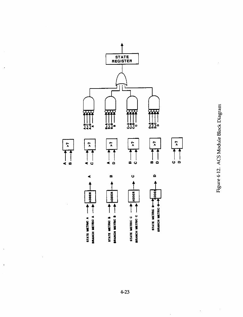
4.2.2.2 ACS Circuits
420

I INPUT
Q INPUT
BRANCH METRIC 0 BRANCH METRIC
BRANCF BRANCH
BRANCH BRANCH
METRIC 1 - METRIC 2
JlETRlC 3
HARD melstme
Figure 4-1 0. Branch Metric Calculator Block Diagram
4-21

I
Figure 4-11. Complete ACS Block Diagram
4-22
REGISTER
o n o n
a
t
4-23
Not shown in Figure 4-12 is some small additional logic needed to encode the ACS selection into binary. This binary code is used by the traceback logic.
In order to implement the time varying code, each one of the four inputs has a disable signal (also not shown in Figure 4-12). On those code steps having only two branches (instead of four), two of the inputs are disabled, preventing them from being selected. By providing four disable lines, the symmetry of the ACS module is preserved, allowing identical modules to be used for all states. Synchronization for the time varying decoding is achieved through the use of the unique word detection pulse.
4.2.2.3 Normalization
Because the ACS circuits continually accumulate metric values, i t is necessary to take care to prevent arithmetic overflow. The normalization circuit performs this function.
4.2.2.3.1 Conventional Normalization
The conventional approach to normalization is to use subtractors in each of the ACS modules to remove a constant offset from each of the accumulated metrics. To provide optimal control of the state metric values, this constant should be the minimum of the 16 state metrics.
decoder. Finding the minimum state metric in real time would require a large amount of circuitry. Placing the subtractors in the ACS modules would impact the ACS complexity and operating speed.
This approach has several drawbacks when applied to a high-speed
4-24

4.2.2.3.2 Selected Approach
While optimal control over the state metric values requires finding the minimum state metric value, it is not practical for a high-speed design to determine the minimum state metric value in real time. The selected approach is to subtract one arbitrarily selected state metric value from the others. As a result, the necessary dynamic range of the state metrics is doubled, which is accommodated by increasing the number of bits of the state metrics by one. A positive constant can be added in the normalization loop to prevent the state metrics from becoming negative. In effect, this normalization approach is a control loop which examines an arbitrary state metric value and attempts to control this value to maintain it at the center of the dynamic range of the state metrics.
Figure 4-13 shows a block diagram of the normalization circuit. This normalization circuit is uniquely suited to very high-speed implementation. The normalization is applied to the branch metrics, significantly enhancing the speed of the critical ACS operation while reducing complexity (fewer subtractors are needed). This technique does add one additional degree of complexity. To obtain very high- speed operation, pipeline registers are placed at the ACS circuit input and output. This produces a two-step delay around the normalization feedback loop. Conventional approaches to normalization fail here because this two-step delay makes the feedback system unstable.
multiplies the state metric value in this feedback system. It has been found that by adding the divide-by-two state, the system is made stable. This approach has the advantage of minimum circuit complexity, since the divide-by-two operation requires no components.
To make this loop stable, it is necessary to alter the coefficient which
4.2.2.4 Traceback Circuit
likelihood estimate of the information bits that were transmitted from the ACS circuit path selection outputs.
The purpose of the traceback circuit is to derive the maximum
4-25

ACS
Figure 4-13. Normalization Block Diagram
4-26

4.2.2.4.1 Conventional Traceback Circuit
A conventional traceback circuit is illustrated in Figure 4-14. This circuit consists of cascaded stages. Each stage has a register and a 440-1 mux. The basic idea behind this circuit is to store a path selection history. As each ACS makes its branch selection, the muxes in the path traceback for that state make the same selection. This copies the path history from the selected state into the registers of the other state. After some number of steps of this process, the registers in the last stage should all contain the same value, indicating that all paths have a common origin. An arbitrary one of these registers can be read as the output.
For a path traceback of length n, 16(n) registers and 16(n) muxes are required. More importantly, the circuit must operate at the symbol rate, 75 MHz.
3.2.2.4.2 Selected Traceback Circuit
The selected traceback approach incorporates innovative design features which dramatically reduce circuit complexity. These features effectively reduce the number of traceback circuit stages to one-third the number required by the conventional approach. This approach also reduces the traceback clock rate to one-third the rate required by the conventional approach.
The rate 8/9 time varying code was selected because it required no more than four branches into each state, resulting in a reasonable ACS complexity. The ACS circuit has to compare all the inputs and select the largest (or smallest, depending on the metric used). The code was chosen to meet the constraints on complexity of the ACS circuit.
The constraints on the path traceback are different than the ACS. The path traceback circuit does not need to compare all the branches and select a minimum or maximum, it just needs to perform some multiplexing depending on the ACS circuit outputs. The selected traceback approach takes advantage of this realization.
4-27

ONE STAGE OF TRACEBACK
4 TO 1 MUX
r
0
FROM ACS 0 I w
4 TO I MUX
1
e e
e FROM ACS 1
e
Figure 4-14. Conventional Traceback Block Diagram
4 TO 1 MUX
4-28
15
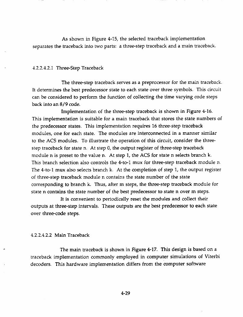
As shown in Figure 4-15, the selected traceback implementation separates the traceback into two parts: a three-step traceback and a main traceback.
4.2.2.4.2.1 Three-Step Traceback
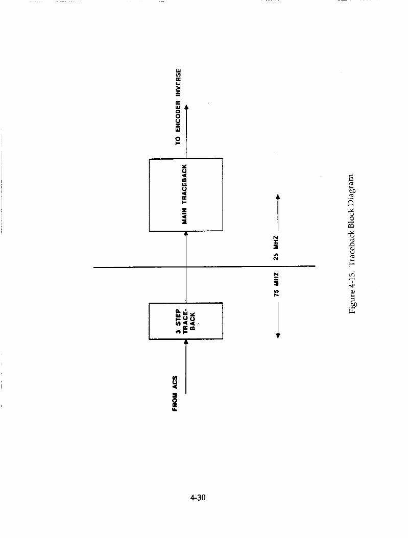
The three-step traceback serves as a preprocessor for the main traceback. It determines the best predecessor state to each state over three symbols. This circuit can be considered to perform the function of collecting the time varying code steps back into an 8/9 code.
This implementation is suitable for a main traceback that stores the state numbers of the predecessor states. This implementation requires 16 three-step traceback modules, one for each state. The modules are interconnected in a manner similar to the ACS modules. To illustrate the operation of this circuit, consider the three- step traceback for state n. At step 0, the output register of three-step traceback module n is preset to the value n. At step 1, the ACS for state n selects branch k. This branch selection also controls the 4-to-1 mux for three-step traceback module n. The 4-to-1 mux also selects branch k. At the completion of step 1, the output register of three-step traceback module n contains the state number of the state corresponding to branch k. Thus, after m steps, the three-step traceback module for state n contains the state number of the best predecessor to state n over m steps.
It is convenient to periodically reset the modules and collect their outputs at three-step intervals. These outputs are the best predecessor to each state over three-code steps.
Implementation of the three-step traceback is shown in Figure 4-16.
4.2.2.4.2.2 Main Traceback
The main traceback is shown in Figure 4-17. This design is based on a traceback implementation commonly employed in computer simulations of Viterbi decoders. This hardware implementation differs from the computer software
4-29
Y 0 U w 0 < c
ai
a
H s N T E s v) cy
+5 m 0 d
4-30
4-31

ONE STEP OF TRACEBACK
f I 0 E+
I
0 8 0 A
E+ e
1 1
e e
e
1
e I
I
e e
16 TO 1 REGISTER 16 TO 1
Figure 4-17. Main Traceback Block Diagram
4-32

I . 5
version, primarily in that the hardware implementation performs all traceback steps in parallel. Each step consists of two registers for each state (total 32 registers) and one 16-to-1 mux. In this design, the registers contain the state number of the best predecessor state to each state. At each traceback step, the best predecessor state number controls the mux, which selects the previous predecessor, thus tracing back: in history.
It operates at onethird the symbol rate (25 MHz), it uses fewer muxes, and the registers are directly cascaded. The last feature eases the implementation, because MSI or LSI shift registers can be used, reducing component count.
This circuit offers three improvements over the conventional design:
4.2.2.5 Hard-Decision Memorv
The hard-decision memory requires no processing. It is simply a shift register with length equal to the delay through the normalization, ACS, and traceback circuits.
memory can be reduced by an integer factor. Reducing the speed to one-third of the symbol rate is a convenient choice for a shift register approach. The speed is reduced simply by collecting the hard-decision data for three steps at a time by serial-to- parallel conversion. The resulting hard decision memory is small enough to be implemented with only a few TI'L shift registers operating at 25 MHz.
Like the traceback circuit, the operating speed of the hard-decision
4.2.2.6 Encoder Inverse
The encoder inverse accepts as input the sequence of best predecessor states over three code steps, and outputs the information bits to which this corresponds. This simple mapping function is easily implemented by PROM, operating at 25 MHz. The encoder inverse also selects the hard-decision bits from the hard-decision memory corresponding to the state transitions. At each 25-MHz
4-33

step, five information bits are output from the encoder inverse and three hard- decision bits are selected from the hard-decision memory.
4.3 ADVANCED COMPONENT TECHNOLOGY DESIGN
The Add-Compareselect (ACS) unit is the key element of a Viterbi Decoder for decoding convolutional codes because it requires the most critical technology development. In general, to implement a Viterbi decoder with "n" states, 'h" ACS operations are required, one for each code state. Each of these operations requires the addition of a state metric input for each path to a branch metric corresponding to that state input. The minimum of these sums is found and selected for output. For a code having "k" paths into each state, "k" addition operations are required, followed by a "k"-input comparison and selection. In the AMTD rate-8/9 codec, there are 16 code states, with 4 paths entering each state. Therefore, a total of 16 4-way high speed Add-Compare-Select (ACS) circuits are required to implement the state metric calculator function of the decoder.
operations must be performed in real time at the input symbol rate. Using current technology, all operations must be performed in parallel to achieve real time operation at rates of 50 Msymbols/sec and higher. Since the symbol rate of the rate- 8/9 codec is 75 Msymbols/sec, the ACS operations are performed in parallel. The ACS units are interconnected in the same manner as the states in the trellis of the convolutional code.
needed to perform the ACS operations, for all of the code states, had to be placed in close proximity to each other to avoid excessive time delays due to the finite propagation speed of the signals. Consequently, to minimize the overall size of the state metric calculator and reduce the distance between the components, miniaturized packaging along with state-of-the-art interconnection technology was used. In particular, a hybrid construction was selected to implement the ACS circuit unit, and a microwire board construction, which allowed double sided component
To implement a Viterbi decoder in real time, addition and comparison
Further, to achieve the high operating speed, all of the components
434

mounting, was employed to interconnect the 16 ACS hybrid circuits needed for the 16 state code.
interconnected by a thin-film processed ceramic substrate of 2.6 x 2.2 inches. The ACS hybrid circuit includes 4 high speed 6-bit adders and 6 high speed comparators, together with output gating and register circuits. The resultant hybrid ACS unit, on the average, consumes approximately 12.5 watts of power. The 16 ACS circuit microwire board absorbs a total of about 200 watts of power.
achieved the necessary speed to enable the high speed Viterbi decoder to meet all of the objectives set for the program, and successfully demonstrate the bandwidth/power efficient AMTD demodulator, the typical power dissipation of the hybrid units is too high for long term reliability. Additionally, the microwire board requires special heat sinks for each of the ACS units. Compressed air is forced through the heat sinks to insure adequate cooling of the ACS units. Even though the hybrids are many times smaller than conventional chip packaging of the same components, they are still relatively large and heavy. Due to the hand assembly required in the hybrid construction, the cost to produce the ACS chips is far greater than that of producing monolithic parts. It was therefore concluded that for quantity, low-cost production of the downlink AMTD units in the future, an advanced component technology implementation of the ACS unit was desired to reduce the risk, improve the performance, lower the power consumption, and enhance the overall producibility of the system. A gate array design of the ACS unit
was undertaken to satisfy this goal.
In the hybrid construction, 22 100K-series ECL integrated circuit dies are
While the ACS hybrid chips, incorporated on the microwire board,
4.3.1 ADD-COMPARE-SELECT GATE ARRAY
The gate array design effort began with a survey of the possible integrated circuit technologies that could be applied to solve this design problem. In particular, the three most promising technologies for gate array implementation were found to be CMOS, GaAs and ECL.
4-35
I 4.3.1.1 CMOS Gate Arrav Option
CMOS arrays are available with very high levels of integration; far higher than needed to replace a single ACS hybrid. Some of the newest parts have internal gate delays suitable for implementing the ACS function at the 75 MHz clock rate. For example, Hughes U-111 series gate array has internal gate delays of 0.4 - 0.6
slow rise and fall times, and inability to accommodate a transmission line environment makes it difficult to integrate CMOS parts, however fast internally, into a system with 75 MHz clock speeds. In fact, it is probably not even feasible to generate a 75 M H z clock with CMOS logic. In short, implementation of the decoder system using CMOS logic would have involved excessive risks due to the difficulties of system integration.
I ns using 1.5 micron technology. Unfortunately, the large voltage swings, relatively
I
I 4.3.1.2 GaAs Gate Arrav Option
GaAs gate arrays are offered by Triquint Semiconductor and Vitesse Semiconductor. The Triquint Q-chip offers a 100 gate package, which is far fewer than required for implementation of the ACS hybrid. The Vitesse VSC4500 array offers 4500 equivalent gates. A 2-input NOR gate, for example, features 0.28 ns maximum propagation delay, with typical power dissipation of 0.3 mw. However, this technology is still quite new and it does suffer from the drawback of a severely limited macro library, which would makes implementation much more difficult than with a more mature part. The GaAs products available were considered to represent too much of an implementation risk.
4.3.1.3 ECL Gate Arrav Option
ECL gate arrays represent a mature, readily available method of I
implementing very high speed digital hardware. While ECL arrays have had a
4-36
reputation for consuming very large amounts of power which ultimately limits thle level of integration, recent advances in ECL design have led to significant improvements in both density and power dissipation. ECL technology is very desirable for the implementation of high speed logic circuits not only because of the high internal gate speeds, but also because of the ability to easily accommodate a transmission line circuit environment. The low risk ECL gate array approach was followed for this portion of the program.
MCAl OOOOECL MOSAIC-111 Macrocell Array. The monolithic component contains two 4-way ACS units, and a single 8-way ACS unit. Each input accepts an 8-bit unsigned positive state metric and an 8-bit signed branch metric. The output is a registered 8-bit positive value with a ninth bit indicating an overflow condition when the result is less than zero.
Specifically, the ACS gate array was developed using Motorola's
4.3.2 ACS MICROWIRE SUBSYSTEM
A drop-in replacement board was constructed to replace the hybrid- based microwire ACS board. Since this involved a substitution of a monolithic chip for the old hybrid parts, and since the monolithic parts are functionally equivalent, but smaller and lower power than the hybrids they replaced, replacement was straightforward. The entire microwire board was replaced, however, since the gate array chips have a different footprint and pinout than the original hybrid chips. The gate array chips yield greater timing margin than the hybrids, which allows for potential future use of these parts as a basis for even higher speed codecs. The design of the current codec has the potential to allow the greater arithmetic capability of the gate array chips to be used, by reprogramming the metric ROMs in the codecs to allow some improvement in coding gain.
The replacement microwire ACS board has many advantages in terms of manufacturability, reliability, size, power consumption, and maximum operating speed. The gate arrays themselves are reliably producible in large quantities. The gate arrays are socketed on the ACS microwire board and can easily be replaced. The
437
ACS board is constructed using Microwire Twin "6" double sided board technology with five internal power planes. Two planes are committed to ground, and three are used for the power supplies -5V, -2V, and -3.4V. All wires are on the top side of the board with the exception of the interconnects between the ACS gate arrays. The gate arrays are mounted components and therefore require no special signal through vias to communicate to the top side of the board. Wiring the state-to-state interconnects on the bottom of the board provided additional critical routing area on the top and allowed for very tight wire length tolerances for the gate array interconnections.
microwire board in the codec. Since the power dissipation of the gate array chips is substantially smaller than the hybrid parts, cooling requirements were reduced. Neither special heat sinks nor the compressed air used to cool the hybrid parts was needed for the gate array units. The performance of the codec using the new microwire board was measured using the digital AWGN channel simulator and its result compared with that of the hybrid ACS units. As desired, the performance of the gate array ACS board was virtually indistinguishable from the performance of the hybrid-based ACS board.
The new microwire board was installed in place of the hybrid-based
4.3.3 IMPLEMENTATION TECHNOLOGY COMPARISON
The gate array implementation yielded a substantial reduction in size, weight, and power, and cost of the codec. Furthermore, the monolithic gate array parts have much better reliability than the hybrid units. The power consumption of the codec was reduced greatly. Moreover, the cooling requirements were drastically reduced and compressed air is no longer needed. The new board is plug-compatible with the old hybrid-based microwire board. Due to the monolithic gate array implementation, the production costs have been significantly reduced as fewer skilled labor hours are required. An additional benefit derived from this development is that the developed gate array ACS chip can be employed in the
4-38
implementation of many other Viterbi codecs, high speed or otherwise, that may be needed for future NASA applications.
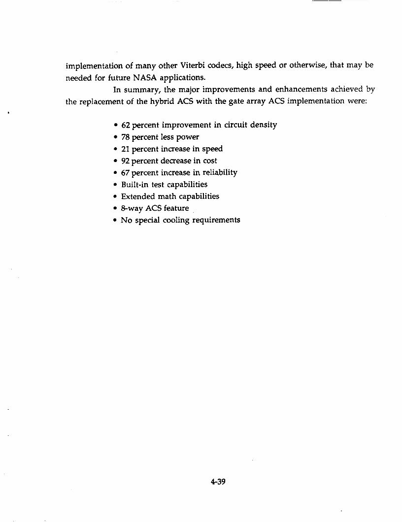
In summary, the major improvements and enhancements achieved by the replacement of the hybrid ACS with the gate array ACS implementation were:
62 percent improvement in circuit density 78 percent less power
0 21 percent increase in speed 92 percent decrease in cost 67 percent increase in reliability Built-in test capabilities Extended math capabilities &way ACS feature No special cooling requirements
4-39
5. MODEM SELF-TESTS
I .
Self-testing of the 8PSK modem portion of the system was carried out during the course of the program in order to verify modem operation within the proposed specifications. This section of the Contractor Report contains the results of those tests, as well as a brief description of each test setup and the procedures under which the tests were performed. Table 5-1 contains an outline of the modem self- tests.
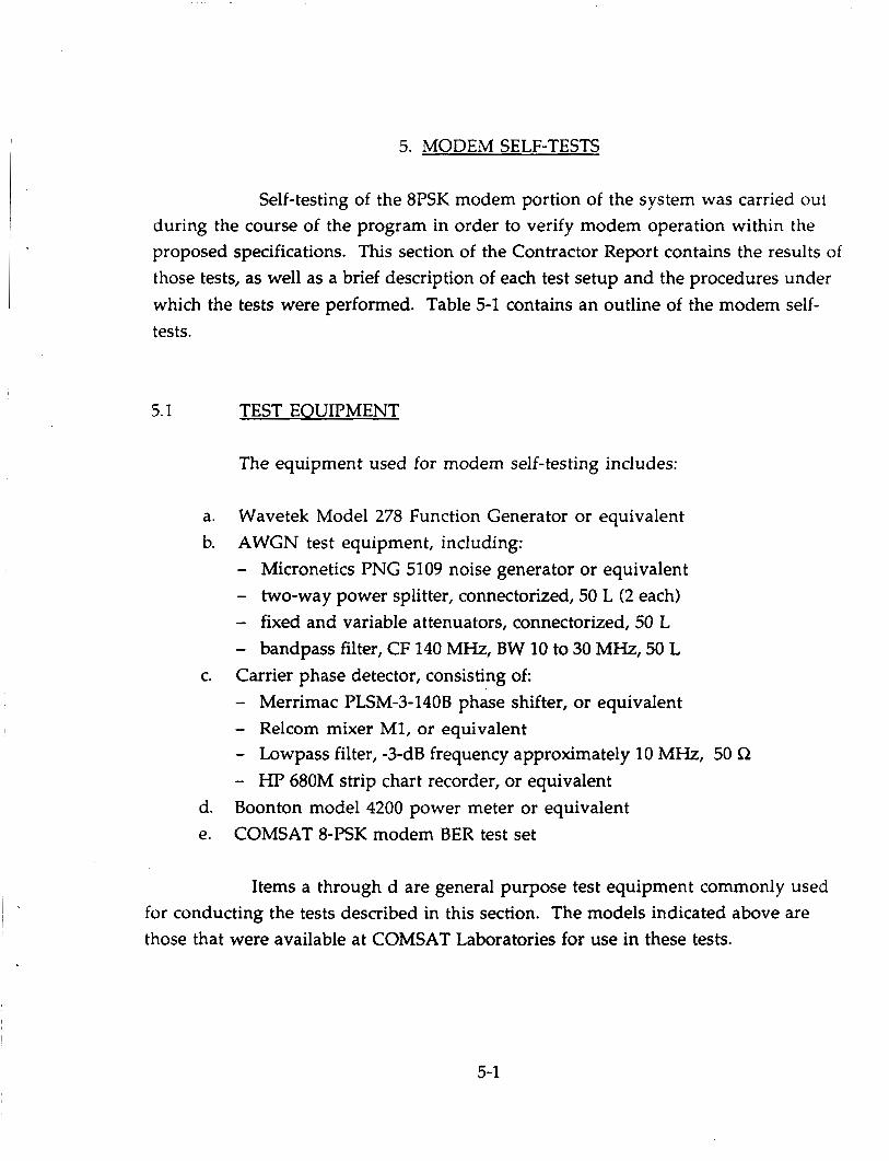
5.1 TEST EQUIPMENT
The equipment used for modem self-testing includes:
a. b. AWGN test equipment, including:
Wavetek Model 278 Function Generator or equivalent
- Micronetics PNG 5109 noise generator or equivalent - two-way power splitter, connectorized, 50 L (2 each) - fixed and variable attenuators, connectorized, 50 L - bandpass filter, CF 140 MHz, BW 10 to 30 MHz, 50 L Carrier phase detector, consisting of - Merrimac PLSM-3-1408 phase shifter, or equivalent - Relcom mixer M1, or equivalent - Lowpass filter, -3-dB frequency approximately 10 MHz, 50 R - HP 680M strip chart recorder, or equivalent Boonton model 4200 power meter or equivalent COMSAT 8-PSK modem BER test set
c.
d. e.
Items a through d are general purpose test equipment commonly used for conducting the tests described in this section. The models indicated above are those that were available at COMSAT Laboratories for use in these tests.
5-1

ln Y - a ln
2
&I C 2;s; z"z! \ P w
z e if J bn
22 3
c m C
'E z"
aJ Y
C .- 4 0 5 aJ M c E
5-2

Item e is a special test fixture designed and built at COMSAT Laboratories especially for use with 8-PSK modems such as the one under test. It allows for stand-alone operation and testing of the modem, independent of the codec or system STE. This test set performs the following functions:
a. It supplies pseudo-random (I") baseband data, in three parallel channels that each runs at 60.416 Mbit/s, to the modulator (TX) portion of the modem, either continuously (unformatted) or in bursts (with a 300 symbol preamble preceding the data in each burst), where the burst length and guard time are independently selectable.
coincident with the data transitions in the data mentioned in a above. b. It supplies a TX clock to the modulator whose positive edges are
c. In burst mode, it supplies a carrier on/off signal to the modulator
d. It supplies the required burst control signals to the demodulator
e. It receives the RX baseband data and clock from the demodulator and
ik-hich is synchronized with the TX data burst.
portion of the modem.
measures the BER in each of the three data channels, making the results available on three front panel numeric LED displays.
Additionally, this test set can be used to force static data patterns to the modulator input which are then used in the alignment of the modem TX and RX circuitry.
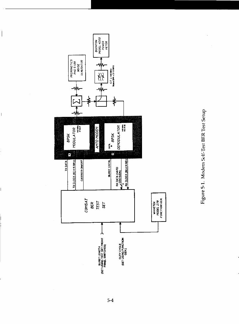
5.2 BER TESTS
The BER performance of the 8PSK modem sub-system is used as the primary benchmark for modem evaluation. The test setup used for modem self-test BER measurement is shown in Figure 5-1.
5-3
k . 47 I
A I I
a 7
8
I- w 3
5-4

5.2.1 BER MEASUREMENT--CONTINUOUS MODE
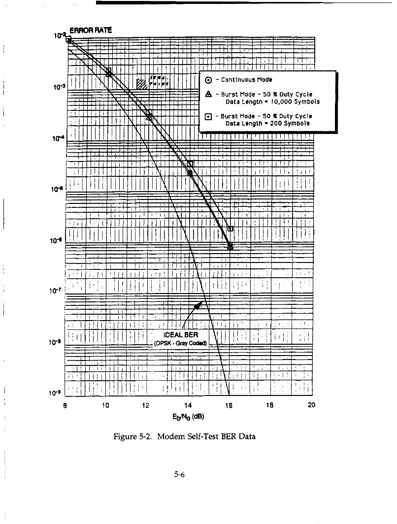
The purpose of this test is to establish the baseline BER performance of the modem under nominal operating conditions. It is generally true that the continuous mode performance of the modem will be the best achievable, consequently, the results of this test can serve as a benchmark when evaluating performance under other conditions.
The results are graphed in Figure 5-2. BER data was taken in both ambiguity states and the results averaged.
5.2.2 BER LMEASUREMENT--BURST MODE, LONG AND SHORT BURSTS
The purpose of these tests is to establish the burst mode BER performance of the modem under nominal conditions, both with a long (10,000 data symbol) and short (200 data symbol) burst, and a 50-percent duty cycle (including preamble and unique word). The long time between bursts, and the short burst length in the 200 symbol test, will demonstrate that the recovery loop hold circuits provide for rapid and accurate demodulator acquisition.
continuous mode data. The results of these tests are graphed in Figure 5-2, along with the
5.3 CARRIER CYCLE SLIP MEASUREMENT
The purpose of this test is to establish the carrier cycle slip performance of the modem under nominal conditions. This must be done with the modem operating in continuous mode due to the long periods of time between slips.
the modem, with the transmit and receive carrier signals as inputs. The phase detector output, after lowpass filtering, will be a DC voltage proportional to the phase difference between the TX and RX carriers. Once this phase detector is
Measuring carrier cycle slips involves using a phase detector external to
5-5
A - Burst Mode - 50 8 Duty Cycle Data Length - 10,000 Symbols
- Burst Mode - 50 % Duty Cycle Data Length - 200 Symbol9
8 10 12 16 18 20
Figure 5-2. Modem Self-Test BER Data
5-6
calibrated so that its DC output is different for each RX carrier phase state (eight are possible) then its output can be observed for step changes in level, which will indicate that the RX carrier phase state has changed, and hence a cycle slip has occurred. A strip chart recorder is connected to the phase detector so that this measurement may proceed unattended, which is desirable due to the long periods of tirile between slips.
is shown in Figure 5-3. This setup is identical to the BER test setup shown in Figure 5-1, except for the addition of the carrier phase detector and strip chart recorder.
this data, the modem is well within the specification of 1 x 10⁻⁴.
The test setup used for modem self-test carrier cycle slip measurement
The results of this test are presented in Table 5-2. As can be seen from
5-7

T I - -
I I + + I t- I
5-8
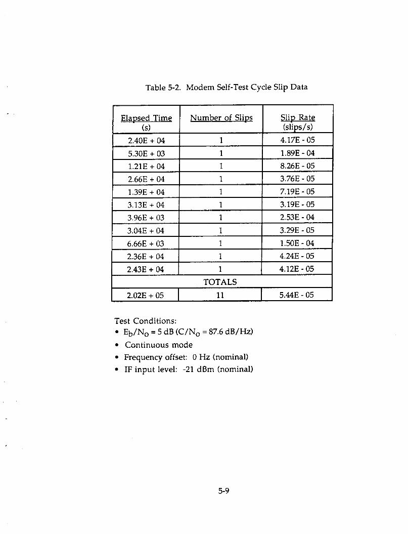
Table 5-2. Modem Self-Test Cycle Slip Data
Elapsed Time Number of Slips Slip Rate (SI (slips/s)
Test Conditions:
Continuous mode Frequency offset: 0 Hz (nominal) IF input level: -21 dBm (nominal)
&/No = 5 dB (C/No = 87.6 dB/Hz)
5-9
6. CODEC SELF-TESTS
I -
C
Self tests have been conducted on the codec in a back to back noise-free environment and over a digital AWGN channel to establish the hardware performance of the codec independant of the other system components, in particular that of the 8PSK modem. An overview of the test setup and the performance results reflecting the observed data in comparison with the computer simulated results will be presented here.
6.1 TEST EQUIPMENT
The equipment used for the Codec Self Tests includes :
a. HP 8656A Signal Generator b. HP 3762A Data Generator c. HP 3763A Error Detector d. IBM PC e. Rate 8/9 convolutional encoder f. Codec Self-Test board g. Special Interface fixture
Items a through d are general purpose test equipment commonly used for conducting performance tests of this type. Item e is part of the special test equipment COMSAT developed under this contract. The encoder encodes the multiplexed information sequence into coded symbols at 75 MSPS, with three bits for each symbol.
quantized AWGN noise at 75 MHz to simulate the effect of AWGN in an ideal modem. The special test board consists of a symbol mapping function, a digital AWGN noise generator, and a digital signal combiner. Each of the three bit symbols is first mapped into a 6 bit x 6 bit coordinate in the (1,Q) phase plane. The digital
Item f is a a special test board developed by COMSAT which generates
6-1
AWGN noise generator consists of PN sequence generators whose outputs form the addresses of two independent AWGN noise RAMs. The contents of each RAM are loaded off-line with 4096 AWGN noise vectors at the desired energy per information bit to one-sided noise spectral density ratio, &/No, by a microprocessor. The digital signal combiner sums the signal and the noise, and then hard-limits the output to 6 bits for each of the two components in the phase plane. The outputs of the codec self-test board include the received signal (two six-bit numbers per symbol), the symbol clock, and a properly delayed start-of-burst signal. These outputs simulate the output of the demodulator.
proper distribution of the contents of the noise RAMs, and the randomness of the addressing sequence. Table 6-1 is a histogram of the noise vectors at an Eb/No of 7 dB. This histogram compares well with that of a quantized Gaussian noise. Figure 6-1 is a block diagram of the codec self-test board.
by the data generator, such that a true 200 Mbit/s information rate is maintained even though the off-theshelf equipment if Items b and c are operated at 1/8 of the real decoder speed. The interface also simulates the function of a burst controller in the STE such that only the valid portion of the decoder output is used for error rate measurement. This special interface also contains a single board microcomputer (Micromint BCC52 Basic Computer Controller) which is used to download the noise vectors to the noise RAMs in the digital AWGN.
,
Accurate simulation of the digitized AWGN channel is ensured by
Item g, the special interface fixture, simulates data traffic not generated
6.2 PERFORMANCE TESTS
Two different BER self-test measurements were made on the codec, a noise-free measurement and a measurement involving additive white Gaussian noise (AWGN). The results of these two tests are discussed in this section.
.
6-2

Table 6-1. Histogram for the Noise Vectors at Eb/No = 7 dB with a Total of 4096 Vectors
Noise 8
No. of Occurrences 1
7
-1
-2
5
668 490
6
I I -4 144 I
19
-6 -7
5
19 5
56 4 144 3 294
I 2 I 490 I 1 688 0 742
-3 294
-5 56 I
-8 1
6-3

Figure 6-1. Codec Self-Test Board Block Diagram
6-4
6.2.1 NOISE-FREE TESTS
At an operating frequency of 72 MSPS there are no observable errors present in the output of the decoder. However, at the design goal operating frequency of 75 MSPS, there is a slight irreducible bit error output from the decoder of approximately 1.2 x 10⁻⁸. This BER results from errors on two of the eight parallel decoder outputs. Specifically bit 2 exhibits a BER of 7.9 x 10⁻⁹ and bit 5 has a BER of 8.5 x 10⁻⁸.
determine the source of this error output. It was determined that at a clock rate of 75 MHz there is an error output, or overflow indicator from hybrid A4 on the ACS board. This hybrid implements state six in the code algorithm, see Figure 6-2. The overflow indicator from this hybrid is apparently due to a very large-valued erroneous output from A12 (state 14) which is sent to A4 and causes it to overflow. It was observed that all branch and state metric inputs to these hybrids have adequate setup and hold time, with respect to their individual clocks, to meet their designed operating speed.
Hybrid A12 was further investigated and it was found that Channel D was always the selected output when the overflow indicator was triggered. It was then attempted to acquire the state and branch values into Channel D when the error occurred. The state input values were within the range of acceptable values. Six of seven bits of the branch metric were also reasonable. However, when bit 5 of the branch metric was probed, it was no longer possible to trigger the data acquisition because the state outputs had changed. This effect is probably due to the changed capacitance, or an induced reflection, on the signal line, which indicates a marginal timing problem. A change in the value of bit 5 of the branch metric would certainly explain a mathematical error output from A12 because it would cause a very small number to be added as a very large number.
performed but the problem was not easily rectified because MBM2DBS feeds three other hybrids whose timing was unfavorably altered when the signal was adjusted
A careful and detailed observation of the decoder was made to
Some minor attempts at adjusting the timing of bit 5, MBM2DB5, were
6-5
Data Gen 6 , I data
9/ > 8, P L ,
C l k > o C l k ) Simulator 75 l l H t / > 6 P : W AWGN n 1
u SB W SB > ) Z cl k >
SB
1 Signal I k
v)
- LL
w
TIf data I I E r r o r Det
gated cl k 25 MHz
SB
e n W
n w W W
0 0 e
n
Figure 6-2. Codec Stand-Alone Test Configuration
6-6

I *
I
to satisfy A12. It was concluded that hybrid A12 would have to be replaced because i t was unable to operate at the speed it was designed for. The hybrid A12 was not replaced, however, because it would have required a substantial increase in the test cycle time with no guarantee that the problem would be completely eliminated by ,a
new hybrid chip.
acceptable because it did not substantially effect the AWGN BER performance of the decoder in the operating area of interest. Additionally, a gate array implementation of the ACS function was being planned at this time which would eliminate this problem due to the higher potential operating speed of the gate array version (see Subsection 7.2.6).
It was concluded instead that the small irreducible error rate was
6.2.2 AWGN BER TESTS
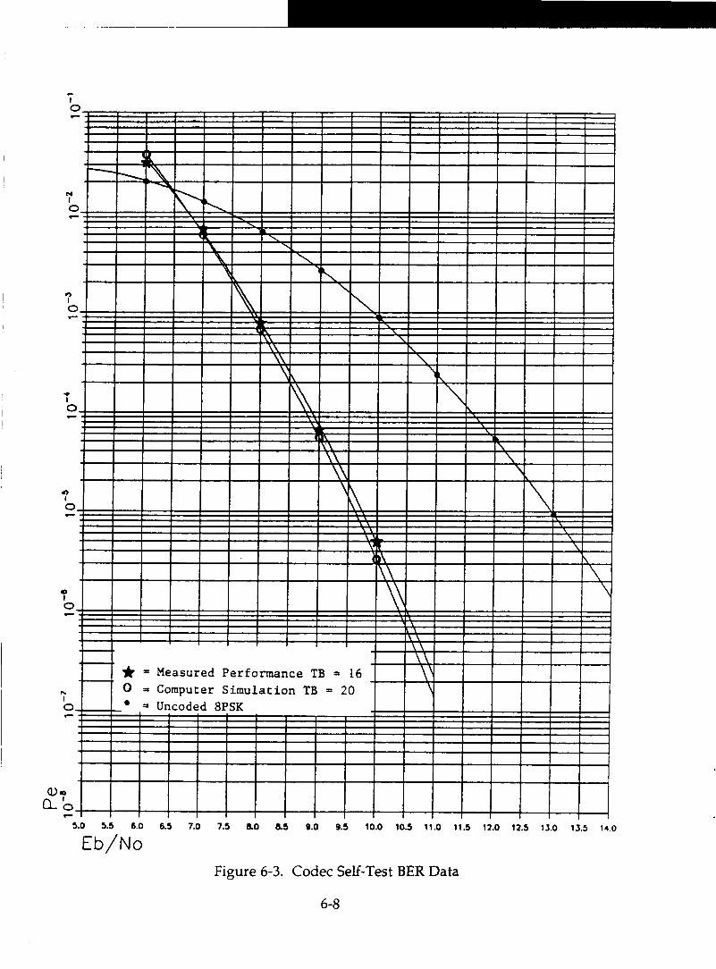
Performance of the Rate 8/9 Viterbi decoder was measured at an operating frequency of 75 MSPS in the stand-alone configuration depicted in Figure 6-2. Figure 6-3 shows the BER performance results for the decoder hardware which has a traceback length of 16 as compared to the computer simulation results which used a traceback length of 20. The uncoded &PSK performance curve is also shown for reference.
6-7
c I
* = Measured Performance TB = 16
m
0 I
7
5.0 5.5 6.0 6.5 7.0 7.5 ao a5 0.0 9.5 10.o 105 11.0 11.5 12.0 12.5 13.0 is.5 14.0
Eb/No Figure 6-3. Codec Self-Test BER Data
6-8

7. SYSTEM TESTS 4
The procedures, setup descriptions, and results obtained for sys tern level testing of the integrated AMTD down-link modem and codec are presented in this section. Table 7-1 contains an outline of the tests performed.
During system test, initial measurements of system BER performance were made at nominal parameters. Then, variations were introduced in receive IF frequency offset and input level, individually, to establish a worst-case set of operating conditions. Finally, a set of tests was conducted under these combined worst case conditions, to demonstrate compliance with the system performance goals.
measured under a variety of operating conditions, as is the case for BER performance. Once testing began, however, it became apparent that the U W miss rate was too low to measure in a reasonable amount of time, and with a reasonable amount of confidence, for all but the worst conditions. Consequently, U W miss data are included in this report for a single case, one which allowed for data collection in the time frame available for testing, and which furthermore served to demonstrate compliance with the system's UW miss performance goals.
It was originally intended that UW miss performance would be
7.1 TEST EQUIPMENT
The equipment needed for system testing includes:
a. b. c. d. AWGN test equipment, including:
HI? 8662A signal generator or equivalent HP 3763A error detector or equivalent HP 5345A frequency counter or equivalent (2 each)
- - -
Micronetics PNG 5109 noise generator or equivalent two-way power splitter, connectorized, 50 L (2 each) fixed and variable attenuators, connectorized, 50 L
7-1

p- i
Y v)
k
2 i? 2 i? e 2 w 2 E iz iz if iz iz iz iz F 3 I I a I I I
2 I I
M M M M M M M M
n m
' n n m rn
E E E E z" 2 2 2 N r- F- r- 2
8 s\" * o * In * o In In * o m * o In s 2 In
0 s\"
0 m
8 N
8 N
8 8 8 0. 2 2
8 8 g $ 0 In 2 2 m c
h n n h n h e m v! c? s m
x e e W
(? "f s 9
m s m
c?
h
m
m c? In
x W v v ? c?
In In In
5 .- c 3 vi aJ C C m c U
-
8 8 E 2: %
5
-5
CJ Y
m CJ
y. 0 J,
C CJ
Y
E E! 3 m m
i2 c, 5 - 0 v) L - a 2 v)
aJ M m
*
7-2
e. f.
g.
Boonton model 4200 power meter or equivalent COMSAT digital noise test set COMSAT AMTD down-link special test equipment (STE)
Items a through e are general-purpose test equipment commonly used for conducting the tests described in this section. The models indicated above are those that were available at COMSAT Laboratories for use in these tests.
Laboratories for use with the AMTD down-link codec. (A complete description of this test fixture may be found in chapter 3 of the document "Advanced Modulation Technology Development for Earth Station Applications - Task VI1 Interim Report: POC Testing and Analysis: Codec Self Tests and Finalized Codec Documentation", May 1988). For the purposes of system testing, this test fixture is used only as an interface between the decoder output and the HP 3763A error detector input. Specifically, it does the following:
Item f is a special test fixture designed and built at COMSAT
a. within the test set.
b. DATA control signal from the decoder, and made available to the HP 3763A error detector using single-ended, 50-0 line drivers.
The channel under test (1 of 8) is selected using a rotary dip switch
The data signal under test and the RX clock are gated using the VALID'
Item g is special test equipment designed and built by COMSAT Labs,
especially for the system tests described in this section. It performs the following functions:
a. It generates eight PN data sequences at 20.138 Mbit/s which are sent to the parallel inputs of the down-link 8/9 encoder (also included in this STE), which then encodes these data bits into three parallel data streams ("A", "B", and T") each at 60.416 Mbit/s.
b. preamble and unique word bits, generates a carrier on/off signal, then makes the
It formats the A, B, and C data streams by prefixing them with the
7-3
three formatted data streams, the TX clock, and the carrier on/off signal available to the modulator portion of the modem using a differential ECL interface.
Using thumbwheel switches located on the front panel of the STE, the following system burst mode parameters are selected:
- burst length - guard time - UW errors allowed - IF delay
Additionally, the burst length information is provided to the decoder using a differential ECL interface.
generated by this equipment and provided to the modem over a differential ECL interface.
e. required by the unique word detector (which resides in the codec chassis, in the system rack) are generated by this equipment and provided to the U W detector over a differential ECL interface.
c.
d. Receive burst control signals required by the demodulator are
The UW WINDOW and ERRORS ALLOWED signals which are
f. Receive ambiguity state and U W miss and detect signals (all originating in the unique word detector) are monitored by this test equipment over a differential ECL interface, and are available on BNC connectors on the STE front panel for measurement purposes.
Figure 7-1 illustrates the timing relationships of the various signals generated by this STE.
7.2 BER TESTS
BER performance of the coded system was measured under the condition described in Table 7-1. A description of these tests and the results are summarized in the following subsections.
7-4
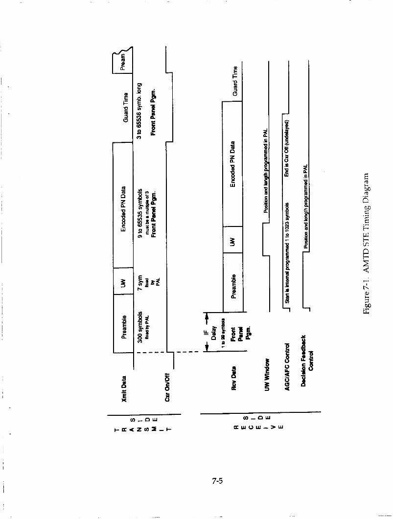
3 -
m E n
F
5;
9 n E
f 0 (3
3
1
7-5

7.2.1 TEST SETUP
The test setup used for system BER measurement is shown in Figure 7-2. Note that the HP 8662A signal generator shown in this figure is needed only when making measurements with frequency offset. (The two HP 5345A frequency counters shown in this figure are used only for UW miss/detect measurement and are not needed when measuring BER.)
7.2.2 BER MEASUREMENT--NOMINAL PARAMETERS
The purpose of this test is to establish the baseline BER performance of the AMTD system under nominal operating conditions. The results obtained for this test should represent the best measured system performance because of the long burst length and the nominal modem operating parameters.
This test was conducted at two data burst lengths, 10,000 and 5,000 symbols. This was done to establish the equivalence of performance at these two burst lengths, so that the remainder of the system tests requiring a "long" burst could be conducted at the 5,000-symbol burst length rather than the 10,000-symbol burst length used for the modem self-test. This change in length was motivated by the fact that the system STE cannot operate at a 10,000-symbol burst length with a 10- percent duty cycle (as would be required for the worst-case tests below), hence the necessity to switch to a shorter burst length.
The results of these tests are graphed in Figure 7-3.
7.2.3 BER MEASUREMENT--WITH FREQUENCY OFFSET
The purpose of this test is to establish the BER performance of the codec/modem system when operated with f25 kHz of carrier frequency offset, with all other parameters set nominally, so as to isolate the effect of frequency offset on system performance.
7-6
ORIGINAL PAGE IS OF POOR QUALITY
L"
7-7
ERROR RATE
@ - Data Length - 10,000 Symbols Duty Cycle - 50 Ip
6 0 10 12 14 16 18
EdNo (68)
Figure 7-3. System BER Data-Nominal Parameters
7-8

The results of these tests are graphed in Figure 7-4.
7.2.4 BER MEASUREMENT--WITH INPUT LEVEL VARIATION
The purpose of this test is to establish the BER performance of the codec/modem system when operated with +2/-10 dB of input level variation, with all other parameters set nominally, so as to isolate the effect of input level variation on svstem performance. The results of these tests are graphed in Figure 7-5.
7.2.5 BER MEASUREMENT-WORST CASE
After determining worst-case frequency offset and input level in the above tests, the codec/modem system was tested at these values, and with the duty cycle reduced to 10 percent. This reduction in duty cycle is made to test the ability of the demodulator track-and-hold circuitry during a long "hold" condition.
Two different burst formats, long burst and short burst, were used so its
to determine the effect of burst length on worst-case system performance. The results of these tests are graphed in Figure 7-6.
7.3 UW MISS MEASUREMENT
The purpose of this test is to establish the LJW MISS performance of the system when operated with worst-case parameters of frequency offset and input level variation, as determined in tests 7.2.3 and 7.2.4 above. A burst length of 200 symbols was used for this test.
7-9

@ - Frequency Offset - 0 kHz
1 I I I , \\I 1 I 1 1 I - I I I I U 1 I I I I I
I I I I I I
1 . I I I I I I 1 I 1 1 I I I I I I ' I . . ! \ I I 1 1 I I I I 1 I , , I I -
I I I I I ' I ' I I I I I I
I I 1 I I 4
14 16 18
Figure 7-4. System BER Data with Frequency Offset
7-10
ERROR RATE
5000 Symbol Burst, 50 % Duty Cycle
@ - RX IF Level - Nomtnal
A - RX IF Level - + 2 d8
I -
8 6 0 10 12 14 16 18
w o (a)
Figure 7-5. System BER Data with RX IF Level Offset
7-1 1

ERROR RATE 1 (r2
104
A - 5000 Symbols, IO % Duty Cycle AF +25 kHZ, AL= - 10 dBm
10J
10-5
I I I I I I I 10-7 I I I I I I 4 1 I I I I I I
6 8 10 12 14 16 18
EdNo (a)
Figure 7-6. System BER Data-Worst Case
7-12

This measurement was accomplished using the system STE and two external counters, as shown in Figure 7-2. One counter is used to count the number of bursts sent, while the other counts the number of unique words missed, as determined by the unique word detector and communicated to the front panel of the system STE via a differential ECL interface. UW miss rate is then calculated as the ratio of these two numbers.
Note that for this test, a duty cycle of 50 percent was used rather than 10 percent as in the worst case BER measurements described above. Also, an Eb/No of 6 dB was used which is much lower than those used during BER measurement.
Bursts Sent
1.796E + 09 1.829E + 09 1.953E + 09 2.018E + 09 2.118E + 09
Both of these changes were made to reduce the testing time required to experience U W misses, which occur very infrequently, even with these modified test parameters (approximately 1 miss per hour under these conditions).
The results of this test are presented in Table 7-2.
Number of Misses Miss Rate (misses / burst)
10 5 .5E - 09 10 5.47E - 09 10 5.12E - 09 10 4.96E - 09 10 4.72E - 09
Table 7-2. System UW Miss Data
Test Conditions: - Eb/No = 6.0 dB - Burst length = 200 data symbols - Duty cycle = 50 percent - Frequency offset : +25 kHz Hz (worst case) - IF input level : -31 dBm (-10 dB offset - worst case)
7-13
8. DISCUSSION OF RESULTS
Complete testing of the coded 8-PSK system has been conducted to demonstrate performance within the desired specifications. Through the use of a number of specially designed pieces of test equipment, the 8-PSK modem performance, the rate 8/9 codec performance and the overall system performance have been measured for burst and continuous mode operation. Results of these tests compared to the desired performance is discussed in the following sections.
8.1 MODEM SELF-TESTS
Although the present system was designed as a jointly optimized modulation/coding configuration, some testing of the modem subsystem was performed to demonstrate proper modem operation. In particular, modem uncoded hard decision BER was measured in continuous and burst mode with long and short bursts. BER degradation was partitioned between the modem and codec, with 1.4 dB allocated to the modem at a BER of 1 x 10⁻³. Measured BER degradation at this BER varied from 0.7 dB to 1.0 dB from ideal, which is well within the specification.
slipping. Measurements taken at an Eb/No of 5 dB show performance to be better than the specified slip rate of 1 x 10⁴ by a factor of 2.
Another important modem performance parameter is carrier cycle
8.2 CODEC SELF-TESTS
BER performance testing of the codec was performed using noise injected between the encoder and decoder. A BER degradation of 0.6 dB was allocated for codec implementation loss. The resulting data shows performance within 0.2 dB from the computer simulated performance predictions, which is well
8-1
within the specification. This testing was conducted at a 200 Mbit/s data rate, which validates compliance with the original design goals.
identical performance for the two implementations as was expected. Although the gate array design has provisions for higher precision mathematics which would potentially improve the overall codec performance, it was not practical to modify remaining codec circuitry to accommodate this increased processing power. Reduction in size, power, and cooling requirements, as well as improvements in reliability and manufacturability were the primary benefits realized from the gate array implementation.
Tests conducted using the gate array in place of the hybrid chip show
8.3 SYSTEM PERFORMANCE
The BER performance of the overall coded system was measured under a variety of conditions to demonstrate operation with frequency offset, input level
performance was also measured under the worst case conditions of frequency offset and input level variation with a short (200 symbol) burst.
I variation, variable burst lengths, and variable burst duty cycle. Unique word miss
8.3.1 SYSTEM BER PERFORMANCE
The BER performance specification for this system was stated to be less than 2 dB degradation form theoretical at a BER of 5 x 10⁻⁷. The computer simulation results presented earlier for the overall system performance indicate that the Eb/No required for this BER is approximately 10.8 dB. The measurements shown in the previous section for nominal conditions show that this BER is achieved at an Eb/No of 11.8 dB. This represents only a 1 dB implementation loss with an additional 1 dB of margin.
It is also useful to compare this systems BER performance with ideal , QPsK performance, since this system offers significantly improved bandwidth
8-2

I '
efficiency when compared with QPSK. Ideal Q E K performance at 5 x 10⁻⁷ is also
10.8 dB. Therefore, there is only a 1 dB loss with respect to ideal QPSK performance. Since QPSK modems operating at this bit rate typically have a 1 to 2 dB implementation loss, the power efficiency of this system is nearly identical to or perhaps better than a typical QPSK system.
IF signal show very little degradation in BER. With respect to input level variations, no degradation was observed at the highest permissible level, while approximately 0.2 dB of degradation was measured at the lowest level.
small duty cycle (10%). The performance for short bursts tends to be worse than the performance for longer bursts, because the recovery loops are still settling during the first part of the burst. In another perfromance measurement made, the frequency offset and input level were set to the worst case of -25 KHz and -10 dB input level with respect to nominal. The performance under these conditions was 12.4 dB to obtain the 5 x 10⁻⁷ BER. This represents an additional 0.6 dB loss from the nominal conditions, but is still within the required 2 dB.
Measurements taken with f25 KHz of frequency offset on the incoming
Measurements were taken with short bursts (200 symbols) and with a
8.3.2 UNIQUE WORD (vw) MISS RATE
In general, the U W miss rate should not contribute significantly to the overall BER. This condition is met if the miss rate is lower than the BER by at least a factor of 10 at a given Eb/No. For this system, the BER is specified as 5 x 10⁻⁷, so that the UW miss rate at this point should be on the order of 5 x 10⁻⁸. The actual specification is 1 x 10⁻⁸. Since the system achieves the required BER at an Eb/No of around 10.8 dB, this is also the point at which the U W miss rate should be measured. However, the UW miss performance was significantly better than the requirement and had to be measured at a much lower %/No to obtain any meaningful results. At an Eb/No of 6 dB, the UW miss rate was approximately 5 x
10-9, which is at least 5 dB better than required.
8-3
8.4 DEMONSTRATION OF BANDWIDTH EFFICIENCY
One of the major goals of this program was to develop a modem/codec which was capable of providing a bandwidth efficiency of 2 bit/s/Hz. The bandwidth efficiency of a system is defined as the information bit rate divided by the bandwidth. Two bandwidths are used in this context, the usable bandwidth and the allocated bandwidth. The usable bandwidth is some fraction of the allocated bandwidth, where some allowance has already been made for a guard band. The bandwidth efficiency obtained from usable bandwidth will therefore be somewhat greater than that obtained using allocated bandwidth.
with x/sinx aperture equalization to shape the transmit spectrum, and square root 40-percent raised cosine filters to filter the receive data. It was found, during the study phase of this program through computer simulations, that these were optimum filters for the down-link system under most operating conditions. A plot of the modulator output spectrum is shown in Figure 8-1. These are identical filters to those used in the INTELSAT 120-Mbit/s TDMA system, which is transmitting QPSK. The spectral shape and bandwidth occupancy is, therefore, nearly identical to that of the INTELSAT QPSK TDMA system. Since the 120-Mbit/s carriers are spaced at 80-MHz intervals, the coded &PSK carriers could also be placed at this spacing. With an information bit rate of 160 Mbit/s and an allocated bandwidth of 80 MHz, the coded &PSK system meets the bandwidth efficiency requirement under the most stringent definition of bandwidth efficiency.
The coded 8-PSK system uses square root 40-percent raised cosine filters
8 4
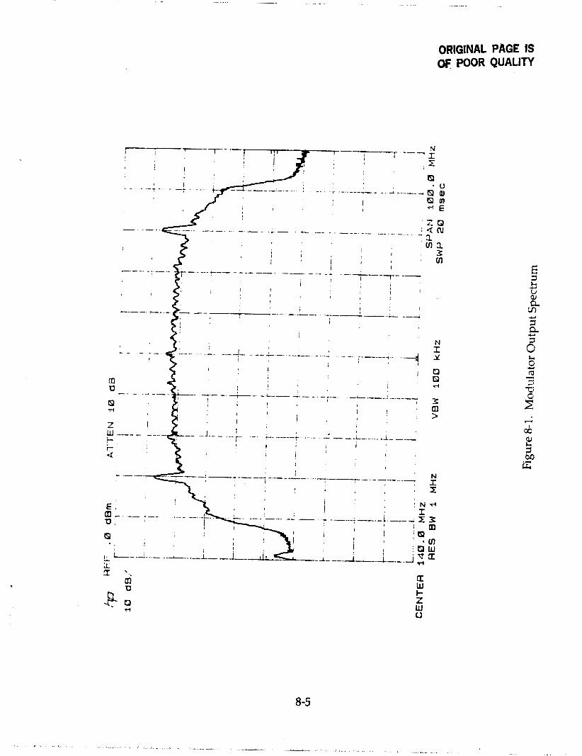
ORIGINAL PAGE IS OF. POOR QUALITY
- I
I
I I 1
N I Y
d
@ Q d
N I 'L:
d
3 m cn w X
8-5
&A
7 a 4-4 a
9. CONCLUSIONS
A jointly optimized coded modulation system has been designed, built a n d tested which provides a bandwidth efficiency of 2 bit/s/Hz at an information rate oi 160 Mbit/s. The BER performance is approximately 1 dB from the theoretically calculated value for this system at a BER of 5 x 10⁻⁷ under nominal conditions. The system operates in burst mode for downlink applications and tests have demonstrated very little degradation in performance with frequency and level offset. Unique word miss rate measurements have been conducted which demonstrate reliable acquisition at low values of Eb/No.
stand alone mode. The codec is capable operation at a 200 Mbit/s information rate as demonstrated using a codec test set which introduces noise digitally. The measured performance is within 0.2 dB of the computer simulated predictions. A gate array implementation of the most time critical element of the high speed Viterbi decoder has been completed. This gate array add-compare-select chip significantly reduces the power consumption and improves the manufacturability of the decoder. This chip has general application in the implementation of high speed Viterbi decoders.
Codec self tests have verified the performance of this subsystem in a
9-1

10. REFERENCES .
[l] INTELSAT TDMA/DSI System Specification, BG-42-65E (Rev. 1) June 25, 1981, pp. 27-30.
10-1
Report Documentation Page
NASA CR-185149
4. Title and Subtitle
Advanced Modulation Technology Development for Earth Station Demodulator Applications
Coded Modulation System Development
7. Author@)
Susan P. Miller, J. Mark Kappes, David H. Layer, and Peter N. Johnson
5. Report Date
April 1990
6. Performing Organization Code
8. Performing Organization Report No.
CTD-90/022
1 Space Administration
1. Report No. I 2. Government Accession No. I 3. Recipient’s Catalog No.
10. Work Unit No.
Clarksburg, Maryland 20871-9475
12. Sponsoring Agency Name and Address
National Aeronautics and Space Administration Lewis Research Center Cleveland, Ohio 44135-3191
I 1 650-20-26
13. Type of Report and Period Covered Contractor Report Final
14. Sponsoring Agency Code
9.Performing Organization Name and Address
COMSAT Laboratories 22300 Comsat Drive
7. Key Words (Suggested by Author@))
11. Contract or Grant No.
NAS3-24680
18. Distribution Statement
9. Security Classif. (of this report) 20. Security Classif. (of this page)
Unclassified Unclassified
____
16. Abstract
Ttris ~eport describes a jointly optimized coded modulation system designed, built, and tested by COMSAT Laboratories for NASA LeRC which provides a bandwidth efficiency of 2 bits/s/Hz at an information rate of 160 Mbit/s. A high speed rate 8/9 encoder with a Viterbi decoder and an Octal PSK modem are used to achieve this. The BER performance is approximately 1 dB from the theoretically calculated value for this system at a BER of 5 E-7 under nominal conditions. The system operates in burst mode for downlink applications and tests have demonstrated very little degradation in performance with frequency and level offset. Unique word miss rate measurements have been conducted which demonstrate reliable acquisition at low values of Eb/No. Codec self tests have verified the performance of this subsystem in a stand alone mode. The codec is capable of operation at a 200 Mbit/s information rate as demonstrated using a codec test set which introduces noise digitally. The measured performance is within 0.2 dB of the computer simulated predictions. A gate array implementation of the most time critical element of the high speed Viterbi decoder bas been completed. This gate array add- compare-select chip significantly reduces the power consumption and improves the manufacturability of the decoder. This chip has general application in the implementation of high speed Viterbi decoders.
21. No. of pages 22. Price’
94 A05
Coded modulation High speed Viterbi decoders M-ary PSK modems
Unclassified - Unlimited Subject Category 32
‘For sale by the National Technical Information Service, Springfield, Virginia 221 61 NASA FORY 1628 OCT BB
Related Documents