Copyright 2000, 2003 MD Ciletti 1 Advanced Digital Design with the Verilog HDL M. D. Ciletti Department of Electrical and Computer Engineering University of Colorado Colorado Springs, Colorado [email protected] Chaps 1 - 3: Review of Combinational and Sequential Logic (rev 9/17/2003) Copyright 2000, 2002, 2003. These notes are solely for classroom use by the instructor. No part of these notes may be copied, reproduced, or distributed to a third party, including students, in any form without the written permission of the author.

Welcome message from author
This document is posted to help you gain knowledge. Please leave a comment to let me know what you think about it! Share it to your friends and learn new things together.
Transcript
Copyright 2000, 2003 MD Ciletti 1
Advanced Digital Design with the Verilog HDL
M. D. Ciletti
Department of
Electrical and Computer Engineering University of Colorado
Colorado Springs, Colorado
Chaps 1 - 3: Review of Combinational and Sequential Logic (rev 9/17/2003)
Copyright 2000, 2002, 2003. These notes are solely for classroom use by the instructor. No part of these notes may be copied, reproduced, or distributed to a third party, including students, in any form without the written permission of the author.

Copyright 2000, 2003 MD Ciletti 2
Note to the instructor: These slides are provided solely for classroom use in academic institutions by the instructor using the text, Advance Digital Design with the Verilog HDL by Michael Ciletti, published by Prentice Hall. This material may not be used in off-campus instruction, resold, reproduced or generally distributed in the original or modified format for any purpose without the permission of the Author. This material may not be placed on any server or network, and is protected under all copyright laws, as they currently exist. I am providing these slides to you subject to your agreeing that you will not provide them to your students in hardcopy or electronic format or use them for off-campus instruction of any kind. Please email to me your agreement to these conditions. I will greatly appreciate your assisting me by calling to my attention any errors or any other revisions that would enhance the utility of these slides for classroom use.
Copyright 2000, 2003 MD Ciletti 3
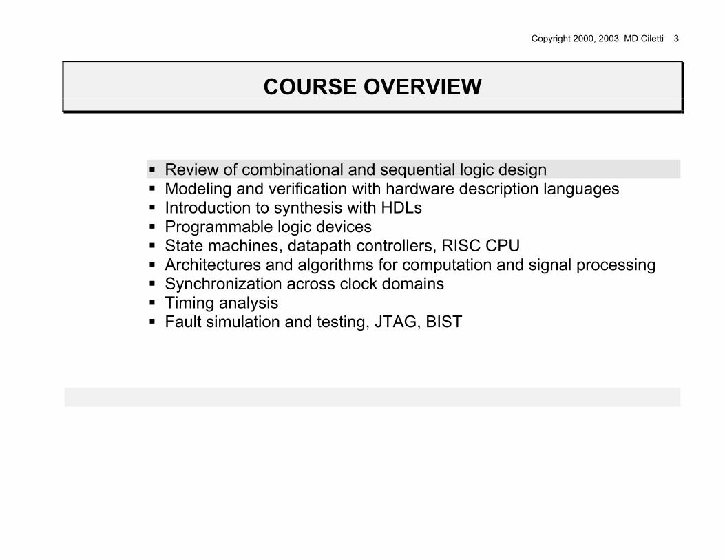
COURSE OVERVIEW
Review of combinational and sequential logic design Modeling and verification with hardware description languages Introduction to synthesis with HDLs Programmable logic devices State machines, datapath controllers, RISC CPU Architectures and algorithms for computation and signal processing Synchronization across clock domains Timing analysis Fault simulation and testing, JTAG, BIST
Copyright 2000, 2003 MD Ciletti 4
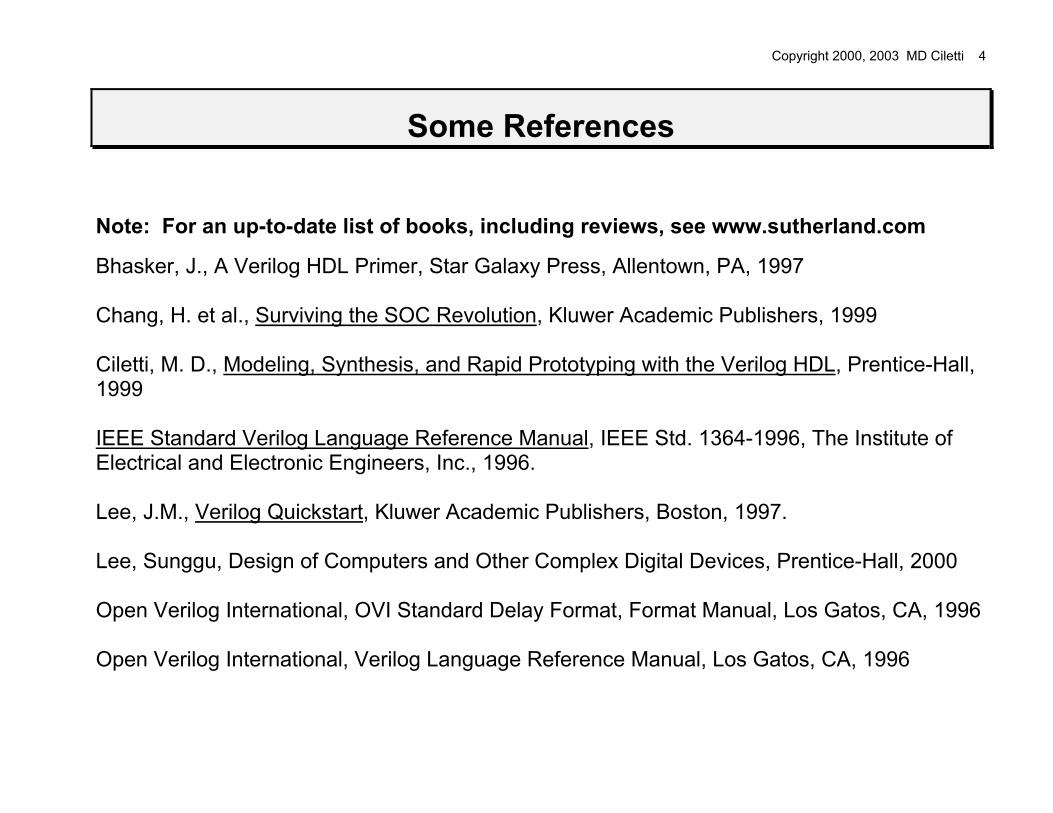
Some References
Note: For an up-to-date list of books, including reviews, see www.sutherland.com
Bhasker, J., A Verilog HDL Primer, Star Galaxy Press, Allentown, PA, 1997 Chang, H. et al., Surviving the SOC Revolution, Kluwer Academic Publishers, 1999 Ciletti, M. D., Modeling, Synthesis, and Rapid Prototyping with the Verilog HDL, Prentice-Hall, 1999 IEEE Standard Verilog Language Reference Manual, IEEE Std. 1364-1996, The Institute of Electrical and Electronic Engineers, Inc., 1996. Lee, J.M., Verilog Quickstart, Kluwer Academic Publishers, Boston, 1997. Lee, Sunggu, Design of Computers and Other Complex Digital Devices, Prentice-Hall, 2000 Open Verilog International, OVI Standard Delay Format, Format Manual, Los Gatos, CA, 1996 Open Verilog International, Verilog Language Reference Manual, Los Gatos, CA, 1996

Copyright 2000, 2003 MD Ciletti 5
Open Verilog International, Programming Language Interface Reference Manual, Los Gatos, CA, 1996 Palnitkar S., Verilog HDL, A Guide to Design and Synthesis, SunSoft Press, Sun Microsystems, Inc., Mountain View, California, 1996. PLI Reference Manual, Open Verilog International Smith, D.J., HDL Chip Design, Doone Publications, Madison, AL, 1996 Smith, M. J., Application-Specific Integrated Circuits, Addison-Wesley Longman, Inc., Reading, Massachusetts, 1997 Sternheim, E. et al., Digital Design and Synthesis with Verilog HDL, Automata Publishing Co., San Jose, California, 1993. Thomas, D.E. and Moorby, P., The Verilog Hardware Description Language, Third Edition, Kluwer Academic Publishers, Boston, 1996.
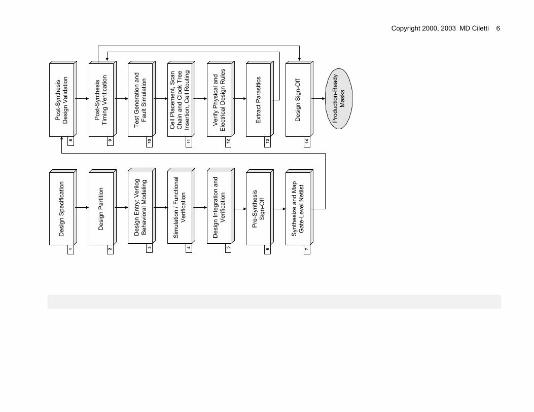
Copyright 2000, 2003 MD Ciletti 6
Sim
ulat
ion
/ Fun
ctio
nal
Ver
ifica
tion
Des
ign
Entry
: Ver
ilog
Beh
avio
ral M
odel
ing
Des
ign
Inte
grat
ion
and
Ver
ifica
tion
Pos
t-Syn
thes
isD
esig
n V
alid
atio
n
Pos
t-Syn
thes
isTi
min
g V
erifi
catio
nD
esig
n P
artit
ion
Des
ign
Spec
ifica
tion
98
54321
Test
Gen
erat
ion
and
Faul
t Sim
ulat
ion
10
Ver
ify P
hysi
cal a
ndE
lect
rical
Des
ign
Rul
es12
Cel
l Pla
cem
ent,
Sca
nC
hain
and
Clo
ck T
ree
Inse
rtion
, Cel
l Rou
ting
11
Extra
ct P
aras
itics
13
Pre-
Synt
hesi
sS
ign-
Off
6
Des
ign
Sig
n-O
ff14
Syn
thes
ize
and
Map
Gat
e-Le
vel N
etlis
t7
Prod
uctio
n-R
eady
Mas
ks

Copyright 2000, 2003 MD Ciletti 7
COMBINATIONAL LOGIC
Combinational logic forms Boolean functions of the input variables. The outputs at any time, t, are a function of only the inputs at time t. The variables are assumed to be binary.
CombinationalLogic
y1
y2
y3
abcd
y1 = f1(a, b, c, d)
y2 = f2(a, b, c, d)
y3 = f3(a, b, c, d)
y4 = f4(a, b, c, d)
A binary variable may have a value of 0 or 1. Later, the logic value system will be
expanded to have more values to support a hardware description language.
POSITIVE LOGIC: Low voltage corresponds to logic 0 and a high voltage corresponds to a logic 1.

Copyright 2000, 2003 MD Ciletti 8
LOGIC GATES
ENB
And Gatey = a . b
Or Gatey = a + b
Nand Gate
y = a . b
ab
ab
y
y
yab
ab
Nor Gate
y = a + b
y ab
y
yab
Xor Gatey = a ^ b
Xnor Gate
y = a ^ b
a y
Buffery = a
a a
Invertery = a
Three-State Buffery = a if ENB = 1, else y = z
y y

Copyright 2000, 2003 MD Ciletti 9
LOGIC GATES - NOTATION
+ denotes logical "or" . denotes logical "and" ^ denotes exclusive or
⊕ denotes "exclusive or" ' denotes logical negation overbar denotes logical negation
LOGIC GATES - CMOS TECHNOLOGY
CMOS Inverter 3-input Nand Gate
d
dd
in outd
dd
in outd
dd
in out
V V V Vdd
B
AY
A B C
C

Copyright 2000, 2003 MD Ciletti 10
BOOLEAN ALGEBRA (p 16)
A binary Boolean algebra consists of a set B = {0, 1} and the operators + and ., having commutative and distributive properties such that for two Boolean variables A and B having values in B, a + b = b + a, and a . b = b . a. The operators + and . have identity elements 0 and 1, respectively, such that for any Boolean variable a, a + 0 = a, and a . 1 = a. Each Boolean variable a has a complement, denoted by a', such that a + a' = 1, and a . a' = 0. Terminology:
• + is called the sum operator, the "OR" operator, or the disjunction operator.
• . is called the product operator, the "AND" operator, or the conjunction operator. • The multi-dimensional space spanned by a set of n binary-valued Boolean variables is
denoted by Bn.
• A point in Bn is called a vertex of and is represented by an n-dimensional vector of binary valued elements, e.g. (100).
• A binary variable can be associated with the dimensions of a binary Boolean space,
and a point is identified with the values of the variables.
Copyright 2000, 2003 MD Ciletti 11
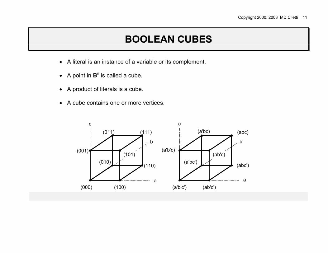
BOOLEAN CUBES
• A literal is an instance of a variable or its complement.
• A point in Bn is called a cube.
• A product of literals is a cube.
• A cube contains one or more vertices.
a
b
c
(a'b'c')
b
c
(ab'c')
(abc')
(abc)(a'bc)
(a'b'c)
(a'bc')
(100)a
(111)
(110)(010)
(001)
(011)
(101) (ab'c)
(000)
Copyright 2000, 2003 MD Ciletti 12
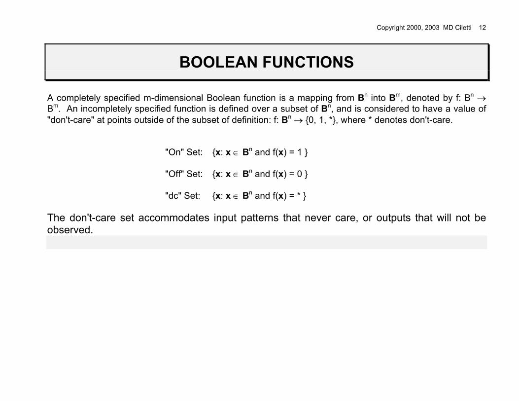
BOOLEAN FUNCTIONS
A completely specified m-dimensional Boolean function is a mapping from Bn into Bm, denoted by f: Bn → Bm. An incompletely specified function is defined over a subset of Bn, and is considered to have a value of "don't-care" at points outside of the subset of definition: f: Bn → {0, 1, *}, where * denotes don't-care.
"On" Set: {x: x ∈ Bn and f(x) = 1 } "Off" Set: {x: x ∈ Bn and f(x) = 0 } "dc" Set: {x: x ∈ Bn and f(x) = * }
The don't-care set accommodates input patterns that never care, or outputs that will not be observed.

Copyright 2000, 2003 MD Ciletti 13
BOOLEAN ALGEBRA
Combinations with 0, 1 a + 0 = a a . 1 =aa + 1 = 1 a . 0 = 0
Commutative a + b = b + a ab = ba
Associative (a + b) + c = a + (b + c) (ab)c = a(bc) = abc = a + b + c
Distributive a(b + c) = ab + ac a + bc = (a + b)(a + c)
Idempote a + a = a a . a = a
Involution (a')' = a
Complementarity a + a' = 1 a . a' = 0
SOP Form POS FormBoolean Algebra Laws
Copyright 2000, 2003 MD Ciletti 14
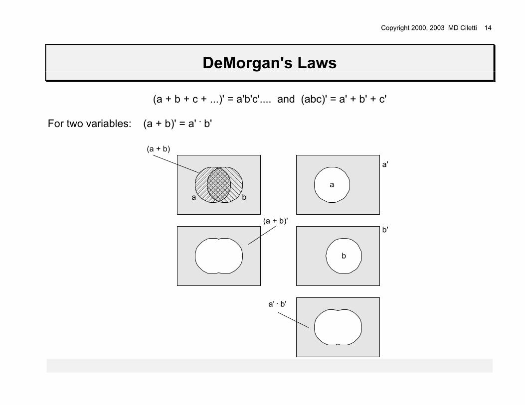
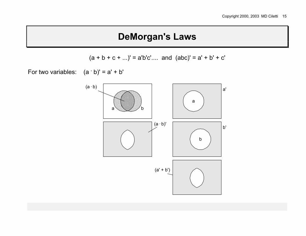
DeMorgan's Laws
(a + b + c + ...)' = a'b'c'.... and (abc)' = a' + b' + c'
For two variables: (a + b)' = a' . b'
a b
(a + b)
(a + b)'
a'
b'
a
b
a' . b'
Copyright 2000, 2003 MD Ciletti 15
DeMorgan's Laws
(a + b + c + ...)' = a'b'c'.... and (abc)' = a' + b' + c'
For two variables: (a . b)' = a' + b'
(a . b)'
(a . b) a'
b'
(a' + b')
a ba
b

Copyright 2000, 2003 MD Ciletti 16
THEOREMS FOR BOOLEAN ALGEBRAIC MINIMIZATION
Logical Adjacency ab + ab' = a (a + b) (a + b') = a
Absorption a + ab = a a(a + b) = aab' + b = a + b (a + b')b = ab
or: a + a'b = a + b (a' + b)a = ab
Multiplication and (a + b)(a' + c) = ac + a'b ab + a'c = (a + c)(a' + b)Factoring
Consensus ab + bc +a'c = ab + a'c (a + b)(b + c)(a' + c) =(a + b)(a' + c)
SOP Form POS FormTheorem
ab'ab
a b
Logical Adjacency
ab
c
bc
ab
Covered by ab
Covered by a'c
The consensus term,bc, is redundant.
Consensus
Copyright 2000, 2003 MD Ciletti 17
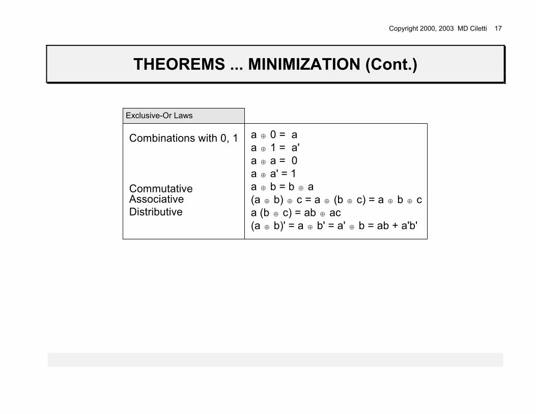
THEOREMS ... MINIMIZATION (Cont.)
Exclusive-Or Laws
Combinations with 0, 1
Commutative
DistributiveAssociative
a ⊕ 0 = aa ⊕ 1 = a'a ⊕ a = 0a ⊕ a' = 1a ⊕ b = b ⊕ a(a ⊕ b) ⊕ c = a ⊕ (b ⊕ c) = a ⊕ b ⊕ ca (b ⊕ c) = ab ⊕ ac(a ⊕ b)' = a ⊕ b' = a' ⊕ b = ab + a'b'
Copyright 2000, 2003 MD Ciletti 18
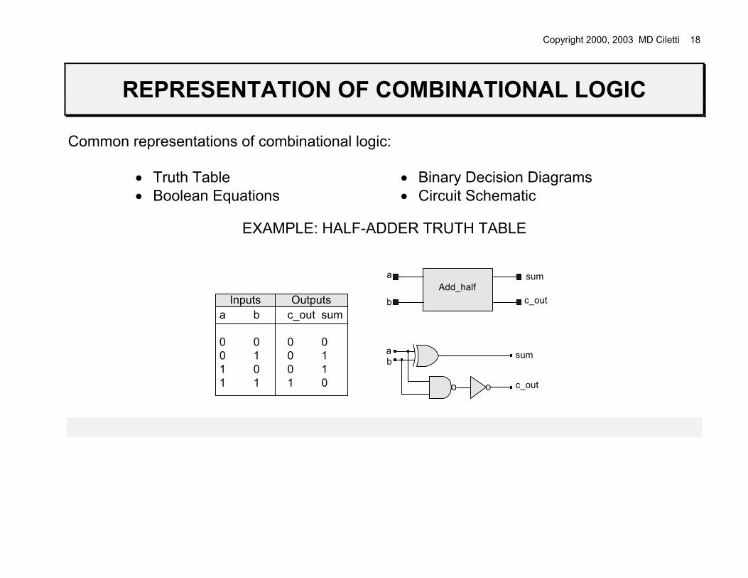
REPRESENTATION OF COMBINATIONAL LOGIC
Common representations of combinational logic:
• Truth Table • Boolean Equations
• Binary Decision Diagrams • Circuit Schematic
EXAMPLE: HALF-ADDER TRUTH TABLE
ba sum
c_out
a
b
sum
c_outAdd_half
a b c_out sum
0 0 0 00 1 0 11 0 0 11 1 1 0
Inputs Outputs
Copyright 2000, 2003 MD Ciletti 19
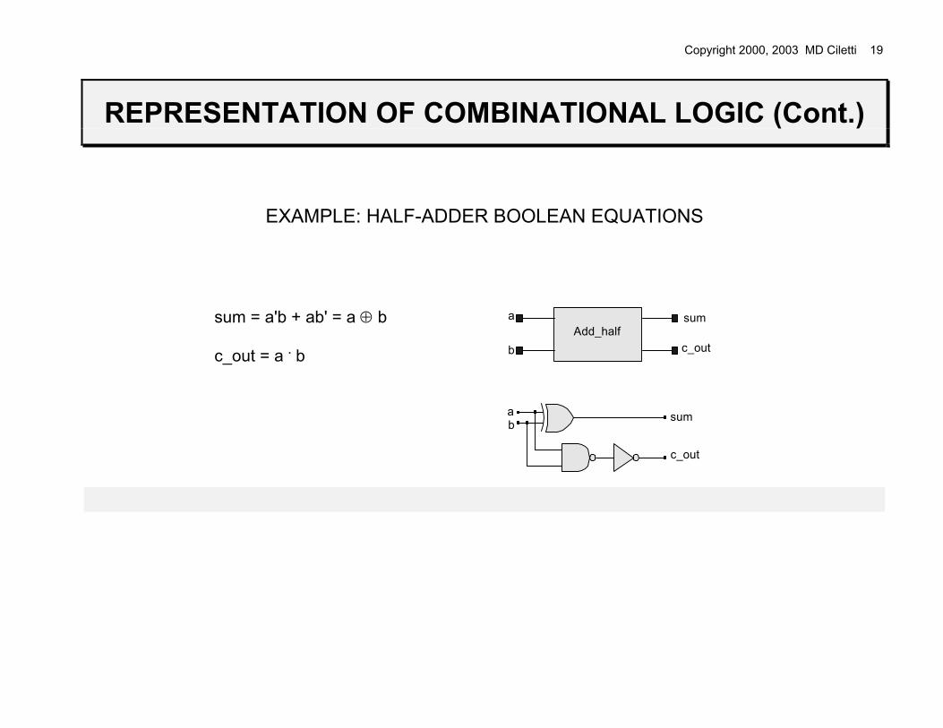
REPRESENTATION OF COMBINATIONAL LOGIC (Cont.)
EXAMPLE: HALF-ADDER BOOLEAN EQUATIONS
sum = a'b + ab' = a ⊕ b
c_out = a . b
ba sum
c_out
a
b
sum
c_outAdd_half

Copyright 2000, 2003 MD Ciletti 20
SOP NOTATION (p 23)
• A cube is formed as the product of literals in which a literal appears in either
uncomplemented or complemented form.
Example: ab'cd is a cube; ab'cbd is not. • A Boolean expression is a set of cubes, and is typically expressed in sum-of-products form
(SOP) as the "or" of product terms (cubes).
Example: abc' + bd • Each term of a Boolean expression in SOP form is called an implicant of the function. • A minterm is a cube in which every variable appears. The variable will be in either true
(uncomplemented) or complemented (but not both) form. Thus, a minterm corresponds to a point (vertex) in Bn. (A term that is not a minterm represents two or more points in Bn). The minterms correspond to the rows of the truth table at which the function has a value of 1.
Example: The cube ab'cd is a minterm in B4. Example: The cube abc is not a minterm. It represents abcd + abcd'.

Copyright 2000, 2003 MD Ciletti 21
SOP NOTATION
• A Boolean expression in SOP form is said to be canonical if every cube has all of the literals
in complemented or uncomplemented form.
Example: The expression abcd + a'bcd is a canonical sum of products. • A canonic SOP function is also called a standard sum of products (SSOP). • Decimal notation: a minterm is denoted by mi, and the pattern of 1s and 0s in the binary
equivalent of the decimal number i indicates the true and complemented literals. •
Example: m7 = a'bcd.

Copyright 2000, 2003 MD Ciletti 22
SOP NOTATION (Cont.)
In Bn There is a one-to-one correspondence between a minterm and a vertex of a n-dimensional cube.
a
b
c
m4
m7
m6m2
m1
m3
m0
m5
Example: m3 = a' . b . c_in A Boolean function is a set of minterms (vertices) at which the function is asserted A Boolean function is expressed as a sum of minterms. Example: c_out = m1 + m3 + m5 + m7 = Σ m(1, 3, 5, 7) sum = m3 + m5 + m6 + m7 = Σ m(3, 5, 6, 7)
Copyright 2000, 2003 MD Ciletti 23
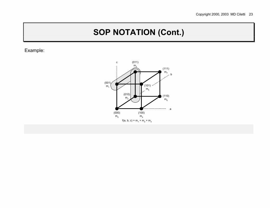
SOP NOTATION (Cont.)
Example:
a
b
c
(100)m4
(111)m7
(110)m6
(010)m2
(011)m3
(101)m5
(000)m0
f(a, b, c) = m1 + m2 + m3
(001)m1
Copyright 2000, 2003 MD Ciletti 24
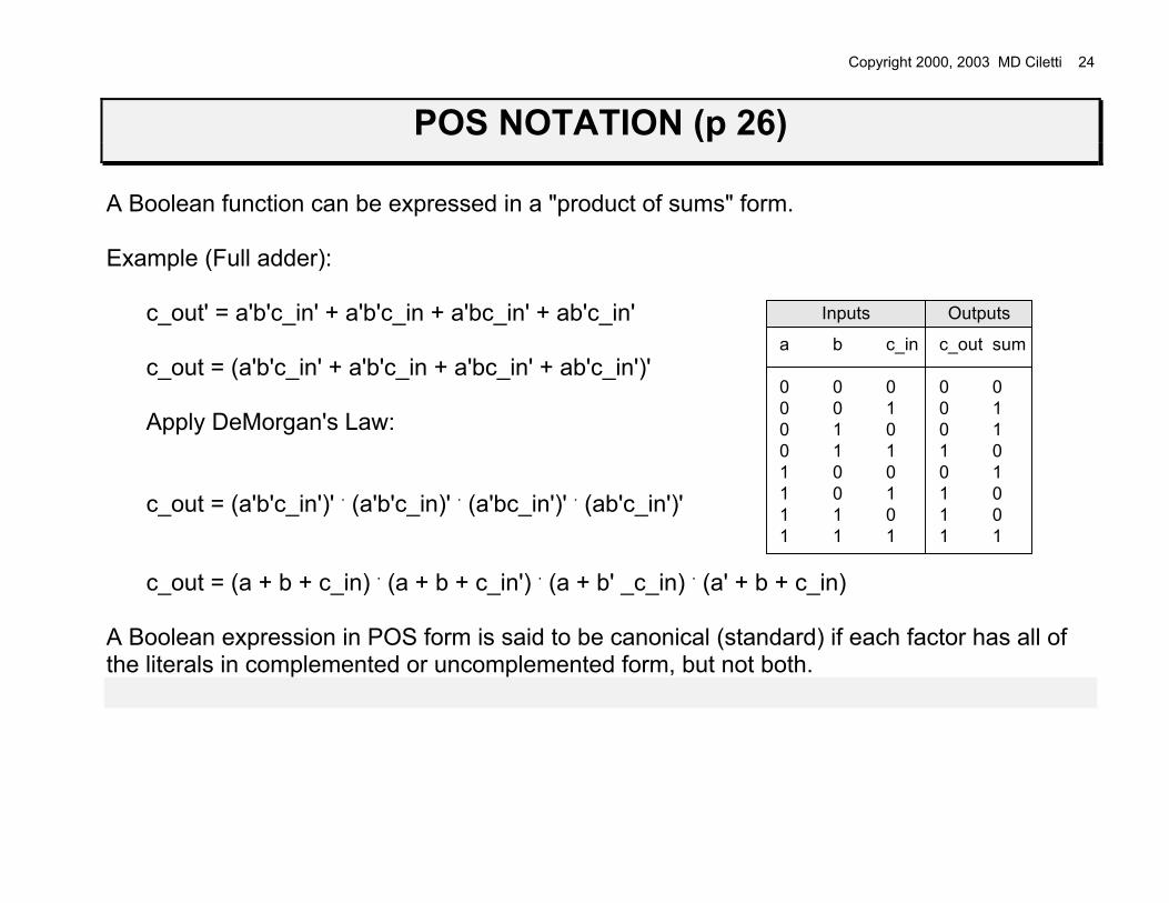
POS NOTATION (p 26)
A Boolean function can be expressed in a "product of sums" form. Example (Full adder):
c_out' = a'b'c_in' + a'b'c_in + a'bc_in' + ab'c_in' c_out = (a'b'c_in' + a'b'c_in + a'bc_in' + ab'c_in')' Apply DeMorgan's Law: c_out = (a'b'c_in')' . (a'b'c_in)' . (a'bc_in')' . (ab'c_in')'
a b c_in c_out sum
0 0 0 0 00 0 1 0 10 1 0 0 10 1 1 1 01 0 0 0 11 0 1 1 01 1 0 1 01 1 1 1 1
Inputs Outputs
c_out = (a + b + c_in) . (a + b + c_in') . (a + b' _c_in) . (a' + b + c_in)
A Boolean expression in POS form is said to be canonical (standard) if each factor has all of the literals in complemented or uncomplemented form, but not both.
Copyright 2000, 2003 MD Ciletti 25
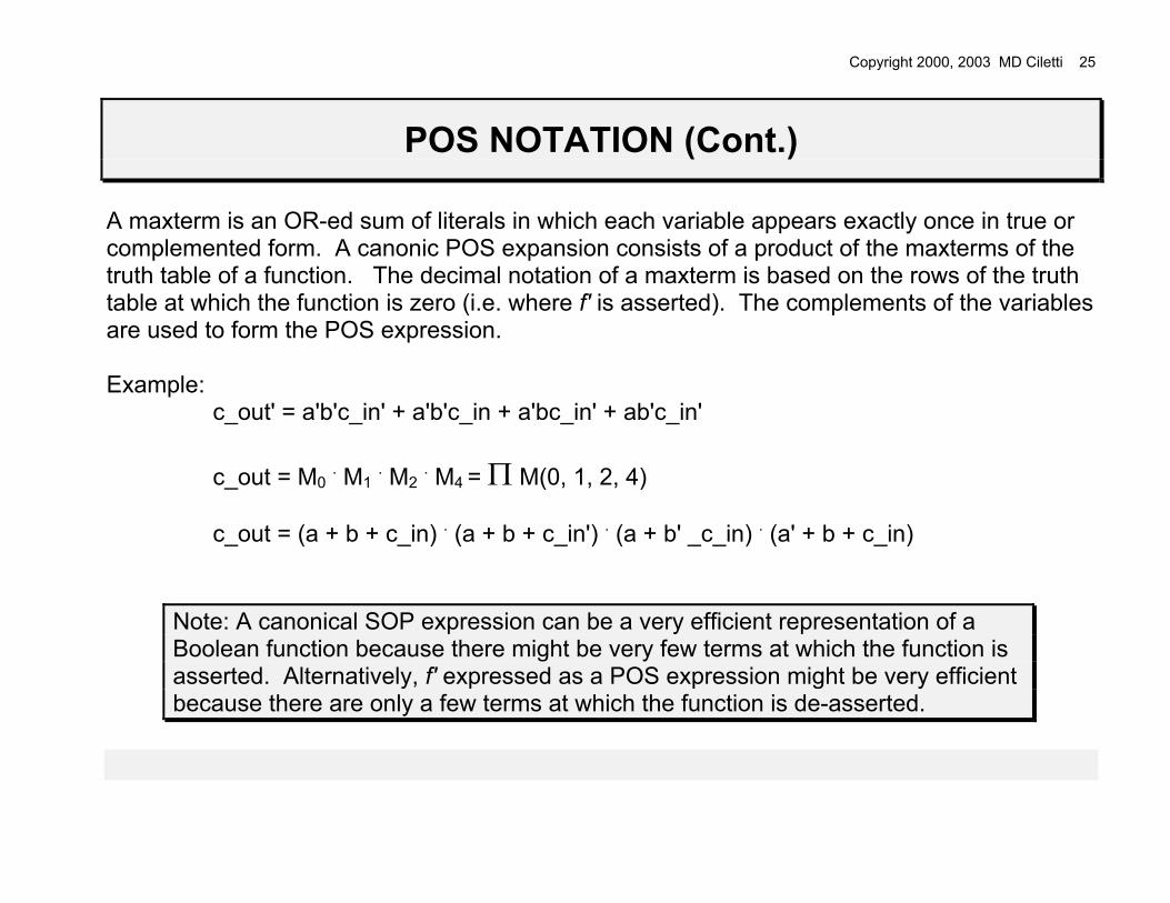
POS NOTATION (Cont.)
A maxterm is an OR-ed sum of literals in which each variable appears exactly once in true or complemented form. A canonic POS expansion consists of a product of the maxterms of the truth table of a function. The decimal notation of a maxterm is based on the rows of the truth table at which the function is zero (i.e. where f' is asserted). The complements of the variables are used to form the POS expression. Example:
c_out' = a'b'c_in' + a'b'c_in + a'bc_in' + ab'c_in' c_out = M0 . M1 . M2 . M4 = Π M(0, 1, 2, 4) c_out = (a + b + c_in) . (a + b + c_in') . (a + b' _c_in) . (a' + b + c_in)
Note: A canonical SOP expression can be a very efficient representation of a Boolean function because there might be very few terms at which the function is asserted. Alternatively, f' expressed as a POS expression might be very efficient because there are only a few terms at which the function is de-asserted.
Copyright 2000, 2003 MD Ciletti 26
SIMPLIFICATION OF BOOLEAN EXPRESSIONS
A SOP expression has a direct hardware implementation as a two-level And-Or logic circuit. The cost of hardware implementing a Boolean expression is related to the number of terms in the expression and to the number of literals in a term. Although a Boolean expression can always be expressed in a canonical form, with every cube containing every literal (in complemented or uncomplemented form), such descriptions usually have more efficient descriptions. In practice, minimization is important.

Copyright 2000, 2003 MD Ciletti 27
SIMPLIFICATION OF BOOLEAN EXPRESSIONS (Cont.)
A Boolean expression in SOP form is said to be minimal if it contains a minimal number of product terms and literals (i.e. a given term cannot be replaced by another that has fewer literals). A minimum SOP form corresponds to a two-level logic circuit having the fewest gates and the fewest number of gate inputs. A Boolean expression in POS form is said to be minimal of it contains a minimal number of factors and literals (i.e. a given factor cannot be replace by another having fewer literals). Three approaches: (1) Karnaugh maps and extended karnaugh maps (Feasible for up to 6 variables) (2) Quine-McCluskey minimization (computer-based) (3) Boolean minimization (manual) uses the theorems describing relationships between Boolean variables to find simpler equivalent expressions (It is not straightforward, is not easy, and requires experience. Now embedded in synthesis tools such as mis II.)

Copyright 2000, 2003 MD Ciletti 28
SIMPLIFICATION OF BOOLEAN EXPRESSIONS (Cont.)
In a Boolean expression, a cube that is contained in another cube is redundant. A Boolean expression is nonredundant (irredundant) if no cube contains another cube. Example: Redundant Expression f(a, b) = a + ab The expression is redundant because ab is a subset of a. After removing the redundant cube: f(a, b) = a Example: Nonredundant Expression f(c, d) = c'd' + cd The cubes of a nonredundant expression do not share a common vertex, i.e. their corresponding sets of vertices are pairwise disjoint. Note: The minimum SOP form and minimum POS forms of a Boolean expression are not unique. Basic approach: To simplify/minimize a Boolean expression, repeatedly combine cubes that differ in only the same literal, and eliminate redundant implicants.
Copyright 2000, 2003 MD Ciletti 29
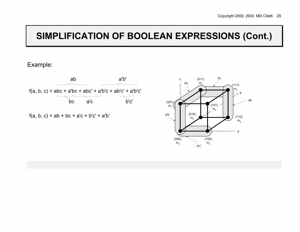
SIMPLIFICATION OF BOOLEAN EXPRESSIONS (Cont.)
Example:
f(a, b, c) = abc + a'bc + abc' + a'b'c + ab'c' + a'b'c'
f(a, b, c) = ab + bc + a'c + b'c' + a'b'
ab a'b'
bc a'c b'c'
a
b
c
(100)m4
(111)m7
(010)m2
(011)m3
(101)m5
(000)m0
(001)m1
(110)m6
a'cbc
ab
b'c'
a'b'
Copyright 2000, 2003 MD Ciletti 30
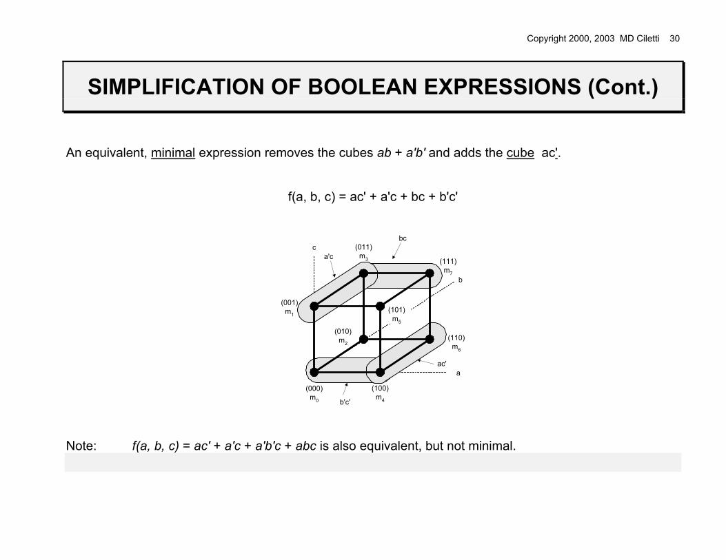
SIMPLIFICATION OF BOOLEAN EXPRESSIONS (Cont.)
An equivalent, minimal expression removes the cubes ab + a'b' and adds the cube ac'.
f(a, b, c) = ac' + a'c + bc + b'c'
a
b
c
(100)m4
(111)m7
(010)m2
(011)m3
(101)m5
(000)m0
(001)m1
(110)m6
a'c
bc
ac'
b'c' Note: f(a, b, c) = ac' + a'c + a'b'c + abc is also equivalent, but not minimal.
Copyright 2000, 2003 MD Ciletti 31
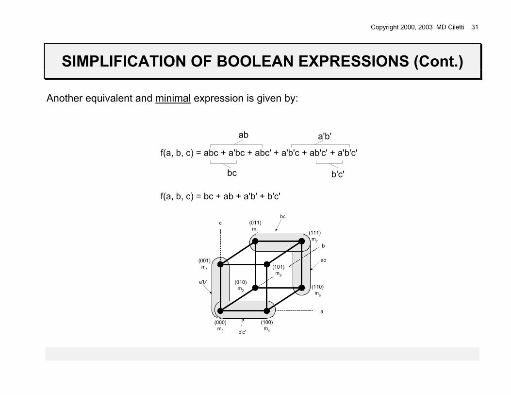
SIMPLIFICATION OF BOOLEAN EXPRESSIONS (Cont.)
Another equivalent and minimal expression is given by:
f(a, b, c) = abc + a'bc + abc' + a'b'c + ab'c' + a'b'c'
f(a, b, c) = bc + ab + a'b' + b'c'
ab
b'c'
a'b'
bc
a
b
c
(100)m4
(111)m7
(010)m2
(011)m3
(101)m5
(000)m0
(001)m1
(110)m6
bc
b'c'
ab
a'b'

Copyright 2000, 2003 MD Ciletti 32
SIMPLIFICATION OF BOOLEAN EXPRESSIONS (Cont.)
Implicant: Each term of a Boolean expression in SOP form is called an implicant of the function. An implicant may cover more than one vertex of the function.
(101)
a
b
c
(100)
(111)
(110)(010)
(001)
(011)
(000)
cube:ab
f(a, b, c) = abc + abc' = ab
vertex
implicant
An implicant covers a vertex if the vertex is included in the set of vertices at which the implicant is asserted. The fewer the number of literals in a cube, the larger the set of covered vertices. So the hardware implementation is minimized if a cube has as few literals as possible

Copyright 2000, 2003 MD Ciletti 33
SIMPLIFICATION OF BOOLEAN EXPRESSIONS (Cont.)
Prime Implicant: An implicant which does not imply any other implicant of the function is called a prime implicant. A prime implicant is a cube that is not properly contained in some other cube of the function. Example: f(a, b, c, d) = a'b'cd + a'bcd + ab'cd + abcd + a'b'c'd' = a'cd + acd + a'b'c'd' = cd + a'b'c'd' Note that a'cd and acd both imply cd, so they are not prime implicants. The term a'b'c'd is a prime implicant. A prime implicant cannot be combined with another implicant to eliminate a literal or to be eliminated from the expression by absorption. An implicant that implies another implicant is said to be "covered" by it; the set of its vertices is a subset of the vertices of the implicant that covers it. The covering implicant, having fewer literals, has more vertices.
Copyright 2000, 2003 MD Ciletti 34
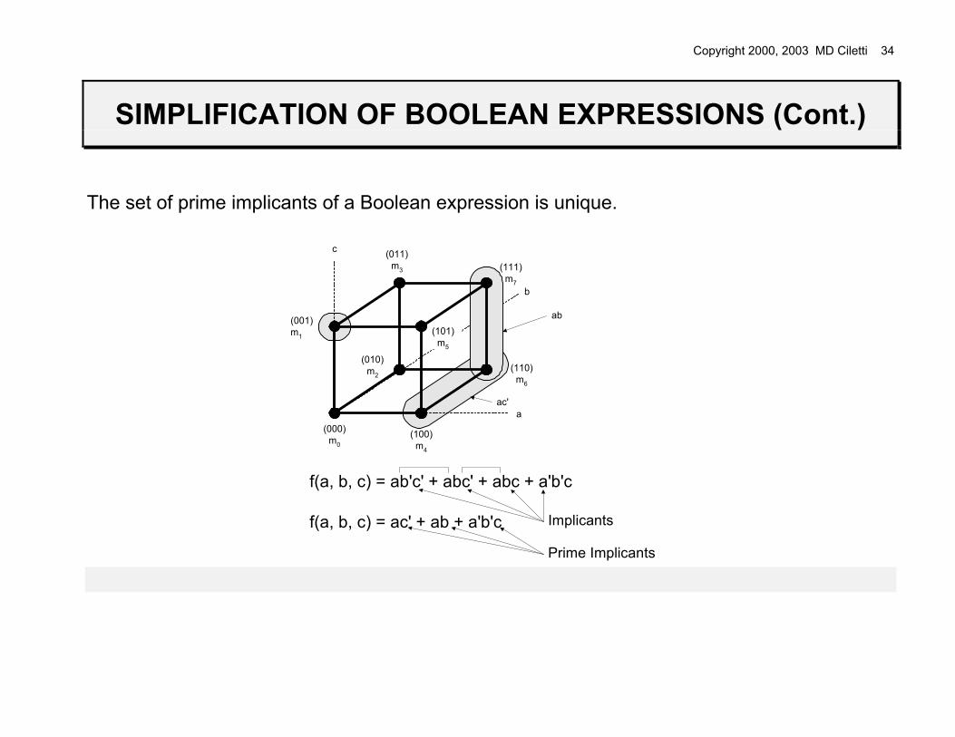
SIMPLIFICATION OF BOOLEAN EXPRESSIONS (Cont.)
The set of prime implicants of a Boolean expression is unique.
a
b
c
(100)m4
(111)m7
(010)m2
(011)m3
(101)m5
(000)m0
f(a, b, c) = ab'c' + abc' + abc + a'b'c
f(a, b, c) = ac' + ab + a'b'c
(001)m1
(110)m6
ab
ac'
Implicants
Prime Implicants
Copyright 2000, 2003 MD Ciletti 35
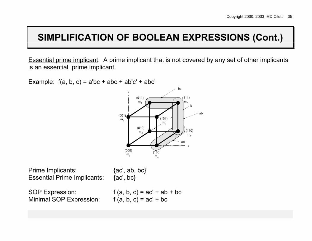
SIMPLIFICATION OF BOOLEAN EXPRESSIONS (Cont.)
Essential prime implicant: A prime implicant that is not covered by any set of other implicants is an essential prime implicant. Example: f(a, b, c) = a'bc + abc + ab'c' + abc'
a
b
c
(100)m4
(111)m7
(010)m2
(011)m3
(101)m5
(000)m0
(001)m1
(110)m6
ab
ac'
bc
Prime Implicants: {ac', ab, bc} Essential Prime Implicants: {ac', bc} SOP Expression: f (a, b, c) = ac' + ab + bc Minimal SOP Expression: f (a, b, c) = ac' + bc

Copyright 2000, 2003 MD Ciletti 36
SIMPLIFICATION OF BOOLEAN EXPRESSIONS (Cont.)
Process for minimization: (1) Find the set of all prime implicants (2) Find a minimal subset which covers all of the prime implicants (includes essential prime implicants). Minimal Cover: A subset of prime implicants that covers all of the prime implicants is called a minimal cover for the function. Example: f(a, b, c, d) = a'b'cd + a'bcd + ab'cd + abcd + a'b'c'd' = a'cd + acd + a'b'c'd' = cd + a'b'c'd' Prime implicants: {cd, a'b'c'd'} Minimal cover: {cd, a'b'c'd'}
Copyright 2000, 2003 MD Ciletti 37
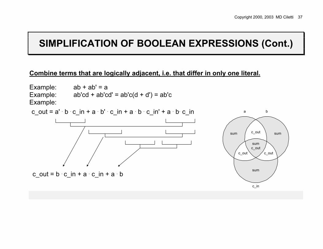
SIMPLIFICATION OF BOOLEAN EXPRESSIONS (Cont.)
Combine terms that are logically adjacent, i.e. that differ in only one literal. Example: ab + ab' = a Example: ab'cd + ab'cd' = ab'c(d + d') = ab'c Example: c_out = a' . b . c_in + a . b' . c_in + a . b . c_in' + a . b. c_in
c_out = b . c_in + a . c_in + a . b
a b
c_in
sum sum
c_out c_out
c_out
sumc_out
sum

Copyright 2000, 2003 MD Ciletti 38
SIMPLIFICATION OF BOOLEAN EXPRESSIONS (Cont.)
Apply logical adjacency to complementary expressions. Example: Consider the expression: (c + db)(a + e') + c'(d' + b')(a + e') and note that: (c + db)' = c'(d' + b') Then (c + db)(a + e') + c'(d' + b')(a + e') = (c + db)(a + e') + (c + db)'(a + e') = a + e'
Copyright 2000, 2003 MD Ciletti 39
SIMPLIFICATION OF BOOLEAN EXPRESSIONS (Cont.)
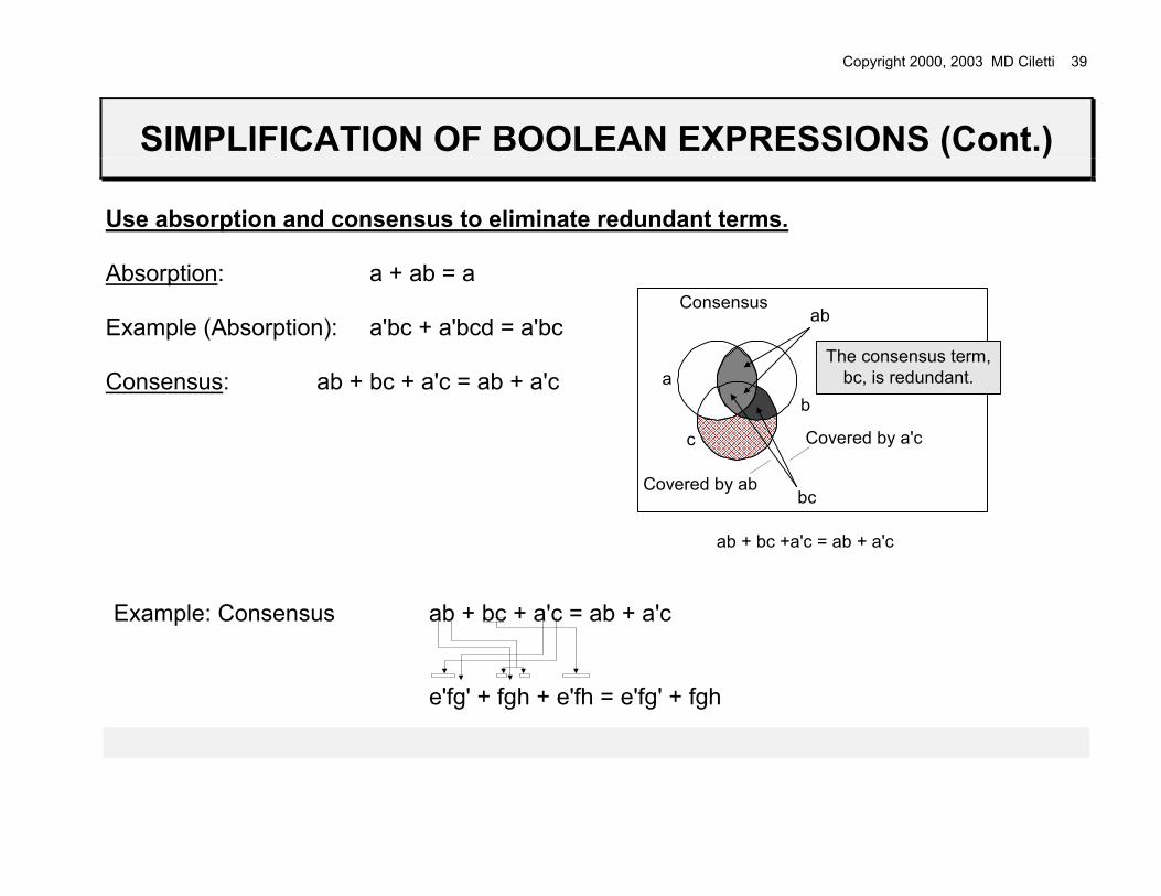
Use absorption and consensus to eliminate redundant terms. Absorption: a + ab = a
Example (Absorption): a'bc + a'bcd = a'bc Consensus: ab + bc + a'c = ab + a'c
ab + bc +a'c = ab + a'c
ab
c
bc
ab
Covered by ab
Covered by a'c
The consensus term,bc, is redundant.
Consensus
Example: Consensus ab + bc + a'c = ab + a'c
e'fg' + fgh + e'fh = e'fg' + fgh

Copyright 2000, 2003 MD Ciletti 40
SIMPLIFICATION OF BOOLEAN EXPRESSIONS (Cont.)
Use absorption repeatedly to eliminate literals. Example: efgh' + e'f'g'h' + e'f = efgh' + e'(f + f'g'h') = efgh' + e'(f + g'h') = f(egh' + e') + e'g'h' = f(gh' + e') + e'g'h' = fgh' + e'f + e'g'h'

Copyright 2000, 2003 MD Ciletti 41
SIMPLIFICATION OF BOOLEAN EXPRESSIONS (Cont.)
Introduce redundant terms to support absorption and logical adjacency. A logical expression in SOP form is preserved under the following operations: (1) Add the term: aa' (2) Add the consensus term, bc, to the terms ab + a'c (3) Add ab to a or to b. A logical expression in POS form is preserved under the following operations: (1) Multiply by the factor (a + a') (2) Introduce the consensus factor, (b + c), in (a + b) (a' + c) (3) Multiply a by the factor (a + b)
Copyright 2000, 2003 MD Ciletti 42
SIMPLIFICATION OF BOOLEAN EXPRESSIONS (Cont.)
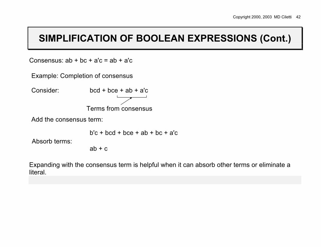
Consensus: ab + bc + a'c = ab + a'c Example: Completion of consensus
Consider: bcd + bce + ab + a'c
Terms from consensus
Add the consensus term:
b'c + bcd + bce + ab + bc + a'cAbsorb terms:
ab + c Expanding with the consensus term is helpful when it can absorb other terms or eliminate a literal.
Copyright 2000, 2003 MD Ciletti 43
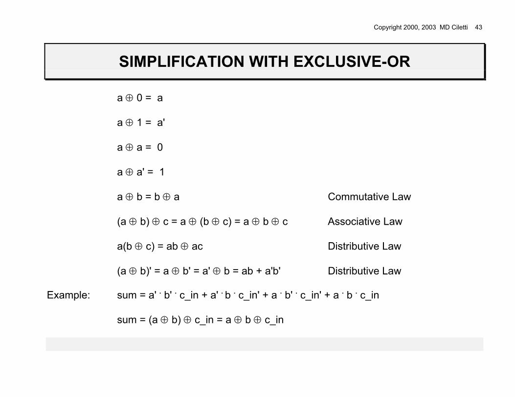
SIMPLIFICATION WITH EXCLUSIVE-OR
a ⊕ 0 = a a ⊕ 1 = a' a ⊕ a = 0 a ⊕ a' = 1 a ⊕ b = b ⊕ a Commutative Law (a ⊕ b) ⊕ c = a ⊕ (b ⊕ c) = a ⊕ b ⊕ c Associative Law a(b ⊕ c) = ab ⊕ ac Distributive Law (a ⊕ b)' = a ⊕ b' = a' ⊕ b = ab + a'b' Distributive Law
Example: sum = a' . b' . c_in + a' . b . c_in' + a . b' . c_in' + a . b . c_in sum = (a ⊕ b) ⊕ c_in = a ⊕ b ⊕ c_in
Copyright 2000, 2003 MD Ciletti 44
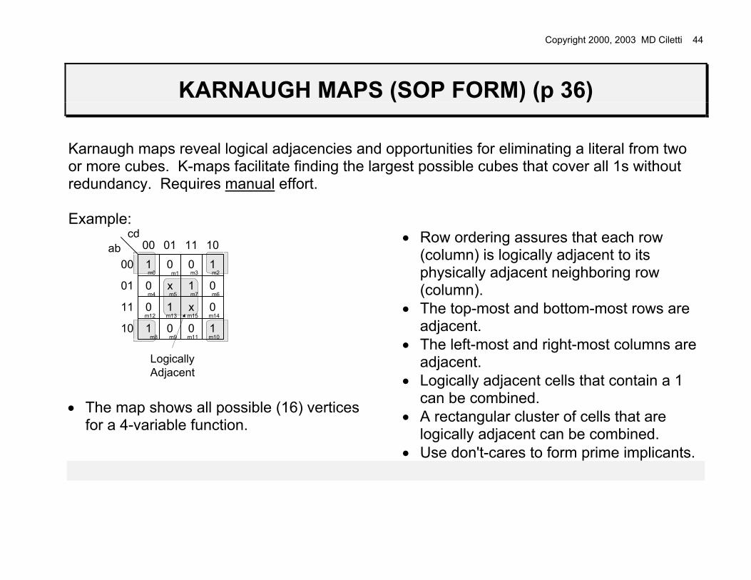
KARNAUGH MAPS (SOP FORM) (p 36)
Karnaugh maps reveal logical adjacencies and opportunities for eliminating a literal from two or more cubes. K-maps facilitate finding the largest possible cubes that cover all 1s without redundancy. Requires manual effort. Example:
cd
00
10
11
01
00 01 11 10
1ab
0 0 1
0 1 0
0 1 x 0
1 0 0 1
xm0 m1 m3 m2
m4 m5 m7 m6
m12 m13 m15 m14
m8 m9 m11 m10
LogicallyAdjacent
• The map shows all possible (16) vertices
for a 4-variable function.
• Row ordering assures that each row (column) is logically adjacent to its physically adjacent neighboring row (column).
• The top-most and bottom-most rows are adjacent.
• The left-most and right-most columns are adjacent.
• Logically adjacent cells that contain a 1 can be combined.
• A rectangular cluster of cells that are logically adjacent can be combined.
• Use don't-cares to form prime implicants.

Copyright 2000, 2003 MD Ciletti 45
KARNAUGH MAPS (Cont.)
00
10
00 01 11 10
1
d
0 0 1
1 1
1 x 0
1 0 0 1
xm0 m1 m3 m2
m5 m7 m6
m12 m13 m15 m14
m8 m9 m11 m10
LogicallyAdjacent
11
01 0
0m4Combined: Combined: a'b'd' + b'c'd' + ab'd' + b'cd' = b'd'
abcCorners: Corners: a'b'c'd' + a'b'cd' + a'b'c'd' + ab'c'd' = a'b'd' + b'c'd'
ab'cd' + ab'c'd' + ab'cd' + a'b'cd' = ab'd' + b'cd'
Inner block: a'bc'd + a'bcd + abc'd + abcd = bc'd + bcd = bd f = b'd' + bd = (b ⊕ d)' Note: Each corner terms imply b'd', and b'd' does not imply another implicant. Therefore, it is a prime implicant. It is also an essential prime implicant. Similarly, bd is an essential prime implicant.
Copyright 2000, 2003 MD Ciletti 46
KARNAUGH MAPS (Cont.)
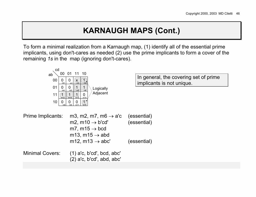
To form a minimal realization from a Karnaugh map, (1) identify all of the essential prime implicants, using don't-cares as needed (2) use the prime implicants to form a cover of the remaining 1s in the map (ignoring don't-cares).
00
10
11
01
00 01 11 10
0ab
cd
0 x 1
0 1 1
1 1 1 0
0 0 0 1
0m0 m1 m3 m2
m4 m5 m7 m6
m12 m13 m15 m14
m8 m9 m11 m10
LogicallyAdjacent
In general, the covering set of prime implicants is not unique.
Prime Implicants: m3, m2, m7, m6 → a'c (essential) m2, m10 → b'cd' (essential) m7, m15 → bcd m13, m15 → abd m12, m13 → abc' (essential) Minimal Covers: (1) a'c, b'cd', bcd, abc' (2) a'c, b'cd', abd, abc'

Copyright 2000, 2003 MD Ciletti 47
KARNAUGH MAPS (Cont.)
General Process to Form a Minimal Cover: (1) Select an uncovered minterm and identify all of its neighboring cells containing a 1 or an x. A single term (not necessarily a minterm) that covers the minterm and all of its adjacent neighbors having a 1 or an x is an essential prime implicant. Add the term to the set of essential prime implicants. (2) Repeat (1) until all of the essential prime implicants have been selected. (3) Find a minimal set of prime implicants that cover the other 1s in the map (do not cover cells containing x). The above steps may produce more than one possible minimal cover. Select the cover having the fewest literals.
Copyright 2000, 2003 MD Ciletti 48
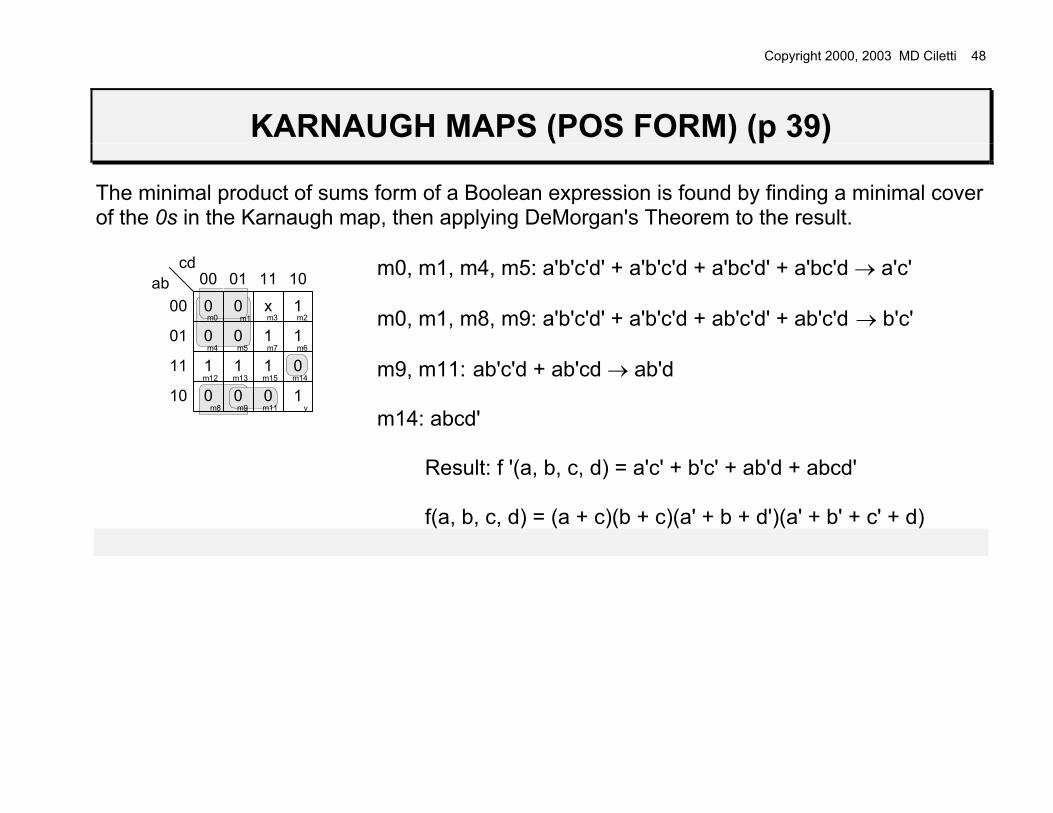
KARNAUGH MAPS (POS FORM) (p 39)
The minimal product of sums form of a Boolean expression is found by finding a minimal cover of the 0s in the Karnaugh map, then applying DeMorgan's Theorem to the result.
00
10
11
01
00 01 11 10
0ab
cd
0 x 1
0 1 1
1 1 1 0
0 0 0 1
0m0 m1 m3 m2
m4 m5 m7 m6
m12 m13 m15 m14
m8 m9 m11 y
m0, m1, m4, m5: a'b'c'd' + a'b'c'd + a'bc'd' + a'bc'd → a'c'
m0, m1, m8, m9: a'b'c'd' + a'b'c'd + ab'c'd' + ab'c'd → b'c' m9, m11: ab'c'd + ab'cd → ab'd m14: abcd'
Result: f '(a, b, c, d) = a'c' + b'c' + ab'd + abcd' f(a, b, c, d) = (a + c)(b + c)(a' + b + d')(a' + b' + c' + d)
Copyright 2000, 2003 MD Ciletti 49
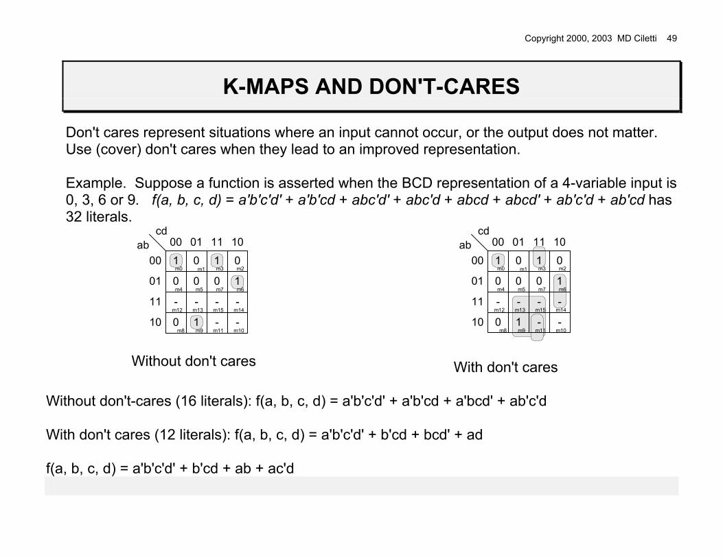
K-MAPS AND DON'T-CARES
Don't cares represent situations where an input cannot occur, or the output does not matter. Use (cover) don't cares when they lead to an improved representation. Example. Suppose a function is asserted when the BCD representation of a 4-variable input is 0, 3, 6 or 9. f(a, b, c, d) = a'b'c'd' + a'b'cd + abc'd' + abc'd + abcd + abcd' + ab'c'd + ab'cd has 32 literals.
00
10
11
01
00 01 11 10
1ab
cd
0 1 0
0 0 1
- - -
0 1 - -
0m0 m1 m3 m2
m4 m5 m7 m6
m12 m13 m15 m14
m8 m9 m11 m10
-
Without don't cares
00
10
11
01
00 01 11 10
1ab
cd
0 1 0
0 0 1
- - - -
0 1 - -
0m0 m1 m3 m2
m4 m5 m7 m6
m12 m13 m15 m14
m8 m9 m11 m10 With don't cares
Without don't-cares (16 literals): f(a, b, c, d) = a'b'c'd' + a'b'cd + a'bcd' + ab'c'd With don't cares (12 literals): f(a, b, c, d) = a'b'c'd' + b'cd + bcd' + ad f(a, b, c, d) = a'b'c'd' + b'cd + ab + ac'd

Copyright 2000, 2003 MD Ciletti 50
EXTENDED KARNAUGH MAPS
A 4-variable Karnaugh map can be extended by entering variables to indicate assertion contingent on the variable being asserted; no entry indicates that the function is not asserted if the variable is not asserted. Example:

Copyright 2000, 2003 MD Ciletti 51
EXTENDED KARNAUGH MAPS (Cont.)
Process: (1) Find the minimal cover with the variables de-asserted. (2) For each variable, find the minimal sum with all 1s changed to x in the map, and all other variables set to 0. Form the product of the minimal sum and the variable. (3) Form the sum obtained by combining (1) with the sum of the results of (2) . Note: The result is a minimal representation if the map-entered variables can be assigned independently. Note: fe is contained in e and f.
Copyright 2000, 2003 MD Ciletti 52
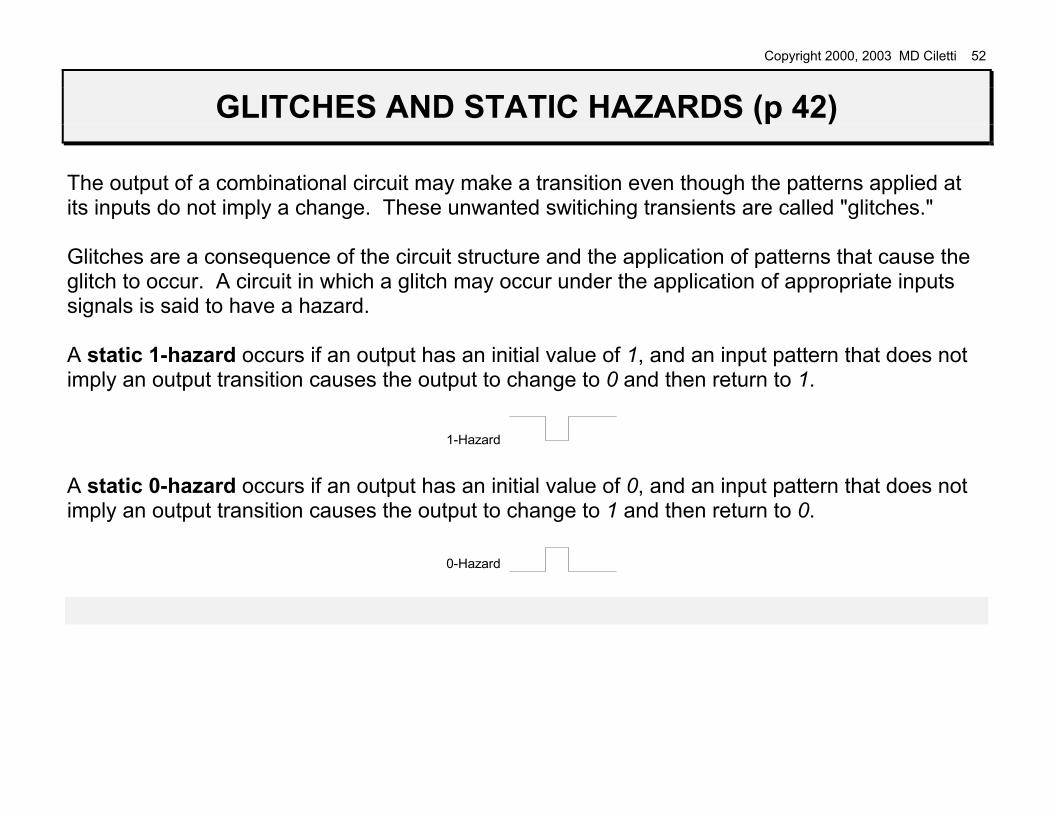
GLITCHES AND STATIC HAZARDS (p 42)
The output of a combinational circuit may make a transition even though the patterns applied at its inputs do not imply a change. These unwanted switiching transients are called "glitches." Glitches are a consequence of the circuit structure and the application of patterns that cause the glitch to occur. A circuit in which a glitch may occur under the application of appropriate inputs signals is said to have a hazard. A static 1-hazard occurs if an output has an initial value of 1, and an input pattern that does not imply an output transition causes the output to change to 0 and then return to 1.
1-Hazard A static 0-hazard occurs if an output has an initial value of 0, and an input pattern that does not imply an output transition causes the output to change to 1 and then return to 0.
0-Hazard
Copyright 2000, 2003 MD Ciletti 53
GLITCHES AND STATIC HAZARDS
Static hazards are caused by differential propagation delays on reconvergent fanout paths. A "minimal"realization of a circuit might not be hazard-free. Static hazards can be eliminated by introducing redundant cubes in the cover of the output expression (the added cubes are called a hazard cover).

Copyright 2000, 2003 MD Ciletti 54
STATIC HAZARDS: Example
AC
B
F Reconvergentfanout paths
1
1 0
1
0 1 0 1
F0
F1
1 0
1 0 1
Consider F = AC + BC' Initial inputs: A = 1, B = 1, C = 1 and F = 1 New inputs: A = 1, B = 1, C = 0 and F = 1 • In a physical realization of the circuit (i.e. non-zero propagation delays), the path to F1 will be
longer than the path to F0, causing a change in C to reach F1 later than it reaches F0. • Consequently, when C changes from 1 to 0, the output undergoes a momentary transition to 0
and returns to 1. • The presence of a static hazard is apparent in the Karnaugh map of the output.
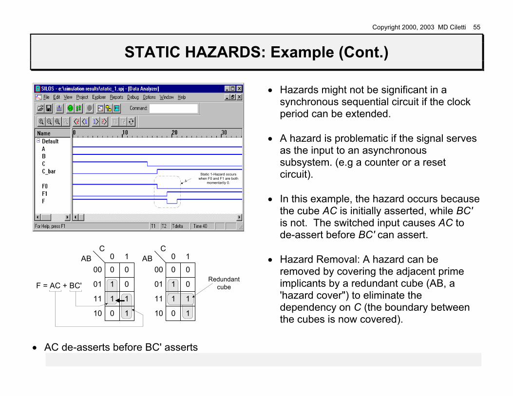
Copyright 2000, 2003 MD Ciletti 55
STATIC HAZARDS: Example (Cont.)
Static 1-Hazard occurswhen F0 and F1 are both
momentarily 0.
y
00
10
11
01
0 1
0AB
C
0
1
1 1
0 1
0F = AC + BC'
00
10
11
01
0 1
0AB
C
0
1
1 1
0 1
0Redundant
cube
• AC de-asserts before BC' asserts
• Hazards might not be significant in a synchronous sequential circuit if the clock period can be extended.
• A hazard is problematic if the signal serves
as the input to an asynchronous subsystem. (e.g a counter or a reset circuit).
• In this example, the hazard occurs because
the cube AC is initially asserted, while BC' is not. The switched input causes AC to de-assert before BC' can assert.
• Hazard Removal: A hazard can be
removed by covering the adjacent prime implicants by a redundant cube (AB, a 'hazard cover") to eliminate the dependency on C (the boundary between the cubes is now covered).

Copyright 2000, 2003 MD Ciletti 56
STATIC HAZARDS: Example (Cont.)
• Hazard covers require extra hardware. Example: For the hazard-free cover: F = AC + BC' + AB
AC
B
F
Copyright 2000, 2003 MD Ciletti 57
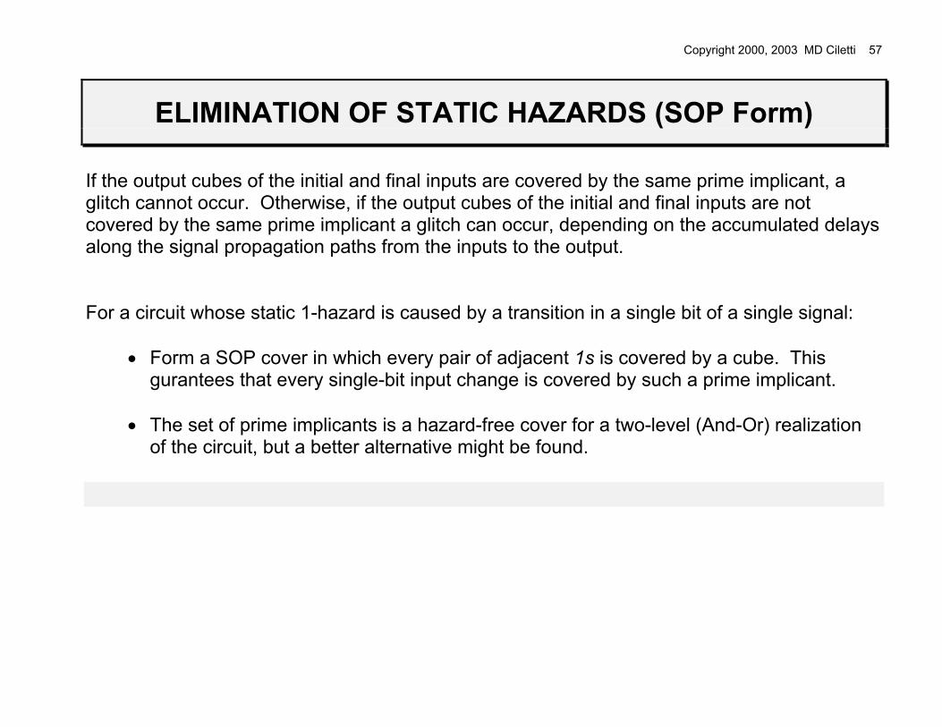
ELIMINATION OF STATIC HAZARDS (SOP Form)
If the output cubes of the initial and final inputs are covered by the same prime implicant, a glitch cannot occur. Otherwise, if the output cubes of the initial and final inputs are not covered by the same prime implicant a glitch can occur, depending on the accumulated delays along the signal propagation paths from the inputs to the output. For a circuit whose static 1-hazard is caused by a transition in a single bit of a single signal:
• Form a SOP cover in which every pair of adjacent 1s is covered by a cube. This gurantees that every single-bit input change is covered by such a prime implicant.
• The set of prime implicants is a hazard-free cover for a two-level (And-Or) realization
of the circuit, but a better alternative might be found.
Copyright 2000, 2003 MD Ciletti 58
ELIMINATION OF STATIC HAZARDS (Cont.)
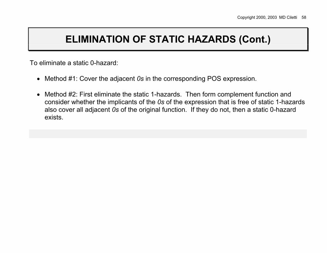
To eliminate a static 0-hazard:
• Method #1: Cover the adjacent 0s in the corresponding POS expression. • Method #2: First eliminate the static 1-hazards. Then form complement function and
consider whether the implicants of the 0s of the expression that is free of static 1-hazards also cover all adjacent 0s of the original function. If they do not, then a static 0-hazard exists.
Copyright 2000, 2003 MD Ciletti 59
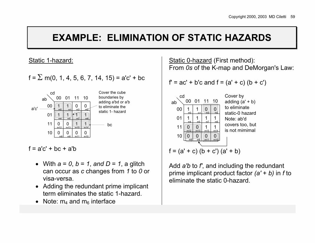
EXAMPLE: ELIMINATION OF STATIC HAZARDS
Static 1-hazard: f = Σ m(0, 1, 4, 5, 6, 7, 14, 15) = a'c' + bc
00
10
11
01
00 01 11 10
1ab
cd
1 0 0
1 1 1
0 0 1 1
0 0 0 0
1m0 m1 m3 m2
m4 m5 m7 m6
m12 m13 m15 m14
m8 m9 m11 m10
Cover the cubeboundaries byadding a'bd or a'bto eliminate thestatic 1- hazard
a'c'
bc
f = a'c' + bc + a'b
• With a = 0, b = 1, and D = 1, a glitch can occur as c changes from 1 to 0 or visa-versa.
• Adding the redundant prime implicant term eliminates the static 1-hazard.
• Note: m4 and m6 interface
Static 0-hazard (First method): From 0s of the K-map and DeMorgan's Law: f' = ac' + b'c and f = (a' + c) (b + c')
11 10
00
10
11
01
00 01
1ab
cd
1 0 0
1 1 1
0 0 1 1
0 0 0 0
1m0 m1 m3 m2
m4 m5 m7 m6
m12 m13 m15 m14
m8 m9 m11 m10
Cover byadding (a' + b)to eliminatestatic-0 hazardNote: ab'dcovers too, butis not mimimal
f = (a' + c) (b + c') (a' + b) Add a'b to f', and including the redundant prime implicant product factor (a' + b) in f to eliminate the static 0-hazard.
Copyright 2000, 2003 MD Ciletti 60
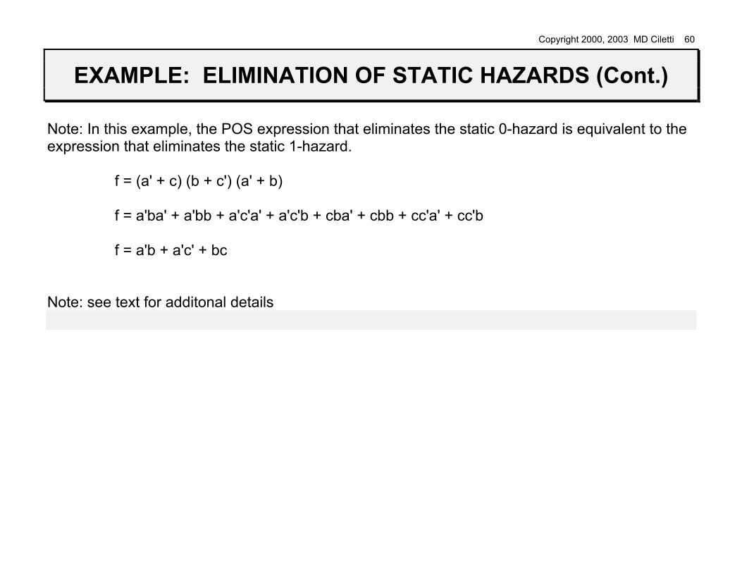
EXAMPLE: ELIMINATION OF STATIC HAZARDS (Cont.)
Note: In this example, the POS expression that eliminates the static 0-hazard is equivalent to the expression that eliminates the static 1-hazard.
f = (a' + c) (b + c') (a' + b) f = a'ba' + a'bb + a'c'a' + a'c'b + cba' + cbb + cc'a' + cc'b f = a'b + a'c' + bc
Note: see text for additonal details

Copyright 2000, 2003 MD Ciletti 61
DYNAMIC HAZARDS (Multiple glitches)
• A circuit has a dynamic hazard if an input transition is supposed to cause a single transition
in an output, but causes two or more transitions before reached its expected value.
Dynamic Hazard
• Dynamic hazards are a consequence of multiple static hazards caused by multiply reconvergent paths in a multilevel circuit.
• Dynamic hazards are not easy to eliminate. • Elimination of all static hazards eliminates dynamic hazards.
• Approach: Transform a multilevel circuit into a two-level circuit and eliminate all of the static
hazards.
Copyright 2000, 2003 MD Ciletti 62
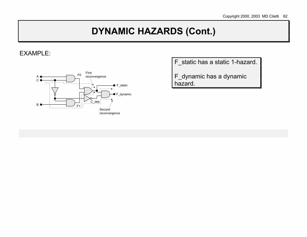
DYNAMIC HAZARDS (Cont.)
EXAMPLE:
AC
B
F_static
F_dynamic
Firstreconvergence
Secondreconvergence
F0
F1C_late
F_static has a static 1-hazard. F_dynamic has a dynamic hazard.

Copyright 2000, 2003 MD Ciletti 63
DYNAMIC HAZARDS (Cont.)
00
10
11
01
0 1
0AB
C
0
1
1 1
0 1
0Redundant
cube
The redundant cube eliminates the static 1-hazard and assures that F_dynamic will not depend on the arrival of the effect of the transition in C.

Copyright 2000, 2003 MD Ciletti 64
DYNAMIC HAZARDS (Cont.)
AC
B
F_static
F_dynamic
F0
F1C_late
F2

Copyright 2000, 2003 MD Ciletti 65
BUILDING BLOCKS: NAND-NOR STRUCTURES (p 55)
In CMOS technology, AND gates and OR gates are not implemented as efficiently as NAND gates and NOR gates. An SOP form or a POS form can always be converted to a NAND logic structure or a NOR logic structure. The "NAND" gate and "NOR" gate are universal logic gates - any Boolean function can be realized from only NAND gates or only NOR gates. DeMorgan's Theorem provides equivalent structures for NAND and NOR gates.
Gate DeMorgan Equivalent
ab
b
b
ba
a
a
y
y = (a . b)'
y = (a + b)'
y = a' + b'
y = a' . b'
Networks realizing SOP forms can be transformed to a realization that uses only nand gates and inverters.

Copyright 2000, 2003 MD Ciletti 66
EXAMPLE: SOP TO NAND STRUCTURES
Y = G + EF + AB'D + CD
G
EF
AB'D
CD
Y
G
EF
AB'D
CD
Y
G
EF
AB'D
CD
Y
(a) (b) (c)
• In the original And-Or structure: replace And by Nand, place inversion bubbles at inputs of Or, include inverter for G to balance bubble at input of Or.
• In the new circuit, replace Or gates having bubble inputs by equivalent Nand gates.
Check: Y = [(G') (EF)' (AB'D)' (CD)']' = (G')' + [(EF)' ]' + [(AB'D)' ]' + [(CD)']' Y = G + EF + AB'D + CD

Copyright 2000, 2003 MD Ciletti 67
EXAMPLE: POS TO NOR STRUCTURES
Y = D(B + C) (A + E + F') (A + G)
D
BC
AEF'
AG
Y
(a) (b)
D
BC
AEF'
AG
Y
(c)
D
BC
AEF'
AG
Y
• In the original Or-And structure: replace Or by Nor, place inversion bubbles at inputs of And, include inverter for D to balance bubble at input of the And gate.
• In the new circuit, replace And gates having bubble inputs by equivalent Nor gates.
Check: Y = [D' + (B + C)' + (A + E + F')' + (A + G)']' = (D')' [(B + C)']' [(A + E+ F')']' [(A + G)']' Y = D (B + C) (A + E + F') (A + G)
Copyright 2000, 2003 MD Ciletti 68
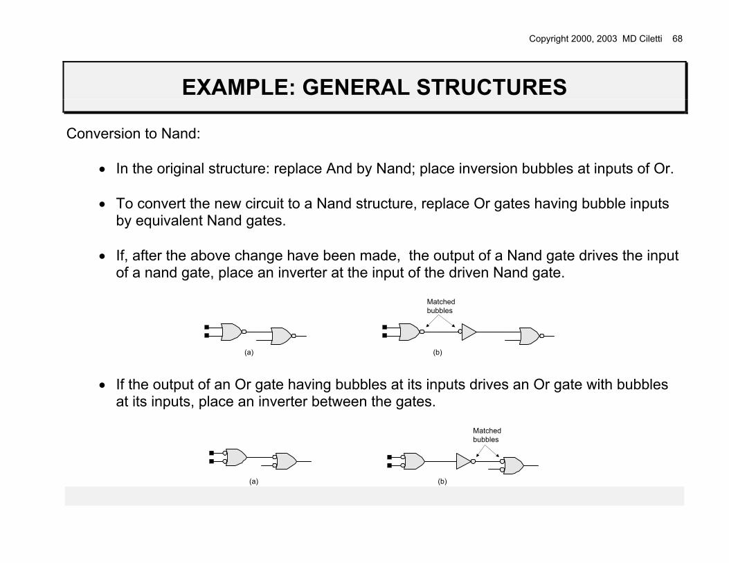
EXAMPLE: GENERAL STRUCTURES
Conversion to Nand:
• In the original structure: replace And by Nand; place inversion bubbles at inputs of Or.
• To convert the new circuit to a Nand structure, replace Or gates having bubble inputs by equivalent Nand gates.
• If, after the above change have been made, the output of a Nand gate drives the input
of a nand gate, place an inverter at the input of the driven Nand gate.
(a) (b)
Matchedbubbles
• If the output of an Or gate having bubbles at its inputs drives an Or gate with bubbles at its inputs, place an inverter between the gates.
(a)
Matchedbubbles
(b)
Copyright 2000, 2003 MD Ciletti 69
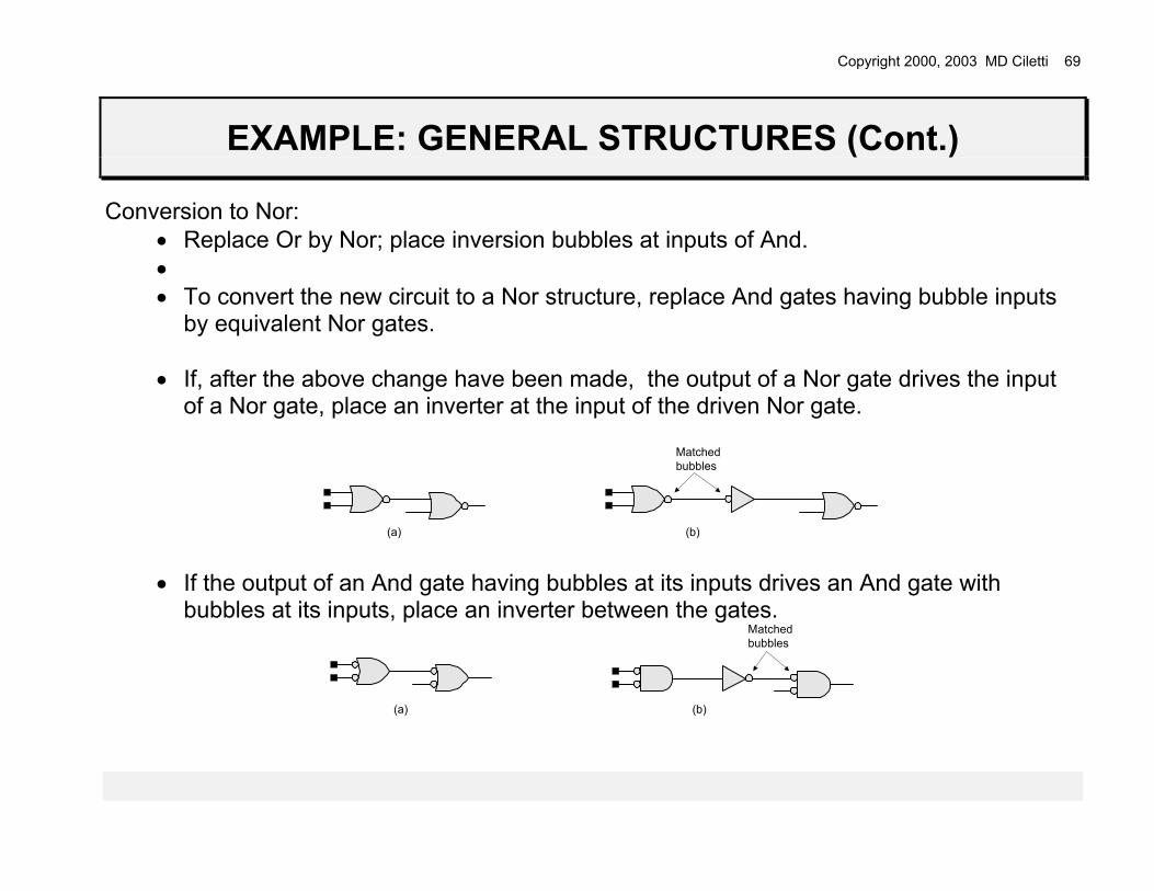
EXAMPLE: GENERAL STRUCTURES (Cont.)
Conversion to Nor: • Replace Or by Nor; place inversion bubbles at inputs of And. • • To convert the new circuit to a Nor structure, replace And gates having bubble inputs
by equivalent Nor gates.
• If, after the above change have been made, the output of a Nor gate drives the input of a Nor gate, place an inverter at the input of the driven Nor gate.
(a) (b)
Matchedbubbles
• If the output of an And gate having bubbles at its inputs drives an And gate with bubbles at its inputs, place an inverter between the gates.
Matched
(a)
bubbles
(b)

Copyright 2000, 2003 MD Ciletti 70
BUILDING BLOCKS: MULTIPLEXERS (p 60)
MUXES PROVIDE STEERING FOR DATAPATHS.
a
b
sel y_out
y_out = sel . a + sel' . b

Copyright 2000, 2003 MD Ciletti 71
MULTIPLEXERS
• A multiplexer has n datapath inputs and a single output. An m-bit address determines which of the inputs is connected to the output.
Address
Data_In
Data_In [n-1]
Data_In [0]
m
Address[m-1: 0]
Data_Out
Multiplexer
Input channel selection:
Data_Out = Data_In [Address[k]]
• A multiplexer is used to control the flow of data in a digital machine.

Copyright 2000, 2003 MD Ciletti 72
DEMULTIPLEXERS
A demultiplexer has a single datapath input, n datapath outputs, and m address inputs. The m-bit address determines which of the n outputs is connected to the input.
Address
Data_In
Data_Out [n-1]
Data_Out [0]
m
Address[m-1: 0]
Data_In
Demultiplexer
Output channel selection:
Data_Out [n-1: 0] = Data_In [Address[k]]

Copyright 2000, 2003 MD Ciletti 73
ENCODERS
An encoder has n inputs and m outputs, with n = 2m. Ordinarily, only one of the inputs is asserted at a time. A unique output bit pattern (code) is assigned to each of the n inputs. The asserted output is determined by the index of the asserted bit of the n-bit binary input word.
Data_In Data_Out
Encoder
n m
Data_Out
Data_In[n-1]
Encoder
m
Data_In[0] Example: n = 4, m = 2, Data_In [3] = 1 and Data_In [k] = 0 for 0 < k < n, k ≠ 3 Data_Out [1:0] = 112 = 310
A Mux does not change the data input, but encoders transform the data input to form the data output. The encoder assigns a unique bit pattern to each input line.

Copyright 2000, 2003 MD Ciletti 74
PRIORITY ENCODERS
A priority encoder allows multiple input bits to be asserted simultaneously, and uses a priority rule to form an output bit pattern. Example:
Data_In [3:0] Data_out [1:0] - - - 1 00 - - 1 - 01 - 1 - - 10 1 - - - 11
Note: "-" denotes a don't care condition.
Copyright 2000, 2003 MD Ciletti 75
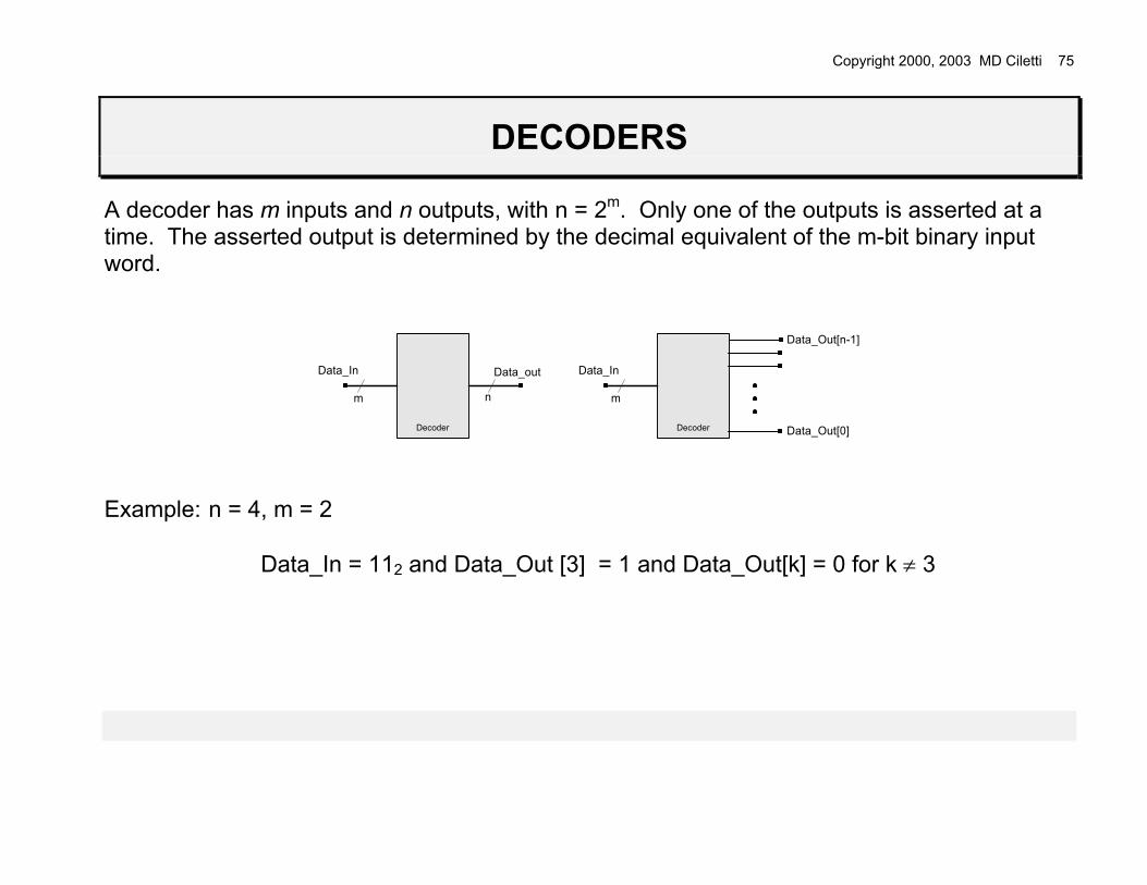
DECODERS
A decoder has m inputs and n outputs, with n = 2m. Only one of the outputs is asserted at a time. The asserted output is determined by the decimal equivalent of the m-bit binary input word.
Data_In Data_out
Decoder
m n
Data_In
Data_Out[n-1]
Decoder
m
Data_Out[0]
Example: n = 4, m = 2 Data_In = 112 and Data_Out [3] = 1 and Data_Out[k] = 0 for k ≠ 3

Copyright 2000, 2003 MD Ciletti 76
STORAGE ELEMENTS: R-S LATCH
• Storage elements are used to store information in a binary format (e.g. state, data, address, opcode, machine status).
• Storage elements may be clocked or unclocked. • Two types: level-sensitive, edge-sensitive Example: R-S latch (Unclocked) The state of an R-S latch is dependent on the value of its R and S inputs.
S' R' Qnext Q'next
R
S
Q
Q'
NotAllowed
Set
0
0
1
1
0
1
0
1
1
1
0
Q
1
0
1
Q'
Reset
Hold
S R Qnext Q'next
Hold
Reset
0
0
1
1
0
1
0
1
Q
0
1
0
Q'
1
0
0
SetNot
Allowed
Q
Q'
S'
R'
Note: Avoid applying 11 to a R-S Nor latch, and 00 to an R'S' Nand latch. The circuit is unstable and oscillation will result.

Copyright 2000, 2003 MD Ciletti 77
STORAGE ELEMENTS: TRANSPARENT LATCHES
Latches are level-sensitive storage elements; data storage is dependent on the level (value ) of the input clock (or enable) signal. The output of a transparent latch changes in response to the data input while the latch is enabled. Changes at the input are visible at the output
data
q_out
enable
data
enable10 20 30 400
1
tsim50
10 20 30 400
1
tsim50
10 20 30 400
1
tsim50
q_out
Copyright 2000, 2003 MD Ciletti 78
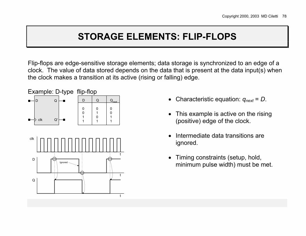
STORAGE ELEMENTS: FLIP-FLOPS
Flip-flops are edge-sensitive storage elements; data storage is synchronized to an edge of a clock. The value of data stored depends on the data that is present at the data input(s) when the clock makes a transition at its active (rising or falling) edge. Example: D-type flip-flop
Q
clk
D
Q'
D Q Qnext
0 0 00 1 01 0 11 1 1
clk
D
Q
t
t
t
Ignored
• Characteristic equation: qnext = D.
• This example is active on the rising (positive) edge of the clock.
• Intermediate data transitions are
ignored. • Timing constraints (setup, hold,
minimum pulse width) must be met.

Copyright 2000, 2003 MD Ciletti 79
MASTER-SLAVE FLIP-FLOP
A master-slave configuration of two data latches samples the input during the active cycle of the clock applied to the master stage. The input is propagated to the output during the slave cycle of the clock. Master-slave implementation of a negative edge-triggered D-type flip-flop:
D
Enable
QDataLatch
D
Enable
QDataLatch
Q'
q
q'
clock
data
Master Slave
Timing constraint: the output of the master stage must settle before the enabling edge of the slave stage. The master stage is enabled on the inactive edge of the clock, and the slave stage is enabled on the active edge. Timing constraints apply to the active edge.
Copyright 2000, 2003 MD Ciletti 80
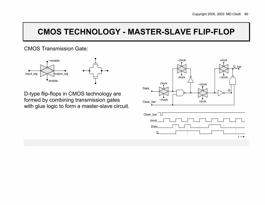
CMOS TECHNOLOGY - MASTER-SLAVE FLIP-FLOP
CMOS Transmission Gate:
output_sig
~enable
enable
input_sig
D-type flip-flops in CMOS technology are formed by combining transmission gates with glue logic to form a master-slave circuit.
clock
Data
~clock
clock ~clock
~clock
~clock
clock
clock
Q_bar
Q
Clear_bar
t
Data
clock
Q
Clear_bar
Copyright 2000, 2003 MD Ciletti 81
CMOS TECHNOLOGY MASTER-SLAVE FLIP-FLOP (Cont.)
clock
data
~clock
clock ~clock
~clock
~clock
clock
clock
Q_
Q
clear_
10
01
10
clock(n-∆) = 0
w1 w2
w3
w4
w01w04
clock
data
~clock
clock ~clock
~clock
~clock
clock
clock
Q_
Q
clear_
clock(n+∆) = 1
01
10
w1 w2
w3
w4
w04w01
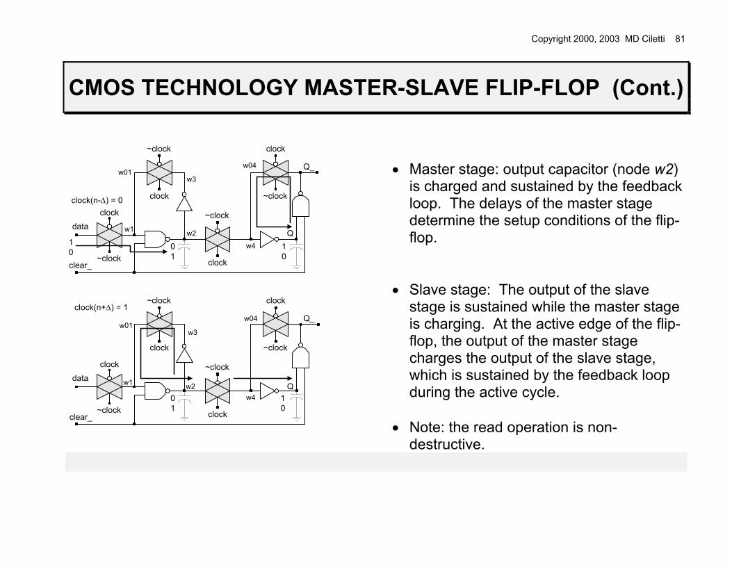
• Master stage: output capacitor (node w2)
is charged and sustained by the feedback loop. The delays of the master stage determine the setup conditions of the flip-flop.
• Slave stage: The output of the slave
stage is sustained while the master stage is charging. At the active edge of the flip-flop, the output of the master stage charges the output of the slave stage, which is sustained by the feedback loop during the active cycle.
• Note: the read operation is non-
destructive.

Copyright 2000, 2003 MD Ciletti 82
J-K FLIP-FLOP
J-K Flip-flops are edge-sensitive storage elements; data storage is synchronized to an edge of a clock. The value of data stored is conditional, depending on the data that is present at the j and k inputs when the clock makes a transition at its active (rising or falling) edge. Cell libraries may omit the J-K flip-flop and implement the functionality with a D-type flip-flop combined with input logic. • Characteristic Equation: qnext = jq' + k'q
q
clk
j
q'
j k q qnext
0 0 q q0 1 q 01 0 q 11 1 q q'
clk
j
q
t
t
t
k
k

Copyright 2000, 2003 MD Ciletti 83
T FLIP-FLOP
T-type flip-flops are edge-sensitive storage elements; data storage is synchronized to an edge of a clock. The value of data stored is conditional, depending on the T-input and the state of the device when the clock makes a transition at its active (rising or falling) edge. If T is asserted, the output toggles, otherwise it has no change. A T-type flip-flop can be more efficient in implementing a counter. • Characteristic Equation: qnext = q T' + q' T = q ⊕ T
• Note: connect T to the j and k inputs of a
j-k flip-flop to for a T-type flip-flop.
q
clk q'
T q qnext
0 q q1 q q'
clk
Tt
t
T
q
t
Copyright 2000, 2003 MD Ciletti 84
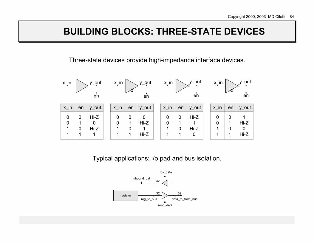
BUILDING BLOCKS: THREE-STATE DEVICES
Three-state devices provide high-impedance interface devices.
0011
0101
Hi-Z0
Hi-Z1
x_in en y_out
0011
0101
0Hi-Z
1Hi-Z
x_in en y_out
0011
0101
Hi-Z1
Hi-Z0
x_in en y_out
0011
0101
1Hi-Z
0Hi-Z
x_in en y_out
y_outx_in
en
y_outx_in
en
y_outx_in
en
y_outx_in
en
Typical applications: i/o pad and bus isolation.
register
inbound_data
reg_to_bus
send_data
rcv_data
data_to_from_bus
32
32 32

Copyright 2000, 2003 MD Ciletti 85
BUILDING BLOCKS: THREE-STATE DEVICES (Cont.)
Combine a multiplexer with a three-state device to reduce bus loading of multiple bus drivers.
Mux
reg_a_to_bus
reg_b_to_bus
enab_a
enab_b
data_to_from_bussel
32
32
32
Copyright 2000, 2003 MD Ciletti 86
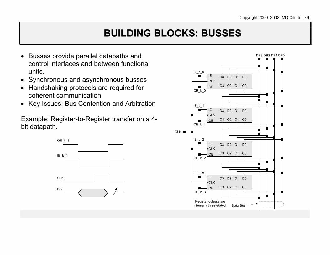
BUILDING BLOCKS: BUSSES
• Busses provide parallel datapaths and
control interfaces and between functional units.
• Synchronous and asynchronous busses • Handshaking protocols are required for
coherent communication • Key Issues: Bus Contention and Arbitration Example: Register-to-Register transfer on a 4-bit datapath.
OE_b_3
IE_b_1
CLK
DB 4
D3 D2 D1 D0
O3 O2 O1 O0
IE
OE
CLK
D3 D2 D1 D0
O3 O2 O1 O0
IE
OE
CLK
D3 D2 D1 D0
O3 O2 O1 O0
IE
OE
CLK
D3 D2 D1 D0
O3 O2 O1 O0
IE
OE
CLK
DB3 DB2 DB1 DB0
Data Bus
IE_b_0
OE_b_0
IE_b_1
OE_b_1
IE_b_2
OE_b_2
IE_b_3
OE_b_3
CLK
Register outputs areinternally three-stated.

Copyright 2000, 2003 MD Ciletti 87
SEQUENTIAL MACHINES (p 80)
• Sequential machines, also called finite state machines, are characterized by an input/output
relationship in which the value of the outputs at a given time depend on the history of the applied inputs as well as their present value.
Example: A machine that is to count the number of 1s in a serially transmitted frame of bits.
• The history of the inputs applied to a sequential machine is represented by the state of the
machine, and requires hardware elements that store information, i.e. requires memory to store the state of the machine as an encoded binary word.
• All sequential machines require feedback that allows the next state of the machine to be
determined from the present state and inputs.
Next State formingLogic
Inputs
MemoryPresentState (PS)Outputs
Feedback of present state
Next State(NS)
The set of states of a sequential machine is always finite, and the number of states is determined by the number of bits that represent the state.

Copyright 2000, 2003 MD Ciletti 88
SEQUENTIAL MACHINES (Cont.)
• Sequential machines may be asynchronous or synchronous (clocked). • The state transitions of a (edge-triggered) flip-flop-based synchronous machine are
synchronized by the active edge (i.e. rising or falling) of a common clock. State changes give rise to changes in the combinational logic that determines the next state and the output of the machine.
period
Rising edge
Falling edge
• A lower bound on the cycle time (period) of the machine's clock is set by the requirement that the period of the clock must be long enough to allow all transients activated by an a transition of the clock to settle at the outputs of the combinational logic before the next active edge occurs.
Copyright 2000, 2003 MD Ciletti 89
SEQUENTIAL MACHINES (Cont.)
• The inputs to the flip-flops must remain stable for a sufficient interval before and after the active
edge of the clock. The former constraint establishes an upper bound on the longest path through the circuit, which constrains the latest allowed arrival of data. The latter constraint imposes a lower bound on the shortest path through the combinational logic that is driving the storage device. It constrains the earliest time at which data from the previous cycle could be overwritten.
• Together, these constraints ensure that valid data is stored. Otherwise, timing violations may
occur at the inputs to the flip-flops, with the result that invalid data is stored. • In an edge-triggered clocking scheme, the clock isolates a storage register's inputs from its
output, thereby allowing feedback without race conditions. • The outputs of a state machine controls the synchronous datapath operations and register
operations of more general digital machine.
Copyright 2000, 2003 MD Ciletti 90
FINITE STATE MACHINES
• Synchronous (i.e. clocked) finite state machines (FSMs) have widespread application in digital
systems, e.g. as datapath controllers in computational units and processors. Synchronous FSMs are characterized by a finite number of states and by clock-driven state transitions.
• Mealy Machine: The next state and the outputs depend on the present state and the inputs. • Moore Machine: The next state depends on the present state and the inputs, but the output
depends on only the present state.

Copyright 2000, 2003 MD Ciletti 91
FINITE STATE MACHINES (Cont.)
Next State and OutputCombinational
Logic
Inputs
StateRegister
Outputs
Next StateCombinational
Logic
InputsState
RegisterOutputsOutput
CombinationalLogic
clock
clock
Moore machine
Mealy machine
Copyright 2000, 2003 MD Ciletti 92
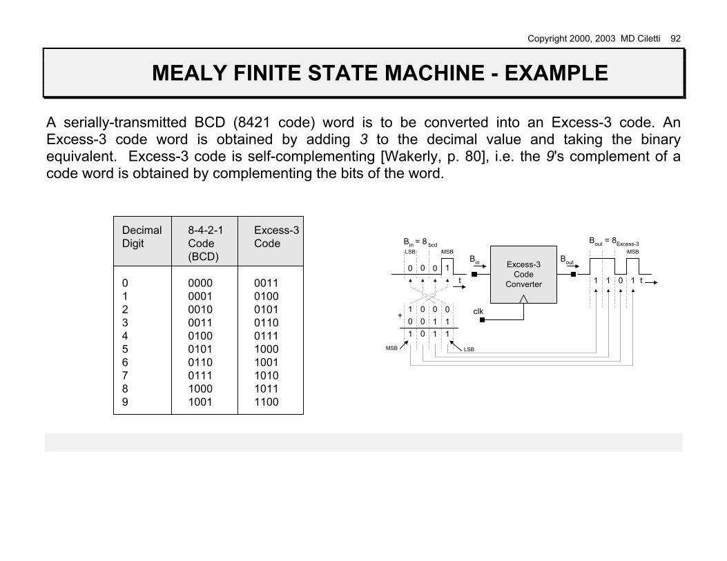
MEALY FINITE STATE MACHINE - EXAMPLE
A serially-transmitted BCD (8421 code) word is to be converted into an Excess-3 code. An Excess-3 code word is obtained by adding 3 to the decimal value and taking the binary equivalent. Excess-3 code is self-complementing [Wakerly, p. 80], i.e. the 9's complement of a code word is obtained by complementing the bits of the word.
Decimal 8-4-2-1 Excess-3Digit Code Code
(BCD)
0 0000 00111 0001 01002 0010 01013 0011 01104 0100 01115 0101 10006 0110 10017 0111 10108 1000 10119 1001 1100
Excess-3Code
Converter
clk
Bout = 8Excess-3
1 0 0 0+
1 1 10
Bin = 8 bcd
Bout
0 0 1 11 0 1 1
LSBMSB
0 0 0 1t
LSB MSB
t
MSBBin

Copyright 2000, 2003 MD Ciletti 93
MEALY FINITE STATE MACHINE - EXAMPLE (Cont.)
The serial code converter is described by the state transition graph of a Mealy FSM.
State Transition Graph
S_5
S_0
input / output
1/00/1
0/1
0/0, 1/1
1/0
0/11/0
0/10/0, 1/1
0/0, 1/1
S_1 S_2
S_4S_3
S_6
statenext state/output
input0 1
S_0 S_1 / 1 S_2 / 0S_1 S_3 / 1 S_4 / 0S_2 S_4 / 0 S_4 / 1S_3 S_5 / 0 S_5 / 1S_4 S_5 / 1 S_6 / 0S_5 S_0 / 0 S_0 / 1S_6 S_0 / 1 - / -
Next State/OutputTable
• The vertices of the state transition graph of a Mealy machine are labeled with the states. • The branches are labeled with (1) the input that causes a transition to the indicated next state,
and (2) with the output that is asserted in the present state for that input. • The state transition is synchronized to a clock. • The state table summarizes the machine's behavior in tabular format.

Copyright 2000, 2003 MD Ciletti 94
DESIGN OF A FINITE STATE MACHINE - EXAMPLE (Cont.)
To design a D-type flip-flop realization of a FSM having the behavior described by a state transition graph, (1) select a state code, (2) encode the state table, (3) develop Boolean equations describing the input of a D-type flip-flop, and (4) using K-maps, optimize the Boolean equations.
statenext state/output
input0 1
S_0 S_1 / 1 S_2 / 0S_1 S_3 / 1 S_4 / 0S_2 S_4 / 0 S_4 / 1S_3 S_5 / 0 S_5 / 1S_4 S_5 / 1 S_6 / 0S_5 S_0 / 0 S_0 / 1S_6 S_0 / 1 - / -
Next State/Output Table
1
0 1
q0
S_0
S_6 S_4
S_2
S_5 S_31
1 0
0 1
0 0
q2 q1
S_1
State Assigment
q2 q1 q0 q2+ q1
+ q0+
input0 1
state next state output
input0 1
S_0 000 001 101 1 0
001 111 011 1 0
101 011 011 0 1
111 110 110 0 1
011 110 010 1 0
110 000 000 0 1
010 000 - 1 -
100 - - - -
S_1
S_2
S_3
S_4
S_5
S_6
Encoded Next state/ Output Table
Copyright 2000, 2003 MD Ciletti 95
DESIGN OF A FINITE STATE MACHINE - EXAMPLE (Cont.)
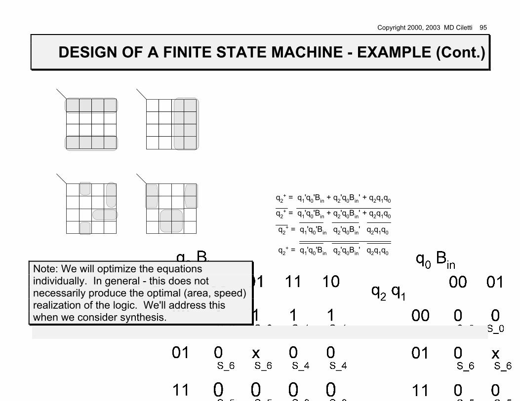
Note: We will optimize the equations individually. In general - this does not necessarily produce the optimal (area, speed) realization of the logic. We'll address this when we consider synthesis.
q2
+ = q1'q0'Bin + q2'q0Bin' + q2q1q0
q2+ = q1'q0'Bin + q2'q0Bin' + q2q1q0
q2+ = q1'q0'Bin q2'q0Bin' q2q1q0
q2+ = q1'q0'Bin q2'q0Bin' q2q1q0
Copyright 2000, 2003 MD Ciletti 96
DESIGN OF A FINITE STATE MACHINE - EXAMPLE (Cont.)
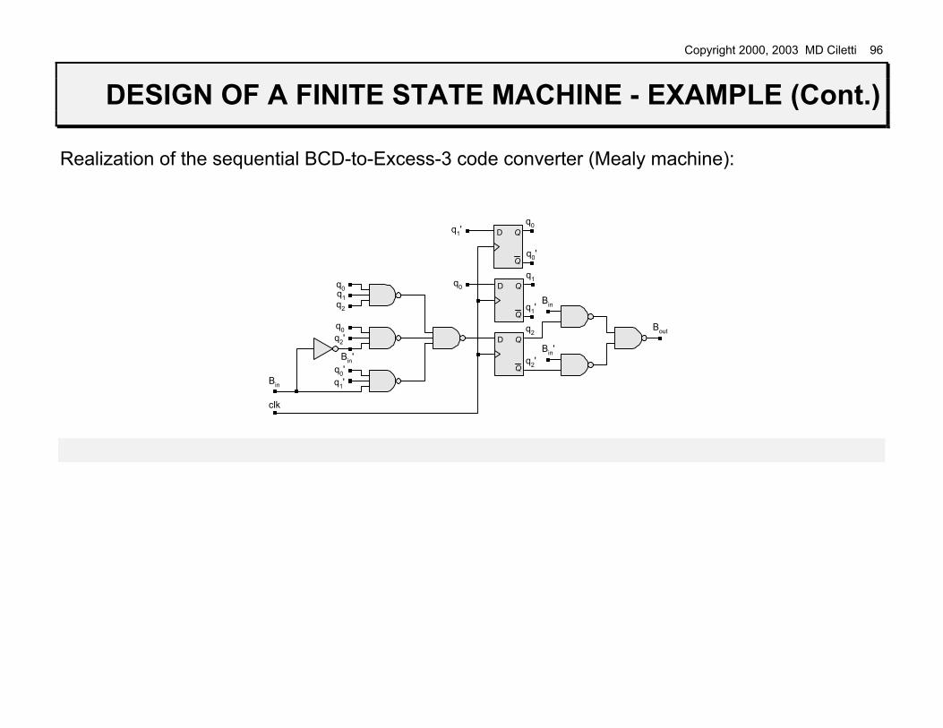
Realization of the sequential BCD-to-Excess-3 code converter (Mealy machine):
q1'q0'
q2'q0
q0q1q2
D
Q
Q
D
Q
Q
D
Q
Q
Bout
Bin
clk
q2'
q2
q1'
q1
q0
q0'
q1'
q0
Bin
Bin'Bin'

Copyright 2000, 2003 MD Ciletti 97
DESIGN OF A FINITE STATE MACHINE - EXAMPLE (Cont.)
Simulation results for Mealy machine:
0 10 01 11 0
B_inB_out

Copyright 2000, 2003 MD Ciletti 98
DESIGN OF A SERIAL LINE CODE CONVERTER (p 89)
Serial Line Codes [Wakerly] are used for serial data transmission or storage. Data recovery requires a clock to define the boundaries of the data bits, a synchronizing signal to define word boundaries, and a data stream. As an alternative to having three separate signal channels, a phone system or a disk read/write head will have a single channel and use a coding scheme to enable clock recovery and synchronization. NRZ Code (Non-Return to Zero): The signal waveform duplicates the bit pattern over the entire bit time. Phase lock loops (PLL) can recover the clock if there are no long series of 1s or 0s. NRZI Code (Non-Return to Zero Invert-on-Ones) A 0 in the bit stream causes the value of the previous bit to be transmitted; a 1 in the bit stream causes the value of the complement of the previous bit to be transmitted. A PLL can recover the clock if there is no long string of 0s. RZ Code (Return-to-Zero): A 0 in the bit stream is transmitted as a 0 for the entire bit time. A 1 in the bit stream is transmitted as a 1 for 1/2 of the bit time, and 0 for the remaining bit time (typically). A PLL can recover the clock if there is no long string of 0s. Manchester Code: A 0 in the bit stream is transmitted as a 0 for the lead half of the bit time, and as a 1 for the remaining half. A 1 in the bit stream is transmitted as a 1 for the leading half of the bit time, and as a 0 for the remaining bit time. Requires higher bandwidth, but allows clock recovery independent of the data stream.
Copyright 2000, 2003 MD Ciletti 99
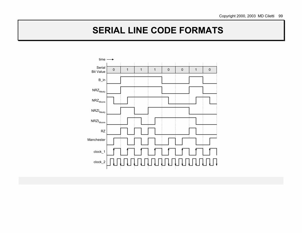
SERIAL LINE CODE FORMATS
SerialBit Value 0 1 1 1 0 0 1 0
NRZMealy
RZ
Manchester
time
clock_1
clock_2
NRZMoore
NRZIMealy
NRZIMoore
B_in
Copyright 2000, 2003 MD Ciletti 100
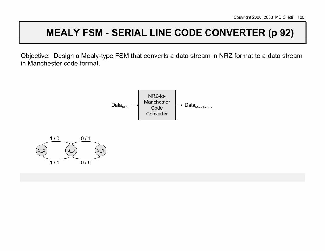
MEALY FSM - SERIAL LINE CODE CONVERTER (p 92)
Objective: Design a Mealy-type FSM that converts a data stream in NRZ format to a data stream in Manchester code format.
NRZ-to-Manchester
CodeConverter
DataManchesterDataNRZ
S_0 S_1S_2
0 / 0
0 / 11 / 0
1 / 1

Copyright 2000, 2003 MD Ciletti 101
MEALY FSM - SERIAL LINE CODE CONVERTER (Cont.)
State Transition Graph
S_0 S_1S_2
0 / 0
0 / 11 / 0
1 / 1 State Table:
statenext state/output
input0 1
S_0 S_1 / 0 S_2 / 1S_1 S_0 / 1 -S_2 - S_0 / 0
State Code:
0 1
q0
S_0
S_21
0
q1
S_1
Encoded State Table:
q1 q0 q1+ q0
+
input0 1
state next state output
input0 1
S_0 00 01 10 0 1
01 00 - 1 -
10 - 00 - 0
S_1
S_2
Copyright 2000, 2003 MD Ciletti 102
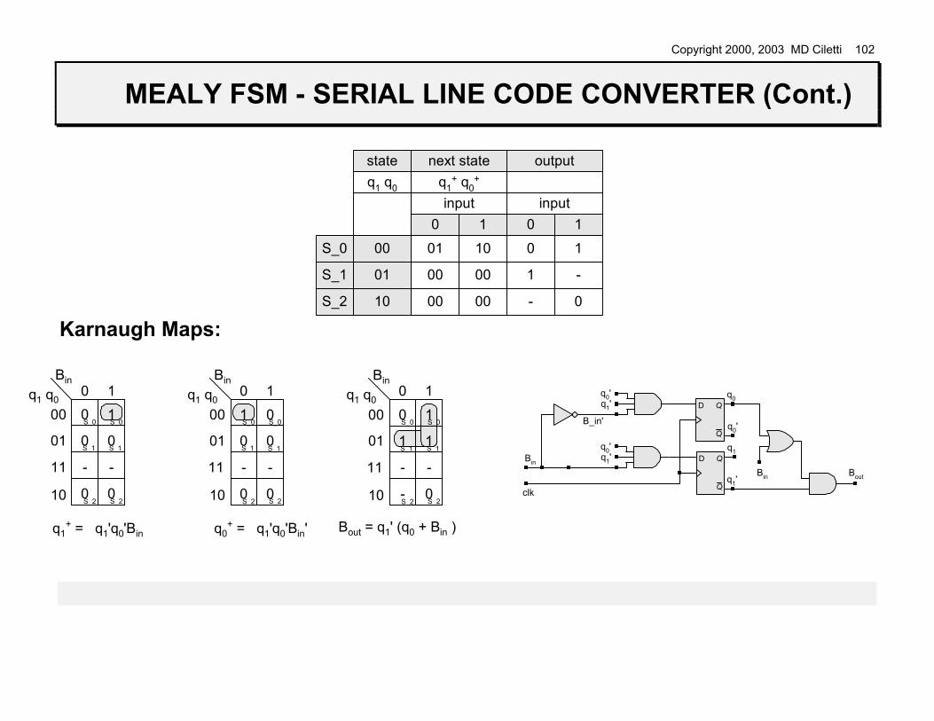
MEALY FSM - SERIAL LINE CODE CONVERTER (Cont.)
q1 q0 q1+ q0
+
input0 1
state next state output
input0 1
S_0 00 01 10 0 1
01 00 00 1 -
10 00 00 - 0
S_1
S_2 Karnaugh Maps:
10
01
00
0 1
0
Binq1 q0
1
1 1S_0 S_0
S_1
-
S_2- 0
S_1
-
S_2
Bout = q1' (q0 + Bin )
11
10
01
00
0 1
1
Bin
q1 q0
0
0 0S_0 S_0
S_1
-
S_20 0
S_1
-
S_2
q0+ = q1'q0'Bin'
1111
10
01
00
0 10
Bin
q1 q0
1
0 0S_0 S_0
S_1
0S_2
- -S_1
0S_2
q1+ = q1'q0'Bin
q0'
B_in'
D
Q
Q
D
Q
Q
Bout
clkq1'
q1
q0
q0'
q1'
q0'Bin
q1'Bin

Copyright 2000, 2003 MD Ciletti 103
MEALY FSM - SERIAL LINE CODE CONVERTER (Cont.)
Input and output bit times coincide
Note: The Mealy machine's output is subject to glitches in the input bit stream.

Copyright 2000, 2003 MD Ciletti 104
SERIAL LINE CODE CONVERTER - MOORE FSM (p 93)
SerialBit Value 0 1 1 1 0 0 1 0
NRZ
NRZI
RZ
Manchester
time
clock_1
clock_2
State Table:
statenext state/output
input0 1
S_0 S_1 / 0 S_3 / 1S_1 S_2 / 1 -S_3 - S_0 / 1S_2 S_1 / 0 S_3 / 0
State Transition Graph:
0S_00
S_10
S_31
S_211
0
0
011

Copyright 2000, 2003 MD Ciletti 105
SERIAL LINE CODE CONVERTER - MOORE FSM (Cont.)
State Transition Graph
0S_00
S_10
S_31
S_211
0 011
<00> <01>
<10><11>
state code
State code:
0 1
q0
S_0
S_2 S_31
0
q1
S_1
Encoded State Table:
q1 q0 q1+ q0
+
input0 1
state next state output
S_0 00 01 11 0
01 10 - 0
11 - 00 1
S_1
S_3
10 01 11 1S_2

Copyright 2000, 2003 MD Ciletti 106
SERIAL LINE CODE CONVERTER - MOORE FSM (Cont.)
Encoded State Table:
state next stateq1 q0 q1
+ q0+
input0 1
output
S_0 00 01 11 0
01 10 - 0
11 - 00 1
S_1
S_3
10 01 11 1S_2
q0
D
Q
Q
D
Q
QBout
clk
q0'
q0
q1
q1'
q1'
q0'
Bin
Karnaugh Maps
1
0
0 1
0
q0q1
0
1 1S_0 S_0
S_1 S_1
B_out = q1
10
01
00
0 1
1
Binq1 q0
1
0 -S_0 S_0
S_1
0
S_21 1
S_1
-
S_2
q0+ = q0'
11S_3 S_3
11
10
01
00
0 1
0
Binq1 q0
1
1 -S_0 S_0
S_1
1S_2
- 0S_1
0S_2
q1+ = q1'q0 + q0'Bin
S_3 S_3
Copyright 2000, 2003 MD Ciletti 107
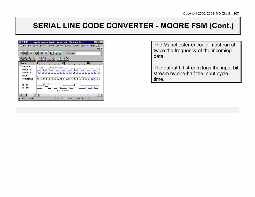
SERIAL LINE CODE CONVERTER - MOORE FSM (Cont.)
NRZ bit time
Manchester bit time
The Manchester encoder must run at twice the frequency of the incoming data. The output bit stream lags the input bit stream by one-half the input cycle time.

Copyright 2000, 2003 MD Ciletti 108
EQUIVALENT STATES (p 95)
Two states are equivalent if they have the same next state and output for all inputs. Equivalent states can be combined without changing the input/output behavior of the machine. Combine equivalent states to simplify the state table and the STG. For every FSM there is a unique equivalent machine that is minimal.
S_0 S_6 S_3 0 0S_1 S_1 S_6 0 1S_2 S_2 S_5 0 1S_3 S_7 S_3 0 1S_4 S_7 S_2 0 0S_5 S_7 S_2 0 0S_6 S_0 S_1 0 0S_7 S_4 S_5 S_3 0 0
0Input
Output
1 0 1
Next StateInput
State
EquivalentStates
S_4
S_5
S_7S_2
0 / 01 / 0
0 / 01 / 0
Copyright 2000, 2003 MD Ciletti 109
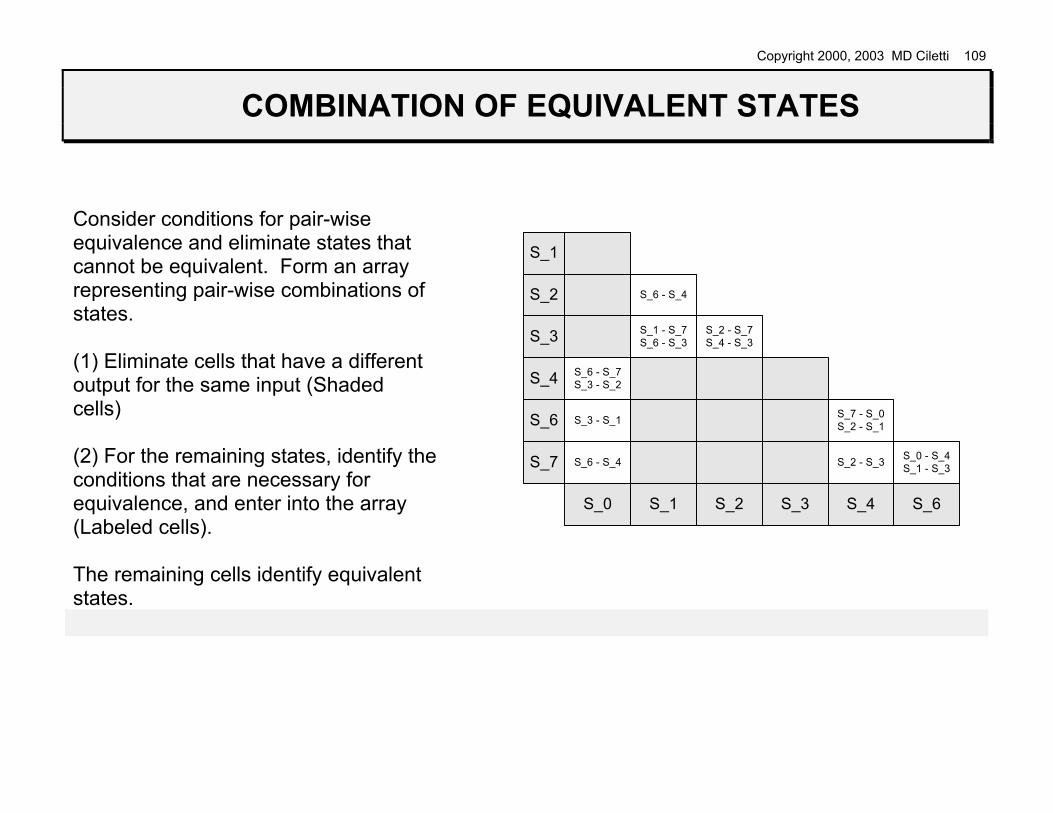
COMBINATION OF EQUIVALENT STATES
Consider conditions for pair-wise equivalence and eliminate states that cannot be equivalent. Form an array representing pair-wise combinations of states. (1) Eliminate cells that have a different output for the same input (Shaded cells) (2) For the remaining states, identify the conditions that are necessary for equivalence, and enter into the array (Labeled cells). The remaining cells identify equivalent states.
S_1
S_2
S_3
S_4
S_6
S_7
S_0 S_1 S_2 S_3 S_4 S_6
S_1 - S_7S_6 - S_3
S_6 - S_7S_3 - S_2
S_6 - S_4
S_3 - S_1
S_6 - S_4
S_2 - S_7S_4 - S_3
S_7 - S_0S_2 - S_1
S_2 - S_3 S_0 - S_4S_1 - S_3

Copyright 2000, 2003 MD Ciletti 110
COMBINATION OF EQUIVALENT STATES (Cont.)
S_0 S_4 S_3 0 0S_1 S_1 S_4 0 1S_3 S_0 S_3 0 1S_4 S_0 S_1 0 0
0Input
Output
1 0 1
Next StateInput
State
Copyright 2000, 2003 MD Ciletti 111
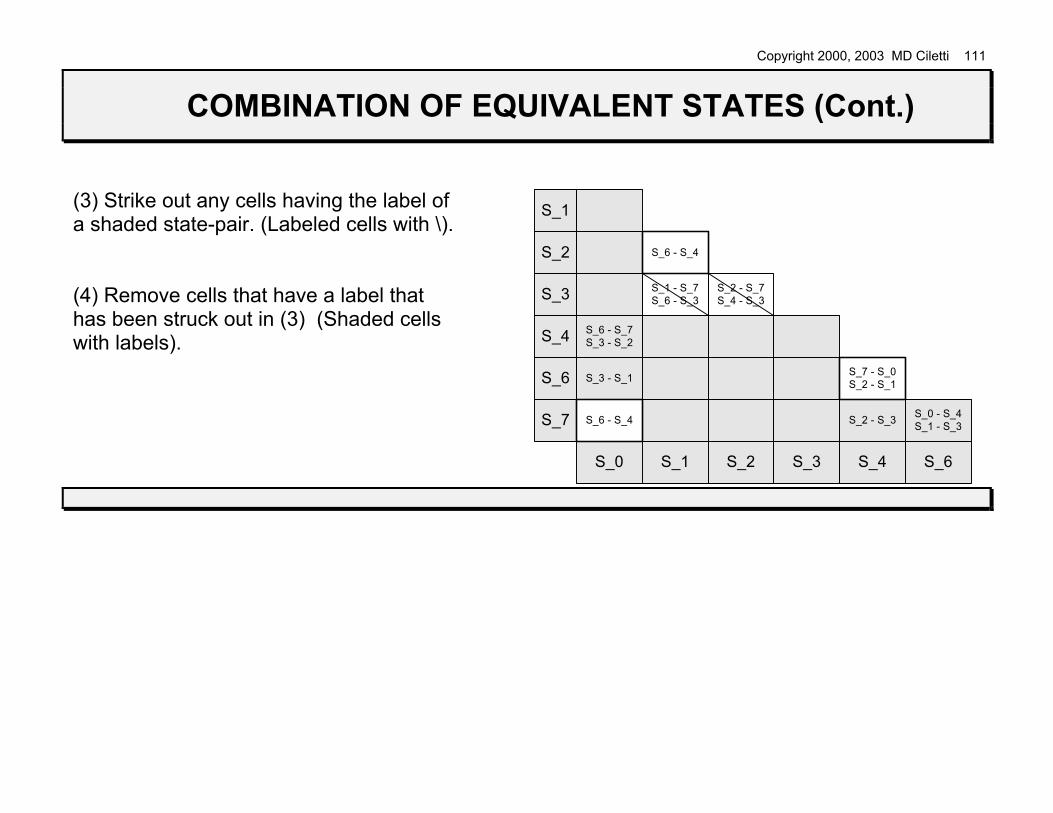
COMBINATION OF EQUIVALENT STATES (Cont.)
(3) Strike out any cells having the label of a shaded state-pair. (Labeled cells with \). (4) Remove cells that have a label that has been struck out in (3) (Shaded cells with labels).
S_2 - S_3
S_1
S_2
S_3
S_4
S_6
S_7
S_0 S_1 S_2 S_3 S_4 S_6
S_1 - S_7S_6 - S_3
S_6 - S_7S_3 - S_2
S_3 - S_1
S_2 - S_7S_4 - S_3
S_0 - S_4S_1 - S_3S_6 - S_4
S_6 - S_4
S_7 - S_0S_2 - S_1
Related Documents