Mixed-Signal DSP Controller with CAN ADSP-21992 Rev. A Information furnished by Analog Devices is believed to be accurate and reliable. However, no responsibility is assumed by Analog Devices for its use, nor for any infringements of patents or other rights of third parties that may result from its use. Specifications subject to change without notice. No license is granted by implication or otherwise under any patent or patent rights of Analog Devices. Trademarks and registered trademarks are the property of their respective companies. One Technology Way, P.O. Box 9106, Norwood, MA 02062-9106 U.S.A. Tel: 781.329.4700 www.analog.com Fax: 781.326.3113 ©2007 Analog Devices, Inc. All rights reserved. FEATURES ADSP-2199x, 16-bit, fixed-point DSP core with up to 160 MIPS sustained performance 48K words of on-chip RAM, as 32K words on-chip 24-bit pro- gram RAM, and 16K words on-chip, 16-bit data RAM External memory interface Dedicated memory DMA controller for data/instruction transfer between internal/external memory Programmable PLL and flexible clock generation circuitry enables full-speed operation from low speed input clocks IEEE JTAG Standard 1149.1 test access port supports on-chip emulation and system debugging 8-channel, 14-bit analog-to-digital converter system, with up to 20 MSPS sampling rate (at 160 MHz core clock rate) 3-phase 16-bit center based PWM generation unit with 12.5 ns resolution at 160 MHz core clock (CCLK) rate Dedicated 32-bit encoder interface unit with companion encoder event timer Dual 16-bit auxiliary PWM outputs 16 general-purpose flag I/O pins 3 programmable 32-bit interval timers SPI communications port with master or slave operation Synchronous serial communications port (SPORT) capable of software UART emulation Controller area network (CAN) module, fully compliant with V2.0B standard Integrated watchdog timer Dedicated peripheral interrupt controller with software priority control Multiple boot modes Precision 1.0 V voltage reference Integrated power-on-reset (POR) generator Flexible power management with selectable power-down and idle modes 2.5 V internal operation with 3.3 V I/O Operating temperature ranges of –40C to +85C and –40C to +125C Figure 1. Functional Block Diagram ADC CONTROL VREF PIPELINE FLASH ADC CLOCK GENERATOR/PLL PM ADDRESS/DATA DM ADDRESS/DATA I/O BUS 16K 16 DM RAM 32K 24 PM RAM EXTERNAL MEMORY INTERFACE (EMI) TIMER 0 TIMER 1 TIMER 2 PM ROM ADSP-219x DSP CORE JTAG TEST AND EMULATION ADDRESS DATA CONTROL I/O REGISTERS PWM GENERATION UNIT ENCODER INTERFACE UNIT (AND EET) AUXILIARY PWM UNIT FLAG I/O SPI SPORT WATCHDOG TIMER INTERRUPT CONTROLLER (ICNTL) POR MEMORY DMA CONTROLLER CONTROLLER AREA NETWORK (CAN) 4K 24

Welcome message from author
This document is posted to help you gain knowledge. Please leave a comment to let me know what you think about it! Share it to your friends and learn new things together.
Transcript
Mixed-Signal DSP Controller with CANADSP-21992
Rev. AInformation furnished by Analog Devices is believed to be accurate and reliable.However, no responsibility is assumed by Analog Devices for its use, nor for anyinfringements of patents or other rights of third parties that may result from its use.Specifications subject to change without notice. No license is granted by implicationor otherwise under any patent or patent rights of Analog Devices. Trademarks andregistered trademarks are the property of their respective companies.
One Technology Way, P.O. Box 9106, Norwood, MA 02062-9106 U.S.A.Tel: 781.329.4700 www.analog.comFax: 781.326.3113 ©2007 Analog Devices, Inc. All rights reserved.
FEATURES
ADSP-2199x, 16-bit, fixed-point DSP core with up to 160 MIPS sustained performance
48K words of on-chip RAM, as 32K words on-chip 24-bit pro-gram RAM, and 16K words on-chip, 16-bit data RAM
External memory interfaceDedicated memory DMA controller for data/instruction
transfer between internal/external memoryProgrammable PLL and flexible clock generation circuitry
enables full-speed operation from low speed input clocks
IEEE JTAG Standard 1149.1 test access port supports on-chip emulation and system debugging
8-channel, 14-bit analog-to-digital converter system, with up to 20 MSPS sampling rate (at 160 MHz core clock rate)
3-phase 16-bit center based PWM generation unit with 12.5 ns resolution at 160 MHz core clock (CCLK) rate
Dedicated 32-bit encoder interface unit with companion encoder event timer
Dual 16-bit auxiliary PWM outputs16 general-purpose flag I/O pins3 programmable 32-bit interval timersSPI communications port with master or slave operationSynchronous serial communications port (SPORT) capable of
software UART emulationController area network (CAN) module, fully compliant with
V2.0B standardIntegrated watchdog timerDedicated peripheral interrupt controller with software
priority controlMultiple boot modesPrecision 1.0 V voltage referenceIntegrated power-on-reset (POR) generatorFlexible power management with selectable power-down
and idle modes2.5 V internal operation with 3.3 V I/OOperating temperature ranges of –40�C to +85�C and –40�C
to +125�C
Figure 1. Functional Block Diagram
ADCCONTROL
VREF
PIPELINEFLASH ADC
CLOCKGENERATOR/PLL
PM ADDRESS/DATA
DM ADDRESS/DATA
I/OBUS
16K � 16DM RAM
32K � 24PM RAM
EXTERNALMEMORY
INTERFACE(EMI)
TIMER 0
TIMER 1
TIMER 2
PM ROMADSP-219x
DSP CORE
JTAGTEST AND
EMULATION
ADDRESS
DATA
CONTROL
I/O REGISTERS
PWMGENERATION
UNIT
ENCODERINTERFACE
UNIT(AND EET)
AUXILIARYPWMUNIT
FLAGI/O
SPI SPORT
WATCHDOGTIMER
INTERRUPTCONTROLLER
(ICNTL)
POR
MEMORY DMACONTROLLER
CONTROLLER AREANETWORK (CAN)
4K � 24
ADSP-21992* PRODUCT PAGE QUICK LINKSLast Content Update: 02/23/2017
COMPARABLE PARTSView a parametric search of comparable parts.
EVALUATION KITS• USB-Based Emulator and High Performance USB-Based
Emulator
DOCUMENTATIONApplication Notes
• AN-227: Digital Control System Design with the ADSP-2100 Family
• AN-348: Avoiding Passive-Component Pitfalls
• EE-06: ADSP-21xx Serial Port Startup Issues
• EE-100: ADSP-218x External Overlay Memory
• EE-102: Mode D and ADSP-218x Pin Compatibility - the FAQs
• EE-104: Setting Up Streams with the VisualDSP Debugger
• EE-11: ADSP-2181 Priority Chain & IDMA Holdoffs
• EE-115: ADSP-2189 IDMA Interface to Motorola MC68300 Family of Microprocessors
• EE-12: Interrupts and Programmable Flags on the ADSP-2185/2186
• EE-121: Porting Code from ADSP-21xx to ADSP-219x
• EE-122: Coding for Performance on the ADSP-219x
• EE-123: An Overview of the ADSP-219x Pipeline
• EE-124: Booting up the ADSP-2192
• EE-125: ADSP-218x Embedded System Software Management and In-System-Programming (ISP)
• EE-128: DSP in C++: Calling Assembly Class Member Functions From C++
• EE-129: ADSP-2192 Interprocessor Communication
• EE-130: Making Fast Transition from ADSP-21xx to ADSP-219x
• EE-131: Booting the ADSP-2191/95/96 DSPs
• EE-133: Converting From Legacy Architecture Files To Linker Description Files for the ADSP-218x
• EE-139: Interfacing the ADSP-2191 to an AD7476 via the SPI Port
• EE-142: Autobuffering, C and FFTs on the ADSP-218x
• EE-144: Creating a Master-Slave SPI Interface Between Two ADSP-2191 DSPs
• EE-145: SPI Booting of the ADSP-2191 using the Atmel AD25020N on an EZ-KIT Lite Evaluation Board
• EE-146: Implementing a Boot Manager for ADSP-218x Family DSPs
• EE-152: Using Software Overlays with the ADSP-219x and VisualDSP 2.0++
• EE-153: ADSP-2191 Programmable PLL
• EE-154: ADSP-2191 Host Port Interface

• EE-156: Support for the H.100 protocol on the ADSP-2191
• EE-158: ADSP-2181 EZ-Kit Lite IDMA to PC Printer Port Interface
• EE-159: Initializing DSP System & Control Registers From C and C++
• EE-164: Advanced EPROM Boot and No-boot Scenarios with ADSP-219x DSPs
• EE-168: Using Third Overtone Crystals with the ADSP-218x DSP
• EE-17: ADSP-2187L Memory Organization
• EE-18: Choosing and Using FFTs for ADSP-21xx
• EE-188: Using C To Implement Interrupt-Driven Systems On ADSP-219x DSPs
• EE-2: Using ADSP-218x I/O Space
• EE-226: ADSP-2191 DSP Host Port Booting
• EE-227: CAN Configuration Procedure for ADSP-21992 DSPs
• EE-249: Implementing Software Overlays on ADSP-218x DSPs with VisualDSP++®
• EE-32: Language Extensions: Memory Storage Types, ASM & Inline Constructs
• EE-35: Troubleshooting your ADSP-218x EZ-ICE
• EE-356: Emulator and Evaluation Hardware Troubleshooting Guide for CCES Users
• EE-38: ADSP-2181 IDMA Port - Cycle Steal Timing
• EE-39: Interfacing 5V Flash Memory to an ADSP-218x (Byte Programming Algorithm)
• EE-5: ADSP-218x Full Memory Mode vs. Host Memory Mode
• EE-60: Simulating an RS-232 UART Using the Synchronous Serial Ports on the ADSP-21xx Family DSPs
• EE-64: Setting Mode Pins on Reset
• EE-68: Analog Devices JTAG Emulation Technical Reference
• EE-71: Minimum Rise Time Specs for Critical Interrupt and Clock Signals on the ADSP-21x1/21x5
• EE-74: Analog Devices Serial Port Development and Troubleshooting Guide
• EE-78: BDMA Usage on 100 pin ADSP-218x DSPs Configured for IDMA Use
• EE-79: EPROM Booting In Host Mode with 100 Pin 218x Processors
• EE-82: Using an ADSP-2181 DSP's IO Space to IDMA Boot Another ADSP-2181
• EE-89: Implementing A Software UART on the ADSP-2181 EZ-Kit-Lite
• EE-96: Interfacing Two AD73311 Codecs to the ADSP-218x
Data Sheet
• ADSP-21992: Mixed Signal DSP Controller With CAN Data Sheet
Evaluation Kit Manuals
• ADSP-21992 EZ-KIT Lite® Evaluation System Manual
Integrated Circuit Anomalies
• ADSP-2199x Anomaly List for Revisions up to 1.1
Processor Manuals
• ADSP 21xx Processors: Manuals
• ADSP-2199x Mixed Signal DSP Controller Hardware Reference
• ADSP-219x DSP Instruction Set Reference
• Using the ADSP-2100 Family Volume 1
Product Highlight
• The ADSP-2199x Family: Mixed-Signal DSPs For Embedded Control & Signal Processing Applications Product Highlight
Software Manuals
• VisualDSP++ 3.5 Assembler and Preprocessor Manual for ADSP-218x and ADSP-219x DSPs
• VisualDSP++ 3.5 C Compiler and Library Manual for ADSP-218x DSPs
• VisualDSP++ 3.5 C/C++ Compiler and Library Manual for ADSP-219x Processors
• VisualDSP++ 3.5 Component Software Engineering User's Guide for 16-Bit Processors
• VisualDSP++ 3.5 Getting Started Guide for 16-Bit Processors
• VisualDSP++ 3.5 Kernel VDK User's Guide for 16-Bit Processors
• VisualDSP++ 3.5 Linker and Utilities Manual for 16-Bit Processors
• VisualDSP++ 3.5 Loader Manual for 16-Bit Processors
• VisualDSP++ 3.5 Quick Installation Reference Card
• VisualDSP++ 3.5 User's Guide for 16-Bit Processors
SOFTWARE AND SYSTEMS REQUIREMENTS• Software and Tools Anomalies Search
TOOLS AND SIMULATIONS• ADSP-21xx Processors: Software and Tools
REFERENCE MATERIALSTechnical Articles
• DSP Motor Control in Domestic Appliance Applications
DESIGN RESOURCES• ADSP-21992 Material Declaration
• PCN-PDN Information
• Quality And Reliability
• Symbols and Footprints
DISCUSSIONSView all ADSP-21992 EngineerZone Discussions.
SAMPLE AND BUYVisit the product page to see pricing options.
TECHNICAL SUPPORTSubmit a technical question or find your regional support number.
DOCUMENT FEEDBACKSubmit feedback for this data sheet.
This page is dynamically generated by Analog Devices, Inc., and inserted into this data sheet. A dynamic change to the content on this page will not trigger a change to either the revision number or the content of the product data sheet. This dynamic page may be frequently modified.
Rev. A | Page 2 of 60 | August 2007
ADSP-21992
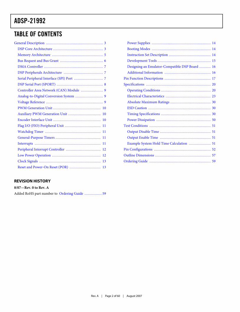
TABLE OF CONTENTSGeneral Description . . . . . . . . . . . . . . . . . . . . . . . . . . . . . . . . . . . . . . . . . . . . . . . . . 3
DSP Core Architecture . . . . . . . . . . . . . . . . . . . . . . . . . . . . . . . . . . . . . . . . . . . 3Memory Architecture . . . . . . . . . . . . . . . . . . . . . . . . . . . . . . . . . . . . . . . . . . . . 5Bus Request and Bus Grant . . . . . . . . . . . . . . . . . . . . . . . . . . . . . . . . . . . . . 6DMA Controller . . . . . . . . . . . . . . . . . . . . . . . . . . . . . . . . . . . . . . . . . . . . . . . . . . . 7DSP Peripherals Architecture . . . . . . . . . . . . . . . . . . . . . . . . . . . . . . . . . . 7Serial Peripheral Interface (SPI) Port . . . . . . . . . . . . . . . . . . . . . . . . . 7DSP Serial Port (SPORT) . . . . . . . . . . . . . . . . . . . . . . . . . . . . . . . . . . . . . . . . 8Controller Area Network (CAN) Module . . . . . . . . . . . . . . . . . . . 9Analog-to-Digital Conversion System .. . . . . . . . . . . . . . . . . . . . . . . 9Voltage Reference . . . . . . . . . . . . . . . . . . . . . . . . . . . . . . . . . . . . . . . . . . . . . . . . . 9PWM Generation Unit . . . . . . . . . . . . . . . . . . . . . . . . . . . . . . . . . . . . . . . . . 10Auxiliary PWM Generation Unit . . . . . . . . . . . . . . . . . . . . . . . . . . . . 10Encoder Interface Unit . . . . . . . . . . . . . . . . . . . . . . . . . . . . . . . . . . . . . . . . . 10Flag I/O (FIO) Peripheral Unit . . . . . . . . . . . . . . . . . . . . . . . . . . . . . . . 11Watchdog Timer . . . . . . . . . . . . . . . . . . . . . . . . . . . . . . . . . . . . . . . . . . . . . . . . 11General-Purpose Timers . . . . . . . . . . . . . . . . . . . . . . . . . . . . . . . . . . . . . . . 11Interrupts . . . . . . . . . . . . . . . . . . . . . . . . . . . . . . . . . . . . . . . . . . . . . . . . . . . . . . . . . 11Peripheral Interrupt Controller . . . . . . . . . . . . . . . . . . . . . . . . . . . . . . 12Low Power Operation . . . . . . . . . . . . . . . . . . . . . . . . . . . . . . . . . . . . . . . . . . 12Clock Signals . . . . . . . . . . . . . . . . . . . . . . . . . . . . . . . . . . . . . . . . . . . . . . . . . . . . . 13Reset and Power-On Reset (POR) . . . . . . . . . . . . . . . . . . . . . . . . . . . 13
Power Supplies . . . . . . . . . . . . . . . . . . . . . . . . . . . . . . . . . . . . . . . . . . . . . . . . . . . 14Booting Modes . . . . . . . . . . . . . . . . . . . . . . . . . . . . . . . . . . . . . . . . . . . . . . . . . . . 14Instruction Set Description . . . . . . . . . . . . . . . . . . . . . . . . . . . . . . . . . . . . 14Development Tools . . . . . . . . . . . . . . . . . . . . . . . . . . . . . . . . . . . . . . . . . . . . . . 15Designing an Emulator-Compatible DSP Board . . . . . . . . . . 16Additional Information . . . . . . . . . . . . . . . . . . . . . . . . . . . . . . . . . . . . . . . . 16
Pin Function Descriptions . . . . . . . . . . . . . . . . . . . . . . . . . . . . . . . . . . . . . . . . 17Specifications . . . . . . . . . . . . . . . . . . . . . . . . . . . . . . . . . . . . . . . . . . . . . . . . . . . . . . . . 20
Operating Conditions . . . . . . . . . . . . . . . . . . . . . . . . . . . . . . . . . . . . . . . . . . . 20Electrical Characteristics . . . . . . . . . . . . . . . . . . . . . . . . . . . . . . . . . . . . . . . 23Absolute Maximum Ratings . . . . . . . . . . . . . . . . . . . . . . . . . . . . . . . . . . . 30ESD Caution . . . . . . . . . . . . . . . . . . . . . . . . . . . . . . . . . . . . . . . . . . . . . . . . . . . . . . 30Timing Specifications . . . . . . . . . . . . . . . . . . . . . . . . . . . . . . . . . . . . . . . . . . . 30Power Dissipation . . . . . . . . . . . . . . . . . . . . . . . . . . . . . . . . . . . . . . . . . . . . . . . 50
Test Conditions . . . . . . . . . . . . . . . . . . . . . . . . . . . . . . . . . . . . . . . . . . . . . . . . . . . . . 51Output Disable Time . . . . . . . . . . . . . . . . . . . . . . . . . . . . . . . . . . . . . . . . . . . . 51Output Enable Time . . . . . . . . . . . . . . . . . . . . . . . . . . . . . . . . . . . . . . . . . . . . 51Example System Hold Time Calculation . . . . . . . . . . . . . . . . . . . 51
Pin Configurations . . . . . . . . . . . . . . . . . . . . . . . . . . . . . . . . . . . . . . . . . . . . . . . . . 52Outline Dimensions . . . . . . . . . . . . . . . . . . . . . . . . . . . . . . . . . . . . . . . . . . . . . . . . 57Ordering Guide . . . . . . . . . . . . . . . . . . . . . . . . . . . . . . . . . . . . . . . . . . . . . . . . . . . . . 59
REVISION HISTORY
8/07—Rev. 0 to Rev. AAdded RoHS part number to Ordering Guide . . . . . . . . . . . . . . . 59
ADSP-21992
Rev. A | Page 3 of 60 | August 2007
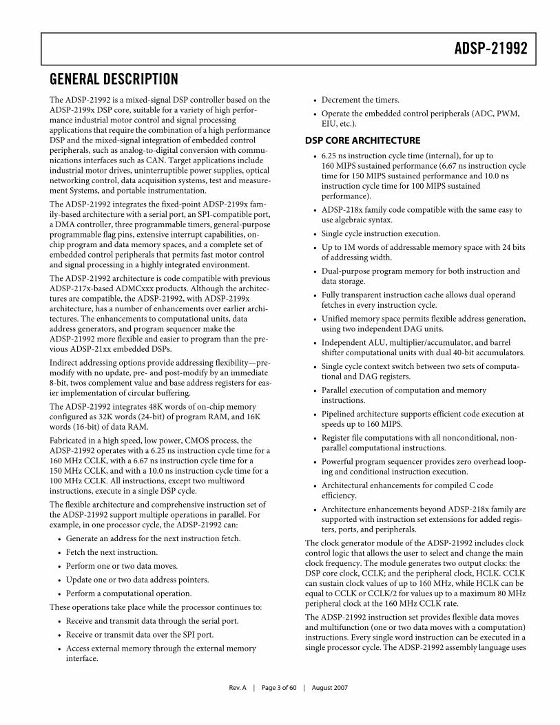
GENERAL DESCRIPTIONThe ADSP-21992 is a mixed-signal DSP controller based on the ADSP-2199x DSP core, suitable for a variety of high perfor-mance industrial motor control and signal processing applications that require the combination of a high performance DSP and the mixed-signal integration of embedded control peripherals, such as analog-to-digital conversion with commu-nications interfaces such as CAN. Target applications include industrial motor drives, uninterruptible power supplies, optical networking control, data acquisition systems, test and measure-ment Systems, and portable instrumentation. The ADSP-21992 integrates the fixed-point ADSP-2199x fam-ily-based architecture with a serial port, an SPI-compatible port, a DMA controller, three programmable timers, general-purpose programmable flag pins, extensive interrupt capabilities, on-chip program and data memory spaces, and a complete set of embedded control peripherals that permits fast motor control and signal processing in a highly integrated environment.The ADSP-21992 architecture is code compatible with previous ADSP-217x-based ADMCxxx products. Although the architec-tures are compatible, the ADSP-21992, with ADSP-2199x architecture, has a number of enhancements over earlier archi-tectures. The enhancements to computational units, data address generators, and program sequencer make the ADSP-21992 more flexible and easier to program than the pre-vious ADSP-21xx embedded DSPs.Indirect addressing options provide addressing flexibility—pre-modify with no update, pre- and post-modify by an immediate 8-bit, twos complement value and base address registers for eas-ier implementation of circular buffering.The ADSP-21992 integrates 48K words of on-chip memory configured as 32K words (24-bit) of program RAM, and 16K words (16-bit) of data RAM.Fabricated in a high speed, low power, CMOS process, the ADSP-21992 operates with a 6.25 ns instruction cycle time for a 160 MHz CCLK, with a 6.67 ns instruction cycle time for a 150 MHz CCLK, and with a 10.0 ns instruction cycle time for a 100 MHz CCLK. All instructions, except two multiword instructions, execute in a single DSP cycle.The flexible architecture and comprehensive instruction set of the ADSP-21992 support multiple operations in parallel. For example, in one processor cycle, the ADSP-21992 can:
• Generate an address for the next instruction fetch.• Fetch the next instruction.• Perform one or two data moves.• Update one or two data address pointers.• Perform a computational operation.
These operations take place while the processor continues to:• Receive and transmit data through the serial port.• Receive or transmit data over the SPI port.• Access external memory through the external memory
interface.
• Decrement the timers.• Operate the embedded control peripherals (ADC, PWM,
EIU, etc.).
DSP CORE ARCHITECTURE
• 6.25 ns instruction cycle time (internal), for up to 160 MIPS sustained performance (6.67 ns instruction cycle time for 150 MIPS sustained performance and 10.0 ns instruction cycle time for 100 MIPS sustained performance).
• ADSP-218x family code compatible with the same easy to use algebraic syntax.
• Single cycle instruction execution.• Up to 1M words of addressable memory space with 24 bits
of addressing width.• Dual-purpose program memory for both instruction and
data storage.• Fully transparent instruction cache allows dual operand
fetches in every instruction cycle.• Unified memory space permits flexible address generation,
using two independent DAG units.• Independent ALU, multiplier/accumulator, and barrel
shifter computational units with dual 40-bit accumulators.• Single cycle context switch between two sets of computa-
tional and DAG registers.• Parallel execution of computation and memory
instructions.• Pipelined architecture supports efficient code execution at
speeds up to 160 MIPS.• Register file computations with all nonconditional, non-
parallel computational instructions.• Powerful program sequencer provides zero overhead loop-
ing and conditional instruction execution.• Architectural enhancements for compiled C code
efficiency.• Architecture enhancements beyond ADSP-218x family are
supported with instruction set extensions for added regis-ters, ports, and peripherals.
The clock generator module of the ADSP-21992 includes clock control logic that allows the user to select and change the main clock frequency. The module generates two output clocks: the DSP core clock, CCLK; and the peripheral clock, HCLK. CCLK can sustain clock values of up to 160 MHz, while HCLK can be equal to CCLK or CCLK/2 for values up to a maximum 80 MHz peripheral clock at the 160 MHz CCLK rate.The ADSP-21992 instruction set provides flexible data moves and multifunction (one or two data moves with a computation) instructions. Every single word instruction can be executed in a single processor cycle. The ADSP-21992 assembly language uses
Rev. A | Page 4 of 60 | August 2007
ADSP-21992
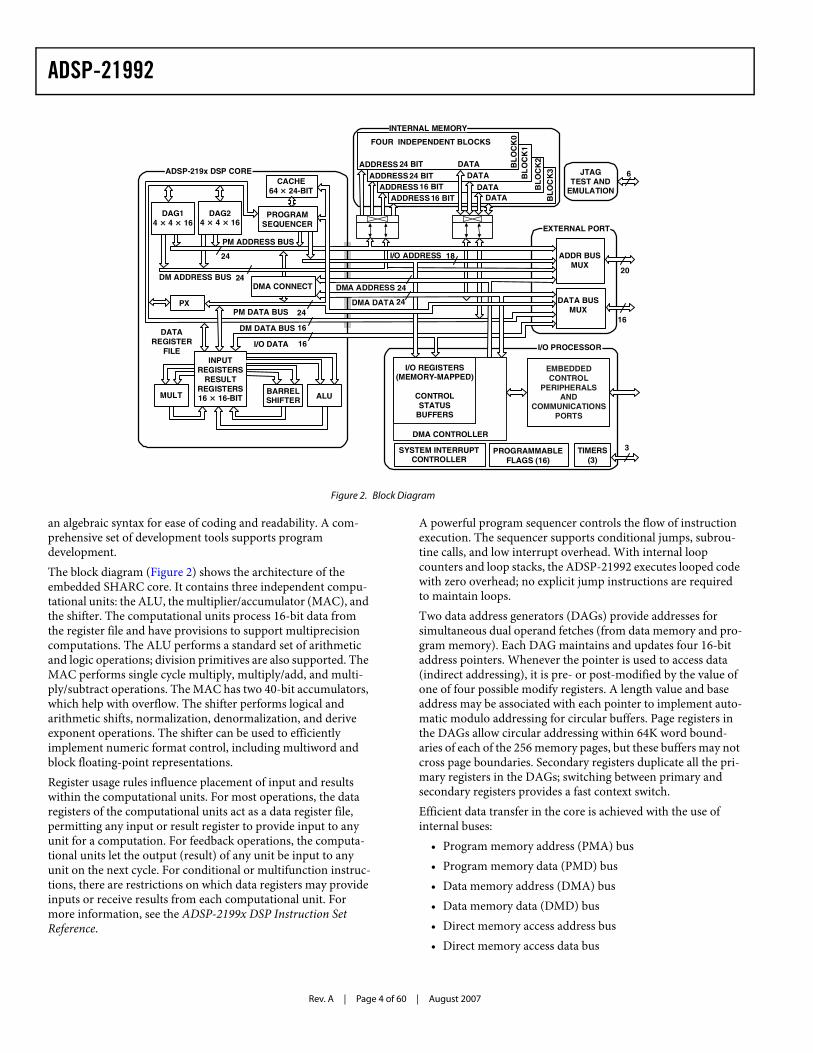
an algebraic syntax for ease of coding and readability. A com-prehensive set of development tools supports program development.The block diagram (Figure 2) shows the architecture of the embedded SHARC core. It contains three independent compu-tational units: the ALU, the multiplier/accumulator (MAC), and the shifter. The computational units process 16-bit data from the register file and have provisions to support multiprecision computations. The ALU performs a standard set of arithmetic and logic operations; division primitives are also supported. The MAC performs single cycle multiply, multiply/add, and multi-ply/subtract operations. The MAC has two 40-bit accumulators, which help with overflow. The shifter performs logical and arithmetic shifts, normalization, denormalization, and derive exponent operations. The shifter can be used to efficiently implement numeric format control, including multiword and block floating-point representations.Register usage rules influence placement of input and results within the computational units. For most operations, the data registers of the computational units act as a data register file, permitting any input or result register to provide input to any unit for a computation. For feedback operations, the computa-tional units let the output (result) of any unit be input to any unit on the next cycle. For conditional or multifunction instruc-tions, there are restrictions on which data registers may provide inputs or receive results from each computational unit. For more information, see the ADSP-2199x DSP Instruction Set Reference.
A powerful program sequencer controls the flow of instruction execution. The sequencer supports conditional jumps, subrou-tine calls, and low interrupt overhead. With internal loop counters and loop stacks, the ADSP-21992 executes looped code with zero overhead; no explicit jump instructions are required to maintain loops.Two data address generators (DAGs) provide addresses for simultaneous dual operand fetches (from data memory and pro-gram memory). Each DAG maintains and updates four 16-bit address pointers. Whenever the pointer is used to access data (indirect addressing), it is pre- or post-modified by the value of one of four possible modify registers. A length value and base address may be associated with each pointer to implement auto-matic modulo addressing for circular buffers. Page registers in the DAGs allow circular addressing within 64K word bound-aries of each of the 256 memory pages, but these buffers may not cross page boundaries. Secondary registers duplicate all the pri-mary registers in the DAGs; switching between primary and secondary registers provides a fast context switch. Efficient data transfer in the core is achieved with the use of internal buses:
• Program memory address (PMA) bus• Program memory data (PMD) bus• Data memory address (DMA) bus• Data memory data (DMD) bus• Direct memory access address bus• Direct memory access data bus
Figure 2. Block Diagram
DATAADDRESS BLO
CK
3
DATAADDRESS BL
OC
K2
SYSTEM INTERRUPTCONTROLLER
I/O DATA
I/O REGISTERS(MEMORY-MAPPED)
CONTROLSTATUS
BUFFERS
I/O PROCESSOR
CACHE64 � 24-BIT
JTAGTEST AND
EMULATION
6
ADDR BUSMUX
DATA BUSMUX
16
20
PM ADDRESS BUS
DM ADDRESS BUS
PM DATA BUS
DM DATA BUS
PX24
16
ADSP-219x DSP CORE
PROGRAMSEQUENCER
DATAREGISTER
FILE
MULT BARRELSHIFTER ALU
DMA CONTROLLER
INPUTREGISTERS
RESULTREGISTERS16 � 16-BIT
INTERNAL MEMORY
24
24
ADDRESS BL
OC
K1
DATADATAADDRESS B
LO
CK
0
24 BIT
16 BIT16 BIT
FOUR INDEPENDENT BLOCKS
PROGRAMMABLEFLAGS (16)
TIMERS(3)
3
DMA CONNECT DMA ADDRESS
EXTERNAL PORT
24 BIT
18I/O ADDRESS
24
16
24DMA DATA
EMBEDDEDCONTROL
PERIPHERALSAND
COMMUNICATIONSPORTS
DAG14 � 4 � 16
DAG24 � 4 � 16
ADSP-21992
Rev. A | Page 5 of 60 | August 2007
The two address buses (PMA and DMA) share a single external address bus, allowing memory to be expanded off-chip, and the two data buses (PMD and DMD) share a single external data bus. Boot memory space and I/O memory space also share the external buses.Program memory can store both instructions and data, permit-ting the ADSP-21992 to fetch two operands in a single cycle, one from program memory and one from data memory. The DSP dual memory buses also let the embedded SHARC core fetch an operand from data memory and the next instruction from pro-gram memory in a single cycle.
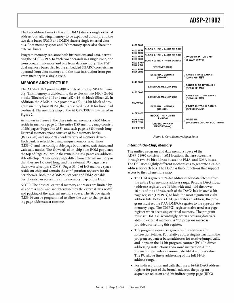
MEMORY ARCHITECTURE
The ADSP-21992 provides 48K words of on-chip SRAM mem-ory. This memory is divided into three blocks: two 16K × 24-bit blocks (Blocks 0 and 1) and one 16K × 16-bit block (Block 2). In addition, the ADSP-21992 provides a 4K × 24-bit block of pro-gram memory boot ROM (that is reserved by ADI for boot load routines). The memory map of the ADSP-21992 is illustrated in Figure 2.As shown in Figure 2, the three internal memory RAM blocks reside in memory page 0. The entire DSP memory map consists of 256 pages (Pages 0 to 255), and each page is 64K words long. External memory space consists of four memory banks (Banks3–0) and supports a wide variety of memory devices. Each bank is selectable using unique memory select lines (MS3–0) and has configurable page boundaries, wait states, and wait state modes. The 4K words of on-chip boot ROM populates the top of Page 255, while the remaining 254 pages are address-able off-chip. I/O memory pages differ from external memory in that they are 1K word long, and the external I/O pages have their own select pin (IOMS). Pages 31–0 of I/O memory space reside on-chip and contain the configuration registers for the peripherals. Both the ADSP-2199x core and DMA capable peripherals can access the entire memory map of the DSP.NOTE: The physical external memory addresses are limited by 20 address lines, and are determined by the external data width and packing of the external memory space. The Strobe signals (MS3-0) can be programmed to allow the user to change start-ing page addresses at runtime.
Internal (On-Chip) Memory
The unified program and data memory space of the ADSP-21992 consists of 16M locations that are accessible through two 24-bit address buses, the PMA, and DMA buses. The DSP uses slightly different mechanisms to generate a 24-bit address for each bus. The DSP has three functions that support access to the full memory map.
• The DAGs generate 24-bit addresses for data fetches from the entire DSP memory address range. Because DAG index (address) registers are 16 bits wide and hold the lower 16 bits of the address, each of the DAGs has its own 8-bit page register (DMPGx) to hold the most significant eight address bits. Before a DAG generates an address, the pro-gram must set the DAG DMPGx register to the appropriate memory page. The DMPG1 register is also used as a page register when accessing external memory. The program must set DMPG1 accordingly, when accessing data vari-ables in external memory. A “C” program macro is provided for setting this register.
• The program sequencer generates the addresses for instruction fetches. For relative addressing instructions, the program sequencer bases addresses for relative jumps, calls, and loops on the 24-bit program counter (PC). In direct addressing instructions (two word instructions), the instruction provides an immediate 24-bit address value. The PC allows linear addressing of the full 24-bit address range.
• For indirect jumps and calls that use a 16-bit DAG address register for part of the branch address, the program sequencer relies on an 8-bit indirect jump page (IJPG)
Figure 3. Core Memory Map at Reset
BLOCK 1: 16K � 24-BIT PM RAM
0x00 0000
0x00 7FFF
0x00 BFFF
0x01 0000
0x40 0000
0x80 0000
0xC0 0000
0xFF 0000
0xFF 1000
0xFF FFFF
0x00 8000
0x00 C000
0x00 FFFF
0xFF 0FFF
PAGE 0 (64K) ON-CHIP(0 WAIT STATE)
EXTERNAL MEMORY(4M–64K)
PAGES 1 TO 63 BANK 0(OFF-CHIP) MS0
PAGE 255(INCLUDES ON-CHIP BOOT ROM)
EXTERNAL MEMORY (4M)
EXTERNAL MEMORY (4M)
PAGES 64 TO 127 BANK 1(OFF-CHIP) MS1
PAGES 128 TO 191 BANK 2(OFF-CHIP) MS2
PAGES 192 TO 254 BANK 3(OFF-CHIP) MS3
EXTERNAL MEMORY(4M–64K)
RESERVED (16K)
BLOCK 2: 16K � 16-BIT DM RAM
BLOCK 3: 4K � 24-BITPM ROM
UNUSED ON-CHIPMEMORY (60K)
BLOCK 0: 16K � 24-BIT PM RAM0x00 3FFF0x00 4000

Rev. A | Page 6 of 60 | August 2007
ADSP-21992
register to supply the most significant eight address bits. Before a cross page jump or call, the program must set the program sequencer IJPG register to the appropriate mem-ory page.
The ADSP-21992 has 4K words of on-chip ROM that holds boot routines. The DSP starts executing instructions from the on-chip boot ROM, which starts the boot process. For more information, see Booting Modes on Page 14. The on-chip boot ROM is located on Page 255 in the DSP memory space map, starting at address 0xFF0000.
External (Off-Chip) Memory
Each of the off-chip memory spaces of the ADSP-21992 has a separate control register, so applications can configure unique access parameters for each space. The access parameters include read and write wait counts, wait state completion mode, I/O clock divide ratio, write hold time extension, strobe polarity, and data bus width. The core clock and peripheral clock ratios influence the external memory access strobe widths. For more information, see Clock Signals on Page 13. The off-chip mem-ory spaces are:
• External memory space (MS3–0 pins)• I/O memory space (IOMS pin)• Boot memory space (BMS pin)
All of these off-chip memory spaces are accessible through the external port, which can be configured for 8-bit or 16-bit data widths.
External Memory Space
External memory space consists of four memory banks. These banks can contain a configurable number of 64K word pages. At reset, the page boundaries for external memory have Bank0 containing pages 1 to 63, Bank1 containing pages 64 to 127, Bank2 containing pages 128 to 191, and Bank3 containing pages 192 to 254. The MS3-0 memory bank pins select Banks 3-0, respectively. Both the ADSP-2199x core and DMA capable peripherals can access the DSP external memory space.All accesses to external memory are managed by the external memory interface unit (EMI).
I/O Memory Space
The ADSP-21992 supports an additional external memory called I/O memory space. The I/O space consists of 256 pages, each containing 1024 addresses. This space is designed to sup-port simple connections to peripherals (such as data converters and external registers) or to bus interface ASIC data registers. The first 32K addresses (I/O pages 0 to 31) are reserved for on-chip peripherals. The upper 224K addresses (I/O pages 32 to
255) are available for external peripheral devices. External I/O pages have their own select pin (IOMS). The DSP instruction set provides instructions for accessing I/O space.
Boot Memory Space
Boot memory space consists of one off-chip bank with 254 pages. The BMS memory bank pin selects boot memory space. Both the ADSP-2199x core and DMA capable peripherals can access the DSP off-chip boot memory space. After reset, the DSP always starts executing instructions from the on-chip boot ROM.
BUS REQUEST AND BUS GRANT
The ADSP-21992 can relinquish control of the data and address buses to an external device. When the external device requires access to the bus, it asserts the bus request (BR) signal. The (BR) signal is arbitrated with core and peripheral requests. External bus requests have the lowest priority. If no other internal request is pending, the external bus request will be granted. Due to synchronizer and arbitration delays, bus grants will be pro-vided with a minimum of three peripheral clock delays. The ADSP-21992 will respond to the bus grant by:
• Three-stating the data and address buses and the MS3–0, BMS, IOMS, RD, and WR output drivers.
• Asserting the bus grant (BG) signal.
Figure 4. I/O Memory Map
Figure 5. Boot Memory Map
ON-CHIP
PERIPHERALS
16-BITS
OFF-CHIP
PERIPHERALS
16-BITS
PAGES 0 TO 31
1024 WORDS/PAGE
2 PERIPHERALS/PAGE
0x00::0x000
0x20::0x000
0xFF::0x3FF
0x1F::0x3FF
PAGES 32 TO 255
1024 WORDS/PAGE
PAGES 1 TO 254
64K WORDS/PAGE
0x01 0000
0xFE 0000
OFF-CHIP
BOOT MEMORY
16-BITS
ADSP-21992
Rev. A | Page 7 of 60 | August 2007
The ADSP-21992 will halt program execution if the bus is granted to an external device and an instruction fetch or data read/write request is made to external general-purpose or peripheral memory spaces. If an instruction requires two exter-nal memory read accesses, the bus will not be granted between the two accesses. If an instruction requires an external memory read and an external memory write access, the bus may be granted between the two accesses. The external memory inter-face can be configured so that the core will have exclusive use of the interface. DMA and bus requests will be granted. When the external device releases BR, the DSP releases BG and continues program execution from the point at which it stopped.The bus request feature operates at all times, even while the DSP is booting and RESET is active.The ADSP-21992 asserts the BGH pin when it is ready to start another external port access, but is held off because the bus was previously granted. This mechanism can be extended to define more complex arbitration protocols for implementing more elaborate multimaster systems.
DMA CONTROLLER
The ADSP-21992 has a DMA controller that supports auto-mated data transfers with minimal overhead for the DSP core. Cycle stealing DMA transfers can occur between the ADSP-21992 internal memory and any of its DMA capable peripherals. Additionally, DMA transfers can be accomplished between any of the DMA capable peripherals and external devices connected to the external memory interface. DMA capable peripherals include the SPORT and SPI ports, and ADC control module. Each individual DMA capable peripheral has a dedicated DMA channel. To describe each DMA sequence, the DMA controller uses a set of parameters—called a DMA descriptor. When successive DMA sequences are needed, these DMA descriptors can be linked or chained together, so the com-pletion of one DMA sequence autoinitiates and starts the next sequence. DMA sequences do not contend for bus access with the DSP core, instead DMAs “steal” cycles to access memory. All DMA transfers use the DMA bus shown in Figure 2 on Page 4. Because all of the peripherals use the same bus, arbitra-tion for DMA bus access is needed. The arbitration for DMA bus access appears in Table 1.
DSP PERIPHERALS ARCHITECTURE
The ADSP-21992 contains a number of special purpose, embed-ded control peripherals, which can be seen in the functional block diagram on Page 1. The ADSP-21992 contains a high per-formance, 8-channel, 14-bit ADC system with dual-channel simultaneous sampling ability across four pairs of inputs. An internal precision voltage reference is also available as part of the ADC system. In addition, a 3-phase, 16-bit, center-based PWM generation unit can be used to produce high accuracy PWM signals with minimal processor overhead. The ADSP-21992 also contains a flexible incremental encoder inter-face unit for position sensor feedback; two adjustable frequency auxiliary PWM outputs, 16 lines of digital I/O; a 16-bit watch-dog timer; three general-purpose timers, and an interrupt controller that manages all peripheral interrupts. Finally, the ADSP-21992 contains an integrated power-on-reset (POR) cir-cuit that can be used to generate the required reset signal for device power-on.The ADSP-21992 has an external memory interface that is shared by the DSP core, the DMA controller, and DMA capable peripherals, which include the ADC, SPORT, and SPI commu-nication ports. The external port consists of a 16-bit data bus, a 20-bit address bus, and control signals. The data bus is config-urable to provide an 8- or 16-bit interface to external memory. Support for word packing lets the DSP access 16- or 24-bit words from external memory regardless of the external data bus width.The memory DMA controller lets the ADSP-21992 move data and instructions from between memory spaces: internal-to-external, internal-to-internal, and external-to-external. On-chip peripherals can also use this controller for DMA transfers. The embedded SHARC core can respond to up to 17 interrupts at any given time: three internal (stack, emulator kernel, and power-down), two external (emulator and reset), and 12 user-defined (peripherals) interrupts. Programmers assign each of the 32 peripheral interrupt requests to one of the 12 user-defined interrupts. These assignments determine the priority of each peripheral for interrupt service.The following sections provide a functional overview of the ADSP-21992 peripherals.
SERIAL PERIPHERAL INTERFACE (SPI) PORT
The serial peripheral interface (SPI) port provides functionality for a generic configurable serial port interface based on the SPI standard, which enables the DSP to communicate with multiple SPI-compatible devices. Key features of the SPI port are:
• Interface to host microcontroller or serial EEPROM.• Master or slave operation (3-wire interface MISO, MOSI,
SCK).• Data rates to HCLK � 4 (16-bit baud rate selector).• 8- or 16-bit transfer.• Programmable clock phase and polarity.• Broadcast Mode–1 master, multiple slaves.• DMA capability and dedicated interrupts.
Table 1. I/O Bus Arbitration Priority
DMA Bus Master Arbitration Priority
SPORT Receive DMA 0—Highest
SPORT Transmit DMA 1
ADC Control DMA 2
SPI Receive/Transmit DMA 3
Memory DMA 4—Lowest
Rev. A | Page 8 of 60 | August 2007
ADSP-21992
• PF0 can be used as slave select input line.• PF1–PF7 can be used as external slave select output.
SPI is a 3-wire interface consisting of 2 data pins (MOSI and MISO), one clock pin (SCK), and a single slave select input (SPISS) that is multiplexed with the PF0 Flag I/O line and seven slave select outputs (SPISEL1 to SPISEL7) that are multiplexed with the PF1 to PF7 flag I/O lines. The SPISS input is used to select the ADSP-21992 as a slave to an external master. The SPISEL1 to SPISEL7 outputs can be used by the ADSP-21992 (acting as a master) to select/enable up to seven external slaves in a multidevice SPI configuration. In a multimaster or a multi-device configuration, all MOSI pins are tied together, all MISO pins are tied together, and all SCK pins are tied together.During transfers, the SPI port simultaneously transmits and receives by serially shifting data in and out on the serial data line. The serial clock line synchronizes the shifting and sam-pling of data on the serial data line.In master mode, the DSP core performs the following sequence to set up and initiate SPI transfers:
• Enables and configures the SPI port operation (data size and transfer format).
• Selects the target SPI slave with the SPISELx output pin (reconfigured programmable flag pin).
• Defines one or more DMA descriptors in Page 0 of I/O memory space (optional in DMA mode only).
• Enables the SPI DMA engine and specifies transfer direc-tion (optional in DMA mode only).
• In nonDMA mode only, reads or writes the SPI port receive or transmit data buffer.
The SCK line generates the programmed clock pulses for simul-taneously shifting data out on MOSI and shifting data in on MISO. In DMA mode only, transfers continue until the SPI DMA word count transitions from 1 to 0.In slave mode, the DSP core performs the following sequence to set up the SPI port to receive data from a master transmitter:
• Enables and configures the SPI slave port to match the operation parameters set up on the master (data size and transfer format) SPI transmitter.
• Defines and generates a receive DMA descriptor in Page 0 of memory space to interrupt at the end of the data transfer (optional in DMA mode only).
• Enables the SPI DMA engine for a receive access (optional in DMA mode only).
• Starts receiving the data on the appropriate SCK edges after receiving an SPI chip select on the SPISS input pin (recon-figured programmable flag pin) from a master.
In DMA mode only, reception continues until the SPI DMA word count transitions from 1 to 0. The DSP core could con-tinue, by queuing up the next DMA descriptor.
The slave mode transmit operation is similar, except the DSP core specifies the data buffer in memory space, generates and relinquishes control of the transmit DMA descriptor, and begins filling the SPI port data buffer. If the SPI controller is not ready on time to transmit, it can transmit a “zero” word.
DSP SERIAL PORT (SPORT)
The ADSP-21992 incorporates a complete synchronous serial port (SPORT) for serial and multiprocessor communications. The SPORT supports the following features:
• Bidirectional: The SPORT has independent transmit and receive sections.
• Double buffered: The SPORT section (both receive and transmit) has a data register for transferring data words to and from other parts of the processor and a register for shifting data in or out. The double buffering provides addi-tional time to service the SPORT.
• Clocking: The SPORT can use an external serial clock or generate its own in a wide range of frequencies down to 0 Hz.
• Word length: Each SPORT section supports serial data word lengths from three to 16 bits that can be transferred either MSB first or LSB first.
• Framing: Each SPORT section (receive and transmit) can operate with or without frame synchronization signals for each data-word; with internally generated or externally generated frame signals; with active high or active low frame signals; with either of two pulse widths and frame signal timing.
• Companding in hardware: Each SPORT section can per-form A law and μ law companding according to CCITT recommendation G.711.
• Direct memory access with single cycle overhead: Using the built-in DMA master, the SPORT can automatically receive and/or transmit multiple memory buffers of data with an overhead of only one DSP cycle per data-word. The on-chip DSP, via a linked list of memory space resident DMA descriptor blocks, can configure transfers between the SPORT and memory space. This chained list can be dynamically allocated and updated.
• Interrupts: Each SPORT section (receive and transmit) generates an interrupt upon completing a data-word trans-fer, or after transferring an entire buffer or buffers if DMA is used.
• Multichannel capability: The SPORT can receive and trans-mit data selectively from channels of a serial bit stream that is time division multiplexed into up to 128 channels. This is especially useful for T1 interfaces or as a network commu-nication scheme for multiple processors. The SPORTs also support T1 and E1 carrier systems.
• DMA Buffer: Each SPORT channel (Tx and Rx) supports a DMA buffer of up to eight 16-bit transfers.
ADSP-21992
Rev. A | Page 9 of 60 | August 2007
• SPORT operates at a frequency of up to one-half the clock frequency of the HCLK.
• SPORT: Capable of UART software emulation.
CONTROLLER AREA NETWORK (CAN) MODULE
The ADSP-21992 contains a controller area network (CAN) module. Key features of the CAN module are:
• Conforms to the CAN V2.0B standard.• Supports both standard (11-bit) and extended (29-bit)
identifiers.Supports data rates of up to 1 Mbps (and higher).
• 16 configurable mailboxes (all receive or transmit).• Dedicated acceptance mask for each mailbox.• Data filtering (first 2 bytes) which can be used for accep-
tance filtering.• Error status and warning registers.• Transmit priority by identifier.• Universal counter module.• Readable receive and transmit counters.
The CAN module is a low baud rate serial interface intended for use in applications where baud rates are typically under 1 Mbps. The CAN protocol incorporates a data CRC check, message error tracking and fault node confinement as means to improve network reliability to the level required for control applications.The CAN module architecture is based around a 16-entry mail-box RAM. The mailbox is accessed sequentially by the CAN serial interface or the host CPU. Each mailbox consists of eight 16-bit data words. The data is divided into fields, which includes a message identifier, a time stamp, a byte count, up to 8 bytes of data, and several control bits. Each node monitors the messages being passed on the network. If the identifier in the transmitted message matches an identifier in one of its mailboxes, then the module knows that the message was meant for it, passes the data into its appropriate mailbox, and signals the host of its arrival with an interrupt.The CAN network itself is a single, differential pair line. All nodes continuously monitor this line. There is no clock wire. Messages are passed in one of four standard message types or frames. Synchronization is achieved by an elaborate sync scheme performed in each CAN receiver. Message arbitration is accomplished one bit at a time. A dominant polarity is estab-lished for the network. All nodes are allowed to start transmitting at the same time following a frame sync pulse.As each node transmits a bit, it checks to see if the bus is the same state that it transmitted. If it is, it continues to transmit. If not, then another node has transmitted a dominant bit so the first node knows it has lost the arbitration and it stops transmit-ting. The arbitration continues, bit by bit until only one node is left transmitting.The electrical characteristics of each network connection are very stringent so the CAN interface is typically divided into two parts: a controller and a transceiver. This allows a single con-troller to support different drivers and CAN networks. The
ADSP-21992 CAN module represents only the controller part of the interface. The network I/O of this module is a single trans-mit line and a single receive line, which communicate to a line transceiver.
ANALOG-TO-DIGITAL CONVERSION SYSTEM
The ADSP-21992 contains a fast, high accuracy, multiple input analog-to-digital conversion system with simultaneous sam-pling capabilities. This analog-to-digital conversion system permits the fast, accurate conversion of analog signals needed in high performance embedded systems. Key features of the ADC system are:
• 14-bit pipeline (6-stage pipeline) flash analog-to-digital converter.
• 8 dedicated analog inputs.• Dual-channel simultaneous sampling capability.• Programmable ADC clock rate to maximum of HCLK � 4.• First channel ADC data valid approximately 375 ns after
CONVST (at 20 MSPS).• All 8 inputs converted in approximately 725 ns (at
20 MSPS).• 2.0 V peak-to-peak input voltage range.• Multiple convert start sources.• Internal or external voltage reference.• Out of range detection.• DMA capable transfers from ADC to memory.
The ADC system is based on a pipeline flash converter core, and contains dual input sample-and-hold amplifiers so that simulta-neous sampling of two input signals is supported. The ADC system provides an analog input voltage range of 2.0 V p-p and provides 14-bit performance with a clock rate of up to HCLK � 4. The ADC system can be programmed to operate at a clock rate from HCLK⁄4 to HCLK⁄30, to a maximum clock rate of 20 MHz (at 160 MHz CCLK rate).The ADC input structure supports eight independent analog inputs; four of which are multiplexed into one sample-and-hold amplifier (A_SHA) and four of which are multiplexed into the other sample-and-hold amplifier (B_SHA).At the 20 MHz sampling rate, the first data value is valid approximately 375 ns after the convert start command. All eight channels are converted in approximately 725 ns.The core of the ADSP-21992 provides 14-bit data such that the stored data values in the ADC data registers are 14 bits wide.
VOLTAGE REFERENCE
The ADSP-21992 contains an on-board band gap reference that can be used to provide a precise 1.0 V output for use by the analog-to-digital system and externally on the VREF pin for biasing and level shifting functions. Additionally, the ADSP-21992 may be configured to operate with an external reference applied to the VREF pin, if required.

Rev. A | Page 10 of 60 | August 2007
ADSP-21992
PWM GENERATION UNIT
Key features of the 3-phase PWM generation unit are:• 16-bit, center-based PWM generation unit.• Programmable PWM pulse width, with resolutions to
12.5 ns (at 80 MHz HCLK Rate).• Single/double update modes• Programmable dead time and switching frequency.• Twos complement implementation which permits smooth
transition into full ON and full OFF states.• Possibility to synchronize the PWM generation to an exter-
nal synchronization.• Special provisions for BDCM operation (crossover and
output enable functions).• Wide variety of special switched reluctance (SR)
operating modes.• Output polarity and clock gating control.• Dedicated asynchronous PWM shutdown signal.• Multiple shutdown sources, independently for each unit.
The ADSP-21992 integrates a flexible and programmable, 3-phase PWM waveform generator that can be programmed to generate the required switching patterns to drive a 3-phase volt-age source inverter for ac induction (ACIM) or permanent magnet synchronous (PMSM) motor control. In addition, the PWM block contains special functions that considerably sim-plify the generation of the required PWM switching patterns for control of the electronically commutated motor (ECM) or brushless dc motor (BDCM). Tying a dedicated pin, PWMSR, to GND, enables a special mode, for switched reluctance motors (SRM). The six PWM output signals consist of three high side drive pins (AH, BH, and CH) and three low side drive signals pins (AL, BL, and CL). The polarity of the generated PWM signals may be set via hardware by the PWMPOL input pin, so that either active HI or active LO PWM patterns can be produced.The switching frequency of the generated PWM patterns is pro-grammable using the 16-bit PWMTM register. The PWM generator is capable of operating in two distinct modes, single update mode or double update mode. In single update mode the duty cycle values are programmable only once per PWM period, so that the resultant PWM patterns are symmetrical about the midpoint of the PWM period. In the double update mode, a sec-ond updating of the PWM registers is implemented at the midpoint of the PWM period. In this mode, it is possible to pro-duce asymmetrical PWM patterns that produce lower harmonic distortion in 3-phase PWM inverters.
AUXILIARY PWM GENERATION UNIT
Key features of the auxiliary PWM generation unit are:• 16-bit, programmable frequency, programmable duty cycle
PWM outputs.• Independent or offset operating modes.• Double buffered control of duty cycle and period registers.
• Separate auxiliary PWM synchronization signal and associ-ated interrupt (can be used to trigger ADC convert start).
• Separate auxiliary PWM shutdown signal (AUXTRIP).The ADSP-21992 integrates a 2-channel, 16-bit, auxiliary PWM output unit that can be programmed with variable frequency, variable duty cycle values and may operate in two different modes, independent mode or offset mode. In independent mode, the two auxiliary PWM generators are completely inde-pendent and separate switching frequencies and duty cycles may be programmed for each auxiliary PWM output. In offset mode the switching frequency of the two signals on the AUX0 and AUX1 pins is identical. Bit 4 of the AUXCTRL register places the auxiliary PWM channel pair in independent or offset mode.The auxiliary PWM generation unit provides two chip output pins, AUX0 and AUX1 (on which the switching signals appear), and one chip input pin, AUXTRIP, which can be used to shut down the switching signals—for example, in a fault condition.
ENCODER INTERFACE UNIT
The ADSP-21992 incorporates a powerful encoder interface block to incremental shaft encoders that are often used for posi-tion feedback in high performance motion control systems.
• Quadrature rates to 53 MHz (at 80 MHz HCLK rate).• Programmable filtering of all encoder input signals.• 32-bit encoder counter.• Variety of hardware and software reset modes.• Two registration inputs to latch EIU count value with cor-
responding registration interrupt.• Status of A/B signals latched with reading of EIU
count value.• Alternative frequency and direction mode.• Single north marker mode.• Count error monitor function with dedicated error
interrupt.• Dedicated 16-bit loop timer with dedicated interrupt.• Companion encoder event (1⁄T) timer unit.
The encoder interface unit (EIU) includes a 32-bit quadrature up-/downconverter, programmable input noise filtering of the encoder input signals and the zero markers, and has four dedi-cated chip pins. The quadrature encoder signals are applied at the EIA and EIB pins. Alternatively, a frequency and direction set of inputs may be applied to the EIA and EIB pins. In addi-tion, two north marker/strobe inputs are provided on pins EIZ and EIS. These inputs may be used to latch the contents of the encoder quadrature counter into dedicated registers, EIZLATCH and EISLATCH, on the occurrence of external events at the EIZ and EIS pins. These events may be pro-grammed to be either rising edge only (latch event) or rising edge if the encoder is moving in the forward direction and fall-ing edge if the encoder is moving in the reverse direction (software latched north marker functionality).

ADSP-21992
Rev. A | Page 11 of 60 | August 2007
The encoder interface unit incorporates programmable noise filtering on the four encoder inputs to prevent spurious noise pulses from adversely affecting the operation of the quadrature counter. The encoder interface unit operates at a clock fre-quency equal to the HCLK rate. The encoder interface unit operates correctly with encoder signals at frequencies of up to 13.25 MHz, at the 80 MHz HCLK rate, corresponding to a max-imum quadrature frequency of 53 MHz (assuming an ideal quadrature relationship between the input EIA and EIB signals).The EIU may be programmed to use the north marker on EIZ to reset the quadrature encoder in hardware, if required.Alternatively, the north marker can be ignored, and the encoder quadrature counter is reset according to the contents of a maxi-mum count register, EIUMAXCNT. There is also a “single north marker” mode available in which the encoder quadrature counter is reset only on the first north marker pulse.The encoder interface unit can also be made to implement some error checking functions. If an encoder count error is detected (due to a disconnected encoder line, for example), a status bit in the EIUSTAT register is set, and an EIU count error interrupt is generated.The encoder interface unit of the ADSP-21992 contains a 16-bit loop timer that consists of a timer register, period register, and scale register so that it can be programmed to time out and reload at appropriate intervals. When this loop timer times out, an EIU loop timer timeout interrupt is generated. This interrupt could be used to control the timing of speed and position con-trol loops in high performance drives. The encoder interface unit also includes a high performance encoder event timer (EET) block that permits the accurate tim-ing of successive events of the encoder inputs. The EET can be programmed to time the duration between up to 255 encoder pulses and can be used to enhance velocity estimation, particu-larly at low speeds of rotation.
FLAG I/O (FIO) PERIPHERAL UNIT
The FIO module is a generic parallel I/O interface that supports 16 bidirectional multifunction flags or general-purpose digital I/O signals (PF15–PF0).All 16 FLAG bits can be individually configured as an input or output based on the content of the direction (DIR) register, and can also be used as an interrupt source for one of two FIO inter-rupts. When configured as input, the input signal can be programmed to set the FLAG on either a level (level sensitive input/interrupt) or an edge (edge sensitive input/interrupt).The FIO module can also be used to generate an asynchronous unregistered wake-up signal FIO_WAKEUP for DSP core wake up after power-down.The FIO lines, PF7–PF1 can also be configured as external slave select outputs for the SPI communications port, while PF0 can be configured to act as a slave select input. The FIO lines can be configured to act as a PWM shutdown source for the 3-phase PWM generation unit of the ADSP-21992.
WATCHDOG TIMER
The ADSP-21992 integrates a watchdog timer that can be used as a protection mechanism against unintentional software events. It can be used to cause a complete DSP and peripheral reset in such an event. The watchdog timer consists of a 16-bit timer that is clocked at the external clock rate (CLKIN or crystal input frequency).In order to prevent an unwanted timeout or reset, it is necessary to periodically write to the watchdog timer register. During abnormal system operation, the watchdog count will eventually decrement to 0 and a watchdog timeout will occur. In the sys-tem, the watchdog timeout will cause a full reset of the DSP core and peripherals.
GENERAL-PURPOSE TIMERS
The ADSP-21992 contains a general-purpose timer unit that contains three identical 32-bit timers. The three programmable interval timers (Timer0, Timer1, and Timer2) generate periodic interrupts. Each timer can be independently set to operate in one of three modes:
• Pulse waveform generation (PWM_OUT) mode.• Pulse width count/capture (WDTH_CAP) mode.• External event watchdog (EXT_CLK) mode.
Each Timer has one bidirectional chip pin, TMR2-TMR0. For each timer, the associated pin is configured as an output pin in PWM_OUT mode and as an input pin in WDTH_CAP and EXT_CLK modes.
INTERRUPTS
The interrupt controller lets the DSP respond to 17 interrupts with minimum overhead. The DSP core implements an inter-rupt priority scheme as shown in Table 2. Applications can use the unassigned slots for software and peripheral interrupts. The peripheral interrupt controller is used to assign the various peripheral interrupts to the 12 user assignable interrupts of the DSP core.
Table 2. Interrupt Priorities/Addresses
InterruptIMASK/IRPTL Vector Address
Emulator (NMI)—Highest Priority
NA NA
Reset (NMI) 0 0x00 0000
Power-Down (NMI) 1 0x00 0020
Loop and PC Stack 2 0x00 0040
Emulation Kernel 3 0x00 0060
User Assigned Interrupt(USR0)
4 0x00 0080
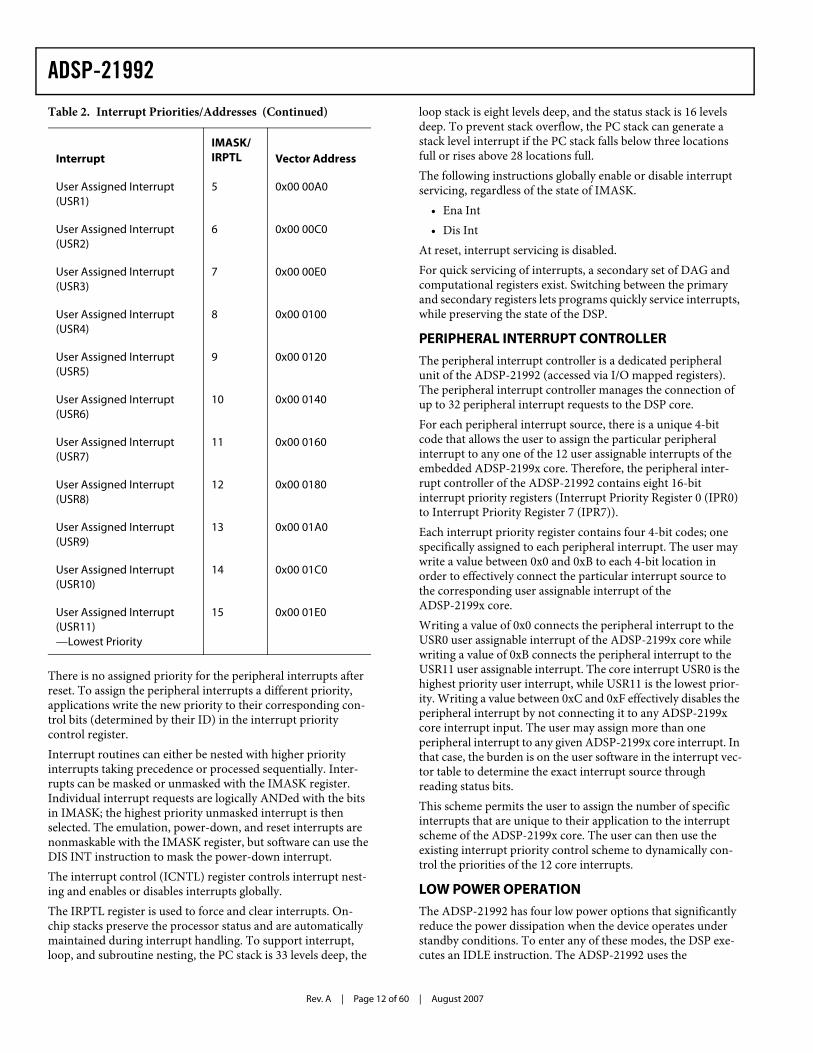
Rev. A | Page 12 of 60 | August 2007
ADSP-21992
There is no assigned priority for the peripheral interrupts after reset. To assign the peripheral interrupts a different priority, applications write the new priority to their corresponding con-trol bits (determined by their ID) in the interrupt priority control register.Interrupt routines can either be nested with higher priority interrupts taking precedence or processed sequentially. Inter-rupts can be masked or unmasked with the IMASK register. Individual interrupt requests are logically ANDed with the bits in IMASK; the highest priority unmasked interrupt is then selected. The emulation, power-down, and reset interrupts are nonmaskable with the IMASK register, but software can use the DIS INT instruction to mask the power-down interrupt.The interrupt control (ICNTL) register controls interrupt nest-ing and enables or disables interrupts globally.The IRPTL register is used to force and clear interrupts. On-chip stacks preserve the processor status and are automatically maintained during interrupt handling. To support interrupt, loop, and subroutine nesting, the PC stack is 33 levels deep, the
loop stack is eight levels deep, and the status stack is 16 levels deep. To prevent stack overflow, the PC stack can generate a stack level interrupt if the PC stack falls below three locations full or rises above 28 locations full. The following instructions globally enable or disable interrupt servicing, regardless of the state of IMASK.
• Ena Int• Dis Int
At reset, interrupt servicing is disabled.For quick servicing of interrupts, a secondary set of DAG and computational registers exist. Switching between the primary and secondary registers lets programs quickly service interrupts, while preserving the state of the DSP.
PERIPHERAL INTERRUPT CONTROLLER
The peripheral interrupt controller is a dedicated peripheral unit of the ADSP-21992 (accessed via I/O mapped registers). The peripheral interrupt controller manages the connection of up to 32 peripheral interrupt requests to the DSP core.For each peripheral interrupt source, there is a unique 4-bit code that allows the user to assign the particular peripheral interrupt to any one of the 12 user assignable interrupts of the embedded ADSP-2199x core. Therefore, the peripheral inter-rupt controller of the ADSP-21992 contains eight 16-bit interrupt priority registers (Interrupt Priority Register 0 (IPR0) to Interrupt Priority Register 7 (IPR7)).Each interrupt priority register contains four 4-bit codes; one specifically assigned to each peripheral interrupt. The user may write a value between 0x0 and 0xB to each 4-bit location in order to effectively connect the particular interrupt source to the corresponding user assignable interrupt of the ADSP-2199x core. Writing a value of 0x0 connects the peripheral interrupt to the USR0 user assignable interrupt of the ADSP-2199x core while writing a value of 0xB connects the peripheral interrupt to the USR11 user assignable interrupt. The core interrupt USR0 is the highest priority user interrupt, while USR11 is the lowest prior-ity. Writing a value between 0xC and 0xF effectively disables the peripheral interrupt by not connecting it to any ADSP-2199x core interrupt input. The user may assign more than one peripheral interrupt to any given ADSP-2199x core interrupt. In that case, the burden is on the user software in the interrupt vec-tor table to determine the exact interrupt source through reading status bits. This scheme permits the user to assign the number of specific interrupts that are unique to their application to the interrupt scheme of the ADSP-2199x core. The user can then use the existing interrupt priority control scheme to dynamically con-trol the priorities of the 12 core interrupts.
LOW POWER OPERATION
The ADSP-21992 has four low power options that significantly reduce the power dissipation when the device operates under standby conditions. To enter any of these modes, the DSP exe-cutes an IDLE instruction. The ADSP-21992 uses the
User Assigned Interrupt(USR1)
5 0x00 00A0
User Assigned Interrupt(USR2)
6 0x00 00C0
User Assigned Interrupt(USR3)
7 0x00 00E0
User Assigned Interrupt(USR4)
8 0x00 0100
User Assigned Interrupt(USR5)
9 0x00 0120
User Assigned Interrupt(USR6)
10 0x00 0140
User Assigned Interrupt(USR7)
11 0x00 0160
User Assigned Interrupt(USR8)
12 0x00 0180
User Assigned Interrupt(USR9)
13 0x00 01A0
User Assigned Interrupt(USR10)
14 0x00 01C0
User Assigned Interrupt(USR11)—Lowest Priority
15 0x00 01E0
Table 2. Interrupt Priorities/Addresses (Continued)
InterruptIMASK/IRPTL Vector Address

ADSP-21992
Rev. A | Page 13 of 60 | August 2007
configuration of the PD, STCK, and STALL bits in the PLLCTL register to select between the low power modes as the DSP exe-cutes the IDLE instruction. Depending on the mode, an IDLE shuts off clocks to different parts of the DSP in the different modes. The low power modes are:
• Idle• Power-down core• Power-down core/peripherals• Power-down all
Idle Mode
When the ADSP-21992 is in idle mode, the DSP core stops exe-cuting instructions, retains the contents of the instruction pipeline, and waits for an interrupt. The core clock and periph-eral clock continue running. To enter idle mode, the DSP can execute the IDLE instruction anywhere in code. To exit idle mode, the DSP responds to an interrupt and (after two cycles of latency) resumes executing instructions.
Power-Down Core Mode
When the ADSP-21992 is in power-down core mode, the DSP core clock is off, but the DSP retains the contents of the pipeline and keeps the PLL running. The peripheral bus keeps running, letting the peripherals receive data. To exit power-down core mode, the DSP responds to an inter-rupt and (after two cycles of latency) resumes executing instructions.
Power-Down Core/Peripherals Mode
When the ADSP-21992 is in power-down core/peripherals mode, the DSP core clock and peripheral bus clock are off, but the DSP keeps the PLL running. The DSP does not retain the contents of the instruction pipeline. The peripheral bus is stopped, so the peripherals cannot receive data.To exit power-down core/peripherals mode, the DSP responds to an interrupt and (after five to six cycles of latency) resumes executing instructions.
Power-Down All Mode
When the ADSP-21992 is in power-down all mode, the DSP core clock, the peripheral clock, and the PLL are all stopped. The DSP does not retain the contents of the instruction pipe-line. The peripheral bus is stopped, so the peripherals cannot receive data.To exit power-down core/peripherals mode, the DSP responds to an interrupt and (after 500 cycles to restabilize the PLL) resumes executing instructions.
CLOCK SIGNALS
The ADSP-21992 can be clocked by a crystal oscillator or a buff-ered, shaped clock derived from an external clock oscillator. If a crystal oscillator is used, the crystal should be connected across the CLKIN and XTAL pins, with two capacitors connected as shown in Figure 6. Capacitor values are dependent on crystal
type and should be specified by the crystal manufacturer. A par-allel resonant, fundamental frequency, microprocessor grade crystal should be used for this configuration.If a buffered, shaped clock is used, this external clock connects to the DSP CLKIN pin. CLKIN input cannot be halted, changed, or operated below the specified frequency during normal opera-tion. This clock signal should be a TTL-compatible signal. When an external clock is used, the XTAL input must be left unconnected.The DSP provides a user-programmable 1� to 32� multiplica-tion of the input clock, including some fractional values, to support 128 external to internal (DSP core) clock ratios. The BYPASS pin, and MSEL6–0 and DF bits, in the PLL configura-tion register, decide the PLL multiplication factor at reset. At runtime, the multiplication factor can be controlled in software. To support input clocks greater that 100 MHz, the PLL uses an additional bit (DF). If the input clock is greater than 100 MHz, DF must be set. If the input clock is less than 100 MHz, DF must be cleared. For clock multiplier settings, see the ADSP-2199x DSP Hardware Reference Manual.The peripheral clock is supplied to the CLKOUT pin. All on-chip peripherals for the ADSP-21992 operate at the rate set by the peripheral clock. The peripheral clock (HCLK) is either equal to the core clock rate or one half the DSP core clock rate (CCLK). This selection is controlled by the IOSEL bit in the PLLCTL register. The maximum core clock is 160 MHz for the ADSP-21992BST, 150 MHz for both the ADSP-21992BBC and ADSP-21992YBC, and 100 MHz for the ADSP-21992YST. The maximum peripheral clock is 80 MHz for the ADSP-21992BST, 75 MHz for both the ADSP-21992BBC and ADSP-21992YBC, and 50 MHz for the ADSP-21992YST—the combination of the input clock and core/peripheral clock ratios may not exceed these limits.
RESET AND POWER-ON RESET (POR)
The RESET pin initiates a complete hardware reset of the ADSP-21992 when pulled low. The RESET signal must be asserted when the device is powered up to assure proper initial-ization. The ADSP-21992 contains an integrated power-on reset (POR) circuit that provides an output reset signal, POR, from the ADSP-21992 on power-up and if the power supply voltage falls below the threshold level. The ADSP-21992 may be reset
Figure 6. External Crystal Connections
CLKIN XTAL
ADSP-2199x

Rev. A | Page 14 of 60 | August 2007
ADSP-21992
from an external source using the RESET signal, or alterna-tively, the internal power-on reset circuit may be used by connecting the POR pin to the RESET pin. During power-up the RESET line must be activated for long enough to allow the DSP core’s internal clock to stabilize. The power-up sequence is defined as the total time required for the crystal oscillator to sta-bilize after a valid VDD is applied to the processor and for the internal phase-locked loop (PLL) to lock onto the specific crys-tal frequency. A minimum of 512 cycles will ensure that the PLL has locked (this does not include the crystal oscillator start-up time).The RESET input contains some hysteresis. If an RC circuit is used to generate the RESET signal, the circuit should use an external Schmitt trigger.The master reset sets all internal stack pointers to the empty stack condition, masks all interrupts, and resets all registers to their default values (where applicable). When RESET is released, if there is no pending bus request, program control jumps to the location of the on-chip boot ROM (0xFF0000) and the booting sequence is performed.
POWER SUPPLIES
The ADSP-21992 has separate power supply connections for the internal (VDDINT) and external (VDDEXT) power supplies. The internal supply must meet the 2.5 V requirement. The external supply must be connected to a 3.3 V supply. All external supply
pins must be connected to the same supply. The ideal power-on sequence for the DSP is to provide power-up of all supplies simultaneously. If there is going to be some delay in power-up between the supplies, provide VDD first, then VDD_IO.
BOOTING MODES
The ADSP-21992 supports a number of different boot modes that are controlled by the three dedicated hardware boot mode control pins (BMODE2, BMODE1, and BMODE0). The use of three boot mode control pins means that up to eight different boot modes are possible. Of these only five modes are valid on the ADSP-21992. The ADSP-21992 exposes the boot mecha-nism to software control by providing a nonmaskable boot interrupt that vectors to the start of the on-chip ROM memory block (at address 0xFF0000). A boot interrupt is automatically initiated following either a hardware initiated reset, via the RESET pin, or a software initiated reset, via writing to the soft-ware reset register. Following either a hardware or a software reset, execution always starts from the boot ROM at address 0xFF0000, irrespective of the settings of the BMODE2, BMODE1, and BMODE0 pins. The dedicated BMODE2, BMODE1, and BMODE0 pins are sampled at hardware reset.The particular boot mode for the ADSP-21992 associated with the settings of the BMODE2, BMODE1, BMODE0 pins is defined in Table 3.
Table 3. Summary of Boot Modes
Boot Mode BMODE2 BMODE1 BMODE0 Function
0 0 0 0 Illegal–Reserved
1 0 0 1 Boot from External 8-Bit Memory over EMI
2 0 1 0 Execute from External 8-Bit Memory
3 0 1 1 Execute from External 16-Bit Memory
4 1 0 0 Boot from SPI ≤ 4K Bits
5 1 0 1 Boot from SPI > 4K Bits
6 1 1 0 Illegal–Reserved
7 1 1 1 Illegal–Reserved
ADSP-21992
Rev. A | Page 15 of 60 | August 2007
INSTRUCTION SET DESCRIPTION
The ADSP-21992 assembly language instruction set has an alge-braic syntax that was designed for ease of coding and readability. The assembly language, which takes full advantage of the unique architecture of the processor, offers the following benefits:
• SHARC assembly language syntax is a superset of and source code compatible (except for two data registers and DAG base address registers) with ADSP-21xx family syn-tax. It may be necessary to restructure ADSP-21xx programs to accommodate the unified memory space of the ADSP-21992 and to conform to its interrupt vector map.
• The algebraic syntax eliminates the need to remember cryptic assembler mnemonics. For example, a typical arith-metic add instruction, such as AR = AX0 + AY0, resembles a simple equation.
• Every instruction, but two, assembles into a single, 24-bit word that can execute in a single instruction cycle. The exceptions are two dual word instructions. One writes 16- or 24-bit immediate data to memory, and the other is an absolute jump/call with the 24-bit address specified in the instruction.
• Multifunction instructions allow parallel execution of an arithmetic, MAC, or shift instruction with up to two fetches or one write to processor memory space during a single instruction cycle.
• Program flow instructions support a wider variety of con-ditional and unconditional jumps/calls and a larger set of conditions on which to base execution of conditional instructions.
DEVELOPMENT TOOLS
The ADSP-21992 is supported with a complete set of CROSSCORE™ software and hardware development tools, including Analog Devices emulators and VisualDSP++™ devel-opment environment. The emulator hardware that supports other SHARC DSPs also fully emulates the ADSP-21992.The VisualDSP++ project management environment lets pro-grammers develop and debug an application. This environment includes an easy to use assembler (which is based on an alge-braic syntax), an archiver (librarian/library builder), a linker, a loader, a cycle-accurate instruction-level simulator, a C/C++ compiler, and a C/C++ runtime library that includes DSP and mathematical functions. A key point for these tools is C/C++ code efficiency. The compiler has been developed for efficient translation of C/C++ code to DSP assembly. The DSP has archi-tectural features that improve the efficiency of compiled C/C++ code.The VisualDSP++ debugger has a number of important fea-tures. Data visualization is enhanced by a plotting package that offers a significant level of flexibility. This graphical representa-tion of user data enables the programmer to quickly determine the performance of an algorithm. As algorithms grow in com-
plexity, this capability can have a significant influence on the design development schedule by increasing productivity. Statis-tical profiling enables the programmer to nonintrusively poll the processor as it is running the program. This feature, unique to VisualDSP++, enables the software developer to passively gather important code execution metrics without interrupting the real-time characteristics of the program. Essentially, the developer can identify bottlenecks in software quickly and effi-ciently. By using the profiler, the programmer can focus on those areas in the program that impact performance and take corrective action.Debugging both C/C++ and assembly programs with the VisualDSP++ debugger, programmers can:
• View mixed C/C++ and assembly code (interleaved source and object information)
• Insert breakpoints• Set conditional breakpoints on registers, memory,
and stacks• Trace instruction execution• Perform linear or statistical profiling of program execution• Fill, dump, and graphically plot the contents of memory• Perform source level debugging• Create custom debugger windows
The VisualDSP++ IDDE lets programmers define and manage DSP software development. Its dialog boxes and property pages let programmers configure and manage all of the SHARC devel-opment tools, including the color syntax highlighting in the VisualDSP++ editor. This capability permits programmers to:
• Control how the development tools process inputs and generate outputs
• Maintain a one-to-one correspondence with the command line switches of the tool
The VisualDSP++ Kernel (VDK) incorporates scheduling and resource management tailored specifically to address the mem-ory and timing constraints of DSP programming. These capabilities enable engineers to develop code more effectively, eliminating the need to start from the very beginning, when developing new application code. The VDK features include threads, critical and unscheduled regions, semaphores, events, and device flags. The VDK also supports priority-based, pre-emptive, cooperative, and time-sliced scheduling approaches. In addition, the VDK was designed to be scalable. If the application does not use a specific feature, the support code for that feature is excluded from the target system.Because the VDK is a library, a developer can decide whether to use it or not. The VDK is integrated into the VisualDSP++ development environment, but can also be used via standard command line tools. When the VDK is used, the development environment assists the developer with many error-prone tasks and assists in managing system resources, automating the gen-eration of various VDK-based objects, and visualizing the system state, when debugging an application that uses the VDK.
Rev. A | Page 16 of 60 | August 2007
ADSP-21992
VCSE is Analog Devices technology for creating, using, and reusing software components (independent modules of sub-stantial functionality) to quickly and reliably assemble software applications. The user can also download components from the Web, drop them into the application and publish component archives from within VisualDSP++. VCSE supports component implementation in C/C++ or assembly language.Use the Expert Linker to visually manipulate the placement of code and data on the embedded system, view memory utiliza-tion in a color-coded graphical form, easily move code and data to different areas of the DSP or external memory with the drag of the mouse, and examine runtime stack and heap usage. The Expert Linker is fully compatible with existing linker definition file (LDF), allowing the developer to move between the graphi-cal and textual environments.Analog Devices DSP emulators use the IEEE 1149.1 JTAG test access port of the ADSP-21992 processor to monitor and con-trol the target board processor during emulation. The emulator provides full speed emulation, allowing inspection and modifi-cation of memory, registers, and processor stacks. Nonintrusive in-circuit emulation is assured by the use of the processor JTAG interface—target system loading and timing are not affected by the emulator.In addition to the software and hardware development tools available from Analog Devices, third parties provide a wide range of tools supporting the SHARC processor family. Hard-ware tools include SHARC DSP PC plug-in cards. Third-party software tools include DSP libraries, real-time operating sys-tems, and block diagram design tools.
DESIGNING AN EMULATOR-COMPATIBLE DSP BOARD
The Analog Devices family of emulators are tools that every DSP developer needs to test and debug hardware and software systems. Analog Devices has supplied an IEEE 1149.1 JTAG test access port (TAP) on each JTAG DSP. The emulator uses the TAP to access the internal features of the DSP, allowing the developer to load code, set breakpoints, observe variables, observe memory, and examine registers. The DSP must be halted to send data and commands, but once an operation has been completed by the emulator, the DSP system is set running at full speed with no impact on system timing.To use these emulators, the target board must include a header that connects the DSP JTAG port to the emulator.For details on target board design issues including mechanical layout, single processor connections, multiprocessor scan chains, signal buffering, signal termination, and emulator pod logic, see the EE-68: JTAG Emulation Technical Reference on the Analog Devices website (www.analog.com)—use site search on “EE-68.” This document is updated regularly to keep pace with improvements to emulator support.
ADDITIONAL INFORMATION
This data sheet provides a general overview of the ADSP-21992 architecture and functionality. For detailed information on the ADSP-21992 embedded DSP core architecture, instruction set,
communications ports and embedded control peripherals, refer to the ADSP-2199x Mixed Signal DSP Controller Hardware Ref-erence Manual.
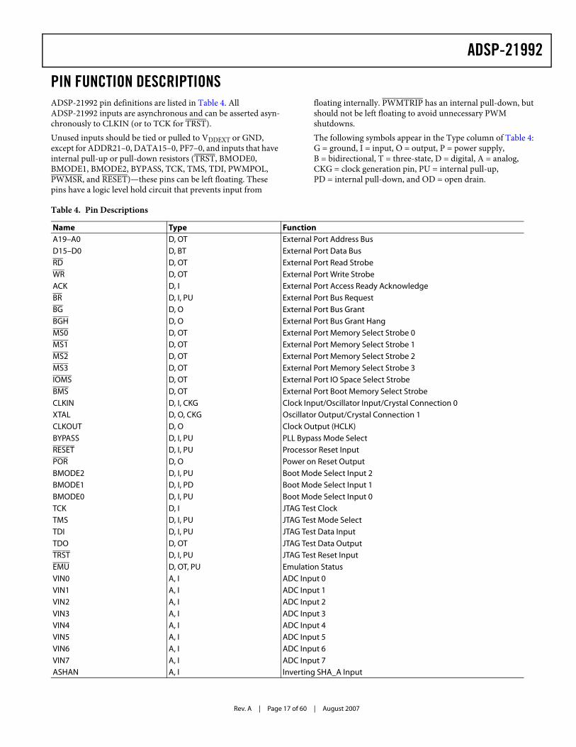
ADSP-21992
Rev. A | Page 17 of 60 | August 2007
PIN FUNCTION DESCRIPTIONSADSP-21992 pin definitions are listed in Table 4. All ADSP-21992 inputs are asynchronous and can be asserted asyn-chronously to CLKIN (or to TCK for TRST).Unused inputs should be tied or pulled to VDDEXT or GND, except for ADDR21–0, DATA15–0, PF7–0, and inputs that have internal pull-up or pull-down resistors (TRST, BMODE0, BMODE1, BMODE2, BYPASS, TCK, TMS, TDI, PWMPOL, PWMSR, and RESET)—these pins can be left floating. These pins have a logic level hold circuit that prevents input from
floating internally. PWMTRIP has an internal pull-down, but should not be left floating to avoid unnecessary PWM shutdowns.The following symbols appear in the Type column of Table 4: G = ground, I = input, O = output, P = power supply, B = bidirectional, T = three-state, D = digital, A = analog, CKG = clock generation pin, PU = internal pull-up, PD = internal pull-down, and OD = open drain.
Table 4. Pin Descriptions
Name Type FunctionA19–A0 D, OT External Port Address BusD15–D0 D, BT External Port Data BusRD D, OT External Port Read StrobeWR D, OT External Port Write StrobeACK D, I External Port Access Ready AcknowledgeBR D, I, PU External Port Bus RequestBG D, O External Port Bus GrantBGH D, O External Port Bus Grant HangMS0 D, OT External Port Memory Select Strobe 0MS1 D, OT External Port Memory Select Strobe 1MS2 D, OT External Port Memory Select Strobe 2MS3 D, OT External Port Memory Select Strobe 3IOMS D, OT External Port IO Space Select StrobeBMS D, OT External Port Boot Memory Select Strobe CLKIN D, I, CKG Clock Input/Oscillator Input/Crystal Connection 0XTAL D, O, CKG Oscillator Output/Crystal Connection 1CLKOUT D, O Clock Output (HCLK)BYPASS D, I, PU PLL Bypass Mode SelectRESET D, I, PU Processor Reset InputPOR D, O Power on Reset Output BMODE2 D, I, PU Boot Mode Select Input 2BMODE1 D, I, PD Boot Mode Select Input 1BMODE0 D, I, PU Boot Mode Select Input 0TCK D, I JTAG Test ClockTMS D, I, PU JTAG Test Mode SelectTDI D, I, PU JTAG Test Data InputTDO D, OT JTAG Test Data Output TRST D, I, PU JTAG Test Reset Input EMU D, OT, PU Emulation StatusVIN0 A, I ADC Input 0VIN1 A, I ADC Input 1VIN2 A, I ADC Input 2VIN3 A, I ADC Input 3VIN4 A, I ADC Input 4VIN5 A, I ADC Input 5VIN6 A, I ADC Input 6VIN7 A, I ADC Input 7ASHAN A, I Inverting SHA_A Input
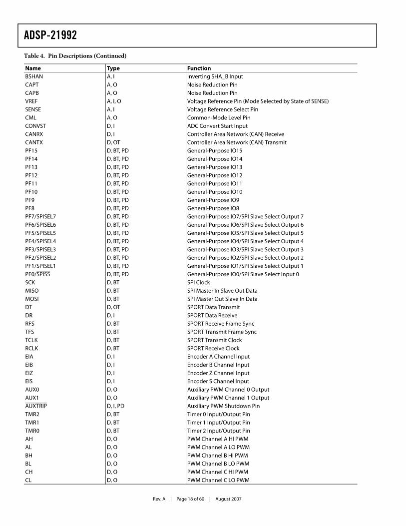
Rev. A | Page 18 of 60 | August 2007
ADSP-21992
BSHAN A, I Inverting SHA_B InputCAPT A, O Noise Reduction PinCAPB A, O Noise Reduction PinVREF A, I, O Voltage Reference Pin (Mode Selected by State of SENSE)SENSE A, I Voltage Reference Select PinCML A, O Common-Mode Level PinCONVST D, I ADC Convert Start InputCANRX D, I Controller Area Network (CAN) ReceiveCANTX D, OT Controller Area Network (CAN) TransmitPF15 D, BT, PD General-Purpose IO15PF14 D, BT, PD General-Purpose IO14PF13 D, BT, PD General-Purpose IO13PF12 D, BT, PD General-Purpose IO12PF11 D, BT, PD General-Purpose IO11PF10 D, BT, PD General-Purpose IO10PF9 D, BT, PD General-Purpose IO9PF8 D, BT, PD General-Purpose IO8PF7/SPISEL7 D, BT, PD General-Purpose IO7/SPI Slave Select Output 7PF6/SPISEL6 D, BT, PD General-Purpose IO6/SPI Slave Select Output 6PF5/SPISEL5 D, BT, PD General-Purpose IO5/SPI Slave Select Output 5PF4/SPISEL4 D, BT, PD General-Purpose IO4/SPI Slave Select Output 4PF3/SPISEL3 D, BT, PD General-Purpose IO3/SPI Slave Select Output 3PF2/SPISEL2 D, BT, PD General-Purpose IO2/SPI Slave Select Output 2PF1/SPISEL1 D, BT, PD General-Purpose IO1/SPI Slave Select Output 1PF0/SPISS D, BT, PD General-Purpose IO0/SPI Slave Select Input 0SCK D, BT SPI ClockMISO D, BT SPI Master In Slave Out DataMOSI D, BT SPI Master Out Slave In DataDT D, OT SPORT Data TransmitDR D, I SPORT Data ReceiveRFS D, BT SPORT Receive Frame SyncTFS D, BT SPORT Transmit Frame SyncTCLK D, BT SPORT Transmit ClockRCLK D, BT SPORT Receive ClockEIA D, I Encoder A Channel InputEIB D, I Encoder B Channel InputEIZ D, I Encoder Z Channel InputEIS D, I Encoder S Channel InputAUX0 D, O Auxiliary PWM Channel 0 OutputAUX1 D, O Auxiliary PWM Channel 1 OutputAUXTRIP D, I, PD Auxiliary PWM Shutdown PinTMR2 D, BT Timer 0 Input/Output PinTMR1 D, BT Timer 1 Input/Output PinTMR0 D, BT Timer 2 Input/Output PinAH D, O PWM Channel A HI PWMAL D, O PWM Channel A LO PWMBH D, O PWM Channel B HI PWMBL D, O PWM Channel B LO PWMCH D, O PWM Channel C HI PWMCL D, O PWM Channel C LO PWM
Table 4. Pin Descriptions (Continued)
Name Type Function
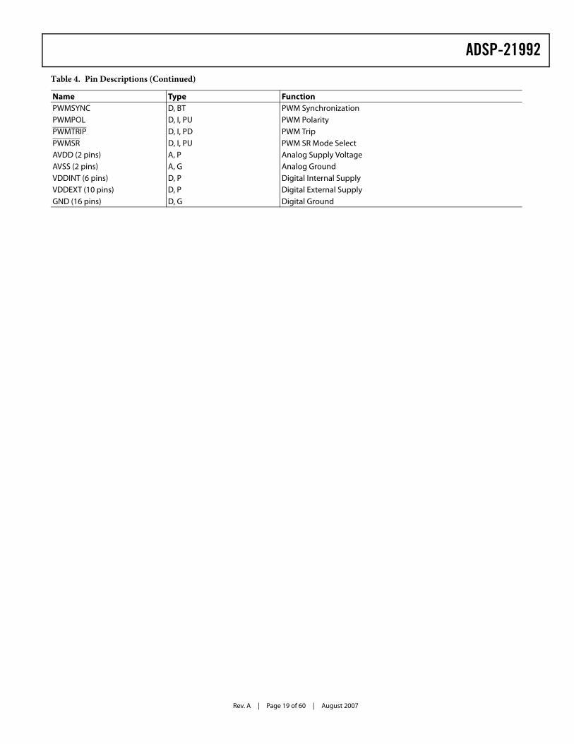
ADSP-21992
Rev. A | Page 19 of 60 | August 2007
PWMSYNC D, BT PWM SynchronizationPWMPOL D, I, PU PWM PolarityPWMTRIP D, I, PD PWM Trip PWMSR D, I, PU PWM SR Mode SelectAVDD (2 pins) A, P Analog Supply VoltageAVSS (2 pins) A, G Analog GroundVDDINT (6 pins) D, P Digital Internal SupplyVDDEXT (10 pins) D, P Digital External SupplyGND (16 pins) D, G Digital Ground
Table 4. Pin Descriptions (Continued)
Name Type Function

Rev. A | Page 20 of 60 | August 2007
ADSP-21992
SPECIFICATIONSSpecifications subject to change without notice.
OPERATING CONDITIONS
Table 5. Recommended Operating Conditions—ADSP-21992BBC
Parameter Conditions Min Typ Max UnitVDDINT Internal (Core) Supply Voltage 2.375 2.5 2.625 VVDDEXT External (I/O) Supply Voltage 3.135 3.3 3.465 VAVDD Analog Supply Voltage 2.375 2.5 2.625 VCCLK DSP Instruction Rate, Core Clock 0 150 MHzHCLK1
, 2
1 The HCLK frequency may be made to appear at the dedicated CLKOUT pin of the device. For low power operation, however, the CLKOUT pin can be disabled.2 The peripherals operate at the HCLK rate, which may be selected to be equal to CCLK or CCLK�2, up to a maximum of a 75 MHz HCLK for the ADSP-21992BBC.
Peripheral Clock Rate 0 75 MHzCLKIN3
3 In order to attain the correct CCLK and HCLK values, the input clock frequency or crystal frequency depends on the internal operation of the clock generation PLL circuit and the associated frequency ratio.
Input Clock Frequency 0 150 MHzTJUNC
4
4 The maximum junction temperature is limited to 140°C in order to meet all of the electrical specifications. It is ultimately the responsibility of the user to ensure that the power dissipation of the ADSP-21992 (including all dc and ac loads) is such that the maximum junction temperature limit of 140°C is not exceeded.
Silicon Junction Temperature 140 �CTAMB Ambient Operating Temperature –40 +85 �C
Table 6. Recommended Operating Conditions—ADSP-21992YBC
Parameter Conditions Min Typ Max UnitVDDINT Internal (Core) Supply Voltage 2.375 2.5 2.625 VVDDEXT External (I/O) Supply Voltage 3.135 3.3 3.465 VAVDD Analog Supply Voltage 2.375 2.5 2.625 VCCLK DSP Instruction Rate, Core Clock 0 150 MHzHCLK1, 2
1 The HCLK frequency may be made to appear at the dedicated CLKOUT pin of the device. For low power operation, however, the CLKOUT pin can be disabled.2 The peripherals operate at the HCLK rate, which may be selected to be equal to CCLK or CCLK � 2, up to a maximum of an 75 MHz HCLK for the ADSP-21992YBC.
Peripheral Clock Rate 0 75 MHzCLKIN3
3 In order to attain the correct CCLK and HCLK values, the input clock frequency or crystal frequency depends on the internal operation of the clock generation PLL circuit and the associated frequency ratio.
Input Clock Frequency 0 150 MHzTJUNC
4
4 The maximum junction temperature is limited to 140°C in order to meet all of the electrical specifications. It is ultimately the responsibility of the user to ensure that the power dissipation of the ADSP-21992 (including all dc and ac loads) is such that the maximum junction temperature limit of 140°C is not exceeded.
Silicon Junction Temperature 140 �CTAMB Ambient Operating Temperature –40 +125 �C
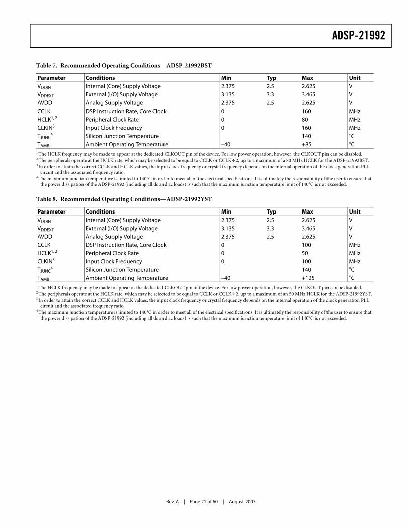
ADSP-21992
Rev. A | Page 21 of 60 | August 2007
Table 7. Recommended Operating Conditions—ADSP-21992BST
Parameter Conditions Min Typ Max UnitVDDINT Internal (Core) Supply Voltage 2.375 2.5 2.625 VVDDEXT External (I/O) Supply Voltage 3.135 3.3 3.465 VAVDD Analog Supply Voltage 2.375 2.5 2.625 VCCLK DSP Instruction Rate, Core Clock 0 160 MHzHCLK1, 2 Peripheral Clock Rate 0 80 MHzCLKIN3 Input Clock Frequency 0 160 MHzTJUNC
4 Silicon Junction Temperature 140 �CTAMB Ambient Operating Temperature –40 +85 �C
1 The HCLK frequency may be made to appear at the dedicated CLKOUT pin of the device. For low power operation, however, the CLKOUT pin can be disabled.2 The peripherals operate at the HCLK rate, which may be selected to be equal to CCLK or CCLK�2, up to a maximum of a 80 MHz HCLK for the ADSP-21992BST.3 In order to attain the correct CCLK and HCLK values, the input clock frequency or crystal frequency depends on the internal operation of the clock generation PLL
circuit and the associated frequency ratio.4 The maximum junction temperature is limited to 140°C in order to meet all of the electrical specifications. It is ultimately the responsibility of the user to ensure that
the power dissipation of the ADSP-21992 (including all dc and ac loads) is such that the maximum junction temperature limit of 140°C is not exceeded.
Table 8. Recommended Operating Conditions—ADSP-21992YST
Parameter Conditions Min Typ Max UnitVDDINT Internal (Core) Supply Voltage 2.375 2.5 2.625 VVDDEXT External (I/O) Supply Voltage 3.135 3.3 3.465 VAVDD Analog Supply Voltage 2.375 2.5 2.625 VCCLK DSP Instruction Rate, Core Clock 0 100 MHzHCLK1, 2 Peripheral Clock Rate 0 50 MHzCLKIN3 Input Clock Frequency 0 100 MHzTJUNC
4 Silicon Junction Temperature 140 �CTAMB Ambient Operating Temperature –40 +125 �C
1 The HCLK frequency may be made to appear at the dedicated CLKOUT pin of the device. For low power operation, however, the CLKOUT pin can be disabled.2 The peripherals operate at the HCLK rate, which may be selected to be equal to CCLK or CCLK�2, up to a maximum of an 50 MHz HCLK for the ADSP-21992YST.3 In order to attain the correct CCLK and HCLK values, the input clock frequency or crystal frequency depends on the internal operation of the clock generation PLL
circuit and the associated frequency ratio.4 The maximum junction temperature is limited to 140°C in order to meet all of the electrical specifications. It is ultimately the responsibility of the user to ensure that
the power dissipation of the ADSP-21992 (including all dc and ac loads) is such that the maximum junction temperature limit of 140°C is not exceeded.
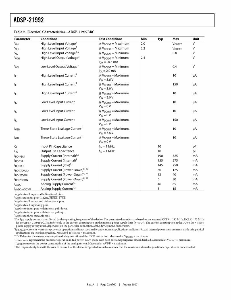
Rev. A | Page 22 of 60 | August 2007
ADSP-21992
Table 9. Electrical Characteristics—ADSP-21992BBC
Parameter Conditions Test Conditions Min Typ Max UnitVIH High Level Input Voltage1 @ VDDEXT = Maximum 2.0 VDDEXT VVIH High Level Input Voltage2 @ VDDEXT = Maximum 2.2 VDDEXT VVIL High Level Input Voltage1, 2 @ VDDEXT = Minimum 0.8 VVOH High Level Output Voltage3 @ VDDEXT = Minimum,
IOH = –0.5 mA2.4 V
VOL Low Level Output Voltage3 @ VDDEXT = Minimum, IOL = 2.0 mA
0.4 V
IIH High Level Input Current4 @ VDDINT = Maximum, VIN = 3.6 V
10 μA
IIH High Level Input Current5 @ VDDINT = Maximum, VIN = 3.6 V
150 μA
IIH High Level Input Current6 @ VDDINT = Maximum, VIN = 3.6 V
10 μA
IIL Low Level Input Current @ VDDINT = Maximum, VIN = 0 V
10 μA
IIL Low Level Input Current @ VDDINT = Maximum, VIN = 0 V
10 μA
IIL Low Level Input Current @ VDDINT = Maximum,VIN = 0 V
150 μA
IOZH Three-State Leakage Current7 @ VDDINT = Maximum, VIN = 3.6 V
10 μA
IOZL Three-State Leakage Current7 @ VDDINT = Maximum, VIN = 0 V
10 μA
CI Input Pin Capacitance fIN = 1 MHz 10 pFCO Output Pin Capacitance fIN = 1 MHz 10 pFIDD-PEAK Supply Current (Internal)8, 9 190 325 mAIDD-TYP Supply Current (Internal)8 155 275 mAIDD-IDLE Supply Current (Idle)8 145 250 mAIDD-STOPCLK Supply Current (Power-Down)8, 10 60 125 mAIDD-STOPALL Supply Current (Power-Down)8, 11 12 40 mAIDD-PDOWN Supply Current (Power-Down)8, 12 6 30 mAIAVDD Analog Supply Current13 46 65 mAIAVDD-ADCOFF Analog Supply Current12 5 15 mA
1 Applies to all input and bidirectional pins.2 Applies to input pins CLKIN, RESET, TRST.3 Applies to all output and bidirectional pins.4 Applies to all input only pins.5 Applies to input pins with internal pull-down.6 Applies to input pins with internal pull-up.7 Applies to three-stateable pins.8 The IDD supply currents are affected by the operating frequency of the device. The guaranteed numbers are based on an assumed CCLK = 150 MHz, HCLK = 75 MHz
for the ADSP-21992BBC. IDD refers only to the current consumption on the internal power supply lines (VDDINT). The current consumption at the I/O on the VDDEXT power supply is very much dependent on the particular connection of the device in the final system.
9 IDD-PEAK represents worst-case processor operation and is not sustainable under normal application conditions. Actual internal power measurements made using typical applications are less than specified. Measured at VDDINT = maximum.
10IDLE denotes the current consumption during execution of the IDLE instruction. Measured at VDDINT = maximum.11IDD-PDOWN represents the processor operation in full power-down mode with both core and peripheral clocks disabled. Measured at VDDINT = maximum.12IAVDD represents the power consumption of the analog system. Measured at AVDD = maximum.13The responsibility lies with the user to ensure that the device is operated in such a manner that the maximum allowable junction temperature is not exceeded.

ADSP-21992
Rev. A | Page 23 of 60 | August 2007
ELECTRICAL CHARACTERISTICS
Table 10. Electrical Characteristics—ADSP-21992YBC
Parameter Conditions Test Conditions Min Typ Max UnitVIH High Level Input Voltage1 @ VDDEXT = Maximum 2.0 VDDEXT VVIH High Level Input Voltage2 @ VDDEXT = Maximum 2.2 VDDEXT VVIL High Level Input Voltage1, 2 @ VDDEXT = Minimum 0.8 VVOH High Level Output Voltage3 @ VDDEXT = Minimum,
IOH = –0.5 mA2.4 V
VOL Low Level Output Voltage3 @ VDDEXT = Minimum, IOL = 2.0 mA
0.4 V
IIH High Level Input Current4 @ VDDINT = Maximum, VIN = 3.6 V
10 μA
IIH High Level Input Current5 @ VDDINT = Maximum, VIN = 3.6 V
150 μA
IIH High Level Input Current6 @ VDDINT = Maximum, VIN = 3.6 V
10 μA
IIL Low Level Input Current @ VDDINT = Maximum, VIN = 0 V
10 μA
IIL Low Level Input Current @ VDDINT = Maximum, VIN = 0 V
10 μA
IIL Low Level Input Current @ VDDINT = Maximum, VIN = 0 V
150 μA
IOZH Three-State Leakage Current7 @ VDDINT = Maximum, VIN = 3.6 V
10 μA
IOZL Three-State Leakage Current7 @ VDDINT = Maximum,VIN = 0 V
10 μA
CI Input Pin Capacitance fIN = 1 MHz 10 pFCO Output Pin Capacitance fIN = 1 MHz 10 pFIDD-PEAK Supply Current (Internal)8, 9 190 325 mAIDD-TYP Supply Current (Internal)8 155 275 mAIDD-IDLE Supply Current (Idle)8 145 250 mAIDD-STOPCLK Supply Current (Power-Down)8, 10 60 125 mAIDD-STOPALL Supply Current (Power-Down)8, 11 12 40 mAIDD-PDOWN Supply Current (Power-Down)8, 12 6 30 mAIAVDD Analog Supply Current13 46 65 mAIAVDD-ADCOFF Analog Supply Current12 5 15 mA
1 Applies to all input and bidirectional pins.2 Applies to input pins CLKIN, RESET, TRST.3 Applies to all output and bidirectional pins.4 Applies to all input only pins.5 Applies to input pins with internal pull-down.6 Applies to input pins with internal pull-up.7 Applies to three-stateable pins.8 The IDD supply currents are affected by the operating frequency of the device. The guaranteed numbers are based on an assumed CCLK = 150 MHz, HCLK = 75 MHz
for the ADSP-21992YBC. IDD refers only to the current consumption on the internal power supply lines (VDDINT). The current consumption at the I/O on the VDDEXT power supply is very much dependent on the particular connection of the device in the final system.
9 IDD-PEAK represents worst-case processor operation and is not sustainable under normal application conditions. Actual internal power measurements made using typical applications are less than specified. Measured at VDDINT = maximum.
10IDLE denotes the current consumption during execution of the IDLE instruction. Measured at VDDINT = maximum.11IDD-PDOWN represents the processor operation in full power-down mode with both core and peripheral clocks disabled. Measured at VDDINT = maximum.12IAVDD represents the power consumption of the analog system. Measured at AVDD = maximum.13The responsibility lies with the user to ensure that the device is operated in such a manner that the maximum allowable junction temperature is not exceeded.

Rev. A | Page 24 of 60 | August 2007
ADSP-21992
Table 11. Electrical Characteristics—ADSP-21992BST
Parameter Conditions Test Conditions Min Typ Max UnitVIH High Level Input Voltage1 @ VDDEXT = Maximum 2.0 VDDEXT VVIH High Level Input Voltage2 @ VDDEXT = Maximum 2.2 VDDEXT VVIL High Level Input Voltage1, 2 @ VDDEXT = Minimum 0.8 VVOH High Level Output Voltage3 @ VDDEXT = Minimum,
IOH = –0.5 mA2.4 V
VOL Low Level Output Voltage3 @ VDDEXT = Minimum, IOL = 2.0 mA
0.4 V
IIH High Level Input Current4 @ VDDINT = Maximum, VIN = 3.6 V
10 μA
IIH High Level Input Current5 @ VDDINT = Maximum, VIN = 3.6 V
150 μA
IIH High Level Input Current6 @ VDDINT = Maximum, VIN = 3.6 V
10 μA
IIL Low Level Input Current @ VDDINT = Maximum, VIN = 0 V
10 μA
IIL Low Level Input Current @ VDDINT = Maximum, VIN = 0 V
10 μA
IIL Low Level Input Current @ VDDINT = Maximum,VIN = 0 V
150 μA
IOZH Three-State Leakage Current7 @ VDDINT = Maximum, VIN = 3.6 V
10 μA
IOZL Three-State Leakage Current7 @ VDDINT = Maximum, VIN = 0 V
10 μA
CI Input Pin Capacitance fIN = 1 MHz 10 pFCO Output Pin Capacitance fIN = 1 MHz 10 pFIDD-PEAK Supply Current (Internal)8, 9 300 350 mAIDD-TYP Supply Current (Internal)8 240 300 mAIDD-IDLE Supply Current (Idle)8 225 275 mAIDD-STOPCLK Supply Current (Power-Down)8, 10 90 150 mAIDD-STOPALL Supply Current (Power-Down)8, 11 20 50 mAIDD-PDOWN Supply Current (Power-Down)8, 12 7 35 mAIAVDD Analog Supply Current13 49 65 mAIAVDD-ADCOFF Analog Supply Current12 7 15 mA
1 Applies to all input and bidirectional pins.2 Applies to input pins CLKIN, RESET, TRST.3 Applies to all output and bidirectional pins.4 Applies to all input only pins.5 Applies to input pins with internal pull-down.6 Applies to input pins with internal pull-up.7 Applies to three-stateable pins.8 The IDD supply currents are affected by the operating frequency of the device. The guaranteed numbers are based on an assumed CCLK = 160 MHz, HCLK = 80 MHz
for the ADSP-21992BST. IDD refers only to the current consumption on the internal power supply lines (VDDINT). The current consumption at the I/O on the VDDEXT power supply is very much dependent on the particular connection of the device in the final system.
9 IDD-PEAK represents worst-case processor operation and is not sustainable under normal application conditions. Actual internal power measurements made using typical applications are less than specified. Measured at VDDINT = maximum.
10IDLE denotes the current consumption during execution of the IDLE instruction. Measured at VDDINT = maximum.11IDD-PDOWN represents the processor operation in full power-down mode with both core and peripheral clocks disabled. Measured at VDDINT = maximum.12IAVDD represents the power consumption of the analog system. Measured at AVDD = maximum.13The responsibility lies with the user to ensure that the device is operated in such a manner that the maximum allowable junction temperature is not exceeded.
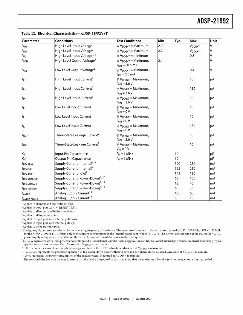
ADSP-21992
Rev. A | Page 25 of 60 | August 2007
Table 12. Electrical Characteristics—ADSP-21992YST
Parameter Conditions Test Conditions Min Typ Max UnitVIH High Level Input Voltage1 @ VDDEXT = Maximum 2.0 VDDEXT VVIH High Level Input Voltage2 @ VDDEXT = Maximum 2.2 VDDEXT VVIL High Level Input Voltage1, 2 @ VDDEXT = minimum 0.8 VVOH High Level Output Voltage3 @ VDDEXT = Minimum,
IOH = –0.5 mA2.4 V
VOL Low Level Output Voltage3 @ VDDEXT = Minimum, IOL = 2.0 mA
0.4 V
IIH High Level Input Current4 @ VDDINT = Maximum, VIN = 3.6 V
10 μA
IIH High Level Input Current5 @ VDDINT = Maximum, VIN = 3.6 V
150 μA
IIH High Level Input Current6 @ VDDINT = Maximum, VIN = 3.6 V
10 μA
IIL Low Level Input Current @ VDDINT = Maximum, VIN = 0 V
10 μA
IIL Low Level Input Current @ VDDINT = Maximum, VIN = 0 V
10 μA
IIL Low Level Input Current @ VDDINT = Maximum, VIN = 0 V
150 μA
IOZH Three-State Leakage Current7 @ VDDINT = Maximum, VIN = 3.6 V
10 μA
IOZL Three-State Leakage Current7 @ VDDINT = Maximum,VIN = 0 V
10 μA
CI Input Pin Capacitance fIN = 1 MHz 10 pFCO Output Pin Capacitance fIN = 1 MHz 10 pFIDD-PEAK Supply Current (Internal)8, 9 190 250 mAIDD-TYP Supply Current (Internal)8 155 210 mAIDD-IDLE Supply Current (Idle)8 145 180 mAIDD-STOPCLK Supply Current (Power-Down)8, 10 60 100 mAIDD-STOPALL Supply Current (Power-Down)8, 11 12 40 mAIDD-PDOWN Supply Current (Power-Down)8, 12 6 35 mAIAVDD Analog Supply Current13 46 65 mAIAVDD-ADCOFF Analog Supply Current12 5 15 mA
1 Applies to all input and bidirectional pins.2 Applies to input pins CLKIN, RESET, TRST.3 Applies to all output and bidirectional pins.4 Applies to all input only pins.5 Applies to input pins with internal pull-down.6 Applies to input pins with internal pull-up.7 Applies to three-stateable pins.8 The IDD supply currents are affected by the operating frequency of the device. The guaranteed numbers are based on an assumed CCLK = 100 MHz, HCLK = 50 MHz
for the ADSP-21992YST. IDD refers only to the current consumption on the internal power supply lines (VDDINT). The current consumption at the I/O on the VDDEXT power supply is very much dependent on the particular connection of the device in the final system.
9 IDD-PEAK represents worst-case processor operation and is not sustainable under normal application conditions. Actual internal power measurements made using typical applications are less than specified. Measured at VDDINT = maximum.
10IDLE denotes the current consumption during execution of the IDLE instruction. Measured at VDDINT = maximum.11IDD-PDOWN represents the processor operation in full power-down mode with both core and peripheral clocks disabled. Measured at VDDINT = maximum.12IAVDD represents the power consumption of the analog system. Measured at AVDD = maximum.13The responsibility lies with the user to ensure that the device is operated in such a manner that the maximum allowable junction temperature is not exceeded.
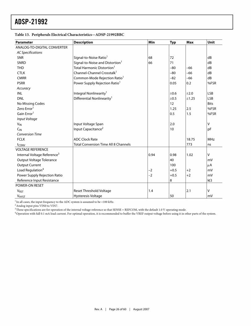
Rev. A | Page 26 of 60 | August 2007
ADSP-21992
Table 13. Peripherals Electrical Characteristics—ADSP-21992BBC
Parameter Description Min Typ Max UnitANALOG-TO-DIGITAL CONVERTER AC Specifications SNR Signal-to-Noise Ratio1 68 72 dB SNRD Signal-to-Noise and Distortion1 66 71 dB THD Total Harmonic Distortion1 –80 –66 dB CTLK Channel-Channel Crosstalk1 –80 –66 dB CMRR Common-Mode Rejection Ratio1 –82 –66 dB PSRR Power Supply Rejection Ratio1 0.05 0.2 %FSR Accuracy INL Integral Nonlinearity1 ±0.6 ±2.0 LSB DNL Differential Nonlinearity1 ±0.5 ±1.25 LSB No Missing Codes 12 Bits Zero Error1 1.25 2.5 %FSR Gain Error1 0.5 1.5 %FSR Input Voltage VIN Input Voltage Span 2.0 V CIN Input Capacitance2 10 pF Conversion Time FCLK ADC Clock Rate 18.75 MHz tCONV Total Conversion Time All 8 Channels 773 nsVOLTAGE REFERENCE
Internal Voltage Reference3 0.94 0.98 1.02 V Output Voltage Tolerance 40 mV Output Current 100 μA Load Regulation4 –2 +0.5 +2 mV Power Supply Rejection Ratio –2 +0.5 +2 mV Reference Input Resistance 8 kΩPOWER-ON RESET
VRST Reset Threshold Voltage 1.4 2.1 V VHYST Hysteresis Voltage 50 mV
1 In all cases, the input frequency to the ADC system is assumed to be <100 kHz.2 Analog input pins VIN0 to VIN7.3 These specifications are for operation of the internal voltage reference so that SENSE = REFCOM, with the default 1.0 V operating mode.4 Operation with full 0.1 mA load current. For optimal operation, it is recommended to buffer the VREF output voltage before using it in other parts of the system.

ADSP-21992
Rev. A | Page 27 of 60 | August 2007
Table 14. Peripherals Electrical Characteristics—ADSP-21992BST
Parameter Description Min Typ Max UnitANALOG-TO-DIGITAL CONVERTER
AC Specifications SNR Signal-to-Noise Ratio1 68 72 dB SNRD Signal-to-Noise and Distortion1 68 71 dB THD Total Harmonic Distortion1 –78 –68 dB CTLK Channel-Channel Crosstalk1 –80 –66 dB CMRR Common-Mode Rejection Ratio1 –74 –66 dB PSRR Power Supply Rejection Ratio1 0.05 0.2 %FSR Accuracy INL Integral Nonlinearity1 ±0.6 ±2.0 LSB DNL Differential Nonlinearity1 ±0.5 ±1.25 LSB No Missing Codes 12 Bits Zero Error1 1.25 2.5 %FSR Gain Error1 0.5 1.5 %FSR Input Voltage VIN Input Voltage Span 2.0 V CIN Input Capacitance2 10 pF Conversion Time FCLK ADC Clock Rate 20 MHz tCONV Total Conversion Time All 8 Channels 725 nsVOLTAGE REFERENCE
Internal Voltage Reference3 0.94 0.98 1.02 V Output Voltage Tolerance 40 mV Output Current 100 μA Load Regulation4 –2 +0.5 +2 mV Power Supply Rejection Ratio –2 +0.5 +2 mV Reference Input Resistance 8 kΩPOWER-ON RESET
VRST Reset Threshold Voltage 1.4 2.1 V VHYST Hysteresis Voltage 50 mV
1 In all cases, the input frequency to the ADC system is assumed to be <100 kHz.2 Analog input pins VIN0 to VIN7.3 These specifications are for operation of the internal voltage reference so that SENSE = REFCOM, with the default 1.0 V operating mode.4 Operation with full 0.1 mA load current. For optimal operation, it is recommended to buffer the VREF output voltage before using it in other parts of the system.

Rev. A | Page 28 of 60 | August 2007
ADSP-21992
Table 15. Peripherals Electrical Characteristics—ADSP-21992YBC
Parameter Description Min Typ Max UnitANALOG-TO-DIGITAL CONVERTER AC Specifications SNR Signal-to-Noise Ratio1 68 72 dB SNRD Signal-to-Noise and Distortion1 66 71 dB THD Total Harmonic Distortion1 –80 –66 dB CTLK Channel-Channel Crosstalk1 –80 –66 dB CMRR Common-Mode Rejection Ratio1 –82 –66 dB PSRR Power Supply Rejection Ratio1 0.05 0.2 %FSR Accuracy INL Integral Nonlinearity1 ±0.6 ±2.0 LSB DNL Differential Nonlinearity1 ±0.5 ±1.25 LSB No Missing Codes 12 Bits Zero Error1 1.25 2.5 %FSR Gain Error1 0.5 1.5 %FSR Input Voltage VIN Input Voltage Span 2.0 V CIN Input Capacitance2 10 pF Conversion Time FCLK ADC Clock Rate 18.75 MHz tCONV Total Conversion Time All 8 Channels 773 nsVOLTAGE REFERENCE
Internal Voltage Reference3 0.94 0.98 1.02 V Output Voltage Tolerance 40 mV Output Current 100 μA Load Regulation4 –2 +0.5 +2 mV Power Supply Rejection Ratio –2 +0.5 +2 mV Reference Input Resistance 8 kΩPOWER-ON RESET
VRST Reset Threshold Voltage 1.4 2.1 V VHYST Hysteresis Voltage 50 mV
1 In all cases, the input frequency to the ADC system is assumed to be <100 kHz.2 Analog input pins VIN0 to VIN7.3 These specifications are for operation of the internal voltage reference so that SENSE = REFCOM, with the default 1.0 V operating mode.4 Operation with full 0.1 mA load current. For optimal operation, it is recommended to buffer the VREF output voltage before using it in other parts of the system.
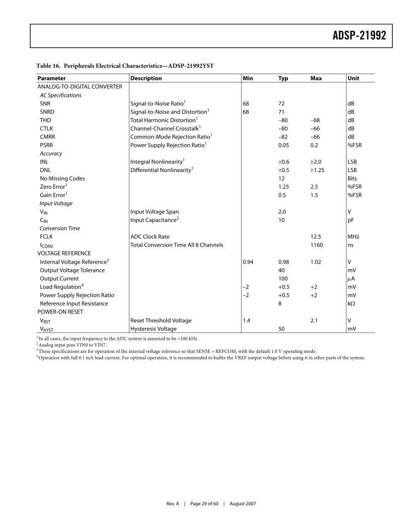
ADSP-21992
Rev. A | Page 29 of 60 | August 2007
Table 16. Peripherals Electrical Characteristics—ADSP-21992YST
Parameter Description Min Typ Max UnitANALOG-TO-DIGITAL CONVERTER
AC Specifications SNR Signal-to-Noise Ratio1 68 72 dB SNRD Signal-to-Noise and Distortion1 68 71 dB THD Total Harmonic Distortion1 –80 –68 dB CTLK Channel-Channel Crosstalk1 –80 –66 dB CMRR Common-Mode Rejection Ratio1 –82 –66 dB PSRR Power Supply Rejection Ratio1 0.05 0.2 %FSR Accuracy INL Integral Nonlinearity1 ±0.6 ±2.0 LSB DNL Differential Nonlinearity1 ±0.5 ±1.25 LSB No Missing Codes 12 Bits Zero Error1 1.25 2.5 %FSR Gain Error1 0.5 1.5 %FSR Input Voltage VIN Input Voltage Span 2.0 V CIN Input Capacitance2 10 pF Conversion Time FCLK ADC Clock Rate 12.5 MHz tCONV Total Conversion Time All 8 Channels 1160 nsVOLTAGE REFERENCE
Internal Voltage Reference3 0.94 0.98 1.02 V Output Voltage Tolerance 40 mV Output Current 100 μA Load Regulation4 –2 +0.5 +2 mV Power Supply Rejection Ratio –2 +0.5 +2 mV Reference Input Resistance 8 kΩPOWER-ON RESET
VRST Reset Threshold Voltage 1.4 2.1 V VHYST Hysteresis Voltage 50 mV
1 In all cases, the input frequency to the ADC system is assumed to be <100 kHz.2 Analog input pins VIN0 to VIN7.3 These specifications are for operation of the internal voltage reference so that SENSE = REFCOM, with the default 1.0 V operating mode.4 Operation with full 0.1 mA load current. For optimal operation, it is recommended to buffer the VREF output voltage before using it in other parts of the system.
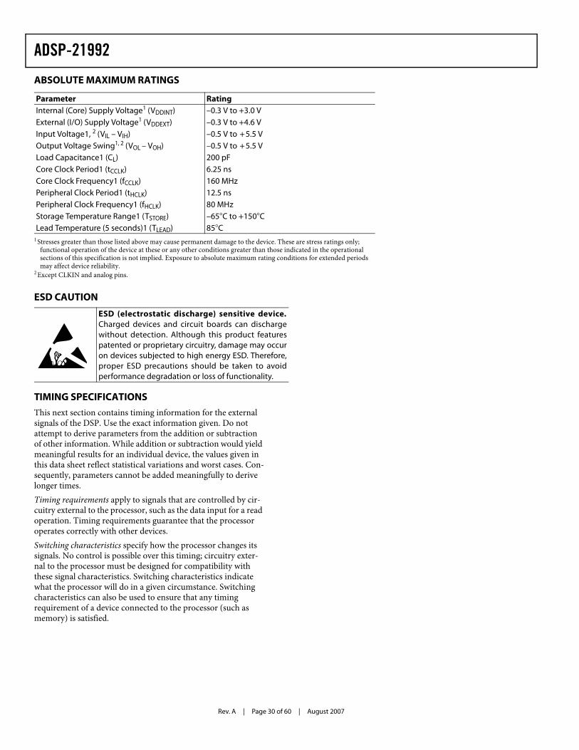
Rev. A | Page 30 of 60 | August 2007
ADSP-21992
ABSOLUTE MAXIMUM RATINGS
ESD CAUTION
TIMING SPECIFICATIONS
This next section contains timing information for the external signals of the DSP. Use the exact information given. Do not attempt to derive parameters from the addition or subtraction of other information. While addition or subtraction would yield meaningful results for an individual device, the values given in this data sheet reflect statistical variations and worst cases. Con-sequently, parameters cannot be added meaningfully to derive longer times.Timing requirements apply to signals that are controlled by cir-cuitry external to the processor, such as the data input for a read operation. Timing requirements guarantee that the processor operates correctly with other devices.Switching characteristics specify how the processor changes its signals. No control is possible over this timing; circuitry exter-nal to the processor must be designed for compatibility with these signal characteristics. Switching characteristics indicate what the processor will do in a given circumstance. Switching characteristics can also be used to ensure that any timing requirement of a device connected to the processor (such as memory) is satisfied.
Parameter RatingInternal (Core) Supply Voltage1 (VDDINT) –0.3 V to +3.0 VExternal (I/O) Supply Voltage1 (VDDEXT) –0.3 V to +4.6 VInput Voltage1, 2 (VIL – VIH) –0.5 V to +5.5 VOutput Voltage Swing1, 2 (VOL – VOH) –0.5 V to +5.5 VLoad Capacitance1 (CL) 200 pFCore Clock Period1 (tCCLK) 6.25 nsCore Clock Frequency1 (fCCLK) 160 MHzPeripheral Clock Period1 (tHCLK) 12.5 nsPeripheral Clock Frequency1 (fHCLK) 80 MHzStorage Temperature Range1 (TSTORE) –65�C to +150�CLead Temperature (5 seconds)1 (TLEAD) 85�C
1 Stresses greater than those listed above may cause permanent damage to the device. These are stress ratings only; functional operation of the device at these or any other conditions greater than those indicated in the operational sections of this specification is not implied. Exposure to absolute maximum rating conditions for extended periods may affect device reliability.
2 Except CLKIN and analog pins.
ESD (electrostatic discharge) sensitive device.Charged devices and circuit boards can dischargewithout detection. Although this product featurespatented or proprietary circuitry, damage may occuron devices subjected to high energy ESD. Therefore,proper ESD precautions should be taken to avoidperformance degradation or loss of functionality.

ADSP-21992
Rev. A | Page 31 of 60 | August 2007
Clock In and Clock Out Cycle Timing
Table 17 and Figure 7 describe clock and reset operations. Com-binations of CLKIN and clock multipliers must not select core/peripheral clocks in excess of 160 MHz/80 MHz for the ADSP-21992BST, 150 MHz/75 MHz for both the ADSP-21992BBC and ADSP-21992YBC, and 100 MHz/50 MHz for the ADSP-21992YST, when the peripheral clock rate is one-
half the core clock rate. If the peripheral clock rate is equal to the core clock rate, the maximum peripheral clock rate is 80 MHz for the ADSP-21992BST, 75 MHz for ADSP-21992BBC and ADSP-21992YBC, and 50 MHz for the ADSP-21992YST. The peripheral clock is supplied to the CLKOUT pins.When changing from bypass mode to PLL mode, allow 512 HCLK cycles for the PLL to stabilize.
Table 17. Clock In and Clock Out Cycle Timing
Parameter Min Max Unit
Timing Requirements
tCK CLKIN Period1, 2 10 200 ns
tCKL CLKIN Low Pulse 4.5 ns
tCKH CLKIN High Pulse 4.5 ns
tWRST RESET Asserted Pulse Width Low 200tCLKOUT ns
tMSS MSELx/BYPASS Stable Before RESET Deasserted Setup 40 μs
tMSH MSELx/BYPASS Stable After RESET Deasserted Hold 1000 ns
tMSD MSELx/BYPASS Stable After RESET Asserted 200 ns
tPFD Flag Output Disable Time After RESET Asserted 10 ns
Switching Characteristics
tCKOD CLKOUT Delay from CLKIN 0 5.8 ns
tCKO CLKOUT Period3 12.5 ns
1 In clock multiplier mode and MSEL6–0 set for 1:1 (or CLKIN = CCLK), tCK = tCCLK.2 In bypass mode, tCK = tCCLK.3 CLKOUT jitter can be as great as 8 ns when CLKOUT frequency is less than 20 MHz. For frequencies greater than 20 MHz, jitter is less than 1 ns.
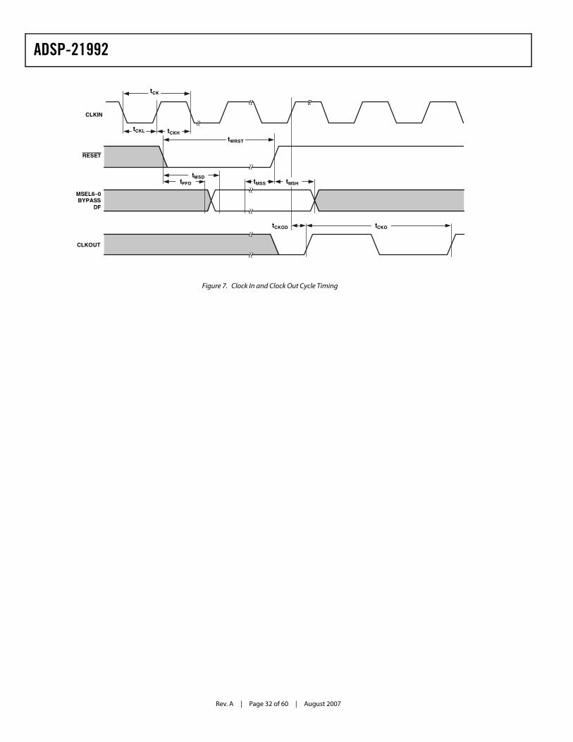
Rev. A | Page 32 of 60 | August 2007
ADSP-21992
Figure 7. Clock In and Clock Out Cycle Timing
tCKOD
CLKOUT
MSEL6–0BYPASS
DF
RESET
CLKIN
tWRST
tCKH
tCK
tCKL
tMSH
tCKO
tPFD
tMSDtMSS
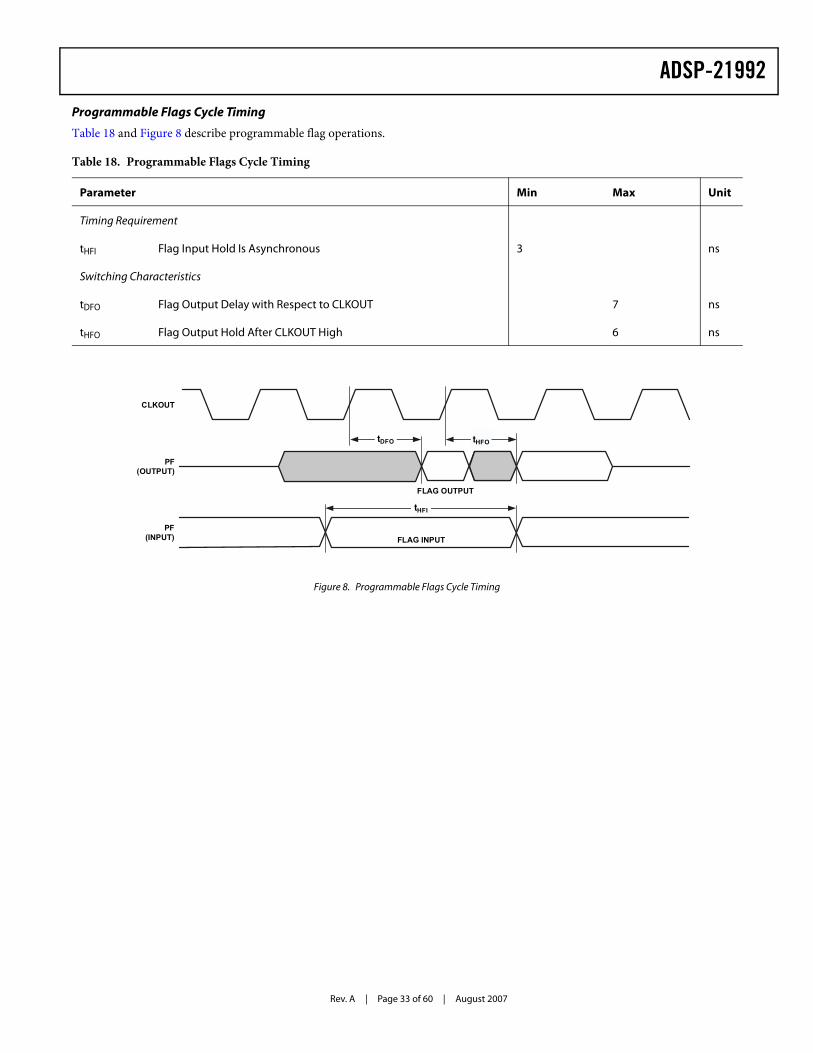
ADSP-21992
Rev. A | Page 33 of 60 | August 2007
Programmable Flags Cycle Timing
Table 18 and Figure 8 describe programmable flag operations.
Table 18. Programmable Flags Cycle Timing
Parameter Min Max Unit
Timing Requirement
tHFI Flag Input Hold Is Asynchronous 3 ns
Switching Characteristics
tDFO Flag Output Delay with Respect to CLKOUT 7 ns
tHFO Flag Output Hold After CLKOUT High 6 ns
Figure 8. Programmable Flags Cycle Timing
tDFO
PF(INPUT)
tHFI
PF(OUTPUT)
CLKOUT
FLAG INPUT
FLAG OUTPUT
tHFO
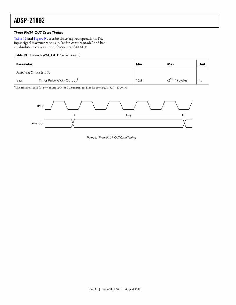
Rev. A | Page 34 of 60 | August 2007
ADSP-21992
Timer PWM_OUT Cycle Timing
Table 19 and Figure 9 describe timer expired operations. The input signal is asynchronous in “width capture mode” and has an absolute maximum input frequency of 40 MHz.
Table 19. Timer PWM_OUT Cycle Timing
Parameter Min Max Unit
Switching Characteristic
tHTO Timer Pulse Width Output1 12.5 (232 –1) cycles ns
1 The minimum time for tHTO is one cycle, and the maximum time for tHTO equals (232 –1) cycles.
Figure 9. Timer PWM_OUT Cycle Timing
HCLK
PWM_OUT
tHTO
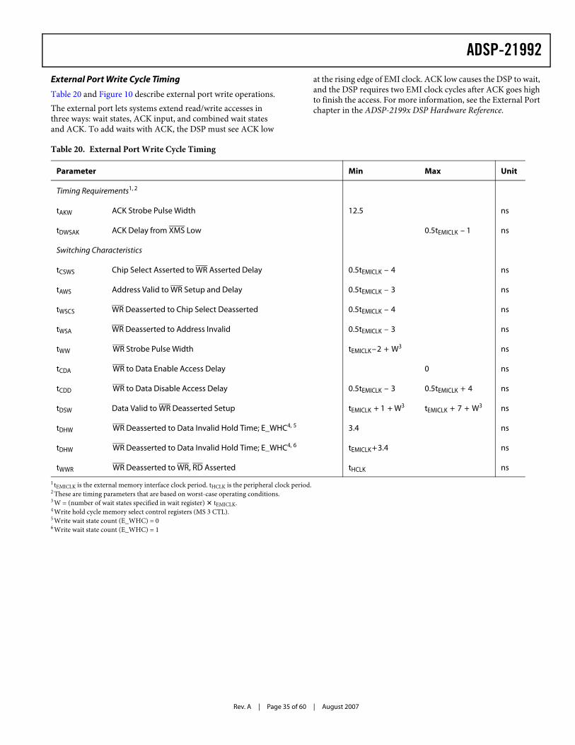
ADSP-21992
Rev. A | Page 35 of 60 | August 2007
External Port Write Cycle Timing
Table 20 and Figure 10 describe external port write operations.The external port lets systems extend read/write accesses in three ways: wait states, ACK input, and combined wait states and ACK. To add waits with ACK, the DSP must see ACK low
at the rising edge of EMI clock. ACK low causes the DSP to wait, and the DSP requires two EMI clock cycles after ACK goes high to finish the access. For more information, see the External Port chapter in the ADSP-2199x DSP Hardware Reference.
Table 20. External Port Write Cycle Timing
Parameter Min Max Unit
Timing Requirements1, 2
tAKW ACK Strobe Pulse Width 12.5 ns
tDWSAK ACK Delay from XMS Low 0.5tEMICLK – 1 ns
Switching Characteristics
tCSWS Chip Select Asserted to WR Asserted Delay 0.5tEMICLK – 4 ns
tAWS Address Valid to WR Setup and Delay 0.5tEMICLK – 3 ns
tWSCS WR Deasserted to Chip Select Deasserted 0.5tEMICLK – 4 ns
tWSA WR Deasserted to Address Invalid 0.5tEMICLK – 3 ns
tWW WR Strobe Pulse Width tEMICLK–2 + W3 ns
tCDA WR to Data Enable Access Delay 0 ns
tCDD WR to Data Disable Access Delay 0.5tEMICLK – 3 0.5tEMICLK + 4 ns
tDSW Data Valid to WR Deasserted Setup tEMICLK + 1 + W3 tEMICLK + 7 + W3 ns
tDHW WR Deasserted to Data Invalid Hold Time; E_WHC4, 5 3.4 ns
tDHW WR Deasserted to Data Invalid Hold Time; E_WHC4, 6 tEMICLK+3.4 ns
tWWR WR Deasserted to WR, RD Asserted tHCLK ns
1 tEMICLK is the external memory interface clock period. tHCLK is the peripheral clock period. 2 These are timing parameters that are based on worst-case operating conditions.3 W = (number of wait states specified in wait register) � tEMICLK.4 Write hold cycle memory select control registers (MS 3 CTL).5 Write wait state count (E_WHC) = 06 Write wait state count (E_WHC) = 1
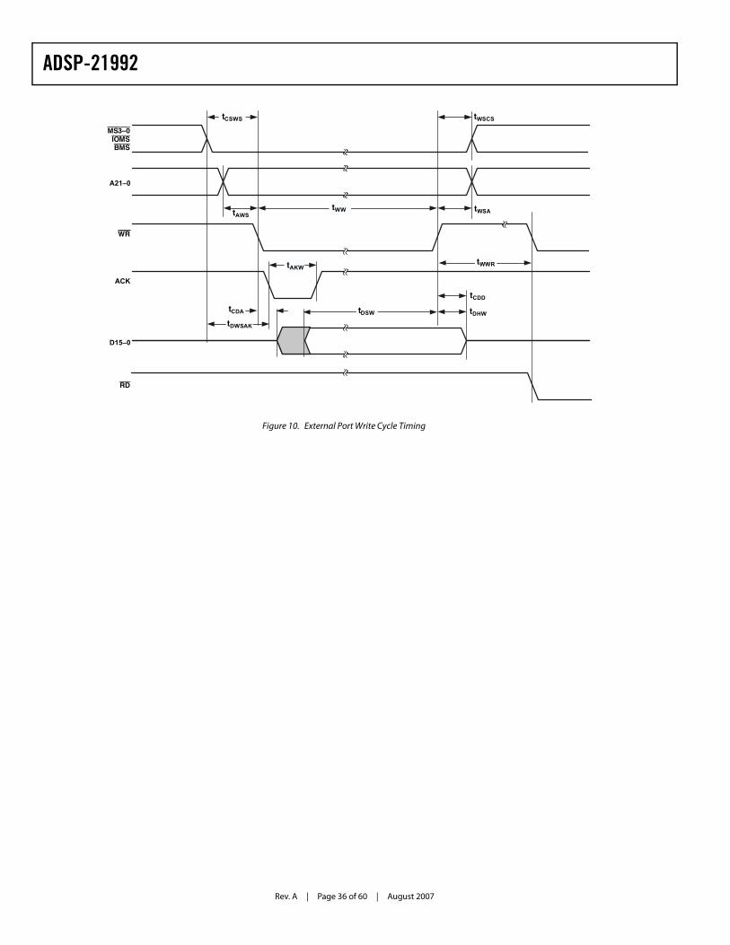
Rev. A | Page 36 of 60 | August 2007
ADSP-21992
Figure 10. External Port Write Cycle Timing
D15–0
tAWStWW
tAKW
tDHW
tCDD
ACK
WR
A21–0
MS3–0IOMSBMS
tCSWS
tWSA
tWSCS
tCDA
RD
tDSW
tWWR
tDWSAK
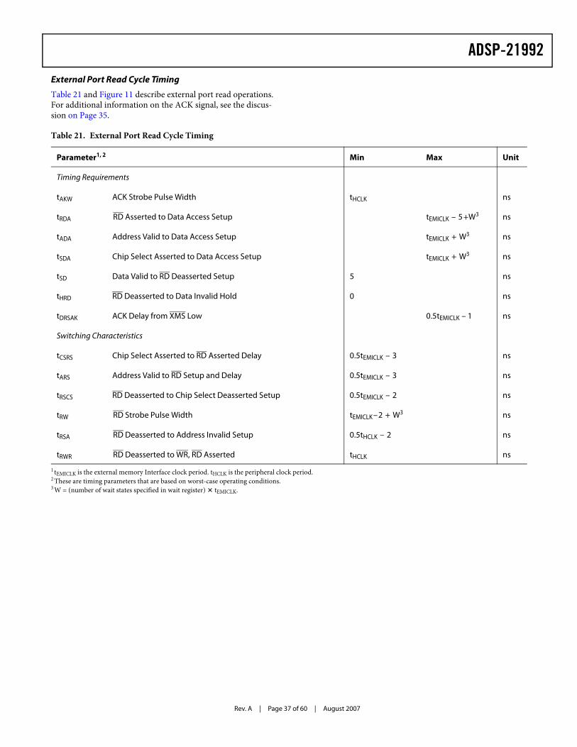
ADSP-21992
Rev. A | Page 37 of 60 | August 2007
External Port Read Cycle Timing
Table 21 and Figure 11 describe external port read operations. For additional information on the ACK signal, see the discus-sion on Page 35.
Table 21. External Port Read Cycle Timing
Parameter1, 2 Min Max Unit
Timing Requirements
tAKW ACK Strobe Pulse Width tHCLK ns
tRDA RD Asserted to Data Access Setup tEMICLK – 5+W3 ns
tADA Address Valid to Data Access Setup tEMICLK + W3 ns
tSDA Chip Select Asserted to Data Access Setup tEMICLK + W3 ns
tSD Data Valid to RD Deasserted Setup 5 ns
tHRD RD Deasserted to Data Invalid Hold 0 ns
tDRSAK ACK Delay from XMS Low 0.5tEMICLK – 1 ns
Switching Characteristics
tCSRS Chip Select Asserted to RD Asserted Delay 0.5tEMICLK – 3 ns
tARS Address Valid to RD Setup and Delay 0.5tEMICLK – 3 ns
tRSCS RD Deasserted to Chip Select Deasserted Setup 0.5tEMICLK – 2 ns
tRW RD Strobe Pulse Width tEMICLK–2 + W3 ns
tRSA RD Deasserted to Address Invalid Setup 0.5tHCLK – 2 ns
tRWR RD Deasserted to WR, RD Asserted tHCLK ns
1 tEMICLK is the external memory Interface clock period. tHCLK is the peripheral clock period. 2 These are timing parameters that are based on worst-case operating conditions.3 W = (number of wait states specified in wait register) � tEMICLK.

Rev. A | Page 38 of 60 | August 2007
ADSP-21992
Figure 11. External Port Read Cycle Timing
tARS
D15–0
tRW
tAKW
tCDA
tRDA
tADA
tSDA
tSD tH RD
ACK
RD
A21–0
tCSRS
tRSA
tRSCS
tRWR
MS3–0IOMSBMS
WR
tDRSAK

ADSP-21992
Rev. A | Page 39 of 60 | August 2007
External Port Bus Request/Grant Cycle Timing
Table 22 and Figure 12 describe external port bus request and bus grant operations.
Table 22. External Port Bus Request and Grant Cycle Timing
Parameter1, 2 Min Max Unit
Timing Requirements
tBS BR Asserted to CLKOUT High Setup 4.6 ns
tBH CLKOUT High to BR Deasserted Hold Time 0 ns
Switching Characteristics
tSD CLKOUT High to xMS, Address, and RD/WR Disable 0.5tHCLK + 1 ns
tSE CLKOUT Low to xMS, Address, and RD/WR Enable 0 4 ns
tDBG CLKOUT High to BG Asserted Setup 0 4 ns
tEBG CLKOUT High to BG Deasserted Hold Time 0 4 ns
tDBH CLKOUT High to BGH Asserted Setup 0 4 ns
tEBH CLKOUT High to BGH Deasserted Hold Time 0 4 ns
1 tHCLK is the peripheral clock period.2 These are timing parameters that are based on worst-case operating conditions.

Rev. A | Page 40 of 60 | August 2007
ADSP-21992
Figure 12. External Port Bus Request and Grant Cycle Timing
tBH
A21–0
CLKOUT
tBS
tSD
tSD
tSD
tDBG
tDBH
tSE
tSE
tSE
tEBG
tEBH
BGH
WRRD
MS3–0IOMSBMS
BR
BG

ADSP-21992
Rev. A | Page 41 of 60 | August 2007
Serial Port Timing
Table 23 and Figure 13 describe SPORT transmit and receive operations, while Figure 14 and Figure 15 describe SPORT frame sync operations.
Table 23. Serial Port1, 2
Parameter Min Max Unit
External Clock Timing Requirements
tSFSE TFS/RFS Setup Before TCLK/RCLK3 4 ns
tHFSE TFS/RFS Hold After TCLK/RCLK3 4 ns
tSDRE Receive Data Setup Before RCLK3 1.5 ns
tHDRE Receive Data Hold After RCLK3 4 ns
tSCLKW TCLK/RCLK Width 0.5tHCLK –1 ns
tSCLK TCLK/RCLK Period 2tHCLK ns
Internal Clock Timing Requirements
tSFSI TFS Setup Before TCLK4; RFS Setup Before RCLK3 4 ns
tHFSI TFS/RFS Hold After TCLK/RCLK3 3 ns
tSDRI Receive Data Setup Before RCLK3 2 ns
tHDRI Receive Data Hold After RCLK3 5 ns
External or Internal Clock Switching Characteristics
tDFSE TFS/RFS Delay After TCLK/RCLK (Internally Generated FS)4
14 ns
tHOFSE TFS/RFS Hold After TCLK/RCLK (Internally Generated FS)4
3 ns
External Clock Switching Characteristics
tDDTE Transmit Data Delay After TCLK4 13.4 ns
tHDTE Transmit Data Hold After TCLK4 4 ns
Internal Clock Switching Characteristics
tDDTI Transmit Data Delay After TCLK4 13.4 ns
tHDTI Transmit Data Hold After TCLK4 4 ns
tSCLKIW TCLK/RCLK Width 0.5tHCLK – 3.5 0.5tHCLK + 2.5 ns
Enable and Three-State Switching Characteristics5
tDTENE Data Enable from External TCLK4 0 12.1 ns
tDDTTE Data Disable from External TCLK4 13 ns
tDTENI Data Enable from Internal TCLK4 0 13 ns
tDDTTI Data Disable from External TCLK4 12 ns
External Late Frame Sync Switching Characteristics
tDDTLFSE Data Delay from Late External TFS with MCE =1, MFD=06, 7 10.5 ns
tDTENLFSE Data Enable from Late FS or MCE =1, MFD=06, 7 3.5 ns1 To determine whether communication is possible between two devices at clock speed n, the following specifications must be confirmed: 1) frame sync delay and frame
sync setup-and-hold, 2) data delay and data setup-and-hold, and 3) SCLK width.2 Word selected timing for I2S mode is the same as TFS/RFS timing (normal framing only).3 Referenced to sample edge.4 Referenced to drive edge.5 Only applies to SPORT.6 MCE =1, TFS enable, and TFS valid follow tDDTENFS and tDDTLFSE.7 If external RFSD/TFS setup to RCLK/TCLK > 0.5tLSCK, tDDTLSCK and tDTENLSCK apply; otherwise, tDDTLFSE and tDTENLFS apply.
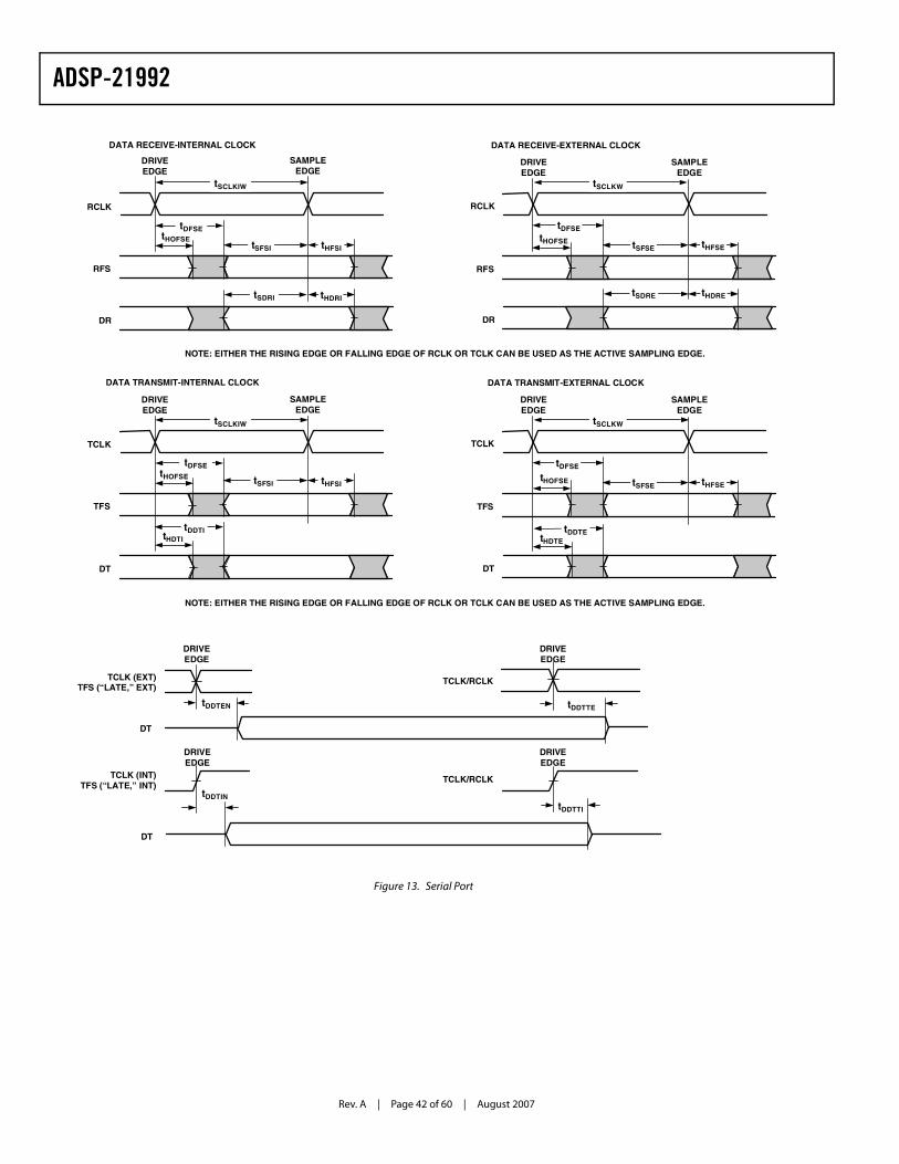
Rev. A | Page 42 of 60 | August 2007
ADSP-21992
Figure 13. Serial Port
DT
DT
tDDTTEtDDTEN
tDDTTI
tDDTIN
DRIVEEDGE
DRIVEEDGE
DRIVEEDGE
DRIVEEDGE
TCLK/RCLK
TCLK/RCLKTCLK (EXT)TFS (“LATE,” EXT)
tSDRI
RCLK
RFS
DR
DRIVEEDGE
SAMPLEEDGE
tHDRI
tSFSI tHFSI
tDFSEtHOFSE
tSCLKIW
DATA RECEIVE-INTERNAL CLOCK
tSDRE
DATA RECEIVE-EXTERNAL CLOCK
RCLK
RFS
DR
DRIVEEDGE
SAMPLEEDGE
tHDRE
tSFSE tHFSE
tDFSE
tSCLKW
tHOFSE
NOTE: EITHER THE RISING EDGE OR FALLING EDGE OF RCLK OR TCLK CAN BE USED AS THE ACTIVE SAMPLING EDGE.
tDDTItHDTI
TCLK
TFS
DT
DRIVEEDGE
SAMPLEEDGE
tSFSI tHFSI
tSCLKIW
tDFSEtHOFSE
DATA TRANSMIT-INTERNAL CLOCK
tDDTEtHDTE
TCLK
TFS
DT
DRIVEEDGE
SAMPLEEDGE
tSFSE tHFSE
tDFSE
tSCLKW
tHOFSE
DATA TRANSMIT-EXTERNAL CLOCK
NOTE: EITHER THE RISING EDGE OR FALLING EDGE OF RCLK OR TCLK CAN BE USED AS THE ACTIVE SAMPLING EDGE.
TCLK (INT)TFS (“LATE,” INT)
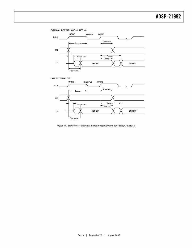
ADSP-21992
Rev. A | Page 43 of 60 | August 2007
Figure 14. Serial Port—External Late Frame Sync (Frame Sync Setup > 0.5tSCLK)
DRIVE SAMPLE DRIVE
tDTENLFSE
tDDTLFSE
EXTERNAL RFS WITH MCE = 1, MFD = 0
1ST BIT 2ND BITDT
RCLK
RFS
LATE EXTERNAL TFS
tHDTE/ I
tDDTE/ I
tSFSE/I
DRIVE SAMPLE DRIVE
tDTENLFSE
tDDTLFSE
1ST BIT 2ND BITDT
TCLK
TFS
tHDTE/ I
tDDTE/ I
tHOSFSE/ I
tHOSFSE/ I
tSFSE/I
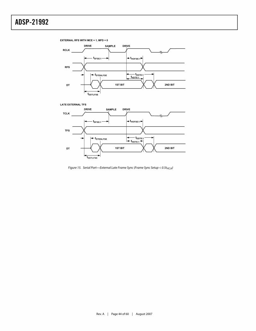
Rev. A | Page 44 of 60 | August 2007
ADSP-21992
Figure 15. Serial Port—External Late Frame Sync (Frame Sync Setup < 0.5tHCLK)
tDDTLFSE
DRIVE SAMPLE DRIVE
tDTENLFSE
tDDTLFSE
EXTERNAL RFS WITH MCE = 1, MFD = 0
1ST BIT 2ND BITDT
RCLK
RFS
LATE EXTERNAL TFS
tHDTE/ ItDDTE/ I
tSFSE/ I
DRIVE SAMPLE DRIVE
tDTENLFSE
1ST BIT 2ND BITDT
TCLK
TFS
tHDTE/ ItDDTE/ I
tHOFSE/ I
tHOFSE/ ItSFSE/ I

ADSP-21992
Rev. A | Page 45 of 60 | August 2007
Serial Peripheral Interface Port—Master Timing
Table 24 and Figure 16 describe SPI port master operations.
Table 24. Serial Peripheral Interface (SPI) Port—Master Timing
Parameter Min Max Unit
Timing Requirements
tSSPID Data Input Valid to SCLK Edge (Data Input Setup) 8 ns
tHSPID SCLK Sampling Edge to Data Input Invalid (Data In Hold) 1 ns
Switching Characteristics
tSDSCIM SPISEL Low to First SCLK Edge 2tHCLK –3 ns
tSPICHM Serial Clock High Period 2tHCLK –3 ns
tSPICLM Serial Clock Low Period 2tHCLK –3 ns
tSPICLK Serial Clock Period 4tHCLK –1 ns
tHDSM Last SCLK Edge to SPISEL High 2tHCLK –3 ns
tSPITDM Sequential Transfer Delay 2tHCLK –2 ns
tDDSPID SCLK Edge to Data Output Valid (Data Out Delay) 0 6 ns
tHDSPID SCLK Edge to Data Output Invalid (Data Out Hold) 0 5 ns
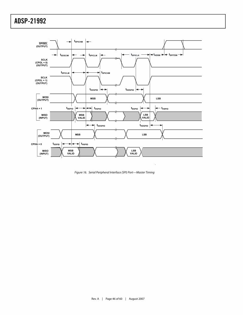
Rev. A | Page 46 of 60 | August 2007
ADSP-21992
Figure 16. Serial Peripheral Interface (SPI) Port—Master Timing
tHSPID
tHDSPID
LSBMSB
tHSPID
tDDSPID
MOSI(OUTPUT)
MISO(INPUT)
SPISEL(OUTPUT)
SCLK(CPOL = 0)(OUTPUT)
SCLK(CPOL = 1)(OUTPUT)
tSPICHM
tSPICLM
tSPICLM
tSPICLK
tSPICHM
tHDSM tSPITDM
tHDSPID
LSBVALID
LSBMSB
MSBVALID
tHSPID
tDDSPID
MOSI(OUTPUT)
MISO(INPUT)
tSSPID
tSDSCIM
tSSPIDCPHA = 1
CPHA = 0
MSBVALID
LSBVALID
tSSPID
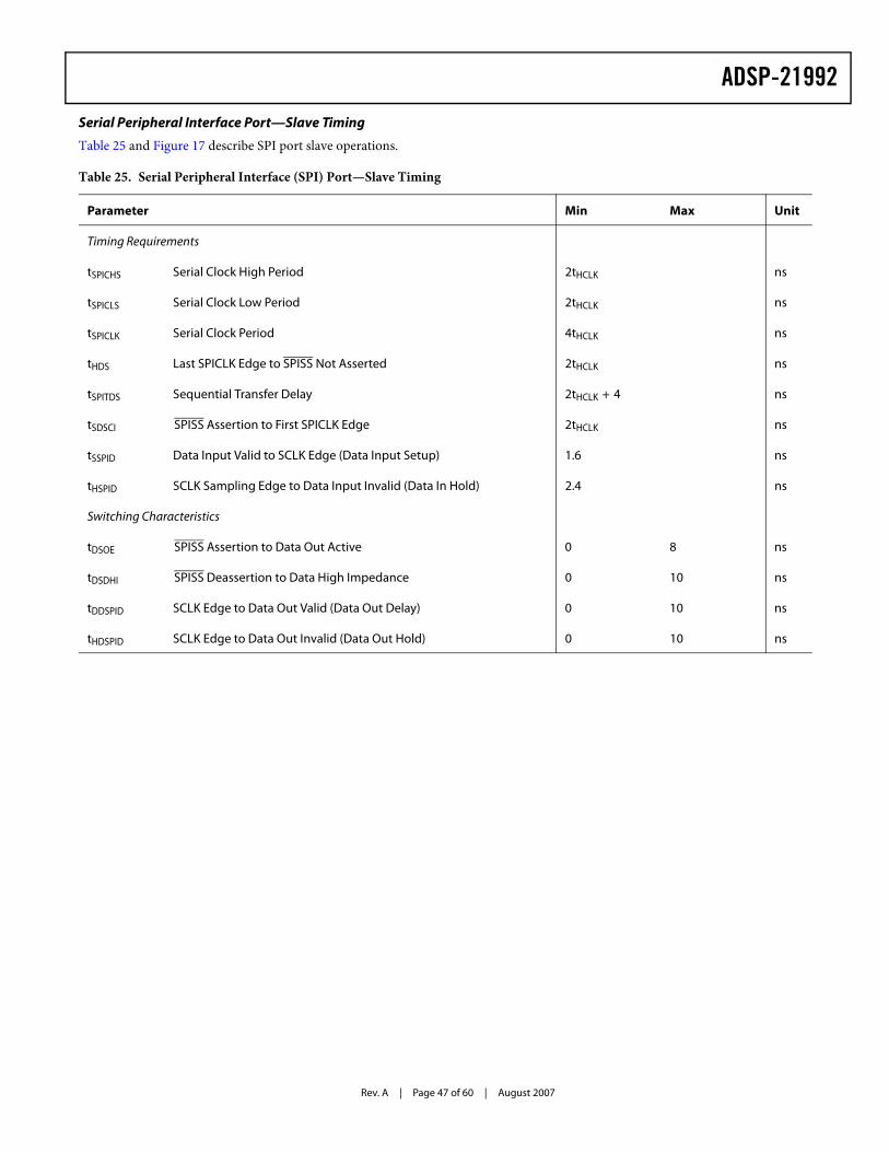
ADSP-21992
Rev. A | Page 47 of 60 | August 2007
Serial Peripheral Interface Port—Slave Timing
Table 25 and Figure 17 describe SPI port slave operations.
Table 25. Serial Peripheral Interface (SPI) Port—Slave Timing
Parameter Min Max Unit
Timing Requirements
tSPICHS Serial Clock High Period 2tHCLK ns
tSPICLS Serial Clock Low Period 2tHCLK ns
tSPICLK Serial Clock Period 4tHCLK ns
tHDS Last SPICLK Edge to SPISS Not Asserted 2tHCLK ns
tSPITDS Sequential Transfer Delay 2tHCLK + 4 ns
tSDSCI SPISS Assertion to First SPICLK Edge 2tHCLK ns
tSSPID Data Input Valid to SCLK Edge (Data Input Setup) 1.6 ns
tHSPID SCLK Sampling Edge to Data Input Invalid (Data In Hold) 2.4 ns
Switching Characteristics
tDSOE SPISS Assertion to Data Out Active 0 8 ns
tDSDHI SPISS Deassertion to Data High Impedance 0 10 ns
tDDSPID SCLK Edge to Data Out Valid (Data Out Delay) 0 10 ns
tHDSPID SCLK Edge to Data Out Invalid (Data Out Hold) 0 10 ns
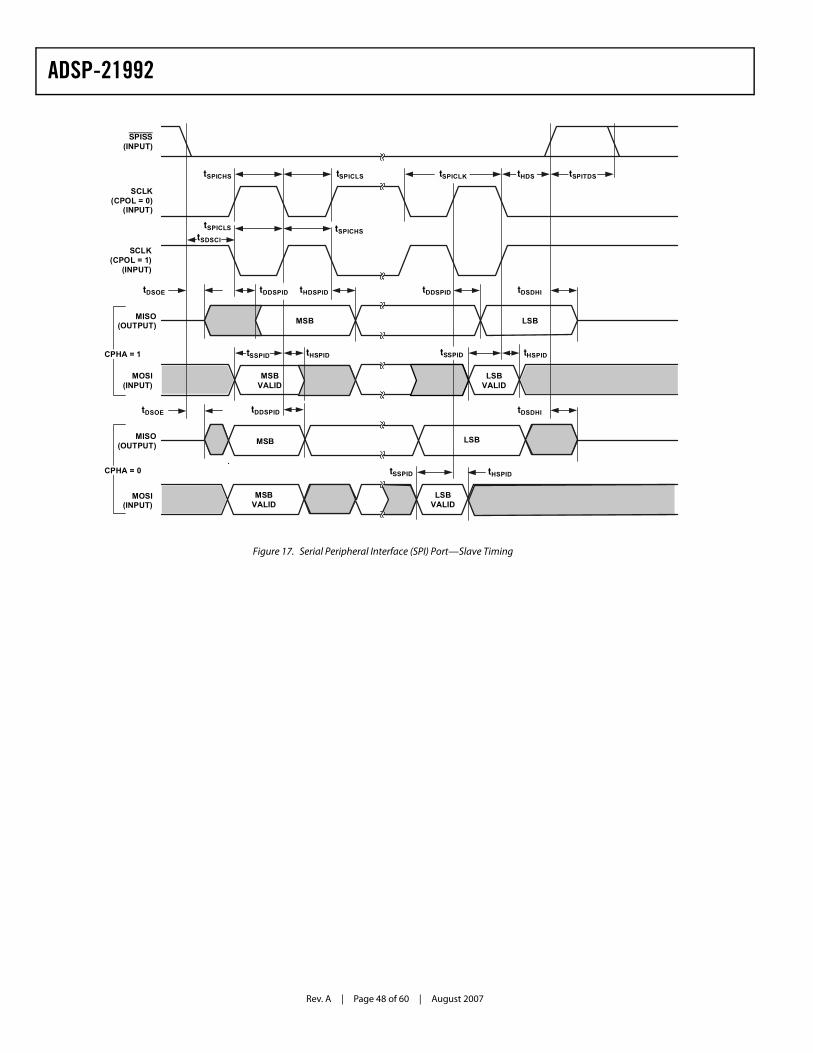
Rev. A | Page 48 of 60 | August 2007
ADSP-21992
Figure 17. Serial Peripheral Interface (SPI) Port—Slave Timing
tHSPID
tDDSPID tDSDHI
LSBMSB
MSBVALID
tHSPID
tDSOE tHDSPID
MISO(OUTPUT)
MOSI(INPUT)
SPISS(INPUT)
SCLK(CPOL = 0)
(INPUT)
SCLK(CPOL = 1)
(INPUT)
tSPICHS tSPICLS
tSPICLS
tSPICLK tHDS
tSPICHS
tSSPID tHSPID
tDSDHI
LSBVALID
MSB
MSBVALID
tDSOE tDDSPID
MISO(OUTPUT)
MOSI(INPUT)
LSBVALID
LSB
tDDSPID
CPHA = 0
CPHA = 1
tSDSCI
tSSPID tSSPID
tSPITDS
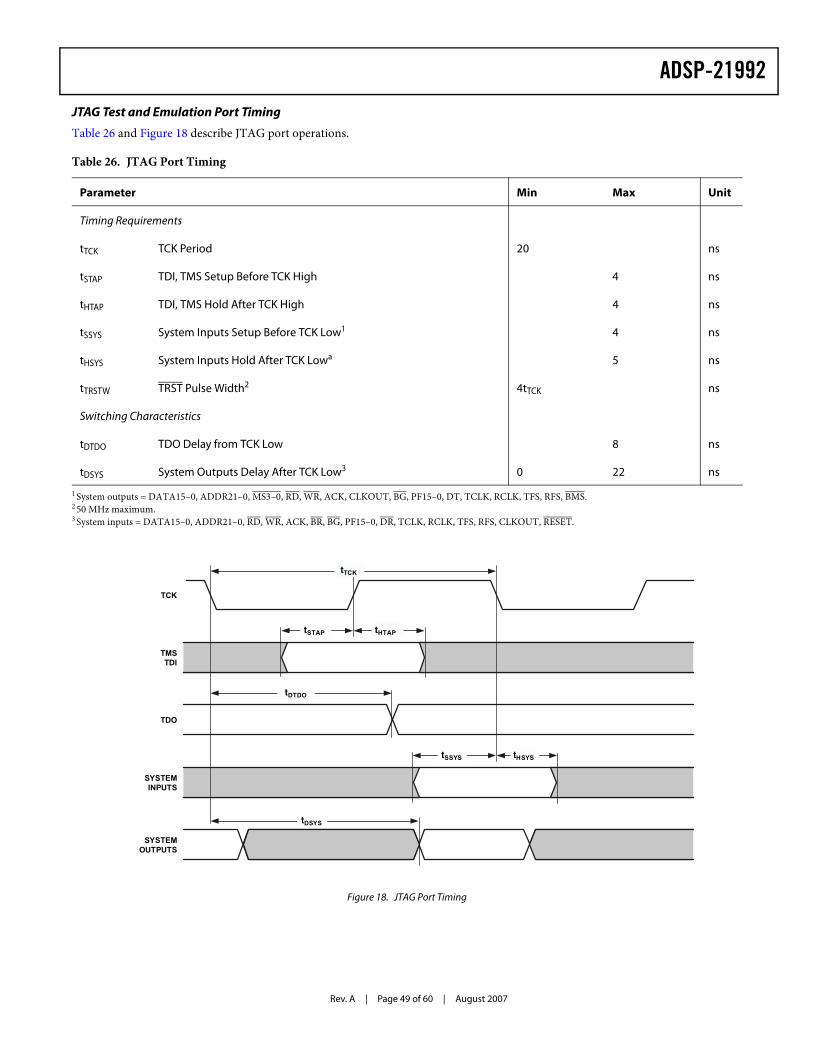
ADSP-21992
Rev. A | Page 49 of 60 | August 2007
JTAG Test and Emulation Port Timing
Table 26 and Figure 18 describe JTAG port operations.
Table 26. JTAG Port Timing
Parameter Min Max Unit
Timing Requirements
tTCK TCK Period 20 ns
tSTAP TDI, TMS Setup Before TCK High 4 ns
tHTAP TDI, TMS Hold After TCK High 4 ns
tSSYS System Inputs Setup Before TCK Low1 4 ns
tHSYS System Inputs Hold After TCK Lowa 5 ns
tTRSTW TRST Pulse Width2 4tTCK ns
Switching Characteristics
tDTDO TDO Delay from TCK Low 8 ns
tDSYS System Outputs Delay After TCK Low3 0 22 ns
1 System outputs = DATA15–0, ADDR21–0, MS3–0, RD, WR, ACK, CLKOUT, BG, PF15–0, DT, TCLK, RCLK, TFS, RFS, BMS.2 50 MHz maximum.3 System inputs = DATA15–0, ADDR21–0, RD, WR, ACK, BR, BG, PF15–0, DR, TCLK, RCLK, TFS, RFS, CLKOUT, RESET.
Figure 18. JTAG Port Timing
TMSTDI
TDO
SYSTEMINPUTS
SYSTEMOUTPUTS
TCK
tTCK
tHTAPtSTAP
tDTDO
tSSYS tHSYS
tDSYS
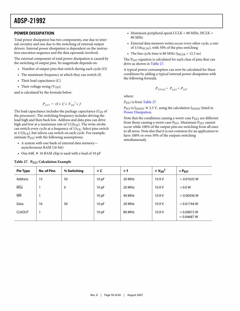
Rev. A | Page 50 of 60 | August 2007
ADSP-21992
POWER DISSIPATION
Total power dissipation has two components, one due to inter-nal circuitry and one due to the switching of external output drivers. Internal power dissipation is dependent on the instruc-tion execution sequence and the data operands involved.The external component of total power dissipation is caused by the switching of output pins. Its magnitude depends on:
• Number of output pins that switch during each cycle (O)• The maximum frequency at which they can switch (f)• Their load capacitance (C)• Their voltage swing (VDD)
and is calculated by the formula below.
The load capacitance includes the package capacitance (CIN of the processor). The switching frequency includes driving the load high and then back low. Address and data pins can drive high and low at a maximum rate of 1/(2tCK). The write strobe can switch every cycle at a frequency of 1/tCK. Select pins switch at 1/(2tCK), but selects can switch on each cycle. For example, estimate PEXT with the following assumptions:
• A system with one bank of external data memory—asynchronous RAM (16-bit)
• One 64K � 16 RAM chip is used with a load of 10 pF
• Maximum peripheral speed CCLK = 80 MHz, HCLK = 80 MHz
• External data memory writes occur every other cycle, a rate of 1/(4tHCLK), with 50% of the pins switching
• The bus cycle time is 80 MHz (tHCLK = 12.5 ns)The PEXT equation is calculated for each class of pins that can drive as shown in Table 27.A typical power consumption can now be calculated for these conditions by adding a typical internal power dissipation with the following formula.
where:PEXT is from Table 27.PINT is IDDINT � 2.5 V, using the calculation IDDINT listed in Power Dissipation.Note that the conditions causing a worst-case PEXT are different from those causing a worst-case PINT. Maximum PINT cannot occur while 100% of the output pins are switching from all ones to all zeros. Note also that it is not common for an application to have 100% or even 50% of the outputs switching simultaneously.
PEXT O C× VDD2× f×=
PTOTAL P= EXT PINT+
Table 27. PEXT Calculation Example
Pin Type No. of Pins % Switching � C � f � VDD2 = PEXT
Address 15 50 10 pF 20 MHz 10.9 V = 0.01635 W
MSx 1 0 10 pF 20 MHz 10.9 V = 0.0 W
WR 1 10 pF 40 MHz 10.9 V = 0.00436 W
Data 16 50 10 pF 20 MHz 10.9 V = 0.01744 W
CLKOUT 1 10 pF 80 MHz 10.9 V = 0.00872 W= 0.04687 W
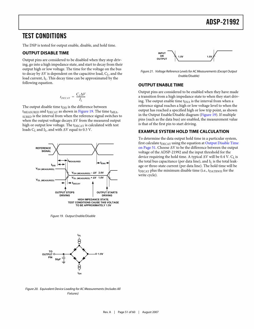
ADSP-21992
Rev. A | Page 51 of 60 | August 2007
TEST CONDITIONSThe DSP is tested for output enable, disable, and hold time.
OUTPUT DISABLE TIME
Output pins are considered to be disabled when they stop driv-ing, go into a high impedance state, and start to decay from their output high or low voltage. The time for the voltage on the bus to decay by ΔV is dependent on the capacitive load, CL, and the load current, IL. This decay time can be approximated by the following equation.
The output disable time tDIS is the difference between tMEASURED and tDECAY as shown in Figure 19. The time tMEA-SURED is the interval from when the reference signal switches to when the output voltage decays ΔV from the measured output high or output low voltage. The tDECAY is calculated with test loads CL and IL, and with ΔV equal to 0.5 V.
OUTPUT ENABLE TIME
Output pins are considered to be enabled when they have made a transition from a high impedance state to when they start driv-ing. The output enable time tENA is the interval from when a reference signal reaches a high or low voltage level to when the output has reached a specified high or low trip point, as shown in the Output Enable/Disable diagram (Figure 19). If multiple pins (such as the data bus) are enabled, the measurement value is that of the first pin to start driving.
EXAMPLE SYSTEM HOLD TIME CALCULATION
To determine the data output hold time in a particular system, first calculate tDECAY using the equation at Output Disable Time on Page 51. Choose ΔV to be the difference between the output voltage of the ADSP-21992 and the input threshold for the device requiring the hold time. A typical ΔV will be 0.4 V. CL is the total bus capacitance (per data line), and IL is the total leak-age or three-state current (per data line). The hold time will be tDECAY plus the minimum disable time (i.e., tDATRWH for the write cycle).
Figure 19. Output Enable/Disable
Figure 20. Equivalent Device Loading for AC Measurements (Includes All Fixtures)
tDECAYCL VΔIL
--------------=
REFERENCESIGNAL
tDIS
OUTPUT STARTSDRIVING
VOH (MEASURED) – �V 2.0V
VOL (MEASURED) + �V 1.0V
tMEASURED
VOH (MEASURED)
VOL (MEASURED)
HIGH IMPEDANCE STATE.TEST CONDITIONS CAUSE THIS VOLTAGE
TO BE APPROXIMATELY 1.5V
OUTPUT STOPSDRIVING
tDECAY
tENA
1.5V
50pF
TOOUTPUT
PIN
IOL
IOH
Figure 21. Voltage Reference Levels for AC Measurements (Except Output Enable/Disable)
INPUTOR
OUTPUT1.5V 1.5V

Rev. A | Page 52 of 60 | August 2007
ADSP-21992
PIN CONFIGURATIONSTable 28 identifies the signal for each CSP_BGA ball number. Table 29 identifies the CSP_BGA ball number for each signal name. Table 30 identifies the signal for each LQFP lead. Table 31 identifies the LQFP lead for each signal name. Table 4 on Page 17 describes each signal.

ADSP-21992
Rev. A | Page 53 of 60 | August 2007
Table 28. 196-Ball CSP_BGA Signal by Ball Number
Ball No. Signal Ball No. Signal Ball No. Signal Ball No. SignalA1 nc D8 AVSS H1 A10 L8 VDDINTA2 DR D9 PF3/SPISEL3 H2 A11 L9 VDDEXTA3 DT D10 AUXTRIP H3 MS3 L10 VDDEXTA4 RFS D11 VDDEXT H4 GND L11 GNDA5 VIN4 D12 AUX1 H5 nc L12 BMODE2A6 BSHAN D13 AUX0 H6 nc L13 BMODE1A7 VIN0 D14 PF15 H7 nc L14 CLKINA8 VIN1 E1 A16 H8 nc M1 A2A9 VIN3 E2 A17 H9 nc M2 A3A10 PF0/SPISS E3 WR H10 nc M3 MS2 A11 PF4/SPISEL4 E4 GND H11 VDDEXT M4 GNDA12 PF6/SPISEL6 E5 VDDEXT H12 TMR0 M5 VDDEXTA13 PF7/SPISEL7 E6 nc H13 POR M6 GNDA14 nc E7 nc H14 RESET M7 VDDEXTB1 SCK E8 nc J1 A8 M8 CANRXB2 RCLK E9 nc J2 A9 M9 CLB3 TCLK E10 nc J3 BMS M10 ALB4 TFS E11 GND J4 VDDEXT M11 PWMPOLB5 VIN6 E12 EIA J5 nc M12 PWMTRIP B6 ASHAN E13 EIB J6 nc M13 BYPASSB7 VIN2 E14 EIS J7 nc M14 BMODE0B8 SENSE F1 A14 J8 nc N1 A0B9 CAPB F2 A15 J9 nc N2 A1B10 PF1/SPISEL1 F3 BG J10 nc N3 D13B11 PF5/SPISEL5 F4 GND J11 GND N4 D11B12 PF8 F5 nc J12 TMS N5 D9B13 PF9 F6 nc J13 TCK N6 D7B14 PF13 F7 nc J14 TDI N7 D5C1 BR F8 nc K1 A6 N8 D3C2 RD F9 nc K2 A7 N9 D1C3 MISO F10 nc K3 MS0 N10 CHC4 MOSI F11 VDDINT K4 GND N11 AHC5 VIN7 F12 EIZ K5 GND N12 ncC6 VIN5 F13 TMR2 K6 GND N13 PWMSYNCC7 CAPT F14 XTAL K7 GND N14 PWMSR C8 VREF G1 A12 K8 GND P1 ncC9 CML G2 A13 K9 GND P2 D15C10 PF2/SPISEL2 G3 BGH K10 GND P3 D14C11 PF10 G4 VDDINT K11 VDDINT P4 D12C12 PF11 G5 nc K12 EMU P5 D10C13 PF12 G6 nc K13 TRST P6 D8C14 PF14 G7 nc K14 TDO P7 D6D1 A18 G8 nc L1 A4 P8 D4D2 A19 G9 nc L2 A5 P9 D2D3 IOMS G10 nc L3 MS1 P10 D0D4 ACK G11 GND L4 VDDEXT P11 BLD5 AVDD G12 TMR1 L5 VDDINT P12 BHD6 AVDD G13 CONVST L6 VDDEXT P13 CANTXD7 AVSS G14 CLKOUT L7 VDDINT P14 nc
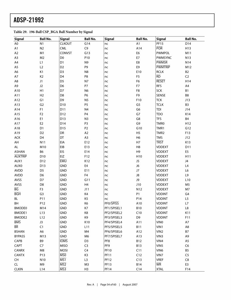
Rev. A | Page 54 of 60 | August 2007
ADSP-21992
Table 29. 196-Ball CSP_BGA Ball Number by Signal
Signal Ball No. Signal Ball No. Signal Ball No. Signal Ball No.A0 N1 CLKOUT G14 nc A1 PF15 D14A1 N2 CML C9 nc A14 POR H13A2 M1 CONVST G13 nc E6 PWMPOL M11A3 M2 D0 P10 nc E7 PWMSYNC N13A4 L1 D1 N9 nc E8 PWMSR N14A5 L2 D2 P9 nc E9 PWMTRIP M12A6 K1 D3 N8 nc E10 RCLK B2A7 K2 D4 P8 nc F5 RD C2A8 J1 D5 N7 nc F6 RESET H14A9 J2 D6 P7 nc F7 RFS A4A10 H1 D7 N6 nc F8 SCK B1A11 H2 D8 P6 nc F9 SENSE B8A12 G1 D9 N5 nc F10 TCK J13A13 G2 D10 P5 nc G5 TCLK B3A14 F1 D11 N4 nc G6 TDI J14A15 F2 D12 P4 nc G7 TDO K14A16 E1 D13 N3 nc G8 TFS B4A17 E2 D14 P3 nc G9 TMR0 H12A18 D1 D15 P2 nc G10 TMR1 G12A19 D2 DR A2 nc H5 TMR2 F13ACK D4 DT A3 nc H6 TMS J12AH N11 EIA E12 nc H7 TRST K13AL M10 EIB E13 nc H8 VDDEXT D11ASHAN B6 EIS E14 nc H9 VDDEXT E5AUXTRIP D10 EIZ F12 nc H10 VDDEXT H11AUX1 D12 EMU K12 nc J5 VDDEXT J4AUX0 D13 GND E4 nc J6 VDDEXT L4AVDD D5 GND E11 nc J7 VDDEXT L6AVDD D6 GND F4 nc J8 VDDEXT L9AVSS D7 GND G11 nc J9 VDDEXT L10AVSS D8 GND H4 nc J10 VDDEXT M5BG F3 GND J11 nc N12 VDDEXT M7BGH G3 GND K4 nc P1 VDDINT G4BL P11 GND K5 nc P14 VDDINT L5BH P12 GND K6 PF0/SPISS A10 VDDINT L7BMODE0 M14 GND K7 PF1/SPISEL1 B10 VDDINT L8BMODE1 L13 GND K8 PF2/SPISEL2 C10 VDDINT K11BMODE2 L12 GND K9 PF3/SPISEL3 D9 VDDINT F11BMS J3 GND K10 PF4/SPISEL4 A11 VIN0 A7BR C1 GND L11 PF5/SPISEL5 B11 VIN1 A8BSHAN A6 GND M4 PF6/SPISEL6 A12 VIN2 B7BYPASS M13 GND M6 PF7/SPISEL7 A13 VIN3 A9CAPB B9 IOMS D3 PF8 B12 VIN4 A5CAPT C7 MISO C3 PF9 B13 VIN5 C6CANRX M8 MOSI C4 PF10 C11 VIN6 B5CANTX P13 MS0 K3 PF11 C12 VIN7 C5CH N10 MS1 L3 PF12 C13 VREF C8CL M9 MS2 M3 PF13 B14 WR E3CLKIN L14 MS3 H3 PF14 C14 XTAL F14
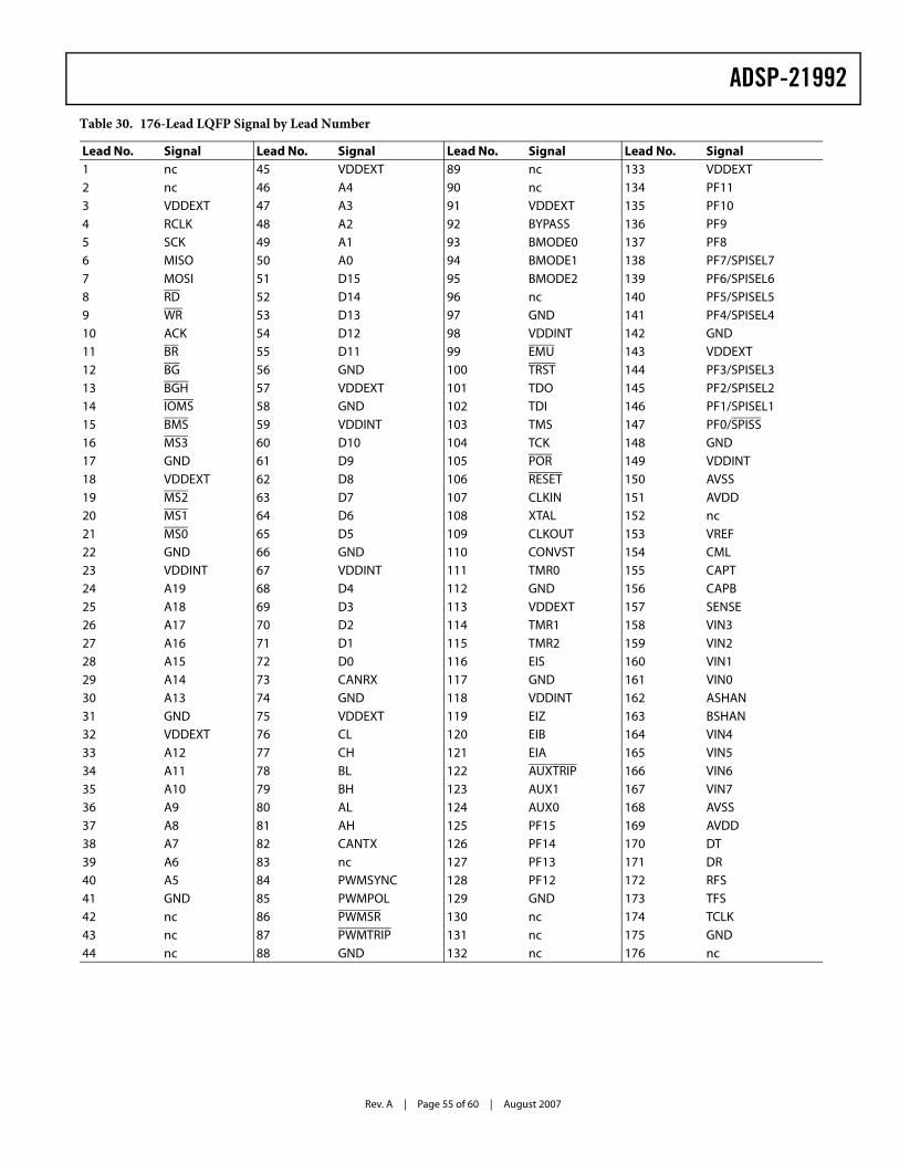
ADSP-21992
Rev. A | Page 55 of 60 | August 2007
Table 30. 176-Lead LQFP Signal by Lead Number
Lead No. Signal Lead No. Signal Lead No. Signal Lead No. Signal1 nc 45 VDDEXT 89 nc 133 VDDEXT2 nc 46 A4 90 nc 134 PF113 VDDEXT 47 A3 91 VDDEXT 135 PF104 RCLK 48 A2 92 BYPASS 136 PF95 SCK 49 A1 93 BMODE0 137 PF86 MISO 50 A0 94 BMODE1 138 PF7/SPISEL77 MOSI 51 D15 95 BMODE2 139 PF6/SPISEL68 RD 52 D14 96 nc 140 PF5/SPISEL59 WR 53 D13 97 GND 141 PF4/SPISEL410 ACK 54 D12 98 VDDINT 142 GND11 BR 55 D11 99 EMU 143 VDDEXT12 BG 56 GND 100 TRST 144 PF3/SPISEL313 BGH 57 VDDEXT 101 TDO 145 PF2/SPISEL214 IOMS 58 GND 102 TDI 146 PF1/SPISEL115 BMS 59 VDDINT 103 TMS 147 PF0/SPISS16 MS3 60 D10 104 TCK 148 GND17 GND 61 D9 105 POR 149 VDDINT18 VDDEXT 62 D8 106 RESET 150 AVSS19 MS2 63 D7 107 CLKIN 151 AVDD20 MS1 64 D6 108 XTAL 152 nc21 MS0 65 D5 109 CLKOUT 153 VREF22 GND 66 GND 110 CONVST 154 CML23 VDDINT 67 VDDINT 111 TMR0 155 CAPT24 A19 68 D4 112 GND 156 CAPB25 A18 69 D3 113 VDDEXT 157 SENSE26 A17 70 D2 114 TMR1 158 VIN327 A16 71 D1 115 TMR2 159 VIN228 A15 72 D0 116 EIS 160 VIN129 A14 73 CANRX 117 GND 161 VIN030 A13 74 GND 118 VDDINT 162 ASHAN31 GND 75 VDDEXT 119 EIZ 163 BSHAN32 VDDEXT 76 CL 120 EIB 164 VIN433 A12 77 CH 121 EIA 165 VIN534 A11 78 BL 122 AUXTRIP 166 VIN635 A10 79 BH 123 AUX1 167 VIN736 A9 80 AL 124 AUX0 168 AVSS37 A8 81 AH 125 PF15 169 AVDD38 A7 82 CANTX 126 PF14 170 DT39 A6 83 nc 127 PF13 171 DR40 A5 84 PWMSYNC 128 PF12 172 RFS41 GND 85 PWMPOL 129 GND 173 TFS42 nc 86 PWMSR 130 nc 174 TCLK43 nc 87 PWMTRIP 131 nc 175 GND44 nc 88 GND 132 nc 176 nc

Rev. A | Page 56 of 60 | August 2007
ADSP-21992
Table 31. 176-Lead LQFP Lead Number by Signal
Signal Lead No. Signal Lead No. Signal Lead No. Signal Lead No.A0 50 CAPB 156 EIS 116 PWMTRIP 87A1 49 CAPT 155 EIZ 119 RCLK 4A10 35 CH 77 EMU 99 RD 8A11 34 CL 76 IOMS 14 RESET 106A12 33 CLKIN 107 MISO 6 RFS 172A13 30 CLKOUT 109 MOSI 7 SCK 5A14 29 CML 154 MS0 21 SENSE 157A15 28 CONVST 110 MS1 20 TCK 104A16 27 D0 72 MS2 19 TCLK 174A17 26 D1 71 MS3 16 TDI 102A18 25 D10 60 nc 1 TDO 101A19 24 D11 55 nc 2 TFS 173A2 48 D12 54 nc 42 TMR0 111A3 47 D13 53 nc 43 TMR1 114A4 46 D14 52 nc 44 TMR2 115A5 40 D15 51 nc 83 TMS 103A6 39 D2 70 nc 89 TRST 100A7 38 D3 69 nc 90 VDDEXT 3A8 37 D4 68 nc 96 VDDEXT 18A9 36 D5 65 nc 130 VDDEXT 32ACK 10 D6 64 nc 131 VDDEXT 45AH 81 D7 63 nc 132 VDDEXT 57AL 80 D8 62 nc 152 VDDEXT 75ASHAN 162 D9 61 nc 176 VDDEXT 91AUX0 124 GND 17 PF0/SPISS 147 VDDEXT 113AUX1 123 GND 22 PF1/SPISEL1 146 VDDEXT 133AUXTRIP 122 GND 31 PF10 135 VDDEXT 143AVDD 151 GND 41 PF11 134 VDDINT 23AVDD 169 GND 56 PF12 128 VDDINT 59AVSS 150 GND 58 PF13 127 VDDINT 67AVSS 168 GND 66 PF14 126 VDDINT 98BG 12 GND 74 PF15 125 VDDINT 118BGH 13 GND 88 PF2/SPISEL2 145 VDDINT 149BH 79 GND 97 PF3/SPISEL3 144 VIN0 161BL 78 GND 112 PF4/SPISEL4 141 VIN1 160BMODE0 93 GND 117 PF5/SPISEL5 140 VIN2 159BMODE1 94 GND 129 PF6/SPISEL6 139 VIN3 158BMODE2 95 GND 142 PF7/SPISEL7 138 VIN4 164BMS 15 GND 148 PF8 137 VIN5 165BR 11 GND 175 PF9 136 VIN6 166BSHAN 163 DR 171 POR 105 VIN7 167BYPASS 92 DT 170 PWMPOL 85 VREF 153CANRX 73 EIA 121 PWMSR 86 WR 9CANTX 82 EIB 120 PWMSYNC 84 XTAL 108
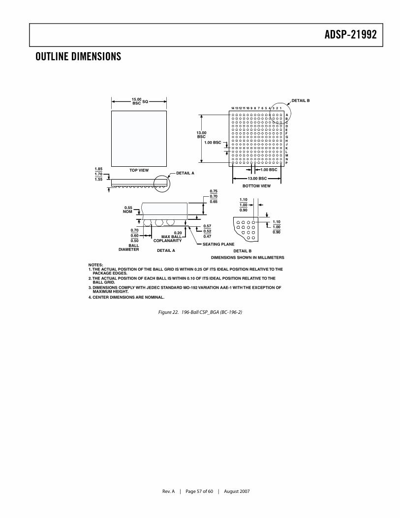
ADSP-21992
Rev. A | Page 57 of 60 | August 2007
OUTLINE DIMENSIONS
Figure 22. 196-Ball CSP_BGA (BC-196-2)
DETAIL B
DETAIL A
SEATING PLANE
DETAIL ABALL
DIAMETER
0.55NOM
0.20MAX BALL
COPLANARITY
13.00 BSC
ABCDEFGHJKLMNP
9 8 7 6 5 4 3 2 1
DETAIL B
1.00 BSC
15.00BSC SQ
TOP VIEW
BOTTOM VIEW
1.00 BSC
NOTES:1. THE ACTUAL POSITION OF THE BALL GRID IS WITHIN 0.25 OF ITS IDEAL POSITION RELATIVE TO THE
PACKAGE EDGES.2. THE ACTUAL POSITION OF EACH BALL IS WITHIN 0.10 OF ITS IDEAL POSITION RELATIVE TO THE
BALL GRID.3. DIMENSIONS COMPLY WITH JEDEC STANDARD MO-192 VARIATION AAE-1 WITH THE EXCEPTION OF
MAXIMUM HEIGHT.4. CENTER DIMENSIONS ARE NOMINAL.
1.851.701.55
13.00BSC
1011121314
0.700.600.50
0.570.520.47
0.750.700.65 1.10
1.000.90
1.101.000.90
DIMENSIONS SHOWN IN MILLIMETERS
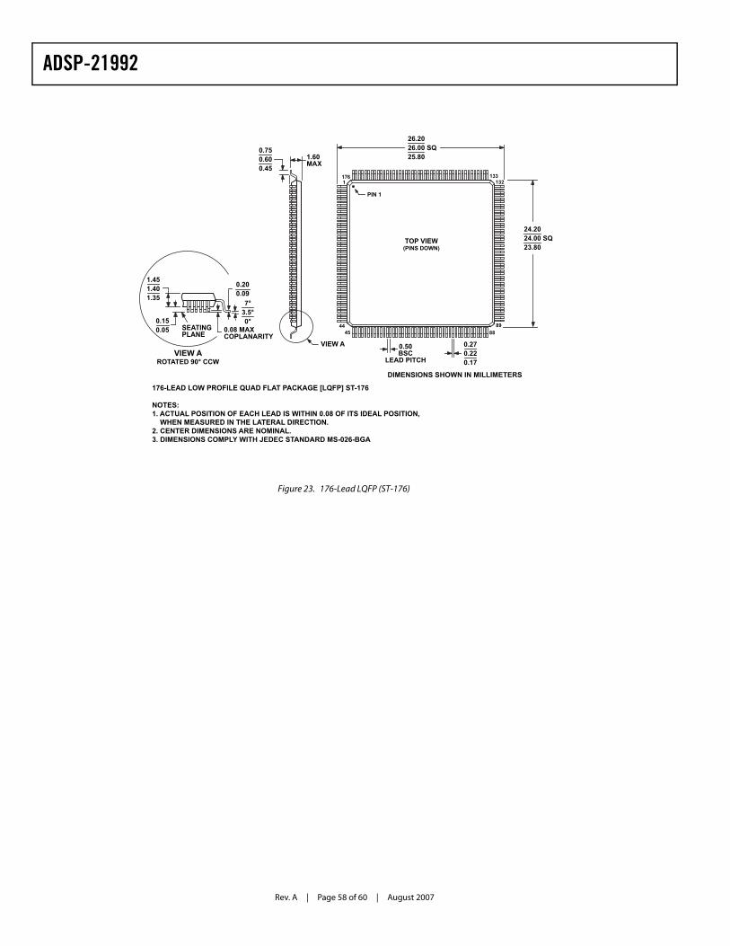
Rev. A | Page 58 of 60 | August 2007
ADSP-21992
Figure 23. 176-Lead LQFP (ST-176)
176-LEAD LOW PROFILE QUAD FLAT PACKAGE [LQFP] ST-176
NOTES:1. ACTUAL POSITION OF EACH LEAD IS WITHIN 0.08 OF ITS IDEAL POSITION, WHEN MEASURED IN THE LATERAL DIRECTION.2. CENTER DIMENSIONS ARE NOMINAL.3. DIMENSIONS COMPLY WITH JEDEC STANDARD MS-026-BGA
TOP VIEW(PINS DOWN)
1331 132
4544
8889
176
0.270.220.17
0.50BSC
LEAD PITCH
1.60MAX
0.750.600.45
VIEW A
PIN 1
1.451.401.35
0.150.05
0.200.09
0.08 MAXCOPLANARITY
VIEW AROTATED 90° CCW
SEATINGPLANE
7°3.5°0°
26.2026.00 SQ25.80
24.2024.00 SQ23.80
DIMENSIONS SHOWN IN MILLIMETERS

ADSP-21992
Rev. A | Page 59 of 60 | August 2007
ORDERING GUIDE
Model Temperature Range1
1 Referenced temperature is ambient temperature.
Instruction Rate Operating Voltage Package Description Package Option
ADSP-21992BBC –40�C to +85�C 150 MHz 2.5 Int. V/3.3 Ext. V 196-Ball CSP_BGA BC-196-2
ADSP-21992YBC –40�C to +125�C 150 MHz 2.5 Int. V/3.3 Ext. V 196-Ball CSP_BGA BC-196-2
ADSP-21992BST –40�C to +85�C 160 MHz 2.5 Int. V/3.3 Ext. V 176-Lead LQFP ST-176
ADSP-21992BSTZ2
2 Z = RoHS Complaint Part
–40�C to +85�C 160 MHz 2.5 Int. V/3.3 Ext. V 176-Lead LQFP ST-176
ADSP-21992YST –40�C to +125�C 100 MHz 2.5 Int. V/3.3 Ext. V 176-Lead LQFP ST-176

Rev. A | Page 60 of 60 | August 2007
ADSP-21992
©2007 Analog Devices, Inc. All rights reserved. Trademarks andregistered trademarks are the property of their respective owners.
D03163-0-8/07(A)
Related Documents