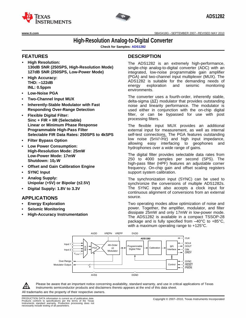
4th-Order DS Modulator Programmable Digital Filter SPI Interface Calibration Control CLK AVDD AVSS DVDD DGND Over-Range Modulator Output ADS1282 DOUT DIN DRDY SCLK SYNC RESET PWDN 3 PGA MUX Input 1 Input 2 VREFN VREFP V COM ADS1282 www.ti.com SBAS418G – SEPTEMBER 2007 – REVISED MAY 2010 High-Resolution Analog-to-Digital Converter Check for Samples: ADS1282 1FEATURES DESCRIPTION 2• High Resolution: The ADS1282 is an extremely high-performance, 130dB SNR (250SPS, High-Resolution Mode) single-chip analog-to-digital converter (ADC) with an 127dB SNR (250SPS, Low-Power Mode) integrated, low-noise programmable gain amplifier (PGA) and two-channel input multiplexer (MUX). The • High Accuracy: ADS1282 is suitable for the demanding needs of THD: –122dB energy exploration and seismic monitoring INL: 0.5ppm environments. • Low-Noise PGA The converter uses a fourth-order, inherently stable, • Two-Channel Input MUX delta-sigma (ΔΣ) modulator that provides outstanding • Inherently-Stable Modulator with Fast noise and linearity performance. The modulator is Responding Over-Range Detection used either in conjunction with the on-chip digital filter, or can be bypassed for use with post • Flexible Digital Filter: processing filters. Sinc + FIR + IIR (Selectable) Linear or Minimum Phase Response The flexible input MUX provides an additional Programmable High-Pass Filter external input for measurement, as well as internal self-test connections. The PGA features outstanding Selectable FIR Data Rates: 250SPS to 4kSPS low noise (5nV/√Hz) and high input impedance, • Filter Bypass Option allowing easy interfacing to geophones and • Low Power Consumption: hydrophones over a wide range of gains. High-Resolution Mode: 25mW The digital filter provides selectable data rates from Low-Power Mode: 17mW 250 to 4000 samples per second (SPS). The Shutdown: 10mW high-pass filter (HPF) features an adjustable corner • Offset and Gain Calibration Engine frequency. On-chip gain and offset scaling registers • SYNC Input support system calibration. • Analog Supply: The synchronization input (SYNC) can be used to Unipolar (+5V) or Bipolar (±2.5V) synchronize the conversions of multiple ADS1282s. The SYNC input also accepts a clock input for • Digital Supply: 1.8V to 3.3V continuous alignment of conversions from an external source. APPLICATIONS Two operating modes allow optimization of noise and • Energy Exploration power. Together, the amplifier, modulator, and filter • Seismic Monitoring dissipate 25mW and only 17mW in low-power mode. • High-Accuracy Instrumentation The ADS1282 is available in a compact TSSOP-28 package and is fully specified from –40°C to +85°C, with a maximum operating range to +125°C. 1 Please be aware that an important notice concerning availability, standard warranty, and use in critical applications of Texas Instruments semiconductor products and disclaimers thereto appears at the end of this data sheet. 2All trademarks are the property of their respective owners. PRODUCTION DATA information is current as of publication date. Copyright © 2007–2010, Texas Instruments Incorporated Products conform to specifications per the terms of the Texas Instruments standard warranty. Production processing does not necessarily include testing of all parameters.

Welcome message from author
This document is posted to help you gain knowledge. Please leave a comment to let me know what you think about it! Share it to your friends and learn new things together.
Transcript
4th-Order
DS
Modulator
Programmable
Digital FilterSPI
InterfaceCalibration
Control
CLK
AVDD
AVSS
DVDD
DGND
Over-Range
Modulator Output
ADS1282
DOUT
DIN
DRDY
SCLK
SYNC
RESET
PWDN3
PGA
MU
X
Input 1
Input 2
VREFN VREFP
VCOM
ADS1282
www.ti.com SBAS418G –SEPTEMBER 2007–REVISED MAY 2010
High-Resolution Analog-to-Digital ConverterCheck for Samples: ADS1282
1FEATURES DESCRIPTION2• High Resolution: The ADS1282 is an extremely high-performance,
130dB SNR (250SPS, High-Resolution Mode) single-chip analog-to-digital converter (ADC) with an127dB SNR (250SPS, Low-Power Mode) integrated, low-noise programmable gain amplifier
(PGA) and two-channel input multiplexer (MUX). The• High Accuracy:ADS1282 is suitable for the demanding needs ofTHD: –122dBenergy exploration and seismic monitoringINL: 0.5ppmenvironments.
• Low-Noise PGAThe converter uses a fourth-order, inherently stable,• Two-Channel Input MUX delta-sigma (ΔΣ) modulator that provides outstanding
• Inherently-Stable Modulator with Fast noise and linearity performance. The modulator isResponding Over-Range Detection used either in conjunction with the on-chip digital
filter, or can be bypassed for use with post• Flexible Digital Filter:processing filters.Sinc + FIR + IIR (Selectable)
Linear or Minimum Phase Response The flexible input MUX provides an additionalProgrammable High-Pass Filter external input for measurement, as well as internal
self-test connections. The PGA features outstandingSelectable FIR Data Rates: 250SPS to 4kSPSlow noise (5nV/√Hz) and high input impedance,• Filter Bypass Optionallowing easy interfacing to geophones and
• Low Power Consumption: hydrophones over a wide range of gains.High-Resolution Mode: 25mW
The digital filter provides selectable data rates fromLow-Power Mode: 17mW250 to 4000 samples per second (SPS). TheShutdown: 10mWhigh-pass filter (HPF) features an adjustable corner
• Offset and Gain Calibration Engine frequency. On-chip gain and offset scaling registers• SYNC Input support system calibration.• Analog Supply: The synchronization input (SYNC) can be used to
Unipolar (+5V) or Bipolar (±2.5V) synchronize the conversions of multiple ADS1282s.The SYNC input also accepts a clock input for• Digital Supply: 1.8V to 3.3Vcontinuous alignment of conversions from an externalsource.APPLICATIONSTwo operating modes allow optimization of noise and• Energy Explorationpower. Together, the amplifier, modulator, and filter• Seismic Monitoringdissipate 25mW and only 17mW in low-power mode.• High-Accuracy InstrumentationThe ADS1282 is available in a compact TSSOP-28package and is fully specified from –40°C to +85°C,with a maximum operating range to +125°C.
1
Please be aware that an important notice concerning availability, standard warranty, and use in critical applications of TexasInstruments semiconductor products and disclaimers thereto appears at the end of this data sheet.
2All trademarks are the property of their respective owners.
PRODUCTION DATA information is current as of publication date. Copyright © 2007–2010, Texas Instruments IncorporatedProducts conform to specifications per the terms of the TexasInstruments standard warranty. Production processing does notnecessarily include testing of all parameters.
ADS1282
SBAS418G –SEPTEMBER 2007–REVISED MAY 2010 www.ti.com
This integrated circuit can be damaged by ESD. Texas Instruments recommends that all integrated circuits be handled withappropriate precautions. Failure to observe proper handling and installation procedures can cause damage.
ESD damage can range from subtle performance degradation to complete device failure. Precision integrated circuits may be moresusceptible to damage because very small parametric changes could cause the device not to meet its published specifications.
ORDERING INFORMATION
For the most current package and ordering information, see the Package Option Addendum at the end of thisdocument, or visit the device product folder at ti.com.
ABSOLUTE MAXIMUM RATINGS (1)
Over operating free-air temperature range (unless otherwise noted).
ADS1282 UNIT
AVDD to AVSS –0.3 to +5.5 V
AVSS to DGND –2.8 to +0.3 V
DVDD to DGND –0.3 to +3.9 V
Input current 100, momentary mA
Input current 10, continuous mA
Analog input voltage AVSS – 0.3 to AVDD + 0.3 V
Digital input voltage to DGND –0.3 to DVDD + 0.3 V
Maximum junction temperature +150 °C
Operating temperature range –40 to +125 °C
Storage temperature range –60 to +150 °C
(1) Stresses above these ratings may cause permanent damage. Exposure to absolute maximum conditions for extended periods maydegrade device reliability. These are stress ratings only, and functional operation of the device at these or any other conditions beyondthose specified is not implied.
2 Submit Documentation Feedback Copyright © 2007–2010, Texas Instruments Incorporated
Product Folder Link(s): ADS1282
ADS1282
www.ti.com SBAS418G –SEPTEMBER 2007–REVISED MAY 2010
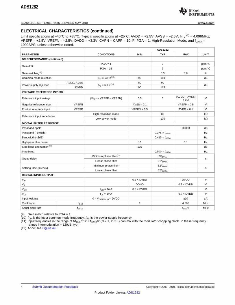
ELECTRICAL CHARACTERISTICSLimit specifications at –40°C to +85°C. Typical specifications at +25°C, AVDD = +2.5V, AVSS = –2.5V, fCLK
(1) = 4.096MHz, VREFP = +2.5V,VREFN = –2.5V, DVDD = +3.3V, CAPN – CAPP = 10nF, PGA = 1, High-Resolution Mode, and fDATA = 1000SPS, unless otherwise noted.
ADS1282
PARAMETER CONDITIONS MIN TYP MAX UNIT
ANALOG INPUTS
Full-scale input voltage VIN = (AINP – AINN) ±VREF/(2 × PGA) V
Absolute input range AINP or AINN AVSS + 0.7 AVDD – 1.25 V
PGA input voltage noise density 5 nV/√Hz
Differential input impedance (2) 1 GΩ
Common-mode input impedance 100 MΩ
Input bias current 1 nA
Crosstalk f = 31.25Hz –135 dB
MUX on-resistance 30 Ω
PGA OUTPUT (CAPP, CAPN)
Absolute output range AVSS + 0.4 AVDD – 0.4 V
PGA differential output impedance 600 Ω
Output impedance tolerance ±10 %
External bypass capacitance 10 100 nF
High-resolution mode 55 kΩModulator differential input impedance
Low-power mode 110 kΩ
AC PERFORMANCE
High-resolution mode 120 124Signal-to-noise ratio (3) SNR dB
Low-power mode 117 121
High-resolution mode
PGA = 1...16 –122 –114
PGA = 32 –117 –110 dB
PGA = 64 –115Total harmonic distortion (4) THD
Low-power mode
PGA = 1...16 –122 –114
PGA = 32 –113 –108 dB
PGA = 64 –109
Spurious-free dynamic dBSFDR 123range
DC PERFORMANCE
Resolution No missing codes 31 Bits
FIR filter mode 250 4000 SPSData rate fDATA
Sinc filter mode 8000 128,000 SPS
Integral nonlinearity (INL) (5) Differential input 0.00005 0.0004 % FSR (6)
Offset error 50 200 mV
Offset error after calibration (7) Shorted input 1 mV
Offset drift 0.02 mV/°C
High-resolution mode –1.5 –1.0 –0.5 %Gain error (8)
Low-power mode –1 –0.5 0 %
Gain error after calibration (7) 0.0002 %
(1) fCLK = system clock.(2) Input impedance is improved by disabling input chopping (CHOP bit = 0).(3) VIN = 20mVDC/PGA; see Table 1.(4) VIN = 31.25Hz, –0.5dBFS.(5) Best-fit method.(6) FSR: Full-scale range = ±VREF/(2 × PGA).(7) Calibration accuracy is on the level of noise reduced by 4 (calibration averages 16 readings).(8) The PGA output impedance and the modulator input impedance results in –1% systematic gain error (high-resolution mode) and –0.5%
error (low-power mode).
Copyright © 2007–2010, Texas Instruments Incorporated Submit Documentation Feedback 3
Product Folder Link(s): ADS1282
ADS1282
SBAS418G –SEPTEMBER 2007–REVISED MAY 2010 www.ti.com
ELECTRICAL CHARACTERISTICS (continued)Limit specifications at –40°C to +85°C. Typical specifications at +25°C, AVDD = +2.5V, AVSS = –2.5V, fCLK
(1) = 4.096MHz,VREFP = +2.5V, VREFN = –2.5V, DVDD = +3.3V, CAPN – CAPP = 10nF, PGA = 1, High-Resolution Mode, and fDATA =1000SPS, unless otherwise noted.
ADS1282
PARAMETER CONDITIONS MIN TYP MAX UNIT
DC PERFORMANCE (continued)
PGA = 1 2 ppm/°CGain drift
PGA = 16 9 ppm/°C
Gain matching (9) 0.3 0.8 %
Common-mode rejection fCM = 60Hz (10) 95 110 dB
AVDD, AVSS 80 90Power-supply rejection fPS = 60Hz (10) dB
DVDD 90 115
VOLTAGE REFERENCE INPUTS
(AVDD – AVSS)Reference input voltage (VREF = VREFP – VREFN) 0.5 5 V+ 0.2
Negative reference input VREFN AVSS – 0.1 VREFP – 0.5 V
Positive reference input VREFP VREFN + 0.5 AVDD + 0.1 V
High-resolution mode 85 kΩReference input impedance
Low-power mode 170 kΩ
DIGITAL FILTER RESPONSE
Passband ripple ±0.003 dB
Passband (–0.01dB) 0.375 × fDATA Hz
Bandwidth (–3dB) 0.413 × fDATA Hz
High-pass filter corner 0.1 10 Hz
Stop band attenuation (11) 135 dB
Stop band 0.500 × fDATA Hz
Minimum phase filter (12) 5/fDATAGroup delay s
Linear phase filter 31/fDATA
Minimum phase filter 62/fDATASettling time (latency) s
Linear phase filter 62/fDATA
DIGITAL INPUT/OUTPUT
VIH 0.8 × DVDD DVDD V
VIL DGND 0.2 × DVDD V
VOH IOH = 1mA 0.8 × DVDD V
VOL IOL = 1mA 0.2 × DVDD V
Input leakage 0 < VDIGITAL IN < DVDD ±10 mA
Clock input fCLK 1 4.096 MHz
Serial clock rate fSCLK fCLK/2 MHz
(9) Gain match relative to PGA = 1.(10) fCM is the input common-mode frequency. fPS is the power-supply frequency.(11) Input frequencies in the range of NfCLK/512 ± fDATA/2 (N = 1, 2, 3...) can mix with the modulator chopping clock. In these frequency
ranges intermodulation = 120dB, typ.(12) At dc; see Figure 49.
4 Submit Documentation Feedback Copyright © 2007–2010, Texas Instruments Incorporated
Product Folder Link(s): ADS1282
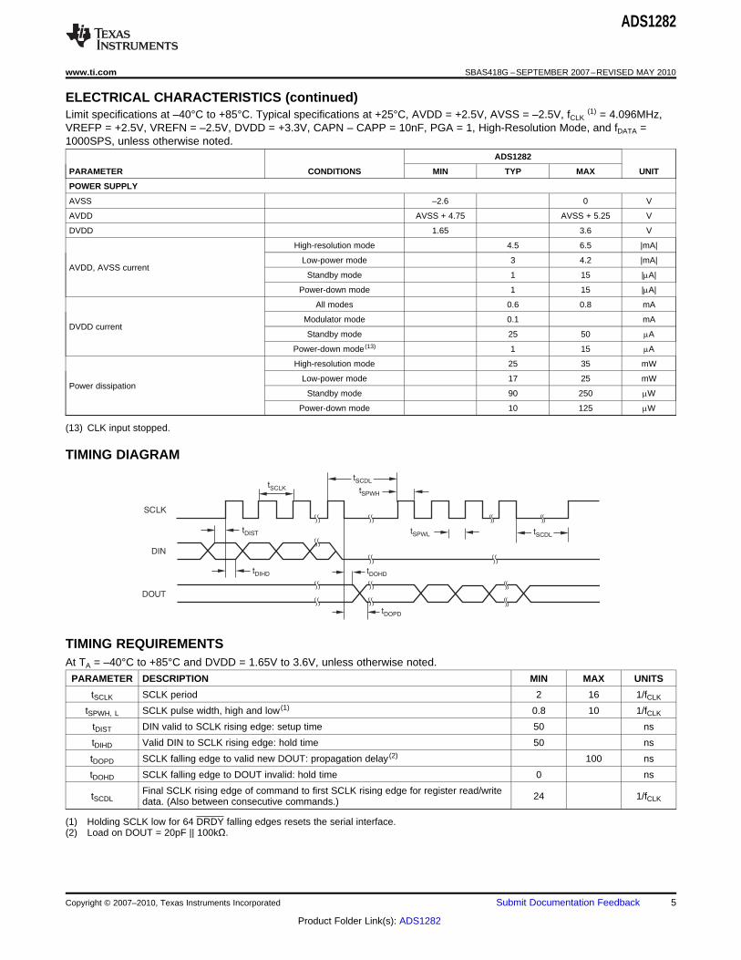
SCLK
DIN
DOUT
tSCLK tSPWH
tSCDLtDIST
tDIHD
tSPWL
tSCDL
tDOHD
tDOPD
ADS1282
www.ti.com SBAS418G –SEPTEMBER 2007–REVISED MAY 2010
ELECTRICAL CHARACTERISTICS (continued)Limit specifications at –40°C to +85°C. Typical specifications at +25°C, AVDD = +2.5V, AVSS = –2.5V, fCLK
(1) = 4.096MHz,VREFP = +2.5V, VREFN = –2.5V, DVDD = +3.3V, CAPN – CAPP = 10nF, PGA = 1, High-Resolution Mode, and fDATA =1000SPS, unless otherwise noted.
ADS1282
PARAMETER CONDITIONS MIN TYP MAX UNIT
POWER SUPPLY
AVSS –2.6 0 V
AVDD AVSS + 4.75 AVSS + 5.25 V
DVDD 1.65 3.6 V
High-resolution mode 4.5 6.5 |mA|
Low-power mode 3 4.2 |mA|AVDD, AVSS current
Standby mode 1 15 |mA|
Power-down mode 1 15 |mA|
All modes 0.6 0.8 mA
Modulator mode 0.1 mADVDD current
Standby mode 25 50 mA
Power-down mode (13) 1 15 mA
High-resolution mode 25 35 mW
Low-power mode 17 25 mWPower dissipation
Standby mode 90 250 mW
Power-down mode 10 125 mW
(13) CLK input stopped.
TIMING DIAGRAM
TIMING REQUIREMENTSAt TA = –40°C to +85°C and DVDD = 1.65V to 3.6V, unless otherwise noted.
PARAMETER DESCRIPTION MIN MAX UNITS
tSCLK SCLK period 2 16 1/fCLK
tSPWH, L SCLK pulse width, high and low (1) 0.8 10 1/fCLK
tDIST DIN valid to SCLK rising edge: setup time 50 ns
tDIHD Valid DIN to SCLK rising edge: hold time 50 ns
tDOPD SCLK falling edge to valid new DOUT: propagation delay (2) 100 ns
tDOHD SCLK falling edge to DOUT invalid: hold time 0 ns
Final SCLK rising edge of command to first SCLK rising edge for register read/writetSCDL 24 1/fCLKdata. (Also between consecutive commands.)
(1) Holding SCLK low for 64 DRDY falling edges resets the serial interface.(2) Load on DOUT = 20pF || 100kΩ.
Copyright © 2007–2010, Texas Instruments Incorporated Submit Documentation Feedback 5
Product Folder Link(s): ADS1282
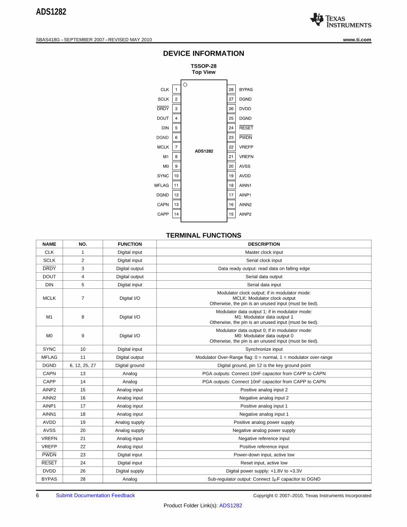
CLK
SCLK
DRDY
DOUT
DIN
DGND
MCLK
M1
M0
SYNC
MFLAG
DGND
CAPN
CAPP
BYPAS
DGND
DVDD
DGND
RESET
PWDN
VREFP
VREFN
AVSS
AVDD
AINN1
AINP1
AINN2
AINP2
1
2
3
4
5
6
7
8
9
10
11
12
13
14
28
27
26
25
24
23
22
21
20
19
18
17
16
15
ADS1282
ADS1282
SBAS418G –SEPTEMBER 2007–REVISED MAY 2010 www.ti.com
DEVICE INFORMATION
TSSOP-28Top View
TERMINAL FUNCTIONSNAME NO. FUNCTION DESCRIPTION
CLK 1 Digital input Master clock input
SCLK 2 Digital input Serial clock input
DRDY 3 Digital output Data ready output: read data on falling edge
DOUT 4 Digital output Serial data output
DIN 5 Digital input Serial data input
Modulator clock output; if in modulator mode:MCLK 7 Digital I/O MCLK: Modulator clock output
Otherwise, the pin is an unused input (must be tied).
Modulator data output 1; if in modulator mode:M1 8 Digital I/O M1: Modulator data output 1
Otherwise, the pin is an unused input (must be tied).
Modulator data output 0; if in modulator mode:M0 9 Digital I/O M0: Modulator data output 0
Otherwise, the pin is an unused input (must be tied).
SYNC 10 Digital input Synchronize input
MFLAG 11 Digital output Modulator Over-Range flag: 0 = normal, 1 = modulator over-range
DGND 6, 12, 25, 27 Digital ground Digital ground, pin 12 is the key ground point
CAPN 13 Analog PGA outputs: Connect 10nF capacitor from CAPP to CAPN
CAPP 14 Analog PGA outputs: Connect 10nF capacitor from CAPP to CAPN
AINP2 15 Analog input Positive analog input 2
AINN2 16 Analog input Negative analog input 2
AINP1 17 Analog input Positive analog input 1
AINN1 18 Analog input Negative analog input 1
AVDD 19 Analog supply Positive analog power supply
AVSS 20 Analog supply Negative analog power supply
VREFN 21 Analog input Negative reference input
VREFP 22 Analog input Positive reference input
PWDN 23 Digital input Power-down input, active low
RESET 24 Digital input Reset input, active low
DVDD 26 Digital supply Digital power supply: +1.8V to +3.3V
BYPAS 28 Analog Sub-regulator output: Connect 1mF capacitor to DGND
6 Submit Documentation Feedback Copyright © 2007–2010, Texas Instruments Incorporated
Product Folder Link(s): ADS1282
0 50
Frequency (Hz)
0
-20
-40
-60
-80
-180
Am
plit
ude (
dB
)
100 150 500250 350 450200 300 400
-100
-120
-140
-160
8192-Point FFT
V = 0.5dBFS, 31.25Hz
High-Resolution Mode
PGA = 1
THD = 124.0dB
IN -
-
0 50
Frequency (Hz)
0
-20
-40
-60
-80
-180
Am
plit
ude (
dB
)
100 150 500250 350 450200 300 400
-100
-120
-140
-160
8192-Point FFT
V = 0.5dBFS, 31.25Hz
Low-Power Mode
PGA = 1
THD = 123.0dB
IN -
-
0 50
Frequency (Hz)
0
-20
-40
-60
-80
-180
Am
plit
ude (
dB
)
100 150 500250 350 450200 300 400
-100
-120
-140
-160
8192-Point FFT
V = 20dBFS, 31.25Hz
High-Resolution Mode
PGA = 1
THD = 120.1dB
IN -
-
0 50
Frequency (Hz)
0
-20
-40
-60
-80
-180
Am
plit
ude (
dB
)
100 150 500250 350 450200 300 400
-100
-120
-140
-160
8192-Point FFT
V = 20dBFS, 31.25Hz
Low-Power Mode
PGA = 1
THD = 117.0dB
IN -
-
0 50
Frequency (Hz)
0
-20
-40
-60
-80
-180
Am
plit
ude (
dB
)
100 150 500250 350 450200 300 400
-100
-120
-140
-160
8192-Point FFT
V = 0.5dBFS, 31.25Hz
High-Resolution Mode
PGA = 16
THD = 122.4dB
IN -
-
0 50
Frequency (Hz)
0
-20
-40
-60
-80
-180
Am
plit
ude (
dB
)
100 150 500250 350 450200 300 400
-100
-120
-140
-160
8192-Point FFT
V = 0.5dBFS, 31.25Hz
Low-Power Mode
PGA = 16
THD = 121.4dB
IN -
-
ADS1282
www.ti.com SBAS418G –SEPTEMBER 2007–REVISED MAY 2010
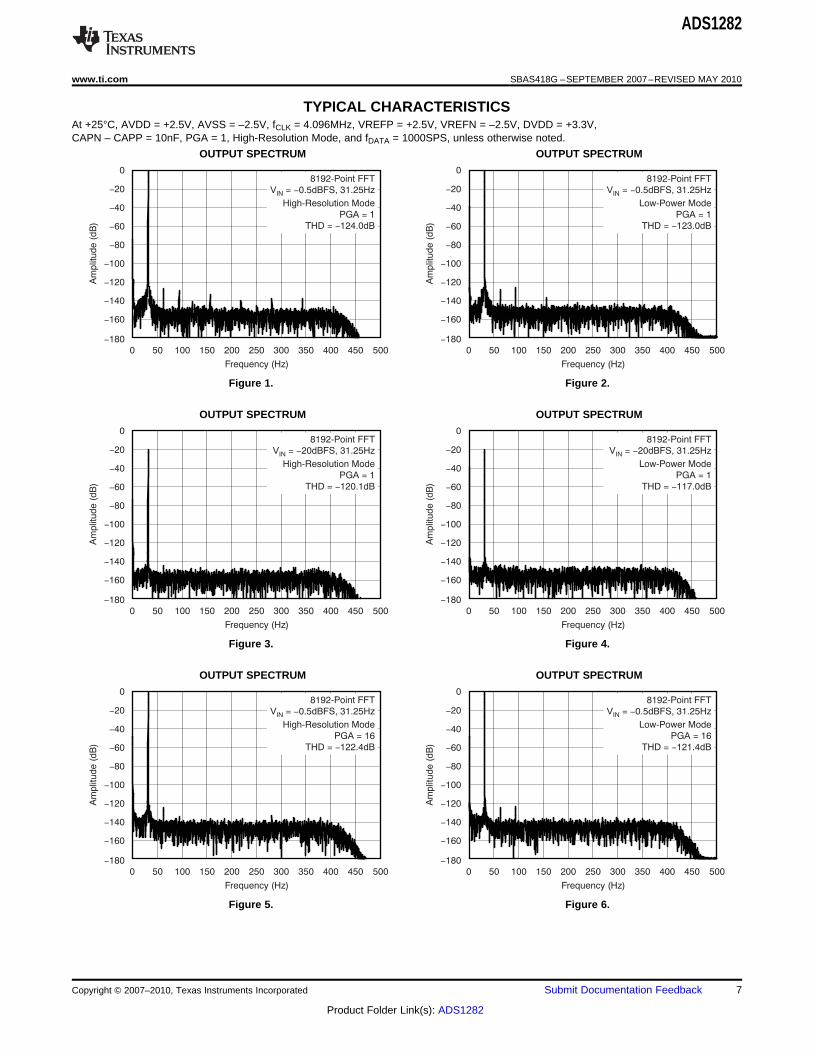
TYPICAL CHARACTERISTICSAt +25°C, AVDD = +2.5V, AVSS = –2.5V, fCLK = 4.096MHz, VREFP = +2.5V, VREFN = –2.5V, DVDD = +3.3V,CAPN – CAPP = 10nF, PGA = 1, High-Resolution Mode, and fDATA = 1000SPS, unless otherwise noted.
OUTPUT SPECTRUM OUTPUT SPECTRUM
Figure 1. Figure 2.
OUTPUT SPECTRUM OUTPUT SPECTRUM
Figure 3. Figure 4.
OUTPUT SPECTRUM OUTPUT SPECTRUM
Figure 5. Figure 6.
Copyright © 2007–2010, Texas Instruments Incorporated Submit Documentation Feedback 7
Product Folder Link(s): ADS1282
0 50
Frequency (Hz)
0
-20
-40
-60
-80
-180
Am
plit
ude (
dB
)
100 150 500250 350 450200 300 400
-100
-120
-140
-160
8192-Point FFT
Shorted Input
High-Resolution Mode
SNR = 124.0dB
0 50
Frequency (Hz)
0
-20
-40
-60
-80
-180
Am
plit
ude (
dB
)
100 150 500250 350 450200 300 400
-100
-120
-140
-160
8192-Point FFT
Shorted Input
Low-Power Mode
SNR = 121.0dB
0 50
Frequency (Hz)
0
-20
-40
-60
-80
-180
Am
plit
ude (
dB
)
100 150 500250 350 450200 300 400
-100
-120
-140
-160
8192-Point FFT
20mV
High-Resolution Mode
SNR = 124.2dB
DC
0 50
Frequency (Hz)
0
-20
-40
-60
-80
-180
Am
plit
ude (
dB
)
100 150 500250 350 450200 300 400
-100
-120
-140
-160
8192-Point FFT
20mV
Low-Power Mode
SNR = 121.3dB
DC
10 20
Input Frequency (Hz)
-
-
-
-
-
-
-
100
105
110
115
120
125
130
Tota
l H
arm
onic
Dis
tort
ion (
dB
)
30 40 10060 8050 70 90
V = 0.5dBFSIN -
THD Limited by
Signal Generator
High-Resolution Mode, PGA = 1
High-Resolution Mode, PGA = 8
Low-Power Mode, PGA = 8
Low-Power Mode, PGA = 1
-55 -35
Temperature ( C)°
126
125
124
123
122
121
120
Sig
nal-to
-Nois
e R
atio (
dB
)
-15 5 12545 8525 65 105
V = 20mVIN DC
Low-Power Mode
High-Resolution Mode
ADS1282
SBAS418G –SEPTEMBER 2007–REVISED MAY 2010 www.ti.com
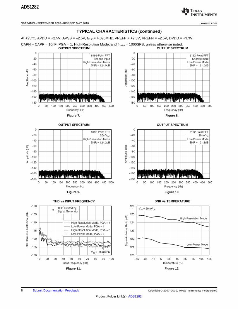
TYPICAL CHARACTERISTICS (continued)
At +25°C, AVDD = +2.5V, AVSS = –2.5V, fCLK = 4.096MHz, VREFP = +2.5V, VREFN = –2.5V, DVDD = +3.3V,
CAPN – CAPP = 10nF, PGA = 1, High-Resolution Mode, and fDATA = 1000SPS, unless otherwise noted.OUTPUT SPECTRUM OUTPUT SPECTRUM
Figure 7. Figure 8.
OUTPUT SPECTRUM OUTPUT SPECTRUM
Figure 9. Figure 10.
THD vs INPUT FREQUENCY SNR vs TEMPERATURE
Figure 11. Figure 12.
8 Submit Documentation Feedback Copyright © 2007–2010, Texas Instruments Incorporated
Product Folder Link(s): ADS1282
-55 -35
Temperature ( C)°
-110
115
120
125
130
-
-
-
-
Tota
l H
arm
onic
Dis
tort
ion (
dB
)
-15 5 12545 8525 65 105
PGA = 8
V = 31.25Hz, 0.5dBFSIN -
Low-Power Mode
High-Resolution Mode
0 1
V (V)REF
130
125
120
115
110
105
100
Sig
nal-to
-Nois
e R
atio (
dB
)
2 3 5.554
Low-Power Mode, PGA = 1
High-Resolution Mode, PGA = 1
Low-Power Mode, PGA = 8
High-Resolution Mode, PGA = 8
0 1
V (V)REF
-110
115
120
125
130
-
-
-
-
Tota
l H
arm
onic
Dis
tort
ion (
dB
)
2 3 654
Low-Power Mode, PGA = 1
High-Resolution Mode, PGA = 1
Low-Power Mode, PGA = 8
High-Resolution Mode, PGA = 8
0.5 1.0
f (MHz)CLK
125
124
123
122
121
120
119
Sig
nal-to
-Nois
e R
atio (
dB
)
1.5 2.0 4.53.02.5 3.5 4.0
V = 20mV
Data Rate = f /4096IN DC
CLK
Low-Power Mode
High-Resolution Mode
0.5 1.0
f (MHz)CLK
-110
115
120
125
130
-
-
-
-
Tota
l H
arm
onic
Dis
tort
ion (
dB
)
1.5 2.0 4.53.02.5 3.5 4.0
PGA = 8
V = 31.25Hz, 0.5dBFS
Data Rate = f /4096IN
CLK
-
Low-Power Mode
High-Resolution Mode
10 100
Input Frequency (Hz)
130
120
110
100
90
80
70
Com
mon-M
ode R
eje
ction (
dB
)
1k 10k 1M100k
Low-Power Mode
High-Resolution Mode
ADS1282
www.ti.com SBAS418G –SEPTEMBER 2007–REVISED MAY 2010
TYPICAL CHARACTERISTICS (continued)
At +25°C, AVDD = +2.5V, AVSS = –2.5V, fCLK = 4.096MHz, VREFP = +2.5V, VREFN = –2.5V, DVDD = +3.3V,
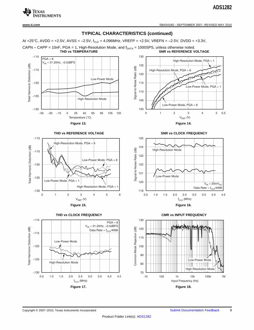
CAPN – CAPP = 10nF, PGA = 1, High-Resolution Mode, and fDATA = 1000SPS, unless otherwise noted.THD vs TEMPERATURE SNR vs REFERENCE VOLTAGE
Figure 13. Figure 14.
THD vs REFERENCE VOLTAGE SNR vs CLOCK FREQUENCY
Figure 15. Figure 16.
THD vs CLOCK FREQUENCY CMR vs INPUT FREQUENCY
Figure 17. Figure 18.
Copyright © 2007–2010, Texas Instruments Incorporated Submit Documentation Feedback 9
Product Folder Link(s): ADS1282
10 100
Power-Supply Frequency (Hz)
140
120
100
80
60
40
20
0
Pow
er-
Supply
Reje
ction (
dB
)
1k 10k 1M100k
DVDD
AVSS
AVDD
-100 -75
Input Amplitude (% Full-Scale)
4
3
2
1
0
1
2
3
4
-
-
-
-
Inte
gra
l N
onlin
earity
(ppm
)
-50 -25 1000 25 50 75
PGA = 8 PGA = 32
PGA = 2
-55 -35
Temperature ( C)°
4
3
2
1
0
Inte
gra
l N
onlin
earity
(ppm
)
-15 5 12525 45 65 85 105 0 50
Frequency (Hz)
0
20
40
60
80
100
120
140
160
180
-
-
-
-
-
-
-
-
-
Am
plit
ude (
dB
)
100 150 500200 250 300 350 400 450
Shorted Input
8192-Point FFT
Adjacent Channel V = 0.5dBFS, 31.25HzIN -
-55 -35
Temperature ( C)°
30
25
20
15
10
Pow
er
(mW
)
-15 5 12525 45 65 85 105
High-Resolution Mode
Low-Power Mode
1.0 1.5
f (MHz)CLK
30
25
20
15
10
5
0
Pow
er
(mW
)
2.0 2.5 4.53.0 3.5 4.0
High-Resolution Mode
Low-Power Mode
ADS1282
SBAS418G –SEPTEMBER 2007–REVISED MAY 2010 www.ti.com
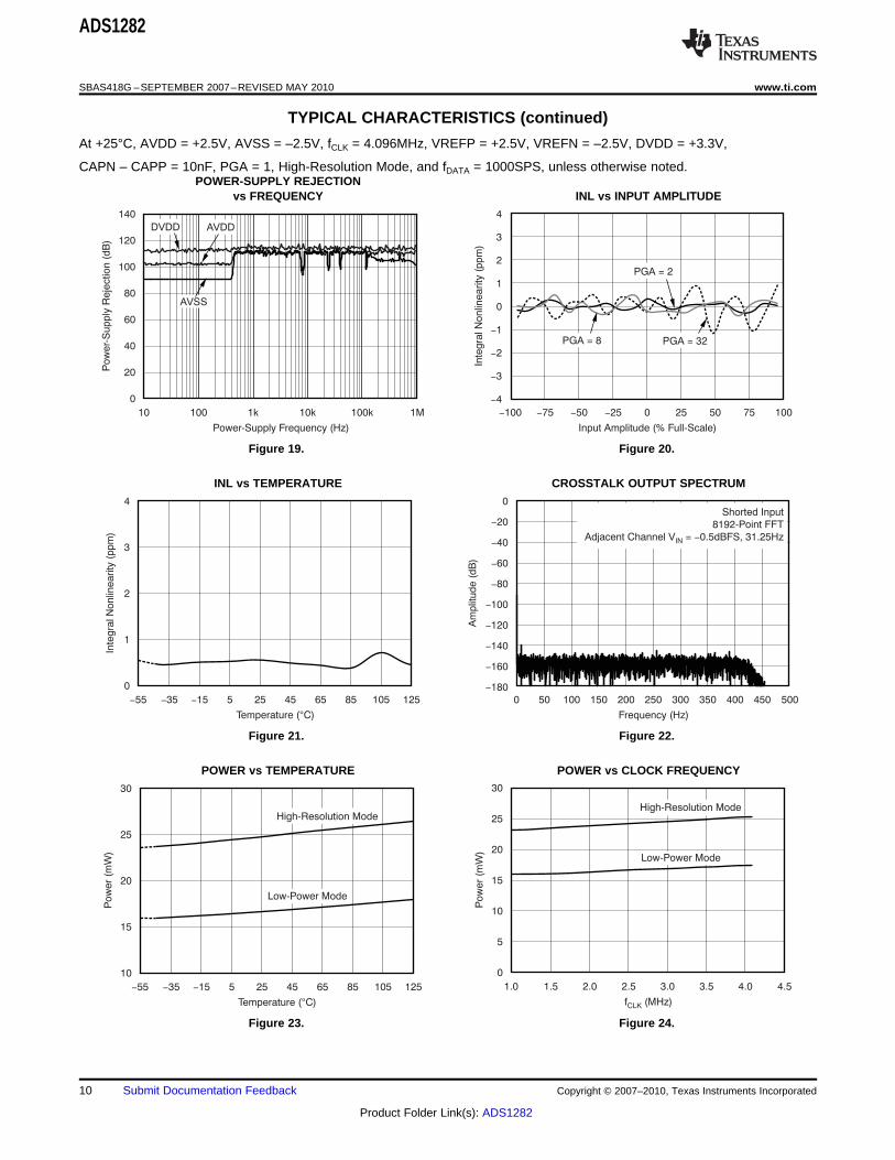
TYPICAL CHARACTERISTICS (continued)
At +25°C, AVDD = +2.5V, AVSS = –2.5V, fCLK = 4.096MHz, VREFP = +2.5V, VREFN = –2.5V, DVDD = +3.3V,
CAPN – CAPP = 10nF, PGA = 1, High-Resolution Mode, and fDATA = 1000SPS, unless otherwise noted.POWER-SUPPLY REJECTION
vs FREQUENCY INL vs INPUT AMPLITUDE
Figure 19. Figure 20.
INL vs TEMPERATURE CROSSTALK OUTPUT SPECTRUM
Figure 21. Figure 22.
POWER vs TEMPERATURE POWER vs CLOCK FREQUENCY
Figure 23. Figure 24.
10 Submit Documentation Feedback Copyright © 2007–2010, Texas Instruments Incorporated
Product Folder Link(s): ADS1282
-100 -80
Offset ( V)m
30
25
20
15
10
5
0
Occurr
ences
-60 -40 100-20 0 20
25 Units
PGA = 8
PGA = 1
806040 -1.2 -1.1
Gain Error (%)
10
8
6
4
2
0
Occurr
ences
-1.0 -0.9 -0.3-0.8 -0.7 -0.6
25 Units
Low-Power Mode
High-Resolution Mode
-0.4-0.5
-15
-14
Gain Drift (ppm/ C)°
90
80
70
60
50
40
30
20
10
0
Occurr
ences
-13
-12 5
-11
-10
-9
PGA = 1, 2, 4
PGA = 8, 64
-7
-8
-6
25 Units Based on +20 C Intervals
Over the Range of 40 C to +85 C
°
° °-
PGA = 32
PGA = 16
43210
-5
-4
-3
-2
-1
-0.1
0
-0.0
8
Offset Drift ( V/ C)m °
90
80
70
60
50
40
30
20
10
0
Occurr
ences
-0.0
6
-0.0
4
0.1
0
-0.0
2 0
0.0
2
PGA = 8
PGA =1
0.0
6
0.0
4
0.0
8
25 Units Based on
+20 C Intervals
Over the Range of
40 C to +85 C
°
° °-
0.5
0
0.4
6
Gain Error (%)
8
6
4
2
0
Occurr
ences
0.4
2
0.3
8
0.0
2
0.3
4
0.3
0
0.2
6
0.1
8
0.2
2
0.1
4
Worst-Case Gain Match Relative PGA = 1 (25 Units)
0.1
0
0.0
6
ADS1282
www.ti.com SBAS418G –SEPTEMBER 2007–REVISED MAY 2010
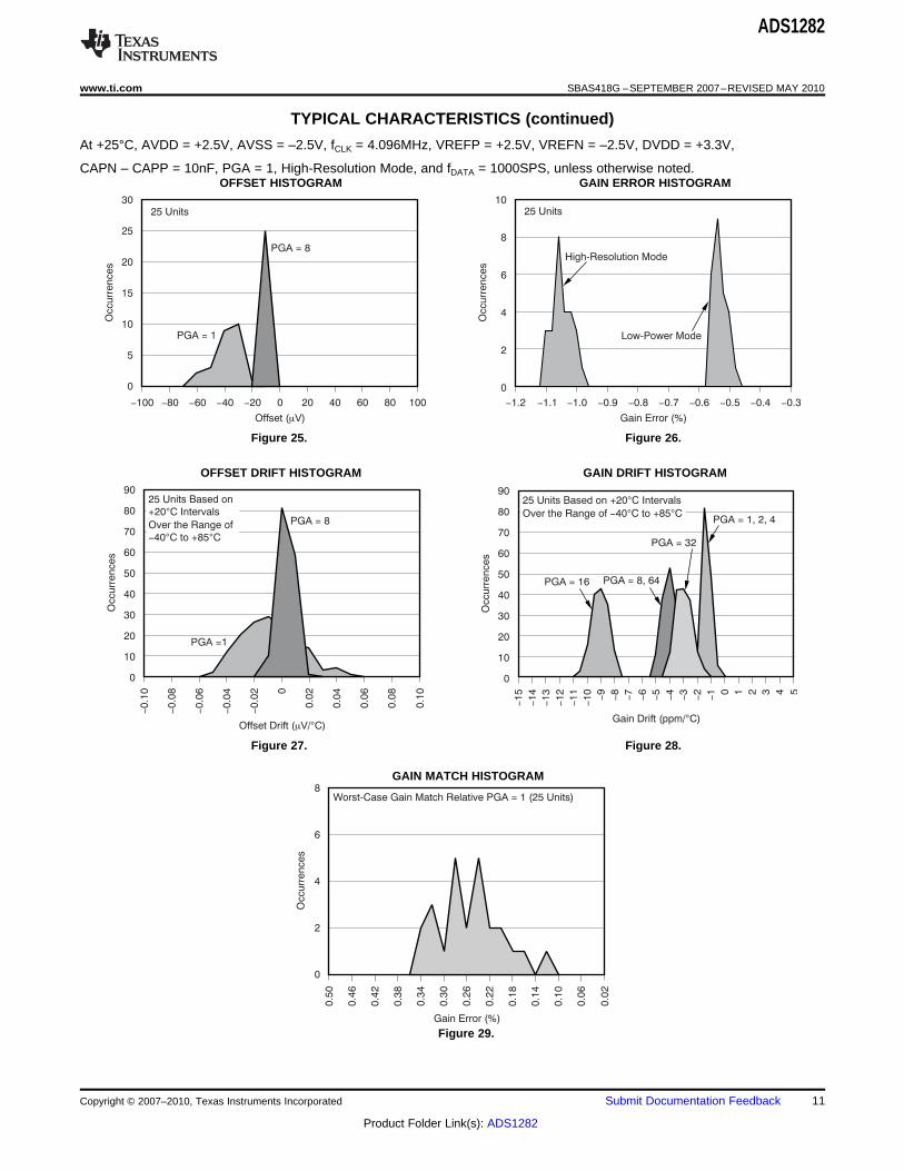
TYPICAL CHARACTERISTICS (continued)
At +25°C, AVDD = +2.5V, AVSS = –2.5V, fCLK = 4.096MHz, VREFP = +2.5V, VREFN = –2.5V, DVDD = +3.3V,
CAPN – CAPP = 10nF, PGA = 1, High-Resolution Mode, and fDATA = 1000SPS, unless otherwise noted.OFFSET HISTOGRAM GAIN ERROR HISTOGRAM
Figure 25. Figure 26.
OFFSET DRIFT HISTOGRAM GAIN DRIFT HISTOGRAM
Figure 27. Figure 28.
GAIN MATCH HISTOGRAM
Figure 29.
Copyright © 2007–2010, Texas Instruments Incorporated Submit Documentation Feedback 11
Product Folder Link(s): ADS1282
4th-Order
DS
Modulator
Programmable
Digital FilterSerial
InterfaceCalibration
Control
AINP1
CA
PN
CA
PP
AVSS
CLK DVDD
DGND
DIN
DOUT
MCLK
DRDY
SCLK
AINN1
VR
EF
N
M0 M1
VR
EF
P
ADS1282
AINN2
AINP2
Over-Range
Detection
BYPAS
LDO
PGA
MU
X
400W
AVDD + AVSS
400W
2
+1.8V
(Digital core)
300W
300W
RESET
PWDN
SYNC
AVDD
MFLAG
ADS1282
SBAS418G –SEPTEMBER 2007–REVISED MAY 2010 www.ti.com
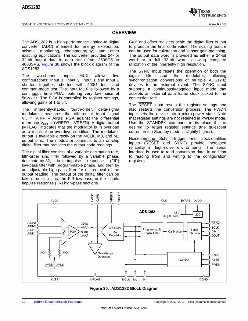
OVERVIEW
The ADS1282 is a high-performance analog-to-digital Gain and offset registers scale the digital filter outputconverter (ADC) intended for energy exploration, to produce the final code value. The scaling featureseismic monitoring, chomatography, and other can be used for calibration and sensor gain matching.exacting applications. The converter provides 24- or The output data word is provided as either a 24-bit32-bit output data in data rates from 250SPS to word or a full 32-bit word, allowing complete4000SPS. Figure 30 shows the block diagram of the utilization of the inherently high resolution.ADS1282.
The SYNC input resets the operation of both theThe two-channel input MUX allows five digital filter and the modulator, allowingconfigurations: Input 1; Input 2; Input 1 and Input 2 synchronization conversions of multiple ADS1282shorted together; shorted with 400Ω test; and devices to an external event. The SYNC inputcommon-mode test. The input MUX is followed by a supports a continuously-toggled input mode thatcontinuous time PGA, featuring very low noise of accepts an external data frame clock locked to the5nV/√Hz. The PGA is controlled by register settings, conversion rate.allowing gains of 1 to 64.
The RESET input resets the register settings andThe inherently-stable, fourth-order, delta-sigma also restarts the conversion process. The PWDNmodulator measures the differential input signal input sets the device into a micro-power state. NoteVIN = (AINP – AINN) PGA against the differential that register settings are not retained in PWDN mode.reference VREF = (VREFP – VREFN). A digital output Use the STANDBY command in its place if it is(MFLAG) indicates that the modulator is in overload desired to retain register settings (the quiescentas a result of an overdrive condition. The modulator current in the Standby mode is slightly higher).output is available directly on the MCLK, M0, and M1
Noise-immune Schmitt-trigger and clock-qualifiedoutput pins. The modulator connects to an on-chipinputs (RESET and SYNC) provide increaseddigital filter that provides the output code readings.reliability in high-noise environments. The serial
The digital filter consists of a variable decimation rate, interface is used to read conversion data, in additionfifth-order sinc filter followed by a variable phase, to reading from and writing to the configurationdecimate-by-32, finite-impulse response (FIR) registers.low-pass filter with programmable phase, and then byan adjustable high-pass filter for dc removal of theoutput reading. The output of the digital filter can betaken from the sinc, the FIR low-pass, or the infiniteimpulse response (IIR) high-pass sections.
Figure 30. ADS1282 Block Diagram
12 Submit Documentation Feedback Copyright © 2007–2010, Texas Instruments Incorporated
Product Folder Link(s): ADS1282
SNR = 20logFSRRMS
NRMS
ADS1282
www.ti.com SBAS418G –SEPTEMBER 2007–REVISED MAY 2010
The device features unipolar and bipolar analog INPUT-REFERRED NOISEpower supplies (AVDD and AVSS, respectively) for
The input-referred noise is related to SNR byinput range flexibility and a digital supply acceptingEquation 1:1.8V to 3.3V. The analog supplies may be set to +5V
to accept unipolar signals (with input offset) or setlower in the range of ±2.5V to accept true bipolarinput signals (ground referenced).
where:An internal sub-regulator is used to supply the digitalcore from DVDD. The BYPAS pin (pin 28) is the FSRRMS = Full-scale range RMS = VREF/(2 × √2 ×sub-regulator output and requires a 1mF capacitor for PGA)noise reduction. BYPAS should not be used to drive
NRMS = Noise RMS (input-referred) (1)external circuitry.
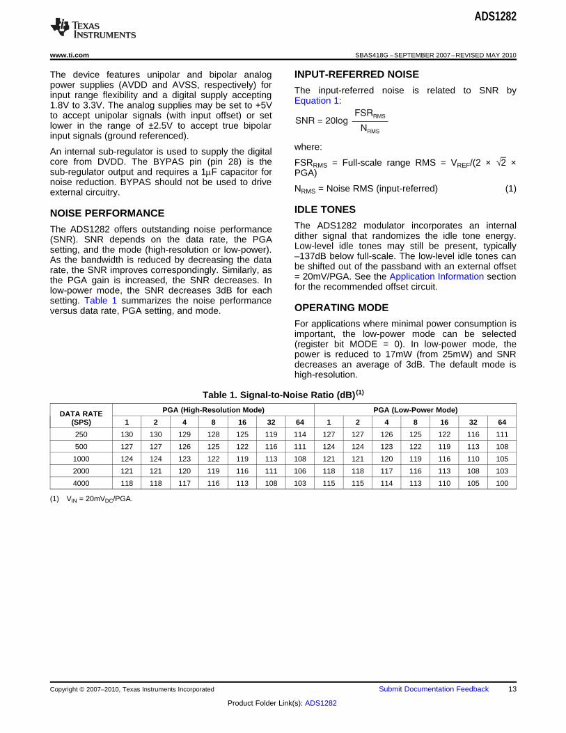
IDLE TONESNOISE PERFORMANCEThe ADS1282 modulator incorporates an internalThe ADS1282 offers outstanding noise performancedither signal that randomizes the idle tone energy.(SNR). SNR depends on the data rate, the PGALow-level idle tones may still be present, typicallysetting, and the mode (high-resolution or low-power).–137dB below full-scale. The low-level idle tones canAs the bandwidth is reduced by decreasing the databe shifted out of the passband with an external offsetrate, the SNR improves correspondingly. Similarly, as= 20mV/PGA. See the Application Information sectionthe PGA gain is increased, the SNR decreases. Infor the recommended offset circuit.low-power mode, the SNR decreases 3dB for each
setting. Table 1 summarizes the noise performanceOPERATING MODEversus data rate, PGA setting, and mode.For applications where minimal power consumption isimportant, the low-power mode can be selected(register bit MODE = 0). In low-power mode, thepower is reduced to 17mW (from 25mW) and SNRdecreases an average of 3dB. The default mode ishigh-resolution.
Table 1. Signal-to-Noise Ratio (dB) (1)
PGA (High-Resolution Mode) PGA (Low-Power Mode)DATA RATE(SPS) 1 2 4 8 16 32 64 1 2 4 8 16 32 64
250 130 130 129 128 125 119 114 127 127 126 125 122 116 111
500 127 127 126 125 122 116 111 124 124 123 122 119 113 108
1000 124 124 123 122 119 113 108 121 121 120 119 116 110 105
2000 121 121 120 119 116 111 106 118 118 117 116 113 108 103
4000 118 118 117 116 113 108 103 115 115 114 113 110 105 100
(1) VIN = 20mVDC/PGA.
Copyright © 2007–2010, Texas Instruments Incorporated Submit Documentation Feedback 13
Product Folder Link(s): ADS1282
Tota
l H
arm
onic
Dis
tort
ion (
dB
)
R ( )WLOAD
0
-
-
-
-
-
-
-
20
40
60
80
100
120
140
0.1k 1k 10k 10M100k 1M
PGA = 1
PGA = 2
PGA = 64PGA = 32PGA = 16
PGA = 8PGA = 4
S1
S2
S3
S4
S5
S6
AINP1
AINP2
AINN2
AINN1
S7
(+)
(-)
To PGAAVDD + AVSS
2
400W
400W
AVSS
AVDD
AVDD
AVSS
ESD Diodes
ESD Diodes
AVSS + 0.7V < (AINN or AINP) < AVDD 1.25V-500W
500W
RLOAD
Input 1
Input 2
ADS1282
ADS1282
SBAS418G –SEPTEMBER 2007–REVISED MAY 2010 www.ti.com
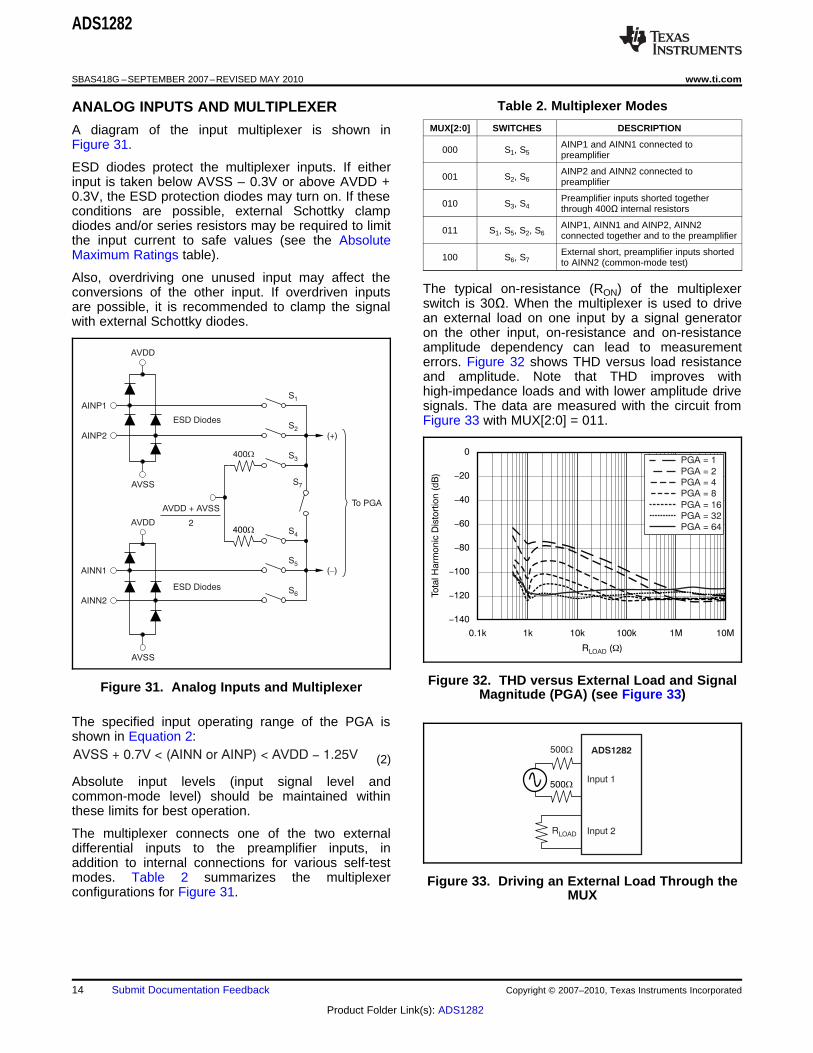
Table 2. Multiplexer ModesANALOG INPUTS AND MULTIPLEXERMUX[2:0] SWITCHES DESCRIPTIONA diagram of the input multiplexer is shown in
AINP1 and AINN1 connected toFigure 31. 000 S1, S5 preamplifierESD diodes protect the multiplexer inputs. If either AINP2 and AINN2 connected to001 S2, S6 preamplifierinput is taken below AVSS – 0.3V or above AVDD +0.3V, the ESD protection diodes may turn on. If these Preamplifier inputs shorted together010 S3, S4 through 400Ω internal resistorsconditions are possible, external Schottky clamp
AINP1, AINN1 and AINP2, AINN2diodes and/or series resistors may be required to limit 011 S1, S5, S2, S6 connected together and to the preamplifierthe input current to safe values (see the AbsoluteExternal short, preamplifier inputs shortedMaximum Ratings table). 100 S6, S7 to AINN2 (common-mode test)
Also, overdriving one unused input may affect theThe typical on-resistance (RON) of the multiplexerconversions of the other input. If overdriven inputsswitch is 30Ω. When the multiplexer is used to driveare possible, it is recommended to clamp the signalan external load on one input by a signal generatorwith external Schottky diodes.on the other input, on-resistance and on-resistanceamplitude dependency can lead to measurementerrors. Figure 32 shows THD versus load resistanceand amplitude. Note that THD improves withhigh-impedance loads and with lower amplitude drivesignals. The data are measured with the circuit fromFigure 33 with MUX[2:0] = 011.
Figure 32. THD versus External Load and SignalFigure 31. Analog Inputs and Multiplexer Magnitude (PGA) (see Figure 33)
The specified input operating range of the PGA isshown in Equation 2:
(2)
Absolute input levels (input signal level andcommon-mode level) should be maintained withinthese limits for best operation.
The multiplexer connects one of the two externaldifferential inputs to the preamplifier inputs, inaddition to internal connections for various self-testmodes. Table 2 summarizes the multiplexer Figure 33. Driving an External Load Through theconfigurations for Figure 31. MUX
14 Submit Documentation Feedback Copyright © 2007–2010, Texas Instruments Incorporated
Product Folder Link(s): ADS1282
f =P
1
6.3 600 C´ ´10
Frequency (Hz)
100
10
1
PG
A N
ois
e (
nV
/)
ÖH
z
100 1k
PGA CHOP Off
PGA CHOP On
AVSS + 0.4V < (CAPN or CAPP) < AVDD 0.4V-
Gain Control
PGA[2:0] Bits
MUX (+)
MUX ( )-
CHOP
Chopping Control CHOP Bit
AVSS
CAPP
300W
300W
A1
A2
AVDD
CAPN
(55k , typ
Modulator
Effective
Impedance
W )(1)
10nF
ADS1282
www.ti.com SBAS418G –SEPTEMBER 2007–REVISED MAY 2010
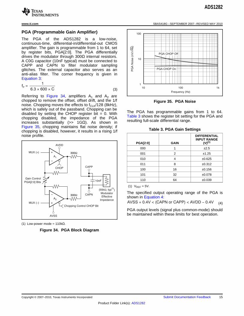
PGA (Programmable Gain Amplifier)
The PGA of the ADS1282 is a low-noise,continuous-time, differential-in/differential-out CMOSamplifier. The gain is programmable from 1 to 64, setby register bits, PGA[2:0]. The PGA differentiallydrives the modulator through 300Ω internal resistors.A C0G capacitor (10nF typical) must be connected toCAPP and CAPN to filter modulator samplingglitches. The external capacitor also serves as ananti-alias filter. The corner frequency is given inEquation 3:
(3)
Referring to Figure 34, amplifiers A1 and A2 arechopped to remove the offset, offset drift, and the 1/f Figure 35. PGA Noisenoise. Chopping moves the effects to fCLK/128 (8kHz),which is safely out of the passband. Chopping can be
The PGA has programmable gains from 1 to 64.disabled by setting the CHOP register bit = 0. WithTable 3 shows the register bit setting for the PGA andchopping disabled, the impedance of the PGAresulting full-scale differential range.increases substantially (>> 1GΩ). As shown in
Figure 35, chopping maintains flat noise density; ifTable 3. PGA Gain Settingschopping is disabled, however, it results in a rising 1/f
noise profile. DIFFERENTIALINPUT RANGE
PGA[2:0] GAIN (V)(1)
000 1 ±2.5
001 2 ±1.25
010 4 ±0.625
011 8 ±0.312
100 16 ±0.156
101 32 ±0.078
110 64 ±0.039
(1) VREF = 5V.
The specified output operating range of the PGA isshown in Equation 4:
(4)
PGA output levels (signal plus common-mode) shouldbe maintained within these limits for best operation.
(1) Low-power mode = 110kΩ.
Figure 34. PGA Block Diagram
Copyright © 2007–2010, Texas Instruments Incorporated Submit Documentation Feedback 15
Product Folder Link(s): ADS1282
Ma
gn
itu
de
(d
B)
Frequency (Hz)
0
-20
-40
-60
-80
-100
-180
1 10 100 100k1k 10k
-120
-140
-160
1Hz Resolution
V = 20mVIN DC
2nd-Order
2nd-Stage
DS
2nd-Order
1st-Stage
DSAnalog Input (V )IN
4th-Order Modulator
MCLK
M0
M1
fCLK/4
Y[n] = 3M0[n 2] 6M0[n 3] + 4M0[n 4]
+ 9(M1[n] 2M1[n 1] + M1[n 2])
- - - -
- - -
ADS1282
SBAS418G –SEPTEMBER 2007–REVISED MAY 2010 www.ti.com
ADC passband. The noise moves out of the passband andappears at the chopping frequency (fCLK/512 = 8kHz).
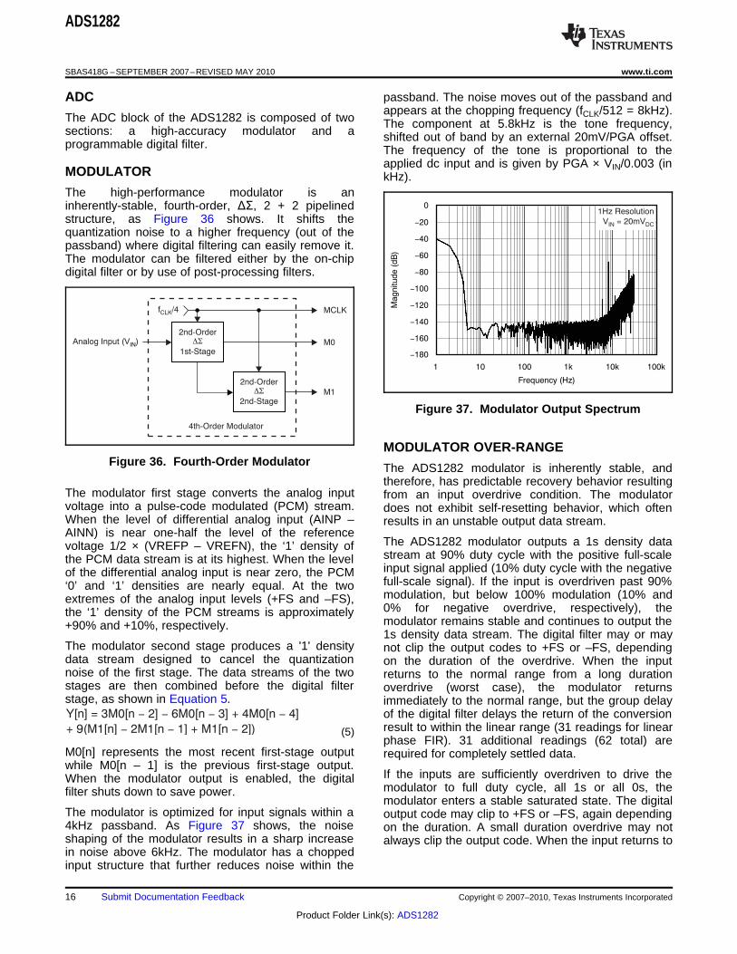
The ADC block of the ADS1282 is composed of two The component at 5.8kHz is the tone frequency,sections: a high-accuracy modulator and a shifted out of band by an external 20mV/PGA offset.programmable digital filter. The frequency of the tone is proportional to the
applied dc input and is given by PGA × VIN/0.003 (inMODULATOR kHz).The high-performance modulator is aninherently-stable, fourth-order, ΔΣ, 2 + 2 pipelinedstructure, as Figure 36 shows. It shifts thequantization noise to a higher frequency (out of thepassband) where digital filtering can easily remove it.The modulator can be filtered either by the on-chipdigital filter or by use of post-processing filters.
Figure 37. Modulator Output Spectrum
MODULATOR OVER-RANGEFigure 36. Fourth-Order Modulator The ADS1282 modulator is inherently stable, and
therefore, has predictable recovery behavior resultingThe modulator first stage converts the analog input from an input overdrive condition. The modulatorvoltage into a pulse-code modulated (PCM) stream. does not exhibit self-resetting behavior, which oftenWhen the level of differential analog input (AINP – results in an unstable output data stream.AINN) is near one-half the level of the reference
The ADS1282 modulator outputs a 1s density datavoltage 1/2 × (VREFP – VREFN), the ‘1’ density ofstream at 90% duty cycle with the positive full-scalethe PCM data stream is at its highest. When the levelinput signal applied (10% duty cycle with the negativeof the differential analog input is near zero, the PCMfull-scale signal). If the input is overdriven past 90%‘0’ and ‘1’ densities are nearly equal. At the twomodulation, but below 100% modulation (10% andextremes of the analog input levels (+FS and –FS),0% for negative overdrive, respectively), thethe ‘1’ density of the PCM streams is approximatelymodulator remains stable and continues to output the+90% and +10%, respectively.1s density data stream. The digital filter may or may
The modulator second stage produces a '1' density not clip the output codes to +FS or –FS, dependingdata stream designed to cancel the quantization on the duration of the overdrive. When the inputnoise of the first stage. The data streams of the two returns to the normal range from a long durationstages are then combined before the digital filter overdrive (worst case), the modulator returnsstage, as shown in Equation 5. immediately to the normal range, but the group delay
of the digital filter delays the return of the conversionresult to within the linear range (31 readings for linear(5)phase FIR). 31 additional readings (62 total) are
M0[n] represents the most recent first-stage output required for completely settled data.while M0[n – 1] is the previous first-stage output.
If the inputs are sufficiently overdriven to drive theWhen the modulator output is enabled, the digitalmodulator to full duty cycle, all 1s or all 0s, thefilter shuts down to save power.modulator enters a stable saturated state. The digital
The modulator is optimized for input signals within a output code may clip to +FS or –FS, again depending4kHz passband. As Figure 37 shows, the noise on the duration. A small duration overdrive may notshaping of the modulator results in a sharp increase always clip the output code. When the input returns toin noise above 6kHz. The modulator has a choppedinput structure that further reduces noise within the
16 Submit Documentation Feedback Copyright © 2007–2010, Texas Instruments Incorporated
Product Folder Link(s): ADS1282
fMOD/2
MFLAG
Pin
100% FSAINN
AINP
P
Q
IABSIå
MFLAG
Pin
+100(AINP AINN)-
-100
0 Time
V(%
of F
ull-
Scale
)IN
ADS1282
www.ti.com SBAS418G –SEPTEMBER 2007–REVISED MAY 2010
the normal range, the modulator requires up to 12 MODULATOR OVER-RANGE DETECTIONmodulator clock cycles (fMOD) to exit saturation and (MFLAG)return to the linear region. The digital filter requires an
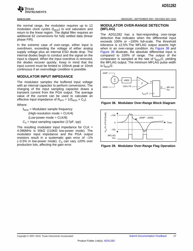
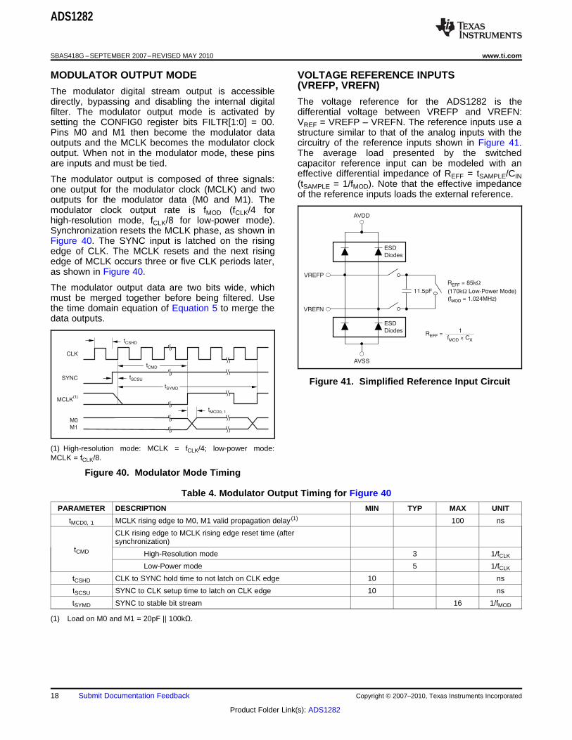
The ADS1282 has a fast-responding over-rangeadditional 62 conversions for fully settled data (lineardetection that indicates when the differential inputphase FIR).exceeds 100% or –100% full-scale. The threshold
In the extreme case of over-range, either input is tolerance is ±2.5%.The MFLAG output asserts highoverdriven, exceeding the voltage of either analog when in an over-range condition. As Figure 38 andsupply voltage plus an internal ESD diode drop. The Figure 39 illustrate, the absolute differential input isinternal diodes begin to conduct and the signal on the compared to 100% of range. The output of theinput is clipped. When the input overdrive is removed, comparator is sampled at the rate of fMOD/2, yieldingthe diodes recover quickly. Keep in mind that the the MFLAG output. The minimum MFLAG pulse widthinput current must be limited to 100mA peak or 10mA is fMOD/2.continuous if an overvoltage condition is possible.
MODULATOR INPUT IMPEDANCE
The modulator samples the buffered input voltagewith an internal capacitor to perform conversions. Thecharging of the input sampling capacitor draws atransient current from the PGA output. The averagevalue of the current can be used to calculate aneffective input impedance of REFF = 1/(fMOD × CS).
Figure 38. Modulator Over-Range Block DiagramWhere:
fMOD = Modulator sample frequency(High-resolution mode = CLK/4)(Low-power mode = CLK/8)
CS = Input sampling capacitor (17pF, typ)
The resulting modulator input impedance for CLK =4.096MHz is 55kΩ (110kΩ low-power mode). Themodulator input impedance and the PGA outputresistors result in a systematic gain error of –1%(–0.5% in low-power mode). CS can vary ±20% overproduction lots, affecting the gain error. Figure 39. Modulator Over-Range Flag Operation
Copyright © 2007–2010, Texas Instruments Incorporated Submit Documentation Feedback 17
Product Folder Link(s): ADS1282
ESD
Diodes
ESD
Diodes
11.5pF
R
(170k Low-Power Mode)
W= 85k
W
(f = 1.024MHz)
EFF
MOD
AVDD
AVSS
VREFP
VREFN
R =EFF f C´MOD X
1
CLK
SYNC
MCLK(1)
M0
M1
tMCD0, 1
tSCSU
tCSHD
tCMD
tSYMD
ADS1282
SBAS418G –SEPTEMBER 2007–REVISED MAY 2010 www.ti.com
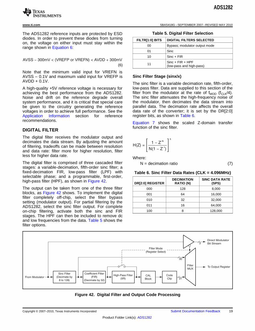
MODULATOR OUTPUT MODE VOLTAGE REFERENCE INPUTS(VREFP, VREFN)
The modulator digital stream output is accessibledirectly, bypassing and disabling the internal digital The voltage reference for the ADS1282 is thefilter. The modulator output mode is activated by differential voltage between VREFP and VREFN:setting the CONFIG0 register bits FILTR[1:0] = 00. VREF = VREFP – VREFN. The reference inputs use aPins M0 and M1 then become the modulator data structure similar to that of the analog inputs with theoutputs and the MCLK becomes the modulator clock circuitry of the reference inputs shown in Figure 41.output. When not in the modulator mode, these pins The average load presented by the switchedare inputs and must be tied. capacitor reference input can be modeled with an
effective differential impedance of REFF = tSAMPLE/CINThe modulator output is composed of three signals: (tSAMPLE = 1/fMOD). Note that the effective impedanceone output for the modulator clock (MCLK) and two of the reference inputs loads the external reference.outputs for the modulator data (M0 and M1). Themodulator clock output rate is fMOD (fCLK/4 forhigh-resolution mode, fCLK/8 for low-power mode).Synchronization resets the MCLK phase, as shown inFigure 40. The SYNC input is latched on the risingedge of CLK. The MCLK resets and the next risingedge of MCLK occurs three or five CLK periods later,as shown in Figure 40.
The modulator output data are two bits wide, whichmust be merged together before being filtered. Usethe time domain equation of Equation 5 to merge thedata outputs.
Figure 41. Simplified Reference Input Circuit
(1) High-resolution mode: MCLK = fCLK/4; low-power mode:MCLK = fCLK/8.
Figure 40. Modulator Mode Timing
Table 4. Modulator Output Timing for Figure 40
PARAMETER DESCRIPTION MIN TYP MAX UNIT
tMCD0, 1 MCLK rising edge to M0, M1 valid propagation delay (1) 100 ns
CLK rising edge to MCLK rising edge reset time (aftersynchronization)
tCMD High-Resolution mode 3 1/fCLK
Low-Power mode 5 1/fCLK
tCSHD CLK to SYNC hold time to not latch on CLK edge 10 ns
tSCSU SYNC to CLK setup time to latch on CLK edge 10 ns
tSYMD SYNC to stable bit stream 16 1/fMOD
(1) Load on M0 and M1 = 20pF || 100kΩ.
18 Submit Documentation Feedback Copyright © 2007–2010, Texas Instruments Incorporated
Product Folder Link(s): ADS1282
AVSS 300mV < (VREFP or VREFN) < AVDD + 300mV-
H(Z) =1 Z-
-N
N(1 Z- )-1
5
Sinc Filter
(Decimate by
8 to 128)
Coefficient Filter
(FIR)
(Decimate by 32)
High-Pass Filter
(IIR)
Filter
MUXTo Output Register
From Modulator
Direct Modulator
Bit Stream
30
3
CAL
Block
Code
Clip 31
Filter Mode
(Register Select)
ADS1282
www.ti.com SBAS418G –SEPTEMBER 2007–REVISED MAY 2010
Table 5. Digital Filter SelectionThe ADS1282 reference inputs are protected by ESDdiodes. In order to prevent these diodes from turning FILTR[1:0] BITS DIGITAL FILTERS SELECTEDon, the voltage on either input must stay within the
00 Bypass; modulator output moderange shown in Equation 6:01 Sinc
10 Sinc + FIR
Sinc + FIR + HPF11(6) (low-pass and high-pass)
Note that the minimum valid input for VREFN isSinc Filter Stage (sinx/x)AVSS – 0.1V and maximum valid input for VREFP is
AVDD + 0.1V. The sinc filter is a variable decimation rate, fifth-order,low-pass filter. Data are supplied to this section of theA high-quality +5V reference voltage is necessary forfilter from the modulator at the rate of fMOD (fCLK/4).achieving the best performance from the ADS1282.The sinc filter attenuates the high-frequency noise ofNoise and drift on the reference degrade overallthe modulator, then decimates the data stream intosystem performance, and it is critical that special careparallel data. The decimation rate affects the overallbe given to the circuitry generating the referencedata rate of the converter; it is set by the DR[2:0]voltages in order to achieve full performance. See theregister bits, as shown in Table 6.Application Information section for reference
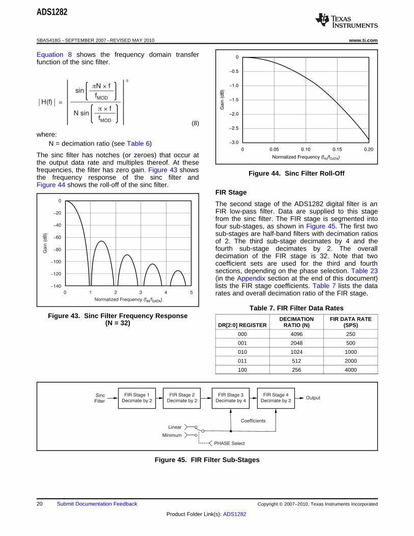
recommendations. Equation 7 shows the scaled Z-domain transferfunction of the sinc filter.DIGITAL FILTER
The digital filter receives the modulator output anddecimates the data stream. By adjusting the amountof filtering, tradeoffs can be made between resolutionand data rate: filter more for higher resolution, filterless for higher data rate. Where:The digital filter is comprised of three cascaded filter N = decimation ratio (7)stages: a variable-decimation, fifth-order sinc filter; afixed-decimation FIR, low-pass filter (LPF) with Table 6. Sinc Filter Data Rates (CLK = 4.096MHz)selectable phase; and a programmable, first-order,
DECIMATION SINC DATA RATEhigh-pass filter (HPF), as shown in Figure 42. DR[2:0] REGISTER RATIO (N) (SPS)
The output can be taken from one of the three filter 000 128 8,000blocks, as Figure 42 shows. To implement the digital 001 64 16,000filter completely off-chip, select the filter bypass
010 32 32,000setting (modulator output). For partial filtering by the
011 16 64,000ADS1282, select the sinc filter output. For complete100 8 128,000on-chip filtering, activate both the sinc and FIR
stages. The HPF can then be included to remove dcand low frequencies from the data. Table 5 shows thefilter options.
Figure 42. Digital Filter and Output Code Processing
Copyright © 2007–2010, Texas Instruments Incorporated Submit Documentation Feedback 19
Product Folder Link(s): ADS1282
½ ½H(f) =
5
sinp ´N f
fMOD
N sinp ´ f
fMOD
Gain
(dB
)
Normalized Frequency (f /f )IN DATA
0
-0.5
-1.0
-1.5
-2.0
-2.5
-3.0
0 0.05 0.10 0.200.15
0 1 2
Normalized Frequency (f /f )IN DATA
0
-20
-40
-60
-80
-100
-120
-140
Gain
(dB
)
3 4 5
OutputFIR Stage 2
Decimate by 2
FIR Stage 1
Decimate by 2Sinc
Filter
FIR Stage 4
Decimate by 2
FIR Stage 3
Decimate by 4
Linear
Minimum
PHASE Select
Coefficients
ADS1282
SBAS418G –SEPTEMBER 2007–REVISED MAY 2010 www.ti.com
Equation 8 shows the frequency domain transferfunction of the sinc filter.
(8)
where:N = decimation ratio (see Table 6)
The sinc filter has notches (or zeroes) that occur atthe output data rate and multiples thereof. At thesefrequencies, the filter has zero gain. Figure 43 shows Figure 44. Sinc Filter Roll-Offthe frequency response of the sinc filter andFigure 44 shows the roll-off of the sinc filter.
FIR Stage
The second stage of the ADS1282 digital filter is anFIR low-pass filter. Data are supplied to this stagefrom the sinc filter. The FIR stage is segmented intofour sub-stages, as shown in Figure 45. The first twosub-stages are half-band filters with decimation ratiosof 2. The third sub-stage decimates by 4 and thefourth sub-stage decimates by 2. The overalldecimation of the FIR stage is 32. Note that twocoefficient sets are used for the third and fourthsections, depending on the phase selection. Table 23(in the Appendix section at the end of this document)lists the FIR stage coefficients. Table 7 lists the datarates and overall decimation ratio of the FIR stage.
Table 7. FIR Filter Data RatesFigure 43. Sinc Filter Frequency Response DECIMATION FIR DATA RATE
(N = 32) DR[2:0] REGISTER RATIO (N) (SPS)
000 4096 250
001 2048 500
010 1024 1000
011 512 2000
100 256 4000
Figure 45. FIR Filter Sub-Stages
20 Submit Documentation Feedback Copyright © 2007–2010, Texas Instruments Incorporated
Product Folder Link(s): ADS1282
0 0.05
Normalized Input Frequency (f /f )IN DATA
2.0
1.5
1.0
0.5
0
0.5
1.0
1.5
2.0
-
-
-
-
Magnitude (
mdB
)
0.10 0.15 0.20 0.400.25 0.30 0.35
0 0.1 0.2
Normalized Input Frequency (f /f )IN DATA
20
0
-
-
-
-
-
-
-
-
20
40
60
80
100
120
140
160
Magnitude (
dB
)
1.00.3 0.4 0.5 0.6 0.7 0.8 0.9
0 5 10
Time Index (1/f )DATA
1.4
1.2
1.0
0.8
0.6
0.4
0.2
0
-0.2
Am
plit
ude (
dB
)
15 20 25 30 35 40 45 50 55 60 65
Linear Phase Filter
Minimum Phase Filter
ADS1282
www.ti.com SBAS418G –SEPTEMBER 2007–REVISED MAY 2010
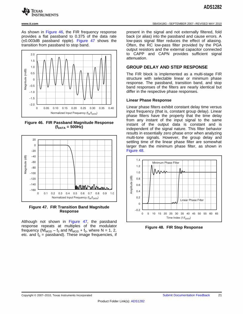
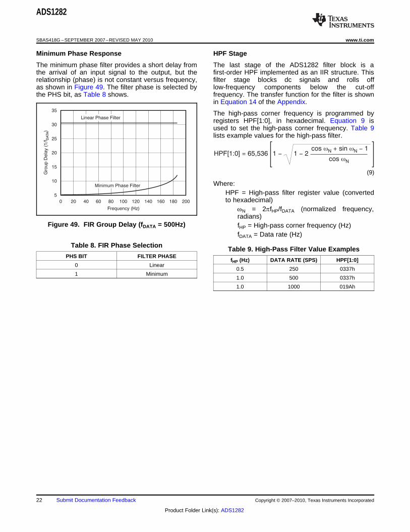
As shown in Figure 46, the FIR frequency response present in the signal and not externally filtered, foldprovides a flat passband to 0.375 of the data rate back (or alias) into the passband and cause errors. A(±0.003dB passband ripple). Figure 47 shows the low-pass signal filter reduces the effect of aliasing.transition from passband to stop band. Often, the RC low-pass filter provided by the PGA
output resistors and the external capacitor connectedto CAPP and CAPN provides sufficient signalattenuation.
GROUP DELAY AND STEP RESPONSE
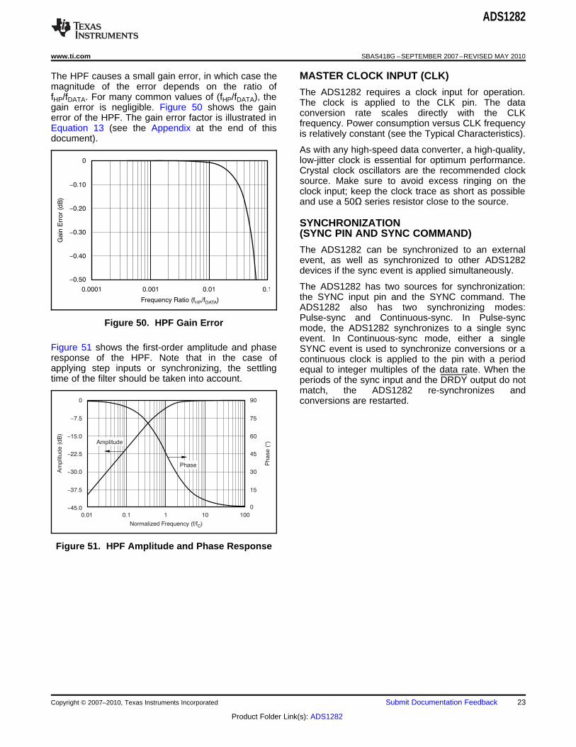
The FIR block is implemented as a multi-stage FIRstructure with selectable linear or minimum phaseresponse. The passband, transition band, and stopband responses of the filters are nearly identical butdiffer in the respective phase responses.
Linear Phase Response
Linear phase filters exhibit constant delay time versusinput frequency (that is, constant group delay). Linearphase filters have the property that the time delayfrom any instant of the input signal to the same
Figure 46. FIR Passband Magnitude Response instant of the output data is constant and is(fDATA = 500Hz) independent of the signal nature. This filter behavior
results in essentially zero phase error when analyzingmulti-tone signals. However, the group delay andsettling time of the linear phase filter are somewhatlarger than the minimum phase filter, as shown inFigure 48.
Figure 47. FIR Transition Band MagnitudeResponse
Although not shown in Figure 47, the passbandresponse repeats at multiples of the modulator Figure 48. FIR Step Responsefrequency (NfMOD – f0 and NfMOD + f0, where N = 1, 2,etc. and f0 = passband). These image frequencies, if
Copyright © 2007–2010, Texas Instruments Incorporated Submit Documentation Feedback 21
Product Folder Link(s): ADS1282
HPF[1:0] = 65,536 1 -cos + sin 1w -N Nw
cos wN
1 2-
0 20 40
Frequency (Hz)
35
30
25
20
15
10
5
Gro
up D
ela
y (
1/f
)D
ATA
60 80 100 120 140 160 180 200
Linear Phase Filter
Minimum Phase Filter
ADS1282
SBAS418G –SEPTEMBER 2007–REVISED MAY 2010 www.ti.com
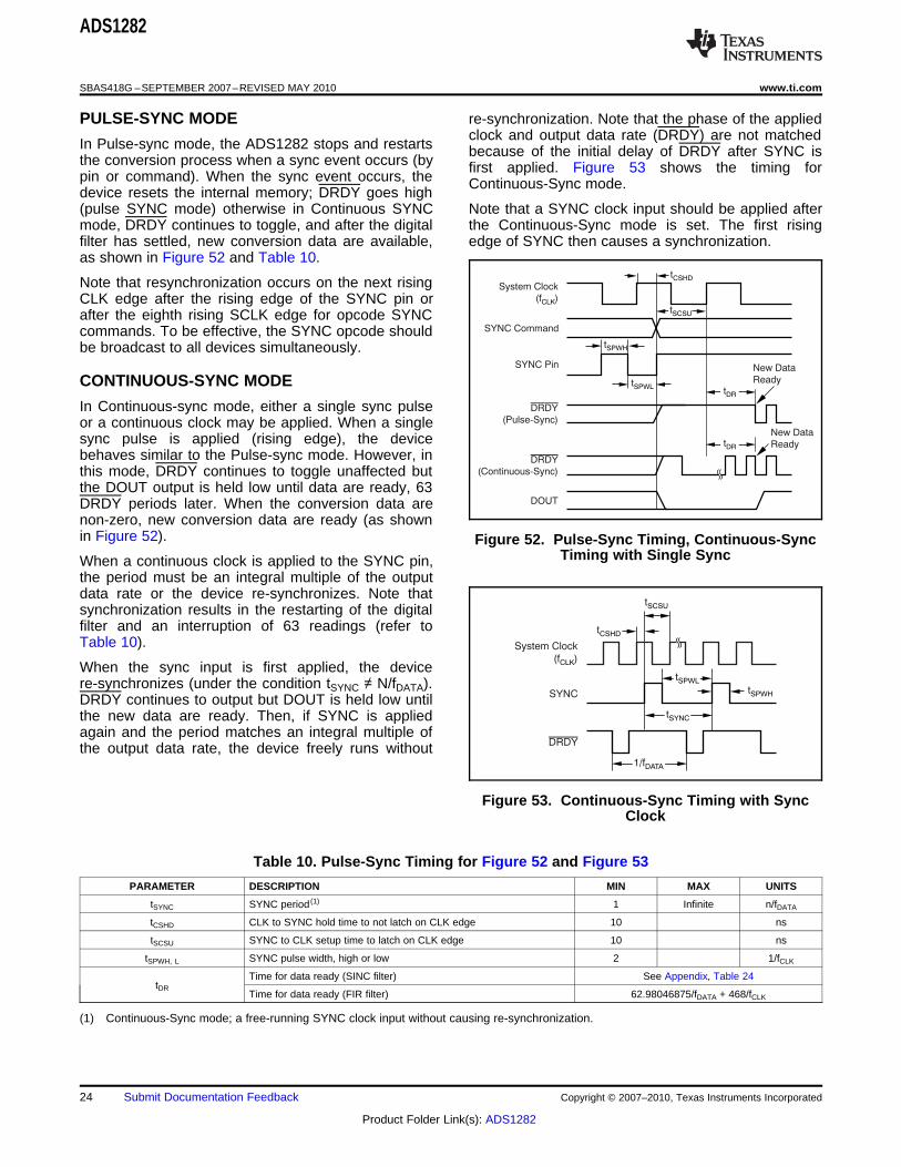
Minimum Phase Response HPF Stage
The minimum phase filter provides a short delay from The last stage of the ADS1282 filter block is athe arrival of an input signal to the output, but the first-order HPF implemented as an IIR structure. Thisrelationship (phase) is not constant versus frequency, filter stage blocks dc signals and rolls offas shown in Figure 49. The filter phase is selected by low-frequency components below the cut-offthe PHS bit, as Table 8 shows. frequency. The transfer function for the filter is shown
in Equation 14 of the Appendix.
The high-pass corner frequency is programmed byregisters HPF[1:0], in hexadecimal. Equation 9 isused to set the high-pass corner frequency. Table 9lists example values for the high-pass filter.
(9)
Where:HPF = High-pass filter register value (convertedto hexadecimal)
wN = 2pfHP/fDATA (normalized frequency,radians)
Figure 49. FIR Group Delay (fDATA = 500Hz) fHP = High-pass corner frequency (Hz)fDATA = Data rate (Hz)
Table 8. FIR Phase Selection Table 9. High-Pass Filter Value ExamplesPHS BIT FILTER PHASE
fHP (Hz) DATA RATE (SPS) HPF[1:0]0 Linear
0.5 250 0337h1 Minimum
1.0 500 0337h
1.0 1000 019Ah
22 Submit Documentation Feedback Copyright © 2007–2010, Texas Instruments Incorporated
Product Folder Link(s): ADS1282
Gain
Err
or
(dB
)
Frequency Ratio (f /f )HP DATA
0
-0.10
-0.20
-0.30
-0.40
-0.50
0.0001 0.001 0.01 0.1
0.01 0.1
Normalized Frequency (f/f )C
0
-7.5
-15.0
-22.5
-30.0
-45.0
Am
plit
ude (
dB
)
90
75
60
45
30
15
0
Phase (
)°
1 10 100
Phase
Amplitude
-37.5
ADS1282
www.ti.com SBAS418G –SEPTEMBER 2007–REVISED MAY 2010
The HPF causes a small gain error, in which case the MASTER CLOCK INPUT (CLK)magnitude of the error depends on the ratio of
The ADS1282 requires a clock input for operation.fHP/fDATA. For many common values of (fHP/fDATA), theThe clock is applied to the CLK pin. The datagain error is negligible. Figure 50 shows the gainconversion rate scales directly with the CLKerror of the HPF. The gain error factor is illustrated infrequency. Power consumption versus CLK frequencyEquation 13 (see the Appendix at the end of thisis relatively constant (see the Typical Characteristics).document).As with any high-speed data converter, a high-quality,low-jitter clock is essential for optimum performance.Crystal clock oscillators are the recommended clocksource. Make sure to avoid excess ringing on theclock input; keep the clock trace as short as possibleand use a 50Ω series resistor close to the source.
SYNCHRONIZATION(SYNC PIN AND SYNC COMMAND)
The ADS1282 can be synchronized to an externalevent, as well as synchronized to other ADS1282devices if the sync event is applied simultaneously.
The ADS1282 has two sources for synchronization:the SYNC input pin and the SYNC command. TheADS1282 also has two synchronizing modes:Pulse-sync and Continuous-sync. In Pulse-syncFigure 50. HPF Gain Error mode, the ADS1282 synchronizes to a single syncevent. In Continuous-sync mode, either a single
Figure 51 shows the first-order amplitude and phase SYNC event is used to synchronize conversions or aresponse of the HPF. Note that in the case of continuous clock is applied to the pin with a periodapplying step inputs or synchronizing, the settling equal to integer multiples of the data rate. When thetime of the filter should be taken into account. periods of the sync input and the DRDY output do not
match, the ADS1282 re-synchronizes andconversions are restarted.
Figure 51. HPF Amplitude and Phase Response
Copyright © 2007–2010, Texas Instruments Incorporated Submit Documentation Feedback 23
Product Folder Link(s): ADS1282
System Clock
(f )CLK
SYNC Command
SYNC Pin
DRDY
(Pulse-Sync)
tSPWL
New Data
Ready
tCSHD
tSPWH
DRDY
(Continuous-Sync)
DOUT
New Data
Ready
tDR
tSCSU
tDR
System Clock
(f )CLK
SYNC
DRDY
tCSHD
tSCSU
tSYNC
1/fDATA
tSPWH
tSPWL
ADS1282
SBAS418G –SEPTEMBER 2007–REVISED MAY 2010 www.ti.com
PULSE-SYNC MODE re-synchronization. Note that the phase of the appliedclock and output data rate (DRDY) are not matched
In Pulse-sync mode, the ADS1282 stops and restarts because of the initial delay of DRDY after SYNC isthe conversion process when a sync event occurs (by first applied. Figure 53 shows the timing forpin or command). When the sync event occurs, the Continuous-Sync mode.device resets the internal memory; DRDY goes high(pulse SYNC mode) otherwise in Continuous SYNC Note that a SYNC clock input should be applied aftermode, DRDY continues to toggle, and after the digital the Continuous-Sync mode is set. The first risingfilter has settled, new conversion data are available, edge of SYNC then causes a synchronization.as shown in Figure 52 and Table 10.
Note that resynchronization occurs on the next risingCLK edge after the rising edge of the SYNC pin orafter the eighth rising SCLK edge for opcode SYNCcommands. To be effective, the SYNC opcode shouldbe broadcast to all devices simultaneously.
CONTINUOUS-SYNC MODE
In Continuous-sync mode, either a single sync pulseor a continuous clock may be applied. When a singlesync pulse is applied (rising edge), the devicebehaves similar to the Pulse-sync mode. However, inthis mode, DRDY continues to toggle unaffected butthe DOUT output is held low until data are ready, 63DRDY periods later. When the conversion data arenon-zero, new conversion data are ready (as shownin Figure 52). Figure 52. Pulse-Sync Timing, Continuous-Sync
Timing with Single SyncWhen a continuous clock is applied to the SYNC pin,the period must be an integral multiple of the outputdata rate or the device re-synchronizes. Note thatsynchronization results in the restarting of the digitalfilter and an interruption of 63 readings (refer toTable 10).
When the sync input is first applied, the devicere-synchronizes (under the condition tSYNC ≠ N/fDATA).DRDY continues to output but DOUT is held low untilthe new data are ready. Then, if SYNC is appliedagain and the period matches an integral multiple ofthe output data rate, the device freely runs without
Figure 53. Continuous-Sync Timing with SyncClock
Table 10. Pulse-Sync Timing for Figure 52 and Figure 53
PARAMETER DESCRIPTION MIN MAX UNITS
tSYNC SYNC period (1) 1 Infinite n/fDATA
tCSHD CLK to SYNC hold time to not latch on CLK edge 10 ns
tSCSU SYNC to CLK setup time to latch on CLK edge 10 ns
tSPWH, L SYNC pulse width, high or low 2 1/fCLK
Time for data ready (SINC filter) See Appendix, Table 24tDR
Time for data ready (FIR filter) 62.98046875/fDATA + 468/fCLK
(1) Continuous-Sync mode; a free-running SYNC clock input without causing re-synchronization.
24 Submit Documentation Feedback Copyright © 2007–2010, Texas Instruments Incorporated
Product Folder Link(s): ADS1282
PWDN Pin
DRDY tDR
Wakeup
Command
System Clock
(f )CLK
DRDY
RESET Pin
RESET Command
tRST
Settled
Data
or
tCRHD
tDR
tRCSU
CLK
DVDD
DRDY
Internal Reset
1V nom
AVDD AVSS- 3.5V nom
216
tDR
fCLK
ADS1282
www.ti.com SBAS418G –SEPTEMBER 2007–REVISED MAY 2010
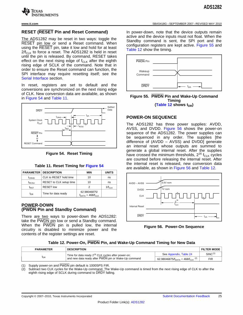
RESET (RESET Pin and Reset Command) In power-down, note that the device outputs remainactive and the device inputs must not float. When the
The ADS1282 may be reset in two ways: toggle the Standby command is sent, the SPI port and theRESET pin low or send a Reset command. When configuration registers are kept active. Figure 55 andusing the RESET pin, take it low and hold for at least Table 12 show the timing.2/fCLK to force a reset. The ADS1282 is held in resetuntil the pin is released. By command, RESET takeseffect on the next rising edge of fCLK after the eighthrising edge of SCLK of the command. Note that inorder to ensure the Reset command can function, theSPI interface may require resetting itself; see theSerial Interface section.
In reset, registers are set to default and theconversions are synchronized on the next rising edgeof CLK. New conversion data are available, as shown
Figure 55. PWDN Pin and Wake-Up Commandin Figure 54 and Table 11.Timing
(Table 12 shows tDR)
POWER-ON SEQUENCE
The ADS1282 has three power supplies: AVDD,AVSS, and DVDD. Figure 56 shows the power-onsequence of the ADS1282. The power supplies canbe sequenced in any order. The supplies [thedifference of (AVDD – AVSS) and DVDD] generatean internal reset whose outputs are summed togenerate a global internal reset. After the supplies
Figure 54. Reset Timing have crossed the minimum thresholds, 216 fCLK cyclesare counted before releasing the internal reset. Afterthe internal reset is released, new conversion dataTable 11. Reset Timing for Figure 54 are available, as shown in Figure 56 and Table 12.
PARAMETER DESCRIPTION MIN UNITS
tCRHD CLK to RESET hold time 10 ns
tRCSU RESET to CLK setup time 10 ns
tRST RESET low 2 1/fCLK
62.98046875/tDR Time for data ready fDATA + 468/fCLK
POWER-DOWN(PWDN Pin and Standby Command)
There are two ways to power-down the ADS1282:take the PWDN pin low or send a Standby command.When the PWDN pin is pulled low, the internal Figure 56. Power-On Sequencecircuitry is disabled to minimize power and thecontents of the register settings are reset.
Table 12. Power-On, PWDN Pin, and Wake-Up Command Timing for New Data
PARAMETER DESCRIPTION FILTER MODE
See Appendix, Table 24 SINC (1)Time for data ready 216 CLK cycles after power-on;tDR and new data ready after PWDN pin or Wake-Up command 62.98046875/fDATA + 468/fCLK
(2) FIR
(1) Supply power-on and PWDN pin default is 1000SPS FIR.(2) Subtract two CLK cycles for the Wake-Up command. The Wake-Up command is timed from the next rising edge of CLK to after the
eighth rising edge of SCLK during command to DRDY falling.
Copyright © 2007–2010, Texas Instruments Incorporated Submit Documentation Feedback 25
Product Folder Link(s): ADS1282
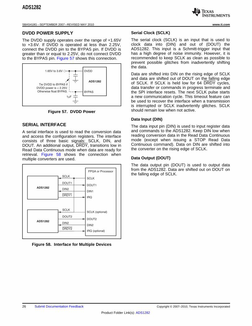
DVDD
BYPAS
1.65V to 3.6V
Tie DVDD to BYPAS if
DVDD power is < 2.25V.
Otherwise float BYPAS.
ADS1282
1 Fm
ADS1282
SCLK
DOUT1
DIN2
ADS1282
SCLK
DOUT2
FPGA or Processor
DOUT1
DIN1
DRDY1IRQ
SCLK (optional)SCLK
DOUT2
DIN2
DRDY2
DIN2
IRQ (optional)
ADS1282
SBAS418G –SEPTEMBER 2007–REVISED MAY 2010 www.ti.com
Serial Clock (SCLK)DVDD POWER SUPPLYThe serial clock (SCLK) is an input that is used toThe DVDD supply operates over the range of +1.65Vclock data into (DIN) and out of (DOUT) theto +3.6V. If DVDD is operated at less than 2.25V,ADS1282. This input is a Schmitt-trigger input thatconnect the DVDD pin to the BYPAS pin. If DVDD ishas a high degree of noise immunity. However, it isgreater than or equal to 2.25V, do not connect DVDDrecommended to keep SCLK as clean as possible toto the BYPAS pin. Figure 57 shows this connection.prevent possible glitches from inadvertently shiftingthe data.
Data are shifted into DIN on the rising edge of SCLKand data are shifted out of DOUT on the falling edgeof SCLK. If SCLK is held low for 64 DRDY cycles,data transfer or commands in progress terminate andthe SPI interface resets. The next SCLK pulse startsa new communication cycle. This timeout feature canbe used to recover the interface when a transmissionis interrupted or SCLK inadvertently glitches. SCLKshould remain low when not active.Figure 57. DVDD Power
Data Input (DIN)SERIAL INTERFACE The data input pin (DIN) is used to input register data
and commands to the ADS1282. Keep DIN low whenA serial interface is used to read the conversion datareading conversion data in the Read Data Continuousand access the configuration registers. The interfacemode (except when issuing a STOP Read Dataconsists of three basic signals: SCLK, DIN, andContinuous command). Data on DIN are shifted intoDOUT. An additional output, DRDY, transitions low inthe converter on the rising edge of SCLK.Read Data Continuous mode when data are ready for
retrieval. Figure 58 shows the connection whenData Output (DOUT)multiple converters are used.
The data output pin (DOUT) is used to output datafrom the ADS1282. Data are shifted out on DOUT onthe falling edge of SCLK.
Figure 58. Interface for Multiple Devices
26 Submit Documentation Feedback Copyright © 2007–2010, Texas Instruments Incorporated
Product Folder Link(s): ADS1282
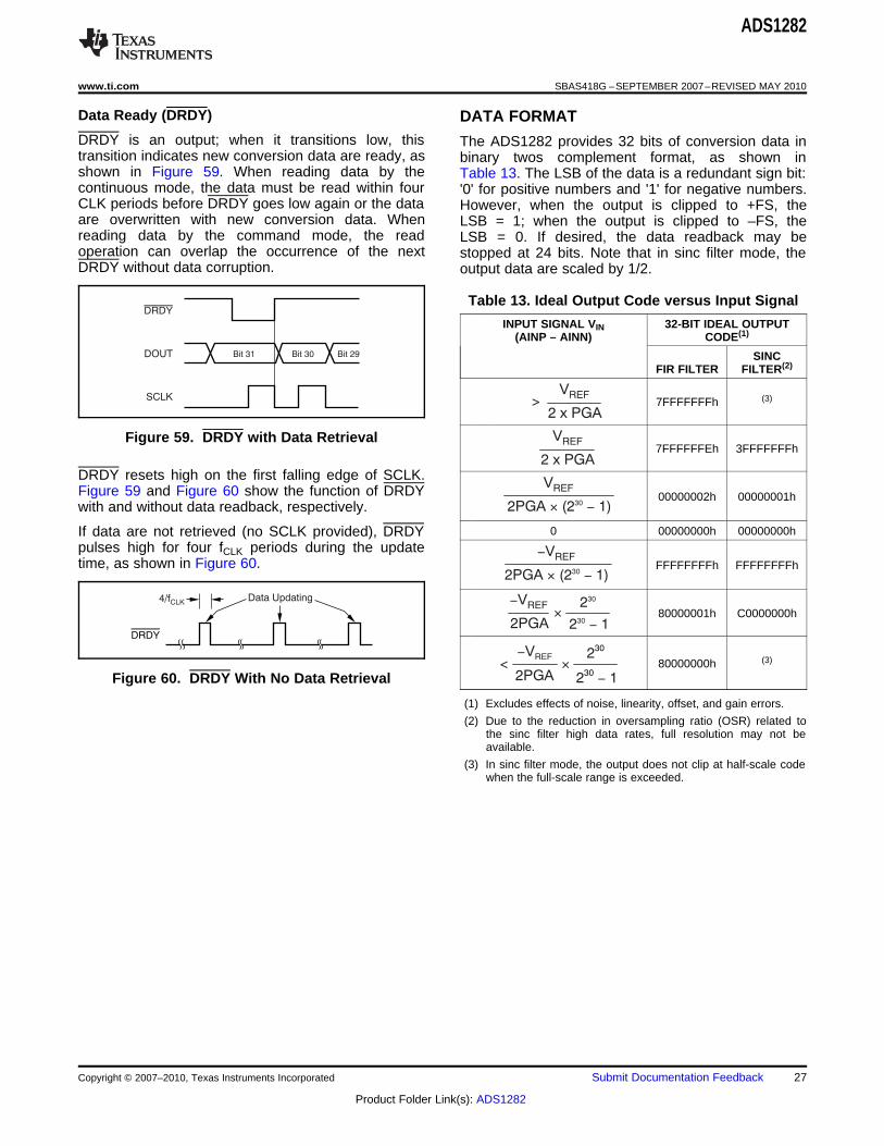
SCLK
DRDY
DOUT Bit 31 Bit 30 Bit 29
VREF
2 x PGA>
VREF
2 x PGA
VREF
2PGA (2 1)´ -30
-VREF
2PGA (2 1)´ -30
-VREF
2PGA
230
2 1-30
´
DRDY
Data Updating4/fCLK
´<-VREF
2PGA
230
2 1-30
ADS1282
www.ti.com SBAS418G –SEPTEMBER 2007–REVISED MAY 2010
Data Ready (DRDY) DATA FORMATDRDY is an output; when it transitions low, this The ADS1282 provides 32 bits of conversion data intransition indicates new conversion data are ready, as binary twos complement format, as shown inshown in Figure 59. When reading data by the Table 13. The LSB of the data is a redundant sign bit:continuous mode, the data must be read within four '0' for positive numbers and '1' for negative numbers.CLK periods before DRDY goes low again or the data However, when the output is clipped to +FS, theare overwritten with new conversion data. When LSB = 1; when the output is clipped to –FS, thereading data by the command mode, the read LSB = 0. If desired, the data readback may beoperation can overlap the occurrence of the next stopped at 24 bits. Note that in sinc filter mode, theDRDY without data corruption. output data are scaled by 1/2.
Table 13. Ideal Output Code versus Input Signal
INPUT SIGNAL VIN 32-BIT IDEAL OUTPUT(AINP – AINN) CODE(1)
SINCFIR FILTER FILTER(2)
7FFFFFFFh (3)
Figure 59. DRDY with Data Retrieval7FFFFFFEh 3FFFFFFFh
DRDY resets high on the first falling edge of SCLK.Figure 59 and Figure 60 show the function of DRDY 00000002h 00000001hwith and without data readback, respectively.
0 00000000h 00000000hIf data are not retrieved (no SCLK provided), DRDYpulses high for four fCLK periods during the updatetime, as shown in Figure 60. FFFFFFFFh FFFFFFFFh
80000001h C0000000h
80000000h (3)
Figure 60. DRDY With No Data Retrieval
(1) Excludes effects of noise, linearity, offset, and gain errors.
(2) Due to the reduction in oversampling ratio (OSR) related tothe sinc filter high data rates, full resolution may not beavailable.
(3) In sinc filter mode, the output does not clip at half-scale codewhen the full-scale range is exceeded.
Copyright © 2007–2010, Texas Instruments Incorporated Submit Documentation Feedback 27
Product Folder Link(s): ADS1282
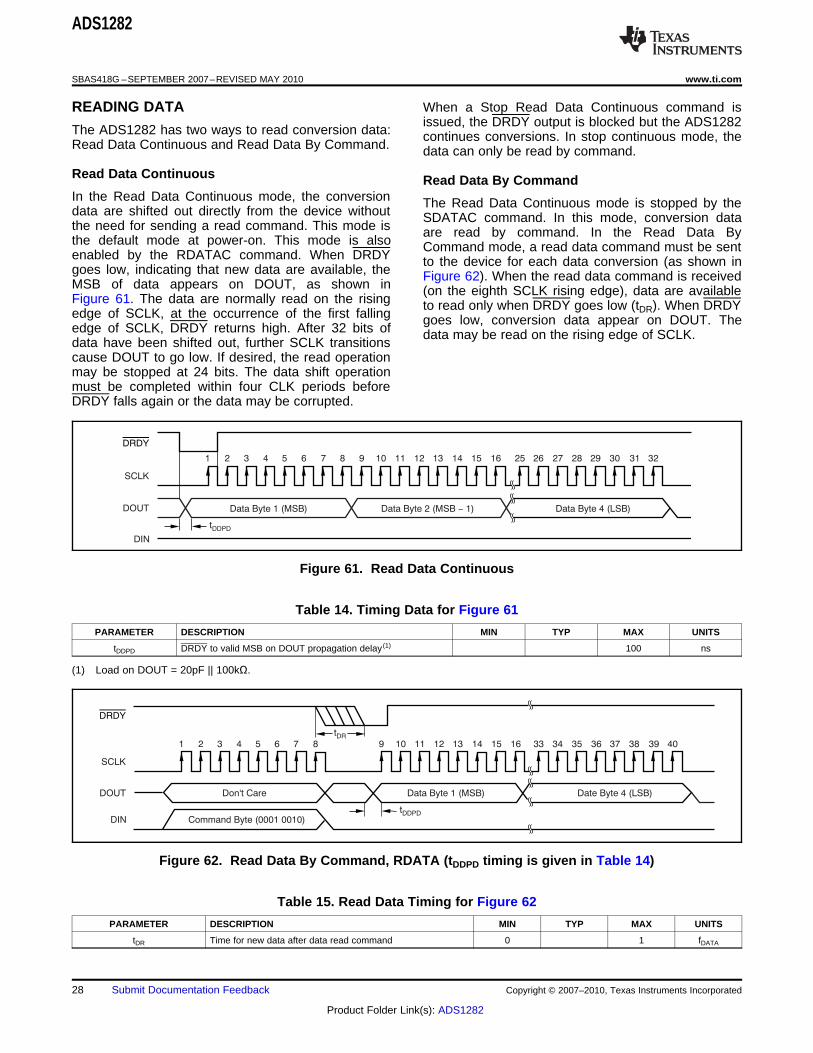
1 2 3 4 5 6 7 8 9 10 11 12 13 14 15 16 25 26 27 28 29 30 31 32
DRDY
SCLK
DOUT Data Byte 1 (MSB) Data Byte 2 (MSB 1)- Data Byte 4 (LSB)
DIN
tDDPD
SCLK
DOUT Don't Care Data Byte 1 (MSB) Date Byte 4 (LSB)
DRDY
1 2 3 4 5 6 7 8 9 10 11 12 13 14 15 16 33 34 35 36 37 38 39 40
DIN Command Byte (0001 0010)
tDR
tDDPD
ADS1282
SBAS418G –SEPTEMBER 2007–REVISED MAY 2010 www.ti.com
READING DATA When a Stop Read Data Continuous command isissued, the DRDY output is blocked but the ADS1282
The ADS1282 has two ways to read conversion data: continues conversions. In stop continuous mode, theRead Data Continuous and Read Data By Command. data can only be read by command.
Read Data Continuous Read Data By CommandIn the Read Data Continuous mode, the conversion The Read Data Continuous mode is stopped by thedata are shifted out directly from the device without SDATAC command. In this mode, conversion datathe need for sending a read command. This mode is are read by command. In the Read Data Bythe default mode at power-on. This mode is also Command mode, a read data command must be sentenabled by the RDATAC command. When DRDY to the device for each data conversion (as shown ingoes low, indicating that new data are available, the Figure 62). When the read data command is receivedMSB of data appears on DOUT, as shown in (on the eighth SCLK rising edge), data are availableFigure 61. The data are normally read on the rising to read only when DRDY goes low (tDR). When DRDYedge of SCLK, at the occurrence of the first falling goes low, conversion data appear on DOUT. Theedge of SCLK, DRDY returns high. After 32 bits of data may be read on the rising edge of SCLK.data have been shifted out, further SCLK transitionscause DOUT to go low. If desired, the read operationmay be stopped at 24 bits. The data shift operationmust be completed within four CLK periods beforeDRDY falls again or the data may be corrupted.
Figure 61. Read Data Continuous
Table 14. Timing Data for Figure 61
PARAMETER DESCRIPTION MIN TYP MAX UNITS
tDDPD DRDY to valid MSB on DOUT propagation delay (1) 100 ns
(1) Load on DOUT = 20pF || 100kΩ.
Figure 62. Read Data By Command, RDATA (tDDPD timing is given in Table 14)
Table 15. Read Data Timing for Figure 62
PARAMETER DESCRIPTION MIN TYP MAX UNITS
tDR Time for new data after data read command 0 1 fDATA
28 Submit Documentation Feedback Copyright © 2007–2010, Texas Instruments Incorporated
Product Folder Link(s): ADS1282
Final Output Data = (Input OFC[2:0])- ´FSC[2:0]
400000h
Standby Performing One-Shot Conversion Standby
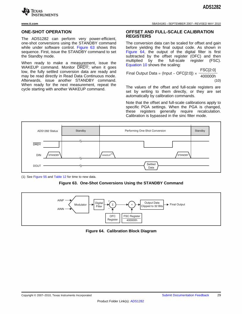
STANDBY
ADS1282 Status
DRDY
DIN
DOUT
WAKEUP(1)
STANDBY
Settled
Data
Modulator
AINP
AINN
Digital
FilterS
OFC
Register
Final OutputOutput Data
Clipped to 32 Bits´
+
-
FSC Register
400000h
ADS1282
www.ti.com SBAS418G –SEPTEMBER 2007–REVISED MAY 2010
ONE-SHOT OPERATION OFFSET AND FULL-SCALE CALIBRATIONREGISTERS
The ADS1282 can perform very power-efficient,one-shot conversions using the STANDBY command The conversion data can be scaled for offset and gainwhile under software control. Figure 63 shows this before yielding the final output code. As shown insequence. First, issue the STANDBY command to set Figure 64, the output of the digital filter is firstthe Standby mode. subtracted by the offset register (OFC) and then
multiplied by the full-scale register (FSC).When ready to make a measurement, issue the Equation 10 shows the scaling:WAKEUP command. Monitor DRDY; when it goeslow, the fully settled conversion data are ready andmay be read directly in Read Data Continuous mode.Afterwards, issue another STANDBY command. (10)When ready for the next measurement, repeat the
The values of the offset and full-scale registers arecycle starting with another WAKEUP command.set by writing to them directly, or they are setautomatically by calibration commands.
Note that the offset and full-scale calibrations apply tospecific PGA settings. When the PGA is changed,these registers generally require recalculation.Calibration is bypassed in the sinc filter mode.
(1) See Figure 55 and Table 12 for time to new data.
Figure 63. One-Shot Conversions Using the STANDBY Command
Figure 64. Calibration Block Diagram
Copyright © 2007–2010, Texas Instruments Incorporated Submit Documentation Feedback 29
Product Folder Link(s): ADS1282
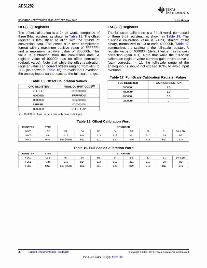
ADS1282
SBAS418G –SEPTEMBER 2007–REVISED MAY 2010 www.ti.com
OFC[2:0] Registers FSC[2:0] Registers
The offset calibration is a 24-bit word, composed of The full-scale calibration is a 24-bit word, composedthree 8-bit registers, as shown in Table 18. The offset of three 8-bit registers, as shown in Table 19. Theregister is left-justified to align with the 32-bits of full-scale calibration value is 24-bit, straight offsetconversion data. The offset is in twos complement binary, normalized to 1.0 at code 400000h. Table 17format with a maximum positive value of 7FFFFFh summarizes the scaling of the full-scale register. Aand a maximum negative value of 800000h. This register value of 400000h (default value) has no gainvalue is subtracted from the conversion data. A correction (gain = 1). Note that while the full-scaleregister value of 00000h has no offset correction calibration register value corrects gain errors above 1(default value). Note that while the offset calibration (gain correction < 1), the full-scale range of theregister value can correct offsets ranging from –FS to analog inputs should not exceed 103% to avoid input+FS (as shown in Table 16), to avoid input overload, overload.the analog inputs cannot exceed the full-scale range.
Table 17. Full-Scale Calibration Register ValuesTable 16. Offset Calibration Values FSC REGISTER GAIN CORRECTION
OFC REGISTER FINAL OUTPUT CODE(1)800000h 2.0
7FFFFFh 80000000h 400000h 1.0000001h FFFFFF00h 200000h 0.5000000h 00000000h 000000h 0FFFFFFh 00000100h
800000h 7FFFFF00h
(1) Full 32-bit final output code with zero code input.
Table 18. Offset Calibration Word
REGISTER BYTE BIT ORDER
OFC0 LSB B7 B6 B5 B4 B3 B2 B1 B0 (LSB)
OFC1 MID B15 B14 B13 B12 B11 B10 B9 B8
OFC2 MSB B23 (MSB) B22 B21 B20 B19 B18 B17 B16
Table 19. Full-Scale Calibration Word
REGISTER BYTE BIT ORDER
FSC0 LSB B7 B6 B5 B4 B3 B2 B1 B0 (LSB)
FSC1 MID B15 B14 B13 B12 B11 B10 B9 B8
FSC2 MSB B23 (MSB) B22 B21 B20 B19 B18 B17 B16
30 Submit Documentation Feedback Copyright © 2007–2010, Texas Instruments Incorporated
Product Folder Link(s): ADS1282
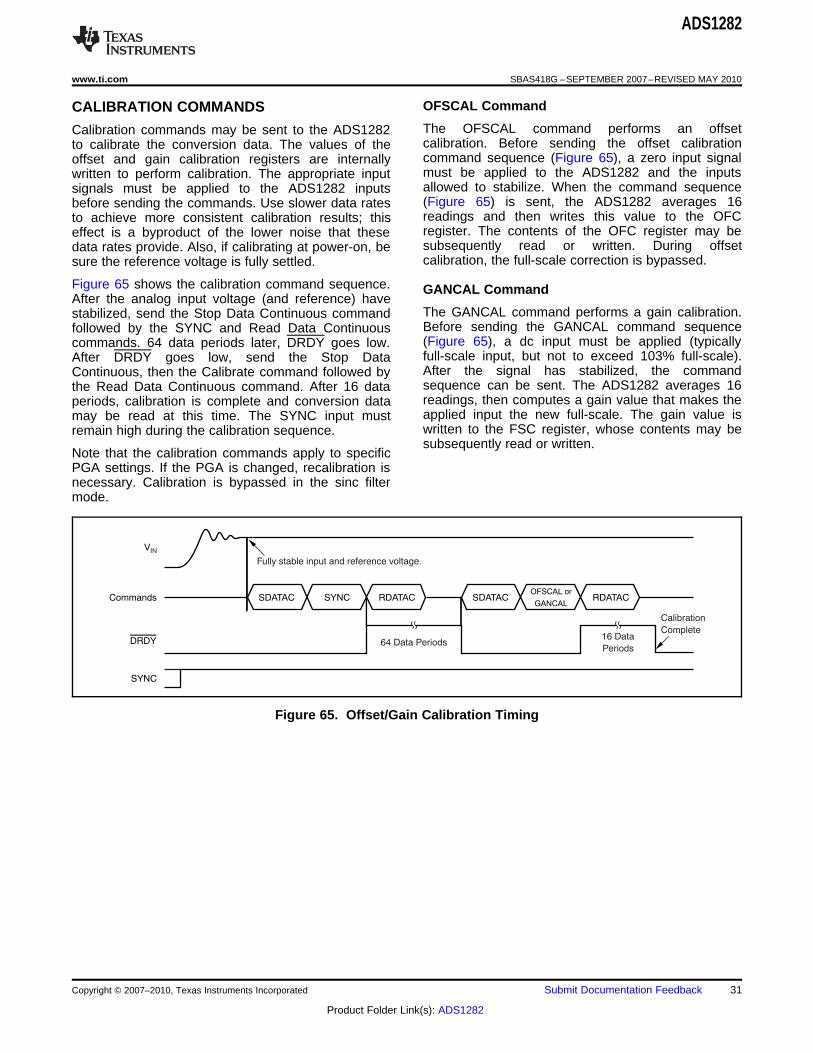
Commands
DRDY
SDATAC SYNC RDATAC
SYNC
VIN
SDATACOFSCAL or
GANCALRDATAC
64 Data Periods16 Data
Periods
Fully stable input and reference voltage.
Calibration
Complete
ADS1282
www.ti.com SBAS418G –SEPTEMBER 2007–REVISED MAY 2010
OFSCAL CommandCALIBRATION COMMANDSThe OFSCAL command performs an offsetCalibration commands may be sent to the ADS1282calibration. Before sending the offset calibrationto calibrate the conversion data. The values of thecommand sequence (Figure 65), a zero input signaloffset and gain calibration registers are internallymust be applied to the ADS1282 and the inputswritten to perform calibration. The appropriate inputallowed to stabilize. When the command sequencesignals must be applied to the ADS1282 inputs(Figure 65) is sent, the ADS1282 averages 16before sending the commands. Use slower data ratesreadings and then writes this value to the OFCto achieve more consistent calibration results; thisregister. The contents of the OFC register may beeffect is a byproduct of the lower noise that thesesubsequently read or written. During offsetdata rates provide. Also, if calibrating at power-on, becalibration, the full-scale correction is bypassed.sure the reference voltage is fully settled.
Figure 65 shows the calibration command sequence. GANCAL CommandAfter the analog input voltage (and reference) have
The GANCAL command performs a gain calibration.stabilized, send the Stop Data Continuous commandBefore sending the GANCAL command sequencefollowed by the SYNC and Read Data Continuous(Figure 65), a dc input must be applied (typicallycommands. 64 data periods later, DRDY goes low.full-scale input, but not to exceed 103% full-scale).After DRDY goes low, send the Stop DataAfter the signal has stabilized, the commandContinuous, then the Calibrate command followed bysequence can be sent. The ADS1282 averages 16the Read Data Continuous command. After 16 datareadings, then computes a gain value that makes theperiods, calibration is complete and conversion dataapplied input the new full-scale. The gain value ismay be read at this time. The SYNC input mustwritten to the FSC register, whose contents may beremain high during the calibration sequence.subsequently read or written.
Note that the calibration commands apply to specificPGA settings. If the PGA is changed, recalibration isnecessary. Calibration is bypassed in the sinc filtermode.
Figure 65. Offset/Gain Calibration Timing
Copyright © 2007–2010, Texas Instruments Incorporated Submit Documentation Feedback 31
Product Folder Link(s): ADS1282
FSC[2:0] = 400000h ´Expected Output Code
Actual Output Code
FSC[2:0] = 400000h ´Expected RMS Value
Actual RMS Value
ADS1282
SBAS418G –SEPTEMBER 2007–REVISED MAY 2010 www.ti.com
USER CALIBRATION The value written to the FSC registers is calculatedby Equation 11.
System calibration of the ADS1282 can be performedwithout using the calibration commands. This DC signal calibration is shown in Equation 11. Theprocedure requires the calibration values to be expected output code is based on 31-bit output data.externally calculated and then written to thecalibration registers. The steps for this procedure are:1. Set the OFSCAL[2:0] register = 0h and (11)
GANCAL[2:0] = 400000h. These values set theoffset and gain registers to 0 and 1, respectively. For ac signal calibration, use an RMS value of
collected data (as shown in Equation 12).2. Apply a zero differential input to the input of thesystem. Wait for the system to settle and thenaverage n output readings. Higher numbers of (12)averaged readings result in more consistentcalibration. Write the averaged value to the OFCregister.
3. Apply a differential dc signal, or an ac signal(typically full-scale, but not to exceed 103%full-scale). Wait for the system to settle and thenaverage the n output readings.
32 Submit Documentation Feedback Copyright © 2007–2010, Texas Instruments Incorporated
Product Folder Link(s): ADS1282
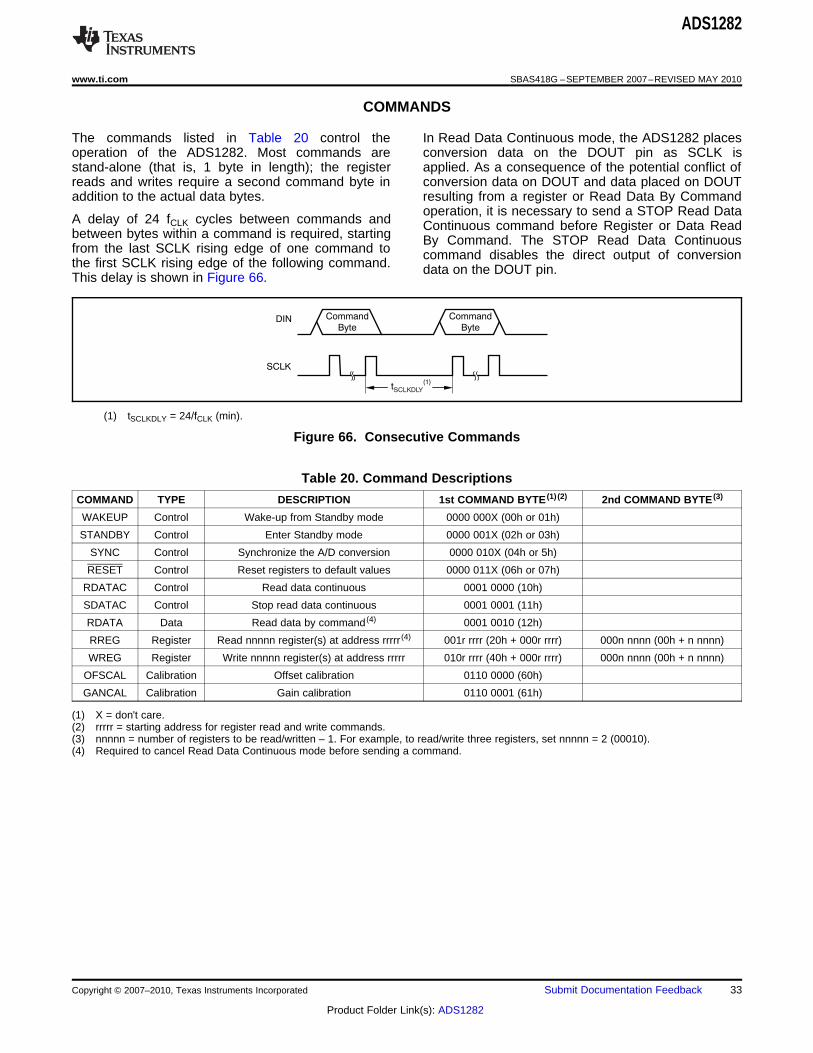
SCLK
DIN Command
Byte
Command
Byte
t(1)
SCLKDLY
ADS1282
www.ti.com SBAS418G –SEPTEMBER 2007–REVISED MAY 2010
COMMANDS
The commands listed in Table 20 control the In Read Data Continuous mode, the ADS1282 placesoperation of the ADS1282. Most commands are conversion data on the DOUT pin as SCLK isstand-alone (that is, 1 byte in length); the register applied. As a consequence of the potential conflict ofreads and writes require a second command byte in conversion data on DOUT and data placed on DOUTaddition to the actual data bytes. resulting from a register or Read Data By Command
operation, it is necessary to send a STOP Read DataA delay of 24 fCLK cycles between commands and Continuous command before Register or Data Readbetween bytes within a command is required, starting By Command. The STOP Read Data Continuousfrom the last SCLK rising edge of one command to command disables the direct output of conversionthe first SCLK rising edge of the following command. data on the DOUT pin.This delay is shown in Figure 66.
(1) tSCLKDLY = 24/fCLK (min).
Figure 66. Consecutive Commands
Table 20. Command Descriptions
COMMAND TYPE DESCRIPTION 1st COMMAND BYTE (1) (2) 2nd COMMAND BYTE (3)
WAKEUP Control Wake-up from Standby mode 0000 000X (00h or 01h)
STANDBY Control Enter Standby mode 0000 001X (02h or 03h)
SYNC Control Synchronize the A/D conversion 0000 010X (04h or 5h)
RESET Control Reset registers to default values 0000 011X (06h or 07h)
RDATAC Control Read data continuous 0001 0000 (10h)
SDATAC Control Stop read data continuous 0001 0001 (11h)
RDATA Data Read data by command (4) 0001 0010 (12h)
RREG Register Read nnnnn register(s) at address rrrrr (4) 001r rrrr (20h + 000r rrrr) 000n nnnn (00h + n nnnn)
WREG Register Write nnnnn register(s) at address rrrrr 010r rrrr (40h + 000r rrrr) 000n nnnn (00h + n nnnn)
OFSCAL Calibration Offset calibration 0110 0000 (60h)
GANCAL Calibration Gain calibration 0110 0001 (61h)
(1) X = don't care.(2) rrrrr = starting address for register read and write commands.(3) nnnnn = number of registers to be read/written – 1. For example, to read/write three registers, set nnnnn = 2 (00010).(4) Required to cancel Read Data Continuous mode before sending a command.
Copyright © 2007–2010, Texas Instruments Incorporated Submit Documentation Feedback 33
Product Folder Link(s): ADS1282
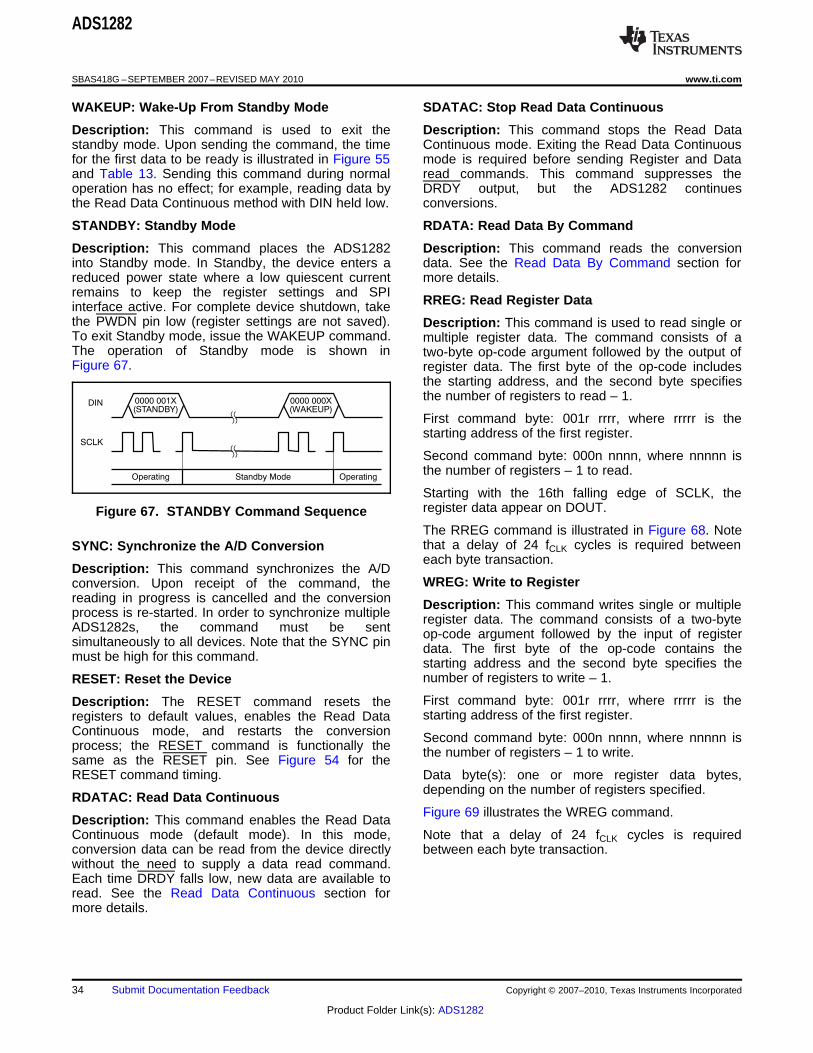
DIN
SCLK
0000 001X(STANDBY)
Operating Standby Mode Operating
0000 000X(WAKEUP)
ADS1282
SBAS418G –SEPTEMBER 2007–REVISED MAY 2010 www.ti.com
WAKEUP: Wake-Up From Standby Mode SDATAC: Stop Read Data Continuous
Description: This command is used to exit the Description: This command stops the Read Datastandby mode. Upon sending the command, the time Continuous mode. Exiting the Read Data Continuousfor the first data to be ready is illustrated in Figure 55 mode is required before sending Register and Dataand Table 13. Sending this command during normal read commands. This command suppresses theoperation has no effect; for example, reading data by DRDY output, but the ADS1282 continuesthe Read Data Continuous method with DIN held low. conversions.
STANDBY: Standby Mode RDATA: Read Data By Command
Description: This command places the ADS1282 Description: This command reads the conversioninto Standby mode. In Standby, the device enters a data. See the Read Data By Command section forreduced power state where a low quiescent current more details.remains to keep the register settings and SPI
RREG: Read Register Datainterface active. For complete device shutdown, takethe PWDN pin low (register settings are not saved). Description: This command is used to read single orTo exit Standby mode, issue the WAKEUP command. multiple register data. The command consists of aThe operation of Standby mode is shown in two-byte op-code argument followed by the output ofFigure 67. register data. The first byte of the op-code includes
the starting address, and the second byte specifiesthe number of registers to read – 1.
First command byte: 001r rrrr, where rrrrr is thestarting address of the first register.
Second command byte: 000n nnnn, where nnnnn isthe number of registers – 1 to read.
Starting with the 16th falling edge of SCLK, theregister data appear on DOUT.Figure 67. STANDBY Command SequenceThe RREG command is illustrated in Figure 68. Notethat a delay of 24 fCLK cycles is required betweenSYNC: Synchronize the A/D Conversioneach byte transaction.
Description: This command synchronizes the A/DWREG: Write to Registerconversion. Upon receipt of the command, the
reading in progress is cancelled and the conversion Description: This command writes single or multipleprocess is re-started. In order to synchronize multiple register data. The command consists of a two-byteADS1282s, the command must be sent op-code argument followed by the input of registersimultaneously to all devices. Note that the SYNC pin data. The first byte of the op-code contains themust be high for this command. starting address and the second byte specifies the
number of registers to write – 1.RESET: Reset the Device
First command byte: 001r rrrr, where rrrrr is theDescription: The RESET command resets thestarting address of the first register.registers to default values, enables the Read Data
Continuous mode, and restarts the conversion Second command byte: 000n nnnn, where nnnnn isprocess; the RESET command is functionally the the number of registers – 1 to write.same as the RESET pin. See Figure 54 for theRESET command timing. Data byte(s): one or more register data bytes,
depending on the number of registers specified.RDATAC: Read Data ContinuousFigure 69 illustrates the WREG command.Description: This command enables the Read Data
Continuous mode (default mode). In this mode, Note that a delay of 24 fCLK cycles is requiredconversion data can be read from the device directly between each byte transaction.without the need to supply a data read command.Each time DRDY falls low, new data are available toread. See the Read Data Continuous section formore details.
34 Submit Documentation Feedback Copyright © 2007–2010, Texas Instruments Incorporated
Product Folder Link(s): ADS1282
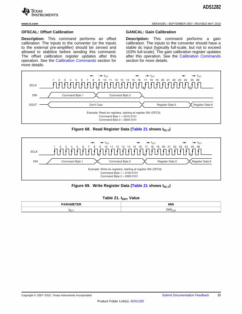
SCLK
DIN Command Byte 1 Command Byte 2
DOUT Don't Care Register Data 5 Register Data 6
1 2 3 4 5 6 7 8 9 10 11 12 13 14 15 16 17 18 25 2619 20 21 22 23 24
Example: Read six registers, starting at register 05h (OFC0)
Command Byte 1 = 0010 0101
Command Byte 2 = 0000 0101
tDLY tDLY tDLY
1 2 3 4 5 6 7 8 9 10 11 12 13 14 15 16 17 18 25 2619 20 21 22 23 24
SCLK
DIN Command Byte 1 Command Byte 2 Register Data 5 Register Data 6
Example: Write six registers, starting at register 05h (OFC0)
Command Byte 1 = 0100 0101
Command Byte 2 = 0000 0101
tDLY tDLY tDLY
ADS1282
www.ti.com SBAS418G –SEPTEMBER 2007–REVISED MAY 2010
OFSCAL: Offset Calibration GANCAL: Gain Calibration
Description: This command performs an offset Description: This command performs a gaincalibration. The inputs to the converter (or the inputs calibration. The inputs to the converter should have ato the external pre-amplifier) should be zeroed and stable dc input (typically full-scale, but not to exceedallowed to stabilize before sending this command. 103% full-scale). The gain calibration register updatesThe offset calibration register updates after this after this operation. See the Calibration Commandsoperation. See the Calibration Commands section for section for more details.more details.
Figure 68. Read Register Data (Table 21 shows tDLY)
Figure 69. Write Register Data (Table 21 shows tDLY)
Table 21. tDRY Value
PARAMETER MIN
tDLY 24/fCLK
Copyright © 2007–2010, Texas Instruments Incorporated Submit Documentation Feedback 35
Product Folder Link(s): ADS1282
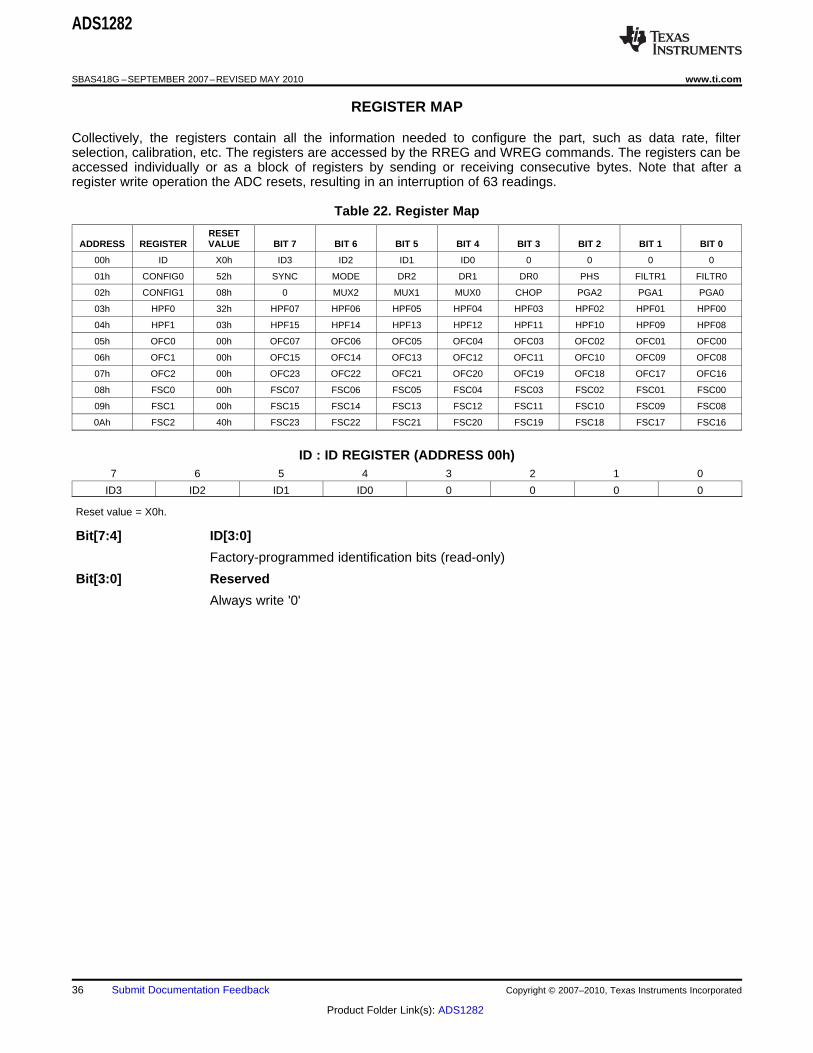
ADS1282
SBAS418G –SEPTEMBER 2007–REVISED MAY 2010 www.ti.com
REGISTER MAP
Collectively, the registers contain all the information needed to configure the part, such as data rate, filterselection, calibration, etc. The registers are accessed by the RREG and WREG commands. The registers can beaccessed individually or as a block of registers by sending or receiving consecutive bytes. Note that after aregister write operation the ADC resets, resulting in an interruption of 63 readings.
Table 22. Register Map
RESETADDRESS REGISTER VALUE BIT 7 BIT 6 BIT 5 BIT 4 BIT 3 BIT 2 BIT 1 BIT 0
00h ID X0h ID3 ID2 ID1 ID0 0 0 0 0
01h CONFIG0 52h SYNC MODE DR2 DR1 DR0 PHS FILTR1 FILTR0
02h CONFIG1 08h 0 MUX2 MUX1 MUX0 CHOP PGA2 PGA1 PGA0
03h HPF0 32h HPF07 HPF06 HPF05 HPF04 HPF03 HPF02 HPF01 HPF00
04h HPF1 03h HPF15 HPF14 HPF13 HPF12 HPF11 HPF10 HPF09 HPF08
05h OFC0 00h OFC07 OFC06 OFC05 OFC04 OFC03 OFC02 OFC01 OFC00
06h OFC1 00h OFC15 OFC14 OFC13 OFC12 OFC11 OFC10 OFC09 OFC08
07h OFC2 00h OFC23 OFC22 OFC21 OFC20 OFC19 OFC18 OFC17 OFC16
08h FSC0 00h FSC07 FSC06 FSC05 FSC04 FSC03 FSC02 FSC01 FSC00
09h FSC1 00h FSC15 FSC14 FSC13 FSC12 FSC11 FSC10 FSC09 FSC08
0Ah FSC2 40h FSC23 FSC22 FSC21 FSC20 FSC19 FSC18 FSC17 FSC16
ID : ID REGISTER (ADDRESS 00h)7 6 5 4 3 2 1 0
ID3 ID2 ID1 ID0 0 0 0 0
Reset value = X0h.
Bit[7:4] ID[3:0]
Factory-programmed identification bits (read-only)
Bit[3:0] Reserved
Always write '0'
36 Submit Documentation Feedback Copyright © 2007–2010, Texas Instruments Incorporated
Product Folder Link(s): ADS1282
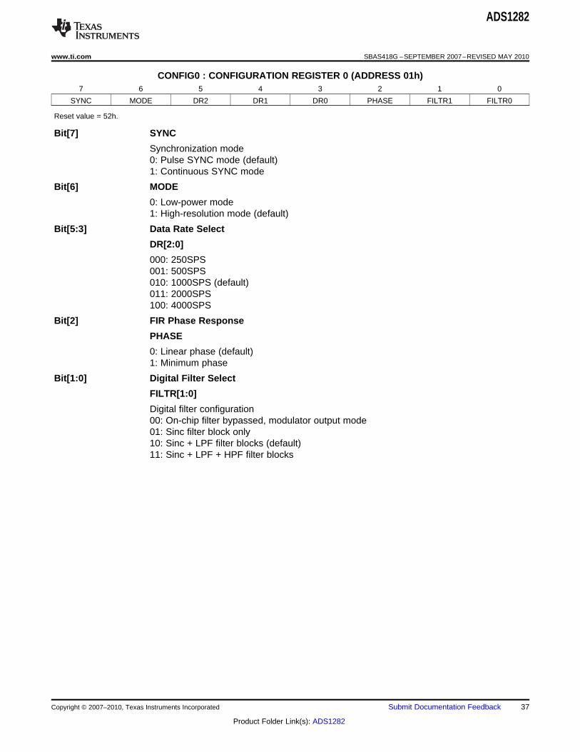
ADS1282
www.ti.com SBAS418G –SEPTEMBER 2007–REVISED MAY 2010
CONFIG0 : CONFIGURATION REGISTER 0 (ADDRESS 01h)7 6 5 4 3 2 1 0
SYNC MODE DR2 DR1 DR0 PHASE FILTR1 FILTR0
Reset value = 52h.
Bit[7] SYNC
Synchronization mode0: Pulse SYNC mode (default)1: Continuous SYNC mode
Bit[6] MODE
0: Low-power mode1: High-resolution mode (default)
Bit[5:3] Data Rate Select
DR[2:0]
000: 250SPS001: 500SPS010: 1000SPS (default)011: 2000SPS100: 4000SPS
Bit[2] FIR Phase Response
PHASE
0: Linear phase (default)1: Minimum phase
Bit[1:0] Digital Filter Select
FILTR[1:0]
Digital filter configuration00: On-chip filter bypassed, modulator output mode01: Sinc filter block only10: Sinc + LPF filter blocks (default)11: Sinc + LPF + HPF filter blocks
Copyright © 2007–2010, Texas Instruments Incorporated Submit Documentation Feedback 37
Product Folder Link(s): ADS1282
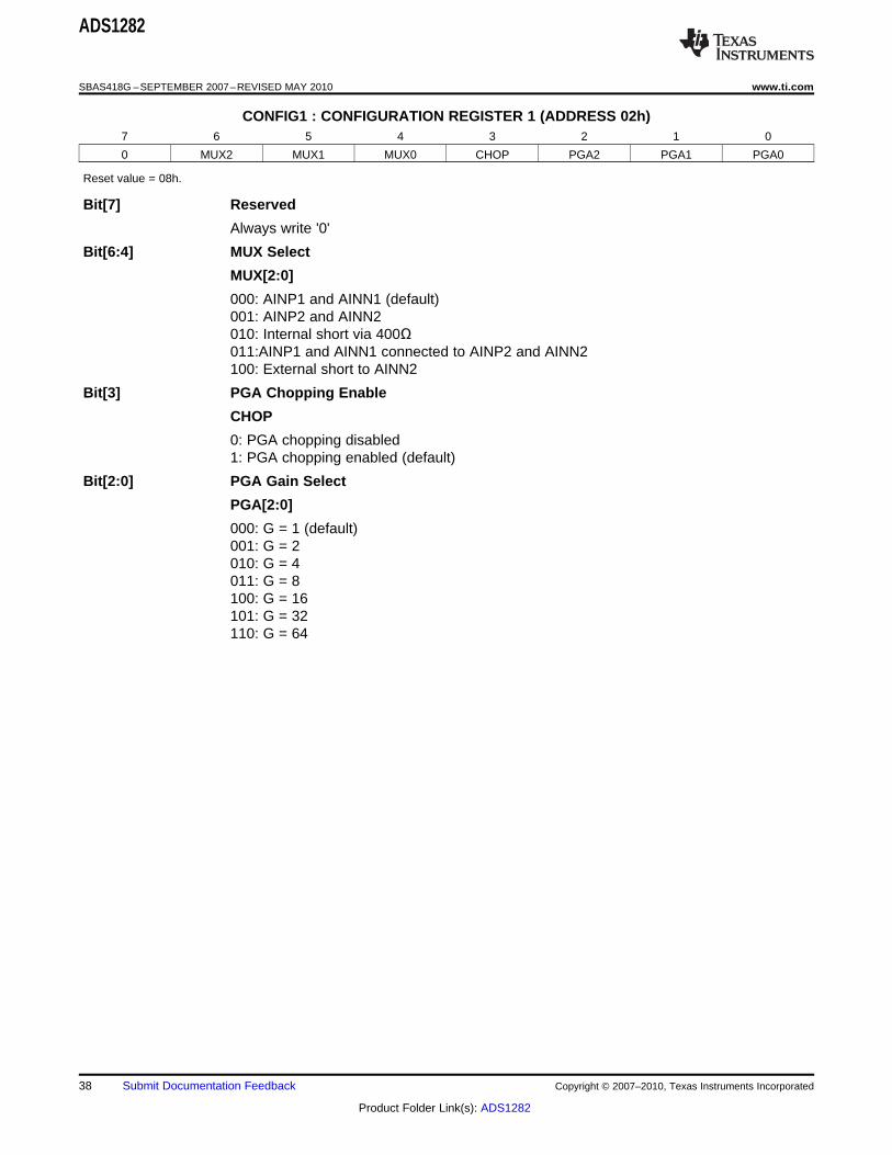
ADS1282
SBAS418G –SEPTEMBER 2007–REVISED MAY 2010 www.ti.com
CONFIG1 : CONFIGURATION REGISTER 1 (ADDRESS 02h)7 6 5 4 3 2 1 0
0 MUX2 MUX1 MUX0 CHOP PGA2 PGA1 PGA0
Reset value = 08h.
Bit[7] Reserved
Always write '0'
Bit[6:4] MUX Select
MUX[2:0]
000: AINP1 and AINN1 (default)001: AINP2 and AINN2010: Internal short via 400Ω011:AINP1 and AINN1 connected to AINP2 and AINN2100: External short to AINN2
Bit[3] PGA Chopping Enable
CHOP
0: PGA chopping disabled1: PGA chopping enabled (default)
Bit[2:0] PGA Gain Select
PGA[2:0]
000: G = 1 (default)001: G = 2010: G = 4011: G = 8100: G = 16101: G = 32110: G = 64
38 Submit Documentation Feedback Copyright © 2007–2010, Texas Instruments Incorporated
Product Folder Link(s): ADS1282
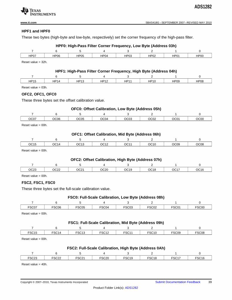
ADS1282
www.ti.com SBAS418G –SEPTEMBER 2007–REVISED MAY 2010
HPF1 and HPF0
These two bytes (high-byte and low-byte, respectively) set the corner frequency of the high-pass filter.
HPF0: High-Pass Filter Corner Frequency, Low Byte (Address 03h)7 6 5 4 3 2 1 0
HP07 HP06 HP05 HP04 HP03 HP02 HP01 HP00
Reset value = 32h.
HPF1: High-Pass Filter Corner Frequency, High Byte (Address 04h)7 6 5 4 3 2 1 0
HP15 HP14 HP13 HP12 HP11 HP10 HP09 HP08
Reset value = 03h.
OFC2, OFC1, OFC0
These three bytes set the offset calibration value.
OFC0: Offset Calibration, Low Byte (Address 05h)7 6 5 4 3 2 1 0
OC07 OC06 OC05 OC04 OC03 OC02 OC01 OC00
Reset value = 00h.
OFC1: Offset Calibration, Mid Byte (Address 06h)7 6 5 4 3 2 1 0
OC15 OC14 OC13 OC12 OC11 OC10 OC09 OC08
Reset value = 00h.
OFC2: Offset Calibration, High Byte (Address 07h)7 6 5 4 3 2 1 0
OC23 OC22 OC21 OC20 OC19 OC18 OC17 OC16
Reset value = 00h.
FSC2, FSC1, FSC0
These three bytes set the full-scale calibration value.
FSC0: Full-Scale Calibration, Low Byte (Address 08h)7 6 5 4 3 2 1 0
FSC07 FSC06 FSC05 FSC04 FSC03 FSC02 FSC01 FSC00
Reset value = 00h.
FSC1: Full-Scale Calibration, Mid Byte (Address 09h)7 6 5 4 3 2 1 0
FSC15 FSC14 FSC13 FSC12 FSC11 FSC10 FSC09 FSC08
Reset value = 00h.
FSC2: Full-Scale Calibration, High Byte (Address 0Ah)7 6 5 4 3 2 1 0
FSC23 FSC22 FSC21 FSC20 FSC19 FSC18 FSC17 FSC16
Reset value = 40h.
Copyright © 2007–2010, Texas Instruments Incorporated Submit Documentation Feedback 39
Product Folder Link(s): ADS1282
ADS1282
SBAS418G –SEPTEMBER 2007–REVISED MAY 2010 www.ti.com
CONFIGURATION GUIDE
4. Set the data mode. After register configuration,After RESET or power-on, the registers can be the device may be configured for Read Dataconfigured using the following procedure: Continuous mode, either by the Read Data1. Reset the serial interface. Before using the Continuous command or configured in Read Data
serial interface, it may be necessary to recover By Register mode using SDATAC command.the serial interface (undefined I/O power-up 5. Synchronize readings. Whenever SYNC is high,sequencing may cause false SCLK detection). To the ADS1282 freely runs the data conversions.reset the SPI interface, toggle the RESET pin or, To stop and re-sync the conversions, take SYNCwhen in Read Data Continuous mode, hold SCLK low and then high.low for 64 DRDY periods.
6. Read data. If the Read Data Continuous mode is2. Configure the registers. The registers are active, the data are read directly after DRDY falls
configured by either writing to them individually or by applying SCLK pulses. If the Read Dataas a group. Software may be configured in either Continuous mode is inactive, the data can onlymode. The SDATAC command must be sent be read by Read Data By Command. The Readbefore register read/write operations to cancel the Data opcode command must be sent in this modeRead Data Continuous mode. to read each conversion result (note that DRDY
3. Verify register data. The register may be read only asserts after each read data command isback for verification of device communications. sent).
40 Submit Documentation Feedback Copyright © 2007–2010, Texas Instruments Incorporated
Product Folder Link(s): ADS1282
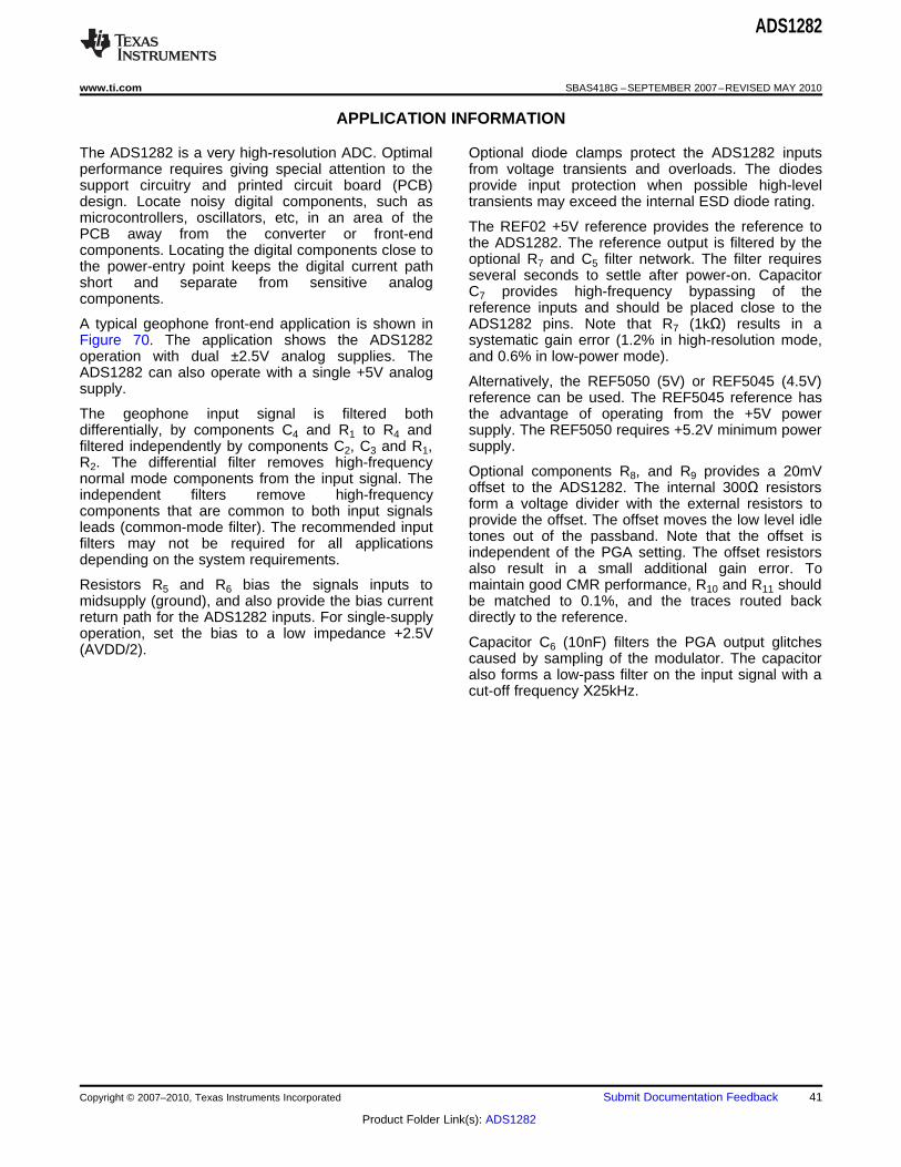
ADS1282
www.ti.com SBAS418G –SEPTEMBER 2007–REVISED MAY 2010
APPLICATION INFORMATION
The ADS1282 is a very high-resolution ADC. Optimal Optional diode clamps protect the ADS1282 inputsperformance requires giving special attention to the from voltage transients and overloads. The diodessupport circuitry and printed circuit board (PCB) provide input protection when possible high-leveldesign. Locate noisy digital components, such as transients may exceed the internal ESD diode rating.microcontrollers, oscillators, etc, in an area of the
The REF02 +5V reference provides the reference toPCB away from the converter or front-endthe ADS1282. The reference output is filtered by thecomponents. Locating the digital components close tooptional R7 and C5 filter network. The filter requiresthe power-entry point keeps the digital current pathseveral seconds to settle after power-on. Capacitorshort and separate from sensitive analogC7 provides high-frequency bypassing of thecomponents.reference inputs and should be placed close to the
A typical geophone front-end application is shown in ADS1282 pins. Note that R7 (1kΩ) results in aFigure 70. The application shows the ADS1282 systematic gain error (1.2% in high-resolution mode,operation with dual ±2.5V analog supplies. The and 0.6% in low-power mode).ADS1282 can also operate with a single +5V analog
Alternatively, the REF5050 (5V) or REF5045 (4.5V)supply.reference can be used. The REF5045 reference has
The geophone input signal is filtered both the advantage of operating from the +5V powerdifferentially, by components C4 and R1 to R4 and supply. The REF5050 requires +5.2V minimum powerfiltered independently by components C2, C3 and R1, supply.R2. The differential filter removes high-frequency
Optional components R8, and R9 provides a 20mVnormal mode components from the input signal. Theoffset to the ADS1282. The internal 300Ω resistorsindependent filters remove high-frequencyform a voltage divider with the external resistors tocomponents that are common to both input signalsprovide the offset. The offset moves the low level idleleads (common-mode filter). The recommended inputtones out of the passband. Note that the offset isfilters may not be required for all applicationsindependent of the PGA setting. The offset resistorsdepending on the system requirements.also result in a small additional gain error. To
Resistors R5 and R6 bias the signals inputs to maintain good CMR performance, R10 and R11 shouldmidsupply (ground), and also provide the bias current be matched to 0.1%, and the traces routed backreturn path for the ADS1282 inputs. For single-supply directly to the reference.operation, set the bias to a low impedance +2.5V
Capacitor C6 (10nF) filters the PGA output glitches(AVDD/2).caused by sampling of the modulator. The capacitoralso forms a low-pass filter on the input signal with acut-off frequency Ⅹ25kHz.
Copyright © 2007–2010, Texas Instruments Incorporated Submit Documentation Feedback 41
Product Folder Link(s): ADS1282
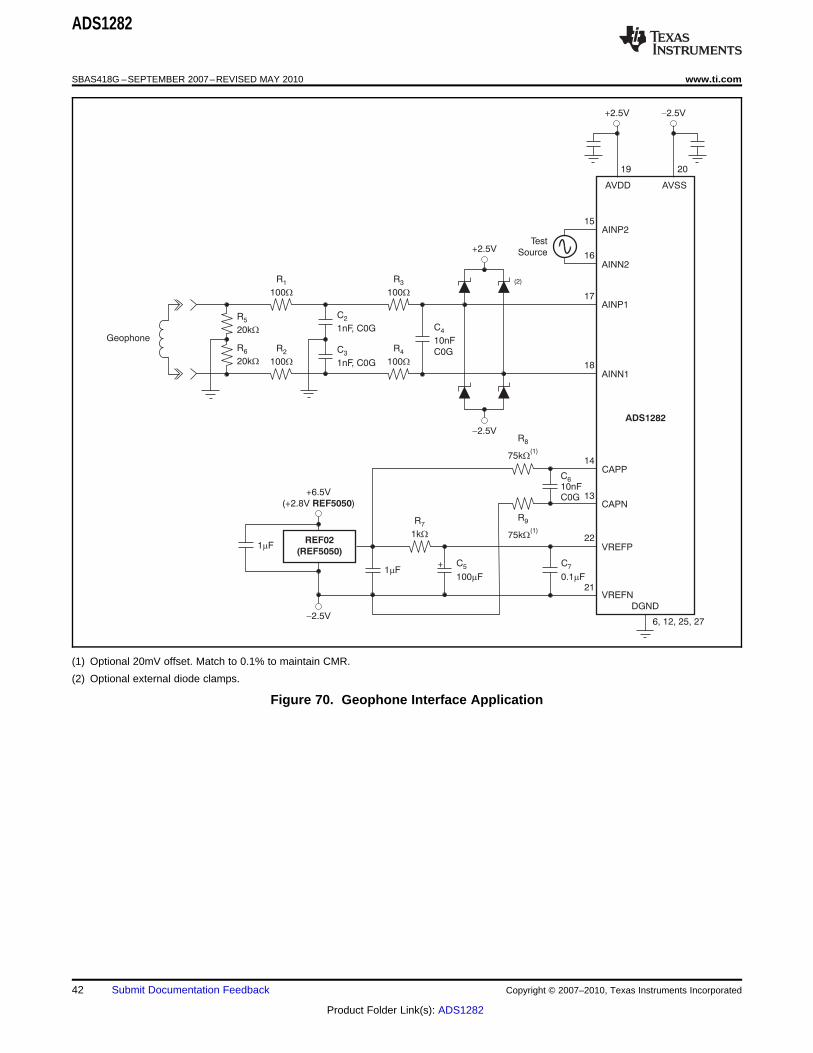
AVSS
AINP1
AINN1
AVDD
+2.5V
ADS1282
C
10nF
C0G
4
R
100W
1
R
100W
2
Geophone
VREFP
VREFN
DGND
R
1kW
7
C7
0.1 Fm
1 Fm
C
100 F5
m
+6.5V
(+2.8V )REF5050
REF02
(REF5050)
+2.5V
R
100W
3
R
100W
4C
1nF, C0G3
CAPP
CAPN
C10nFC0G
6
+
AINP2
AINN2
Test
Source
21
22
18
17
16
15
13
14
6, 12, 25, 27
R
20k5
W
R
20k6
W
19 20
R
(1)
9
75kW
R
75kW
8
(1)
C
1nF, C0G2
1 Fm
-2.5V
-2.5V
-2.5V
(2)
ADS1282
SBAS418G –SEPTEMBER 2007–REVISED MAY 2010 www.ti.com
(1) Optional 20mV offset. Match to 0.1% to maintain CMR.
(2) Optional external diode clamps.
Figure 70. Geophone Interface Application
42 Submit Documentation Feedback Copyright © 2007–2010, Texas Instruments Incorporated
Product Folder Link(s): ADS1282
RESETCLK Input
RESET
DOUT
DIN
SCLK
SYNC
MFLAGDGND
CLK
24
4
5
4, 12, 23
2
10
11
1
SYNC
MFLAG1
DRDY
MFLAG2
DVDD
47W
47W
47W
47W
47W
47W
47W
1 Fm
+3.3V(1)
ADS1282
RESET
DOUT
DIN
SCLK
SYNC
MFLAG
DGND
CLK
24
4
5
6, 12, 25
2
10
11
1DVDD
47W
DRDY3
47W
47W
1 Fm
+3.3V(1)
ADS1282
4.096MHz Clock
FPGA
26
28BYPAS
1 Fm
28BYPAS
1 Fm
DOUT1
DIN1
SCLK1
47W
DOUT2
DIN2
SCLK2
26
ADS1282
www.ti.com SBAS418G –SEPTEMBER 2007–REVISED MAY 2010
Figure 71 shows the digital connection to a field For best performance, the FPGA and the ADS1282sprogrammable gate array (FPGA) device. In this should operate from the same clock. Avoid ringing onexample, two ADS1282s are shown connected. The the digital inputs. 47Ω resistors in series with theDRDY output from each ADS1282 can be used; digital traces can help to reduce ringing by controllinghowever, when the devices are synchronized, the impedances. Place the resistors at the source (driver)DRDY output from only one device is sufficient. A end of the trace. Unused digital inputs should notshared SCLK line between the devices is optional. float; tie them to DVDD or GND. This includes the
modulator data pins, M0, M1, and MCLK.The modulator over-range flag (MFLAG) from eachdevice ties to the FPGA. For synchronization, oneSYNC control line connects all ADS1282 devices.The RESET line also connects to all ADS1282devices.
NOTE: Dashed line is optional.
(1) For DVDD < 2.25V, see the DVDD Power Supply section.
Figure 71. Microcontroller Interface with Dual ADS1282s
Copyright © 2007–2010, Texas Instruments Incorporated Submit Documentation Feedback 43
Product Folder Link(s): ADS1282
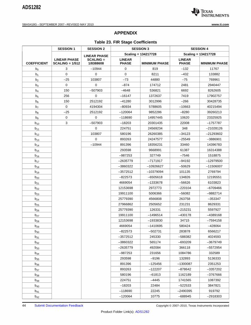
ADS1282
SBAS418G –SEPTEMBER 2007–REVISED MAY 2010 www.ti.com
APPENDIX
Table 23. FIR Stage Coefficients
SESSION 1 SESSION 2 SESSION 3 SESSION 4
Scaling = 134217728 Scaling = 134217728LINEAR PHASELINEAR PHASE SCALING = LINEAR LINEAR
COEFFICIENT SCALING = 1/512 1/8388608 PHASE MINIMUM PHASE PHASE MINIMUM PHASE
b0 3 –10944 0 819 –132 11767
b1 0 0 0 8211 –432 133882
b2 –25 103807 –73 44880 –75 769961
b3 0 0 –874 174712 2481 2940447
b4 150 –507903 –4648 536821 6692 8262605
b5 256 0 –16147 1372637 7419 17902757
b6 150 2512192 –41280 3012996 –266 30428735
b7 0 4194304 –80934 5788605 –10663 40215494
b8 –25 2512192 –120064 9852286 –8280 39260213
b9 0 0 –118690 14957445 10620 23325925
b10 3 –507903 –18203 20301435 22008 –1757787
b11 0 224751 24569234 348 –21028126
b12 103807 580196 26260385 –34123 –21293602
b13 0 893263 24247577 –25549 –3886901
b14 –10944 891396 18356231 33460 14396783
b15 293598 9668991 61387 16314388
b16 –987253 327749 –7546 1518875
b17 –2635779 –7171917 –94192 –12979500
b18 –3860322 –10926627 –50629 –11506007
b19 –3572512 –10379094 101135 2769794
b20 –822573 –6505618 134826 12195551
b21 4669054 –1333678 –56626 6103823
b22 12153698 2972773 –220104 –6709466
b23 19911100 5006366 –56082 –9882714
b24 25779390 4566808 263758 –353347
b25 27966862 2505652 231231 8629331
b26 25779390 126331 –215231 5597927
b27 19911100 –1496514 –430178 –4389168
b28 12153698 –1933830 34715 –7594158
b29 4669054 –1410695 580424 –428064
b30 –822573 –502731 283878 6566217
b31 –3572512 245330 –588382 4024593
b32 –3860322 565174 –693209 –3679749
b33 –2635779 492084 366118 –5572954
b34 –987253 231656 1084786 332589
b35 293598 –9196 132893 5136333
b36 891396 –125456 –1300087 2351253
b37 893263 –122207 –878642 –3357202
b38 580196 –61813 1162189 –3767666
b39 224751 –4445 1741565 1087392
b40 –18203 22484 –522533 3847821
b41 –118690 22245 –2490395 919792
b42 –120064 10775 –688945 –2918303
44 Submit Documentation Feedback Copyright © 2007–2010, Texas Instruments Incorporated
Product Folder Link(s): ADS1282
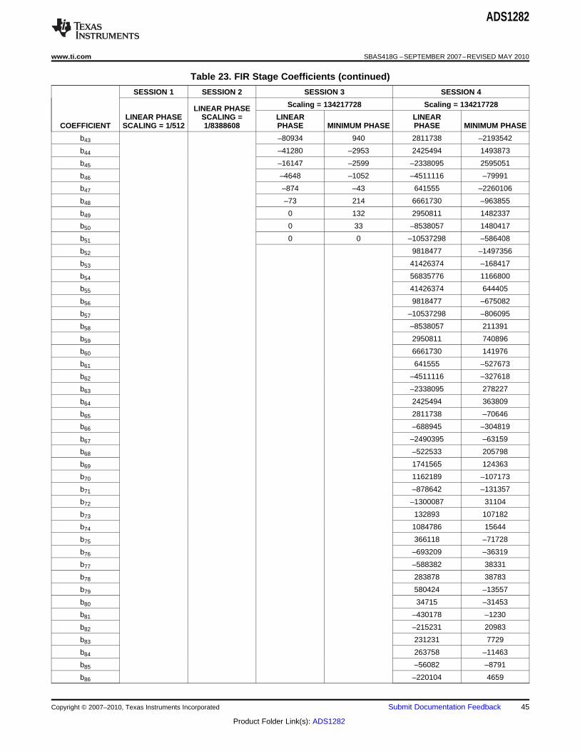
ADS1282
www.ti.com SBAS418G –SEPTEMBER 2007–REVISED MAY 2010
Table 23. FIR Stage Coefficients (continued)
SESSION 1 SESSION 2 SESSION 3 SESSION 4
Scaling = 134217728 Scaling = 134217728LINEAR PHASELINEAR PHASE SCALING = LINEAR LINEAR
COEFFICIENT SCALING = 1/512 1/8388608 PHASE MINIMUM PHASE PHASE MINIMUM PHASE
b43 –80934 940 2811738 –2193542
b44 –41280 –2953 2425494 1493873
b45 –16147 –2599 –2338095 2595051
b46 –4648 –1052 –4511116 –79991
b47 –874 –43 641555 –2260106
b48 –73 214 6661730 –963855
b49 0 132 2950811 1482337
b50 0 33 –8538057 1480417
b51 0 0 –10537298 –586408
b52 9818477 –1497356
b53 41426374 –168417
b54 56835776 1166800
b55 41426374 644405
b56 9818477 –675082
b57 –10537298 –806095
b58 –8538057 211391
b59 2950811 740896
b60 6661730 141976
b61 641555 –527673
b62 –4511116 –327618
b63 –2338095 278227
b64 2425494 363809
b65 2811738 –70646
b66 –688945 –304819
b67 –2490395 –63159
b68 –522533 205798
b69 1741565 124363
b70 1162189 –107173
b71 –878642 –131357
b72 –1300087 31104
b73 132893 107182
b74 1084786 15644
b75 366118 –71728
b76 –693209 –36319
b77 –588382 38331
b78 283878 38783
b79 580424 –13557
b80 34715 –31453
b81 –430178 –1230
b82 –215231 20983
b83 231231 7729
b84 263758 –11463
b85 –56082 –8791
b86 –220104 4659
Copyright © 2007–2010, Texas Instruments Incorporated Submit Documentation Feedback 45
Product Folder Link(s): ADS1282
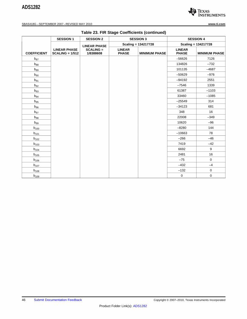
ADS1282
SBAS418G –SEPTEMBER 2007–REVISED MAY 2010 www.ti.com
Table 23. FIR Stage Coefficients (continued)
SESSION 1 SESSION 2 SESSION 3 SESSION 4
Scaling = 134217728 Scaling = 134217728LINEAR PHASELINEAR PHASE SCALING = LINEAR LINEAR
COEFFICIENT SCALING = 1/512 1/8388608 PHASE MINIMUM PHASE PHASE MINIMUM PHASE
b87 –56626 7126
b88 134826 –732
b89 101135 –4687
b90 –50629 –976
b91 –94192 2551
b92 –7546 1339
b93 61387 –1103
b94 33460 –1085
b95 –25549 314
b96 –34123 681
b97 348 16
b98 22008 –349
b99 10620 –96
b100 –8280 144
b101 –10663 78
b102 –266 –46
b103 7419 –42
b104 6692 9
b105 2481 16
b106 –75 0
b107 –432 –4
b108 –132 0
b109 0 0
46 Submit Documentation Feedback Copyright © 2007–2010, Texas Instruments Incorporated
Product Folder Link(s): ADS1282
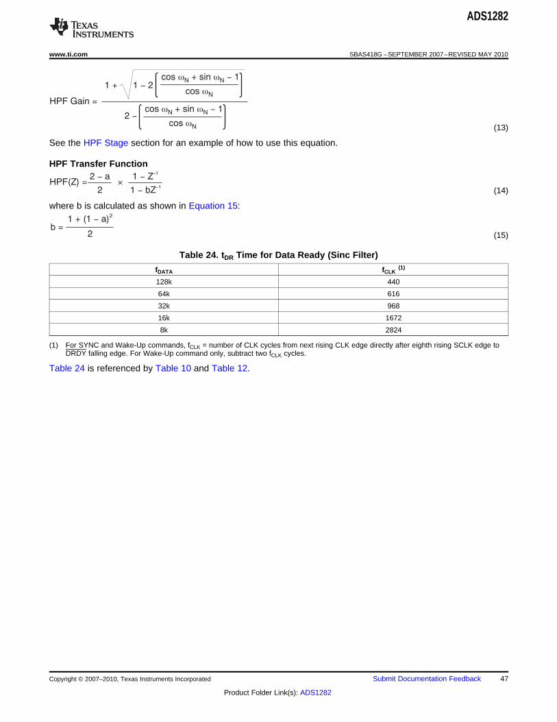
HPF Gain =cos + sin 1w -N Nw
cos wN
2 -
1 2-1 +cos + sin 1-w wN N
cos wN
HPF(Z) =1 Z-
-1
1 bZ--1
2 a-
2´
b =1 + (1 a)-
2
2
ADS1282
www.ti.com SBAS418G –SEPTEMBER 2007–REVISED MAY 2010
(13)
See the HPF Stage section for an example of how to use this equation.
HPF Transfer Function
(14)
where b is calculated as shown in Equation 15:
(15)
Table 24. tDR Time for Data Ready (Sinc Filter)
fDATA fCLK(1)
128k 440
64k 616
32k 968
16k 1672
8k 2824
(1) For SYNC and Wake-Up commands, fCLK = number of CLK cycles from next rising CLK edge directly after eighth rising SCLK edge toDRDY falling edge. For Wake-Up command only, subtract two fCLK cycles.
Table 24 is referenced by Table 10 and Table 12.
Copyright © 2007–2010, Texas Instruments Incorporated Submit Documentation Feedback 47
Product Folder Link(s): ADS1282
ADS1282
SBAS418G –SEPTEMBER 2007–REVISED MAY 2010 www.ti.com
REVISION HISTORY
NOTE: Page numbers for previous revisions may differ from page numbers in the current version.
Changes from Revision F (March 2009) to Revision G Page
• Corrected typical specification in Digital Filter Response, Minimum phase filter settling time in ElectricalCharacteristics table ............................................................................................................................................................. 4
• Corrected units typo of Figure 46 ....................................................................................................................................... 21
• Moved Equation 14 and Equation 15 to the Appendix from the HPF Stage section .......................................................... 22
• Added footnote 2 to Table 13, Ideal Output Code .............................................................................................................. 27
• Corrected sign typo in Equation 13 .................................................................................................................................... 47
Changes from Revision E (October 2008) to Revision F Page
• Added tCMD specification for low-power mode in Modulator Output Timing table ............................................................... 18
• Updated Equation 7 ............................................................................................................................................................ 19
• Updated Equation 8 ............................................................................................................................................................ 20
• Updated Figure 46 .............................................................................................................................................................. 21
• Minor graphical edits to Figure 52 ...................................................................................................................................... 24
• Minor graphical edits to Figure 53 ...................................................................................................................................... 24
• Changed 466/fCLK to 468/fCLK in tDR row of Table 10 .......................................................................................................... 24
• Updated Figure 70, showing alternate bias resistor location .............................................................................................. 42
• Corrected Table 23 (Appendix, FIR Stage Coefficients) .................................................................................................... 44
48 Submit Documentation Feedback Copyright © 2007–2010, Texas Instruments Incorporated
Product Folder Link(s): ADS1282
PACKAGE OPTION ADDENDUM
www.ti.com 23-Oct-2010
Addendum-Page 1
PACKAGING INFORMATION
Orderable Device Status (1) Package Type PackageDrawing
Pins Package Qty Eco Plan (2) Lead/Ball Finish
MSL Peak Temp (3) Samples
(Requires Login)
ADS1282IPW ACTIVE TSSOP PW 28 50 Green (RoHS& no Sb/Br)
CU NIPDAU Level-1-260C-UNLIM Request Free Samples
ADS1282IPWG4 ACTIVE TSSOP PW 28 50 Green (RoHS& no Sb/Br)
CU NIPDAU Level-1-260C-UNLIM Request Free Samples
ADS1282IPWR ACTIVE TSSOP PW 28 2000 Green (RoHS& no Sb/Br)
CU NIPDAU Level-1-260C-UNLIM Purchase Samples
ADS1282IPWRG4 ACTIVE TSSOP PW 28 2000 Green (RoHS& no Sb/Br)
CU NIPDAU Level-1-260C-UNLIM Purchase Samples
(1) The marketing status values are defined as follows:ACTIVE: Product device recommended for new designs.LIFEBUY: TI has announced that the device will be discontinued, and a lifetime-buy period is in effect.NRND: Not recommended for new designs. Device is in production to support existing customers, but TI does not recommend using this part in a new design.PREVIEW: Device has been announced but is not in production. Samples may or may not be available.OBSOLETE: TI has discontinued the production of the device.
(2) Eco Plan - The planned eco-friendly classification: Pb-Free (RoHS), Pb-Free (RoHS Exempt), or Green (RoHS & no Sb/Br) - please check http://www.ti.com/productcontent for the latest availabilityinformation and additional product content details.TBD: The Pb-Free/Green conversion plan has not been defined.Pb-Free (RoHS): TI's terms "Lead-Free" or "Pb-Free" mean semiconductor products that are compatible with the current RoHS requirements for all 6 substances, including the requirement thatlead not exceed 0.1% by weight in homogeneous materials. Where designed to be soldered at high temperatures, TI Pb-Free products are suitable for use in specified lead-free processes.Pb-Free (RoHS Exempt): This component has a RoHS exemption for either 1) lead-based flip-chip solder bumps used between the die and package, or 2) lead-based die adhesive used betweenthe die and leadframe. The component is otherwise considered Pb-Free (RoHS compatible) as defined above.Green (RoHS & no Sb/Br): TI defines "Green" to mean Pb-Free (RoHS compatible), and free of Bromine (Br) and Antimony (Sb) based flame retardants (Br or Sb do not exceed 0.1% by weightin homogeneous material)
(3) MSL, Peak Temp. -- The Moisture Sensitivity Level rating according to the JEDEC industry standard classifications, and peak solder temperature.
Important Information and Disclaimer:The information provided on this page represents TI's knowledge and belief as of the date that it is provided. TI bases its knowledge and belief on informationprovided by third parties, and makes no representation or warranty as to the accuracy of such information. Efforts are underway to better integrate information from third parties. TI has taken andcontinues to take reasonable steps to provide representative and accurate information but may not have conducted destructive testing or chemical analysis on incoming materials and chemicals.TI and TI suppliers consider certain information to be proprietary, and thus CAS numbers and other limited information may not be available for release.
In no event shall TI's liability arising out of such information exceed the total purchase price of the TI part(s) at issue in this document sold by TI to Customer on an annual basis.
OTHER QUALIFIED VERSIONS OF ADS1282 :
PACKAGE OPTION ADDENDUM
www.ti.com 23-Oct-2010
Addendum-Page 2
NOTE: Qualified Version Definitions:
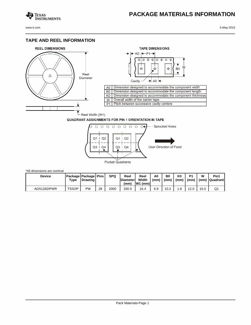
TAPE AND REEL INFORMATION
*All dimensions are nominal
Device PackageType
PackageDrawing
Pins SPQ ReelDiameter
(mm)
ReelWidth
W1 (mm)
A0(mm)
B0(mm)
K0(mm)
P1(mm)
W(mm)
Pin1Quadrant
ADS1282IPWR TSSOP PW 28 2000 330.0 16.4 6.9 10.2 1.8 12.0 16.0 Q1
PACKAGE MATERIALS INFORMATION
www.ti.com 5-May-2010
Pack Materials-Page 1
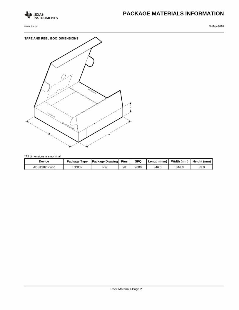
*All dimensions are nominal
Device Package Type Package Drawing Pins SPQ Length (mm) Width (mm) Height (mm)
ADS1282IPWR TSSOP PW 28 2000 346.0 346.0 33.0
PACKAGE MATERIALS INFORMATION
www.ti.com 5-May-2010
Pack Materials-Page 2
MECHANICAL DATA
MTSS001C – JANUARY 1995 – REVISED FEBRUARY 1999
POST OFFICE BOX 655303 • DALLAS, TEXAS 75265
PW (R-PDSO-G**) PLASTIC SMALL-OUTLINE PACKAGE14 PINS SHOWN
0,65 M0,10
0,10
0,25
0,500,75
0,15 NOM
Gage Plane
28
9,80
9,60
24
7,90
7,70
2016
6,60
6,40
4040064/F 01/97
0,30
6,606,20
8
0,19
4,304,50
7
0,15
14
A
1
1,20 MAX
14
5,10
4,90
8
3,10
2,90
A MAX
A MIN
DIMPINS **
0,05
4,90
5,10
Seating Plane
0°–8°
NOTES: A. All linear dimensions are in millimeters.B. This drawing is subject to change without notice.C. Body dimensions do not include mold flash or protrusion not to exceed 0,15.D. Falls within JEDEC MO-153
IMPORTANT NOTICE
Texas Instruments Incorporated and its subsidiaries (TI) reserve the right to make corrections, modifications, enhancements, improvements,and other changes to its products and services at any time and to discontinue any product or service without notice. Customers shouldobtain the latest relevant information before placing orders and should verify that such information is current and complete. All products aresold subject to TI’s terms and conditions of sale supplied at the time of order acknowledgment.
TI warrants performance of its hardware products to the specifications applicable at the time of sale in accordance with TI’s standardwarranty. Testing and other quality control techniques are used to the extent TI deems necessary to support this warranty. Except wheremandated by government requirements, testing of all parameters of each product is not necessarily performed.
TI assumes no liability for applications assistance or customer product design. Customers are responsible for their products andapplications using TI components. To minimize the risks associated with customer products and applications, customers should provideadequate design and operating safeguards.
TI does not warrant or represent that any license, either express or implied, is granted under any TI patent right, copyright, mask work right,or other TI intellectual property right relating to any combination, machine, or process in which TI products or services are used. Informationpublished by TI regarding third-party products or services does not constitute a license from TI to use such products or services or awarranty or endorsement thereof. Use of such information may require a license from a third party under the patents or other intellectualproperty of the third party, or a license from TI under the patents or other intellectual property of TI.
Reproduction of TI information in TI data books or data sheets is permissible only if reproduction is without alteration and is accompaniedby all associated warranties, conditions, limitations, and notices. Reproduction of this information with alteration is an unfair and deceptivebusiness practice. TI is not responsible or liable for such altered documentation. Information of third parties may be subject to additionalrestrictions.
Resale of TI products or services with statements different from or beyond the parameters stated by TI for that product or service voids allexpress and any implied warranties for the associated TI product or service and is an unfair and deceptive business practice. TI is notresponsible or liable for any such statements.
TI products are not authorized for use in safety-critical applications (such as life support) where a failure of the TI product would reasonablybe expected to cause severe personal injury or death, unless officers of the parties have executed an agreement specifically governingsuch use. Buyers represent that they have all necessary expertise in the safety and regulatory ramifications of their applications, andacknowledge and agree that they are solely responsible for all legal, regulatory and safety-related requirements concerning their productsand any use of TI products in such safety-critical applications, notwithstanding any applications-related information or support that may beprovided by TI. Further, Buyers must fully indemnify TI and its representatives against any damages arising out of the use of TI products insuch safety-critical applications.
TI products are neither designed nor intended for use in military/aerospace applications or environments unless the TI products arespecifically designated by TI as military-grade or "enhanced plastic." Only products designated by TI as military-grade meet militaryspecifications. Buyers acknowledge and agree that any such use of TI products which TI has not designated as military-grade is solely atthe Buyer's risk, and that they are solely responsible for compliance with all legal and regulatory requirements in connection with such use.
TI products are neither designed nor intended for use in automotive applications or environments unless the specific TI products aredesignated by TI as compliant with ISO/TS 16949 requirements. Buyers acknowledge and agree that, if they use any non-designatedproducts in automotive applications, TI will not be responsible for any failure to meet such requirements.
Following are URLs where you can obtain information on other Texas Instruments products and application solutions:
Products Applications
Amplifiers amplifier.ti.com Audio www.ti.com/audio
Data Converters dataconverter.ti.com Automotive www.ti.com/automotive
DLP® Products www.dlp.com Communications and www.ti.com/communicationsTelecom
DSP dsp.ti.com Computers and www.ti.com/computersPeripherals
Clocks and Timers www.ti.com/clocks Consumer Electronics www.ti.com/consumer-apps
Interface interface.ti.com Energy www.ti.com/energy
Logic logic.ti.com Industrial www.ti.com/industrial
Power Mgmt power.ti.com Medical www.ti.com/medical
Microcontrollers microcontroller.ti.com Security www.ti.com/security
RFID www.ti-rfid.com Space, Avionics & www.ti.com/space-avionics-defenseDefense
RF/IF and ZigBee® Solutions www.ti.com/lprf Video and Imaging www.ti.com/video
Wireless www.ti.com/wireless-apps
Mailing Address: Texas Instruments, Post Office Box 655303, Dallas, Texas 75265Copyright © 2010, Texas Instruments Incorporated
Related Documents


![2015 [Methods in Molecular Biology] Coronaviruses Volume 1282 __](https://static.cupdf.com/doc/110x72/613ca6b79cc893456e1e862b/2015-methods-in-molecular-biology-coronaviruses-volume-1282-.jpg)


