Addressing Reliability and Degradation of Chemitransistor Sensors by Electrical Tuning of the Sensitivity G. M. Lazzerini, L. M. Strambini & G. Barillaro Dipartimento di Ingegneria dell’Informazione: Elettronica, Informatica, Telecomunicazioni, Via G. Caruso 16, 56122 Pisa (Italy). Here we show that electrical tuning of the sensitivity of chemitransistor sensors, namely field-effect-transistors (FETs) exploiting nano/mesostructured sensing materials, can be used to effectively address two chief problems of state-of-the-art gas sensors, specifically fabrication reliability and degradation by aging. Both experimental evidences and theoretical calculations are provided to support such a result, using as a case-of-study junction field-effect-transistors (JFETs) exploiting mesostructured porous silicon (PS) as sensing material (PSJFETs) for the detection of nitrogen dioxide (NO 2 ) at hundreds ppb. Proof of concept is given by fully compensating the effect of fabrication errors on the sensitivity of two PSJFETs integrated on the same chip, which, though identical in principle, feature sensitivities to NO 2 differing from about 30% before compensation. Although here-demonstrated for the specific case of PSJFETs, the concept of sensor reliability/aging problem compensation by sensitivity electrical-tuning can be applied to other chemitransistor sensors that exploit sensing materials different than PS. N O 2 is one of the most dangerous air-pollutants affecting human health and safety already at concentra- tions of a few part-per-million (ppm) 1 . The need for miniaturized, sensitive, and reliable sensors for NO 2 detection, in particular, and for air-quality monitoring, in general, has significantly pushed the research in the field in last years. Besides the well-known "chemiresistor" concept 2–4 , the "chemitransistor" concept, based on changes of the current of a FET structure that exploits a meso/nanostructured material as extra gate electrode, is an interesting alternative for gas sensors, in general, and NO 2 detection, in particular 5–7 . A number of meso/ nanostructured materials, such as organic polymers 8,9 , porous silicon 10,11 , silicon nanowires 12,13 , carbon nano- tubes 14,15 , and metal-oxide 16 nanowires 17 , have been successfully used. The key advantage of chemitransistors over chemiresistors is the amplified sensor response due to current modulation by the extra gate electrode 18 , which allows sensitivity and limit of detection to be improved up to the part-per-billion (ppb) range for NO 2 detection. Moreover, modulation of the extra gate voltage of chemitransistors has been demonstrated to allow tuning of the sensitivity to be effectively performed 19–24 . Nonetheless, aging effects and fabrication reliability, which lead to sensor sensitivity degradation over time and to different sensitivity values among identical (in principle, at least) sensors, respectively, still remain challenging for chemitransistor sensors, as well as for chemiresistor sensors, and represent a major bottleneck towards on-field applications. In recent years there has been an intense research into self-healing and self-repairing materials (mostly polymer-based systems) capable of autonomously restoring either electrical or mechanical (or both of them in some cases) properties 25–27 . These smart materials are tremendously useful for enhancing structural safety, increasing lifetime, and improving environmental sustainability, with significant impact over a broad range of applications, from biology to electronics. As to electronics, self-healing digital circuits that rely on hardware redundancy or self-tuning digital circuits able to adapt circuit parameters in real-time have been proposed so far for addressing reliability problems and aging effects, respectively 28,29 . Here we show, for the first time to our best knowledge, that real-time tuning of the sensitivity of chemitransistor sensors by controlling the electrical bias of the transistor gate-terminal can be used to effectively address two chief problems of state-of-the-art gas sensors, namely fabrication reliability and degradation by aging. Both experimental evidences and theoretical calculations are provided to support such a result, using as a case of study junction field- effect transistors (JFETs) with a mesostructured porous silicon (PS) extra gate (PSJFETs) for the room-temperature detection of nitrogen dioxide (NO 2 ) in the range of hundreds ppb. Proof of concept is given by fully compensating the effect of fabrication errors on the sensitivity of two PSJFETs integrated on the same chip, which, though identical in principle, result to have sensitivities to NO 2 that differ by about 30% before compensation. SUBJECT AREAS: ELECTRICAL AND ELECTRONIC ENGINEERING SENSORS AND BIOSENSORS ELECTRONIC PROPERTIES AND MATERIALS APPLIED PHYSICS Received 30 August 2012 Accepted 15 January 2013 Published 30 January 2013 Correspondence and requests for materials should be addressed to G.B. (g.barillaro@iet. unipi.it) SCIENTIFIC REPORTS | 3 : 1161 | DOI: 10.1038/srep01161 1

Welcome message from author
This document is posted to help you gain knowledge. Please leave a comment to let me know what you think about it! Share it to your friends and learn new things together.
Transcript
Addressing Reliability and Degradationof Chemitransistor Sensors by ElectricalTuning of the SensitivityG. M. Lazzerini, L. M. Strambini & G. Barillaro
Dipartimento di Ingegneria dell’Informazione: Elettronica, Informatica, Telecomunicazioni, Via G. Caruso 16, 56122 Pisa (Italy).
Here we show that electrical tuning of the sensitivity of chemitransistor sensors, namelyfield-effect-transistors (FETs) exploiting nano/mesostructured sensing materials, can be used to effectivelyaddress two chief problems of state-of-the-art gas sensors, specifically fabrication reliability and degradationby aging. Both experimental evidences and theoretical calculations are provided to support such a result,using as a case-of-study junction field-effect-transistors (JFETs) exploiting mesostructured porous silicon(PS) as sensing material (PSJFETs) for the detection of nitrogen dioxide (NO2) at hundreds ppb. Proof ofconcept is given by fully compensating the effect of fabrication errors on the sensitivity of two PSJFETsintegrated on the same chip, which, though identical in principle, feature sensitivities to NO2 differing fromabout 30% before compensation. Although here-demonstrated for the specific case of PSJFETs, the conceptof sensor reliability/aging problem compensation by sensitivity electrical-tuning can be applied to otherchemitransistor sensors that exploit sensing materials different than PS.
NO2 is one of the most dangerous air-pollutants affecting human health and safety already at concentra-tions of a few part-per-million (ppm)1. The need for miniaturized, sensitive, and reliable sensors for NO2
detection, in particular, and for air-quality monitoring, in general, has significantly pushed the researchin the field in last years. Besides the well-known "chemiresistor" concept2–4, the "chemitransistor" concept, basedon changes of the current of a FET structure that exploits a meso/nanostructured material as extra gate electrode,is an interesting alternative for gas sensors, in general, and NO2 detection, in particular5–7. A number of meso/nanostructured materials, such as organic polymers8,9, porous silicon10,11, silicon nanowires12,13, carbon nano-tubes14,15, and metal-oxide16 nanowires17, have been successfully used. The key advantage of chemitransistors overchemiresistors is the amplified sensor response due to current modulation by the extra gate electrode18, whichallows sensitivity and limit of detection to be improved up to the part-per-billion (ppb) range for NO2 detection.Moreover, modulation of the extra gate voltage of chemitransistors has been demonstrated to allow tuning of thesensitivity to be effectively performed19–24. Nonetheless, aging effects and fabrication reliability, which lead tosensor sensitivity degradation over time and to different sensitivity values among identical (in principle, at least)sensors, respectively, still remain challenging for chemitransistor sensors, as well as for chemiresistor sensors, andrepresent a major bottleneck towards on-field applications.
In recent years there has been an intense research into self-healing and self-repairing materials (mostlypolymer-based systems) capable of autonomously restoring either electrical or mechanical (or both of them insome cases) properties25–27. These smart materials are tremendously useful for enhancing structural safety,increasing lifetime, and improving environmental sustainability, with significant impact over a broad range ofapplications, from biology to electronics. As to electronics, self-healing digital circuits that rely on hardwareredundancy or self-tuning digital circuits able to adapt circuit parameters in real-time have been proposed so farfor addressing reliability problems and aging effects, respectively28,29.
Here we show, for the first time to our best knowledge, that real-time tuning of the sensitivity of chemitransistorsensors by controlling the electrical bias of the transistor gate-terminal can be used to effectively address two chiefproblems of state-of-the-art gas sensors, namely fabrication reliability and degradation by aging. Both experimentalevidences and theoretical calculations are provided to support such a result, using as a case of study junction field-effect transistors (JFETs) with a mesostructured porous silicon (PS) extra gate (PSJFETs) for the room-temperaturedetection of nitrogen dioxide (NO2) in the range of hundreds ppb. Proof of concept is given by fully compensatingthe effect of fabrication errors on the sensitivity of two PSJFETs integrated on the same chip, which, thoughidentical in principle, result to have sensitivities to NO2 that differ by about 30% before compensation.
SUBJECT AREAS:ELECTRICAL AND
ELECTRONICENGINEERING
SENSORS AND BIOSENSORS
ELECTRONIC PROPERTIES ANDMATERIALS
APPLIED PHYSICS
Received30 August 2012
Accepted15 January 2013
Published30 January 2013
Correspondence andrequests for materials
should be addressed toG.B. (g.barillaro@iet.
unipi.it)
SCIENTIFIC REPORTS | 3 : 1161 | DOI: 10.1038/srep01161 1
This paper clearly demonstrates that concepts of self-repairing(self-tuning) materials and electronics can be successfully appliedto sensor design, thus envisaging a novel class of self-tuning gassensors with increased lifetime, enhanced reliability, and improvedenvironmental sustainability.
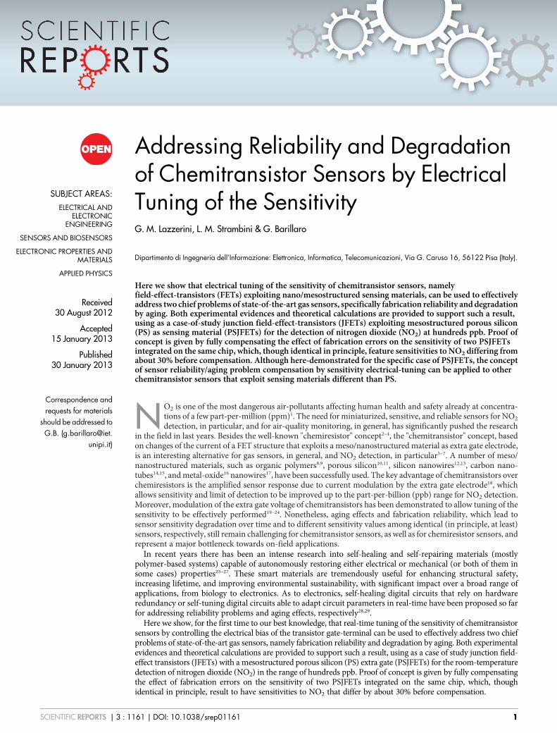
ResultsThe PSJFET sensor is a p-channel JFET30 modified with a mesos-tructured porous silicon (PS) layer that is integrated on top of the p-channel between the source (S) and drain (D) terminals (Fig. 1a)31. PSis a nano/mesostructured form of silicon, obtained by electrochem-ical erosion of crystalline silicon in acidic solutions under anodicpolarization, that features peculiar characteristics very appealingfor gas sensing applications, among which huge surface-to-volumeratio (over 500 m2/cm3), effective room temperature interaction withgas molecules, and compatibility with commercial silicon-based inte-grated processes11. The PSJFET sensor is characterized by two inde-pendent gates: a solid electrical gate (G), which allows the current ofthe JFET device to be electrically tuned, and a mesostructured sens-ing gate, which allows the JFET device to be provided with sensingcapability. The two gates, electrical and sensing, independently
operate on the depletion regions (also known as space charge regionsbecause they are free of mobile charge carriers and only contain fixedcharges) x1 at the p-channel/n-silicon interface and x2 at the PS/p-channel interface, respectively, thus affecting the JFET current(Fig. 1a). On the one hand, the electrical gate allows the depletionregion width x1 at the p-channel/n-silicon interface to be electricallytuned, thus effectively modulating the p-channel thickness and, inturn, the current flowing in the p-channel independently of the ana-lyte concentration (Fig. 1a and 2a). On the other hand, the sensinggate allows the depletion region width x2 at the PS/p-channel inter-face to be tuned upon adsorption of analytes in the PS layer itself,thus effectively changing the p-channel thickness and, in turn, thecurrent flowing in the p-channel dependently on the analyte concen-tration, for a given gate voltage (Fig. 1a and 2b).
The PSJFET sensor is fabricated by defining aluminum source anddrain comb-finger contacts on a silicon substrate, this latter consist-ing of a 2.4-mm-thick p-type silicon layer on top of a n-type siliconsubstrate, then performing the selective electrochemical erosion ofpart of the p-type silicon between drain and source contacts to pro-duce the mesostructured PS layer on top of the p-channel31. Theelectrochemical erosion step is controlled to obtain mesostructured
Figure 1 | (a) Schematic cross-section of the PSJFET sensor and effect of the gate voltage and analytes adsorbed into the PS on the depletion regions x1 and
x2, respectively; (b) Optical microscope top-image of two PSJFET sensors highlighting source and drain interdigitated contacts, and (inset)
magnification of one of the sensors in which the PS layer between contacts is clearly visible; (c) typical SEM cross-section image of the PS layer integrated
between drain and source terminals of the PSJFET; (d) high-magnification SEM image of the PS layer in (c) highlighting the mesostructured morphology
of the sensing gate.
www.nature.com/scientificreports
SCIENTIFIC REPORTS | 3 : 1161 | DOI: 10.1038/srep01161 2
PS layers with uniform thickness tPS, which can be tuned between 800nm and 1200 nm. Consequently, the thickness of the crystalline p-channel underneath the PS layer ranges between 1600 nm and1200 nm. Fig. 1b shows an optical microscope image of twoPSJFETs, together with details (in inset) of the PS layer betweensource and drain terminals. Fig. 1c and 1d show typical ScanningElectron Microscope (SEM) cross-section images of the mesostruc-tured PS layer integrated between drain and source terminals of thePSJFET. In Fig. 1d, which was acquired at high magnifications(500 kx), the mesostructured morphology of the PS layer (sensinggate) is clearly visible.
The PSJFET sensors are tested with NO2 at concentrations in therange 0–500 ppb, using the flow-through technique. For all theexperiments, flow-rate is maintained at 200 standard cubic centi-meter per minute (sccm), synthetic air is used as carrier gas, relativehumidity is set to zero, and temperature is set to 30uC. Both time-resolved (current versus time) and static (current versus voltage)measurements are performed for different VGS values and NO2 con-centrations on a large set of silicon chips, each one integrating severalPSJFETs with different channel width W and length L, so as to carryout a quantitative investigation of the PSJFET behavior both fromelectrical and sensing points of view.
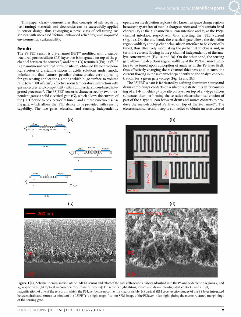
Fig. 2a and 2b show typical output curves of the PSJFET, that isIPSJFET versus VDS for different VGS values and NO2 concentrations,respectively. In the specific case of Fig. 2a and 2b, the output curvesrefer to a PSJFET sensor with channel length L 5 10 mm, effectivewidth W 5 3.9 mm, and PS thickness tPS 5 800 nm. The outputcurves of the PSJFET sensor exhibit the typical behavior of a JFETdevice. For a given VGS value and NO2 concentration, the increase ofthe absolute value of the VDS voltage initially produces a linear increaseof the absolute value of the sensor current IPSJFET (linear region); byincreasing the absolute value of VDS beyond the linear region a satura-tion of the sensor current IPSJFET is observed (saturation region), espe-cially evident in synthetic air and for the lower NO2 concentrations.The effect of increasing VGS is that of reducing the sensor currentIPSJFET for any VDS value, while only slightly increasing the outputresistance (slope of the curves in the saturation region slightly decreas-ing) of the PSJFET sensor (Fig. 2a). The effect of increasing the NO2
concentration is that of significantly increasing the sensor currentIPSJFET for any VDS value, while reducing the output resistance (slopeof the curves in the saturation region increasing) of the PSJFET sensor,especially at the higher NO2 concentrations (Fig. 2b). In fact, the PSlayer, which acts as a resistor in parallel to the p-channel of the JFET,has a conductivity whose value increases with the NO2 concentration32.
According to the literature, NO2 molecules act as strong acceptors at PSsurface, thus producing an increase of the hole concentration (conduc-tivity) of PS after adsorption of NO2 molecules. For a given VGS,especially at the higher NO2 concentrations, the increase of the con-ductivity of the PS layer significantly reduces PS resistance value and, inturn, the output resistance of the PSJFET sensor, thus accounting fornon-saturation of the sensor current IPSJFET.
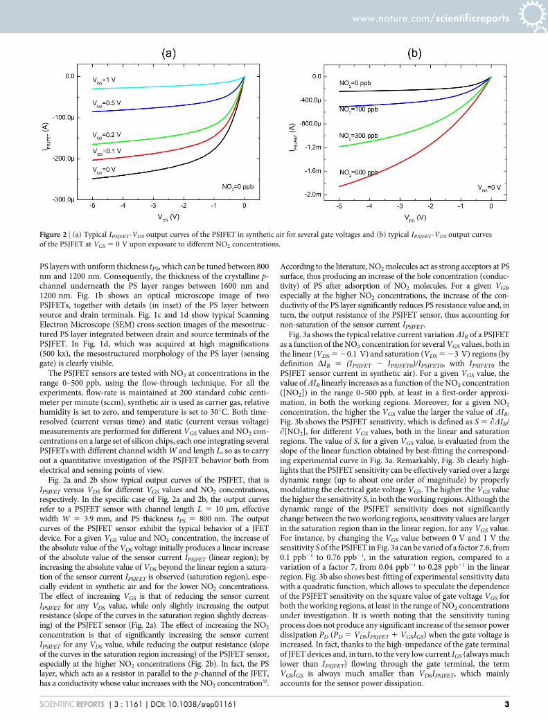
Fig. 3a shows the typical relative current variation DIR of a PSJFETas a function of the NO2 concentration for several VGS values, both inthe linear (VDS 5 20.1 V) and saturation (VDS 5 23 V) regions (bydefinition DIR 5 (IPSJFET 2 IPSJFET0)/IPSJFET0, with IPSJFET0 thePSJFET sensor current in synthetic air). For a given VGS value, thevalue of DIR linearly increases as a function of the NO2 concentration([NO2]) in the range 0–500 ppb, at least in a first-order approxi-mation, in both the working regions. Moreover, for a given NO2
concentration, the higher the VGS value the larger the value of DIR.Fig. 3b shows the PSJFET sensitivity, which is defined as S 5 LDIR/L[NO2], for different VGS values, both in the linear and saturationregions. The value of S, for a given VGS value, is evaluated from theslope of the linear function obtained by best-fitting the correspond-ing experimental curve in Fig. 3a. Remarkably, Fig. 3b clearly high-lights that the PSJFET sensitivity can be effectively varied over a largedynamic range (up to about one order of magnitude) by properlymodulating the electrical gate voltage VGS. The higher the VGS valuethe higher the sensitivity S, in both the working regions. Although thedynamic range of the PSJFET sensitivity does not significantlychange between the two working regions, sensitivity values are largerin the saturation region than in the linear region, for any VGS value.For instance, by changing the VGS value between 0 V and 1 V thesensitivity S of the PSJFET in Fig. 3a can be varied of a factor 7.6, from0.1 ppb21 to 0.76 ppb21, in the saturation region, compared to avariation of a factor 7, from 0.04 ppb21 to 0.28 ppb21 in the linearregion. Fig. 3b also shows best-fitting of experimental sensitivity datawith a quadratic function, which allows to speculate the dependenceof the PSJFET sensitivity on the square value of gate voltage VGS forboth the working regions, at least in the range of NO2 concentrationsunder investigation. It is worth noting that the sensitivity tuningprocess does not produce any significant increase of the sensor powerdissipation PD (PD 5 VDSIPSJFET 1 VGSIGS) when the gate voltage isincreased. In fact, thanks to the high-impedance of the gate terminalof JFET devices and, in turn, to the very low current IGS (always muchlower than IPSJFET) flowing through the gate terminal, the termVGSIGS is always much smaller than VDSIPSJFET, which mainlyaccounts for the sensor power dissipation.
Figure 2 | (a) Typical IPSJFET-VDS output curves of the PSJFET in synthetic air for several gate voltages and (b) typical IPSJFET-VDS output curves
of the PSJFET at VGS 5 0 V upon exposure to different NO2 concentrations.
www.nature.com/scientificreports
SCIENTIFIC REPORTS | 3 : 1161 | DOI: 10.1038/srep01161 3
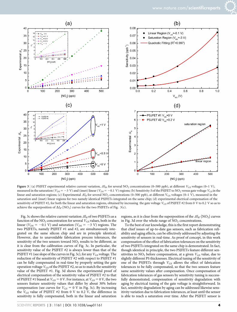
Fig. 3c shows the relative current variation DIR of two PSJFETs as afunction of the NO2 concentration for several VGS values, both in thelinear (VDS 5 20.1 V) and saturation (VDS 5 23 V) regions. Thetwo PSJFETs, namely PSJFET #1 and #2, are simultaneously inte-grated on the same silicon chip and are in principle identical.However, due to unavoidable fabrication process tolerances, thesensitivity of the two sensors toward NO2 results to be different, asit is clear from the calibration curves of Fig. 3c. In particular, thesensitivity value of the PSJFET #2 is always lower than that of thePSJFET #1 (see slope of the curves in Fig. 3c), for any VGS voltage. Thereduction of the sensitivity of PSJFET #2 with respect to PSJFET #1can be fully compensated in real-time by properly setting the gateoperation voltage VGS of the PSJFET #2, so as to match the sensitivityvalue of the PSJFET #1. Fig. 3d shows the experimental proof ofelectrical compensation of the sensitivity value of PSJFET #2 to thatof PSJFET #1 biased at VGS 5 0 V. For instance, at VGS 5 0 V, the twosensors feature sensitivity values that differ by about 30% beforecompensation (see curves for VGS 5 0 V in Fig. 3c). By increasingthe VGS value of PSJFET #2 from 0 V to 0.2 V, the difference insensitivity is fully compensated, both in the linear and saturation
regions, as it is clear from the superposition of the DIR-[NO2] curvesin Fig. 3d over the whole range of NO2 concentrations.
To the best of our knowledge, this is the first report demonstratingthat chief issues of up-to-date gas sensors, such as fabrication reli-ability and aging effects, can be effectively addressed by adjusting thesensitivity of sensors in real-time. As proof of concept, in this workcompensation of the effect of fabrication tolerances on the sensitivityof two PSJFETs integrated on the same chip is demonstrated. In fact,though identical in principle, the two PSJFETs feature different sen-sitivities to NO2 before compensation, at a given VGS value, due toslightly different PS thicknesses. Electrical tuning of the sensitivity ofone of the PSJFETs through VGS allows the effect of fabricationtolerances to be fully compensated, so that the two sensors featuresame sensitivity values after compensation. Once compensation offabrication tolerances of gas sensors by sensitivity tuning is success-fully demonstrated, compensation of sensitivity degradation withaging by electrical tuning of the gate voltage is straightforward. Infact, sensitivity degradation by aging can be addressed likewise sens-itivity variation due to fabrication tolerances, at least until the sensoris able to reach a saturation over time. After the PSJFET sensor is
Figure 3 | (a) PSJFET experimental relative current variation, DIR, for several NO2 concentrations (0–500 ppb), at different VGS voltages (0–1 V),
measured in the saturation (VDS 5 23 V) and (inset) linear (VDS 5 20.1 V) regions; (b) Sensitivity S of the PSJFET to NO2 versus gate voltage VGS in the
linear and saturation regions; (c) Experimental DIR for several NO2 concentrations (0–500 ppb), at different VGS voltages (0–1 V), measured in the
saturation and (inset) linear regions for two namely identical PSJFETs integrated on the same chip; (d) experimental electrical compensation of the
sensitivity of PSJFET #2, for both the linear and saturation regions, obtained by increasing the gate voltage VGS of PSJFET #2 from 0 V to 0.2 V so as to
achieve the superposition of DIR-[NO2] curves for the two PSJFETs of Fig. 3(c).
www.nature.com/scientificreports
SCIENTIFIC REPORTS | 3 : 1161 | DOI: 10.1038/srep01161 4
fabricated and initially calibrated, aging effects usually induce areduction of the slope of the calibration curve (i.e. the sensitivity),being the saturation values for aged sensors generally different fromthose of the initial calibration curve, at the same gas concentrations.Sensitivity degradation over time due to aging effects can be thencompensated likewise sensitivity variation due to fabrication toler-ances by properly tuning the gate voltage of the PSJFET sensor.
A semi-analytical model10 of the PSJFET sensor is used to theoret-ically corroborate experimental results on the electrical tuning of thesensitivity by gate-voltage control. The model takes into accountchanges in both conductance GPS and fixed-charge density QPS ofthe PS layer upon exposure to NO2. Under the assumption that thesetwo effects give rise to two independent contributions to the sensorcurrent, the PS is schematized with a resistance RPS 5 1/GPS 5 L/(sPS?W?tPS) (being sPS the PS conductivity) operating in parallel to aJFET with a p-channel cross-section that is reduced by a factor x2 5
QPS?tPS/qNA, being q the elementary charge and NA the p-dopingconcentration. The current flowing into the PSJFET sensor IPSJFET istherefore given by the sum of the current flowing into RPS (IPS) andinto the JFET (IJFET), both depending on the NO2 concentration. Inaddition, two resistors RS and RD in series to the JFET/RPS branch arealso included to model the silicon resistive paths from the externalsource (S) and drain (D) contacts to the PSJFET active region (rightunderneath the PS layer), and the contact resistances at the S and Dterminals. An analytical equation can be written for IPSJFET thattheoretically describes the PSJFET electrical behavior as a functionof both VDS and VGS voltages and NO2 concentration. This equationis used to perform the best-fitting of experimental current-voltageoutput curves measured for several VGS values at different NO2 con-centrations so as to obtain quantitative data on GPS and QPS as afunction of the NO2 concentration in the range under investigationand, in turn, on the variation of IPS and IJFET with NO2. Fig. S1 showsan example of theoretical (dotted lines) current-voltage outputcurves best-fitting the experimental (solid lines) curves, measuredfor one of the PSJFET used in this work. A good agreement betweentheoretical and experimental curves is clearly obtained for all testedVGS values and NO2 concentrations, thus validating the proposedsemi-analytical model. Details of analytical equations describing thePSJFET and of the best-fitting procedure are provided in the sectionMethods, subsection Theoretical modeling and fitting.
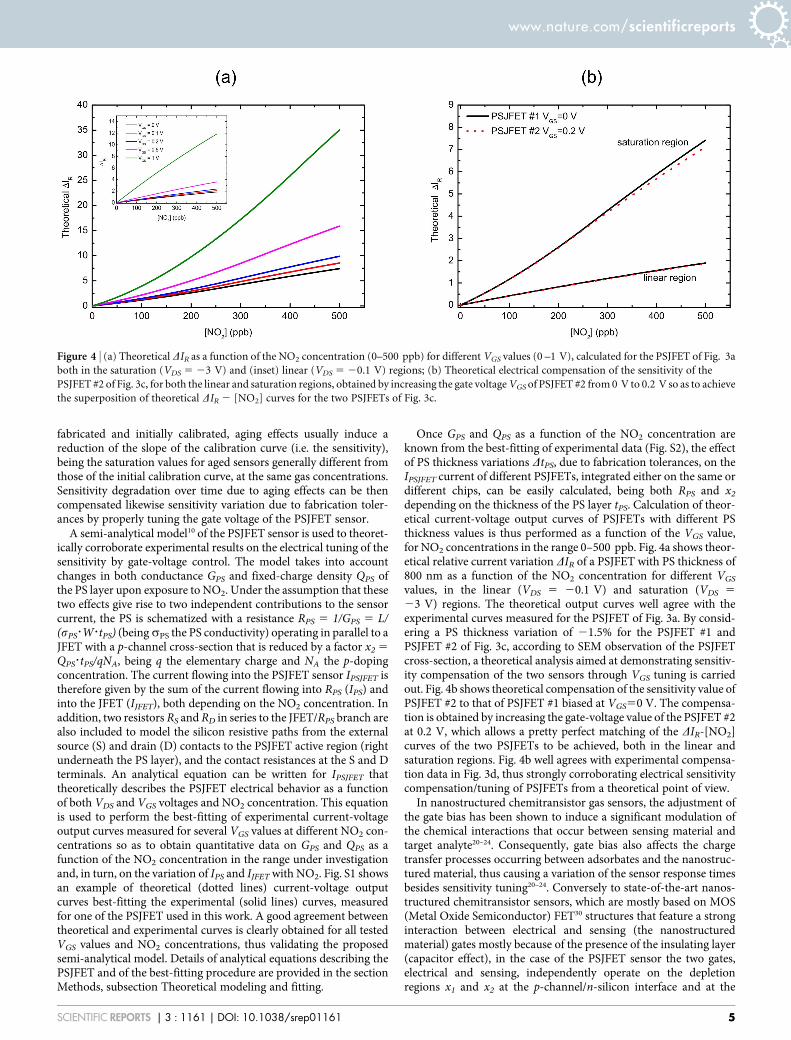
Once GPS and QPS as a function of the NO2 concentration areknown from the best-fitting of experimental data (Fig. S2), the effectof PS thickness variations DtPS, due to fabrication tolerances, on theIPSJFET current of different PSJFETs, integrated either on the same ordifferent chips, can be easily calculated, being both RPS and x2
depending on the thickness of the PS layer tPS. Calculation of theor-etical current-voltage output curves of PSJFETs with different PSthickness values is thus performed as a function of the VGS value,for NO2 concentrations in the range 0–500 ppb. Fig. 4a shows theor-etical relative current variation DIR of a PSJFET with PS thickness of800 nm as a function of the NO2 concentration for different VGS
values, in the linear (VDS 5 20.1 V) and saturation (VDS 5
23 V) regions. The theoretical output curves well agree with theexperimental curves measured for the PSJFET of Fig. 3a. By consid-ering a PS thickness variation of 21.5% for the PSJFET #1 andPSJFET #2 of Fig. 3c, according to SEM observation of the PSJFETcross-section, a theoretical analysis aimed at demonstrating sensitiv-ity compensation of the two sensors through VGS tuning is carriedout. Fig. 4b shows theoretical compensation of the sensitivity value ofPSJFET #2 to that of PSJFET #1 biased at VGS50 V. The compensa-tion is obtained by increasing the gate-voltage value of the PSJFET #2at 0.2 V, which allows a pretty perfect matching of the DIR-[NO2]curves of the two PSJFETs to be achieved, both in the linear andsaturation regions. Fig. 4b well agrees with experimental compensa-tion data in Fig. 3d, thus strongly corroborating electrical sensitivitycompensation/tuning of PSJFETs from a theoretical point of view.
In nanostructured chemitransistor gas sensors, the adjustment ofthe gate bias has been shown to induce a significant modulation ofthe chemical interactions that occur between sensing material andtarget analyte20–24. Consequently, gate bias also affects the chargetransfer processes occurring between adsorbates and the nanostruc-tured material, thus causing a variation of the sensor response timesbesides sensitivity tuning20–24. Conversely to state-of-the-art nanos-tructured chemitransistor sensors, which are mostly based on MOS(Metal Oxide Semiconductor) FET30 structures that feature a stronginteraction between electrical and sensing (the nanostructuredmaterial) gates mostly because of the presence of the insulating layer(capacitor effect), in the case of the PSJFET sensor the two gates,electrical and sensing, independently operate on the depletionregions x1 and x2 at the p-channel/n-silicon interface and at the
Figure 4 | (a) Theoretical DIR as a function of the NO2 concentration (0–500 ppb) for different VGS values (0 –1 V), calculated for the PSJFET of Fig. 3a
both in the saturation (VDS 5 23 V) and (inset) linear (VDS 5 20.1 V) regions; (b) Theoretical electrical compensation of the sensitivity of the
PSJFET #2 of Fig. 3c, for both the linear and saturation regions, obtained by increasing the gate voltage VGS of PSJFET #2 from 0 V to 0.2 V so as to achieve
the superposition of theoretical DIR 2 [NO2] curves for the two PSJFETs of Fig. 3c.
www.nature.com/scientificreports
SCIENTIFIC REPORTS | 3 : 1161 | DOI: 10.1038/srep01161 5
PS/p-channel interface, respectively. This has been demonstratedboth with experimental data and theoretical analyses (see Ref. 10and section Methods, subsection Theoretical modeling and fitting,of this manuscript). In the PSJFET sensor the voltage VGS appliedbetween gate and source terminals mostly drops across the depletionregion x1, at the p-channel/n-silicon interface, with two main advan-tages. The former is an efficient modulation of the width of thedepletion region x1 with the VGS value (typical of Junction FETstructures), which allows the PSJFET sensitivity to be tuned withhigh efficacy. The latter is an effective minimization of the electricalinteraction between gate terminal and sensing material, which allowsto strongly reduce the effect of the gate voltage on the chemicalinteraction occurring between adsorbates and nanostructuredmaterial.
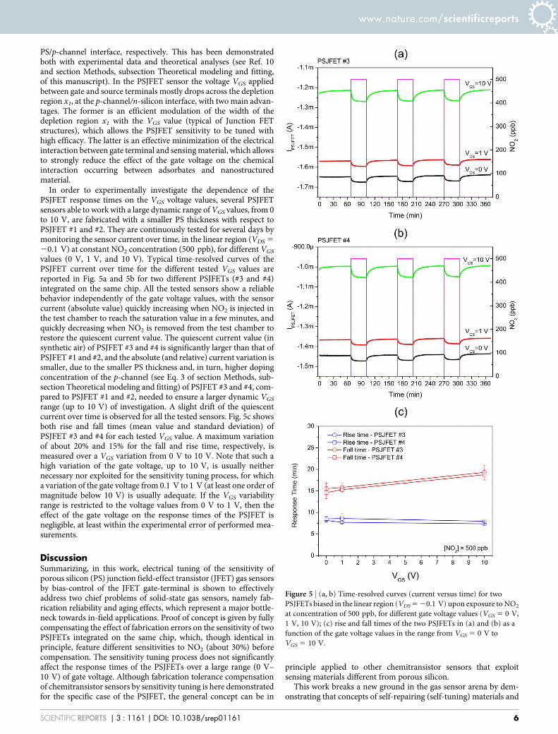
In order to experimentally investigate the dependence of thePSJFET response times on the VGS voltage values, several PSJFETsensors able to work with a large dynamic range of VGS values, from 0to 10 V, are fabricated with a smaller PS thickness with respect toPSJFET #1 and #2. They are continuously tested for several days bymonitoring the sensor current over time, in the linear region (VDS 5
20.1 V) at constant NO2 concentration (500 ppb), for different VGS
values (0 V, 1 V, and 10 V). Typical time-resolved curves of thePSJFET current over time for the different tested VGS values arereported in Fig. 5a and 5b for two different PSJFETs (#3 and #4)integrated on the same chip. All the tested sensors show a reliablebehavior independently of the gate voltage values, with the sensorcurrent (absolute value) quickly increasing when NO2 is injected inthe test chamber to reach the saturation value in a few minutes, andquickly decreasing when NO2 is removed from the test chamber torestore the quiescent current value. The quiescent current value (insynthetic air) of PSJFET #3 and #4 is significantly larger than that ofPSJFET #1 and #2, and the absolute (and relative) current variation issmaller, due to the smaller PS thickness and, in turn, higher dopingconcentration of the p-channel (see Eq. 3 of section Methods, sub-section Theoretical modeling and fitting) of PSJFET #3 and #4, com-pared to PSJFET #1 and #2, needed to ensure a larger dynamic VGS
range (up to 10 V) of investigation. A slight drift of the quiescentcurrent over time is observed for all the tested sensors. Fig. 5c showsboth rise and fall times (mean value and standard deviation) ofPSJFET #3 and #4 for each tested VGS value. A maximum variationof about 20% and 15% for the fall and rise time, respectively, ismeasured over a VGS variation from 0 V to 10 V. Note that such ahigh variation of the gate voltage, up to 10 V, is usually neithernecessary nor exploited for the sensitivity tuning process, for whicha variation of the gate voltage from 0.1 V to 1 V (at least one order ofmagnitude below 10 V) is usually adequate. If the VGS variabilityrange is restricted to the voltage values from 0 V to 1 V, then theeffect of the gate voltage on the response times of the PSJFET isnegligible, at least within the experimental error of performed mea-surements.
DiscussionSummarizing, in this work, electrical tuning of the sensitivity ofporous silicon (PS) junction field-effect transistor (JFET) gas sensorsby bias-control of the JFET gate-terminal is shown to effectivelyaddress two chief problems of solid-state gas sensors, namely fab-rication reliability and aging effects, which represent a major bottle-neck towards in-field applications. Proof of concept is given by fullycompensating the effect of fabrication errors on the sensitivity of twoPSJFETs integrated on the same chip, which, though identical inprinciple, feature different sensitivities to NO2 (about 30%) beforecompensation. The sensitivity tuning process does not significantlyaffect the response times of the PSJFETs over a large range (0 V–10 V) of gate voltage. Although fabrication tolerance compensationof chemitransistor sensors by sensitivity tuning is here demonstratedfor the specific case of the PSJFET, the general concept can be in
principle applied to other chemitransistor sensors that exploitsensing materials different from porous silicon.
This work breaks a new ground in the gas sensor arena by dem-onstrating that concepts of self-repairing (self-tuning) materials and
Figure 5 | (a, b) Time-resolved curves (current versus time) for two
PSJFETs biased in the linear region (VDS 5 20.1 V) upon exposure to NO2
at concentration of 500 ppb, for different gate voltage values (VGS 5 0 V,
1 V, 10 V); (c) rise and fall times of the two PSJFETs in (a) and (b) as a
function of the gate voltage values in the range from VGS 5 0 V to
VGS 5 10 V.
www.nature.com/scientificreports
SCIENTIFIC REPORTS | 3 : 1161 | DOI: 10.1038/srep01161 6
electronics can be successfully applied to sensor design, thus envis-aging a novel class of self-tuning gas sensors with increased lifetime,enhanced reliability, and improved environmental sustainability.
MethodsFabrication and experimental measurements. The fabrication process of thePSJFET consists of the following main steps: i) n-type silicon substrate with doping of1015 cm23; ii) boron implantation and diffusion to form a p-type layer, 2.4 mm deepwith a maximum surface doping of 1017 cm23; iii) definition of aluminiuminterdigitated electrical contacts for drain and source terminals (1st mask);iv) aluminium evaporation for electrical gate contact formation on the back of thechip; v) source and drain contacts protection by using a photoresist mask (2nd mask)hardbaked at 140uC for 30 minutes, which is a crucial step for making the resist layerable to withstand the subsequent electrochemical etching (anodization); vi) selectiveanodization in aqueous HF-based solution of the p-type material, through thephotoresist-free spaces, to form a PS layer with uniform thickness. Several PSJFETsensors with channel length L 5 10 mm, different channel width, W, (W1 5 9.6 mm,W2 5 5.8 mm, and W3 5 3.9 mm) and same nominal PS thickness are integrated onthe same chip. Several chips are prepared using the same anodization current densityand only changing the anodization time in order to produce PSJFETs featuring PSlayers with different chip-to-chip thicknesses, ranging from 800 nm and 1000 nm,but same morphological mesostructured features. Each chip is then mounted on aTO12 metal-package and placed into a sealed chamber with temperature fixed at 30 6
0.5uC for testing.The flow-through technique is used to expose the PSJFETs to a constant flux of 200
sccm alternating synthetic air and mixtures of synthetic air NO2 at different NO2
concentrations between 100 ppb and 500 ppb. The sensors are exposed to NO2
mixtures for 30 min and then to synthetic air for 60 min. Response time, which isdefined as the time required for the sensor output to change from its previous state toa final settled value within a tolerance band of 610%, ranges from a few minutes toseveral minutes at room temperature for NO2 adsorption and desorption cycles,respectively. Response times are estimated by monitoring the sensor current IPSJFET
over time (up to a few days) for different NO2 concentrations, at constant VDS and VGS
values. The effect of the electrical gate on the response time is evaluated by monitoringthe sensor current IPSJFET over time (up to a few days) for constant NO2 concentrationand VDS value, and different VGS values in the range from 0 V to 10 V. PSJFETs withdifferent L and W values show similar qualitative behavior and a quantitative beha-vior that is coherent with the ratio W/L, as expected.
Output current-voltage curves IPSJFET-VDS of the PSJFETs are measured using asource-measure unit (Keithley 2400), by sweeping the VDS value between 0 V and25 V, with step of 20.05 V, and simultaneously monitoring the current flowingbetween the drain and source terminals, for a given VGS value. The effect of theelectrical gate on the sensor current is measured by changing the VGS voltage between0 V and 1 V, with a minimum step of 0.1 V. Once the response times of the sensors atroom temperature are known from the time-resolved analysis, the measurement ofthe output current-voltage curves are carried out by exposing the sensors to NO2
mixtures for 30 min and then to synthetic air for 30 min.
Theoretical modeling and fitting. The PSJFET electrical behavior is described by aset of equations that include the dependence on the NO2 concentration of the currentflowing through the JFET and structure and the PS layer10.
As for the JFET structure, the current IJFET can be modeled in the linear region by:
IJFET lin~k1(VDi{VSi)z(3=4)k2½(VbizVG{VDi)4=3{(VbizVG{VSi)
4=3� ð1Þ
where VDi and VSi are the drain and source voltages corrected of the voltage dropacross the resistive paths RD and RS from external source and drain contacts to theJFET active region right underneath the PS layer, respectively, Vbi is the built-involtage at the pn junction, k2 is a constant that depends on the doping profile of the pnjunction, and k1 is a parameter that takes into account the geometrical dimension ofthe p-channel and the effect of the adsorbed NO2 molecules on the depletion region x2
at the PS/p-channel interface:
k1~WrL:(h{x2) ð2Þ
where r is the resistivity of the channel, W, L, and h are the width, length, andmetallurgical height of the p-channel, respectively, and x2 is given by:
x2~QPS(½NO2�)
qNA
:tPS ð3Þ
being q the elementary charge, NA the p-doping concentration of the channel, and tPS
the thickness of the PS layer. QPS is the fixed-charge density in the PS layer andrepresents the charge distributed on the PS layer surface and here macroscopicallyschematized as a volume charge uniformly distributed in the PS layer.
The pinch-off occurs when, at the JFET drain (Di), the sum of the depletionregions, x1 and x2 equals h. This occurs when VDi reaches the value:
VDi sat~VbizVG{ k1=k2ð Þ3 ð4Þ
Under this condition, the JFET current reaches its saturation value, which isindependent of any further increase of the drain voltage:
IJFET sat~k1(VDi sat{VSi)z(3=4)k2½(VbizVG{VDi sat )4=3{(VbizVG{VSi)
4=3� ð5Þ
As for the current flowing through the PS layer IPS, this is given by:
IPS~GPS(½NO2�):(VDi{VSi) ð6Þ
where GPS([NO2]) 5 1/RPS([NO2]), being RPS([NO2]) the PS resistance.Equations 1–6 are used to best-fit experimental output current-voltage curves for a
number of PSJFETs, integrated both on the same and different chips, and extractquantitative information on the effect of NO2 on the sensor current through GPS, k1,and k2 that are used as fitting parameters. For all the devices RS 5 RD 5 25 V, which isestimated from the sensor geometrical dimensions and doping profiles. Fig S1 showsexperimental output curves (solid lines) of a PSJFET for several VGS values at differentNO2 concentrations superimposed to theoretical output curves (dotted lines)obtained by the best-fitting of experimental data. Fig. S2(a–c) show mean values ofGPS, k1, and k2 as a function of the NO2 concentration, for the different VGS values,resulting from the best-fitting procedure of data in Fig. S1, with error bars repre-senting one standard deviation. As expected, k1 and GPS are independent of the gatevoltage VGS, though they significantly depend on the NO2 concentration. Inparticular, k1 increases from 0.99 3 1023 A?V21 for [NO2] 5 0 ppb to 1.38 3
1023 A?V21 for [NO2] 5 500 ppb; GPS increases from 9.7 3 1026 S for [NO2] 5
0 ppb to 1.67 3 1024 S for [NO2] 5 500 ppb. On the contrary, k2 only depends on thegeometrical characteristics and doping profiles of the JFET structure, and its value isexpected to be independent of both NO2 concentration and gate voltage VGS. In fact,k2 has a mean value of 7.9 3 1024 A?V3/4 for [NO2] between 0 ppb and 500 ppb, witha standard deviation of 0.2 3 1024 A?V3/4.
Equations 2 and 3 are then used to extract information on x2 and, in turn, on QPS asa function of the NO2 concentration. Remarkably, together with an increase of GPS,the model confirms that x2 reduces from 1.1 mm for [NO2] 5 0 ppb to 0.9 mm for[NO2] 5 500 ppb, due to a reduction of the charge density QPS in the PS layer from 13 1015 cm23 for [NO2] 5 0 ppb to 8.1 3 1014 cm23 for [NO2] 5 500 ppb (Fig. S2(d–e)). By best-fitting experimental data obtained for GPS and QPS versus NO2 concen-tration with a second-order polynomial function the following equations areobtained:
GPS(½NO2�)~1:85:10{10|½NO2�2{2:26:10{7|½NO2�z9:75:10{6 ð7Þ
QPS(½NO2�)~1:97:108|½NO2�2{4:56:1011|½NO2�z9:94:1014 ð8Þwith [NO2] in ppb (red curve in Fig. S2(a) and (d)).
Equations 7 and 8 are exploited to perform the quantitative evaluation of the effectof fabrication process tolerances, such as variation of the PS thickness with respect tothe nominal value, on the sensitivity of PSJFET sensors. To this end, tPS is defined astPS 5 tPS0(1 1 Dtrel), Dtrel being the relative variation of the PS thickness with respectto the nominal value tPS0. Being QPS by definition independent of the thickness of thePS layer, k1 and GPS0 can be expressed as:
k1~WrL
|(h{QPS
qNA
:tPS(1zDtrel)) ð9Þ
GPS~GPS0(1zDtrel) ð10Þ
where GPS0 is the PS conductance value at Dtrel 5 0.
1. Guerreiro, C., Larssen, S., de Leeuw, F. & Foltescu, V. Air quality in Europe —2011 report. EEA Technical Report 12, (2011) (http://www.eea.europa.eu/publications/air-quality-in-europe-2011) accessed 30th August 2012.
2. Jimenez-Cadena, G., Riu, J. & Rius, F. X. Gas sensors based on nanostructuredmaterials. The Analyst 132, 1083–1099 (2007).
3. Janata, J. & Josowicz, M. Conducting polymers in electronic chemical sensors.Nature Materials 2, 19–24 (2003).
4. Tricoli, A., Righettoni, M. & Teleki, A. Semiconductor Gas Sensors: Dry Synthesisand Application. Angewandte Chemie International Edition 49, 7632–7659(2010).
5. Stewart, M. P. & Buriak, J. M. Chemical and Biological Applications of PorousSilicon Technology. Advanced Materials 12, 859–869 (2000).
6. Lin, P. & Yan, F. Organic Thin-Film Transistors for Chemical and BiologicalSensing. Advanced Materials 24, 34–51 (2012).
7. Kauffman, D. R. & Star, A. Carbon Nanotube Gas and Vapor Sensors, AngewandteChemie International Edition 47, 6550–6570 (2008).
8. Das, A. et al. A nitrogen dioxide sensor based on an organic transistor constructedfrom amorphous semiconducting polymers. Advanced Materials 19, 4018–4023(2007).
9. Kolmakov, A., Zhang, Y. X., Cheng, G. S. & Moskovits, M. Detection of CO and O2
Using Tin Oxide Nanowire Sensors. Advanced Materials 15, 997–1000 (2003).10. Barillaro, G., Lazzerini, G. M. & Strambini, L. M. Modeling of porous silicon
junction field effect transistor gas sensors: Insight into NO2 interaction. AppliedPhysics Letters 96, 162105–1/3 (2010).
11. Barillaro, G. & Strambini, L. M. An integrated CMOS sensing chip for NO2
detection. Sensors and Actuators B 134, 585–590 (2008).12. McAlpine, M. C., Ahmad, H., Wang, D. W. & Heath, J. R. Highly ordered
nanowire arrays on plastic substrates for ultrasensitive flexible chemical sensors.Nature Materials 6, 379–384 (2007).
www.nature.com/scientificreports
SCIENTIFIC REPORTS | 3 : 1161 | DOI: 10.1038/srep01161 7

13. Engel, Y. et al. Supersensitive Detection of Explosives With Silicon NanowireArrays. Angewandte Chemie International Edition 49, 6830–6835 (2010).
14. Kong, J. et al. Nanotube Molecular Wires as Chemical Sensors. Science 287,622–625 (2000).
15. Lu, G., Ocola, L. E. & Chen, J. Room-Temperature Gas Sensing Based on ElectronTransfer between Discrete Tin Oxide Nanocrystals and Multiwalled CarbonNanotubes. Advanced Materials 21, 2487–2491 (2009).
16. Andringa, A.-M. et al. Gate-Bias Controlled Charge Trapping as a Mechanism forNO2 Detection with Field-Effect Transistors. Advanced Functional Materials 21,100–107 (2011).
17. Zhang, D. H. et al. Detection of NO2 down to ppb levels using individual andmultiple In203 nanowire devices, Nano Letters 4, 1919–1924 (2004).
18. Torsi, L. & Dodabalapur, A. Organic Thin-Film Transistors as Plastic AnalyticalSensors. Analitical Chemistry 77, 380A–387A (2005).
19. Hellmich, W., Muller, G., Braunmuhl, Ch. Bosch-v., Doll, T. & Eisele, I. Field-effect-induced gas sensitivity changes in metal oxides. Sensors and Actuators B:Chemical 41, 132–139 (1997).
20. Fan, Z., Wang, D., Chang, P.-C., Tseng, W.-Y. & Lu, J. G. ZnO Nanowire FieldEffect Transistor and Oxygen Sensing Property. Applied Physics Letters 85,5923–5925 (2004).
21. Zhang, Y., Kolmakov, A., Chretien, S. & Metiu, H., Moskovits, M. Control ofcatalytic reactions at the surface of a metal oxide nanowire by manipulatingelectron density inside it. Nano Letters 4, 403–407 (2004).
22. Dattoli, E. N., Davydov, A. V. & Benkstein, K. D. Tin oxide nanowire sensor withintegrated temperature and gate control for multi-gas recognition. Nanoscale 4,1760–1769 (2012).
23. Chen, G., Paronyan, T. M., Pigos, E. M. & Harutyunyan, A. R. Enhanced gassensing in pristine carbon nanotubes under continuous ultraviolet lightillumination. Scientific Reports 2, 343 (2012).
24. Mubeen, S. & Moskovits, M. Gate-Tunable Surface Processes on a Single-Nanowire Field-Effect Transistor. Advanced Materials 23, 2306–2312 (2011).
25. Yaun, W., et al. Fault-tolerant dielectric elastomer actuators using single-walledcarbon nanotube electrodes. Advanced Materials 20, 621–625 (2008).
26. Blaiszik, B. J., et al. Autonomic restoration of electrical conductivity. AdvancedMaterials 24, 398–401 (2012).
27. Tee, B. C.-K., Wang, C., Allen, R. & Bao, Z. An electrically and mechanically self-healing composite with pressure- and flexion-sensitive properties for electronicskin applications. Nature Nanotechnology 7, 825–832 (2012).
28. Tseng, T.-W., Huang, Y.-J. & Li, J.-F. DABISR: A Defect-Aware Built-In Self-Repair Scheme for Single/Multi-Port RAMs in SoCs. IEEE Transactions onComputer-Aided Design of Integrated Circuits and Systems, 29, 1628–1639 (2010).
29. Mintarno, E., et al. Self-Tuning for Maximized Lifetime Energy-Efficiency in thePresence of Circuit Aging. IEEE Transactions On Computer-Aided Design OfIntegrated Circuits And Systems 30, 760–773 (2011).
30. Sze, S. M. Physics of Semiconductor Devices, 2nd Edition, John Wiley and Sons(WIE), Wiley, November 18, 1981.
31. Barillaro, G., Lazzerini, G. M. & Strambini, L. M. A porous silicon JFET gas sensor:Experimental and modeling. Proceedings of IEEE Sensors 4716485, 494 (2008).
32. Boarino, L. et al. Local environment of boron impurities in porous silicon andtheir interaction with NO2 molecules. Physical Review B 64, 205308–1/4 (2001).
AckwnoledgmentsAuthors would like to thank staff at ST Microelectronics, Milan (Italy), for SEM images ofPSJET.
Author contributionsG.B. conceived and designed the research. G.B. and G.M.L. worked out the theory. G.M.L.and L.M.S. performed the experiments. All authors analyzed the data and wrote themanuscript.
Additional informationSupplementary information accompanies this paper at http://www.nature.com/scientificreports
Competing financial interests: The authors declare no competing financial interests.
License: This work is licensed under a Creative CommonsAttribution-NonCommercial-ShareAlike 3.0 Unported License. To view a copy of thislicense, visit http://creativecommons.org/licenses/by-nc-sa/3.0/
How to cite this article: Lazzerini, G.M., Strambini, L.M. & Barillaro, G. AddressingReliability and Degradation of Chemitransistor Sensors by Electrical Tuning of theSensitivity. Sci. Rep. 3, 1161; DOI:10.1038/srep01161 (2013).
www.nature.com/scientificreports
SCIENTIFIC REPORTS | 3 : 1161 | DOI: 10.1038/srep01161 8
Related Documents