Introduction Next-generation systems require ever increasing memory bandwidth to meet their application goals. These requirements are being driven by a host of end applications ranging from high-performance computing (HPC), networking, and server type applications. Conventional memory technologies are not scaling as fast as application requirements. The industry has typically described this challenge by using the “Memory Wall” terminology. Moore’s law dictates that transistor counts double every 18 months, thereby resulting in increased core performance, and the need for memory sub-systems to keep pace. In addition, host microprocessors are typically on a roadmap that involves multicores and multithreading to get maximum efficiency and performance gains. This essentially translates into distributing work sets into smaller blocks and distributing them among multiple compute elements. Having multiple compute elements per processor requires an increasing amount of memory per elements. This results in a greater need for both memory bandwidth and memory density to be tightly coupled to the host. Latency and density metrics that conventional memory systems offer are not able to keep pace with the ever increasing demands from the processor sub-systems. The challenge with memory bandwidth Figure 1 illustrates the memory challenge quite effectively. Intel FPGAs and Hybrid Memory Cube serial memory solutions solve the memory bandwidth bottleneck. Authors Manish Deo Senior Product Marketing Manager Intel Programmable Solutions Group Jeffrey Schulz In-Package I/O Implementation Lead Intel Programmable Solutions Group Addressing Next-Generation Memory Requirements Using Intel® FPGAs and HMC Technology FPGA Table of Contents Introduction .................... 1 The challenge with memory bandwidth .................... 1 HMC benefits ................... 2 Intel® FPGA HMC interoperability platform ..................... 2 Intel's HMC roadmap ............ 6 Networking system usage example ...................... 6 Conclusion ...................... 8 References ...................... 9 Where to get more information . . . 9 Figure 1. Memory Bandwidth Challenge Application Requirements 2x Every 2 Years DDR Memory or I/O Bandwidth Every 4-5 Years Memory Interface Bandwidth Timeline WHITE PAPER

Welcome message from author
This document is posted to help you gain knowledge. Please leave a comment to let me know what you think about it! Share it to your friends and learn new things together.
Transcript

IntroductionNext-generation systems require ever increasing memory bandwidth to meet their application goals. These requirements are being driven by a host of end applications ranging from high-performance computing (HPC), networking, and server type applications. Conventional memory technologies are not scaling as fast as application requirements.
The industry has typically described this challenge by using the “Memory Wall” terminology. Moore’s law dictates that transistor counts double every 18 months, thereby resulting in increased core performance, and the need for memory sub-systems to keep pace. In addition, host microprocessors are typically on a roadmap that involves multicores and multithreading to get maximum efficiency and performance gains. This essentially translates into distributing work sets into smaller blocks and distributing them among multiple compute elements. Having multiple compute elements per processor requires an increasing amount of memory per elements. This results in a greater need for both memory bandwidth and memory density to be tightly coupled to the host. Latency and density metrics that conventional memory systems offer are not able to keep pace with the ever increasing demands from the processor sub-systems.
The challenge with memory bandwidthFigure 1 illustrates the memory challenge quite effectively.
Intel FPGAs and Hybrid Memory Cube serial memory solutions solve the memory bandwidth bottleneck.
AuthorsManish Deo
Senior Product Marketing ManagerIntel Programmable Solutions Group
Jeffrey SchulzIn-Package I/O Implementation LeadIntel Programmable Solutions Group
Addressing Next-Generation Memory Requirements Using Intel® FPGAs and HMC Technology
FPGA
Table of Contents
Introduction . . . . . . . . . . . . . . . . . . . . 1
The challenge with memory bandwidth . . . . . . . . . . . . . . . . . . . . 1
HMC benefits . . . . . . . . . . . . . . . . . . . 2
Intel® FPGA HMC interoperability platform . . . . . . . . . . . . . . . . . . . . . 2
Intel's HMC roadmap . . . . . . . . . . . . 6
Networking system usage example . . . . . . . . . . . . . . . . . . . . . . 6
Conclusion . . . . . . . . . . . . . . . . . . . . . . 8
References . . . . . . . . . . . . . . . . . . . . . . 9
Where to get more information . . . 9Figure 1. Memory Bandwidth Challenge
ApplicationRequirements
2x Every2 Years
DDR Memory or I/O Bandwidth Every 4-5 Years
Mem
ory
Inte
rfac
e Ba
ndw
idth
Timeline
white paper

White Paper | Addressing Next-Generation Memory Requirements Using Intel FPGAs and HMC Technology
Figure 1 plots memory interface bandwidth versus timeline. From Figure 1, we can see that next-generation requirements typically require that memory bandwidth double roughly every two years. Conventional memory technologies such as DDR enable memory bandwidth to double only every four to five years. There is a clear gap between what is available and what is required. This gap needs to be effectively addressed to meet future requirements effectively. In addition, next-generation systems will also need ever increasing general-purpose I/O counts to meet overall system bandwidth goals. Conventional memory technologies such as DDR4 SDRAM can potentially provide a solution up to 3.2 gigabits per second (Gbps) and no roadmap has been defined beyond that. Given the number of components and pin requirements per component on next-generation systems, board space is also becoming an increasingly critical metric that system designers need to take into account. These next-generation system requirements need significantly higher performance, lower power, and a reduced form factor.
Figure 2 plots power (pj/bit) and bandwidth vs. timeline for conventional DRAM technology. From Figure 2, we can see that there have been incremental gains in the power/performance function over a 10 year+ period (2000-2012). In other words, conventional DRAM technology provided performance gains with corresponding decrease in the power consumption (pJ/bit). Extrapolating out this trend four years from the year 2012, we find that conventional DRAM technology will continue to provide incremental gains in performance. However these incremental gains in performance come with a decreasing return on the overall rate of power reduction. This is precisely the conundrum that the industry is finding itself in. Next-generation systems are demanding memory technology that not only provides an exponential increase in the bandwidth gigabyte per second (GBps), but also requiring a significant decrease in the power consumption (pJ/bit). This is where newer serial-based technologies such as the HMC look promising. HMC technology promises to deliver significantly higher bandwidth (GBps) at a fraction of the power (pJ/bit) of conventional DRAM technology.
HMC benefits The HMC provides significant benefits for next-generation systems looking to get higher performance, lower power, and save board space:
• Higher performance—15 times faster than a DDR3 SDRAM module
• Lower interface power—70% less energy than existing DDR3-1333
• Smaller form factor—90% less space than with existing RDIMM’s
• Better reliability—Enhanced reliability, availability, serviceability (RAS) feature set
• Reduced design complexity—Abstracted memory removes burden from host (HMC takes care of all memory management functions)
The HMC is a next-generation 3D stacked, multibank DRAM memory that combines best of logic and DRAM processes into a single heterogeneous package. The memory has a base logic section, which is used to manage multiple functions such as BIST, test access, vault control, cross bar switch, and so on. The DRAM memory is stacked on top of this base logic die using state-of-the-art through silicon via (TSV) based technology. The HMC interface consists of four links. Each link is built up using up to 16 full-duplex transceiver channels.
Figure 3 shows the top-level HMC architecture scheme. The stacked DRAM layers within one partition constitute a vault. Each vault is functionally and operationally independent and has a corresponding vault controller in the base logic layer. The interface to the external world is through the link interface controller in the logic base die. The collective internally available bandwidth from all of the vaults is made accessible to the interface links via the crossbar switch. Commands and data are transmitted in both directions across the link using a packet-based protocol where the packets consist of 128 bit flow units called “FLITs.” These FLITs are serialized, transmitted across the physical lanes of the link, and then re-assembled at the receiving end of the link. The data packets are scrambled at the requestor and then descrambled at the responder. No additional encoding is required. The HMC features RAS functions, such as cyclic redundancy check (CRC), error retry, and error correction code (ECC) to name a few. Packet integrity across the links is ensured via CRC, which is embedded in the tail of every packet.
Intel® FPGA HMC interoperability platform Intel has designed a demonstration board for the HMC and Intel FPGAs. The platform uses a 28 nm Stratix® V FPGA to interoperate with a HMC device. This is a significant announcement because it proves technology leadership in the memory domain by providing equivalent bandwidth of greater than eight (8) DDR4-2400 DIMMs using a single HMC device. In addition, it enables end customers to leverage their current development with the Stratix V FPGAs and prepare
Figure 2. Power and Bandwidth Projection
2000 2004 2008 2012 20161
10
100
1,000
Power(pj/bit)
1
10
100
1,000
Bandwidth(Gbps)
Current DRAMPower Trend
HMCPerformance
Current DRAMPerformanceTrend
HMC Power
Image Is Courtesy of Micron Technology

White Paper | Addressing Next-Generation Memory Requirements Using Intel FPGAs and HMC Technology
Memory Control
Crossbar Switch
Vault Control Vault Control Vault Control
Link InterfaceController
Link InterfaceController
Link InterfaceController
Link InterfaceController
ProcessorLinks
Logic Base
VaultDRAM
Logic Base
Logic Base Multiple High-Speed Local Buses for Data Movement Advanced Memory Controller Functions DRAM Control at Memory Instead of Distant Host Controller Reduced Memory Controller Complexity and Increased Efficiency
Vaults Maximize Overall Device Availability Optimized Energy and Refresh Management Self Test, Error Detection, Connection, and Repair in the Logic Base Layer
Vault Control
DRAMSequencer
WriteBuffer
ReadBuffer
RefreshController DRAM Repair
TSV Repair
Crossbar Switch
MemoryController
Read
Dat
a
Writ
e D
ata
Requ
est
Memory Interface Detail
DRAM7DRAM6DRAM5DRAM4DRAM3DRAM2DRAM1DRAM0Logic Chip
3DI and TSV Technology
Image Is Courtesy of Micron Technology
Figure 3. Top-Level HMC Architecture Scheme
ATX Form FactorStratix VFPGAs
HybridMemory Cube
10/100/1,000 EthernetConnectors
ATX Power SupplyConnector
Figure 4. Intel FPGA HMC Demonstration Platform
White Paper | Addressing Next-Generation Memory Requirements Using Intel FPGAs and HMC Technology
for production deployment with Intel's Generation 10 devices. A joint announcement regarding the successful interoperability was released on September 4, 2013.
• For more information, refer to the Altera and Micron Lead Industry with FPGA and Hybrid Memory Cube Interoperability press release on www.altera.com.
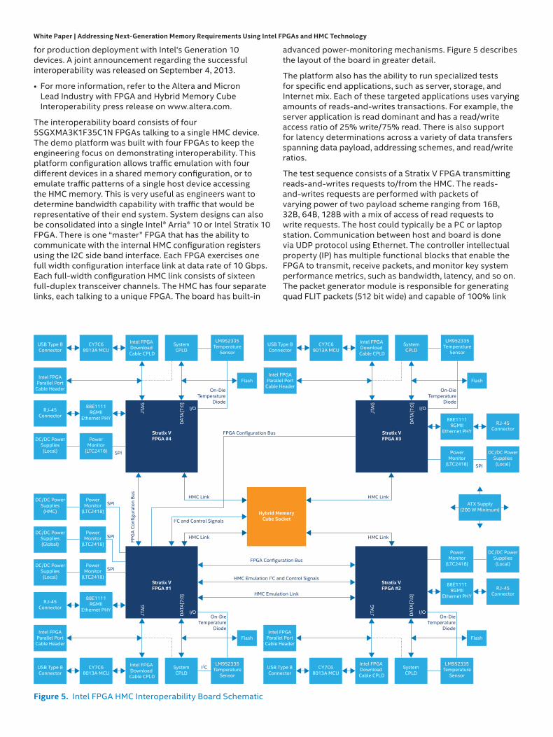
The interoperability board consists of four 5SGXMA3K1F35C1N FPGAs talking to a single HMC device. The demo platform was built with four FPGAs to keep the engineering focus on demonstrating interoperability. This platform configuration allows traffic emulation with four different devices in a shared memory configuration, or to emulate traffic patterns of a single host device accessing the HMC memory. This is very useful as engineers want to determine bandwidth capability with traffic that would be representative of their end system. System designs can also be consolidated into a single Intel® Arria® 10 or Intel Stratix 10 FPGA. There is one “master” FPGA that has the ability to communicate with the internal HMC configuration registers using the I2C side band interface. Each FPGA exercises one full width configuration interface link at data rate of 10 Gbps. Each full-width configuration HMC link consists of sixteen full-duplex transceiver channels. The HMC has four separate links, each talking to a unique FPGA. The board has built-in
advanced power-monitoring mechanisms. Figure 5 describes the layout of the board in greater detail.
The platform also has the ability to run specialized tests for specific end applications, such as server, storage, and Internet mix. Each of these targeted applications uses varying amounts of reads-and-writes transactions. For example, the server application is read dominant and has a read/write access ratio of 25% write/75% read. There is also support for latency determinations across a variety of data transfers spanning data payload, addressing schemes, and read/write ratios.
The test sequence consists of a Stratix V FPGA transmitting reads-and-writes requests to/from the HMC. The reads-and-writes requests are performed with packets of varying power of two payload scheme ranging from 16B, 32B, 64B, 128B with a mix of access of read requests to write requests. The host could typically be a PC or laptop station. Communication between host and board is done via UDP protocol using Ethernet. The controller intellectual property (IP) has multiple functional blocks that enable the FPGA to transmit, receive packets, and monitor key system performance metrics, such as bandwidth, latency, and so on. The packet generator module is responsible for generating quad FLIT packets (512 bit wide) and capable of 100% link
USB Type BConnector
CY7C68013A MCU
Intel FPGA Download Cable CPLD
SystemCPLD
LM952335Temperature
Sensor
I2C
Intel FPGAParallel Port
Cable Header
RJ-45Connector
88E1111RGMII
Ethernet PHY
Stratix VFPGA #4
JTAG
DAT
A[7:
0]
Flash
I/O
USB Type BConnector
CY7C68013A MCU
Intel FPGA Download Cable CPLD
SystemCPLD
LM952335Temperature
Sensor
I2C
Intel FPGAParallel Port
Cable Header
Stratix VFPGA #3
JTAG
DAT
A[7:
0]
Flash
I/O
USB Type BConnector
CY7C68013A MCU
Intel FPGA Download Cable CPLD
SystemCPLD
LM952335Temperature
Sensor
I2C
Intel FPGAParallel Port
Cable Header
RJ-45Connector
88E1111RGMII
Ethernet PHY
Stratix VFPGA #1
JTAG
DAT
A[7:
0]
Flash
I/O
USB Type BConnector
CY7C68013A MCU
Intel FPGA Download Cable CPLD
SystemCPLD
LM952335Temperature
Sensor
I2C
Intel FPGAParallel Port
Cable Header
Stratix VFPGA #2
JTAG
DAT
A[7:
0]
Flash
I/O
On-DieTemperature
Diode
On-DieTemperature
Diode
On-DieTemperature
Diode
On-DieTemperature
Diode
DC/DC PowerSupplies(Local)
PowerMonitor
(LTC2418) SPI
RJ-45Connector
88E1111RGMII
Ethernet PHY
DC/DC PowerSupplies(Local)
PowerMonitor
(LTC2418) SPI
RJ-45Connector
88E1111RGMII
Ethernet PHY
DC/DC PowerSupplies(Local)
PowerMonitor
(LTC2418) SPIDC/DC PowerSupplies(Local)
PowerMonitor
(LTC2418)SPI
DC/DC PowerSupplies(Global)
PowerMonitor
(LTC2418)SPI
DC/DC PowerSupplies
(HMC)
PowerMonitor
(LTC2418)SPI
Hybrid MemoryCube Socket
FPG
A Co
nfig
urat
on B
us
FPGA Configuration Bus
HMC Link
HMC Link
I2C and Control Signals
HMC Link
HMC Link
ATX Supply(200 W Minimum)
FPGA Configuration Bus
HMC Emulation I2C and Control Signals
HMC Emulation Link
Figure 5. Intel FPGA HMC Interoperability Board Schematic
White Paper | Addressing Next-Generation Memory Requirements Using Intel FPGAs and HMC Technology
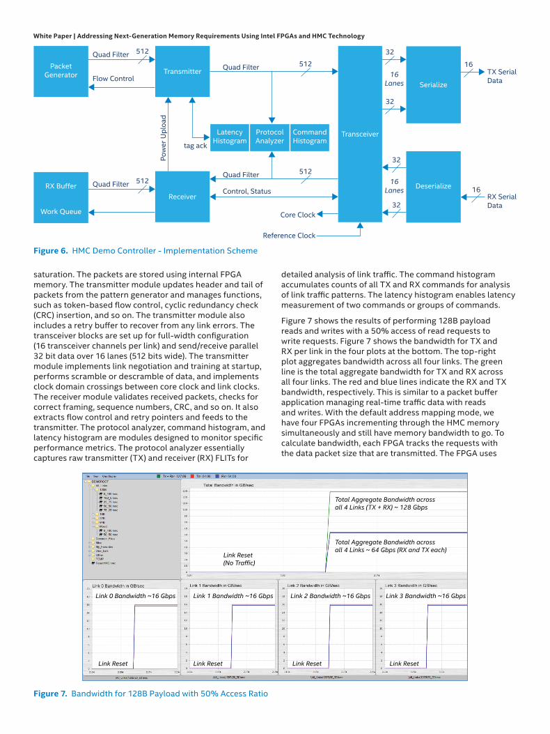
saturation. The packets are stored using internal FPGA memory. The transmitter module updates header and tail of packets from the pattern generator and manages functions, such as token-based flow control, cyclic redundancy check (CRC) insertion, and so on. The transmitter module also includes a retry buffer to recover from any link errors. The transceiver blocks are set up for full-width configuration (16 transceiver channels per link) and send/receive parallel 32 bit data over 16 lanes (512 bits wide). The transmitter module implements link negotiation and training at startup, performs scramble or descramble of data, and implements clock domain crossings between core clock and link clocks. The receiver module validates received packets, checks for correct framing, sequence numbers, CRC, and so on. It also extracts flow control and retry pointers and feeds to the transmitter. The protocol analyzer, command histogram, and latency histogram are modules designed to monitor specific performance metrics. The protocol analyzer essentially captures raw transmitter (TX) and receiver (RX) FLITs for
detailed analysis of link traffic. The command histogram accumulates counts of all TX and RX commands for analysis of link traffic patterns. The latency histogram enables latency measurement of two commands or groups of commands.
Figure 7 shows the results of performing 128B payload reads and writes with a 50% access of read requests to write requests. Figure 7 shows the bandwidth for TX and RX per link in the four plots at the bottom. The top-right plot aggregates bandwidth across all four links. The green line is the total aggregate bandwidth for TX and RX across all four links. The red and blue lines indicate the RX and TX bandwidth, respectively. This is similar to a packet buffer application managing real-time traffic data with reads and writes. With the default address mapping mode, we have four FPGAs incrementing through the HMC memory simultaneously and still have memory bandwidth to go. To calculate bandwidth, each FPGA tracks the requests with the data packet size that are transmitted. The FPGA uses
PacketGenerator Transmitter
Receiver
Quad Filter
Flow Control
512
Quad Filter 512RX Buffer
Work Queue
Pow
er U
ploa
d
LatencyHistogram
ProtocolAnalyzer
CommandHistogram
Transceiver
Quad Filter 512
Quad Filter 512
Core Clock
tag ack
Serialize
Deserialize
Reference Clock
32
32
32
32
16Lanes
16Lanes
16
16
TX SerialData
RX SerialData
Control, Status
Link Reset(No Traffic)
Total Aggregate Bandwidth acrossall 4 Links (TX + RX) ~ 128 Gbps
Total Aggregate Bandwidth acrossall 4 Links ~ 64 Gbps (RX and TX each)
Link 0 Bandwidth ~16 Gbps
Link Reset
Link 1 Bandwidth ~16 Gbps
Link Reset
Link 2 Bandwidth ~16 Gbps
Link Reset
Link 3 Bandwidth ~16 Gbps
Link Reset
Figure 6. HMC Demo Controller - Implementation Scheme
Figure 7. Bandwidth for 128B Payload with 50% Access Ratio
White Paper | Addressing Next-Generation Memory Requirements Using Intel FPGAs and HMC Technology
the system clock as the timer to calculate the total packet size and data traffic between HMC and the FPGA. Each FPGA bandwidth is aggregated to calculate the total HMC memory bandwidth used.
As you can see from the plot in Figure 7, the results are pretty phenomenal with 128 GBps of total aggregate read and write bandwidth for 128B payload with 50% read/write access ratio. For details on exact overheads for the HMC links, refer to the HMC specification document. Each link in full-width configuration (16 transceiver channels) is running at 10 Gbps, providing a total of 160 Gbps or 20 GBps bandwidth. In the example above, we are using a 128B payload. Therefore, we need a total of nine FLITs (128 bit each). For a write request, we essentially have 8 FLITs worth of payload because each header and tail in the packet is 64 bit. Thus, when we exercise a 50% read/write access ratio, we repeat a write request (8 /9) followed by a read request (0/1) for a total efficiency of 8/10 for the TX bus. This gives us an efficiency of 20 Gbps *8/10 = 16 GBps bandwidth for the TX bus. On the RX bus, we get a write response 0/1 and read response 8/9 for a total efficiency of 8/10 for the RX bus. This also translates to 16 GBps, so the total bandwidth for the link (RX + TX) = 32 GBps.
Intel's HMC roadmapIntel will provide full production support for the HMC devices starting with the Generation 10 FPGAs and SoCs. The Generation 10 product family includes Arria 10 and Stratix 10 FPGAs and SoCs. As mentioned perviously, Intel has already demonstrated full inter-operation between Stratix V FPGA and an HMC device.
The Arria 10 FPGAs and SoCs will be the first Generation 10 products to be shipped. The Arria 10 FPGAs are built using TSMC’s 20 nm process and will feature up to 96 transceivers capable of running up to 28 Gbps chip-to-chip. The transceiver channel count enables customers to leverage the full bandwidth of the HMC. The Arria 10 FPGAs and SoCs will also provide 15% higher core performance than today’s highest performance Stratix V FPGAs.
The Stratix 10 FPGAs and SoCs will be built using Intel's state-of-the-art 14 nm Tri-Gate process. The Stratix 10 FPGA is designed for ultra-high performance and will be industry’s first Gigahertz FPGA. It will also feature 70% lower power at performance levels equivalent to the previous generation. The Stratix 10 FPGA will provide for up to 144 transceiver channels capable of running up to 32 Gbps chip-to-chip.
Intel will release internally developed HMC FPGA IP to align with the Intel® Quartus® Prime software release schedule. The HMC IP supports data rates ranging from 10 Gbps, 12.5 Gbps to 15 Gbps across full-width and half-width configurations.
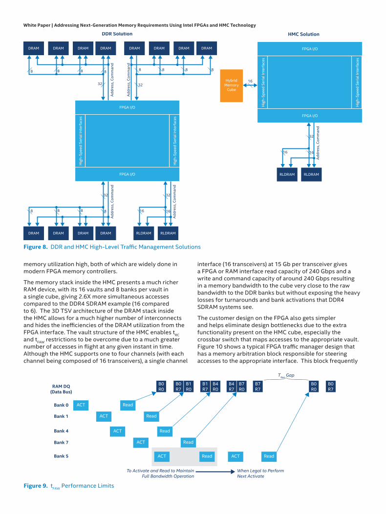
Networking system usage example As a specific example of a HMC-optimized application, consider an example of building a FPGA-based traffic management solution with a data buffer supporting 200 Gbps of port bandwidth. This solution can be constructed with either a HMC or using DDR3 SDRAM parts.
The DDR solution is constructed with a die in a 1,517-pin package with 624 I/O and 48 transceivers. The HMC solution is constructed in a 1,517-pin package. The DDR solution has a mixture of DDR for bulk data storage and RLDRAM for random access and control storage for structures, such as policing data, counters, and lookup tables. The HMC solution replaces the DDR with a single HMC and uses a single link (16 links X 10G) to give equivalent bandwidth to multiple DRAM interfaces.
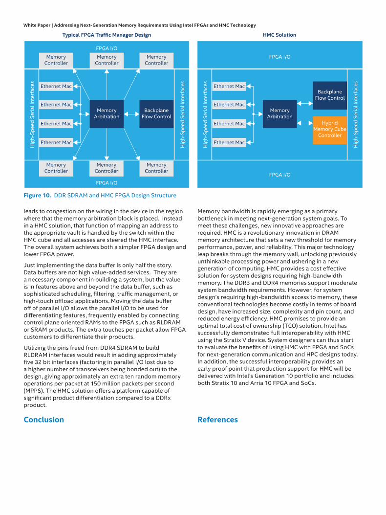
Packet buffering emphasizes random access patterns and building a system with DDR4 SDRAM generally sizes the DRAM to have an effective RAM bandwidth around 2.5x port performance. The 2.5x accounts for each packet needs to be written and read and for DDR4 SDRAM performance loss due to meeting DDR timing parameters. Due to the random access pattern, conventional DDR solutions are generally limited by tRC (bank cycle time) and tFAW (minimum time for four bank activations). tFAW has been a clock speed scaling problem for data communications access patterns since DDR3-1066 because it restricts bandwidth if only a single burst is transferred with each bank activate, which is typical for packet buffering applications.
tFAW establishes a timing window where only four activates can be done in that time period. DRAMs require a pipeline of active/read commands (with precharge) sent to different banks to maintain high data bus utilization for highly random access patterns. The only way around tFAW is to always access more than a single burst with each activation. System builders have responded by moving to a higher number of slimmer interfaces, allowing each interface to run longer bursts to transfer a fixed-size buffer. A FPGA-based traffic manager solution could use 6-32 bit interfaces running at 1,333 MHz giving a raw bandwidth of 512 Gbps and requires around 580 I/O. Memory controllers for this application would need to support both command look-ahead and data reordering to minimize expensive bus turn-arounds to keep
Reinventing the Midrange
• TSMC 20 nm Process
• 15% Higher Performance than Current High-End with 40% Lower Midrange Power
• Compatible 32-bit Dual ARM* A9 with 1.6x Processor System Improvement
• Up to 96 Transceiver Channels
Delivering Unimaginable Performance
• Intel 14 nm Tri-Gate Process
• 2X Performance Increase or 70% Power Savings
• 64 bit Quad ARM A53
• 3D-Capable for Integrating SRAM, DRAM, and ASICs
• 32 Gbps Chip-to-Chip
Generation 10 FPGAs and SoCs Deliver Hybrid Memory Cube for Volume Production
Arria 10 Stratix 10
White Paper | Addressing Next-Generation Memory Requirements Using Intel FPGAs and HMC Technology
memory utilization high, both of which are widely done in modern FPGA memory controllers.
The memory stack inside the HMC presents a much richer RAM device, with its 16 vaults and 8 banks per vault in a single cube, giving 2.6X more simultaneous accesses compared to the DDR4 SDRAM example (16 compared to 6). The 3D TSV architecture of the DRAM stack inside the HMC allows for a much higher number of interconnects and hides the inefficiencies of the DRAM utilization from the FPGA interface. The vault structure of the HMC enables tRC and tFAW restrictions to be overcome due to a much greater number of accesses in flight at any given instant in time. Although the HMC supports one to four channels (with each channel being composed of 16 transceivers), a single channel
interface (16 transceivers) at 15 Gb per transceiver gives a FPGA or RAM interface read capacity of 240 Gbps and a write and command capacity of around 240 Gbps resulting in a memory bandwidth to the cube very close to the raw bandwidth to the DDR banks but without exposing the heavy losses for turnarounds and bank activations that DDR4 SDRAM systems see.
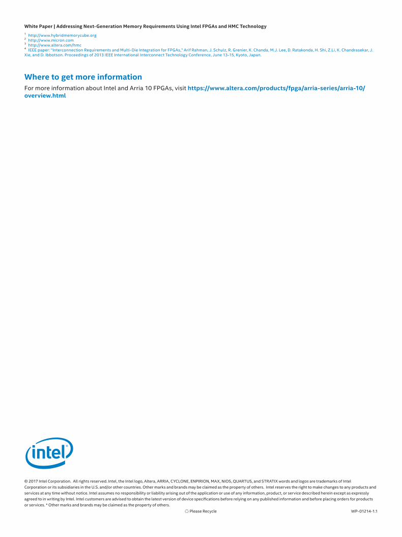
The customer design on the FPGA also gets simpler and helps eliminate design bottlenecks due to the extra functionality present on the HMC cube, especially the crossbar switch that maps accesses to the appropriate vault. Figure 10 shows a typical FPGA traffic manager design that has a memory arbitration block responsible for steering accesses to the appropriate interface. This block frequently
DRAM DRAM DRAM DRAM DRAM DRAMDRAM DRAM
FPGA I/O
FPGA I/O
Hig
h-Sp
eed
Seria
l Int
erfa
ces
Hig
h-Sp
eed
Seria
l Int
erfa
ces
8 8 8 8
32
Addr
ess,
Com
man
d
8 8 8 8
32
Addr
ess,
Com
man
d
DRAM DRAM DRAM DRAM
8 8 8 8
32
Addr
ess,
Com
man
d
RLDRAM RLDRAM
16 16
32
Addr
ess,
Com
man
d
DDR Solution
FPGA I/O
FPGA I/O
Hig
h-Sp
eed
Seria
l Int
erfa
ces
Hig
h-Sp
eed
Seria
l Int
erfa
ces
HybridMemory
Cube
16
RLDRAM RLDRAM
16 16
32
Addr
ess,
Com
man
d
HMC Solution
Figure 8. DDR and HMC High-Level Traffic Management Solutions
ACT Read
B0R0
ACT
ACT
ACT
Read
Read
Read
ACT ReadReadACT
To Activate and Read to MaintainFull Bandwidth Operation
When Legal to PerformNext Activate
RAM DQ(Data Bus)
Bank 0
Bank 1
Bank 4
Bank 7
Bank 5
B0R7
B1R0
B1R7
B4R0
B4R7
B7R0
B7R7
B0R0
B0R7
Tfaw Gap
Figure 9. tFAW Performance Limits
White Paper | Addressing Next-Generation Memory Requirements Using Intel FPGAs and HMC Technology
FPGA I/O
Hig
h-Sp
eed
Seria
l Int
erfa
ces
Hig
h-Sp
eed
Seria
l Int
erfa
ces
Ethernet Mac
Ethernet Mac
Ethernet Mac
Ethernet Mac
MemoryController
MemoryController
FPGA I/O
MemoryController
MemoryController
MemoryArbitration
MemoryController
MemoryController
BackplaneFlow Control
FPGA I/O
Hig
h-Sp
eed
Seria
l Int
erfa
ces
Hig
h-Sp
eed
Seria
l Int
erfa
ces
Ethernet Mac
Ethernet Mac
Ethernet Mac
Ethernet Mac
FPGA I/O
MemoryArbitration
BackplaneFlow Control
HybridMemory Cube
Controller
Typical FPGA Traffic Manager Design HMC Solution
Figure 10. DDR SDRAM and HMC FPGA Design Structure
leads to congestion on the wiring in the device in the region where that the memory arbitration block is placed. Instead in a HMC solution, that function of mapping an address to the appropriate vault is handled by the switch within the HMC cube and all accesses are steered the HMC interface. The overall system achieves both a simpler FPGA design and lower FPGA power.
Just implementing the data buffer is only half the story. Data buffers are not high value-added services. They are a necessary component in building a system, but the value is in features above and beyond the data buffer, such as sophisticated scheduling, filtering, traffic management, or high-touch offload applications. Moving the data buffer off of parallel I/O allows the parallel I/O to be used for differentiating features, frequently enabled by connecting control plane oriented RAMs to the FPGA such as RLDRAM or SRAM products. The extra touches per packet allow FPGA customers to differentiate their products.
Utilizing the pins freed from DDR4 SDRAM to build RLDRAM interfaces would result in adding approximately five 32 bit interfaces (factoring in parallel I/O lost due to a higher number of transceivers being bonded out) to the design, giving approximately an extra ten random memory operations per packet at 150 million packets per second (MPPS). The HMC solution offers a platform capable of significant product differentiation compared to a DDRx product.
Conclusion
Memory bandwidth is rapidly emerging as a primary bottleneck in meeting next-generation system goals. To meet these challenges, new innovative approaches are required. HMC is a revolutionary innovation in DRAM memory architecture that sets a new threshold for memory performance, power, and reliability. This major technology leap breaks through the memory wall, unlocking previously unthinkable processing power and ushering in a new generation of computing. HMC provides a cost effective solution for system designs requiring high-bandwidth memory. The DDR3 and DDR4 memories support moderate system bandwidth requirements. However, for system design’s requiring high-bandwidth access to memory, these conventional technologies become costly in terms of board design, have increased size, complexity and pin count, and reduced energy efficiency. HMC promises to provide an optimal total cost of ownership (TCO) solution. Intel has successfully demonstrated full interoperability with HMC using the Stratix V device. System designers can thus start to evaluate the benefits of using HMC with FPGA and SoCs for next-generation communication and HPC designs today. In addition, the successful interoperability provides an early proof point that production support for HMC will be delivered with Intel’s Generation 10 portfolio and includes both Stratix 10 and Arria 10 FPGA and SoCs.
References
1 http://www.hybridmemorycube.org2 http://www.micron.com3 http://www.altera.com/hmc4 IEEE paper: “Interconnection Requirements and Multi-Die Integration for FPGAs,” Arif Rahman, J. Schulz, R. Grenier, K. Chanda, M.J. Lee, D. Ratakonda, H. Shi, Z.Li, K. Chandrasekar, J. Xie, and D. Ibbotson. Proceedings of 2013 IEEE International Interconnect Technology Conference, June 13-15, Kyoto, Japan.
Where to get more informationFor more information about Intel and Arria 10 FPGAs, visit https://www.altera.com/products/fpga/arria-series/arria-10/overview.html
White Paper | Addressing Next-Generation Memory Requirements Using Intel FPGAs and HMC Technology
© 2017 Intel Corporation. All rights reserved. Intel, the Intel logo, Altera, ARRIA, CYCLONE, ENPIRION, MAX, NIOS, QUARTUS, and STRATIX words and logos are trademarks of IntelCorporation or its subsidiaries in the U.S. and/or other countries. Other marks and brands may be claimed as the property of others. Intel reserves the right to make changes to any products andservices at any time without notice. Intel assumes no responsibility or liability arising out of the application or use of any information, product, or service described herein except as expresslyagreed to in writing by Intel. Intel customers are advised to obtain the latest version of device specifications before relying on any published information and before placing orders for products or services. * Other marks and brands may be claimed as the property of others. Please Recycle WP-01214-1.1
Related Documents