ADDRESS SPACE PARTITIONING Intel 8085 uses a 16-bit wide address bus or addressing memory and I/O devices. It can access 2 16=64k bytes of memory and I/O devices. There are two schemes for the allocation of address to memories or I/O devices. 1. Memory mapped I/O scheme 2. I/O mapped I/O scheme 1. Memory Mapped I/O Scheme In this scheme there is only one address space. Address space is defined as set of all possible addresses that a microprocessor can generate. Some address are assigned to memories and some address to I/O devices. Suppose memory locations are assigned the address 2000-2500. One address is assigned to each memory location. These addresses cannot be assigned to I/O devices. The addresses assigned to I/O devices are different from address assigned to memory. For example, 2500, 2501, 2502 etc. may be assigned to I/O devices. One address is assigned to each I/O device. In this scheme all the data transfer instruction of the microprocessor can be used for both memory as well as I/O devices. For example, MOV A, M will be valid for data transfer from the memory location or I/O device whose address is in H-L pair. This scheme is suitable for small system. 2. I/O Mapped I/O Scheme In this scheme the address are assigned to memory locations can also be assigned to I/O devices. To distinguish whether the address on an address bus is for memory location or I/O devices. The Intel 8085 issues IO/M…… signal for this purpose. When the signal is high the address of an address bus is for I/O device. When low, the address is for a memory location. Two extra instructions IN and OUT are used to address I/O device. The IN instruction is used to read data from

Welcome message from author
This document is posted to help you gain knowledge. Please leave a comment to let me know what you think about it! Share it to your friends and learn new things together.
Transcript
ADDRESS SPACE PARTITIONING
Intel 8085 uses a 16-bit wide address bus or addressing memory and I/O devices. It
can access 2 16=64k bytes of memory and I/O devices.
There are two schemes for the allocation of address to memories or I/O devices.
1. Memory mapped I/O scheme
2. I/O mapped I/O scheme
1. Memory Mapped I/O Scheme
In this scheme there is only one address space. Address space is defined as
set of all possible addresses that a microprocessor can generate. Some address are
assigned to memories and some address to I/O devices. Suppose memory locations
are assigned the address 2000-2500. One address is assigned to each memory
location. These addresses cannot be assigned to I/O devices. The addresses
assigned to I/O devices are different from address assigned to memory. For
example, 2500, 2501, 2502 etc. may be assigned to I/O devices. One address is
assigned to each I/O device. In this scheme all the data transfer instruction of the
microprocessor can be used for both memory as well as I/O devices. For example,
MOV A, M will be valid for data transfer from the memory location or I/O device
whose address is in H-L pair. This scheme is suitable for small system.
2. I/O Mapped I/O Scheme
In this scheme the address are assigned to memory locations can also be
assigned to I/O devices. To distinguish whether the address on an address bus is for
memory location or I/O devices. The Intel 8085 issues IO/M…… signal for this
purpose. When the signal is high the address of an address bus is for I/O device.
When low, the address is for a memory location. Two extra instructions IN and
OUT are used to address I/O device. The IN instruction is used to read data from
an input device. And OUT instruction is used to an output device. This scheme is
suitable for large system
Memory and I/O Interfacing
Memory Interfacing
When we are executing any instruction, we need the microprocessor to access the memory for
reading instruction codes and the data stored in the memory. For this, both the memory and the
microprocessor requires some signals to read from and write to registers.
The interfacing process includes some key factors to match with the memory requirements and
microprocessor signals. The interfacing circuit therefore should be designed in such a way that
it matches the memory signal requirements with the signals of the microprocessor.
IO Interfacing
There are various communication devices like the keyboard, mouse, printer, etc. So, we need to
interface the keyboard and other devices with the microprocessor by using latches and buffers.
This type of interfacing is known as I/O interfacing.
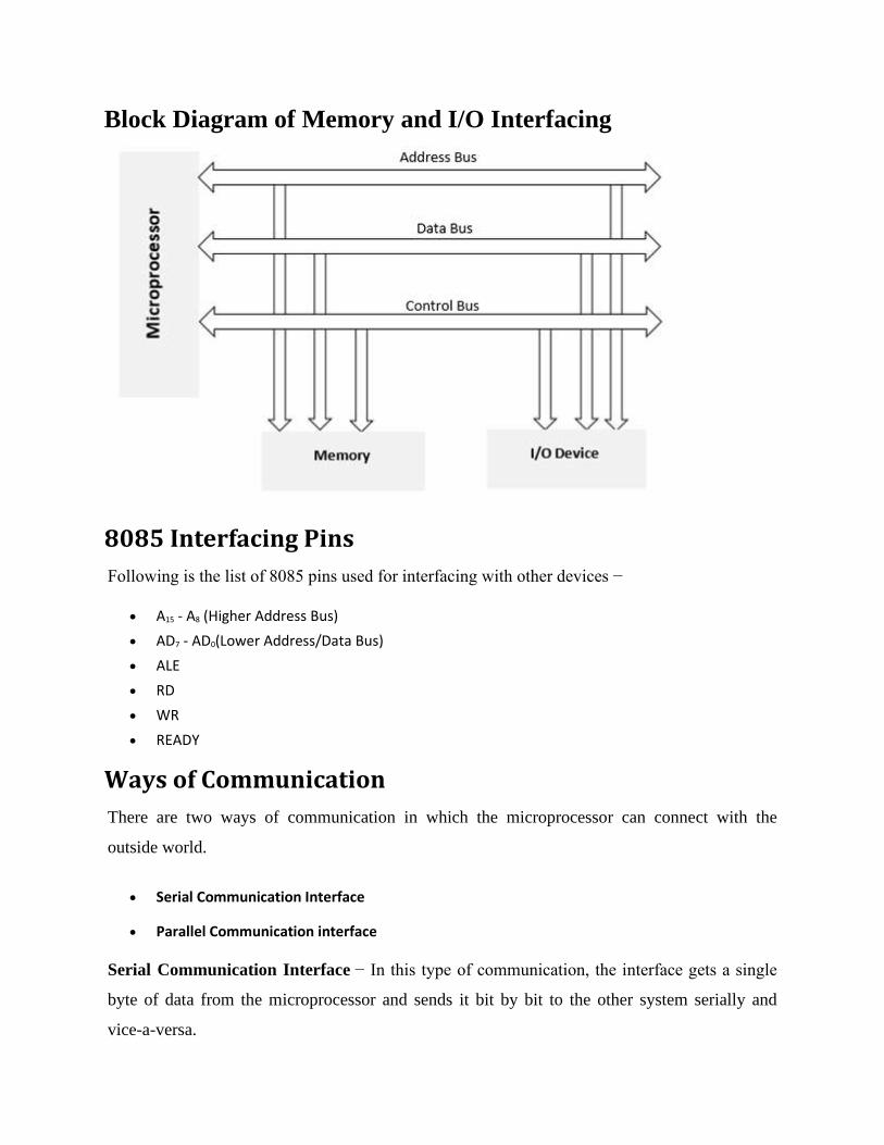
Block Diagram of Memory and I/O Interfacing
8085 Interfacing Pins
Following is the list of 8085 pins used for interfacing with other devices −
• A15 - A8 (Higher Address Bus)
• AD7 - AD0(Lower Address/Data Bus)
• ALE
• RD
• WR
• READY
Ways of Communication
There are two ways of communication in which the microprocessor can connect with the
outside world.
• Serial Communication Interface
• Parallel Communication interface
Serial Communication Interface − In this type of communication, the interface gets a single
byte of data from the microprocessor and sends it bit by bit to the other system serially and
vice-a-versa.
Parallel Communication Interface − In this type of communication, the interface gets a byte
of data from the microprocessor and sends it bit by bit to the other systems in simultaneous (or)
parallel fashion and vice-a-versa.
Interrupts in 8085
Interrupts are the signals generated by the external devices to request the microprocessor to
perform a task. There are 5 interrupt signals, i.e. TRAP, RST 7.5, RST 6.5, RST 5.5, and INTR.
Interrupt are classified into following groups based on their parameter −
• Vector interrupt − In this type of interrupt, the interrupt address is known to the
processor. For example: RST7.5, RST6.5, RST5.5, TRAP.
• Non-Vector interrupt − In this type of interrupt, the interrupt address is not known to
the processor so, the interrupt address needs to be sent externally by the device to
perform interrupts. For example: INTR.
• Maskable interrupt − In this type of interrupt, we can disable the interrupt by writing
some instructions into the program. For example: RST7.5, RST6.5, RST5.5.
• Non-Maskable interrupt − In this type of interrupt, we cannot disable the interrupt by
writing some instructions into the program. For example:TRAP.
• Software interrupt − In this type of interrupt, the programmer has to add the
instructions into the program to execute the interrupt. There are 8 software interrupts in
8085, i.e. RST0, RST1, RST2, RST3, RST4, RST5, RST6, and RST7.
• Hardware interrupt − There are 5 interrupt pins in 8085 used as hardware interrupts,
i.e. TRAP, RST7.5, RST6.5, RST5.5, INTA.
Note − NTA is not an interrupt, it is used by the microprocessor for sending acknowledgement.
TRAP has the highest priority, then RST7.5 and so on.
Interrupt Service Routine (ISR)
A small program or a routine that when executed, services the corresponding interrupting source
is called an ISR.
TRAP
It is a non-maskable interrupt, having the highest priority among all interrupts. Bydefault, it is
enabled until it gets acknowledged. In case of failure, it executes as ISR and sends the data to
backup memory. This interrupt transfers the control to the location 0024H.
RST7.5
It is a maskable interrupt, having the second highest priority among all interrupts. When this
interrupt is executed, the processor saves the content of the PC register into the stack and
branches to 003CH address.
RST 6.5
It is a maskable interrupt, having the third highest priority among all interrupts. When this
interrupt is executed, the processor saves the content of the PC register into the stack and
branches to 0034H address.
RST 5.5
It is a maskable interrupt. When this interrupt is executed, the processor saves the content of the
PC register into the stack and branches to 002CH address.
INTR
It is a maskable interrupt, having the lowest priority among all interrupts. It can be disabled by
resetting the microprocessor.
When INTR signal goes high, the following events can occur −
• The microprocessor checks the status of INTR signal during the execution of each
instruction.
• When the INTR signal is high, then the microprocessor completes its current instruction
and sends active low interrupt acknowledge signal.
• When instructions are received, then the microprocessor saves the address of the next
instruction on stack and executes the received instruction.
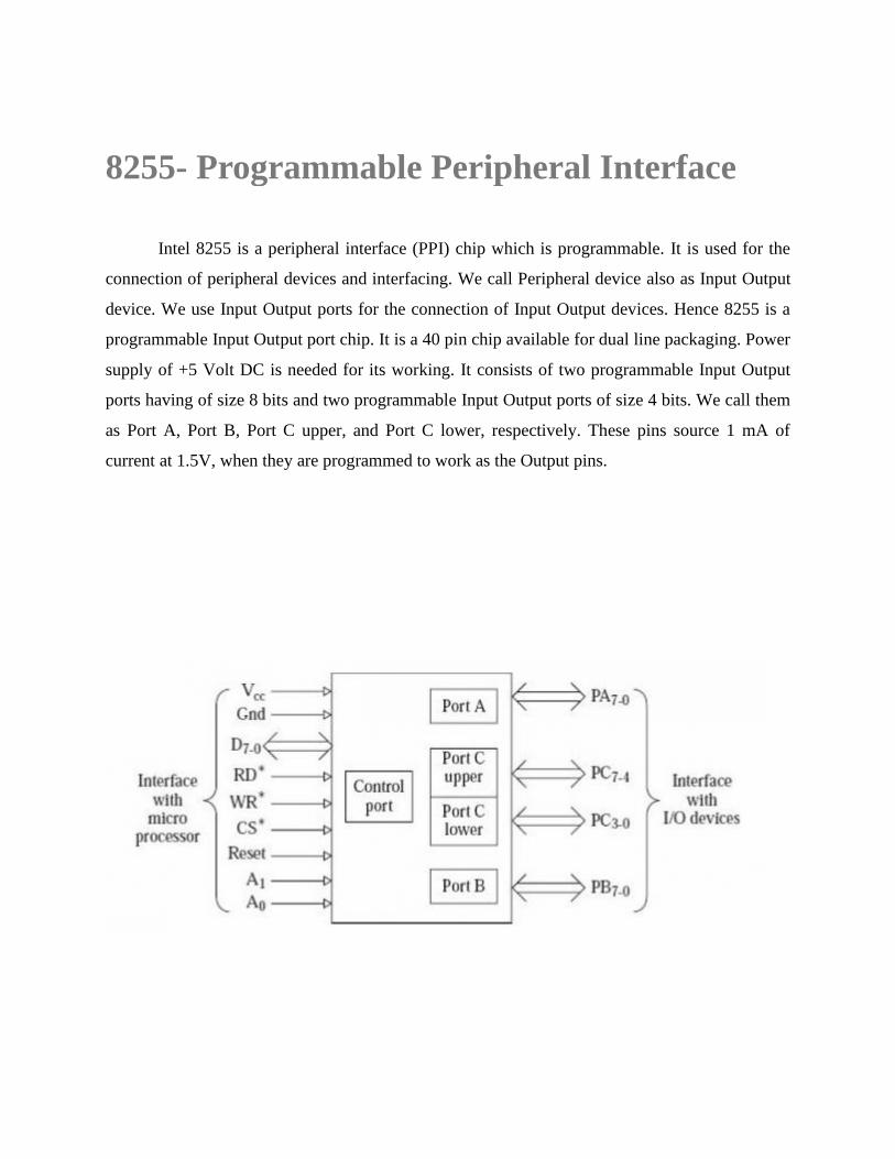
8255- Programmable Peripheral Interface
Intel 8255 is a peripheral interface (PPI) chip which is programmable. It is used for the
connection of peripheral devices and interfacing. We call Peripheral device also as Input Output
device. We use Input Output ports for the connection of Input Output devices. Hence 8255 is a
programmable Input Output port chip. It is a 40 pin chip available for dual line packaging. Power
supply of +5 Volt DC is needed for its working. It consists of two programmable Input Output
ports having of size 8 bits and two programmable Input Output ports of size 4 bits. We call them
as Port A, Port B, Port C upper, and Port C lower, respectively. These pins source 1 mA of
current at 1.5V, when they are programmed to work as the Output pins.
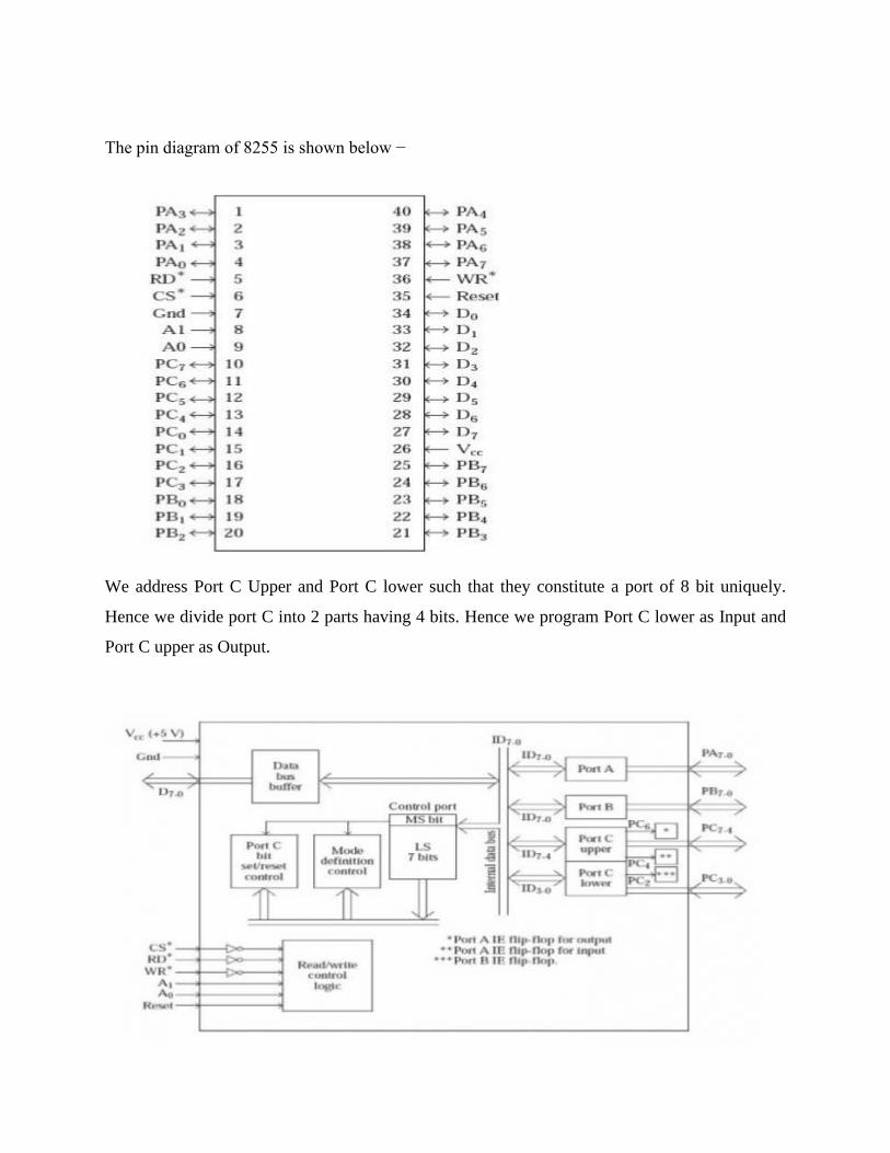
The pin diagram of 8255 is shown below −
We address Port C Upper and Port C lower such that they constitute a port of 8 bit uniquely.
Hence we divide port C into 2 parts having 4 bits. Hence we program Port C lower as Input and
Port C upper as Output.
The port selection logic is given where the output is set by us to the logic 1 and we reset it to
logic 0.
There are three modes of operation performed by 8255 they are as mode 0, mode 1 and mode 2.
We call the mode 0 as the simple Input Output or the basic Input Output for performing the
simplest mode of operation. Every ports of 8255 can be programmed to work in mode 0. We call
mode 1 as the strobed Input Output or handshake Input Output. It is useful when data is supplied
to the input device by the microprocessor at irregular interval of time. Finally, when the data is
read by the processor the port informs the Input device that the processors already read the data.
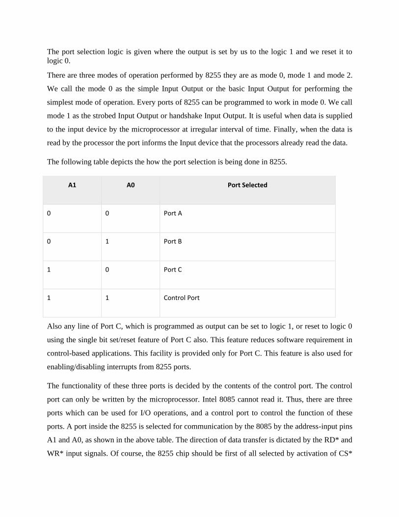
The following table depicts the how the port selection is being done in 8255.
A1 A0 Port Selected
0 0 Port A
0 1 Port B
1 0 Port C
1 1 Control Port
Also any line of Port C, which is programmed as output can be set to logic 1, or reset to logic 0
using the single bit set/reset feature of Port C also. This feature reduces software requirement in
control-based applications. This facility is provided only for Port C. This feature is also used for
enabling/disabling interrupts from 8255 ports.
The functionality of these three ports is decided by the contents of the control port. The control
port can only be written by the microprocessor. Intel 8085 cannot read it. Thus, there are three
ports which can be used for I/O operations, and a control port to control the function of these
ports. A port inside the 8255 is selected for communication by the 8085 by the address-input pins
A1 and A0, as shown in the above table. The direction of data transfer is dictated by the RD* and
WR* input signals. Of course, the 8255 chip should be first of all selected by activation of CS*
signal before a port inside 8255 can be selected. For example, the control port is written with the
contents sent out by 8085 on D7-0 pins of 8255 when CS* = 0, WR* = 0, A1 = 1, and A0 = 1.
Thus, A1 and A0 together with RD*, WR*, and CS* decide the manner in which 8085
communicates with 8255.
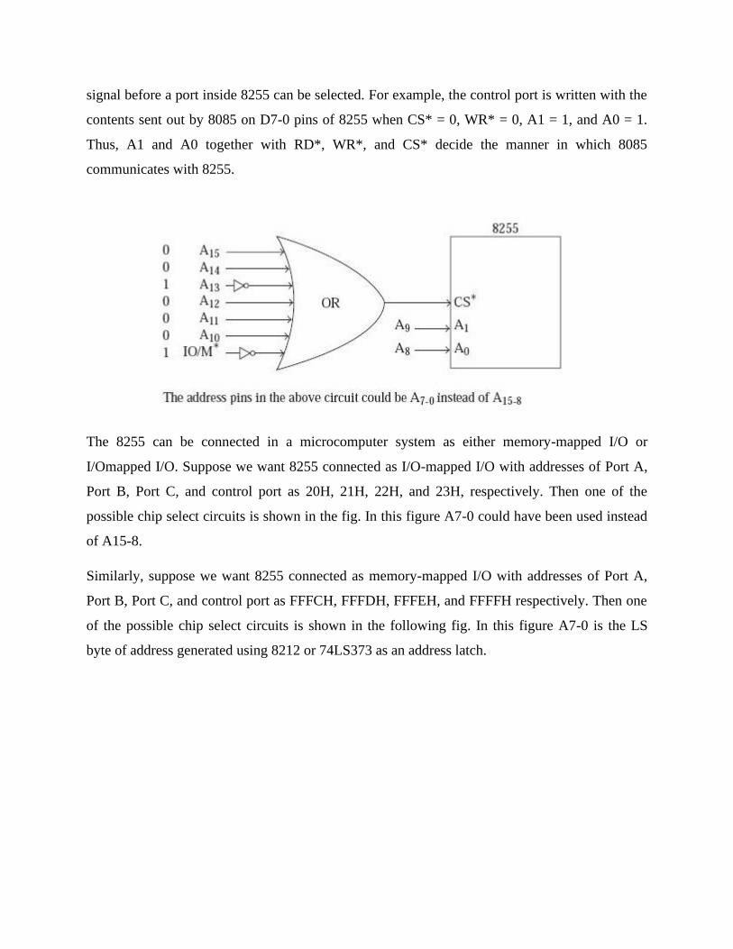
The 8255 can be connected in a microcomputer system as either memory-mapped I/O or
I/Omapped I/O. Suppose we want 8255 connected as I/O-mapped I/O with addresses of Port A,
Port B, Port C, and control port as 20H, 21H, 22H, and 23H, respectively. Then one of the
possible chip select circuits is shown in the fig. In this figure A7-0 could have been used instead
of A15-8.
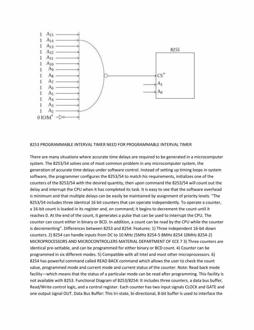
Similarly, suppose we want 8255 connected as memory-mapped I/O with addresses of Port A,
Port B, Port C, and control port as FFFCH, FFFDH, FFFEH, and FFFFH respectively. Then one
of the possible chip select circuits is shown in the following fig. In this figure A7-0 is the LS
byte of address generated using 8212 or 74LS373 as an address latch.
8253 PROGRAMMABLE INTERVAL TIMER NEED FOR PROGRAMMABLE INTERVAL TIMER
There are many situations where accurate time delays are required to be generated in a microcomputer
system. The 8253/54 solves one of most common problem in any microcomputer system, the
generation of accurate time delays under software control. Instead of setting up timing loops in system
software, the programmer configures the 8253/54 to match his requirements, initializes one of the
counters of the 8253/54 with the desired quantity, then upon command the 8253/54 will count out the
delay and interrupt the CPU when it has completed its task. It is easy to see that the software overhead
is minimum and that multiple delays can be easily be maintained by assignment of priority levels. “The
8253/54 includes three identical 16 bit counters that can operate independently. To operate a counter,
a 16-bit count is loaded in its register and, on command; it begins to decrement the count until it
reaches 0. At the end of the count, it generates a pulse that can be used to interrupt the CPU. The
counter can count either in binary or BCD. In addition, a count can be read by the CPU while the counter
is decrementing”. Differences between 8253 and 8254: Features: 1) Three independent 16-bit down
counters. 2) 8254 can handle inputs from DC to 10 MHz (5MHz 8254-5 8MHz 8254 10MHz 8254-2)
MICROPROCESSORS AND MICROCONTROLLERS MATERIAL DEPARTMENT OF ECE 7 3) Three counters are
identical pre-settable, and can be programmed for either binary or BCD count. 4) Counter can be
programmed in six different modes. 5) Compatible with all Intel and most other microprocessors. 6)
8254 has powerful command called READ BACK command which allows the user to check the count
value, programmed mode and current mode and current status of the counter. Note: Read back mode
facility—which means that the status of a particular mode can be read after programming. This facility is
not available with 8253. Functional Diagram of 8253/8254: It includes three counters, a data bus buffer,
Read/Write control logic, and a control register. Each counter has two input signals CLOCK and GATE and
one output signal OUT. Data Bus Buffer: This tri-state, bi-directional, 8-bit buffer is used to interface the

8253/54 to the system data bus. The Data bus buffer has three basic functions. 1. Programming the
modes of 8253/54. 2. Loading the count registers. 3. Reading the count values. Read/Write Logic: The
Read/Write logic has five signals: RD, WR, CS and the address lines A0 and A1. The control word register
and counters are selected according to the signals on lines A0 and A1. MICROPROCESSORS AND
MICROCONTROLLERS MA
Related Documents