ADC121S051 Single Channel, 200 to 500 ksps, 12-Bit A/D Converter General Description The ADC121S051 is a low-power, single channel CMOS 12-bit analog-to-digital converter with a high-speed serial interface. Unlike the conventional practice of specifying per- formance at a single sample rate only, the ADC121S051 is fully specified over a sample rate range of 200 ksps to 500 ksps. The converter is based upon a successive- approximation register architecture with an internal track- and-hold circuit. The output serial data is straight binary, and is compatible with several standards, such as SPI™, QSPI™, MICROWIRE, and many common DSP serial interfaces. The ADC121S051 operates with a single supply that can range from +2.7V to +5.25V. Normal power consumption using a +3.6V or +5.25V supply is 1.7 mW and 8.7 mW, respectively. The power-down feature reduces the power consumption to as low as 2.6 μW using a +5.25V supply. The ADC121S051 is packaged in 6-lead LLP and SOT-23 packages. Operation over the industrial temperature range of -40˚C to +85˚C is guaranteed. Features n Specified over a range of sample rates. n 6-lead LLP and SOT-23 packages n Variable power management n Single power supply with 2.7V - 5.25V range n SPI™/QSPI™/MICROWIRE/DSP compatible Key Specifications n DNL +0.5/-0.25 LSB (typ) n INL +0.45/-0.40 LSB (typ) n SNR 72.0 dB (typ) n Power Consumption — 3.6V Supply 1.7 mW (typ) — 5.25V Supply 8.7 mW (typ) Applications n Portable Systems n Remote Data Acquisition n Instrumentation and Control Systems Pin-Compatible Alternatives by Resolution and Speed All devices are fully pin and function compatible. Resolution Specified for Sample Rate Range of: 50 to 200 ksps 200 to 500 ksps 500 ksps to 1 Msps 12-bit ADC121S021 ADC121S051 ADC121S101 10-bit ADC101S021 ADC101S051 ADC101S101 8-bit ADC081S021 ADC081S051 ADC081S101 Connection Diagram 20144605 Ordering Information Order Code Temperature Range Description Top Mark ADC121S051CISD -40˚C to +85˚C 6-Lead LLP Package X4C ADC121S051CISDX -40˚C to +85˚C 6-Lead LLP Package, Tape and Reel X4C ADC121S051CIMF -40˚C to +85˚C 6-Lead SOT-23 Package X13C ADC121S051CIMFX -40˚C to +85˚C 6-Lead SOT-23 Package, Tape & Reel X13C ADC121S051EVAL SOT-23 Evaluation Board TRI-STATE ® is a trademark of National Semiconductor Corporation QSPI™ and SPI™ are trademarks of Motorola, Inc. February 2006 ADC121S051 Single Channel, 200 to 500 ksps, 12-Bit A/D Converter © 2006 National Semiconductor Corporation DS201446 www.national.com

Welcome message from author
This document is posted to help you gain knowledge. Please leave a comment to let me know what you think about it! Share it to your friends and learn new things together.
Transcript

ADC121S051Single Channel, 200 to 500 ksps, 12-Bit A/D ConverterGeneral DescriptionThe ADC121S051 is a low-power, single channel CMOS12-bit analog-to-digital converter with a high-speed serialinterface. Unlike the conventional practice of specifying per-formance at a single sample rate only, the ADC121S051 isfully specified over a sample rate range of 200 ksps to500 ksps. The converter is based upon a successive-approximation register architecture with an internal track-and-hold circuit.
The output serial data is straight binary, and is compatiblewith several standards, such as SPI™, QSPI™,MICROWIRE, and many common DSP serial interfaces.
The ADC121S051 operates with a single supply that canrange from +2.7V to +5.25V. Normal power consumptionusing a +3.6V or +5.25V supply is 1.7 mW and 8.7 mW,respectively. The power-down feature reduces the powerconsumption to as low as 2.6 µW using a +5.25V supply.
The ADC121S051 is packaged in 6-lead LLP and SOT-23packages. Operation over the industrial temperature rangeof −40˚C to +85˚C is guaranteed.
Featuresn Specified over a range of sample rates.n 6-lead LLP and SOT-23 packagesn Variable power managementn Single power supply with 2.7V - 5.25V rangen SPI™/QSPI™/MICROWIRE/DSP compatible
Key Specificationsn DNL +0.5/-0.25 LSB (typ)n INL +0.45/-0.40 LSB (typ)n SNR 72.0 dB (typ)n Power Consumption
— 3.6V Supply 1.7 mW (typ)— 5.25V Supply 8.7 mW (typ)
Applicationsn Portable Systemsn Remote Data Acquisitionn Instrumentation and Control Systems
Pin-Compatible Alternatives by Resolution and SpeedAll devices are fully pin and function compatible.
Resolution Specified for Sample Rate Range of:
50 to 200 ksps 200 to 500 ksps 500 ksps to 1 Msps
12-bit ADC121S021 ADC121S051 ADC121S101
10-bit ADC101S021 ADC101S051 ADC101S101
8-bit ADC081S021 ADC081S051 ADC081S101
Connection Diagram
20144605
Ordering InformationOrder Code Temperature Range Description Top Mark
ADC121S051CISD −40˚C to +85˚C 6-Lead LLP Package X4C
ADC121S051CISDX −40˚C to +85˚C 6-Lead LLP Package, Tape and Reel X4C
ADC121S051CIMF −40˚C to +85˚C 6-Lead SOT-23 Package X13C
ADC121S051CIMFX −40˚C to +85˚C 6-Lead SOT-23 Package, Tape & Reel X13C
ADC121S051EVAL SOT-23 Evaluation Board
TRI-STATE® is a trademark of National Semiconductor CorporationQSPI™ and SPI™ are trademarks of Motorola, Inc.
February 2006A
DC
121S051
Single
Channel,200
to500
ksps,12-Bit
A/D
Converter
© 2006 National Semiconductor Corporation DS201446 www.national.com

Block Diagram
20144607
Pin Descriptions and Equivalent Circuits
Pin No. Symbol Description
ANALOG I/O
3 VIN Analog input. This signal can range from 0V to VA.
DIGITAL I/O
4 SCLK Digital clock input. This clock directly controls the conversion and readout processes.
5 SDATADigital data output. The output samples are clocked out of this pin on falling edges ofthe SCLK pin.
6 CS Chip select. On the falling edge of CS, a conversion process begins.
POWER SUPPLY
1 VA
Positive supply pin. This pin should be connected to a quiet +2.7V to +5.25V sourceand bypassed to GND with a 1 µF capacitor and a 0.1 µF monolithic capacitor locatedwithin 1 cm of the power pin.
2 GND The ground return for the supply and signals.
PAD GNDFor package suffix CISD(X) only, it is recommended that the center pad should beconnected to ground.
AD
C12
1S05
1
www.national.com 2

Absolute Maximum Ratings (Notes 1, 2)
If Military/Aerospace specified devices are required,please contact the National Semiconductor Sales Office/Distributors for availability and specifications.
Analog Supply Voltage VA −0.3V to 6.5V
Voltage on Any Digital Pin to GND −0.3V to 6.5V
Voltage on Any Analog Pin to GND −0.3V to (VA +0.3V)
Input Current at Any Pin (Note 3) ±10 mA
Package Input Current (Note 3) ±20 mA
Power Consumption at TA = 25˚C See (Note 4)
ESD Susceptibility (Note 5)Human Body ModelMachine Model
3500V300V
Junction Temperature +150˚C
Storage Temperature −65˚C to +150˚C
Operating Ratings (Notes 1, 2)
Operating Temperature Range −40˚C ≤ TA ≤ +85˚C
VA Supply Voltage +2.7V to +5.25V
Digital Input Pins Voltage Range(regardless of supply voltage)
−0.3V to +5.25V
Analog Input Pins Voltage Range 0V to VA
Clock Frequency 1 MHz to 10 MHz
Sample Rate up to 500 ksps
Package Thermal ResistancePackage θJA
6-lead LLP 94˚C / W
6-lead SOT-23 265˚C / W
Soldering process must comply with National Semiconduc-tor’s Reflow Temperature Profile specifications. Refer towww.national.com/packaging. (Note 6)
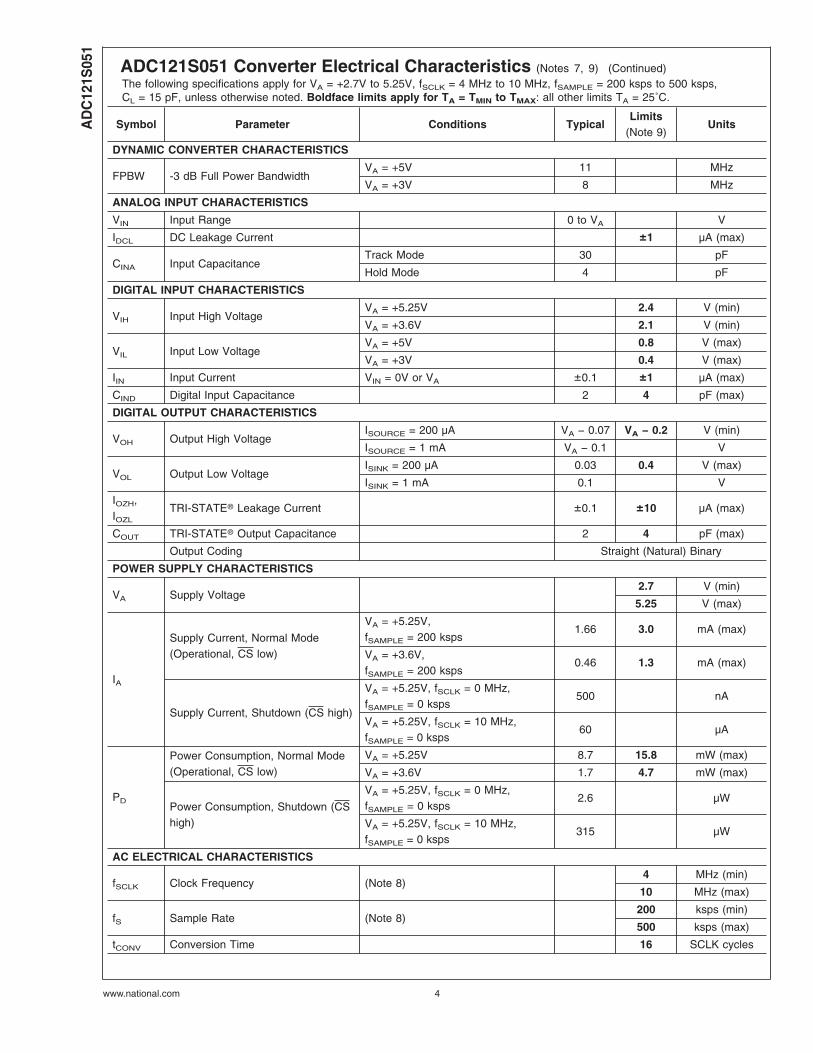
ADC121S051 Converter Electrical Characteristics (Notes 7, 9)
The following specifications apply for VA = +2.7V to 5.25V, fSCLK = 4 MHz to 10 MHz, fSAMPLE = 200 ksps to 500 ksps,CL = 15 pF, unless otherwise noted. Boldface limits apply for TA = TMIN to TMAX: all other limits TA = 25˚C.
Symbol Parameter Conditions TypicalLimits
(Note 9)Units
STATIC CONVERTER CHARACTERISTICS
Resolution with No Missing Codes 12 Bits
INL Integral Non-Linearity
VA = +2.7V to +3.6V+0.45
±1.0LSB (max)
−0.40 LSB (min)
VA = +4.75 to +5.25V+0.75 LSB (max)
−0.45 LSB (min)
DNL Differential Non-Linearity
VA = +2.7V to +3.6V+0.50 +1.0 LSB (max)
−0.25 −0.9 LSB (min)
VA = +4.75 to +5.25V+0.80 LSB (max)
−0.50 LSB (min)
VOFF Offset ErrorVA = +2.7V to +3.6V −0.18 ±1.2
LSB (max)VA = +4.75 to +5.25V +1.9
GE Gain ErrorVA = +2.7V to +3.6V −0.62 ±1.5
LSB (max)VA = +4.75 to +5.25V −1.50
DYNAMIC CONVERTER CHARACTERISTICS
SINAD Signal-to-Noise Plus Distortion RatioVA = +2.7V to 5.25VfIN = 100 kHz, −0.02 dBFS
72 70 dB (min)
SNR Signal-to-Noise RatioVA = +2.7V to 5.25VfIN = 100 kHz, −0.02 dBFS
72 70.8 dB (min)
THD Total Harmonic DistortionVA = +2.7V to 5.25VfIN = 100 kHz, −0.02 dBFS
−83 dB
SFDR Spurious-Free Dynamic RangeVA = +2.7V to 5.25VfIN = 100 kHz, −0.02 dBFS
84 dB
ENOB Effective Number of BitsVA = +2.7V to 5.25VfIN = 100 kHz, −0.02 dBFS
11.7 11.3 Bits (min)
IMD
Intermodulation Distortion, SecondOrder Terms
VA = +5.25Vfa = 103.5 kHz, fb = 113.5 kHz
−83 dB
Intermodulation Distortion, ThirdOrder Terms
VA = +5.25Vfa = 103.5 kHz, fb = 113.5 kHz
−82 dB
AD
C121S
051
www.national.com3
ADC121S051 Converter Electrical Characteristics (Notes 7, 9) (Continued)The following specifications apply for VA = +2.7V to 5.25V, fSCLK = 4 MHz to 10 MHz, fSAMPLE = 200 ksps to 500 ksps,CL = 15 pF, unless otherwise noted. Boldface limits apply for TA = TMIN to TMAX: all other limits TA = 25˚C.
Symbol Parameter Conditions TypicalLimits
(Note 9)Units
DYNAMIC CONVERTER CHARACTERISTICS
FPBW -3 dB Full Power BandwidthVA = +5V 11 MHz
VA = +3V 8 MHz
ANALOG INPUT CHARACTERISTICS
VIN Input Range 0 to VA V
IDCL DC Leakage Current ±1 µA (max)
CINA Input CapacitanceTrack Mode 30 pF
Hold Mode 4 pF
DIGITAL INPUT CHARACTERISTICS
VIH Input High VoltageVA = +5.25V 2.4 V (min)
VA = +3.6V 2.1 V (min)
VIL Input Low VoltageVA = +5V 0.8 V (max)
VA = +3V 0.4 V (max)
IIN Input Current VIN = 0V or VA ±0.1 ±1 µA (max)
CIND Digital Input Capacitance 2 4 pF (max)
DIGITAL OUTPUT CHARACTERISTICS
VOH Output High VoltageISOURCE = 200 µA VA − 0.07 VA − 0.2 V (min)
ISOURCE = 1 mA VA − 0.1 V
VOL Output Low VoltageISINK = 200 µA 0.03 0.4 V (max)
ISINK = 1 mA 0.1 V
IOZH,IOZL
TRI-STATE® Leakage Current ±0.1 ±10 µA (max)
COUT TRI-STATE® Output Capacitance 2 4 pF (max)
Output Coding Straight (Natural) Binary
POWER SUPPLY CHARACTERISTICS
VA Supply Voltage2.7 V (min)
5.25 V (max)
IA
Supply Current, Normal Mode(Operational, CS low)
VA = +5.25V,fSAMPLE = 200 ksps
1.66 3.0 mA (max)
VA = +3.6V,fSAMPLE = 200 ksps
0.46 1.3 mA (max)
Supply Current, Shutdown (CS high)
VA = +5.25V, fSCLK = 0 MHz,fSAMPLE = 0 ksps
500 nA
VA = +5.25V, fSCLK = 10 MHz,fSAMPLE = 0 ksps
60 µA
PD
Power Consumption, Normal Mode(Operational, CS low)
VA = +5.25V 8.7 15.8 mW (max)
VA = +3.6V 1.7 4.7 mW (max)
Power Consumption, Shutdown (CShigh)
VA = +5.25V, fSCLK = 0 MHz,fSAMPLE = 0 ksps
2.6 µW
VA = +5.25V, fSCLK = 10 MHz,fSAMPLE = 0 ksps
315 µW
AC ELECTRICAL CHARACTERISTICS
fSCLK Clock Frequency (Note 8)4 MHz (min)
10 MHz (max)
fS Sample Rate (Note 8)200 ksps (min)
500 ksps (max)
tCONV Conversion Time 16 SCLK cycles
AD
C12
1S05
1
www.national.com 4
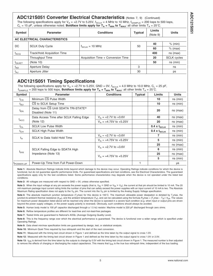
ADC121S051 Converter Electrical Characteristics (Notes 7, 9) (Continued)The following specifications apply for VA = +2.7V to 5.25V, fSCLK = 4 MHz to 10 MHz, fSAMPLE = 200 ksps to 500 ksps,CL = 15 pF, unless otherwise noted. Boldface limits apply for TA = TMIN to TMAX: all other limits TA = 25˚C.
Symbol Parameter Conditions TypicalLimits
(Note 9)Units
AC ELECTRICAL CHARACTERISTICS
DC SCLK Duty Cycle fSCLK = 10 MHz 5040 % (min)
60 % (max)
tACQ Track/Hold Acquisition Time 400 ns (max)
Throughput Time Acquisition Time + Conversion Time 20 SCLK cycles
tQUIET (Note 10) 50 ns (min)
tAD Aperture Delay 3 ns
tAJ Aperture Jitter 30 ps
ADC121S051 Timing SpecificationsThe following specifications apply for VA = +2.7V to 5.25V, GND = 0V, fSCLK = 4.0 MHz to 10.0 MHz, CL = 25 pF,fSAMPLE = 200 ksps to 500 ksps, Boldface limits apply for TA = TMIN to TMAX: all other limits TA = 25˚C.
Symbol Parameter Conditions Typical Limits Units
tCS Minimum CS Pulse Width 10 ns (min)
tSU CS to SCLK Setup Time 10 ns (min)
tENDelay from CS Until SDATA TRI-STATE®
Disabled (Note 11)20 ns (max)
tACCData Access Time after SCLK Falling Edge(Note 12)
VA = +2.7V to +3.6V 40 ns (max)
VA = +4.75V to +5.25V 20 ns (max)
tCL SCLK Low Pulse Width 0.4 x tSCLK ns (min)
tCH SCLK High Pulse Width 0.4 x tSCLK ns (min)
tH SCLK to Data Valid Hold TimeVA = +2.7V to +3.6V 7 ns (min)
VA = +4.75V to +5.25V 5 ns (min)
tDISSCLK Falling Edge to SDATA HighImpedance (Note 13)
VA = +2.7V to +3.6V25 ns (max)
6 ns (min)
VA = +4.75V to +5.25V25 ns (max)
5 ns (min)
tPOWER-UP Power-Up Time from Full Power-Down 1 µs
Note 1: Absolute Maximum Ratings indicate limits beyond which damage to the device may occur. Operating Ratings indicate conditions for which the device isfunctional, but do not guarantee specific performance limits. For guaranteed specifications and test conditions, see the Electrical Characteristics. The guaranteedspecifications apply only for the test conditions listed. Some performance characteristics may degrade when the device is not operated under the listed testconditions.
Note 2: All voltages are measured with respect to GND = 0V, unless otherwise specified.
Note 3: When the input voltage at any pin exceeds the power supply (that is, VIN < GND or VIN > VA), the current at that pin should be limited to 10 mA. The 20mA maximum package input current rating limits the number of pins that can safely exceed the power supplies with an input current of 10 mA to two. The AbsoluteMaximum Rating specification does not apply to the VA pin. The current into the VA pin is limited by the Analog Supply Voltage specification.
Note 4: The absolute maximum junction temperature (TJmax) for this device is 150˚C. The maximum allowable power dissipation is dictated by TJmax, thejunction-to-ambient thermal resistance (θJA), and the ambient temperature (TA), and can be calculated using the formula PDmax = (TJmax − TA) / θJA. The valuesfor maximum power dissipation listed above will be reached only when the device is operated in a severe fault condition (e.g. when input or output pins are drivenbeyond the power supply voltages, or the power supply polarity is reversed). Obviously, such conditions should always be avoided.
Note 5: Human body model is 100 pF capacitor discharged through a 1.5 kΩ resistor. Machine model is 220 pF discharged through zero ohms.
Note 6: Reflow temperature profiles are different for lead-free and non-lead-free packages.
Note 7: Tested limits are guaranteed to National’s AOQL (Average Outgoing Quality Level).
Note 8: This is the frequency range over which the electrical performance is guaranteed. The device is functional over a wider range which is specified underOperating Ratings.
Note 9: Data sheet min/max specification limits are guaranteed by design, test, or statistical analysis.
Note 10: Minimum Quiet Time required by bus relinquish and the start of the next conversion.
Note 11: Measured with the timing test circuit shown in Figure 1 and defined as the time taken by the output signal to cross 1.0V.
Note 12: Measured with the timing test circuit shown in Figure 1 and defined as the time taken by the output signal to cross 1.0V or 2.0V.
Note 13: tDIS is derived from the time taken by the outputs to change by 0.5V with the timing test circuit shown in Figure 1. The measured number is then adjustedto remove the effects of charging or discharging the output capacitance. This means that tDIS is the true bus relinquish time, independent of the bus loading.
AD
C121S
051
www.national.com5

Timing Diagrams
20144608
FIGURE 1. Timing Test Circuit
20144606
FIGURE 2. ADC121S051 Serial Timing Diagram
AD
C12
1S05
1
www.national.com 6
Specification DefinitionsACQUISITION TIME is the time required to acquire the inputvoltage. That is, it is time required for the hold capacitor tocharge up to the input voltage.
APERTURE DELAY is the time between the fourth fallingSCLK edge of a conversion and the time when the inputsignal is acquired or held for conversion.
APERTURE JITTER (APERTURE UNCERTAINTY) is thevariation in aperture delay from sample to sample. Aperturejitter manifests itself as noise in the output.
CONVERSION TIME is the time required, after the inputvoltage is acquired, for the ADC to convert the input voltageto a digital word.
DIFFERENTIAL NON-LINEARITY (DNL) is the measure ofthe maximum deviation from the ideal step size of 1 LSB.
DUTY CYCLE is the ratio of the time that a repetitive digitalwaveform is high to the total time of one period. The speci-fication here refers to the SCLK.
EFFECTIVE NUMBER OF BITS (ENOB, or EFFECTIVEBITS) is another method of specifying Signal-to-Noise andDistortion or SINAD. ENOB is defined as(SINAD − 1.76) / 6.02 and says that the converter is equiva-lent to a perfect ADC of this (ENOB) number of bits.
FULL POWER BANDWIDTH is a measure of the frequencyat which the reconstructed output fundamental drops 3 dBbelow its low frequency value for a full scale input.
GAIN ERROR is the deviation of the last code transition(111...110) to (111...111) from the ideal (VREF − 1.5 LSB),after adjusting for offset error.
INTEGRAL NON-LINEARITY (INL) is a measure of thedeviation of each individual code from a line drawn fromnegative full scale (1⁄2 LSB below the first code transition)through positive full scale (1⁄2 LSB above the last codetransition). The deviation of any given code from this straightline is measured from the center of that code value.
INTERMODULATION DISTORTION (IMD) is the creation ofadditional spectral components as a result of two sinusoidalfrequencies being applied to the ADC input at the same time.It is defined as the ratio of the power in the second and thirdorder intermodulation products to the sum of the power inboth of the original frequencies. IMD is usually expressed indB.
MISSING CODES are those output codes that will neverappear at the ADC outputs. The ADC121S051 is guaranteednot to have any missing codes.
OFFSET ERROR is the deviation of the first code transition(000...000) to (000...001) from the ideal (i.e. GND + 0.5LSB).
SIGNAL TO NOISE RATIO (SNR) is the ratio, expressed indB, of the rms value of the input signal to the rms value of thesum of all other spectral components below one-half thesampling frequency, not including harmonics or d.c.
SIGNAL TO NOISE PLUS DISTORTION (S/N+D or SINAD)Is the ratio, expressed in dB, of the rms value of the inputsignal to the rms value of all of the other spectral compo-nents below half the clock frequency, including harmonicsbut excluding d.c.
SPURIOUS FREE DYNAMIC RANGE (SFDR) is the differ-ence, expressed in dB, between the desired signal ampli-tude to the amplitude of the peak spurious spectral compo-nent, where a spurious spectral component is any signalpresent in the output spectrum that is not present at the inputand may or may not be a harmonic.
TOTAL HARMONIC DISTORTION (THD) is the ratio, ex-pressed in dB or dBc, of the rms total of the first fiveharmonic components at the output to the rms level of theinput signal frequency as seen at the output. THD is calcu-lated as
where Af1 is the RMS power of the input frequency at theoutput and Af2 through Af6 are the RMS power in the first 5harmonic frequencies.
THROUGHPUT TIME is the minimum time required betweenthe start of two successive conversion. It is the acquisitiontime plus the conversion time.
AD
C121S
051
www.national.com7

Typical Performance Characteristics TA = +25˚C, fSAMPLE = 200 ksps to 500 ksps,fSCLK = 4 MHz to 10 MHz, fIN = 100 kHz unless otherwise stated.
DNLfSCLK = 4 MHz
INLfSCLK = 4 MHz
20144620 20144621
DNLfSCLK = 10 MHz
INLfSCLK = 10 MHz
20144660 20144661
DNL vs. Clock Frequency INL vs. Clock Frequency
20144665 20144666
AD
C12
1S05
1
www.national.com 8

Typical Performance Characteristics TA = +25˚C, fSAMPLE = 200 ksps to 500 ksps,fSCLK = 4 MHz to 10 MHz, fIN = 100 kHz unless otherwise stated. (Continued)
SNR vs. Clock Frequency SINAD vs. Clock Frequency
20144663 20144664
SFDR vs. Clock Frequency THD vs. Clock Frequency
20144667 20144668
Spectral Response, VA = 5.25VfSCLK = 4 MHz
Spectral Response, VA = 5.25VfSCLK = 10 MHz
20144669 20144670
AD
C121S
051
www.national.com9

Typical Performance Characteristics TA = +25˚C, fSAMPLE = 200 ksps to 500 ksps,fSCLK = 4 MHz to 10 MHz, fIN = 100 kHz unless otherwise stated. (Continued)
Power Consumption vs. Throughput,fSCLK = 10 MHz
20144655
AD
C12
1S05
1
www.national.com 10

Applications Information
1.0 ADC121S051 OPERATION
The ADC121S051 is a successive-approximation analog-to-digital converters designed around a charge-redistributiondigital-to-analog converter core. Simplified schematics of theADC121S051 in both track and hold modes are shown inFigure 3 and Figure 4, respectively. In Figure 3, the device isin track mode: switch SW1 connects the sampling capacitorto the input, and SW2 balances the comparator inputs. Thedevice is in this state until CS is brought low, at which pointthe device moves to the hold mode.
Figure 4 shows the device in hold mode: switch SW1 con-nects the sampling capacitor to ground, maintaining thesampled voltage, and switch SW2 unbalances the compara-tor. The control logic then instructs the charge-redistributionDAC to add or subtract fixed amounts of charge from thesampling capacitor until the comparator is balanced. Whenthe comparator is balanced, the digital word supplied to theDAC is the digital representation of the analog input voltage.The device moves from hold mode to track mode on the 13thrising edge of SCLK.
2.0 USING THE ADC121S051
The serial interface timing diagram for the ADC121S051 isshown in Figure 2. CS is chip select, which initiates conver-sions on the ADC121S051 and frames the serial data trans-fers. SCLK (serial clock) controls both the conversion pro-cess and the timing of serial data. SDATA is the serial dataout pin, where a conversion result is found as a serial datastream.
Basic operation of the ADC121S051 begins with CS goinglow, which initiates a conversion process and data transfer.Subsequent rising and falling edges of SCLK will be labelledwith reference to the falling edge of CS; for example, "thethird falling edge of SCLK" shall refer to the third falling edgeof SCLK after CS goes low.
At the fall of CS, the SDATA pin comes out of TRI-STATE,and the converter moves from track mode to hold mode. Theinput signal is sampled and held for conversion on the falling
edge of CS. The converter moves from hold mode to trackmode on the 13th rising edge of SCLK (see Figure 2). TheSDATA pin will be placed back into TRI-STATE after the 16thfalling edge of SCLK, or at the rising edge of CS, whicheveroccurs first. After a conversion is completed, the quiet time(tQUIET) must be satisfied before bringing CS low again tobegin another conversion.
Sixteen SCLK cycles are required to read a completesample from the ADC121S051. The sample bits (includingleading zeroes) are clocked out on falling edges of SCLK,and are intended to be clocked in by a receiver on subse-quent falling edges of SCLK. The ADC121S051 will producethree leading zero bits on SDATA, followed by twelve databits, most significant first.
If CS goes low before the rising edge of SCLK, an additional(fourth) zero bit may be captured by the next falling edge ofSCLK.
20144609
FIGURE 3. ADC121S051 in Track Mode
20144610
FIGURE 4. ADC121S051 in Hold Mode
AD
C121S
051
www.national.com11

Applications Information (Continued)
3.0 ADC121S051 TRANSFER FUNCTION
The output format of the ADC121S051 is straight binary.Code transitions occur midway between successive integerLSB values. The LSB width for the ADC121S051 is VA/4096.The ideal transfer characteristic is shown in Figure 5. Thetransition from an output code of 0000 0000 0000 to a codeof 0000 0000 0001 is at 1/2 LSB, or a voltage of VA/8192.Other code transitions occur at steps of one LSB.
4.0 TYPICAL APPLICATION CIRCUIT
A typical application of the ADC121S051 is shown inFigure 6. Power is provided in this example by the NationalSemiconductor LP2950 low-dropout voltage regulator, avail-able in a variety of fixed and adjustable output voltages. Thepower supply pin is bypassed with a capacitor network lo-cated close to the ADC121S051. Because the reference forthe ADC121S051 is the supply voltage, any noise on thesupply will degrade device noise performance. To keep noiseoff the supply, use a dedicated linear regulator for this de-vice, or provide sufficient decoupling from other circuitry tokeep noise off the ADC121S051 supply pin. Because of theADC121S051’s low power requirements, it is also possible touse a precision reference as a power supply to maximizeperformance. The three-wire interface is shown connected toa microprocessor or DSP.
5.0 ANALOG INPUTS
An equivalent circuit for the ADC121S051’s input is shown inFigure 7. Diodes D1 and D2 provide ESD protection for theanalog inputs. At no time should the analog input go beyond(VA + 300 mV) or (GND − 300 mV), as these ESD diodes willbegin conducting, which could result in erratic operation.
The capacitor C1 in Figure 7 has a typical value of 4 pF, andis mainly the package pin capacitance. Resistor R1 is the onresistance of the track / hold switch, and is typically 500ohms. Capacitor C2 is the ADC121S051 sampling capacitorand is typically 26 pF. The ADC121S051 will deliver bestperformance when driven by a low-impedance source toeliminate distortion caused by the charging of the samplingcapacitance. This is especially important when using theADC121S051 to sample AC signals. Also important whensampling dynamic signals is an anti-aliasing filter.
6.0 DIGITAL INPUTS AND OUTPUTS
The ADC121S051 digital inputs (SCLK and CS) are notlimited by the same maximum ratings as the analog inputs.The digital input pins are instead limited to +5.25V withrespect to GND, regardless of VA, the supply voltage. Thisallows the ADC121S051 to be interfaced with a wide rangeof logic levels, independent of the supply voltage.
7.0 MODES OF OPERATION
The ADC121S051 has two possible modes of operation:normal mode, and shutdown mode. The ADC121S051 en-ters normal mode (and a conversion process is begun) whenCS is pulled low. The device will enter shutdown mode if CSis pulled high before the tenth falling edge of SCLK after CSis pulled low, or will stay in normal mode if CS remains low.Once in shutdown mode, the device will stay there until CS isbrought low again. By varying the ratio of time spent in thenormal and shutdown modes, a system may trade-offthroughput for power consumption, with a sample rate as lowas zero.
7.1 Normal Mode
The fastest possible throughput is obtained by leaving theADC121S051 in normal mode at all times, so there are nopower-up delays. To keep the device in normal mode con-tinuously, CS must be kept low until after the 10th fallingedge of SCLK after the start of a conversion (remember thata conversion is initiated by bringing CS low).
If CS is brought high after the 10th falling edge, but beforethe 16th falling edge, the device will remain in normal mode,but the current conversion will be aborted, and SDATA willreturn to TRI-STATE (truncating the output word).
Sixteen SCLK cycles are required to read all of a conversionword from the device. After sixteen SCLK cycles have
20144611
FIGURE 5. Ideal Transfer Characteristic
20144613
FIGURE 6. Typical Application Circuit
20144614
FIGURE 7. Equivalent Input Circuit
AD
C12
1S05
1
www.national.com 12

Applications Information (Continued)
elapsed, CS may be idled either high or low until the nextconversion. If CS is idled low, it must be brought high againbefore the start of the next conversion, which begins whenCS is again brought low.
After sixteen SCLK cycles, SDATA returns to TRI-STATE.Another conversion may be started, after tQUIET haselapsed, by bringing CS low again.
7.2 Shutdown Mode
Shutdown mode is appropriate for applications that either donot sample continuously, or it is acceptable to trade through-put for power consumption. When the ADC121S051 is inshutdown mode, all of the analog circuitry is turned off.
To enter shutdown mode, a conversion must be interruptedby bringing CS high anytime between the second and tenthfalling edges of SCLK, as shown in Figure 8. Once CS hasbeen brought high in this manner, the device will entershutdown mode; the current conversion will be aborted andSDATA will enter TRI-STATE. If CS is brought high before thesecond falling edge of SCLK, the device will not changemode; this is to avoid accidentally changing mode as a resultof noise on the CS line.
To exit shutdown mode, bring CS back low. Upon bringingCS low, the ADC121S051 will begin powering up (power-uptime is specified in the Timing Specifications table). Thispower-up delay results in the first conversion result beingunusable. The second conversion performed after power-up,however, is valid, as shown in Figure 9.
If CS is brought back high before the 10th falling edge ofSCLK, the device will return to shutdown mode. This is doneto avoid accidentally entering normal mode as a result ofnoise on the CS line. To exit shutdown mode and remain innormal mode, CS must be kept low until after the 10th fallingedge of SCLK. The ADC121S051 will be fully powered-upafter 16 SCLK cycles.
8.0 POWER MANAGEMENT
The ADC121S051 takes time to power-up, either after firstapplying VA, or after returning to normal mode from shut-down mode. This corresponds to one "dummy" conversionfor any SCLK frequency within the specifications in thisdocument. After this first dummy conversion, theADC121S051 will perform conversions properly. Note thatthe tQUIET time must still be included between the firstdummy conversion and the second valid conversion.
When the VA supply is first applied, the ADC121S051 maypower up in either of the two modes: normal or shutdown. Assuch, one dummy conversion should be performed afterstart-up, as described in the previous paragraph. The partmay then be placed into either normal mode or the shutdownmode, as described in Sections 7.1 and 7.2.
When the ADC121S051 is operated continuously in normalmode, the maximum throughput is fSCLK / 20. Throughputmay be traded for power consumption by running fSCLK at itsmaximum specified rate and performing fewer conversionsper unit time, raising the ADC121S051 CS line after the 10thand before the 15th fall of SCLK of each conversion. A plot oftypical power consumption versus throughput is shown inthe Typical Performance Curves section. To calculate thepower consumption for a given throughput, multiply the frac-tion of time spent in the normal mode by the normal modepower consumption and add the fraction of time spent inshutdown mode multiplied by the shutdown mode powerconsumption. Note that the curve of power consumption vs.throughput is essentially linear. This is because the powerconsumption in the shutdown mode is so small that it can beignored for all practical purposes.
20144616
FIGURE 8. Entering Shutdown Mode
20144617
FIGURE 9. Entering Normal Mode
AD
C121S
051
www.national.com13

Applications Information (Continued)
9.0 POWER SUPPLY NOISE CONSIDERATIONS
The charging of any output load capacitance requires cur-rent from the power supply, VA. The current pulses requiredfrom the supply to charge the output capacitance will causevoltage variations on the supply. If these variations are largeenough, they could degrade SNR and SINAD performanceof the ADC. Furthermore, discharging the output capaci-tance when the digital output goes from a logic high to a logiclow will dump current into the die substrate, which is resis-tive. Load discharge currents will cause "ground bounce"
noise in the substrate that will degrade noise performance ifthat current is large enough. The larger the output capaci-tance, the more current flows through the die substrate andthe greater is the noise coupled into the analog channel,degrading noise performance.
To keep noise out of the power supply, keep the output loadcapacitance as small as practical. It is good practice to use a100 Ω series resistor at the ADC output, located as close tothe ADC output pin as practical. This will limit the charge anddischarge current of the output capacitance and improvenoise performance.
AD
C12
1S05
1
www.national.com 14

Physical Dimensions inches (millimeters) unless otherwise noted
6-Lead LLPOrder Number ADC121S051CISD or ADC121S051CISDX
NS Package Number SDB06A
6-Lead SOT-23Order Number ADC121S051CIMF, ADC121S051CIMFX
NS Package Number MF06A
AD
C121S
051
www.national.com15

Notes
National does not assume any responsibility for use of any circuitry described, no circuit patent licenses are implied and National reservesthe right at any time without notice to change said circuitry and specifications.
For the most current product information visit us at www.national.com.
LIFE SUPPORT POLICY
NATIONAL’S PRODUCTS ARE NOT AUTHORIZED FOR USE AS CRITICAL COMPONENTS IN LIFE SUPPORT DEVICES OR SYSTEMSWITHOUT THE EXPRESS WRITTEN APPROVAL OF THE PRESIDENT AND GENERAL COUNSEL OF NATIONAL SEMICONDUCTORCORPORATION. As used herein:
1. Life support devices or systems are devices or systemswhich, (a) are intended for surgical implant into the body, or(b) support or sustain life, and whose failure to perform whenproperly used in accordance with instructions for useprovided in the labeling, can be reasonably expected to resultin a significant injury to the user.
2. A critical component is any component of a life supportdevice or system whose failure to perform can be reasonablyexpected to cause the failure of the life support device orsystem, or to affect its safety or effectiveness.
BANNED SUBSTANCE COMPLIANCE
National Semiconductor manufactures products and uses packing materials that meet the provisions of the Customer ProductsStewardship Specification (CSP-9-111C2) and the Banned Substances and Materials of Interest Specification (CSP-9-111S2) and containno ‘‘Banned Substances’’ as defined in CSP-9-111S2.
Leadfree products are RoHS compliant.
National SemiconductorAmericas CustomerSupport CenterEmail: [email protected]: 1-800-272-9959
National SemiconductorEurope Customer Support Center
Fax: +49 (0) 180-530 85 86Email: [email protected]
Deutsch Tel: +49 (0) 69 9508 6208English Tel: +44 (0) 870 24 0 2171Français Tel: +33 (0) 1 41 91 8790
National SemiconductorAsia Pacific CustomerSupport CenterEmail: [email protected]
National SemiconductorJapan Customer Support CenterFax: 81-3-5639-7507Email: [email protected]: 81-3-5639-7560
www.national.com
AD
C12
1S05
1S
ingl
eC
hann
el,2
00to
500
ksps
,12-
Bit
A/D
Con
vert
er
Related Documents