EECS 247 Lecture 19: Data Converters © 2004 H.K. Page 1 EE247 Lecture 19 ADC Converters - ADC architectures - Comparator architectures • High gain amplifier with differential analog input & single-ended large swing output • Latched comparators; in response to a strobe, input stage disabled & digital output stored in a latch till next strobe • Sample-data comparators – Offset cancellation EECS 247 Lecture 19: Data Converters © 2004 H.K. Page 2 ADC Architectures • Slope Converters • Successive approximation • Flash • Folding • Time-interleaved / parallel converter • Residue type ADCs – Two-step – Pipeline – Algorithmic –… • Oversampled ADCs

Welcome message from author
This document is posted to help you gain knowledge. Please leave a comment to let me know what you think about it! Share it to your friends and learn new things together.
Transcript
EECS 247 Lecture 19: Data Converters © 2004 H.K. Page 1
EE247Lecture 19
ADC Converters- ADC architectures- Comparator architectures
• High gain amplifier with differential analog input & single-ended large swing output
• Latched comparators; in response to a strobe, input stage disabled & digital output stored in a latch till next strobe
• Sample-data comparators– Offset cancellation
EECS 247 Lecture 19: Data Converters © 2004 H.K. Page 2
ADC Architectures• Slope Converters• Successive approximation• Flash• Folding• Time-interleaved / parallel converter• Residue type ADCs
– Two-step– Pipeline– Algorithmic– …
• Oversampled ADCs
EECS 247 Lecture 19: Data Converters © 2004 H.K. Page 3
Residue Type ADC
• Quantization error output (“residuum”) enables cascading for higher resolution
• Great flexibility for stages: flash, oversampling ADC, …• Optional S/H enables parallelism (pipelining)• Fast: one clock per conversion (with S/H), latency
S/H & Gain(optional)
coarse ADC(1 ... 6 Bit)
Partial Digital Output
VIN
ErrorDAC
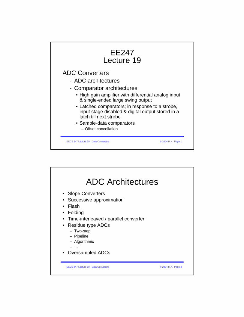
EECS 247 Lecture 19: Data Converters © 2004 H.K. Page 4
Pipelined ADC
• Approaches speed of flash, but much lower complexity• One clock per conversion, but K clocks latency• Efficient digital calibration possible• Versatile: from 16Bits / 1MS/s to 14Bits / 100MS/s
Digital Correction Logic
Stage 1B1 Bits
Stage 2B2 Bits
Stage KBk Bits
Digital outputup to (B1 + B2 + ... + Bk) Bits
VIN
EECS 247 Lecture 19: Data Converters © 2004 H.K. Page 5
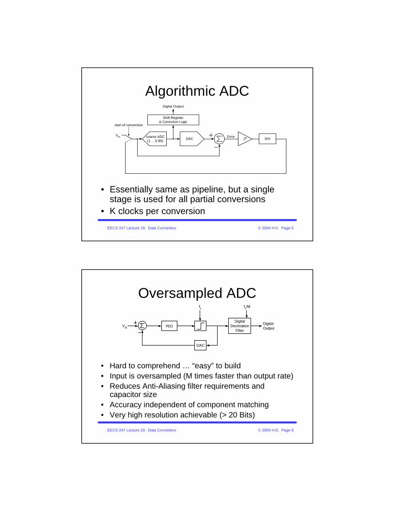
Algorithmic ADC
• Essentially same as pipeline, but a single stage is used for all partial conversions
• K clocks per conversion
S/H coarse ADC (1 ... 6 Bit)
Digital Output
VIN ErrorDAC
Shift Register& Correction Logic
start of conversion
2B
EECS 247 Lecture 19: Data Converters © 2004 H.K. Page 6
Oversampled ADC
• Hard to comprehend … “easy” to build• Input is oversampled (M times faster than output rate)• Reduces Anti-Aliasing filter requirements and
capacitor size• Accuracy independent of component matching• Very high resolution achievable (> 20 Bits)
H(z)Digital
DecimationFilter
DAC
VINDigitalOutput
fs fs/M

EECS 247 Lecture 19: Data Converters © 2004 H.K. Page 7
Throughput Rate Comparison
100
101
102
103
104
105
0
2
4
6
8
10
12
14
16
18
Clock Cycles per Conversion
Res
olut
ion
[Bit
]
Fla
sh, P
ipel
ine~
1 to
2
Suc
cess
ive
App
roxi
mat
ion~
B2
ndO
rder
1-B
it
Ove
rsam
pled
~2(0
.4B+
1)
Serial ~2B
EECS 247 Lecture 19: Data Converters © 2004 H.K. Page 8
Speed-Resolution Map
[www.v-corp.com]
EECS 247 Lecture 19: Data Converters © 2004 H.K. Page 9
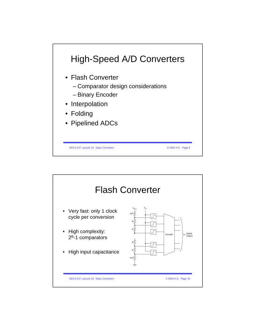
High-Speed A/D Converters
• Flash Converter– Comparator design considerations– Binary Encoder
• Interpolation• Folding• Pipelined ADCs
EECS 247 Lecture 19: Data Converters © 2004 H.K. Page 10
Flash Converter
• Very fast: only 1 clock cycle per conversion
• High complexity: 2B-1 comparators
• High input capacitance
R/2
R
R
R
R/2
R
Encoder DigitalOutput
VINVREF
EECS 247 Lecture 19: Data Converters © 2004 H.K. Page 11
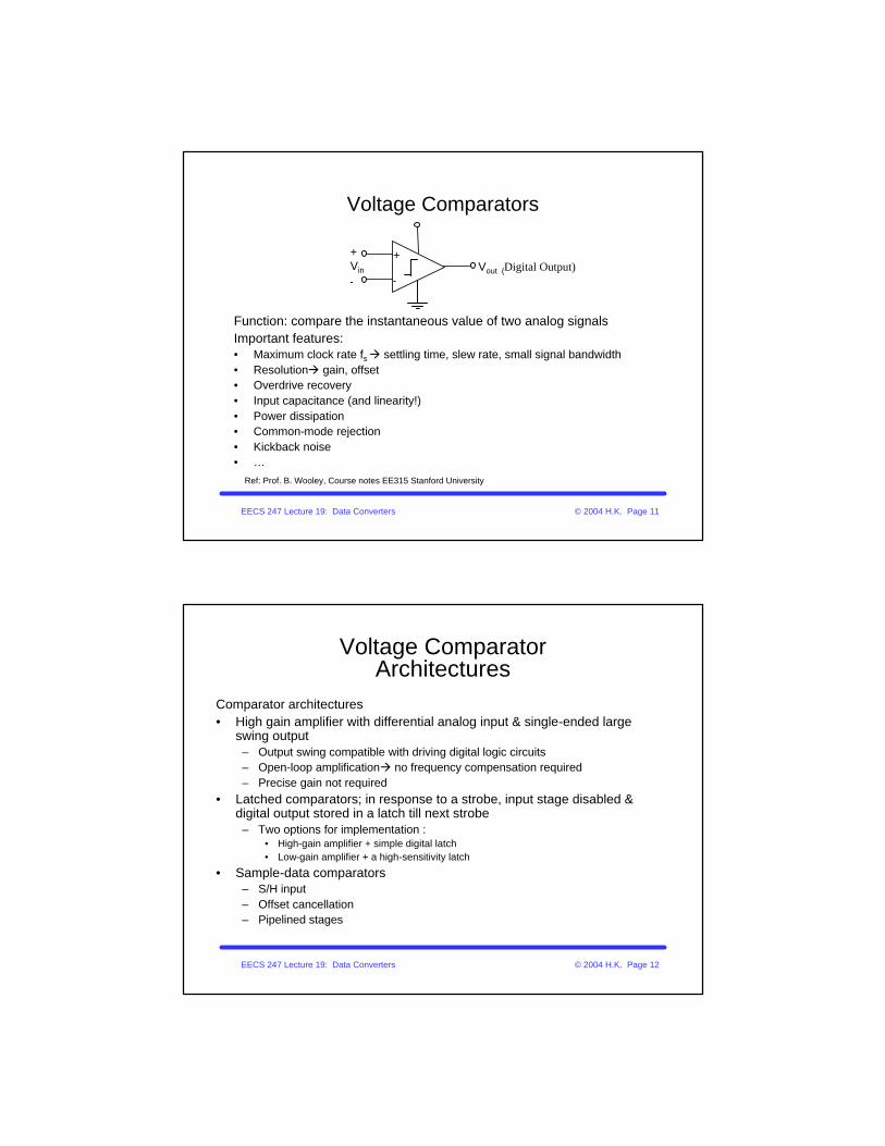
Voltage Comparators
Function: compare the instantaneous value of two analog signalsImportant features:• Maximum clock rate fs à settling time, slew rate, small signal bandwidth• Resolutionà gain, offset• Overdrive recovery• Input capacitance (and linearity!)• Power dissipation• Common-mode rejection• Kickback noise• …
+Vin-
+
-Vout (Digital Output)
Ref: Prof. B. Wooley, Course notes EE315 Stanford University
EECS 247 Lecture 19: Data Converters © 2004 H.K. Page 12
Voltage ComparatorArchitectures
Comparator architectures• High gain amplifier with differential analog input & single-ended large
swing output– Output swing compatible with driving digital logic circuits– Open-loop amplificationà no frequency compensation required– Precise gain not required
• Latched comparators; in response to a strobe, input stage disabled & digital output stored in a latch till next strobe– Two options for implementation :
• High-gain amplifier + simple digital latch• Low-gain amplifier + a high-sensitivity latch
• Sample-data comparators– S/H input– Offset cancellation– Pipelined stages

EECS 247 Lecture 19: Data Converters © 2004 H.K. Page 13
Comparators w/ High-Gain Amplification
Amplify Vin(min) to VDD
Vin(min) determined by ADC resolution
Example: 12-bit res. & full-scale input 2Và 1LSB=0.5mV
à For 2.5V output:
v
os
2.5VA 10,000
0.25mV
V 1 LSB
= =
<
EECS 247 Lecture 19: Data Converters © 2004 H.K. Page 14
Comparators w/ High-Gain Amplification
Too slow!à Cascade of lower gain stages to broadband response
fu=10-1000MHz
0
0
V
0 0
=unity gain frequency, 3 frequency
1100
10,000
11.6 sec
2
u
u
f f dB
f GHzf kHz
A
fτ µ
π
= −
= = =
= =
EECS 247 Lecture 19: Data Converters © 2004 H.K. Page 15
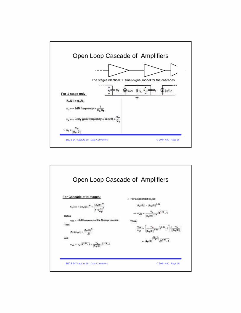
Open Loop Cascade of Amplifiers
The stages identical à small-signal model for the cascades:
For 1-stage only:
EECS 247 Lecture 19: Data Converters © 2004 H.K. Page 16
Open Loop Cascade of Amplifiers
For Cascade of N-stages:
EECS 247 Lecture 19: Data Converters © 2004 H.K. Page 17
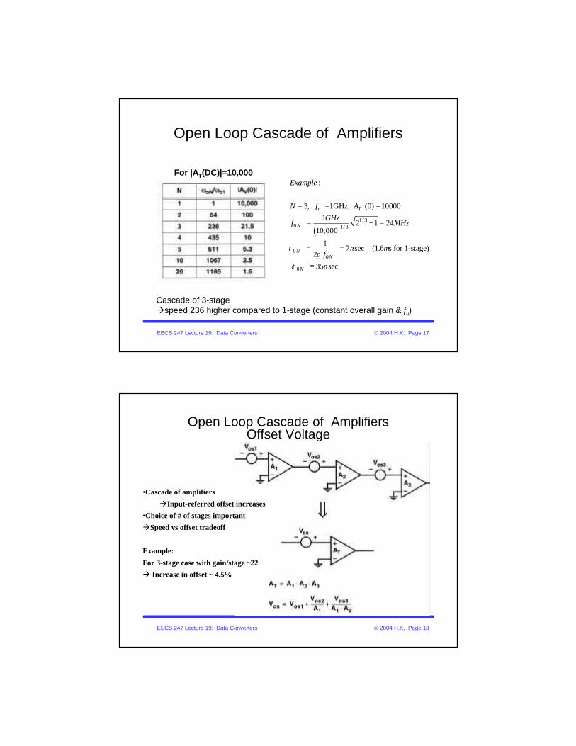
Open Loop Cascade of Amplifiers
For |AT(DC)|=10,000
( )
T
1 /30 1/ 3
0 0
0
:
3, =1GHz, (0) 10000
12 1 24
10,000
17 sec (1.6 s for 1-stage)
2
5 35 sec
u
N
NN
N
Example
N f A
GHzf MHz
nf
n
τ µπ
τ
= =
= − =
= =
=
Cascade of 3-stage àspeed 236 higher compared to 1-stage (constant overall gain & fu)
EECS 247 Lecture 19: Data Converters © 2004 H.K. Page 18
Open Loop Cascade of AmplifiersOffset Voltage
•Cascade of amplifiers
àInput-referred offset increases
•Choice of # of stages important
àSpeed vs offset tradeoff
Example:
For 3-stage case with gain/stage ~22
à Increase in offset ~ 4.5%

EECS 247 Lecture 19: Data Converters © 2004 H.K. Page 19
Open Loop Cascade of AmplifiersStep Response
•Assuming linear behavior
t
EECS 247 Lecture 19: Data Converters © 2004 H.K. Page 20
Open Loop Cascade of AmplifiersStep Response
•Assuming linear behavior
EECS 247 Lecture 19: Data Converters © 2004 H.K. Page 21
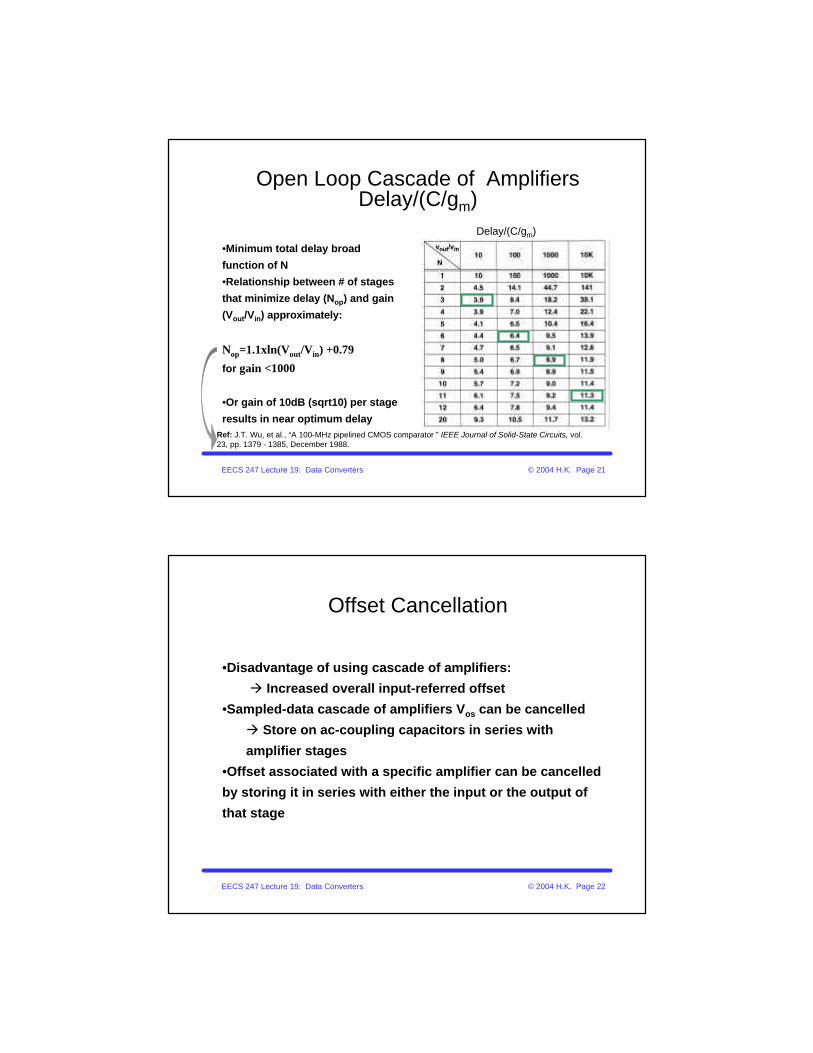
Open Loop Cascade of AmplifiersDelay/(C/gm)
•Minimum total delay broad
function of N
•Relationship between # of stages
that minimize delay (Nop) and gain
(Vout/Vin) approximately:
Nop=1.1xln(Vout/Vin) +0.79
for gain <1000
•Or gain of 10dB (sqrt10) per stage
results in near optimum delay
Delay/(C/gm)
Ref: J.T. Wu, et al., “A 100-MHz pipelined CMOS comparator ” IEEE Journal of Solid-State Circuits, vol. 23, pp. 1379 - 1385, December 1988.
EECS 247 Lecture 19: Data Converters © 2004 H.K. Page 22
Offset Cancellation
•Disadvantage of using cascade of amplifiers:
à Increased overall input-referred offset
•Sampled-data cascade of amplifiers Vos can be cancelled
à Store on ac-coupling capacitors in series with
amplifier stages
•Offset associated with a specific amplifier can be cancelled
by storing it in series with either the input or the output of
that stage

EECS 247 Lecture 19: Data Converters © 2004 H.K. Page 23
Offset CancellationOutput Series Cancellation
•Amp modeled as ideal +
Vos (input referred)
•Store offset:
•S1, S4è open
•S2, S3à closed
à VC=AxVOS
EECS 247 Lecture 19: Data Converters © 2004 H.K. Page 24
Offset CancellationOutput Series Cancellation
Amplify:
•S1, S4è closed
•S2, S3à open
àVC=AxVOS
Circuit requirements:
•Amp not saturate during offset
storage
•High-impedance (C) load à Cc
not discharged
•Cc >> CL to avoid attenuation
•Cc >> Cswitch offset due to charge
injection

EECS 247 Lecture 19: Data Converters © 2004 H.K. Page 25
Offset CancellationCascaded Output Series Cancellation
Note: Extra offset cancellation phase requiredà Overall speed compromised
EECS 247 Lecture 19: Data Converters © 2004 H.K. Page 26
Offset CancellationCascaded Output Series Cancellation
1- S1à open, S2,3,4,5 closed
VC1=A1xVos1
VC2=A2xVos2
VC3=A3xVos3
EECS 247 Lecture 19: Data Converters © 2004 H.K. Page 27
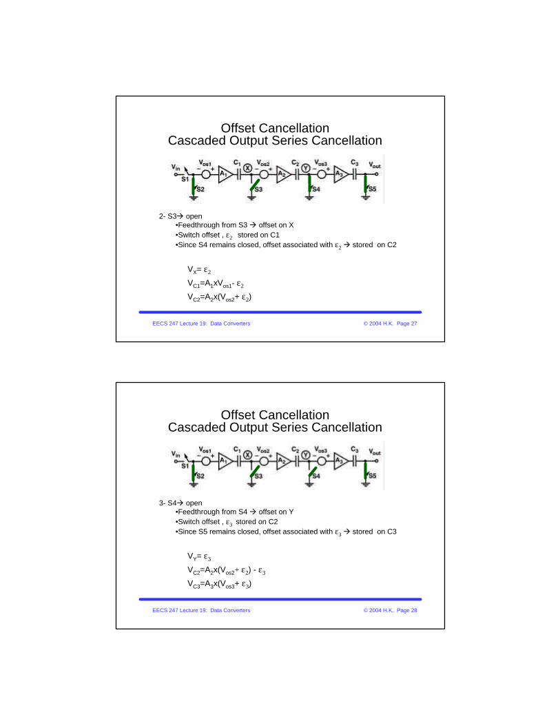
Offset CancellationCascaded Output Series Cancellation
2- S3à open•Feedthrough from S3 à offset on X•Switch offset , ε2 stored on C1•Since S4 remains closed, offset associated with ε2à stored on C2
VX= ε2
VC1=A1xVos1- ε2
VC2=A2x(Vos2+ ε2)
EECS 247 Lecture 19: Data Converters © 2004 H.K. Page 28
Offset CancellationCascaded Output Series Cancellation
3- S4à open•Feedthrough from S4 à offset on Y•Switch offset , ε3 stored on C2•Since S5 remains closed, offset associated with ε3à stored on C3
VY= ε3
VC2=A2x(Vos2+ ε2) - ε3
VC3=A3x(Vos3+ ε3)
EECS 247 Lecture 19: Data Converters © 2004 H.K. Page 29
Offset CancellationCascaded Output Series Cancellation
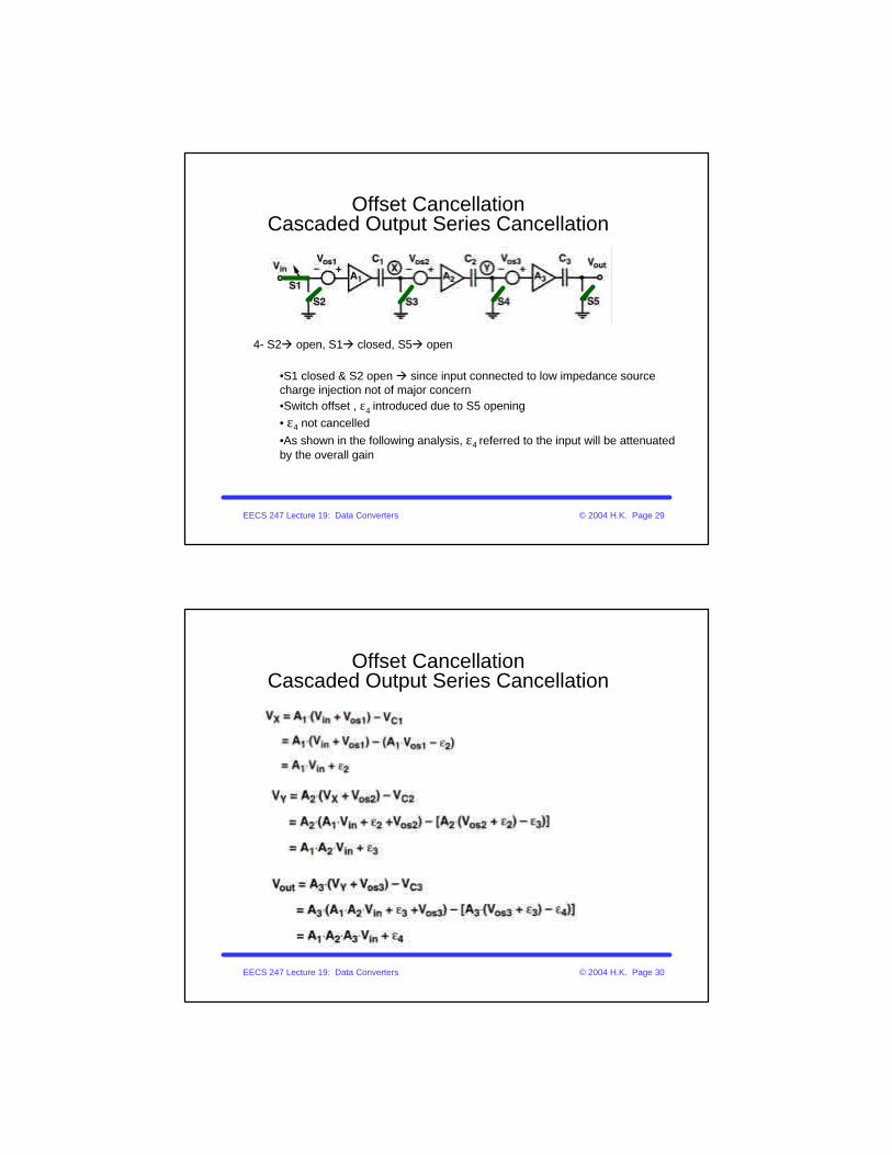
4- S2à open, S1à closed, S5à open
•S1 closed & S2 open à since input connected to low impedance source charge injection not of major concern•Switch offset , ε4 introduced due to S5 opening• ε4 not cancelled •As shown in the following analysis, ε4 referred to the input will be attenuated by the overall gain
EECS 247 Lecture 19: Data Converters © 2004 H.K. Page 30
Offset CancellationCascaded Output Series Cancellation
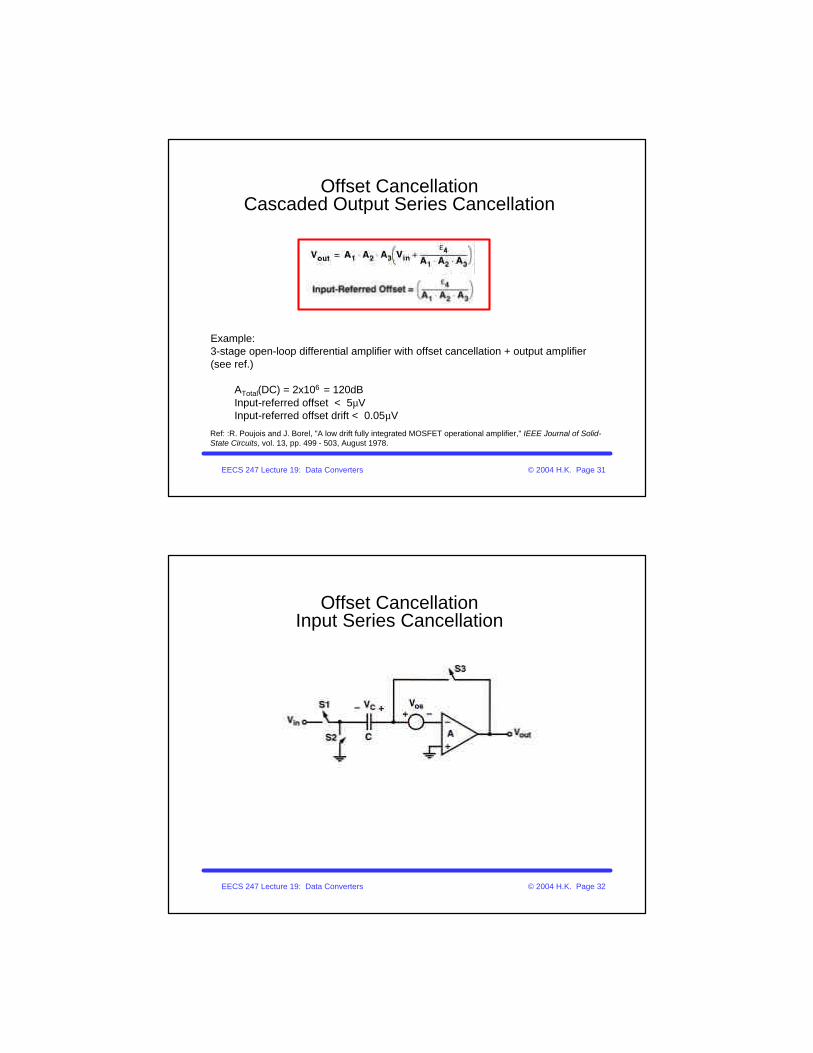
EECS 247 Lecture 19: Data Converters © 2004 H.K. Page 31
Offset CancellationCascaded Output Series Cancellation
Example: 3-stage open-loop differential amplifier with offset cancellation + output amplifier (see ref.)
ATotal(DC) = 2x106 = 120dBInput-referred offset < 5µVInput-referred offset drift < 0.05µV
Ref: :R. Poujois and J. Borel, "A low drift fully integrated MOSFET operational amplifier," IEEE Journal of Solid-State Circuits, vol. 13, pp. 499 - 503, August 1978.
EECS 247 Lecture 19: Data Converters © 2004 H.K. Page 32
Offset CancellationInput Series Cancellation
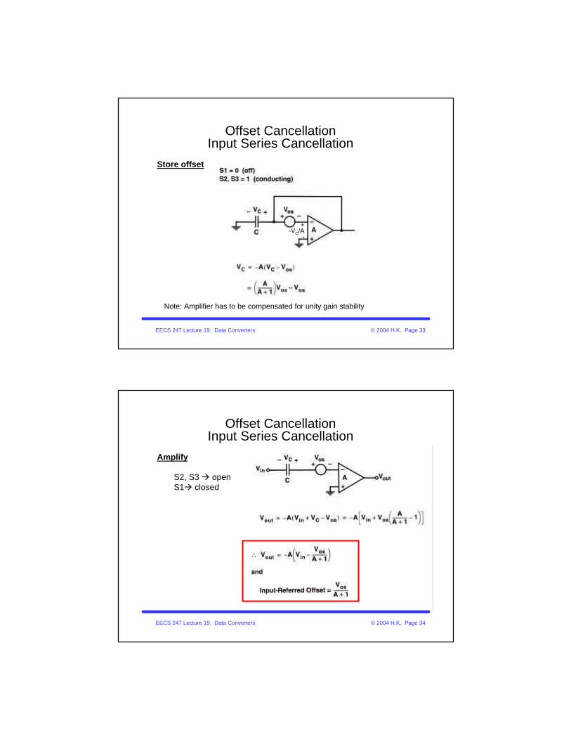
EECS 247 Lecture 19: Data Converters © 2004 H.K. Page 33
Offset CancellationInput Series Cancellation
Store offset
+-VC/A
-
Note: Amplifier has to be compensated for unity gain stability
EECS 247 Lecture 19: Data Converters © 2004 H.K. Page 34
Offset CancellationInput Series Cancellation
Amplify
S2, S3 à openS1à closed

EECS 247 Lecture 19: Data Converters © 2004 H.K. Page 35
Offset CancellationCascaded Input Series Cancellation
ε2àopening of S4 charge injection
àAmplifier A1 offset à fully cancelledàAmplifier A2 offset à attenuated by 1/A1.A2àError associated with opening of S4 charge injection attenuated by 1/A1
EECS 247 Lecture 19: Data Converters © 2004 H.K. Page 36
CMOS ComparatorsCascade of Gain Stages
Fully differential gain stages à 1st order cancellation of switch feedthrough & charge injection offsets
1-Output series offset cancellation
2- Input series offset cancellation
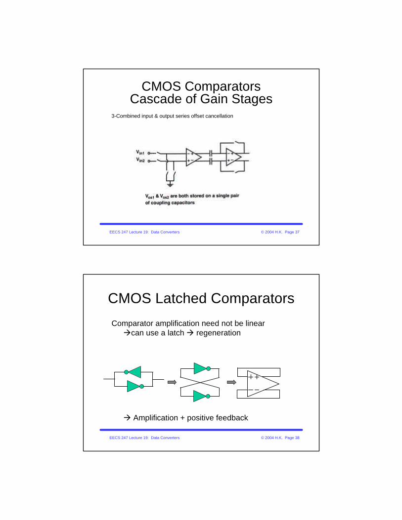
EECS 247 Lecture 19: Data Converters © 2004 H.K. Page 37
CMOS ComparatorsCascade of Gain Stages
3-Combined input & output series offset cancellation
EECS 247 Lecture 19: Data Converters © 2004 H.K. Page 38
CMOS Latched Comparators
Comparator amplification need not be linearàcan use a latch à regeneration
à Amplification + positive feedback

EECS 247 Lecture 19: Data Converters © 2004 H.K. Page 39
CMOS Latched Comparators
Latch can be modeled as a single-pole amp + positive feedback
EECS 247 Lecture 19: Data Converters © 2004 H.K. Page 40
CMOS Latched ComparatorsDelay
Compared to a 3-stage open-loop cascade of amps for equal gain of 1000
àLatch faster by about x3Only drawback à high latch offset (typically 10- 100mV)àUse preamp w/gain =10-100 to reduce input-referred latch offsetàOr use offset cancellation
τD(3-state amp)= 18.2(C/gm)
Normalized Latch Delay
EECS 247 Lecture 19: Data Converters © 2004 H.K. Page 41
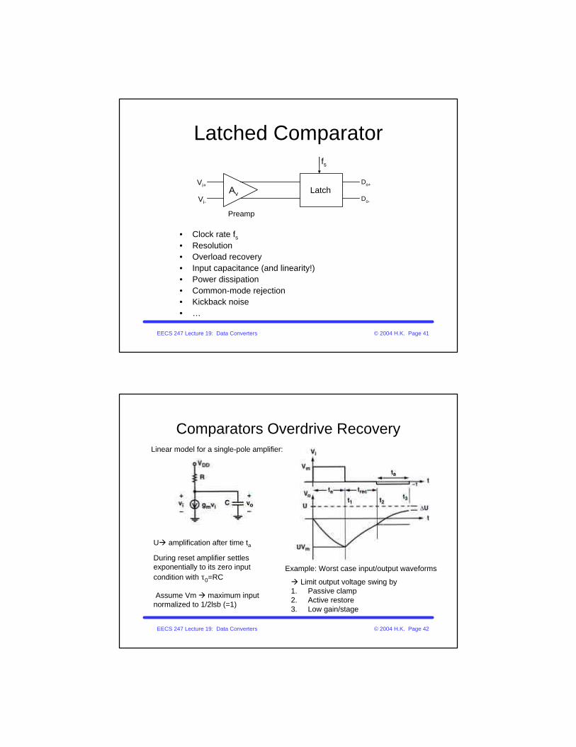
Latched Comparator
• Clock rate fs• Resolution• Overload recovery• Input capacitance (and linearity!)• Power dissipation• Common-mode rejection• Kickback noise• …
Av LatchVi+
Vi-
Do+
Do-
fs
Preamp
EECS 247 Lecture 19: Data Converters © 2004 H.K. Page 42
Comparators Overdrive Recovery
Uà amplification after time ta
During reset amplifier settles exponentially to its zero input condition with τ0=RC
Assume Vm à maximum input normalized to 1/2lsb (=1)
Linear model for a single-pole amplifier:
Example: Worst case input/output waveforms
à Limit output voltage swing by1. Passive clamp2. Active restore3. Low gain/stage
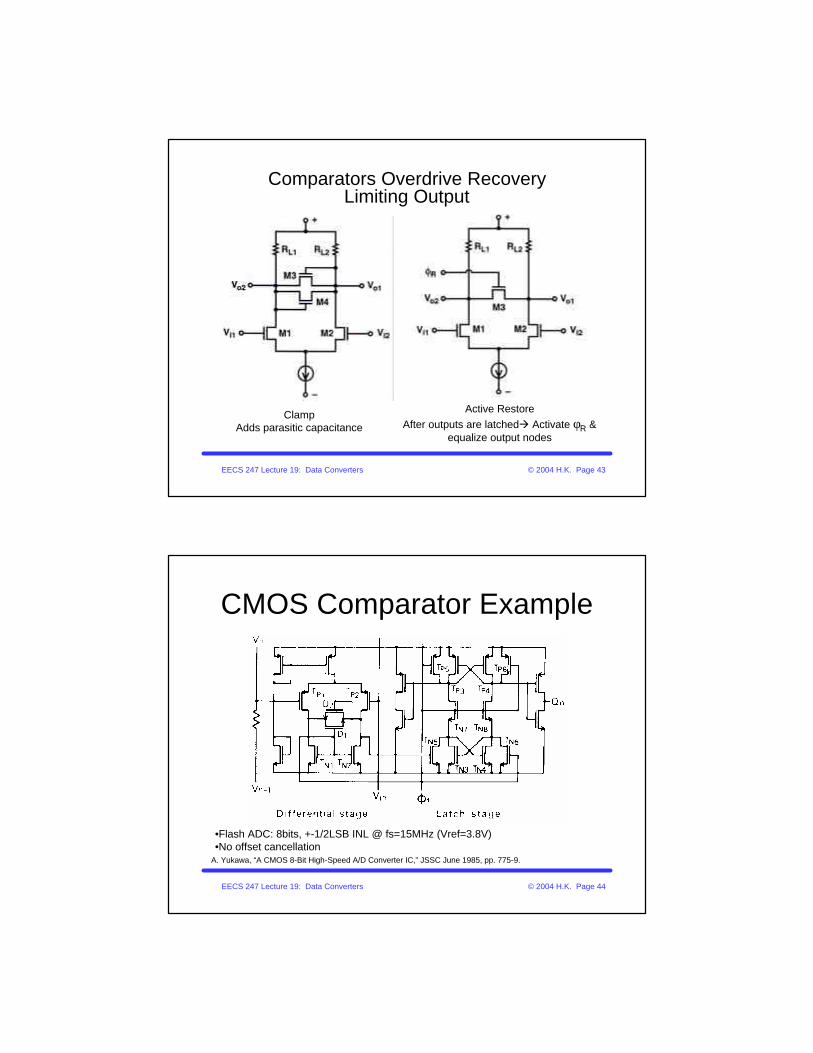
EECS 247 Lecture 19: Data Converters © 2004 H.K. Page 43
Comparators Overdrive RecoveryLimiting Output
ClampAdds parasitic capacitance
Active RestoreAfter outputs are latchedà Activate φR &
equalize output nodes
EECS 247 Lecture 19: Data Converters © 2004 H.K. Page 44
CMOS Comparator Example
A. Yukawa, “A CMOS 8-Bit High-Speed A/D Converter IC,” JSSC June 1985, pp. 775-9.
•Flash ADC: 8bits, +-1/2LSB INL @ fs=15MHz (Vref=3.8V)•No offset cancellation

EECS 247 Lecture 19: Data Converters © 2004 H.K. Page 45
Comparator with Auto-Zero
I. Mehr and L. Singer, “A 500-Msample/s, 6-Bit Nyquist-Rate ADC for Disk-Drive Read-Channel Applications,” JSSC July 1999, pp. 912-20.
EECS 247 Lecture 19: Data Converters © 2004 H.K. Page 46
Auto-Zero Implementation
Ref:I. Mehr and L. Singer, “A 55-mW, 10-bit, 40-Msample/s Nyquist-Rate CMOS ADC,” JSSC March 2000, pp. 318-25.
EECS 247 Lecture 19: Data Converters © 2004 H.K. Page 47
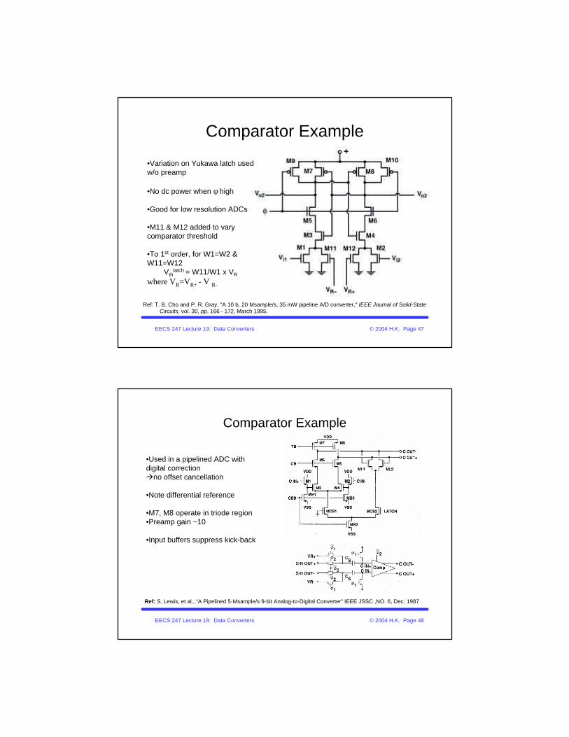
Comparator Example
Ref: T. B. Cho and P. R. Gray, "A 10 b, 20 Msample/s, 35 mW pipeline A/D converter," IEEE Journal of Solid-State Circuits, vol. 30, pp. 166 - 172, March 1995.
•Variation on Yukawa latch used w/o preamp
•No dc power when φ high
•Good for low resolution ADCs
•M11 & M12 added to vary comparator threshold
•To 1st order, for W1=W2 & W11=W12
Vthlatch = W11/W1 x VR
where VR=VR+ - V R-
EECS 247 Lecture 19: Data Converters © 2004 H.K. Page 48
Comparator Example
•Used in a pipelined ADC with digital correctionàno offset cancellation
•Note differential reference
•M7, M8 operate in triode region•Preamp gain ~10
•Input buffers suppress kick-back
Ref: S. Lewis, et al., “A Pipelined 5-Msample/s 9-bit Analog-to-Digital Converter” IEEE JSSC ,NO. 6, Dec. 1987
EECS 247 Lecture 19: Data Converters © 2004 H.K. Page 49
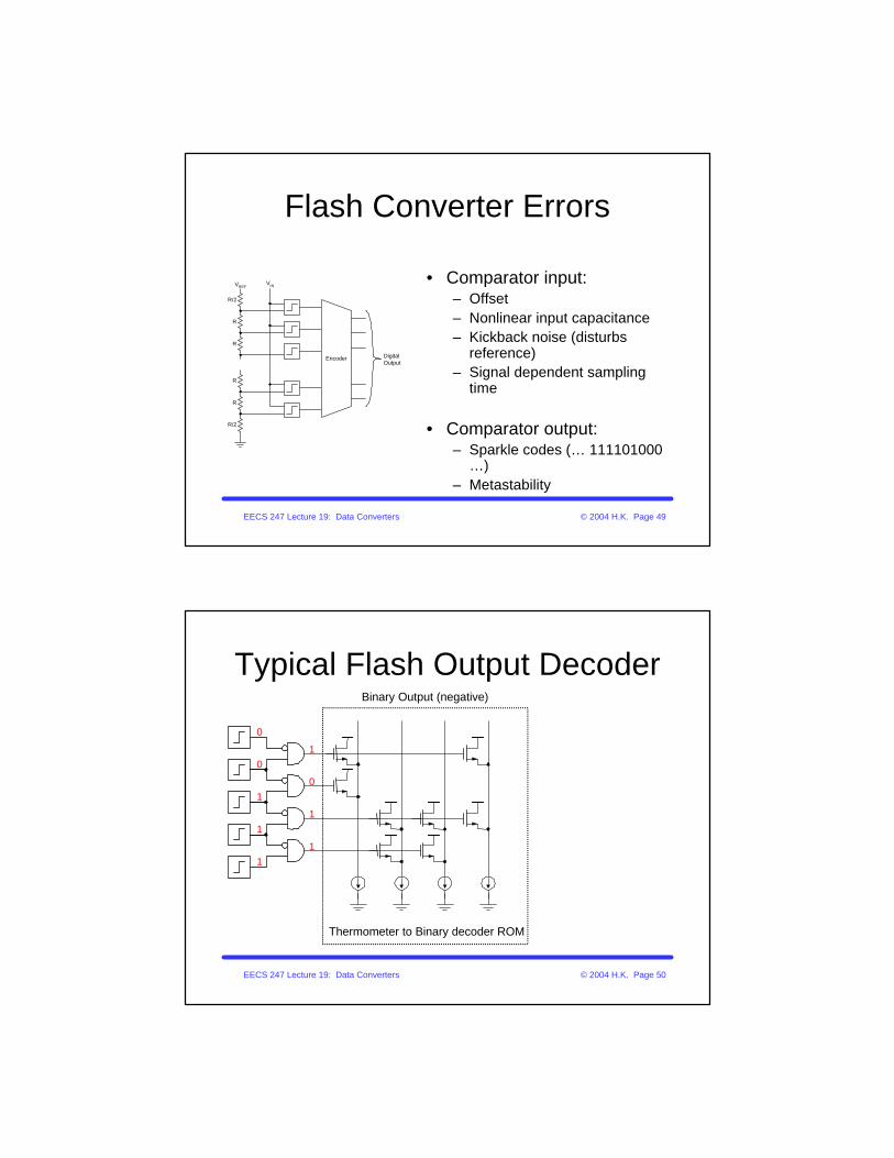
Flash Converter Errors
• Comparator input:– Offset– Nonlinear input capacitance– Kickback noise (disturbs
reference)– Signal dependent sampling
time
• Comparator output:– Sparkle codes (… 111101000
…)– Metastability
R/2
R
R
R
R/2
R
Encoder DigitalOutput
VINVREF
EECS 247 Lecture 19: Data Converters © 2004 H.K. Page 50
Typical Flash Output Decoder
0
0
1
1
1
1
0
1
1
Binary Output (negative)
Thermometer to Binary decoder ROM
EECS 247 Lecture 19: Data Converters © 2004 H.K. Page 51
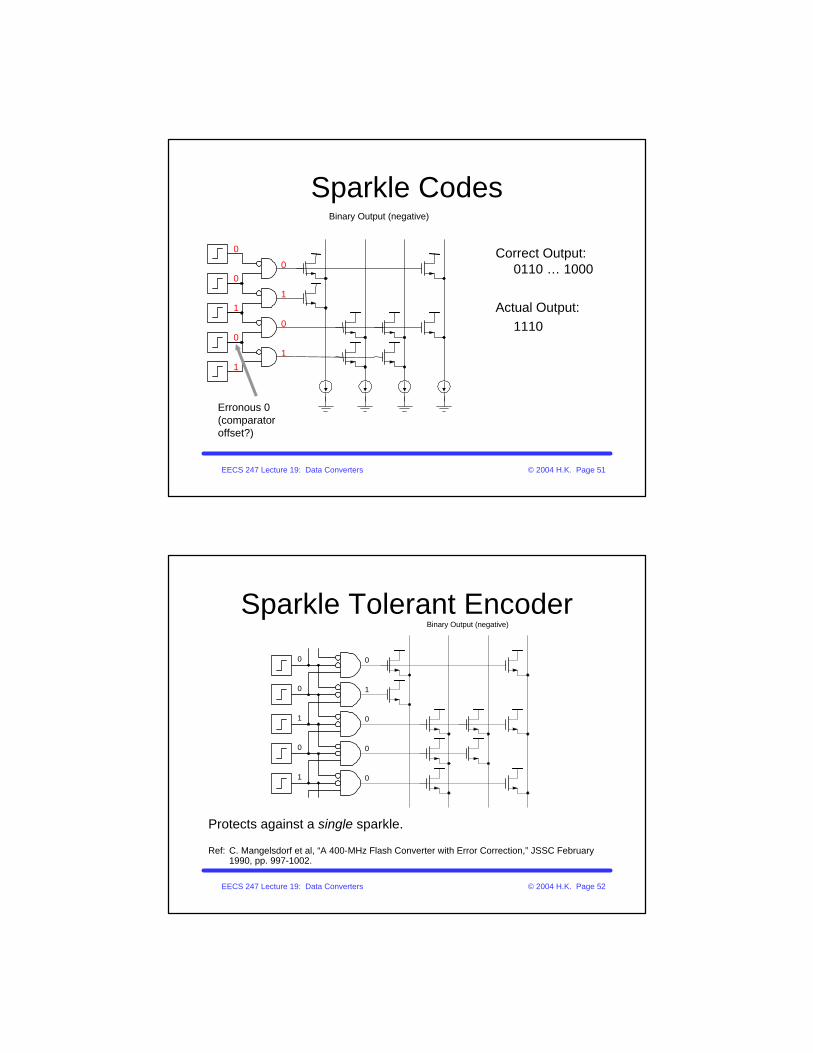
Sparkle Codes
Correct Output:0110 … 1000
Actual Output:1110
0
0
1
0
1
0
1
0
1
Binary Output (negative)
Erronous 0 (comparator offset?)
EECS 247 Lecture 19: Data Converters © 2004 H.K. Page 52
Sparkle Tolerant Encoder
0
0
1
0
1
0
1
0
0
Binary Output (negative)
0
Protects against a single sparkle.
Ref: C. Mangelsdorf et al, “A 400-MHz Flash Converter with Error Correction,” JSSC February 1990, pp. 997-1002.
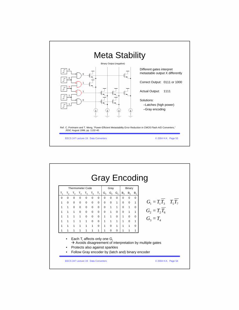
EECS 247 Lecture 19: Data Converters © 2004 H.K. Page 53
Meta StabilityDifferent gates interpret metastable output X differently
Correct Output: 0111 or 1000
Actual Output: 1111
Solutions:–Latches (high power)–Gray encoding
0
0
X
1
1
0
1
1
0
Binary Output (negative)
Ref: C. Portmann and T. Meng, “Power-Efficient Metastability Error Reduction in CMOS Flash A/D Converters,” JSSC August 1996, pp. 1132-40.
EECS 247 Lecture 19: Data Converters © 2004 H.K. Page 54
Gray Encoding
• Each Ti affects only one Già Avoids disagreement of interpretation by multiple gates
• Protects also against sparkles• Follow Gray encoder by (latch and) binary encoder
BinaryGrayThermometer Code
1110011111111
0111010111111
1011110011111
0010110001111
1100100000111
0101100000011
1001000000001
0000000000000
B1B2B3G1G2G3T7T6T5T4T3T2T1
43
622
75311
TGTTG
TTTTG
==
+=
Related Documents