Int. J. Electron. Commun. (AEÜ) 62 (2008) 740 – 753 www.elsevier.de/aeue Adaptive digital phase modulation schemes using transition-initiated phase acceleration Rajarshi Mahapatra ∗ , Anindya Sundar Dhar, Debasish Datta Department of Electronics and Electrical Communication Engineering, Indian Institute of Technology, Kharagpur 721 302, India Received 16 November 2006; accepted 24 September 2007 Abstract Link adaptation (LA) schemes, where signal transmission features, such as, modulation, coding rate, etc. are dynamically selected based on the feedback information from receiver regarding the channel condition, have recently emerged as powerful tools for increasing data rate and spectral efficiency of wireless networks. In this paper, we examine an adaptive modulation scheme for LA, based on digital phase-modulation techniques, employing a novel phase-shifting scheme. In the proposed technique, the abrupt phase shift of carrier waveform, required after each data transition, is realized by incrementing the frequency of the voltage-controlled oscillator (VCO) for a short duration, immediately following the data transition. The momentary increase in VCO frequency is realized by feeding the VCO with narrow control pulses, derived from the baseband data stream using a simple supporting circuit. The proposed technique can be used for very large scale integration (VLSI) of adaptive modulation schemes, and one such candidate scheme has been designed for VLSI implementation with triple options of binary phase-shift keying (BPSK), quadrature PSK (QPSK), and quadrature amplitude modulation (QAM). 2007 Elsevier GmbH. All rights reserved. Keywords: BPSK; QPSK; QAM; VCO; VLSI; Transition-initiated phase acceleration (TIPA); BER; Link adaptation 1. Introduction In recent years, wireless communications industry has gone through unprecedented developments in both fixed and mobile applications. Continued increase in demand for all types of wireless services (voice, data, and multime- dia) have fuelled the need for higher capacity. Although improved compression technologies have reduced the band- width needed for voice calls, data traffic will demand much more bandwidth as new services come on-line. The wireless data channels are subject to significant interference and fad- ing, resulting in widely varying received signal quality. Sig- nal variation occurs due to three major causes: variation of received signal strength with distance from the transmitter, shadow fading caused by large obstructions and Rayleigh ∗ Corresponding author. E-mail address: [email protected] (R. Mahapatra). 1434-8411/$ - see front matter 2007 Elsevier GmbH. All rights reserved. doi:10.1016/j.aeue.2007.09.011 fading caused by local scatterers around the receiver [1,2]. Furthermore, in packet-based data systems, the bursty nature of data traffic also causes rapid changes in the interference characteristics. In order to handle such rapid variation in signal conditions, techniques that adapt the bit rate, trans- mission power and other transmission features/parameters to channel conditions are being proposed for next-generation wireless system. In this context, emerging technologies that can improve wireless spectrum efficiency are becoming a necessity, especially in broadband applications. One useful approach in this direction is to employ link adaptation (LA) [3] using smart antennas with adaptive beam formation [4], in particular the multiple-input multiple-output (MIMO) technology [5], coded multi-carrier modulation, and trans- mission schemes using dynamic modulation and coding techniques [6]. The basic idea behind LA techniques is to adapt the trans- mission parameters to cope up with the prevailing channel

Welcome message from author
This document is posted to help you gain knowledge. Please leave a comment to let me know what you think about it! Share it to your friends and learn new things together.
Transcript
Int. J. Electron. Commun. (AEÜ) 62 (2008) 740–753
www.elsevier.de/aeue
Adaptive digital phase modulation schemes using transition-initiated phaseacceleration
Rajarshi Mahapatra∗, Anindya Sundar Dhar, Debasish Datta
Department of Electronics and Electrical Communication Engineering, Indian Institute of Technology, Kharagpur 721 302, India
Received 16 November 2006; accepted 24 September 2007
Abstract
Link adaptation (LA) schemes, where signal transmission features, such as, modulation, coding rate, etc. are dynamicallyselected based on the feedback information from receiver regarding the channel condition, have recently emerged as powerfultools for increasing data rate and spectral efficiency of wireless networks. In this paper, we examine an adaptive modulationscheme for LA, based on digital phase-modulation techniques, employing a novel phase-shifting scheme. In the proposedtechnique, the abrupt phase shift of carrier waveform, required after each data transition, is realized by incrementing thefrequency of the voltage-controlled oscillator (VCO) for a short duration, immediately following the data transition. Themomentary increase in VCO frequency is realized by feeding the VCO with narrow control pulses, derived from the basebanddata stream using a simple supporting circuit. The proposed technique can be used for very large scale integration (VLSI)of adaptive modulation schemes, and one such candidate scheme has been designed for VLSI implementation with tripleoptions of binary phase-shift keying (BPSK), quadrature PSK (QPSK), and quadrature amplitude modulation (QAM).� 2007 Elsevier GmbH. All rights reserved.
Keywords: BPSK; QPSK; QAM; VCO; VLSI; Transition-initiated phase acceleration (TIPA); BER; Link adaptation
1. Introduction
In recent years, wireless communications industry hasgone through unprecedented developments in both fixedand mobile applications. Continued increase in demand forall types of wireless services (voice, data, and multime-dia) have fuelled the need for higher capacity. Althoughimproved compression technologies have reduced the band-width needed for voice calls, data traffic will demand muchmore bandwidth as new services come on-line. The wirelessdata channels are subject to significant interference and fad-ing, resulting in widely varying received signal quality. Sig-nal variation occurs due to three major causes: variation ofreceived signal strength with distance from the transmitter,shadow fading caused by large obstructions and Rayleigh
∗ Corresponding author.E-mail address: [email protected] (R. Mahapatra).
1434-8411/$ - see front matter � 2007 Elsevier GmbH. All rights reserved.doi:10.1016/j.aeue.2007.09.011
fading caused by local scatterers around the receiver [1,2].Furthermore, in packet-based data systems, the bursty natureof data traffic also causes rapid changes in the interferencecharacteristics. In order to handle such rapid variation insignal conditions, techniques that adapt the bit rate, trans-mission power and other transmission features/parameters tochannel conditions are being proposed for next-generationwireless system. In this context, emerging technologies thatcan improve wireless spectrum efficiency are becoming anecessity, especially in broadband applications. One usefulapproach in this direction is to employ link adaptation (LA)[3] using smart antennas with adaptive beam formation [4],in particular the multiple-input multiple-output (MIMO)technology [5], coded multi-carrier modulation, and trans-mission schemes using dynamic modulation and codingtechniques [6].
The basic idea behind LA techniques is to adapt the trans-mission parameters to cope up with the prevailing channel
R. Mahapatra et al. / Int. J. Electron. Commun. (AEÜ) 62 (2008) 740–753 741
conditions. It exploits the variations of the wireless channel(over time, frequency, and/or space) by dynamically adjust-ing certain key transmission parameters observed betweenthe base station and the subscriber. The major parametersto be adapted include modulation and coding schemes, butother parameters can also be adjusted for the benefit of thesystem, such as, power level (as in power control), transmis-sion rate, and more. Implementation of LA requires feed-back information from the receiver to the transmitter aboutthe link conditions [3,7]. More specifically, the growingpopularity of space-time coding (STC) [8] and availabilityof a wide range of modulation schemes can support theneed for LA solutions that integrate temporal, spatial, andspectral control functionalities together. The systems arenow-a-days becoming more and more complex and theirimplementation can only be carried out efficiently with thehelp of very large-scale integration (VLSI). The key issuetherein is the design of robust low complexity and cost ef-fective solutions for compact VLSI implementation. An im-portant indication of the popularity of such techniques is thecurrent proposals for third generation wireless packet dataservices, such as code division multiple access (CDMA)schemes like CDMA2000, wideband CDMA (WCDMA)and general packet radio system (GPRS, GPRS-136),wherein LA is recommended as a means to provide higherdata rates.
In practical LA implementations, the values for the trans-mission parameters are quantized and grouped together inwhat we refer to as a set of modes. Each mode is usuallylimited to a pair of modulation schemes or more. One of thegoals of an LA algorithm is to ensure that the most efficientmodulation is always used when channel conditions change,based on a mode selection criterion [9]. Therefore, in LA-based wireless transmission systems, one of the major func-tionalities is to implement adaptive modulation schemesoffering reconfigurable digital phase-modulation options,which in turn needs simpler ways to realize various modula-tion functionalities on a single VLSI fabric. In digital phasemodulation, phase-shifting mechanism of carrier at datatransitions is in general an essential operation in modulators,such as in systems using binary phase-shift keying (BPSK),quadrature phase-shift keying (QPSK), minimum-shift key-ing (MSK), quadrature amplitude modulation (QAM) andso on. The phase-shifting mechanism of BPSK is usuallyconceived as a multiplier functionality with unmodulatedcarrier and data stream as its two input waveforms. In otherphase modulations, the data stream is divided into in-phaseand quadrature components and then used to modulate thecarrier by two multipliers. However, multiplier functionalitybeing complex in general for VLSI implementation, sev-eral other methods have been explored for implementationof digital phase modulation systems. Two such methods,using 180◦ phase shifter [10] and a phase-splitter circuit[11] were proposed in microwave band, and are usefulfor VLSI implementation. In another study [12], BPSKmodulator has been proposed with a voltage-controlled
current source, a resonator and a limiting amplifier. Animplementation of digital modulators was proposed in[13] without true hardware multiplier. In order to reducethe hardware, the author utilized the periodicity and otherproperties of sine and cosine functions to implement thedigital modulators. In [14], the author proposed a transmul-tiplexer, which used a multiplier-free modulation scheme.It was pointed out that the frequency shifting can be car-ried out without requiring multiplications by numbers otherthan +1, −1, and 0, and that multistage direct modula-tion schemes for large-channel systems can be devised thisway without the need for multipliers in the modulators. Inpractical implementation, the digital phase modulation inmicrowave range has been implemented either by usinga digital phase shifter [15] or by numerically controlledoscillator governed by the data sequence.
In the present work, we propose an adaptive modu-lation scheme with triple options for BPSK, QPSK and16-QAM modulations, which obviates the need of themultiplier functionality. In particular, to simplify the mod-ulation hardware, the phase shift of the carrier waveform(for BPSK, QPSK and 16-QAM) required at the momentof a given data transition is realized by incrementing theinstantaneous frequency of a voltage-controlled oscillator(VCO) for a short duration immediately following the datatransition. During this short duration, due to the incrementin instantaneous frequency, the carrier at VCO output ex-periences a transition-initiated phase acceleration (TIPA).Performance of basic TIPA implementation for BPSK mod-ulation has been examined in our earlier work [16], while inthe present work, we propose a VLSI implementation of aBPSK/QPSK/16-QAM-based adaptive modulation schemeusing TIPA-based digital phase modulation of a single VCO.First, we examine the operational features of the TIPA-BPSK and analyze its performance in terms of receiverbit error rate (BER) and spectrum. The proposed methodprovides a generic VLSI implementation scheme for phase-shifting operation and one can use the same as a buildingblock to implement other phase-modulation schemes, suchas, in MSK and higher-order QAMs. As mentioned earlier,LA requires feedback information from the receiver to thetransmitter about the link conditions. However, in our work,we assume that this information is available from the rele-vant receiver end from the measurements on its short-termsignal-to-noise ratio.
The rest of this paper is organized as follows. Section 2presents the TIPA-based phase-shifting technique with thegoverning equation to be used for designing a given BPSKmodulator. Subsequently, the proposed technique for theBPSK modulator is extended for QPSK and 16-QAM mod-ulators. In Section 3, we present an analytical model forevaluating BER at the receiver for the proposed TIPA-BPSKmodulation scheme and the spectrum of the BPSK waveformobtained using this scheme is examined through simulation.In Section 4, we report a possible CMOS VLSI implemen-tation of the proposed TIPA-based modulators and examine
742 R. Mahapatra et al. / Int. J. Electron. Commun. (AEÜ) 62 (2008) 740–753
their design issues. Section 5 provides a realistic approachof adaptive modulation with the help of TIPA-based mod-ulation schemes. Finally, Section 6 presents the concludingremarks on our work.
2. TIPA-based phase-shifting scheme
In this section, we explain the basic principle of the TIPA-based phase-shifting scheme, which obviates the need ofmultiplier functionality, and its realization into BPSK, QPSKand 16-QAM modulation schemes. Under the TIPA scheme,the phase swing of the carrier waveform at each data transi-tion is achieved by accelerating the phase of the carrier wave-form during a short interval immediately following eachdata transition. In the present work, all the above-mentionedTIPA-based modulation schemes have been realized withthe help of a single VCO and appropriate control circuits.
2.1. TIPA-BPSK
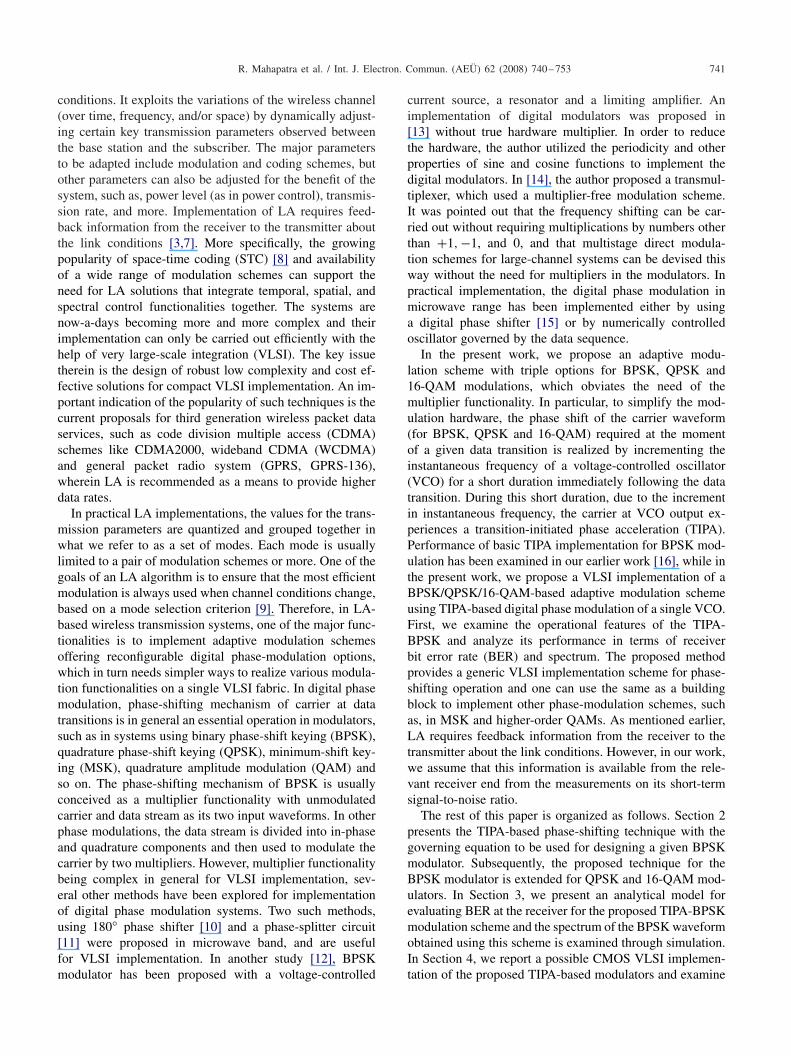
In this subsection, we reproduce the theoretical modelused in our earlier work [16] for evaluation of the TIPA-BPSK system, for the sake of completeness of the presentpaper. The phase-shifting scheme for the TIPA-based BPSKunder consideration is illustrated in Fig. 1, wherein the car-rier frequency fc of a VCO is momentarily increased (usinga rectangular control pulse at VCO input) by an amount �f
for a short duration �, following each data transition, with �being much less than the bit interval (T). During this inter-val (�), due to the increment in instantaneous frequency, thecarrier waveform at VCO output experiences a TIPA. If �and �f are chosen appropriately during the TIPA interval,carrier phase can undergo an additional phase shift of 180◦(or its odd multiple) at the end of the TIPA interval, andthereafter the carrier returns to its original frequency fc butwith a phase shift of 180◦ with respect to its waveform in thepreceding bit interval. Thus the carrier waveform achievesthe desired phase shift following the data transition withoutany multiplier operation, albeit with an imperfect waveformduring the short duration (�) of the TIPA interval. Indeed,
T
ε
Input BitStream
Narrow Pulseto VCO Input
BPSKOutput
Fig. 1. Waveforms for illustrating the TIPA-BPSK scheme.
to make the TIPA-based scheme comparable in performancewith an ideal BPSK generation scheme, one needs to mini-mize � (as compared to T) and we examine this issue later.The governing equation for � and �f is obtained by ensur-ing that, at the end of a TIPA interval, the phase-acceleratedcarrier with an instantaneous frequency (fc + �f ) accumu-lates an additional phase equal to an odd multiple of � withrespect to the original carrier waveform of frequency fc, i.e.,
2�(fc + �f )� = 2�fc� + (2n + 1)�, (1)
where n represents a positive integer including zero. Thisin turn implies that one should ensure the following designconstraint on � and �f , given by
2��f � = (2n + 1)�. (2)
The BPSK waveform, generated in this process after a givendata transition, can be represented in two parts (first partduring the TIPA interval, and the second part in the remain-ing period in a bit interval following the completion of theTIPA interval) as
vT X ={
Ac cos(2�fc + 2��f )t 0� t ��,Ac cos(2�fct) � < t �T ,
(3)
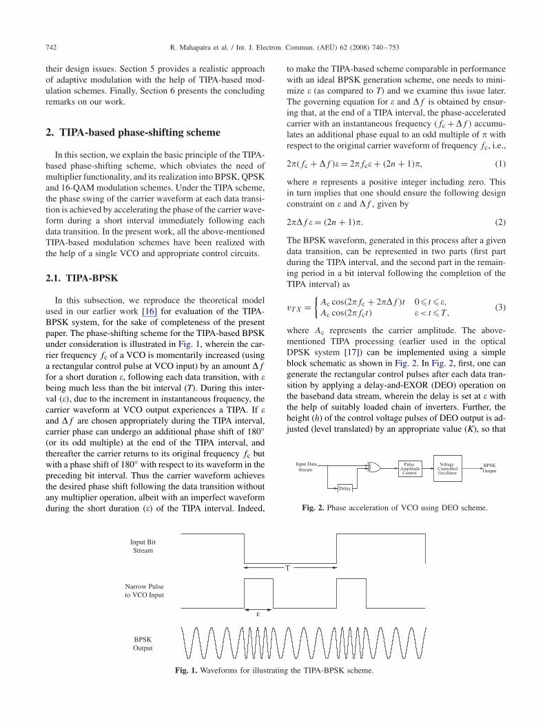
where Ac represents the carrier amplitude. The above-mentioned TIPA processing (earlier used in the opticalDPSK system [17]) can be implemented using a simpleblock schematic as shown in Fig. 2. In Fig. 2, first, one cangenerate the rectangular control pulses after each data tran-sition by applying a delay-and-EXOR (DEO) operation onthe baseband data stream, wherein the delay is set at � withthe help of suitably loaded chain of inverters. Further, theheight (h) of the control voltage pulses of DEO output is ad-justed (level translated) by an appropriate value (K), so that
Pulse
ControlAmplitude
Delay
Input Data Stream
VoltageControlledOscillator
BPSKOutput
Fig. 2. Phase acceleration of VCO using DEO scheme.
R. Mahapatra et al. / Int. J. Electron. Commun. (AEÜ) 62 (2008) 740–753 743
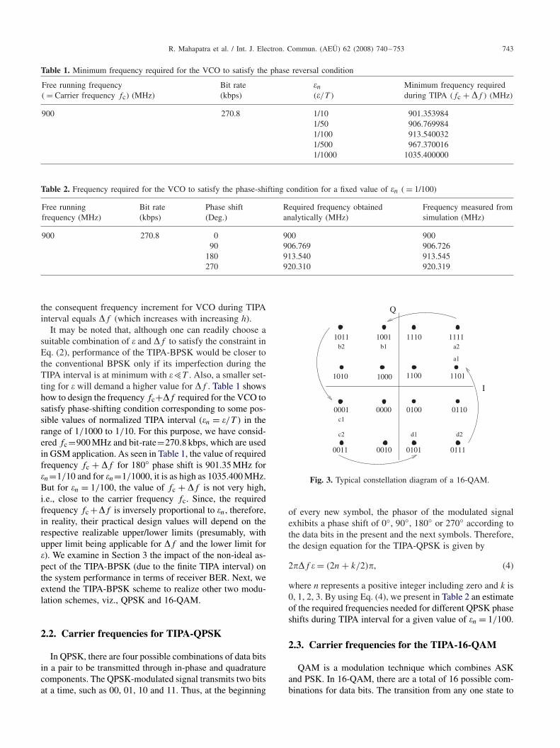
Table 1. Minimum frequency required for the VCO to satisfy the phase reversal condition
Free running frequency Bit rate �n Minimum frequency required( = Carrier frequency fc) (MHz) (kbps) (�/T ) during TIPA (fc + �f ) (MHz)
900 270.8 1/10 901.3539841/50 906.7699841/100 913.5400321/500 967.3700161/1000 1035.400000
Table 2. Frequency required for the VCO to satisfy the phase-shifting condition for a fixed value of �n ( = 1/100)
Free running Bit rate Phase shift Required frequency obtained Frequency measured fromfrequency (MHz) (kbps) (Deg.) analytically (MHz) simulation (MHz)
900 270.8 0 900 90090 906.769 906.726
180 913.540 913.545270 920.310 920.319
the consequent frequency increment for VCO during TIPAinterval equals �f (which increases with increasing h).
It may be noted that, although one can readily choose asuitable combination of � and �f to satisfy the constraint inEq. (2), performance of the TIPA-BPSK would be closer tothe conventional BPSK only if its imperfection during theTIPA interval is at minimum with �>T . Also, a smaller set-ting for � will demand a higher value for �f . Table 1 showshow to design the frequency fc+�f required for the VCO tosatisfy phase-shifting condition corresponding to some pos-sible values of normalized TIPA interval (�n = �/T ) in therange of 1/1000 to 1/10. For this purpose, we have consid-ered fc=900 MHz and bit-rate=270.8 kbps, which are usedin GSM application. As seen in Table 1, the value of requiredfrequency fc + �f for 180◦ phase shift is 901.35 MHz for�n=1/10 and for �n=1/1000, it is as high as 1035.400 MHz.But for �n = 1/100, the value of fc + �f is not very high,i.e., close to the carrier frequency fc. Since, the requiredfrequency fc +�f is inversely proportional to �n, therefore,in reality, their practical design values will depend on therespective realizable upper/lower limits (presumably, withupper limit being applicable for �f and the lower limit for�). We examine in Section 3 the impact of the non-ideal as-pect of the TIPA-BPSK (due to the finite TIPA interval) onthe system performance in terms of receiver BER. Next, weextend the TIPA-BPSK scheme to realize other two modu-lation schemes, viz., QPSK and 16-QAM.
2.2. Carrier frequencies for TIPA-QPSK
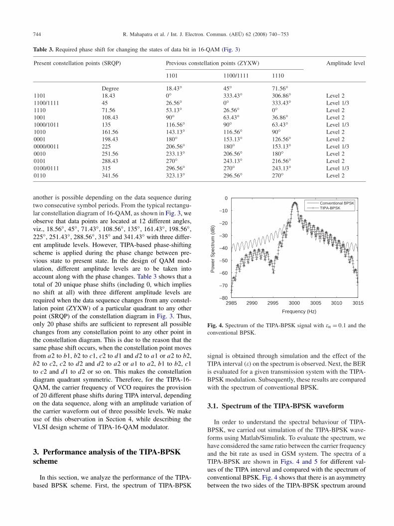
In QPSK, there are four possible combinations of data bitsin a pair to be transmitted through in-phase and quadraturecomponents. The QPSK-modulated signal transmits two bitsat a time, such as 00, 01, 10 and 11. Thus, at the beginning
Q
110111001010 1000
0011 0010 0101 0111
00000001 0100 0110
1011 1001 1110 1111
I
a2b1b2
c1
c2 d2d1
a1
Fig. 3. Typical constellation diagram of a 16-QAM.
of every new symbol, the phasor of the modulated signalexhibits a phase shift of 0◦, 90◦, 180◦ or 270◦ according tothe data bits in the present and the next symbols. Therefore,the design equation for the TIPA-QPSK is given by
2��f � = (2n + k/2)�, (4)
where n represents a positive integer including zero and k is0, 1, 2, 3. By using Eq. (4), we present in Table 2 an estimateof the required frequencies needed for different QPSK phaseshifts during TIPA interval for a given value of �n = 1/100.
2.3. Carrier frequencies for the TIPA-16-QAM
QAM is a modulation technique which combines ASKand PSK. In 16-QAM, there are a total of 16 possible com-binations for data bits. The transition from any one state to
744 R. Mahapatra et al. / Int. J. Electron. Commun. (AEÜ) 62 (2008) 740–753
Table 3. Required phase shift for changing the states of data bit in 16-QAM (Fig. 3)
Present constellation points (SRQP) Previous constellation points (ZYXW) Amplitude level
1101 1100/1111 1110
Degree 18.43◦ 45◦ 71.56◦1101 18.43 0◦ 333.43◦ 306.86◦ Level 21100/1111 45 26.56◦ 0◦ 333.43◦ Level 1/31110 71.56 53.13◦ 26.56◦ 0◦ Level 21001 108.43 90◦ 63.43◦ 36.86◦ Level 21000/1011 135 116.56◦ 90◦ 63.43◦ Level 1/31010 161.56 143.13◦ 116.56◦ 90◦ Level 20001 198.43 180◦ 153.13◦ 126.56◦ Level 20000/0011 225 206.56◦ 180◦ 153.13◦ Level 1/30010 251.56 233.13◦ 206.56◦ 180◦ Level 20101 288.43 270◦ 243.13◦ 216.56◦ Level 20100/0111 315 296.56◦ 270◦ 243.13◦ Level 1/30110 341.56 323.13◦ 296.56◦ 270◦ Level 2
another is possible depending on the data sequence duringtwo consecutive symbol periods. From the typical rectangu-lar constellation diagram of 16-QAM, as shown in Fig. 3, weobserve that data points are located at 12 different angles,viz., 18.56◦, 45◦, 71.43◦, 108.56◦, 135◦, 161.43◦, 198.56◦,225◦, 251.43◦, 288.56◦, 315◦ and 341.43◦ with three differ-ent amplitude levels. However, TIPA-based phase-shiftingscheme is applied during the phase change between pre-vious state to present state. In the design of QAM mod-ulation, different amplitude levels are to be taken intoaccount along with the phase changes. Table 3 shows that atotal of 20 unique phase shifts (including 0, which impliesno shift at all) with three different amplitude levels arerequired when the data sequence changes from any constel-lation point (ZYXW) of a particular quadrant to any otherpoint (SRQP) of the constellation diagram in Fig. 3. Thus,only 20 phase shifts are sufficient to represent all possiblechanges from any constellation point to any other point inthe constellation diagram. This is due to the reason that thesame phase shift occurs, when the constellation point movesfrom a2 to b1, b2 to c1, c2 to d1 and d2 to a1 or a2 to b2,b2 to c2, c2 to d2 and d2 to a2 or a1 to a2, b1 to b2, c1to c2 and d1 to d2 or so on. This makes the constellationdiagram quadrant symmetric. Therefore, for the TIPA-16-QAM, the carrier frequency of VCO requires the provisionof 20 different phase shifts during TIPA interval, dependingon the data sequence, along with an amplitude variation ofthe carrier waveform out of three possible levels. We makeuse of this observation in Section 4, while describing theVLSI design scheme of TIPA-16-QAM modulator.
3. Performance analysis of the TIPA-BPSKscheme
In this section, we analyze the performance of the TIPA-based BPSK scheme. First, the spectrum of TIPA-BPSK
2985 2990 2995 3000 3005 3010 3015−80
−70
−60
−50
−40
−30
−20
−10
0
Frequency (Hz)
Pow
er
Spectr
um
(dB
)
Conventional BPSK
TIPA-BPSK
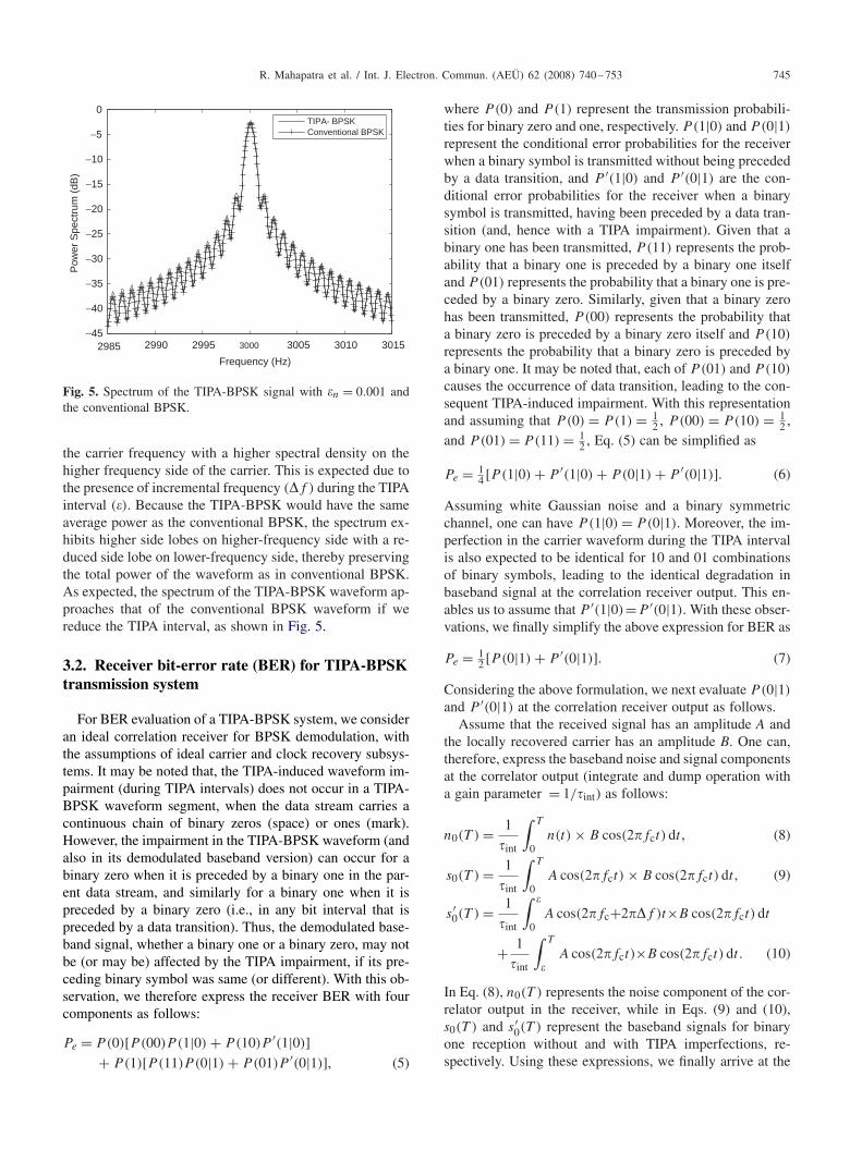
Fig. 4. Spectrum of the TIPA-BPSK signal with �n = 0.1 and theconventional BPSK.
signal is obtained through simulation and the effect of theTIPA interval (�) on the spectrum is observed. Next, the BERis evaluated for a given transmission system with the TIPA-BPSK modulation. Subsequently, these results are comparedwith the spectrum of conventional BPSK.
3.1. Spectrum of the TIPA-BPSK waveform
In order to understand the spectral behaviour of TIPA-BPSK, we carried out simulation of the TIPA-BPSK wave-forms using Matlab/Simulink. To evaluate the spectrum, wehave considered the same ratio between the carrier frequencyand the bit rate as used in GSM system. The spectra of aTIPA-BPSK are shown in Figs. 4 and 5 for different val-ues of the TIPA interval and compared with the spectrum ofconventional BPSK. Fig. 4 shows that there is an asymmetrybetween the two sides of the TIPA-BPSK spectrum around
R. Mahapatra et al. / Int. J. Electron. Commun. (AEÜ) 62 (2008) 740–753 745
2985 2990 2995 3000 3005 3010 3015−45
−40
−35
−30
−25
−20
−15
−10
−5
0
Frequency (Hz)
Po
we
r S
pe
ctr
um
(d
B)
TIPA- BPSK
Conventional BPSK
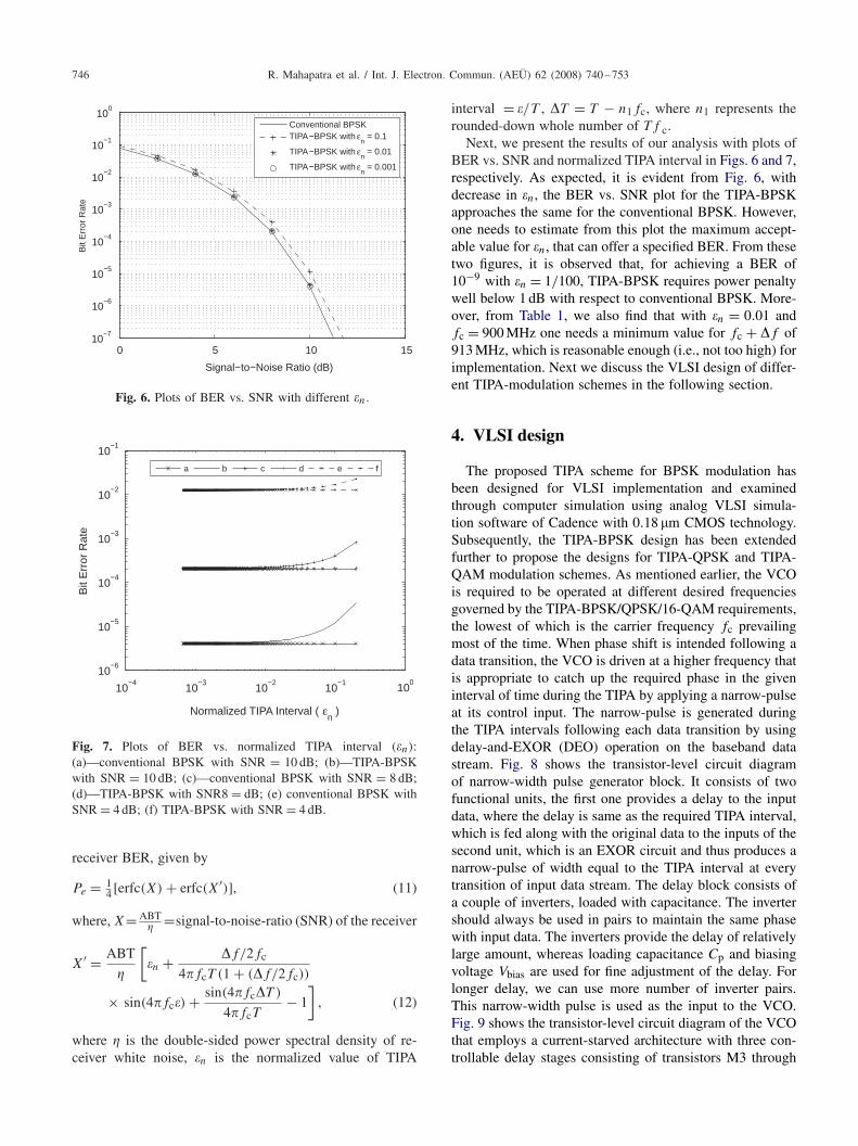
Fig. 5. Spectrum of the TIPA-BPSK signal with �n = 0.001 andthe conventional BPSK.
the carrier frequency with a higher spectral density on thehigher frequency side of the carrier. This is expected due tothe presence of incremental frequency (�f ) during the TIPAinterval (�). Because the TIPA-BPSK would have the sameaverage power as the conventional BPSK, the spectrum ex-hibits higher side lobes on higher-frequency side with a re-duced side lobe on lower-frequency side, thereby preservingthe total power of the waveform as in conventional BPSK.As expected, the spectrum of the TIPA-BPSK waveform ap-proaches that of the conventional BPSK waveform if wereduce the TIPA interval, as shown in Fig. 5.
3.2. Receiver bit-error rate (BER) for TIPA-BPSKtransmission system
For BER evaluation of a TIPA-BPSK system, we consideran ideal correlation receiver for BPSK demodulation, withthe assumptions of ideal carrier and clock recovery subsys-tems. It may be noted that, the TIPA-induced waveform im-pairment (during TIPA intervals) does not occur in a TIPA-BPSK waveform segment, when the data stream carries acontinuous chain of binary zeros (space) or ones (mark).However, the impairment in the TIPA-BPSK waveform (andalso in its demodulated baseband version) can occur for abinary zero when it is preceded by a binary one in the par-ent data stream, and similarly for a binary one when it ispreceded by a binary zero (i.e., in any bit interval that ispreceded by a data transition). Thus, the demodulated base-band signal, whether a binary one or a binary zero, may notbe (or may be) affected by the TIPA impairment, if its pre-ceding binary symbol was same (or different). With this ob-servation, we therefore express the receiver BER with fourcomponents as follows:
Pe = P(0)[P(00)P (1|0) + P(10)P ′(1|0)]+ P(1)[P(11)P (0|1) + P(01)P ′(0|1)], (5)
where P(0) and P(1) represent the transmission probabili-ties for binary zero and one, respectively. P(1|0) and P(0|1)
represent the conditional error probabilities for the receiverwhen a binary symbol is transmitted without being precededby a data transition, and P ′(1|0) and P ′(0|1) are the con-ditional error probabilities for the receiver when a binarysymbol is transmitted, having been preceded by a data tran-sition (and, hence with a TIPA impairment). Given that abinary one has been transmitted, P(11) represents the prob-ability that a binary one is preceded by a binary one itselfand P(01) represents the probability that a binary one is pre-ceded by a binary zero. Similarly, given that a binary zerohas been transmitted, P(00) represents the probability thata binary zero is preceded by a binary zero itself and P(10)
represents the probability that a binary zero is preceded bya binary one. It may be noted that, each of P(01) and P(10)
causes the occurrence of data transition, leading to the con-sequent TIPA-induced impairment. With this representationand assuming that P(0) = P(1) = 1
2 , P(00) = P(10) = 12 ,
and P(01) = P(11) = 12 , Eq. (5) can be simplified as
Pe = 14 [P(1|0) + P ′(1|0) + P(0|1) + P ′(0|1)]. (6)
Assuming white Gaussian noise and a binary symmetricchannel, one can have P(1|0) = P(0|1). Moreover, the im-perfection in the carrier waveform during the TIPA intervalis also expected to be identical for 10 and 01 combinationsof binary symbols, leading to the identical degradation inbaseband signal at the correlation receiver output. This en-ables us to assume that P ′(1|0)=P ′(0|1). With these obser-vations, we finally simplify the above expression for BER as
Pe = 12 [P(0|1) + P ′(0|1)]. (7)
Considering the above formulation, we next evaluate P(0|1)
and P ′(0|1) at the correlation receiver output as follows.Assume that the received signal has an amplitude A and
the locally recovered carrier has an amplitude B. One can,therefore, express the baseband noise and signal componentsat the correlator output (integrate and dump operation witha gain parameter = 1/�int) as follows:
n0(T ) = 1
�int
∫ T
0n(t) × B cos(2�fct) dt , (8)
s0(T ) = 1
�int
∫ T
0A cos(2�fct) × B cos(2�fct) dt , (9)
s′0(T ) = 1
�int
∫ �
0A cos(2�fc+2��f )t×B cos(2�fct) dt
+ 1
�int
∫ T
�A cos(2�fct)×B cos(2�fct) dt . (10)
In Eq. (8), n0(T ) represents the noise component of the cor-relator output in the receiver, while in Eqs. (9) and (10),s0(T ) and s′
0(T ) represent the baseband signals for binaryone reception without and with TIPA imperfections, re-spectively. Using these expressions, we finally arrive at the
746 R. Mahapatra et al. / Int. J. Electron. Commun. (AEÜ) 62 (2008) 740–753
0 5 10 1510
106
105
104
103
102
101
100
Signal to Noise Ratio (dB)
Bit E
rro
r R
ate
Conventional BPSK
TIPA BPSK with εn = 0.1
TIPA BPSK with εn = 0.01
TIPA BPSK with εn = 0.001
Fig. 6. Plots of BER vs. SNR with different �n.
104
103
102
101
100
106
105
104
103
102
101
Normalized TIPA Interval ( εn )
Bit E
rro
r R
ate
a b c d e f
Fig. 7. Plots of BER vs. normalized TIPA interval (�n):(a)—conventional BPSK with SNR = 10 dB; (b)—TIPA-BPSKwith SNR = 10 dB; (c)—conventional BPSK with SNR = 8 dB;(d)—TIPA-BPSK with SNR8 = dB; (e) conventional BPSK withSNR = 4 dB; (f) TIPA-BPSK with SNR = 4 dB.
receiver BER, given by
Pe = 14 [erfc(X) + erfc(X′)], (11)
where, X= ABT� =signal-to-noise-ratio (SNR) of the receiver
X′ = ABT
�
[�n + �f/2fc
4�fcT (1 + (�f/2fc))
× sin(4�fc�) + sin(4�fc�T )
4�fcT− 1
], (12)
where � is the double-sided power spectral density of re-ceiver white noise, �n is the normalized value of TIPA
interval = �/T , �T = T − n1fc, where n1 represents therounded-down whole number of Tf c.
Next, we present the results of our analysis with plots ofBER vs. SNR and normalized TIPA interval in Figs. 6 and 7,respectively. As expected, it is evident from Fig. 6, withdecrease in �n, the BER vs. SNR plot for the TIPA-BPSKapproaches the same for the conventional BPSK. However,one needs to estimate from this plot the maximum accept-able value for �n, that can offer a specified BER. From thesetwo figures, it is observed that, for achieving a BER of10−9 with �n = 1/100, TIPA-BPSK requires power penaltywell below 1 dB with respect to conventional BPSK. More-over, from Table 1, we also find that with �n = 0.01 andfc = 900 MHz one needs a minimum value for fc + �f of913 MHz, which is reasonable enough (i.e., not too high) forimplementation. Next we discuss the VLSI design of differ-ent TIPA-modulation schemes in the following section.
4. VLSI design
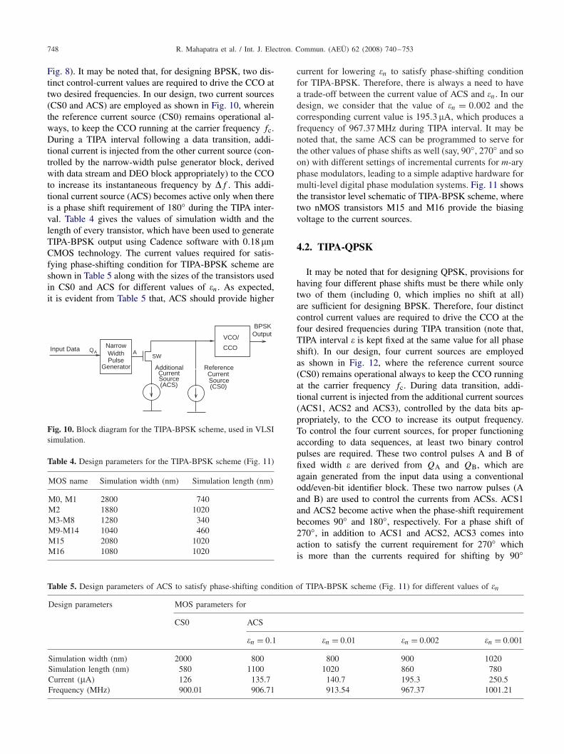
The proposed TIPA scheme for BPSK modulation hasbeen designed for VLSI implementation and examinedthrough computer simulation using analog VLSI simula-tion software of Cadence with 0.18 �m CMOS technology.Subsequently, the TIPA-BPSK design has been extendedfurther to propose the designs for TIPA-QPSK and TIPA-QAM modulation schemes. As mentioned earlier, the VCOis required to be operated at different desired frequenciesgoverned by the TIPA-BPSK/QPSK/16-QAM requirements,the lowest of which is the carrier frequency fc prevailingmost of the time. When phase shift is intended following adata transition, the VCO is driven at a higher frequency thatis appropriate to catch up the required phase in the giveninterval of time during the TIPA by applying a narrow-pulseat its control input. The narrow-pulse is generated duringthe TIPA intervals following each data transition by usingdelay-and-EXOR (DEO) operation on the baseband datastream. Fig. 8 shows the transistor-level circuit diagramof narrow-width pulse generator block. It consists of twofunctional units, the first one provides a delay to the inputdata, where the delay is same as the required TIPA interval,which is fed along with the original data to the inputs of thesecond unit, which is an EXOR circuit and thus produces anarrow-pulse of width equal to the TIPA interval at everytransition of input data stream. The delay block consists ofa couple of inverters, loaded with capacitance. The invertershould always be used in pairs to maintain the same phasewith input data. The inverters provide the delay of relativelylarge amount, whereas loading capacitance Cp and biasingvoltage Vbias are used for fine adjustment of the delay. Forlonger delay, we can use more number of inverter pairs.This narrow-width pulse is used as the input to the VCO.Fig. 9 shows the transistor-level circuit diagram of the VCOthat employs a current-starved architecture with three con-trollable delay stages consisting of transistors M3 through
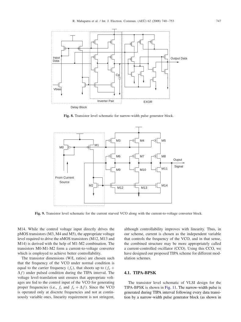
R. Mahapatra et al. / Int. J. Electron. Commun. (AEÜ) 62 (2008) 740–753 747
Delay Block
EXOR
Output DataDataInput
Vbias
Inverter Pair
Cp
Fig. 8. Transistor level schematic for narrow-width pulse generator block.
M0
M2
M9
M6
M3 M4
M10
M13M14
M11
M5
M7
M1
M12
Signal
OuputM8
From Current
Source
Fig. 9. Transistor level schematic for the current starved VCO along with the current-to-voltage converter block.
M14. While the control voltage input directly drives thepMOS transistors (M3, M4 and M5), the appropriate voltagelevel required to drive the nMOS transistors (M12, M13 andM14) is derived with the help of M1-M2 combination. Thetransistors M0-M1-M2 form a current-to-voltage converterwhich is employed to achieve better controllability.
The transistor dimensions (W/L ratios) are chosen suchthat the frequency of the VCO under normal condition isequal to the carrier frequency (fc), that shoots up to (fc +�f ) under pulsed condition during the TIPA interval. Thevoltage level-translation unit ensures that appropriate volt-ages are fed to the control input of the VCO for generatingproper frequencies (i.e., fc and fc + �f ). Since the VCOis operated only at discrete frequencies and not at contin-uously variable ones, linearity requirement is not stringent,
although controllability improves with linearity. Thus, inour scheme, current is chosen as the independent variablethat controls the frequency of the VCO, and in that sense,the combined structure may be more appropriately calleda current-controlled oscillator (CCO). Using this CCO, wehave designed our proposed TIPA scheme for different mod-ulation schemes.
4.1. TIPA-BPSK
The transistor level schematic of VLSI design for theTIPA-BPSK is shown in Fig. 11. The narrow-width pulse isgenerated during TIPA interval following every data transi-tion by a narrow-width pulse generator block (as shown in
748 R. Mahapatra et al. / Int. J. Electron. Commun. (AEÜ) 62 (2008) 740–753
Fig. 8). It may be noted that, for designing BPSK, two dis-tinct control-current values are required to drive the CCO attwo desired frequencies. In our design, two current sources(CS0 and ACS) are employed as shown in Fig. 10, whereinthe reference current source (CS0) remains operational al-ways, to keep the CCO running at the carrier frequency fc.During a TIPA interval following a data transition, addi-tional current is injected from the other current source (con-trolled by the narrow-width pulse generator block, derivedwith data stream and DEO block appropriately) to the CCOto increase its instantaneous frequency by �f . This addi-tional current source (ACS) becomes active only when thereis a phase shift requirement of 180◦ during the TIPA inter-val. Table 4 gives the values of simulation width and thelength of every transistor, which have been used to generateTIPA-BPSK output using Cadence software with 0.18 �mCMOS technology. The current values required for satis-fying phase-shifting condition for TIPA-BPSK scheme areshown in Table 5 along with the sizes of the transistors usedin CS0 and ACS for different values of �n. As expected,it is evident from Table 5 that, ACS should provide higher
QA AInput Data
CurrentAdditional
Source(ACS)
SourceCurrent
Reference
(CS0)
Output
SW
BPSK
VCO/
CCONarrow
Generator
WidthPulse
Fig. 10. Block diagram for the TIPA-BPSK scheme, used in VLSIsimulation.
Table 4. Design parameters for the TIPA-BPSK scheme (Fig. 11)
MOS name Simulation width (nm) Simulation length (nm)
M0, M1 2800 740M2 1880 1020M3-M8 1280 340M9-M14 1040 460M15 2080 1020M16 1080 1020
Table 5. Design parameters of ACS to satisfy phase-shifting condition of TIPA-BPSK scheme (Fig. 11) for different values of �n
Design parameters MOS parameters for
CS0 ACS
�n = 0.1 �n = 0.01 �n = 0.002 �n = 0.001
Simulation width (nm) 2000 800 800 900 1020Simulation length (nm) 580 1100 1020 860 780Current (�A) 126 135.7 140.7 195.3 250.5Frequency (MHz) 900.01 906.71 913.54 967.37 1001.21
current for lowering �n to satisfy phase-shifting conditionfor TIPA-BPSK. Therefore, there is always a need to havea trade-off between the current value of ACS and �n. In ourdesign, we consider that the value of �n = 0.002 and thecorresponding current value is 195.3 �A, which produces afrequency of 967.37 MHz during TIPA interval. It may benoted that, the same ACS can be programmed to serve forthe other values of phase shifts as well (say, 90◦, 270◦ and soon) with different settings of incremental currents for m-aryphase modulators, leading to a simple adaptive hardware formulti-level digital phase modulation systems. Fig. 11 showsthe transistor level schematic of TIPA-BPSK scheme, wheretwo nMOS transistors M15 and M16 provide the biasingvoltage to the current sources.
4.2. TIPA-QPSK
It may be noted that for designing QPSK, provisions forhaving four different phase shifts must be there while onlytwo of them (including 0, which implies no shift at all)are sufficient for designing BPSK. Therefore, four distinctcontrol current values are required to drive the CCO at thefour desired frequencies during TIPA transition (note that,TIPA interval � is kept fixed at the same value for all phaseshift). In our design, four current sources are employedas shown in Fig. 12, where the reference current source(CS0) remains operational always to keep the CCO runningat the carrier frequency fc. During data transition, addi-tional current is injected from the additional current sources(ACS1, ACS2 and ACS3), controlled by the data bits ap-propriately, to the CCO to increase its output frequency.To control the four current sources, for proper functioningaccording to data sequences, at least two binary controlpulses are required. These two control pulses A and B offixed width � are derived from QA and QB, which areagain generated from the input data using a conventionalodd/even-bit identifier block. These two narrow pulses (Aand B) are used to control the currents from ACSs. ACS1and ACS2 become active when the phase-shift requirementbecomes 90◦ and 180◦, respectively. For a phase shift of270◦, in addition to ACS1 and ACS2, ACS3 comes intoaction to satisfy the current requirement for 270◦ whichis more than the currents required for shifting by 90◦
R. Mahapatra et al. / Int. J. Electron. Commun. (AEÜ) 62 (2008) 740–753 749
NarrowWidthPulse
Generator
M15
M16
M0
M2
M9
M6
M3 M4
M10
M13M14
M11
M5
M7
InputData
SW1
ACS
CS0
M1
M12
Output
BPSKM8
Fig. 11. Transistor level schematic for TIPA-BPSK scheme, used in VLSI simulation.
(Q )B
(Q )A
NarrowWidthPulse
Generator
NarrowWidthPulse
Generator
A
B
ODD
EVEN
InputData
Selection
Block
Bit
EVEN
ODD/
VCO /
ACS0 ACS1 ACS2 CS0
CCO
QPSK
Output
Fig. 12. Illustration of the basic TIPA-QPSK scheme.
PreviousConstellation
Point(ZYXW)
Serialto
ParallelConverter
InputData
AQ
BQ
CQ
DQ
EQ
A
B
C
D
E
ControlSignal
GeneratorBlock ACSs )
VCO /
CurrentSourceArrayand
SelectionLogic
(includeCS0and
NarrowWidthPulse
Generator
NarrowWidthPulse
Generator
NarrowWidthPulse
Generator
NarrowWidthPulse
Generator
NarrowWidthPulse
Generator
VGASignalOutput
AmplitudeControlLogic
ba
QP
CCO
PresentConstellation
Point(SRQP)
Fig. 13. Logic diagram for TIPA-16-QAM scheme.
and by 180◦ taken together. Table 2, as discussed earlier inSection 2 provides an idea about the required frequenciesfor the desired phase shifts for a particular value of �.
4.3. TIPA-16-QAM
The block diagram of VLSI design scheme for the TIPA-based 16-QAM is shown in Fig. 13, which consists of sixdifferent functional blocks. Beside the narrow-width pulse
generator blocks and VCO which are used in the earlier TIPAscheme for QPSK, the other four are control signal genera-tor block, current source array, selection logic block and avariable gain amplifier (VGA). The control signal generatorblock controls the five narrow-width pulse generator blocksin such a way, that the appropriate pulse generators are se-lected from a group of five, to generate narrow pulses ofTIPA interval following each data transition. In a standardconstellation, as shown in Fig. 3, any particular constella-tion point differs from its neighbouring points typically by
750 R. Mahapatra et al. / Int. J. Electron. Commun. (AEÜ) 62 (2008) 740–753
Q QQQE AB
QCD
Subtractor
PQRSWXYZ
Z Z Y X WX W
Fig. 14. Block diagram for control-signal generation of 16-QAM.
I
Q
0010 0011 01100101
0111010000000001
1111 1100 1000 1001
1010101111011110
Fig. 15. Typical constellation diagram of a 16-QAM after mapping.
one bit to facilitate error control mechanism. A small com-binational circuit, as shown in Fig. 14, is employed to mapthe standard constellation in Fig. 3 into an intermediate one,as shown in Fig. 15, where the binary-weighted values asso-ciated with the constellation points increase monotonicallyas one moves in a counter-clockwise direction. This rear-rangement in the constellation enables the usage of the con-ventional arithmetic (viz., subtraction) to control the currentsources for implementing 16-QAM effectively. The imple-mentation of TIPA-16-QAM has been carried out in twosteps. In the first step, we have designed the control signalgeneration block and in the second step, a selection logic hasbeen employed to control the current sources. In these twosteps, the current sources are controlled in a structured man-ner. As shown in Fig. 14, five control signals QA, QB, QC,QD and QE are generated, which are sufficient to control 19ACSs with a reference current source (CS0). In 16-QAM,the various required phase shifts (20 in number) can be se-lected by 19 ACS’s in the current-source array (Fig. 16),which are controlled by five narrow pulses A, B, C, D and
To VCO / CCO
A
B
C
D
E
Additional CurrentSources
(19 in Numbers)
Selection
ReferenceCurrentSource(CS 0)
Logic
19 Lines
Fig. 16. Block diagram for the current-source array and selectionlogic unit in VLSI simulation.
PQ a
b
P Q a b AmpludeLevel
0 00
0 011
11
1
11 1
1 0Level 1Level 2Level 2Level 3
0
Fig. 17. Circuit diagram for the amplitude control logic unit inVLSI simulation.
E derived from QA, QB, QC, QD and QE. Fig. 16 showsthat 19 ACSs and CS0 are controlled by five narrow pulsesA, B, C, D and E with the help of a selection logic cir-cuit and used to feed the appropriate current level to VCO.Thus, QA, QB, QC, QD and QE become active for realiz-ing the desired value of phase-shift, while the two amplitudecontrol bits P and Q (the same one, which are shown inFig. 3) are used to control the amplitude of the carrier wave-form of VCO with the help of VGA control by amplitudecontrol logic unit. The circuit diagram of amplitude controllogic unit is shown in Fig. 17, wherein the table provides thelogic to control the three different amplitude levels. Table 6provides the current values corresponding to the requiredphase shifts with �n = 0.002.
As mentioned earlier, in order to examine the feasibil-ity of TIPA scheme, we have carried out a sample sim-ulation of basic TIPA scheme for BPSK. In our simula-tion, the desired phase shift (i.e., 180◦ for TIPA-BPSK) hasbeen realized with a supply voltage of 1.8 V at a temper-ature of 27 ◦C with typical process parameters using Ca-dence software for 0.18 �m CMOS technology. However,in a practical system, variation of supply voltage, tempera-ture and process will make the phase shift wander aroundthe desired value. In order to have a reliable system op-eration, the designer has to ensure that the circuit satis-fies the given specification despite the variation of the am-bient temperature, supply voltage and the process varia-tion during device fabrication. From our preliminary study,it is observed that the drift of phase shift is not signifi-cant (less than ±6◦) with supply voltage variation withinthe considered voltage range of 1.4 to 2.0 V (for a nomi-nal supply voltage of 1.8 V), while the phase shift showsstronger sensitivity (upto ±35◦) to temperature changes in
R. Mahapatra et al. / Int. J. Electron. Commun. (AEÜ) 62 (2008) 740–753 751
Table 6. Current values for satisfy phase-shifting condition of TIPA-16-QAM scheme with �n = 0.002
Phase shift Frequency (MHz) Current value (�A) Phase shift Frequency (MHz) Current value (�A)
0 900 126 (CS0) 180 967 195 (ACS10 = 69)26 906 135.7 (ACS1 = 9.7) 206 977 209 (ACS11 = 14)36 913 140.3 (ACS2 = 14.3) 216 981 215 (ACS12 = 20)53 919 146 (ACS3 = 20) 233 987 224 (ACS13 = 29)63 923 150 (ACS4 = 24) 243 991 232 (ACS14 = 37)90 933 155 (ACS5 = 29) 270 1001 250 (ACS15 = 26)
116 943 165 (ACS6 = 10) 296 1011 268 (ACS16 = 44)126 947 169 (ACS7 = 14) 306 1015 280 (ACS17 = 56)143 953 177 (ACS8 = 22) 323 1021 295 (ACS18 = 71)153 957 183 (ACS9 = 27) 333 1025 315 (ACS19 = 91)
the range of −20 ◦C to 80 ◦C. Impact of process variationhas not been examined in the present work.
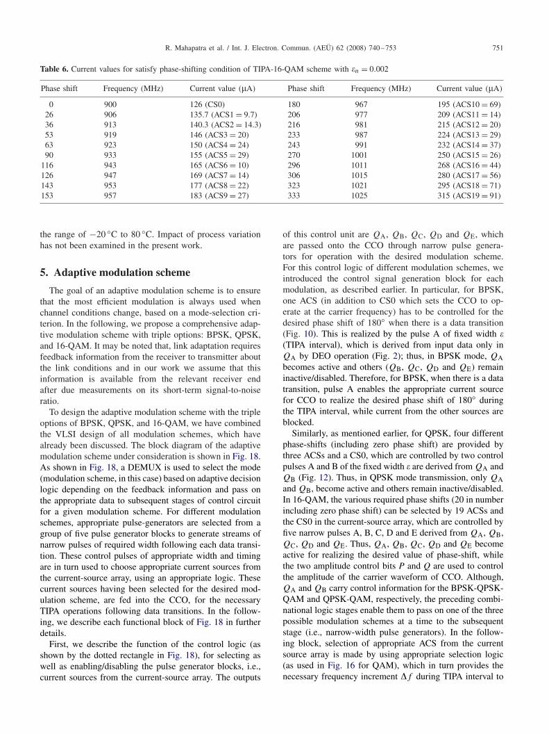
5. Adaptive modulation scheme
The goal of an adaptive modulation scheme is to ensurethat the most efficient modulation is always used whenchannel conditions change, based on a mode-selection cri-terion. In the following, we propose a comprehensive adap-tive modulation scheme with triple options: BPSK, QPSK,and 16-QAM. It may be noted that, link adaptation requiresfeedback information from the receiver to transmitter aboutthe link conditions and in our work we assume that thisinformation is available from the relevant receiver endafter due measurements on its short-term signal-to-noiseratio.
To design the adaptive modulation scheme with the tripleoptions of BPSK, QPSK, and 16-QAM, we have combinedthe VLSI design of all modulation schemes, which havealready been discussed. The block diagram of the adaptivemodulation scheme under consideration is shown in Fig. 18.As shown in Fig. 18, a DEMUX is used to select the mode(modulation scheme, in this case) based on adaptive decisionlogic depending on the feedback information and pass onthe appropriate data to subsequent stages of control circuitfor a given modulation scheme. For different modulationschemes, appropriate pulse-generators are selected from agroup of five pulse generator blocks to generate streams ofnarrow pulses of required width following each data transi-tion. These control pulses of appropriate width and timingare in turn used to choose appropriate current sources fromthe current-source array, using an appropriate logic. Thesecurrent sources having been selected for the desired mod-ulation scheme, are fed into the CCO, for the necessaryTIPA operations following data transitions. In the follow-ing, we describe each functional block of Fig. 18 in furtherdetails.
First, we describe the function of the control logic (asshown by the dotted rectangle in Fig. 18), for selecting aswell as enabling/disabling the pulse generator blocks, i.e.,current sources from the current-source array. The outputs
of this control unit are QA, QB, QC, QD and QE, whichare passed onto the CCO through narrow pulse genera-tors for operation with the desired modulation scheme.For this control logic of different modulation schemes, weintroduced the control signal generation block for eachmodulation, as described earlier. In particular, for BPSK,one ACS (in addition to CS0 which sets the CCO to op-erate at the carrier frequency) has to be controlled for thedesired phase shift of 180◦ when there is a data transition(Fig. 10). This is realized by the pulse A of fixed width �(TIPA interval), which is derived from input data only inQA by DEO operation (Fig. 2); thus, in BPSK mode, QAbecomes active and others (QB, QC, QD and QE) remaininactive/disabled. Therefore, for BPSK, when there is a datatransition, pulse A enables the appropriate current sourcefor CCO to realize the desired phase shift of 180◦ duringthe TIPA interval, while current from the other sources areblocked.
Similarly, as mentioned earlier, for QPSK, four differentphase-shifts (including zero phase shift) are provided bythree ACSs and a CS0, which are controlled by two controlpulses A and B of the fixed width � are derived from QA andQB (Fig. 12). Thus, in QPSK mode transmission, only QAand QB, become active and others remain inactive/disabled.In 16-QAM, the various required phase shifts (20 in numberincluding zero phase shift) can be selected by 19 ACSs andthe CS0 in the current-source array, which are controlled byfive narrow pulses A, B, C, D and E derived from QA, QB,QC, QD and QE. Thus, QA, QB, QC, QD and QE becomeactive for realizing the desired value of phase-shift, whilethe two amplitude control bits P and Q are used to controlthe amplitude of the carrier waveform of CCO. Although,QA and QB carry control information for the BPSK-QPSK-QAM and QPSK-QAM, respectively, the preceding combi-national logic stages enable them to pass on one of the threepossible modulation schemes at a time to the subsequentstage (i.e., narrow-width pulse generators). In the follow-ing block, selection of appropriate ACS from the currentsource array is made by using appropriate selection logic(as used in Fig. 16 for QAM), which in turn provides thenecessary frequency increment �f during TIPA interval to
752 R. Mahapatra et al. / Int. J. Electron. Commun. (AEÜ) 62 (2008) 740–753
Serialto
ParallelConverter
ODD/EVENBit Selection
BlockNarrowWidthPulse
Generator
NarrowWidthPulse
Generator
NarrowWidthPulse
Generator
NarrowWidthPulse
Generator
NarrowWidthPulse
Generator
BQ
AQ
CQ
DQ
EQ
Data
BPSK
QPSK
QAM
DEMUX
DecisionLogic Based on
FeedbackFrom Rx
Adaptation
SelectionMode
(Modulation
1:3 Input
Block)
ZYXW
RSQP
SignalGenerator
Control
Block
A
B
C
D
E
CurrentSourceArrayand
SelectionLogic
(includeCS0and
ACSs)
VCO /CCO VGA
SignalOutput
AmplitudeControlLogic
PQ
a b
Even
Odd
Fig. 18. Block diagram for the adaptive modulation scheme.
satisfy the phase-shifting requirement and the CS0 remainsoperational always to keep the VCO running at the nominalcarrier frequency fc. Immediately after a data transition,additional current is injected from ACSs, controlled bythe data bits, to the VCO to increase its output frequencyduring TIPA interval. Finally, it may be noted that the twocontrol bits (P and Q) in Fig. 18 would control the ampli-tude of CCO for 16-QAM modulation, but for BPSK andQPSK the CCO output would maintain a constant envelopewaveform.
6. Conclusion
An adaptive modulation scheme with triple options ofBPSK/QPSK/16-QAM has been examined for applica-tion in wireless networks using a phase-shifting techniquefor digital phase modulation. The proposed phase-shiftingscheme uses TIPA, employing a VCO and narrow pulsegenerator blocks. The spectrum and BER analysis of TIPA-BPSK scheme show that it approaches ideal BPSK perfor-mance for lower value of TIPA interval, which needs highervalue of �f and thus a trade-off is necessary. Simulationof a TIPA-BPSK modulation has been carried out usingCadence software for 0.18 �m CMOS technology, ensuringthe feasibility of the proposed modulation technique usingTIPA. The adaptive modulation scheme with triple op-tions has been designed for possible VLSI implementationwith five number of pulse generator blocks. The num-ber of pulse generator blocks depends on the modulationschemes under consideration. The proposed scheme offersa simple and scalable means for VLSI implementation,while offering a performance similar to other conventionalschemes. This feature will prove useful for LA realization,as the LA-based systems would demand multiple modula-tion schemes to remain available concurrently on the samechip.
References
[1] Jakes WC. Microwave mobile communication. 2nd ed., IEEEPress; 1994.
[2] Rappaport TS. Wireless communication: principle andpractice. 2nd ed., Pearson Education; 2003.
[3] Catreux S. et al. Adaptive modulation and MIMO codingfor broadband wireless data networks. IEEE Commun Mag2002; 108–15.
[4] IEEE Pers Commun. Special issue, Smart Antennas, 1998;5(1).
[5] Foschini GJ, Gans MJ. On limits of wireless communicationsin a fading environment when using multiple antennas.Wireless Pers Commun 1998;6:311–35.
[6] Gesbert D. et al. Technologies and performance of non line-of-sight broadband wireless access networks. IEEE CommunMag 2002;40(4):86–95.
[7] Gesbert D. et al. From theory to practice: an overview ofMIMO space time coded wireless system. IEEE J SelectAreas Commun 2003;21(3):281–302.
[8] Foschini GJ. Layered space-time architechture for wirelesscommunication. Bell Labs Tech 1996;1:41–59.
[9] Nanda S, Balachandran K, Kumar S. Adaptation techniquesin wireless packet data services. IEEE Commun Mag 2000;54–64.
[10] Mazumder SR, Waterman RC. A novel 6 to 18 GHz 180-degree bit phase shifter configuration having very smallamplitude and phase errors. IEEE MIT-S Int MicrowaveSymposium Digest, 23–27 May, vol. 1, 1994. p. 83–6.
[11] Goldfarb ME, Cole JB, Platzker A. A novel MMIC bi-phase modulator with variable gain using enhancement-modeFETs suitable for 3 V wireless applications. IEEE Microwaveand Millimeter-Wave Monolithic Circuits Symposium, 22–25May, 1994. p. 99–102.
[12] Chen JH, Tsao HW. BPSK modulator using VCCS andresonator without carrier signal and balanced modulator.Electron Lett 1997;33(5):1286–7.
[13] Gazsi L. On the reduction of hardware in digital modulators.IEEE Trans Commun 1979;COM-27(1):1575–86.
R. Mahapatra et al. / Int. J. Electron. Commun. (AEÜ) 62 (2008) 740–753 753
[14] Fettweis A. Transmultiplexers with either analog conversioncircuits, wave digital filters, or SC filters A review. IEEETrans Commun 1982;COM-30(7):221–8.
[15] Kamilo Feher, Digital communications: microwave applica-tion. Prentice-Hall of India; 1987.
[16] Mahapatra R, Dhar AS, Datta D. On feasibility of a multiplierless phase-shifting scheme for digital phase modulationand its VLSI implementation. Int J Electronics 2007;94(2):171–81.
[17] Datta D. Analysis of a new technique for optical DPSKtransmission without external modulation. Int J Opto 1993;8:451–7.
Rajarshi Mahapatra is a ResearchScholar at Department of Electronicsand Electrical Communication Engi-neering of Indian Institute of Technol-ogy, Kharagpur. He obtained B. Tech.and M. Tech. degrees in Optics and Op-toelectronics from the Department ofApplied Physics, Calcutta University,Kolkata in 1998 and 2000, respectively.His current research interests include
adaptive modulation, space–time coding and emerging techniquesin wireless networks.
Anindya Sundar Dhar received hisBachelor degree in Electronics andTelecommunication Engineering fromBengal Engineering College, Sibpur,India in 1987. In 1989, he received hisM. Tech. degree in Integrated Circuitsand Systems Engineering from IndianInstitute of Technology, Kharagpur. Hereceived his Ph.D. degree from the sameInstitute in 1994, where he is presently
serving as an Assistant Professor in the Department of Electronicsand Electrical Communication Engineering. His research interestsinclude VLSI for communication and DSP architectures for realtime signal processing.
Debasish Datta received his B. Tech.degree in 1973 from the Institute ofRadiophysics and Electronics, CalcuttaUniversity, and M. Tech. and Ph.D.degrees from IIT Kharagpur in 1976and 1986, respectively. He has beenengaged in teaching and research at IITKharagpur in the Department of Elec-tronics and Electrical CommunicationEngineering during the last 28 years
and currently he serves therein as the Head of the Department. Dur-ing the period 1999–2002, he also served as the Chairman of G.S.Sanyal School of Telecommunications at IIT Kharagpur. In theearly phase of his career, he worked for Transmission R&D Divi-sion in Indian Telephone Industries, Bangalore, during 1976–1978,and in Production Management Division of Audio and IntercomSystems of Philips India Ltd, Calcutta, during 1980–1981. Dur-ing his stay at IIT Kharagpur, he was awarded Indo-US Fellow-ship by the Department of Science and Technology, Governmentof India, and the United States Agency for International develop-ment, to carry out research at Stanford University for one yearduring 1992–1993 in the area of Coherent Optical Communica-tions. Thereafter, he visited University of California at Davis dur-ing 1997–1999 and Chonbuk National University, South Korea,during 2003–2004 to carry out collaborative research in the areaof optical networking.He received Sir J.C. Bose Premium Award in 1985 during his doc-toral work from the Institution of Radio Engineers (IERE), UK,for a paper on Optical Receiver in the Journal of IERE. In the re-cent past, he served as Guest Editor for IEEE Journal of SelectedAreas in Communication for the January-2002 Special Issue onWDM-based Network Architectures, and presently he serves as anEditor for the Elsevier Journal of Optical Switching and Networks.He has been and also serves presently in the technical programcommittees of several national as well as international conferencesin the area of optical communications and networking. His cur-rent research interests include survivable wavelength-routed opti-cal networks, optical access networks, optical burst switching andlink adaptation in wireless networks employing diversity aidedadaptive modulation and power control schemes.
Related Documents