12-Bit, 170 MSPS/210 MSPS/250 MSPS, 1.8 V Analog-to-Digital Converter AD9230 Rev. 0 Information furnished by Analog Devices is believed to be accurate and reliable. However, no responsibility is assumed by Analog Devices for its use, nor for any infringements of patents or other rights of third parties that may result from its use. Specifications subject to change without notice. No license is granted by implication or otherwise under any patent or patent rights of Analog Devices. Trademarks and registered trademarks are the property of their respective owners. One Technology Way, P.O. Box 9106, Norwood, MA 02062-9106, U.S.A. Tel: 781.329.4700 www.analog.com Fax: 781.461.3113 ©2007 Analog Devices, Inc. All rights reserved. FEATURES SNR = 64.9 dBFS @ fIN up to 70 MHz @ 250 MSPS ENOB of 10.4 @ fIN up to 70 MHz @ 250 MSPS (−1.0 dBFS) SFDR = −79 dBc @ fIN up to 70 MHz @ 250 MSPS (−1.0 dBFS) Excellent linearity DNL = ±0.3 LSB typical INL = ±0.5 LSB typical LVDS at 250 MSPS (ANSI-644 levels) 700 MHz full power analog bandwidth On-chip reference, no external decoupling required Integrated input buffer and track-and-hold Low power dissipation 434 mW @ 250 MSPS—LVDS SDR mode 400 mW @ 250 MSPS—LVDS DDR mode Programmable input voltage range 1.0 V to 1.5 V, 1.25 V nominal 1.8 V analog and digital supply operation Selectable output data format (offset binary, twos complement, Gray code) Clock duty cycle stabilizer Integrated data capture clock APPLICATIONS Wireless and wired broadband communications Cable reverse path Communications test equipment Radar and satellite subsystems Power amplifier linearization FUNCTIONAL BLOCK DIAGRAM AGND PWDN RBIAS AVDD (1.8V) VIN+ VIN– CML TRACK-AND-HOLD REFERENCE ADC 12-BIT CORE OUTPUT STAGING LVDS CLK+ CLK– CLOCK MANAGEMENT SERIAL PORT RESET SCLK SDIO CSB DCO– DCO+ OR– OR+ D11 TO D0 DRGND DRVDD 12 12 AD9230 06002-001 Figure 1. Functional Block Diagram GENERAL DESCRIPTION The AD9230 is a 12-bit monolithic sampling analog-to-digital converter optimized for high performance, low power, and ease of use. The product operates at up to a 250 MSPS conversion rate and is optimized for outstanding dynamic performance in wideband carrier and broadband systems. All necessary functions, including a track-and-hold (T/H) and voltage reference, are included on the chip to provide a complete signal conversion solution. The ADC requires a 1.8 V analog voltage supply and a differential clock for full performance operation. The digital outputs are LVDS (ANSI-644) compatible and support either twos complement, offset binary format, or Gray code. A data clock output is available for proper output data timing. Fabricated on an advanced CMOS process, the AD9230 is available in a 56-lead LFCSP, specified over the industrial temperature range (−40°C to +85°C). PRODUCT HIGHLIGHTS 1. High Performance—Maintains 64.9 dBFS SNR @ 250 MSPS with a 70 MHz input. 2. Low Power—Consumes only 434 mW @ 250 MSPS. 3. Ease of Use—LVDS output data and output clock signal allow interface to current FPGA technology. The on-chip reference and sample and hold provide flexibility in system design. Use of a single 1.8 V supply simplifies system power supply design. 4. Serial Port Control—Standard serial port interface supports various product functions, such as data formatting, disabling the clock duty cycle stabilizer, power-down, gain adjust, and output test pattern generation. 5. Pin-Compatible Family—10-bit pin-compatible family offered as AD9211.

Welcome message from author
This document is posted to help you gain knowledge. Please leave a comment to let me know what you think about it! Share it to your friends and learn new things together.
Transcript
12-Bit, 170 MSPS/210 MSPS/250 MSPS, 1.8 V Analog-to-Digital Converter
AD9230
Rev. 0 Information furnished by Analog Devices is believed to be accurate and reliable. However, no responsibility is assumed by Analog Devices for its use, nor for any infringements of patents or other rights of third parties that may result from its use. Specifications subject to change without notice. No license is granted by implication or otherwise under any patent or patent rights of Analog Devices. Trademarks and registered trademarks are the property of their respective owners.
One Technology Way, P.O. Box 9106, Norwood, MA 02062-9106, U.S.A.Tel: 781.329.4700 www.analog.com Fax: 781.461.3113 ©2007 Analog Devices, Inc. All rights reserved.
FEATURES SNR = 64.9 dBFS @ fIN up to 70 MHz @ 250 MSPS ENOB of 10.4 @ fIN up to 70 MHz @ 250 MSPS (−1.0 dBFS) SFDR = −79 dBc @ fIN up to 70 MHz @ 250 MSPS (−1.0 dBFS) Excellent linearity
DNL = ±0.3 LSB typical INL = ±0.5 LSB typical
LVDS at 250 MSPS (ANSI-644 levels) 700 MHz full power analog bandwidth On-chip reference, no external decoupling required Integrated input buffer and track-and-hold Low power dissipation
434 mW @ 250 MSPS—LVDS SDR mode 400 mW @ 250 MSPS—LVDS DDR mode
Programmable input voltage range 1.0 V to 1.5 V, 1.25 V nominal
1.8 V analog and digital supply operation Selectable output data format (offset binary, twos
complement, Gray code) Clock duty cycle stabilizer Integrated data capture clock
APPLICATIONS Wireless and wired broadband communications Cable reverse path Communications test equipment Radar and satellite subsystems Power amplifier linearization
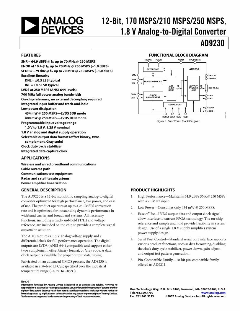
FUNCTIONAL BLOCK DIAGRAM AGNDPWDNRBIAS AVDD (1.8V)
VIN+VIN–
CML
TRACK-AND-HOLD
REFERENCE
ADC12-BITCORE
OUTPUTSTAGING
LVDS
CLK+CLK–
CLOCKMANAGEMENT
SERIAL PORT
RESET SCLK SDIO CSB
DCO–DCO+
OR–OR+
D11 TO D0
DRGNDDRVDD
12 12
AD9230
0600
2-00
1
Figure 1. Functional Block Diagram
GENERAL DESCRIPTION The AD9230 is a 12-bit monolithic sampling analog-to-digital converter optimized for high performance, low power, and ease of use. The product operates at up to a 250 MSPS conversion rate and is optimized for outstanding dynamic performance in wideband carrier and broadband systems. All necessary functions, including a track-and-hold (T/H) and voltage reference, are included on the chip to provide a complete signal conversion solution.
The ADC requires a 1.8 V analog voltage supply and a differential clock for full performance operation. The digital outputs are LVDS (ANSI-644) compatible and support either twos complement, offset binary format, or Gray code. A data clock output is available for proper output data timing.
Fabricated on an advanced CMOS process, the AD9230 is available in a 56-lead LFCSP, specified over the industrial temperature range (−40°C to +85°C).
PRODUCT HIGHLIGHTS 1. High Performance—Maintains 64.9 dBFS SNR @ 250 MSPS
with a 70 MHz input.
2. Low Power—Consumes only 434 mW @ 250 MSPS.
3. Ease of Use—LVDS output data and output clock signal allow interface to current FPGA technology. The on-chip reference and sample and hold provide flexibility in system design. Use of a single 1.8 V supply simplifies system power supply design.
4. Serial Port Control—Standard serial port interface supports various product functions, such as data formatting, disabling the clock duty cycle stabilizer, power-down, gain adjust, and output test pattern generation.
5. Pin-Compatible Family—10-bit pin-compatible family offered as AD9211.
AD9230
Rev. 0 | Page 2 of 32
TABLE OF CONTENTS Features .............................................................................................. 1 Applications....................................................................................... 1 Functional Block Diagram .............................................................. 1 General Description ......................................................................... 1 Product Highlights ........................................................................... 1 Revision History ............................................................................... 2 Specifications..................................................................................... 3
DC Specifications ......................................................................... 3 AC Specifications.......................................................................... 4 Digital Specifications ................................................................... 5 Switching Specifications .............................................................. 6 Timing Diagrams.......................................................................... 7
Absolute Maximum Ratings............................................................ 8 Thermal Resistance ...................................................................... 8 ESD Caution.................................................................................. 8
Pin Configurations and Function Descriptions ........................... 9 Equivalent Circuits ......................................................................... 13 Typical Performance Characteristics ........................................... 14
Theory of Operation ...................................................................... 21 Analog Input and Voltage Reference ....................................... 21 Clock Input Considerations...................................................... 22 Power Dissipation and Power-Down Mode ........................... 23 Digital Outputs ........................................................................... 23 Timing ......................................................................................... 24 RBIAS........................................................................................... 24 AD9230 Configuration Using the SPI ..................................... 24 Hardware Interface..................................................................... 25 Configuration Without the SPI ................................................ 25
Memory Map .................................................................................. 27 Reading the Memory Map Table.............................................. 27 Reserved Locations .................................................................... 27 Default Values ............................................................................. 27 Logic Levels ................................................................................. 27
Outline Dimensions ....................................................................... 30 Ordering Guide .......................................................................... 30
REVISION HISTORY 2/07—Revision 0: Initial Version
AD9230
Rev. 0 | Page 3 of 32
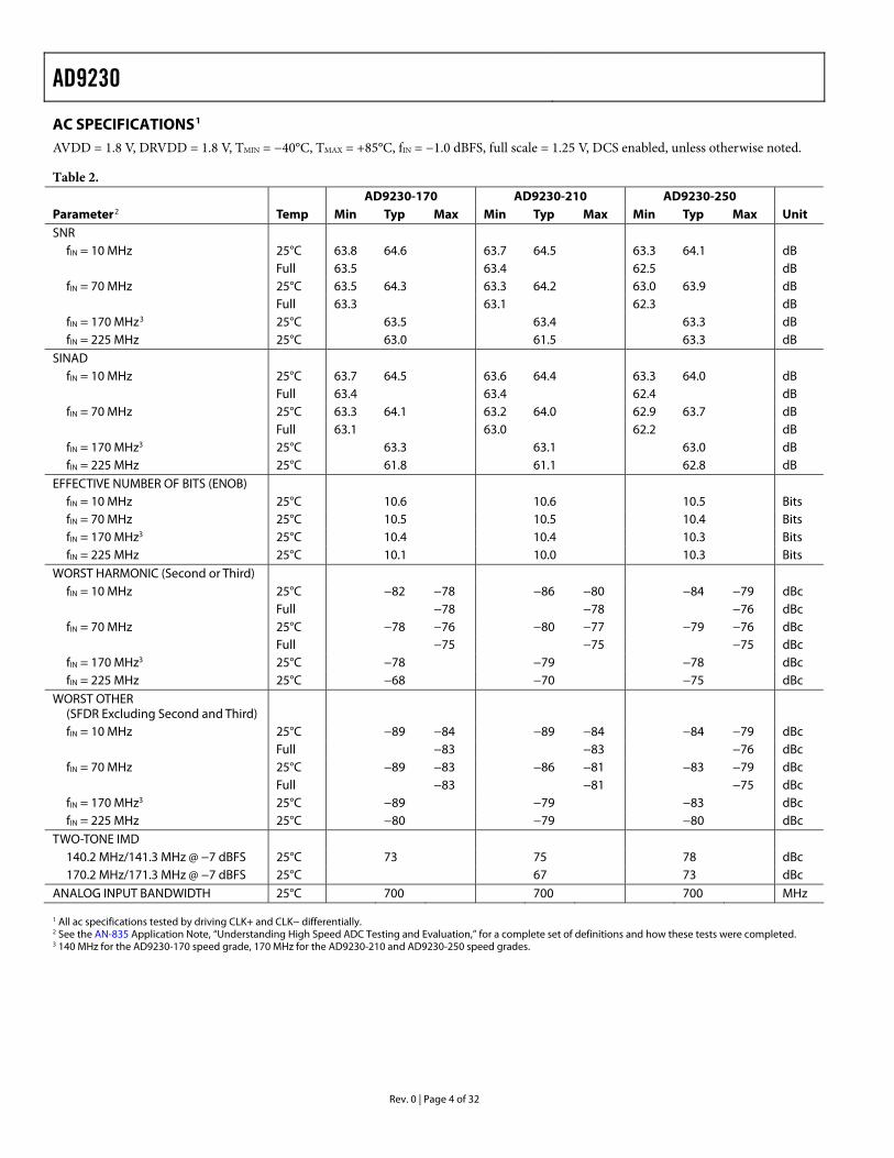
SPECIFICATIONS DC SPECIFICATIONS AVDD = 1.8 V, DRVDD = 1.8 V, TMIN = −40°C, TMAX = +85°C, fIN = −1.0 dBFS, full scale = 1.25 V, DCS enabled, unless otherwise noted.
Table 1. AD9230-170 AD9230-210 AD9230-250 Parameter1 Temp Min Typ Max Min Typ Max Min Typ Max Unit RESOLUTION 12 12 12 Bits ACCURACY
No Missing Codes Full Guaranteed Guaranteed Guaranteed Offset Error 25°C 4.2 4.3 4.5 mV Full −12 12 −12 12 −12 12 mV Gain Error 25°C 0.89 1.0 1.1 mV Full −1.5 3.5 −1.5 3.5 −1.5 3.5 % FS Differential Nonlinearity 25°C ±0.3 ±0.3 ±0.3 LSB (DNL) Full −0.5 0.5 −0.5 0.5 −0.6 0.6 LSB Integral Nonlinearity (INL) 25°C ±0.5 ±0.4 ±0.5 LSB Full −0.75 0.75 −0.75 0.75 −1.0 +1.0 LSB
TEMPERATURE DRIFT Offset Error Full ±9 ±8 ±7 μV/°C
Gain Error Full 0.019 0.021 0.018 %/°C ANALOG INPUTS (VIN+, VIN−)
Differential Input Voltage Range2 Full 0.98 1.25 1.5 0.98 1.25 1.5 0.98 1.25 1.5 V p-p Input Common-Mode Voltage Full 1.4 1.4 1.4 V Input Resistance (Differential) Full 4.3 4.3 4.3 kΩ Input Capacitance 25°C 2 2 2 pF
POWER SUPPLY AVDD Full 1.7 1.8 1.9 1.7 1.8 1.9 V DRVDD Full 1.7 1.8 1.9 1.7 1.8 1.9 V Supply Currents
IAVDD3 Full 136 145 154 164 181 194 mA
IDRVDD3/SDR Mode4 Full 58 61 59 62 60 63 mA
IDRVDD3/DDR Mode5 Full 39 40 41 mA
Power Dissipation3 Full mW SDR Mode4 Full 349 371 383 407 434 463 mW DDR Mode5 Full 315 349 400 mW
1 See the AN-835 Application Note, “Understanding High Speed ADC Testing and Evaluation,” for a complete set of definitions and how these tests were completed. 2 The input range is programmable through the SPI, and the range specified reflects the nominal values of each setting. See the Memory Map section. 3 IAVDD and IDRVDD are measured with a −1 dBFS, 10.3 MHz sine input at rated sample rate. 4 Single data rate mode; this is the default mode of the AD9230. 5 Double data rate mode; user-programmable feature. See the Memory Map section.
AD9230
Rev. 0 | Page 4 of 32
AC SPECIFICATIONS1
AVDD = 1.8 V, DRVDD = 1.8 V, TMIN = −40°C, TMAX = +85°C, fIN = −1.0 dBFS, full scale = 1.25 V, DCS enabled, unless otherwise noted.
Table 2. AD9230-170 AD9230-210 AD9230-250 Parameter2 Temp Min Typ Max Min Typ Max Min Typ Max Unit SNR
fIN = 10 MHz 25°C 63.8 64.6 63.7 64.5 63.3 64.1 dB Full 63.5 63.4 62.5 dB fIN = 70 MHz 25°C 63.5 64.3 63.3 64.2 63.0 63.9 dB Full 63.3 63.1 62.3 dB fIN = 170 MHz3 25°C 63.5 63.4 63.3 dB fIN = 225 MHz 25°C 63.0 61.5 63.3 dB
SINAD fIN = 10 MHz 25°C 63.7 64.5 63.6 64.4 63.3 64.0 dB Full 63.4 63.4 62.4 dB fIN = 70 MHz 25°C 63.3 64.1 63.2 64.0 62.9 63.7 dB Full 63.1 63.0 62.2 dB fIN = 170 MHz3 25°C 63.3 63.1 63.0 dB fIN = 225 MHz 25°C 61.8 61.1 62.8 dB
EFFECTIVE NUMBER OF BITS (ENOB) fIN = 10 MHz 25°C 10.6 10.6 10.5 Bits fIN = 70 MHz 25°C 10.5 10.5 10.4 Bits fIN = 170 MHz3 25°C 10.4 10.4 10.3 Bits fIN = 225 MHz 25°C 10.1 10.0 10.3 Bits
WORST HARMONIC (Second or Third) fIN = 10 MHz 25°C −82 −78 −86 −80 −84 −79 dBc Full −78 −78 −76 dBc fIN = 70 MHz 25°C −78 −76 −80 −77 −79 −76 dBc Full −75 −75 −75 dBc fIN = 170 MHz3 25°C −78 −79 −78 dBc fIN = 225 MHz 25°C −68 −70 −75 dBc
WORST OTHER (SFDR Excluding Second and Third)
fIN = 10 MHz 25°C −89 −84 −89 −84 −84 −79 dBc Full −83 −83 −76 dBc fIN = 70 MHz 25°C −89 −83 −86 −81 −83 −79 dBc Full −83 −81 −75 dBc fIN = 170 MHz3 25°C −89 −79 −83 dBc fIN = 225 MHz 25°C −80 −79 −80 dBc
TWO-TONE IMD 140.2 MHz/141.3 MHz @ −7 dBFS 25°C 73 75 78 dBc 170.2 MHz/171.3 MHz @ −7 dBFS 25°C 67 73 dBc
ANALOG INPUT BANDWIDTH 25°C 700 700 700 MHz 1 All ac specifications tested by driving CLK+ and CLK− differentially. 2 See the AN-835 Application Note, “Understanding High Speed ADC Testing and Evaluation,” for a complete set of definitions and how these tests were completed. 3 140 MHz for the AD9230-170 speed grade, 170 MHz for the AD9230-210 and AD9230-250 speed grades.
AD9230
Rev. 0 | Page 5 of 32
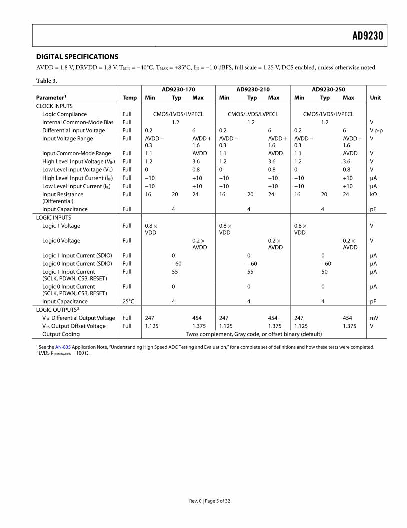
DIGITAL SPECIFICATIONS AVDD = 1.8 V, DRVDD = 1.8 V, TMIN = −40°C, TMAX = +85°C, fIN = −1.0 dBFS, full scale = 1.25 V, DCS enabled, unless otherwise noted.
Table 3. AD9230-170 AD9230-210 AD9230-250 Parameter1 Temp Min Typ Max Min Typ Max Min Typ Max Unit CLOCK INPUTS
Logic Compliance Full CMOS/LVDS/LVPECL CMOS/LVDS/LVPECL CMOS/LVDS/LVPECL Internal Common-Mode Bias Full 1.2 1.2 1.2 V Differential Input Voltage Full 0.2 6 0.2 6 0.2 6 V p-p Input Voltage Range Full AVDD −
0.3 AVDD +
1.6 AVDD − 0.3
AVDD + 1.6
AVDD − 0.3
AVDD + 1.6
V
Input Common-Mode Range Full 1.1 AVDD 1.1 AVDD 1.1 AVDD V High Level Input Voltage (VIH) Full 1.2 3.6 1.2 3.6 1.2 3.6 V Low Level Input Voltage (VIL) Full 0 0.8 0 0.8 0 0.8 V High Level Input Current (IIH) Full −10 +10 −10 +10 −10 +10 μA Low Level Input Current (IIL) Full −10 +10 −10 +10 −10 +10 μA Input Resistance (Differential)
Full 16 20 24 16 20 24 16 20 24 kΩ
Input Capacitance Full 4 4 4 pF LOGIC INPUTS
Logic 1 Voltage Full 0.8 × VDD
0.8 × VDD
0.8 × VDD
V
Logic 0 Voltage Full 0.2 × AVDD
0.2 × AVDD
0.2 × AVDD
V
Logic 1 Input Current (SDIO) Full 0 0 0 μA Logic 0 Input Current (SDIO) Full −60 −60 −60 μA Logic 1 Input Current (SCLK, PDWN, CSB, RESET)
Full 55 55 50 μA
Logic 0 Input Current (SCLK, PDWN, CSB, RESET)
Full 0 0 0 μA
Input Capacitance 25°C 4 4 4 pF LOGIC OUTPUTS2
VOD Differential Output Voltage Full 247 454 247 454 247 454 mV VOS Output Offset Voltage Full 1.125 1.375 1.125 1.375 1.125 1.375 V Output Coding Twos complement, Gray code, or offset binary (default)
1 See the AN-835 Application Note, “Understanding High Speed ADC Testing and Evaluation,” for a complete set of definitions and how these tests were completed. 2 LVDS RTERMINATION = 100 Ω.
AD9230
Rev. 0 | Page 6 of 32
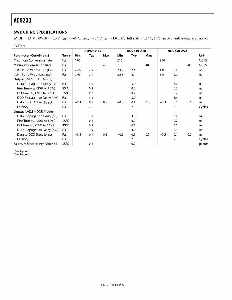
SWITCHING SPECIFICATIONS AVDD = 1.8 V, DRVDD = 1.8 V, TMIN = −40°C, TMAX = +85°C, fIN = −1.0 dBFS, full scale = 1.25 V, DCS enabled, unless otherwise noted.
Table 4. AD9230-170 AD9230-210 AD9230-250 Parameter (Conditions) Temp Min Typ Max Min Typ Max Unit Maximum Conversion Rate Full 170 210 250 MSPS Minimum Conversion Rate Full 40 40 40 MSPS
CLK+ Pulse Width High (tCH) Full 2.65 2.9 2.15 2.4 1.8 2.0 ns CLK+ Pulse Width Low (tCL) Full 2.65 2.9 2.15 2.4 1.8 2.0 ns Output (LVDS − SDR Mode)1
Data Propagation Delay (tPD) Full 3.0 3.0 3.0 ns Rise Time (tR) (20% to 80%) 25°C 0.2 0.2 0.2 ns Fall Time (tF) (20% to 80%) 25°C 0.2 0.2 0.2 ns DCO Propagation Delay (tCPD) Full 3.9 3.9 3.9 ns Data to DCO Skew (tSKEW) Full −0.3 0.1 0.5 −0.3 0.1 0.5 −0.3 0.1 0.5 ns Latency Full 7 7 7 Cycles
Output (LVDS − DDR Mode)2 Data Propagation Delay (tPD) Full 3.8 3.8 3.8 ns Rise Time (tR) (20% to 80%) 25°C 0.2 0.2 0.2 ns Fall Time (tF) (20% to 80%) 25°C 0.2 0.2 0.2 ns DCO Propagation Delay (tCPD) Full 3.9 3.9 3.9 ns Data to DCO Skew (tSKEW) Full −0.5 0.1 0.3 −0.5 0.1 0.3 −0.5 0.1 0.3 ns Latency Full 7 7 7 Cycles
Aperture Uncertainty (Jitter, tJ) 25°C 0.2 0.2 ps rms 1 See Figure 2. 2 See Figure 3.
AD9230
Rev. 0 | Page 7 of 32
TIMING DIAGRAMS N – 1
N
N + 2
N + 3
N + 4N + 5
N + 1
CLK+
N – 7 N – 6 N – 5 N – 4 N – 3
CLK–
DCO+
DCO–
DX+
DX–
VIN
tA
tCH tCL 1/fS
tCPD
tSKEW
tPD
0600
2-00
2
Figure 2. Single Data Rate Mode
N – 1
N
N + 2
N + 3
N + 4N + 5
N + 1
CLK+
CLK–
DCO+
DCO–
D6N – 8
D0N – 7
D6N – 7
D0N – 6
D6N – 6
D0N – 5
D6N – 5
D0N – 4
D6N – 4
D0N – 3
D0/D6+
D0/D6–
D11N – 8
D5N – 7
D11N – 7
D5N – 6
D11N – 6
D5N – 5
D11N – 5
D5N – 4
D11N – 4
D5N – 3
D5/D11+
D5/D11–
VIN
tA
tCH tCL 1/fS
tCPD
tSKEW
tPD
0600
2-00
36 MSBs
6 LSBs Figure 3. Double Data Rate Mode
AD9230
Rev. 0 | Page 8 of 32
ABSOLUTE MAXIMUM RATINGS Table 5.
Parameter Rating ELECTRICAL
AVDD to AGND −0.3 V to +2.0 V DRVDD to DRGND −0.3 V to +2.0 V AGND to DRGND −0.3 V to +0.3 V AVDD to DRVDD −2.0 V to +2.0 V D0+/D0− through D13+/D13−
to DRGND −0.3 V to DRVDD + 0.3 V
DCO to DRGND −0.3 V to DRVDD + 0.3 V OR to DGND −0.3 V to DRVDD + 0.3 V CLK+ to AGND −0.3 V to +3.9 V CLK− to AGND −0.3 V to +3.9 V VIN+ to AGND −0.3 V to AVDD + 0.2 V VIN− to AGND −0.3 V to AVDD + 0.2 V SDIO/DCS to DGND −0.3 V to DRVDD + 0.3 V PDWN to AGND −0.3 V to +3.9 V CSB to AGND −0.3 V to +3.9 V SCLK/DFS to AGND −0.3 V to +3.9 V
ENVIRONMENTAL Storage Temperature Range −65°C to +125°C Operating Temperature Range −40°C to +85°C Lead Temperature (Soldering 10 sec)
300°C
Junction Temperature 150°C
Stresses above those listed under Absolute Maximum Ratings may cause permanent damage to the device. This is a stress rating only; functional operation of the device at these or any other conditions above those indicated in the operational section of this specification is not implied. Exposure to absolute maximum rating conditions for extended periods may affect device reliability.
THERMAL RESISTANCE The exposed paddle must be soldered to the ground plane for the LFCSP package. Soldering the exposed paddle to the customer board increases the reliability of the solder joints, maximizing the thermal capability of the package.
Table 6. Package Type θJA θJC Unit 56-Lead LFCSP (CP-48-3) 30.4 2.9 °C/W
Typical θJA and θJC are specified for a 4-layer board in still air. Airflow increases heat dissipation, effectively reducing θJA. In addition, metal in direct contact with the package leads from metal traces, and through holes, ground, and power planes reduces the θJA.
ESD CAUTION
AD9230
Rev. 0 | Page 9 of 32
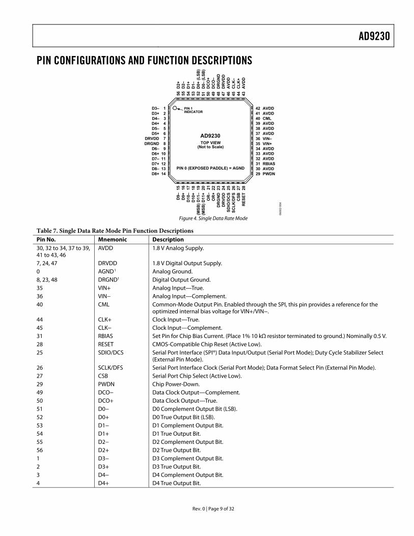
PIN CONFIGURATIONS AND FUNCTION DESCRIPTIONS
PIN 1INDICATOR
1D3–2D3+3D4–4D4+5D5–6D5+7DRVDD8DRGND9D6–
10D6+11D7–12D7+13D8–14D8+
35 VIN+36 VIN–37 AVDD38 AVDD39 AVDD40 CML41 AVDD42 AVDD
34 AVDD33 AVDD32 AVDD31 RBIAS30 AVDD29 PWDN
15D
9–16
D9+
17D
10–
19(M
SB) D
11–
21O
R–
20(M
SB) D
11+
22O
R+
23D
RG
ND
24D
RVD
D25
SDIO
/DC
S26
SCLK
/DFS
27C
SB28
RES
ET
18D
10+
45C
LK–
46A
VDD
47D
RVD
D48
DR
GN
D49
DC
O–
50D
CO
+51
D0–
(LSB
)52
D0+
(LSB
)53
D1–
54D
1+
44C
LK+
43A
VDD
TOP VIEW(Not to Scale)
PIN 0 (EXPOSED PADDLE) = AGND
AD9230
55D
2–56
D2+
0600
2-00
4
Figure 4. Single Data Rate Mode
Table 7. Single Data Rate Mode Pin Function Descriptions Pin No. Mnemonic Description 30, 32 to 34, 37 to 39, 41 to 43, 46
AVDD 1.8 V Analog Supply.
7, 24, 47 DRVDD 1.8 V Digital Output Supply. 0 AGND1 Analog Ground. 8, 23, 48 DRGND1 Digital Output Ground. 35 VIN+ Analog Input—True. 36 VIN− Analog Input—Complement. 40 CML Common-Mode Output Pin. Enabled through the SPI, this pin provides a reference for the
optimized internal bias voltage for VIN+/VIN−. 44 CLK+ Clock Input—True. 45 CLK− Clock Input—Complement. 31 RBIAS Set Pin for Chip Bias Current. (Place 1% 10 kΩ resistor terminated to ground.) Nominally 0.5 V. 28 RESET CMOS-Compatible Chip Reset (Active Low). 25 SDIO/DCS Serial Port Interface (SPI®) Data Input/Output (Serial Port Mode); Duty Cycle Stabilizer Select
(External Pin Mode). 26 SCLK/DFS Serial Port Interface Clock (Serial Port Mode); Data Format Select Pin (External Pin Mode). 27 CSB Serial Port Chip Select (Active Low). 29 PWDN Chip Power-Down. 49 DCO− Data Clock Output—Complement. 50 DCO+ Data Clock Output—True. 51 D0− D0 Complement Output Bit (LSB). 52 D0+ D0 True Output Bit (LSB). 53 D1− D1 Complement Output Bit. 54 D1+ D1 True Output Bit. 55 D2− D2 Complement Output Bit. 56 D2+ D2 True Output Bit. 1 D3− D3 Complement Output Bit. 2 D3+ D3 True Output Bit. 3 D4− D4 Complement Output Bit. 4 D4+ D4 True Output Bit.
AD9230
Rev. 0 | Page 10 of 32
Pin No. Mnemonic Description 5 D5− D5 Complement Output Bit. 6 D5+ D5 True Output Bit. 9 D6− D6 Complement Output Bit. 10 D6+ D6 True Output Bit. 11 D7− D7 Complement Output Bit. 12 D7+ D7 True Output Bit. 13 D8− D8 Complement Output Bit. 14 D8+ D8 True Output Bit. 15 D9− D9 Complement Output Bit. 16 D9+ D9 True Output Bit. 17 D10− D10 Complement Output Bit. 18 D10+ D10 True Output Bit. 19 D11− D11 Complement Output Bit (MSB). 20 D11+ D11 True Output Bit (MSB). 21 OR− Overrange Complement Output Bit. 22 OR+ Overrange True Output Bit. 1 AGND and DRGND should be tied to a common quiet ground plane.
AD9230
Rev. 0 | Page 11 of 32
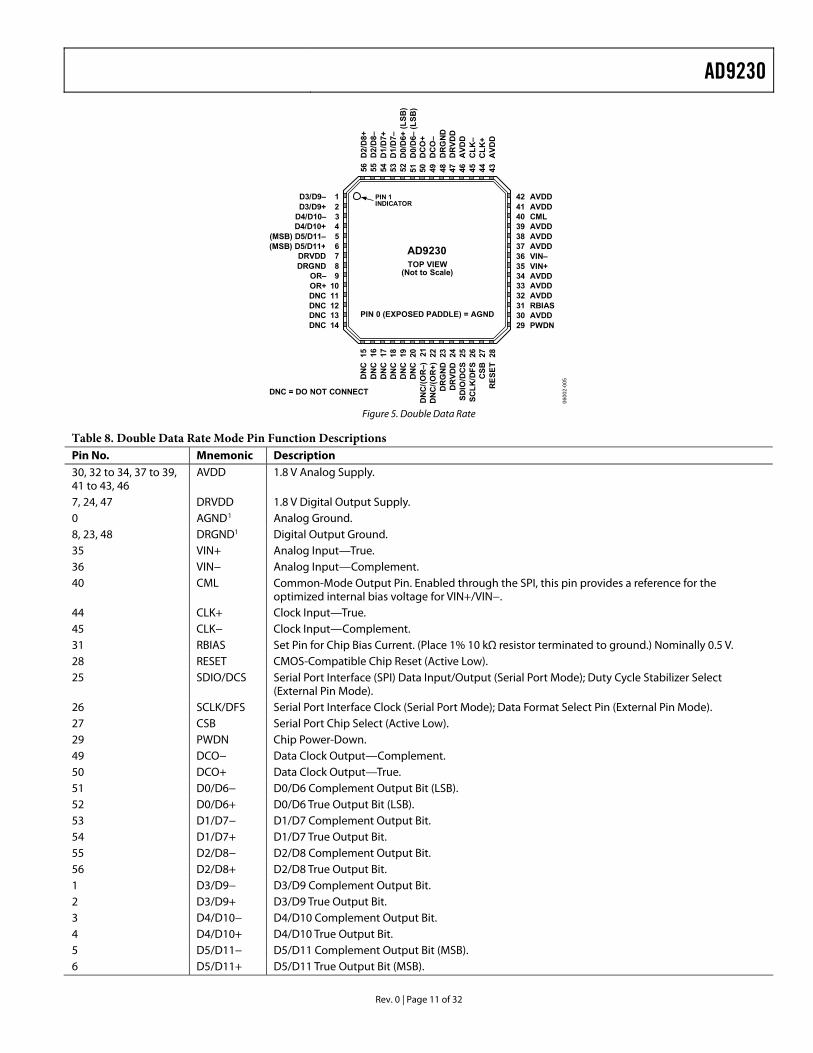
DNC = DO NOT CONNECT
PIN 1INDICATOR
1D3/D9–2D3/D9+3D4/D10–4D4/D10+5(MSB) D5/D11–6(MSB) D5/D11+7DRVDD8DRGND9OR–
10OR+11DNC12DNC13DNC14DNC
35 VIN+36 VIN–37 AVDD38 AVDD39 AVDD40 CML41 AVDD42 AVDD
34 AVDD33 AVDD32 AVDD31 RBIAS30 AVDD29 PWDN
15D
NC
16D
NC
17D
NC
19D
NC
21D
NC
/(OR
–)20
DN
C
22D
NC
/(OR
+)23
DR
GN
D24
DR
VDD
25SD
IO/D
CS
26SC
LK/D
FS27
CSB
28R
ESET
18D
NC
45C
LK–
46A
VDD
47D
RVD
D48
DR
GN
D49
DC
O–
50D
CO
+51
D0/
D6–
(LSB
)52
D0/
D6+
(LSB
)53
D1/
D7–
54D
1/D
7+
44C
LK+
43A
VDD
TOP VIEW(Not to Scale)
PIN 0 (EXPOSED PADDLE) = AGND
AD9230
55D
2/D
8–56
D2/
D8+
0600
2-00
5
Figure 5. Double Data Rate
Table 8. Double Data Rate Mode Pin Function Descriptions Pin No. Mnemonic Description 30, 32 to 34, 37 to 39, 41 to 43, 46
AVDD 1.8 V Analog Supply.
7, 24, 47 DRVDD 1.8 V Digital Output Supply. 0 AGND1 Analog Ground. 8, 23, 48 DRGND1 Digital Output Ground. 35 VIN+ Analog Input—True. 36 VIN− Analog Input—Complement. 40 CML Common-Mode Output Pin. Enabled through the SPI, this pin provides a reference for the
optimized internal bias voltage for VIN+/VIN−. 44 CLK+ Clock Input—True. 45 CLK− Clock Input—Complement. 31 RBIAS Set Pin for Chip Bias Current. (Place 1% 10 kΩ resistor terminated to ground.) Nominally 0.5 V. 28 RESET CMOS-Compatible Chip Reset (Active Low). 25 SDIO/DCS Serial Port Interface (SPI) Data Input/Output (Serial Port Mode); Duty Cycle Stabilizer Select
(External Pin Mode). 26 SCLK/DFS Serial Port Interface Clock (Serial Port Mode); Data Format Select Pin (External Pin Mode). 27 CSB Serial Port Chip Select (Active Low). 29 PWDN Chip Power-Down. 49 DCO− Data Clock Output—Complement. 50 DCO+ Data Clock Output—True. 51 D0/D6− D0/D6 Complement Output Bit (LSB). 52 D0/D6+ D0/D6 True Output Bit (LSB). 53 D1/D7− D1/D7 Complement Output Bit. 54 D1/D7+ D1/D7 True Output Bit. 55 D2/D8− D2/D8 Complement Output Bit. 56 D2/D8+ D2/D8 True Output Bit. 1 D3/D9− D3/D9 Complement Output Bit. 2 D3/D9+ D3/D9 True Output Bit. 3 D4/D10− D4/D10 Complement Output Bit. 4 D4/D10+ D4/D10 True Output Bit. 5 D5/D11− D5/D11 Complement Output Bit (MSB). 6 D5/D11+ D5/D11 True Output Bit (MSB).
AD9230
Rev. 0 | Page 12 of 32
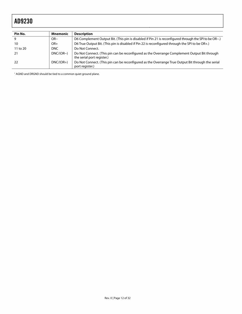
Pin No. Mnemonic Description 9 OR− D6 Complement Output Bit. (This pin is disabled if Pin 21 is reconfigured through the SPI to be OR−.) 10 OR+ D6 True Output Bit. (This pin is disabled if Pin 22 is reconfigured through the SPI to be OR+.) 11 to 20 DNC Do Not Connect. 21 DNC/(OR−) Do Not Connect. (This pin can be reconfigured as the Overrange Complement Output Bit through
the serial port register.) 22 DNC/(OR+) Do Not Connect. (This pin can be reconfigured as the Overrange True Output Bit through the serial
port register.) 1 AGND and DRGND should be tied to a common quiet ground plane.
AD9230
Rev. 0 | Page 13 of 32
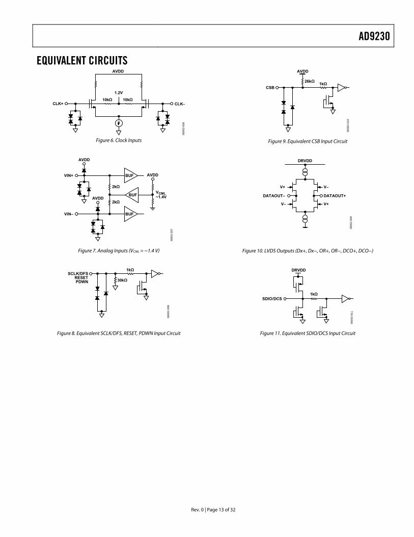
EQUIVALENT CIRCUITS
0600
2-00
6
1.2V10kΩ 10kΩ
CLK+ CLK–
AVDD
Figure 6. Clock Inputs
VIN+
AVDD
BUF
VIN–
AVDD
BUF
2kΩ
2kΩ
BUF
AVDD
VCML~1.4V
0600
2-00
7
Figure 7. Analog Inputs (VCML = ~1.4 V)
SCLK/DFSRESETPDWN
1kΩ
30kΩ
0600
2-00
8
Figure 8. Equivalent SCLK/DFS, RESET, PDWN Input Circuit
0600
2-01
0
CSB1kΩ26kΩ
AVDD
Figure 9. Equivalent CSB Input Circuit
DRVDD
DATAOUT+
V–
V+
DATAOUT–
V+
V–
0600
2-00
9
Figure 10. LVDS Outputs (Dx+, Dx−, OR+, OR−, DCO+, DCO−)
0600
2-01
1
SDIO/DCS1kΩ
DRVDD
Figure 11. Equivalent SDIO/DCS Input Circuit
AD9230
Rev. 0 | Page 14 of 32
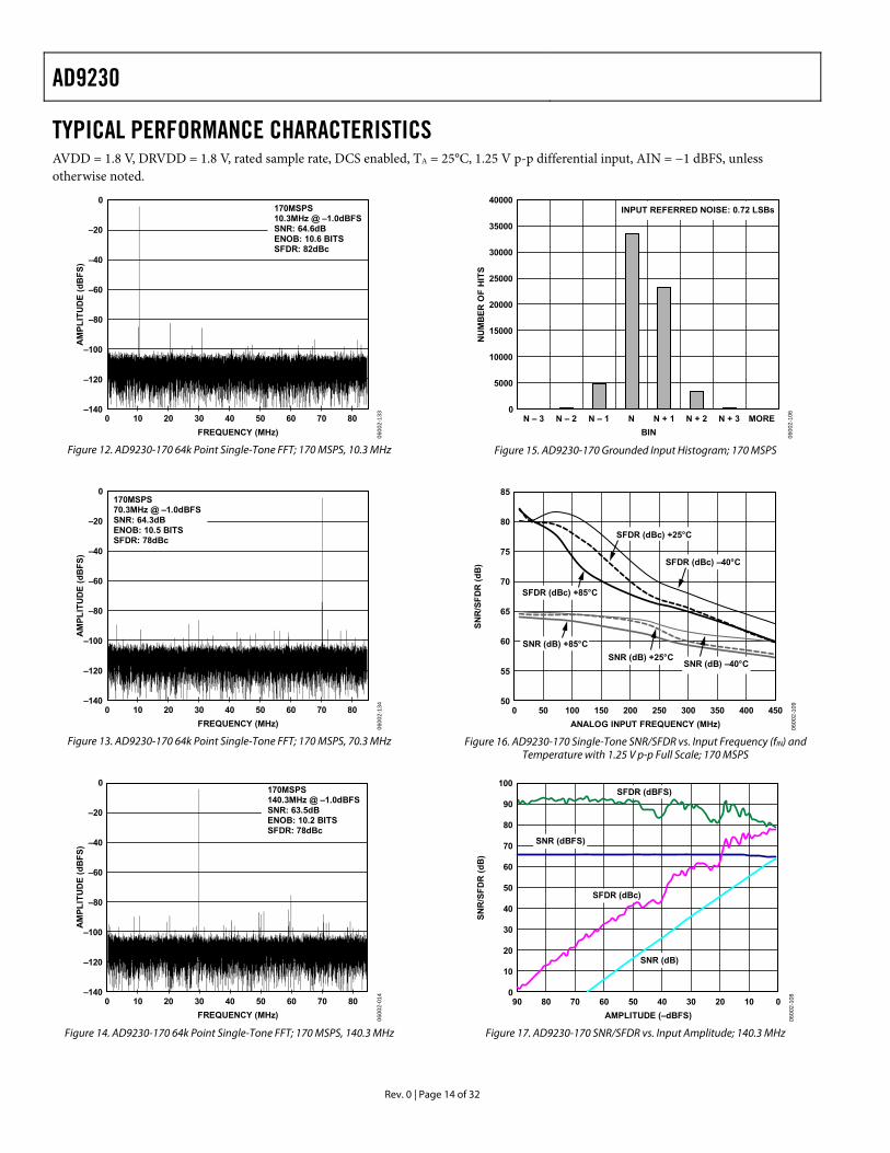
TYPICAL PERFORMANCE CHARACTERISTICS AVDD = 1.8 V, DRVDD = 1.8 V, rated sample rate, DCS enabled, TA = 25°C, 1.25 V p-p differential input, AIN = −1 dBFS, unless otherwise noted.
0
–20
–40
–60
–80
–100
–120
–140
AM
PLIT
UD
E (d
BFS
)
FREQUENCY (MHz)
170MSPS10.3MHz @ –1.0dBFSSNR: 64.6dBENOB: 10.6 BITSSFDR: 82dBc
0 8060 705040302010
0600
2-13
3
60 705040302010
AM
PLIT
UD
E (d
BFS
)
FREQUENCY (MHz)
Figure 12. AD9230-170 64k Point Single-Tone FFT; 170 MSPS, 10.3 MHz
0
–20
–40
–60
–80
–100
–120
–1400 80
40000
35000
30000
25000
20000
15000
10000
5000
0N – 3 N – 2 N – 1 N N + 1 N + 2 N + 3 MORE
NU
MB
ER O
F H
ITS
BIN
INPUT REFERRED NOISE: 0.72 LSBs
0600
2-10
6
170MSPS70.3MHz @ –1.0dBFSSNR: 64.3dBENOB: 10.5 BITSSFDR: 78dBc
0600
2-13
4
70605040302010
AM
PLIT
UD
E (d
BFS
)
FREQUENCY (MHz)
Figure 13. AD9230-170 64k Point Single-Tone FFT; 170 MSPS, 70.3 MHz
0
–20
–40
–60
–80
–100
–120
–1400 80
0600
2-01
4
170MSPS140.3MHz @ –1.0dBFSSNR: 63.5dBENOB: 10.2 BITSSFDR: 78dBc
Figure 14. AD9230-170 64k Point Single-Tone FFT; 170 MSPS, 140.3 MHz
Figure 15. AD9230-170 Grounded Input Histogram; 170 MSPS
85
80
75
70
65
60
55
500 450350 40030025020015050 100
SNR
/SFD
R (d
B)
ANALOG INPUT FREQUENCY (MHz)
SNR (dB) –40°C
SFDR (dBc) –40°C
SNR (dB) +25°C
SFDR (dBc) +25°C
SFDR (dBc) +85°C
SNR (dB) +85°C
0600
2-10
9
Figure 16. AD9230-170 Single-Tone SNR/SFDR vs. Input Frequency (fIN) and
Temperature with 1.25 V p-p Full Scale; 170 MSPS
100
10
20
30
40
50
60
70
80
90
090 020 103040506080 70
SNR
/SFD
R (d
B)
AMPLITUDE (–dBFS)
SNR (dBFS)
SFDR (dBc)
SFDR (dBFS)
SNR (dB)
0600
2-10
8
Figure 17. AD9230-170 SNR/SFDR vs. Input Amplitude; 140.3 MHz
AD9230
Rev. 0 | Page 15 of 32
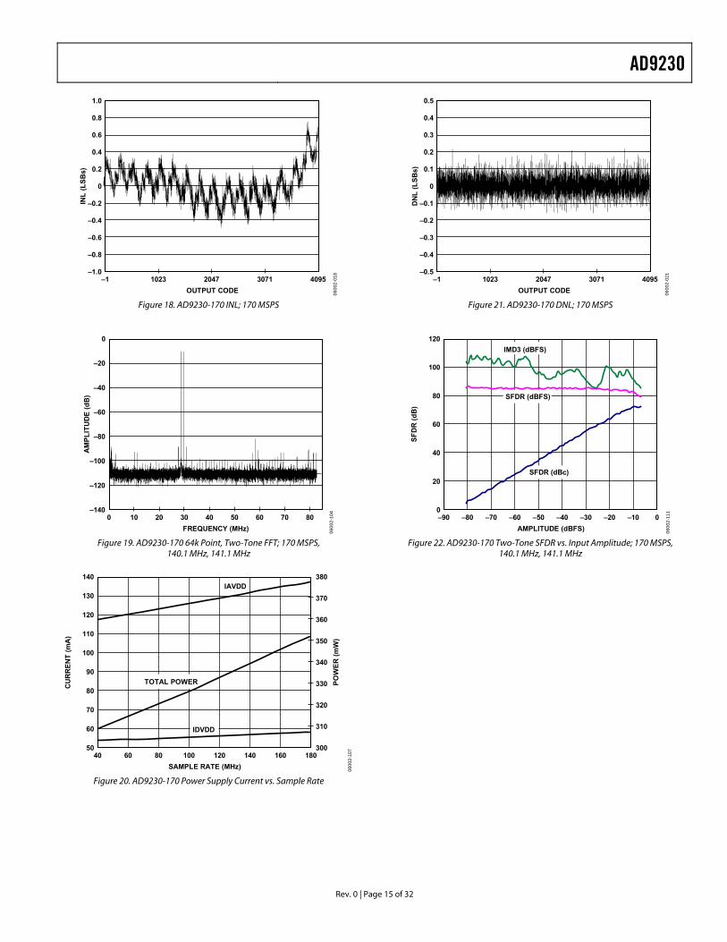
1.0
–1.0
–0.8
–0.6
–0.4
–0.2
0
0.2
0.4
0.6
0.8
–1 4095307120471023
INL
(LSB
s)
OUTPUT CODE 0600
2-01
8
Figure 18. AD9230-170 INL; 170 MSPS
0
–20
–40
–60
–80
–100
–120
–1400 8070605040302010
AM
PLIT
UD
E (d
B)
FREQUENCY (MHz) 0600
2-10
4
Figure 19. AD9230-170 64k Point, Two-Tone FFT; 170 MSPS,
140.1 MHz, 141.1 MHz
140
60
70
80
90
100
110
120
130
50
380
310
320
340
330
350
360
370
30040 1801601401201008060
CU
RR
ENT
(mA
)
POW
ER (m
W)
SAMPLE RATE (MHz)
IAVDD
IDVDD
TOTAL POWER
0600
2-10
7
Figure 20. AD9230-170 Power Supply Current vs. Sample Rate
0.5
–0.5
–0.4
–0.3
–0.2
–0.1
0
0.1
0.2
0.3
0.4
–1 4095307120471023
DN
L (L
SBs)
OUTPUT CODE 0600
2-02
1
Figure 21. AD9230-170 DNL; 170 MSPS
120
0
20
40
60
80
100
–90 0–10–20–30–40–50–60–70–80
SFD
R (d
B)
AMPLITUDE (dBFS)
SFDR (dBc)
SFDR (dBFS)
IMD3 (dBFS)
0600
2-11
1
Figure 22. AD9230-170 Two-Tone SFDR vs. Input Amplitude; 170 MSPS,
140.1 MHz, 141.1 MHz
AD9230
Rev. 0 | Page 16 of 32
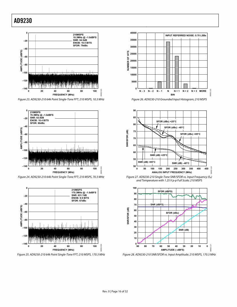
0
–20
–40
–60
–80
–100
–120
–1400 10080604020
AM
PLIT
UD
E (d
BFS
)
FREQUENCY (MHz) 0600
2-02
3
210MSPS10.3MHz @ –1.0dBFSSNR: 64.5dBENOB: 10.5 BITSSFDR: 79dBc
Figure 23. AD9230-210 64k Point Single-Tone FFT; 210 MSPS, 10.3 MHz
0
–20
–40
–60
–80
–100
–120
–1400 10080604020
AM
PLIT
UD
E (d
BFS
)
FREQUENCY (MHz) 0600
2-02
4
210MSPS70.3MHz @ –1.0dBFSSNR: 63.9dBENOB: 10.4 BITSSFDR: 80dBc
Figure 24. AD9230-210 64k Point Single-Tone FFT; 210 MSPS, 70.3 MHz
0
–20
–40
–60
–80
–100
–120
–1400 10080604020
AM
PLIT
UD
E (d
BFS
)
FREQUENCY (MHz) 0600
2-02
4
210MSPS170.3MHz @ –1.0dBFSSNR: 631.7dBENOB: 9.9 BITSSFDR: 67dBc
Figure 25. AD9230-210 64k Point Single-Tone FFT; 210 MSPS, 170.3 MHz
40000
35000
30000
25000
20000
15000
10000
5000
0N – 3 N – 2 N – 1 N N + 1 N + 2 N + 3 MORE
NU
MB
ER O
F H
ITS
BIN
INPUT REFERRED NOISE: 0.70 LSBs
0600
2-11
5
Figure 26. AD9230-210 Grounded Input Histogram; 210 MSPS
90
85
80
75
70
65
60
55
500 45040035030025020015010050
SNR
/SFD
R (d
B)
ANALOG INPUT FREQUENCY (MHz)
SNR (dB) –40°C
SFDR (dBc) –40°C
SNR (dB) +25°C
SFDR (dBc) +25°C
SNR (dB) +85°C
SFDR (dBc) +85°C
0600
2-11
8
Figure 27. AD9230-210 Single-Tone SNR/SFDR vs. Input Frequency (fIN)
and Temperature with 1.25 V p-p Full Scale; 210 MSPS
100
90
80
70
60
50
40
30
20
10
090 01020304050607080
SNR
/SFD
R (d
B)
AMPLITUDE (–dBFS)
SNR (dBFS)
SFDR (dBc)
SFDR (dBFS)
SNR (dB)
0600
2-11
7
Figure 28. AD9230-210 SNR/SFDR vs. Input Amplitude; 210 MSPS, 170.3 MHz
AD9230
Rev. 0 | Page 17 of 32
1.0
–1.0
–0.8
–0.6
–0.4
–0.2
0
0.2
0.4
0.6
0.8
–1 4095307120471023
INL
(LSB
s)
OUTPUT CODE 0600
2-02
9
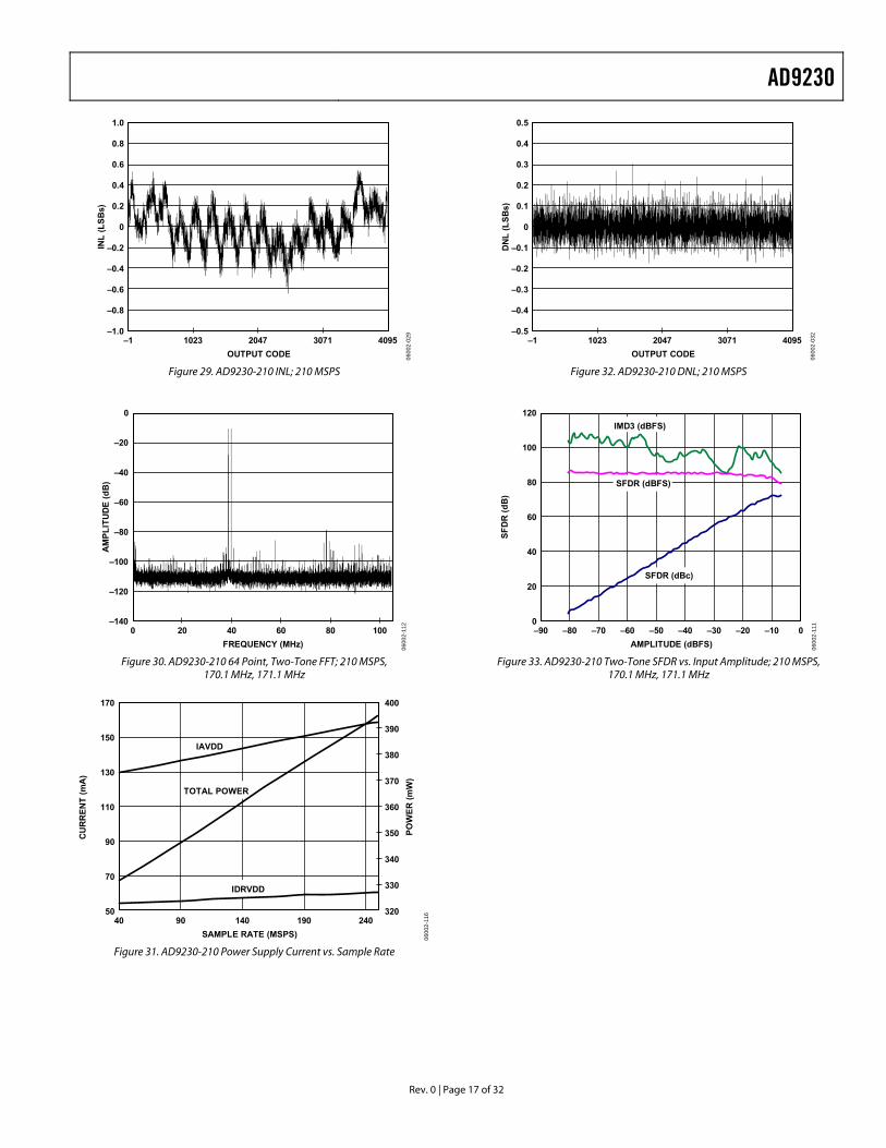
Figure 29. AD9230-210 INL; 210 MSPS
0
–20
–40
–60
–80
–100
–120
–1400 10080604020
AM
PLIT
UD
E (d
B)
FREQUENCY (MHz) 0600
2-11
2
Figure 30. AD9230-210 64 Point, Two-Tone FFT; 210 MSPS,
170.1 MHz, 171.1 MHz
170
150
70
90
110
130
50
400
320
330
340
350
360
370
380
390
40 24019014090
CU
RR
ENT
(mA
)
POW
ER (m
W)
SAMPLE RATE (MSPS)
IAVDD
IDRVDD
TOTAL POWER
0600
2-11
6
Figure 31. AD9230-210 Power Supply Current vs. Sample Rate
0.5
–0.5
–0.4
–0.3
–0.2
–0.1
0
0.1
0.2
0.3
0.4
–1 4095307120471023
DN
L (L
SBs)
OUTPUT CODE 0600
2-03
2
Figure 32. AD9230-210 DNL; 210 MSPS
120
0
20
40
60
80
100
–90 0–10–20–30–40–50–60–70–80
SFD
R (d
B)
AMPLITUDE (dBFS)
SFDR (dBc)
SFDR (dBFS)
IMD3 (dBFS)
0600
2-11
1
Figure 33. AD9230-210 Two-Tone SFDR vs. Input Amplitude; 210 MSPS,
170.1 MHz, 171.1 MHz
AD9230
Rev. 0 | Page 18 of 32
0
–20
–40
–60
–80
–100
–120
–1400 12010080604020
AM
PLIT
UD
E (d
BFS
)
FREQUENCY (MHz)
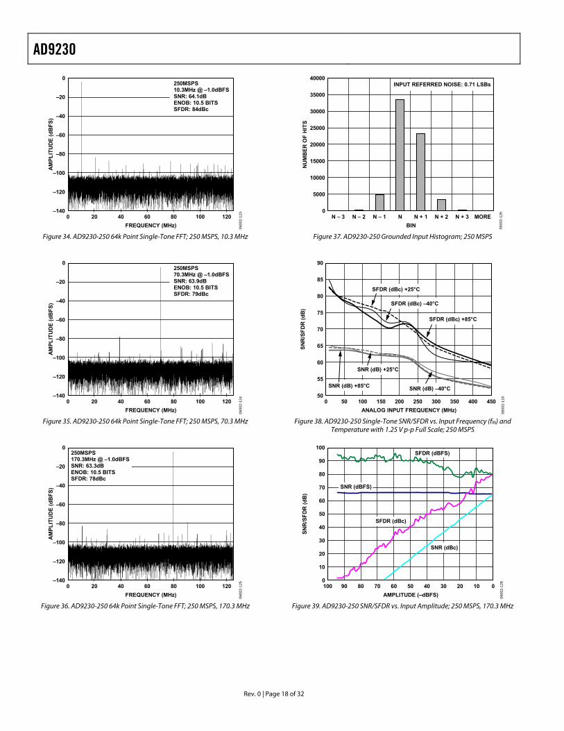
250MSPS10.3MHz @ –1.0dBFSSNR: 64.1dBENOB: 10.5 BITSSFDR: 84dBc
0600
2-12
3
Figure 34. AD9230-250 64k Point Single-Tone FFT; 250 MSPS, 10.3 MHz
0
–20
–40
–60
–80
–100
–120
–1400 12010080604020
AM
PLIT
UD
E (d
BFS
)
FREQUENCY (MHz)
250MSPS70.3MHz @ –1.0dBFSSNR: 63.9dBENOB: 10.5 BITSSFDR: 79dBc
0600
2-12
4
Figure 35. AD9230-250 64k Point Single-Tone FFT; 250 MSPS, 70.3 MHz
0
–20
–40
–60
–80
–100
–120
–1400 12010080604020
AM
PLIT
UD
E (d
BFS
)
FREQUENCY (MHz)
250MSPS170.3MHz @ –1.0dBFSSNR: 63.3dBENOB: 10.5 BITSSFDR: 78dBc
0600
2-12
5
Figure 36. AD9230-250 64k Point Single-Tone FFT; 250 MSPS, 170.3 MHz
40000
35000
30000
25000
20000
15000
10000
5000
0N – 3 N – 2 N – 1 N N + 1 N + 2 N + 3 MORE
NU
MB
ER O
F H
ITS
BIN
INPUT REFERRED NOISE: 0.71 LSBs
0600
2-12
6
Figure 37. AD9230-250 Grounded Input Histogram; 250 MSPS
90
85
80
75
70
65
60
55
500 45040035030025020015010050
SNR
/SFD
R (d
B)
ANALOG INPUT FREQUENCY (MHz)
SNR (dB) –40°C
SFDR (dBc) –40°C
SNR (dB) +25°C
SFDR (dBc) +25°C
SNR (dB) +85°C
SFDR (dBc) +85°C
0600
2-11
8
Figure 38. AD9230-250 Single-Tone SNR/SFDR vs. Input Frequency (fIN) and
Temperature with 1.25 V p-p Full Scale; 250 MSPS
100
10
20
30
40
50
60
70
80
90
0100 90 020 103040506080 70
SNR
/SFD
R (d
B)
AMPLITUDE (–dBFS)
SNR (dBFS)
SFDR (dBc)
SFDR (dBFS)
SNR (dBc)
0600
2-12
8
Figure 39. AD9230-250 SNR/SFDR vs. Input Amplitude; 250 MSPS, 170.3 MHz
AD9230
Rev. 0 | Page 19 of 32
1.0
–1.0
–0.8
–0.6
–0.4
–0.2
0
0.2
0.4
0.6
0.8
–1 4095307120471023
INL
(LSB
s)
OUTPUT CODE 0600
2-13
5
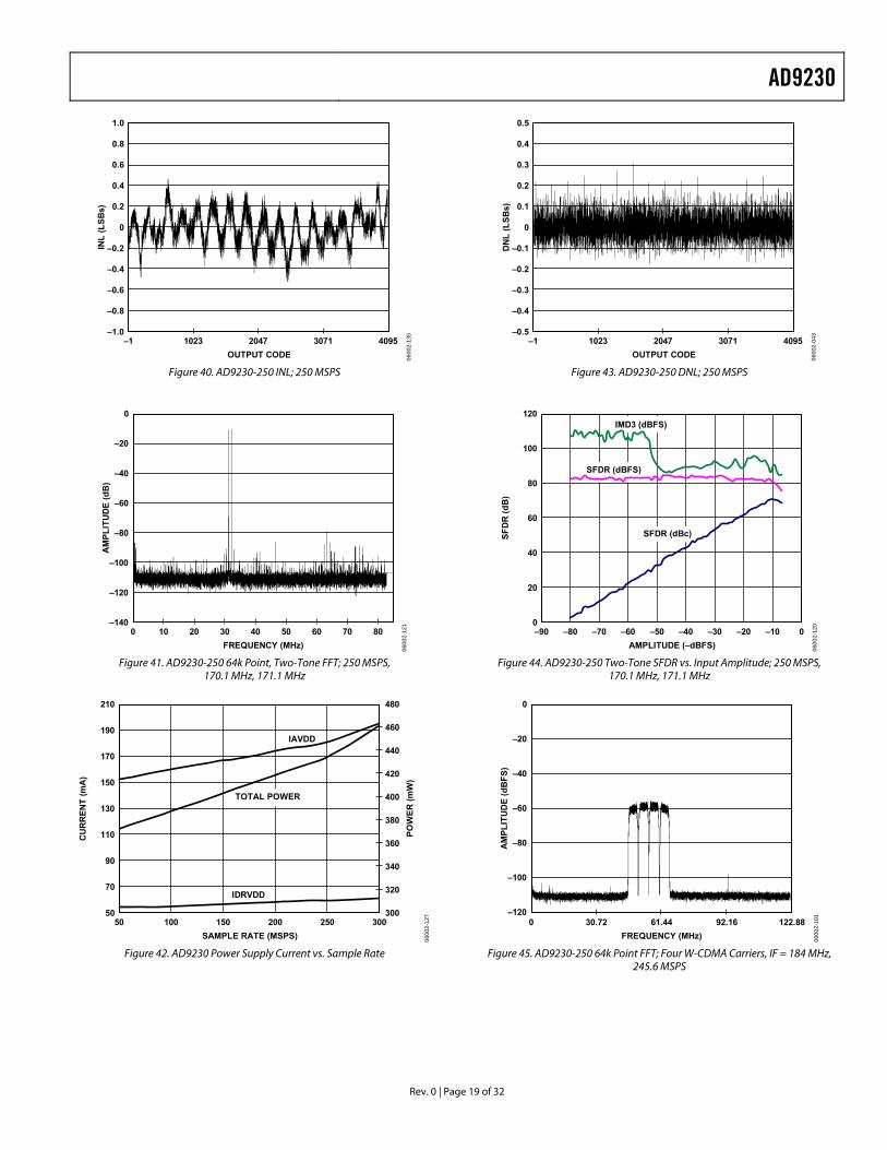
Figure 40. AD9230-250 INL; 250 MSPS
0
–20
–40
–60
–80
–100
–120
–1400 8070605040302010
AM
PLIT
UD
E (d
B)
FREQUENCY (MHz) 0600
2-12
1
Figure 41. AD9230-250 64k Point, Two-Tone FFT; 250 MSPS,
170.1 MHz, 171.1 MHz
210
50
70
90
110
130
150
170
190
480
300
320
340
360
380
400
420
440
460
50 300250200150100
CU
RR
ENT
(mA
)
POW
ER (m
W)
SAMPLE RATE (MSPS)
IAVDD
IDRVDD
TOTAL POWER
0600
2-12
7
Figure 42. AD9230 Power Supply Current vs. Sample Rate
0.5
–0.5
–0.4
–0.3
–0.2
–0.1
0
0.1
0.2
0.3
0.4
–1 4095307120471023
DN
L (L
SBs)
OUTPUT CODE 0600
2-04
3
Figure 43. AD9230-250 DNL; 250 MSPS
120
100
80
60
40
20
0–90 0–10–20–30–40–50–60–70–80
SFD
R (d
B)
AMPLITUDE (–dBFS)
SFDR (dBc)
SFDR (dBFS)
IMD3 (dBFS)
0600
2-12
0
Figure 44. AD9230-250 Two-Tone SFDR vs. Input Amplitude; 250 MSPS,
170.1 MHz, 171.1 MHz
0
–20
–40
–60
–80
–100
–1200 30.72 61.44 92.16 122.88
AM
PLIT
UD
E (d
BFS
)
FREQUENCY (MHz) 0600
2-10
1
Figure 45. AD9230-250 64k Point FFT; Four W-CDMA Carriers, IF = 184 MHz,
245.6 MSPS
AD9230
Rev. 0 | Page 20 of 32
85
80
75
70
65
60
55
501.0 1.1 1.2 1.3 1.4 1.5 1.6 1.7 1.8
SNR
/SFD
R (d
B)
VCM (V)
SNR (dB)
SFDR (dBc)
0600
2-13
0
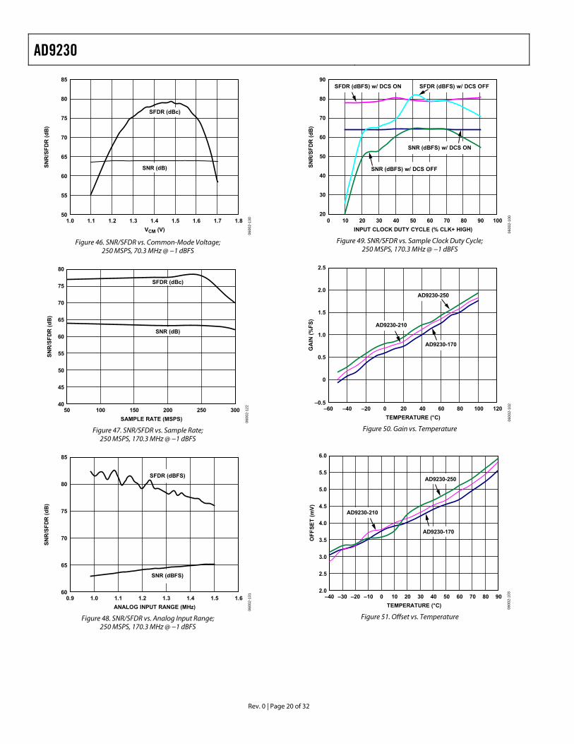
Figure 46. SNR/SFDR vs. Common-Mode Voltage;
250 MSPS, 70.3 MHz @ −1 dBFS
80
40
45
50
55
60
65
70
75
50 300250200150100
SNR
/SFD
R (d
B)
SAMPLE RATE (MSPS)
SNR (dB)
SFDR (dBc)
0600
2-12
2
Figure 47. SNR/SFDR vs. Sample Rate;
250 MSPS, 170.3 MHz @ −1 dBFS
85
80
75
70
65
600.9 1.61.51.41.31.21.11.0
SNR
/SFD
R (d
B)
ANALOG INPUT RANGE (MHz)
SNR (dBFS)
SFDR (dBFS)
0600
2-13
1
Figure 48. SNR/SFDR vs. Analog Input Range;
250 MSPS, 170.3 MHz @ −1 dBFS
90
20
30
40
50
60
70
80
0 10 20 30 40 50 60 70 80 90 100
SNR
/SFD
R (d
B)
INPUT CLOCK DUTY CYCLE (% CLK+ HIGH)
SNR (dBFS) w/ DCS ON
SFDR (dBFS) w/ DCS ON
SNR (dBFS) w/ DCS OFF
SFDR (dBFS) w/ DCS OFF
0600
2-10
0
Figure 49. SNR/SFDR vs. Sample Clock Duty Cycle;
250 MSPS, 170.3 MHz @ −1 dBFS
2.5
2.0
1.5
1.0
0.5
0
–0.5–60 120100806040200–20–40
GA
IN (%
FS)
TEMPERATURE (°C)
AD9230-210
AD9230-250
AD9230-170
0600
2-10
2
Figure 50. Gain vs. Temperature
6.0
5.5
5.0
4.5
4.0
3.5
3.0
2.5
2.0–40 –30 –20 –10 0 908070605040302010
OFF
SET
(mV)
TEMPERATURE (°C)
AD9230-170
AD9230-210
AD9230-250
0600
2-10
3
Figure 51. Offset vs. Temperature
AD9230
Rev. 0 | Page 21 of 32
THEORY OF OPERATION The AD9230 architecture consists of a front-end sample and hold amplifier (SHA) followed by a pipelined switched capacitor ADC. The quantized outputs from each stage are combined into a final 12-bit result in the digital correction logic. The pipelined architecture permits the first stage to operate on a new input sample, while the remaining stages operate on preceding samples. Sampling occurs on the rising edge of the clock.
Each stage of the pipeline, excluding the last, consists of a low resolution flash ADC connected to a switched capacitor DAC and interstage residue amplifier (MDAC). The residue amplifier magnifies the difference between the reconstructed DAC output and the flash input for the next stage in the pipeline. One bit of redundancy is used in each stage to facilitate digital correction of flash errors. The last stage simply consists of a flash ADC.
The input stage contains a differential SHA that can be ac- or dc-coupled in differential or single-ended mode. The output-staging block aligns the data, carries out the error correction, and passes the data to the output buffers. The output buffers are powered from a separate supply, allowing adjustment of the output voltage swing. During power-down, the output buffers go into a high impedance state.
ANALOG INPUT AND VOLTAGE REFERENCE The analog input to the AD9230 is a differential buffer. For best dynamic performance, the source impedances driving VIN+ and VIN− should be matched such that common-mode settling errors are symmetrical. The analog input is optimized to provide superior wideband performance and requires that the analog inputs be driven differentially. SNR and SINAD performance degrades significantly if the analog input is driven with a single-ended signal.
A wideband transformer, such as Mini-Circuits® ADT1-1WT, can provide the differential analog inputs for applications that require a single-ended-to-differential conversion. Both analog inputs are self-biased by an on-chip resistor divider to a nominal 1.3 V.
An internal differential voltage reference creates positive and negative reference voltages that define the 1.25 V p-p fixed span of the ADC core. This internal voltage reference can be adjusted by means of SPI control. See the AD9230 Configuration Using the SPI section for more details.
Differential Input Configurations
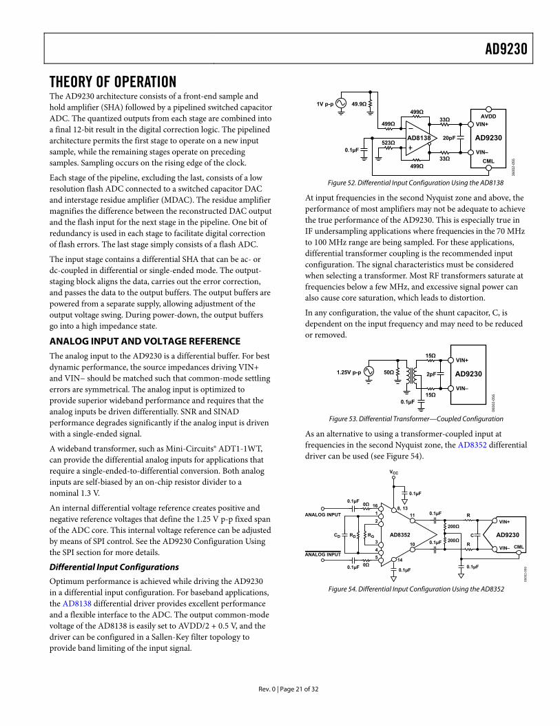
Optimum performance is achieved while driving the AD9230 in a differential input configuration. For baseband applications, the AD8138 differential driver provides excellent performance and a flexible interface to the ADC. The output common-mode voltage of the AD8138 is easily set to AVDD/2 + 0.5 V, and the driver can be configured in a Sallen-Key filter topology to provide band limiting of the input signal.
VIN+
VIN–
AVDD
CML
AD8138523Ω
499Ω
499Ω
499Ω33Ω
33Ω
49.9Ω1V p-p
0.1µF
20pF AD9230
0600
2-05
5
Figure 52. Differential Input Configuration Using the AD8138
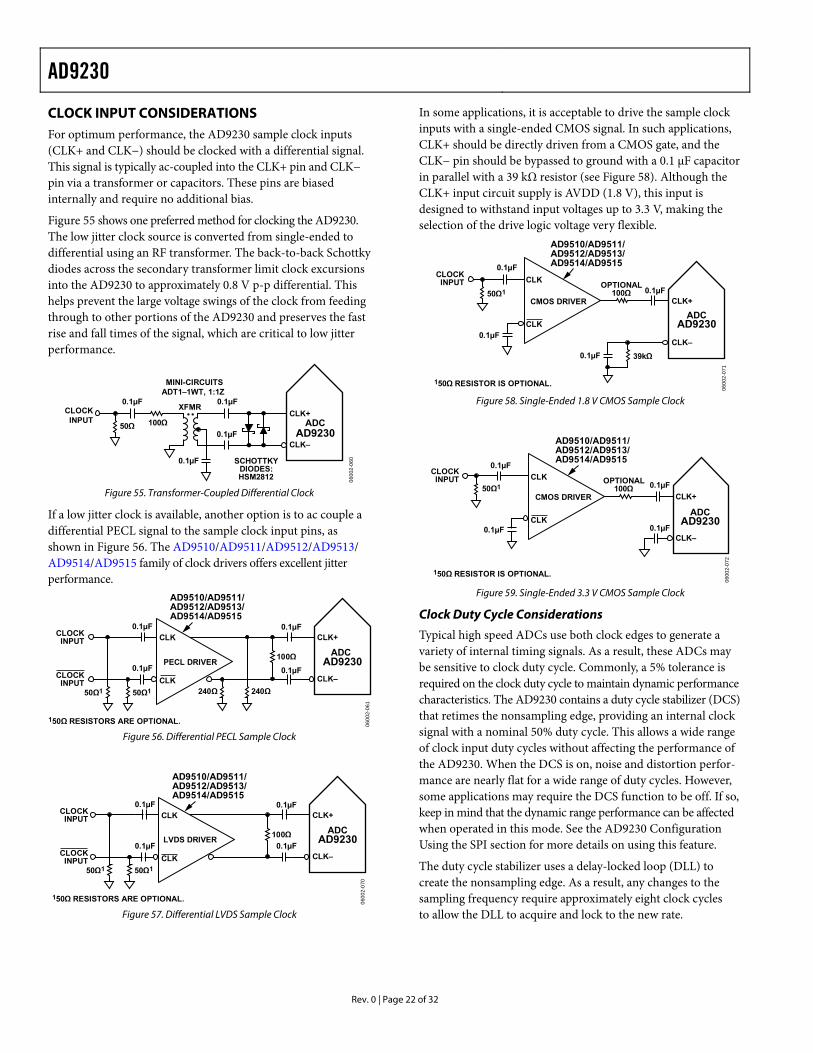
At input frequencies in the second Nyquist zone and above, the performance of most amplifiers may not be adequate to achieve the true performance of the AD9230. This is especially true in IF undersampling applications where frequencies in the 70 MHz to 100 MHz range are being sampled. For these applications, differential transformer coupling is the recommended input configuration. The signal characteristics must be considered when selecting a transformer. Most RF transformers saturate at frequencies below a few MHz, and excessive signal power can also cause core saturation, which leads to distortion.
In any configuration, the value of the shunt capacitor, C, is dependent on the input frequency and may need to be reduced or removed.
VIN+
VIN–
15Ω
15Ω
50Ω1.25V p-p
0.1µF
2pF AD9230
0600
2-05
6
Figure 53. Differential Transformer—Coupled Configuration
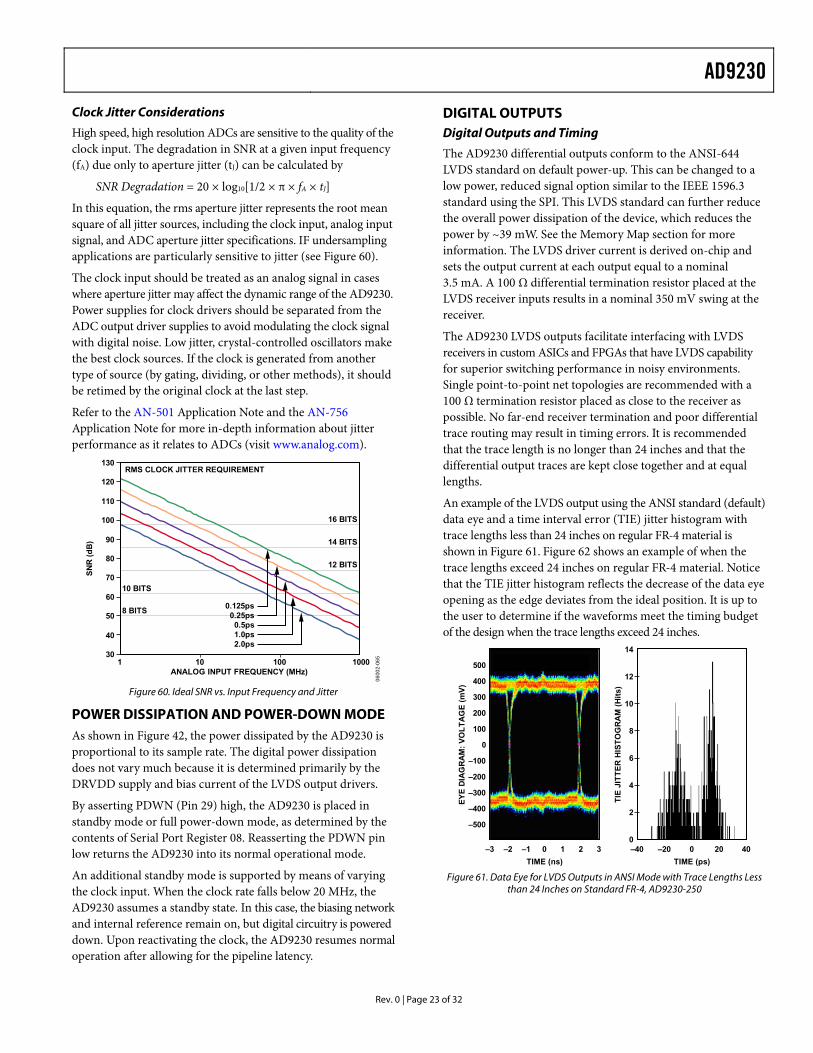
As an alternative to using a transformer-coupled input at frequencies in the second Nyquist zone, the AD8352 differential driver can be used (see Figure 54).
0600
2-05
9
AD9230AD8352
0Ω
R
0Ω
CD RD RG
0.1µF
0.1µF
0.1µF
VIN+
VIN– CML
C
0.1µF
0.1µF
1612
345
11
R0.1µF
0.1µF
10
8, 13
14
VCC
200Ω
200Ω
ANALOG INPUT
ANALOG INPUT
Figure 54. Differential Input Configuration Using the AD8352
AD9230
Rev. 0 | Page 22 of 32
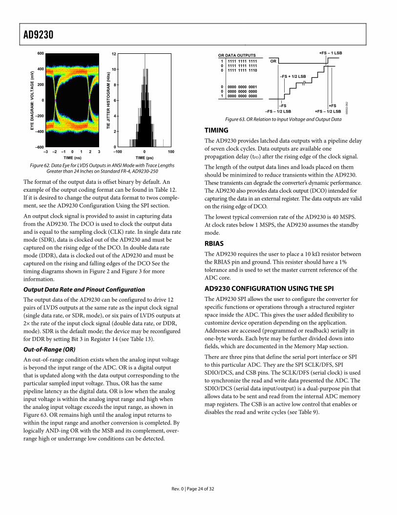
CLOCK INPUT CONSIDERATIONS For optimum performance, the AD9230 sample clock inputs (CLK+ and CLK−) should be clocked with a differential signal. This signal is typically ac-coupled into the CLK+ pin and CLK− pin via a transformer or capacitors. These pins are biased internally and require no additional bias.
Figure 55 shows one preferred method for clocking the AD9230. The low jitter clock source is converted from single-ended to differential using an RF transformer. The back-to-back Schottky diodes across the secondary transformer limit clock excursions into the AD9230 to approximately 0.8 V p-p differential. This helps prevent the large voltage swings of the clock from feeding through to other portions of the AD9230 and preserves the fast rise and fall times of the signal, which are critical to low jitter performance.
0600
2-06
0
0.1µF
0.1µF
0.1µF0.1µFCLOCK
INPUT50Ω 100Ω
CLK–
CLK+ADC
AD9230
MINI-CIRCUITSADT1–1WT, 1:1Z
XFMR
SCHOTTKYDIODES:HSM2812
Figure 55. Transformer-Coupled Differential Clock
If a low jitter clock is available, another option is to ac couple a differential PECL signal to the sample clock input pins, as shown in Figure 56. The AD9510/AD9511/AD9512/AD9513/ AD9514/AD9515 family of clock drivers offers excellent jitter performance.
0600
2-06
1
100Ω0.1µF
0.1µF0.1µF
0.1µF
240Ω240Ω
AD9510/AD9511/AD9512/AD9513/AD9514/AD9515
50Ω1 50Ω1CLK
CLK
150Ω RESISTORS ARE OPTIONAL.
CLK–
CLK+
ADCAD9230PECL DRIVER
CLOCKINPUT
CLOCKINPUT
Figure 56. Differential PECL Sample Clock
0600
2-07
0
CLOCKINPUT
CLOCKINPUT
100Ω0.1µF
0.1µF0.1µF
0.1µF
50Ω1
LVDS DRIVER
50Ω1CLK
CLK
150Ω RESISTORS ARE OPTIONAL.
CLK–
CLK+
ADCAD9230
AD9510/AD9511/AD9512/AD9513/AD9514/AD9515
Figure 57. Differential LVDS Sample Clock
In some applications, it is acceptable to drive the sample clock inputs with a single-ended CMOS signal. In such applications, CLK+ should be directly driven from a CMOS gate, and the CLK− pin should be bypassed to ground with a 0.1 μF capacitor in parallel with a 39 kΩ resistor (see Figure 58). Although the CLK+ input circuit supply is AVDD (1.8 V), this input is designed to withstand input voltages up to 3.3 V, making the selection of the drive logic voltage very flexible.
0600
2-07
1
0.1µF
0.1µF
0.1µF
39kΩ
CMOS DRIVER50Ω1
OPTIONAL100Ω
0.1µFCLK
CLK
150Ω RESISTOR IS OPTIONAL.
CLK–
CLK+
ADCAD9230
AD9510/AD9511/AD9512/AD9513/AD9514/AD9515
CLOCKINPUT
Figure 58. Single-Ended 1.8 V CMOS Sample Clock
0600
2-07
2
0.1µF
0.1µF
0.1µF
CMOS DRIVER
CLK
CLK
150Ω RESISTOR IS OPTIONAL.
0.1µFCLK–
CLK+
AD9510/AD9511/AD9512/AD9513/AD9514/AD9515
ADCAD9230
CLOCKINPUT
50Ω1OPTIONAL
100Ω
Figure 59. Single-Ended 3.3 V CMOS Sample Clock
Clock Duty Cycle Considerations
Typical high speed ADCs use both clock edges to generate a variety of internal timing signals. As a result, these ADCs may be sensitive to clock duty cycle. Commonly, a 5% tolerance is required on the clock duty cycle to maintain dynamic performance characteristics. The AD9230 contains a duty cycle stabilizer (DCS) that retimes the nonsampling edge, providing an internal clock signal with a nominal 50% duty cycle. This allows a wide range of clock input duty cycles without affecting the performance of the AD9230. When the DCS is on, noise and distortion perfor-mance are nearly flat for a wide range of duty cycles. However, some applications may require the DCS function to be off. If so, keep in mind that the dynamic range performance can be affected when operated in this mode. See the AD9230 Configuration Using the SPI section for more details on using this feature.
The duty cycle stabilizer uses a delay-locked loop (DLL) to create the nonsampling edge. As a result, any changes to the sampling frequency require approximately eight clock cycles to allow the DLL to acquire and lock to the new rate.
AD9230
Rev. 0 | Page 23 of 32
Clock Jitter Considerations
High speed, high resolution ADCs are sensitive to the quality of the clock input. The degradation in SNR at a given input frequency (fA) due only to aperture jitter (tJ) can be calculated by
SNR Degradation = 20 × log10[1/2 × π × fA × tJ]
In this equation, the rms aperture jitter represents the root mean square of all jitter sources, including the clock input, analog input signal, and ADC aperture jitter specifications. IF undersampling applications are particularly sensitive to jitter (see Figure 60).
The clock input should be treated as an analog signal in cases where aperture jitter may affect the dynamic range of the AD9230. Power supplies for clock drivers should be separated from the ADC output driver supplies to avoid modulating the clock signal with digital noise. Low jitter, crystal-controlled oscillators make the best clock sources. If the clock is generated from another type of source (by gating, dividing, or other methods), it should be retimed by the original clock at the last step.
Refer to the AN-501 Application Note and the AN-756 Application Note for more in-depth information about jitter performance as it relates to ADCs (visit www.analog.com).
0600
2-06
5
1 10 100 1000
16 BITS
14 BITS
12 BITS
30
40
50
60
70
80
90
100
110
120
130
0.125ps0.25ps
0.5ps1.0ps2.0ps
ANALOG INPUT FREQUENCY (MHz)
10 BITS
8 BITS
RMS CLOCK JITTER REQUIREMENT
SNR
(dB
)
Figure 60. Ideal SNR vs. Input Frequency and Jitter
POWER DISSIPATION AND POWER-DOWN MODE As shown in Figure 42, the power dissipated by the AD9230 is proportional to its sample rate. The digital power dissipation does not vary much because it is determined primarily by the DRVDD supply and bias current of the LVDS output drivers.
By asserting PDWN (Pin 29) high, the AD9230 is placed in standby mode or full power-down mode, as determined by the contents of Serial Port Register 08. Reasserting the PDWN pin low returns the AD9230 into its normal operational mode.
An additional standby mode is supported by means of varying the clock input. When the clock rate falls below 20 MHz, the AD9230 assumes a standby state. In this case, the biasing network and internal reference remain on, but digital circuitry is powered down. Upon reactivating the clock, the AD9230 resumes normal operation after allowing for the pipeline latency.
DIGITAL OUTPUTS Digital Outputs and Timing
The AD9230 differential outputs conform to the ANSI-644 LVDS standard on default power-up. This can be changed to a low power, reduced signal option similar to the IEEE 1596.3 standard using the SPI. This LVDS standard can further reduce the overall power dissipation of the device, which reduces the power by ~39 mW. See the Memory Map section for more information. The LVDS driver current is derived on-chip and sets the output current at each output equal to a nominal 3.5 mA. A 100 Ω differential termination resistor placed at the LVDS receiver inputs results in a nominal 350 mV swing at the receiver.
The AD9230 LVDS outputs facilitate interfacing with LVDS receivers in custom ASICs and FPGAs that have LVDS capability for superior switching performance in noisy environments. Single point-to-point net topologies are recommended with a 100 Ω termination resistor placed as close to the receiver as possible. No far-end receiver termination and poor differential trace routing may result in timing errors. It is recommended that the trace length is no longer than 24 inches and that the differential output traces are kept close together and at equal lengths.
An example of the LVDS output using the ANSI standard (default) data eye and a time interval error (TIE) jitter histogram with trace lengths less than 24 inches on regular FR-4 material is shown in Figure 61. Figure 62 shows an example of when the trace lengths exceed 24 inches on regular FR-4 material. Notice that the TIE jitter histogram reflects the decrease of the data eye opening as the edge deviates from the ideal position. It is up to the user to determine if the waveforms meet the timing budget of the design when the trace lengths exceed 24 inches.
500
–500
–400
–300
–200
–100
0
100
200
300
400
–3 –2 –1 0 1 2 3
EYE
DIA
GR
AM
: VO
LTA
GE
(mV)
TIME (ns)
14
12
10
8
6
4
2
0–40 –20 0 20 40
TIE
JITT
ER H
ISTO
GR
AM
(Hits
)
TIME (ps) Figure 61. Data Eye for LVDS Outputs in ANSI Mode with Trace Lengths Less
than 24 Inches on Standard FR-4, AD9230-250
AD9230
Rev. 0 | Page 24 of 32
600
–600
–400
–200
0
200
400
–3 –2 –1 0 1 2 3
EYE
DIA
GR
AM
: VO
LTA
GE
(mV)
TIME (ns)
12
10
8
6
4
2
0–100 0 100
TIE
JITT
ER H
ISTO
GR
AM
(Hits
)
TIME (ps) Figure 62. Data Eye for LVDS Outputs in ANSI Mode with Trace Lengths
Greater than 24 Inches on Standard FR-4, AD9230-250
The format of the output data is offset binary by default. An example of the output coding format can be found in Table 12. If it is desired to change the output data format to twos comple-ment, see the AD9230 Configuration Using the SPI section.
An output clock signal is provided to assist in capturing data from the AD9230. The DCO is used to clock the output data and is equal to the sampling clock (CLK) rate. In single data rate mode (SDR), data is clocked out of the AD9230 and must be captured on the rising edge of the DCO. In double data rate mode (DDR), data is clocked out of the AD9230 and must be captured on the rising and falling edges of the DCO See the timing diagrams shown in Figure 2 and Figure 3 for more information.
Output Data Rate and Pinout Configuration
The output data of the AD9230 can be configured to drive 12 pairs of LVDS outputs at the same rate as the input clock signal (single data rate, or SDR, mode), or six pairs of LVDS outputs at 2× the rate of the input clock signal (double data rate, or DDR, mode). SDR is the default mode; the device may be reconfigured for DDR by setting Bit 3 in Register 14 (see Table 13).
Out-of-Range (OR)
An out-of-range condition exists when the analog input voltage is beyond the input range of the ADC. OR is a digital output that is updated along with the data output corresponding to the particular sampled input voltage. Thus, OR has the same pipeline latency as the digital data. OR is low when the analog input voltage is within the analog input range and high when the analog input voltage exceeds the input range, as shown in Figure 63. OR remains high until the analog input returns to within the input range and another conversion is completed. By logically AND-ing OR with the MSB and its complement, over-range high or underrange low conditions can be detected.
100
001
OR DATA OUTPUTSOR
+FS – 1 LSB
+FS – 1/2 LSB+FS–FS
–FS + 1/2 LSB
–FS – 1/2 LSB
111111111111
000000000000
111111111111
000000000000
111111111110
000100000000
0600
2-06
2
Figure 63. OR Relation to Input Voltage and Output Data
TIMING The AD9230 provides latched data outputs with a pipeline delay of seven clock cycles. Data outputs are available one propagation delay (tPD) after the rising edge of the clock signal.
The length of the output data lines and loads placed on them should be minimized to reduce transients within the AD9230. These transients can degrade the converter’s dynamic performance. The AD9230 also provides data clock output (DCO) intended for capturing the data in an external register. The data outputs are valid on the rising edge of DCO.
The lowest typical conversion rate of the AD9230 is 40 MSPS. At clock rates below 1 MSPS, the AD9230 assumes the standby mode.
RBIAS The AD9230 requires the user to place a 10 kΩ resistor between the RBIAS pin and ground. This resister should have a 1% tolerance and is used to set the master current reference of the ADC core.
AD9230 CONFIGURATION USING THE SPI The AD9230 SPI allows the user to configure the converter for specific functions or operations through a structured register space inside the ADC. This gives the user added flexibility to customize device operation depending on the application. Addresses are accessed (programmed or readback) serially in one-byte words. Each byte may be further divided down into fields, which are documented in the Memory Map section.
There are three pins that define the serial port interface or SPI to this particular ADC. They are the SPI SCLK/DFS, SPI SDIO/DCS, and CSB pins. The SCLK/DFS (serial clock) is used to synchronize the read and write data presented the ADC. The SDIO/DCS (serial data input/output) is a dual-purpose pin that allows data to be sent and read from the internal ADC memory map registers. The CSB is an active low control that enables or disables the read and write cycles (see Table 9).
AD9230
Rev. 0 | Page 25 of 32
HARDWARE INTERFACE Table 9. Serial Port Pins Mnemonic Function The pins described in Table 9 comprise the physical interface
between the user’s programming device and the serial port of the AD9230. All serial pins are inputs, which is an open-drain output and should be tied to an external pull-up or pull-down resistor (suggested value of 10 kΩ).
SCLK (Serial Clock) is the serial shift clock in. SCLK is used to synchronize serial interface reads and writes.
SCLK
SDIO (Serial Data Input/Output) is a dual-purpose pin. The typical role for this pin is an input and output depending on the instruction being sent and the relative position in the timing frame.
SDIO
This interface is flexible enough to be controlled by either PROMS or PIC mirocontrollers as well. This provides the user with an alternate method to program the ADC other than a SPI controller.
CSB (Chip Select Bar) is active low controls that gates the read and write cycles.
CSB
Master Device Reset. When asserted, device assumes default settings. Active low.
RESET If the user chooses not to use the SPI interface, some pins serve a dual function and are associated with a specific function when strapped externally to AVDD or ground during device power on. The Configuration Without the SPI section describes the strappable functions supported on the AD9230.
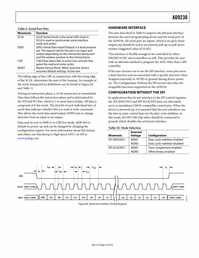
The falling edge of the CSB, in conjunction with the rising edge of the SCLK, determines the start of the framing. An example of the serial timing and its definitions can be found in Figure 64 and Table 11.
CONFIGURATION WITHOUT THE SPI During an instruction phase, a 16-bit instruction is transmitted. Data then follows the instruction phase and is determined by the W0 and W1 bits, which is 1 or more bytes of data. All data is composed of 8-bit words. The first bit of each individual byte of serial data indicates whether this is a read or write command. This allows the serial data input/output (SDIO) pin to change direction from an input to an output.
In applications that do not interface to the SPI control registers, the SPI SDIO/DCS and SPI SCLK/DFS pins can alternately serve as standalone CMOS-compatible control pins. When the device is powered up, it is assumed that the user intends to use the pins as static control lines for the duty cycle stabilizer. In this mode, the SPI CSB chip select should be connected to ground, which disables the serial port interface.
Table 10. Mode Selection
Mnemonic
Data may be sent in MSB or in LSB first mode. MSB first is default on power-up and can be changed by changing the configuration register. For more information about this feature and others, see Interfacing to High Speed ADCs via SPI at www.analog.com.
External Voltage Configuration AVDD Duty cycle stabilizer enabled SPI SDIO/DCS AGND Duty cycle stabilizer disabled AVDD Twos complement enabled SPI SCLK/DFS AGND Offset binary enabled
DON’T CARE
DON’T CAREDON’T CARE
DON’T CARE
SDIO
SCLK
CSB
tS tDH
tHI tCLK
tLO
tDS tH
R/W W1 W0 A12 A11 A10 A9 A8 A7 D5 D4 D3 D2 D1 D0
0600
2-06
3
Figure 64. Serial Port Interface Timing Diagram
AD9230
Rev. 0 | Page 26 of 32
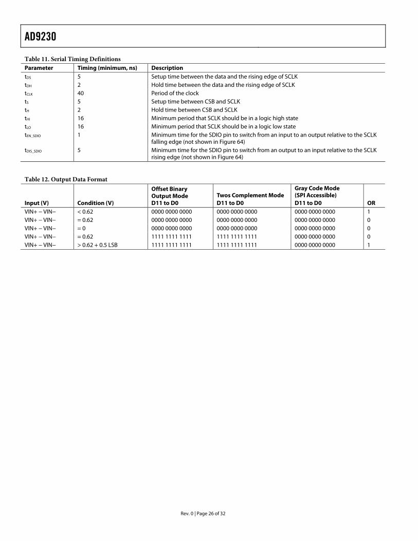
Table 11. Serial Timing Definitions Parameter Timing (minimum, ns) Description tDS 5 Setup time between the data and the rising edge of SCLK tDH 2 Hold time between the data and the rising edge of SCLK tCLK 40 Period of the clock tS 5 Setup time between CSB and SCLK tH 2 Hold time between CSB and SCLK tHI 16 Minimum period that SCLK should be in a logic high state tLO 16 Minimum period that SCLK should be in a logic low state tEN_SDIO 1 Minimum time for the SDIO pin to switch from an input to an output relative to the SCLK
falling edge (not shown in Figure 64) tDIS_SDIO 5 Minimum time for the SDIO pin to switch from an output to an input relative to the SCLK
rising edge (not shown in Figure 64)
Table 12. Output Data Format
Input (V) Condition (V)
Offset Binary Output Mode D11 to D0
Twos Complement Mode D11 to D0
Gray Code Mode (SPI Accessible) D11 to D0 OR
VIN+ − VIN− < 0.62 0000 0000 0000 0000 0000 0000 0000 0000 0000 1 VIN+ − VIN− = 0.62 0000 0000 0000 0000 0000 0000 0000 0000 0000 0 VIN+ − VIN− = 0 0000 0000 0000 0000 0000 0000 0000 0000 0000 0 VIN+ − VIN− = 0.62 1111 1111 1111 1111 1111 1111 0000 0000 0000 0 VIN+ − VIN− > 0.62 + 0.5 LSB 1111 1111 1111 1111 1111 1111 0000 0000 0000 1
AD9230
Rev. 0 | Page 27 of 32
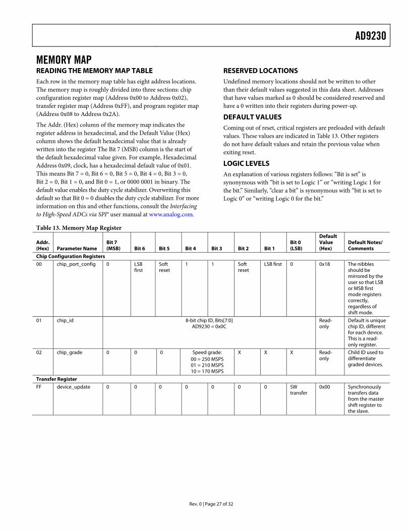
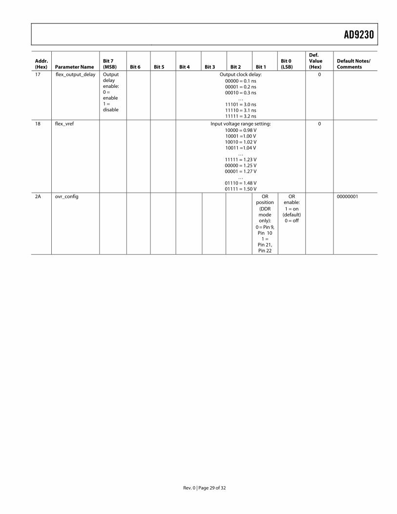
MEMORY MAP READING THE MEMORY MAP TABLE Each row in the memory map table has eight address locations. The memory map is roughly divided into three sections: chip configuration register map (Address 0x00 to Address 0x02), transfer register map (Address 0xFF), and program register map (Address 0x08 to Address 0x2A).
The Addr. (Hex) column of the memory map indicates the register address in hexadecimal, and the Default Value (Hex) column shows the default hexadecimal value that is already written into the register The Bit 7 (MSB) column is the start of the default hexadecimal value given. For example, Hexadecimal Address 0x09, clock, has a hexadecimal default value of 0x01. This means Bit 7 = 0, Bit 6 = 0, Bit 5 = 0, Bit 4 = 0, Bit 3 = 0, Bit 2 = 0, Bit 1 = 0, and Bit 0 = 1, or 0000 0001 in binary. The default value enables the duty cycle stabilizer. Overwriting this default so that Bit 0 = 0 disables the duty cycle stabilizer. For more information on this and other functions, consult the Interfacing to High-Speed ADCs via SPI® user manual at www.analog.com.
RESERVED LOCATIONS Undefined memory locations should not be written to other than their default values suggested in this data sheet. Addresses that have values marked as 0 should be considered reserved and have a 0 written into their registers during power-up.
DEFAULT VALUES Coming out of reset, critical registers are preloaded with default values. These values are indicated in Table 13. Other registers do not have default values and retain the previous value when exiting reset.
LOGIC LEVELS An explanation of various registers follows: “Bit is set” is synonymous with “bit is set to Logic 1” or “writing Logic 1 for the bit.” Similarly, “clear a bit” is synonymous with “bit is set to Logic 0” or “writing Logic 0 for the bit.”
Table 13. Memory Map Register
Addr. (Hex) Parameter Name
Bit 7 (MSB) Bit 6 Bit 5 Bit 4 Bit 3 Bit 2 Bit 1
Bit 0 (LSB)
Default Value (Hex)
Default Notes/ Comments
Chip Configuration Registers
00 chip_port_config 0 LSB first
Soft reset
1 1 Soft reset
LSB first 0 0x18 The nibbles should be mirrored by the user so that LSB or MSB first mode registers correctly, regardless of shift mode.
01 chip_id 8-bit chip ID, Bits[7:0] AD9230 = 0x0C
Read-only
Default is unique chip ID, different for each device. This is a read-only register.
02 chip_grade 0 0 0 Speed grade: 00 = 250 MSPS 01 = 210 MSPS 10 = 170 MSPS
X X X Read-only
Child ID used to differentiate graded devices.
Transfer Register
FF device_update 0 0 0 0 0 0 0 SW transfer
0x00 Synchronously transfers data from the master shift register to the slave.
AD9230
Rev. 0 | Page 28 of 32
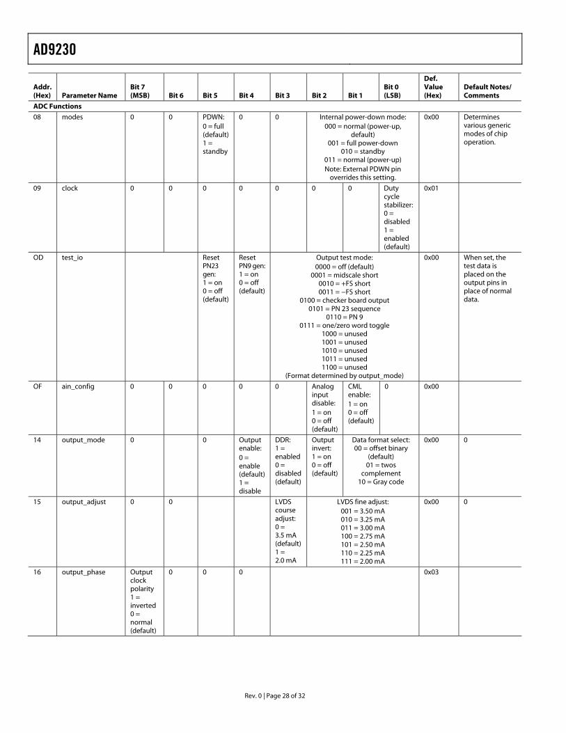
Addr. (Hex) Parameter Name
Bit 7 (MSB) Bit 6 Bit 5 Bit 4 Bit 3 Bit 2 Bit 1
Bit 0 (LSB)
Def. Value (Hex)
Default Notes/ Comments
ADC Functions
08 modes 0 0 PDWN: 0 = full (default)1 = standby
0 0 Internal power-down mode: 000 = normal (power-up,
default) 001 = full power-down
010 = standby 011 = normal (power-up) Note: External PDWN pin
overrides this setting.
0x00 Determines various generic modes of chip operation.
09 clock 0 0 0 0 0 0 0 Duty cycle stabilizer: 0 = disabled 1 = enabled (default)
0x01
OD test_io Reset PN23 gen: 1 = on 0 = off (default)
Reset PN9 gen:1 = on 0 = off (default)
Output test mode: 0000 = off (default)
0001 = midscale short 0010 = +FS short 0011 = −FS short
0100 = checker board output 0101 = PN 23 sequence
0110 = PN 9 0111 = one/zero word toggle
1000 = unused 1001 = unused 1010 = unused 1011 = unused 1100 = unused
(Format determined by output_mode)
0x00 When set, the test data is placed on the output pins in place of normal data.
OF ain_config 0 0 0 0 0 Analog input disable: 1 = on 0 = off (default)
CML enable: 1 = on 0 = off (default)
0 0x00
14 output_mode 0 0 Output enable: 0 = enable (default)1 = disable
DDR: 1 = enabled 0 = disabled(default)
Output invert: 1 = on 0 = off (default)
Data format select: 00 = offset binary
(default) 01 = twos
complement 10 = Gray code
0x00 0
15 output_adjust 0 0 LVDS course adjust: 0 = 3.5 mA (default)1 = 2.0 mA
LVDS fine adjust: 001 = 3.50 mA 010 = 3.25 mA 011 = 3.00 mA 100 = 2.75 mA 101 = 2.50 mA 110 = 2.25 mA 111 = 2.00 mA
0x00 0
16 output_phase Output clock polarity 1 = inverted 0 = normal (default)
0 0 0 0x03
AD9230
Rev. 0 | Page 29 of 32
Addr. (Hex) Parameter Name
Bit 7 (MSB) Bit 6 Bit 5 Bit 4 Bit 3 Bit 2 Bit 1
Bit 0 (LSB)
Def. Value (Hex)
Default Notes/ Comments
17 flex_output_delay Output delay enable: 0 = enable 1 = disable
Output clock delay: 00000 = 0.1 ns 00001 = 0.2 ns 00010 = 0.3 ns
… 11101 = 3.0 ns 11110 = 3.1 ns 11111 = 3.2 ns
0
18 flex_vref Input voltage range setting: 10000 = 0.98 V 10001 =1.00 V 10010 = 1.02 V 10011 =1.04 V
… 11111 = 1.23 V 00000 = 1.25 V 00001 = 1.27 V
… 01110 = 1.48 V 01111 = 1.50 V
0
2A ovr_config OR position
(DDR mode only):
0 = Pin 9, Pin 10
1 = Pin 21, Pin 22
OR enable: 1 = on
(default) 0 = off
00000001
AD9230
Rev. 0 | Page 30 of 32
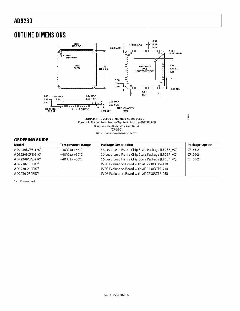
OUTLINE DIMENSIONS
COMPLIANT TO JEDEC STANDARDS MO-220-VLLD-2 1128
05-0
PIN 1INDICATOR
TOPVIEW 7.75
BSC SQ
8.00BSC SQ
156
1415
4342
2829
4.454.30 SQ4.15
0.500.400.30
0.300.230.18
0.50 BSC0.20 REF
12° MAX 0.80 MAX0.65 TYP
1.000.850.80
6.50REF
SEATINGPLANE
0.60 MAX0.60 MAX
PIN 1INDICATOR
COPLANARITY0.08
0.05 MAX0.02 NOM
0.30 MIN
EXPOSEDPAD
(BOTTOM VIEW)
Figure 65. 56-Lead Lead Frame Chip Scale Package [LFCSP_VQ]
8 mm × 8 mm Body, Very Thin Quad (CP-56-2)
Dimensions shown in millimeters
ORDERING GUIDE Model Temperature Range Package Description Package Option AD9230BCPZ-170 −40°C to +85°C 56-Lead Lead Frame Chip Scale Package [LFCSP_VQ] CP-56-2 1
AD9230BCPZ-210 −40°C to +85°C 56-Lead Lead Frame Chip Scale Package [LFCSP_VQ] CP-56-2 1
AD9230BCPZ-250 −40°C to +85°C 56-Lead Lead Frame Chip Scale Package [LFCSP_VQ] CP-56-2 1
AD9230-170EBZ LVDS Evaluation Board with AD9230BCPZ-170 1
AD9230-210EBZ LVDS Evaluation Board with AD9230BCPZ-210 1
AD9230-250EBZ LVDS Evaluation Board with AD9230BCPZ-250 1
1 Z = Pb-free part.

AD9230
Rev. 0 | Page 31 of 32
NOTES

AD9230
Rev. 0 | Page 32 of 32
NOTES
©2007 Analog Devices, Inc. All rights reserved. Trademarks and registered trademarks are the property of their respective owners. D06002-0-2/07(0)
Related Documents