Energy Metering IC with Integrated Oscillator and Reverse Polarity Indication AD71056 Rev. A Information furnished by Analog Devices is believed to be accurate and reliable. However, no responsibility is assumed by Analog Devices for its use, nor for any infringements of patents or other rights of third parties that may result from its use. Specifications subject to change without notice. No license is granted by implication or otherwise under any patent or patent rights of Analog Devices. Trademarks and registered trademarks are the property of their respective owners. One Technology Way, P.O. Box 9106, Norwood, MA 02062-9106, U.S.A. Tel: 781.329.4700 www.analog.com Fax: 781.461.3113 ©2006 Analog Devices, Inc. All rights reserved. FEATURES On-chip oscillator as clock source High accuracy, supports 50 Hz/60 Hz IEC62053-21 Less than 0.1% error over a dynamic range of 500 to 1 Supplies average real power on frequency outputs (F1, F2) High frequency output (CF) calibrates and supplies instantaneous real power Logic output (REVP) indicates potential miswiring or negative power Direct drive for electromechanical counters and 2-phase stepper motors (F1, F2) Proprietary ADCs and DSP provide high accuracy over large variations in environmental conditions and time On-chip power supply monitoring On-chip creep protection (no load threshold) On-chip reference 2.45 V (20 ppm/°C typical) with external overdrive capability Single 5 V supply, low power (20 mW typical) Low cost CMOS process GENERAL DESCRIPTION The AD71056 1 is a high accuracy, electrical energy metering IC with a precise oscillator circuit that serves as a clock source to the chip. The AD71056 eliminates the need for an external crystal or resonator, thus reducing the overall cost of building a meter with this IC. The chip directly interfaces with the shunt resistor. The AD71056 specifications surpass the accuracy requirements as quoted in the IEC62053-21 standard. The only analog circuitry used in the AD71056 is in the Σ-Δ ADCs and reference circuit. All other signal processing, such as multiplication and filtering, is carried out in the digital domain. This approach provides superior stability and accuracy over time and in extreme environmental conditions. The AD71056 supplies average real power information on F1 and F2, the low frequency outputs. These outputs either directly drive an electromechanical counter or interface with an MCU. The high frequency CF logic output, ideal for calibration purposes, provides instantaneous real power information. The AD71056 includes a power supply monitoring circuit on the VDD supply pin. The AD71056 remains inactive until the supply voltage on VDD reaches approximately 4 V. If the supply falls below 4 V, the AD71056 also remains inactive and the F1, F2, and CF outputs are in their nonactive modes. Internal phase matching circuitry ensures that the voltage and current channels are phase matched, and the HPF in the current channel eliminates dc offsets. An internal no load threshold ensures that the AD71056 does not exhibit creep when no load is present. The part is available in a 16-lead, narrow body SOIC package. FUNCTIONAL BLOCK DIAGRAM MULTIPLIER REVP V2P V2N V1P RCLKIN REF IN/OUT F1 F2 CF SCF S0 S1 PHASE CORRECTION 4kΩ ...110101... SIGNAL PROCESSING BLOCK POWER SUPPLY MONITOR Σ-Δ ADC V1N AD71056 ...11011001... 2.5V REFERENCE V DD AGND DGND Ф INTERNAL OSCILLATOR Σ-Δ ADC LPF HPF + + 1 6 13 7 11 8 10 12 14 16 15 9 DIGITAL-TO-FREQUENCY CONVERTER 2 3 4 5 05636-001 Figure 1. 1 U.S. Patents 5,745,323; 5,760,617; 5,862,069; 5,872,469; others pending.

Welcome message from author
This document is posted to help you gain knowledge. Please leave a comment to let me know what you think about it! Share it to your friends and learn new things together.
Transcript
Energy Metering IC with Integrated Oscillator and Reverse Polarity Indication
AD71056
Rev. A Information furnished by Analog Devices is believed to be accurate and reliable. However, no responsibility is assumed by Analog Devices for its use, nor for any infringements of patents or other rights of third parties that may result from its use. Specifications subject to change without notice. No license is granted by implication or otherwise under any patent or patent rights of Analog Devices. Trademarks and registered trademarks are the property of their respective owners.
One Technology Way, P.O. Box 9106, Norwood, MA 02062-9106, U.S.A.Tel: 781.329.4700 www.analog.com Fax: 781.461.3113 ©2006 Analog Devices, Inc. All rights reserved.
FEATURES On-chip oscillator as clock source High accuracy, supports 50 Hz/60 Hz IEC62053-21 Less than 0.1% error over a dynamic range of 500 to 1 Supplies average real power on frequency outputs (F1, F2) High frequency output (CF) calibrates and supplies
instantaneous real power Logic output (REVP) indicates potential miswiring or
negative power Direct drive for electromechanical counters and 2-phase
stepper motors (F1, F2) Proprietary ADCs and DSP provide high accuracy over large
variations in environmental conditions and time On-chip power supply monitoring On-chip creep protection (no load threshold) On-chip reference 2.45 V (20 ppm/°C typical) with external
overdrive capability Single 5 V supply, low power (20 mW typical) Low cost CMOS process
GENERAL DESCRIPTION
The AD710561 is a high accuracy, electrical energy metering IC with a precise oscillator circuit that serves as a clock source to the chip. The AD71056 eliminates the need for an external crystal or resonator, thus reducing the overall cost of building a meter with this IC. The chip directly interfaces with the shunt resistor.
The AD71056 specifications surpass the accuracy requirements as quoted in the IEC62053-21 standard.
The only analog circuitry used in the AD71056 is in the Σ-Δ ADCs and reference circuit. All other signal processing, such as multiplication and filtering, is carried out in the digital domain. This approach provides superior stability and accuracy over time and in extreme environmental conditions.
The AD71056 supplies average real power information on F1 and F2, the low frequency outputs. These outputs either directly drive an electromechanical counter or interface with an MCU. The high frequency CF logic output, ideal for calibration purposes, provides instantaneous real power information.
The AD71056 includes a power supply monitoring circuit on the VDD supply pin. The AD71056 remains inactive until the supply voltage on VDD reaches approximately 4 V. If the supply falls below 4 V, the AD71056 also remains inactive and the F1, F2, and CF outputs are in their nonactive modes.
Internal phase matching circuitry ensures that the voltage and current channels are phase matched, and the HPF in the current channel eliminates dc offsets. An internal no load threshold ensures that the AD71056 does not exhibit creep when no load is present.
The part is available in a 16-lead, narrow body SOIC package.
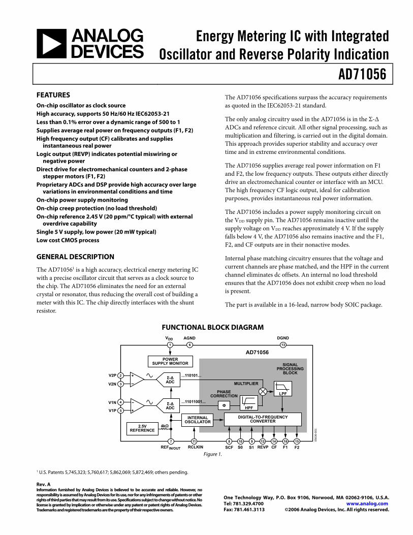
FUNCTIONAL BLOCK DIAGRAM
MULTIPLIER
REVP
V2P
V2N
V1P
RCLKINREFIN/OUT F1 F2CFSCF S0 S1
PHASECORRECTION
4kΩ
...110101...
SIGNALPROCESSING
BLOCK
POWERSUPPLY MONITOR
Σ-ΔADC
V1N
AD71056
...11011001...
2.5VREFERENCE
VDD AGND DGND
Ф
INTERNALOSCILLATOR
Σ-ΔADC
LPF
HPF
+
+
1 6 13
7 11 8 10 12 14 16 159
DIGITAL-TO-FREQUENCYCONVERTER
2
3
4
5
0563
6-00
1
Figure 1.
1 U.S. Patents 5,745,323; 5,760,617; 5,862,069; 5,872,469; others pending.
AD71056
Rev. A | Page 2 of 20
TABLE OF CONTENTS Features .............................................................................................. 1
General Description ......................................................................... 1
Functional Block Diagram .............................................................. 1
Revision History ............................................................................... 2
Specifications..................................................................................... 3
Timing Characteristics ................................................................ 4
Absolute Maximum Ratings............................................................ 5
ESD Caution.................................................................................. 5
Terminology ...................................................................................... 6
Pin Configuration and Function Descriptions............................. 7
Typical Performance Characteristics ............................................. 8
Theory of Operation ...................................................................... 10
Power Factor Considerations.................................................... 10
Nonsinusoidal Voltage and Current........................................ 10
Applications..................................................................................... 12
Analog Inputs ............................................................................. 12
Power Supply Monitor............................................................... 13
Internal Oscillator (OSC).......................................................... 15
Transfer Function....................................................................... 15
Selecting a Frequency for an Energy Meter Application...... 16
No Load Threshold .................................................................... 17
Negative Power Information..................................................... 17
Outline Dimensions ....................................................................... 18
Ordering Guide .......................................................................... 18
REVISION HISTORY
8/06—Revision A: Initial Version
AD71056
Rev. A | Page 3 of 20
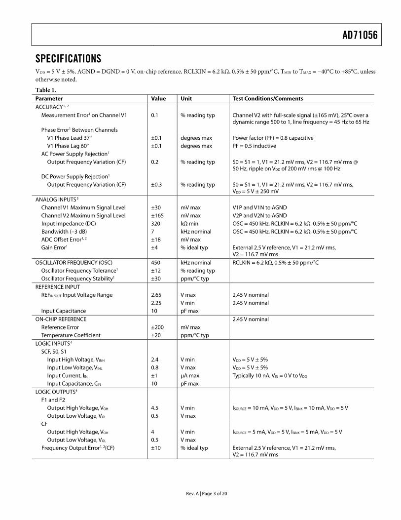
SPECIFICATIONS VDD = 5 V ± 5%, AGND = DGND = 0 V, on-chip reference, RCLKIN = 6.2 kΩ, 0.5% ± 50 ppm/°C, TMIN to TMAX = −40°C to +85°C, unless otherwise noted.
Table 1. Parameter Value Unit Test Conditions/Comments ACCURACY1 , 2
Measurement Error1 on Channel V1 0.1 % reading typ Channel V2 with full-scale signal (±165 mV), 25°C over a dynamic range 500 to 1, line frequency = 45 Hz to 65 Hz
Phase Error1 Between Channels V1 Phase Lead 37° ±0.1 degrees max Power factor (PF) = 0.8 capacitive V1 Phase Lag 60° ±0.1 degrees max PF = 0.5 inductive
AC Power Supply Rejection1 Output Frequency Variation (CF) 0.2 % reading typ S0 = S1 = 1, V1 = 21.2 mV rms, V2 = 116.7 mV rms @
50 Hz, ripple on VDD of 200 mV rms @ 100 Hz DC Power Supply Rejection1
Output Frequency Variation (CF) ±0.3 % reading typ S0 = S1 = 1, V1 = 21.2 mV rms, V2 = 116.7 mV rms, VDD = 5 V ± 250 mV
ANALOG INPUTS3 Channel V1 Maximum Signal Level ±30 mV max V1P and V1N to AGND Channel V2 Maximum Signal Level ±165 mV max V2P and V2N to AGND Input Impedance (DC) 320 kΩ min OSC = 450 kHz, RCLKIN = 6.2 kΩ, 0.5% ± 50 ppm/°C Bandwidth (–3 dB) 7 kHz nominal OSC = 450 kHz, RCLKIN = 6.2 kΩ, 0.5% ± 50 ppm/°C ADC Offset Error1, 2 ±18 mV max Gain Error1 ±4 % ideal typ External 2.5 V reference, V1 = 21.2 mV rms,
V2 = 116.7 mV rms OSCILLATOR FREQUENCY (OSC) 450 kHz nominal RCLKIN = 6.2 kΩ, 0.5% ± 50 ppm/°C
Oscillator Frequency Tolerance1 ±12 % reading typ Oscillator Frequency Stability1 ±30 ppm/°C typ
REFERENCE INPUT REFIN/OUT Input Voltage Range 2.65 V max 2.45 V nominal
2.25 V min 2.45 V nominal Input Capacitance 10 pF max
ON-CHIP REFERENCE 2.45 V nominal Reference Error ±200 mV max Temperature Coefficient ±20 ppm/°C typ
LOGIC INPUTS4 SCF, S0, S1
Input High Voltage, VINH 2.4 V min VDD = 5 V ± 5% Input Low Voltage, VINL 0.8 V max VDD = 5 V ± 5% Input Current, IIN ±1 μA max Typically 10 nA, VIN = 0 V to VDD Input Capacitance, CIN 10 pF max
LOGIC OUTPUTS4 F1 and F2
Output High Voltage, VOH 4.5 V min ISOURCE = 10 mA, VDD = 5 V, ISINK = 10 mA, VDD = 5 V Output Low Voltage, VOL 0.5 V max
CF Output High Voltage, VOH 4 V min ISOURCE = 5 mA, VDD = 5 V, ISINK = 5 mA, VDD = 5 V Output Low Voltage, VOL 0.5 V max
Frequency Output Error1, 2(CF) ±10 % ideal typ External 2.5 V reference, V1 = 21.2 mV rms, V2 = 116.7 mV rms
AD71056
Rev. A | Page 4 of 20
Parameter Value Unit Test Conditions/Comments POWER SUPPLY For specified performance
VDD 4.75 V min 5 V − 5% 5.25 V max 5 V + 5% IDD 5 mA max Typically 4 mA
1 See the Terminology section for an explanation of specifications. 2 See plots in the Typical Performance Characteristics section. 3 See the Analog Inputs section. 4 Sample tested during initial release and after any redesign or process change that may affect this parameter.
TIMING CHARACTERISTICS VDD = 5 V ± 5%, AGND = DGND = 0 V, on-chip reference, RCLKIN = 6.2 kΩ, 0.5% ± 50 ppm/°C, TMIN to TMAX = −40°C to +85°C, unless otherwise noted.
Sample tested during initial release and after any redesign or process change that may affect this parameter. See Figure 2.
Table 2. Parameter Specifications Unit Test Conditions/Comments
t11 120 ms F1 and F2 pulse width (logic low).
t2 See Table 6 sec Output pulse period. See the Transfer Function section. t3 1/2 t2 sec Time between F1 falling edge and F2 falling edge. t4
1, 2 90 ms CF pulse width (logic high). t5 See Table 7 sec CF pulse period. See the Transfer Function section. t6 2 μs Minimum time between F1 and F2 pulses. 1 The pulse widths of F1, F2, and CF are not fixed for higher output frequencies. See the Frequency Outputs section. 2 The CF pulse is always 35 μs in high frequency mode. See the Frequency Outputs section and Table 7.
Timing Diagram
F1
F2
CF
t1
t5t4
t2
t6
t3
0563
6-00
2
Figure 2. Timing Diagram for Frequency Outputs
AD71056
Rev. A | Page 5 of 20
ABSOLUTE MAXIMUM RATINGS TA = 25°C, unless otherwise noted.
Table 3. Parameter Rating VDD to AGND −0.3 V to +7 V VDD to DGND −0.3 V to +7 V Analog Input Voltage to AGND
V1P, V1N, V2P, and V2N −6 V to +6 V Reference Input Voltage to AGND −0.3 V to VDD + 0.3 V Digital Input Voltage to DGND −0.3 V to VDD + 0.3 V Digital Output Voltage to DGND −0.3 V to VDD + 0.3 V Operating Temperature Range −40°C to +85°C Storage Temperature Range −65°C to +150°C Junction Temperature 150°C 16-Lead Plastic SOIC, Power Dissipation 350 mW
θJA Thermal Impedance1 124.9°C/W
Package Temperature Soldering See J-STD-20 1 JEDEC 1S standard (2-layer) board data.
Stresses above those listed under Absolute Maximum Ratings may cause permanent damage to the device. This is a stress rating only; functional operation of the device at these or any other conditions above those indicated in the operational section of this specification is not implied. Exposure to absolute maximum rating conditions for extended periods may affect device reliability.
ESD CAUTION ESD (electrostatic discharge) sensitive device. Electrostatic charges as high as 4000 V readily accumulate on the human body and test equipment and can discharge without detection. Although this product features proprietary ESD protection circuitry, permanent damage may occur on devices subjected to high energy electrostatic discharges. Therefore, proper ESD precautions are recommended to avoid performance degradation or loss of functionality.
AD71056
Rev. A | Page 6 of 20
TERMINOLOGY Measurement Error The error associated with the energy measurement made by the AD71056 is defined by the following formula:
%100% ×−
=EnergyTrue
EnergyTrueAD71056byRegisteredEnergyError
Phase Error Between Channels The high-pass filter (HPF) in the current channel (Channel V1) has a phase-lead response. To offset this phase response and equalize the phase response between channels, a phase correction network is also placed in Channel V1. The phase correction network matches the phase to within 0.1° over a range of 45 Hz to 65 Hz, and 0.2° over a range 40 Hz to 1 kHz (see Figure 23 and Figure 24).
Power Supply Rejection (PSR) This quantifies the AD71056 measurement error as a percentage of reading when the power supplies are varied.
For the ac PSR measurement, a reading at nominal supplies (5 V) is taken. A 200 mV rms/100 Hz signal is then introduced onto the supplies and a second reading is obtained under the same input signal levels. Any error introduced is expressed as a percentage of reading—see the Measurement Error definition.
For the dc PSR measurement, a reading at nominal supplies (5 V) is taken. The supplies are then varied 5% and a second reading is obtained with the same input signal levels. Any error introduced is, again, expressed as a percentage of reading.
ADC Offset Error This refers to the small dc signal (offset) associated with the analog inputs to the ADCs. However, the HPF in Channel V1 eliminates the offset in the circuitry. Therefore, the power calculation is not affected by this offset.
Frequency Output Error (CF) The frequency output error of the AD71056 is defined as the difference between the measured output frequency (minus the offset) and the ideal output frequency. The difference is expressed as a percentage of the ideal frequency. The ideal frequency is obtained from the AD71056 transfer function. See Figure 14 for a typical distribution of part-to-part variation of CF frequency.
Gain Error The gain error of the AD71056 is defined as the difference between the measured output of the ADCs (minus the offset) and the ideal output of the ADCs. The difference is expressed as a percentage of the ideal output of the ADCs.
Oscillator Frequency Tolerance The oscillator frequency tolerance of the AD71056 is defined as the part-to-part frequency variation in terms of percentage at room temperature (25°C). It is measured by taking the difference between the measured oscillator frequency and the nominal frequency as defined in the Specifications section.
Oscillator Frequency Stability Oscillator frequency stability is defined as the frequency variation in terms of the parts-per-million drift over the operating temperature range. In a metering application, the temperature range is −40°C to +85°C. Oscillator frequency stability is measured by taking the difference between the measured oscillator frequency at −40°C and +85°C and the measured oscillator frequency at +25°C.
AD71056
Rev. A | Page 7 of 20
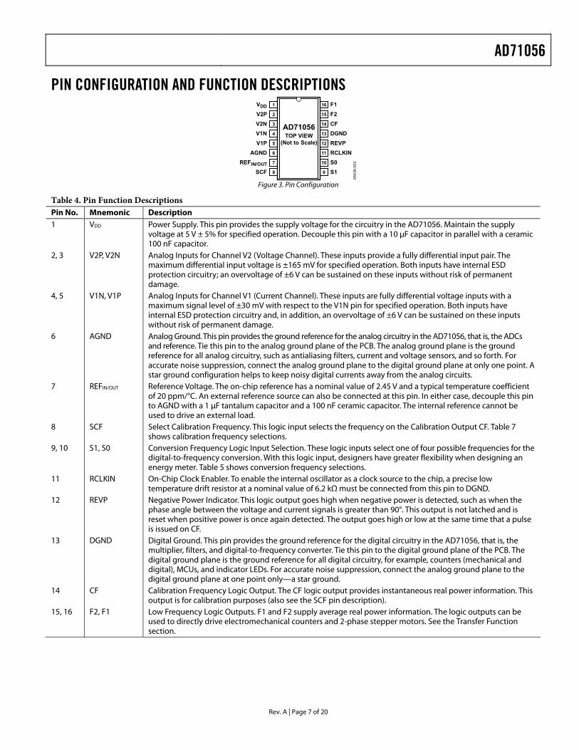
PIN CONFIGURATION AND FUNCTION DESCRIPTIONS
0563
6-00
3
VDD 1
V2P 2
V2N 3
V1N 4
F116
F215
CF14
DGND13
V1P 5 REVP12
AGND 6 RCLKIN11
REFIN/OUT 7 S010
SCF 8 S19
AD71056TOP VIEW
(Not to Scale)
Figure 3. Pin Configuration
Table 4. Pin Function Descriptions Pin No. Mnemonic Description 1 VDD Power Supply. This pin provides the supply voltage for the circuitry in the AD71056. Maintain the supply
voltage at 5 V ± 5% for specified operation. Decouple this pin with a 10 μF capacitor in parallel with a ceramic 100 nF capacitor.
2, 3 V2P, V2N Analog Inputs for Channel V2 (Voltage Channel). These inputs provide a fully differential input pair. The maximum differential input voltage is ±165 mV for specified operation. Both inputs have internal ESD protection circuitry; an overvoltage of ±6 V can be sustained on these inputs without risk of permanent damage.
4, 5 V1N, V1P Analog Inputs for Channel V1 (Current Channel). These inputs are fully differential voltage inputs with a maximum signal level of ±30 mV with respect to the V1N pin for specified operation. Both inputs have internal ESD protection circuitry and, in addition, an overvoltage of ±6 V can be sustained on these inputs without risk of permanent damage.
6 AGND Analog Ground. This pin provides the ground reference for the analog circuitry in the AD71056, that is, the ADCs and reference. Tie this pin to the analog ground plane of the PCB. The analog ground plane is the ground reference for all analog circuitry, such as antialiasing filters, current and voltage sensors, and so forth. For accurate noise suppression, connect the analog ground plane to the digital ground plane at only one point. A star ground configuration helps to keep noisy digital currents away from the analog circuits.
7 REFIN/OUT Reference Voltage. The on-chip reference has a nominal value of 2.45 V and a typical temperature coefficient of 20 ppm/°C. An external reference source can also be connected at this pin. In either case, decouple this pin to AGND with a 1 μF tantalum capacitor and a 100 nF ceramic capacitor. The internal reference cannot be used to drive an external load.
8 SCF Select Calibration Frequency. This logic input selects the frequency on the Calibration Output CF. Table 7 shows calibration frequency selections.
9, 10 S1, S0 Conversion Frequency Logic Input Selection. These logic inputs select one of four possible frequencies for the digital-to-frequency conversion. With this logic input, designers have greater flexibility when designing an energy meter. Table 5 shows conversion frequency selections.
11 RCLKIN On-Chip Clock Enabler. To enable the internal oscillator as a clock source to the chip, a precise low temperature drift resistor at a nominal value of 6.2 kΩ must be connected from this pin to DGND.
12 REVP Negative Power Indicator. This logic output goes high when negative power is detected, such as when the phase angle between the voltage and current signals is greater than 90°. This output is not latched and is reset when positive power is once again detected. The output goes high or low at the same time that a pulse is issued on CF.
13 DGND Digital Ground. This pin provides the ground reference for the digital circuitry in the AD71056, that is, the multiplier, filters, and digital-to-frequency converter. Tie this pin to the digital ground plane of the PCB. The digital ground plane is the ground reference for all digital circuitry, for example, counters (mechanical and digital), MCUs, and indicator LEDs. For accurate noise suppression, connect the analog ground plane to the digital ground plane at one point only—a star ground.
14 CF Calibration Frequency Logic Output. The CF logic output provides instantaneous real power information. This output is for calibration purposes (also see the SCF pin description).
15, 16 F2, F1 Low Frequency Logic Outputs. F1 and F2 supply average real power information. The logic outputs can be used to directly drive electromechanical counters and 2-phase stepper motors. See the Transfer Function section.
AD71056
Rev. A | Page 8 of 20
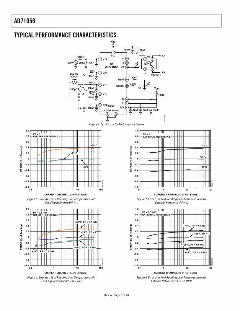
TYPICAL PERFORMANCE CHARACTERISTICS
6.2kΩ
V2N
200Ω220V
150nF
V2P
200Ω
602kΩ
V1P
V1N
350µΩ
40A TO40mA
REFIN/OUT100nF1µF
100nF 10µF
VDD
DGND
F1
F2
CF
REVP
RCLKIN
S0S1
SCF10nF 10nF 10nF
U3
PS2501-1
K7
K8
U1AD71056
10kΩ
VDD
200Ω
200Ω150nF
150nF
AGND
150nF
VDD
+
+
+
820Ω
2
3
5
4
7
6 13
1
16
15
14
12
11
10
9
8
1 4
2 3
0563
6-00
4
Figure 4. Test Circuit for Performance Curves
–1.0
–0.8
–0.6
–0.4
–0.2
0
ERR
OR
(% o
f Rea
ding
)
0.2
0.4
0.6
CURRENT CHANNEL (% of Full Scale)
0.1 101 100
0.8
1.0
+25°C
+85°C
–40°C
PF = 1ON-CHIP REFERENCE
0563
6-00
5
Figure 5. Error as a % of Reading over Temperature with
On-Chip Reference (PF = 1)
–1.0
–0.8
–0.6
–0.4
–0.2
0
ERR
OR
(% o
f Rea
ding
)
0.2
0.4
0.6
CURRENT CHANNEL (% of Full Scale)
0.1 101 100
0.8
1.0
+85°C, PF = 0.5 IND
+25°C, PF = 1
–40°C, PF = 0.5 IND+25°C, PF = 0.5 IND
PF = 0.5 INDON-CHIP REFERENCE
0563
6-00
6
Figure 6. Error as a % of Reading over Temperature with
On-Chip Reference (PF = 0.5 IND)
–1.0
–0.8
–0.6
–0.4
–0.2
0
ERR
OR
(% o
f Rea
ding
)
0.2
0.4
0.6
CURRENT CHANNEL (% of Full Scale)
0.1 101 100
0.8
1.0
+25°C
+85°C
–40°C
PF = 1EXTERNAL REFERENCE
0563
6-00
7
Figure 7. Error as a % of Reading over Temperature with
External Reference (PF = 1)
–1.0
–0.8
–0.6
–0.4
–0.2
0
ERR
OR
(% o
f Rea
ding
)
0.2
0.4
0.6
CURRENT CHANNEL (% of Full Scale)
0.1 101 100
0.8
1.0
+85°C, PF = 0.5 IND
+25°C, PF = 1
+25°C, PF = 0.5 IND
–40°C, PF = 0.5 IND
PF = 0.5 INDEXTERNAL REFERENCE
0563
6-00
8
Figure 8. Error as a % of Reading over Temperature with
External Reference (PF = 0.5 IND)
AD71056
Rev. A | Page 9 of 20
–0.5
–0.4
–0.3
–0.2
–0.1
0
0.1
0.2
0.3
0.4
0.5
ERR
OR
(% o
f Rea
ding
)
FREQUENCY (Hz)
5045 55 60 65
PF = 0.5 IND
PF = 0.5 CAP
PF = 1
0563
6-00
9
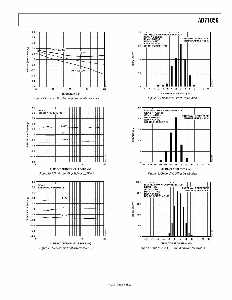
Figure 9. Error as a % of Reading over Input Frequency
–1.0
–0.8
–0.6
–0.4
–0.2
0
ERR
OR
(% o
f Rea
ding
)
0.2
0.4
0.6
CURRENT CHANNEL (% of Full Scale)
0.1 101 100
0.8
1.0
5.25V
5V
4.75V
PF = 1ON-CHIP REFERENCE
0563
6-01
0
Figure 10. PSR with On-Chip Reference, PF = 1
–1.0
–0.8
–0.6
–0.4
–0.2
0
ERR
OR
(% o
f Rea
ding
)
0.2
0.4
0.6
CURRENT CHANNEL (% of Full Scale)
0.1 101 100
0.8
1.0
5.25V
5V
4.75V
PF = 1EXTERNAL REFERENCE
0563
6-01
1
Figure 11. PSR with External Reference, PF = 1
40
FREQ
UEN
CY
CHANNEL V1 OFFSET (mV)
–5 –4 –3 –2 –1 0 1 2 3 4 5 6 7 8 9
EXTERNAL REFERENCETEMPERATURE = 25°C
0
10
20
30
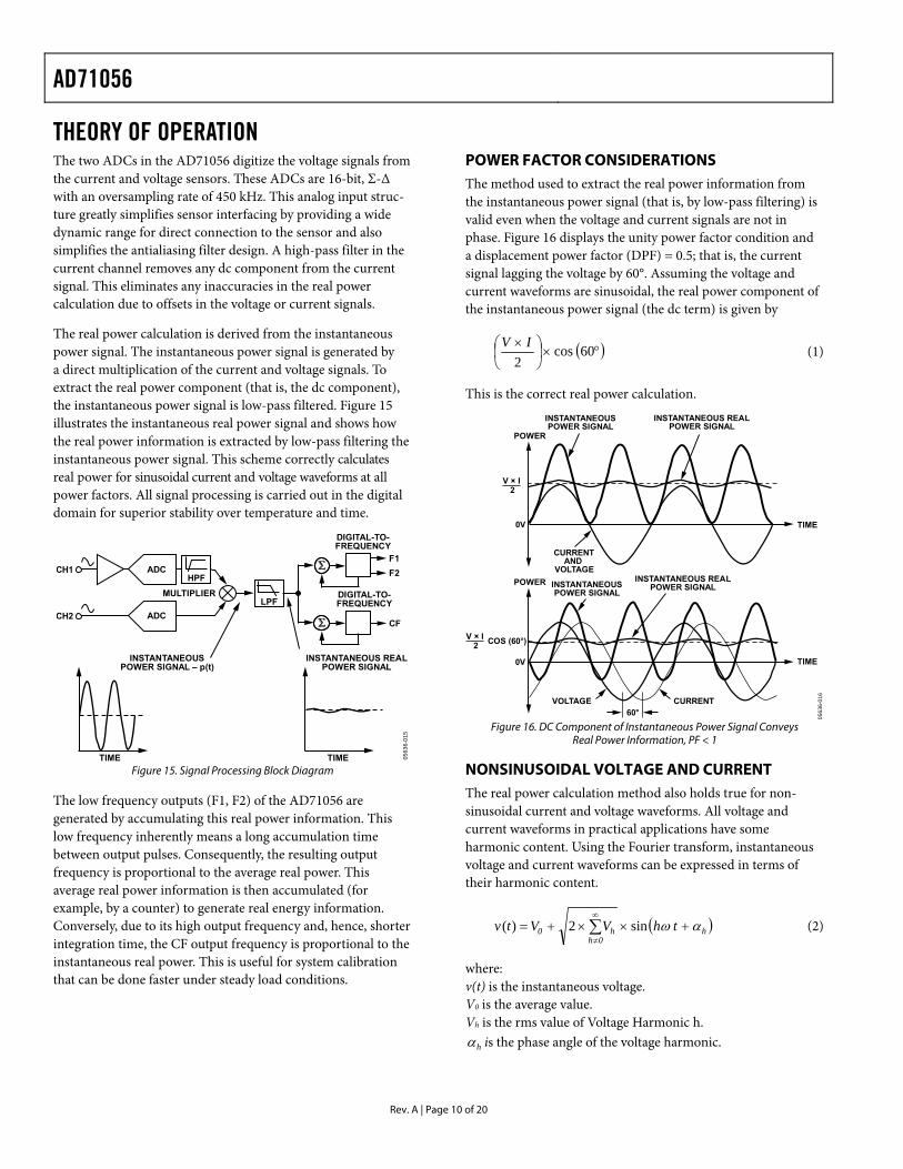
DISTRIBUTION CHARACTERISTICSMEAN = 2.247828SDs = 1.367176MIN = –2.09932MAX = +5.28288NO. OF POINTS = 100
0563
6-01
2
Figure 12. Channel V1 Offset Distribution
0
10
20
30
40
50
FREQ
UEN
CY
CHANNEL V2 OFFSET (mV)
–12 –10 –8 –6 –4 –2 0 2 4 6 8 10 12
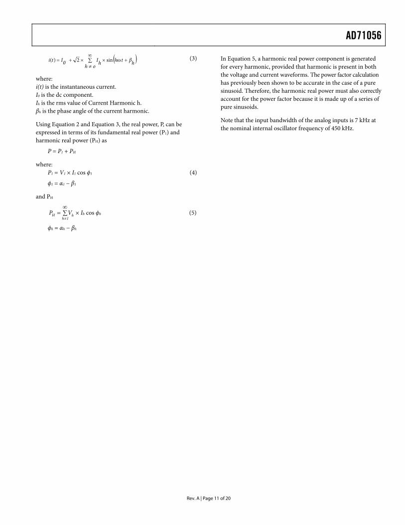
EXTERNAL REFERENCETEMPERATURE = 25°C
DISTRIBUTION CHARACTERISTICSMEAN = –1.563484SDs = 2.040699MIN = –6.82969MAX = +2.6119NO. OF POINTS = 100
0563
6-01
3
Figure 13. Channel V2 Offset Distribution
–10 –8 –6 –4 –2 0 2 4 6 8 10 120
200
400
600
800
1000
FREQ
UEN
CY
DEVIATION FROM MEAN (%)
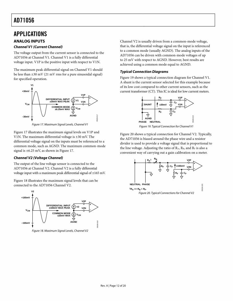
EXTERNAL REFERENCETEMPERATURE = 25°C
DISTRIBUTION CHARACTERISTICSMEAN = 0%SDs = 1.55%MIN = –11.79%MAX = +6.08%NO. OF POINTS = 3387
0563
6-01
4
Figure 14. Part-to-Part CF Distribution from Mean of CF
AD71056
Rev. A | Page 10 of 20
THEORY OF OPERATION The two ADCs in the AD71056 digitize the voltage signals from the current and voltage sensors. These ADCs are 16-bit, Σ-Δ with an oversampling rate of 450 kHz. This analog input struc-ture greatly simplifies sensor interfacing by providing a wide dynamic range for direct connection to the sensor and also simplifies the antialiasing filter design. A high-pass filter in the current channel removes any dc component from the current signal. This eliminates any inaccuracies in the real power calculation due to offsets in the voltage or current signals.
The real power calculation is derived from the instantaneous power signal. The instantaneous power signal is generated by a direct multiplication of the current and voltage signals. To extract the real power component (that is, the dc component), the instantaneous power signal is low-pass filtered. Figure 15 illustrates the instantaneous real power signal and shows how the real power information is extracted by low-pass filtering the instantaneous power signal. This scheme correctly calculates real power for sinusoidal current and voltage waveforms at all power factors. All signal processing is carried out in the digital domain for superior stability over temperature and time.
TIME TIME
ADC
ADC
CH1
CH2
MULTIPLIER
F1F2
DIGITAL-TO-FREQUENCY
CF
DIGITAL-TO-FREQUENCY
INSTANTANEOUS REALPOWER SIGNAL
INSTANTANEOUSPOWER SIGNAL – p(t)
LPF
HPF
0563
6-01
5
Figure 15. Signal Processing Block Diagram
The low frequency outputs (F1, F2) of the AD71056 are generated by accumulating this real power information. This low frequency inherently means a long accumulation time between output pulses. Consequently, the resulting output frequency is proportional to the average real power. This average real power information is then accumulated (for example, by a counter) to generate real energy information. Conversely, due to its high output frequency and, hence, shorter integration time, the CF output frequency is proportional to the instantaneous real power. This is useful for system calibration that can be done faster under steady load conditions.
POWER FACTOR CONSIDERATIONS The method used to extract the real power information from the instantaneous power signal (that is, by low-pass filtering) is valid even when the voltage and current signals are not in phase. Figure 16 displays the unity power factor condition and a displacement power factor (DPF) = 0.5; that is, the current signal lagging the voltage by 60°. Assuming the voltage and current waveforms are sinusoidal, the real power component of the instantaneous power signal (the dc term) is given by
( °×⎟⎠⎞
⎜⎝⎛ × 60cos
2IV ) (1)
This is the correct real power calculation.
V × I2
0V
POWER
CURRENTAND
VOLTAGEPOWER
TIME
TIME
VOLTAGE CURRENT
V × I2 COS (60°)
0V
INSTANTANEOUSPOWER SIGNAL
INSTANTANEOUS REALPOWER SIGNAL
INSTANTANEOUSPOWER SIGNAL
INSTANTANEOUS REALPOWER SIGNAL
60°
0563
6-01
6
Figure 16. DC Component of Instantaneous Power Signal Conveys
Real Power Information, PF < 1
NONSINUSOIDAL VOLTAGE AND CURRENT The real power calculation method also holds true for non-sinusoidal current and voltage waveforms. All voltage and current waveforms in practical applications have some harmonic content. Using the Fourier transform, instantaneous voltage and current waveforms can be expressed in terms of their harmonic content.
( h0h
h0 thVVtv αω +××+= ∑∞
≠sin2)( ) (2)
where: v(t) is the instantaneous voltage. V0 is the average value. Vh is the rms value of Voltage Harmonic h.
is the phase angle of the voltage harmonic. hα
AD71056
Rev. A | Page 11 of 20
(∑∞
≠+ω××+=
oh hβthhI0Iti sin2)( ) (3)
where: i(t) is the instantaneous current. I0 is the dc component. Ih is the rms value of Current Harmonic h. βh is the phase angle of the current harmonic.
Using Equation 2 and Equation 3, the real power, P, can be expressed in terms of its fundamental real power (P1) and harmonic real power (PH) as
P = P1 + PH
where: P1 = V1 × I1 cos ϕ1 (4)
ϕ1 = α1 − β1
and PH
∑∞
=≠1h
hH VP × Ih cos ϕh (5)
ϕh = αh − βh
In Equation 5, a harmonic real power component is generated for every harmonic, provided that harmonic is present in both the voltage and current waveforms. The power factor calculation has previously been shown to be accurate in the case of a pure sinusoid. Therefore, the harmonic real power must also correctly account for the power factor because it is made up of a series of pure sinusoids.
Note that the input bandwidth of the analog inputs is 7 kHz at the nominal internal oscillator frequency of 450 kHz.
AD71056
Rev. A | Page 12 of 20
APPLICATIONSANALOG INPUTS Channel V1 (Current Channel)
The voltage output from the current sensor is connected to the AD71056 at Channel V1. Channel V1 is a fully differential voltage input. V1P is the positive input with respect to V1N.
The maximum peak differential signal on Channel V1 should be less than ±30 mV (21 mV rms for a pure sinusoidal signal) for specified operation.
+30mV
–30mV
VCM
V1
DIFFERENTIAL INPUT±30mV MAX PEAK
COMMON MODE±6.25mV MAX
V1P
V1NV1
VCM
AGND
0563
6-01
7
Figure 17. Maximum Signal Levels, Channel V1
Figure 17 illustrates the maximum signal levels on V1P and V1N. The maximum differential voltage is ±30 mV. The differential voltage signal on the inputs must be referenced to a common mode, such as AGND. The maximum common-mode signal is ±6.25 mV, as shown in Figure 17.
Channel V2 (Voltage Channel)
The output of the line voltage sensor is connected to the AD71056 at Channel V2. Channel V2 is a fully differential voltage input with a maximum peak differential signal of ±165 mV.
Figure 18 illustrates the maximum signal levels that can be connected to the AD71056 Channel V2.
+165mV
–165mV
VCM
V2
DIFFERENTIAL INPUT±165mV MAX PEAK
COMMON MODE±25mV MAX
V2P
V2NV2
VCM
AGND
0563
6-01
8
Figure 18. Maximum Signal Levels, Channel V2
Channel V2 is usually driven from a common-mode voltage, that is, the differential voltage signal on the input is referenced to a common mode (usually AGND). The analog inputs of the AD71056 can be driven with common-mode voltages of up to 25 mV with respect to AGND. However, best results are achieved using a common mode equal to AGND.
Typical Connection Diagrams
Figure 19 shows a typical connection diagram for Channel V1. A shunt is the current sensor selected for this example because of its low cost compared to other current sensors, such as the current transformer (CT). This IC is ideal for low current meters.
V1P
V1NCF
CF
RF
RF
±30mVSHUNT
AGNDPHASE NEUTRAL 05
636-
019
Figure 19. Typical Connection for Channel V1
Figure 20 shows a typical connection for Channel V2. Typically, the AD71056 is biased around the phase wire and a resistor divider is used to provide a voltage signal that is proportional to the line voltage. Adjusting the ratio of RA, RB, and RF is also a convenient way of carrying out a gain calibration on a meter.
V2P
V2N
CF
PHASENEUTRAL
RF
±165mVCFRF
RBRA1
1RA >> RB + RF.
0563
6-02
0
Figure 20. Typical Connections for Channel V2
AD71056
Rev. A | Page 13 of 20
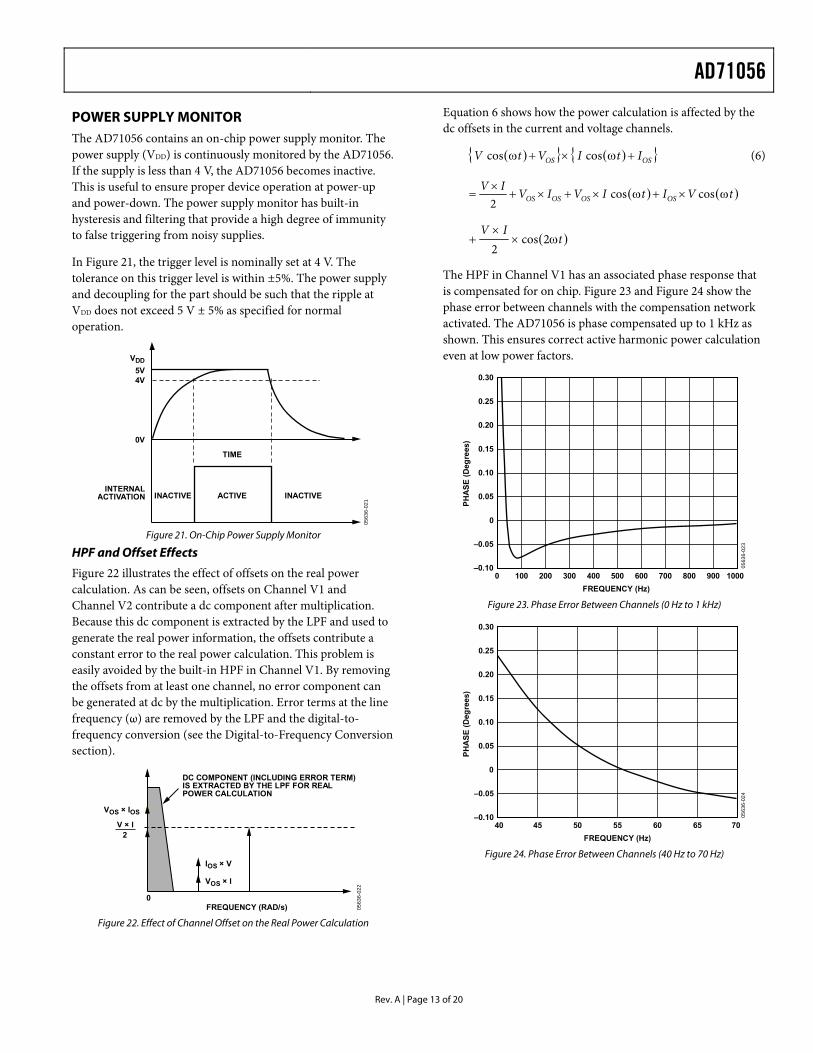
POWER SUPPLY MONITOR The AD71056 contains an on-chip power supply monitor. The power supply (VDD) is continuously monitored by the AD71056. If the supply is less than 4 V, the AD71056 becomes inactive. This is useful to ensure proper device operation at power-up and power-down. The power supply monitor has built-in hysteresis and filtering that provide a high degree of immunity to false triggering from noisy supplies.
In Figure 21, the trigger level is nominally set at 4 V. The tolerance on this trigger level is within ±5%. The power supply and decoupling for the part should be such that the ripple at VDD does not exceed 5 V ± 5% as specified for normal operation.
VDD5V4V
0V
TIME
INACTIVE ACTIVE INACTIVEINTERNAL
ACTIVATION
0563
6-02
1
Figure 21. On-Chip Power Supply Monitor
HPF and Offset Effects
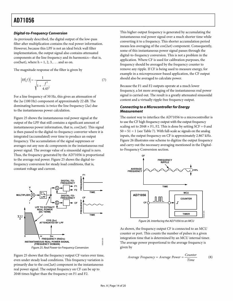
Figure 22 illustrates the effect of offsets on the real power calculation. As can be seen, offsets on Channel V1 and Channel V2 contribute a dc component after multiplication. Because this dc component is extracted by the LPF and used to generate the real power information, the offsets contribute a constant error to the real power calculation. This problem is easily avoided by the built-in HPF in Channel V1. By removing the offsets from at least one channel, no error component can be generated at dc by the multiplication. Error terms at the line frequency (ω) are removed by the LPF and the digital-to-frequency conversion (see the Digital-to-Frequency Conversion section).
DC COMPONENT (INCLUDING ERROR TERM)IS EXTRACTED BY THE LPF FOR REALPOWER CALCULATION
IOS × V
VOS × I
VOS × IOS
V × I2
0FREQUENCY (RAD/s) 05
636-
022
Figure 22. Effect of Channel Offset on the Real Power Calculation
Equation 6 shows how the power calculation is affected by the dc offsets in the current and voltage channels.
( ) ( ) OSOS ItIVtV +ω×+ω coscos (6)
( ) ( )tVItIVIVIVOSOSOSOS ω×+ω×+×+
×= coscos
2
( )tIV
ω××
+ 2cos2
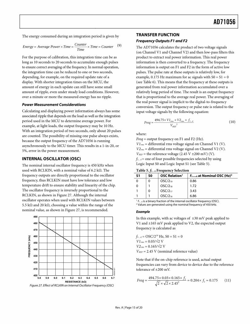
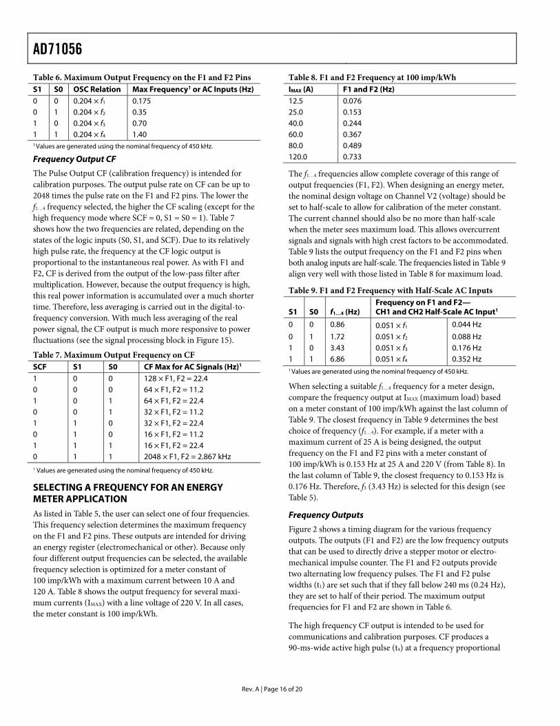
The HPF in Channel V1 has an associated phase response that is compensated for on chip. Figure 23 and Figure 24 show the phase error between channels with the compensation network activated. The AD71056 is phase compensated up to 1 kHz as shown. This ensures correct active harmonic power calculation even at low power factors.
FREQUENCY (Hz)
0.30
PHA
SE (D
egre
es)
0.25
0.20
0.15
0.10
0.05
0
–0.05
–0.100 100 200 300 400 500 600 700 800 900 1000
0563
6-02
3
Figure 23. Phase Error Between Channels (0 Hz to 1 kHz)
FREQUENCY (Hz)
0.30
PHA
SE (D
egre
es)
0.25
0.20
0.15
0.10
0.05
0
–0.05
–0.1040 45 50 55 60 65 70
0563
6-02
4
Figure 24. Phase Error Between Channels (40 Hz to 70 Hz)
AD71056
Rev. A | Page 14 of 20
Digital-to-Frequency Conversion
As previously described, the digital output of the low-pass filter after multiplication contains the real power information. However, because this LPF is not an ideal brick wall filter implementation, the output signal also contains attenuated components at the line frequency and its harmonics—that is, cos(hωt), where h = 1, 2, 3, . . . and so on.
The magnitude response of the filter is given by
( )2
2
45.41
1
ffH
+
= (7)
For a line frequency of 50 Hz, this gives an attenuation of the 2ω (100 Hz) component of approximately 22 dB. The dominating harmonic is twice the line frequency (2ω) due to the instantaneous power calculation.
Figure 25 shows the instantaneous real power signal at the output of the LPF that still contains a significant amount of instantaneous power information, that is, cos(2ωt). This signal is then passed to the digital-to-frequency converter where it is integrated (accumulated) over time to produce an output frequency. The accumulation of the signal suppresses or averages out any non-dc components in the instantaneous real power signal. The average value of a sinusoidal signal is zero. Thus, the frequency generated by the AD71056 is proportional to the average real power. Figure 25 shows the digital-to-frequency conversion for steady load conditions, that is, constant voltage and current.
F1F2
DIGITAL-TO-FREQUENCY
CF
DIGITAL-TO-FREQUENCY
MULTIPLIER
F1
TIME
CF
TIME
FREQ
UEN
CY
FREQ
UEN
CY
V
I
0FREQUENCY (RAD/s)
ω 2ω
COS (2ω)ATTENUATED BY LPF
V × I2
LPF TO EXTRACTREAL POWER
(DC TERM)
INSTANTANEOUS REAL POWER SIGNAL(FREQUENCY DOMAIN)
LPF
0563
6-02
5
Figure 25. Real Power-to-Frequency Conversion
Figure 25 shows that the frequency output CF varies over time, even under steady load conditions. This frequency variation is primarily due to the cos(2ωt) component in the instantaneous real power signal. The output frequency on CF can be up to 2048 times higher than the frequency on F1 and F2.
This higher output frequency is generated by accumulating the instantaneous real power signal over a much shorter time while converting it to a frequency. This shorter accumulation period means less averaging of the cos(2ωt) component. Consequently, some of this instantaneous power signal passes through the digital-to-frequency conversion. This is not a problem in the application. Where CF is used for calibration purposes, the frequency should be averaged by the frequency counter to remove any ripple. If CF is being used to measure energy, for example in a microprocessor-based application, the CF output should also be averaged to calculate power.
Because the F1 and F2 outputs operate at a much lower frequency, a lot more averaging of the instantaneous real power signal is carried out. The result is a greatly attenuated sinusoidal content and a virtually ripple free frequency output.
Connecting to a Microcontroller for Energy Measurement
The easiest way to interface the AD71056 to a microcontroller is to use the CF high frequency output with the output frequency scaling set to 2048 × F1, F2. This is done by setting SCF = 0 and S0 = S1 = 1 (see Table 7). With full-scale ac signals on the analog inputs, the output frequency on CF is approximately 2.867 kHz. Figure 26 illustrates one scheme to digitize the output frequency and carry out the necessary averaging mentioned in the Digital-to-Frequency Conversion section.
CF
TIME
±10%
FREQUENCYRIPPLE
AVERAGEFREQUENCY
AD71056COUNTER
TIMER
MCU
CF05
636-
026
Figure 26. Interfacing the AD71056 to an MCU
As shown, the frequency output CF is connected to an MCU counter or port. This counts the number of pulses in a given integration time that is determined by an MCU internal timer. The average power proportional to the average frequency is given by
TimeCounterPowerAverageFrequencyAverage == (8)
AD71056
Rev. A | Page 15 of 20
The energy consumed during an integration period is given by
CounterTimeTime
CounterTimePowerAverageEnergy =×=×= (9)
For the purpose of calibration, this integration time can be as long as 10 seconds to 20 seconds to accumulate enough pulses to ensure correct averaging of the frequency. In normal operation, the integration time can be reduced to one or two seconds, depending, for example, on the required update rate of a display. With shorter integration times on the MCU, the amount of energy in each update can still have some small amount of ripple, even under steady load conditions. However, over a minute or more the measured energy has no ripple.
Power Measurement Considerations
Calculating and displaying power information always has some associated ripple that depends on the load as well as the integration period used in the MCU to determine average power. For example, at light loads, the output frequency may be 10 Hz. With an integration period of two seconds, only about 20 pulses are counted. The possibility of missing one pulse always exists, because the output frequency of the AD71056 is running asynchronously to the MCU timer. This results in a 1-in-20, or 5%, error in the power measurement.
INTERNAL OSCILLATOR (OSC) The nominal internal oscillator frequency is 450 kHz when used with RCLKIN, with a nominal value of 6.2 kΩ. The frequency outputs are directly proportional to the oscillator frequency, thus RCLKIN must have low tolerance and low temperature drift to ensure stability and linearity of the chip. The oscillator frequency is inversely proportional to the RCLKIN, as shown in Figure 27. Although the internal oscillator operates when used with RCLKIN values between 5.5 kΩ and 20 kΩ, choosing a value within the range of the nominal value, as shown in Figure 27, is recommended.
RESISTANCE (kΩ)5.8 5.9 6.1 6.3 6.7
FREQ
UEN
CY
(kH
z)
420
430
440
450
460
480
470
490
6.0 6.2 6.4 6.5 6.6
410
400 0563
6-02
7
Figure 27. Effect of RCLKIN on Internal Oscillator Frequency (OSC)
TRANSFER FUNCTION Frequency Outputs F1 and F2
The AD71056 calculates the product of two voltage signals (on Channel V1 and Channel V2) and then low-pass filters this product to extract real power information. This real power information is then converted to a frequency. The frequency information is output on F1 and F2 in the form of active low pulses. The pulse rate at these outputs is relatively low, for example, 0.175 Hz maximum for ac signals with S0 = S1 = 0 (see Table 6). This means that the frequency at these outputs is generated from real power information accumulated over a relatively long period of time. The result is an output frequency that is proportional to the average real power. The averaging of the real power signal is implicit to the digital-to-frequency conversion. The output frequency or pulse rate is related to the input voltage signals by the following equation:
2...75.494
REF
41rmsrms
VfV2V1
Freq×××
= (10)
where: Freq = output frequency on F1 and F2 (Hz). V1rms = differential rms voltage signal on Channel V1 (V). V2rms = differential rms voltage signal on Channel V2 (V). VREF = the reference voltage (2.45 V ±200 mV) (V). f1…4 = one of four possible frequencies selected by using Logic Input S0 and Logic Input S1 (see Table 5).
Table 5. f1…4 Frequency Selection S1 S0 OSC Relation1 f1…4 at Nominal OSC (Hz)2
0 0 OSC/219 0.86 0 1 OSC/218 1.72 1 0 OSC/217 3.43 1 1 OSC/216 6.86 1 f1…4 is a binary fraction of the internal oscillator frequency (OSC). 2 Values are generated using the nominal frequency of 450 kHz.
Example
In this example, with ac voltages of ±30 mV peak applied to V1 and ±165 mV peak applied to V2, the expected output frequency is calculated as
f1…4 = OSC/219 Hz, S0 = S1 = 0 V1rms = 0.03/√2 V V2rms = 0.165/√2 V VREF = 2.45 V (nominal reference value)
Note that if the on-chip reference is used, actual output frequencies can vary from device to device due to the reference tolerance of ±200 mV.
175.0204.045.222165.003.075.494
2 =×=××
×××= 1
1 ffFreq (11)
AD71056
Rev. A | Page 16 of 20
Table 6. Maximum Output Frequency on the F1 and F2 Pins S1 S0 OSC Relation Max Frequency1 or AC Inputs (Hz) 0 0 0.204 × f1 0.175 0 1 0.204 × f2 0.35 1 0 0.204 × f3 0.70 1 1 0.204 × f4 1.40 1 Values are generated using the nominal frequency of 450 kHz.
Frequency Output CF
The Pulse Output CF (calibration frequency) is intended for calibration purposes. The output pulse rate on CF can be up to 2048 times the pulse rate on the F1 and F2 pins. The lower the f1…4 frequency selected, the higher the CF scaling (except for the high frequency mode where SCF = 0, S1 = S0 = 1). Table 7 shows how the two frequencies are related, depending on the states of the logic inputs (S0, S1, and SCF). Due to its relatively high pulse rate, the frequency at the CF logic output is proportional to the instantaneous real power. As with F1 and F2, CF is derived from the output of the low-pass filter after multiplication. However, because the output frequency is high, this real power information is accumulated over a much shorter time. Therefore, less averaging is carried out in the digital-to-frequency conversion. With much less averaging of the real power signal, the CF output is much more responsive to power fluctuations (see the signal processing block in Figure 15).
Table 7. Maximum Output Frequency on CF SCF S1 S0 CF Max for AC Signals (Hz)1 1 0 0 128 × F1, F2 = 22.4 0 0 0 64 × F1, F2 = 11.2 1 0 1 64 × F1, F2 = 22.4 0 0 1 32 × F1, F2 = 11.2 1 1 0 32 × F1, F2 = 22.4 0 1 0 16 × F1, F2 = 11.2 1 1 1 16 × F1, F2 = 22.4 0 1 1 2048 × F1, F2 = 2.867 kHz 1 Values are generated using the nominal frequency of 450 kHz.
SELECTING A FREQUENCY FOR AN ENERGY METER APPLICATION As listed in Table 5, the user can select one of four frequencies. This frequency selection determines the maximum frequency on the F1 and F2 pins. These outputs are intended for driving an energy register (electromechanical or other). Because only four different output frequencies can be selected, the available frequency selection is optimized for a meter constant of 100 imp/kWh with a maximum current between 10 A and 120 A. Table 8 shows the output frequency for several maxi-mum currents (IMAX) with a line voltage of 220 V. In all cases, the meter constant is 100 imp/kWh.
Table 8. F1 and F2 Frequency at 100 imp/kWh IMAX (A) F1 and F2 (Hz) 12.5 0.076 25.0 0.153 40.0 0.244 60.0 0.367 80.0 0.489 120.0 0.733
The f1…4 frequencies allow complete coverage of this range of output frequencies (F1, F2). When designing an energy meter, the nominal design voltage on Channel V2 (voltage) should be set to half-scale to allow for calibration of the meter constant. The current channel should also be no more than half-scale when the meter sees maximum load. This allows overcurrent signals and signals with high crest factors to be accommodated. Table 9 lists the output frequency on the F1 and F2 pins when both analog inputs are half-scale. The frequencies listed in Table 9 align very well with those listed in Table 8 for maximum load.
Table 9. F1 and F2 Frequency with Half-Scale AC Inputs
S1 S0 f1…4 (Hz) Frequency on F1 and F2— CH1 and CH2 Half-Scale AC Input1
0 0 0.86 0.051 × f1 0.044 Hz
0 1 1.72 0.051 × f2 0.088 Hz 1 0 3.43 0.051 × f3 0.176 Hz 1 1 6.86 0.051 × f4 0.352 Hz 1 Values are generated using the nominal frequency of 450 kHz.
When selecting a suitable f1…4 frequency for a meter design, compare the frequency output at IMAX (maximum load) based on a meter constant of 100 imp/kWh against the last column of Table 9. The closest frequency in Table 9 determines the best choice of frequency (f1…4). For example, if a meter with a maximum current of 25 A is being designed, the output frequency on the F1 and F2 pins with a meter constant of 100 imp/kWh is 0.153 Hz at 25 A and 220 V (from Table 8). In the last column of Table 9, the closest frequency to 0.153 Hz is 0.176 Hz. Therefore, f3 (3.43 Hz) is selected for this design (see Table 5).
Frequency Outputs
Figure 2 shows a timing diagram for the various frequency outputs. The outputs (F1 and F2) are the low frequency outputs that can be used to directly drive a stepper motor or electro-mechanical impulse counter. The F1 and F2 outputs provide two alternating low frequency pulses. The F1 and F2 pulse widths (t1) are set such that if they fall below 240 ms (0.24 Hz), they are set to half of their period. The maximum output frequencies for F1 and F2 are shown in Table 6.
The high frequency CF output is intended to be used for communications and calibration purposes. CF produces a 90-ms-wide active high pulse (t4) at a frequency proportional
AD71056
Rev. A | Page 17 of 20
to active power. The CF output frequencies are given in Table 7. As with F1 and F2, if the period of CF (t5) falls below 180 ms, the CF pulse width is set to half the period. If the CF frequency, for example, is 20 Hz, the CF pulse width is 25 ms.
When the high frequency mode is selected (that is, SCF = 0, S1 = S0 = 1), the CF pulse width is fixed at 35 μs. Therefore, t4 is always 35 μs, regardless of the output frequency on CF.
NO LOAD THRESHOLD The AD71056 also includes a no load threshold and start-up current feature that eliminates any creep effects in the meter. The AD71056 is designed to issue a minimum output frequency. Any load generating a frequency lower than this minimum frequency does not cause a pulse to be issued on F1, F2, or CF. The minimum output frequency is given as 0.00244% for each of the f1…4 frequency selections (see Table 5).
For example, for an energy meter with a meter constant of 100 imp/kWh on F1, F2 using f3 (3.43 Hz), the minimum
output frequency at F1 or F2 equals 0.00244% of 3.43 Hz or 8.38 × 10⁻⁵ Hz. This is 2.68 × 10⁻³ Hz at CF (32 × F1 Hz) when SCF = S0 = 1, S1 = 0. In this example, the no load threshold is equivalent to 3 W of load or a start-up current of 13.72 mA at 220 V. Compare this value to the IEC62053-21 specification that states the meter must start up with a load equal to or less than 0.4% Ib. For a 5 A (Ib) meter, 0.4% of Ib is equivalent to 20 mA.
NEGATIVE POWER INFORMATION The AD71056 detects when the current and voltage channels have a phase shift greater than 90°. This mechanism can detect wrong connection of the meter or generation of negative power.
The REVP pin output goes active high when negative power is detected and active low when positive power is detected. The REVP pin output changes state as a pulse is issued on CF.
AD71056
Rev. A | Page 18 of 20
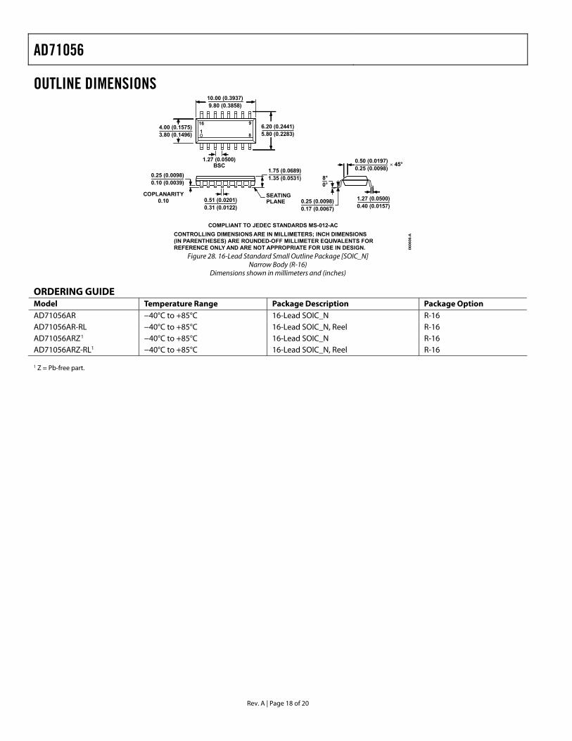
OUTLINE DIMENSIONS
CONTROLLING DIMENSIONS ARE IN MILLIMETERS; INCH DIMENSIONS(IN PARENTHESES) ARE ROUNDED-OFF MILLIMETER EQUIVALENTS FORREFERENCE ONLY AND ARE NOT APPROPRIATE FOR USE IN DESIGN.
COMPLIANT TO JEDEC STANDARDS MS-012-AC
10.00 (0.3937)9.80 (0.3858)
16 9
81
6.20 (0.2441)5.80 (0.2283)
4.00 (0.1575)3.80 (0.1496)
1.27 (0.0500)BSC
SEATINGPLANE
0.25 (0.0098)0.10 (0.0039)
0.51 (0.0201)0.31 (0.0122)
1.75 (0.0689)1.35 (0.0531)
0.50 (0.0197)0.25 (0.0098)
1.27 (0.0500)0.40 (0.0157)
0.25 (0.0098)0.17 (0.0067)
COPLANARITY0.10
8°0°
0606
06-A
45°
Figure 28. 16-Lead Standard Small Outline Package [SOIC_N]
Narrow Body (R-16) Dimensions shown in millimeters and (inches)
ORDERING GUIDE Model Temperature Range Package Description Package Option AD71056AR −40°C to +85°C 16-Lead SOIC_N R-16 AD71056AR-RL −40°C to +85°C 16-Lead SOIC_N, Reel R-16 AD71056ARZ1 −40°C to +85°C 16-Lead SOIC_N R-16 AD71056ARZ-RL1 −40°C to +85°C 16-Lead SOIC_N, Reel R-16 1 Z = Pb-free part.

AD71056
Rev. A | Page 19 of 20
NOTES

AD71056
Rev. A | Page 20 of 20
NOTES
©2006 Analog Devices, Inc. All rights reserved. Trademarks and registered trademarks are the property of their respective owners. D05636-0-8/06(A)
Related Documents