ACT364 DESIGN GUIDE Jun 2014 Copyright © 2014 Active-Semi International, Inc. - - www.active-semi.com Innovative Power TM AC/DC LED Lighting Rev3.1 Apr 2011 www.active-semi.com June 2014 www.active-semi.com PRODUCT SELECTION GUIDE LED Lighting Reference Designs Innovative LED Solutions Innovative LED Solutions

Active Semi 2014 PSG LED General Lighting Applications Released
Feb 15, 2016
Active-semi-2014-PSG_LED_General-Lighting-Applications_Released.pdf
Welcome message from author
This document is posted to help you gain knowledge. Please leave a comment to let me know what you think about it! Share it to your friends and learn new things together.
Transcript

ACT364 DESIGN GUIDE Jun 2014
Copyright © 2014 Active-Semi International, Inc. - - www.active-semi.com
Innovative PowerTM
AC/DC LED Lighting
Rev3.1 Apr 2011
www.active-semi.com
June 2014
www.active-semi.com
PRODUCT SELECTION GUIDE LED Lighting Reference Designs
Innovative LED Solutions Innovative LED Solutions
Table of Contents
ACT364 1W 350mA(3.5V) E27.……………………………………………………………..…………….………3
ACT364 1W 350mA(3.5V) E27 Non-isolated…….………...…….……………………………..…….…...…...5
ACT364 3W 700mA(4V) GU10..…………………………………….…………………………………...………..7
ACT364 3W 700mA(4V) GU10 Non-isolated…………….………………………………….………………….9
ACT364 3W 350mA(12V) GU10………………………….……….………………………………….………11
ACT364 3W 350mA(12V) GU10 Non-isolated..……….……….……………………………………………..13
ACT365 7.8W 350mA(26V) PAR30 ………………….….………………...…………………….……………...15
ACT365 7.8W 350mA(26V) PAR30 Non-isolated…….………….……….….………………….….………...17
ACT512 16.8W 700mA(24V) PAR38 ………………….….………………...………………………….…….19
ACT111A 4.8-30VDC (up to 1.5A) MR16……………………………...………………………………………..21
LED DESIGN GUIDE Innovative PowerTM Jun 2014
Copyright © 2014 Active-Semi International, Inc. - 2 - www.active-semi.com
ACT364 DESIGN GUIDE Jun 2014
Innovative PowerTM
Copyright © 2014 Active-Semi International, Inc. - 3 - www.active-semi.com
(1.1)
OUTCV
SW
2
CSPOUTCC V
F
R
9.0396.0L
2
1I
Input Voltage LED(s) Output Voltage Power Output Topology Device
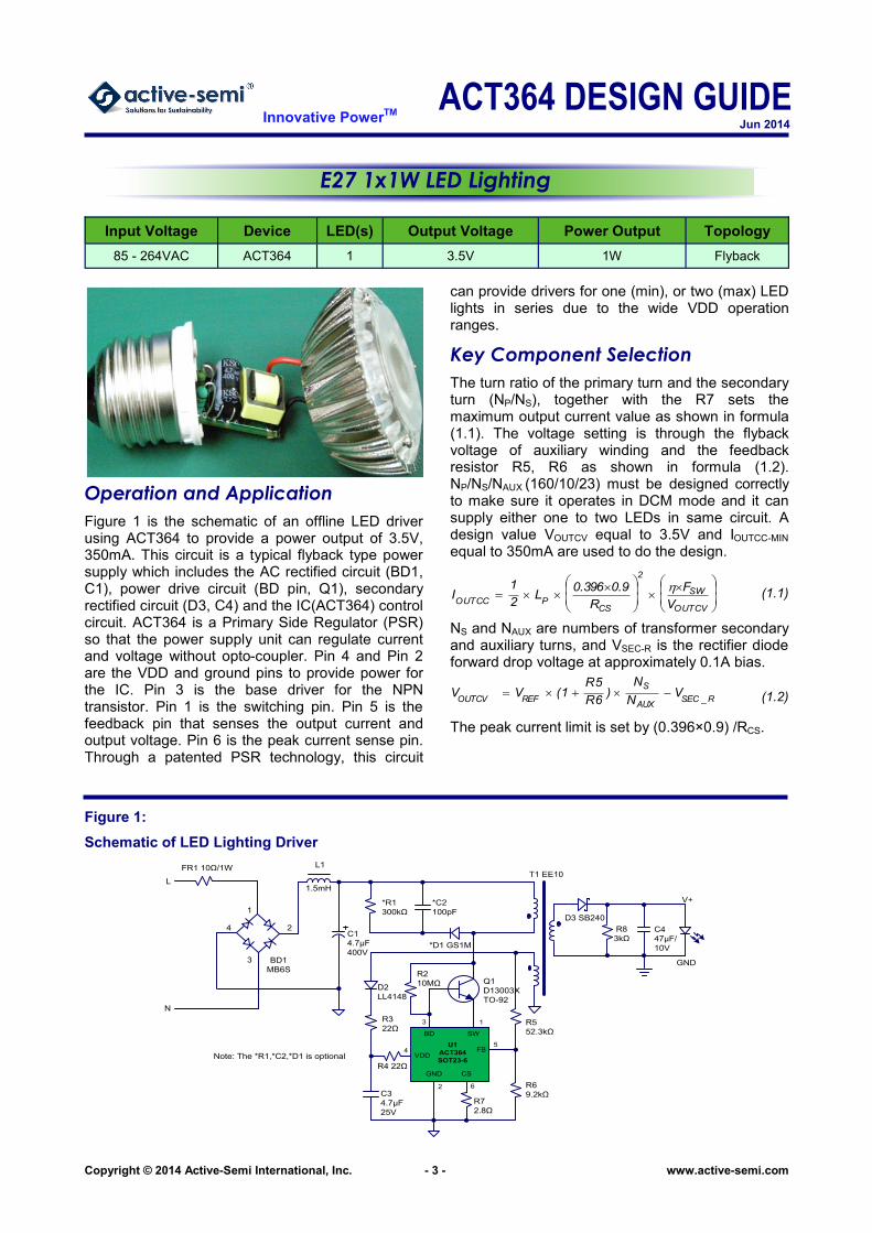
85 - 264VAC 1 3.5V 1W Flyback ACT364
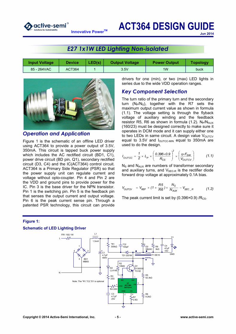
E27 1x1W LED Lighting
Figure 1:
Schematic of LED Lighting Driver
Operation and Application
Figure 1 is the schematic of an offline LED driver using ACT364 to provide a power output of 3.5V, 350mA. This circuit is a typical flyback type power supply which includes the AC rectified circuit (BD1, C1), power drive circuit (BD pin, Q1), secondary rectified circuit (D3, C4) and the IC(ACT364) control circuit. ACT364 is a Primary Side Regulator (PSR) so that the power supply unit can regulate current and voltage without opto-coupler. Pin 4 and Pin 2 are the VDD and ground pins to provide power for the IC. Pin 3 is the base driver for the NPN transistor. Pin 1 is the switching pin. Pin 5 is the feedback pin that senses the output current and output voltage. Pin 6 is the peak current sense pin. Through a patented PSR technology, this circuit
can provide drivers for one (min), or two (max) LED lights in series due to the wide VDD operation ranges.
Key Component Selection
The turn ratio of the primary turn and the secondary turn (NP/NS), together with the R7 sets the maximum output current value as shown in formula (1.1). The voltage setting is through the flyback voltage of auxiliary winding and the feedback resistor R5, R6 as shown in formula (1.2). NP/NS/NAUX (160/10/23) must be designed correctly to make sure it operates in DCM mode and it can supply either one to two LEDs in same circuit. A design value VOUTCV equal to 3.5V and IOUTCC-MIN equal to 350mA are used to do the design.
NS and NAUX are numbers of transformer secondary and auxiliary turns, and VSEC-R is the rectifier diode forward drop voltage at approximately 0.1A bias.
The peak current limit is set by (0.396×0.9) /RCS.
R_SECAUX
S
REFOUTCVV
N
N)
6R
5R1(VV (1.2)
C4
47µF/
10V
T1 EE10
L1
D3 SB240
R8
3kΩ
*R1
300kΩ
C1
4.7µF
400V
*C2
100pF
*D1 GS1M
FR1 10Ω/1W
BD1
MB6S
L
N
1
4
3
2
VDD
U1
ACT364
SOT23-6
Q1
D13003X
TO-92
R2
10MΩD2
LL4148
R3
22Ω
R4 22Ω
C3
4.7µF
25V
R7
2.8Ω
R6
9.2kΩ
GND CS
FB
SWBD
4
3 1
5
2 6
V+
GND
R5
52.3kΩ
1.5mH
Note: The *R1,*C2,*D1 is optional
ACT364 DESIGN GUIDE Jun 2014
Innovative PowerTM
Copyright © 2014 Active-Semi International, Inc. - 4 - www.active-semi.com
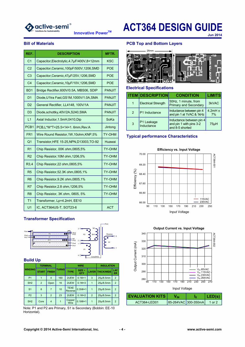
Efficiency vs. Input Voltage
70.00
69.20
68.40
67.60
66.80
66.00
AC
T3
64
-00
1
Effic
iency (
%)
Output Current vs. Input Voltage
340
330
320
310
300
290
280
AC
T3
64
-00
2
Outp
ut
Curr
ent
(mA
) Typical performance Characteristics
EVALUATION KITS VIN I0 LED(s)
ACT364-LED01 85-264VAC 300-350mA 1 or 2
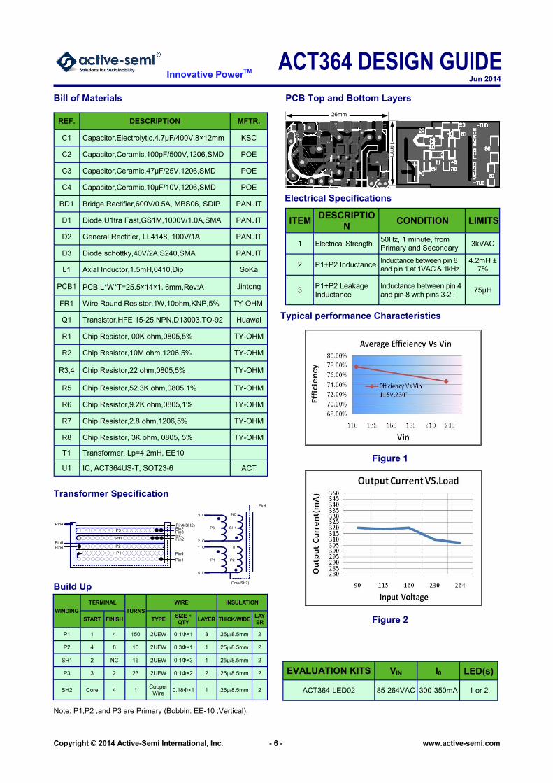
Bill of Materials PCB Top and Bottom Layers
Build Up
REF. DESCRIPTION MFTR.
C1 Capacitor,Electrolytic,4.7µF/400V,8×12mm KSC
C2 Capacitor,Ceramic,100pF/500V,1206,SMD POE
C3 Capacitor,Ceramic,47µF/25V,1206,SMD POE
C4 Capacitor,Ceramic,10µF/10V,1206,SMD POE
BD1 Bridge Rectifier,600V/0.5A, MBS06, SDIP PANJIT
D1 Diode,U1tra Fast,GS1M,1000V/1.0A,SMA PANJIT
D2 General Rectifier, LL4148, 100V/1A PANJIT
D3 Diode,schottky,40V/2A,S240,SMA PANJIT
L1 Axial Inductor,1.5mH,0410,Dip SoKa
PCB1 PCB,L*W*T=25.5×14×1.6mm,Rev:A Jintong
FR1 Wire Round Resistor,1W,10ohm,KNP,5% TY-OHM
Q1 Transistor,HFE 15-25,NPN,D13003,TO-92 Huawai
R1 Chip Resistor, 00K ohm,0805,5% TY-OHM
R2 Chip Resistor,10M ohm,1206,5% TY-OHM
R3,4 Chip Resistor,22 ohm,0805,5% TY-OHM
R5 Chip Resistor,52.3K ohm,0805,1% TY-OHM
R6 Chip Resistor,9.2K ohm,0805,1% TY-OHM
R7 Chip Resistor,2.8 ohm,1206,5% TY-OHM
R8 Chip Resistor, 3K ohm, 0805, 5% TY-OHM
T1 Transformer, Lp=4.2mH, EE10
U1 IC, ACT364US-T, SOT23-6 ACT
Transformer Specification
Note: P1 and P2 are Primary, S1 is Secondary (Bobbin: EE-10 Horizontal).
ITEM DESCRIPTION CONDITION LIMITS
1 Electrical Strength 50Hz, 1 minute, from Primary and Secondary
3kVAC
2 P1 Inductance Inductance between pin 4 and pin 1 at 1VAC & 1kHz
4.2mH ± 7%
3 P1 Leakage Inductance
Inductance between pin 4 and pin 1 with pins 3-2 and 8-5 shorted
75µH
Electrical Specifications
26mm
14
mm
115VAC 230VAC
90
Input Voltage
110 130 150 170 190 210 230 250
90
Input Voltage
110 130 150 170 190 210 230 250 270
VIN 85VAC VIN 115VAC VIN 230VAC VIN 264VAC
Pin4
Pin2
P1
S1
P2
Pin1
Pin3Pin8
Pin7
Pin2SH1NC
Pin4
S1
8
P1
1
4
P2
3
2
SH1
7
NC
Core(SH2)
Pin4
Reverse
WINDING
TERMINAL
TURNS
WIRE INSULATION
START FINISH TYPE SIZE × QTY
LAYER THICK/WIDE LAYER
P1 1 4 160 2UEW 0.1Φ×1 3 25µ/8.5mm 2
SH2 2 Open 16 2UEW 0.1Φ×3 1 25µ/8.5mm 2
S1 8 7 10 TEXE
Reverse 0.35Φ×1 1 25µ/8.5mm 2
P2 3 2 23 2UEW 0.1Φ×2 2 25µ/8.5mm 2
SH2 Core 4 1 Copper
Wire 0.18Φ×1 1 25µ/8.5mm 2
ACT364 DESIGN GUIDE Jun 2014
Innovative PowerTM
Copyright © 2014 Active-Semi International, Inc. - 5 - www.active-semi.com
(1.1)
OUTCV
SW
2
CSPOUTCC V
F
R
9.0396.0L
2
1I
Input Voltage LED(s) Output Voltage Power Output Topology Device
85 - 264VAC 1 3.5V 1W buck ACT364
E27 1x1W LED Lighting Non-isolated
Figure 1:
Schematic of LED Lighting Driver
Operation and Application
Figure 1 is the schematic of an offline LED driver using ACT364 to provide a power output of 3.5V, 350mA. This circuit is tapped buck power supply which includes the AC rectified circuit (BD1, C1), power drive circuit (BD pin, Q1), secondary rectified circuit (D3, C4) and the IC(ACT364) control circuit. ACT364 is a Primary Side Regulator (PSR) so that the power supply unit can regulate current and voltage without opto-coupler. Pin 4 and Pin 2 are the VDD and ground pins to provide power for the IC. Pin 3 is the base driver for the NPN transistor. Pin 1 is the switching pin. Pin 5 is the feedback pin that senses the output current and output voltage. Pin 6 is the peak current sense pin. Through a patented PSR technology, this circuit can provide
drivers for one (min), or two (max) LED lights in series due to the wide VDD operation ranges.
Key Component Selection
The turn ratio of the primary turn and the secondary turn (NP/NS), together with the R7 sets the maximum output current value as shown in formula (1.1). The voltage setting is through the flyback voltage of auxiliary winding and the feedback resistor R5, R6 as shown in formula (1.2). NP/NAUX
(160/23) must be designed correctly to make sure it operates in DCM mode and it can supply either one to two LEDs in same circuit. A design value VOUTCV equal to 3.5V and IOUTCC-MIN equal to 350mA are used to do the design.
NS and NAUX are numbers of transformer secondary and auxiliary turns, and VSEC-R is the rectifier diode forward drop voltage at approximately 0.1A bias.
The peak current limit is set by (0.396×0.9) /RCS.
R_SECAUX
S
REFOUTCVV
N
N)
6R
5R1(VV (1.2)
C4
47µF
10V
T1 EE10
L1
R8
3kΩ
*R1
300kΩ
C1
4.7µF
400V
*C2
100pF
*D1 GS1M
FR1 10Ω 1W
BD1
MB6S
L
N
1
4
3
2
VDD
U1
ACT364
SOT23-6
Q1
D13003X
TO-92
R2
10MΩD2
LL4148
R3
22Ω
R4 22Ω
C3
4.7µF
25V R7
2.8Ω
R6
9.2kΩ
GND CS
FB
SWBD
4
3 1
5
2 6
V+
GND
R5
52.3kΩ
1.5mH
Note: The *R1,*C2,*D1 is optional
D2
SB240
ACT364 DESIGN GUIDE Jun 2014
Innovative PowerTM
Copyright © 2014 Active-Semi International, Inc. - 6 - www.active-semi.com
Typical performance Characteristics
EVALUATION KITS VIN I0 LED(s)
ACT364-LED02 85-264VAC 300-350mA 1 or 2
Bill of Materials PCB Top and Bottom Layers
Build Up
REF. DESCRIPTION MFTR.
C1 Capacitor,Electrolytic,4.7µF/400V,8×12mm KSC
C2 Capacitor,Ceramic,100pF/500V,1206,SMD POE
C3 Capacitor,Ceramic,47µF/25V,1206,SMD POE
C4 Capacitor,Ceramic,10µF/10V,1206,SMD POE
BD1 Bridge Rectifier,600V/0.5A, MBS06, SDIP PANJIT
D1 Diode,U1tra Fast,GS1M,1000V/1.0A,SMA PANJIT
D2 General Rectifier, LL4148, 100V/1A PANJIT
D3 Diode,schottky,40V/2A,S240,SMA PANJIT
L1 Axial Inductor,1.5mH,0410,Dip SoKa
PCB1 PCB,L*W*T=25.5×14×1.6mm,Rev:A Jintong
FR1 Wire Round Resistor,1W,10ohm,KNP,5% TY-OHM
Q1 Transistor,HFE 15-25,NPN,D13003,TO-92 Huawai
R1 Chip Resistor, 00K ohm,0805,5% TY-OHM
R2 Chip Resistor,10M ohm,1206,5% TY-OHM
R3,4 Chip Resistor,22 ohm,0805,5% TY-OHM
R5 Chip Resistor,52.3K ohm,0805,1% TY-OHM
R6 Chip Resistor,9.2K ohm,0805,1% TY-OHM
R7 Chip Resistor,2.8 ohm,1206,5% TY-OHM
R8 Chip Resistor, 3K ohm, 0805, 5% TY-OHM
T1 Transformer, Lp=4.2mH, EE10
U1 IC, ACT364US-T, SOT23-6 ACT
Transformer Specification
ITEM DESCRIPTIO
N CONDITION LIMITS
1 Electrical Strength 50Hz, 1 minute, from Primary and Secondary
3kVAC
2 P1+P2 Inductance Inductance between pin 8 and pin 1 at 1VAC & 1kHz
4.2mH ± 7%
3 P1+P2 Leakage Inductance
Inductance between pin 4 and pin 8 with pins 3-2 .
75µH
Electrical Specifications
26mm
14
mm
P1
1
4
P3
3
2
SH1
NC
Core(SH2)
Pin4
8
P2
Pin4
Pin2
P1
P2
P3
Pin1
Pin3
Pin8
Pin4
Pin2SH1NC
Pin4 Pin4(SH2)
WINDING
TERMINAL
TURNS
WIRE INSULATION
START FINISH TYPE SIZE × QTY
LAYER THICK/WIDE LAYER
P1 1 4 150 2UEW 0.1Φ×1 3 25µ/8.5mm 2
P2 4 8 10 2UEW 0.3Φ×1 1 25µ/8.5mm 2
SH1 2 NC 16 2UEW 0.1Φ×3 1 25µ/8.5mm 2
P3 3 2 23 2UEW 0.1Φ×2 2 25µ/8.5mm 2
SH2 Core 4 1 Copper
Wire 0.18Φ×1 1 25µ/8.5mm 2
Note: P1,P2 ,and P3 are Primary (Bobbin: EE-10 ;Vertical).
Figure 2
Figure 1
ACT364 DESIGN GUIDE Jun 2014
Innovative PowerTM
Copyright © 2014 Active-Semi International, Inc. - 7 - www.active-semi.com
R_SECAUX
S
REFOUTCVV
N
N)
6R
5R1(VV (1.2)
OUTCV
SW
2
CSPOUTCC V
F
R
9.0396.0L
2
1I
(1.1)
Input Voltage LED(s) Output Voltage Power Output Topology Device
85 - 264VAC 1 4V 3W Flyback ACT364
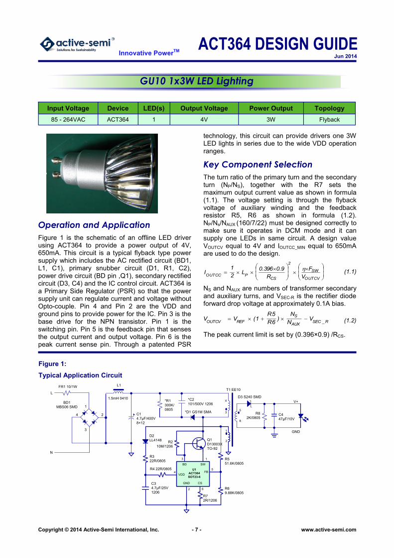
GU10 1x3W LED Lighting
Figure 1:
Typical Application Circuit
Operation and Application
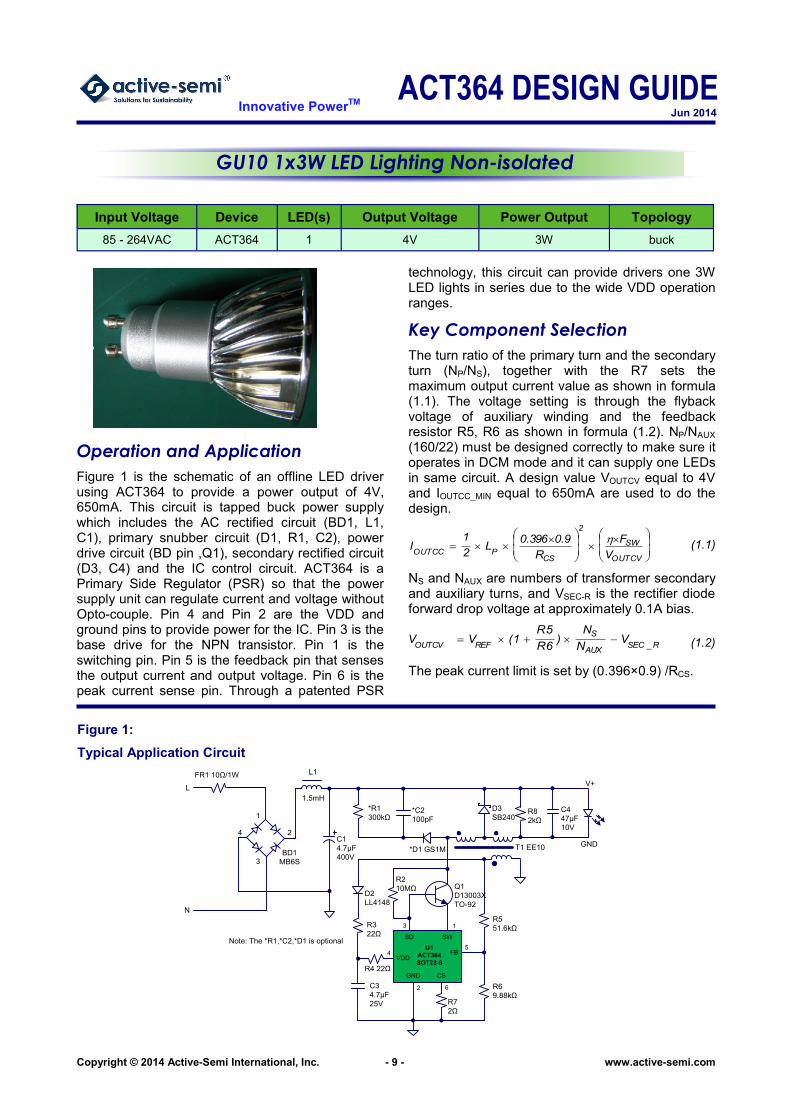
Figure 1 is the schematic of an offline LED driver using ACT364 to provide a power output of 4V, 650mA. This circuit is a typical flyback type power supply which includes the AC rectified circuit (BD1, L1, C1), primary snubber circuit (D1, R1, C2), power drive circuit (BD pin ,Q1), secondary rectified circuit (D3, C4) and the IC control circuit. ACT364 is a Primary Side Regulator (PSR) so that the power supply unit can regulate current and voltage without Opto-couple. Pin 4 and Pin 2 are the VDD and ground pins to provide power for the IC. Pin 3 is the base drive for the NPN transistor. Pin 1 is the switching pin. Pin 5 is the feedback pin that senses the output current and output voltage. Pin 6 is the peak current sense pin. Through a patented PSR
technology, this circuit can provide drivers one 3W LED lights in series due to the wide VDD operation ranges.
Key Component Selection
The turn ratio of the primary turn and the secondary turn (NP/NS), together with the R7 sets the maximum output current value as shown in formula (1.1). The voltage setting is through the flyback voltage of auxiliary winding and the feedback resistor R5, R6 as shown in formula (1.2). NP/Ns/NAUX (160/7/22) must be designed correctly to make sure it operates in DCM mode and it can supply one LEDs in same circuit. A design value VOUTCV equal to 4V and IOUTCC_MIN equal to 650mA are used to do the design.
NS and NAUX are numbers of transformer secondary and auxiliary turns, and VSEC-R is the rectifier diode forward drop voltage at approximately 0.1A bias.
The peak current limit is set by (0.396×0.9) /RCS.
C4
47µF/10V
T1 EE10
L1
D3 S240 SMD
R8
2K/0805
*R1
300K/
0805
C1
4.7µF/400V
8×12
*C2
101/500V 1206
*D1 GS1M SMA
FR1 10/1W
BD1
MBS06 SMD
L
N
1
4
3
2
VDD
U1
ACT364
SOT23-6
1
Q1
D13003X
TO-92
R2
10M/1206
D2
LL4148
R3
22R/0805
R4 22R/0805
C3
4.7µF/25V
1206R7
2R/1206
R6
9.88K/0805
GND CS
FB
SWBD
2
3
4
5
8
4
3 1
5
2 6
V+
GND
R5
51.6K/0805
1.5mH 0410
ACT364 DESIGN GUIDE Jun 2014
Innovative PowerTM
Copyright © 2014 Active-Semi International, Inc. - 8 - www.active-semi.com
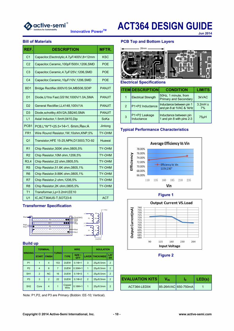
Bill of Materials PCB Top and Bottom Layers
Build up
Efficiency vs. Input Voltage
Input Voltage
90 110 130 150 170 190 210 230 250
AC
T3
64
-00
1
Effic
iency (
%)
Output Current vs. Input Voltage
VOUT1 = 1.8V
AC
T3
64
-00
2
Outp
ut
Curr
ent
(mA
)
Transformer Specification
Typical Performance Characteristics
EVALUATION KITS VIN I0 LED(s)
ACT364-LED03 85-264VAC 650-750mA 1
P1 and P2 are Primary, S1 is Secondary (Bobbin: EE-10 Vertical)
ITEM DESCRIPTION CONDITION LIMITS
1 Electrical Strength 50Hz, 1 minute, from Primary and Secondary
3kVAC
2 P1 Inductance Inductance between pin 1 and pin 4 at 1VAC & 1kHz
3.2mH ± 7%
3 P1 Leakage Inductance
Inductance between pin 1 and pin 4 with pins 3-2 and 7-8 shorted
75µH
Electrical Specifications
3 LEDs 115VAC 230VAC
85VAC 115VAC 230VAC 264VAC
720
700
680
660
640
620
REF. DESCRIPTION MFTR.
C1 Capacitor,Electrolytic,4.7µF/400V,8×12mm KSC
C2 Capacitor,Ceramic,100pF/500V,1206,SMD POE
C3 Capacitor,Ceramic,4.7µF/25V,1206,SMD POE
C4 Capacitor,Ceramic,10µF/10V,1206,SMD POE
BD1 Bridge Rectifier,600V/0.5A,MBS06,SDIP PANJIT
D1 Diode,U1tra Fast,GS1M,1000V/1.0A,SMA PANJIT
D2 General Rectifier,LL4148,100V/1A PANJIT
D3 Diode,schottky,40V/2A,S240,SMA PANJIT
L1 Axial Inductor,1.5mH,0410,Dip SoKa
PCB1 PCB,L*W*T=25.5×14×1.6mm,Rev:A Jintong
FR1 Wire Round Resistor,1W,10ohm,KNP,5% TY-OHM
Q1 Transistor,HFE 15-25,NPN,D13003,TO-92 Huawai
R1 Chip Resistor,300K ohm,0805,5% TY-OHM
R2 Chip Resistor,10M ohm,1206,5% TY-OHM
R3,4 Chip Resistor,22 ohm,0805,5% TY-OHM
R5 Chip Resistor,51.6K ohm,0805,1% TY-OHM
R6 Chip Resistor,9.88K ohm,0805,1% TY-OHM
R7 Chip Resistor,2 ohm,1206,5% TY-OHM
R8 Chip Resistor,2K ohm,0805,5% TY-OHM
T1 Transformer,Lp=3.2mH,EE10
U1 IC,ACT364US-T,SOT23-6 ACT
WINDING
TERMINAL
TURNS
WIRE INSULATION
START FINISH TYPE SIZE × QTY
LAYER THICK/WIDE LAYER
P1 1 4 160 2UEW 0.1Φ×1 3 25µ/8.5mm 2
SH2 2 NC 16 2UEW 0.1Φ×3 1 25µ/8.5mm 2
S1 8 7 7 TEXE
Reverse 0.35Φ×1 1 25µ/8.5mm 2
P2 3 2 22 2UEW 0.1Φ×2 2 25µ/8.5mm 2
SH2 Core 4 1 Copper
Wire 0.18Φ×1 1 25µ/8.5mm 2
26mm
14
mm
70.00
69.20
68.40
67.60
66.80
66.00
115VAC 230VAC
90
Input Voltage
110 130 150 170 190 210 230 250 270
Pin4
Pin2
P1
S1
P2
Pin1
Pin3Pin8
Pin7
Pin2SH1NC
Pin4
S1
8
P1
1
4
P2
3
2
SH1
7
NC
Core(SH2)
Pin4
Reverse
ACT364 DESIGN GUIDE Jun 2014
Innovative PowerTM
Copyright © 2014 Active-Semi International, Inc. - 9 - www.active-semi.com
R_SECAUX
S
REFOUTCVV
N
N)
6R
5R1(VV (1.2)
OUTCV
SW
2
CSPOUTCC V
F
R
9.0396.0L
2
1I
(1.1)
Input Voltage LED(s) Output Voltage Power Output Topology Device
85 - 264VAC 1 4V 3W buck ACT364
GU10 1x3W LED Lighting Non-isolated
Figure 1:
Typical Application Circuit
Operation and Application
Figure 1 is the schematic of an offline LED driver using ACT364 to provide a power output of 4V, 650mA. This circuit is tapped buck power supply which includes the AC rectified circuit (BD1, L1, C1), primary snubber circuit (D1, R1, C2), power drive circuit (BD pin ,Q1), secondary rectified circuit (D3, C4) and the IC control circuit. ACT364 is a Primary Side Regulator (PSR) so that the power supply unit can regulate current and voltage without Opto-couple. Pin 4 and Pin 2 are the VDD and ground pins to provide power for the IC. Pin 3 is the base drive for the NPN transistor. Pin 1 is the switching pin. Pin 5 is the feedback pin that senses the output current and output voltage. Pin 6 is the peak current sense pin. Through a patented PSR
technology, this circuit can provide drivers one 3W LED lights in series due to the wide VDD operation ranges.
Key Component Selection
The turn ratio of the primary turn and the secondary turn (NP/NS), together with the R7 sets the maximum output current value as shown in formula (1.1). The voltage setting is through the flyback voltage of auxiliary winding and the feedback resistor R5, R6 as shown in formula (1.2). NP/NAUX
(160/22) must be designed correctly to make sure it operates in DCM mode and it can supply one LEDs in same circuit. A design value VOUTCV equal to 4V and IOUTCC_MIN equal to 650mA are used to do the design.
NS and NAUX are numbers of transformer secondary and auxiliary turns, and VSEC-R is the rectifier diode forward drop voltage at approximately 0.1A bias.
The peak current limit is set by (0.396×0.9) /RCS.
C4
47µF
10V
T1 EE10
L1
R8
2kΩ
*R1
300kΩ
C1
4.7µF
400V
*C2
100pF
*D1 GS1M
FR1 10Ω/1W
BD1
MB6S
L
N
1
4
3
2
VDD
U1
ACT364
SOT23-6
Q1
D13003X
TO-92
R2
10MΩD2
LL4148
R3
22Ω
R4 22Ω
C3
4.7µF
25V R7
2Ω
R6
9.88kΩ
GND CS
FB
SWBD
4
3 1
5
2 6
V+
GND
R5
51.6kΩ
1.5mH
Note: The *R1,*C2,*D1 is optional
D3
SB240
ACT364 DESIGN GUIDE Jun 2014
Innovative PowerTM
Copyright © 2014 Active-Semi International, Inc. - 10 - www.active-semi.com
Bill of Materials PCB Top and Bottom Layers
Build up
Transformer Specification
Typical Performance Characteristics
EVALUATION KITS VIN I0 LED(s)
ACT364-LED04 85-264VAC 650-750mA 1
ITEM DESCRIPTION CONDITION LIMITS
1 Electrical Strength 50Hz, 1 minute, from Primary and Secondary
3kVAC
2 P1+P2 Inductance Inductance between pin 1 and pin 8 at 1VAC & 1kHz
3.2mH ± 7%
3 P1+P2 Leakage Inductance
Inductance between pin 1 and pin 8 with pins 2-3
75µH
Electrical Specifications
REF. DESCRIPTION MFTR.
C1 Capacitor,Electrolytic,4.7µF/400V,8×12mm KSC
C2 Capacitor,Ceramic,100pF/500V,1206,SMD POE
C3 Capacitor,Ceramic,4.7µF/25V,1206,SMD POE
C4 Capacitor,Ceramic,10µF/10V,1206,SMD POE
BD1 Bridge Rectifier,600V/0.5A,MBS06,SDIP PANJIT
D1 Diode,U1tra Fast,GS1M,1000V/1.0A,SMA PANJIT
D2 General Rectifier,LL4148,100V/1A PANJIT
D3 Diode,schottky,40V/2A,SB240,SMA PANJIT
L1 Axial Inductor,1.5mH,0410,Dip SoKa
PCB1 PCB,L*W*T=25.5×14×1.6mm,Rev:A Jintong
FR1 Wire Round Resistor,1W,10ohm,KNP,5% TY-OHM
Q1 Transistor,HFE 15-25,NPN,D13003,TO-92 Huawai
R1 Chip Resistor,300K ohm,0805,5% TY-OHM
R2 Chip Resistor,10M ohm,1206,5% TY-OHM
R3,4 Chip Resistor,22 ohm,0805,5% TY-OHM
R5 Chip Resistor,51.6K ohm,0805,1% TY-OHM
R6 Chip Resistor,9.88K ohm,0805,1% TY-OHM
R7 Chip Resistor,2 ohm,1206,5% TY-OHM
R8 Chip Resistor,2K ohm,0805,5% TY-OHM
T1 Transformer,Lp=3.2mH,EE10
U1 IC,ACT364US-T,SOT23-6 ACT
26mm
14
mm
P1
1
4
P3
3
2
SH1
NC
Core(SH2)
Pin4
8
P2Pin4
Pin2
P1
P2
P3
Pin1
Pin3
Pin8
Pin4
Pin2SH1NC
Pin4 Pin4(SH2)
Figure 1
Figure 2 WINDING
TERMINAL
TURNS
WIRE INSULATION
START FINISH TYPE SIZE × QTY
LAYER THICK/WIDE LAYER
P1 1 4 153 2UEW 0.1Φ×1 3 25µ/8.5mm 2
P2 4 8 7 2UEW 0.35Φ×1 1 25µ/8.5mm 2
SH1 2 NC 16 2UEW 0.1Φ×3 1 25µ/8.5mm 2
P3 3 2 22 2UEW 0.1Φ×2 2 25µ/8.5mm 2
SH2 Core 4 1 Copper
Wire 0.18Φ×1 1 25µ/8.5mm 2
Note: P1,P2, and P3 are Primary (Bobbin: EE-10; Vertical).
680685690695700705710715720725730735740
90 115 160 230 264
Ou
tpu
t C
urr
en
t(m
A)
Input Voltage
Output Current VS.Load
66.00%
68.00%
70.00%
72.00%
74.00%
76.00%
78.00%
110 135 160 185 210 235
Eff
icie
ncy
Vin
Average Efficiency Vs Vin
Efficiency Vs Vin 115V,230"
ACT364 DESIGN GUIDE Jun 2014
Copyright © 2014 Active-Semi International, Inc. - 11 - www.active-semi.com
Innovative PowerTM
OUTCV
SW
2
CSPOUTCC V
F
R
9.0396.0L
2
1I
(1.1)
Input Voltage LED(s) Output Voltage Power Output Topology Device
85 - 264VAC 3 12V 3W Flyback ACT364
GU10 3x1W LED Lighting
Figure 1:
Schematic of LED Lighting Driver
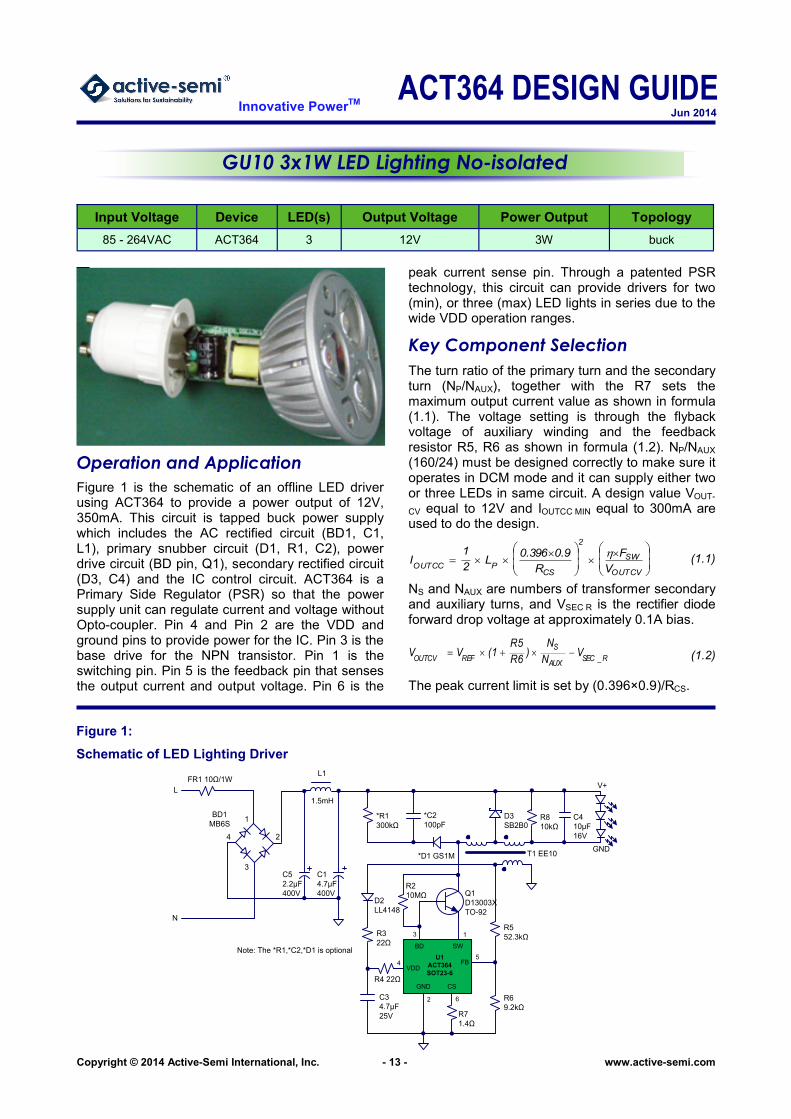
Operation and Application
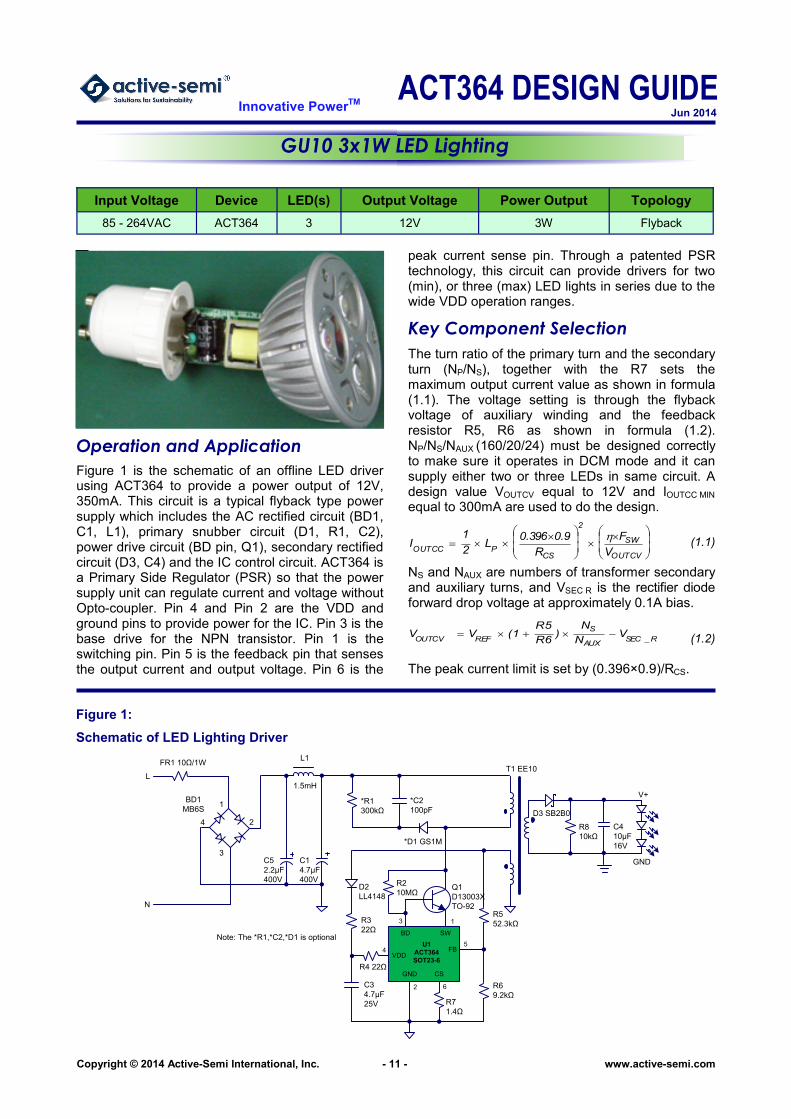
Figure 1 is the schematic of an offline LED driver using ACT364 to provide a power output of 12V, 350mA. This circuit is a typical flyback type power supply which includes the AC rectified circuit (BD1, C1, L1), primary snubber circuit (D1, R1, C2), power drive circuit (BD pin, Q1), secondary rectified circuit (D3, C4) and the IC control circuit. ACT364 is a Primary Side Regulator (PSR) so that the power supply unit can regulate current and voltage without Opto-coupler. Pin 4 and Pin 2 are the VDD and ground pins to provide power for the IC. Pin 3 is the base drive for the NPN transistor. Pin 1 is the switching pin. Pin 5 is the feedback pin that senses the output current and output voltage. Pin 6 is the
peak current sense pin. Through a patented PSR technology, this circuit can provide drivers for two (min), or three (max) LED lights in series due to the wide VDD operation ranges.
Key Component Selection
The turn ratio of the primary turn and the secondary turn (NP/NS), together with the R7 sets the maximum output current value as shown in formula (1.1). The voltage setting is through the flyback voltage of auxiliary winding and the feedback resistor R5, R6 as shown in formula (1.2). NP/NS/NAUX (160/20/24) must be designed correctly to make sure it operates in DCM mode and it can supply either two or three LEDs in same circuit. A design value VOUTCV equal to 12V and IOUTCC MIN equal to 300mA are used to do the design.
NS and NAUX are numbers of transformer secondary and auxiliary turns, and VSEC R is the rectifier diode forward drop voltage at approximately 0.1A bias.
The peak current limit is set by (0.396×0.9)/RCS.
R_SECAUX
S
REFOUTCVV
N
N)
6R
5R1(VV (1.2)
C4
10µF
16V
L1
R8
10kΩ
*R1
300kΩ
C1
4.7µF
400V
*C2
100pF
*D1 GS1M
FR1 10Ω/1W
BD1
MB6S
L
N
1
4
3
2
VDD
U1
ACT364
SOT23-6
Q1
D13003X
TO-92
R2
10MΩD2
LL4148
R3
22Ω
R4 22Ω
C3
4.7µF
25V R7
1.4Ω
R6
9.2kΩ
GND CS
FB
SWBD
4
3 1
5
2 6
V+
GND
R5
52.3kΩ
1.5mH
Note: The *R1,*C2,*D1 is optional
C5
2.2µF
400V
T1 EE10
D3 SB2B0
ACT364 DESIGN GUIDE Jun 2014
Copyright © 2014 Active-Semi International, Inc. - 12 - www.active-semi.com
Innovative PowerTM
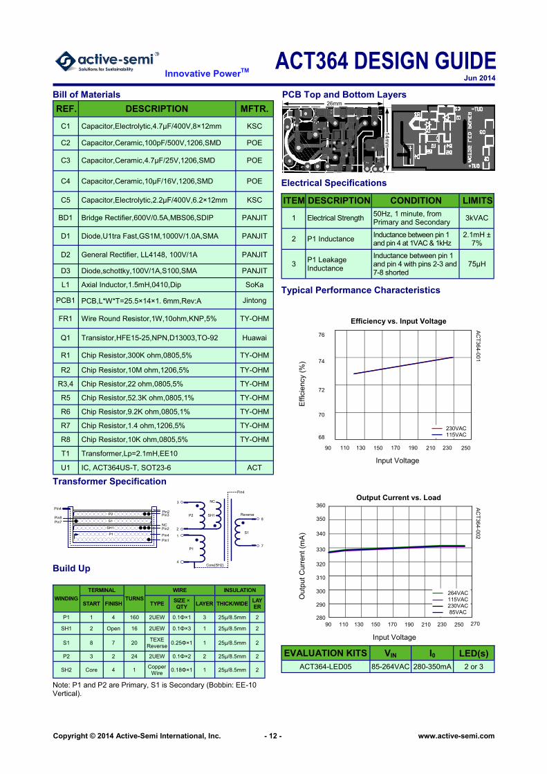
Bill of Materials PCB Top and Bottom Layers
Build Up
Transformer Specification
Typical Performance Characteristics
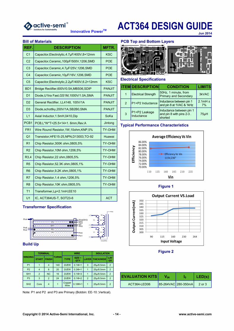
EVALUATION KITS VIN I0 LED(s)
ACT364-LED05 85-264VAC 280-350mA 2 or 3
Note: P1 and P2 are Primary, S1 is Secondary (Bobbin: EE-10 Vertical).
ITEM DESCRIPTION CONDITION LIMITS
1 Electrical Strength 50Hz, 1 minute, from Primary and Secondary
3kVAC
2 P1 Inductance Inductance between pin 1 and pin 4 at 1VAC & 1kHz
2.1mH ± 7%
3 P1 Leakage Inductance
Inductance between pin 1 and pin 4 with pins 2-3 and 7-8 shorted
75µH
Electrical Specifications
Efficiency vs. Input Voltage
76
74
72
70
68
AC
T3
64
-00
1
Effic
iency (
%)
230VAC 264VAC 110VAC 85VAC
115VAC 230VAC
Output Current vs. Load 360
350
340
330
320
310
300
290
280
AC
T3
64
-00
2
Outp
ut
Curr
ent
(mA
)
REF. DESCRIPTION MFTR.
C1 Capacitor,Electrolytic,4.7µF/400V,8×12mm KSC
C2 Capacitor,Ceramic,100pF/500V,1206,SMD POE
C3 Capacitor,Ceramic,4.7µF/25V,1206,SMD POE
C4 Capacitor,Ceramic,10µF/16V,1206,SMD POE
C5 Capacitor,Electrolytic,2.2µF/400V,6.2×12mm KSC
BD1 Bridge Rectifier,600V/0.5A,MBS06,SDIP PANJIT
D1 Diode,U1tra Fast,GS1M,1000V/1.0A,SMA PANJIT
D2 General Rectifier, LL4148, 100V/1A PANJIT
D3 Diode,schottky,100V/1A,S100,SMA PANJIT
L1 Axial Inductor,1.5mH,0410,Dip SoKa
PCB1 PCB,L*W*T=25.5×14×1.6mm,Rev:A Jintong
FR1 Wire Round Resistor,1W,10ohm,KNP,5% TY-OHM
Q1 Transistor,HFE15-25,NPN,D13003,TO-92 Huawai
R1 Chip Resistor,300K ohm,0805,5% TY-OHM
R2 Chip Resistor,10M ohm,1206,5% TY-OHM
R3,4 Chip Resistor,22 ohm,0805,5% TY-OHM
R5 Chip Resistor,52.3K ohm,0805,1% TY-OHM
R6 Chip Resistor,9.2K ohm,0805,1% TY-OHM
R7 Chip Resistor,1.4 ohm,1206,5% TY-OHM
R8 Chip Resistor,10K ohm,0805,5% TY-OHM
T1 Transformer,Lp=2.1mH,EE10
U1 IC, ACT364US-T, SOT23-6 ACT
26mm
14
mm
WINDING
TERMINAL
TURNS
WIRE INSULATION
START FINISH TYPE SIZE × QTY
LAYER THICK/WIDE LAYER
P1 1 4 160 2UEW 0.1Φ×1 3 25µ/8.5mm 2
SH1 2 Open 16 2UEW 0.1Φ×3 1 25µ/8.5mm 2
S1 8 7 20 TEXE
Reverse 0.25Φ×1 1 25µ/8.5mm 2
P2 3 2 24 2UEW 0.1Φ×2 2 25µ/8.5mm 2
SH2 Core 4 1 Copper
Wire 0.18Φ×1 1 25µ/8.5mm 2
90
Input Voltage
110 130 150 170 190 210 230 250
90
Input Voltage
110 130 150 170 190 210 230 250
230VAC 115VAC
270
264VAC 115VAC 230VAC 85VAC
Pin4
Pin2
P1
S1
P2
Pin1
Pin3Pin8
Pin7
Pin2SH1NC
Pin4
S1
8
P1
1
4
P2
3
2
SH1
7
NC
Core(SH2)
Pin4
Reverse
ACT364 DESIGN GUIDE Jun 2014
Innovative PowerTM
Copyright © 2014 Active-Semi International, Inc. - 13 - www.active-semi.com
OUTCV
SW
2
CSPOUTCC V
F
R
9.0396.0L
2
1I
(1.1)
Input Voltage LED(s) Output Voltage Power Output Topology Device
85 - 264VAC 3 12V 3W buck ACT364
GU10 3x1W LED Lighting No-isolated
Figure 1:
Schematic of LED Lighting Driver
Operation and Application
Figure 1 is the schematic of an offline LED driver using ACT364 to provide a power output of 12V, 350mA. This circuit is tapped buck power supply which includes the AC rectified circuit (BD1, C1, L1), primary snubber circuit (D1, R1, C2), power drive circuit (BD pin, Q1), secondary rectified circuit (D3, C4) and the IC control circuit. ACT364 is a Primary Side Regulator (PSR) so that the power supply unit can regulate current and voltage without Opto-coupler. Pin 4 and Pin 2 are the VDD and ground pins to provide power for the IC. Pin 3 is the base drive for the NPN transistor. Pin 1 is the switching pin. Pin 5 is the feedback pin that senses the output current and output voltage. Pin 6 is the
peak current sense pin. Through a patented PSR technology, this circuit can provide drivers for two (min), or three (max) LED lights in series due to the wide VDD operation ranges.
Key Component Selection
The turn ratio of the primary turn and the secondary turn (NP/NAUX), together with the R7 sets the maximum output current value as shown in formula (1.1). The voltage setting is through the flyback voltage of auxiliary winding and the feedback resistor R5, R6 as shown in formula (1.2). NP/NAUX
(160/24) must be designed correctly to make sure it operates in DCM mode and it can supply either two or three LEDs in same circuit. A design value VOUT-
CV equal to 12V and IOUTCC MIN equal to 300mA are used to do the design.
NS and NAUX are numbers of transformer secondary and auxiliary turns, and VSEC R is the rectifier diode forward drop voltage at approximately 0.1A bias.
The peak current limit is set by (0.396×0.9)/RCS.
R_SECAUX
S
REFOUTCVV
N
N)
6R
5R1(VV (1.2)
C4
10µF
16V
T1 EE10
L1
R8
10kΩ
*R1
300kΩ
C1
4.7µF
400V
*C2
100pF
*D1 GS1M
FR1 10Ω/1W
BD1
MB6S
L
N
1
4
3
2
VDD
U1
ACT364
SOT23-6
Q1
D13003X
TO-92
R2
10MΩD2
LL4148
R3
22Ω
R4 22Ω
C3
4.7µF
25V R7
1.4Ω
R6
9.2kΩ
GND CS
FB
SWBD
4
3 1
5
2 6
V+
GND
R5
52.3kΩ
1.5mH
Note: The *R1,*C2,*D1 is optional
D3
SB2B0
C5
2.2µF
400V
ACT364 DESIGN GUIDE Jun 2014
Innovative PowerTM
Copyright © 2014 Active-Semi International, Inc. - 14 - www.active-semi.com
Bill of Materials PCB Top and Bottom Layers
Build Up
Transformer Specification
Typical Performance Characteristics
EVALUATION KITS VIN I0 LED(s)
ACT364-LED06 85-264VAC 280-350mA 2 or 3
Note: P1 and P2 and P3 are Primary (Bobbin: EE-10 ;Vertical).
ITEM DESCRIPTION CONDITION LIMITS
1 Electrical Strength 50Hz, 1 minute, from Primary and Secondary
3kVAC
2 P1+P2 Inductance Inductance between pin 1 and pin 8 at 1VAC & 1kHz
2.1mH ± 7%
3 P1+P2 Leakage Inductance
Inductance between pin 1 and pin 8 with pins 2-3 . shorted
75µH
Electrical Specifications
REF. DESCRIPTION MFTR.
C1 Capacitor,Electrolytic,4.7µF/400V,8×12mm KSC
C2 Capacitor,Ceramic,100pF/500V,1206,SMD POE
C3 Capacitor,Ceramic,4.7µF/25V,1206,SMD POE
C4 Capacitor,Ceramic,10µF/16V,1206,SMD POE
C5 Capacitor,Electrolytic,2.2µF/400V,6.2×12mm KSC
BD1 Bridge Rectifier,600V/0.5A,MBS06,SDIP PANJIT
D1 Diode,U1tra Fast,GS1M,1000V/1.0A,SMA PANJIT
D2 General Rectifier, LL4148, 100V/1A PANJIT
D3 Diode,schottky,200V/1A,SB2B0,SMA PANJIT
L1 Axial Inductor,1.5mH,0410,Dip SoKa
PCB1 PCB,L*W*T=25.5×14×1.6mm,Rev:A Jintong
FR1 Wire Round Resistor,1W,10ohm,KNP,5% TY-OHM
Q1 Transistor,HFE15-25,NPN,D13003,TO-92 Huawai
R1 Chip Resistor,300K ohm,0805,5% TY-OHM
R2 Chip Resistor,10M ohm,1206,5% TY-OHM
R3,4 Chip Resistor,22 ohm,0805,5% TY-OHM
R5 Chip Resistor,52.3K ohm,0805,1% TY-OHM
R6 Chip Resistor,9.2K ohm,0805,1% TY-OHM
R7 Chip Resistor,1.4 ohm,1206,5% TY-OHM
R8 Chip Resistor,10K ohm,0805,5% TY-OHM
T1 Transformer,Lp=2.1mH,EE10
U1 IC, ACT364US-T, SOT23-6 ACT
26mm
14
mm
WINDING
TERMINAL
TURNS
WIRE INSULATION
START FINISH TYPE SIZE × QTY
LAYER THICK/WIDE LAYER
P1 1 4 140 2UEW 0.1Φ×1 3 25µ/8.5mm 2
P2 4 8 20 2UEW 0.3Φ×1 1 25µ/8.5mm 2
SH1 2 NC 16 2UEW 0.1Φ×3 1 25µ/8.5mm 2
P3 3 2 24 2UEW 0.1Φ×2 2 25µ/8.5mm 2
SH2 Core 4 1 Copper
Wire 0.18Φ×1 1 25µ/8.5mm 2
Figure 1
Figure 2
P1
1
4
P3
3
2
SH1
NC
Core(SH2)
Pin4
8
P2Pin4
Pin2
P1
P2
P3
Pin1
Pin3
Pin8
Pin4
Pin2SH1NC
Pin4 Pin4(SH2)
70.00%72.00%74.00%76.00%78.00%80.00%82.00%84.00%86.00%
110 135 160 185 210 235
Eff
icie
ncy
Vin
Average Efficiency Vs Vin
Efficiency Vs Vin 115V,230"
300305310315320325330335340345350
90 115 160 230 264
Ou
tpu
t C
urr
en
t(m
A)
Input Voltage
Output Current VS.Load
ACT365 DESIGN GUIDE Jun 2014
Innovative PowerTM
Copyright © 2014 Active-Semi International, Inc. - 15 - www.active-semi.com
(2)
(1)
Input Voltage LED(s) Output Voltage Power Output Topology Device Transformer
85 - 264VAC 7 26V 7.8W Flyback ACT365 EE16
PAR30 7x1W LED Lighting
Figure 1:
Schematic of LED Lighting Driver
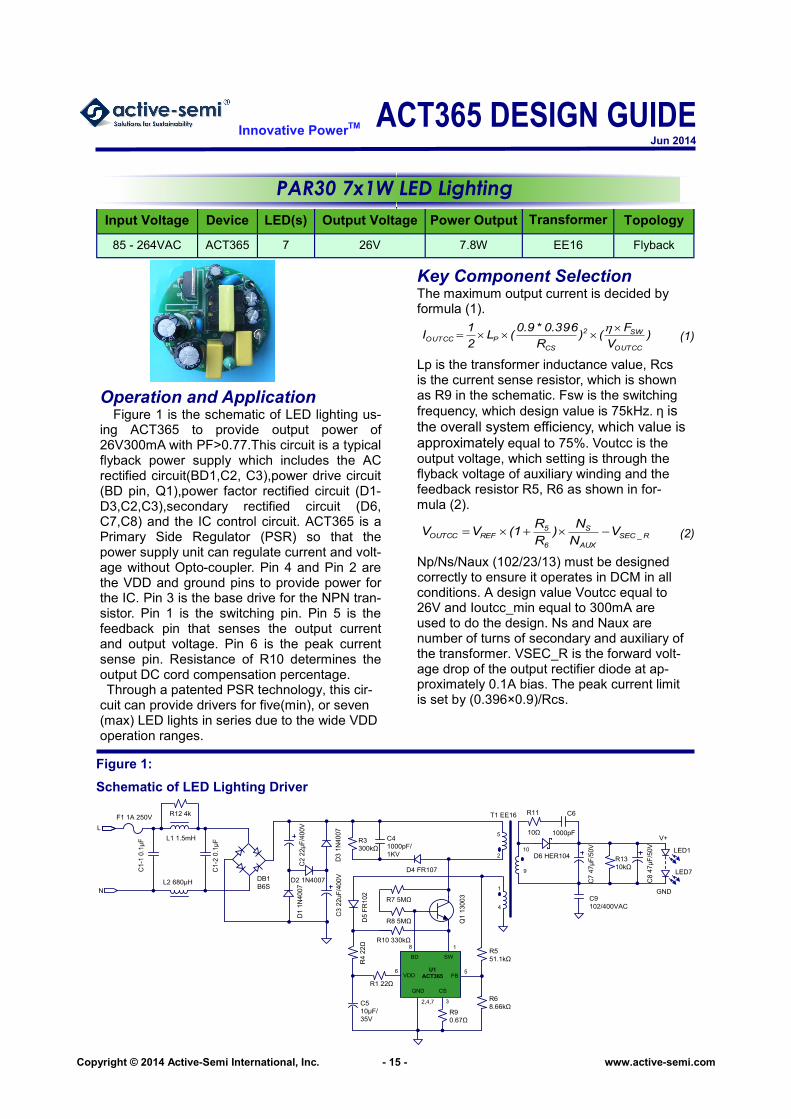
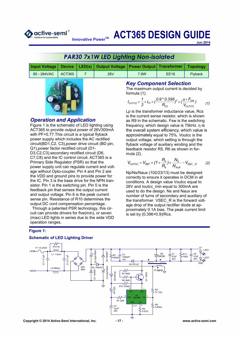
Operation and Application Figure 1 is the schematic of LED lighting us-
ing ACT365 to provide output power of 26V300mA with PF>0.77.This circuit is a typical flyback power supply which includes the AC rectified circuit(BD1,C2, C3),power drive circuit (BD pin, Q1),power factor rectified circuit (D1-D3,C2,C3),secondary rectified circuit (D6, C7,C8) and the IC control circuit. ACT365 is a Primary Side Regulator (PSR) so that the power supply unit can regulate current and volt-age without Opto-coupler. Pin 4 and Pin 2 are the VDD and ground pins to provide power for the IC. Pin 3 is the base drive for the NPN tran-sistor. Pin 1 is the switching pin. Pin 5 is the feedback pin that senses the output current and output voltage. Pin 6 is the peak current sense pin. Resistance of R10 determines the output DC cord compensation percentage. Through a patented PSR technology, this cir-cuit can provide drivers for five(min), or seven (max) LED lights in series due to the wide VDD operation ranges.
Key Component Selection The maximum output current is decided by formula (1).
Lp is the transformer inductance value, Rcs is the current sense resistor, which is shown as R9 in the schematic. Fsw is the switching
frequency, which design value is 75kHz. η is the overall system efficiency, which value is approximately equal to 75%. Voutcc is the output voltage, which setting is through the flyback voltage of auxiliary winding and the feedback resistor R5, R6 as shown in for-mula (2).
Np/Ns/Naux (102/23/13) must be designed correctly to ensure it operates in DCM in all conditions. A design value Voutcc equal to 26V and Ioutcc_min equal to 300mA are used to do the design. Ns and Naux are number of turns of secondary and auxiliary of the transformer. VSEC_R is the forward volt-age drop of the output rectifier diode at ap-proximately 0.1A bias. The peak current limit is set by (0.396×0.9)/Rcs.
)V
F()
R
396.0*9.0(L
2
1I
OUTCC
SW2
CS
POUTCC
R_SEC
AUX
S
6
5REFOUTCC V
N
N)
R
R1(VV
T1 EE16
D6 HER104
VDDU1
ACT365
1
R1 22Ω
C5
10µF/
35V R9
0.67Ω
R6
8.66kΩ
GND CS
FB
SWBD
4
2
5
10
9
6
8 1
5
2,4,7 3
V+
GND
R7 5MΩ
R5
51.1kΩ
D2 1N4007
R3
300kΩ
C4
1000pF/
1KV
C6
C9
102/400VAC
LED1
LED7DB1
B6S
C2
22
µF
/40
0V
C3
22u
F/4
00
V
D1
1N
40
07
D3
1N
40
07
D5
FR
10
2
R8 5MΩ
R10 330kΩ
R4
22
Ω
Q1
13
00
3
D4 FR107
R11
C7
47
µF
/50V
C8
47µ
F/5
0V
10Ω 1000pF
F1 1A 250V
L
C1-2
0.1
µFL1 1.5mH
L2 680µH
R12 4k
C1
-1 0
.1µ
F
R13
10kΩ
N
ACT365 DESIGN GUIDE Jun 2014
Innovative PowerTM
Copyright © 2014 Active-Semi International, Inc. - 16 - www.active-semi.com
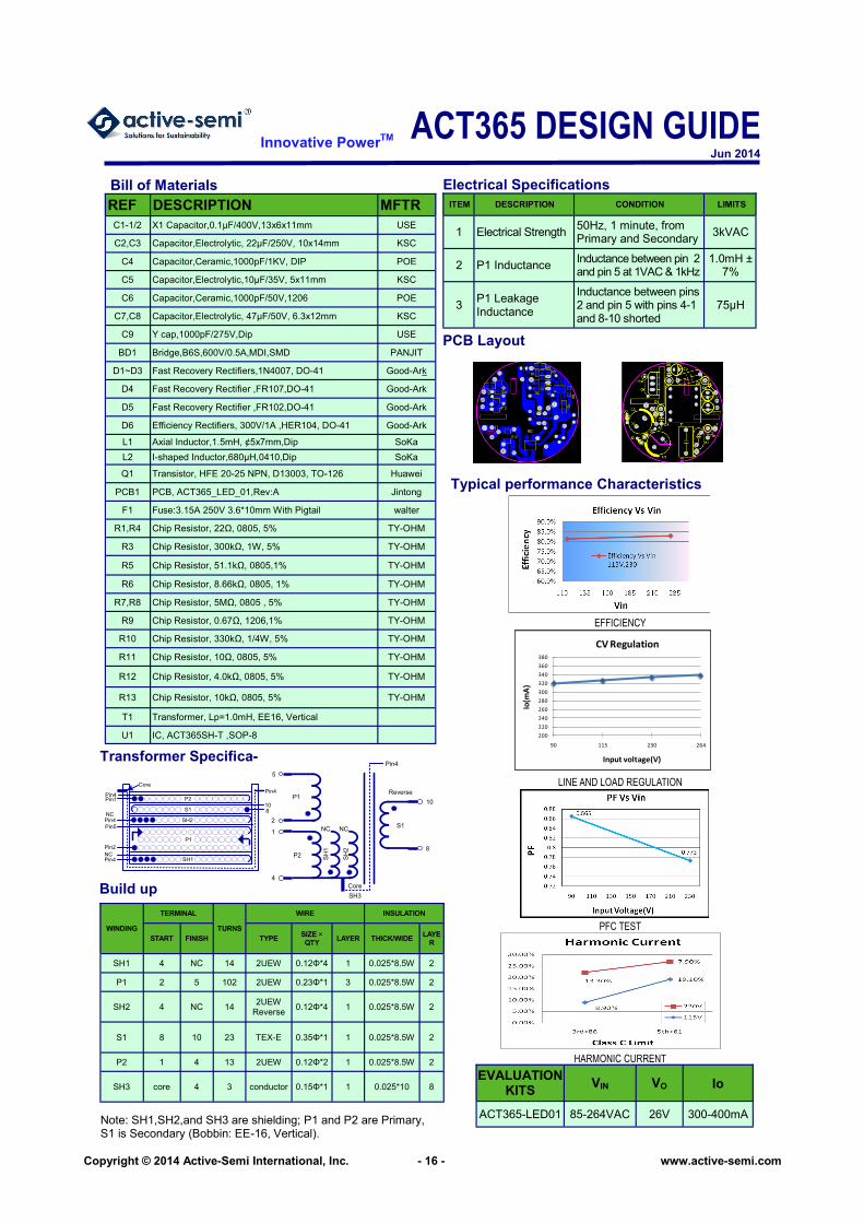
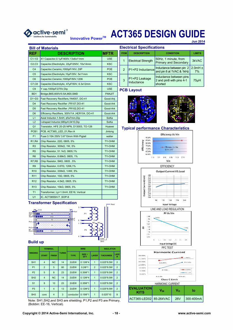
EVALUATION KITS
VIN VO Io
ACT365-LED01 85-264VAC 26V 300-400mA
Bill of Materials
Build up
REF DESCRIPTION MFTR
C1-1/2 X1 Capacitor,0.1µF/400V,13x6x11mm USE
C2,C3 Capacitor,Electrolytic, 22µF/250V, 10x14mm KSC
C4 Capacitor,Ceramic,1000pF/1KV, DIP POE
C5 Capacitor,Electrolytic,10µF/35V, 5x11mm KSC
C6 Capacitor,Ceramic,1000pF/50V,1206 POE
C7,C8 Capacitor,Electrolytic, 47µF/50V, 6.3x12mm KSC
C9 Y cap,1000pF/275V,Dip USE
BD1 Bridge,B6S,600V/0.5A,MDI,SMD PANJIT
D1~D3 Fast Recovery Rectifiers,1N4007, DO-41 Good-Ark
D4 Fast Recovery Rectifier ,FR107,DO-41 Good-Ark
D5 Fast Recovery Rectifier ,FR102,DO-41 Good-Ark
D6 Efficiency Rectifiers, 300V/1A ,HER104, DO-41 Good-Ark L1 Axial Inductor,1.5mH, ¢5x7mm,Dip SoKa
L2 I-shaped Inductor,680µH,0410,Dip SoKa
Q1 Transistor, HFE 20-25 NPN, D13003, TO-126 Huawei
PCB1 PCB, ACT365_LED_01,Rev:A Jintong
F1 Fuse:3.15A 250V 3.6*10mm With Pigtail walter
R1,R4 Chip Resistor, 22Ω, 0805, 5% TY-OHM
R3 Chip Resistor, 300kΩ, 1W, 5% TY-OHM
R5 Chip Resistor, 51.1kΩ, 0805,1% TY-OHM
R6 Chip Resistor, 8.66kΩ, 0805, 1% TY-OHM
R7,R8 Chip Resistor, 5MΩ, 0805 , 5% TY-OHM
R9 Chip Resistor, 0.67Ω, 1206,1% TY-OHM
R10 Chip Resistor, 330kΩ, 1/4W, 5% TY-OHM
R11 Chip Resistor, 10Ω, 0805, 5% TY-OHM
R12 Chip Resistor, 4.0kΩ, 0805, 5% TY-OHM
R13 Chip Resistor, 10kΩ, 0805, 5% TY-OHM
T1 Transformer, Lp=1.0mH, EE16, Vertical
U1 IC, ACT365SH-T ,SOP-8
Transformer Specifica-
Note: SH1,SH2,and SH3 are shielding; P1 and P2 are Primary, S1 is Secondary (Bobbin: EE-16, Vertical).
ITEM DESCRIPTION CONDITION LIMITS
1 Electrical Strength 50Hz, 1 minute, from Primary and Secondary
3kVAC
2 P1 Inductance Inductance between pin 2 and pin 5 at 1VAC & 1kHz
1.0mH ± 7%
3 P1 Leakage Inductance
Inductance between pins 2 and pin 5 with pins 4-1 and 8-10 shorted
75µH
Electrical Specifications
WINDING
TERMINAL
TURNS
WIRE INSULATION
START FINISH TYPE SIZE × QTY
LAYER THICK/WIDE LAYE
R
SH1 4 NC 14 2UEW 0.12Φ*4 1 0.025*8.5W 2
P1 2 5 102 2UEW 0.23Φ*1 3 0.025*8.5W 2
SH2 4 NC 14 2UEW Reverse 0.12Φ*4 1 0.025*8.5W 2
S1 8 10 23 TEX-E 0.35Φ*1 1 0.025*8.5W 2
P2 1 4 13 2UEW 0.12Φ*2 1 0.025*8.5W 2
SH3 core 4 3 conductor 0.15Φ*1 1 0.025*10 8
Typical performance Characteristics
S1
10
P2
1
4
P1
5
2
SH
1 8
NC NC
SH
2
Core
SH3
Reverse
Pin4
NC
Pin4
SH1
S1
P2
Pin4
108
SH2
Pin2
Pin5
Pin4NC
Pin1
P1
Pin4
Core
PCB Layout
EFFICIENCY
LINE AND LOAD REGULATION
PFC TEST
HARMONIC CURRENT
200
220
240
260
280
300
320
340
360
380
90 115 230 264
Io(m
A)
Input voltage(V)
CV Regulation
ACT365 DESIGN GUIDE Jun 2014
Innovative PowerTM
Copyright © 2014 Active-Semi International, Inc. - 17 - www.active-semi.com
(2)
(1)
Input Voltage LED(s) Output Voltage Power Output Topology Device Transformer
85 - 264VAC 7 26V 7.8W Flyback ACT365 EE16
PAR30 7x1W LED Lighting Non-isolated
Figure 1:
Schematic of LED Lighting Driver
Operation and Application Figure 1 is the schematic of LED lighting using ACT365 to provide output power of 26V300mA with PF>0.77.This circuit is a typical flyback power supply which includes the AC rectified circuit(BD1,C2, C3),power drive circuit (BD pin, Q1),power factor rectified circuit (D1-D3,C2,C3),secondary rectified circuit (D6, C7,C8) and the IC control circuit. ACT365 is a Primary Side Regulator (PSR) so that the power supply unit can regulate current and volt-age without Opto-coupler. Pin 4 and Pin 2 are the VDD and ground pins to provide power for the IC. Pin 3 is the base drive for the NPN tran-sistor. Pin 1 is the switching pin. Pin 5 is the feedback pin that senses the output current and output voltage. Pin 6 is the peak current sense pin. Resistance of R10 determines the output DC cord compensation percentage. Through a patented PSR technology, this cir-cuit can provide drivers for five(min), or seven (max) LED lights in series due to the wide VDD operation ranges.
Key Component Selection The maximum output current is decided by formula (1).
Lp is the transformer inductance value, Rcs is the current sense resistor, which is shown as R9 in the schematic. Fsw is the switching
frequency, which design value is 75kHz. η is the overall system efficiency, which value is approximately equal to 75%. Voutcc is the output voltage, which setting is through the flyback voltage of auxiliary winding and the feedback resistor R5, R6 as shown in for-mula (2).
Np/Ns/Naux (102/23/13) must be designed correctly to ensure it operates in DCM in all conditions. A design value Voutcc equal to 26V and Ioutcc_min equal to 300mA are used to do the design. Ns and Naux are number of turns of secondary and auxiliary of the transformer. VSEC_R is the forward volt-age drop of the output rectifier diode at ap-proximately 0.1A bias. The peak current limit is set by (0.396×0.9)/Rcs.
)V
F()
R
396.0*9.0(L
2
1I
OUTCC
SW2
CS
POUTCC
R_SEC
AUX
S
6
5REFOUTCC V
N
N)
R
R1(VV
VDDU1
ACT365
R1 22R
C5
10µF/
35V R9
0.67Ω
R6
8.66kΩ
GND CS
FB
SWBD
6
8 1
5
2,4,7 3
R7 5MΩ
R5
51.1kΩ
R3
300kΩ
C4
1000pF/
1kV
D5
FR
10
2
R8 5MΩ
R10 330kΩ
R4
22
Ω
Q1
13
00
3
D4 FR107
C7
47µF
50V
V+
GND
C8
47µF
50V
LED1
LED7
T1 EE16
D6
SB2B0R13
10kΩ
D2 1N4007DB1
B6S
C2
22µ
F/4
00
V
C3
22
uF
/40
0V
D1
1N
40
07
D3
1N
40
07
F1 1A 250V
L
C1
-2 0
.1µ
FL1 1.5mH
L2 680µH
R12 4k
C1-1
0.1
µF
N
ACT365 DESIGN GUIDE Jun 2014
Innovative PowerTM
Copyright © 2014 Active-Semi International, Inc. - 18 - www.active-semi.com
EVALUATION KITS
VIN VO Io
ACT365-LED02 85-264VAC 26V 300-400mA
Bill of Materials
Build up
REF DESCRIPTION MFTR
C1-1/2 X1 Capacitor,0.1µF/400V,13x6x11mm USE
C2,C3 Capacitor,Electrolytic, 22µF/250V, 10x14mm KSC
C4 Capacitor,Ceramic,1000pF/1KV, DIP POE
C5 Capacitor,Electrolytic,10µF/35V, 5x11mm KSC
C6 Capacitor,Ceramic,1000pF/50V,1206 POE
C7,C8 Capacitor,Electrolytic, 47µF/50V, 6.3x12mm KSC
C9 Y cap,1000pF/275V,Dip USE
BD1 Bridge,B6S,600V/0.5A,MDI,SMD PANJIT
D1~D3 Fast Recovery Rectifiers,1N4007, DO-41 Good-Ark
D4 Fast Recovery Rectifier ,FR107,DO-41 Good-Ark
D5 Fast Recovery Rectifier ,FR102,DO-41 Good-Ark
D6 Efficiency Rectifiers, 300V/1A ,HER104, DO-41 Good-Ark L1 Axial Inductor,1.5mH, ¢5x7mm,Dip SoKa
L2 I-shaped Inductor,680µH,0410,Dip SoKa
Q1 Transistor, HFE 20-25 NPN, D13003, TO-126 Huawei
PCB1 PCB, ACT365_LED_01,Rev:A Jintong
F1 Fuse:3.15A 250V 3.6*10mm With Pigtail walter
R1,R4 Chip Resistor, 22Ω, 0805, 5% TY-OHM
R3 Chip Resistor, 300kΩ, 1W, 5% TY-OHM
R5 Chip Resistor, 51.1kΩ, 0805,1% TY-OHM
R6 Chip Resistor, 8.66kΩ, 0805, 1% TY-OHM
R7,R8 Chip Resistor, 5MΩ, 0805 , 5% TY-OHM
R9 Chip Resistor, 0.67Ω, 1206,1% TY-OHM
R10 Chip Resistor, 330kΩ, 1/4W, 5% TY-OHM
R11 Chip Resistor, 10Ω, 0805, 5% TY-OHM
R12 Chip Resistor, 4.0kΩ, 0805, 5% TY-OHM
R13 Chip Resistor, 10kΩ, 0805, 5% TY-OHM
T1 Transformer, Lp=1.0mH, EE16, Vertical
U1 IC, ACT365SH-T ,SOP-8
Transformer Specification
Note: SH1,SH2,and SH3 are shielding; P1,P2 and P3 are Primary, (Bobbin: EE-16, Vertical).
ITEM DESCRIPTION CONDITION LIMITS
1 Electrical Strength 50Hz, 1 minute, from Primary and Secondary
3kVAC
2 P1+P2 Inductance Inductance between pin 2 and pin 8 at 1VAC & 1kHz
2.0mH ± 7%
3 P1+P2 Leakage Inductance
Inductance between pins 2 and pin8 with pins 4-1 shorted
75µH
Electrical Specifications
WINDING
TERMINAL
TURNS
WIRE INSULATION
START FINISH TYPE SIZE × QTY
LAYER THICK/WIDE LAYE
R
SH1 4 NC 14 2UEW 0.12Φ*4 1 0.025*8.5W 2
P1 2 5 80 2UEW 0.2Φ*1 2 0.025*8.5W 2
P2 5 8 23 2UEW 0.35Φ*1 1 0.025*8.5W 2
SH2 4 NC 14 2UEW 0.12Φ*4 1 0.025*8.5W 2
S1 8 10 23 2UEW 0.35Φ*1 1 0.025*8.5W 2
P3 1 4 13 2UEW 0.12Φ*2 1 0.025*8.5W 2
SH3 core 4 3 conductor 0.15Φ*1 1 0.025*10 8
Typical performance Characteristics
PCB Layout
EFFICIENCY
LINE AND LOAD REGULATION
PFC TEST
HARMONIC CURRENT
P3
1
4
P1
5
2
SH
1
NC NC
SH
2
Core
SH3
Pin4
8
P2
NC
Pin4
SH1
P2
P3
Pin4
85
SH2
Pin2
Pin5
Pin4NCPin1
P1
Pin4
Core
ACT512 DESIGN GUIDE Jun 2014
Innovative PowerTM
Copyright © 2014 Active-Semi International, Inc. - 19 - www.active-semi.com
(2)
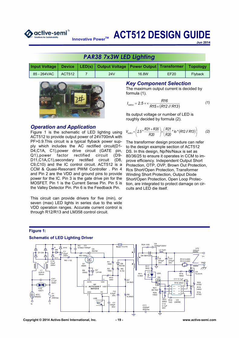
Input Voltage LED(s) Output Voltage Power Output Topology Device Transformer
85 - 264VAC 7 24V 16.8W Flyback ACT512 EF20
PAR38 7x3W LED Lighting
Figure 1:
Schematic of LED Lighting Driver
Operation and Application Figure 1 is the schematic of LED lighting using ACT512 to provide output power of 24V700mA with PF>0.9.This circuit is a typical flyback power sup-ply which includes the AC rectified circuit(D1-D4,C1A, C1),power drive circuit (GATE pin, Q1),power factor rectified circuit (D9-D11,C1A,C1),secondary rectified circuit (D8, C9,C10) and the IC control circuit. ACT512 is a CCM & Quasi-Resonant PWM Controller . Pin 4 and Pin 2 are the VDD and ground pins to provide power for the IC. Pin 3 is the gate drive pin for the MOSFET. Pin 1 is the Current Sense Pin. Pin 5 is the Valley Detector Pin. Pin 6 is the Feedback Pin.
This circuit can provide drivers for five (min), or seven (max) LED lights in series due to the wide VDD operation ranges. Accurate current control is through R12/R13 and LM358 control circuit.
Key Component Selection The maximum output current is decided by formula (1).
Its output voltage or number of LED is roughly decided by formula (2).
The transformer design procedure can refer to the design example section of ACT512 DS. In this design, Np/Ns/Naux is set as 80/36/25 to ensure it operates in CCM to im-prove efficiency. Independent Output Short Protection, OTP, OVP, Brown Out Protection, Rcs Short/Open Protection, Transformer Winding Short Protection, Output Diode Short/Open Protection, Open Loop Protec-tion, are integrated to protect damage on cir-cuits and LED die itself.
C9
470µF
35V
L1
UU9.8
30mH
D8 SB10200
R17
5KΩ
R2
510kΩ
C3
1000pF
C1
22µF
250V
CS
U1
ACT512US-T
SOT23-6
GND FB
VDDGATE
1
3 4
2
GND
VDET5
R6 1.1ΩR1
1MΩ
R2
1MΩ
D5
RS1M
D6
RS1M
R5
4.7Ω
C7
100pF
50V
C4
6.8µF
35VR8
8.25kΩ
R7
54.9kΩ
R4 100Ω
U4
TL431A
C8
1000pF/200VR24 10Ω
C10
470µF
35V
NTC
5RS5C
L
N
D1-D4
R11
3.3kΩ
6
D11
Q1
4N65
CX1
0.1uF
400V
F1
2A
250Vac
TVS
10471
U2B
R12 0.22Ω
R18 20kΩ
R14
18kΩ
C12
0.1µF
50V
CY1
2200pF
400Vac
R10
22Ω
R9
330Ω
D7
L4148
V+
LF2
200µH
Bead T3.5*9
D9
D10
C1A
22µF
250V
8
7
6
5 4
3
2
1VCC
OUT2
IN2-
IN2+ GND
IN1+
IN1-
OUT1
L2 3uH
U2A
U3
LM358R19
1kΩ
R23
20kΩ
R20
10kΩ
R21
88.7kΩ
C11 0.1µF
R22
510Ω
R15
14KΩ
R16
470Ω
R13 0.22Ω
D9
13R//12R15R
16R5.2Ioutcc
13R//12R*Io*
20R
21R
20R
20R21R*5.2Voutcv
(1)
ACT512 DESIGN GUIDE Jun 2014
Innovative PowerTM
Copyright © 2014 Active-Semi International, Inc. - 20 - www.active-semi.com
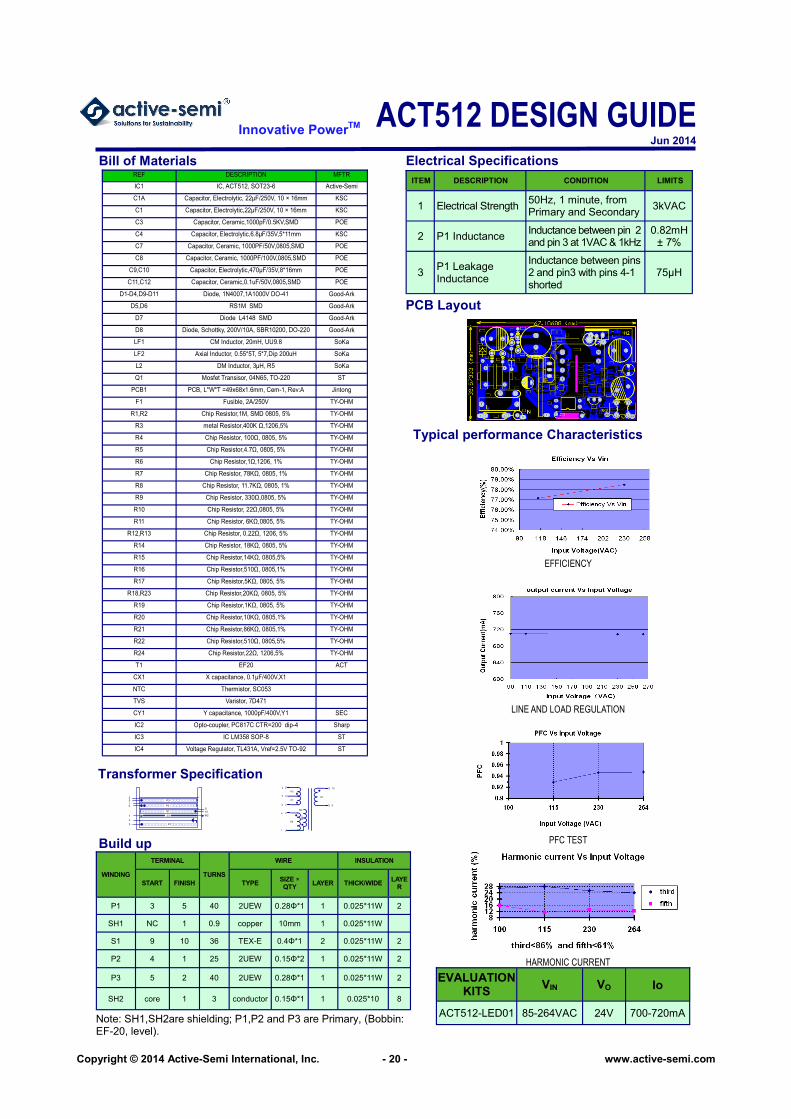
EVALUATION KITS
VIN VO Io
ACT512-LED01 85-264VAC 24V 700-720mA
Bill of Materials
Build up
Transformer Specification
Note: SH1,SH2are shielding; P1,P2 and P3 are Primary, (Bobbin: EF-20, level).
ITEM DESCRIPTION CONDITION LIMITS
1 Electrical Strength 50Hz, 1 minute, from Primary and Secondary
3kVAC
2 P1 Inductance Inductance between pin 2 and pin 3 at 1VAC & 1kHz
0.82mH ± 7%
3 P1 Leakage Inductance
Inductance between pins 2 and pin3 with pins 4-1 shorted
75µH
Electrical Specifications
WINDING
TERMINAL
TURNS
WIRE INSULATION
START FINISH TYPE SIZE × QTY
LAYER THICK/WIDE LAYE
R
P1 3 5 40 2UEW 0.28Φ*1 1 0.025*11W 2
SH1 NC 1 0.9 copper 10mm 1 0.025*11W
S1 9 10 36 TEX-E 0.4Φ*1 2 0.025*11W 2
P2 4 1 25 2UEW 0.15Φ*2 1 0.025*11W 2
P3 5 2 40 2UEW 0.28Φ*1 1 0.025*11W 2
SH2 core 1 3 conductor 0.15Φ*1 1 0.025*10 8
Typical performance Characteristics
PCB Layout
EFFICIENCY
LINE AND LOAD REGULATION
PFC TEST
HARMONIC CURRENT
REF DESCRIPTION MFTR
IC1 IC, ACT512, SOT23-6 Active-Semi
C1A Capacitor, Electrolytic, 22µF/250V, 10 × 16mm KSC
C1 Capacitor, Electrolytic,22µF/250V, 10 × 16mm KSC
C3 Capacitor, Ceramic,1000pF/0.5KV,SMD POE
C4 Capacitor, Electrolytic,6.8µF/35V,5*11mm KSC
C7 Capacitor, Ceramic, 1000PF/50V,0805,SMD POE
C8 Capacitor, Ceramic, 1000PF/100V,0805,SMD POE
C9,C10 Capacitor, Electrolytic,470µF/35V,8*16mm POE
C11,C12 Capacitor, Ceramic,0.1uF/50V,0805,SMD POE
D1-D4,D9-D11 Diode, 1N4007,1A1000V DO-41 Good-Ark
D5,D6 RS1M SMD Good-Ark
D7 Diode L4148 SMD Good-Ark
D8 Diode, Schottky, 200V/10A, SBR10200, DO-220 Good-Ark
LF1 CM Inductor, 20mH, UU9.8 SoKa
LF2 Axial Inductor, 0.55*5T, 5*7,Dip 200uH SoKa
L2 DM Inductor, 3µH, R5 SoKa
Q1 Mosfet Transisor, 04N65, TO-220 ST
PCB1 PCB, L*W*T =49x68x1.6mm, Cem-1, Rev:A Jintong
F1 Fusible, 2A/250V TY-OHM
R1,R2 Chip Resistor,1M, SMD 0805, 5% TY-OHM
R3 metal Resistor,400K Ω,1206,5% TY-OHM
R4 Chip Resistor, 100Ω, 0805, 5% TY-OHM
R5 Chip Resistor,4.7Ω, 0805, 5% TY-OHM
R6 Chip Resistor,1Ω,1206, 1% TY-OHM
R7 Chip Resistor, 78KΩ, 0805, 1% TY-OHM
R8 Chip Resistor, 11.7KΩ, 0805, 1% TY-OHM
R9 Chip Resistor, 330Ω,0805, 5% TY-OHM
R10 Chip Resistor, 22Ω,0805, 5% TY-OHM
R11 Chip Resistor, 6KΩ,0805, 5% TY-OHM
R12,R13 Chip Resistor, 0.22Ω, 1206, 5% TY-OHM
R14 Chip Resistor, 18KΩ, 0805, 5% TY-OHM
R15 Chip Resistor,14KΩ, 0805,5% TY-OHM
R16 Chip Resistor,510Ω, 0805,1% TY-OHM
R17 Chip Resistor,5KΩ, 0805, 5% TY-OHM
R18,R23 Chip Resistor,20KΩ, 0805, 5% TY-OHM
R19 Chip Resistor,1KΩ, 0805, 5% TY-OHM
R20 Chip Resistor,10KΩ, 0805,1% TY-OHM
R21 Chip Resistor,86KΩ, 0805,1% TY-OHM
R22 Chip Resistor,510Ω, 0805,5% TY-OHM
R24 Chip Resistor,22Ω, 1206,5% TY-OHM
T1 EF20 ACT
CX1 X capacitance, 0.1µF/400V,X1
NTC Thermistor, SC053
TVS Varistor, 7D471
CY1 Y capacitance, 1000pF/400V,Y1 SEC
IC2 Opto-coupler, PC817C CTR=200 dip-4 Sharp
IC3 IC LM358 SOP-8 ST
IC4 Voltage Regulator, TL431A, Vref=2.5V TO-92 ST
P13
10
9P24
SH1
S1
1
NC
P352
5
1
S1
P2
2
5
P1
3
SH
1
NC
4
1
P3
9
10
ACT111A High Efficiency, Low Cost HB LED Lighting
Design Features
For AC input, if a conventional step-down line trans-
former is used, a low cost IN4001can be used for D1-D4.
However, if a high frequency electronic transformer is
used, a Schottky diode such as SS14 should be used for
high efficiency operation. For input and output capaci-
tors, small size and low ESR ceramic capacitor is pre-
ferred.
PC Board Layout Guidance
Place input capacitor (C1) to IN pin, inductor (L1) and
diode (D5) to SW pin as close as possible to reduce the
voltage ringing at these pins. Place the current sense
resistor (R2 ) close to FB pin. Minimize ground noise by
connecting high current ground returns, the input capaci-
tor ground lead, and the output filter ground lead to a
single point (star ground configuration). There are two
power loops in normal operation, one is formed when the
SW is high and the high current flows through input ca-
pacitor (C1), internal MOSFET, inductor(L1), LEDs,
RSENSE(R2) to ground. The other loop is through inductor
(L1), LEDs, RSENSE(R2), ground to diode(D5). Make these
loop areas as small as possible to minimize noise inter-
action.
95% Efficiency
4.8V to 30V Input and up to 1.5A Output
1.4 MHz Switching & Small SOT23-6 Package
PWM (0-100%, 0.1-10kHz) Dimming
Thermal Shutdown & Short Circuit Protection
Operation and Application
The bridge rectifier is for AC input only. The DC input is
directly connected to IN and ground. The ACT111A has an
under-voltage lockout (UVLO) at 4.0V with 250mV hys-
teresis. When input voltage falls below 4.0V, SW stops
switching. The device is activated as input voltage goes
higher than 4.2V.
The LED output current is sensed by a resistor in series
with the LED. The ACT111A precisely regulates the LED
current by the internal EA and 0.1V reference. The aver-
age LED current is determined by the equation: ILED =0.1V/
RSENSE.
The ACT111A allows dimming with a PWM signal at the
DIM pin. A signal level above 1.5V enables switching and
turns LED on. To turn off the LED current, the signal level
has to be below 1.52V. The dimming signal frequency
range is from 100Hz to 10kHz.A 200kΩ resistor is needed
to connect between FB pin RSENSE. A 100pF capacitor is
recommended to connect from the FB pin to ground.
Input Voltage LED # Output Current VFB Topology
4.8 – 30VDC 1-6 1.5A 100mV Buck
An inductor with RMS rating greater than load current
and its saturation current at least 30% higher should be
used. Inductance value is selected to make its ripple
current 20-30% of the load current. A Schottky diode
(D5) is usually used for better efficiency as long as the
breakdown voltage can withstand the maximum output
voltage. The forward current rating of the diode must
be at least equal to the maximum LED current.
Key Component Selection
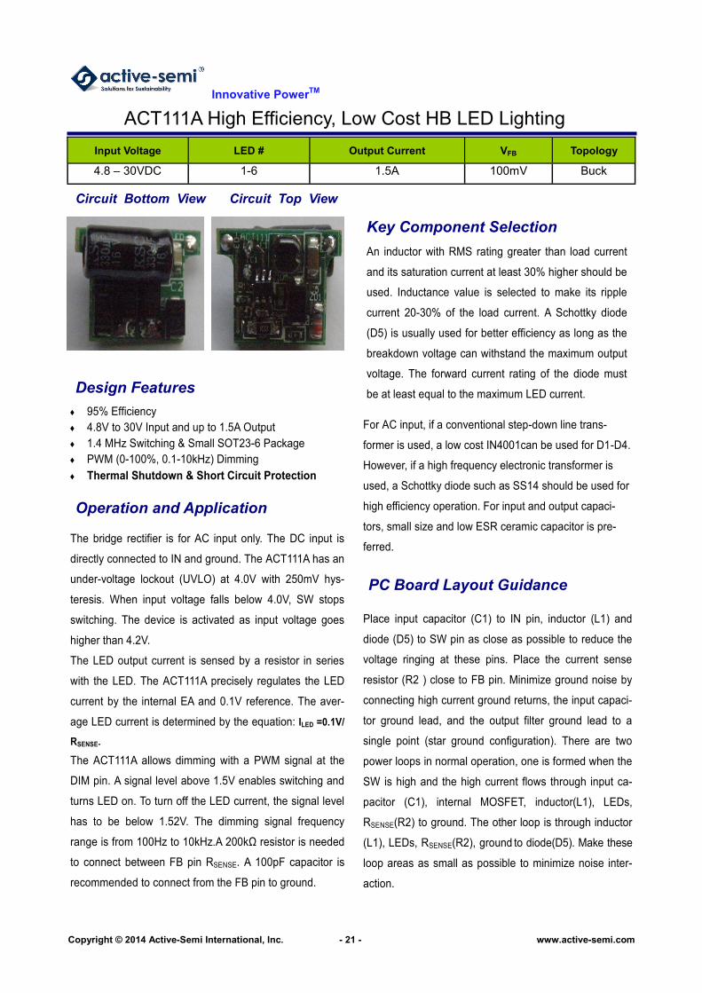
Circuit Bottom View Circuit Top View
Innovative PowerTM
Copyright © 2014 Active-Semi International, Inc. - 21 - www.active-semi.com
ACT111A High Efficiency, Low Cost HB LED Lighting
Bill of Materials
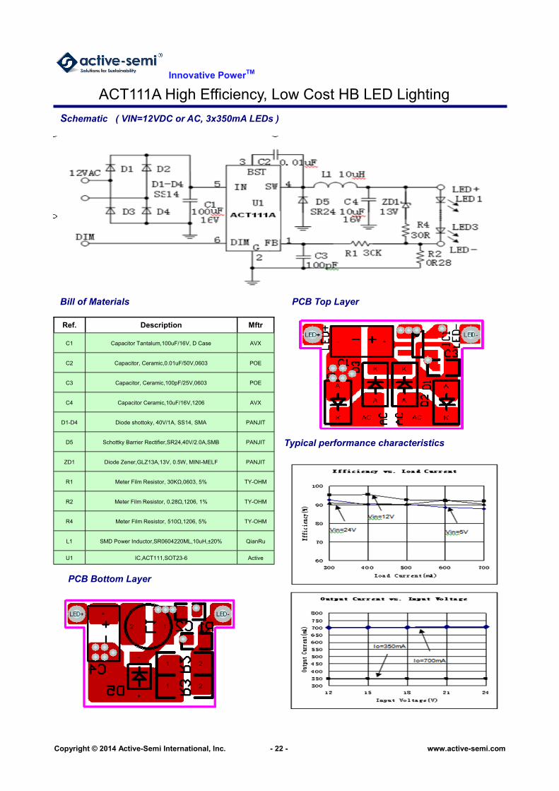
PCB Bottom Layer
Typical performance characteristics
Ref. Description Mftr
C1 Capacitor Tantalum,100uF/16V, D Case AVX
C2 Capacitor, Ceramic,0.01uF/50V,0603 POE
C3 Capacitor, Ceramic,100pF/25V,0603 POE
C4 Capacitor Ceramic,10uF/16V,1206 AVX
D1-D4 Diode shottoky, 40V/1A, SS14, SMA PANJIT
D5 Schottky Barrier Rectifier,SR24,40V/2.0A,SMB PANJIT
ZD1 Diode Zener,GLZ13A,13V, 0.5W, MINI-MELF PANJIT
R1 Meter Film Resistor, 30KΩ,0603, 5% TY-OHM
R2 Meter Film Resistor, 0.28Ω,1206, 1% TY-OHM
R4 Meter Film Resistor, 510Ω,1206, 5% TY-OHM
L1 SMD Power Inductor,SR0604220ML,10uH,±20% QianRu
U1 IC,ACT111,SOT23-6 Active
Schematic ( VIN=12VDC or AC, 3x350mA LEDs )
PCB Top Layer
Innovative PowerTM
Copyright © 2014 Active-Semi International, Inc. - 22 - www.active-semi.com
Related Documents