University of Birmingham Active screen plasma surface co-alloying of 316 austenitic stainless steel with both nitrogen and niobium for the application of bipolar plates in proton exchange membrane fuel cells Lin, Kaijie; Li, Xiaoying; Tian, Linhai; Dong, Hanshan DOI: 10.1016/j.ijhydene.2015.06.010 License: Creative Commons: Attribution (CC BY) Document Version Publisher's PDF, also known as Version of record Citation for published version (Harvard): Lin, K, Li, X, Tian, L & Dong, H 2015, 'Active screen plasma surface co-alloying of 316 austenitic stainless steel with both nitrogen and niobium for the application of bipolar plates in proton exchange membrane fuel cells', International Journal of Hydrogen Energy, vol. 40, no. 32, pp. 10281–10292. https://doi.org/10.1016/j.ijhydene.2015.06.010 Link to publication on Research at Birmingham portal General rights Unless a licence is specified above, all rights (including copyright and moral rights) in this document are retained by the authors and/or the copyright holders. The express permission of the copyright holder must be obtained for any use of this material other than for purposes permitted by law. • Users may freely distribute the URL that is used to identify this publication. • Users may download and/or print one copy of the publication from the University of Birmingham research portal for the purpose of private study or non-commercial research. • User may use extracts from the document in line with the concept of ‘fair dealing’ under the Copyright, Designs and Patents Act 1988 (?) • Users may not further distribute the material nor use it for the purposes of commercial gain. Where a licence is displayed above, please note the terms and conditions of the licence govern your use of this document. When citing, please reference the published version. Take down policy While the University of Birmingham exercises care and attention in making items available there are rare occasions when an item has been uploaded in error or has been deemed to be commercially or otherwise sensitive. If you believe that this is the case for this document, please contact [email protected] providing details and we will remove access to the work immediately and investigate. Download date: 18. Feb. 2022

Welcome message from author
This document is posted to help you gain knowledge. Please leave a comment to let me know what you think about it! Share it to your friends and learn new things together.
Transcript
University of Birmingham
Active screen plasma surface co-alloying of 316austenitic stainless steel with both nitrogen andniobium for the application of bipolar plates inproton exchange membrane fuel cellsLin, Kaijie; Li, Xiaoying; Tian, Linhai; Dong, Hanshan
DOI:10.1016/j.ijhydene.2015.06.010
License:Creative Commons: Attribution (CC BY)
Document VersionPublisher's PDF, also known as Version of record
Citation for published version (Harvard):Lin, K, Li, X, Tian, L & Dong, H 2015, 'Active screen plasma surface co-alloying of 316 austenitic stainless steelwith both nitrogen and niobium for the application of bipolar plates in proton exchange membrane fuel cells',International Journal of Hydrogen Energy, vol. 40, no. 32, pp. 10281–10292.https://doi.org/10.1016/j.ijhydene.2015.06.010
Link to publication on Research at Birmingham portal
General rightsUnless a licence is specified above, all rights (including copyright and moral rights) in this document are retained by the authors and/or thecopyright holders. The express permission of the copyright holder must be obtained for any use of this material other than for purposespermitted by law.
•Users may freely distribute the URL that is used to identify this publication.•Users may download and/or print one copy of the publication from the University of Birmingham research portal for the purpose of privatestudy or non-commercial research.•User may use extracts from the document in line with the concept of ‘fair dealing’ under the Copyright, Designs and Patents Act 1988 (?)•Users may not further distribute the material nor use it for the purposes of commercial gain.
Where a licence is displayed above, please note the terms and conditions of the licence govern your use of this document.
When citing, please reference the published version.
Take down policyWhile the University of Birmingham exercises care and attention in making items available there are rare occasions when an item has beenuploaded in error or has been deemed to be commercially or otherwise sensitive.
If you believe that this is the case for this document, please contact [email protected] providing details and we will remove access tothe work immediately and investigate.
Download date: 18. Feb. 2022
ww.sciencedirect.com
i n t e r n a t i o n a l j o u r n a l o f h y d r o g e n en e r g y 4 0 ( 2 0 1 5 ) 1 0 2 8 1e1 0 2 9 2
Available online at w
ScienceDirect
journal homepage: www.elsevier .com/locate/he
Active screen plasma surface co-alloying of 316austenitic stainless steel with both nitrogen andniobium for the application of bipolar plates inproton exchange membrane fuel cells
Kaijie Lin*, Xiaoying Li, Linhai Tian, Hanshan Dong
School of Metallurgy and Materials, The University of Birmingham, Birmingham B15 2TT, UK
a r t i c l e i n f o
Article history:
Received 10 April 2015
Received in revised form
27 May 2015
Accepted 3 June 2015
Available online 2 July 2015
Keywords:
Proton exchange membrane fuel
cells
Bipolar plates
316 stainless steel
Active screen plasma surface alloy-
ing
Nitrogen
Niobium
* Corresponding author.E-mail address: [email protected] (K. L
http://dx.doi.org/10.1016/j.ijhydene.2015.06.010
0360-3199/Copyright © 2015, The Authors. Publishe
CC BY license (http://creativecommons.org/license
a b s t r a c t
Austenitic stainless steel has been researched as a promising candidate material for
bipolar plates in proton exchange membrane fuel cells. However, its interfacial
contact resistance (ICR) is about 16 times higher that of the Department of Energy (DOE)
target (10 mU cm2), which leads to undesirable fuel cell performance. In this work, a new
hybrid plasma surface engineering process, based on active screen plasma co-alloying,
has been developed to simultaneously alloy 316 austenitic stainless steel (316 SS)
surfaces with both nitrogen and niobium. The results demonstrated that the layer
structure of the modified surfaces can be tailored by adjusting the treatment conditions.
All the plasma treated 316 SS samples exhibited significantly reduced ICR below the DOE
target of 10 mU cm2. The corrosion resistance of the N/Nb co-alloyed 316 SS was much
better than active screen plasma nitrided and marginally better than the untreated
material.
Copyright © 2015, The Authors. Published by Elsevier Ltd on behalf of Hydrogen Energy
Publications, LLC. This is an open access article under the CC BY license (http://
creativecommons.org/licenses/by/4.0/).
Introduction
As an efficient, clean and quite power source, proton ex-
changemembrane fuel cells (PEMFCs) have received extensive
interest in the last decade mainly due to the concerns over
severe air pollution caused by conventional power sources
and the depletion of fossil energies. Significant improvement
has been made recently in the efficiency and performance of
PEMFCs. However, the wide commercial application of
in).
d by Elsevier Ltd on behalf of
s/by/4.0/).
PEMFCs has been retarded, to a large extent, by the low me-
chanical strength and the high fabrication cost of graphite
bipolar plates [1].
To this end, great efforts have been made to explore
metallic bipolar plates, such as aluminium alloys [2,3], ti-
tanium alloys [4,5] and amorphous alloys [6,7]. Among
them, austenitic stainless steels (SS) have attracted more
and more attention as promising candidates for bipolar
plate application mainly because of their good mechanical
performance, relatively low cost and ease of manufacture
Hydrogen Energy Publications, LLC. This is an open access article under the
i n t e rn a t i o n a l j o u r n a l o f h y d r o g e n en e r g y 4 0 ( 2 0 1 5 ) 1 0 2 8 1e1 0 2 9 210282
[8e10]. However, there are still some limitations of austen-
itic stainless steels and hence technical challenges to be
addressed. For example, their insufficient corrosion resis-
tance [11,12] and poor conductivity due to the formation of
passive oxide layer [13,14] can lead to undesired degradation
of the power output of PEMFCs. It is known that surface
modification has been successfully used to improve the
surface properties of materials and components. Hence, it
could be a promising method to improve the surface con-
ductivity and/or corrosion resistance of stainless steel bi-
polar plates [15e18].
In our recent paper, a low-temperature active screen
plasma nitriding (ASPN) technique is reported to modify the
surface properties of 316 SS [19]. The surface conductivity of
316 SS has been successfully improved by the low-
temperature ASPN induced nitrogen-supersaturated S-phase
case. For example, the interfacial contact resistance (ICR) can
be reduced from 158 mU cm2 for the as-received 316 SS to
33 mU cm2 for the ASPN treated surfaces. However, the ICR of
the ASPN treated 316 SS surface is still larger than the target
(10 mU cm2) set by Department of Energy (DOE) [20]. Clearly,
alloying with interstitial nitrogen along cannot meet the DOE
target and new plasma surface co-alloying techniques with
both interstitial and substitutional alloying elements could be
a desirable approach.
Niobium and its compounds are well-known for their
excellent corrosion resistance and surface conductivity.
Many researchers have applied niobium coating onto the
surface of stainless steel bipolar plates to improve their
performance in PEMFC environment. Different methods
have been explored such as cladding [21,22], physical
vapour deposition (PVD) [23,24] and electro-deposition [25]
to improve the corrosion resistance and surface conductiv-
ity of stainless steel. However, the bonding strength be-
tween Nb layer and the substrate is low after annealing
treatment [26]. Electro-deposition of Nb improves the
corrosion resistance of 304 SS but leads to the degradation
of surface conductivity due to the formation of NbO and
Nb2O5.
In view of the problems associated with Nb coatings, Feng
et al. [27] utilizes ion implantation method to introduce Nb
into 316 SS. The corrosion current density of the Nb
implanted 316 SS is reduced effectively but due to the for-
mation of Nb oxide, the surface conductivity of the Nb
implanted stainless steel is still much higher than the DOE
target of 10 mU cm2.
Clearly, new surface engineering technologies need to be
developed to further improve the surface electrical conduc-
tivity of 316 SS. This paper reports a new hybrid plasma sur-
face technology which combines low-temperature active
screen plasma co-alloying with both nitrogen and niobium
with deposition of a thin surface niobium layer on the top. The
microstructure and composition of the plasma treated sur-
faces were fully studied by X-ray diffraction (XRD), energy
dispersive spectroscopy (EDS), X-ray photoelectron spectros-
copy (XPS) and scanning electron microscopy (SEM). The sur-
face conductivity and corrosion behaviour were also
evaluated. Experimental results have demonstrated that the
ICR of the plasma co-alloyed 316 SS surfaces is well below the
DOE target (10 mU cm2).
Materials and methods
Materials and sample preparation: Commercial 316 austenitic
stainless steel (316 SS) was selected as the substrate, and its
chemical composition is (wt%): 0.06% C, 17.20% Cr, 1.30% Mn,
2.20% Mo, 11.70% Ni, 0.014% S and Fe balanced. Coupon
samples of 6 mm in thickness were cut off from 1 inch
(25.4 mm) hot rolled bars using a SiC cutting wheel. The front
side of the coupon samples was firstly wet ground using sili-
con carbide abrasive paper up to #1200 grit and subsequently
polished using 6 mm and 1 mm diamond pastes. The backside
was wet ground up to #1200 grit. Prior to treatment, samples
were washed with soapy water, cleaned with acetone in ul-
trasonic bath for 5min, and finally dried under hot flowing air.
Cross sections were cut from treated coupon samples and
mounted in conductive bakelite. The mounted samples were
wet ground and then polished using the same procedures as
described above. In order to reveal the micro-structure of the
cross sections, an etching agent containing 25 ml H2O, 25 ml
HNO3 and 50 ml HCl was used. After etching for about 20 s,
samples were rinsed immediately with water then acetone,
and dried in hot flowing air.
Active screen plasma treatments: Active screen plasma sur-
face co-alloying treatments with both N and Nb
(ASPA(N þ Nb)) were conducted in an AS Plasma Metal 75 kVA
industrial scale furnace and the experimental setting for the
ASPA(N þ Nb) treatment is shown in Fig. 1, schematically.
The small metal active screen was placed on the worktable
of the large furnace, where bias was applied. The lid of the
active screen was specially designed to carry niobium. The
sample was insulated by ceramic and hence stayed at a
floating potential. The effect of bias on the small metal active
screen was studied using three different biases: 5%, 10% and
15% of the main power supply of 15 kVA, and the treatment
parameters as well as the sample codes are listed in Table 1.
Characterization methods: The phase constituent of the
plasma treated samples was investigated using XRD (Bruker
D8 Advance) with Cu Ka radiation (l ¼ 0.154 nm). The surface
morphology and the cross-sectional microstructure of the
samples before and after treatment were observed using SEM
(Jeol 7000). The chemical compositions of the treated surfaces
and cross-sections were examined by EDS (Oxford Instrument
Inca). The composition and chemical state of the elements
were analysed by XPS (Theta Probe). Elemental concentration
depth profiles were determined by glow discharge optical
emission spectroscopy (GDOES) (Leco GDS-750). The hardness
depth profileswere probed using nano-indentation (Nano Test
600).
Corrosion tests: The corrosion behaviour of untreated and
plasma treated 316 SS samples under different conditions was
evaluated by electrochemical tests consisting of potentiody-
namic polarization and potentiostatic polarization. A stan-
dard three electrodes system was employed in the
polarization tests. A platinum rod, a saturated calomel elec-
trode (SCE) and the to-be-measured sample were acted as the
counter electrode, the reference electrode and the working
electrode, respectively. The Gamry electrochemical worksta-
tion was used to measure and record the corrosion data. To
simulate the working environment of PEMFC, a sulphuric acid
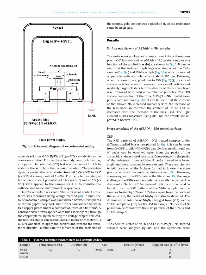
Fig. 1 e Schematic diagram of experimental setting.
i n t e r n a t i o n a l j o u r n a l o f h y d r o g e n en e r g y 4 0 ( 2 0 1 5 ) 1 0 2 8 1e1 0 2 9 2 10283
aqueous solution (0.5MH2SO4þ 2 ppmHF)was selected as the
corrosion solution. Prior to the potentiodynamic polarization,
an open circle potential (OCP) test was conducted for 1 h to
stabilize the sample in the corrosion solution. The potentio-
dynamic polarization scan started from�0.6 V (vs SCE) to 1.2 V
(vs SCE) at a sweep rate of 1 mV/s. For the potentiostatic po-
larization, constant potentials of 0.6 V (vs SCE) and �0.1 V (vs
SCE) were applied to the sample for 4 h, to simulate the
cathode and anode environment, respectively.
Interfacial contact resistance: The interfacial contact resis-
tance was measured using Wang's method [28]. In brief, the
to-be-measured sample was sandwiched between two pieces
of carbon paper (Tory 120), and further sandwiched between
two copper plates under a compaction force of 140 N/cm2. A
constant current was applied onto this assembly cell through
the copper plates. By measuring the voltage drop of this cell,
the total resistance can be calculated. Amicro-ohmmeter (TTi
BS407) was used to apply the current and present the resis-
tance directly. To eliminate the influence of the back side of
Table 1 e Plasma treatment parameters and sample codes.
Sample Temperature (�C) Duration (h) Gas
5% Bs 450 10 25%N2 þ10% Bs
15% Bs
the sample, gold-coating was applied on it, so the resistance
could be neglected.
Results
Surface morphology of ASPA(N þ Nb) samples
The surfacemorphology and composition of the active-screen
plasmaN/Nb co-alloyed i.e. ASPA(NþNb) treated samples as a
function of the applied bias (Bs) are shown in Fig. 2. It can be
seen that the surface morphology was similar for the 5%Bs
sample (Fig. 2(a)) and 10%Bs sample (Fig. 2(b)), which consisted
of particles with a similar size of about 100 nm. However,
when increased the applied bias to 15% (Fig. 2(c)), the size of
surface particles became unevenwith very small particles and
relatively larger clusters but the density of the surface layer
was improved with reduced number of pinholes. The EDS
surface composition of the three ASPA(N þ Nb) treated sam-
ples is compared in Fig. 2(d). It can be seen that the content
of the alloyed Nb increased markedly with the increase of
the bias used; in contrast, the content of Cr, Ni and Fe
decreased with the increase of the bias used. The light
element N was measured using XPS and the results are re-
ported in Section 3.2.2.
Phase constitute of the ASPA(N þ Nb) treated surfaces
XRDThe XRD patterns of ASPA(N þ Nb) treated samples under
different applied biases are plotted in Fig. 3. It can be seen
from the XRD profile of the 5%Bs sample that an additional set
of peaks can be observed apart from the peaks of the
austenitic stainless steel substrate. Comparing with the peaks
of the substrate, those additional peaks moved to a lower
angle and were broaden to some extent. These are charac-
teristic features of the S-phase formed in low-temperature
plasma nitrided austenitic stainless steel [29]. However,
comparing with the XRD data in the literature [19], the angle
shifting of the 5%Bs sample is relatively smaller, which will be
discussed in Section 4.2. No peaks of niobium nitride could be
found from the XRD pattern of the 5%Bs sample. For the
samples treated by 10% and 15% bias, apart from the peaks of
the substrate, the peaks of Nb4N5 can also be detected. The
dominated orientation of Nb4N5 changed from (211) for the
10%Bs sample to (310) for the 15%Bs sample. No peaks of S-
phase can be found from the XRD patterns of the 10%Bs and
15%Bs samples.
XPSThe chemical states of Nb, N and Fe in ASPA(N þ Nb) treated
surfaces were analysed by XPS and the spectrums were
Pressure (mbar) Applied bias (% of 15 kVA)
75%H2 0.75 5
10
15
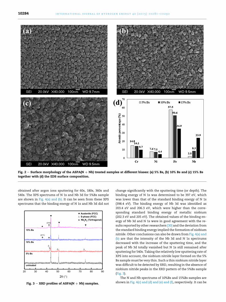
Fig. 2 e Surface morphology of the ASPA(N þ Nb) treated samples at different biases: (a) 5% Bs, (b) 10% Bs and (c) 15% Bs
together with (d) the EDS surface composition.
i n t e rn a t i o n a l j o u r n a l o f h y d r o g e n en e r g y 4 0 ( 2 0 1 5 ) 1 0 2 8 1e1 0 2 9 210284
obtained after argon ions sputtering for 60s, 180s, 360s and
540s. The XPS spectrums of N 1s and Nb 3d for 5%Bs sample
are shown in Fig. 4(a) and (b). It can be seen from these XPS
spectrums that the binding energy of N 1s and Nb 3d did not
Fig. 3 e XRD profiles of ASPA(N þ Nb) samples.
change significantly with the sputtering time (or depth). The
binding energy of N 1s was determined to be 397 eV, which
was lower than that of the standard binding energy of N 1s
(398.4 eV). The binding energy of Nb 3d was identified as
203.4 eV and 206.3 eV, which were higher than the corre-
sponding standard binding energy of metallic niobium
(202.3 eV and 205 eV). The obtained values of the binding en-
ergy of Nb 3d and N 1s were in good agreement with the re-
sults reported by other researchers [30] and the deviation from
the standard binding energy implied the formation of niobium
nitride. Other conclusions can also be drawn from Fig. 4(a) and
(b) are that the intensity of the Nb 3d and N 1s spectrums
decreased with the increase of the sputtering time, and the
peak of Nb 3d totally vanished but N 1s still remained after
sputtering for 540s. Taking the relatively low sputtering rate of
XPS into account, the niobium nitride layer formed on the 5%
Bs samplemust be very thin. Such a thin niobiumnitride layer
was difficult to be detected by XRD, resulting in the absence of
niobium nitride peaks in the XRD pattern of the 5%Bs sample
(Fig. 3).
The N and Nb spectrums of 10%Bs and 15%Bs samples are
shown in Fig. 4(c) and (d) and (e) and (f), respectively. It can be
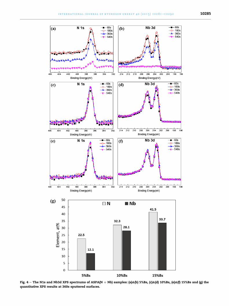
Fig. 4 e The N1s and Nb3d XPS spectrums of ASPA(N þ Nb) samples: (a)&(b) 5%Bs, (c)&(d) 10%Bs, (e)&(f) 15%Bs and (g) the
quantitative XPS results at 360s sputtered surfaces.
i n t e r n a t i o n a l j o u r n a l o f h y d r o g e n en e r g y 4 0 ( 2 0 1 5 ) 1 0 2 8 1e1 0 2 9 2 10285
i n t e rn a t i o n a l j o u r n a l o f h y d r o g e n en e r g y 4 0 ( 2 0 1 5 ) 1 0 2 8 1e1 0 2 9 210286
seen that the N and Nb spectrums obtained from the 10%Bs
sample were the same as those from the 15%Bs sample.
Except for the spectrums of 60s-sputtered surface, other
spectrums of 180s, 360s and 540s sputtered surfaces exhibited
almost identical profiles. The binding energy of N 1s and Nb 3d
identified from the surfaces of the 10%Bs and the 15%Bs
samples was the same as that determined from the 5%Bs
sample. Therefore, the XPS results of the 10%Bs and the 15%Bs
samples also indicated the formation of a niobium nitride
layer on the surface of these two samples and the niobium
nitride layers were thicker than that formed on the surface of
the 5%Bs sample as these spectrums were independent of the
sputtering time up to 540s.
The spectrums obtained after argon irons sputtering for
360s were quantitatively analysed and the results are sum-
marized in Fig. 4(g). It can be cleanly seen that the atomic
percentage of N and Nb increased with the increase of the
applied bias. The identification of Nb4N5 peaks from the XRD
patterns (Fig. 3) was in agreement with the quantification
analysis of the XPS spectrums. The atomic ratio of N/Nb for
the 15%Bs sample was around 1.23, which was close to that of
the Nb4N5 (1.25).
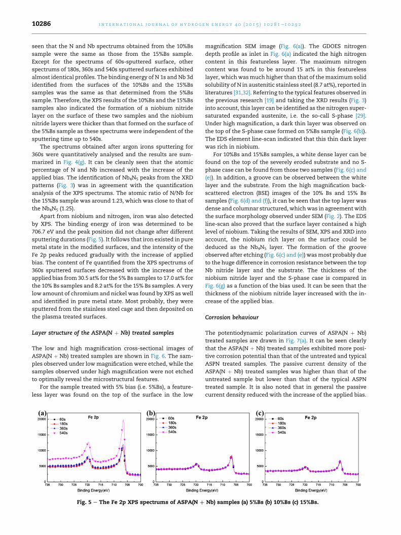
Apart from niobium and nitrogen, iron was also detected
by XPS. The binding energy of iron was determined to be
706.7 eV and the peak position did not change after different
sputtering durations (Fig. 5). It follows that iron existed in pure
metal state in the modified surfaces, and the intensity of the
Fe 2p peaks reduced gradually with the increase of applied
bias. The content of Fe quantified from the XPS spectrums of
360s sputtered surfaces decreased with the increase of the
applied bias from 30.5 at% for the 5% Bs samples to 17.0 at% for
the 10% Bs samples and 8.2 at% for the 15% Bs samples. A very
low amount of chromium and nickel was found by XPS as well
and identified in pure metal state. Most probably, they were
sputtered from the stainless steel cage and then deposited on
the plasma treated surfaces.
Layer structure of the ASPA(N þ Nb) treated samples
The low and high magnification cross-sectional images of
ASPA(N þ Nb) treated samples are shown in Fig. 6. The sam-
ples observed under lowmagnification were etched, while the
samples observed under high magnification were not etched
to optimally reveal the microstructural features.
For the sample treated with 5% bias (i.e. 5%Bs), a feature-
less layer was found on the top of the surface in the low
Fig. 5 e The Fe 2p XPS spectrums of ASPA(N þ
magnification SEM image (Fig. 6(a)). The GDOES nitrogen
depth profile as inlet in Fig. 6(a) indicated the high nitrogen
content in this featureless layer. The maximum nitrogen
content was found to be around 15 at% in this featureless
layer, whichwasmuch higher than that of themaximumsolid
solubility of N in austenitic stainless steel (8.7 at%), reported in
literatures [31,32]. Referring to the typical features observed in
the previous research [19] and taking the XRD results (Fig. 3)
into account, this layer can be identified as the nitrogen super-
saturated expanded austenite, i.e. the so-call S-phase [29].
Under high magnification, a dark thin layer was observed on
the top of the S-phase case formed on 5%Bs sample (Fig. 6(b)).
The EDS element line-scan indicated that this thin dark layer
was rich in niobium.
For 10%Bs and 15%Bs samples, a white dense layer can be
found on the top of the severely eroded substrate and no S-
phase case can be found from those two samples (Fig. 6(c) and
(e)). In addition, a groove can be observed between the white
layer and the substrate. From the high magnification back-
scattered electron (BSE) images of the 10% Bs and 15% Bs
samples (Fig. 6(d) and (f)), it can be seen that the top layer was
dense and columnar structured, whichwas in agreementwith
the surface morphology observed under SEM (Fig. 2). The EDS
line-scan also proved that the surface layer contained a high
level of niobium. Taking the results of SEM, XPS and XRD into
account, the niobium rich layer on the surface could be
deduced as the Nb4N5 layer. The formation of the groove
observed after etching (Fig. 6(c) and (e)) wasmost probably due
to the huge difference in corrosion resistance between the top
Nb nitride layer and the substrate. The thickness of the
niobium nitride layer and the S-phase case is compared in
Fig. 6(g) as a function of the bias used. It can be seen that the
thickness of the niobium nitride layer increased with the in-
crease of the applied bias.
Corrosion behaviour
The potentiodynamic polarization curves of ASPA(N þ Nb)
treated samples are drawn in Fig. 7(a). It can be seen clearly
that the ASPA(N þ Nb) treated samples exhibited more posi-
tive corrosion potential than that of the untreated and typical
ASPN treated samples. The passive current density of the
ASPA(N þ Nb) treated samples was higher than that of the
untreated sample but lower than that of the typical ASPN
treated sample. It is also noted that in general the passive
current density reduced with the increase of the applied bias.
Nb) samples (a) 5%Bs (b) 10%Bs (c) 15%Bs.
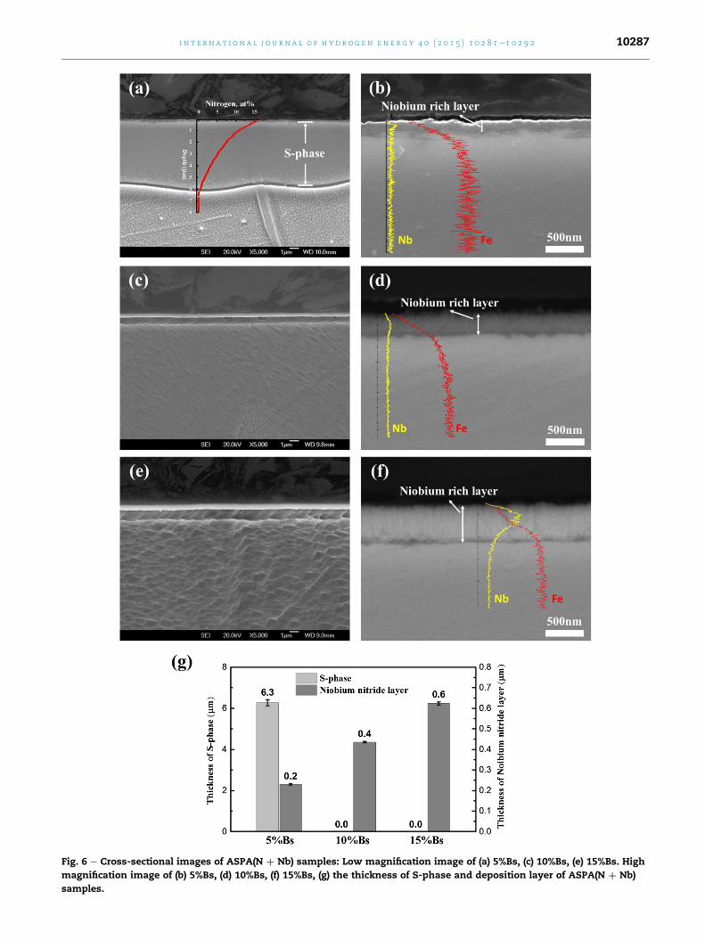
Fig. 6 e Cross-sectional images of ASPA(N þ Nb) samples: Low magnification image of (a) 5%Bs, (c) 10%Bs, (e) 15%Bs. High
magnification image of (b) 5%Bs, (d) 10%Bs, (f) 15%Bs, (g) the thickness of S-phase and deposition layer of ASPA(N þ Nb)
samples.
i n t e r n a t i o n a l j o u r n a l o f h y d r o g e n en e r g y 4 0 ( 2 0 1 5 ) 1 0 2 8 1e1 0 2 9 2 10287
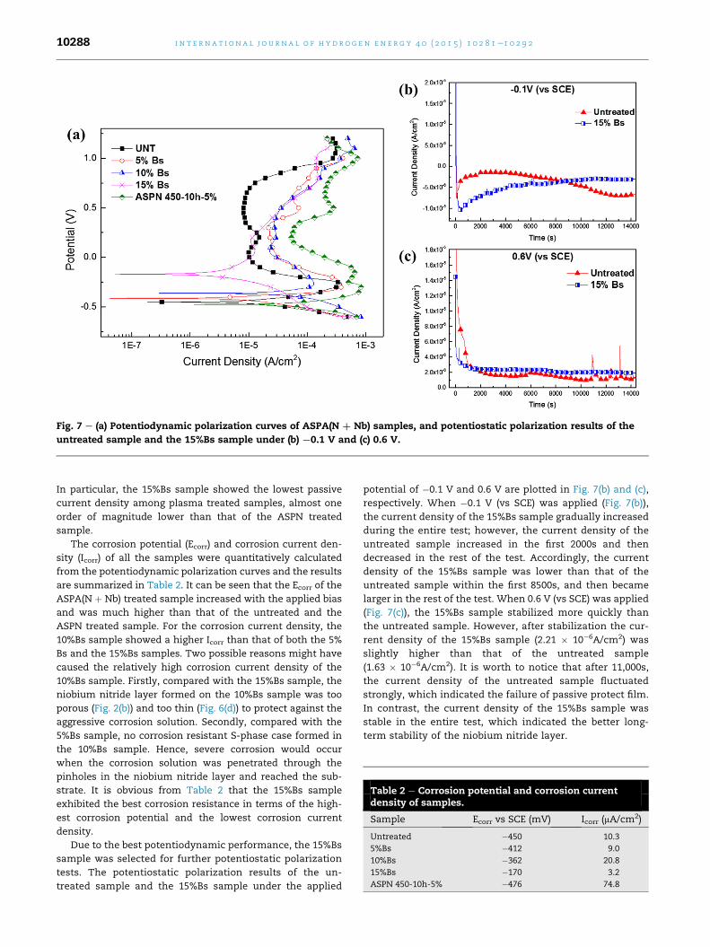
Fig. 7 e (a) Potentiodynamic polarization curves of ASPA(N þ Nb) samples, and potentiostatic polarization results of the
untreated sample and the 15%Bs sample under (b) ¡0.1 V and (c) 0.6 V.
Table 2 e Corrosion potential and corrosion currentdensity of samples.
Sample Ecorr vs SCE (mV) Icorr (mA/cm2)
Untreated �450 10.3
5%Bs �412 9.0
10%Bs �362 20.8
15%Bs �170 3.2
ASPN 450-10h-5% �476 74.8
i n t e rn a t i o n a l j o u r n a l o f h y d r o g e n en e r g y 4 0 ( 2 0 1 5 ) 1 0 2 8 1e1 0 2 9 210288
In particular, the 15%Bs sample showed the lowest passive
current density among plasma treated samples, almost one
order of magnitude lower than that of the ASPN treated
sample.
The corrosion potential (Ecorr) and corrosion current den-
sity (Icorr) of all the samples were quantitatively calculated
from the potentiodynamic polarization curves and the results
are summarized in Table 2. It can be seen that the Ecorr of the
ASPA(N þ Nb) treated sample increased with the applied bias
and was much higher than that of the untreated and the
ASPN treated sample. For the corrosion current density, the
10%Bs sample showed a higher Icorr than that of both the 5%
Bs and the 15%Bs samples. Two possible reasons might have
caused the relatively high corrosion current density of the
10%Bs sample. Firstly, compared with the 15%Bs sample, the
niobium nitride layer formed on the 10%Bs sample was too
porous (Fig. 2(b)) and too thin (Fig. 6(d)) to protect against the
aggressive corrosion solution. Secondly, compared with the
5%Bs sample, no corrosion resistant S-phase case formed in
the 10%Bs sample. Hence, severe corrosion would occur
when the corrosion solution was penetrated through the
pinholes in the niobium nitride layer and reached the sub-
strate. It is obvious from Table 2 that the 15%Bs sample
exhibited the best corrosion resistance in terms of the high-
est corrosion potential and the lowest corrosion current
density.
Due to the best potentiodynamic performance, the 15%Bs
sample was selected for further potentiostatic polarization
tests. The potentiostatic polarization results of the un-
treated sample and the 15%Bs sample under the applied
potential of �0.1 V and 0.6 V are plotted in Fig. 7(b) and (c),
respectively. When �0.1 V (vs SCE) was applied (Fig. 7(b)),
the current density of the 15%Bs sample gradually increased
during the entire test; however, the current density of the
untreated sample increased in the first 2000s and then
decreased in the rest of the test. Accordingly, the current
density of the 15%Bs sample was lower than that of the
untreated sample within the first 8500s, and then became
larger in the rest of the test. When 0.6 V (vs SCE) was applied
(Fig. 7(c)), the 15%Bs sample stabilized more quickly than
the untreated sample. However, after stabilization the cur-
rent density of the 15%Bs sample (2.21 � 10�6A/cm2) was
slightly higher than that of the untreated sample
(1.63 � 10�6A/cm2). It is worth to notice that after 11,000s,
the current density of the untreated sample fluctuated
strongly, which indicated the failure of passive protect film.
In contrast, the current density of the 15%Bs sample was
stable in the entire test, which indicated the better long-
term stability of the niobium nitride layer.
i n t e r n a t i o n a l j o u r n a l o f h y d r o g e n en e r g y 4 0 ( 2 0 1 5 ) 1 0 2 8 1e1 0 2 9 2 10289
Surface electrical conductivity
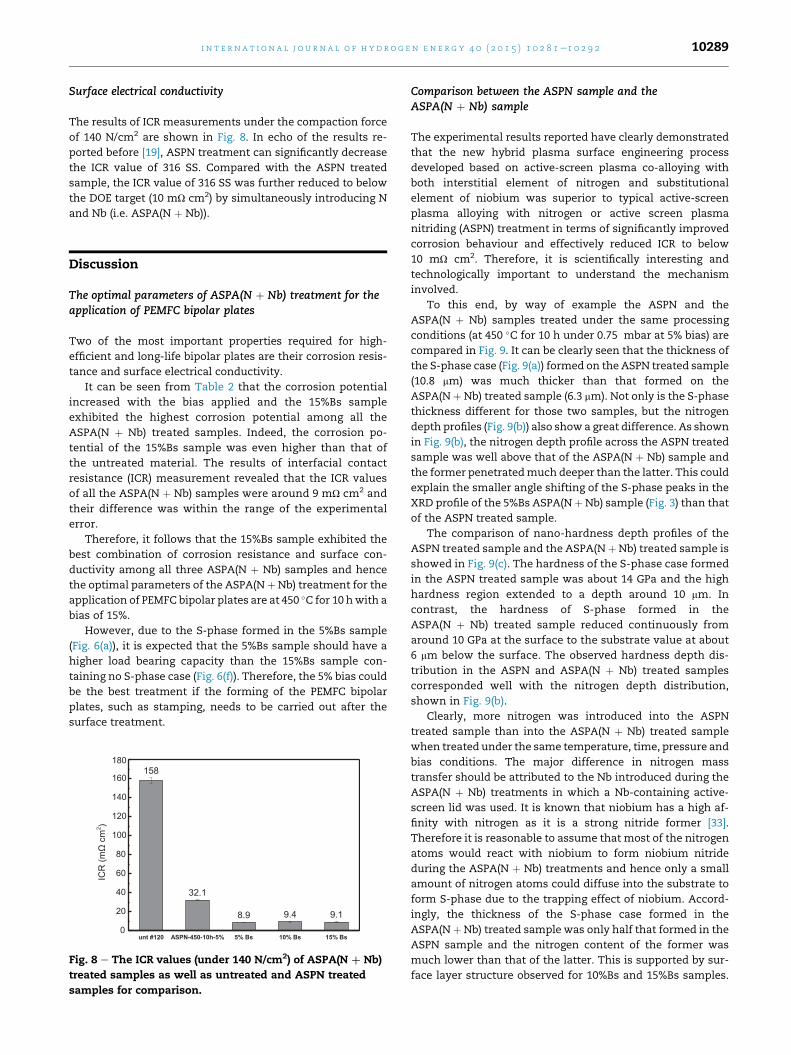
The results of ICR measurements under the compaction force
of 140 N/cm2 are shown in Fig. 8. In echo of the results re-
ported before [19], ASPN treatment can significantly decrease
the ICR value of 316 SS. Compared with the ASPN treated
sample, the ICR value of 316 SS was further reduced to below
the DOE target (10 mU cm2) by simultaneously introducing N
and Nb (i.e. ASPA(N þ Nb)).
Discussion
The optimal parameters of ASPA(N þ Nb) treatment for theapplication of PEMFC bipolar plates
Two of the most important properties required for high-
efficient and long-life bipolar plates are their corrosion resis-
tance and surface electrical conductivity.
It can be seen from Table 2 that the corrosion potential
increased with the bias applied and the 15%Bs sample
exhibited the highest corrosion potential among all the
ASPA(N þ Nb) treated samples. Indeed, the corrosion po-
tential of the 15%Bs sample was even higher than that of
the untreated material. The results of interfacial contact
resistance (ICR) measurement revealed that the ICR values
of all the ASPA(N þ Nb) samples were around 9 mU cm2 and
their difference was within the range of the experimental
error.
Therefore, it follows that the 15%Bs sample exhibited the
best combination of corrosion resistance and surface con-
ductivity among all three ASPA(N þ Nb) samples and hence
the optimal parameters of the ASPA(NþNb) treatment for the
application of PEMFC bipolar plates are at 450 �C for 10 hwith a
bias of 15%.
However, due to the S-phase formed in the 5%Bs sample
(Fig. 6(a)), it is expected that the 5%Bs sample should have a
higher load bearing capacity than the 15%Bs sample con-
taining no S-phase case (Fig. 6(f)). Therefore, the 5% bias could
be the best treatment if the forming of the PEMFC bipolar
plates, such as stamping, needs to be carried out after the
surface treatment.
158
32.1
8.9 9.4 9.1
unt #120 ASPN-450-10h-5% 5% Bs 10% Bs 15% Bs0
20
40
60
80
100
120
140
160
180
ICR
(mΩ
cm
2 )
Fig. 8 e The ICR values (under 140 N/cm2) of ASPA(N þ Nb)
treated samples as well as untreated and ASPN treated
samples for comparison.
Comparison between the ASPN sample and theASPA(N þ Nb) sample
The experimental results reported have clearly demonstrated
that the new hybrid plasma surface engineering process
developed based on active-screen plasma co-alloying with
both interstitial element of nitrogen and substitutional
element of niobium was superior to typical active-screen
plasma alloying with nitrogen or active screen plasma
nitriding (ASPN) treatment in terms of significantly improved
corrosion behaviour and effectively reduced ICR to below
10 mU cm2. Therefore, it is scientifically interesting and
technologically important to understand the mechanism
involved.
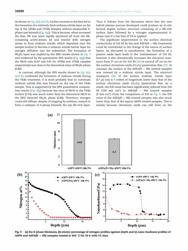
To this end, by way of example the ASPN and the
ASPA(N þ Nb) samples treated under the same processing
conditions (at 450 �C for 10 h under 0.75 mbar at 5% bias) are
compared in Fig. 9. It can be clearly seen that the thickness of
the S-phase case (Fig. 9(a)) formed on the ASPN treated sample
(10.8 mm) was much thicker than that formed on the
ASPA(N þ Nb) treated sample (6.3 mm). Not only is the S-phase
thickness different for those two samples, but the nitrogen
depth profiles (Fig. 9(b)) also show a great difference. As shown
in Fig. 9(b), the nitrogen depth profile across the ASPN treated
sample was well above that of the ASPA(N þ Nb) sample and
the former penetratedmuch deeper than the latter. This could
explain the smaller angle shifting of the S-phase peaks in the
XRD profile of the 5%Bs ASPA(NþNb) sample (Fig. 3) than that
of the ASPN treated sample.
The comparison of nano-hardness depth profiles of the
ASPN treated sample and the ASPA(N þNb) treated sample is
showed in Fig. 9(c). The hardness of the S-phase case formed
in the ASPN treated sample was about 14 GPa and the high
hardness region extended to a depth around 10 mm. In
contrast, the hardness of S-phase formed in the
ASPA(N þ Nb) treated sample reduced continuously from
around 10 GPa at the surface to the substrate value at about
6 mm below the surface. The observed hardness depth dis-
tribution in the ASPN and ASPA(N þ Nb) treated samples
corresponded well with the nitrogen depth distribution,
shown in Fig. 9(b).
Clearly, more nitrogen was introduced into the ASPN
treated sample than into the ASPA(N þ Nb) treated sample
when treated under the same temperature, time, pressure and
bias conditions. The major difference in nitrogen mass
transfer should be attributed to the Nb introduced during the
ASPA(N þ Nb) treatments in which a Nb-containing active-
screen lid was used. It is known that niobium has a high af-
finity with nitrogen as it is a strong nitride former [33].
Therefore it is reasonable to assume that most of the nitrogen
atoms would react with niobium to form niobium nitride
during the ASPA(N þ Nb) treatments and hence only a small
amount of nitrogen atoms could diffuse into the substrate to
form S-phase due to the trapping effect of niobium. Accord-
ingly, the thickness of the S-phase case formed in the
ASPA(NþNb) treated sample was only half that formed in the
ASPN sample and the nitrogen content of the former was
much lower than that of the latter. This is supported by sur-
face layer structure observed for 10%Bs and 15%Bs samples.
i n t e rn a t i o n a l j o u r n a l o f h y d r o g e n en e r g y 4 0 ( 2 0 1 5 ) 1 0 2 8 1e1 0 2 9 210290
As shown in Fig. 6(d) and (f), further increase in the bias led to
the formation of a relatively thick niobium nitride layer on the
top of the 10%Bs and 15%Bs samples without measurable S-
phase case beneath (Fig. 6(g)). This is because, when increased
the bias, Nb was more rapidly sputtered off from the Nb-
containing active-screen lid and reacted with nitrogen
atoms to form niobium nitride, which deposited onto the
sample surface to become a niobium nitride barrier layer for
nitrogen diffusion into the subsurface. The formation of
Nb4N5 layer was implied by the XRD results shown in Fig. 3
and evidenced by the quantitative XPS results (Fig. 4(g)) that
the Nb/N ratio (0.87 and 0.81 for 10%Bs and 15%Bs samples
respectively) was close to the theoretical value of Nb4N5 phase
(0.80).
In contrast, although the XPS results shown in Fig. 4(a)
and (b) confirmed the formation of niobium nitride during
the 5%Bs treatment, it is most probably that no continues
niobium nitride film was formed on the top of the 5%Bs
sample. This is supported by the XPS quantitative composi-
tion results (Fig. 4(g)) because the ratio of Nb/N in the 5%Bs
surface (0.54) was much lower than the theoretical Nb/N in
the XRD detected Nb4N5 phase (0.80). Therefore, nitrogen
could still diffuse, despite of trapping by niobium, inward to
form a sublayer of S-phase beneath the top Nb-rich layer.
Fig. 9 e (a) the S-phase thickness, (b) atomic percentage of nitro
ASPN and ASPA(N þ Nb) samples treated at 450 �C for 10 h wit
Thus it follows from the discussion above that the new
hybrid plasma process developed could produce an in-site
formed duplex surface structure consisting of a Nb-rich
surface layer followed by a nitrogen supersaturated S-
phase case if a low bias of 5% is applied.
The significant improvement in the surface electrical
conductivity of 316 SS by the new ASPA(N þ Nb) treatments
could be contributed to the change of the nature of surface
layers. As discussed in introduction, the formation of a
passive oxide layer leads to the ‘stainlessness’ of 316 SS;
however it also dramatically increases the electrical resis-
tance from 77 mU cm for 316 SS [34] to around 108 mU cm for
the surface chromium oxide (Cr2O3) passivation film [35]. In
contrast, the surface of the ASPA(N þ Nb) treated samples
was covered by a niobium nitride layer. The electrical
resistance [36] of the surface niobium nitride layer
(57 mU cm) is 7 orders of magnitude lower than that of the
surface chromium oxide (Cr2O3) passivation film. As a
result, the ICR value has been significantly reduced from 316
SS (158 mU cm2) to ASPA(N þ Nb) treated samples
(9 mU cm2). From the comparison of ICR in Fig. 8, the ICR
value of the ASPA(N þ Nb) treated samples was also much
lower than that of the typical ASPN treated samples. This is
mainly because chromium oxide can still form on the
gen profiles against depth and (c) nano-hardness profiles of
h 5% bias.
i n t e r n a t i o n a l j o u r n a l o f h y d r o g e n en e r g y 4 0 ( 2 0 1 5 ) 1 0 2 8 1e1 0 2 9 2 10291
surface of S-phase formed in austenite stainless steel by the
ASPN treatments [37].
Apart from the effectively improved surface electrical
conductivity, the corrosion resistance of the ASPA(N þ Nb)
treated samples was also superior to that of the typical ASPN
treated samples in terms of reduced corrosion current density
and increased corrosion potential. This could be attributed to
the formation of surface niobium nitride layer by the
ASPA(N þ Nb) treatment in view of the superior corrosion
resistance of the niobium nitride [38]. As reported in our pre-
vious paper [19], the surface of the ASPN treated 316 SS is
covered by a layer of iron nitrides [39], which exhibits
poor corrosion behaviour than niobium nitride. The slightly
higher passive current density of the ASPA(N þ Nb) treated
316 SS relative to that of the untreated material could be
related to the corrosion of iron embedded in the niobium
nitride layer (Fig. 5).
Conclusions
A new hybrid plasma surface co-alloying process has been
successfully developed to simultaneously alloy 316 austenitic
stainless steel (316 SS) surfaces with both nitrogen and
niobium. By adjusting the treatment condition, the layer
structure of the modified surfaces can be tailored. When
treated under a low applied bias of 5%, a duplex surface layer
structure consisting of a very thin niobium nitride surface
layer followed by an S-phase case can be produced; however,
when treated under high applied bias (10e15%), only a
niobium nitride layer can be formed on the surface without
the formation of S-phase case underneath.
The electrochemical corrosion resistance and the interfa-
cial contact resistance (ICR) of the ASPA(N þ Nb) treated sur-
faces have been evaluated and compared with untreated and
typical active screen plasma nitrided (ASPN) surfaces. The
electrochemical corrosion tests have revealed that the corro-
sion potential of 316 SS can be increased by all three
ASPA(N þ Nb) treatments but the passive current density of
the treated sampleswas higher than that of the untreated one;
the ASPA(N þ Nb) treated samples were superior to the ASPN
treated ones in terms of increased corrosion potential and
reduced passive current density. Among the three
ASPA(N þ Nb) treated samples, the 15%Bs sample exhibited
the best corrosion resistance.
The results of interfacial contact resistance tests show
that the ICR values of all three ASPA(N þ Nb) treated sam-
ples were about 9 mU cm2. This is about 18 and 3.6 times
lower than that of the untreated and ASPN treated 316 SS,
respectively, which is also lower than the DOE target
(10 mU cm2).
Taking the corrosion properties and interfacial contact
resistant into account, the ASPA(NþNb) treatment at 15% bias
(15%Bs) is the best treatment potentially for the application of
PEMFC bipolar plates.
Further tests, such as single cell tests and long-duration
corrosion tests, are needed to evaluate the performance of
the ASPA(N þ Nb) treated 316 stainless steel bipolar plates in
the real PEMFC working environment.
Acknowledgements
The financial support from European Commission (PIIC-GA-
2012-327750) and EPSRC (EP/J018252/1) is gratefully acknowl-
edged. One of the authors (KL) wishes to express his appreci-
ation to China Scholarship Council (CSC) and The University
of Birmingham for their PhD studentships.
r e f e r e n c e s
[1] Steele B, Heinzel A. Materials for fuel-cell technologies.Nature 2001;414:345e52.
[2] Jin CK, Kang CG. Fabrication by vacuum die casting andsimulation of aluminum bipolar plates with micro-channelson both sides for proton exchange membrane (PEM) fuelcells. Int J Hydrogen Energy 2012;37:1661e76. http://dx.doi.org/10.1016/j.ijhydene.2011.10.050.
[3] Fetohi AE, Abdel Hameed RM, El-Khatib KM. NieP andNieMoeP modified aluminium alloy 6061 as bipolar platematerial for proton exchange membrane fuel cells. J PowerSources 2013;240:589e97. http://dx.doi.org/10.1016/j.jpowsour.2013.04.085.
[4] Zhang D, Duan L, Guo L, Wang Z, Zhao J, Tuan W-H, et al.TiN-coated titanium as the bipolar plate for PEMFC bymulti-arc ion plating. Int J Hydrogen Energy2011;36:9155e61. http://dx.doi.org/10.1016/j.ijhydene.2011.04.123.
[5] Ren Z, Zhang D, Wang Z. Stacks with TiN/titanium as thebipolar plate for PEMFCs. Energy 2012;48:577e81. http://dx.doi.org/10.1016/j.energy.2012.10.020.
[6] Yokoyama M, Yamaura S, Kimura H, Inoue A. Production ofmetallic glassy bipolar plates for PEM fuel cells by hotpressing in the supercooled liquid state. Int J HydrogenEnergy 2008;33:5678e85. http://dx.doi.org/10.1016/j.ijhydene.2008.07.034.
[7] Kim S, Yamaura S, Makino A, Inoue A. Production of Ni-Pamorphous alloy-coated bipolar plate for PEM fuel cell byelectro-less plating. Mater Trans 2011;52:709e13. http://dx.doi.org/10.2320/matertrans.MBW201007.
[8] Antunes RA, Oliveira MCL, Ett G, Ett V. Corrosion of metalbipolar plates for PEM fuel cells: a review. Int J HydrogenEnergy 2010;35:3632e47. http://dx.doi.org/10.1016/j.ijhydene.2010.01.059.
[9] Tawfik H, Hung Y, Mahajan D. Metal bipolar plates for PEMfuel cellda review. J Power Sources 2007;163:755e67. http://dx.doi.org/10.1016/j.jpowsour.2006.09.088.
[10] Karimi S, Fraser N, Roberts B, Foulkes FR. A review of metallicbipolar plates for proton exchange membrane fuel cells:materials and fabrication methods. Adv Mater Sci Eng2012:2012. http://dx.doi.org/10.1155/2012/828070.
[11] Andr�e J, Antoni L, Petit J-P. Corrosion resistance of stainlesssteel bipolar plates in a PEFC environment: a comprehensivestudy. Int J Hydrogen Energy 2010;35:3684e97. http://dx.doi.org/10.1016/j.ijhydene.2010.01.062.
[12] Feng K, Wu G, Li Z, Cai X, Chu PK. Corrosion behavior ofSS316L in simulated and accelerated PEMFC environments.Int J Hydrogen Energy 2011;36:13032e42. http://dx.doi.org/10.1016/j.ijhydene.2011.07.058.
[13] Davies D, Adcock P, Turpin M, Rowen S. Stainless steel as abipolar plate material for solid polymer fuel cells. J PowerSources 2000;86:237e42. http://dx.doi.org/10.1016/S0378-7753(99)00524-8.
[14] Yang Y, Ning X, Tang H, Guo L, Liu H. Effects of passive filmson corrosion resistance of uncoated SS316L bipolar plates for
i n t e rn a t i o n a l j o u r n a l o f h y d r o g e n en e r g y 4 0 ( 2 0 1 5 ) 1 0 2 8 1e1 0 2 9 210292
proton exchange membrane fuel cell application. Appl SurfSci 2014. http://dx.doi.org/10.1016/j.apsusc.2014.09.049.
[15] Hermann A, Chaudhuri T, Spagnol P. Bipolar plates for PEMfuel cells: a review. Int J Hydrogen Energy 2005;30:1297e302.http://dx.doi.org/10.1016/j.ijhydene.2005.04.016.
[16] Tian R, Sun J. Corrosion resistance and interfacial contactresistance of TiN coated 316L bipolar plates for protonexchange membrane fuel cell. Int J Hydrogen Energy2011;36:6788e94. http://dx.doi.org/10.1016/j.ijhydene.2011.03.021.
[17] Yun Y-H. Deposition of goldetitanium and goldenickelcoatings on electropolished 316L stainless steel bipolarplates for proton exchange membrane fuel cells. Int JHydrogen Energy 2010;35:1713e8. http://dx.doi.org/10.1016/j.ijhydene.2009.12.036.
[18] Husby H, Kongstein OE, Oedegaard A, Seland F. Carbon-polymer composite coatings for PEM fuel cell bipolar plates.Int J Hydrogen Energy 2014;39:951e7. http://dx.doi.org/10.1016/j.ijhydene.2013.10.115.
[19] Lin K, Li X, Sun Y, Luo X, Dong H. Active screen plasmanitriding of 316 stainless steel for the application of bipolarplates in proton exchange membrane fuel cells. Int JHydrogen Energy 2014;39:21470e9. http://dx.doi.org/10.1016/j.ijhydene.2014.04.102.
[20] Papageorgopoulos D. DOE fuel cell technology programoverview and introduction to the 2010 fuel cell pre-solicitation workshop in DOE fuel cell pre-solicitationworkshop. Lakewood, Color: Dep Energy; 2010.
[21] Weil K, Xia G, Yang Z, Yongkim J. Development of a niobiumclad PEM fuel cell bipolar plate material. Int J HydrogenEnergy 2007;32:3724e33. http://dx.doi.org/10.1016/j.ijhydene.2006.08.041.
[22] Pozio A, Silva R, Masci A. Corrosion study of SS430/Nb asbipolar plate materials for PEMFCs. Int J Hydrogen Energy2008;33:5697e702. http://dx.doi.org/10.1016/j.ijhydene.2008.05.099.
[23] Kim J, Kim S, You Y, Kim D, Hong S, Suh H, et al. Niobiumsputter coated stainless steel as a bipolar plate material forpolymer electrolyte membrane fuel cell stacks. Int JElectrochem Sci 2011;6:4365e77.
[24] Kim J-H, Jung D-W, Kim S, Hong S, You Y, Kim D. Durabilityof a niobium thin film for bipolar plates in PEMFC. Vacuum2012;86:1789e94. http://dx.doi.org/10.1016/j.vacuum.2012.03.042.
[25] Cao C, Liang C, Huang N. Electrochemical behavior ofstainless steel with niobium electrodeposited in [emim] OTfionic liquids in PEMFC environment. Rare Met Mater Eng2013;42:569.
[26] Hong S-T, Weil KS. Niobium-clad 304L stainless steel PEMFCbipolar plate material. J Power Sources 2007;168:408e17.http://dx.doi.org/10.1016/j.jpowsour.2007.03.032.
[27] Feng K, Li Z, Cai X, Chu PK. Corrosion behavior and electricalconductivity of niobium implanted 316L stainless steel usedas bipolar plates in polymer electrolyte membrane fuel cells.Surf Coatings Technol 2010;205:85e91. http://dx.doi.org/10.1016/j.surfcoat.2010.06.009.
[28] Wang H. Stainless steel as bipolar plate material for polymerelectrolyte membrane fuel cells. J Power Sources2003;115:243e51. http://dx.doi.org/10.1016/S0378-7753(03)00023-5.
[29] Dong H. S-phase surface engineering of Fe-Cr, Co-Cr and Ni-Cr alloys. Int Mater Rev 2010;55:65e98. http://dx.doi.org/10.1179/095066009X12572530170589.
[30] Olaya JJ, Huerta L, Rodil SE, Escamilla R. Superconductingniobium nitride films deposited by unbalanced magnetronsputtering. Thin Solid Films 2008;516:8768e73. http://dx.doi.org/10.1016/j.tsf.2008.06.065.
[31] Jack KH. The occurrence and the crystal structure offormula-iron nitride; a new type of interstitial alloy formedduring the tempering of nitrogen-martensite. Proc R Soc AMath Phys Eng Sci 1951;208:216e24. http://dx.doi.org/10.1098/rspa.1951.0155.
[32] Li XY, Dong H. Effect of annealing on corrosion behaviour ofnitrogen S phase in austenitic stainless steel. Mater SciTechnol 2003;19:1427e34. http://dx.doi.org/10.1179/026708303225007924.
[33] Brauer G. Nitrides, carbonitrides and oxynitrides of niobium.J Less Common Met 1960;2:131e7.
[34] Ho CY, Chu TK. Electrical resistivity and thermalconductivity of nine selected AISI stainless steels. DTIC Doc1977.
[35] Cheng C-S, Gomi H, Sakata H. Electrical and opticalproperties of Cr203 films prepared by chemical vapourdeposition. Phys Status Solidi 1996;417:417e25.
[36] Nigro A, Nobile G, Rubino MG, Vaglio R. Electrical resistivityof polycrystalline niobium nitride films. Phys Rev B1988;37:3970e2. http://dx.doi.org/10.1103/PhysRevB.37.3970.
[37] Nikolov K, K€oster K, Kaestner P, Br€auer G, Klages CP. Striphollow cathode method for plasma thermochemicaltreatment for surface modification of thin metal strips:plasma nitriding of austenitic stainless steel sheets forbipolar plates. Vacuum 2014;102:31e7. http://dx.doi.org/10.1016/j.vacuum.2013.11.001.
[38] Wang L, Sun J, Sun J, Lv Y, Li S, Ji S, et al. Niobium nitridemodified AISI 304 stainless steel bipolar plate for protonexchange membrane fuel cell. J Power Sources2012;199:195e200. http://dx.doi.org/10.1016/j.jpowsour.2011.10.034.
[39] Corujeira Gallo S, Dong H. On the fundamental mechanismsof active screen plasma nitriding. Vacuum 2009;84:321e5.http://dx.doi.org/10.1016/j.vacuum.2009.07.002.
Related Documents