15 A CTIVE F ILTERS CHAPTER OUTLINE 15–1 Basic Filter Responses 15–2 Filter Response Characteristics 15–3 Active Low-Pass Filters 15–4 Active High-Pass Filters 15–5 Active Band-Pass Filters 15–6 Active Band-Stop Filters 15–7 Filter Response Measurements Application Activity Programmable Analog Technology CHAPTER OBJECTIVES ◆ Describe and analyze the gain-versus-frequency responses of basic types of filters ◆ Describe three types of filter response characteristics and other parameters ◆ Identify and analyze active low-pass filters ◆ Identify and analyze active high-pass filters ◆ Analyze basic types of active band-pass filters ◆ Describe basic types of active band-stop filters ◆ Discuss two methods for measuring frequency response KEY TERMS RFID stands for Radio Frequency Identification and is a technology that enables the tracking and/or identification of objects. Typically, an RFID system consists of an RF tag containing an IC chip that transmits data about the object, a reader that receives transmitted data from the tag, and a data-processing system that processes and stores the data passed to it by the reader. In this application, you will focus on the RFID reader. RFID systems are used in metering ap- plications such as electronic toll collection, inventory control and tracking, merchandise control, asset tracking and recov- ery, tracking parts moving through a manufacturing process, and tracking goods in a supply chain. VISIT THE COMPANION WEBSITE Study aids and Multisim files for this chapter are available at http://www.pearsonhighered.com/electronics INTRODUCTION Power supply filters were introduced in Chapter 2. In this chapter, active filters that are used for signal processing are introduced. Filters are circuits that are capable of passing sig- nals with certain selected frequencies while rejecting signals with other frequencies. This property is called selectivity. Active filters use transistors or op-amps combined with passive RC, RL, or RLC circuits. The active devices provide voltage gain, and the passive circuits provide frequency selec- tivity. In terms of general response, the four basic categories of active filters are low-pass, high-pass, band-pass, and band- stop. In this chapter, you will study active filters using op- amps and RC circuits. APPLICATION ACTIVITY PREVIEW ◆ Filter ◆ Low-pass filter ◆ Pole ◆ Roll-off ◆ High-pass filter ◆ Band-pass filter ◆ Band-stop filter ◆ Damping factor

Welcome message from author
This document is posted to help you gain knowledge. Please leave a comment to let me know what you think about it! Share it to your friends and learn new things together.
Transcript
15ACTIVE FILTERS
CHAPTER OUTLINE
15–1 Basic Filter Responses15–2 Filter Response Characteristics15–3 Active Low-Pass Filters15–4 Active High-Pass Filters15–5 Active Band-Pass Filters15–6 Active Band-Stop Filters15–7 Filter Response Measurements
Application ActivityProgrammable Analog Technology
CHAPTER OBJECTIVES
◆ Describe and analyze the gain-versus-frequency responsesof basic types of filters
◆ Describe three types of filter response characteristics andother parameters
◆ Identify and analyze active low-pass filters
◆ Identify and analyze active high-pass filters
◆ Analyze basic types of active band-pass filters
◆ Describe basic types of active band-stop filters
◆ Discuss two methods for measuring frequency response
KEY TERMS
RFID stands for Radio Frequency Identification and is atechnology that enables the tracking and/or identification ofobjects. Typically, an RFID system consists of an RF tag containing an IC chip that transmits data about the object, a reader that receives transmitted data from the tag, and adata-processing system that processes and stores the datapassed to it by the reader. In this application, you will focuson the RFID reader. RFID systems are used in metering ap-plications such as electronic toll collection, inventory controland tracking, merchandise control, asset tracking and recov-ery, tracking parts moving through a manufacturing process,and tracking goods in a supply chain.
VISIT THE COMPANION WEBSITE
Study aids and Multisim files for this chapter are available athttp://www.pearsonhighered.com/electronics
INTRODUCTION
Power supply filters were introduced in Chapter 2. In thischapter, active filters that are used for signal processing areintroduced. Filters are circuits that are capable of passing sig-nals with certain selected frequencies while rejecting signalswith other frequencies. This property is called selectivity.
Active filters use transistors or op-amps combined withpassive RC, RL, or RLC circuits. The active devices providevoltage gain, and the passive circuits provide frequency selec-tivity. In terms of general response, the four basic categoriesof active filters are low-pass, high-pass, band-pass, and band-stop. In this chapter, you will study active filters using op-amps and RC circuits.
APPLICATION ACTIVITY PREVIEW
◆ Filter
◆ Low-pass filter
◆ Pole
◆ Roll-off
◆ High-pass filter
◆ Band-pass filter
◆ Band-stop filter
◆ Damping factor
764 ◆ ACTIVE FILTERS
Low-Pass Filter Response
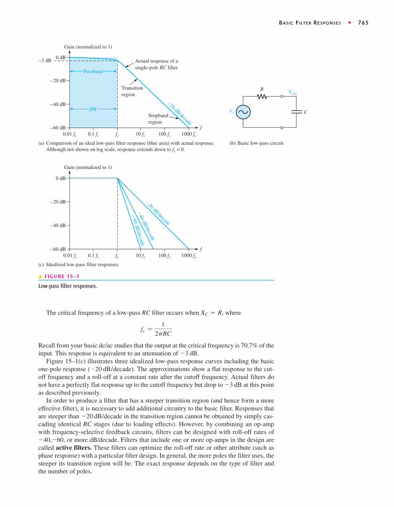
A filter is a circuit that passes certain frequencies and attenuates or rejects all other fre-quencies. The passband of a filter is the range of frequencies that are allowed to passthrough the filter with minimum attenuation (usually defined as less than of attenu-ation). The critical frequency, (also called the cutoff frequency) defines the end of thepassband and is normally specified at the point where the response drops (70.7%)from the passband response. Following the passband is a region called the transition regionthat leads into a region called the stopband. There is no precise point between the transi-tion region and the stopband.
A low-pass filter is one that passes frequencies from dc to and significantly attenu-ates all other frequencies. The passband of the ideal low-pass filter is shown in the blue-shaded area of Figure 15–1(a); the response drops to zero at frequencies beyond the pass-band. This ideal response is sometimes referred to as a “brick-wall” because nothing getsthrough beyond the wall. The bandwidth of an ideal low-pass filter is equal to fc.
fc
-3 dBfc,
-3 dB
15–1 BASIC FILTER RESPONSES
Filters are usually categorized by the manner in which the output voltage varies withthe frequency of the input voltage. The categories of active filters are low-pass, high-pass, band-pass, and band-stop. Each of these general responses are examined.
After completing this section, you should be able to
❏ Describe and analyze the gain-versus-frequency responses of basic types of filters❏ Describe low-pass filter response
◆ Define passband and critical frequency ◆ Determine the bandwidth◆ Define pole ◆ Explain roll-off rate and define its unit ◆ Calculate the criticalfrequency
❏ Describe high-pass filter response◆ Explain how the passband is limited ◆ Calculate the critical frequency
❏ Describe band-pass filter response◆ Determine the bandwidth ◆ Determine the center frequency ◆ Calculate thequality factor (Q)
❏ Describe band-stop filter response◆ Determine the bandwidth
Equation 15–1
The ideal response shown in Figure 15–1(a) is not attainable by any practical filter. Actualfilter responses depend on the number of poles, a term used with filters to describe the num-ber of RC circuits contained in the filter. The most basic low-pass filter is a simple RC circuitconsisting of just one resistor and one capacitor; the output is taken across the capacitor asshown in Figure 15–1(b). This basic RC filter has a single pole, and it rolls off at
beyond the critical frequency. The actual response is indicated by the blueline in Figure 15–1(a). The response is plotted on a standard log plot that is used for filters toshow details of the curve as the gain drops. Notice that the gain drops off slowly until the fre-quency is at the critical frequency; after this, the gain drops rapidly.
The roll-off rate for the gain of a basic RC filter means that at a fre-quency of the output will be (10%) of the input. This roll-off rate is not a par-ticularly good filter characteristic because too much of the unwanted frequencies (beyondthe passband) are allowed through the filter.
-20 dB10fc,-20 dB/decade
-20 dB/decade
BW � fc
BASIC FILTER RESPONSES ◆ 765
Comparison of an ideal low-pass filter response (blue area) with actual response.Although not shown on log scale, response extends down to fc = 0.
f
(c)
0 dB
–20 dB
10 fc
–40 dB
–60 dB0.1 fc fc0.01 fc 100 fc 1000 fc
Gain (normalized to 1)
Idealized low-pass filter responses
f
BW
(a)
0 dB
–20 dB
10 fc
–40 dB
–60 dB0.1 fc fc0.01 fc 100 fc 1000 fc
Passband
–3 dB
Gain (normalized to 1)
Actual response of asingle-pole RC filter
Transitionregion
Stopbandregion
–20 dB/decade
–20 dB/decade
–40
dB/decade
–60
dB/decade
VoutR
Vs C
Basic low-pass circuit(b)
� FIGURE 15–1
Low-pass filter responses.
The critical frequency of a low-pass RC filter occurs when where
Recall from your basic dc/ac studies that the output at the critical frequency is 70.7% of theinput. This response is equivalent to an attenuation of
Figure 15–1(c) illustrates three idealized low-pass response curves including the basicone-pole response The approximations show a flat response to the cut-off frequency and a roll-off at a constant rate after the cutoff frequency. Actual filters donot have a perfectly flat response up to the cutoff frequency but drop to at this pointas described previously.
In order to produce a filter that has a steeper transition region (and hence form a moreeffective filter), it is necessary to add additional circuitry to the basic filter. Responses thatare steeper than in the transition region cannot be obtained by simply cas-cading identical RC stages (due to loading effects). However, by combining an op-ampwith frequency-selective feedback circuits, filters can be designed with roll-off rates of
or more dB/decade. Filters that include one or more op-amps in the design arecalled active filters. These filters can optimize the roll-off rate or other attribute (such asphase response) with a particular filter design. In general, the more poles the filter uses, thesteeper its transition region will be. The exact response depends on the type of filter andthe number of poles.
-40,-60,
-20 dB/decade
-3 dB
(-20 dB/decade).
-3 dB.
fc =1
2pRC
XC = R,

766 ◆ ACTIVE FILTERS
High-Pass Filter Response
A high-pass filter is one that significantly attenuates or rejects all frequencies below and passes all frequencies above The critical frequency is, again, the frequency at whichthe output is 70.7% of the input (or ) as shown in Figure 15–2(a). The ideal re-sponse, indicated by the blue-shaded area, has an instantaneous drop at which, ofcourse, is not achievable. Ideally, the passband of a high-pass filter is all frequencies abovethe critical frequency. The high-frequency response of practical circuits is limited by theop-amp or other components that make up the filter.
fc,-3 dB
fc.fc
Comparison of an ideal high-pass filter response (blue area) with actual response
f
(c)
0 dB
–20 dB
fc
–40 dB
–60 dB0.01 fc 0.1fc0.001 fc 10 fc 100 fc
Gain (normalized to 1)
Idealized high-pass filter responses
f
(a)
0 dB
–20 dB
fc
–40 dB
–60 dB0.01 fc 0.1 fc0.001 fc 10 fc 100 fc
Passband
–3 dB
Gain (normalized to 1)
Actual responseof a single-poleRC filter
–20dB
/deca
de
–20dB
/deca
de
–40
dB/d
ecad
e–
60dB
/dec
ade
Vout
RVs
C
Basic high-pass circuit(b)
� FIGURE 15–2
High-pass filter responses.
A simple RC circuit consisting of a single resistor and capacitor can be configured as ahigh-pass filter by taking the output across the resistor as shown in Figure 15–2(b). As inthe case of the low-pass filter, the basic RC circuit has a roll-off rate of asindicated by the blue line in Figure 15–2(a). Also, the critical frequency for the basic high-pass filter occurs when where
Figure 15–2(c) illustrates three idealized high-pass response curves including the basicone-pole response for a high-pass RC circuit. As in the case of the low-pass filter, the approximations show a flat response to the cutoff frequency and a roll-off at
(-20 dB/decade)
fc =1
2pRC
XC = R,
-20 dB/decade,

BASIC FILTER RESPONSES ◆ 767
0.707
1
Vout (normalized to 1)
BW
fc1 f0 fc2
f
� FIGURE 15–3
General band-pass response curve.
a constant rate after the cutoff frequency. Actual high-pass filters do not have the perfectlyflat response indicated or the precise roll-off rate shown. Responses that are steeper than
in the transition region are also possible with active high-pass filters; theparticular response depends on the type of filter and the number of poles.
Band-Pass Filter Response
A band-pass filter passes all signals lying within a band between a lower-frequency limitand an upper-frequency limit and essentially rejects all other frequencies that are outsidethis specified band. A generalized band-pass response curve is shown in Figure 15–3. Thebandwidth (BW) is defined as the difference between the upper critical frequency andthe lower critical frequency ( fc1).
( fc2)
-20 dB/decade
Equation 15–2
The critical frequencies are, of course, the points at which the response curve is 70.7% ofits maximum. Recall from Chapter 12 that these critical frequencies are also called 3 dBfrequencies. The frequency about which the passband is centered is called the center fre-quency, defined as the geometric mean of the critical frequencies.f0,
BW � fc2 � fc1
Equation 15–3f0 � 2fc1 fc2
Quality Factor The quality factor (Q) of a band-pass filter is the ratio of the center fre-quency to the bandwidth.
Equation 15–4
The value of Q is an indication of the selectivity of a band-pass filter. The higher thevalue of Q, the narrower the bandwidth and the better the selectivity for a given value of Band-pass filters are sometimes classified as narrow-band or wide-band
The quality factor (Q) can also be expressed in terms of the damping factor(DF) of the filter as
You will study the damping factor in Section 15–2.
Q =1
DF
(Q 6 10).(Q 7 10)
f0.
Q �f0
BW

768 ◆ ACTIVE FILTERS
Band-Stop Filter Response
Another category of active filter is the band-stop filter, also known as notch, band-reject,or band-elimination filter. You can think of the operation as opposite to that of the band-pass filter because frequencies within a certain bandwidth are rejected, and frequenciesoutside the bandwidth are passed. A general response curve for a band-stop filter is shownin Figure 15–4. Notice that the bandwidth is the band of frequencies between the 3 dBpoints, just as in the case of the band-pass filter response.
–3
Gain (dB)
fc1 f0 fc2
f
0
BW
� FIGURE 15–4
General band-stop filter response.
A certain band-pass filter has a center frequency of 15 kHz and a bandwidth of 1 kHz.Determine Q and classify the filter as narrow-band or wide-band.
Solution
Because this is a narrow-band filter.
Related Problem* If the quality factor of the filter is doubled, what will the bandwidth be?
Q 7 10,
Q =f0
BW=
15 kHz
1 kHz= 15
EXAMPLE 15–1
*Answers can be found at www.pearsonhighered.com/floyd.
1. What determines the bandwidth of a low-pass filter?
2. What limits the passband of an active high-pass filter?
3. How are the Q and the bandwidth of a band-pass filter related? Explain how theselectivity is affected by the Q of a filter.
SECTION 15–1 CHECKUPAnswers can be found at www.pearsonhighered.com/floyd.
15–2 FILTER RESPONSE CHARACTERISTICS
Each type of filter response (low-pass, high-pass, band-pass, or band-stop) can betailored by circuit component values to have either a Butterworth, Chebyshev, orBessel characteristic. Each of these characteristics is identified by the shape of theresponse curve, and each has an advantage in certain applications.

FILTER RESPONSE CHARACTERISTICS ◆ 769
Butterworth, Chebyshev, or Bessel response characteristics can be realized with mostactive filter circuit configurations by proper selection of certain component values. A gen-eral comparison of the three response characteristics for a low-pass filter response curve isshown in Figure 15–5. High-pass and band-pass filters can also be designed to have anyone of the characteristics.
ButterworthBesselChebyshev
Av
f
� FIGURE 15–5
Comparative plots of three types offilter response characteristics.
After completing this section, you should be able to
❏ Describe three types of filter response characteristics and other parameters❏ Discuss the Butterworth characteristic❏ Describe the Chebyshev characteristic❏ Discuss the Bessel characteristic❏ Define damping factor
◆ Calculate the damping factor ◆ Show the block diagram of an active filter❏ Analyze a filter for critical frequency and roll-off rate
◆ Explain how to obtain multi-order filters ◆ Describe the effects of cascadingon roll-off rate
The Butterworth Characteristic The Butterworth characteristic provides a very flat am-plitude response in the passband and a roll-off rate of The phase re-sponse is not linear, however, and the phase shift (thus, time delay) of signals passing throughthe filter varies nonlinearly with frequency. Therefore, a pulse applied to a filter with aButterworth response will cause overshoots on the output because each frequency compo-nent of the pulse’s rising and falling edges experiences a different time delay. Filters with theButterworth response are normally used when all frequencies in the passband must have thesame gain. The Butterworth response is often referred to as a maximally flat response.
The Chebyshev Characteristic Filters with the Chebyshev response characteristic areuseful when a rapid roll-off is required because it provides a roll-off rate greater than
This is a greater rate than that of the Butterworth, so filters can beimplemented with the Chebyshev response with fewer poles and less complex circuitry fora given roll-off rate. This type of filter response is characterized by overshoot or ripples inthe passband (depending on the number of poles) and an even less linear phase responsethan the Butterworth.
-20 dB/decade/pole.
-20 dB/decade/pole.
770 ◆ ACTIVE FILTERS
The Bessel Characteristic The Bessel response exhibits a linear phase characteristic,meaning that the phase shift increases linearly with frequency. The result is almost noovershoot on the output with a pulse input. For this reason, filters with the Bessel responseare used for filtering pulse waveforms without distorting the shape of the waveform.
The Damping Factor
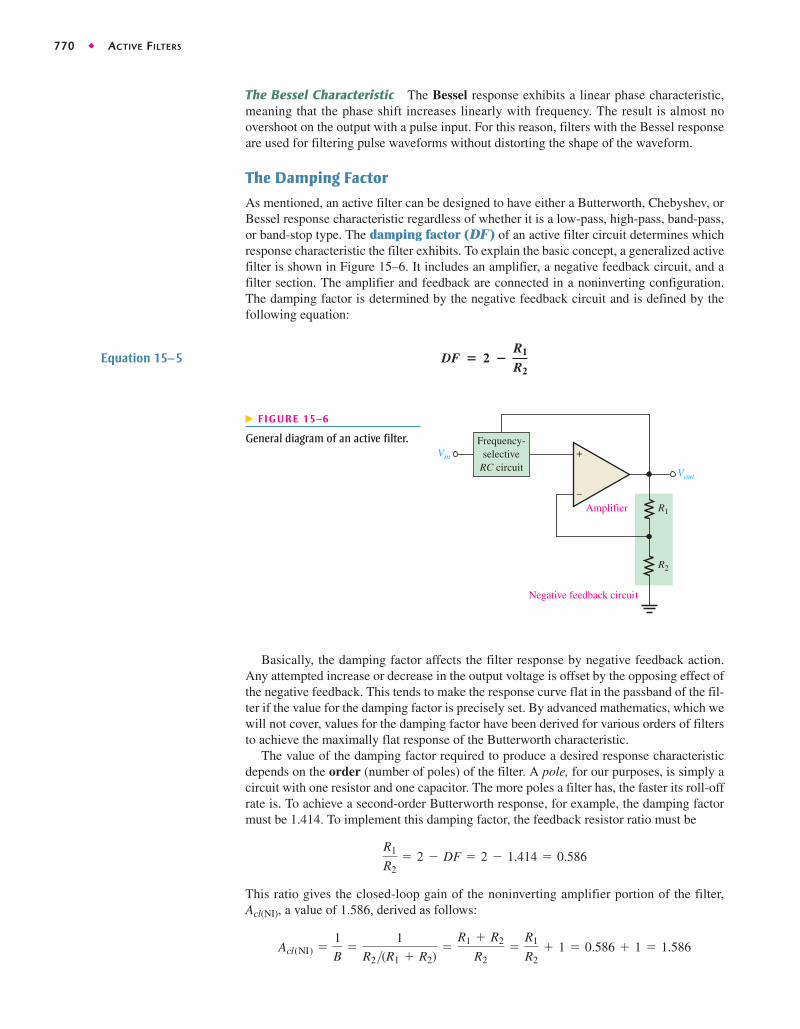
As mentioned, an active filter can be designed to have either a Butterworth, Chebyshev, orBessel response characteristic regardless of whether it is a low-pass, high-pass, band-pass,or band-stop type. The damping factor (DF ) of an active filter circuit determines whichresponse characteristic the filter exhibits. To explain the basic concept, a generalized activefilter is shown in Figure 15–6. It includes an amplifier, a negative feedback circuit, and afilter section. The amplifier and feedback are connected in a noninverting configuration.The damping factor is determined by the negative feedback circuit and is defined by thefollowing equation:
+
–R1
R2
Frequency-selective
RC circuitVin
Amplifier
Vout
Negative feedback circuit
� FIGURE 15–6
General diagram of an active filter.
Equation 15–5 DF � 2 �R1
R2
Basically, the damping factor affects the filter response by negative feedback action.Any attempted increase or decrease in the output voltage is offset by the opposing effect ofthe negative feedback. This tends to make the response curve flat in the passband of the fil-ter if the value for the damping factor is precisely set. By advanced mathematics, which wewill not cover, values for the damping factor have been derived for various orders of filtersto achieve the maximally flat response of the Butterworth characteristic.
The value of the damping factor required to produce a desired response characteristicdepends on the order (number of poles) of the filter. A pole, for our purposes, is simply acircuit with one resistor and one capacitor. The more poles a filter has, the faster its roll-offrate is. To achieve a second-order Butterworth response, for example, the damping factormust be 1.414. To implement this damping factor, the feedback resistor ratio must be
This ratio gives the closed-loop gain of the noninverting amplifier portion of the filter,a value of 1.586, derived as follows:
Acl(NI) =1
B=
1
R2>(R1 + R2)=
R1 + R2
R2=
R1
R2+ 1 = 0.586 + 1 = 1.586
Acl(NI),
R1
R2= 2 - DF = 2 - 1.414 = 0.586

FILTER RESPONSE CHARACTERISTICS ◆ 771
Critical Frequency and Roll-Off Rate
The critical frequency is determined by the values of the resistors and capacitors in thefrequency-selective RC circuit shown in Figure 15–6. For a single-pole (first-order) filter,as shown in Figure 15–7, the critical frequency is
Although we show a low-pass configuration, the same formula is used for the of a single-pole high-pass filter. The number of poles determines the roll-off rate of the filter. AButterworth response produces So, a first-order (one-pole) filter hasa roll-off of -20 dB/decade; a second-order (two-pole) filter has a roll-off rate of
a third-order (three-pole) filter has a roll-off rate of andso on.
-60 dB/decade;-40 dB/decade;
-20 dB/decade/pole.
fc
fc =1
2pRC
+
– R1
R2
Vin
Vout
Single-polelow-pass circuit
R
C
� FIGURE 15–7
First-order (one-pole) low-pass filter.
If resistor in the feedback circuit of an active single-pole filter of the type in Figure15–6 is what value must be to obtain a maximally flat Butterworth response?
Solution
Using the nearest standard 5 percent value of will get very close to the idealButterworth response.
Related Problem What is the damping factor for R2 = 10 kÆ and R1 = 5.6 kÆ?
5.6 kÆ
R1 = 0.586R2 = 0.586(10 kÆ) = 5.86 kæ
R1
R2= 0.586
R110 kÆ,R2EXAMPLE 15–2
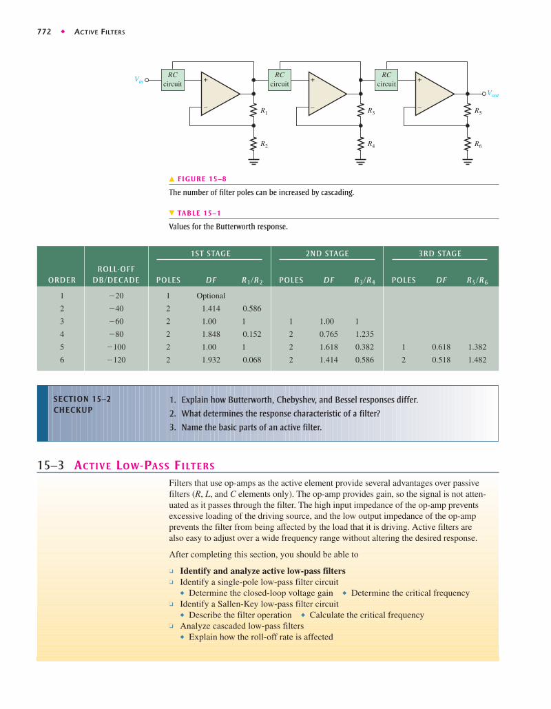
Generally, to obtain a filter with three poles or more, one-pole or two-pole filters arecascaded, as shown in Figure 15–8. To obtain a third-order filter, for example, cascadea second-order and a first-order filter; to obtain a fourth-order filter, cascade twosecond-order filters; and so on. Each filter in a cascaded arrangement is called a stageor section.
Because of its maximally flat response, the Butterworth characteristic is the mostwidely used. Therefore, we will limit our coverage to the Butterworth response to illus-trate basic filter concepts. Table 15–1 lists the roll-off rates, damping factors, and feed-back resistor ratios for up to sixth-order Butterworth filters. Resistor designationscorrespond to the gain-setting resistors in Figure 15–8 and may be different on othercircuit diagrams.
772 ◆ ACTIVE FILTERS
+
–
Vout
RCcircuit
+
–
RCcircuit
+
–
VinRC
circuit
R1
R2
R3
R4
R5
R6
� FIGURE 15–8
The number of filter poles can be increased by cascading.
� TABLE 15–1
Values for the Butterworth response.
1ST STAGE 2ND STAGE 3RD STAGE
ROLL-OFFORDER DB/DECADE POLES DF R1/R2 POLES DF R3/R4 POLES DF R5/R6
1 �20 1 Optional
2 �40 2 1.414 0.586
3 �60 2 1.00 1 1 1.00 1
4 �80 2 1.848 0.152 2 0.765 1.235
5 �100 2 1.00 1 2 1.618 0.382 1 0.618 1.382
6 �120 2 1.932 0.068 2 1.414 0.586 2 0.518 1.482
1. Explain how Butterworth, Chebyshev, and Bessel responses differ.
2. What determines the response characteristic of a filter?
3. Name the basic parts of an active filter.
SECTION 15–2 CHECKUP
15–3 ACTIVE LOW-PASS FILTERS
Filters that use op-amps as the active element provide several advantages over passivefilters (R, L, and C elements only). The op-amp provides gain, so the signal is not atten-uated as it passes through the filter. The high input impedance of the op-amp preventsexcessive loading of the driving source, and the low output impedance of the op-ampprevents the filter from being affected by the load that it is driving. Active filters arealso easy to adjust over a wide frequency range without altering the desired response.
After completing this section, you should be able to
❏ Identify and analyze active low-pass filters❏ Identify a single-pole low-pass filter circuit
◆ Determine the closed-loop voltage gain ◆ Determine the critical frequency❏ Identify a Sallen-Key low-pass filter circuit
◆ Describe the filter operation ◆ Calculate the critical frequency❏ Analyze cascaded low-pass filters
◆ Explain how the roll-off rate is affected
ACTIVE LOW-PASS FILTERS ◆ 773
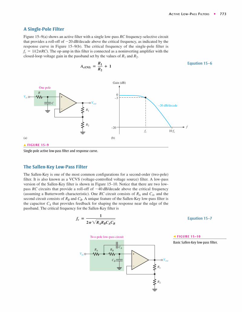
A Single-Pole Filter
Figure 15–9(a) shows an active filter with a single low-pass RC frequency-selective circuitthat provides a roll-off of above the critical frequency, as indicated by theresponse curve in Figure 15–9(b). The critical frequency of the single-pole filter is
The op-amp in this filter is connected as a noninverting amplifier with theclosed-loop voltage gain in the passband set by the values of and R2.R1
fc = 1/(2pRC).
-20 dB/decade
+
– R1
R2
Vin
Vout
One pole
R
C–20 dB/decade
–20
–3
Gain (dB)
0
fc 10 fc
f
(b)(a)
� FIGURE 15–9
Single-pole active low-pass filter and response curve.
Acl(NI) �R1
R2� 1
fc �1
2P2RARBCACB
Equation 15–6
Equation 15–7
The Sallen-Key Low-Pass Filter
The Sallen-Key is one of the most common configurations for a second-order (two-pole)filter. It is also known as a VCVS (voltage-controlled voltage source) filter. A low-passversion of the Sallen-Key filter is shown in Figure 15–10. Notice that there are two low-pass RC circuits that provide a roll-off of above the critical frequency(assuming a Butterworth characteristic). One RC circuit consists of and and thesecond circuit consists of and A unique feature of the Sallen-Key low-pass filter isthe capacitor that provides feedback for shaping the response near the edge of thepassband. The critical frequency for the Sallen-Key filter is
CA
CB.RB
CA,RA
-40 dB/decade
+
– R1
R2
Vin
Vout
RBRACA
Two-pole low-pass circuit
CB
� FIGURE 15–10
Basic Sallen-Key low-pass filter.
774 ◆ ACTIVE FILTERS
The component values can be made equal so that and In thiscase, the expression for the critical frequency simplifies to
As in the single-pole filter, the op-amp in the second-order Sallen-Key filter acts as anoninverting amplifier with the negative feedback provided by resistors and As youhave learned, the damping factor is set by the values of and thus making the filter re-sponse either Butterworth, Chebyshev, or Bessel. For example, from Table 15–1, the ratio must be 0.586 to produce the damping factor of 1.414 required for a second-orderButterworth response.
R1/R2
R2,R1
R2.R1
fc =1
2pRC
CA = CB = C.RA = RB = R
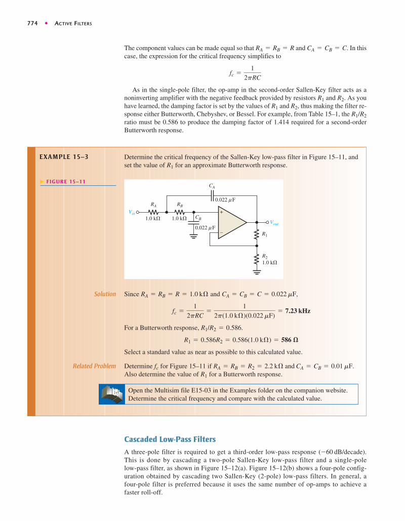
Determine the critical frequency of the Sallen-Key low-pass filter in Figure 15–11, andset the value of for an approximate Butterworth response.R1
EXAMPLE 15–3
0.022 Fμ
+
– R1
R21.0 k�
RBRA
CA
0.022 F
1.0 k�1.0 k� CB
Vin
Vout
μ
� FIGURE 15–11
Solution Since and
For a Butterworth response,
Select a standard value as near as possible to this calculated value.
Related Problem Determine for Figure 15–11 if Also determine the value of for a Butterworth response.
Open the Multisim file E15-03 in the Examples folder on the companion website.Determine the critical frequency and compare with the calculated value.
R1
RA = RB = R2 = 2.2 kÆ and CA = CB = 0.01 mF.fc
R1 = 0.586R2 = 0.586(1.0 kÆ) = 586 æ
R1/R2 = 0.586.
fc =1
2pRC=
1
2p(1.0 kÆ)(0.022 mF)= 7.23 kHz
CA = CB = C = 0.022 mF,RA = RB = R = 1.0 kÆ
Cascaded Low-Pass Filters
A three-pole filter is required to get a third-order low-pass response This is done by cascading a two-pole Sallen-Key low-pass filter and a single-pole low-pass filter, as shown in Figure 15–12(a). Figure 15–12(b) shows a four-pole config-uration obtained by cascading two Sallen-Key (2-pole) low-pass filters. In general, afour-pole filter is preferred because it uses the same number of op-amps to achieve afaster roll-off.
(-60 dB/decade).
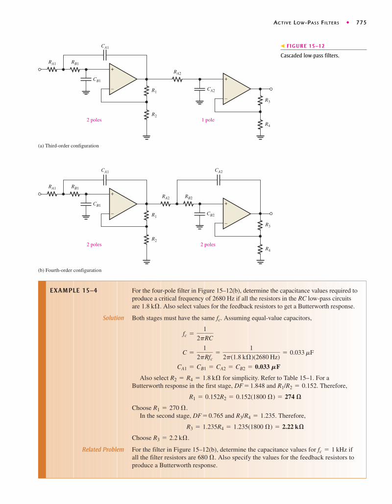
ACTIVE LOW-PASS FILTERS ◆ 775
+
– R3
R4
RA2
CA2
+
– R1
R2
RB1
CB1
RA1
CA1
1 pole2 poles
(a) Third-order configuration
+
– R3
R4
CB2
+
– R1
R2
RB1
CB1
RA1
CA1
2 poles2 poles
(b) Fourth-order configuration
CA2
RB2RA2
� FIGURE 15–12
Cascaded low-pass filters.
For the four-pole filter in Figure 15–12(b), determine the capacitance values required toproduce a critical frequency of 2680 Hz if all the resistors in the RC low-pass circuitsare Also select values for the feedback resistors to get a Butterworth response.
Solution Both stages must have the same Assuming equal-value capacitors,
Also select for simplicity. Refer to Table 15–1. For aButterworth response in the first stage, DF = 1.848 and Therefore,
ChooseIn the second stage, DF = 0.765 and Therefore,
Choose
Related Problem For the filter in Figure 15–12(b), determine the capacitance values for ifall the filter resistors are Also specify the values for the feedback resistors toproduce a Butterworth response.
680 Æ.fc = 1 kHz
R3 = 2.2 kÆ.
R3 = 1.235R4 = 1.235(1800 Æ) = 2.22 kæ
R3/R4 = 1.235.R1 = 270 Æ.
R1 = 0.152R2 = 0.152(1800 Æ) = 274 æ
R1/R2 = 0.152.R2 = R4 = 1.8 kÆ
CA1 = CB1 = CA2 = CB2 = 0.033 MF
C =1
2pRfc=
1
2p(1.8 kÆ)(2680 Hz)= 0.033 mF
fc =1
2pRC
fc.
1.8 kÆ.
EXAMPLE 15–4
776 ◆ ACTIVE FILTERS
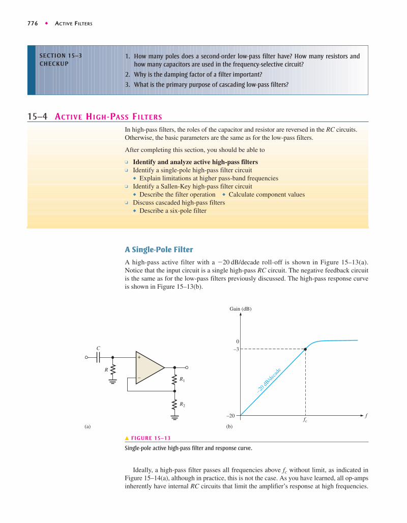
A Single-Pole Filter
A high-pass active filter with a roll-off is shown in Figure 15–13(a).Notice that the input circuit is a single high-pass RC circuit. The negative feedback circuitis the same as for the low-pass filters previously discussed. The high-pass response curveis shown in Figure 15–13(b).
-20 dB/decade
Gain (dB)
+
– R1
R2
R
C
f
(b)fc
–20
–3
0
–20 dB
/deca
de
(a)
� FIGURE 15–13
Single-pole active high-pass filter and response curve.
1. How many poles does a second-order low-pass filter have? How many resistors andhow many capacitors are used in the frequency-selective circuit?
2. Why is the damping factor of a filter important?
3. What is the primary purpose of cascading low-pass filters?
SECTION 15–3 CHECKUP
15–4 ACTIVE HIGH-PASS FILTERS
In high-pass filters, the roles of the capacitor and resistor are reversed in the RC circuits.Otherwise, the basic parameters are the same as for the low-pass filters.
After completing this section, you should be able to
❏ Identify and analyze active high-pass filters❏ Identify a single-pole high-pass filter circuit
◆ Explain limitations at higher pass-band frequencies❏ Identify a Sallen-Key high-pass filter circuit
◆ Describe the filter operation ◆ Calculate component values❏ Discuss cascaded high-pass filters
◆ Describe a six-pole filter
Ideally, a high-pass filter passes all frequencies above without limit, as indicated inFigure 15–14(a), although in practice, this is not the case. As you have learned, all op-ampsinherently have internal RC circuits that limit the amplifier’s response at high frequencies.
fc

ACTIVE HIGH-PASS FILTERS ◆ 777
Therefore, there is an upper-frequency limit on the high-pass filter’s response which, ineffect, makes it a band-pass filter with a very wide bandwidth. In the majority of applica-tions, the internal high-frequency limitation is so much greater than that of the filter’scritical frequency that the limitation can be neglected. In some applications, discrete tran-sistors are used for the gain element to increase the high-frequency limitation beyond thatrealizable with available op-amps.
The Sallen-Key High-Pass Filter
A high-pass Sallen-Key configuration is shown in Figure 15–15. The componentsand form the two-pole frequency-selective circuit. Notice that the positions
of the resistors and capacitors in the frequency-selective circuit are opposite to those in thelow-pass configuration. As with the other filters, the response characteristic can be opti-mized by proper selection of the feedback resistors, and R2.R1
CBRA, CA, RB,
fcf
Av
(a) Ideal
fcf
Av
(b) Nonideal
Inherentinternalop-amproll-off
� FIGURE 15–14
High-pass filter response.
+
– R1
R2
Vin
Vout
RA
RB
CB
Two-pole high-pass circuit
CA
� FIGURE 15–15
Basic Sallen-Key high-pass filter.
778 ◆ ACTIVE FILTERS
Cascading High-Pass Filters
As with the low-pass configuration, first- and second-order high-pass filters can be cas-caded to provide three or more poles and thereby create faster roll-off rates. Figure 15–16shows a six-pole high-pass filter consisting of three Sallen-Key two-pole stages. With thisconfiguration optimized for a Butterworth response, a roll-off of isachieved.
-120 dB/decade
+
– R1
R2
Vin
RA1
RB1
CB1CA1
+
– R3
R4
RA2
RB2
CB2CA2
+
– R5
R6
Vout
RA3
RB3
CB3CA3
� FIGURE 15–16
Sixth-order high-pass filter.
Choose values for the Sallen-Key high-pass filter in Figure 15–15 to implement anequal-value second-order Butterworth response with a critical frequency of approxi-mately 10 kHz.
Solution Start by selecting a value for RA and RB (R1 or R2 can also be the same value as RA andRB for simplicity).
Next, calculate the capacitance value from
For a Butterworth response, the damping factor must be 1.414 and
If you had chosen then
Either way, an approximate Butterworth response is realized by choosing the neareststandard values.
Related Problem Select values for all the components in the high-pass filter of Figure 15–15 to obtainan Use equal-value components with and optimize for aButterworth response.
R = 10 kÆfc = 300 Hz.
R2 =R1
0.586=
3.3 kÆ0.586
= 5.63 kÆ
R1 = 3.3 kÆ,
R1 = 0.586R2 = 0.586(3.3 kÆ) = 1.93 kæ
R1>R2 = 0.586.
C = CA = CB =1
2pRfc=
1
2p(3.3 kÆ)(10 kHz)= 0.0048 MF
fc = 1>(2pRC).
R = RA = RB = R2 = 3.3 kæ (an arbitrary selection)
EXAMPLE 15–5

ACTIVE BAND-PASS FILTERS ◆ 779
Cascaded Low-Pass and High-Pass Filters
One way to implement a band-pass filter is a cascaded arrangement of a high-pass filterand a low-pass filter, as shown in Figure 15–17(a), as long as the critical frequencies aresufficiently separated. Each of the filters shown is a Sallen-Key Butterworth configurationso that the roll-off rates are indicated in the composite response curve ofFigure 15–17(b). The critical frequency of each filter is chosen so that the response curvesoverlap sufficiently, as indicated. The critical frequency of the high-pass filter must be suf-ficiently lower than that of the low-pass stage. This filter is generally limited to wide band-width applications.
The lower frequency of the passband is the critical frequency of the high-pass fil-ter. The upper frequency is the critical frequency of the low-pass filter. Ideally, as dis-cussed earlier, the center frequency of the passband is the geometric mean of
The following formulas express the three frequencies of the band-pass filter inFigure 15–17.
Of course, if equal-value components are used in implementing each filter, the critical fre-quency equations simplify to the form fc = 1>(2pRC).
f0 = 1fc1 fc2
fc2 =1
2p2RA2RB2CA2CB2
fc1 =1
2p2RA1RB1CA1CB1
fc1 and fc2.f0
fc2
fc1
-40 dB/decade,
1. How does a high-pass Sallen-Key filter differ from the low-pass configuration?
2. To increase the critical frequency of a high-pass filter, would you increase or decreasethe resistor values?
3. If three two-pole high-pass filters and one single-pole high-pass filter are cascaded,what is the resulting roll-off?
SECTION 15–4 CHECKUP
15–5 ACTIVE BAND-PASS FILTERS
As mentioned, band-pass filters pass all frequencies bounded by a lower-frequencylimit and an upper-frequency limit and reject all others lying outside this specifiedband. A band-pass response can be thought of as the overlapping of a low-frequencyresponse curve and a high-frequency response curve.
After completing this section, you should be able to
❏ Analyze basic types of active band-pass filters❏ Describe how to cascade low-pass and high-pass filters to create a band-pass filter
◆ Calculate the critical frequencies and the center frequency❏ Identify and analyze a multiple-feedback band-pass filter
◆ Determine the center frequency, quality factor (Q), and bandwidth ◆ Calculatethe voltage gain
❏ Identify and describe the state-variable filter◆ Explain the basic filter operation ◆ Determine the Q
❏ Identify and discuss the biquad filter

780 ◆ ACTIVE FILTERS
Multiple-Feedback Band-Pass Filter
Another type of filter configuration, shown in Figure 15–18, is a multiple-feedback band-pass filter. The two feedback paths are through R2 and C1. Components R1 and C1 providethe low-pass response, and R2 and C2 provide the high-pass response. The maximum gain,A0, occurs at the center frequency. Q values of less than 10 are typical in this type of filter.
+
– R3
R4
CB2
+
– R1
R2
RA1
RB1
CA1
Two-pole low-passTwo-pole high-pass
(a)
CA2
RB2RA2
CB1
Vout
Vin
(b)
Low-pass response
Av
fc1
–40
dB
/dec
ade
0 dB
High-pass response
–3 dB
–40 dB/decade
f0 fc2
f
� FIGURE 15–17
Band-pass filter formed by cascadinga two-pole high-pass and a two-polelow-pass filter (it does not matter inwhich order the filters are cascaded).
–
+
Vin
Vout
R3
C2
C1
R1
R2
An expression for the center frequency is developed as follows, recognizing that R1 and R3appear in parallel as viewed from the C1 feedback path (with the Vin source replaced by a short).
f0 =1
2p2(R1 7 R3)R2C1C2
� FIGURE 15–18
Multiple-feedback band-pass filter.

ACTIVE BAND-PASS FILTERS ◆ 781
Making
=1
2pCA
1
R2(R1 7 R3)=
1
2pCAa
1
R2b a
1
R1R3/R1 + R3b
f0 =1
2p2(R1 7 R3)R2C2=
1
2pC2(R1 7 R3)R2
C1 = C2 = C yields
A value for the capacitors is chosen and then the three resistor values are calculated toachieve the desired values for f0, BW, and A0. As you know, the Q can be determined fromthe relation The resistor values can be found using the following formulas(stated without derivation):
To develop a gain expression, solve for Q in the and formulas as follows:
Then,
Cancelling yields
2A0R1 = R2
2pf0A0CR1 = pf0CR2
Q = pf0CR2
Q = 2pf0A0CR1
R2R1
R3 =Q
2pf0C(2Q2 - A0)
R2 =Q
pf0C
R1 =Q
2pf0CA0
Q = f0>BW.
f0 �1
2PCA
R1 � R3
R1R2R3Equation 15–8
Equation 15–9
In order for the denominator of the equation to be positive,which imposes a limitation on the gain.A0 6 2Q2,
R3 = Q>[2pf0C(2Q2 - A0)]
A0 �R2
2R1
Determine the center frequency, maximum gain, and bandwidth for the filter inFigure 15–19.
EXAMPLE 15–6
0.01 Fμ
–
+
Vin
Vout
R2
R32.7 k�
R1180 k�
0.01 F
68 k�
C1
C2
μ
� FIGURE 15–19
782 ◆ ACTIVE FILTERS
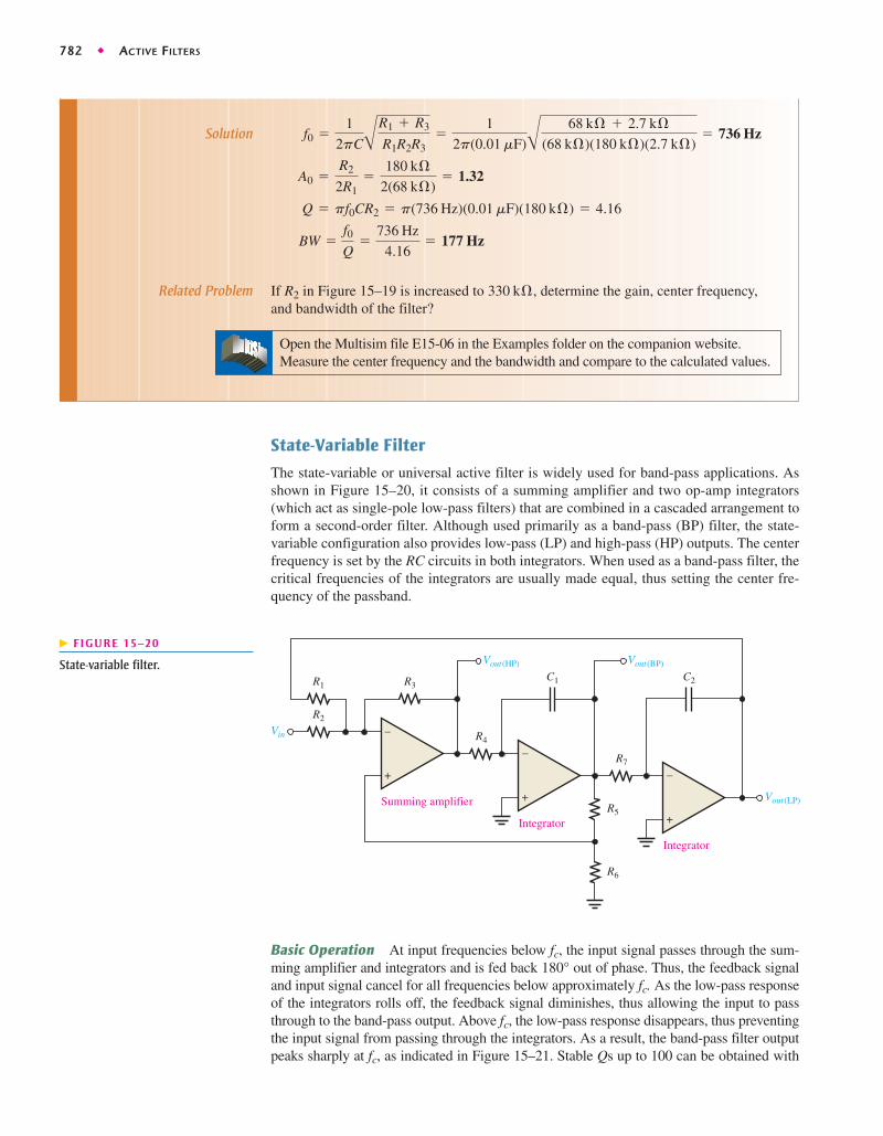
State-Variable Filter
The state-variable or universal active filter is widely used for band-pass applications. Asshown in Figure 15–20, it consists of a summing amplifier and two op-amp integrators(which act as single-pole low-pass filters) that are combined in a cascaded arrangement toform a second-order filter. Although used primarily as a band-pass (BP) filter, the state-variable configuration also provides low-pass (LP) and high-pass (HP) outputs. The centerfrequency is set by the RC circuits in both integrators. When used as a band-pass filter, thecritical frequencies of the integrators are usually made equal, thus setting the center fre-quency of the passband.
–
+
Vout(LP)R5
C2
R7
Integrator
R6
–
+
C1
R4
Integrator
–
+
Vin
R1
Summing amplifier
R2
R3
Vout(BP)Vout(HP)
� FIGURE 15–20
State-variable filter.
Solution
Related Problem If in Figure 15–19 is increased to determine the gain, center frequency,and bandwidth of the filter?
Open the Multisim file E15-06 in the Examples folder on the companion website.Measure the center frequency and the bandwidth and compare to the calculated values.
330 kÆ,R2
BW =f0Q
=736 Hz
4.16= 177 Hz
Q = pf0CR2 = p(736 Hz)(0.01 mF)(180 kÆ) = 4.16
A0 =R2
2R1=
180 kÆ2(68 kÆ)
= 1.32
f0 =1
2pCA
R1 + R3
R1R2R3=
1
2p(0.01 mF)A
68 kÆ + 2.7 kÆ(68 kÆ)(180 kÆ)(2.7 kÆ)
= 736 Hz
Basic Operation At input frequencies below fc, the input signal passes through the sum-ming amplifier and integrators and is fed back out of phase. Thus, the feedback signaland input signal cancel for all frequencies below approximately fc. As the low-pass responseof the integrators rolls off, the feedback signal diminishes, thus allowing the input to passthrough to the band-pass output. Above fc, the low-pass response disappears, thus preventingthe input signal from passing through the integrators. As a result, the band-pass filter outputpeaks sharply at fc, as indicated in Figure 15–21. Stable Qs up to 100 can be obtained with
180°

ACTIVE BAND-PASS FILTERS ◆ 783
this type of filter. The Q is set by the feedback resistors R5 and R6 according to the follow-ing equation:
The state-variable filter cannot be optimized for low-pass, high-pass, and narrow band-pass performance simultaneously for this reason: To optimize for a low-pass or a high-passButterworth response, DF must equal 1.414. Since a Q of 0.707 will result.Such a low Q provides a very wide band-pass response (large BW and poor selectivity). Foroptimization as a narrow band-pass filter, the Q must be set high.
Q = 1/DF,
Q =1
3a
R5
R6+ 1b
Gain
Low-pass High-pass
fc = f0
Passband
f
� FIGURE 15–21
General state-variable response curves.
Determine the center frequency, Q, and BW for the passband of the state-variable filterin Figure 15–22.
EXAMPLE 15–7
–
+R5100 k�
C2
R7–
+
C1
R4–
+
Vin
R2
R3
Vout(BP)
Vout(LP)
Vout(HP)
10 k�
10 k�
1.0 k�
1.0 k�
R61.0 k�
R110 k�
0.022 Fμ 0.022 Fμ
� FIGURE 15–22

784 ◆ ACTIVE FILTERS
The Biquad Filter
The biquad filter is similar to the state-variable filter except that it consists of an integrator, fol-lowed by an inverting amplifier, and then another integrator, as shown in Figure 15–23. Thesedifferences in the configuration between a biquad and a state-variable filter result in some op-erational differences although both allow a very high Q value. In a biquad filter, the bandwidthis independent and the Q is dependent on the critical frequency; however, in the state-variablefilter it is just the opposite: the bandwidth is dependent and the Q is independent on the criti-cal frequency. Also, the biquad filter provides only band-pass and low-pass outputs.
–
+
C2
R4
Integrator
–
+
C1
R2
Invertingamplifier
–
+
VIN
R1
R3
R5
Integrator
BPLP
� FIGURE 15–23
A biquad filter.
Solution For each integrator,
The center frequency is approximately equal to the critical frequencies of theintegrators.
Related Problem Determine f0, Q, and BW for the filter in Figure 15–22 if with all other component values the same as shown on the schematic.
Open the Multisim file E15-07 in the Examples folder on the companion website.Measure the center frequency and the bandwidth and compare to the calculated values.
R4 = R6 = R7 = 330 Æ
BW =f0Q
=7.23 kHz
33.7= 215 Hz
Q =1
3a
R5
R6+ 1b =
1
3a
100 kÆ1.0 kÆ
+ 1b = 33.7
f0 = fc = 7.23 kHz
fc =1
2pR4C1=
1
2pR7C2=
1
2p(1.0 kÆ)(0.022 mF)= 7.23 kHz
1. What determines selectivity in a band-pass filter?
2. One filter has a Q � 5 and another has a Q � 25. Which has the narrower bandwidth?
3. List the active elements that make up a state-variable filter.
4. List the active elements that make up a biquad filter.
SECTION 15–5 CHECKUP
ACTIVE BAND-STOP FILTERS ◆ 785
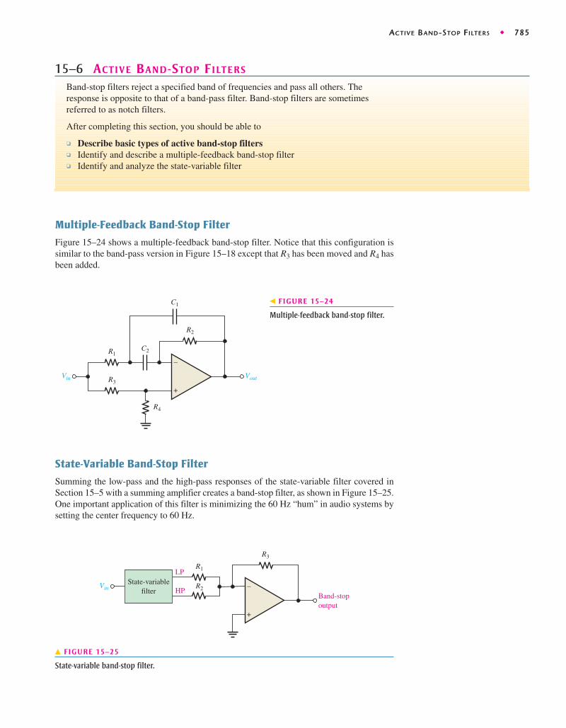
Multiple-Feedback Band-Stop Filter
Figure 15–24 shows a multiple-feedback band-stop filter. Notice that this configuration issimilar to the band-pass version in Figure 15–18 except that R3 has been moved and R4 hasbeen added.
15–6 ACTIVE BAND-STOP FILTERS
Band-stop filters reject a specified band of frequencies and pass all others. Theresponse is opposite to that of a band-pass filter. Band-stop filters are sometimesreferred to as notch filters.
After completing this section, you should be able to
❏ Describe basic types of active band-stop filters❏ Identify and describe a multiple-feedback band-stop filter❏ Identify and analyze the state-variable filter
State-Variable Band-Stop Filter
Summing the low-pass and the high-pass responses of the state-variable filter covered inSection 15–5 with a summing amplifier creates a band-stop filter, as shown in Figure 15–25.One important application of this filter is minimizing the 60 Hz “hum” in audio systems bysetting the center frequency to 60 Hz.
Vout
R2
R4
R1
Vin R3
C1
C2
–
+
� FIGURE 15–24
Multiple-feedback band-stop filter.
–
+
Band-stopoutput
R1
VinState-variable
filter
LP
HPR2
R3
� FIGURE 15–25
State-variable band-stop filter.

786 ◆ ACTIVE FILTERS
1. How does a band-stop response differ from a band-pass response?
2. How is a state-variable band-pass filter converted to a band-stop filter?
SECTION 15–6 CHECKUP
Verify that the band-stop filter in Figure 15–26 has a center frequency of 60 Hz, andoptimize the filter for a Q of 10.
EXAMPLE 15–8
Solution f0 equals the fc of the integrator stages. (In practice, component values are critical.)
You can obtain a Q � 10 by choosing R6 and then calculating R5.
Choose Then
Use the nearest standard value of
Related Problem How would you change the center frequency to 120 Hz in Figure 15–26?
Open the Multisim file E15-08 in the Examples folder on the companion website and verify that the center frequency is approximately 60 Hz.
100 kÆ.
R5 = [3(10) - 1]3.3 kÆ = 95.7 kÆ
R6 = 3.3 kæ.
R5 = (3Q - 1)R6
Q =1
3a
R5
R6+ 1b
f0 =1
2pR4C1=
1
2pR7C2=
1
2p(12 kÆ)(0.22 mF)= 60 Hz
Vout
R5
R7
R6
–
+
C1
R4–
+
Vin
R110 k�
R2
R3
10 k�
10 k�
12 k�
12 k�
R10
10 k�
–
+
C2 R810 k�
R910 k�
0.22 F –
+
μ 0.22 Fμ
� FIGURE 15–26

FILTER RESPONSE MEASUREMENTS ◆ 787
Discrete Point Measurement
Figure 15–27 shows an arrangement for taking filter output voltage measurements at dis-crete values of input frequency using common laboratory instruments. The general proce-dure is as follows:
1. Set the amplitude of the sine wave generator to a desired voltage level.
2. Set the frequency of the sine wave generator to a value well below the expectedcritical frequency of the filter under test. For a low-pass filter, set the frequency asnear as possible to 0 Hz. For a band-pass filter, set the frequency well below the ex-pected lower critical frequency.
3. Increase the frequency in predetermined steps sufficient to allow enough datapoints for an accurate response curve.
4. Maintain a constant input voltage amplitude while varying the frequency.
5. Record the output voltage at each value of frequency.
6. After recording a sufficient number of points, plot a graph of output voltage versusfrequency.
If the frequencies to be measured exceed the frequency response of the DMM, an oscillo-scope may have to be used instead.
15–7 FILTER RESPONSE MEASUREMENTS
Two methods of determining a filter’s response by measurement are discrete pointmeasurement and swept frequency measurement.
After completing this section, you should be able to
❏ Discuss two methods for measuring frequency response❏ Explain discrete-point measurement
◆ List the steps in the procedure ◆ Show a test setup❏ Explain swept frequency measurement
◆ Show a test setup for this method using a spectrum analyzer ◆ Show a testsetup for this method using an oscilloscope
Output
–+V
–+V
Input
Filter
Sine wavegenerator
� FIGURE 15–27
Test setup for discrete point meas-urement of the filter response.(Readings are arbitrary and for display only.)
Swept Frequency Measurement
The swept frequency method requires more elaborate test equipment than does thediscrete point method, but it is much more efficient and can result in a more accurate re-sponse curve. A general test setup is shown in Figure 15–28(a) using a swept frequency

788 ◆ ACTIVE FILTERS
generator and a spectrum analyzer. Figure 15–28(b) shows how the test can be madewith an oscilloscope.
The swept frequency generator produces a constant amplitude output signal whose fre-quency increases linearly between two preset limits, as indicated in Figure 15–28. Thespectrum analyzer is essentially an elaborate oscilloscope that can be calibrated for a de-sired frequency span/division rather than for the usual time/division setting. Therefore, asthe input frequency to the filter sweeps through a preselected range, the response curve istraced out on the screen of the spectrum analyzer or an oscilloscope.
X
Sweepgenerator
VinFilter
Oscilloscope
Y
Sawtoothoutput
(a) Test setup for a filter response using a spectrum analyzer
(b) Test setup for a filter response using an oscilloscope. The scope is placed in X-Y mode. The sawtooth waveformfrom the sweep generator drives the X-channel of the oscilloscope.
Vout
Spectrum analyzer
Sweepgenerator
Vin VoutFilter
� FIGURE 15–28
Test setup for swept frequency measurement of the filter response.
1. What is the purpose of the two tests discussed in this section?
2. Name one disadvantage and one advantage of each test method.
SECTION 15–7 CHECKUP

APPLICATION ACTIVIT Y ◆ 789
Application Activity: RFID System
RFID (radio frequency identification) is a technology that enables the tracking and/oridentification of objects. Typically, an RFID system contains an RFID tag that consists ofan IC chip that transmits data about the object, an RFID reader that receives transmitteddata from the tag, and a data-processing system that processes and stores the data passedto it by the reader. A basic block diagram is shown in Figure 15–29.
The RFID Tag
RFID tags are tiny, very thin microchips with memory and a coil antenna. The tags listenfor a radio signal sent by an RFID reader. When a tag receives a signal, it responds bytransmitting its unique ID code and other data back to the reader.
Passive RFID Tag This type of tag does not require batteries. The tag is inactive untilpowered by the energy from the electromagnetic field of an RFID reader. Passive tags canbe read from distances up to about 20 feet and are generally read-only, meaning the datathey contain cannot be altered or written over.
Active RFID Tag This type of tag is powered by a battery and is capable of communi-cating up to 100 feet or more from the RFID reader. Generally, the active tag is larger andmore expensive than a passive tag, but can hold more data about the product and is com-monly used for identification of high-value assets. Active tags may be read-write, mean-ing the data they contain can be written over.
Tags are available in a variety of shapes. Depending on the application, they may beembedded in glass or epoxy, or they may be in label or card form. Another type of tag,often called the smart label, is a paper (or similar material) label with printing, but alsowith the RF circuitry and antenna embedded in it.
Some advantages of RFID tags compared to bar codes are
◆ Non-line-of-sight identification◆ More information can be stored◆ Coverage at greater distances◆ Unattended operations are possible◆ Ability to identify moving objects that have tags embedded◆ Can be used in diverse environments
Disadvantages of RFID tags are that they are expensive compared to the bar code andthey are bulkier because the electronics is embedded in the tag.
RFID tags and readers must be tuned to the same frequency to communicate. RFID sys-tems use many different frequencies, but generally the most common are low frequency
RFID readerDataprocessor
RFID tag
� FIGURE 15–29
Basic block diagram of an RFID system.

790 ◆ ACTIVE FILTERS
(125 kHz), high frequency (13.56 MHz), and ultra-high frequency, or UHF (850–900 MHz).Microwave (2.45 GHz) is also used in some applications. The frequency used depends onthe particular type of application.
Low-frequency systems are the least expensive and have the shortest range. They aremost commonly used in security access, asset tracking, and animal identification applica-tions. High-frequency systems are used for applications such as railroad car tracking andautomated toll collection.
Some typical RFID application areas are
◆ Metering applications such as electronic toll collection◆ Inventory control and tracking such as merchandise control◆ Asset tracking and recovery◆ Tracking parts moving through a manufacturing process◆ Tracking goods in a supply chain
The RFID Reader
Data is stored on the RFID tag in digital form and is transmitted to the reader as a modu-lated signal. Many RFID systems use ASK (amplitude shift keying) or FSK (frequencyshift keying). In ASK, the amplitude of a carrier signal is varied by the digital data. InFSK, the frequency of a carrier signal is varied by the digital data. Examples of theseforms of modulation are shown Figure 15–30. In this system, the carrier is 125 kHz, andthe modulating signal is a digital waveform at the rate of 10 kHz, representing a stream of1s and 0s.
Project
Your company is developing a new RFID reader using ASK modulation at a carrier fre-quency of 125 kHz. A block diagram is shown in Figure 15–31. The purpose of eachblock is as follows. The band-pass filter passes the 125 kHz signal and reduces signalsand noise from other sources; the 2-stage amplifier increases the very small signal fromthe tag to a usable level; the rectifier eliminates the negative portions of the modulatedsignal; the low-pass filter eliminates the 125 kHz carrier frequency but passes the 10 kHz
Digital modulatingsignal 0 0 0 0 0 0 01 1 1 1 1 1
ASK
FSK
� FIGURE 15–30
Examples of ASK and FSK modulation transmitted by an RFID tag.
APPLICATION ACTIVIT Y ◆ 791
ASK signalfrom RFID tag
125 kHzband-passfilter
2-stageamplifier
Half-waverectifier
Low-passfilterfc = 22 kHz
Comparator Digital data toprocessor
� FIGURE 15–31
Block diagram of RFID reader.
modulating signal; and the comparator restores the digital signal to a usable stream ofdigital data.
1. In general, what are RFID systems used for?2. Name the three basic components of an RFID system.3. Explain the purpose of an RFID tag.4. Explain the purpose of an RFID reader.
Simulation
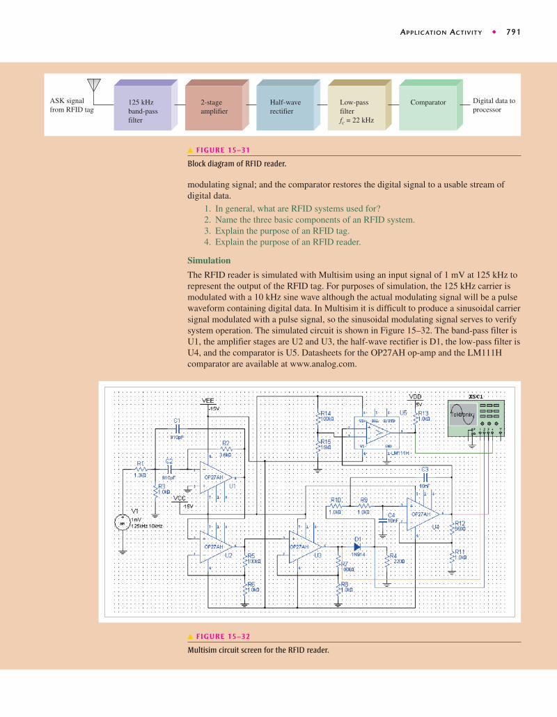
The RFID reader is simulated with Multisim using an input signal of 1 mV at 125 kHz torepresent the output of the RFID tag. For purposes of simulation, the 125 kHz carrier ismodulated with a 10 kHz sine wave although the actual modulating signal will be a pulsewaveform containing digital data. In Multisim it is difficult to produce a sinusoidal carriersignal modulated with a pulse signal, so the sinusoidal modulating signal serves to verifysystem operation. The simulated circuit is shown in Figure 15–32. The band-pass filter isU1, the amplifier stages are U2 and U3, the half-wave rectifier is D1, the low-pass filter isU4, and the comparator is U5. Datasheets for the OP27AH op-amp and the LM111Hcomparator are available at www.analog.com.
� FIGURE 15–32
Multisim circuit screen for the RFID reader.
792 ◆ ACTIVE FILTERS
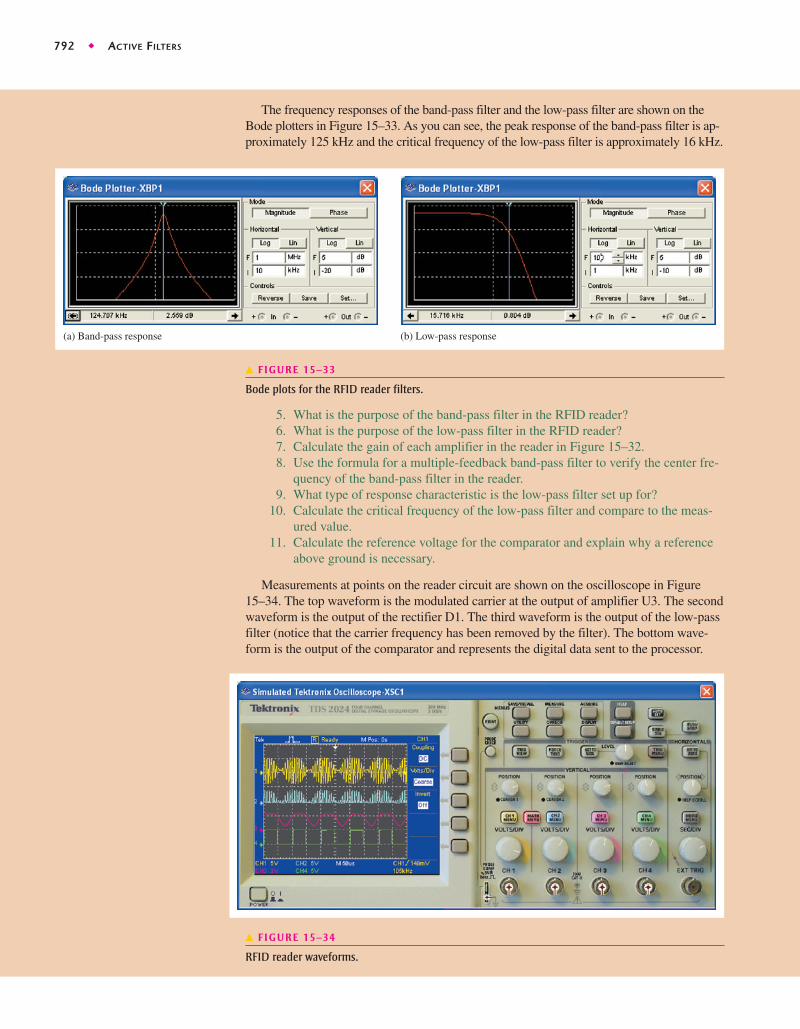
The frequency responses of the band-pass filter and the low-pass filter are shown on theBode plotters in Figure 15–33. As you can see, the peak response of the band-pass filter is ap-proximately 125 kHz and the critical frequency of the low-pass filter is approximately 16 kHz.
5. What is the purpose of the band-pass filter in the RFID reader?6. What is the purpose of the low-pass filter in the RFID reader?7. Calculate the gain of each amplifier in the reader in Figure 15–32.8. Use the formula for a multiple-feedback band-pass filter to verify the center fre-
quency of the band-pass filter in the reader.9. What type of response characteristic is the low-pass filter set up for?
10. Calculate the critical frequency of the low-pass filter and compare to the meas-ured value.
11. Calculate the reference voltage for the comparator and explain why a referenceabove ground is necessary.
Measurements at points on the reader circuit are shown on the oscilloscope in Figure15–34. The top waveform is the modulated carrier at the output of amplifier U3. The secondwaveform is the output of the rectifier D1. The third waveform is the output of the low-passfilter (notice that the carrier frequency has been removed by the filter). The bottom wave-form is the output of the comparator and represents the digital data sent to the processor.
(a) Band-pass response (b) Low-pass response
� FIGURE 15–33
Bode plots for the RFID reader filters.
� FIGURE 15–34
RFID reader waveforms.
APPLICATION ACTIVIT Y ◆ 793
Simulate the RFID reader circuit using your Multisim software. Observe the operation with the oscilloscope and Bode plotter.
Prototyping and Testing
Now that the circuit has been simulated, the prototype circuit is constructed and tested.After the circuit is successfully tested on a protoboard, it is ready to be finalized on aprinted circuit board.
To build and test a low-pass filter similar to one used in the RFID reader, go to Ex-periment 15–A in your lab manual (Laboratory Exercises for Electronic Devices byDavid Buchla and Steven Wetterling).
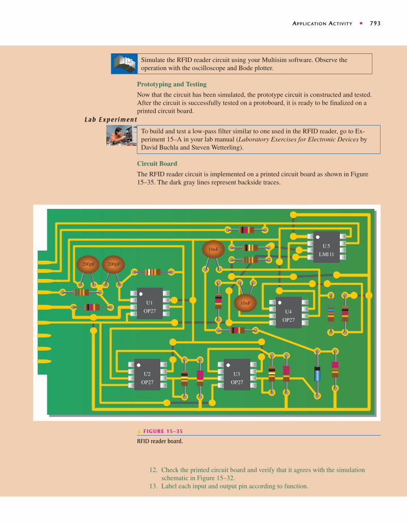
Circuit Board
The RFID reader circuit is implemented on a printed circuit board as shown in Figure15–35. The dark gray lines represent backside traces.
LM111
U5
OP27
U4
OP27
U3
OP27
U2
OP27
U1
200pF 200pF
10nF
10nF
� FIGURE 15–35
RFID reader board.
12. Check the printed circuit board and verify that it agrees with the simulationschematic in Figure 15–32.
13. Label each input and output pin according to function.
Lab Experiment
794 ◆ ACTIVE FILTERS
Programmable Analog Technology
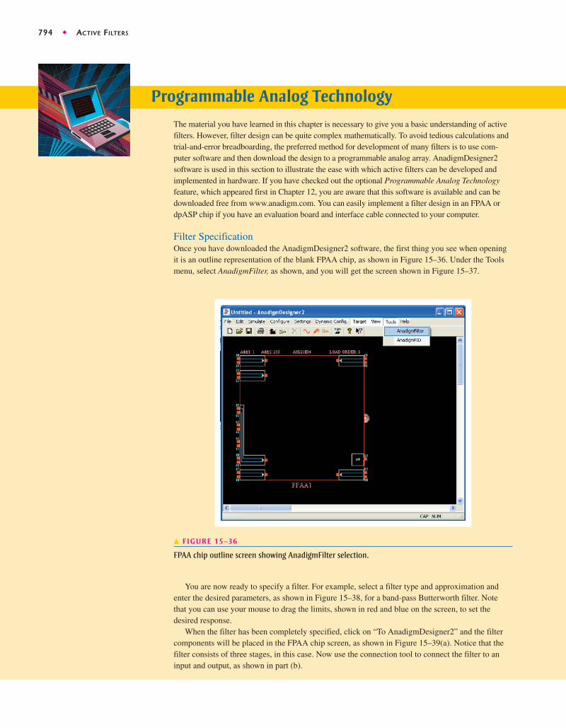
The material you have learned in this chapter is necessary to give you a basic understanding of activefilters. However, filter design can be quite complex mathematically. To avoid tedious calculations andtrial-and-error breadboarding, the preferred method for development of many filters is to use com-puter software and then download the design to a programmable analog array. AnadigmDesigner2software is used in this section to illustrate the ease with which active filters can be developed andimplemented in hardware. If you have checked out the optional Programmable Analog Technologyfeature, which appeared first in Chapter 12, you are aware that this software is available and can bedownloaded free from www.anadigm.com. You can easily implement a filter design in an FPAA ordpASP chip if you have an evaluation board and interface cable connected to your computer.
Filter SpecificationOnce you have downloaded the AnadigmDesigner2 software, the first thing you see when openingit is an outline representation of the blank FPAA chip, as shown in Figure 15–36. Under the Toolsmenu, select AnadigmFilter, as shown, and you will get the screen shown in Figure 15–37.
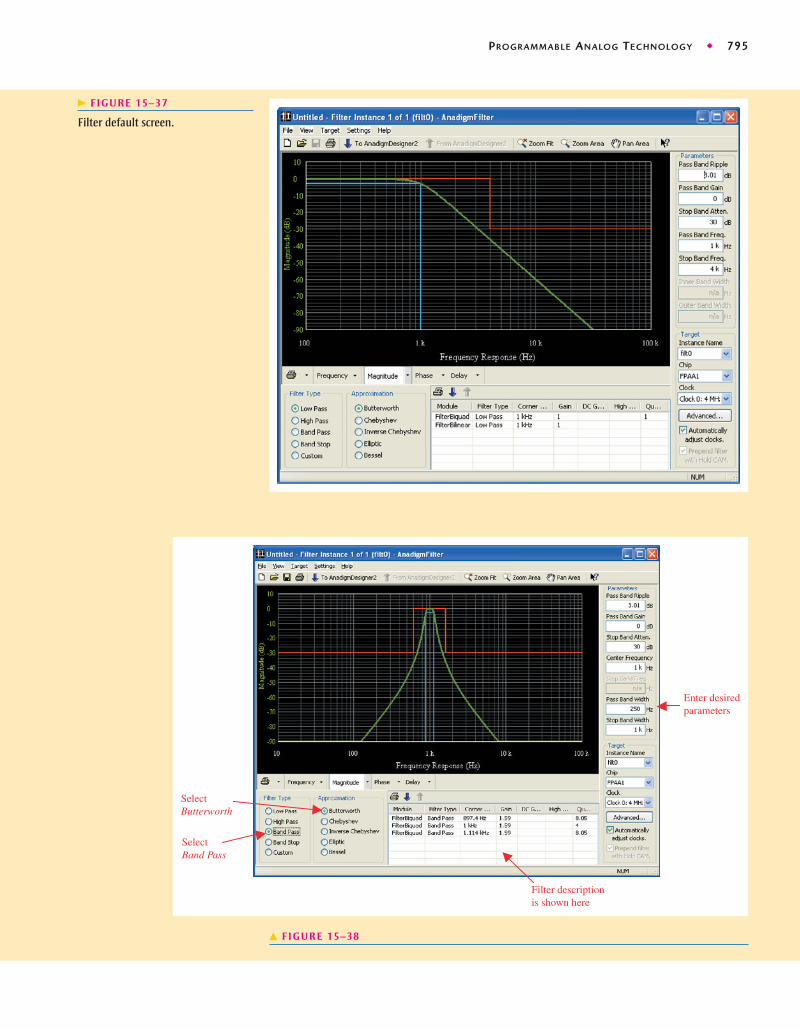
You are now ready to specify a filter. For example, select a filter type and approximation andenter the desired parameters, as shown in Figure 15–38, for a band-pass Butterworth filter. Notethat you can use your mouse to drag the limits, shown in red and blue on the screen, to set thedesired response.
When the filter has been completely specified, click on “To AnadigmDesigner2” and the filtercomponents will be placed in the FPAA chip screen, as shown in Figure 15–39(a). Notice that thefilter consists of three stages, in this case. Now use the connection tool to connect the filter to aninput and output, as shown in part (b).
� FIGURE 15–36
FPAA chip outline screen showing AnadigmFilter selection.
PROGRAMMABLE ANALOG TECHNOLOGY ◆ 795
� FIGURE 15–37
Filter default screen.
Filter descriptionis shown here
SelectBand Pass
SelectButterworth
Enter desiredparameters
� FIGURE 15–38

796 ◆ ACTIVE FILTERS
� FIGURE 15–40
Design screen showing the RFID reader in FPAA1 and an ASK generator representing the RFID tag inFPAA2.
(a) (b)
� FIGURE 15–39
By attaching actual signal generators and oscilloscope probes to the board, you can verify thatthe downloaded circuit is behaving just as the simulator indicated it would. Note that an FPAA ordpASP is reprogrammable so you can make circuit changes, download, and test indefinitely.
Design AssignmentImplement the RFID reader circuit using AnadigmDesigner2 software.Procedure: Figure 15–40 shows a version of the circuit implemented in FPAA1. Because of limi-tations on implementing the ASK input signal, modifications have been made. Since the input cell

SUMMARY ◆ 797
� FIGURE 15–41
Simulation waveforms for the RFID reader.
contains an amplifier with gain, the amplifier in the RFID reader circuit has less gain than if a 1 mVASK signal were available. Also, the rectifier and low-pass filter are combined in one CAM.FPAA2 is used as a signal source to replicate a 125 kHz carrier modulated with a 10 kHz squarewave. This chip is for test purposes only and is not part of the RFID reader.
Analysis: The simulation of the RFID reader is shown in Figure 15–41. The top waveform is theoutput of the 125 kHz band-pass filter CAM and is an ASK input signal representing a digital 1 fol-lowed by a 0. The second waveform is the output of the inverting gain stage CAM with a unitygain. The third waveform is the output of the half-wave rectifier/low-pass filter CAM. The bottomoutput is the digital signal from the comparator.
Programming Exercises1. Why is a software program the best way to specify and implement active filters?2. List the filter types available in the AnadigmFilter software.3. List the filter approximations available in the AnadigmFilter software.
To program, download, and test a circuit using AnadigmDesigner2 software and the programmableanalog module (PAM) board, go to Experiment 15–B in Laboratory Exercises for Electronic Devices by David Buchla and Steven Wetterling.
PAM Experiment
SUMMARY
Section 15–1 ◆ In filter terminology, a single RC circuit is called a pole.
◆ The bandwidth in a low-pass filter equals the critical frequency because the response extendsto 0 Hz.
◆ The passband of a high-pass filter extends above the critical frequency and is limited only by theinherent frequency limitation of the active circuit.

798 ◆ ACTIVE FILTERS
◆ A band-pass filter passes all frequencies within a band between a lower and an upper critical fre-quency and rejects all others outside this band.
◆ The bandwidth of a band-pass filter is the difference between the upper critical frequency andthe lower critical frequency.
◆ The quality factor Q of a band-pass filter determines the filter’s selectivity. The higher the Q, thenarrower the bandwidth and the better the selectivity.
◆ A band-stop filter rejects all frequencies within a specified band and passes all those outside thisband.
Section 15–2 ◆ Filters with the Butterworth response characteristic have a very flat response in the passband,exhibit a roll-off of and are used when all the frequencies in the passbandmust have the same gain.
◆ Filters with the Chebyshev characteristic have ripples or overshoot in the passband and exhibit afaster roll-off per pole than filters with the Butterworth characteristic.
◆ Filters with the Bessel characteristic are used for filtering pulse waveforms. Their linear phasecharacteristic results in minimal waveshape distortion. The roll-off rate per pole is slower thanfor the Butterworth.
◆ Each pole in a Butterworth filter causes the output to roll off at a rate of
◆ The damping factor determines the filter response characteristic (Butterworth, Chebyshev, orBessel).
Section 15–3 ◆ Single-pole low-pass filters have a roll-off.
◆ The Sallen-Key low-pass filter has two poles (second order) and has a roll-off.
◆ Each additional filter in a cascaded arrangement adds to the roll-off rate.
Section 15–4 ◆ Single-pole high-pass filters have a roll-off.
◆ The Sallen-Key high-pass filter has two poles (second order) and has a roll-off.
◆ Each additional filter in a cascaded arrangement adds to the roll-off rate.
◆ The response of an active high-pass filter is limited by the internal op-amp roll-off.
Section 15–5 ◆ Band-pass filters pass a specified band of frequencies.
◆ A band-pass filter can be achieved by cascading a low-pass and a high-pass filter.
◆ The multiple-feedback band-pass filter uses two feedback paths to achieve its responsecharacteristic.
◆ The state-variable band-pass filter uses a summing amplifier and two integrators.
◆ The biquad filter consists of an integrator followed by an inverting amplifier and a secondintegrator.
Section 15–6 ◆ Band-stop filters reject a specified band of frequencies.
◆ Multiple-feedback and state-variable are common types of band-stop filters.
Section 15–7 ◆ Filter response can be measured using discrete point measurement or swept frequency measurement.
KEY TERMS Key terms and other bold terms in the chapter are defined in the end-of-book glossary.
Band-pass filter A type of filter that passes a range of frequencies lying between a certain lowerfrequency and a certain higher frequency.
Band-stop filter A type of filter that blocks or rejects a range of frequencies lying between a cer-tain lower frequency and a certain higher frequency.
Damping factor A filter characteristic that determines the type of response.
Filter A circuit that passes certain frequencies and attenuates or rejects all other frequencies.
High-pass filter A type of filter that passes frequencies above a certain frequency while rejectinglower frequencies.
Low-pass filter A type of filter that passes frequencies below a certain frequency while rejectinghigher frequencies.
-20 dB
-40 dB/deacde
-20 dB/decade
-20 dB
-40 dB/decade
-20 dB/decade
-20 dB/decade.
-20 dB/decade /pole,

TRUE/FALSE QUIZ ◆ 799
Pole A circuit containing one resistor and one capacitor that contributes to a filter’sroll-off rate.
Roll-off The rate of decrease in gain, below or above the critical frequencies of a filter.
KEY FORMULAS15–1 Low-pass bandwidth
15–2 Filter bandwidth of a band-pass filter
15–3 Center frequency of a band-pass filter
15–4 Quality factor of a band-pass filter
15–5 Damping factor
15–6 Closed-loop voltage gain
15–7 Critical frequency for a second-order Sallen-Key filter
15–8 Center frequency of a multiple-feedback filter
15–9 Gain of a multiple-feedback filter
TRUE/FALSE QUIZ Answers can be found at www.pearsonhighered.com/floyd.
1. The response of a filter can be identified by its passband.
2. A filter pole is the cutoff frequency of a filter.
3. A single-pole filter has one RC circuit.
4. A single-pole filter produces a roll-off of -25 dB/decade.
5. A low-pass filter can pass a dc voltage.
6. A high-pass filter passes any frequency above dc.
7. The critical frequency of a filter depends only on R and C values.
8. The band-pass filter has two critical frequencies.
9. The quality factor of a band-pass filter is the ratio of bandwidth to the center frequency.
10. The higher the Q, the narrower the bandwidth of a band-pass filter.
11. The Butterworth characteristic provides a flat response in the passband.
12. Filters with a Chebyshev response have a slow roll-off.
13. A Chebyshev response has ripples in the passband.
14. Bessel filters are useful in filtering pulse waveforms.
15. The order of a filter is the number of poles it contains.
16. A Sallen-Key filter is also known as a VCVS filter.
17. Multiple feedback is used in low-pass filters.
18. A state-variable filter uses differentiators.
19. A band-stop filter rejects certain frequencies.
20. Filter response can be measured using a sweep generator.
A0 �R2
2R1
f0 �1
2PC A
R1 � R3
R1R2R3
fc �1
2P1RARBCACB
Acl(NI) �R1
R2� 1
DF � 2 �R1
R2
Q �f0
BW
f0 � 1fc1 fc2
BW � fc2 � fc1
BW � fc
-20 dB/decade

800 ◆ ACTIVE FILTERS
CIRCUIT-ACTION QUIZ Answers can be found at www.pearsonhighered.com/floyd.
1. If the critical frequency of a low-pass filter is increased, the bandwidth will
(a) increase (b) decrease (c) not change
2. If the critical frequency of a high-pass filter is increased, the bandwidth will
(a) increase (b) decrease (c) not change
3. If the Q of a band-pass filter is increased, the bandwidth will
(a) increase (b) decrease (c) not change
4. If the value of CA and CB in Figure 15–11 are increased by the same amount, the criticalfrequency will
(a) increase (b) decrease (c) not change
5. If the the value of R2 in Figure 15–11 is increased, the bandwidth will
(a) increase (b) decrease (c) not change
6. If two filters like the one in Figure 15–15 are cascaded, the roll-off rate of the frequencyresponse will
(a) increase (b) decrease (c) not change
7. If the value of R2 in Figure 15–19 is decreased, the Q will
(a) increase (b) decrease (c) not change
8. If the capacitors in Figure 15–19 are changed to the center frequency will
(a) increase (b) decrease (c) not change
SELF-TEST Answers can be found at www.pearsonhighered.com/floyd.
Section 15–1 1. The term pole in filter terminology refers to
(a) a high-gain op-amp (b) one complete active filter
(c) a single RC circuit (d) the feedback circuit
2. A single resistor and a single capacitor can be connected to form a filter with a roll-off rate of
(a) (b)
(c) (d) answers (a) and (c)
3. A band-pass response has
(a) two critical frequencies (b) one critical frequency
(c) a flat curve in the passband (d) a wide bandwidth
4. The lowest frequency passed by a low-pass filter is
(a) 1 Hz (b) 0 Hz (c) 10 Hz (d) dependent on the critical frequency
5. The quality factor (Q) of a band-pass filter depends on
(a) the critical frequencies (b) only the bandwidth
(c) the center frequency and the bandwidth (d) only the center frequency
Section 15–2 6. The damping factor of an active filter determines
(a) the voltage gain (b) the critical frequency
(c) the response characteristic (d) the roll-off rate
7. A maximally flat frequency response is known as
(a) Chebyshev (b) Butterworth (c) Bessel (d) Colpitts
8. The damping factor of a filter is set by
(a) the negative feedback circuit (b) the positive feedback circuit
(c) the frequency-selective circuit (d) the gain of the op-amp
9. The number of poles in a filter affect the
(a) voltage gain (b) bandwidth
(c) center frequency (d) roll-off rate
-6 dB/octave
-40 dB/decade-20 dB/decade
0.022 mF,

PROBLEMS ◆ 801
Section 15–3 10. Sallen-Key low-pass filters are
(a) single-pole filters (b) second-order filters
(c) Butterworth filters (d) band-pass filters
11. When low-pass filters are cascaded, the roll-off rate
(a) increases (b) decreases (c) does not change
Section 15–4 12. In a high-pass filter, the roll-off occurs
(a) above the critical frequency (b) below the critical frequency
(c) during the mid range (d) at the center frequency
13. A two-pole Sallen-Key high-pass filter contains
(a) one capacitor and two resistors (b) two capacitors and two resistors
(c) a feedback circuit (d) answers (b) and (c)
Section 15–5 14. When a low-pass and a high-pass filter are cascaded to get a band-pass filter, the criticalfrequency of the low-pass filter must be
(a) equal to the critical frequency of the high-pass filter
(b) less than the critical frequency of the high-pass filter
(c) greater than the critical frequency of the high-pass filter
15. A state-variable filter consists of
(a) one op-amp with multiple-feedback paths
(b) a summing amplifier and two integrators
(c) a summing amplifier and two differentiators
(d) three Butterworth stages
Section 15–6 16. When the gain of a filter is minimum at its center frequency, it is
(a) a band-pass filter (b) a band-stop filter
(c) a notch filter (d) answers (b) and (c)
PROBLEMS Answers to all odd-numbered problems are at the end of the book.
BASIC PROBLEMS
Section 15–1 Basic Filter Responses
1. Identify each type of filter response (low-pass, high-pass, band-pass, or band-stop) inFigure 15–42.
(a)
f
Gain
(d)
f
Gain
(b)
f
Gain
(c)
f
Gain
� FIGURE 15–42
2. A certain low-pass filter has a critical frequency of 800 Hz. What is its bandwidth?
3. A single-pole high-pass filter has a frequency-selective circuit with What is the critical frequency? Can you determine the bandwidth from the
available information?
4. What is the roll-off rate of the filter described in Problem 3?
5. What is the bandwidth of a band-pass filter whose critical frequencies are 3.2 kHz and 3.9 kHz?What is the Q of this filter?
6. What is the center frequency of a filter with a Q of 15 and a bandwidth of 1 kHz?
C = 0.0015 mF.R = 2.2 kÆ and

802 ◆ ACTIVE FILTERS
Section 15–2 Filter Response Characteristics
7. What is the damping factor in each active filter shown in Figure 15–43? Which filters are ap-proximately optimized for a Butterworth response characteristic?
(a)
f
Vout
(c)
f
Vout
(d)
f
Vout
(b)
f
Vout
� FIGURE 15–44
0.0022 Fμ
0.0022 Fμ
0.001 Fμ0.001 Fμ0.015 Fμ
+
– R6330 �
R5
C3
+
– R3330 �
(c)
Vout
R71.0 k�
1.0 k�
R2
C21.0 k�
R1
1.0 k�Vin
R41.0 k�
+
– R31.2 k�
(a)
R2
C2
1.2 k�
R1
1.2 k�Vin
0.015 F
R41.2 k�
+
– R3560 �
Vout
R41.0 k�
(b)
Vout
Vin
R21.0 k�
R1
1.0 k�
C1
C1
C2C1μ
0.0022 Fμ
� FIGURE 15–43
Multisim file circuits are identified with a logo and are in the Problems folder on the companionwebsite. Filenames correspond to figure numbers (e.g., F15-43).
8. For the filters in Figure 15–43 that do not have a Butterworth response, specify the changesnecessary to convert them to Butterworth responses. (Use nearest standard values.)
9. Response curves for second-order filters are shown in Figure 15–44. Identify each asButterworth. Chebyshev, or Bessel.

PROBLEMS ◆ 803
Section 15–3 Active Low-Pass Filters
10. Is the four-pole filter in Figure 15–45 approximately optimized for a Butterworth response?What is the roll-off rate?
11. Determine the critical frequency in Figure 15–45.
12. Without changing the response curve, adjust the component values in the filter of Figure 15–45to make it an equal-value filter. Select for both stages.
13. Modify the filter in Figure 15–45 to increase the roll-off rate to while main-taining an approximate Butterworth response.
14. Using a block diagram format, show how to implement the following roll-off rates usingsingle-pole and two-pole low-pass filters with Butterworth responses.
(a) (b)
(c) (d)
(e) -120 dB/decade
-100 dB/decade-60 dB/decade
-20 dB/decade-40 dB/decade
-120 dB/decade
C = 0.22 mF
0.047 Fμ
+
– R31.5 k�
R1
2.7 k�
Vin
R42.7 k�
Vout
C1
R22.7 k�
0.047 F
C2
μ
� FIGURE 15–46
0.22 Fμ
+
– R76.8 k�
+
– R31.0 k�
Vout
R85.6 k�
Vin
R46.8 k�
R5
4.7 k�
R1
4.7 k�
0.22 F
C3
C20.1 F
C1
R2
6.8 k�R6
6.8 k�
C40.1 F
μ
μ
μ
� FIGURE 15–45
Section 15–4 Active High-Pass Filters
15. Convert the filter in Problem 12 to a high-pass with the same critical frequency and responsecharacteristic.
16. Make the necessary circuit modification to reduce by half the critical frequency in Problem 15.
17. For the filter in Figure 15–46, (a) how would you increase the critical frequency? (b) Howwould you increase the gain?

804 ◆ ACTIVE FILTERS
Section 15–5 Active Band-Pass Filters
18. Identify each band-pass filter configuration in Figure 15–47.
19. Determine the center frequency and bandwidth for each filter in Figure 15–47.
0.001 Fμ
0.022 Fμ
0.022 Fμ
0.047 Fμ
–
+
C2
R7–
+
C1
R4–
+
Vin
R2
R3
10 k�
10 k�
10 k�
Vout
10 k�
(c)
–
+
Vin
Vout
R2
R31.8 k�
C2
C1
R1
(b)
150 k�
47 k�
+
– R7560 �
R6+
– R3560 �
(a)
Vout
R81.0 k�
1.0 k�R21.0 k�
R1
1.0 k�
Vin
R51.0 k�
R4
1.0 k�
0.047 F
C1 C2
C40.022 F
0.022 F
C3
0.001 F
R110 k�
R5560 k�
R610 k�
μ
μ
μ
μ
� FIGURE 15–47
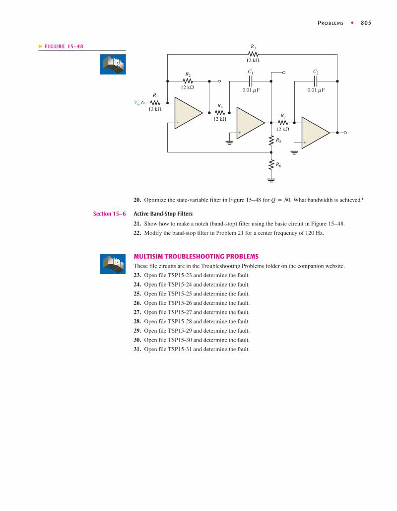
PROBLEMS ◆ 805
20. Optimize the state-variable filter in Figure 15–48 for What bandwidth is achieved?
Section 15–6 Active Band-Stop Filters
21. Show how to make a notch (band-stop) filter using the basic circuit in Figure 15–48.
22. Modify the band-stop filter in Problem 21 for a center frequency of 120 Hz.
MULTISIM TROUBLESHOOTING PROBLEMSThese file circuits are in the Troubleshooting Problems folder on the companion website.
23. Open file TSP15-23 and determine the fault.
24. Open file TSP15-24 and determine the fault.
25. Open file TSP15-25 and determine the fault.
26. Open file TSP15-26 and determine the fault.
27. Open file TSP15-27 and determine the fault.
28. Open file TSP15-28 and determine the fault.
29. Open file TSP15-29 and determine the fault.
30. Open file TSP15-30 and determine the fault.
31. Open file TSP15-31 and determine the fault.
Q = 50.
0.01 Fμ
–
+R5
R7–
+
R4–
+
Vin
R1
R2
12 k�
12 k�
12 k�
12 k�
R6
R3
12 k�
C2
0.01 F
C1
μ
� FIGURE 15–48
Related Documents