Dissertation submitted to the Faculty of the Virginia Polytechnic Institute & State University in partial fulfillment of the requirements for the degree of Doctor of Philosophy in Electrical Engineering Active Antenna Bandwidth Control Using Reconfigurable Antenna Elements Nathan P. Cummings Virginia Tech Antenna Group Bradley Department of Electrical & Computer Engineering Blacksburg, Virginia 24061-0111 Committee Members: Warren L. Stutzman, Chair Christopher A. Beattie Gary S. Brown William A. Davis Timothy Pratt December 8, 2003 Blacksburg, Virginia Keywords: Reconfigurable Antennas, Bandwidth Control Copyright 2003, Nathan P. Cummings

Welcome message from author
This document is posted to help you gain knowledge. Please leave a comment to let me know what you think about it! Share it to your friends and learn new things together.
Transcript

Dissertation submitted to the Faculty of theVirginia Polytechnic Institute & State University
in partial fulfillment of the requirements for the degree of
Doctor of Philosophyin
Electrical Engineering
Active Antenna Bandwidth Control UsingReconfigurable Antenna Elements
Nathan P. Cummings
Virginia Tech Antenna GroupBradley Department of Electrical & Computer Engineering
Blacksburg, Virginia 24061-0111
Committee Members:
Warren L. Stutzman, ChairChristopher A. Beattie
Gary S. BrownWilliam A. DavisTimothy Pratt
December 8, 2003Blacksburg, Virginia
Keywords: Reconfigurable Antennas, Bandwidth Control
Copyright 2003, Nathan P. Cummings

Active Antenna Bandwidth Control Using
Reconfigurable Antenna Elements
Nathan P. Cummings
(ABSTRACT)
Reconfigurable antennas represent a recent innovation in antenna design that
changes from classical fixed-form, fixed-function antennas to modifiable structures
that can be adapted to fit the requirements of a time varying system. Advances in
microwave semiconductor processing technologies have enabled the use of compact,
ultra-high quality RF and microwave switches in novel aspects of antenna design. This
dissertation introduces the concept of reconfigurable antenna bandwidth control and
how advances in switch technology have made these designs realizable. Specifically,
it details the development of three new antennas capable of reconfigurable bandwidth
control. The newly developed antennas include the reconfigurable ring patch, the
reconfigurable planar inverted-F and the reconfigurable parasitic folded dipole. The
relevant background work to these designs is described and then design details along
with computer simulations and measured experimental results are given.

Acknowledgments
I would first like to thank Dr. Warren L. Stutzman for serving as my committeechairman and as my advisor during both my M.S. and Ph.D. degrees. His generousdirection, encouragement, advice and support have been invaluable throughout mygraduate education. I would like to thank Dr. William A. Davis, Dr. Gary S. Brown,Dr. Tim Pratt and Dr. Christopher A. Beattie for serving on my committee. I wantto give special thanks to Dr. Davis the time and advice he has graciously given to mewhile working with the Virginia Tech Antenna Group.
I would like to thank all the members of VTAG that I have worked with duringmy time spent with the group. The opportunity to interact, both in and out of the lab,with such a talented and diverse group of individuals has been extremely enlightening.Additionally, I am indebted to Randall Nealy for the assistance he has given me inantenna construction and measurement.
Finally, and most importantly, I would like to thank my parents–Patrick andSusan Cummings–along with the rest of my family. The limitless patience and supportthey have given me during my pursuit of this degree is infinitely appreciated.
iii

Contents
1 Introduction 11.1 Motivation . . . . . . . . . . . . . . . . . . . . . . . . . . . . . . . . . . 11.2 Executive Summary . . . . . . . . . . . . . . . . . . . . . . . . . . . . . 21.3 Dissertation Overview . . . . . . . . . . . . . . . . . . . . . . . . . . . 5
2 Previous Work 72.1 Ring Patch Antenna . . . . . . . . . . . . . . . . . . . . . . . . . . . . 72.2 Planar Inverted-F Antenna (PIFA) . . . . . . . . . . . . . . . . . . . . 92.3 Folded Dipole Antenna . . . . . . . . . . . . . . . . . . . . . . . . . . . 142.4 Reconfigurable Antennas . . . . . . . . . . . . . . . . . . . . . . . . . . 16
2.4.1 Reconfigurable Elements . . . . . . . . . . . . . . . . . . . . . . 172.4.2 Distributed Radiators . . . . . . . . . . . . . . . . . . . . . . . 222.4.3 Reconfigurable Arrays . . . . . . . . . . . . . . . . . . . . . . . 24
3 Reconfigurable Antennas and Technology 273.1 Reconfigurable Antenna Methodologies . . . . . . . . . . . . . . . . . . 28
3.1.1 Total Geometry Morphing Method . . . . . . . . . . . . . . . . 293.1.2 Matching Network Morphing Method . . . . . . . . . . . . . . . 313.1.3 Smart Geometry Reconfiguration . . . . . . . . . . . . . . . . . 32
3.2 Antenna Switch Technologies . . . . . . . . . . . . . . . . . . . . . . . 333.2.1 Mechanical Switches . . . . . . . . . . . . . . . . . . . . . . . . 353.2.2 PIN Diode Switches . . . . . . . . . . . . . . . . . . . . . . . . 363.2.3 Field Effect Transistor Switches . . . . . . . . . . . . . . . . . . 373.2.4 MEMS Switches . . . . . . . . . . . . . . . . . . . . . . . . . . . 40
3.3 Switch Modeling for Reconfigurable Antenna Applications . . . . . . . 463.3.1 Antenna Field Simulators . . . . . . . . . . . . . . . . . . . . . 463.3.2 Modeling Methods . . . . . . . . . . . . . . . . . . . . . . . . . 503.3.3 Switch Simulation Method Comparison . . . . . . . . . . . . . . 51
4 Reconfigurable Ring Patch 574.1 Introduction . . . . . . . . . . . . . . . . . . . . . . . . . . . . . . . . . 574.2 Antenna Structure . . . . . . . . . . . . . . . . . . . . . . . . . . . . . 58
4.2.1 The Reconfigurable Ring Patch Antenna . . . . . . . . . . . . . 644.3 Simulation of Reconfigurable Ring Patch . . . . . . . . . . . . . . . . . 674.4 Experimental Results for RRPA . . . . . . . . . . . . . . . . . . . . . . 70
4.4.1 Impedance Measurements . . . . . . . . . . . . . . . . . . . . . 70
iv

4.4.2 Pattern Measurements . . . . . . . . . . . . . . . . . . . . . . . 814.5 Summary . . . . . . . . . . . . . . . . . . . . . . . . . . . . . . . . . . 95
5 Reconfigurable Planar Inverted-F 965.1 Introduction . . . . . . . . . . . . . . . . . . . . . . . . . . . . . . . . . 965.2 Antenna Structure . . . . . . . . . . . . . . . . . . . . . . . . . . . . . 97
5.2.1 Ground Plane Influence On Bandwidth . . . . . . . . . . . . . . 995.2.2 The Reconfigurable Planar Inverted-F Antenna . . . . . . . . . 103
5.3 Simulation of RPIFA . . . . . . . . . . . . . . . . . . . . . . . . . . . . 1075.4 Experimental Results for RPIFA . . . . . . . . . . . . . . . . . . . . . . 109
5.4.1 Impedance Measurements . . . . . . . . . . . . . . . . . . . . . 1125.4.2 Pattern Measurements . . . . . . . . . . . . . . . . . . . . . . . 121
5.5 Summary . . . . . . . . . . . . . . . . . . . . . . . . . . . . . . . . . . 134
6 Reconfigurable Folded Dipole 1356.1 Introduction . . . . . . . . . . . . . . . . . . . . . . . . . . . . . . . . . 1356.2 Antenna Structure . . . . . . . . . . . . . . . . . . . . . . . . . . . . . 137
6.2.1 Parasitic Element Length Influence On Bandwidth . . . . . . . 1386.2.2 The Reconfigurable Parasitic Folded Dipole Antenna . . . . . . 142
6.3 Simulation of RPFDA . . . . . . . . . . . . . . . . . . . . . . . . . . . 1456.4 Experimental Results for RPFDA . . . . . . . . . . . . . . . . . . . . . 148
6.4.1 Impedance Measurements . . . . . . . . . . . . . . . . . . . . . 1486.4.2 Pattern Measurements . . . . . . . . . . . . . . . . . . . . . . . 160
6.5 Summary . . . . . . . . . . . . . . . . . . . . . . . . . . . . . . . . . . 177
7 Conclusions 1787.1 Summary . . . . . . . . . . . . . . . . . . . . . . . . . . . . . . . . . . 1787.2 Contributions . . . . . . . . . . . . . . . . . . . . . . . . . . . . . . . . 1807.3 Future Work . . . . . . . . . . . . . . . . . . . . . . . . . . . . . . . . . 181
v

List of Figures
2.1 Ring microstrip patch antenna . . . . . . . . . . . . . . . . . . . . . . . 82.2 Basic geometry of the planar inverted-F antenna. . . . . . . . . . . . . 102.3 Surface current on PIFA top plate for various aspect ratios, L/W , and
grounding strap widths, S. . . . . . . . . . . . . . . . . . . . . . . . . . 112.4 Typical PIFA designed for operation near cellular band. . . . . . . . . . 122.5 VSWR versus frequency for the PIFA of Figure 2.4 calculated using the
moment method code IE3D. . . . . . . . . . . . . . . . . . . . . . . . . 132.6 Input reflection coefficient for the PIFA of Figure 2.4 calculated using
the moment method code IE3D. . . . . . . . . . . . . . . . . . . . . . . 132.7 The geometry of the wire-form folded dipole antenna. . . . . . . . . . . 142.8 Network representation of the decomposition of the folded dipole. . . . 152.9 The printed folded-slot dipole antenna. . . . . . . . . . . . . . . . . . . 162.10 The reconfigurable Vee-dipole antenna. . . . . . . . . . . . . . . . . . . 182.11 Geometry of the proximity coupled reconfigurable dime antenna com-
posed of four quarter-dime stacked patch antennas. . . . . . . . . . . . 192.12 The reconfigurable leaky mode patch antenna. . . . . . . . . . . . . . . 202.13 The reconfigurable stacked bowtie antenna. . . . . . . . . . . . . . . . . 212.14 The reconfigurable microstrip patch antenna. . . . . . . . . . . . . . . . 222.15 The MEMS cantilever RF switch used in the microswitch array. . . . . 242.16 The reconfigurable flared notch array element with time-delay beam
steering. . . . . . . . . . . . . . . . . . . . . . . . . . . . . . . . . . . . 25
3.1 The total geometry morphing method of reconfigurable antenna design. 293.2 Microstrip feed configurations for impedance matching of reconfigurable
antenna design. . . . . . . . . . . . . . . . . . . . . . . . . . . . . . . . 313.3 Series PIN diode RF switch model. . . . . . . . . . . . . . . . . . . . . 373.4 Shunt PIN diode RF switch model. . . . . . . . . . . . . . . . . . . . . 383.5 Series field effect transistor RF switch model. . . . . . . . . . . . . . . 393.6 Shunt field effect transistor RF switch model. . . . . . . . . . . . . . . 393.7 Cantilever style RF MEMS series switch layout in both on and off states. 413.8 Isolation versus on state capacitance for a typical dc-contact MEMS
series switch given from (3.6) calculated using MATLAB. . . . . . . . . 423.9 Comparison of transmission line circuit model switches. . . . . . . . . . 503.10 Multi-band dipole antenna with three resonant lengths: L0, L1 and L2. 51
vi

3.11 Return loss as a function of frequency for dipole antennas of Figure 3.10with arm lengths of 80.0 mm, 68.4 mm and 41.4 mm simulated usingIE3D. . . . . . . . . . . . . . . . . . . . . . . . . . . . . . . . . . . . . 52
3.12 IE3D models for the reconfigurable dipole including RF switches. . . . 543.13 Computed return loss as a function of frequency for the frequency agile
dipole antenna of Figure 3.12 simulated using IE3D. . . . . . . . . . . . 553.14 Reconfigurable antenna modeling comparison. . . . . . . . . . . . . . . 56
4.1 Geometry of the reconfigurable ring patch antenna that operates at2.5 GHz, units are in mm. . . . . . . . . . . . . . . . . . . . . . . . . . 59
4.2 Difference in current path length for rectangular patch and square ringpatch. . . . . . . . . . . . . . . . . . . . . . . . . . . . . . . . . . . . . 60
4.3 Equivalent magnetic currents for TM11 and TM12 modes on the squarering patch. . . . . . . . . . . . . . . . . . . . . . . . . . . . . . . . . . . 61
4.4 VSWR versus frequency of the ring patch antenna of Figure 4.1 forvarious ring widths, Rw, computed using IE3D. . . . . . . . . . . . . . 63
4.5 Bandwidth versus ring width aspect ratio, Ri/Ro, of the ring patchantenna of Figure 4.1 computed using IE3D. . . . . . . . . . . . . . . . 63
4.6 Reconfigurable ring patch active layer switch configuration states. . . . 664.7 Input impedance versus frequency of the reconfigurable ring patch an-
tenna for switch states of Figure 4.6 simulated using IE3D. . . . . . . . 694.8 VSWR versus frequency of the reconfigurable ring patch antenna for
switch states of Figure 4.6 simulated using IE3D. . . . . . . . . . . . . 694.9 Hardware test model of the reconfigurable ring patch antenna with ring
layer geometries specified in Table 4.2. . . . . . . . . . . . . . . . . . . 714.10 Hardware models for each of the switch states of Figure 4.6. . . . . . . 724.11 Measured and simulated input impedance for the ring patch. . . . . . . 744.12 Measured and simulated VSWR for the ring patch. . . . . . . . . . . . 774.13 Measured VSWR for the ring patch in all states. . . . . . . . . . . . . . 804.14 Measured return loss for the ring patch in all states. . . . . . . . . . . . 804.15 Measured and simulated elevation radiation patterns in the principal
planes for the RRPA. . . . . . . . . . . . . . . . . . . . . . . . . . . . . 834.16 Measured and simulated conical Etotal radiation patterns for the RRPA. 864.17 Measured and simulated conical Eθ & Eφ radiation patterns for the RRPA. 894.18 Comparison of measured elevation radiation patterns in the principal
planes for all switch states of the RRPA. . . . . . . . . . . . . . . . . . 924.19 Comparison of measured conical radiation patterns for all switch states
of the RRPA. . . . . . . . . . . . . . . . . . . . . . . . . . . . . . . . . 934.20 Comparison of measured conical radiation patterns for all switch states
of the RRPA. . . . . . . . . . . . . . . . . . . . . . . . . . . . . . . . . 94
5.1 Geometry of the reconfigurable planar inverted-F antenna. . . . . . . . 985.2 VSWR versus frequency of the planar inverted-F antenna of Figure 5.1
for various ground plane lengths, L, computed using IE3D. . . . . . . . 101
vii

5.3 Bandwidth versus ground plane length for the geometry in Figure 5.1computed using IE3D. . . . . . . . . . . . . . . . . . . . . . . . . . . . 101
5.4 Average current distribution on RPIFA ground plane computed usingIE3D. . . . . . . . . . . . . . . . . . . . . . . . . . . . . . . . . . . . . 104
5.5 Reconfigurable PIFA with active ground plate. . . . . . . . . . . . . . . 1055.6 Reconfigurable PIFA active layer switch configuration states. . . . . . . 1065.7 Input impedance versus frequency of RPIFA simulated using IE3D. . . 1085.8 VSWR versus frequency of the RPIFA simulated using IE3D. . . . . . . 1085.9 Hardware test model of RPIFA. . . . . . . . . . . . . . . . . . . . . . . 1105.10 Feed end of RPIFA hardware test model showing dielectric sleeve and
shorting post. . . . . . . . . . . . . . . . . . . . . . . . . . . . . . . . . 1115.11 Close-up of copper tape RF switch for RPIFA hardware test model. . . 1115.12 Measured and simulated input impedance for the reconfigurable PIFA. 1145.13 Measured and simulated VSWR for the reconfigurable PIFA. . . . . . . 1175.14 Measured VSWR for the reconfigurable PIFA in all states. . . . . . . . 1205.15 Measured return loss for the reconfigurable PIFA in all states. . . . . . 1205.16 Measured and simulated conical radiation patterns for the RPIFA. . . . 1235.17 Measured and simulated conical radiation patterns for the RPIFA. . . . 1265.18 Measured and simulated elevation radiation patterns in the x-z plane
for the RPIFA. . . . . . . . . . . . . . . . . . . . . . . . . . . . . . . . 1295.19 Comparison of measured azimuth directivity patterns for all switch states
of the reconfigurable PIFA, Eφ (θ = 10). . . . . . . . . . . . . . . . . . 1325.20 Comparison of measured azimuth directivity patterns for all switch states
of the reconfigurable PIFA, Eθ (θ = 10). . . . . . . . . . . . . . . . . . 1325.21 Comparison of measured azimuth directivity patterns for all switch states
of the reconfigurable PIFA, Eφ (θ = 90). . . . . . . . . . . . . . . . . . 1335.22 Comparison of measured elevation directivity patterns for all switch
states of the reconfigurable PIFA, Eθ (φ = 0). . . . . . . . . . . . . . . 133
6.1 Geometry of the reconfigurable parasitic folded dipole antenna. . . . . . 1376.2 Geometry of the N-element folded dipole antenna. . . . . . . . . . . . . 1386.3 Input impedance versus parasitic element length for the geometry in
Figure 6.1 at 1.05 GHz computed using IE3D. . . . . . . . . . . . . . . 1406.4 Bandwidth versus parasitic element length for the geometry in Figure 6.1
computed using IE3D. . . . . . . . . . . . . . . . . . . . . . . . . . . . 1406.5 VSWR versus frequency of the parasitic loaded folded dipole antenna
of Figure 6.1 for various parasitic element lengths, Lp, computed usingIE3D. . . . . . . . . . . . . . . . . . . . . . . . . . . . . . . . . . . . . 141
6.6 Geometry of the reconfigurable parasitic folded dipole antenna. . . . . . 1436.7 Reconfigurable PFDA active parasitic element switch configuration states.1446.8 Input impedance versus frequency of RPFDA simulated using IE3D. . . 1466.9 VSWR versus frequency of the RPFDA simulated using IE3D. . . . . . 1476.10 Hardware test model of RPFDA and coax feed network. . . . . . . . . 1496.11 Hardware test model for each of the switch states of Figure 6.7. . . . . 150
viii

6.12 Measured and simulated input impedance for the reconfigurable foldeddipole. . . . . . . . . . . . . . . . . . . . . . . . . . . . . . . . . . . . . 153
6.13 Measured and simulated VSWR for the reconfigurable folded dipole. . . 1566.14 Measured VSWR for the reconfigurable folded dipole in all states. . . . 1596.15 Measured return loss for the reconfigurable folded dipole in all states. . 1596.16 Measured and simulated elevation radiation patterns in the principal
planes for the RPFDA. . . . . . . . . . . . . . . . . . . . . . . . . . . . 1626.17 Measured and simulated conical radiation patterns (θ = 10) for the
RPFDA. . . . . . . . . . . . . . . . . . . . . . . . . . . . . . . . . . . . 1656.18 Measured and simulated conical radiation patterns (θ = 45) for the
RPFDA. . . . . . . . . . . . . . . . . . . . . . . . . . . . . . . . . . . . 1686.19 Measured and simulated conical Etotal radiation patterns for the RPFDA.1716.20 Comparison of measured elevation radiation patterns for all switch states
of the RPFDA, Eθ (φ = 0). . . . . . . . . . . . . . . . . . . . . . . . . 1746.21 Comparison of measured elevation radiation patterns for all switch states
of the RPFDA, Eφ (φ = 90). . . . . . . . . . . . . . . . . . . . . . . . 1746.22 Comparison of measured conical radiation patterns for all switch states
of the RPFDA, Eθ (θ = 10). . . . . . . . . . . . . . . . . . . . . . . . 1756.23 Comparison of measured conical radiation patterns for all switch states
of the RPFDA, Eφ (θ = 10). . . . . . . . . . . . . . . . . . . . . . . . 1756.24 Comparison of measured conical radiation patterns for all switch states
of the RPFDA, Eθ (θ = 45). . . . . . . . . . . . . . . . . . . . . . . . 1766.25 Comparison of measured conical radiation patterns for all switch states
of the RPFDA, Eφ (θ = 45). . . . . . . . . . . . . . . . . . . . . . . . 176
ix

List of Tables
3.1 RF switch comparison summary . . . . . . . . . . . . . . . . . . . . . . 45
4.1 Electrical performance based on ring width of the ring patch antennasimulated using IE3D. . . . . . . . . . . . . . . . . . . . . . . . . . . . 62
4.2 Discrete ring widths for selected antenna bandwidth states based onsimulations from Section 4.2. . . . . . . . . . . . . . . . . . . . . . . . . 64
4.3 Impedance bandwidth performance and reconfigurable ring geometry forthe RRPA with switch states of Figure 4.6 computed using IE3D . . . . 68
4.4 Summary of the measured and simulated 2:1 VSWR impedance band-width performance for the RRPA. . . . . . . . . . . . . . . . . . . . . . 73
4.5 Selectable bandwidth performance for the reconfigurable ring patch an-tenna with switch states of Figure 4.6. . . . . . . . . . . . . . . . . . . 95
5.1 Electrical performance of PIFA based on ground plane length. . . . . . 1025.2 Discrete ground plane lengths for selected antenna bandwidth states
based on simulations from Section 5.2.1. . . . . . . . . . . . . . . . . . 1035.3 Impedance bandwidth performance of the RPIFA computed using IE3D. 1075.4 Summary of the measured and simulated 2:1 VSWR impedance band-
width performance for the RPIFA. . . . . . . . . . . . . . . . . . . . . 1135.5 Selectable bandwidth performance for the reconfigurable planar inverted-
F antenna with switch states of Figure 5.6. . . . . . . . . . . . . . . . . 134
6.1 Electrical performance of PFDA based on parasitic element length. . . 1416.2 Discrete parasitic element lengths, Lp, as shown in Figure 6.6 for selected
antenna bandwidth states based on simulations from Section 6.2.1. . . . 1426.3 Impedance bandwidth performance and reconfigurable parasitic element
geometry for the RPFDA of Figure 6.6 with switch states of Figure 6.7computed using IE3D . . . . . . . . . . . . . . . . . . . . . . . . . . . . 146
6.4 Summary of the measured and simulated 2:1 VSWR impedance band-width performance for the RPFDA of Figure 6.6. . . . . . . . . . . . . 152
6.5 Selectable bandwidth performance for the reconfigurable parasitic foldeddipole antenna with switch states of Figure 6.7. . . . . . . . . . . . . . 177
7.1 Bandwidth reconfigurable antennas performance comparison. . . . . . . 180
x

Chapter 1
Introduction
1.1 Motivation
The recent advent of microelectromechanical system (MEMS) components into mi-
crowave and millimeter wave regimes has opened new and novel avenues of antenna
technology development. High quality, miniature RF switches provide the antenna
designer with a new tool for creating dynamic radiating structures. The antenna is
beginning to be seen as a component or sub-system that may be intelligently altered
in-situ to meet operational goals.
This dissertation discusses a comprehensive investigation of reconfigurable anten-
nas with a primary focus on antenna bandwidth control. The problem motivation is to
investigate the use of new RF switch technology to actively and intelligently change the
operating bandwidth of an antenna. The key design objectives that are considered in
the bandwidth control design problem include: high degree of bandwidth control, min-
imization of active switching components and an overall reduction in antenna design
complexity.
1

CHAPTER 1. INTRODUCTION
1.2 Executive Summary
From a systems standpoint, antennas have historically been viewed as static and passive
devices with time-constant characteristics. Once an antenna design is finalized, its
operational characteristics remain unchanged during system use. However, the recent
advent of microelectromechanical system (MEMS) components into microwave and
millimeter wave applications has opened new and novel avenues of antenna technology
development. High quality, miniature RF switches provide the antenna designer with
a new tool for creating dynamic radiating structures that can be reconfigured during
operation. MEMS switches are of particular interest because they offer broadband
operation, low insertion loss and high contrast between active states. In the near
future the antenna will evolve as a component that will offer intelligence that alters
itself in-situ to meet operational goals. This development is similar to the introduction
of viable field programmable gate arrays for integrated circuit logic in the late 1980s.
While the method of antenna operation is evolving, its role in communication
systems still remains the same. The task that an antenna must perform is funda-
mentally that of a radiator and thus the metrics by which antennas operate and are
measured are still intact. Gain, bandwidth, polarization, antenna feature size, etc.
are still the realizable quantities of interest. But now the introduction of dynamic
radiating structures has given the antenna designer an additional degree of freedom
to meet these design goals. This dissertation discusses a comprehensive investigation
of reconfigurable antennas with a primary focus on dynamic impedance bandwidth
control. The essence of the problem is to use new RF switch technology to actively
and intelligently change the operating band and bandwidth of an antenna. The overall
objective of bandwidth control is to change only the antenna impedance bandwidth
and not significantly affect any other radiating characteristics characteristics of the
antenna. By maintaining all other performance characteristics, predictable antenna
behavior can be ensured regardless of the impedance bandwidth. The objectives that
are considered in the bandwidth control design problem include: high degree of band-
width control, minimization of active switching components, and an overall reduction
in antenna design complexity.
2

CHAPTER 1. INTRODUCTION
Successful completion of this research effort will have several key impacts on both
theoretical antenna analysis and practical antenna design. Thorough understanding of
the operation and design of reconfigurable antennas is necessary for development of
new and innovative antenna designs and applications, a increased maturity level in the
understanding of reconfigurable antenna elements then leads to practical applications.
The ability to control the operating band of an antenna system can have many
useful applications. Systems that operate in an acquire-and-track configuration would
see a benefit from active bandwidth control. In such systems a wide band search mode
is first employed to find a desired signal then a narrow band track mode is used to follow
only that signal. Utilizing active antenna bandwidth control, a single antenna would
function for both the wide band and narrow band configurations providing the rejection
of unwanted signals with the antenna hardware. This ability to move a portion of the
RF filtering out of the receiver and onto the antenna itself will also aid in reducing the
complexity of the often expensive RF processing subsystems.
This project will also have beneficial implications for communication systems
that operate in hostile signal environments. Military communication systems in par-
ticular can be subject to intentional jamming signals. Active bandwidth control will
provide an additional layer of protection. Performing RF signal rejection at the an-
tenna level can prevent damaging or interfering signals from ever reaching sensitive
internal components.
Though antenna bandwidth control is fundamentally a frequency domain topic,
the potential exists for extension into time domain antenna design. The recent publi-
cation of the FCC part 15 standard for ultrawideband systems has spawned a renewed
interest in time-domain antenna development. In many time-domain systems, transmit
pulse shaping is a critical aspect of antenna operation. The antenna frequency domain
bandwidth has a direct impact on the time-domain response and thus plays a key role
in pulse shaping [1].
There has also been a recent move to increased integration between the antenna
radiating elements and the underlying RF subsystems. The goal of single chip radio
solutions is to package all RF components, including the antenna, on one generic chip.
The ability to reconfigure an integrated on-chip antenna will be required to achieve
3
CHAPTER 1. INTRODUCTION
generic operation for single chip solutions.
MEMS and PIN diode switches have already been used to a limited extent to
create reconfigurable antenna geometries. The focus of current reconfigurable antenna
research has been limited primarily to beam steering and multiple band frequency
selection scenarios. The reconfigurable Vee dipole antenna [2] uses MEMS actuators
to vary the pitch angle of a Vee dipole antenna to change the beam shape. The
reconfigurable tapered slot array [3] achieves beam steering via a different manner
but also with MEMS switches. It consists of an array of tapered slot antennas whose
slot lengths can be changed by altering the state of MEMS switches placed along the
length of each slot. Computer simulation and hardware verification of these antennas
and others have shown the viability of RF MEMS switches for antenna applications.
Work performed at Virginia Tech includes investigation and analysis of several
preliminary bandwidth reconfigurable designs. The present research has been limited
to antenna elements only, but arrays are popular realizations and are being intensively
investigated elsewhere. The reconfigurable parasitic dipole and the reconfigurable mi-
crostrip patch have been studied extensively with computer simulation as preliminary
designs. Three original encouraging designs have also been developed. The reconfig-
urable folded dipole, the reconfigurable planar inverted-F (PIFA), and the reconfig-
urable ring patch show all excellent bandwidth control capabilities.
The concept of bandwidth control through reconfigurable antennas is introduced
and explained in this dissertation. The primary contributions to the field however,
are the new reconfigurable antenna designs. These designs include the reconfigurable
folded dipole, the reconfigurable stacked dipole, the reconfigurable PIFA and the re-
configurable ring patch. Additionally, detailed analysis and explanation of how the
antennas operate is presented through mathematical calculation and measurements.
Three broad methods have been identified for achieving reconfigurable of antenna
designs and operation. These three methods are total geometry morphing, matching
network morphing and smart geometry reconfiguration. Total geometry morphing is
implemented though a large array of switchable sub-elements. These sub-elements
are combined to form the desired radiating structure. Matching network morphing
modifies only the feed structure or impedance matching network of the antenna while
4

CHAPTER 1. INTRODUCTION
the radiating structure remains constant. The smart geometry reconfiguration method
modifies only critical parameters of the antenna radiating structure to achieve the
desired bandwidth control.
Each of these methods have been examined and the important aspects are de-
tailed here. The total geometry morphing method has the advantage of being highly
reconfigurable. It gives wide control over many antenna characteristics and the level
of parameter control is limited only by sub-element granularity. It has the obvious
disadvantage of being extremely complex. A large number of sub-elements, switches
and control lines are required to implement reconfigurable geometries. The impedance
network method has the advantage of being extremely simple to implement because
the number of switching components is kept to a minimum. Its disadvantage is the
level of parameter control is extremely limited.
The solution method that has been selected is the smart geometry reconfiguration
method. This method is desirable because of its lower overall antenna complexity. A
high level of parameter control can be obtained but with considerably fewer control
elements than the total geometry method. This method does exhibit the constraint that
the level of parameter control is ultimately limited by the electrical characteristics of
the geometry. It also requires that the behavior of the antenna must be well understood
in order to implement a reconfigurable antenna geometry.
1.3 Dissertation Overview
This dissertation is organized into three parts. The first part consists of the first
two chapters and is a review of previous work and necessary background information.
The motivation and overview of the dissertation is presented in Chapter 1. A review
of several different antenna geometries which form the basis for the reconfigurable
antenna designs is included in Chapter 2. It provides an introduction and analysis of
piecewise wideband antennas which forms the foundation upon which the reconfigurable
antenna concept is built. Chapter 2 also includes a description of the current state of
reconfigurable antenna research.
5

CHAPTER 1. INTRODUCTION
The second part of the dissertation is contained in Chapters 3. It provides an
expanded and detailed analysis of the reconfigurable antenna concept. It also expands
the description of reconfigurable antenna technology including various methodologies
for achieving antenna reconfiguration along with the physical components used in re-
configurable antennas.
Chapters 4, 5 and 6 present the results of specific investigations using simulations
and experimental methods. The original antenna designs for achieving bandwidth re-
configuration are presented. Chapter 4 presents the reconfigurable ring patch antenna.
Various geometries for achieving the bandwidth reconfiguration and control for the
ring patch are presented. The investigation of the reconfigurable ring patch includes
computer simulations performed with IE3D, Fidelity and HFSS along with an analy-
sis of the measured prototype antennas. Chapters 5 and 6, present similar analyses
for the reconfigurable planar inverted-F and the reconfigurable folded dipole antennas.
Conclusions are then presented in Chapter 7.
6

Chapter 2
Previous Work
This chapter presents a review of the previous work performed related to the subject
of reconfigurable antennas and background information for the new designs developed
in this dissertation. Sections 2.1-2.3 present conventional antenna designs germane
to the new antennas developed. Section 2.4 gives an overview of the current state of
reconfigurable antennas.
2.1 Ring Patch Antenna
The ring patch antenna is a modification of the ubiquitous rectangular microstrip patch
antenna [4, 5, 6]. Figure 2.1 shows the layout of the ring patch antenna. The ring
patch is an attractive element because it can offer a significant reduction in antenna
size over the solid microstrip patch antenna. Like the microstrip patch, the ring patch
is characterized by the length and width of its metal radiator along with the height
of the metal layer above the ground plane and the dielectric constant of the substrate
material. The ring patch antenna consists of a planar dielectric substrate material with
of a radiating patch on one side and a ground plane on the other. The ring patch differs
from the rectangular patch due to the removal of a section of material, W2 × L2, from
the center of the patch. The patch is fed against the ground at the point (Fx, Fy) and
common feed methods are the microstrip line, coaxial probe, and proximity coupled
feeds. Figure 2.1 shows a coaxial probe feed to the ring radiator.
7

CHAPTER 2. PREVIOUS WORK
PSfrag replacements
W1
W2
W3
L1
L2
L3
Fx
Fy
(a) antenna overview
PSfrag replacements
W1
W2
W3
L1 L2L3
Fx
Fy
(b) antenna dimensioning
Figure 2.1 Ring microstrip patch antenna
Analysis of the ring patch antenna typically begins with an examination of the
rectangular microstrip patch antenna. A charge distribution is developed between the
underside of the patch metalization and the ground plane when the patch is excited.
The electrical behavior can be visualized as two magnetic surface currents flowing along
the radiating patch edges normal to the feed line. These magnetic currents are the
result of the fringing fields along the radiating edges. In order to maintain real-valued
input impedances, the microstrip patch antenna is normally operated near resonance.
An approximate value for the length of a resonant half-wave patch is [7]
L ≈ 0.49λ√εr
(2.1)
where λ is the free-space wavelength and εr is the relative dielectric dielectric constant
of the media. Removing the center section of the patch and thus creating the ring
patch has the effect of increasing the resonant length of the antenna and lowering its
operating frequency. The ring patch lies functionally between a microstrip patch and
a wire loop radiator above a ground plane [8]. Thus, the resonant length of the patch
is between that of the patch and the loop: λeff/4 < L2 < λeff/2, where λeff is the
effective wavelength in the dielectric medium. As more metal is removed from the
microstrip patch, it becomes the printed loop and the resonant length L increases.
The area of the removed section also affects the input impedance and impedance
8

CHAPTER 2. PREVIOUS WORK
bandwidth of the antenna. The real part of the impedance increases as the removed
metal area is increased [9]. For a fixed ring outer perimeter the impedance can go from
a few hundred ohms, for small area of removal, to a few thousand ohms for a large area
of removal [8]. The impedance bandwidth decreases as the subtracted area increases.
The bandwidth varies between a few percent for the solid microstrip patch to less than
a 1% for the ring patch with ring width ratio W2/W1 = 0.7.
Several methods exist for improving both the input impedance and bandwidth
of the ring patch antenna. One of the most common methods is stacking additional
radiators above the ring patch [10, 8]. Attempts have been made using both solid and
ring stacked radiators with bandwidth increases from 6%-10% being reported [9].
2.2 Planar Inverted-F Antenna (PIFA)
The planar version of the inverted-F antenna, the planar inverted-F antenna (PIFA),
is a popular antenna for reduced size environments. Figure 2.2 shows the general
structure of the planar inverted-F antenna. The PIFA can be viewed a modification of
the wire-form inverted-F antenna (IFA) [11]. The wire horizontal radiating element of
the IFA is replaced by a plate and results in an increase in bandwidth. Some variations
of the PIFA also replace the vertical shorting wire of the IFA with a vertical strap or
plate to further enhance the bandwidth performance. A flush mounted PIFA extends in
height approximately 1/20 of a wavelength as opposed to a conventional 1/4 wavelength
monopole. The unobtrusive design of the PIFA makes it ideally suited for mobile and
handheld situations where accidental damage to the antenna via unintentional contact
with other objects is avoided. The PIFA offers very high radiation efficiency and
adequate bandwidth for mobile applications in a compact antenna. A bandwidth of
10% can be realized with the PIFA.
The increased complexity of the PIFA structure over the IFA and monopole
brings an associated increase in complexity of the PIFA design and analysis. The
size and aspect ratio of the top radiating plate, the height of the plate above the
ground plane, the size and position of the shorting plate, and the feed point location
all have considerable impact on the electrical performance of the antenna. Several
9
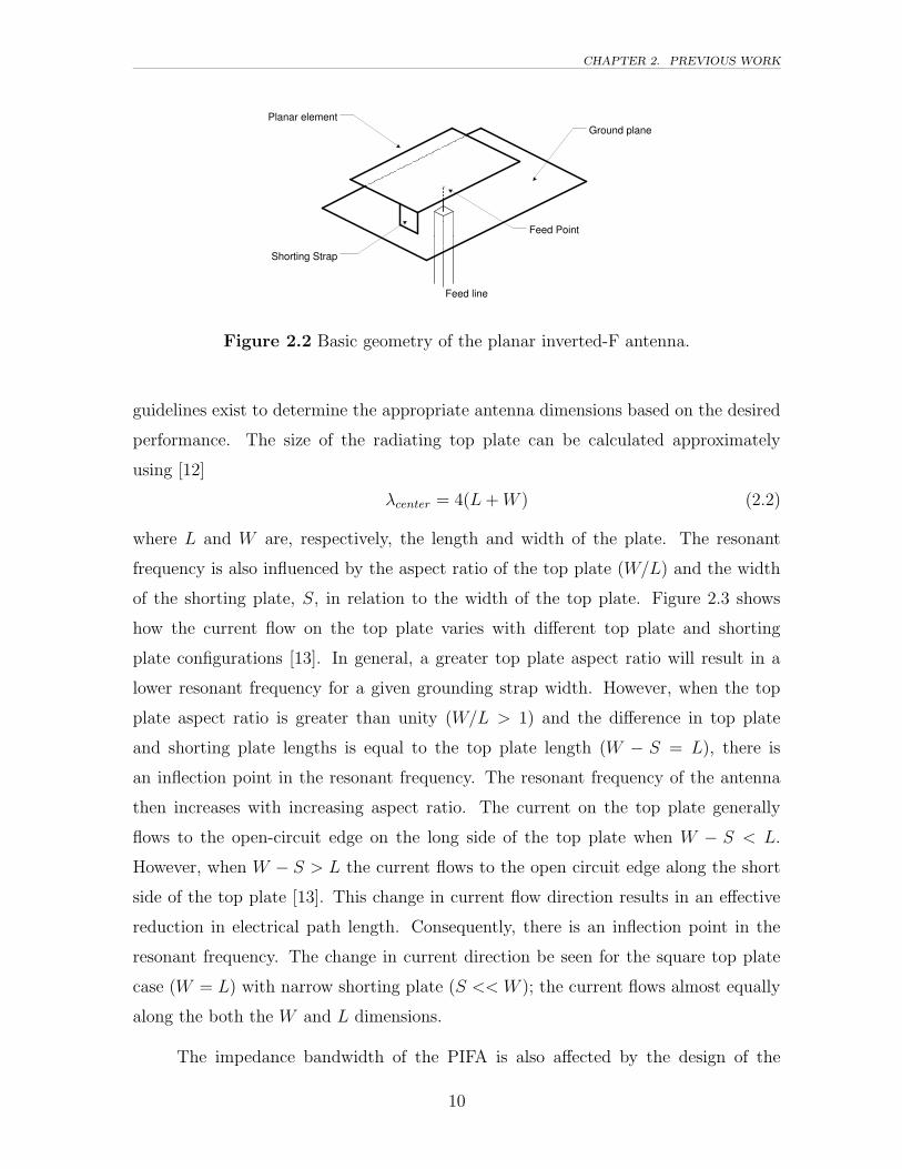
CHAPTER 2. PREVIOUS WORK
Feed Point
Planar element Ground plane
Shorting Strap
Feed line
Figure 2.2 Basic geometry of the planar inverted-F antenna.
guidelines exist to determine the appropriate antenna dimensions based on the desired
performance. The size of the radiating top plate can be calculated approximately
using [12]
λcenter = 4(L + W ) (2.2)
where L and W are, respectively, the length and width of the plate. The resonant
frequency is also influenced by the aspect ratio of the top plate (W/L) and the width
of the shorting plate, S, in relation to the width of the top plate. Figure 2.3 shows
how the current flow on the top plate varies with different top plate and shorting
plate configurations [13]. In general, a greater top plate aspect ratio will result in a
lower resonant frequency for a given grounding strap width. However, when the top
plate aspect ratio is greater than unity (W/L > 1) and the difference in top plate
and shorting plate lengths is equal to the top plate length (W − S = L), there is
an inflection point in the resonant frequency. The resonant frequency of the antenna
then increases with increasing aspect ratio. The current on the top plate generally
flows to the open-circuit edge on the long side of the top plate when W − S < L.
However, when W − S > L the current flows to the open circuit edge along the short
side of the top plate [13]. This change in current flow direction results in an effective
reduction in electrical path length. Consequently, there is an inflection point in the
resonant frequency. The change in current direction be seen for the square top plate
case (W = L) with narrow shorting plate (S << W ); the current flows almost equally
along the both the W and L dimensions.
The impedance bandwidth of the PIFA is also affected by the design of the
10

CHAPTER 2. PREVIOUS WORK
L
W
L / W > 1
L / W = 1.0
S < W S << W
Shorting Plate
L / W > 1
L / W = 1.0 S << W
S < W
Figure 2.3 Surface current on PIFA top plate for various aspect ratios, L/W , and
grounding strap widths, S.
structure. The height, H, of the radiating top plate above the ground plate and the
shorting plate width, S have the greatest influence on PIFA bandwidth. In general,
the bandwidth increases with both increasing top plate height and increasing shorting
plate width. However, as the height of the top plate approaches the length of the
grounding strap, H ≈ S, the height also begins to influence the resonant frequency.
The resonant frequency then given from [13]
λcenter = 4(L + W + H). (2.3)
PIFA bandwidth is greatest when the shorting plate is the same width as the top plate
(S = W ). As the width of the grounding strap decreases, the relative bandwidth of
the PIFA decreases. The bandwidth of a PIFA with the grounding strap width much
less than the width of the top plate (S/W ≤ 0.1) can be reduced to below 1%.
There are several procedures available for designing PIFAs and many different
PIFA layouts may satisfy the same design criteria. One particular design of a cellular
PIFA is given by [14] and is re-analyzed here for clarity. The design of Figure 2.4 has
a radiating top plate that is 6.40 cm long and 2.29 cm wide. The height of the top
plate is 1.78 cm and the shorting strap is equal in width to the top plate. The metal
strips used in the simulation are 60 mils thick and the probe feed is model as a single
11

CHAPTER 2. PREVIOUS WORK
6.40 cm
1.78 cm
2.59 cm 2.29 cm
1.78 cm
Figure 2.4 Typical PIFA designed for operation near cellular band.
strip 1.6 mm wide. The antenna is simulated over an infinite ground plane with the
moment method package IE3D. The PIFA of Figure 2.4 shows and excellent impedance
match to 50 Ω at 1 GHz. The 2:1 VSWR bandwidth in Figure 2.5 shows an impedance
bandwidth of over 8%.
Further conventional PIFA modifications have been investigated to improve the
antenna radiation performance [11, 12, 15, 16, 17, 18]. One particular modification is
a PIFA with a partial shorting plate. This shorted PIFA was designed for operation
on a handset was demonstrated to have 8 to 12% bandwidth [19]. This antenna,
however, has an appreciable amount of radiation in the broadside direction as well as
the horizontal plane.
12

CHAPTER 2. PREVIOUS WORK
0.95 1 1.05 1.1 1.15 1.21
1.5
2
2.5
3
3.5
4
4.5
5
Frequency (GHz)
VS
WR
Figure 2.5 VSWR versus frequency for the PIFA of Figure 2.4 calculated using the
moment method code IE3D.
0 .2 .5 1 2 5 inf
.2
.2
.5
.5
1
1
2
2
Figure 2.6 Input reflection coefficient for the PIFA of Figure 2.4 calculated using the
moment method code IE3D.
13
CHAPTER 2. PREVIOUS WORK
PSfrag replacements
d
L
αFp
Figure 2.7 The geometry of the wire-form folded dipole antenna.
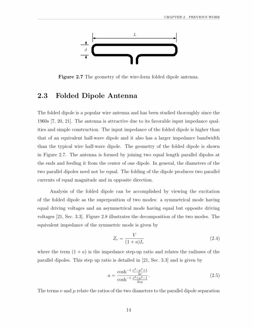
2.3 Folded Dipole Antenna
The folded dipole is a popular wire antenna and has been studied thoroughly since the
1960s [7, 20, 21]. The antenna is attractive due to its favorable input impedance qual-
ities and simple construction. The input impedance of the folded dipole is higher than
that of an equivalent half-wave dipole and it also has a larger impedance bandwidth
than the typical wire half-wave dipole. The geometry of the folded dipole is shown
in Figure 2.7. The antenna is formed by joining two equal length parallel dipoles at
the ends and feeding it from the center of one dipole. In general, the diameters of the
two parallel dipoles need not be equal. The folding of the dipole produces two parallel
currents of equal magnitude and in opposite direction.
Analysis of the folded dipole can be accomplished by viewing the excitation
of the folded dipole as the superposition of two modes: a symmetrical mode having
equal driving voltages and an asymmetrical mode having equal but opposite driving
voltages [21, Sec. 3.3]. Figure 2.8 illustrates the decomposition of the two modes. The
equivalent impedance of the symmetric mode is given by
Zr =V
(1 + a)Ir
(2.4)
where the term (1 + a) is the impedance step-up ratio and relates the radiuses of the
parallel dipoles. This step up ratio is detailed in [21, Sec. 3.3] and is given by
a =cosh−1 ν2
−µ2+1
2ν
cosh−1 ν2+µ2−1
2νµ
. (2.5)
The terms ν and µ relate the ratios of the two diameters to the parallel dipole separation
14

CHAPTER 2. PREVIOUS WORK
= +
PSfrag replacements
d
r1 r2
Ii
Vi VVV
Ir aIr
aV
IfIf
Figure 2.8 Network representation of the decomposition of the folded dipole.
distance d and are given from
ν =d
r1
, µ =r2
r1
. (2.6)
The asymmetrical mode can be viewed as a shorted transmission line of length equal
to the folded dipole length, L, and its impedance is given by
Zf =(1 + a)V
2If
= jZ0 tan βL/2 (2.7)
where Z0 is the characteristic impedance of the transmission line. The expression for
the input impedance is then obtained by combining Zr and Zf and is
Zi =(1 + a)V
Ir + If
=2(1 + a)2ZrZf
(1 + a)2Zr + 2Zf
. (2.8)
For the special case of the half-wave folded dipole (L = λ/2) with equal radius arms
(r1 = r2) Equation 2.8 reduces to
Zi = 4Zdipole. (2.9)
The input impedance of a half-wave dipole is roughly 70 Ω thus the input impedance
of the folded dipole is 280 Ω [7].
15

CHAPTER 2. PREVIOUS WORK
PSfrag replacements
a
L
αFp
Figure 2.9 The printed folded-slot dipole antenna.
The printed slot folded dipole in Figure 2.9 is a variation on the wire form of the
folded dipole [22, 23, 24, 25, 26]. It is constructed by etching a slot on a metallized
substrate in the shape of a folded dipole. The printed version is an attractive alternative
due to the rugged nature of printed antenna technology. The printed slot also lends well
to use with coplanar waveguide feed networks. The input impedance of the printed
slot antenna may be obtained by applying Babinet’s principle to the geometry [22].
Babinet’s principle views a thin slot in an infinite ground plane as the compliment to a
dipole in free space. This gives an expression for the impedance of the half-wave folded
dipole slot as
Zslot =Zfs
4Zdipole
(2.10)
where the free space impedance is given by Zfs ≈ 377 Ω and the half-wave folded
dipole impedance is again Zdipole ≈ 70 Ω. This results in a Zslot ≈ 500 Ω. As expected,
the radiation patterns of the folded dipole and folded slot antenna are similar to those
of the half-wave dipole.
2.4 Reconfigurable Antennas
This section gives a survey of previous and current research involving reconfigurable
antennas. Reconfigurable antennas are a relatively recent phenomena in antenna de-
sign. The late 1990s marks the transition into viable reconfigurable antenna design and
there has been a rapid increase in the number of literature references containing recon-
16

CHAPTER 2. PREVIOUS WORK
figurable designs and applications since that time. The current literature is divided into
a few broad categories of reconfigurable antennas. Most reconfigurable antennas can
be classified as either reconfigurable elements designs, fragmented apertures designs or
reconfigurable arrays designs.
2.4.1 Reconfigurable Elements
Reconfigurable elements represent antennas that radiate with one or few primary ra-
diating elements. That primary element is reconfigured via switches or some other
variable element to provide parameter control. The antennas listed in this subsection
all function in this manner (lumped reconfigurable elements).
2.4.1.1 Planar Reconfigurable Slot
The reconfigurable slot antenna presented in [27] is an electronically tunable planar
VHF slot antenna. It consists of a microstrip fed resonant slot structure loaded with
a series of PIN diode switches. The resonant frequency of operation is selected by
varying the length of the radiating slot and thus changing its electrical length. The
length of the slot is altered by biasing the PIN diode switches along the slot length. It
is capable of operating at four different frequencies in the band from 500 to 900 MHz.
2.4.1.2 MEMS Reconfigurable Vee
The MEMS reconfigurable Vee antenna is a printed antenna that uses dynamic ac-
tuators to alter the radiation characteristics of the antenna. Figure 2.10 shows the
geometry of the reconfigurable Vee antenna. The antenna presented in [28, 2, 29] uses
MEMS actuators to alter geometry of the Vee dipole. Push-pull actuators connected
to the dipole arms enable reconfiguration of the Vee pitch angle. Each arm of the
Vee is independently controlled, allowing the antenna to both steer the antenna beam
and alter the beam shape. Symmetrical movements of the Vee actuators result in a
widening and narrowing of the Vee angle, α, and thus widens and narrows the main
beam. The main beam may be steered off broadside by moving each Vee actuator by
17

CHAPTER 2. PREVIOUS WORK
Push-Pull Actuators
Transmission Line
PSfrag replacements
α
Figure 2.10 The reconfigurable Vee-dipole antenna.
different distances.
The antennas presented in [2, 29] were fabricated using a three layer polysil-
icon surface micromachining process. Two versions were detailed, a 3 GHz version
and a 17.5 GHz version, and were shown to offer a considerable amount of dynamic
reconfigurability. The antennas demonstrated 48 of main beam shift from broadside.
2.4.1.3 Reconfigurable Dime and Q-dime Antennas
The dime antenna [30, 31, 32] and its constituent q-dime element are broadband multi-
layered stacked circular patches. Figure 2.11 shows the basic geometry of the dime
antenna. The dime antenna is constructed as either a single monolithic element or as
a combination of four quarter dime (q-dime) elements. The antennas are electrically
small (radius < 0.2λ and height < 0.5λ) and volumetric in nature to achieve the size
reduction. Broadband operation is accomplished by creating two degenerate modes via
two cylindrical radiating slots in the patch structures. MEMS switches located within
the geometry of the the patches allow the antenna to alter the working frequency of the
design. The switches are successively turned on to tune the frequency of the antennas.
18

CHAPTER 2. PREVIOUS WORK
MEMS switched shorting plates Feed point
Capacitively coupled feed plate
q-dime
Side view Top view
PSfrag replacements
0.4λ
λ/4
Figure 2.11 Geometry of the proximity coupled reconfigurable dime antenna com-
posed of four quarter-dime stacked patch antennas.
The antennas are also able to control polarization and radiation pattern shape by
activating the MEMS switches.
2.4.1.4 Reconfigurable Leaky Mode Patch
The antenna presented in [33], [34] is a combination of normal microstrip patch an-
tenna and a leaky-wave antenna. Leaky-wave radiation is facilitated by the presence of
higher order modes on microstrip structures [35]. The antenna is shown in Figure 2.12
and consists of a high-order mode launcher connected to a length of X-band leaky-
mode microstrip antenna. The mode launcher is composed of a microstrip impedance
transformer, 180 phase shifter and an even-mode suppressor. The leaky-mode antenna
is then connected via MEMS switches to a conventional C-band microstrip patch an-
tenna. When the MEMS switches are deactivated the antenna operates as a conven-
tional patch antenna. Activating the switches causes the patch structure to become
part of the leaky-mode structure and the antenna radiates as a leaky-mode antenna.
19

CHAPTER 2. PREVIOUS WORK
Diode Switches
C-band Microstrip Patch
X-band Leaky Mode Antenna
Feed and High Order Mode Launcher
Figure 2.12 The reconfigurable leaky mode patch antenna.
2.4.1.5 MEMS Mechanical Beam Steering
The antenna system presented in [36] addresses the problem of scan loss inherent to
electronically steered antennas. Scan loss is a broadening of array main beam and the
associated reduction of array gain seen as the main beam is steered off broadside. The
system overcomes this loss by steering the antenna electromechanically via a MEMS
structure as opposed to a strictly electrical scan as in a phased array. The antenna
system presented has a V-band radiating patch antenna element. It uses a MEMS
fabricated element platform with two degrees of rotational freedom to facilitate the
main beam scanning. The MEMS antenna system is capable of scanning the main
beam over 60 with no measured scan loss.
2.4.1.6 Stacked Reconfigurable Bowtie
The stacked reconfigurable bowtie antenna [37] consists of a dual layer arrangement
of unequal size balanced microstrip bowtie elements. Figure 2.13 shows the geometry
of the stacked reconfigurable bowtie antenna. The individual bow ties are situated on
mixed dielectric layers above a ground plane and the bowtie geometries are designed for
3.1 GHz and 8 GHz operation. Each bowtie layer is constructed on top of a mixed layer
dielectric consisting of a thick polymer layer (εr ≈ 3.0) over a thin foam layer (εr ≈1.0). This layered dielectric arrangement provides both upper and lower operating
bands with nearly 25% bandwidth. The smaller high-frequency bowtie layer is stacked
on top of the larger low-frequency bowtie layer. The low-frequency antenna acts as a
virtual ground plane for the high frequency antenna when the antenna is operating in
the high-frequency mode. Several sets of MEMS switches are present under the ground
20
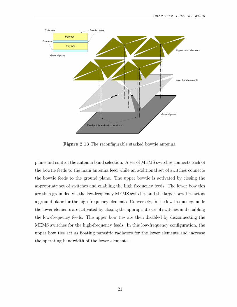
CHAPTER 2. PREVIOUS WORK
Upper band elements
Lower band elements
Ground plane
Feed points and switch locations
Side view Bowtie layers
Polymer
Polymer
Ground plane
Foam
Figure 2.13 The reconfigurable stacked bowtie antenna.
plane and control the antenna band selection. A set of MEMS switches connects each of
the bowtie feeds to the main antenna feed while an additional set of switches connects
the bowtie feeds to the ground plane. The upper bowtie is activated by closing the
appropriate set of switches and enabling the high frequency feeds. The lower bow ties
are then grounded via the low-frequency MEMS switches and the larger bow ties act as
a ground plane for the high-frequency elements. Conversely, in the low-frequency mode
the lower elements are activated by closing the appropriate set of switches and enabling
the low-frequency feeds. The upper bow ties are then disabled by disconnecting the
MEMS switches for the high-frequency feeds. In this low-frequency configuration, the
upper bow ties act as floating parasitic radiators for the lower elements and increase
the operating bandwidth of the lower elements.
21

CHAPTER 2. PREVIOUS WORK
MEMS Shunt Switches
PSfrag replacements
L
Fp
Figure 2.14 The reconfigurable microstrip patch antenna.
2.4.1.7 Reconfigurable Patch
The patch described in [38] uses a conventional microstrip patch antenna with the
addition of two MEMS controllable shorting elements. Figure 2.14 illustrates the ge-
ometry of the reconfigurable patch antenna. The antenna is fed through a conventional
microstrip line. The MEMS switches are positioned at the far end of the microstrip
patch. The patch operates at its nominal frequency when the MEMS switches are in
the off state. As with other rectangular microstrip patches, frequency of operation is
determined by the length L, the edge parallel to the microstrip feed. When the MEMS
actuators are turned to the on state, they add a capacitance in shunt with the input
impedance of the patch. This added capacitance has the effect of lowering the resonant
frequency of the antenna. The antenna presented was designed to operate at 25 GHz.
A frequency reduction of 1.6% was achieved with the MEMS switches in the “on” state.
2.4.2 Distributed Radiators
The second broad class of reconfigurable antennas are the distributed radiators. This
class represents antennas that radiate primarily by combining sub-elements together
to form a larger discontinuous radiating structure. They are frequently referred to as
22

CHAPTER 2. PREVIOUS WORK
fragmented apertures or microswitch arrays because the radiating structure is formed
from a subset of elements from a large array of elements. The operation of this class
of antennas is distinct from conventional arrays because the individual elements that
make up the radiator effectively radiate as a single unit with a single feed. The elements
or, more precisely, sub-elements do not act as autonomous radiating structures. The
sub-elements control the current distribution on the aperture of the structure and thus
control the radiation properties of the antenna. It is the combination of these sub-
elements which allows the overall structure to radiate. The reconfigurable nature of
the switch elements allows the antenna to change its functionality by activating and
deactivating specific switches.
The micro-switched fragmented aperture [39, 40, 41] developed by Georgia Tech
Research Institute (GTRI) has been studied extensively. The aperture investigated by
GTRI consists of small metallic conducting pads connected by MEMS switches. The
MEMS switches are activated by control chips that are placed on or near the radiating
aperture. Each control chip directs either a single switch or a small functional cell of
switches. A bowtie dipole has been simulated and tested in the fragmented aperture.
The bowtie geometry has shown promising results in its ability to control radiation
characteristics such as polarization and operational frequency.
The GTRI fragmented aperture has also been configured to radiate via a genetic
algorithm structure search [39]. An array test bed was created that allowed a computer
routine to automatically generate the radiating structure based on a desired radiation
characteristic. The search routine evaluated the fitness of the radiation performance
of a previous generation and generated the next generation of aperture structure. The
large number of sub-elements present in the fragmented aperture has made optimization
routines such as genetic algorithms particularly well suited to antenna design.
The MEMS switched reconfigurable antenna presented in [42] is very similar in
layout and operation to the GTRI fragmented aperture. The antenna consists of a
3 × 3 array of patches connected with MEMS switches. This reconfigurable patch
module is used a building block for larger conformal antenna structures. A dual L/X-
band prototype antenna was constructed using ideal open/closed switches in place of
functional MEMS switches. The antenna was able to achieve 1.2% bandwidth and
23
CHAPTER 2. PREVIOUS WORK
Cantilever MEMS Switches
RF Path
Figure 2.15 The MEMS cantilever RF switch used in the microswitch array.
acceptable radiation patters for the L-band operation and greater than 7% bandwidth
for X-band operation.
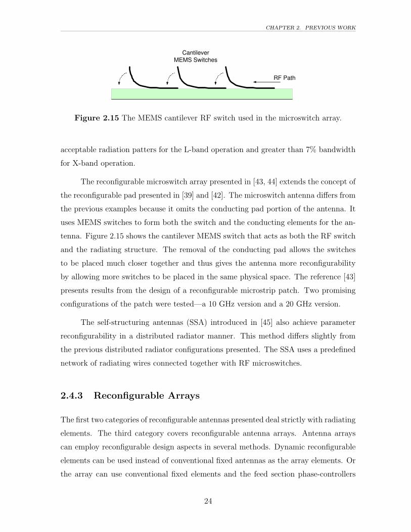
The reconfigurable microswitch array presented in [43, 44] extends the concept of
the reconfigurable pad presented in [39] and [42]. The microswitch antenna differs from
the previous examples because it omits the conducting pad portion of the antenna. It
uses MEMS switches to form both the switch and the conducting elements for the an-
tenna. Figure 2.15 shows the cantilever MEMS switch that acts as both the RF switch
and the radiating structure. The removal of the conducting pad allows the switches
to be placed much closer together and thus gives the antenna more reconfigurability
by allowing more switches to be placed in the same physical space. The reference [43]
presents results from the design of a reconfigurable microstrip patch. Two promising
configurations of the patch were tested—a 10 GHz version and a 20 GHz version.
The self-structuring antennas (SSA) introduced in [45] also achieve parameter
reconfigurability in a distributed radiator manner. This method differs slightly from
the previous distributed radiator configurations presented. The SSA uses a predefined
network of radiating wires connected together with RF microswitches.
2.4.3 Reconfigurable Arrays
The first two categories of reconfigurable antennas presented deal strictly with radiating
elements. The third category covers reconfigurable antenna arrays. Antenna arrays
can employ reconfigurable design aspects in several methods. Dynamic reconfigurable
elements can be used instead of conventional fixed antennas as the array elements. Or
the array can use conventional fixed elements and the feed section phase-controllers
24
CHAPTER 2. PREVIOUS WORK
Open Switches
Closed Switches
Pat
h Le
ngth
Coplanar Strip
Transmission Line
(a) Flared notch with reconfigurable
feed section.
Scan Angle
(b) Array showing beam steering with recon-
figurable feed section.
Figure 2.16 The reconfigurable flared notch array element with time-delay beam
steering.
might employ reconfigurable elements.
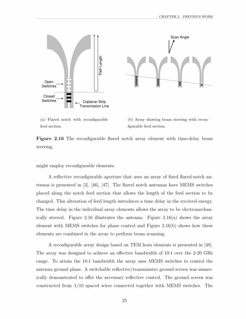
A reflective reconfigurable aperture that uses an array of fixed flared-notch an-
tennas is presented in [3], [46], [47]. The flared notch antennas have MEMS switches
placed along the notch feed section that allows the length of the feed section to be
changed. This alteration of feed length introduces a time delay in the received energy.
The time delay in the individual array elements allows the array to be electromechan-
ically steered. Figure 2.16 illustrates the antenna. Figure 2.16(a) shows the array
element with MEMS switches for phase control and Figure 2.16(b) shows how these
elements are combined in the array to perform beam scanning.
A reconfigurable array design based on TEM horn elements is presented in [48].
The array was designed to achieve an effective bandwidth of 10:1 over the 2-20 GHz
range. To attain the 10:1 bandwidth the array uses MEMS switches to control the
antenna ground plane. A switchable reflective/transmissive ground screen was numer-
ically demonstrated to offer the necessary reflective control. The ground screen was
constructed from λ/10 spaced wires connected together with MEMS switches. The
25

CHAPTER 2. PREVIOUS WORK
MEMS switches allow the screen inter-element spacing to be varied, and consequently,
the screen can be configured such that it is transparent or opaque to selected frequen-
cies.
A method is presented in [49] for control of reconfigurable array antennas. The
method requires phase-only control of quantized phase shifters that is directly applica-
ble to use with MEMS phase shifters. A 150,000 element space-based radar is presented
in [50] that uses MEMS phase shifters. The weight of the electronically scanned array
was reduced by employing the MEMS phase shifters in place of conventional phase
shifters.
26
Chapter 3
Reconfigurable Antennas and
Technology
This chapter presents the concept of reconfigurable antennas and details the emerging
technologies that make reconfigurable antennas possible. First, a description of the
methodologies available for designing reconfigurable antennas is presented. Then a
description of the physical switch technologies and how they can be utilized for antenna
design. Their electrical characteristics are described and the mathematical models used
in simulating the switches in an RF environment are presented.
From a systems standpoint, antennas have historically been viewed as static
devices with time-constant characteristics. Once an antenna design is finalized, its
operational characteristics remain unchanged during system use. However, the recent
advent of microelectromechanical system (MEMS) components into microwave and
millimeter wave applications has opened new and novel avenues of antenna technology
development. High quality, miniature RF switches provide the antenna designer with
a new tool for creating dynamic radiating structures that can be reconfigured during
operation. MEMS switches are of particular interest because they offer broadband
operation, low insertion loss and high contrast between active states. In the near
future the antenna will evolve as a component that will offer intelligence that alters
itself in-situ to meet operational goals. This development is similar to the introduction
of viable field programmable gate arrays for integrated circuit logic in the late 1980s.
27

CHAPTER 3. RECONFIGURABLE ANTENNAS AND TECHNOLOGY
While the method of antenna operation is evolving, its role in communication
systems still remains the same. The task that an antenna must perform is funda-
mentally that of a radiator and thus the metrics by which antennas operate and are
measured are still intact. Gain, bandwidth, polarization, antenna feature size, etc.
are still the realizable quantities of interest. Only now the introduction of dynamic
radiating structures has given the antenna designer an additional degree of freedom to
meet these design goals.
3.1 Reconfigurable Antenna Methodologies
This section details the methodologies identified for designing reconfigurable antennas.
It describes each method and illustrates the strengths and weaknesses associated with
each. Example designs are presented for each method.
Classical non-reconfigurable design methods have dominated antenna engineer-
ing for the majority of antenna design history. To make the transformation from
fixed element operation to reconfigurable antenna design requires a suitable conver-
sion in design methodology. The short existence of reconfigurable has produced two
primary design methods: total geometry morphing and matching network morphing.
A third method is also identified and expanded in this dissertation—smart geometry
reconfiguration. Thus, three broad methodologies have been identified for achieving
reconfigurable antenna designs and operation.
Total geometry morphing represents the most structurally complicated of the
methods. It is implemented though a large array of switchable sub-elements which are
combined to form the desired radiating structure. Matching network morphing is the
simplest of the methods and modifies only the feed structure or impedance matching
network of the antenna while the radiating structure remains constant. The smart
geometry reconfiguration method lies between the other two in its structural imple-
mentation complexity. It modifies only critical parameters of the antenna radiating
structure to achieve the desired range of reconfigurable control.
28

CHAPTER 3. RECONFIGURABLE ANTENNAS AND TECHNOLOGY
PSfrag replacements
Sub-patch Unit Cell
RF Switch
StructureConducting
Figure 3.1 The total geometry morphing method of reconfigurable antenna design.
3.1.1 Total Geometry Morphing Method
The total geometry morphing method achieves reconfigurable operation by switching
a large array of interconnected sub-elements. The sub-elements are connected together
via RF switches and are typically less than λ/20 in size. Because the sub-elements
are much less than a wavelength in size they do not form efficient radiating elements
individually. However, switching together multiple adjacent sub-elements results in an
aggregate structure that forms the desired radiator. This sub-element arraying allows
considerable flexibility in forming the radiator. The geometry of the aggregate radiating
structure can take a wide variety of forms depending on the desired application. The
reconfigurable antennas designed via this method are often referred to in the literature
as distributed radiators because the total radiating structure is distributed over many
smaller structures.
Figure 3.1 illustrates the concept of the total geometry morphing method. The
example is a reconfigurable microstrip patch antenna consisting of a large grid of
switched microstrip sub-patches that are available on the dielectric substrate. These
sub-patches do not represent individual microstrip patch antennas themselves but act
29

CHAPTER 3. RECONFIGURABLE ANTENNAS AND TECHNOLOGY
as actively reconfigurable conducting structures. The detailed blow-up in Figure 3.1
shows a single functional unit cell for the composite antenna. These unit cells illus-
trates the concept of the sub-patch conducting structure. Each unit cell consists of a
small conducting patch of metal and four RF microswitches. The switches provide the
RF conduction path to the nearest neighboring unit cell. The composite antenna is
then constructed by activating the necessary switches to form then antenna. In this
example the structure is first configured to form a conventional rectangular microstrip
patch antenna. Next, several of the sub-patches along the length of the microstrip feed
are switched to the off state. This moves the effective feed point for the patch antenna
closer to the center of the patch and alters the input impedance of the patch. Fi-
nally, the unit cells are configured to form a bow-tie patch antenna which has different
radiation characteristics than the rectangular patch.
The total geometry morphing method has the obvious advantage of providing a
large amount of antenna reconfigurability. The array of sub-elements provides a large
level of flexibility in composing the aggregate antenna. Because of the flexibility in
configuring the antenna, a wide range of control over many antenna characteristics is
offered by employing this method. Thus, a single reconfigurable platform could be used
for a large number of applications. System operation over multiple frequency bands,
with variable radiation pattern characteristics and selective polarization is possible with
a single reconfigurable platform. Likewise, the layout of the sub-element array pattern
is not limited to two dimensional planar microstrip geometries. Surface conformal and
three dimensional geometries also represent viable configurations.
The highly flexible nature of total geometry morphing dictates the primary dif-
ficulty with implementing this method. The extreme complexity involving numerous
individual components to necessary to realize the geometries is inherent in this method.
A large number of sub-elements, switches and control lines are required to implement
the reconfigurable geometry. This leads directly to geometry and component manage-
ment issues. A large number of active components also means there are a large number
of points of failure. Recent advancements in RF MEMS switches have been the driving
force behind much the reconfigurable antenna designs. As with any mechanical switch,
MEMS devices are susceptible to reliability issues due to mechanical fatigue. Thus,
30
CHAPTER 3. RECONFIGURABLE ANTENNAS AND TECHNOLOGY
Figure 3.2 Microstrip feed configurations for impedance matching of reconfigurable
antenna design.
any structure which depends explicitly on the reliable operation of these switches will
be subject to performance degradation in the case of switch failure.
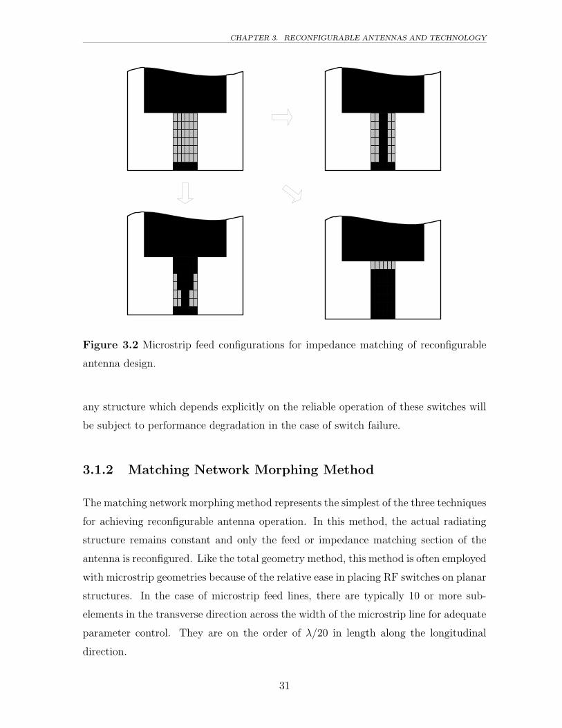
3.1.2 Matching Network Morphing Method
The matching network morphing method represents the simplest of the three techniques
for achieving reconfigurable antenna operation. In this method, the actual radiating
structure remains constant and only the feed or impedance matching section of the
antenna is reconfigured. Like the total geometry method, this method is often employed
with microstrip geometries because of the relative ease in placing RF switches on planar
structures. In the case of microstrip feed lines, there are typically 10 or more sub-
elements in the transverse direction across the width of the microstrip line for adequate
parameter control. They are on the order of λ/20 in length along the longitudinal
direction.
31

CHAPTER 3. RECONFIGURABLE ANTENNAS AND TECHNOLOGY
Figure 3.2 illustrates one implementation of the matching network morphing
method. In this example a microstrip patch antenna is edge fed by a reconfigurable
microstrip line. The reconfigurable microstrip line consists of a small array of switch-
able microstrip sub-elements. Each of these sub-elements may be switched on or off by
activating one of the miniature RF switches that form the interconnections between
the sub-elements and compose the overall microstrip structure. The width and length
of the feed line is altered to change the impedance of the microstrip. The grey boxes
represent inactive sub-elements and the block boxes represent active sub-elements.
The top left configuration in Figure 3.2 shows the microstrip patch antenna and
the available microstrip feed lattice. The top right sub-element arrangement shows the
feed configured as a narrow microstrip line having a characteristic impedance. The
patch antenna operates in a radiation mode that is specified by this feed configuration.
The bottom two arrangements in Figure 3.2 show the microstrip feed line configured in
two other possible formations. These variations in feed impedance then excite different
radiation modes in the microstrip patch antenna.
The matching network morphing technique carries the distinct advantage of be-
ing extremely simple to implement in practice. The only component of the antenna
that is changed is the feed network and thus the complexity of the design is minimized.
As a result, the number of physical switching components is kept to a minimum and
switch reliability becomes less of an issue. Conversely, this method exhibits the dis-
advantage of limited antenna reconfigurability. The antenna operation is varied only
through changes in matching. Consideration is not given to other critical radiation
characteristics. Because the principal radiation mode is altered by the impedance, the
electrical performance characteristics are likely to change as well.
3.1.3 Smart Geometry Reconfiguration
The final identified method of reconfigurable antenna design is smart geometry re-
configuration. Falling between total geometry morphing and the matching network
morphing method in both the amount of achievable parameter control and system
complexity, this method modifies only critical parameters of the antenna radiating
32

CHAPTER 3. RECONFIGURABLE ANTENNAS AND TECHNOLOGY
structure to achieve the desired reconfigurable performance. It can be implemented
with considerably fewer control elements than the total geometry method and thus has
the advantage of reduced design complexity. However, with a thorough understanding
of the underlying antenna design and careful design consideration it can yield a high
level of reconfigurability and antenna parameter control. The primary disadvantage of
this method is that the underlying physics of the particular antenna must be known
in order to take advantage of minor geometry modifications to achieve the reconfig-
urable goal. Additionally, the amount of reconfigurability is ultimately limited by the
electrical characteristics of the antenna geometry.
3.2 Antenna Switch Technologies
This section gives a brief overview of the current state of RF switches available for use in
antenna systems. It includes switches have been used in both classical antenna systems
and more recent reconfigurable implementations. In particular it explores conventional
mechanical switches, PIN diodes, and FET switches, and MEMS switches and makes
recommendations of candidates for use in reconfigurable antenna designs.
The fundamental role of a switch or relay is a device to make or break an electric
circuit. In static and quasi-static regimes, a switch operates simply as either a con-
duction path or a break in the conduction path. However, switch operation in an RF
system will include additional electrical properties. Switch resistance, capacitance and
inductance along the RF signal path must be included in the analysis of the system. In
RF antenna systems, switch function typically entails controlling and directing the flow
of RF energy along a desired RF path. Traditionally, this path may include any of the
RF subsystems leading to the antenna feed distribution network as well as the antenna
feed and, in the case of arrays, any power distribution network. The introduction of
reconfigurable antennas has also added the antenna itself to the list of places where
switches are utilized to control the direction and flow of RF current.
Irrespective of the type of switch used, there are several important characteristics
that must be evaluated for all RF switch applications and particularly reconfigurable
antenna designs. The selection of switch type depends fundamentally on the switching
33

CHAPTER 3. RECONFIGURABLE ANTENNAS AND TECHNOLOGY
speed required by the application and the switched signal power level. Other critical
parameters to consider in the selection of RF switches include impedance character-
istics, switch biasing and activations conditions, package and form factor, and switch
cost.
The usable speed that a switch can toggle between states in an RF signal path
is actually composed of three complementary mechanisms: transition time, switch rate
and transient behavior. Switch transition time measures the speed at which the switch
can alternate between on and off states. For RF applications, this is typically defined
as the time required for the RF power level to change from 10% to 90% for an on
transition or 90% to 10% for an off transition [51]. The switch rate represents the
speed at which the switch can respond to a control signal. It measures how long after
sending a signal to the switch will the output state change. This is normally defined
as the time between the appearance of 50% of the control voltage and 90% of the RF
output level. Switch transient behavior represents the exponentially decaying signal
components seen on the switch due to the physical change in switch state. Transients
are often manifested by large, quickly decaying voltage spikes at the RF input and
output. Transients may contain both electromechanical and electromagnetic in nature.
Electromechanical transients are caused by the mechanical movement of the switching
component while electromagnetic transients represent energy exchange between electric
and magnetic fields in the switch components.
The power handling capability of a switch measures how well the switch will
pass the RF signal level from switch input to output. An ideal switch would pass
all signal levels through linearly with no distortion. However, real switches tend to
have a upper limit to which signals will pass linearly. Above this level, input signals
become compressed and are passed in a non-linear manner. This maximum signal level
is typically used as a measure of switch performance. Often the 1 dB compression point
is specified to indicated the input level at which the output sees 1 dB of compression
from linear switch operation.
Impedance issues relating to switch characterization are also described by sev-
eral related quantities. The overall impedance matching of the switch, insertion loss,
isolation, and series resistance are all related to switch impedance performance. For
34

CHAPTER 3. RECONFIGURABLE ANTENNAS AND TECHNOLOGY
maximum power transfer, the switch should be match with the transmission paths to
which it is connected. Impedance mismatches in RF components result in undesir-
able reflections which degrade system performance. Insertion loss is directly related to
impedance matching and provides a measure of the transmission efficiency. Insertion
loss is given for the conduction or on-state of the switch and is normally specified by the
S-parameter coefficient S21 in decibels. Efficient on-state switch transmission requires
small insertion losses. Also specified by the S-parameter transmission coefficient S21 is
switch isolation. Isolation is defined for the non-conduction or off-state and represents
the coupling between the input and output points. A high level of isolation is necessary
to block RF energy from propagating through the switch when it should be off. The
contrast between insertion loss and isolation provides a quick measure of the quality
of the switch. Switches with high contrast function more like ideal switches than lower
contrast switches. Switch bandwidth can also be considered an impedance property
because the available bandwidth is often limited predominantly by device resistances
and reactances.
3.2.1 Mechanical Switches
Due to their large size conventional mechanical switches are not practical for reconfig-
urable antenna applications. However, they have been used extensively in high power
RF applications. Mechanical switching is normally accomplished by breaking the con-
ducting path of a transmission line within the switch. The electrical performance of
mechanical switches are often much better than those of solid state switches. Insertion
losses of less than 0.1 dB and isolations of over 70 dB are common [51]. The excellent
matching characteristics and high power handling capabilities make them the only suit-
able alternative for many applications such as broadcast systems. Next to their large
size however, the other major drawback of mechanical RF switches is long transition
times associated with mechanically actuating a switch. The moving switch components
parts have a mechanical resonant frequency that naturally limit the speed at which the
switch can change states. Typical switching speeds for mechanical switches are on the
order of 2 ms [51].
35
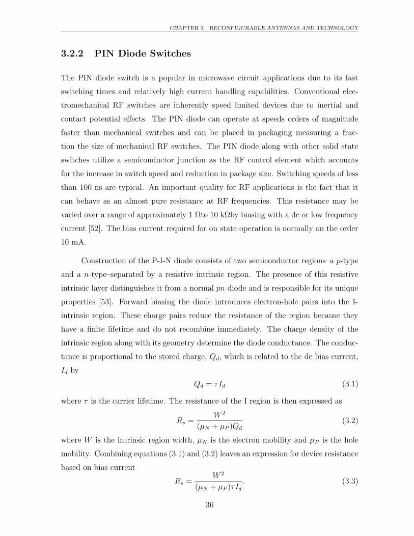
CHAPTER 3. RECONFIGURABLE ANTENNAS AND TECHNOLOGY
3.2.2 PIN Diode Switches
The PIN diode switch is a popular in microwave circuit applications due to its fast
switching times and relatively high current handling capabilities. Conventional elec-
tromechanical RF switches are inherently speed limited devices due to inertial and
contact potential effects. The PIN diode can operate at speeds orders of magnitude
faster than mechanical switches and can be placed in packaging measuring a frac-
tion the size of mechanical RF switches. The PIN diode along with other solid state
switches utilize a semiconductor junction as the RF control element which accounts
for the increase in switch speed and reduction in package size. Switching speeds of less
than 100 ns are typical. An important quality for RF applications is the fact that it
can behave as an almost pure resistance at RF frequencies. This resistance may be
varied over a range of approximately 1 Ωto 10 kΩby biasing with a dc or low frequency
current [52]. The bias current required for on state operation is normally on the order
10 mA.
Construction of the P-I-N diode consists of two semiconductor regions–a p-type
and a n-type–separated by a resistive intrinsic region. The presence of this resistive
intrinsic layer distinguishes it from a normal pn diode and is responsible for its unique
properties [53]. Forward biasing the diode introduces electron-hole pairs into the I-
intrinsic region. These charge pairs reduce the resistance of the region because they
have a finite lifetime and do not recombine immediately. The charge density of the
intrinsic region along with its geometry determine the diode conductance. The conduc-
tance is proportional to the stored charge, Qd, which is related to the dc bias current,
Id by
Qd = τId (3.1)
where τ is the carrier lifetime. The resistance of the I region is then expressed as
Rs =W 2
(µN + µP )Qd
(3.2)
where W is the intrinsic region width, µN is the electron mobility and µP is the hole
mobility. Combining equations (3.1) and (3.2) leaves an expression for device resistance
based on bias current
Rs =W 2
(µN + µP )τId
. (3.3)
36

CHAPTER 3. RECONFIGURABLE ANTENNAS AND TECHNOLOGY
RF in
Control Bias
DC Block
PIN
RF Choke
DC Return RF Choke
RF out
(a) PIN diode switch circuit
R s (PIN)
R l
R g
(b) Ideal equivalent RF circuit repre-
sentation
Figure 3.3 Series PIN diode RF switch model.
The low frequency limit of useful application is determined by the carrier lifetime [52].
At frequencies lower than f0 = 1/2πτ the RF signal modulates the stored charge just
as the DC bias thus causing the PIN diode to behave as a normal pn diode [53].
When used in an RF circuit application having a system characteristic impedance,
Zo, the switch transfer functions for the circuit descriptions of Figures 3.3 and 3.4 are
given by [52]∣
∣S21
∣
∣
−1
series= 20 log10
[
1 +Rdiode
2Zo
]
(3.4)
∣
∣S21
∣
∣
−1
shunt= 20 log10
[
1 +Zo
2Rdiode
]
(3.5)
Need plot of the isolation and loss for typical PIN diodes that ties together all these
equations.
3.2.3 Field Effect Transistor Switches
Before the emergence and common application of gallium arsenide field effect tran-
sistors (GaAs FET) as microwave switches in the mid 1980s, the PIN diode was pri-
marily the only high speed alternative available. However, advances in semiconductor
processing techniques and design innovations have moved GaAs FETS as well as other
37
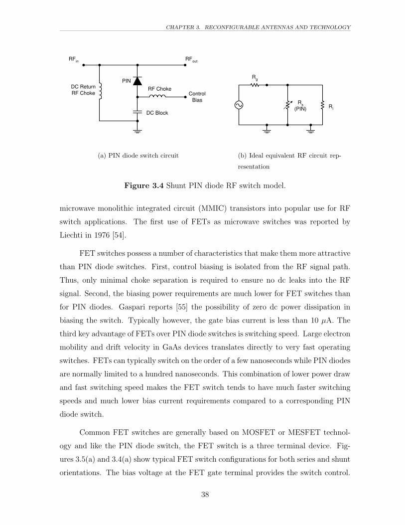
CHAPTER 3. RECONFIGURABLE ANTENNAS AND TECHNOLOGY
RF in
Control Bias
DC Block
PIN RF Choke DC Return
RF Choke
RF out
(a) PIN diode switch circuit
R s (PIN)
R g
R l
(b) Ideal equivalent RF circuit rep-
resentation
Figure 3.4 Shunt PIN diode RF switch model.
microwave monolithic integrated circuit (MMIC) transistors into popular use for RF
switch applications. The first use of FETs as microwave switches was reported by
Liechti in 1976 [54].
FET switches possess a number of characteristics that make them more attractive
than PIN diode switches. First, control biasing is isolated from the RF signal path.
Thus, only minimal choke separation is required to ensure no dc leaks into the RF
signal. Second, the biasing power requirements are much lower for FET switches than
for PIN diodes. Gaspari reports [55] the possibility of zero dc power dissipation in
biasing the switch. Typically however, the gate bias current is less than 10 µA. The
third key advantage of FETs over PIN diode switches is switching speed. Large electron
mobility and drift velocity in GaAs devices translates directly to very fast operating
switches. FETs can typically switch on the order of a few nanoseconds while PIN diodes
are normally limited to a hundred nanoseconds. This combination of lower power draw
and fast switching speed makes the FET switch tends to have much faster switching
speeds and much lower bias current requirements compared to a corresponding PIN
diode switch.
Common FET switches are generally based on MOSFET or MESFET technol-
ogy and like the PIN diode switch, the FET switch is a three terminal device. Fig-
ures 3.5(a) and 3.4(a) show typical FET switch configurations for both series and shunt
orientations. The bias voltage at the FET gate terminal provides the switch control.
38
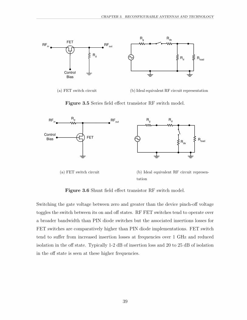
CHAPTER 3. RECONFIGURABLE ANTENNAS AND TECHNOLOGY
RF in
Control Bias
RF out
R d
FET
(a) FET switch circuit
R ds R g
R load R d
(b) Ideal equivalent RF circuit representation
Figure 3.5 Series field effect transistor RF switch model.
RF in
Control Bias
RF out R d
FET
(a) FET switch circuit
R ds
R g
R load
R d
(b) Ideal equivalent RF circuit represen-
tation
Figure 3.6 Shunt field effect transistor RF switch model.
Switching the gate voltage between zero and greater than the device pinch-off voltage
toggles the switch between its on and off states. RF FET switches tend to operate over
a broader bandwidth than PIN diode switches but the associated insertions losses for
FET switches are comparatively higher than PIN diode implementations. FET switch
tend to suffer from increased insertion losses at frequencies over 1 GHz and reduced
isolation in the off state. Typically 1-2 dB of insertion loss and 20 to 25 dB of isolation
in the off state is seen at these higher frequencies.
39

CHAPTER 3. RECONFIGURABLE ANTENNAS AND TECHNOLOGY
3.2.4 MEMS Switches
As previously described, conventional PIN diode and FET switches have seen limited
use in RF and microwave antenna design. However, specific disadvantages make them
unsuitable for reconfigurable antenna design where a large number of switches may
employed and individual device losses have a cumulative impact on overall antenna
performance. Device deficiencies including narrow bandwidth, comparatively low iso-
lation and high insertion loss, and finite power consumption make them unattractive
for use in many reconfigurable applications. Additionally, the non-linear nature of
solid-state semiconductor switches always has the potential to introduce undesirable
inter-modulation products into the RF signal path. RF microelectromechanical sys-
tems (MEMS) have moved the forefront of reconfigurable antenna design because of
their potential to overcome the limitations imposed by conventional RF switches. RF
MEMS switches have been shown to exhibit excellent and consistent switching char-
acteristics over an extremely wide range of operational frequencies. Additionally, their
large isolation and low insertion loss characteristics result in a switch that is very close
to an ideal switch for RF applications. This switch contrast ratio coupled with very
low actuation power consumption, small feature size and extremely wide bandwidth
makes MEMS switches ideally suited to reconfigurable antenna applications.
MEMS are microscopic electronic devices fabricated using existing semiconductor
process technologies that typically include a mechanical moving component. Surface
micromachining has been the most important fabrication method for MEMS but other
processes such as bulk micromachining, fusion bonding and LIGA (lithography, electro-
plating and molding) are frequently used [56]. Surface micromachining can be viewed
as a three dimensional lithographic process and involves depositing various patterns
of thin films on a substrate. Free-standing or suspended structures are created by
applying patterns of sacrificial film layers below non-sacrificial or ‘release’ layers [57].
Selective etching of the sacrificial layers then leaves a suspended film which is capable
of mechanical actuation.
Active MEMS devices can function as variable capacitors, resistors and inductors;
filters; resonators and switches. However, for reconfigurable antenna applications, the
MEMS RF switch is the most important MEMS device. As with other RF switch tech-
40

CHAPTER 3. RECONFIGURABLE ANTENNAS AND TECHNOLOGY
RF Path
Pull down electrode
Switch off state
Switch on state
Figure 3.7 Cantilever style RF MEMS series switch layout in both on and off states.
nologies, RF MEMS switches normally are designed in either series or shunt topologies.
Shunt switches are commonly used with coplanar waveguide structures and function by
shorting the RF signal path to the coplanar ground lines. A movable MEMS shunting
bridge is placed between the ground lines and suspended above the signal trace. Ac-
tivating the switch pulls the shorting bridge down and it into contact with the signal
line which shorts the RF signal path [58].
Series MEMS switches are favorable for use in microstrip topologies and one
configuration is illustrated in Figure 3.7. This is the so-called cantilever switch because
the moving part is suspended above the microstrip transmission line like a cantilever
beam. In the absence of a control voltage, the beam remains suspended above the
microstrip transmission line and the switch is in the off state. When a control voltage
is applied to the pull-down electrode, the cantilever beam is brought into contact with
the microstrip line and completes the transmission path. The switch is then in the
on state and acts as a continuous microstrip transmission line. The off state isolation
the simple dc-contact series MEMS switch is can be derived from its transmission
coefficients and is given by [59]
S21 =2jωCuZ0
1 + 2jωCuZ0
(3.6)
where Cu is the up state (off) capacitance of the switch and Z0 is the characteristic
41

CHAPTER 3. RECONFIGURABLE ANTENNAS AND TECHNOLOGY
0 5 10 15 20−70
−60
−50
−40
−30
−20
−10
Frequency, GHz
Isol
atio
n, d
B
1 fF2 fF4 fF8 fF
Figure 3.8 Isolation versus on state capacitance for a typical dc-contact MEMS series
switch given from (3.6) calculated using MATLAB.
impedance of the transmission line. The up state capacitance is a result of two mech-
anisms: the coupling between the open ends of the transmission line and the coupling
between the cantilever beam and the transmission line. There is only a small inductive
term due the short length of switch and can be neglected [59]. Thus the isolation be-
comes a dependent only on the up state capacitance. This capacitance is typically very
small and results in quite high isolation values even at high frequencies. Figure 3.8
compares switch isolations for realistic values of Cu.
When the device is in the down position (on state) the insertion loss is dominated
by the contact resistance of the switch, Rs. This term represents the resistance between
the switch beam and the transmission line. Rs is a function of switch contact area, the
amount of force applied to hold the switch down and the metal contact quality [60].
The transmission coefficient expression for the switch reduces to
S21 = 1 − Rs
2Z0
(3.7)
where the contact resistance of the switch and is typically less than 1 Ω. This yields
42

CHAPTER 3. RECONFIGURABLE ANTENNAS AND TECHNOLOGY
on state insertion losses of less than 0.1 dB [61, 62]. The performance of dc-contact
series switches is very close to an ideal RF switch over a very large bandwidth.
The advantages that MEMS switches offer over current PIN diode or FET RF
switches are as follow:
Wide Bandwidth Similar to conventional mechanical switches, the bandwidth of
RF MEMS switches is quite large. Unlike solid state which rely on a semiconductor
junction, the conduction path is based on metal to metal contact. The upper limit
on frequency of operation is normally restricted by reduced device isolation in the off
state. RF MEMS switches have been reported to operate with high reliability from dc
to 110 GHz [63].
High Isolation The attenuation between input and output ports of the switch when
in the off state is isolation. The small switch contact area and air gap filling of metal
contact switches produces very little electromagnetic coupling between switch points
while in the off state. Consequently, the off state capacitance of MEMS switches are in
the femto-farad range. DC-contact switches operating at less than 60 GHz can achieve
isolations of 50-60 dB while higher frequency capacitive switches produce acceptable
isolation up to 100 GHz [64].
Low Insertion Loss The attenuation between input and output ports of the switch
when in the on state is insertion loss. Small on state capacitances and very low contact
resistance facilitate very low insertion loss characteristics for MEMS switches. Insertion
losses of less than 0.1 dB can be achieved for switches up to 40 GHz [61, 65].
Low Power Consumption Many RF MEMS switches are actuated using electro-
static mechanisms which consume almost no power and offers several critical advan-
tages. The first and most obvious result is that total system power is minimized which
is critical for portable applications. The second result of very low power consumption is
one of potentially greater significance. One of the primary concerns in designing highly
integrated reconfigurable antennas is to what degree do the dc bias and control lines
43

CHAPTER 3. RECONFIGURABLE ANTENNAS AND TECHNOLOGY
effect the performance of the RF structure by coupling from the RF portions of the
antenna to the bias sections. Because almost no power is required to bias the switch,
control lines may be created with high impedance materials and thus provide poor
conduction paths for RF energy. This fact can be used to minimize and or eliminate
any antenna performance degradation from the bias section.
Linearity The quality of the signal passed through the switch is measured by its
linearity. Switches which pass signals without distortion or the introduction of har-
monics are said to be highly linear. The linearity of MEMS switches can be as much as
50 dB better than that of solid-state switches. This results in very low intermodulation
products in switching operations [64].
There are also critical disadvantages of RF MEMS switches compared to PIN
diodes and FET switches. Though none are considered insurmountable, it is necessary
to identify the characteristics of MEMS switches that could potentially cause problems
for reconfigurable antenna applications.
Slow Switching Speed Switching speed is one aspect where MEMS switches lag
behind PIN diode and FET switches in performance significantly. Because MEMS
are inherently mechanical in nature they are subject to inertial forces and bound by
structural resonant frequencies. The fastest electrostatic topologies switch in 2-40 µs
whereas PIN diode switches can operate in the nanosecond range [51].
Low Power Handling One of the biggest limitations that MEMS switches cur-
rently face is power handling capability–most cannot reliably handle more than 200-
500 mW of power [66]. This number however, has increased by a factor of ten in just
two years and current research is targeted at improving the power capabilities [67].
High Actuation Voltage Typical dc-contact MEMS switches require 20-80 V for
electrostatic actuation [68]. This can present a problem for portable devices where
high voltage signals may not be readily available and up-converters would be needed
to provide adequate switching potential. Low voltage switches are being developed to
44

CHAPTER 3. RECONFIGURABLE ANTENNAS AND TECHNOLOGY
help mitigate this problem and devices have been produced which require as little as
6 V [69].
Low Reliability Reliability considerations have been another major stumbling block
for widespread use of MEMS switches. Current designs have demonstrated only 40
billion switching cycles [64]. While this may appear to be a very large number of
switch toggles, many systems require switches capable of withstanding over 200 billion
cycles.
Packaging Considerations MEMS switches are inherently moving devices and
thus are susceptible to environmental contamination and physical contact. Special
attention must be given to the protective packaging used to shield the components and
hermetic sealing is an essential part of the package assembly. Packaging also has an
impact on device size, performance and cost.
Table 3.1 provides a summary comparison for the RF switches identified for use
in reconfigurable antenna designs.
Table 3.1 RF switch comparison summary
Mechanical relay PIN diode FET MEMS
Insertion loss at 1 GHz (dB) 0.25 0.5–1.0 0.5–1.0 < 0.1Isolation at 1 GHz (dB) 70 20–40 40 > 40Switching speed (s) 2 · 10−3 650 · 10−9 10−9–10−8 10−6
Bandwidth (MHz) dc–1200 20-2000 ? dc–100000Actuation voltage (V) 100–200 3–5 5–50 3–30Bias current (µA) 1–2 104 < 10 < 10
45

CHAPTER 3. RECONFIGURABLE ANTENNAS AND TECHNOLOGY
3.3 Switch Modeling for Reconfigurable Antenna
Applications
This section presents the methods available for analyzing reconfigurable antennas that
incorporate RF MEMS devices as switching elements. Modeling effort limitations leave
two practical ways exist to model the MEMS switches using conventional field solvers:
as non-ideal reactive switches or as ideal on/off switches. A brief overview of field
solver capabilities is presented along with the two possible modeling methods. A simple
reconfigurable dipole antenna is then simulated using both methods and the results are
compared.
3.3.1 Antenna Field Simulators
The task of accurately modeling microwave circuits containing intricate MEMS com-
ponents is critical for predicting antenna behavior. In the past 20 years, EM field
simulators have become the most common type of tool for designing and simulating
antennas. A wide variety of field solver techniques exist including moment method
(MoM), finite element method (FEM), finite difference time domain (FDTD), finite
integration technique (FIT) and transmission line modeling (TLM). Though the spe-
cific details of each approach are different, all field solvers solve Maxwell’s equations
to determine the antenna’s electrical properties. Fundamentally, field solvers take a
microscopic approach to calculating the antenna design problem and work by subdi-
viding the problem space into smaller pieces referred to as cells. Cell size is typically
based on many conditions and is highly dependent on the particular solver formulation
used, but in all cases, the guided wavelength is critical. Several other cell discretization
parameters include direction of field propagation, material properties, and geometrical
discontinuities. Consequently, the numerical size of the total field problem is directly
related to the resolution of the geometry discretization. Field solvers are an excellent
choice for antenna design because it is possible to include all electromagnetic effects
from first principles without having to include compensation terms which are often
required in circuit theory or other model approximations methods.
46

CHAPTER 3. RECONFIGURABLE ANTENNAS AND TECHNOLOGY
The small feature size of RF MEMS devices compared to typical operating wave-
lengths presents an immediate problem for normal field solvers. Most solvers require a
minimum number of cells per geometric feature to converge with at the correct solu-
tion. Proper discretization of the MEMS device in the presence of the entire antenna
geometry forces a prohibitively large number of unknowns. It is often impractical to
model both the MEMS device and the antenna in the same simulation. As a result, the
approach that is taken to model the reconfigurable antenna must be modified. From
the field simulator standpoint there is a clear tradeoff between modeling accuracy and
modeling effort. Modeling effort encompasses both the amount of time required to
define the the problem and the amount of time required to numerically find the solu-
tion. Ideally the modeling effort should be minimized while the modeling accuracy is
maximized.
3.3.1.1 IE3D Solution Formulation
The commercial moment method package IE3D [14] is the primary simulation tool
used in this dissertation for studying reconfigurable antennas. As with any package,
care must be taken to ensure that the computed models reflect the actual behavior of
the antenna. IE3D is a full-wave, frequency-domain simulation package that utilizes
a laterally-open moment method engine capable of simulating arbitrary metalization
geometries. Its primary formulation is an integral equation obtained through the use
of Green’s functions. Both the electric current on metallic structures and the magnetic
current representing field distributions on metallic apertures can be modeled.
The solution to a general electromagnetic scattering problem, assuming a con-
ducting structure S in a dielectric environment, requires finding resulting current J(r)
on S, induced by the incident field Ei(r). The induced field will create a secondary
field to satisfy the boundary conditions on the surface. The induced field is distributed
on the conducting surface and the boundary condition is given from [14]
E(r) = Zs(r)J(r), (3.8)
where r ∈ S, E(r) is the total tangential field on S, J(r) is the current distribution on
S, and Zs(r) is the surface impedance of the conductor.
47

CHAPTER 3. RECONFIGURABLE ANTENNAS AND TECHNOLOGY
IE3D uses a mixed potential integral equation (MPIE) based solution formula-
tion. Thus it retains all vector and scalar components of the Green’s function in all
calculations. This allows the placement of metal in arbitrary directions. The solver
itself, however, is referred to as a 2.5 dimension solver–while the field solutions depend
on three spatial dimensions, the sources are confined to planes with only two spatial
dimensions and dielectrics must be layered and homogeneous. This results in a simplifi-
cation of the problem space but comes at expense of problem generality. The resulting
Green’s function formulation for 2.5D codes requires dielectrics to be infinite in lat-
eral extent but of arbitrary height or thickness. This formulation makes 2.5D solvers
particularly suited for planar geometries such as microstrip and multi-layer structures.
When the structure is in a layered dielectric, the total field can be then written as [14]
E(r) = Ei(r) +
∫
S
G(r|r′) · J(r′)ds, (3.9)
where G(r|r′) is the dyadic Green’s function for the dielectric environment and Ei(r)
is the incident field on the conducting surface. Replacing Equation (3.8) into Equa-
tion (3.9) gives the integral equation
Zs(r)J(r) = Ei(r) +
∫
S
G(r|r′) · J(r′)ds. (3.10)
The incident field, Ei(r), and the surface impedance are specified from the problem
and the Green’s function is derived from the solver setup. The unknown to be solved
for is the current distribution, J(r).
It is assumed that the current distribution can be represented by a complete set
of known basis functions
J(r) =∞
∑
n=1
InBn(r), (3.11)
where the In terms represent the unknown expansion coefficients. Substituting Equa-
tion (3.11) into Equation (3.10) gives
Zs(r)∞
∑
n=1
InBn(r) = Ei(r) +∞
∑
n=1
In
∫
S
G(r|r′) · Bn(r)ds′. (3.12)
Equation (3.12) can be converted into matrix form by the Galerkin’s method as [14]
Sm
∫
S
dsEi(r) · Bn(r) = SmSnIn
∫
S
dsZs(r)Bm(r) · Bn(r)
+
∫
S
ds
∫
S
ds′Bm(r) · G(r|r′) · Bn(r′)
(3.13)
48

CHAPTER 3. RECONFIGURABLE ANTENNAS AND TECHNOLOGY
This formulation Equation (3.13) enforces Equation (3.12) with a complete set of test-
ing functions that are the same as the basis functions. The formulation of a complete
set of basis functions for Equation (3.13) necessarily requires an infinite number of
terms and must be truncated in order to calculate. The truncation of a continuous
equation involves a mathematical projection of the solution onto finite-dimensional
subspaces. These subspaces are defined by the basis and testing functions. For an-
tenna purposes, it is convenient to represent this projection as the familiar Kirchoff’s
network formulation given by [7]
N∑
n=1
ZmnIm = Vm, m = 1, 2, . . . , N (3.14)
where
Zmn =
∫
S
dsZs(r)Bm(r) · Bn(r) +
∫
S
ds
∫
S
ds′Bm(r) · G(r|r′) · Bn(r′) (3.15)
and
Vm =
∫
S
dsEi(r) · Bn(r). (3.16)
Equation (3.14) is often written in the compact formulation
[Zmn][Im] = [Vm], (3.17)
where the matrices [Zmn], [Im], and [Vm] are referred to as generalized impedance,
current and voltage matrices, respectively [7]. The solution of Equation (3.14) gives
the current distribution for the structure. With the current distribution solved, it is
a relatively simple matter to calculate the S-parameters, radiation patterns and other
quantities for the structure.
Accurate convergence of the numerical approximation in Equation (3.14) requires
that the major components of the actual solution be within the finite dimensions of
the approximation. The discretization of the problem geometry into a mesh structure
dictates the basis functions. IE3D implements a triangular and rectangular mixed
meshing scheme to form a non-uniform discretization mesh. The package discretizes the
geometry to be simulated using its non-uniform mesh based on the specified number of
cells per wavelength. The simulations performed in subsequent sections use a minimum
of 15 cells per wavelength. This discretization value has been shown to give a good
balance between high simulation accuracy and reasonable solution times.
49

CHAPTER 3. RECONFIGURABLE ANTENNAS AND TECHNOLOGY
Ideal Switch
Non-Ideal Switch
On State Off State
R on ~ 0.1 - 0.5
R off ~ high
C on ~ 2 fF
Figure 3.9 Comparison of ideal and non-ideal transmission line circuit model
switches [59].
3.3.2 Modeling Methods
A considerable amount of effort and research has gone into accurately predicting the
electrical behavior of RF MEMS switches [70, 71, 72]. One of the most compelling rea-
sons for using MEMS in antenna applications is that they have shown to approximate,
to a very good degree, ideal switches. This allows us to forego the nearly impossible task
(at present) of a complete field simulation of an entire antenna structure including all
the minute details of the MEMS switches. Thus, reconfigurable antenna modeling can
be performed using a less complex approach with simplified equivalent switch switches
in place of the actual MEMS structures.
Two options are examined to model reconfigurable antennas in a simplified man-
ner. The first approach taken is called the reactive switch model and treats the RF
switch as a non-ideal component. Electrically the switch is modeled with lumped ele-
ments. The on-state consists of a small series resistance, Ron, in the switch transmission
line path. Ron is the switch contact resistance and is normally between 0.1 and 0.5 Ω.
The specific value chosen for Ron depends on the actual switch to be used. The off-
state is modeled as a large series resistance, Roff , in parallel with a small capacitance,
Coff . The off-state capacitance is generally quite small (1-2 fF) and is describe in
more detail in Section 3.2.4. Incorporating the reactive switch model can be rather
cumbersome if large numbers of switches are to be used. Placing a discrete component
within the model requires the insertion of a port at the physical switch location in
50

CHAPTER 3. RECONFIGURABLE ANTENNAS AND TECHNOLOGY
L 0
L 1
L 2
(a) Multiple frequencies of interest normally
requires multiple elements
L 0
L 2
L 1
L 0
(b) Dipole with constructed with variable
length arms via RF switches
Figure 3.10 Multi-band dipole antenna with three resonant lengths: L0, L1 and L2.
the geometry definition. IE3D performs the field calculations based on the specified
geometry and port details and upon completion, the S-parameter data for the structure
is available. The task of adding the switch properties now becomes solving a circuit
based model. The switch electrical properties are added to the S-parameter data and
the final solution to the problem is obtained after post-processing is complete.
This model takes into account the well understood behavior of the reactive prop-
erties of MEMS switches [59]. The second approach will model the MEMS switches as
ideal elements and will only include the reactive characteristics intrinsic to the discon-
tinuities caused by the presence of the switch itself. Figure 3.9 depicts the two models
in terms of equivalent transmission lines.
3.3.3 Switch Simulation Method Comparison
The antenna to be examined as a case study is the canonical multi-band dipole. This
antenna is attractive for many applications where it is desirable to have a single an-
tenna that can be dynamically reconfigured to operate on multiple frequency bands.
Essentially it is a dipole with variable length arms and thus has a modifiable center
frequency. It consists of a linear array of sub-elements connected together via RF
51
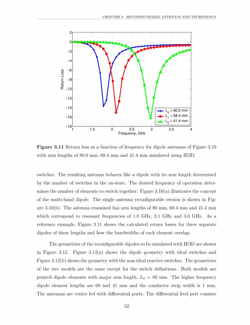
CHAPTER 3. RECONFIGURABLE ANTENNAS AND TECHNOLOGY
1 1.5 2 2.5 3 3.5 4−18
−16
−14
−12
−10
−8
−6
−4
−2
0
2
Frequency, GHz
Ret
urn
Loss
L0 = 80.0 mm
L1 = 68.4 mm
L2 = 41.4 mm
Figure 3.11 Return loss as a function of frequency for dipole antennas of Figure 3.10
with arm lengths of 80.0 mm, 68.4 mm and 41.4 mm simulated using IE3D.
switches. The resulting antenna behaves like a dipole with its arm length determined
by the number of switches in the on-state. The desired frequency of operation deter-
mines the number of elements to switch together. Figure 3.10(a) illustrates the concept
of the multi-band dipole. The single antenna reconfigurable version is shown in Fig-
ure 3.10(b). The antenna examined has arm lengths of 80 mm, 68.4 mm and 41.4 mm
which correspond to resonant frequencies of 1.8 GHz, 2.1 GHz and 3.0 GHz. As a
reference example, Figure 3.11 shows the calculated return losses for three separate
dipoles of these lengths and how the bandwidths of each element overlap.
The geometries of the reconfigurable dipoles to be simulated with IE3D are shown
in Figure 3.12. Figure 3.12(a) shows the dipole geometry with ideal switches and
Figure 3.12(b) shows the geometry with the non-ideal reactive switches. The geometries
of the two models are the same except for the switch definitions. Both models are
printed dipole elements with major arm length, L0 = 80 mm. The higher frequency
dipole element lengths are 68 and 41 mm and the conductor strip width is 1 mm.
The antennas are center fed with differential ports. The differential feed port consists
52
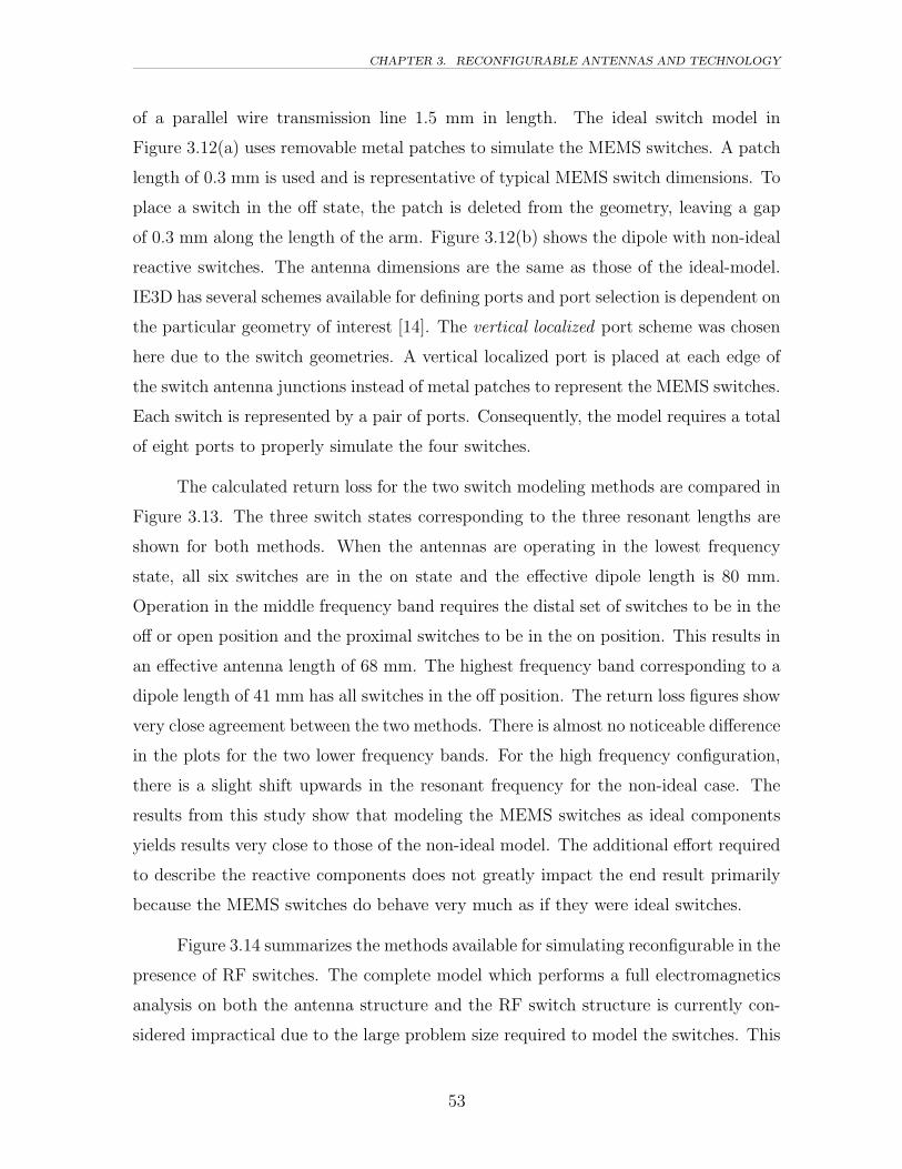
CHAPTER 3. RECONFIGURABLE ANTENNAS AND TECHNOLOGY
of a parallel wire transmission line 1.5 mm in length. The ideal switch model in
Figure 3.12(a) uses removable metal patches to simulate the MEMS switches. A patch
length of 0.3 mm is used and is representative of typical MEMS switch dimensions. To
place a switch in the off state, the patch is deleted from the geometry, leaving a gap
of 0.3 mm along the length of the arm. Figure 3.12(b) shows the dipole with non-ideal
reactive switches. The antenna dimensions are the same as those of the ideal-model.
IE3D has several schemes available for defining ports and port selection is dependent on
the particular geometry of interest [14]. The vertical localized port scheme was chosen
here due to the switch geometries. A vertical localized port is placed at each edge of
the switch antenna junctions instead of metal patches to represent the MEMS switches.
Each switch is represented by a pair of ports. Consequently, the model requires a total
of eight ports to properly simulate the four switches.
The calculated return loss for the two switch modeling methods are compared in
Figure 3.13. The three switch states corresponding to the three resonant lengths are
shown for both methods. When the antennas are operating in the lowest frequency
state, all six switches are in the on state and the effective dipole length is 80 mm.
Operation in the middle frequency band requires the distal set of switches to be in the
off or open position and the proximal switches to be in the on position. This results in
an effective antenna length of 68 mm. The highest frequency band corresponding to a
dipole length of 41 mm has all switches in the off position. The return loss figures show
very close agreement between the two methods. There is almost no noticeable difference
in the plots for the two lower frequency bands. For the high frequency configuration,
there is a slight shift upwards in the resonant frequency for the non-ideal case. The
results from this study show that modeling the MEMS switches as ideal components
yields results very close to those of the non-ideal model. The additional effort required
to describe the reactive components does not greatly impact the end result primarily
because the MEMS switches do behave very much as if they were ideal switches.
Figure 3.14 summarizes the methods available for simulating reconfigurable in the
presence of RF switches. The complete model which performs a full electromagnetics
analysis on both the antenna structure and the RF switch structure is currently con-
sidered impractical due to the large problem size required to model the switches. This
53

CHAPTER 3. RECONFIGURABLE ANTENNAS AND TECHNOLOGY
differential feed port
0.3 mm removable metal
patches
1 mm
(a) ideal switches modeled with removable metal patches
differential feed port #1
0.3 mm
1 mm # 2 # 3
# 6 # 7
# 4 # 5
# 8 # 9
vertical localized ports
(b) non-ideal reactive switches modeled with multiple ports
Figure 3.12 IE3D models for the reconfigurable dipole including RF switches.
54

CHAPTER 3. RECONFIGURABLE ANTENNAS AND TECHNOLOGY
1 1.5 2 2.5 3 3.5 4−16
−14
−12
−10
−8
−6
−4
−2
0
2
Frequency, GHz
Ret
urn
Loss
L0 ideal
L0 non−ideal
L1 ideal
L1 non−ideal
L2 ideal
L2 non−ideal
Figure 3.13 Computed return loss as a function of frequency for the frequency agile
dipole antenna of Figure 3.12 simulated using IE3D. The ideal switch model is from
Figure 3.12(a) and the non-ideal model is from Figure 3.12(b).
55
CHAPTER 3. RECONFIGURABLE ANTENNAS AND TECHNOLOGY
Full electromagnetic analysis of antenna with detailed RF
switch models
IMPRACTICAL
Electromagnetic analysis of antenna structure with
circuit model switches
PRACTICAL (limited to small number of
switches)
Electromagnetic analysis of antenna structure with
ideal model switches
PRACTICAL
Reactive Ideal
Complete Model Reduced Models
Figure 3.14 Reconfigurable antenna modeling comparison.
leaves the reduced models which represent the switches in a more manageable man-
ner. The non-ideal model treats the switches as reactive elements requires additional
port structures in the model. It also requires the additional step of post processing
to include switch the effects within the model and is practical for reconfigurable an-
tennas with only a small number of switches (less than 10). The ideal model is the
only method currently practical for antennas with a relatively large number (greater
than 10) of switches. There is no post processing needed to include the switch effects
and toggling between switch states is performed simply by adding or removing metal
patches.
56

Chapter 4
Analysis and Measurement of
Reconfigurable Ring Patch
This chapter presents the design and analysis of the reconfigurable ring patch antenna.
The newly developed reconfigurable ring patch patch antenna achieves an adjustable
bandwidth of up to 15% while maintaining constant performance over the other elec-
trical characteristics. The antenna structure is shown along with an explanation of its
operation. Analysis of its bandwidth controllable behavior, computer simulations and
measured results are also presented.
4.1 Introduction
The microstrip patch antenna has become one of the most commonly used antenna
types in the last 20 years for a broad assortment of applications, including hand-held,
automotive and aircraft applications. Its popularity is due to a number of factors:
unobtrusive and low profile shape, rugged form factor, and low construction cost. In
general, the microstrip patch antenna consists of a patch of metalization suspended over
a grounded substrate. The substrate height is normally much less than the operational
wavelength (h < λ/20) and is responsible for the very low-profile device form factor.
The low-profile comes at the expense of bandwidth. The microstrip patch is a resonant
antenna, and in its basic form has only a few percent bandwidth [7]. By increasing the
57

CHAPTER 4. RECONFIGURABLE RING PATCH
structure complexity, bandwidth can be increased considerably.
There is a wide array of geometric variations on the general microstrip patch
antenna. The ring patch antenna is one variant of the conventional microstrip patch
that has favorable radiation characteristics for a number of applications. Ring patches
can be designed for both linear and circular polarization and typically have a single
main beam in the broadside direction. During the investigation of the conventional
ring patch antenna it was determined that the impedance bandwidth of the antenna
could be altered by varying the width of the microstrip ring. These findings lead to
the invention of the reconfigurable ring patch antenna with parasitic matching plate
(RRPA). This antenna performs similar to the ring patch antenna but with the ability
to control the bandwidth of operation. The new antenna is describe in detail in this
chapter.
4.2 Antenna Structure
This section presents the reconfigurable ring patch antenna geometry. The geometry
of the reconfigurable ring patch antenna is shown in Figure 4.1. It is a two layer,
probe-fed, printed patch antenna designed to operate at a nominal center frequency
of 2.5 GHz. The primary feature of the RRPA is the ring patch layer. The printed
ring patch is similar to a solid microstrip patch except that a central portion of the
metal is removed to create a ring. The ring layer located 1.575 mm above the ground
plane and is situated on a substrate with a dielectric constant of 2.35. The ring layer
is responsible for controlling the reconfigurable bandwidth of the antenna and will be
detailed in Section 4.2.1. There is a second parasitic radiating structure above the
ring layer which improves the impedance matching characteristics. It is a 47 mm long
square patch located 4.9 mm above the ring layer. The parasitic patch is supported
with a foam block to approximate the dielectric constant of air (εr ≈ 1). The antenna
is fed via a standard through-hole probe feed located 11.5 mm from the center of the
patch along the centerline. In order to operate properly the antenna must be placed
over a ground plane.
The square annular ring patch operates similar to the annular ring microstrip
58

CHAPTER 4. RECONFIGURABLE RING PATCH
47
R o
R i
11.5
h = 4.925
t = 1.575 SMA Connector
Substrate Parasitic Plate
Reconfigurable Ring Layer
Feed Point
R w
All lengths in mm
z
y
x
PSfrag replacements
ε1 ≈ 1.0
ε2 = 2.35
Figure 4.1 Geometry of the reconfigurable ring patch antenna that operates at
2.5 GHz, units are in mm.
59

CHAPTER 4. RECONFIGURABLE RING PATCH
TM 10
W
L
PSfrag replacements
λd/2
λd/2
(a) rectangular (square) patch
TM 11
PSfrag replacements
λd/2
λd/2
(b) square ring patch
Figure 4.2 Difference in current path length for rectangular patch and square ring
patch. The guided wavelength is λd = λ/√
εr, where εr is the dielectric constant of the
substrate.
patch antenna [73, 8] shown in Figure 4.2(b). The ring patch behaves electrically as an
intermediate between a ground plane backed loop and a solid microstrip patch shown
in Figure 4.2. The square ring patch evolved from the ring patch when Mink [74] found
that the resonant frequency of a conventional patch could be reduced considerably by
removing a portion of metal from the center of the patch turning it into an annular
structure. The dominant modes for the rectangular MSA and the rectangular ring are
shown in Figure 4.2. It can be seen from Figure 4.2 that for equal sized patch antennas,
the ring structure forces the current to take a longer path and decreases the frequency
of operation. The average path length traveled by the current in the square ring is
longer than that of the square ring.
Similar to the rectangular microstrip patch, the ring patch can be viewed as
radiating via equivalent magnetic currents caused by fringing electric fields present at
the patch edges. These fringing fields act as radiating slots and, through equivalence,
can be viewed as magnetic currents. Ring resonators tend to excite TMmn modes
with the TM1n (n = 2, 4 ,. . . ) being suitable for antenna applications due to favorable
efficiency and bandwidth characteristics [75]. Polarity of the magnetic current can be
determined from the fringing fields at the edge of the patch. Figure 4.3 shows that the
60

CHAPTER 4. RECONFIGURABLE RING PATCH
+ +
-
Magnetic Currents
-
y
x
(a) TM11
Magnetic Currents
+ +
- -
+ +
- -
y
x
(b) TM12
Figure 4.3 Equivalent magnetic currents for TM11 and TM12 modes on the square
ring patch.
TM11 mode has opposing direction magnetic currents on the inner and outer edge of
the ring while the TM12 mode has magnetic currents with the same polarity. When
the equivalent magnetic sources are of the same polarity, they interfere constructively
and are suitable for radiation.
Antenna impedance bandwidth of the square ring is determined primarily by the
width of the square ring, Rw. Rw is the width of the patch metalization measured
along the x-axis and is defined by
Rw =Ro − Ri
2(4.1)
where Ro is the outer ring dimension and Ri is the inner dimension as shown in Fig-
ure 4.1. The separation of adjacent antenna modes is determined by the ring width.
The outer ring dimension Ro limits the lower end of the operational frequency while the
inner dimension, Ri, controls the upper end. When the ring width is small (Rw < λg/10
where λg is the guided wavelength defined by λg = λ0/√
εr), the modes are closely
spaced and the antenna operates with effectively one radiation mode. However, as the
ring width increases the single TM12 mode spreads into two degenerate TM modes.
An investigation was conducted using IE3D to determine the usable limits of
61

CHAPTER 4. RECONFIGURABLE RING PATCH
on ring width, RW . The ring dimensions were studied for the ring patch antenna
with solid, continuously varying ring widths in the patch layer. The results obtained
from this investigation are used in the subsequent sections to develop the discrete
ring states for the reconfigurable ring patch antenna geometry. The inner and outer
ring dimensions (Ro and Ri) were varied together and all antenna geometry parameters
were held constant to explore the effect of ring width on antenna impedance bandwidth.
Figure 4.4 shows the calculated VSWR for ring widths of 4 to 11 mm. Provided Rw
does not become too large, it is possible to use mode separation behavior to selectively
increase or decrease the bandwidth of the antenna without adversely affecting the other
antenna electrical properties. It can be seen that the radiation mode splits into two
modes when Rw > 8 mm (0.1λg). Figure 4.5 shows the antenna bandwidth versus ring
width aspect ratio, Ro/Ri. The plot shows that antenna bandwidth gets larger with
increasing ring width. Bandwidth increases up to a maximum value and then begins
to drop back down. Above an aspect ratio of 2.6, the two radiation modes become
distinct and begin diverging resulting in an overall reduction in antenna bandwidth.
Table 4.1 summarizes electrical performance of the ring patch antenna from Figure 4.1
based on different ring widths simulated using IE3D.
Table 4.1 Electrical performance based on ring width of the ring patch antenna sim-ulated using IE3D.
Ring width Inner dimension Outer dimension Bandwidth MinimumRw (mm) Ri (mm) Ro (mm) 2:1 VSWR (%) VSWR
4 9.25 13.25 - 2.55 8.75 13.75 - 2.16 8.25 14.25 5.0 1.57 7.75 14.75 8.6 1.28 7.25 15.25 11.4 1.29 6.75 15.75 15.7 1.310 6.25 16.25 11.8 1.311 5.75 16.75 3.1 1.2
62
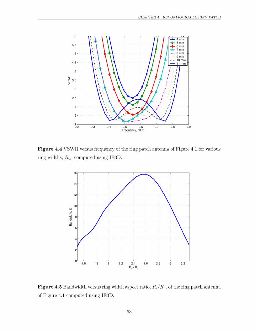
CHAPTER 4. RECONFIGURABLE RING PATCH
2.2 2.3 2.4 2.5 2.6 2.7 2.8 2.91
1.5
2
2.5
3
3.5
4
4.5
5
5.5
6
Frequency, GHz
VS
WR
4 mm5 mm6 mm7 mm8 mm9 mm10 mm11 mm
Figure 4.4 VSWR versus frequency of the ring patch antenna of Figure 4.1 for various
ring widths, Rw, computed using IE3D.
1.6 1.8 2 2.2 2.4 2.6 2.8 3 3.20
2
4
6
8
10
12
14
16
Ro / R
i
Ban
dwid
th, %
Figure 4.5 Bandwidth versus ring width aspect ratio, Ri/Ro, of the ring patch antenna
of Figure 4.1 computed using IE3D.
63

CHAPTER 4. RECONFIGURABLE RING PATCH
4.2.1 The Reconfigurable Ring Patch Antenna
Specific discrete ring widths are selected for several antenna bandwidth values based
on the ring width investigation performed in Section 4.2. Six ring widths have been
chosen to achieve discrete bandwidth states from 0% (effectively off) to 15% (maximum
bandwidth). These ring width states are used in the subsequent work to accomplish the
desired reconfigurable performance. Table 4.2 summarizes the ring widths chosen to
achieve the selectable bandwidth behavior along with the estimated bandwidth values
based on the ring width investigation in Section 4.2.
Table 4.2 Discrete ring widths for selected antenna bandwidth states based on simu-lations from Section 4.2.
State Ring width Inner dimension Outer dimension BandwidthRw (mm) Ri (mm) Ro (mm) 2:1 VSWR (%)
A 10.10 6.20 16.30 15B 8.98 6.76 15.74 13C 7.86 7.32 15.18 11D 6.74 7.88 14.62 9E 5.62 8.44 14.06 5F 4.50 9.00 13.50 0
The design task becomes how to physically vary the width of the ring to achieve
the desired reconfigurable operation. With the limits on the ring width defined from
Figure 4.4 and listed in Table 4.2, the solid layer ring is replaced by a new structure
with reconfigurable components. The ring is reformed as a single smaller solid ring
with a series of thin concentric rings on the inside and outside connected together via
MEMS switches as shown in Figure 4.6. The electrical width of the ring is varied by
selectively activating the interconnecting switches between the concentric rings and a
variable impedance bandwidth of 0 –15% is obtained.
The ring layer is replaced by a solid ring 4.5 mm in width having inner and outer
dimensions of Ri = 18 mm and Ro = 27 mm respectively. The feed point remains
the same at 11.25 mm from the patch center which results in a mean ring diameter R
= 45 mm, or roughly λg/4 for 2.55 GHz. To facilitate bandwidth control, the inner
and outer portions of the solid ring are replaced with concentric strip rings connected
64

CHAPTER 4. RECONFIGURABLE RING PATCH
together with RF switches. Figure 4.6 shows the layout of the rings and switches. The
strips are 0.36 mm wide and their length depends on their location within the ring
layer. The inner ring strips have a length of 12.4 mm and the outer strips have a
length of 31.88 mm. Following the switch modeling procedures from Section 3.3, the
switches are chosen to be 0.2 mm square. There are switches are placed at the corners
and the middle of the strips to ensure that in the on-position the connected sections
act as solid rings. They function in groups so the ring size changes in a symmetric
fashion, for example, the outer and inner rings switch together.
65

CHAPTER 4. RECONFIGURABLE RING PATCH
(a) state A, Rw = 10.10 mm (b) state B, Rw = 8.98 mm
(c) state C, Rw = 7.86 mm (d) state D, Rw = 6.74 mm
(e) state E, Rw = 5.62 mm (f) state F, Rw = 4.50 mm
Figure 4.6 Reconfigurable ring patch active layer switch configuration states. Switches
in on position are shown in dark and switches in off position are shown in light.
66
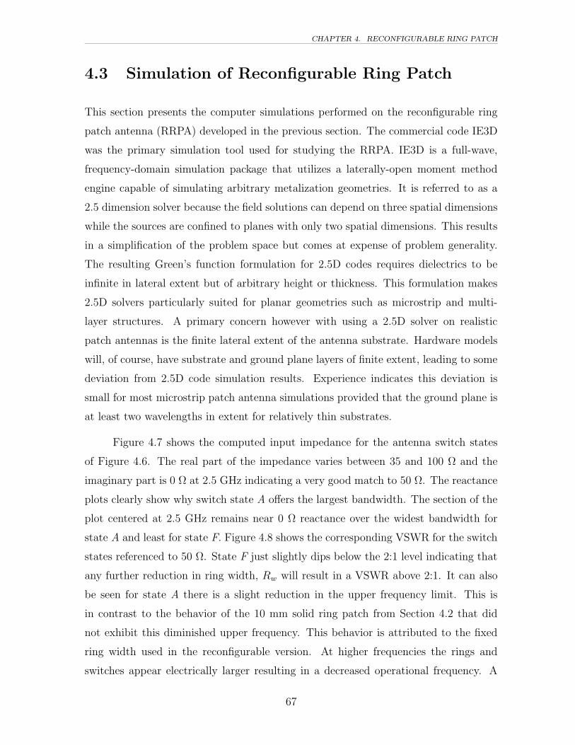
CHAPTER 4. RECONFIGURABLE RING PATCH
4.3 Simulation of Reconfigurable Ring Patch
This section presents the computer simulations performed on the reconfigurable ring
patch antenna (RRPA) developed in the previous section. The commercial code IE3D
was the primary simulation tool used for studying the RRPA. IE3D is a full-wave,
frequency-domain simulation package that utilizes a laterally-open moment method
engine capable of simulating arbitrary metalization geometries. It is referred to as a
2.5 dimension solver because the field solutions can depend on three spatial dimensions
while the sources are confined to planes with only two spatial dimensions. This results
in a simplification of the problem space but comes at expense of problem generality.
The resulting Green’s function formulation for 2.5D codes requires dielectrics to be
infinite in lateral extent but of arbitrary height or thickness. This formulation makes
2.5D solvers particularly suited for planar geometries such as microstrip and multi-
layer structures. A primary concern however with using a 2.5D solver on realistic
patch antennas is the finite lateral extent of the antenna substrate. Hardware models
will, of course, have substrate and ground plane layers of finite extent, leading to some
deviation from 2.5D code simulation results. Experience indicates this deviation is
small for most microstrip patch antenna simulations provided that the ground plane is
at least two wavelengths in extent for relatively thin substrates.
Figure 4.7 shows the computed input impedance for the antenna switch states
of Figure 4.6. The real part of the impedance varies between 35 and 100 Ω and the
imaginary part is 0 Ω at 2.5 GHz indicating a very good match to 50 Ω. The reactance
plots clearly show why switch state A offers the largest bandwidth. The section of the
plot centered at 2.5 GHz remains near 0 Ω reactance over the widest bandwidth for
state A and least for state F. Figure 4.8 shows the corresponding VSWR for the switch
states referenced to 50 Ω. State F just slightly dips below the 2:1 level indicating that
any further reduction in ring width, Rw will result in a VSWR above 2:1. It can also
be seen for state A there is a slight reduction in the upper frequency limit. This is
in contrast to the behavior of the 10 mm solid ring patch from Section 4.2 that did
not exhibit this diminished upper frequency. This behavior is attributed to the fixed
ring width used in the reconfigurable version. At higher frequencies the rings and
switches appear electrically larger resulting in a decreased operational frequency. A
67

CHAPTER 4. RECONFIGURABLE RING PATCH
ring width that varies progressively larger toward ring extremes would mitigate this
effect. However, this would require the use of variable switch sizes in the antenna
design. Table 4.3 summarizes the computed 2:1 VSWR impedance bandwidth and
geometry parameters for the antenna switch states of Figure 4.6.
Table 4.3 Impedance bandwidth performance and reconfigurable ring geometry forthe RRPA with switch states of Figure 4.6 computed using IE3D
State Ring width Center frequency Bandwidth MinimumRw (mm) fo (GHz) 2:1 VSWR (%) VSWR
A 10.10 2.498 15.0 1.05B 8.98 2.530 13.4 1.10C 7.86 2.533 11.7 1.20D 6.74 2.530 9.1 1.10E 5.62 2.515 5.6 1.45F 4.50 2.503 0.6 1.95
68

CHAPTER 4. RECONFIGURABLE RING PATCH
0
50
100
150
200
Res
ista
nce,
Ω
Real state Astate Bstate Cstate Dstate Estate F
2.1 2.2 2.3 2.4 2.5 2.6 2.7 2.8 2.9−150
−100
−50
0
50
100
150
Frequency, GHz
Rea
ctan
ce, Ω
Imaginary state Astate Bstate Cstate Dstate Estate F
Figure 4.7 Input impedance versus frequency of the reconfigurable ring patch antenna
for switch states of Figure 4.6 simulated using IE3D.
2.1 2.2 2.3 2.4 2.5 2.6 2.7 2.8 2.91
2
3
4
5
6
7
8
9
10
Frequency, GHz
VS
WR
state Astate Bstate Cstate Dstate Estate F
Figure 4.8 VSWR versus frequency of the reconfigurable ring patch antenna for switch
states of Figure 4.6 simulated using IE3D.
69
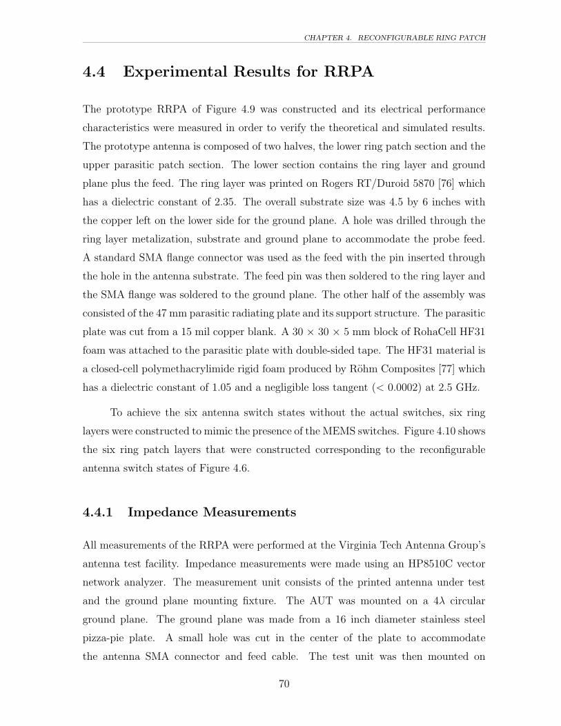
CHAPTER 4. RECONFIGURABLE RING PATCH
4.4 Experimental Results for RRPA
The prototype RRPA of Figure 4.9 was constructed and its electrical performance
characteristics were measured in order to verify the theoretical and simulated results.
The prototype antenna is composed of two halves, the lower ring patch section and the
upper parasitic patch section. The lower section contains the ring layer and ground
plane plus the feed. The ring layer was printed on Rogers RT/Duroid 5870 [76] which
has a dielectric constant of 2.35. The overall substrate size was 4.5 by 6 inches with
the copper left on the lower side for the ground plane. A hole was drilled through the
ring layer metalization, substrate and ground plane to accommodate the probe feed.
A standard SMA flange connector was used as the feed with the pin inserted through
the hole in the antenna substrate. The feed pin was then soldered to the ring layer and
the SMA flange was soldered to the ground plane. The other half of the assembly was
consisted of the 47 mm parasitic radiating plate and its support structure. The parasitic
plate was cut from a 15 mil copper blank. A 30 × 30 × 5 mm block of RohaCell HF31
foam was attached to the parasitic plate with double-sided tape. The HF31 material is
a closed-cell polymethacrylimide rigid foam produced by Rohm Composites [77] which
has a dielectric constant of 1.05 and a negligible loss tangent (< 0.0002) at 2.5 GHz.
To achieve the six antenna switch states without the actual switches, six ring
layers were constructed to mimic the presence of the MEMS switches. Figure 4.10 shows
the six ring patch layers that were constructed corresponding to the reconfigurable
antenna switch states of Figure 4.6.
4.4.1 Impedance Measurements
All measurements of the RRPA were performed at the Virginia Tech Antenna Group’s
antenna test facility. Impedance measurements were made using an HP8510C vector
network analyzer. The measurement unit consists of the printed antenna under test
and the ground plane mounting fixture. The AUT was mounted on a 4λ circular
ground plane. The ground plane was made from a 16 inch diameter stainless steel
pizza-pie plate. A small hole was cut in the center of the plate to accommodate
the antenna SMA connector and feed cable. The test unit was then mounted on
70
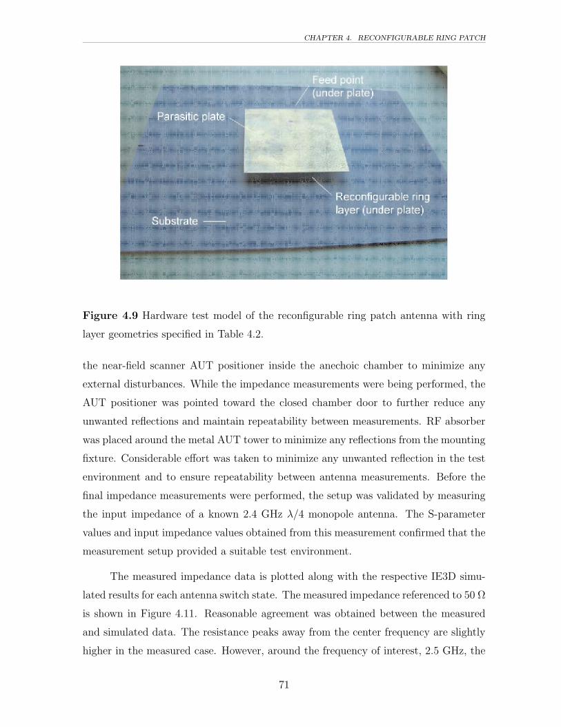
CHAPTER 4. RECONFIGURABLE RING PATCH
Figure 4.9 Hardware test model of the reconfigurable ring patch antenna with ring
layer geometries specified in Table 4.2.
the near-field scanner AUT positioner inside the anechoic chamber to minimize any
external disturbances. While the impedance measurements were being performed, the
AUT positioner was pointed toward the closed chamber door to further reduce any
unwanted reflections and maintain repeatability between measurements. RF absorber
was placed around the metal AUT tower to minimize any reflections from the mounting
fixture. Considerable effort was taken to minimize any unwanted reflection in the test
environment and to ensure repeatability between antenna measurements. Before the
final impedance measurements were performed, the setup was validated by measuring
the input impedance of a known 2.4 GHz λ/4 monopole antenna. The S-parameter
values and input impedance values obtained from this measurement confirmed that the
measurement setup provided a suitable test environment.
The measured impedance data is plotted along with the respective IE3D simu-
lated results for each antenna switch state. The measured impedance referenced to 50 Ω
is shown in Figure 4.11. Reasonable agreement was obtained between the measured
and simulated data. The resistance peaks away from the center frequency are slightly
higher in the measured case. However, around the frequency of interest, 2.5 GHz, the
71
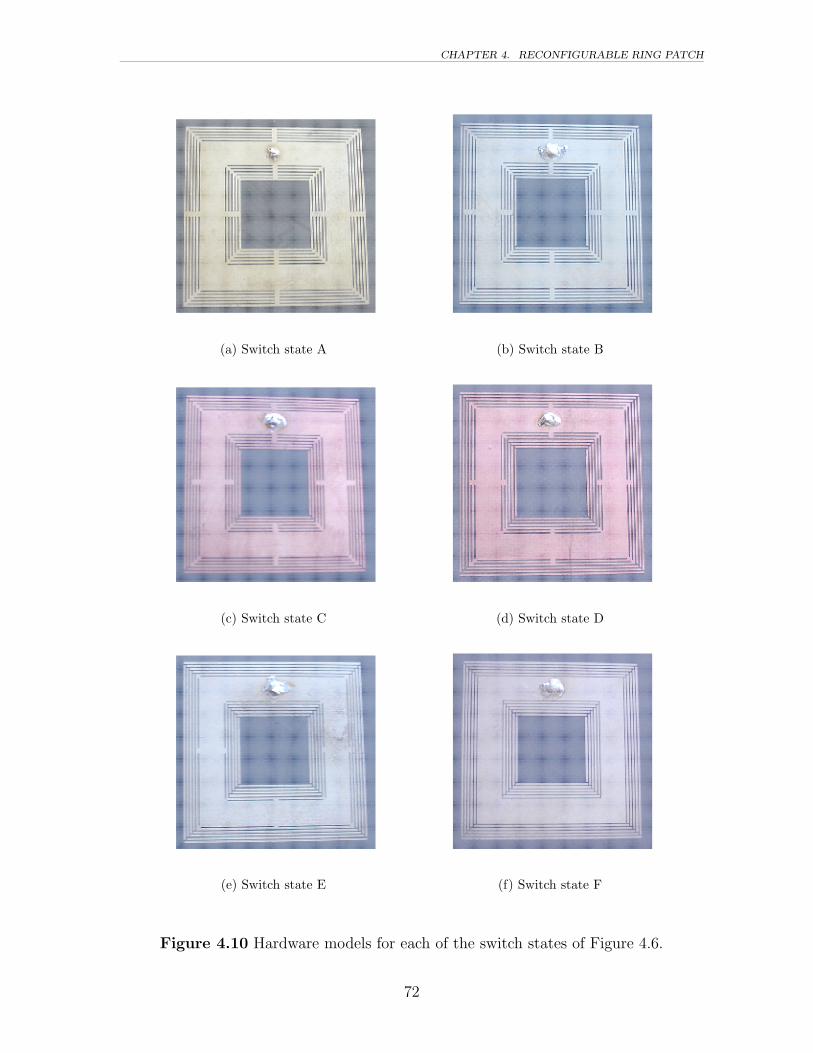
CHAPTER 4. RECONFIGURABLE RING PATCH
(a) Switch state A (b) Switch state B
(c) Switch state C (d) Switch state D
(e) Switch state E (f) Switch state F
Figure 4.10 Hardware models for each of the switch states of Figure 4.6.
72

CHAPTER 4. RECONFIGURABLE RING PATCH
measured resistance and reactance for all switch states is very similar to the computed
values. This indicates that that the design is somewhat sensitive to manufacturing
tolerances off resonance. The height, h, of the parasitic plate has a significant impact
on the input impedance and the process of hand sanding the foam support block was
the most prone to manufacturing tolerance errors and most likely contributed to the
slight measurement differences.
Figure 4.12 shows the measured VSWR for all states compared to the computed
values. There is a small overall upward shift in the center frequency noted for all
switch states in comparison to the simulated antenna. However, the total 2:1 VSWR
impedance bandwidths are very close to the computed values for all switch states.
Figure 4.13 compares the VSWR for all switch states on the same graph. It is noted
that the reduction in upper frequency limit seen in simulated state A also appears
in the measured data. The associated return loss for all switch states is shown in
Figure 4.14. Table 4.4 provides a summary of the measured and simulated 2:1 VSWR
performance of the RRPA.
Table 4.4 Summary of the measured and simulated 2:1 VSWR impedance bandwidthperformance for the RRPA.
Bandwidth Center Frequency Minimum2:1 VSWR (%) fo (GHz) VSWR
State measured simulated measured simulated measured simulated
A 13.3 15.0 2.52 2.50 1.05 1.05B 11.0 13.4 2.54 2.53 1.10 1.10C 8.0 11.7 2.54 2.53 1.35 1.20D 4.5 9.1 2.51 2.53 1.70 1.10E 0 5.6 2.52 2.52 2.05 1.45F 0 0.6 2.52 2.50 2.52 1.95
73
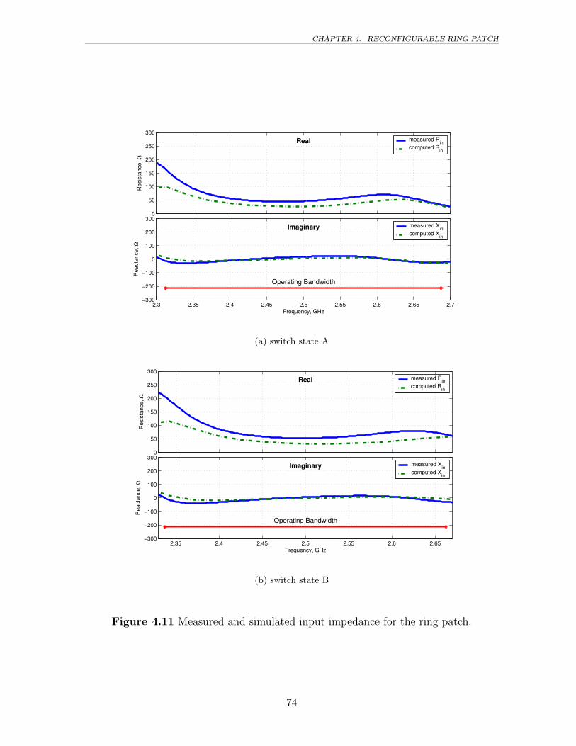
CHAPTER 4. RECONFIGURABLE RING PATCH
0
50
100
150
200
250
300R
esis
tanc
e, Ω
Real measured Rin
computed R
in
2.3 2.35 2.4 2.45 2.5 2.55 2.6 2.65 2.7−300
−200
−100
0
100
200
300
Frequency, GHz
Rea
ctan
ce, Ω
Imaginary
Operating Bandwidth
measured Xin
computed X
in
(a) switch state A
0
50
100
150
200
250
300
Res
ista
nce,
Ω
Real measured Rin
computed R
in
2.35 2.4 2.45 2.5 2.55 2.6 2.65−300
−200
−100
0
100
200
300
Frequency, GHz
Rea
ctan
ce, Ω
Imaginary
Operating Bandwidth
measured Xin
computed X
in
(b) switch state B
Figure 4.11 Measured and simulated input impedance for the ring patch.
74

CHAPTER 4. RECONFIGURABLE RING PATCH
0
100
200
300
400R
esis
tanc
e, Ω
Real measured Rin
computed R
in
2.35 2.4 2.45 2.5 2.55 2.6 2.65−300
−200
−100
0
100
200
300
Frequency, GHz
Rea
ctan
ce, Ω
Imaginary
Operating Bandwidth
measured Xin
computed X
in
(c) switch state C
0
100
200
300
400
Res
ista
nce,
Ω
Real measured Rin
computed R
in
2.4 2.45 2.5 2.55 2.6−300
−200
−100
0
100
200
300
Frequency, GHz
Rea
ctan
ce, Ω
Imaginary
Operating Bandwidth
measured Xin
computed X
in
(d) switch state D
Figure 4.11 Measured and simulated input impedance for the ring patch (cont.)
75

CHAPTER 4. RECONFIGURABLE RING PATCH
0
100
200
300
400
500
600
Res
ista
nce,
ΩReal measured R
in
computed Rin
2.44 2.46 2.48 2.5 2.52 2.54 2.56−300
−200
−100
0
100
200
300
Frequency, GHz
Rea
ctan
ce, Ω
Imaginary
Operating Bandwidth
measured Xin
computed X
in
(e) switch state E
0
100
200
300
400
500
600
Res
ista
nce,
Ω
Real measured Rin
computed R
in
2.44 2.46 2.48 2.5 2.52 2.54 2.56−300
−200
−100
0
100
200
300
Frequency, GHz
Rea
ctan
ce, Ω
Imaginary
No Bandwidth
measured Xin
computed X
in
(f) switch state F
Figure 4.11 Measured and simulated return loss for the ring patch (cont.)
76
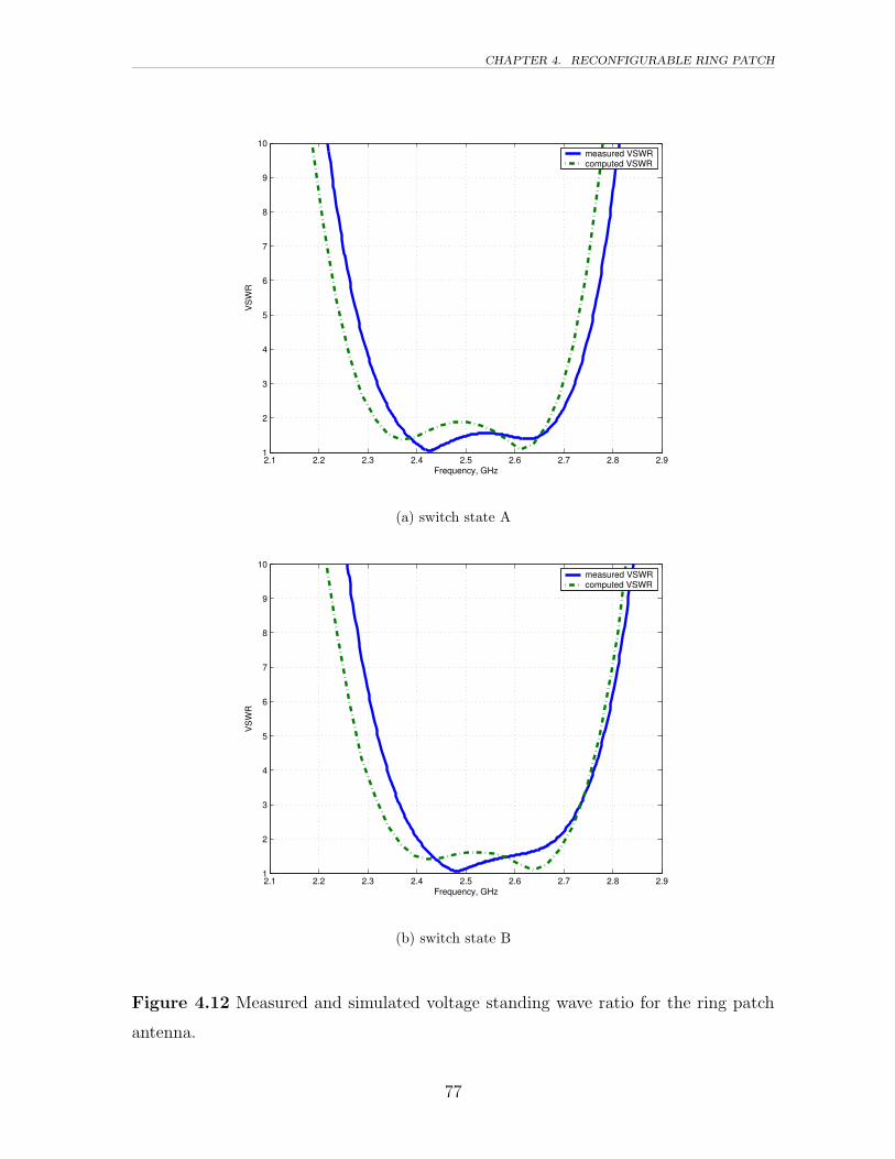
CHAPTER 4. RECONFIGURABLE RING PATCH
2.1 2.2 2.3 2.4 2.5 2.6 2.7 2.8 2.91
2
3
4
5
6
7
8
9
10
Frequency, GHz
VS
WR
measured VSWRcomputed VSWR
(a) switch state A
2.1 2.2 2.3 2.4 2.5 2.6 2.7 2.8 2.91
2
3
4
5
6
7
8
9
10
Frequency, GHz
VS
WR
measured VSWRcomputed VSWR
(b) switch state B
Figure 4.12 Measured and simulated voltage standing wave ratio for the ring patch
antenna.
77

CHAPTER 4. RECONFIGURABLE RING PATCH
2.1 2.2 2.3 2.4 2.5 2.6 2.7 2.8 2.91
2
3
4
5
6
7
8
9
10
Frequency, GHz
VS
WR
measured VSWRcomputed VSWR
(c) switch state C
2.1 2.2 2.3 2.4 2.5 2.6 2.7 2.8 2.91
2
3
4
5
6
7
8
9
10
Frequency, GHz
VS
WR
measured VSWRcomputed VSWR
(d) switch state D
Figure 4.12 Measured and simulated voltage standing wave ratio for the ring patch
antenna (cont.)
78
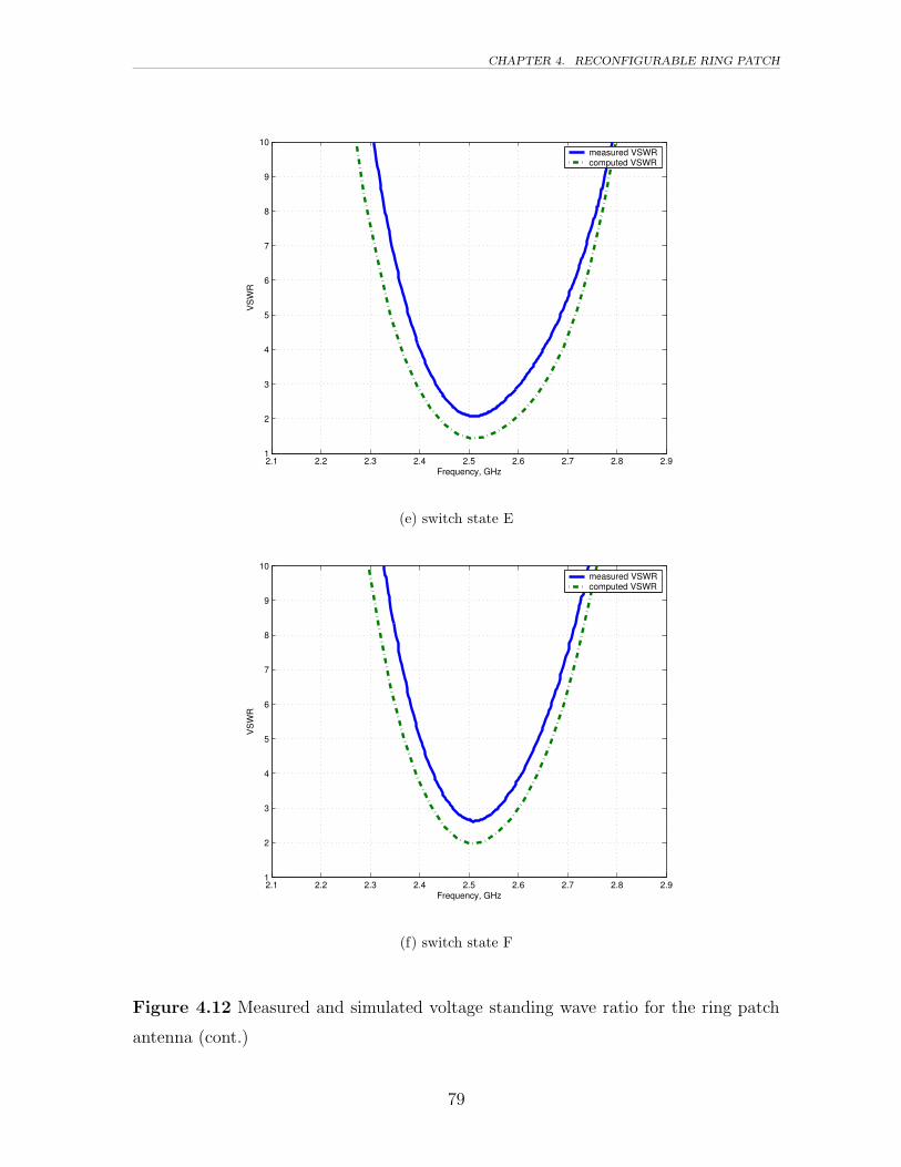
CHAPTER 4. RECONFIGURABLE RING PATCH
2.1 2.2 2.3 2.4 2.5 2.6 2.7 2.8 2.91
2
3
4
5
6
7
8
9
10
Frequency, GHz
VS
WR
measured VSWRcomputed VSWR
(e) switch state E
2.1 2.2 2.3 2.4 2.5 2.6 2.7 2.8 2.91
2
3
4
5
6
7
8
9
10
Frequency, GHz
VS
WR
measured VSWRcomputed VSWR
(f) switch state F
Figure 4.12 Measured and simulated voltage standing wave ratio for the ring patch
antenna (cont.)
79

CHAPTER 4. RECONFIGURABLE RING PATCH
2.1 2.2 2.3 2.4 2.5 2.6 2.7 2.8 2.91
2
3
4
5
6
7
8
9
10
Frequency, GHz
VS
WR
state Astate Bstate Cstate Dstate Estate F
Figure 4.13 Measured voltage standing wave ratio for the ring patch in all states.
2.1 2.2 2.3 2.4 2.5 2.6 2.7−35
−30
−25
−20
−15
−10
−5
0
Frequency, GHz
20 lo
g |Γ
|, dB
state Astate Bstate Cstate Dstate Estate F
Figure 4.14 Measured return loss for the ring patch in all states.
80

CHAPTER 4. RECONFIGURABLE RING PATCH
4.4.2 Pattern Measurements
Radiation patterns were measured in the VTAG indoor anechoic chamber using the
near-field measurement system. The pattern measurements were made using the same
pie-plate ground plane test fixture that was used in the impedance measurements
presented in Section 4.4.1. However, for the pattern measurements the AUT was con-
nected to the near-field scanner through the AUT positioner. Additional RF absorber
was placed behind the test antenna and around the AUT tower to minimize any re-
flection from the test equipment. A spherical scan was performed with the near-field
scanner and the results for selected pattern cuts are presented here compared to the
simulated patterns. Prior to performing the final pattern measurements of the AUT,
the setup was validated by measuring the radiation patterns of a known 2.4 GHz λ/4
monopole antenna. The radiation patterns obtained from this validation measurement
confirmed that the measurement setup provided a suitable test environment.
The patterns were made at several frequencies and the results for 2.5 GHz are
presented here. Similar to the rectangular microstrip patch, the RRPA has a broad,
unidirectional beam in the boresight (z-axis) direction. This is the expected pattern
behavior arising from the x-directed, equivalent magnetic surface currents on the patch
edges described in Figure 4.3(b). As was predicted by the simulations, the radiation
pattern behavior of the antenna remains nearly constant from one switch state to
the next. This is a desired behavior of the antenna in order to maintain predictable
performance while selecting the antenna bandwidth. The principal plane elevation
cuts are shown in Figure 4.15. The elevation E-plane (φ = 90) cut is slightly broader
than the H-plane (φ = 0) pattern cut which is expected from the surface currents.
The elevation patterns remain nearly constant over all six switch states showing only
0.04 dB variation from the maximum directivity of 9.18 dB. The measured elevation
patterns show a small amount of high-frequency diffraction ripple for low elevation
angles behind the ground plane (−90 < θ < 90). This ripple is a result of the finite
nature of the measured ground plane and arises from diffraction currents along the
edge of the circular ground plane. The diffraction effects are not seen in the simulated
patterns because a infinite ground plane was assumed in the simulations. Figures 4.16
and 4.17 show the measured azimuth patterns. The ground plane edge diffraction is
81

CHAPTER 4. RECONFIGURABLE RING PATCH
again visible in Figure 4.16 for θ = 80; this conical pattern cut corresponds to the
elevation angle around the ground plane. As with the elevation patterns, there is very
little deviation in the patterns between the each state and good agreement to the
simulated performance. Figures 4.18, 4.19 and 4.20 re-plot the directivity patterns for
each switch state on the same graph to illustrate those pattern consistency over all
bandwidth states.
Due to the difficulty in measuring the gain for electrically small antennas, abso-
lute gain measurements were not made. However, the close agreement between com-
puted and measured performance for pattern and impedance leads to a high level of
confidence in the predicted gain obtained from the IE3D simulations even though ab-
solute gain was not measured. In the absence of gain standard measurements, the
near-field measurement software reports only directivity measurements.
82

CHAPTER 4. RECONFIGURABLE RING PATCH
0 −10 −20 −30 −40 −50 −40 −30 −20 −10 0
30
−150
60
−120
90−90
120
−60
150
−30
180
0
Max = 9.16
Eφ ( φ = 0o ) measuredEφ ( φ = 0o ) simulatedEθ ( φ = 90o ) measuredEθ ( φ = 90o ) simulated
(a) switch state A
0 −10 −20 −30 −40 −50 −40 −30 −20 −10 0
30
−150
60
−120
90−90
120
−60
150
−30
180
0
Max = 9.14
Eφ ( φ = 0o ) measuredEφ ( φ = 0o ) simulatedEθ ( φ = 90o ) measuredEθ ( φ = 90o ) simulated
(b) switch state B
Figure 4.15 Measured and simulated elevation radiation patterns in the principal
planes for the RRPA.
83

CHAPTER 4. RECONFIGURABLE RING PATCH
0 −10 −20 −30 −40 −50 −40 −30 −20 −10 0
30
−150
60
−120
90−90
120
−60
150
−30
180
0
Max = 9.16
Eφ ( φ = 0o ) measuredEφ ( φ = 0o ) simulatedEθ ( φ = 90o ) measuredEθ ( φ = 90o ) simulated
(c) switch state C
0 −10 −20 −30 −40 −50 −40 −30 −20 −10 0
30
−150
60
−120
90−90
120
−60
150
−30
180
0
Max = 9.15
Eφ ( φ = 0o ) measuredEφ ( φ = 0o ) simulatedEθ ( φ = 90o ) measuredEθ ( φ = 90o ) simulated
(d) switch state D
Figure 4.15 Measured and simulated elevation radiation patterns in the principal
planes for the RRPA (cont.)
84

CHAPTER 4. RECONFIGURABLE RING PATCH
0 −10 −20 −30 −40 −50 −40 −30 −20 −10 0
30
−150
60
−120
90−90
120
−60
150
−30
180
0
Max = 9.16
Eφ ( φ = 0o ) measuredEφ ( φ = 0o ) simulatedEθ ( φ = 90o ) measuredEθ ( φ = 90o ) simulated
(e) switch state E
0 −10 −20 −30 −40 −50 −40 −30 −20 −10 0
30
−150
60
−120
90−90
120
−60
150
−30
180
0
Max = 9.18
Eφ ( φ = 0o ) measuredEφ ( φ = 0o ) simulatedEθ ( φ = 90o ) measuredEθ ( φ = 90o ) simulated
(f) switch state F
Figure 4.15 Measured and simulated elevation radiation patterns in the principal
planes for the RRPA (cont.)
85

CHAPTER 4. RECONFIGURABLE RING PATCH
0 −10 −20 −30 −40 −50 −40 −30 −20 −10 0
30
−150
60
−120
90−90
120
−60
150
−30
180
0
Max = 8.28
Etot
(θ = 10o ) measuredE
tot (θ = 10o ) simulated
Etot
(θ = 45o ) measuredE
tot (θ = 45o ) simulated
Etot
(θ = 80o ) measuredE
tot (θ = 80o ) simulated
(a) switch state A
0 −10 −20 −30 −40 −50 −40 −30 −20 −10 0
30
−150
60
−120
90−90
120
−60
150
−30
180
0
Max = 8.98
Etot
(θ = 10o ) measuredE
tot (θ = 10o ) simulated
Etot
(θ = 45o ) measuredE
tot (θ = 45o ) simulated
Etot
(θ = 80o ) measuredE
tot (θ = 80o ) simulated
(b) switch state B
Figure 4.16 Measured and simulated conical Etotal radiation patterns for the RRPA.
86
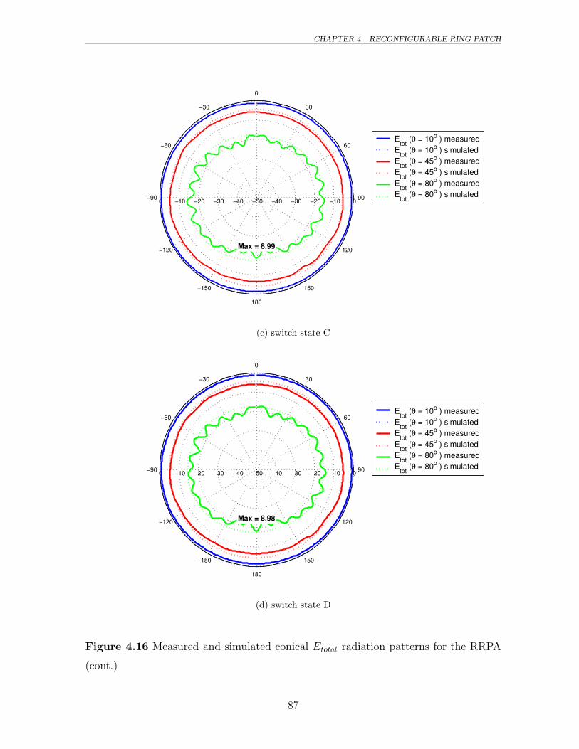
CHAPTER 4. RECONFIGURABLE RING PATCH
0 −10 −20 −30 −40 −50 −40 −30 −20 −10 0
30
−150
60
−120
90−90
120
−60
150
−30
180
0
Max = 8.99
Etot
(θ = 10o ) measuredE
tot (θ = 10o ) simulated
Etot
(θ = 45o ) measuredE
tot (θ = 45o ) simulated
Etot
(θ = 80o ) measuredE
tot (θ = 80o ) simulated
(c) switch state C
0 −10 −20 −30 −40 −50 −40 −30 −20 −10 0
30
−150
60
−120
90−90
120
−60
150
−30
180
0
Max = 8.98
Etot
(θ = 10o ) measuredE
tot (θ = 10o ) simulated
Etot
(θ = 45o ) measuredE
tot (θ = 45o ) simulated
Etot
(θ = 80o ) measuredE
tot (θ = 80o ) simulated
(d) switch state D
Figure 4.16 Measured and simulated conical Etotal radiation patterns for the RRPA
(cont.)
87
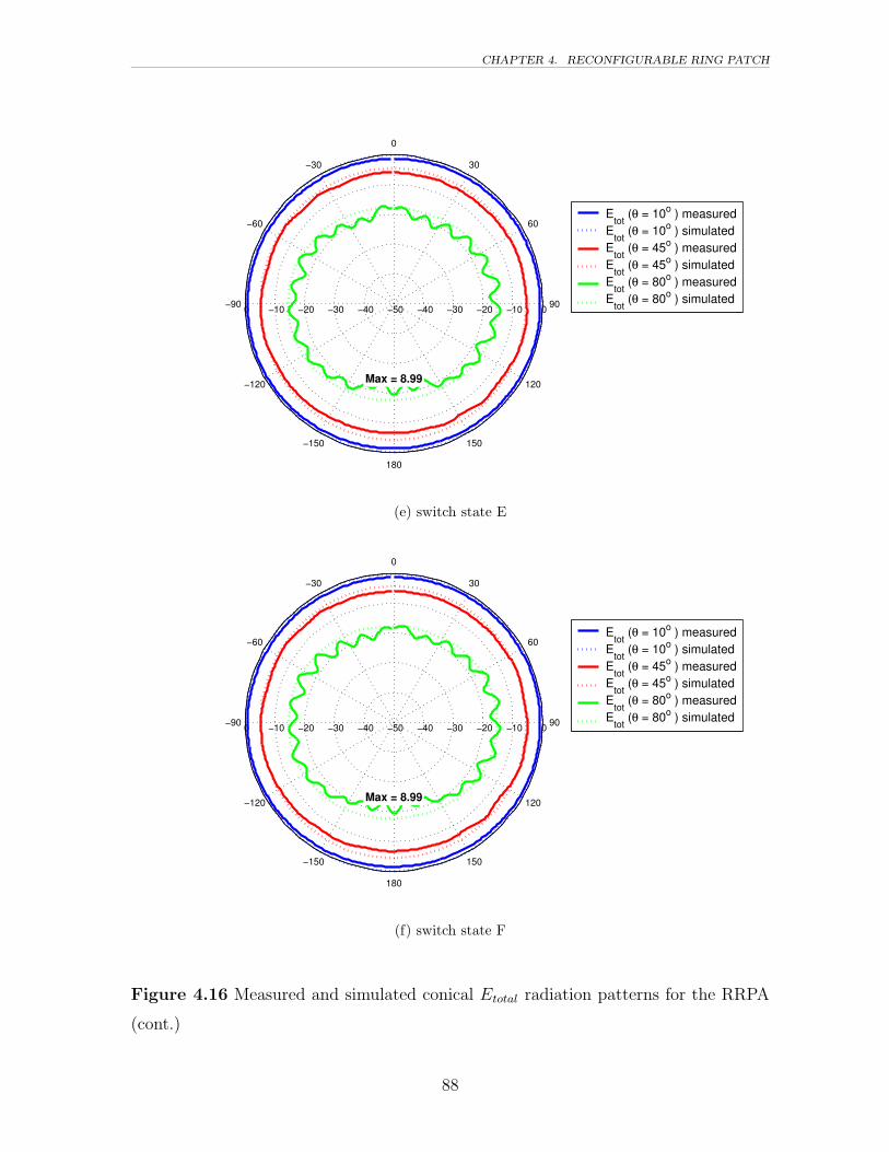
CHAPTER 4. RECONFIGURABLE RING PATCH
0 −10 −20 −30 −40 −50 −40 −30 −20 −10 0
30
−150
60
−120
90−90
120
−60
150
−30
180
0
Max = 8.99
Etot
(θ = 10o ) measuredE
tot (θ = 10o ) simulated
Etot
(θ = 45o ) measuredE
tot (θ = 45o ) simulated
Etot
(θ = 80o ) measuredE
tot (θ = 80o ) simulated
(e) switch state E
0 −10 −20 −30 −40 −50 −40 −30 −20 −10 0
30
−150
60
−120
90−90
120
−60
150
−30
180
0
Max = 8.99
Etot
(θ = 10o ) measuredE
tot (θ = 10o ) simulated
Etot
(θ = 45o ) measuredE
tot (θ = 45o ) simulated
Etot
(θ = 80o ) measuredE
tot (θ = 80o ) simulated
(f) switch state F
Figure 4.16 Measured and simulated conical Etotal radiation patterns for the RRPA
(cont.)
88

CHAPTER 4. RECONFIGURABLE RING PATCH
0 −5 −10 −15 −20 −15 −10 −5 0
30
−150
60
−120
90−90
120
−60
150
−30
180
0
Max = 8.28
Eθ (θ = 10o ) measuredEθ (θ = 10o ) simulatedEφ (θ = 10o ) measuredEφ (θ = 10o ) simulatedEθ (θ = 45o ) measuredEθ (θ = 45o ) simulatedEφ (θ = 45o ) measuredEφ (θ = 45o ) simulated
(a) switch state A
0 −5 −10 −15 −20 −15 −10 −5 0
30
−150
60
−120
90−90
120
−60
150
−30
180
0
Max = 8.98
Eθ (θ = 10o ) measuredEθ (θ = 10o ) simulatedEφ (θ = 10o ) measuredEφ (θ = 10o ) simulatedEθ (θ = 45o ) measuredEθ (θ = 45o ) simulatedEφ (θ = 45o ) measuredEφ (θ = 45o ) simulated
(b) switch state B
Figure 4.17 Measured and simulated conical Eθ & Eφ radiation patterns for the
RRPA.
89
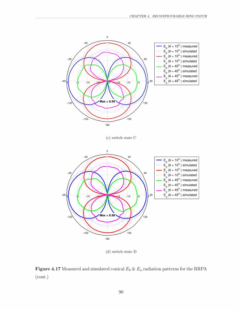
CHAPTER 4. RECONFIGURABLE RING PATCH
0 −5 −10 −15 −20 −15 −10 −5 0
30
−150
60
−120
90−90
120
−60
150
−30
180
0
Max = 8.99
Eθ (θ = 10o ) measuredEθ (θ = 10o ) simulatedEφ (θ = 10o ) measuredEφ (θ = 10o ) simulatedEθ (θ = 45o ) measuredEθ (θ = 45o ) simulatedEφ (θ = 45o ) measuredEφ (θ = 45o ) simulated
(c) switch state C
0 −5 −10 −15 −20 −15 −10 −5 0
30
−150
60
−120
90−90
120
−60
150
−30
180
0
Max = 8.98
Eθ (θ = 10o ) measuredEθ (θ = 10o ) simulatedEφ (θ = 10o ) measuredEφ (θ = 10o ) simulatedEθ (θ = 45o ) measuredEθ (θ = 45o ) simulatedEφ (θ = 45o ) measuredEφ (θ = 45o ) simulated
(d) switch state D
Figure 4.17 Measured and simulated conical Eθ & Eφ radiation patterns for the RRPA
(cont.)
90

CHAPTER 4. RECONFIGURABLE RING PATCH
0 −5 −10 −15 −20 −15 −10 −5 0
30
−150
60
−120
90−90
120
−60
150
−30
180
0
Max = 8.99
Eθ (θ = 10o ) measuredEθ (θ = 10o ) simulatedEφ (θ = 10o ) measuredEφ (θ = 10o ) simulatedEθ (θ = 45o ) measuredEθ (θ = 45o ) simulatedEφ (θ = 45o ) measuredEφ (θ = 45o ) simulated
(e) switch state E
0 −5 −10 −15 −20 −15 −10 −5 0
30
−150
60
−120
90−90
120
−60
150
−30
180
0
Max = 8.99
Eθ (θ = 10o ) measuredEθ (θ = 10o ) simulatedEφ (θ = 10o ) measuredEφ (θ = 10o ) simulatedEθ (θ = 45o ) measuredEθ (θ = 45o ) simulatedEφ (θ = 45o ) measuredEφ (θ = 45o ) simulated
(f) switch state F
Figure 4.17 Measured and simulated conical Eθ & Eφ radiation patterns for the RRPA
(cont.)
91

CHAPTER 4. RECONFIGURABLE RING PATCH
0 −10 −20 −30 −40 −30 −20 −10 0
30
−150
60
−120
90−90
120
−60
150
−30
180
0
Max = 9.18
State AState BState CState DState EState F
(a) Eθ (φ = 90)
0 −10 −20 −30 −40 −30 −20 −10 0
30
−150
60
−120
90−90
120
−60
150
−30
180
0
Max = 9.18
State AState BState CState DState EState F
(b) Eφ (φ = 0)
Figure 4.18 Comparison of measured elevation radiation patterns in the principal
planes for all switch states of the RRPA.
92

CHAPTER 4. RECONFIGURABLE RING PATCH
0 −5 −10 −15 −20 −25 −30 −25 −20 −15 −10 −5 0
30
−150
60
−120
90−90
120
−60
150
−30
180
0
Max = 8.30
State AState BState CState DState EState F
(a) Eθ (θ = 10)
0 −5 −10 −15 −20 −25 −30 −25 −20 −15 −10 −5 0
30
−150
60
−120
90−90
120
−60
150
−30
180
0
Max = 8.30
State AState BState CState DState EState F
(b) Eφ (θ = 10)
Figure 4.19 Comparison of measured conical radiation patterns for all switch states
of the RRPA.
93

CHAPTER 4. RECONFIGURABLE RING PATCH
0 −5 −10 −15 −20 −25 −30 −25 −20 −15 −10 −5 0
30
−150
60
−120
90−90
120
−60
150
−30
180
0
Max = 8.30
State AState BState CState DState EState F
(a) Eθ (θ = 45)
0 −5 −10 −15 −20 −25 −30 −25 −20 −15 −10 −5 0
30
−150
60
−120
90−90
120
−60
150
−30
180
0
Max = 8.30
State AState BState CState DState EState F
(b) Eφ (θ = 45)
Figure 4.20 Comparison of measured conical radiation patterns for all switch states
of the RRPA.
94
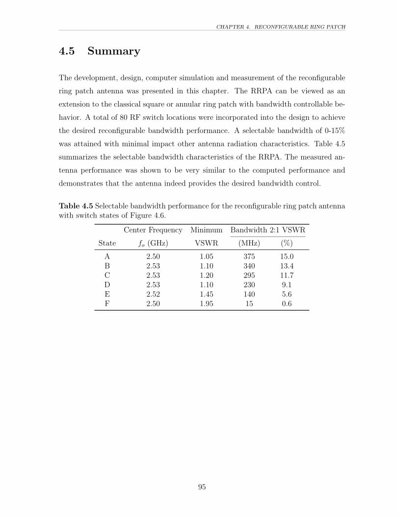
CHAPTER 4. RECONFIGURABLE RING PATCH
4.5 Summary
The development, design, computer simulation and measurement of the reconfigurable
ring patch antenna was presented in this chapter. The RRPA can be viewed as an
extension to the classical square or annular ring patch with bandwidth controllable be-
havior. A total of 80 RF switch locations were incorporated into the design to achieve
the desired reconfigurable bandwidth performance. A selectable bandwidth of 0-15%
was attained with minimal impact other antenna radiation characteristics. Table 4.5
summarizes the selectable bandwidth characteristics of the RRPA. The measured an-
tenna performance was shown to be very similar to the computed performance and
demonstrates that the antenna indeed provides the desired bandwidth control.
Table 4.5 Selectable bandwidth performance for the reconfigurable ring patch antennawith switch states of Figure 4.6.
Center Frequency Minimum Bandwidth 2:1 VSWR
State fo (GHz) VSWR (MHz) (%)
A 2.50 1.05 375 15.0B 2.53 1.10 340 13.4C 2.53 1.20 295 11.7D 2.53 1.10 230 9.1E 2.52 1.45 140 5.6F 2.50 1.95 15 0.6
95

Chapter 5
Analysis and Measurement of
Reconfigurable Planar Inverted-F
This chapter presents the design and analysis of the reconfigurable planar inverted-F
antenna. The newly developed antenna achieves an adjustable bandwidth of up to
16% while maintaining constant performance over other electrical characteristics. The
antenna structure is presented along with an explanation of its operation. The methods
used for controllable bandwidth are given, an analysis of its bandwidth controllable
behavior is detailed and finally measured results are presented for the antenna.
5.1 Introduction
The planar inverted-F antenna (PIFA) is a very popular solution for compact and em-
bedded mobile devices. Its small size, light weight and low production cost coupled
with very favorable radiation characteristics have made it particularly appealing for
consumer level personal communication devices such as cell phones and PDAs. The
PIFA and its variations have also become popular because of their ability to overcome
one of the primary limitations inherent to low-profile antennas—narrow bandwidth.
Compact antenna bandwidth is typically limited by impedance matching issues within
the system where the antenna must be favorably matched to 50 Ω. Whereas conven-
tional microstrip patch antennas are usually limited to a few percent bandwidth [7],
96

CHAPTER 5. RECONFIGURABLE PLANAR INVERTED-F
conventional PIFA designs without complicated matching or tuning schemes have been
shown to offer 10% bandwidth [13]. The gain and pattern characteristics for common
PIFAs are also very favorable for personal communication devices. Mobile devices typ-
ically require omnidirectional patterns in the azimuthal direction because the position
of the user relative to the base station is normally not known. The PIFA radiation pat-
tern is omni or near-omnidirectional in most cases and 1-4 dB peak gain is common.
These attractive radiation characteristics are accomplished within antenna packages
normally less than λ/4 in length and λ/10 in height.
Numerous literature sources describe geometric variations on the basic PIFA
design for achieving specific performance enhancements [13, 15, 12]. Antenna size re-
duction, pattern manipulation, and bandwidth improvement are common design goals.
Several studies have reported the effects of ground plane size on the impedance prop-
erties of the PIFA [78, 79]. During the investigation of conventional PIFA designs
and the ground plane effects, it was determined that the PIFA impedance bandwidth
could be altered by changing the ground plane size and aspect ratio. These findings
lead directly to the invention of the reconfigurable planar inverted-F antenna (RPIFA)
which is presented here. The RPIFA performs similar to a conventional PIFA but with
the ability to control the bandwidth of operation. It achieves bandwidth adjustable
behavior by altering the ground plane length via RF switching elements.
5.2 Antenna Structure
This section presents the reconfigurable planar inverted-F antenna geometry. The
PIFA is an example of a small antenna that is operated over an electrically small finite
ground plane. The geometry of the newly developed RPIFA is shown in Figure 5.1.
The antenna consists of a rectangular top radiating plate suspended via two posts
above a finite ground plane. The top plate is 26 mm long, 34 mm wide and at a height
of 11 mm above the ground plane. The top plate is positioned 5 mm away from the
edge of the ground plane and centered along the y-axis. The ground plane contains
the reconfigurable portion of the antenna and has an envelope that is 117.5 mm long
and 42 mm wide corresponding to 0.6λ × 0.2λ. The details of the ground plane are
97

CHAPTER 5. RECONFIGURABLE PLANAR INVERTED-F
117.5
4
11
26
34
5
18 17
42
All units in mm
Feed point
Shorting post
x
y
z
Reconfigurable section of ground plane
Feed Point
Shorting post
Figure 5.1 Geometry of the reconfigurable planar inverted-F antenna that operates
at 1.5 GHz. Units are in mm.
presented in Sections 5.2.1 and 5.2.2. The antenna is fed from the underside of the
ground plane with the feed pin consisting of a standard through hole type feed having
a pin diameter of 1.27 mm. The feed point is 18 mm from the ground plane back
edge along the x-axis. It extends through the ground plane vertically and is connected
to the center of the top plate. The second feature that supports the top plate is the
shorting post which connects the top plate to the ground plane and has a diameter of
0.7 mm. The shorting post is located 4 mm away from the feed pin at 45 from the
x-axis.
98
CHAPTER 5. RECONFIGURABLE PLANAR INVERTED-F
5.2.1 Ground Plane Influence On Bandwidth
While conventional PIFA designs offer relatively large impedance bandwidths, new
broadband communication applications have forced designers to create novel methods
for widening the bandwidth [13]. Common approaches employed for increasing the
bandwidth include increasing the height of the radiating top plate above the ground
plane, varying the position and width of the shorting post, altering the aspect ratio
of the top plate and the inclusion of parasitic or dielectrically loaded elements. PIFA
variations utilizing these modifications have demonstrated single-band bandwidths as
high as 40% [79] several have been described that offer dual [12, 18] and triple band
behavior [80]. While these techniques provide mechanisms for modifying the PIFA
bandwidth, none provide a convenient manner for use with reconfigurable antenna
components such as planar RF switches. Additionally, bandwidth enhancement via
these methods typically comes at the expense of other electrical characteristics; pattern
and polarization purity are often sacrificed for impedance bandwidth enhancements.
Several studies have been performed on the effects of ground plane size on small
antennas [81, 82, 83, 84] and a very limited number of sources exists on PIFA ground
plane effects [79, 85]. A parametric study was performed by Huynh [85] that provides a
detailed description of ground plane size effects on a canonical edge-strap shorted PIFA
configuration. It was found, for a square top plate and square ground plane, that the
relative bandwidth increases with increasing ground plane dimensions for small ground
planes less than one wavelength in size. The bandwidth increases from 4% for a ground
plane of 0.2λ to 10% for a ground plane of 1.0λ. However, the impedance bandwidth
does not grow unbounded for increasing ground plane sizes. Once the ground plane
size reaches about one wavelength in extent the bandwidth oscillates around 8%—the
relative bandwidth for the same PIFA with an infinite ground plane. Huynh [85] also
reported that the ground plane size can have a marked influence on antenna gain. Very
small ground planes (L < 0.5λ) tend to have small peak gain values of around 1 dB
and as the ground plane size reaches 0.65-0.75 λ the peak gain tends to flatten out at
around 4 dB.
The results presented in [79, 85] provide a starting point for the bandwidth
reconfigurable PIFA design. While it was shown that the ground plane size can have
99

CHAPTER 5. RECONFIGURABLE PLANAR INVERTED-F
a large effect on all radiation parameters, careful attention to the top plate design and
shorting post configuration along with judicious ground plane envelope selection can
result in the desired bandwidth control without significant impact on other radiation
properties. The selection of an elongated ground plane and top plate form, as opposed
to a square shape, results in currents that are primarily directed in the longitudinal
direction. Thus, the input impedance can be varied by altering only the length of the
ground plane.
An investigation was conducted using IE3D to quantify the effects of ground
plane length, L, on antenna bandwidth for the geometry of Figure 5.1. The results
obtained from this investigation are used in the subsequent sections to develop discrete
ground plane length states for the reconfigurable antenna geometry. The ground plane
length was varied while its width, W = 42 mm, was kept constant. All other PIFA
dimensions were held constant as well: top plate height, H = 11 mm; width, u =
34 mm; and length, v = 26 mm. Figure 5.2 shows the calculated VSWR for ground
plane lengths of 50 to 130 mm. The curves shown in solid represent ground plane
lengths where the the center frequency remains fixed at 1.53 GHz and the VSWR is
less than 2:1. The ground plane lengths shown by these solid curves represent lengths
that are suitable for the subsequent reconfigurable design. It can be seen that ground
plane lengths less than 130 mm yield VSWR plots which are within the 2:1 criteria.
However, when the ground plane length falls below 85 mm, the center frequency, f0
begins to move away from 1.53 GHz. Figure 5.3 plots the computed bandwidth as a
function of ground plane length, L, for the RPIFA shown in Figure 5.1. The bandwidth
behavior is similar to that seen in [85] as the bandwidth initially increases with ground
plane length and then decreases. Table 5.1 summarizes the electrical performance of the
PIFA from Figure 5.1 based on different ground plane lengths simulated using IE3D.
Note that the bandwidth peaks at 18% for a ground plane length of L= 80 mm. This
maximum bandwidth is slightly larger than the maximum bandwidth of 10% reported
by Huynh [78].
100

CHAPTER 5. RECONFIGURABLE PLANAR INVERTED-F
1.2 1.3 1.4 1.5 1.6 1.7 1.81
1.5
2
2.5
3
3.5
4
4.5
5
Frequency, GHz
VS
WR
50 mm70 mm80 mm85 mm90 mm110 mm120 mm130 mm
Figure 5.2 VSWR versus frequency of the planar inverted-F antenna of Figure 5.1 for
various ground plane lengths, L, computed using IE3D.
60 70 80 90 100 110 120 1300
2
4
6
8
10
12
14
16
18
20
Ground Plane Length, L (mm)
Ban
dwid
th, %
Figure 5.3 Bandwidth versus ground plane length for the geometry in Figure 5.1
computed using IE3D.
101

CHAPTER 5. RECONFIGURABLE PLANAR INVERTED-F
Table 5.1 Electrical performance based on ground plane length, L, for the PIFA ofFigure 5.1 simulated using IE3D.
Ground plane length, L Center frequency Minimum Bandwidth
(mm) (wavelengths) f0 (GHz) VSWR 2:1 VSWR (%)
50 0.255 1.52 3.49 -60 0.306 1.49 2.28 -65 0.332 1.48 1.77 6.570 0.357 1.48 1.37 12.480 0.408 1.5 1.01 18.485 0.434 1.53 1.05 17.390 0.459 1.54 1.17 14.7100 0.510 1.54 1.44 10.3110 0.560 1.54 1.73 6.6120 0.612 1.54 1.98 1.8130 0.663 1.53 2.14 -140 0.714 1.51 2.16 -
102

CHAPTER 5. RECONFIGURABLE PLANAR INVERTED-F
5.2.2 The Reconfigurable Planar Inverted-F Antenna
Specific discrete ground plane lengths were selected for several antenna bandwidth val-
ues based on the ground plane length investigation performed in Section 5.2.1. Five
ground plane lengths were chosen to achieve discrete bandwidth states from 0% (effec-
tively off) to 17% (maximum bandwidth.) These ground plane lengths are used in the
subsequent sections to accomplish the desired reconfigurable bandwidth performance.
Table 5.2 summarizes the discrete ground plane lengths, L, selected to achieve the
bandwidth controllable behavior along with the predicted bandwidth values based on
the ground plane length investigation in Section 5.2.1.
Table 5.2 Discrete ground plane lengths for selected antenna bandwidth states basedon simulations from Section 5.2.1.
Length Bandwidth
State (mm) (wavelengths) 2:1 VSWR (%)
A 85.0 0.43 17B 91.7 0.47 15C 98.1 0.50 10D 104.5 0.53 7E 117.5 0.60 0
To determine a suitable method for altering the length of the ground plane a
second numerical investigation was performed. Figure 5.4 shows the average current
distribution on the ground plane of antenna from Figure 5.1 computed using IE3D.
Along the length of the structure, the current is primarily constrained to the long edges
of the ground plane. The fact that the current on the ground plane is located along the
edge of the conductor will be exploited to achieve the reconfigurable bandwidth goal.
The ground plate is replaced by a five smaller ground plate sections separated by
0.3 mm gaps as shown in Figure 5.5. The ground plate section on the radiative feed
end of the antenna is 85 mm long. The three ground plate strips closest to the feed end
are 6.1 mm long and the outer strip is 12.7 mm long. The larger segment is required
at the outer end of the ground plate because the current intensity decreases away from
the feed, thus having a reduced impact on performance. Figures 5.6(a)-5.6(e) show the
103

CHAPTER 5. RECONFIGURABLE PLANAR INVERTED-F
(a) scale (b) current on ground plane
Figure 5.4 Average current distribution on RPIFA ground plane computed using
IE3D.
layout of the ground plate switches and detail the discrete switch states. The switches
span the 0.3 mm gap separating the ground plate section and when activated connect
adjacent sections. A set of switches are also placed along the ground plane central axis
and ensure continuity of the current gradient across the width of the ground plane.
This prevents current loops on the ground plane strip sections.
104

CHAPTER 5. RECONFIGURABLE PLANAR INVERTED-F
0.3
6.1
2 x 0.3
12.7
switches
85
130.5
y
x
Figure 5.5 Reconfigurable planar inverted-F with active ground plate and RF switch
locations.
105
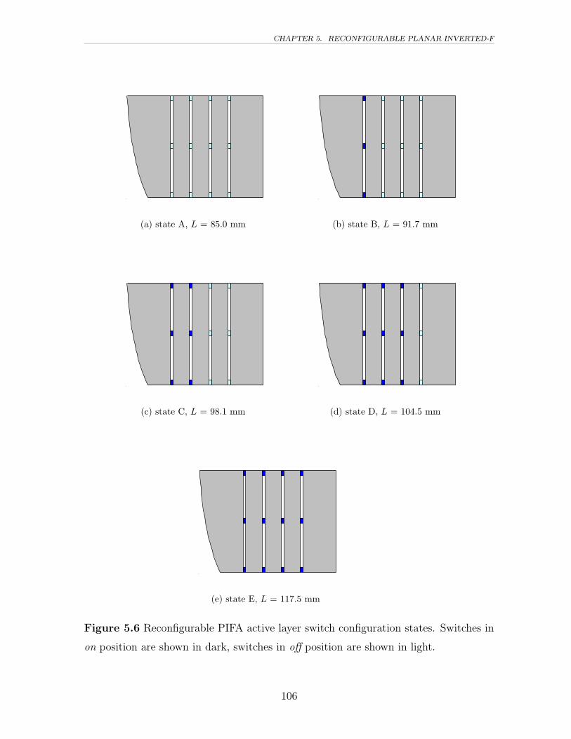
CHAPTER 5. RECONFIGURABLE PLANAR INVERTED-F
(a) state A, L = 85.0 mm (b) state B, L = 91.7 mm
(c) state C, L = 98.1 mm (d) state D, L = 104.5 mm
(e) state E, L = 117.5 mm
Figure 5.6 Reconfigurable PIFA active layer switch configuration states. Switches in
on position are shown in dark, switches in off position are shown in light.
106

CHAPTER 5. RECONFIGURABLE PLANAR INVERTED-F
5.3 Simulation of RPIFA
The commercial code IE3D was the primary simulation tool used for studying the
RRPA. IE3D is a full-wave frequency-domain package utilizing a laterally-open mo-
ment method engine capable of simulating arbitrary metalization geometries and was
described in Section 4.3. The simulation model of the RPIFA does not contain di-
electric components thus it is not subject to the 2.5 dimensional substrate caveat of
finite extent substrates as was seen in the ring patch model. There is however, a small
section of dielectric material used in the feed post of the prototype antenna that will
be ignored for now.
Figure 5.7 shows the computed input impedance for the antenna switch states
of Figure 5.5. The real part of the impedance varies between 25 Ω for state E and
and 50 Ω for state A, while the imaginary part is between -18 Ω and -5 Ω. This
provides a very close match to 50 Ω at the design frequency of 1.53 GHz. The desired
antenna bandwidth control is facilitated primarily by altering the real part of the
input impedance as seen in Figure 5.7. Figure 5.8 shows the corresponding VSWR for
the switch states referenced to 50 Ω. As was predicted from Figure 5.3, the largest
bandwidth is seen with the ground plane in state A. The ground plane length in state
A is 85 mm, or 0.44 λ, and results in a relative antenna bandwidth of 15.4 %. Table 5.3
summarizes the computed 2:1 VSWR impedance bandwidth and geometry parameters
for the RPIFA with switch states of Figure 5.6.
Table 5.3 Impedance bandwidth performance and reconfigurable ground plate geom-etry for the RPIFA with switch states of Figure 5.6 computed using IE3D
State Ground plate Center frequency Bandwidth MinimumRw length, L (mm) fo (GHz) 2:1 VSWR (%) VSWR
A 85.0 1.53 15.8 1.13B 91.7 1.54 12.4 1.30C 98.1 1.54 9.4 1.51D 104.5 1.54 5.1 1.76E 117.5 1.53 0 2.10
107

CHAPTER 5. RECONFIGURABLE PLANAR INVERTED-F
0
50
100
150
200
Res
ista
nce,
Ω
Real state Astate Bstate Cstate Dstate E
1.2 1.3 1.4 1.5 1.6 1.7 1.8−150
−100
−50
0
50
100
Frequency, GHz
Rea
ctan
ce, Ω
Imaginary
Figure 5.7 Input impedance versus frequency of the reconfigurable planar inverted-F
antenna for switch states of Figure 5.6 simulated using IE3D.
1.2 1.3 1.4 1.5 1.6 1.7 1.81
1.5
2
2.5
3
3.5
4
4.5
5
Frequency, GHz
VS
WR
state Astate Bstate Cstate Dstate E
Figure 5.8 VSWR versus frequency of the reconfigurable planar inverted-F antenna
for switch states of Figure 5.6 simulated using IE3D.
108

CHAPTER 5. RECONFIGURABLE PLANAR INVERTED-F
5.4 Experimental Results for RPIFA
The prototype RPIFA of Figure 5.9 was constructed and its electrical properties were
measured in order to verify the theoretical and simulation results. The top plate and
42×85 mm ground plate section were constructed from standard 25 mil hobby brass.
The ground plate strip sections were constructed with 30 mil hobby brass. The ground
plate sections were attached to a 76×45 cm piece of 62 mil RT/Duroid 5870 for me-
chanical support. The sections were attached to the Duroid with common double sided
tape. Figure 5.10 shows a side view of the antenna feed end. An extended length SMA
connector was used as the antenna feed. This connector has the same body dimensions
as a standard SMA connector with the center-pin and the dielectric sleeve extended
0.65 inches and 0.59 inches respectively. The Teflon (PTFE) extended dielectric sleeve
is visible in the figure next to the shorting post. The dielectric sleeve provides a con-
venient structural support for the RPIFA top plate. Teflon has a dielectric constant of
2.0, thus the presence of the sleeve impacts the electrical performance of the antenna
slightly. The measured center frequency of a preliminary RPIFA prototype antenna
was slightly lower than the simulated results from Section 5.3. Loading effects of the
dielectric and the resulting decrease in measured antenna operating frequency were
compensated by reducing the height of the top plate. The compensated height was
experimentally determined to be 2 mm less than the simulated design. The height of
the top plate, H, was 9 mm for the final measured prototype RPIFA. The shorting
post is also visible in Figure 5.10. The post was made from hobby stock brass rod with
a diameter of 1.27 mm. The post was soldered to both the top plate and the ground
plate as seen in Figure 5.10.
To achieve the five antenna ground plate lengths, small strips of copper used as
substitutes for the MEMS switches. The copper strips were soldered to the ground plate
sections at the switch locations to simulate on switch states. The solder locations are
visible in Figure 5.9 and correspond to the switch locations specified in Figure 5.5. The
copper strips were made from standard copper tape and were approximately 0.6 mm
wide. The tape switches were sufficiently long enough (2 mm) to both span the 0.3 mm
gap separating the ground plate sections and provide enough metal to metal contact
for good solder joints. Figure 5.11 gives a close-up view of one copper tape switch
109

CHAPTER 5. RECONFIGURABLE PLANAR INVERTED-F
Figure 5.9 Hardware test model of the RPIFA with switch states specified from Fig-
ure 5.6.
connecting adjacent ground plate strip sections.
110

CHAPTER 5. RECONFIGURABLE PLANAR INVERTED-F
Figure 5.10 Feed end of RPIFA hardware test model showing dielectric sleeve and
shorting post.
Figure 5.11 Close-up of copper tape RF switch for RPIFA hardware test model.
111

CHAPTER 5. RECONFIGURABLE PLANAR INVERTED-F
5.4.1 Impedance Measurements
All measurements of the RPIFA were performed at the Virginia Tech Antenna Group’s
antenna test facility. Impedance measurements of the RPIFA were made using an
HP8510C vector network analyzer. The measurement unit consisted of the antenna
under test (AUT) and a PVC mounting fixture. The AUT was secured to the PVC
fixture and then mounted to the near-field scanner AUT positioner inside the anechoic
chamber to minimized external disturbances. While the impedance measurements
were being performed, the AUT positioner was pointed toward the closed chamber
door to further reduce any unwanted reflections and maintain repeatability between
measurements. RF absorber was placed around the metal AUT tower and behind
the PVC fixture to minimize any reflections from the tower and mounting fixture.
Considerable effort was taken to minimize any unwanted reflection in the test envi-
ronment and to ensure repeatability between antenna measurements. Before the final
impedance measurements were performed, the setup was validated by measuring the
input impedance of a known 1.5 GHz λ/4 monopole antenna. The S-parameter val-
ues and input impedance values obtained from this measurement confirmed that the
measurement setup provided a suitable test environment.
The measured impedance data is plotted along with the respective IE3D sim-
ulated results for each switch state ground plane configuration. The measured input
impedance referenced to 50 Ω is shown in Figure 5.12. Acceptable agreement is seen
between the measured and simulated data, particularly around the design frequency
of 1.53 GHz. The reactance plots show very good agreement for all states over most
of the measured bandwidth. In all switch states, the simulated reactance tends be
slightly higher than the measured reactance at the lower frequencies. The measured
resistance plots follow the same general curves as the simulated data for all states.
However, the measured resistances are slightly higher than the computed values at
the lower frequencies and somewhat lower at the higher frequencies. The net effect
of this minor divergence in impedances at the higher frequencies can be seen in the
VSWR plots. Figures 5.13(a) - 5.13(e) show the measured VSWR compared to the
computed VSWR for all antenna states. Above the center frequency, the measured
VSWR levels do not increase as quickly as the computed values for all antenna states.
112

CHAPTER 5. RECONFIGURABLE PLANAR INVERTED-F
The measured bandwidths are slightly larger than the predicted values, most likely
due to loss mechanisms caused by the PTFE sleeve that is present in the experimental
antenna but not in the computed model. There is also a small amount of high order
ripple in the measured VSWR plots, particularly at the higher frequencies. Measured
ripple of this type is often caused by connector mismatch or external reflections. Fig-
ure 5.14 shows a comparison of the five measured VSWR values. Because of the ripple
on the measured VSWR curves, the comparison plot is not as clean as the computed
plot, however the trend of increasing bandwidth with decreasing ground plane length is
present. Figure 5.15 re-plots a comparison of the measured impedance data as return
loss for all switch states. Again, the bandwidth control is visible for each ground plane
switch state. Table 5.4 gives a summary of the measured and simulated 2:1 VSWR
impedance bandwidth performance of the RPIFA.
Table 5.4 Summary of the measured and simulated 2:1 VSWR impedance bandwidthperformance for the RPIFA.
Bandwidth Center Frequency Minimum2:1 VSWR (%) fo (GHz) VSWR
State measured simulated measured simulated measured simulated
A 16.0 15.8 1.55 1.53 1.40 1.13B 13.4 12.4 1.56 1.54 1.45 1.30C 8.5 9.4 1.57 1.54 1.65 1.51D 6.4 5.1 1.57 1.54 1.75 1.76E 1.3 0 1.54 1.53 1.95 2.10
113
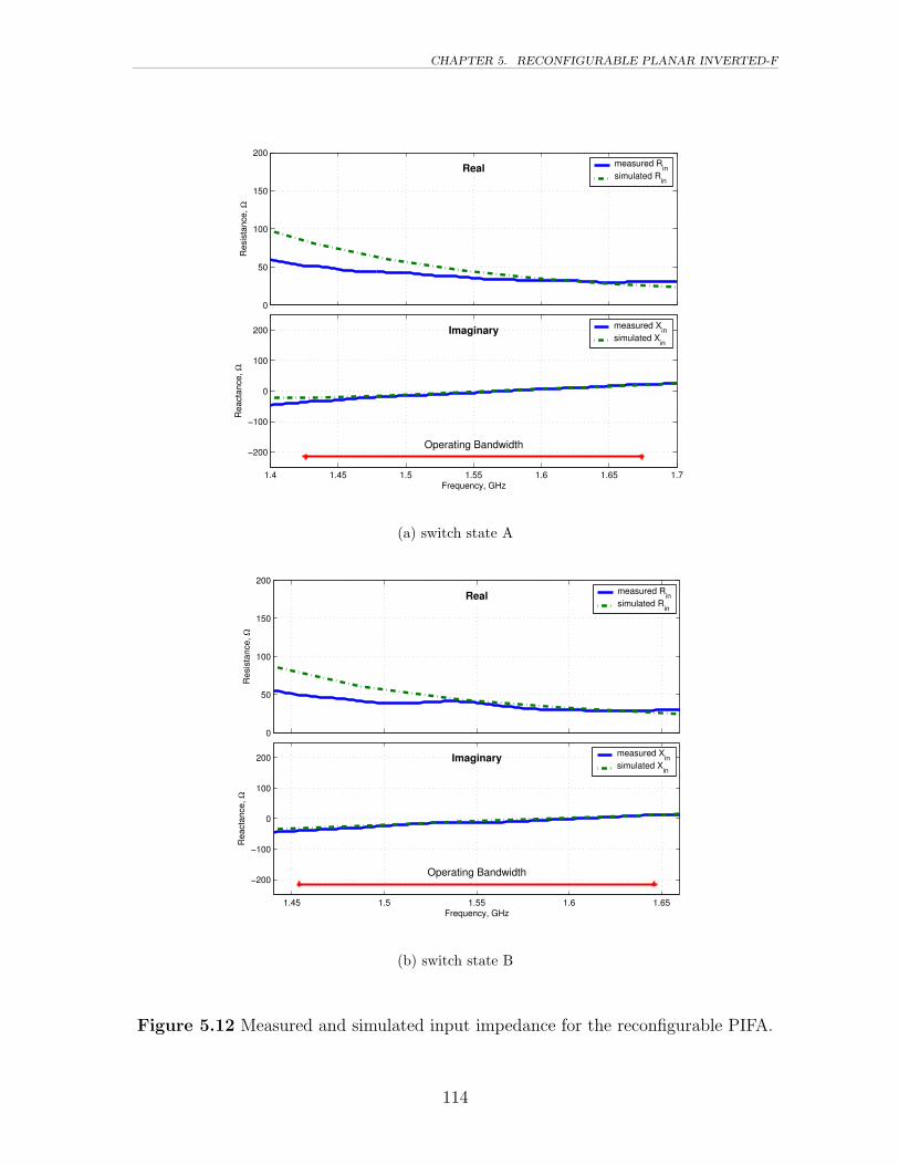
CHAPTER 5. RECONFIGURABLE PLANAR INVERTED-F
0
50
100
150
200
Res
ista
nce,
Ω
Real measured Rin
simulated Rin
1.4 1.45 1.5 1.55 1.6 1.65 1.7
−200
−100
0
100
200
Frequency, GHz
Rea
ctan
ce, Ω
Imaginary
Operating Bandwidth
measured Xin
simulated Xin
(a) switch state A
0
50
100
150
200
Res
ista
nce,
Ω
Real measured Rin
simulated Rin
1.45 1.5 1.55 1.6 1.65
−200
−100
0
100
200
Frequency, GHz
Rea
ctan
ce, Ω
Imaginary
Operating Bandwidth
measured Xin
simulated Xin
(b) switch state B
Figure 5.12 Measured and simulated input impedance for the reconfigurable PIFA.
114

CHAPTER 5. RECONFIGURABLE PLANAR INVERTED-F
0
50
100
150
200
Res
ista
nce,
Ω
Real measured Rin
simulated Rin
1.48 1.5 1.52 1.54 1.56 1.58 1.6 1.62
−200
−100
0
100
200
Frequency, GHz
Rea
ctan
ce, Ω
Imaginary
Operating Bandwidth
measured Xin
simulated Xin
(c) switch state C
0
50
100
150
200
Res
ista
nce,
Ω
Real measured Rin
simulated Rin
1.5 1.51 1.52 1.53 1.54 1.55 1.56 1.57 1.58 1.59 1.6
−200
−100
0
100
200
Frequency, GHz
Rea
ctan
ce, Ω
Imaginary
Operating Bandwidth
measured Xin
simulated Xin
(d) switch state D
Figure 5.12 Measured and simulated input impedance for the reconfigurable PIFA
(cont.)
115

CHAPTER 5. RECONFIGURABLE PLANAR INVERTED-F
0
50
100
150
200
Res
ista
nce,
Ω
Real measured Rin
simulated Rin
1.5 1.51 1.52 1.53 1.54 1.55 1.56 1.57 1.58 1.59 1.6
−200
−100
0
100
200
Frequency, GHz
Rea
ctan
ce, Ω
Imaginary
No Bandwidth
measured Xin
simulated Xin
(e) switch state E
Figure 5.12 Measured and simulated input impedance for the reconfigurable PIFA
(cont.)
116

CHAPTER 5. RECONFIGURABLE PLANAR INVERTED-F
1.2 1.3 1.4 1.5 1.6 1.7 1.8 1.9 21
2
3
4
5
6
7
8
9
10
Frequency, GHz
VS
WR
measured VSWRcomputed VSWR
(a) switch state A
1.2 1.3 1.4 1.5 1.6 1.7 1.8 1.9 21
2
3
4
5
6
7
8
9
10
Frequency, GHz
VS
WR
measured VSWRcomputed VSWR
(b) switch state B
Figure 5.13 Measured and simulated voltage standing wave ratio for the reconfigurable
PIFA.
117

CHAPTER 5. RECONFIGURABLE PLANAR INVERTED-F
1.2 1.3 1.4 1.5 1.6 1.7 1.8 1.9 21
2
3
4
5
6
7
8
9
10
Frequency, GHz
VS
WR
measured VSWRcomputed VSWR
(c) switch state C
1.2 1.3 1.4 1.5 1.6 1.7 1.8 1.9 21
2
3
4
5
6
7
8
9
10
Frequency, GHz
VS
WR
measured VSWRcomputed VSWR
(d) switch state D
Figure 5.13 Measured and simulated voltage standing wave ratio for the reconfigurable
PIFA (cont.)
118

CHAPTER 5. RECONFIGURABLE PLANAR INVERTED-F
1.2 1.3 1.4 1.5 1.6 1.7 1.8 1.9 21
2
3
4
5
6
7
8
9
10
Frequency, GHz
VS
WR
measured VSWRcomputed VSWR
(e) switch state E
Figure 5.13 Measured and simulated voltage standing wave ratio for the reconfigurable
PIFA(cont.)
119

CHAPTER 5. RECONFIGURABLE PLANAR INVERTED-F
1.2 1.3 1.4 1.5 1.6 1.7 1.81
1.5
2
2.5
3
3.5
4
4.5
5
Frequency, GHz
VS
WR
state Astate Bstate Cstate Dstate E
Figure 5.14 Measured voltage standing wave ratio for the reconfigurable PIFA in all
states.
1.2 1.3 1.4 1.5 1.6 1.7 1.8−18
−16
−14
−12
−10
−8
−6
−4
−2
0
Frequency, GHz
20 lo
g |Γ
|, dB
state Astate Bstate Cstate Dstate E
Figure 5.15 Measured return loss for the reconfigurable PIFA in all states.
120
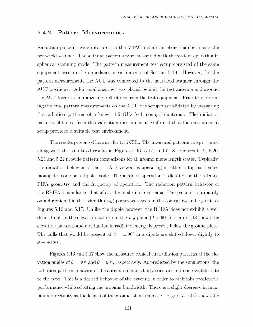
CHAPTER 5. RECONFIGURABLE PLANAR INVERTED-F
5.4.2 Pattern Measurements
Radiation patterns were measured in the VTAG indoor anechoic chamber using the
near-field scanner. The antenna patterns were measured with the system operating in
spherical scanning mode. The pattern measurement test setup consisted of the same
equipment used in the impedance measurements of Section 5.4.1. However, for the
pattern measurements the AUT was connected to the near-field scanner through the
AUT positioner. Additional absorber was placed behind the test antenna and around
the AUT tower to minimize any reflections from the test equipment. Prior to perform-
ing the final pattern measurements on the AUT, the setup was validated by measuring
the radiation patterns of a known 1.5 GHz λ/4 monopole antenna. The radiation
patterns obtained from this validation measurement confirmed that the measurement
setup provided a suitable test environment.
The results presented here are for 1.55 GHz. The measured patterns are presented
along with the simulated results in Figures 5.16, 5.17, and 5.18. Figures 5.19, 5.20,
5.21 and 5.22 provide pattern comparisons for all ground plane length states. Typically,
the radiation behavior of the PIFA is viewed as operating in either a top-hat loaded
monopole mode or a dipole mode. The mode of operation is dictated by the selected
PIFA geometry and the frequency of operation. The radiation pattern behavior of
the RPIFA is similar to that of a z-directed dipole antenna. The pattern is primarily
omnidirectional in the azimuth (x-y) planes as is seen in the conical Eθ and Eφ cuts of
Figures 5.16 and 5.17. Unlike the dipole however, the RPIFA does not exhibit a well
defined null in the elevation pattern in the x-y plane (θ = 90.) Figure 5.18 shows the
elevation patterns and a reduction in radiated energy is present below the ground plate.
The nulls that would be present at θ = ± 90 in a dipole are shifted down slightly to
θ = ±120.
Figures 5.16 and 5.17 show the measured conical cut radiation patterns at the ele-
vation angles of θ = 10 and θ = 90, respectively. As predicted by the simulations, the
radiation pattern behavior of the antenna remains fairly constant from one switch state
to the next. This is a desired behavior of the antenna in order to maintain predictable
performance while selecting the antenna bandwidth. There is a slight decrease in max-
imum directivity as the length of the ground plane increases. Figure 5.16(a) shows the
121

CHAPTER 5. RECONFIGURABLE PLANAR INVERTED-F
maximum value for state A was 1.1 dB and Figure 5.16(e) shows a value of −0.7 dB for
state E. This effect is attributed to the lengthening of the ground plate. The measured
elevation patterns are shown in Figure 5.18. The measured patterns exhibit primarily
z-directed radiation as was predicted by the simulated patterns. However, there is
considerable ripple seen in the measured pattern. This ripple is most likely caused by
the z-directed AUT positioner where the antenna was mounted. Unfortunately, this
behavior often results when measuring electrically small antennas operated without
a ground plane to block the positioner interaction. Figure 5.22 shows a comparison
between the measured elevation patterns for each switch state. There is relatively good
agreement between the measured patterns between the switch states with only a few
dB of deviation between the maximum and minimum ground plane lengths.
122

CHAPTER 5. RECONFIGURABLE PLANAR INVERTED-F
0 −5 −10 −15 −20 −25 −30 −25 −20 −15 −10 −5 0
30
−150
60
−120
90−90
120
−60
150
−30
180
0
Max = 1.10
Eθ (θ = 10o ) measuredEθ (θ = 10o ) simulatedEφ (θ = 10o ) measuredEφ (θ = 10o ) simulated
(a) switch state A
0 −5 −10 −15 −20 −25 −30 −25 −20 −15 −10 −5 0
30
−150
60
−120
90−90
120
−60
150
−30
180
0
Max = 0.96
Eθ (θ = 10o ) measuredEθ (θ = 10o ) simulatedEφ (θ = 10o ) measuredEφ (θ = 10o ) simulated
(b) switch state B
Figure 5.16 Measured and simulated conical radiation patterns for the RPIFA.
123

CHAPTER 5. RECONFIGURABLE PLANAR INVERTED-F
0 −5 −10 −15 −20 −25 −30 −25 −20 −15 −10 −5 0
30
−150
60
−120
90−90
120
−60
150
−30
180
0
Max = 0.72
Eθ (θ = 10o ) measuredEθ (θ = 10o ) simulatedEφ (θ = 10o ) measuredEφ (θ = 10o ) simulated
(c) switch state C
0 −5 −10 −15 −20 −25 −30 −25 −20 −15 −10 −5 0
30
−150
60
−120
90−90
120
−60
150
−30
180
0
Max = 0.33
Eθ (θ = 10o ) measuredEθ (θ = 10o ) simulatedEφ (θ = 10o ) measuredEφ (θ = 10o ) simulated
(d) switch state D
Figure 5.16 Measured and simulated conical radiation patterns for the RPIFA (cont.)
124

CHAPTER 5. RECONFIGURABLE PLANAR INVERTED-F
0 −5 −10 −15 −20 −25 −30 −25 −20 −15 −10 −5 0
30
−150
60
−120
90−90
120
−60
150
−30
180
0
Max = −0.68
Eθ (θ = 10o ) measuredEθ (θ = 10o ) simulatedEφ (θ = 10o ) measuredEφ (θ = 10o ) simulated
(e) switch state E
Figure 5.16 Measured and simulated conical radiation patterns for the RPIFA (cont.)
125
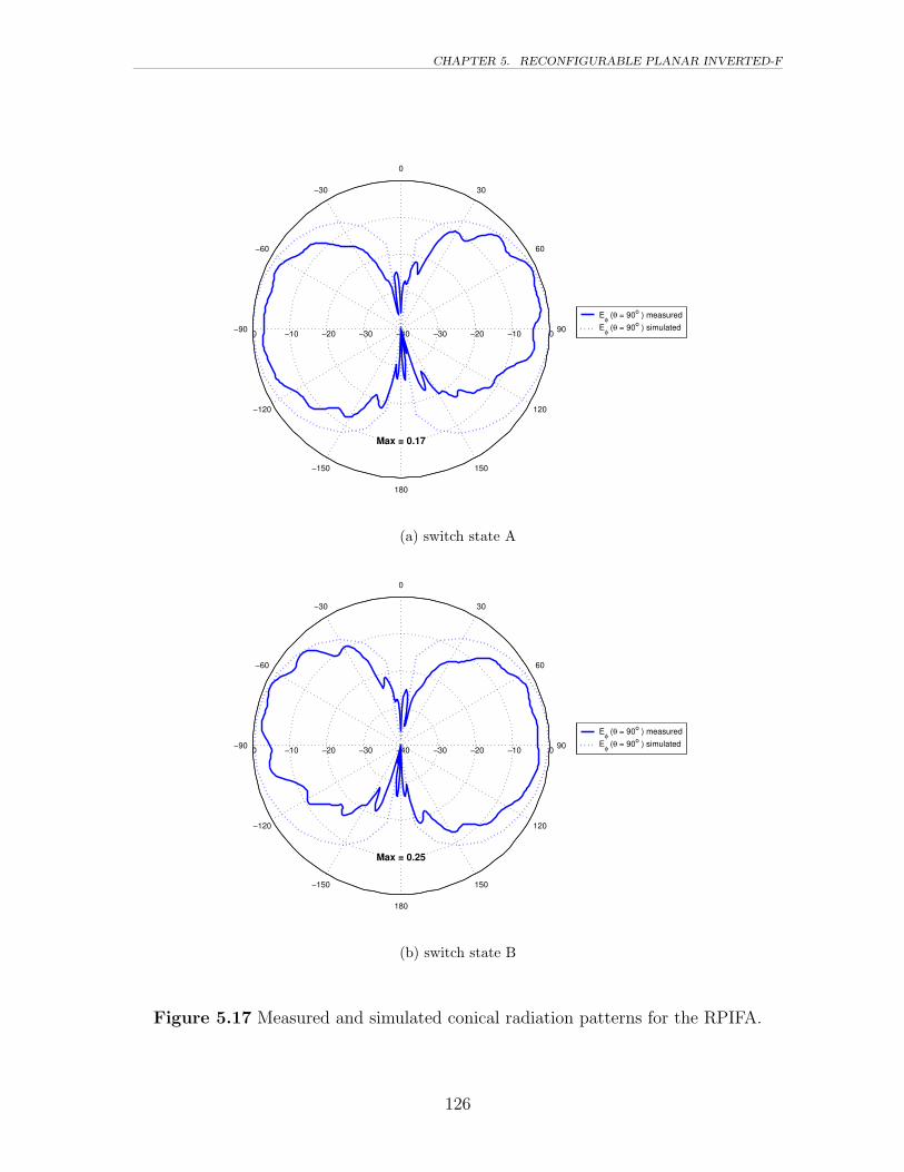
CHAPTER 5. RECONFIGURABLE PLANAR INVERTED-F
0 −10 −20 −30 −40 −30 −20 −10 0
30
−150
60
−120
90−90
120
−60
150
−30
180
0
Max = 0.17
Eφ (θ = 90o ) measuredEφ (θ = 90o ) simulated
(a) switch state A
0 −10 −20 −30 −40 −30 −20 −10 0
30
−150
60
−120
90−90
120
−60
150
−30
180
0
Max = 0.25
Eφ (θ = 90o ) measuredEφ (θ = 90o ) simulated
(b) switch state B
Figure 5.17 Measured and simulated conical radiation patterns for the RPIFA.
126

CHAPTER 5. RECONFIGURABLE PLANAR INVERTED-F
0 −10 −20 −30 −40 −30 −20 −10 0
30
−150
60
−120
90−90
120
−60
150
−30
180
0
Max = 0.43
Eφ (θ = 90o ) measuredEφ (θ = 90o ) simulated
(c) switch state C
0 −10 −20 −30 −40 −30 −20 −10 0
30
−150
60
−120
90−90
120
−60
150
−30
180
0
Max = 0.86
Eφ (θ = 90o ) measuredEφ (θ = 90o ) simulated
(d) switch state D
Figure 5.17 Measured and simulated conical radiation patterns for the RPIFA (cont.)
127
CHAPTER 5. RECONFIGURABLE PLANAR INVERTED-F
0 −10 −20 −30 −40 −30 −20 −10 0
30
−150
60
−120
90−90
120
−60
150
−30
180
0
Max = 0.24
Eφ (θ = 90o ) measuredEφ (θ = 90o ) simulated
(e) switch state E
Figure 5.17 Measured and simulated conical radiation patterns for the RPIFA (cont.)
128

CHAPTER 5. RECONFIGURABLE PLANAR INVERTED-F
0 −5 −10 −15 −20 −25 −30 −25 −20 −15 −10 −5 0
30
−150
60
−120
90−90
120
−60
150
−30
180
0
Max = 2.22
Eθ ( φ = 0o ) measuredEθ ( φ = 0o ) simulated
(a) switch state A
0 −5 −10 −15 −20 −25 −30 −25 −20 −15 −10 −5 0
30
−150
60
−120
90−90
120
−60
150
−30
180
0
Max = 2.12
Eθ ( φ = 0o ) measuredEθ ( φ = 0o ) simulated
(b) switch state B
Figure 5.18 Measured and simulated elevation radiation patterns in the x-z plane for
the RPIFA.
129

CHAPTER 5. RECONFIGURABLE PLANAR INVERTED-F
0 −5 −10 −15 −20 −25 −30 −25 −20 −15 −10 −5 0
30
−150
60
−120
90−90
120
−60
150
−30
180
0
Max = 1.94
Eθ ( φ = 0o ) measuredEθ ( φ = 0o ) simulated
(c) switch state C
0 −5 −10 −15 −20 −25 −30 −25 −20 −15 −10 −5 0
30
−150
60
−120
90−90
120
−60
150
−30
180
0
Max = 1.62
Eθ ( φ = 0o ) measuredEθ ( φ = 0o ) simulated
(d) switch state D
Figure 5.18 Measured and simulated elevation radiation patterns in the x-z plane for
the RPIFA (cont.)
130
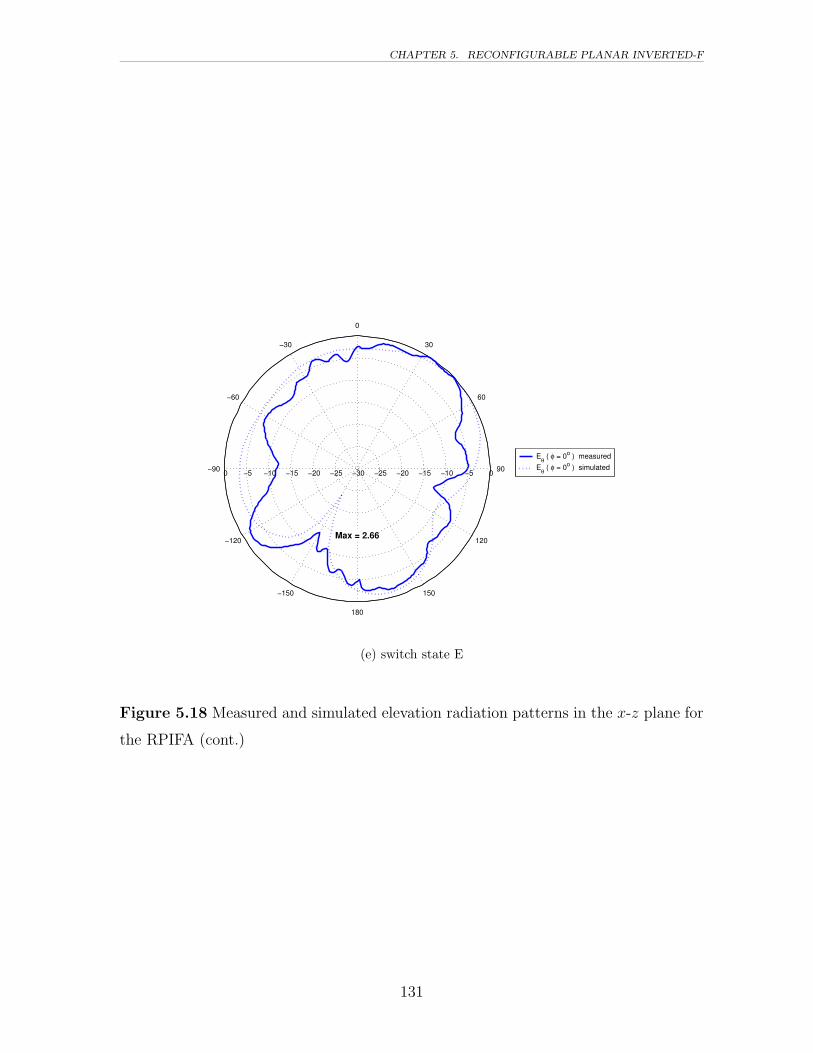
CHAPTER 5. RECONFIGURABLE PLANAR INVERTED-F
0 −5 −10 −15 −20 −25 −30 −25 −20 −15 −10 −5 0
30
−150
60
−120
90−90
120
−60
150
−30
180
0
Max = 2.66
Eθ ( φ = 0o ) measuredEθ ( φ = 0o ) simulated
(e) switch state E
Figure 5.18 Measured and simulated elevation radiation patterns in the x-z plane for
the RPIFA (cont.)
131

CHAPTER 5. RECONFIGURABLE PLANAR INVERTED-F
0 −10 −20 −30 −40 −30 −20 −10 0
30
−150
60
−120
90−90
120
−60
150
−30
180
0
Max = −0.02
State AState BState CState DState E
Figure 5.19 Comparison of measured azimuth directivity patterns for all switch states
of the reconfigurable PIFA, Eφ (θ = 10).
0 −10 −20 −30 −40 −30 −20 −10 0
30
−150
60
−120
90−90
120
−60
150
−30
180
0
Max = −0.79
State AState BState CState DState E
Figure 5.20 Comparison of measured azimuth directivity patterns for all switch states
of the reconfigurable PIFA, Eθ (θ = 10).
132
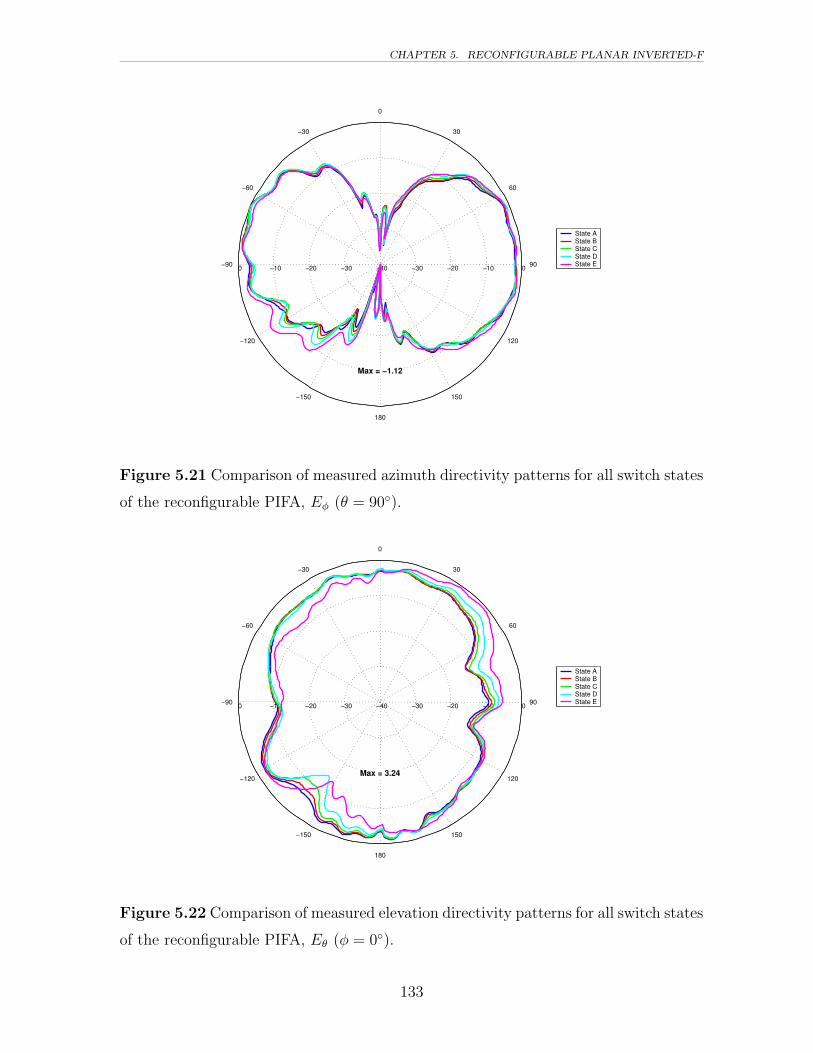
CHAPTER 5. RECONFIGURABLE PLANAR INVERTED-F
0 −10 −20 −30 −40 −30 −20 −10 0
30
−150
60
−120
90−90
120
−60
150
−30
180
0
Max = −1.12
State AState BState CState DState E
Figure 5.21 Comparison of measured azimuth directivity patterns for all switch states
of the reconfigurable PIFA, Eφ (θ = 90).
0 −10 −20 −30 −40 −30 −20 −10 0
30
−150
60
−120
90−90
120
−60
150
−30
180
0
Max = 3.24
State AState BState CState DState E
Figure 5.22 Comparison of measured elevation directivity patterns for all switch states
of the reconfigurable PIFA, Eθ (φ = 0).
133

CHAPTER 5. RECONFIGURABLE PLANAR INVERTED-F
5.5 Summary
The development, design computer simulation and measurement of the reconfigurable
planar inverted-F antenna was presented in this chapter. The ground plate influence
on the RPIFA bandwidth was included in the RPIFA design to obtain discrete band-
width states. A antenna in five discrete steps covering a bandwidth of 0-16% was
achieved with only minimal impact on the other radiation properties of the antenna.
The bandwidth steps were realized with three conducting inter connects per band that
simulated embedded switches. A total of 12 RF switch locations were incorporated into
the reconfigurable antenna design to achieve the desired selectable bandwidth behav-
ior. Table 5.5 summarizes the selectable bandwidth characteristics of the RPIFA. The
measured antenna performance was shown to be similar to the computed performance.
A slight deviation in measured pattern behavior was seen in the elevation pattern most
likely due to AUT positioner interference.
Table 5.5 Selectable bandwidth performance for the reconfigurable planar inverted-Fantenna with switch states of Figure 5.6.
Center Frequency Minimum Bandwidth 2:1 VSWR
State fo (GHz) VSWR (MHz) (%)
A 1.53 1.13 242 15.8B 1.54 1.30 191 12.4C 1.54 1.51 145 9.4D 1.54 1.76 79 5.1E 1.53 2.10 0 0
134
Chapter 6
Analysis and Measurement of
Reconfigurable Folded Dipole
This chapter presents the design and analysis of the reconfigurable folded dipole an-
tenna. First, the antenna structure is presented along with the methods used for con-
trollable bandwidth reconfiguration. Next, an explanation of how the antenna struc-
ture radiates and what aspects of its geometry allow for bandwidth reconfiguration.
A description of the computer antenna computer model then follows along with the
computational results. Then, the antenna prototype measurement setup and the as-
sociated antenna measured results are presented. Finally, an overall analysis of the
reconfigurable antenna is given which relates the theory to the computed performance
and compares these results to the measured data.
6.1 Introduction
The folded dipole was studied extensively the 1960s [20, 21]. The antenna is attractive
because of its favorable input impedance characteristics and relatively simple and ro-
bust construction. The input impedance of the folded dipole is higher than that of an
equivalent half-wave dipole and it has a larger impedance bandwidth than the typical
wire half-wave dipole. Its input impedance is very close to that of standard 300 Ω
twin-lead coax transmission line and it can be easily constructed from twin-lead by
135

CHAPTER 6. RECONFIGURABLE FOLDED DIPOLE
separating the conductors and folding back over themselves, making it a natural choice
for an antenna connected to common twin-lead transmission line. Slot versions of the
folded dipole are popular in embedded applications because of the ease of printing on
microwave substrates.
The folded dipole antenna has also experienced considerable popularity as wire
array antenna element. Its favorable input impedance qualities and simplistic con-
struction make it ideally suited to a variety of array applications. It is frequently used
as the feed element in Yagi-Uda arrays and as the dipole element in log-periodic array
configurations. The folded log-periodic dipole array (FLPDA) is popular because of
the convenient feeding mechanism provided by the folded dipole. A phase reversal is
required between adjacent elements in the LPDA and in conventional dipole LPDAs
this phase reversal is accomplished by crossing or twisting the transmission line path
between adjacent elements. This twisting is often undesirable for antennas constructed
on planar printed surfaces because it requires vias to the opposite side to cross the
transmission line paths. Using a reentrant folded dipole as the LPDA element, it is
not necessary to twist the transmission line paths and is suitable for printing on only
one side of a planar structure. A further extension of the folded log-periodic dipole
array is the FLPDA using parasitically loaded slot elements [86]. This variation has
a smaller radiating slot inside the folded dipole element. The parasitic elements allow
for individual control of the phase progression between adjacent elements.
During the author’s design of a folded log-periodic dipole array [87] it was de-
termined that the parasitic phasing slots not only contribute to the phase progression
between array elements, they contribute to the bandwidth of the individual element.
Thus, when a parasitically loaded folded dipole is operated by itself, the parasitic slot
plays a critical role in antenna impedance bandwidth. The size and shape of the par-
asitic slot can be modified to achieve bandwidth controllable behavior. These findings
lead to the invention of the reconfigurable folded parasitic dipole antenna (RPFDA).
The antenna performs similar to the folded dipole antenna but with the ability to
control the bandwidth of operation. The new antenna is described in detail in this
chapter.
136
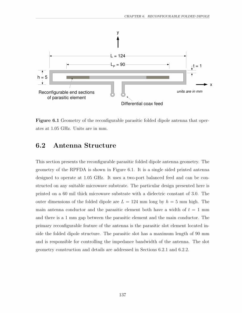
CHAPTER 6. RECONFIGURABLE FOLDED DIPOLE
L = 124
y
x
h = 5
t = 1
Differential coax feed
Reconfigurable end sections of parasitic element
units are in mm
L P = 90
Figure 6.1 Geometry of the reconfigurable parasitic folded dipole antenna that oper-
ates at 1.05 GHz. Units are in mm.
6.2 Antenna Structure
This section presents the reconfigurable parasitic folded dipole antenna geometry. The
geometry of the RPFDA is shown in Figure 6.1. It is a single sided printed antenna
designed to operate at 1.05 GHz. It uses a two-port balanced feed and can be con-
structed on any suitable microwave substrate. The particular design presented here is
printed on a 60 mil thick microwave substrate with a dielectric constant of 3.0. The
outer dimensions of the folded dipole are L = 124 mm long by h = 5 mm high. The
main antenna conductor and the parasitic element both have a width of t = 1 mm
and there is a 1 mm gap between the parasitic element and the main conductor. The
primary reconfigurable feature of the antenna is the parasitic slot element located in-
side the folded dipole structure. The parasitic slot has a maximum length of 90 mm
and is responsible for controlling the impedance bandwidth of the antenna. The slot
geometry construction and details are addressed in Sections 6.2.1 and 6.2.2.
137

CHAPTER 6. RECONFIGURABLE FOLDED DIPOLE
1
2
3
N
Element
Figure 6.2 Geometry of the N-element folded dipole antenna.
6.2.1 Parasitic Element Length Influence On Bandwidth
A numerical investigation was conducted using IE3D to determine the effect of the
parasitic element on antenna performance. The results obtained from this investigation
are used in the subsequent sections to determine discrete parasitic element lengths for
the controllable bandwidth states of the reconfigurable parasitic folded dipole antenna
geometry. The length of the parasitic element, Lp, was varied symmetrically around the
dipole center and all other antenna geometry parameters were held constant to explore
the effect on input impedance and ultimately the impact on impedance bandwidth
bandwidth.
The folded dipole has been investigated extensively since the 1960s [20, 22]. The
parasitically loaded folded dipole antenna can be viewed as a modification of the N -
element folded dipole as shown in Figure 6.2. The PFDA is a three-element folded
dipole with a shortened middle element. It is well known that the input impedance of
a N -element folded dipole is given by [88]
Zin = N2Zdipole (6.1)
where the input impedance of a dipole in free-space at its first resonance is Zdipole ≈70 Ω.
Figure 6.3 shows the input impedance of the antenna from Figure 6.1 as a func-
tion of parasitic element length, Lp, computed using IE3D at the design frequency of
1.05 GHz. When Lp = 122 mm the parasitic element extends the entire length of the
folded dipole and the element touches the ends of the folded dipole and the antenna
138

CHAPTER 6. RECONFIGURABLE FOLDED DIPOLE
becomes the three-element folded dipole. The input reactance becomes zero and the
resistance ≈ 560 Ω, or 32×70 Ω, as predicted from Equation (6.1). The input resistance
drops sharply and the reactance grows quickly as the length of the parasitic element
is reduced. The reactance vanishes when Lp is about 100 mm and 25 mm. The input
resistance nearly vanishes as well when Lp = 105 mm. The resistance climbs back to
favorable values for Lp < 80 mm.
Figure 6.4 shows the antenna bandwidth versus parasitic element length from 0
to 100 mm referenced to 300 Ω for the antenna geometry of Figure 6.1. The antenna
has a maximum bandwidth of 16% for Lp = 0 mm. The bandwidth decreases slowly
to 13% where Lp = 60 mm. The bandwidth then rapidly decreases to 0% for Lp =
85 mm. Figure 6.5 shows the calculated VSWR for parasitic element lengths of 25 to
85 mm. The center frequency of the antenna is lowered when the parasitic element
becomes shorter than 55 mm. Figures 6.4 and 6.5 give the usable limits for the length
of the parasitic element. If the parasitic element is longer than 85 mm, the impedance
bandwidth is reduced to 0% and the antenna is effectively turned off. Parasitic element
lengths shorter than 55 mm cause the center frequency of the antenna to deviate from
the design frequency of 1.05 GHz and are thus undesirable even though the antenna
impedance bandwidth is increased. Table 6.1 summarizes the electrical performance of
the parasitic folded dipole antenna from Figure 6.1 based on different parasitic element
lengths simulated using IE3D.
139
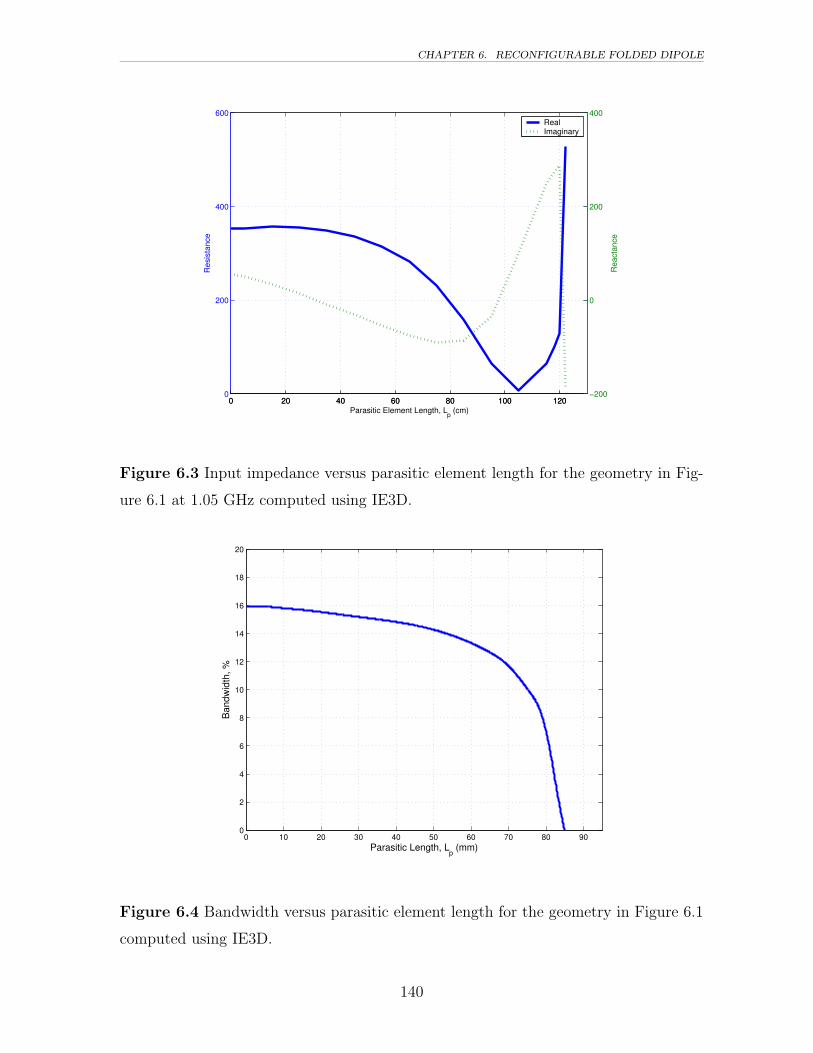
CHAPTER 6. RECONFIGURABLE FOLDED DIPOLE
0 20 40 60 80 100 1200
200
400
600
Parasitic Element Length, Lp (cm)
Res
ista
nce
0 20 40 60 80 100 120−200
0
200
400
Rea
ctan
ce
RealImaginary
Figure 6.3 Input impedance versus parasitic element length for the geometry in Fig-
ure 6.1 at 1.05 GHz computed using IE3D.
0 10 20 30 40 50 60 70 80 900
2
4
6
8
10
12
14
16
18
20
Parasitic Length, Lp (mm)
Ban
dwid
th, %
Figure 6.4 Bandwidth versus parasitic element length for the geometry in Figure 6.1
computed using IE3D.
140

CHAPTER 6. RECONFIGURABLE FOLDED DIPOLE
Table 6.1 Electrical performance based on parasitic element length, Lp, for the PFDAof Figure 6.1 simulated using IE3D.
Parasitic length, Lp Center frequency Minimum Bandwidth
(mm) (wavelengths) f0 (GHz) VSWR 2:1 VSWR (%)
25 0.088 1.03 1.04 15.435 0.123 1.04 1.06 15.045 0.158 1.04 1.11 14.655 0.193 1.05 1.18 13.965 0.228 1.05 1.30 12.770 0.245 1.05 1.40 11.775 0.263 1.05 1.53 10.180 0.280 1.05 1.75 7.085 0.298 1.05 2.10 095 0.333 1.01 4.00 0105 0.368 0.94 11.5 0115 0.403 1.12 6.08 0
0.9 0.95 1 1.05 1.1 1.151
1.2
1.4
1.6
1.8
2
2.2
2.4
2.6
2.8
3
Frequency, GHz
VS
WR
25 mm55 mm70 mm75 mm80 mm85 mm
Figure 6.5 VSWR versus frequency of the parasitic loaded folded dipole antenna of
Figure 6.1 for various parasitic element lengths, Lp, computed using IE3D.
141

CHAPTER 6. RECONFIGURABLE FOLDED DIPOLE
6.2.2 The Reconfigurable Parasitic Folded Dipole Antenna
Specific parasitic element lengths, Lp, were selected for discrete antenna bandwidth
values based on the investigation performed in Section 6.2.1. These parasitic element
length states are used in the subsequent work to accomplish the desired reconfigurable
bandwidth performance. Five parasitic element lengths were selected to achieve dis-
crete bandwidth states from 0% (effectively off) to 13% (maximum bandwidth). Ta-
ble 6.2 summarizes the element lengths chosen for the selectable bandwidth states
along with the predicted bandwidth values based on the the element length study in
Section 6.2.1.
Table 6.2 Discrete parasitic element lengths, Lp, as shown in Figure 6.6 for selectedantenna bandwidth states based on simulations from Section 6.2.1.
Length, Lp Bandwidth for
State (mm) (wavelengths) ≤ 2:1 VSWR (%)
A 62.0 0.217 13B 69.0 0.242 11C 76.0 0.266 9D 83.0 0.291 5E 90.0 0.315 0
With the parasitic element lengths selected, the design task becomes how to
physically vary the length of the element to achieve the desired reconfigurable oper-
ation. The solid parasitic element is replaced by a new structure with reconfigurable
components. The sub-elements and the main element are connected together with RF
MEMS switches as shown in Figure 6.7. The single, solid 90 mm parasitic element is
replaced by a shorter 62 mm parasitic element and four 3.2 mm sub-elements on either
side. There is a 0.3 mm gap separating the adjacent sections to accommodate the RF
switching elements as described in Section 3.3. The electrical length of the parasitic
element is varied by selectively activating the interconnecting switches between the
sub-elements and a variable impedance bandwidth of 0-13% is obtained.
142
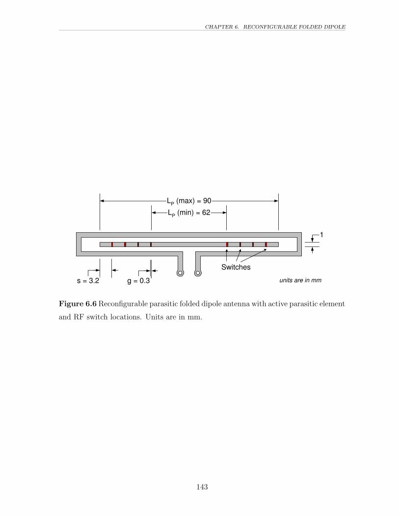
CHAPTER 6. RECONFIGURABLE FOLDED DIPOLE
1
Switches
units are in mm
L P (max) = 90
L P (min) = 62
s = 3.2 g = 0.3
Figure 6.6 Reconfigurable parasitic folded dipole antenna with active parasitic element
and RF switch locations. Units are in mm.
143
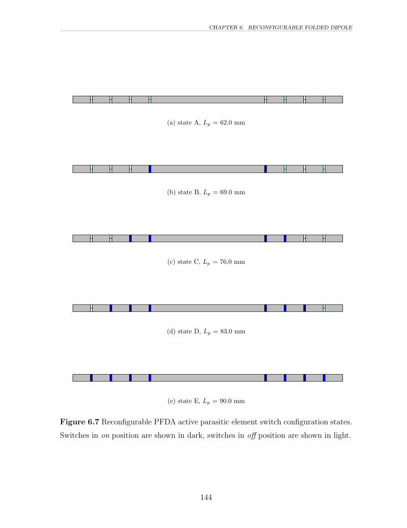
CHAPTER 6. RECONFIGURABLE FOLDED DIPOLE
(a) state A, Lp = 62.0 mm
(b) state B, Lp = 69.0 mm
(c) state C, Lp = 76.0 mm
(d) state D, Lp = 83.0 mm
(e) state E, Lp = 90.0 mm
Figure 6.7 Reconfigurable PFDA active parasitic element switch configuration states.
Switches in on position are shown in dark, switches in off position are shown in light.
144

CHAPTER 6. RECONFIGURABLE FOLDED DIPOLE
6.3 Simulation of RPFDA
This section describes the computer simulation and associated numerical results for the
reconfigurable parasitic folded dipole antenna presented in Section 6.2.2. The commer-
cial code IE3D was the primary simulation tool used for studying the RPFDA. IE3D
is a full-wave frequency-domain package utilizing a laterally-open moment method
engine capable of simulating arbitrary metalization geometries and was described in
Section 4.3. The simulation model of the RPFDA contains dielectric substrate layer
used for supporting the antenna structure. As was previously described, the 2.5 di-
mensional substrate limitation of finite extent substrates as was seen in the ring patch
model applies to the modeling of the RPFDA. However, the radiation mechanism of
this RPFDA is not a microstrip fringing mechanism as was present in the operation
of the ring patch antenna. Experience shows that the finite extent of the supporting
substrate of the hardware model RPFDA will not present a significant problem for
accurate simulation of the antenna.
Figure 6.8 shows the computed input impedance for the antenna switch states of
Figure 6.7. The real part of the impedance varies between 100 Ω for state E and and
300 Ω for state A, while the imaginary part remains nearly constant at -100 Ω over
all switch states at 1.05 GHz. The desired antenna bandwidth control is facilitated
primarily by altering the real part of the input impedance as seen in Figure 4.7. Fig-
ure 6.9 shows the corresponding VSWR for the switch states referenced to 300 Ω. As
was predicted from Figure 6.4, the widest bandwidth is seen with the parasitic element
in switch state A with a length of 62 mm. Table 6.3 summarizes the computed 2:1
VSWR impedance bandwidth and geometry parameters for the RPFDA with switch
states of Figure 6.7.
145

CHAPTER 6. RECONFIGURABLE FOLDED DIPOLE
Table 6.3 Impedance bandwidth performance and reconfigurable parasitic elementgeometry for the RPFDA of Figure 6.6 with switch states of Figure 6.7 computedusing IE3D
Parasitic length, Center frequency, Bandwidth for MinimumState Lp (mm) fo (GHz) ≤ 2:1 VSWR (%) VSWR
A 62.0 1.05 13.1 1.28B 69.0 1.05 11.5 1.40C 76.0 1.05 9.3 1.60D 83.0 1.05 2.0 1.98E 90.0 1.03 0 2.80
0
50
100
150
200
250
300
350
400
Res
ista
nce,
Ω
Real State AState BState CState DState E
0.95 1 1.05 1.1 1.15−400
−300
−200
−100
0
100
Frequency, GHz
Rea
ctan
ce, Ω
Imaginary
Figure 6.8 Input impedance versus frequency of the reconfigurable parasitic folded
dipole antenna for switch states of Figure 6.7 for the RPFDA of Figure 6.6 simulated
using IE3D.
146

CHAPTER 6. RECONFIGURABLE FOLDED DIPOLE
0.95 1 1.05 1.1 1.151
1.2
1.4
1.6
1.8
2
2.2
2.4
2.6
2.8
3
Frequency, GHz
VS
WR
state Astate Bstate Cstate Dstate E
Figure 6.9 VSWR versus frequency of the reconfigurable parasitic folded dipole an-
tenna referenced to 300 Ω for switch states of Figure 6.7 for the RPFDA of Figure 6.6
simulated using IE3D.
147

CHAPTER 6. RECONFIGURABLE FOLDED DIPOLE
6.4 Experimental Results for RPFDA
This section discusses the construction and measurement of the hardware test model
RPFDA. The prototype RPFDA of Figure 6.10 was constructed and its electrical per-
formance characteristics were measured in order to verify the theoretical and simulated
results. The prototype antennas were printed on Rogers RO3003 [89] microwave ma-
terial using standard photo-etching processes. The RO3003 material has a dielectric
constant of 3.0 and a thickness of 60 mils. The overall substrate size was 7 × 1.5 inches.
Two holes were drilled through the substrate at the feed locations to accommodate the
feed network. The feed network was constructed from two pieces of 141 semi-rigid coax
formed into a Y–shaped connector as shown in Figure 6.10. The coax connector used
two standard SMA plugs. At the antenna side of the Y–connector, the outer shield and
dielectric were stripped back and the center conductors were fed though the RO3003
material and soldered to the circular pads at the feed points.
To achieve the five separate antenna states in absence of the actual MEMS
switches, five individual antennas were printed as substitutes. The five printed an-
tennas are shown in Figures 6.11 and correspond to the switch states specified in
Figure 6.7.
6.4.1 Impedance Measurements
All measurements of the RPFDA ware performed at the Virginia Tech Antenna Group’s
antenna test facility. Impedance measurements were made using an HP 8510C vector
network analyzer. The measurement unit consisted of the printed reconfigurable par-
asitic folded dipole and coax Y–feed as shown in Figure 6.10. The test unit was
mounted on the near-field scanner AUT positioner inside the anechoic chamber. While
the impedance measurements were being performed, the AUT positioner was pointed
toward the closed chamber door to minimize any external disturbances and maintain
test repeatability between measurements. RF absorber was placed around the metal
AUT tower to minimize any reflections from the mounting fixture. Considerable effort
was taken to minimize any unwanted reflection in the test environment and to ensure
repeatability between antenna measurements. Before the final impedance measure-
148

CHAPTER 6. RECONFIGURABLE FOLDED DIPOLE
Figure 6.10 Hardware test model of the RPFDA with coaxial feed network.
149

CHAPTER 6. RECONFIGURABLE FOLDED DIPOLE
(a) Switch state A
(b) Switch state B
(c) Switch state C
(d) Switch state D
(e) Switch state E
Figure 6.11 Hardware test model for each of the switch states of Figure 6.7.
150

CHAPTER 6. RECONFIGURABLE FOLDED DIPOLE
ments were performed, the setup was validated by measuring the input impedance of
a known 1.0 GHz printed half-wave dipole antenna. The S-parameter values and input
impedance values obtained from this measurement confirmed that the measurement
setup provided a suitable test environment.
The input impedance measurements of the RPFDA were made using the 2-port
impedance measurement technique developed by Davis [90]. The technique uses stan-
dard two-port scattering parameters for balanced antenna. Each half of the balanced
antenna input port is fed as one port of a two port network. This method eliminates
the need for a balun or wideband 180 hybrid when measuring the input impedance of
a balanced antenna. Impedance is estimated by measuring the two port response of
the antenna and is given by [90]
ZAUT = 2Z0
1 − s11 + s21
1 + s11 − s21
(6.2)
where Z0 is the characteristic impedance and s11, s21 are the two-port response mea-
surements from the network analyzer.
The measured impedance data is plotted along with the respective IE3D sim-
ulated results for each antenna switch state. The measured impedance referenced to
300 Ω is shown in Figure 6.12. Figures 6.13 and 6.14 show the measured VSWR and
Figure 6.15 shows the measured return loss for the antennas; all figures are referenced
to 300 Ω. Reasonable agreement is obtained between the measured and simulated data,
particularly at the design frequency of fo = 1.05 GHz and for antenna switch states
A-D (Figures 6.12(a)-6.12(d)). Both the measured resistance and reactance deviate
slightly from the simulated cases away from the design frequency. In Figures 6.12(a)-
6.12(d), both the real and imaginary parts of the measured input impedance are nearly
identical to the simulated values for frequencies up to fo. For the higher frequencies,
the measured input resistance is somewhat higher than the simulated resistance. The
discrepancy in measured input impedance is also visible in the measured VSWR and
return loss plots of Figures 6.13 and 6.15, respectively. The measured VSWR is slightly
lower than the simulated values but within the measurement tolerances that would be
expected for small antennas at this operating frequency. However, several mechanisms
may be responsible for the discrepancies noted in the impedance plots. As with any
high-frequency device, antenna performance is very sensitive to construction dimen-
151

CHAPTER 6. RECONFIGURABLE FOLDED DIPOLE
sional tolerances. The production of hardware models that perform as predicted relies
heavily on careful construction techniques. The Y–coax feed network was not included
in the simulation models and is likely a source of some measurement error. There
is also a small amount of noise observed in the VSWR and return loss plots. Noise
of this type is normally due to mismatch reflections from the connecters. Table 6.4
provides a summary and comparison of the measured and simulated performance for
the RPFDA. As can be seen, the center frequency remained constant at fo = 1.05 GHz
over all switch states and the measured values agreed with the simulated values for all
switch states except for state E where it decreased slightly to 1.03 GHz.
Table 6.4 Summary of the measured and simulated 2:1 VSWR impedance bandwidthperformance for the RPFDA of Figure 6.6.
Bandwidth Center Frequency Minimum2:1 VSWR (%) fo (GHz) VSWR
State measured simulated measured simulated measured simulated
A 10.6 13.1 1.05 1.05 1.23 1.28B 9.8 11.5 1.05 1.05 1.30 1.40C 8.0 9.3 1.05 1.05 1.42 1.60D 7.3 2.0 1.05 1.05 1.53 1.98E 2.3 0 1.05 1.03 1.8 2.80
152

CHAPTER 6. RECONFIGURABLE FOLDED DIPOLE
0
100
200
300
400
500
600
Res
ista
nce,
Ω
Real measured Rin
simulated Rin
0.98 1 1.02 1.04 1.06 1.08 1.1 1.12−500
0
500
Frequency, GHz
Rea
ctan
ce, Ω
Imaginary
Operating Bandwidth
measured Xin
simulated Xin
(a) switch state A
0
100
200
300
400
500
600
Res
ista
nce,
Ω
Real measured Rin
simulated Rin
1 1.02 1.04 1.06 1.08 1.1−500
0
500
Frequency, GHz
Rea
ctan
ce, Ω
Imaginary
Operating Bandwidth
measured Xin
simulated Xin
(b) switch state B
Figure 6.12 Measured and simulated input impedance for the reconfigurable folded
dipole.
153

CHAPTER 6. RECONFIGURABLE FOLDED DIPOLE
0
100
200
300
400
500
600
Res
ista
nce,
Ω
Real measured Rin
simulated Rin
1 1.01 1.02 1.03 1.04 1.05 1.06 1.07 1.08 1.09 1.1−500
0
500
Frequency, GHz
Rea
ctan
ce, Ω
Imaginary
Operating Bandwidth
measured Xin
simulated Xin
(c) switch state C
0
100
200
300
400
500
600
Res
ista
nce,
Ω
Real measured Rin
simulated Rin
1.04 1.042 1.044 1.046 1.048 1.05 1.052 1.054 1.056 1.058 1.06−500
0
500
Frequency, GHz
Rea
ctan
ce, Ω
Imaginary
Operating Bandwidth
measured Xin
simulated Xin
(d) switch state D
Figure 6.12 Measured and simulated input impedance for the reconfigurable folded
dipole (cont.)
154

CHAPTER 6. RECONFIGURABLE FOLDED DIPOLE
0
100
200
300
400
500
600
Res
ista
nce,
Ω
Real measured Rin
simulated Rin
1.044 1.046 1.048 1.05 1.052 1.054 1.056−500
0
500
Frequency, GHz
Rea
ctan
ce, Ω
Imaginary
No Bandwidth
measured Xin
simulated Xin
(e) switch state E
Figure 6.12 Measured and simulated input impedance for the reconfigurable folded
dipole (cont.)
155

CHAPTER 6. RECONFIGURABLE FOLDED DIPOLE
0.95 1 1.05 1.1 1.151
1.5
2
2.5
3
3.5
4
4.5
5
Frequency, GHz
VS
WR
measuredsimulated
(a) switch state A
0.95 1 1.05 1.1 1.151
1.5
2
2.5
3
3.5
4
4.5
5
Frequency, GHz
VS
WR
measuredsimulated
(b) switch state B
Figure 6.13 Measured and simulated voltage standing wave ratio for the reconfigurable
folded dipole.
156

CHAPTER 6. RECONFIGURABLE FOLDED DIPOLE
0.95 1 1.05 1.1 1.151
1.5
2
2.5
3
3.5
4
4.5
5
Frequency, GHz
VS
WR
measuredsimulated
(c) switch state C
0.95 1 1.05 1.1 1.151
1.5
2
2.5
3
3.5
4
4.5
5
Frequency, GHz
VS
WR
measuredsimulated
(d) switch state D
Figure 6.13 Measured and simulated voltage standing wave ratio for the reconfigurable
folded dipole (cont.)
157

CHAPTER 6. RECONFIGURABLE FOLDED DIPOLE
0.95 1 1.05 1.1 1.151
1.5
2
2.5
3
3.5
4
4.5
5
Frequency, GHz
VS
WR
measuredsimulated
(e) switch state E
Figure 6.13 Measured and simulated voltage standing wave ratio for the reconfigurable
folded dipole (cont.)
158

CHAPTER 6. RECONFIGURABLE FOLDED DIPOLE
0.95 1 1.05 1.1 1.151
1.2
1.4
1.6
1.8
2
2.2
2.4
2.6
2.8
3
Frequency, GHz
VS
WR
state Astate Bstate Cstate Dstate E
Figure 6.14 Measured voltage standing wave ratio for the reconfigurable folded dipole
in all states.
0.85 0.9 0.95 1 1.05 1.1 1.15 1.2−20
−18
−16
−14
−12
−10
−8
−6
−4
−2
0
Frequency, GHz
20 lo
g |Γ
|, dB
state Astate Bstate Cstate Dstate E
Figure 6.15 Measured return loss for the reconfigurable folded dipole in all states.
159

CHAPTER 6. RECONFIGURABLE FOLDED DIPOLE
6.4.2 Pattern Measurements
Radiation patterns were measured in the VTAG indoor anechoic chamber using the
near-field scanner. The patterns were made with the system operating in spherical
scanning mode. The pattern measurement test setup consisted of the same equip-
ment used in the impedance measurements of Section 6.4.1. However, for the pattern
measurements the AUT was connected to the near-field scanner through the AUT po-
sitioner. The measurement unit consisted of the printed reconfigurable parasitic folded
dipole and coax Y–feed as shown in Figure 6.10. Additional RF absorber was placed
behind the test antenna and around the AUT tower to minimize any reflection from the
test equipment. Prior to performing the final pattern measurements of the AUT, the
setup was validated by measuring the radiation patterns of a known 1.0 GHz printed
half-wave dipole antenna. The radiation patterns obtained from this validation mea-
surement confirmed that the measurement setup provided a suitable test environment.
The results presented here are for 1.05 GHz. The measured patterns are presented
along with the simulated results in Figures 6.16, 6.17, 6.18 and 6.19. Figures 6.20 -
6.25 provide pattern comparisons for all parasitic element length states. The radiation
pattern behavior for the RPFDA is like that of a simple x-directed λ/2 dipole antenna.
The pattern is primarily omnidirectional in the azimuthal and conical cuts. Excellent
agreement is seen between the measured and simulated radiation patterns. The pattern
is primarily omnidirectional in the conical Eθ and Eφ cuts of Figures 6.17 and 6.18 and
the conical Etotal cuts of Figure 6.19. Figure 6.16 shows the x-z and y-z plane elevation
patterns for Eθ and Eφ.
As was predicted by the simulations, the radiation pattern behavior of the an-
tenna remains nearly constant from one switch state to the next. This is a desired
behavior of the antenna in order to maintain predictable performance while selecting
the antenna bandwidth. This consistency can be seen clearly in the pattern com-
parisons of Figures 6.20 - 6.25. Examining the maximum directivity values for each
pattern cut also illustrates the pattern consistency. There was only 0.1 dB difference
in the maximum directivity for the both the elevation pattern cuts and the conical pat-
tern cuts. Due to the difficulty in measuring the gain for electrically small antennas,
absolute gain measurements were not made. However, the close agreement between
160

CHAPTER 6. RECONFIGURABLE FOLDED DIPOLE
computed and measured performance for pattern and impedance leads to a high level
of confidence in the predicted gain obtained from the IE3D simulations even though
absolute gain was not measured. In the absence of gain standard measurements, the
near-field measurement software reports only directivity measurements.
161

CHAPTER 6. RECONFIGURABLE FOLDED DIPOLE
0 −5 −10 −15 −20 −25 −20 −15 −10 −5 0
30
−150
60
−120
90−90
120
−60
150
−30
180
0
Max = 3.67
Eφ ( φ = 90o ) measuredEφ ( φ = 90o ) simulatedEθ ( φ = 0o ) measuredEθ ( φ = 0o ) simulated
(a) switch state A
0 −5 −10 −15 −20 −25 −20 −15 −10 −5 0
30
−150
60
−120
90−90
120
−60
150
−30
180
0
Max = 3.71
Eφ ( φ = 90o ) measuredEφ ( φ = 90o ) simulatedEθ ( φ = 0o ) measuredEθ ( φ = 0o ) simulated
(b) switch state B
Figure 6.16 Measured and simulated elevation radiation patterns in the principal
planes for the RPFDA.
162

CHAPTER 6. RECONFIGURABLE FOLDED DIPOLE
0 −5 −10 −15 −20 −25 −20 −15 −10 −5 0
30
−150
60
−120
90−90
120
−60
150
−30
180
0
Max = 3.61
Eφ ( φ = 90o ) measuredEφ ( φ = 90o ) simulatedEθ ( φ = 0o ) measuredEθ ( φ = 0o ) simulated
(c) switch state C
0 −5 −10 −15 −20 −25 −20 −15 −10 −5 0
30
−150
60
−120
90−90
120
−60
150
−30
180
0
Max = 3.64
Eφ ( φ = 90o ) measuredEφ ( φ = 90o ) simulatedEθ ( φ = 0o ) measuredEθ ( φ = 0o ) simulated
(d) switch state D
Figure 6.16 Measured and simulated elevation radiation patterns in the principal
planes for the RPFDA (cont.)
163
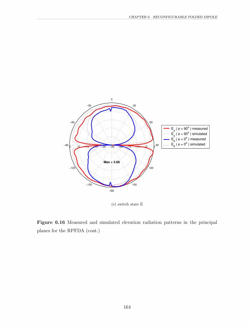
CHAPTER 6. RECONFIGURABLE FOLDED DIPOLE
0 −5 −10 −15 −20 −25 −20 −15 −10 −5 0
30
−150
60
−120
90−90
120
−60
150
−30
180
0
Max = 3.68
Eφ ( φ = 90o ) measuredEφ ( φ = 90o ) simulatedEθ ( φ = 0o ) measuredEθ ( φ = 0o ) simulated
(e) switch state E
Figure 6.16 Measured and simulated elevation radiation patterns in the principal
planes for the RPFDA (cont.)
164

CHAPTER 6. RECONFIGURABLE FOLDED DIPOLE
0 −5 −10 −15 −20 −25 −30 −25 −20 −15 −10 −5 0
30
−150
60
−120
90−90
120
−60
150
−30
180
0
Max = 2.49
Eθ (θ = 10o ) measuredEθ (θ = 10o ) simulatedEφ (θ = 10o ) measuredEφ (θ = 10o ) simulated
(a) switch state A
0 −5 −10 −15 −20 −25 −30 −25 −20 −15 −10 −5 0
30
−150
60
−120
90−90
120
−60
150
−30
180
0
Max = 2.59
Eθ (θ = 10o ) measuredEθ (θ = 10o ) simulatedEφ (θ = 10o ) measuredEφ (θ = 10o ) simulated
(b) switch state B
Figure 6.17 Measured and simulated conical radiation patterns (θ = 10) for the
RPFDA.
165
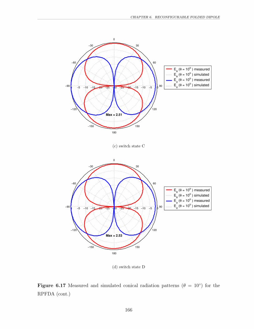
CHAPTER 6. RECONFIGURABLE FOLDED DIPOLE
0 −5 −10 −15 −20 −25 −30 −25 −20 −15 −10 −5 0
30
−150
60
−120
90−90
120
−60
150
−30
180
0
Max = 2.51
Eθ (θ = 10o ) measuredEθ (θ = 10o ) simulatedEφ (θ = 10o ) measuredEφ (θ = 10o ) simulated
(c) switch state C
0 −5 −10 −15 −20 −25 −30 −25 −20 −15 −10 −5 0
30
−150
60
−120
90−90
120
−60
150
−30
180
0
Max = 2.53
Eθ (θ = 10o ) measuredEθ (θ = 10o ) simulatedEφ (θ = 10o ) measuredEφ (θ = 10o ) simulated
(d) switch state D
Figure 6.17 Measured and simulated conical radiation patterns (θ = 10) for the
RPFDA (cont.)
166

CHAPTER 6. RECONFIGURABLE FOLDED DIPOLE
0 −5 −10 −15 −20 −25 −30 −25 −20 −15 −10 −5 0
30
−150
60
−120
90−90
120
−60
150
−30
180
0
Max = 2.55
Eθ (θ = 10o ) measuredEθ (θ = 10o ) simulatedEφ (θ = 10o ) measuredEφ (θ = 10o ) simulated
(e) switch state E
Figure 6.17 Measured and simulated conical radiation patterns (θ = 10) for the
RPFDA (cont.)
167
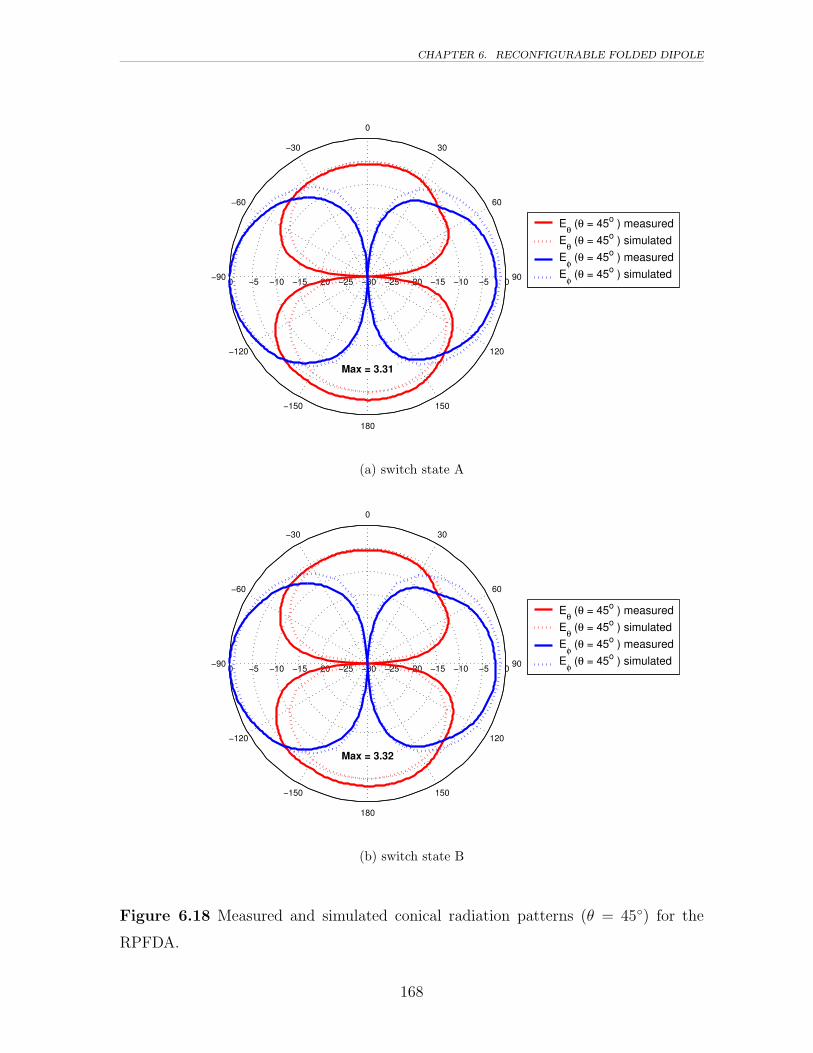
CHAPTER 6. RECONFIGURABLE FOLDED DIPOLE
0 −5 −10 −15 −20 −25 −30 −25 −20 −15 −10 −5 0
30
−150
60
−120
90−90
120
−60
150
−30
180
0
Max = 3.31
Eθ (θ = 45o ) measuredEθ (θ = 45o ) simulatedEφ (θ = 45o ) measuredEφ (θ = 45o ) simulated
(a) switch state A
0 −5 −10 −15 −20 −25 −30 −25 −20 −15 −10 −5 0
30
−150
60
−120
90−90
120
−60
150
−30
180
0
Max = 3.32
Eθ (θ = 45o ) measuredEθ (θ = 45o ) simulatedEφ (θ = 45o ) measuredEφ (θ = 45o ) simulated
(b) switch state B
Figure 6.18 Measured and simulated conical radiation patterns (θ = 45) for the
RPFDA.
168

CHAPTER 6. RECONFIGURABLE FOLDED DIPOLE
0 −5 −10 −15 −20 −25 −30 −25 −20 −15 −10 −5 0
30
−150
60
−120
90−90
120
−60
150
−30
180
0
Max = 3.33
Eθ (θ = 45o ) measuredEθ (θ = 45o ) simulatedEφ (θ = 45o ) measuredEφ (θ = 45o ) simulated
(c) switch state C
0 −5 −10 −15 −20 −25 −30 −25 −20 −15 −10 −5 0
30
−150
60
−120
90−90
120
−60
150
−30
180
0
Max = 3.34
Eθ (θ = 45o ) measuredEθ (θ = 45o ) simulatedEφ (θ = 45o ) measuredEφ (θ = 45o ) simulated
(d) switch state D
Figure 6.18 Measured and simulated conical radiation patterns (θ = 45) for the
RPFDA (cont.)
169

CHAPTER 6. RECONFIGURABLE FOLDED DIPOLE
0 −5 −10 −15 −20 −25 −30 −25 −20 −15 −10 −5 0
30
−150
60
−120
90−90
120
−60
150
−30
180
0
Max = 3.35
Eθ (θ = 45o ) measuredEθ (θ = 45o ) simulatedEφ (θ = 45o ) measuredEφ (θ = 45o ) simulated
(e) switch state E
Figure 6.18 Measured and simulated conical radiation patterns (θ = 45) for the
RPFDA (cont.)
170

CHAPTER 6. RECONFIGURABLE FOLDED DIPOLE
0 −5 −10 −15 −20 −15 −10 −5 0
30
−150
60
−120
90−90
120
−60
150
−30
180
0
Max = 3.32
Etotal
(θ = 10o ) measuredE
total (θ = 10o ) simulated
Etotal
(θ = 45o ) measuredE
total (θ = 45o ) simulated
(a) switch state A
0 −5 −10 −15 −20 −15 −10 −5 0
30
−150
60
−120
90−90
120
−60
150
−30
180
0
Max = 3.32
Etotal
(θ = 10o ) measuredE
total (θ = 10o ) simulated
Etotal
(θ = 45o ) measuredE
total (θ = 45o ) simulated
(b) switch state B
Figure 6.19 Measured and simulated conical Etotal radiation patterns for the RPFDA.
171

CHAPTER 6. RECONFIGURABLE FOLDED DIPOLE
0 −5 −10 −15 −20 −15 −10 −5 0
30
−150
60
−120
90−90
120
−60
150
−30
180
0
Max = 3.33
Etotal
(θ = 10o ) measuredE
total (θ = 10o ) simulated
Etotal
(θ = 45o ) measuredE
total (θ = 45o ) simulated
(c) switch state C
0 −5 −10 −15 −20 −15 −10 −5 0
30
−150
60
−120
90−90
120
−60
150
−30
180
0
Max = 3.34
Etotal
(θ = 10o ) measuredE
total (θ = 10o ) simulated
Etotal
(θ = 45o ) measuredE
total (θ = 45o ) simulated
(d) switch state D
Figure 6.19 Measured and simulated conical Etotal radiation patterns for the RPFDA
(cont.)
172

CHAPTER 6. RECONFIGURABLE FOLDED DIPOLE
0 −5 −10 −15 −20 −15 −10 −5 0
30
−150
60
−120
90−90
120
−60
150
−30
180
0
Max = 3.35
Etotal
(θ = 10o ) measuredE
total (θ = 10o ) simulated
Etotal
(θ = 45o ) measuredE
total (θ = 45o ) simulated
(e) switch state E
Figure 6.19 Measured and simulated conical Etotal radiation patterns for the RPFDA
(cont.)
173

CHAPTER 6. RECONFIGURABLE FOLDED DIPOLE
0 −5 −10 −15 −20 −15 −10 −5 0
30
−150
60
−120
90−90
120
−60
150
−30
180
0
Max = 3.65
State AState BState CState DState E
Figure 6.20 Comparison of measured elevation radiation patterns for all switch states
of the RPFDA, Eθ (φ = 0).
0 −5 −10 −15 −20 −15 −10 −5 0
30
−150
60
−120
90−90
120
−60
150
−30
180
0
Max = 3.71
State AState BState CState DState E
Figure 6.21 Comparison of measured elevation radiation patterns for all switch states
of the RPFDA, Eφ (φ = 90).
174

CHAPTER 6. RECONFIGURABLE FOLDED DIPOLE
0 −5 −10 −15 −20 −15 −10 −5 0
30
−150
60
−120
90−90
120
−60
150
−30
180
0
Max = 2.20
State AState BState CState DState E
Figure 6.22 Comparison of measured conical radiation patterns for all switch states
of the RPFDA, Eθ (θ = 10).
0 −5 −10 −15 −20 −15 −10 −5 0
30
−150
60
−120
90−90
120
−60
150
−30
180
0
Max = 2.58
State AState BState CState DState E
Figure 6.23 Comparison of measured conical radiation patterns for all switch states
of the RPFDA, Eφ (θ = 10).
175

CHAPTER 6. RECONFIGURABLE FOLDED DIPOLE
0 −5 −10 −15 −20 −15 −10 −5 0
30
−150
60
−120
90−90
120
−60
150
−30
180
0
Max = 0.10
State AState BState CState DState E
Figure 6.24 Comparison of measured conical radiation patterns for all switch states
of the RPFDA, Eθ (θ = 45).
0 −5 −10 −15 −20 −15 −10 −5 0
30
−150
60
−120
90−90
120
−60
150
−30
180
0
Max = 3.35
State AState BState CState DState E
Figure 6.25 Comparison of measured conical radiation patterns for all switch states
of the RPFDA, Eφ (θ = 45).
176
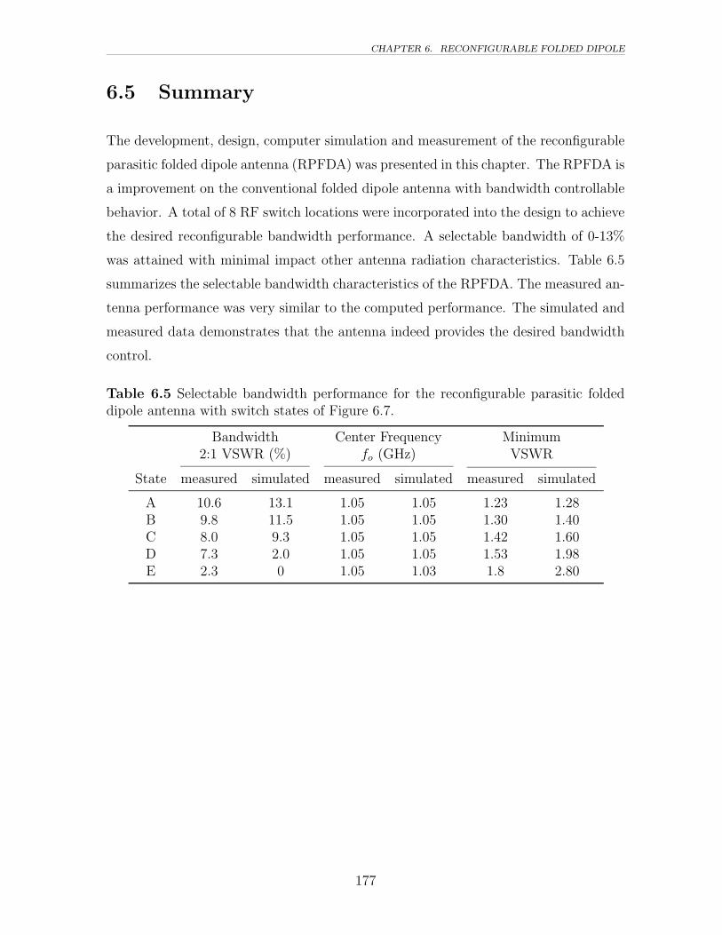
CHAPTER 6. RECONFIGURABLE FOLDED DIPOLE
6.5 Summary
The development, design, computer simulation and measurement of the reconfigurable
parasitic folded dipole antenna (RPFDA) was presented in this chapter. The RPFDA is
a improvement on the conventional folded dipole antenna with bandwidth controllable
behavior. A total of 8 RF switch locations were incorporated into the design to achieve
the desired reconfigurable bandwidth performance. A selectable bandwidth of 0-13%
was attained with minimal impact other antenna radiation characteristics. Table 6.5
summarizes the selectable bandwidth characteristics of the RPFDA. The measured an-
tenna performance was very similar to the computed performance. The simulated and
measured data demonstrates that the antenna indeed provides the desired bandwidth
control.
Table 6.5 Selectable bandwidth performance for the reconfigurable parasitic foldeddipole antenna with switch states of Figure 6.7.
Bandwidth Center Frequency Minimum2:1 VSWR (%) fo (GHz) VSWR
State measured simulated measured simulated measured simulated
A 10.6 13.1 1.05 1.05 1.23 1.28B 9.8 11.5 1.05 1.05 1.30 1.40C 8.0 9.3 1.05 1.05 1.42 1.60D 7.3 2.0 1.05 1.05 1.53 1.98E 2.3 0 1.05 1.03 1.8 2.80
177

Chapter 7
Conclusions
The new concept of antenna bandwidth control using reconfigurable antenna elements
has been presented in this dissertation. Three new antenna designs have been de-
veloped to demonstrate the bandwidth control concept. The new designs presented
are the reconfigurable ring patch antenna (RRPA), reconfigurable planar inverted-F
antenna (RPIFA) and reconfigurable parasitic folded dipole antenna (RPFDA). This
chapter summarizes the important points in this dissertation, details the contribu-
tions presented in this dissertation and proposes future work to enhance the existing
research.
7.1 Summary
A review of previous work and important background information related to this dis-
sertation was presented in Chapters 1 and 2. Reviews of the square ring patch antenna,
the planar inverted-F antenna and the folded dipole antenna were covered in 2. These
conventional antenna designs formed the the bases for the newly developed bandwidth
reconfigurable antenna designs. Also included in Chapter 2 was a description of the
current state of reconfigurable antenna research.
Chapter 3 provided an expanded and detailed analysis of the reconfigurable an-
tenna concept. Descriptions of current and proposed reconfigurable antenna technolo-
178

CHAPTER 7. CONCLUSIONS
gies including the various methodologies employed for achieving antenna reconfigura-
tion were explored. The three broad methods for achieving reconfigurable antenna
operation were identified as total geometry morphing, matching network morphing and
smart geometry reconfiguration. An overview of RF switch technologies was given and
a detailed comparison between the switch technologies was presented. Descriptions
of the physical components and switching devices used in reconfigurable antennas was
given along with the relevant electrical switch characteristics and mathematical models
necessary for simulating the switches in an RF environment.
The next three chapters presented the newly developed antenna designs capable
of reconfigurable bandwidth control. Chapter 4 presented the development, design,
computer simulation and measurement of the reconfigurable ring patch antenna. The
RRPA is an extension of the conventional square ring patch antenna with reconfigurable
bandwidth control. A total of 80 RF MEMS switches were incorporated into the
new design to give the antenna selectable bandwidth control. Six discrete antenna
states were designed with for a controllable bandwidth performance of up to 15%.
The inclusion of the selectable bandwidth behavior resulted in a very minimal impact
on the other important radiation properties of the antenna. The measured antenna
performance was very similar to the predicted computer simulation performance and
demonstrated that the antenna provides the desired bandwidth control.
The development, design, simulation and measurement of the reconfigurable pla-
nar inverted-F antenna was presented in Chapter 5. A total of 24 RF MEMS switches
were incorporated into the new design to give the antenna selectable bandwidth control.
Five discrete antenna states were designed for a controllable bandwidth performance
of up to 16%. The reconfigurable behavior of the RPIFA resulted in only a minor in-
fluence on the other important radiation characteristics of the antenna. The measured
antenna performance was similar to the computed performance and demonstrated that
the antenna achieves the desired bandwidth control.
Chapter 6 presented the development, design, computer simulation and mea-
surement of the reconfigurable parasitic folded dipole antenna. The RPFDA is an
improvement on the conventional printed folded dipole antenna with reconfigurable
bandwidth behavior. A total of eight RF MEMS switches were integrated into the
179

CHAPTER 7. CONCLUSIONS
antenna design to achieve the reconfigurable bandwidth control. Five discrete antenna
states were designed for a selectable bandwidth control of 13%. The bandwidth recon-
figurable behavior of the antenna resulted in only very minimal impact on the other
radiation characteristics of the antenna. The measured antenna performance was very
similar to the computed performance and demonstrated that the antenna achieves the
desired reconfigurable antenna behavior.
7.2 Contributions
The major contribution of this dissertation is twofold. First the new concept of ac-
tive antenna bandwidth control using reconfigurable antenna elements was developed.
Recent advances in RF switch technology have allowed for the development of new
classes of dynamically reconfigurable antenna. Until now, the primary areas of interest
in reconfigurable antenna designs has been confined to radiation pattern control and
steering, frequency of operation selection, and array applications.
The second significant contribution presented here encompasses the three new
antenna designs created to achieve the active bandwidth control. The new designs
developed in this dissertation are the reconfigurable ring patch antenna (RRPA), the
reconfigurable planar inverted-F antenna (RPIFA) and the reconfigurable folded par-
asitic dipole antenna (RPFDA). These antennas all exhibit the desired bandwidth
control while maintaining nearly constant performance over all other critical electrical
characteristics. Table 7.1 provides a summary of the important performance charac-
teristics for the three antennas developed in this work.
Table 7.1 Bandwidth reconfigurable antennas performance comparison.
Number of Number of Maximum Selectable BandwidthAntenna Switches States Bandwidth (%) States (%)
RRPA 80 6 15.0 0, 5.0, 9.0, 11.0, 13.0, 15.0RPIFA 12 5 15.8 0, 5.1, 9.4, 12.4, 15.8RPFDA 8 5 13.1 0, 2.0, 9.3, 11.5, 13.1
180

CHAPTER 7. CONCLUSIONS
7.3 Future Work
The research presented in this dissertation may be extended in several ways. The ex-
amination and development of additional antenna designs which incorporate reconfig-
urable elements to achieve bandwidth control is the first extension to the work already
presented here. Additionally, construction and measurement of the designs presented
here using actual RF MEMS switches and the subsequent comparison of these measure-
ments to the results presented in this dissertation is a logical extension of the present
work. In particular, the MEMS switch control biasing details should be examined more
closely to verify that the assumptions presented here are valid. While it is believed
that the biasing effects can be minimized through the use of high impedance control
lines and judicious trace routing, these details should be examined before production
level units can be developed.
181

References
[1] S. Licul, “Time-domain antenna characterization and design,” Ph.D. dissertation,Virginia Tech, Blacksburg, VA, 2004.
[2] J.-C. Chiao, Y. Fu, I. M. Chio, M. DeLisio, and L.-Y. Lin, “MEMS reconfigurableVee antenna,” in Microwave Symposium Digest, 1999 IEEE MTT-S International,M. Matloubian and E. Ponti, Eds., vol. 4. IEEE, June 1999, pp. 1515–1518.
[3] J. H. Schaffner, D. F. Sievenpiper, R. Y. Loo, J. L. Lee, and S. W. Livingston, “Awideband beam switching antenna using RF MEMS switches,” HRL Laboratories,Malibu, CA, USA, Tech. Rep., 2001.
[4] W.-S. Chen, C.-K. Wu, , and K.-L. Wong, “Square-ring microstrip antenna witha cross strip for compact circular polarization operation,” IEEE Transactions onAntennas and Propagation, vol. 47, no. 10, pp. 1566–1568, October 1999.
[5] W.-S. Chen and H.-D. Chen, “Single-feed circularly polarized square-ring mi-crostrip antennas with a slit,” in IEEE Antennas and Propagation Society In-ternational Symposium, 1998, vol. 3, Atlanta, GA, June 1998, pp. 1360–1363.
[6] V. Palanisamy and R. Garg, “Analysis of circularly polarized square ring and cross-strip microstrip antennas,” IEEE Transactions on Antennas and Propagation, vol.AP-34, no. 11, pp. 1340–1346, November 1986.
[7] W. L. Stutzman and G. A. Thiele, Antenna Theory and Design. New York: JohnWiley & Sons, Inc., 1998.
[8] P. M. Bafrooei and L. Shafai, “Characteristics of single- and double-layer mi-crostrip square-ring antennas,” IEEE Transactions on Antennas and Propagation,vol. 47, no. 10, pp. 1633–1639, October 1999.
[9] P. Moosavi and L. Shafai, “Stacked square ring resonators for bandwidth en-hancment,” in IEEE Antennas and Propagation Society International Symposium,1997, vol. 2, Montreal, July 1997, pp. 944–947.
[10] J. Gomez-Tagle and C. G. Christodoulou, “Extended cavity model analysis ofstacked ring microstrip antennas,” IEEE Transactions on Antennas and Propaga-tion, vol. 45, no. 11, pp. 1626–1635, November 1997.
182

REFERENCES
[11] A. Gobien, “Investigation of low profile antenna designs for use in hand-held ra-dios,” Master’s thesis, Virginia Polytechnic Institute and State University, August1997.
[12] Z. Liu, P. Hall, and D. Wake, “Dual-frequency planar inverted-F antenna,” IEEETransactions on Antennas and Propagation, vol. 45, no. 10, pp. 1451–1458, Octo-ber 1997.
[13] T. Taga, Analysis, Design, and Measurement of Small and Low-Profile Antennas.Boston: Artech House Publishers, 1992, ch. 5: Analysis of Planar Inverted-FAntennas and Antenna Design for Portable Radio Equipment, pp. 161 – 180.
[14] IE3D User’s Manual, 8th ed., Zeland Software Inc., 2001.
[15] C. R. Rowell and R. D. Murch, “A capacitively loaded PIFA for compact mobiletelephone handsets,” IEEE Transactions on Antennas and Propagation, vol. 45,no. 5, pp. 837–842, May 1997.
[16] M. A. Jensen and Y. Rahmat-Samii, “Performance analysis of antennas for hand-held transceivers using FDTD,” IEEE Transactions on Antennas and Propagation,vol. 42, no. 8, pp. 1106–1113, August 1994.
[17] K. Virga and Y. Rahmat-Samii, “An enhanced-bandwidth integrated dual-L an-tenna for mobile communications systems–design and measurement,” in Antennas& Propagation Society International Symposium Digest. Newport Beach, CA:IEEE, 1995.
[18] Z. Liu and P. Hall, “A novel dual-band antenna for hand-held po[r]table tele-phone,” in Antennas & Propagation Society International Symposium Digest,vol. 1. Baltimore, MD: IEEE, July 1996, pp. 54–57.
[19] M. A. Jensen and Y. Rahmat-Samii, “FDTD analysis of pifa diversity antennas ona hand-held transceiver unit,” in Antennas & Propagation Society InternationalSymposium Digest, vol. 2. Ann Arbor, MI: IEEE, July 1993.
[20] C. Harrison and R. King, “Folded dipoles and loops,” IRE Transactions on An-tennas and Propagation, vol. 9, pp. 171–187, March 1961.
[21] H. Jasik, Ed., Antenna Engineering Handbook. McGraw-Hill, 1961.
[22] H.-S. Tsai and R. A. York, “FDTD analysis of cpw-fed folded-slot and multiple-slotantennas on thin substrates,” IEEE Transactions on Antennas and Propagation,vol. 44, no. 2, pp. 217–226, February 1996.
[23] T. M. Weller, L. P. B. Katehi, and G. M. Rebeiz, “Single and double folded-slot antennas on semi-infinite substrates,” IEEE Transactions on Antennas andPropagation, vol. 43, no. 12, pp. 1423–1428, December 1995.
183

REFERENCES
[24] M. W. Nurnberger, J. L. Volakis, J. A. Mosko, and T. Ozdemir, “Analysis ofthe log-periodic folded slot array,” IEEE Antennas and Propagation InternationalSymposium Digest, 1994, vol. 3, pp. 1282–1285, June 1994.
[25] H. K. Schuman, “Modeling folded dipoles and feedlines for radiation and scatter-ing,” IEEE Transactions on Antennas and Propagation, vol. 38, no. 1, pp. 30–39,January 1990.
[26] W. T. Whistler, “The microstrip dual folded dipole as a phased array element,”IEEE International Antennas and Propagation Symposium Digest, 1987, vol. 25,pp. 1024–1027, June 1987.
[27] D. Peroulis, K. Sarabandi, and L. Katehi, “A planar VHF reconfigurable slotantenna,” in Antennas and Propagation Society, 2001 IEEE International Sym-posium, vol. 1, Boston, MA, July 2001, pp. 154 – 157.
[28] J.-C. Chiao, “MEMS RF devices for antenna applications,” in Microwave Confer-ence, 2000 Asia-Pacific. Sydney: IEEE, December 2000, pp. 895–898.
[29] J.-C. Chiao, Y. Fu, D. Choudhury, and L.-Y. Lin, “MEMS millimeterwave com-ponents,” in Microwave Symposium Digest, 1999 IEEE MTT-S International,M. Matloubian and E. Ponti, Eds., vol. 2. IEEE, June 1999, pp. 463–466.
[30] B. Cetiner, L. Jofre, and F. De Flaviis, “Reconfigurable miniature multielementantenna for wireless networking,” in IEEE Radio and Wireless Conference, 2001.RAWCON 2001, August 2001, pp. 203–206.
[31] L. Jofre, B. Cetiner, and F. De Flaviis, “Miniature multi-element antenna for wire-less communications,” IEEE Transactions on Antennas and Propagation, vol. 50,no. 5, pp. 658–669, May 2002.
[32] B. Cetiner, L. Jofre, G. Li, and F. de Flaviis, “A packaged reconfigurable multi-element antenna for wireless networking,” in 2001 Asian-Pacific Microwave Con-ference. APMC 2001, vol. 2, Taipei, Taiwan, December 2001, pp. 705–708.
[33] B. Chang, Y. Qian, and T. Itoh, “A reconfigurable leaky mode/patch antennacontrolled by pin diode switches,” in IEEE Antennas and Propagation SocietyInternational Symposium, 1999, vol. 4, Orlando, FL, July 1999, pp. 2694–2697.
[34] Y. Qian, B. Chang, M. Chang, and T. Itoh, “Reconfigurable leaky-mode multi-function patch antenna structure,” Electronic Letters, vol. 35, no. 2, pp. 104–105,January 1999.
[35] C.-K. C. Tzuang, “Leaky mode perspective an printed antenna,” Proceedings ofNational Science Council ROC(A), vol. 23, no. 4, pp. 544–549, 1999.
[36] C.-W. Baek, S. Song, C. Cheon, Y.-K. Kim, and Y. Kwon, “2-D mechanical beamsteering antenna fabricated using MEMS technology,” in IEEE MTT-S Interna-tional Microwave Symposium Digest, 2001, Phoenix, AZ, May 2001, pp. 211–214.
184

REFERENCES
[37] J. Bernhard, R. Wang, R. Clark, and P. Mayes, “Stacked reconfigurable antennaelements for space-based radar applications,” in IEEE Antennas and PropagationSociety International Symposium, 2001, vol. 1, Boston, MA, July 2001, pp. 158–161.
[38] R. Simons, D. Chun, and L. Katehi, “Reconfigurable array antenna using micro-electromechanical systems (MEMS) actuators,” in IEEE International SymposiumAntennas and Propagation Society, 2001, vol. 3, Boston, July 2001, pp. 674–677.
[39] J. Maloney, M. Kesler, L. Lust, L. Pringle, T. Fountain, P. Harms, and G. Smith,“Switched fragmented aperture antennas,” in IEEE Antennas and PropagationSociety International Symposium, 2000, Salt Lake City, July 2000, pp. 310–313.
[40] L. Pringle, D. Denison, P. Frederich, E. Kuster, et al., “Micro-switched fragmentedreconfigurable apertures,” workshop presentation, July 2000, gTRI RECAP Sym-posium 2000.
[41] L. Pringle, P. Friederich, S. Blalock, G. Kiesel, P. Harms, D. Denison, E. Kuster,and G. Smith, “GTRI reconfigurable aperture design,” in IEEE Antennas andPropagation Society International Symposium, 2002, vol. 1, San Antonio, June2002, pp. 473–476.
[42] W. H. Weedon, W. J. Payne, and G. M. Rebeiz, “MEMS-switched reconfigurableantennas,” in IEEE Antennas and Propagation Society International Symposium,2001, vol. 3. Boston: IEEE, July 2001, pp. 654–657.
[43] C. Bozler, R. Drangmeister, S. Duffy, M. Gouker, J. Knecht, L. Kushner, R. Parr,S. Rabe, and L. Travis, “MEMs microswitch arrays for reconfigurable distributedmicrowave components,” in IEEE Antennas and Propagation Society InternationalSymposium, 2000, vol. 2. Salt Lake City: IEEE, July 2000, pp. 587–591.
[44] ——, “MEMs microswitch arrays for reconfigurable distributed microwave compo-nents,” in Microwave Symposium Digest. 2000 IEEE MTT-S International, vol. 1.Boston: IEEE, June 2000, pp. 153–156.
[45] C. Coleman, E. Rothwell, J. Ross, and L. Nagy, “Self-structuring antennas,” IEEEAntennas and Propagation Magazine, vol. 44, no. 3, pp. 11–23, June 2002.
[46] J. H. Schaffner, D. F. Sievenpiper, R. Y. Loo, J. L. Lee, and S. W. Livingston, “Awideband beam switching antenna using RF MEMS switches,” in IEEE Antennasand Propagation Society International Symposium, 2001, vol. 3, Boston, MA, July2001, pp. 658–661.
[47] J. Schaffner, R. Loo, D. Sievenpiper, F. Dolezal, G. Tangonan, J. Colburn,J. Lynch, J. Lee, S. Livingston, R. Broas, and M. Wu, “Reconfigurable aper-ture antennas using RF MEMS switches for multi-octave tunability and beamsteering,” in IEEE Antennas and Propagation Society International Symposium,2000, Salt Lake City, UT, July 2000, pp. 321–324.
185

REFERENCES
[48] J. Veihl, R. Hodges, D. McGrath, and C. Monzon, “Reconfigurable aperturedecade bandwidth array,” in IEEE Antennas and Propagation Society Interna-tional Symposium, 2000, vol. 1. IEEE, July 2000, pp. 314–317.
[49] F. Dobias and J. Gunther, “Reconfigurable array antennas with phase-only controlof quantized phase shifters,” in Vehicular Technology Conference, 1995 IEEE 45th,vol. 1, Chicago, IL, USA, July 1995, pp. 35–39.
[50] B. Norvell, R. Hancock, J. Smith, M. Pugh, S. Theis, and J. Kriatkofsky, “Microelectro mechanical switch (mems) technology applied to electronically scannedarrays for space based radar,” in IEEE Aerospace Conference Proceedings, 1999,vol. 3, Snowmass at Aspen, CO, March 1999, pp. 239–247.
[51] V. K. Varadan, K. J. Vinoy, and K. A. Jose, RF MEMS and Their Applications.West Sussex, England: John Wiley & Sons, 2003.
[52] Applications of PIN Diodes, Hewlett-Packard, 1997.
[53] PIN Diode Designers’ Handbook, Microsemi Corp., Watertown, MA, 1998.
[54] C. A. Liechti, “Microwave field-effect transistors–1976,” IEEE Transactions onMicrowave Theory and Techniques, vol. MTT-24, no. 6, pp. 279–300, June 1976.
[55] R. A. Gaspari and H. Yee, “Microwave GaAs FET switching,” in Microwave Sym-posium Digest, MTT-S International, vol. 78, no. 1, June 1978, pp. 58–60.
[56] H. J. D. L. Santos, RF MEMS Circuit Design for Wireless Commuications, ser.Artech House Microelectromechanical Systems Series. Boston: Artech HousePublishers, 2002.
[57] E. R. Brown, “RF-MEMs switches for reconfigurable integrated circuits,” IEEETransactions on Microwave Theory and Techniques, vol. 46, no. 11, pp. 1868–1880,November 1998.
[58] C. Goldsmith, J. Randall, S. Eshelman, T. Lin, D. Denniston, S. Chen, andB. Norvell, “Characteristics of micromachined switches at microwave frequencies,”in Microwave Symposium Digest, 1996., IEEE MTT-S International, vol. 2, June1996, pp. 1141 – 1144.
[59] G. M. Rebeiz, RF MEMS: Theory, Design, and Technology. Hoboken, NJ: Wiley-Interscience, 2003.
[60] D. Hyman and M. Mehregany, “Contact physics of gold microcontacts forMEMS switches,” IEEE Transactions on Components and Packaging Technolo-gies, vol. 22, no. 3, September 1999.
[61] D. Peroulis, K. Sarabandi, and L. Katehi, “Low contact resistance series MEMSswitches,” in Microwave Symposium Digest, 2002 IEEE MTT-S International,vol. 1, Seattle, WA, June 2002.
186
REFERENCES
[62] R. Mihailovich, M. Kim, J. Hacker, E. Sovero, J. Studer, J. Higgins, and J. DeNa-tale, “MEM relay for reconfigurable RF circuits,” IEEE Microwave And WirelessComponent Letters, vol. 11, no. 2, pp. 53 – 55, February 2001.
[63] J. Poon, L. C. Ling, and N. Karmakar, “Investigations into RF MEMS switchesfor reconfigurable phased antenna arrays,” in Antennas and Propagation SocietyInternational Symposium, 2002, vol. 2. IEEE, 2002, pp. 18–21.
[64] G. M. Rebeiz, “RF MEMS switches: Status of the technology,” in TRANSDUC-ERS, Solid-State Sensors, Actuators and Microsystems, 12th Innational Confer-ence on, vol. 2, June 2003, pp. 1726 – 1729.
[65] J. Yao and M. Chang, “A surface micromachined miniature switch for telecommu-nications applications with signal frequencies from dc up to 4 ghz,” in Solid-StateSensors and Actuators, 1995 and Eurosensors IX. Transducers ’95. The 8th In-ternational Conference on, vol. 2, June 1995, pp. 384 –387.
[66] A. De Silva, C. Vaughan, D. Frear, L. Liu, S. Kuo, J. Foerstner, J. Drye,J. Abrokwah, H. Hughes, C. Amrine, C. Butler, S. Markgraf, H. Denton, andS. Springer, “Motorola mems switch technology for high frequency applications,”in Microelectromechanical Systems Conference, 2001, Berkeley, CA, 2001, pp. 22– 24.
[67] C. T.-C. Nguyen, L. P. Katehi, and G. M. Rebeiz, “Micromachined devices forwireless communications,” Proceedings of the IEEE, vol. 86, no. 8, pp. 1756 – 1768,1998.
[68] G. M. Rebeiz and J. B. Muldavin, “RF MEMS switches and circuits,” IEEEMicrowave Magazine, pp. 59–71, December 2001.
[69] D. Peroulis, S. P. Pacheco, K. Sarabandi, and L. P. B. Katehi, “Electromechanicalconsiderations in developing low-voltage RF MEMS switches,” IEEE Transactionson Microwave Theory and Techniques, vol. 51, no. 1, pp. 259–270, January 2003.
[70] N. Bushyager and M. Tentzeris, “Modeling and design of RF MEMS structuresusing computationsally efficient numerical techniques,” in Electronic Componentsand Technology Conference, 2001. Proceedings., 51st, Orlando, May 2001, pp. 327– 330.
[71] J. B. Muldavin and G. M. Rebeiz, “Inline capacitive and DC-contact MEMS shuntswitches,” IEEE Microwave And Wireless Component Letters, vol. 11, no. 8, pp.334 – 336, August 2001.
[72] ——, “High-isolation CPW MEMS shunt switches–part 1: Modeling,” IEEETransactions on Microwave Theory and Techniques, vol. 48, no. 6, pp. 1045 –1051, June 2000.
187

REFERENCES
[73] J. Gomez-Tagle and C. G. Christodoulou, “Extended cavity model analysis ofstacked microstrip ring antennas,” IEEE Transactions on Antennas and Propaga-tion, vol. 45, no. 11, pp. 1626 – 1637, November 1997.
[74] J. W. Mink, “Circular ring microstrip antenna elements,” in Antennas and Prop-agation Society International Symposium, 1980, vol. 18, June 1980, pp. 605 –608.
[75] W. C. Chew, “A broad-band annular-ring microstrip antenna,” IEEE Transactionson Antennas and Propagation, vol. AP-30, no. 5, pp. 918–922, September 1982.
[76] “RT/duroid 5870 datasheet,” Rogers Corp., http://www.rogerscorporation.com/mwu/pdf/5000data.pdf; accessed June, 2003.
[77] “Rohacell HF31 datasheet,” Degussa, http://www.rohacell.com; accessed June,2003.
[78] M.-C. Huynh and W. Stutzman, “Ground plane effects on planar inverted-F an-tenna performance,” IEE Proceedings - Microwaves, Antennas and Propagation,vol. 150, no. 4, pp. 209 – 213, August 2003.
[79] K.-L. Wong, Planar Antennas For Wireless Communications. Hoboken, NJ: JohnWiley & Sons, Inc., 2003.
[80] P. Song, P. Hall, H. Ghafouri-Shiraz, and D. Wake, “Triple-band planar inverted-Fantenna,” in Antennas and Propagation Society, 1999. IEEE International Sym-posium 1999, vol. 2, Orlando, FL, July 1999, pp. 908 – 911.
[81] K.-L. Wong and T.-W. Chiou, “Finite ground plane effects on broad-band dualpolarized patch antenna properties,” IEEE Transactions on Antennas and Prop-agation, vol. 51, no. 4, pp. 903 – 904, April 2003.
[82] J. H. Richmond, “Monopole antenna on circular disk,” IEEE Transactions onAntennas and Propagation, vol. 12, no. AP-32, pp. 1282 – 1287, December 1984.
[83] J. Huang, “Finite ground plane effect on the microstrip antenna radiation pat-terns,” IEEE Transactions on Antennas and Propagation, vol. AP-31, no. 4, pp.649 – 653, July 1983.
[84] M. M. Weiner, “Monopole element at the center of a circular ground plane whoseradius is small or comparable to a wavelength,” IEEE Transactions on Antennasand Propagation, vol. 35, no. 5, pp. 488 – 495, May 1987.
[85] M.-C. T. Huynh, “A numerical and experimental investigation of planar inverted-F antennas for wireless communication applications,” Master’s thesis, VirginiaTech, Blacksburg, VA, October 19 2000.
[86] J. W. Greiser, “Log-periodic antenna structure,” U.S. Patent 3 369 243, Feb. 18,1968.
188

REFERENCES
[87] N. P. Cummings and W. L. Stutzman, “UHF Subscriber and Hub Antenna De-signs,” Virginia Tech Antenna Group, Blacksburg, VA, Final Report to SpikeBroadband Systems, R00-4, October 2000.
[88] C. A. Balanis, Antenna Theory: Analysis and Design. New York: John Wiley &Sons, 1982.
[89] “RO3003 datasheet,” Rogers Corp., http://www.rogerscorporation.com/mwu/pdf/3000data.pdf; accessed June, 2003.
[90] W. Davis, J. Nealy, G. Ricciardi, and W. Stutzman, “Techniques for the measure-ment of the impedance of wideband balanced antennas,” in Antenna MeasurementTechniques Association Symposium, no. 95-7, Williamsburg, VA, November 1995,pp. 60 – 63.
189

Vita
Nathan P. Cummings was born in January 1975 in Parkersburg, West Virginia. Hespent his entire precollegiate life on the same street in the town of Vienna, a suburbof Parkersburg. He graduated from high school in 1993 and began his studies in Elec-trical Engineering at Virginia Polytechnic Institute & State University in the fall ofthat year. His undergraduate tenure included a co-op position with G.E. Fanuc Au-tomation, North America in Charlottesville, Virginia. He received his B.S. in electricalengineering from Virginia Tech in May of 1998. Upon completion of his undergradu-ate degree he joined the Virginia Tech Antenna Group. Nathan received his M.S. inelectrical engineering in December of 2001 and his Ph.D. in electrical engineering inDecember of 2003, both from Virginia Tech.
190
Related Documents