Actel HDL Coding Style Guide

Welcome message from author
This document is posted to help you gain knowledge. Please leave a comment to let me know what you think about it! Share it to your friends and learn new things together.
Transcript
Actel HDL Coding
Style Guide
Actel HDL Coding
Style Guide
Actel Corporation, Sunnyvale, CA 94086© 1997 Actel Corporation. All rights reserved.
Printed in the United States of America
Part Number: 5029105-0
Release: November 1997
No part of this document may be copied or reproduced in any form or by any means without prior written consent of Actel.
Actel makes no warranties with respect to this documentation and disclaims any implied warranties of merchantability or fitness for a particular purpose.
Information in this document is subject to change without notice. Actel assumes no responsibility for any errors that may appear in this document.
This document contains confidential proprietary information that is not to be disclosed to any unauthorized person without prior written consent of ActelCorporation.
TrademarksActel and the Actel logotype are registered trademarks of Actel Corporation.
Verilog is a registered trademark of Open Verilog International.
All other products or brand names mentioned are trademarks or registered trademarks of their respective holders.
ii
Table of Contents
Introduction . . . . . . . . . . . . . . . . . . . . . . . ixDocument Organization . . . . . . . . . . . . . . . . . . . ix
Document Assumptions . . . . . . . . . . . . . . . . . . . . x
Document Conventions . . . . . . . . . . . . . . . . . . . . x
HDL Keywords and Naming Conventions . . . . . . . . . . . . x
VHDL . . . . . . . . . . . . . . . . . . . . . . . . . . . xi
Verilog . . . . . . . . . . . . . . . . . . . . . . . . . . xii
Related Manuals . . . . . . . . . . . . . . . . . . . . . . . xiii
1 Design Flow . . . . . . . . . . . . . . . . . . . . . . . . 1Design Flow Illustrated . . . . . . . . . . . . . . . . . . . . 1
Design Flow Overview . . . . . . . . . . . . . . . . . . . . 2
Design Creation/Verification . . . . . . . . . . . . . . . . . 2
Design Implementation . . . . . . . . . . . . . . . . . . . . 3
Programming . . . . . . . . . . . . . . . . . . . . . . . . 4
System Verification . . . . . . . . . . . . . . . . . . . . . . 4
2 Technology Independent Coding Styles . . . . . . . . . 5Sequential Devices . . . . . . . . . . . . . . . . . . . . . . 5
Flip-Flops (Registers) . . . . . . . . . . . . . . . . . . . . . 5
D-Latches . . . . . . . . . . . . . . . . . . . . . . . . . 13
Datapath . . . . . . . . . . . . . . . . . . . . . . . . . . 17
Priority Encoders Using If-Then-Else. . . . . . . . . . . . . 17
Multiplexors Using Case . . . . . . . . . . . . . . . . . . 19
Decoders . . . . . . . . . . . . . . . . . . . . . . . . . 24
Counters . . . . . . . . . . . . . . . . . . . . . . . . . . 25
Arithmetic Operators . . . . . . . . . . . . . . . . . . . . 29
Relational Operators . . . . . . . . . . . . . . . . . . . . 31
Equality Operator . . . . . . . . . . . . . . . . . . . . . 32
Shift Operators . . . . . . . . . . . . . . . . . . . . . . . 33
Finite State Machine . . . . . . . . . . . . . . . . . . . . . 35
Mealy Machine . . . . . . . . . . . . . . . . . . . . . . . 37
Moore Machine . . . . . . . . . . . . . . . . . . . . . . 41
iii
Table of Contents
Input-Output Buffers . . . . . . . . . . . . . . . . . . . . 44
Tri-State Buffer . . . . . . . . . . . . . . . . . . . . . . . 45
Bi-Directional Buffer . . . . . . . . . . . . . . . . . . . . 47
Generics and Parameters. . . . . . . . . . . . . . . . . . . 49
3 Performance Driven Coding . . . . . . . . . . . . . . 51Reducing Logic Levels on Critical Paths . . . . . . . . . . . . 51
Resource Sharing . . . . . . . . . . . . . . . . . . . . . . 53
Operators Inside Loops . . . . . . . . . . . . . . . . . . . 55
Coding for Combinability . . . . . . . . . . . . . . . . . . 56
Register Duplication . . . . . . . . . . . . . . . . . . . . . 57
Partitioning a Design . . . . . . . . . . . . . . . . . . . . 60
4 Technology Specific Coding Techniques . . . . . . . 61Multiplexors. . . . . . . . . . . . . . . . . . . . . . . . . 61
Internal Tri-State to Multiplexor Mapping . . . . . . . . . . . 62
Registers . . . . . . . . . . . . . . . . . . . . . . . . . . 64
Synchronous Clear or Preset . . . . . . . . . . . . . . . . 65
Clock Enabled . . . . . . . . . . . . . . . . . . . . . . . 66
Asynchronous Preset . . . . . . . . . . . . . . . . . . . . 68
Asynchronous Preset and Clear . . . . . . . . . . . . . . . 71
Registered I/Os . . . . . . . . . . . . . . . . . . . . . . . 71
CLKINT/CLKBUF for Reset and/or High Fanout Networks . . . 73
QCLKINT/QCLKBUF for Medium Fanout Networks . . . . . . 75
ACTgen Counter. . . . . . . . . . . . . . . . . . . . . . . 75
Dual Architecture Coding in VHDL . . . . . . . . . . . . . . 77
SRAM . . . . . . . . . . . . . . . . . . . . . . . . . . . . 80
Register-Based Single Port SRAM . . . . . . . . . . . . . . 80
Register-Based Dual-Port SRAM . . . . . . . . . . . . . . . 82
ACTgen RAM . . . . . . . . . . . . . . . . . . . . . . . 84
FIFO . . . . . . . . . . . . . . . . . . . . . . . . . . . . 86
Register-Based FIFO . . . . . . . . . . . . . . . . . . . . 86
iv
Table of Contents
ACTgen FIFO . . . . . . . . . . . . . . . . . . . . . . . 92
A Product Support . . . . . . . . . . . . . . . . . . . . . 95Actel U.S. Toll-Free Line . . . . . . . . . . . . . . . . . . . 95
Customer Service . . . . . . . . . . . . . . . . . . . . . . 95
Customer Applications Center . . . . . . . . . . . . . . . . 96
Action Facts . . . . . . . . . . . . . . . . . . . . . . . . . 96
Web Site . . . . . . . . . . . . . . . . . . . . . . . . . . 96
Guru Automated Technical Support . . . . . . . . . . . . . 97
HLD Web Site . . . . . . . . . . . . . . . . . . . . . . . . 97
FTP Site. . . . . . . . . . . . . . . . . . . . . . . . . . . 97
Electronic Mail . . . . . . . . . . . . . . . . . . . . . . . 97
Index . . . . . . . . . . . . . . . . . . . . . . . . . . . 99
v

List of Figures
Actel HDL Synthesis-Based Design Flow . . . . . . . . . . . . . . 1
D Flip-Flop . . . . . . . . . . . . . . . . . . . . . . . . . . . . 6
D Flip-Flop with Asynchronous Reset . . . . . . . . . . . . . . . 7
D Flip-Flop with Asynchronous Preset . . . . . . . . . . . . . . . 8
D Flip-Flop with Asynchronous Reset and Preset . . . . . . . . . . 9
D Flip-Flop with Synchronous Reset . . . . . . . . . . . . . . . 10
D Flip-Flop with Synchronous Preset . . . . . . . . . . . . . . 11
D Flip-Flop with Asynchronous Reset and Clock Enable . . . . . 12
D-Latch . . . . . . . . . . . . . . . . . . . . . . . . . . . . 13
D-Latch with Gated Asynchronous Data . . . . . . . . . . . . . 14
D-Latch with Gated Enable . . . . . . . . . . . . . . . . . . . 15
D-Latch with Asynchronous Reset . . . . . . . . . . . . . . . . 16
Priority Encoder Using an If-Then-Else Statement . . . . . . . . . 17
Multiplexor Using a Case Statement . . . . . . . . . . . . . . . 19
Basic Structure of a Moore FSM . . . . . . . . . . . . . . . . . 35
Basic Structure of a Mealy FSM . . . . . . . . . . . . . . . . . 36
Mealy State Diagram . . . . . . . . . . . . . . . . . . . . . . 37
Tri-State Buffer . . . . . . . . . . . . . . . . . . . . . . . . . 45
Bi-Directional Buffer . . . . . . . . . . . . . . . . . . . . . . 47
Single Module Implementation of a Synchronous Clearor Preset Register . . . . . . . . . . . . . . . . . . . . . . 65
Single Module Implementation of a Clock Enabled Register . . . . 66
Asynchronous Preset . . . . . . . . . . . . . . . . . . . . . . 69
Equivalent Asynchronous Preset . . . . . . . . . . . . . . . . . 69
Registered I/O Cell . . . . . . . . . . . . . . . . . . . . . . . 71
RAM Behavioral Simulation Model . . . . . . . . . . . . . . . . 80
FIFO Behavioral Simulation Mode . . . . . . . . . . . . . . . . 86
vii

Introduction
VHDL and Verilog® HDL are high level description languages for system and circuit design. These languages support various abstraction levels of design, including architecture-specific design. At the higher levels, these languages can be used for system design without regard to a specific technology. To create a functional design, you only need to consider a specific target technology. However, to achieve optimal performance and area from your target device, you must become familiar with the architecture of the device and then code your design for that architecture.
Efficient, standard HDL code is essential for creating good designs. The structure of the design is a direct result of the structure of the HDL code. Additionally, standard HDL code allows designs to be reused in other designs or by other HDL designers.
This document provides the preferred coding styles for the Actel architecture. The information is to be used as reference material with instructions to optimize your HDL code for the Actel architecture. Examples in both VHDL and Verilog code are provided to illustrate these coding styles and to help implement the code into your design.
Document OrganizationThe Actel HDL Coding Style Guide is divided into the following chapters:
Chapter 1 - Design Flow describes the basic design flow for creating Actel designs with HDL synthesis and simulation tools.
Chapter 2 - Technology Independent Coding Styles describes basic high level HDL coding styles and techniques.
Chapter 3 - Performance Driven Coding illustrates efficient design practices and describes synthesis implementations and techniques that can be used to reduce logic levels on a critical path.
Chapter 4 - Technology Specific Coding Techniques describes how to implement technology specific features and technology specific macros for optimal area and performance utilization.
Appendix A - Product Support provides information about contacting Actel for customer and technical support.
ix
Introduction
Document AssumptionsThe information in this manual is based on the following assumptions:
• You are familiar with Verilog or VHDL hardware description language, and HDL design methodology for designing logic circuits.
• You are familiar with FPGA design software, including design synthesis and simulation tools.
Document ConventionsThe following conventions are used throughout this manual.
Information that is meant to be input by the user is formatted as follows:
keyboard input
The contents of a file is formatted as follows:
file contents
HDL code appear as follows, with HDL keyword in bold:
entity actel isport (a: in bit;y: out bit);
end actel;
Messages that are displayed on the screen appear as follows:
HDL Keywords and Naming ConventionsThere are naming conventions you must follow when writing Verilog or VHDL code. Additionally, Verilog and VHDL have reserved words that cannot be used for signal or entity names. This section lists the naming conventions and reserved keywords for each.
Screen Message
x
Introduction
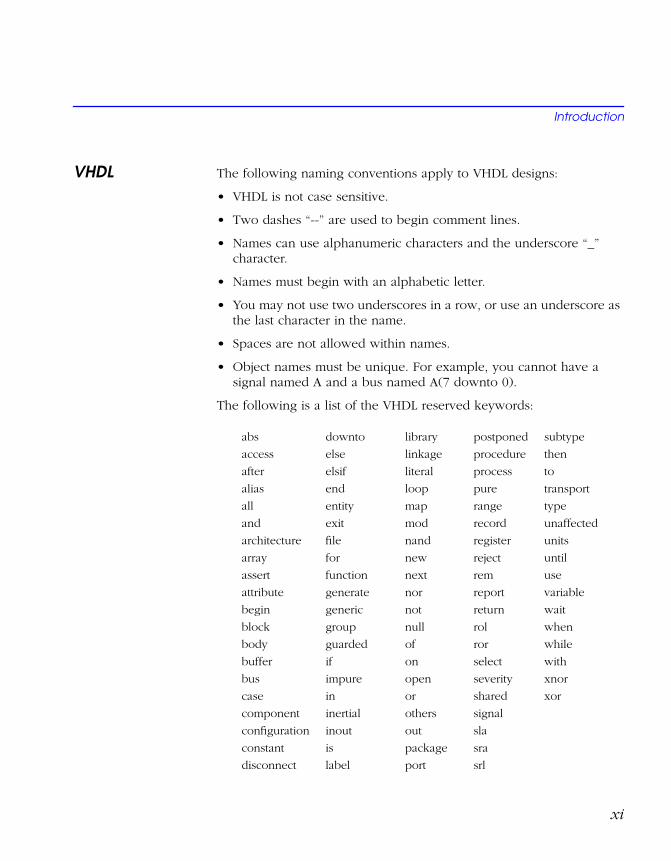
VHDL The following naming conventions apply to VHDL designs:
• VHDL is not case sensitive.
• Two dashes “--” are used to begin comment lines.
• Names can use alphanumeric characters and the underscore “_” character.
• Names must begin with an alphabetic letter.
• You may not use two underscores in a row, or use an underscore as the last character in the name.
• Spaces are not allowed within names.
• Object names must be unique. For example, you cannot have a signal named A and a bus named A(7 downto 0).
The following is a list of the VHDL reserved keywords:
abs downto library postponed subtype
access else linkage procedure then
after elsif literal process to
alias end loop pure transport
all entity map range type
and exit mod record unaffected
architecture file nand register units
array for new reject until
assert function next rem use
attribute generate nor report variable
begin generic not return wait
block group null rol when
body guarded of ror while
buffer if on select with
bus impure open severity xnor
case in or shared xor
component inertial others signal
configuration inout out sla
constant is package sra
disconnect label port srl
xi
Introduction
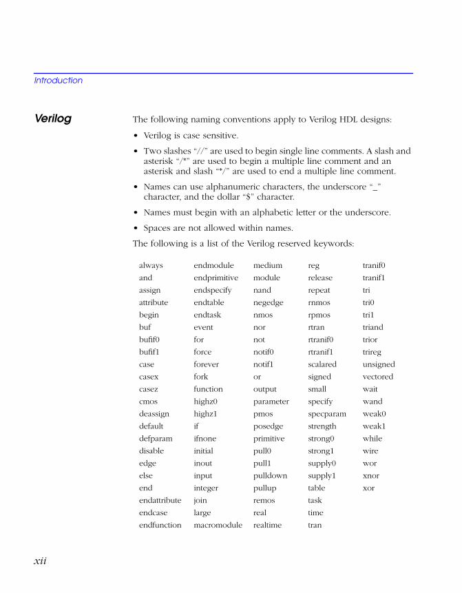
Verilog The following naming conventions apply to Verilog HDL designs:
• Verilog is case sensitive.
• Two slashes “//” are used to begin single line comments. A slash and asterisk “/*” are used to begin a multiple line comment and an asterisk and slash “*/” are used to end a multiple line comment.
• Names can use alphanumeric characters, the underscore “_” character, and the dollar “$” character.
• Names must begin with an alphabetic letter or the underscore.
• Spaces are not allowed within names.
The following is a list of the Verilog reserved keywords:
always endmodule medium reg tranif0
and endprimitive module release tranif1
assign endspecify nand repeat tri
attribute endtable negedge rnmos tri0
begin endtask nmos rpmos tri1
buf event nor rtran triand
bufif0 for not rtranif0 trior
bufif1 force notif0 rtranif1 trireg
case forever notif1 scalared unsigned
casex fork or signed vectored
casez function output small wait
cmos highz0 parameter specify wand
deassign highz1 pmos specparam weak0
default if posedge strength weak1
defparam ifnone primitive strong0 while
disable initial pull0 strong1 wire
edge inout pull1 supply0 wor
else input pulldown supply1 xnor
end integer pullup table xor
endattribute join remos task
endcase large real time
endfunction macromodule realtime tran
xii
Introduction
Related ManualsThis guide refers to the Designer Series documentation, which provides information about designing and programming Actel devices. The Designer Series documentation is available in PDF format on the Designer Series CD ROM and the Actel Web Site.
The following manuals provide additional information about designing and programming Actel FPGAs using HDL design methodology:
ACTmap VHDL Synthesis Methodology Guide. This guide contains information about designing an Actel FPGA using the ACTmap VHDL synthesis tool, including preferred HDL coding styles and design considerations. This guide is available in PDF format on the Designer Series CD ROM and the Actel Web Site.
Synopsys Synthesis Methodology Guide. This guide contains information about designing an Actel FPGA using Synopsys synthesis tools, including preferred HDL coding styles, design considerations, and synthesis constraints. This guide is available in PDF format on the Designer Series CD ROM and the Actel Web Site.
Digital Design and Synthesis with Verilog HDL. Madhavan, Rajeev, and others. San Jose, CA: Automata Publishing Company, 1993. This book contains information to allow designers to write synthesizable designs with Verilog HDL.
HDL Chip Design. Smith, Douglas J. Madison, AL: Doone Publications, 1996. This book describes and gives examples of how to design FPGAs using VHDL and Verilog.
IEEE Standard VHDL Language Reference Manual. New York: Institute of Electrical and Electronics Engineers, Inc., 1994. This manual specifies IEEE Standard 1076-1993, which defines the VHDL standard and the use of VHDL in the creation of electronic systems.
xiii

1Design Flow
This chapter illustrates and describes the basic design flow for creating Actel designs using HDL synthesis and simulation tools.
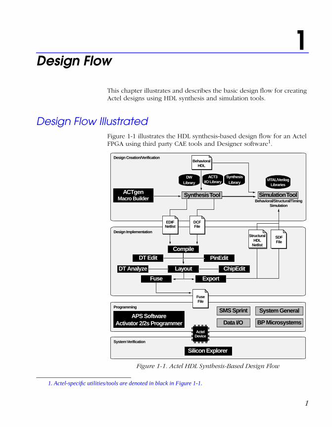
Design Flow IllustratedFigure 1-1 illustrates the HDL synthesis-based design flow for an Actel FPGA using third party CAE tools and Designer software1.
1. Actel-specific utilities/tools are denoted in black in Figure 1-1.
Design Creation/Verification
Silicon Explorer
Data I/O
System General
FuseFile
ActelDevice
APS SoftwareActivator 2/2s Programmer BP Microsystems
SMS Sprint
Design Implementation
Programming
System Verification
Compile
Layout
DT Edit PinEdit
DT Analyze ChipEdit
ExportFuse
SDFFile
StructuralHDL
Netlist
I/O LibraryACT3
LibrarySynthesis
LibraryDW
EDIFNetlist
DCFFile
Synthesis Tool Simulation ToolACTgenMacro Builder Behavioral/Structural/Timing
Simulation
BehavioralHDL
LibrariesVITAL/Verilog
Figure 1-1. Actel HDL Synthesis-Based Design Flow
1
Chapter 1: Design Flow
Design Flow OverviewThe Actel HDL synthesis-based design flow has four main steps; Design Creation/Verification, Design Implementation, Programming, and System Verification. These steps are described in detail in the following sections.
Design Creation/Verification
During design creation/verification, a design is captured in an RTL-level (behavioral) HDL source file. After capturing the design, a behavioral simulation of the HDL file can be performed to verify that the HDL code is correct. The code is then synthesized into an Actel gate-level (structural) HDL netlist. After synthesis, a structural simulation of the design can be performed. Finally, an EDIF netlist is generated for use in Designer and an HDL structural netlist is generated for timing simulation.
HDL Design Source EntryEnter your HDL design source using a text editor or a context-sensitive HDL editor. Your HDL source file can contain RTL-level constructs, as well as instantiations of structural elements, such as ACTgen macros.
Behavioral SimulationYou can perform a behavioral simulation of your design before synthesis. Behavioral simulation verifies the functionality of your HDL code. Typically, unit delays are used and a standard HDL test bench can be used to drive simulation. Refer to the documentation included with your simulation tool for information about performing behavioral simulation.
SynthesisAfter you have created your behavioral HDL source file, you must synthesize it before placing and routing it in Designer. Synthesis translates the behavioral HDL file into a gate-level netlist and optimizes the design for a target technology. Refer to the documentation included with your synthesis tool for information about performing design synthesis.
2
Design Flow Overview
EDIF Netlist GenerationAfter you have created, synthesized, and verified your design, you must generate an Actel EDIF netlist for place and route in Designer. This EDIF netlist is also used to generate a structural HDL netlist for use in structural simulation. Refer to the Designer Series documentation for information about generating an EDIF netlist.
Structural Netlist GenerationYou can generate a structural HDL netlist from your EDIF netlist for use in structural simulation by either exporting it from Designer or by using the Actel “edn2vhdl” or “edn2vlog” program. Refer to the Designer Series documentation for information about generating a structural netlist.
Structural SimulationYou can perform a structural simulation of your design before placing and routing it. Structural simulation verifies the functionality of your post-synthesis structural HDL netlist. Default unit delays included in the compiled Actel VITAL libraries are used for every gate. Refer to the documentation included with your simulation tool for information about performing structural simulation.
Design Implementation
During design implementation, a design is placed and routed using Designer. Additionally, timing analysis is performed on a design in Designer with the DT Analyze tool. After place and route, post-layout (timing) simulation is performed.
Place and RouteUse Designer to place and route your design. Refer to the Designer Series documentation for information about using Designer.
Timing AnalysisUse the DT Analyze tool in Designer to perform static timing analysis on your design. Refer to the Designer Series documentation for information about using DT Analyze.
3
Chapter 1: Design Flow
Timing SimulationAfter placing and routing your design, you perform a timing simulation to verify that the design meets timing constraints. Timing simulation requires timing information exported from Designer, which overrides default unit delays in the compiled Actel VITAL libraries. Refer to the Designer Series documentation for information about exporting timing information from Designer.
Programming Programming a device requires software and hardware from Actel or a supported 3rd party programming system. Refer to the Designing wih Actel manual and the Activator Installation and APS Programming Guide for information on programming an Actel device.
System Verification
You can perform system verification on a programmed device using the Actel ActionProbe or Silicon Explorer. Refer to the Activator Installation and APS Programming Guide or Silicon Explorer Quick Start for information on using Action Probe or Silicon Explorer.
4
2Technology Independent Coding Styles
This chapter describes basic, HDL coding styles and techniques. These coding styles are essential when writing efficient, standard HDL code and creating technology independent designs.
Sequential DevicesA sequential device, either a flip-flop or a latch, is a one-bit memory device. A latch is a level-sensitive memory device and a flip-flop is an edge-triggered memory device.
Flip-Flops (Registers)
Flip-flops, also called registers, are inferred in VHDL using wait and if statements within a process using either a rising edge or falling edge detection expression. There are two types of expressions that can be used, a 'event attribute or a function call. For example:
(clk'event and clk='1') --rising edge 'event attribute(clk'event and clk='0') --falling edge 'event attributerising_edge(clock) --rising edge function callfalling_edge(clock) --falling edge function call
The examples in this guide use rising edge 'event attribute expressions, but falling edge expressions could be used. The 'event attribute expression is used because some VHDL synthesis tools may not recognize function call expressions. However, using a function call expression is preferred for simulation because a function call only detects an edge transition (0 to 1 or 1 to 0) but not a transition from X to 1 or 0 to X, which may not be a valid transition. This is especially true if using a multi-valued data type like std_logic, which has nine possible values (U, X, 0, 1, Z, W, L, H, -).
This section describes and gives examples for different types of flip-flops. Refer to “Registers” on page 64 for additional information about using specific registers in the Actel architecture.
5
Chapter 2: Technology Independent Coding Styles
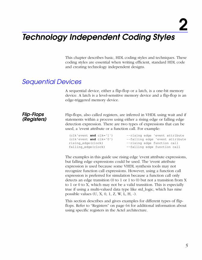
Rising Edge Flip-FlopThe following examples infer a D flip-flop without asynchronous or synchronous reset or preset. This flip-flop is a basic sequential cell in the Actel antifuse architecture.
VHDL library IEEE;use IEEE.std_logic_1164.all;
entity dff isport (data, clk : in std_logic;
q : out std_logic);end dff;
architecture behav of dff isbeginprocess (clk) begin
if (clk'event and clk = '1') thenq <= data;
end if;end process;end behav;
Verilog module dff (data, clk, q);
input data, clk;output q;reg q;
always @(posedge clk)q = data;
endmodule
data
clk
q
Figure 2-1. D Flip-Flop
6
Sequential Devices
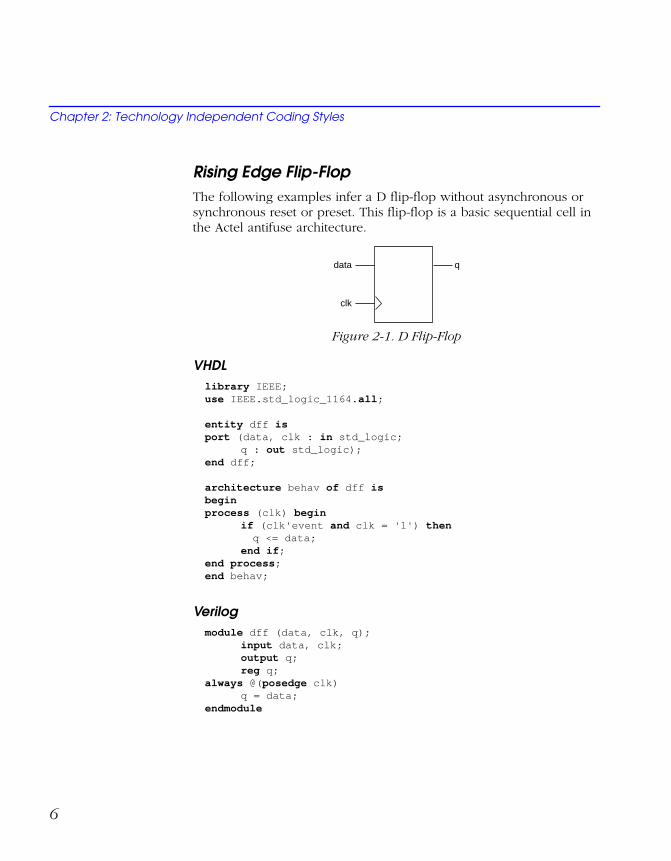
Rising Edge Flip-Flop with Asynchronous ResetThe following examples infer a D flip-flop with an asynchronous reset. This flip-flop is a basic sequential cell in the Actel antifuse architecture.
VHDLlibrary IEEE;use IEEE.std_logic_1164.all;
entity dff_async_rst isport (data, clk, reset : in std_logic;
q : out std_logic);end dff_async_rst;
architecture behav of dff_async_rst isbeginprocess (clk, reset) begin
if (reset = '0') thenq <= '0';
elsif (clk'event and clk = '1') thenq <= data;
end if;end process;end behav;
Verilog module dff_async_rst (data, clk, reset, q);
input data, clk, reset;output q;reg q;
always @(posedge clk or negedge reset)if (~reset)q = 1'b0;
elseq = data;
endmodule
Figure 2-2. D Flip-Flop with Asynchronous Reset
data
clk
q
reset
7
Chapter 2: Technology Independent Coding Styles
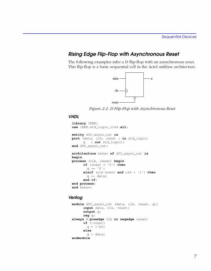
Rising Edge Filp-Flop with Asynchronous PresetThe following examples infer a D flip-flop with an asynchronous preset. Refer to “Registers” on page 64 for additional information about using preset flip-flops with the Actel architecture.
VHDLlibrary IEEE;use IEEE.std_logic_1164.all;
entity dff_async_pre isport (data, clk, preset : in std_logic;
q : out std_logic);end dff_async_pre;
architecture behav of dff_async_pre isbeginprocess (clk, preset) begin
if (preset = '0') thenq <= '1';
elsif (clk'event and clk = '1') thenq <= data;
end if;end process;end behav;
Verilogmodule dff_async_pre (data, clk, preset, q);input data, clk, preset;output q;reg q;always @(posedge clk or negedge preset)if (~preset)q = 1'b1;
elseq = data;
endmodule
data
clk
q
preset
Figure 2-3. D Flip-Flop with Asynchronous Preset
8
Sequential Devices
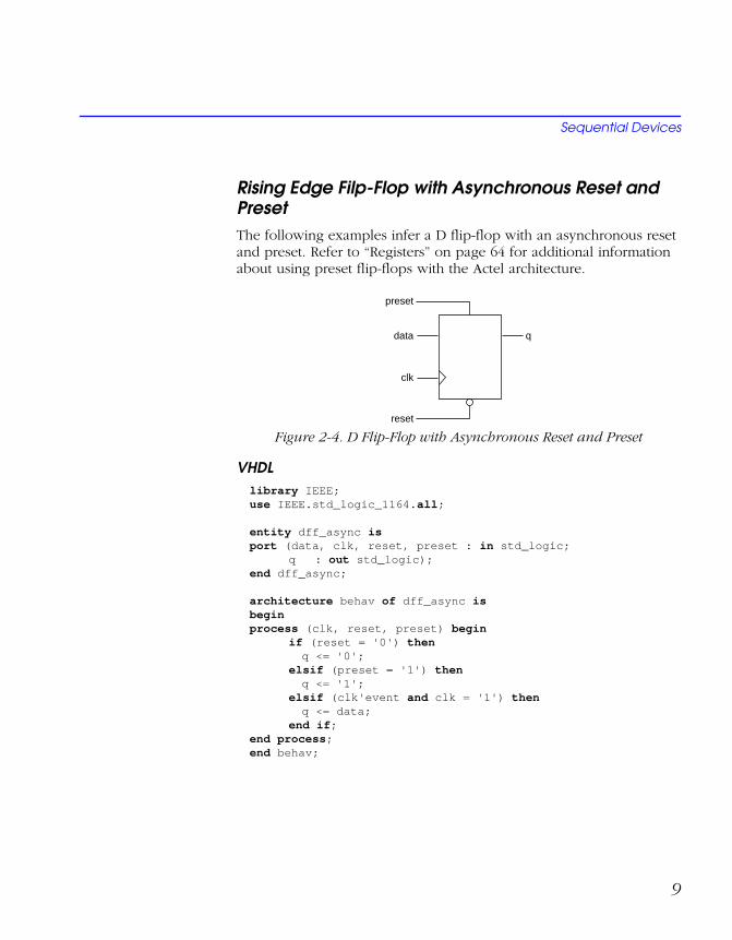
Rising Edge Filp-Flop with Asynchronous Reset and PresetThe following examples infer a D flip-flop with an asynchronous reset and preset. Refer to “Registers” on page 64 for additional information about using preset flip-flops with the Actel architecture.
VHDL library IEEE;use IEEE.std_logic_1164.all;
entity dff_async isport (data, clk, reset, preset : in std_logic;
q : out std_logic);end dff_async;
architecture behav of dff_async isbeginprocess (clk, reset, preset) begin
if (reset = '0') thenq <= '0';
elsif (preset = '1') thenq <= '1';
elsif (clk'event and clk = '1') thenq <= data;
end if;end process;end behav;
data
clk
preset
q
reset
Figure 2-4. D Flip-Flop with Asynchronous Reset and Preset
9
Chapter 2: Technology Independent Coding Styles
Verilog module dff_async (reset, preset, data, q, clk);
input clk;input reset, preset, data;output q;reg q;
always @ (posedge clk or negedge reset or posedge preset)if (~reset)q = 1'b0;
else if (preset)q = 1'b1;
else q = data;endmodule
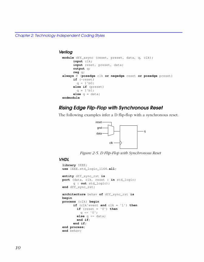
Rising Edge Filp-Flop with Synchronous ResetThe following examples infer a D flip-flop with a synchronous reset.
VHDLlibrary IEEE;use IEEE.std_logic_1164.all;
entity dff_sync_rst isport (data, clk, reset : in std_logic;
q : out std_logic);end dff_sync_rst;
architecture behav of dff_sync_rst isbeginprocess (clk) begin
if (clk'event and clk = '1') thenif (reset = '0') thenq <= '0';
else q <= data;end if;
end if;end process;end behav;
Figure 2-5. D Flip-Flop with Synchronous Reset
data
gnd
clk
reset
q
10
Sequential Devices
Verilog module dff_sync_rst (data, clk, reset, q);
input data, clk, reset;output q;reg q;
always @ (posedge clk)if (~reset)q = 1'b0;
else q = data;endmodule
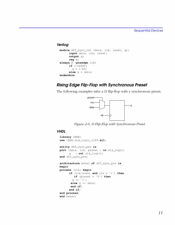
Rising Edge Filp-Flop with Synchronous PresetThe following examples infer a D flip-flop with a synchronous preset.
VHDL library IEEE;use IEEE.std_logic_1164.all;
entity dff_sync_pre isport (data, clk, preset : in std_logic;
q : out std_logic);end dff_sync_pre;
architecture behav of dff_sync_pre isbeginprocess (clk) begin
if (clk'event and clk = '1') then if (preset = '0') then q <= '1'; else q <= data; end if;end if;
end process;end behav;
Figure 2-6. D Flip-Flop with Synchronous Preset
data
vcc
clk
preset
q
11
Chapter 2: Technology Independent Coding Styles
Verilogmodule dff_sync_pre (data, clk, preset, q);
input data, clk, preset;output q;reg q;
always @ (posedge clk)if (~preset)q = 1'b1;
else q = data;endmodule
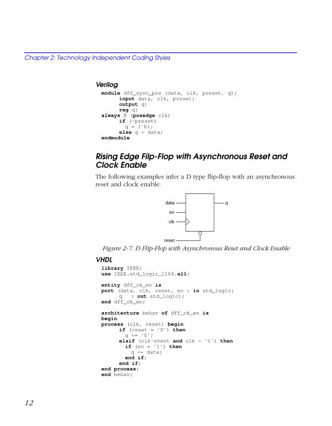
Rising Edge Filp-Flop with Asynchronous Reset and Clock EnableThe following examples infer a D type flip-flop with an asynchronous reset and clock enable.
VHDLlibrary IEEE;use IEEE.std_logic_1164.all;
entity dff_ck_en isport (data, clk, reset, en : in std_logic;
q : out std_logic);end dff_ck_en;
architecture behav of dff_ck_en isbeginprocess (clk, reset) begin
if (reset = '0') thenq <= '0';
elsif (clk'event and clk = '1') thenif (en = '1') thenq <= data;
end if;end if;
end process;end behav;
data
en
clk
q
reset
Figure 2-7. D Flip-Flop with Asynchronous Reset and Clock Enable
12
Sequential Devices
Verilog module dff_ck_en (data, clk, reset, en, q);
input data, clk, reset, en;output q;reg q;
always @ (posedge clk or negedge reset)if (~reset)q = 1'b0;
else if (en)q = data;
endmodule
D-Latches This section describes and gives examples of different types of D-latches.
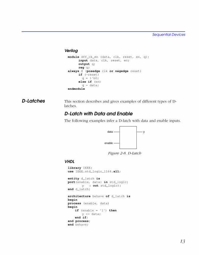
D-Latch with Data and EnableThe following examples infer a D-latch with data and enable inputs.
VHDL library IEEE;use IEEE.std_logic_1164.all;
entity d_latch isport(enable, data: in std_logic;
y : out std_logic);end d_latch;
architecture behave of d_latch isbeginprocess (enable, data)begin
if (enable = '1') theny <= data;
end if;end process;end behave;
Figure 2-8. D-Latch
data
enable
y
13
Chapter 2: Technology Independent Coding Styles
Verilog module d_latch (enable, data, y);
input enable, data;output y;reg y;
always @(enable or data)if (enable)
y = data;endmodule
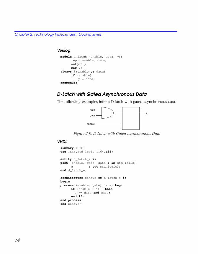
D-Latch with Gated Asynchronous DataThe following examples infer a D-latch with gated asynchronous data.
VHDL library IEEE;use IEEE.std_logic_1164.all;
entity d_latch_e isport (enable, gate, data : in std_logic;
q : out std_logic);end d_latch_e;
architecture behave of d_latch_e isbeginprocess (enable, gate, data) begin
if (enable = '1') thenq <= data and gate;
end if;end process;end behave;
Figure 2-9. D-Latch with Gated Asynchronous Data
data
enable
qgate
14
Sequential Devices
Verilog module d_latch_e(enable, gate, data, q);
input enable, gate, data;output q;reg q;
always @ (enable or data or gate)if (enable)q = (data & gate);
endmodule
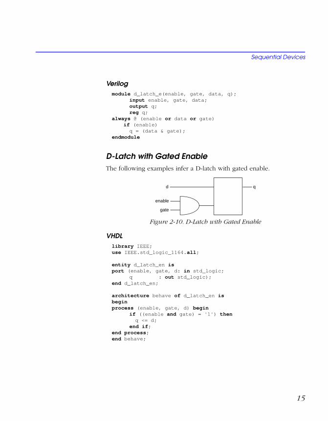
D-Latch with Gated EnableThe following examples infer a D-latch with gated enable.
VHDL library IEEE;use IEEE.std_logic_1164.all;
entity d_latch_en isport (enable, gate, d: in std_logic;
q : out std_logic);end d_latch_en;
architecture behave of d_latch_en isbeginprocess (enable, gate, d) begin
if ((enable and gate) = '1') thenq <= d;
end if;end process;end behave;
Figure 2-10. D-Latch with Gated Enable
enable
d q
gate
15
Chapter 2: Technology Independent Coding Styles
Verilog module d_latch_en(enable, gate, d, q);
input enable, gate, d;output q;reg q;
always @ (enable or d or gate)if (enable & gate)q = d;
endmodule
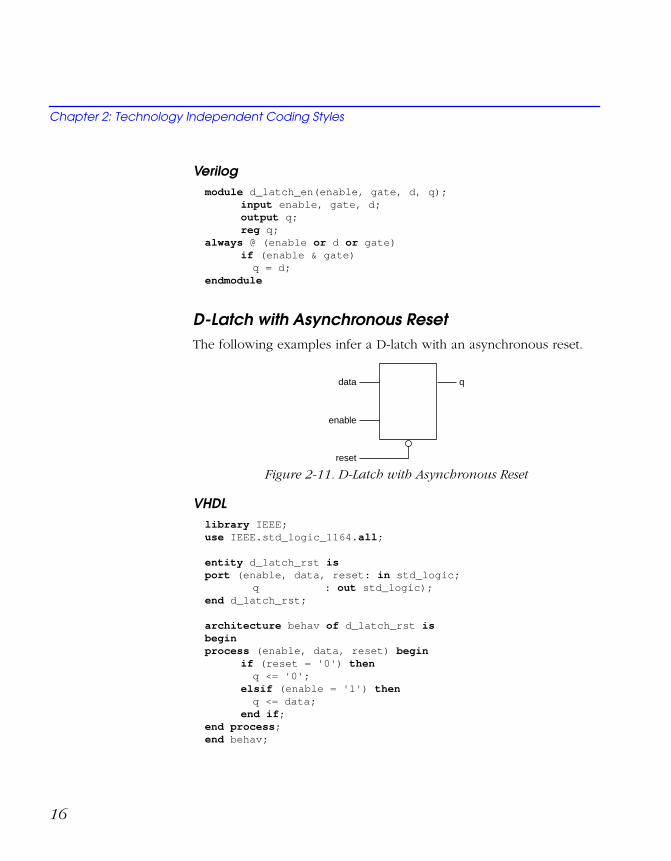
D-Latch with Asynchronous ResetThe following examples infer a D-latch with an asynchronous reset.
VHDL library IEEE;use IEEE.std_logic_1164.all;
entity d_latch_rst isport (enable, data, reset: in std_logic;
q : out std_logic);end d_latch_rst;
architecture behav of d_latch_rst isbeginprocess (enable, data, reset) begin
if (reset = '0') thenq <= '0';
elsif (enable = '1') thenq <= data;
end if;end process;end behav;
data
enable
reset
q
Figure 2-11. D-Latch with Asynchronous Reset
16
Datapath
Verilog module d_latch_rst (reset, enable, data, q);
input reset, enable, data;output q;reg q;
always @ (reset or enable or data)if (~reset)q = 1'b0;
else if (enable)q = data;
endmodule
DatapathDatapath logic is a structured repetitive function. These structures are modeled in various different implementations based on area and timing constraints. Most synthesis tools generate optimal implementations for the target technology.
Priority Encoders Using If-Then-Else
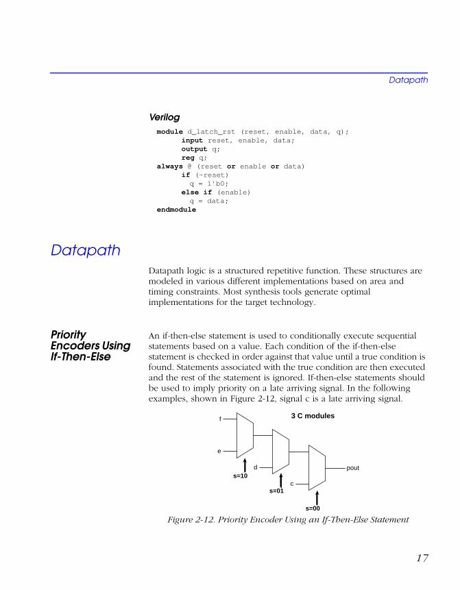
An if-then-else statement is used to conditionally execute sequential statements based on a value. Each condition of the if-then-else statement is checked in order against that value until a true condition is found. Statements associated with the true condition are then executed and the rest of the statement is ignored. If-then-else statements should be used to imply priority on a late arriving signal. In the following examples, shown in Figure 2-12, signal c is a late arriving signal.
f
e
d
cs=10
s=01
s=00
pout
3 C modules
Figure 2-12. Priority Encoder Using an If-Then-Else Statement
17
Chapter 2: Technology Independent Coding Styles
VHDL library IEEE;use IEEE.std_logic_1164.all;
entity my_if isport (c, d, e, f: in std_logic;
s : in std_logic_vector(1 downto 0);pout : out std_logic);
end my_if;
architecture my_arc of my_if isbeginmyif_pro: process (s, c, d, e, f) begin
if s = “00” thenpout <= c;
elsif s = “01” thenpout <= d;
elsif s = “10” thenpout <= e;
else pout <= f;end if;
end process myif_pro;end my_arc;
Verilogmodule IF_MUX (c, d, e, f, s, pout);
input c, d, e, f;input [1:0]s;output pout;reg pout;
always @(c or d or e or f or s) beginif (s == 2'b00) pout = c;
else if (s ==2'b01)pout = d;
else if (s ==2'b10)pout = e;
else pout = f;end
endmodule
18
Datapath
Multiplexors Using Case
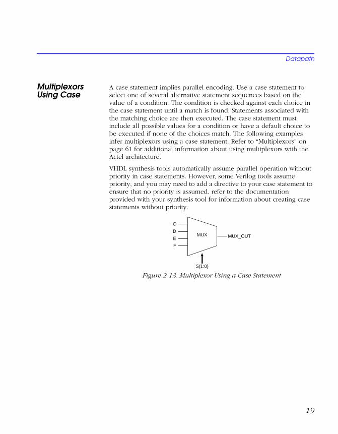
A case statement implies parallel encoding. Use a case statement to select one of several alternative statement sequences based on the value of a condition. The condition is checked against each choice in the case statement until a match is found. Statements associated with the matching choice are then executed. The case statement must include all possible values for a condition or have a default choice to be executed if none of the choices match. The following examples infer multiplexors using a case statement. Refer to “Multiplexors” on page 61 for additional information about using multiplexors with the Actel architecture.
VHDL synthesis tools automatically assume parallel operation without priority in case statements. However, some Verilog tools assume priority, and you may need to add a directive to your case statement to ensure that no priority is assumed. refer to the documentation provided with your synthesis tool for information about creating case statements without priority.
C
F
MUX_OUTD
EMUX
S(1:0)
Figure 2-13. Multiplexor Using a Case Statement
19
Chapter 2: Technology Independent Coding Styles
4:1 MultiplexorThe following examples infer a 4:1 multiplexor using a case statement.
VHDL --4:1 Multiplexorlibrary IEEE;use IEEE.std_logic_1164.all;
entity mux isport (c, d, e, f : in std_logic;
s : in std_logic_vector(1 downto 0);muxout : out std_logic);
end mux;
architecture my_mux of mux isbeginmux1: process (s, c, d, e, f) begincase s is
when “00” => muxout <= c;when “01” => muxout <= d;when “10” => muxout <= e;when others => muxout <= f;
end case;end process mux1;end my_mux;
Verilog //4:1 Multiplexormodule MUX (C, D, E, F, S, MUX_OUT);
input C, D, E, F;input [1:0] S;output MUX_OUT;reg MUX_OUT;
always @(C or D or E or F or S)begincase (S)
2'b00 : MUX_OUT = C;2'b01 : MUX_OUT = D;2'b10 : MUX_OUT = E;default : MUX_OUT = F;
endcaseendendmodule
20
Datapath
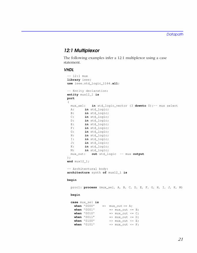
12:1 MultiplexorThe following examples infer a 12:1 multiplexor using a case statement.
VHDL-- 12:1 muxlibrary ieee;use ieee.std_logic_1164.all;
-- Entity declaration:entity mux12_1 isport(mux_sel: in std_logic_vector (3 downto 0);-- mux selectA: in std_logic;B: in std_logic;C: in std_logic;D: in std_logic;E: in std_logic;F: in std_logic;G: in std_logic;H: in std_logic;I: in std_logic;J: in std_logic;K: in std_logic;M: in std_logic;mux_out: out std_logic -- mux output
);end mux12_1;
-- Architectural body:architecture synth of mux12_1 is
begin
proc1: process (mux_sel, A, B, C, D, E, F, G, H, I, J, K, M)
begin
case mux_sel iswhen "0000" => mux_out <= A;when "0001" => mux_out <= B;when "0010" => mux_out <= C; when "0011” => mux_out <= D;when "0100" => mux_out <= E; when "0101" => mux_out <= F;
21
Chapter 2: Technology Independent Coding Styles
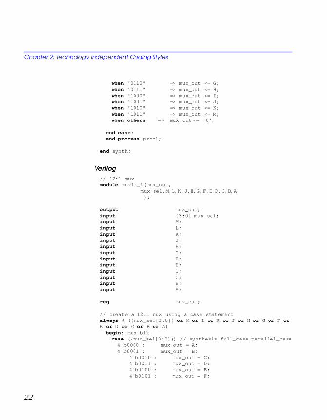
when "0110" => mux_out <= G; when "0111" => mux_out <= H;when "1000" => mux_out <= I;when "1001" => mux_out <= J;when "1010" => mux_out <= K;when "1011" => mux_out <= M;when others => mux_out <= '0';
end case;end process proc1;
end synth;
Verilog// 12:1 muxmodule mux12_1(mux_out,
mux_sel,M,L,K,J,H,G,F,E,D,C,B,A );
output mux_out;input [3:0] mux_sel;input M;input L;input K;input J;input H;input G;input F;input E;input D;input C;input B;input A;
reg mux_out;
// create a 12:1 mux using a case statementalways @ ({mux_sel[3:0]} or M or L or K or J or H or G or F or E or D or C or B or A)begin: mux_blkcase ({mux_sel[3:0]}) // synthesis full_case parallel_case4'b0000 : mux_out = A;4'b0001 : mux_out = B;
4'b0010 : mux_out = C; 4'b0011 : mux_out = D; 4'b0100 : mux_out = E; 4'b0101 : mux_out = F;
22
Datapath
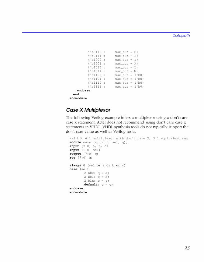
4'b0110 : mux_out = G; 4'b0111 : mux_out = H; 4'b1000 : mux_out = J; 4'b1001 : mux_out = K; 4'b1010 : mux_out = L; 4'b1011 : mux_out = M; 4'b1100 : mux_out = 1'b0; 4'b1101 : mux_out = 1'b0; 4'b1110 : mux_out = 1'b0; 4'b1111 : mux_out = 1'b0;
endcaseend
endmodule
Case X MultiplexorThe following Verilog example infers a multiplexor using a don’t care case x statement. Actel does not recommend using don’t care case x statements in VHDL. VHDL synthesis tools do not typically support the don’t care value as well as Verilog tools.
//8 bit 4:1 multiplexor with don't care X, 3:1 equivalent muxmodule mux4 (a, b, c, sel, q);input [7:0] a, b, c;input [1:0] sel;output [7:0] q;reg [7:0] q;
always @ (sel or a or b or c)case (sel)
2'b00: q = a;2'b01: q = b;2'b1x: q = c;default: q = c;
endcaseendmodule
23
Chapter 2: Technology Independent Coding Styles
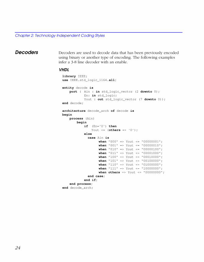
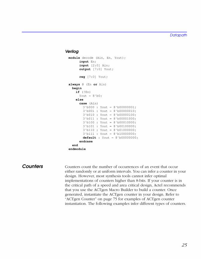
Decoders Decoders are used to decode data that has been previously encoded using binary or another type of encoding. The following examples infer a 3-8 line decoder with an enable.
VHDL library IEEE;use IEEE.std_logic_1164.all;
entity decode is port ( Ain : in std_logic_vector (2 downto 0);
En: in std_logic;Yout : out std_logic_vector (7 downto 0));
end decode;
architecture decode_arch of decode isbegin
process (Ain)begin
if (En='0') thenYout <= (others => '0');
elsecase Ain is
when "000" => Yout <= "00000001"; when "001" => Yout <= "00000010";when "010" => Yout <= "00000100";when "011" => Yout <= "00001000";when "100" => Yout <= "00010000";when "101" => Yout <= "00100000";when "110" => Yout <= "01000000";when "111" => Yout <= "10000000";when others => Yout <= "00000000";
end case;end if;
end process;end decode_arch;
24
Datapath
Verilog module decode (Ain, En, Yout);
input En;input [2:0] Ain;output [7:0] Yout;
reg [7:0] Yout;
always @ (En or Ain)beginif (!En)Yout = 8'b0;
elsecase (Ain)3'b000 : Yout = 8'b00000001;3'b001 : Yout = 8'b00000010;3'b010 : Yout = 8'b00000100;3'b011 : Yout = 8'b00001000;3'b100 : Yout = 8'b00010000;3'b101 : Yout = 8'b00100000;3'b110 : Yout = 8'b01000000;3'b111 : Yout = 8'b10000000;default : Yout = 8'b00000000;
endcaseend
endmodule
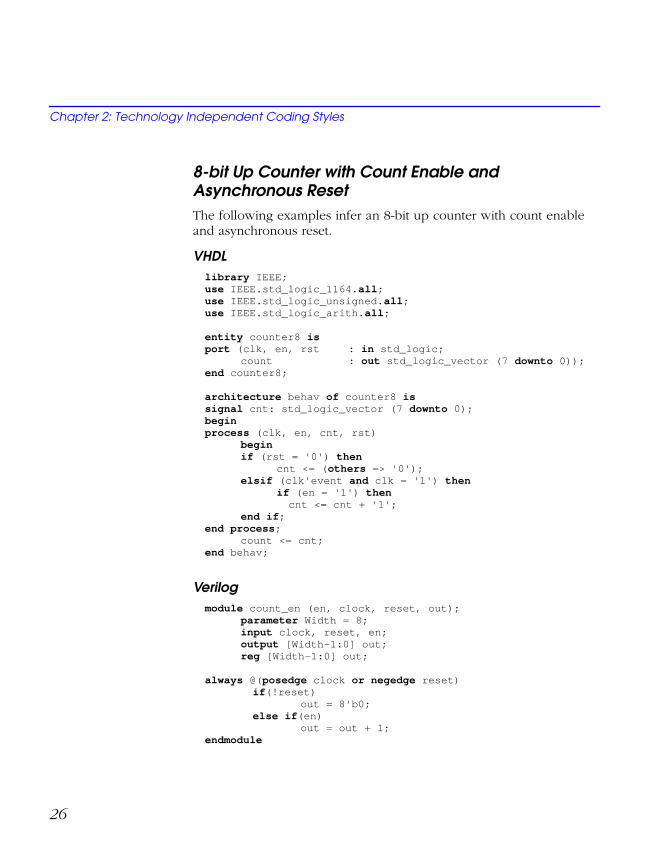
Counters Counters count the number of occurrences of an event that occur either randomly or at uniform intervals. You can infer a counter in your design. However, most synthesis tools cannot infer optimal implementations of counters higher than 8-bits. If your counter is in the critical path of a speed and area critical design, Actel recommends that you use the ACTgen Macro Builder to build a counter. Once generated, instantiate the ACTgen counter in your design. Refer to “ACTgen Counter” on page 75 for examples of ACTgen counter instantiation. The following examples infer different types of counters.
25
Chapter 2: Technology Independent Coding Styles
8-bit Up Counter with Count Enable and Asynchronous ResetThe following examples infer an 8-bit up counter with count enable and asynchronous reset.
VHDLlibrary IEEE;use IEEE.std_logic_1164.all;use IEEE.std_logic_unsigned.all;use IEEE.std_logic_arith.all;
entity counter8 isport (clk, en, rst : in std_logic;
count : out std_logic_vector (7 downto 0));end counter8;
architecture behav of counter8 issignal cnt: std_logic_vector (7 downto 0);beginprocess (clk, en, cnt, rst)
beginif (rst = '0') then
cnt <= (others => '0');elsif (clk'event and clk = '1') then
if (en = '1') thencnt <= cnt + '1';
end if;end process;
count <= cnt;end behav;
Verilogmodule count_en (en, clock, reset, out);
parameter Width = 8;input clock, reset, en;output [Width-1:0] out;reg [Width-1:0] out;
always @(posedge clock or negedge reset)if(!reset)
out = 8'b0;else if(en)
out = out + 1;endmodule
26
Datapath
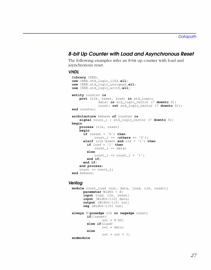
8-bit Up Counter with Load and Asynchronous ResetThe following examples infer an 8-bit up counter with load and asynchronous reset.
VHDLlibrary IEEE;use IEEE.std_logic_1164.all;use IEEE.std_logic_unsigned.all;use IEEE.std_logic_arith.all;
entity counter isport (clk, reset, load: in std_logic;
data: in std_logic_vector (7 downto 0);count: out std_logic_vector (7 downto 0));
end counter;
architecture behave of counter issignal count_i : std_logic_vector (7 downto 0);
beginprocess (clk, reset)beginif (reset = '0') then
count_i <= (others => '0');elsif (clk'event and clk = '1') thenif load = '1' then
count_i <= data;else
count_i <= count_i + '1';end if;
end if;end process;count <= count_i;
end behave;
Verilogmodule count_load (out, data, load, clk, reset);
parameter Width = 8;input load, clk, reset;input [Width-1:0] data;output [Width-1:0] out;reg [Width-1:0] out;
always @(posedge clk or negedge reset)if(!reset)
out = 8'b0;else if(load)
out = data;else
out = out + 1;endmodule
27
Chapter 2: Technology Independent Coding Styles
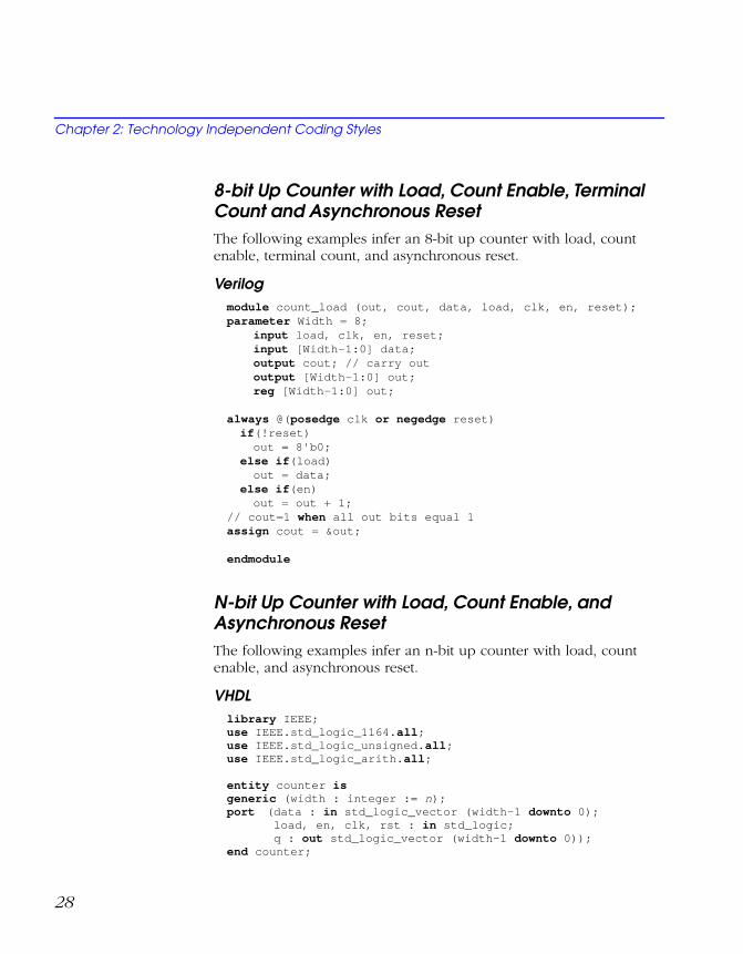
8-bit Up Counter with Load, Count Enable, Terminal Count and Asynchronous ResetThe following examples infer an 8-bit up counter with load, count enable, terminal count, and asynchronous reset.
Verilogmodule count_load (out, cout, data, load, clk, en, reset);parameter Width = 8;
input load, clk, en, reset;input [Width-1:0] data;output cout; // carry outoutput [Width-1:0] out;reg [Width-1:0] out;
always @(posedge clk or negedge reset)if(!reset)out = 8'b0;
else if(load)out = data;
else if(en)out = out + 1;
// cout=1 when all out bits equal 1assign cout = &out;
endmodule
N-bit Up Counter with Load, Count Enable, and Asynchronous ResetThe following examples infer an n-bit up counter with load, count enable, and asynchronous reset.
VHDLlibrary IEEE;use IEEE.std_logic_1164.all;use IEEE.std_logic_unsigned.all;use IEEE.std_logic_arith.all;
entity counter isgeneric (width : integer := n);port (data : in std_logic_vector (width-1 downto 0);
load, en, clk, rst : in std_logic; q : out std_logic_vector (width-1 downto 0));
end counter;
28
Datapath
architecture behave of counter issignal count : std_logic_vector (width-1 downto 0);beginprocess(clk, rst)beginif rst = '1' thencount <= (others => '0');
elsif (clk'event and clk = '1') thenif load = '1' thencount <= data;
elsif en = '1' thencount <= count + 1;
end if;end if;
end process;q <= count;end behave;
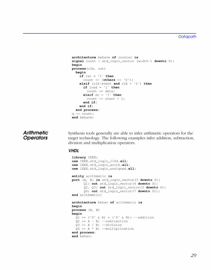
Arithmetic Operators
Synthesis tools generally are able to infer arithmetic operators for the target technology. The following examples infer addition, subtraction, division and multiplication operators.
VHDL library IEEE;use IEEE.std_logic_1164.all;use IEEE.std_logic_arith.all;use IEEE.std_logic_unsigned.all;
entity arithmetic isport (A, B: in std_logic_vector(3 downto 0); Q1: out std_logic_vector(4 downto 0); Q2, Q3: out std_logic_vector(3 downto 0); Q4: out std_logic_vector(7 downto 0));
end arithmetic;
architecture behav of arithmetic isbeginprocess (A, B)beginQ1 <= ('0' & A) + ('0' & B); --additionQ2 <= A - B; --subtractionQ3 <= A / B; --divisionQ4 <= A * B; --multiplication
end process;end behav;
29
Chapter 2: Technology Independent Coding Styles
If the multiply and divide operands are powers of 2, replace them with shift registers. Shift registers provide speed optimized implementations with large savings in area. For example:
Q <= C/16 + C*4;
can be represented as:
Q <= shr (C, “100”) + shl (C, “10”);
or
VHDL Q <= “0000” & C (8 downto 4) + C (6 downto 0) & ”00”;
The functions “shr” and “shl” are available in the IEEE.std_logic_arith.all library.
Verilog module arithmetic (A, B, Q1, Q2, Q3, Q4);input [3:0] A, B;output [4:0] Q1;output [3:0] Q2, Q3;output [7:0] Q4;reg [4:0] Q1;reg [3:0] Q2, Q3;reg [7:0] Q4;
always @ (A or B)beginQ1 = A + B; //additionQ2 = A - B; //subtractionQ3 = A / 2; //divisionQ4 = A * B; //multiplication
endendmodule
If the multiply and divide operands are powers of 2, replace them with shift registers. Shift registers provide speed optimized implementations with large savings in area. For example:
Q = C/16 + C*4;
can be represented as:
Q = {4b'0000 C[8:4]} + {C[6:0] 2b'00};
30
Datapath
Relational Operators
Relational operators compare two operands and indicate whether the comparison is true or false. The following examples infer greater than, less than, greater than equal to, and less than equal to comparators. Synthesis tools generally optimize relational operators for the target technology.
VHDLlibrary IEEE;use IEEE.std_logic_1164.all;use IEEE.std_logic_arith.all;
entity relational isport (A, B : in std_logic_vector(3 downto 0); Q1, Q2, Q3, Q4 : out std_logic);
end relational;
architecture behav of relational isbeginprocess (A, B)begin-- Q1 <= A > B; -- greater than-- Q2 <= A < B; -- less than-- Q3 <= A >= B; -- greater than equal toif (A <= B) then –- less than equal toQ4 <= '1';
elseQ4 <= '0';
end if;end process;end behav;
Verilog module relational (A, B, Q1, Q2, Q3, Q4);input [3:0] A, B;output Q1, Q2, Q3, Q4;reg Q1, Q2, Q3, Q4;
always @ (A or B)begin // Q1 = A > B; //greater than // Q2 = A < B; //less than // Q3 = A >= B; //greater than equal to if (A <= B) //less than equal toQ4 = 1;
elseQ4 = 0;
endendmodule
31
Chapter 2: Technology Independent Coding Styles
Equality Operator
The equality and non-equality operators indicate a true or false output based on whether the two operands are equivalent or not. The following examples infer equality operators.
VHDL library IEEE;use IEEE.std_logic_1164.all;
entity equality isport (
A: in STD_LOGIC_VECTOR (3 downto 0); B: in STD_LOGIC_VECTOR (3 downto 0); Q1: out STD_LOGIC; Q2: out STD_LOGIC);
end equality;
architecture equality_arch of equality isbeginprocess (A, B)beginQ1 <= A = B; -- equalityif (A /= B) then -- inequalityQ2 <= '1';
elseQ2 <= '0';
end if;end process;
end equality_arch;
ORlibrary IEEE;use IEEE.std_logic_1164.all;
entity equality isport (
A: in STD_LOGIC_VECTOR (3 downto 0); B: in STD_LOGIC_VECTOR (3 downto 0); Q1: out STD_LOGIC; Q2: out STD_LOGIC);
end equality;
architecture equality_arch of equality isbegin
Q1 <= '1' when A = B else '0'; -- equalityQ2 <= '1' when A /= B else '0'; -- inequality
end equality_arch;
32
Datapath
Verilog module equality (A, B, Q1, Q2);input [3:0] A;input [3:0] B;output Q1;output Q2;reg Q1, Q2;
always @ (A or B)beginQ1 = A == B; //equalityif (A != B) //inequalityQ2 = 1;
elseQ2 = 0;
endendmodule
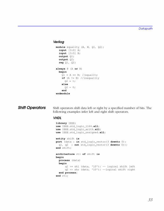
Shift Operators Shift operators shift data left or right by a specified number of bits. The following examples infer left and right shift operators.
VHDL library IEEE;use IEEE.std_logic_1164.all;use IEEE.std_logic_arith.all;use IEEE.std_logic_unsigned.all;
entity shift isport (data : in std_logic_vector(3 downto 0);q1, q2 : out std_logic_vector(3 downto 0));
end shift;
architecture rtl of shift isbeginprocess (data)begin q1 <= shl (data, "10"); -- logical shift left q2 <= shr (data, "10"); --logical shift rightend process;
end rtl;
33
Chapter 2: Technology Independent Coding Styles
ORlibrary IEEE;use IEEE.std_logic_1164.all;
entity shift isport (data : in std_logic_vector(3 downto 0);
q1, q2 : out std_logic_vector(3 downto 0));end shift;
architecture rtl of shift isbeginprocess (data)begin q1 <= data(1 downto 0) & “10”; -- logical shift left q2 <= “10” & data(3 downto 2); --logical shift rightend process;
end rtl;
Verilog module shift (data, q1, q2);input [3:0] data;output [3:0] q1, q2;
parameter B = 2;reg [3:0] q1, q2;
always @ (data)beginq1 = data << B; // logical shift leftq2 = data >> B; //logical shift right
endendmodule
34
Finite State Machine
Finite State MachineA finite state machine (FSM) is a type of sequential circuit that is designed to sequence through specific patterns of finite states in a predetermined sequential manner. There are two types of FSM, Mealy and Moore. The Moore FSM has outputs that are a function of current state only. The Mealy FSM has outputs that are a function of the current state and primary inputs. An FSM consists of three parts:
1. Sequential Current State Register: The register, a set of n-bit flip-flops (state vector flip-flops) clocked by a single clock signal is used to hold the state vector (current state or simply state) of the FSM. A state vector with a length of n-bit has 2
n possible binary patterns,
known as state encoding. Often, not all 2n patterns are needed, so
the unused ones should be designed not to occur during normal operation. Alternatively, an FSM with m-state requires at least log2(m) state vector flip-flops.
2. Combinational Next State Logic: An FSM can only be in one state at any given time, and each active transition of the clock causes it to change from its current state to the next state, as defined by the next state logic. The next state is a function of the FSM’s inputs and its current state.
3. Combinational Output Logic: Outputs are normally a function of the current state and possibly the FSM’s primary inputs (in the case of a Mealy FSM). Often in a Moore FSM, you may want to derive the outputs from the next state instead of the current state, when the outputs are registered for faster clock-to-out timings.
Moore and Mealy FSM structures are shown in Figure 2-14 and Figure 2-15.
InputsOutputsNext State
Logic(Combinatorial)
Current StateRegister*
(Sequential)
OutputLogic
(Combinatorial)
Asychronous ResetSychronous Reset
Next
State
Current
State
* State Vector Flip-flops
Figure 2-14. Basic Structure of a Moore FSM
35
Chapter 2: Technology Independent Coding Styles
Use a reset to guarantee fail safe behavior. This ensures that the FSM is always initialized to a known valid state before the first active clock transition and normal operation begins. In the absence of a reset, there is no way of predicting the initial value of the state register flip-flops during the “power up” operation of an Actel FPGA. It could power up and become permanently stuck in an unencoded state. The reset should be implemented in the sequential current state process of the FSM description.
An asynchronous reset is generally preferred over a synchronous reset because an asynchronous reset does not require decoding unused states, minimizing the next state logic.
Because FPGA technologies are register rich, “one hot” state machine implementations generated by the synthesis tool may generate optimal area and performance results
InputsOutputsNext State
Logic(Combinatorial)
Current StateRegister*
(Sequential)
OutputLogic
(Combinatorial)
Asychronous ResetSychronous Reset
Next
StateCurrent
State
* State Vector Flip-flops
Figure 2-15. Basic Structure of a Mealy FSM
36
Finite State Machine
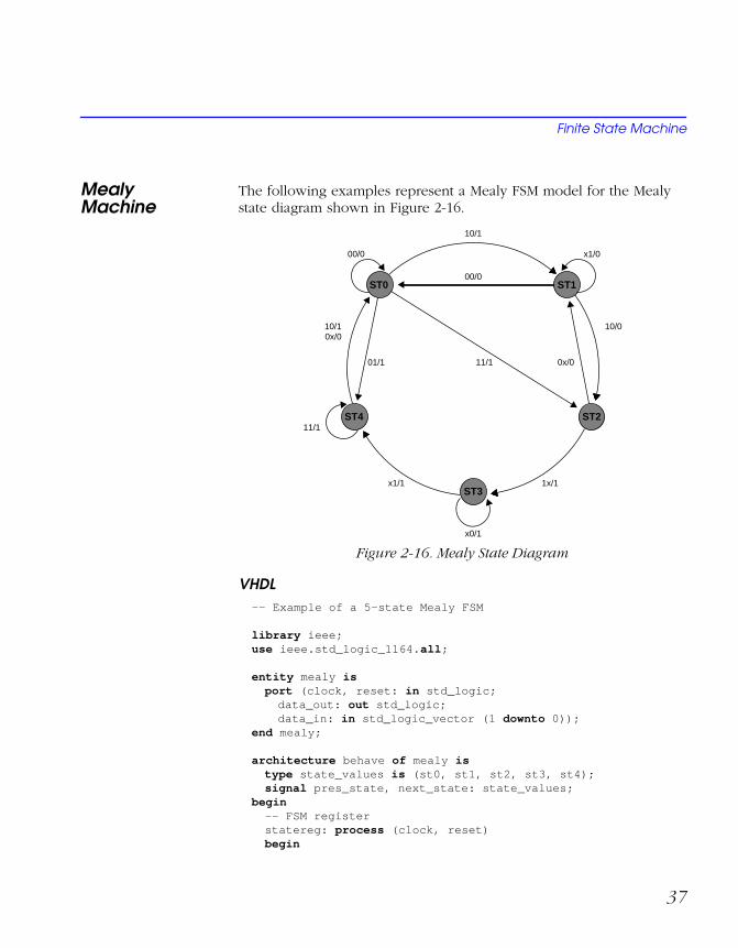
Mealy Machine
The following examples represent a Mealy FSM model for the Mealy state diagram shown in Figure 2-16.
VHDL -- Example of a 5-state Mealy FSM
library ieee;use ieee.std_logic_1164.all;
entity mealy isport (clock, reset: in std_logic;data_out: out std_logic;data_in: in std_logic_vector (1 downto 0));
end mealy;
architecture behave of mealy istype state_values is (st0, st1, st2, st3, st4);signal pres_state, next_state: state_values;
begin-- FSM registerstatereg: process (clock, reset)begin
Figure 2-16. Mealy State Diagram
x0/1
x1/1 1x/1
10/1
11/1
00/0 x1/0
11/1 0x/0
00/0
01/1
10/10x/0
10/0
ST3
ST2
ST1ST0
ST4
37
Chapter 2: Technology Independent Coding Styles
if (reset = '0') thenpres_state <= st0;
elsif (clock'event and clock ='1') thenpres_state <= next_state;
end if;end process statereg;
-- FSM combinational blockfsm: process (pres_state, data_in)begin
case pres_state iswhen st0 => case data_in iswhen "00" => next_state <= st0;when "01" => next_state <= st4;when "10" => next_state <= st1;when "11" => next_state <= st2;when others => null;
end case;when st1 =>case data_in iswhen "00" => next_state <= st0;when "10" => next_state <= st2;when others => next_state <= st1;
end case;when st2 => case data_in iswhen "00" => next_state <= st1;when "01" => next_state <= st1;when "10" => next_state <= st3;when "11" => next_state <= st3;when others => null;
end case;when st3 => case data_in iswhen "01" => next_state <= st4;when "11" => next_state <= st4;when others => next_state <= st3;
end case;when st4 => case data_in iswhen "11" => next_state <= st4;when others => next_state <= st0;
end case;when others => next_state <= st0;
end case;end process fsm;
38
Finite State Machine
-- Mealy output definition using pres_state w/ data_in outputs: process (pres_state, data_in)begin
case pres_state iswhen st0 => case data_in iswhen "00" => data_out <= '0';when others => data_out <= '1';
end case;when st1 => data_out <= '0';when st2 => case data_in iswhen "00" => data_out <= '0';when "01" => data_out <= '0';when others => data_out <= '1';
end case;when st3 => data_out <= '1';when st4 => case data_in iswhen "10" => data_out <= '1';when "11" => data_out <= '1';when others => data_out <= '0';
end case;when others => data_out <= '0';
end case;end process outputs;
end behave;
Verilog // Example of a 5-state Mealy FSM
module mealy (data_in, data_out, reset, clock);output data_out;input [1:0] data_in;input reset, clock;
reg data_out;reg [2:0] pres_state, next_state;
parameter st0=3'd0, st1=3'd1, st2=3'd2, st3=3'd3, st4=3'd4;
// FSM registeralways @ (posedge clock or negedge reset)begin: statereg
if(!reset)// asynchronous reset
39
Chapter 2: Technology Independent Coding Styles
pres_state = st0;elsepres_state = next_state;
end // statereg
// FSM combinational blockalways @(pres_state or data_in)begin: fsm
case (pres_state)st0: case(data_in)2'b00: next_state=st0;2'b01: next_state=st4;2'b10: next_state=st1; 2'b11: next_state=st2;
endcasest1: case(data_in)2'b00: next_state=st0;2'b10: next_state=st2;default: next_state=st1;
endcasest2: case(data_in)2'b0x: next_state=st1;2'b1x: next_state=st3;
endcasest3: case(data_in)2'bx1: next_state=st4;default: next_state=st3;
endcasest4: case(data_in)2'b11: next_state=st4;default: next_state=st0;
endcasedefault: next_state=st0;endcase
end // fsm
// Mealy output definition using pres_state w/ data_inalways @(data_in or pres_state)begin: outputscase(pres_state)st0: case(data_in)2'b00: data_out=1'b0;default: data_out=1'b1;
endcasest1: data_out=1'b0;st2: case(data_in)
40
Finite State Machine
2'b0x: data_out=1'b0;default: data_out=1'b1;
endcasest3: data_out=1'b1;st4: case(data_in)2'b1x: data_out=1'b1;default: data_out=1'b0;
endcasedefault: data_out=1'b0;endcase
end // outputs
endmodule
Moore Machine
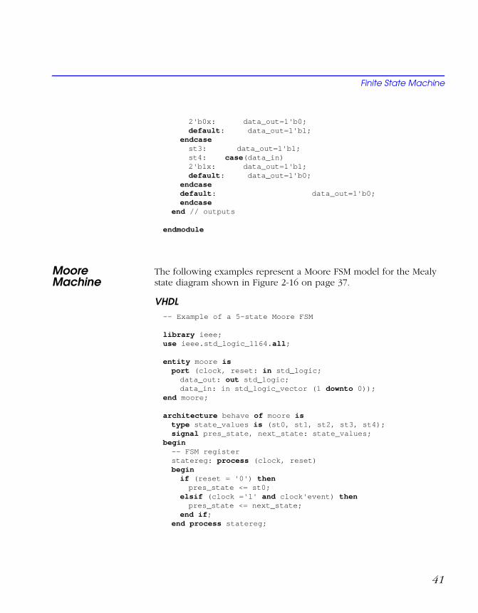
The following examples represent a Moore FSM model for the Mealy state diagram shown in Figure 2-16 on page 37.
VHDL -- Example of a 5-state Moore FSM
library ieee;use ieee.std_logic_1164.all;
entity moore isport (clock, reset: in std_logic;data_out: out std_logic;data_in: in std_logic_vector (1 downto 0));
end moore;
architecture behave of moore istype state_values is (st0, st1, st2, st3, st4);signal pres_state, next_state: state_values;
begin-- FSM registerstatereg: process (clock, reset)beginif (reset = '0') thenpres_state <= st0;
elsif (clock ='1' and clock'event) thenpres_state <= next_state;
end if;end process statereg;
41
Chapter 2: Technology Independent Coding Styles
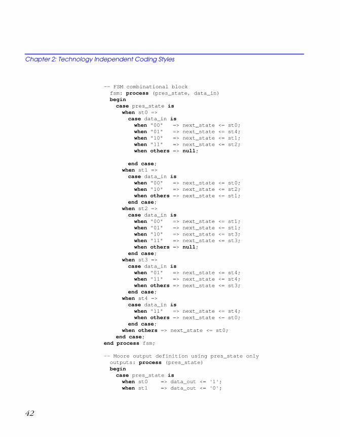
-- FSM combinational blockfsm: process (pres_state, data_in)begin case pres_state is
when st0 => case data_in iswhen "00" => next_state <= st0;when "01" => next_state <= st4;when "10" => next_state <= st1;when "11" => next_state <= st2;when others => null;
end case;when st1 => case data_in iswhen "00" => next_state <= st0;when "10" => next_state <= st2;when others => next_state <= st1;
end case;when st2 => case data_in iswhen "00" => next_state <= st1;when "01" => next_state <= st1;when "10" => next_state <= st3;when "11" => next_state <= st3;when others => null;
end case;when st3 => case data_in iswhen "01" => next_state <= st4;when "11" => next_state <= st4;when others => next_state <= st3;
end case;when st4 => case data_in iswhen "11" => next_state <= st4;when others => next_state <= st0;
end case;when others => next_state <= st0;
end case;end process fsm;
-- Moore output definition using pres_state onlyoutputs: process (pres_state)begin case pres_state is
when st0 => data_out <= '1'; when st1 => data_out <= '0';
42
Finite State Machine
when st2 => data_out <= '1'; when st3 => data_out <= '0'; when st4 => data_out <= '1';when others => data_out <= '0';
end case;end process outputs;
end behave;
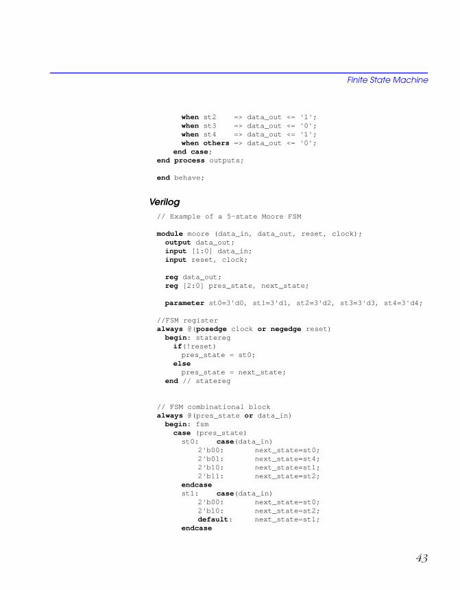
Verilog // Example of a 5-state Moore FSM
module moore (data_in, data_out, reset, clock);output data_out;input [1:0] data_in;input reset, clock;
reg data_out;reg [2:0] pres_state, next_state;
parameter st0=3'd0, st1=3'd1, st2=3'd2, st3=3'd3, st4=3'd4;
//FSM registeralways @(posedge clock or negedge reset)begin: stateregif(!reset)pres_state = st0;
elsepres_state = next_state;
end // statereg
// FSM combinational blockalways @(pres_state or data_in)begin: fsmcase (pres_state)st0: case(data_in)
2'b00: next_state=st0;2'b01: next_state=st4;2'b10: next_state=st1;2'b11: next_state=st2;
endcasest1: case(data_in)
2'b00: next_state=st0;2'b10: next_state=st2;default: next_state=st1;
endcase
43
Chapter 2: Technology Independent Coding Styles
st2: case(data_in)2'b0x: next_state=st1;2'b1x: next_state=st3;
endcasest3: case(data_in)
2'bx1: next_state=st4;default: next_state=st3;
endcasest4: case(data_in)
2'b11: next_state=st4;default: next_state=st0;
endcasedefault: next_state=st0;
endcaseend // fsm
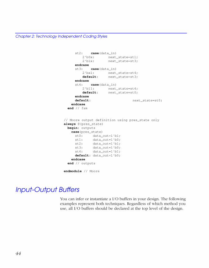
// Moore output definition using pres_state onlyalways @(pres_state) begin: outputscase(pres_state)st0: data_out=1'b1;st1: data_out=1'b0;st2: data_out=1'b1;st3: data_out=1'b0;st4: data_out=1'b1;default: data_out=1'b0;
endcaseend // outputs
endmodule // Moore
Input-Output BuffersYou can infer or instantiate a I/O buffers in your design. The following examples represent both techniques. Regardless of which method you use, all I/O buffers should be declared at the top level of the design.
44
Input-Output Buffers
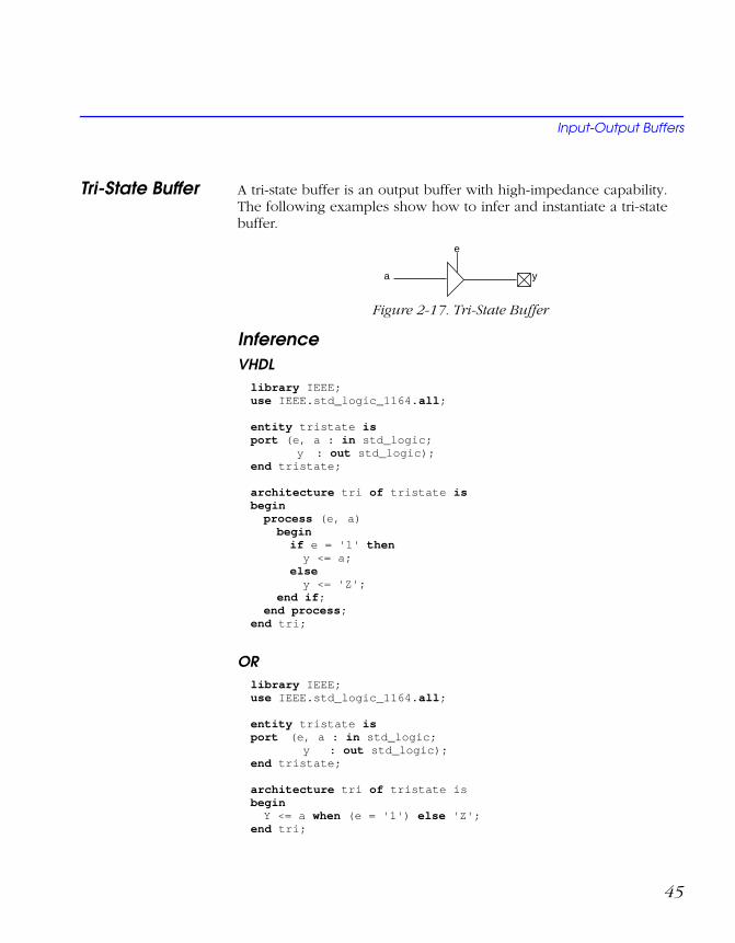
Tri-State Buffer A tri-state buffer is an output buffer with high-impedance capability. The following examples show how to infer and instantiate a tri-state buffer.
InferenceVHDLlibrary IEEE;use IEEE.std_logic_1164.all;
entity tristate isport (e, a : in std_logic;
y : out std_logic);end tristate;
architecture tri of tristate isbeginprocess (e, a)beginif e = '1' theny <= a;
elsey <= 'Z';
end if;end process;
end tri;
ORlibrary IEEE;use IEEE.std_logic_1164.all;
entity tristate isport (e, a : in std_logic;
y : out std_logic);end tristate;
architecture tri of tristate isbeginY <= a when (e = '1') else 'Z';
end tri;
a
e
y
Figure 2-17. Tri-State Buffer
45
Chapter 2: Technology Independent Coding Styles
Verilogmodule TRISTATE (e, a, y);input a, e;output y;reg y;
always @ (e or a) beginif (e)y = a;
elsey = 1'bz;
endendmodule
ORmodule TRISTATE (e, a, y);input a, e;output y;
assign y = e ? a : 1'bZ;
endmodule
Instantiation
VHDLlibrary IEEE;use IEEE.std_logic_1164.all;
entity tristate isport (e, a : in std_logic;y : out std_logic);end tristate;
architecture tri of tristate is
component TRIBUFFport (D, E: in std_logic;PAD: out std_logic);
end component;
beginU1: TRIBUFF port map (D => a,
E => e, PAD => y);
end tri;
46

Input-Output Buffers
Verilogmodule TRISTATE (e, a, y);input a, e;output y;
TRIBUFF U1 (.D(a), .E(e), .PAD(y));
endmodule
Bi-Directional Buffer
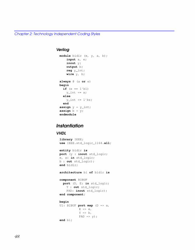
A bi-directional buffer can and input or output buffer with high impedance capability. The following examples show how to infer and instantiate a bi-directional buffer.
InferenceVHDLlibrary IEEE;use IEEE.std_logic_1164.all;
entity bidir isport (y : inout std_logic;
e, a: in std_logic;b : out std_logic);
end bidir;
architecture bi of bidir is
beginprocess (e, a)begincase e iswhen '1' => y <= a;when '0' => y <= 'Z';when others => y <= 'X';
end case;end process;
b <= y;end bi;
e
ya
b
Figure 2-18. Bi-Directional Buffer
47
Chapter 2: Technology Independent Coding Styles
Verilogmodule bidir (e, y, a, b);
input a, e;inout y;output b;reg y_int;wire y, b;
always @ (a or e)beginif (e == 1'b1)y_int <= a;
elsey_int <= 1'bz;
endassign y = y_int;assign b = y;endmodule
InstantiationVHDLlibrary IEEE;use IEEE.std_logic_1164.all;
entity bidir isport (y : inout std_logic;e, a: in std_logic;b : out std_logic);end bidir;
architecture bi of bidir is
component BIBUFport (D, E: in std_logic;Y : out std_logic;PAD: inout std_logic);
end component;
beginU1: BIBUF port map (D => a,
E => e, Y => b, PAD => y);
end bi;
48
Generics and Parameters
Verilogmodule bidir (e, y, a, b);
input a, e;inout y;output b;
BIBUF U1 ( .PAD(y), .D(a), .E(e), .Y(b) );
endmodule
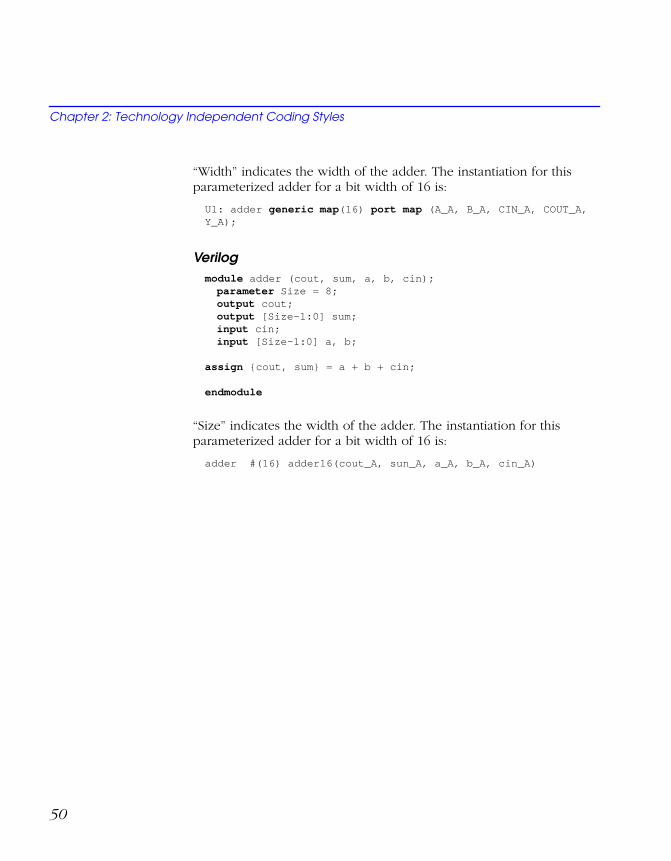
Generics and ParametersGenerics and parameters are used to define the size of a component. This allows the design of parameterized components for which size and feature sets may be defined by values of the instantiation parameters. The following examples show how to use generics and parameters when describing a parameterized adder. Furthermore, this adder is instantiated for varying widths.
VHDL library IEEE;use IEEE.std_logic_1164.all;use IEEE.std_logic_arith.all;use IEEE.std_logic_unsigned.all;
entity adder is generic (WIDTH : integer := 8);port (A, B: in UNSIGNED(WIDTH-1 downto 0);CIN: in std_logic;COUT: out std_logic;Y: out UNSIGNED(WIDTH-1 downto 0));end adder;
architecture rtl of adder is beginprocess (A,B,CIN)variable TEMP_A,TEMP_B,TEMP_Y:UNSIGNED(A'length downto 0);beginTEMP_A := '0' & A;TEMP_B := '0' & B;TEMP_Y := TEMP_A + TEMP_B + CIN;Y <= TEMP_Y (A'length-1 downto 0);COUT <= TEMP_Y (A'length);
end process;end rtl;
49
Chapter 2: Technology Independent Coding Styles
“Width” indicates the width of the adder. The instantiation for this parameterized adder for a bit width of 16 is:
U1: adder generic map(16) port map (A_A, B_A, CIN_A, COUT_A,Y_A);
Verilogmodule adder (cout, sum, a, b, cin);parameter Size = 8; output cout;output [Size-1:0] sum; input cin;input [Size-1:0] a, b;
assign {cout, sum} = a + b + cin;
endmodule
“Size” indicates the width of the adder. The instantiation for this parameterized adder for a bit width of 16 is:
adder #(16) adder16(cout_A, sun_A, a_A, b_A, cin_A)
50
3Performance Driven Coding
Unlike ASICs, FPGAs are module based arrays. Each logic level used on a path can add delay. As a result, meeting timing constraints on a critical path with too many logic levels becomes difficult. Using an efficient coding style is very important because it dictates the synthesis logic implementation. This chapter describes synthesis implementations, techniques, and efficient design practices that can be used to reduce logic levels on a critical path.
Reducing Logic Levels on Critical PathsEach logic level on the critical path in an FPGA can add significant delay. To ensure that timing constraints can be met, logic level usage must be considered when describing the behavior of a design. The following examples illustrate how to reduce logic levels on critical paths.
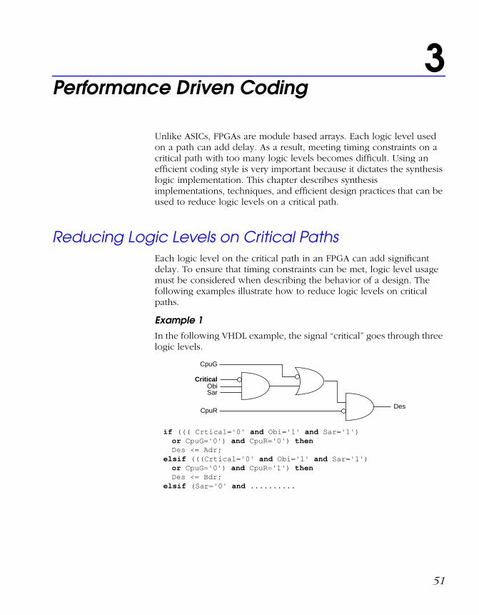
Example 1In the following VHDL example, the signal “critical” goes through three logic levels.
if ((( Crtical='0' and Obi='1' and Sar='1')or CpuG='0') and CpuR='0') thenDes <= Adr;
elsif (((Crtical='0' and Obi='1' and Sar='1')or CpuG='0') and CpuR='1') thenDes <= Bdr;
elsif (Sar='0' and ..........
CriticalObi
CpuG
CpuR
Sar
Des
51
Chapter 3: Performance Driven Coding
The signal “critical” is a late arriving signal. To reduce the logic level usage on “critical”, imply priority by using an if-then-else statement. As a result, the signal “critical” goes through one logic level, as shown below.
if (Critical='0') thenif (((Obi='1' and Sar='1')or CpuG='0') and CpuR='0') then Des <= Adr;
elsif (((Obi='1' and Sar='1')or CpuG='0' and CpuR='1') thenDes <= Bdr;
end if;end if;
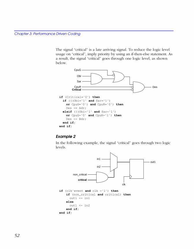
Example 2In the following example, the signal “critical” goes through two logic levels.
if (clk'event and clk ='1') thenif (non_critical and critical) thenout1 <= in1
elseout1 <= in2
end if;end if;
Critical
Obi
CpuG
CpuR
Sar
Des
in1
in2
out1
clk
non_critical
critical
52
Resource Sharing
To reduce the logic level usage on “critical”, multiplex inputs “in1” and “in2” based on “non_critical”, and call this output “out_temp”. Then multiplex “out_temp” and “in2” based on “critical”. As a result, the signal “critical” goes through one logic level, as shown below.
signal out_temp : std_logicif (non_critical)
out_temp <= in1;else out_temp <= in2;
if (clk'event and clk ='1') thenif (critical) then
out1 <= out_temp;else out1 <= in2;end if;
end if;end if;
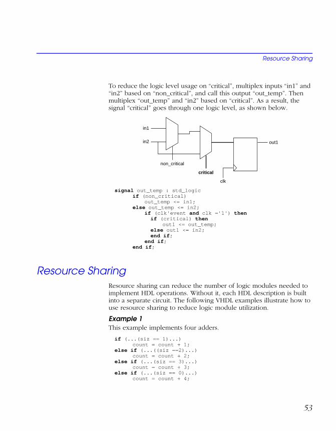
Resource SharingResource sharing can reduce the number of logic modules needed to implement HDL operations. Without it, each HDL description is built into a separate circuit. The following VHDL examples illustrate how to use resource sharing to reduce logic module utilization.
Example 1This example implements four adders.
if (...(siz == 1)...)count = count + 1;
else if (...((siz ==2)...)count = count + 2;
else if (...(siz == 3)...)count = count + 3;
else if (...(siz == 0)...)count = count + 4;
in1
in2 out1
clk
non_critical
critical
53
Chapter 3: Performance Driven Coding
By adding the following code, two adders can be eliminated:
if (...(siz == 0)...)count = count + 4;
else if (...)count = count + siz
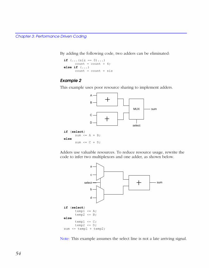
Example 2This example uses poor resource sharing to implement adders.
if (select)sum <= A + B;
elsesum <= C + D;
Adders use valuable resources. To reduce resource usage, rewrite the code to infer two multiplexors and one adder, as shown below.
if (select)temp1 <= A;temp2 <= B;
elsetemp1 <= C;temp2 <= D;
sum <= temp1 + temp2;
Note: This example assumes the select line is not a late arriving signal.
A
B
sum
select
C
D
MUX
a
c
sum
b
select
d
54
Operators Inside Loops
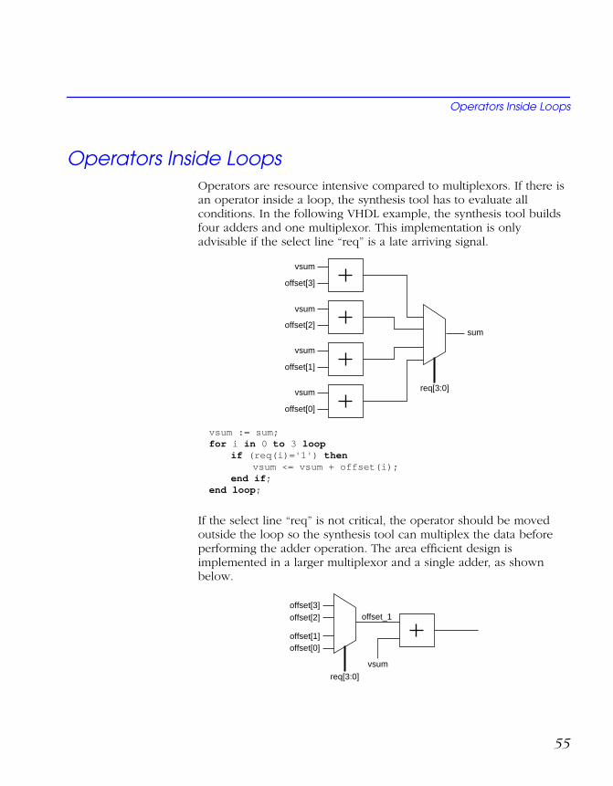
Operators Inside LoopsOperators are resource intensive compared to multiplexors. If there is an operator inside a loop, the synthesis tool has to evaluate all conditions. In the following VHDL example, the synthesis tool builds four adders and one multiplexor. This implementation is only advisable if the select line “req” is a late arriving signal.
vsum := sum;for i in 0 to 3 loop
if (req(i)='1') thenvsum <= vsum + offset(i);
end if;end loop;
If the select line “req” is not critical, the operator should be moved outside the loop so the synthesis tool can multiplex the data before performing the adder operation. The area efficient design is implemented in a larger multiplexor and a single adder, as shown below.
offset[3]
vsum
vsum
sum
req[3:0]
offset[2]
offset[1]
vsum
offset[0]
vsum
offset[2]offset[3]
offset[1]
req[3:0]
vsum
offset[0]
offset_1
55
Chapter 3: Performance Driven Coding
vsum := sum;for i in 0 to 3 loop
if (req(i)='1') thenoffset_1 <= offset(i);
end if;end loop;vsum <= vsum + offset_1;
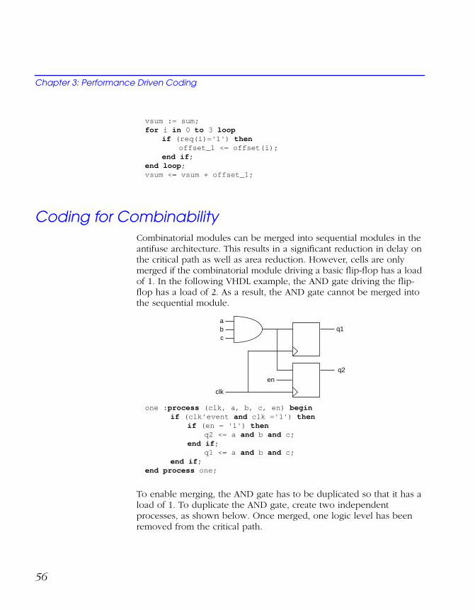
Coding for CombinabilityCombinatorial modules can be merged into sequential modules in the antifuse architecture. This results in a significant reduction in delay on the critical path as well as area reduction. However, cells are only merged if the combinatorial module driving a basic flip-flop has a load of 1. In the following VHDL example, the AND gate driving the flip-flop has a load of 2. As a result, the AND gate cannot be merged into the sequential module.
one :process (clk, a, b, c, en) beginif (clk'event and clk ='1') then
if (en = '1') thenq2 <= a and b and c;
end if;q1 <= a and b and c;
end if;end process one;
To enable merging, the AND gate has to be duplicated so that it has a load of 1. To duplicate the AND gate, create two independent processes, as shown below. Once merged, one logic level has been removed from the critical path.
ab q1
q2
c
clk
en
56
Register Duplication
Note: Some synthesis tools automatically duplicate logic on the critical path. Other synthesis tools detect the function “a & b & c” in the two processes and share the function on a single gate. If the function is shared, the logic is not duplicated and instantiation should be considered.
part_one: process (clk, a, b, c, en) beginif (clk'event and clk ='1') then
if (en = '1') thenq2 <= a and b and c;
end if;end if;end process part_one;part_two: process (clk, a, b, c) beginif (clk'event and clk ='1') then
q1 <= a and b and c;end if;end process part_two;
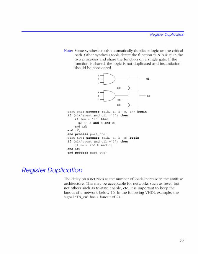
Register DuplicationThe delay on a net rises as the number of loads increase in the antifuse architecture. This may be acceptable for networks such as reset, but not others such as tri-state enable, etc. It is important to keep the fanout of a network below 16. In the following VHDL example, the signal “Tri_en” has a fanout of 24.
ab q1
q2
c
abc en
clk
clk
57
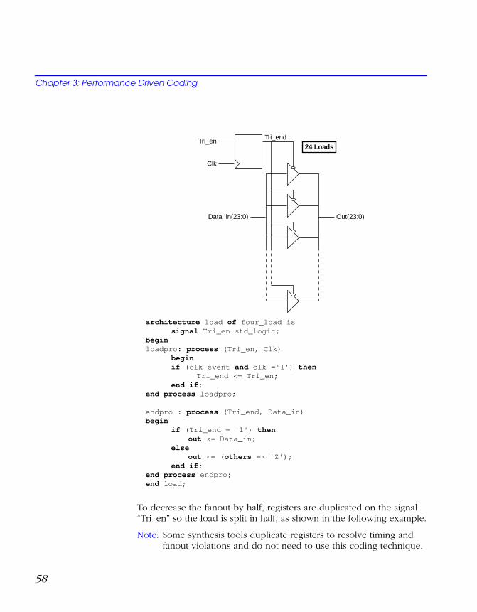
Chapter 3: Performance Driven Coding
architecture load of four_load issignal Tri_en std_logic;
beginloadpro: process (Tri_en, Clk)
beginif (clk'event and clk ='1') then
Tri_end <= Tri_en;end if;
end process loadpro;
endpro : process (Tri_end, Data_in)begin
if (Tri_end = '1') thenout <= Data_in;
else out <= (others => 'Z');
end if;end process endpro;end load;
To decrease the fanout by half, registers are duplicated on the signal “Tri_en” so the load is split in half, as shown in the following example.
Note: Some synthesis tools duplicate registers to resolve timing and fanout violations and do not need to use this coding technique.
Clk
Tri_en Tri_end
Out(23:0)Data_in(23:0)
24 Loads
58
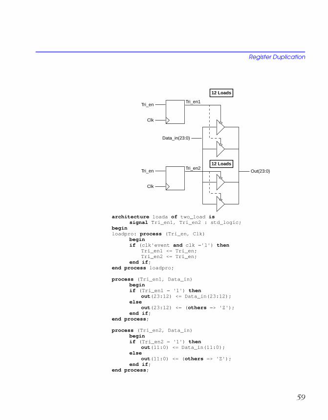
Register Duplication
architecture loada of two_load issignal Tri_en1, Tri_en2 : std_logic;
beginloadpro: process (Tri_en, Clk)
beginif (clk'event and clk ='1') then
Tri_en1 <= Tri_en;Tri_en2 <= Tri_en;
end if; end process loadpro;
process (Tri_en1, Data_in)beginif (Tri_en1 = '1') then
out(23:12) <= Data_in(23:12);else
out(23:12) <= (others => 'Z');end if;
end process;
process (Tri_en2, Data_in)beginif (Tri_en2 = '1') then
out(11:0) <= Data_in(11:0);else
out(11:0) <= (others => 'Z');end if;
end process;
Clk
Tri_en
Out(23:0)
Data_in(23:0)
12 Loads
12 Loads
Clk
Tri_enTri_en2
Tri_en1
59
Chapter 3: Performance Driven Coding
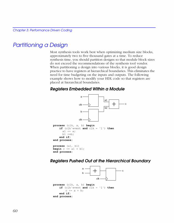
Partitioning a DesignMost synthesis tools work best when optimizing medium size blocks, approximately two to five thousand gates at a time. To reduce synthesis time, you should partition designs so that module block sizes do not exceed the recommendations of the synthesis tool vendor. When partitioning a design into various blocks, it is good design practice to have registers at hierarchical boundaries. This eliminates the need for time budgeting on the inputs and outputs. The following example shows how to modify your HDL code so that registers are placed at hierarchical boundaries.
Registers Embedded Within a Module
process (clk, a, b) beginif (clk'event and clk = '1') thena1 <= a; b1 <=b;
end if;end process;
process (a1, b1)begin c <= a1 + b1;end process;
Registers Pushed Out at the Hierarchical Boundary
process (clk, a, b) beginif (clk'event and clk = '1') then
c <= a + b;end if;
end process;
a1
b2
b
clk
clk
a
c
clk
ca
b
60
4Technology Specific Coding Techniques
In addition to technology independent coding and performance driven coding, there are coding techniques that can be used to take advantage of the Actel architecture to improve speed and area utilization of your design. Additionally, most synthesis tools can implement random logic, control logic and certain datapath macros. However, they may not generate technology optimal implementations for datapath elements that cannot be inferred using operators, such as counters, RAM, FIFO, etc. This chapter describes coding techniques to take advantage of technology specific features and how to instantiate technology specific macros generated by the ACTgen Macro Builder tool for optimal area and performance.
MultiplexorsUsing case statements with the multiplexor based Actel architecture provides area and speed efficient solutions and is more efficient than inference of priority encoders using if-then-else statements. Actel recommends that you use case statements instead of long, nested if-then-else statements to force mapping to multiplexors in the Actel architecture. Refer to “Multiplexors Using Case” on page 19 for examples of multiplexor coding.
VHDL synthesis tools automatically assume parallel operation without priority in case statements. However, some Verilog tools assume priority, and you may need to add a directive to your case statement to ensure that no priority is assumed. refer to the documentation provided with your synthesis tool for information about creating case statements without priority.
61
Chapter 4: Technology Specific Coding Techniques
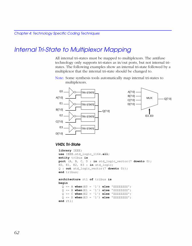
Internal Tri-State to Multiplexor MappingAll internal tri-states must be mapped to multiplexors. The antifuse technology only supports tri-states as in/out ports, but not internal tri-states. The following examples show an internal tri-state followed by a multiplexor that the internal tri-state should be changed to.
Note: Some synthesis tools automatically map internal tri-states to multiplexors.
VHDL Tri-Statelibrary IEEE;use IEEE.std_logic_1164.all;entity tribus isport (A, B, C, D : in std_logic_vector(7 downto 0);E0, E1, E2, E3 : in std_logic;Q : out std_logic_vector(7 downto 0));end tribus;
architecture rtl of tribus isbeginQ <= A when(E0 = '1') else "ZZZZZZZZ";Q <= B when(E1 = '1') else "ZZZZZZZZ";Q <= C when(E2 = '1') else "ZZZZZZZZ";Q <= D when(E3 = '1') else "ZZZZZZZZ";
end rtl;
A[7:0]
E0
E1
E2
E3
D[7:0]
Q[7:0]B[7:0]
C[7:0]
TRI-STATE
TRI-STATE
TRI-STATE
TRI-STATE
A[7:0]
D[7:0]
Q[7:0]B[7:0]
C[7:0]MUX
E3..E0
62
Internal Tri-State to Multiplexor Mapping
VHDL Multiplexorlibrary IEEE;use IEEE.std_logic_1164.all;entity muxbus isport (A, B, C, D : in std_logic_vector(7 downto 0);E0, E1, E2, E3 : in std_logic;Q : out std_logic_vector(7 downto 0));end muxbus;
architecture rtl of muxbus issignal E_int : std_logic_vector(1 downto 0);beginprocess (E0, E1, E2, E3)variable E : std_logic_vector(3 downto 0);beginE := E0 & E1 & E2 & E3;
case E iswhen "0001" => E_int <= "00";when "0010" => E_int <= "01";when "0100" => E_int <= "10";when "1000" => E_int <= "11";when others => E_int <= "--";
end case;end process;
process (E_int, A, B, C, D)begin case E_int is when "00" => Q <= D; when "01" => Q <= C; when "10" => Q <= B; when "11" => Q <= A; when others => Q <= (others => '-');end case;
end process;end rtl;
Verilog Tri-Statemodule tribus (A, B, C, D, E0, E1, E2, E3, Q);
input [7:0]A, B, C, D;output [7:0]Q;input E0, E1, E2, E3;
assign Q[7:0] = E0 ? A[7:0] : 8'bzzzzzzzz;assign Q[7:0] = E1 ? B[7:0] : 8'bzzzzzzzz;assign Q[7:0] = E2 ? C[7:0] : 8'bzzzzzzzz;assign Q[7:0] = E3 ? D[7:0] : 8'bzzzzzzzz;
endmodule
63
Chapter 4: Technology Specific Coding Techniques
Verilog Multiplexormodule muxbus (A, B, C, D, E0, E1, E2, E3, Q);
input [7:0]A, B, C, D;output [7:0]Q;input E0, E1, E2, E3;wire [3:0] select4;reg [1:0] select2;reg [7:0]Q;
assign select4 = {E0, E1, E2, E3};
always @ (select4)begincase(select4) 4'b0001 : select2 = 2'b00;4'b0010 : select2 = 2'b01;4'b0100 : select2 = 2'b10;4'b1000 : select2 = 2'b11;default : select2 = 2'bxx;
endcaseend
always @ (select2 or A or B or C or D)begincase(select2)2'b00 : Q = D;2'b01 : Q = C;2'b10 : Q = B;2'b11 : Q = A;
endcaseend
endmodule
RegistersThe XL, DX, MX, and ACT 3 families have dedicated asynchronous reset registers in the sequential modules (SMOD). In each SMOD is a 4:1 multiplexor with some gating logic on the select lines. Implementing a simple register or an asynchronous reset register allows the gating logic in front of the register to be pulled into the SMOD, reducing the path delay by one level. This is called full combinability. Full combinability offers improved speed, increasing a 50MHz operation to 75MHz in some designs. The following examples show how to use registers for combinability and discuss any speed or area penalty associated with using the register.
64
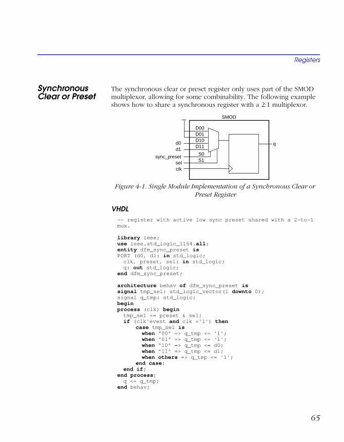
Registers
Synchronous Clear or Preset
The synchronous clear or preset register only uses part of the SMOD multiplexor, allowing for some combinability. The following example shows how to share a synchronous register with a 2:1 multiplexor.
VHDL-- register with active low sync preset shared with a 2-to-1 mux.
library ieee;use ieee.std_logic_1164.all;entity dfm_sync_preset isPORT (d0, d1: in std_logic;clk, preset, sel: in std_logic;q: out std_logic;
end dfm_sync_preset;
architecture behav of dfm_sync_preset issignal tmp_sel: std_logic_vector(1 downto 0);signal q_tmp: std_logic;beginprocess (clk) begintmp_sel <= preset & sel;if (clk'event and clk ='1') then
case tmp_sel iswhen "00" => q_tmp <= '1';when "01" => q_tmp <= '1';when "10" => q_tmp <= d0;when "11" => q_tmp <= d1;when others => q_tmp <= '1';
end case;end if;
end process;q <= q_tmp;
end behav;
clksel
sync_preset
d1d0 q
D00D01D10D11
S0S1
SMOD
Figure 4-1. Single Module Implementation of a Synchronous Clear or Preset Register
65
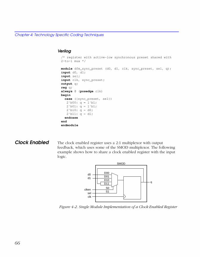
Chapter 4: Technology Specific Coding Techniques
Verilog/* register with active-low synchronous preset shared with2-to-1 mux */
module dfm_sync_preset (d0, d1, clk, sync_preset, sel, q);input d0, d1;input sel;input clk, sync_preset;output q;reg q;always @ (posedge clk)begincase ({sync_preset, sel}) 2'b00: q = 1'b1; 2'b01: q = 1'b1; 2'b10: q = d0; 2'b11: q = d1;endcase
endendmodule
Clock Enabled The clock enabled register uses a 2:1 multiplexor with output feedback, which uses some of the SMOD multiplexor. The following example shows how to share a clock enabled register with the input logic.
clksel
clken
d1d0
q
D00D01D10D11
S0S1
SMOD
Figure 4-2. Single Module Implementation of a Clock Enabled Register
66
Registers
VHDL-- register with active low async reset, shared with a 2-to-1-- mux, and an active high clock enable.
library ieee;use ieee.std_logic_1164.all;entity dfm_clken isPORT (d0, d1: in std_logic;clk, reset, clken, sel: in std_logic;q: out std_logic;
end dfm_clken;
architecture behav of dfm_clken issignal tmp_sel: std_logic_vector(1 downto 0);signal q_tmp: std_logic;beginprocess (clk, reset) begintmp_sel <= clken & sel;if (reset = '0') then
q_tmp <= '0';elsif (clk'event and clk ='1') then
case tmp_sel iswhen "00" => q_tmp <= d0;when "01" => q_tmp <= d1;when "10" => q_tmp <= q_tmp;when "11" => q_tmp <= q_tmp;when others => q_tmp <= q_tmp;
end case;end if;
end process;q <= q_tmp;
end behav;
67
Chapter 4: Technology Specific Coding Techniques
Verilog/* register with asynchronous set, clock enable, shared with a 2-to-1 mux */
module dfm_clken (d0, d1, clk, reset, clken, sel, q);input d0, d1;input sel;input clk, reset, clken;output q;reg q;always @ (posedge clk or negedge reset)beginif (!reset) q = 8'b0;
elsecase ({clken, sel})2'b00: q = d0;2'b01: q = d1;2'b10: q = q;2'b11: q = q;
endcaseendendmodule
Asynchronous Preset
Some synthesis tools automatically translate an asynchronous preset register into an asynchronous reset register without performance penalties. The bubbled logic can then be pushed into the surrounding logic without any delay penalty. There are various types of preset registers in the Actel libraries. Some of the registers use two combinatorial modules (CMOD) and most use an inverter, which consumes part of the SMOD multiplexor. If your synthesis tool does not automatically translate an asynchronous preset register into a functionally equivalent asynchronous preset register using an asynchronous reset register, use the following examples to design an asynchronous reset register.
68
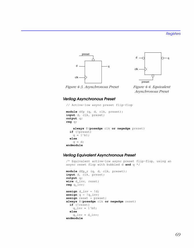
Registers
Verilog Asynchronous Preset// Active-low async preset flip-flop
module dfp (q, d, clk, preset);input d, clk, preset;output q;reg q;
always @(posedge clk or negedge preset)if (!preset)q = 1'b1;
elseq = d;
endmodule
Verilog Equivalent Asynchronous Preset/* Equivalent active-low async preset flip-flop, using an async reset flop with bubbled d and q */
module dfp_r (q, d, clk, preset);input d, clk, preset;output q;wire d_inv, reset;reg q_inv;
assign d_inv = !d;assign q = !q_inv;assign reset = preset;always @(posedge clk or negedge reset)if (!reset)q_inv = 1'b0;
elseq_inv = d_inv;
endmodule
d
clk
q
preset
Figure 4-3. Asynchronous Preset
d
clk
q
preset
Figure 4-4. Equivalent Asynchronous Preset
69
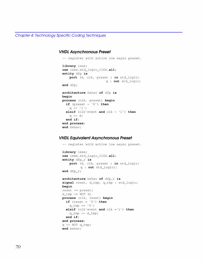
Chapter 4: Technology Specific Coding Techniques
VHDL Asynchronous Preset-- register with active low async preset.
library ieee;use ieee.std_logic_1164.all;entity dfp is
port (d, clk, preset : in std_logic;q : out std_logic;
end dfp;
architecture behav of dfp isbeginprocess (clk, preset) beginif (preset = '0') thenq <= '1';
elsif (clk'event and clk = '1') thenq <= d;
end if;end process;end behav;
VHDL Equivalent Asynchronous Preset-- register with active low async preset.
library ieee;use ieee.std_logic_1164.all;entity dfp_r is
port (d, clk, preset : in std_logic;q : out std_logic);
end dfp_r;
architecture behav of dfp_r issignal reset, d_tmp, q_tmp : std_logic;beginreset <= preset;d_tmp <= NOT d;process (clk, reset) beginif (reset = '0') thenq_tmp <= '0';
elsif (clk'event and clk ='1') thenq_tmp <= d_tmp;
end if;end process;q <= NOT q_tmp;end behav;
70
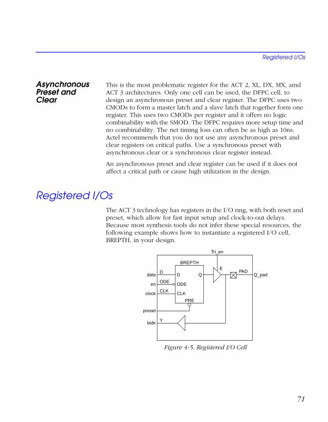
Registered I/Os
Asynchronous Preset and Clear
This is the most problematic register for the ACT 2, XL, DX, MX, amd ACT 3 architectures. Only one cell can be used, the DFPC cell, to design an asynchronous preset and clear register. The DFPC uses two CMODs to form a master latch and a slave latch that together form one register. This uses two CMODs per register and it offers no logic combinability with the SMOD. The DFPC requires more setup time and no combinability. The net timing loss can often be as high as 10ns. Actel recommends that you do not use any asynchronous preset and clear registers on critical paths. Use a synchronous preset with asynchronous clear or a synchronous clear register instead.
An asynchronous preset and clear register can be used if it does not affect a critical path or cause high utilization in the design.
Registered I/OsThe ACT 3 technology has registers in the I/O ring, with both reset and preset, which allow for fast input setup and clock-to-out delays. Because most synthesis tools do not infer these special resources, the following example shows how to instantiate a registered I/O cell, BREPTH, in your design.
data Q_pad
en
clock
preset
bidir
D
ODE
CLK
Y
D Q
ODE
CLK
PRE
EBREPTH
Tri_en
PAD
Figure 4-5. Registered I/O Cell
71
Chapter 4: Technology Specific Coding Techniques
VHDLlibrary IEEE;use IEEE.std_logic_1164.all;
entity regio isport (data, en, Tri_en, clock, preset : in std_logic;
bidir : inout std_logic; q_pad : out std_logic);
end regio;
architecture rtl of regio is
-- Component Declarationcomponent BREPTH
port (D, ODE, E, IOPCL, CLK : in std_logic; Y : out std_logic; PAD : inout std_logic);
end component;
begin-- Concurrent StatementU0 : BREPTH port map ( D => data,
ODE => en, E => Tri_en, IOPCL => preset, CLK => clock, Y => q_pad,PAD => bidir);
end rtl;
Verilogmodule regio (data, Q_pad, clock, preset, Tri_en, en, bidir);
input data, clock, preset, Tri_en, en; output Q_pad; inout bidir;
BREPTH U1 (.PAD(Q_pad), .D(data), .CLK(clock), .IOPCL(preset), .E(Tri_en), .ODE(en), .Y(bidir));
endmodule
Note: As a good design practice, instantiate all input/output cells at the top level of your design.
72
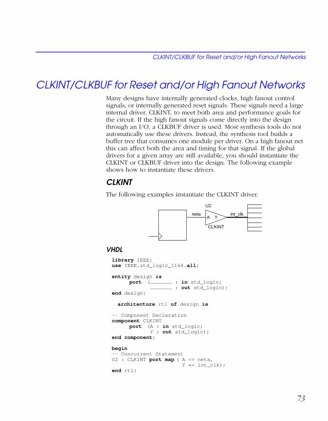
CLKINT/CLKBUF for Reset and/or High Fanout Networks
CLKINT/CLKBUF for Reset and/or High Fanout NetworksMany designs have internally generated clocks, high fanout control signals, or internally generated reset signals. These signals need a large internal driver, CLKINT, to meet both area and performance goals for the circuit. If the high fanout signals come directly into the design through an I/O, a CLKBUF driver is used. Most synthesis tools do not automatically use these drivers. Instead, the synthesis tool builds a buffer tree that consumes one module per driver. On a high fanout net this can affect both the area and timing for that signal. If the global drivers for a given array are still available, you should instantiate the CLKINT or CLKBUF driver into the design. The following example shows how to instantiate these drivers.
CLKINTThe following examples instantiate the CLKINT driver.
VHDL library IEEE;use IEEE.std_logic_1164.all;
entity design isport (………………… : in std_logic;
………………… : out std_logic);end design;
architecture rtl of design is
-- Component Declarationcomponent CLKINT
port (A : in std_logic; Y : out std_logic);
end component;
begin-- Concurrent StatementU2 : CLKINT port map ( A => neta,
Y => int_clk);end rtl;
CLKINT
U2
neta int_clkYA
73
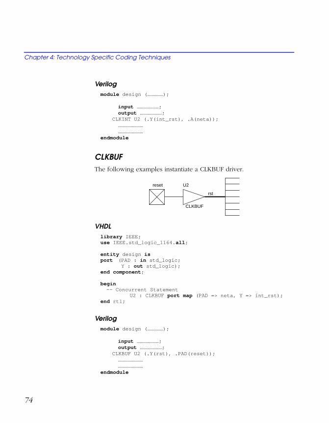
Chapter 4: Technology Specific Coding Techniques
Verilog module design (……………);
input …………………;output …………………;
CLKINT U2 (.Y(int_rst), .A(neta));…………………………………………
endmodule
CLKBUFThe following examples instantiate a CLKBUF driver.
VHDLlibrary IEEE;use IEEE.std_logic_1164.all;
entity design isport (PAD : in std_logic;
Y : out std_logic);end component;
begin-- Concurrent Statement
U2 : CLKBUF port map (PAD => neta, Y => int_rst);end rtl;
Verilogmodule design (……………);
input …………………;output …………………;
CLKBUF U2 (.Y(rst), .PAD(reset));…………………………………………
endmodule
CLKBUF
U2reset
rst
74
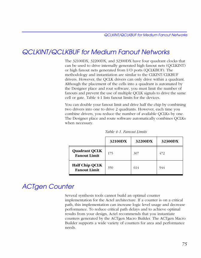
QCLKINT/QCLKBUF for Medium Fanout Networks
QCLKINT/QCLKBUF for Medium Fanout NetworksThe 32100DX, 32200DX, and 32300DX have four quadrant clocks that can be used to drive internally generated high fanout nets (QCLKINT) or high fanout nets generated from I/O ports (QCLKBUF). The methodology and instantiation are similar to the CLKINT/CLKBUF drivers. However, the QCLK drivers can only drive within a quadrant. Although the placement of the cells into a quadrant is automated by the Designer place and rout software, you must limit the number of fanouts and prevent the use of multiple QCLK signals to drive the same cell or gate. Table 4-1 lists fanout limits for the devices.
You can double your fanout limit and drive half the chip by combining two drivers into one to drive 2 quadrants. However, each time you combine drivers, you reduce the number of available QCLKs by one. The Designer place and route software automatically combines QCLKs when necessary.
ACTgen CounterSeveral synthesis tools cannot build an optimal counter implementation for the Actel architecture. If a counter is on a critical path, this implementation can increase logic level usage and decrease performance. To reduce critical path delays and to achieve optimal results from your design, Actel recommends that you instantiate counters generated by the ACTgen Macro Builder. The ACTgen Macro Builder supports a wide variety of counters for area and performance needs.
Table 4-1. Fanout Limits
32100DX 32200DX 32300DX
Quadrant QCLKFanout Limit
175 307 472
Half Chip QCLKFanout Limit
350 614 944
75
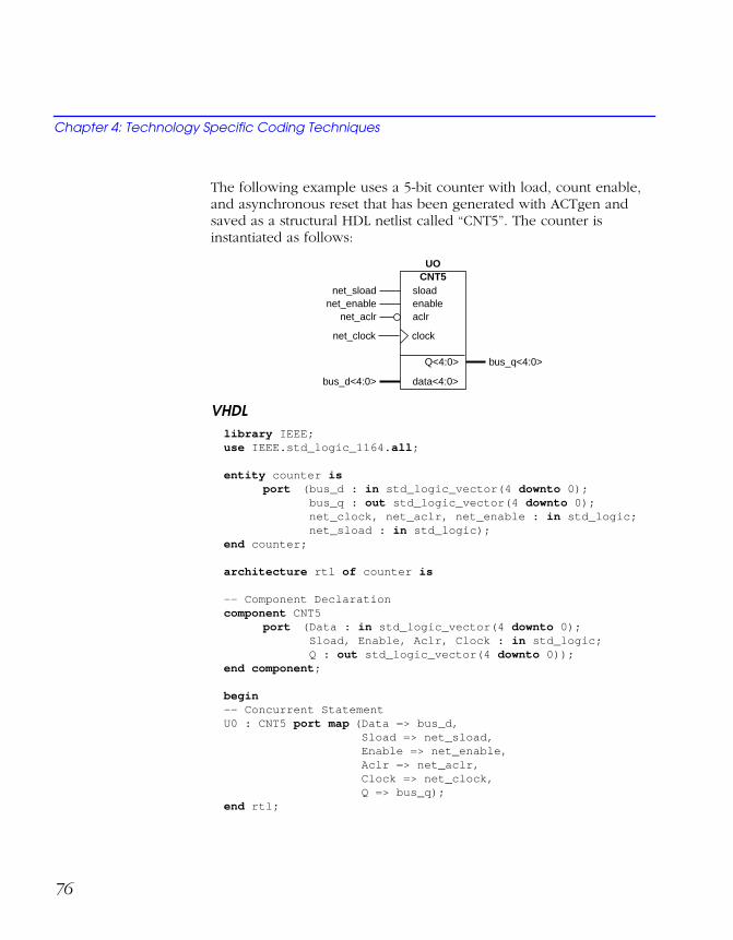
Chapter 4: Technology Specific Coding Techniques
The following example uses a 5-bit counter with load, count enable, and asynchronous reset that has been generated with ACTgen and saved as a structural HDL netlist called “CNT5”. The counter is instantiated as follows:
VHDL library IEEE;use IEEE.std_logic_1164.all;
entity counter isport (bus_d : in std_logic_vector(4 downto 0);
bus_q : out std_logic_vector(4 downto 0); net_clock, net_aclr, net_enable : in std_logic; net_sload : in std_logic);
end counter;
architecture rtl of counter is
-- Component Declarationcomponent CNT5
port (Data : in std_logic_vector(4 downto 0); Sload, Enable, Aclr, Clock : in std_logic; Q : out std_logic_vector(4 downto 0));
end component;
begin-- Concurrent StatementU0 : CNT5 port map (Data => bus_d,
Sload => net_sload, Enable => net_enable, Aclr => net_aclr, Clock => net_clock, Q => bus_q);
end rtl;
net_sloadnet_enable
net_aclr
net_clock
bus_d<4:0>
sloadenableaclr
clock
data<4:0>
bus_q<4:0>Q<4:0>
CNT5UO
76
Dual Architecture Coding in VHDL
Verilog module counter (bus_q, bus_d, net_clock, net_aclr, net_enable,
net_sload);input [4:0] data;input net_sload, net_enable, net_aclr, net_clock;output [4:0] bus_q;
CNT5 U0 (.Q(bus_q), .Data(bus_d), .Clock(net_clock), .Aclr(net_aclr), .Enable(net_enable), .Sload(net_sload));
endmodule
Dual Architecture Coding in VHDLIt is possible to maintain technology independence after instantiating an ACTgen macro into your design. By adding a second technology independent architecture, you can maintain two functionally equivalent architectures of the same entity in your design. The ACTgen macro is Actel specific and instantiated in your design to take advantage of the architectural features of the target Actel FPGA. This allows you to meet your design goals quickly. The technology independent architecture is functionally equivalent to the Actel specific architecture (verified by simulation) and can be used to synthesize the design to another technology if necessary. The following example shows the technology independent (RTL) and Actel specific (structural) architecture for a counter called “CNT5” and illustrates how to write your code so that you can choose which architecture to use.
RTL ArchitectureThis implementation of “CNT5” is written as a behavioral description directly into the design.
library IEEE;use IEEE.std_logic_1164.all;use IEEE.std_logic_unsigned.all;
entity CNT5 isport (Data: in std_logic_vector(4 downto 0);
Sload, Enable, Aclr, Clock: in std_logic; Q: out std_logic_vector(4 downto 0));
end CNT5;
77
Chapter 4: Technology Specific Coding Techniques
architecture RTL of CNT5 is
signal cnt: std_logic_vector(4 downto 0);
begincounter : process (Aclr, Clock)beginif (Aclr = '0') thencnt <= (others => '0'); -- asynchronous reset
elsif (Clock'event and Clock = '1') thenif (Sload = '1') thencnt <= Data;-- synchronous load
elsif (Enable = '1') thencnt <= cnt + '1'; -- increment counter
end if;end if;end process;Q <= cnt; -- assign counter output to output portend RTL;
Structural ArchitectureThis implementation of “CNT5” is created by the ACTgen macro builder. The port names for the RTL description must match the port names of the structural “CNT5” netlist generated by ACTgen.
library ieee;use ieee.std_logic_1164.all;library ACT3;
entity CNT5 isport (Data : in std_logic_vector(4 downto 0);Enable, Sload,
Aclr, Clock : in std_logic; Q : out std_logic_vector(4 downto 0)) ;
end CNT5;
architecture DEF_ARCH of CNT5 is
component DFM7Aport(D0, D1, D2, D3, S0, S10, S11, CLR, CLK : in std_logic; Q : out std_logic);
end component;
. . .
end DEF_ARCH;
78
Dual Architecture Coding in VHDL
Instantiating “CNT5” in the Top Level DesignOnce you have created both architectures, instantiate “CNT5” into your design, adding binding statements for both architectures. The binding statements are used to specify which architecture the synthesis tool uses in the design. The technology independent RTL architecture might not meet the performance requirements. The Actel specific DEF_ARCH architecture is optimized for the Actel FPGA architecture and may provide higher performance. By removing the comment on one of the “use” statements in the code, a particular architecture can be chosen to meet the design needs.
library IEEE;use IEEE.std_logic_1164.all;
entity counter isport (bus_d: in std_logic_vector(4 downto 0);
bus_q: out std_logic_vector(4 downto 0); net_clock, net_aclr, net_enable: in std_logic; net_sload: in std_logic);
end counter;
architecture rtl of counter is
-- Component Declarationcomponent CNT5port (Data : in std_logic_vector(4 downto 0);Enable, Sload,
Aclr, Clock : in std_logic; Q : out std_logic_vector(4 downto 0));
end component;
-- Binding statements to specify which CNT5 architecture to use-- RTL architecture for behavioral CNT5-- DEF_ARCH architecture for structural (ACTgen) CNT5-- for all: CNT5 use entity work.CNT5(RTL);-- for all: CNT5 use entity work.CNT5(DEF_ARCH);
begin-- Concurrent StatementU0: CNT5 port map (Data => bus_d,
Sload => net_sload,Enable => net_enable,Aclr => net_aclr;Clock => net_clock,Q => bus_q);
end rtl;
79
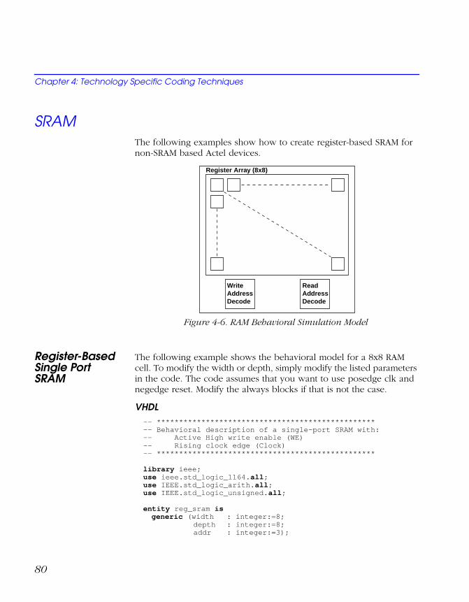
Chapter 4: Technology Specific Coding Techniques
SRAMThe following examples show how to create register-based SRAM for non-SRAM based Actel devices.
Register-Based Single Port SRAM
The following example shows the behavioral model for a 8x8 RAM cell. To modify the width or depth, simply modify the listed parameters in the code. The code assumes that you want to use posedge clk and negedge reset. Modify the always blocks if that is not the case.
VHDL-- *************************************************-- Behavioral description of a single-port SRAM with:-- Active High write enable (WE)-- Rising clock edge (Clock)-- *************************************************
library ieee;use ieee.std_logic_1164.all;use IEEE.std_logic_arith.all;use IEEE.std_logic_unsigned.all;
entity reg_sram isgeneric (width : integer:=8;
depth : integer:=8;addr : integer:=3);
Register Array (8x8)
WriteAddressDecode
ReadAddressDecode
Figure 4-6. RAM Behavioral Simulation Model
80
SRAM
port (Data : in std_logic_vector (width-1 downto 0);Q : out std_logic_vector (width-1 downto 0);Clock : in std_logic;WE : in std_logic;Address : in std_logic_vector (addr-1 downto 0));
end reg_sram;
architecture behav of reg_sram istype MEM is array (0 to depth-1) of std_logic_vector(width-1downto 0);signal ramTmp : MEM;
beginprocess (Clock)beginif (clk'event and clk='1') thenif (WE = '1') thenramTmp (conv_integer (Address)) <= Data;
end if;end if;
end process;Q <= ramTmp(conv_integer(Address));end behav;
Verilog`timescale 1 ns/100 ps//########################################################//# Behavioral single-port SRAM description ://# Active High write enable (WE)//# Rising clock edge (Clock)//#######################################################
module reg_sram (Data, Q, Clock, WE, Address);
parameter width = 8;parameter depth = 8;parameter addr = 3;
input Clock, WE;input [addr-1:0] Address;input [width-1:0] Data;output [width-1:0] Q;wire [width-1:0] Q;reg [width-1:0] mem_data [depth-1:0];
always @(posedge Clock)if(WE)
mem_data[Address] = #1 Data;
assign Q = mem_data[Address];
endmodule
81
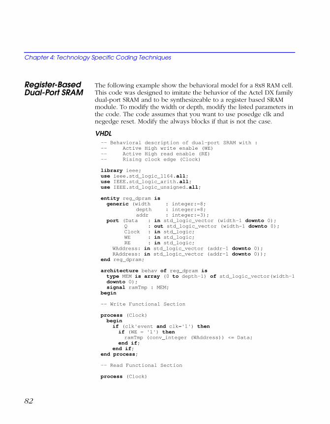
Chapter 4: Technology Specific Coding Techniques
Register-Based Dual-Port SRAM
The following example show the behavioral model for a 8x8 RAM cell. This code was designed to imitate the behavior of the Actel DX family dual-port SRAM and to be synthesizeable to a register based SRAM module. To modify the width or depth, modify the listed parameters in the code. The code assumes that you want to use posedge clk and negedge reset. Modify the always blocks if that is not the case.
VHDL-- Behavioral description of dual-port SRAM with :-- Active High write enable (WE) -- Active High read enable (RE) -- Rising clock edge (Clock)
library ieee;use ieee.std_logic_1164.all;use IEEE.std_logic_arith.all;use IEEE.std_logic_unsigned.all;
entity reg_dpram isgeneric (width : integer:=8;
depth : integer:=8;addr : integer:=3);
port (Data : in std_logic_vector (width-1 downto 0);Q : out std_logic_vector (width-1 downto 0); Clock : in std_logic;WE : in std_logic;RE : in std_logic;
WAddress: in std_logic_vector (addr-1 downto 0);RAddress: in std_logic_vector (addr-1 downto 0));
end reg_dpram; architecture behav of reg_dpram istype MEM is array (0 to depth-1) of std_logic_vector(width-1downto 0);signal ramTmp : MEM;
begin
-- Write Functional Section
process (Clock)beginif (clk'event and clk='1') thenif (WE = '1') thenramTmp (conv_integer (WAddress)) <= Data;
end if;end if;
end process;
-- Read Functional Section
process (Clock)
82
SRAM
beginif (clk'event and clk='1') thenif (RE = '1') thenQ <= ramTmp(conv_integer (RAddress));
end if;end if;
end process;
end behav;
Verilog`timescale 1 ns/100 ps//########################################################//# Behavioral dual-port SRAM description ://# Active High write enable (WE)//# Active High read enable (RE)//# Rising clock edge (Clock)//#######################################################
module reg_dpram (Data, Q, Clock, WE, RE, WAddress, RAddress);
parameter width = 8;parameter depth = 8;parameter addr = 3;
input Clock, WE, RE;input [addr-1:0] WAddress, RAddress;input [width-1:0] Data;output [width-1:0] Q;reg [width-1:0] Q;reg [width-1:0] mem_data [depth-1:0];
// #########################################################// # Write Functional Section// #########################################################always @(posedge Clock)begin
if(WE)mem_data[WAddress] = #1 Data;
end
//#########################################################//# Read Functional Section//#########################################################always @(posedge Clock)begin
if(RE)Q = #1 mem_data[RAddress];
end
endmodule
83
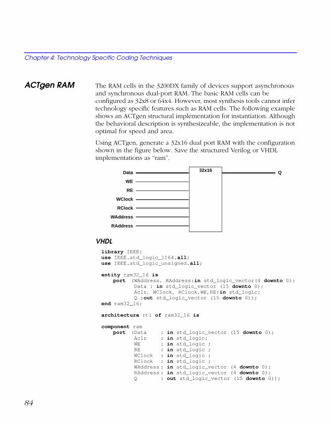
Chapter 4: Technology Specific Coding Techniques
ACTgen RAM The RAM cells in the 3200DX family of devices support asynchronous and synchronous dual-port RAM. The basic RAM cells can be configured as 32x8 or 64x4. However, most synthesis tools cannot infer technology specific features such as RAM cells. The following example shows an ACTgen structural implementation for instantiation. Although the behavioral description is synthesizeable, the implementation is not optimal for speed and area.
Using ACTgen, generate a 32x16 dual port RAM with the configuration shown in the figure below. Save the structured Verilog or VHDL implementations as “ram”.
VHDL library IEEE;use IEEE.std_logic_1164.all;use IEEE.std_logic_unsigned.all;
entity ram32_16 is port (WAddress, RAddress:in std_logic_vector(4 downto 0);
Data : in std_logic_vector (15 downto 0); Aclr, WClock, RClock,WE,RE:in std_logic; Q :out std_logic_vector (15 downto 0));
end ram32_16;
architecture rtl of ram32_16 is
component ramport (Data : in std_logic_vector (15 downto 0);
Aclr : in std_logic; WE : in std_logic ; RE : in std_logic ; WClock : in std_logic ; RClock : in std_logic ; WAddress : in std_logic_vector (4 downto 0); RAddress : in std_logic_vector (4 downto 0); Q : out std_logic_vector (15 downto 0));
32x16Data Q
RE
WE
WClock
RClock
WAddress
RAddress
84
SRAM
end component;
begin
R_32_16: ramport map (Data => Data,
Aclr => Aclr, WE => WE, WAddress => WAddress, RE => RE, RAddress => RAddress, WClock => WClock, RClock => RClock, Q => Q);
end rtl;
Verilog module ram (WAddress, RAddress, Data, WClock, WE,
RE, Rclock, Q);input [4:0] WAddress, RAddress; input [15:0] Data; input Rclock, WClock; input WE, RE; output [15:0] Q;
RAM R_32_16(.Data(Data), .WE(WE), .RE(RE), .WClock(WClock), .Rclock(Rclock), .Q(Q), .WAddress(WAddress), .RAddress(RAddress));
endmodule
85
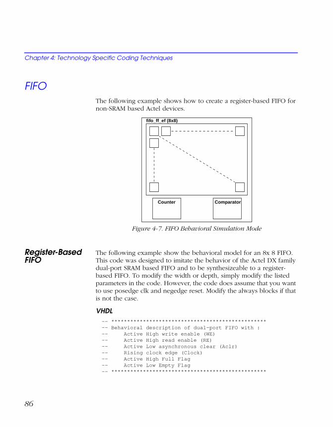
Chapter 4: Technology Specific Coding Techniques
FIFOThe following example shows how to create a register-based FIFO for non-SRAM based Actel devices.
Register-Based FIFO
The following example show the behavioral model for an 8x 8 FIFO. This code was designed to imitate the behavior of the Actel DX family dual-port SRAM based FIFO and to be synthesizeable to a register-based FIFO. To modify the width or depth, simply modify the listed parameters in the code. However, the code does assume that you want to use posedge clk and negedge reset. Modify the always blocks if that is not the case.
VHDL-- ************************************************* -- Behavioral description of dual-port FIFO with :-- Active High write enable (WE) -- Active High read enable (RE)-- Active Low asynchronous clear (Aclr) -- Rising clock edge (Clock)-- Active High Full Flag-- Active Low Empty Flag-- *************************************************
fifo_ff_ef (8x8)
Counter Comparator
Figure 4-7. FIFO Behavioral Simulation Mode
86
FIFO
library ieee;use ieee.std_logic_1164.all;use IEEE.std_logic_arith.all;
entity reg_fifo is
generic (width : integer:=8; depth : integer:=8; addr : integer:=3);
port (Data : in std_logic_vector (width-1 downto 0); Q : out std_logic_vector (width-1 downto 0); Aclr : in std_logic; Clock : in std_logic; WE : in std_logic; RE : in std_logic; FF : out std_logic; EF : out std_logic);
end reg_fifo;
library ieee;use ieee.std_logic_1164.all;use IEEE.std_logic_arith.all;use IEEE.std_logic_unsigned.all;
architecture behavioral of reg_fifo is
type MEM is array(0 to depth-1) of std_logic_vector(width-1 downto 0);signal ramTmp : MEM;signal WAddress : std_logic_vector (addr-1 downto 0);signal RAddress : std_logic_vector (addr-1 downto 0);signal words : std_logic_vector (addr-1 downto 0);
begin
-- ########################################################-- # Write Functional Section-- ########################################################
WRITE_POINTER : process (Aclr, Clock) beginif (Aclr = '0') thenWAddress <= (others => '0');
elsif (Clock'event and Clock = '1') thenif (WE = '1') thenif (WAddress = words) then
87
Chapter 4: Technology Specific Coding Techniques
WAddress <= (others => '0');elseWAddress <= WAddress + '1';
end if;end if;
end if;end process;
WRITE_RAM : process (Clock)beginif (Clock'event and Clock = '1') then
if (WE = '1') thenramTmp (conv_integer (WAddress)) <= Data;
end if;end if;
end process;
-- ######################################################## -- # Read Functional Section-- ########################################################
READ_POINTER : process (Aclr, Clock) beginif (Aclr = '0') thenRAddress <= (others => '0');
elsif (Clock'event and Clock = '1') thenif (RE = '1') thenif (RAddress = words) thenRAddress <= (others => '0');
elseRAddress <= RAddress + '1';
end if;end if;
end if;end process;
READ_RAM : process (Clock)beginif (Clock'event and Clock = '1') thenif (RE = '1') thenQ <= ramTmp(conv_integer(RAddress));
end if;end if;
end process;
88
FIFO
-- ########################################################-- # Full Flag Functional Section : Active high-- ########################################################
FFLAG : process (Aclr, Clock)beginif (Aclr = '0') thenFF <= '0';
elsif (Clock'event and Clock = '1') thenif (WE = '1' and RE = '0') thenif ((WAddress = RAddress-1) or
((WAddress = depth-1) and (RAddress = 0))) thenFF <= '1';
end if;elseFF <= '0';
end if;end if;
end process;
-- ########################################################-- # Empty Flag Functional Section : Active low-- ########################################################
EFLAG : process (Aclr, Clock)beginif (Aclr = '0') thenEF <= '0';
elsif (Clock'event and Clock = '1') thenif (RE = '1' and WE = '0') thenif ((WAddress = RAddress+1) or
((RAddress = depth-1) and (WAddress = 0))) thenEF <= '0';
end if;elseEF <= '1';
end if;end if;
end process;
end behavioral;
89
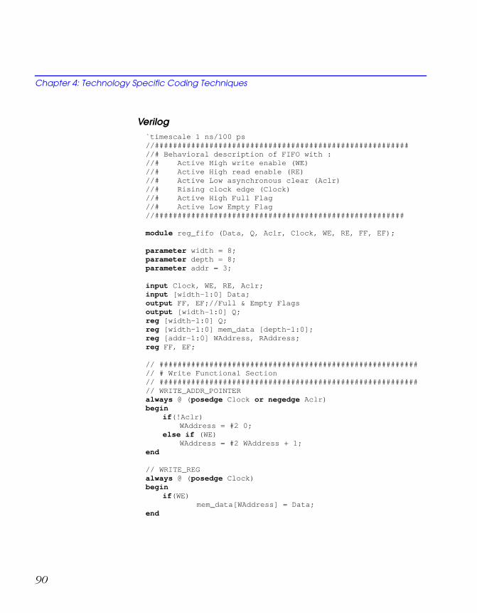
Chapter 4: Technology Specific Coding Techniques
Verilog`timescale 1 ns/100 ps//########################################################//# Behavioral description of FIFO with ://# Active High write enable (WE)//# Active High read enable (RE)//# Active Low asynchronous clear (Aclr)//# Rising clock edge (Clock)//# Active High Full Flag//# Active Low Empty Flag//#######################################################
module reg_fifo (Data, Q, Aclr, Clock, WE, RE, FF, EF);
parameter width = 8;parameter depth = 8;parameter addr = 3;
input Clock, WE, RE, Aclr;input [width-1:0] Data;output FF, EF;//Full & Empty Flagsoutput [width-1:0] Q;reg [width-1:0] Q;reg [width-1:0] mem_data [depth-1:0];reg [addr-1:0] WAddress, RAddress;reg FF, EF;
// #########################################################// # Write Functional Section// #########################################################// WRITE_ADDR_POINTERalways @ (posedge Clock or negedge Aclr)begin
if(!Aclr) WAddress = #2 0;
else if (WE)WAddress = #2 WAddress + 1;
end
// WRITE_REGalways @ (posedge Clock)begin
if(WE)mem_data[WAddress] = Data;
end
90
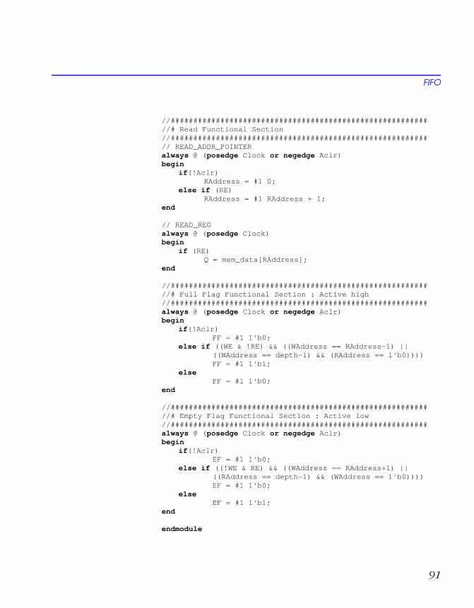
FIFO
//#########################################################//# Read Functional Section//#########################################################// READ_ADDR_POINTERalways @ (posedge Clock or negedge Aclr)begin
if(!Aclr) RAddress = #1 0;
else if (RE)RAddress = #1 RAddress + 1;
end
// READ_REGalways @ (posedge Clock)begin
if (RE)Q = mem_data[RAddress];
end
//#########################################################//# Full Flag Functional Section : Active high//#########################################################always @ (posedge Clock or negedge Aclr)begin
if(!Aclr)FF = #1 1'b0;
else if ((WE & !RE) && ((WAddress == RAddress-1) || ((WAddress == depth-1) && (RAddress == 1'b0))))FF = #1 1'b1;
elseFF = #1 1'b0;
end
//#########################################################//# Empty Flag Functional Section : Active low//#########################################################always @ (posedge Clock or negedge Aclr)begin
if(!Aclr)EF = #1 1'b0;
else if ((!WE & RE) && ((WAddress == RAddress+1) || ((RAddress == depth-1) && (WAddress == 1'b0))))EF = #1 1'b0;
elseEF = #1 1'b1;
end
endmodule
91
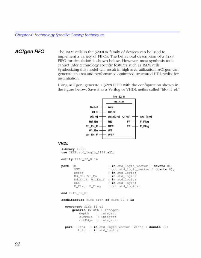
Chapter 4: Technology Specific Coding Techniques
ACTgen FIFO The RAM cells in the 3200DX family of devices can be used to implement a variety of FIFOs. The behavioral description of a 32x8 FIFO for simulation is shown below. However, most synthesis tools cannot infer technology specific features such as RAM cells. Synthesizing this model will result in high area utilization. ACTgen can generate an area and performance optimized structured HDL netlist for instantiation.
Using ACTgen, generate a 32x8 FIFO with the configuration shown in the figure below. Save it as a Verilog or VHDL netlist called “fifo_ff_ef.”
VHDLlibrary IEEE;use IEEE.std_logic_1164.all;
entity fifo_32_8 is
port (D : in std_logic_vector(7 downto 0); OUT : out std_logic_vector(7 downto 0); Reset : in std_logic; Rd_En, Wr_En : in std_logic; Rd_En_F, Wr_En_F : in std_logic; CLK : in std_logic; E_Flag, F_Flag : out std_logic);
end fifo_32_8;
architecture fifo_arch of fifo_32_8 is
component fifo_ff_efgeneric (width : integer;
depth : integer;clrPola : integer;clkEdge : integer);
port (Data : in std_logic_vector (width-1 downto 0); Aclr : in std_logic;
fifo_ff_ef
fifo_32_8
Reset
OUT[7:0]D[7:0]
CLK
Rd_En
Rd_En_F
Wr_En
Wr_En_F
Aclr
Data[7:0]
Clock
RE
REF
WE
WEF
F_Flag
E_Flag
Q[7:0]
FF
EF
92
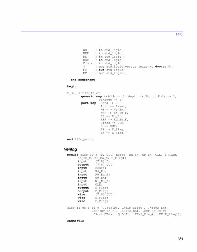
FIFO
WE : in std_logic ; WEF : in std_logic ; RE : in std_logic ; REF : in std_logic ; Clock : in std_logic ; Q : out std_logic_vector (width-1 downto 0); FF : out std_logic; EF : out std_logic);
end component;
begin
F_32_8: fifo_ff_efgeneric map (width => 8, depth => 32, clrPola => 1,
clkEdge => 1)port map (Data => D,
Aclr => Reset, WE = > We_En, WEF => We_En_F, RE => Rd_En, REF => Rd_En_F, Clock => CLK, Q => OUT, FF => F_Flag, EF => E_Flag);
end fifo_arch;
Verilogmodule fifo_32_8 (D, OUT, Reset, Rd_En, Wr_En, CLK, E_Flag,
Rd_En_F, Wr_En_F, F_Flag);input [7:0] D; output [7:0] OUT; input Reset; input Rd_En; input Rd_En_F;input Wr_En; input Wr_En_F;input CLK; output E_Flag; output F_Flag; wire [7:0] OUT; wire E_Flag; wire F_Flag;
fifo_ff_ef F_32_8 (.Data(D), .Aclr(Reset), .WE(Wr_En),.WEF(Wr_En_F), .RE(Rd_En), .REF(Rd_En_F).Clock(CLK), .Q(OUT), .FF(F_Flag), .EF(E_Flag));
endmodule
93

AProduct Support
Actel backs its products with various technical support services including a Web site, monthly Fax Broadcast, a fax back service, a bulletin board system, electronic mail, Customer Service, and a Customer Applications Center.
Actel U.S. Toll-Free LineUse the Actel toll-free line to contact Actel for sales information, technical support, requests for literature about Actel and Actel products, Customer Service, investor information, and using the Action Facts service.
The Actel Toll-Free Line is (888) 99-ACTEL.
Customer ServiceContact Customer Service for non-technical product support, such as product pricing, product upgrades, update information, order status, and authorization.
From Northeast and North Central U.S.A., call (408) 522-4480.From Southeast and Southwest U.S.A., call (408) 522-4480.From South Central U.S.A., call (408) 522-4474.From Northwest U.S.A., call (408) 522-4434.From Canada, call (408) 522-4480.From Europe, call (408) 522-4474 or +44 (0) 1256 305600.From Japan, call (408) 522-4252.From the rest of the world, call (408) 522-4252.Fax, from anywhere in the world (408) 522-8044.
95
Appendix A Product Support
Customer Applications CenterThe Customer Applications Center is staffed by applications engineers who can answer your hardware, software, and design questions.
All calls are answered by our Technical Message Center. The center retrieves information, such as your name, company name, phone number and your question, and then issues a case number. The Center then forwards the information to a queue where the first available application engineer receives the data and returns your call. The phone hours are from 7:30 a.m. to 5 p.m., Pacific Standard Time, Monday through Friday.
The Customer Applications Center number is (800) 262-1060.
European customers can call +44 (0) 1256 305600.
Action FactsAction Facts is a 24-hour fax-back service that allows you to have technical literature faxed directly to you. The literature includes current applications notes, device diagrams, radiation testing reports, CAE-related documents, training release schedules, and much more.
To receive your free copy of the catalog or any of our literature, contact us at (800) 262-1062 or (408) 739-1588.
Web SiteActel has a World Wide Web home page where you can browse a variety of technical and non-technical information. Use a Web browser (Netscape recommended) to access Actel’s home page. The URL is http://www.actel.com. You are welcome to share the resources we have provided on the net.
Be sure to visit the “Actel User Area” on our Web site, which contains information regarding: products, technical services, Designer’s Digest, current manuals, and release notes.
96
HLD Web Site
HLD Web SiteActel also has an HLD web site at http://www.actel.com/hld/ that you can browse for HLD design information. The site provides detailed information and examples on coding styles and synthesis and simulation flow, as well as links to our synthesis and simulation partners.
Guru Automated Technical SupportGuru is a Web based automated technical support system accessible through the Actel home page (http://www.actel.com). Guru provides answers to technical questions about Actel products. Many answers include diagrams, illustrations and links to other resources on the Actel Web site. Guru is available 24 hours a day, seven days a week.
FTP SiteActel has an anonymous FTP site located at ftp://ftp.actel.com. You can directly obtain library updates (such as VITAL), software patches, design files, and data sheets.
Electronic MailYou can communicate your technical questions to our e-mail address and receive answers back by e-mail, fax, or phone. Also, if you have design problems, you can e-mail your design files to receive assistance. The e-mail account is monitored several times per day.
The technical support e-mail address is: [email protected].
97

Index
AACT 3 I/O 71Actel FTP Site 97Actel Web Site 96
Technical Support 97ACTgen
Counter Instantiation 75FIFO 92RAM 84
Action Facts 96Addition 29Arithmetic Operator 29
Shift Register Implementation 30Assumptions x
BBehavioral Simulation 2BREPTH 71
CCapturing a Design 2Case Statement 19, 61
Adding Directive 61CLKBUF 73CLKINT 73Coding Dual Architecture 77
Instantiating 79RTL 77Structural 78
Combinatorial/Sequential Module Merging 56Combining Logic 53, 56Component
Size 49Width 49
Contacting ActelCustomer Service 95
Electronic Mail 97Technical Support 96Toll-Free 95Web Based Technical Support 97
Conventions xDocument xNaming, Verilog xiiNaming, VHDL xi
Counter 25–298-Bit, Count Enable, Asynchronous Reset 268-Bit, Load and Asynchronous Reset 278-Bit, Load, Count Enable, Terminal Count and
Asynchronous Reset 28Instantiation 75N-Bit, Load, Count Enable, and Asynchronous
Reset 28Recommendations 25, 75
Critical Path Logic Reduction 51Customer Service 95
DData Shift 33Datapath 17–34
Arithmetic Operator 29Counter 25Decoder 24Equality Operator 32If-Then-Else 17Multiplexor 19Relational Operator 31Shift Operator 33
Decoder 24Design Creation/Verification 2
Behavioral Simulation 2EDIF Netlist Generation 3HDL Source Entry 2
99
Index
Structural Netlist Generation 3Structural Simulation 3Synthesis 2
Design FlowDesign Creation/Verification 2Design Implementation 3Programming 4System Verification 4
Design Implementation 3Place and Route 3Timing Analysis 3Timing Simulation 4
Design Layout 3Design Partitioning 60Design Synthesis 2Designer
DT Analyze Tool 3Place and Route 3Timing Analysis 3
Device Programming 4DFPC Cell 71Division 29D-Latch 5–17
with Asynchronous Reset 16with Data and Enable 13with Gated Asynchronous Data 14with Gated Enable 15
Document Assumptions xDocument Conventions xDocument Organization ixDon’t Care 23DT Analyze 3Dual Architecture Coding 77
Instantiating 79RTL 77Structural 78
100
Dual Port SRAM 82, 84Duplicating Logic 57
EEdge-Triggered Memory Device 5EDIF Netlist Generation 3Electronic Mail 97Equality Operator 32
FFanout
High Fanout Networks 73, 75Reducing 57
FIFO 86–93ACTgen Implementation 92Behavioral Implementation 86Register-Based 86Structural Implementation 92
Finite State Machine 35–44Combinational Next State Logic 35Combinational Output Logic 35Mealy 37Moore 41One Hot 36Sequential Current State Register 35Structure 35
Flip-Flop 5–13See Also RegisterPositive Edge Triggered 6with Asynchronous Preset 8with Asynchronous Reset 7with Asynchronous Reset and Clock Enable 12with Asynchronous Reset and Preset 9with Synchronous Preset 11with Synchronous Reset 10
FSM. See Finite State Machine
Index
GGate-Level Netlist 2Generating
EDIF Netlist 3Gate-Level Netlist 2Structural Netlist 3
Generics 49–50Greater Than 31Greater Than Equal To 31
HHDL Design Flow
Design Creation/Verification 2Design Implementation 3Programming 4System Verification 4
HDL Source Entry 2HLD Web Site 97
IIf-Then-Else Statement 17Input-Output Buffer 44–48
Bi-Directional 47Tri-State 45
InstantiatingCKLBUF Driver 73CLKINT Driver 73Counters 75Dual Coding 77FIFO 92QCKLBUF Driver 75QCLKINT Driver 75RAM 84Registered I/Os 71
Internal Tri-State Mapping 62Internally Generated Clock 73, 75
KKeywords
Verilog xiiVHDL xi
LLatch 5
Master 71Slave 71
Less Than 31Less Than Equal To 31Level-Sensitive Memory Device 5Load Reduction 57Logic Level Reduction 51Loops 55
MMerging Logic Modules 56Module Block Partitioning 60Multiplexor 19, 61
Case X 23Four to One 20Mapping Internal Tri-State to 62Moving Operators Outside Loops 55Twelve to One 21
Multiplication 29
NNaming Conventions
Verilog xiiVHDL xi
Netlist GenerationEDIF 3Gate-Level 2Structural 3
101
Index
OOne Hot State Machine 36Operator
Arithmetic 29Equality 32Inside Loops 55Relational 31Removing from Loops 55Shift 33
PParallel Encoding 19Parallel Operation 61Parameters 49–50Partitioning a Design 60Performance Driven Coding 51–60Place and Route 3Priority Encoding 17Product Support 95–97
Action Facts 96Customer Applications Center 96Customer Service 95Electronic Mail 97FTP Site 97HLD Web Site 97Technical Support 96, 97Toll-Free Line 95Web Site 96
Programming a Device 4
QQCLKBUF 75QCLKINT 75Quadrant Clock 75
Limitations 75
102
RRAM 84Reducing Fanout 57Reducing Logic
on a Critical Path 51Usage 53
Register 64See Also Flip-FlopAsynchronous Preset 68Asynchronous Preset and Clear 71Clock Enabled 66Duplication 57Functionally Equivalent Asynchronous Preset
68Placed at Hierarchical Boundaries 60Recommended Usage 64–71Synchronous Clear or Preset 65
Register-BasedFIFO 86SRAM 80–83
Dual Port 82Single Port 80
Registered I/O 71BREPTH 71
Related Manuals xiiiRelational Operator 31Removing Operators from Loops 55Reset Signals 73, 75Resource Sharing 53
SSequential Device 5–13
D-Latch 5Flip-Flop 5
Sharing Resources 53Shift Operator 33
Index
Shift Register 30Simulation
Behavioral 2Structural 3Timing 4
Single Port SRAM 80Size 49SRAM 80–85
ACTgen Implementation 84Dual Port 82Register Based 80Single Port 80Structural Implementation 84
Static Timing Analysis 3Structural Netlist Generation 3Structural Simulation 3Subtraction 29Synthesis 2
Reducing Duration of 60System Verification
Action Probe 4Silicon Explorer 4
TTechnical Support 96Technology Independent Coding 5–50Technology Specific Coding 61–93Timing Analysis 3Timing Constraints 51Timing Simulation 4Toll-Free Line 95Tri-State Mapping 62True/False Operands 32
UUnit Delays 2
VVerilog
Naming Conventions xiiReserved Words xii
VHDLNaming Conventions xiReserved Words xi
WWeb Based Technical Support 97Width 49
103
Actel Corporation955 East Arques AvenueSunnyvale, CA USA 94086 Actel Europe Ltd. Actel Japan
U.S. Toll Free Line 888.99.ACTEL Daneshill House EXOS Ebisu Bldg. 4FCustomer Service: 408.739.1010 Lutyens Close 1-24-14 Ebisu Shibuya-kuCustomer Service FAX: 408.522.8044 Basingstoke Toyko 150 JapanAction Facts Technical Documents: 800.262.1062 Hampshire RG24 8AG Tel: +81.(0)3.3445.7671Customer Applications Center: 800.262.1060 United Kingdom Fax: +81.(0)3.3445.7668Customer Applications FAX: 408.739.1540 Tel: +44(0) 1256.305600
Fax: +44(0) 1256.355420
5029105-0
Related Documents


