120927 Power Electronics for Next "E" Stage Expansion / Evolution / Eco-Solutions AC/DC control IC and PFC IC Selection Guide SANKEN ELECTRIC CO.,LTD POWER CONVERSION DEVICE DIVISION ENGINEERING HEADQUARTERS

Welcome message from author
This document is posted to help you gain knowledge. Please leave a comment to let me know what you think about it! Share it to your friends and learn new things together.
Transcript
120927 Power Electronics for Next "E" Stage Expansion / Evolution / Eco-Solutions
AC/DC control IC and PFC IC Selection Guide
SANKEN ELECTRIC CO.,LTD POWER CONVERSION DEVICE DIVISION ENGINEERING HEADQUARTERS

120927 Power Electronics for Next "E" Stage Expansion / Evolution / Eco-Solutions
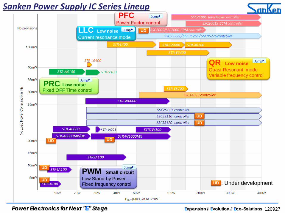
PRC Low noise Fixed OFF Time control
PFC Power Factor control
LLC Low noise Current resonance mode
QR Low noise Quasi-Resonant mode Variable frequency control
PWM Small circuit Pulse Width Modulation Fixed frequency control
Jump▸
Jump▸
Jump▸
Jump▸
Application
Jump▸
120927 Power Electronics for Next "E" Stage Expansion / Evolution / Eco-Solutions
PRC Low noise Fixed OFF Time control
PFC Power Factor control
LLC Low noise Current resonance mode
QR Low noise Quasi-Resonant mode Variable frequency control
PWM Small circuit Low Stand-by Power Fixed frequency control UD : Under development UD
UD
UD
Sanken Power Supply IC Series Lineup Jump▸
Jump▸
Jump▸
Jump▸
Jump▸
UD UD
UD UD
UD

120927 Power Electronics for Next "E" Stage Expansion / Evolution / Eco-Solutions
Max
imum
No
Load
Pow
er
Con
sum
ptio
n, P
IN
(mW
)
STR5A100T
STR4A100
STR3A100 15
10
5
0
STR3A100 PIN< 15mW
High heat release design
STR4A100 PIN< 10mW
Sense MOSFET(One Chip)
STR5A100T PIN< zero (< 5mW) Primary Side Sensing
Sense MOSFET(One Chip) VAC
C1C5 R3
D3
D2 R2
C2
T1D4
C6
R4
R5
U2
R9
R7
C7
D
P
S
PC1
PC1
C3ROCP
C9
D1
R6
R8
L2
C8
C4
VOUT
GND
1 2 3 4
D/ST D/ST
VCC
NC
S/OCP FB/OLPGND
D/ST D/ST
8 7 6 5
STR3A100U1
VAC
C1C5 R3
D3
D2 R2
C2
T1D4
C6
R4
R5
U2
R9
R7
C7
D
P
S
PC1
PC1C3C9
D1
R6
R8
L2
C8C4
VOUT
GND
1 2 4
S/GND S/GND
VCC
NC
FB/OLP D/ST
S/GND S/GND
8 7 6 5
STR4A100U1
VDSS=650V /700V
5 10 15 20 25 30 35 40 45 Maximum Output Power, POUT at AC230V (W)
DIP8 DIP8 SOIC
No ROCP
No photo-coupler
VDSS=700V
Preliminary
UD : Under development
UD
UD
UD UD
Low Standby Power IC New Lineup
VAC
C1 R4
D2
T1 D3
D
P1 S1
C5
VOUT
GND
L1
C3
R5
C6
C8 R7
C2C7R6
S/G
ND
VCC
NC
FB D/S
T
STR5A164TU1
2 3 4 5
COM
P
1
R1
R2
D1
C4
R3
VDSS=700V
TO-251(low profile)
UD
Rice cooker
Vacuum cleaner
Charger
Adapter
Smart meter
Air conditioner
Air purifier
Electrical water heater
Air conditioner Monitor Laser printer

120927 Power Electronics for Next "E" Stage Expansion / Evolution / Eco-Solutions
AC/DC PWM control IC
Series Package No Load Power Consumption (PIN)
Feature Link
Hybrid IC
STR-W6000 TO-220F-6L <30mW Brown in/out
STR-A6000 DIP8
<25mW
Brown in/out
STR-V653 SIP8L Brown in/out
STR-W6000MX TO-220F-6L Brown in/out, HVP ―
STR-W6000MV TO-220F-6L Selectable Standby Operation Point ―
STR-A6000MX/HX DIP8 Brown in/out, HVP ―
STR2W100D TO-220F-6L
STR3A100 DIP8 <10mW~15mW High heat release package
STR4A100 DIP8/SOIC8 <10mW 1chip solution ―
STR5A100 DIP8/SOIC8 Zero(<5mW) 1chip solution Primary detection ―
Controller
SSC2S110 SOIC8
<25mW SSC3S110 SOIC8 Selectable Standby Operation Point ―
SSC3S120 SOIC8 Brown in/out, HVP ―
Back to ALL lineup
UD : Under development
UD
UD
Jump▸
Jump▸
Jump▸
Jump▸
Jump▸
UD
UD
Jump▸
UD
UD
UD
For Low Standby Power and Small Circuit Application PWM is the Pulse Width Modulation, Fixed Frequency Control UD
120927 Power Electronics for Next "E" Stage Expansion / Evolution / Eco-Solutions
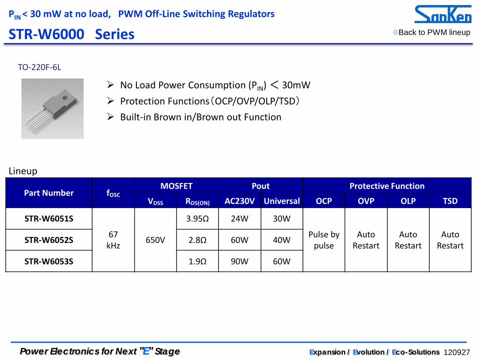
No Load Power Consumption (PIN) < 30mW Protection Functions(OCP/OVP/OLP/TSD) Built-in Brown in/Brown out Function
Lineup
TO-220F-6L
Part Number fOSC MOSFET Pout Protective Function
VDSS RDS(ON) AC230V Universal OCP OVP OLP TSD
STR-W6051S
67 kHz 650V
3.95Ω 24W 30W
Pulse by pulse
Auto Restart
Auto Restart
Auto Restart STR-W6052S 2.8Ω 60W 40W
STR-W6053S 1.9Ω 90W 60W
Back to PWM lineup STR-W6000 Series PIN < 30 mW at no load, PWM Off-Line Switching Regulators

120927 Power Electronics for Next "E" Stage Expansion / Evolution / Eco-Solutions
Pin Assignment
Circuit Package
TO-220F-6L
Features No Load Power Consumption (PIN< 30mW) Built-in Random Switching Function Built-in Startup Circuit Bias Assist function (to reduce VCC voltage drop) Slope Compensation (to prevent Sub-Harmonic oscillations) OCP with Built-in Input Compensation Circuit Auto Standby function (to enable low standby power)
Leading Edge Blanking Audible Noise Suppression Function for standby mode Brown-in/Brown-out function Two Chip Structure(MOSFET guaranteed Avalanche Energy) Protection Functions
OLP :Auto restart, built-in delay timer(external capacitor less) OCP: Pulse by pulse OVP/TSD: Auto restart
Back to PWM lineup STR-W6000 Series PIN < 30 mW at no load, PWM Off-Line Switching Regulators
Pin No. Symbol Function
1 D/ST MOSFET Drain / Startup current input
3 S/OCP MOSFET Source/OCP
4 Vcc Power supply input /Over Voltage Protection
5 GND Ground
6 FB/OLP Feedback control / Over Load Protection
7 BR Brown-in/Brown-out control

120927 Power Electronics for Next "E" Stage Expansion / Evolution / Eco-Solutions
STR-A6000 Series
No Load Power Consumption (PIN) < 25mW(HL<15mW) Protection Functions(OCP/OVP/OLP/TSD) Built-in Brown in/Brown out Function
Lineup
DIP8
Part Number fOSC MOSFET Pout Protective Function PIN VDSS RDS(ON) AC230V Universal OCP OVP OLP TSD STR-A6051M
67 kHz
650V
3.95Ω 16W 12W
Pulse by pulse Latched Auto
Restart Latched <25mW STR-A6052M 2.8Ω 20W 16W
STR-A6053M 1.9Ω 24W 20W
STR-A6079M 800V 19.2Ω 8W 5W
STR-A6059H
100 kHz
650V 6.0Ω 10W 8W
Pulse by pulse Latched Auto
Restart Latched <25mW STR-A6061H
700V
3.95Ω 13W 11W
STR-A6062H 2.8Ω 15W 13W
STR-A6069H 6.0Ω 10W 8W
STR-A6069HD
100 kHz 700V
6.0Ω 10W 8W
Pulse by pulse Latched Auto
Restart Latched <25mW STR-A6061HD 3.95Ω 13W 11W
STR-A6062HD 2.8Ω 15W 13W
STR-A6063HD 1.9Ω 24W 20W
STR-A6069HL 100kHz 700V 6.0Ω 10W 8W Pulse by pulse Latched Auto
Restart Latched <15mW
Back to PWM lineup
PIN < 25 mW at no load, PWM Off-Line Switching Regulators
UD
UD
UD : Under development UD

120927 Power Electronics for Next "E" Stage Expansion / Evolution / Eco-Solutions
Features No Load Power Consumption (PIN< 25mW) Built-in Random Switching Function Built-in Startup Circuit Bias Assist function (to reduce VCC voltage drop) Slope Compensation (to prevent Sub-Harmonic oscillations) OCP with Built-in Input Compensation Circuit Auto Standby function (to enable low standby power)
Pin No. Symbol Function
1 S/OCP MOSFET Source/OCP
2 BR Brown-in/Brown-out control
3 GND Ground
4 FB/OLP Feedback control Over Load Protection
5 Vcc Power supply input /Over Voltage Protection
6 - - 7
D/ST MOSFET Drain Startup current input 8
Pin Assignment
Leading Edge Blanking Audible Noise Suppression Function for standby mode Brown-in/Brown-out function Two Chip Structure(MOSFET guaranteed Avalanche Energy) Protection Functions
OLP: Auto restart, built-in delay timer (external capacitor less) OCP: Pulse by pulse OVP/TSD: Latch shutdown
Circuit Package
DIP8
Back to PWM lineup STR-A6000 Series PIN < 25 mW at no load, PWM Off-Line Switching Regulators
120927 Power Electronics for Next "E" Stage Expansion / Evolution / Eco-Solutions
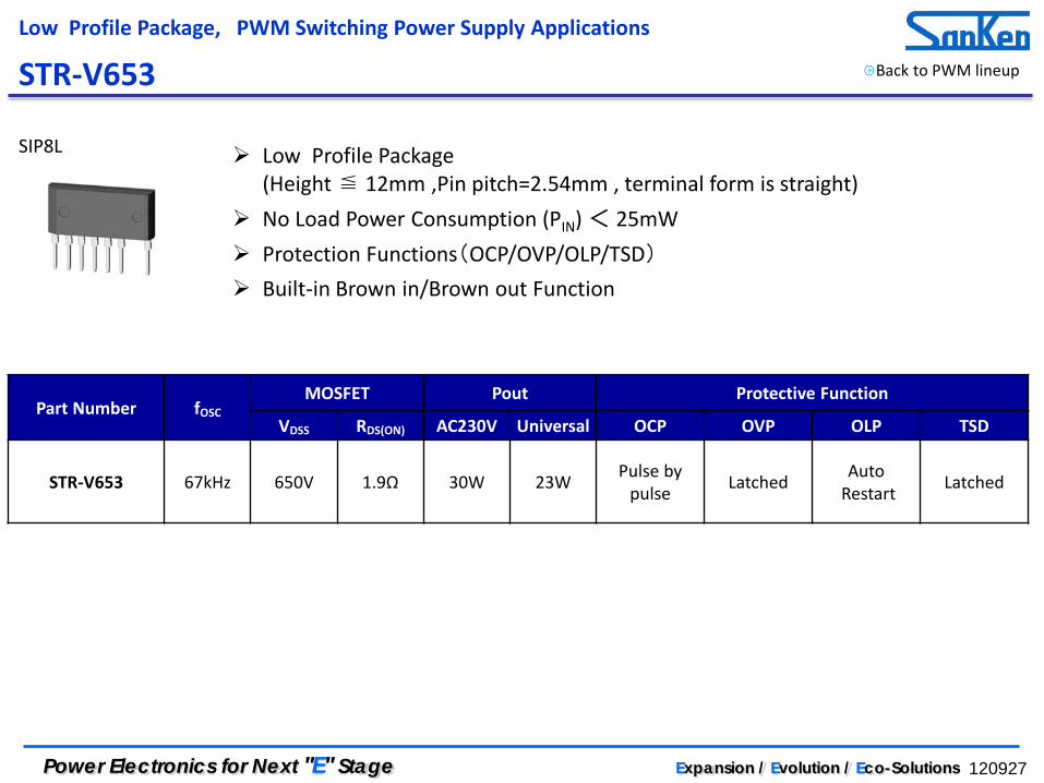
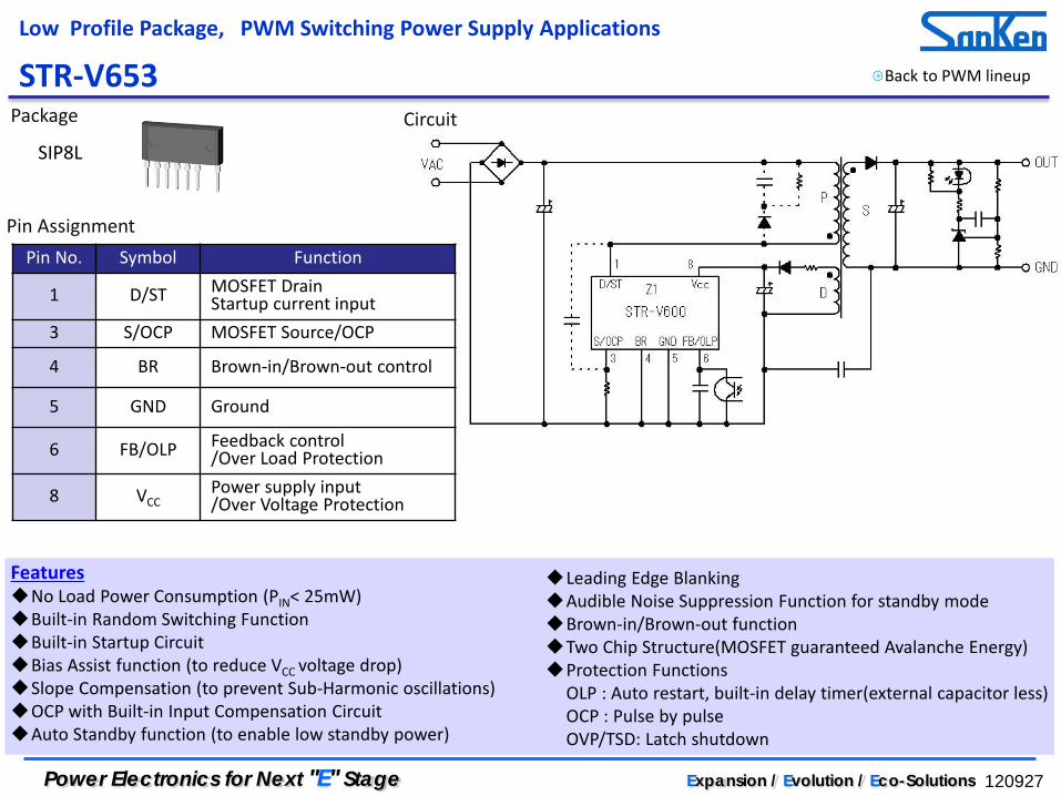
Low Profile Package (Height ≦ 12mm ,Pin pitch=2.54mm , terminal form is straight)
No Load Power Consumption (PIN) < 25mW Protection Functions(OCP/OVP/OLP/TSD) Built-in Brown in/Brown out Function
SIP8L
Part Number fOSC MOSFET Pout Protective Function
VDSS RDS(ON) AC230V Universal OCP OVP OLP TSD
STR-V653 67kHz 650V 1.9Ω 30W 23W Pulse by pulse Latched Auto
Restart Latched
Back to PWM lineup STR-V653 Low Profile Package, PWM Switching Power Supply Applications
120927 Power Electronics for Next "E" Stage Expansion / Evolution / Eco-Solutions
Pin Assignment
Circuit Package
SIP8L
Features No Load Power Consumption (PIN< 25mW) Built-in Random Switching Function Built-in Startup Circuit Bias Assist function (to reduce VCC voltage drop) Slope Compensation (to prevent Sub-Harmonic oscillations) OCP with Built-in Input Compensation Circuit Auto Standby function (to enable low standby power)
Leading Edge Blanking Audible Noise Suppression Function for standby mode Brown-in/Brown-out function Two Chip Structure(MOSFET guaranteed Avalanche Energy) Protection Functions
OLP : Auto restart, built-in delay timer(external capacitor less) OCP : Pulse by pulse OVP/TSD: Latch shutdown
Back to PWM lineup STR-V653 Low Profile Package, PWM Switching Power Supply Applications
Pin No. Symbol Function
1 D/ST MOSFET Drain Startup current input
3 S/OCP MOSFET Source/OCP
4 BR Brown-in/Brown-out control
5 GND Ground
6 FB/OLP Feedback control /Over Load Protection
8 VCC Power supply input /Over Voltage Protection
120927 Power Electronics for Next "E" Stage Expansion / Evolution / Eco-Solutions
No Load Power Consumption (PIN) < 25mW Protection Functions(OCP/OVP/OLP/TSD)
Lineup
TO-220F-6L
Part Number fOSC MOSFET Pout Protective Function
VDSS RDS(ON) AC230V Universal OCP OVP OLP TSD
STR2W152D 67
kHz 650V 3.0Ω 60W 40W
Pulse by pulse
Auto Restart
Auto Restart
Auto Restart
STR2W153D 1.9Ω 90W 60W
Back to PWM lineup STR2W100D Series PIN < 25 mW at no load, PWM Off-Line Switching Regulators

120927 Power Electronics for Next "E" Stage Expansion / Evolution / Eco-Solutions
Pin Assignment
Circuit Package
TO-220F-6L
Features No Load Power Consumption (PIN< 25mW) Built-in Random Switching Function Built-in Startup Circuit Bias Assist function Slope Compensation (to prevent Sub-Harmonic oscillations) OCP with Built-in Input Compensation Circuit Auto Standby function (to enable low standby power)
Leading Edge Blanking Two Chip Structure(MOSFET guaranteed Avalanche Energy) Protection Functions
OLP : Auto restart, built-in delay timer(external capacitor less) OCP : Pulse by pulse OVP/TSD: Auto restart
Back to PWM lineup STR2W100D Series PIN < 25 mW at no load, PWM Off-Line Switching Regulators
Pin No. Symbol Function
1 D/ST MOSFET Drain / Startup current input
3 S/OCP MOSFET Source/OCP
4 Vcc Power supply input /Over Voltage Protection
5 GND Ground
6 FB/OLP Feedback control Over Load Protection
7 NC ―

120927 Power Electronics for Next "E" Stage Expansion / Evolution / Eco-Solutions
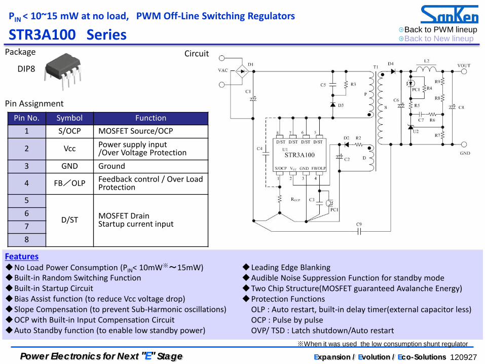
No Load Power Consumption (PIN) < 10mW ※ ~15mW
High heat release design Protection Functions(OCP/OVP/OLP/TSD)
Lineup
DIP8
Part Number fOSC MOSFET Pout Protective Function
VDSS RDS(ON) AC230V Universal OCP OVP OLP TSD
STR3A151
67 kHz 650V
4.0Ω 24W 16W
Pulse by pulse Latched Auto
Restart Latched
STR3A152 3.0Ω 30W 23W
STR3A153 1.9Ω 36W 30W
STR3A154 1.4Ω 40W 32W
STR3A155 1.1Ω 43W 35W
STR3A151D
67 kHz 650V
4.0Ω 24W 16W
Pulse by pulse
Auto Restart
Auto Restart
Auto Restart
STR3A152D 3.0Ω 30W 23W
STR3A153D 1.9Ω 36W 30W
STR3A154D 1.4Ω 40W 32W
STR3A155D 1.1Ω 43W 35W
STR3A161HD 100 kHz 700V
4.2Ω 26W 17W Pulse by
pulse Auto
Restart Auto
Restart Auto
Restart STR3A162HD 3.2Ω 29W 20W
STR3A163HD 2.2Ω 35W 29W
※When it was used the low consumption shunt regulator
Back to PWM lineup Back to New lineup STR3A100 Series
PIN < 10~15 mW at no load, PWM Off-Line Switching Regulators
UD
UD : Under development UD
120927 Power Electronics for Next "E" Stage Expansion / Evolution / Eco-Solutions
Pin No. Symbol Function 1 S/OCP MOSFET Source/OCP
2 Vcc Power supply input /Over Voltage Protection
3 GND Ground
4 FB/OLP Feedback control / Over Load Protection
5
D/ST MOSFET Drain Startup current input
6 7 8
Pin Assignment
Circuit Package
DIP8
Features No Load Power Consumption (PIN< 10mW※~15mW) Built-in Random Switching Function Built-in Startup Circuit Bias Assist function (to reduce Vcc voltage drop) Slope Compensation (to prevent Sub-Harmonic oscillations) OCP with Built-in Input Compensation Circuit Auto Standby function (to enable low standby power)
Leading Edge Blanking Audible Noise Suppression Function for standby mode Two Chip Structure(MOSFET guaranteed Avalanche Energy) Protection Functions
OLP : Auto restart, built-in delay timer(external capacitor less) OCP : Pulse by pulse OVP/ TSD : Latch shutdown/Auto restart
※When it was used the low consumption shunt regulator
Back to PWM lineup Back to New lineup STR3A100 Series
PIN < 10~15 mW at no load, PWM Off-Line Switching Regulators

120927 Power Electronics for Next "E" Stage Expansion / Evolution / Eco-Solutions
Pin Assignment Circuit
Package
SOIC8
Features No Load Power Consumption (PIN< 25mW) Built-in Random Switching Function Built-in Startup Circuit Bias Assist function Slope Compensation (to prevent Sub-Harmonic oscillations) OCP with Built-in Input Compensation Circuit Auto Standby function (to enable low standby power)
Leading Edge Blanking Protection Functions
OLP : Auto restart, built-in delay timer(external capacitor less) OCP: Pulse by pulse OVP/TSD: Auto restart
No Load Power Consumption (PIN) < 25mW This IC is the controller of STR2W100D
Pin No. Symbol Function 1 GND Ground
2 FB/OLP Feedback control Over Load Protection
3 NC ― 4 ST Startup current input 5 NC ― 6 DRIVE Gate drive output 7 OCP OCP signal input
8 VCC Power supply input /Over Voltage Protection
Part Number fOSC ST terminal voltage
Protective Function OCP OCP2 OVP OLP TSD
SSC2S110 67kHz 600V(MAX) Pulse by pulse Pulse by pulse Auto Restart Auto Restart Auto Restart
Back to PWM lineup SSC2S110 (Controller) PIN < 25 mW at no load, PWM Off-Line Switching Regulators

120927 Power Electronics for Next "E" Stage Expansion / Evolution / Eco-Solutions
AC/DC PRC control IC
Hybrid Power IC
Series Package No Load Power Consumption (PIN)
Link
STR-A6100 DIP8 <40mW
STR-V100 SIP8L <40mW
Back to ALL lineup
Jump▸
Jump▸
For Low Noise Application PRC is the Pulse Ratio Control (Controlling ON-time under fixed OFF-time)

120927 Power Electronics for Next "E" Stage Expansion / Evolution / Eco-Solutions
STR-A6100 Series
No Load Power Consumption (PIN) is < 40mW Protection Functions(OCP/OVP/OLP/TSD)
Lineup
DIP8
Part Number MOSFET
t(OFF) POUT Protective Function
VDSS RDS(ON) AC220V Universal Auto Bias OCP OVP OLP TSD
STR-A6131 500V
3.95Ω
8μs
AC100V 13W
AC120V 15W
Yes Pulse by pulse Latched Auto
Restart Latched
STR-A6132 2.62Ω AC100V 16W
AC120V 18W
STR-A6159 650V
6Ω 13W 10W
STR-A6151 3.95Ω 15W 13W
STR-A6169 800V 19.2Ω 8μs 8W 5W
STR-A6131M 500V 3.95Ω
11.5μs
13W AC120V 15W
No Pulse by pulse Latched Auto
Restart Latched STR-A6159M 650V
6Ω 13W 10W
STR-A6151M 3.95Ω 15W 13W
STR-A6153E 650V 1.9Ω 11.5μs 22W 18W No Pulse by pulse Latched Auto
Restart Latched
Back to PRC lineup
Built-in Auto Standby Function, PRC Off-Line Switching Regulators
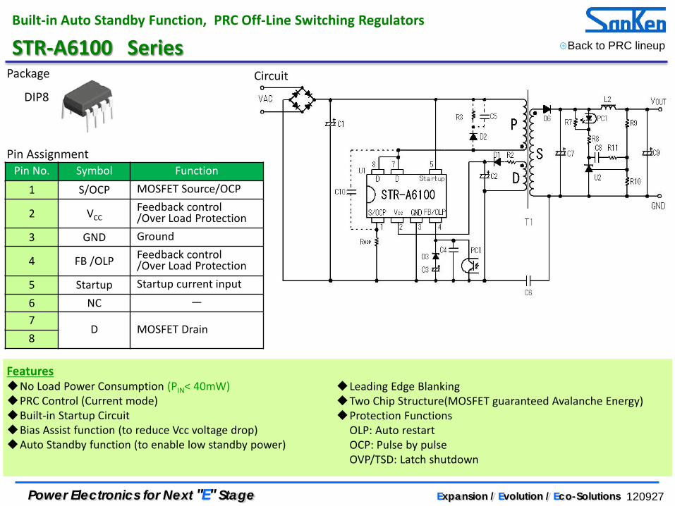
120927 Power Electronics for Next "E" Stage Expansion / Evolution / Eco-Solutions
Pin No. Symbol Function 1 S/OCP MOSFET Source/OCP
2 VCC Feedback control /Over Load Protection
3 GND Ground
4 FB /OLP Feedback control /Over Load Protection
5 Startup Startup current input 6 NC ― 7
D MOSFET Drain 8
Pin Assignment
Circuit Package
DIP8
Features No Load Power Consumption (PIN< 40mW) PRC Control (Current mode) Built-in Startup Circuit Bias Assist function (to reduce Vcc voltage drop) Auto Standby function (to enable low standby power)
Leading Edge Blanking Two Chip Structure(MOSFET guaranteed Avalanche Energy) Protection Functions
OLP: Auto restart OCP: Pulse by pulse OVP/TSD: Latch shutdown
Back to PRC lineup STR-A6100 Series Built-in Auto Standby Function, PRC Off-Line Switching Regulators

120927 Power Electronics for Next "E" Stage Expansion / Evolution / Eco-Solutions
Part Number MOSFET
t(OFF) POUT Protective Function
VDSS RDS(ON) AC220V Universal Auto Bias OCP OVP OLP TSD
STR-V152
650V
2.8Ω 8μs 22W 17W Yes Pulse by
pulse Latched Auto Restart Latched
STR-V153 2.0Ω 11.5μs 30W 23W No
Low Profile Package (Height ≦ 12mm, Pin pitch=2.54mm, terminal form is straight)
No Load Power Consumption (PIN) < 40mW Protection Functions(OCP/OVP/OLP/TSD)
SIP8L
Lineup
Back to PRC lineup STR-V100 Series Low Profile Package, PRC Off-Line Switching Regulators

120927 Power Electronics for Next "E" Stage Expansion / Evolution / Eco-Solutions
Pin No. Symbol Function 1 D MOSFET Drain 2 - - 3 S/OCP MOSFET Source/OCP
4 VCC Feedback control Over Load Protection
5 GND Ground
6 FB/OLP Power supply input /Over Voltage Protection
7 - - 8 Startup Startup current input
Pin Assignment
Circuit Package
SIP8L
Features No Load Power Consumption (PIN< 40mW) PRC Control (Current mode) Built-in Startup Circuit Bias Assist function (to reduce Vcc voltage drop) Slope Compensation (to prevent Sub-Harmonic oscillations) Auto Standby function (to enable low standby power)
Leading Edge Blanking Two Chip Structure(MOSFET guaranteed Avalanche Energy) Protection Functions
OLP: Auto restart OCP: Pulse by pulse OVP/TSD: Latch shutdown
Back to PRC lineup STR-V100 Series Low Profile Package, PRC Off-Line Switching Regulators

120927 Power Electronics for Next "E" Stage Expansion / Evolution / Eco-Solutions
AC/DC QR control IC
Series Package No Load Power Consumption (PIN)
Link
STR-G5600 TO-220F-5L ―
STR-L400 SIP10L ―
STR-Y6400 TO-220F-7L <0.1W
STR-Y6700 TO-220F-7L <0.3W(AC100V) <0.5W(AC240V)
STR-L6400 SIP10L <0.1W
STR-X6700 TO-3PF-7L ―
Hybrid Power IC
Series Package No Load Power Consumption (PIN)
Link
SSC1S310 SOIC8 <30mW(AC100V) <50mW(AC240V)
Controller
Back to ALL lineup
Jump▸
Jump▸
Jump▸
Jump▸
Jump▸
Jump▸
Jump▸
For Low Noise and High Power Application QR is the Quasi-Resonant Mode, Bottom ON Switching

120927 Power Electronics for Next "E" Stage Expansion / Evolution / Eco-Solutions
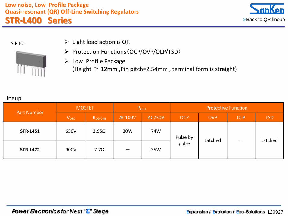
Light load action is QR Protection Functions(OCP/OVP/OLP/TSD)
Lineup
TO-220F-5L
Part Number MOSFET POUT Protective Function
VDSS RDS(ON) AC100V AC120V OCP OVP OLP TSD
STR-G5623
450V
1.3Ω 72W 96W
Pulse by pulse Latched - Latched STR-G5624 1Ω 90W 120W
STR-G5653 650V 1.9Ω 125W Universal 60W
Back to QR lineup STR-G5600 Series Low noise, Quasi-resonant (QR) Off-Line Switching Regulators

120927 Power Electronics for Next "E" Stage Expansion / Evolution / Eco-Solutions
Pin Assignment
Circuit Package
TO-220F-5L
Pin No. Symbol Function
1 D MOSFET Drain 2 S MOSFET Source 3 GND Ground
4 VIN Feedback control Over Load Protection
5 OCP/FB OCP/Feedback control
Features Light Load action is PRC Control Built-in Startup Circuit Built-in Step drive circuit Built-in Constant voltage drive circuit
Two Chip Structure(MOSFET guaranteed Avalanche Energy) Protection Functions
OCP: Pulse by pulse OVP/TSD: Latch shutdown
Back to QR lineup STR-G5600 Series Low noise, Quasi-resonant (QR) Off-Line Switching Regulators
120927 Power Electronics for Next "E" Stage Expansion / Evolution / Eco-Solutions
SIP10L Light load action is QR Protection Functions(OCP/OVP/OLP/TSD) Low Profile Package
(Height ≦ 12mm ,Pin pitch=2.54mm , terminal form is straight)
Lineup
Part Number MOSFET POUT Protective Function
VDSS RDS(ON) AC100V AC230V OCP OVP OLP TSD
STR-L451 650V 3.95Ω 30W 74W Pulse by
pulse Latched - Latched
STR-L472 900V 7.7Ω - 35W
Back to QR lineup STR-L400 Series
Low noise, Low Profile Package Quasi-resonant (QR) Off-Line Switching Regulators
120927 Power Electronics for Next "E" Stage Expansion / Evolution / Eco-Solutions
Circuit
Pin No. Symbol Function 1
D MOSFET Drain 2 3 4 5 - - 6 S MOSFET Source 7 GND Ground
8 VIN Feedback control Over Load Protection
9 OCP/FB OCP/Feedback control 10 GND GND
Features Light Load action is PRC Control Built-in Startup Circuit Built-in Step drive circuit Built-in Constant voltage drive circuit
Two Chip Structure(MOSFET guaranteed Avalanche Energy) Protection Functions
OCP: Pulse by pulse OVP/TSD: Latch shutdown
Pin Assignment
Package
SIP10L
Back to QR lineup STR-L400 Series
Low noise, Low Profile Package Quasi-resonant (QR) Off-Line Switching Regulators

120927 Power Electronics for Next "E" Stage Expansion / Evolution / Eco-Solutions
Auto Standby function No Load Power Consumption (PIN) is < 0.1W Auto Burst Function(1 or 2skip) Protection Functions(OCP/OVP/OLP/TSD)
How to stop OLP can be chosen by Latch or Auto restart
Lineup
TO-220F-7L
Part Number MOSFET POUT Protective Function
VDSS RDS(ON) AC100V AC240V OCP OVP OLP TSD
STR-Y6453 650V
1.8Ω 58W 110W
Pulse by pulse Latched
Latched or
Auto Restart
Latched
STR-Y6456 0.73Ω 140W 220W -
STR-Y6473 850V
3.6Ω 32W 60W Latched
STR-Y6476 1.3Ω 68W 130W -
Back to QR lineup STR-Y6400 Series Low noise, Quasi-resonant (QR) Off-Line Switching Regulators
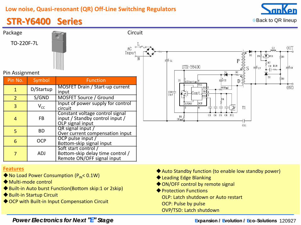
120927 Power Electronics for Next "E" Stage Expansion / Evolution / Eco-Solutions
Pin Assignment
Circuit Package
TO-220F-7L
Features No Load Power Consumption (PIN< 0.1W) Multi-mode control Built-in Auto burst Function(Bottom skip:1 or 2skip) Built-in Startup Circuit OCP with Built-in Input Compensation Circuit
Auto Standby function (to enable low standby power) Leading Edge Blanking ON/OFF control by remote signal Protection Functions
OLP: Latch shutdown or Auto restart OCP: Pulse by pulse OVP/TSD: Latch shutdown
Pin No. Symbol Function
1 D/Startup MOSFET Drain / Start-up current input
2 S/GND MOSFET Source / Ground
3 VCC Input of power supply for control circuit
4 FB Constant voltage control signal input / Standby control input / OLP signal input
5 BD QR signal input / Over current compensation input
6 OCP OCP pulse input / Bottom-skip signal input
7 ADJ Soft start control / Bottom-skip delay time control / Remote ON/OFF signal input
Back to QR lineup STR-Y6400 Series Low noise, Quasi-resonant (QR) Off-Line Switching Regulators

120927 Power Electronics for Next "E" Stage Expansion / Evolution / Eco-Solutions
Auto Standby function No Load Power Consumption (PIN) is < 30mW(AC100V) Auto Burst Function(1skip) Protection Functions(OCP/OVP/OLP/TSD)
How to stop OLP can be chosen by Latch or Auto restart
Lineup
TO-220F-7L
Part Number MOSFET POUT Protective Function
VDSS RDS(ON) DC380V Universal OCP OVP OLP TSD
STR-Y6735 500V 0.8Ω AC100V 120W ―
Pulse by pulse Latched Latched/
Auto Restart Latched
STR-Y6753 650V
1.9Ω 100W 60W
STR-Y6754 1.4Ω 120W 67W
STR-Y6763
800V
3.5Ω 80W 50W
STR-Y6765 2.2Ω 120W 70W
STR-Y6766 1.7Ω 140W 80W
Back to QR lineup STR-Y6700 Series
Low noise, PIN is < 30mW Quasi-resonant (QR) Off-Line Switching Regulators

120927 Power Electronics for Next "E" Stage Expansion / Evolution / Eco-Solutions
Pin Assignment
Circuit Package
TO-220F-7L
Features No Load Power Consumption
PIN<30mW(AC100V),<50mW(AC230V) Multi-mode control Built-in Auto burst Function(Bottom skip:1skip) Auto Standby function (to enable low standby power)
Built-in Startup Circuit OCP with Built-in Input Compensation Circuit Leading Edge Blanking Protection Functions
OLP : Latch shutdown or Auto restart OCP : Pulse by pulse OVP/TSD : Latch shutdown
Pin No. Symbol Function
1 D/ST MOSFET Drain / Start-up current input
2 S/OCP MOSFET Source / OCP pulse input
3 VCC Power supply input /Over Voltage Protection
4 GND Ground
5 FB/OLP Feedback control /Over Load Protection
6 BD Bottom Detection Signal Input / Input Compensation Detection Signal Input
7 NF ―
Back to QR lineup STR-Y6700 Series
Low noise, PIN is < 30mW Quasi-resonant (QR) Off-Line Switching Regulators

120927 Power Electronics for Next "E" Stage Expansion / Evolution / Eco-Solutions
QR Control IC Auto Standby function No Load Power Consumption (PIN) is < 0.1W Auto Burst Function(1 or 2skip) Protection Functions(OCP/OVP/OLP/TSD)
How to stop OLP can be chosen by Latch or Auto restart Low Profile Package
(Height ≦ 12mm ,Pin pitch=2.54mm , terminal form is straight)
Lineup
SIP10L
Part Number MOSFET POUT Protective Function
VDSS RDS(ON) AC100V AC240V OCP OVP OLP TSD
STR-L6472 850V 6.5Ω 15W 25W Pulse by pulse Latched Latched/
Auto Restart Latched
Back to QR lineup STR-L6400 Series
Low noise, Low Profile Package Quasi-resonant (QR) Off-Line Switching Regulators
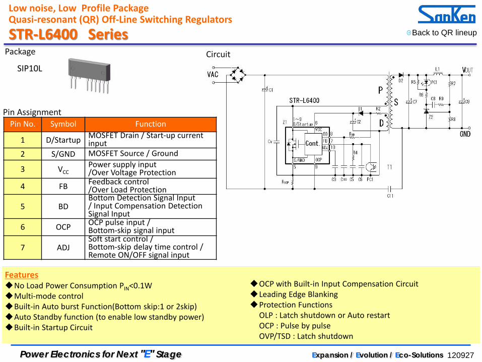
120927 Power Electronics for Next "E" Stage Expansion / Evolution / Eco-Solutions
Pin Assignment
Circuit Package
SIP10L
Features No Load Power Consumption PIN<0.1W Multi-mode control Built-in Auto burst Function(Bottom skip:1 or 2skip) Auto Standby function (to enable low standby power) Built-in Startup Circuit
OCP with Built-in Input Compensation Circuit Leading Edge Blanking Protection Functions
OLP : Latch shutdown or Auto restart OCP : Pulse by pulse OVP/TSD : Latch shutdown
Pin No. Symbol Function
1 D/Startup MOSFET Drain / Start-up current input
2 S/GND MOSFET Source / Ground
3 VCC Power supply input /Over Voltage Protection
4 FB Feedback control /Over Load Protection
5 BD Bottom Detection Signal Input / Input Compensation Detection Signal Input
6 OCP OCP pulse input / Bottom-skip signal input
7 ADJ Soft start control / Bottom-skip delay time control / Remote ON/OFF signal input
Back to QR lineup STR-L6400 Series
Low noise, Low Profile Package Quasi-resonant (QR) Off-Line Switching Regulators
120927 Power Electronics for Next "E" Stage Expansion / Evolution / Eco-Solutions
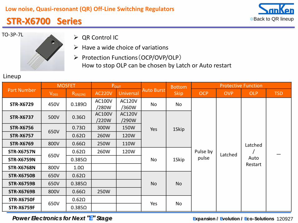
QR Control IC Have a wide choice of variations Protection Functions(OCP/OVP/OLP)
How to stop OLP can be chosen by Latch or Auto restart
Part Number MOSFET POUT
Auto Burst Bottom Skip
Protective Function VDSS RDS(ON) AC220V Universal OCP OVP OLP TSD
STR-X6729 450V 0.189Ω AC100V /280W
AC120V /360W No No
Pulse by pulse Latched
Latched /
Auto Restart
―
STR-X6737 500V 0.36Ω AC100V /220W
AC120V /290W
Yes 1Skip STR-X6756 650V
0.73Ω 300W 150W STR-X6757 0.62Ω 260W 120W STR-X6769 800V 0.66Ω 250W 110W
STR-X6757N 650V
0.62Ω 260W 120W No 1Skip STR-X6759N 0.385Ω
STR-X6768N 800V 1.0Ω STR-X6750B 650V 0.62Ω
No No STR-X6759B 650V 0.385Ω STR-X6769B 800V 0.66Ω 250W STR-X6750F
650V 0.62Ω
Yes No STR-X6759F 0.385Ω
TO-3P-7L
Lineup
Back to QR lineup STR-X6700 Series Low noise, Quasi-resonant (QR) Off-Line Switching Regulators

120927 Power Electronics for Next "E" Stage Expansion / Evolution / Eco-Solutions
Pin Assignment
Circuit
Package
TO-3PF-7L
Features OCP with Input Compensation Circuit
Pin No. Symbol Function
1 D MOSFET Drain 2 S MOSFET Source / Ground
3 GND Ground
4 VCC Power supply input /Over Voltage Protection
5 SS/OLP Soft start control / Over Load Protection
6 FB Feedback control
7 OCP/BD OCP pulse input / Bottom-skip signal input
Back to QR lineup STR-X6700 Series Low noise, Quasi-resonant (QR) Off-Line Switching Regulators
Protection Functions OLP : Latch shutdown or Auto restart OCP : Pulse by pulse OVP : Latch shutdown
120927 Power Electronics for Next "E" Stage Expansion / Evolution / Eco-Solutions
Back to QR lineup
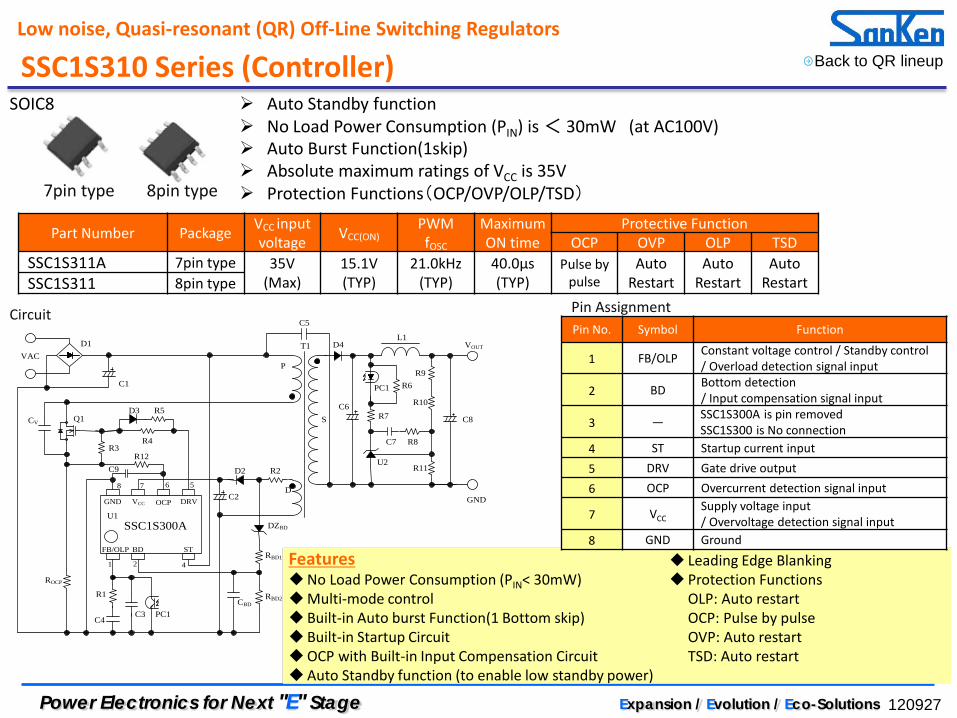
Auto Standby function No Load Power Consumption (PIN) is < 30mW (at AC100V) Auto Burst Function(1skip) Absolute maximum ratings of VCC is 35V Protection Functions(OCP/OVP/OLP/TSD)
Part Number Package VCC input voltage VCC(ON)
PWM fOSC
Maximum ON time
Protective Function OCP OVP OLP TSD
SSC1S311A 7pin type 35V (Max)
15.1V (TYP)
21.0kHz (TYP)
40.0μs (TYP)
Pulse by pulse
Auto Restart
Auto Restart
Auto Restart SSC1S311 8pin type
SSC1S310 Series (Controller) Low noise, Quasi-resonant (QR) Off-Line Switching Regulators
7pin type 8pin type
SOIC8
Pin Assignment
Features No Load Power Consumption (PIN< 30mW) Multi-mode control Built-in Auto burst Function(1 Bottom skip) Built-in Startup Circuit OCP with Built-in Input Compensation Circuit Auto Standby function (to enable low standby power)
Leading Edge Blanking Protection Functions
OLP: Auto restart OCP: Pulse by pulse OVP: Auto restart TSD: Auto restart
Pin No. Symbol Function
1 FB/OLP Constant voltage control / Standby control / Overload detection signal input
2 BD Bottom detection / Input compensation signal input
3 ― SSC1S300A is pin removed SSC1S300 is No connection
4 ST Startup current input 5 DRV Gate drive output 6 OCP Overcurrent detection signal input
7 VCC Supply voltage input / Overvoltage detection signal input
8 GND Ground
Circuit
VAC
C1
D2 R2
C2
T1 D4
C6
R6
R7
U2
R9
R11
C7
D
P
S
PC1
PC1C4
ROCP
D1
R8
R10
L1
C8CV
VOUT
GND
1 2 4
GND VCC
BDFB/OLP ST
OCP DRV
8 7 6 5
SSC1S300AU1
D3 R5
R4R3
Q1
C3
RBD2
RBD1
DZBD
CBD
R1
C5
R12C9

120927 Power Electronics for Next "E" Stage Expansion / Evolution / Eco-Solutions
AC/DC LLC control IC
Series PKG
Function
Link Brown in/out
DT control
fMAX /fMIN
Auto Burst
Reset Detect FMAX(SS)
(3)
RC Latch
External Latch
SSC9522S SOP18 ○ Auto 300kHz /28.3kHz ○ × × ○ ○
SSC9526S SOP18 ○ Auto(1) 340kHz /30.5kHz × ○ ○ × ○
SSC9527S SOP18 ○ Fix 300kHz /28.3kHz(2) × ○ ○ ○ ×
Controller
Back to ALL lineup
Jump▸
Notes; (1) In heavy load, dead time fixed 350ns(TYP) (2) Adjustable minimum frequency (3) Soft start maximum frequency
Jump▸
Jump▸
For Low Noise and High Power Application
120927 Power Electronics for Next "E" Stage Expansion / Evolution / Eco-Solutions
Part Number VS pin voltage
VCC input voltage F(MAX)
Protective Function OCP OVP OLP TSD
SSC9522S 600V 35V(Max) 300kHz Pulse by pulse Latched Latched Latched
Package SOP18
Brown-in/out Function Auto Dead-time control Auto Burst Function Uncontrollable Operation Detection Function Protection Functions(OCP/OVP/OLP/TSD)
Features Built-in floating drive circuit for High-side MOSFET Built-in Soft Start Function Uncontrollable Operation Detection Function on pulse-by-
pulse basis Automatic Dead Time Adjustment Function Auto Burst Function
Built-in Brown-In/Brown-Out Function External Latch Function Protection Functions
OCP : Three steps protection corresponding to over current levels OLP /OVP/TSD: Latch shutdown
Pin No. Symbol Pin No. Symbol
1 VSEN 10 COM 2 VCC 11 VGL 3 FB 12 (NC) 4 GND 13 (NC) 5 CSS 14 VB 6 OC 15 VS 7 RC 16 VGH 8 Reg 17 (NC) 9 RV 18 (NC)
Circuit
Back to LLC lineup SSC9522S Controller Low noise, Half bridge topology LLC Off-Line Switching Regulators
Pin Assignment
VAC C1
T1
PC1
D1
RC
R4
R5
R6
R7
R1 R2
R13
R11ROCP
R9D2
D3C11
Cv
Ci
C12
D4
D5
C9
C10
CVCC
C7 C6 C8 C13 C14
C15
C16
PC1
外部電源
VS
VGL
VGH
COMOC
VB
REG
VCC
CSSFB
GND
VSEN SSC9527S
15
11
2
4
3 5 6 7
10
16
1
8
14
RC
RA(H)
DS(H)RB(H)
RGS(H)
RA(L)
DS(L)RB(L)
RGS(L)
Q(H)
Q(L)
Power supply

120927 Power Electronics for Next "E" Stage Expansion / Evolution / Eco-Solutions
Part Number VS pin voltage
VCC input voltage F(MAX)
Protective Function OCP OVP OLP TSD
SSC9526S 600V 35V(Max) 340kHz Pulse by pulse Latched Latched Latched
Package SOP18
Brown-in/out Function Automatic Dead-time control (in heavy load, dead time fixed 350ns(TYP)) Reset Detect Function Soft start maximum frequency, F(MAX)SS= 520kHz Uncontrollable Operation Detection Function Protection Functions(OCP/OVP/OLP/TSD)
Features Built-in floating drive circuit for High-side MOSFET Built-in Soft Start Function Uncontrollable Operation Detection Function on pulse-by-
pulse basis Automatic Dead Time control Function
(In heavy loads, fixed 350ns(TYP))
Built-in Brown-In/Brown-Out Function Reset detect function External Latch Function Protection Functions
OCP : Three steps protection corresponding to over current levels OLP/OVP/TSD : Latch shutdown
Pin No. Symbol Pin No. Symbol
1 VSEN 10 COM 2 VCC 11 VGL 3 FB 12 (NC) 4 GND 13 (NC) 5 CSS 14 VB 6 OC 15 VS 7 RC 16 VGH 8 Reg 17 (NC) 9 RV 18 (NC)
Circuit
Back to LLC lineup SSC9526S Controller Low noise, Half bridge topology LLC Off-Line Switching Regulators
Pin Assignment
VAC C1
T1
PC1
D1
RC
R6
R7
R1 R2R11
ROCP
R9D2
D3C11
Cv
Ci
C12
D4
D5
C9
C10
CVCC
C7 C6 C8 C13 C14
C15
C16
PC1
Power supply
VS
VGL
VGH
COMOC
VB
REG
VCC
CSSFB
GND
VSEN SSC9526S
15
11
2
4
3 5 6 7
10
16
1
8
14
RC
RA(H)
DS(H)RB(H)
RGS(H)
RA(L)
DS(L)RB(L)
RGS(L)
Q(H)
Q(L)
9
RV
R5
R4
CRV
NEW Products

120927 Power Electronics for Next "E" Stage Expansion / Evolution / Eco-Solutions
Part Number VS pin voltage
VCC input voltage F(MAX)
Protective Function OCP OVP OLP TSD
SSC9527S 600V 35V(Max) 300kHz Pulse by pulse Latched Latched Latched
Package SOP18
Features Built-in floating drive circuit for High-side MOSFET Built-in Soft Start Function Uncontrollable Operation Detection Function on pulse-by-
pulse basis Fixed dead-time 0.3µs(TYP) Adjustable minimum frequency
Built-in Brown-In/Brown-Out Function Reset detect function Protection Functions
OCP : Three steps protection corresponding to over current levels OLP/OVP/TSD : Latch shutdown
Pin No. Symbol Pin No. Symbol
1 VSEN 10 COM 2 VCC 11 VGL 3 FB 12 (NC) 4 GND 13 (NC) 5 CSS 14 VB 6 OC 15 VS 7 RC 16 VGH 8 Reg 17 (NC) 9 (NC) 18 (NC)
Circuit
Back to LLC lineup SSC9527S Controller Low noise, Half bridge topology LLC Off-Line Switching Regulators
Pin Assignment
Brown-in/out Function Fixed dead-time 0.3µs(TYP) Adjustable minimum frequency Reset Detect Function Soft start maximum frequency, F(MAX)SS= 520kHz Uncontrollable Operation Detection Function Protection Functions(OCP/OVP/OLP/TSD)
VAC C1
T1
PC1
D1
RC
R4
R5
R6
R7
R1 R2
R13
R11ROCP
R9D2
D3C11
Cv
Ci
C12
D4
D5
C9
C10
CVCC
C7 C6 C8 C13 C14
C15
C16
PC1
外部電源
VS
VGL
VGH
COMOC
VB
REG
VCC
CSSFB
GND
VSEN SSC9527S
15
11
2
4
3 5 6 7
10
16
1
8
14
RC
RA(H)
DS(H)RB(H)
RGS(H)
RA(L)
DS(L)RB(L)
RGS(L)
Q(H)
Q(L)
Power supply
NEW Products

120927 Power Electronics for Next "E" Stage Expansion / Evolution / Eco-Solutions
PFC control IC
Series Package Type Link
SSC2100S SOP8 DCM(Discontinuous Conduction Mode) (Two-phase interleaved)
SSC2001S SOP8 CCM(Continuous Conduction Mode)
SSC2005 SOIC8 CRM(Critical Conduction Mode)
―
SSC2006 SOIC8 ―
Controller
Back to ALL lineup
UD
UD : Under development
UD
Jump▸
Jump▸
UD

120927 Power Electronics for Next "E" Stage Expansion / Evolution / Eco-Solutions
Part Number VCC(ON)
Maximum ON Time VFB(REF)
Protective Function OCP OVP TSD
SSC2101S 11.6V
15µs 3.5V Pulse-by-pulse Auto-restart Auto-restart
SSC2102S 20.7µs
Package SOP8
Interleaved DCM Operation Low Peak Current Low Ripple Current Low Noise Maximum ON Time: 15μs/20.7μs (TYP)
Features Interleaved Discontinuous Conduction Mode (DCM)
Operation Voltage Mode Control Built-in Soft Start Function Built-in High Speed Response (HSR)
Protection Functions Soft Overvoltage Protection (SOVP):Output voltage decrease Output Overvoltage Protection (OVP) :Pulse-by-pulse Over current Protection (OCP):Dual level OCP, Auto-restart Output Open Loop Detection (OLD): Switching operation stop and transition to standby mode Open Terminal Protection (OTP): Shift to standby mode .Auto-restart. Thermal Shutdown (TSD):Auto-restart with hysteresis
Circuit
Back to PFC lineup
Pin No. Symbol Functions 1 COMP Error amplifier output 2 VIN Rectified input voltage detection 3 VFB Feedback control 4 VCC Power supply for IC 5 OUT2 2nd Gate driver output 6 GND Ground 7 OUT1 1st Gate driver output
8 IS Peak current detection signal input
SSC2100S Controller Interleaved DCM Operation , Power Factor Control IC
Pin Assignment

120927 Power Electronics for Next "E" Stage Expansion / Evolution / Eco-Solutions
Part Number VCC(ON) fOSC
Maximum On Duty VFB(REF)
Protective Function OCP OVP TSD
SSC2001S 11.3V 65kHz 94% 3.5V Pulse by pulse Auto-restart ―
Package SOP8
CCM Operation Low Peak Current Maximum ON Duty: 94%(TYP) Error Amplifier Reference Voltage: 3.5V(TYP) Brown-in/out Function
Features Continuous Conduction Mode(CCM) Operation Average Current Control Method PWM Control (Built-in Random Switching Function) Built-in High Speed Response (HSR) Brown-In / Brown-Out Function
Protection Functions Over current Protection (OCP) : Auto Restart Input Current Limitation (OCPL) Peak Current Limitation (OCPH) Overvoltage Protection (OVP) : Pulse-by-pulse Output Open Loop Detection (OLD) : Auto Restart
Circuit Pin No. Symbol Functions
1 GND Ground 2 ICOMP Current amplifier output 3 IS Over current detection signal input 4 VINS Low VIN detection signal input 5 VCOMP Error amplifier out put 6 VFB Feedback control 7 VCC Power supply for IC 8 GATE Gate driver output
D1
R8
R9
C1
L1
D2
R1
8 GATE
7 VCC
1 GND
2 ICOMP
3 IS
4 VINS 5 VCOMP
6 VFB
C8
C3C4
R3
R4
C5 C6
R5 C7
R6
R7
R2
Q1C2
GND
ZD1
外部電源
VACVOUT入力
フィルター
IN
Z1
SSC2001S
E
Back to PFC lineup SSC2001S Controller CCM Operation, Power Factor Control IC
Pin Assignment
120927 Power Electronics for Next "E" Stage Expansion / Evolution / Eco-Solutions
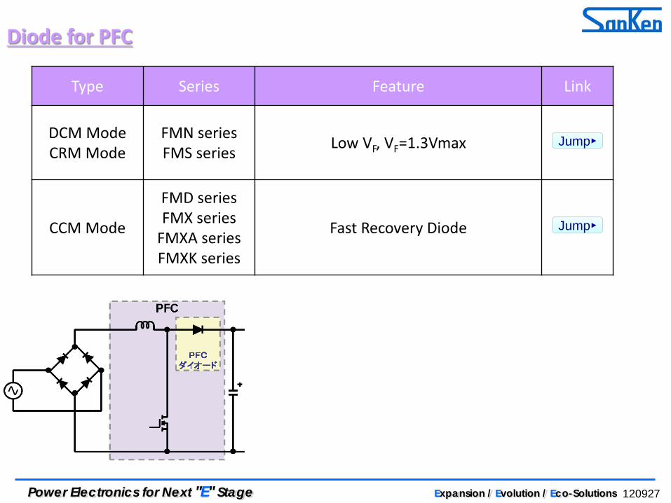
Diode for PFC
Type Series Feature Link
DCM Mode CRM Mode
FMN series FMS series Low VF, VF=1.3Vmax
CCM Mode
FMD series FMX series
FMXA series FMXK series
Fast Recovery Diode
Jump▸
Jump▸
120927 Power Electronics for Next "E" Stage Expansion / Evolution / Eco-Solutions
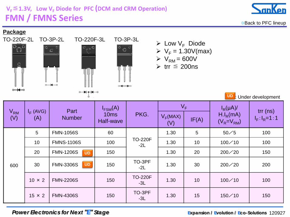
Back to PFC lineup FMN / FMNS Series
Package TO-220F-2L TO-3P-2L TO-220F-3L TO-3P-3L
VRM (V)
IF (AVG) (A)
Part Number
IFSM(A) 10ms
Half-wave PKG.
VF IR(μA)/ H.IR(mA) (VR=VRM)
trr (ns) IF:IR=1:1 VF(MAX)
(V) IF(A)
600
5 FMN-1056S 60 TO-220F
-2L
1.30 5 50/5 100
10 FMNS-1106S 100 1.30 10 100/10 100
20 FMN-1206S 150 1.30 20 200/20 150
30 FMN-3306S 150 TO-3PF -2L 1.30 30 200/20 200
10 × 2 FMN-2206S 150 TO-220F -3L 1.30 10 100/10 100
15 × 2 FMN-4306S 150 TO-3PF -3L 1.30 15 150/10 150
Low VF Diode VF = 1.30V(max) VRM = 600V trr ≦ 200ns
VF≦1.3V, Low VF Diode for PFC (DCM and CRM Operation)
UD : Under development
UD
UD
UD
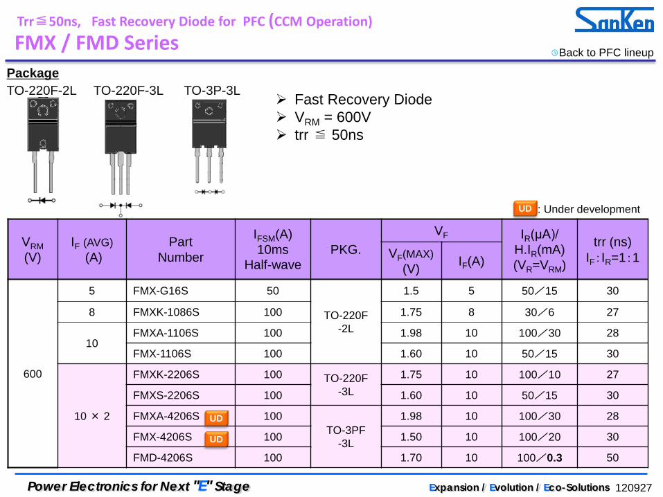
120927 Power Electronics for Next "E" Stage Expansion / Evolution / Eco-Solutions
Back to PFC lineup
VRM (V)
IF (AVG) (A)
Part Number
IFSM(A) 10ms
Half-wave PKG.
VF IR(μA)/ H.IR(mA) (VR=VRM)
trr (ns) IF:IR=1:1 VF(MAX)
(V) IF(A)
600
5 FMX-G16S 50
TO-220F -2L
1.5 5 50/15 30
8 FMXK-1086S 100 1.75 8 30/6 27
10 FMXA-1106S 100 1.98 10 100/30 28
FMX-1106S 100 1.60 10 50/15 30
10 × 2
FMXK-2206S 100 TO-220F -3L
1.75 10 100/10 27
FMXS-2206S 100 1.60 10 50/15 30
FMXA-4206S 100 TO-3PF
-3L
1.98 10 100/30 28
FMX-4206S 100 1.50 10 100/20 30
FMD-4206S 100 1.70 10 100/0.3 50
Fast Recovery Diode VRM = 600V trr ≦ 50ns
Package TO-220F-2L TO-220F-3L TO-3P-3L
FMX / FMD Series Trr≦50ns, Fast Recovery Diode for PFC (CCM Operation)
UD
UD
UD : Under development UD
120927 Power Electronics for Next "E" Stage Expansion / Evolution / Eco-Solutions
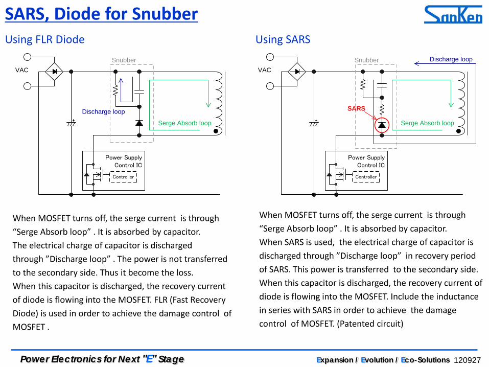
SARS, Diode for Snubber
Power SupplyControl IC
VACSnubber
Controller
SARS
Discharge loop
Serge Absorb loop
Power SupplyControl IC
VACSnubber
Controller
Discharge loop
Serge Absorb loop
Using SARS Using FLR Diode
When MOSFET turns off, the serge current is through “Serge Absorb loop” . It is absorbed by capacitor. The electrical charge of capacitor is discharged through ”Discharge loop” . The power is not transferred to the secondary side. Thus it become the loss. When this capacitor is discharged, the recovery current of diode is flowing into the MOSFET. FLR (Fast Recovery Diode) is used in order to achieve the damage control of MOSFET .
When MOSFET turns off, the serge current is through “Serge Absorb loop” . It is absorbed by capacitor. When SARS is used, the electrical charge of capacitor is discharged through ”Discharge loop” in recovery period of SARS. This power is transferred to the secondary side. When this capacitor is discharged, the recovery current of diode is flowing into the MOSFET. Include the inductance in series with SARS in order to achieve the damage control of MOSFET. (Patented circuit)

120927 Power Electronics for Next "E" Stage Expansion / Evolution / Eco-Solutions
SARS, Diode for Adjunct Switch Package SJP TO-220F-2L Axial-φ2.7mm/φ0.60mm
Buck to PFC lineup
Improve Circuit Efficiency Snubber System
Improve Circuit Efficiency Snubber System
VRM=800V
X / Y / Z = 4.5 : 2.6 : 2.15 Unit : mm
Axial-φ4.0mm/φ0.78mm
Type Part
Number VRM IF (AVG)
IFSM 50Hz
Half-wave
VF trr
IF:IR=1:1 Package VF
(max) IF
External resistance
SARS01 800V 1.2A 110A 0.92V 1.2A 2 to18 Axial-φ2.7/φ0.60
SARS02 800V 1.5A 100A 0.92V 1.5A 2 to18 Axial-φ4.0/φ0.78
SARS05 800V 1A 30A 1.05V 1A 2 to 18 SJP(SMA:4.5×2.6)
Built-in resistance(22Ω) SARS10 800 0.3A 1.5A 13V 0.5A 1 to 9 TO220F-2L
Related Documents