C in T 1 D R e s e t N s N p N r Q1 PWM Controller VDC D S/H C S/ H V S/H S/ H Control C in T 1 D R e s e t N s N p N r Q1 PWM Controller VDC D S/H C S/ H V S/H S/ H Control AC/DC BOOK OF KNOWLEDGE Practical tips for the User By Steve Roberts M.Sc. B.Sc. Technical Director, RECOM

Welcome message from author
This document is posted to help you gain knowledge. Please leave a comment to let me know what you think about it! Share it to your friends and learn new things together.
Transcript

D 1
Cout RLoad
Cin
T1
DReset
D2
Lout
N sN p N r
Q1PWMController
VDC
Lfb
DS/H
CS/ H
V S/ H
S/HControl
D 1
Cout RLoad
Cin
T1
DReset
D2
Lout
N sN p N r
Q1PWMController
VDC
Lfb
DS/H
CS/ H
V S/ H
S/HControl
AC/DC BOOK OF KNOWLEDGE
Practical tips for the User
By Steve Roberts M.Sc. B.Sc.Technical Director, RECOM

1
AC/DC Book of Knowledge
Practical Tips for the User
By Steve Roberts, M.Sc. B.Sc.
Technical Director, RECOM
Second Edition
©2019 All rights RECOM Engineering GmbH & Co.KG, Austria (hereafter RECOM)
The contents of this book or excerpts thereof may not be reproduced, duplicated or distributed in any form without the written permission of RECOM.
The disclosure of the information contained in this book is correct to the best of the knowledge of the author, but no responsibility can be accepted for any mistakes, omissions or typograph-ical errors. The diagrams indicate typical applications and are not necessarily complete.

2 3
With thanks to my colleagues at RECOM for their advice and help with proof reading:
Konrad Berger, Matthew Dauterive, Stanislav Suchovsky, Markus Stöger, Alois Taranetz and Wolfgang Wolfsgruber.
With special thanks to Simone Starlinger from Marktkraft for typesetting, getting the graphics into shape and generally for her ability to work to impossible deadlines. This book is a work in progress, so I welcome suggestions for improvements or corrections.Please send your recommendations to [email protected].
With thanks to the following who have already sent in their comments:Dietmar Kiefer, Werner Froehling

4 5
Preface from RECOM Management
When we introduced our first DC/DC converter nearly 30 years ago, there was little pub-lished technical material available and hardly any international standards to follow. There was a pressing need to communicate practical application information to our customers, which prompted us to add some simple application notes as an appendix to our first published prod-uct catalogue. The content of these guidelines grew over the years as we gained more and more expertise. Although they are still of a rudimentary nature, they are well received by our customer base and today they have become a 70-page application note package available on our Website for download.
The advance of semiconductor technology and the shift towards highly integrated digital elec-tronics has diminished the knowledge base of analogue techniques in many design labs, uni-versities and technical colleges over the years. We often see a lack of practical know-how in analogue circuit design, particularly with regard to applied techniques, test and measurementand the understanding of filtering and noise suppression. Therefore, as experts in this arena, we saw the need for a much more comprehensive technical handbook that could be used as a reference by hardware designers and students alike.
Eventually, at the start of 2014, Steve Roberts, our Technical Director, started to invest his free time to start documenting the extensive application knowledge on the design, test and ap-plication of DC/DC converters available within the RECOM group. Despite all of the pressures of his demanding job, he managed to complete this onerous task in time for Electronica 2014. Two years later, in time for Electronica 2016, the third edition of the RECOM DC/DC Bookof Knowledge was enlarged to include an additional chapter on magnetics.
In keeping with this biennial tradition, Electronica 2018 sees the release of the RECOM AC/DC Book of Knowledge. We released our first AC/DC converter back in 2006, so we have also accumulated a considerable body of knowledge on AC/DC power conversion that has allowed us to offer products from 1W up to 1kW and beyond with industrial, medical and household certifications.
Steve has presented us with a new handbook that we are sure will greatly benefit the engi-neering community and all those who are interested in AC/DC power conversion and its ap-plications. The handbook will initially be available as a printed hard-copy version and as PDF soft-copy available for free download from the RECOM website.
Board of Directors, Gmunden, 2018
RECOM Group

6 7
Preface from the Author
This AC/DC Book of Knowledge is a companion book to the DC/DC Book of Knowledge. They are designed to be read to-gether, so I have deliberately avoided repeating information except where it is necessary for clarity. Some chapters are equally applicable to DC/DC as to AC/DC applications, so I have taken the opportunity to cover topics that were not in the DC/DC book, but perhaps should have been.
The success of the DC/DC Book of Knowledge has been part-ly due to the lack of other text books or sources of information specifically for DC/DC applications. This is not the case for AC/DC applications, where there is a multitude of books, application notes and technical papers that are available. Therefore, I have decided to just cover the aspects that interest me in particular (it is my book, after all). Some AC/DC topics have had whole text books written about them which I dismiss in just a few sentences, other topics are less well covered and deserving of far more detail than I have space for in this book. I have had to tread a fine line between giving useful information for the majority of readers and being overly wordy about topics that I find fascinating, but might not interest everyone.
This book is all my own work but I am acutely conscious that the breadth of knowledge re-quired to do proper justice to this topic is wider than a single person can ever hope to achieve. Therefore, I have relied heavily on my colleagues and the published knowledge of many others as well as my own experience. My thanks go to everyone who has had the courage to poke their head above the parapet and publish their ideas, concepts, designs or experimental results and risk the barrage of critisism from the mass of other experts in this field. Bearing this in mind, feel free to contact me if you find any errors, omissions or inaccuracies in this book and I will get them corrected.
Steve Roberts Gmunden, 2018
Technical Director
RECOM
8 9
Table of Contents
CHAPTER 1 ......................................................................................... 13
A Historical Introduction ........................................................... 13
CHAPTER 2 .......................................................................................... 22
Linear AC/DC Power Supplies .................................................. 22
CHAPTER 3 ......................................................................................... 27
Apparent, Reactive and Active Power ..................................... 27
CHAPTER 4 .......................................................................................... 31
AC Theory ................................................................................... 314.1 AC Theory - basics ............................................................................31
CHAPTER 5 .......................................................................................... 37
Passive Components ................................................................. 37
5.1 Capacitors ............................................................................. 375.1.1 Class X and Y capacitors ..........................................................375.1.2 Electrolytic capacitors ...............................................................395.1.2.1 Design considerations of electrolytic capacitors. ...................405.1.2.2 Electrolytic capacitor lifetime calculation ................................425.1.2.3 Deriving ripple current from electrolytic capacitor temperature rise .....................................................43
5.2 Common mode chokes .....................................................................455.2.1 EMC common mode filter worked example ..............................46
CHAPTER 6 .......................................................................................... 49
Active Components ................................................................... 496.1 Silicon MOSFET ................................................................................496.2 SiC MOSFET.....................................................................................526.3 IGBT ..................................................................................................536.4 GaN HEMT ........................................................................................54
6.4.1 GAN Transistor gate driver considerations ...............................566.4.2 Power transistor layout considerations .....................................59
6.5 Unplanned turn-on due to the effect of the Miller capacitance ..........606.6 Unplanned turn-on due to the effect of the parasitic inductances (Lgate and Lemitter) ...............................................61
CHAPTER 7 .......................................................................................... 66
Power Factor Correction ........................................................... 66

10 11
7.1 Passive PFC......................................................................................667.1.1 Valley Fill PFC ...........................................................................68
7.2 Active PFC ........................................................................................697.2.1 DCM power factor correction ....................................................697.2.2 CCM power factor correction. ...................................................707.2.3 CrCM power factor correction. ..................................................717.2.4 Mixed-Mode PFC ......................................................................727.2.5 Interleaved PFC ........................................................................737.2.6 Bridgeless (totem pole) PFC .....................................................74
CHAPTER 8 .......................................................................................... 78
AC/DC Converter Topologies .................................................... 788.1 Single-Ended Flyback .......................................................................78
8.1.1 Single-ended flyback snubber networks ...................................828.1.3 Ringing snubbers ......................................................................848.1.2 Active clamp and regenerative snubbers ..................................878.1.2.1 High-side active clamp ...........................................................878.2.1.2 Low-side active clamp ............................................................888.2.1.3 Regenerative clamp ...............................................................90
8.3 Quasi-resonant flyback converter......................................................908.3.1 Resonant frequency of a transformer in QR mode ...................91
8.4 Half-Bridge Resonant Mode converter ..............................................918.5 Full-bridge resonant mode converters...............................................93
8.5.1 Phase-shifted resonant full bridge .............................................938.5.2 Resonant full bridge ..................................................................94
8.6 Single-Ended Forward converter.......................................................978.6.1 Interleaved Single-Ended Forward ..........................................1018.6.2 Current-Fed Single-Ended Forward converter ........................105
8.7 Two-Transistor topologies ...............................................................1078.7.1 Two-Transistor Forward converter ..........................................1078.7.2 Push-Pull Forward converter ...................................................1098.7.3 Current-Fed Push-Pull Forward converter ..............................110
8.8 Using paralleled transformers to increase the power ......................1138.9 Poly-phase supplies ........................................................................116
8.9.1 Three-phase PFC ....................................................................117
CHAPTER 9 ........................................................................................ 120
Transformerless AC power supplies ...................................... 1209.1 Capacitively-coupled AC/DC ...........................................................1209.2 Non-Isolated Buck regulator ............................................................1229.3 High voltage linear regulators..........................................................1239.4 Off-line regulator IC .........................................................................124
CHAPTER 10 ...................................................................................... 127
Wireless power ......................................................................... 12710.1. Resonant wireless power transfer ................................................12910.2. Inductive wireless power transfer .................................................12910.3 PCB inductive power transfer ........................................................131
CHAPTER 11 ...................................................................................... 136
Feedback ................................................................................... 13611.1 Measuring loop stability ................................................................13711.2 Type 1 feedback loop compensation calculation ..........................14111.3 Type 2 feedback loop compensation.............................................14211.5 Optocoupler feedback loop compensation ....................................14511.6 Secondary-side feedback compensation ......................................14811.7 Magnetic feedback .......................................................................149
11.7.1 Secondary-side powered PWM feedback transformer ..........14911.7.2 Direct magnetic feedback ......................................................15011.7.3 Primary-side driven magnetic feedback ................................151
11.8 Capacitively coupled feedback ......................................................15311.9 Primary-side regulation .................................................................155
CHAPTER 12 ...................................................................................... 158
Low Standby Power Consumption Techniques .................... 15812.1 Passive losses...............................................................................159
12.1.1 HV start up disconnect ..........................................................15912.1.2 Half-wave HV start up ...........................................................16112.1.3 Bleeder resistor losses .........................................................161
12.2 Feedback losses ...........................................................................16212.2 Active losses .................................................................................164
12.2.1 Clamp losses .........................................................................16412.2.2 Variable switching frequency ................................................16512.2.3 Variable valley switching .......................................................16612.2.4 Pulse skipping .......................................................................16612.2.5 Synchronous rectification ......................................................16712.2.6 Output load detection (zero-power) .......................................169
12.3 Measuring standby power consumption ........................................171
CHAPTER 13: ................................................................................... 172
Measuring AC .......................................................................... 17213.1 AC voltage measurements ............................................................172
13.1.1 High frequency AC voltage measurements ...........................17613.2 AC current measurement techniques ............................................177
13.2.1 Precision shunt resistor .........................................................17713.2.2 Shunt + current mirror ...........................................................179

12
13.2.3 Shunt + isolation amplifier .....................................................18013.3 Current transformer .......................................................................181
13.3.1 Compensated CT (AC zero-flux) ...........................................18313.4 Rogowski Coil................................................................................18313.5 Hall-effect current sensor ..............................................................18413.6 Flux-gate current sensor ...............................................................18613.7 GMR current sensor ......................................................................187
REFERENCES AND FURTHER READING ....................................... 189
SOME RECOMMENDED APPLICATION NOTES ............................. 189
ABOUT THE AUTHOR ....................................................................... 190
ABOUT RECOM ................................................................................. 190

13
Chapter 1
A Historical Introduction
Depending where you are travelling in the world, the mains voltage available from the wall plate will be 50Hz or 60Hz AC (Alternating Current) with a nominal voltage of around 120VAC or 230VAC. Unless you are plugging in a hair dryer, kettle or a lamp, you will probably need an adaptor to con-vert the high voltage AC supply down to a low voltage DC (Direct Current) to be useful, for example to charge your phone or power your laptop. Considering that all electronic equipment runs natively on DC power, you might think why is the mains power always AC? And while we are on the sub-ject, who chose 50/60Hz or 120V/230VAC as the “correct” numbers for the mains supply anyway?
Back in the nineteenth century, when public power distribution networks were first being de-veloped, the choice was much wider. Both AC and DC mains supplies were offered, with the standard AC frequency ranging from as low as 16⅔Hz up to as high as 133Hz. Electronic appliances had not yet been invented, so the most common use of electricity was for lighting or heating, both of which worked equally well with either AC or DC supplies, so the AC fre-quency was not so important. The most common value was 42Hz and in America, Edison patented DC power distribution and heavily promoted it as being as safe as and more reliable than AC1. To a certain extent, this was true, as early electrical generators were less than reli-able and the banks of batteries both stabilized the output voltage and bridged any short dura-tion generator faults with the DC supply. This was not the case with AC generators which needed very good speed regulators to maintain the correct output voltage with changes in demand and had no back-up supply possibility in the event of a generator fault.
AC eventually won over DC distributed networks for three main reasons: the simplicity of the first AC generators which led to a rapid improvement in reliability, the ease in which the voltage could be changed up or down using transform-ers and the advantages of multiple-pole alternators to re-duce the rotation speed of more powerful generators.
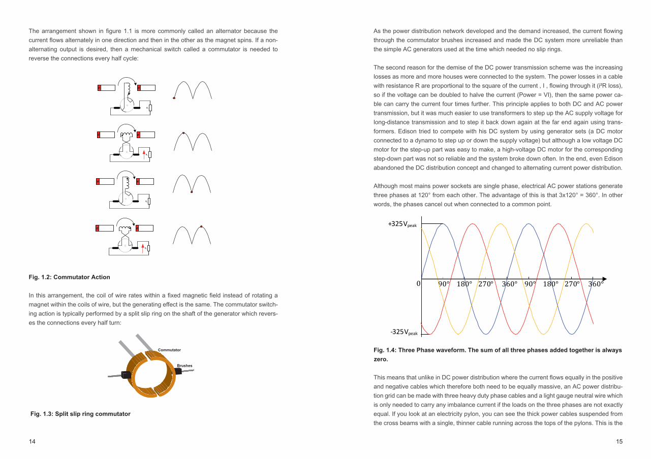
The simple electrical generators used at the time convert-ed mechanical energy into electrical energy by rotating a magnet within coils of wire (figure 1.1).
Note that there are no moving electrical contacts.
Fig. 1.1: Principle of operation of an alternator
N
RL
N
RL
N
RL
N
RL
N
RL
1 Edison famously ran newspaper adverts explaining that the newly invented electric chair used AC to kill condemned men, callously implying that his DC system was safer.
14 15
As the power distribution network developed and the demand increased, the current flowing through the commutator brushes increased and made the DC system more unreliable than the simple AC generators used at the time which needed no slip rings.
The second reason for the demise of the DC power transmission scheme was the increasing losses as more and more houses were connected to the system. The power losses in a cable with resistance R are proportional to the square of the current , I , flowing through it (i²R loss), so if the voltage can be doubled to halve the current (Power = VI), then the same power ca-ble can carry the current four times further. This principle applies to both DC and AC power transmission, but it was much easier to use transformers to step up the AC supply voltage for long-distance transmission and to step it back down again at the far end again using trans-formers. Edison tried to compete with his DC system by using generator sets (a DC motor connected to a dynamo to step up or down the supply voltage) but although a low voltage DC motor for the step-up part was easy to make, a high-voltage DC motor for the corresponding step-down part was not so reliable and the system broke down often. In the end, even Edison abandoned the DC distribution concept and changed to alternating current power distribution.
Although most mains power sockets are single phase, electrical AC power stations generate three phases at 120° from each other. The advantage of this is that 3x120° = 360°. In other words, the phases cancel out when connected to a common point.
Fig. 1.4: Three Phase waveform. The sum of all three phases added together is always
zero.
This means that unlike in DC power distribution where the current flows equally in the positive and negative cables which therefore both need to be equally massive, an AC power distribu-tion grid can be made with three heavy duty phase cables and a light gauge neutral wire which is only needed to carry any imbalance current if the loads on the three phases are not exactly equal. If you look at an electricity pylon, you can see the thick power cables suspended from the cross beams with a single, thinner cable running across the tops of the pylons. This is the
90° 180° 270° 360°
-325Vpeak
+325Vpeak
0 90° 180° 270° 360°
The arrangement shown in figure 1.1 is more commonly called an alternator because the current flows alternately in one direction and then in the other as the magnet spins. If a non- alternating output is desired, then a mechanical switch called a commutator is needed to reverse the connections every half cycle:
Fig. 1.2: Commutator Action
In this arrangement, the coil of wire rates within a fixed magnetic field instead of rotating a magnet within the coils of wire, but the generating effect is the same. The commutator switch-ing action is typically performed by a split slip ring on the shaft of the generator which revers-es the connections every half turn:
Fig. 1.3: Split slip ring commutator
RL
N N
RL
N N
RL
N N
RL
N N
Commutator
Brushes

16 17
But the fi nal nail in the coffi n for DC distribution was the popularity of electrical lighting. As more and more houses, public buildings and streets switched from gas lighting to electric lamps, the demand for electrical power increased rapidly. The lower cabling cost of three-phase transmission compared to DC became the deciding factor when raising the investment needed to electrify whole towns (a 3-phase system uses 50% more copper than a 2-phase system, but delivers three times the power).
More powerful and larger generators were manufactured to meet this demand. These genera-tors were very heavy and the slower a very massive generator rotor can rotate, the less stress on the bearings and framework. This is why there were originally so many diff erent AC frequen-cies used: a smaller generator spinning at 2500 RPM created a 42Hz output, while a larger one spinning at 1000 RPM created a 16⅔Hz output (note that “a nice whole number” of revolutions per minute (RPM) was more often used, an indication that mechanical engineers built the al-ternators, not electrical engineers. 16⅔Hz is still used by the railways because if a commutator is fi tted to both the stator and rotor windings, an electric motor will run with either DC or AC at this low frequency). However, while an incandescent fi lament may not fl icker much at 42Hz, at 16⅔Hz it was disturbingly visible. The AC fl icker was even more pronounced with arc lighting which became increasingly used in theatres, open spaces and for street lighting.
The solution for high frequency AC output with slower rotation speeds was to use multiple pole alternators: instead of two windings, four windings could be used wired alternately in series. Then instead of one AC cycle per rotation, two cycles would be generated. For the same output AC frequency, the rotor speed could be halved, signifi cantly reducing the stress on the generator.
In the meantime, the mechanical problems with slip rings had been solved and multiple wind-ings could be wound on the rotor with multiple magnetic poles built into the stator. This meant that the optimum rotation speed could be chosen for the physical size of the generator and almost any output frequency could be generated by selecting the appropriate number of rotor windings and stator poles. The original Niagara Falls power station in the USA used 12 pole, low speed (250 RPM) generators to output 25Hz AC, but this was later doubled up to 50Hz by simply rearranging the windings while keeping the original low RPM which was optimally matched to the water turbines.
Fig. 1.7: Example of a Multiple Pole Alternator.
N
N
S S
neutral return wire. The earth (or ground) connection is for safety only. It carries no current in normal conditions. If a current fl ows from any phase to earth then it is due to a fault and a protective device (fuse or residual current trip) should cut off the power.
The following simplifi ed diagram illustrates this arrangement when applied to whole streets in a town.
Fig. 1.5: Diagrammatic representation of a three-phase power distribution system. The
neutral wire will carry no current if the load on each phase is balanced.
Why three phases and not two? Well, two-phase power distribution is still used in some parts of the USA (2x120VAC at 180° so that 240VAC equipment for heavier loads such as ovens and washing machines could be used on a 120V system), but the big advantage of an odd number of phases is for use with AC motors. It does not matter where the rotor sits, a three-phase motor will always start up in the same direction and as the load is equally balanced on all three phases, a neutral wire is not required (L1, L2, L3 and Earth). An AC motor with an even number of phas-es could either not start if the rotor was exactly in line with the poles, or worse, start up in the wrong direction. Additionally, a two phase system delivers power at twice the fundamental fre-quency and this pulsating supply must be smoothed out by the inertia of the motor, making a two phase motor larger and heavier than a 3-phase motor of the same power.
Fig. 1.6: Principle of operation of a three-phase motor. As each phase peaks, the rotor is
pulled around to line up with that set of windings. The rotor then follows the rotating mag-
netic fi eld.
3 Phases
P1
P2
N
P3
Common
O
1
-1

18 19
limits were wide enough so that UK could stay at 240V and the rest of Europe remain at 220V and both say that they delivered a nominally 230VAC supply. A typical European solution to the problem! In the meantime, the power stations have all been adjusted to deliver 230VAC on average, although my colleague in the UK still measures 240V on his supply as he is very close to a substation.
There are still several countries that for various reasons have “non-standard” mains voltages. Many ex-Commonwealth countries still use the original British 240VAC supply voltage. Japan has opted for 100VAC supplies for safety reasons, but because the South Island was supplied with generators from Westinghouse and the north island from AEG, they have either 60Hz or 50Hz supply frequencies depending where you are in Japan. Four frequency converter sub-stations have now been built to balance out the load between the islands by transferring 50Hz and 60Hz power back-and-forth. In the USA, many large buildings use 115/277VAC split supplies. The higher voltage is primarily used for lighting to increase the overall building effi-ciency, as lighting can account for 40% of the total power consumption of a large office block. Aircraft quickly settled on a 400Hz AC standard to reduce the weight and size of the motors and transformers used in aeroplanes.
Fig. 1.9: Map of world mains voltages and frequencies
As mentioned previously, the advantage of three phases over a single phase or two phases at 180° is that a motor wound with three windings will automatically start to rotate following each phase peak in turn and always in the same direction. This makes three-phase motors very simple, robust and reliable and therefore popular in industrial automation applications.Three-phase motors do not use the neutral connection and very often have a four-wire cable of just the three phases and earth. As there is no neutral wire, any auxiliary power supply must
200 - 240V/50Hz
100-127V/60Hz
220-240V/60Hz
100-127V/50Hz
By this time (mid 1850’s), AEG was the leading electrical equipment manufacturer in Europe. 50Hz was supposedly chosen as the standard AC frequency in Europe because it was an even number of 100 peaks per second, which appealed to the Teutonic mind. In America, Westinghouse chose 60Hz, supposedly because 50Hz flicker was still just about visible with arc lighting and therefore Nicola Tesla (who licenced his AC generation patents to Westing-house) had recommended a higher mains frequency, but equally probably to protect their home market from foreign competition. Either way, commercial interests decided that 50Hz in some regions and 60Hz in other regions should eventually become standard.
Fig. 1.8: Waveforms of 230VAC/50Hz and 120VAC/60Hz single-phase supplies.
The effective voltage (dotted line) is the square root of the mean of the squares of the AC voltage (RMS), in other words, the DC voltage that would have the same heating effect as the AC voltage.
So, protectionism could explain why the AC mains is 50Hz in some countries and 60Hz in others, but why the different supply voltages of 120VAC or 230VAC? Originally, 110-120VAC was a pretty-much universal standard (also in pre-war Europe) because the influential Edi-son used 110V for his DC distribution system. The competition therefore also chose similar voltages so that any heating or lighting equipment designed to run on Edison’s system could also be used with their own power supply network. As the number of domestic appliances per household increased, the I²R losses of the 120VAC supply became more and more signifi-cant, but the wealth of post-war US citizens meant that so many refrigerators, air conditioners and televisions with 120VAC input were already in use that an increase in mains supply voltage in the USA was impractical. Europe, on the other hand, was recovering from the war with no such legacy problems and realizing that the demand for electrical power would only in-crease in the future chose to double the 110/120VAC voltage (220VAC in continental Europe, 240VAC in the UK) to halve the current and quarter the losses. Eventually, in 1994, the EU decided to harmonize throughout Europe on 230VAC which was within the operating range of both 220VAC and 240VAC equipment. In practice, however, the allowable voltage tolerance
5 10 15 20 25 30 4035
+325Vpeak
230Vrms
+172Vpeak
120Vrms
-172Vpeak
-325Vpeak
50Hz
60Hz
ms0
20 21
Footnote: Modern Power Distribution
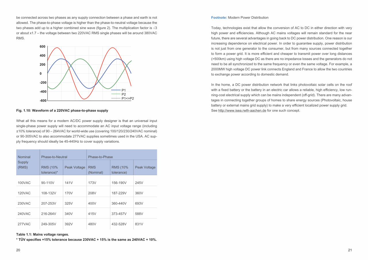
Today, technologies exist that allow the conversion of AC to DC in either direction with very high power and efficiencies. Although AC mains voltages will remain standard for the near future, there are several advantages in going back to DC power distribution. One reason is our increasing dependence on electrical power. In order to guarantee supply, power distribution is not just from one generator to the consumer, but from many sources connected together to form a power grid. It is more efficient and cheaper to transmit power over long distances (>500km) using high voltage DC as there are no impedance losses and the generators do not need to be all synchronized to the same frequency or even the same voltage. For example, a 2000MW high voltage DC power link connects England and France to allow the two countries to exchange power according to domestic demand.
In the home, a DC power distribution network that links photovoltaic solar cells on the roof with a fixed battery or the battery in an electric car allows a reliable, high efficiency, low run-ning-cost electrical supply which can be mains independent (off-grid). There are many advan-tages in connecting together groups of homes to share energy sources (Photovoltaic, house battery or external mains grid supply) to make a very efficient localized power supply grid. See http://www.isea.rwth-aachen.de for one such concept.
be connected across two phases as any supply connection between a phase and earth is not allowed. The phase-to-phase voltage is higher than the phase-to-neutral voltage because the two phases add up to a higher combined sine wave (figure 2). The multiplication factor is √3 or about x1.7 – the voltage between two 220VAC RMS single phases will be around 380VAC RMS.
Fig. 1.10: Waveform of a 220VAC phase-to-phase supply
What all this means for a modern AC/DC power supply designer is that an universal input single-phase power supply will need to accommodate an AC input voltage range (including ±10% tolerance) of 90 – 264VAC for world-wide use (covering 100/120/230/240VAC nominal) or 90-305VAC to also accommodate 277VAC supplies sometimes used in the USA. AC sup-ply frequency should ideally be 45-440Hz to cover supply variations.
NominalSupply(RMS)
Phase-to-Neutral Phase-to-Phase
RMS (10% tolerance)*
Peak Voltage RMS (Nominal)
RMS (10% tolerance)
Peak Voltage
100VAC 90-110V 141V 173V 156-190V 245V
120VAC 108-132V 170V 208V 187-229V 360V
230VAC 207-253V 325V 400V 360-440V 693V
240VAC 216-264V 340V 415V 373-457V 588V
277VAC 249-305V 392V 480V 432-528V 831V
Table 1.1: Mains voltage ranges.
* TÜV specifies +15% tolerance because 230VAC + 15% is the same as 240VAC + 10%.
P1P2P1<>P2
600
400
200
0
-200
-400
-600
22 23
Chapter 2
Linear AC/DC Power Supplies
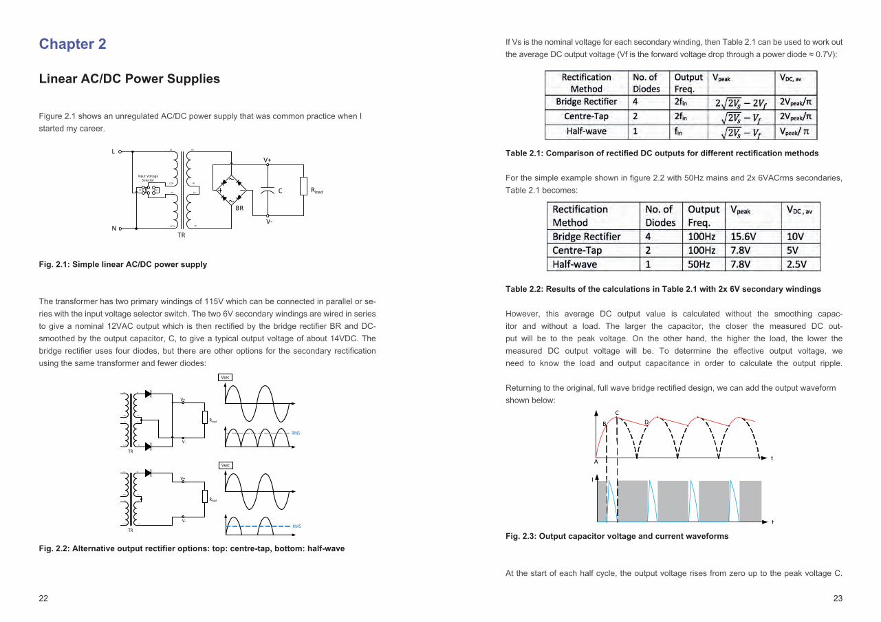
Figure 2.1 shows an unregulated AC/DC power supply that was common practice when I started my career.
Fig. 2.1: Simple linear AC/DC power supply
The transformer has two primary windings of 115V which can be connected in parallel or se-ries with the input voltage selector switch. The two 6V secondary windings are wired in series to give a nominal 12VAC output which is then rectified by the bridge rectifier BR and DC-smoothed by the output capacitor, C, to give a typical output voltage of about 14VDC. The bridge rectifier uses four diodes, but there are other options for the secondary rectification using the same transformer and fewer diodes:
Fig. 2.2: Alternative output rectifier options: top: centre-tap, bottom: half-wave
115V 230V
Input Voltage Selector
C
L
N
V+
V-
115V
115V
0V
0V 0V
6V
0V
6V
TR
BR
Rload
V+
V-
115V
115V
0V
0V 0V
6V
0V
6V
TR
Rload
V+
V-
115V
115V
0V
0V 0V
6V
0V
6V
TR
Rload
Vsec
Vsec
RMS
RMS
If Vs is the nominal voltage for each secondary winding, then Table 2.1 can be used to work out the average DC output voltage (Vf is the forward voltage drop through a power diode ≈ 0.7V):
Table 2.1: Comparison of rectified DC outputs for different rectification methods
For the simple example shown in figure 2.2 with 50Hz mains and 2x 6VACrms secondaries, Table 2.1 becomes:
Table 2.2: Results of the calculations in Table 2.1 with 2x 6V secondary windings
However, this average DC output value is calculated without the smoothing capac-itor and without a load. The larger the capacitor, the closer the measured DC out-put will be to the peak voltage. On the other hand, the higher the load, the lower the measured DC output voltage will be. To determine the effective output voltage, we need to know the load and output capacitance in order to calculate the output ripple.
Returning to the original, full wave bridge rectified design, we can add the output waveform shown below:
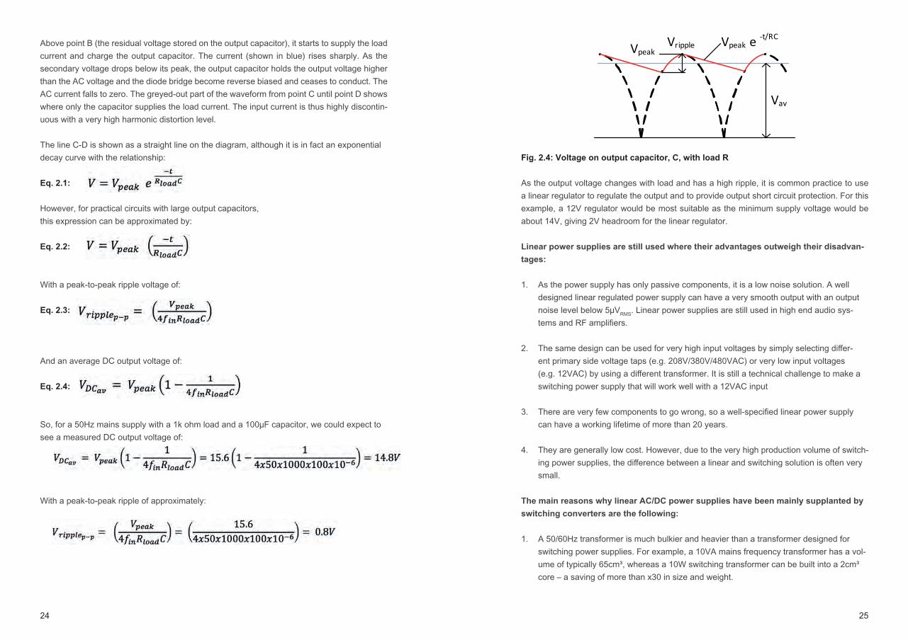
Fig. 2.3: Output capacitor voltage and current waveforms
At the start of each half cycle, the output voltage rises from zero up to the peak voltage C.
t
I
t
A
B
CD
24 25
Above point B (the residual voltage stored on the output capacitor), it starts to supply the load current and charge the output capacitor. The current (shown in blue) rises sharply. As the secondary voltage drops below its peak, the output capacitor holds the output voltage higher than the AC voltage and the diode bridge become reverse biased and ceases to conduct. The AC current falls to zero. The greyed-out part of the waveform from point C until point D shows where only the capacitor supplies the load current. The input current is thus highly discontin-uous with a very high harmonic distortion level.
The line C-D is shown as a straight line on the diagram, although it is in fact an exponential decay curve with the relationship:
Eq. 2.1:
However, for practical circuits with large output capacitors, this expression can be approximated by:
Eq. 2.2:
With a peak-to-peak ripple voltage of:
Eq. 2.3:
And an average DC output voltage of:
Eq. 2.4:
So, for a 50Hz mains supply with a 1k ohm load and a 100µF capacitor, we could expect to see a measured DC output voltage of:
With a peak-to-peak ripple of approximately:
VrippleVpeakVpeak e -t/RC
Vav
Fig. 2.4: Voltage on output capacitor, C, with load R
As the output voltage changes with load and has a high ripple, it is common practice to use a linear regulator to regulate the output and to provide output short circuit protection. For this example, a 12V regulator would be most suitable as the minimum supply voltage would be about 14V, giving 2V headroom for the linear regulator.
Linear power supplies are still used where their advantages outweigh their disadvan-
tages:
1. As the power supply has only passive components, it is a low noise solution. A well designed linear regulated power supply can have a very smooth output with an output noise level below 5µVRMS. Linear power supplies are still used in high end audio sys-tems and RF amplifiers.
2. The same design can be used for very high input voltages by simply selecting differ-ent primary side voltage taps (e.g. 208V/380V/480VAC) or very low input voltages (e.g. 12VAC) by using a different transformer. It is still a technical challenge to make a switching power supply that will work well with a 12VAC input
3. There are very few components to go wrong, so a well-specified linear power supply can have a working lifetime of more than 20 years.
4. They are generally low cost. However, due to the very high production volume of switch-ing power supplies, the difference between a linear and switching solution is often very small.
The main reasons why linear AC/DC power supplies have been mainly supplanted by
switching converters are the following:
1. A 50/60Hz transformer is much bulkier and heavier than a transformer designed for switching power supplies. For example, a 10VA mains frequency transformer has a vol-ume of typically 65cm³, whereas a 10W switching transformer can be built into a 2cm³ core – a saving of more than x30 in size and weight.

26
2. 50/60Hz power supplies are inefficient. Power is transferred only at the peaks of the mains cycle – the remaining part of the cycle is not used. On the secondary side, the rectification diodes dissipate a significant amount of power due to the high capacitor charging peak currents. If linear regulators are used to stabilize the output, then the effi-ciency drops even lower. Overall efficiencies of below 50% are not unusual. In compari-son, switching power supplies with efficiencies exceeding 90% are common.
3. 50/60Hz power supplies have poor regulation. The output voltage is load dependent and also directly proportional to the input voltage. The hold-up time is short, so the out-put voltage will be adversely affected by mains brown-outs and any dropped cycles. The transient load response time is also very poor as the power supply must wait until the next AC peak to transfer any extra energy required to cope with a sudden load increase.
4. The no load power consumption is too high to meet modern energy efficiency regula-tions. In addition, the fact that power is transferred only at the cycle peaks means that the power factor is also too low for many applications (a linear power supply has a power factor of typically 0.5 – 0.7)
5. The cost of switching power supplies is now so low that a low power linear power supply may actually be more expensive that the more complex switching converter alternative.
27
Chapter 3
Apparent, Reactive and Active Power
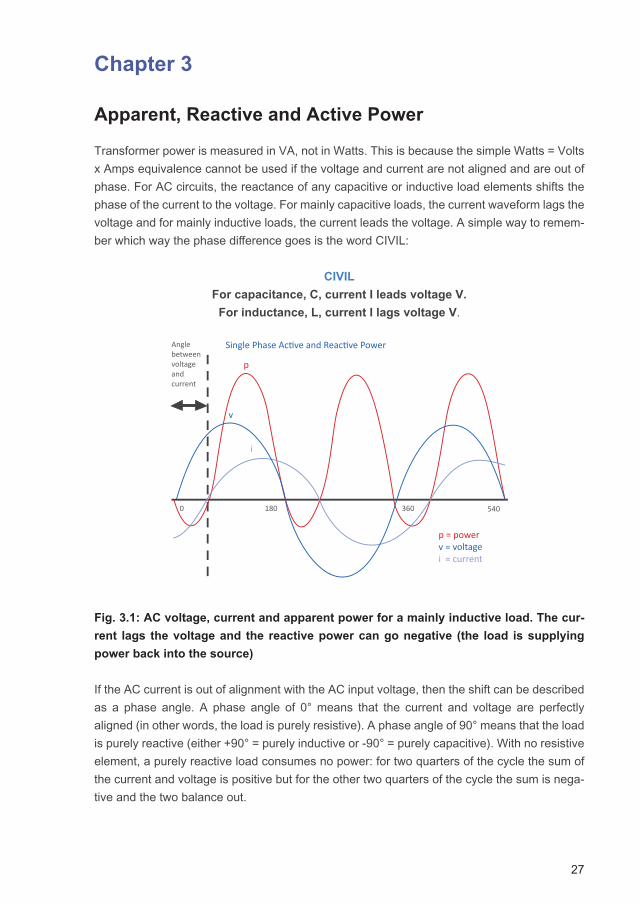
Transformer power is measured in VA, not in Watts. This is because the simple Watts = Volts x Amps equivalence cannot be used if the voltage and current are not aligned and are out of phase. For AC circuits, the reactance of any capacitive or inductive load elements shifts the phase of the current to the voltage. For mainly capacitive loads, the current waveform lags the voltage and for mainly inductive loads, the current leads the voltage. A simple way to remem-ber which way the phase diff erence goes is the word CIVIL:
CIVIL
For capacitance, C, current I leads voltage V.
For inductance, L, current I lags voltage V.
Fig. 3.1: AC voltage, current and apparent power for a mainly inductive load. The cur-
rent lags the voltage and the reactive power can go negative (the load is supplying
power back into the source)
If the AC current is out of alignment with the AC input voltage, then the shift can be described as a phase angle. A phase angle of 0° means that the current and voltage are perfectly aligned (in other words, the load is purely resistive). A phase angle of 90° means that the load is purely reactive (either +90° = purely inductive or -90° = purely capacitive). With no resistive element, a purely reactive load consumes no power: for two quarters of the cycle the sum of the current and voltage is positive but for the other two quarters of the cycle the sum is nega-tive and the two balance out.
180 360 5400
p = powerv = voltagei = current
Single Phase Active and Reactive PowerAnglebetweenvoltageand current
p
v
i

28 29
of this energy is returned in other parts of the cycle, the distribution system has to cope with the worst case instantaneous power consumption. Also, the reactive power circulating current and therefore the cable losses in a system with “poor” power factor will be higher than one with a “good” power factor (closer to 1). By encouraging customers to power-factor-correct their energy consumption (by either charging more for poor power factor loads or by lobbying governments to force customers to add power factor correction), the power companies can save money.
It is a common mistake to think that, for example, an LED driver with power factor correction is somehow “greener” and consumes less power. The additional power factor correction cir-cuitry actually reduces overall effi ciency by adding additional power stages to the design.
A more serious issue is the problem of electromagnetic interference if the pow-er supply is not properly power factor corrected. Take the example shown in fi gure 3.4 of a linear power supply. The input current is in phase with the input voltage, but severely distorted. Using the relationship shown in fi gure 3.3 might give the impression that the power factor = 1 as Cos φ = 1.
Fig. 3.4: Linear power supply
input current vs voltage
However, looking at the harmonics generated by the distorted input current reveals a diff erent story:
Fig. 3.5: Harmonics generated by the input current shown in fi gure 3.4
Top: Input Voltage Bo�om: Input Current
0%
20%
40%
60%
80%
100%
Harmonic Number
21191715131197531
Fig. 3.2: Waveforms and apparent power for a purely inductive load
In practice purely reactive loads do not exist as there are always some resistive losses in the wiring. In a power supply circuit, there will be a mix of both reactive and resistive losses lead-ing to a power factor (the ratio of active power to reactive power) somewhere between 1 and 0 (a power factor of 1 corresponds to a phase angle of zero and a power factor of 0 corre-sponds to a phase angle of 90°):
Apparent Power [VA] , S² = P² + Q²
Active Power [W], P = S cosφ
Reactive Power [VAR], Q = S sinφ
Fig. 3.3: Apparent power vector diagram. Reactive power does no useful work - like
the head in a beer glass
By convention, capacitive loads generate reactive power and inductive loads consume reac-tive power. This is very useful, as a capacitor can be used to bring the power factor closer to 1 for a mainly inductive load such as a motor or an inductor can be used to bring the power factor closer to 1 for a mainly capacitive load. Adding such reactive components to adjust the power factor is called passive power factor correction.
But why bother correcting the power factor? The purely reactive element of the load consumes no power overall as energy absorbed in one part of the cycle is returned in another part, so most electricity meters only measure the active power consumed and ignore the reactive pow-er. The main problem is that the electricity company has to supply enough power to cope with the peak power demand which is the combination of active and reactive powers. Even if some
S
P
φ
Ǫ
Reactive power (KVar)
Active power (KW)
Apparent power (KW
)
θ
P
iv
360°180°90°PAVG
30
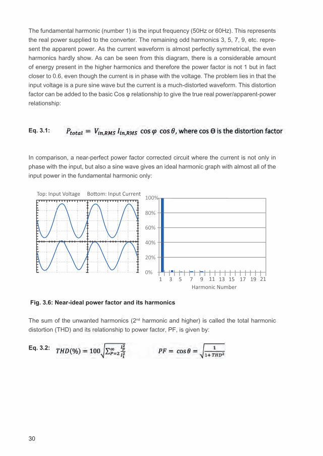
The fundamental harmonic (number 1) is the input frequency (50Hz or 60Hz). This represents the real power supplied to the converter. The remaining odd harmonics 3, 5, 7, 9, etc. repre-sent the apparent power. As the current waveform is almost perfectly symmetrical, the even harmonics hardly show. As can be seen from this diagram, there is a considerable amount of energy present in the higher harmonics and therefore the power factor is not 1 but in fact closer to 0.6, even though the current is in phase with the voltage. The problem lies in that the input voltage is a pure sine wave but the current is a much-distorted waveform. This distortion factor can be added to the basic Cos φ relationship to give the true real power/apparent-power relationship:
Eq. 3.1:
In comparison, a near-perfect power factor corrected circuit where the current is not only in phase with the input, but also a sine wave gives an ideal harmonic graph with almost all of the input power in the fundamental harmonic only:
Fig. 3.6: Near-ideal power factor and its harmonics
The sum of the unwanted harmonics (2nd harmonic and higher) is called the total harmonic distortion (THD) and its relationship to power factor, PF, is given by:
Eq. 3.2:
Bo�om: Input Current Top: Input Voltage
Harmonic Number21191715131197531
0%
20%
40%
60%
80%
100%

31
Chapter 4
AC Theory
Note: This next section is optional. You can skip straight to the next chapter or you can read further. While you are deciding, following the advice of Steven Sandler who claims that all successful books must contain a dragon, preferably a medieval dragon; please find a pic-ture of a dragon:
Fig. 4.1: Dragon (source: MS Clipart)
4.1 AC Theory - basics
In the previous section, the concept of apparent power was introduced as being a vector composed of the elements of reactive power and active power. A vector is a two-dimensional quantity composed of two single dimensional quantities called scalars at right angles to each other (P and Q in figure 3.3).
• A vector can be denoted by an arrow above it (e .g. S) or more simply by bold type, e.g. S. • The length of a vector (its magnitude or modulus) is the square root of the sum of the
squares of the two scalars that define it and is shown by bars on either side |S|. So, in figure 3.3:
Just as apparent power is a vector, so are impedances. The reactance of an inductor consists of two elements, its DC resistance, (DCR), which does not change with frequency and its impedance, which is directly proportional to frequency. As both are measured in Ohms, they can be represented on the same vector diagram.
32 33
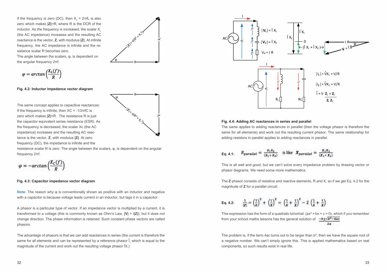
Fig. 4.4: Adding AC reactances in series and parallel
The same applies to adding reactances in parallel (then the voltage phasor is therefore the same for all elements) and work out the resulting current phasor. The same relationship for adding resistors in parallel applies to adding reactances in parallel:
Eq. 4.1:
This is all well and good, but we can’t solve every impedance problem by drawing vector or phasor diagrams. We need some more mathematics.
The Z phasor consists of resistive and reactive elements, R and X, so if we get Eq. 4.2 for the magnitude of Z for a parallel circuit:
Eq. 4.2:
This expression has the form of a quadratic binomial (ax² + bx + c = 0), which if you remember from your school maths lessons has the general solution of
The problem is, if the term 4ac turns out to be larger than b², then we have the square root of a negative number. We can’t simply ignore this. This is applied mathematics based on real components, so such results exist in real life.
I R
V = Î Zϕ
AC V
│VL│= Î XL
│VC│= Î XC
VR = I R
VL
VC
VR
Î XL
Î XC 0
(Î XL + Î XC )
I
AC V
│IL│= VXL + V/R
RL
I L
I
I C
Rc
│IC│= VXC + V/R
I = V ZL + ZC
ZL ZC
If the frequency is zero (DC), then XL = 2πfL is also zero which makes |Z|=R, where R is the DCR of the inductor. As the frequency is increased, the scalar XL
(the AC impedance) increases and the resulting AC reactance is the vector, Z, with modulus |Z|. At infi nite frequency, the AC impedance is infi nite and the re-sistance scalar R becomes zero.The angle between the scalars, φ, is dependent on the angular frequency 2πf.
Fig. 4.2: Inductor impedance vector diagram
The same concept applies to capacitive reactances:If the frequency is infi nite, then XC = -1/2πfC is zero which makes |Z|=R . The resistance R is just the capacitor equivalent series resistance (ESR). As the frequency is decreased, the scalar Xc (the AC impedance) increases and the resulting AC reac-tance is the vector, Z, with modulus |Z|. At zero frequency (DC), the impedance is infi nite and the resistance scalar R is zero. The angle between the scalars, φ, is dependent on the angular frequency 2πf.
Fig. 4.3: Capacitor impedance vector diagram
Note: The reason why φ is conventionally shown as positive with an inductor and negative with a capacitor is because voltage leads current in an inductor, but lags it in a capacitor.
A phasor is a particular type of vector. If an impedance vector is multiplied by a current, it is transformed to a voltage (this is commonly known as Ohm’s Law, |V| = I|Z|), but it does not change direction. The phase information is retained. Such constant phase vectors are called phasors.
The advantage of phasors is that we can add reactances in series (the current is therefore the same for all elements and can be represented by a reference phasor Î, which is equal to the magnitude of the current and work out the resulting voltage phasor ÎX.)
R
X L
│Z│=
√(R² +
X L²)
ϕ
R
XC
│Z│= √(R² + XC ²)
ϕ

34 35
In other situations, the ± terms are not equivalent: when Equation 4.3 is applied to light trans-mission, for example, then the positive and negative terms are more commonly called right and left circularly polarized light.
In general, we can simplify the description of the rectangular form reactance vector diagram into a much neater complex number representation: Z = cosφ |Z|+sinφ |Z|, → R + jX
The beauty of this notation is that it allows us to extend the familiar Ohm’s Law relationships from DC to AC situations (from resistances to reactances) and to use traditional solutions such as Thévenin’s Theorem to analyse component networks.
Ohm’s Law (DC) V = IR R=V/I I=V/R
Ohm’s Law (AC) V = I(R + jX) (R + jX)=V/I I=V/(R + jX) = V(R + jX)/(R² + X²)
Adding reactances together becomes simpler because the results are always in the form of Z = R + jX. For example, the reactance of an inductor, capacitor and resistor placed in series becomes:
Eq. 4.4:
Fig. 4.7: LCR network
To also show how useful this notation is, let us take the network shown above which is a res-onant tank and work out its response. As the network is in series, the current flowing through all three components must be the same.At resonance, the L and C reactances cancel out, so the peak current, Io, flowing through the network is simply │V│/ R (assuming that R is much larger than the capacitor ESR and the inductor DCR). At other frequencies, the current I that flows through the network is:
Eq. 4.5:
AC
I
V
L
C
R
Leonhard Euler (*1707 - †1783) gave the term “i” for the quantity √ (-1), but as “i” can be con-fused with the symbol for current, in electronics we use “j” instead.
Any relationship including √ (-1) is a complex number with a real part and an imaginary part. The word “imaginary” somehow implies that the term does not really exist, which is not true. It is maybe more helpful to think of a number line of real numbers from –infinity to + infinity with imaginary numbers placed at 90° also going from –infinity to + infinity in the imaginary plane:
Fig. 4.5: Number line representation of a complex number
If we now spin the imaginary number line around the real number axis, we get this image:
Fig. 4.6: Figure 4.5 with the J axis rotated
Does this look familiar? Maybe like the typical image of the field surrounding a straight wire? And lo and behold! Maxwell’s electromagnetic field equation can be written in the form of:
Eq. 4.3:
Where F is the combined EM field created by the combination of the E electric and H magnet-ic fields. In the case of magnetics, the fact that the imaginary part has both a positive and a negative solution is not relevant; we can choose just the positive or the negative part as they are symmetrical.
Imag
inar
y
Nu
mbe
rs
Real NumbersIm
agin
ary
Num
bers
Real Numbers

36
The magnifi cation factor, Q, determines how quickly the current decreases away from the peak at the resonant frequency. It is defi ned as X0/R where X0 is the reactance of the network at resonance,
If the results of Equation 4.5 are plotted with diff erent Q values, we get the following typical curves:
Fig. 4.8: Example of a series resonant current plot with diff erent Q values.
Thus we can calculate in advance the response of our resonant tank circuit without actually having to build it and determine the optimum Q factor experimentally.
21.81.6f/f01.41.210.80.60.40.200
0.10.2
0.30.4
0.5
0.6
0.7
0.8
0.91,0 I.I₀ 0.1
-3
-6
-10
-15-20-30
Series ResonatorCurrent vs. frequency
Q = 10
Q = 100
Q = 1
20Log (I/I₀)

37
Chapter 5
Passive Components
5.1 Capacitors
Capacitors play an important part in AC power supplies because the input voltage drops to zero twice during every AC mains cycle. An energy storage element is usually needed to keep the power supply running (although there are AC powered LED drivers that allow the output to fail at every zero crossing as a 100Hz or 120Hz LED flicker is not perceptible to most people). An inductor can be used to effectively store current in the form of its magnetic field, but ca-pacitors are needed to store DC voltage in the form of the electric field between its electrodes.
In addition, AC filter capacitors are needed between the line inputs and between line and ground for EMC and surge protection. As such, they are classed as safety critical components.
5.1.1 Class X and Y capacitors
AC filter capacitors are typically ceramic disc or metallized film. Both of these constructions are symmetric and work equally well with either voltage polarity. A ceramic disc capacitor consists of two metal electrodes separated by a ceramic dielectric substrate. This gives a very stable capacitance value over a wide operating temperature range, but limited capacitance in the range of picofarads to tens of nanofarads. Multiple layers can be used to increase the insulation, so withstand voltages in the range of 1kV up to 15kV are available, as are SMD versions.
Fig. 5.1: Ceramic disc capacitor
Metalized film capacitors use multiple layer plastic film insulators which are coated on one or both sides with a metal film to make the electrodes. There are many different plastic films that can be used but PTFE, polypropylene and polyester are the most common. As many layers can be interleaved, high capacitance values are possible (nanofarads to tens of microfarads),
EpoxyCoating Ceramic disc
(dielectric)
Electrode
38 39
Both X-class and Y-class capacitors are classified according to their peak or rated operating voltage and over-voltage withstand ability as defined by IEC 60384-14:
Class Peak Voltage Over-voltage withstand ability
X1 ≤ 4kVDC 4kV per C ≤ 1µF or 4/√C kV per C >1µF
X2 ≤ 2.5kVDC 2.5kV per C ≤ 1µF or 2.5/√C kV per C >1µF
X3 ≤ 1.2kVDC None
Class Rated Voltage Over-voltage withstand ability
Y1 ≤ 500VAC 8kV
Y2 ≤ 300VAC 5kV
Y3 ≤ 250VAC None
Y4 ≤ 150VAC 2.5kV
Table 5.1: X-Class and Y-class capacitor ratings
Another use of film capacitors is in tuned filter and resonance circuits, phase shifters and pow-er factor correction circuits. The inherently low parasitic inductance and low ESR makes the frequency response very stable and the capacitance value remains linear over a wide range of operating temperatures, simplifying the design process.
5.1.2 Electrolytic capacitors
As mentioned previously, the other main function of capacitors is to store energy. Electrolytic capacitors are almost exclusively used as the bulk storage elements in AC/DC converters due to their high volumetric efficiency, high voltage and temperature rating and low cost. The downside is that electrolytics are polarized (DC only), so they can only be used after the rectification stage, and they can explosively fail if the electrolyte overheats and starts to evaporate.
The internal construction is similar to the foil capacitor, except with a liquid or solid (polymer) dielectric, so that they have much in common with a battery cell construction. For example, Supercapacitors are low voltage capacitors with very high capacitance (several Farads) which are a cross-over between a rechargeable battery and a capacitor. The most common electro-lytic capacitor is the aluminium type that uses aluminium oxide (AL2O3) as the liquid electrolyte
but they can become very bulky with both high rated voltage and high capacitance values. Film capacitors also have inherently low ESR and ESL values which makes them also suitable for snubber and filtering applications. Film capacitors are almost exclusively available as through-hole mounting only.
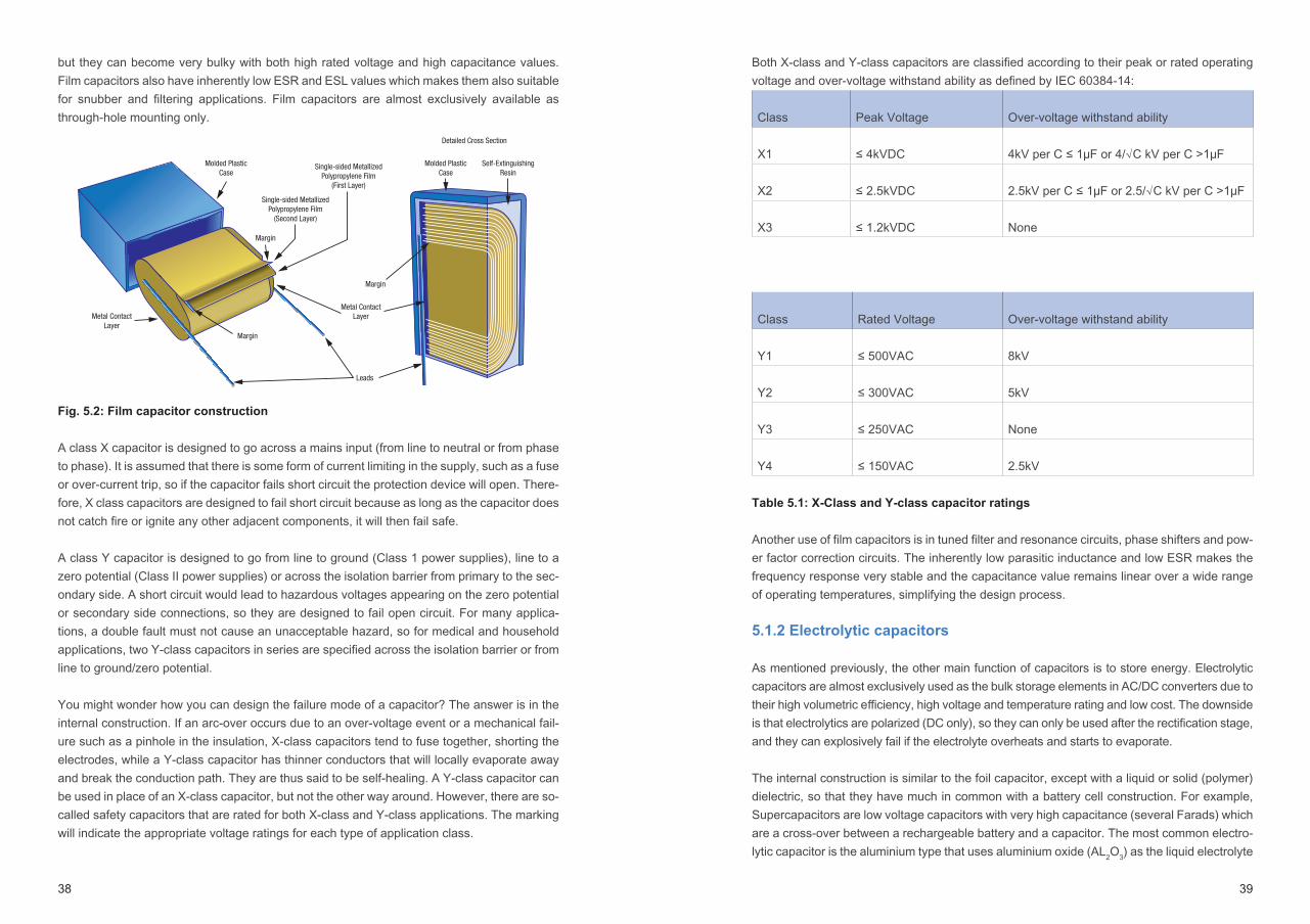
Fig. 5.2: Film capacitor construction
A class X capacitor is designed to go across a mains input (from line to neutral or from phase to phase). It is assumed that there is some form of current limiting in the supply, such as a fuse or over-current trip, so if the capacitor fails short circuit the protection device will open. There-fore, X class capacitors are designed to fail short circuit because as long as the capacitor does not catch fire or ignite any other adjacent components, it will then fail safe.
A class Y capacitor is designed to go from line to ground (Class 1 power supplies), line to a zero potential (Class II power supplies) or across the isolation barrier from primary to the sec-ondary side. A short circuit would lead to hazardous voltages appearing on the zero potential or secondary side connections, so they are designed to fail open circuit. For many applica-tions, a double fault must not cause an unacceptable hazard, so for medical and household applications, two Y-class capacitors in series are specified across the isolation barrier or from line to ground/zero potential.
You might wonder how you can design the failure mode of a capacitor? The answer is in the internal construction. If an arc-over occurs due to an over-voltage event or a mechanical fail-ure such as a pinhole in the insulation, X-class capacitors tend to fuse together, shorting the electrodes, while a Y-class capacitor has thinner conductors that will locally evaporate away and break the conduction path. They are thus said to be self-healing. A Y-class capacitor can be used in place of an X-class capacitor, but not the other way around. However, there are so-called safety capacitors that are rated for both X-class and Y-class applications. The marking will indicate the appropriate voltage ratings for each type of application class.
Molded PlasticCase
Molded PlasticCase
Self-ExtinguishingResin
Single-sided MetallizedPolypropylene Film
(First Layer)
Single-sided MetallizedPolypropylene Film
(Second Layer)
Margin
Margin
Margin
Detailed Cross Section
Leads
Metal ContactLayer
Metal ContactLayer

40 41
The equivalent series resistance, ESR, has three main components: the ohmic resistance of the connections (≈10milliohm) plus the frequency dependent resistance of the dielectric oxide layer, called the dissipation factor, Dox, plus the temperature dependent resistance of the electrolyte, Re[T] which is typically:
Eq. 5.1:
The combination of the fi rst two factors (ohmic resistance and frequency dependent resist-ance) gives the blue line in the right hand image on the diagram above that will also change with temperature according to the third factor (dissipation factor). The equivalent series in-ductance, ESL will also vary, but this eff ect is minor and can usually be ignored.
Question: When is a low-ESR 100µF electrolytic not a low-ESR 100µF capacitor? Answer: When the capacitor is old. As an electrolytic capacitor ages, the liquid electrolyte dries out and the ESR and equivalent series inductance, ESL, increases while the capaci-tance decreases. The defi nition of the end of useful life is when the ESR, ESL or capacitance fall outside of their respective limits. This does not mean that the capacitor will immediately fail, but the higher dissipation will gradually increase the internal temperature until failure is inevitable.
Fig. 5.5: Electrolytic capacitor equivalent circuit
The tan-delta fi gure is thus an important indicator of capacitor reliability:
Eq. 5.2:
Fig. 5.6: Typical Electrolytic tanδ vs service hours
=C Rleakage
ESR
ESL
0.1
0.2
0 1000 2000 3000 4000 5000 6000 7000Service Hours
EoL
tanδ
between foil electrodes which have an etched surface to increase their eff ective surface area. This allows a high capacitance-volume (CV) product with low ESR (equivalent series resist-ance), both important factors for bulk storage capacitors.
5.1.2.1 Design considerations of electrolytic capacitors.
Question: When is a low-ESR 100µF electrolytic not a low-ESR 100µF capacitor? Answer: When it is operated with a high frequency ripple current. As the frequency increases beyond around 1 kHz, the eff ective capacitance decays. If the capacitor is used to smooth rectifi ed mains frequency, then the datasheet capacitance value can be reliably used. Howev-er, if the capacitor is used in a PFC circuit operating at a higher switching frequency (typically 100kHz), then a 450VDC 100µF capacitor might act like a 60µF capacitor.
Fig. 5.3: Electrolytic capacitance vs frequency.
Question: When is a low-ESR 100µF electrolytic not a low-ESR 100µF capacitor? Answer: when the ambient temperature is not 25°C. At low temperatures, the liquid elec-trolyte becomes viscous and less conductive, so the ESR increases and the capacitance decreases. At high ambient temperatures, the capacitor core expands, eff ectively decreasing the separation between the foil electrodes, so the capacitance increases. A 100µF capacitor at 25°C could be a 62µF capacitor at -40°C and a 110µF capacitor at 105°C. (Note: polymer electrolytics do not exhibit this eff ect)
Fig. 5.4: Typical electrolytic capacitance vs temperature and ESR vs temperature
1.1
1.0
c/c₀
0.8
0.7
0.6
0.5
10 100 1k 10k 100k f(Hz)
25V
160V
450V
ESR/ESR100
10
1.0
0.10
0.01-50 -25 25 75 100 125500
TI°CI
10 0
-10 -20 -30 -40 -50
20
-55 -20 0 20 85 105
Temperature v. Capacitance
Capa
ctan
ce C
hang
e (%
)
Temperature (°C)
Solid CAPElectrolyte - CAP
ESR Ratio
42 43
Thus, the calculated service lifetime, L = 7000 x 32 x 1.3 x 0.6 = 174,000 hours or nearly 20 years when all of the lifetime multipliers are taken into account.
To simplify such electrolytic capacitor lifetime calculations, RECOM off ers an on-line calcula-tor tool on its website (www.recom-power.com)
It is useful to play around with the data in the lifetime calculator to see how small changes in the operating conditions can aff ect the lifetime:
For the example given above:
However:Changing the maximum voltage from 90% rated to 80% rated increases the lifetime to nearly 36 years. Changing the maximum ambient temperature from 70°C to 85°C reduces the life-time from 20 years down to only 7 years. Changing the ripple current from 50% rated to 60% rated reduces the lifetime by only 6% (from 174 khrs down to 167.5 khours), but changing it to 100% rated current loses nearly 4 years off the lifetime.
Component selection is often a compromise between performance and cost, so by careful design, the optimal price/specifi cation benefi t can be realized.
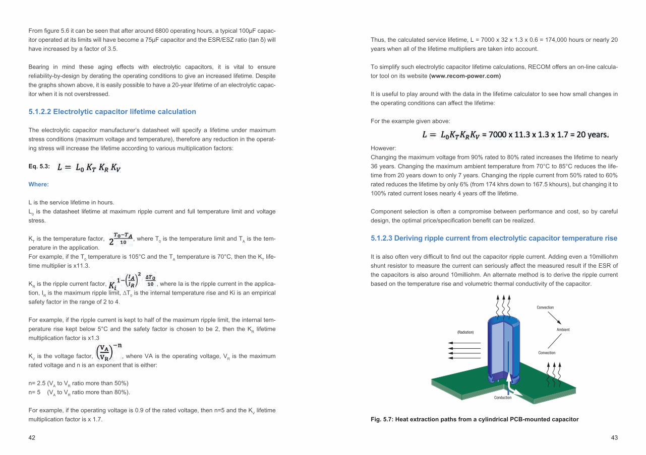
5.1.2.3 Deriving ripple current from electrolytic capacitor temperature rise
It is also often very diffi cult to fi nd out the capacitor ripple current. Adding even a 10milliohm shunt resistor to measure the current can seriously aff ect the measured result if the ESR of the capacitors is also around 10milliohm. An alternate method is to derive the ripple current based on the temperature rise and volumetric thermal conductivity of the capacitor.
Fig. 5.7: Heat extraction paths from a cylindrical PCB-mounted capacitor
(Radiation)Ambient
Convection
Convection
Conduction
From fi gure 5.6 it can be seen that after around 6800 operating hours, a typical 100µF capac-itor operated at its limits will have become a 75µF capacitor and the ESR/ESZ ratio (tan δ) will have increased by a factor of 3.5.
Bearing in mind these aging eff ects with electrolytic capacitors, it is vital to ensure reliability-by-design by derating the operating conditions to give an increased lifetime. Despite the graphs shown above, it is easily possible to have a 20-year lifetime of an electrolytic capac-itor when it is not overstressed.
5.1.2.2 Electrolytic capacitor lifetime calculation
The electrolytic capacitor manufacturer’s datasheet will specify a lifetime under maximum stress conditions (maximum voltage and temperature), therefore any reduction in the operat-ing stress will increase the lifetime according to various multiplication factors:
Eq. 5.3:
Where:
L is the service lifetime in hours.L0 is the datasheet lifetime at maximum ripple current and full temperature limit and voltage stress.
KT is the temperature factor, , where T0 is the temperature limit and TA is the tem-perature in the application.For example, if the T0 temperature is 105°C and the TA temperature is 70°C, then the KT life-time multiplier is x11.3.
KR is the ripple current factor, , where Ia is the ripple current in the applica-tion, IR is the maximum ripple limit, ∆T0 is the internal temperature rise and Ki is an empirical safety factor in the range of 2 to 4.
For example, if the ripple current is kept to half of the maximum ripple limit, the internal tem-perature rise kept below 5°C and the safety factor is chosen to be 2, then the KR lifetime multiplication factor is x1.3
KV is the voltage factor, , where VA is the operating voltage, VR is the maximum rated voltage and n is an exponent that is either:
n= 2.5 (VA to VR ratio more than 50%) n= 5 (VA to VR ratio more than 80%).
For example, if the operating voltage is 0.9 of the rated voltage, then n=5 and the KV lifetime multiplication factor is x 1.7.
44 45
chokes and transformers. Any stray AC magnetic fields can generate eddy currents in the metallized foil conductors which will increase the core temperature and reduce lifetime.
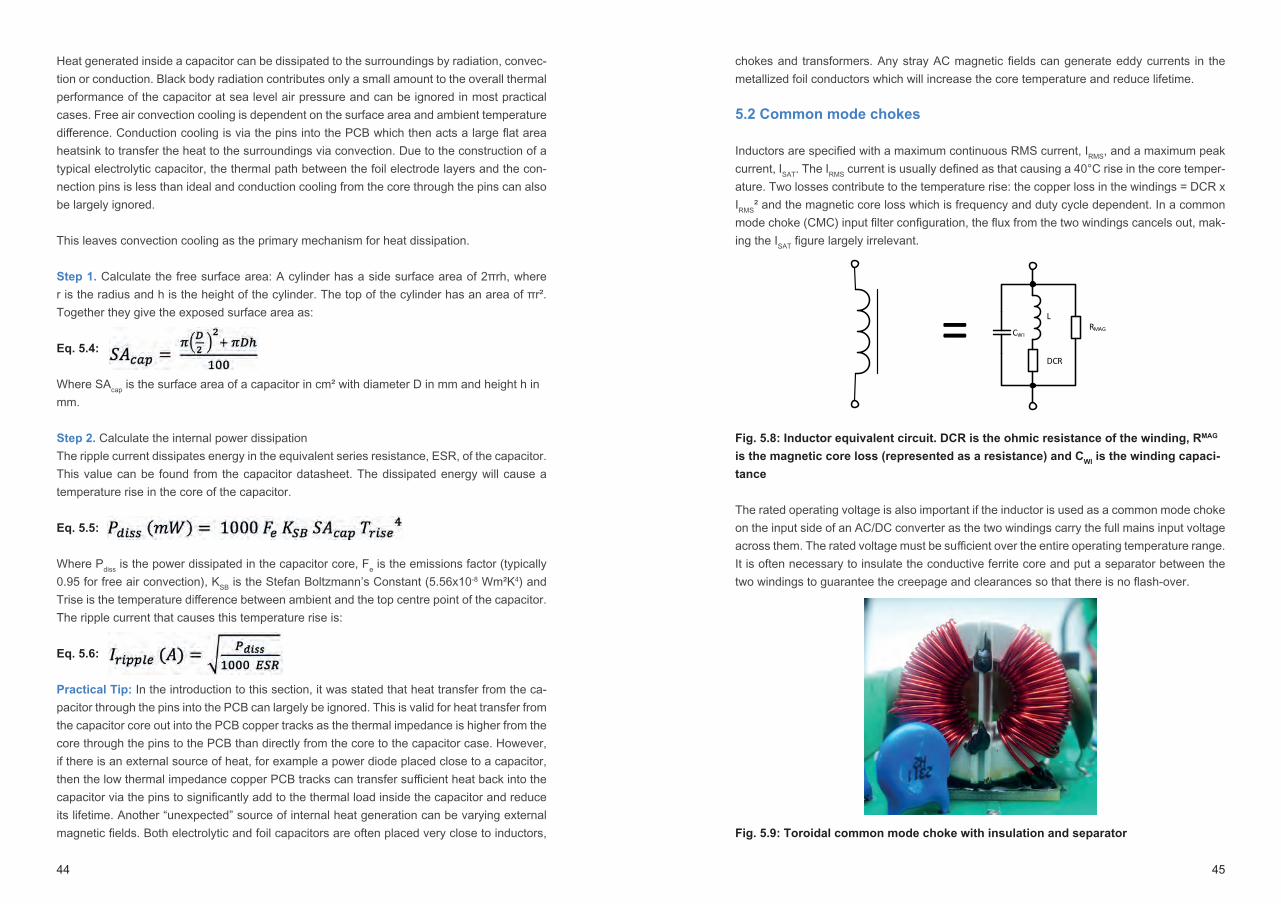
5.2 Common mode chokes
Inductors are specified with a maximum continuous RMS current, IRMS, and a maximum peak current, ISAT. The IRMS current is usually defined as that causing a 40°C rise in the core temper-ature. Two losses contribute to the temperature rise: the copper loss in the windings = DCR x IRMS² and the magnetic core loss which is frequency and duty cycle dependent. In a common mode choke (CMC) input filter configuration, the flux from the two windings cancels out, mak-ing the ISAT figure largely irrelevant.
Fig. 5.8: Inductor equivalent circuit. DCR is the ohmic resistance of the winding, RMAG
is the magnetic core loss (represented as a resistance) and CWI
is the winding capaci-
tance
The rated operating voltage is also important if the inductor is used as a common mode choke on the input side of an AC/DC converter as the two windings carry the full mains input voltage across them. The rated voltage must be sufficient over the entire operating temperature range. It is often necessary to insulate the conductive ferrite core and put a separator between the two windings to guarantee the creepage and clearances so that there is no flash-over.
Fig. 5.9: Toroidal common mode choke with insulation and separator
= CWIRMAG
DCR
L
Heat generated inside a capacitor can be dissipated to the surroundings by radiation, convec-tion or conduction. Black body radiation contributes only a small amount to the overall thermal performance of the capacitor at sea level air pressure and can be ignored in most practical cases. Free air convection cooling is dependent on the surface area and ambient temperature difference. Conduction cooling is via the pins into the PCB which then acts a large flat area heatsink to transfer the heat to the surroundings via convection. Due to the construction of a typical electrolytic capacitor, the thermal path between the foil electrode layers and the con-nection pins is less than ideal and conduction cooling from the core through the pins can also be largely ignored.
This leaves convection cooling as the primary mechanism for heat dissipation.
Step 1. Calculate the free surface area: A cylinder has a side surface area of 2πrh, where r is the radius and h is the height of the cylinder. The top of the cylinder has an area of πr². Together they give the exposed surface area as:
Eq. 5.4:
Where SAcap is the surface area of a capacitor in cm² with diameter D in mm and height h in mm.
Step 2. Calculate the internal power dissipationThe ripple current dissipates energy in the equivalent series resistance, ESR, of the capacitor. This value can be found from the capacitor datasheet. The dissipated energy will cause a temperature rise in the core of the capacitor.
Eq. 5.5:
Where Pdiss is the power dissipated in the capacitor core, Fe is the emissions factor (typically 0.95 for free air convection), KSB is the Stefan Boltzmann’s Constant (5.56x10⁻⁸ Wm²K4) and Trise is the temperature difference between ambient and the top centre point of the capacitor. The ripple current that causes this temperature rise is:
Eq. 5.6:
Practical Tip: In the introduction to this section, it was stated that heat transfer from the ca-pacitor through the pins into the PCB can largely be ignored. This is valid for heat transfer from the capacitor core out into the PCB copper tracks as the thermal impedance is higher from the core through the pins to the PCB than directly from the core to the capacitor case. However, if there is an external source of heat, for example a power diode placed close to a capacitor, then the low thermal impedance copper PCB tracks can transfer sufficient heat back into the capacitor via the pins to significantly add to the thermal load inside the capacitor and reduce its lifetime. Another “unexpected” source of internal heat generation can be varying external magnetic fields. Both electrolytic and foil capacitors are often placed very close to inductors,

46 47
Step 5: Select a suitable common mode choke and the X and Y capacitors to make up the fi lter as shown below:
Fig. 5.10: Basic AC input fi lter
As the application is a universal mains fi lter, the choke needs to be rated for 250VAC opera-tion. From step 4, we need a current rating of 1.14A or higher. From step 3, it should have a peak attenuation close to 225kHz.
We could choose a 5mH choke rated at 250VAC, 2A @ Tamb + 40°C for example. The high common mode inductance will give an attenuation curve that peaks at around 0.2MHz, which is ideal. The stray inductance is typically 1%, i.e. 47µHThe X-capacitor reacts with the stray inductance to make a diff erential mode fi lter:
The Y-capacitors react with the common mode inductance to make a common mode fi lter:
Fig. 5.11: Initial design of the EMC fi lter
UnfilteredAC
Mains
C1
X2
C3
Y2
C2
Y2
FilteredAC
Mains
CMC
UnfilteredAC
Mains
1µF
X2
10n
Y2
10n
Y2
FilteredAC
Mains
CMC
5mH
47µH
The impedance of a CMC increases with increasing frequency until it reaches a peak at the self-resonant frequency (SRF), then it declines due to the eff ect of the interwinding capaci-tance. The SRF should be chosen to be close to the frequency of the maximum noise inter-ference (usually the switching frequency or a multiple thereof) to give the largest attenuation.
Eq. 5.7:
Where SRF is the self-resonant frequency (assuming DCR is low and RMAG is high)
5.2.1 EMC common mode fi lter worked example
Power supply specifi cation: 100W, 115 – 230V supply, 45 kHz switching frequency, 85% effi cient fl yback design.
Step 1. Determine the probable noise levelThe circuit switches at 45kHz with a 50% duty cycle at full load. This will generate a funda-mental noise peak at 45kHz with harmonics at higher frequency intervals of nf0, where n = 1,3,5,… decreasing in intensity with -20dBµV/decade. Frequencies below 150kHz are ignored by the industrial EMC standards, so we need only concern ourselves from the fi fth harmonic at 5f0 or 225kHz and above. If we assume a 1V drop across the diode bridge, then the fun-damental frequency will have an amplitude:
Eq. 5.8:
And the 5th harmonic will have an amplitude of:
Eq. 5.9:
Step 2. Determine the fi lter attenuation:The required attenuation is equal to the noise amplitude (fi rst odd harmonic above 150kHz) minus the EN55011 EMI Quasi peak limit (65dBµV) plus a 3dB safety margin. For our exam-ple, the attenuation, A, at the fi fth harmonic needs to be 108 – 65 + 3 = 46dBµV.
Step 3. Find the fi lter corner frequency:The fi lter should attenuate the noise from the fi fth harmonic at 225kHz with a +40dB/decade attenuation. This gives a corner frequency of:
Step 4: Determine the maximum AC current:
The maximum input current occurs at full load with the minimum input voltage (115VAC -10% ≈ 103VAC). Assuming power factor is corrected, the input current will then be (100/0.85)/103 = 1.14A

48
It must be stressed that the above calculation is not sufficient to guarantee an EMC test pass. It is just a first step to allow a test set-up to be made.
Practical Tip: It is often quite difficult to find a common mode choke with enough stray leak-age inductance to keep the size of the X-capacitor reasonable. It is often worth using either using a differential mode choke in series with the common mode choke or using a hybrid choke which incorporates elements of both DM and CM types in one body.

49
Chapter 6
Active Components
6.1 Silicon MOSFET
The Metal Oxide Silicon Field Effect Transistor (MOSFET) is the workhorse of the majority of AC/DC circuits. The basic construction is simple with a gate insulated from the body by a thin metal oxide layer. The source and drain regions are heavily doped (n+ and p+) so that there is a semiconductor barrier to the flow of charge. When a gate-source voltage higher than the threshold voltage is applied, this barrier is overcome and current flows freely:
Fig. 6.1: Basic construction of a planar epitaxial n-MOSFET
Integral to the MOSFET’s construction is a body diode formed from the PN junction between the P+ and N- interface (shown in red in the figure). This means that a MOSFET can only be used to switch unipolar voltages. However, in some applications, the body diode is useful as a freewheeling diode to conduct with a negative voltage across a MOSFET that is switched off.
The equivalent model shows the various parasitic elements that affect the switching perfor-mance:
Lgate, Ldrain and Lsource are the lead impedancesRgate is the gate resistanceRDSon is the drain source resistance when fully enhancedCmiller is the gate-drain capacitanceCGS is the gate-source capacitanceCoS is the drain-source capacitance equal to (CGS + Cmiller) Coss is the overall output small signal capacitance
Fig. 6.2: MOSFET equivalent switching model
DRAIN
N+ BUFFER
N- BASEP+P+ N+ N+
SOURCE SOURCEGATE
GATE ISOLATION D
S
G
Rgate
Cmiller
CGS
CDS
RDSon
Drain
Source
Gate
Ldrain
Lsource
C OSSDbody
Lgate

50 51
See the fi nal section in this chapter (Use of Kelvin contacts) for considerations to reduce or eliminate these eff ects.
During these stage 2 and stage 3 transition periods, the transistor is behaving as a variable resistor and dissipating a lot of power. When the transistor is fully off , only leakage currents fl ow and when the transistor is fully on, the main loss is through the RDSON resistance, which is typically in the region of milliohms and also very low. However, during repetitive on-off transi-tions, the power dissipation will be much higher than in the static fully-on condition.
A simplifi ed gate drive and switching loss calculation is shown below:
Eq. 6.1:
Where Qgate is the total charge needed to charge the gate capacitances.
The power dissipation in the transistor is dependent on the transition times:
Eq. 6.2:
Where IL is the load current and tstage2 / tstage3 is the time spent is stages 2 and 3 of the total switching time, T, respectively.
With a high current gate drive, these stage 2 and stage 3 times can be reduced, so it is impor-tant to use a low impedance gate voltage source. To reduce the switching losses further, the gate voltage can be increased to charge and discharge the gate capacitances more quickly. In particular, if the gate voltage switches to a negative value, the switch-off time can be reduced signifi cantly compared to just switching from above VTH down to zero volts. There is a limit to the gate voltage defi ned by the breakdown voltage between gate and source, BVDSS. In order to reduce the gate capacitance to a minimum, the metal oxide insulation layer is made very thin, at the cost that the breakdown voltage is then very low (VGS,max is typically ±15-20 volts).
Another way to reduce switching losses is to reduce the switching frequency, fsw, but this can increase losses in other parts of the circuit or reduce the control loop response time to unac-ceptable levels. The only other factor remaining is the gate charge, Qgate. A typical low voltage MOSFET will have a total gate charge of around 5-10nC, but this value also increases with increased VDS capability. A 700V MOSFET will have a total gate charge of around 10-25nC, simply due to the thicker epitaxial layers needed for the higher breakdown voltage strength.
The turn-on characteristic of a MOSFET can be divided into 4 stages:
Stage 1. The gate turn-on voltage is applied. Cgs is charged up via Lgate and Rgate. The transistor is still off .Stage 2. The gate threshold voltage, Vth, is reached. ID starts to linearly increase proportional to Vgate
Stage 3. The Miller plateau is reached. The ID is at maximum and VDS is starting to decrease. The gate voltage remains constant as any excess gate current is diverted to charge up the miller capacitance.Stage 4. VDS has almost reached its minimum (VDS,min = ID.RDSon) and the gate voltage can now rise further, fully enhancing the transistor and reducing the RDSon to its minimum value.
Fig. 6.3: MOSFET turn-on characteristic
The turn-off characteristic is essentially the same process in reverse:
Stage 1. The gate turn-off voltage is applied. Cgs and Cgd are discharged via Rgate. The transistor is still on.Stage 2. Cmiller is now fully discharged and the negative gate current can now start to deplete the charge on CGS, turning off the transistor. VDS starts to linearly increase while Vgs remains constant. Stage 3. VDS is now at the supply voltage and ID starts to decrease. The gate voltage can decrease further as CDS is now fully discharged. Stage 4. The transistor is fully off as Vgate is now below VTH.
The remaining time is just to fully discharge any parasitic gate capacitances.
Fig. 6.4: MOSFET turn off characteristic
Practical Tip: As can be seen from the turn on and turn off characteristics, there are periods when the voltage across the transistor and the current through the resistor are in transition. One dangerous area is turn off , stage 2. The output voltage is ramping up and this dv/dt will feed back through the miller capacitance and attempt to pull up the gate voltage. If the eff ec-tive gate drive impedance is too high, the transistor can switch itself back on again! A similar eff ect can occur during switch on, stage 2. The drain current is ramping up which can cause the drain voltage to rise up due to inductances in the drain to ground path (ground bounce). This will reduce the eff ective VGS voltage and could turn the transistor back off again.
VGS
VDS
VTH
IG
ID
① ② ③ ④
VGS
VDS
VTH
IG
ID
① ② ③ ④

52 53
6.3 IGBT
Insulated Gate Bipolar Transistors (IGBTs) combine the insulated gate characteristics of MOSFETs with the high current capability of bipolar transistors. It is in effect a voltage-con-trolled transistor:
Fig. 6.6: Equivalent model of an insulated gate bipolar transistor (n-channel IGBT)
One of the main differences to a MOSFET is that an IGBT has no body diode, so it will not conduct reverse currents. If an anti-parallel free-wheeling diode is required, then it needs to be added externally.
Fig. 6.7: Comparison of IGBT and MOSFET blocking capabilities
Although IGBTs switch on quickly, they switch off more slowly. This is due to an effect called the recombination tail. Once the gate voltage has been turned off, any remaining charge in the transistor body region must be dissipated by recombination of the holes with electrons as there is no terminal to remove them. This process is relatively slow and delays the switch-off characteristic:
N-MOSFET
NPN
G
E
C
E
C
G =
-
+
G
C
E-
+
G
C
E
N-MOSFET
S
D
G
N-MOSFET
S
D
G
-
+
G
C
E+
G
C
E
-
N-MOSFET
S
D
G
N-MOSFET
S
D
G
+ + - -
- - + +
6.2 SiC MOSFET
Silicon Carbide or SiC MOSFETs are increasingly finding new applications in power electron-ics. Full-bridge and half-bridge circuits for high-voltage applications (several hundred volts) were previously reserved for only the IGBT domain (see next section) because Silicon MOS-FETs, especially Super Junction MOSFETs are not suitable for these applications due to the extremely poor parasitic body diode performance; when silicon MOSFETs experience an unwanted turn-on effect, the body diode quickly goes into thermal destruction. Often, even a single false switching operation on the conductive body diode either exceeds the maximum di/dt of the body diode and thus destroys the MOSFET, or the switching operation incites the gate to oscillate, so that the maximum gate source voltage is exceeded and the transistor is also destroyed.
SiC MOSFETs use a different substrate with a 10x higher dielectric breakdown strength than Silicon, so the layers can be made thinner to reduce the gate charge and RDSon values. In ad-dition, SiC has a three times better thermal conductivity, so the power handling capacity can be increased in the same sized package.
Fig. 6.5: Diagrammatic comparison between Si-MOSFET and SIC-MOSFET construc-
tion
Due to the higher dielectric strength, the SiC substrate can be made up to 10x thinner than the Si substrate, reducing the body resistance by a factor of up to 1000. The thinner layers also reduce the internal capacitances. So, for the same switching frequency, a SiC MOSFET will have around a third to a quarter of the switching losses of an equivalent Si MOSFET. Put an-other way, a SiC MOSFET can be operated four times faster for the same power dissipation.
SiC MOSFETs also have a far more robust body diode than Si MOSFETS. The maximum switching di/dt of the body diode of super junction MOSFETs is around 60A/μs for the latest generation and of fast switching MOSFETs up to 900A/μs for SJ MOSFETs with ultra-fast body diodes, but these values pale in comparison with SiC MOSFETs with up to 6000A/µs. The main disadvantage of SiC-MOSFETs is that they are often more expensive than Si MOS-FETs, but this difference will reduce over time (the price difference between a SiC-MOSFET and a superjunction Si-MOSFET is already comparable).
DRAIN
Si N+ Buffer
N- BASE P+P+ N+ N+SOURCE SOURCE
GATEGATE ISOLATION
DRAINSiC N+ BUFFER
N- BASE P+P+ N+ N+
SOURCE SOURCEGATE
GATE ISOLATIONX10 Size Reduction

54 55
Fig. 6.10: Enhancement-mode GaN transistor in the OFF (top) and ON (bottom) condi-
tions
The extreme thinness of the gate isolation layer means that high gate-source voltages will cause an internal fl ashover, even though the material itself has a high breakdown voltage rating. A GaN E-HEMT has a typical full enhancement voltage of 7V but will be damaged if the VGS exceeds ±10V, much lower than the gate voltages that are typically used in IGBT or SiC gate drivers. Due to the extremely fast rise and fall times of the low-capacitance gate channel, any excessive inductance in the external gate drive could cause spikes or voltage ringing and exceed these voltage limits. Therefore, a 6V gate drive voltage is a good compromise between high effi ciency and staying within a safe operating area.
IGBT or SiC gate drive circuits also typically turn off with a negative gate drive voltage. This speeds up the charge extraction from the gate capacitance and therefore the switch-off time. GaN Transistors have such low gate capacitance that a negative gate drive is not necessary. A gate voltage of 0V will completely and reliably turn off the HEMT in nanoseconds.
Only if the layout has excessive inductance would a negative gate drive off er protection against unintentional turn-on caused by ringing. However, as GaN HEMT do not have a body diode like MOSFETs and are symmetrically conductive devices, a negative gate voltage will increase reverse conduction losses. A single-ended 6V gate drive voltage is suffi cient, al-though for very high frequency switching applications, a bipolar +6V/-1V drive is sometimes suggested to account for layout parasitics.
Figure 6.11 shows typical gate driver voltages that are commonly used to drive switching tran-sistors. The 1st Generation SiC MOSFETS use +20/-5V supplies, but 2nd Generation devices will use +15/-3V supply voltages:
DRAINSOURCE
AlN BUFFER
GaN
GATEGATE ISOLATION
DepletionZone
DRAINSOURCE
AlN BUFFER
GaN
GATEGATE ISOLATION
Depletion Zone
Fig. 6.8: Comparison of the switch-on and switch-off characteristics of an IGBT. The
recombination tail in the turn-off characteristic slows down the switching speed and
increases the power dissipation
Despite this disadvantage, IGBTs are widely used in power switching for high current/high voltage applications such as motor inverters, power rectifi ers and photovoltaic power.
Fig. 6.9: Photovoltaic application using IGBTs for the Maximum Power Point Tracking
function and for the DC/AC inverter stage
6.4 GaN HEMT
Gallium Nitride (GaN) semiconductors are High Electron Mobility Transistor (HEMT) devices, a class of transistors with almost perfect switching characteristics. HEMT means that electrons travel within the internal crystal structure as a two-dimensional electron gas with very high mobility, thus creating a device with very high conductivity and low RDSON. The use of GaN chemistry increases the breakdown voltage which means that the layers within the transistor can be made very thin and close together. This both accelerates the switching speed and reduces the gate capacitance.
The enhancement mode type (E-HEMT) has a depletion zone under the gate which blocks the fl ow of electrons and requires a positive gate voltage with respect to the source pin to turn on. As the depletion zone under the gate is so thin, very little injected charge is needed to turn the transistor on and off , so switching speeds in the MHz region are possible without incurring high switching losses.
0IGBT turn-on
t
CEVIC
0IGBT turn-off
t
CEVIC
Solar Panels Boost Converterwith MPPT
DC to ACInverter Filter
AC
DC

56 57
Fig. 6.12: slope control using gate resistors
5. High-side gate drivers are often implemented with a bootstrap power supply circuit (figure 6.13). Although this means that the same isolated power supply can be used for both high-side and low-side drivers, it has some inherent weaknesses.
Fig. 6.13: Typical high-side bootstrap supply circuit showing unwanted parasitic in-
ductances. For a nominal 6V VDDH, the bootstrap voltage can vary between 5.5V and
8.5V depending on operating conditions (see text below)
The bootstrap diode must have an ultrafast recovery characteristic. If it cannot switch as quickly as the GaN output then a reverse current will flow back into the VDD supply. Not only will these current spikes affect the lifetime of the diode but the resulting high frequency interference on the supply rail will cause havoc with the EMC compliance. The gate driver bootstrap supply voltage is dependent on the difference between the VDD supply and the capacitively-coupled output (switching node) voltage. This means that the voltage across the bootstrap capacitor can vary by more than ±20% during operation.
There will be a volt drop across the bootstrap diode of around 0.7V meaning a 6.7V VDD would be needed to have a VDDH voltage of 6V. The switching node voltage may not go com-pletely to the ground voltage during forward conduction, meaning that the effective gate driver
20R
20R
G
S
D
GaNFETGate Drive
PWMH 20R
20R
G
S
D
GaNFET
Half-Bridge Gate Driver
V+
G
S
DGaNFET
VDDH
VSSH
VOH
VOL
BootstrapCapacitor
20R
20R
PWML
BootstrapDiode
VDD
LParasitic
LParasitic
LParasitic
Out
LParasitic
LParasitic
Fig. 6.11: Typical supply voltages for IGBT, SiC and GaN gate drivers
6.4.1 GAN Transistor gate driver considerations
1. The majority of ultrafast gate driver ICs have an under-voltage lock-out (UVLO) function that disables the output if the supply voltage is too low. Those meant for IGBT/SiC applications will often have a relatively high UVLO level as they are designed to operate from supply voltages up to 24V. A gate driver that is compatible with the much lower gate voltages used in GaN must be selected.
2. The current needed to charge and discharge the gate capacitance is dependent on the gate capacitance and the rate of change of the gate voltage. Although the GaN gate capac-itance is very low, the high dv/dt means that a gate driver with a current drive capability of at least ±0.5A (or better 1A sink) is required. This peak current will be supplied from a ceram-ic capacitor mounted as close to the driver pins as possible, so the average supply current will be much lower (in the tens of milliamps range). The gate driver sink drive should be low-impedance (<2 ohms) to reduce the chance of cross-conduction (see next comment).
3. The maximum and minimum pulse widths should be limited to avoid false triggering and interaction with any the overlap protection circuit. At 5MHz operating frequency, this mini-mum pulse width limits the duty cycle to 90%. At higher frequencies, this limitation becomes more significant and the duty cycle may need to be controlled so that it does not exceed 80%.
4. An ultrafast gate drive design is susceptible to undesired turn-on (causing cross-conduc-tion in bridge circuits) due to parasitic gate driver inductances interacting with the high Miller capacitance discharge current thus creating a ringing oscillation that could send the gate voltage momentarily high again. The slew rates can be limited by a dv/dt limiting gate resistor to reduce the possibility of this effect.
A turn-on gate resistor in the range of 10-20 ohms will typically give an 80-40kV/µs slew rate. The turn-off resistance should be smaller to reduce the turn-off losses. A Schottky diode with a resistor in parallel with the gate resistor can be used to independently control the turn-on and turn-off slew rates:
PWMG
S
DGaNFET+6V
GND
PWMG
S
DSiCFET+20 (+15)
-5 (-3)
GNDPWM
G
E
CIGBT+15
-9
GND

58 59
This floating design uses an isolated DC/DC converter and digital isolator to create a gate driver circuit for a GaN HEMT that could be used as a boost converter, buck converter or buck/boost converter switching application on either the high side or low side. The single-channel digital isolator output stage is powered from a low power LDO regulator connected to the 6V gate driver supply. The UCC27322 high speed driver can deliver up to ±9A peak current and the Schmitt-trigger input switches cleanly from the 5V output of the digital isolator. A dead-time delay can be implemented with a simple RC filter.
The lateral construction of GaN transistors also creates the possibility to integrate the gate driver inside the transistor package. This reduces the parasitic gate inductances and allows higher switching frequencies or higher slew rates without the risk of false triggering. Neverthe-less, an isolated gate driver power supply and drive signal isolator are still required.
6.4.2 Power transistor layout considerations
Irrespective of the power transistor type used (see table below), careful PCB layout is required when switching high voltages and high currents.
Transistor Type Si-MOSFET SiC IGBT GaN
Max. Voltage Up to 1000V More than 5000V
More than 5000V
Up to 1000V
Max. Current Up to 200A Up to 1000A Up to 1200A Up to 50A
Gate Drive, Vg 0V/+3V up to0V/+10V
-3V/+15V up to-5V/+20V
-9V/+15V typ. 0V/+6V up to-1V/+6V
Switching speed fast Very fast slow Very, very fast
Cost Low Medium Low High
Table 6.1: Comparison of power transistor characteristics
The following discussion is based on IGBT switching transistors, but the basic principles are the same for Si-MOSFETS, SiC-MOSFETS and GaN-MOSFETs.
supply voltage may be as low as 5.5V. If the gate driver supply voltage is too low, the GaN HEMT will not be fully enhanced and the conduction losses will be higher.
However, it is not advisable to increase the VDD supply voltage because during reverse con-duction conditions, the switching node voltage can swing to as much as -2.5V below ground, meaning an effective bootstrap voltage is +6.7V -0.7V +2.5V = 8.5V. This is getting perilously close to the absolute maximum gate voltage of 10V. In addition, the interaction with the load current and parasitic inductances can cause negative-going spikes to be generated at the switching node by high di/dt transitions. There could be operating conditions where the boot-strap voltage will exceed 10V when the di/dt undershoot spikes are also taken into account.
A more reliable solution is to use a separate galvanically isolated supply for the high-side gate driver. This will ensure a stable gate voltage swing irrespective of the operating conditions.
6. Gate driver inductances can be minimized by good design, but it is more difficult to con-trol the parasitic inductances of the power ground as the layout choices for high current paths are more restricted. Although a low-side switching circuit has a common pow-er ground and gate driver ground, any parasitic layout inductances will create ground bounce under high di/dt conditions. For operational safety, it is therefore advisable also to galvanically isolate the low-side drivers as well as the high-side drivers. If the gate drivers are isolated, then the influence of the layout power ground inductances can be eliminated by connecting the gate driver ground directly to the transistor source connection (or to the Kelvin connection if this is supported in the transistor package).
7. The PWM isolator and galvanically isolated DC/DC converter should have low isolation capacitance. The high dV/dt slew rates and switching frequencies possible with GaN de-vices will stress the isolation barrier, even if the absolute voltage swings are well within the voltage ratings of the components. For high dV/dt applications, the isolation capacitance should be <4pF for the PWM isolator and <10pF for the high side DC/DC converter. If a DC/DC converter is also used on the low side to eliminate ground bounce, then the isolation capacitance is not so critical, however an isolation capacitance of <100pF is desirable.
Practical Tip: Isolated GaN Power Switch.
Fig. 6.14: Example of an isolated high-side or low-side GaN power switch gate drive
+Vin
-Vin1µF
+6Viso
OVP6V8
Zener
1µF
LDO
50 R
22pF
PWM
0V
1K
100pF
GateDriver
In OutSDM03U40-7
20R
20R
G
S
DGaNFET
IsolationBarrier R15P06S
DC/DC
Dead-time Circuit
(optional )
Digital Isolator
+5Viso
4.7µF 0.22 µF
+Vout
-Vout
+15V

60 61
The additional capacitive load of Creverse will not be a problem for most driver circuits: it only becomes an issue when the gate-emitter capacitance Cinput becomes suffi ciently charged by the remaining current fl owing from Creverse that the gate voltage can rise so that transistor turns on again.
The charging current of Cinput can be defi ned from the following relationship:
Eq. 6.4
Where Idriver is dependent on the gate driver internal impedance, the DC gate resistance and the AC impedance of Lgate
Fig. 6.17: Residual input capacitance charging current
So what measures can be taken to avoid undesired turn-on due to the reverse capacitance current? i. Limit the dV/dt. By slowing the rate of change of the VCE voltage, the Creverse current is reduced. However, this means higher switching losses. ii. Reduce the parasitic inductance Lgate. By suitable choice of layout and package, the Creverse current can be diverted away from charging up the gate-emitter capacitance, Cinput. However, this restricts the design freedom of the PCB layouter. iii. Use a negative gate emitter voltage. If the driver output goes negative, the gate is held hard off and the safety margin between the gate turn-on threshold voltage and actual gate voltage is increased. Thus, an unwanted turn-on is impossible even under worst case dV/dt conditions. iv. Use GaN HEMTs which have a negligible reverse capacitance.
6.6 Unplanned turn-on due to the eff ect of the parasitic inductances (L
gate and L
emitter)
In the ON state, current fl ows through the transistor and also through the emitter-side induct-ance of the load current. If the current is now turned abruptly off , a negative voltage is gener-ated by emitter-side load inductance voltage according to the following relationship:
PWMG
E
C
IGBTLgate
C reverse
Coutput
Cinput
ICreverse
ICinput
IDriver
Fig. 6.15: IGBT gate driver with parasitic components and an anti-parallel diode
The driver circuit must be designed to prevent unwanted turn-on in all operating conditions. Otherwise, this can lead to shoot-through short circuits, which can manifest itself in increased losses, increased component stress, shorter service life, worse EMC and in extreme cases, to the destruction of the transistor. Essentially, we have two kinds of unwanted switch-on timing: • An unwanted turn-on due to the eff ect of the CGE capacitance (Creverse).• An unwanted turn-on due to the eff ect of the parasitic inductances (Lgate and Lemitter)
6.5 Unplanned turn-on due to the eff ect of the Miller capacitance
As the collector emitter voltage rises, either when the low-side IGBT is turned off or in a bridge circuit, the high-side IGBT is turned on and current fl ows through the anti-parallel diode, the Miller capacitance, Creverse, must be charged up. The Miller capacitance charging current can be calculated as follows:
Eq. 6.3:
The Miller capacitance is given in most transistor da-tasheets, but this is, however, just a rough value. The value of Creverse is strongly voltage dependent and also varies with temperature and current. Most data sheets only defi ne the Miller capacitance under certain ideal conditions, so measuring the value under real operat-ing conditions is strongly recommended.
The following graph shows the eff ect of VCE on the reverse capacitance:
Fig. 6.16: Variation of Creverse
with VCE
in an IGBT
PWMG
E
C
IGBTLgate
C reverse
Coutput
Cinput
1000
100
10
0 10 20 30
VCE, COLLECTOR-EMITTER VOLTAGE [V]
C, C
APAC
ITAN
CE [p
F]
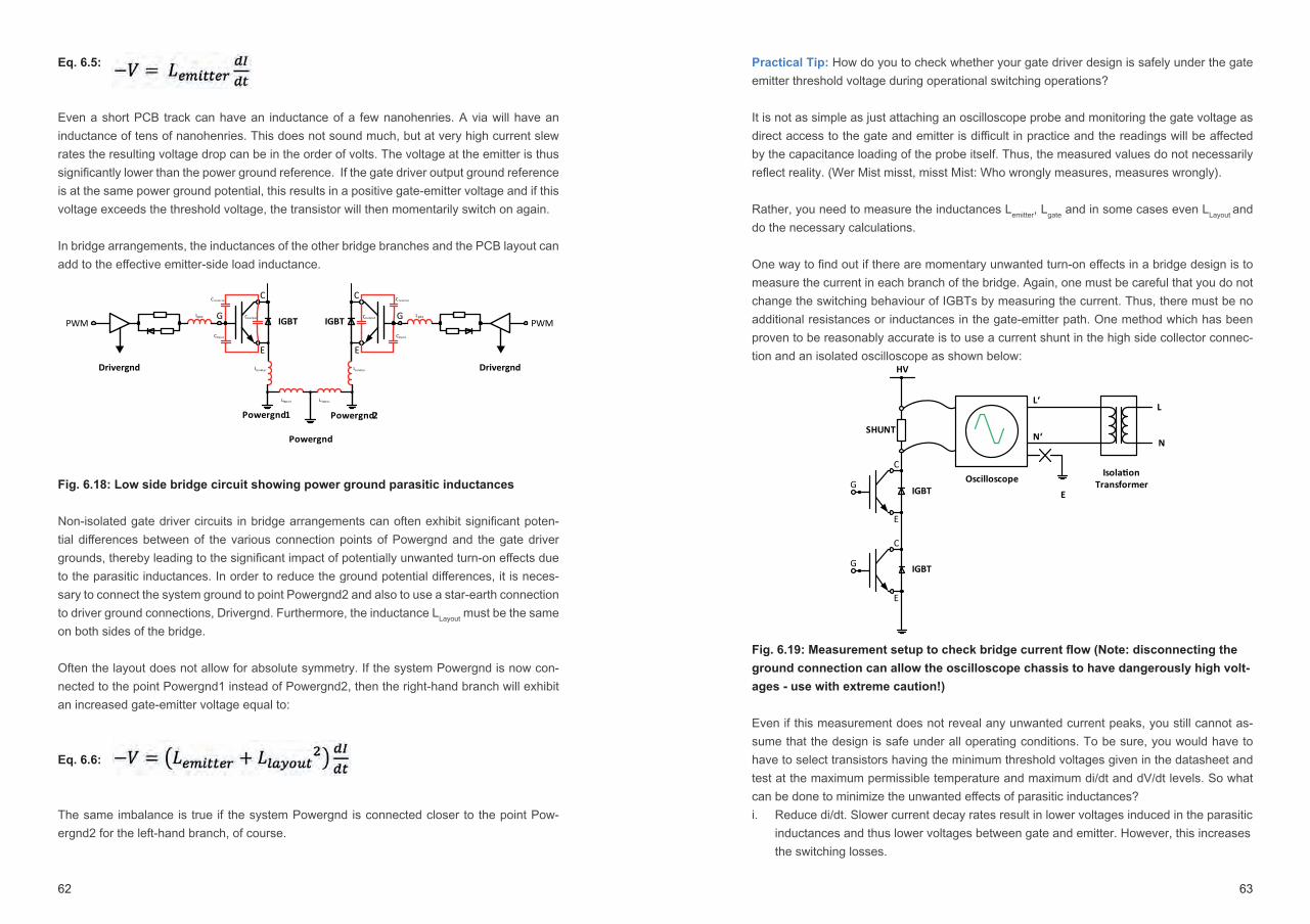
62 63
Practical Tip: How do you to check whether your gate driver design is safely under the gate emitter threshold voltage during operational switching operations?
It is not as simple as just attaching an oscilloscope probe and monitoring the gate voltage as direct access to the gate and emitter is difficult in practice and the readings will be affected by the capacitance loading of the probe itself. Thus, the measured values do not necessarily reflect reality. (Wer Mist misst, misst Mist: Who wrongly measures, measures wrongly).
Rather, you need to measure the inductances Lemitter, Lgate and in some cases even LLayout and do the necessary calculations.
One way to find out if there are momentary unwanted turn-on effects in a bridge design is to measure the current in each branch of the bridge. Again, one must be careful that you do not change the switching behaviour of IGBTs by measuring the current. Thus, there must be no additional resistances or inductances in the gate-emitter path. One method which has been proven to be reasonably accurate is to use a current shunt in the high side collector connec-tion and an isolated oscilloscope as shown below:
Fig. 6.19: Measurement setup to check bridge current flow (Note: disconnecting the
ground connection can allow the oscilloscope chassis to have dangerously high volt-
ages - use with extreme caution!)
Even if this measurement does not reveal any unwanted current peaks, you still cannot as-sume that the design is safe under all operating conditions. To be sure, you would have to have to select transistors having the minimum threshold voltages given in the datasheet and test at the maximum permissible temperature and maximum di/dt and dV/dt levels. So what can be done to minimize the unwanted effects of parasitic inductances? i. Reduce di/dt. Slower current decay rates result in lower voltages induced in the parasitic
inductances and thus lower voltages between gate and emitter. However, this increases the switching losses.
G
E
C
IGBT
G
E
C
IGBT
SHUNT
HV
L
N
L‘
N‘
EOscilloscope Isolation
Transformer
Eq. 6.5:
Even a short PCB track can have an inductance of a few nanohenries. A via will have an inductance of tens of nanohenries. This does not sound much, but at very high current slew rates the resulting voltage drop can be in the order of volts. The voltage at the emitter is thus significantly lower than the power ground reference. If the gate driver output ground reference is at the same power ground potential, this results in a positive gate-emitter voltage and if this voltage exceeds the threshold voltage, the transistor will then momentarily switch on again.
In bridge arrangements, the inductances of the other bridge branches and the PCB layout can add to the effective emitter-side load inductance.
Fig. 6.18: Low side bridge circuit showing power ground parasitic inductances
Non-isolated gate driver circuits in bridge arrangements can often exhibit significant poten-tial differences between of the various connection points of Powergnd and the gate driver grounds, thereby leading to the significant impact of potentially unwanted turn-on effects due to the parasitic inductances. In order to reduce the ground potential differences, it is neces-sary to connect the system ground to point Powergnd2 and also to use a star-earth connection to driver ground connections, Drivergnd. Furthermore, the inductance LLayout must be the same on both sides of the bridge.
Often the layout does not allow for absolute symmetry. If the system Powergnd is now con-nected to the point Powergnd1 instead of Powergnd2, then the right-hand branch will exhibit an increased gate-emitter voltage equal to:
Eq. 6.6:
The same imbalance is true if the system Powergnd is connected closer to the point Pow-ergnd2 for the left-hand branch, of course.
PWMG
E
C
IGBTLgate
C reverse
Coutput
Cinput
Lemi�er
Powergnd1
Llayout
PWMG
E
C
Lgate
C reverse
Coutput
Cinput
Lemi�er
L layout
Powergnd2
Powergnd
Drivergnd Drivergnd
IGBT
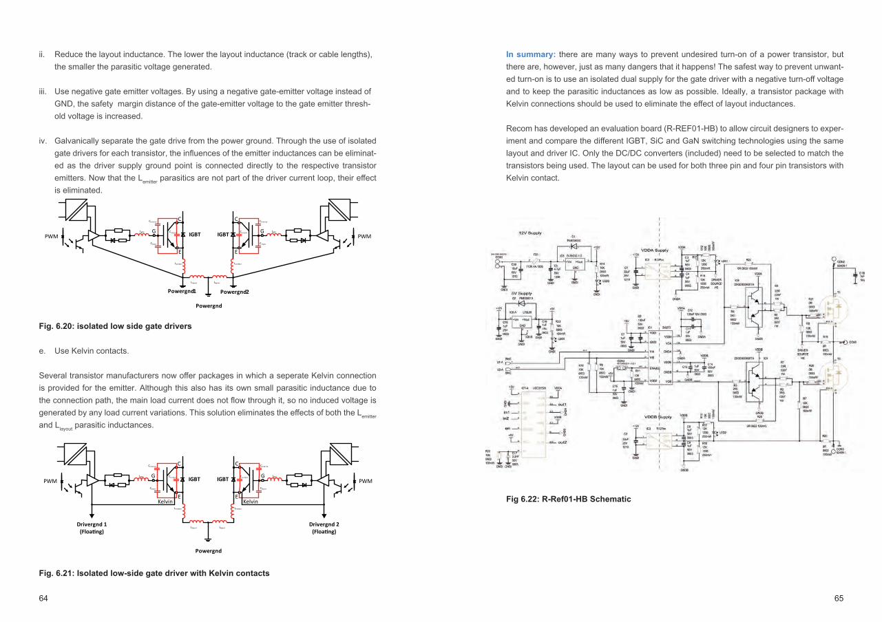
64 65
In summary: there are many ways to prevent undesired turn-on of a power transistor, but there are, however, just as many dangers that it happens! The safest way to prevent unwant-ed turn-on is to use an isolated dual supply for the gate driver with a negative turn-off voltage and to keep the parasitic inductances as low as possible. Ideally, a transistor package with Kelvin connections should be used to eliminate the effect of layout inductances.
Recom has developed an evaluation board (R-REF01-HB) to allow circuit designers to exper-iment and compare the different IGBT, SiC and GaN switching technologies using the same layout and driver IC. Only the DC/DC converters (included) need to be selected to match the transistors being used. The layout can be used for both three pin and four pin transistors with Kelvin contact.
Fig 6.22: R-Ref01-HB Schematic
ii. Reduce the layout inductance. The lower the layout inductance (track or cable lengths), the smaller the parasitic voltage generated.
iii. Use negative gate emitter voltages. By using a negative gate-emitter voltage instead of GND, the safety margin distance of the gate-emitter voltage to the gate emitter thresh-old voltage is increased.
iv. Galvanically separate the gate drive from the power ground. Through the use of isolated gate drivers for each transistor, the influences of the emitter inductances can be eliminat-ed as the driver supply ground point is connected directly to the respective transistor emitters. Now that the Lemitter parasitics are not part of the driver current loop, their effect is eliminated.
Fig. 6.20: isolated low side gate drivers
e. Use Kelvin contacts.
Several transistor manufacturers now offer packages in which a seperate Kelvin connection is provided for the emitter. Although this also has its own small parasitic inductance due to the connection path, the main load current does not flow through it, so no induced voltage is generated by any load current variations. This solution eliminates the effects of both the Lemitter
and Llayout parasitic inductances.
Fig. 6.21: Isolated low-side gate driver with Kelvin contacts
G
E
C
IGBTLgate
Creverse
Coutput
Cinput
Lemitter
Powergnd1
Llayout
G
E
C
Lgate
Creverse
Coutput
C input
Lemitter
Llayout
Powergnd2
Powergnd
IGBTPWM PWM
G
E
C
IGBTLgate
Creverse
Coutput
Cinput
Lemi�er
Drivergnd 1(Floating)
Llayout
Powergnd
IGBTPWM
Kelvin
G
E
C
Lgate
Creverse
C output
Cinput
Lemi�er
Drivergnd 2(Floating)
Llayout
PWM
Kelvin

66 67
Chapter 7
Power Factor Correction
Power Factor Correction (PFC) is required for AC/DC power supplies with more than 75W output power (25W in the case of LED drivers) in order to comply with IEC/EN 61000-3-2. PFC circuits also allow higher output powers without exceeding the maximum input current limit of the mains supply:
Eq. 7.1.
For an 85% efficient AC/DC converter operating from a fixed 230VAC supply fitted with a 10A over-current protection:PF = 0.70 allows a maximum output power of 0.70 x 0.85 x 230V x 10A ≈ 1370WPF = 0.95 allows a maximum output power of 0.95 x 0.85 x 230V x 10A ≈ 1860W
7.1 Passive PFC
Returning to our simple linear power supply design in Chapter 2, the reactive power is mainly capacitive although the load across the mains supply is the transformer, a primarily inductive component. This is because the transformer “reflects” the secondary load phase shift to the primary side. Thus the reactive power seen by the mains supply is mainly capacitive and the current leads the voltage. It would be possible to shift the current waveform to partially correct the power factor by adding a series inductor - but it is not possible to fill in all of the greyed-out areas in the waveform shown in figure 2.3 with current, so the power factor cannot be made perfectly equal to 1.
In practice, a passive power factor correction (PFC) solution can improve an uncorrected power factor from around 0.4 to around 0.7 by using PFC chokes (typically an iron-cored transformer with only a single winding) but such inductors are often nearly as large and as heavy as the isolation transformer itself:
Fig. 7.1: Passive power factor correction - the PFC
choke partially cancels out the phase shift caused
by the output capacitor C. The resulting voltage/cur-
rent graph shows how the input current has been
“delayed” by the PFC choke to give a better overall
PF value
C
L
N
V+
V-
PFC Choke
Rload
O
1
-1
π/2 π 2π3π/2
V
I
One of the main problems with the simple passive PFC correction circuit shown above is that the PFC choke can only operate over a limited input voltage range and still adequately correct the power factor. A solution often used in very low-cost passive PFC circuits is to add a volt-age selector switch between 115VAC and 230VAC operation (figure 7.2). The switch is either open (230V) and the PFC choke is connected in series with the full wave rectifier or closed (115V) making the circuit then the same as a half wave voltage doubler so that the output voltage stays the same (only the left half of the PFC choke and the left half of the full bridge are active).
Fig. 7.2: Passive PFC with input voltage range switch
The voltage doubler capacitors can be calculated from the relationship:
Eq. 7.2:
For a 100W power supply with 80% efficiency at 115VAC/60Hz input:Iin = 100W/325VDC= 0.3A/0.8=0.375A, tholdup = 1/120Hz =0.08
So, assuming an acceptable ripple Voltage of Vripple = 30V
Fig. 7.3: An example of a pas-
sive PFC design with mains
selector switch. The PFC choke
can be seen above the two
voltage doubler capacitors. The
advantage of this circuit is that
the electrolytic capacitors each
need only be rated for 200V
operation, even with a 230VAC
input.
C2
L
N
V+
V-
PFC Choke
Rload
230 VAC/115 VAC
C1
≈ 325 Vdc
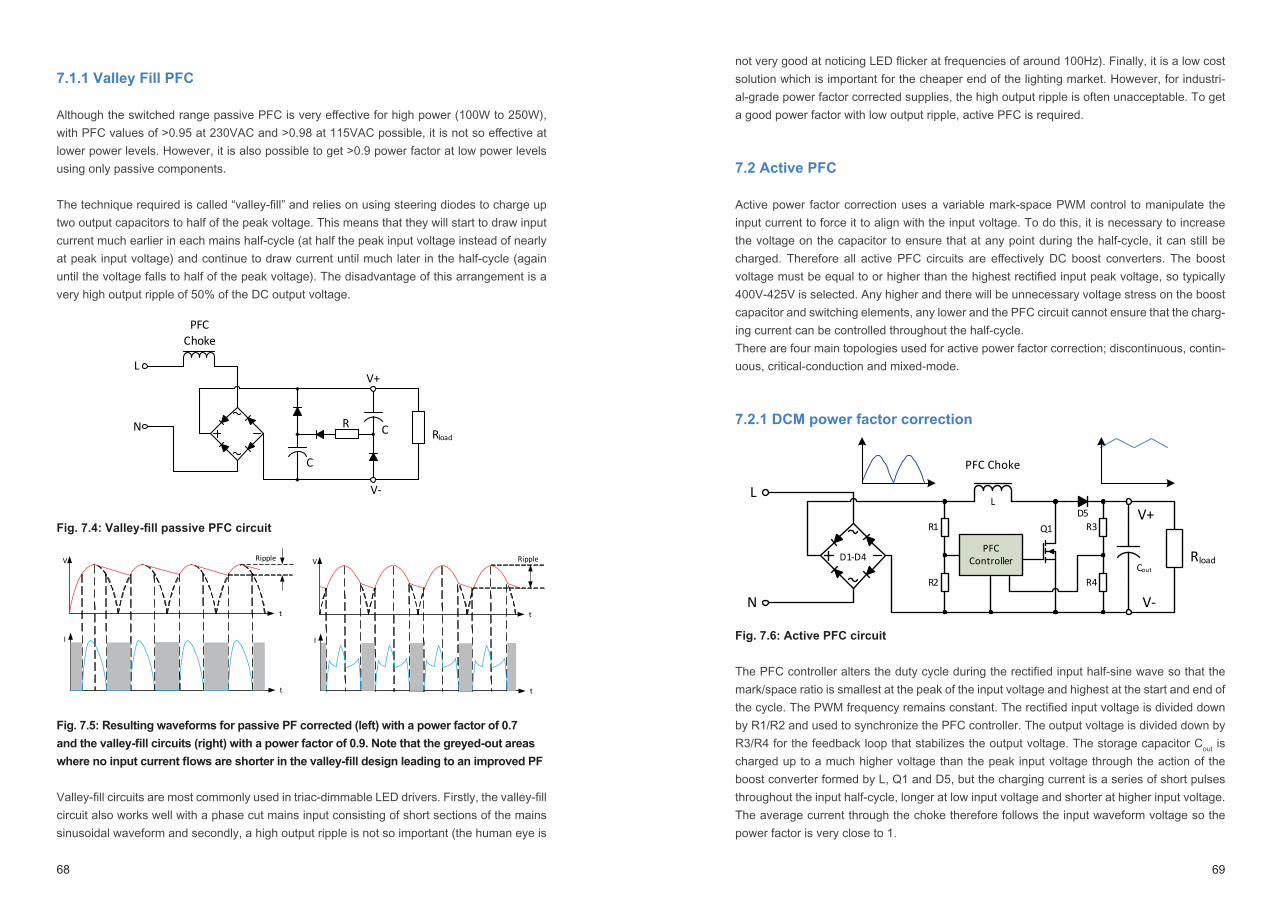
68 69
7.1.1 Valley Fill PFC
Although the switched range passive PFC is very effective for high power (100W to 250W), with PFC values of >0.95 at 230VAC and >0.98 at 115VAC possible, it is not so effective at lower power levels. However, it is also possible to get >0.9 power factor at low power levels using only passive components.
The technique required is called “valley-fill” and relies on using steering diodes to charge up two output capacitors to half of the peak voltage. This means that they will start to draw input current much earlier in each mains half-cycle (at half the peak input voltage instead of nearly at peak input voltage) and continue to draw current until much later in the half-cycle (again until the voltage falls to half of the peak voltage). The disadvantage of this arrangement is a very high output ripple of 50% of the DC output voltage.
Fig. 7.4: Valley-fill passive PFC circuit
Fig. 7.5: Resulting waveforms for passive PF corrected (left) with a power factor of 0.7
and the valley-fill circuits (right) with a power factor of 0.9. Note that the greyed-out areas
where no input current flows are shorter in the valley-fill design leading to an improved PF
Valley-fill circuits are most commonly used in triac-dimmable LED drivers. Firstly, the valley-fill circuit also works well with a phase cut mains input consisting of short sections of the mains sinusoidal waveform and secondly, a high output ripple is not so important (the human eye is
L
N
V+
V-
PFC Choke
Rload
C
CR
V
t
I
t
V
t
I
t
Ripple
Ripple
V
t
I
t
V
t
I
t
Ripple
Ripple
not very good at noticing LED flicker at frequencies of around 100Hz). Finally, it is a low cost solution which is important for the cheaper end of the lighting market. However, for industri-al-grade power factor corrected supplies, the high output ripple is often unacceptable. To get a good power factor with low output ripple, active PFC is required.
7.2 Active PFC
Active power factor correction uses a variable mark-space PWM control to manipulate the input current to force it to align with the input voltage. To do this, it is necessary to increase the voltage on the capacitor to ensure that at any point during the half-cycle, it can still be charged. Therefore all active PFC circuits are effectively DC boost converters. The boost voltage must be equal to or higher than the highest rectified input peak voltage, so typically 400V-425V is selected. Any higher and there will be unnecessary voltage stress on the boost capacitor and switching elements, any lower and the PFC circuit cannot ensure that the charg-ing current can be controlled throughout the half-cycle.There are four main topologies used for active power factor correction; discontinuous, contin-uous, critical-conduction and mixed-mode.
7.2.1 DCM power factor correction
Fig. 7.6: Active PFC circuit
The PFC controller alters the duty cycle during the rectified input half-sine wave so that the mark/space ratio is smallest at the peak of the input voltage and highest at the start and end of the cycle. The PWM frequency remains constant. The rectified input voltage is divided down by R1/R2 and used to synchronize the PFC controller. The output voltage is divided down by R3/R4 for the feedback loop that stabilizes the output voltage. The storage capacitor Cout is charged up to a much higher voltage than the peak input voltage through the action of the boost converter formed by L, Q1 and D5, but the charging current is a series of short pulses throughout the input half-cycle, longer at low input voltage and shorter at higher input voltage. The average current through the choke therefore follows the input waveform voltage so the power factor is very close to 1.
L
N
V+
V-
PFC Choke
RloadCout
L
Q1D5
R1
R2
PFC Controller
R3
R4
D1-D4

70 71
Fig. 7.7: Discontinuous conduction mode (DCM).
The inductor current is shown in black, the input voltage in red and the average input current in blue. The inductor current falls to zero at the end of each PWM pulse.
The main advantage of DCM power factor correction is that the inductor is fully magnetized and de-magnetized during each PWM cycle, so the inductor current falls to zero at the end of each pulse. The switching transistor then switches on at zero voltage/zero current, so it is very effi -cient and almost lossless. Also, the recovery speed of the boost rectifi cation diode is not critical.
The disadvantage of this method is the high EMI generated from the high peak cur-rents of the chopped input waveform. A discontinuous PFC circuit needs a very good in-put EMC input fi lter to meet the regulatory conducted interference limits. The PFC choke must also be capable of handling the high peak currents, so the choke is large and heavy.
7.2.2 CCM power factor correction.
A solution to the EMC problems of DCM power factor correction is to use a continuous con-duction power factor correction controller. This is the same circuit as above, but the induct-ance is increased so that the current in the choke varies only slightly above and below the ideal sinusoidal waveform. Typically, the CCM current ripple is chosen to be around 20%-40% of the average inductor current. Again, the PWM frequency is constant:
Fig. 7.8: Continuous conduction mode (CCM)
DCM- (Discon�nuous Conduc�on-) Mode
The inductor current is shown in black, the input voltage in red and the average input current in blue. The inductor current does not fall to zero at the end of each PWM pulse.
The PWM controller is more complex as it must track the input voltage and adjust the input current more precisely, but the EMI generated is much lower as the input current is continuous and not pulsating.
The major disadvantages are the signifi cantly higher switching losses in the transistor and higher recovery losses in both the diode and the transistor. For a CCM design, the boost rectifi cation diode must be ultra-fast (very low Qrr). The choke needs to have a much larger inductance than for a DCM design, although the peak current is lower.
7.2.3 CrCM power factor correction.
Both the DCM and CCM power factor correction circuits use a fi xed PWM frequency. Howev-er, if the frequency is also made variable and synchronized to the input half-cycle, then the inductor current can be adjusted so that it only just touches zero at the end of each PWM pulse, whatever the input voltage is during the half-cycle (this is called boundary conduction mode (BCM) or critical conduction mode(CrCM).
Fig. 7.9: Boundary or Critical Conduction mode (CrCM)
The inductor current is shown in black, the input voltage in red and the average input current in blue. The inductor current falls to zero at the end of each PWM pulse and the PWM frequency varies.
With CrCM control, the switching losses in the transistor and the recovery losses in the diode are as low as in the DCM circuit plus the inductor can be made smaller than in the CCM circuit because the peak currents are lower.
The disadvantage is the variable frequency PWM requires EMC fi lters that are eff ective over a wider range of frequencies.

72 73
Fig. 7.10: Comparison between the inductor current waveforms in CCM, CrCM and
DCM PFC circuits.
All three solutions have the same average inductor current, but the peak-to-peak inductor current in the CrCM is a compromise between the very high levels of the DCM inductor and the very low levels of the CCM circuit.
7.2.4 Mixed-Mode PFC
There are many PFC controllers on the market that are capable of switching between diff erent modes of operation according to the operating conditions of the converter. A chosen value of choke that works well with a CCM controller at low input voltage (90 – 125VAC) may transition to DCM due to the lower input current at higher input voltages (180-265VAC), thus harming the power factor correction fi gure. To avoid having to make a compromise, the controller can be made variable frequency/variable PWM to keep the circuit in CCM/CrCM throughout the input voltage range. There are also powder core chokes called “swinging chokes” that change their inductance according to the current though them. At low currents, the inductance in-creases, thus keeping the PFC in CCM/CrCM whatever the operating conditions.
Practical Tip: PFC stages are susceptible to damage from input surge voltages. The bridge rectifi er will rectify both positive and negative-going surges into a high positive voltage into the PFC choke. The resulting high current can rapidly saturate the core so that the choke no longer behaves like an inductor, but lets all of the surge voltage through. The PFC diode now has to cope with the high charging current (sometimes hundreds of amps) into the PFC capac-itor and can quickly fail. The solution is to add a high current diode in parallel with the PFC choke and diode. Under normal operating conditions, the PFC voltage will be higher than the input voltage and the bypass diode will be reverse biased. Under surge conditions, the input exceeds the PFC voltage and it will conduct, relieving the stress on both the PFC diode and PFC choke as well as reducing the voltage across the bridge rectifi er.
Fig. 7.11: Active PFC with surge bypass diode
15
10
5
0IL(t)
Iin(t)
Discontinuoud Conduction Mode (DCM)
15
10
5
0IL(t)
Iin(t)
Critical Conduction Mode (CrCM)
15
10
5
0IL(t)
Iin(t)
Continuous Conduction Mode (CCM)
L
N
V+
V-
PFC Choke
RloadCout
L
Q1D5
R1
R2
PFC Controller
R3
R4
D1-D4
Dbypass
7.2.5 Interleaved PFC
As has been mentioned several times in this chapter, the EMC considerations are an impor-tant factor in choosing the appropriate conduction mode for the PFC controller. If the EMI is too high to be eff ectively fi ltered out then an alternative topology is to use two interleaved PFC circuits so that the ripple current in each stage is halved and added in anti-phase.
Interleaving also has the advantage of sharing the output current across two inductors and two diodes, thus allowing either higher output currents or improved operating temperatures.
Fig. 7.12: Interleaved PFC circuit
An interleaved PFC is mainly used for high power AC/DC converters where the high input current would make the EMC input fi lter very bulky and more expensive than the extra circuitry of using two CrCM PFC boost converters. The PWM outputs operate 180°C out of phase, so although the current in either of the inductors falls to zero at the end of each pulse, the current fl owing into the PFC capacitor is continuous (current fl ows alternately through D1 and D2).
The output voltage ripple is signifi cantly lower than is possible with a single stage PFC and with a 50% duty cycle, the interleaved topology has zero input current ripple as the two PFC stages cancel out. Besides the increased cost, the biggest disad-vantage is that all of the components used must be very carefully matched to maintain the same performance over all operation conditions.
Fig. 7.13: Comparison of the duty
cycle vs input ripple current for
single phase and interleaved
phase PFC boost circuits
L
N
V+
V-
RloadCout
L2Q1 D6
R1
R2
InterleavedPFC
Controller
R3
R4
D1-D4
L1D5
Q2
0 20 40 60 80 100
0,8
0,7
0,6
0,5
0,4
0,3
0,2
0,1
0
0,9
1
Single phase boost converterTwo phase interleaved boost converter
Duty Cycle [%]

74 75
7.2.6 Bridgeless (totem pole) PFC
The bridgeless or totem-pole PFC topology is becoming more popular because of its very high efficiency. The bridge rectifier diodes are replaced by two high voltage transistors that alternately switch at the mains frequency to rectify the input. The diode forward voltage drops are therefore eliminated and the internal body diodes of the transistors aid the current flow and increase the efficiency.
It is usual to use different transistor types for the slower 50Hz switching and the high frequen-cy PFC switching.
Fig. 7.14: Bridgeless Totem-Pole PFC topology and switching current paths
The single switching FET in the previous PFC designs is replaced by two FETs Q1 and Q2. During a positive mains half-cycle, Q4 is switched on, Q3 is off, Q1 is operated with a PWM signal to boost the output voltage and Q2 is operated with the inverted PWM signal to act as a rectifier. During a negative mains half-cycle, Q3 is switched on, Q4 is off, Q2 is operated with a PWM signal to boost the output voltage and Q1 is operated with the inverted PWM signal to act as a rectifier.
As Q3 and Q4 are switched at a low frequency (50/60Hz), they do not need to switch quickly and can be regular MOSFETS. Diodes are placed in parallel to help increase the efficiency by sharing the peak current, but the power switching is done with the MOSFETs. The forward voltage losses of the conventional bridge rectifier are thus eliminated, so the rectification loss-es can be very low (<1%).
AC
Q1
Q2 Q3
Q4
C RL
LPFC
AC
Q1
Q2 Q3
Q4
C RL
LPFC
AC
Q1
Q2 Q3
Q4
C RL
LPFC
AC
Q1
Q2 Q3
Q4
C RL
LPFC
The transistors Q1 and Q2 cannot be MOSFETs because the reverse recovery losses would be too high. The switching delay would cause shoot-through and large current spikes during AC ze-ro-crossing. One solution is to use JFET transistor in a cascode configuration with a MOSFET:
Fig. 7.15: SiC/JFET cascode
The JFET is normally on and has a gate input that is effectively grounded. When the MOSFET is off, the MOSFET VDS rises until the JFET VGS is sufficiently negative to switch the JFET off. The supply voltage then appears almost entirely across the JFET. When the MOSFET is switched on, the VDS drops to close to zero and the JFET turns on. The advantage of this arrangement is that the JFET gate and the MOSFET VDS and VGS are all close to zero, so the reverse recovery, Coss and Miller capacitance losses are also close to zero. The switching speed is vastly improved.
More recently, high electron mobility transistors (HEMT) such as GaN FETS are being used to replace the cascode as they are ideal for such totem-pole topologies (very fast switching slew rates, no body diode, and low gate capacitance). Overall PFC stage efficiencies in excess of 99% are possible with GaN FET totem pole designs.
The following bridgeless totem pole PFC circuit uses two half bridge power stages to replace the bridge rectifier and the PFC switcher normally required by AC powered applications. The synchronous rectifier consists of two silicon MOSFETs alternately switched with a 50% duty cycle at 50/60Hz in time with the AC mains input. This creates a rectified output without the need for an input bridge rectifier. The PFC half-bridge circuit runs with a higher frequency and variable duty cycle PWM signal to perform the power factor correction function using low loss GaN transistors. With the low component count, the gate driver components can be placed closer together and parasitic inductances and stray capacitances minimized. Two RP-1506S converters and a dual channel digital isolator are used to create the fully isolated high-speed half-bridge GaN gate driver circuit for the PFC with a BOM count of only 20 parts.
The 50/60Hz AC synchronous rectification half-bridge runs at a much lower frequency, so lower-cost MOSFETs can be used without sacrificing overall efficiency or performance. The isolated +15V high-side MOSFET gate drive power is supplied by a RP-1515S converter. All
Si MOSFET
SiC JFET
= G
S
D
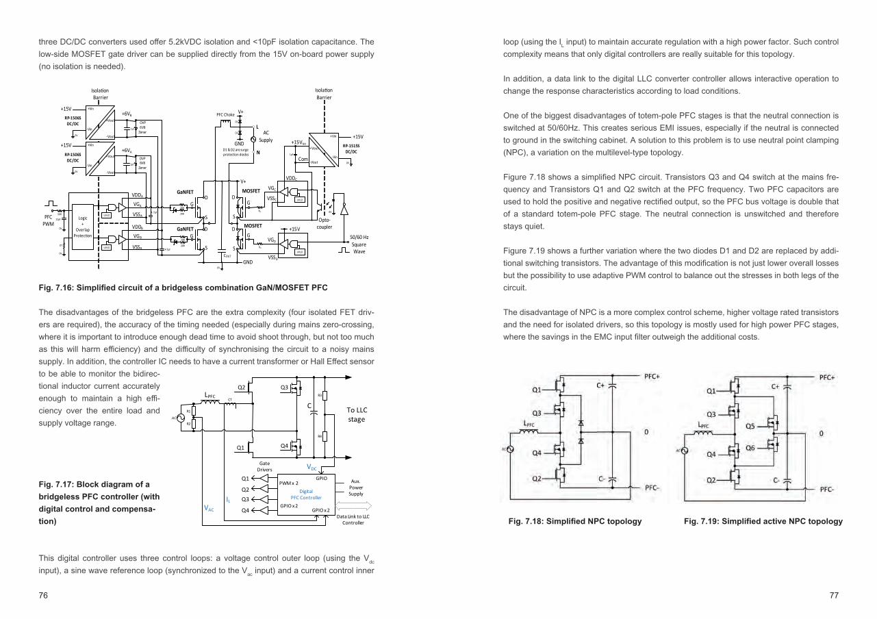
76 77
three DC/DC converters used off er 5.2kVDC isolation and <10pF isolation capacitance. The low-side MOSFET gate driver can be supplied directly from the 15V on-board power supply (no isolation is needed).
Fig. 7.16: Simplifi ed circuit of a bridgeless combination GaN/MOSFET PFC
The disadvantages of the bridgeless PFC are the extra complexity (four isolated FET driv-ers are required), the accuracy of the timing needed (especially during mains zero-crossing, where it is important to introduce enough dead time to avoid shoot through, but not too much as this will harm effi ciency) and the diffi culty of synchronising the circuit to a noisy mains supply. In addition, the controller IC needs to have a current transformer or Hall Eff ect sensor to be able to monitor the bidirec-tional inductor current accurately enough to maintain a high effi -ciency over the entire load and supply voltage range.
Fig. 7.17: Block diagram of a
bridgeless PFC controller (with
digital control and compensa-
tion)
This digital controller uses three control loops: a voltage control outer loop (using the Vdc
input), a sine wave reference loop (synchronized to the Vac input) and a current control inner
+Vin
-Vin
RP-1515SDC/DC
+15V
0V1µF
OVP6V8
Zener
50R
22pFPFCPWM
0V
G
S
DGaNFET
IsolationBarrier
+6VB
Logic+
OverlapProtection
UVLO
UVLO
V+
G
S
DGaNFET
DT
0V
VDDA
VSSA
VDDB
VSSB
VGA
VGB
4. 7µF
4.7µF
1µF
OVP6V8
Zener
+6VA
20R
20R
20R
20R
PFC Choke
G
G
MOSFET
RG
1µF
IsolationBarrier
+15Viso
Com
UVLO
VDDC
VSSC
VGC
RG
GND
D1
D2
V+
GND
50/60 HzSquareWaveUVLO
VGD
D
SMOSFETD
S
0V
+15V
+Vout
-Vout
+Vin
-Vin
RP-1506SDC/DC
+15V
0V
+Vin
-Vin
RP-1506SDC/DC
+15V
0V
+Vout
-Vout
+Vout
-Vout
0V
Opto-coupler
VSSDCOUT
N
L
D1 & D2 are surge protection diodes
ACSupply
AC
Q1
Q2 Q3
Q4
CLPFC
DigitalPFC Controller
CT
R1
R2
Q1
Q2Q3
Q4
PWM x 2
GPIO x 2GPIO x 2
ILVAC
GateDrivers
Aux.PowerSupply
Data Link to LLC Controller
To LLCstage
R3
R4
GPIO
VDC
loop (using the IL input) to maintain accurate regulation with a high power factor. Such control complexity means that only digital controllers are really suitable for this topology.
In addition, a data link to the digital LLC converter controller allows interactive operation to change the response characteristics according to load conditions.
One of the biggest disadvantages of totem-pole PFC stages is that the neutral connection is switched at 50/60Hz. This creates serious EMI issues, especially if the neutral is connected to ground in the switching cabinet. A solution to this problem is to use neutral point clamping (NPC), a variation on the multilevel-type topology.
Figure 7.18 shows a simplifi ed NPC circuit. Transistors Q3 and Q4 switch at the mains fre-quency and Transistors Q1 and Q2 switch at the PFC frequency. Two PFC capacitors are used to hold the positive and negative rectifi ed output, so the PFC bus voltage is double that of a standard totem-pole PFC stage. The neutral connection is unswitched and therefore stays quiet.
Figure 7.19 shows a further variation where the two diodes D1 and D2 are replaced by addi-tional switching transistors. The advantage of this modifi cation is not just lower overall losses but the possibility to use adaptive PWM control to balance out the stresses in both legs of the circuit.
The disadvantage of NPC is a more complex control scheme, higher voltage rated transistors and the need for isolated drivers, so this topology is mostly used for high power PFC stages, where the savings in the EMC input fi lter outweigh the additional costs.
Fig. 7.18: Simplifi ed NPC topology Fig. 7.19: Simplifi ed active NPC topology

78 79
Chapter 8
AC/DC Converter Topologies
(This section is largely based on the DC/DC book of knowledge discussion of the different topologies, but as DC/DC and AC/DC share several conversion topologies2 , it is reproduced here for the sake of completeness).In the family of isolated AC/DC converters there is a wide variety of topologies available, but only some of them are applicable to the discussion of modern AC/DC designs. This section will limit its consideration to flyback (single and doubled ended versions), forward (active clamp, single and double ended versions), push-pull, bridge converter (half-bridge and full bridge) and resonant (ZVS, LLC) topologies. In these types of isolated converters, the transfer of energy from input to the output is performed via an isolating transformer. Line voltage and output load regulation is performed by a PWM controller. Ideal components are again assumed.
8.1 Single-Ended Flyback
The flyback converter converts an input voltage into a regulated output voltage by storing energy in the transformer core gap during the transistor ON time and transferring it to the secondary during the OFF time. Technically the transformer consists of two coupled inductors as the energy transfer is not by true transformer action. Figure 8.1 shows the simplified circuit:
Fig. 8.1: Isolated flyback converter simplified schematic
For a power supply without PFC, the rectified mains input voltage will be between about 126VDC and 320VDC, but the output voltage is typically between 3.3V and 24V. This is a big voltage difference! If a PFC front end is used, the rectified input voltage will be even higher and the difference even greater.
D1
C2 RL
AC C1
T1
N:1
Current Flow, Q1 closedCurrent Flow, Q1 open
Q1
2 Note: DC cannot be converted directly via a transformer, so all DC/DC converters are essen-tially DC-to-AC//AC-to-DC couplers. On the other hand, AC switched mode power supplies run at a higher frequency than the mains input, so they rectify the AC input to DC and are AC-to-DC-to-AC//AC-to-DC couplers. It is not surprising that they have many elements in common.
One of the advantages of a flyback transformer design is that the turns ratio decides the fun-damental input/output voltage ratio (Eq. 8.1). The variable mark-space PWM controller on the input power stage can then easily compensate for any variation in input voltage or output load. Duty cycles higher than 0.5 are possible with the flyback topology, but in general should be avoided to reduce the average current in the output diode.
Eq. 8.1:
So, for a universal input AC/DC with a minimum input range of 90VAC (no PFC, so 126VDC when rectified) and an output voltage of 24VDC, the transformer turns ratio would be chosen to be 5:1.At this input voltage, the PWM would have 50% duty cycle. At the highest input voltage of 264VAC (370VDC when rectified), the PWM would have a 25% duty cycle. The relevant rela-tionships are as follows:
Eq. 8.2:
Where the reflected output voltage, VOR, equals (Vout + VDrop,D1) multiplied by the turns ratio, N.
Given the above values, VOR = (24V + 1V) x 5 = 125V. For the same power supply with a PFC front end, the DC boost voltage would be chosen to be around 385VDC, so the transformer turns ratio would be 16:1 and the PWM would have an ideal 50% duty cycle over the whole input voltage range.
Another advantage of the flyback topology is that multiple outputs (with different polarities if required) can be easily implemented by adding multiple secondary windings. In particular, a low voltage secondary winding wound on the primary-side of the transformer can be used to power the primary controller IC. (See section 12). The component count is also very low, so this topology is good for low cost designs.
With output voltage or current monitoring and an isolated feedback path (typically via an opto-coupler) a very stable regulated output can be generated. But flyback converters can also be primary side regulated by monitoring the auxilliary winding waveform and using the knee-point to detect when the secondary current has reached zero. This eliminates the optocoupler and reduces the component count still further.
The disadvantage is that the transformer core needs careful selection, the air-gapped core should not saturate even though there is an average DC current flowing through the trans-former and efficiency can be lost if it has a large magnetic hysteresis. Also eddy current losses in the windings can be a problem due to the high peak currents. These two effects limit the practical operational frequency and power range of this topology.
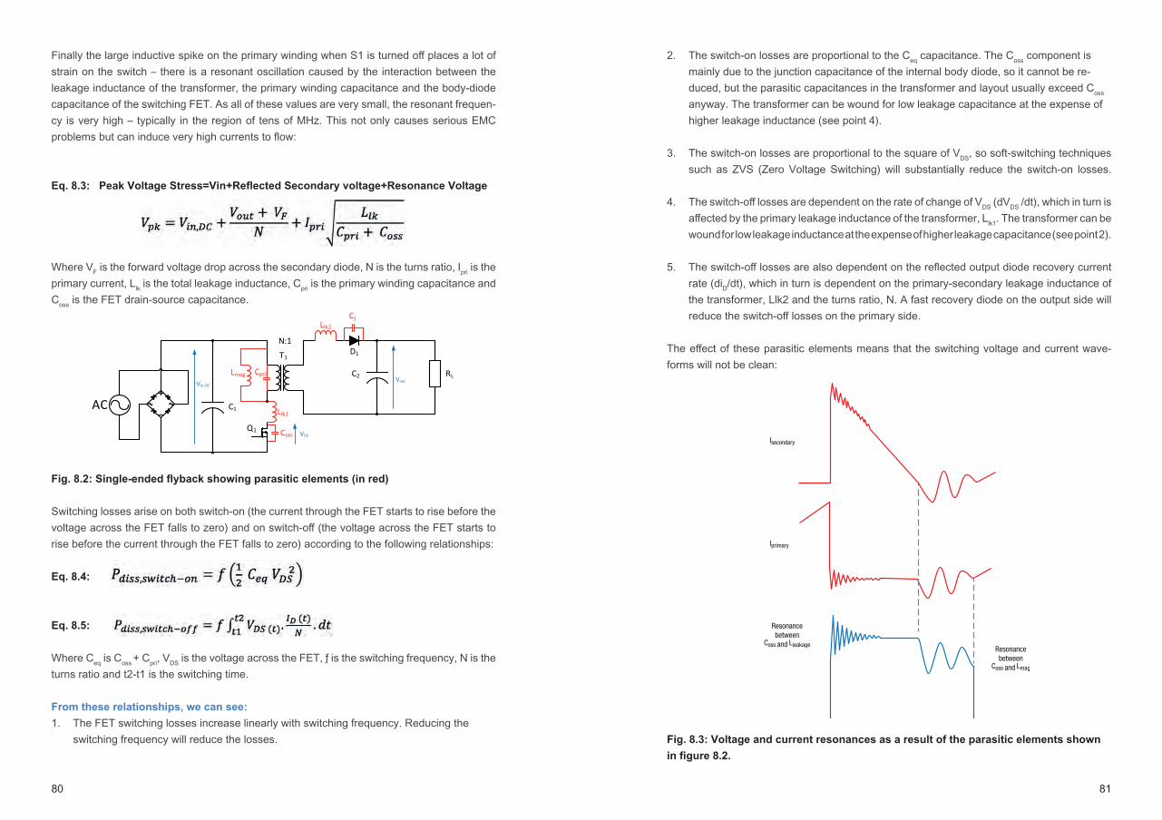
80 81
Finally the large inductive spike on the primary winding when S1 is turned off places a lot of strain on the switch – there is a resonant oscillation caused by the interaction between the leakage inductance of the transformer, the primary winding capacitance and the body-diode capacitance of the switching FET. As all of these values are very small, the resonant frequen-cy is very high – typically in the region of tens of MHz. This not only causes serious EMC problems but can induce very high currents to flow:
Eq. 8.3: Peak Voltage Stress=Vin+Reflected Secondary voltage+Resonance Voltage
Where VF is the forward voltage drop across the secondary diode, N is the turns ratio, Ipri is the primary current, Llk is the total leakage inductance, Cpri is the primary winding capacitance and Coss is the FET drain-source capacitance.
Fig. 8.2: Single-ended flyback showing parasitic elements (in red)
Switching losses arise on both switch-on (the current through the FET starts to rise before the voltage across the FET falls to zero) and on switch-off (the voltage across the FET starts to rise before the current through the FET falls to zero) according to the following relationships:
Eq. 8.4:
Eq. 8.5:
Where Ceq is Coss + Cpri, VDS is the voltage across the FET, ƒ is the switching frequency, N is the turns ratio and t2-t1 is the switching time.
From these relationships, we can see:
1. The FET switching losses increase linearly with switching frequency. Reducing the switching frequency will reduce the losses.
D1
C2 RL
AC C1
T1
N:1
Q1
Lmag
Llk1
Coss
Llk2
Cj
Cpri
VDS
Vin,DCVout
2. The switch-on losses are proportional to the Ceq capacitance. The Coss component is mainly due to the junction capacitance of the internal body diode, so it cannot be re-duced, but the parasitic capacitances in the transformer and layout usually exceed Coss anyway. The transformer can be wound for low leakage capacitance at the expense of higher leakage inductance (see point 4).
3. The switch-on losses are proportional to the square of VDS, so soft-switching techniques such as ZVS (Zero Voltage Switching) will substantially reduce the switch-on losses.
4. The switch-off losses are dependent on the rate of change of VDS (dVDS /dt), which in turn is affected by the primary leakage inductance of the transformer, Llk1. The transformer can be wound for low leakage inductance at the expense of higher leakage capacitance (see point 2).
5. The switch-off losses are also dependent on the reflected output diode recovery current rate (diD/dt), which in turn is dependent on the primary-secondary leakage inductance of the transformer, Llk2 and the turns ratio, N. A fast recovery diode on the output side will reduce the switch-off losses on the primary side.
The effect of these parasitic elements means that the switching voltage and current wave-forms will not be clean:
Fig. 8.3: Voltage and current resonances as a result of the parasitic elements shown
in figure 8.2.
Isecondary
Iprimary
Resonancebetween
Coss and LieakageResonancebetween
Coss and Lmag

82 83
8.1.1 Single-ended flyback snubber networks
To absorb this damaging high frequency parasitic oscillation, a snubber is often required. The most common arrangement on the high side is a RCD (Resistor-Capacitor-Diode) snubber:
Fig. 8.4 Single-ended flyback with RCD snubber circuit (shown in blue)
The capacitor and resistor absorb the energy of the resonance ringing and cause it to decay more rapidly. The recovery diode is typically a standard power diode (not a fast diode) as a relatively slow reverse recovery time (Trr) also helps to damp out the ringing. The negative current that flows during this recovery time allows the snubber capacitor to damp the ringing more effectively by absorbing current on the positive cycle and delivering current on the neg-ative cycle despite the diode rectification. The power dissipated in the snubber network is highest at minimum Vin and full load:
Eq. 8.6:
Where ƒ is the switching frequency and VCS is the voltage across the snubber capacitor Cs.
Practical Tip: Vcs can be adjusted by changing the value of the snubber capacitor. If the ca-pacitor is too small, the voltage will be high and the snubber ineffective. If the capacitor is too large, then VCs will be small, but the power dissipation will be high. For optimum results, Cs should be chosen to be have a VCs equal of twice the sum of n (Vout + VD).
The optimum value of the snubber capacitance is also dependent on the snubber resistor, Rs, as they both operate together to absorb the ringing energy.
Eq. 8.7:
Where ∆VCS is the ripple voltage across the snubber capacitor (typically chosen to be 5%-10% of VCs). RS can be found from the relationship:
Eq. 8.8:
D1
C2 RL
ACC1
T1
N:1
Q1
CSRS
DS
If needed, a resistor in series with the diode can be added to damp the resonant peak between the primary leakage inductance and the snubber capacitor. This is called a R2CD snubber network.
For low standby current applications, the RCD snubber can be replaced by a TVS diode in series with an ultra-fast recovery diode and a damping resistor. It is a more expensive solu-tion, but avoids the RCD snubber dissipation, which is constant irrespective of load. Unlike the RCD snubber, a TVS snubber needs an ultra-fast diode for high efficiency.
Fig. 8.5: Single-ended flyback with TVS snubber network (shown in blue)
Practical Tip: When using quasi-resonant primary side regulation, care must be taken not to over-damp the resonances with snubber networks, because the regulation circuit needs to track the first or second valley of the Lm/Coss DCM resonance.
A practical example
Consider a 10W AC/DC power supply with the following specifications:
Vin = 100-240VAC nominal (no PFC)Vout = 5V @ 2A, VD = 0.5VOperating frequency = 50kHzTurns ratio = 12Lk = 750nH (by measurement)Peak Ipri = 400mA (by measurement)450V rated FET with Coss = 20pFPrimary winding capacitance = 10pF (by measurement)
For reliability, the peak voltage stress on the FET should be below 80% of its rated voltage. At maximum Vin, the peak voltage stress (from equation 8.2) is:
Peak Voltage Stress,
D1
C2 RL
ACC1
T1
N:1
Q1
RS
DFR
TVS

84 85
Although 437V is within the rating of the FET, it is much higher than 80% of VDSS, so the relia-bility will be poor as the transistor is close to its voltage stress limit. Adding an RCD snubber will signifi cantly improve the lifetime of the FET.
First we choose VCS to be twice n(Vout + VD) = 2 x 12(5V + 0.5V) = 132V
Next, we defi ne the snubber resistor, Rs, from Equation 8.8:
The power dissipation in the snubber resistor will be V²/R = 132V²/22k ohm = 0.8W.Choose a resistor with at least double this power rating or place two 1W resistors in parallel.
With 10% ripple, the snubber capacitor, Cs, will be from Equation 8.7:
Finally, the diode should be chosen to manage the peak voltage stress (choose at least dou-ble the rated voltage) and be able to cope with the diode power dissipation.
Suitable components for the snubber network would be a 22k/2W resistor in parallel with a 10nF/200V capacitor and a 1N4004 diode.
8.1.3 Ringing snubbers
Besides reducing the voltage stress on the main switching transistor, snubbers can also be used to damp ringing in the primary FET or secondary rectifi er diode.
Fig. 8.6: Single-ended fl yback with primary snubber (low side snubber)
The low side snubber provides damping for the LC resonance of the switching FET caused by the interaction of the primary leakage inductance and the MOSFET junction capacitance when the FET is turned off .
D1
C2 RL
ACC1
T1
N:1
Q1
RS
CS
Practical Tip: If a current sense resistor is used, the snubber must be placed across the tran-sistor only and not from the drain connection to ground, otherwise the sense resistor will be aff ected by the snubber discharge current. One way to calculate the required snubber compo-nents is to measure the transformer primary inductance with the outputs short circuited using an inductance meter (or a frequency response analyser if you have one) and use an oscillo-scope to measure the ringing frequency ƒr (hold the probe close to, but not touching the drain pin – the probe will pick up the signal without damping it with the probe’s own capacitance ;-) The snubber resistor is then:
Eq. 8.9:
And the snubber capacitor:
Eq. 8.10:
The power dissipation in the snubber resistor needs also to be checked:
Eq. 8.11:
Where f is the switching frequency (not the ringing frequency) and VDS is the peak FET voltage.
Practical Tip: Another way to determine the ringing snubber component values is by exper-iment:1. Find out ƒr using the method above2. Add capacitance (MLCC’s are best) across the FET until the frequency halves. The stray
capacitance is then equal 1/3 of the additional capacitance e.g. if adding 62pF halves the frequency, then Coss ≈ 20pF
3. Calculate the stray leakage inductance using the equation Eq. 8.12:
Eq. 8.12:
4. The snubber resistor is then the same as the characteristic impedance, Z:
Eq. 8.13:
5. The snubber capacitor can be chosen to be four to fi ve times Coss (the leak-age capacitance varies a lot in practice, so by choosing a larger capacitor, we can be sure that the ringing is properly damped - including production tolerances)
Ringing also occurs on the secondary output diode when it becomes reverse biased, so it can be useful to also put a snubber across it:

86 87
Fig. 8.7: Single-ended flyback with output diode snubber (shown in blue)
The peak ringing voltage across the secondary side diode if a snubber was not fitted would be:
Eq. 8.14:
Where Lk2 is the secondary leakage inductance and Cj is the junction capacitance of the diode.
For a typical power diode, the junction capacitance will be around 5pF. For a typical 12:1 turns ratio transformer, the secondary leakage inductance would be around 8nH (very approxi-mate). This would give a ringing voltage across the secondary diode of:
The output capacitor will absorb most of the ringing voltage if it has a low ESR and the PCB track inductance is not too high, but the diode must be able to survive this peak reverse voltage.
Adding the secondary side snubber not only dissipates the energy safely and protects the diode, but reduces the EMI generated by the secondary ringing which can be in the order of tens of MHz. On the other hand, as the ringing frequency is much higher than the switching frequency, it is relatively easy to filter out without incurring a high power dissipation loss.
Typical values for secondary snubber components are 4x the junction capacitance for the capacitor and a resistor value equal to the term.
In our example, suitable component values for the secondary side diode snubber would be a 20pF capacitor in series with a 40 ohm resistor.
D1
C2 RL
ACC1
T1
N:1
Q1
RSCS 8.1.2 Active clamp and regenerative snubbers
RC snubbers are dissipative circuits: the energy stored in the leakage inductance is diverted by the capacitor and dissipated in the snubber resistor. This consumes between 2%-5% of the total power so the resistor and diodes must be adequately dimensioned to cope with their internal temperature rise.A more efficient solution is to use active clamping and store the excess energy in a capacitor so that it can be returned to the next cycle. There are two ways to do this; a low-side p-channel clamp in series with the main switch or a high-side n-channel clamp to replace the clamping diode.
Fig. 8.8: Single-ended flyback active clamp configurations: high side and low side con-
figurations
8.1.2.1 High-side active clamp
The high-side solution shown in figure 8.8 requires an isolated gate driver but uses a lower cost n-channel MOSFET. Q2 is driven in antiphase to the main power transistor Q1 but with a dead time between cycles to avoid shoot-through.
Fig. 8.9: Single-ended flyback low-side active clamp current flow
T1
Q1
Lmag
Llk
Vin,DC
Q2
CS
Gate Drive
T1
Q1
Lmag
Llk
Vin,DC
Q2
CS
Gate Drive
Dead Time
Gate Drive
T1
Q1
Vin,DC
Q2
CS
Gate Drive
Dead Time
Phase 1 Phase 2
T1
Q1
Vin,DC
Q2
CS
Gate Drive
Dead Time
Ipri
Iclamp
Phase 3
T1
Q1
Vin,DC
Q2
CS
Gate Drive
Dead Time
Iclamp
T1
Q1
Q2
CS
Gate Drive
Dead Time
Phase 4
Cw
Cin Cin Cin Cin
Vin,DC
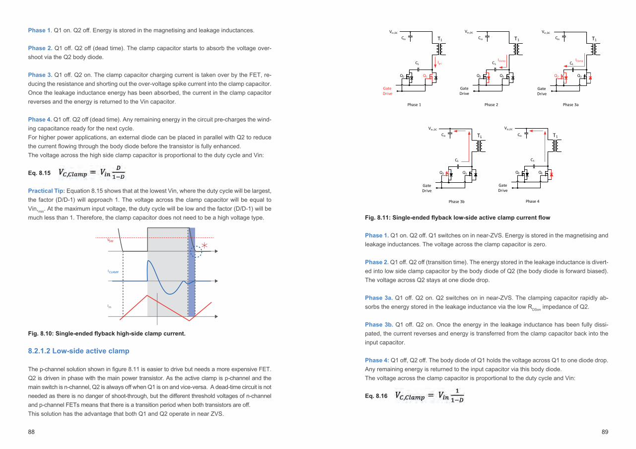
88 89
Phase 1. Q1 on. Q2 off . Energy is stored in the magnetising and leakage inductances.
Phase 2. Q1 off . Q2 off (dead time). The clamp capacitor starts to absorb the voltage over-shoot via the Q2 body diode.
Phase 3. Q1 off . Q2 on. The clamp capacitor charging current is taken over by the FET, re-ducing the resistance and shorting out the over-voltage spike current into the clamp capacitor. Once the leakage inductance energy has been absorbed, the current in the clamp capacitor reverses and the energy is returned to the Vin capacitor.
Phase 4. Q1 off . Q2 off (dead time). Any remaining energy in the circuit pre-charges the wind-ing capacitance ready for the next cycle.For higher power applications, an external diode can be placed in parallel with Q2 to reduce the current fl owing through the body diode before the transistor is fully enhanced.The voltage across the high side clamp capacitor is proportional to the duty cycle and Vin:
Eq. 8.15
Practical Tip: Equation 8.15 shows that at the lowest Vin, where the duty cycle will be largest, the factor (D/D-1) will approach 1. The voltage across the clamp capacitor will be equal to Vin,min. At the maximum input voltage, the duty cycle will be low and the factor (D/D-1) will be much less than 1. Therefore, the clamp capacitor does not need to be a high voltage type.
Fig. 8.10: Single-ended fl yback high-side clamp current.
8.2.1.2 Low-side active clamp
The p-channel solution shown in fi gure 8.11 is easier to drive but needs a more expensive FET. Q2 is driven in phase with the main power transistor. As the active clamp is p-channel and the main switch is n-channel, Q2 is always off when Q1 is on and vice-versa. A dead-time circuit is not needed as there is no danger of shoot-through, but the diff erent threshold voltages of n-channel and p-channel FETs means that there is a transition period when both transistors are off .This solution has the advantage that both Q1 and Q2 operate in near ZVS.
I CLAMP
mI
SWV
Fig. 8.11: Single-ended fl yback low-side active clamp current fl ow
Phase 1. Q1 on. Q2 off . Q1 switches on in near-ZVS. Energy is stored in the magnetising and leakage inductances. The voltage across the clamp capacitor is zero.
Phase 2. Q1 off . Q2 off (transition time). The energy stored in the leakage inductance is divert-ed into low side clamp capacitor by the body diode of Q2 (the body diode is forward biased). The voltage across Q2 stays at one diode drop.
Phase 3a. Q1 off . Q2 on. Q2 switches on in near-ZVS. The clamping capacitor rapidly ab-sorbs the energy stored in the leakage inductance via the low RDSon impedance of Q2.
Phase 3b. Q1 off . Q2 on. Once the energy in the leakage inductance has been fully dissi-pated, the current reverses and energy is transferred from the clamp capacitor back into the input capacitor.
Phase 4: Q1 off , Q2 off . The body diode of Q1 holds the voltage across Q1 to one diode drop. Any remaining energy is returned to the input capacitor via this body diode.The voltage across the clamp capacitor is proportional to the duty cycle and Vin:
Eq. 8.16
T1
Q1
Vin,DC
Q2
CS
Gate Drive
Phase 1
Ipri
T1
Q1
Vin,DC
Q2
CS
Gate Drive
Phase 2
Iclamp
T1
Q1Q2
CS
Gate Drive
Phase 3a
T1
Q1Q2
CS
Gate Drive
Phase 3b
Iclamp
Vin,DC
Vin,DC
T1
Q1Q2
CS
Gate Drive
Phase 4
Vin,DC
Cin Cin Cin
Cin Cin
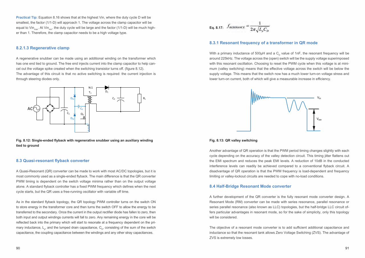
90 91
Practical Tip: Equation 8.16 shows that at the highest Vin, where the duty cycle D will be smallest, the factor (1/1-D) will approach 1. The voltage across the clamp capacitor will be equal to Vinmax. At Vinmin. the duty cycle will be large and the factor (1/1-D) will be much high-er than 1. Therefore, the clamp capacitor needs to be a high voltage type.
8.2.1.3 Regenerative clamp
A regenerative snubber can be made using an additional winding on the transformer which has one end tied to ground. The free end injects current into the clamp capacitor to help can-cel out the voltage spike created when the switching transistor turns off. (figure 8.12).The advantage of this circuit is that no active switching is required: the current injection is through steering diodes only.
Fig. 8.12: Single-ended flyback with regenerative snubber using an auxiliary winding
tied to ground
8.3 Quasi-resonant flyback converter
A Quasi-Resonant (QR) converter can be made to work with most AC/DC topologies, but it is most commonly used as a single-ended flyback. The main difference is that the QR converter PWM timing is dependent on the switch voltage minima rather than on the output voltage alone. A standard flyback controller has a fixed PWM frequency which defines when the next cycle starts, but the QR uses a free-running oscillator with variable off time.
As in the standard flyback topology, the QR topology PWM controller turns on the switch ON to store energy in the transformer core and then turns the switch OFF to allow the energy to be transferred to the secondary. Once the current in the output rectifier diode has fallen to zero, then both input and output windings currents will fall to zero. Any remaining energy in the core will be reflected back into the primary which will start to resonate at a frequency dependent on the pri-mary inductance, Lp, and the lumped drain capacitance, CD, consisting of the sum of the switch capacitance, the coupling capacitance between the windings and any other stray capacitances.
D1
C2 RL
ACC1
T1
N:1
Q1
CS
DS1
DS2
Eq. 8.17:
8.3.1 Resonant frequency of a transformer in QR mode
With a primary inductance of 500µH and a CD value of 1nF, the resonant frequency will be around 225kHz. The voltage across the (open) switch will be the supply voltage superimposed with this resonant oscillation. Choosing to reset the PWM cycle when this voltage is at mini-mum (valley switching) means that the effective voltage across the switch will be below the supply voltage. This means that the switch now has a much lower turn-on voltage stress and lower turn-on current, both of which will give a measurable increase in efficiency.
Fig. 8.13: QR valley switching
Another advantage of QR operation is that the PWM period timing changes slightly with each cycle depending on the accuracy of the valley detection circuit. This timing jitter flattens out the EMI spectrum and reduces the peak EMI levels. A reduction of 10dB in the conducted interference levels can readily be achieved compared to a conventional flyback circuit. A disadvantage of QR operation is that the PWM frequency is load-dependent and frequency limiting or valley-lockout circuits are needed to cope with no-load conditions.
8.4 Half-Bridge Resonant Mode converter
A further development of the QR converter is the fully resonant mode converter design. A Resonant Mode (RM) converter can be made with series resonance, parallel resonance or series parallel resonance (also known as LLC) topologies, but the half-bridge LLC circuit of-fers particular advantages in resonant mode, so for the sake of simplicity, only this topology will be considered.
The objective of a resonant mode converter is to add sufficient additional capacitance and inductance so that the resonant tank allows Zero Voltage Switching (ZVS). The advantage of ZVS is extremely low losses.
Vin
Vsw

92 93
Fig. 8.14: Half-bridge LLC resonant mode topology
This topology has two resonant frequencies. The fi rst being the series resonance tank formed from Cr and Lr and the second the parallel resonance tank formed by Cr and Lm+Lr. Typically, both Lm and Lr are wound side-by-side on the transformer core to reduce the space required. The double resonant frequencies of an LLC converter can be calculated from Equation 8.17:
Eq. 8.18:
The advantage of the double resonances is that one or the other takes precedence according to load. So while a series resonant circuit has a frequency that increases with reduced load and a parallel resonant circuit has a frequency that increases with increasing load, a well-de-signed series parallel resonant circuit has a stable frequency over the whole load range. The switching frequency and values of Lr and Cr are chosen so that the primary winding in in continuous resonance and sees an almost perfect sinusoidal waveform. The two half-bridge switches Q1 and Q2 are operated in antiphase. When the FETs are activated, the voltage across them is actually negative. The Gate-Drain voltage is only the internal diode drop and the gate drive current is thus extremely low. As the voltage transitions to positive, the FETs are already ON and start to conduct as the sinusoidal voltage passes through zero.
Combined with the low switching losses and the low transformer losses due to the sinusoidal drive waveform, conversion effi ciencies exceeding 95% are readily achievable. Another ad-vantage is that the EMI emissions are extremely low as the entire power train is sinusoidal.
The disadvantages of the LCC converter topology is that the required inductances can be high in order to get a stable resonant frequency with a good Q factor (i.e. low Cr). The converter must also be tuned to operate below the maximum possible gain to allow it start up without problems. Typically a working gain of 80-90% of the maximum is a safe margin.
D3Cout RL
ACCin
T1
Q1
Q2 D2
D1
Cr
Lr
Lm
D4
Additional pulse-mode circuitry may be needed for no-load operation. Although the LLC load range theoretically includes zero load, in practice component tolerances can make the con-verter unstable with no load.
Finally, the side-by-side transformer construction requires careful design if the creepage and clearance separations required for safety are to be met.
8.5 Full-bridge resonant mode converters
8.5.1 Phase-shifted resonant full bridge
A phase-shifted full bridge resonant converter uses a conventional full bridge topology with the addition of a series inductor on the input. The two pairs of switching transistors are driven with two fi xed 50% duty cycle PWM signals which are then phase shifted to control the power delivery. (fi gure 8.15). If the overlap between the two 50% duty PWM signals is low, then only a small amount of energy is transferred across the transformer. If it is high, then full power is transferred. Regulation is thus achieved by shifting the phase of the two PWM signals alone.
Fig. 8.15: Simplifi ed phase-shifted resonant full bridge schematic and the wave forms.
The PWM signals are fi xed frequency and fi xed 50% duty cycle. The blue shaded
areas represent the amount of overlap between the two PWM drive signals which
controls the amount of power transmission
The advantages of the phase-shifted full bridge topology are that due to the fi xed-frequency resonant operation, all of the transistors switch at zero voltage (ZVS) or near zero voltage, so switching losses are very low. The transistor drive circuit is simplifi ed because only two fi xed frequency PWM signals which can be very easily generated from fl ip-fl op circuits (50% duty cycle) are needed to drive all four switches. The resonance inductor, Lres, can be omitted if the inherent resonance between the transistor’s Coss capacitance and transformer leakage induct-ance is suffi cient to ensure ZVS operation. In this case, both D1 and D2 could also be omitted.
Lr
QA
QB
QC
QD
PWM1
PWM1
PWM2
PWM2
D1
D2
T1
QD
QC
QB
QA
TransformerPrimaryVoltage
TransformerPrimaryCurrent
Low Power High Power
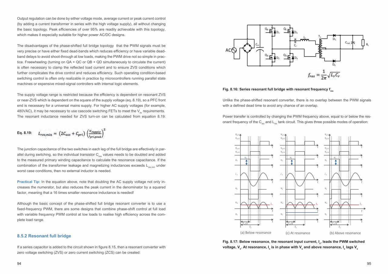
94 95
Output regulation can be done by either voltage mode, average current or peak current control (by adding a current transformer in series with the high voltage supply), all without changing the basic topology. Peak effi ciencies of over 95% are readily achievable with this topology, which makes it especially suitable for higher power AC/DC designs.
The disadvantages of the phase-shifted full bridge topology that the PWM signals must be very precise or have either fi xed dead-bands which reduces effi ciency or have variable dead-band delays to avoid shoot-through at low loads, making the PWM drive not so simple in prac-tice. Freewheeling (turning on QA + QC or QB + QD simultaneously to circulate the current) is often necessary to clamp the refl ected load current and to ensure ZVS conditions which further complicates the drive control and reduces effi ciency. Such operating condition-based switching control is often only realizable in practice by microcontrollers running parallel state machines or expensive mixed-signal controllers with internal logic elements.
The supply voltage range is restricted because the effi ciency is dependent on resonant ZVS or near-ZVS which is dependent on the square of the supply voltage (eq. 8.19), so a PFC front end is necessary for a universal mains supply. For higher AC supply voltages (for example, 480VAC), it may be necessary to use cascode switching FETs to meet the Vds requirements. The resonant inductance needed for ZVS turn-on can be calculated from equation 8.19:
Eq. 8.19:
The junction capacitance of the two switches in each leg of the full bridge are eff ectively in par-allel during switching, so the individual transistor Coss values needs to be doubled and added to the measured primary winding capacitance to calculate the resonance capacitance. If the combination of the transformer leakage and magnetizing inductances exceeds Lres,min under worst case conditions, then no external inductor is needed.
Practical Tip: In the equation above, note that doubling the AC supply voltage not only in-creases the numerator, but also reduces the peak current in the denominator by a squared factor, meaning that a 16 times smaller resonance inductance is needed!
Although the basic concept of the phase-shifted full bridge resonant converter is to use a fi xed-frequency PWM, there are some designs that combine phase-shift control at full load with variable frequency PWM control at low loads to realise high effi ciency across the com-plete load range.
8.5.2 Resonant full bridge
If a series capacitor is added to the circuit shown in fi gure 8.15, then a resonant converter with zero voltage switching (ZVS) or zero current switching (ZCS) can be created:
Fig. 8.16: Series resonant full bridge with resonant frequency fres
Unlike the phase-shifted resonant converter, there is no overlap between the PWM signals with a defi ned dead time to avoid any chance of an overlap.
Power transfer is controlled by changing the PWM frequency above, equal to or below the res-onant frequency of the Cres and Lres tank circuit. This gives three possible modes of operation:
Fig. 8.17: Below resonance, the resonant input current, Is, leads the PWM switched
voltage, Vs. At resonance, I
s is in phase with V
s and above resonance, I
s lags V
s
D5Cout RL
ACCin
T1
QD
QCD3
D4
Cr
Lr
D6
QB
QAD1
D2
vg.S1
vo
vg.S3
vg.S2
vg.S4
v5
i 5
vp
vor
v5
t
t
t
t
t
t
t
Io
T /2o
To
(a) Below resonance
vg.S1
vo
vg.S3
vg.S2
vg.S4
v5
i 5
vp
vor
v5
t
t
t
t
t
t
t
Io
T /2o
To
(c) At resonance
vg.S1
vo
vg.S3
vg.S2
vg.S4
v5
i 5
vp
vor
v5
t
t
t
t
t
t
t
Io
T /2o
To
(b) Above resonance

96 97
Mode 1: Below resonance. The input current leads the switched supply voltage, i.e. the im-pedance is capacitive. The transistors switch in ZCS mode.
Mode 2: At resonance. The input current is in phase with the switched supply voltage, i.e. the impedance is purely resistive. The transistors switch in ZCS mode and the output voltage is at its maximum.
Mode 3: Above resonance. The input current lags the switched supply voltage, i.e. the imped-ance is inductive. The transistors switch in ZVS mode.The output voltage is at a maximum when the switching frequency is equal to the resonant frequency:
Eq. 8.20:
Where ω is the relative operating angular frequency, , and Q is the quality factor:
Eq. 8.21:
Where RAC represents the transformer load.
The 0.9 factor in the numerator of Eq. 8.20 comes from a relationship of which means that at resonance, the output voltage is 0.9Vin (refer to fi gure 8.18)
Output power can be reduced by changing the PWM frequency either above or below the resonant frequency, but as ZVS control is optimal for both turn-on and turn-off losses whereas ZCS only helps with turn-off losses, typically an increase in frequency is used to reduce the output power.
Fig. 8.18: Output voltage control by increasing the PWM frequency above resonance
opV
i0,9v
(a) output voltage
(b) Impedance magnitude
Preferred operational area
Small Q
High Q
s[Z ]
f= fr/fs
f- fr/fs
Capacitive impedance Inductive impedance
The advantage the variable frequency full bridge resonant controller is high effi ciency over a wide load range as the topology remains in resonance from full load down to light load.
The disadvantage is that no-load operation is not possible without losing resonant operation and therefore losing control over the output voltage, so a minimum load is always required.
This drawback can be eliminated by adding an additional resonance capacitor in parallel with the transformer primary winding to make a series-parallel resonant full bridge (fi gure 8.19). This topology will stay in resonance from full load down to no-load conditions with good light load effi ciency, but requires a PFC front end to provide a stable bus voltage.
Fig. 8.19: Series-parallel resonant full bridge converter
8.6 Single-Ended Forward converter
Although the forward converter seems similar to the fl yback topology, it functions in a com-pletely diff erent way, relying on continuous transformer action to transfer power from input to output rather than intermittently storing the energy in the magnetic fi eld of the core gap. The input voltage is converted into a regulated output voltage as a function of the turns ratio of the transformer and no gap is needed nor desirable. Figure 8.20 shows the simplifi ed circuit (refer to the DC/DC Book of Knowledge for the voltage and current waveforms and explanation of the transfer function).
As the power transfer is continuous over time, we speak of volt-seconds. The volt-seconds during the ON time must not exceed the volt-seconds during the OFF time, otherwise the core will eventually saturate due to a process called fl ux walking (refer to the DC/DC Book of Knowledge, Chapter 10). This is guaranteed by adding a reset winding that ensures that the core is fully demagnetized at the end of each switching cycle.
As the reset winding ensures that the core fully desaturates at the end of each cycle, the duty cycle can not be higher than 50% maximum, unless a reset winding with a diff erent turns ratio is used. This limits the input voltage range of the converter to typically 2:1, making a universal input AC/DC forward converter more diffi cult to design than a fl yback. Thus AC/DC forward converters are usually used with a PFC front end to give a stable DC bus voltage to work from.
D5Cout RL
AC
Cin
T1
QD
QCD3
D4
Crs
Lr
D6
QB
QAD1
D2
Crp
PFCFront End
VDC

98 99
Fig. 8.20: Forward topology (simplified)
As a forward converter transformer has a continuous magnetic core, the magnetic field is more evenly distributed and the associated hysteresis losses and radiated EMI from the con-centrated fields across a gap in the flyback topology are avoided.
Other advantages are that the lower peak current reduces winding and diode losses and lead to a lower input ripple is discontinous so high and output ripple current (figure 8.21). The reset winding transfers excess stored energy back into the PFC capacitor rather than simply having to dissipate the energy in a snubber network. For the same output power, a forward converter will therefore be more efficient than a flyback.
Fig. 8.21: Comparison of forward and flyback (DCM) waveforms. The peak currents
in the forward topology are lower and in particular, the output capacitor has a much
lower ripple current
D1
Cout RLoad
AC CinT1
DReset
D2
Lout
NsNp Nr
Q1
PFCFront End
VDC
PrimaryWindingCurrent
SecondaryWindingCurrent
Cout
RippleCurrent
Forward Converter
Flyback Converter
time
Curr
ent
Curr
ent
Curr
ent
Curr
ent
Curr
ent
Curr
ent
time
time
time
time
time
The disadvantages of the forward topology are a more complicated transformer construction with an additional resest winding which makes meeting the required creepage and clearance separations more troublesome and an increased component cost as an output inductor, Lout, is needed for each output. If a bipolar (±) output is required where the positive and negative output voltages are complementary, then a transformer style (two inductors sharing the same core) output inductor can be used to save costs. This is not a true transformer but two mutually cou-pled inductors, so it is important that the windings are bifilar wound to get good coupling and the turns are in the same proportion as the transformer secondaries. This will improve the cross regulation and reduce the output ripple considerably compared to two independent chokes.
Fig. 8.22: Forward converter with bipolar output using a mutually coupled output
inductor
If multiple independent outputs are required, then each forward converter output needs an output inductor and capacitor, so in this case, the flyback topology would often be a better choice (but refer also to the current-fed forward converter Section 8.6.2).
As with the flyback topology, snubbers are needed to supress transients to protect the active components. Unlike the flyback, additional voltage transients caused by leakage inductance between the primary and reset windings need to be controlled. In the conventional forward clamp topology with the same number of turns on the primary and reset windings, if the volt-age across the switching transistor when it turns off exceeds double the supply voltage, then current will begin to flow in the reset winding. However, this transfer of energy is not instan-taneous. The time taken for the current to transfer from the primary to the reset winding is slowed down by the leakage inductance between the primary winding and the reset winding. During this delay, the voltage on the switching transistor will exceed double the supply voltage and can overstress the transistor. The capacitor Cclamp mitigates this overvoltage by providing a low impedance path through the reset winding diode (figure 8.23).
As the current flows back into the input capacitor, energy is returned into the circuit rather than being simply dissipated through a clamping resistor, so this is an example of a lossless clamp.

100 101
Fig. 8.23: Lossless clamp forward converter (simplified)
The required clamping capacitance can be calculated from the following equation (assuming that the primary and reset windings have the same number of turns):
Eq. 8.22:
Where Lp is the primary inductance, Nps is the primary/secondary turns ratio, Vs is the supply voltage and Vos is the desired maximum overshoot voltage.
As the reset diode has to carry the excess energy transferred via the clamping capacitor, it must be peak current rated > Iload/Nps. The voltage rating must, of course, be higher than 2Vs.
In addition to the primary side clamp, there is often a need to add snubbers across the switch-ing transistor and secondary diode D2 to control any high frequency ringing that can cause EMI problems.
This is because when Q1 switches on, current starts to flow in the rectifier diode D1, until it has fully charged the output capacitor and now only has to supply the load current. At this point, the voltage across the diode will increase further due to the reflected input voltage trans-ferred by the transformer leakage inductance. As no more current can flow in the load, the current starts to oscillate across the diode D2 junction capacitance. Adding a snubber Cssn + Rssn across D2 will absorb this excess energy and damp the ringing (figure 8.24).
Fig. 8.24: Forward converter with both over-voltage clamp and primary side and sec-
ondary side snubbers
D1
Cout RLoad
AC CinT1
DReset
D2
Lout
NsNp Nr
Q1
PFCFront End
VDC
Cclamp
D1
Cout RLoad
AC CinT1
DReset
D2
Lout
NsNp Nr
Q1
PFCFront End
VDC
Cclamp
Cssn
Rssn
Cpsn
Rpsn
Practical Tip: Finding the optimum values for Cssn and Rssn can be done by experiment:
1. Measure the ringing frequency without a snubber2. Add sufficient capacitance in parallel with D2 until the frequency is halved3. The parasitic capacitance, Cpara is 1/3 of the added capacitance4. The parasitic inductance can be calculated from Equation 8.23:
Eq. 8.23:
5. The snubber resistor should be ideally the same as the characteristic impedance:
Eq. 8.24:
6. The power dissipated in the snubber resistor can be calculated from:
Eq. 8.25:
Where fsw is the operating switching frequency, Cssn is the secondary snubber capacitor and Vpk is the peak voltage across D2.
If the power dissipation in the snubber resistor is too high, then a compromise may be required to increase the stress on the diode in exchange for reducing the stress on the snubber.
8.6.1 Interleaved Single-Ended Forward
AC/DC forward converters are typically used up to around 200W. Above this power level the high discontinuous primary current cannot be easily handled by increasing the size of the input capacitor bank and by paralleling up the primary switching transistors. Furthermore, the output inductor and capacitor become very bulky.
Synchronous rectification (SR) on the output helps reduce the losses, but using SR makes it difficult to parallel the outputs of two forward converters if more power is required (the SR switching can interfere with the load share current balancing circuit).
One solution to high current, low voltage forward converters is to interleave the power stage using two transformers switched 180° out of phase (figure 8.25). The additional complexity adds some cost, but this is often balanced out by the reduced size of the input and output capacitors as the ripple currents are significantly reduced (each forward converter stage ex-
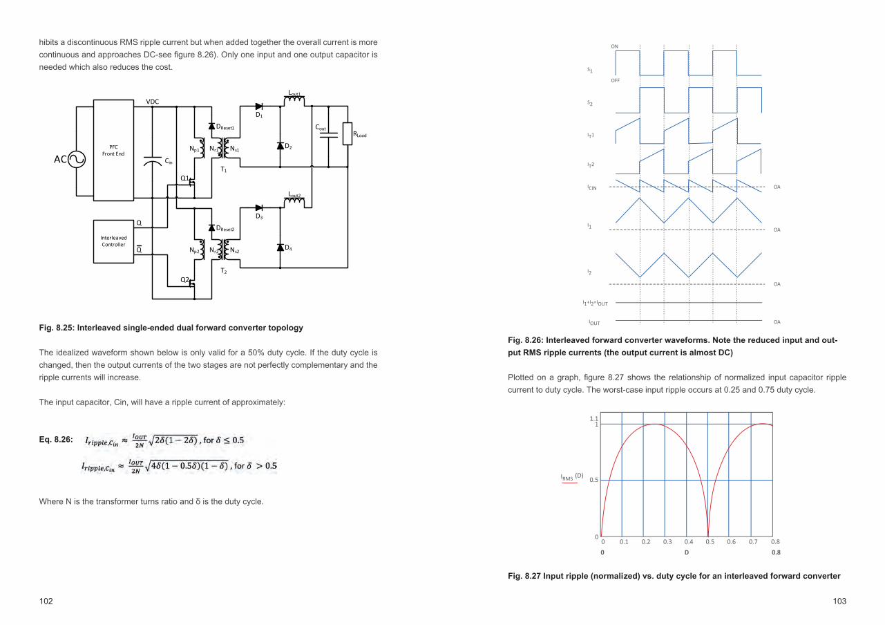
102 103
hibits a discontinuous RMS ripple current but when added together the overall current is more continuous and approaches DC-see fi gure 8.26). Only one input and one output capacitor is needed which also reduces the cost.
Fig. 8.25: Interleaved single-ended dual forward converter topology
The idealized waveform shown below is only valid for a 50% duty cycle. If the duty cycle is changed, then the output currents of the two stages are not perfectly complementary and the ripple currents will increase.
The input capacitor, Cin, will have a ripple current of approximately:
Eq. 8.26:
Where N is the transformer turns ratio and δ is the duty cycle.
D1
CoutRLoad
AC CinT1
DReset1
D2
Lout1
Ns1Np1 Nr1
Q1
PFCFront End
VDC
D3
T2
DReset2
D4
Lout2
Ns2Np2 Nr2
Q2
InterleavedController
Q
Q
Fig. 8.26: Interleaved forward converter waveforms. Note the reduced input and out-
put RMS ripple currents (the output current is almost DC)
Plotted on a graph, fi gure 8.27 shows the relationship of normalized input capacitor ripple current to duty cycle. The worst-case input ripple occurs at 0.25 and 0.75 duty cycle.
Fig. 8.27 Input ripple (normalized) vs. duty cycle for an interleaved forward converter
S1
S2
IT1
IT2
ICIN
I1
I2
I1+I2=IOUT
IOUT
ON
OFF
OA
OA
OA
OA
IRMS (D)
0
0.5
11.1
0 0.1 0.2 0.3 0.4 0.5 0.6 0.7 0.8D0 0.8

104 105
The output ripple current follows a diff erent relationship as in Equation 8.27:
Eq. 8.27:
Plotted on a graph, fi gure 8.28 shows the relationship of the ripple cancellation factor, K(δ), (capacitor ripple current divided by inductor ripple current) to the duty cycle.
Fig. 8.28: Ripple cancellation factor (normalized) vs duty cycle
As can be seen from fi gures 8.27 and 8.28, the interleaved forward converter is most effi cient if the duty cycle is very close to 0.5. Therefore, a PFC front end is essential to compensate for input voltage variations while keeping the duty cycle constant.
If more power is needed, then three input power stages and transformers can be wired in parallel with 120°C phase shift. With 0.33 duty cycle, the input and output ripple currents will all superim-pose to give a very low combined overall ripple current. And if even more current is needed, then two 180°C interleaved forward converters can be paralleled to deliver 100A. The current bal-ance between these paralleled stages must be very carefully controlled: even a small deviation in the phase current sharing between the stages will increase the ripple currents dramatically.
In practice, some kind of active duty cycle control is needed to compensate for component tolerances, temperature variations and dynamic loads. In addition, each of these paralleled power stages will need their own snubber networks on the primary switch and secondary diodes which will reduce the overall effi ciency, especially at low loads. Interleaving the power stages reduces conduction losses (the current paths have lower impedances) but increases the switching losses. At high output currents, conduction losses dominate, but at low output currents, switching losses dominate.
0 0.1 0.2 0.3 0.4 0.5 0.6 0.7 0.8 0.9 11.554x10
K(D)=
k(D)
∆I COUT
∆I 1
-150
0.1
0.2
0.3
0.4
0.5
0.6
0.7
0.8
0.9
1
Practical Tip: One technique to improve the effi ciency over the whole load range is to shut down one or more parallel phases at low loads. This can add as much as 15% to the low load effi ciency by operating the converter as a single-phase forward converter with all of the current fl owing through one power stage only. Another saving can be made by switching off the synchronous rectifi cation on the secondary side under low-load conditions and relying on paralleled diodes across the FETs to rectify any residual output current.
Without digital control, such complex feedback mechanisms are impractical, but with a pro-grammable controller it is possible to ensure effi ciencies of better than 95% across a very wide load range.
In order to get the best of both worlds and have good effi ciency at both very heavy load and light load, a forward converter topology is often preferred for high power, high effi ciency designs.
8.6.2 Current-Fed Single-Ended Forward converter
As previously mentioned, a forward converter relies on a storage inductor on the output as ideally no energy is stored or lost in the transformer itself. This means that a multiple output voltage-fed forward converter rapidly becomes very expensive as every output requires its own inductor.
Fig. 8.29: Triple output voltage-fed forward converter with inductors on each output.
The current-fed forward topology adds the inductive storage element on the primary side, making the topology a current converter rather than a voltage converter. This eliminates the necessity of an output inductor and makes multiple outputs more commercially attractive. The disadvantage is that a current source rather than a voltage source is required, typically real-ized by adding a chopper or buck converter input stage. Output regulation can be achieved by controlling the PWM signal of the input stage only, leaving the forward converter running with
D1
Cout1RLoad1
AC CinT1
DReset
D2
Lout1
NsNp Nr
Q1
PFCFront End
VDC
Cclamp
D3
Cout2RLoad2
D4
Lout2
D5
Cout3 RLoad3
D6
Lout3

106 107
a fixed 50% duty cycle (alternatively, the buck converter can be operated with a fixed duty cy-cle and the forward converter duty cycle modified for regulation). In either case, the topology is insensitive to the rise and fall times so high frequency PWM frequencies can be used to reduce the inductor and transformer sizes.
Current-fed forward converters typically use two-transistor, push-pull or full-bridge topologies (see following sections). This is because the two switches must overlap, so that the current flow through the transformer is continuous and uninterrupted (any break in the current flow would cause destructively high voltages to develop). The primary side inductor limits the cur-rent when both switches are on, which also gives the advantage that the topology is inherent-ly short-circuit protected. This is very important for high power applications, as designing a reliable over-current trip with high dynamic current loads is tricky; as the current fed forward topology can tolerate brief short circuit conditions without damage, the over-current trip time can be extended to avoid nuisance tripping in noisy electrical environments.
As an active PFC boost stage is impractical (boost followed by a buck followed by a forward converter), current-fed forward converters are typically used where power factor correction is not an issue, such as in three-phase supplies or where the power is higher than 3kW and the regulations do not apply.
Fig. 8.30: Triple output current-fed full bridge forward converter
L2, Cin, QE and D6 form the current source. L1 is the forward primary side storage inductor replacing the inductors on each output. The full bridge configuration avoids the need for a reset winding as long as the duty cycle is ≤50%. D5 clamps and recycles any excess energy back into the input capacitor.
D7Cout1 RLoad1
AC
Cin
T1
QD
QCD3
D4
L2
D8
QB
QAD1
D2
QE
D6
L1
D5
D9Cout2 RLoad2D10
D11Cout3 RLoad3D12
8.7 Two-Transistor topologies
8.7.1 Two-Transistor Forward converter
Fig. 8.31: Two-transistor forward topology
Two-transistor (TT) converters are considered one of the most reliable topologies for higher power AC/DC converters. There are several reasons for this:
1. The switching transistors have to handle only the maximum input voltage (which is a fixed voltage if a PFC front end is used). Any turn-off switching transients caused by parasitic elements are gated by the fast recovery diodes. This means that the tran-sistors need only be rated for the input voltage plus some headroom, rather than for double the input voltage as in a single-ended switched topology.
2. Timing is not critical – as both transistors turn on and off together, there is no require-ment for any dead times to avoid shoot-through.
3. No snubber networks are needed. Both the residual magnetizing energy and any ener-gy stored in the leakage inductance are transferred back into the PFC capacitor at the end of each cycle by the two diodes. This enhances the efficiency and reduces EMI as excess energy is not dissipated but recycled.
4. There is no need for a reset winding, simplifying the construction of the transformer and lowering the cost.
5. As the topology is hard switching, no reverse voltages appear across the MOSFETs under any operating condition, so the transistor body diodes are not stressed.
The disadvantages are that ZVS-operation is not possible which limits the operating frequency and that the duty cycle must be kept below 0.5 to allow the transformer time to reset on each cycle. Also, the freewheeling diodes must be the more expensive high voltage fast-acting type.
D3
Cout RL
ACCin
T1
N:1D1
D2
Q1
Q2
D4
Lout

108 109
Although both transistors are driven by the same PWM signal, the high side FET will need a fl oating gate driver which also adds cost. However, as the FETs need only be rated for Vin, the additional costs are often balanced out by cheaper power-FET prices.
Fig. 8.32: TT-Forward topology CCM current paths with the transistors on (blue) and off
(green). Excess energy is returned to the input capacitor at the end of each cycle, so no
snubber is required
Fig. 8.33: Current fl owing in the switch (ISW
), secondary winding (IL) and in the primary
winding, IL, mag
. As a rule-of-thumb, the peak IL,mag
is chosen to be 1/10th of ISW,peak
During the fi rst part of the cycle (red), both transistors are on and the freewheeling diodes are biased off . The current through the transistors (ISW) and in the primary winding (IPRI) ramps up. During the second half of the cycle, the transistors are turned off (ISW = 0) and the primary current and magnetizing current ramp down again through the freewheeling diodes back into the input capacitor until the core has been completely demagnetized (green section). The
D3
Cout RL
ACCin
T1
N:1
Current Flow, Q1 + Q2 onCurrent Flow, Q1 + Q2 off
D1
D2
Q1
Q2
D4
Lout
ISW
IL
ILmag
t
t
t
freewheeling diodes then turn off . The time until the next cycle starts (blue section) is the margin needed to ensure that the core is completely reset each cycle. During this time, the primary winding current still continues to ramp down as current is still circulating through the output diode (CCM operation).
8.7.2 Push-Pull Forward converter
The push-pull topology uses a centre-tapped primary and secondary transformer winding and alternately switching transistors. This adds to the complexity of the transformer construction and increases the switching voltage stress on the transistors to 2Vin, but allows four-quadrant use of the magnetic core. In other words, double the power for the same sized transformer core compared to a single-ended forward design.This makes the push-pull topology suitable for AC/DC converters up to 1kW. However, as the full input current fl ows through each primary half-winding, they each need to cope with double the current compared to a single-ended design, so they need to be suitably dimensioned to cope.
Fig. 8.34: Push-pull topology and the B-H curve operating area
To avoid core saturation, both transistors need to be switched on for the same time so that the core magnetic fl ux density swings reliably from B1 to B2 with each cycle and does not “fl ux-walk” into saturation. Any imbalance caused by timing errors, winding diff erences or unequal voltage drop across the output diodes can cause a gradual drift into core saturation as there is no separate core reset mechanism. There are a number of techniques that can be used to avoid or detect impending core saturation: the simplest is to use peak current mode feedback to adjust the Ton times to keep the peak current under control. If voltage mode regulation is required for the application, then an alternative is to add a small air gap to the core so that the core fl ux density is reduced to manageable levels.
The switching transistors need to cope with at least double Vin (add 20% margin for safety, i.e. 900V rated transistors are needed for a 230VAC input) and be switched with a dead time to avoid shoot-through. This creates severe problems for the output diodes during the dead-times unless diode snubbers are added.
D1
Cout RL
ACCin
T1
N:1Q1Q2
D2
Lout
∆B
H
BSAT
B2
B
B1
BSAT
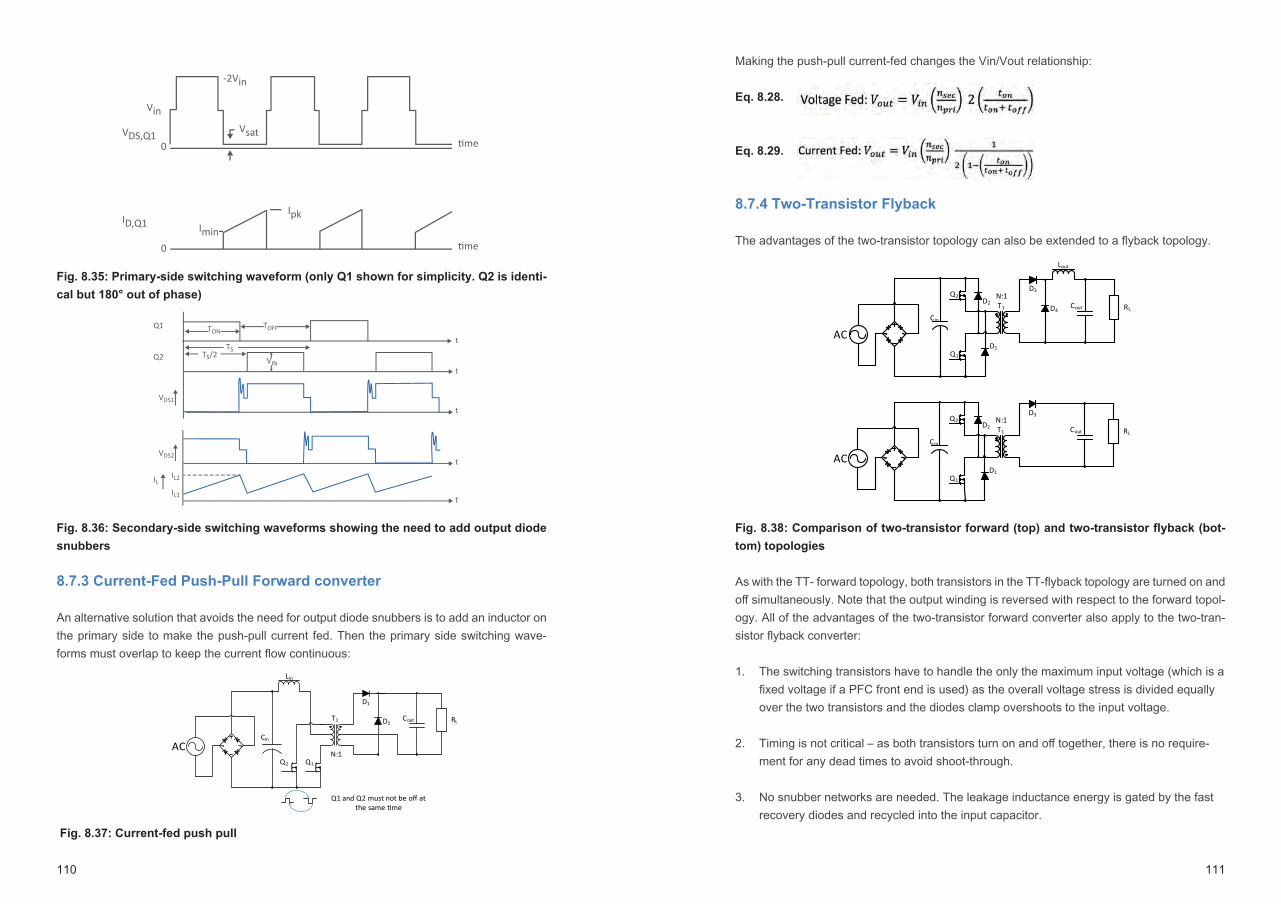
110 111
Fig. 8.35: Primary-side switching waveform (only Q1 shown for simplicity. Q2 is identi-
cal but 180° out of phase)
Fig. 8.36: Secondary-side switching waveforms showing the need to add output diode
snubbers
8.7.3 Current-Fed Push-Pull Forward converter
An alternative solution that avoids the need for output diode snubbers is to add an inductor on the primary side to make the push-pull current fed. Then the primary side switching wave-forms must overlap to keep the current fl ow continuous:
Fig. 8.37: Current-fed push pull
-2Vin
Vsat
Vin
VDS,Q10
ID,Q1
0
Imin
Ipk
time
time
t
t
t
t
t
VDS1
VDS2
IL2ILIL1
Q2
Q1 TONTOFF
TSTS/2
VIN
D1
Cout RL
ACCin
T1
N:1Q1Q2
D2
Lin
Q1 and Q2 must not be off at the same �me
Making the push-pull current-fed changes the Vin/Vout relationship:
Eq. 8.28.
Eq. 8.29.
8.7.4 Two-Transistor Flyback
The advantages of the two-transistor topology can also be extended to a fl yback topology.
Fig. 8.38: Comparison of two-transistor forward (top) and two-transistor fl yback (bot-
tom) topologies
As with the TT- forward topology, both transistors in the TT-fl yback topology are turned on and off simultaneously. Note that the output winding is reversed with respect to the forward topol-ogy. All of the advantages of the two-transistor forward converter also apply to the two-tran-sistor fl yback converter:
1. The switching transistors have to handle the only the maximum input voltage (which is a fi xed voltage if a PFC front end is used) as the overall voltage stress is divided equally over the two transistors and the diodes clamp overshoots to the input voltage.
2. Timing is not critical – as both transistors turn on and off together, there is no require-ment for any dead times to avoid shoot-through.
3. No snubber networks are needed. The leakage inductance energy is gated by the fast recovery diodes and recycled into the input capacitor.
D3
Cout RL
ACCin
T1
N:1
D1
D2
Q1
Q2
D4
Lout
D3
Cout RL
ACCin
T1
N:1
D1
D2
Q1
Q2
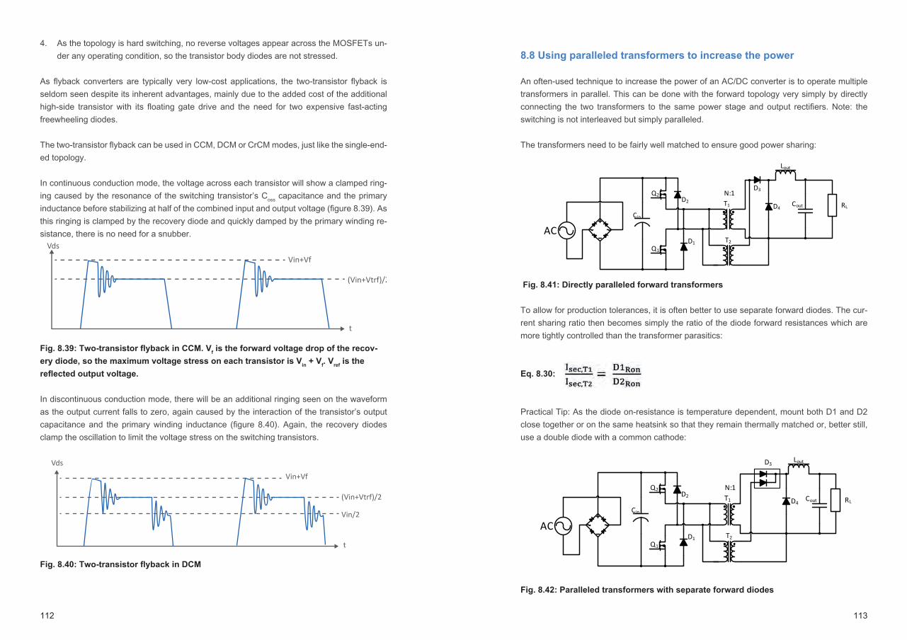
112 113
4. As the topology is hard switching, no reverse voltages appear across the MOSFETs un-der any operating condition, so the transistor body diodes are not stressed.
As fl yback converters are typically very low-cost applications, the two-transistor fl yback is seldom seen despite its inherent advantages, mainly due to the added cost of the additional high-side transistor with its fl oating gate drive and the need for two expensive fast-acting freewheeling diodes.
The two-transistor fl yback can be used in CCM, DCM or CrCM modes, just like the single-end-ed topology.
In continuous conduction mode, the voltage across each transistor will show a clamped ring-ing caused by the resonance of the switching transistor’s Coss capacitance and the primary inductance before stabilizing at half of the combined input and output voltage (fi gure 8.39). As this ringing is clamped by the recovery diode and quickly damped by the primary winding re-sistance, there is no need for a snubber.
Fig. 8.39: Two-transistor fl yback in CCM. Vf is the forward voltage drop of the recov-
ery diode, so the maximum voltage stress on each transistor is Vin + V
f. V
ref is the
refl ected output voltage.
In discontinuous conduction mode, there will be an additional ringing seen on the waveform as the output current falls to zero, again caused by the interaction of the transistor’s output capacitance and the primary winding inductance (fi gure 8.40). Again, the recovery diodes clamp the oscillation to limit the voltage stress on the switching transistors.
Fig. 8.40: Two-transistor fl yback in DCM
Vds
Vg
Vin+Vf
(Vin+Vtrf)/2
t
t
Vds
Vg
Vin+Vf
(Vin+Vtrf)/2
t
t
Vin/2
8.8 Using paralleled transformers to increase the power
An often-used technique to increase the power of an AC/DC converter is to operate multiple transformers in parallel. This can be done with the forward topology very simply by directly connecting the two transformers to the same power stage and output rectifi ers. Note: the switching is not interleaved but simply paralleled.
The transformers need to be fairly well matched to ensure good power sharing:
Fig. 8.41: Directly paralleled forward transformers
To allow for production tolerances, it is often better to use separate forward diodes. The cur-rent sharing ratio then becomes simply the ratio of the diode forward resistances which are more tightly controlled than the transformer parasitics:
Eq. 8.30:
Practical Tip: As the diode on-resistance is temperature dependent, mount both D1 and D2 close together or on the same heatsink so that they remain thermally matched or, better still, use a double diode with a common cathode:
Fig. 8.42: Paralleled transformers with separate forward diodes
D3
Cout RL
ACCin
T1
N:1
D1
D2
Q1
Q2
D4
Lout
T2
D3
Cout RL
ACCin
T1
N:1
D1
D2
Q1
Q2
D4
Lout
T2

114 115
It is also possible to operate transformers in series to share the dissipated power and reduce the core temperatures. This is more commonly called a stacked topology. An elegant solution is to use a capacitive divider to set the centre voltage at half the rectifi ed DC bus voltage. The voltage stress on the switching transistors is then halved. The stacking can be repeated if higher voltages need to be accommodated:
Fig. 8.43: Stacked two-transistors forward converters. Each switching transistor has
half the voltage stress of a single stage. If three transformers and capacitors were to
be used, then each transistor has a third of the voltage stress
In this interesting example of a stacked interleaved transformer fl yback converter*, fi gure 8.44, only a single active clamp is required. This variation of a stacked converter uses auxilia-ry windings on each transformer to improve the power factor by injecting current back into the DC bus voltage (a technique called input current shaping):
Fig. 8.44: Stacked fl yback topology with capacitor divider
D5
AC
Cin1
T1
N:1D1
D2
Q1
Q2
D6
Lout1
D7
Cout RLT2
N:1D3
D4
Q3
Q4
D8
Lout2
Cin2
D3
AC
Cin1
T1
N:1
Q2
D4
Cout RLT2
N:1Q1
Cin2
Q3
Cclamp
D1
D2
T1
T2
Lin
Q1 and Q2 are operated alternately with a suitable dead time between them. During the dead time, Q3 is operated to actively clamp the combined transformer voltage by circulating the current back into clamp capacitor Cclamp. As the clamp current fl ows in both directions, Cclamp must be non-polarized and Q3 switched with a fl oating driver supply:
Fig. 8.45: Stacked converter switching sequence. S3 is the active clamp switching
waveform
*Reference: Example is based on “A Single-Phase Single-Stage AC-DC Stacked Flyback Converter with Active Clamp ZVS”, Yuntong Li and Gerry Moschopoulos, Western University, London, Canada.
Published in: 2018 IEEE Applied Power Electronics Conference and Exposition (APEC) DOI: 10.1109/APEC.2018.8341297
Stacking or paralleling transformers can increase the power handling if space (especially height) is limited and off ers many opportunities for innovative switching topologies, such as the examples given above. The main disadvantages are increased costs and the diffi culty of matching the transformers precisely enough so that parasitic eff ects (especially leakage inductance diff erences) do not aff ect the performance. Nevertheless, it is a useful technique in certain situations.
Q1
Q2
Q3
ILin
Io
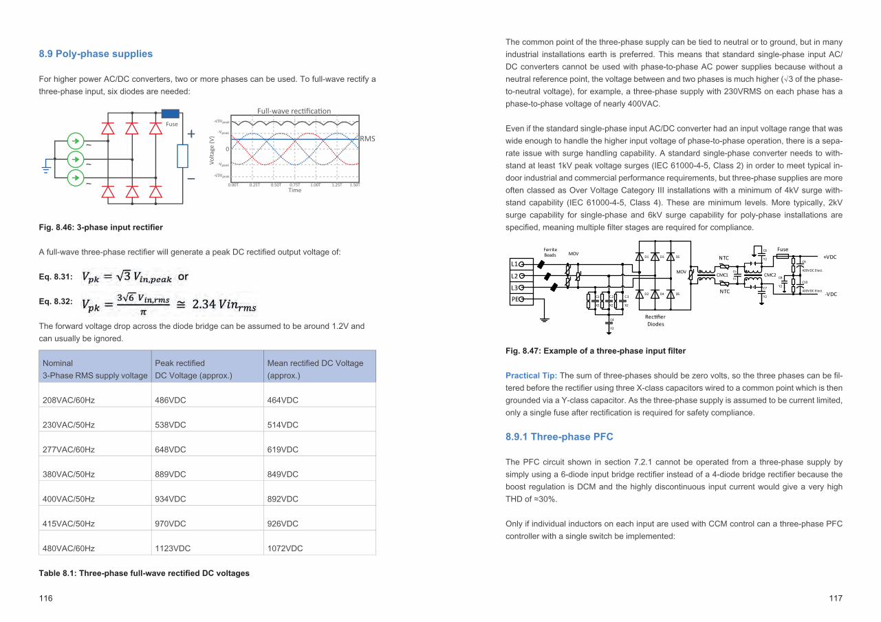
116 117
8.9 Poly-phase supplies
For higher power AC/DC converters, two or more phases can be used. To full-wave rectify a three-phase input, six diodes are needed:
Fig. 8.46: 3-phase input rectifi er
A full-wave three-phase rectifi er will generate a peak DC rectifi ed output voltage of:
Eq. 8.31:
Eq. 8.32:
The forward voltage drop across the diode bridge can be assumed to be around 1.2V and can usually be ignored.
Nominal 3-Phase RMS supply voltage
Peak rectifi ed DC Voltage (approx.)
Mean rectifi ed DC Voltage(approx.)
208VAC/60Hz 486VDC 464VDC
230VAC/50Hz 538VDC 514VDC
277VAC/60Hz 648VDC 619VDC
380VAC/50Hz 889VDC 849VDC
400VAC/50Hz 934VDC 892VDC
415VAC/50Hz 970VDC 926VDC
480VAC/60Hz 1123VDC 1072VDC
Table 8.1: Three-phase full-wave rectifi ed DC voltages
Full-wave rectification
RMS
0.00T 0.25T 0.50T 0.75T 1.00T 1.25T 1.50TTime
-√3Vpeak
-√3Vpeak
-Vpeak
-Vpeak
0
Volta
ge (V
)
Fuse
The common point of the three-phase supply can be tied to neutral or to ground, but in many industrial installations earth is preferred. This means that standard single-phase input AC/DC converters cannot be used with phase-to-phase AC power supplies because without a neutral reference point, the voltage between and two phases is much higher (√3 of the phase-to-neutral voltage), for example, a three-phase supply with 230VRMS on each phase has a phase-to-phase voltage of nearly 400VAC.
Even if the standard single-phase input AC/DC converter had an input voltage range that was wide enough to handle the higher input voltage of phase-to-phase operation, there is a sepa-rate issue with surge handling capability. A standard single-phase converter needs to with-stand at least 1kV peak voltage surges (IEC 61000-4-5, Class 2) in order to meet typical in-door industrial and commercial performance requirements, but three-phase supplies are more often classed as Over Voltage Category III installations with a minimum of 4kV surge with-stand capability (IEC 61000-4-5, Class 4). These are minimum levels. More typically, 2kV surge capability for single-phase and 6kV surge capability for poly-phase installations are specifi ed, meaning multiple fi lter stages are required for compliance.
Fig. 8.47: Example of a three-phase input fi lter
Practical Tip: The sum of three-phases should be zero volts, so the three phases can be fi l-tered before the rectifi er using three X-class capacitors wired to a common point which is then grounded via a Y-class capacitor. As the three-phase supply is assumed to be current limited, only a single fuse after rectifi cation is required for safety compliance.
8.9.1 Three-phase PFC
The PFC circuit shown in section 7.2.1 cannot be operated from a three-phase supply by simply using a 6-diode input bridge rectifi er instead of a 4-diode bridge rectifi er because the boost regulation is DCM and the highly discontinuous input current would give a very high THD of ≈30%.
Only if individual inductors on each input are used with CCM control can a three-phase PFC controller with a single switch be implemented:
D2
D1
D4
D3
D5
D5
C3
X2
C2
X2
C1
X2
C5
X1
C7
Y2
C6
Y2
C8
Y2
C9
420VDC Elect.
C10
420VDC Elect.
L1
L2
L3PE
NTC
NTC
MOV
MOVFerrite Beads
Rectifier Diodes
CMC1
C4
Y2
Fuse+VDC
-VDC
CMC2
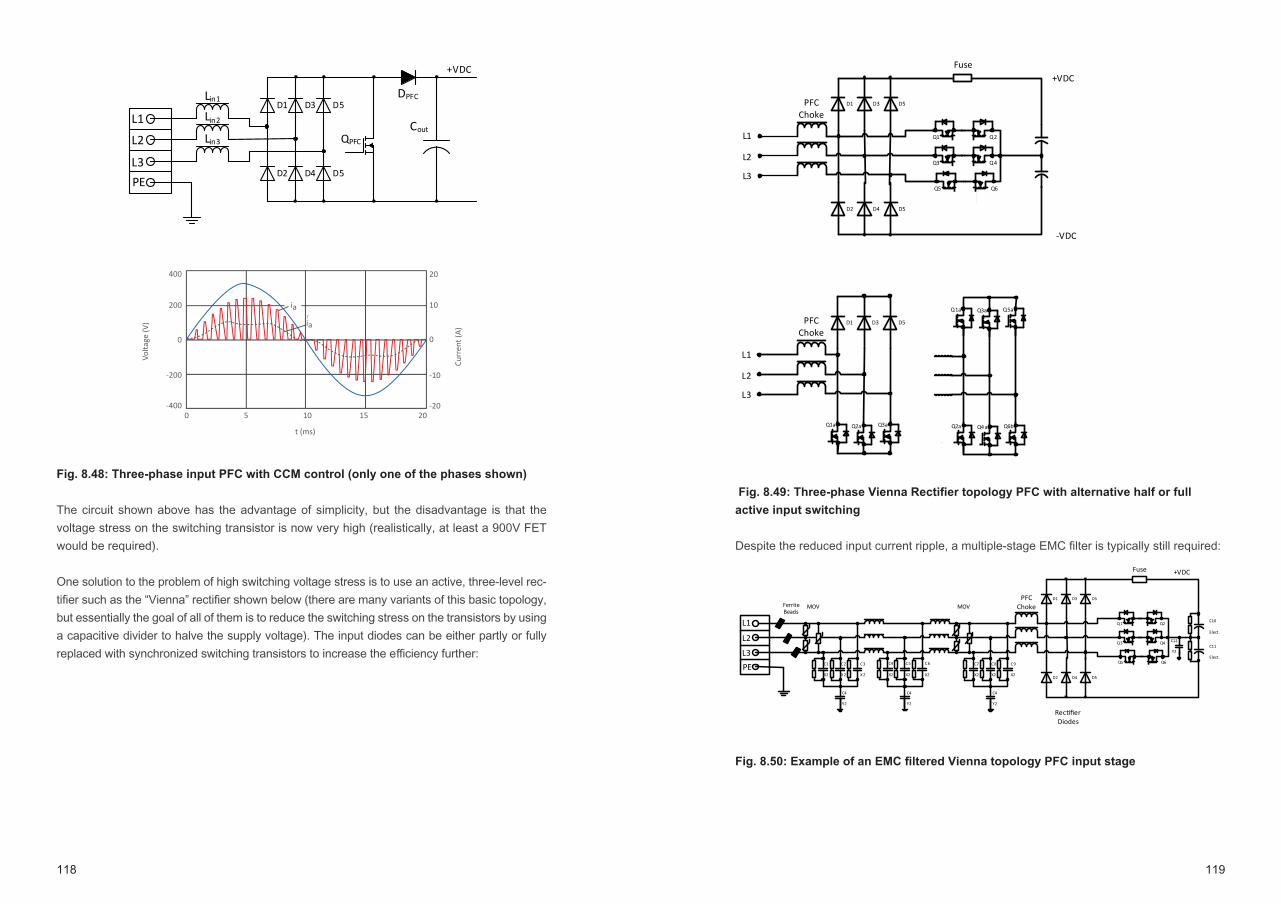
118 119
Fig. 8.48: Three-phase input PFC with CCM control (only one of the phases shown)
The circuit shown above has the advantage of simplicity, but the disadvantage is that the voltage stress on the switching transistor is now very high (realistically, at least a 900V FET would be required).
One solution to the problem of high switching voltage stress is to use an active, three-level rec-tifi er such as the “Vienna” rectifi er shown below (there are many variants of this basic topology, but essentially the goal of all of them is to reduce the switching stress on the transistors by using a capacitive divider to halve the supply voltage). The input diodes can be either partly or fully replaced with synchronized switching transistors to increase the effi ciency further:
D2
D1
D4
D3
D5
D5L1
L2
L3PE
QPFC
+VDC
Lin1
Lin2
Lin3
DPFC
Cout
400
200
0
-200
-400
20
10
0
-10
-20
Curr
ent (
A)
Volta
ge (V
)
0 5 10 15 20
t (ms)
ia
iaT
D2
D1
D4
D3
D5
D5
+VDC
-VDC
Fuse
PFCChoke
Q1 Q2
Q3 Q4
Q5 Q6
L1
L2
L3
D1 D3 D5PFCChoke
L1
L2
L3
Q3aQ2aQ1a Q6bQ4 aQ2a
Q5aQ3aQ1a
Fig. 8.49: Three-phase Vienna Rectifi er topology PFC with alternative half or full
active input switching
Despite the reduced input current ripple, a multiple-stage EMC fi lter is typically still required:
Fig. 8.50: Example of an EMC fi ltered Vienna topology PFC input stage
D2
D1
D4
D3
D5
D5
C3
X2
C2
X2
C1
X2
L1
L2
L3PE
MOVFerrite Beads
Rectifier Diodes
C4
Y2
+VDC
C12
Y2
C10
Elect.
C11
Elect.
Fuse
C6
X2
C5
X2
C4
X2
C4
Y2
C9
X2
C8
X2
C7
X2
MOV
C4
Y2
PFCChoke
Q1 Q2
Q3 Q4
Q5 Q6
D2
D1
D4
D3
D5
D5
+VDC
-VDC
Fuse
PFCChoke
Q1 Q2
Q3 Q4
Q5 Q6
L1
L2
L3
D1 D3 D5PFCChoke
L1
L2
L3
Q3aQ2aQ1a Q6bQ4 aQ2a
Q5aQ3aQ1a

120 121
Chapter 9
Transformerless AC power supplies
If isolation is not required, then a very low-cost AC/DC power supply can be made without using a safety isolation transformer. There are several techniques available to handle the large voltage diff erence between the AC supply and the DC output.
9.1 Capacitively-coupled AC/DC
This is one of the simplest AC power supply designs. A dropper resistor would dissipate too much power and get very hot, but the AC reactance of a series capacitor can be used to drop the input voltage without dissipating too much energy.
Fig. 9.1: Capacitively coupled AC/DC converter
The reactance of the dropper capacitor is:
Eq. 9.1:
So, for a 115VAC input and the 680nF capacitor shown above, Xc works out to be about 3.9 kohms for 60Hz mains and 4.6 kohms for 50Hz mains. This is much less than 470k so the parallel resistor can be ignored for the remaining calculations (it is required to discharge the capacitor when the power is switched off and to act as a primitive EMI fi lter to reduce the conducted harmonics).
The dropper capacitor current can be derived from:
Eq. 9.2:
So, for an 115VAC/60Hz input, Irms = 43354 C ≈ 40mA/µF and for a 230V/50Hz input, Irms = 72257 C ≈ 70mA/µF.
AC
Fusible Resistor100R
680nF,400V, X1
470kMOV
275VAC12V
330µF,25V
+12V, 30mA
0V
Non-Isolated!
The above circuit will have a maximum output current of 47mA for 230VAC supply or 27mA for a 115VAC supply, so the Zener diode needs to have a 1W rating to survive a no-load condition (12V x 0.047A = 564mW)
The metal oxide varistor (MOV) is required to avoid AC surge voltages exceeding the rating of the dropper capacitor. The fusible resistor has two functions: to act as a fuse if the circuit malfunctions or the output is short-circuited and to act as a resistor to limit both the inrush current and MOV current.
Practical Tip: The output voltage rise is not instantaneous. With each peak half-cycle of the mains input, current fl ows into the output capacitor, but during the cross-over period, very little charging current fl ows. Thus, the output rises in small steps until the Zener diode voltage limit is reached. Increasing the load slows down the rise time so any rise-time sensitive circuitry operated from such power supplies should have either an under-voltage lockout or a long start-up time delay.
Fig. 9.2: DC output voltage rise with and without an output load
Typical transformerless applications include passive IR movement detectors or relay time delay circuits (the relay output contacts provide the necessary output isolation to the mains supply and a 555 timer is not too fussy about the input voltage regulation).
Fig. 9.3: Example of a turn-on-delay circuit
15 cycles (300ms) are required for the output voltage to stabilize when there is no output load.
30 cycles (600ms) are required for the output voltage to stabilize when there is 50% resistive output load.
VoutVout
tt
50% Load0% Load
AC
Fusible Resistor100R
680nF,400V, X1
470kMOV
275VAC12V
330µF,25V
IsolatedContacts555
Com
NO
NC
910k
C
1
4 826
100n
53
Time delay ≈ C (in µF) seconds

122 123
9.2 Non-Isolated Buck regulator
The disadvantages of a limited output current and the slow stabilization time for the capaci-tively coupled transformerless power supply can be overcome using a high voltage non-iso-lated buck converter. The AC input is rectifi ed and smoothed to provide a high voltage DC bus which can then be effi ciently down-converted to a low voltage output.
The output current restriction is lifted so that higher power designs can be achieved and the very wide input voltage range of the buck converter means that a much smaller bulk capacitor can be used compared with equivalent isolated designs (see input stage below, where a 2.2µF bulk capacitor is all that is needed for a 2.5W design)
Fig. 9.4: Example of a non-isolated high input voltage buck converter
The controller IC is a standard buck converter controller that operates from a 5V supply (it is not necessary to have a high voltage part, even though this design is non-isolated).
The rectifi ed 115V or 230VAC mains input (160VDC or 325VDC) is used to supply the start-up supply voltage via the 300k dropper resistor and the 5.1V Zener. Once the power supply is operational, the 5V output is fed back via the Schottky diode (D2) to bootstrap the supply voltage from the output.
Transistor Q1 acts as a constant current sink. The base is tied to 5V, forcing the emitter to be one junction drop lower at 5V - 0.7V = 4.3V. When the controller output, SW, is high, then no current fl ows through Q1 as it is reverse biased. When the controller output is low, then the current fl owing out of the emitter is 4.3V/50R = 86mA. The current fl owing in to the collector must be the same as the current fl owing out of the emitter, so the current through the 200R resistor is also 86mA, irrespective of the voltage of the DC bus. The volt drop across the 200R resistor will be equal to 200R x 0.086A = 17.2V. The duty cycle of the controller will be very
AC
DB1
Fuse
10nF400V
470µH
2.2µF400V
300k
5V1Zener100n
Q1NPN
Q2NPN
Q3PNP
200R
50R
Controller
Rgate
470k
Q4P-Channel
FET
D1
12VZener 100 n
100 k
1 mH
220µF10 V
R2
Vcc SW
GND FB
D2Schottky
5V @ 500mA
R1
HV DC BusNon-
Isolated!
short when regulating, so this relatively high current will only fl ow for 1.5% of the time and a ¼ W resistor will suffi ce.
The push-pull transistor pair Q2 and Q3 level-shift the controller’s PWM control signal to a high-side gate drive for the P-channel FET, Q4, which switches between the high voltage DC supply and a voltage that is 12V lower than that, as set by the 12V Zener diode in series with the 100k resistor to ground. The output is then smoothed by the output inductor and capacitor to provide a regulated 5VDC supply.
Q2 and Q3 are general-purpose bipolar transistors, only Q1 and Q4 have to withstand the full DC bus voltage. A Spice simulation (simulated without any feedback) shows that the output soon settles to 5.0VDC. In fi gure 9.5 below, the blue trace is the output voltage referenced to ground, the red trace is the gate drive signal and the green trace is the 12V Zener diode volt-age (both referenced to the HV bus supply).
Fig. 9.5: SPICE simulation of the circuit shown above without feedback. With feed-
back, the initial over-voltage peak would be regulated out
There are a number of design limitations to this high voltage buck converter design due to the extremely short on-time. The operating frequency is limited to around 30kHz by the slow response time of the power transistors. This means that a controller IC has to be selected with an adjustable frequency setting as most standard buck converter ICs oper-ate at much higher frequencies. Secondly, the output has a strong saw-tooth ripple even with heavy fi ltering. The biggest advantage is that the output current is restricted only by the P-channel FET’s power rating and the output inductor power dissipation limits.
9.3 High voltage linear regulators
An alternative to the capacitive dropper or discrete buck converter AC/DC is to use high input voltage linear or switching regulators. With a linear regulator, the output current is limited to
0.0V0.7V1.4V2.1V2.8V3.5V4.2V4.9V5.6V6.3V7.0V
1V-1V
-3V-5V-7V-9V
-11V-13V
1ms0ms 2ms 3ms 4ms 5ms 6ms 7ms 8ms 9ms 10ms
V[vout]
V[V_G,VIN] V[V_ZENER,VIN]

124 125
10mA or less, but this is suffi cient for many microcontrollers and Internet-of-Things (IoT) ap-plications. One of the characteristics of IoT is that the data links are wireless, so the individual nodes need only have a power supply input without any output connectors3 and can be per-manently sealed. An isolated internal power supply is therefore not necessary.
Although very ineffi cient (<3%!), high voltage linear regulators off er tight regulation, low quies-cent current and wide AC input range supply from 85VAC to 250VAC or DC supply voltage from around 60V to up to 450V. The output voltage can also be adjusted over a wider range than most other solutions. High voltage linear regulators are also available as SMD compo-nents making very compact, low-cost solutions possible.
Fig. 9.6: Functional block diagram of a high voltage linear regulator
9.4 Off -line regulator IC
For slightly higher output currents (up to 175mA), a very compact and cost-effi cient, non-isolated off -line AC/DC converter can be constructed using an integrated switcher IC that contains a built-in high voltage switching transistor, a high voltage current source for the internal power supply and a minimum off -time PWM controller with over-current, short-circuit and over-temperature protection, all in one integrated monolithic package. More advanced ICs also include frequency jittering to reduce the EMC signature and cycle skipping to reduce the no-load consumption.
Fig. 9.7: Off -line AC/DC converter with dual outputs
10µF450V
PassElement
DCReference
+
-10µA
R2
R1
1µF
AC or DC Input
24-250V
DC Out3.3V – 238VDC
10mA max.
Non-Isolated!
AC
FR1 Fusible Resistor
D1
D2
C1400V
L1
C2400V
Off-Line Controller
D3
L2
C5
3 .3V LDO
C6 C7
C4 D4
R2
R1
C3
R3
Non-Isolated!
Drain Source
FBBP
0V Return
3.3V @ 100mA
5V @ 120mAFerriteBead
3 The only problem is the antenna connection. If an external stick antenna is used, then the metal SMA connector represents a touchable live conductor. The stick antenna must be either fully enclosure within the plastic enclosure or, more often, an on-board ceramic or PCB trace antenna is used instead.
The input is half-wave rectifi ed by diodes D1 and D2 and followed by a simple EMC fi lter formed by C1, L1, C2 and the ferrite bead (D2 ist optional, but it improves the surge with stand voltage). The fusible resistor limits the inrush and input ripple currents and acts as a fuse in the event of a failure. As the controller IC is fl oating with a directconnection to the high voltage input only, a “trick” is needed to make the circuit work.
The trick is the combination of D3, D4 and C4. If the D3 and D4 are the same part with the same characteristics, then the resulting voltage across C4 is the same as that across C5. In other words, the output voltage is refl ected onto C4. The output voltage can thus be regulated and set by the ratio of R1 and R2 connected across C4, even though the common of C4 is not connected to the output. The source-pin referenced voltage across C4 also allows the internal high input voltage shunt regulator to be bypassed and the IC to be powered via R3 once it has started up.
For many IoT applications, it is useful to have a main 5V supply for the 2.4GHz radio or a 12V supply for a relay coil plus a 3.3V supply for the microcontroller and sensors. Adding a low cost LDO regulator to the 5V or 12V main output adds an additional 3.3V output with very little increase in the BoM cost or overall size of the solution. The overall effi ciencies are high because there are no transformer losses:
Fig. 9.8: Effi ciency/load graphs for 115VAC input and 230VAC input for an off -line converter
For controller ICs with pulse-skipping mode, the no-load power consumption is also very low
35.00%
40.00%
45.00%
50.00%
80.00%
75.00%
70.00%
65.00%
60.00%
55.00%
Effici
ency
Iout(mA)50,00 100,00 150,00
5V only
5V & 3.3V
12V only
12V & 3.3V115VAC
35.00%
40.00%
45.00%
50.00%
80.00%
75.00%
70.00%
65.00%
60.00%
55.00%
Effici
ency
Iout(mA)
5V only
5V & 3.3V
12V only
12V & 3.3V230 VAC
20,00 40,00 60,00 100,00 140,00120,0080,00
35.00%
40.00%
45.00%
50.00%
80.00%
75.00%
70.00%
65.00%
60.00%
55.00%
Effici
ency
Iout(mA)50,00 100,00 150,00
5V only
5V & 3.3V
12V only
12V & 3.3V115VAC
35.00%
40.00%
45.00%
50.00%
80.00%
75.00%
70.00%
65.00%
60.00%
55.00%
Effici
ency
Iout(mA)
5V only
5V & 3.3V
12V only
12V & 3.3V230 VAC
20,00 40,00 60,00 100,00 140,00120,0080,00
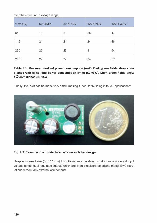
126
over the entire input voltage range.
V rms [V] 5V ONLY 5V & 3.3V 12V ONLY 12V & 3.3V
85 19 23 25 47
115 21 24 24 48
230 26 29 31 54
265 29 32 34 57
Table 9.1: Measured no-load power consumption (mW). Dark green fields show com-
pliance with 5I no load power consumption limits (≤0.03W). Light green fields show
4 compliance (≤0.15W)
Finally, the PCB can be made very small, making it ideal for building in to IoT applications:
Fig. 9.9: Example of a non-isolated off-line switcher design.
Despite its small size (33 x17 mm) this off-line switcher demonstrator has a universal input voltage range, dual regulated outputs which are short-circuit protected and meets EMC regu-lations without any external components.

127
Chapter 10
Wireless power
Most of us are familiar with an electric toothbrush charger. The toothbrush simply slots on to a spigot and the battery charging indicator starts to blink without there being any electrical connection. At its most basic, the charging circuit consists of a relaxation oscillator that gen-erates a varying magnetic field which is intercepted by a matched coil in the toothbrush to transfer power wirelessly to the rechargeable battery.
Fig. 10.1: Simplified electric toothbrush charging circuit using a Colpitts oscillator
This self-oscillating design uses a Colpitts oscillator to generate an AC sine wave output from the rectified and stabilized DC input. On switch-on, the transistor Q1 is turned on by the bias resistors on its base connection and the capacitor C1 starts to charge up. The increasing volt-age across C1 generates an increasing magnetic field in the inductor L. Once the capacitor C1 is fully charged, the voltage across the inductor L is constant and the magnetic field starts to collapse. This induces a voltage across it that is higher than the supply voltage, turning off Q1 via C2 and holding it off until the magnetic field in the inductor has dissipated. The cycle then begins again. The resulting voltage waveform across the inductor is approximately a sine wave. The resonant frequency of a Colpitts oscillator is given by:
Eq. 10.1:
The matching receiver coil must be accurately positioned to intercept the resulting magnetic field generated by the transmitter coil. The induced AC voltage is rectified and used to trick-le-charge the rechargeable batteries. As the battery voltage rises, the voltage drop across the resistor Rcharge reduces and the charging LED extinguishes.The maximum power transmission (minimum losses) can be calculated from:
Eq. 10.2:
Q1
L1C1
C2
ReRb2
Rb1
L2
D1 Rcharge
Batt 1
Batt 2
M CM
LED
RectifiedAC
C3
C4
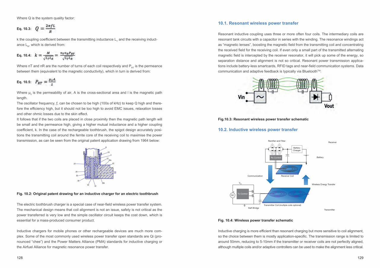
128 129
10.1. Resonant wireless power transfer
Resonant inductive coupling uses three or more often four coils. The intermediary coils are resonant tank circuits with a capacitor in series with the winding. The resonance windings act as “magnetic lenses”, boosting the magnetic fi eld from the transmitting coil and concentrating the received fi eld for the receiving coil. If even only a small part of the transmitted alternating magnetic fi eld is intercepted by the receiver resonator, it will pick up some of the energy, so separation distance and alignment is not so critical. Resonant power transmission applica-tions include battery-less smartcards, RFID tags and near-fi eld communication systems. Data communication and adaptive feedback is typically via BluetoothTM:
Fig.10.3: Resonant wireless power transfer schematic
10.2. Inductive wireless power transfer
Fig. 10.4: Wireless power transfer schematic
Inductive charging is more effi cient than resonant charging but more sensitive to coil alignment, so the choice between them is mostly application-specifi c. The transmission range is limited to around 50mm, reducing to 5-10mm if the transmitter or receiver coils are not perfectly aligned, although multiple coils and/or adaptive controllers can be used to make the alignment less critical.
Recti�er and FilterReceiver
Receiver CoilCommunication
Transmitter Coil (multiple coils optional)
Wireless Energy Transfer
TransmitterHalf-Bridge
VIN
Tx ControlDC
BatteryCharger
BatteryRx Control
Where Q is the system quality factor:
Eq. 10.3:
k the coupling coeffi cient between the transmitting inductance LT and the receiving induct-ance LR, which is derived from:
Eq. 10.4:
Where nT and nR are the number of turns of each coil respectively and PRT is the permeance between them (equivalent to the magnetic conductivity), which in turn is derived from:
Eq. 10.5:
Where μ0 is the permeability of air, A is the cross-sectional area and l is the magnetic path length.The oscillator frequency, ƒ, can be chosen to be high (100s of kHz) to keep Q high and there-fore the effi ciency high, but it should not be too high to avoid EMC issues, relaxation losses and other ohmic losses due to the skin eff ect. It follows that if the two coils are placed in close proximity then the magnetic path length will be small and the permeance high, giving a higher mutual inductance and a higher coupling coeffi cient, k. In the case of the rechargeable toothbrush, the spigot design accurately posi-tions the transmitting coil around the ferrite core of the receiving coil to maximise the power transmission, as can be seen from the original patent application drawing from 1964 below:
Fig. 10.2: Original patent drawing for an inductive charger for an electric toothbrush
The electric toothbrush charger is a special case of near-fi eld wireless power transfer system. The mechanical design means that coil alignment is not an issue, safety is not critical as the power transferred is very low and the simple oscillator circuit keeps the cost down, which is essential for a mass-produced consumer product.
Inductive chargers for mobile phones or other rechargeable devices are much more com-plex. Some of the most commonly used wireless power transfer open standards are Qi (pro-nounced “chee”) and the Power Matters Alliance (PMA) standards for inductive charging or the Airfuel Alliance for magnetic resonance power transfer.
24
26
H
16
5
22
42
36a
36
3836b
3230

130 131
Communication is achieved by the receiver generating coded load pulses which the transmit-ter can detect and decode (fi gure 10.6).
Fig. 10.6: Bi-directional data communication via pulse modulation (used, for example,
in the Qi system)
A further advantage of data communication is that the receiver can send a received signal strength value back to the transmitter to form a closed loop control system to handle load tran-sients, misalignments and fault conditions. Other systems use a separate radio link to transmit data back to the transmitter.
Wireless charging is nowadays most commonly used to recharge mobile phones, but it also has a place in industry for IoT applications. For example, consider a remote sensor module that is hermetically sealed against liquids, contaminants and vapours with no external connectors. It could be placed next to a piece of heavy industrial equipment and transmit local environment sensor readings such as ambient temperature, magnetic fi eld strength, acoustic noise levels or shock/vibration via a data link that uses an on-board chip antenna. The system could be powered from an internal supercapacitor or rechargeable battery whose voltage is monitored and transmitted along with the other data. Once the internal power source becomes drained, the whole sensor module is removed to a safe environment and placed on a recharging pad to recharge the internal energy store. Thus, wireless charging is not just a “gimmick” for industrial applications; it could become an accepted element in many harsh environment applications.
10.3 PCB inductive power transfer
A small amount of power (1-2W) can be transferred across an isolation barrier using a core-less transformer formed from adjacent PCB spiral tracks. The dielectric strength of FR4 PCB material is 800V-1500V/mil, so a standard 4-layer PCB with 40 mils between layer 2 and layer
Transmi�er Receiver
Rec�fica�onCommunica�onControl
COMM
Control processor on RX side will apply load pulses for signalling back to TX.
VoltageSense
Power Control
Comm Demodula�on
�100 KHz AC Col Voltage on TX side
2 KHz Load Pulses on RX Side
Fig. 10.5: Eff ect of various misalignments on transfer effi ciency (typical transfer curves)
The energy transfer follows a square law in the Z direction (coil separation), a roughly linear relationship for lateral misalignment (coils not perfectly overlapping) and a non-linear relation-ship for angular misalignment (receiver tilted with respect to the transmitter coil).
Unlike the simple electric toothbrush charger, inductive charging systems such as Qi use fl at coils with no magnetic cores and run at higher frequencies (typically between 0.1MHz and 1MHz). This allows higher power transfer rates from 3W up to 70W or more, but then creates the problem of unwanted or hazardous induced voltages in any conductive metallic objects placed into the mag-netic fi eld. This hazard is eliminated by bidirectional data communication between the transmitter and receiver so that the full output power is only activated after the receiver has been properly identifi ed as a Qi-compatible device and that there are no metallic obstacles in the way.
Z (mm)
Eff (%)
Y (mm)
Eff (%)
Angle (degrees)
Eff (%)
Z
Y
X∆ Z
Z-axis misalignment (vertical)
Z
Y
X
∆ Y
X or Y-axis misalignment (lateral)
∆ X
Z
Y
X
ϴ misalignment (angular)
Z‘
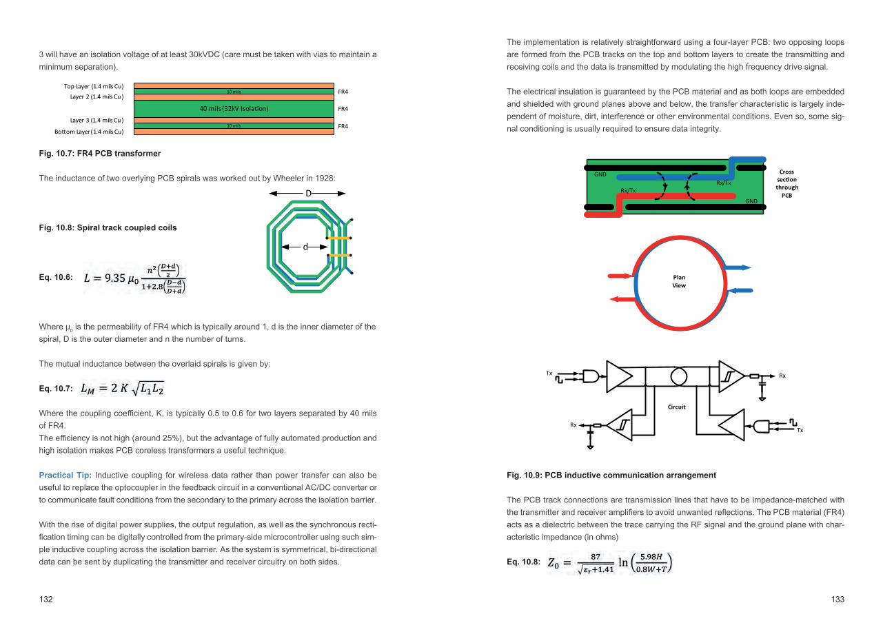
132 133
The implementation is relatively straightforward using a four-layer PCB: two opposing loops are formed from the PCB tracks on the top and bottom layers to create the transmitting and receiving coils and the data is transmitted by modulating the high frequency drive signal.
The electrical insulation is guaranteed by the PCB material and as both loops are embedded and shielded with ground planes above and below, the transfer characteristic is largely inde-pendent of moisture, dirt, interference or other environmental conditions. Even so, some sig-nal conditioning is usually required to ensure data integrity.
Fig. 10.9: PCB inductive communication arrangement
The PCB track connections are transmission lines that have to be impedance-matched with the transmitter and receiver amplifiers to avoid unwanted reflections. The PCB material (FR4) acts as a dielectric between the trace carrying the RF signal and the ground plane with char-acteristic impedance (in ohms)
Eq. 10.8:
Rx/TxRx/Tx
GND
GND Cross sectionthrough
PCB
PlanView
Rx
Tx
Tx
Circuit
Rx
3 will have an isolation voltage of at least 30kVDC (care must be taken with vias to maintain a minimum separation).
Fig. 10.7: FR4 PCB transformer
The inductance of two overlying PCB spirals was worked out by Wheeler in 1928:
Fig. 10.8: Spiral track coupled coils
Eq. 10.6:
Where μ0 is the permeability of FR4 which is typically around 1, d is the inner diameter of the spiral, D is the outer diameter and n the number of turns.
The mutual inductance between the overlaid spirals is given by:
Eq. 10.7:
Where the coupling coefficient, K, is typically 0.5 to 0.6 for two layers separated by 40 mils of FR4.The efficiency is not high (around 25%), but the advantage of fully automated production and high isolation makes PCB coreless transformers a useful technique.
Practical Tip: Inductive coupling for wireless data rather than power transfer can also be useful to replace the optocoupler in the feedback circuit in a conventional AC/DC converter or to communicate fault conditions from the secondary to the primary across the isolation barrier.
With the rise of digital power supplies, the output regulation, as well as the synchronous recti-fication timing can be digitally controlled from the primary-side microcontroller using such sim-ple inductive coupling across the isolation barrier. As the system is symmetrical, bi-directional data can be sent by duplicating the transmitter and receiver circuitry on both sides.
10 mils
40 mils (32kV Isolation)
10 mils
Top Layer (1.4 mils Cu)Layer 2 (1.4 mils Cu)
Layer 3 (1.4 mils Cu)
Bottom Layer (1.4 mils Cu)
FR4
FR4
FR4
D
d

134 135
Multilayer PCB characteristic capacitance [pF/in]:
Eq. 10.12:
Multilayer PCB propagation delay [ps/in]:
Eq. 10.13:
NOTE: PCB dimensions are still commonly defined in imperial measurements (inch, mils), so these have been used here instead of the metric system.
Fig. 10.10: PCB stripline geometry and characteristic impedance (Z0) relationship
For a standard PCB, the dielectric constant, ℇ, is equal to 4, so if the 1-ounce copper track is 20 mil wide and the PCB thickness is 10 mil, the resulting impedance will be 50 ohms. For a 75 ohm impedance, reduce the track thickness to 8.3 mils.
The PCB transmission lines will also have a characteristic capacitance [pF/in] of:
Eq. 10.9:
And a propagation delay [in ps/in] of:
Eq. 10.10:
For multilayer PCBs where the tracks are embedded between two ground or power planes, the above relationships need to be modified slightly:
Fig. 10.11: Embedded transmission line in a multilayer PCB
Multilayer PCB characteristic impedance [ohms]:
Eq. 10.11:
PCB Track
WT
H
EmbeddedPCB Track
Ground Plane
FR4 Dielectric
WT
H
HGround Plane
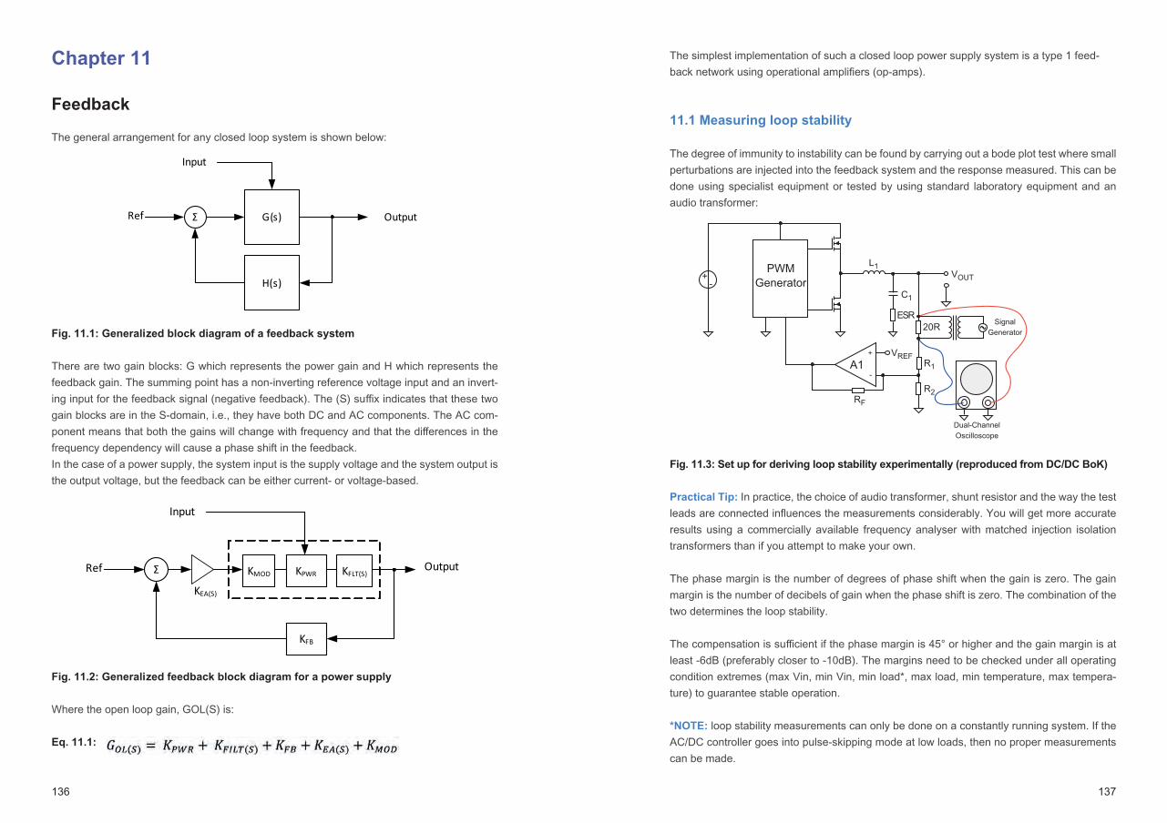
136 137
Chapter 11
Feedback
The general arrangement for any closed loop system is shown below:
Fig. 11.1: Generalized block diagram of a feedback system
There are two gain blocks: G which represents the power gain and H which represents the feedback gain. The summing point has a non-inverting reference voltage input and an invert-ing input for the feedback signal (negative feedback). The (S) suffix indicates that these two gain blocks are in the S-domain, i.e., they have both DC and AC components. The AC com-ponent means that both the gains will change with frequency and that the differences in the frequency dependency will cause a phase shift in the feedback. In the case of a power supply, the system input is the supply voltage and the system output is the output voltage, but the feedback can be either current- or voltage-based.
Fig. 11.2: Generalized feedback block diagram for a power supply
Where the open loop gain, GOL(S) is:
Eq. 11.1:
G(s)
H(s)
Ʃ Ref
Input
Output
Ʃ Ref
Input
OutputKMOD KPWR KFLT(S)
KEA(S)
KFB
The simplest implementation of such a closed loop power supply system is a type 1 feed-back network using operational amplifiers (op-amps).
11.1 Measuring loop stability
The degree of immunity to instability can be found by carrying out a bode plot test where small perturbations are injected into the feedback system and the response measured. This can be done using specialist equipment or tested by using standard laboratory equipment and an audio transformer:
Fig. 11.3: Set up for deriving loop stability experimentally (reproduced from DC/DC BoK)
Practical Tip: In practice, the choice of audio transformer, shunt resistor and the way the test leads are connected influences the measurements considerably. You will get more accurate results using a commercially available frequency analyser with matched injection isolation transformers than if you attempt to make your own.
The phase margin is the number of degrees of phase shift when the gain is zero. The gain margin is the number of decibels of gain when the phase shift is zero. The combination of the two determines the loop stability.
The compensation is sufficient if the phase margin is 45° or higher and the gain margin is at least -6dB (preferably closer to -10dB). The margins need to be checked under all operating condition extremes (max Vin, min Vin, min load*, max load, min temperature, max tempera-ture) to guarantee stable operation.
*NOTE: loop stability measurements can only be done on a constantly running system. If the AC/DC controller goes into pulse-skipping mode at low loads, then no proper measurements can be made.
��
������
����
��
��
���
��
����
��� �����
��������
�����
�
�
����������������������

138 139
The injection point in the loop is optimum if the impedance on one side of the injection point is much higher than on the other, for example between the low impedance output stage and the high impedance resistor divider to the feedback comparator (as shown below in figure 11.4) It would also be possible in theory to inject the signal between the comparator output and PWM controller input, but in many controller ICs, this point is internal to the IC and not accessible.
Fig. 11.4: Suitable injection point for low output voltages
However, for high voltage outputs such as a PFC stage, the injection point shown in figure 11.4 is not ideal. This is because the perturbation signal is so attenuated by the high resist-ance voltage divider that the measurements become unreliable. In this situation, an additional buffer op-amp can be used to allow the signal to be successfully injected. The op-amp is unity gain, so will not affect the readings as long as it has a high enough bandwidth.
Fig. 11.5: Alternative injection point using a unity gain op-amp for high output voltages
PWMGenerator
Rinj
R1
R2
Rin
C1
Vref
InjectionTransformer
LowImpedance
HighImpedance
+
-
Vout = Low Voltage
PWMGenerator
R1
R2Rin
C1
Vref
InjectionTransformer
LowImpedance
HighImpedance
+
-Rinj
-+
Vout = High Voltage
R1
R1
R1
If the injected perturbation signal is too weak, then the measurements will become increasing-ly inaccurate at low frequencies because the signal-to-noise ratio will be too low. If the injected signal is too strong, then the measurements will become erratic at higher frequencies as the perturbations will over-ride the internal feedback voltage levels.
Fig. 11.6: Bode plot showing instability at low frequencies (blue circle) caused by poor
signal-to-noise margin - the plot becomes noisy
Fig. 11.7: Bode plot showing erratic readings at higher frequencies (blue circle)
caused by excessive perturbation signal strength- the plot is no longer smooth
-60
-40
-20
0
20
40
60
-120
-180
-60
0
60
120
180
Gain
(dB)
Phas
e (°
)
1 10 100 1000
Frequency (kHz)
GainPhase
-60
-40
-20
0
20
40
60
-120
-60
0
60
120
180
Gain
(dB)
Phas
e (°
)
1 10 100 1000
Frequency (kHz)
GainPhase
140 141
Fig. 11.8: Bode plot with optimal signal injection
Another way of visualizing the same gain and phase information is to use a Nyquist diagram. Most professional-grade frequency analysers can output the measurements as either a Bode plot or a Nyquist diagram. The advantage of a Nyquist diagram is that not only the gain and phase margins can be determined, but also the stability margin, which occurs at the frequency where the curve is closest to the (-1,0) point (refer to figure 11.9). The factor -1 takes into account the -180° phase change implicit in negative feedback. The Nyquist diagram can also be reflected along the imaginary axis to show the instability point at (1,0) for the entire feedback loop.
Fig. 11.9: Nyquist diagrams for negative
feedback loop stability. From the plotted
results, the angles and separations from the
instability point (-1,0) can be measured to
derive the phase margin, gain margin and
stability margin
The phase reserve is the angle between the plot and the real axis where it crosses the -1,0 circle.The amplitude reserve is the separation between the plot and the -1,0 point measured along the real axis.
The stability reserve is the separation between the plot and the -1,0 point measured at its closest approach.
-40
-30
-10
-20
0
10
20
30
40
50
60
-120
-60
0
60
120
180
Gain
(dB)
Phas
e (°
)
1 10 100 1000
Frequency (kHz)
GainPhase
Real
Imaginary
ω=0ω=∞ (-1,0)
Real
Imaginary
ω=0ω=∞ (-1,0)
Real
Imaginary
ω=0ω=∞ (-1,0)
Phase Reserve
Amplitude Reserve
Stability Reserve
ϴ
11.2 Type 1 feedback loop compensation calculation
It is also possible to determine stability by calculation, depending on the type of compensation circuit used in the feedback loop.A Type 1 feedback circuit is shown below in both voltage (output voltage controlled by input voltage) and transconductance (output current controlled by input voltage) variants:
Fig. 11.10: Type 1 feedback circuits (voltage and transconductance versions)
For example, if the desired output voltage is 5.0 volts and the reference voltage is 2.5 volts, then resistor R1 will be made equal to R2 so that the output voltage is divided by two.
These circuits are integrators: sudden changes in the input signal are turned into a more slowly ramping output signal which gives the power supply some immunity from breaking into oscillation by over-correcting for changes in load or input voltage. The output ramp rate is dependent on R1 and C1 only, R2 plays no role in the integration coefficient.The gain/phase response for a type 1 feedback system is shown below:
Fig. 11.11: Type 1 feedback gain and phase relationship with frequency
The point at which the gain = 1 is the system zero.
+
-Vref
C1 R1
R2
Vout
Voltage
+
-Vref
C1
R1
R2
Vout
gmIg
Transconductance
R1, C1
Frequency (Log Scale)
1
0
fzero
0Ph
ase
(°)
Frequency (Log Scale)
R1, C1
Frequency (Log Scale)
1
0
fzero
0
Phas
e (°)
Frequency (Log Scale)

142 143
For voltage feedback:
Eq. 11.2:
For transconductance feedback, the transfer function is: (written in the s-format)
Eq. 11.3:
Practical Tip: The choice of the resistor values used in the divider network is unimportant for the transconductance circuit as only the ratio affects the gain. The circuit would have the same frequency response if either two 10k resistors or two 100k resistors were used for R1 and R2, for example. However, in the voltage feedback version, R1 appears in the frequency equation but R2 does not. Changing R1 from 10k to 100k would alter the gain plot. There-fore, if the output voltage needs to be trimmed when using voltage feedback, only R2 should be made variable and R1 kept fixed.
The slope of the gain is -20dB per decade, defined by the classic integration function of R1 and C1. If the op-amp has an ideal linear response time to small signal changes, then both the gain slope and the phase shift are constant over frequency. This can become a problem with repetitive or sudden step changes in the load or supply voltage. At higher frequencies than the system zero, the power supply struggles to maintain regulation as the phase and gain margins are too low.
11.3 Type 2 feedback loop compensation
A solution to the problem of low gain and phase margins is to selectively boost them at higher frequencies. The Type 2 feedback circuit and gain and phase frequency responses are shown below:
Fig. 11.12: Type 2 feedback circuits (voltage and transconductance versions)
As is evident from the frequency graphs in figure 11.13, the additional C2 and R3 components have added both a gain boost and a phase boost at higher frequencies. The phase boost is
+
-Vref
C1 R1
R2
Vout
Vfb+
-Vref
C1
R1
R2
Vout
gmIg
C2 R3
C2
R3
Voltage Transconductance
limited to 90°, meaning that the maximum overall phase shift is 180°C. The peak of the phase boost response lies at the half way point between the zero and pole frequencies.
Fig. 11.13: Type 2 gain and phase relationship with frequency
The new relationships are (assuming that C2 is much larger than C1):
Type 2 voltage feedback:
Eq. 11.4:
Type 2 transconductance feedback transfer function (written in s-format)
Eq. 11.5:
This equation combines the three main factors of the DC gain and the zero and the pole terms, which individually can be derived from the following relationships:
Eq. 11.6:
Eq. 11.7:
The gain at the crossover frequency is:
Eq. 11.8:
R1, C2 R3, C2
R3, C1
fzero fpole
PhaseBoost< 90°
Frequency (Log Scale)
Gain
(dB)
Phas
e (°)
Frequency (Log Scale)
1
0
R1, C2 R3, C2
R3, C1
fzero fpole
PhaseBoost< 90°
Frequency (Log Scale)
Gain
(dB)
Phas
e (°)
Frequency (Log Scale)
1
0

144 145
11.4 Type 3 feedback loop compensation
In some fast transient response power supply circuits, even the additional gain and phase boost created by the Type 2 compensation may not be suffi cient. This is especially true for CCM power stages that suff er from a large phase swing when the resonant frequency is ex-ceeded. Type 3 compensators place an additional “speed up” circuit across the input voltage potential divider:
Fig. 11.14: Type 3 feedback circuits (voltage and transconductance versions)
Fig. 11.15: Type 3 gain and phase relationship with frequency
+
-Vref
C1 R1
R2
Vout
+
-Vref
C1
R1
R2
Vout
gmIg
C2 R3
C2
R3
R4
C3
R4
C3
Voltage Transconductance
Frequency (Log Scale)
Gain
(dB)
Phas
e (°)
Frequency (Log Scale)
1
0
R1,C1 R4,C3
R3, C1
fzero1 fzero2 fpole 1 fpole2
R1,R4, C3
R3,C2
PhaseBoost>90°
As is evident from the frequency graphs, the additional C4 and R4 components have added more gain and a phase boost at higher frequencies. The phase boost is now more than 90°, meaning that the maximum overall phase shift is 225°C. The new relationships for Type 3 volt-age feedback are (assuming that C2 is much larger than C1 and R1 is much larger than R4):
Eq. 11.9:
Type 3 transconductance feedback transfer function (written in s-format)
Eq. 11.10:
This equation combines the fi ve main factors of the DC gain and the four zero and the pole terms, which individually can be derived from the following relationships:
Eq. 11.11:
Eq. 11.12:
The gain at the crossover frequency is then:
Eq. 11.13:
11.5 Optocoupler feedback loop compensation
In practice, most AC/DC power supplies require input/output isolation. The feedback path is no longer direct but via an opto-isolator which also has a frequency dependent response.The most common opto-coupler circuit uses the ‘431’ shunt regulator to control the optocou-pler LED current. The 431 is a very versatile IC that acts like a tuneable Zener diode. A typical circuit is shown below:
:

146 147
Fig. 11.16: Opto-coupler isolated feedback circuit (with a Type 1 comparator)
In this circuit, R1x and R2x define the shunt regulator (IC1) threshold voltage (and therefore the output voltage regulation point), RLED is the current limiting resistor for the optocoupler LED and Cx is used to define the AC response of the 431 IC. On the primary side, the phototransis-tor bypasses R1, filtered by the Ropto, Copto components.
If the output voltage rises too high, IC1 starts to conduct more current and the LED shines more brightly, causing the phototransistor to bypass more current and pull the junction of R1 and R2 closer to Vcc, regulating the output voltage down. If the output voltage falls, the opto-coupler LED current is decreases and the R1 bypass current also decrease causing the junc-tion voltage of R1 and R2 to drop, forcing the op-amp to increase its output drive to compen-sate. The feedback is thus a closed loop, even though the output is galvanically isolated from the input.
Fig. 11.17: Types of optocoupler: a) is the over-and-under type, b) the side-by-side
type
The over-and-under type (figure 11.17a) typically has a transparent high dielectric strength film between emitter and receiver to improve the isolation withstand voltage. The total internal reflection type (figure 11.17b) is a more complicated construction method, but does not need a separating film and has a lower coupling capacitance as the input and output planes are sideways on.
R1x
R2x
Vout
Vfb
RLED
Cx
Copto
IC1+
-Vref
C1 R1
R2
Vcc Ropto
Cout
Double-molded construction
Film
Co-planar construction
Inner mold materialOuter mold material
IRED
IRED
Sensor
Sensor
Silicone gel
b)a)
Adding these extra active components obviously affects the gain and phase frequency re-sponse of the feedback loop. If we take the simplest Type 1 comparator, the opto-coupler adds an additional pole and changes the flat phase response plot so that it behaves more like a Type 2 feedback loop:
Fig. 11.18: Type 1 comparator gain and phase relationship when modified with op-
to-coupled feedback
Practical Tip: The gain of the optocoupler (the current transfer ratio, CTR) is both age and temperature dependent, which makes calculating the tolerances tricky. The datasheet CTR figure is usually given at 25°C, but it will increase if the temperature drops and decrease if the temperature rises. At 100°C ambient, the CTR will be around 70% of the datasheet value.
The main problem is that the optocoupler is typically positioned very close to the power trans-former as they are both placed across the isolation gap. The transformer can run very hot under full load conditions and the heat radiating out can easily cause the CTR to become too low for proper regulation. The optocoupler output current can be increased by increasing the LED current, but then the no-load power consumption can become significant. Also, the aging of the optocoupler is very dependent on the LED drive current, so increasing the LED current from, say, 5mA to 15mA will reduce the effective lifetime (the point where the CTR drops to 50% of its nominal value) from around 400k hours to 150k hours. Thus the position of the optocoupler on the PCB and its ambient temperature affects the optimal resistor values that need to be chosen!
R1, C1
R1x, CxRopto , Copto ,
R1, C1
fzero fpole
PhaseBoost< 45°
Frequency (Log Scale)
Gain
(dB)
1
0
Phas
e (°)
R1, C1
R1x, CxRopto , Copto ,
R1, C1
fzero fpole
PhaseBoost< 45°
Frequency (Log Scale)
Gain
(dB)
1
0
Phas
e (°)

148 149
11.6 Secondary-side feedback compensation
It is also possible to add additional components to compensate on the secondary side for deficiencies in gain or boost. One common amendment is to add Rcomp and Ccomp components to cancel out the unwanted zero caused by the output capacitor’s own ESR:
Fig. 11.19: Output Capacitor ESR zero cancellation (Rcomp
, Ccomp
)
Another useful secondary-side compensation technique is to add HF bypass components across the LED current limiting resistor to increase the useful bandwidth of the opto-coupler (the response time is dependent on the LED current) and to ensure that a minimum current always flows through the shunt regulator.
Fig. 11.20: High frequency boost (Rcomp
, Ccomp
)
R1x
R2x
RLED
Cx
CoutCcomp
Rcomp
(Cout,ESR)
Vout
R1x
R2x
RLED
Cx
Cout
Ccomp
Rcomp
Vout
The gain/phase characteristic of a power supply will have multiple overlying components caused by the contributions from the power stage, compensation network and other control loop elements. It is possible to calculate all of the terms involved and guarantee stability under all operating conditions by design, but confirmation by real-life measurement is needed to check that component tolerances and temperature effects do not cause the power supply to drift into a region where instability can occur.
11.7 Magnetic feedback
As mentioned previously, the CTR of an optocoupler varies with temperature and degrades with age. It also deteriorates when subjected to radiation in the form of neutron bombardment or gammas rays. The radiation permanently damages the sensitive photo junction in the re-ceiving transistor as well as reducing the efficacy of the LED, eventually reducing the CTR to near zero. This makes optocoupler feedback undesirable for military, space or high-altitude applications.An alternative to opto-coupled isolators is to use magnetic feedback. A separate transformer can be used to close the feedback loop while keeping the isolation intact. There are several ways of doing this:
11.7.1 Secondary-side powered PWM feedback transformer
A secondary side powered PWM oscillator drives a small signal transformer with a PWM sig-nal that is proportional to the output voltage. The output winding on the primary side is rectified and smoothed to deliver a control voltage for the main switching oscillator:
Fig. 11.21: Magnetic feedback using separate PWM transformer
Care needs to be taken to ensure that the circuit starts up correctly as the feedback regu-lation transformer is powered by the output voltage. Therefore, the same circuit is shown here as used with the previous opto-coupler feedback design, R1 and R2 set the maximum permissible output voltage which can then only be regulated down by the feedback from the PWM oscillator. The PWM oscillator needs to run at a high enough frequency to ensure a fast response to load changes and to keep the ripple acceptable without making Cmag too big.
R1x
R2x
Cmag
IC1+
-Vref
C1 R1
R2
Vcc Rmag
Cout
Vout
PWM

150 151
A good starting point would be x10 to x20 the main oscillator frequency. The advantage of this design is that it will work with any single-output topology; forward, flyback or resonant. The disadvantages are that the response time is relatively slow, so it is not suitable for dynamic loads and that the output voltage always peaks to the maximum on power-up unless a soft-start circuit is used.
11.7.2 Direct magnetic feedback
Forward converters rely on an output inductor to store energy and maintain the output voltage during the power transformer reset. The current in the output inductor ramps up and down con-tinuously, so the inductor can be used as the primary winding of a feedback transformer without any additional circuitry on the secondary side. This solves one of the major problems of all sec-ondary feedback circuits: namely how to reliably power the necessary feedback components on the secondary side? If the power supply is started up with a short or an overload on the output, then output regulation can be very difficult to control as the output voltage cannot rise fully.
With direct magnetic feedback, the voltage induced on the primary-side winding of the feed-back transformer is sampled just after the main power switch is turned off by a sample-and-hold circuit and then buffered to be used to control the main oscillator:
Fig. 11.22: Direct-sampling magnetic feedback
The advantage of this circuit is the simplicity of implementation on the secondary side and its accuracy, as the sample-and-hold window can be adjusted to ignore any switching transients and to sample the induced output voltage only when it is stable. It also works well with multi-ple outputs that share a common output magnetic core (figure 11.23). The induced feedback signal is then the summation of the output voltages.
The disadvantage of direct sampling is the difficulty of maintaining proper regulation under no load conditions. With no output load, the power switch on-time becomes very short and the
D1
Cout RLoad
Cin
T1
DReset
D2
Lout
NsNp Nr
Q1PWMController
VDC
Lfb
DS/H
CS/H
VS/H
S/HControl
sampling window even shorter. It can be nearly impossible to get an accurate feedback volt-age to ensure proper regulation. Therefore, direct magnetic feedback should only be used with power supplies with a minimum load specification.
Fig. 11.23: Direct sampling magnetic feedback with multiple outputs
11.7.3 Primary-side driven magnetic feedback
One further method of implementing magnetic feedback deserves a mention, and that is a pri-mary-side driven signal transformer. This technique combines the previous two examples: a PWM-driven 1:1 transformer with fixed operating frequency and a simple sample-and-hold cir-cuit to detect the appropriate measurement point in the cycle. Its main advantage is that the secondary side feedback circuit is separately powered from the main power stage so will func-tion correctly even if the output is turned off. The schematic is shown below in figure 11.24:
Fig. 11.24: Magnetically coupled shunt regulator schematic
D1
Cout1RLoad1
Cin
T1
DReset
D2
Lout1
NsNp Nr
Q1PWMController
VDC
Lfb
DS/H
CS/H
VS/H
S/HControl
D3
D4
Lout2
Cout2RLoad2
Q1Fixed Frequency
PWM
Lfb,priDS/HCS/H
VS/H
S/HControl
Lfb,secD1
Q2PowerStage PWMController
ShuntRegulator
Vout
152 153
The topology is essentially flyback. When the PWM signal is high, current flows through the primary winding and the transformer core becomes magnetized. Due to the reversed output winding, no current flows through the shunt regulator as the negative output voltage is blocked by the diode D1. When the PWM signal is low, the output voltage becomes positive as the magnetic field inside the core collapses, but is now clamped by the shunt regulator at a volt-age determined by the output voltage Vout
The reflected voltage on the primary side is the same as on the secondary side minus the di-ode drop, but with reversed polarity. The negative primary voltage can be sampled using the simple peak detector formed from DS/H and CS/H and then inverted or used as a negative refer-ence voltage to modulate the feedback of the main power stage.
Fig. 11.25: Waveforms of the magnetically coupled shunt regulator
A practical circuit is shown below in figure 11.26 using a constant on-time PWM modulation signal.
Fig. 11.26: Practical circuit for a magnetically coupled shunt regulator
IL�,priPWM
onPWM
off
VL�,priVC
VOut, reflected
Vf, D1
Vf, D S/H
S/H
VOut
Lfb,priDS/H
CS/H
VS/H
Lfb,sec2
D1
ShuntRegulator
R1 x
R2 x
VoutRe
Rb
VCC
Lfb,sec1
D2Csupply
Rsupply
R3x
Rcomp
Ccomp
R1
R2
Vref
VCC
C1
R3 Cx
T11:1:1
A 1:1:1 transformer is used so that one output winding can be half-wave rectified by D2 to create an isolated supply voltage for the shunt regulator. As this winding is not reversed with respect to the primary, the current that flows into Ccv is not measured by the hold capacitor CH due to the blocking diode DH (the voltage on the primary side is positive and equal to the voltage on the output capacitor CCV minus one diode drop).
The voltage across CH slowly charges up through R1 and R2, “resetting“ the negative hold ca-pacitor voltage. When Q1 is switched off, the output voltages are reversed. Now D2 is reverse biased and D1 is forward biased.
The reflected primary winding voltage is negative and equal to the shunt regulator voltage plus the forward drop of D1. The voltage across CH is pulled down via DH to this negative voltage. If all of the diodes are the same with the same forward voltage drops, then the voltage across CH is exactly equal to the shunt regulator voltage. Thus, the voltage on the hold capacitor is renewed every cycle and tracks changes in the output voltage accurately. Once the core has become completely demagnetized, then all of the diodes become reverse biased and no more current flows. At this point, the PWM signal should be triggered to start the next cycle so that the hold capacitor voltage does not droop.
The disadvantage of this technique is that the peak detector output is negative, so in some designs, it would need to be inverted with another op-amp stage to be useful. Secondly, the transformer must not go be allowed to go into saturation, so the core cannot be made too small even though the transmitted power is low. Finally, the value for CH is a compromise between being high enough for low ripple and low enough for a fast response.
The advantages are the cycle-by-cycle tracking of the output voltage and the ability to operate at high ambient temperatures of 100°C or more as no opto-couplers are used.
11.8 Capacitively coupled feedback
As more and more power supplies now use digital controllers, the use of digital isolators is also becoming more prevalent. The feedback path is no longer purely analogue, but the output voltage is sampled and converted into a digital control signal using general-purpose microprocessors or custom DSPs (Digital Signal Processors). The DSP can be either on the primary-side for a full digital control topology or on the secondary-side sending back data to modulate an analogue primary-side controller or two microprocessors can be used to send data back and forth. The advantage of a microprocessor on the primary-side is a guaranteed start up but at the cost of needing to generate a clean low voltage supply from the high voltage mains supply. The advantage of a microprocessor on the output side is that the micropro-cessor power supply is much simpler, and the ability to have multiple outputs or switchable constant voltage or constant current modes. The disadvantage is that start-up into a short circuit may be compromised. Microprocessors are nowadays so cheap that it is often easier to use them on both the prima-

154 155
ry- and secondary-sides and use a digital isolator for communication between them. Capac-itively coupled digital isolators off er very high isolation (typically 5kVAC/1 minute) in a very compact package with cleaned-up outputs with well controlled slew rates.
Capacitively coupled digital isolators come in two main fl avours: modulated or edge triggered. A modulated digital isolator consists of a capacitively coupled modulator and demodulator than run at a much higher frequency than the signal bandwidth being transmitted. Data is transmitted by On-Off Keying (OOK) meaning that the digital input is simply used to gate a high frequency oscillator typically running at tens of Megahertz, so data rates from DC up to 100Mbps are possible.
Fig. 11.27 Schematic of a capacitively coupled modulated digital isolator
The disadvantage of using modulated couplers is the very high internal operating frequency which can cause EMI problems if a spread spectrum oscillator is not used or if the PCB layout is not carefully designed with lots of decoupling capacitors and separated ground/power planes.
The relatively slow reaction time of the demodulator creates a propagation delay of 10-100ns, which for fast control loops may be signifi cant delay. The alternative is to use edge triggered communication:
Receiver
OutputInput
Transmitter
DEMODULATORMODULATOR
RFOSCILLATOR
Capacitive Isolation Barrier
Input Signal
Output Signal
Modulation Signal
Fig. 11.28: Schematic of a capacitively coupled edge-triggered digital isolator
Edge-triggered digital isolators have lower propagation delays and higher data throughput than modulated digital isolators, but are more expensive and despite the diff erential inputs can be more susceptible to interference from stray electric fi elds.
11.9 Primary-side regulation
Although digital isolators fi nd many uses in high end, space and military applications, they are too expensive for many cost-sensitive industrial and commercial power supplies. Primary-side regulation (PSR) is the most commonly used method as even the cost of the optocoupler can be signifi cant in a design with a BoM budget of only a few dollars. PSR also has the advantage that the auxiliary winding is needed in any case to bootstrap-power the controller IC and to reduce the power lost in the start-up resistor chain. A typical IC-based PSR topology is shown below, along with the waveforms.
Fig. 11.29: Primary-side regulated controller with integrated power switch
Tx
Vcc
LatchSet
Reset Q Rx
Clk
IsolationBarrier
DOUTCOUT
RLAC
C1
Np:NsVf,Dout
FusibleResistor
CIN
L1
C2
RHV 1
RHV 2
CVcc
RsupplyD1
PSRController Rs
R1
R2
Vcc DRsFb
Gnd
IDSIDS
RL,min
V W

156 157
Fig. 11.30: Typical PSR waveforms
There are four distinct phases of operation:
Phase 1: The MOSFET is gated on and current through the primary winding increases linearly until it reaches the peak current limit, Ipk, which is detected by measuring the voltage across the sense resistor, Rs
Phase 2: The MOSFET is turned off and the energy stored in the core is released through the output diode as the magnetic fi eld collapses. The current through the diode decreases from a peak current of Ipk times the primary to secondary turns ratio, Np: Ns linearly down to zero.
Phase 3: The voltage on the auxiliary winding, VAW, meanwhile decreases from a peak volt-age of the auxiliary to secondary turns ratio multiplied by (Vout + diode drop, VF) to just Na:Ns
multiplied by Vout as the diode current decreases to zero. At this point the auxiliary winding voltage is sampled via the resistor divider R1 and R2. The resistor divider ratio is the opposite of the auxiliary turns ratio, so the voltage on VFB is simply the output voltage. This is used to regulate the PWM controller.
ts
tDtON
Ipk
Vo
NaNs
.____
NaNs
.____
NpNs
.___
ID.avg =Io
Ipk
Ids (MOSFET Drain-to-Source Curren)
ID (Diode Current)
Vw (Auxiliary Winding Voltage)
VF
Phase 4: The transformer goes into quasi-resonant mode. The auxiliary voltage is monitored for the next valley before restarting the cycle. This allows the main power MOSFET to switch on at the minimum primary voltage to reduce the switching stress.
The big advantage of PSR is the low component count as the necessary PWM control, sam-ple–and-hold and protection circuitry is all integrated inside the control IC. The auxiliary wind-ing does not just eliminate the need for an opto-coupler, it also provides enough bootstrap power to run the IC. A high value resistor chain RHV1 + RHV2 from the rectifi ed input voltage is used to start up the IC, but as soon as it is running, the IC switches to the rectifi ed low voltage supply from the auxiliary output via Rsupply and D1. This reduces the power consumption con-siderably and increases the effi ciency.
The disadvantages are the need for an auxiliary winding. This does not add much cost, but can make the transformer construction more complex, especially if split primary windings are used. The windings need to be carefully arranged so that the insulation withstand voltage and the clearances are not aff ected by the extra winding. Also, the topology require discontinuous opera-tion to sample the refl ected output voltage on the auxiliary winding correctly, and this makes con-stant current converters more diffi cult to design to ensure DCM under all operating conditions.
Also, a dummy load resistor, RLmin, is needed to keep the switching frequency above a mini-mum limit and to stop the output voltage rising out of specifi cation under no-load conditions (refer to the next chapter for low power consumption techniques)
In general, the advantages outweigh the disadvantages to such an extent that quasi-resonant PSR is the most commonly used AC/DC topology for almost all low power converters.
Fig. 11.31: Photos of the top and bottom sides of the RECOM RAC02 series showing
the compact assembly and low component count possible with PSR topology

158 159
Chapter 12
Low Standby Power Consumption Techniques
Until relatively recently, one of the main selling points of any AC/DC design was the full load efficiency. This is mainly because the figures are often very impressive (if a 100W AC/DC power supply has no losses but needs 1W to power its internal ‘housekeeping’ power con-sumption, then it can be advertised as being 99% efficient). However, the same power supply with a 1W load would only be 50% efficient and all power supplies have zero efficiency under no-load conditions.
The regulatory authorities have recognized that most power supplies operate most of the time under no-load standby conditions, so have introduced standards for standby as well as full load losses. This is because consumer electronics are so widespread that the average home has now upwards of 40 mains-powered devices in it which even in standby consume between 5%-10% of the total electricity demand.
The main energy efficiency regulations for external power supplies standby (no load) power consumption are:
US Department of Energy (DoE) Energy Star ≤ 0.30 W up to 10W, ≤ 0.5 W up to 250W
CECP (China Energy Conservation Program) ≤ 0.30 W up to 10W, ≤ 0.5 W up to 250W
EU EcoDesign (Energy using Products-EuP) ≤ 0.30 W for non-PFC, ≤ 0.5 W for PFC
Australia High Efficiency ≤ 0.5 W up to 180W
Table 12.1: Comparison of standby power consumption limits
External battery charger power supplies have stricter limits (0.075W up to 50W, 0.15W up to 250W) as it is assumed that they will be left plugged in yet spend most of their time in standby.Internal built-in power supplies have a more relaxed specification (0.5W in standby, 1W if there is an active display) as it assumed that the device will be switchedoff or disconnected if not needed.
The losses in an AC/DC converter which are not load-dependent can be split into passive and active elements:
Eq. 12.1:
There are several techniques that can be used to reduce the no-load or light-load power consumption.
12.1 Passive losses
12.1.1 HV start up disconnect
All AC/DC controllers need a start-up circuit. The rectified high voltage DC bus is fed via high resistance dropper resistors (usually two or more are used in series to spread the voltage stress across each resistor) and a Zener diode limiter to the Vcc input of the controller IC. Usually, as soon as the controller starts up, the operating Vcc current is then supplied by an auxiliary winding (which can also act as the feedback for primary side feedback applications). Thus, the HV start-up circuit must only provide enough current to start the controller IC oscil-lating: thereafter the “bootstrap” auxiliary winding takes over to provide the operating current (so called because of the image of pulling oneself up into the air by tugging on one’s own bootstraps or shoe-laces).
Figure 12.1 shows such an arrangement. RHV1 and RHV2 are the two high voltage dropper re-sistors wired in series to reduce the voltage stress across each resistor and ZD1 is the voltage limiting Zener diode (typically around 15V). After start-up, the operating current will be sup-plied by the auxiliary winding rectified by D1 and smoothed by CVcc. To avoid overloading the Zener diode, a series resistor Rsupply limits the running current to a safe level.
Fig. 12.1 HV start-up circuit with bootstrap
AC
C1
FusibleResistor
CIN
L1
C2
RHV1
RHV2
CVcc
Rsupply
D1
PWMController
Vcc
D
ZD1
Start-upCurrent
RunningCurrent
Rectification and EMC Filter Start -up and Housekeeping Supply
PowerStage
160 161
Even if the majority of the operating current is provided by the auxiliary winding, significant current still flows through the HV start-up resistors after start-up (equal to the rectified DC mains voltage – ZD1 divided by RHV1 + RHV2). This represents a loss that becomes significant under no-load conditions. RHV1 and RHV2 cannot be reduced, otherwise the controller IC will either not have enough current to start up or the start-up time (time to fully charge up CVcc) would become unacceptably long.
One solution is to disconnect the HC start-up resistors immediately after a successful start-up by adding the components shown in blue in figure 12.2:
Fig. 12.2: Detail of the HV start-up with disconnect circuit
During start-up, the base of Q1 is clamped at the Zener voltage, VZD1. The controller supply voltage, Vcc, is one base-emitter drop lower than this. Once the controller has started, the auxiliary winding increases the Vcc voltage until it is clamped to VZD1 + VfD1, or one diode drop above the VZD1 Zener voltage. This reverse bias turns off Q1, which was supplying the start-up current via RHV3. The supply current for the controller is now supplied only from the auxiliary winding. The no-load residual current is now just the bias current flowing through RHV1+RHV2, but as this needs to be only just enough to turn on Q1 during start-up, it is much lower than the start-up current needed by the controller IC. A big advantage is that RHV3 can now be made relatively low to give a high start-up current to give a fast turn-on time without affecting the HV dropper resistor loss after start up.
The beauty of this circuit is that it works with any topology or controller, both analogue or dig-ital. It also has the advantage that if the mains input voltage suffers a brown-out or black-out sufficiently long to stop the converter from running, it auto-resets. There are controller ICs that incorporate such auto-disconnect circuits internally, but an external circuit allows more fine
RHV1
RHV2
CVcc
Rsupply
D1
PWMController
Vcc
D
ZD1
Q1
RHV3
D2
adjustment between stand-by power consumption and start-up time. The main disadvantages are that Q1 must be an expensive high voltage type and the residual losses due to the Zener bias current through RHV1 and RHV2.
12.1.2 Half-wave HV start up
A variation on the above circuit is to supply the HV start-up dropper resistor through separate diodes rather than the output of the bridge rectifier. This adds the cost of the additional diodes, but halves the voltage drop across the dropper resistor as the AC input is only half-wave rec-tified instead of being full-wave rectified. The big advantage is that the rectified HV voltage range between high-line voltage and the low-line is reduced, so in many cases, only one drop-per resistor is needed instead of two, even for a wide range 100-240VAC input. The biggest disadvantage is that CVCC must be made large enough to adequately smooth the half-wave rectified input at the low-line input voltage which can lead to a longer start-up time.
12.1.3 Bleeder resistor losses
External power supplies that are not permanently wired-in3 require an input discharge circuit to protect the user from a residual energy shock from the exposed connectors when the pow-er supply is unplugged. The requirement is that the voltage stored in the input filter (mainly in the X-capacitor placed across the supply) should be reduced to a safe level (less than 60V) within 1 second of disconnection (IEC decision: CTL DSH 1080). Simply adding a bleed resis-tor, Rdis, across the input would meet this requirement (figure 12.3), but at the cost of a signif-icant no-load power consumption.
Fig. 12.3: Placement of an X-capacitor bleeder resistor, Rdis
For a 230VAC/50Hz mains supply, a suitable fixed bleeder resistor would consume between 12mW and 20mW under no-load conditions, depending on the size of the X-capacitor required (the dropper resistor consumes VAC²/R).
Fuse
AC
CMC1
CxCy
Cy
CMC2
Rdis
4 Note: built-in power supplies or power supplies that are permanently connected to the mains supply do not need this protection circuit.

162 163
Alternatively, there are several low power automatic X-capacitor discharge ICs that are avail-able that monitor the zero-crossing of the input and then discharge the X-capacitor if the mains is disconnected:
Fig. 12.4: Block diagram of an automatic X-capacitor discharge circuit
Ct determines the delay time before the discharge is triggered, R1 and R2 limit the discharge current and provide additional surge protection for the IC. Such ICs typically consume only 1mW in standby.
12.2 Feedback losses
A secondary side shunt regulator circuit is powered from the output. If an optocoupler is used, then the series regulator current limiting resistor, RLED, must be set high enough to drive the LED inside the optocoupler with enough current that the opto-transistor functions over the entire output voltage (including ripple) and operating temperature range. As the current trans-fer ratio decreases to as low as 50% at extremes of temperature, an adequate optocoupler current at lower or higher operating temperatures means at 20°C, the LED current must be double.
Fuse
AC
CMC1
CxCy
Cy
CMC2
Ct
R1
R2
R1x
R2x
RLED
Cx
Copto
IC1
R1
R2
Ropto
Cout
ILED
Fig. 12.5: Optocoupler LED current and CTR vs temperature graph
Practical Tip: Under no-load, room temperature conditions, the largest power loss is usually the feedback circuit which can contribute 10-30mW to the overall power consumption! This is because a minimum current of 1mA is required for a 431 shunt regulator to maintain regulation and to supply its internal circuitry. However, to compensate for the opto-coupler performance deterioration over time and operating temperature, a minimum of 2mA must be set. For a 12V output, this current alone contributes 24mW on the output side or close to 30mW on the input side with effi ciency losses.
On the primary side, the photo-transistor needs a pull-up resistor, Ropto, to ensure correct start up. This resistor cannot be made too large otherwise the feedback will become unstable or the optocoupler output will fall below the minimum compensation voltage that the controller can accept (Vcomp,min). Many controller ICs include an internal constant-current source for the opto-coupler input which eliminates the need for an external Ropto pull-up resistor and reduces the stand-by power consumption. Equation 12.2 shows the calculation to determine the larg-est acceptable RLED value:
Eq. 12.2 :
CTRmin is the worst-case current transfer ratio of the optocoupler over the entire operating temperature range and taking ageing into account. A higher CTR will allow a higher value of RLED and a lower no-load power consumption.
An alternative solution is to use an active feedback regulator which avoids the minimum cath-ode current requirement of the 431 shunt regulator. The following example shows a cur-rent-controlled feedback loop.
0
40
20
60
80
100
120
-50 0 50 100 150
Current Transfer Ra�o vs TemperatureILED = 5mA
Curr
ent T
ranf
er R
a�o
= CT
R (%
)
Temperature (°C)
Lower percen�le
Upper percen�leTypical
164 165
Fig. 12.6: Active feedback loop control (current controlled)
The output current is measured directly using the current shunt resistor Rshunt and then am-plifi ed by IC1. IC2 adds frequency compensation and supplies the drive current for the op-to-coupler LED. The advantage of this circuit is that either current or voltage can be used for the feedback control making a constant voltage or constant current power supply easy to implement. Also, the gain can be optimized for the best optocoupler performance.
There is a further variation on this circuit where the optocoupler op-amp is replaced with a PWM generator. The PWM output can drive the optocoupler LED harder because as long as the mark/space ratio is below 50%, the average current is still low. The output is then integrat-ed by Ccomp to recover the original control signal.
The disadvantages of active feedback controllers are that they need regulated supplies and reference voltages which also adds to the overall losses and the additional cost. For very low standby power consumption, primary-side regulation is usually needed to eliminate the losses in the shunt regulator and optocoupler.
12.2 Active losses
Active losses are characterised by a dependence on the switching frequency. Each time the transformer is energized or de-energized, losses occur in the switching or clamping circuits. To make the analysis easier, the commonly-used QR fl yback topology is assumed.
12.2.1 Clamp losses
A passive snubber is designed to dissipate the excess energy stored in the leakage induct-ance of the transformer each time the main power switch is turned off . The power lost in the clamping circuit shown in fi gure 8.4 is given in equation 8.5, but it can also be rewritten as equation 12.3:
Eq. 12.3:
+Vout
RLED
Copto
IC1
R1
R2
Ropto
Cout
+-
+-
-Vout
Rshunt
R1xRfx
R2x
R3x
C2x
C1x
VrefIC2
Where VCL is the voltage across the clamp capacitor, f is the switching frequency and ton, D is the turn-on time for the diode. The clamp losses can be decreased by reducing the volt-age across the clamp capacitor (not very helpful as this increases the voltage stress on the switching transistor), by using a faster switching diode to reduce the ton time or by reducing the switching frequency or load.
12.2.2 Variable switching frequency
Under full load, the converter will run at the minimum switching frequency determined by the input voltage and minimum off -time of the controller. As the load is reduced, the switching fre-quency will increase as Ipeak reduces and the off time increases. The free-running QR switch-ing frequency is given by equation 12.4 which is plotted in fi gure 12.7:
Eq. 12.4:
Where VDC is the rectifi ed supply voltage, Vrefl ected is equal to Vout x turns ratio and Coss is the switching transistor drain-source capacitance. For a fi xed input and output voltage, the switching frequency is inversely proportional to the primary peak current which is load dependent.
Fig. 12.7: Typical relationship between QR switching frequency and load
The inverse relationship between switching frequency and load means that the power dis-sipation in the snubber remains constant from full load down to light load. This means that proportionally, the losses in the snubber become more signifi cant as the load decreases. The switching losses are also frequency dependent: although the conduction losses decrease with load, the switching losses increase as the load decreases. The clamp and switching losses together mean that a power supply that operates very effi ciently at full load will become
280
240
200160
40
0
80
120
0 20 40 60 80 100Load (%)
Switc
hing
Fre
quen
cy (k
Hz)

166 167
increasingly ineffi cient at loads below 50%.One solution to this problem is to introduce variable valley switching and pulse skipping under light load conditions.
12.2.3 Variable valley switching
Under light load conditions, the switching frequency will have reached its maximum. Any fur-ther reduction in load can only be accommodated by changing from CCM or CrCM mode to DCM mode. In eff ect, the controller does not switch on again after the fi rst minimum (valley), but waits for the second, third, fourth, etc. valley before initiating the next switching cycle (fi g-ure 12.8). The switching voltage increases slightly with each successive valley, but the stretched cycle time reduces the power consumption to give a net reduction in the losses.
Fig. 12.8: Example of a third-valley switching
As the transformer is fully de-energized at the start of the fi rst valley, the output voltage must be maintained by the output capacitor until the next cycle. As the number of valleys increases, it becomes less important (and much more diffi cult) to detect the minimum of the next valley, so the next cycle can be triggered even if the voltage is not a minimum. It becomes more im-portant to maintain the output voltage regulation than to minimise the switching losses by only switching at precisely the next valley.
Under no-load conditions, even this slowed-down, multiple valley, switching cycle becomes wasteful of energy. There is a minimum on-time defi ned by the slew rate of the FET driver and the gate capacitance, so under no-load conditions, the output capacitor may be over-charged. The output voltage rises and cannot be regulated back down.
12.2.4 Pulse skipping
No-load power consumption can be reduced using a technique called pulse skipping. Instead of a regular switching cycle, the converter generates a short burst of pulses and then idles to minimize the power dissipation and to keep the output voltage below the maximum limit. The short burst charges up the output capacitor to VH and then the output voltage slowly decays
1st Valle
y
2nd Valley
3rd Valley
Vsw
until a lower threshold, VL, is reached, whereupon the controller generates the next burst. The idle time is either fi xed (the designer must choose the size of output capacitor to maintain the output between VH and VL) or can be made variable by changing a timer capacitor or by pro-gramming an internal register.
Fig. 12.9: Pulse skipping
Using pulse skipping, the no-load power consumption can be reduced to below 100mW. The disadvantage of the pulse-skipping technique is a high output ripple and the diffi culty of fi l-tering out the bursts of high frequency operation on both the main input and on the auxiliary winding controller supply circuit.
Practical Tip: Use only a TVS snubber with pulse skipping controllers. A clamping capaci-tor would become completely discharged between bursts, so the magnetising energy in the transformer would be fi rst diverted into the clamp capacitor before being transferred to the output. For the fi rst few switching cycles in the bursts, the clamp dissipation would be dispro-portionately high compared to a low capacitance TVS snubber clamp. Additionally, the ESR of the output capacitor will aff ect the losses in burst mode. The increased ripple voltage is best accommodated by either a low ESR electrolytic or two electrolytics wired in parallel to reduce the overall ESR.
12.2.5 Synchronous rectifi cation
The forward voltage drop across the secondary-side rectifi cation diodes generates a signifi cant power loss, especially at higher power with lower output voltages. If a typical silicon rectifi ca-tion diode has a Vf of 600mV, then for a 3.3V output, the rectifi er diode dissipates 18% of the available output power. Replacing the output rectifi er with a synchronous rectifi er (SR) using MOSFETs reduces the power dissipation to approximately Iout² x RDS,ON (there are some addi-tional MOSFET losses associated with the body diode conduction losses, gate drive dissipation and output capacitance losses, but these losses are small compared with the output current dissipation).
VOVH
VL
VDRV Active
TBurst
TActive
Idle
T Idle
VO_Ripple
NDRVt
t
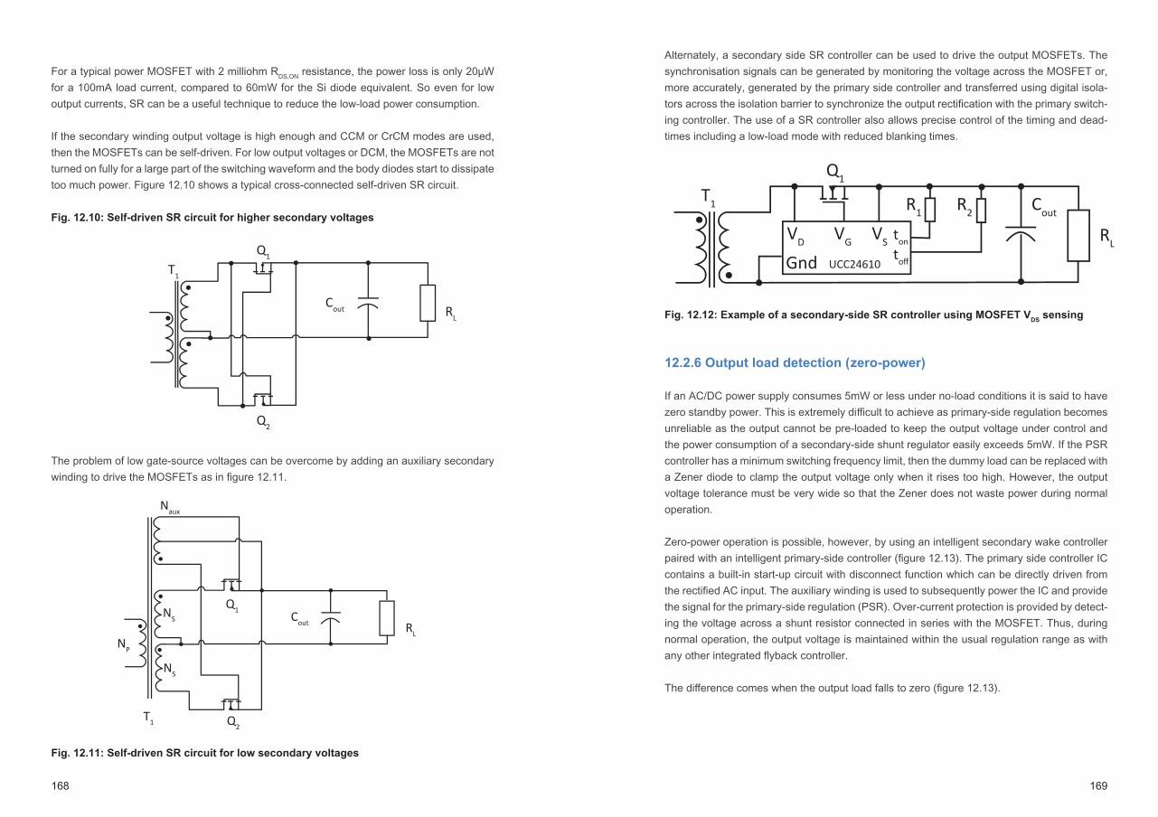
168 169
For a typical power MOSFET with 2 milliohm RDS,ON resistance, the power loss is only 20µW for a 100mA load current, compared to 60mW for the Si diode equivalent. So even for low output currents, SR can be a useful technique to reduce the low-load power consumption.
If the secondary winding output voltage is high enough and CCM or CrCM modes are used, then the MOSFETs can be self-driven. For low output voltages or DCM, the MOSFETs are not turned on fully for a large part of the switching waveform and the body diodes start to dissipate too much power. Figure 12.10 shows a typical cross-connected self-driven SR circuit.
Fig. 12.10: Self-driven SR circuit for higher secondary voltages
The problem of low gate-source voltages can be overcome by adding an auxiliary secondary winding to drive the MOSFETs as in fi gure 12.11.
Fig. 12.11: Self-driven SR circuit for low secondary voltages
Q1
RL
Q2
Cout
T1
Naux
Q1NS
NS
Cout RL
Q2T1
NP
Alternately, a secondary side SR controller can be used to drive the output MOSFETs. The synchronisation signals can be generated by monitoring the voltage across the MOSFET or, more accurately, generated by the primary side controller and transferred using digital isola-tors across the isolation barrier to synchronize the output rectifi cation with the primary switch-ing controller. The use of a SR controller also allows precise control of the timing and dead-times including a low-load mode with reduced blanking times.
Fig. 12.12: Example of a secondary-side SR controller using MOSFET VDS
sensing
12.2.6 Output load detection (zero-power)
If an AC/DC power supply consumes 5mW or less under no-load conditions it is said to have zero standby power. This is extremely diffi cult to achieve as primary-side regulation becomes unreliable as the output cannot be pre-loaded to keep the output voltage under control and the power consumption of a secondary-side shunt regulator easily exceeds 5mW. If the PSR controller has a minimum switching frequency limit, then the dummy load can be replaced with a Zener diode to clamp the output voltage only when it rises too high. However, the output voltage tolerance must be very wide so that the Zener does not waste power during normal operation.
Zero-power operation is possible, however, by using an intelligent secondary wake controller paired with an intelligent primary-side controller (fi gure 12.13). The primary side controller IC contains a built-in start-up circuit with disconnect function which can be directly driven from the rectifi ed AC input. The auxiliary winding is used to subsequently power the IC and provide the signal for the primary-side regulation (PSR). Over-current protection is provided by detect-ing the voltage across a shunt resistor connected in series with the MOSFET. Thus, during normal operation, the output voltage is maintained within the usual regulation range as with any other integrated fl yback controller.
The diff erence comes when the output load falls to zero (fi gure 12.13).
T1
Q1
R1
VD
Gnd UCC24610
VG VS ton
toff
R2
RL
Cout

170 171
Fig. 12.13: An example of a zero-standby solution
Under no-load conditions, the controller goes into deep sleep mode and turns off the main power stage completely. The power consumption of the controller IC is now minimal and the output voltage is supplied only by the output capacitor, Cout
If the output voltage drops below a certain limit, then the secondary side wake controller issues a short burst of pulses across the secondary winding which is detected on the primary side to wake up the PWM controller and initiate normal operation. The average power consumption of these short periods of activity interspersed with long sleep periods is below 5mW.
AC
C1
Fuse L1
C2 CVcc
D1
UCC28730PWMController
Vcc
D Q1HV
R1
R2
Vs
RCs
UCC24650WakeController
CoutRLoad
GndCs
VHV
IWAKE
VOUT(ripple)
0.97VS&H
(Dotted lines indicate waveforms if primary-side controller does not respond to wake-up signal.)
12.3 Measuring standby power consumption
It is not easy to measure the power consumption of an AC/DC converter in standby without the use of a power analyser. Especially for very low standby consumption designs (<100mW), an expensive high-end power analyser is required. The reasons for this are four-fold:
1. High sample rate: A high sample rate is needed to capture the short, high-frequency burst signals. It is not suffi cient to just detect the peak input current; the waveform must also be measured and analyzed. A sample rate of 20MHz is required to accurately measure a short current peak lasting only a few milliseconds.
2. High sensitivity: The peak input current of a low-standby power converter may be only 100-200µA. To get an acceptable measurement accuracy, a 1-2 µA current resolution is need-ed. Voltage resolution is not so critical (around 1V volt resolution is acceptable), but care must be taken when converting to true RMS values (see next section).
3. No auto-ranging: As most of the time, the power supply consumes very little power, any auto-ranging function will automatically select the highest possible resolution range. When a sudden burst signal occurs, the autoranging circuit may not react quickly enough. Therefore, the autoranging function must be disabled.
4. Large memory: Due to the high sample rate and very long averaging time (minimum 500 mains cycles), an analyser with a very deep memory is needed.Even with a high-end power analyser costing upwards of 30k€, the no-load power consump-tion can only be measured with a reliable accuracy of only around ±2%.

172 173
Chapter 13:
Measuring AC
13.1 AC voltage measurements
The simplest way of measuring an AC voltage is to use a multimeter. The meter will respond to the AC component of the input and ignore any DC off sets. This gives a more-or-less accu-rate AC value but can lead to false power calculations if the DC component also contributes to the load current.Since the average of a purely sinusoidal waveform is zero, the meter needs to measure either the peak-to-peak voltage, the average rectifi ed voltage or the true RMS voltage. For the same AC signal, the displayed values will be diff erent! For example, if we set up a waveform gener-ator to give a sinusoidal waveform output with a peak-to-peak voltage of 10.00V, it will have a rectifi ed average voltage of 6.37V and an RMS voltage of 7.07V. Electronic multimeters use RMS because this is the equivalent DC voltage that would give the same heating eff ect with a resistive load.However, if the AC signal is not a pure sine wave, the readings will be very diff erent depending on the waveform:
Fig. 13.1: Eff ect of the waveform on the RMS meter readings
The solution to all of these problems is a “True RMS” multimeter which can accommodate both the AC and DC components of continuous waveforms and display the correct result:
Eq. 13.1:
However, the situation is made more complex if the AC signal is discontinuous. Then, even a true RMS voltmeter will not give the correct reading. Unfortunately, such discontinuous signals are very common in AC/DC circuits, such as the trapezoidal signal from a switching transistor, the saw tooth current through a diode or the triangular voltage across an inductor. The equivalent RMS voltage is an integral over time:
Eq. 13.2:
Response to sine wave
Response to square wave
Response to single phase
diode rec�fier
Response to 3 phase rec�fier with
on phase missing
Correct 10 % high 40 % low 5 % to 30 % low
So, the only way to measure the RMS value of a discontinuous signal accurately is with an oscilloscope.
With any digital meter or digital storage oscilloscope (DSO), another important source of error is the crest factor. This is simply the ratio of the peak to RMS voltage. If a digital meter is to measure the signal accurately, it must have suffi cient dynamic input voltage range to cope with the crest factor which can vary from 1 for a square wave, √2 for a sine wave up to 10 or more for an asymmetrically pulsed input.
Fig. 13.2: Continuous waveforms
Amplitude, A
RMS value=
Crest Factor=Sawtooth
√3
A√3
Amplitude, A
RMS value=
Crest Factor=Triangle
A√3
√3
Amplitude, A
RMS value= A
Crest Factor= 1Square
Amplitude, A
RMS value=
Crest Factor=Sine
√3
A2
Voffset2(1-k) + k(A2 + -Aa)
Amplitude, A
Amplitude, A
Amplitude, A
Amplitude, A
Amplitude, A
Amplitude, A
Amplitude,a
Amplitude,a
Amplitude,a
VOffset
VOffset
RMS value=
Crest Factor= 2
RMS value=
Crest Factor
RMS value=
Crest Factor
RMS value=
Crest Factor=
RMS value=
Crest Factor
RMS value=
Crest Factor
ta
ta
ta
ta
ta
ta
T
T
T
T
T
T
A2
k(A2 + -Aa)a2
31k�
1k
a2
12
a2
3
A2
3
A 3
�
1k�
1k�
k3A
Aav2 +
Voffset2+k(A.Voffset + )

174 175
Fig. 13.3: Discontinuous Waveforms
Practical Tip: Passive oscilloscope probes must always be calibrated before any AC meas-urements are taken. All oscilloscopes have a square wave reference output on the front panel. The oscilloscope probe should be hooked on to this output and the small variable capacitor in the plug adjusted until the display shows a flat-topped square wave. Figure 13.4 below shows two identical probes connected to the same internal square wave source. Channel 2 is cor-rectly adjusted. Channel 1 is not:
Fig. 13.4: Passive oscilloscope probe calibration. Both channels are measuring the
same signal. Channel 1 needs to be calibrated using the trimmer access hole in the
plug (arrowed)
Voffset2(1-k) + k(A2 + -Aa)
Amplitude, A
Amplitude, A
Amplitude, A
Amplitude, A
Amplitude, A
Amplitude, A
Amplitude,a
Amplitude,a
Amplitude,a
VOffset
VOffset
RMS value=
Crest Factor= 2
RMS value=
Crest Factor
RMS value=
Crest Factor
RMS value=
Crest Factor=
RMS value=
Crest Factor
RMS value=
Crest Factor
ta
ta
ta
ta
ta
ta
T
T
T
T
T
T
A2
k(A2 + -Aa)a2
31k�
1k
a2
12
a2
3
A2
3
A 3
�
1k�
1k�
k3A
Aav2 +
Voffset2+k(A.Voffset + )
For most measurements, the 10:1 attenuator setting should be used on the probe. This will increase the probe’s DC impedance from 1 Mohm to 10 Mohm and reduce the loading of the probe on the measured signal at the cost of a less accurate measurement of very small signals.
Great care must be taken when measuring high voltages such as AC mains or rectified AC using oscilloscope probes. The ground connection of the probe is connected to earth via the power lead, so simply connecting the probe to the high voltage circuit will blow the fuse or trip the earth leakage detector in the mains supply.
There are several solutions to this problem:
1. Use an isolated active probe.2. Use an active differential voltage probe (also isolated, but with a higher input voltage
range).3. Run the oscilloscope from a mains isolation transformer and disconnect the ground wire.
Also make sure that here are no connectors used for remote control (GPIB or USB) that could ground the oscilloscope through the data lines.
Note that option 3 means that any exposed metalwork (for example the BNC connectors and case of the oscilloscope) may no longer be at ground potential, so be especially careful when using an isolated oscilloscope. To measure hazardous voltages, use only option 1 or 2.
Practical Tip: When using an isolated probe or isolated oscilloscope, the probe tip and probe ring can be connected between any two arbitrary points on the circuit being tested. However, the ring should be connected to a stable voltage and not a switching node to avoid false read-ings. In the following example, the correct way to measure the voltage across a totem pole PFC choke is to use two probes and then use the mathematical function of the oscilloscope to display the difference:
AC
Q1
Q2 Q3
Q4
C RL
LPFC
Isolated Probe
AC
Q1
Q2 Q3
Q4
C RL
LPFC
Isolated Probe A
Isolated Probe B
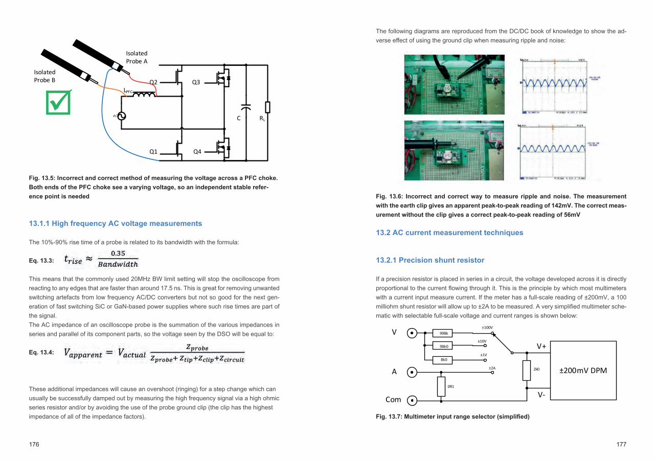
176 177
Fig. 13.5: Incorrect and correct method of measuring the voltage across a PFC choke.
Both ends of the PFC choke see a varying voltage, so an independent stable refer-
ence point is needed
13.1.1 High frequency AC voltage measurements
The 10%-90% rise time of a probe is related to its bandwidth with the formula:
Eq. 13.3:
This means that the commonly used 20MHz BW limit setting will stop the oscilloscope from reacting to any edges that are faster than around 17.5 ns. This is great for removing unwanted switching artefacts from low frequency AC/DC converters but not so good for the next gen-eration of fast switching SiC or GaN-based power supplies where such rise times are part of the signal.The AC impedance of an oscilloscope probe is the summation of the various impedances in series and parallel of its component parts, so the voltage seen by the DSO will be equal to:
Eq. 13.4:
These additional impedances will cause an overshoot (ringing) for a step change which can usually be successfully damped out by measuring the high frequency signal via a high ohmic series resistor and/or by avoiding the use of the probe ground clip (the clip has the highest impedance of all of the impedance factors).
AC
Q1
Q2 Q3
Q4
C RL
LPFC
Isolated Probe
AC
Q1
Q2 Q3
Q4
C RL
LPFC
Isolated Probe A
Isolated Probe B
The following diagrams are reproduced from the DC/DC book of knowledge to show the ad-verse effect of using the ground clip when measuring ripple and noise:
Fig. 13.6: Incorrect and correct way to measure ripple and noise. The measurement
with the earth clip gives an apparent peak-to-peak reading of 142mV. The correct meas-
urement without the clip gives a correct peak-to-peak reading of 56mV
13.2 AC current measurement techniques
13.2.1 Precision shunt resistor
If a precision resistor is placed in series in a circuit, the voltage developed across it is directly proportional to the current flowing through it. This is the principle by which most multimeters with a current input measure current. If the meter has a full-scale reading of ±200mV, a 100 milliohm shunt resistor will allow up to ±2A to be measured. A very simplified multimeter sche-matic with selectable full-scale voltage and current ranges is shown below:
Fig. 13.7: Multimeter input range selector (simplified)
±200mV DPM
998k
98k0
0R1
8k0
2k0±2A
±1V
±10V
±100V
Com
A
V
V+
V-

178 179
The shunt resistor must be kept low-ohmic so that the in-circuit voltage drop is insignificant (in the example above only 200mV) and to reduce the errors caused by self-heating. All resistive materials have a temperature coefficient of resistance (TCR) which will cause a change in the resistance with temperature, so it is important that the shunt resistor is made of a material with a very low TCR, ideally less than ±100 ppm/°C
For a fixed shunt resistor on a PCB that is used to measure direct or alternating currents, the additional errors caused by the copper tracks can become very significant (copper has a typ-ical TCR of around +0.004%/°C or +4000ppm/°C). To avoid measurement errors, four-termi-nal (kelvin contact) shunt resistors should be used, so that the voltage measurement tracks are not carrying any significant current themselves:
Fig. 13.8: Four-terminal current sensing shunt resistor
The advantage of shunt resistors is that they can be used to measure both DC and AC cur-rents and that they can be suitably dimensioned to measure both very small and very large currents. With careful track layout, shunt resistors can also be used to accurately measure high frequency alternating currents.
Often a simple low pass filter formed by a capacitor in series with the shunt and high ohmic resistors placed in the measurement legs will allow clean current measurements to be made even on noisy installations. Finally, the performance does not deteriorate with short-circuit or high surge currents: there is no avalanche or thermal runaway failure mode.
High Current Trace
Copper Trace
Current Sensing Resistor Current Sensing Trace
Fig. 13.9: Shunt resistor with low pass filtering (used to measure the supply current
for a noisy motor in this example)
Practical Tip: Current shunts can run hot enough to affect adjacent components, so always leave a good clearance gap and use thick copper traces to help dissipate the heat. High current capability shunts are often raised off from the PCB. This avoids overheating the FR4 material beneath the central high-resistance hot-spot of the shunt and helps with air cooling. Check also that the expansion coefficients of the shunt and PCB are not too mismatched to avoid thermally-induced cracking and solder-joint stress.
The disadvantages of using a shunt resistor are that the measurement contact is direct with-out any isolation, the power dissipation in the shunt resistor can affect the readings and very low ohmic shunts need high voltage magnification to generate a useful signal which introduc-es noise, drift and offset errors. Furthermore, high-precision power shunt resistors (0.1% or better) with low TCR and low drift are expensive components.
13.2.2 Shunt + current mirror
As a current-sensing shunt resistor is not isolated nor necessarily referenced to ground, this can create problems when attempting to measure the current in a higher voltage circuit. The following example shows how to use a current mirror to voltage-shift the current output to a level, say, suitable for the input pin of a microcontroller. DC and AC with DC offset (for exam-ple output ripple current) can be measured with this circuit.
M
Rs
Cs R>>RsR>>Rs
V

180 181
Fig. 13.10: Current sense shunt resistor and current mirror level shifter
The voltage developed across the current sense resistor, Rs, is amplified by the op-amp to generate an output current, Isense = Rs /R. As this current is referenced to the high voltage sup-ply, it needs to be current-mirrored to generate an output voltage, Vsense, which is referenced to the 5V supply.The Vsense output voltage is:
Eq. 13.5:
13.2.3 Shunt + isolation amplifier
The use of a current mirror in combination with a high-side shunt resistor is useful for medium supply voltages, but not safe for higher supply voltages. To measure the current in a PFC stage or AC conductor, safety isolation is required. One technique to accurately measure AC or DC currents on a high voltage supply is to use an isolation op-amp with an isolated DC/DC supply:
DC Supply or AC with DC
Offset
NPN
C
- +
Rs
R>>Rs R>>Rs
RoutCurrentmirror
5V
Isense
Iload
Vsense
Load
Fig. 13.11: Isolated current sense shunt resistor
13.3 Current transformer
A transformer can be used to measure the AC current flowing in a conductor if the conductor passes through it to effectively make a single turn:
Fig. 13.12: Current transformer construction
The secondary current, IS, is proportional to the primary current, Ip divided by the secondary turns:
Eq. 13.6: (For a single turn primary)
High voltageAC or DC
Cs
-
+
Rs
Iload
Vsense
Load
Rout
Vcc
Vcc
+Viso
-Viso
High IsolationDC/DC
IsolationOp-Amp
Vout,+
Vout,-
IsolationBarrier
AC.T.
Ip
Is
Is
IpHollow Core
Main PrimaryConductor
Main PrimaryConductor
PrimaryCurrent
Construction
SecondaryWinding
SecondaryWinding
Ammeter
CircuitSymbol

182 183
Current transformers (CTs) are useful for measuring high AC currents as the output current can be made a ratio, for example, of 20:1 to the conductor current by simply winding 20 turns on the secondary. If more sensitivity is required, then the primary conductor can be wound twice around the core to increase the full-scale reading to 10:1 or the secondary turns can be increased. Split-core versions are also available that can be clamped around a conductor or opened to allow more primary turns to be added without needing to cut the wires.
Practical Tip: Never operate a current transformer without a load. If the output current has a 20:1 attenuation, then the open-circuit output voltage has an x20 multiplication, so a current transformer measuring mains current can easily generate thousands of volts across the ter-minals if the load is disconnected. Always short-circuit the outputs if the load is not attached!Current transformers cannot measure DC currents, so only the AC component (for example, the ripple current) will generate an output signal. As the measurements rely on the perfor-mance of the high permeability magnetic core, a current transformer will have a bandwidth limit, a rated minimum and maximum primary current, a maximum primary voltage rating and an accuracy rating (typically between 0.2% and 3%, valid over a primary current in the range of 5% to 120%). Finally, CTs have a maximum output burden rating due to the secondary impedance interacting with the ammeter load. If the output load is too high, the output reading will be too low and the CT will also load the supply.
The main advantages of a current transformer are an output which is also a current source, high isolation withstand voltage, near-lossless measurement and a bidirectional output. Figure 13.13 shows a CT used in a high-power phase-shifted full bridge application to provide an isolated current feedback signal:
Fig. 13.13: Current Transformer (CT) used in a 1kW full bridge demonstrator
PWMController
R-REF01-HB#1
PWM1
PWM2R-REF01-HB
#2
PWM4PWM3
Q1
Q2
Q3
Q4
+HVDC
Primary
CS1 CS2
Secondary 1
Secondary 2
LOUTC4 C5 C6 C7 C8 C9
+48V Iso.
0VR-78HB-15-0.5
+Vref+Vin+Vout
GND
ShuntRegulator
+15V+15V
+15V
FB
PWRGND
PWRGND
GNDGNDGND
Q1-Q4SiC MOSFET
CT
Current Feedback
Voltage Feedback
13.3.1 Compensated CT (AC zero-flux)
To increase a current transformers low-frequency response, a feedback circuit can be added to cancel out the load caused by the secondary winding. A separate winding is used to cancel out the magnetic flux in the core:
Fig. 13.14: AC zero-flux current transformer
AC zero-flux CTs eliminate the B-H characteristics of the magnetic core, so offer high linear-ity, low insertion impedance and a wide bandwidth. However, the detection winding and AC amplifier add cost.
13.4 Rogowski Coil
Although similar in appearance to a split-core current transformer, a Rogowski coil (RC) does not operate in the same way, generating an output voltage proportional to the measured cur-rent instead of an output current. An RC needs no magnetic core which reduces the cost and the loading on the primary conductor and the quick response is useful for measuring small, fast changing currents.
‚
‚
Magne�c flux produced by the current being measured Magne�c flux produced by
the secondary current
Magne�c core
Magne�c flux
Current being measured
Difference between the magne�c flux produced by the curret being measured and the magne�c flux produced by the secondary curret
Detec�on winding
AMP
Conductor being measured
Feedback winding (N)
Secondary current
Output (Vout)
Shunt resistance (r)

184 185
Fig. 13.15: Rogowski coil
The output voltage v(t) is dependent on the rate of change of the primary current, Ip:
Eq. 13.7:
Where A is the cross-sectional area of the core, N the number of secondary turns with length l and μ0 is the magnetic constant, 4π x 10-7. As these are all fi xed units, the resulting output voltage is simply equal to the rate of change of the primary current dip/dt multiplied by –M, a constant dependent on the mechanical dimensions only.
The secondary wiring is in a helical arrangement with the return wire passing back under the secondary so that both wire ends are at the same end of the open core. This makes it very useful for clamp-style current meters as no wires bridge the gap. Flexible RC designs exist where the secondary is wound over a plastic tube that can simply be wrapped around the primary conductor or conductors.
As the output is proportional to the rate of change of the primary current rather than its abso-lute value, the signal is usually integrated with an operational amplifi er to generate a voltage that is directly proportional to the current. This introduces some errors in the measurements due to amplifi er off sets and integration times and creates a frequency response that drops off at both low and high frequencies. Nevertheless, over a wide range of frequencies the re-sponse is linear and fl at.
13.5 Hall-eff ect current sensor
The Hall-eff ect current sensor relies on monitoring the voltage induced by a magnetic fi eld created by the primary current rather than measuring the current directly. When current fl ows through a thin fl at conductor, no potential diff erence appears across the
R3R1
-+
C1IP
R
transverse (longer) sides unless the charge carriers are infl uenced by an external magnetic fi eld. The magnetic fi eld exerts a transverse force which causes a charge imbalance to occur, resulting in a voltage developing between the transverse sides which is proportional to the magnetic fi eld strength.
Fig. 13.16: Principle of the Hall-eff ect sensor
The Hall voltage, VH, is directly proportional to the bias current, I, and the magnetic fi eld strength, B, and inversely proportional to the number of charge carriers per unit volume, n, the charge on each carrier, e, and the thickness of the fl at conductor, d:
Eq. 13.8:
The Hall-eff ect will occur in any fl at conductor, but as n= 1029 m-3 for copper and n= 1025 m-3
for silicon, the resulting Hall-eff ect voltage for a silicon conductor will be 1000 times greater. Therefore, semiconductors are more often used rather than metallic conductors for Hall-ef-fect sensors.
The bias current, I, can be supplied from a constant current source to create an output that is only dependent on the external magnetic fi eld strength, B or the sensor can be placed be-tween the poles of a permanent magnet in order to measure an external bias current. In this way, the Hall sensor can measure DC current.
To use a Hall-eff ect sensor to measure AC current in an external conductor, it can be placed in the air gap of a transformer core through which the primary conductor passes:
Fig. 13.17: Hall-eff ect current sensor
V=OI I
B
VH=V
Ampli�er
VH
Ip
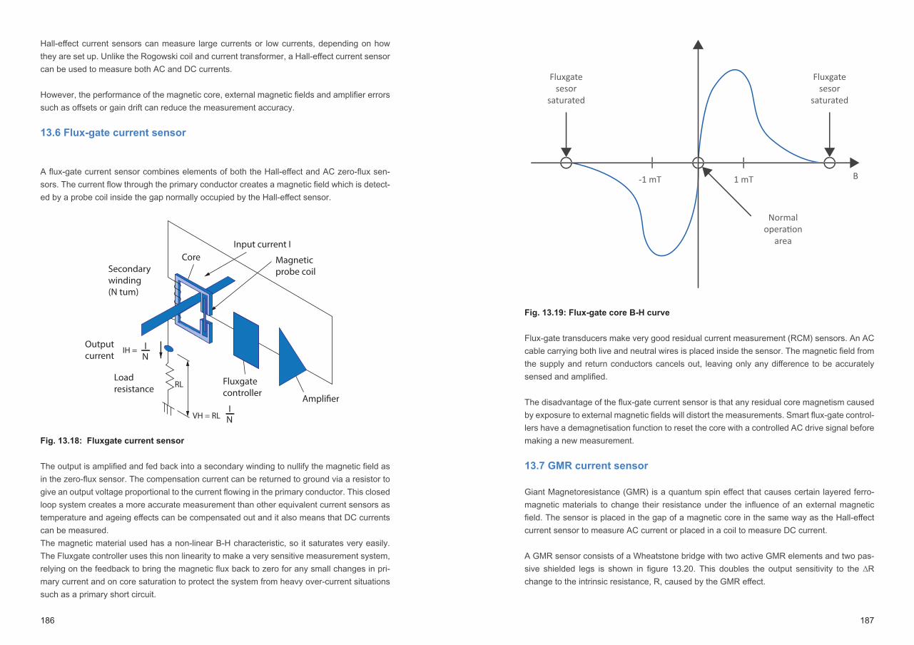
186 187
Hall-eff ect current sensors can measure large currents or low currents, depending on how they are set up. Unlike the Rogowski coil and current transformer, a Hall-eff ect current sensor can be used to measure both AC and DC currents.
However, the performance of the magnetic core, external magnetic fi elds and amplifi er errors such as off sets or gain drift can reduce the measurement accuracy.
13.6 Flux-gate current sensor
A fl ux-gate current sensor combines elements of both the Hall-eff ect and AC zero-fl ux sen-sors. The current fl ow through the primary conductor creates a magnetic fi eld which is detect-ed by a probe coil inside the gap normally occupied by the Hall-eff ect sensor.
Fig. 13.18: Fluxgate current sensor
The output is amplifi ed and fed back into a secondary winding to nullify the magnetic fi eld as in the zero-fl ux sensor. The compensation current can be returned to ground via a resistor to give an output voltage proportional to the current fl owing in the primary conductor. This closed loop system creates a more accurate measurement than other equivalent current sensors as temperature and ageing eff ects can be compensated out and it also means that DC currents can be measured. The magnetic material used has a non-linear B-H characteristic, so it saturates very easily. The Fluxgate controller uses this non linearity to make a very sensitive measurement system, relying on the feedback to bring the magnetic fl ux back to zero for any small changes in pri-mary current and on core saturation to protect the system from heavy over-current situations such as a primary short circuit.
Input current ICore Magnetic
probe coil
Ampli�er
Fluxgatecontroller
Loadresistance RL
VH = RL
Outputcurrent
Secondarywinding(N tum)
IN
IH = IN
Fig. 13.19: Flux-gate core B-H curve
Flux-gate transducers make very good residual current measurement (RCM) sensors. An AC cable carrying both live and neutral wires is placed inside the sensor. The magnetic fi eld from the supply and return conductors cancels out, leaving only any diff erence to be accurately sensed and amplifi ed.
The disadvantage of the fl ux-gate current sensor is that any residual core magnetism caused by exposure to external magnetic fi elds will distort the measurements. Smart fl ux-gate control-lers have a demagnetisation function to reset the core with a controlled AC drive signal before making a new measurement.
13.7 GMR current sensor
Giant Magnetoresistance (GMR) is a quantum spin eff ect that causes certain layered ferro-magnetic materials to change their resistance under the infl uence of an external magnetic fi eld. The sensor is placed in the gap of a magnetic core in the same way as the Hall-eff ect current sensor to measure AC current or placed in a coil to measure DC current.
A GMR sensor consists of a Wheatstone bridge with two active GMR elements and two pas-sive shielded legs is shown in fi gure 13.20. This doubles the output sensitivity to the ∆R change to the intrinsic resistance, R, caused by the GMR eff ect.
Fluxgate sesor
saturated
Fluxgate sesor
saturated
Normal operation
area
-1 mT 1 mT B

188
Fig. 13.20: GMR Wheatstone bridge
The GMR sensor has a very fast reaction time and is very sensitive, so it a useful sensor for measuring small signal AC currents up to 5MHz. Despite the Wheatstone bridge arrange-ment, it still needs careful thermal compensation for accurate readings as the GMR effect is relatively weak.
SensorTechnology
Shunt CT Zero AC Flux
Rogowski Hall Effect
Fluxgate GMR
Current AC or DC
AC AC AC AC or DC
AC or DC
AC or DC
Frequency DC to MHz
50Hz-10kHz
50Hz-100kHz
100kHz-100MHz
DC to 1MHz
DC to 100kHz
DC to 5MHz
Isolation None Yes Yes YesYes (AC) or none (DC)
Yes Yes
Non Line-arity
0.01% 0.05% 0.05% 0.05% 0.1% 0.001% 0.01%
Relative Cost
Low Low Medium Low Medium High High
Table 13.1: Comparison of the main current measuring techniques
R-∆R
R-∆RR
R
V+
V-
Vout
GMRResistor
Magnetically Shielded Resistor
Magnetically Shielded Resistor
GMRResistor

189
References and Further Reading
Ceraolo, M and Poli, D (2014) “Fundamentals of Electric Power Engineering: From Elec-
tromagnetics to Power Systems”, First Edition, Copyright IEEE, Published by John Wiley and Sons, Inc.
NA, Z (2018) “A Study of Electrolytic Capacitor Thermal Conductivity, Behaviour &
Measurement”, Mentor Graphics, Engineering Edge , Volume 5, Issue 1
Lee, B-H and Kim, C-E (2012) “No-Load Power Reduction Technique for AC/DC Adapt-
ers“, IEEE Transactions on Power Electronics, Vol. 27, No. 8
Siebt, A, (2014) “DC and AC Signals/Parameters and their correct Representation by
Measuring Instruments”, Bodo’s Power, Oct.
Kolar, J.W and Friedli, T (2011) „The Essence of Three Phase PFC Rectifier Systems“, PES Laboratory, ETH Zurich, published in the Proceedings of the 33rd IEEE International Telecommunications Energy Conference, Amsterdam.
HBD853/D (2014) “Power Factor Correction (PFC) Handbook”, ON Semiconductor
Yarborough B (2015) “Components and Methods for Current Measurement”, Vishay
Knight, D.W. (2015) “AC Electrical Theory- An introduction to phasors, impedance and
admittance, with emphasis on radio frequencies “, http://www.g3ynh.info/zdocs/AC_the-ory/AC_theory.pdf
Mammano, R.A. (2017) “Fundamentals of Power Supply Design”, Published by Texas Instruments Inc.
Sandler, S.M. (2014) “Power Integrity”, Published by McGraw-Hill Education
Some Recommended Application Notes
SLUA535 (2010) “Understanding and Designing an Active Clamp Current Mode Con-
trolled Converter using the UCC2887A”, Texas Instruments Inc.
AN-8033 (2009) “Design Guideline for Primary Side Regulated (PSR) Flyback Converter
Using FAN103 and FSEZ13X7”, Fairchiild (now ON Semiconductor)
AN-4147 (2006) “Design Guidelines for RCD Snubber of Flyback Converters”, Fairchild (now ON Semiconductor)
SLUP340 (2016) “Switch Mode power converter compensation made easy”, Texas In-struments Inc.
SLUP325 (2014) “Control challenges for Low Power AC/DC Converters”, Texas Instru-ments Inc.

190
About the Author
Steve Roberts was born in England. He obtained a B.Sc. in Physics and Electronics at Brunel University, London (now University of West London) before working at University College Hospital. He later spent 12 years at the Science Museum as Head of Interactives, where he completed his M.Sc. at University College, London. He moved to Austria, joining RECOM’s Tech Support team developing custom converters and answering customer’s questions before be-coming Technical Director for the RECOM group at their new headquarters in Gmunden, Austria.
About Recom
It was about 30 years ago when we showed our first hand made DC/DC converter to a leading German manufacturer of cellular phones. The product successfully passed all tests and a few weeks later we received our first order for 8000 pieces. A new product category was born „DC/DC converters in the form of a module.
At that time the shift from analogue to digital electronics accelerated the demand for DC/DC modules due to the need for standardized on-board switching power supplies. In addition, I/O ports or amplifier channels required isolation to increase safety or to eliminate earth loops - another important requirement that DC/DC converters could fulfil. RECOM was there from the very early days to supply reliable, efficient and modular solutions for customers that did not want to invest the time and effort designing their own discrete converters.
From 2006, RECOM extended its portfolio to include AC/DC converters – primarily for existing customers that again did not want to invest the time and effort in certifying their own discrete converters. In the meantime, RECOM offers AC/DC converters from 1W up to 1kW in a variety of different form factors such as PCB mount, wired, low profile and DIN-rail mounting for use in both single-phase and three-phase supplies. RECOM plans to expand the AC/DC range beyond the existing low and mid-range products to break through the 10kW barrier – in effect offering a “one stop shop” for all DC/DC and AC/DC products for industrial, medical, transport and household applications.
Today, RECOM’s ultra-modern campus-style headquarters in Gmunden and a separate R&D Centre in Vienna provides room for expansion to meet these ambitious goals. A team of in-ternational engineers works in well-equipped, state-of-the-art labs to create a constant flow of new products and customer solutions. We have also invested heavily in our own EMC test chambers in Gmunden and Vienna to be independent from external facilities.

L
N
V+
V-
RloadCout
L2Q1
D6R1
R2
InterleavedPFC
Controller
R3
R4
D1-D4
L1
D5
Q2
L
N
V+
V-
RloadCout
L2Q1
D6R1
R2
InterleavedPFC
Controller
R3
R4
D1-D4
L1
D5
Q2
L
N
V+
V-
RloadCout
L2Q1
D6R1
R2
InterleavedPFC
Controller
R3
R4
D1-D4
L1
D5
Q2
PWMGenerator
Rinj
R1
R2Rin
C1
Vref
Injec�onTransformer
LowImpedance
HighImpedance
+
-
Vout = Low Voltage
PWMGenerator
Rinj
R1
R2Rin
C1
Vref
Injec�onTransformer
LowImpedance
HighImpedance
+
-
Vout = Low Voltage
PWMGenerator
Rinj
R1
R2Rin
C1
Vref
Injec�onTransformer
LowImpedance
HighImpedance
+
-
Vout = Low Voltage
PWMGenerator
Rinj
R1
R2Rin
C1
Vref
Injec�onTransformer
LowImpedance
HighImpedance
+
-
Vout = Low Voltage
© 2019, RECOM Power GmbH, Second Edition
RECOM Power GmbH andRECOM Engineering GmbH & Co KGMünzfeld 35, 4810 Gmunden, Austria
WE POWER YOUR PRODUCTS www.recom-power.com
Related Documents