MAPLD MAPLD Accelerating FPGA Designs and Design Accelerating FPGA Designs and Design Work: Implementing Faster Designs Faster Work: Implementing Faster Designs Faster Bryan Penner Xilinx FAE – Arizona and New Mexico

Welcome message from author
This document is posted to help you gain knowledge. Please leave a comment to let me know what you think about it! Share it to your friends and learn new things together.
Transcript

MAPLDMAPLD
Accelerating FPGA Designs and Design Accelerating FPGA Designs and Design Work: Implementing Faster Designs FasterWork: Implementing Faster Designs Faster
Bryan PennerXilinx FAE – Arizona and New Mexico

Implementing Faster FPGA Designs Faster 2
Agenda
• Understanding the Virtex5 FPGA Architecture• A look at how coding affects performance• Software tools that can help increase
performance and reduce design time

Implementing Faster FPGA Designs Faster 3
Agenda
• Understanding the Virtex5 FPGA Architecture• A look at how coding affects performance• Software tools that can help increase
performance and reduce design time

Implementing Faster FPGA Designs Faster 4
• Family contains 4 platforms– LX
• High-performance logic – LXT
• High-performance logic with lowest power serial connectivity
– SXT• Extensive signal processing with
lowest power serial connectivity– FXT
• Embedded-oriented with highest performance microprocessor and serial connectivity
The Virtex-5 Family
LXPlatformPlatform
LXTPlatformPlatform
SXTPlatformPlatform
FXTPlatformPlatform

Implementing Faster FPGA Designs Faster 5
Continuing the Drive for Innovation
LXT/SXT Platform
FXT Platform
LXT/SXT/FXT Platforms
Common to All Platforms
Most Advanced High-Performance
Express Fabric
Most Advanced High-Performance
Express Fabric 36Kbit Dual-Port Block RAM / FIFO
with Integrated ECC
36Kbit Dual-Port Block RAM / FIFO
with Integrated ECC
SelectIO with ChipSync
Technology and XCITE DCI
SelectIO with ChipSync
Technology and XCITE DCI
550 MHz ClockManagement Tile
with DCM and PLL
550 MHz ClockManagement Tile
with DCM and PLL
25x18 DSP Slice25x18 DSP Slice
Advanced Configuration
Options
Advanced Configuration
Options
10/100/1000 MbpsEthernet
MAC Blocks
10/100/1000 MbpsEthernet
MAC Blocks
PCI-ExpressEndpoint Blocks
PCI-ExpressEndpoint Blocks
3.75Gbps GTPSerial
Transceivers
3.75Gbps GTPSerial
Transceivers
IntegratedSystem Monitor
IntegratedSystem Monitor
PowerPC440Processors with
Optimized Interfacing
PowerPC440Processors with
Optimized Interfacing
6.5Gbps GTXSerial
Transceivers
6.5Gbps GTXSerial
Transceiverswww.xilinx.com/virtex5
Implementing Faster FPGA Designs Faster 6
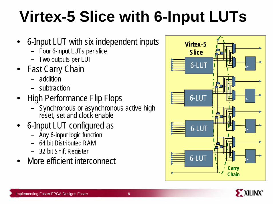
Virtex-5 Slice with 6-Input LUTs• 6-Input LUT with six independent inputs
– Four 6-input LUTs per slice– Two outputs per LUT
• Fast Carry Chain– addition – subtraction
• High Performance Flip Flops– Synchronous or asynchronous active high
reset, set and clock enable • 6-Input LUT configured as
– Any 6-input logic function– 64 bit Distributed RAM– 32 bit Shift Register
• More efficient interconnectCarry Chain
Virtex-5 Slice
6-LUT
6-LUT
6-LUT
6-LUT
Implementing Faster FPGA Designs Faster 7
ACIN BCIN
ACOUT BCOUT
PCIN
PCOUT
Optio
nal P
ipeli
ne R
egist
er/
Rout
ing
Logi
cOp
tiona
l Pip
eline
Reg
ister
/Ro
utin
g Lo
gic
Optio
nal P
ipeli
ne R
egist
er/
Rout
ing
Logi
cOp
tiona
l Pip
eline
Reg
ister
/Ro
utin
g Lo
gic
Rout
ing
Logi
cRo
utin
g Lo
gic
Optio
nal R
egist
erOp
tiona
l Reg
ister
Multi
plier
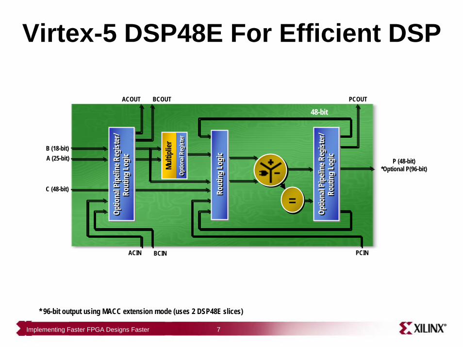
P (48-bit)*Optional P(96-bit)
C (48-bit)
B (18-bit)A (25-bit)
=
48-bit
Virtex-5 DSP48E For Efficient DSP
* 96-bit output using MACC extension mode (uses 2 DSP48E slices)
Implementing Faster FPGA Designs Faster 8
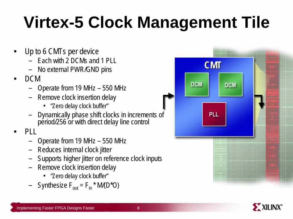
CMTCMT• Up to 6 CMTs per device
– Each with 2 DCMs and 1 PLL– No external PWR/GND pins
• DCM– Operate from 19 MHz – 550 MHz– Remove clock insertion delay
• “Zero delay clock buffer”– Dynamically phase shift clocks in increments of
period/256 or with direct delay line control• PLL
– Operate from 19 MHz – 550 MHz– Reduces internal clock jitter– Supports higher jitter on reference clock inputs– Remove clock insertion delay
• “Zero delay clock buffer”– Synthesize Fout = Fin * M/(D*O)
Virtex-5 Clock Management Tile

Implementing Faster FPGA Designs Faster 9
Agenda
• Understanding the Virtex5 FPGA Architecture• A look at how coding affects performance• Software tools that can help increase
performance and reduce design time
Implementing Faster FPGA Designs Faster 10
Intro• There is not a single way to create a design
– Different coding styles, synthesis / implementation tool optionswill lead to different results
• And no one formula will work best in all cases• There are however guidelines that can generally
lead to improved performance, area and power– I am not telling you how to code your design
• I am trying to relay the ramifications and drawbacksof some typical coding decisions

Flip-Flops
D Q
SET
RST
CE
Initial value of Q output will relate to the controls used.
Data stored synchronously on a positive or negative clock edge.
Data input
Clock Enable qualifies that the clock edge should be used to store data.
Local reset (Q=0) can be asynchronous or synchronous.
Local set (Q=1) can be asynchronous or synchronous.
The D-input naturally connects to the output of the LUT and leads to best density and highest performance.
D Q
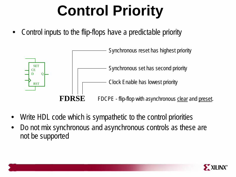
Control Priority
D Q
SET
RST
CE
FDRSE
Synchronous reset has highest priority
Synchronous set has second priority
Clock Enable has lowest priority
FDCPE - flip-flop with asynchronous clear and preset.
• Write HDL code which is sympathetic to the control priorities • Do not mix synchronous and asynchronous controls as these are
not be supported
• Control inputs to the flip-flops have a predictable priority

Flip-Flop Controls
byte_register: process (clk, reset_in)beginif reset_in ='1' then
reg_data <= "00000000";elsif clk'event and clk='1' then if set_in ='1' then
reg_data <= "11111111";elsif enable_in='1' then
reg_data <= data_in;end if;
end if;end process;
signal reg_data: std_logic_vector(7 downto 0);
• Eight bit data register with reset (global reset?)• Reset forces output to “00000000”.• Synchronously set to “11111111”• Input value captured when enable is high
• Code looks reasonable. Might assume it will require 8 FFs to implement

Flip-Flop ControlsT
D Q
CLR
reset_in
reg_data0
set_in
data_in0
All 4 inputs of each LUT are used to emulate the required flip-flops.
Design logic will need to use other LUT and the
cost will double.
Asynchronous clear prevents synchronous set.
enable_in
Precedence of set prevents clock enable.
D Q
CLR
reg_data0data_in0
D Q
CLR
reg_data0data_in0
Flip-Flop Controls
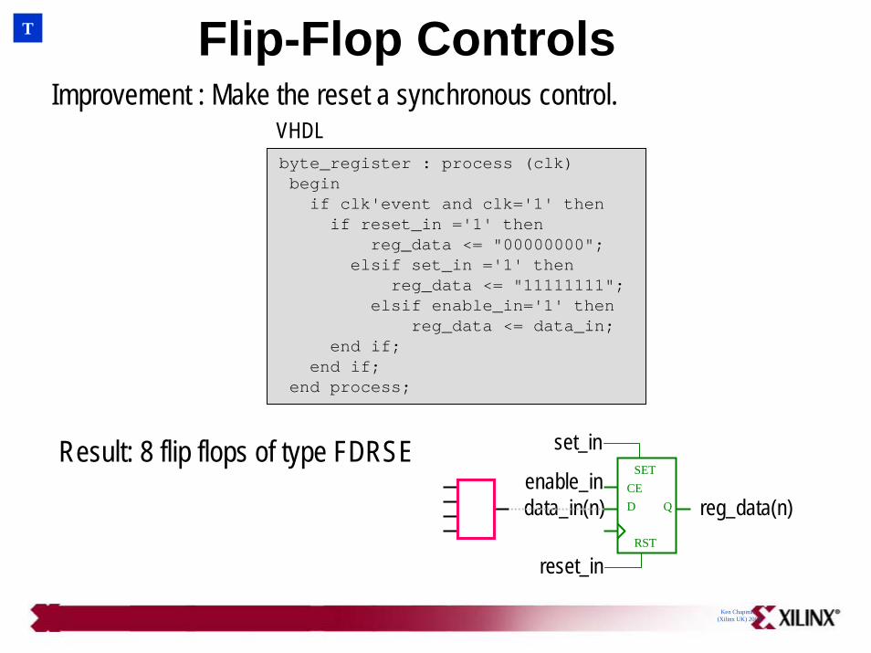
Ken Chapman(Xilinx UK) 2003
byte_register : process (clk)beginif clk'event and clk='1' thenif reset_in ='1' then
reg_data <= "00000000";elsif set_in ='1' then
reg_data <= "11111111";elsif enable_in='1' then
reg_data <= data_in;end if;
end if;end process;
Improvement : Make the reset a synchronous control.
T
Result: 8 flip flops of type FDRSED Q
SETCE
reg_data(n)
set_in
data_in(n)enable_in
reset_inRST
VHDL
Implementing Faster FPGA Designs Faster 16
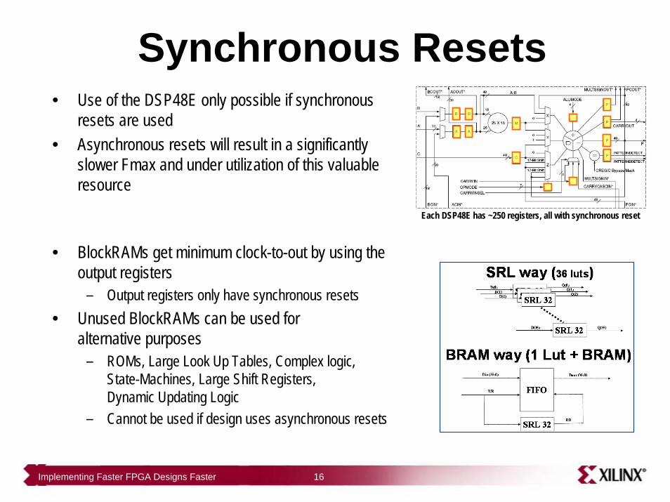
Synchronous Resets• Use of the DSP48E only possible if synchronous
resets are used• Asynchronous resets will result in a significantly
slower Fmax and under utilization of this valuable resource
• BlockRAMs get minimum clock-to-out by using the output registers
– Output registers only have synchronous resets• Unused BlockRAMs can be used for
alternative purposes– ROMs, Large Look Up Tables, Complex logic,
State-Machines, Large Shift Registers, Dynamic Updating Logic
– Cannot be used if design uses asynchronous resets
Each DSP48E has ~250 registers, all with synchronous reset

Implementing Faster FPGA Designs Faster 17
How to Change to Synchronous Resets
• It is suggested that all new code should use synchronous resets when a reset is necessary
• For existing code, you have 3 choices– Leave alone
• Acknowledge the possible drawbacks of asynchronous resets– Use synthesis switch
Not the same as changing to synchronous reset but can help– Manually change the asynchronous reset to a synchronous
Synplicity:syn_clean_reset
XST:-async_to_sync YES
Implementing Faster FPGA Designs Faster 18
What’s Better than Synchronous Resets?
Resets

Implementing Faster FPGA Designs Faster 19
Why No Resets at All?More Free Logic Even Fewer Control Signals
• Using synchronous resets frees up additional logic– Potentially, a “free” AND and/or OR gate can be realized for
every FF in the design• Greater register packing within Slices may be realized
– Greater flexibility for registers packing with fewer control signals
Async Reset Sync Reset No Reset

Why No Resets at All?No reset on LUTRAM
I3
I1I2
I0
O
A3
A1A2
A0
O
WE
INIT=1234
INIT=1234
LUT4
SRAM16X1
D
D Q
• Coding a reset when describing a RAM or shift register will prevent the use of LUTRAM
• The DistRAM is synchronously written, but asynchronously read.
• Follow the RAM with the dedicated FF to make a synchronous read and improve performance.
• The dedicated FF has a faster clock to out time than the SRL16E LUT.
• Synthesis should place the last register in shift chain in the FF.
• The initial contents of the LUTRAM can be specified or zero will be the default value.
D Q
A3
A1A2
A0
Q
CE
INIT=1234
SRL16E
D

Implementing Faster FPGA Designs Faster 21
Why No Resets at All?Routing Congestion
• Routing can be considered one of the more valuable resources• Resets compete for the same resources as the rest of the active signals of the
design – Including the critical paths
• Designs without resets have fewer timing paths– By an average of 18% fewer timing paths
• Results in less runtime

Implementing Faster FPGA Designs Faster 22
FPGAs Enable Massively Parallel DSP
Data OutData Out
MAC UnitMAC Unit
CoefficientsCoefficients
Programmable DSP Programmable DSP -- SequentialSequential
1 GHz1 GHz1 GHz256 clock cycles256 clock cycles256 clock cycles = 4 MSPS= 4 MSPS= 4 MSPS
256 clock 256 clock cycles cycles
neededneeded
Data InData In
XX
++RegReg
500 MHz500 MHz500 MHz1 clock cycle1 clock cycle1 clock cycle
= 500 MSPS= 500 MSPS= 500 MSPS
Data OutData Out
FPGA FPGA -- Fully Parallel ImplementationFully Parallel Implementation
256 operations 256 operations in 1 clock cyclein 1 clock cycle
Data InData In
XX
++
C0C0 C0C0XXC1C1 XXC2C2 XXC3C3 XXC255C255…
Example 256 TAP Filter ImplementationExample 256 TAP Filter Implementation
RegReg
RegReg
RegReg
RegReg
Implementing Faster FPGA Designs Faster 23
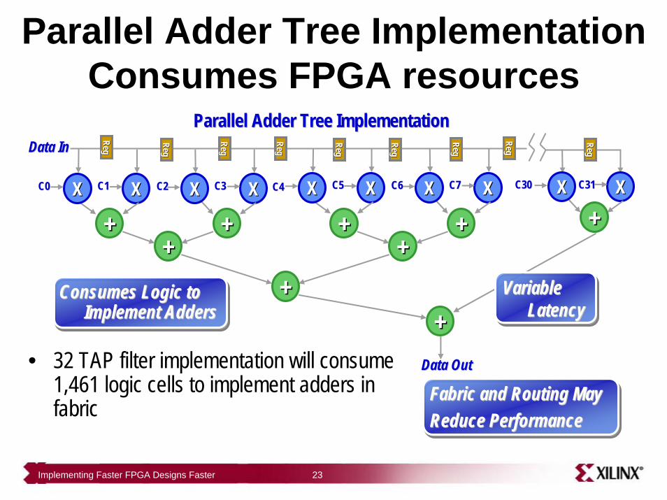
Parallel Adder Tree Implementation Consumes FPGA resources
Fabric and Routing MayFabric and Routing MayReduce PerformanceReduce Performance
• 32 TAP filter implementation will consume 1,461 logic cells to implement adders in fabric
Parallel Adder Tree ImplementationParallel Adder Tree ImplementationData InData In
XX
++C0C0 C0C0XXC1C1 XXC2C2 XXC3C3
++++
XXC4C4 C0C0XXC5C5 XXC6C6 XXC7C7 XXC30C30 XXC31C31
++++ ++++
Data OutData Out
++++Consumes Logic to Consumes Logic to
Implement AddersImplement AddersVariable Variable
LatencyLatency
RegReg
RegReg
RegReg
RegReg
RegReg
RegReg
RegReg
RegReg
RegReg

Implementing Faster FPGA Designs Faster 24
Parallel Adder Cascade Implementation in DSP48 ColumnParallel Adder Cascade Implementation in DSP48 Column
Data InData In
XX
++
XX
++XX
++Data OutData Out
XX
++
XX
++
XX
++
XX
++
XX
++
XX
++
• 32 TAP filter implementation using 32 XtremeDSP Slices• Guaranteed 550 MHz operation•
Parallel Implementation Consumes Zero Logic Resources
HDL coding examples in Virtex-5 FPGA XtremeDSPDesign Considerations User Guide
C0C0 C1C1 C2C2 C3C3 C5C5 C6C6 C7C7 C30C30 C31C31C4C4 XX
++
RegReg
RegReg
RegReg
RegReg
RegReg
RegReg
RegReg
RegReg
RegReg
RegReg
RegReg
RegReg
RegReg
RegReg
RegReg
RegReg
RegReg
RegReg
RegReg
RegReg
RegReg
RegReg
RegReg
RegReg
RegReg
RegReg
RegReg
….
….
….
DSP48 ColumnDSP48 Column

Implementing Faster FPGA Designs Faster 25
Pipelining• Pipelining cannot be an afterthought
– Adding pipeline registers “later” is not easy– Number and placement of registers need to be considered during initial
coding
• Too little pipelining will result in under-performing designs• Maximum performance seen when…
– There are 6 inputs to a logic function• This is different than previous architectures due to the 6-LUT
– Extra caution is taken around Multipliers and RAMs

Implementing Faster FPGA Designs Faster 26
Where to find more information• WP231 – HDL Coding Practices to Accelerate Design Performance• WP272 – Get Smart About Reset: Think Local Not Global• WP271 – Saving Costs with the SRL16E• WP333 – FIFOs in Virtex-5 FPGAs• WP284 – Advantages of Virtex-5 FPGA 6-Input LUT Architecture• WP275 – Get your Priorities Right – Make Your Design up to 50% Smaller• WP248 – Retargeting Guidelines for Virtex-5 FPGAs• WP245 – Achieving Higher System Performance with the Virtex-5 Family of FPGAs• Synthesis and Simulation Design Guide in Software Manual.• Coding Examples in the Language Template

Implementing Faster FPGA Designs Faster 27
Agenda
• Understanding the Virtex5 FPGA Architecture• A look at how coding affects performance• Software tools that can help increase
performance and reduce design time

Implementing Faster FPGA Designs Faster 28
Timing Constraints• All designs should have timing constraints for IO, clocks and multi-cycle paths• Implementation tools are timing driven
– Without timing constraints implementation only concern is runtime• Synthesis tools are also timing driven
– Synthesis will make logic decisions based on timing constraints• See the Constraints Guide in Software Manual• Language Template in Project Navigator has constraint examples
OUT1X
Y
Z<0:9>
OUT22 Levels of Logic
PERIODOFFSET IN
FROM:TO
OFFSET OUT
1 Level of Logic
QD QD
CLK

Implementing Faster FPGA Designs Faster 29
Strategy-Based Implementation
• Software switches can impact performance, area and power
• Automatically identifies optimal implementation algorithm based on design goals
– Balanced: (Default) Delivers balance of performance and runtime
– Timing Performance: Delivers optimal performance
– Minimum Runtime: Focuses on minimizing runtime– Area Reduction: Slice Reduction with minimal
impact to performance– Power Optimization: Minimizes dynamic power
with minimal impact to performance
Set the Goal instead of multiple implementation settings

Implementing Faster FPGA Designs Faster 30
SmartCompile Technology
• SmartPreview– Provides visibility into implementation– Create bitstream for lab debug– Preserve latest results as snapshot
and continue processing• SmartGuide
– Timing preservation in the midst of changes– Average 2x to 4x faster re-implementation
runtimes for small design changes• Partitions
– Implementation preservation in the midst of changes
– Allows flexibility to preserve routing, placement, synthesis SmartPreview Partitions
SmartGuide
Previous CurrentExact Preservation

Implementing Faster FPGA Designs Faster 31
PlanAhead: Floorplanning & More• Increase performance through hierarchical
floorplanning– Floorplan prior to physical implementation– Guide place and route toward better results– Easily view utilization of hierarchy – Create Area Constraints quickly
• Analyze Multiple Results from ISE– Highlight failing timing paths from post-route timing
analysis• Analyze timing early through TimeAhead
– Quickly identify, select and constrain critical path logic• ExploreAhead
– Run multiple implementations with different implementation switches.
• Simplify managing complex interface between FPGA and PCB with PinAhead
– Facilitates early and intelligent pinout definition– Performs WASSO & Design Rule Checks early
in design cycle– HDL & CSV Import – Export
www.xilinx.com/planahead

Implementing Faster FPGA Designs Faster 32
System Generator and AccelDSP
www.xilinx.com/dsp

Implementing Faster FPGA Designs Faster 33
Intellectual Property Cores
http://www.xilinx.com/memory
SystemIOSerial10 &1 GE MACsEthernet PHYsXAUIPCI ExpressAuroraMany more …
ParallelPCIPCI-X SPI-4SPI-3XGMIIMany more …
DSP & MathMathMultipliersMACDividerFiltersCORDICMany more …
AdvancedReed-SolomonTurbo CodecsVirterbiVideoWirelessMany More …
ProcessorInfrastructureCoreConnect BusArbiterBridgeMemory controllersSoft processorsSoftware IP Many more …
PeripheralsInterrupt ControllerUARTsTimerGPIOSPIMany more …
General PurposeCORE Generator Building BlocksMemory GeneratorsIOB ConfigurationsArithmetic and ShiftersRegistersBuffersMany More …
Optimized for Performance or Area
http://www.xilinx.com/ipcenter

Implementing Faster FPGA Designs Faster 34
Signal Probing with FPGA Editor• FPGA Editor shows design
layout on device• Probe internally in design
without rerunning implementation
• Find internal signal and route to spare pin
– Automatically– Manually
• Delay from probe point to selected pin automatically reported
• Good for probing a handful of signals Probe
Route Delay
Implementing Faster FPGA Designs Faster 35
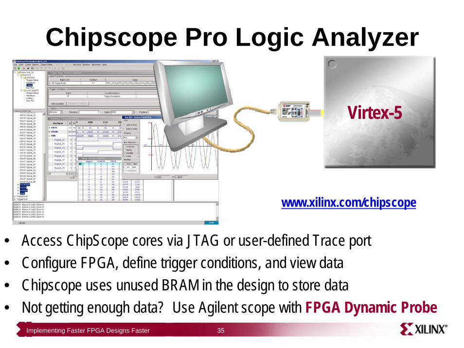
Chipscope Pro Logic Analyzer
• Access ChipScope cores via JTAG or user-defined Trace port• Configure FPGA, define trigger conditions, and view data• Chipscope uses unused BRAM in the design to store data• Not getting enough data? Use Agilent scope with FPGA Dynamic Probe
Virtex-5
www.xilinx.com/chipscope

Implementing Faster FPGA Designs Faster 36
ChipScope Pro Serial IO Toolkit • ChipScope Pro IBERT core embedded within
the design to provide on-chip access • Real-time control of each GTP
– GTP status and control– BERT status and control– Adjust clock settings and line rate– Control TX and RX settings
• Edit MGT attributes or DRP directly– Dump DRP attributes to screen– Dump DRP attributes to UCF file to
include in end design
Implementing Faster FPGA Designs Faster 37
Summary
• Many different software tools and settings that can help increase the performance and reduce area and power.
• Hard and soft cores that can be leveraged.• The number one way to increase performance and
reduce area and power is to understand the basic features of the target architecture down to the FF and LUT.
• Best way to understand the target architecture is to……READ, READ, READ and then READ some more!!!

Implementing Faster FPGA Designs Faster 38
Appendix

Implementing Faster FPGA Designs Faster 39
Where to find more information• Xilinx Support Home Page
– mysupport.xilinx.com
• Virtex-5 FPGA Data Sheet: DC and Switching Characteristics– http://www.xilinx.com/support/documentation/data_sheets/ds202.pdf
• Virtex-5 FGPA User Guide– http://www.xilinx.com/support/documentation/user_guides/ug190.pdf
• Virtex-5 FPGA XtremeDSP Design Considerations User Guide– http://www.xilinx.com/support/documentation/user_guides/ug193.pdf
• Virtex-5 FPGA XtremeDSP Design Considerations User Guide– http://www.xilinx.com/support/documentation/user_guides/ug198.pdf
Implementing Faster FPGA Designs Faster 40
New Video Demos
• Improving Design Performance with PlanAhead• Optimizing Implementation Results using ExploreAhead• Improving the FGPA on PCB Integration with PinAhead• Partial Reconfiguration Design using PlanAhead• Get the Most Out of Your Design Using XST Synthesis Strategies• Reduce FPGA Verification Time Using New Simulation Features• Improve Productivity Using Multiple Constraint Files• Simplify Entry and Analysis of I/O Timing Constraints• Improve Time-to-Market Using Partitions and SmartGuide• Improve DSP and Embedded Design Productivity• Optimize FPGA Performance Using Goals, Strategies, and SmartXplorer• Improve Productivity Using the EDA Standard Tool Command Language (Tcl)• Fine-Tune FPGA Power Budgets Using New Power Analysis and Optimization• Video demo for XPE: http://www.demosondemand.com/clients/xilinx/001/page/index_destools.asp• Improve Configuration Ease of Use with Project Navigator and iMPACT
Streaming videos are available at http://www.xilinx.com/design.
Related Documents