NAME: ………………………. REGD NO: ………………….. DEPARTMENT OF ELECTRONICS AND COMMUNICATIONS ENGINEERING Malineni Lakshmaiah Women’s Engineering College. Pulladigunta-522 017 1

Welcome message from author
This document is posted to help you gain knowledge. Please leave a comment to let me know what you think about it! Share it to your friends and learn new things together.
Transcript
NAME: ……………………….
REGD NO: …………………..
DEPARTMENT OF ELECTRONICS AND COMMUNICATIONS ENGINEERING
MALINENI LAKSHMAIAH WOMEN’S ENGINEERING COLLEGE(Approved by AICTE NEW DELHI & Affiliated to JNTU KAKINADA)
PULLADIGUNTA (V), VATTICHERUKURU (M), GUNTUR DIST. A.P-522017
Malineni Lakshmaiah Women’s Engineering College. Pulladigunta-522 017 1
1. Course Code : EC 2228
2. Course Title : ANALOG COMMUNICATION LAB
3. Core / Elective : Core
4. Pre–requisite (if any) : COMMUNICATION THEORY
5. Year in which offered : II Year B.Tech., ECE II SEM
6. No. of weeks of instruction : 16
7. No. of hours per week : 3 periods
8. Course objectives :
To verify the various analog modulation and de-modulation methods like amplitude,
frequency modulation and demodulation, etc. And to verify the spectrum of the amplitude
and frequency modulations using the spectrum analyzer. Also to study and verify the
receiver characteristics.
9. List of experiments actually performed as per JNTU Syllabus:
1. Amplitude modulation and demodulation.2. Diode detector characteristics.3. Frequency modulation and demodulation.4. Balanced modulator.5. Pre-emphasis & de-emphasis.6. Characteristics of mixer.7. Digital Phase detector.8. Phase locked loop.9. Synchronous detector.10. SSB system.11. Spectral analysis of AM and FM signals using spectrum analyzer.12. Squelch Circuit.13. Frequency Synthesiser.14. AGC Characteristics.
10. List of major equipment and soft ware tools used:
1. CRO (20 MHz, 30 MHz and 60 MHz).
2. Communications Trainer Kits.
3. Spectrum analyzer (1 GHz).
4. Fiber optics Kit (Analog).
Malineni Lakshmaiah Women’s Engineering College. Pulladigunta-522 017 2
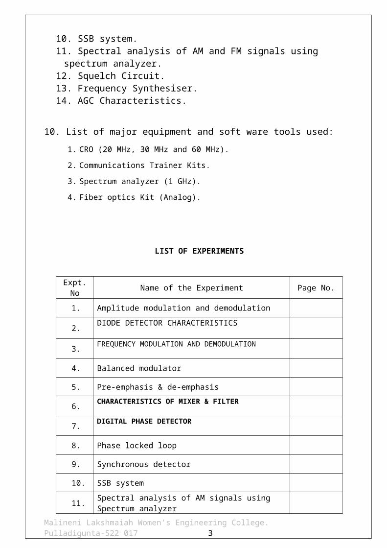
LIST OF EXPERIMENTS
Expt. No Name of the Experiment Page No.
1. Amplitude modulation and demodulation
2.DIODE DETECTOR CHARACTERISTICS
3.FREQUENCY MODULATION AND DEMODULATION
4. Balanced modulator
5. Pre-emphasis & de-emphasis
6.CHARACTERISTICS OF MIXER & FILTER
7.DIGITAL PHASE DETECTOR
8. Phase locked loop
9. Synchronous detector
10. SSB system
11.Spectral analysis of AM signals using Spectrum analyzer
11(A)Spectral analysis of FM signals using Spectrum analyzer
12.
13.FREQUENCY SYNTHESIZER
14. AGC Characteristics
Malineni Lakshmaiah Women’s Engineering College. Pulladigunta-522 017 3

1. AIM:
1.1 To study the amplitude modulation and demodulation for different modulation
index.
2. COMPONENTS & TOOLS REQUIRED:
2. 1. Audio signal generator
2. 2. Carrier generator
2. 3. Amplitude Modulator Trainer Kit
2. 4. Cathode Ray Oscilloscope (30 MHz).
2.5. Connecting wires
3. THEORY:
Modulation is defined as process in which changing the
characteristics usually amplitude, frequency and phase of high frequency
wave (Carrier wave) by using instantaneous values of the low frequency
signal (modulating signal).
Need for modulation:
3.1.1 Antenna height and operating frequencies are related each other. So
antenna heights are comparable to the quarter wavelengths. For
usual audio frequencies antenna heights are unthinkable and
impracticable.
3.1.2 Audio frequencies are directly transmitted when there is a possibility
of mixing with the other frequencies in near by station.
3.1.3 If high frequency signals are directly transmitted there is no varying
parameter compared to the audio frequency
Amplitude modulation is defined as the process in which changing
the amplitude of the Carrier wave by using the instantaneous voltages of
the modulating signal. In this carrier signal frequency remains constant
Malineni Lakshmaiah Women’s Engineering College. Pulladigunta-522 017 4
AMPLITUDE MODULATION AND DEMODULATION
EXPT. NO : 1
DATE :
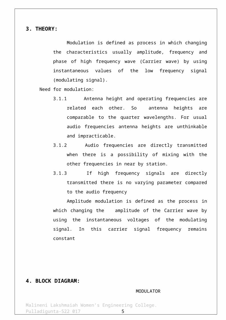
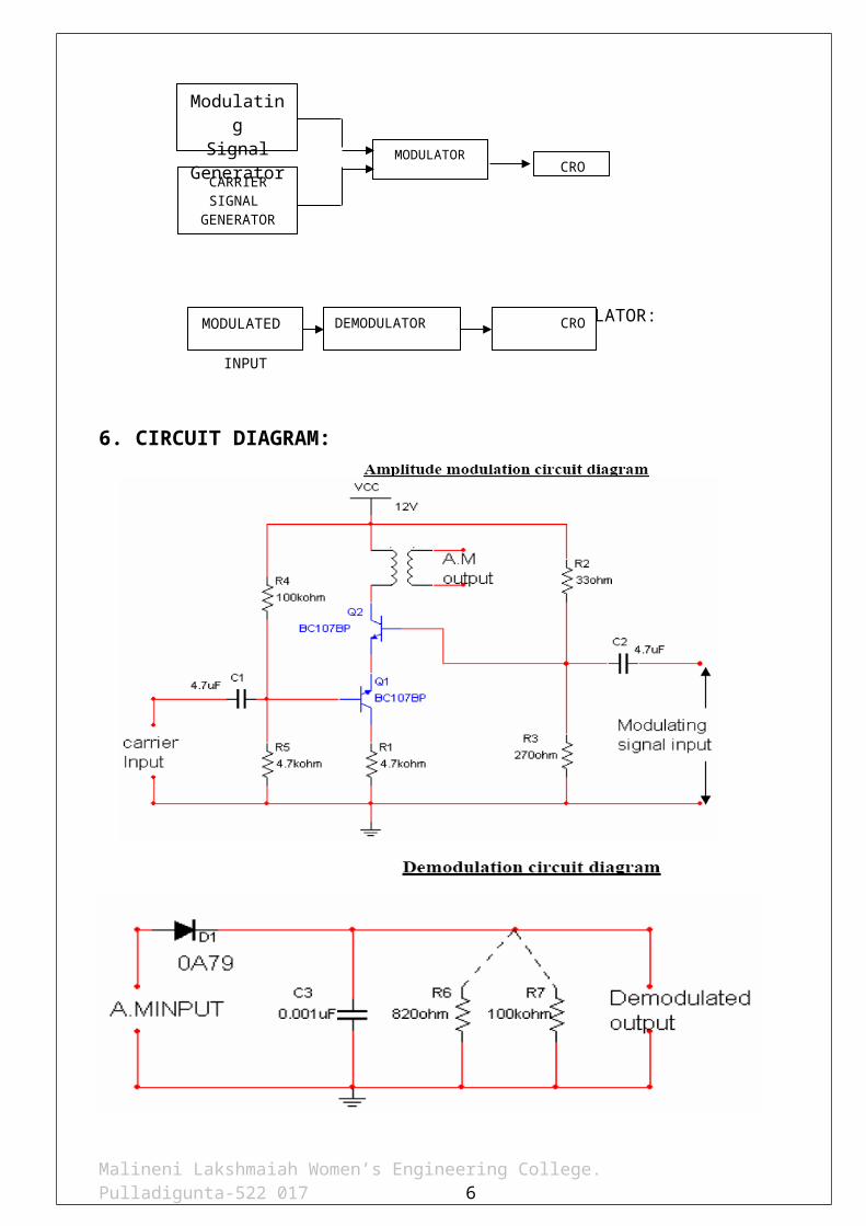
4. BLOCK DIAGRAM:
MODULATOR
DEMODULATOR:
6. CIRCUIT DIAGRAM:
Malineni Lakshmaiah Women’s Engineering College. Pulladigunta-522 017 5
MODULATED INPUT
DEMODULATOR CRO
CARRIER SIGNAL
GENERATOR
MODULATOR CRO
ModulatingSignal
Generator
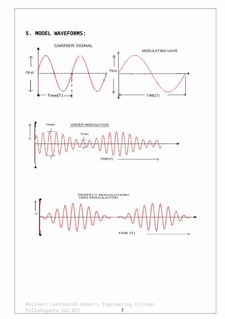
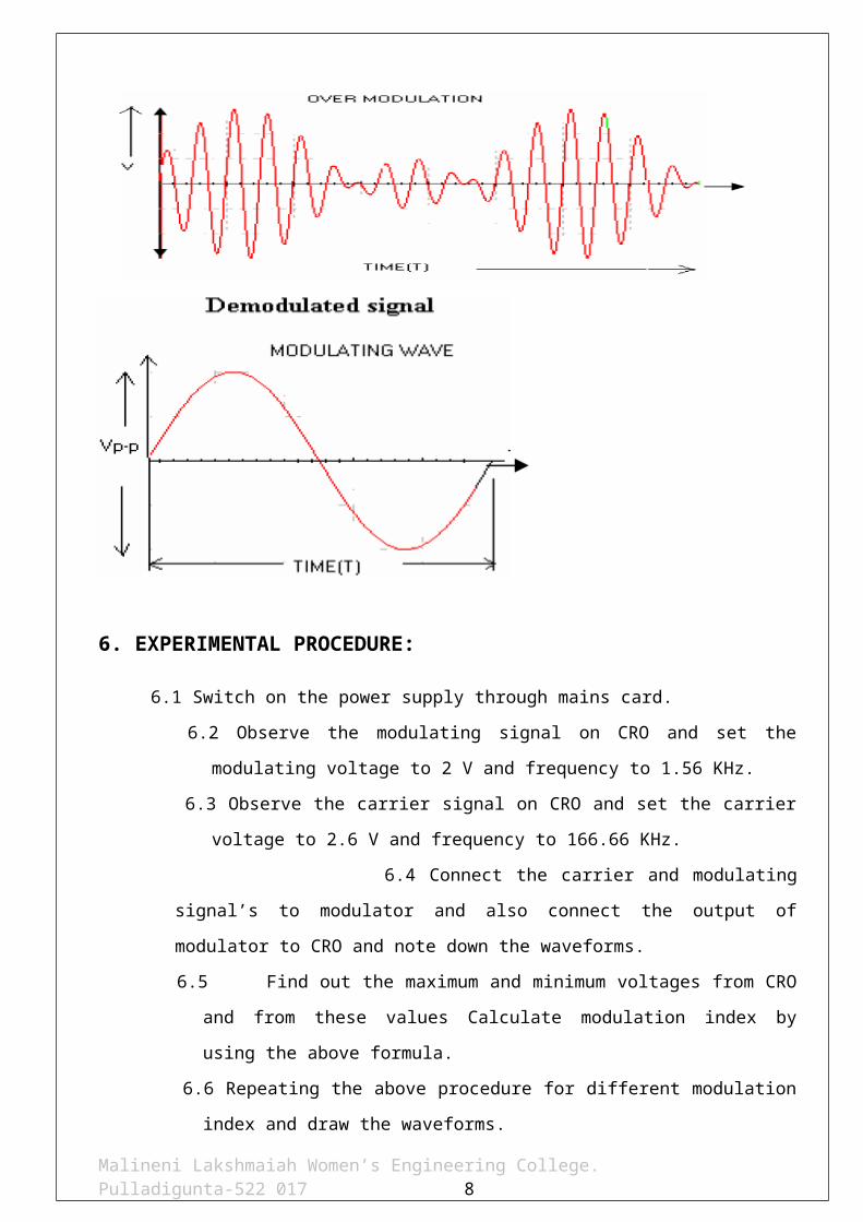
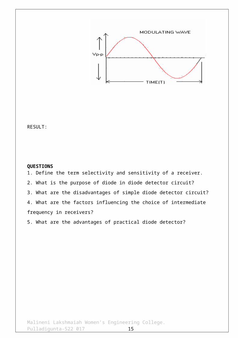
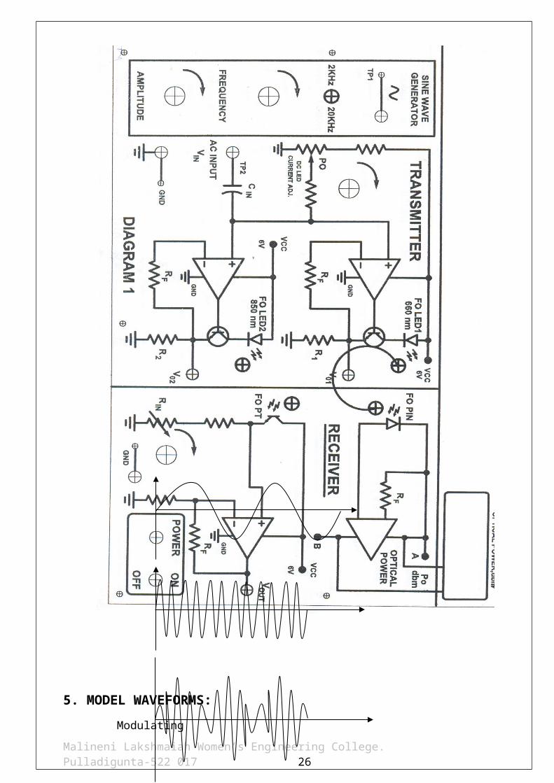
5. MODEL WAVEFORMS:
Malineni Lakshmaiah Women’s Engineering College. Pulladigunta-522 017 6
6. EXPERIMENTAL PROCEDURE:
6.1 Switch on the power supply through mains card.
6.2 Observe the modulating signal on CRO and set the modulating voltage to 2 V and
frequency to 1.56 KHz.
6.3 Observe the carrier signal on CRO and set the carrier voltage to 2.6 V and
frequency to 166.66 KHz.
6.4 Connect the carrier and modulating signal’s to modulator and also
connect the output of modulator to CRO and note down the waveforms.
6.5 Find out the maximum and minimum voltages from CRO and from these
values Calculate modulation index by using the above formula.
6.6 Repeating the above procedure for different modulation index and draw the
waveforms.
6.7 Connect the amplitude modulated signal to the demodulator
6.8 Connect the CRO across the out put terminals of the demodulator
6.9 Observe the waveforms the modulating signal for different modulation indicies.
7. PRECAUTIONS:
Malineni Lakshmaiah Women’s Engineering College. Pulladigunta-522 017 7
Check for loose contacts of wires and components.
Keep all the control knobs in the minimum position.
Adjust the control knobs smoothly.
After taking the readings bring back all the control knobs to minimum position.
8. OBSERVATIONS:
8.1 Amplitude of modulating signal_____________
8.2 Frequency of modulating signal______________
8.3 Amplitude of carrier signal_________________
8.4 Frequency of carrier signal_________________
8.5 Amplitude of demodulating signal___________
8.6 Frequency of demodulating signal___________
9. CONCLUSION:
For various modulation indices the amplitude modulation and de-modulation is verified.
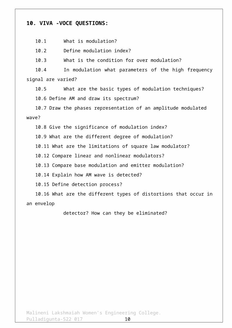
10. VIVA -VOCE QUESTIONS:
10.1 What is modulation?
10.2 Define modulation index?
10.3 What is the condition for over modulation?
10.4 In modulation what parameters of the high frequency signal are varied?
10.5 What are the basic types of modulation techniques?
10.6 Define AM and draw its spectrum?
10.7 Draw the phases representation of an amplitude modulated wave?
10.8 Give the significance of modulation index?
10.9 What are the different degree of modulation?
10.11 What are the limitations of square law modulator?
10.12 Compare linear and nonlinear modulators?
10.13 Compare base modulation and emitter modulation?
10.14 Explain how AM wave is detected?
10.15 Define detection process?
Malineni Lakshmaiah Women’s Engineering College. Pulladigunta-522 017 8
10.16 What are the different types of distortions that occur in an envelop
detector? How can they be eliminated?
Malineni Lakshmaiah Women’s Engineering College. Pulladigunta-522 017 9
Signature of the In – Charge Date:
Malineni Lakshmaiah Women’s Engineering College. Pulladigunta-522 017 10

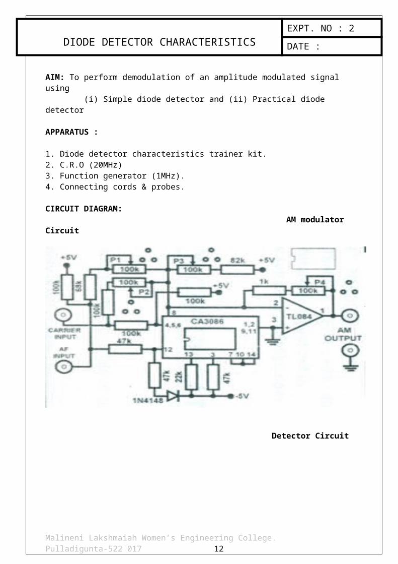
AIM: To perform demodulation of an amplitude modulated signal using (i) Simple diode detector and (ii) Practical diode detector
APPARATUS :
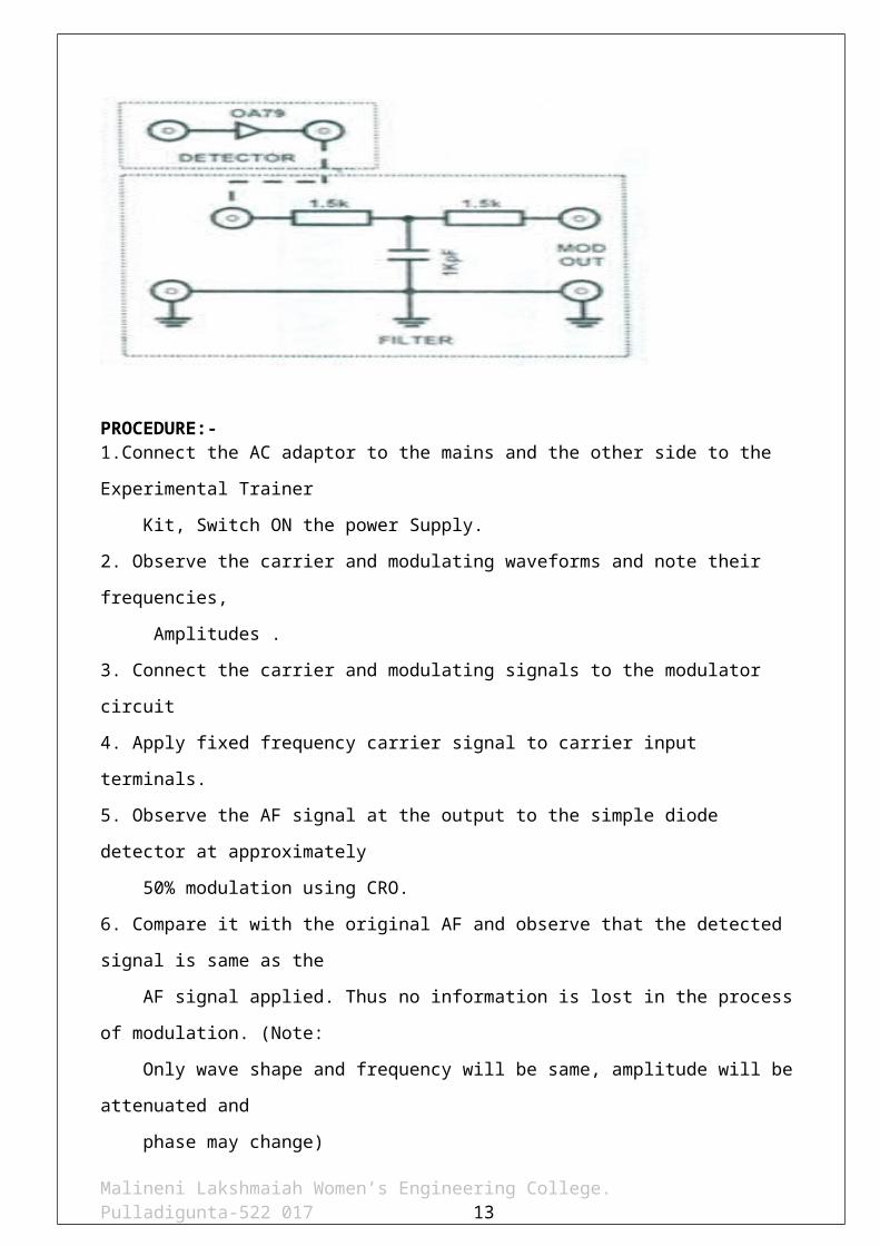
1. Diode detector characteristics trainer kit.2. C.R.O (20MHz)3. Function generator (1MHz).4. Connecting cords & probes.
CIRCUIT DIAGRAM: AM modulator Circuit
Detector Circuit
Malineni Lakshmaiah Women’s Engineering College. Pulladigunta-522 017 11
DIODE DETECTOR CHARACTERISTICSEXPT. NO : 2
DATE :
PROCEDURE:-1.Connect the AC adaptor to the mains and the other side to the Experimental Trainer
Kit, Switch ON the power Supply.
2. Observe the carrier and modulating waveforms and note their frequencies,
Amplitudes .
3. Connect the carrier and modulating signals to the modulator circuit
4. Apply fixed frequency carrier signal to carrier input terminals.
5. Observe the AF signal at the output to the simple diode detector at approximately
50% modulation using CRO.
6. Compare it with the original AF and observe that the detected signal is same as the
AF signal applied. Thus no information is lost in the process of modulation. (Note:
Only wave shape and frequency will be same, amplitude will be attenuated and
phase may change)
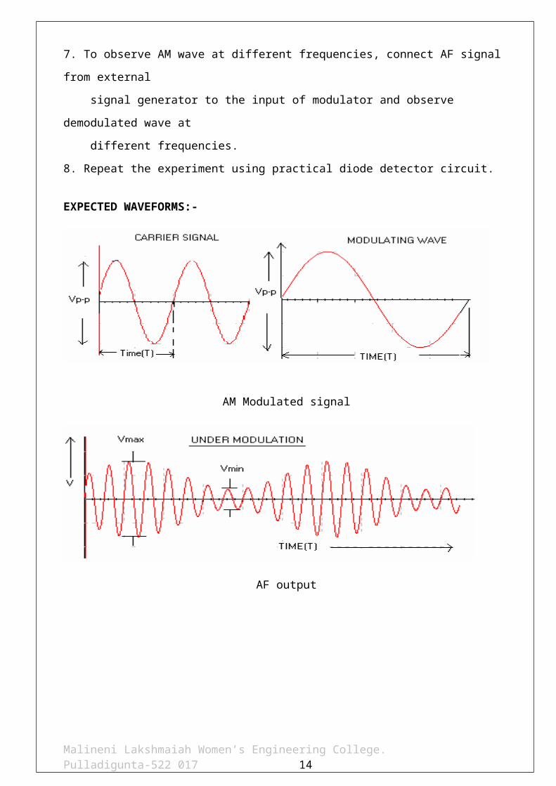
7. To observe AM wave at different frequencies, connect AF signal from external
signal generator to the input of modulator and observe demodulated wave at
different frequencies.
8. Repeat the experiment using practical diode detector circuit.
EXPECTED WAVEFORMS:-
AM Modulated signal
Malineni Lakshmaiah Women’s Engineering College. Pulladigunta-522 017 12
AF output
RESULT:
QUESTIONS1. Define the term selectivity and sensitivity of a receiver.
2. What is the purpose of diode in diode detector circuit?
3. What are the disadvantages of simple diode detector circuit?
4. What are the factors influencing the choice of intermediate frequency in receivers?
5. What are the advantages of practical diode detector?
Malineni Lakshmaiah Women’s Engineering College. Pulladigunta-522 017 13
Signature of the In – Charge Date:
Malineni Lakshmaiah Women’s Engineering College. Pulladigunta-522 017 14
Signature of the In – Charge Date:
1. AIM:
1.1 To study the frequency modulation and demodulation for different modulation
index.
2. COMPONENTS & TOOLS REQUIRED:
2. 1. Audio signal generator
2. 2. Carrier generator
2. 3. Frequency modulator Trainer Kit
2. 4. Cathode ray oscilloscope (30 MHz).
2.5. Connecting wires
3. THEORY:
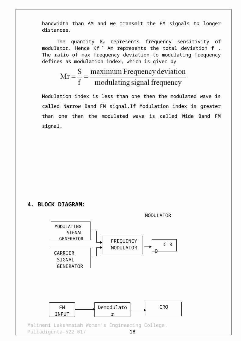
FM Modulation is a non-linear modulation technique. In FM the frequency of carrier is varied in accordance with amplitude of modulating signal (AF signal). But amplitude is maintained constant. Since the variation in phase angular term it is comes under angle modulation scheme, the most important feature of FM modulation is that it can be provide better discrimination against noise and interference than AM. The disadvantage of FM is it requires more transmission bandwidth than AM and we transmit the FM signals to longer distances.
The quantity Kf represents frequency sensitivity of modulator. Hence Kf * Am represents the total deviation f . The ratio of max frequency deviation to modulating frequency defines as modulation index, which is given by
Modulation
index is less than one then the modulated wave is called Narrow Band FM signal.If
Modulation index is greater than one then the modulated wave is called Wide Band
FM signal.
Malineni Lakshmaiah Women’s Engineering College. Pulladigunta-522 017 15
FREQUENCY MODULATION & DEMODULATION
EXPT. NO : 3
DATE :

4. BLOCK DIAGRAM:
MODULATOR
DEMODULATOR:
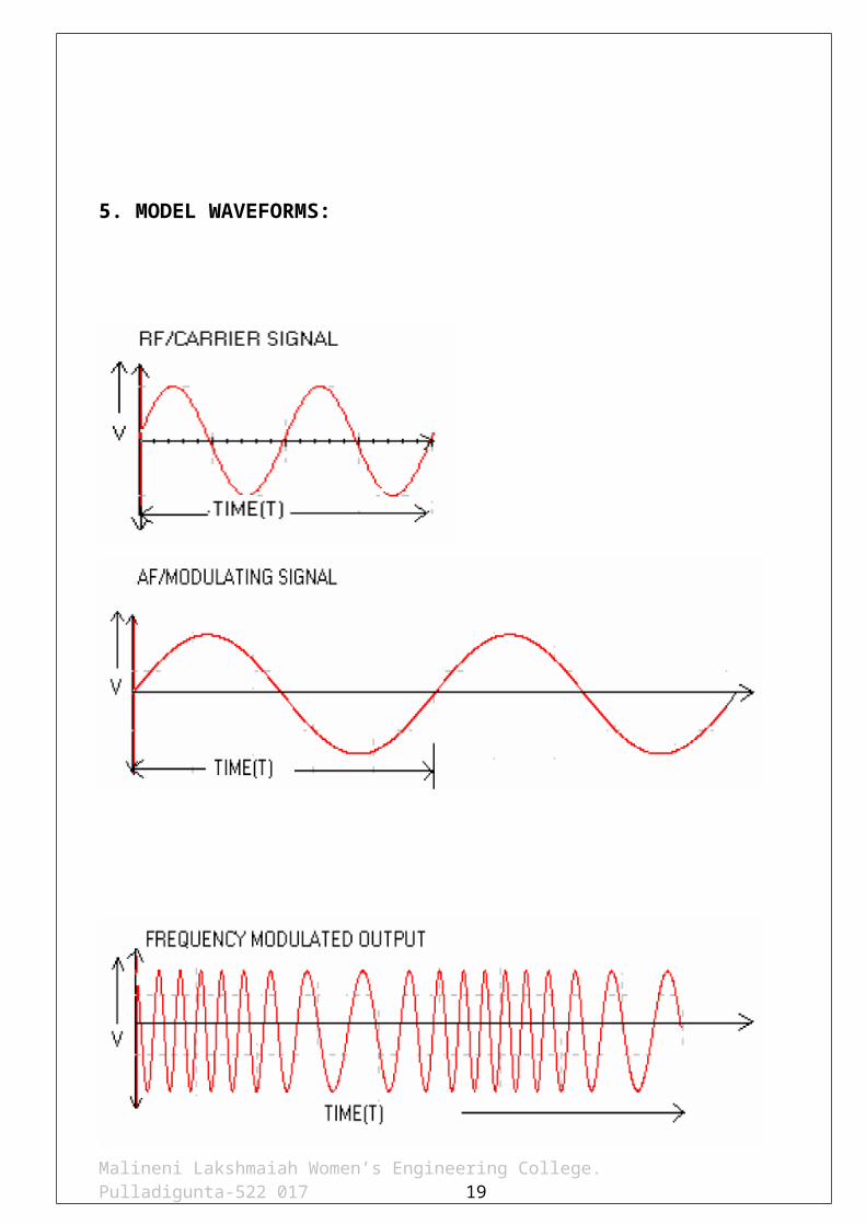
5. MODEL WAVEFORMS:
Malineni Lakshmaiah Women’s Engineering College. Pulladigunta-522 017 16
MODULATING SIGNAL
GENERATOR
CARRIER SIGNAL GENERATOR
FREQUENCY MODULATOR C R O
FMINPUT
Demodulator CRO
6. EXPERIMENTAL PROCEDURE:
6.1 Switch on the power supply through mains card.
6.2 Observe the modulating signal in CRO and set the modulating voltage to 1.2 V and frequency to 10 KHz and note down these values. (Here the carrier is internally generated signal).
6.3 Connect the modulating signal to modulator also connect the output of modulator to CRO and note down the waveforms.
6.4 Find out the maximum and minimum frequency of frequency modulated wave
from CRO and note down these values, from these values calculate modulation
index by using the above formula.
6.5 Connect the frequency-modulated signal to the demodulator.
6.6 Connect the CRO across the output terminals of the demodulator.
6.7 Observe the waveform of the modulating signal for different modulating indices
7. PRECAUTIONS:
7.1 Check for loose contacts of wires and components.
7.2 Keep all the control knobs in the minimum position.
7.3 Before switch on the power supply get the circuit connections verified by the
teacher.
7.4 Adjust the control knobs smoothly.
7.5 After taking the readings bring back all the control knobs to minimum
position.
7.6 Switch off the power supply before leaving the experimental table.
Malineni Lakshmaiah Women’s Engineering College. Pulladigunta-522 017 17
8. Observations:
8.1 Amplitude of modulating signal_____________
8.2 Frequency of modulating signal______________
8.3 Amplitude of carrier signal_________________
8.4 Frequency of carrier signal_________________
8.5 Frequency deviation _________________
8.6 Amplitude of demodulating signal___________
8.7 Frequency of demodulating signal___________
9. CONCLUSION: The output waveforms of frequency modulation are observed for
modulation index less than one and greater than one. Also demodulation is verified.
10. VIVA -VOCE QUESTIONS:
10.1 What is frequency modulation?
10.2 How the FM can be differentiated from the frequency translation?
10.3 In Frequency modulated waveform where does the message signal
exist?
10.4 What is meant by carrier nulls?
10.5 What is the bandwidth required for NBFM?
Malineni Lakshmaiah Women’s Engineering College. Pulladigunta-522 017 18
Signature of the In – Charge Date:
Malineni Lakshmaiah Women’s Engineering College. Pulladigunta-522 017 19
1. AIM:
1.1 To study the DSB – SC Modulation using balance modulator
2. COMPONENTS & TOOLS REQUIRED:
2. 1. Audio signal generator
2. 2. Carrier generator
2. 3. Balanced modulator Trainer Kit
2. 4. Cathode Ray Oscilloscope.
2.5. Connecting wires
3. THEORY:
Balance modulator is used for generation of double side band suppress
carrier signal. The output of balanced modulator is equal to the product of applied
input signals. In order to generate this it uses the non-linear characteristics of semi
conductor device. Since the carrier does not convey any information, transmitting
the carrier along with side band is only wasting of transmission power, there fore
carrier is suppressed before transmission. By doing suppression 67% of
transmission power can be saved. The method of transmission of modulated wave
with out carrier is DSBSC signal.
Balance modulator is also used in generation of SSB signals. The
modulated signal undergoes a phase reversal whenever the base band signal
crosses zero. Unlike AM, The envelope of DSBSC id different from base band
signal. The ring modulator is another circuit for generating the DSBSC signal.
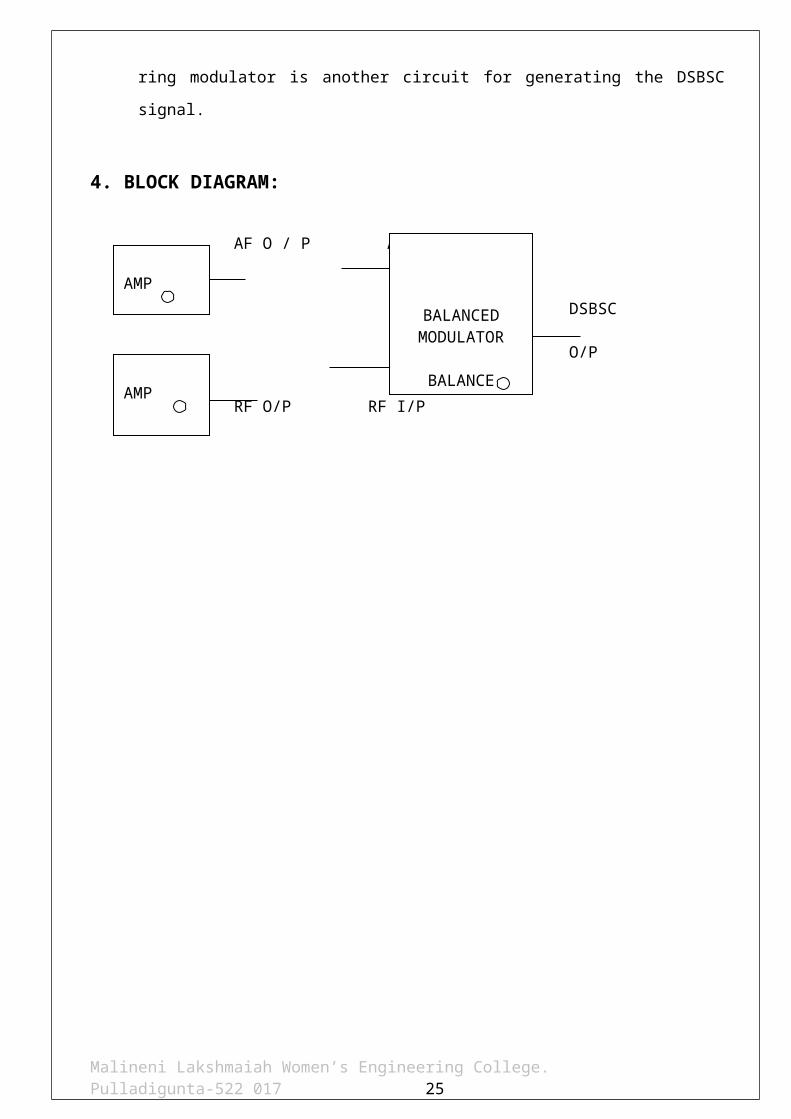
4. BLOCK DIAGRAM:
AF O / P AF I/P
DSBSC O/P
RF O/P RF I/P
Malineni Lakshmaiah Women’s Engineering College. Pulladigunta-522 017 20
BALANCED MODULATION EXPT. NO : 4
DATE :
AMP
AMP
BALANCEDMODULATOR
BALANCE
Malineni Lakshmaiah Women’s Engineering College. Pulladigunta-522 017 21

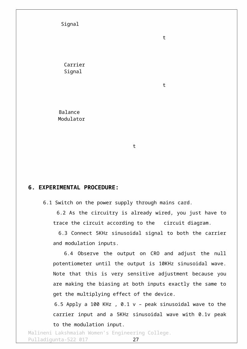
5. MODEL WAVEFORMS:
Modulating Signal
t
Carrier Signal
t
Balance Modulator
t
6. EXPERIMENTAL PROCEDURE:
6.1 Switch on the power supply through mains card.
6.2 As the circuitry is already wired, you just have to trace the circuit according to
the circuit diagram.
6.3 Connect 5KHz sinusoidal signal to both the carrier and modulation inputs.
6.4 Observe the output on CRO and adjust the null potentiometer until the output
is 10KHz sinusoidal wave. Note that this is very sensitive adjustment because
you are making the biasing at both inputs exactly the same to get the
multiplying effect of the device.
6.5 Apply a 100 KHz , 0.1 v – peak sinusoidal wave to the carrier input and a 5KHz
sinusoidal wave with 0.1v peak to the modulation input.
6.6 Adjust carrier null potentiometer to obtain a DSBSC wave as output Vary the
amplitude frequency of the message signals at different levels.
6.7 Observe the variation in side bands and suppression of carrier.
6.8 Record the exact frequency levels of side bands suppressed carrier from
CRO.
Malineni Lakshmaiah Women’s Engineering College. Pulladigunta-522 017 22
7.PRECAUTIONS:
Check for loose contacts of wires and components.
Keep all the control knobs in the minimum position.
Before switch on the power supply get the circuit connections verified by the
teacher.
Adjust the control knobs smoothly.
After taking the readings bring back all the control knobs to minimum position.
Switch off the power supply before leaving the experimental table.
8. Observations:
8.1 Amplitude of modulating signal -------------------------------
8.2 Frequency of modulating signal--------------------------------
8.3 Amplitude of carrier signal -------------------------------------
8.4 Frequency of carrier signal -------------------------------------
8.5 Frequency of Balanced detector output signal---------------
9. CONCLUSION: The out put waveform of balanced modulator is observed and plotted.
10. VIVA -VOCE QUESTIONS:
10.1 What is the significance of the balanced modulator?
10.2 What is the disadvantage of DSB-FC?
10.3 What is the percentage of power saving in DSB-SC over DSB-FC?
10.4 What is the bandwidth required for the transmission of DSB-SC signals?
10.5 Which detector is used for detecting the DSB-SC signals?
Malineni Lakshmaiah Women’s Engineering College. Pulladigunta-522 017 23
Signature of the In – Charge Date:
Malineni Lakshmaiah Women’s Engineering College. Pulladigunta-522 017 24
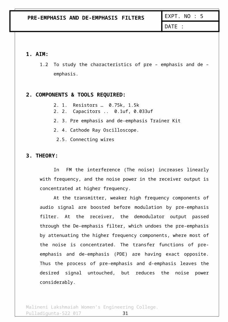
1. AIM:
1.2 To study the characteristics of pre – emphasis and de – emphasis.
2. COMPONENTS & TOOLS REQUIRED:
2. 1. Resistors … 0.75k, 1.5k2. 2. Capacitors .. 0.1uf, 0.033uf
2. 3. Pre emphasis and de-emphasis Trainer Kit
2. 4. Cathode Ray Oscilloscope.
2.5. Connecting wires
3. THEORY:
In FM the interference (The noise) increases linearly with frequency, and
the noise power in the receiver output is concentrated at higher frequency.
At the transmitter, weaker high frequency components of audio signal are
boosted before modulation by pre-emphasis filter. At the receiver, the demodulator
output passed through the De-emphasis filter, which undoes the pre-emphasis by
attenuating the higher frequency components, where most of the noise is
concentrated. The transfer functions of pre-emphasis and de-emphasis (PDE) are
having exact opposite. Thus the process of pre-emphasis and d-emphasis leaves
the desired signal untouched, but reduces the noise power considerably.
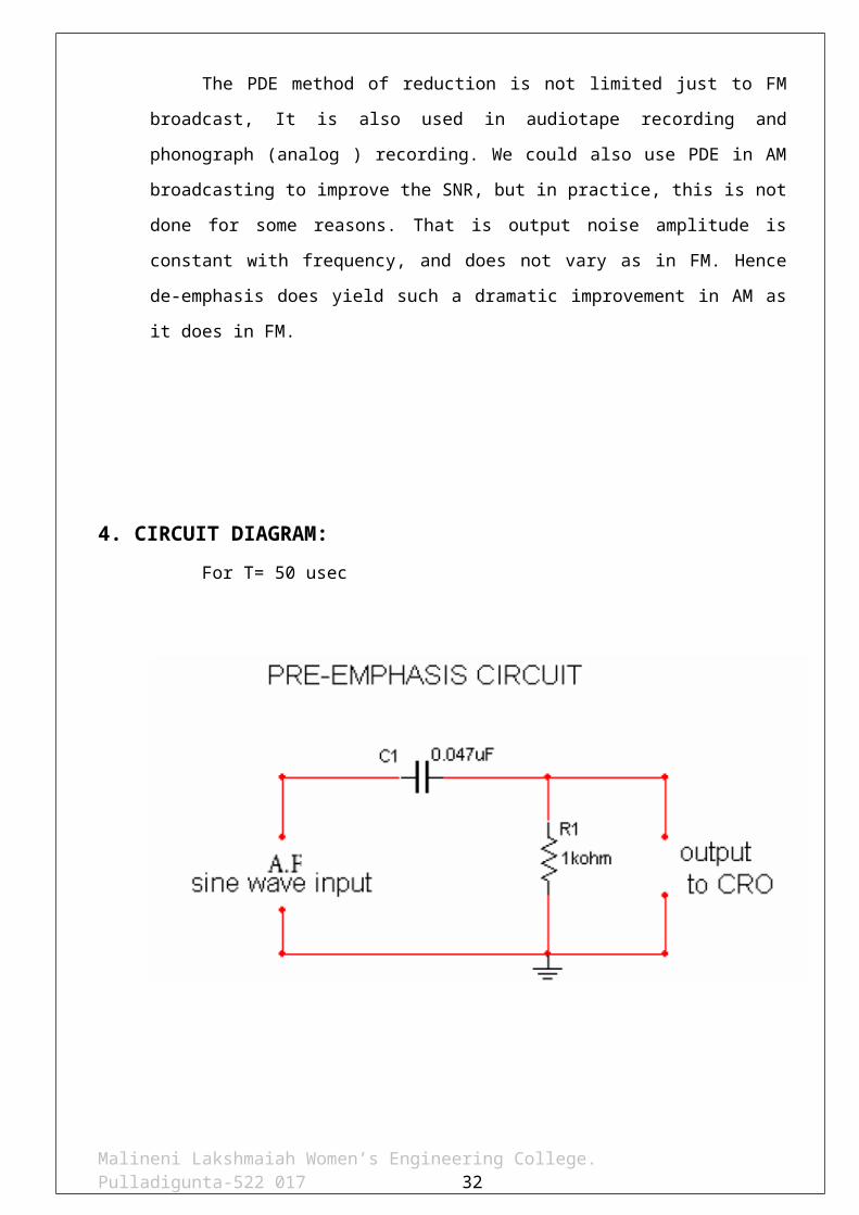
The PDE method of reduction is not limited just to FM broadcast, It is also
used in audiotape recording and phonograph (analog ) recording. We could also
use PDE in AM broadcasting to improve the SNR, but in practice, this is not done
for some reasons. That is output noise amplitude is constant with frequency, and
does not vary as in FM. Hence de-emphasis does yield such a dramatic
improvement in AM as it does in FM.
4. CIRCUIT DIAGRAM:
Malineni Lakshmaiah Women’s Engineering College. Pulladigunta-522 017 25
PRE-EMPHASIS AND DE-EMPHASIS FILTERS EXPT. NO : 5
DATE :
For T= 50 usec
Malineni Lakshmaiah Women’s Engineering College. Pulladigunta-522 017 26
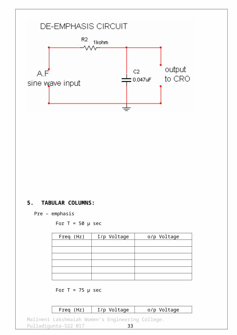
5. TABULAR COLUMNS:
Pre – emphasis
For T = 50 μ sec
Freq (Hz) I/p Voltage o/p Voltage
For T = 75 μ sec
Freq (Hz) I/p Voltage o/p Voltage
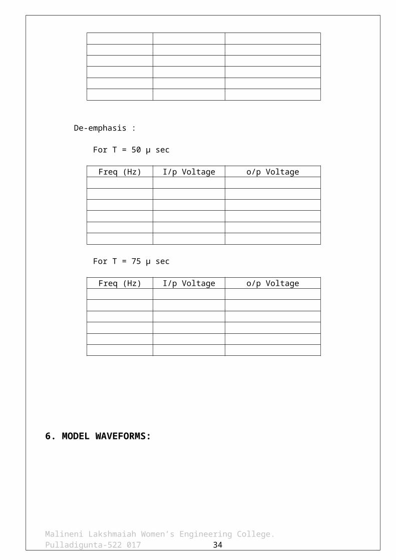
De-emphasis :
For T = 50 μ sec
Freq (Hz) I/p Voltage o/p Voltage
For T = 75 μ sec
Freq (Hz) I/p Voltage o/p Voltage
Malineni Lakshmaiah Women’s Engineering College. Pulladigunta-522 017 27
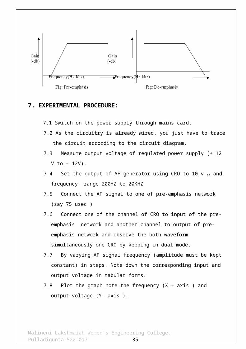
6. MODEL WAVEFORMS:
7. EXPERIMENTAL PROCEDURE:
7.1 Switch on the power supply through mains card.
7.2 As the circuitry is already wired, you just have to trace the circuit according to
the circuit diagram.
7.3 Measure output voltage of regulated power supply (+ 12 V to – 12V).
7.4 Set the output of AF generator using CRO to 10 v pp and frequency range
200HZ to 20KHZ
7.5 Connect the AF signal to one of pre-emphasis network (say 75 usec )
7.6 Connect one of the channel of CRO to input of the pre-emphasis network and
another channel to output of pre-emphasis network and observe the both
waveform simultaneously one CRO by keeping in dual mode.
7.7 By varying AF signal frequency (amplitude must be kept constant) in steps.
Note down the corresponding input and output voltage in tabular forms.
7.8 Plot the graph note the frequency (X – axis ) and output voltage (Y- axis ).
7.9 From the graph note the frequency at which the output is 70.7% of input
voltage and compare with the theoretical value which is given by 1/2RC).
7.10 Initially set the amplitude of AF generator to minimum level and sampling
frequency to 1khZ (by adjusting the preset provided in pulse generator
block). Note down the output of modulator by varying amplitude of
modulating signal observe the modulator output so you that you can notice
the amplitude of the sampling pulses is varying in accordance with the
amplitude of the modulating signal
7.11 Repeat all the above steps for time period 50 usec.
7.12 Connect AF signal to one of De-emphasis network (say 75 usec ).
Malineni Lakshmaiah Women’s Engineering College. Pulladigunta-522 017 28
7.13 Connect one of the channel of CRO to input of the De-emphasis network
and another channel to output of De-emphasis network and observe the
both waveforms simultaneously one CRO by keeping in dual mode.
7.14 By varying AF signal frequency (amplitude must be kept constant ) in steps.
Note down the corresponding input and output voltages in tabular forms.
7.15 Plot the graph between frequency (X-axisis) and output voltage (Y-axis).
7.16 From the graph note the frequency at which the output is 70.7% of input
voltage and compare with the theoretical value which is given by 1/2RC).
7.17 Initially set the amplitude of AF generator to minimum level and sampling
frequency to 1khZ (by adjusting the preset provided in pulse generator
block). Note down the output of modulator by varying amplitude of
modulating signal observe the modulator output so you that you can notice
the amplitude of the sampling pulses is varying in accordance with the
amplitude of the modulating signal
7.18 Repeat all the above steps for time period 50 μ sec.
8. PRECAUTIONS:
8.1 Check for loose contacts of wires and components.
8.2 Keep all the control knobs in the minimum position.
8.3 Before switch on the power supply get the circuit connections verified by the
teacher. Adjust the control knobs smoothly.
8.4 After taking the readings bring back all the control knobs to minimum position.
8.5 Switch off the power supply before leaving the experimental table.
9. OBSERVATIONS:
9.1 For 75 μ sec Pre-emphasis network
R =-----------------K ohm,
C = ----------------- μ F
Theoretical value = -------------------
Practical value = ---------------------
9.2 For 50 μ sec Pre-emphasis network
R =-----------------K ohm,
C = ----------------- μ F
Theoretical value = -------------------
Practical value = ---------------------
9.3. For 75 μ sec De-emphasis network
Malineni Lakshmaiah Women’s Engineering College. Pulladigunta-522 017 29

R =-----------------K ohm,
C = ----------------- μ F
Theoretical value = -------------------
Practical value = ---------------------
9.4. For 50 μ sec De-emphasis network
R =-----------------K ohm,
C = ----------------- μ F
Theoretical value = -------------------
Practical value = ---------------------
10. CONCLUSION: The characteristics of pre-emphasis and de-emphasis are studied and
plotted.
11. VIVA -VOCE QUESTIONS:
11.1 What is pre-emphasis?
11.2 What is de-emphasis?
11.3 What is the necessity of pre-emphasis and de-emphasis circuits?
11.4 Where we use the pre-emphasis and de-emphasis circuits?
11.5 Can we use the pre-emphasis and de-emphasis circuits in AM
receivers?
Malineni Lakshmaiah Women’s Engineering College. Pulladigunta-522 017 30
Signature of the In – Charge Date:
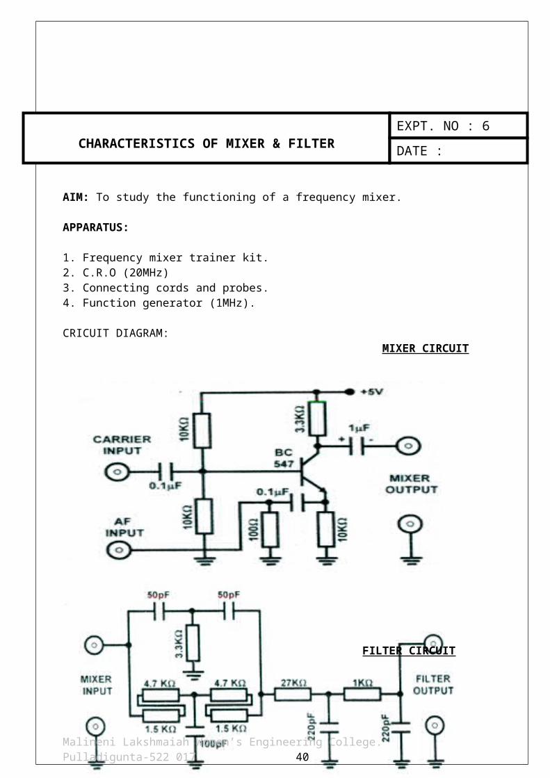
AIM: To study the functioning of a frequency mixer.
APPARATUS:
1. Frequency mixer trainer kit.2. C.R.O (20MHz)
Malineni Lakshmaiah Women’s Engineering College. Pulladigunta-522 017 31
CHARACTERISTICS OF MIXER & FILTEREXPT. NO : 6
DATE :
3. Connecting cords and probes.4. Function generator (1MHz).
CRICUIT DIAGRAM: MIXER CIRCUIT
FILTER CIRCUIT
PROCEDURE:
1. Connect the circuit as per the given circuit diagram.
2. Switch on the power supply of trainer kit.
3. Apply a sine wave at input fx of 2 VP-P amplitude and 250 KHz frequency.
4. Apply a sine wave at input fy of 2 VP-P amplitude and 270 KHz frequency.
5. Observe the output waveform on the CRO.
Malineni Lakshmaiah Women’s Engineering College. Pulladigunta-522 017 32
6. Repeat the steps 3, 4 and 5 by changing the values of Fx once greater than and less
than FY in a steps of 5Khz(in the range 80KHz to 120KHz)
7. Verify the output signal obtained with the theoretical value.
8. Plot the graph for fx versus f(x-y).
NOTE: - Note down the waveform of inputs as well as the respective outputs.
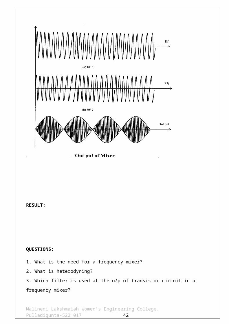
EXPECTED WAVEFORMS:
RESULT:
Malineni Lakshmaiah Women’s Engineering College. Pulladigunta-522 017 33
QUESTIONS:
1. What is the need for a frequency mixer?
2. What is heterodyning?
3. Which filter is used at the o/p of transistor circuit in a frequency mixer?
4. What are the frequency components that appear at the collector of the transistor in the
mixer circuit?
5. Why is the transistor operated in the nonlinear region in a frequency mixer?
Malineni Lakshmaiah Women’s Engineering College. Pulladigunta-522 017 34
Signature of the In – Charge Date:
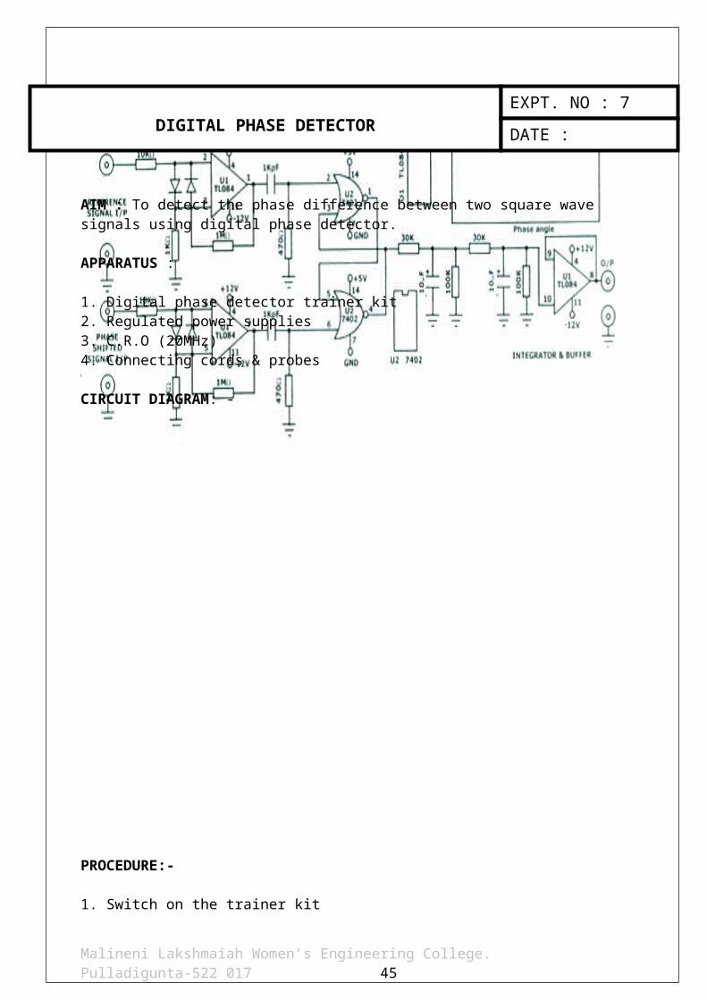
AIM : To detect the phase difference between two square wave signals using digital phase detector.
APPARATUS :
Malineni Lakshmaiah Women’s Engineering College. Pulladigunta-522 017 35
DIGITAL PHASE DETECTOREXPT. NO : 7
DATE :
1. Digital phase detector trainer kit2. Regulated power supplies3. C.R.O (20MHz)4. Connecting cords & probes
CIRCUIT DIAGRAM: -
PROCEDURE:-
1. Switch on the trainer kit
2. Observe the output of the square wave generator available on the trainer kit using
CRO and measure the range with the help of frequency counter, the frequency
range
should be around 2KHz to 13KHz.
3. Calculate the free running range of the VCO output i.e between 4th pin of IC
PLL 565 and ground. For different values of timing resistor Rt, fout is given by
Fout = t t R C 0.3 where Ct: timing capacitor = 0.01 μF, Rt : timing resistor.
4. Connect the square wave to the input of IC PLL 565 and short 4th and 5th pin of
PLL. Vary the input frequency of the square wave, when the PLL is locked that is
connected to one input fout EX-OR phase detector. The other input fin of EX-OR
phase detector is the coming from inbuilt of square wave generator.
5. Connect the pulse generator output to the input of IC 565 PLL and short 4th & 5th
Malineni Lakshmaiah Women’s Engineering College. Pulladigunta-522 017 36
pin of PLL. Vary the input frequency of the square wave when the PLL is locked
that is connected to one input of Edge triggered phase detector input i.e. fout. The
other input fin of edge triggered phase detector is the pulse input coming from the
inbuilt pulse generator.
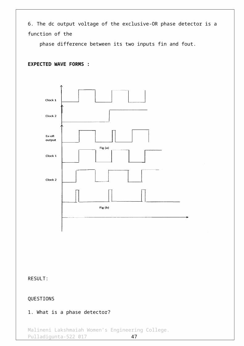
6. The dc output voltage of the exclusive-OR phase detector is a function of the
phase difference between its two inputs fin and fout.
EXPECTED WAVE FORMS :
RESULT:
QUESTIONS
1. What is a phase detector?
Malineni Lakshmaiah Women’s Engineering College. Pulladigunta-522 017 37
2. What are the various types of digital phase detectors?
3. What is the major difference between digital and analog PLLs?
4. List the basic building blocks of the discrete PLL.
5. What is the major advantage of a monolithic phase detector over an exclusive OR
and edge triggered phase detector?
Malineni Lakshmaiah Women’s Engineering College. Pulladigunta-522 017 38

Signature of the In – Charge Date:
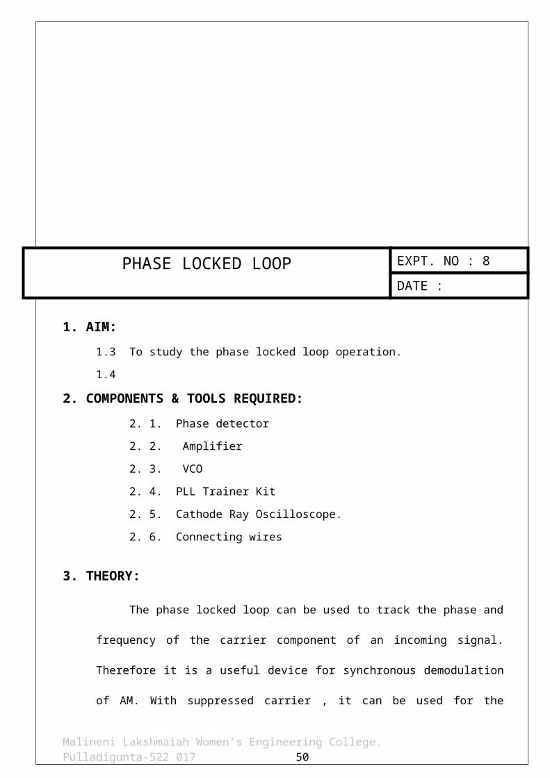
1. AIM:
Malineni Lakshmaiah Women’s Engineering College. Pulladigunta-522 017 39
PHASE LOCKED LOOP EXPT. NO : 8
DATE :
1.3 To study the phase locked loop operation.
1.4
2. COMPONENTS & TOOLS REQUIRED:
2. 1. Phase detector
2. 2. Amplifier
2. 3. VCO
2. 4. PLL Trainer Kit
2. 5. Cathode Ray Oscilloscope.
2. 6. Connecting wires
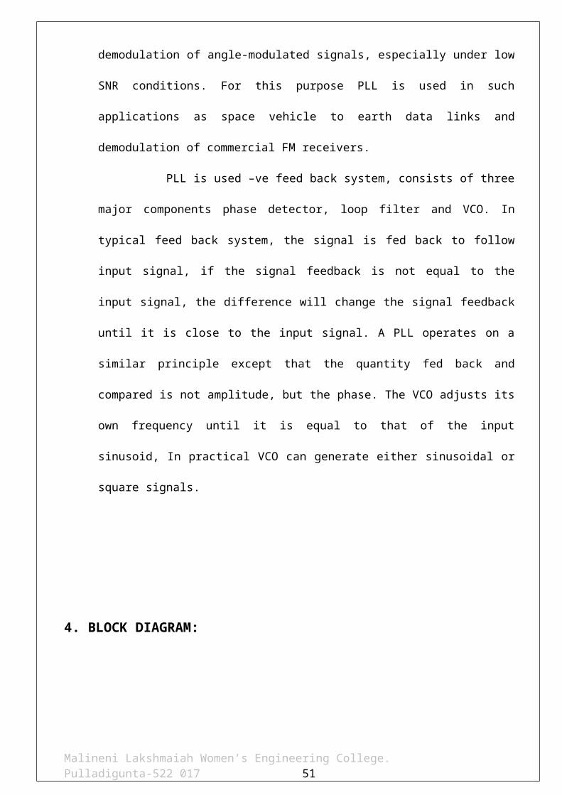
3. THEORY:
The phase locked loop can be used to track the phase and frequency of the
carrier component of an incoming signal. Therefore it is a useful device for
synchronous demodulation of AM. With suppressed carrier , it can be used for the
demodulation of angle-modulated signals, especially under low SNR conditions.
For this purpose PLL is used in such applications as space vehicle to earth data
links and demodulation of commercial FM receivers.
PLL is used –ve feed back system, consists of three major
components phase detector, loop filter and VCO. In typical feed back system, the
signal is fed back to follow input signal, if the signal feedback is not equal to the
input signal, the difference will change the signal feedback until it is close to the
input signal. A PLL operates on a similar principle except that the quantity fed back
and compared is not amplitude, but the phase. The VCO adjusts its own frequency
until it is equal to that of the input sinusoid, In practical VCO can generate either
sinusoidal or square signals.
4. BLOCK DIAGRAM:
Malineni Lakshmaiah Women’s Engineering College. Pulladigunta-522 017 40
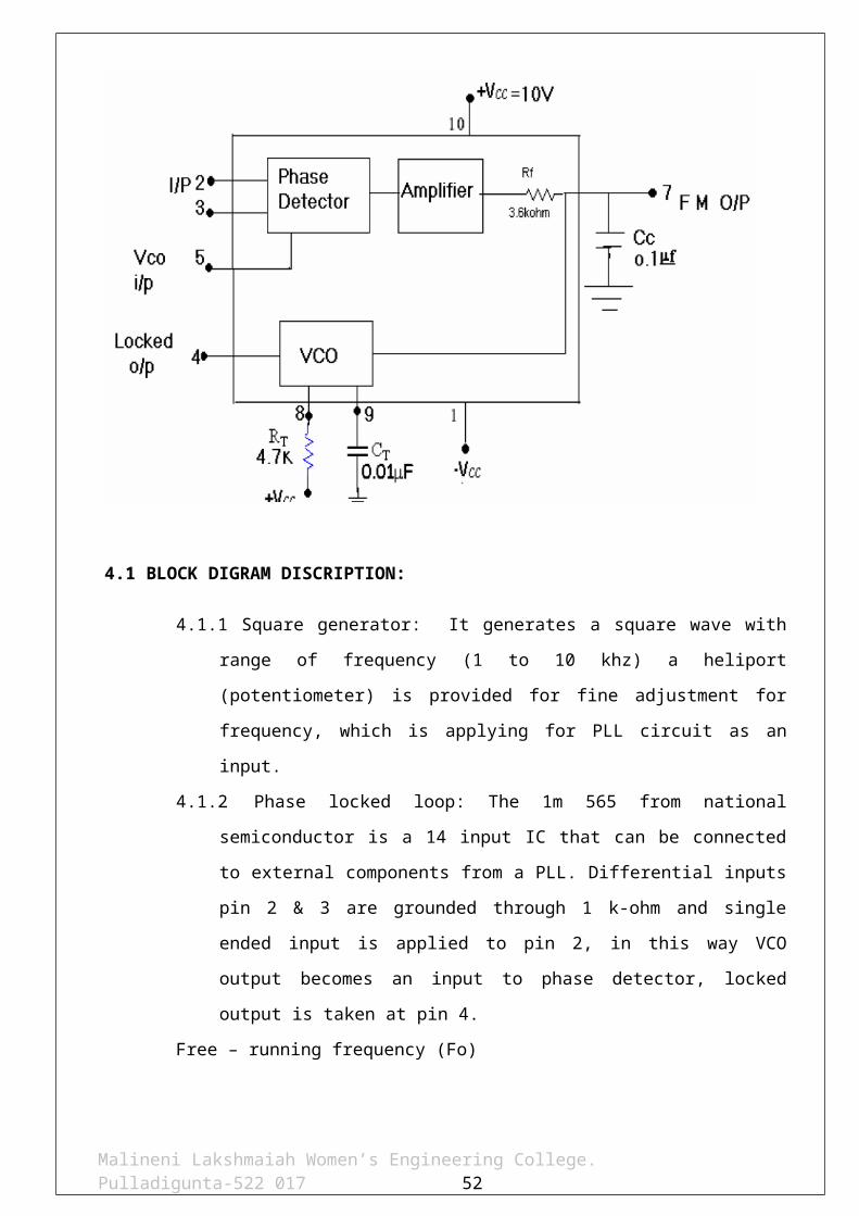
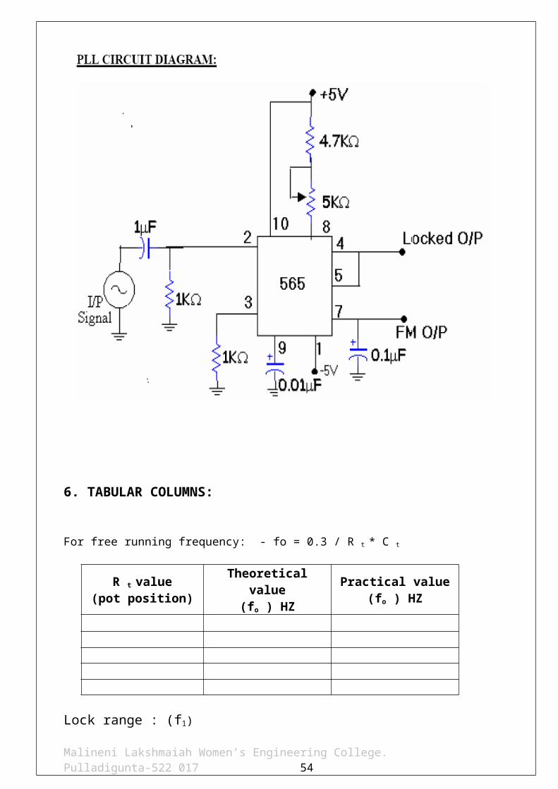
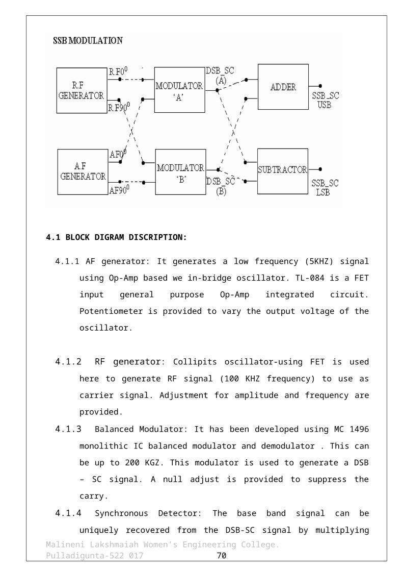
4.1 BLOCK DIGRAM DISCRIPTION:
4.1.1 Square generator: It generates a square wave with range of frequency (1
to 10 khz) a heliport (potentiometer) is provided for fine adjustment for
frequency, which is applying for PLL circuit as an input.
4.1.2 Phase locked loop: The 1m 565 from national semiconductor is a 14 input
IC that can be connected to external components from a PLL. Differential
inputs pin 2 & 3 are grounded through 1 k-ohm and single ended input is
applied to pin 2, in this way VCO output becomes an input to phase
detector, locked output is taken at pin 4.
Free – running frequency (Fo)
When there is no input to the pin 2 PLL said to be in free
running mode with its frequency determined by its circuit elements Rt
and Ct.
Free running frequency Fo = 0.3 / (Rt * Ct).
Where Rt = Timing resistor AND Ct = Timing capacitor.
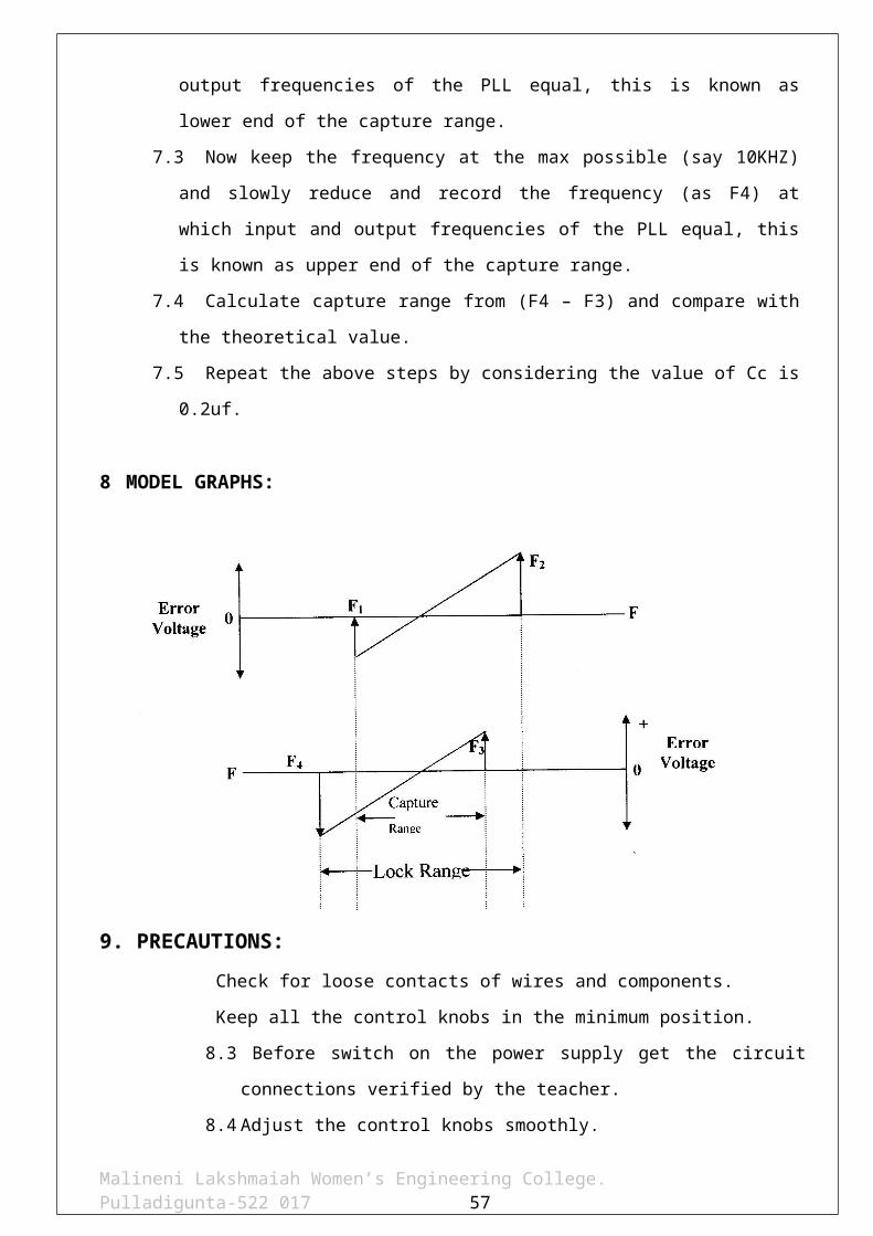
Lock range (FL)
Malineni Lakshmaiah Women’s Engineering College. Pulladigunta-522 017 41
Lock range of PLL is the range of frequencies in which the
already locked PLL will remain in lock and this is given by
(FL) = 8 fo / Vt = supply voltage (+Vcc-( - Vcc)).
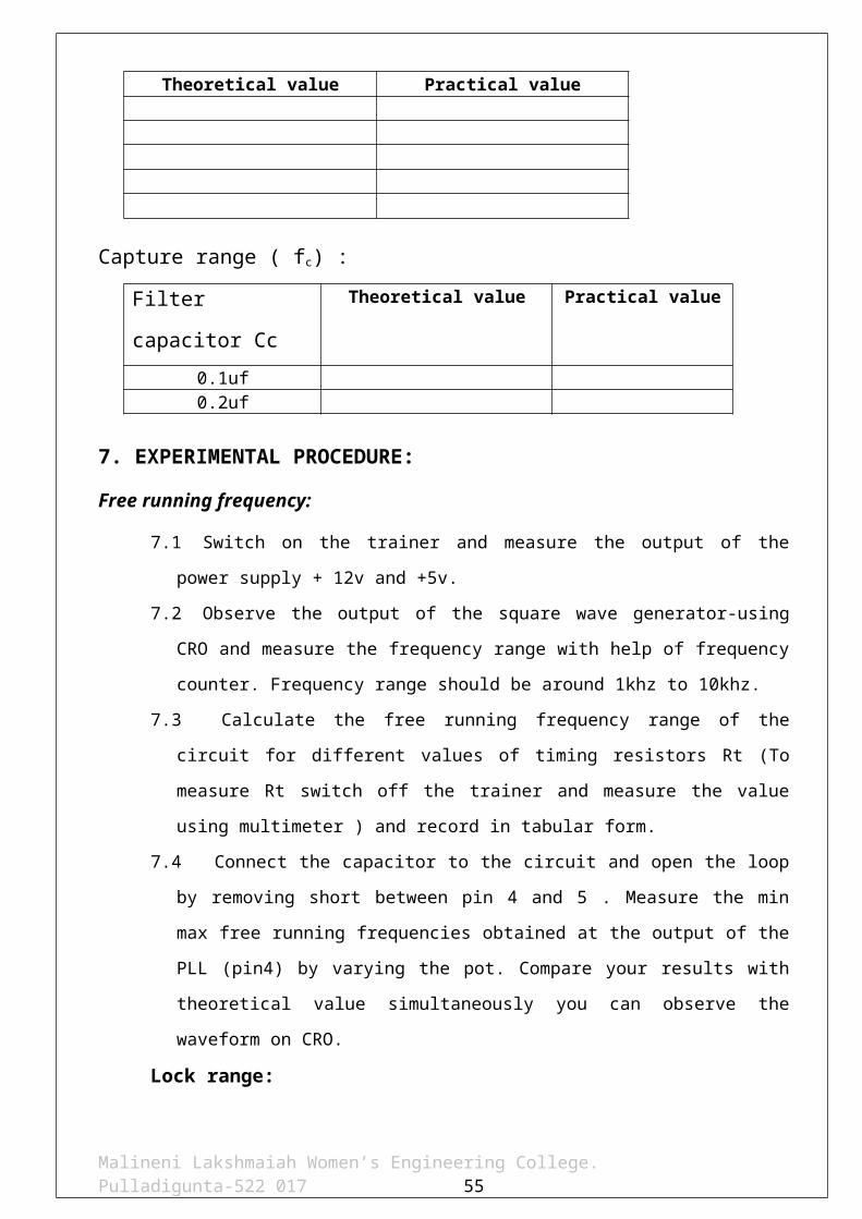
Capture range (Fc)The capture range of the PLL is the range of frequencies on
which it will lock prior to being in lock. The capacitor Cc and internal
resistor 3.6K-ohm from a low pass RC filter to remove the original
frequencies, this harmonics, and the sum frequency and the
approximately given by Fc =__________
5. CIRCUIT DIGRAM:
6. TABULAR COLUMNS:
Malineni Lakshmaiah Women’s Engineering College. Pulladigunta-522 017 42
For free running frequency: - fo = 0.3 / R t * C t
R t value(pot position)
Theoretical value(fo ) HZ
Practical value(fo ) HZ
Lock range : (f1)
Theoretical value Practical value
Capture range ( fc) :
Filter capacitor Cc Theoretical value Practical value
0.1uf0.2uf
7. EXPERIMENTAL PROCEDURE:
Free running frequency:
7.1Switch on the trainer and measure the output of the power supply + 12v and
+5v.
7.2Observe the output of the square wave generator-using CRO and measure the
frequency range with help of frequency counter. Frequency range should be
around 1khz to 10khz.
7.3 Calculate the free running frequency range of the circuit for different values of
timing resistors Rt (To measure Rt switch off the trainer and measure the value
using multimeter ) and record in tabular form.
7.4 Connect the capacitor to the circuit and open the loop by removing short
between pin 4 and 5 . Measure the min max free running frequencies obtained
at the output of the PLL (pin4) by varying the pot. Compare your results with
theoretical value simultaneously you can observe the waveform on CRO.
Lock range:
Malineni Lakshmaiah Women’s Engineering College. Pulladigunta-522 017 43

7.1 Calculate the lock range of the circuit for 5KHZ free running frequency and
record in the table.
7.2 Connect pins 4 and 5 with help of springs and adjust the potentiometer to get a
free running frequency 5KHZ. Connect square waveform output to the PLL
circuit. Provide a 5KHZ square signal of 1V pp approximately (make this close to
VCO frequency as possible ).
7.3 Connect the frequency counter to the input and output of PLL.
7.4 Observe the input and output frequencies while slowly increasing the
frequency of the square wave at the input. For some range output and input are
equal. A9 this is known as locking and PLL said to be locked with input signal.
Record frequency at which the PLL breaks lock (output frequency of the PLL
will be around VCO frequency and in CRO you will see a jitter waveform when
it breaks lock instead of clear square wave). This frequency is called as upper
end of the lock range and record this frequency as F1.
7.5 Beginning with 5KHZ, slowly decrease the frequency of input and determine
the frequency at which the PLL breaks the lock on lower end of and record it as
F2.
7.6Find lock range from (F2 – F1) and compare with theoretical value.
Capture range:
7.1Calculate the capture range of the circuit for 5KHZ free running frequency let
filter capacitor Cc is 0.1uf.
7.2With CRO slowly increase the input frequency from min (1KHZ). Record the
frequency (as F3) at which input and output frequencies of the PLL equal, this
is known as lower end of the capture range.
7.3Now keep the frequency at the max possible (say 10KHZ) and slowly reduce
and record the frequency (as F4) at which input and output frequencies of the
PLL equal, this is known as upper end of the capture range.
7.4Calculate capture range from (F4 – F3) and compare with the theoretical value.
7.5Repeat the above steps by considering the value of Cc is 0.2uf.
8 MODEL GRAPHS:
Malineni Lakshmaiah Women’s Engineering College. Pulladigunta-522 017 44
9. PRECAUTIONS:
Check for loose contacts of wires and components.
Keep all the control knobs in the minimum position.
8.3 Before switch on the power supply get the circuit connections verified by
the teacher.
8.4 Adjust the control knobs smoothly.
8.5 After taking the readings bring back all the control knobs to minimum
position.
8.6 Switch off the power supply before leaving the experimental table.
10. OBSERVATIONS:
9.1Amplitude of input signal = ------------------------- v
9.2Frequency of input signal = -------------------------KHz
9.3Free running frequency = -------------------------KHz
9.4Capture range = ------------------------KHz
F4 = ---------------------KHz
F3 = ---------------------KHz
9.5 Locked range = -------------------------KHz
F2 = ---------------------KHz
F1 = ---------------------KHz
11. CONCLUSION:
Malineni Lakshmaiah Women’s Engineering College. Pulladigunta-522 017 45
The behavior of the PLL is studied and verified in free running range, lock range
and capture range.
12. VIVA -VOCE QUESTIONS:
1. What is the use of PLL?2. What is the application of PLL?3. What are the main blocks in PLL?4. What is meant by capture range?
5. What is meant by free running range? 6. What is a PLL? 7. What is a VCO? 8. Define the lock range of a PLL? 9. Define the capture range of PLL? 10. Give the expression for free running frequency f0 of a PLL? 11. What is meant by the free running frequency of a PLL? 12 Give the formulae for the lock range and capture range of the PLL?
Malineni Lakshmaiah Women’s Engineering College. Pulladigunta-522 017 46
Signature of the In – Charge Date:
Malineni Lakshmaiah Women’s Engineering College. Pulladigunta-522 017 47
SYNCHRONOUS DETECTION EXPT. NO : 9
DATE :
AIM: To study the Working of Synchronous detector.
APPARATUS:1. Sync detector trainer kit2. C.R.O (20MHz)3. Connecting cords and probes4. Function generator (1MHz)
3. THEORY:
A method for detecting AM – suppressed carrier signal shown in block
diagram is used at the receiver end for receiving of the message signal . The
method of retranslation is similar to that of translation. Here modulated signal f(t)
cos Wc t is multiplied with cos wct and passed through a low pass filter. The signal f
(t) cos Wc t , then multiplied with Wc t yields.
f(t) cos Wc t = ½ f(t) (1+cosa 2 Wc t )
= ½ f(t) + ½ f(t) cos 2 Wc t
It is clear that form right hand side of the above equation that the ½ f(t)cos 2
Wc t cantered near+ 2 Wc can be by passed by allow pass filter, in the output of the
low pass filter, original base band signal ½ f(t)is recovered. The spectrum of f(t) cos 2 Wc t is obtained by taking flourier transform of above equation when passed
through a low pass filter with a cut – off frequency wm. The original base band signal
appears at the output of the filter. The spectrum cantered near = or – 2 wc is not
allowed to pass through a low pass filter. Note down that wc>>wm and 2 wc is still
greater than wm and is easily filtered out. Thus, the original message signal f(t) is
recovered from the AM-SC signal.
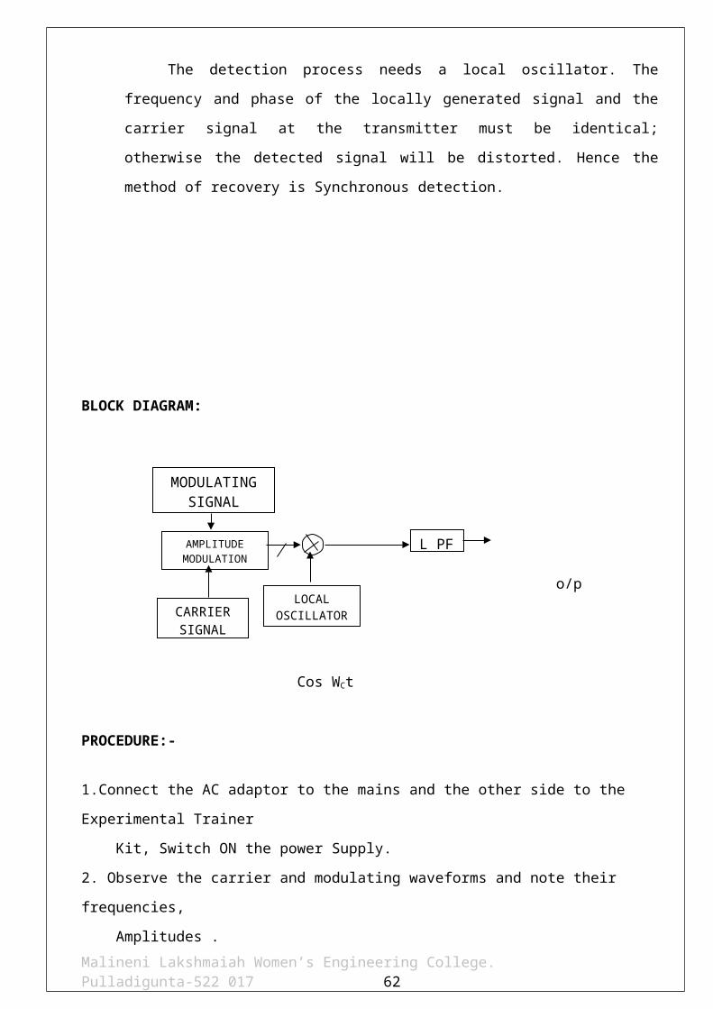
The detection process needs a local oscillator. The frequency and phase of
the locally generated signal and the carrier signal at the transmitter must be
identical; otherwise the detected signal will be distorted. Hence the method of
recovery is Synchronous detection.
BLOCK DIAGRAM:
Malineni Lakshmaiah Women’s Engineering College. Pulladigunta-522 017 48

o/p
Cos WCt
PROCEDURE:-
1.Connect the AC adaptor to the mains and the other side to the Experimental Trainer
Kit, Switch ON the power Supply.
2. Observe the carrier and modulating waveforms and note their frequencies,
Amplitudes .
3. Connect the carrier and modulating signals to the modulator circuit
4. Apply fixed frequency carrier signal to carrier input terminals.
5. Apply a 5 KHz signal to both RF and AF inputs of 0.1VP-P.
6. Measure the output signal frequency and amplitude by connecting the output to
CRO.
7. Repeat the steps 3 and 4 by changing the applied input signal frequency to
100KHZ and 500KHz. And note down the output signals.
II-Generation of DSB-SC
1. For the same circuit apply the modulating signal(AF) frequency in between 1Khz to
5Khz having 0.4 VP-P and a carrier signal(RF) of 100KHz having a 0.1 VP-P .
2. Adjust the RF carrier null potentiometer to observe a DSB-SC waveform at the
output terminal on CRO and plot the same.
3. Repeat the above process by varying the amplitude and frequency of AF but RF
Maintained constant.
4. Connect the output of DSB modulator along with Carrier Signal to the input of Sync detector .
5. Measure the output of the Sync detector and draw the waveform.
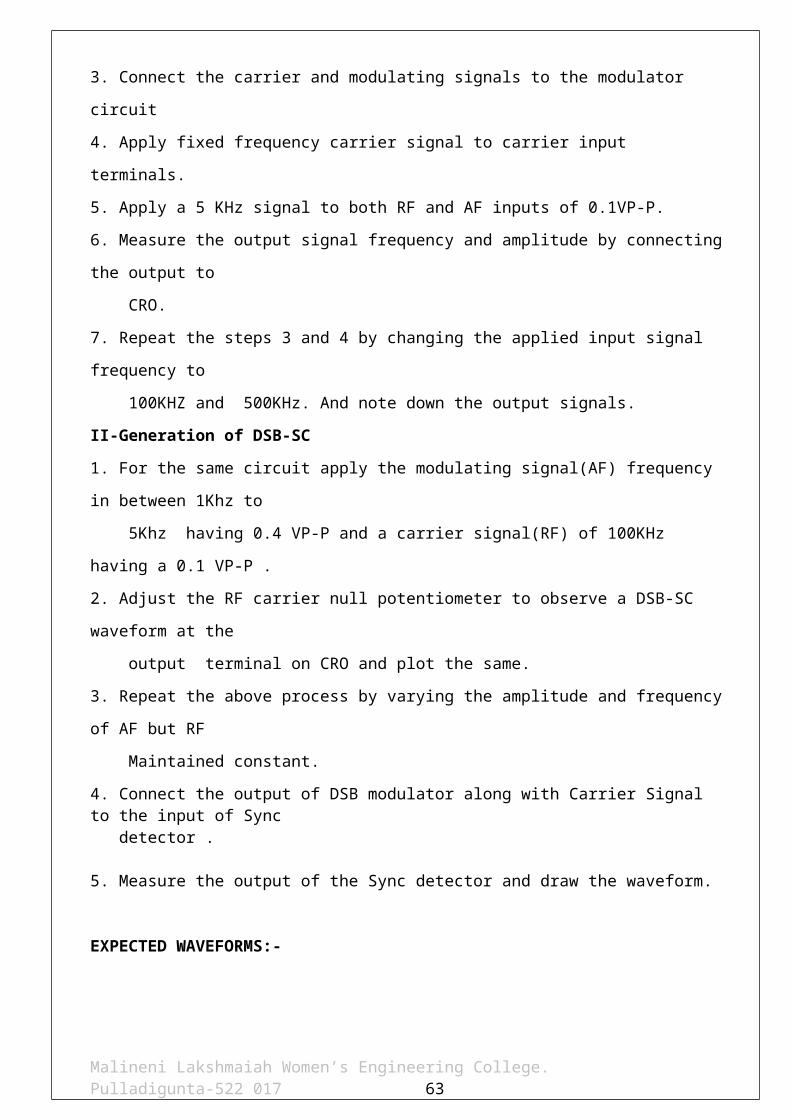
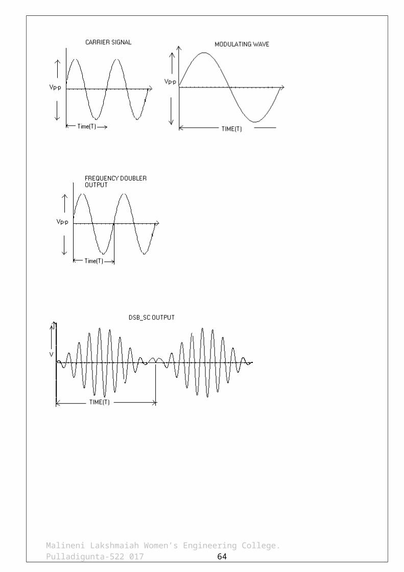
EXPECTED WAVEFORMS:-
Malineni Lakshmaiah Women’s Engineering College. Pulladigunta-522 017 49
MODULATINGSIGNAL
CARRIERSIGNAL
AMPLITUDEMODULATION
L PF
LOCALOSCILLATOR
Malineni Lakshmaiah Women’s Engineering College. Pulladigunta-522 017 50
PRECAUTIONS:
Check for loose contacts of wires and components.
Keep all the control knobs in the minimum position.
Before switch on the power supply get the circuit connections verified by the teacher.
Adjust the control knobs smoothly.
After taking the readings bring back all the control knobs to minimum position.
Switch off the power supply before leaving the experimental table.
Malineni Lakshmaiah Women’s Engineering College. Pulladigunta-522 017 51
OBSERVATIONS:
1. Amplitude of modulating signal_____________
2. Frequency of modulating signal______________
3. Amplitude of carrier signal_________________
4. Frequency of carrier signal_________________
5. Amplitude of demodulating signal___________
6. Frequency of demodulating signal___________
CONCLUSION:
The AM signals are demodulated using synchronous detector and the out put wave
forms are plotted.
VIVA -VOCE QUESTIONS:
1. What are the two ways of generating DSB_SC.
2. What are the applications of balanced modulator?
3. What is the advantages of suppressing the carrier?
4. What are the advantages of balanced modulator?
5. What are the advantages of Ring modulator?
6. Write the expression for the output voltage of a balanced modulator
8. What is the use of synchronous detector?
9. What is the purpose of LPF in synchronous detector?
10. What is the other name of synchronous detector?
11. If the local oscillator frequency is different from the carrier frequency at the modulator, then what would be the out put waveform?
12.How can we eliminate frequency and phase distortions, and which one is dangerous
SSB DETECTION
7. Give the circuit for synchronous detector?
8. What are the uses of synchronous or coherent detector?
9. Give the block diagram of synchronous detector?
10. Why the name synchronous detector?
Malineni Lakshmaiah Women’s Engineering College. Pulladigunta-522 017 52
Signature of the In – Charge Date:
Malineni Lakshmaiah Women’s Engineering College. Pulladigunta-522 017 53
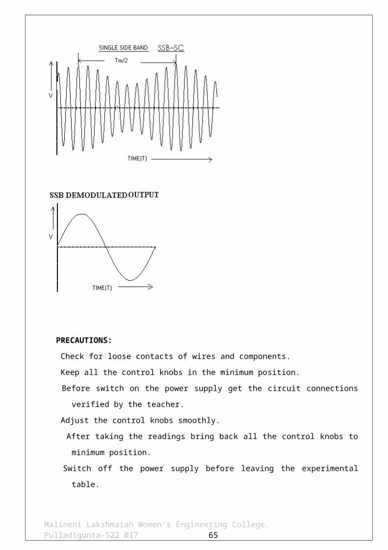
SINGLE SIDE BAND MODULATION AND DEMODULATION EXPT. NO : 10
DATE :
1. AIM:
1.5 To study the SSB modulation and demodulation process.
2. COMPONENTS & TOOLS REQUIRED:
2.1 A.F. generator
2.2 R.F generator
2.3 Balanced modulator - 1
2.4 Balance modulator - 2
2.5 Summer and substractor
2.6 Synchronous detector
2.7 CRO
3. THEORY:
AM & DSB-SC both modulation techniques require bandwidth twice of the
modulating signal bandwidth. Since two side bands having the same information. It
is possible to recover the base band signal from any one of the side band, So only
one side band is enough to give information with out any loss of course the carrier
is suppressed. Such transmission system is called single side band transmission
system. SSB requires transmission bandwidth is equal to modulating signal
bandwidth.
The reduced bandwidth also improves the SNR ratio and allows more
no of channels in a given frequency. These advantage of SSB results in wide
spread of SSB for aircrafts, transonic radio telephones, mature radio
communication systems.
4. BLOCK DIAGRAM:
Malineni Lakshmaiah Women’s Engineering College. Pulladigunta-522 017 54
4.1 BLOCK DIGRAM DISCRIPTION:
4.1.1 AF generator: It generates a low frequency (5KHZ) signal using Op-Amp based
we in-bridge oscillator. TL-084 is a FET input general purpose Op-Amp
integrated circuit. Potentiometer is provided to vary the output voltage of the
oscillator.
4.1.2 RF generator: Collipits oscillator-using FET is used here to generate RF
signal (100 KHZ frequency) to use as carrier signal. Adjustment for amplitude
and frequency are provided.
4.1.3 Balanced Modulator: It has been developed using MC 1496 monolithic IC
balanced modulator and demodulator . This can be up to 200 KGZ. This
modulator is used to generate a DSB – SC signal. A null adjust is provided to
suppress the carry.
4.1.4 Synchronous Detector: The base band signal can be uniquely recovered
from the DSB-SC signal by multiplying with a locally generated sine carrier and
then to a low pass filtering the product. The frequency and phase of local
oscillator output signal must be equal to carrier signal. This type of coherent
demodulation is called Synchronous detection. For demodulation also MC 1496
is used.
Malineni Lakshmaiah Women’s Engineering College. Pulladigunta-522 017 55
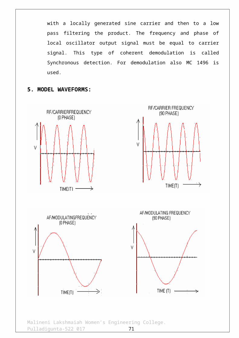
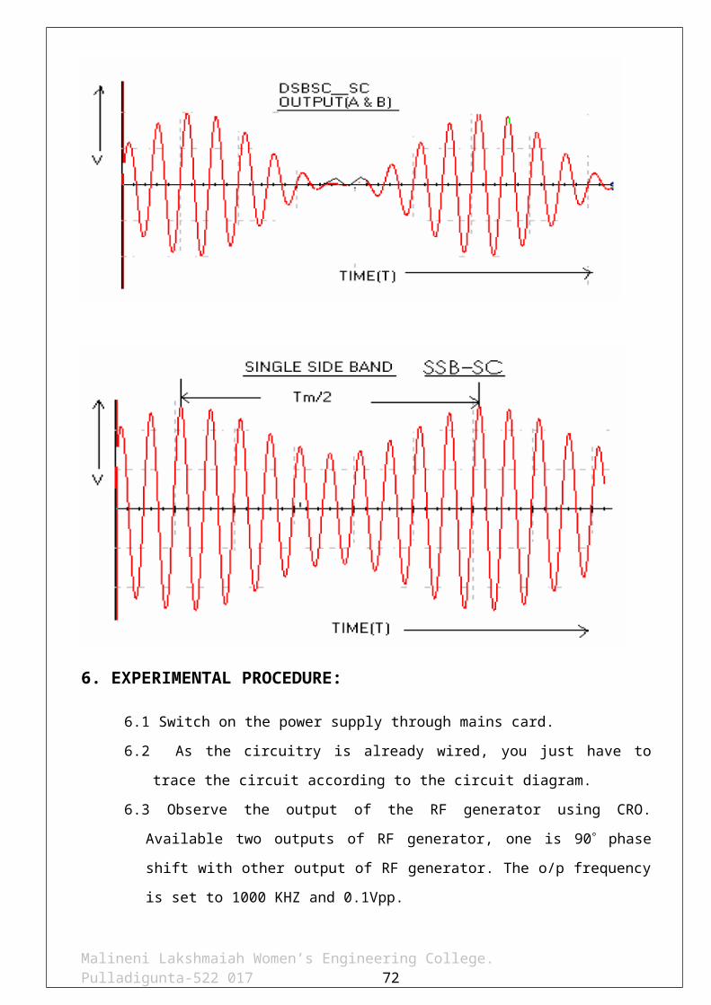
5. MODEL WAVEFORMS:
Malineni Lakshmaiah Women’s Engineering College. Pulladigunta-522 017 56
6. EXPERIMENTAL PROCEDURE:
6.1 Switch on the power supply through mains card.
6.2 As the circuitry is already wired, you just have to trace the circuit according to
the circuit diagram.
6.3Observe the output of the RF generator using CRO. Available two outputs of
RF generator, one is 90 phase shift with other output of RF generator. The o/p
frequency is set to 1000 KHZ and 0.1Vpp.
6.4 Similarly there are two o/p’s available for AF generator also. One is direct
output another one is 90 phase shift with direct output. Switch is provided to
select 2k/4k/6kHZ . AGC potentiometer is also provided for gain adjustment set
the amplitude to 10Vpp.
Malineni Lakshmaiah Women’s Engineering College. Pulladigunta-522 017 57
6.5 Connect 0’ phase shift RF generator output and 90 phase shift AF generator
o/p are to a balanced modulator and reaming two o/p’s are connected to other
balanced modulator.
6.6 Observe the both balanced modulator outputs simultaneously on the CRO and
adjust the balance control until you get the DSBSC wave on CRO. To get the
SSB (LSB) signal connect balance modulator outputs to subs tractor and note
down the frequency of SSB wave and compare this with theoretical value.
SSB (LSB) = RF frequency - AF Frequency
= 100KHZ - 2 KHZ
= 98KHZ
6.7 To get the SSB (USB) signal connect balanced modulator outputs to summer
and note down the frequency of SSB wave and compare this with theoretical
value
SSB (USB) = RF frequency - AF Frequency
= 100KHZ + 2 KHZ
= 102KHZ.
6.8 Connect the SSB signal from summer or subs tractor to SSB signal input of
synchronous detector and RF signal to the RF input of the synchronous
detector.
6.9Observe the detector output , which is replica of modulating signal (AF signal).
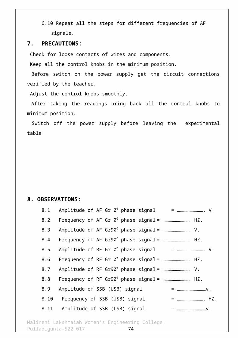
6.10Repeat all the steps for different frequencies of AF signals.
7. PRECAUTIONS:
Check for loose contacts of wires and components.
Keep all the control knobs in the minimum position.
Before switch on the power supply get the circuit connections verified by the teacher.
Adjust the control knobs smoothly.
After taking the readings bring back all the control knobs to minimum position.
Switch off the power supply before leaving the experimental table.
8. OBSERVATIONS:
Malineni Lakshmaiah Women’s Engineering College. Pulladigunta-522 017 58
8.1 Amplitude of AF Gr 00 phase signal = ………………………. V.
8.2 Frequency of AF Gr 00 phase signal = ………………………. HZ.
8.3 Amplitude of AF Gr900 phase signal = ………………………. V.
8.4 Frequency of AF Gr900 phase signal = ………………………. HZ.
8.5 Amplitude of RF Gr 00 phase signal = ………………………. V.
8.6 Frequency of RF Gr 00 phase signal = ………………………. HZ.
8.7 Amplitude of RF Gr900 phase signal = ………………………. V.
8.8 Frequency of RF Gr900 phase signal = ………………………. HZ.
8.9 Amplitude of SSB (USB) signal = …………………………v.
8.10 Frequency of SSB (USB) signal = ………………………. HZ.
8.11 Amplitude of SSB (LSB) signal = …………………………v.
8.12 Frequency of SSB (LSB) signal = ………………………. HZ.
9. CONCLUSION:
The out put waveforms of SSB modulation and de-modulation are observed
and plotted.
10. VIVA -VOCE QUESTIONS:
10.1 What is the use of SSB modulation over DSB-SC modulation?
10.2 What is the amount of power saving in SSB over DSB-SC?
10.3 What is the bandwidth of SSB?
10.4 What is the application of SSB?
10.5 What are the advantages of SSB over conventional AM and DSB-
SC?
Malineni Lakshmaiah Women’s Engineering College. Pulladigunta-522 017 59

Signature of the In – Charge Date:
1. AIM:
Malineni Lakshmaiah Women’s Engineering College. Pulladigunta-522 017 60
SPECTRUM ANALYSER USING AM SIGNAL EXPT. NO : 11(a)
DATE :
1.6 To study the spectrum of AM signals using spectrum analyzer.
2. COMPONENTS & TOOLS REQUIRED:
2.1 Spectrum Analyzer.
2.2 Function generator.
2.3 AM Wave generators
3. THEORY:
3.1. INTRODUCTION TO SPECTRUM ANALYSER:
The analyzer of electrical signals is a fundamental problems for many
Engineers and scientists .
The traditional ways of observing the electrical signal is in time domain by
using oscilloscope . The time domain is used to recover relative timing and phase
information which is used to characterize electric circuit behavior .
But practically some circuits like Amplifiers , Filters , Oscillators ,
Modulators , Mixers etc,. requires frequency domain analysis . This frequency
domain analysis can be easily studied in using Spectrum analyzer. It graphically
displays voltage or power function of frequency on a circuit .
Basically two types of spectrum analyzer are available . They are
1. Swept – tuned
2. Real – time
The HM5010 is the swept – tuned Spectrum analyzer . This spectrum
analyzer permits the detection of spectrum components of electrical signal in the
frequency range of 0.15MHz to1050 MHz In the oscilloscope the amplitude is
displayed on the time domain and in spectrum analyzer it will be displayed in
frequency domain .
3.2. ADVANTAGES OF SPECTRUM ANALYZER :
3.2.1 Spectrum analyzer are used to observe the difference fill
characteristics.
Malineni Lakshmaiah Women’s Engineering College. Pulladigunta-522 017 61
3.2.2 It used to observe the Modulated wave from spectrum
3.2.3 It is used to observe the Noise level in the transmission
Ex : In CATV
3.3. CONTROL ELEMENTS:3.3.1. MARKER ON / OFF:
When the marker push button is set to the off position the CF indicator is lit
and display shows the center frequency. When the switch is in the ON
position 1 MHz the display shows the marker frequency. The marker shows
on the screen a sharp peak the marker frequency is adjustable by means of
the marker knob and can be aligned with a spectral line.
NOTE: Switch off the marker before taking correct amplitude reading.
3.3.2. CF / MK: (CENTER FREQUENCY / MARKER)
The CF LED is lit when the digital display shows the center frequency. The
center frequency is the frequency, which is displayed in the horizontal
center of the CRT. The MK LED is lit when the marker pushbutton is in the
ON position. The digital display shows the marker frequency in the case.
3.3.3. DIGITAL DISPLAY: (DISPLAY OF CENTER FREQUENCY /
MARKER FREQUENCY ):
SIGM: Display with 100 KHz resolution.
UNCAL: Blinking of this LED indicates incorrectly displayed amplitude
values. This is to scan width and filter setting combinations which give to
low amplitude readings because the IF filters have not being settled. This
may occur when the scanned frequency range is too large compared to the
IF bandwidth (20 KHz) and or the video filter bandwidth (4KHz).
Measurements in the case can either be taken with out a video filter or the
scan width has to be decreased
CENTER FREQUENCY: COARSE / FINE :
Both rotary knobs are used for center frequency setting. The center
frequency is displayed at the horizontal center of the screen.
BAND WIDTH: Selects between 400 KHz. If a bandwidth of 20 KHz is
selected the noise level decreases and the selectivity is improved spectral
lines which are relatively close together can be distinguished. As the small
signal transient response amplitude values if the scan width is set at too
wide a frequency span . The uncial LED will indicate this condition.
Malineni Lakshmaiah Women’s Engineering College. Pulladigunta-522 017 62
SCAN WIDTH: The scan width selectors control the scan width per division
of the horizontal axis. The frequency / Dis can be increased by means of the
> button and decreased by means of the < button. The width of the scan
range is displayed in MHz / Div and refers to each horizontal division on the
graticule the center frequency is indicated by the vertical line at middle of
the horizontal axis. The frequency decreased to the left in a similar way. In
this case the left graticule line corresponds to 0 Hz with these settings a
spectral line is visible which is refereed to as zero frequency. Spectral lines
displayed left of the zero frequency point are so called image frequency. In
the zero scan made the spectrum analyzer operates like a receiver with
selectable band width . The frequency is selected via the center
frequency .The selected scan width / div settings are indicated by a number
of LEDs above the range setting puss buttons.
3.4 APPLICATIONS:
3.4.1 The spectrum analyzer is useful for observing the amplitude
modulation frequency, modulation frequency spectrum.
3.4.2. It is useful in measuring low level modulation.
3.4.3. It is used in measuring carrier frequency and modulation level.
4. MODEL WAVEFORMS:
AM Spectral Analysis Signal :
Malineni Lakshmaiah Women’s Engineering College. Pulladigunta-522 017 63
5. PRECAUTIONS:
5.1 Check for loose contacts of wires and components.
5.2 Keep all the control knobs in the minimum position.
5.3 Before switch on the power supply get the circuit connections verified by the
teacher.
5.4 Adjust the control knobs smoothly.
5.5 After taking the readings bring back all the control knobs to minimum position.
5.6 Switch off the power supply before leaving the experimental table.
6. CONCLUSION:The spectrum of AM Signals are observed using spectrum analyzer and
plotted.
7. VIVA -VOCE QUESTIONS:
7.1 Define a spectrum?
7.2 Is it possible to visualize the time domain signals using spectrum
analyzer?
7.3How can we select the central frequency?
7.4How many side bands appear for a conventional AM signal?
7.5What are the major components required to apply the AM signals to the
spectrum analyzer?
Malineni Lakshmaiah Women’s Engineering College. Pulladigunta-522 017 64
Signature of the In – Charge Date
1. AIM:
1.7 To study the spectrum of FM signals using spectrum analyzer.
Malineni Lakshmaiah Women’s Engineering College. Pulladigunta-522 017 65
SPECTRUM ANALYSER USING FM SIGNAL EXPT. NO : 11(b)
DATE :
2. COMPONENTS & TOOLS REQUIRED:
2.1 Spectrum Analyzer.
2.2 Function generator.
2.3 AM Wave generators
3. THEORY:
3.1. INTRODUCTION TO SPECTRUM ANALYSER:
The analyzer of electrical signals is a fundamental problems for many
Engineers and scientists .
The traditional ways of observing the electrical signal is in time domain by
using oscilloscope . The time domain is used to recover relative timing and phase
information which is used to characterize electric circuit behavior .
But practically some circuits like Amplifiers , Filters , Oscillators ,
Modulators , Mixers etc,. requires frequency domain analysis . This frequency
domain analysis can be easily studied in using Spectrum analyzer. It graphically
displays voltage or power function of frequency on a circuit .
Basically two types of spectrum analyzer are available . They are
3. Swept – tuned
4. Real – time
The HM5010 is the swept – tuned Spectrum analyzer . This spectrum
analyzer permits the detection of spectrum components of electrical signal in the
frequency range of 0.15MHz to1050 MHz In the oscilloscope the amplitude is
displayed on the time domain and in spectrum analyzer it will be displayed in
frequency domain .
3.2. ADVANTAGES OF SPECTRUM ANALYZER :
3.2.4 Spectrum analyzer are used to observe the difference fill
characteristics.
3.2.5 It used to observe the Modulated wave from spectrum
3.2.6 It is used to observe the Noise level in the transmission
Malineni Lakshmaiah Women’s Engineering College. Pulladigunta-522 017 66
Ex : In CATV
3.3. CONTROL ELEMENTS:3.3.1. MARKER ON / OFF:
When the marker push button is set to the off position the CF indicator is lit and
display shows the center frequency. When the switch is in the ON position 1 MHz
the display shows the marker frequency. The marker shows on the screen a sharp
peak the marker frequency is adjustable by means of the marker knob and can be
aligned with a spectral line.
NOTE: Switch off the marker before taking correct amplitude reading.
3.3.2. CF / MK: (CENTER FREQUENCY / MARKER)
The CF LED is lit when the digital display shows the center frequency. The center
frequency is the frequency, which is displayed in the horizontal center of the CRT.
The MK LED is lit when the marker pushbutton is in the ON position. The digital
display shows the marker frequency in the case.
3.3.3. DIGITAL DISPLAY: (DISPLAY OF CENTER FREQUENCY / MARKER
FREQUENCY ):
SIGM: Display with 100 KHz resolution.
UNCAL: Blinking of this LED indicates incorrectly displayed amplitude values. This
is to scan width and filter setting combinations which give to low amplitude
readings because the IF filters have not being settled. This may occur when the
scanned frequency range is too large compared to the IF bandwidth (20 KHz) and
or the video filter bandwidth (4KHz). Measurements in the case can either be taken
with out a video filter or the scan width has to be decreased
CENTER FREQUENCY: COARSE / FINE :
Both rotary knobs are used for center frequency setting. The center frequency is
displayed at the horizontal center of the screen.
BAND WIDTH: Selects between 400 KHz. If a bandwidth of 20 KHz is selected the
noise level decreases and the selectivity is improved spectral lines which are
Malineni Lakshmaiah Women’s Engineering College. Pulladigunta-522 017 67
relatively close together can be distinguished. As the small signal transient
response amplitude values if the scan width is set at too wide a frequency span .
The uncial LED will indicate this condition.
SCAN WIDTH: The scan width selectors control the scan width per division of the
horizontal axis. The frequency / Dis can be increased by means of the > button and
decreased by means of the < button. The width of the scan range is displayed in
MHz / Div and refers to each horizontal division on the graticule the center
frequency is indicated by the vertical line at middle of the horizontal axis. The
frequency decreased to the left in a similar way. In this case the left graticule line
corresponds to 0 Hz with these settings a spectral line is visible which is refereed to
as zero frequency. Spectral lines displayed left of the zero frequency point are so
called image frequency. In the zero scan made the spectrum analyzer operates like
a receiver with selectable band width . The frequency is selected via the center
frequency .The selected scan width / div settings are indicated by a number of
LEDs above the range setting puss buttons.
3.4 APPLICATIONS:
3.4.1 The spectrum analyzer is useful for observing the amplitude
modulation frequency, modulation frequency spectrum.
3.4.4. It is useful in measuring low level modulation.
3.4.5. It is used in measuring carrier frequency and modulation level.
4. MODEL WAVEFORMS:
FM Spectral Analysis Signal:
Malineni Lakshmaiah Women’s Engineering College. Pulladigunta-522 017 68
5. PRECAUTIONS:
5.1 Check for loose contacts of wires and components.
5.2 Keep all the control knobs in the minimum position.
5.3 Before switch on the power supply get the circuit connections verified by the
teacher.
5.4 Adjust the control knobs smoothly.
5.5 After taking the readings bring back all the control knobs to minimum position.
5.6 Switch off the power supply before leaving the experimental table.
6. CONCLUSION: The spectrum of FM Signals is observed using spectrum analyzer and
plotted.
7. VIVA -VOCE QUESTIONS:
7.1 Define a spectrum?
7.2 Is it possible to visualize the time domain signals using spectrum
analyzer?
7.3 How can we select the central frequency?
7.4 How many side bands appear for a conventional FM signal?
7.5 What are the major components required to apply the FM signals to the
spectrum analyzer?
Malineni Lakshmaiah Women’s Engineering College. Pulladigunta-522 017 69
Signature of the In – Charge Date:
AIM: To study the operation of frequency synthesizer using PLL
Malineni Lakshmaiah Women’s Engineering College. Pulladigunta-522 017 70
FREQUENCY SYNTHESIZEREXPT. NO : 13
DATE :
APPARATUS:1. Frequency synthesizer trainer AET -26A2. Dual trace C.R.O (20MHz)3. Digital frequency counter or multi-meter4. Patch chords
CIRCUIT DIAGRAM:
THEORY:
Phase locked loop:
PLL stands for ‘Phase locked loop’ and it is basically a closed loop frequency
control system, which functioning is based on phase sensitive detection of phase
difference between the input and output signals of controlled oscillator.
Before the input is applied the PLL is in free running state. Once the input
frequency is applied the VCO frequency starts change and phase locked loop is said to
be in captured mode. The VCO frequency continues to change until it equals the input
frequency and PLL is then in the phase locked state. When phase locked the loop tracks
any change in the input frequency through its repetitive action.
Frequency synthesizer:
The frequency divider is inserted between the VCO and the phase comparator.
Since the output of the divider is locked to the input frequency fin, VCO is running at
multiple of the input frequency. The desired amount of multiplication can be obtained by
selecting a proper divide by N network. Where N is an integer. For example fout = 5 fin a
divide by N=10, 2 network is needed as shown in block diagram. This function performed
by a 4 bit binary counter 7490 configured as a divide by 10, 2 circuit. In this circuit
transistor Q1 used as a driver stage to increase the driving capability of LM565 as shown
in fig.b.
Malineni Lakshmaiah Women’s Engineering College. Pulladigunta-522 017 71
To verify the operation of the circuit, we must determine the input frequency range
and then adjust the free running frequency Fout of VCO by means of R1 (between 10th
and 8th pin) and C1 (9th pin), so that the output frequency of the 7490 driver is midway
within the predetermined input frequency range. The output of the VCO now should be
5Fin.
Free running frequency (f0):
Where there is no input signal applied, it is in free running mode.
F0 = 0.3 / (RtCt) where Rt is the timing resistor
Ct
is the timing capacitor.
Lock range of PLL (fL)
FL = ± 8f0/VCC where f0 is the free running frequency
= 2VCC
PROCEDURE:1. Switch on the trainer ad verify the output of the regulated power supply i.e. ± 5V. These
supplies are internally connected to the circuit so no extra connections are required.
2. Observe output of the square wave generator using oscilloscope and measure the
range with the help of frequency counter, frequency range should be around 1KHz to
10KHz.
3. Calculate the free running frequency range of the circuit (VCO output between 4th pin
and ground). For different values of timing resistor R1 (to measure Rt switch off the trainer
and measure Rt value using digital multi-meter between given test points). And record the
Malineni Lakshmaiah Women’s Engineering College. Pulladigunta-522 017 72
frequency values in tabular 1. fout = 0.3 / (RtCt) where Rt is the timing resistor and Ct is the
timing capacitor = 0.01 μ f.
4. Connect 4th pin of LM 565 (fout) to the driver stage and 5th pin (Phase comparator)
connected to 11th pin of 7490. Output can be taken at the 11th pin of the 7490. It should
be divided by the 10, 2 times of the fout.
EXPECTED WAVEFORMS:
QUESTIONS:1. What are the applications of PLL?2. What is PLL?3. Define Lock range of a PLL.4. What is a VCO?5. What are the applications of frequency synthesizer?6. What is meant by the free running frequency of PLL?7. What is the operation of a frequency synthesizer?
Malineni Lakshmaiah Women’s Engineering College. Pulladigunta-522 017 73
8. Which block is mainly used in frequency synthesizer?
Malineni Lakshmaiah Women’s Engineering College. Pulladigunta-522 017 74
Signature of the In – Charge Date:
AIM:1. Study of AGC Characteristics of amplifier.
APPARATUS:-
Malineni Lakshmaiah Women’s Engineering College. Pulladigunta-522 017 75
AGC CHARACTERISTICS TRAINEREXPT. NO : 14
DATE :

1. AGC Characteristics Trainer Kit, 2. Cathode Ray Oscilloscope – 20MHz Dual Channel
Oscilloscope/25MHz DSO (OS 5022)3. Patch cords.
AF SIGNAL GENERATOR (1KHZ) AUTOMATIC GAIN CONTROLLER (AGC)
PROCEDURE :
1. Switch on the trainer.
2. Adjust amplitude and frequency of AF Generator to 20mvs and 2KHz
respectively.
3. Connect AF output terminal to input terminal AF amplifier
4. Connect AGC I/P terminal to Ground. As shown in test diagram 1.
5. Measure input signal volts and output signal volts.
6. Vary input signal level and take output values each time.
7. Now, switch on AGC and connect AGC I/P to AGC output terminal instead to
ground. As shown in test diagram 2.
8. Set DC bias volts to about 0.5 volts.
Malineni Lakshmaiah Women’s Engineering College. Pulladigunta-522 017 76
9. Measure AF output volts for the same input levels of signal as in step 6.
10. Tabulate the readings and draw the output/input volt curves for simple AGC
and without AGC for the AF amplifier.
11. Repeat the experiment for different frequencies of input signal.
S.NO Fin Vin V0 without AGC V0 with AGC1. 2k 1. 20 mv
2.3.4.5.
200mv 180mv
2.
MODEL GRAPHS:
RESULT:
Malineni Lakshmaiah Women’s Engineering College. Pulladigunta-522 017 77
Signature of the In – Charge Date:
Malineni Lakshmaiah Women’s Engineering College. Pulladigunta-522 017 78
Related Documents