ABSTRACT Title of Thesis: RF TO DC POWER GENERATION Juventino Delfino Rosas Espejel, Master of Science, 2003 Thesis directed by: Professor Robert Wayne Newcomb Department of Electrical & Computer Engineering This work considers the reception of radio frequency signals as a way to power wirelessly a passive strain sensor circuit, possibly on or embedded in the body of a concrete bridge. The received signal, sent by an interrogator device, generates a sinusoidal voltage in the terminals of the sensor circuit antenna. This voltage is then rectified, filtered and multiplied to generate a DC voltage that can be used to supply and activate the circuitry of the strain-sensor. Throughout, theoretical formulation and simulation are used as tools to prove the feasibility of different voltage multiplier circuits as charge pumps and transformers. The design and fabrication theory of a novel threshold-voltage free RF-to DC-Voltage circuit is presented in chapter IV. The circuit is designed with MOSFET transistors. Chapter V reviews some of the potential open problems and opportunities in an interrogator-strain-sensor system based in totally different technologies.

Welcome message from author
This document is posted to help you gain knowledge. Please leave a comment to let me know what you think about it! Share it to your friends and learn new things together.
Transcript

ABSTRACT
Title of Thesis: RF TO DC POWER GENERATION
Juventino Delfino Rosas Espejel, Master of Science, 2003
Thesis directed by: Professor Robert Wayne Newcomb Department of Electrical & Computer Engineering
This work considers the reception of radio frequency signals as a way to power
wirelessly a passive strain sensor circuit, possibly on or embedded in the body of a
concrete bridge. The received signal, sent by an interrogator device, generates a
sinusoidal voltage in the terminals of the sensor circuit antenna. This voltage is then
rectified, filtered and multiplied to generate a DC voltage that can be used to supply and
activate the circuitry of the strain-sensor. Throughout, theoretical formulation and
simulation are used as tools to prove the feasibility of different voltage multiplier circuits
as charge pumps and transformers.
The design and fabrication theory of a novel threshold-voltage free RF-to DC-Voltage
circuit is presented in chapter IV. The circuit is designed with MOSFET transistors.
Chapter V reviews some of the potential open problems and opportunities in an
interrogator-strain-sensor system based in totally different technologies.

RF TO DC POWER GENERATION
by
Juventino Delfino Rosas Espejel
Thesis submitted to the Faculty of the Graduate School of the University of Maryland, College Park in partial fulfillment
of the requirements for the degree of Master of Science
2003
Advisory Committee:
Professor Robert W. Newcomb, Chair/Advisor Professor Ankur Srivastava Professor C. Martin Peckerar


ii
ACKNOWLEDGEMENTS
I want to show my appreciation to my professors and the institutions that have shaped my
life and work. Besides, I would like to express my gratitude to the Fulbright Program for
the support and supervision to my program during my stay in the United States. I have
been also fortunate to have the support of my home institution the Tecnológico de
Monterrey, Campus Estado de México and Dr. Juan López Díaz, Director de la División
de Profesional y Graduados.
There is a special person that I must acknowledge due to their importance in my work,
support, his belief in me and the encouragement to the next step in my future: my advisor
Professor Robert Wayne Newcomb. I know this is one more step in the never-ending
learning process in life. Thank you!
The University of Maryland at College Park is an incredible learning place. At the same
time that I was taking the courses in my program, I could enrich my acknowledgement
with many graduate courses in other three fields I was interested on. To all those
professors who asked themselves “what is that guy doing here”, thanks.
“Creative leadership and liberal education … are the first requirements for a hopeful
future for humankind. Fostering these – leadership, earning, and empathy between
cultures – was and remains the purpose of the international scholarship program.”
Senator J. William Fulbright

iii
TABLE OF CONTENTS
ABSTRACT ii
AKNOWLEDGEMENT iii
Chapter 1. INTRODUCTION 1 a. Basic Wireless Sensor System 1 b. Power Transfer 2 c. Applications 7 d. Important Results in this Research 13
Chapter 2. STATE OF TECHNOLOGY 14 a. History: Wireless Sensors and Previous Power Transfer Technologies 14
i. RF Identification Tags 17 ii. Wireless Sensor Systems 18
b. Physics of the Components in the Magnetic Coupled RF System 19 i. Radio Frequency Magnetic Waves 19
ii. Inductance of the Antenna 22 iii. Mutual Inductance Between Antennas 24 iv. Resonance 28
Chapter 3. RADIO FREQUENCY TO DC CIRCUITS 36 a. Regulator Circuit 37 b. Charge Pump Circuits 39 c. Charge Pump Circuit Simulations 47
Chapter 4. DESIGNS AND TEST RESULTS 55 a. Design of a Sensor Circuit Based on an Up-Transformer 55
i. Design of the basic sensor circuit with an up-transformer in resonance 55
ii. Reader-Sensor system circuit with an up-transformer in resonance 58
iii. Reader-Sensor system circuit with an up-transformer in resonance and output doubler charge pump 61
b. Design of an RF-to-DC-Voltage Circuit for VLSI Implementation 72
i. MOSFET Antenna-Rectifier Circuit 73 ii. MOSFET Antenna-Rectifier-Charge-Pump Circuit 78
c. Test results to the Commercial RFID MCRF355 Tag Chip 81 d. Construction Material Issues in the Design of Embedded
Magnetic Coupled Circuits 84

iv
Chapter 5. CONCLUSIONS AND OPEN PROBLEMS 87 a. Open Problems and Opportunities 89
i. Surface Acoustic Wave Sensors 90 ii. Out of the Box Reader-Sensor System Implementation 94
Appendix A: RF Power Transfer in Free Space 99 Appendix B: Antenna Near Field Region 101 Appendix C: Interrogator–Sensor Communication Issues 105
a. Modulation 105 b. Encoding – Decoding 106 c. Bandwidth, DC Component and Collision Detection 110 d. Error Correcting Codes and Security 114
Appendix D: Wiring and Matching in the Strain-Sensor System Design 116 Appendix E: Standards 120
REFERENCES 121

1
Chapter I. INTRODUCTION
a. Basic Wireless Sensor System
This research deals with the use of radio frequency signals to transfer and feed
power to some target circuit. However, it is important to remark that the main
application envisaged of this research will be applied to sense strain of a bridge.
Therefore, research and implementation must consider issues regarding the attenuation
and distortion of the signal by the material used in the construction of the bridge. The
sensor circuit will be embedded in the concrete of the bridge. Besides, the sensor is a
passive circuit, i.e., there are no batteries in the sensor circuit to power it, through the
lifetime of the bridge, usually more than fifty years.
Through out history, there have been many attempts to eliminate wiring from a
reader system to a sensor circuit, commonly known as a transponder. The cost associated
with installation and maintenance of a network prevented wide use of sensors in multiple
applications. A cable network has poor reliability due to failing connections and
contacts, especially in corrosive environments.
Given these circumstances, there have been multiple efforts to look for
alternatives. Wireless circuit sensors in a chip were the logical step. By adding radio
telemetry capacity to a circuit sensor, it was possible to overcome the problems
associated with wiring. Wireless sensor networks allow companies to benefit from
machine monitoring, to perform preventive maintenance, and as consequence to increase
productivity. It is also possible to embed the sensor in products for logistic real time
information to reduce costs. See Figure 1.

2
Reader
Sensor
Sensor
Figure 1. Basic Wireless Sensor Network
In this model, it is possible to deploy sensors stuck on or embedded in machines,
products, structures or systems that can be remotely accessed via the Internet. There are
some basic limitations for success of sensor networks: cost, robustness on industrial
environments and power.
Cost can be addressed through mass production. Sensor systems fit economies of scale
up to some minimal production cost given by the sensor application and application
market. Robustness on industrial environments could require relatively expensive sensor
circuits, however, they will be able to protect expensive capital assets. Moreover, it is
known that deployment of this technology can improve production efficiency and reduce
emissions, helping industries to cope with intense competition and improving relations
with their communities.
b. Power Transfer
Power is not a problem when it is possible to feed sensor circuits through wires or
batteries. However, wireless passive sensors must be considered for applications where
no accesses to power sources are available. Consider the researchers at DARPA, who

3
propose to sprinkle thousands of very small sensors in a battlefield [45, pp 357-360].
Sensors would self-organize in a network and send data on foes movements without
alerting them to their presence. The information would be collected, filtered and sent to
the central command. The lifetime of the “intelligent dust” network would be limited
mainly by the time that batteries could deliver power to the sensors. Ideally, sensors
would be passive, and they would be able to get power through RF signals, or any other
means.
An important question is: how to power passive devices in an efficient way? There have
been some methods proposed and implemented: microwave power transmission [2, pp
87-89], bio-batteries [51, pp 25-28], RFID [46 pp 1-5], surface acoustic wave devices
[47, pp 69-72], piezoelectric generators [48, pp 897-904], differential-heat generators [49,
pp 5/1-5/6], solar cells [50, pp 1199-1206], and so on.
Given the development of high power microwave tubes, in the 1950s DARPA supported
the design of a system to wirelessly power aircrafts. Later in 1964 William C. Brown [2,
pp 87-89] of Raytheon Co. showed a 2.45 GHz wireless-powered chopper with
assembled tether (conducting cable) to collect the power. These kinds of systems are able
to transmit power on the order of kilowatts, more than 30KW, but they are expensive.
Figure 2 shows a typical rectenna, acronym for “RECTifier_anTENNA. The elements of
the antenna collect the power sent by a microwave antenna, rectify and filter it to deliver
a DC voltage. Actual implementations include arrays of many of these rectennas, and use
of a back reflector at 4/λ to improve efficiency by 6 dB. The most common operation
frequency is 2.45 GHz [2, pp 87-89] because of the negligible atmospheric losses at that

4
frequency. The efficiency reached by this system is about 97% @ 19 GW, for Gaussian
shaped beams.
Figure 2. Rectenna
A rectenna circuit with full-wave rectifier is shown in Figure 3. The dipoles, at
2/λ lengths, collect the RF signal. The signal is rectified and filtered by the bridge-
capacitor combination and to yield a constant voltage at the output terminals.
Figure 3. Rectenna Circuit
However, rectenna circuits can deliver more power if they work in arrays as shown in
Figure 4 [5, pp 1234-1236]. Separation between bridges is about 2/λ . Theoretically, the
full-wave rectifier is more efficient to deliver DC voltage, however, because the
simplicity of construction and cost, half-wave rectifiers are more popular in rectenna
implementations.
- +VDC
Lambda
Lamda/2
Dipole
DCVoltage

5
Given their importance they are a good alternative for transmission of power in the
future. Nowadays, to power chips or small systems wirelessly, though, the system is
expensive.
Dipole DipoleDipole Dipole
Dipole DipoleDipole Dipole
VDC
Figure 4. Rectenna Array [Brown, W.C., Patent 3,434,678, 1984, page 1]
Bio-fuel cells use a colony of bacteria to break down sugar without the use of
oxygen, depositing electrons as a byproduct. If the colony is placed in an electrode and
this electrode is wired to another electrode exposed to air, a flow of current is observed
[53, pp 172-177]. Efficiency has been very low, as low as 1%. There has been some
research showing potential by using Rhodoferax Ferrireducens bacteria to do the job [52,
pp 1229-1232], with those bio-full cells said to have reached an efficiency of 80%. In

6
practice, an electrode with the colony should be placed at the bottom of a pile of waste to
generate electricity. The power could be used to operate sensors, or any other device, in
remote areas where no other source of power is available. Theoretically, a cup of sugar
would be enough to power a 60 watts light bulb for 17 hours. No more data is presently
available; researchers just argue that voltage is still small and conversion from sugar to
current is slow for some practical applications [52, pp 1229-1232].
Thermoelectric generators work based on the thermocouple principle, i.e., two
different metals are connected together, and each one is exposed to a different
temperature. The resultant effect is an electric potential between the wires, which can be
translated into a current flow. Different temperatures can be obtained from different
sources. In space, this condition is reached by exposing one of the metals to the sunlight
and the other to the darkness. In geothermal areas, like Iceland, hot water is used to heat
one metal and ice to cool the other metal. The higher the difference of temperatures, the
higher the power that is delivered by the thermoelectric generator. Nowadays
thermoelectric generators have efficiencies in the order of 3%.
This work will be focused on passive wireless sensors applied to monitoring strain
in steady structures as bridges, buildings, etc. Therefore power transfer through a wall is
one important challenge. An option is to place an exterior antenna to collect the power
and deliver to the sensor circuit via cable to the embedded sensor circuit, however
periodic maintenance must be carried out to check for corrosion or any other defect that
may interfere with the correct performance of the system. A better option could be to
embed the whole sensor circuit in the bridge concrete so that no maintenance is necessary
in the lifetime of the bridge, usually more than 50 years, because the sensor circuit is

7
protected from the exterior environment. The sensor circuit design must be highly
reliable and, in order to increase the reader distance, attenuation of the bridge structure
concrete must be maintained at a minimum for the signal and frequency used. Some
research [3, pp 674-682] indicates that attenuation of the electrical field inside the
concrete is high. As expected, this attenuation is increased as thickness of concrete
increases. Tests run in the microelectronics laboratory showed that this attenuation is
small for magnetic fields if thickness of the construction material is less than 2 inches.
c. Applications
The first fatigue test on steel chains, at ten cycles per second, was performed, in
1829. The material fatigue behavior is important for safety on structures, as bridges. The
structural response to loading is important to monitor structure condition and for
reliability analysis.
In order to monitor the structure condition remote wireless sensors can be used in
the field of material damage and health assessment. Remotely powered, possibly
embedded, wireless sensors could allow for the building of a remote sensing network that
could monitor in real time the condition on a bridge. By saving data on fatigue, it could
be possible to analyze the health of the bridge avoiding collapsing in serious events.
After occurrence of an earthquake, it could be possible to monitor the state of the
bridge without risk to human lives, and allow for traffic as the health of the bridge,
monitored in real time, allows.

8
Sensor1 Sensor2 Sensor3 SensorN
Reader
Laptop computer
Bridge
Figure 5. Basic Bridge Sensor System
The basic bridge system is shown in Figure 5 where the reader interrogates the sensor
network. It sends a radio frequency signal to wake up the sensor communication circuits.
Then, every sensor circuit sends its last strain measurement to the reader. The reader
collects and sends them to the database for analysis.
Ideally, all sensors should have gotten their power from external sources. This thesis
work considers an electrical power source from a vibration-bending generator to feed the
internal sensor circuit and read a strain measurement. Then a radio frequency signal is
sent to the communication circuit, to turn it on and send the measurement data back to the
reader. In general, transponders will be embedded in the bridge structure with no access
for maintenance on the bridge lifespan.
Therefore, the sensor circuit must be reliable and dependable through many years.
Another important application for wireless sensors is to identification tags. In
recent years, there has been a trend to take RFID (Radio Frequency Identification)
technology from labs to commercial applications. In this application, the system must
maximize reading distance and robustness to collisions with cheap tag fabrication. Tags

9
can be used to keep track on some retail products for inventory control, automatic selling
systems, intelligent systems at home, and so on.
The following list shows some milestones on the life of some representative wireless
identification systems:
1949 -- the first barcode is invented
1959 -- first wildlife radio tags
1967 -- first retail barcode scanning system
1975 --anti-theft material tags appear in libraries and stores
1980 -- RFID is invented
1990 -- Automobile toll-collection tags appear
1997 -- first all-polymer IC tag demonstrated
Bernard Silver invented the barcode in the Drexel Institute of Technology in
Philadelphia. A local food chain president requested an automatic product read system
for checkout. At the beginning, a code of four white lines in a black background was
made, allowing classification of seven different products. Encoding was done based on
the presence or absence of lines a binary system with 23 – 1 combinations because the
first combination was useless. The system progressed to 10 lines with potential to
recognize up to 1023 tags. (US Patent 2,612,994)
The system started gaining recognition in 1966 when the National Association of Food
Chains called for a system to speed up the checkout process. In 1969, the process to
develop a standard started and finally in 1974 NCR Corp. installed the first system in
Troy, Ohio.

10
Nowadays, the most popular barcode is the EAN (European Article Number) with
structure shown in Figure 6. The CD acronym stands for company identifier.
CountryIdentifier
FRG
4 4
Company Identifier
0 8 7 4 3
JR Technology SystemsUniversity Boulevard 1025
Item Number
1 7 7 2 5
Intelligent Sensor 1032
CD
4
Figure 6. Barcode Structure
Researchers use different systems to get remote information on wildlife. They use
transmitters to monitor behavior on animals. In this case, transmitters must be adequate
to species under study. Transmitters must be robust but at the same time must not disturb
normal behavior on the animal under study. If the animal spends an important amount of
time under water, the transmitter must be designed to survive frequent immersions;
implants should be considered. Therefore, monitor systems must be chosen on basis of
size, lifestyle and body type. For some species, radio tags could be a good and cheap
option to collect data.
Automatic fare collection is a reality. There are some commercial systems available. As
an example, people living along the eastern seaboard can enjoy E – Zpass, which uses
radio frequency identification cards to collect fares. See Figure 7.
Toll collecting tags can be used to improve today’s fare collecting systems, which rely on
paper tickets in an ample variety of services. By using a prepaid card costumers could
get access to different services without staying on line; fares could automatically be
discounted from their prepaid card.

11
Nowadays, these systems are relatively expensive but as technology improves, it could be
possible to extend automatic fare discount to more and more services, from shopping to
product tracking on manufacturing companies. The idea could be to move tags at least to
mass production, or ideally, to economies of scope, permeating automatic tracking to all
products, cheap ones included.
A detailed description of the electronic collecting system is shown in Figure 8. The
driver must buy a transponder, size of a credit card, and deposit money in the account of
it. The transponder must be placed inside the windshield, behind the rear mirror. When
the car drives through the toll lane there is a detector sensor to know that a car is arriving
At the same time an array of two antennas aim a RF signal to power the transponder chip,
the transponder wakes up and sends its identification number back. A computer system
automatically charges the account based on the number of axes detected by the sensor
strips embedded in the road.
Figure 7. Automatic Toll System [1]

12
Antenna2
Antenna1
Exit Curtain
Cameras
EntryDetector
EntryDetector
Figure 8. Detailed Automatic Toll System
If the prepaid account has not enough money or no transponder is in the car, a monitoring
camera takes a picture of the car tag and a fine is mailed to the violator owner. The range
of the antennas is about 3 meters, working at 900 MHz. The velocity drivers can drive
through the setup is in the range from 8 to 85 Km/hr. Sometimes special transponders are
issued to drivers when their car windows use some metallic tint that impedes the RF
reach of the transponder. In those cases, transponders must be stacked outside the car.
It is known that companies today loose approximately 10% of some popular
products because somebody stole them on their way to the consumer. With this
technology in place, it could be possible to track every product, from production to
consumer purchase.
Some public concerns, regarding privacy, must be address. People don’t like “big
brother” looking on their shoulder. I belief that for most commercial applications,
benefits clearly overcome any possible disruption on public privacy.
d. Important Results in this research

13
As mentioned before, this work is focused on the efficient power transmission through
radio frequency signals, given the application of the project to strain passive sensors
embedded in a concrete bridge. Some of the important results produced in this work are:
1. Simulation and comparison in the performance of combination of magnetic
coupled rectifiers with up-transformers and charge pumps working in resonance
as RF to DC generators. Chapters III and IV.
2. Analytical setup to analyze the severe voltage drop on the circuits mentioned in
bullet one, and working in resonance. Chapter IV.
3. Design of an MOSFET RF-to-DC-Voltage circuit free of threshold voltage.
Chapter IV.
4. In the search for bigger reading distance range: analysis and theoretical design of
aRF powered strain sensor circuit based on a surface acoustic wave device
operating in the far field, i.e., powered by the electrical field instead of the
magnetic field. Chapter V.
These results will be presented through this thesis in the chapters mentioned and with
strong theoretical support of chapter II and the appendices.
2. STATE OF TECHNOLOGY

14
a. History: Wireless Sensors and Previous Power Transfer Technologies
This section will review wireless sensors powered by radio frequency signals and their
previous technologies. Some of the previous technologies seems not to be directly
related to the transfer of power through RF, however, when there is more than one
wireless sensor in the area of the reader coverage, some kind of identification code and
communication protocol must be implemented to identify the sensor that is transmitting
measured data and when the sensors must transmit. The effects of these elements must be
considered to minimize the use of the limited power. If two or more sensors try to send
information at the same time a collision will occur, and one algorithm must be added to
make sure data is read successfully. Intrinsically, it implies the use of additional power.
When there is only one sensor circuit the design target is usually to maximize distance
between sensor and reader circuits with accurate reception of data measured. If the
system grows to a network of passive sensor circuits, there is an additional burden of
processing to identify the sensor that is transmitting the data. Processing uses power,
therefore, the circuit design must be power efficient, and the processing program must be
performed as fast as possible.
Therefore, the first part of this chapter will review the history of some of the systems
used to automatically identify products, persons, etc. They focus on processes, but some
ideas can be translated to sensor network power efficiency, verification and safety.
Traditionally, most data collection is done by writing on paper or typing to enter data in a
computer system. If, for example, somebody wants to know the condition of a bridge,
usually, it will involve running tests in the field or lab, collection of data to the computer

15
system and writing reports. This process is repetitive, costly, outdated and sometimes
inaccurate.
Another example involves production and service activities. As diversification and
activities of companies increase there is a need to collect larger amounts of data, doing
this by hand is inappropriate given the amount of personnel required to keep the
information system updated. There is big pressure on companies to keep them
competitive; therefore, they try to add optimal operating schemes such as “just in time”
or “project management” to daily operations. To operate efficiently the flow of
information must be sufficient to synchronize process and personnel work.
The solution to this kind of problem involves adding some kind of automatic collection
information system. Consider a bridge after an earthquake; depending on the earthquake
magnitude there is a need to know if the bridge is safe to traffic. Nowadays,
transportation personnel must perform tests to verify bridge safety; in the mean time, as
the bridge is closed, economic loss piles up unnecessarily.
In an ideal situation, the state of the bridge must be known in real time, so transportation
officers can make decisions in short time. A real time information system also can be
helpful in the maintenance program and annual budgeting.
The real time information system of the bridge should have a network of sensors that
send information to a central database, and then, information could be preprocessed
before being presented to the personnel in charge of the bridge. This information could

16
be delivered to a state or national safety organization or as many stakeholders as
necessary.
The project, that includes research in this thesis, involves sensing of strain as a way to
check the bridge condition, as mentioned in the introduction.
A possible sensor network should have a sensor with a passive circuit so that it only turns
active when some external source of power feeds it. A further improvement could
include the use of more than one external source of power to secure continuous operation.
One of the power sources could feed the circuit when acquisition is carried out, and could
get power through compression/decompression of a piezoelectric element embedded on
the bridge. The piezoelectric element generates power from the compression produced by
the car wheels as cars circulate on the bridge. The advantage of the piezoelectric
generator is its ability to generate relatively high voltages. The disadvantage of
piezoelectric generators is that they need a relatively long time to accumulate the charge
in a capacitor, before charge can feed the sensor circuit.
Reading of the sensor data must be done as fast as possible. If it is done with a handset,
the operator wants to read one sensor and move to the next one. Therefore, the operator
would be happy if his/her handset interrogation device wakes up the sensor circuit
rapidly, instantaneously in her/his perception, by sending a radio frequency signal.
Ideally, collection of data should be done in real time, however, given power constraints
imposed on the RF power delivered by any device, the interrogator device must operate
relatively close to the sensor circuit to turn it into its active state. Next Section will
explain these technologies.

17
i. RF Identification Tags (RFID)
RFID is considered a wireless automatic product identification. They use an RF signal to
power a tag-circuit. RFID systems are more expensive than bar code systems, but their
cost is expected to decrease as products move to economy of scale. There are important
advantages of RFID tags over other identification systems. First, they can be attached to
almost anything. Secondly, they do not need any battery to operate; the power is taken
from the RF signal sent by the reader device. Third, the chips embedded in the tags can
be as small as 0.4 mm2. Usually they operate around 134 KHz but there are systems
working up to 5.8 GHz. To read the tag information it is not necessary to be in the line of
sight for low and middle frequencies, as long as the tag is in the range of the reader
device.
Commercial applications for this technology go from inventory control to automatic
payment at shopping stores.
There are some disadvantages, first, tag activation is done by a magnetic field, and
because of that, they must operate in the near field given the strong attenuation of
magnetic signals in the far field.
Secondly, the cost per tag is at present around $0.50. This is expensive for reaching vast
number of products. However, there is some research that suggests $0.05 per tag as the
threshold cost per tag to get them attached to almost everything.
Third, there are concerns regarding privacy. In a good use, tags can be used to pay
shopping automatically. Later, in your home, your refrigerator can automatically sense if
you are running out of your favorite ice cream, or any other product by reading the

18
information on the tags. Then, if you instruct your system to do that, it can send the
information to the store, and the shopping store can deliver your ice cream to home at
some predetermined time when they know you are there to receive it. This will allow
getting closer to an intelligent house. On the bad side, it could be possible for anybody to
track your products, so they could collect information about your preferences. That
information could be then saved in a database, with the information of other people, and
sold to the companies that later will bother you with “new promotions”. In addition to
this problem, from the database it is possible to get unintended information that could be
used, for example, increasing your health insurance given your consumption pattern, etc.
ii. Wireless Sensor Systems
As sensors become smaller and more reliable, their applications increase. By adding a
wireless feature into the sensor, it could be possible to array them into a network.
Microsensors could be ultimately embedded into any physical system, the human body
included, to get measures of unprecedented detail. The research in this thesis is an
example for this technology. To operate correctly, networks must be scalable and robust
with small power consumption circuits.
Sensor networks must operate under limited power, with self-configuration ability as
sensors are taken into and out of the network. Finally, sensor localization is important in
order to know what part of the system is being monitored.
The theory and implementation of an RF sensor system will be further explored in this
thesis.

19
b. Physics of the Components in the Magnetic Coupled RF System
i. Radio Frequency Magnetic Waves
From Figure 5, the strong attenuation suffered by electromagnetic signals through lossy
media [10, pp 1-5], and the encouraging results obtained in the laboratory for magnetic
fields when the receiving antenna is embedded in concrete, a sensor system operating
under inductive coupling is recommended.
As it is known, a flux with strength H is generated around a current carrying conductor.
This phenomenon can be described by [11, equation (16-9-3), pp 439]
Figure 9. Magnetic Flux Around a Wire
It is known that for a straight conductor the field strength is given by [11, equation (14-3-
6), pp 372]
In the basic sensor system, described in Figure 1, a loop conductor is used as an antenna
to generate a magnetic alternating field. The alternating field is coupled to the receiver
antenna, another loop conductor, to generate power in order to turn on the sensor circuit
)1.2(. sdHI rr=
)2.2(2
1
rH
π=
Current
Magnetic Flux

20
and send back to the reader the strain sensor measurement. When the antennas were
tested, it was noticed, as expected, that H decreases with distance.
Consider the inductor, with radius r, shown in Figure 10.a. Note that the flux line density
is stronger in the x direction as shown in Figure 10.b. Therefore, when the strain sensor
system is operating, in order to optimize the reading distance, transmission and reception
antennas should be aligned on the same “x” axis.
The strength of the magnetic field along the x direction is calculated from [11, equation
14-5-3, pp 375]
Where r is the coil radius, N is the number of windings, and x is the distance from the
center of the inductor along the x axe. In
duc
tor
x
Magnetic Field Distribution
Figure 10. (a) Magnetic flux around the interrogator/sensor antenna. (b) Magnetic Field
distribution on the neighborhood of a short inductor antenna
We want to work in the near field to generate adequate voltage level, therefore x must be
smaller than 2 / . We recommend the design of the antenna to be made on a printed
circuit board to make it less disruptive to the bridge structure. From equation 2.3 it is
( ))3.2(
2322
2
xr
rNIH o
+=
µ

21
clear that increasing N or I increase H, on the contrary an increase in r decreases H. A
typical coil antenna described by (2.3) exhibits the behavior shown on Figure 11. Note
that the magnetic field strength holds constant up to some distance and after that, it
decreases at an approximate 60 dB per decade. The inflexion point will be at a bigger
distance as the radius decreases but simultaneously the constant magnetic field, before
the inflexion point, will be smaller as the radius decreases for some fixed N and I.
Considering (2.3) again, assume N and I constant; fix x to some value and compute H for
an interval that includes x. The optimal radius results to be x = 21/2 r as shown in Figure
12. It means that the optimal radius between the reader and sensor as distance increases
also increases in the same proportion. This effect can be obtained by taking the
derivative with respect to r in (2.3).
Figure 11. Typical induced
voltage as distance between
transmitter and receiver coil
antennas increases
It is important to remark that these graphs result by considering operation on the near
field.

22
When the distance between the interrogator and strain-sensor is increased to work in the
closer far field, the antenna radius must be bigger to generate a stronger magnetic field in
the sensor circuit and as a consequence to generate an adequate voltage to feed the sensor
circuit.
Figure 12. Optimal radius for reader
antenna when the distance x,
between the reader and sensor is 5
centimeters
If the strain sensor circuit, with the antenna, is embedded in some construction material,
an additional attenuation is expected, given the higher absorption produced by materials
different from a vacuum. This effect must be considered because it results in reduction of
the interrogation range for some fixed power transmitted. Theoretically, it can be
considered by changing the permeability ro µµµ = in (2.3), and assuming it constant
through the concrete material, i.e., take the average permeability. However, in practice,
the shielding effect produced by reinforced concrete or the structure of the bridge is not
captured in (2.3), and it changes for different bridges.
Therefore, reading distances will vary along a bridge, and for different bridges as metallic
rods and beams are distributed on the structure.
ii. Inductance of the Antenna
It is desirable to compute the inductance L associated with the designed antenna because,
later, we will learn that the antenna circuit must operate in an LC resonant circuit in order
5 10 15 20 25 30 35
0.01
0.02
0.03

23
to maximize reading range. By using the Biot-Savart Law, and (2.3), the flux density is
given by [11, 14-2-3, pp 369]
And magnetic flux is NILAB /==Φ . En general the inductance is computed for a
closed loop antenna with the diameter of the loop much bigger than the diameter of the
conductor used in winding, see Figure 13.
Figure 13. Loop used to compute inductance
The inductance, using (2.3), at some distance x will be
( ) ( ))5.2(
22322
422
322
2
xr
rN
xr
rNI
I
AN
I
HAN
I
NBA
I
NL
+=
+===Φ= πµµµµ
with ( )AV /104 70 πµµ == for free space coupling. Some adjustment will be
required because it is easier for the software used in the antenna printed circuit board to
design an antenna with a square shape. However, a closed inductance approximation
results with the equation (2.5).
)4.2(
)(2
)(2
322
2
0
xr
INrHHxB r
+=== µµµµ
r
ro

24
iii. Mutual Inductance Between Antennas
In the interrogator-sensor system, the coupling factor is influenced by the distance
between both circuits and the relative position of the antennas with respect to their axis of
optimal coupling.
Figure 14. Interrogator – Strain Sensor System
In order to analyze this effect a transformer circuit model will be used, see Figure 15.
Figure 15. Transformer Model
It is important to remark that the transformer model for magnetic fields is only valid in
the near field.
The equations describing this model are:
( )( ) )6.2()(
)(
12222
21111
VMsILsRIV
VMsILsRIV
++=++=

25
Where M, the mutual inductance, is given as a function of the magnetic coupling factor
21LLkM = . And 0 < k < 1, with k = 0 for large distance or a strong shielding
condition, and k = 1 when both coils closely wound on the same high permeability core.
Recall that the induced voltage in the antenna coil when in a sinusoidal magnetic field
)cos( tAB ω=Φ is given by
)7.2()sin( tABNdtdNV ωω−=Φ=
then from (2.4), 0, (2.6) and inductance with a core different from air [12, pp 401]
)8.2(4
220
20
l
dN
l
ANL rr πµµµµ
==
the coupling coefficient will be given by
Figure 16 describes the general arrangement of interrogator/sensor antennas in order to
describe how the angle θ affects the coupling coefficient.
Figure 16. Antenna
arrangement to compute the
coupling coefficient
( ))9.2(
)cos()(
2
322
22
RxRxTx
RxTx
rxrr
rrxk
+=
θ
X
2rRx
2rTx
0

26
Clearly, in order to maximize coupling between antennas must be given by πn , n = 0,
1, 2, . . ., The size of the antennas should be the same and the distance X must be as small
as possible.
From Figure 17, the coupling coefficient decreases as distance X between antennas
increases. And as the diameter of the interrogator antenna is increased more energy
reaches the sensor antenna at farther distances.
In practice, there is a limit to the antenna size because of cost constraints, and it is
agood idea to make rreader rtransponder, because the sensor circuit, antenna included,
should be as small as possible in order to avoid disturbing the bridge structure where the
sensor should be embedded.
Figure 17. Coupling Coefficient
behavior for different r =
rtransponder = rreader
It is possible to integrate the antenna on-chip as a square-type planar spiral as shown in
Figure 18.
A zero-order estimate of the inductance in this kind of antenna is: ][20 HenriesrnL µ≈ ,
where n is the number of turns and r is half of the maximum length of a side of the square

27
spiral, as described in Figure 18 [9, equation (17), pp 48]. Exactitude of the formula is in
the 30% range.
As an example in [9, pp 47-52], a 120 – nH inductor needs 27 turns and a half of the
maximum length of a side of the square spiral r = 140 m. That is the equivalent area
taken by the bond pads. Therefore, the integration on-chip of an inductor is “area”
expensive.
Figure 18. Square Planar Spiral Inductor [9, pp 48]
Additionally the skin effect reduces the effective cross-sectional area increasing the series
resistance. Finally, the inner area is too small to work as an antenna, and such an
approach is not worth additional consideration in present CMOS IC technology.

28
iv. Resonance
A voltage is induced in the sensor antenna. In order to maximize it, the antenna
circuit must operate in resonance as an LC circuit. A capacitor is placed in parallel with
L2 of Figure 15, to set a resonance condition. Figure 19 shows a typical resonance curve.
Note, voltage is maximized at the resonance frequency; therefore, in order to increase
readout distance, it is best that the interrogator and strain sensor circuits work in
resonance.
In practice, instead of one capacitor, two capacitors exist on the sensor circuit one of
them is the parasitic capacitance CL mainly associated with the coil antenna and the other
is C2, see Figure 22.
The resonant frequency of an LC circuits is given by
).10.2(2/1 22 aCLf π=
C2 = C2 + CL, and CL is the parasitic capacitance on the circuit.
Figure 19. Typical Resonance Curve
The definition in (2.10.a) does not include the effect of the coupling between antennas or
the interaction with the rest of the components of the circuit, because (2.10.a) is for
simple serie or parallel LC circuits. A complete analysis is shown in (4.4), the resultant
equation is reproduced here for convenience.

29
).10.2(1)
1)(( 222
1212 b
RCjRLj
ILLkjV
L
+++=
ωω
ω
To compute the real resonant frequency we need to solve for the frequency when
).10.2(1)1
)(( 222 cR
CjRLjL
−=++ ωω
given
For sake of completeness, let’s fix: L1 = 200 H, L2 = 3.5 H, C2 = 16.61 nF, RL = 10K,
R2 = 0.1, k = 0.01, and solve for the resonant frequency.
Solving for 2.10.c gives f1 = - 668151.+ 2764.52ä , and f2 = 668151.+ 2764.52ä , resulting
in an absolute value in both cases of: fresonance = 668,156 Hz. Now we want check last
result against the simulation of (4.4) in Figure 20.
Figure 20. Resonant Frequency in Example
668150 668155 668160 668165frequency
134.224
134.224
134.224
134.224
134.224
Amplitude
600000 650000 700000 750000frequency
20
40
60
80
100
120
Amplitude

30
From Figure 20 clearly the resonant frequency matches our calculations. Let’s go a step
further and allow the coupling coefficient k vary from zero to one, to observe the effect of
the variation k on the resonant frequency. The resultant plot is described in Figure 21,
observe that the resonant frequency in the sensor circuit is practically independent from
the coupling coefficient k.
0.2 0.4 0.6 0.8 1
k
250000
500000
750000
1´ 1061.25 ´ 106
f
0
100
200
300
Amplitude
0
100
200
300
Amplitude
Figure 21. Resonant Frequency Versus Coupling Coefficient
A high quality factor in the reader antenna is important to increase reading distance. It is
defined as: ≡Q π2 (maximum instantaneous energy stored/energy dissipated in a single
cycle) = ff ∆/0 where f0 is the resonance frequency and f is the bandwidth 3 dB below
the maximum voltage peak. In a final design, the quality factor is also important to fix
the system bandwidth, the lower the quality factor, the wider the bandwidth, and vice
versa.

31
Figure 22. Circuit with Parasitic Capacitor Included
Lets express the quality factor as function of the reader components [9, pp 89]:
)11.2(2
1
10
R
LfQ
π=
And then the resonance voltage in the reader becomes:
)12.2(2 1
1 πQV
VL =
Therefore, as quality factor increases so does the voltage in the reader antenna, reaching
voltages in the order of hundred volts. The high voltage induces high currents [9, pp 89]:
)13.2(||||1 inL IQI =
Therefore, when the antenna is designed this effect must be considered. As an example, if
Q = 1500 and Iin = 2/3 Amperes, then the current in the resistor will be 0.67 ampere but
the current in the inductor will be 1000 amperes. It seems that high voltages could be
dangerous to people, however, when somebody touches the antenna the additional
capacitance of his body, or more specifically his hand, rapidly detunes the circuit, and as
aconsequence the voltage decreases rapidly.
When the reader – transponder circuit operates, both circuits must be tuned to the same
resonant frequency. It is possible to have a series LC circuit in the reader and a parallel
circuit LC in the transponder. In practice, there is not exactly the same resonant
frequency, even when circuits are carefully designed because of temperature effects and

32
component tolerances. If frequencies in the reader and transponder are different, it could
happen that no signal can be detected. To analyze this case, consider a real interrogator-
sensor circuit, as described in the Figure 23. We want to compute the impedance of the
sensor circuit as seen by the interrogator, Z0, as described in Figure 23.
Figure 23. Equivalent Reader – Transponder Circuit
In the last Figure the voltage source V1 represents the induced voltage in inductor L2, R2
is the intrinsic resistance of the inductor L2, and Z2 is the impedance of the rest of the
sensor circuit; generally represented as a resistor in parallel with a capacitor. Note the
sensor antenna was separated in its inductance, resistance and induced voltage effects to
make analysis easier. The mutual inductance M is defined as
)14.2(),(
)(
Re
Re0
Re
Re
2112 ∫ ====
AreaAntennaSensor ader
Sensorader
taderCircui
AntennaSensoraching
I
AIxNH
I
antennasensorareadB
MMMµ
Where ASensor is the area of the sensor antenna, and x is the distance between antennas.
However it is customary to work with the coupling coefficient, 21/ LLMk = , instead of
the mutual inductance.

33
)15.2(11
11
222
12122
1111
11222
1111
111
222
1111
1112111
1110
ZsLR
ILLksIRI
sCIsL
ZsLR
sMIsMIRI
sCIsL
ZsLR
VsMIRI
sCIsLsMIIRI
sCIsLV
++−++=
++−++
=++
−++=−++=
Therefore, the impedance of the sensor seen by the reader circuit becomes:
).16.2(1
)(222
2122
11
1 aZsLR
LLksR
sCsLsZi ++
−++=
and at resonance
).16.2()(
)(2202
2122
010 b
ZLjR
LLkjRjZi ++
−=ω
ωω
In (2.16.b), it was assumed that the resonance frequencies in the interrogator and sensor
circuits were equal. However, when the interrogator and sensor circuits are not well
tuned, some drift will occur between the transmitted signal and the signal sends back by
the sensor circuit. Its effect can be described by the formula [13, pp 33-41]:
)17.2(1801
arctan Re πθ
−−=
R
SR
Sader
f
ff
fQ
Where fS is the sensor circuit resonant frequency, fR is the reader resonant frequency and
is the phase shift. Figure 24 shows a typical behavior of phase drift between the send
and received signals as effect of the difference between resonant frequencies.
When fS/fR = 1, phase shift is zero, any other value results in phase shift.

34
0.25 0.5 0.75 1 1.25 1.5 1.75
-75
-50
-25
25
50
75
Figure 24. Phase Shift
The phase drift could be 90o as a result of the different resonant frequencies in the
interrogator and sensor circuits, but could be more phase shift because of the distance
between interrogator and sensor. However, this effect does not affect the demodulation
of the data send by the strain sensor, unless it is modulated in phase and there is need to
add a reference phase. Nevertheless, to mitigate the frequency shift it is recommended to
use components with small tolerances and low sensitivity to temperature in the range
where the system will be operating.
This Chapter established the theory necessary to efficiently transfer the power through
RF signals in interrogator-sensor systems based on magnetic coupling. For maximum
readout distances these systems must operate at resonance along the same axis, as
described in Figure 10. However, readout distance will change depending on the cement
mix of the bridge where the sensor circuit is embedded, as the relative permeability r
changes, equation (2.4). The readout distance can be increased by using antennas with
ferromagnetic cores. By the contrary, if the sensor is embedded in a cement mix with
high permittivity, as steel, it creates a shield effect that makes the embedded sensor
circuit unreadable. Note that “maximum readout distance” is equivalent to “highest
power transfer”.
The information of this chapter will be used in chapter V to design the RF-to-DC power
circuit for the strain sensor circuit. The next chapter will address how to take the RF

35
signal generated in the sensor antenna and get an adequate DC voltage to power the rest
of the sensor circuit.

36
Chapter 3. RADIO FREQUENCY TO DC CIRCUITS
The previous chapter analyzed how to transfer in an optimal way an RF signal. The
antenna allows collecting a sinusoidal signal, then this signal is converted to a DC
voltage and used to power the sensor circuit, see Figure 25.
Figure 25. Sensor Circuit Power Configuration
Observe that there is an additional piezoelectric power generator, this approach is
considered in the implementation of a sensor circuit in this thesis, but it is optional. The
RF to DC circuit can be as simple as a half-wave rectifier or as complex as a multistage
pump-charge circuit. An inherent trade-off exists between reading distance and the
complexity of the circuit, given the threshold voltage, the voltage at which a PN junction
begins to pass a current, of the discrete components used in the implementation of the RF
to DC circuits. As more discrete components are used, the reading distance is decreased
because the input signal must provide not just power to the sensor circuit but voltage to
overcome the accumulated threshold voltage of all discrete components. The threshold
voltage is taken off the rest of the circuit.
The rest of the chapter will present different circuit approaches on RF to DC
conversion, some of them can be implemented in an electric circuit board, but most of
Antenna
RF to DC Circuit
Antenna
Rest of the Sensor CircuitPiezoelectric Power
Generator
Reader Circuit
Wal
l

37
them are suitable for VLSI fabrication. Comments in their advantages and disadvantages
will be provided.
a. Regulator Circuit
In order to power the sensor circuit the input signal must be converted from AC to DC
with the smallest ripple. To accomplish this task, half or full-wave bridges using diodes
can be used. However, diodes need peak input voltages bigger than their added threshold
voltage to operate, reducing in this way the amount of power the regulator circuit can
deliver to the rest of the sensor circuit.
In order to mitigate this problem Germanium diodes would be more conveniently used in
ahalf-bridge rectifier configuration, as shown in Figure 26.
Figure 26. Regulation Circuit in Sensor Circuit
The output voltage for this circuit, as the load changes, can be considered constant for the
voltage range on the sensor circuit. It is known that HB µ= and from (2.3) the output
voltage in the sensor circuit, for sinusoidal RF signal, results [11, (3-6-1), pp 50]:
)1.3()()(
)()2)()(()(2/322
2422 tSin
xr
frINtSinfrHtSinBAe ωπµωππµωω
+===
In practice the area, frequency and permeability keep constant, therefore )sin(1 tHke ω≈ ,
and Figure 11 results. Note, how the induced voltage, e, rapidly decreases as distance

38
between reader and transponder increases after some point defined by the radius of the
antenna, as explained in chapter 2.
Some circuit configurations are used to eliminate diode threshold voltage. However, all
of them rely on additional voltage sources, not available in a passive circuit.
Figure 27. Output of the Regulator Circuit in Figure 26
In order to keep Vout constant it will be necessary to change RL over some range that
could consume too much scarce power. A better circuit solution could be the shunt
circuit in Figure 28. This circuit can reduce its internal resistance when some threshold
voltage is reached, and therefore keep the output voltage constant over a large range. The
shunt circuit consumes almost no power up to some threshold voltage, when transistor Q1
turns on.
Figure 28. Shunt
regulator

39
Another potential approach considered and tested, in this thesis was the use of low–
voltage charge pumps to multiply the RF input voltage “n” times before delivering to the
load as DC voltage.
b. Charge Pump Circuits
An approach widely explored and tested in this work is the use of charge pumps. Ideally,
these circuits are able not only to rectify the input signal but they can deliver a DC output
signal that is a multiple of the input signal amplitude. Theoretically, by increasing the
number of stages on the charge pump circuit it is possible to deliver whatever DC voltage
is needed at the output.
The basic circuit for a voltage doubler is shown in Figure 29. The circuit operates as
follows:
1. Assuming a sinusoidal input signal, Vin = A Sin( t), with peak amplitude larger
than the threshold voltage, Vth, of two similar diodes, and with load resistance that
goes to infinity. If the first semi cycle is positive, and after Vin Vth the capacitor
C1 start to charge, and keeps charging up to the peak voltage (A-Vth), at that
moment VC1 = A-Vth. This behavior can be observed in the first 4 ms of Figure
31.
2. When the sinusoidal semi cycle starts decreasing in magnitude, the capacitor
retains its voltage because it has not available discharge path, VC1 VL2 =
Vsecondary and both diodes behave as open circuits. See Figure 31 in the 4 to 8 ms
range.

40
3. In the sinusoidal negative semi cycle D1 behaves as an open circuit, and D2 as a
short-circuit, after |Vin| |Vth|, see Figure 30.b. Now C2 charges up to (A-Vth).
Note polarity of VC2, and VC2 = A-Vth. The output voltage is given by Vout = VC1
+ VC2 = (A-Vth) + VC2. Notice how VC2 is incrementing in the 8 to 12 ms range
of Figure 31.
4. Similarly, as explained in bullet 2, VC2 VL2 and both diodes behave as open
circuits with no trajectory to discharge.
5. Because both the capacitors have charged, and behave as DC voltage sources in
series, the output voltage is: Vout = VC1 + VC2 = 2(A-Vth), and it represents
roughly twice the peak voltage of the input signal. See the 12 to 15 ms range in
Figure 31.
6. Actually, the load current should be different from zero and, therefore, some
current will be applied to the load resistance. The current load will discharge the
capacitors and Vout = VC1 + VC2 < 2(A-Vth). To mitigate, to some extent, the
voltage reduction; capacitors of larger values should be used. In order to operate
correctly, the input signal amplitude must be considerably larger that the diode
threshold voltage (Vth), i.e., Vth = 0.7 volts if we use Silicon diodes or Vth = 0.3
volts if Germanium diodes are used.
Figure 29. Doubler Circuit

41
Figure 30. Doubler Circuit Operation
a) Positive Semi Cycle b) Negative Semi Cycle
Figure 31 shows the output signal of the doubler circuit. As expected, the output voltage
is twice the input peak voltage of 10 V, minus twice the diode threshold voltage, 1.4 V.
The output voltage is taken in the output terminals of the circuit, with the lower terminal
used as ground reference. If ground is in the middle then we have a positive and negative
output voltage.
Figure 31. Doubler Output Signal. (a) Input Signal. (b) Output Signal
The circuit concept in Figure 29 can be extended to “n” stages. Theoretically, this circuit
produces 2nVin as output voltage in the terminals of the output capacitor, C2n in Figure
32.

42
Figure 32. Cascade of Doubler Circuits as Voltage Multiplier
However, this ideal output voltage is valid only when the load of the circuit is negligible.
When the circuit is loaded, there is a charge drained from the capacitors that results in a
drop of the output voltage. The charge drained by the load per period is [17, (24), pp
526]
)2.3(/ fITIq loadload ==∆
A complete analysis on the causes of the voltage drop using charge variations in charge
pumps is given in [17 (50)-(51), pp528]. The output voltage of an n-stage charge pump
as described in Figure 32 results in:
)3.3(1
loadino ICf
nnVV
−−=
Where C is the stage capacitance, Iload is the load current, f is the frequency of the input
signal and n is the number of stages. From (3.3), the voltage drop increases as the load
current or the number of stages increases. To compensate for this drop, the frequency or
the capacitance must increase.
There are some important assumptions used to derive (3.3) in [17]: the multiplier network
consists of n ideal capacitors, ideal diodes and one sinusoidal voltage source. The
analysis is done in the steady state, the capacitance of the last capacitor goes to infinity,

43
and the rest of the capacitors have the same value. The topology of the charge pump used
to derive (3.3) is described in Figure 32.
Effort was done to summarize derivation in [17] in a few pages, but it was not possible to
do that without losing the essence of the major results in that paper. Please, refer to [17]
for the derivation of (3.3). For graph theory and notation, not explained in [17], refer to
[18, pp 104-112]. As an example, if we assume Iload = 3.25 mA, f = 125 KHz, C = 1 F
and n = 4 in (3.3), the voltage drop results to be 78 mV. The result is not a considerable
voltage drop. However, there are also non-linear and charge- storage effects of the diodes
that cause additional voltage drop. To analyze the additional voltage drop, consider a
non-ideal model for the diode as shown in Figure 33, where C1 is given by the summation
of the junction capacitance Cj and the storage capacitance Cs. VD is the threshold
voltage, 0.7 for Silicon and 0.3 for Germanium respectively.
Figure 33. Silicon Diode Large Signal Model
a) Diode b) Forward Bias Model c) Inverse Bias Model
Note: sj CCC =1 [13, pp 33-41], where Cj is the junction capacitance due to the
depletion region and Cs is the storage capacitance due to diffused charges.
)4.3(
10
0
m
D
jj
V
CC
−
=
ϕ

44
Where Cj0 is the zero-bias capacitance, VD is the diode voltage, m is the grading
coefficient and 0 is the built-in potential
)5.3(ln20
=
i
DAT n
NNVϕ
NA and ND are the acceptor and donor dopings, q
kTVT = , the thermal equivalent voltage
and ni is the intrinsic Silicon carrier concentration. A typical behavior of Cj in (3.4) is
sketched on Figure 34.
-2 -1.5 -1 -0.5
8´ 10-13
9´ 10-13
1´ 10-12
1.1 ´ 10-12
Figure 34. Depletion Capacitance vs. VD, with m = ½ and o = 0.75V
In this model, there is power dissipation in RD, adrop voltage VD and a current leakage
through C1. Cj is the dominant capacitance in the model, and m depends on doping
geometry. For uniform abrupt junction m = ½, and for linear variation doping m = 1/3.
The storage capacitance is given by:
)6.3(T
RDS nV
IC
τ=
Where ID is the diode current, R is the carrier lifetime, i.e., time to recombine an electron
with a hole, n is the non-ideality factor in the typical range between one and two.
When the diode is reverse biased the depletion region is widened as the majority carriers
are pulled away from the PN junction. The model for this condition is described in Figure
33.c, and C2 is given by [19, (4.3.8), 190]

45
( ))7.3(
112
2
1
0
2
−
+
=
inda
s
VNN
qC
φ
ε
rεεε 0= is the permittivity, 0ε is the permittivity of vacuum
( 1140 10854.8 −−= cmFxε ), rε is the relative permittivity of the semiconductor material
( GermaniumSiliconr 16,7.11=ε ) and q is the electronic charge ( Cxq 1910602.1 −= ). If
aSilicon PN junction with Nd = 1015 cm-3, Na = 1018 cm-3, and ni = 1.45x 1010cm-3 is
fabricated, then from (3.5) and (3.7) the C2 capacitance results
Vn
NN
q
kT
i
DA 75.0ln20 =
=ϕ
and
( )
( )( )( )( ) ( )
FV
x
V
xx
VNN
qC
inininda
s
2
125
2
1
1518
1419
2
1
0
2
75.0
110877.2
75.010
1
10
12
7.1110854.8106.1
112 −
=
−
+
=
−
+
= −
−−
−−
φ
ε
Plotting C2 versus the bias voltage on previous example shows how the capacitance
decreases as the inverse voltage increases.
Figure 35. Capacitance Versus Inverse Bias
Voltage in a PN Junction

46
The capacitance effect is more evident as the charge pump operation frequency is
increased because the impedance of the capacitor decreases with frequency,
CfCjZC πω 2
11 == . To complete the potential causes of the voltage drop in a charge
pump it is necessary to review the currents in a PN junction. For forward bias, the most
important limitation of the diodes in a charge pump is the threshold voltage associated to
all PN junctions, because the threshold voltage sets an inferior limit to the amplitude of
the input RF signal to generate voltage to the rest of the sensor circuit.
For reverse bias the current associated with the minority carriers, i.e., holes in the “n”
region and electrons in the “p” region, leaks the charge stored in the capacitors of the
charge pump circuit decreasing the voltage in the capacitors in that process. The total
minority current can be calculated as [19, (5.3.15) and (5.3.19), pp 237 and 239]
)8.3(10
−= kT
qV
t
a
eJJ
J0 is the saturation current density when a negative bias is equal to kT/q volts and Va is
the applied voltage, negative or positive as described in Figure 36. J0 is determined by
the less doped region in a PN junction [19, p239]. Equation (3.8) describes the current
flow in a PN junction for both forward and reverse bias. The diode threshold voltage is
given by the built-in potential at the PN junction [19, (4.2.10), pp181] as described by
)9.3(ln2i
adth n
NN
q
kTV =
Those capacitances, their associated leakage currents and the diode threshold voltage
result in an ineffective power driven multiplier. The effect becomes more evident as the
input voltage becomes smaller.

47
Figure 36. PN Junction Diode Structure Used to Derive
Inverse Current [19, Figure 5.5, pp 233]
c. Charge Pump Circuit Simulations
Next, simulations will show how internal capacitances and leaky current affect the
performance of charge pumps. Figure 37 shows a potential quintupler circuit. For an
input signal of 0.75 sin ( t) the ideal expected output voltage is five times 0.75 V, or 3.75
volts. However, from Figure 38 and R7 in 37, the output is 3.25 volts at 3.25 mA load,
i.e., a loss of 0.5 volts. Now lets consider (3.3)
Voltsxxx
xICf
nVnVV loadthino 4276.30035.0
105000,125
43.075.05
162 =−−=−−−= −
where Vth = 0.33 volts is the threshold voltage of the Schottky diodes in Figure 37.
Figure 37. Quintupler Charge Pump Circuit
D2
180NQ0451 2
V2
FREQ = 125kVAMPL = 0.75VOFF = 0
D4
180NQ0451 2
C3
5uC2
5u
C6
5uV
D1
180NQ04512
D6
180NQ0451 2
R7
1k
C1
5u
C4
5u
D3
180NQ04512 C5
5u
D5
180NQ04512
V
0
Va
WB-WE-xp +xn
+ -
p-region n-region
ohmiccontact
ohmiccontact
0 x
Depletion Region

48
Figure 38. (a) Quintupler Input Signal. (b) Quintupler Output Signal (Plots not at scale)
Therefore, the diode parasitic capacitances and inverse current saturation are responsible
for an additional voltage drop of
VoltssimulationinmeasuredVVV oo 1776.025.34276.3__2 =−=−=∆ .
Given the limitations on the input voltage, it seems that this circuit works acceptably
well, the additional losses are mainly due to the threshold voltage of the Schottky diode:
0.33 volts compared to 0.1776 of the other undesirable effects.
However, the front-end of this circuit will be used to send measurement data. Data will
produce a dynamic variation on the input power supply resistance because the sidebands
of the modulated signal are not at the resonant frequency. To simulate this effect a
variable resistance in the input circuit is added. Besides, it is desirable to consider the
effect of the intrinsic resistance of the nodes in the breadboard on which the charge pump
will be assembled. Small resistors throughout the charge pump circuit simulate this
influence as shown in Figure 39.
49
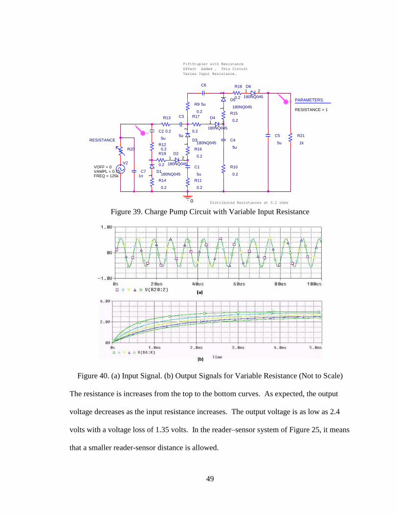
Figure 39. Charge Pump Circuit with Variable Input Resistance
Figure 40. (a) Input Signal. (b) Output Signals for Variable Resistance (Not to Scale)
The resistance is increases from the top to the bottom curves. As expected, the output
voltage decreases as the input resistance increases. The output voltage is as low as 2.4
volts with a voltage loss of 1.35 volts. In the reader–sensor system of Figure 25, it means
that a smaller reader-sensor distance is allowed.
R16
0.2
R17
0.2
D5
180NQ04512
R10
0.2
R11
0.2
PARAMETERS:
RESISTANCE = 1
R14
0.2
R21
1k
V2
FREQ = 125kVAMPL = 0.75VOFF = 0
V
Fifthtupler with ResistanceEffect Added . This CircuitVaries Input Resistance.
R15
0.2
R9
0.2
C6
5u
D6
180NQ045
1 2
R13
0.2
R120.2
C4
5u
D3180NQ0451
2
C1
5u
V C2
5u
0
D1180NQ0451
2
R18
0.2
C5
5u
D2
180NQ045
1 2R19
0.2
Distributed Resistances at 0.2 ohms
C3
5u
C71n
R20
RESISTANCE
D4
180NQ045
1 2
50
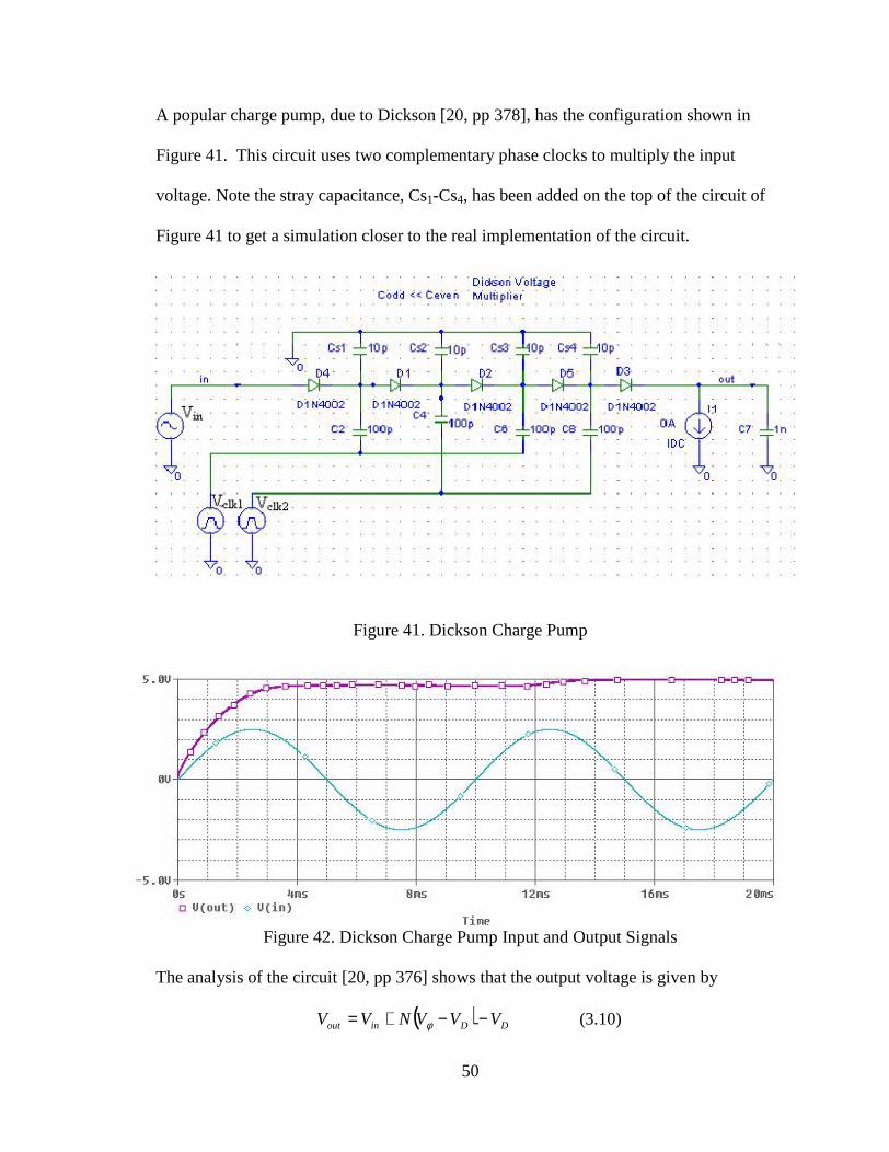
A popular charge pump, due to Dickson [20, pp 378], has the configuration shown in
Figure 41. This circuit uses two complementary phase clocks to multiply the input
voltage. Note the stray capacitance, Cs1-Cs4, has been added on the top of the circuit of
Figure 41 to get a simulation closer to the real implementation of the circuit.
Figure 41. Dickson Charge Pump
Figure 42. Dickson Charge Pump Input and Output Signals
The analysis of the circuit [20, pp 376] shows that the output voltage is given by
( ) )10.3(DDinout VVVNVV −−+= φ

51
where φV is the voltage amplitude of the two anti-phase clock signals and VD is the built-
in voltage of the diodes. However, the stray capacitance reduces the transferred voltage
by )/( sCCC + , where C is any of the capacitances in the circuit. The output voltage will
be
)11.3(DDs
inout VVVCC
CNVV −
−
++= φ
Observe in Figure 41 that the load current is zero. If the effect of the load current is
considered, then the output voltage will be additionally reduced by the factor [20, (2), pp
376]
( ) )12.3(oscs
outfCC
NI+
and the output voltage will be
( ) )13.3(Doscs
outD
sinout V
fCC
IVV
CC
CNVV −
+
−−+
+= φ
with multiplication effect if and only if
( ) )14.3(0>+
−−+ oscs
outD
s fCC
IVV
CC
Cφ
In practice, the diodes are substituted by NMOS transistors connected as diodes, and DV
becomes the threshold voltage thV of the diodes. If the Dickson charge-pump circuit is
cascaded to the strain-sensor circuit of Figure 28, the anti-phase clock signals can be
obtained from the terminals of the antenna as described in Figure 69 in the role of the
terminals of the inductor Lsen. More elaborated circuits have been designed [21, 22, 23],
some of them to work on input voltages as low as one volt, however, all of them require
an external power supply to provide a voltage bigger than one volt. Another drawback of
52
those circuits, if operated as part of a passive wireless sensor, is the relatively large power
dissipation. There are some other papers that consider ultra low voltage operation [27,
28], but they try to overcome the threshold voltage by a floating-well or by using cell
arrays. The last approach considers the use of a cell that can be driven by input voltages
as low as 0.3sin( t). However, to make the cell active, it requires an external voltage
supply of at least 1.2 v, making the circuit useless when there is no access to the 1.2
voltage supply, as in the sensor circuit of interest here. Anyway, it is possible to reduce
the threshold voltage on the charge pump circuit just by using Germanium transistors in a
diode connection. It produced a modest gain on the reading distance.
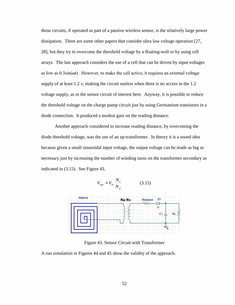
Another approach considered to increase reading distance, by overcoming the
diode threshold voltage, was the use of an up-transformer. In theory it is a sound idea
because given a small sinusoidal input voltage, the output voltage can be made as big as
necessary just by increasing the number of winding turns on the transformer secondary as
indicated in (3.15). See Figure 43.
)15.3(p
sinout N
NVV =
Figure 43. Sensor Circuit with Transformer
A run simulation in Figures 44 and 45 show the validity of the approach.
53
Figure 44. Sensor Circuit with Transformer
Observe in Figure 45 the peak amplitude of the sinusoidal input signal is just 20 mV, and
the output is slightly more than 2.5 volts, i.e., a voltage multiplication of 125. It is not
possible to display clearly the sinusoidal input signal given the long time took by the
capacitor C1 to charge. The input inductance was set to 3.5 H and the output to 100,000
H, working at 125KHz.
Figure 45. (a) Input Signal. (b) Output Signal (Plot (a) not at Scale)
However, the expected output voltage, from (3.15) and circuit in Figure 44, is:
voltsx
xxV
L
LVV
N
NVV th
p
sinth
p
sinout 73.5707.0
105.3
10000,1001020
6
63 =−
=−=−≈ −
−−

54
The output voltage on the simulation is small compared to the expected output voltage.
The reason of this huge difference is based in the transformer behavior at relatively high
frequencies. There is a tendency for high frequency currents in the wiring to move to the
wire surface, reducing the transversal area of the wire, then, increasing the resistance
associated to the cable, ALR /ρ= , resulting in a substantial increasing of the winding
loss. Also, as frequency increases, the impedance of the stray capacitance between
winding turns, CjZC ω/1= , decreases limiting the amplitude of the transformer-
generated signal.
These, effects can be mitigated at some level, by interleaving coil windings, and a good
transformer design can produce the desired output voltage, especially at medium
frequencies like 125 KHz.
The last discussion shows the feasibility of the transformer approach to increase
the reading distance as desired. However there is an insolvable characteristic in all
transformers: they are bulky, and they become bulkier as the desired reading distance,
between reader and sensor circuits, is increased, and proportionally the number of turns
in the secondary of the transformer need to increase.
If the design of the structure of the bridge allows embedding sensor circuits the size of a
HP calculator, this is a good approach to consider. In the next chapter, the design of a
complete sensor circuit based on an up-transformer will be presented.
Finally, it is important to remember that the reading distance of the up-transformer sensor
circuit is limited to operate in the near field, see appendix B.

55
Chapter 4. DESIGNS AND TEST RESULTS
a. Design of a Sensor Circuit Based on an Up-Transformer
Consider the design of the transformer for the circuit simulated in Figure 44, and
implemented as in Figure 43, reproduced in Figure 46.
Figure 46. Sensor Circuit with Transformer
The design will be explored in three steps:
i. Design of the basic sensor circuit with an up-transformer in resonance
ii. Reader-Sensor system circuit with an up-transformer in resonance
iii. Reader-Sensor system circuit with an up-transformer in resonance and output
doubler charge pump
i. Design of the basic sensor circuit with an up-transformer in resonance
For the first design, Figure 47, it is necessary to compute the self-inductances of the
primary and secondary windings, from [24, (8.19), pp 190]:
)1.4(2
Henrysl
ANL
µ=
where A is the transversal area of the core in square meters, l is the length of the winding
in meters and is the permeability.
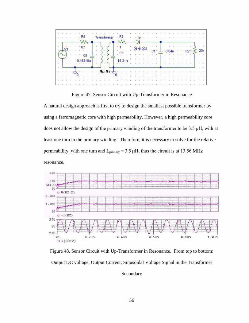
56
Figure 47. Sensor Circuit with Up-Transformer in Resonance
A natural design approach is first to try to design the smallest possible transformer by
using a ferromagnetic core with high permeability. However, a high permeability core
does not allow the design of the primary winding of the transformer to be 3.5 H, with at
least one turn in the primary winding. Therefore, it is necessary to solve for the relative
permeability, with one turn and Lprimary = 3.5 H, thus the circuit is at 13.56 MHz
resonance.
Figure 48. Sensor Circuit with Up-Transformer in Resonance. From top to bottom:
Output DC voltage, Output Current, Sinusoidal Voltage Signal in the Transformer
Secondary

57
Let us use a commercial iron toroidal core with dimensions: 36/25/7 mm,
(external_perimeter/internal_perimeter/wide), and cross sectional area A = 7x11 mm =
0.000077 m2. We want to keep the transformer primary turns to a minimum, N =1, so,
that the relative permeability of the core is so large that saturation of the core is avoided,
and the number of turns in the secondary is minimum. Pick wire AWG 14, with cross
sectional area equal to 2.08 mm, then l = 0.00162737m(diameter of the cable). We
want to compute the relative permeability r to have an inductance of 3.5 H, then from
(3.15):
)2.4(8646.580
2==
AN
lLr µ
µ
Use (4.2) to compute the number of turns, N, in the secondary to have Lsecondary= 0.1
Henry inductance, so that voltage gain is considerable and the toroidal coil is not so big.
In this case, the length of the coil is the perimeter of the toroidal core, l = 0.09582 m at
same core cross sectional area A.
)2.4(129703.12972
1
0
turnsA
lLN
r
≈=
=
µµ
To compute the capacitance values needed to set both sides of the transformer in
resonance
)3.4(1 2
1
0
=
LCω
The resultant circuit and its signals, Figures 47 and 48, works well for fo = 13.56MHz.
However, the supply signal was set relatively large, 5 Sin( t), to force the circuit to
deliver 1 mA. Note the expected size of the transformer to give here. Recall, that the
sensor circuit, motive of this research, will be embedded in the body of a bridge and

58
should be kept to minimum size, so it does not perturb the physical structure of the
bridge. To extend the distance between reader and sensor circuits, we need to consider
the whole reader-sensor system of Figure 25, as is done in the next design.
Figure 49. Size of the Up-Transformer
ii. Reader-Sensor system circuit with an up-transformer in resonance
From Figure 23, 21LLkM = , (2.15) and considering Z2 = C2 || RL, it is possible to show
that the output voltage in that sensor circuit is given by:
1)1
)((
)4.4(1)
1)((
222
121
222
1
222
212
+++=
+++=
++==
L
L
out
RCsRLs
ILLks
RCsRLs
V
ZRLs
ZVVV
Note that C2 may include the stray capacitances. If all parameters are fixed and the
frequency is varied, a typical response of the circuit occurs, see Figure 50. As expected,
there is a resonance frequency. As explained in chapter 2 and from (4.1) and Figure 50, it
is a good idea to set the reader-sensor circuit in resonance to maximize Vout and
consequently extending the reading distance. In the circuit of Figure 23 it is
recommended to keep C2 variable to get fine-tuning after the circuit is assembled, that is

59
equivalent to keep C1 variable in Figure 51. The steps to design this circuit are the same
as before, the circuit designed and its output signals are presented in Figures 51 and 52.
Figure 50. Frequency Response of (4.1)
Figure 51. Reader-Sensor system circuit with an up-transformer in resonance
Figure 52. System Signals. From Top-to-Bottom: Load Current, Load Voltage

60
Note that the coupling factor k = 0.05,is very small and still the sensor circuit was able to
deliver 7 volts with a load of 0.7 mA. The small load current the circuit is able to deliver
put a pressure in the design of the rest of the sensor circuit, but at least the voltage is
adequate. If the reading distance is incremented, the coupling factor k suffers an
additional decrease, and at some point the circuit will not be able to deliver enough
voltage, neither current, to the load.
Figure 53. Reader-Sensor System Signals. From Top-to-Bottom: Voltage in
Sensor Antenna, Voltage in Secondary of Transformer of Figure 51
Observe in Figure 53 that the display of the signals is when the DC output voltage is
stable in Figure 52.
The top of Figure 53 shows how the antenna voltage at less than 0.5 Vpeak is unable to
overcome the silicon threshold voltage of the diode. The bottom plot shows the signal
after the up-transformer, about 70 Vpeak for a voltage gain of about 140. Resolution of
the signals in PSpice is not good but still shows the important effect of the transformer.
The final DC voltage, 7 volts, is small because transformer works at constant power:
)5.4(secsec ondaryondaryprimaryprimary IVIV =
When the transformer amplifies the voltage signal, it must reduce the secondary current
to keep the power at the same level.

61
Therefore, even though the transformer delivers a big amplitude voltage, at the same
time, it is not able to provide more current to charge a bigger C1 capacitor which could be
used to feed a larger load. The size of the transformer is even now the same as in the
basic sensor circuit with an up-transformer in resonance, Figure 49.
The next design step considers the use of a charge pump as a mean to increase the VDC
output level, or to keep the same VDC level but requiring less turns in the transformer
secondary, and consequently reducing the size of the transformer.
iii. Reader-Sensor system circuit with an up-transformer in resonance and output
doubler charge pump
To investigate the use of a charge pump, there will be added a doubler to the circuit in
Figure 51, as shown in Figure 54. The design steps are the same as for the previous two
circuits with the addition of the doubler circuit; the circuit was fine-tuned to resonance
again. The circuit delivers a smaller voltage than the previous circuit without the voltage
doubler, but still is adequate to power the sensor circuit. However, observe that the load
was significantly reduced from the previous design to force the circuit to deliver an
adequate VDC, and the load current is only 28.57% from that design. With the same load
resistance as in Figure 51, the circuit cannot deliver more than one volt VDC.
The problem seems to be that the addition of C6 implies that the transformer must charge
an additional capacitor, each capacitor at different semicycle, or equivalently Cequivalent
C1 + C6.

62
However, the low voltage effect persists even when C1 and C6 values are cut in half to
compensate for the additional capacitance, and retuning. If additional voltage multiplier
stages are added, the voltage drop and smaller driven load effects get worse.
Figure 54. Reader-Sensor system circuit with an up-transformer in resonance and output
doubler charge pump
Figure 55. Circuit Signals. Bottom- Up:
Output Voltage, Load Current
We want to investigate why this severe voltage drop occurs when the charge pump circuit
is added.
To start, let’s modify (3.3) to include the effect of the transformer as (Nsecondary/Nprimary):

63
)6.4(1sec
loadthinprimary
ondaryo I
Cf
nVV
N
NnV
−−−
=
A close analysis of (4.6) does not give any clue why the severe Vo drop, in fact, Iload is
smaller than the previous design, n = 2, so, theoretically, from (4.6) we should expect a
bigger output voltage than the previous circuit.
The reason of this severe drop was found in the combined effects of the transformer, the
charge pump circuit and the resonance operation of the whole sensor circuit.
To explain how it happens a fast review of parallel and series resonance is necessary.
Resonance is the condition when the impedance effects of the reactive elements are
cancelled, i.e.,
)7.4(1
:1 2
1
====
LCthen
CLZZ o
ooCL ω
ωω
The (4.7) resonance occurs in both series and parallel LC circuits, see Figure 56.
Figure 56. Parallel and Series LC Circuits
The impedance of the parallel LC circuit is given by
)8.4(1
||
2
1
1
2∞==
−=
+==
=
LCw
CL
CLCLp
LC
Lj
ZZ
ZZZZZ
ωω

64
(4.8) means that the LC parallel circuit at resonance behaves as an open circuit.
For the series LC circuit
)9.4(01
2
1
1
=
=+=+=
LCw
CLs CjLjZZZ
ωω
(4.9) indicates that the series LC circuit behaves as a short circuit at resonance.
More realistic LC circuits should include a resistor, Figure 57.
Figure 57. Parallel and Series LC Circuits with Resistance
The resonance frequencies are the same as described in (4.7). To compute the impedance
in the parallel RLC circuit the Norton Transformation is used, then the admittance is
computed and finally it is transformed to its equivalent impedance:
)10.4(11
2
1
1
RY
ZthenGGLj
CjGYYYp
p
LCw
CLp ===++=++=
=
ωω
For the series RLC circuit
( ) )11.4(01
2
1
1
RRRCj
LjRZZZ
LCw
CLs =+=+
+=++=
=
ωω
In both RLC circuits the equivalent impedance at resonance is just R.

65
Now we need to review the effect of the impedance on the ideal transformer model,
Figure 58. From the (4.9) circuit and the basic relations in a transformer model:
)12.4(,
,
2
11
2
121
1
22
2
2
1
1
N
NaandI
N
NIV
N
NV
I
VZ
I
VZ Lin
===
==
then
)13.4(2
2
12
2
2
2
2
1
1Lin
L
L
in ZN
NZor
a
Z
aIa
ZI
aIa
V
I
VZ
=====
The impedance in the secondary is reflected to the primary side scaled by the factor a.
Zin
I1 I2+
-
+
-
Figure 58. Ideal Transformer Model
Figure 59. (a) Doubler Charge Pump. (b) Equivalent Circuit for Both Semicycles

66
We can use the last formulas to analyze the behavior of the doubler charge pump, from
Figure 54, neglecting the inductor resistance, the equivalent circuit is described in Figure
59.a. The equivalent circuit for both semicycles, negative and positive, is shown in
4.10.b. Assuming both capacitors have same value, then
( ))14.4(
4
4
4
2
1
224
22433
224
22244
2
2
2
RC
RCLRCj
RC
CRC
ZX
ZXLjZ
RCj
Z
C
C
ωωωω
ωωωω
ω
++++
++=
++=
+=
At resonance the imaginary part goes to zero, and the solutions are:
( ))15.4(
2,0
2
1223
2
1
LRCRC
Lj
+=ω
Substituting (4.15) into the real part of (4.14) gives
)16.4()(
)(2
CLRRC
CLRLZ
+−=
To observe the behavior of the impedance, first fix R and plot Z at resonance when L and
C varies, then fix L and observe Z when C and R are varied, Figure 60. Note that the
impedance in (4.16) is real.
20406080100 Resistance R
0.00020.0004
0.00060.0008
0.001
Capacitance C
0
50
100
150
Z
20406080100 Resistance R
0.00020.0004
0.00060.0008
0.001
Capacitance C
Figure 60. Impedance of the Charge Pump at Resonance
0.20.4
0.60.8
1Inductance L
0.00020.0004
0.00060.0008
0.001Capacitance C
0
5000
10000
15000
Z
0
5000
10000
15000
Z

67
Note the scaled effect of the impedance. It was found that for R > 500 the effect of the
charge pump circuit is to amplify the resistance, for R < 500 the impedance is
attenuated, and for R = 500 the impedance stays constant.
At this point, two comments are important:
1. The intrinsic resistance of the diode in forward bias, Figures 23 and 59, was
neglected because it is small compared to the load resistance. From [19, pp 247],
)17.4()1(0 −= kT
qV
D
a
eJJ
because the current is the charge crossing an area, then multiplying the current density J0
by the area we get the ideal diode equation:
)18.4()1(0 −= kT
qV
D
a
eII
Plotting (4.18)
Figure 61. Diode Characteristic Curve at 25o C
From the Figure 61 diode curve, RD varies with VD, and as long as VD is bigger than the
diode threshold voltage, RD goes to zero and therefore it can be neglected when compared
to the load resistance RL.

68
2. The capacitances of the diode in forward bias were not considered because they
do not contribute to the voltage drop observed in the reader-sensor circuit with
up-transformer and charge pump, as long as the circuit is tuned to resonance.
From (4.7), LC/10 =ω , achange in the capacitance, when the forward-bias diode
capacitances are added, just results in a shift in the frequency of resonance, but it does
not affect its amplitude at resonance. The effects of diode capacitance on inverse-bias
will be reviewed later.
Now, from (4.16) and Figure 60 it is clear that the impedance is scaled up on the
practical implementation of a reader-sensor system, motive of this research, where
load resistances must be much bigger than 500 , given the scarce power available.
A quick review of the quality factor Q for a series LC circuit combined with the
impedance scale will give the reason of the voltage drop.
From [15, (3) and (15), pp 88 and 91], the quality factor Q for a series RLC circuit is
defined as:
)19.4(RC
L
dissipatedpoweraverage
storedenergyQ =≡ω
From (4.19) as R is increased Q decreases and the voltage in any of the reactive
components decreases, Figure 62.

69
Figure 62. Resonance Curves Q1 > Q2 > Q3
In the RLC circuit, series or parallel, the resistance causes a drop in the output
voltage, more severe if it is taken between the two terminals of any of the two
reactive components, because VL or VC is Q times the voltage between the terminals
of the resistor. As Q is reduced, VL or VC reduces voltage in same proportion.
In the reader-sensor system with up-transformer and charge pump, the voltage
drop is caused when the charge pump – up-transformer, working in resonance,
multiplies the effect of the impedance in the secondary, (4.16), looking by the
primary. The additional impedance in the primary reduces the flow of the current in
the primary winding, producing less magnetic flux to reach the secondary circuit, and
then generating less voltage in the secondary. The drop of voltage is severe because
the multiplicative factor of the secondary impedance looking into the primary circuit
can be in the order of thousands, Figure 60. A simplified model is described in
Figure 63.

70
Figure 63. Model of the Primary Circuit with Charge Pump
Where K is the multiplicative effect of the secondary impedance when the charge pump
is added in the secondary circuit, and Zi and Zsecondary are the original impedances.
Equation (4.6) is modified to include this effect:
)20.4(1
sec
secloadthin
ondaryiL
L
primary
ondaryo I
Cf
nVV
ZKZX
X
N
NnV
primary
primary −−−
++
=
In general K should be calculated as
)21.4(arg
arg
pumpechwithout
pumpechwith
Z
ZK =
Z with charge pump is the impedance from the secondary looking into the primary circuit, like
(4.16). The multiplicative effect occurs for three additional charge pump circuits that
were analyzed, including the general implementation suggested in [17].
It is important to remark that all calculations, and the resulting formulas, are valid only at
resonance or in its close vicinity.
From the previous discussion and simulations, it is evident that the circuit in Figure 51
with only the up-transformer in resonance is better suited to wirelessly power the sensor
circuit.
Some people, [29, pp 15-23, 30, pp 28-31], are working in the fabrication of
transformers on VLSI, however, the inductance of the transformer windings is still small,

71
less than 20 H with Q in the order of 10. Therefore, the monolithic transformers are not
still ready to be integrated in a chip, and the resultant sensor circuit will be relatively
bulky as suggested in Figure 49.
The effect of the inverse-bias on a diode produces a leakage current [19, (4.3.8), pp190],
as shown the plot of (4.22) in Figure 64. The effect becomes more evident as frequency
increases.
( ))22.4(
112
2
1
tan
+
==
ida
s
cecapacileakage
NNq
VZ
VI
φ
εω
where Na is the number of acceptors, Nd is the number of donors, s is the permittivity of
the silicon, i is the built-in potential and q is the charge of the electron.
Figure 64. Leakage Current of an Inverse Biased Diode
Observe that time was fixed and the voltage is sinusoidal in Figure 64. The leakage diode
current results in a partial capacitor discharge that contributes to the drop in voltage.

72
However, the voltage drop effect of the diode leakage-current is small when compared to
other effects previously analyzed, and can be kept under control with well design diodes.
Next section will show the design of an all-MOSFET RF-to DC-Voltage circuit
that avoids the PN junction threshold voltage, then faces the MOSFET channel threshold
voltage and finally outcomes a free-threshold-voltage circuit.
b. Design of an RF-to-DC-Voltage Circuit for VLSI Implementation
The design of the radio frequency to DC voltage system to power a strain sensor is
challenging because the current necessary to make work a commercial strain sensor: a
minimum of about 1 mA at 3 volts with the present technology. However, as explained
in next chapter, it could be possible to design a piezoelectric sensor that works with very
small current and can be activated with currents in the A range, in that case a MOSFET
RF-to-DC-Voltage VLSI design is satisfactory.
First the design of the MOSFET rectifier is addressed, next the rectifier is extended to
dual rectifiers with negative and positive output voltages. Finally a charge-pump circuit
is cascade to form a complete RF-to-DC-Voltage. The circuit is suitable for MOSFET
VLSI, and if fabricated under some characteristics it is possible to avoid the waste of any
voltage to overcome threshold voltages.
In practice, it is not expected to get perfectly rid of the threshold voltage, but to reduce to
aminimum threshold voltage close to zero.

73
i. MOSFET Antenna-Rectifier Circuit
Consider the class-B amplifier shown in Figure 65 [57, Figure 8.14, pp 449], this
amplifier switch Q1 ON and Q2 OFF in the sinusoidal positive semicycle. Therefore, as
long as the sinusoidal signal is positive it is amplified by Q1. In the negative semicycle
Q1 is turned OFF and Q2 ON, and the signal is amplified by Q2. The drawback in this
amplifier is the crossover distortion [57, pp 448-451].
Figure 65. Class-B Amplifier
Now, let’s extend the class-B amplifier idea to a rectifier implemented with MOSFET
transistors. After some preliminary designs, the circuit in Figure 66 resulted.
Figure 66. Proposed NMOS Rectifier

74
As in the class-B amplifier, in this circuit the positive semicycle turns M1 ON and M2
holds OFF and CL is charged through M1. In the negative semicycle M1 turns OFF and
M2 turns ON, now CL is charged through M2. M1 and M2 are part of the rectifier and CL
is the filter, the output is a positive DC voltage. Note that the circuit still is working in
resonance. The previous circuit worked with NMOS transistors, but the idea also works
for PMOS transistors to get a negative DC voltage, see Figure 67.
Figure 67. Dual MOSFET Rectifier
Figure 68. Dual MOSFET Rectifier Signals

75
VCL1 is a positive DC voltage and VCL2 is a negative DC voltage, both voltages are shown
in Figure 68, the difference allows the generated voltage to be doubled, or to have
negative and positive voltages to power the sensor circuit.
The problem, as in the diodes, is the threshold voltage Vth necessary to turn on the
transistors. However, the threshold voltage of the MOSFET transistors is not to
overcome a PN junction as to turn on the diodes but to open a channel between the drain
and the source. To control the threshold voltage let us review the theory behind Vth of a
MOSFET transistor. The depletion-region charge density per unit area, when the surface
is inverted, is given by [19, equation (8.3.9), pp 396].
where Na is the number of acceptors, Nd is the number of donors, pϕ and nϕ are the bulk
potentials, Cxq 1910602.1 −= is the electronic charge, the permittivity of the silicon is
given by )7.11)(10854.8( 1140
−−=∈=∈∈ cmFxrS , VS is the source voltage and VB is the
bulk voltage. Note VS = VC as described in [19, Figure 8.9 pp 395].
In agreement with [19, equation (8.3.18), pp 398] the equations to compute Vth in the
MOSFET transistor are given by
)24.4(
2
2
−−+
−++=
NMOSC
QVV
PMOSC
QVV
V
ox
dnSFB
ox
dpSFB
th
φ
φ
( )( )
)23.4(22
22
−+∈+
−+∈−=
TransistorNMOSVVqN
TransistorPMOSVVqNQ
SBndS
BSpaS
d
φ
φ

76
Where Cox is the oxide capacitance, VFB is the flat-band voltage [19, equation (8.1.1), pp
384] given by the difference in the work functions of the metal and silicon, typically
negative for P and N channel MOSFET transistors
The potential at the neutral edge of the depletion-region in the P-and-N-type material [19,
(4.2.9b), pp179] are
)26.4(
ln
ln
+=
−=
i
dn
i
ap
n
N
q
kT
n
N
q
kT
ϕ
ϕ
where 1231038.1 −−= JKxk is the Boltzmann’s constant, T is the absolute temperature in
Kelvin degrees, Cxq 1910602.1 −= and in is the intrinsic carrier density.
Equation (4.24) indicates how to control Vth in a MOSFET transistor. First, if the source-
substrate reverse bias, VSB, is increased then Vth is also increased. Therefore, we need to
keep VS = VB, to cancel the body effect. And (4.24) becomes [19, (9.3.1) and (9.3.2), pp
443]
Observe in (4.27) that VFB is typically negative for both NMOS and PMOS transistors,
and Qd in a PMOS (when VS = VB) becomes
)25.4(MSSMFBV Φ≡Φ−Φ=
)27.4(
2
2
++
−−=
NMOSC
QV
PMOSC
QV
V
ox
dnFB
ox
dnFB
th
φ
φ
( )( )
)28.4(22
22
∈+
∈−=
TransistorNMOSqN
TransistorPMOSqNQ
ndS
paS
d
φ
φ

77
Clearly, from (4.27) to control Vth in a NMOS transistor we need
)29.4(2ox
dnFB C
QV +≈ ϕ
with constraint
)30.4(2ox
dnFB C
QV +< ϕ
Because we want Vth in our NMOS transistor to be positive but close to zero. This goal
can be reached by control of Nd in Qd on the fabrication process.
Similar analysis can be done for a PMOS transistor, and the control of Vth is reached by
control Na in Qd. Note that in order to reduce Vth, Na or Nd must be decreased for both
MOSFETS, and is more difficult to reduce Vth in a PMOS transistor using this approach.
Another way to decrease Vth is by reducing the size of the MOSFET by a factor
K. Table 1 shows how scaling affects the MOSFET parameters.
Table 1. Scaling Rules [19, Table 10.1, pp 497]
If the MOSFET becomes smaller, and ’2 pSBV ϕ>> , then Vth is also reduced as [19,
(10.4.2), pp 497].
Scaling Rules for Constant Field ScalingScaling Factor
Surface Dimensions 1/KVertical Dimensions KImpurity Concentrations 1/KCurrent, Voltages KCurrent Density KCapacitance per area 1Transconductance 1/KCircuit Delay Time 1/(K^2)Power Dissipation 1/KPower Density 1Power-Delay Product 1/(K^3)

78
)31.4(’
K
VV th
th≈
where K is the scale factor when the area occupied by the MOSFET is reduced K times.
Observe that (4.31) is an approximation and even could be not valid in some cases.
Finally, ion implantation is commonly used to adjust Vth in the channel region
without increase doping in the rest of the substrate, because the heavy doping worsen the
performance of the MOSFET. The ion implantation is used to increases Vth by replace
the original doping in the channel by Na’ = Na(ion) + Na in the PMOS or Nd
’ = Nd(ion) + Nd
in the NMOS transistor in equation (4.23) and consequently in (4.24). If no ion-implant
is executed at the fabrication process, then Vth is kept close to zero. Maybe the resultant
MOSFETS will not be reliable for regular applications but they will be excellent in our
rectifier-charge-pump circuits, Figures 66-70. The advantage of the channel-ion-
implantation is so as to be selective, i.e., it is possible to execute ion implantation to all
the MOSFETS of the VLSI circuit except the MOSFETS of the rectifier and charge-
pump subcircuits.
The short channel effects should also be considered to control Vth as well, refer to [19].
From the last discussion, we found that there is a collection of methods to reduce or keep
close to zero the Vth in the fabrication of the MOSFET transistors used in the rectifier
circuit and ,consequently, increases the interrogation distance in the interrogator-strain
sensor system.
ii. MOSFET Antenna-Rectifier-Charge-Pump Circuit
Now let us increase the output voltage further through a charge pump as shown in Figure
69. The charge pump [55, pp 7] works well and delivered 3.5 volts at 50 MHz. To
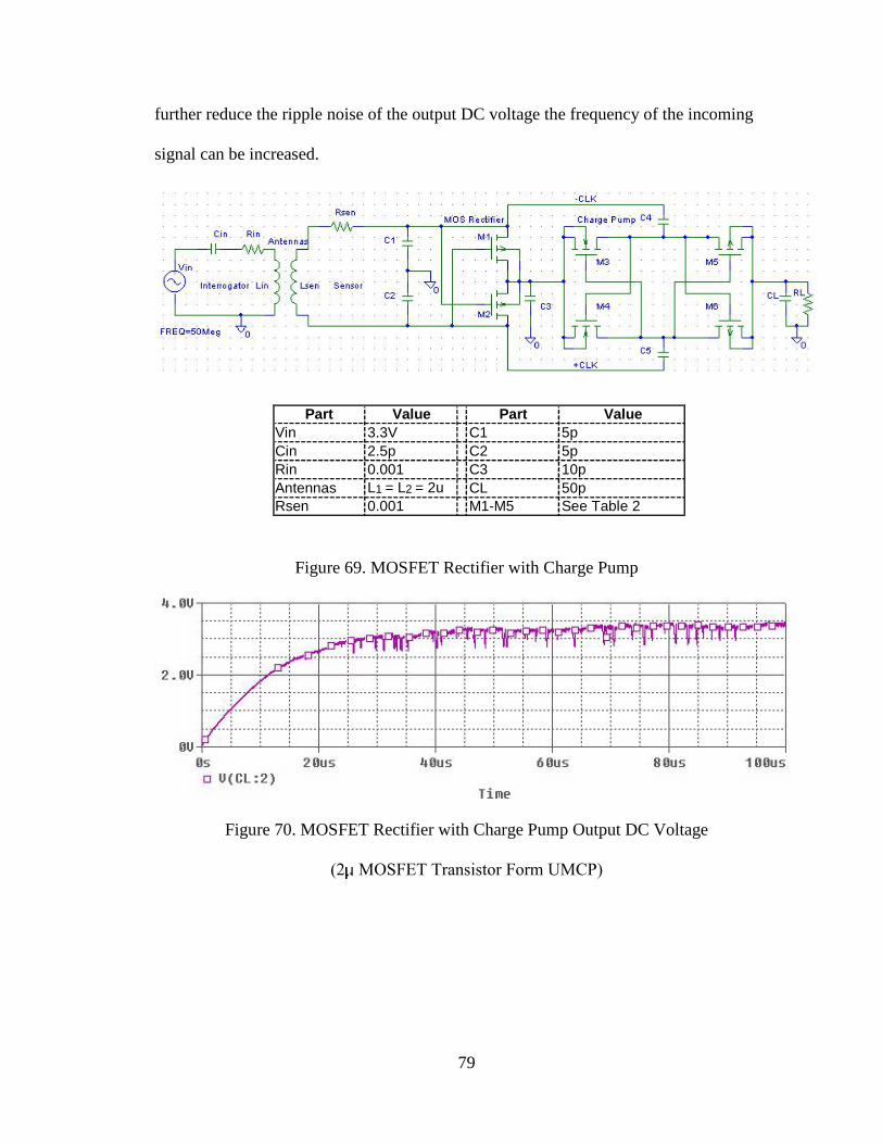
79
further reduce the ripple noise of the output DC voltage the frequency of the incoming
signal can be increased.
Figure 69. MOSFET Rectifier with Charge Pump
Figure 70. MOSFET Rectifier with Charge Pump Output DC Voltage
(2 MOSFET Transistor Form UMCP)
Part Value Part ValueVin 3.3V C1 5pCin 2.5p C2 5pRin 0.001 C3 10pAntennas L1 = L2 = 2u CL 50pRsen 0.001 M1-M5 See Table 2

80
Figure 71. MOSFET Rectifier with Charge Pump Output DC Voltage
(0.5 MOSFET Transistor Form UMCP)
Table 2. Characteristics of the MOSFET Transistors Used in the Simulation and
Output DC-Voltages and Currents in the Antenna-Rectifier-Charge- Pump Circuit [59]
Remarks:
• Note the increase of output voltage and maximum current of the circuit when
the size of the MOSFET is reduced from width = length = 4 meters in the
Bicmos12 family [59], to width = length = 3.15 meters in the Amcmos05
family.
• From Table 2 it is not possible to conclude that the most important factor in
the grow of the output voltage and current is due to the threshold voltage
Technology [Micrometers]
MOSIS Transistor Run Name
MOSFET Transistors Names in the Circuit
Threshold Voltage Changed to [V]
Simulated Output Voltage in Figure
Simulated Maximum Output Current [MicroAmperes]
0.5, W=L=2.5 T13V M1, M2, M5, M6 -0.01 71 590.5, W=L=2.5 T13V M3,M4 0.01 71 592.0, W=L=10 N21H M1, M2, M5, M6 -0.01 70 322.0, W=L=10 N21H M3,M4 0.01 70 32

81
• The combination antenna-rectifier delivered: 45 A, but with larger coupling
coefficient than the antenna-rectifier-charge-pump circuits, i.e., smaller
interrogator-sensor distance
• The charge pump of Figure 69 needs to operate at frequencies larger than 46
MHz, for smaller frequencies the output DC voltage drops sharply
• To improve the output current the threshold voltage should be reduced at
fabrication phase. The RF to DC circuit of Figure 69 is adequate to power
systems designed with MOSFET transistors, given the small currents that they
need to operate.
c. Test results to the Commercial RFID MCRF355 Tag Chip
The MCRF355 is a commercial RFID chip used in tagging. The device operates at 13.56
MHz and can be reprogrammed with some code in its 154 bits memory. Figure 72 depicts
the typical working ensemble.
Figure 72. MCRF355 RFID Tag System
When the interrogator activates the MCRF355 through an RF signal, it responds by
sending the word stored in its memory, and keeps sending this data as long there is
sufficient power to keep it alive.
Interrogator
RF Signal

82
In the test, it was found that the MCRF355 chip is able to deliver power not just to its
internal circuitry but to another circuit too. Between the pin 8, VDD, and the pin 5, VSS, is
possible to get a positive voltage up to 3.2 volts when the distance between antennas is
less than one centimeter and the incoming RF signal has a 20 MHz frequency. A
summary of the tests is presented in Figure 73.
Figure 73.a shows the frequency response of the MCRF355, its behavior resembles a
high pass filter. That test was run at 10 Vpeak constant interrogator voltage. When the
interrogator peak voltage is increased and the distance is keep constant the output DC
voltage goes up accordingly, Figure 73.b. This test and next tests were run at 13.56
MHz.
Figure 73. MCRF355 Output Signals
As expected, as the distance between interrogator and the MCRF355 antenna is
increased, the output voltage decreases as described in Figure 73.c.

83
Figure 73.d describes the current the chip is able to deliver, up to 24 A at a VDC of 2.4
volts, i.e. a resistance of 100 K . If the resistance is slightly decreased from 100 K , the
current and voltage drops to zero immediately.
The MCRF355 works well when the load demands no more than 24 A. Note that we do
not know what is the voltage and current the MCRF355 can generate for its internal
circuitry.
Figure 74 shows the signal of the MCRF355 chip, acquired with a logic analyzer. The
important signal is number five, it shows the Manchester encoded signal send back by the
MCRF355 to the interrogator circuit, when it is wirelessly powered through its antenna.
Actually, this signal is sinusoidal, i.e., a binary Manchester encoded data modulated in
amplitude. In order to freeze and record as TIFF file, an OPAM biased at five volts was
used to fit the signal into the logic analyzer because the oscilloscope in the laboratory
does not have recording capability.
Figure 74. Recorded Signals on the Sensor Circuit

84
The signal in line five of Figure 74 shows that the MCRF355 is working, i.e., gets power
from the RF signal and sends back the information data stored in its memory. Hence, the
MCRF355 can be used in the design of a magnetic coupled strain sensor.
d. Construction Material Issues in the Design of Magnetic Coupled Circuits
As explained in the first chapter, the sensor circuit is expecting to be embedded in
the body of a concrete bridge to measure the strain. The attenuation on the RF signal,
introduced by the cement or other construction material, can make the sensor useless.
From a basic test conducted in the Microelectronics laboratory, it seems that, at least for
the brick used as the material of the bridge, the attenuation of the RF signal at 125 KHz
introduced on average 0.16 volts. The effect is a slight reduction in the reading distance.
The schematic setup for testing is described in Figure 75, the coil antennas are not shown.
The rectifier-filter circuit was fully enclosed inside the brick. The cable of the
oscilloscope is shielded by fabrication, so there was not way to pick up additional RF
power via the cables.
Figure 75. Construction Material Attenuation Test Setup
However, in real life every bridge is constructed with different materials and every
material with different permeability . For that reason the sensor circuit must operate

85
at some frequency were the specific bridge construction material presents the lowest
attenuation. In the worst case, when metallic-like materials are used in mix of the
concrete used to build the bridge the RF signal will not able to reach the sensor circuit
because it will be practically shielded from the signal. The shielding effect could be
also produced if after the end of the construction of the bridge, at some moment in its
life, any metallic-like layer is applied to the surface of the bridge for protection or any
other reason.
This shielding effect could be also produced in a natural way in the life span of the
bridge when different materials deposit on the surface, creating a shield. Deposit
speed could vary for different geographic areas, but deposit could be fastened on
some industrial areas as pollution deposits on the surface of the bridge.
There has been some research on how concrete walls affect the electromagnetic
signals used in cell telephony [32, pp 12-21]. The results on that research suggest us
the use of shapes on the face concrete bridge as way to increase the absorption of the
signal by the bridge, and consequently increase the power of the RF signal that could
reach the strain sensor circuit.
Finally, changes in the best frequency to reach the strain sensor change with time.
Through the life of the strain sensor its circuitry components get old, changing the
resonance frequency, only slightly if good quality components are used. Besides, the
concrete material used in the construction of the bridge are expected to change its
permeability over time, hence changing the frequency that is better absorbed by the
bridge to reach the strain sensor device. Moreover, that permeability change could be
different for strain sensors embedded at different locations on the body of the bridge.

86
Previous discussion suggest us the addition of some features to the reader and the
strain sensor circuits for improved performance:
1. The reader must transmit RF signals over an interval of frequencies, no just a
frequency, to improve the chances to activate the strain sensor circuit. The
price of this feature is a reduction on the reading distance, as the Q of the
reader circuit is reduced. The reader can transmit all frequencies on that
interval at the same time or sweep them over time, stopping in the frequency
where the strain sensor is activated.
2. The strain sensor circuit must be able to adjust its resonance frequency,
maybe on a limited range to avoid a significant reduction of the quality factor
Q. Using this capability to search for the best frequency to receive power
from the reader as soon as it is activated. The overhead on this feature is the
additional power necessary to carry out the adjustment.
The auto-search for the best frequency in both, the reader and the sensor circuits,
could also help to automatically overcome changes over time on the permeability
of the concrete construction material and its resultant shift of the best frequency to
transfer power. A limited solution is the addition of a feedback loop in the strain-
sensor circuit, Figure 79.
Other, potential solutions and problems on the design and implementation
of a wireless strain-sensor system will be given in the next chapter.

87
Chapter 5. CONCLUSIONS AND OPEN PROBLEMS
This work presented the feasibility of wireless techniques in the near field, to
power a strain sensor circuit, possibly embedded in the body of a concrete bridge. The
efficiency of the output power generated was enhanced by the use of voltage multipliers
as charge pumps and transformers. Results of section 4.a showed that they operate better
separately. The DC voltage drop when they worked jointly was analyzed. Theory and
simulation shows the impedance multiplying effect on the primary circuit of the
transformer results in a severe degradation of the DC output voltage when the charge
pump is inserted in series.
The transformer working in resonance and followed by a rectifier-filter was the
circuit with the best performance. The sinusoidal voltage generated in the terminals of
the receiving antenna was as low as 20 mV, and yet capable to generating a DC voltage
of about 6 volts for a multiplicative factor of 300, at 800 A. The output DC current is
relatively small but sufficient to power a well-designed VLSI circuit. The drawback of
this approach is the relatively big size of the transformer that potentially could disturb the
strength of the bridge when embedded.
As shown in section 4.a.iii charge pumps showed poor results at low input
voltages. The different charge pump circuits consistently suffered a DC voltage drop
when the load was incremented. In the best case, at perfect resonance, one of them
delivered up to 200 A.
The threshold voltage of the diodes, Vth, is a serious drawback on the use of charge
pumps. When the peak voltage generated on the terminals of the antenna drop below Vth,
0.7 V for Si or 0.3 V for Ge, the output DC voltage and current were zero.

88
To overcome the threshold voltage the rectifier in Figure 66 was designed, the PN
junction Vth was changed to a channel Vth. The discussion in chapter 4.b.i and 4.b.ii
proved that the Vth of the channel can be done as small as desired at the MOSFET
fabrication process. For practical purposes we can have a zero Vth rectifier.
Note that the same fabrication principle can be applied to the charge pump in Figure 69,
that makes the VLSI RF-to-DC-Voltage system practically threshold voltage free.
That sounds great, but the VLSI RF-to-DC-Voltage system, even is able to generate 3.5
volts, it is not able to deliver the current necessary to power the less demanding
commercial strain sensor, that is about 1 mA. For that reason, we propose the use of a
surface acoustic wave as strain sensor, working in the topologies reported in Figures 77
and 78. In Figure 78 the VLSI RF-to-DC-Voltage system could be used to power the
processing unit. The system in Figure 78 is restricted to frequencies in the 10 MHz to 2
GHz range, i.e., the response range of the SAW devices, and the SAW sensor must be
fabricated in a separated chip of the rest of the circuit because it requires a piezoelectric
material to operate. The MCRF355 can be used to implement a strain-sensor circuit
based in commercial components as described in Figure 80. This prototype circuit could
operate at 13.56 MHz.
Literature research on the effects of the bridge concrete suggested that they could
be as small as to be neglected or as big as to make the system useless. If the concrete mix
presents a shield effect, a magnetic coupling is impossible or very small and the sensor
circuit becomes isolated from its activating RF signal. Tests in the laboratory showed
that the RF signal to generate power suffered only a slight attenuation at 125KHz.
However, some tests must be conducted on the concrete of every bridge, previous to the

89
design of the strain-sensor system, to look for the penetrating signal frequency that
suffers less attenuation. Ideally, the penetrating frequency with the least attenuation
should be used to design the system so maximizing the power that can reach the strain
sensor antenna. Therefore, a designed system must be fit to every particular bridge.
a. Open Problems and Opportunities
The RF transfer of power explored in this research was done with the strain sensor
system in mind. Interrogator devices should be portable and small as possible for easy
use by technicians. And sensor circuits should be kept as small as possible so as not to
disturb the bridge.
Given the results in this thesis still there are variables that must be analyzed to optimize
the use of power. This work did not addressed any chip package model and its effects on
the power consumption of the designed circuit. Neither considered the design of
microstrip patch antennas as an alternative to the coil antennas or array of antennas.
Third, even in the most optimized design, the strain sensor is still dumb. Some
intelligence should be added to allow the sensor to learn about its bridge environment in
order to optimize its variables: strain accuracy, power consumption, frequency of
communication, radiation pattern, etc. The problem in the last point is that the
intelligence feature is power hungry, i.e., another open problem.
If the interrogator size constrain is relaxed then it is possible to use antenna arrays that
can concentrate power to small areas, and increase the interrogation distance accordingly.
The software of the interrogator could in a predetermined order switch on and off the
antennas, and in the process sweep with the concentrated RF signal a big area. There are
two main advantages in this approach: The reading distance is incremented, something

90
that is important in tall bridges where the distance between reader (interrogator) and the
strain sensor embedded inside the concrete is relatively large. Secondly, because the RF
power is concentrated in a smaller area the chances of collision, when more than one
sensor are activated simultaneously, is minimized, see appendix A. The disadvantage is
an increase of the size and complexity of the interrogator, mainly because of the
antennas.
Another option is the use of ferromagnetic cores, with large permeability r, inside the
interrogator and sensor antennas. They could increase the efficiency of the transferred RF
power. The area of the antennas could be reduced, but at the same time they could
become bulky, i.e., wide and length are reduced but high is increased.
There are some other technologies that can potentially be used in the wirelessly
interrogator-strain sensor system. Some of them will be visited in the rest of the chapter.
i. Surface Acoustic Wave Sensors
Because the existing commercial strain-sensors need to operate relatively large amounts
of current, the design of a strain-sensor that consumes little current should be considered.
By reducing the amount of power necessary to activate the sensor, the interrogation
distance can be incremented or more power is available to operate the rest of the strain-
sensor circuit. Surface Acoustic Wave devices (SAW devices) are heavily used in the
telecommunication sector as filters. Nowadays, all the cell phones use the SAW devices
to process signals. Since the 1980’s there has been a strong interest in the application of
the SAW devices as sensors because they can be interrogated wirelessly [33, pp 1281-
1292].

91
SAW devices are constructed using piezoelectric crystals. When a RF signal send
by an interrogator device hits the antenna of the SAW device, the comb-like elements on
the surface of the SAW device, called interdigital transducers (IDT), transform the RF
signal into an acoustic surface wave that propagates on the crystal, see Figure 76.a.
Figure 76. [34, pp 2208, fig.1] (a) Schematic Layout of the Passive SAW Sensor
(b) Signals
The propagated waves are reflected by other IDT arrays placed at distances L1 and L2 in
the path of the acoustic waves. They propagate back to the IDT connected to the antenna.
This IDT converts the sound signals back into electromagnetic signals and retransmits
back to the interrogator device. The interrogator device processes the returning signals,
Figure 76.b, to get the phase, delay and frequency information.
The delay, phase or frequency of the acoustic wave may change as a function of the
variables that it is desired to sense. Different crystals are used to sense different variables
like temperature, pressure, strain, etc. Some crystals are more sensitive than others to
change the phase, delay or frequency of the acoustic wave as a function of the sensed
variables.
Note that it is possible to place the IDT’s at unique distances on the surface of the SAW
device therefore the difference in delay between the returning signal bursts can be used as
way to identify uniquely every SAW device [34, pp 2208].

92
According to [35, (13.20), pp 368], the phase of the returning signal burst can be used to
sense the strain as:
)1.5(00ετωϕ ≈∆
where )( 21 ϕϕϕ −∆=∆ is the variation of the phase on the burst returning from the IDTS
at distances L1 and L2, )/()( 1212 LLLL −−∆=ε is the strain and0τ is the traveling time
when the sensed strain is zero. Note that raising the operation frequency 0ω can increase
the sensitivity of this SAW sensor. SAW sensors can operate on frequencies from few
hundred MHz to about 3 GHz, and readout distances up to 2.5 m with 10 mW peak
power. There are advantages if SAW devices are used in the strain sensor researched in
this thesis:
1. They do not need to operate in the near field, therefore theoretically they could be
interrogated at bigger distances.
2. There is no need to receive power in the sensor to activate complex overhead
circuitry, just the IDTS and the piezoelectric body of the sensor.
3. SAW devices are fabricated in stable single crystals that are nearly aging free.
4. As for the magnetic coupled system of this thesis, SAW sensors do not require a
battery to operate.
5. They are small. Typically: 12 x 5 x 1 millimeters.
The disadvantages:

93
1. If the SAW sensors are embedded in the bridge concrete, and the concrete mix
changes attenuation at the operating frequency, the SAW sensor could become
useless.
2. The FCC (Federal Communications Commission) restricts the power of the
electromagnetic signals radiated to a few milliwatts. This factor strongly limits
the readout distance.
3. Addition of intelligence is limited, because digital processing could be power
hungry
The first SAW sensor disadvantage can be overcome by placing groups of SAW sensors
designed to operate at different frequencies, i.e., the expected window of frequencies with
less attenuation where the concrete of the bridge will shift along its life span. Other ways
to overcome the attenuation problem is by the use of magnetic coupling for the SAW
sensor as described in Figure 77. The SAW sensor works as before, but the interrogator
electrical signal is magnetic coupled.
Figure 77. Strain SAW Sensor Operated with Magnetic Coupling

94
If it is desired to add extra features as security encoding and signal processing then the
circuit in Figure 78 should be used.
Figure 78. Strain SAW Sensor Operated with Magnetic Coupling and
Processing Capacity
The second is a political but not technical limitation, so, presently there is no way to
overcome this restriction in SAW sensors operating on plane waves. On the contrary,
magnetic coupled systems have not that legal limitation.
The third constraint can be addressed with the arrangement of Figure 78. The processing
unit could short-circuit some of the elements of the IDTS to change dynamically the
characteristics of the SAW sensor, or maybe an array of sensors, as the environment
changes.
ii. Out of the Box Reader-Sensor System Implementation
The circuit for a complete RF-to-DC-Voltage powered strain sensor can be
implemented as shown in Figure 79. This circuit is an improved version of [54].
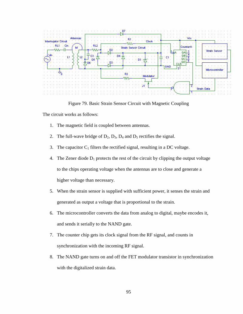
95
Figure 79. Basic Strain Sensor Circuit with Magnetic Coupling
The circuit works as follows:
1. The magnetic field is coupled between antennas.
2. The full-wave bridge of D2, D3, D4 and D5 rectifies the signal.
3. The capacitor C1 filters the rectified signal, resulting in a DC voltage.
4. The Zener diode D1 protects the rest of the circuit by clipping the output voltage
to the chips operating voltage when the antennas are to close and generate a
higher voltage than necessary.
5. When the strain sensor is supplied with sufficient power, it senses the strain and
generated as output a voltage that is proportional to the strain.
6. The microcontroller converts the data from analog to digital, maybe encodes it,
and sends it serially to the NAND gate.
7. The counter chip gets its clock signal from the RF signal, and counts in
synchronization with the incoming RF signal.
8. The NAND gate turns on and off the FET modulator transistor in synchronization
with the digitalized strain data.

96
9. The load “modulator”, FET, changes the load in concordance with the strain data,
resulting in an amplitude-modulated signal. This load switch is sensed in the
interrogator circuit through the magnetic coupling.
10. Diode D7 and the varactor D6 are used in a feedback loop to compensate for
changes in the shift of the resonant frequency. When the output voltage drops the
varactor changes its capacitance and shifts to the capacitance where the output
voltage is maximum. This loop can be used to compensate for changes in aging
components and surroundings.
The sensed signal is demodulated and decoded in the interrogator circuit. The decoded
signal can be read by the operator or stored for future reference. The circuit is not
optimized but is helpful for understanding the operation of a potential strain-sensor
circuit.
The last circuit can be taken a step further. Based upon the results of tests of the
MCRF355 it is possible to implement a strain-sensor circuit integrated with commercial
chips as described in Figure 80.
The circuit works as follow. The strain sensor circuit generates a voltage that is
proportional to the strain. The Microcontroller chip, PIC 16C71, performs a strain
measurement, by sensing the voltage in pin 17, converts the measured voltage to its
digital equivalent with its analog-to-digital converter, and saves its datum in its internal
memory. After that, it transfers the information to the MCRF355 chip memory using 6-9
pines.
The MCRF355 is used to temporarily store the strain-measured data. Later, when the
interrogator device is in its near field vicinity and transmits an adequate magnetic signal

97
to hit the MCRF355 antenna, it takes the power of the RF magnetic signal, and uses it to
power its circuits. Then, the MCRF355 sends the information stored in its memory as
long as it has enough power to do that. When the power of the received signal drops
below some threshold the MCRF355 turn off, until another adequate RF signal is
received. In the mean time, the microcontroller can transfer new strain information into
the MCRF355 memory.
Figure 80. Strain-Sensor Circuit
The PIC16C71 is used in this circuit because of its low power consumption feature: 15
A, when working with a clock signal at 32 KHz, and less than 1 A on standby. The
transfer of information between the microcontroller and the MCRF355 is performed in
two handshake steps: first, a programming word is send and next the information data is
transferred.

98
Note that the microcontroller, the ADG417 switches and the strain sensor are not
powered by the RF signal. The RF signal send by the reader device is used just to power
the MCRF355 and get the information stored in its memory.
In the prototype circuit of Figure 80, in the end, the microcontroller, switches and strain
sensor must be powered by an external piezoelectric system that will be feeding power
intermittently from the vibration and pressure generated by the cars circulating on the
bridge.
Because that flow of power is not continuous, the microcontroller must transfer the last
strain measurement data to the MCRF355 as soon as possible, before it looses power.
The microcontroller will take strain measurements and saving them into the MCRF355
memory as long as there is enough power available.
To read the data stored in the MCRF355 an interrogator circuit must be in the proximity
of the sensor circuit. The interrogator circuit sends a constant 13.56 MHz sinusoidal
signal, which arrives to the MCRF355 coil antenna. This signal is then rectified and
filtered to generate a DC voltage, which powers the MCRF355 internal circuitry.
After activated, the MCRF355 modulates the load seen by the interrogator with the strain
data stored in its memory; it looks like a signal modulated on AM for the interrogator
device. The MCRF355 keeps sending the same information as long as there is enough
RF signal to power its circuitry.
The maker of the MCRF355 indicates that when some data is recorded on the MCRF355,
it is retained at a minimum of 200 minutes. This time allows the recover of the
information on critical structures long time after no power is feed to the circuit.

99
Appendix A. RF Power Transfer in Free Space
Figure 81. Interrogator-Strain Sensor Front–End
To analyze the transfer of power in the free space we start by computing the power
density in the sensor circuit [38, (12.24), pp 673]:
)1.(4 2
Ax
GPPD AT
π=
where PT is the transmitted power, GA is the gain of the antenna and x is the distance
between the reader (also called interrogator) and the sensor circuits. When this power
arrives to the sensor circuit, it is used to energize the circuit, processing the signal and
send back a signal with the strain measurement. This power process can be modeled as
[38, (12.25), pp 674]:
)2.(10, AkkPDPS ≤≤=
where k can be considered equivalent to the radar cross-section and is a measure of the
amount of energy sends back to the reader. The actual value of k depends on the
attenuation of the bridge material were the sensor circuit is embedded, angle between
antennas, material of antennas and frequency.
To compute the power received back, we can use the effective absorption area of the
reader antenna given by [37, pp 522]:

100
)3.(4
2
AG
A Aeff π
λ=
Then the power received in the reader circuit will be [38, (12.27), pp 674]:
( ))4.(
4 42A
x
kAGPPD effAT
Rx π=
Or equivalently, by substituting A.3 into A.4:
( ))5.(
4 43
22
Ax
kGPPD AT
Rx πλ
=
From A.5, if we keep fixed all variables in this formula but want to double the readout
distance, then the power to carry out the job must be increased by sixteen. Most of the
power send to the sensor circuit is lost on the free space.

101
Appendix B. Antenna Near Field Region
There is a still some debate regarding the use of formulas when working in the
Fraunhofer region of the antenna, (far field region), the region where the propagated
wave front from one antenna to the other antenna is essentially a plane wave, and the
Fresnel region of the antenna (near field region), where the propagated wavefront is
spherical. For some applications it can result in phase variation of the signal at the
receiving antenna due to radiation of the signal from different parts of the transmitting
antenna.
Figure 82. Near–Far Field Regions Boundary
The boundary line is rather diffuse, but it is customary to set it at πλ 2/ , Figure 82. The
characteristic impedance is given by [38, pp 17]: Ω≈= 37700εµZ , and the typical
behavior of the fields in both regions is described in Figure 83. Note that starting at
πλ 2/ the electromagnetic wave impedance becomes independent of the distance from
the antenna, or in other words: the electromagnetic wave has not effect on its generation
antenna, and as a consequence there is no more inductive coupling, and the transformer
model does not describe the system anymore. If there is not magnetic coupling, then
there is not transfer of power. Therefore, for practical applications, the inductive coupling
Antenna
Near Field
Far Field

102
must be carried out on the Fresnel field, and there is not way to extend this limit beyond
πλ 2/ .
Electric Field
Magnetic Field
Plane Wave
Distance from Source in lambdas/2*pi
1
Wav
efor
mIm
peda
nce
[ohm
s]
10
100
1000
Tra
nsiti
onR
egio
n
377 ohms
Figure 83. Transition Region Between Fields
Let’s compute the free space loss for the system given in equation A.5. Knowing that the
path loss is defined as [37, pp 522]: DTL PPP /= , assuming GA = k = 1 and fc /=λ
with c = 3 x 10⁸ m/s, then the path loss is:
( ))1.(
4 43
22
BPx
kGPP
T
ATL π
λ=
and becomes
)2.()log(20)log()20(256.147][ BfxdBPL ++−=
Note that in B.2 that the second term represents the loss of power of the RF signal when
it propagates in free space from the interrogator to the sensor circuit and vice versa [40,

103
pp 49]. Plot of B.2 results in a signal attenuation of 20 dB by decade, which is true for the
far field, Figure 84.
Figure 84. Free Space Loss in a Sensor–Interrogator System
However, in the near field the magnetic field, H falls off at rate 3/1 x or 60 dB per decade,
and there is a transition distance in the vicinity of πλ 2/ as indicated in Figure 83.
Observe how at 40MHz the border of the near field is roughly one meter, i.e., this is the
maximum readout distance in an interrogator-strain sensor system based on magnetic
coupling. Of course, it is possible to overcome this limit by:
1. Grow the size of the interrogator and sensor antennas.
2. Increase considerably the power delivered by the reader circuit.
3. Decrease the frequency of the system.
Though, those are not practical solutions for some applications given the increase in cost
and size of the system.

104
Figure 85. Near Field Boundary Distance From Antenna

105
Appendix C. Interrogator–Sensor Communication Issues
Chapter 4 described the implementation of a sensor circuit based on commercial
components. One of the chips used is the MCRF355, this chip gets its power from the
RF signal, and sends the strain information stored in its memory to the interrogator circuit
through the same receiving antenna. This appendix was written to explain how the strain
data is encoded and modulated by the sensor system.
a. Modulation
Communication of the measurement data in the system becomes more complex when
there is more than one sensor circuit. A model of a communication network better fits this
expanded scheme. A useful communication model depicted through encoding – decoding
and modulation – demodulation blocks is shown in Figure 86.
Figure 86. Communications Scheme of the Interrogator–Sensor System
The encoder–decoder takes care of security and error–correction of the measured data
and the modulator–demodulator blocks care to send and receive the information
wirelessly. Collision is the event when two or more devices transmit simultaneously.
There are three basic digital modulations: amplitude shift keying (ASK),
frequency shift keying (FSK) and phase shift keying (PSK). ASK is important when
dealing with collision on a low power passive circuits, and is used in some of the
commercial implementations for RFID tag circuits like the MCRF355.
Encoder Modulator Demodulator Decoder

106
An ASK signal is described by [41, pp 333-336]
)1.()cos()()( CttAmtx cω=
with envelope )()( tAmty = . If we assume NRZ unipolar with two equally likely values
A and 0. Then the power spectrum density will be [41]:
)2.()(
)(2
)(22
CfT
fTSinTf
AfP
b
bby
+=
ππδ
With average normalized power 2/2A for x(t) peak value 2 . An example of the
baseband and ASK signals for bipolar NRZ are shown in Figure 87.
Figure 87. ASK Signal
b. Encoding – Decoding
In an interrogator-to-one – strain sensor system operating in the near field, the
communication is smooth. However, when the system grows to include more than one
sensor in the proximity of each other there is a chance that two or more circuit sensors try
to send information to reader at the same time, this condition results in collision. The
standard approach is, after detecting collision, to wait some random time before try to

107
establish communication again. This approach was first used by the University of Hawaii
in 1971 and has been widely studied.
If the data words (packets) sent by all sensors are defined as traffic, then there will
be some reasonable expectation that some of the packets will collide as illustrated in
Figure 88.
Figure 88. Signal Collision on the Interrogator-Multisensor System
in Near Field Region
From traffic theory, let λ be the total traffic arriving to the reader, then it can be
decomposed in traffic accepted aλ and unsuccessful traffic rλ then [42, (11.16), pp 679]:
)3.(Cra λλλ +=
If the length of every message is b, the average accepted traffic would be
abλρ =’ . If the channel capacity is defined in R bits per second, then the normalized
average accepted traffic, or throughput, becomes [42, (11.19), pp 680]:
Reader
Transponder 1
Transponder 2
Transponder N
Collision

108
)4.(CR
b aλρ =
and the total normalized total traffic
)5.(CR
bG
λ=
The time every packet will take to be transmitted is [42, (11.21), pp 680]:
)6.(CR
b=τ
Let’s (C.4) and (C.5) to be rewritten as
)7.(CG λτ=
)8.(Caτλρ =
When some sensor transmit it will take τ seconds to successfully send its
information. However, if any of the other sensors inside the near field region try to send
information before the previous sensor finish then collision will occur. If it is assumed
that packets are independent, then traffic can be modeled as Poisson Process, with
distribution [42, (11.24), pp 680]
)9.(!
)()( C
k
ekxP
k λτλτ −
==
To avoid collision is necessary that only one packet is sent in one τ2 interval,
therefore (C.9) becomes
)10.(!0
)2()0( 2
20
Cee
xP τλλτλτ −
−
===
By definition, the probability to have a packet successfully transmitted is
)11.()0( CxP a
λλ
==

109
From (C.10) and (C.11) we get:
)12.(2 Ceaτλλλ −=
If (C.12), (C.7) and (C.8) are combined
)13.(2 CGe G−=ρ
Where (C.13) represents the normalized successful traffic as function of the total
traffic. Figure 89 shows the graph of this function. Note how successful traffic increases
as traffic increases up to half of the communication channel capacity, after reaching that
point, the traffic produces numerous collisions and as a result successful traffic decreases
becoming almost cero when traffic is four times the capacity of the channel.
Figure 89. Normalized successful Traffic Versus Normalized Total Traffic
From this graph, the maximum normalized successful traffic is 1/2or 0.18, i.e.,
the maximum successful traffic is 18% of the channel capacity. That means that
collisions occur regularly in a digital communication system. Fortunately, the
interrogator–sensor system generates traffic well below this value in the readout range.

110
c. Bandwidth, DC Component and Collision Detection
Encoding the measured data has many objectives, but one of the most important, in
passive magnetic coupling, is to cancel the DC component of the signal send from the
sensor to the interrogator. The energy in the DC component is wasted because magnetic
couplings have not sensitivity to DC or even to low frequency signals. Therefore, the
encoding process must allocate all the energy on higher frequencies. However, there is
tradeoff between the power saved by not encoding the DC component and the additional
power used to encode the measured data.
From chapter two, it is known that the antennas in the interrogator and sensor
circuits work in resonance and therefore they can be modeled as band-pass filters. A
higher Q is desirable to increase the reader distance, however there is a tradeoff, because
of the affect of a narrow bandwidth on the encoded signal as shown in Figure 90.a.
Note that, as the system bandwidth becomes smaller, the recovered signal suffers
higher delay and distortion when compared with the original data, in the last row of plots
it is not possible to differentiate between the ones and zeros. This problem is exacerbated
if there is an important amount of noise as seen in Figure 90.b. To observe the effect of
both variables, bandwidth and noise, it is customary to use the eye diagram. An open and
clean eye diagram is desirable, the closer and smaller eye imply difficulty on estimation
and detection of the incoming data by the interrogator circuit.

111
Figure 90. (a) Effect of decreasing Bandwidth on a Digital Signal
(5000,3000, 2000, 1000 and 500 Hz of Bandwidth). (b) Encoded Signal Plus
Noise
(c) Eye diagram (see paragraph for an explanation)
In the first column of plots, the noise power is kept to 0.01 watts but bandwidth is
decreased from 3KHz to 2KHz and to 1KHz. On the second column of plots, the
bandwidth is constant at 4KHz, but the power noise is incremented from 0.02W to 0.08W
and to 0.10W. In both cases, the bandwidth of the incoming signal is 1KHz.
From discussion in chapter 4, a higher Q is desirable to increase the readout
distance, however, Q must be kept to an adequate value to allow the system to transfer

112
data without appreciable distortion. There is a relation between Q and the bandwidth of
the communication system given by [9, (12), pp 90]:
)14.(1
0
CQ
BW =ω
Where BW is the bandwidth of the communication system, and 0ω is the
resonance frequency. Addition of an error correcting coding algorithm in the interrogator
circuit can mitigate the problem, but again, it will also add on overhead, cost and
complexity on the strain sensor circuits.
The Detection of collision can be done by encoding the measured data before
modulate. Figure 91 shows three popular line encoding methods and their power
spectrums: NRZ, RZ and Manchester. Note how RZ and Manchester requires twice the
bandwidth of RZ. However, RZ and Manchester have inherent synchronizing features
that allow them to recover the clock from the incoming data signal, with a relatively low
complexity PLL circuit.
Also, observe that the DC component presents important magnitudes in RZ and
NRZ, but that component is almost inexistent for Manchester. That is an important saving
on power for passive sensors.
There are many ways to implement error-correcting codes, some more energy
efficient than others. But in a magnetic coupled sensor system, with more than one strain
sensor circuit, the most important source of errors is not the environment noise but
collisions. Therefore, collision detection is very important. The most important
advantage of Manchester Encoding is its ability to generate a clear error when a collision
occurs.

113
Figure 92.a shows when two sensors, first row of plots, transmit at the same time.
The second row shows the ASK encoded signals, and the last row, first column shows the
received signal in the reader after a collision occurs. Finally, in the very last graph the
NRZ decoded signal is displayed. Observe that not error is generated in the decoded
signal when collision occurs, and therefore the collision is not detected.
Figure 91. (a) Line Encoding. (b) Spectrums for NRZ, RZ and Manchester
Figure 92. (a) Collision on NRZ Encoded Sensor Signals
(b) Collision in Manchester (See text for explanation)
Figure 92.b shows same situation when two sensor signals are transmitted at the
same time, but now the signals are encoded in Manchester. The first and second rows of

114
plots show the Manchester encoded sensor signals and their ASK modulated
representation. The last row, first column, shows the ASK signal received in the reader
and the very last plot shows the decoded signal.
Observe that the wider pulse is not possible in a well Manchester encoded signal,
and therefore an error is detected and that packet of information is discarded. See [42] on
page 87 for an explanation on Manchester coding.
d. Error Correcting Codes and Security
In regular use, an error correcting encoding take cares of the detection and correction
of the errors generated in the transmission of information. A well-designed error
correcting coding should save power because; even it adds redundant bits, on the average,
it avoids retransmission of packets of data that use additional power, therefore, on the
average the bit per symbol is decreased.
In the interrogator–sensor system the error correction system is not necessary because the
collision already generates a sequence that is not allowed in Manchester encoding. This
condition indicates to the interrogator that there is an error in the received data, and
consequently the data is discarded. Then, the interrogator waits to receive the data again.
The sensor circuits transmit their ID and data at random time intervals as long as they get
adequately power from the RF reader signal. Therefore, the interrogator gets the same
data more than once, given it the opportunity to correct or update its database.
From chapter two we know that all magnetic-coupling communications must occur inside
the near field, which limit is calculated as πλ 2/ . For a 13.56 MHz communication, the
limit would be a radius of 3.521 meters.

115
However, as depicted in Figure 93, an eavesdropper could potentially get the signal send
by the sensor circuit outside the limit of the near field. If there is need to protect the
sensor data from eavesdroppers then an encryption algorithm must be added to the
measured data before the transmission.
Figure 93. Eavesdroppers in an Interrogator–Sensor System
The encryption algorithms use a key word, which is known by both parties but not by the
eavesdropper to encode the data before sending to the communication channel.
To encode the key word and data, an XOR digital gate takes, one-by-one, a bit from the
key and another bit from the data words. The output word is send to the channel. In the
receiver, the incoming word is XOR gating again with the same key word and the
original data is recovered. For additional information on encryption algorithms see [44,
pp 12-49].
Reader Sensor
Eavesdropper
Near Field Limit

116
Appendix D. Wiring and Matching in the Strain-Sensor System Design
There are common improvements, in addition working at resonance for both the
reader, also known as interrogator, and the sensor circuit, with the purpose of maximize
the amount of power transfer to the sensor circuit.
First, the length of the cable from the circuit to the antenna must be on the vicinity of
zero or multiples of 4/λ . This fact is based on the assumption that perfect match
between the circuits and their antennas is not perfect and therefore by controlling the
length of the cable between the circuit and the antenna we can control the reflected
signals to the minimum.
Let us elaborate on this assumption. It is known [9, (55), pp127] that the quotient ZL/Zin
of the load and input impedances of a transmission line is given by:
)1.()sin()cos(
)sin()cos()(D
zjZzZ
zjZzZ
Z
zZ
Lin
inL
in ββββ
−−
=
Figure 94 shows (D.1) plot. Observe that only when there is perfect match the quotient is
constant and equal to one, all other cases are periodic.
Figure 94. Impedance Behaviors Along a Transmission Line

117
Recall, the reflection coefficient is given by [9, (47) and (48), pp 126]:
)2.(1
)(
1)(
1
1
D
Z
zZZ
zZ
Z
ZZ
Z
in
in
in
L
in
L
+
−≈
+
−=Γ
In the second part of the equation, the reflection coefficient was modified to observe its
behavior along a transmission line. Clearly from (D.2) and Figure 94, the only lengths of
the transmission line that result in a reflection coefficient equal to one are multiples of
4/λ , all other lengths result in reflected signals, and therefore in lost power. The
reflected power results in a decreased reading distance. In Figure 94, the second and
third plots show cases for Zin = 50 , ZL = 30 and Zin = 30 , ZL = 50 , i.e., a strong
mismatch between the impedances of the circuit and the antennas. Note, that the swing
of the impedance quotient, equation (D.1), has a shift phase of 180o, but still presents
perfect match at multiples of 4/λ .
As an example, for a reader-sensor system working a 2.4 GHz 4/λ = 3.125cm, and the
length of the cable feeding the antenna must be close to zero, ideally zero, or multiple of
3.125 cm.
If the design frequency of the sensor circuit is 13.56 MHz, i.e., 4/λ = 5.531m, the length
of the wires is not an issue in the optimization of the interrogation distance because all
the expected cable lengths are less than 20 cm length. However, as frequency increases,
the length of the feeding cable must be carefully restricted to multiples of 4/λ .
Second, the design of a match circuit must be considered. Perfect match is very
difficult to get in practice; most of the time, after the design is completed some of the
reactive components must be keep variable so that a tune up is available to maximize

118
interrogation distance. Tune up should be done in conditions close to the final
environment were the circuits will be operating, in order to consider the parasitic
capacitances of the surrounding materials and operators.
However, after the circuit is finished and place in its final location, components get older,
capacitors dry off and change their values, and the sensor circuit losses its matching
effect, conveying a decrease in the interrogation distance.
The design of the matching circuit starts by considering the transformation from a
series to a parallel circuit, as a helping tool to design. It is described in Figure 95.
Figure 95. Series and Parallel Complex Circuits
It is wanted Zs = Zp, index s stand for series and p by parallel, or
)3.(DjXR
jXRjXR
PP
PPSS +
=+
After some algebra
)4.(22
2
22
2
DXR
RXXand
XR
XRR
PP
PPS
PP
PPS +
=+
=
If we have a parallel circuit, with some ZP, the RS and XS values necessary to keep ZS =
ZP but implemented as series circuit are given by (D.4).
In the same way, it is wanted 1/Zs = 1/Zp, and the algebra yields
)5.(2222
DX
XRXand
R
XRR
S
SSP
S
SSP
+=
+=

119
Now, If we have a series circuit with some ZS, the RP and XP values necessary to keep ZS
= ZP implemented as series circuit are given by (D.5).
As an example of design, consider the match of a voltage source in series with a 50
resistance, to an impedance given by: 10+j20. From (D.5)
)6.(2520
20102
2222
DX
XRX
S
SSP =+=
+=
Because the original reactive component j20 is positive then the reactive component
given by (D.6) must be negative, i.e., a capacitor. The capacitor must be place in parallel
as described in Figure 96.
Figure 96. Matched Circuit
To check that the circuit was matched the equivalent impedance is calculated in (D.7)
)7.(50510
)510(50
252010
)25)(2010(D
J
J
JJ
JJZequivalent Ω=
−−=
−+−+=
Because Zequivalent is the same as Rin the circuit has been matched. In the strain-sensor
system, matching is more elaborated because resonance must be preserved. Therefore,
the capacitors of the matching circuit should be variable for fine-tuning.

120
Appendix E. Standards
Table 3. Standards [60, 61, 62]
StandardsStandard Frequency Power (depending on class)
EN 300 330 - 1 V1.3.1 9 kHz-30 MHz
437.7 dBµA/m at 10m (at 135 kHz, descending 3 dB/octave from 135 kHz to 1 MHz)
EN 300 220-2 V1.3..1 25 - 1000 Meg up to 500mWEN 300 328 - 1: V 1.2.2 2.4-2.4835 GHz up to 100mWISO 18000- 3 (FCC) 13.553-13.567MHz max 10mV/m at 30 metersISO 15240 425-435 MHz max 11mV/m at 3 metersISO 18000- 6B (FCC) 900 MHz 4 W
ISO International Organization for StandardizationEN European Telecommunications Standards Institute (ETSI)

121
REFERENCES
1. E – Zpass New Jersey Costumer Service.
http://www.ezpass.com/static/info/howit.shtml
2. Maryniak, G.E., “Status of International Experimentation in wireless power
transmission”, Solar Energy, Vol. 56, No. 1, pp 87-89, January 1996.
3. Sato, H., Domae, H., Takahashi, M., Abe, M., “Reflection and Transmission
Control of Electromagnetic Wave for Concrete Walls”, Electronics and
Communications in Japan, Part 2, vol. 83, No. 11, pp 674–682, 2000.
4. Tsukamoto, H., “Hermetically Sealed Lithium Rechargeable Batteries for
High Reliability Applications: Medical, Aerospace and Other Specialties”,
Proceedings of the 17th Annual Battery Conference on Application and
Advances, Long Beach, pp 129-134, January 2002.
5. Brown, C.B., “The History of Power Transmission by Radio Waves”, IEEE
Transactions on Microwave Theory and Techniques”, Vol. MIT-32, No. 9, pp
1230-1242, September 1984.
6. Palmer, C. R., “The Bar Code Book”, Helmers Publishing, Inc.,
Peterborough, New Hampshire, 3rd edition, pp 123 – 127, November 1995.
7. Daugman, J., “How Iris Recognition Works”, The Computer Laboratory,
Cambridge, UK, pp 1-3, http://www.CL.cam.ac.uk/users/jgd1000
8. Cohen, J., “Automatic Identification and Data Collection Systems”, McGraw
Hill, New York, November 1994.
9. Lee, T.H., “The Design of CMOS Radio – Frequency Integrated Circuits”,
Cambridge University Press, New York, 1998.

122
10. Austin, B. A., “Electromagnetic Propagation Underground with Special
Reference to Mining”, Trans. SAIEE (The South African Institute of
Electrical Engineers), Vol. 76, No. 1, pp 1-5, January 1985.
11. Winch, R. P., “Electricity and Magnetism”, Second Edition, Prentice-Hall,
Englewood Cliffs, N.J., 1963.
12. Vasudeva, D.N., “Fundamentals of Magnetism and Electricity”, S. Chand &
Co., Delhi, 1966.
13. Baker, R.J., Li, H. W., Boyce, D.E., “CMOS Circuit Design, Layout, and
Simulation”, Wiley InterScience, New York, 1998.
14. Pylarinos, L. and Roger, E. “Charge Pumps: An Overview”, Department of
Electrical and Computer Engineering, University of Toronto, pp 2 – 3,
http://www.eecg.toronto.edu/~kphang/ece1371/chargepumps.pdf
15. Okamura, H., Atsumo, T., Takeda, K., Takada, M., Imai, K., Kinoshita, Y.,
Yamazaki, T., “A Sub-2.0 BiCMOS Logic Circuit with a BiCMOS Charge
Pump”, IEEE Journal of Solid-State Circuits, Vol. 31, Issue 1, pp 84-90,
January 1996.
16. Stremler, F.G., “Introduction to Communication Systems”, 3rd Edition,
Addison-Wesley, New York, pp 372-413, 1990.
17. Lin, P.M., “Topological Generation and Analysis of Voltage Multiplier
Circuits”, IEEE Transactions on Circuits and Systems, Vol. CAS-24, No. 10,
p 528, October 1977.
18. Peikari, B., “Fundamentals of Network Analysis and Synthesis”, First
Edition, Robert E. Krieger Publishing Company, Malabar, Florida, 1981.

123
19. Muller, R. S. and Kamins, T.I, “Device Electronics for Integrated Circuits”,
Second Edition, John Wiley & Sons, New York, 1986.
20. Dickson, J.F., “On-Chip High-Voltage Generation in MNOS Integrated
Circuits Using an Improved Voltage Multiplier Technique”, IEEE Journal of
Solid-State Circuits Vol. SC-11, No. 3, pp 374-378, June 1976.
21. Di Cataldo, G., Palumbo, G., ”Optimized design of 4 stage Dickson voltage
multiplier”, IEEE International Symposium on Circuits and Systems,
London, UK, Vol. 5, pp 693-696, June 1994.
22. Di Cataldo, G., Palumbo, G., “Dynamic analysis of 3 stage Dickson voltage
multiplier for an optimized design”, Procedings of the Electrotechnical
Conference, 7th Mediterranean, Antalya, Turkey, Vol.2, pp 633-636, 12-14
April 1994.
23. Starzyk, J.A., Jan, Y., Qiu, F.,”A DC-DC charge pump design based on
voltage doublers”, IEEE Transactions on Circuits and Systems I:
Fundamental Theory and Applications, Vol.48, Issue 3, pp 350-359, March
2001.
24. Kip, A. F.,”Electricity and Magnetism”, McGraw-Hill, New York, 1962
25. Baker, R.J., Li, H. W., Boyce, D.E., “CMOS Circuit Design, Layout, and
Simulation”, Wiley InterScience, New York, pp 33 – 41, 1998.
26. Pylarinos, L., Phang, K., “Analysis of output ripple in multi-phase clocked
charge pumps”, Proceedings of the 2003 International Symposium on
Circuits and Systems, ISCAS '03, Vol.5, pp 25-28 May 2003.

124
27. Ioth, K., Fridi, A.R., Bellaouar, A. and Elmasry, M.I., “A Deep Sub-V Single
Power supply SRAM Cell with Multi-VT Boosted Storage Node and
Dynamic Load”, 1996 Symposium on VLSI Circuits, Digest of Technical
Papers, Honolulu, HI, pp 132-133, June 1996.
28. Choi, K., Park, J., Kim, J., Jung, T. and Suh, K., “Floating-well Charge Pump
Circuits for Sub-2.0V Single Power Supply Flash Memories” 1997
Symposium on VLSI Circuits, Digest of Technical Papers, pp 61-62, June
1997.
29. Allstot, D.J., Park, J., Choi, K., “Parasitic-Aware Optimization of CMOS RF
Circuits”, Kluwer Academic Publishers, Boston, Massachusetts, 2003.
30. Niknejad, A.M. and Meyer, R.G., “Inductors and Transformers for Si RF
ICs”, Kluwer Academic Publishers, Boston, Massachusetts, 2000.
31. MCRF355/360 Datasheet, Microchip Co., pp 7, http://www.microchip.com
32. Sato, H., “Reflection and Transmission Control of Electromagnetic Wave for
Concrete Walls”, Electronics and Communications in Japan, Part 2, Vol. 83,
No. 11, pp 12-21, 2000.
33. Reindl, L., Scholl, G., Ostertag, T., Scherr, H., Wolff, U., Schmidt, F.,
“Theory and Application of Passive SAW Radio Transponders as Sensors”,
IEEE Transactions on Ultrasonics, Ferroelectrics, and Frequency Control,
Vol. 45, No. 5, pp 1281-1292, September 1999.
34. Pohl, A., Seifert, F., “New Applications of Wirelessly Interrogable Passive
SAW Sensors”, IEEE Transactions on Microwave Theory and Techniques,
Vol. 46, No. 12, pp 2208-2211, December 1998.

125
35. Gardner, J.W., “Microsensors MEMS and Smart Devices”, John Wiley &
Sons, New York, 2001.
36. Schmidt, F., Sczesny, O., Ruppel, C., Magori, V., “Wireless Interrogator
System for SAW-Identification-Marks and SAW-Sensor Components”,
Proceedings of the 1996 IEEE International Frequency Control Symposium,
Honolulu, HI, pp 208-215, June 1996.
37. Haykin, S., “Communication Systems”, 4th edition, John Wiley & Sons, New
York, 2000.
38. Pozar, D., “Microwave Engineering”, Wiley, New York, 1998
39. Saunders, S., “Antennas and Propagation for Wireless Communication
Systems”, Wiley, New York, 1999.
40. G. Kohn, “Theoretische Elektrotechnik und Elektronik”, Springer Verlag,
Wien, Austria, 14th Edition, 1993.
41. Couch, L.W., “Digital and Analog Communication Systems”, Prentice Hall,
Englewood Cliffs, New Jersey, 1997.
42. Sklar, B., ”Digital Communications. Fundamentals and Applications”,
Second Edition, Prentice Hall, Englewood Cliffs, New Jersey, 2000.
43. Wicker, S.B., “Error Control Systems for Digital Communication and
Storage”, Prentice Hall, Englewood Cliffs, New Jersey, 1995.
44. Trappe, W. and Washington, L., “Introduction to Cryptography with Coding
Theory”, Prentice Hall, Englewood Cliffs, New Jersey, 2002.
45. Warneke, B., Awood, B., Pister, K.S.J., “Smart Dust Mote Forerunners”,
Proceedings of The 14th IEEE International Conference on Micro Electro

126
Mechanical Systems, 2001. MEMS 2001, Interlaken, Switzerland, pp 357-
360, January 2001.
46. Raza, N., Bradshaw, V., ”Applications of RFID Technology”, Proceedings of
The IEE Colloquium on RFID Technology, Savoy Place, London, pp 1-5,
October 1999.
47. Rotter, M., Ruile, W., Bernklau, D., Riechert, H., Wixforth, A., ”Significantly
Enhanced SAW Trasnmission in Voltage Tunable GaAs/LiNbO3 Hybrid
Devices”, Proceedings of The IEEE Ultrasonic Symposium, Sendai, Japan,
Vol. 1, pp 69-72, October 1998.
48. Schmidt, V.H., “Piezoelectric Energy Conversion in Windmills”, IEEE
Proceedings of Ultrasonic Symposium, Tucson, AZ, Vol. 2, pp 897-904,
October 1992.
49. Smith, G.A., Barnes, S.A., “Electrical Power Generation from Heat Engines”,
IEE Colloquium on Power Electronics for Renewable Energy, Digest N.
1997/170, London, UK, pp 5/1-5/6, June 1997.
50. Hamakawa, Y., “Recent Progress of Amorphous Silicon Cell Technology in
Japan”, IEEE Conference Record of the Twenty Second, Las Vegas, NV,
Vol. 2, pp 1199-1206, October 1991.
51. Doig, A., “Off-grid Electricity for Developing Countries”, IEE Review, Vol.
45, Issue 1, pp 25-28, January 1999.
52. Chaudhuri, S.K. and Lovley, D., “Electricity Generation by Direct Oxidation
of Glucose in Mediatorless Microbial Fuel Cells”, Nature Biotechnology,
Vol. 21, No. 10, pp 1229-1232, October 2003.

127
53. Van, J. W., “Biotechnology and the Utilization of Biowaste as a Resource for
Bioproduct Development”, Trends in Biotechnology, Vol.19, Issue 5, pp 172-
177, 2001.
54. Shenck, N.S., “Piezoelectric shoe power: two approaches “ IEEE Computer
Society, Internet Page Article, 2002.
http://www.computer.org/micro/homepage/may_june/shenck/01a.ht
m
55. Pelliconi, R., “Power Efficient Charge Pump in Deep Submicron Standard
CMOS Technology”, Proceedings of The 27th European Solid- State Circuits
Conference, Session 1.4 Voltage Regulators, Villach Austria, p 7, September
18th 2001.
56. Richalot, E., Bonilla, M., Wong, M., Fouad-Hanna, V., Baudrand, H., Wiart,
J., “Electromagnetic Propagation into Reinforced-Concrete Walls”, IEEE
Transactions on Microwave Theory and Techniques, Vol. 48, No. 3, pp 357-
366, March 2000.
57. Boylestad, R., Nashelsky L., “Electronic Devices and Circuit Theory”,
Prentice Hall, Englewood Cliffs, New Jersey, 1972.
58. Assaderaghi, F., Parke, S., Sinitsky, D., Bokor J., Ko, P.K., “A Dynamic
Threshold Voltage MOSFET (DTMOS) for Very Low Voltage Operation”,
IEEE Electron Device Letters, Vol. 15, No. 12, pp 510-512, December 1994.
59. Newcomb, R.W., “Microsystems Laboratory VLSI Page”,
http://www.ee.umd.edu/newcomb/mslab-vlsi.html
60. Federal Communications Commission, http://www.fcc.gov/

128
61. International Organization for Standardization,
http://www.iso.ch/iso/en/ISOOnline.frontpage
62. The association for automatic identification and Data Capture Technologies,
http://www.aimglobal.org/standards/rfidstds/RFIDStandard.htm
Related Documents