Appendix A Physical Noise Sources Contents A.1 Physical Noise Sources ................ A-2 A.1.1 Thermal Noise ................ A-3 A.1.2 Nyquist’s Formula .............. A-5 A.1.3 Shot Noise .................. A-10 A.1.4 Other Noise Sources ............. A-11 A.1.5 Available Power ............... A-12 A.1.6 Frequency Dependence ............ A-14 A.1.7 Quantum Noise ................ A-14 A.2 Characterization of Noise in Systems ......... A-15 A.2.1 Noise Figure of a System ........... A-15 A.2.2 Measurement of Noise Figure ........ A-17 A.2.3 Noise Temperature .............. A-19 A.2.4 Effective Noise Temperature ......... A-20 A.2.5 Cascade of Subsystems ............ A-21 A.2.6 Attenuator Noise Temperature and Noise Fig- ure ...................... A-22 A.3 Free-Space Propagation Channel ........... A-27 A-1

Welcome message from author
This document is posted to help you gain knowledge. Please leave a comment to let me know what you think about it! Share it to your friends and learn new things together.
Transcript
Appendix APhysical Noise Sources
Contents
A.1 Physical Noise Sources . . . . . . . . . . . . . . . . A-2A.1.1 Thermal Noise . . . . . . . . . . . . . . . . A-3A.1.2 Nyquist’s Formula . . . . . . . . . . . . . . A-5A.1.3 Shot Noise . . . . . . . . . . . . . . . . . . A-10A.1.4 Other Noise Sources . . . . . . . . . . . . . A-11A.1.5 Available Power . . . . . . . . . . . . . . . A-12A.1.6 Frequency Dependence . . . . . . . . . . . . A-14A.1.7 Quantum Noise . . . . . . . . . . . . . . . . A-14
A.2 Characterization of Noise in Systems . . . . . . . . . A-15A.2.1 Noise Figure of a System . . . . . . . . . . . A-15A.2.2 Measurement of Noise Figure . . . . . . . . A-17A.2.3 Noise Temperature . . . . . . . . . . . . . . A-19A.2.4 Effective Noise Temperature . . . . . . . . . A-20A.2.5 Cascade of Subsystems . . . . . . . . . . . . A-21A.2.6 Attenuator Noise Temperature and Noise Fig-
ure . . . . . . . . . . . . . . . . . . . . . . A-22A.3 Free-Space Propagation Channel . . . . . . . . . . . A-27
A-1
CONTENTS
A.1 Physical Noise Sources
� In communication systems noise can come from both internaland external sources
� Internal noise sources include
– Active electronic devices such as amplifiers and oscilla-tors
– Passive circuitry
� Internal noise is primarily due to the random motion of chargecarriers within devices and circuits
� The focus of this chapter is modeling and analysis associatedwith internal noise sources
� External sources include
– Atmospheric, solar, and cosmic noise
– Man-made sources such as intentional or unintentionaljamming
� To analyze system performance due to external noise locationcan be very important
� Understanding the impact on system performance will requireon-site measurements
A-2 ECE 5625 Communication Systems I
A.1. PHYSICAL NOISE SOURCES
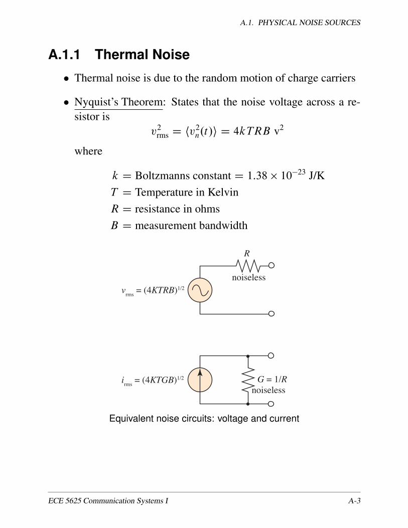
A.1.1 Thermal Noise
� Thermal noise is due to the random motion of charge carriers
� Nyquist’s Theorem: States that the noise voltage across a re-sistor is
v2rms D hv2n.t/i D 4kTRB v2
where
k D Boltzmanns constant D 1:38 � 10�23 J/KT D Temperature in KelvinR D resistance in ohmsB D measurement bandwidth
R
G = 1/R
vrms
= (4KTRB)1/2
irms
= (4KTGB)1/2
noiseless
noiseless
Equivalent noise circuits: voltage and current
ECE 5625 Communication Systems I A-3
CONTENTS
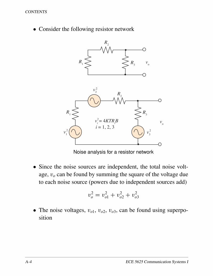
� Consider the following resistor network
R1
R1
R2
R2
R3
R3
vo
vo
v12
v22
v32
vi = 4KTR
iB2
i = 1, 2, 3
Noise analysis for a resistor network
� Since the noise sources are independent, the total noise volt-age, vo can be found by summing the square of the voltage dueto each noise source (powers due to independent sources add)
v2o D v2o1 C v
2o2 C v
2o3
� The noise voltages, vo1, vo2, vo3, can be found using superpo-sition
A-4 ECE 5625 Communication Systems I
A.1. PHYSICAL NOISE SOURCES
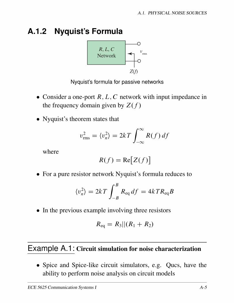
A.1.2 Nyquist’s Formula
R, L, CNetwork
vrms
Z(f)
Nyquist’s formula for passive networks
� Consider a one-port R;L;C network with input impedance inthe frequency domain given by Z.f /
� Nyquist’s theorem states that
v2rms D hv2ni D 2kT
Z1
�1
R.f / df
whereR.f / D Re
�Z.f /
�� For a pure resistor network Nyquist’s formula reduces to
hv2ni D 2kT
Z B
�B
Req df D 4kTReqB
� In the previous example involving three resistors
Req D R3jj.R1 CR2/
Example A.1: Circuit simulation for noise characterization
� Spice and Spice-like circuit simulators, e.g. Qucs, have theability to perform noise analysis on circuit models
ECE 5625 Communication Systems I A-5
CONTENTS
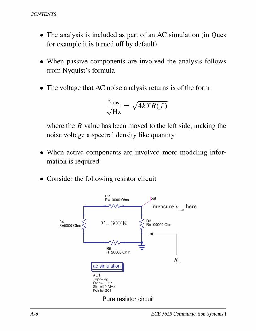
� The analysis is included as part of an AC simulation (in Qucsfor example it is turned off by default)
� When passive components are involved the analysis followsfrom Nyquist’s formula
� The voltage that AC noise analysis returns is of the form
vrmsp
HzDp4kTR.f /
where the B value has been moved to the left side, making thenoise voltage a spectral density like quantity
� When active components are involved more modeling infor-mation is required
� Consider the following resistor circuit
Req
measure vrms
here
T = 300oK
Pure resistor circuit
A-6 ECE 5625 Communication Systems I
A.1. PHYSICAL NOISE SOURCES
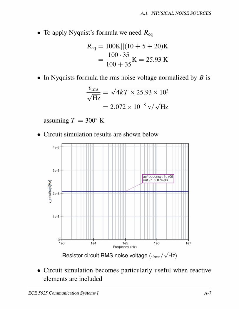
� To apply Nyquist’s formula we need Req
Req D 100Kjj.10C 5C 20/K
D100 � 35
100C 35K D 25:93 K
� In Nyquists formula the rms noise voltage normalized by B isvrmsp
HzD
p
4kT � 25:93 � 103
D 2:072 � 10�8 v=p
Hz
assuming T D 300ı K
� Circuit simulation results are shown below
Resistor circuit RMS noise voltage (vrms=p
Hz)
� Circuit simulation becomes particularly useful when reactiveelements are included
ECE 5625 Communication Systems I A-7
CONTENTS
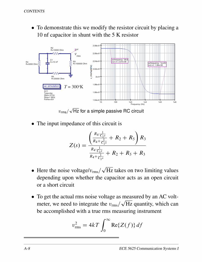
� To demonstrate this we modify the resistor circuit by placing a10 nf capacitor in shunt with the 5 K resistor
vrms
T = 300oK
vrms=p
Hz for a simple passive RC circuit
� The input impedance of this circuit is
Z.s/ D
�R4�
1C1s
R4C1C1s
CR2 CR5
�R3
R4�1C1s
R4C1C1s
CR2 CR5 CR3
� Here the noise voltage/vrms=p
Hz takes on two limiting valuesdepending upon whether the capacitor acts as an open circuitor a short circuit
� To get the actual rms noise voltage as measured by an AC volt-meter, we need to integrate the vrms=
pHz quantity, which can
be accomplished with a true rms measuring instrument
v2rms D 4kT
Z1
0
RefZ.f /g df
A-8 ECE 5625 Communication Systems I

A.1. PHYSICAL NOISE SOURCES
Example A.2: Active circuit modeling
� For Op-Amp based circuits noise model information is usuallyavailable from the data sheet1
� Circuit simulators include noise voltage and current sourcesjust for this purpose
en
inn
inp
NoiselessOp Amp+
−
Op Amp Noise Model
741 Noise Data
Op amp noise model with 741 data sheet noise information
� Consider an inverting amplifier with a gain of 10 using a 741op-amp
� This classic op amp, has about a 1MHz gain-bandwidth prod-uct, so with a gain of 10, the 3 dB cutoff frequency of theamplifier is at about 100 kHz
� The noise roll-off is at the same frequency1Ron Mancini, editor, Op Amps for Everyone: Design Reference, Texas Instruments Advanced
Analog Products, Literature number SLOD006, September 2000.
ECE 5625 Communication Systems I A-9
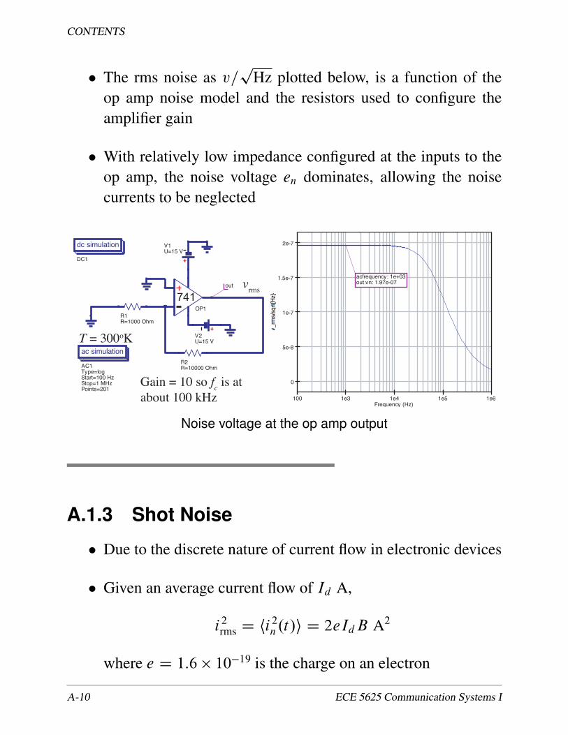
CONTENTS
� The rms noise as v=p
Hz plotted below, is a function of theop amp noise model and the resistors used to configure theamplifier gain
� With relatively low impedance configured at the inputs to theop amp, the noise voltage en dominates, allowing the noisecurrents to be neglected
741
Gain = 10 so fc is at
about 100 kHz
vrms
T = 300oK
Noise voltage at the op amp output
A.1.3 Shot Noise
� Due to the discrete nature of current flow in electronic devices
� Given an average current flow of Id A,
i2rms D hi2n.t/i D 2eIdB A2
where e D 1:6 � 10�19 is the charge on an electron
A-10 ECE 5625 Communication Systems I
A.1. PHYSICAL NOISE SOURCES
� Special Case: For a PN junction diode
I D Is
�exp
�eV
kT
�� 1
�A
where Is is the reverse saturation current
� Assuming Is and Is exp.eV=kT / to be independent sources interms of noise sources, then
i2rms,tot D
�2eIs exp
�eV
kT
�C 2eIs
�B
D 2e�I C Is
�B A2
� For I � Is the diode differential conductance is
go DdI
dVDeI
kT;
thusirms,tot ' 2eIB D 2kTgoB
which is half the noise due to a pure resistance
A.1.4 Other Noise Sources
� Generation-Recombination Noise: Results from generated freecarriers recombining in a semiconductor (like shot noise)
� Temperature-Fluctuation Noise: Results from fluctuating heatexchange between devices and the environment
� Flicker Noise: Has a spectral density of the form 1=f ˛ ' 1=f ,also known as pink noise; the physics is not well understood
ECE 5625 Communication Systems I A-11
CONTENTS
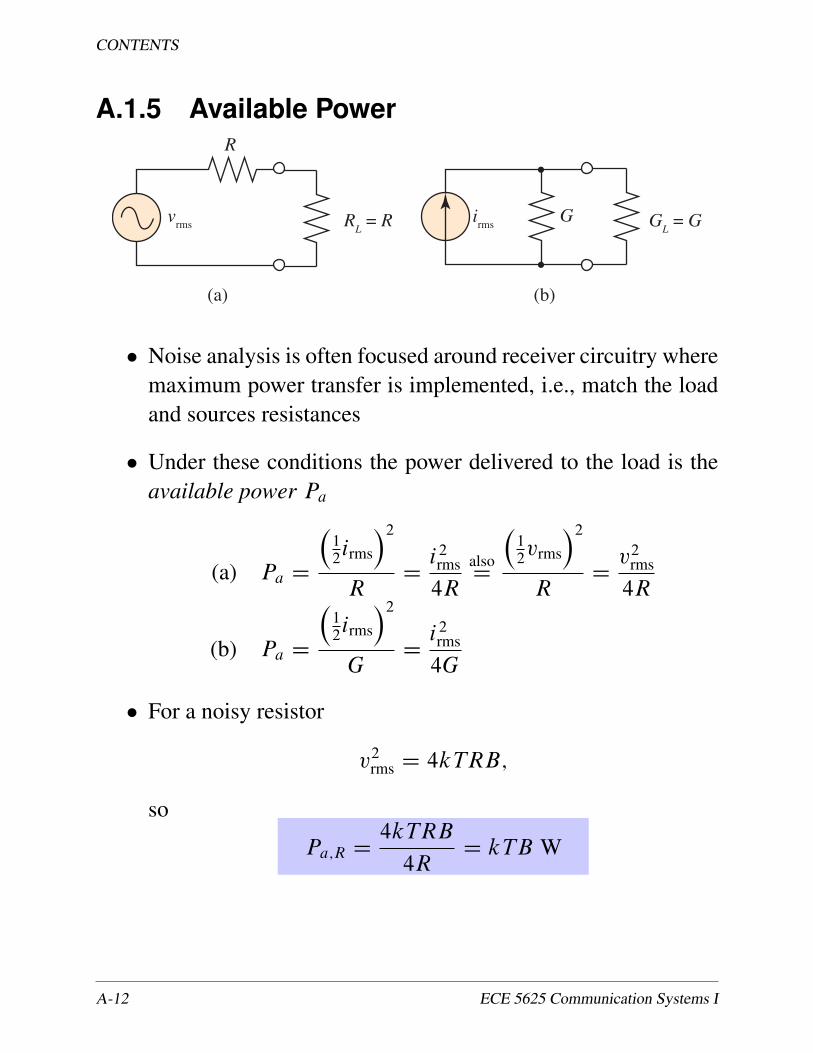
A.1.5 Available PowerR
G RL = R G
L = G
(a) (b)
vrms
irms
� Noise analysis is often focused around receiver circuitry wheremaximum power transfer is implemented, i.e., match the loadand sources resistances
� Under these conditions the power delivered to the load is theavailable power Pa
(a) Pa D
�12irms
�2R
Di2rms
4R
alsoD
�12vrms
�2R
Dv2rms
4R
(b) Pa D
�12irms
�2G
Di2rms
4G
� For a noisy resistor
v2rms D 4kTRB;
so
Pa;R D4kTRB
4RD kTB W
A-12 ECE 5625 Communication Systems I
A.1. PHYSICAL NOISE SOURCES
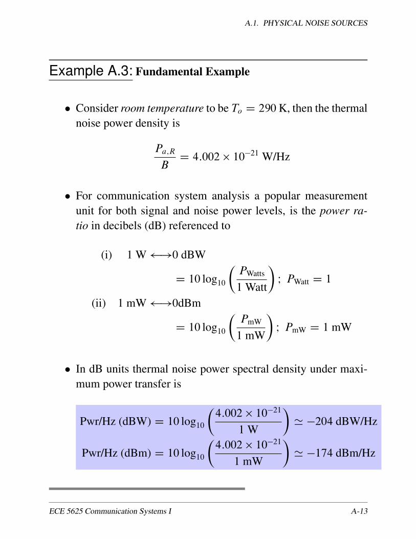
Example A.3: Fundamental Example
� Consider room temperature to be To D 290K, then the thermalnoise power density is
Pa;R
BD 4:002 � 10�21 W/Hz
� For communication system analysis a popular measurementunit for both signal and noise power levels, is the power ra-tio in decibels (dB) referenced to
(i) 1 W !0 dBW
D 10 log10
�PWatts
1 Watt
�I PWatt D 1
(ii) 1 mW !0dBm
D 10 log10
�PmW
1 mW
�I PmW D 1 mW
� In dB units thermal noise power spectral density under maxi-mum power transfer is
Pwr/Hz (dBW) D 10 log10
�4:002 � 10�21
1 W
�' �204 dBW/Hz
Pwr/Hz (dBm) D 10 log10
�4:002 � 10�21
1 mW
�' �174 dBm/Hz
ECE 5625 Communication Systems I A-13
CONTENTS
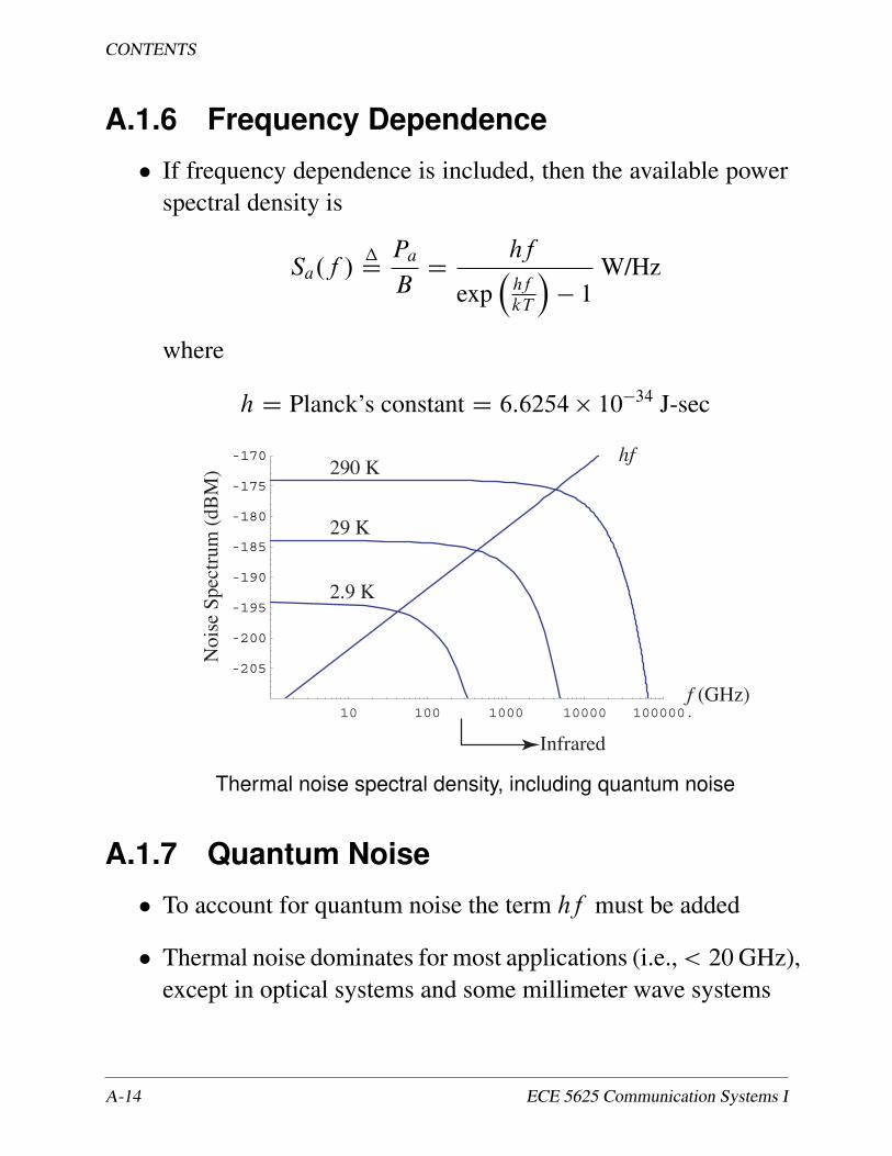
A.1.6 Frequency Dependence
� If frequency dependence is included, then the available powerspectral density is
Sa.f /�DPa
BD
hf
exp�hf
kT
�� 1
W/Hz
where
h D Planck’s constant D 6:6254 � 10�34 J-sec
10 100 1000 10000 100000.
-205
-200
-195
-190
-185
-180
-175
-170
f (GHz)
Infrared
hf290 K
29 K
2.9 K
Noi
se S
pect
rum
(dB
M)
Thermal noise spectral density, including quantum noise
A.1.7 Quantum Noise
� To account for quantum noise the term hf must be added
� Thermal noise dominates for most applications (i.e.,< 20GHz),except in optical systems and some millimeter wave systems
A-14 ECE 5625 Communication Systems I
A.2. CHARACTERIZATION OF NOISE IN SYSTEMS
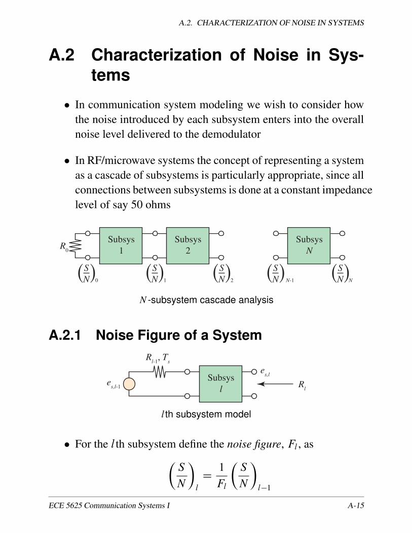
A.2 Characterization of Noise in Sys-tems
� In communication system modeling we wish to consider howthe noise introduced by each subsystem enters into the overallnoise level delivered to the demodulator
� In RF/microwave systems the concept of representing a systemas a cascade of subsystems is particularly appropriate, since allconnections between subsystems is done at a constant impedancelevel of say 50 ohms
Subsys1
Subsys2
SubsysNR
0
SN)) 0
SN)) 1
SN)) 2
SN)) N
SN)) N-1
N -subsystem cascade analysis
A.2.1 Noise Figure of a System
Subsysl R
l
es,l
es,l-1
Rl-1
, Ts
l th subsystem model
� For the l th subsystem define the noise figure, Fl , as�S
N
�l
D1
Fl
�S
N
�l�1
ECE 5625 Communication Systems I A-15
CONTENTS
� Ideally, Fl D 1, in practice Fl > 1, meaning that each subsys-tems generates some noise of its own
� In dB the noise figure (NF) is
FdB D 10 log10Fl
� Assuming the subsystem input and output impedances (resis-tances) are matched, then our analysis may be done in terms ofthe available signal power and available noise power
� For the l th subsystem the available signal power at the input is
Psa;l�1 De2s;l�1
4Rl�1
� Assuming thermal noise only, the available noise power is
Pna;l�1 D kTsB
where Ts denotes the source temperature
� Assuming that the l th subsystem (device) has power gain Ga,it follows that
Psa;l D GaPsa;l�1
where we have also assumed the system is linear
� We can now write that�S
N
�l
DPsa;l
Pna;lD
1
Fl
Psa;l�1
Pna;l�1D
1
Fl
�S
N
�l�1
which implies that
Fl DPsa;l�1
Pna;l�1�Pna;l
Psa;l„ƒ‚…GaPsa;l�1
DPna;l
Ga Pna;l�1„ƒ‚…kTsB
A-16 ECE 5625 Communication Systems I
A.2. CHARACTERIZATION OF NOISE IN SYSTEMS
� NowPna;l D GaPna;l�1 C Pint;l
where Pint;l is internally generated noise
� Finally we can write that
Fl D 1CPint;l
GakTsB
– Note that if Ga � 1 ) Fl ' 1, assuming that Ga isindependent of Pint;l
� As a standard, NF is normally given with Ts D T0 D 290 K,so
Fl D 1CPint;l
GakT0B
A.2.2 Measurement of Noise Figure
� In practice NF is measured using one or two calibrated noisesources
Method #1
� A source can be constructed using a saturated diode which pro-duces noise current
Ni2n D 2eIdB A2
� The current passing through the diode is adjusted until thenoise power at the output of the devide under test (DUT) isdouble the amount obtained without the diode, then we obtain
F DeIdRs
2kT0
ECE 5625 Communication Systems I A-17
CONTENTS
where Rs is the diode series resistance and Id is the diode cur-rent
Method #2
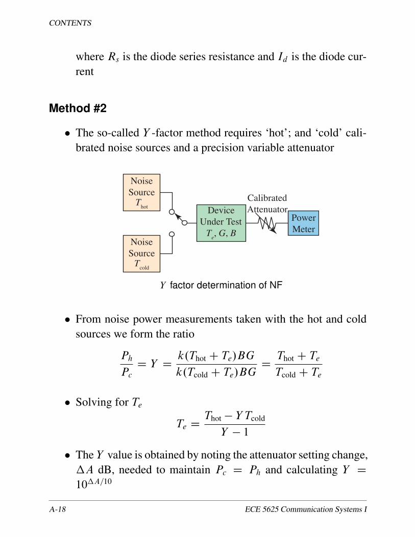
� The so-called Y -factor method requires ‘hot’; and ‘cold’ cali-brated noise sources and a precision variable attenuator
NoiseSourceT
hot
NoiseSourceT
cold
DeviceUnder TestTe, G, B
PowerMeter
CalibratedAttenuator
Y factor determination of NF
� From noise power measurements taken with the hot and coldsources we form the ratio
Ph
PcD Y D
k.Thot C Te/BG
k.Tcold C Te/BGDThot C Te
Tcold C Te
� Solving for Te
Te DThot � Y Tcold
Y � 1
� The Y value is obtained by noting the attenuator setting change,�A dB, needed to maintain Pc D Ph and calculating Y D10�A=10
A-18 ECE 5625 Communication Systems I
A.2. CHARACTERIZATION OF NOISE IN SYSTEMS
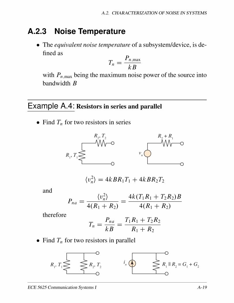
A.2.3 Noise Temperature
� The equivalent noise temperature of a subsystem/device, is de-fined as
Tn DPn;max
kBwith Pn;max being the maximum noise power of the source intobandwidth B
Example A.4: Resistors in series and parallel
� Find Tn for two resistors in series
vn
R2, T
2
R1, T
1
R2 + R
1
hv2ni D 4kBR1T1 C 4kBR2T2
and
Pna Dhv2ni
4.R1 CR2/D4k.T1R1 C T2R2/B
4.R1 CR2/
thereforeTn D
Pna
kBDT1R1 C T2R2
R1 CR2
� Find Tn for two resistors in parallel
in R
1 || R
2 = G
1 + G
2R1, T
1R
2, T
2
ECE 5625 Communication Systems I A-19
CONTENTS
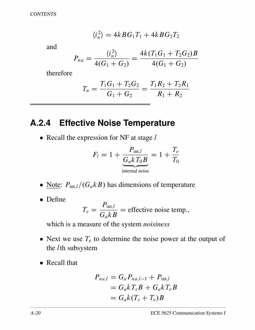
hi2ni D 4kBG1T1 C 4kBG2T2
and
Pna Dhi2ni
4.G1 CG2/D4k.T1G1 C T2G2/B
4.G1 CG2/
therefore
Tn DT1G1 C T2G2
G1 CG2DT1R2 C T2R1
R1 CR2
A.2.4 Effective Noise Temperature
� Recall the expression for NF at stage l
Fl D 1CPint;l
GakT0B„ ƒ‚ …internal noise
D 1CTe
T0
� Note: Pint;l=.GakB/ has dimensions of temperature
� DefineTe D
Pint;l
GakBD effective noise temp.;
which is a measure of the system noisiness
� Next we use Te to determine the noise power at the output ofthe l th subsystem
� Recall that
Pna;l D GaPna;l�1 C Pint;l
D GakTsB CGakTeB
D Gak.Ts C Te/B
A-20 ECE 5625 Communication Systems I
A.2. CHARACTERIZATION OF NOISE IN SYSTEMS
� This references all of the noise to the subsystem input by virtueof the Ga term
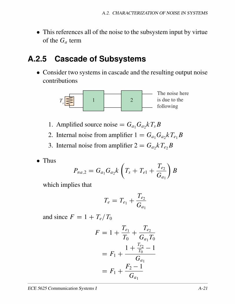
A.2.5 Cascade of Subsystems
� Consider two systems in cascade and the resulting output noisecontributions
1 2Ts
The noise here is due to the following
1. Amplified source noiseD Ga1Ga2kTsB
2. Internal noise from amplifier 1D Ga1Ga2kTe1B
3. Internal noise from amplifier 2D Ga2kTe2B
� Thus
Pna;2 D Ga1Ga2k
�Ts C Te1 C
Te2Ga1
�B
which implies that
Te D Te1 CTe2Ga1
and since F D 1C Te=T0
F D 1CTe1T0C
Te2Ga1T0
D F1 C1C
Te2T0� 1
Ga1
D F1 CF2 � 1
Ga1
ECE 5625 Communication Systems I A-21
CONTENTS
� In general for an arbitrary number of stages (Frii’s formula)
F D F1 CF2 � 1
Ga1CF3 � 1
Ga1Ga2C � � �
Te D Te1 CTe2Ga1C
Te3Ga1Ga2
C � � �
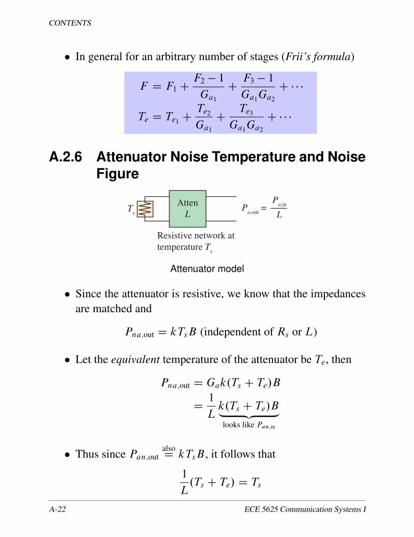
A.2.6 Attenuator Noise Temperature and NoiseFigure
AttenL
Ts
Pa,out
=Pa,in
L
Resistive network at temperature T
s
Attenuator model
� Since the attenuator is resistive, we know that the impedancesare matched and
Pna;out D kTsB (independent of Rs or L)
� Let the equivalent temperature of the attenuator be Te, then
Pna;out D Gak.Ts C Te/B
D1
Lk.Ts C Te/B„ ƒ‚ …
looks like Pan;in
� Thus since Pan;outalsoD kTsB , it follows that
1
L.Ts C Te/ D Ts
A-22 ECE 5625 Communication Systems I
A.2. CHARACTERIZATION OF NOISE IN SYSTEMS
orTe D .1 � L/Ts
� Now since
F D 1CTe
T0D 1C
.L � 1/Ts
T0
with Ts D T0 (i.e., attenuator at room temperature)
Fattn D 1C L � 1 D L
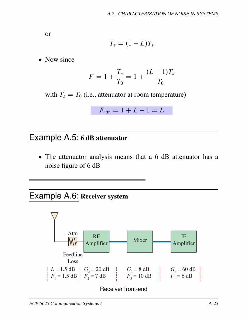
Example A.5: 6 dB attenuator
� The attenuator analysis means that a 6 dB attenuator has anoise figure of 6 dB
Example A.6: Receiver system
RFAmplifier
IFAmplifierMixer
Attn
FeedlineLoss
L = 1.5 dB G2 = 20 dB G
3 = 8 dB G
4 = 60 dB
F1 = 1.5 dB F
2 = 7 dB F
3 = 10 dB F
4 = 6 dB
Receiver front-end
ECE 5625 Communication Systems I A-23
CONTENTS
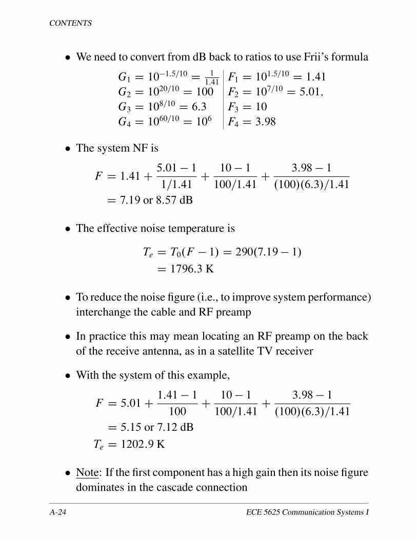
� We need to convert from dB back to ratios to use Frii’s formula
G1 D 10�1:5=10 D
11:41
F1 D 101:5=10 D 1:41
G2 D 1020=10 D 100 F2 D 10
7=10 D 5:01;
G3 D 108=10 D 6:3 F3 D 10
G4 D 1060=10 D 106 F4 D 3:98
� The system NF is
F D 1:41C5:01 � 1
1=1:41C
10 � 1
100=1:41C
3:98 � 1
.100/.6:3/=1:41
D 7:19 or 8:57 dB
� The effective noise temperature is
Te D T0.F � 1/ D 290.7:19 � 1/
D 1796:3 K
� To reduce the noise figure (i.e., to improve system performance)interchange the cable and RF preamp
� In practice this may mean locating an RF preamp on the backof the receive antenna, as in a satellite TV receiver
� With the system of this example,
F D 5:01C1:41 � 1
100C
10 � 1
100=1:41C
3:98 � 1
.100/.6:3/=1:41
D 5:15 or 7:12 dBTe D 1202:9 K
� Note: If the first component has a high gain then its noise figuredominates in the cascade connection
A-24 ECE 5625 Communication Systems I

A.2. CHARACTERIZATION OF NOISE IN SYSTEMS
� Note: The antenna noise temperature has been omitted, butcould be very important
Example A.7: Receiver system with antenna noise tempera-ture
RFAmplifier
IFAmplifierMixer
Attn
FeedlineLoss
L = 1.5 dB G2 = 20 dB G
3 = 8 dB G
4 = 60 dB
F1 = 1.5 dB F
2 = 7 dB F
3 = 10 dB F
4 = 6 dB
Ts = 400 K
F = 7.19 or FdB
= 8.57 dB, Te = 1796.3 K
� Rework the previous example, except now we calculate avail-able noise power and signal power with additional assumptionsabout the receiving antenna
� Suppose the antenna has an effective noise temperature of Ts D400 K and the system bandwidth is B D 100 kHz
� What is the maximum available output noise power in dBm?
� Since
Pna D Gak.Ts C Te/B D .Ga/.kT0/
�Ts C Te
T0
�.B/
ECE 5625 Communication Systems I A-25
CONTENTS
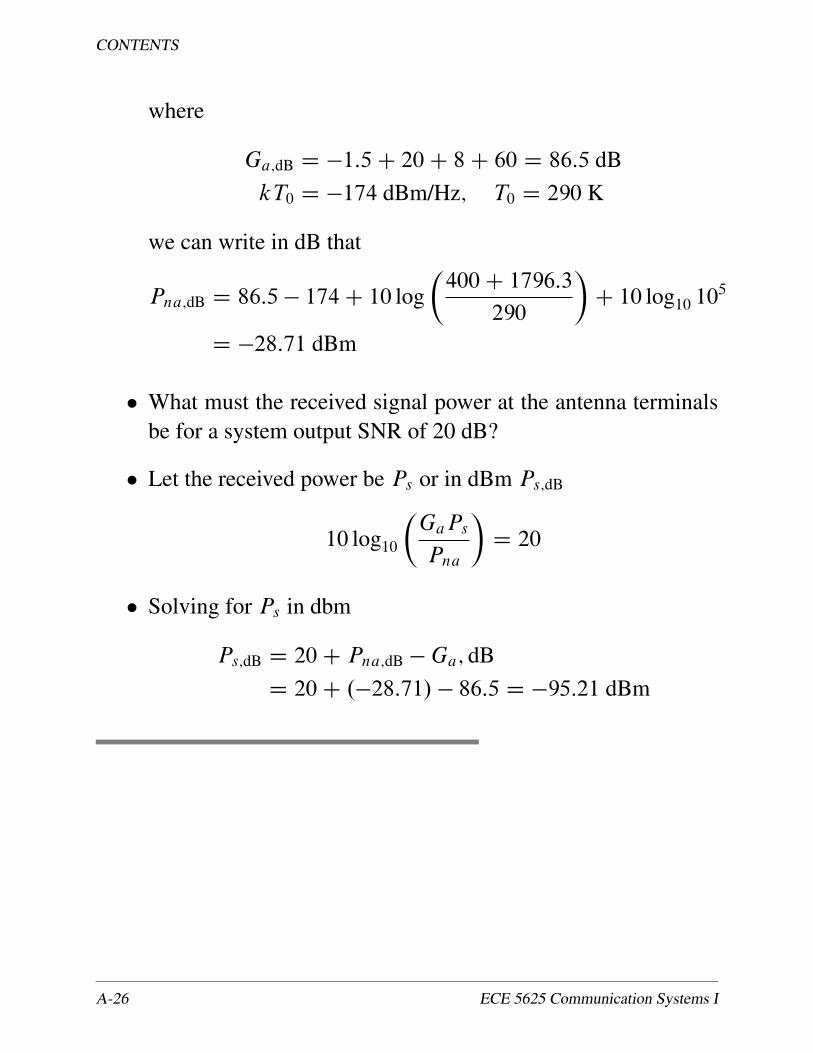
where
Ga;dB D �1:5C 20C 8C 60 D 86:5 dBkT0 D �174 dBm/Hz; T0 D 290 K
we can write in dB that
Pna;dB D 86:5 � 174C 10 log�400C 1796:3
290
�C 10 log10 10
5
D �28:71 dBm
� What must the received signal power at the antenna terminalsbe for a system output SNR of 20 dB?
� Let the received power be Ps or in dBm Ps;dB
10 log10
�GaPs
Pna
�D 20
� Solving for Ps in dbm
Ps;dB D 20C Pna;dB �Ga; dBD 20C .�28:71/ � 86:5 D �95:21 dBm
A-26 ECE 5625 Communication Systems I
A.3. FREE-SPACE PROPAGATION CHANNEL
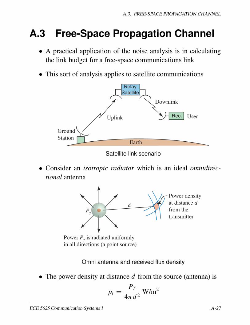
A.3 Free-Space Propagation Channel
� A practical application of the noise analysis is in calculatingthe link budget for a free-space communications link
� This sort of analysis applies to satellite communications
RelaySatellite
Rec.
GroundStation
UserUplink
Downlink
Earth
Satellite link scenario
� Consider an isotropic radiator which is an ideal omnidirec-tional antenna
P
Power PT is radiated uniformly
in all directions (a point source)
Power density at distance d from the transmitter
d
Omni antenna and received flux density
� The power density at distance d from the source (antenna) is
pt DPT
4�d 2W/m2
ECE 5625 Communication Systems I A-27
CONTENTS
� An antenna with directivity (more power radiated in a par-ticular direction), is described by a power gain, GT , over anisotropic antenna
� For an aperture-type antenna, e.g., a parabolic dish antenna,with aperture area, AT , such that
AT � �2
with � the transmit wavelength, GT is given by
GT D4�AT
�2
� Assuming a receiver antenna with aperture area, AR, it followsthat the received power is
PR D ptAR DPTGT
4�d 2� AR
DPTGTGR�
2
.4�d/2
since AR D GR�2=.4�/
� For system analysis purposes modify the PR expression to in-clude a fudge factor called the system loss factor, L0, then wecan write
PR D
��
4�d
�2„ ƒ‚ …
Free space loss
PTGTGR
L0
A-28 ECE 5625 Communication Systems I

A.3. FREE-SPACE PROPAGATION CHANNEL
� In dB (actually dBW or dBm) we have
PR;dB D 10 log10PR
D 20 log10
��
4�d
�C 10 log10PT C 10 log10GT„ ƒ‚ …
EIRP
C 10 log10GR � 10 log10L0
where EIRP denotes the effective isotropic radiated power
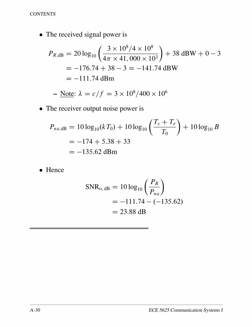
Example A.8: Free-Space Propagation
� Consider a free-space link (satellite communications) where
Trans. EIRP D .28C 10/ D 38 dBWTrans. Freq D 400 MHz
� The receiver parameters are:
Rec. noise temp. D Ts C Te D 1000 KRec. ant. gain D 0 dB
Rec. system loss L0/ D 3 dBRec. bandwidth D 2 kHz
Path length d D 41; 000 Km
� Find the output SNR in the 2 kHz receiver bandwidth
ECE 5625 Communication Systems I A-29
CONTENTS
� The received signal power is
PR;dB D 20 log10
�3 � 108=4 � 108
4� � 41; 000 � 103
�C 38 dBWC 0 � 3
D �176:74C 38 � 3 D �141:74 dBWD �111:74 dBm
– Note: � D c=f D 3 � 108=400 � 106
� The receiver output noise power is
Pna;dB D 10 log10.kT0/C 10 log10
�Ts C Te
T0
�C 10 log10B
D �174C 5:38C 33
D �135:62 dBm
� Hence
SNRo, dB D 10 log10
�PR
Pna
�D �111:74 � .�135:62/
D 23:88 dB
A-30 ECE 5625 Communication Systems I
Related Documents