A Wideband Microwave Transceiver Front-end for an Airborne Software Defined Radio Experiment Arthur P Blair Jr Thesis submitted to the faculty of the Virginia Polytechnic Institute and State University in partial fulfillment of the requirements for the degree of Master of Science In Electrical Engineering Robert McGwier Dennis Sweeney Jeffery Reed Dec 9 th , 2014 Blacksburg VA Keywords: Microwave front-end, software defined radio

Welcome message from author
This document is posted to help you gain knowledge. Please leave a comment to let me know what you think about it! Share it to your friends and learn new things together.
Transcript

A Wideband Microwave Transceiver Front-end for an Airborne Software Defined Radio
Experiment
Arthur P Blair Jr
Thesis submitted to the faculty of the Virginia Polytechnic Institute and State University
in partial fulfillment of the requirements for the degree of
Master of Science
In
Electrical Engineering
Robert McGwier
Dennis Sweeney
Jeffery Reed
Dec 9th, 2014
Blacksburg VA
Keywords: Microwave front-end, software defined radio

A Wideband Microwave Transceiver Front-end for an Airborne Software Defined Radio
Experiment
Arthur P Blair Jr
ABSTRACT
This document describes the design, simulation, construction, and test of a
wideband analog transceiver front-end for use in an airborne software defined radio
(SDR) experiment. The transceiver must operate in the GSM-1800 and IEEE 802.11b/g
WiFi frequency bands and accommodate beamforming. It consists of a transmitter and
dual band receiver. The receiver input is fed by a helical antenna and the outputs are
digitized for use in the SDR. The transmitter is fed by a complex baseband output from a
Digital-to-Analog Converter (DAC) and its output fed to another helical antenna. The
requirements for the transceiver were driven by a spectral survey of the operating
environment and the physical and electrical limitations of the platform. The spectral
survey showed a great disparity in the received power levels between the signals of
interest and potential interferers. Simulations of several candidate receiver architectures
showed that meeting the needs of the experiment would require a high degree of linearity
and filtering. It was found that the receiver requirements could be met by a single
downconversion with high order filters and passband sampling. A series of analyses
determined the requirements of the individual components that make up the system.
Performance was verified by simulations using measured data of the individual
components and lab tests of the assembled hardware. Suggestions for improved
performance and expanded operation are made.

iii
Table of Contents
1. Introduction…………………………………...…………………..... 1
2. Principles of Receiver Design…………………...…………………. 5
3. Requirements Analysis…………………………..………………… 24
4. Design and Performance………………………………………….... 34
5. Conclusions……………………………………………………........ 56
References………………………………………………………….. 60
Appendix A………………………………………………………… 61
Appendix B………………………………………………………… 62

iv
List of Figures:
Figure 1 A high level block diagram of the transceiver ...................................................... 3
Figure 2 Simplified receiver ............................................................................................... 6
Figure 3 Direct Conversion Receiver. ................................................................................ 7
Figure 4 Superheterodyne receiver ..................................................................................... 8
Figure 5 Passband sampling uses aliasing to do the last downconversion ......................... 9
Figure 6 Noisy 2-port driven by matched source.............................................................. 10
Figure 7 Transfer function of a nonlinear device. ............................................................. 11
Figure 8 3rd order 2 tone intermodulation ........................................................................ 13
Figure 9 2-tone spur free dynamic range. All powers are referenced to the input ........... 14
Figure 10 A simple receiver. The sample-&-hold and quantizer make up the ADC........ 17
Figure 11 The transfer function of a mid-tread quantizer ................................................. 18
Figure 12 Simulation setup to study dithering .................................................................. 18
Figure 13 Voltage out of the quantizer with Vin=0.49q and no noise .............................. 19
Figure 14 Voltage out of the quantizer with Vin=0.49q and added noise with Vrms = q/2 19
Figure 15 Spectrum of the output of the quantizer shows the signal can be recovered .... 19
Figure 16 Spectrum of quantizer output with weak signal and no noise .......................... 20
Figure 17 Spectrum of quantizer output with weak signal and noise rms=q/2 ................. 20
Figure 18 Mixer spur chart ............................................................................................... 21
Figure 19 Flow of requirements from mission to system ................................................. 25
Figure 20 The minimum set of components preceding the front end ............................... 28
Figure 21 The final transceiver front-end design. ............................................................. 34
Figure 22 Spur charts for low and high side injection in wideband path tuned to GSM
band ................................................................................................................................... 36
Figure 23 - First iteration of the receiver design............................................................... 36
Figure 24 Genesys model for the receiver ........................................................................ 40
Figure 25 The transmitter.................................................................................................. 42
Figure 26 The built-in-test system .................................................................................... 42
Figure 27 The plates from the wideband IF box ............................................................... 43
Figure 28 The components in the narrowband box. ......................................................... 44
Figure 29 The RF box ....................................................................................................... 44
Figure 30 The transmitter.................................................................................................. 45
Figure 31 Test set used for frequency response ................................................................ 46
Figure 32 Frequency response of wideband path tuned to the GSM-1800 band .............. 46
Figure 33 Frequency response of wideband path when tuned to WiFi band .................... 47
Figure 34 The frequency response of one narrowband path tuned to 1710 MHz............. 48
Figure 35 The in-band frequency response of one narrowband path tuned to 1710 MHz.
........................................................................................................................................... 48
Figure 36 Frequency response of one narrowband path when tuned to 2415 MHz. ........ 49
Figure 37 In-band frequency response of one narrowband path when tuned to 2415 MHz.
........................................................................................................................................... 49
Figure 38 Receiver gain vs input power level reveals the input 1dB compression point . 51
Figure 39 Measuring the 3rd order input intercept point .................................................. 52
Figure 40 Output of wideband path when BIT source is injected .................................... 54
Figure 41 A more complex design that offers better performance and broader frequency
coverage ............................................................................................................................ 57

v
Figure 42 The assembled wideband & narrowband IF boxes ........................................... 58
Figure 43 A better assembly for the IF boxes ................................................................... 58

vi
List of Tables:
Table 1 Performance of final front-end design ................................................................... 3 Table 2 Mixer spur table for Marki Microwave T3A mixers. Values listed are in dB
relative to desired output. .................................................................................................. 17 Table 3 Emitters of interest ............................................................................................... 26 Table 4 Power levels from emitters of interest ................................................................. 29 Table 5 Potential interference sources .............................................................................. 29 Table 6 NEXRAD & ARSR radar specifications ............................................................. 30
Table 7 First iteration of wideband receiver chain ........................................................... 38 Table 8 Performance of first iteration wideband receiver design ..................................... 38 Table 9 First iteration of narrowband receiver design ...................................................... 39 Table 10 Performance of first iteration narrowband receiver design ............................... 39
Table 11 Comparison of test results to hardware requirements ........................................ 55

1
CHAPTER 1
INTRODUCTION
Past work in airborne software defined radio (SDR) systems used in cognitive
radio networks has revealed a need for a wideband analog front-end to precede the analog
to digital converter (ADC) [1]. The prior work showed that although a direct to digital
approach could meet the performance requirements, the throughput that results required
hardware that was too large, too heavy, and consumed too much power for an airborne
platform. An analog front end can help alleviate all three issues by reducing the
throughput requirements of the digital hardware that follows the ADC. This document
describes the design and performance of an analog front-end to support an airborne
software defined radio transceiver. Chapter 1 briefly describes the overall project
mission, describes the final transceiver design, and provides a roadmap to the rest of the
document.
1.1 The Supported Mission
The mission of the overall system that the front end supports is to coordinate
frequency use and provide interconnectivity between similar and dissimilar data and
voice links from an airborne platform. For the current research only users in the GSM-
1800 and IEEE 802.11B & G WiFi bands are supported.
Different needs, different manufacturers, different services, & even different
countries have resulted in a wide variety of technologies used for data and voice
communication links in any modern arena. Add to that the progress in technology that is
not backwards compatible with earlier generation hardware and the result is a lot of links
that are entirely incapable of interconnection. Communication between all users is
essential for not only the most effective deployment of resources but for the safety of
each. Area-wide communication requires that everyone have one of everyone else’s
radios or replacing them all with one standard, neither of which is practical. The
supported system serves as an intermediary between these links. The system can not only
prevent them from interfering with each other but can translate between dissimilar links
enabling seamless interconnectivity of new and old generation technology. Being
airborne enables non-line-of-sight communication for hardware that would normally be

2
incapable, especially in mountainous terrain. The system ensures every user sees the
same picture despite vastly different perspectives.
Software defined radio is uniquely suited to such a mission. Trying to
accommodate such a wide variety of signal and data formats would be difficult to
accomplish in dedicated hardware and would require a constant stream of new hardware
as technology progressed. Being in an airborne platform places limits on the size, weight,
and power consumption of the system. But an entirely digital solution, digitizing without
a downconversion, has also proven too cumbersome. Only a combination of analog and
digital technology has the promise of making such a radio-agnostic system small, light,
and efficient enough to operate in an airborne platform.
1.2 The Transceiver
A block diagram of the final transceiver design is shown in figure 1. The frequency
coverage is 1710-2500 MHz to cover the GSM-1800 and IEEE 802.11B/G WiFi bands. It
includes a dual channel receiver and a simple transmitter. One channel of the receiver has
enough bandwidth to cover the entire GSM-1800 or 2.4 GHz WiFi bands to provide a
high probability of interception. But the wideband channel is susceptible to interference
so the system includes a narrowband channel for more detailed analysis of any one
signal. There are two transceivers to accommodate beam-forming. Both include a
common built-in-test (BIT) input to verify that the hardware is working and measure the
phase difference between receivers. The outputs of each receiver are fed to two high
speed ADCs. Each transmitter is driven by two high speed digital to analog converters
(DAC) in quadrature. The IQ modulator translates the complex baseband input to an RF
carrier amplified to 500 mW. The front-end uses mostly off-the-shelf connectorized
components for speed of development. Table 1 lists the performance parameters for the
final design.
3
Figure 1 A high level block diagram of the transceiver
Required Measured
RF coverage (MHz) 1710 - 2500 1710-2500
Wideband
receiver
channel
IF 3dB Bandwidth (MHz) 175 200
Gain (dB) 40 40
Noise figure (dB) 6 (goal) 6.6
3rd order 2-tone input intercept point
(dBm)
-1 -10
1dB input compression point (dBm) -29 -20
Narrowband
receiver
channel
IF 3dB Bandwidth (MHz) 25 25
Gain (dB) 35 35
Noise figure (dB) 6 (goal) 6.3
3rd order 2-tone input intercept point
(dBm)
-1 -10
1dB input compression point (dBm) -25 -21
Transmitter
Frequency coverage (MHz) 1710 - 2500
1 dB output compression point (dBm) 27
Bandwidth (MHz) 25
Table 1 Performance of final front-end design

4
1.3 The Document
The purpose of this document is 3-fold: to describe the work done, to serve as a user
manual for existing hardware, and to serve as a design guide for the front-ends that will
be needed to support future expansions of the current research. Since the receiver is the
most complex element of this transceiver, chapter 2 provides a brief introduction to
receiver design within the scope of the current applications. Chapter 3 describes the flow
of requirements from the mission needs to detailed specifications for the hardware.
Chapter 4 describes the finished transceiver and how the methods in chapter 2 and
requirements of chapter 3 were used to develop it. Also described are the results of
simulations and measurements used to verify the design and the design iterations that
came out of that effort. Simulations are compared to measured data wherever possible.
The test results led to further iterations of the design that are discussed. Finally chapter 5
summarizes the current work and provides a blueprint for follow-on work.

5
Chapter 2
Principles of Receiver Design
Since one purpose of this document is to serve as a design guide for future work it
is worth taking a moment to cover the basic principles of receiver design for the
inexperienced reader. This is a broad area of study so this introduction will be confined to
architectures and issues that are relevant to the current mission and similar applications.
A description of the design process is given followed by a catalog of candidate
architectures. The relevant specifications for the components that make up those
architectures are described. Also discussed are the figures of merit that are commonly
used as goals for the design and to measure the performance of a finished receiver design.
2.1 The design process
There is no universal recipe for receiver design. But for this application the closest
thing to a design algorithm could be [2]
1. From the mission requirements determine the requirements for the
performance of the receiver (as a black box) using the figures-of-merit
described in the section 2.3.
2. Select an architecture from section 2.2.
3. Make a frequency plan that determines the band breaks of the preselector
filter(s), the intermediate frequency (IF) center frequency or frequencies,
and the local oscillator (LO) frequencies. The primary goal of the initial
frequency plan is to minimize the presence of spurious mixer products as
described in section 2.3.
4. Fill in the architecture with generic ideal components including functions
beyond the basic architecture like gain control, protection (power
limiters,) and built-in-test. Use best guess values for gains and losses.
Simulate to verify the basic design.
5. Replace the components with still generic but more realistic components
including noise and nonlinearities. Use catalog data & experience for this
step.

6
6. Optimize the gain distribution between the amplifiers for maximum
dynamic range. The constraints include a fixed system gain and a tolerable
noise performance. A constrained optimization tool is well suited for this
task.
7. If using off-the-shelf hardware, select the parts to use and replace generic
components in design with measured data including s-parameters.
Simulate to verify not only the original performance specifications but
how they vary with frequency and cross channel effects.
8. Simulate using a multitude of signals more representative of the expected
RF environment than a single tone.
9. Iterate until all requirements are met or a tolerable compromise is reached.
The tools used in the current work for the frequency plan and gain
optimization are included in the appendix. Agilent’s system level RF CAD
tool, Genesys, is used for analysis.
2.2 Receiver architectures
A simplified block diagram of a receiver is shown in Figure 2.
Figure 2 Simplified receiver
The preselector filter suppresses signals and noise outside the frequency range of
interest. The preselector is either a single fixed filter, a switched filter bank, or a
continuously tunable filter. The frequency mixer that follows the preselector
translates one band within the preselector bandwidth to a lower intermediate
frequency (IF) where the ADC can digitize it. The last filter picks out one band in the

7
frequency range of interest, suppresses out-of-band products from the mixer, and
suppresses aliasing in the ADC.
2.2.1 Direct Conversion [3]
In a direct conversion receiver, the IF is centered at 0 Hz. This is usually done by
breaking the signal into quadrature components I & Q as shown in Figure 3.
Mathematically the result is a complex baseband version of the signal.
Figure 3 Direct Conversion Receiver.
The advantage of direct conversion is its simplicity which is why it’s a common
approach in GSM and WiFi applications. One disadvantage is that the final passband
is more than one octave wide. That means a signal with frequency less than half the
cutoff frequency of the low pass filters will generate harmonics that fall in-band. And
without some compensation there may be a DC term that can limit the dynamic range
of the system. It is also sensitive to phase and amplitude imbalances between the I &
Q channels over the entire RF bandwidth.
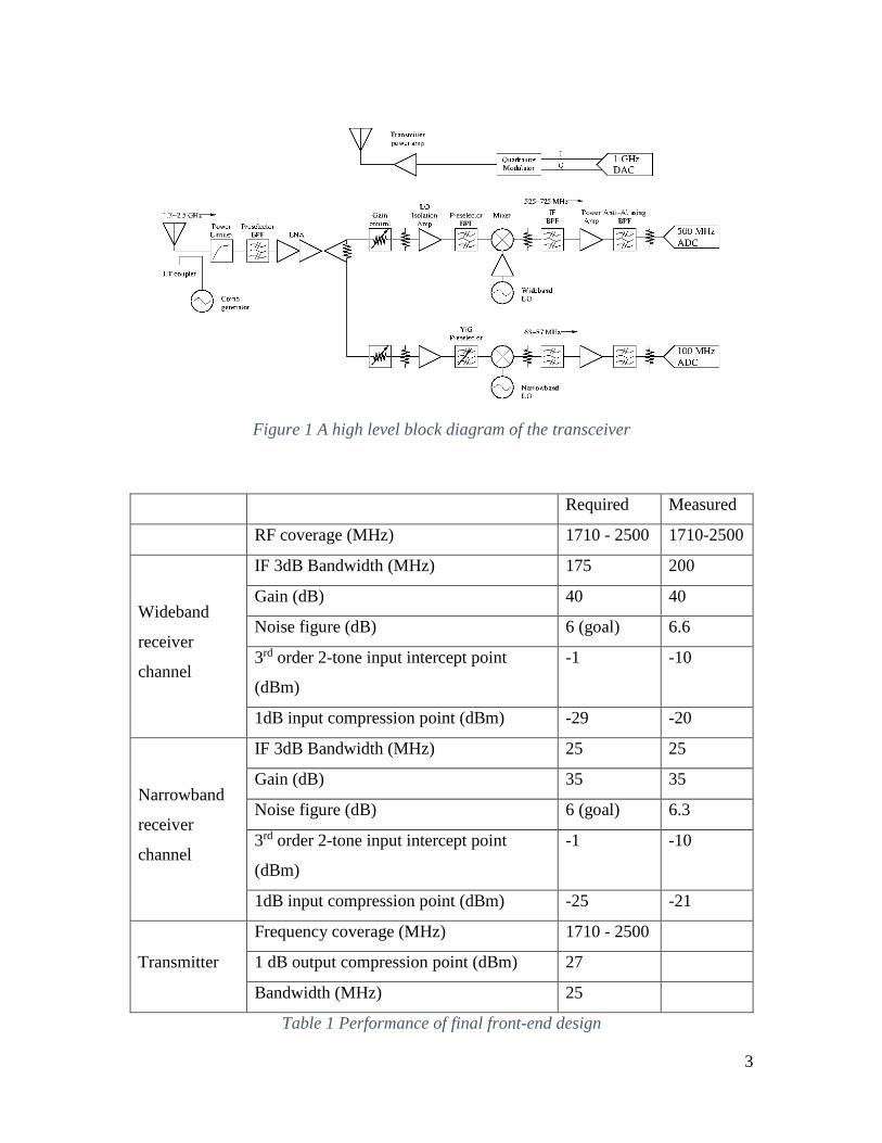
2.2.2 Superheterodyne Conversion [4]
8
In a superheterodyne receiver, the IF passband is centered not at 0 Hz but at some
intermediate frequency that is usually lower than the lowest input RF frequency as
shown in Figure 4. Another conversion translates that signal to a second IF or to
complex baseband. One advantage of the intermediate step is that the quadrature
down conversion in the last stage starts at a lower frequency and only has to operate
over the IF bandwidth which is likely much narrower than the RF coverage. So I/Q
balance is easier to achieve than with direct conversion.
Figure 4 Superheterodyne receiver
2.2.3 Passband Sampling [5]
The downconverter described in this document takes a hybrid approach by
sampling the IF signal without an analog conversion to baseband. This is possible
because the ADC sample rate is much higher than the system bandwidth. The receiver
is shown in Figure 2. By taking advantage of aliasing in the sample-and-hold of the
ADC, the final IF center frequency can be set above the Nyquist frequency or even
above the sampling rate (undersampling) as illustrated in Figure 5. The mixer
performs the first frequency translation and aliasing performs the second. The result
can be down-converted to complex baseband in the DSP subsystem if needed. This
approach has the advantage that the final analog signal bandwidth is less than an

9
octave wide so harmonics fall outside the filter bandwidth. As we’ll see later, a high
final IF center frequency yields fewer spurious terms from the mixer.
Figure 5 Passband sampling uses aliasing to do the last downconversion
2.3 Receiver Figures-of-Merit [2] [6]
For a given bandwidth, the performance of a receiver is measured by the range of
signal power levels and number of signals it can process without corruption by non-ideal
factors in the hardware. This Dynamic Range is set by two criteria. For this application,
the internally-generated noise determines the low end of the dynamic range.
Nonlinearities limit the high end.
2.3.1 Noise Performance and Sensitivity
In this application, the low end of the dynamic range, the sensitivity, of the receiver
is limited by how much internal noise the receiver generates. Every electrical device
generates random thermal noise, well modeled as Gaussian and white within the system
bandwidth [7]. An ordinary resistor generates a random noise voltage level of √4𝑘𝑇𝐵𝑅
Vrms where k is Boltzmanns constant (8.854 x 10⁻¹² W/K), T is temperature in Kelvin, R
is the resistance in ohms, and B is the noise bandwidth in Hz. Since every circuit has
some resistivity, even passive devices contribute. Active devices like amplifiers have
their own noise sources in the semiconductors. Together these noise sources combine
with the finite bandwidth of the system to produce a noise power spectral density at the
output of a receiver chain below which a signal cannot be detected with any confidence.
The noise bandwidth is determined by the signal processing in the DSP subsystem. For
purposes of comparison, the noise power is typically referenced to the input of the
receiver so it appears mathematically as an additive source followed by a noiseless
receiver.

10
Figure 6 shows a noisy 2-port device driven by a matched source. The matched
source impedance Z0 delivers a noise power of kTB. The noise figure (F) of the device is
a measure of how much excess noise it generates. It is defined as the ratio of the input
and output signal to noise ratios (SNR) when the only source of input noise is the
matched source impedance [8].
𝐹 =
𝑆𝑖𝑁𝑖⁄
𝑆𝑜𝑁𝑜⁄
(1)
Noise figure is usually expressed in dB. The ratio of the signal powers is just the gain of
the device so
𝐹 =
𝑁𝑜𝐺𝑁𝑖
=𝑁𝑜
𝐺𝑘𝑇𝐵 (2)
Figure 6 Noisy 2-port driven by matched source
Typical receivers have a noise figure anywhere from a few tenths of a dB to 30 dB. When
referenced to the input, the output noise power is called the noise floor (NF.) Expressed
in dBm the noise floor is
𝑁𝐹 = 10 log (
𝑁𝑜𝐺) = 10 log(𝑘𝑇𝐵𝐹) = −114 + 10 log(𝐵) + 𝐹
(3)
Where B is the noise bandwidth in MHz and the temperature T is room temperature (290
Kelvin.) For a cascade of linear devices that make up a receiver, each with their own
noise figures and gains, the overall system noise figure is given by Friis equation:
𝐹 = 𝐹1 +
𝐹2 − 1
𝐺1+𝐹3 − 1
𝐺1𝐺2+⋯ (4)
If G1 is large (e.g. an amplifier) the first stage will dominate the noise figure of the
system.

11
Some minimum signal to noise ratio is necessary for accurate reception of any
signal and is usually determined by a maximum tolerable bit error rate BER. This sets a
threshold above the noise floor for which we declare the minimum detectable signal
(MDS).
𝑀𝐷𝑆(𝑑𝐵𝑚) = 𝑁𝐹 + 𝑆𝑁𝑅𝑚𝑖𝑛 = −114 + 10 log(𝐵) + 𝐹 + 𝑆𝑁𝑅𝑚𝑖𝑛 (5)
2.3.2 Linearity
The high end of the dynamic range is limited by the nonlinearities of the components.
Within its operating bandwidth an ideal device multiplies a signal by the gain of the
device
𝑉𝑜𝑢𝑡 = 𝑎1𝑉𝑖𝑛 (6)
So the voltage transfer function is just a straight line. But practical solid-state devices
have a nonlinear voltage transfer function as shown in Figure 7 and are better modeled by
a polynomial
𝑉𝑜𝑢𝑡 = 𝑎1𝑉𝑖𝑛 + 𝑎2𝑉𝑖𝑛2 + 𝑎3𝑉𝑖𝑛
3 +⋯ (7)
Figure 7 Transfer function of a nonlinear device.
Compression
As the power level of the input is increased, a point is reached at which the active
devices, like amplifiers and mixers, will saturate. This saturation level is reached
gracefully, not abruptly. The 1 dB compression point, P1dB, is a figure of merit for
saturation. It is the power level at which the gain of the device has decreased by 1 dB. It
is herein expressed in dBm. For amplifiers this is usually referenced to the output and is
12
set by the transistor voltages reaching the saturation or cutoff levels. For diode mixers it
is usually referenced to the input and is limited by the voltages at which the switching of
the diodes of the device is no longer dominated by the signal from the local oscillator.
For overall systems described in this document, it is referenced to the input. The
compression free dynamic range (CFDR) in dB is defined as
𝐶𝐹𝐷𝑅 = 𝑃1𝑑𝐵 − 𝑁𝐹 (8)
Where NF is the noise floor. Although it seems sensible to use the MDS as the bottom of
the CFDR this is not the convention. Since different signal formats require different
SNRs for reliable reception the MDS would vary for different links. For convenience, the
convention is to use the noise floor as the bottom of any dynamic range.
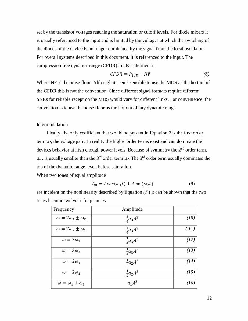
Intermodulation
Ideally, the only coefficient that would be present in Equation 7 is the first order
term a1, the voltage gain. In reality the higher order terms exist and can dominate the
devices behavior at high enough power levels. Because of symmetry the 2nd order term,
a2 , is usually smaller than the 3rd order term a3. The 3rd order term usually dominates the
top of the dynamic range, even before saturation.
When two tones of equal amplitude
𝑉𝑖𝑛 = 𝐴𝑐𝑜𝑠(𝜔1𝑡) + 𝐴cos(𝜔2𝑡) (9)
are incident on the nonlinearity described by Equation (7,) it can be shown that the two
tones become twelve at frequencies:
Frequency Amplitude
𝜔 = 2𝜔1 ± 𝜔2 3
4𝑎3𝐴
3 (10)
𝜔 = 2𝜔2 ± 𝜔1 3
4𝑎3𝐴
3 ( 11)
𝜔 = 3𝜔1 1
4𝑎3𝐴
3 (12)
𝜔 = 3𝜔2 1
4𝑎3𝐴
3 (13)
𝜔 = 2𝜔1 1
2𝑎2𝐴
2 (14)
𝜔 = 2𝜔2 1
2𝑎2𝐴
2 (15)
𝜔 = 𝜔1 ± 𝜔2 𝑎2𝐴2 (16)
13
𝜔 = 𝜔1 𝑎1𝐴 +9
4𝑎3𝐴
3 (17)
𝜔 = 𝜔2 𝑎1𝐴 +9
4𝑎3𝐴
3 (18)
For the components that make up the system described herein 𝑎2 < 𝑎3 <
𝑎1 and the bandwidths are usually less than an octave so the 2nd order terms, the
frequency summation terms, and the second term in equations (17) and (18) can
be neglected leaving
𝑉𝑜𝑢𝑡 = 𝑎1𝐴 cos(𝜔1𝑡) + 𝑎1𝐴 cos(𝜔2𝑡)
+3
4𝑎3𝐴
3 cos((2𝜔1 − 𝜔2)𝑡)
+3
4𝑎3𝐴
3 cos((2𝜔1 − 𝜔2)𝑡)
(19)
The tones at the original frequencies are amplified (or attenuated) by the gain a1.
If 𝜔2 −𝜔1 is much less than the bandwidth, the original two tones have become
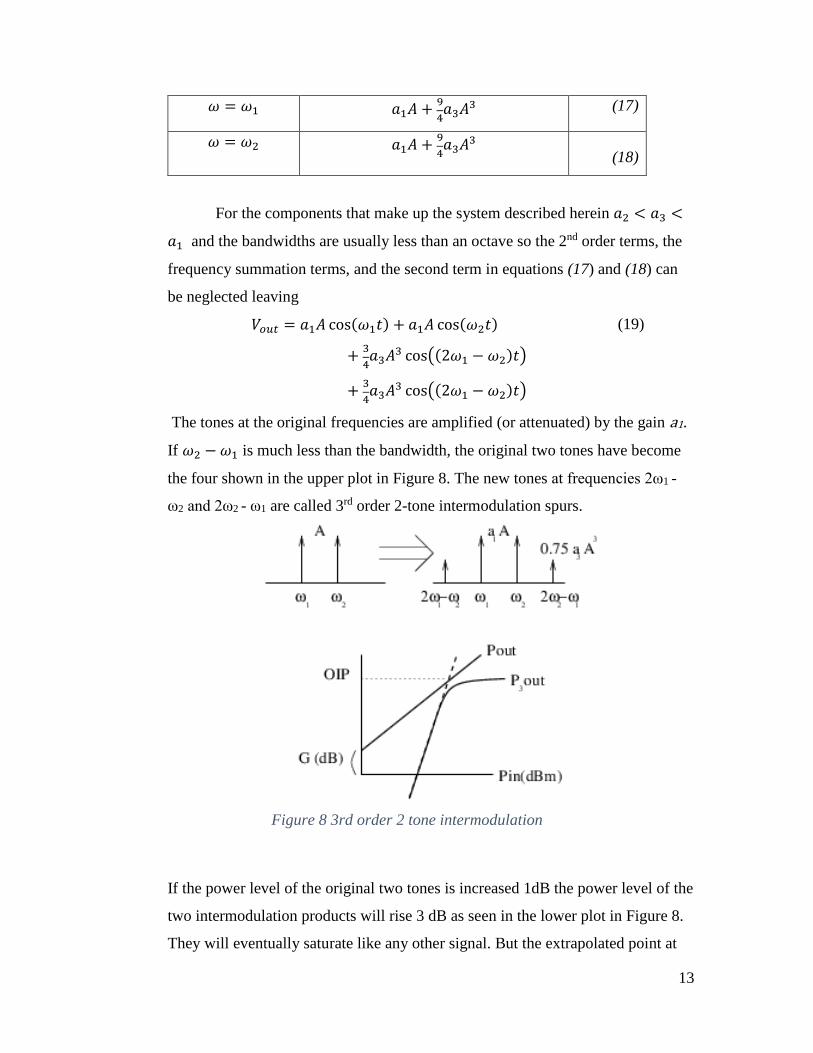
the four shown in the upper plot in Figure 8. The new tones at frequencies 2ω1 -
ω2 and 2ω2 - ω1 are called 3rd order 2-tone intermodulation spurs.
Figure 8 3rd order 2 tone intermodulation
If the power level of the original two tones is increased 1dB the power level of the
two intermodulation products will rise 3 dB as seen in the lower plot in Figure 8.
They will eventually saturate like any other signal. But the extrapolated point at

14
which the power level of the intermodulation products equals the power of the
desired 1st order terms is called the 3rd order 2-tone output intercept point (OIP3).
Amplifier manufacturers typically use the output intercept point as a figure-of-
merit. Mixer intercept points are usually referenced to the input (the 3rd order 2-
tone input intercept point (IIP3)). The difference between the OIP3 and IIP3 is
simply the gain. It can be shown that the power level (in dBm) of the
intermodulation terms is
𝑃3 = 3𝑃𝑖𝑛 − 2𝐼𝐼𝑃3 + 𝐺 (20)
For a cascade of devices it can be shown that the overall input intercept point of a
system can be found from
1
𝐼𝐼𝑃3,𝑇=
1
𝐼𝐼𝑃3,1+
𝐺1𝐼𝐼𝑃3,2
+𝐺1𝐺2𝐼𝐼𝑃3,3
+⋯+𝐺1𝐺2…𝐺𝑛−1
𝐼𝐼𝑃3,𝑛 (21)
where the gains are no longer in dB and intercept points are no longer in dBm.
This equation is typically dominated by the last nonlinear device in the cascade.
Contrast that to the fact that concentrating the gain in the first stage yields the best
noise figure. The design engineer must strike a balance between the two.
The presence of intermodulation spurs establishes another limit on the
dynamic range of the receiver. The 2-tone spur free dynamic range (SFDR) is the
difference between the noise floor of the system and the input power level that
puts an intermodulation spur at the noise floor. The situation is described in
Figure 9.
Figure 9 2-tone spur free dynamic range. All powers are referenced to the input
Looking back at Equation (20), the power level of a 3rd order intermodulation
spur, referenced to the input is
𝑃3𝑖 = 3𝑃𝑖𝑛 − 2𝐼𝐼𝑃3 (22)

15
So the input power level that puts the intermodulation spur power level equal to
the noise floor is
𝑃𝑖𝑛 =1
3(𝑁𝐹 + 2𝐼𝐼𝑃3) (23)
The difference between this and the noise floor is the SFDR.
𝑆𝐹𝐷𝑅 =2
3(𝐼𝐼𝑃3 − 𝑁𝐹) (24)
The discussion so far has only considered the effect of nonlinearities on
two tones. Recall that two tones incident on a nonlinear device modeled to the 3rd
order generated twelve tones. But in a realistic environment there may be quite a
few more than two. It comes as no surprise that the number of intermodulation
spurs rises rapidly with the number of incident tones [9].
If m tones are incident on a nonlinear device
𝑉𝑖𝑛 = 𝐴1 cos(𝜔1𝑡) + 𝐴2 cos(𝜔2𝑡) + ⋯+ 𝐴𝑚cos(𝜔𝑚𝑡) (25)
The 3rd order term will generate intermodulation spurs at frequencies
𝜔 = ±𝑘1𝜔1 ± 𝑘2𝜔2 ±…±𝑘𝑚𝜔𝑚 (26)
for all combinations of 𝑘1, 𝑘2, … 𝑘𝑚 ≤ 3 for which ±𝑘1 ± 𝑘2 ±⋯± 𝑘𝑚 = 3. This
is in addition to the original m tones. As said earlier, m=2 yields 12
intermodulation spurs. m=4 yields 60. m=8 yields 408. This alarming growth is
why the filter bandwidths should only be as wide as is necessary. The simplest
way to minimize intermodulation spurs is to use devices with high intercept points
and to limit the bandwidths of both the preselector and IF filters.
2.3.3 Mixing spurs
Frequency mixers can generate spurious combinations of not only the input
frequencies but of those combined with harmonics of the local oscillator.
An ideal frequency mixer multiplies the input signal(s) by the sinusoidal local
oscillator (LO) yielding the sum and difference frequencies
𝐴𝑐𝑜𝑠(𝜔𝑅𝐹𝑡) cos(𝜔𝐿𝑂𝑡)
= 𝐴
2cos((𝜔𝑅𝐹 −𝜔𝐿𝑂)𝑡) +
𝐴
2cos((𝜔𝑅𝐹 +𝜔𝐿𝑂)𝑡)
(27)
For downconversion, the difference frequency may be 𝜔𝐼𝐹 = 𝜔𝑅𝐹 − 𝜔𝐿𝑂 (low
side injection) or 𝜔𝐼𝐹 = 𝜔𝐿𝑂 − 𝜔𝑅𝐹 (high side injection.) The two RF frequencies

16
that yield the same IF frequency are called the upper (𝜔𝐿𝑂 + 𝜔𝐼𝐹) and lower
(𝜔𝐿𝑂 − 𝜔𝐼𝐹) sidebands.
A more realistic mixer is a bi-phase-shift-keyed modulator, in effect
multiplying the input signal by a bipolar square wave from the local oscillator.
Since multiplication in the time domain is convolution in the frequency domain,
the input spectrum is reproduced about every harmonic of the LO frequency.
Additionally, nonlinearities in the signal path create harmonics of the RF signal.
What comes out is a combination of the harmonics of each.
𝜔𝐼𝐹 = 𝑚𝜔𝑅𝐹 + 𝑛𝜔𝐿𝑂 (28)
Where m & n are positive or negative integers. Theoretically m & n can be any
integer from −∞⋯∞. In reality m and n are limited by the bandwidth of the
circuits. If the input RF signal is a summation of signals then the same behavior
seen in amplifiers occurs in the mixer compounded by the presence of the LO
harmonics. Between the two, mixers can generate larger spurious components
than amplifiers and it is their behavior that drives the first draft of the frequency
plan. The magnitude of these spurious components varies from device to device
depending primarily on the power level of the LO. Very high dynamic range
mixers are available for which only m = -1, 0, & 1 need be considered in any but
the most sensitive applications.
There is no single figure-of-merit for mixer spurs. The spur free
performance of a mixer can, however, be described in a table like that in Table 2
that lists the relative amplitudes of the m x n spurs from a mixer given a particular
input power level and frequency combination. Given the narrow scope of the
mixer spur table it is an imperfect measure but at least provides a way to compare
different mixers in a catalog.

17
RF = +10 dBm at 2000 MHz, LO = +15 dBm at 2100 MHz, IF =
100 MHz
n x LO
m x
RF
0 1 2 3 4
0 -15 -20 -20 -30
1 -18 0 -27 -10 -36
2 -70 -71 -71 -72 -68
3 -100 -88 -96 -85 -93
4 < -110 < -110 < -110 < -110 < -110
Table 2 Mixer spur table for Marki Microwave T3A mixers. Values listed are in dB
relative to desired output.
2.3.4 Gain
For this application, in order to maximize the dynamic range of the system, the total
receiver gain should be minimized. More gain requires more of the active devices that
contribute to the nonlinearity of the system. If the gain is too small, depending on the
noise floor, a small signal may never cross the smallest quantization level of the ADC
and never be detected. This section will explain why the gain of the receiver should
only be enough to ensure the standard deviation of the thermal noise output of the
analog section be comparable to the smallest quantization level of the ADC.
Figure 10 shows a simple receiver. The output of the analog front end is sampled
by the sample-and-hold in the ADC and then quantized.
Figure 10 A simple receiver. The sample-&-hold and quantizer make up the ADC
The quantizer maps the continuum of analog voltages to a finite number of integer
values as depicted in Figure 11. q is the smallest quantization voltage and is
commonly referred to by the misnomer lsb (least significant bit.) So the full scale
voltage swing of an n bit two-sided ADC is 𝑉𝑝𝑝 = 𝑞 × 2𝑛.

18
Figure 11 The transfer function of a mid-tread quantizer
There are two varieties of quantizer, mid-tread and mid-riser. In the mid-tread
quantizer shown in Figure 11 zero volts input maps to zero. The transfer function of a
mid-riser quantizer is offset by q/2 on both axes so there is no zero output value. The
ADC used in the current work is mid-tread. As seen in the transfer function there is a
dead zone between –q/2 & q/2. A signal whose amplitude is smaller than q/2 will
never be detected. But the signal could be recovered if it is superimposed on a larger
signal. The act of adding such a signal before digitization is called dithering and is
routinely used in digital image and audio signal processing [10] [11].
Random noise is a good candidate for the dithering signal since it will trend
toward zero in any coherent integration in the DSP subsystem leaving the smaller
signal intact as will be seen. A simple simulation will illustrate the point. The
Simulink diagram is shown in Figure 12
Figure 12 Simulation setup to study dithering
A 2048 point FFT serves as a source of coherent integration after the ADC. The input
signal is a 47 Hz sinusoid with amplitude 0.49q. The sample rate is 1 kHz. In Figure
13, with nothing but the signal present there is, as expected, zero output from the
quantizer since the peak signal voltage is less than the smallest quantization level. But

19
if noise with an rms level of q/2 is added to the signal as in Figure 14 the signal is
easily recovered by the FFT in Figure 15.
Figure 13 Voltage out of the quantizer with Vin=0.49q and no noise
Figure 14 Voltage out of the quantizer with Vin=0.49q and added noise with Vrms = q/2
Figure 15 Spectrum of the output of the quantizer shows the signal can be recovered
Random noise has the added advantage of spreading the power spectral density of the
quantization error so that it looks more white. If the signal amplitude is increased to
2q and the noise turned off the resulting spectrum in Figure 16 shows a multitude of
spectral lines because the quantization error for weak signals is not sufficiently
uncorrelated with the signal. But if the q/2 noise is added the spectrum becomes that
of Figure 17. The spurious spectral lines have been replaced by white noise.

20
Figure 16 Spectrum of quantizer output with weak signal and no noise
Figure 17 Spectrum of quantizer output with weak signal and noise rms=q/2
The receiver has a natural source of random noise, the thermal noise floor amplified by
gain of the analog front end. In dBm, the thermal noise power output of the analog front-
end is given by 𝑁𝑜 = 𝑘𝑇𝐵𝐹𝐺
The question becomes how much gain is required. Kester has found that an rms
noise level between q/2 & q is optimal. If an rms noise level of q Volts is desired, the
gain of an analog front end feeding an ADC with a 50 ohm input impedance should be
just enough that 𝑘𝑇𝐵𝐹𝐺 = 𝑞2 50⁄ . It should be said the aforementioned references did
not consider undersampled systems (passband sampling.) From the author’s
undocumented experience, 2 LSB’s of noise are required to realize most of the processing
gain of the DSP in a digital receiver that employs passband sampling.
2.3.5 Laying out a frequency plan [6]
The frequency plan is the selection of preselector band breaks (if using a switched
filter bank), LO frequencies, and IF center frequencies. Some of these will be limited by
other factors like RF frequency coverage and the ADC sampling rate. The first draft of
the plan should be to meet these constraints while avoiding the m x n mixer spurs
described in section 2.3. There are a variety of design tools available for the task. The

21
simplest is the classic spur chart shown in Figure 18. The chart boundaries depend on the
frequency ranges and whether down or up conversion is needed.
Figure 18 Mixer spur chart
Each line is simply a plot of one of the lines described by Equation (28) normalized
by the LO frequency 𝜔𝐿𝑂. The thick diagonal line extending from (0, 1) to (1, 0)
represents the desired m=-1, n=1 output 𝜔𝐼𝐹 = 𝜔𝐿𝑂 − 𝜔𝑅𝐹 (high-side injection.) The
other lines are plots of all other 𝑚 × 𝑛 combinations and are to be avoided. To use the
chart the designer chooses an IF center frequency and bandwidth and two 3dB points on a
preselector bandpass filter. One band is chosen within the RF frequency range for
downconversion. The LO frequency is then chosen for either high or low side injection.
In the example above the IF center frequency, perhaps determined by the ADC sampling
rate, is 625 MHz. The IF bandwidth, likely determined by the mission requirements, is
200 MHz. The preselector passband, set by the mission requirements, is 1700 to 2500
MHz. To down convert the 2300-2500 MHz band using high side injection the LO
frequency is 3025 MHz. The vertical boundaries of the box shown are the preselector
band cutoff frequencies normalized to the LO frequency. The horizontal boundaries are
the IF cutoff frequencies normalized by the LO frequency. Any line that crosses inside
the box represents an 𝑚 × 𝑛 spur that may fall inside the IF bandwidth. For instance, a
signal, perhaps an interferer, at 0.74 × 3025 ≈ 2250𝑀𝐻𝑧 will produce a 3 × −2 spur

22
in the IF passband at 700 MHz. The user will have to keep track of which spur
corresponds to which line. The goal of the designer is to choose frequencies that yield a
box within which only the desired term crosses. The simplest way would be to narrow the
preselector passband but that entails using more preselector filters in a switched filter
bank to meet the RF coverage requirement. Another option is to use multiple
conversions, perhaps with multiple IF center frequencies in a switched filter bank. If this
is not possible because of cost or size constraints then the highest dynamic range mixers
that meet the cost constraints should be used. The finite rolloff of the preselector filters
should also be considered. High order filters with fast roll-off provide better rejection but
at the expense of cost, size, insertion loss, and group delay distortion. The process is
repeated until the required RF range is covered. A tool for this process is included in the
appendix.
The preceding process minimizes the effect of only a few potential sources of
interference and without intermodulation between the sources. Later design iterations
should include a simulation using a more realistic representation of the spectral
environment. The results may mandate more band breaks in the preselector filter bank.
Trying to use this less structured process for the first draft of the frequency plan may
prove cumbersome.
2.3.6 Optimizing the gain distribution
Placement of amplifiers throughout the cascade is done at the designers discretion
based on iterations and experience with a few caveats. Again, these advisories reflect the
priorities of the current application and experience of the author.
A low noise amplifier (LNA) should be placed as close to the antenna as
possible since this amplifier will dominate the noise figure of the system.
A built-in-test directional coupler (for diagnostics,) a power limiter (for
protection), and a bandpass filter (to minimize the effects of out-of-band
interference) should precede it and little else. If the spectral environment is
such that intermodulation terms from this amplifier become a problem it
may be necessary to put multiple LNA’s after the filters in the preselector
switched filter bank.

23
An amplifier should never be placed directly before a mixer without a
filter between them or the amplifier may generate noise in the other
sideband of the mixer.
The last amplifier in the chain should have a high intercept point since it
will dominate the system intercept point.
A power limiter should follow the last amplifier to avoid damaging the
ADC if the 1dB output compression point is greater than the damaging
level of the ADC. An alternative is to attenuate the output of the amplifier
and reduce the reference voltages of the ADC proportionally.
A tool for optimizing the gain distribution in a receiver chain is included in
the appendix.
2.3.7 Electromechanical design
Although it may result in further design iterations, the last step in the design
process is the electromechanical design. A few random tips are listed.
A design using connectorized components may be faster to develop, build,
and modify if needed but will be larger, heavier, more expensive, and may
lead to more passband ripple (gain variation vs frequency.) Nevertheless they
are well suited to prototyping a new design, especially one that will never
leave the lab.
A board level design may be smaller, lighter, less expensive, and perform
better than one with connectorized components. But board level designs are
difficult and expensive to iterate so they entail more risk to a limited schedule.
A reliable simulation tool is a must.
Power amplifiers should be given adequate cooling including heat sinks and
airflow.
Switching power supplies are smaller but may produce switching spikes that
can damage delicate RF components. Linear supplies may be larger and more
expensive but are usually cleaner.

24
Chapter 3
Requirements Analysis
The design goals of a transceiver are driven by the mission requirements, the
spectral environment it has to operate in, size and weight constraints, power consumption
limitations, and cost. Size, weight, and power consumption are what drove the program
behind this research to consider an analog front end in the first place. This chapter will
discuss the flow of mission requirements to electrical requirements of the transceiver. For
the current application the receiver design is far more involved than the transmitter so it
will dominate the discussion.
3.1 Requirements flow
The flow from mission requirements to system level requirements of the receiver
is shown in the unavoidably busy chart in Figure 19. The bold outlined boxes are the
given conditions or requirements. The shaded boxes are the sought design goals that
describe the receiver as a black box. The dashed boxes are intermediate values. The
mission requirements dictate what the receiver should do with the signals of interest.
They list the nature of the transmitters and where they are located. Constrained by the
given hardware specifications like those of the antenna and ADC, they prescribe the in-
band performance of the receiver. The results of the spectral survey prescribes the out-of-
band performance. For this application, the seven shaded requirements and the frequency
plan are enough to start the electrical design of the receiver.

25
Figure 19 Flow of requirements from mission to system
The next sections will follow each of these paths to find the design goals.
1. Pre-existing hardware requirements
The antennas to be used are helical with a gain of 10 dBi over the band of interest.
The sidelobes are 0 dBi. Whatever impedance matching is required to provide a 50
ohm output impedance is already part of the antenna system. Each transceiver has
separate transmit & receive antennas and there are two transceivers to facilitate
beamforming. So there are four antennas on a gimbal mount. The transceivers use
time domain multiplexing to avoid trying to transmit and receive at the same time

26
since there is insufficient isolation between the antennas to keep the transmitters from
saturating the receivers. Since the platform is airborne the antennas will usually be
pointed at the ground from the horizon downward.
The wideband digitizer selected is the FMC110 by 4dsp. The device has two 12-bit 1
GSPS ADC’s that will be used at 500 MSPS to digitize both wideband receiver
channels. Also on the FMC110 are two 1GSPS DAC’s that will be used for the I & Q
inputs to one of the transmitters. The narrowband digitizer is the FMC150 by 4dsp. It
has two 14-bit 250 MSPS ADC’s that will be used at 100 MSPS to digitize both
narrowband receiver channels. It too includes two DAC’s that will feed the I & Q
inputs to the other transmitter.
2. Emitters of interest
The program behind this research will be working with mobile users of GSM
handsets and wireless networking (WiFi) devices. The nature of each emitter is given
by the mission requirements and are listed in Table 3. The antennas on mobile
devices are assumed to have 0 dBi gain, a usable approximation.
Frequency Range
(MHz) Power (dBm)
Antenna gain
/sidelobes (dBi)
GSM-1800
handsets 1710-1785 30 0
GSM-1800 base
stations 1805-1880 46 18/2
WiFi 2400-2500 30 0
Table 3 Emitters of interest
The mission requirements dictate the receiver must be sensitive enough to provide the
requisite SNR in the prescribed noise bandwidth (200 kHz) for any of the emitters
listed as far away as 5 km or as close as 300 m with a few caveats: the receiver is

27
expected to survive if the main beam of the receiver antenna is directed at a base
station but is not expected to meet any of the electrical specifications. Also, the
system is not required to detect any mobile emitter in the sidelobes of the receive
antenna.
3. Frequency coverage and IF bandwidth
From Table 3 we see that the receiver must operate between 1710-1880 MHz and
2400-2500 MHz. The region between 1880-2400 MHz is not of interest but, judging
by the results of the spectral survey, there are no signals in that region strong enough
to cause saturation or generate intermodulation problems in the receiver so there is no
need to try to filter it out. So the RF frequency coverage stands at 1710-2500 MHz.
The mission requires the IF bandwidth be enough to cover the entire GSM-1800
or WiFi band in one dwell to maximize the probability of interception of a
transmitter. The GSM-1800 band is 170 MHz wide. The WiFi band is 100 MHz wide.
So an IF bandwidth of 175 MHz will accommodate both with some margin for filter
roll off near the passband edges. The wider the IF bandwidth the more susceptible the
receiver is to interference. If a narrowband channel is included in the design it must
have enough bandwidth to accommodate the broadest band signal. The IEEE 802.11g
signal is 20 MHz wide. An IF bandwidth of 25 MHz will provide some margin for
filter roll off near the passband edges.
4. Minimum detectable signal, noise floor, and noise figure
The weakest transmitters of interest are the GSM-1800 handset & WiFi transmitter.
The WiFi signals suffers more path loss since it has a shorter wavelength. At 5 km the
path loss at 2500 MHz is given by
𝐿 = 20log(
4𝜋𝑅
𝜆) = 114𝑑𝐵
(29)
The minimum detectable signal is the weakest received signal power level in the main
beam of the received antenna:
𝑃𝑇𝑋 + 𝐺𝑇𝑋 − 𝐿 + 𝐺𝑅𝑋 = 30 + 0 − 114 + 10 = −74𝑑𝐵𝑚
The minimum tolerable SNR is given as 10 dB [12]. So the noise floor assuming the
200 kHz noise bandwidth can be no larger than -84 dBm referenced to the input of the

28
receiver. From the definition of the noise floor in Equation (3) the maximum tolerable
noise figure is found to be
𝐹 < 𝑁𝐹 + 114 − 10 log(𝐵𝑀𝐻𝑧) = 37𝑑𝐵
37 dB is a very large noise figure and easily achieved. The question becomes ‘what
can be achieved with readily available components?’ Any receiver design for the
present application will at a minimum include the components shown in Figure 20.
They include a built-in-test directional coupler for diagnostics, a band pass filter to
suppress out-of-band interference, a power limiter to protect the receiver, and the
LNA. Shown are typical losses for the first three based on Minicircuits catalog data.
From the same catalog, 3dB is a typical LNA noise figure in the present frequency
range. So 6 dB is a reasonable goal for the system noise figure. If that is achieved the
system noise floor would be
−114 + 10 log(𝐵𝑀𝐻𝑧) + 𝐹 = −115𝑑𝐵𝑚
Figure 20 The minimum set of components preceding the front end
5. The spectral survey
The requirements for any receiver design are driven not only by the performance
needed for signals of interest but also by the environment it has to operate in. With
that in mind a survey was taken of any transmitters the system might encounter in the
field. Table 4 lists the power levels the receiver is expected to encounter from just the
emitters of interest with a few caveats. It is given that the system will not point the
antenna directly at a GSM base station. The base station transmitters are strong
enough that doing so is unnecessary even at the longest range (5 km.) Nor will the
platform fly into the main beam of a base station when nearby (300m.) From the
table, the strongest signal the receiver must be able to process successfully from an
emitter of interest is -39 dBm.

29
GSM handset
(dBm)
WiFi
(dBm)
GSM Base station
(dBm)
Range Main beam Side lobes
RX main
beam
300 m -47 -50 X X
5000 m -72 -74 X X
RX side
lobes
300 m -57 -60 X -39
5000 m -82 -84 -48 -64
Table 4 Power levels from emitters of interest
Table 5 lists potential sources of interference. The data is derived from FCC
regulations and, when available, manufacturer data. The scope was limited to the
frequency range from 500-4000 MHz since it is reasonable to assume the preselector
filters can suppress anything further from the RF passband. 1500 W 13cm
omnidirectional amateur radio transmitters are rare as are Globalstar satellite phone
customers. The most likely sources of interference the system might encounter within
the continental United States are the NEXRAD weather radar and the long range
ARSR airport surveillance radar. The specifications for each, from manufacturer data
[13] [14], are shown in Table 6.
Frequency (MHz)
Received power
(dBm)
NEXRAD weather radar 2700-3000 14
ARSR airport radar 1215-1370 & 2700-2900 17
Military use 1755-1850 ?
13 cm ham radio 2304 -30
Globalstar handsets 1610-1621 -54
PCS-1900 1850-1990 -39
3G,4G 1710–1755 & 2110–2155 -39
Table 5 Potential interference sources
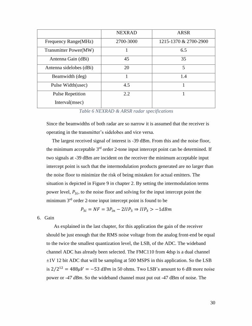
30
NEXRAD ARSR
Frequency Range(MHz) 2700-3000 1215-1370 & 2700-2900
Transmitter Power(MW) 1 6.5
Antenna Gain (dBi) 45 35
Antenna sidelobes (dBi) 20 5
Beamwidth (deg) 1 1.4
Pulse Width(usec) 4.5 1
Pulse Repetition
Interval(msec)
2.2 1
Table 6 NEXRAD & ARSR radar specifications
Since the beamwidths of both radar are so narrow it is assumed that the receiver is
operating in the transmitter’s sidelobes and vice versa.
The largest received signal of interest is -39 dBm. From this and the noise floor,
the minimum acceptable 3rd order 2-tone input intercept point can be determined. If
two signals at -39 dBm are incident on the receiver the minimum acceptable input
intercept point is such that the intermodulation products generated are no larger than
the noise floor to minimize the risk of being mistaken for actual emitters. The
situation is depicted in Figure 9 in chapter 2. By setting the intermodulation terms
power level, 𝑃3𝑖, to the noise floor and solving for the input intercept point the
minimum 3rd order 2-tone input intercept point is found to be
𝑃3𝑖 = 𝑁𝐹 = 3𝑃𝑖𝑛 − 2𝐼𝐼𝑃3 ⇒ 𝐼𝐼𝑃3 > −1𝑑𝐵𝑚
6. Gain
As explained in the last chapter, for this application the gain of the receiver
should be just enough that the RMS noise voltage from the analog front-end be equal
to the twice the smallest quantization level, the LSB, of the ADC. The wideband
channel ADC has already been selected. The FMC110 from 4dsp is a dual channel
±1V 12 bit ADC that will be sampling at 500 MSPS in this application. So the LSB
is 2 212⁄ = 488𝜇𝑉 = −53𝑑𝐵𝑚 in 50 ohms. Two LSB’s amount to 6 dB more noise
power or -47 dBm. So the wideband channel must put out -47 dBm of noise. The

31
noise floor of the analog section of the wideband channel was determined in section
5 to be
−114 + 10 log(𝐵𝑀𝐻𝑧) + 𝐹 = −114 + 10 log(175) + 6 = −86𝑑𝐵𝑚
Where the bandwidth here is that of the analog section (175 MHz) not the overall
system noise bandwidth (200 kHz.) So the wideband analog channel must have at
least 86 − 47 = 39𝑑𝐵 of gain.
The narrowband ADC chosen is the FMC150 from 4dsp. It is a dual
channel ±1V 14 bit ADC that will be sampling at 100 MSPS in this application. So
the LSB is 2 214⁄ = 122𝜇𝑉 = −65𝑑𝐵𝑚 in 50 ohms. So the narrowband channel
must put out -65+6=-59 dBm of noise. The noise floor of the analog section of the
narrowband channel was determined in section 5 to be
−114 + 10 log(𝐵𝑀𝐻𝑧) + 𝐹 = −114 + 10 log(25) + 6 = −94𝑑𝐵𝑚
Where, again, the bandwidth here is that of the analog section (25 MHz) not the
overall system noise bandwidth (200 kHz.) So the narrowband analog channel must
have at least 94 − 59 = 35𝑑𝐵 of gain.
7. 1dB compression point
Both wideband and narrowband ADC’s have a full scale swing, meaning they clip, at
2 Vpp which is +10 dBm in 50 ohms. In order to make use of the full range of the
ADC the analog front end should have an output 1dB compression point of at least
+10 dBm. Since the wideband channel has 39 dB of gain the 1dB input compression
point of the wideband channel must be at least 10 − 39 = −29𝑑𝐵𝑚. Since the
narrowband channel has 35 dB of gain it should have an input 1dB compression point
of at least 10 − 35 = −25𝑑𝐵𝑚. Since the strongest signal of interest is -39 dBm the
front end will not saturate under normal operation if this requirement is met.
8. Out-of-band suppression
From Table 5, the strongest out-of-band emitters are the NEXRAD weather radar and
ARSR long range air surveillance radar. In the sidelobes the equivalent isotropically
radiated power of the NEXRAD radar is 31 MW (104 dBm) if the receiver is in the
radar sidelobes and vice versa. The path loss of 300m at 2700 MHz is 91 dB. So the
signal from the NEXRAD radar may be as strong as 104-91=14 dBm under those
conditions. The system noise floor has been established at -115 dBm. In order to

32
minimize the risk of interference the preselector filters should suppress the interferer
to below the noise floor. So the preselector filter must have at least 129 dB of
rejection at 2700 MHz. Communications with filter manufacturers indicate 60 dB is
as much as can be reasonably expected so more than one filter will be required in the
receiver chain. By the same reasoning the preselector filters must provide 132 dB of
rejection at 1370 MHz to suppress the signal from the ARSR radar.
9. Transmitter
Little has been said about the transmitter so far since it is so much simpler than the
receiver. It must accommodate the same signals as the receiver so the frequency range
is the same (1710-2500 MHz.) The bandwidth must be enough to accommodate the
broadest band signals of interest, the 802.11G WiFi signal, so the bandwidth should
be at least 20 MHz. The mission requirements dictate a 1 W EIRP. The antenna that
will be used will be the same as is used for the receiver which as 10 dBi of gain in the
main lobe. So the transmitter power must be at least 100 mW (20 dBm.)
10. Other requirements
As of this writing the physical limitations (size and weight) have not been established
since the airborne platform has not been selected. But the program requirements
stipulate a few other requirements:
A built-in-test (BIT) coupler after the antenna for diagnostics and phase
calibration.
All local oscillators and the BIT oscillator must be derived from a single GPS
disciplined 10 MHz master reference oscillator.
USB control interface
120VAC power
There must be two identical transceivers on the platform to accommodate
beam-forming.
11. Summary
This chapter detailed the flow of requirements from the mission to the transceiver
system viewed as a black box. To summarize the requirements:

33
Receiver
Frequency Coverage 1710-2500 MHz
Narrow/Wide-band Bandwidth 175/25 MHz
Noise Figure 6 dB goal, 37 dB max
Wideband input 1dB compression point -29 dBm min
Narrowband input 1dB compression point -25 dBm min
3rd order 2-tone input intercept point -1 dBm min
Wideband channel gain 39 dB
Narrowband channel gain 35 dB
Out-of-band suppression 130 dB at 1370 and 2700 MHz
Transmitter
Frequency coverage 1710-2500 MHz
Bandwidth 20 MHz min
Power 20 dBm min

34
Chapter 4
Design and Performance
After several design iterations, one channel of the final design is shown in figure 21. All
components are SMA connectorized parts or were made so. Most were chosen more for
their availability and cost than their performance so sacrifices in dynamic range were
made. Specifically, transmitter power was reduced from the desired 1 W to ½ W. Also,
the desired gains of the amplifiers were determined by optimization but then
approximated to what was close and available from stock rather than what was exact and
custom made.
Figure 21 The final transceiver front-end design.
1. The Receiver Design
Since the receiver is so much more complex than the transmitter the discussion
begins with the receiver. The design process employs a collection of tools written in
MATLAB followed by iterations of simulations using Agilent’s Genesys. The latter starts
with idealized components and progresses toward increasingly realistic and ultimately
measured data provided by manufacturers.

35
Following the receiver design process described in chapter 2, the requirements
have already been established and the next step is to select an architecture. Direct
conversion was ruled out for its low dynamic range. The next consideration is a
superheterodyne conversion with a switched preselector filter bank, multiple conversions,
and multiple IF center frequencies ultimately ending in a quadrature conversion to
baseband. Looking back at 2.3.5, the flexibility of such an architecture allows the
designer to keep each conversion in a clear region on the spur chart of Figure 18. But
such a complex architecture was ruled out by the cost. The final architecture selected is a
hybrid of the superheterodyne conversion and passband sampling. This yields the
superior dynamic range of superheterodyne conversion without the weaknesses of analog
quadrature downconversion. A multiple conversion with multiple IF center frequencies
would yield better spur-free performance but is too costly, so a single conversion is used.
Passband sampling is possible because the IF bandwidths of both channels are
significantly more narrow than the sampling rates of the given ADC’s.
The next step is to make a frequency plan. The process is simplified by the simple
architecture and limited input frequency ranges and ADC sampling rates. The IF
bandwidths were imposed by the mission requirements. The only degree of freedom is
which Nyquist band of the ADC’s would be used and whether high or low side injection
would be employed. A tool was written in MATLAB to complement the spur chart
described in chapter 2. The end result is a wideband IF center frequency of 625 MHz and
narrowband IF center frequency of 75 MHz. High side injection is employed for all bands
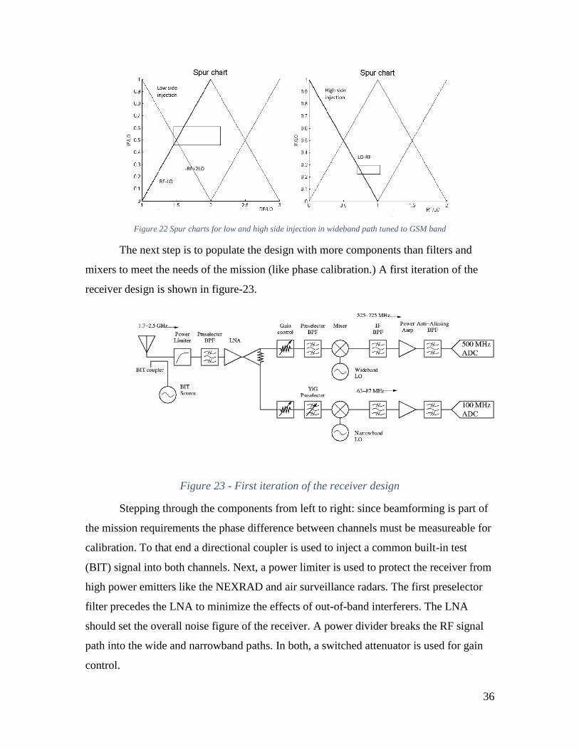
since it yielded fewer mixer spurs than low-side injection. The spur charts in Figure 22
illustrate why. For each the wideband path is tuned to the GSM-1800 band. The lines
represent the dominant output terms from a Marki Microwave T3A mixer, the highest
dynamic range mixer available in the needed frequency range. Any line that crosses
within the box represents terms that can fall within the IF bandwidth. The bold line
represents the desired product. The chart on the right shows the chart for low side
injection. The right shows the results of high side injection. In the left chart the line
representing the 1x2 mixer spur (-fRF+2fLO) crosses the box indicating that it can fall in
the IF bandwidth. The chart on the right shows no such intersection. This was found to be
the case for every band. So high side injection is used throughout.
36
Figure 22 Spur charts for low and high side injection in wideband path tuned to GSM band
The next step is to populate the design with more components than filters and
mixers to meet the needs of the mission (like phase calibration.) A first iteration of the
receiver design is shown in figure-23.
Figure 23 - First iteration of the receiver design
Stepping through the components from left to right: since beamforming is part of
the mission requirements the phase difference between channels must be measureable for
calibration. To that end a directional coupler is used to inject a common built-in test
(BIT) signal into both channels. Next, a power limiter is used to protect the receiver from
high power emitters like the NEXRAD and air surveillance radars. The first preselector
filter precedes the LNA to minimize the effects of out-of-band interferers. The LNA
should set the overall noise figure of the receiver. A power divider breaks the RF signal
path into the wide and narrowband paths. In both, a switched attenuator is used for gain
control.

37
Following the wideband path, another fixed preselector filter is used to provide
further out-of-band suppression and to eliminate the noise from the broadband LNA that
would otherwise fall into the image band of the mixer. The IF and anti-aliasing filters are
identical to reduce cost. The final gain stage is a power amplifier that should determine
the nonlinear performance of the receiver as measured by the 3rd order 2-tone intercept
point.
Returning to the narrowband path a tunable YiG filter is employed as the second
stage of preselection. The bandwidth should be the same as the narrowband IF
bandwidth. The rest of the narrowband path is identical to the wideband path except for
the lower IF frequencies.
The next step is to approximate the losses and nonlinearities of the passive
components and make a first estimate of the gains, noise, and nonlinearities of the
amplifiers. The only gains left to optimize were those of the LNA and final amplifier.
There is plenty of available data from manufacturers to make very accurate predictions
for the performance of each component even before selecting the exact model. An
optimizer was written in MATLAB using constrained optimization to determine the gains
of the amplifiers. This is arguably unnecessary for just two amplifiers but the work was
done for earlier, more complex design iterations. LNA’s with 6dB noise figure are readily
available. For the final amplifier, the cost of goes up dramatically when the output 1dB
compression point exceeds 1 Watt (30 dBm) so a 1 Watt amplifier is assumed. The mixer
is assumed to have the highest available spur-free performance to compensate for the
absence of a switched preselector filter bank. The result of this guess work is shown for
the wideband path in table 7. The first 5 columns are self-descriptive. The 6th column is
the input power to the chain that would saturate that component. The 7th column shows
the percent contribution of that component to the overall noise figure.

38
Gain (dB)
Noise figure (dB)
Output compression
point (dBm)
Output intercept
point (dBm)
Psat (dBm) %F
coupler -0.5 0.5 2.9
limiter -1 1 15 25 16.5 7
filter -1 1 8.8
amp 24.2 3 20 30 -1.7 42.7
power divider -3.5 3.5 0.2
switched attenuator -2 2 38 48 21.8 0.2
filter -1 1 0.2
mixer -7 7 3 25 -5.2 2.9
filter -1 1 0.9
amp 32.8 5 30 40 -10 10
filter -1 1 0 Table 7 First iteration of wideband receiver chain
The overall system performance for this first-cut design is listed in table alongside the
required values from chapter 3. All requirements are exceeded or very nearly met.
Required Simulated
Noise Figure (dB) 6 max (goal) 6.2
Input compression point (dBm) -29 min -10
3rd order 2-tone input intercept point (dBm) -1 min -0.7
Gain (dB) 39 39
Table 8 Performance of first iteration wideband receiver design
Assuming a noise bandwidth of 200 kHz, the wideband path would have a compression
free dynamic range of 105 dB and a 2-tone spur free dynamic range of 76 dB.
The same results for the narrowband path are shown in tables 9 & 10. The
compression-free dynamic range is 108 dB and spur-free dynamic range is 77 dB.

39
Gain (dB)
noise figure (dB)
output compression
point (dBm)
output intercept
point (dBm)
Psat (dBm) %F
coupler -0.5 0.5 2.9
limiter -1 1 15 23 16.5 7
filter -1 1 8.8
amp 29.1 3 20 30 -6.6 42.5
power divider -3.5 3.5 0.1
switched attenuator -2 2 38 48 16.9 0.1
filter -6 6 0.6
mixer -7 7 3 25 -5.1 3
filter -1 1 1
amp 28.9 5 30 40 -6 10.2
filter -1 1 0 Table 9 First iteration of narrowband receiver design
Required Simulated
Noise Figure (dB) 6 max 6.2
Input compression point (dBm) -25 min -7
3rd order 2-tone input intercept point (dBm) -1 min 0.6
Gain (dB) 35 dB 35
Table 10 Performance of first iteration narrowband receiver design
The next step in the design process is to select real components that best fit the
results of the optimizations and use measured data from the manufacturers of those
components to do more detailed simulations. The parts selected are listed in the appendix.
Their s-parameters were imported into Genesys where available. Included in the data is
noise figure across frequency and the compression and intercept points at the center of
the bands of interest. Those of the only custom components, the filters, were guessed to
accommodate the requirements of out-of-band suppression. The Genesys model is shown
in Figure 24.

40
Figure 24 Genesys model for the receiver
Using this model populated with measured data from the manufacturers, the
system could be simulated before components were purchased. The selection of
components can be altered (as long as data is available) to get the best performance for
the money spent. One discovery found in the simulations is that, when the wideband path
is tuned to the GSM-1800 band, the 2420 MHz LO signal was leaking past the LO-RF
isolation of the mixer, passing through the low loss path of the power divider, reflecting
off the poor output VSWR of the LNA, back through the power divider and into the
narrowband path so that it would fall in-band when the narrowband path is tuned to the
WiFi band. The same was happening in the other direction though the result was much
weaker because of the high Q of the YiG filter. The solution is to employ high isolation
amplifiers on each output of the power divider as seen in the figure. A better solution
would use ferrite isolators since they have very little loss and are very linear but this
option is ruled out as too expensive. So high isolation amplifiers were used and the gain
cancelled out by the preceding attenuator knowing this may reduce the sensitivity and
dynamic range of the receiver.
Also seen in the figure are fixed attenuators after the mixer. These act as a crude
impedance matching network. Outside the IF passband, the return loss in the skirts of the
IF filter is very nearly 0dB and out-of-band mixing products would reflect from the filter
back into the mixer. In a diode-ring mixer these reflected terms interact with the desired
outputs leading to in-band ripple in the frequency response. A 3dB attenuator adds 6 dB
of return loss to the filter. A better solution would use broadband ferrite isolators but at
low IF frequencies isolators are large and prohibitively expensive. Another solution is to

41
use a diplexer with the undesired output terminated in a matched load but custom filters
are more expensive and require longer delivery times than a fixed attenuator.
The last addition to the design are the fixed attenuators at the end of each path.
This is an unfortunate necessity. The final gain stage must have a high intercept point to
maintain a high degree of linearity. But high intercept points go hand-in-hand with high
power output capabilities. Typically, the 2-tone 3rd order output intercept point of an
amplifier is approximately 10 dB higher than the 1dB output compression point. A
readily available medium power amplifier with an intercept point of 40 dBm will have a
1dB compression point of approximately 30 dBm. The ADC’s chosen for this project
suffer permanent damage at power levels above 23 dBm. A 10 dB attenuator reduces the
maximum output power of the front-end at the expense of dynamic range. How much
gain is required to compensate for this loss while maintaining the requisite noise level at
the output as described in chapter 2 will be the subject of later experiments. For the
current design it was assumed that all 10 dB should be recoverable thus 10 dB of
compression free dynamic range were lost. This can be reduced later with the gain
control switched attenuator. A better solution would be a power limiter like the one that
protects the receiver. But a limiter with a saturation point between +10 and +23 dBm and
an intercept point near +40 dBm could not be found.
Frequency response, noise figure, and nonlinearity were simulated and the final
component selections were made. The results will be shown alongside measured data in
section 5.
3. The Transmitter
Little has been said about the transmitter thus far because it is much simpler than
the receiver. The transmitted signal is generated in digital signal processing in complex
baseband, converted to I & Q analog channels, then upconverted to RF frequencies with a
quadrature modulator. The design is shown in figure 25. The integrated quadrature
modulator is from Polyphase microwave. It includes a synthesized local oscillator so the
only inputs are I, Q, a 10 MHz reference, and the USB digital control bus. The power
amplifier amplifies the signal to 500 mW. The 500 mW amplifiers were chosen over the
minimum 100 mW requirement since they were readily available and not much more
expensive. 1 W was originally desired but reduced to cut cost.

42
Figure 25 The transmitter
4. The Built-in-Test system
To test the health of the receiver and provide for the phase calibration needed for
beam-forming, a built-in-test source is injected into the RF path. As seen in Figure 26 a
common source feeds both paths. The BIT coupler is the first component in the receiver
chain. The source is a comb generator fed by the 10 MHz master reference oscillator. It
produces a tone every 10 MHz near the center of the system dynamic range.
Figure 26 The built-in-test system
5. The Hardware
To minimize delivery and build time the entire system was built with
connectorized components. The components were purchased largely from stock. Most are
from Minicircuits. The exceptions were the filters. The fixed filters were custom made by
EWT Filters. For risk mitigation two YiG manufacturers were used, OmniYig and
Teledyne. The Teledyne YiG uses a phase locked loop to ensure stability of the filter
since YiG filters are known to drift without some compensation. The OmniYig filters rely
on temperature compensation but cost less than half as much as the Teledyne devices and
required one third the delivery time.
In the current design, the components were first assembled in a table-top
prototype to confirm operation and apply any design iterations if needed. In order to
minimize volume needed for the airborne platform the components were then mounted
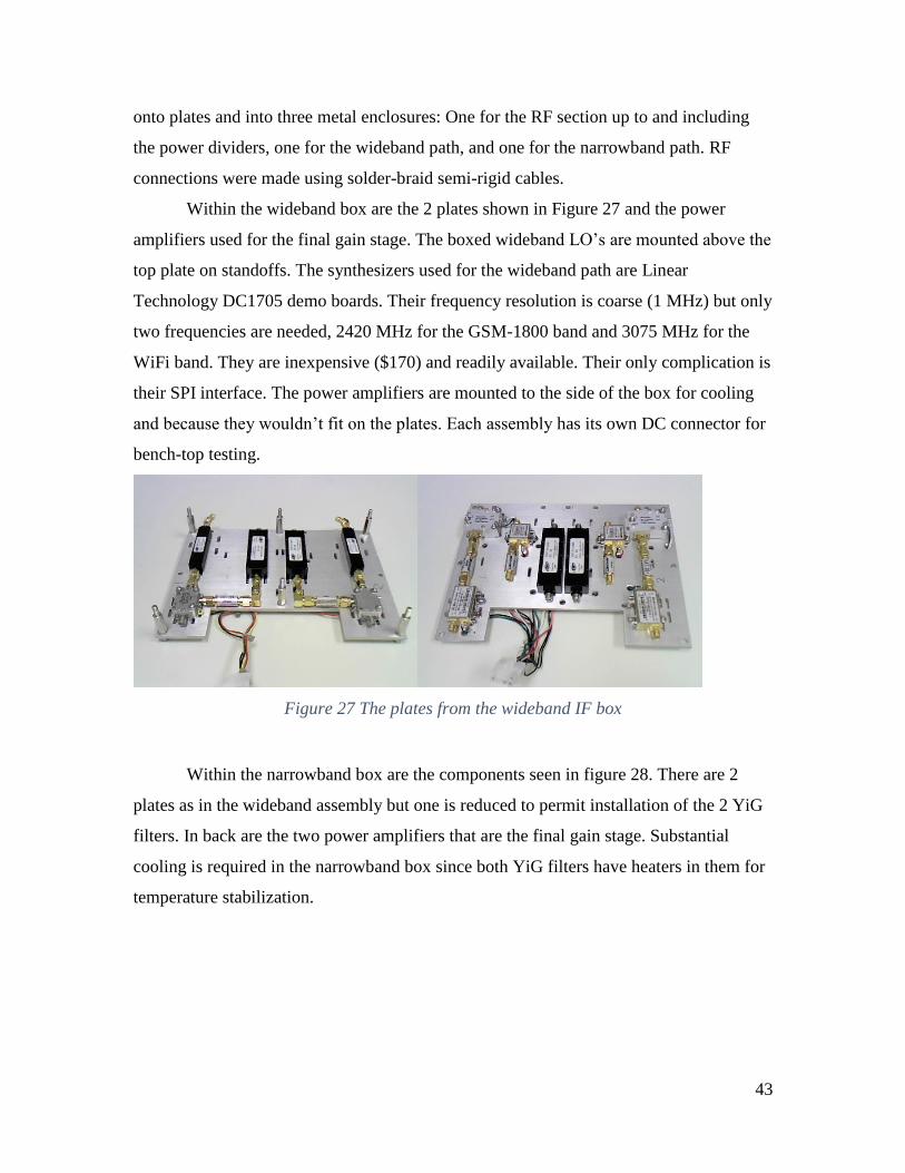
43
onto plates and into three metal enclosures: One for the RF section up to and including
the power dividers, one for the wideband path, and one for the narrowband path. RF
connections were made using solder-braid semi-rigid cables.
Within the wideband box are the 2 plates shown in Figure 27 and the power
amplifiers used for the final gain stage. The boxed wideband LO’s are mounted above the
top plate on standoffs. The synthesizers used for the wideband path are Linear
Technology DC1705 demo boards. Their frequency resolution is coarse (1 MHz) but only
two frequencies are needed, 2420 MHz for the GSM-1800 band and 3075 MHz for the
WiFi band. They are inexpensive ($170) and readily available. Their only complication is
their SPI interface. The power amplifiers are mounted to the side of the box for cooling
and because they wouldn’t fit on the plates. Each assembly has its own DC connector for
bench-top testing.
Figure 27 The plates from the wideband IF box
Within the narrowband box are the components seen in figure 28. There are 2
plates as in the wideband assembly but one is reduced to permit installation of the 2 YiG
filters. In back are the two power amplifiers that are the final gain stage. Substantial
cooling is required in the narrowband box since both YiG filters have heaters in them for
temperature stabilization.

44
Figure 28 The components in the narrowband box.
The assembled RF box is shown in figure 29. The LNA’s are mounted on the top plate.
Underneath them are the couplers, limiters, preselector filters, & the BIT system.
Figure 29 The RF box
The BIT signal used is a comb generator. This was chosen over a synthesizer for its
simplicity. It generates a tone every 10 MHz across the 1710-2500 MHz input frequency
range.
The transmitter has only two components per channel, the quadrature modulator
and power amp as seen in figure 30. The power amps are under the heatsinks.

45
Figure 30 The transmitter
The switched attenuators, YiG filters, BIT control, and wideband LO’s are all
controlled by an Arduino Due. The interface to the front-end as a subsystem is USB. The
entire front-end is powered by bench top supplies with one caveat, the 3.3 V bus is
derived from the 5 V bus with a voltage regulator. One critical aspect of the power
supplies is that the -5V bus must be powered before the +5V bus or the four mixers in the
system will suffer immediate damage.
6. The test results
The assembled hardware is put through a variety of tests to verify operation and
for characterization. The test results were then compared to the requirements to verify
compliance. The results for the current design show that all but one requirement, the
intercept point, were met. In this section, the methodology and results for each test are
described.
6.1 Frequency Response
The instrument used throughout characterization is a Rhode & Schwartz ZVL
combination spectrum/vector network analyzer. The frequency response was measured
for both wide and narrowband paths using a Minicircuits swept oscillator and the ZVL
spectrum analyzer as seen in figure 31.

46
Figure 31 Test set used for frequency response
Ordinarily the vector network analyzer would be used for this so that all four s-
parameters could be measured but the ZVL network analyzer function does not
accommodate frequency translations. So the spectrum analyzer trace was set to max-hold
and the combination acted like a scalar network analyzer. Figure 32 shows both measured
and simulated results for the wideband path tuned to the GSM-1800 band (1710-1880
MHz). Within the frequency range of GSM-1800 the simulated and measured results
agree to within 1 dB. The curve for measured data flattens out at -30 dBm because of the
limited dynamic range of the spectrum analyzer.
Figure 32 Frequency response of wideband path tuned to the GSM-1800 band

47
Figure 33 shows the same curves when the wideband path is tuned to the 2400 MHz WiFi
band. Again, within the 2400-2500 MHz frequency range of interest the simulated and
measured data agree to within 1 dB.
Figure 33 Frequency response of wideband path when tuned to WiFi band
For the narrowband path, figure 34 shows the frequency response when the OmniYig
filter is tuned to a center frequency of 1710 MHz. Data for the Teledyne channel was not
available as of this writing but should be comparable since both filters were built to the
same specification. Immediately obvious in this plot is the appearance of the image band
90 dB down from the passband centered at 1710+2x75=1860 MHz. Because the
bandwidth of the narrowband path is smaller than that of the wideband path a lower IF
center frequency is used so that a slower, higher resolution ADC could be used. But a
lower IF center frequency means the image band is closer to the band of interest and
requires more suppression by the preselector filters. 90dB is less than the desired 108 dB
compression free dynamic range. If image rejection should prove inadequate in field tests
an easy solution is to take two dwells of each band with slightly different LO frequencies.
Signals in the image band will move in the opposite direction to those in the desired

48
passband. Another solution is to use high side injection in one channel and low side
injection in the other and, after mirroring the spectrum of one channel, compare the two.
Future designs may require higher IF center frequencies or higher Q YiG filters to get
more image rejection than the current design. Figure 35 shows the in-band response.
Again the simulated and measured data are, on average, within 1 dB of each other.
Figure 34 The frequency response of one narrowband path tuned to 1710 MHz
Figure 35 The in-band frequency response of one narrowband path tuned to 1710 MHz.

49
Figures 36 & 37 show the same curves when the narrowband path is tuned to 2415 MHz,
the low end of the WiFi band. Again the image band is apparent and again the measured
in-band response is within 1 dB of the simulated response.
Figure 36 Frequency response of one narrowband path when tuned to 2415 MHz.
Figure 37 In-band frequency response of one narrowband path when tuned to 2415 MHz.

50
6.2 Out-of-band Suppression
High order filters are used in the current design to suppress out-of-band interferers
like the NEXRAD weather radar at 2700 MHz and +14 dBm and long-range air
surveillance radar at 1370 MHz and +17 dBm as detailed in chapter 3. To verify the 130
dB suppression, signals at each frequency are incident on the receiver at the frequencies
and power levels listed. The 1370 MHz signal is applied when the wideband receiver is
tuned to its lowest band and the 2700 MHz signal is applied when the receiver is tuned to
highest since these bands are closest to the interferers. The 1370 MHz signal would yield
an IF signal of 1050 MHz and the 2700 MHz signal would yield a tone at 125 MHz. The
spectrum analyzer is tuned to this frequency and the sensitivity maximized. For both
cases any result was below the analyzer noise floor of -115 dBm so the suppression
specification requirement is met.
6.2 1 dB Compression point
As explained in chapter 2, the 1dB compression point defines the top end of the
single-tone dynamic range. It is the input power level at which the gain decreases by 1dB.
To measure it, the input power was swept from -50 to -10 dBm. Figure 38 shows the
measured and simulated gain vs input power for the wideband path tuned to the center of
the GSM-1800 band. It is evident that the measured 1dB input compression point is -21
dBm. This is 11 dB short of the -10 dBm of the first cut design. This is because of the 10
dB attenuator at the end of the receiver chain. To compensate for the loss, 10 dB of gain
had to be added to the design so the final stage amplifier started compressing at a receiver
input power level 10 dB lower. This is the sacrifice made to protect the ADC from the
final gain stage while maintaining the requisite noise power at the output. If experiments
show that the mission requirements can be met with less output noise power, the gain
control attenuator can reduce the gain, recovering some of the lost dynamic range. The
measured value also falls 3 dB short of the simulated value of -18 dBm. This appears to
be a problem in the Genesys amplifier model that combines s-parameter data with
nonlinearity. Nevertheless, the measured value still exceeds the required -29 dBm. The
measurement and simulation was repeated for the WiFi band with the same result.

51
Figure 38 Receiver gain vs input power level reveals the input 1dB compression point
The test was repeated for the narrowband path with the OmniYig filter. The
measured 1dB input compression point was -19 dBm. This is less than the expected -15
dBm. Given that the narrowband channel has 5 dB less gain than the wideband path and
the same amplifier is used for both for the final gain stage, the amplifier should compress
5 dB higher in the narrowband path than in the wideband path. The lower than expected
compression point is because the YiG filter is not a linear device. It has an input
compression point of +10 dBm. It is compressing 3 dB lower than the final stage
amplifier otherwise would have.
6.3 3rd order 2-tone intercept point
As described in chapter 2, the 3rd order 2-tone intercept point is the other standard
metric for the nonlinear behavior of a device or system. For this test and simulation two
tones of equal power level, -40 dBm, were incident on the receiver and the output viewed
with the spectrum analyzer. From the output power level of the desired and
intermodulation products the input intercept point can be derived as shown in Figure 39.

52
Figure 39 Measuring the 3rd order input intercept point
By this method the 3rd order 2-tone input intercept point was determined to be -9 dBm.
This falls 8 dB short of the required -1 dBm. This loss of performance is, again, due the
need for the 10 dB attenuator at the end of the chain to protect the ADC and the added
gain needed to compensate for it. Looking at equation 24 in chapter two, this results in a
6 dB loss of spur free dynamic range. Once again, experiments will determine how much,
if any, of this performance loss can be recovered by gain control.
The same method is used to measure the input intercept point of the narrowband
path with the OmniYig filter. The measured value is -9.5 dBm, nearly the same as the
wideband path. This is surprising given that the narrowband channel has less gain than
the wideband path. It should be -5 dBm. It is this low, again, because the YiG filter is not
a linear device. Although unspecified in any datasheet, the measured input intercept point
is 28 dBm. Simulations show that the YiG filter is the dominant contributor to the
intercept point of the narrowband path. The 5 dB difference reduces the 2-tone dynamic
range by approximately 3 dB.
6.4 Noise Figure
The sensitivity of the receiver is determined by the noise figure. Ordinarily a
noise figure meter with a calibrated noise source would be used but none was available so
the spectrum analyzer is used instead. As detailed in chapter 2, the noise floor of a
receiver is, for a given noise bandwidth:
𝑁𝐹𝑑𝐵𝑚 = −114 + 10 log(𝐵𝑀𝐻𝑧) + 𝐹𝑑𝐵 (30)
Assuming the resolution bandwidth of the spectrum analyzer is approximately the noise
bandwidth, equation 30 can be solved for F, the noise figure. This is only possible if the
noise from the receiver is greater than the internal noise of by the spectrum analyzer. If
the resolution bandwidth of the spectrum analyzer is set to 30 kHz and video bandwidth

53
to 30 Hz and attenuation to 0 dB the noise floor of the Rhode & Schwartz ZVL spectrum
analyzer with a matched termination on the input is found to be -99 dBm at the center of
the wideband IF band (625 MHz.) By inserting the wideband receiver tuned to the GSM-
1800 band between the termination and the ZVL, the new noise floor is -83 dBm, much
more than the spectrum analyzer itself. Since the gain of the wideband path is known
from previous tests to be 40 dB so the input noise floor is -123 dBm. Solving equation 30
for F yields a noise figure of 6.2 dB, which is close to the goal of 6 dB. Repeating the test
with the receiver tuned to the WiFi band yields a noise figure of 6.6 dB. Using the same
method in simulations yielded nearly the same results, 6.7 dB for the GSM-1800 band
and 6.8 dB for the WiFi band.
The noise figure of the narrowband path is measured the same way. In the current
design it is 6.3 dBm in the GSM-1800 band, nearly the same as the noise figure of the
wideband path. This is no surprise since the noise figure is determined largely by the first
components in the RF section, which is common to both paths.
6.5 BIT system
To test the health of the system and to facilitate phase calibration needed for
beamforming, a built-in-test source feeds both channels of the receiver. The source
chosen is a comb generator that produces a tone every 10 MHz across the RF spectrum.
The output spectrum of the wideband path is shown in Figure 40. The power level of the
tones referenced to the receiver input are between -65 & -70 dBm, which is near the
middle of the 1-tone dynamic range.

54
Figure 40 Output of wideband path when BIT source is injected
Without the DAC’s the transmitter could not be tested as of this writing. Given its
simplicity no problems are foreseen.
Table 11 summarizes the results of the receiver tests and compares them to the
required values. All requirements were met or exceeded except for the 2-tone intercept
point which fell short by 9dB, which is expected to reduce the 2-tone dynamic range by 6
dB.
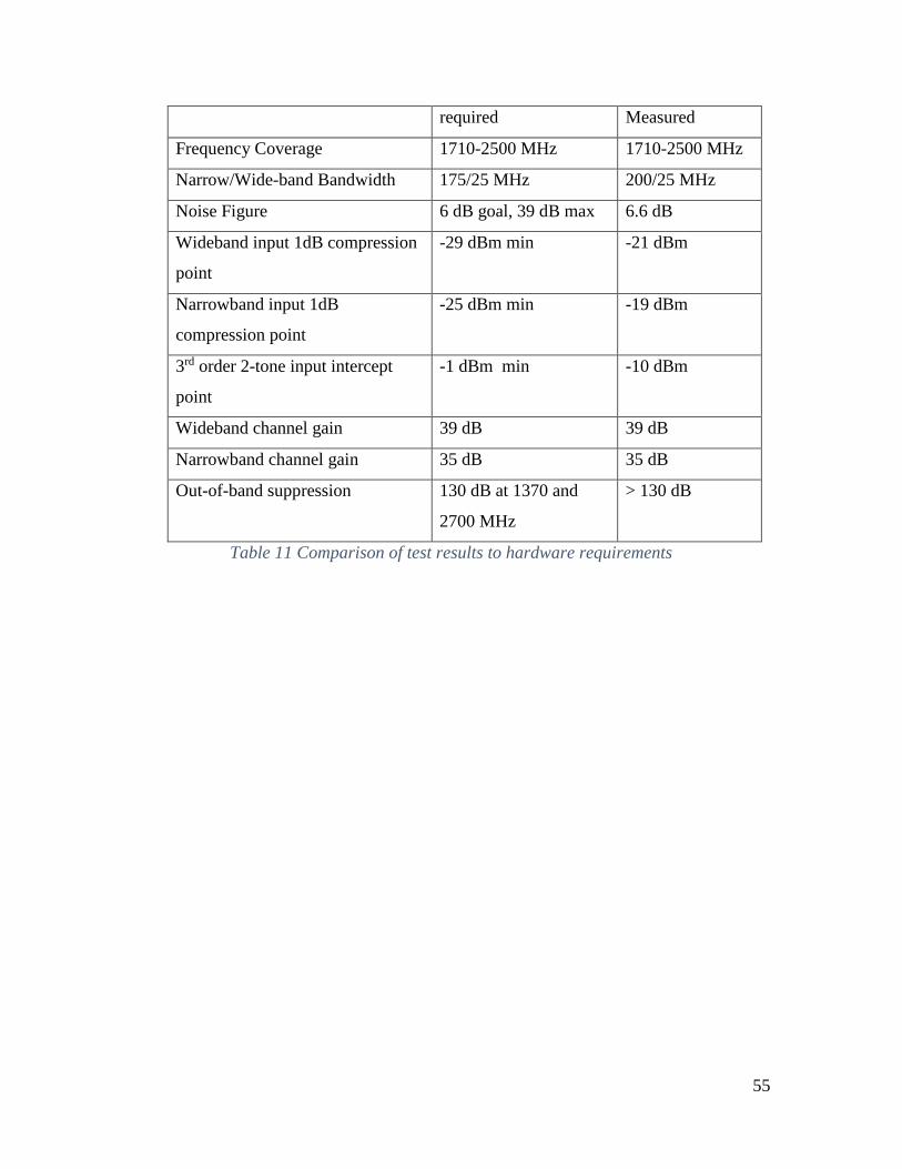
55
required Measured
Frequency Coverage 1710-2500 MHz 1710-2500 MHz
Narrow/Wide-band Bandwidth 175/25 MHz 200/25 MHz
Noise Figure 6 dB goal, 39 dB max 6.6 dB
Wideband input 1dB compression
point
-29 dBm min -21 dBm
Narrowband input 1dB
compression point
-25 dBm min -19 dBm
3rd order 2-tone input intercept
point
-1 dBm min -10 dBm
Wideband channel gain 39 dB 39 dB
Narrowband channel gain 35 dB 35 dB
Out-of-band suppression 130 dB at 1370 and
2700 MHz
> 130 dB
Table 11 Comparison of test results to hardware requirements

56
Chapter 5
Conclusions
A broadband microwave front-end for a software-defined-radio transceiver was
designed & built for operation in the GSM-1800 and 2.4 GHz WiFi bands in an
airborne software defined radio experiment. The design goals were driven by the
spectral environment the system has to operate in. All but one hardware requirements
were met. The nonlinear performance was hindered by components necessary to
protect the ADC from damaging levels. A survey was taken of possible emitters
likely to cross the detectability threshold or otherwise hinder the performance of the
receiver. The system includes one wideband and one narrowband receiver and one
wideband transmitter all capable of simultaneous independent operation. The
wideband system covers the entire GSM-1800 or WiFi band in one dwell. The
narrowband system allows the user to select a 25MHz band across the entire range of
1710 to 2500 MHz, 25 MHz corresponding to the widest WiFi modulation format. A
built-in-test system is included that injects a signal common to both channels that
allows the user to verify the health of the receiver and do the phase calibration needed
for beamforming. The design includes a 500 mW transmitter capable of any
modulation format with 25 MHz of bandwidth. The linear and nonlinear performance
of the system was simulated with a variety of tools that yielded results comparable to
measured values.
Follow-on work for the front-end might include:
1. Expand the frequency range. Figure 40 shows a design once considered for the
current application. It covers 700-4700 MHz. It uses a switched filter bank for better

57
preselection. It has multiple conversions with multiple IF center frequencies to yield
better spur-free performance. The switched filter bank on the transmitter yields fewer
spurious emissions. The local oscillator considered had no phase locked loops and
hence no phase ambiguities result each time the receiver is tuned to a new band. This
would have simplified phase calibration. The switch/amplifier/attenuator at the
beginning of the chain provides RF gain control and a high sensitivity mode of
operation for sparse low-level spectral environments that provide little risk of
interference. At an estimated cost of $120,000 the design was ruled out as too
expensive for the current application but future applications might require the better
performance.
Figure 41 A more complex design that offers better performance and broader frequency
coverage
2. Repackage the IF subsystem.
The wideband and narrowband IF boxes are shown side by side in figure 41. In
retrospect, it was a mistake to cram so much hardware into off-the-shelf enclosures. Both
boxes are so crowded everything has to be removed to troubleshoot them and alteration is
difficult at best. The narrowband boxes, with four sources of heat required forced air

58
cooling. Despite the apparent density, because of the disparate sizes of the components
within there is still a lot of dead space left.
Figure 42 The assembled wideband & narrowband IF boxes
A better approach would be the one shown in figure 42. It is a miniature custom
made rack. Components are mounted on plates that slide into the housing. It is open on
both ends where there would be cabling between the plates. Such an open structure would
be much easier to build, troubleshoot, and modify. Cooling would be easier. The
disadvantage is that it might prove slightly larger than the current assembly.
Figure 43 A better assembly for the IF boxes
3. A power sequencer
The Marki Microwave mixers are active devices that use +/- 5V. But the -5V pins
must be energized before the +5V or four very expensive mixers will be destroyed. A
power sequencer would mitigate that risk.
4. A better way to protect the ADC
The current approach to protect the ADC from the final gain stages degraded the
spur free dynamic range significantly. A better approach would be a power limiter that
clipped the input to +/- 1V but had a 3rd order 2-tone output intercept point of at least +40

59
dBm. No passive limiter will do this so an active device is needed. Such a device would
find a broad range of applications for any digital receiver that required exceptional
linearity.
5. Better metrics
The metrics described herein: frequency response, noise figure, compression &
intercept point are the standard measures of an analog front end. They describe the
systems response to simple sinusoidal signals. But of more interest to the present
application are complex digitally modulated signals. A better set of metrics would
describe the effects of the systems imperfections on reception and transmission of these
signals. For instance, the self-descriptive Adjacent Channel Power Ratio (ACPR) would
be a more relevant measure of transmitter performance than the intercept point. Metrics
of the receiver performance are more complex as performance varies with the modulation
format of the signal. Ultimately, the best way to assess the performance of the receiver
would be with an environmental simulator that would yield, in the lab, the same RF
signal the receiver would see from an antenna in the field.

60
References
[1] R. McGwier, "Prior Hume Work," 2013.
[2] J. Tsui, Digital Techniques for Wideband Receivers, Artech House Pub, 2001.
[3] B. Razavi, "Design Considerations for Direct-Conversion Receivers," IEEE Trans.
Circuits and Systems, vol. 44, pp. 428-435, 1997.
[4] B. Razavi, RF Microelectronics, 2nd ed, Prentice Hall, 2012.
[5] R. Vauhan, "The Theory of Bandpass Sampling," IEEE Trans on Signal
Processing, vol. 39, no. 9, pp. 1973-1984, 1991.
[6] J. Tsui, Microwave Receivers, Peninsula Pub, 1985.
[7] J. Johnson, "Thermal Agitation of Electricity in Conductors," Phys Rev, vol. 32,
1928.
[8] H. Friis, "Noise Figure of Radio Receivers," Proc IRE, vol. 32, pp. 419-422, 1944.
[9] J. Pedro and N. Carvalho, "On the Use of Multitone Techniques for Assessing RF
Components Intermodulation Distortion," IEEE Trans Microwave Theory &
Techniques, vol. 47, no. 12, pp. 2393-2403, 1999.
[10] L. Roberts, "Picture coding using pseudo-random noise," IRE transactions on
Information Theory, vol. 8, no. 2, pp. 145-154, 1962.
[11] L. Schuchman, "Dither Signals and their Effect on Quantization Noise," IEEE
Transactions on Communication Technology, vol. 12, no. 4, pp. 162-165, 1964.
[12] J. Zeigler, Personal Communication, 2014.
[13] National Telecommunications & Information Administration, "Inventory
Briefings," in International Symposium on Advanced Radio Technologies, 2011.
[14] Lockheed Martin, "NEXRAD WSR-88D," Lockheed Martin Ocean Sensors and
Radar.
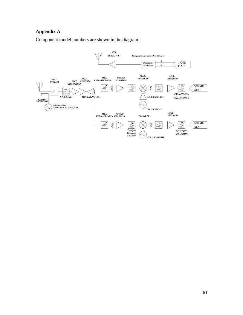
61
Appendix A
Component model numbers are shown in the diagram.

62
Appendix B
Arduino code to control receiver functions.
/*
Control the arduino DUE in the front end including:
The omniyig filter in ch2 of the narrowband IF box.
The Teledyne YiG filter in ch1.
The switched attenuators in the wide and narrowband IF boxes.
The Linear technologies synthesizers in the wideband IF box.
BIT control.
Measure temperature in the OmniYig and narrowband IF boxes.
The only commands needed are the self descriptive:
setupEverything();
setWidebandChannel1CenterFrequency() &
setWidebandChannel2CenterFrequency() for the wideband paths
setWidebandChannel1Attenuator() & setWidebandChannel2Attenuator() for
the wideband gain control attenuators
setNarrowbandChannel1CenterFrequency() &
setNarrowbandChannel2CenterFrequency() for the narrowband paths
setNarrowbandChannel1Attenuator() & setNarrowbandChanne21Attenuator()
BITOn() turns the BIT source on & BITOff() turns it off.
readNarrowBandBoxTemperature() will get the temp in deg C inside the
narrow band box
readOmniyigTemperature() gets temp inside omniyig. This may be needed
for our own temperature compensation
*/
// The wideband LO's are Linear Technologies DC1705-A demo boards with
LTC6946 synthesizer chips.
// They are controlled over a makeshift SPI bus.
// The DB37 cable from the arduino to the wideband IF box must be no
longer than 4 ft. The less the better.
const int SPIClockPin = 17;
const int SPIMISOPin = 18;
const int SPIMOSIPin = 19;
const int wblo_ch1_chipSelectPin = 21;
const int wblo_ch2_chipSelectPin = 20;
int SPIChipSelectPin = wblo_ch1_chipSelectPin;
// Registers for LTC synthesizers.
//byte LTCRegisters[11] = {0x00, 0x04, 0x0c, 0x00, 0x0a, 0x0f, 0x00,
0x31, 0xf9, 0x8b, 0x00}; // -C 3840MHz
byte channel1LTCRegisters[11] = {0x00, 0x04, 0x04, 0x00, 0x0a, 0x09,
0x74, 0x31, 0xf9, 0x8b, 0x00}; // -A 2420MHz
byte channel2LTCRegisters[11] = {0x00, 0x04, 0x04, 0x00, 0x0a, 0x09,
0x74, 0x31, 0xf9, 0x8b, 0x00}; // -A 2420MHz
byte *LTCRegisters;
const int omniyigPins[12] = {12, 11, 10, 9, 8, 7, 6, 5, 4, 3, 2, 14};
const int omniyigTempPin = A0;

63
int wb_ch2_attn_pins[7] = {41, 43, 45, 47, 49, 51, 53}; // 0.5, 1, 2,
4, 8, 16 dB, enable
int wb_ch1_attn_pins[7] = {23, 25, 27, 29, 31, 33, 35}; // 0.5, 1, 2,
4, 8, 16 dB, enable
int nb_ch1_attn_pins[7] = {52, 50, 48, 46, 44, 42, 40}; // 0.5, 1, 2,
4, 8, 16 dB, enable
int nb_ch2_attn_pins[7] = {34, 32, 30, 28, 26, 24, 22}; // 0.5, 1, 2,
4, 8, 16 dB, enable
const int teledyneTunePin = 13;
const int teledyneSamplePin = A7;
const int teledyneLockPin = 69;
// The NB IF box has a temperature sensor in it.
const int NBBoxTempPin = A1;
// Control for built-in-test. The BIT source is a 10 MHz comb
generator.
const int BITPin = A8;
void setup() {
Serial.begin(9600);
setupEverything();
// tune wideband system
setWidebandChannel1CenterFrequency(2437);
setWidebandChannel2CenterFrequency(2437);
setWidebandChannel1Attenuator(20);
setWidebandChannel2Attenuator(20);
// tune narrowband system
setNarrowbandChannel1CenterFrequency(2437);
setNarrowbandChannel2CenterFrequency(2437);
setNarrowbandChannel1Attenuator(20);
setNarrowbandChannel2Attenuator(20);
// make sure BIT is off
BITOff();
// read temperatures in narrowband box
Serial.println(readNarrowBandBoxTemperature());
Serial.println(readOmniyigTemperature());
}
void setupEverything()
{
analogWriteResolution(12);
analogReadResolution(12);
setupWidebandLOs();
setupOmniyig();
setupAttenuators();
setupTeledyne();

64
setupBIT();
}
// turn the BIT comb generator on
void BITOn()
{
digitalWrite(BITPin, HIGH);
}
// or off
void BITOff()
{
digitalWrite(BITPin, LOW);
}
void setupBIT()
{
pinMode(BITPin, OUTPUT);
digitalWrite(BITPin, LOW);
}
void setNarrowbandChannel1CenterFrequency(int f)
{
setNarrowbandChannel1FilterFrequency(f);
}
void setNarrowbandChannel2CenterFrequency(int f)
{
setNarrowbandChannel2FilterFrequency(f);
}
// test to see if the teledyne yig is locked. for troubleshooting.
int teledyneLocked()
{
return !digitalRead(teledyneLockPin);
}
// temp inside NB box
float readNarrowBandBoxTemperature()
{
return 100.0*analogRead(NBBoxTempPin)*3.3/4096 - 60.0;
}
// watch this one for manual temp compensation
float readOmniyigTemperature()
{
return 100.0*analogRead(omniyigTempPin)*3.3/4096 - 60.0;
}
// set the frequency of the teledyne yig
void setNarrowbandChannel1FilterFrequency(int f)
{
digitalWrite(teledyneSamplePin, LOW);
int fword = int(map(f, 1600, 2700, 0, 4068));

65
analogWrite(teledyneTunePin, fword);
delay(1000);
digitalWrite(teledyneSamplePin, HIGH);
}
// set the frequency of the omniyig filter
void setNarrowbandChannel2FilterFrequency(int f)
{
int fword = int((f-1600)*4096/1100);
for (int j = 0; j < 12; j++)
{
digitalWrite(omniyigPins[j], bitRead(fword, j));
}
}
// sets LTC freq synthesizer
void setWidebandChannel1CenterFrequency(int f)
{
SPIChipSelectPin = wblo_ch1_chipSelectPin;
LTCRegisters = channel1LTCRegisters;
setLTCFrequency(f + 625);
setRFPower(0);
}
void setWidebandChannel2CenterFrequency(int f)
{
SPIChipSelectPin = wblo_ch2_chipSelectPin;
LTCRegisters = channel2LTCRegisters;
setLTCFrequency(f + 625);
setRFPower(0);
}
void setWidebandChannel1Attenuator(float attndb)
{
setAttenuator(attndb, wb_ch1_attn_pins);
}
void setWidebandChannel2Attenuator(float attndb)
{
setAttenuator(attndb, wb_ch2_attn_pins);
}
void setNarrowbandChannel1Attenuator(float attndb)
{
setAttenuator(attndb, nb_ch1_attn_pins);
}
void setNarrowbandChannel2Attenuator(float attndb)
{
setAttenuator(attndb, nb_ch2_attn_pins);
}
// sets minicircuits switch attenuators

66
void setAttenuator(float attndb, int pins[]) {
float attn = 0.5 * int(attndb*2);
digitalWrite(pins[6], LOW); // enable
digitalWrite(pins[0], bitRead(int(2*attn), 0)); // 0.5dB
digitalWrite(pins[1], bitRead(int(2*attn), 1)); // 1 dB
digitalWrite(pins[2], bitRead(int(2*attn), 2)); // 2 dB
digitalWrite(pins[3], bitRead(int(2*attn), 3)); // 4 dB
digitalWrite(pins[4], bitRead(int(2*attn), 4)); // 8 dB
digitalWrite(pins[5], bitRead(int(2*attn), 5)); // 16 dB
digitalWrite(pins[6], HIGH); // enable
digitalWrite(pins[6], LOW); // enable
}
void setupAttenuators()
{
for (int j = 0; j < 7; j++)
{
pinMode(wb_ch1_attn_pins[j], OUTPUT);
pinMode(wb_ch2_attn_pins[j], OUTPUT);
pinMode(nb_ch1_attn_pins[j], OUTPUT);
pinMode(nb_ch2_attn_pins[j], OUTPUT);
}
}
void setupTeledyne()
{
pinMode(teledyneTunePin, OUTPUT);
digitalWrite(teledyneTunePin, LOW);
pinMode(teledyneSamplePin, OUTPUT);
digitalWrite(teledyneSamplePin, LOW);
pinMode(teledyneLockPin, INPUT);
}
// set up the pins for the omniyig as outputs
void setupOmniyig()
{
for (int j = 0; j < 12; j++)
{
pinMode(omniyigPins[j], OUTPUT);
digitalWrite(omniyigPins[j], LOW);
}
// setup temperature measurement
analogRead(omniyigTempPin);
}
void setupWidebandLOs()
{
pinMode(wblo_ch1_chipSelectPin, OUTPUT);
pinMode(wblo_ch2_chipSelectPin, OUTPUT);
pinMode(SPIClockPin, OUTPUT);
pinMode(SPIMOSIPin, OUTPUT);
pinMode(SPIMISOPin, INPUT);
digitalWrite(SPIClockPin, LOW);
digitalWrite(wblo_ch1_chipSelectPin, HIGH);

67
digitalWrite(wblo_ch2_chipSelectPin, HIGH);
digitalWrite(SPIMOSIPin, LOW);
SPIChipSelectPin = wblo_ch1_chipSelectPin;
LTCRegisters = channel1LTCRegisters;
writeToLTCRegisters();
SPIChipSelectPin = wblo_ch2_chipSelectPin;
LTCRegisters = channel2LTCRegisters;
writeToLTCRegisters();
}
// filll all the registers in the LTC synthesizers
void writeToLTCRegisters()
{
for (int i = 1; i < 11; i++)
{
writeToRegister(i, LTCRegisters[i]);
}
writeToRegister(0x07, 0x63);
}
void setLTCFrequency(int f)
{
setBDivider(0);
setRDivider(10);
setNDivider(f);
setODivider(1);
cal();
setRFPower(0);
}
// set power output of LTC synthesizer
// pwr must be -9, -6, -3, or 0 dBm
void setRFPower(int pwr)
{
byte RFO;
switch (pwr)
{
case -9:
RFO = 0; break;
case -6:
RFO = 1; break;
case -3:
RFO = 2; break;
default:
RFO = 3;
}
LTCRegisters[8] = (LTCRegisters[8] & 0xE7) | (RFO << 3);
writeToRegister(8, LTCRegisters[8]);
}
// sets O divider of LTC synthesizers
// o < 8

68
void setODivider(unsigned int o)
{
if (o > 0 && o < 8)
{
LTCRegisters[8] = (LTCRegisters[8] & 0xF8) | o;
writeToRegister(8, LTCRegisters[8]);
}
}
void setNDivider(unsigned int n)
{
byte LSB = n & 0xFF;
byte MSB = (n >> 8) & 0xFF;
writeToRegister(5, MSB);
writeToRegister(6, LSB);
}
// r < 1024
void setRDivider(unsigned int r)
{
byte LSB = r & 0xFF;
byte MSB = (r >> 8) & 0x03; // 2 bits
LTCRegisters[3] = (LTCRegisters[3] & 0xF0) | MSB;
writeToRegister(3, LTCRegisters[3]);
writeToRegister(4, LSB);
}
// b < 12
void setBDivider(unsigned int b)
{
if (b < 12)
{
LTCRegisters[3] = (LTCRegisters[3] & 0x0F) | (b << 4);
writeToRegister(3, LTCRegisters[3]);
}
}
// cal must be initiated everytime a frequency is changed
void cal()
{
writeToRegister(0x07, 0x63);
}
// print contents of 1 LTC register
void printRegister(byte registerAddress)
{
Serial.print("register ");
Serial.print(registerAddress, DEC);
Serial.print(" = ");
byte data = readRegister(registerAddress);
Serial.print(data, HEX);
Serial.print(" : ");

69
Serial.println(data, BIN);
}
// set 1 bit in an LTC synthesizer register
// bitNumber=0-7
// bitvalue = 1 or 0
void setBit(byte registerAddress, int bitNumber, int bitValue)
{
byte data = LTCRegisters[registerAddress];
byte mask = 1 << bitNumber;
if (bitValue == 1)
{
data = data | mask;
}
else
{
data = data & ~mask;
}
LTCRegisters[registerAddress] = data;
writeToRegister(registerAddress, data);
}
// turn RF output of LTC synthesizer on
void RFon()
{
setBit(0x02, 1, 0);
}
void RFoff()
{
setBit(0x02, 1, 1);
}
// read 1 register in LTC synthesizer. Only works if cable between
arduino & wideband box is < 1 ft
byte readRegister(byte registerAddress)
{
digitalWrite(SPIChipSelectPin, LOW);
pinMode(SPIMISOPin, OUTPUT); digitalWrite(SPIMISOPin, LOW);
shiftOut(SPIMOSIPin, SPIClockPin, MSBFIRST, (registerAddress << 1) |
0x01);
pinMode(SPIMISOPin, INPUT);
byte response = myShiftIn(SPIMISOPin, SPIClockPin, MSBFIRST);
delayMicroseconds(20);
digitalWrite(SPIChipSelectPin, HIGH);
return response;
}
// needed my own shiftin to make readRegister work
uint8_t myShiftIn(uint8_t dataPin, uint8_t clockPin, uint8_t bitOrder)
{
uint8_t value = 0;
uint8_t i;

70
for (i = 0; i < 8; ++i) {
digitalWrite(clockPin, HIGH);
if (bitOrder == LSBFIRST)
value |= digitalRead(dataPin) << i;
else
value |= digitalRead(dataPin) << (7-i);
digitalWrite(clockPin, LOW);
}
return value;
}
// write to 1 register in LTC synthesizer
void writeToRegister(byte registerAddress, byte data)
{
digitalWrite(SPIChipSelectPin, LOW);
shiftOut(SPIMOSIPin, SPIClockPin, MSBFIRST, (registerAddress <<
1));
shiftOut(SPIMOSIPin, SPIClockPin, MSBFIRST, data);
delayMicroseconds(20);
digitalWrite(SPIChipSelectPin, HIGH);
delayMicroseconds(20);
}
void loop() {
delay(1000);
}
Related Documents