A SUB-10PS TIME-TO-DIGITAL CONVERTER WITH 204NS DYNAMIC RANGE FOR TIME-RESOLVED IMAGING AND RANGING APPLICATIONS A Thesis by NOBLE NII NORTEY NARKU-TETTEH Submitted to the Office of Graduate and Professional Studies of Texas A&M University in partial fulfillment of the requirements for the degree of MASTER OF SCIENCE Chair of Committee, Samuel Palermo Co-Chair of Committee, Edgar Sanchez-Sinencio Committee Members, Robert Balog Yoonsuck Choe Head of Department, Chanan Singh May 2014 Major Subject: Electrical Engineering Copyright 2014 Noble Nii Nortey Narku-Tetteh

Welcome message from author
This document is posted to help you gain knowledge. Please leave a comment to let me know what you think about it! Share it to your friends and learn new things together.
Transcript
A SUB-10PS TIME-TO-DIGITAL CONVERTER WITH 204NS DYNAMIC
RANGE FOR TIME-RESOLVED IMAGING AND RANGING APPLICATIONS
A Thesis
by
NOBLE NII NORTEY NARKU-TETTEH
Submitted to the Office of Graduate and Professional Studies of
Texas A&M University
in partial fulfillment of the requirements for the degree of
MASTER OF SCIENCE
Chair of Committee, Samuel Palermo
Co-Chair of Committee, Edgar Sanchez-Sinencio
Committee Members, Robert Balog
Yoonsuck Choe
Head of Department, Chanan Singh
May 2014
Major Subject: Electrical Engineering
Copyright 2014 Noble Nii Nortey Narku-Tetteh
ii
ABSTRACT
Time-resolved quantization has become inherent in systems that incorporate a
Time-of-Flight (ToF) or Time-of-Arrival (ToA) measurement. Such systems have diverse
applications ranging from direct time-of-flight measurements in 3D ranging systems such
as Radar and Lidar systems to imaging systems using Time-Correlated Single Photon
Counting (TCSPC) (in fields such as nuclear instrumentation, molecular biology, artificial
vision in computer systems, etc.). Time resolution in the order of picoseconds, especially
in imaging applications has become important due to the increasing demands on the
functionality and accuracy of the DSP (digital signal processing) in such systems. The
increasing density of integration in CMOS implementations of such imaging and ranging
systems places large constrains on area and power consumption. Furthermore, the
increased variability of the range of the measurement quantities introduces an undesirable
trade-off between dynamic range and precision/resolution. Therefore there is a need for
time-to-digital converters which achieve high precision, high resolution and large dynamic
range, without excessive costs in area and power.
In this thesis, a wide range, high resolution TDC is designed to offer a timing
resolution of less than 10ps and a dynamic range of 204.8ns. This is achieved by using a
digitally-intensive hierarchical approach, using two looped structures, which incorporates
a novel control logic algorithm. This guarantees accurate operation of the loops, removing
the possibility of MSB errors in the digital word. Firstly the measurement is subdivided
into 2 different sections: a coarse quantization and a fine quantization. Both of the
iii
conversion steps involve the use of a looped delay–line structure utilizing only 4 elements
per delay line. This together with the control logic, makes the design of a wide dynamic
range TDC achievable without excessive area and power consumption.
The design has been simulated, fabricated and tested in the IBM 0.18µm
technology. The proposed design achieves a resolution of 8.125ps with an input dynamic
range of 204.8ns, a maximum input occurrence rate of 100MHz and a minimum dead time
of 7.5ns. The fabricated TDC has a power consumption of < 20mW (1.8V supply; FSR
signal at 4MS/s) and < 35mW at the maximum output rate of 100MS/s.

iv
DEDICATION
To my father and mother
v
ACKNOWLEDGEMENTS
I would like to thank my advisor, Dr. Samuel Palermo, for his excellent mentorship
throughout the entire duration of my Master’s degree program. The knowledge Dr. Samuel
Palermo has imparted to me, has helped in my development as an analog engineer. I would
also like to thank my committee members, Dr. Edgar Sanchez-Sinencio, Dr. Robert Balog
and Dr. Choe Yoonsuck for their time and support.
Thanks also go to my friends and colleagues, the department faculty and staff for
making my time at Texas A&M University a great experience. I am also thankful for all
the support and encouragement of my parents and sister.
Finally, thanks to Texas Instruments (TI) for taking on the sponsorship of my
graduate education. My thanks particularly go to Tuli Dake, Ben Sarpong, Dee Hunter and
Art George all of TI who played an active role in initiating the African Analog University
Relations Program (AAURP) which is in fact the channel for sponsoring my master’s
program.
vi
NOMENCLATURE
ADC Analog-to-Digital Converter
CCCC CTDC Counter Clock Control
CML Current-Mode Logic
CTDC Coarse Phase Time-to-Digital Converter
DFF D Flip Flop
DLL Delay-Locked-Loop
DR Dynamic Range
FCS Fluorescence Correlation Spectroscopy
FLIM Fluorescence Lifetime Imaging
FRET Fluorescence Energy Transfer
FSR Full-Scale-Range
FTDC Fine Phase Time-to-Digital Converter
GBW Gain-Bandwidth Product
IC Integrated Circuit
JKFF J-K Flip Flop
LIDAR Laser/Light Detection and Ranging
MR Master Reset
MRI Magnetic-Resonance Imaging
NS Noise Shaping
PCB Printed Circuit Board
vii
PD Propagation delay
PET Positron-Emission Tomography
PG Pulse Generator
PMT Photomultiplier Tube
PV Process Voltage
PVT Process Voltage and Temperature
RADAR Radio Detection and Ranging
RES Resolution
SADFF Sense-Amplifier based D Flip Flop
SSE Single-Shot Experiment
SSP Single-Shot Precision
TCSPC Time-Correlated Single Photon Counting
TDC Time-to-Digital Converter
viii
TABLE OF CONTENTS
Page
ABSTRACT .......................................................................................................................ii
DEDICATION .................................................................................................................. iv
ACKNOWLEDGEMENTS ............................................................................................... v
NOMENCLATURE .......................................................................................................... vi
TABLE OF CONTENTS ............................................................................................... viii
LIST OF FIGURES ............................................................................................................ x
LIST OF TABLES .......................................................................................................... xiv
1. INTRODUCTION ...................................................................................................... 1
1.1 System Considerations of TDC for ToF in Imaging .................................. 6
1.2 System Considerations of TDC for ToF in Ranging .................................. 6
1.3 Thesis Organization .................................................................................... 8
2. OVERVIEW OF TIME-TO-DIGITAL CONVERTERS ......................................... 10
2.1 TDC Basics and Theory of Operation ...................................................... 10
2.2 Linear and Non-linear Non-idealities of TDC Characteristic .................. 13
2.3 Definition of Key Terms in Characterizing TDC Performance .............. 15
2.4 State-of-the-Art and Existing Works ........................................................ 17
2.5 Motivation and Problem Statement .......................................................... 23
3. SYSTEM DESIGN CONSIDERATIONS ............................................................... 24
3.1 System Overview ..................................................................................... 24
3.2 System Definition ..................................................................................... 30
3.3 Signal Nature: Pulse vs. Edge .................................................................. 32
4. BLOCK LEVEL DESIGN ........................................................................................ 34
ix
Page
4.1 Coarse Stage Time-To-Digital Converter (CTDC) .................................. 34
4.2 FTDC STOP Input Signal Control Block ................................................ 59
4.3 Fine Stage Time-To-Digital Converter (FTDC) ...................................... 62
4.4 Delay-Locked-Loop (DLL) ...................................................................... 73
4.5 Miscellaneous Considerations .................................................................. 79
5. SUMMARY AND CONCLUSIONS ....................................................................... 89
REFERENCES ................................................................................................................. 91
x
LIST OF FIGURES
Page
Figure 1.1 SPAD and front-end circuit [26] ................................................................ 3
Figure 1.2 Idealized waveforms on nodes VSPAD, VINV and VOUT illustrating the
circuit operation when a photon is detected [26] ....................................... 3
Figure 1.3 Lidar system depiction diagram (fiber point type) [29] ............................. 4
Figure 1.4 Lidar system composition [29] ................................................................... 5
Figure 2.1 Ideal input–output characteristic of time-to-digital converter [31] .......... 12
Figure 2.2 Input–output characteristic of a TDC with offset error [31] .................... 14
Figure 2.3 Input–output characteristic of a TDC with gain error [31] ...................... 14
Figure 2.4 Input–output characteristic of a TDC illustrating DNL error .................. 15
Figure 2.5 Single-shot experiment illustration setup ................................................. 16
Figure 2.6 PDF of quantization error in the presence of physical noise for
increasing timing uncertainty στ [31] ....................................................... 17
Figure 2.7 Block diagram of DLL based TDC .......................................................... 18
Figure 2.8 Bock diagram of 128 column-parallel TDC with time amplification ...... 19
Figure 2.9 Block diagram of DLL array-based TDC ................................................ 20
Figure 2.10 Block diagram of Lidar transceiver .......................................................... 21
Figure 2.11 System diagram of third order MASH ∆Σ TDC ...................................... 22
Figure 3.1 Hierarchical TDC with coarse looped TDC In 1st stage and fine TDC
in 2nd stage ............................................................................................... 24
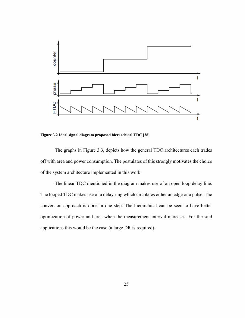
Figure 3.2 Ideal signal diagram proposed hierarchical TDC [38] ............................. 25
xi
Page
Figure 3.3 Area and power consumption of TDC architectures depending on the
application [38] ........................................................................................ 26
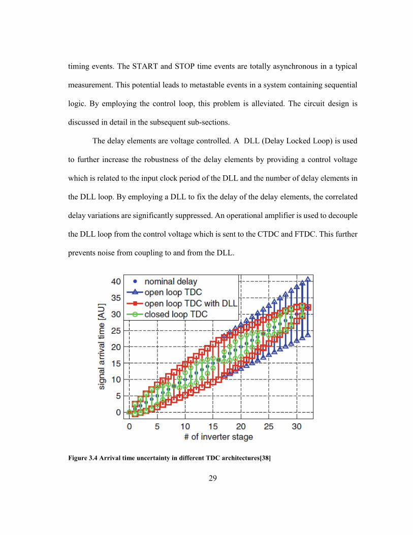
Figure 3.4 Arrival time uncertainty in different TDC architectures[38] ................... 29
Figure 3.5 Top-level block diagram of proposed TDC ............................................. 32
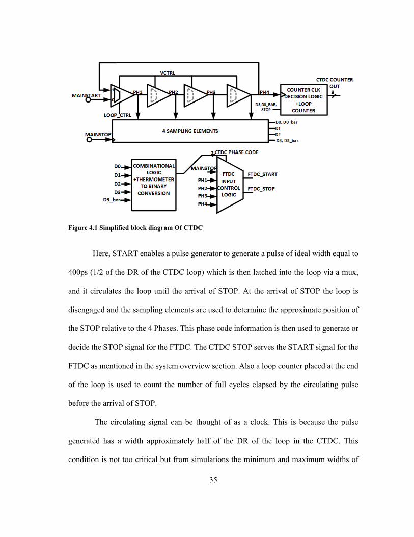
Figure 4.1 Simplified block diagram Of CTDC ........................................................ 35
Figure 4.2 Proposed pulse generator circuit diagram ................................................ 37
Figure 4.3 Pulse generator output for a sweep of input PW from 50ps to 650ps at
1.25GHz ................................................................................................... 37
Figure 4.4 Schematic of TSPC DFF .......................................................................... 39
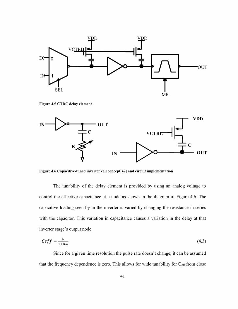
Figure 4.5 CTDC delay element ................................................................................ 41
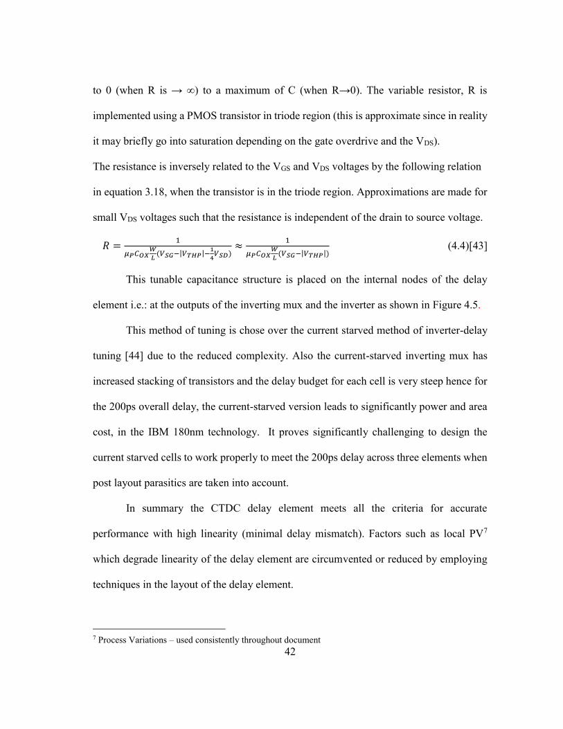
Figure 4.6 Capacitive-tuned inverter cell concept[42] and circuit implementation .. 41
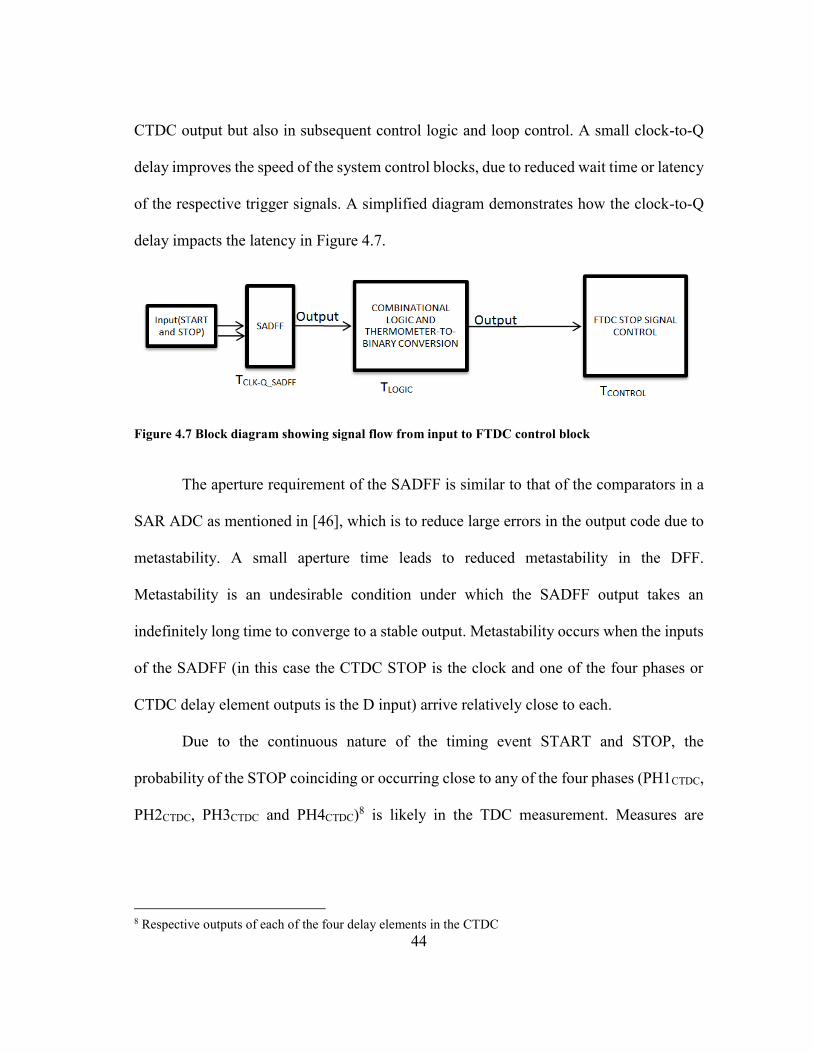
Figure 4.7 Block diagram showing signal flow from input to FTDC control block . 44
Figure 4.8 Schematic of strong-arm latch used in SADFF ........................................ 46
Figure 4.9 SADFF output for CLK-DATA delay of -2.5ps (CLK lags DATA) ....... 47
Figure 4.10 SADFF output for CLK-DATA delay of 2.5ps (CLK leads DATA) ....... 47
Figure 4.11 Sampling instance tuning for SADFF ...................................................... 48
Figure 4.12 A 4-bit synchronous up-counter using 'T' (toggle) flip-flops ................... 49
Figure 4.13 Timing diagram for 4 bit up-counter ........................................................ 49
Figure 4.14 Concept diagram of the pseudo-synchronous counter ............................. 50
Figure 4.15 Full gate-level schematic of the 8-bit pseudo-synchronous counter ........ 51
Figure 4.16 CTDC loop counter transient simulation result. Up count from 0 to 255 52
Figure 4.17 Flow diagram for CCCC algorithm .......................................................... 54
xii
Page
Figure 4.18 Circuit implementation of CCCC algorithm ............................................ 54
Figure 4.19 Conceptual timing diagram for CCCC algorithm operation .................... 55
Figure 4.20 Simulation results of CCCC algorithm illustrating the 4 possible
scenarios ................................................................................................... 55
Figure 4.21 Detailed diagram of implemented CTDC block ...................................... 57
Figure 4.22 CTDC I/O characteristic curve from transient simulation. ...................... 58
Figure 4.23 Circuit implementation for FTDC START signal control logic .............. 60
Figure 4.24 Timing diagram for FTDC input signal control logic operation .............. 61
Figure 4.25 Cut-out of a Vernier delay-line based TDC[54] ....................................... 63
Figure 4.26 FTDC operation algorithm ....................................................................... 65
Figure 4.27 Simplified FTDC block diagram .............................................................. 66
Figure 4.28 FTDC delay element circuit diagram ....................................................... 70
Figure 4.29 Transient simulation result - FTDC output .............................................. 72
Figure 4.30 FTDC characteristic ................................................................................. 72
Figure 4.31 FTDC DNL and INL characterization ..................................................... 73
Figure 4.32 Block diagram of DLL ............................................................................. 75
Figure 4.33 Schematic of single-ended folded-cascode OTA ..................................... 76
Figure 4.34 DLL transient simulation result showing control voltages from loop
filter and opamp ....................................................................................... 78
Figure 4.35 DLL transient simulation result showing delay settling error .................. 78
Figure 4.36 DLL transient simulation result showing delay of cells across delay
line ............................................................................................................ 79
xiii
Page
Figure 4.37 Layout of CTDC block ............................................................................. 81
Figure 4.38 Layout of FTDC block ............................................................................. 81
Figure 4.39 Layout of entire TDC chip ....................................................................... 82
Figure 4.40 Die micrograph of TDC chip ................................................................... 82
Figure 4.41 A section of test setup of TDC chip ......................................................... 84
Figure 4.42 General test set-up for SSE ...................................................................... 84
Figure 4.43 SSE result for 13ps input .......................................................................... 85
Figure 4.44 SSE result for 486ps input ........................................................................ 85
Figure 4.45 SSE result for 4.017ns input ..................................................................... 86
Figure 4.46 SSE result for 101.4ns input ..................................................................... 86
Figure 4.47 SSP vs. input time difference ................................................................... 87
xiv
LIST OF TABLES
Page
Table 4.1 Summary of performance of CTDC ......................................................... 58
Table 4.2 Summary of performance of FTDC ......................................................... 71
Table 4.3 Summary of performance comparison of this work against the state-of-
the-art ....................................................................................................... 88
1
1. INTRODUCTION
Time-to-digital converters are fast becoming prevalent a part of the present day
implementations of mixed-signal and data acquisition and processing interfaces. Time-to-
digital converters are inherent in any time-domain signal processing implementation[1].
Due to technology scaling resulting from the increased stress for high levels of digital
integration (for the advantages of speed and low power consumption)[2], time resolved
signal processing is being applied in many systems[3]. In many systems involving real-
world analog data, the quantity of interest may already be present in time and not as a
voltage or current, it therefore makes sense to apply some form of time-resolved
processing to simplify the mixed signal interface.
The potential applications of time-domain signal processing (TDSP) widely vary,
with applications in analog-to-digital conversion for mixed signal interfaces [4, 5],
impedance spectroscopy[6], Time-of-Flight measurements for ranging[7-11] and also in
imaging systems[11-16], nuclear science and high energy physics applications [16-19],
all-digital phase-locked-loops (ADPLL) [20-22], for medical applications in cancer
treatment, cardiovascular tissue study[23, 24], etc., bio-medical image sensors [21, 25],
just to mention a few. As each application’s specifications influences the nature of the
signal processing, the architecture of the TDC is also strongly determined as such. The
focus of the TDC in this work is towards time-resolved imaging and ranging applications.
In these two fields of applications, namely ToF for ranging and imaging, there are
various system implementations which vary in their specific task. In time-resolved
2
imaging systems various techniques exist for different applications (PET, FLIM, FRET,
FCS, biomedical imaging applications, etc.). One technique used in nuclear image sensing
is the so-called time-correlated-single-photon counting (TCSPC) [19], which is defined as
a technique used for the reconstruction of fast very low-intensity optical waveforms.
The sample is excited repetitively and the emitted photons are detected every excitation
cycle. A large number of events per excitation cycle are required to effectively reconstruct
the optical signals waveform.
In another example, for the PET nuclear imaging technique where 3D images of
the body are created for applications in oncology and brain function analyses, the gamma
event can be recorded using PMTs (photomultiplier tubes), but these are not easily
integrated into systems with MRI (Magnetic-Resonance Imaging). To allow for
integration and high-density, while maintaining sensitivity to the gamma event, TCSPC
can be employed to record the gamma event by first sensing the incident photons and then
recording the hits or photon count. An example of the sensors used is the SPAD (Single
Photon Avalanche Diode) which allows for easy integration into low-cost CMOS systems.
A TDC can be integrated along with the SPAD sensor to form a smart pixel as
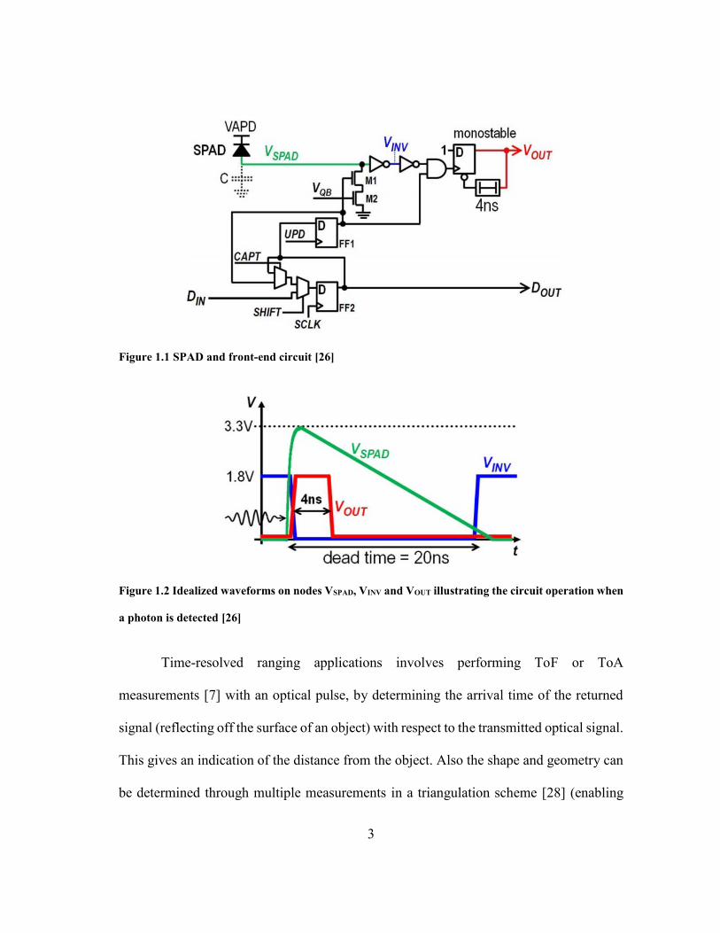
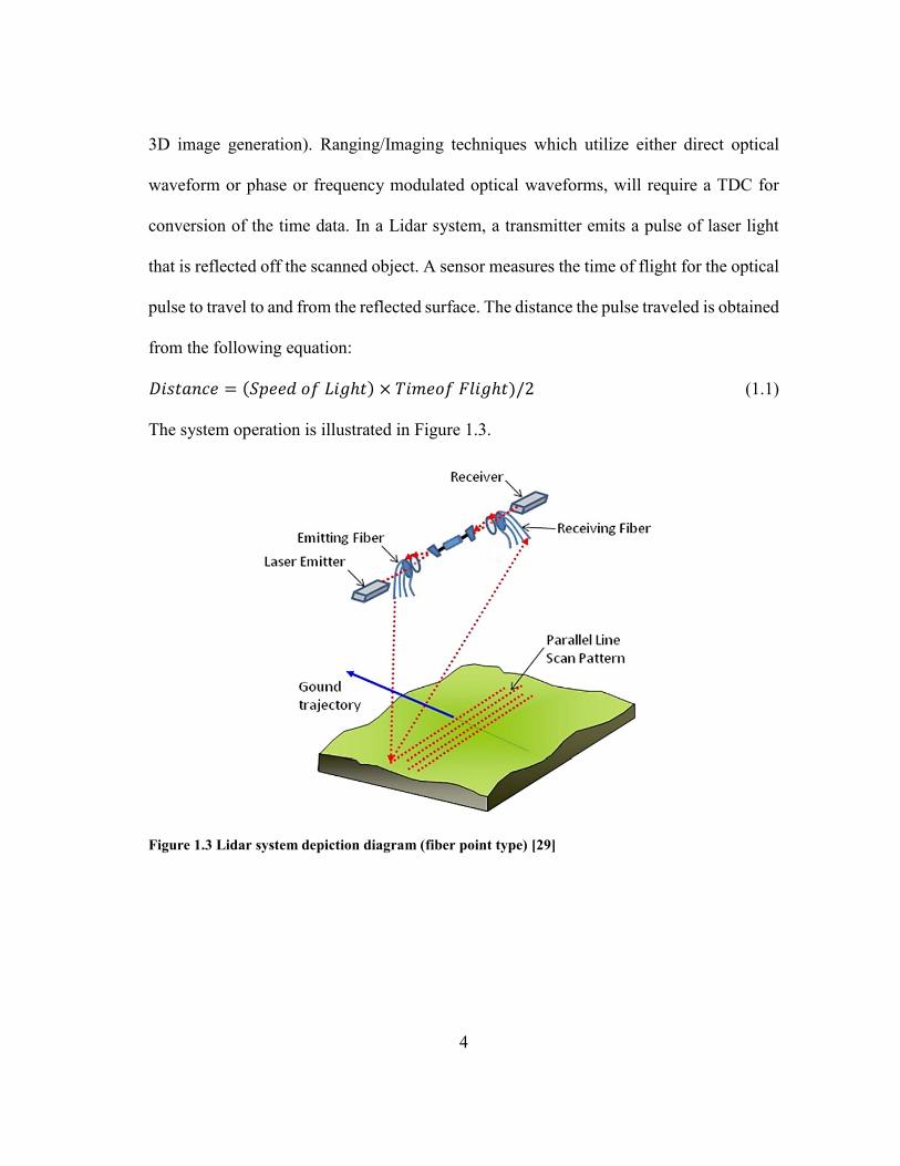
demonstrated in [14, 16, 19, 23, 26, 27]. For example, in [26] the photon is sensed by the
SPAD. A pulse is generated when the photon hits or arrives (ToA). The TDC quantizes
the time difference between the transmission and ToA. This is depicted in Figure 1.1 and
Figure 1.2. A higher pixel count allows for multiple measurements or larger photon sense
per cycle. This creates the need for smaller quantizer area.
3
Figure 1.1 SPAD and front-end circuit [26]
Figure 1.2 Idealized waveforms on nodes VSPAD, VINV and VOUT illustrating the circuit operation when
a photon is detected [26]
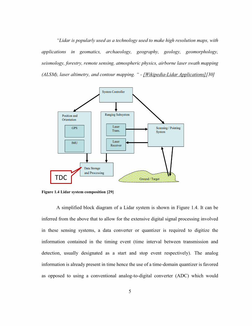
Time-resolved ranging applications involves performing ToF or ToA
measurements [7] with an optical pulse, by determining the arrival time of the returned
signal (reflecting off the surface of an object) with respect to the transmitted optical signal.
This gives an indication of the distance from the object. Also the shape and geometry can
be determined through multiple measurements in a triangulation scheme [28] (enabling
4
3D image generation). Ranging/Imaging techniques which utilize either direct optical
waveform or phase or frequency modulated optical waveforms, will require a TDC for
conversion of the time data. In a Lidar system, a transmitter emits a pulse of laser light
that is reflected off the scanned object. A sensor measures the time of flight for the optical
pulse to travel to and from the reflected surface. The distance the pulse traveled is obtained
from the following equation:
𝐷𝑖𝑠𝑡𝑎𝑛𝑐𝑒 = (𝑆𝑝𝑒𝑒𝑑 𝑜𝑓 𝐿𝑖𝑔ℎ𝑡) × 𝑇𝑖𝑚𝑒𝑜𝑓 𝐹𝑙𝑖𝑔ℎ𝑡)/2 (1.1)
The system operation is illustrated in Figure 1.3.
Figure 1.3 Lidar system depiction diagram (fiber point type) [29]
5
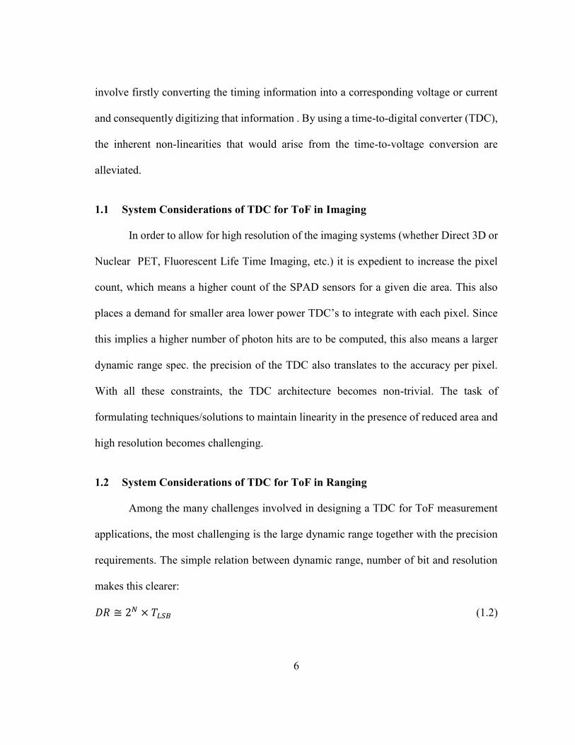
“Lidar is popularly used as a technology used to make high resolution maps, with
applications in geomatics, archaeology, geography, geology, geomorphology,
seismology, forestry, remote sensing, atmospheric physics, airborne laser swath mapping
(ALSM), laser altimetry, and contour mapping. “ - [Wikipedia-Lidar Applications][30]
Figure 1.4 Lidar system composition [29]
A simplified block diagram of a Lidar system is shown in Figure 1.4. It can be
inferred from the above that to allow for the extensive digital signal processing involved
in these sensing systems, a data converter or quantizer is required to digitize the
information contained in the timing event (time interval between transmission and
detection, usually designated as a start and stop event respectively). The analog
information is already present in time hence the use of a time-domain quantizer is favored
as opposed to using a conventional analog-to-digital converter (ADC) which would
TDC
6
involve firstly converting the timing information into a corresponding voltage or current
and consequently digitizing that information . By using a time-to-digital converter (TDC),
the inherent non-linearities that would arise from the time-to-voltage conversion are
alleviated.
1.1 System Considerations of TDC for ToF in Imaging
In order to allow for high resolution of the imaging systems (whether Direct 3D or
Nuclear PET, Fluorescent Life Time Imaging, etc.) it is expedient to increase the pixel
count, which means a higher count of the SPAD sensors for a given die area. This also
places a demand for smaller area lower power TDC’s to integrate with each pixel. Since
this implies a higher number of photon hits are to be computed, this also means a larger
dynamic range spec. the precision of the TDC also translates to the accuracy per pixel.
With all these constraints, the TDC architecture becomes non-trivial. The task of
formulating techniques/solutions to maintain linearity in the presence of reduced area and
high resolution becomes challenging.
1.2 System Considerations of TDC for ToF in Ranging
Among the many challenges involved in designing a TDC for ToF measurement
applications, the most challenging is the large dynamic range together with the precision
requirements. The simple relation between dynamic range, number of bit and resolution
makes this clearer:
𝐷𝑅 ≅ 2𝑁 × 𝑇𝐿𝑆𝐵 (1.2)
7
DR is the dynamic range. N is the number of bits. TLSB is the minimum resolvable time
interval.
From equation 1.2 it is evident that the larger the number of bits the larger the
possible DR for a given TRES. Area and power budget constraints limit the maximum
possible N for a given design architecture and target resolution. In most Radar/Lidar
systems the measurement phase is sub divided into a number of coarse and fine sections
in order to allow for the resolution requirements to be met without sacrificing dynamic
range. The number of subdivisions possible per measurement translates into system
latency and maximum bandwidth constraints. These are usually application specific since
the timing events can vary from an occurrence rate of as low as sub-kHz to a few MHz
depending on the range of distances of the objects and terrains being sensed.
In this work, a new design approach is presented to maximize the dynamic range
of a TDC while maintaining a high resolution (<10ps) and sampling rate with relatively
low area and power overhead. By utilizing the pre-existing hierarchical approach in a two-
step methodology and making use of a looped structure it is possible to achieve both
resolution and large dynamic range with relatively few elements. The fine measurement
is achieved by implementing a Vernier ring or loop technique and limiting the time input
to only an LSB (least significant bit) of the coarse phase measurement.
The thesis is organized as follows.
8
1.3 Thesis Organization
In order to design a TDC for time resolved imaging or ToF applications, it is
necessary to maximize dynamic range while achieving fine resolution for a given
area/power budget. The objective of this work is to demonstrate a new topology based on
both existing techniques and new ideas, which is able to achieve sub-gate delay resolution
and wide range, for a minimal area and power budget. The largest challenge is the tradeoff
that exists between dynamic range and resolution. By using a two-step approach of
quantization and making use of the theoretically infinite dynamic range of a loop, a new
design is proposed which achieves high resolution without sacrificing dynamic range.
In Section 2, an overview of time-to-digital converters is presented. The section
commences with briefly explaining what a TDC is, its basic operation and what the general
high level concepts are in TDC design. This is followed by a general discussion on
linearity and its impact on the performance of the TDC. Also the definitions of basic
metrics such as dynamic range, resolution, latency, etc., are given and their relation with
the TDC, are mentioned. A literature survey of the current state-of-the art works in the
target field is presented, briefly commenting on each topology and highlighting the
strengths and drawbacks with each architecture. The section concludes with a summary of
the major challenges and considerations involved in design a TDC for the said
applications, The problem statement is introduced, motivation is drawn from a summary
of previous works (targeted at the ToF ranging and imaging applications) and the main
goal/target of this work is stated.
9
Section 3 starts off with an overview and introduction of the proposed architecture.
A top-down design methodology is adopted and the high level considerations for the entire
system are discussed. The specifications of the TDC are defined from preliminary
specifications and calculations, and this enables the definition of the various sections of
the system. The novel techniques and algorithms employed in the design are highlighted
also. This section is concluded with a discussion of the nature and choice of the signal that
propagates along the delay lines, due to its impacts on the system implementation.
In Section 4, the design considerations of each of the sections and blocks of the
proposed system architecture are presented. This is done in a hierarchical manner
beginning with the coarse quantization stage, descending down to its lower level building
blocks. Also the major control algorithms which distinguish this work and allows for
achieving the said performance are discussed. The simulation results for each of the blocks
of interest are also presented in this section. In some cases the performance metrics are
summarized in tables. The section concludes with a highlight of all general considerations
made for miscellaneous blocks and over the entire design cycle including layout and
testing of the proposed time-to-digital converter IC. The experimental results of the
proposed design are presented and the overall performance of the TDC chip is summarized
and compared with some of the existing solutions.
In Section 5, a summary of the work is given, conclusions are made and the nature
and scope of future work in this thesis is discussed.
10
2. OVERVIEW OF TIME-TO-DIGITAL CONVERTERS
The term time-to-digital converter refers to a data converter interface whose analog
input is a timing event and output is a digital word corresponding to the magnitude (and
sometimes polarity) of that timing event with some quantization error.
𝛥 𝑇 = [𝐵𝑜𝑢𝑡]𝑑𝑒𝑐𝑖𝑚𝑎𝑙 × 𝑇𝐿𝑆𝐵 + 𝜀 (2.1)
Where ε represents the quantization error associated with finite resolution of the
conversion process (this will be further explained), ΔT describes the analog time event
and Bout is the binary digital word output of the conversion process. There are practically
many approaches for converting/quantizing a time-event into its digital equivalent, but
this work will focus on the digitally intensive approach. In the next sub-section some basic
concepts and general design challenges will be discussed followed by a sub-section on
some state-of the-art-works with particular highlights on solutions for the applications in
time-resolved imaging and also ranging.
2.1 TDC Basics and Theory of Operation
Time to digital converters have found use in many applications including all-
digital phase locked loops (ADPLLs), instrumentation and remote image sensing
applications such as Radar and Lidar ToF measurements, measurement applications in
nuclear physics, time-domain quantizers in Σ-Δ modulators, etc. In all these applications,
the use of the TDC always involves digitizing or quantizing an analog timing event into
the appropriate digital word to allow for signal processing in the digital domain. Hence
what differentiates the various TDC architectures stems from the conversion approach
11
used. This potentially implies that for a particular application one topology would be
preferred or be more suitable over another. Also the different approaches presents various
leverages in power consumption, dynamic range vs. resolution, dynamic vs. static
performance, area, system latency, conversion time, dead time, input signal occurrence
rate, etc. However in this section the theoretical aspects and the basic operation of TDC’s,
considered as a black box, is discussed.
Also a Time-to-Digital Converter draws many parallels with an ADC (Analog-to-
Digital Converter) in terms of its characteristics. The basic difference is that the nature of
the analog input is voltage domain for ADC’s while that of TDC’s is time domain. Besides
that many of the terms used to describe the imperfections of an ADC such as gain error,
INL (integral non-linearity) and DNL (differential non-linearity) are applicable to a TDC
also. These are all explained and their impact on the performance of TDC’s is highlighted.
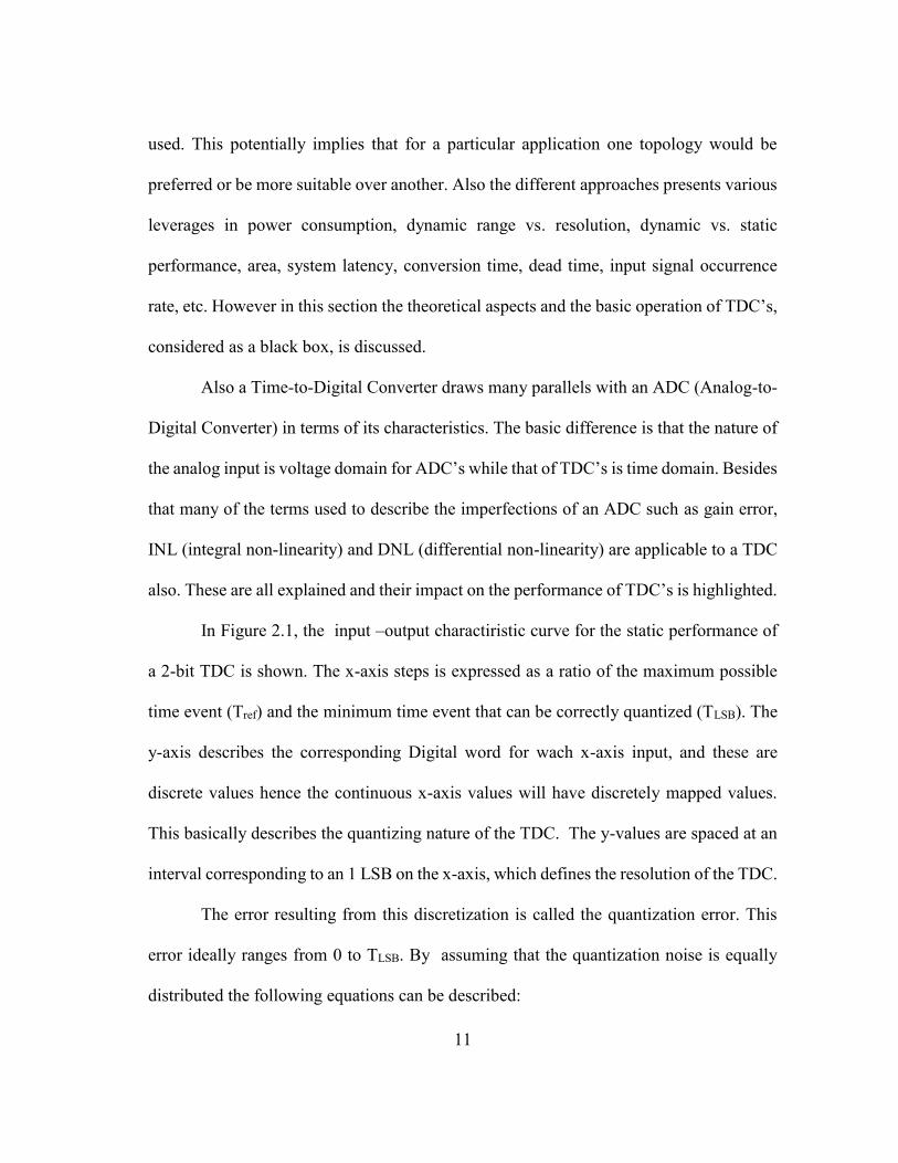
In Figure 2.1, the input –output charactiristic curve for the static performance of
a 2-bit TDC is shown. The x-axis steps is expressed as a ratio of the maximum possible
time event (Tref) and the minimum time event that can be correctly quantized (TLSB). The
y-axis describes the corresponding Digital word for wach x-axis input, and these are
discrete values hence the continuous x-axis values will have discretely mapped values.
This basically describes the quantizing nature of the TDC. The y-values are spaced at an
interval corresponding to an 1 LSB on the x-axis, which defines the resolution of the TDC.
The error resulting from this discretization is called the quantization error. This
error ideally ranges from 0 to TLSB. By assuming that the quantization noise is equally
distributed the following equations can be described:
12
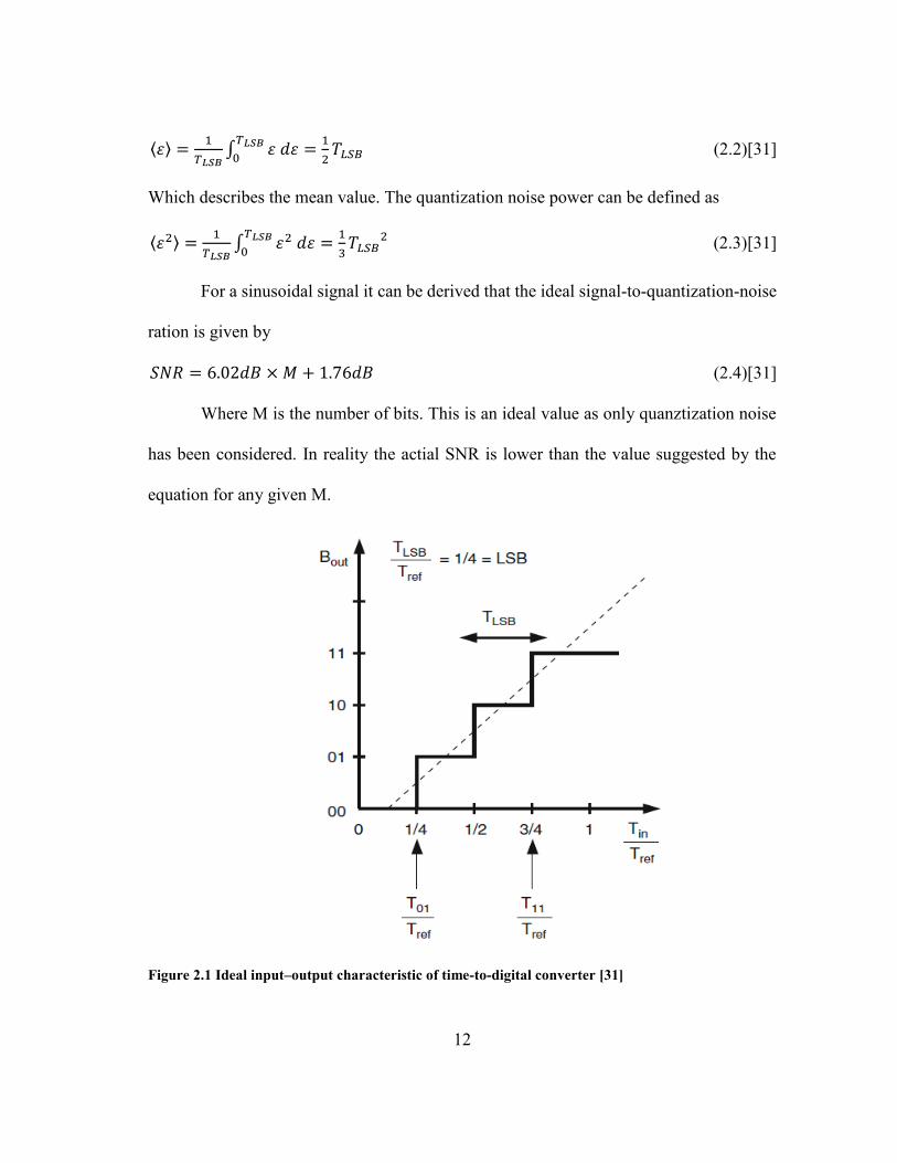
⟨𝜀⟩ =1
𝑇𝐿𝑆𝐵∫ 𝜀 𝑑𝜀
𝑇𝐿𝑆𝐵
0=
1
2𝑇𝐿𝑆𝐵 (2.2)[31]
Which describes the mean value. The quantization noise power can be defined as
⟨𝜀2⟩ =1
𝑇𝐿𝑆𝐵∫ 𝜀2 𝑑𝜀
𝑇𝐿𝑆𝐵
0=
1
3𝑇𝐿𝑆𝐵
2 (2.3)[31]
For a sinusoidal signal it can be derived that the ideal signal-to-quantization-noise
ration is given by
𝑆𝑁𝑅 = 6.02𝑑𝐵 × 𝑀 + 1.76𝑑𝐵 (2.4)[31]
Where M is the number of bits. This is an ideal value as only quanztization noise
has been considered. In reality the actial SNR is lower than the value suggested by the
equation for any given M.
Figure 2.1 Ideal input–output characteristic of time-to-digital converter [31]
13
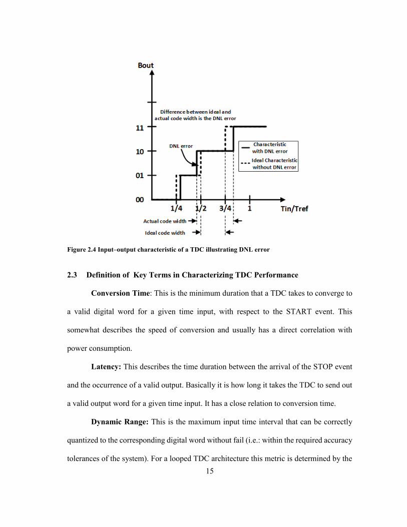
2.2 Linear and Non-linear Non-idealities of TDC Characteristic
The imperfections or non-idealities of the TDC characteristic can be classified as
linear and non-linear. Gain error and offset are two linear imperfections while INL and
DNL are both non-linear imperfections. Linear imperfections usually present less
difficulty in correcting for them and are readily or easily seen in the characteristic. DNL
and INL require more rigorous calibration schemes to correct for them and mostly they
cannot be completely remove.
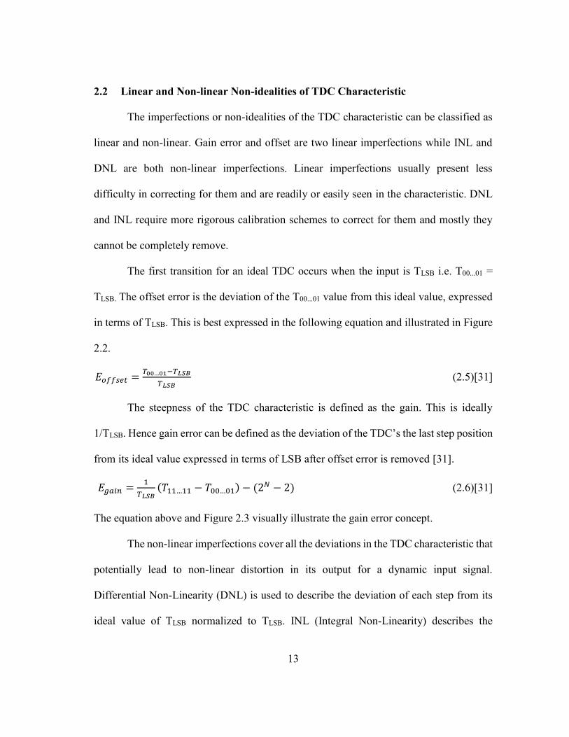
The first transition for an ideal TDC occurs when the input is TLSB i.e. T00...01 =
TLSB. The offset error is the deviation of the T00...01 value from this ideal value, expressed
in terms of TLSB. This is best expressed in the following equation and illustrated in Figure
2.2.
𝐸𝑜𝑓𝑓𝑠𝑒𝑡 =𝑇00…01−𝑇𝐿𝑆𝐵
𝑇𝐿𝑆𝐵 (2.5)[31]
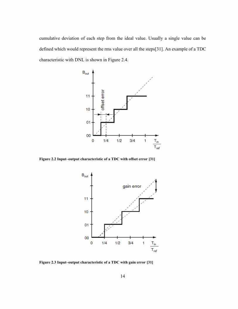
The steepness of the TDC characteristic is defined as the gain. This is ideally
1/TLSB. Hence gain error can be defined as the deviation of the TDC’s the last step position
from its ideal value expressed in terms of LSB after offset error is removed [31].
𝐸𝑔𝑎𝑖𝑛 =1
𝑇𝐿𝑆𝐵(𝑇11…11 − 𝑇00…01) − (2𝑁 − 2) (2.6)[31]
The equation above and Figure 2.3 visually illustrate the gain error concept.
The non-linear imperfections cover all the deviations in the TDC characteristic that
potentially lead to non-linear distortion in its output for a dynamic input signal.
Differential Non-Linearity (DNL) is used to describe the deviation of each step from its
ideal value of TLSB normalized to TLSB. INL (Integral Non-Linearity) describes the
14
cumulative deviation of each step from the ideal value. Usually a single value can be
defined which would represent the rms value over all the steps[31]. An example of a TDC
characteristic with DNL is shown in Figure 2.4.
Figure 2.2 Input–output characteristic of a TDC with offset error [31]
Figure 2.3 Input–output characteristic of a TDC with gain error [31]
15
Figure 2.4 Input–output characteristic of a TDC illustrating DNL error
2.3 Definition of Key Terms in Characterizing TDC Performance
Conversion Time: This is the minimum duration that a TDC takes to converge to
a valid digital word for a given time input, with respect to the START event. This
somewhat describes the speed of conversion and usually has a direct correlation with
power consumption.
Latency: This describes the time duration between the arrival of the STOP event
and the occurrence of a valid output. Basically it is how long it takes the TDC to send out
a valid output word for a given time input. It has a close relation to conversion time.
Dynamic Range: This is the maximum input time interval that can be correctly
quantized to the corresponding digital word without fail (i.e.: within the required accuracy
tolerances of the system). For a looped TDC architecture this metric is determined by the
16
loop counter which tracks the number of complete cycles the input signal (either edges or
pulses) has made across the loop. Since a loop theoretically has infinite length. The
number of bits of the counter then places a bound on the range.
Time Resolution: This describes the minimum possible time interval that a TDC
can correctly quantize. It has an inverse proportionality with the dynamic range for a given
number of bits.
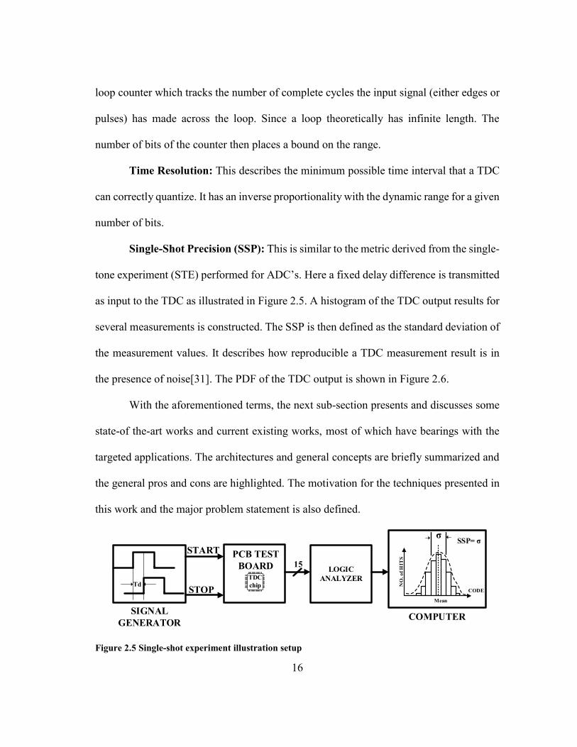
Single-Shot Precision (SSP): This is similar to the metric derived from the single-
tone experiment (STE) performed for ADC’s. Here a fixed delay difference is transmitted
as input to the TDC as illustrated in Figure 2.5. A histogram of the TDC output results for
several measurements is constructed. The SSP is then defined as the standard deviation of
the measurement values. It describes how reproducible a TDC measurement result is in
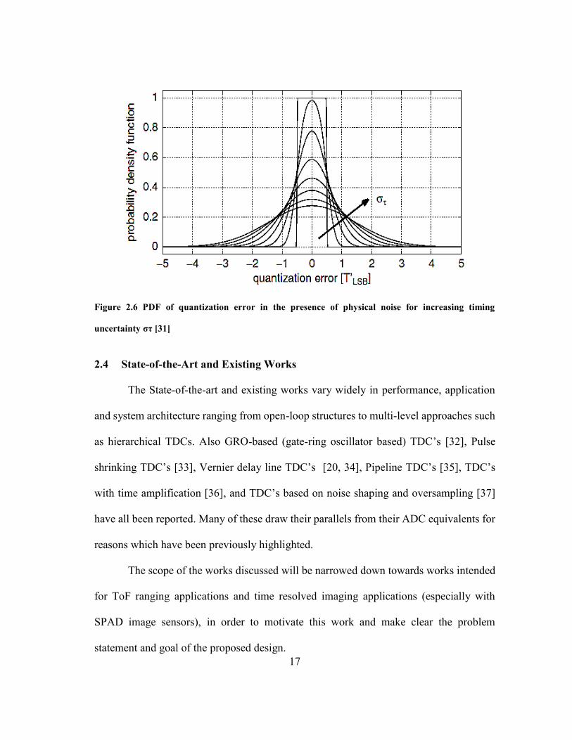
the presence of noise[31]. The PDF of the TDC output is shown in Figure 2.6.
With the aforementioned terms, the next sub-section presents and discusses some
state-of the-art works and current existing works, most of which have bearings with the
targeted applications. The architectures and general concepts are briefly summarized and
the general pros and cons are highlighted. The motivation for the techniques presented in
this work and the major problem statement is also defined.
START
STOP
PCB TEST
BOARD LOGIC
ANALYZER
SSP= σ
SIGNAL
GENERATOR
15
σ
Td
COMPUTER
CODE
NO
. o
f H
ITS
Mean
TDC
chip
Figure 2.5 Single-shot experiment illustration setup
17
Figure 2.6 PDF of quantization error in the presence of physical noise for increasing timing
uncertainty στ [31]
2.4 State-of-the-Art and Existing Works
The State-of-the-art and existing works vary widely in performance, application
and system architecture ranging from open-loop structures to multi-level approaches such
as hierarchical TDCs. Also GRO-based (gate-ring oscillator based) TDC’s [32], Pulse
shrinking TDC’s [33], Vernier delay line TDC’s [20, 34], Pipeline TDC’s [35], TDC’s
with time amplification [36], and TDC’s based on noise shaping and oversampling [37]
have all been reported. Many of these draw their parallels from their ADC equivalents for
reasons which have been previously highlighted.
The scope of the works discussed will be narrowed down towards works intended
for ToF ranging applications and time resolved imaging applications (especially with
SPAD image sensors), in order to motivate this work and make clear the problem
statement and goal of the proposed design.
18
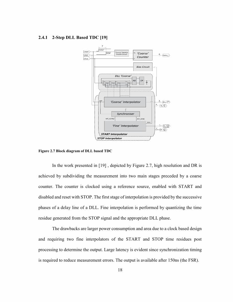
2.4.1 2-Step DLL Based TDC [19]
Figure 2.7 Block diagram of DLL based TDC
In the work presented in [19] , depicted by Figure 2.7, high resolution and DR is
achieved by subdividing the measurement into two main stages preceded by a coarse
counter. The counter is clocked using a reference source, enabled with START and
disabled and reset with STOP. The first stage of interpolation is provided by the successive
phases of a delay line of a DLL. Fine interpolation is performed by quantizing the time
residue generated from the STOP signal and the appropriate DLL phase.
The drawbacks are larger power consumption and area due to a clock based design
and requiring two fine interpolators of the START and STOP time residues post
processing to determine the output. Large latency is evident since synchronization timing
is required to reduce measurement errors. The output is available after 150ns (the FSR).

19
2.4.2 TDC Employing Time Amplification [27]
Figure 2.8 Bock diagram of 128 column-parallel TDC with time amplification
The work in [27] is targeted for PET applications. The main goal is to reduce the
area occupancy of the smart pixel consisting of both SPAD sensor and the TDC. The first
step quantization is achieved using a VCO and a cycle counter (enabled by START and
STOP), and the phases of the VCO give coarse measurement. The time residue is
amplified and quantized by a second stage VCO and cycle counter in a similar fashion.
Resolution is TLSB/G where G is the gain of the TA and TLSB is the delay between 2
successive phases of the VCO. The system diagram is shown in Figure 2.8.
Drawbacks are latency and conversion time (320ns) since it is VCO based. Also
time amplification is non-linear and requires robust calibration to meet linearity
requirements. Highlights are small area and power per pixel.
20
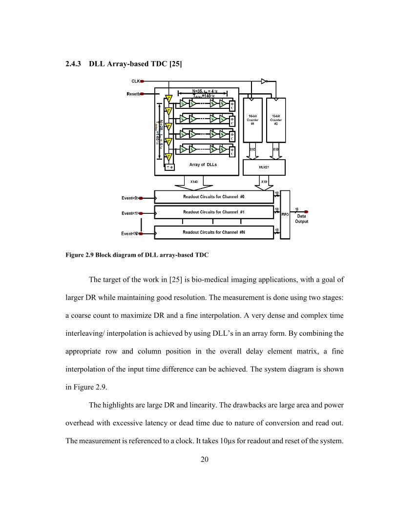
2.4.3 DLL Array-based TDC [25]
Figure 2.9 Block diagram of DLL array-based TDC
The target of the work in [25] is bio-medical imaging applications, with a goal of
larger DR while maintaining good resolution. The measurement is done using two stages:
a coarse count to maximize DR and a fine interpolation. A very dense and complex time
interleaving/ interpolation is achieved by using DLL’s in an array form. By combining the
appropriate row and column position in the overall delay element matrix, a fine
interpolation of the input time difference can be achieved. The system diagram is shown
in Figure 2.9.
The highlights are large DR and linearity. The drawbacks are large area and power
overhead with excessive latency or dead time due to nature of conversion and read out.
The measurement is referenced to a clock. It takes 10µs for readout and reset of the system.
21
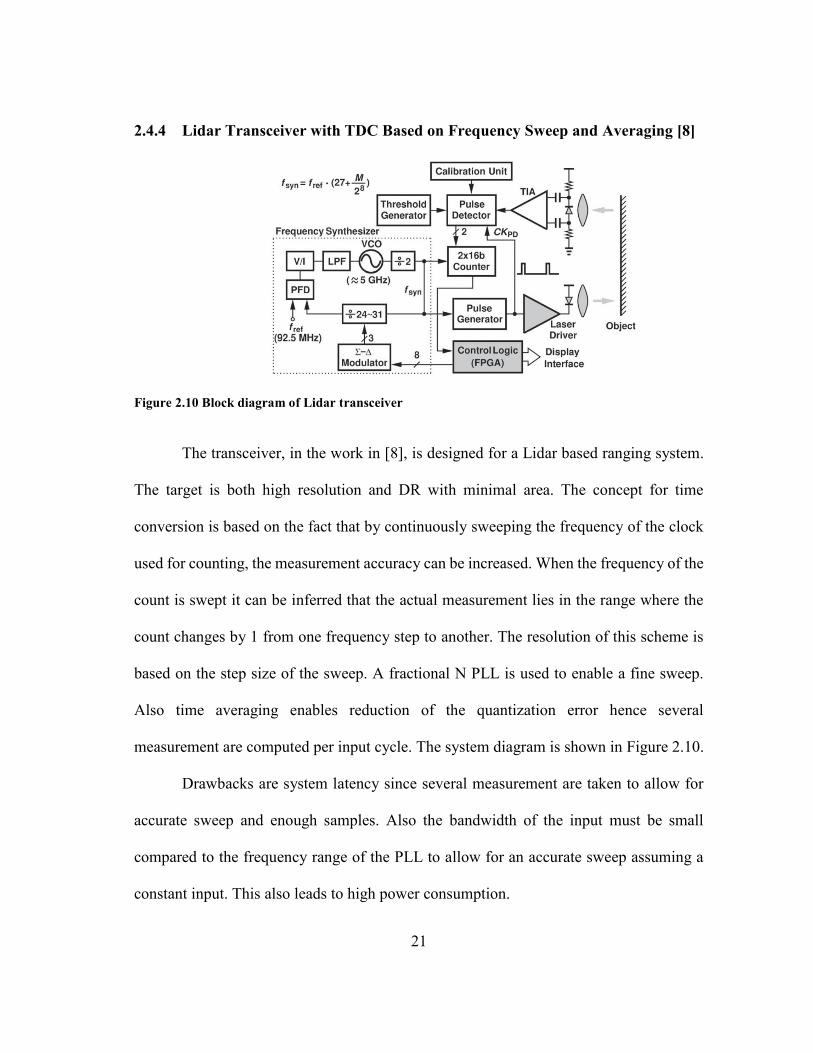
2.4.4 Lidar Transceiver with TDC Based on Frequency Sweep and Averaging [8]
Figure 2.10 Block diagram of Lidar transceiver
The transceiver, in the work in [8], is designed for a Lidar based ranging system.
The target is both high resolution and DR with minimal area. The concept for time
conversion is based on the fact that by continuously sweeping the frequency of the clock
used for counting, the measurement accuracy can be increased. When the frequency of the
count is swept it can be inferred that the actual measurement lies in the range where the
count changes by 1 from one frequency step to another. The resolution of this scheme is
based on the step size of the sweep. A fractional N PLL is used to enable a fine sweep.
Also time averaging enables reduction of the quantization error hence several
measurement are computed per input cycle. The system diagram is shown in Figure 2.10.
Drawbacks are system latency since several measurement are taken to allow for
accurate sweep and enough samples. Also the bandwidth of the input must be small
compared to the frequency range of the PLL to allow for an accurate sweep assuming a
constant input. This also leads to high power consumption.

22
2.4.5 MASH 1-1-1 ∆Σ TDC [17]
Figure 2.11 System diagram of third order MASH ∆Σ TDC
In the work in [17], targeted for Lidar ranging applications, the concept of
oversampling and noise shaping (NS) is employed to reduce quantization error and
maximize resolution while utilizing little power. Coarse measurement is achieved by a
count with oversampling clock cycles, hence maximizing the DR. QE of the 1st stage is
converted to voltage and forwarded into the next measurement phase, achieving a 1st order
NS in closed loop. Doing this successively three times, enables 3rd order NS.
𝑂𝑆𝑅 = 𝐹𝑂𝑆𝐶 𝐹𝐼𝑁𝑃𝑈𝑇⁄ (2.7)
Where FINPUT is the input occurrence rate and FOSC is the frequency of the oscillator.
The drawbacks here are system latency and circuit complexity. Linearity is also
hindered by several voltage-to-time and time-to-voltage conversions, since these suffer
from analog impairments in sub-micron technologies. The conceptual system diagram is
shown in Figure 2.11.
23
2.5 Motivation and Problem Statement
The key conclusion that can be drawn from the previously mentioned works is that,
the challenge of resolution trading off with dynamic range, area and power is inherent,
and the most promising approach for achieving high precision is to subdivide the
measurement into different steps. The higher the number of sub conversion sections, with
the preceding steps having lower resolution and higher DR, the better the tradeoff will be
between DR and TRES. The challenge however is a trade off with system latency as the
number of sub conversions would imply longer conversion times and more complex logic
for proper operation. This also leads to area and power overheads. These major challenges
motivates this work. The goal is to design a 2 step-hierarchical TDC that maximizes both
DR and TRES while optimizing area and power consumption. The main aim, therefore, is
to apply techniques that maximize DR without trading off linearity, resolution, area and
power consumption.
By taking advantage of a looped architecture with lower resolution, a wide DR is
achieved. The employment of another loop structure with a deliberately limited input
range and fine resolution the TRES is maximized. A novel control algorithm completely
alleviates the possibility of an error in the MSB. Hence linearity is determined mostly by
the fine quantization stage. Another control algorithm optimizes system activity (hence
power consumption) and simplifies the interface between the two stages of conversion
which reduces the latency bottle neck and enables more streamline conversion.
24
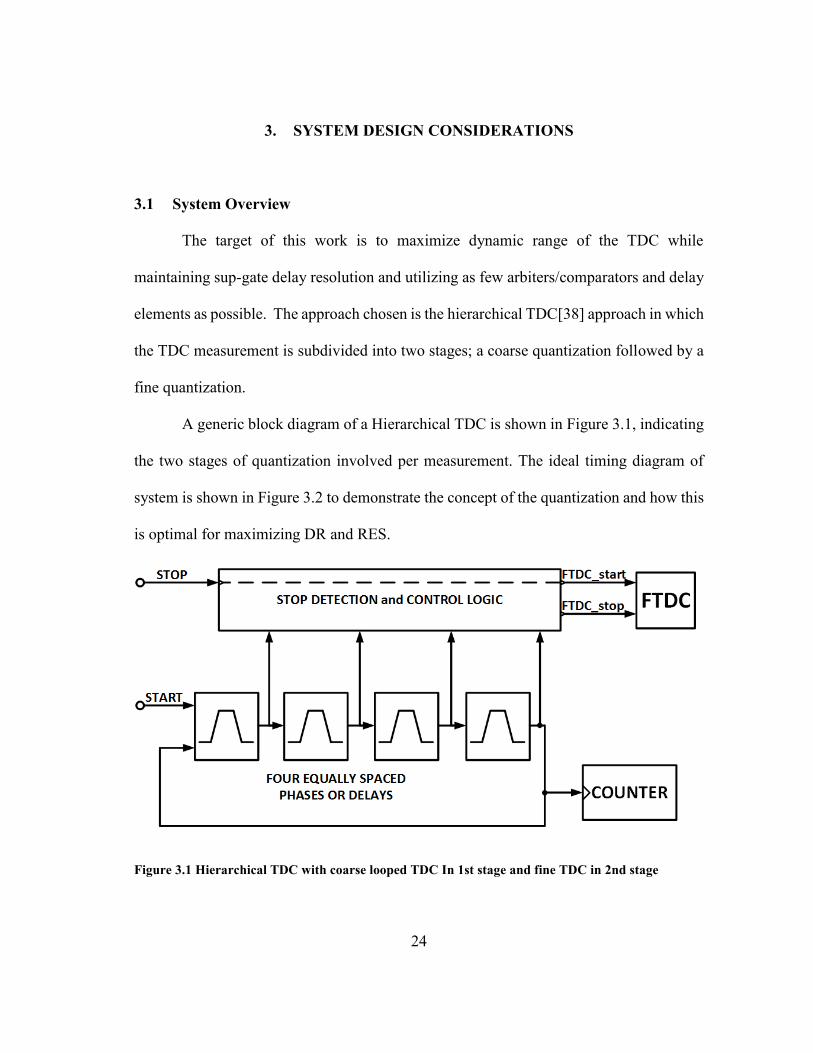
3. SYSTEM DESIGN CONSIDERATIONS
3.1 System Overview
The target of this work is to maximize dynamic range of the TDC while
maintaining sup-gate delay resolution and utilizing as few arbiters/comparators and delay
elements as possible. The approach chosen is the hierarchical TDC[38] approach in which
the TDC measurement is subdivided into two stages; a coarse quantization followed by a
fine quantization.
A generic block diagram of a Hierarchical TDC is shown in Figure 3.1, indicating
the two stages of quantization involved per measurement. The ideal timing diagram of
system is shown in Figure 3.2 to demonstrate the concept of the quantization and how this
is optimal for maximizing DR and RES.
Figure 3.1 Hierarchical TDC with coarse looped TDC In 1st stage and fine TDC in 2nd stage
25
Figure 3.2 Ideal signal diagram proposed hierarchical TDC [38]
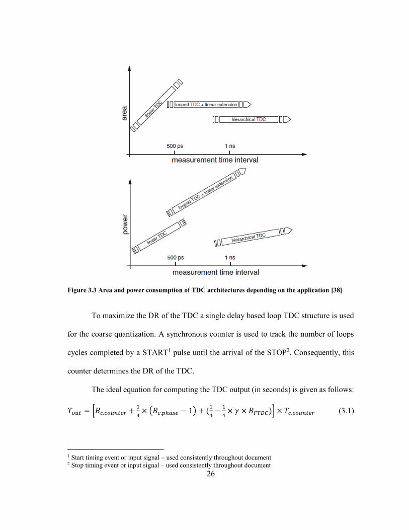
The graphs in Figure 3.3, depicts how the general TDC architectures each trades
off with area and power consumption. The postulates of this strongly motivates the choice
of the system architecture implemented in this work.
The linear TDC mentioned in the diagram makes use of an open loop delay line.
The looped TDC makes use of a delay ring which circulates either an edge or a pulse. The
conversion approach is done in one step. The hierarchical can be seen to have better
optimization of power and area when the measurement interval increases. For the said
applications this would be the case (a large DR is required).
26
Figure 3.3 Area and power consumption of TDC architectures depending on the application [38]
To maximize the DR of the TDC a single delay based loop TDC structure is used
for the coarse quantization. A synchronous counter is used to track the number of loops
cycles completed by a START1 pulse until the arrival of the STOP2. Consequently, this
counter determines the DR of the TDC.
The ideal equation for computing the TDC output (in seconds) is given as follows:
𝑇𝑜𝑢𝑡 = [𝐵𝑐.𝑐𝑜𝑢𝑛𝑡𝑒𝑟 +1
4× (𝐵𝑐.𝑝ℎ𝑎𝑠𝑒 − 1) + (
1
4−
1
4× 𝛾 × 𝐵𝐹𝑇𝐷𝐶)] × 𝑇𝑐.𝑐𝑜𝑢𝑛𝑡𝑒𝑟 (3.1)
1 Start timing event or input signal – used consistently throughout document 2 Stop timing event or input signal – used consistently throughout document
27
In the above Equation 3.1, Bc.counter is the output value of the CTDC3 loop counter.
Tout is the time equivalent of the TDC digital word.
Tc.counter is the resolution of the CTDC loop counter which is equal to 4*TCTDCPHASE (the
ideal time resolution or delay of a delay element in the CTDC).
Bc.counter is the digital decimal output of the loop counter of the CTDC.
Bc.phase is the number of the CTDC phase or delay element which stops the FTDC4 (ranging
from 1 to 4 in this work).
BFTDC is the integer value of the raw FTDC digital output.
NB: the factor ¼ is due to the number of delay elements used the CTDC. Hence this could
be 1/N where N is the number delay elements in the loop or ring of the CTDC.
Also γ is the inverse of the maximum possible BFTDC (FTDC output) for a time input equal
to a delay element of the CTDC. i.e.:
𝛾 =1
[𝐵𝐹𝑇𝐷𝐶]𝑚𝑎𝑥|
𝐹𝑇𝐷𝐶 𝑖𝑛𝑝𝑢𝑡= 𝑇𝐶𝑇𝐷𝐶.𝑝ℎ𝑎𝑠𝑒
(3.2)
It can be inferred that the resolution of the FTDC is given by
𝑇𝑟𝑒𝑠 =𝑇𝑐.𝑐𝑜𝑢𝑛𝑡𝑒𝑟
4× 𝛾 = 𝑇𝐶𝑇𝐷𝐶.𝑝ℎ𝑎𝑠𝑒 × 𝛾 (3.3)
Where TCTDC.phase is the resolution of the CTDC. (i.e.: the delay of a single delay element
in the CTDC).
For the system architecture in this work, the following condition must be met:
𝑇𝐶𝑇𝐷𝐶.𝑝ℎ𝑎𝑠𝑒 ≤ 𝐷𝑅𝐹𝑇𝐷𝐶 (3.4)
3 Coarse Stage Time-to-Digital Converter used in the coarse measurement (1st step) – used consistently
throughout document 4 Fine Stage Time-to-Digital Converter used for fine quantization (2nd step) – used consistently throughout
document
28
Where DRFTDC is the dynamic range of the FTDC.
The difference between the two quantities in equation (3.4) is however kept small
to maximize the actual DR of the FTDC. From equation (3.3) it is seen that the larger the
[BFTDC] max the finer the resolution of the FTDC, and the smaller the value of γ, which is
ideally desired to be as close as possible to zero. There are practical limitations however,
for a given architecture. Effort is made in this work to maximize the value [BFTDC] max for
a fixed DRFTDC and design measures are taken to realize this.
As mentioned previously, the DR of the FTDC (fine TDC) is limited to just the
resolution of the CTDC (Coarse TDC) which is the time delay of a single delay element
of the CTDC. This enables design effort targeted at high resolution in the FTDC stage.
The fine quantization is performed using a Vernier-ring structure. This enables very fine
resolution below the gate delay in a given technology without sacrificing dynamic range.
This is because the use of a loop allows for element re-use and reduced device count. This
minimizes accumulated jitter due to process variations and non-linear imperfections
resulting from increased delay element count.
Various control schemes are implemented to enable the proper timing sequence of
each conversion step (coarse and fine conversion) since looped structures require control
to allow for proper functioning and prevent unstable events of the loop getting locked in
an undesirable state.
A novel control loop scheme based on DF (decision feedback) is used to correctly
determine the coarse clocking in order to totally remove inaccurate MSB (most significant
bit) values. This challenge comes from the analog or continuous-time nature of the input
29
timing events. The START and STOP time events are totally asynchronous in a typical
measurement. This potential leads to metastable events in a system containing sequential
logic. By employing the control loop, this problem is alleviated. The circuit design is
discussed in detail in the subsequent sub-sections.
The delay elements are voltage controlled. A DLL (Delay Locked Loop) is used
to further increase the robustness of the delay elements by providing a control voltage
which is related to the input clock period of the DLL and the number of delay elements in
the DLL loop. By employing a DLL to fix the delay of the delay elements, the correlated
delay variations are significantly suppressed. An operational amplifier is used to decouple
the DLL loop from the control voltage which is sent to the CTDC and FTDC. This further
prevents noise from coupling to and from the DLL.
Figure 3.4 Arrival time uncertainty in different TDC architectures[38]
30
In Figure 3.4, a plot of signal arrival time (STOP arrival) uncertainty is shown to
increase with the number of delay elements passed, in the presence of process variations.
Hence by reducing the number of elements and employing a DLL to compensate for the
gain of the loop the TDC characteristic can be greatly improved. Challenges such as
increased non-linearity and layout sensitivity are discussed, and potential solutions to
circumvent these problems will be discussed in detail.
The next subsection discusses the system definition and estimation of some of the
ideal performance metrics of the architecture mentioned previously.
3.2 System Definition
The system is designed using the IBM 180nm technology and the nominal supply
is 1.8V. The typical FO4 delay is about 100ps tt (typical corner).
An estimate of the CTDC delay resolution is made and set to be 200ps with a total
number of 4 delay elements in the CTDC. This results in a word length of 2 bits, for the
delay elements of the CTDC. With that established, the following further definitions are
estimated.
𝐷𝑅𝐶𝑇𝐷𝐶.𝑝ℎ𝑎𝑠𝑒 = 𝑁𝐶𝑇𝐷𝐶.𝑒𝑙𝑒𝑚𝑒𝑛𝑡𝑠 × 𝑇𝐶𝑇𝐷𝐶.𝑝ℎ𝑎𝑠𝑒 = 4 × 200𝑝𝑠 = 800𝑝𝑠 (3.5)
𝐷𝑅𝐶𝑇𝐷𝐶.𝑐𝑜𝑢𝑛𝑡𝑒𝑟 = [2𝑁𝐶𝑇𝐷𝐶.𝑐𝑜𝑢𝑛𝑡 − 1] × 𝐷𝑅𝐶𝑇𝐷𝐶.𝑝ℎ𝑎𝑠𝑒 (3.6)
𝑇𝐹𝑇𝐷𝐶 =𝐷𝑅𝐹𝑇𝐷𝐶
(2𝑁𝐹𝑇𝐷𝐶−1)≤ 10𝑝𝑠 (3.7)
𝐷𝑅𝐹𝑇𝐷𝐶 ≥ 𝑇𝐶𝑇𝐷𝐶.𝑝ℎ𝑎𝑠𝑒 (3.8)
⇒ 𝑁𝐹𝑇𝐷𝐶 ≥ log2 [𝑇𝐶𝑇𝐷𝐶.𝑝ℎ𝑎𝑠𝑒
10𝑝𝑠+ 1] ≥ 4.3923 (3.9)
∴ 𝑁𝐹𝑇𝐷𝐶 ≥ 5 (3.10)
31
The number of bits of the CTDC loop counter is selected to be 8. This leads to
𝐷𝑅𝐶𝑇𝐷𝐶.𝑐𝑜𝑢𝑛𝑡𝑒𝑟 = [28 − 1] × 800𝑝𝑠 ≅ 204𝑛𝑠 (3.11)
The entire word length of the TDC is then given as 15 bits with an approximate
DR equal to that of the CTDC loop counter. The exact total DR can be estimated using
equation (3.1) using the maximum of CTDC section’s digital word and minimum for
FTDC. I.e.:
𝐵𝐶𝑇𝐷𝐶.𝑐𝑜𝑢𝑛𝑡𝑒𝑟|𝑀𝐴𝑋 = [28 − 1] = 225 (3.12)
𝐵𝐶𝑇𝐷𝐶.𝑝ℎ𝑎𝑠𝑒|𝑀𝐴𝑋
= [22 − 1] = 3 (3.13)
𝐵𝐹𝑇𝐷𝐶|𝑚𝑖𝑛 = 0 (3.14)
With the above definitions, the dynamic range (DR) of the proposed TDC can be
estimated from equation (3.1) as
𝐷𝑅𝑇𝐷𝐶 ≈ [28] × 800𝑝𝑠 ≅ 204.8𝑛𝑠 (3.15)
Due to the limitation of memory capabilities of the test equipment and resources
used in design, the number of bits of the CTDC loop counter was deliberated limited to
only 8 to allow for reduced simulation time and also to allow for practical testing. In reality
the techniques applied in this design allow for an indefinite extension of the DR of the
TDC by the addition of an external counter. The trade-off would be between measurement
range and conversion time. The performance and linearity would not be limited by the
measurement range itself as demonstrated in Figure 3.4, due the looped structure and use
of a DLL. The limitations arise from physical noise accumulated during the measurement
operation but for the target DR this did not significantly impact performance.
32
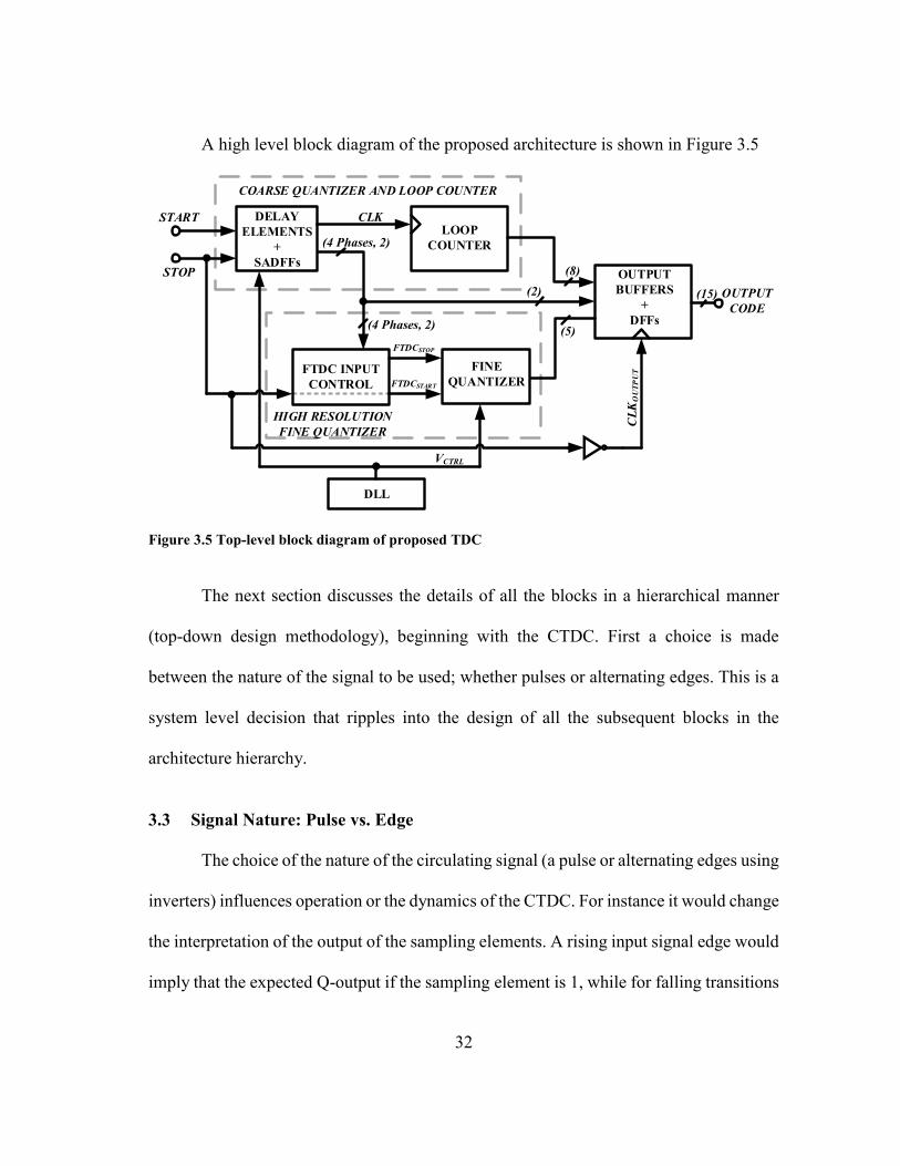
A high level block diagram of the proposed architecture is shown in Figure 3.5
(4 Phases, 2)
CLK
(2)
(8)
(5)(4 Phases, 2)
(15) OUTPUT
CODE
HIGH RESOLUTION
FINE QUANTIZER
COARSE QUANTIZER AND LOOP COUNTER
OUTPUT
BUFFERS
+
DFFs
FINE
QUANTIZERFTDC INPUT
CONTROL
DELAY
ELEMENTS
+
SADFFs
LOOP
COUNTER
DLL
VCTRL
CL
KO
UT
PU
T
START
STOP
FTDCSTOP
FTDCSTART
Figure 3.5 Top-level block diagram of proposed TDC
The next section discusses the details of all the blocks in a hierarchical manner
(top-down design methodology), beginning with the CTDC. First a choice is made
between the nature of the signal to be used; whether pulses or alternating edges. This is a
system level decision that ripples into the design of all the subsequent blocks in the
architecture hierarchy.
3.3 Signal Nature: Pulse vs. Edge
The choice of the nature of the circulating signal (a pulse or alternating edges using
inverters) influences operation or the dynamics of the CTDC. For instance it would change
the interpretation of the output of the sampling elements. A rising input signal edge would
imply that the expected Q-output if the sampling element is 1, while for falling transitions
33
the expected output would be 0. This complicates the thermometer code interpretation of
the delay chain.
The loop counter would also have to be correctly designed to trigger with both a
rising and a falling transition of the trigger or clock signal. Matching rising and falling
transitions is a major challenge also due to the inherent mobility differences between
NMOS and PMOS transistors (µn and µp). And this difference varies a lot with process. It
is nearly impossible to match the transition times over process and temperature.
The use of a circulating pulse simplifies the aforementioned complexities. The
thermometer code is easily interpreted with a few enhancements to account for the pulsed
nature. Also if the input and output signals are identical for each delay element, then the
CTDC can be assumed as non-distorting and inherently linear. By replicating the input
stage of the CTDC loop in all the delay elements, the delay mismatch due to the input mux
of the CTDC loop is alleviated. The counter design is simplified since it can be designed
to trigger with only one edge (rising or falling). The mismatch in the rise and fall times is
non-existent since the pulse is regenerated after every delay element hence the pulse is
perfectly reserved. With these pros and cons considered, the pulsed nature for the
circulating signal is chosen for the CTDC.
34
4. BLOCK LEVEL DESIGN
This section presents all the considerations that are made in design each block of
the TDC. Design issues and various techniques used to circumvent challenges are all
discussed using a top-down hierarchical design methodology. The first of the blocks to be
considered is the CTDC.
4.1 Coarse Stage Time-To-Digital Converter (CTDC)
The main aim or goal of this step of the quantization is to provide a very coarse
measurement and generate a time residue no larger than the delay of a single delay
element. The targets are large DR and low resolution. The low resolution of the CTDC
sets a constraint on the DR of the FTDC hence the architecture chosen takes into account
this constraint in minimizing the CTDC resolution (selecting a “not-so-large” delay for
the CTDC delay element) while maximizing its DR.
The looped structure of the CTDC allows for a theoretical infinite DR, limited only
by the loop counter and not the loop itself. In practice, however physical noise and a
phenomenon known as pulse growth or shrinking limits during the measurement the DR
of the TDC. Design techniques were implemented to circumvent the pulse growth or
shrinking problem.
A simplified block diagram of the CTDC is shown below in Figure 4.1.
35
Figure 4.1 Simplified block diagram Of CTDC
Here, START enables a pulse generator to generate a pulse of ideal width equal to
400ps (1/2 of the DR of the CTDC loop) which is then latched into the loop via a mux,
and it circulates the loop until the arrival of STOP. At the arrival of STOP the loop is
disengaged and the sampling elements are used to determine the approximate position of
the STOP relative to the 4 Phases. This phase code information is then used to generate or
decide the STOP signal for the FTDC. The CTDC STOP serves the START signal for the
FTDC as mentioned in the system overview section. Also a loop counter placed at the end
of the loop is used to count the number of full cycles elapsed by the circulating pulse
before the arrival of STOP.
The circulating signal can be thought of as a clock. This is because the pulse
generated has a width approximately half of the DR of the loop in the CTDC. This
condition is not too critical but from simulations the minimum and maximum widths of
36
the circulating pulse in the CTDC are 250ps and 600ps respectively for a CTDC loop DR
of 800ps. These constraints are set by the logic used to interpret the DFF (flip-flop) outputs
of the CTDC i.e. the outputs of the sampling elements of the CTDC.
As is evident with this looped structure the main challenges are identical delay
elements, sampling element accuracy and dynamics of the counting mechanism and these
are discussed next.
4.1.1 The Pulse Generator
The considerations of this system and its performance widely depends on pulses.
Various pulses are used as control signals, and the main signal that circulates the CTDC
loop as well as the signals used in the FTDC Vernier ring are all pulses. The nature of the
input signals of these loops necessitates the design of a pulse generator which generates a
pulse of fixed width which is independent of the width of the input trigger pulse/ signal.
The architecture in [39] is simple and straight-forward. However, there is a limitation as
to the width on the pulse generated: the input signal width cannot be less than the output
pulse width. This fails to meet the system requirement. A novel structure is proposed
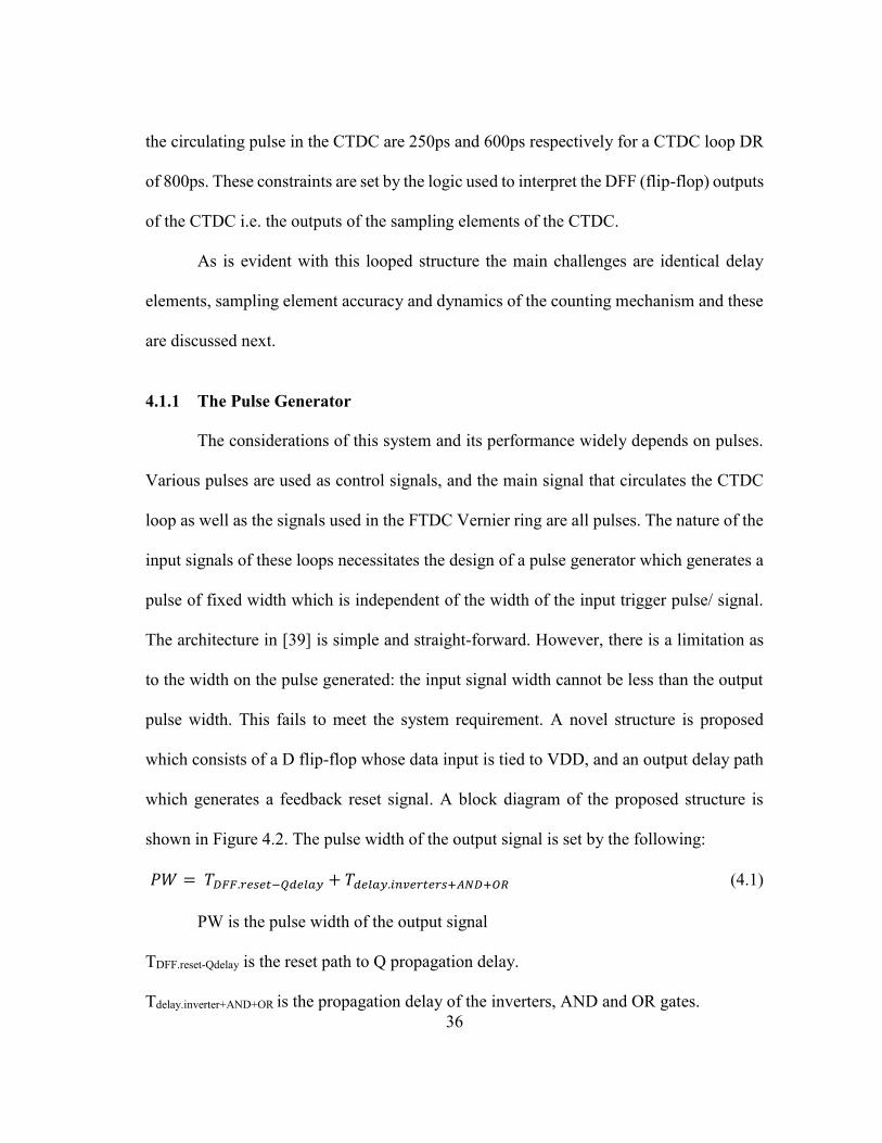
which consists of a D flip-flop whose data input is tied to VDD, and an output delay path
which generates a feedback reset signal. A block diagram of the proposed structure is
shown in Figure 4.2. The pulse width of the output signal is set by the following:
𝑃𝑊 = 𝑇𝐷𝐹𝐹.𝑟𝑒𝑠𝑒𝑡−𝑄𝑑𝑒𝑙𝑎𝑦 + 𝑇𝑑𝑒𝑙𝑎𝑦.𝑖𝑛𝑣𝑒𝑟𝑡𝑒𝑟𝑠+𝐴𝑁𝐷+𝑂𝑅 (4.1)
PW is the pulse width of the output signal
TDFF.reset-Qdelay is the reset path to Q propagation delay.
Tdelay.inverter+AND+OR is the propagation delay of the inverters, AND and OR gates.
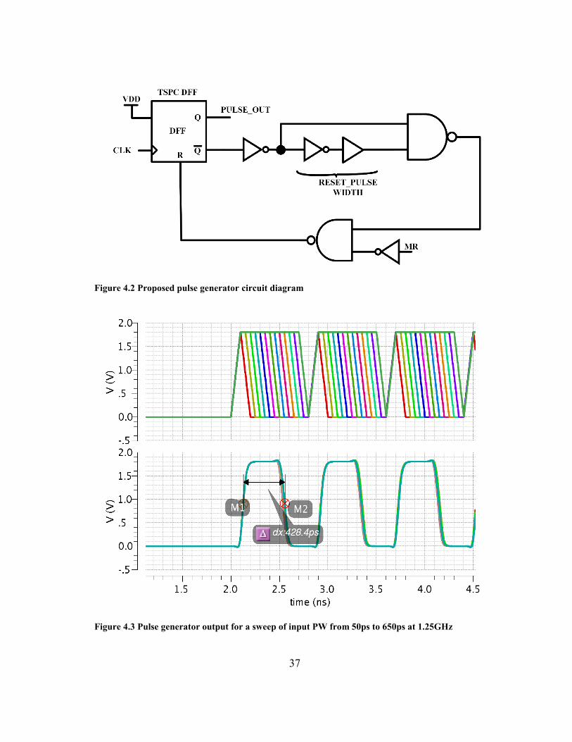
37
Figure 4.2 Proposed pulse generator circuit diagram
Figure 4.3 Pulse generator output for a sweep of input PW from 50ps to 650ps at 1.25GHz
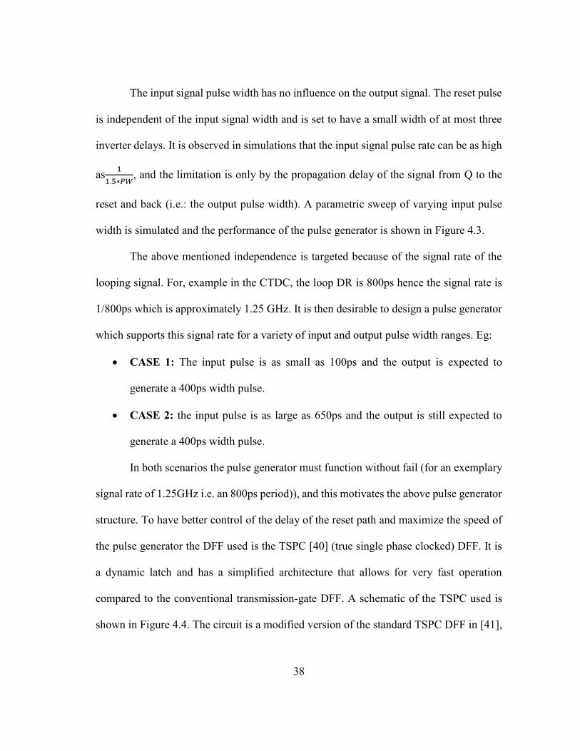
38
The input signal pulse width has no influence on the output signal. The reset pulse
is independent of the input signal width and is set to have a small width of at most three
inverter delays. It is observed in simulations that the input signal pulse rate can be as high
as1
1.5∗𝑃𝑊, and the limitation is only by the propagation delay of the signal from Q to the
reset and back (i.e.: the output pulse width). A parametric sweep of varying input pulse
width is simulated and the performance of the pulse generator is shown in Figure 4.3.
The above mentioned independence is targeted because of the signal rate of the
looping signal. For, example in the CTDC, the loop DR is 800ps hence the signal rate is
1/800ps which is approximately 1.25 GHz. It is then desirable to design a pulse generator
which supports this signal rate for a variety of input and output pulse width ranges. Eg:
CASE 1: The input pulse is as small as 100ps and the output is expected to
generate a 400ps width pulse.
CASE 2: the input pulse is as large as 650ps and the output is still expected to
generate a 400ps width pulse.
In both scenarios the pulse generator must function without fail (for an exemplary
signal rate of 1.25GHz i.e. an 800ps period)), and this motivates the above pulse generator
structure. To have better control of the delay of the reset path and maximize the speed of
the pulse generator the DFF used is the TSPC [40] (true single phase clocked) DFF. It is
a dynamic latch and has a simplified architecture that allows for very fast operation
compared to the conventional transmission-gate DFF. A schematic of the TSPC used is
shown in Figure 4.4. The circuit is a modified version of the standard TSPC DFF in [41],
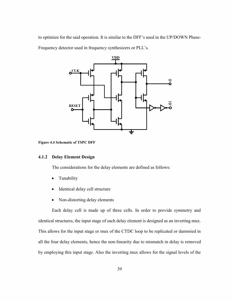
39
to optimize for the said operation. It is similar to the DFF’s used in the UP/DOWN Phase-
Frequency detector used in frequency synthesizers or PLL’s.
Figure 4.4 Schematic of TSPC DFF
4.1.2 Delay Element Design
The considerations for the delay elements are defined as follows:
Tunability
Identical delay cell structure
Non-distorting delay elements
Each delay cell is made up of three cells. In order to provide symmetry and
identical structures, the input stage of each delay element is designed as an inverting mux.
This allows for the input stage or mux of the CTDC loop to be replicated or dummied in
all the four delay elements, hence the non-linearity due to mismatch in delay is removed
by employing this input stage. Also the inverting mux allows for the signal levels of the
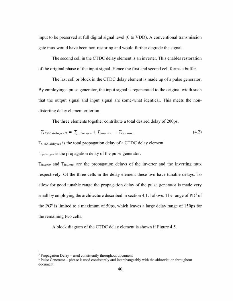
40
input to be preserved at full digital signal level (0 to VDD). A conventional transmission
gate mux would have been non-restoring and would further degrade the signal.
The second cell in the CTDC delay element is an inverter. This enables restoration
of the original phase of the input signal. Hence the first and second cell forms a buffer.
The last cell or block in the CTDC delay element is made up of a pulse generator.
By employing a pulse generator, the input signal is regenerated to the original width such
that the output signal and input signal are some-what identical. This meets the non-
distorting delay element criterion.
The three elements together contribute a total desired delay of 200ps.
𝑇𝐶𝑇𝐷𝐶.𝑑𝑒𝑙𝑎𝑦𝑐𝑒𝑙𝑙 = 𝑇𝑝𝑢𝑙𝑠𝑒.𝑔𝑒𝑛 + 𝑇𝑖𝑛𝑣𝑒𝑟𝑡𝑒𝑟 + 𝑇𝑖𝑛𝑣.𝑚𝑢𝑥 (4.2)
TCTDC.delaycell is the total propagation delay of a CTDC delay element.
Tpulse.gen is the propagation delay of the pulse generator.
Tinverter and Tinv.mux are the propagation delays of the inverter and the inverting mux
respectively. Of the three cells in the delay element these two have tunable delays. To
allow for good tunable range the propagation delay of the pulse generator is made very
small by employing the architecture described in section 4.1.1 above. The range of PD5 of
the PG6 is limited to a maximum of 50ps, which leaves a large delay range of 150ps for
the remaining two cells.
A block diagram of the CTDC delay element is shown if Figure 4.5.
5 Propagation Delay – used consistently throughout document 6 Pulse Generator – phrase is used consistently and interchangeably with the abbreviation throughout
document
41
Figure 4.5 CTDC delay element
Figure 4.6 Capacitive-tuned inverter cell concept[42] and circuit implementation
The tunability of the delay element is provided by using an analog voltage to
control the effective capacitance at a node as shown in the diagram of Figure 4.6. The
capacitive loading seen by in the inverter is varied by changing the resistance in series
with the capacitor. This variation in capacitance causes a variation in the delay at that
inverter stage’s output node.
𝐶𝑒𝑓𝑓 =𝐶
1+𝑠𝐶𝑅 (4.3)
Since for a given time resolution the pulse rate doesn’t change, it can be assumed
that the frequency dependence is zero. This allows for wide tunability for Ceff from close
0
1
OUT
MR
VCTRL
SEL
D 0
IN
VDD VDD
R
C
IN OUT
IN OUT
VDD
VCTRL
C
42
to 0 (when R is → ∞) to a maximum of C (when R→0). The variable resistor, R is
implemented using a PMOS transistor in triode region (this is approximate since in reality
it may briefly go into saturation depending on the gate overdrive and the VDS).
The resistance is inversely related to the VGS and VDS voltages by the following relation
in equation 3.18, when the transistor is in the triode region. Approximations are made for
small VDS voltages such that the resistance is independent of the drain to source voltage.
𝑅 =1
𝜇𝑃𝐶𝑂𝑋𝑊
𝐿(𝑉𝑆𝐺−|𝑉𝑇𝐻𝑃|−
1
4𝑉𝑆𝐷)
≈1
𝜇𝑃𝐶𝑂𝑋𝑊
𝐿(𝑉𝑆𝐺−|𝑉𝑇𝐻𝑃|)
(4.4)[43]
This tunable capacitance structure is placed on the internal nodes of the delay
element i.e.: at the outputs of the inverting mux and the inverter as shown in Figure 4.5.
This method of tuning is chose over the current starved method of inverter-delay
tuning [44] due to the reduced complexity. Also the current-starved inverting mux has
increased stacking of transistors and the delay budget for each cell is very steep hence for
the 200ps overall delay, the current-starved version leads to significantly power and area
cost, in the IBM 180nm technology. It proves significantly challenging to design the
current starved cells to work properly to meet the 200ps delay across three elements when
post layout parasitics are taken into account.
In summary the CTDC delay element meets all the criteria for accurate
performance with high linearity (minimal delay mismatch). Factors such as local PV7
which degrade linearity of the delay element are circumvented or reduced by employing
techniques in the layout of the delay element.
7 Process Variations – used consistently throughout document
43
4.1.3 Sense-Amplifier Based D Flip-Flop
The considerations for the sampling element design are listed below
High signal rate or frequency support
Low latency or small conversion time
Low clock-to –Q propagation delay
Small aperture time (ideally ±TFTDC for the CTDC, (to reduce inaccuracy of
the FTDC output due to erroneous CTDC computations) and ~≤±20% of TFTDC
for the FTDC)
Clocked architecture (since STOP is used like a clock)
Symmetrical Q and QB delay paths
Considering the above factors, to meet accuracy requirements of the quantization
process especially in the FTDC, the sampling elements architecture used is that of the
sense-amplifier based DFF (D- flip flop)[45] (SADFF). The same structure is used for
both CTDC and FTDC hence the sampling element design requirements for the FTDC,
which are more stringent, are used in the design if the SADFF. The following discusses
the above outlined factors and highlights why the SADFF is preferred.
Due to the high signal rate of the loops in the CTDC and FTDC and the nature of
the pulses, high frequency support for the sampling element is required. The pulses are
fast changing with a width of ~400ps. The sampling element is expected to have sampled
and computed the outputs before the data or clock changes.
Low clock-to –Q propagation delay and low latency is desired to reduce the entire
system conversion time. The sampling element outputs are not only used to compute the
44
CTDC output but also in subsequent control logic and loop control. A small clock-to-Q
delay improves the speed of the system control blocks, due to reduced wait time or latency
of the respective trigger signals. A simplified diagram demonstrates how the clock-to-Q
delay impacts the latency in Figure 4.7.
Figure 4.7 Block diagram showing signal flow from input to FTDC control block
The aperture requirement of the SADFF is similar to that of the comparators in a
SAR ADC as mentioned in [46], which is to reduce large errors in the output code due to
metastability. A small aperture time leads to reduced metastability in the DFF.
Metastability is an undesirable condition under which the SADFF output takes an
indefinitely long time to converge to a stable output. Metastability occurs when the inputs
of the SADFF (in this case the CTDC STOP is the clock and one of the four phases or
CTDC delay element outputs is the D input) arrive relatively close to each.
Due to the continuous nature of the timing event START and STOP, the
probability of the STOP coinciding or occurring close to any of the four phases (PH1CTDC,
PH2CTDC, PH3CTDC and PH4CTDC)8 is likely in the TDC measurement. Measures are
8 Respective outputs of each of the four delay elements in the CTDC
45
therefore taken to reduce metastability, prevent instability in the loop control and resulting
errors in the coarse measurement due to this.
There is a limit to the maximum clock-to-Q delay allowable due to metastability.
The output code of the CTDC sampling elements is used by the FTDC STOP input signal
control logic to determine the appropriate CTDC phase to use as the FTDC STOP signal.
A metastable SADFF will therefore lead to an erroneous output from this control logic.
The START and STOP signals are digital in nature, and the outputs of the sampling
elements are taken only when STOP arrives hence a clocked flip-flop allows for optimized
power performance since it works only in the presence of clock edge. The use of a flip-
flop architecture in which the sense-amplifier based latch is cascaded with an optimized
RS-latch[47], allows for an edge triggered flip-flop, which is sensitive only to the
transitions of the clock edge.
With the aforementioned considerations the sense-amplifier based DFF is
preferred. The architecture of the sense-amplifier input stage determines the nature overall
structure, and results in various performance tradeoffs. The second stage is made up of an
optimized RS-latch. This allows for balanced load of the sense-amplifier and equal
propagation delay for combinations of the input logic.
There are different existing sense-amplifier architectures targeted for high-speed
and low power applications. Each topology offers different trade-offs in power, are,
aperture time, clock-to-Q delay, etc. the architectures in [48-50], all present suitable
solutions for the sense amplifier input stage of the regenerative latches. Another suitable
candidate for the SADFF is a CML (current-mode logic) latch as seen in [51]. It can
46
operate at very high speeds, and the clock-to-Q PD is low. However, the large static power
consumption presents a large and undesirable power overhead for the same performance
as the previously mentioned sense-amplifier based latches in [48-50] .
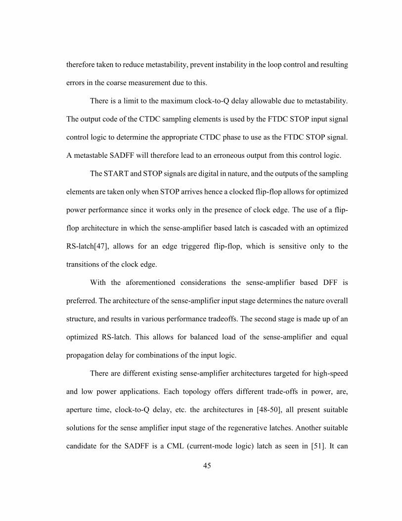
The Strong-Arm latch [47] is chosen, designed and characterized. The schematics
for the sense-amplifier topology used is shown below in Figure 4.8.
Figure 4.8 Schematic of strong-arm latch used in SADFF
The strong–arm latch architecture is chosen for its speed, accuracy and optimal
power consumption. Of the candidates, it offers optimal performance in terms of the trade-
off between speed and power consumption. The designed SADFF performance is
summarized in schematic simulation results in Figure 4.9 and Figure 4.10.
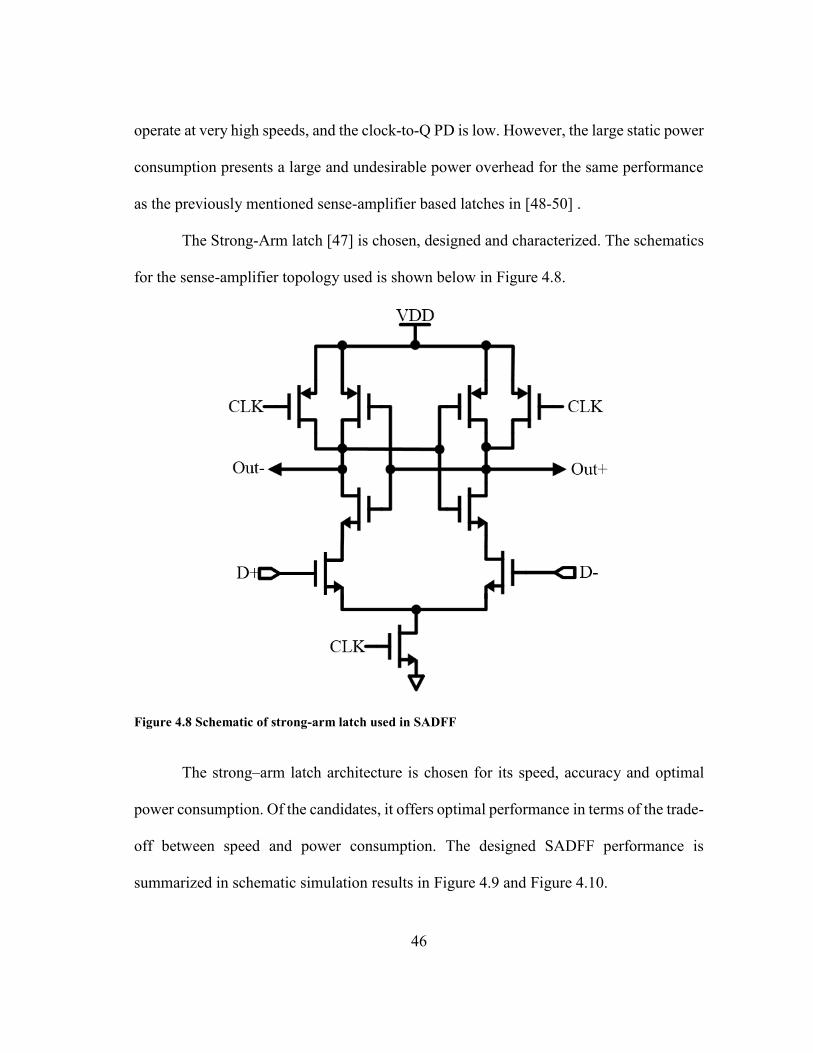
47
Figure 4.9 SADFF output for CLK-DATA delay of -2.5ps (CLK lags DATA)
Figure 4.10 SADFF output for CLK-DATA delay of 2.5ps (CLK leads DATA)
48
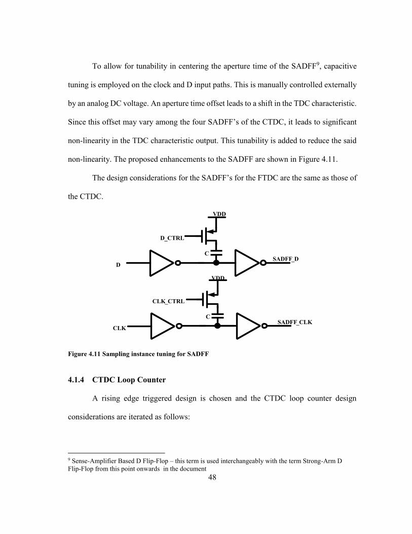
To allow for tunability in centering the aperture time of the SADFF9, capacitive
tuning is employed on the clock and D input paths. This is manually controlled externally
by an analog DC voltage. An aperture time offset leads to a shift in the TDC characteristic.
Since this offset may vary among the four SADFF’s of the CTDC, it leads to significant
non-linearity in the TDC characteristic output. This tunability is added to reduce the said
non-linearity. The proposed enhancements to the SADFF are shown in Figure 4.11.
The design considerations for the SADFF’s for the FTDC are the same as those of
the CTDC.
Figure 4.11 Sampling instance tuning for SADFF
4.1.4 CTDC Loop Counter
A rising edge triggered design is chosen and the CTDC loop counter design
considerations are iterated as follows:
9 Sense-Amplifier Based D Flip-Flop – this term is used interchangeably with the term Strong-Arm D
Flip-Flop from this point onwards in the document
D SADFF _ D
VDD
D _ CTRL
C
CLK SADFF _ CLK
VDD
CLK _ CTRL
C
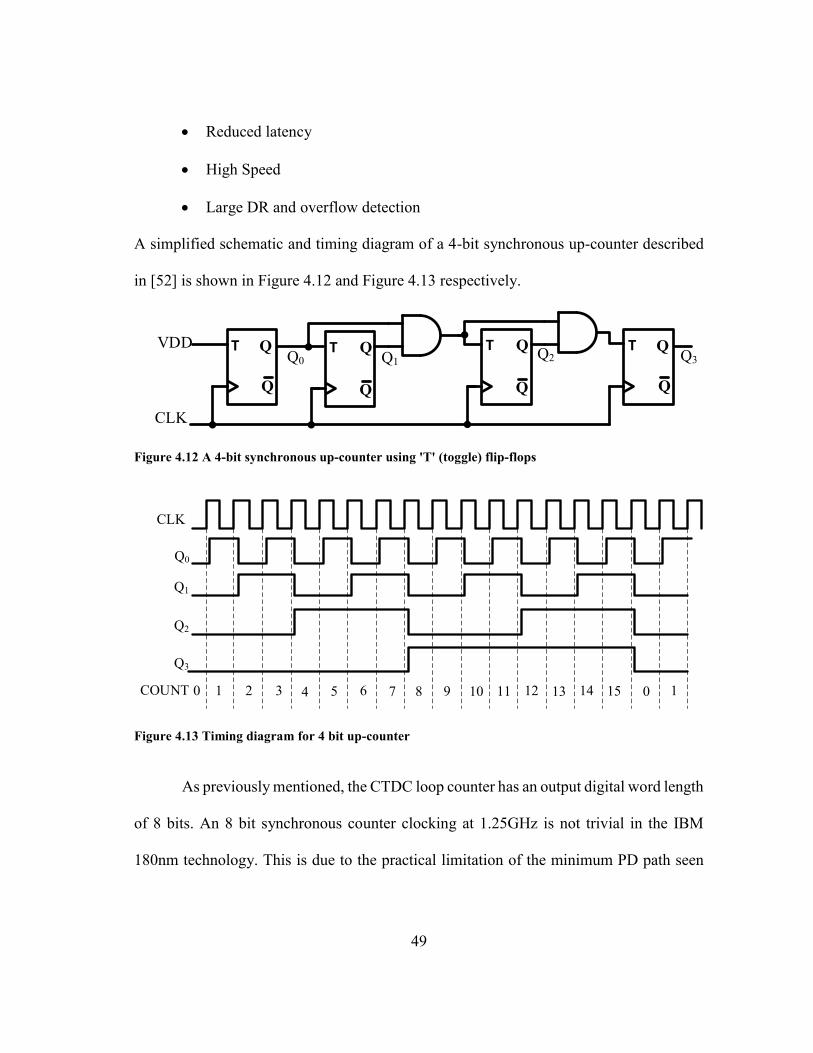
49
Reduced latency
High Speed
Large DR and overflow detection
A simplified schematic and timing diagram of a 4-bit synchronous up-counter described
in [52] is shown in Figure 4.12 and Figure 4.13 respectively.
Q
Q
T Q
Q
T Q
Q
TQ
Q
TQ0 Q1
Q2 Q3
CLK
VDD
Figure 4.12 A 4-bit synchronous up-counter using 'T' (toggle) flip-flops
CLK
COUNT 0 1 2 3 4 5 6 7 8 9 10 11 12 13 14 15 0 1
Q0
Q1
Q2
Q3
Figure 4.13 Timing diagram for 4 bit up-counter
As previously mentioned, the CTDC loop counter has an output digital word length
of 8 bits. An 8 bit synchronous counter clocking at 1.25GHz is not trivial in the IBM
180nm technology. This is due to the practical limitation of the minimum PD path seen
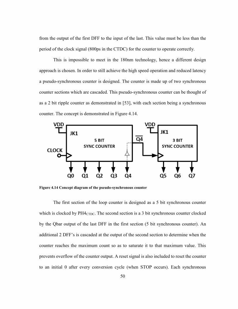
50
from the output of the first DFF to the input of the last. This value must be less than the
period of the clock signal (800ps in the CTDC) for the counter to operate correctly.
This is impossible to meet in the 180nm technology, hence a different design
approach is chosen. In order to still achieve the high speed operation and reduced latency
a pseudo-synchronous counter is designed. The counter is made up of two synchronous
counter sections which are cascaded. This pseudo-synchronous counter can be thought of
as a 2 bit ripple counter as demonstrated in [53], with each section being a synchronous
counter. The concept is demonstrated in Figure 4.14.
Figure 4.14 Concept diagram of the pseudo-synchronous counter
The first section of the loop counter is designed as a 5 bit synchronous counter
which is clocked by PH4CTDC. The second section is a 3 bit synchronous counter clocked
by the Qbar output of the last DFF in the first section (5 bit synchronous counter). An
additional 2 DFF’s is cascaded at the output of the second section to determine when the
counter reaches the maximum count so as to saturate it to that maximum value. This
prevents overflow of the counter output. A reset signal is also included to reset the counter
to an initial 0 after every conversion cycle (when STOP occurs). Each synchronous
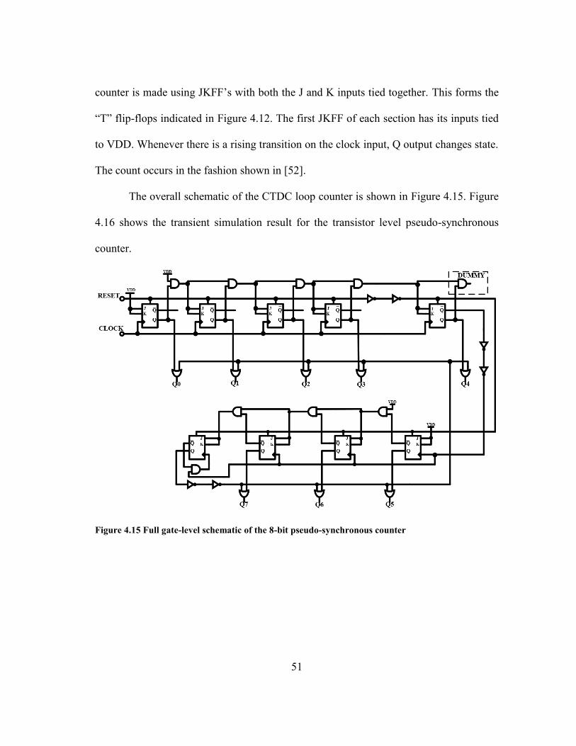
51
counter is made using JKFF’s with both the J and K inputs tied together. This forms the
“T” flip-flops indicated in Figure 4.12. The first JKFF of each section has its inputs tied
to VDD. Whenever there is a rising transition on the clock input, Q output changes state.
The count occurs in the fashion shown in [52].
The overall schematic of the CTDC loop counter is shown in Figure 4.15. Figure
4.16 shows the transient simulation result for the transistor level pseudo-synchronous
counter.
Figure 4.15 Full gate-level schematic of the 8-bit pseudo-synchronous counter
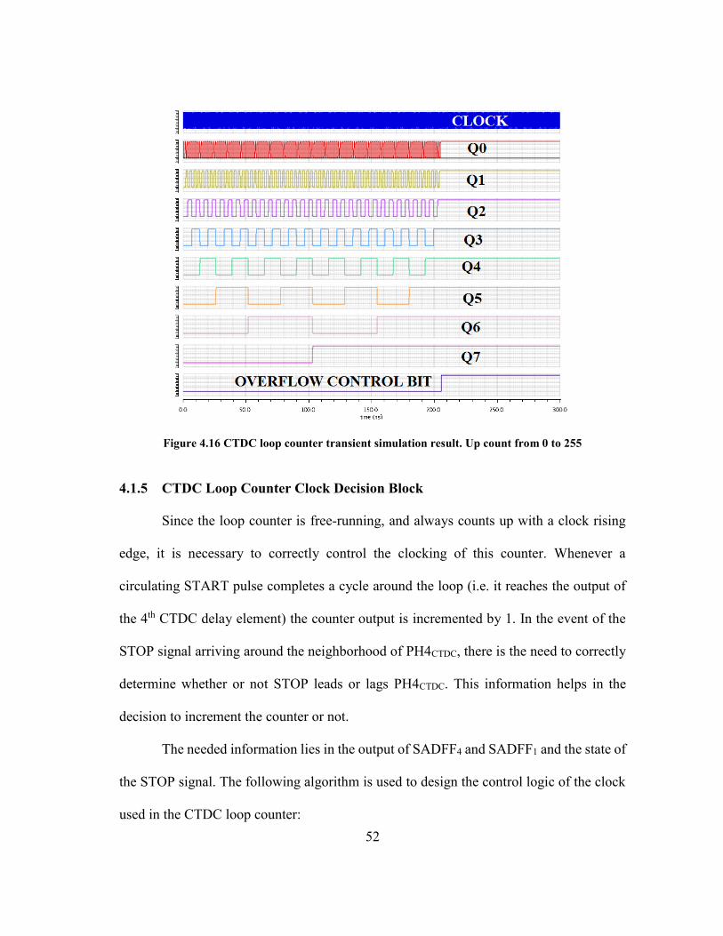
52
Figure 4.16 CTDC loop counter transient simulation result. Up count from 0 to 255
4.1.5 CTDC Loop Counter Clock Decision Block
Since the loop counter is free-running, and always counts up with a clock rising
edge, it is necessary to correctly control the clocking of this counter. Whenever a
circulating START pulse completes a cycle around the loop (i.e. it reaches the output of
the 4th CTDC delay element) the counter output is incremented by 1. In the event of the
STOP signal arriving around the neighborhood of PH4CTDC, there is the need to correctly
determine whether or not STOP leads or lags PH4CTDC. This information helps in the
decision to increment the counter or not.
The needed information lies in the output of SADFF4 and SADFF1 and the state of
the STOP signal. The following algorithm is used to design the control logic of the clock
used in the CTDC loop counter:
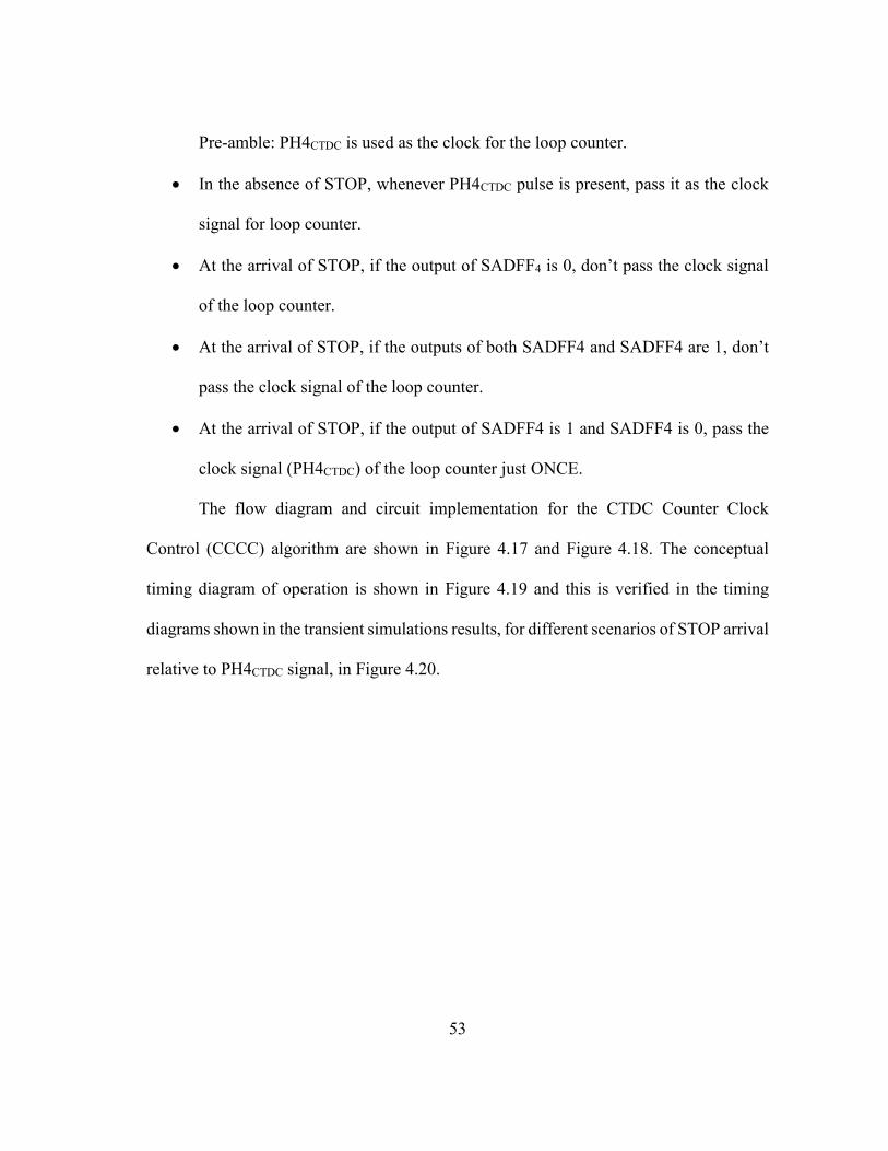
53
Pre-amble: PH4CTDC is used as the clock for the loop counter.
In the absence of STOP, whenever PH4CTDC pulse is present, pass it as the clock
signal for loop counter.
At the arrival of STOP, if the output of SADFF4 is 0, don’t pass the clock signal
of the loop counter.
At the arrival of STOP, if the outputs of both SADFF4 and SADFF4 are 1, don’t
pass the clock signal of the loop counter.
At the arrival of STOP, if the output of SADFF4 is 1 and SADFF4 is 0, pass the
clock signal (PH4CTDC) of the loop counter just ONCE.
The flow diagram and circuit implementation for the CTDC Counter Clock
Control (CCCC) algorithm are shown in Figure 4.17 and Figure 4.18. The conceptual
timing diagram of operation is shown in Figure 4.19 and this is verified in the timing
diagrams shown in the transient simulations results, for different scenarios of STOP arrival
relative to PH4CTDC signal, in Figure 4.20.
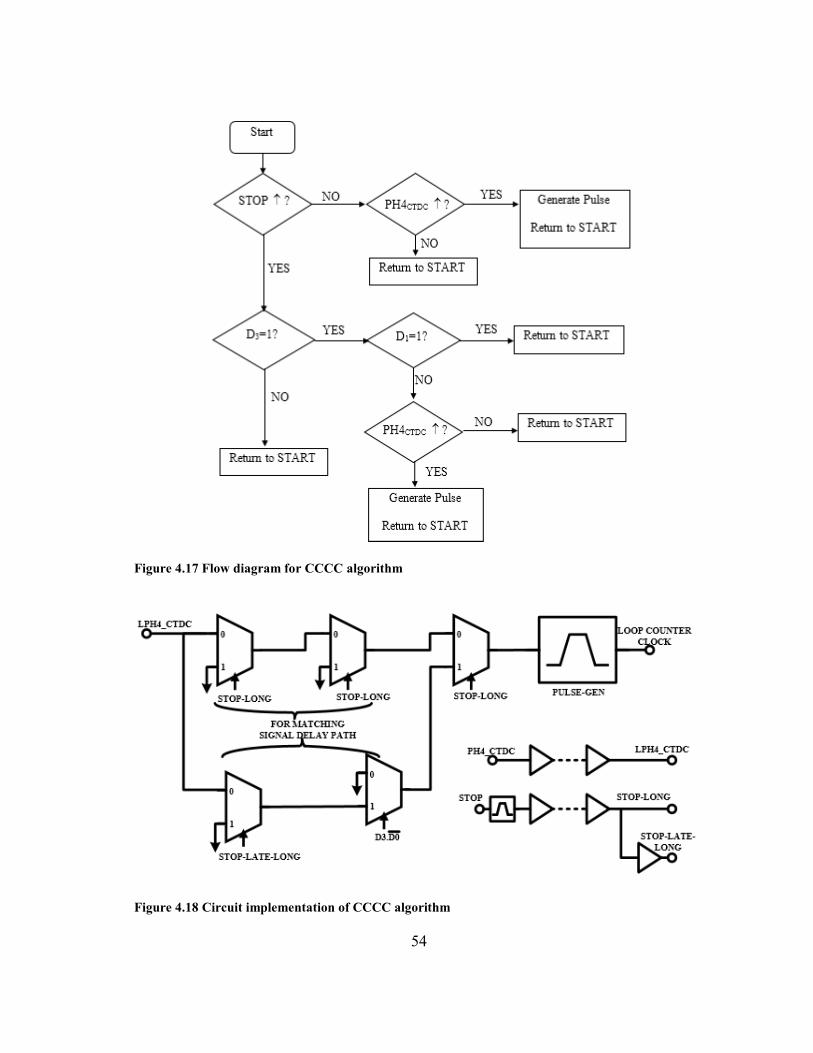
54
Figure 4.17 Flow diagram for CCCC algorithm
Figure 4.18 Circuit implementation of CCCC algorithm
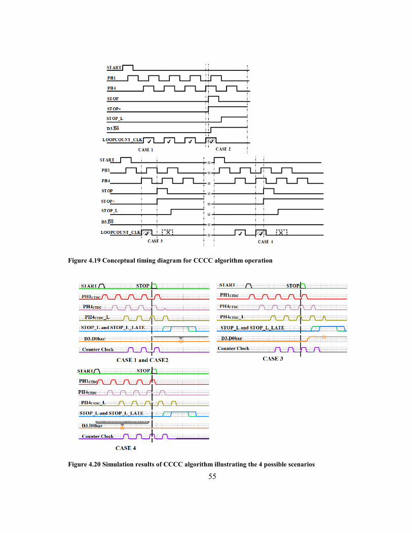
55
Figure 4.19 Conceptual timing diagram for CCCC algorithm operation
Figure 4.20 Simulation results of CCCC algorithm illustrating the 4 possible scenarios
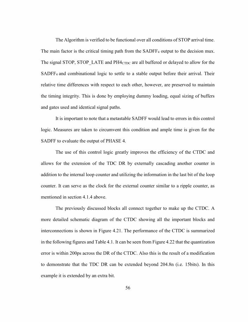
56
The Algorithm is verified to be functional over all conditions of STOP arrival time.
The main factor is the critical timing path from the SADFF4 output to the decision mux.
The signal STOP, STOP_LATE and PH4CTDC are all buffered or delayed to allow for the
SADFF4 and combinational logic to settle to a stable output before their arrival. Their
relative time differences with respect to each other, however, are preserved to maintain
the timing integrity. This is done by employing dummy loading, equal sizing of buffers
and gates used and identical signal paths.
It is important to note that a metastable SADFF would lead to errors in this control
logic. Measures are taken to circumvent this condition and ample time is given for the
SADFF to evaluate the output of PHASE 4.
The use of this control logic greatly improves the efficiency of the CTDC and
allows for the extension of the TDC DR by externally cascading another counter in
addition to the internal loop counter and utilizing the information in the last bit of the loop
counter. It can serve as the clock for the external counter similar to a ripple counter, as
mentioned in section 4.1.4 above.
The previously discussed blocks all connect together to make up the CTDC. A
more detailed schematic diagram of the CTDC showing all the important blocks and
interconnections is shown in Figure 4.21. The performance of the CTDC is summarized
in the following figures and Table 4.1. It can be seen from Figure 4.22 that the quantization
error is within 200ps across the DR of the CTDC. Also this is the result of a modification
to demonstrate that the TDC DR can be extended beyond 204.8n (i.e. 15bits). In this
example it is extended by an extra bit.
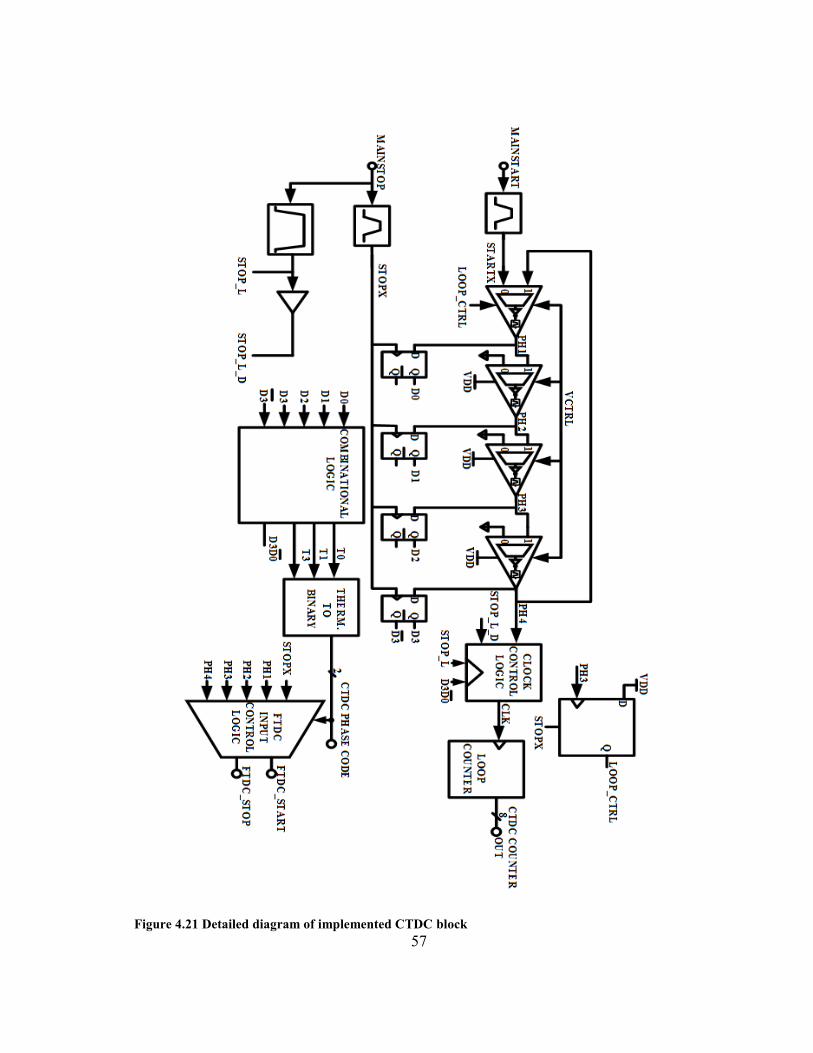
57
Figure 4.21 Detailed diagram of implemented CTDC block
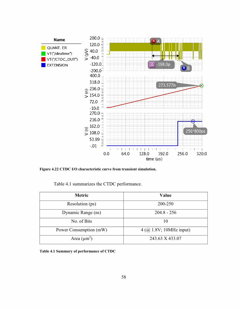
58
Figure 4.22 CTDC I/O characteristic curve from transient simulation.
Table 4.1 summarizes the CTDC performance.
Metric Value
Resolution (ps) 200-250
Dynamic Range (ns) 204.8 - 256
No. of Bits 10
Power Consumption (mW) 4 (@ 1.8V; 10MHz input)
Area (µm2) 243.63 X 433.07
Table 4.1 Summary of performance of CTDC
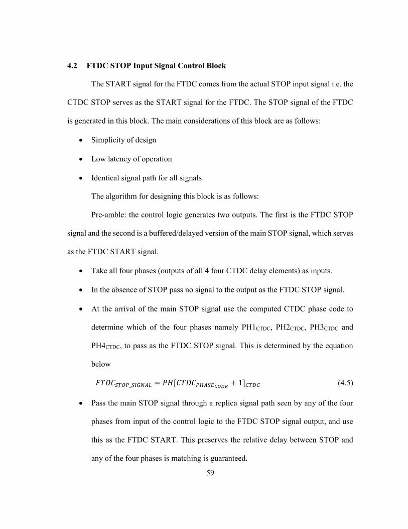
59
4.2 FTDC STOP Input Signal Control Block
The START signal for the FTDC comes from the actual STOP input signal i.e. the
CTDC STOP serves as the START signal for the FTDC. The STOP signal of the FTDC
is generated in this block. The main considerations of this block are as follows:
Simplicity of design
Low latency of operation
Identical signal path for all signals
The algorithm for designing this block is as follows:
Pre-amble: the control logic generates two outputs. The first is the FTDC STOP
signal and the second is a buffered/delayed version of the main STOP signal, which serves
as the FTDC START signal.
Take all four phases (outputs of all 4 four CTDC delay elements) as inputs.
In the absence of STOP pass no signal to the output as the FTDC STOP signal.
At the arrival of the main STOP signal use the computed CTDC phase code to
determine which of the four phases namely PH1CTDC, PH2CTDC, PH3CTDC and
PH4CTDC, to pass as the FTDC STOP signal. This is determined by the equation
below
𝐹𝑇𝐷𝐶𝑆𝑇𝑂𝑃_𝑆𝐼𝐺𝑁𝐴𝐿 = 𝑃𝐻[𝐶𝑇𝐷𝐶𝑃𝐻𝐴𝑆𝐸𝐶𝑂𝐷𝐸+ 1]𝐶𝑇𝐷𝐶 (4.5)
Pass the main STOP signal through a replica signal path seen by any of the four
phases from input of the control logic to the FTDC STOP signal output, and use
this as the FTDC START. This preserves the relative delay between STOP and
any of the four phases is matching is guaranteed.
60
This algorithm is implemented at circuit (gate/transistor) level and the schematic
is shown in Figure 4.23.
PH1
FTDC STOP
VDD
1
01
0
0
1
B0
B11
0
B0
0
1
PH4
PH3
PH2
STOP
VDD
DUMMY
FTDC START
Figure 4.23 Circuit implementation for FTDC START signal control logic
The timing diagrams for various scenarios is also shown in Figure 4.24 to validate
the control algorithm.
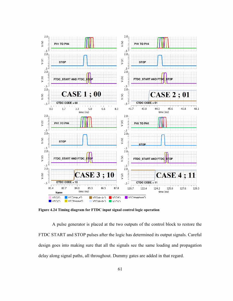
61
Figure 4.24 Timing diagram for FTDC input signal control logic operation
A pulse generator is placed at the two outputs of the control block to restore the
FTDC START and STOP pulses after the logic has determined its output signals. Careful
design goes into making sure that all the signals see the same loading and propagation
delay along signal paths, all throughout. Dummy gates are added in that regard.

62
4.3 Fine Stage Time-To-Digital Converter (FTDC)
The resolution of the entire TDC is determined by the performance of this block.
The objective at this stage of the quantization, namely the fine quantization, is to quantize
the time residue generated by the FTDC STOP input signal block (i.e.: the FTDC START
and STOP signals) with the highest possible time resolution, while maintaining the system
linearity within desired limits. For the system to be considered to have a linearity metric
which doesn’t lead to missing codes (or having a non-monotonic TDC ramp characteristic)
the following equation must hold over the entire DR of the TDC:
𝐷𝑁𝐿 ≤ 0.5 × 𝐿𝑆𝐵 (4.6)
Where DNL is the differential non-linearity and LSB is the Lease-Significant Bit
of the output digital word of the TDC. The design considerations for the FTDC take in
account the following factors:
High resolution
Robust to PV
Good linearity
DR larger than FTDCINPUT MAX
The design considerations for overall architecture of the TDC takes into account
the tradeoff between DR and RES. Hence the choice of the architecture maximized the
RES attainable while maintain a high DR. by employing the control logic described in
section 4.2 above, the DR of the FTDC is limited to a maximum of only TCTDC.phase. i.e.:
the delay of a single delay element of the CTDC.
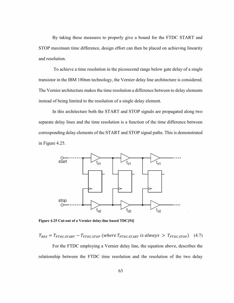
63
By taking these measures to properly give a bound for the FTDC START and
STOP maximum time difference, design effort can then be placed on achieving linearity
and resolution.
To achieve a time resolution in the picosecond range below gate delay of a single
transistor in the IBM 180nm technology, the Vernier delay line architecture is considered.
The Vernier architecture makes the time resolution a difference between to delay elements
instead of being limited to the resolution of a single delay element.
In this architecture both the START and STOP signals are propagated along two
separate delay lines and the time resolution is a function of the time difference between
corresponding delay elements of the START and STOP signal paths. This is demonstrated
in Figure 4.25.
Figure 4.25 Cut-out of a Vernier delay-line based TDC[54]
𝑇𝑅𝐸𝑆 = 𝑇𝐹𝑇𝐷𝐶.𝑆𝑇𝐴𝑅𝑇 − 𝑇𝐹𝑇𝐷𝐶.𝑆𝑇𝑂𝑃 (𝑤ℎ𝑒𝑟𝑒 𝑇𝐹𝑇𝐷𝐶.𝑆𝑇𝐴𝑅𝑇 𝑖𝑠 𝑎𝑙𝑤𝑎𝑦𝑠 > 𝑇𝐹𝑇𝐷𝐶.𝑆𝑇𝑂𝑃) (4.7)
For the FTDC employing a Vernier delay line, the equation above, describes the
relationship between the FTDC time resolution and the resolution of the two delay
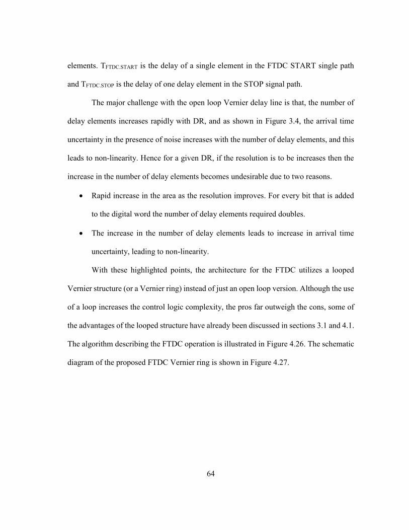
64
elements. TFTDC.START is the delay of a single element in the FTDC START single path
and TFTDC.STOP is the delay of one delay element in the STOP signal path.
The major challenge with the open loop Vernier delay line is that, the number of
delay elements increases rapidly with DR, and as shown in Figure 3.4, the arrival time
uncertainty in the presence of noise increases with the number of delay elements, and this
leads to non-linearity. Hence for a given DR, if the resolution is to be increases then the
increase in the number of delay elements becomes undesirable due to two reasons.
Rapid increase in the area as the resolution improves. For every bit that is added
to the digital word the number of delay elements required doubles.
The increase in the number of delay elements leads to increase in arrival time
uncertainty, leading to non-linearity.
With these highlighted points, the architecture for the FTDC utilizes a looped
Vernier structure (or a Vernier ring) instead of just an open loop version. Although the use
of a loop increases the control logic complexity, the pros far outweigh the cons, some of
the advantages of the looped structure have already been discussed in sections 3.1 and 4.1.
The algorithm describing the FTDC operation is illustrated in Figure 4.26. The schematic
diagram of the proposed FTDC Vernier ring is shown in Figure 4.27.

65
Figure 4.26 FTDC operation algorithm
td is the input time difference between START and STOP of the FTDC.
Tres = TD1-TD2 which is the delay difference between the corresponding START and STOP
loop delay elements.
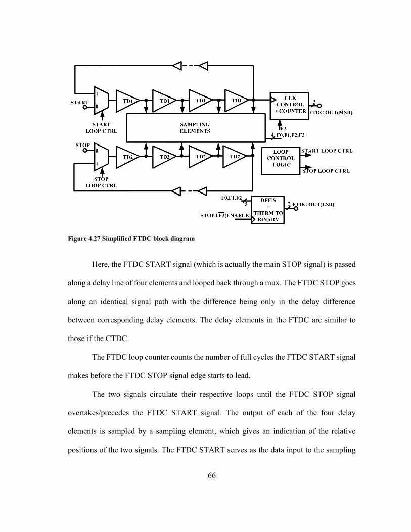
66
Figure 4.27 Simplified FTDC block diagram
Here, the FTDC START signal (which is actually the main STOP signal) is passed
along a delay line of four elements and looped back through a mux. The FTDC STOP goes
along an identical signal path with the difference being only in the delay difference
between corresponding delay elements. The delay elements in the FTDC are similar to
those if the CTDC.
The FTDC loop counter counts the number of full cycles the FTDC START signal
makes before the FTDC STOP signal edge starts to lead.
The two signals circulate their respective loops until the FTDC STOP signal
overtakes/precedes the FTDC START signal. The output of each of the four delay
elements is sampled by a sampling element, which gives an indication of the relative
positions of the two signals. The FTDC START serves as the data input to the sampling
67
element and the FTDC STOP functions as the clock for the sampling element, similar to
the set-up in the CTDC. The condition which marks the end of a measurement occurs
when any of the sampling elements outputs a 0, after it is clocked by the FTDC.
When the STOP signal precedes the START the looping is undone (by flipping
over the loop control mux output to the default position), and the last outputs of the four
sampling elements are used to as a thermometer code to determine the LSBs of the FTDC
measurement. This gives a 2 bit fine measurement with a resolution equal to the delay
difference between the corresponding FTDC START and FTDC STOP delay elements.
The output bits of the FTDC loop counter are taken as the MSBs of the FTDC
measurement, since it represents the number of cycles the FTDC START signal leads the
FTDC STOP signal.
𝑇𝐹𝑇𝐷𝐶.𝑃𝐻𝐴𝑆𝐸[𝑖] = 𝑇𝐹𝑇𝐷𝐶.𝑆𝑇𝐴𝑅𝑇[𝑖] − 𝑇𝐹𝑇𝐷𝐶.𝑆𝑇𝑂𝑃[𝑖] (4.8)
(𝑤ℎ𝑒𝑟𝑒 𝑇𝐹𝑇𝐷𝐶.𝑆𝑇𝐴𝑅𝑇 > 𝑇𝐹𝑇𝐷𝐶.𝑆𝑇𝑂𝑃)
𝑇𝐹𝑇𝐷𝐶.𝐶𝑂𝑈𝑁𝑇𝐸𝑅 = ∑ 𝑇𝐹𝑇𝐷𝐶.𝑃𝐻𝐴𝑆𝐸[𝑖]4𝑖=1 ≈ 4 × 𝑇𝐹𝑇𝐷𝐶.𝑃𝐻𝐴𝑆𝐸 (𝑓𝑜𝑟 𝑡ℎ𝑒 𝑖𝑑𝑒𝑎𝑙 𝑐𝑎𝑠𝑒) (4.9)
Where TFTDC.PHASE[i] is the delay difference between the ith FTDC START and
FTDC STOP delay elements, TFTDC.START[i] is the delay of the ith FTDC START delay
element, TFTDC.STOP[i] is the delay of the ith FTDC STOP delay element and TFTDC.COUNTER
is the sum of the delay differences between the two delay lines (FTDC START and FTDC
STOP delay lines), indicating the time resolution of the FTDC loop counter. The equations
(4.8) and (4.9) give a mathematical summary of the time resolutions of the FTDC phase
code or sampling element output and the FTDC loop counter respectively.
68
Therefore as discussed previously, by using a very low delay element count, the
non-linearity of the delay line due to PVT variations can be reduced. Using a Vernier ring
allows for attaining a high DR with few elements. The DR is limited only by the FTDC
loop counter. The next sub section discusses design consideration and issues with each
block or cell of the FTDC starting with the Delay element.
4.3.1 FTDC Delay Element Design
The delay elements have similar considerations as those used in the CTDC:
Tunability
Identical and non-distorting delay cell structure
Each delay cell is made up of three cells. The first two cells are inverting and the
last is non-inverting. In order to provide symmetry and identical structures, the first two
cells of each delay element in both the FTDC START and FTDC STOP delay rings are
inverters. The corresponding inverters in the FTDC START and FTDC STOP delay lines
are identically sized, this improves the delay matching and PVT tracking provided the two
elements are placed as closely as possible in the layout. The two inverters in each delay
line serve to buffer the input pulse.
Similar to the CTDC, last cell or block in the delay element of each of the two
FTDC delay rings is a pulse generator. By employing a pulse generator, the input signal
is regenerated to the original width such that the output signal and input signal are some-
what identical if local process variations are ignored for now. This meets the non-
distorting delay element criterion.
69
The difference between any two corresponding delay elements in the FTDC delay
rings contributes a tie resolution or delay difference of < 10ps. For any delay element, the
three aforementioned cells (two inverters and one pulse generator) leads to a delay of about
150ps (in the FTDC STOP delay element) or 160ps (in the FTDC START delay element).
These are illustrated in the following expressions.
𝑇𝐹𝑇𝐷𝐶.𝑆𝑇𝐴𝑅𝑇 = 𝑇𝑝𝑢𝑙𝑠𝑒.𝑔𝑒𝑛 + 𝑇𝐹𝑇𝐷𝐶.𝑆𝑇𝐴𝑅𝑇.𝐼𝑁𝑉2 + 𝑇𝐹𝑇𝐷𝐶.𝑆𝑇𝐴𝑅𝑇.𝐼𝑁𝑉1 (4.10)
𝑇𝐹𝑇𝐷𝐶.𝑆𝑇𝑂𝑃 = 𝑇𝑝𝑢𝑙𝑠𝑒.𝑔𝑒𝑛 + 𝑇𝐹𝑇𝐷𝐶.𝑆𝑇𝑂𝑃.𝐼𝑁𝑉2 + 𝑇𝐹𝑇𝐷𝐶.𝑆𝑇𝑂𝑃.𝐼𝑁𝑉1 (4.11)
TFTDC.START is the propagation delay of a delay element in the FTDC START delay
line.
TFTDC.STOP is the propagation delay of a delay element in the FTDC STOP delay line.
TFTDC.START.INV1 and TFTDC.START.INV2 are the propagation delays of the 1st and 2nd inverters
of an FTDC START delay element.
TFTDC.STOP.INV1 and TFTDC.STOP.INV2 are the propagation delays of the 1st and 2nd inverters of
an FTDC STOP delay element.
TPULSE.GEN is the propagation delay of the pulse generator in the delay element of
either delay rings. The FTDC START and STOP delay elements have identical pulse
generators.
The delay elements are variable and are tuned by use of an analog control voltage.
The two delay elements are designed such that for the same voltage the delay difference
gives us the initial target resolution of about 10ps. The architecture is however the same.
The said difference comes from different capacitor sizes. The absolute delay of each of
the elements ranges from 120ps to 150ps with the delay elements in the STOP loop being
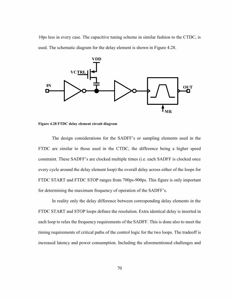
70
10ps less in every case. The capacitive tuning scheme in similar fashion to the CTDC, is
used. The schematic diagram for the delay element is shown in Figure 4.28.
Figure 4.28 FTDC delay element circuit diagram
The design considerations for the SADFF’s or sampling elements used in the
FTDC are similar to those used in the CTDC, the difference being a higher speed
constraint. These SADFF’s are clocked multiple times (i.e. each SADFF is clocked once
every cycle around the delay element loop) the overall delay across either of the loops for
FTDC START and FTDC STOP ranges from 700ps-900ps. This figure is only important
for determining the maximum frequency of operation of the SADFF’s.
In reality only the delay difference between corresponding delay elements in the
FTDC START and STOP loops defines the resolution. Extra identical delay is inserted in
each loop to relax the frequency requirements of the SADFF. This is done also to meet the
timing requirements of critical paths of the control logic for the two loops. The tradeoff is
increased latency and power consumption. Including the aforementioned challenges and
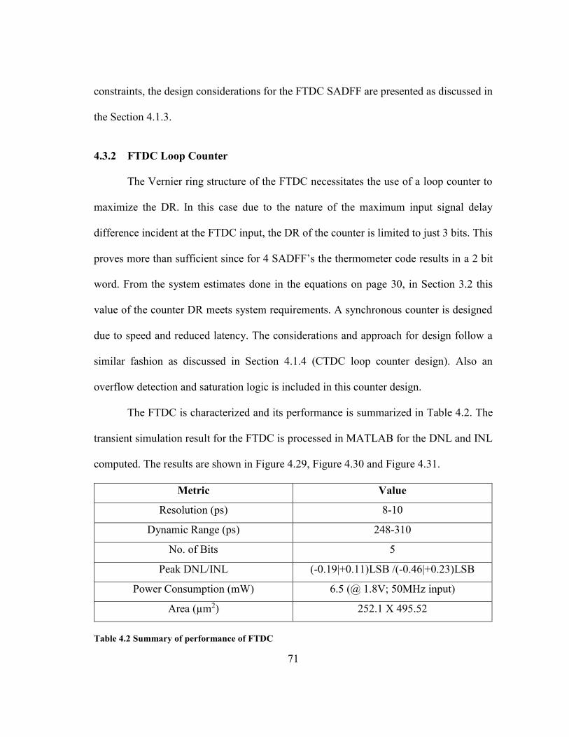
71
constraints, the design considerations for the FTDC SADFF are presented as discussed in
the Section 4.1.3.
4.3.2 FTDC Loop Counter
The Vernier ring structure of the FTDC necessitates the use of a loop counter to
maximize the DR. In this case due to the nature of the maximum input signal delay
difference incident at the FTDC input, the DR of the counter is limited to just 3 bits. This
proves more than sufficient since for 4 SADFF’s the thermometer code results in a 2 bit
word. From the system estimates done in the equations on page 30, in Section 3.2 this
value of the counter DR meets system requirements. A synchronous counter is designed
due to speed and reduced latency. The considerations and approach for design follow a
similar fashion as discussed in Section 4.1.4 (CTDC loop counter design). Also an
overflow detection and saturation logic is included in this counter design.
The FTDC is characterized and its performance is summarized in Table 4.2. The
transient simulation result for the FTDC is processed in MATLAB for the DNL and INL
computed. The results are shown in Figure 4.29, Figure 4.30 and Figure 4.31.
Metric Value
Resolution (ps) 8-10
Dynamic Range (ps) 248-310
No. of Bits 5
Peak DNL/INL (-0.19|+0.11)LSB /(-0.46|+0.23)LSB
Power Consumption (mW) 6.5 (@ 1.8V; 50MHz input)
Area (µm2) 252.1 X 495.52
Table 4.2 Summary of performance of FTDC
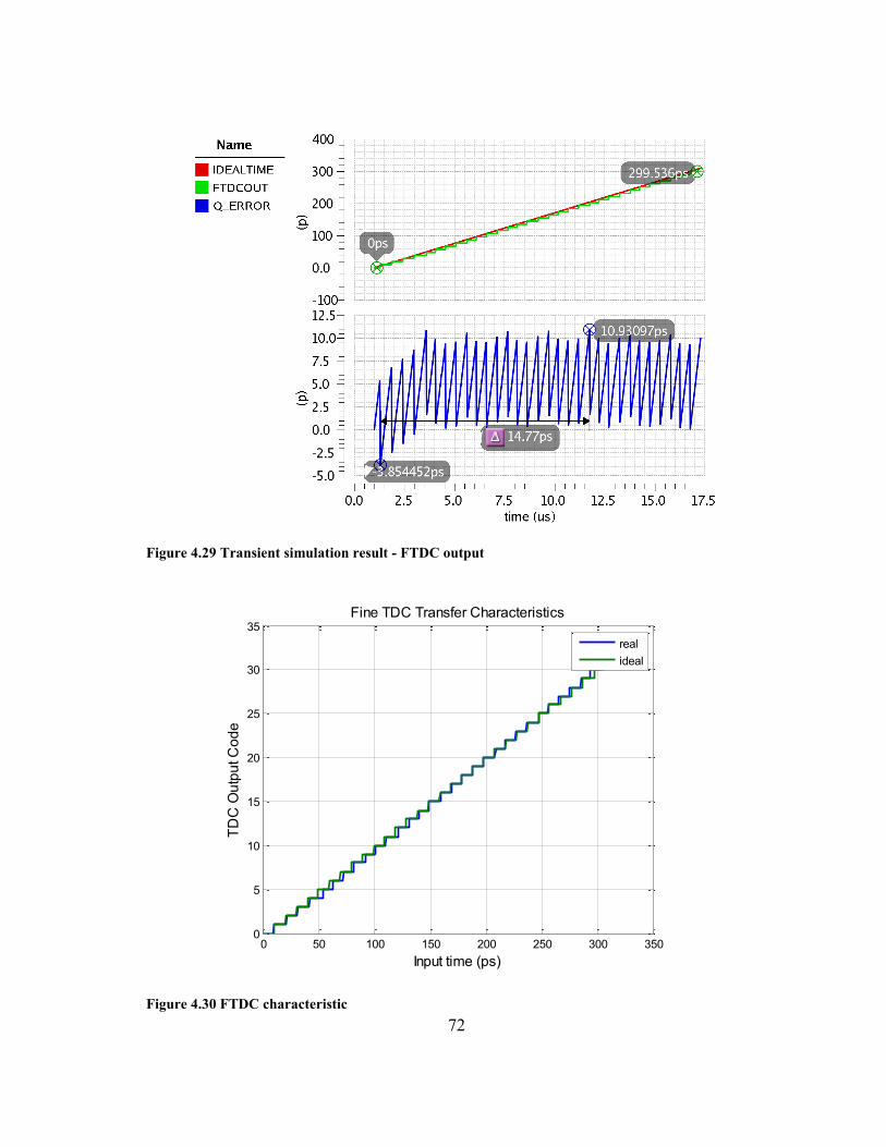
72
Figure 4.29 Transient simulation result - FTDC output
Figure 4.30 FTDC characteristic
0 50 100 150 200 250 300 3500
5
10
15
20
25
30
35
Input time (ps)
TD
C O
utp
ut C
od
e
Fine TDC Transfer Characteristics
real
ideal
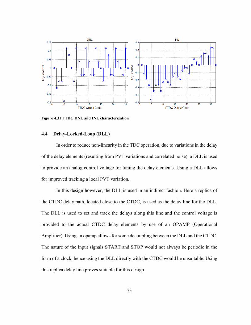
73
Figure 4.31 FTDC DNL and INL characterization
4.4 Delay-Locked-Loop (DLL)
In order to reduce non-linearity in the TDC operation, due to variations in the delay
of the delay elements (resulting from PVT variations and correlated noise), a DLL is used
to provide an analog control voltage for tuning the delay elements. Using a DLL allows
for improved tracking a local PVT variation.
In this design however, the DLL is used in an indirect fashion. Here a replica of
the CTDC delay path, located close to the CTDC, is used as the delay line for the DLL.
The DLL is used to set and track the delays along this line and the control voltage is
provided to the actual CTDC delay elements by use of an OPAMP (Operational
Amplifier). Using an opamp allows for some decoupling between the DLL and the CTDC.
The nature of the input signals START and STOP would not always be periodic in the
form of a clock, hence using the DLL directly with the CTDC would be unsuitable. Using
this replica delay line proves suitable for this design.
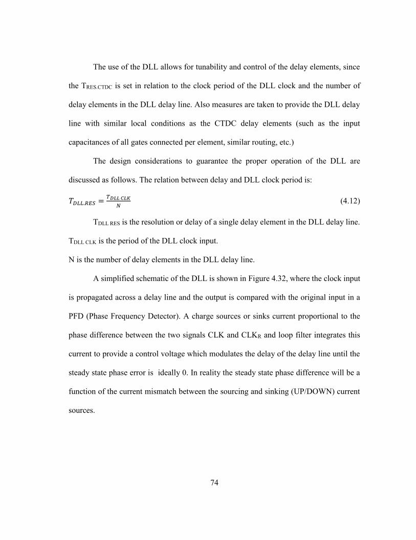
74
The use of the DLL allows for tunability and control of the delay elements, since
the TRES.CTDC is set in relation to the clock period of the DLL clock and the number of
delay elements in the DLL delay line. Also measures are taken to provide the DLL delay
line with similar local conditions as the CTDC delay elements (such as the input
capacitances of all gates connected per element, similar routing, etc.)
The design considerations to guarantee the proper operation of the DLL are
discussed as follows. The relation between delay and DLL clock period is:
𝑇𝐷𝐿𝐿.𝑅𝐸𝑆 =𝑇𝐷𝐿𝐿 𝐶𝐿𝐾
𝑁 (4.12)
TDLL RES is the resolution or delay of a single delay element in the DLL delay line.
TDLL CLK is the period of the DLL clock input.
N is the number of delay elements in the DLL delay line.
A simplified schematic of the DLL is shown in Figure 4.32, where the clock input
is propagated across a delay line and the output is compared with the original input in a
PFD (Phase Frequency Detector). A charge sources or sinks current proportional to the
phase difference between the two signals CLK and CLKR and loop filter integrates this
current to provide a control voltage which modulates the delay of the delay line until the
steady state phase error is ideally 0. In reality the steady state phase difference will be a
function of the current mismatch between the sourcing and sinking (UP/DOWN) current
sources.
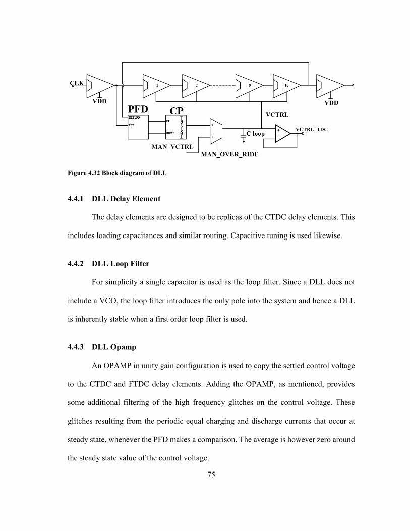
75
Figure 4.32 Block diagram of DLL
4.4.1 DLL Delay Element
The delay elements are designed to be replicas of the CTDC delay elements. This
includes loading capacitances and similar routing. Capacitive tuning is used likewise.
4.4.2 DLL Loop Filter
For simplicity a single capacitor is used as the loop filter. Since a DLL does not
include a VCO, the loop filter introduces the only pole into the system and hence a DLL
is inherently stable when a first order loop filter is used.
4.4.3 DLL Opamp
An OPAMP in unity gain configuration is used to copy the settled control voltage
to the CTDC and FTDC delay elements. Adding the OPAMP, as mentioned, provides
some additional filtering of the high frequency glitches on the control voltage. These
glitches resulting from the periodic equal charging and discharge currents that occur at
steady state, whenever the PFD makes a comparison. The average is however zero around
the steady state value of the control voltage.
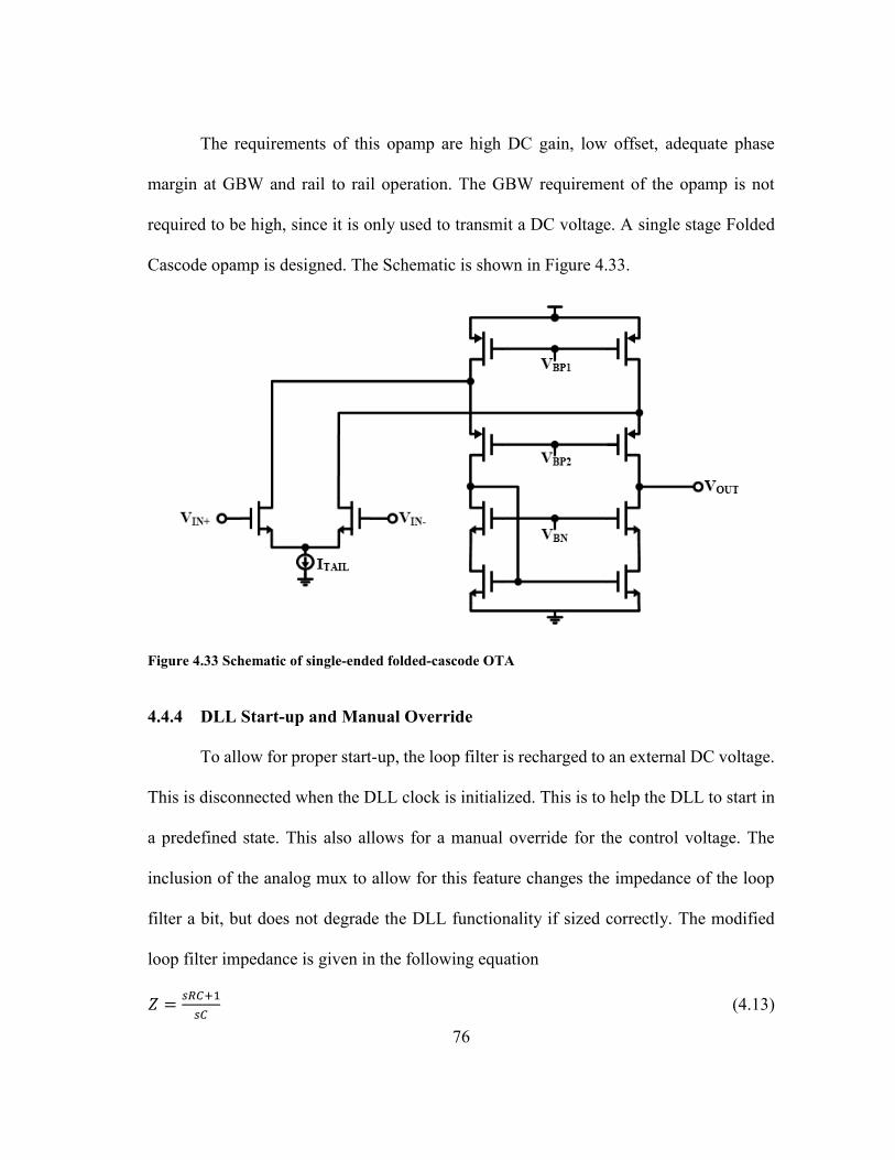
76
The requirements of this opamp are high DC gain, low offset, adequate phase
margin at GBW and rail to rail operation. The GBW requirement of the opamp is not
required to be high, since it is only used to transmit a DC voltage. A single stage Folded
Cascode opamp is designed. The Schematic is shown in Figure 4.33.
Figure 4.33 Schematic of single-ended folded-cascode OTA
4.4.4 DLL Start-up and Manual Override
To allow for proper start-up, the loop filter is recharged to an external DC voltage.
This is disconnected when the DLL clock is initialized. This is to help the DLL to start in
a predefined state. This also allows for a manual override for the control voltage. The
inclusion of the analog mux to allow for this feature changes the impedance of the loop
filter a bit, but does not degrade the DLL functionality if sized correctly. The modified
loop filter impedance is given in the following equation
𝑍 =𝑠𝑅𝐶+1
𝑠𝐶 (4.13)
77
But the transfer function from output of the charge pump to the control voltage of
the delay elements is still:
𝑉𝑐𝑡𝑟𝑙
𝐼𝐶𝑃= 𝐼𝐶𝑃 × 𝑍 ×
1𝑠𝐶⁄
1𝑠𝐶⁄ +𝑅
=𝐼𝐶𝑃
𝑠𝐶 (4.14)
ICP is the charge pump output current. VCTRL is the input voltage of the delay
elements. Z is the combined output impedance of the loop filter and analog mux. R is the
series resistance of the analog mux. C is the lumped capacitance including the loop filter
capacitance, the opamp input capacitance and the input capacitance of the delay elements.
The schematic diagram of the DLL and opamp blocks, including the
aforementioned modifications, is shown in Figure 4.32.
The transient simulation results for the DLL (transistor level) locking are shown
in Figure 4.34, Figure 4.35 and Figure 4.36.
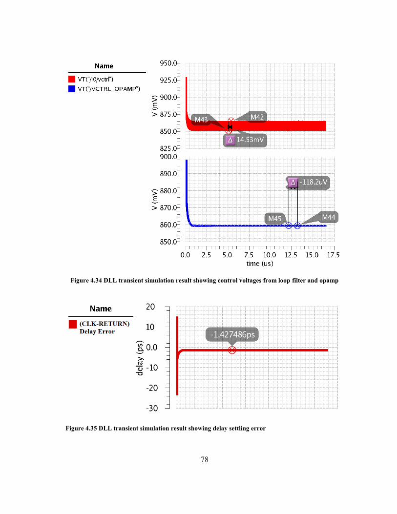
78
Figure 4.34 DLL transient simulation result showing control voltages from loop filter and opamp
Figure 4.35 DLL transient simulation result showing delay settling error
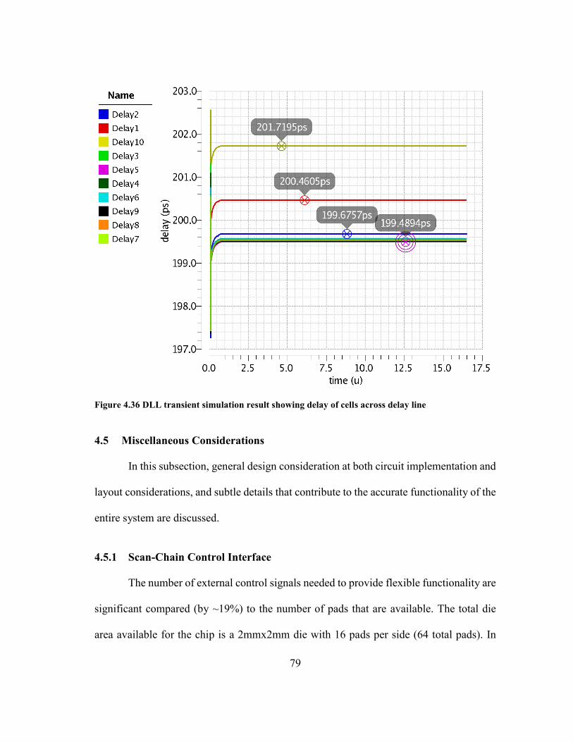
79
Figure 4.36 DLL transient simulation result showing delay of cells across delay line
4.5 Miscellaneous Considerations
In this subsection, general design consideration at both circuit implementation and
layout considerations, and subtle details that contribute to the accurate functionality of the
entire system are discussed.
4.5.1 Scan-Chain Control Interface
The number of external control signals needed to provide flexible functionality are
significant compared (by ~19%) to the number of pads that are available. The total die
area available for the chip is a 2mmx2mm die with 16 pads per side (64 total pads). In
80
order make better utilization of the available pads Scan-Chain (a serial control interface)
is used to provide all the control signals. The pad count for the scan-chain interface is only
5 (namely: PHI1, PHI2, PHIEN, SIN and SOUT) to reduce the pin count.
4.5.2 Layout Considerations
In the layout of each block, there are certain general considerations namely:
Routing parasitic reduction
Signal buffering and reduction of driving long routing lines
High density and area reduction
Block placement and signal propagation delay reduction
Beyond these other considerations are made for the high speed and mismatch
sensitive blocks (such as the SADFF’s and delay elements).
Symmetry in placement
Matching of routing and loading capacitances (especially in the Vernier delay line)
Considerations for the power grid and sizing of the power lines are made in a
fashion suitable for digital circuit layout. This improves the power distribution and reduces
the IR drops on power lines across the chip. Figure 4.37, Figure 4.38 and Figure 4.39 show
the layouts for the CTDC, FTDC and entire chip. Figure 4.40 shows the die micrograph
of the fabricated TDC IC.
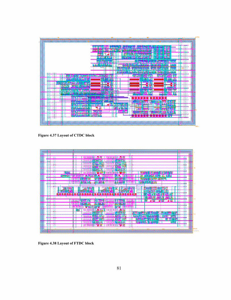
81
Figure 4.37 Layout of CTDC block
Figure 4.38 Layout of FTDC block
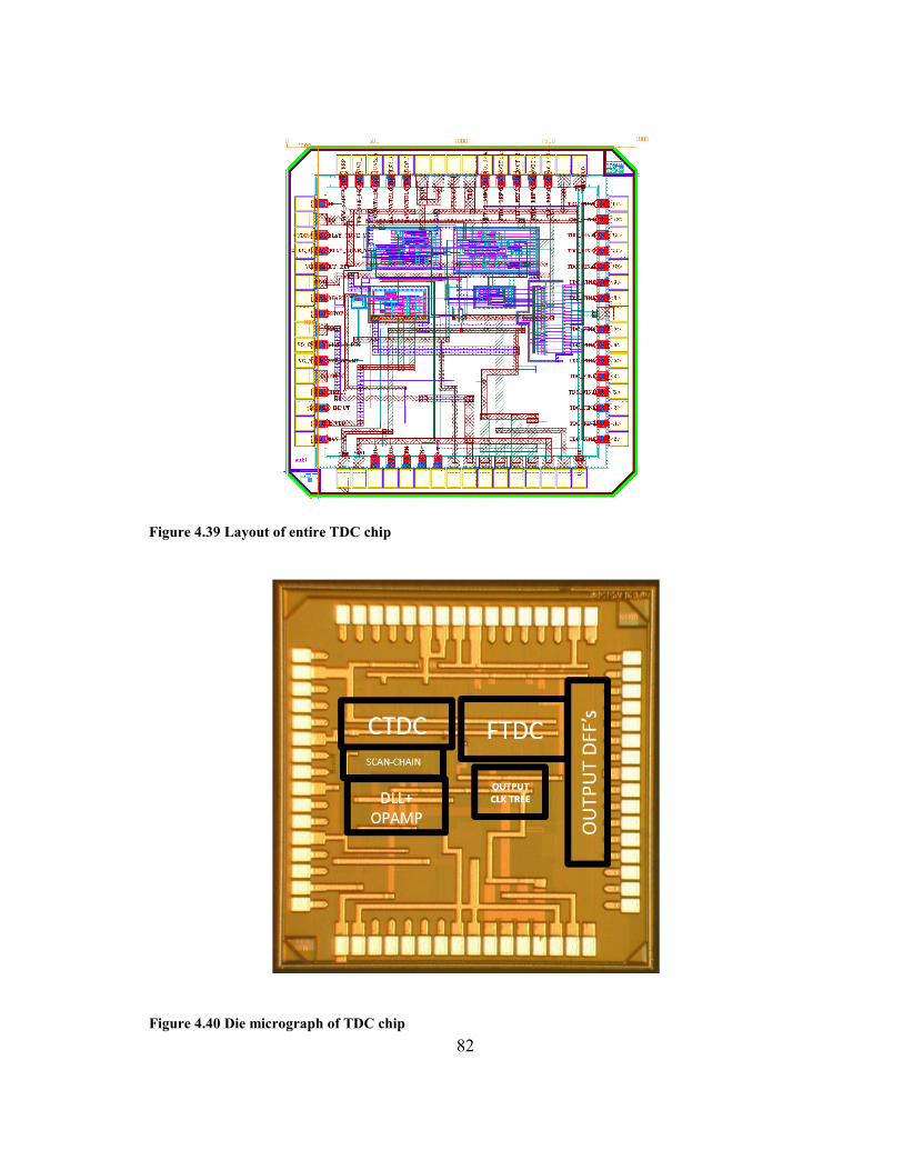
82
Figure 4.39 Layout of entire TDC chip
Figure 4.40 Die micrograph of TDC chip
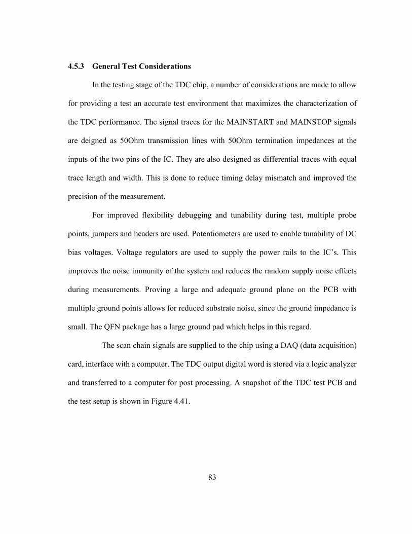
83
4.5.3 General Test Considerations
In the testing stage of the TDC chip, a number of considerations are made to allow
for providing a test an accurate test environment that maximizes the characterization of
the TDC performance. The signal traces for the MAINSTART and MAINSTOP signals
are deigned as 50Ohm transmission lines with 50Ohm termination impedances at the
inputs of the two pins of the IC. They are also designed as differential traces with equal
trace length and width. This is done to reduce timing delay mismatch and improved the
precision of the measurement.
For improved flexibility debugging and tunability during test, multiple probe
points, jumpers and headers are used. Potentiometers are used to enable tunability of DC
bias voltages. Voltage regulators are used to supply the power rails to the IC’s. This
improves the noise immunity of the system and reduces the random supply noise effects
during measurements. Proving a large and adequate ground plane on the PCB with
multiple ground points allows for reduced substrate noise, since the ground impedance is
small. The QFN package has a large ground pad which helps in this regard.
The scan chain signals are supplied to the chip using a DAQ (data acquisition)
card, interface with a computer. The TDC output digital word is stored via a logic analyzer
and transferred to a computer for post processing. A snapshot of the TDC test PCB and
the test setup is shown in Figure 4.41.
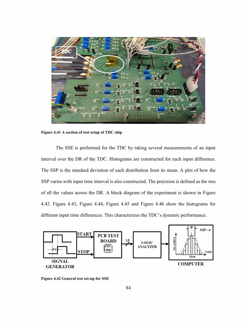
84
Figure 4.41 A section of test setup of TDC chip
The SSE is performed for the TDC by taking several measurements of an input
interval over the DR of the TDC. Histograms are constructed for each input difference.
The SSP is the standard deviation of each distribution from its mean. A plot of how the
SSP varies with input time interval is also constructed. The precision is defined as the rms
of all the values across the DR. A block diagram of the experiment is shown in Figure
4.42. Figure 4.43, Figure 4.44, Figure 4.45 and Figure 4.46 show the histograms for
different input time differences. This characterizes the TDC’s dynamic performance.
Figure 4.42 General test set-up for SSE
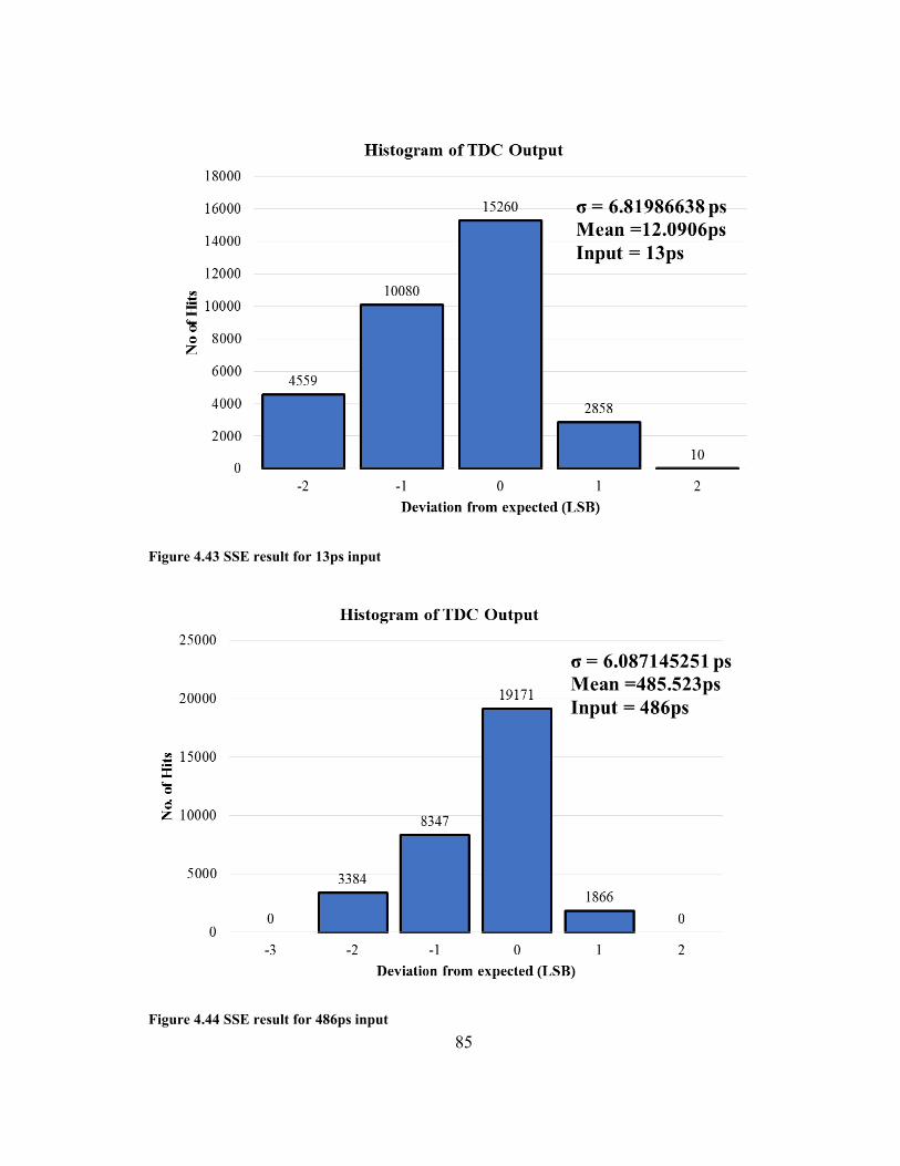
85
Figure 4.43 SSE result for 13ps input
Figure 4.44 SSE result for 486ps input
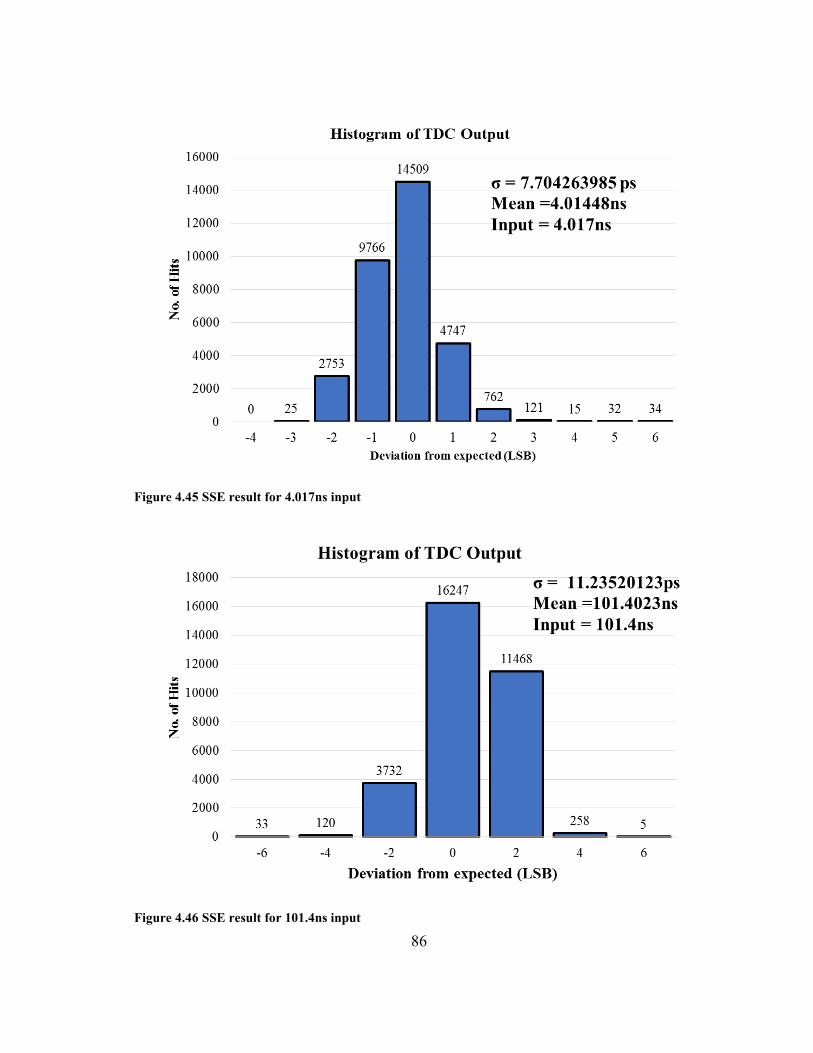
86
Figure 4.45 SSE result for 4.017ns input
Figure 4.46 SSE result for 101.4ns input
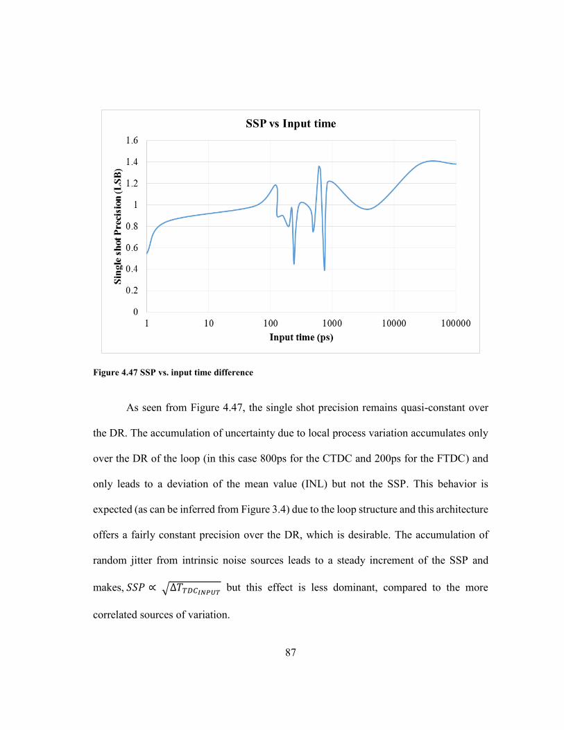
87
Figure 4.47 SSP vs. input time difference
As seen from Figure 4.47, the single shot precision remains quasi-constant over
the DR. The accumulation of uncertainty due to local process variation accumulates only
over the DR of the loop (in this case 800ps for the CTDC and 200ps for the FTDC) and
only leads to a deviation of the mean value (INL) but not the SSP. This behavior is
expected (as can be inferred from Figure 3.4) due to the loop structure and this architecture
offers a fairly constant precision over the DR, which is desirable. The accumulation of
random jitter from intrinsic noise sources leads to a steady increment of the SSP and
makes, 𝑆𝑆𝑃 ∝ √∆𝑇𝑇𝐷𝐶𝐼𝑁𝑃𝑈𝑇 but this effect is less dominant, compared to the more
correlated sources of variation.
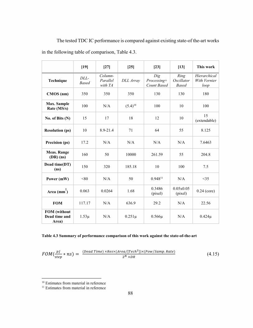
88
The tested TDC IC performance is compared against existing state-of the-art works
in the following table of comparison, Table 4.3.
[19] [27] [25] [23] [13] This work
Technique DLL-
Based
Column-
Parallel
with TA
DLL Array
Dig
Processing+
Count Based
Ring
Oscillator
Based
Hierarchical
With Vernier
loop
CMOS (nm) 350 350 350 130 130 180
Max. Sample
Rate (MS/s) 100 N/A (5.4)10 100 10 100
No. of Bits (N) 15 17 18 12 10 15
(extendable)
Resolution (ps) 10 8.9-21.4 71 64 55 8.125
Precision (ps) 17.2 N/A N/A N/A N/A 7.6463
Meas. Range
(DR) (ns) 160 50 10000 261.59 55 204.8
Dead time(DT)
(ns) 150 320 185.18 10 100 7.5
Power (mW) <80 N/A 50 0.94811 N/A <35
Area (mm2) 0.063 0.0264 1.68
0.3486
(pixel)
0.05x0.05
(pixel) 0.24 (core)
FOM 117.17 N/A 636.9 29.2 N/A 22.56
FOM (without
Dead time and
Area)
1.53µ N/A 0.251µ 0.566µ N/A 0.424µ
Table 4.3 Summary of performance comparison of this work against the state-of-the-art
𝐹𝑂𝑀(𝑝𝐽
𝑠𝑡𝑒𝑝∗ 𝑛𝑠) =
(𝐷𝑒𝑎𝑑 𝑇𝑖𝑚𝑒) ×𝑅𝑒𝑠×(𝐴𝑟𝑒𝑎 [𝑇𝑒𝑐ℎ2]⁄ )×(𝑃𝑜𝑤 𝑆𝑎𝑚𝑝. 𝑅𝑎𝑡𝑒)⁄
2𝑁 ×𝐷𝑅 (4.15)
10 Estimates from material in reference 11 Estimates from material in reference
89
5. SUMMARY AND CONCLUSIONS
In this work, a high resolution TDC has been realized in IBM 0.18um technology
with a DR of 204.8ns and maximum input rate of 100MHz. The chip consumes less than
35mW of power (with 1.8V supply) when quantizing at the maximum measurement rate.
The single-shot precision (SSP) of the proposed architecture is less than 15ps across the
entire DR. To alleviate this variation a reference recycling technique [11] can be employed
to cause the accumulated jitter to be reset after a predetermined interval or number of
cycles.
The resolution and DR achieved makes this proposed architecture suitable for
applications in ToF for ranging and also imaging applications. The moderate area
occupancy and maximum sample rate support of 100MS/s, makes possible the integration
of this TDC into CMOS implementations of SPAD-based sensor interfaces, where high
density is key. The larger the number of measurements per input cycle, the higher the
system accuracy and this emphasizes the need for high sample rate support.
Novel techniques for realizing high resolution and DR without sacrificing power
and area have been demonstrated. A control algorithm for making the TDC range
indefinitely extendable has been realized, by removing the possibility of MSB errors. The
trade-off is only noise accumulated for large measurement intervals. For a small area
increment of only about 0.011mm2 (consisting of a 96µmx69µm pad, JKFF, some logic
gates and an output register and buffer) per bit increment, the TDC range can be extended.
This is less than 0.3% of the 4mm2 area if the pad is included.
90
Future work may involve the consideration of a one delay element Vernier loop as
an improvement to allow for improved linearity of the FTDC stage. A one-bit quantization
is inherently linear since there are no mismatch concerns. Any deviations in delay from
the nominal result in only a gain error.
The designed TDC is demonstrated to be suitable for ToF measurements in
imaging and ranging applications due to maximized precision and DR. A time resolution
of 8.125ps translates into a ranging resolution of 1.219mm, while achieving DR of 30m
(but can be extended to several kilometers, as has been demonstrated) in a Lidar system
application. Also in SPAD-based imaging applications, for example, the TDC output rate
of 100MS/s would imply that for a 1024 pixel array, it would take 10.24µs to read out the
entire pixel array 15 bits (per pixel) at a time, corresponding to a frame rate of 97Kfps
(frames-per-second). The TDC throughput then only limits the frame rate for a per-pixel
read-out to ([100MS/s]/N), where N is the number of pixels in the array.
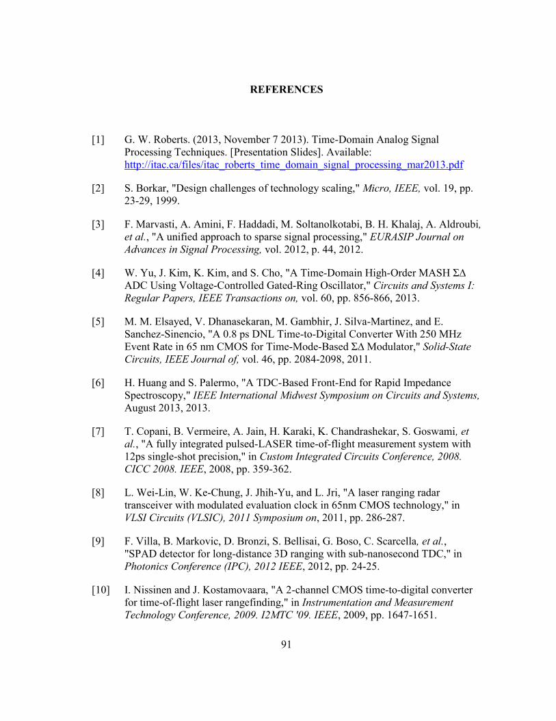
91
REFERENCES
[1] G. W. Roberts. (2013, November 7 2013). Time-Domain Analog Signal
Processing Techniques. [Presentation Slides]. Available:
http://itac.ca/files/itac_roberts_time_domain_signal_processing_mar2013.pdf
[2] S. Borkar, "Design challenges of technology scaling," Micro, IEEE, vol. 19, pp.
23-29, 1999.
[3] F. Marvasti, A. Amini, F. Haddadi, M. Soltanolkotabi, B. H. Khalaj, A. Aldroubi,
et al., "A unified approach to sparse signal processing," EURASIP Journal on
Advances in Signal Processing, vol. 2012, p. 44, 2012.
[4] W. Yu, J. Kim, K. Kim, and S. Cho, "A Time-Domain High-Order MASH Σ∆
ADC Using Voltage-Controlled Gated-Ring Oscillator," Circuits and Systems I:
Regular Papers, IEEE Transactions on, vol. 60, pp. 856-866, 2013.
[5] M. M. Elsayed, V. Dhanasekaran, M. Gambhir, J. Silva-Martinez, and E.
Sanchez-Sinencio, "A 0.8 ps DNL Time-to-Digital Converter With 250 MHz
Event Rate in 65 nm CMOS for Time-Mode-Based Σ∆ Modulator," Solid-State
Circuits, IEEE Journal of, vol. 46, pp. 2084-2098, 2011.
[6] H. Huang and S. Palermo, "A TDC-Based Front-End for Rapid Impedance
Spectroscopy," IEEE International Midwest Symposium on Circuits and Systems,
August 2013, 2013.
[7] T. Copani, B. Vermeire, A. Jain, H. Karaki, K. Chandrashekar, S. Goswami, et
al., "A fully integrated pulsed-LASER time-of-flight measurement system with
12ps single-shot precision," in Custom Integrated Circuits Conference, 2008.
CICC 2008. IEEE, 2008, pp. 359-362.
[8] L. Wei-Lin, W. Ke-Chung, J. Jhih-Yu, and L. Jri, "A laser ranging radar
transceiver with modulated evaluation clock in 65nm CMOS technology," in
VLSI Circuits (VLSIC), 2011 Symposium on, 2011, pp. 286-287.
[9] F. Villa, B. Markovic, D. Bronzi, S. Bellisai, G. Boso, C. Scarcella, et al.,
"SPAD detector for long-distance 3D ranging with sub-nanosecond TDC," in
Photonics Conference (IPC), 2012 IEEE, 2012, pp. 24-25.
[10] I. Nissinen and J. Kostamovaara, "A 2-channel CMOS time-to-digital converter
for time-of-flight laser rangefinding," in Instrumentation and Measurement
Technology Conference, 2009. I2MTC '09. IEEE, 2009, pp. 1647-1651.
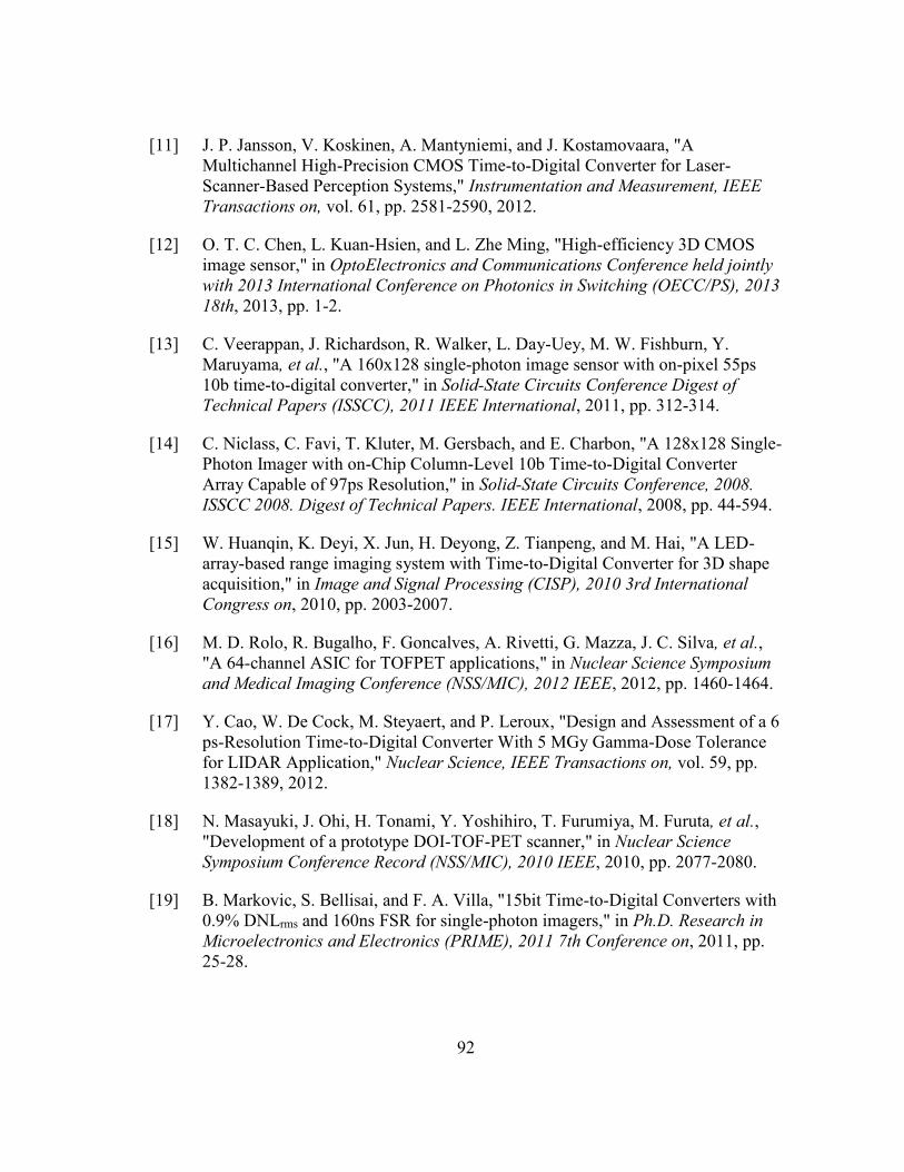
92
[11] J. P. Jansson, V. Koskinen, A. Mantyniemi, and J. Kostamovaara, "A
Multichannel High-Precision CMOS Time-to-Digital Converter for Laser-
Scanner-Based Perception Systems," Instrumentation and Measurement, IEEE
Transactions on, vol. 61, pp. 2581-2590, 2012.
[12] O. T. C. Chen, L. Kuan-Hsien, and L. Zhe Ming, "High-efficiency 3D CMOS
image sensor," in OptoElectronics and Communications Conference held jointly
with 2013 International Conference on Photonics in Switching (OECC/PS), 2013
18th, 2013, pp. 1-2.
[13] C. Veerappan, J. Richardson, R. Walker, L. Day-Uey, M. W. Fishburn, Y.
Maruyama, et al., "A 160x128 single-photon image sensor with on-pixel 55ps
10b time-to-digital converter," in Solid-State Circuits Conference Digest of
Technical Papers (ISSCC), 2011 IEEE International, 2011, pp. 312-314.
[14] C. Niclass, C. Favi, T. Kluter, M. Gersbach, and E. Charbon, "A 128x128 Single-
Photon Imager with on-Chip Column-Level 10b Time-to-Digital Converter
Array Capable of 97ps Resolution," in Solid-State Circuits Conference, 2008.
ISSCC 2008. Digest of Technical Papers. IEEE International, 2008, pp. 44-594.
[15] W. Huanqin, K. Deyi, X. Jun, H. Deyong, Z. Tianpeng, and M. Hai, "A LED-
array-based range imaging system with Time-to-Digital Converter for 3D shape
acquisition," in Image and Signal Processing (CISP), 2010 3rd International
Congress on, 2010, pp. 2003-2007.
[16] M. D. Rolo, R. Bugalho, F. Goncalves, A. Rivetti, G. Mazza, J. C. Silva, et al.,
"A 64-channel ASIC for TOFPET applications," in Nuclear Science Symposium
and Medical Imaging Conference (NSS/MIC), 2012 IEEE, 2012, pp. 1460-1464.
[17] Y. Cao, W. De Cock, M. Steyaert, and P. Leroux, "Design and Assessment of a 6
ps-Resolution Time-to-Digital Converter With 5 MGy Gamma-Dose Tolerance
for LIDAR Application," Nuclear Science, IEEE Transactions on, vol. 59, pp.
1382-1389, 2012.
[18] N. Masayuki, J. Ohi, H. Tonami, Y. Yoshihiro, T. Furumiya, M. Furuta, et al.,
"Development of a prototype DOI-TOF-PET scanner," in Nuclear Science
Symposium Conference Record (NSS/MIC), 2010 IEEE, 2010, pp. 2077-2080.
[19] B. Markovic, S. Bellisai, and F. A. Villa, "15bit Time-to-Digital Converters with
0.9% DNLrms and 160ns FSR for single-photon imagers," in Ph.D. Research in
Microelectronics and Electronics (PRIME), 2011 7th Conference on, 2011, pp.
25-28.
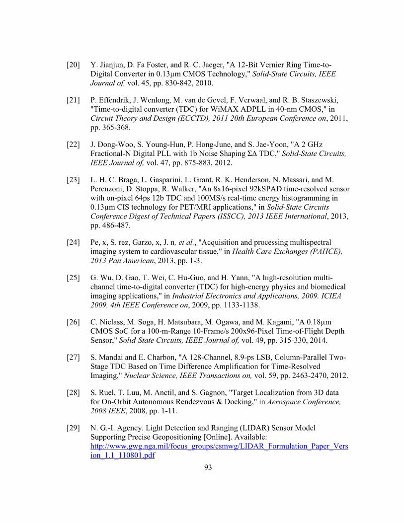
93
[20] Y. Jianjun, D. Fa Foster, and R. C. Jaeger, "A 12-Bit Vernier Ring Time-to-
Digital Converter in 0.13µm CMOS Technology," Solid-State Circuits, IEEE
Journal of, vol. 45, pp. 830-842, 2010.
[21] P. Effendrik, J. Wenlong, M. van de Gevel, F. Verwaal, and R. B. Staszewski,
"Time-to-digital converter (TDC) for WiMAX ADPLL in 40-nm CMOS," in
Circuit Theory and Design (ECCTD), 2011 20th European Conference on, 2011,
pp. 365-368.
[22] J. Dong-Woo, S. Young-Hun, P. Hong-June, and S. Jae-Yoon, "A 2 GHz
Fractional-N Digital PLL with 1b Noise Shaping Σ∆ TDC," Solid-State Circuits,
IEEE Journal of, vol. 47, pp. 875-883, 2012.
[23] L. H. C. Braga, L. Gasparini, L. Grant, R. K. Henderson, N. Massari, and M.
Perenzoni, D. Stoppa, R. Walker, "An 8x16-pixel 92kSPAD time-resolved sensor
with on-pixel 64ps 12b TDC and 100MS/s real-time energy histogramming in
0.13µm CIS technology for PET/MRI applications," in Solid-State Circuits
Conference Digest of Technical Papers (ISSCC), 2013 IEEE International, 2013,
pp. 486-487.
[24] Pe, x, S. rez, Garzo, x, J. n, et al., "Acquisition and processing multispectral
imaging system to cardiovascular tissue," in Health Care Exchanges (PAHCE),
2013 Pan American, 2013, pp. 1-3.
[25] G. Wu, D. Gao, T. Wei, C. Hu-Guo, and H. Yann, "A high-resolution multi-
channel time-to-digital converter (TDC) for high-energy physics and biomedical
imaging applications," in Industrial Electronics and Applications, 2009. ICIEA
2009. 4th IEEE Conference on, 2009, pp. 1133-1138.
[26] C. Niclass, M. Soga, H. Matsubara, M. Ogawa, and M. Kagami, "A 0.18µm
CMOS SoC for a 100-m-Range 10-Frame/s 200x96-Pixel Time-of-Flight Depth
Sensor," Solid-State Circuits, IEEE Journal of, vol. 49, pp. 315-330, 2014.
[27] S. Mandai and E. Charbon, "A 128-Channel, 8.9-ps LSB, Column-Parallel Two-
Stage TDC Based on Time Difference Amplification for Time-Resolved
Imaging," Nuclear Science, IEEE Transactions on, vol. 59, pp. 2463-2470, 2012.
[28] S. Ruel, T. Luu, M. Anctil, and S. Gagnon, "Target Localization from 3D data
for On-Orbit Autonomous Rendezvous & Docking," in Aerospace Conference,
2008 IEEE, 2008, pp. 1-11.
[29] N. G.-I. Agency. Light Detection and Ranging (LIDAR) Sensor Model
Supporting Precise Geopositioning [Online]. Available:
http://www.gwg.nga.mil/focus_groups/csmwg/LIDAR_Formulation_Paper_Vers
ion_1.1_110801.pdf
94
[30] Wikipedia. (2013, November 9 2013). Lidar Description. Available:
http://en.wikipedia.org/wiki/Lidar
[31] S. Henzler and SpringerLink (Online service), "Theory of TDC Operation," in
Time-to-Digital Converters, D. K. Itoh, T. Lee, T. Sakurai, W. M. C. Sansen, and
D. Schmitt-Landsiedel, Eds., 1st ed. Dordrecht ; London: Springer, 2010, pp. 21-
26.
[32] M. Yu, S. Zong, X. Tang, and Y. Wang, "A temperature stabilized multi-path
gated ring oscillator based TDC," in Computer Science and Information
Processing (CSIP), 2012 International Conference on, 2012, pp. 703-708.
[33] R. Szplet and K. Klepacki, "An FPGA-Integrated Time-to-Digital Converter
Based on Two-Stage Pulse Shrinking," Instrumentation and Measurement, IEEE
Transactions on, vol. 59, pp. 1663-1670, 2010.
[34] V. Ramakrishnan and P. T. Balsara, "A wide-range, high-resolution, compact,
CMOS time to digital converter," in VLSI Design, 2006. Held jointly with 5th
International Conference on Embedded Systems and Design., 19th International
Conference on, 2006, p. 6 pp.
[35] S. Young-Hun, K. Jun-Seok, P. Hong-June, and S. Jae-Yoon, "A 0.63ps
resolution, 11b pipeline TDC in 0.13µm CMOS," in VLSI Circuits (VLSIC), 2011
Symposium on, 2011, pp. 152-153.
[36] L. Minjae and A. A. Abidi, "A 9b, 1.25ps Resolution Coarse-Fine Time-to-
Digital Converter in 90nm CMOS that Amplifies a Time Residue," in VLSI
Circuits, 2007 IEEE Symposium on, 2007, pp. 168-169.
[37] S. Uemori, M. Ishii, H. Kobayashi, Y. Doi, O. Kobayashi, T. Matsuura, et al.,
"Multi-bit sigma-delta TDC architecture with self-calibration," in Circuits and
Systems (APCCAS), 2012 IEEE Asia Pacific Conference on, 2012, pp. 671-674.
[38] S. Henzler and SpringerLink (Online service), "Advanced TDC Design Issues,"
in Time-to-Digital Converters, D. K. Itoh, T. Lee, T. Sakurai, W. M. C. Sansen,
and D. Schmitt-Landsiedel, Eds., 1st ed. Dordrecht ; London: Springer, 2010, pp.
48-68.
[39] N. H. E. Weste and D. M. Harris, "Pulsed Latches," in CMOS VLSI design : a
circuits and systems perspective, M. Hirsch and M. Goldstein, Eds., 4th ed
Boston: Addison Wesley, 2011, p. 295.
[40] L. Won-Hyo, C. Jun-dong, and L. Sung-Dae, "A high speed and low power
phase-frequency detector and charge-pump," in Design Automation Conference,
95
1999. Proceedings of the ASP-DAC '99. Asia and South Pacific, 1999, pp. 269-
272 vol.1.
[41] M. Banu and A. Dunlop, "A 660 Mb/s CMOS clock recovery circuit with
instantaneous locking for NRZ data and burst-mode transmission," in Solid-State
Circuits Conference, 1993. Digest of Technical Papers. 40th ISSCC., 1993 IEEE
International, 1993, pp. 102-103.
[42] M. Bazes, "A novel precision MOS synchronous delay line," Solid-State
Circuits, IEEE Journal of, vol. 20, pp. 1265-1271, 1985.
[43] B. Razavi, "Basic MOS Device Physics," in Design of analog CMOS integrated
circuits, K. T. Kane, Ed., ed Boston: McGraw-Hill, 2001, pp. 18-19.
[44] J. Deog-Kyoon, G. Borriello, D. Hodges, and R. H. Katz, "Design of PLL-based
clock generation circuits," Solid-State Circuits, IEEE Journal of, vol. 22, pp.
255-261, 1987.
[45] K. Jaeha, B. S. Leibowitz, R. Jihong, and C. J. Madden, "Simulation and
Analysis of Random Decision Errors in Clocked Comparators," Circuits and
Systems I: Regular Papers, IEEE Transactions on, vol. 56, pp. 1844-1857, 2009.
[46] B. Razavi, "Design Considerations for Interleaved ADCs," Solid-State Circuits,
IEEE Journal of, vol. 48, pp. 1806-1817, 2013.
[47] B. Nikolic, V. G. Oklobdzija, V. Stojanovic, J. Wenyan, C. James Kar-Shing,
and M. Ming-Tak Leung, "Improved sense-amplifier-based flip-flop: design and
measurements," Solid-State Circuits, IEEE Journal of, vol. 35, pp. 876-884,
2000.
[48] B. Goll and H. Zimmermann, "A 65nm CMOS comparator with modified latch
to achieve 7GHz/1.3mW at 1.2V and 700MHz/47µW at 0.6V," in Solid-State
Circuits Conference - Digest of Technical Papers, 2009. ISSCC 2009. IEEE
International, 2009, pp. 328-329,329a.
[49] M. Matsui, H. Hara, Y. Uetani, K. Lee-Sup, T. Nagamatsu, Y. Watanabe, et al.,
"A 200 MHz 13 mm2 2-D DCT macrocell using sense-amplifying pipeline flip-
flop scheme," Solid-State Circuits, IEEE Journal of, vol. 29, pp. 1482-1490,
1994.
[50] D. Schinkel, E. Mensink, E. Klumperink, E. Van Tuijl, and B. Nauta, "A Double-
Tail Latch-Type Voltage Sense Amplifier with 18ps Setup+Hold Time," in Solid-
State Circuits Conference, 2007. ISSCC 2007. Digest of Technical Papers. IEEE
International, 2007, pp. 314-605.
96
[51] T. Toifl, C. Menolfi, M. Ruegg, R. Reutemann, P. Buchmann, M. Kossel, et al.,
"A 22-gb/s PAM-4 receiver in 90-nm CMOS SOI technology," Solid-State
Circuits, IEEE Journal of, vol. 41, pp. 954-965, 2006.
[52] S. D. Brown and Z. G. Vranesic, "Synchronous Counters," in Fundamentals of
digital logic with Verilog design, C. Paulson, Ed., 2nd ed Boston: McGraw-Hill
Higher Education, 2008, pp. 374-376.
[53] T. L. Floyd, "A 2 Bit Asynchronous Counter," in Digital fundamentals, K.
Linsner and R. Davidson, Eds., 9th ed Upper Saddle River, N.J.: Prentice Hall,
2006, pp. 428-431.
[54] S. Henzler and SpringerLink (Online service), "Vernier TDC," in Time-to-Digital
Converters, D. K. Itoh, T. Lee, T. Sakurai, W. M. C. Sansen, and D. Schmitt-
Landsiedel, Eds., 1st ed. Dordrecht ; London: Springer, 2010, pp. 74-80.
Related Documents