A study on wide bandgap oxide semiconductors March 2017 Department of Science and Advanced Technology Graduate School of Science and Engineering Saga University Xu WANG

Welcome message from author
This document is posted to help you gain knowledge. Please leave a comment to let me know what you think about it! Share it to your friends and learn new things together.
Transcript
A study on wide bandgap oxide
semiconductors
March 2017
Department of Science and Advanced Technology
Graduate School of Science and Engineering
Saga University
Xu WANG


I
A study on wide bandgap oxide semiconductors
Abstract
In recent years, wide bandgap oxide semiconductor has attracted considerable
attention owing to its application in ultraviolet (UV) optoelectronic devices,
especially in deep UV light emitters and detectors, due to their potential application in
Ozone hole detection, chemical-biological agent sensors, missile plume sensors and
space-to-space communications. Among all the wide bandgap oxide semiconductors,
MgZnO alloy films are ideal materials for developing the UV optoelectronic devices
because of their particular advantages, such as wide bandgap, low growth temperature,
availability of lattice-matched single-crystal substrates, and high radiation hardness.
Since the ionic radius of Mg2+
(0.057 nm) is similar to that of Zn2+
(0.060 nm),
there can be some replacement in either structure without changing the original
structure when alloying. However, there is large crystal structure dissimilarity
between wurtzite hexagonal ZnO and rock-salt-cubic MgO, which leads to phase
separation. It limited the application of MgZnO alloy in deep UV region. In
comparison with ZnO semiconductor, Ga2O3 has a wider bandgap of about 4.9 eV.
The bandgap of In-Al-Ga-O system which is obtained by alloying In or Al element
into Ga2O3 can be tuned from 3.5-8.6 eV, thus In-Al-Ga-O system can be used as deep
UV light-emitting diode, deep UV detector, and deep UV transparent electrode.
In Chapter 1, the review of studies on the wide bandgap oxide semiconductors were

II
described. The purpose of this study was also presented.
In Chapter 2, film growth and characterization methods were introduced.
In Chapter 3, the influence of Mg content on crystal structure and properties of
single phase MgZnO films grown in all Mg content was been discussed. The
structural transition from hexagonal to cubic phase has been observed at the Mg
content around 0.4. We have also investigated the effect of the substrate temperature
and oxygen pressure on crystal structure and properties of MgZnO films grown by
using pulsed laser deposition (PLD) method.
In Chapter 4, we reported on bandgap bowing parameters for wurtzite and cubic
MgZnO alloys from a study of high quality and single phase films in all Mg content
range. The Mg contents in the MgZnO films were accurately determined using the
Energy dispersive spectrometer and X-ray photoelectron spectroscopy (XPS). The
measurement of bandgap energies by examining the onset of inelastic energy loss in
core-level atomic spectra from XPS was proved to be valid for determining the
bandgap of MgZnO films. The dependence of the energy bandgap on Mg content was
found to deviate downwards from linearity. Fitting of the bandgap energies resulted in
two bowing parameters of 2.01 and 1.48 eV corresponding to wurtzite and cubic
MgZnO films, respectively.
In Chapter 5, (1) (AlGa)2O3 thin films were deposited on (0001) sapphire substrates
by PLD at different substrate temperatures. The influence of substrate temperature on
surface morphology, optical properties, and crystal quality has been systematically
investigated by atomic force microscope, transmission spectra, X-ray diffraction, and

III
Raman spectroscopy. The results revealed that all the (AlGa)2O3 films had smooth
surface and high transmittance. The (AlGa)2O3 film with the better crystal quality can
be obtain at a substrate temperature of 400 ℃. (2) We also report a detailed
investigation on temperature-dependent Raman scattering of β-(AlGa)2O3 thin films
with different Al content (0-0.72) under the temperature range of 77-300 K. The
temperature-dependent Raman shifts and linewidths of the phonon modes were
obtained by employing Lorentz fitting. The linewidths broadening of phonon modes
with the temperature can be well explained by a model involving the effects of
thermal expansion, lattice-mismatch-induced strain, and decay of optical phonon into
two and three phonons. It is clearly demonstrated dependence of the linewidths and
decay process on the Al content in β-(AlGa)2O3 thin films.
In Chapter 6, we reported measurements of Raman scattering of cubic In2O3 and
(In0.83Ga0.17)2O3 films grown on sapphire substrates by PLD as a function of
temperature (77-500 K). We analyzed the temperature-dependent Raman shifts and
linewidths of six Raman modes in In2O3 film and Ag(1)
and Ag(2)
/Tg(2)
modes in
(In0.83Ga0.17)2O3 film. The Raman shifts of phonon modes were found to vary linearly
with temperature. The temperature coefficients for six Raman modes of In2O3 film
were in the range of -0.014 and -0.006 cm-1
/K, while temperature coefficients of Ag(1)
and Ag(2)
/Tg(2)
modes in (In0.83Ga0.17)2O3 film were -0.017 and -0.024 cm-1
/ K,
respectively. Through the aid of a model involving three- and four-phonon coupling,
the effects of temperature on linewidths were clearly illustrated, which demonstrated
that three-phonon process always dominated in the decay process for all the modes in

IV
both In2O3 and (In0.83Ga0.17)2O3 films.

V
Contents
1 Introduction………………………………….………………….………………….1
1.1 Background……………………………………………....……………………..1
1.2 Review of study on wide bandgap oxide semiconductor…………...………….2
1.2.1 Group II oxides.............................................………...……….……...……..2
1.2.2 Group III oxides….…….......…….…...........................................…..........11
1.3 Purpose and Outline…………………………………………….……...……...19
References……………..………………………………………...……………23
2 Growth and characterization methods…………………………………..……..29
2.1 PLD…………………………………………..………………………………..29
2.2 Characterization method………………………………………………………34
3 Growth and characterization of MgZnO films……………………..…..……..40
3.1 Mg content influence……………..………………………………....………...40
3.2 Substrate temperature influence…………………………..………………..…50
3.3 Oxygen pressure influence………………………………………......……..…59
3.4 Conclusions……………………………………………………………...……62
References……………………………..………………………...……………63
4 Bandgap engineering of MgxZn1-xO films………………………...……………65

VI
4.1 Introduction……………………………………………………………...……65
4.2 Experiment…………………………………………………………………….67
4.3 Results and discussion……………………………..……………………….…68
4.4 Conclusions………………………...…………………………………………75
References..…………………………………………………………………....76
5 Raman scattering in (AlxGa1-x)2O3 films………….………………………….…..78
5.1 Substrate temperature effect…………...……….…...……………..........…….78
5.2 Raman scattering…………….……..…………………………………......…..91
5.3 Conclusions……………………….………..……….………………….........107
References………………..…………………………………..………........…109
6 Raman scattering in (InxGa1-x)2O3 films….………….….....….........……...….113
6.1 Introduction………………………………………………………...…......…113
6.2 Experiment…………………………………………………………………...114
6.3 Results and discussion……………………………..………………..……….115
6.4 Conclusions………………………...………...……………….…………..…127
References……………………………………………..………………………128
7 Summary………………..………………………………………..………….….131
Acknowledgments………………………………………………………………......134
List of publications………………………………………………………………….135

1
Chapter 1
Introduction
1.1 Background
With the increase in demand for ultraviolet (UV) optoelectronic devices,
piezoelectric sensors, power device application, and thin film transistors, wide
bandgap oxide semiconductors become the hot spot of recent research due to their
particular properties such as wide bandgap, high conductivity, and high transmittance.
In addition, they can be easily prepared by common methods such as pulsed laser
deposition (PLD), molecular beam epitaxy (MBE), magnetron sputtering, and
metal-organic chemical vapor deposition (MOCVD).
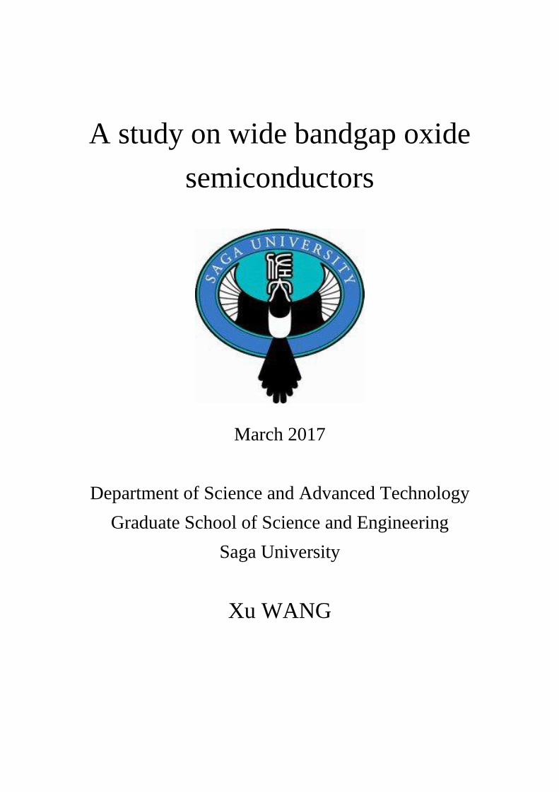
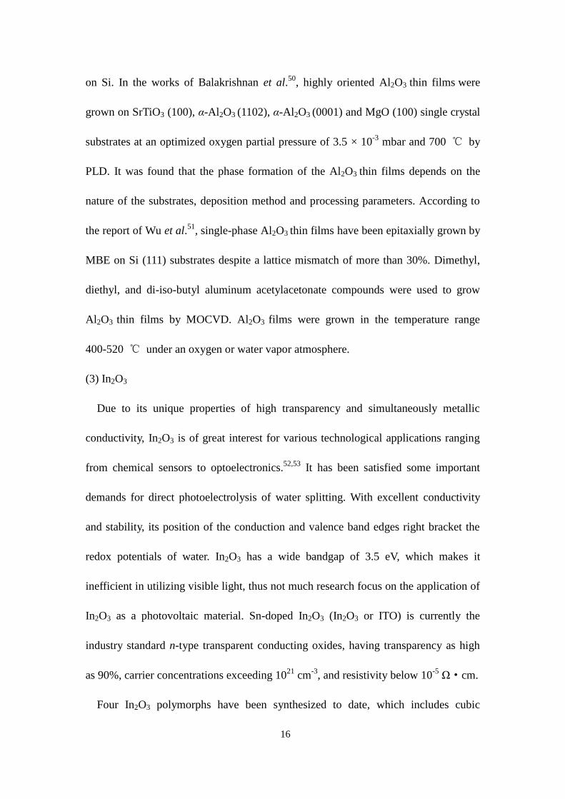
Figure 1.1 is a comparison of the bandgap energies and lattice constants (a) of wide
bandgap oxide semiconductors and other well-known oxide semiconductors. The two
main types of wide bandgap oxide semiconductors are: (1) Group II oxides such as
ZnO and MgO, (2) Group III oxides such as Ga2O3, Al2O3, and In2O3. The bandgap
engineering is an indispensable issue to be achieved for developing these applications.
For Group II oxides, alloying ZnO with MgO can tune the bandgap from 3.31 eV to
7.8 eV. MgZnO alloy material has received much attention due to their potential
applications in the short-wavelength optoelectronic devices such as UV light-emitting
diodes and laser diodes. For Group III oxides, the bandgap of In-Al-Ga-O system
which is obtained by alloying In or Al element into Ga2O3 can be tuned from 3.5-8.6
eV, thus In-Al-Ga-O system can be used as deep UV light-emitting diode, deep UV

2
detector, and deep UV transparent electrode.
2 4 6 8 10 12
1
2
3
4
5
6
7
8
9
Group III
Group II
Infrared
Visible
Ultraviolet
Ba
nd
ga
p e
ne
rgy (
eV
)
Lattice constant a (Å)
Fe3O
4
Fe2O
3
Cu2O
CdO
CuO
NiOTiO
2
In2O
3
Al2O
3
MgO
Ga2O
3
ZnO
Figure 1.1 The relationship between energy bandgap and lattice constant (a) of
oxide semiconductors.
1.2 Review of study on wide bandgap oxide semiconductor
1.2.1 Group II oxides
(1) ZnO
Owing to its direct wide bandgap of 3.3 eV and large exciton binding energy of 60
meV at room temperature, ZnO semiconductor has attracted tremendous attention for
applications in blue and UV light-emitting diodes, which is expected to be an

3
alternative to those based on GaN (Eg ~ 3.4 eV at 300 K). In general, II-VI binary
semiconductors crystallize in hexagonal wurtzite structure or cubic zinc-blende
structure in which four cations surrounded one anion at the corners of tetrahedron.
The crystal structures which ZnO shares are cubic, zinc-blende, and wurtzite1, as
shown in Table 1.1.
Table 1.1 Space group, crystal structure, lattice parameters of ZnO.
Space group Crystal
structure
Lattice
parameters
Density
(g·cm-3
)
Reference
Fm3m Cubic a = 4.28 Å - PDF#77-0191
F43̅m Zinc-blende a = 4.62 Å - Ref. 2
P63mc Hexagonal a = 3.25 Å
c = 5.21 Å
5.61 PDF#36-1451
Cubic ZnO belongs to space group Fm3m and this cubic structure is sixfold
coordinated. However, the stabilized ZnO with cubic structure can’t be obtained by
the epitaxial growth. Same with other II-VI oxide semiconductors, hexagonal ZnO
can be transformed into the cubic structure at relatively high pressures, because the
reduction of the lattice dimensions leads to the interionic Coulomb interaction to favor
the ionicity more over the covalent nature. For ZnO, the phase transition from the
wurtzite to the cubic induced by high pressure was found at 10 GPa by Bates et al.3,
and a large volume decreased of around 17 %. Decremps et al. 4
have investigated the

4
structure of ZnO transformed from hexagonal to cubic at around 9 GPa by Raman
spectroscopy.
In the zinc-blende structure, each Zn atom has four nearest neighbors. The in-plane
bonds are stronger than the out-of-plane bonds. The zinc-blende structure ZnO has the
highest symmetry compatible with the existence of piezoelectric polarization under
the strain in the c-axis direction.3 Moreover, it possesses technological advantages
such as easier laser cavity growth along the [110] direction, which is evidence for
higher optical gain. Ashrafi et al.5 grew the zinc-blend ZnO on GaAs (001) substrates
with a ZnS buffer layer by using microwave-plasma-assisted metalorganic
molecular-beam epitaxy.
Figure 1.2 Schematic representation of the ZnO with wurtzite structure. The shaded
green and orange spheres denote O and Zn atoms respecticely.
Among these structures, hexagonal wurtzite structure ZnO has been dominantly
observed and is thought to be the most stable structure. ZnO with wurtzite structure
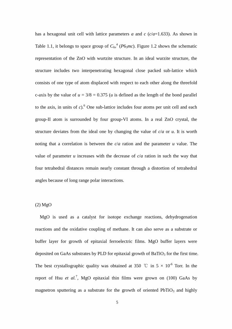
5
has a hexagonal unit cell with lattice parameters a and c (c/a=1.633). As shown in
Table 1.1, it belongs to space group of C6v4 (P63mc). Figure 1.2 shows the schematic
representation of the ZnO with wurtzite structure. In an ideal wurzite structure, the
structure includes two interpenetrating hexagonal close packed sub-lattice which
consists of one type of atom displaced with respect to each other along the threefold
c-axis by the value of u = 3/8 = 0.375 (u is defined as the length of the bond parallel
to the axis, in units of c).6 One sub-lattice includes four atoms per unit cell and each
group-II atom is surrounded by four group-VI atoms. In a real ZnO crystal, the
structure deviates from the ideal one by changing the value of c/a or u. It is worth
noting that a correlation is between the c/a ration and the parameter u value. The
value of parameter u increases with the decrease of c/a ration in such the way that
four tetrahedral distances remain nearly constant through a distortion of tetrahedral
angles because of long range polar interactions.
(2) MgO
MgO is used as a catalyst for isotope exchange reactions, dehydrogenation
reactions and the oxidative coupling of methane. It can also serve as a substrate or
buffer layer for growth of epitaxial ferroelectric films. MgO buffer layers were
deposited on GaAs substrates by PLD for epitaxial growth of BaTiO3 for the first time.
The best crystallographic quality was obtained at 350 ℃ in 5 × 10⁻⁶
Torr. In the
report of Hsu et al.7, MgO epitaxial thin films were grown on (100) GaAs by
magnetron sputtering as a substrate for the growth of oriented PbTiO3 and highly

6
oriented crystalline MgO films were obtained when the substrate temperature range
from 500 to 530 ℃.
MgO has a wide bandgap of 7.8 eV and cubic unit cell with lattice parameters of
4.21 Å.8 Cubic MgO belongs to space group of Fm3m̅. Figure 1.3 shows schematic
representation of the MgO with cubic structure. The shaded green and blue spheres
denote O and Mg atoms, respectively.
Figure 1.3 Schematic representation of the MgO with cubic structure. The shaded
green and blue spheres denote O and Mg atoms, respectively.
MgO films were usually grown by evaporating the metallic component in a
moderate oxygen atmosphere on an adequate metallic substrate. The lattice match
plays an important role in epitaxial growth, in which the planarity of the overlayer and
the detailed nature of the oxide-metal bonding depend on the extent of interface strain.
According to previous report, due to the reduction of lattice mismatch, Ag and Mo
substrates were regarded as good candidates for the growth of MgO epitaxial layers.

7
The lattice structure and optical property of epitaxial MgO layers grown on Ag and
Mo substrates have been studied.9 Wollshlager et al.
10 studied the stoichiometry and
the morphology of MgO layers epitaxially grown on Ag (100) by means of X-ray
photoelectron and high-resolution spot profile analysis low-energy electron diffraction.
Strong differences have been found for epitaxy of MgO films, depending on the
preparation condition. Ultra-thin MgO films have been synthesized under UHV
conditions by evaporating Mg onto Mo (100) various background pressures of oxygen.
Low-energy electron diffraction studies indicated that MgO films grow epitaxially in
the 200-600 K substrate temperature range with the (100) face of MgO oriented
parallel to Mo (100).11
In recent years, MgO films were also grown by other methods
such as PLD, MBE, magnetron sputtering, and sol-gel method on various substrates.
Susaki et al.12
have found that epitaxial MgO (111) films grow under a wide range of
deposition conditions (substrate temperature of 400 -800 ℃, oxygen partial pressures
of 10-4
-100 Pa) on Al2O3 substrates by PLD. Chen et al.13
reported about selective
growth of singly oriented (110)-, (100)-, and (111)-MgO films on Si (100) substrates
by PLD and the mechanism of the orientation selection is attributed to the energy
balance between the surface and interface energies.
(3) MgZnO
Gourp-II elements such as Mg and Cd are extensively used in adjusting the
bandgap of ZnO. Since radii of Zn2+
is 0.60 Å and Radii of Mg2+
is 0.57 Å,14
therefore,
Mg can be easily incorporated in to the ZnO lattice with smaller structural

8
deformations.15
MgZnO alloy material is considered to be one the best candidate to
increase the bandgap energy of ZnO from 3.3 to 7.8 eV by alloying it with different
content of MgO.16
MgZnO is a promising material for optoelectronic applications in
the UV and deep UV region. MgZnO alloy has two different crystal structures,
hexagonal wurzite (a = 3.24 Å and b = 5.20 Å) and rock-salt cubic (a = 4.24 Å)
structure. According to the phase diagram of the ZnO-MgO solid solution, the
thermodynamic solubility limit of ZnO in MgO is ~40 %, while that of MgO in ZnO
is very small ~ 4 %.16
MgZnO films grown via the PLD growth technique were found
to exceed the low solubility limit of MgO in ZnO, and single phase films with the
hexagonal wurzite structure if up to ~35 % Mg were achieved.17
On the other hand,
the thermal stability of the cubic-phase MgZnO films was studied by annealing the
films at high temperatures. In the report of Chen et al.18
, for the MgZnO films with
the Mg content exceeding 0.55, the films had stable cubic phase after annealing at
high temperature of 1000 ℃.
It requires accurate information of fundamental properties, in particular, the
emission property, bandgap energy, and the index of transmission for designing
MgZnO-based UV optoelectronic devices. Optical research about MgZnO, including
the photoluminescence measurements for emission hehaviour and transmission
spectra for bandgap energy, indicated that the bandgap energy of MgZnO has a
blueshift with the increase of the Mg content. Ohtomo et al. 19
found the bandgap
energy increased from 3.30 to 3.99 eV with Mg content up to 33% in hexagonal
MgZnO films. Similar results were also reported by Narayan et al. 20
The

9
investigation reported by Choopun et al. indicated that MgZnO films with Mg content
exceeding 50 % showed a wide bandgap lager than 5.0 eV.21
In the work of Thapa et
al. 22
MgZnO films with bandgaps that span the UV range of 3.2-5.7 eV were realized.
For fabrication of MgZnO films, growth conditions such as substrate temperature
and oxygen pressure have a great influence on crystal structure, optical properties, and
electrical properties. Liu et al.23
have found that as the substrate temperature increases
from 300 to 900 ℃, Mg content in single-phase wurtzite MgZnO films increased
significantly from 27 close to 46 %, and the bandgap is shifted from 3.49 to 3.88 eV.
Han et al.24
investigated the effect of oxygen pressure on preferred deposition
orientations and optical properties of cubic MgZnO thin films. It indicated that the
preferred orientation of cubic MgZnO changed from (200) to (111) when deposition
pressure increased and the absorption edges of which shift to longer wavelength
direction due to the decrease of Mg content in the MgZnO film. Moreover, in spite of
the lattice mismatch between epitaxial films and substrate, MgZnO can be grown on
many substrates, such as sapphire, Si, GaN, GaAs, ScAlMgO4, and ITO as well as
ZnO or MgO layers.
Up to now, a lot of common deposition methods succeeded in preparing the
high-quality MgZnO alloy films, such as MBE,25
MOCVD,26
electrophoretic
deposition (EPD),27
reactive electron beam evaporation deposition (REBED),28
RF
magnetron sputtering,22
and PLD.29,30
Ohtomo et al.19
reported the c-axis MgZnO films were epitaxially grown by PLD
on ZnO epitaxial films and sapphire (0001) substrates using ceramic tagerts. The

10
MgZnO film with the Mg content of 0.33 had a bandgap energy of 3.99 eV at room
temperature. When the Mg content was above 0.36, MgO impurity phase separation
can be observed. Sharma et al.31
investigated the optical and structural properties of
high-quality single-crystal epitaxial MgZnO films grown by PLD method. The intense
UV band edge was observed at room temperature and 77 K with the Mg content up to
36% in the films. Moreover, post-deposition annealing in oxygen was found to reduce
the number of defects and to improve the optical properties of the films. In the work
of Teng et al.,32
indices of refraction for MgZnO epitaxial films grown by PLD on
sapphire substrates with Mg content up to 36 % were determined in the range of
wavelength 457-968 nm by analysis of optical transmission spectra and prism-coupled
waveguide measurement. Choopun et al.21
reported on the realization of wide
bandgap (5-6 eV), single-phase, metastable, and epitaxial MgZnO thin film alloys
grown on sapphire by PLD. It was found that the Mg content, structure, and bandgap
of MgZnO film alloys depended critically on the growth temperature. A wurtzite
N-doped MgZnO film with the Mg content of 20 % was grown by plasma-assisted
MBE on c-plane sapphire using radical NO as oxygen source and nitrogen dopant. A
hole concentration of 6.1 × 10¹⁷
cm-3
and a mobility of 6.42 cm2/V·s were observed in
p-type MgZnO:N by Wei et al.33
Ju et al.34
grew the phase stability of cubic
Mg0.55Zn0.45O thin film by MOCVD and studied this film by continuous thermal
annealing. A continuous thermal annealing at 750 ℃ can improved the crystal
quality and surface smoothness greatly. However, the phase separation occurred when
the sample was annealed at a higher temperature. A lower pumping threshold was

11
expected, if an exciton-related recombination rather than an electron-hole plasma
recombination is employed. The quantum well structure is effective toward this goal.
Ohtomo et al.35
succeeded in growing ZnO/Mg0.2Zn0.8O quantum well structure with a
bandgap offset of about 0.5 eV by using MBE on sapphire substrate. The thickness of
well layer was in the range of 1.7-12 nm and the thickness of barrier layer is 6.2 nm.
As the well layer thickness decreased below 5 nm, the emission peak and absorption
edge show a blueshift due to the quantum-size effect. MgZnO-based solar-blind UV
detectors have attracted increasing attention. In the report of Han et al.36
, an UV
photodetector was fabricated on MgZnO thin film grown by MOCVD. The peak
response of the device centers at 238 nm and the cutoff wavelength is 253 nm. The
peak responsivity is 129 mA/W at 15 V bias and the UV/visible reject ratio is 4 orders
of magnitude. High mobility in two-dimensional electron systems were observed in
high quality MgZnO/ZnO heterojunctions. Solovyev et al.37
studied the optical
transitions present in two-dimensional electron systems confined at MgZnO/ZnO
heterojunctions by using low temperature PL and reflectance measurement. The first
excited electron subband is shown to be empty of electrons. Falson et al.38
found the
carrier mobility exceeded 1 × 106 cm
2/Vs in MgZnO/ZnO heterostructures grown at
730 ℃ by using MBE method.
1.2.2 Group III oxides
(1) Ga2O3
Owing to its large bandgap energy (~ 4.9 eV),39
Ga2O3 has recently attracted

12
focused interest as a promising material for UV optical and power-electronic devices.
Ga2O3 has five phases classified as α, β, γ, δ, and ε. Among these five phases, β-Ga2O3
is the thermally most stable. Heat treatment of the other metastable transition phases
can convert to β-Ga2O3. Figure 1.4 shows the conversion relationships among these
five phases.
Figure 1.4 Conversion relationships among the five phases of Ga2O3.
Monoclinic β-Ga2O3 has a melting point of 1740 ℃. It belongs to the monoclinic
system and lattice parameters are a = 1.22 nm, b = 0.30 nm, c = 0.58 nm, α = γ = 90 °,
and β = 103.83 °.10
The Ga ions are in distorted octahedral and tetrahedral sites with
Ga-O bond distances of 2.00 and 1.83 Å, repectively, and the O ions are in a distorted
cubic closest packing arrangement. Distortions in Ga2O3 structure are the reasons for
the level of stability. Figure 1.5 shows schematic representation of monoclinic
β-Ga2O3. The tetrahedral coordination Ga ions named Ga (IV) and the octahedral
650 ℃ dry
600 ℃ dry
300 ℃ wet
300 ℃ wet
670 ℃ dry
β-Ga2O3
α-Ga2O3
ε-Ga2O3 γ-Ga2O3
δ-Ga2O3
< 500 ℃ dry
500 ℃ few hours

13
coordinal Ga ions called Ga (VI) are shown in figure 1.5. The chains are connected by
GaO4 tetrahedral chains, and the doubly connected straight chains of GaO6 edge
shared octahedral run along b. Moreover, since octahedral Ga (VI) chain which can
constitute the paths followed by carrier electrons is present in the lattice along the b
axis, thus (-201) oriented β-Ga2O3 film in which the b axis is parallel to the substrate
is considered to enhance the conductivity.41
Figure 1.5 Schematic representation of monoclinic β-Ga2O3. The shaded green and
red spheres denote O and Ga atoms, respectively.
Ga2O3 films have been grown by various methods such as sputtering, spray
Ga (VI)
Ga (IV)
14
pyrolysis, sol-gel method, MBE, and PLD. 42-43
In our previous work, Ga2O3 films
were grown on (0001) sapphire substrates by PLD method. The effect of substrate
temperature on crystal structure, surface morphology, and transmittance has been
systematically investigated. The (-201) oriented Ga2O3 films can be obtained at
substrate temperature of 500 ℃.39
(2) Al2O3
Al2O3 is a technically important material with chemical and thermal stability,
excellent dielectric properties, and the strong adhesion to various materials.44
It is
widely used as buffer layers, gate oxides, and other electronic circuit elements.45
Moreover, Al2O3 has paid increasing attention to explore its potential applications in
high energy storage density capacitors due to its wide bandgap, high dielectric
strength and large permittivity.46
Table 1.2 Common methods for formation of metastable structure and the stable
α-Al2O3 phase.
fcc
γ-AlOOH (boehmite) γ δ θ α-Al2O3
α-Al(OH)3 (bayerite) η θ α-Al2O3
Melting Al γ δ θ α-Al2O3
hcp
α- AlOOH (diaspore) α-Al2O3
γ- Al(OH)3 (gibbsite) χ κ α-Al2O3
5 Al2O3·H2O κ α-Al2O3
300-500 ℃ 700-800 ℃ 900-1000 ℃ 1000-1100 ℃
200-300 ℃ 600-800 ℃ 1000-1100 ℃
700-800 ℃
150-300 ℃ 650-750 ℃ 1000 ℃
700-800 ℃ 1000 ℃
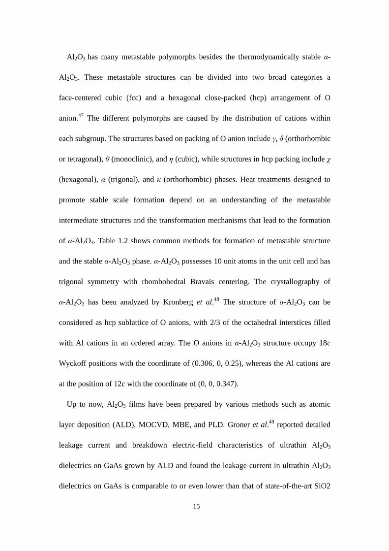
15
Al2O3 has many metastable polymorphs besides the thermodynamically stable α-
Al2O3. These metastable structures can be divided into two broad categories a
face-centered cubic (fcc) and a hexagonal close-packed (hcp) arrangement of O
anion.47
The different polymorphs are caused by the distribution of cations within
each subgroup. The structures based on packing of O anion include γ, δ (orthorhombic
or tetragonal), θ (monoclinic), and η (cubic), while structures in hcp packing include χ
(hexagonal), α (trigonal), and κ (orthorhombic) phases. Heat treatments designed to
promote stable scale formation depend on an understanding of the metastable
intermediate structures and the transformation mechanisms that lead to the formation
of α-Al2O3. Table 1.2 shows common methods for formation of metastable structure
and the stable α-Al2O3 phase. α-Al2O3 possesses 10 unit atoms in the unit cell and has
trigonal symmetry with rhombohedral Bravais centering. The crystallography of
α-Al2O3 has been analyzed by Kronberg et al.48
The structure of α-Al2O3 can be
considered as hcp sublattice of O anions, with 2/3 of the octahedral interstices filled
with Al cations in an ordered array. The O anions in α-Al2O3 structure occupy 18c
Wyckoff positions with the coordinate of (0.306, 0, 0.25), whereas the Al cations are
at the position of 12c with the coordinate of (0, 0, 0.347).
Up to now, Al2O3 films have been prepared by various methods such as atomic
layer deposition (ALD), MOCVD, MBE, and PLD. Groner et al.49
reported detailed
leakage current and breakdown electric-field characteristics of ultrathin Al2O3
dielectrics on GaAs grown by ALD and found the leakage current in ultrathin Al2O3
dielectrics on GaAs is comparable to or even lower than that of state-of-the-art SiO2
16
on Si. In the works of Balakrishnan et al.50
, highly oriented Al2O3 thin films were
grown on SrTiO3 (100), α-Al2O3 (1102), α-Al2O3 (0001) and MgO (100) single crystal
substrates at an optimized oxygen partial pressure of 3.5 × 10⁻³
mbar and 700 ℃ by
PLD. It was found that the phase formation of the Al2O3 thin films depends on the
nature of the substrates, deposition method and processing parameters. According to
the report of Wu et al.51
, single-phase Al2O3 thin films have been epitaxially grown by
MBE on Si (111) substrates despite a lattice mismatch of more than 30%. Dimethyl,
diethyl, and di-iso-butyl aluminum acetylacetonate compounds were used to grow
Al2O3 thin films by MOCVD. Al2O3 films were grown in the temperature range
400-520 ℃ under an oxygen or water vapor atmosphere.
(3) In2O3
Due to its unique properties of high transparency and simultaneously metallic
conductivity, In2O3 is of great interest for various technological applications ranging
from chemical sensors to optoelectronics.52,53
It has been satisfied some important
demands for direct photoelectrolysis of water splitting. With excellent conductivity
and stability, its position of the conduction and valence band edges right bracket the
redox potentials of water. In2O3 has a wide bandgap of 3.5 eV, which makes it
inefficient in utilizing visible light, thus not much research focus on the application of
In2O3 as a photovoltaic material. Sn-doped In2O3 (In2O3 or ITO) is currently the
industry standard n-type transparent conducting oxides, having transparency as high
as 90%, carrier concentrations exceeding 1021
cm-3
, and resistivity below 10-5
Ω·cm.
Four In2O3 polymorphs have been synthesized to date, which includes cubic

17
bixbyite-type c-In2O3 (C-type structure of rare-earth oxides), rhombohedral
corundum-type rh-In2O3, orthorhombic Rh2O3 (II)-type o’-In2O3, and orthorhombic
Gd2S3 (II)-type o”-In2O3, respectively.54
c-In2O3 and rh-In2O3 can be obtained by
solution-based and solvothermal routes. The growth method and stability of o’-In2O3
face some controversy. According to the report, o’-In2O3 is stable in the pressure range
from 8.1 to 19.9 GPa. Orthorhombic Gd2S3 (II)-type o”-In2O3 structure can be
observed at the pressure over 19.9 GPa, and it transforms to rh-In2O3 when
decompression.
(4) (AlGa)2O3 and (InGa)2O3
In order to further increasing the bandgap energy of Ga2O3, e.g. for designing of
heterostructures like quantum wells or light detectors which are sensitive even deeper
in the UV spectral range, the (AlGa)2O3 alloy material is a promising candidate due to
the tunable bandgap from 4.9 (Ga2O3) to 8.6 eV (Al2O3). 55
α-Al2O3 has a crystal structure of corundum which is different from that of Ga2O3.
It suggests that (AlGa)2O3 alloys exhibit phase separation at certain Al content.
According to previous works, different upper limits of the incorporation of Al atoms
into the Ga2O3 lattice were reported. For powder materials this limits is around 78 %
and for film samples approximately 60 % were found. Several thin-film growth
methods have been used to develop for the epitaxial growth of (AlGa)2O3 alloys.
Among these growth methods, PLD has many advantages such as relative high kinetic
energies that the ablated species have and completely compositional consistency

18
between a target and a deposited film. Therefore, it is one of the promising growth
technologies for obtained (AlGa)2O3 alloy thin film.
In 2009, Oshima et al.56
grew β-(AlGa)2O3 alloy thin films on (100)-oriented
β-Ga2O3 substrates by plasma-assisted MBE. The β phase structure can be observed in
the Al content range from 0 to 0.61. When the Al content is below 0.4, step-flow
growth was realized and carrier accumulation can be observed in the heterointerface.
In the work of Watanabe et al,57
the γ-Ga2O3-Al2O3 solid solutions were grown by
spray pyrolysis. For Ga rich composition, γ-Ga2O3-Al2O3 solid solutions can be
directly grown, while for Al rich composition a sufficient thermal energy needed to be
supplied during the spray pyrolysis. Moreover, the spray pyrolysis conditions had a
great effect on the physical properties of γ-Ga2O3-Al2O3 solid solutions. Ito et al.58
showed the deposition of the (AlGa)2O3 with corundum structure by the spray-assisted
mist CVD method. In their work, the control of the Al content and bandgap energy
were also reported. Zhang et al.59
prepared the (AlGa)2O3 films on sapphire substrates
by using the PLD method. The bandgap energies of (AlGa)2O3 films increased from 5
to 7 eV with the Al content with the increase of Al content in all Al content range.
Kranert et al.60
presented the investigations about XRD and Raman spectroscopy of
(AlGa)2O3 films grown with different Al content on MgO (100) substrate and
bulk-like ceramics.Grund et al.61
determined the dielectric function of the (AlGa)2O3
alloy material with the Al content from 0.11 to 0.55 by using spectroscopic
ellipsometry within a spectral range from 0.5 to 8.5 eV. Wakabayashi et al.62
reported
on impacts of oxygen-radical (O*) atmosphere for PLD of (AlGa)2O3 alloy films on
19
(010) β-Ga2O3 substrate in comparison with conventional PLD in O2 atmosphere.
Due to its wide bandgap between 3.6 to 4.9 eV,11
the (InGa)2O3 alloy material can
be promising for use in applications such as transparent electronics, high-power
devices, and solar-blind UV detectors. In order to realize a photodetector that exhibits
high responsivity in the deep UV region, the bandgap need to be decreased. One way
of decreasing the bandgap is by alloying with materials with a smaller bandgap. In2O3
having a bandgap of 3.5 eV with cubic structure can be used to alloy Ga2O3. The
structure of (InGa)2O3 alloys were that of either cubic In2O3 or β-Ga2O3, which
depended on the Ga/In ratio in it.
Recently, (InGa)2O3 alloy films have been grown by various methods, such a
sputtering, MOCVD, MBE, sol-gel method, and PLD. In our previous work,
(InGa)2O3 films were grown on (0001) sapphire substrates by using PLD method. The
bandgap energies of (InGa)2O3 films can be adjusted from 3.8 to 5.1 eV. The thermal
annealing effects on the (InGa)2O3 films with In content of 0.3. Moreover, in order to
understand the annealing effect, the further research on the (InGa)2O3 films with same
nominal indium content of 0.3 was carried out by studying the annealing gas ambient
and temperature influences.
1.3 Purpose and Outline
As has discussed above, MgZnO with a tunable bandgap in the range from 3.3-7.8
eV is a promising candidate for UV and deep UV optoelectronic devices which have
attracted much attention for their potential application in convert communications,
20
missile plume sensing, chemical/biological agents detection, flame sensing, and water
purification. In order to realize MgZnO optoelectronic devices, great efforts have
made remarkable progress for growing this alloy material. However, the structural
difference between hexagonal ZnO and cubic MgO leads to phase separation, which
greatly degraded the crystalline quality of MgZnO films. It limited the application of
MgZnO alloy in deep UV region. Therefore, it is very necessary to grow single phase
MgZnO alloy thin films in all Mg content range. Moreover, in order to calculate the
band alignment for designing and engineering a device, it is important to investigate
the fundamental bandgap of single phase MgZnO epitaxial films grown in all Mg
content range. The determination of bandgap bowing parameter which characterizes
the nonlinear dependence of the fundamental bandgap on the alloy composition is also
needed for the design of optoelectronic devices.
Due to the phase separation and poor crystalline quality, the application of MgZnO
alloy was limited in deep UV region. In comparison with ZnO, Ga2O3 has a wider
bandgap (4.9 eV) at room temperature. Therefore, it has attracted much attention as
the most promising materials for fabricating deep UV optoelectronic devices such as
light detectors and emitters. A crucial step for designing optoelectronic devices is to
develop quantum well structures according to bandgap engineering. The doping into
wide bandgap binary semiconductors like Ga2O3 with selective elements provides an
effective method to engineer the bandgap of alloys. Group III indium and aluminum
are extensively used to tailor the bandgap of Ga2O3. Indium doping was studied by
some researchers for narrowing the bandgap of Ga2O3 and aluminum doping in Ga2O3

21
was explored for enlarging the bandgap. In our previous work, bandgap engineering
in (AlGa)2O3 and (InGa)2O3 alloys has been realized. For further developing the
(AlGa)2O3 and (InGa)2O3-based optoelectronic devices, detailed and reliable
experimental data on the optical properties of (AlGa)2O3 and (InGa)2O3 thin films
must be clearly investigated. Raman spectroscopy, as a convenient, effective, and
nondestructive method for studying the lattice vibration characteristics, has been
widely employed for semiconductors. It is well known that temperature-dependent
Raman scattering can be used to obtain the information of phonon decay which is an
essential aspect to understand the phonon behaviors. Moreover, the particular
temperature coefficients for different Raman active modes can also be estimated by
temperature-dependent Raman scattering, which can be used to obtain structural
information. Therefore, the temperature-dependent Raman scattering of (AlGa)2O3
and (InGa)2O3 thin films were studied.
The purpose of this dissertation mainly includes:
(1) Growth of single phase MgZnO thin films.
(2) Bandgap engineering of MgZnO thin films grown in all Mg content.
(3) Temperature dependence of Raman scattering in (AlGa)2O3 thin films.
(4) Temperature dependence of Raman scattering in (InGa)2O3 thin films.
My dissertation is divided into seven chapters, and the outline is as follows,
In Chapter 1, the background of MgZnO, (AlGa)2O3 and (InGa)2O3 alloys is
presented, and the purpose of this research is also presented.
In Chapter 2, the PLD system and characterization methods are introduced.

22
In Chapter 3, the effects of Mg content, oxygen pressure, and substrate temperature
on structure and optical properties of single MgZnO films grown in all Mg content by
PLD are described. The influence of different substrate is also been discussed.
In Chapter 4, bandgap tunable MgZnO films are grown on sapphire substrates by
using PLD. Bandgap energies of MgZnO films are determined by examining the onset
of inelastic energy loss in core-level atomic spectra. Fitting of the bandgap energies
resulted in two bowing parameters of wurtzite and cubic MgZnO films.
In Chapter 5, the effects of the substrate temperature on surface morphology,
optical properties, and crystal quality were studied. Temperature dependence of
Raman scattering in (AlGa)2O3 thin films has been measured. The decay process of
phonon is discussed in detail.
In Chapter 6, temperature dependence of Raman scattering in (InGa)2O3 thin films
has been measured. The decay process of phonon is discussed in detail.
In Chapter 7, the summary of my work is described.

23
References
[1] A. Segura, J. A. Sans, F. J. Manjon, A. Munoz, and M. J. Herrera-Gabrera, Appl.
Phys. Lett., 83, 278 (2003).
[2] F. J. Manjon, K. Syassen, and R. Lauck, High Press. Res., 22, 299 (2002).
[3] C. H. Bates, W. B. White, and R. Roy, Science, 137, 993 (1962).
[4] F. Decremps, J. Pellicer-Porres, F. Datchi, J.P. Itie, A. Polian, F. Baudelet, and J. Z.
Jiang, Appl. Phys. Lett., 81, 4820 (2002).
[5] A. B. M. A. Ashrafi, A. Ueta, A. Avramescu, H. Kumano, and I. Suemune, Appl.
Phys. Lett., 76, 550 (2000).
[6] U. Ozgur, Y. I. Alivov, C. Liu, A. Teke, M. A. Reshchikov, S. Dogan, V. Avrutin, S.
J. Cho, and H. Morkoc, J. Appl. Phys., 98, 041301 (2005).
[7] W. Y. Hsu, and R. Raj, Appl. Phys. Lett., 60, 3105 (1992).
[8] K. J. Chang and M. L. Cohen, Phys. Rev. B, 15. 4774 (1984).
[9] T. Kado, J. Cryst. Growth, 144, 329 (1994).
[10] J. Wollschlager, J. Viernow, C. Tegenkamp, D. Erdos, K. M. Schroder, and H.
Pfnur, Appl. Surf. Sci., 142, 129 (1999).
[11] M. C. Wu, J. S. Corneille, C. A. Estrada, J. W. He, and D. W. Goodman, Chem.
Phys. Lett., 182, 472 (1991).
[12] T. Susaki, S. Kumada, T. Katase, K. Matsuzaki, M. Miyakawa, and H. Hosono,
Appl. Phys. Express, 2, 1403 (2009).
[13] X. Y. Chen, K. H. Wong, C. L. Mak, X. B. Yin, M. Wang, J. M. Liu, and Z. G.
Liu, J. Appl. Phys., 91, 5728 (2002).
24
[14] H. Zhang, T. Zhao, G. Hu, L. Miao, and Y. Yang, J. Mater. Sci: Mater. Electron,
23, 1933 (2012).
[15] W. L. Bond, J. Appl. Phys., 36, 1674 (1965).
[16] X. Gu, M. A. Reshchikov, A. Teke, D. Johnstone, H. Morkoc, B. Nemeth, and J.
Nause, Appl. Phys. Lett., 84, 2268 (2004).
[17] E. Ohshima, H. Ogino, I. Niikura, K. Maeda, M. Sato, M. Ito, and T. Fukuda, J.
Cryst. Growth, 260, 166 (2004).
[18] J. Chen, W. Z. Chen, N. B. Chen, D. J. Qiu, and H. Z. Wu, J. Phys.: Conden.
Matter, 15, L475 (2003).
[19] A. Ohtomo, M. Kawasaki, T. Koida, K. Masubuchi, H. koinuma, Y. Sakurai, Y.
Yoshida, T. Yasuda, and Y. Segawa, Appl. Phys. Lett., 72, 2466 (1998).
[20] J. Narayan, A. K. Sharama, A. Kvit, C. Jin, J. F. Muth, O. W. Holland, Solid state
Commun., 121, 9 (2002).
[21] S. Choopun, R. D. Vispute, W. Yang, R. P. Sharma, T. Venkatesan, and H. Shen,
Appl. Phys. Lett., 80, 1529 (2002).
[22] D. Thapa, J. Huso, H. Che, M. Huso, J.L. Morrison, D. Gutierrez, M.G. Norton,
and L. Bergman, Appl. Phys. Lett.,102, 191902 (2013).
[23] C. Y. Liu, H. Y. Xu, L. Wang, X. H. Li, and Y. C. Liu, J. Appl. Phys., 106, 073518
(2009).
[24] S. Han, Y. K. Shao, Y. M. Lu, P. J. Cao, W. J. Liu, Y. X. Zeng, F. Jia, and D. L.
Zhu, Mater. Res. Bull., 64, 76 (2015).
[25] H. D. Sun, T. Makino, Y. Segawa, M. Kawasaki, A. Ohtomo, K. Tamura, H.
25
Koinuma, J. Appl. Phys., 91, 1993 (2002).
[26] W. I. Park, G. C. Yi, H. M. Jang, Appl. Phys. Lett., 79, 2002 (2001).
[27] Y. B. Jin, B. Zhang, S. M. Yang, Y. Z. Wang, J. Chen, H. Z. Zhang, C. H. Huang,
C. Q. Cao, H. Cao, R. P. H. Chang, Solid state Commun., 119, 409 (2001).
[28] N. B. Chen, H. Z. Wu, T. N. Xu, J. Appl. Phys., 97, 023515 (2005).
[29] X. Wang, K. Saito, T. Tanaka, M. Nishio, Q. Guo, J. Alloy. Compd., 627, 383
(2015).
[30] X. Wang, K. Saito, T. Tanaka, M. Nishio, T. Nagaoka, M. Arita, and Q. Guo,
Appl. Phys. Lett., 107, 022111 (2015).
[31] A. K. Sharma, J. Narayan, J. F. Muth, C. W. Teng, C. Jin, A. Kvit, R. M. Kolbas,
and, O. W. Holland, Appl. Phys. Lett., 75, 21 (1999).
[32] C. W. Teng, J. F. Muth, U. Ozgur, M. J. Bergmann, H. O. Everitt, A. K. Sharma,
C. Jin, and J. Narayan, Appl. Phys. Lett., 76, 979 (2000).
[33] Z. P. Wei, B. Yao, Z. Z. Zhang, Y. M. Lu, D. Z. Shen, B. H. Li, X. H. Wang, J. Y.
Zhang, D. X. Zhao, and X. W. Fan, Appl. Phys. Lett., 89, 102104 (2006).
[34] Z. G. Ju, C. X. Shan, C. L. Yang, J. Y. Zhang, B. Yao, D. X. Shen, and X. W. Fan,
Appl. Phys. Lett., 94, 10192 (2009).
[35] A. Ohtomo, M. Kawasaki, I. Ohkubo, H. Koinuma, T. Yasuda, and Y. Segawa,
Appl. Phys. Lett., 75, 980 (1999).
[36] S. Han, Z. Zhang, J. Zhang, L. Wang, J. Zheng, H. Zhao, Y. Zhang, M. Jiang, S.
Wang, D. Zhao, C. Shan, B. Li, and D. Shen, Appl. Phys. Lett., 99, 242105 (2011).
[37] V. V. Solovyev, A. B. Vankov, I. V. Kukushkin, J. Falson, D. Zhang, D. Maryenko,
26
Y. Kozuka, A. Tsukazaki, J. H. Smet, and M. Kawasaki, Appl. Phys. Lett., 106,
082102 (2015).
[38] J. Falson, Y. Kozuka, M. Uchida, J. H. Smet, T. Arima, A. Tsukazaki, and M.
Kawasaki, Sci. Rep., 6, 26598 (2016).
[39] F. Zhang, K. Saito, T. Tanaka, M. Nishio, and Q. Guo, J. Cryst. Growth, 387, 96
(2014).
[40] V. G. H. Roy, E. F. Osborn, J. Am. Chen. Soc., 74, 719 (1952).
[41] N. Ueda, H. Hosono, R. Waseda and H. Kawazoe, Appl. Phys. Lett., 71, 933
(1997).
[42] D. Shinohara, S. Fujita, Jpn. J. Appl. Phys., 47, 7311 (2008).
[43] A. Ortiz, J. C. Alonso, E. Andrade, C. Urbiola, Jpn. J. Appl. Phys., 148, F26
(2008).
[44] Y. Peng, M. Yao, R. Xiao, X. Yao, J. Mater. Sci: Mater. Electron., 27, 11495
(2016).
[45] H. Fujikawa, Y. Taga, J. Appl. Phys., 75, 2538 (1994).
[46] R. B. V. Dover, Appl. Phys. Lett., 74, 3041 (1999).
[47] I. Levin, and D. Brandon, J. Am. Ceram. Soc., 81, 1995 (1998).
[48] M. L. Kronberg, Acta. Metall., 5, 507 (1957).
[49] M. D. Groner, F. H. Fabreguette, J. W. Elam, and S. M George, Chem. Mater., 16
639 (2003).
[50] G. Balakrishnan, R. Venkatesh Babu, K.S. Shin, J. I. Song, Opt. Laser Technol.,
56, 317 (2014).
27
[51] S. Y. Wu, M. Hong, A. R. Kortan, J. Kwo, J. P. Mannaerts, W. C. Lee, and Y. L.
Huang, Appl. Phys. Lett., 87, 091908 (2005).
[52] J. Gan, X. Lu, J. Wu, S. Xie, T. Zhai, M. Yu, Z. Zhang, Y. Mao, S. C. Wang. Y.
Shen, and T. Tong, Sci. Rep., 3, 1021 (2013).
[53] D. Scanlon, A. Regoutz, R. Egdell, D. Morgan, and G. Watson, Appl. Phys. Lett.,
103, 262108 (2013).
[54] M. F. Bekheet, M. R. Schwarz, S. Lauterbach, H. Kleebe, P. Kroll, R. Riedel, and
A. Gurlo, Angew. Chem. Int. Ed., 52, 6531(2013).
[55] F. Zhang, K. Saito, T. Tanaka, M. Nishio, M. Arita, and Q. Guo, Appl. Phys. Lett.,
105, 162107 (2014).
[56] T. Oshima, T. Okuno, N. Arai, Y. Kobayashi, and S. Fujita, J. Appl. Phys., 48,
070202 (2009).
[57] T. Wantanabe, Y. Miki, T. Masuda, H. Deguch, H. Kanai, S. Hosokawa, K. Wada,
M. Inoue, Ceramics International, 37, 3183 (2011).
[58] H. Ito, K. Kaneko, and S. Fujita, Jpn. J. Appl. Phys., 51, 1002047 (2012).
[59] F. Zhang, K. Saito, T. Tanaka, M. Nishio, M. Arita, and Q. Guo, Appl. Phys. Lett.,
105, 162107 (2014).
[60] C. Kranert, M. Jenderka, J. Lenzner, M. Lorenz, H. Wenckstern, R. S. Grund, and
M. Grundmann, J. Appl. Phys., 117, 1257031 (2015).
[61] R. Grund, C. Kranert , H. Wenckstern, V. Zviagin, M. Lorenz, and M.
Grundmann, J. Appl. Phys., 117, 165371 (2015).
[62] R. Wakabayashi, T. Oshima, M. Hattori, K. Sasaki, T. Masui, A. Kuramata, S.

28
Yamakoshi, K. Yoshimatsu, A. Ohtomo, J. Cryst. Growth, 387, 77 (2015).

29
Chapter 2
Growth and characterization methods
2.1 PLD
2.1.1 Introduction
The method of PLD has been used to obtain high quality films of materials for
more than a decade. The PLD system melts, evaporates and ionizes material from the
surface of a target by using high power laser pulses (typically ~108 Wcm-2
). The
"ablation" event leads to a transient, highly luminous plasma plume which expands
rapidly away from the target surface. The ablated material is deposited on an
appropriately placed substrate upon which it condenses and the thin film grows. The
PLD method can be used in the production of superconducting and insulating circuit
components to improved wear and biocompatibility for medical applications. It can
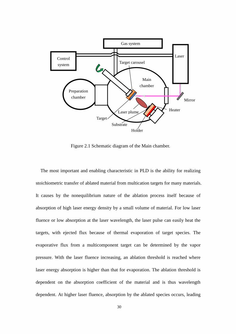
also be used to grow semiconductor thin film for scientific research. Figure 2.1 shows
the schematic diagram of the main chamber.
Several features make PLD particularly attractive for growing complex material
films, such as generation of energetic species, stoichiometric transfer of material from
the target, compatibility with background pressures ranging from ultrahigh vacuum
(UHV) to 1 Torr, and hyperthermal reaction between the ablated cations and the
background gas in the ablation plasma. Films can be deposited with PLD using single,
stoichiometric targets of the material of interest, or with multiple targets for different
elements.
30
Figure 2.1 Schematic diagram of the Main chamber.
The most important and enabling characteristic in PLD is the ability for realizing
stoichiometric transfer of ablated material from multication targets for many materials.
It causes by the nonequilibrium nature of the ablation process itself because of
absorption of high laser energy density by a small volume of material. For low laser
fluence or low absorption at the laser wavelength, the laser pulse can easily heat the
targets, with ejected flux because of thermal evaporation of target species. The
evaporative flux from a multicomponent target can be determined by the vapor
pressure. With the laser fluence increasing, an ablation threshold is reached where
laser energy absorption is higher than that for evaporation. The ablation threshold is
dependent on the absorption coefficient of the material and is thus wavelength
dependent. At higher laser fluence, absorption by the ablated species occurs, leading
Target
Substrate
Holder
Target carousel
Laser plume Heater
Main
chamber
Preparation
chamber
Control
system
Gas system
Laser
Mirror

31
to the formation of the plasma at the surface of target. With appropriate choice of
ablation wavelength and absorbing target material, high-energy densities are absorbed
by a small volume of material, leading to vaporization that is not dependent on the
vapor pressures of the constituent cations.
In growth process of PLD, a background gas is often introduced which has two
purposes. First, the formation of thin film materials often needs a reactive species as a
component of the flux. The amount of reactant gas required for phase formation will
depend on the thermodynamic stability of the desired phase. Interaction of ablated
species with the background gas often produces molecular species in the ablation
plume. These species facilitate multication phase formation. In addition to actively
participating in the chemistry of film growth, the background gas can also be used to
reduce the kinetic energies of the ablated species. Time-resolved spectroscopy studies
of ablation plume expansion have shown that kinetic energies on the order of several
hundred electron volts can be observed. A background gas can moderate the plume
energies to much less than 1 eV. The vapor formed by laser ablation compresses the
surrounding background gas resulting in the formation of a shock wave. Interaction
with the ambient gas slows the ablation plume expansion.
2.1.2 PLD equipment in our laboratory
Figure 2.2 shows the appearance of the PLD equipment in our laboratory. This PLD
system is composed of control system, laser, main chamber, preparation chamber, and
gases.

32
(1) The control system
The control system of PLD possesses many functions, as shown in figure 2.3. It can
be used to adjust the substrate temperature, to adjust the pressure of main chamber
and preparation chamber. The control system can also be used to control pumps in the
main chamber and preparation chamber. The target carousel is controlled by control
system. Moreover, the substrate temperature is programmable by employing this
system.
Figure 2.2 The appearance of the PLD equipment.
(2) Laser
The KrF laser (248 nm) uses combination of a noble krypton and a reactive fluorine
gas. In an excited state (high energy electron beams or induced by an electrical, with
Control system
Gas
Preparation chamber Main chamber
Laser

33
can make high energy pulses), noble gas krypton can form temporarily bound
molecules with themselves or fluorine. The excited gas can lose energy by the way of
emission or spontaneous, inducing a strongly repulsive ground state molecule that
very quickly dissociates back into two unbound atoms. It causes a population
inversion. The reflection mirrors can adjust the direction of the laser towards the
growth chamber. The laser is focused by using a lens before it enters the chamber.
Figure 2.3 The view of the control panel.
(3) Main chamber
The main chamber is equipped with rotary pump (RP) and turbo molecular pump
(TMP) for evacuation. The pressure for the deposition is in the range from 10-6
Pa to
10 Pa. Targets can revolve around the center of target rotation system and can also
spin. In the growth process, one target is exposed and faced to the laser and the

34
substrate. The others are shield. The heater which is made from pyrolytic boron
nitride (PBN) resistance is used to heat the samples. The temperature range can be
adjusted from room temperature to 1200 ℃. It has many advantages such as: low
thermal mass, tailored thermal gradients for specific requirements and ultra-fast
response, unaffected by vibration, thermally shock resistant, mechanically durable,
high resistance for low cost power supplies, dimensionally and electrically stable,
long life, liquids, chemically inert to most corrosive gases, and superior performance
in ultra-high vacuum. The substrate can be heated by a surface contacted substrate
holder that is on the heater.
(4) Preparation chamber
The preparation chamber is also equipped with RP and TMP for evacuation. Before
the substrate is changed, the preparation chamber need be leaked with nitrogen. In
order to keep the main chamber in vacuum when the load chamber is leaked, there is a
valve between the preparation chamber and main chamber.
(5) Gas adjusting system
High purity nitrogen and oxygen are used to adjust the pressure of chambers during
the film growth. The purity nitrogen is used for the leak of the preparation chamber
and main chamber. The hafnium, neon, and krypton and helium are used for laser.
2.2 Characterization method
2.2.1 X-ray diffraction
XRD can provide information on unit cell dimensions. It is a rapid non-destructive
35
technique that primarily used for obtaining the structural information of the material.
The chemical composition, the crystallographic structure, and physical properties can
be studied by observing the intensity of an X-ray beam hitting a sample as a function
of incident angle. PANalytical X’Pert Materials Research XRD system was used for
XRD measurement. This system can be used to investigate the structure of thin film,
nanomaterials, and advanced semiconductors. A wide variety of X-ray scattering
methods, such as nonambient analysis, stress, grazing incidence small angle X-ray
scattering, wafer mapping, thin film phase analysis, and high resolution diffraction,
can be carried out in this system. Compared the XRD diffractogram with the
international center for diffraction data base, identification of the patterns can be
achieved. Moreover, the crystalline quality can be evaluated by X-ray rocking curve.
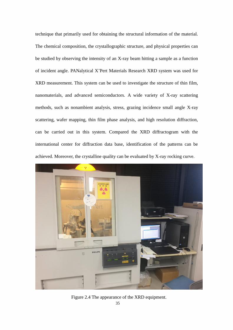
Figure 2.4 The appearance of the XRD equipment.
36
2.2.2 Atomic Force Microscopy
A multi-mode scanning probe microscope (MM-SPM) was used in my work.
MM-SPM can be used to be measured small samples by employing a series of
interchangeable scanners and can provide images from the atomic scale to the size of
about 175 μm. A triangular probe is employed to scan the surface of the sample by
measuring forces between the surface and the probe at a very short distance during the
measuring process of AFM.
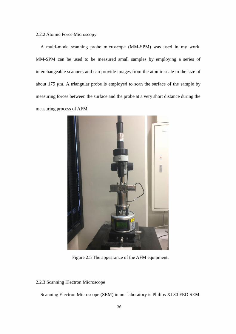
Figure 2.5 The appearance of the AFM equipment.
2.2.3 Scanning Electron Microscope
Scanning Electron Microscope (SEM) in our laboratory is Philips XL30 FED SEM.

37
It can be used to obtain the morphological information of materials. SEM with built-in
energy-dispersive X-ray spectroscopy (EDS) analysis capability can be used to
measure the component of samples. A field emission high resolution scanning electron
microscope which can be carried out both at high acceleration voltage of 30 kV and
low acceleration voltage of 200 V. The cathodoluminescence (CL) spectra can also be
measured in SEM system by using an Oxford instrument monocle system.
Figure 2.6 The appearance of the SEM equipment.
2.2.4 Spectrophotometer
A Jasco V-570 spectrophotometer is used to measure the transmittance of films in
our laboratory. This system has a double beam system with single monochromatic.
The measured wavelength is in the range from 190 to 2500 nm with a wavelength

38
accuracy of 1.5 nm.
Figure 2.7 The appearance of the spectrophotometer equipment.
2.2.5 Raman devices
The Raman spectra were recorded in the back-scattering geometry of the z (x, -) ͞z
configuration by using a Horiba Jobin Yvon LabRAM HR 800 system equipped with
an Andor DU420 classic charge-coupled device detector. The 488 nm line of Ar laser
was used to excite the samples. The employment of a 50 × optical microscopy
objective with a numerical aperture of 0.5 will yield a laser spot size of ~0.8 μm. A
MicrostatHE
hot/cold stage (Oxford instruments) with a quartz window was used to
heat the samples from 77 K to 300 K under flowing nitrogen. The temperature was
controlled by a K-type thermocouple which has an accuracy of better than ± 1 K. For

39
each measurement point, the temperature was kept for 10 min to avoid temperature
fluctuations before acquiring a spectrum for 15 min.
Figure 2.8 The appearance of Raman spectrometer.
Figure 2.9 The photo taken in temperature-dependent Raman measurement
40
Chapter 3
Growth and characterization of MgZnO films
3.1 Mg content influence
ZnO is an II-VI wide bandgap (3.37 eV) semiconductor with a large exciton
binding energy of 60 meV. It is expected that alloying ZnO with MgO can tune the
bandgap from 3.37 eV to 7.8 eV.1, 2
Therefore, MgZnO alloy material has received
much attention due to their potential applications in the short-wavelength
optoelectronic devices such as light-emitting diodes (LEDs) and laser diodes. 3-6
Since the ionic radius of Mg2+
(0. 057 nm) is similar to that of Zn2+
(0.060 nm),
there can be some replacement in either structure without changing the original
structure when alloying.7 However, there is large crystal structure dissimilarity
between wurtzite hexagonal ZnO and rock-salt-cubic MgO, which leads to unstable
phase mixing. In the phase diagram of the ZnO-MgO binary system, the
thermodynamic solubility limit of MgO in ZnO is only 4 at. % and MgO allows a
maximum of 56 at. % ZnO solubility at 1600 ℃.8 Vashaei et al.
9 have tried to use
plasma-assisted molecular-beam epitaxy (MBE) for growing MgZnO films over a
wide Mg composition range from 0 to 0.97 and have found that phase separation
occurs in MgZnO films with Mg content from 0.34 to 0.65. Similar results have been
reported for the MgZnO films obtained by sputtering growth technique.10, 11
Pulsed
laser deposition (PLD) is an effective growth method for fabricating such metastable
phase films due to the relative high kinetic energies that the ablated species have.12-14,

41
Using this method, Ohtomo et al. have succeeded in growing single phase wurtzite
MgZnO films with Mg content up to 0.33.15
In this paper, we report on the successful
growth of single phase MgZnO films without phase separation in all Mg content
range by PLD.
A series of MgZnO films were fabricated by PLD using a KrF laser source (λ = 248
nm) on (0001) sapphire substrates. MgZnO bulks with different Mg content were used
as targets. Before growth, the sapphire substrates were cleaned in organic solvents
ultrasonically, chemically etched in a hot H2SO4:H3PO4 (3:1) solution, then rinsed in
deionized water. The pulsed laser with a frequency of 2 Hz was irradiated and the
distance between targets and substrates was about 30 mm. Pure oxygen gas (99.999%)
was introduced through mass flow controllers after the growth chamber was
evacuated below 5×10⁻⁶
Pa. The oxygen pressure during the growth was maintained
at 1×10⁻¹
Pa while the substrate temperatures were kept at 400 ℃ or 500 ℃. The
deposition time was 40 min for all samples.
The element contents in the prepared MgZnO films were determined by energy
dispersive X-ray spectroscopy (EDS). The thicknesses of the MgZnO films were
measured by using a surface step profile analyzer. The crystal structures of the layers
were examined by conventional θ-2θ XRD using Cu Kα emission line. The optical
transmission spectra were measured with a spectrophotometer at room temperature.
Figure 3.1(a) and (b) show the EDS of MgZnO films grown using various Mg
content in the targets (x) at substrate temperature of 400℃ and 500℃, respectively,
From the spectra, elements of O, Zn, Mg, and Al are observed. The peak related to Al

42
is attributed to the sapphire substrate due to the thickness of the films were smaller
than 600 nm. It is obvious that the intensity ratio of Mg/Zn in the MgZnO films
increases with the increase of Mg content in the targets both for substrate
temperatures of 400 and 500 ℃.
0.5 1.0 1.5 2.0 2.5
xt=1
xt=0.90
xt=0.79
xt=0.10
xt=0
Inte
nsi
ty
arb
. u
nit
s
X-ray energy keV
xt=0.67
xt=0.50
xt=0.33
xt=0.26
xt=0.18
(a)AlMg
Zn
O
0.5 1.0 1.5 2.0 2.5
Inte
nsi
ty
arb
. u
nit
s
X-ray energy keV
xt=0
xt=0.18
xt=0.10
xt=0.26
xt=0.50
xt=0.33
xt=0.67
xt=1
xt=0.90
xt=0.79
O
Zn
Mg
Al (b)
Figure 3.1 EDS of MgZnO films grown at substrate temperatures of (a) 400 ℃ and
(b) 500 ℃ by using MgZnO targets with various Mg content x.
Figure 3.2 presents the dependence of Mg content x in MgZnO films obtained from
the EDS spectra on Mg content in the MgZnO targets. The Mg content in the films
increases almost linearly with the increase of Mg content in the targets, suggesting the
composition of MgZnO films can be controlled by adjusting Mg content in the targets.
From Fig. 3.13, it is clear that the Mg content in the MgZnO films grown at substrate
temperature of 400℃ is smaller than that of MgZnO films grown at substrate
temperature of 500℃ for same Mg content in the MgZnO targets, indicating that

43
substrate temperature is also an important parameter to affect the composition of
MgZnO films in the PLD process.
0.0 0.2 0.4 0.6 0.8 1.0
0.0
0.2
0.4
0.6
0.8
1.0
Mg content in the targets
Mg
co
nte
nt in
th
e film
s
400 C
500 C
Figure 3.2 Dependence of the Mg content in the MgZnO films grown at the substrate
temperatures of 400 ℃ and 500 ℃ on the Mg content in the MgZnO targets.
Choopun et al.16
have fabricated MgZnO films onto c-plane sapphire by PLD. The
Mg content is range from 0.5 to 1 by controlling the substrate temperature from room
temperature to 750 ℃ using one MgZnO target with Mg content of 0.5. This
phenomenon can be explained by the difference of vapor pressure between Mg and Zn
species. Zn species have a higher vapor pressure and can be desorbed more easily
than that of Mg species at same growth temperature which results in the more Mg
enriched films at high growth temperatures. In order to verify this phenomenon, we
investigated the growth rate of MgZnO films at the substrate temperature 400 ℃ and
500 ℃ as shown in figure 3.3. The growth rate of the MgZnO films grown at the

44
substrate temperature 500 ℃ is clearly lower than that at 400 ℃ for a given
MgZnO target in the low Mg content region due to the Zn desorption. However, the
growth rates for both of substrate temperature 400 ℃ and 500 ℃ are almost same
in the high Mg content region. The results are consistent with that reported by
Choopun et al.16
.
0.0 0.2 0.4 0.6 0.8 1.00
2
4
6
8
10
12
14
Mg content in the films
Gro
wth
ra
te (
nm
/min
)
400C
500C
Figure 3.3 Dependence of the growth rate of MgZnO films grown at the substrate
temperatures of 400 ℃ and 500 ℃ on the Mg content in the MgZnO targets.
Figure 3.4(a) shows the XRD patterns of MgZnO films deposited on (0001)
sapphire substrates at substrate temperature of 400 ℃. When the Mg content in the
target is lower than 0.26, the (0002) diffraction peaks of MgZnO films are observed
together with the peak of (0006) reflection from sapphire substrate. None of the (100),
(101) and (102) peaks of MgZnO film can be detected within the searched angle
(30 °≤ 2θ ≤ 80 °), indicating that the grown MgZnO films are highly c-axis oriented
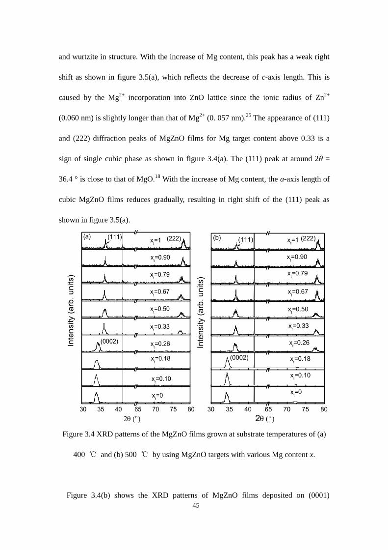
45
and wurtzite in structure. With the increase of Mg content, this peak has a weak right
shift as shown in figure 3.5(a), which reflects the decrease of c-axis length. This is
caused by the Mg2+
incorporation into ZnO lattice since the ionic radius of Zn2+
(0.060 nm) is slightly longer than that of Mg2+
(0. 057 nm).25
The appearance of (111)
and (222) diffraction peaks of MgZnO films for Mg target content above 0.33 is a
sign of single cubic phase as shown in figure 3.4(a). The (111) peak at around 2θ =
36.4 ° is close to that of MgO.18
With the increase of Mg content, the a-axis length of
cubic MgZnO films reduces gradually, resulting in right shift of the (111) peak as
shown in figure 3.5(a).
30 35 40 65 70 75 80
(111)
xt=0
Inte
nsity (
arb
. u
nits)
(222)
(0002)
xt=0.10
xt=0.18
xt=0.26
xt=0.33
xt=0.50
xt=0.67
xt=0.90
xt=0.79
xt=1
(a)
30 35 40 65 70 75 80
xt=0
2
Inte
nsity (
arb
. u
nits)
xt=0.10
(0002) xt=0.18
xt=0.26
xt=0.33
xt=0.50
xt=0.67
xt=0.79
xt=0.90
(222)(111) xt=1
(b)
Figure 3.4 XRD patterns of the MgZnO films grown at substrate temperatures of (a)
400 ℃ and (b) 500 ℃ by using MgZnO targets with various Mg content x.
Figure 3.4(b) shows the XRD patterns of MgZnO films deposited on (0001)
46
sapphire substrates at substrate temperature of 500 ℃. It has the similar tendency
with figure 3.4(a). However, it is clear that when the Mg target content is 0.26, the
MgZnO films grown at 500 ℃ has cubic structure while the MgZnO films grown at
400 ℃ is of hexagonal structure. This difference is due to the different Mg content in
the MgZnO films (0.42 for 500 ℃ and 0.39 for 400 ℃) as shown in figure 3.2.
Based to figure 3.2 and 3.4, it is obvious that the phase transformation from
hexagonal wurtzite to cubic structure occurs in the Mg content between 0.39 and 0.42.
According to the phase diagram of the MgZnO alloy system, the MgZnO films can
keep stable hexagonal phase in a solid solution state when the Mg content is in the
range 0 ≤ x ≤ 0.04 and the cubic phase has the Mg content range of 0.56 ≤ x ≤ 1.
When the Mg content x is outside these two ranges, a mixed phase is observed.19
However, it is known that the solid solubility can be significantly modified in films
form, and it is also influenced by the growth conditions. For example, Ohtomo et al.15
have demonstrated that the MgZnO films which have a single hexagonal phase can be
prepared by PLD with the Mg content up to 0.33 at a temperature of 600 ℃. Using
the same technique Yang et al.20
reported the single hexagonal phase is in the Mg
content range of 0-0.34 at substrate temperature of 750 ℃. Takeuchi et al.21
have
fabricated MgZnO films by PLD at substrate temperature of 600 ℃ and found the
phase separation region of the phase diagram in the range of 0.37 ≤ x ≤ 0.6. In our
work, the lower substrate temperatures (400 and 500 ℃) lead kinetics instead of
thermodynamics dominate the growth process. Thus most radicals do not have enough
energy to reach their energy-minimum sites,22
which results in the almost no phase

47
separation observed in our MgZnO films.
30 32 34 36 38 40
xt=0
Inte
nsity (
arb
. u
nits)
2
(111)
(0002)
xt=0.10
xt=0.18
xt=0.26
xt=0.33
xt=0.50
xt=0.67
xt=0.90
xt=0.79
xt=1
(a)
30 32 34 36 38 40
xt=0
2
Inte
nsity (
arb
. u
nits)
x
t=0.10
(0002) xt=0.18
xt=0.26
xt=0.33
xt=0.50
xt=0.67
xt=0.79
xt=0.90
(111)xt=1
(b)
Figure 3.5 Enlarged XRD patterns of the single MgZnO films grown at substrate
temperatures of (a) 400 ℃ and (b) 500 ℃.
The transmittance spectra of typical MgZnO films are obtained as shown in figure
3.6. The transmittances of the MgZnO films in all Mg content range are above 80% in
the wavelength range from 400 to 1000 nm. The absorption edges of the MgZnO
films have a shift to short wavelength direction with the increase of Mg content.
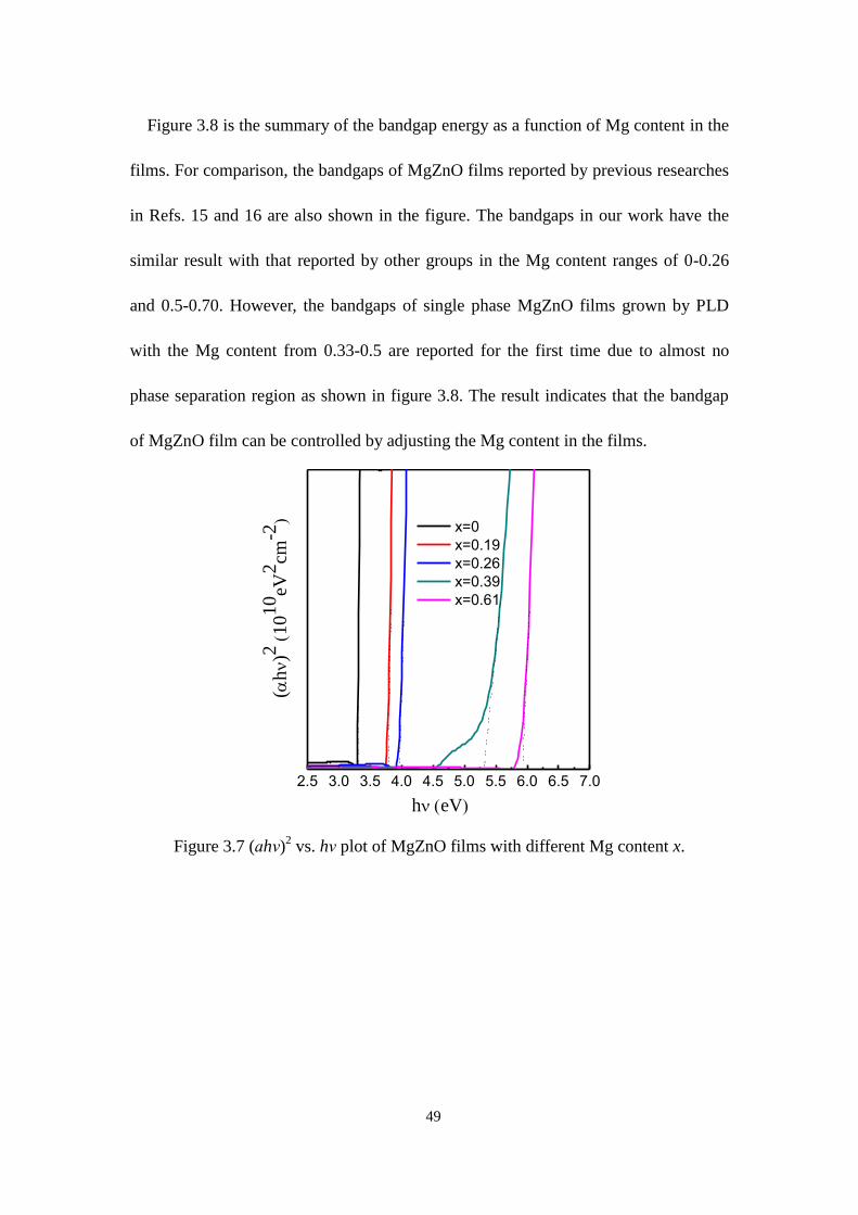
It is well known that for layers with direct bandgap, the absorption follows a power
law of the form:
(αhν) = A(hν-Eg)1/2
Where hν is the energy of the incident photon, α is the absorption coefficient, A is the
absorption edge width parameter, and Eg is the bandgap. The optical absorption

48
coefficient α of the layers is evaluated using the standard relation taking the film
thickness into account. The plot of (αhν)2 as a function of photon energy is shown in
figure 3.7. The absorption coefficient increases rapidly at the photon energy range
around 3.31-5.9 eV depending on the Mg content x, and (αhν)2
as a function of hν fits
the straight line quite well, indicating that the obtained MgZnO films are of direct
transition. The bandgap value about 3.31eV with Mg content x = 0 agrees with that of
bulk ZnO.15
200 400 600 800 10000
20
40
60
80
100
x=1x=0.89x=0.61x=0.39x=0.26x=0.19x=0
Wavelength (nm)
Tra
nsm
itta
nce
Figure 3.6 Transmittance spectra of typical MgZnO films with Mg content x in the
films.
49
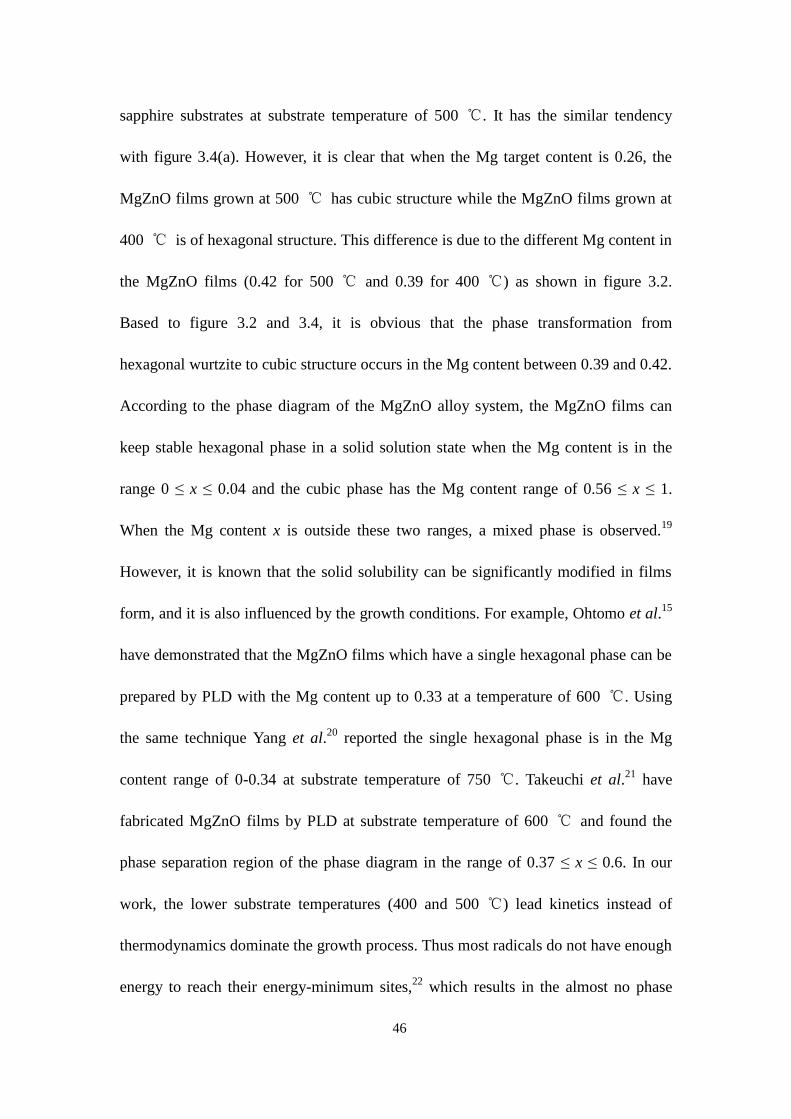
Figure 3.8 is the summary of the bandgap energy as a function of Mg content in the
films. For comparison, the bandgaps of MgZnO films reported by previous researches
in Refs. 15 and 16 are also shown in the figure. The bandgaps in our work have the
similar result with that reported by other groups in the Mg content ranges of 0-0.26
and 0.5-0.70. However, the bandgaps of single phase MgZnO films grown by PLD
with the Mg content from 0.33-0.5 are reported for the first time due to almost no
phase separation region as shown in figure 3.8. The result indicates that the bandgap
of MgZnO film can be controlled by adjusting the Mg content in the films.
2.5 3.0 3.5 4.0 4.5 5.0 5.5 6.0 6.5 7.0
heV
(h)2
1
01
0eV
2cm
-2
x=0
x=0.19
x=0.26
x=0.39
x=0.61
Figure 3.7 (ɑhν)2 vs. hν plot of MgZnO films with different Mg content x.

50
0.0 0.2 0.4 0.6 0.8 1.03.0
3.5
4.0
4.5
5.0
5.5
6.0
6.5
Mg content x in the films
Ba
nd
ga
p (
eV
)
This work
Ref. 15
Ref. 16
Figure 3.8 Dependence of the bandgap of MgZnO on Mg content x in the films.
3.2 Substrate temperature influence
MgZnO films were prepared by PLD using a KrF laser source (λ=248nm) on c-plane
sapphire substrates. Before the deposition, the sapphire substrates were cleaned in
carbinol solution and acetone solution by an ultrasonic cleaning system, and then
chemically etched in a hot H3PO4: H2SO4 (1:3) solution. In the growth chamber, facing
the substrate the MgxZn1-xO alloys target was set. The Mg composition in the target was
0.5. The pulsed laser with a frequency of 2 Hz was irradiated and the distance between
target and substrate was about 30 mm. The laser energy was set 190 mJ. The oxygen
pressure of the growth chamber was 1×10⁻¹
Pa by introducing high purity oxygen gas
(99.999%). In the deposition, the substrate temperature was varied from room
temperature (RT) to 500 ℃. The deposition time was 40 min for all the layers.
The composition of MgZnO films were determined by energy dispersive EDS. The

51
thickness of the films was measured by using a surface step profile analyzer. The
structural properties of the films were examined by conventional θ-2θ XRD. The
optical transmission spectra were measured with a spectrophotometer. The surface
morphology and roughness were studied by atomic force microscope (AFM).
Figure 3.9 shows the EDS of MgZnO films which were grown on c-plane sapphire
substrates at different substrate temperatures. In the spectra the elements of oxygen,
zinc, magnesium and aluminum have been observed. When the substrate temperature
was below 200 ℃, the Mg content in the MgZnO films were almost same. And it was
obvious that the Mg content increased with the increase of substrate temperature when
the substrate temperature was higher than 300 ℃. Figure 3.10 shows the dependence
of Mg content in the MgxZn1-xO films on the substrate temperature. At the low substrate
temperature, the Mg content in the MgxZn1-xO films was equal to that in the target. The
rise started from 300 ℃.The Mg content in the film was linear growth with the
increase of the substrate temperature by a slope factor of 0.00063. The content variation
between film and target can be owing to the difference of vapor pressure between Zn
and Mg species at higher substrate temperatures. Zn-related species have a higher vapor
pressure and are easily desorbed at higher substrate temperatures. It leads to Mg
enrichment on the substrates.

52
0.4 0.8 1.2 1.6 2.0
RT
100C
200C
300C
400C
500CO AlMgZn
X-ray energy keV
Inte
nsi
ty
arb
. u
nit
s
Figure 3.9 EDS of MgZnO films grown at different substrate temperatures.
0 100 200 300 400 5000.45
0.50
0.55
0.60
0.65
0.70
0.75
Mg c
on
tent in
the
film
s
Substrate temperture C
Figure 3.10 Dependence of the Mg content in MgZnO films grown at different
substrate temperatures on the Mg content in the MgZnO targets.
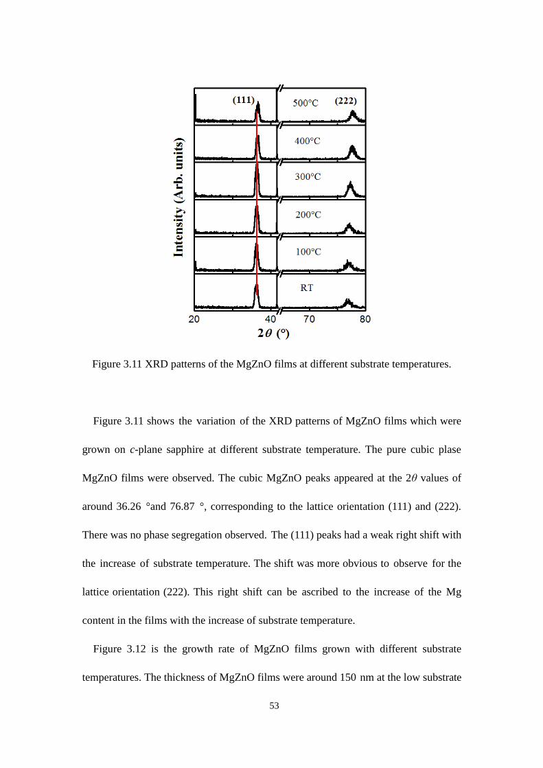
53
Figure 3.11 XRD patterns of the MgZnO films at different substrate temperatures.
Figure 3.11 shows the variation of the XRD patterns of MgZnO films which were
grown on c-plane sapphire at different substrate temperature. The pure cubic plase
MgZnO films were observed. The cubic MgZnO peaks appeared at the 2θ values of
around 36.26 °and 76.87 °, corresponding to the lattice orientation (111) and (222).
There was no phase segregation observed. The (111) peaks had a weak right shift with
the increase of substrate temperature. The shift was more obvious to observe for the
lattice orientation (222). This right shift can be ascribed to the increase of the Mg
content in the films with the increase of substrate temperature.
Figure 3.12 is the growth rate of MgZnO films grown with different substrate
temperatures. The thickness of MgZnO films were around 150 nm at the low substrate

54
temperatures. The growth rate was about 3.7 nm/min. And the thickness started to
reduce from 300℃ with a growth rate of 3.15 nm/min. While the substrate temperature
was above 400℃, the thickness was about 105 nm and the growth rate was about 2.63
nm/min. The decline of the thickness was attributed to the release of the Zn at the high
substrate temperature.
0 100 200 300 400 500
2.6
2.8
3.0
3.2
3.4
3.6
3.8
Gro
wth
rate
(nm
/min
)
Substrate temperature (C)
Figure 3.12 Growth rates of MgZnO films grown with different substrate temperatures
Figure 3.13 is the AFM morphologies of the cubic MgZnO films grown at different
substrate temperatures. The surface of MgxZn1-xO films were smooth at the substrate
temperature below 200 ℃. The crystal islands were observed with the temperature
increasing to 300 ℃. The diameter of the crystal islands grew with increasing the
substrate temperature.
Figure 3.14 is the roughness of MgZnO films prepared at different substrate

55
temperatures. The roughness of MgZnO films increases almost linearly with the
increase of the substrate temperature above 100 ℃, and it was in the range from 0.3 to
0.65 nm with different substrate temperatures.
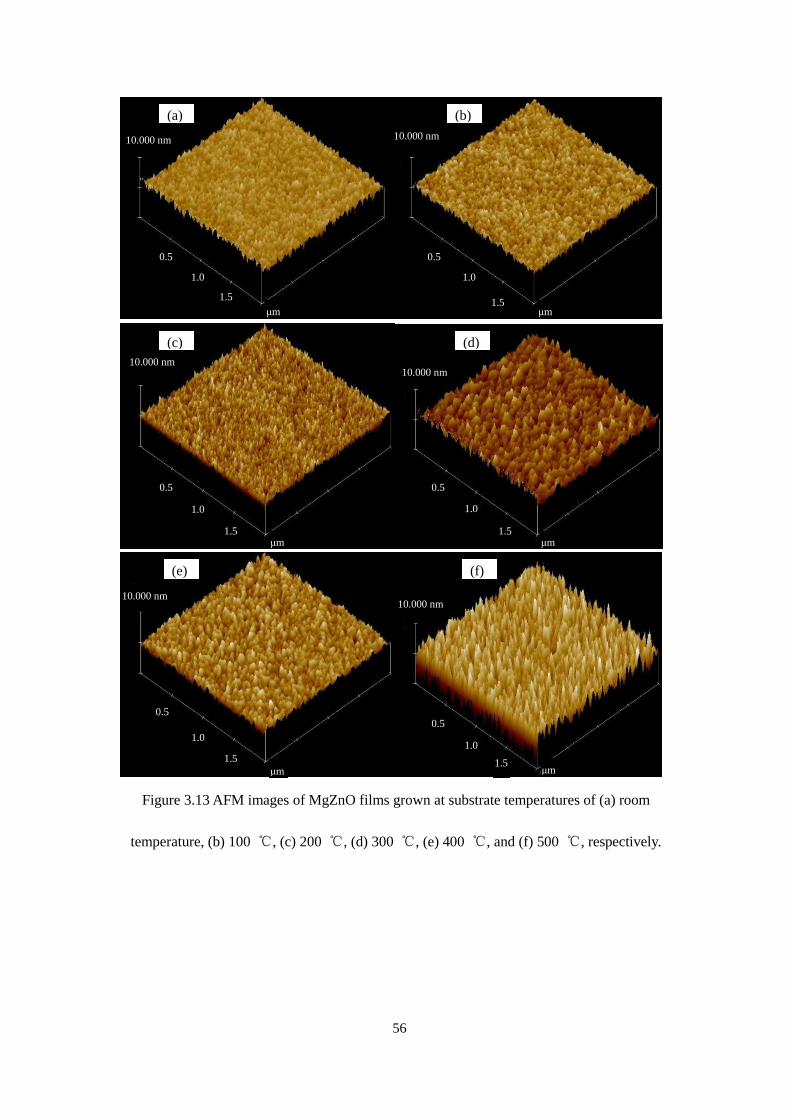
56
Figure 3.13 AFM images of MgZnO films grown at substrate temperatures of (a) room
temperature, (b) 100 ℃, (c) 200 ℃, (d) 300 ℃, (e) 400 ℃, and (f) 500 ℃, respectively.
(a) (b)
(c) (d)
(e) (f)
10.000 nm
0.5
1.0
1.5
μm
10.000 nm
0.5
1.0
1.5 μm
10.000 nm
0.5
1.0
1.5 μm
10.000 nm
0.5
1.0
1.5 μm
μm
1.5
1.0
0.5
10.000 nm
10.000 nm
0.5
1.0
1.5 μm
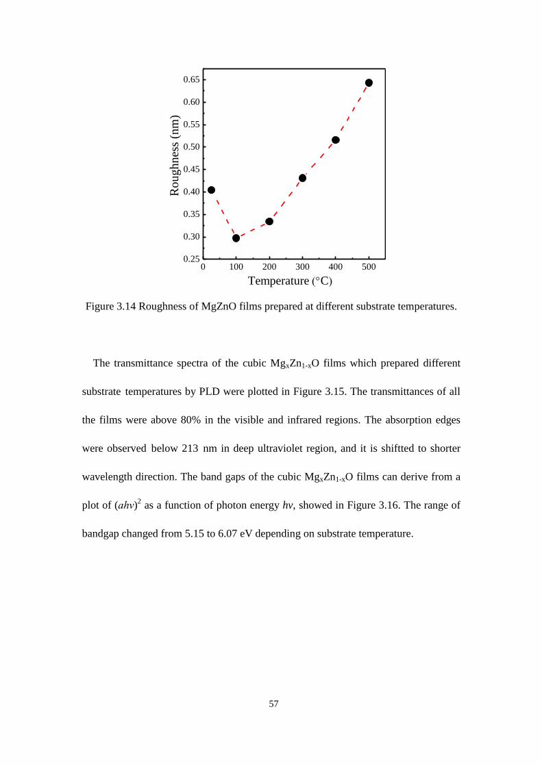
57
0 100 200 300 400 5000.25
0.30
0.35
0.40
0.45
0.50
0.55
0.60
0.65
Ro
ug
hn
ess
(nm
)
Temperature C
Figure 3.14 Roughness of MgZnO films prepared at different substrate temperatures.
The transmittance spectra of the cubic MgxZn1-xO films which prepared different
substrate temperatures by PLD were plotted in Figure 3.15. The transmittances of all
the films were above 80% in the visible and infrared regions. The absorption edges
were observed below 213 nm in deep ultraviolet region, and it is shiftted to shorter
wavelength direction. The band gaps of the cubic MgxZn1-xO films can derive from a
plot of (ɑhv)2 as a function of photon energy hv, showed in Figure 3.16. The range of
bandgap changed from 5.15 to 6.07 eV depending on substrate temperature.

58
200 400 600 800 10000
20
40
60
80
100
RT
100C
200C
300C
400C
500C
Tra
nsm
itta
nce
%
Wavelengh nm
Figure 3.15 Transmittance spectra of MgZnO films grown at different substrate temperatures.
2 3 4 5 6
RT
100C
200C
300C
400C
500C
(h)2
1
01
0eV
2cm
-2
heV
Figure 3.16 (ɑhν)2 vs. hν plot of MgZnO films grown with different substrate temperatures.

59
3.3 Oxygen pressure influence
MgZnO films were prepared by PLD using a KrF laser source (λ=248nm) on c-plane
sapphire substrates. Before the deposition, the sapphire substrates were cleaned in
carbinol solution and acetone solution by an ultrasonic cleaning system, and then
chemically etched in a hot H3PO4: H2SO4 (1:3) solution. In the growth chamber, facing
the substrate the MgxZn1-xO alloys target was set. The Mg content in the target was
0.5. The pulsed laser with a frequency of 2 Hz was irradiated and the distance between
target and substrate was about 30 mm. The laser energy was set 190 mJ. The oxygen
pressure of the growth chamber was from 10-4
to10-1
Pa by introducing high purity
oxygen gas (99.999%). In the deposition, the substrate temperature was 400 ℃. The
deposition was 40 min for all the layers.
The structural properties of the films were examined by conventional θ-2θ XRD.
The optical transmission spectra were measured with a spectrophotometer.
Figure 3.17 shows the XRD patterns of MgZnO films deposited on (0001) sapphire
substrates at different oxygen pressures. The (111) diffraction peaks of MgZnO films
are observed together with the peak of (0006) reflection from sapphire substrate.
None of the (100), (101) and (102) peaks of MgZnO film can be detected within the
searched angle (30 °≤ 2θ ≤ 80 °), indicating that the grown MgZnO films are highly
c-axis oriented and wurtzite in structure. The (111) diffraction peaks have no obvious
shift with the increase of oxygen pressure, which indicates that oxygen pressure in the
range from 10-4
to10-1
Pa has a minimal effect on the structure of MgZnO films.

60
30 40 50 60 70 80
10-1
Pa
Inte
nsity (
arb
.un
its)
2 ()
10-2 Pa
10-3
Pa
10-4
Pa
Mg
Zn
O(2
22
)
Mg
Zn
O(1
11
)
Figure 3.17 XRD patterns of the MgZnO films grown on the c-plane sapphire at
different oxygen pressures.
The transmittance spectra of MgZnO films prepared at different oxygen pressures
were plotted in Figure 3.18. The transmittances of all the layers were above 80% in the
visible and infrared regions. The absorption edges were observed in deep ultraviolet
region, and it has a small shift with the increase of oxygen pressure. The band gaps of
MgZnO films at different oxygen pressures can derive from a plot of (ɑhv)2 as a
function of photon energy hv, as shown in Figure 3.19. The bandgap energy of MgZnO
films increases from 5.63 to 5.88 eV with the decrease of the oxygen pressure.
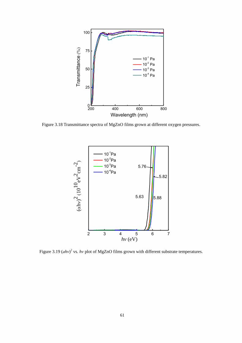
61
200 400 600 8000
25
50
75
100
Tra
nsm
itta
nce
Wavelength (nm)
10-1 Pa
10-2 Pa
10-3 Pa
10-4 Pa
Figure 3.18 Transmittance spectra of MgZnO films grown at different oxygen pressures.
2 3 4 5 6 7
(h)2
1
01
0eV
2cm
-2
hv (eV)
5.63
5.76
5.82
5.88
10-1Pa
10-2Pa
10-3Pa
10-4Pa
Figure 3.19 (ɑhν)2 vs. hν plot of MgZnO films grown with different substrate temperatures.
62
3.4 Conclusion
In this chapter, we have reported the Mg content, substrate temperature, and oxygen
pressure on the structure and optical properties of MgZnO films grown by PLD. The
following conclusions were summarized.
(1) The growth of crystalline MgZnO films on sapphire (0001) substrate by PLD
has been shown. The Mg content x can be controlled by changing target Mg content
and substrate temperature. Single phase MgZnO films are obtained in all Mg content
range. The phase transformation from hexagonal to cubic phase is determined at the
Mg content around 0.4. Optical analysis indicates that the bandgaps of MgZnO films
can be tailored by controlling the Mg content in the films.
(2) The XRD patterns illustrated that the cubic phase (111) and (222) peaks appeared
at the 2θ values of about 36.26°and 76.87°, and the MgxZn1-xO film with good crystal
quality can be obtained at a substrate temperature of 400℃. The bandgaps of the pure
cubic MgxZn1-xO layers were increased from 5.15 to 6.07eV with increasing the
substrate temperature. Moreover, the roughness of the cubic MgxZn1-xO films was
negligible.
(3) The (111) diffraction peaks have no obvious shift with the increase of oxygen
pressure, which indicates that oxygen pressure in the range from 10-4
to10-1
Pa has a
minimal effect on the structure of MgZnO films. The bandgap energy of MgZnO films
increases from 5.63 to 5.88 eV with the decrease of the oxygen pressure.

63
Reference
[1] A.K. Sharma, J.Narayan, J.F. Muth, C.W. Teng, C.Jin, A. Kvit, R.M. Kolbas, and
O.W. Holland, Appl, Phys. Lett., 75, 3327 (1999).
[2] J.W. Kim, H.S. Kang, J.H. Kim, S.Y. Lee, J.K. Lee, and M. Nastasi, J. Appl. Phys.,
100, 033701 (2006).
[3] T. Makino, A. Obhtomo, C.H. Chia, Y. Segawa, H. Koinuma, and M. Kawasaki,
Physical E, 216,71 (2004).
[4] A. Ashrafi. Appl, Phys. Lett., 107, 123527 (2010).
[5] M. Stolzel, A. Muller, G. Benndorf, M. Brandt, M. Lorenz, and M. Grundmann,
Phy. Rev. B., 88, 045315 (2013).
[6] H.Y. Chen, K.W. Liu, M.M. Jiang, Z.Z. Zhang, X.H. Xie, D.K. Wang, L. liu, B.H.
Li, D.X. Zhao, C.X. Shan, and D.Z. Shen, Appl. Phys. Lett., 104, 091119 (2014).
[7] A. Ohtomo, M. Kawasaki, I. Ohkubo, Appl. Phys. Lett., 75, 980 (1999).
[8] E.R. Segnit, and A.E. Holland, J. Am. Ceram. Soc., 48, 409 (1965).
[9] Z. Vashaei, T. Minegishi, H. Suzuki, T. Hanada, M. W. Cho, T. Yao, and A.
Setiawan, J. Appl. Phys., 98, 054911 (2005).
[10] D. Thapa, J. Huso, H. Che, M. Huso, J.L. Morrison, D. Gutierrez, M.G. Norton,
and L. Bergman, Appl. Phys. Lett., 102, 191902 (2013).
[11] J. Huso, H. Che, D. Thapa, J.L. Morrison, M.G. Norton, and L. Bergman, Appl.
Phys. Lett., 104, 031908 (2014).
[12] X.Q. Gu, Y. L. Zhao, Y. H. Qiang, Superlattice Microstruct., 61, 168 (2013).
[13] F.B. Zhang, K. Saito, T. Tanaka, M. Nishio, Q.X. Guo, J. Cryst. Growth, 387, 96

64
(2014).
[14] F.B. Zhang, K. Saito, T. Tanaka, M. Nishio, Q.X. Guo, Solid State Commun., 186
28 (2014).
[15] A. Ohtomo, M. Kawasaki, T. Koida, K. Masubuchi, H. koinuma, Y. Sakurai, Y.
Yoshida, T. Yasuda, and Y. Segawa, Appl. Phys. Lett., 72, 2466 (1998).
[16] S. Choopun, R.D. Vispute, W. Yang, R.P. Sharma, T. Venkatesan, and H. Shen,
Appl. Phys. Lett., 80, 1529 (2002).
[17] C.Y. Liu, H.Y. Xu, L. Wang, X.H. Li, and Y.C. Liu, J. Appl. Phys., 106, 073518
(2009).
[18] J.G. Yoon, and K. Kim, Appl. Phys. Lett., 66, 2661 (1995).
[19] E.M. Levin, C.R. Robbins, H.F. McMurdie, M.K. Reser, American Ceramic
Society, Columbus, Ohio, 1964.
[20] W. Yang, R.D. Vispute, S. Choopun, R.P. Sharma, and T. Venkatesan, Appl. Phys.
Lett., 78, 2787 (2001).
[21] I. Takeuchi, W. Yang, K.S. Chang, M.A. Aronova, and T. Venkatesan, J. Appl.
Phys., 94, 7336 (2003).
[22] L.K. Wang, Z.G. Ju, C.X. Shan, D.Z. Shen, B.X. Zhao, Z.Z. Zhang, B.H. Li and
J.Y. Zhang, Solid State Commun., 149, 2021 (2009).

65
Chapter 4
Bandgap engineering of MgZnO films
4.1 Introduction
Ternary semiconducting crystals are interesting because it is possible to smoothly
change many important physical properties by varying their composition.1-4
In
particular, the MgZnO alloy system covers a wide ultraviolet (UV) spectral range
between the direct bandgaps of ~3.37 eV for ZnO and ~7.8 eV for MgO at room
temperature, and is very attractive for short-wavelength optical applications such as
UV detectors and UV light emitters.5, 6
MgZnO alloys with different bandgap energies
can be used to form ZnO/MgZnO or MgZnO/MgO multilayer quantum wells (QWs)
heterostructure in UV light emitting diodes and laser diodes.7, 8
Therefore, in order to
calculate the band alignment for designing and engineering a device, it is important to
investigate the fundamental bandgap of MgZnO epitaxial films in all Mg content
range. Moreover, the determination of bandgap bowing parameter which characterizes
the nonlinear dependence of the fundamental bandgap on the alloy composition is also
needed for the design of optoelectronic devices.9
In recent years, a large number of researches on the relationship between the Mg
content and the bandgap energy were reported.10-13
Ohtomo et al.10
firstly prepared the
MgZnO films with the bandgap energy from 3.3 to 4.0 eV corresponding to Mg
content in the range of 0-0.33. Choopun et al.11
reported the cubic MgZnO films with
the Mg content from 0.5 to 0.7 have bandgap from 4.0 to 6.0 eV. Thapa et al.3 grew

66
the MgZnO films with bandgap energy varying from 3.3 to 6.0 eV in the Mg content
range of 0-0.78. However, there is no experimental data on MgZnO films which has
the bandgap higher than 6.0 eV up to now. As described in Chapter 3, single phase
MgZnO films without phase separation in all Mg content range were prepared by
PLD.12
The largest bandgap of Mg0.69Zn0.31O film was measured as 6.1 eV by
transmittance spectra.12
However, the wavelength range of the spectrometer for this
method is commonly higher than 200 nm, which restrict the measurements for
material with bandgap higher than 6.2 eV. The bandgap of MgZnO film with the Mg
content above 0.70 can’t be evaluated and bandgap bowing parameter can’t be
determined due to incomplete the relationship between the bandgap energy and the
Mg content. Therefore, more valid method of testing the bandgap energy is highly
required.
It is known that X-ray photoelectron spectroscopy (XPS) can be used to analyze
the inelastic collisions in photoexcitation and photoemission of electrons from the
material.14
The inelastic collisions mainly include a fast-moving charged particle in
the bulk material or an electron escaping from material surface can lose energy to
excite another electron from the valence band into the conduction band.15
The
fundamental lower limit of inelastic loss is equal to the bandgap energy. Therefore,
the onset of the inelastic energy loss spectra corresponds directly to the bandgap
energy.16
Based on this method, Ragesh et al.17
demonstrated ZrO2 had a bandgap of
6.4 eV. Their reports indicate the bandgap of semiconductors can be obtained by XPS.
In this work, we report the dependence of the energy bandgap on Mg content in all

67
Mg content range by analyzing the O 1s energy loss spectra obtained from XPS. The
bowing parameter is calculated by the relationship between the bandgap energy and
the Mg content.
4.2 Experiment
A series of MgZnO films were deposited by PLD using a KrF laser source (λ = 248
nm) on (0001) sapphire substrates. The MgZnO bulks with different Mg content were
used as targets. The oxygen pressure during the growth was maintained at 1×10⁻¹
Pa
while the substrate temperatures were kept at 500℃. The deposition time was 40 min
for all samples. XRD revealed that the (0002) diffraction peaks are observed from
MgZnO films together with the peak of (0006) reflection from sapphire substrate in
lower Mg content films, and the appearance of (111) and (222) diffraction peaks in
higher Mg content films is a sign of single cubic phase. 12
The atomic force
microscope results show the maximum roughness of the MgZnO is below 4 nm,
indicating smooth surface. The XPS measurement was performed by Mg Kα X-ray
source. The binding energy of C 1s peak was used as a standard reference. Before
XPS analysis the surface of the MgZnO films was etched by Ar+ ion (3 keV) for 2
min.

68
4.3 Results and discussion
Figure 4.1 (a) shows a representative scan of the O 1s core level spectrum from the
MgO film grown in this work. From figure 4.1 (a), the largest signal corresponds to
the primary photoelectron peak caused by the O 1s core level electrons located at
binding energy 532.2 eV. The bulk plasmon loss peak is observed at 554.9 eV,
corresponding to the bulk plasmon energy 22.7 eV. Moreover, a small overlapping
peak observed at 523.4 eV is attributed to X-ray satellite peaks because of Kα
transitions from the non-monochromatic Mg X-ray source. In order to verify this
method for determining the bandgap energy of MgZnO films by XPS, a XPS scan of
the O 1s core level spectrum from the MgO film has been obtained as shown in figure
4.1 (b). A linear fit is made to the measured loss spectra curve near the approximate
location of onset of inelastic loss.15
And then, the background line which is parallel to
horizontal axis can be determined by subtracting the background fitting. The initial
energy of inelastic loss is obtained by extrapolating the linear-fit line and calculating
its intersection with the “zero” level line. The bandgap energy of MgO film is equal to
the difference between the O 1s core level peak energy and the initial energy of
inelastic losses. Thus, the bandgap energy is calculated to be 7.3 eV which has good
agreement with the previous values for MgO3,18
, indicating that the XPS is a valid
way to determine the bandgap of MgZnO films.

69
Figure 4.1 Measurement of the bandgap of MgO film by onset of electron energy loss
spectra. (a), XPS scan of the O 1s core level for MgO film (b).
Figure 4.2 (a) and (b) show the XPS spectra of Mg 2p and Zn 2p core levels for
MgZnO films grown with different Mg content xt in the target. As shown in figure
4.2(a), the Mg 2p peaks of MgZnO films with different Mg content xt exhibit a nearly
Gaussian line shape, indicating a single chemical state of Mg element. The Mg 2p
peaks are located at 50.2 eV which is attributed to Mg-O bonding and the intensity of
Mg 2p peak increases with the increase of Mg content xt. The Zn 2p core-level of ZnO
film (xt = 0) has two peaks at about 1021.9 and 1044.2 eV assigned to Zn 2p3/2 and Zn
2p1/2, respectively. The intensity of Zn 2p peaks decreases with the increase of Mg

70
content xt.
Figure 4.2 Mg 2p (a) and Zn 2p (b) core level spectra of MgZnO films with different
Mg contents in targets xt.
The Mg contents in the MgZnO films are determined from the XPS peak area after
using an atomic sensitivity factor, which convert relative peak areas to relative
numbers of atoms in the detected volume.20
The Mg contents in the MgZnO films
obtained from the XPS spectra is shown in figure 4.3 as a function of Mg content in
the target xt. The element content in the film is larger than that in the target. This
phenomenon can be explained by the difference of vapor pressure between Mg and
Zn species. Zn species have a higher vapor pressure and can be desorbed more easily

71
than that of Mg species at same growth temperature which results in the more Mg
enriched films at high growth temperatures. These content results from the XPS
spectra are agreed with those from Energy Dispersive Spectrometer (EDS) which
have been reported in the Chapter 3. It is well known that XPS is primarily a surface
technique. The analyzed depth is about 2 nm and the area of analysis is an ellipse on
the surface.21
Compared with XPS, the analysis depth of EDS is much deeper and the
analyzed volume is shaped like a Florence flask with the narrow neck shortened due
to subsurface scattering.21
Therefore, the same Mg content results from two methods
indicate the samples measured in this work have very uniform composition
distribution in the MgZnO films.
Figure 4.3 The Mg content in the films obtained by XPS.

72
Figure 4.4 The O 1s peak and inelastic scattering loss for MgZnO films in all Mg
content.
Figure 4.4 shows the O 1s core level peaks of MgZnO films with various Mg
contents in the MgZnO films. The bandgap energies of MgZnO films with Mg content
of 0.21, 0.26, 0.39, 0.51 and 0.59 are determined to be 3.8, 4.2, 5.2, 5.8 and 6.0 eV,

73
respectively. These values show good agreement with those measured from
transmittance spectra in Chapter 3 as shown in figure 4.5. The O 1s core level peaks
of MgZnO films in the Mg content range from 0.68 to 1 are also shown in figure 4.4
corresponding to the bandgaps from 6.3 to 7.3 eV which have been plotted in figure
4.5 together with the experimental data from transmittance spectra.
0.0 0.2 0.4 0.6 0.8 1.03
4
5
6
7
Ba
nd
ga
p (
eV
)
wurtzite MgZnO
Mg content in the films
This work (XPS)
Chapter 3
Fitting curves
Ref. 22
Ref. 25
cubic MgZnO
Figure 4.5 Dependence of the bandgap of MgZnO films on Mg content x in the films.
In order to describe the compositional dependence of bandgap of the MgZnO alloys,
we used the standard bowing equation,
Eg (MgxZn1-xO) = (1–x) · Eg (ZnO) + x · Eg (MgO) – b · x · (1–x) (1)
Here, Eg (ZnO), Eg (MgO) and Eg (MgxZn1-xO) are the energy bandgaps of ZnO, MgO
and MgZnO films. b is a band bowing parameter which characterizes the degree of
deviation from linearity. As shown in figure 4.5, the relationship between the bandgap
energy and the Mg content in all Mg content range can be fitted by quadratic function
74
as two red solid lines corresponding to different crystal structures.
According to figure 4.5, the lower red solid line fitted to the bandgaps of wurtzite
MgZnO films shows a quadratic form:
Eg (wurtzite MgxZn1-xO) = 3.31 · (1 – x) + 7.41· x – 2.01 · x (1 – x) (2)
Based on Eq. (2), the bandgap of wurtzite MgO is calculated to be 7.41 eV which
agrees well with the value of 7.5 eV predicted by Jang et al.22
using ab initio
calculations as shown in figure 4.5. According to the analysis of fitting curve, the
obtained bowing parameter b of (2.01 ± 0.02) eV is very close to that of 2.84 eV from
the calculations of Schleife et al.18
The band bowing occurs due to volume
deformation, spontaneous polarization, structural relaxation and alloy mismatch. In
wurtzite MgZnO alloys, the bandgap bowing is mainly attributed to spontaneous
polarization. Because the wurtzite MgZnO alloy is a polar material exhibiting a
spontaneous polarization along the c-axis, increasing with Mg content. The internal
field caused by piezoelectric and spontaneous polarizations, which presents along the
growth axis of the system, makes the bandgap shift. 23
Similar phenomenon was also
found in AlGaN alloys. 24
For the cubic MgZnO films, the dependence of the energy bandgap on Mg content
can be fitted as
Eg (cubic MgxZn1-xO) = 4.44 · (1-x) + 7.30· x – 1.48 · x (1-x) (3)
The bandgap energy of cubic ZnO film is determined to be 4.44 eV from Eq. (3). This
value has reasonable agreement with that (4.7 eV) calculated by Ni et al. using
quasiparticle methods.25
The value for bowing parameter b of (1.48 ± 0.07) eV is

75
obtaied. It is less than the value of 6.14 eV calculated by Schleife et al. using ab initio
calculations, which is attributed to the lower bandgap of 2.88 eV for cubic ZnO used
in their calculations.18
4.4 Conclusion
In this chapter, the bandgap bowing parameters for wurtzite and cubic MgZnO
alloys in all Mg content range are reported. The Mg contents in the MgZnO films
were accurately determined using EDS and XPS. The measurement of bandgap
energies by examining the onset of inelastic energy loss in core-level atomic spectra
from XPS was proved to be valid for determining the bandgap of MgZnO films. The
dependence of the energy bandgap on Mg content was found to deviate downwards
from linearity. Fitting of the bandgap energies resulted in two bowing parameters of
2.01 and 1.48 eV corresponding to wurtzite and cubic MgZnO films, respectively.
These data are crucial for designing ZnO/MgZnO or MgZnO/MgO quantum wells for
enhancing performance in deep UV light emitting diodes and laser diodes

76
References
[1] Y. N. Hou, Z. X. Mei, H. L. Liang, D. Q. Ye, C. Z. Gu, and X. L. Du, Appl. Phys.
Lett., 102, 153510 (2013).
[2] W. Z. Liu, H. Y. Xu, J. G. Ma, C. Y. Liu, Y. X. Liu, and Y. C. Liu, Appl. Phys. Lett.,
100, 203101 (2012).
[3] D. Thapa, J. Huso, H. Che, M. Huso, J. L. Morrison, D. Gutierrez, M. G. Norton,
and L. Bergman, Appl. Phys. Lett., 102, 191902 (2013).
[4] L. K. Wang, Z. G. Ju, J. Y. Zhang, J. Zheng, D. Z. Shen, B. Yao, D. X. Zhao, Z. Z.
Zhang, B. H. Li, and C. X. Shan, Appl. Phys. Lett., 95, 131113 (2009).
[5] M. M. Morshed, M. Suja, Z. Zuo, and J. L. Liu, Appl. Phys. Lett., 105, 211107
(2014).
[6] J. W. Kang, Y. S. Choi, B. H. Kim, C. G. Kang, B. H. Lee, C. W. Tu, and S. J. Park,
Appl. Phys. Lett., 104, 051120 (2014).
[7] H. Y. Chen, K. W. Liu, M. M. Jiang, Z. Z. Zhang, X. H. Xie, D. K. Wang, L. Liu,
B. H. Li, D. X. Zhao, C. X. Shan, and D. Z. Shen, Appl. Phys. Lett., 104, 091119
(2014).
[8] J. S. Wrench, I. F. Brunell, P. R. Chalker, J. D. Jin, A. Shaw, I. Z. Mitrovic, and S.
Hall, Appl. Phys. Lett., 105, 202109 (2014).
[9] E. Sakalauskas, O. Tuna, A. Kraus, H. Bremers, U. Rossow, C. Giesen, M, Heuken,
A. Hangleiter, G. Gobsch, and Goldhahn, Phys Status Solidi B, 249, 485 (2012).
[10] A. Ohtomo, M. Kawasaki, T. Koida, K. Masubuchi, H. Koinuma, Y. Sakurai, Y.
Yoshida, T. Yasuda, and Y. segawa, Appl. Phys. Lett., 72, 2466 (1998)

77
[11] S. Choopun, R. D. Vispute, W. Yang, R. P. Sharma, T. Venkatesan, and H. Shen,
Appl. Phys. Lett., 80, 1529 (2002).
[12] X. Wang, K. Saito, T. Tanaka, M. Nishio, and Q. X. Guo. J. Alloys Compd., 627,
383 (2015).
[13] J. Tauc, Mater. Res. Bull., 3, 37 (1968).
[14] F. B. Zhang, K. Saito, T. Tanaka, M. Nishio, M. Arita, and Q. X. Guo, Appl. Phys.
Lett., 105, 162107 (2014).
[15] M. T. Nichols, W. Li, D. Pei, G. A. Antonelli, Q. Lin, S. Banna, Y. Nishi, and J. L.
Shohet, J. Appl. Phys., 115, 094105 (2014).
[16] F. G. Bell and L. Ley, Phys. Rev. B, 37, 8383 (1988).
[17] R. Puthenkovilakam and J. P. Chang, Appl. Phys. Lett., 84, 1353 (2004).
[18] A. Schleife, C. Rodl, J. Furthmuller and F. Bechstedt, New J. Phys., 13, 085012
(2011).
[19] H. Y. Yu, M. F. Li, B. J. Cho, C. C. Yeo, M. S. Joo, D. L. Kwong, J. S. Pan, C. H.
Ang, J. Z. Zheng, and S. Ramanathan, Appl. Phys. Lett., 81, 376 (2002).
[20] C. D. Wagner, J. Electron. Spectrosc. Relat. Phenom., 32, 99 (1983).
[21] P. Sanguino, R. Schwarz, M. Wilhelm, M. Kunst, and O. Teodoro, Vacuum, 81,
1524 (2007).
[22] S.-H. Jang and S. F. Chichibu, J. Appl. Phys., 112, 073503 (2012).
[23] A. Ashrafi, and Y. Segawa, J. Appl. Phys., 104, 123528 (2008).
[24] F. Bernardini and V. Fiorentini, Phys. Rev. B, 64, 085207 (2001).
[25] H. Q. Ni, Y. F. Lu, and Z. M. Ren, J. Appl. Phys., 91, 1339 (2002).

78
Chapter 5
Raman scattering in (AlxGa1-x)2O3 films
5.1 Substrate temperature effect
Owing to its direct wide-bandgap (4.9 eV) at room temperature, Ga2O3 has
attracted much attention as the most promising materials for fabricating deep
ultraviolet (DUV) optoelectronic devices such as light detectors and emitters.1-4
A
crucial step for designing optoelectronic devices is to develop quantum well structures
according to bandgap engineering.5,6
The doping into wide bandgap binary
semiconductors like Ga2O3 with selective elements provides an effective method to
engineer the bandgap of alloys.7, 8
Group III indium and aluminum are extensively
used to tailor the bandgap of Ga2O3. Indium doping was studied by some researchers
for narrowing the bandgap of Ga2O3 and aluminum doping in Ga2O3 was explored for
enlarging the bandgap. Al2O3 has a larger direct bandgap of 8.8 eV, and by alloying
with Al2O3, the bandgap of Ga2O3 can be modulated toward higher energy, and the
luminescence of (AlGa)2O3 alloys is expected to cover a larger DUV region.
Moreover, the experimental result indicates that the replacement of the proper amount
of Ga by Al can’t cause a significant change in lattice constant and crystal
structure.9,10
Therefore, the (AlGa)2O3 alloy is a promising material as the barrier layer
in Ga2O3-based quantum well structures, which is the key elements in DUV
optoelectronic devices.
Recently, we succeeded in preparing (AlGa)2O3 thin films on (0001) sapphire

79
substrates by pulsed laser deposition (PLD) and observed the bandgap of (AlGa)2O3
films increases continuously from about 5 to 7 eV with Al content covering the whole
Al content range, paving the way for obtaining (AlGa)2O3 barrier layer of
Ga2O3-based quantum well structure.11
The (AlGa)2O3 film grown by using the 0.17
Al content target has a bandgap of around 5.5 eV which is sufficient for barrier layer
in Ga2O3-based quantum well structure. It is well known that the crystal structure of
the semiconductor thin film can be strongly influenced by substrate temperature.12, 13
It has been reported that the epitaxial Ga2O3 films grown at substrate temperature
from 500 to 550 ℃ have a crystal structure different from that of β-Ga2O3 and when
substrate temperature is above 600 ℃, no film growth occurred due to evaporation of
Ga atoms.14
Therefore, in order to obtain optimized Ga2O3-based quantum well
structure, systematically investigation about the influence of substrate temperature on
the structure and properties of (AlGa)2O3 films with proper Al content is highly
required. To the best of our knowledge, there is no related report up to now. In this
Chapter, we have deposited (AlGa)2O3 films by using 0.17 Al content target at
different substrate temperatures. The effects of substrate temperature on structure,
surface morphology, and optical properties were systematically investigated, which
will provide an experimental basis for realizing the Ga2O3-based quantum well.
(AlGa)2O3 films were performed by PLD using a KrF laser source (λ=248 nm) on
(0001) sapphire substrates. The bulk with the Al content of 0.17 (mole ratio of Al/
(Ga+Al)) was used as target. Before growth, the sapphire substrates were cleaned in
organic solvents by in an ultrasonic cleaning system, and then chemically etched in a

80
hot H3PO4: H2SO4 (1:3) solution. In the growth chamber, facing the substrate, the
target was set. The pulsed laser with a frequency of 2 Hz was irradiated and the
distance between target and substrate was about 30 mm. The laser energy was set 225
mJ. The oxygen pressure of the growth chamber was set at 1×10⁻¹
Pa by introducing
high purity oxygen gas (99.999%) while the substrate temperature was varied from
300 to 600 ℃. The deposition time was 3 h for all the (AlGa)2O3 films.
After the growth, the thickness of (AlGa)2O3 films was measured by using a surface
step profile analyzer. The surface morphology and root mean square (RMS) roughness
of the (AlGa)2O3 films were studied by AFM. The optical transmission spectra were
measured with a spectrophotometer. The crystal structure and crystal quality of the
(AlGa)2O3 films were evaluated by using x-ray diffraction (XRD) and x-ray rocking
curve (XRC). Raman measurements were performed on a micro-Raman system with a
classic charge-coupled device detector.
The growth rate of (AlGa)2O3 films grown at different substrate temperatures is
shown in figure 5.1. The growth rate decreases with increasing the substrate
temperature from 300 to 400 ℃ and then is about 1.3 nm/min in the substrate
temperature range from 400 to 500 ℃. When the substrate temperature is higher than
500 ℃, the growth rate decreases rapidly, which can be attributed to reevaporation of
the absorbed spices on the surface of the substrate.13
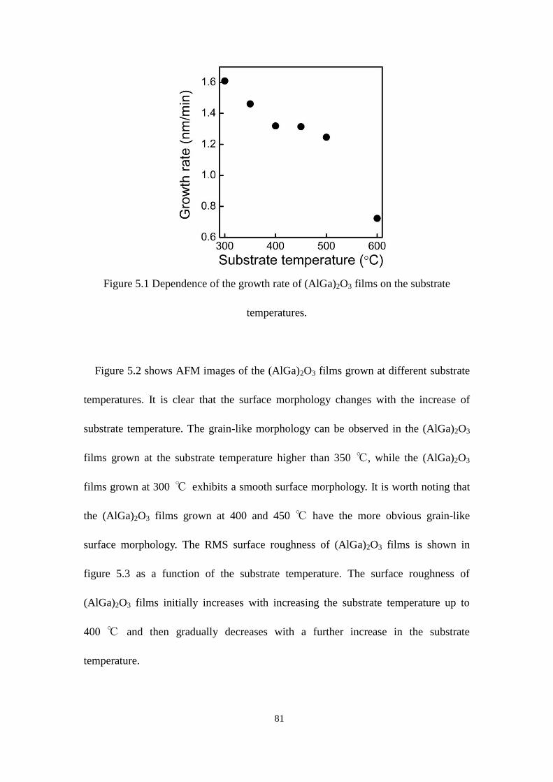
81
Figure 5.1 Dependence of the growth rate of (AlGa)2O3 films on the substrate
temperatures.
Figure 5.2 shows AFM images of the (AlGa)2O3 films grown at different substrate
temperatures. It is clear that the surface morphology changes with the increase of
substrate temperature. The grain-like morphology can be observed in the (AlGa)2O3
films grown at the substrate temperature higher than 350 ℃, while the (AlGa)2O3
films grown at 300 ℃ exhibits a smooth surface morphology. It is worth noting that
the (AlGa)2O3 films grown at 400 and 450 ℃ have the more obvious grain-like
surface morphology. The RMS surface roughness of (AlGa)2O3 films is shown in
figure 5.3 as a function of the substrate temperature. The surface roughness of
(AlGa)2O3 films initially increases with increasing the substrate temperature up to
400 ℃ and then gradually decreases with a further increase in the substrate
temperature.
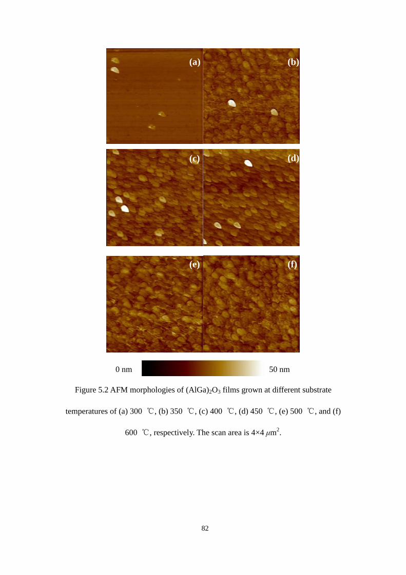
82
Figure 5.2 AFM morphologies of (AlGa)2O3 films grown at different substrate
temperatures of (a) 300 ℃, (b) 350 ℃, (c) 400 ℃, (d) 450 ℃, (e) 500 ℃, and (f)
600 ℃, respectively. The scan area is 4×4 μm2.
(c) (d)
(e) (f)
0 nm 50 nm
(a) (b)
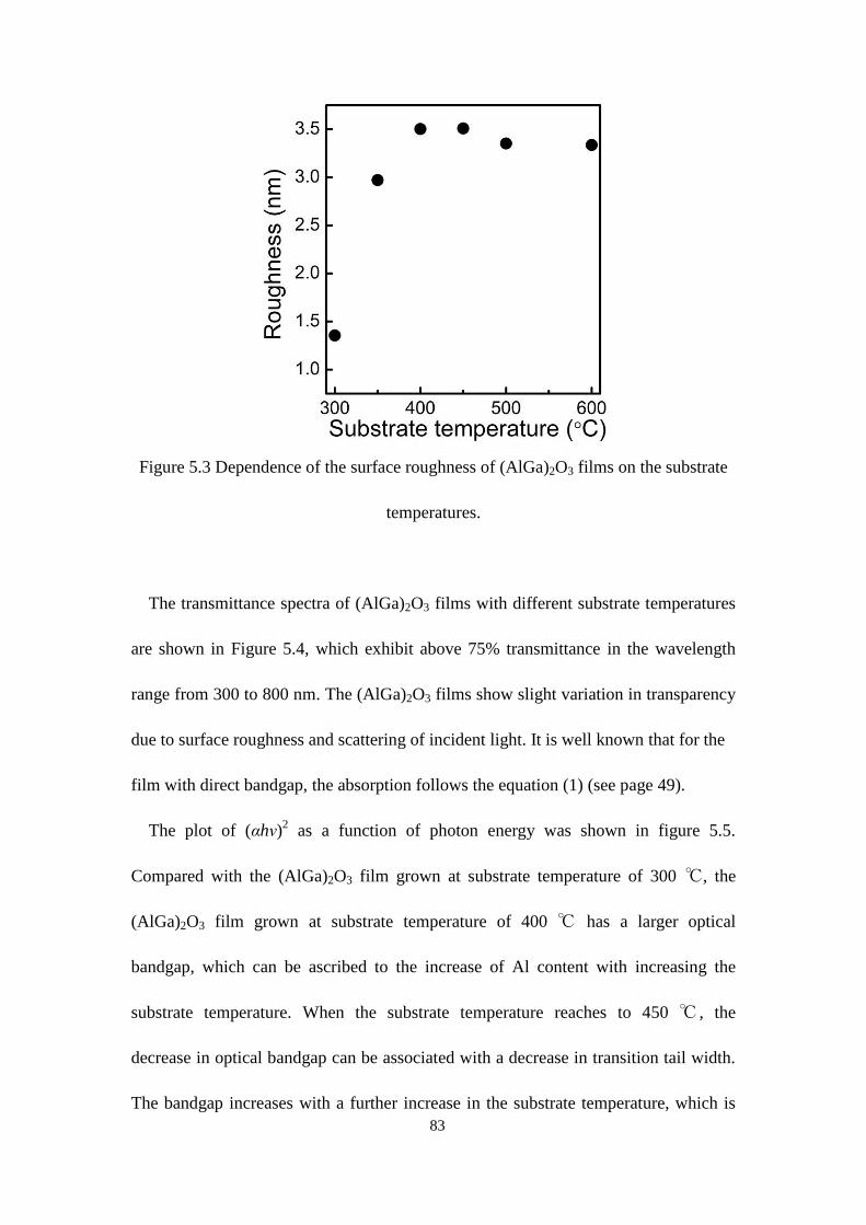
83
Figure 5.3 Dependence of the surface roughness of (AlGa)2O3 films on the substrate
temperatures.
The transmittance spectra of (AlGa)2O3 films with different substrate temperatures
are shown in Figure 5.4, which exhibit above 75% transmittance in the wavelength
range from 300 to 800 nm. The (AlGa)2O3 films show slight variation in transparency
due to surface roughness and scattering of incident light. It is well known that for the
film with direct bandgap, the absorption follows the equation (1) (see page 49).
The plot of (αhν)2 as a function of photon energy was shown in figure 5.5.
Compared with the (AlGa)2O3 film grown at substrate temperature of 300 ℃, the
(AlGa)2O3 film grown at substrate temperature of 400 ℃ has a larger optical
bandgap, which can be ascribed to the increase of Al content with increasing the
substrate temperature. When the substrate temperature reaches to 450 ℃ , the
decrease in optical bandgap can be associated with a decrease in transition tail width.
The bandgap increases with a further increase in the substrate temperature, which is

84
caused by the increase of Al content due to difference of vapor pressure between Ga
and Al species at higher substrate temperature. The similar phenomenon has been
confirmed in our previous work about MgZnO films.16
Figure 5.4 Transmittance spectra of (AlGa)2O3 films grown at different substrate
temperatures.
Figure 5.5 (ɑhν)2 vs. hν plot of (AlGa)2O3 films grown at different substrate
temperatures.

85
Figure 5.6 XRD patterns of (AlGa)2O3 films grown at different substrate
temperatures.
In order to investigate the effect of the substrate temperature on crystal structure,
we measured the XRD patterns of the (AlGa)2O3 films as shown in figure 5.6. When
the substrate temperature is 300 ℃, there is almost no peak except the (0006) peak
from sapphire substrate. The (AlGa)2O3 films grown in the substrate temperature
range from 350 to 500 ℃ exhibit three peaks at 18.97°, 38.27°, and 59.18° which are
ascribed to the patterns of monoclinic β-(AlGa)2O3 can be assigned as the (-201),
(-402), and (-603) faces, respectively.11
None of the (111), (001), and (-101) peaks of
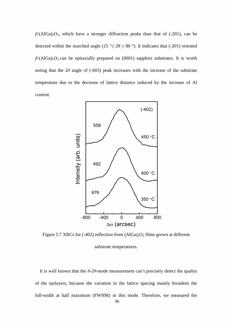
86
β-(AlGa)2O3, which have a stronger diffraction peaks than that of (-201), can be
detected within the searched angle (15 °≤ 2θ ≤ 80 °). It indicates that (-201) oriented
β-(AlGa)2O3 can be epitaxially prepared on (0001) sapphire substrates. It is worth
noting that the 2θ angle of (-603) peak increases with the increase of the substrate
temperature due to the decrease of lattice distance induced by the increase of Al
content.
-800 -400 0 400 800
676
492
450 C
400 C
Inte
nsity (
arb
. units)
(arcsec)
350 C
(-402)
558
Figure 5.7 XRCs for (-402) reflection from (AlGa)2O3 films grown at different
substrate temperatures.
It is well known that the θ-2θ-mode measurement can’t precisely detect the quality
of the epilayers, because the variation in the lattice spacing mainly broadens the
full-width at half maximum (FWHM) in this mode. Therefore, we measured the
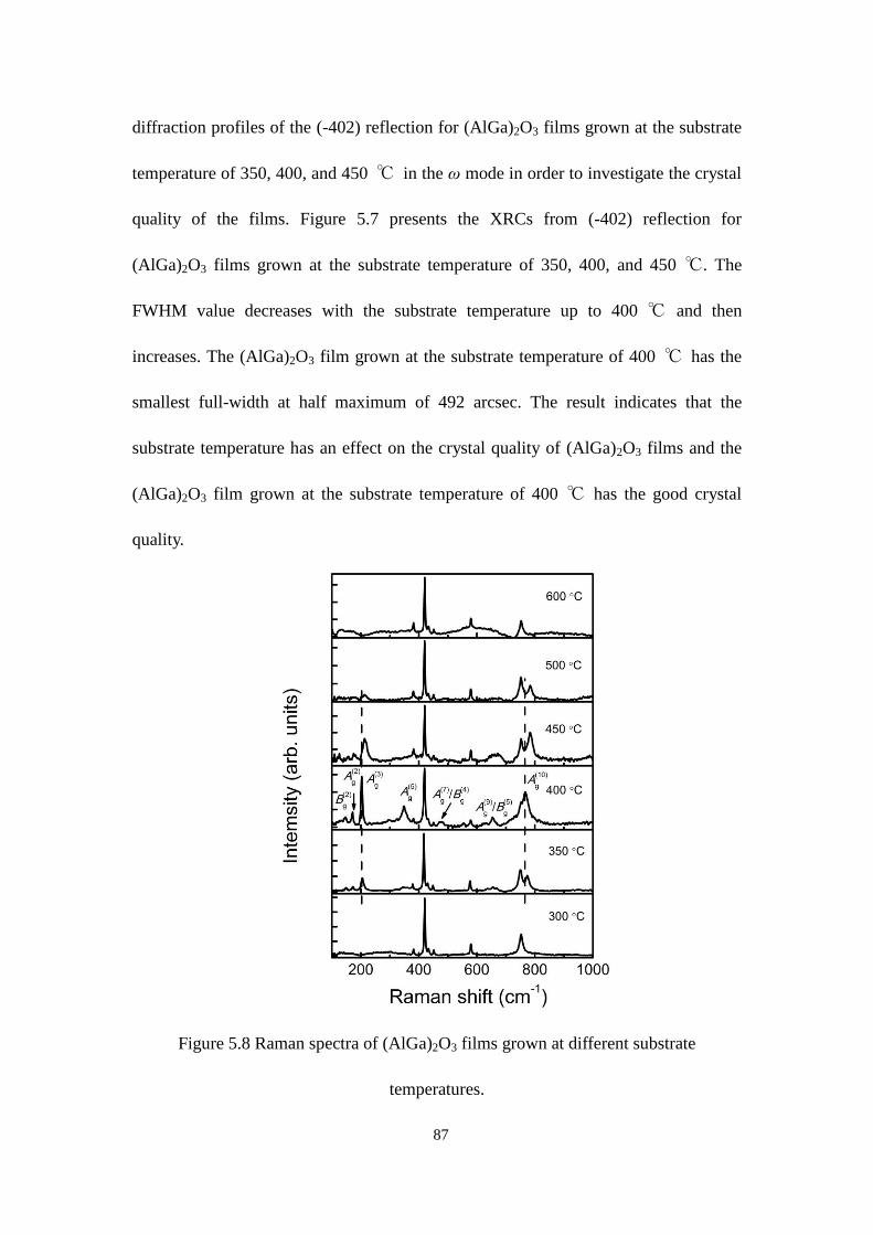
87
diffraction profiles of the (-402) reflection for (AlGa)2O3 films grown at the substrate
temperature of 350, 400, and 450 ℃ in the ω mode in order to investigate the crystal
quality of the films. Figure 5.7 presents the XRCs from (-402) reflection for
(AlGa)2O3 films grown at the substrate temperature of 350, 400, and 450 ℃. The
FWHM value decreases with the substrate temperature up to 400 ℃ and then
increases. The (AlGa)2O3 film grown at the substrate temperature of 400 ℃ has the
smallest full-width at half maximum of 492 arcsec. The result indicates that the
substrate temperature has an effect on the crystal quality of (AlGa)2O3 films and the
(AlGa)2O3 film grown at the substrate temperature of 400 ℃ has the good crystal
quality.
Figure 5.8 Raman spectra of (AlGa)2O3 films grown at different substrate
temperatures.

88
Raman scattering is considered to be a powerful nondestructive and sensitive
technique to study the crystal quality in the alloy materials because the extended
defects can broaden the Raman peaks. Figure 5.8 shows the Raman spectra obtained
at room temperature for (AlGa)2O3 films grown at different substrate temperatures.
Raman scattering was recorded in the back-scattering geometry of the z (x, -) ͞z
configuration17
using an Ar laser at 488 nm. When the substrate temperature is
300 ℃, no peak from β-(AlGa)2O3 can be observed in the Raman shift range from
100 to 1000 cm-1
except the peaks at 418, 580, and 754 cm-1
caused by sapphire
substrate. For (AlGa)2O3 film grown at the substrate temperature from 350 to 500 ℃,
nine Raman mode peaks can be observed. It is well known that the monoclinic Ga2O3
belongs to the space group C2/m/C3
2h. The phonon modes of β-Ga2O3 can be
classified into three groups: low-frequency libration and translation (below 200 cm-1
)
of tetrahedra-octahedra chains, mid-frequency deformation of Ga2O6 octahedra
(~310-480 cm-1
), and high-frequency stretching and bending of GaO4 tetrahedra
(~500-770 cm-1
).18
Therefore, these peaks can be assigned to Bg(2)
, Ag(2)
, Ag(3)
, Ag(5)
,
Ag(7)
/Bg(4)
, Ag(9)
/Bg(5)
, and Ag(10)
phonon modes, respectively. The peak of Ag(7)
/Bg(4)
phonon modes as well as Ag(9)
/Bg(5)
can’t be unambiguously assigned to one of the
mode peaks Ag(7)
or Bg(4)
because Raman shifts of Ag(7)
(Ag(9)
) modes is very close to
that of Bg(4)
(Bg(5)
) modes. Moreover, compared with the Raman shifts of Ga2O3, all
the phonon modes of (AlGa)2O3 films have a shift toward the direction of large
Raman shift, which can be attributed to the cooperation of Al atom. In order to
investigate the effect of growth temperature, the Raman shifts and linewidth of Ag(3)
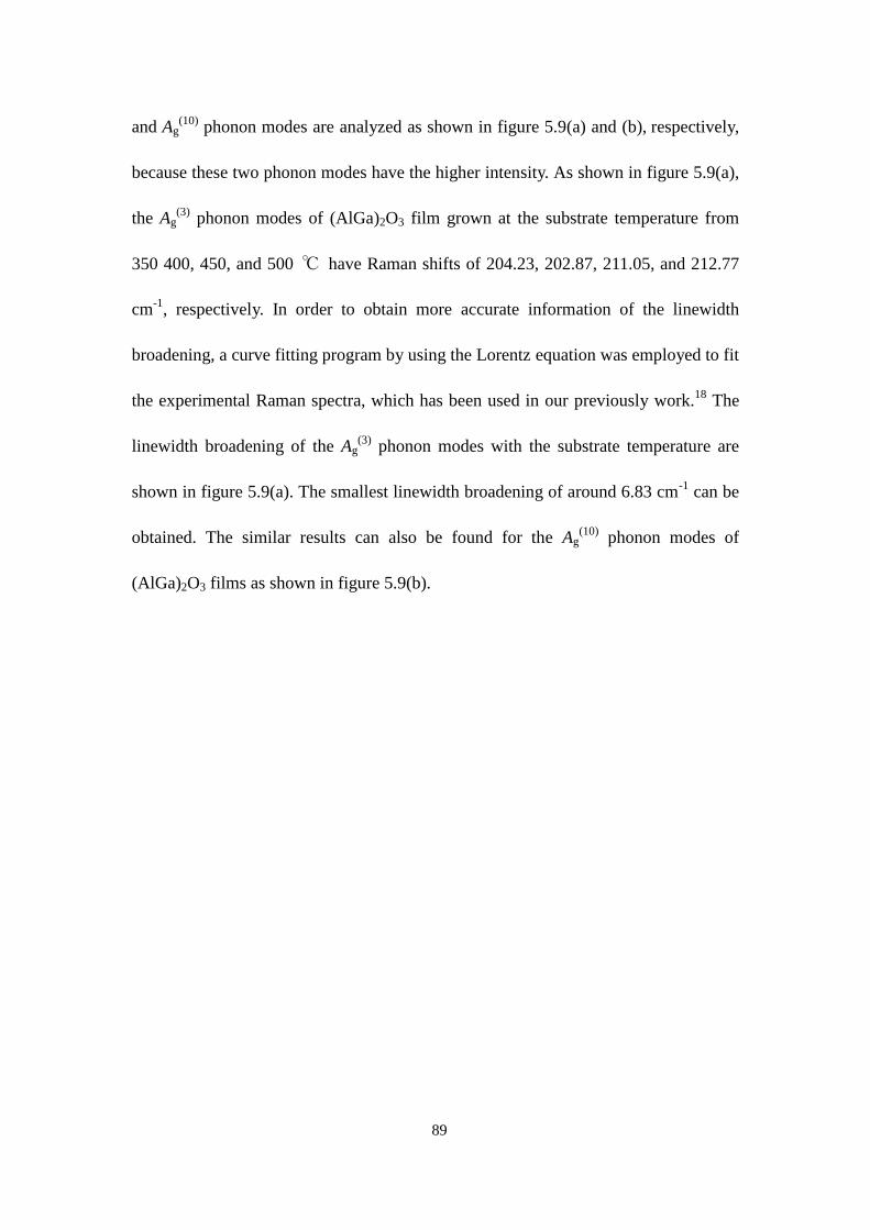
89
and Ag(10)
phonon modes are analyzed as shown in figure 5.9(a) and (b), respectively,
because these two phonon modes have the higher intensity. As shown in figure 5.9(a),
the Ag(3)
phonon modes of (AlGa)2O3 film grown at the substrate temperature from
350 400, 450, and 500 ℃ have Raman shifts of 204.23, 202.87, 211.05, and 212.77
cm-1
, respectively. In order to obtain more accurate information of the linewidth
broadening, a curve fitting program by using the Lorentz equation was employed to fit
the experimental Raman spectra, which has been used in our previously work.18
The
linewidth broadening of the Ag(3)
phonon modes with the substrate temperature are
shown in figure 5.9(a). The smallest linewidth broadening of around 6.83 cm-1
can be
obtained. The similar results can also be found for the Ag(10)
phonon modes of
(AlGa)2O3 films as shown in figure 5.9(b).
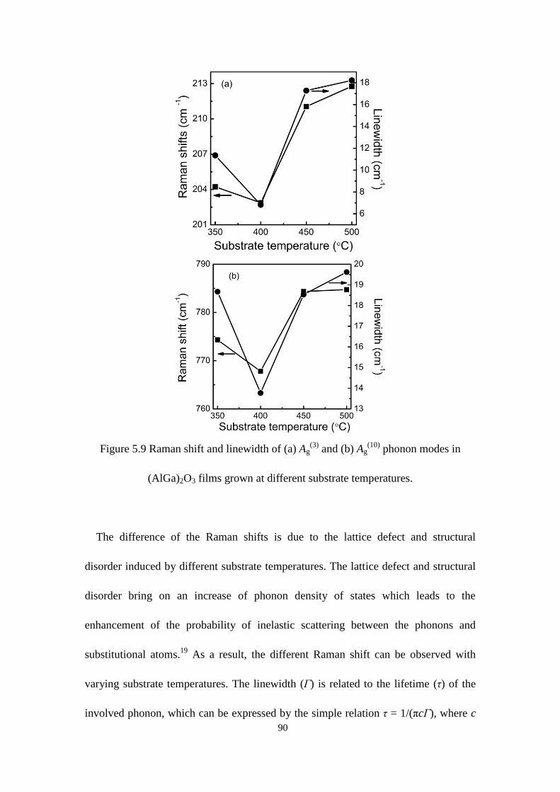
90
Figure 5.9 Raman shift and linewidth of (a) Ag(3)
and (b) Ag(10)
phonon modes in
(AlGa)2O3 films grown at different substrate temperatures.
The difference of the Raman shifts is due to the lattice defect and structural
disorder induced by different substrate temperatures. The lattice defect and structural
disorder bring on an increase of phonon density of states which leads to the
enhancement of the probability of inelastic scattering between the phonons and
substitutional atoms.19
As a result, the different Raman shift can be observed with
varying substrate temperatures. The linewidth (Г) is related to the lifetime (τ) of the
involved phonon, which can be expressed by the simple relation τ = 1/(πcГ), where c
91
is velocity of light. The smaller linewidth results in a larger decay lifetime, and so the
more phonon free paths exist.20
It reflects the higher crystal quality of the (AlGa)2O3
film as observed by XRC measurements as shown in figure 5.7. It is obvious from the
above experimental results that the substrate temperature has a dramatic effect of the
growth of (AlGa)2O3 films and the (AlGa)2O3 film with the good crystal quality can
be obtained at the substrate temperature of 400 ℃ which is much lower than the
growth temperature by other methods. In general, high growth temperature is better
for crystal growth. However, for PLD process, high growth temperature induces the
reevaporation of the adsorbed spices on the surface of the substrate. The evaporation
of Ga atoms from the growing film became dominant and no film growth occurred at
high growth temperature in the work of Kosuke et al.14
. The large lattice mismatch
between sapphire and epitaxial film generates a high density of threading dislocations,
which leads to non-radiative recombination centers and thereby limits the emission
efficiency.21
One way to suppress threading dislocations is known to be reduction of
the growth temperature.22
Moreover, the determination of the optimal growth
temperature for (AlGa)2O3 film will provide an experimental basis for realizing
Ga2O3-based quantum well.
5. 2 Raman scattering
Deep ultraviolet optoelectronic devices such as light detectors and emitters are paid
more and more attention for their potential applications in biological and chemical
agent detection, environmental protection, solar blind detection and high-density data

92
storage.23-26
As a wide variable bandgap semiconductor, ternary (AlGa)2O3 is a
promising candidate for deep ultraviolet optoelectronic device applications because
(AlGa)2O3 has an advantage of large tunable bandgaps from 4.8 eV (Ga2O3) to 8.6 eV
(Al2O3) at room temperature.8,9
In order to realize (AlGa)2O3 application in deep
ultraviolet optoelectronic devices, great efforts have made remarkable progress for
growing this alloy.27
In our previous experiment, (AlGa)2O3 thin films were
successfully deposited by PLD, and β-(AlGa)2O3 thin film could be obtained in the Al
content range of 0-0.72.11
For further development of (AlGa)2O3-based optoelectronic
device, detailed and reliable experimental data on the optical properties of
β-(AlGa)2O3 thin films must be clearly investigated.
Compared with other spectroscopic techniques, Raman spectroscopy has a great of
advantages such as nondestructive, no special sample preparation, and contactless.28-31
Therefore, it has been widely employed in semiconductors. Kranert et al.10
have
reported Raman spectra of (AlGa)2O3 films with different Al content (0-0.55) at room
temperature. However, in contrast to the comprehensive investigation of temperature
effect of Raman scattering for other semiconductors,19,32
temperature dependence of
phonon behavior in β-(AlGa)2O3 thin films has not been reported up to now. The
temperature dependent Raman linewidths and shifts can be interpreted in the terms of
anharmonic processes which results in a better understanding of electronic properties
of (AlGa)2O3 at different temperature.33
Moreover, it has been demonstrated that the
anharmonic constant which was extracted by analyzing anharmonic processes is very
important for the MgZnO-based light emission device applications.19
In this work, we

93
reported on the temperature-dependence Raman scattering of β-(AlGa)2O3 thin films
with different Al content (0-0.72) in the temperature range from 77 to 300 K. In
combination with detailed theoretical modellings for the frequency downshift and
linewidths broadening, we can clearly illustrate the temperature effect on the Raman
shift and linewidths in the β-(AlGa)2O3 thin films, which provides an experimental
basis for realization of (AlGa)2O3-based optoelectronic device applications.
The (AlGa)2O3 films used for present research were deposited by PLD using a KrF
laser source (λ = 248 nm) on (0001) sapphire substrates. The (AlGa)2O3 bulks with Al
content in the range of 0-0.72 were used as targets. The oxygen pressure during the
growth was maintained at 1×10⁻¹
Pa while the substrate temperature was kept at
400℃.11
The XRD revealed that the (-201), (-402), and (-603) diffraction peaks are
observed from (AlGa)2O3 films together with the peak of (0006) reflection from
sapphire substrate, indicating the patterns of monoclinic β-(AlGa)2O3.11
The atomic
concentrations were estimated from XPS element peak area by using an atomic
sensitivity factor.11
The thickness of these (AlGa)2O3 films measured by using a
surface step profile analyzer are between 200 and 300 nm. The surface morphologies
and root mean square (RMS) roughness of (AlGa)2O3 films were characterized by
atomic force microscope (AFM) as shown in figure 5.10.

94
Figure 5.10 AFM images of (AlxGa1-x)2O3 films with different Al content x of (a) 0, (b)
0.11, (c) 0.22, (d) 0.53, and (e) 0.72, respectively. The scan area is 1×1 μm2.
The Raman spectra were recorded in the back-scattering geometry of the z (x, -) ͞z
configuration34
by using a Horiba Jobin Yvon LabRAM HR 800 system equipped
with an Andor DU420 classic charge-coupled device detector. The 488 nm line of Ar
laser was used to excite the samples. The employment of a 50 × optical microscopy
objective with a numerical aperture of 0.5 will yield a laser spot size of ~0.8 μm. A
MicrostatHE
hot/cold stage (Oxford instruments) with a quartz window was used to
20 nm 0 nm
(c) (d)
(e)
RMS: 1.2 nm RMS: 1.1 nm
0 nm 20 nm
0 nm 50 nm
RMS: 18.4 nm
(a) (b)
RMS: 3.1 nm RMS: 2.8 nm
0 nm 20 nm
0 nm 20 nm

95
heat the samples from 77 K to 300 K under flowing nitrogen. The temperature was
controlled by a K-type thermocouple which has an accuracy of better than ± 1 K. For
each measurement point, the temperature was kept for 10 min to avoid temperature
fluctuations before acquiring a spectrum for 15 min. The power of the laser was set to
about 2 mW to avoid thermal contributions coming from the laser.
The monoclinic β-Ga2O3 belongs to the space group C2/m/C32h. The Raman-active
modes of β-Ga2O3 can be classified into three groups: low-frequency libration and
translation (below 200 cm-1
) of tetrahedra-octahedra chains, mid-frequency
deformation of Ga2O6 octahedra (~310-480 cm-1
), and high-frequency stretching and
bending of GaO4 tetrahedra (~500-770 cm-1
).18
It has 27 optical phonon modes
belonging to the irreducible representation
Гopt
= 10Ag + 5Bg + 4Au + 8Bu (1)
Where symmetry Ag and Bg phonon modes are Raman active while phonon modes
with Au and Bu symmetry are infrared active.36
Figure 5.11 shows Raman spectra of (AlxGa1-x)2O3 films with Al content x in the
range of 0-0.72 measured at room temperature. For Ga2O3 film, six Ag and three Bg
Raman active modes can be observed. The Raman peaks at 146.2, 169.6, 201.6, 351.3,
483.3, 656.4, and 767.4 cm-1
correspond to Bg(2)
, Ag(2)
, Ag(3)
, Ag(5)
, Ag(7)
/Bg(4)
, Ag(9)
/Bg(5)
,
and Ag(10)
phonon modes, respectively. The peak of Ag(7)
/Bg(4)
phonon modes as well as

96
Figure 5.11 Raman spectra of β-(AlGa)2O3 thin film with different Al content at room
temperature.
Ag(9)
/Bg(5)
can’t be unambiguously assigned to one of the mode peaks Ag(7)
or Bg(4)
because Raman shifts of Ag(7)
modes is very close to that of Bg(4)
modes. The positions
of these mode peaks have good agreements with those of Ga2O3 bulk and nanowires
reported by other researchers.35,36
With the increase of Al content, the Raman active
modes of (AlGa)2O3 films have a clear right shift. The Raman spectra also exhibit a
line broadening for (AlGa)2O3 films at higher Al content. This broadening is
particularly true for the Raman modes in mid-spectral range between 310 and 480
cm-1
, which is contributed to the more Al atoms entering into the crystal lattices of
Ga2O3 to form ternary solid solution. For Al2O3 film, almost no peak can be observed

97
except the Raman peak of sapphire substrates. Figure 5.12 shows the dependence of
the spectral positions of Ag(3)
, Ag(9)
/Bg(5)
, and Ag(10)
phonon modes on the Al content. As
shown in figure 5.12, for the Al content range of 0-0.72, the Ag(3)
phonon mode
exhibits a shift of ~41 cm-1
, the Ag(9)
/Bg(5)
phonon mode has a shift of ~65 cm-1
, and
the shift is Ag(10)
phonon modes is ~46 cm-1
.
Figure 5.12 Raman shifts of Ag(3)
, Ag(9)
/Bg(5)
, and Ag(10)
phonon modes as a function of
Al content.
Next, we measured the temperature-dependent Raman spectra of (AlGa)2O3 films
by keeping samples on the stage. Figure 5.13 presents the temperature-dependent
Raman spectra of (AlGa)2O3 films with Al content in the range of 0-0.72. The sharp
Raman peaks of Ga2O3 films located at 201.6 and 767.4 cm-1
are attributed to the Ag(3)
and Ag(10)
phonon modes, respectively, while peaks at 418, 580, and 754 cm-1
are
caused by sapphire substrate Here, we note that in temperature-dependent Raman
measurement process, some of Raman modes disappeared due to absorption of the

98
window of the stage. These peaks can only be observed at lower temperature. In order
to observe the temperature effect on the phonon modes in (AlGa)2O3 films, the
enlarged Raman shift spectra of Ag(3)
and Ag(10)
phonon modes were shown in figure
5.14(a) and (b). The black solid curves are experimental Raman spectra. In order to
obtain the more accurate information, a curve fitting program by using the Lorentz
equation was employed to fit the experimental Raman spectra to determine the Raman
shifts and linewidth broadening. The fitting curves are shown as red dash curves in
figure 5.14(a) and (b). This approach has been shown to be very powerful for
analyzing the contributions of different phonon modes in compound semiconductors
such as AlInN and MgZnO.19,32

99
Figure 5.13 Temperature dependence Raman spectra of β-(AlGa)2O3 thin film with
different Al content.

100
Figure 5.14(a) Enlarge Raman spectra of Ag(3)
modes in β-(AlGa)2O3 thin films with
different Al content.
Figure 5.15 shows the Raman shift of Ag(3)
and Ag(10)
phonon modes with
temperature. It is clear that the Ag(3)
and Ag(10)
structure shifts to lower frequency with
the increase of temperature. The temperature dependence of Raman shifts exhibit
nonlinear behavior at the temperature from 77 to 300 K. In general, several factors are
responsible for temperature-dependent Raman shift such as electron-phonon,
anharmonic phonon-phonon interactions, and thermal expansion.37,38
However, for the

101
effect of thermal expansion, the experimental structural information of (AlGa)2O3,
such as Grüneisen parameters and phonon deformation potentials, was not established
up to now. Therefore, there is no generally accurate method to describe the downshift
of phonon frequencies in (AlGa)2O3 films with the increase of temperature at this
moment.
Figure 5.14(b) Enlarge Raman spectra of Ag(10)
modes in β-(AlGa)2O3 thin films with
different Al content.
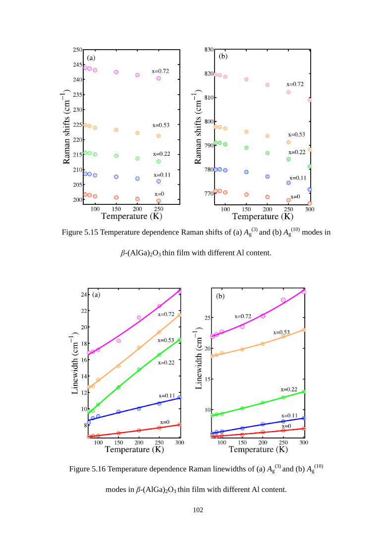
102
Figure 5.15 Temperature dependence Raman shifts of (a) Ag(3)
and (b) Ag(10)
modes in
β-(AlGa)2O3 thin film with different Al content.
Figure 5.16 Temperature dependence Raman linewidths of (a) Ag(3)
and (b) Ag(10)
modes in β-(AlGa)2O3 thin film with different Al content.
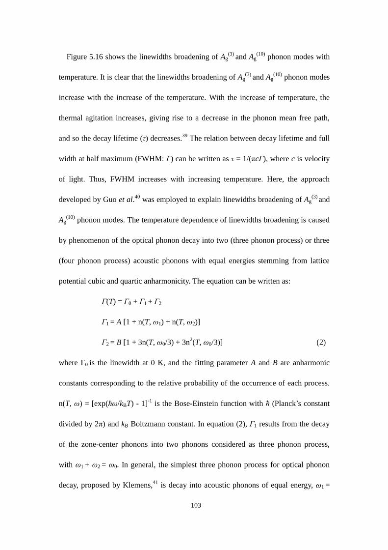
103
Figure 5.16 shows the linewidths broadening of Ag(3)
and Ag(10)
phonon modes with
temperature. It is clear that the linewidths broadening of Ag(3)
and Ag(10)
phonon modes
increase with the increase of the temperature. With the increase of temperature, the
thermal agitation increases, giving rise to a decrease in the phonon mean free path,
and so the decay lifetime (τ) decreases.39
The relation between decay lifetime and full
width at half maximum (FWHM: Г) can be written as τ = 1/(πcГ), where c is velocity
of light. Thus, FWHM increases with increasing temperature. Here, the approach
developed by Guo et al.40
was employed to explain linewidths broadening of Ag(3)
and
Ag(10)
phonon modes. The temperature dependence of linewidths broadening is caused
by phenomenon of the optical phonon decay into two (three phonon process) or three
(four phonon process) acoustic phonons with equal energies stemming from lattice
potential cubic and quartic anharmonicity. The equation can be written as:
Γ(T) = Γ0 + Γ1 + Γ2
Γ1 = A [1 + n(T, ω1) + n(T, ω2)]
Γ2 = B [1 + 3n(T, ω0/3) + 3n2(T, ω0/3)] (2)
where Γ0 is the linewidth at 0 K, and the fitting parameter A and B are anharmonic
constants corresponding to the relative probability of the occurrence of each process.
n(T, ω) = [exp(ħω/kBT) - 1]-1
is the Bose-Einstein function with ħ (Planck’s constant
divided by 2π) and kB Boltzmann constant. In equation (2), Γ1 results from the decay
of the zone-center phonons into two phonons considered as three phonon process,
with ω1 + ω2 = ω0. In general, the simplest three phonon process for optical phonon
decay, proposed by Klemens,41
is decay into acoustic phonons of equal energy, ω1 =

104
ω2, and opposite. And Γ2 corresponds to the decay into three phonons (four phonon
process), with the frequency ω0/3. ω0 is the harmonic frequency of phonon mode. The
solid curves shown in figure 5.16 are the fit of Eq. (2) for the temperature-dependent
linewidths broadening of Ag(3)
and Ag(10)
phonon modes. The agreement between the
theoretical fit and experimental data is very good. In addition, it is clear that the
gradient of fitting curves increases with the increase of the Al content. Similar
phenomena were also observed in AlInN and MgZnO alloy materials.19,32
The fitting
parameters Γ0, A, and B have been obtained as shown in Table 6.1. It is obvious that
there is a rapid increase in Γ0 with the increase of Al content because of the formation
of lattice defect and structural disorder after Al implantation. Moreover, the
dependence of Γ0 on Al content play the closely related behavior with that of Urbach
band tail according to report of Jiang, et al. In pure Ga2O3 film, Γ0 of Ag(3)
phonon
mode is larger than that of Ag(10)
phonon mode, implying that Ag(3)
phonon mode is
more strongly affected by impurity and/or defect scattering than that of Ag(10)
phonon
mode. However, Γ0 of Ag(10)
phonon mode increases much more rapidly with the
increase of Al content than that of Ag(3)
phonon mode. As we know, Ag(10)
phonon
mode belongs to high-frequency stretching and bending modes of GaO4 tetrahedra.36
The stretching and bending modes involve the shortest Ga-O bonds (1.80 Å) which
lead to more lattice defect and structural disorder when Al was implanted. These
defects and disorders will result in strong enhancement of the impurity scattering in
Ag(10)
phonon mode of (AlGa)2O3 films.32
It is well known that the constants A and B
can be related to the lifetime of the optical phonon decay into two (three phonon

105
process) and three (four phonon process) acoustic phonons, respectively. It has been
confirmed the inverse relation between the lifetime and the anharmonic constants.39
From Table 5.1, it is obvious that the constants A and B increase with the increase of
Al content. It can be explained that Al atom incorporation makes the more lattice
defect and structural disorder which lead to shorten lifetime of decay process.
Table 5.1 Fitting parameters for linewidth broadening of Ag(3)
and (b) Ag(10)
in
β-(AlGa)2O3 thin film.
Raman modes x Γ0 A B
Ag(3)
0 6.17 0.1676 0.0026
0.11 8.50 0.4655 0.0030
0.22 9.52 1.396 0.0976
0.53 12.57 0.8681 0.0363
0.72 16.61 1.262 0.0459
Ag(10)
0 5.24 0.1481 0.0025
0.11 6.08 0.4573 0.0034
0.22 8.74 0.5135 0.0049
0.53 17.87 0.6054 0.0674
0.72 20.52 0.9693 0.0949
In order to better understand the contributions of the three phonon and four
phonon processes in (AlGa)2O3 films, the ratios of A and B were calculated. Figure
5.17 displays the ratios of A and B for Ag(3)
and Ag(10)
phonon modes of Ga2O3 and
(AlGa)2O3 films. It is obvious that the ratios of A and B are much larger than 1.0,
indicating that the decay into two phonons is the prevailing process while the
contribution from the four phonon processes is minor in the anharmonic coupling of
Ag(3)
and Ag(10)
phonon modes. This result has a well agreement with the report on
Ga2O3 bulk,35
which further indicates the reliability of our results estimated by

106
theoretical fitting. For (AlGa)2O3 films, with the increasing of Al content, the ratios of
A and B for Ag(3)
and Ag(10)
phonon modes decrease, indicating that the contribution
from the three phonon process decreases after Al implantation. It can be explained by
the increase of ω0 in (AlGa)2O3 films leads to larger values of ω1 and ω2, which brings
on the decrease of the contribution from the four phonon process.19
Moreover, it
should be noted that three phonon process always dominates the linewidths
broadening of Ag(3)
and Ag(10)
phonon modes in (AlGa)2O3 films.
Figure 5.17 Dependence of A/B on the Al content in β-(AlGa)2O3 thin films.
The above results permit us to have a well understanding of the temperature effect
on the Raman shift and linewidth in (AlGa)2O3 films, which establishes an
experimental base for micro-Raman as a contactless, nondestructive, and fast method
to monitor the local temperature during the operation of (AlGa)2O3-based devices
with submicrometer spatial resolution.32
The obtained temperature and Al content
dependence of Raman shift and linewidth can be used for deriving calibration curves

107
as reported in MgZnO layer.42
The local temperature for the (AlGa)2O3-based devices
in operation can thus be determined by the calibration curve.32
Moreover, the
information about the anharmonic effect is also important for the (AlGa)2O3-based
device applications, because the degree of lattice disorder in mirrors by Raman
microprobe spectroscopy correlates to the strength of facet heating and to the power
limit at optical mirror damage.43,44
5.3 Conclusion
We investigated in detail the substrate temperature influenced on the surface
roughness, optical properties and crystal quality of (AlGa)2O3 films grown on (0001)
sapphire substrates by PLD. AFM and transmission spectra indicate the (AlGa)2O3
films have smooth surface and high transmittance. XRD, XRC, and Raman spectra
analysis shows (AlGa)2O3 film with the good crystal quality can be obtained at
substrate temperature of 400 ℃. These results will provide an experimental basis for
realizing Ga2O3-based quantum well.
The temperature-dependent Raman shifts and linewidths of the Ag(3)
and Ag(10)
phonon modes were obtained by employing Lorentz fitting. Through the aid of a
model involving the contributions of lattice-mismatch-induced strain, thermal
expansion, and three and four phonon coupling, the effects of temperature on
linewidths broadening were clearly illustrated. We demonstrated the dependence of
the linewidths and decay process on the Al content in β-(AlGa)2O3 thin films. It is
clearly observed that the three phonon process always dominates the linewidths

108
broadening of Ag(3)
and Ag(10)
phonon modes in (AlGa)2O3 films. These results will
provide an experimental basis for realization of (AlGa)2O3-based optoelectronic
device applications.

109
References
[1] Y. Kokubun, K. Miura, F. Endo, S. Nakagomi, Appl. Phys. Lett., 90, 031912
(2007).
[2] K. Shimanura, E. Villora, T. Ujiie, and K. Aoki, Appl. Phys. Lett., 92, 021914
(2008).
[3] R. Suzuki, S. Nakagomi, Y. Kokubun, N. Arai, and S. Ohira, Appl. Phys. Lett., 94,
222102 (2009).
[4] Y. Li, T. Tokizono, M. Liao, M. Zhong, Y. Koide, I. Yamada, and J. Delaunay, Adv.
Funct. Mater., 20, 3972 (2010).
[5] Y. Sui, Y. Yue, Y. Cao, B. Yao, X. Liu, J. Lang, M. Gao, X. Li, X. Li, and L. Yang,
Ceram. Int., 40, 9189 (2014).
[6] V. Devi, M. Kumar, R. Kumar, B. Joshi, Ceram. Int., 41, 6269 (2015).
[7] T. Oshima, T. Okuno, N. Arai, Y. Kobayashi, and S. Fujita, Jpn. J. Appl. Phys., 48,
070202 (2009).
[8] H. Ito, K. Kaneko, and S. Fujita, Jpn. J. Appl. Phys., 51, 1002047 (2012).
[9] R. Grund, C. Kranert , H. Wenckstern, V. Zviagin, M. Lorenz, and M. Grundmann,
J. Appl. Phys., 117, 165371 (2015).
[10] C. Kranert, M. Jenderka, J. Lenzner, M. Lorenz, H. Wenckstern, R. S. Grund, and
M. Grundmann, J. Appl. Phys., 117, 125703 (2015).
[11] F. Zhang, K. Satio, T. Tanaka, M. Nishio, M. Arita, and Q. Guo, Appl. Phys. Lett.,
105, 162107 (2014).
110
[12] K. Satio, Y. Inoue, Y. Hayashida, T. Tanaka, Q. Guo, and M. Nishio, Appl. Surf.
Sci., 258, 2137 (2012).
[13] F. Zhang, K. Saito, T. Tanaka, M. Nishio, and Q. Guo, J. Cryst. Growth, 387, 96
(2014).
[14] K. Matsuzaki, H. Hiramatsu, K. Nomura, H. Yanagi, T. Kamiya, M. Hirano, and
H. Hosono, Thin solid films, 496, 37 (2006).
[15] X. Wang, K. Saito, T. Tanaka, M. Nishio, and Q. Guo, J. Aollys Compd., 627,
383 (2015).
[16] X. Wang, K. Saito, T. Tanaka, M. Nishio, T. Nagaoka, M. Arita, and Q. Guo,
Appl. Phys. Lett., 107, 022111 (2015).
[17] Q. Guo, M. Nada, Y. Ding, T. Tanaka, and M. Nishio, J. Appl. Phys., 107, 123525
(2010).
[18] X. Wang, Z. Chen, F. Zhang, K. Satio, T. Tanaka, M. Nishio, and Q. Guo, AIP
Adv., 6, 015111 (2016).
[19] J. Kong, W. Shen, Y. Zhang, X. Li, and Q. Guo, Solid State Commun., 149,10
(2009).
[20] P. Verma, S. Abbi, and K. Jain, Phys. Rev. B, 51,16660 (1995).
[21] R. G. Banal, Y. Taniyasu, and H. Yamamoto, Appl. Phys. Lett., 105, 053104
(2014).
[22] D. J. Eaglesham, and M. Cerullo, Appl. Phys. Lett., 58, 2276 (1991).
[23] M. Khizar, Z. Y. Fan, K. H. Kim, J. Y. Lin and H. X. Jiang, Appl. Phys. Lett., 86,
173504 (2005).

111
[24] Z. Ren, Q. Sun, S. Y. Kwon, J. Han, K. Davitt, Y. K. Song, A. V. Nurmikko, H. K.
Cho, W. Liu, J. A. Smart, and L. J. Schowalter, Appl. Phys. Lett., 91, 051116 (2007).
[25] L. Wang, H. Xu, C, Zhang, X. Li, Y. Liu, X Zhang, Y Tao, Y. Huang, and D. chen,
J. Alloys Compd., 513, 399 (2012).
[26] L. Wang, J. Ma, H. Xu, C. Zhang, X. Ling, and Y. Liu, Appl. Phys. Lett., 102,
031905 (2013).
[27] G. L. Li, F. B. Zhang, Y. T. Cui, H. Oji, J. Y. Son, and Q. X. Guo, Appl. Phys.
Lett., 107, 022109 (2015).
[28] J.R. Shealy and G. W. Wicks, Appl. Phys. Lett., 50, 1173 (1987).
[29] I. Calizo, A. A. Balandin, W. Bao, F. Miao, C. N. R. Rao, Nano Lett., 7, 2645
(2007).
[30] T. T. Kang, A. Hashimoto, and A. Yamamoto, Phys. Rev. B, 79, 033301 (2009).
[31] A.A. Balandin, Nature Mater., 10, 569 (2011).
[32] L. F. Jiang, J. F. Kong, W. Z. Shen, and Q. X. Guo. J. Appl. Phys., 109, 113514
(2011).
[33] M. S. Liu, L. A. Bursill, S. Prawer, and K. W. Nugemt, Appl. Phys. Lett., 74,
3125 (1999).
[34] Q. X. Guo, M. Nada, Y. Ding, T. Tanaka, and M. Nishio, J. Appl. Phys., 107,
123525 (2010).
[35] R. Rao, A. M. Rao, B. Xu, J. Dong, S. Sharma, M. K. Sunkara, J. Appl. Phys., 98,
094312 (2005).
[36] D. Dohy, and J. Gavarri, J. Solid State Chem., 45, 180(1982).

112
[37] W. S. Li, Z. X. Shen, Z. C. Feng, and S. J. Chua, J. Appl. Phys., 87, 3332 (2000).
[38] X. D. Pu, J. Chen, and W. Z. Shen, H. Ogawa, and Q. X. Guo, J. Appl. Phys., 98,
033527 (2005).
[39] P. Verma, S. C. Abbi, and K. P. Jain, Phys. Rev. B, 51, 16660 (1995).
[40] L. L. Guo, Y. H. Zhang, and W. Z. Shen, Appl. Phys. Lett., 89, 161920 (2006).
[41] P. G. Klemecs, Phys. Rev. B, 148, 845 (1966).
[42] A. Link, K. Bitzer, W. Limmer, R. Sauer, C. Kirchner, V. Schwegler, M. Kamp, D.
G. Ebling, K. W. Benz, J. Appl. Phys., 86, 6256 (1999).
[43] P. W. Eppwelein, P. Buchmann, A. Jakubowicz, Appl. Phys. Lett., 62, 455 (1993).
[44] J. Jimenez, E. Martin, A. Torres, J. P. Landesman, Phys. Rev. B, 58, 10463
(1998).
113
Chapter 6
Raman scattering in (InxGa1-x)2O3 films
6.1. Introduction
(InGa)2O3 alloys have attracted considerable attention as promising materials for
ultraviolet (UV) optoelectronic applications such as light emitters and detectors,1-4
because their bandgaps are content tunable in a wide range of energies (3.7-4.9 eV
depending on the In content).5,6
A crucial step for optoelectronic applications is to
develop quantum well (QW) structure following the bandgap engineering.7,8
In our
previous work, (InGa)2O3 films were successfully deposited by pulsed laser deposition
(PLD) in all In content range and the difference of bandgap energies between In2O3
and (In0.83Ga0.17)2O3 films has been confirmed as 0.25 eV which is suited for
designing the In2O3-based QW.9 In order to realize high-efficiency In2O3-based QW,
the detailed and reliable information on the structural characteristics of both well and
barrier layers must be clearly investigated.
Raman spectroscopy, as a convenient, effective, and nondestructive method for
studying the lattice vibration characteristics, has been widely employed for (InGa)2O3
films.10,11
Kranert et al.10
have reported Raman spectra of (InGa)2O3 films with
different In content (0-0.33) at room temperature. Regoutz et al.11
have presented
typical Raman peaks related the disorder-active modes of cubic (InGa)2O3 films
grown in the high In content range (0.9-1) at room temperature and the major phonon
modes have blueshift due to the strain caused by defects and the broadened linewidth

114
to the deterioration of crystal structure in comparison with the Raman scattering of
In2O3. Though great efforts have been made in the investigation of (InGa)2O3 alloy by
Raman spectroscopy, temperature-dependent Raman scattering of cubic (InGa)2O3
thin films have not been reported up to now. It is well known that
temperature-dependent Raman scattering can be used to obtain the information of
phonon decay which is an essential aspect to understand the phonon behaviors.12
Moreover, the particular temperature coefficients for different Raman active modes
can also be estimated by temperature-dependent Raman scattering, which can be used
to obtain structural information.13
In this chapter, we report the
temperature-dependent Raman scattering of cubic (In0.83Ga0.17)2O3 and In2O3 thin films
in the temperature range from 77 to 500 K. In combination with detailed theoretical
modellings for the Raman downshift and linewidths broadening, we can clearly
illustrate the influence of temperature on the Raman shifts and linewidths in the cubic
(InGa)2O3 and In2O3 thin films.
6.2 Experiment
(InGa)2O3 thin films were grown by pulsed laser deposition (PLD) using a KrF
laser source (λ=248 nm) on (0001) sapphire substrates. Before growth, the sapphire
substrates were cleaned in organic solvents by in an ultrasonic cleaning system, and
then chemically etched in a hot H3PO4: H2SO4 (1:3) solution.14
In the growth chamber,
facing the substrate, the bulks with the In contents of 0.9 and 1 (mole ratio of In / (Ga
+ In)) were set as the target. The pulsed laser with a frequency of 1 Hz was irradiated
115
and the distance between target and substrate was about 30 mm. The energy of the
pulsed laser was set 225 mJ for deposition. The oxygen pressure of the growth
chamber was 1×10⁻¹
Pa by introducing high purity oxygen gas (99.999%). In the
deposition, the substrate temperature was set as 500 ℃ and the deposition time was
3 h for these films.
After deposition, energy dispersive X-ray spectroscopy results revealed that the
(InGa)2O3 thin films grown with the In contents of 0.9 and 1 in the targets have the In
contents of 0.83 and 1 in the films, respectively.9 The surface morphology and RMS
roughness of (InGa)2O3 thin films were studied by AFM. The crystal structures of
(InGa)2O3 thin films were evaluated by using XRD. Raman scattering was performed
on a Horiba Jobin Yvon LabRAM HR 800 system equipped with an Andor DU420
classic charge-coupled detector. Raman experiments were carried out by using an
argon ion laser (488 nm) as the excitation source. A MicrostatHE
hot/cold stage
(Oxford instruments) with quartz window was used to heat the films from 77 to 500 K
under flowing nitrogen. The temperature was controlled by a K-type thermocouple
which has an accuracy of better than ±1 K. For each measurement point, the
temperature was kept for 10 min to avoid temperature fluctuations before acquiring a
spectrum for 10 min.15
6.3. Results and discussion
Fig. 6.1 shows AFM images of In2O3 and (In0.83Ga0.17)2O3 films. The surface
morphologies of both In2O3 and (In0.83Ga0.17)2O3 films are very flat as seen in figure.

116
The RMS roughness of (InGa)2O3 films are also marked in Fig. 6.1. It is well known
that the exciton localization effect in quantum well structure is enhanced by
increasing the thickness of well layer up to a certain value. If the thickness of well
layer is further increased to above this value, the exciton localization effect becomes
weak.16
Finally, the exciton localization effect cannot be observed. According to
previous reports, the value is about 2.5 nm for GaN/InGaN QW16
and 4 nm for
ZnO/MgZnO QW.17
The smaller roughness of both well and barrier layer is essential
for quantum well structure. In this work, thicknesses of cubic In2O3 and
(In0.83Ga0.17)2O3 films measured by a surface step profile analyzer are 352 and 346 nm,
respectively. The roughness of the In2O3 and (In0.83Ga0.17)2O3 films are 1.24 and 2.57
nm, respectively. The roughness of both In2O3 and (In0.83Ga0.17)2O3 films is small
enough to meet the requirement of In2O3-based QW.
Figure 6.1 AFM morphologies of (InGa)2O3 films grown with the In content of (a) 1
and (b) 0.83. The scan area is 10×10 μm2.
Next, we investigate the crystal structure of In2O3 and (In0.83Ga0.17)2O3 films by

117
XRD in the θ-2θ-mode as shown in Fig. 6.2. Both In2O3 and (In0.83Ga0.17)2O3 films
exhibit two peaks (111) and (222) in XRD patterns together with the peak of the
(0006) reflection from (0001) sapphire substrate, indicating that the (111) axis of
these two samples is perpendicular to the surface of the sapphire substrate. The lattice
constants of (InGa)2O3 films grown with the In content of 1 and 0.83 are 5.10 and 5.07
Å, respectively, at room temperature, giving a lattice mismatch of 0.5% between
In2O3 and (In0.83Ga0.17)2O3 films, which is expressed by (aIn2O3 - a (In0.83Ga0.17)2O3) / a
(In0.83Ga0.17)2O3.18
Since threading dislocation induced by lattice mismatch between well
and barrier layers can limit the emission efficiency, this small lattice mismatch
between In2O3 and (In0.83Ga0.17)2O3 films indicates that the (InGa)2O3 films grown in
this work are well suited to form In2O3-based QW.
Figure 6.2 XRD patterns of In2O3 and (In0.83Ga0.17)2O3 films.
Since the primitive cell of cubic In2O3 contains eight formula units, group theory
predicts the cubic In2O3 have 120 vibrational modes with the following

118
representation19,20
:
Гopt
= 4 Ag + 4 Eg + 14 Tg + 5 Au + 5 Eu + 16 Tu,
where Ag, Eg, and Tg are Raman-active modes, Au and Eu represent silent modes, and
Tu is infrared-active modes. Fig. 6.3 shows the Raman spectra measured at room
temperature for In2O3 and (In0.83Ga0.17)2O3 films. The peaks at 376.1, 415.4, 428.8,
447, 576.4, and 749.5 cm-1
marked by cross symbols are caused by sapphire substrate
as seen in figure.21
For In2O3 film, three Ag and three Tg Raman active modes can be
observed. The Raman peaks at 131.9, 309.4, 367.8, 500.2, and 636.3 cm-1
correspond
to Ag(1)
, Ag(2)
/Tg(2)
, Tg(3)
, Ag(3)
, and Tg(4)
phonon modes, respectively. The peak of
Ag(2)
/Tg(2)
phonon modes can’t be unambiguously assigned to one of the mode peaks
Ag(2)
or Tg(2)
because peak position of Ag(2)
mode is very close to that of Tg(2)
mode.
The peak at 131.9 cm-1
is assigned to the In-O vibration of InO6 structure units. The
scattering feature at 309.4 cm-1
is usually interpreted as the bending vibration of
octahedrons. The other two peaks at 500.2, and 636.3 cm-1
are the stretching
vibrations of the same octahedrons, whereas the peak at 367.8 cm-1
is assigned to the
stretching vibrations of the In-O-In, which also reflects the oxygen vacancies in the
In2O3 film.22
The positions of these mode peaks are in good agreements with those of
In2O3 bulk and nanostructure reported by other groups.20,23
In comparison with the
In2O3 film, the Raman active modes of (In0.83Ga0.17)2O3 film have clear blueshift and a
linewidth broadening, which can be contributed to the Ga atoms entering into the
crystal lattices of In2O3 to form ternary solid solution. The relative intensity of the
peak at 367.8 cm-1
for (InGa)2O3 film is lower than that for In2O3 films, implying

119
(InGa)2O3 film possess less oxygen vacancy.24
Figure 6.3 Raman spectra of In2O3 and (In0.83Ga0.17)2O3 films at room temperature.
Peaks marked by cross symbols belong to sapphire substrate.
Figure 6.4 Temperature-dependent Raman spectra of cubic (a) In2O3 and (b)
(In0.83Ga0.17)2O3 films.

120
Figure 6.5 Enlarge Raman spectra of (a) Ag(1)
, (b) Tg(1)
, (c) Ag(2)
/Tg(2)
, (c) Tg(3)
, and (e)
Ag(3)
modes in cubic In2O3 film.

121
Figure 6.6 Enlarge Raman spectra of (a) Ag(1)
, and (b) Ag(2)
/Tg(2)
modes in cubic
(In0.83Ga0.17)2O3 film.
Next, the temperature-dependent Raman spectra of In2O3 and (In0.83Ga0.17)2O3
films were measured by keeping sample on the stage. In Fig. 6.4(a) and (b), the
measured Raman spectra are shown for selected temperatures between 77 and 500 K.
For In2O3 film, in spectra measured at 77 K, six Raman peaks are observed at 132.3,
270.5, 308.6, 362.6, and 499.0 cm-1
corresponding to Ag(1)
, Tg(1)
, Ag(2)
/Tg(2)
, Tg(3)
, and
Ag(3)
modes, respectively. For (In0.83Ga0.17)2O3 films, three main Raman modes Ag(1)
and Ag(2)
/Tg(2)
are observed at 133.6 and 316.1 cm-1
, respectively. Here, we note that
the Tg(4)
mode disappears owing to absorption of the window of the stage in
temperature-dependent Raman measurement process. In order to observe the
temperature effect on the phonon modes in In2O3 and (In0.83Ga0.17)2O3 films, enlarged
Raman spectra of Raman active modes of In2O3 and (In0.83Ga0.17)2O3 films are
presented in Fig. 6.5 and Fig. 6.6, respectively. The black solid curves are
122
experimental Raman spectra. A curve fitting program operated in commercial
software is used to fit Raman spectra to determine the Raman shift and linewidth
broadening. This program allows peak fitting using combination of Gauss or Lorentz
peak profiles and the subtraction of a background. A pure Lorentz profile and a linear
background were selected in this fitting, because it has been demonstrated that a better
fit to data can be obtained by using Lorentz peak profiles in the report of Smit et al.25
.
The standard error of the peak position varies from 0 to 0.4 cm-1
in the process of
peak fitting. The fitting curves are shown as red dash curves in figures. This method
has been demonstrated to be very powerful for analyzing the contributions of different
modes in (AlGa)2O3 films.15
It is clear that all the Raman active modes of In2O3 and
(In0.83Ga0.17)2O3 films exhibit downshift and linewidth broadening with the increase of
temperature.

123
Figure 6.7 Temperature-dependent (a) Raman shifts and (b) linewidths of different
modes in cubic In2O3 and (In0.83Ga0.17)2O3 films. The data represented by black circle
belong to In2O3 film while that represented by blue triangle belong to (In0.83Ga0.17)2O3
film. The red dash lines are fitting curves.
In the following, we focus on the temperature dependence of Raman active modes.
The Raman shift and linewidth broadening of Ag(1)
, Tg(1)
, Ag(2)
/Tg(2)
, Tg(3)
, and Ag(3)
modes in In2O3 film are displayed as a function of the temperature in Fig. 6.7. The
Raman shifts of these six modes vary linearly with temperature as shown in Fig.
6.7(a), which can be described by first order temperature coefficient. The data of
Raman shift are fitted by using the following equation26
:
ω(T) = ω0 + χ × T (1)

124
where ω0 is the Raman shift of phonon mode at zero Kelvin temperature and χ is the
first order temperature coefficient of the phonon mode. The plot of each mode versus
temperature gives straight line as shown in Fig. 6.7(a) and the slope of the fitted line
is the value of temperature coefficient χ. On the other side, some factors are
responsible for temperature-dependent linewidth broadening of different modes in
In2O3 film like electron-phonon, anharmonic phonon-phonon interactions, and
thermal expansion.
Table 6.1 Fitting parameters for Raman shift [Eq. (1)] and linewidth [Eq. (2)] of cubic
In2O3 film.
Phonon modes Ag(1) Tg
(1) Ag(2)/Tg
(2) Tg(3) Ag
(3)
ω0 (cm-1) 133.5 ± 0.3 269.4 ± 1.2 309.2 ± 0.3 364.5 ± 0.08 499.8 ± 0.3
χ (cm-1/K) -0.006 ± 0.001 0.012 ± 0.006 -0.009 ± 0.001 -0.014 ± 0.003 -0.012 ± 0.001
Γ0 (cm-1) 1.566 ± 0.016 5.968 ± 0.002 5.546 ± 0.025 22.585 ± 0.010 7.020 ± 0.009
A (cm-1) -0.0100 ± 0.0005 -1.2530 ± 0.0024 -0.0196 ± 0.0021 -0.0183 ± 0.0014 -0.0105 ± 0.0006
B (cm-1) -0.0017 ± 0.0001 0.0493 ± 0.0015 -0.0022 ± 0.0001 -0.0018 ± 0.0002 -0.0010 ± 0.0001
Here, in order to describe linewidth broadening with temperature, the method
developed by Balkanski et al.12
is employed to explain linewidth broadening of Ag(1)
,
Tg(1)
, Ag(2)
/Tg(2)
, Tg(3)
, and Ag(3)
modes. The temperature-dependent linewidth
broadening is induced by phenomenon of the optical phonon decay into two (three
phonon process) or three (four phonon process) acoustic phonons with equal energies
stemming from lattice potential cubic and quartic anharmonicity. The data of
linewidth broadening can be explained by the following equation15
:
Γ(T) = Γ0 + A [1 + 2 / (ex - 1)] + B {1 + [3 / (e
y - 1)] + [3 / (e
y - 1)
2]} (2)
where Γ0 is the linewidth at zero Kelvin temperature, A and B are anharmonic

125
constants corresponding to three phonon process and four phonon process,
respectively, x = ħω0/2kBT, y = ħω0/3kBT, ħ is Planck’s constant divided by 2π and kB
is Boltzmann constant. The red dash curves shown in Fig. 6.7(b) are the fit of Eq. (2)
for the temperature-dependent linewidths broadening of different phonon modes. The
fitting parameters ω0, χ, Γ0, A, and B have been obtained as shown in Table 6.1 for
In2O3 film. It is obvious that a large difference is observed between the
temperature-dependent Raman downshifts for phonon modes of In2O3 film. The most
intensive peak of Ag(1)
phonon modes is shifted by about 3.15 cm-1
for the temperature
increase from 77 to 500 K and the value of temperature coefficient is about 0.006
cm-1
/ K. This value of temperature coefficient is smaller than those of GaN film
(0.017 cm-1
/ K for Ag(1)
mode)13
and GaAs film (0.018 cm-1
/ K for ALO1 mode), 27
which are widely employed as well layer in QW structure. The smaller temperature
coefficient suggests lower anharmonicity of Raman-active mode in In2O3 film. The
thermal expansion of the crystal is technically considered an anharmonic effect, it is a
distinct physical phenomenon from the anharmonic coupling between phonons.28
It is
expected that thermal expansion to play a minimal role in quantum well structure. The
maximum value of temperature coefficient χ can be observed for Tg(3)
phonon mode is
-0.014 cm-1
/ K and the Raman peak is redshift by about 7.39 cm-1
in the temperature
range from 77 to 500 K. Moreover, the anharmonic constant B is several times smaller
than A constant, indicating that the probability of the three phonon process is greater
than that of four phonon process.

126
Table 6.2 Fitting parameters for Raman shift [Eq. (1)] and linewidth [Eq. (2)] of cubic
(In0.83Ga0.17)2O3 film.
Phonon modes Ag(1) Ag
(2)/Tg(2)
ω0 (cm-1) 135.5 ± 0.5 319.2 ± 0.6
χ (cm-1/K) -0.017 ± 0.002 -0.024 ± 0.002
Γ0 (cm-1) 20.341 ± 0.032 23.147 ± 1.564
A (cm-1) -0.0709 ± 0.0012 -0.0197 ± 0.0036
B (cm-1) -0.0205 ± 0.0025 -0.0068 ± 0.0011
Fig. 6.7 also shows the temperature-dependent Raman shifts and linewidths
broadening of Ag(1)
and Ag(2)
/Tg(2)
phonon modes in (In0.83Ga0.17)2O3 film as well as the
fitting curves obtained by employing Eqs. (1) and (2). The fitting parameters ω0, χ, Γ0,
A, and B of these two modes are presented in Table 6.2. For (In0.83Ga0.17)2O3 film,
Raman shifts of Ag(1)
and Ag(2)
/Tg(2)
modes decrease by about 7.31 and 9.89 cm-1
when
temperature is increased from 77 to 500 K. The temperature coefficients of these two
modes are 0.017 and 0.024 cm-1
/ K, which are several times larger than those of In2O3
film. It indicates that these modes are more sensitive to the change of temperature
than in the case of In2O3 film because the more lattice defect and structural disorder
are induced when Ga was implanted. The three phonon process dominates the line
broadening of Ag(1)
and Ag(2)
/Tg(2)
modes in (In0.83Ga0.17)2O3 film. However, in
comparison with the cause of In2O3 film, the ratios of A and B for Ag(1)
and Ag(2)
/Tg(2)
modes decrease, suggesting that the contribution from the four-phonon process
increase after Ga implantation.
The detailed information of temperature coefficient for different Raman active
modes is important in thermal metrology based on the Raman spectroscopy, which
127
was used for monitoring of local temperature of operating device.26
Moreover, the
information of the anharmonic effect is significant for the In2O3-based device
applications, since the degree of lattice disorder in mirrors by Raman microprobe
spectroscopy correlates to the strength of facet heating and to the power limit at
optical mirror damage.29
6.3. Conclusions
The temperature-dependent Raman shifts and linewidths of six modes for In2O3 and
three modes for (In0.83Ga0.17)2O3 are analyzed. We noticed linear behavior of Raman
shifts of phonon modes with temperature. Among modes in In2O3 film, the most
sensitive to the temperature is Tg(3)
mode with temperature coefficient of 0.014 cm-1
/
K, while temperature coefficients of Ag(1)
and Ag(2)
/Tg(2)
modes in (In0.83Ga0.17)2O3
films are 0.017 and 0.024 cm-1
/ K. Through the aid of a model involving three- and
four-phonon coupling, the effects of temperature on linewidths are clearly illustrated.
It is obvious that the three phonon process dominates in the decay process for all the
modes of In2O3 and (In0.83Ga0.17)2O3 films. These basic properties are very important
for improving the quality of In2O3 and (In0.83Ga0.17)2O3 films, which can be used as
well and barrier layers in In2O3-based quantum well.

128
References
[1] P. D. C. King, T. D. Veal, D. J. Payne, A. Bourlange, R. G. Egdell, and C. F.
McConville, Phys. Rev. Lett., 101, 116808 (2008).
[2] F. Yang, J. Ma, C. Luan, L. Kong, Appl. Surf. Sci., 255, 4401 (2009).
[3] Y. Kokubun, T. Abe, and S. Nakagomi, Phys. Status Solidi A, 207, 1741 (2010).
[4] Z. Zhang, H. Wenckstern, J. Lenzner, M. Lorenz, and M. Grundmann, Appl. Phys.
Lett., 108, 123503 (2016).
[5] F. Zhang, K. Satio, T. Tanaka, M. Nishio, Q. Guo, J. Aollys Compd., 614, 173
(2014).
[6] H. Peelaers, D. Steiauf, J. Varley, A. Janotti, and C. G. V. Walle, Phys. Rev. B, 92,
085206 (2015).
[7] Y. Sui, Y. Yue, Y. Cao, B. Yao, X. Liu, J. Lang, M. Gao, X. Li, X. Li, and L. Yang,
Ceram. Int., 40, 9189 (2014).
[8] X. Wang, K. Saito, T. Tanaka, M. Nishio, T. Nagaoka, M. Arita, and Q. Guo, Appl.
Phys. Lett., 107, 022111 (2015).
[9] F. Zhang, K. Saito, T. Tanaka, M. Nishio, Q. Guo, Solid State Commun., 186, 28
(2014).
[10] C. Kranert, J. Lenzner, M. Jenderka, M. Lorenz, H. Wencksern, R. S. Grund, and
M. Grundmann, J. Appl. Phys., 87, 013505 (2000).
[11] A. Regoutz, R. G. Egdell, D. J. Morgan, R. G. Palgrave, H. Tellez, S. J. Skinner,
D. J. Payne, G. W. Watson, D. O. Scanlon, Appl. Surf. Sci., 349, 970 (2015).

129
[12] M. Balkanshi, R. F. Wallis, and E. Haro, Phys. Rev. B, 28, 1928 (1983).
[13] W. S. Li, Z. X. Shen, Z. C. Feng, and S. J. Chua, J. Appl. Phys., 87, 3332 (2000).
[14] X. Wang, K. Saito, T. Tanaka, M. Nishio, and Q. Guo, J. Aollys Compd., 627,
383 (2015).
[15] X. Wang, Z. Chen, F. Zhang, K. Satio, T. Tanaka, M. Nishio, and Q. Guo, AIP
Adv., 6, 015111 (2016).
[16] J. Bai, T. Wang, and S. Sakai, J. Appl. Phys., 88, 4729 (2000).
[17] T. Makino, K. Tamura, C. H. Chia, Y. Segawa, M. Kawasaki, and A. Ohtomo,
Appl. Phys. Lett., 81, 2355 (2002).
[18] Q. Guo, M. Nada, Y. Ding, T. Tanaka, and M. Nishio, J. Appl. Phys., 107, 123525
(2010).
[19] J. Qi, J. F. Liu, Y. He, W. Chen, and C. Wang, J. Appl. Phys., 109, 063520 (2011).
[20] B. G. Domene, H. M. Ortiz, O. Gomis, J. A. Sans, and F. J. Manjon, J. Appl.
Phys., 112, 123511 (2012).
[21] X. Wang, Z. Chen, F. Zhang, K. Saito, T. Tanaka, M. Nishio, T. Nagaoka, and Q.
Guo, Ceram. Int., 42, 12783 (2016).
[22] A. Baszczuk, M. Jasiorshi, M. Nyk. J. Hanuza, M. Maczka, and W. Strek, J. Alloy.
Compd., 394, 88 (2005).
[23] O. M. Berengue, A. D. Rodrigues, C. J. Dalmaschio, A. J. C. Lanfredi. E. R.
Leite, and A. J. Chiquito, J. Phys. D: Appl. Phys., 43, 045401 (2010).
[24] J. Gan, X. Lu, J. Wu, S. Xie, T. Zhai, M. Yu, Z. Zhang, Y. Mao, S. C. Wang. Y.
Shen, and T. Tong, Sci. Rep., 3, 1021 (2013).

130
[25] C. Smit, R. A. C. M. M. van Swaaij, H. Donker, A. M. H. N. Petit, W. M. M.
Kessels and M. C. M. van de Sanden, J. Appl. Phys., 87, 3582 (2003).
[26] A. Taube, A. Lapinska, J. Judek, and M. Zdrojek, Appl. Phys. Lett., 107, 013105
(2015).
[27] J. Jimenez, E. Martin, and A. Torres, and J. P. Landesman, Phys. Rev. B, 58
10463 (1998).
[28] I. Calizo, A. A. Balandin, W. Bao, F. Miao, and C. N. Lau, Nano Lett., 7, 2645
(2007).
[29] J. Kong, W. Shen, Y. Zhang, X. Li, and Q. Guo, Solid State Commun., 149, 10
(2009).

131
Chapter 7
Summary
Wide bandgap oxide semiconductor has attracted considerable attention owing to
its application in ultraviolet (UV) optoelectronic devices, especially in deep UV light
emitters and detectors, due to their potential application in Ozone hole detection,
chemical-biological agent sensors, missile plume sensors and space-to-space
communications. Among all the wide bandgap oxide semiconductors, MgZnO,
(AlGa)2O3, and (InGa)2O3 alloy films are ideal materials for developing the deep UV
optoelectronic devices because of their wide bandgap.
In Chapter 1, the review of studies on wide bandgap oxide semiconductor was
described. The purpose of this study was also presented.
In Chapter 2, film growth and characterization methods were introduced.
In Chapter 3, we have investigated the effect of the oxygen pressure, growth
temperature and substrate on the crystal structure and properties of MgZnO films
grown by using pulsed laser deposition (PLD) method. The influence of Mg content
was also been discussed. Single phase MgZnO films were successfully obtained in all
Mg content. The structural transition from hexagonal to cubic phase has been
observed at the Mg content around 0.4. Optical analysis indicated that the bandgap of
the MgZnO films could be tailored by controlling the Mg content in the films.
In Chapter 4, We reported on bandgap bowing parameters for wurtzite and cubic
MgZnO alloys from a study of high quality and single phase films in all Mg content

132
range. The Mg contents in the MgZnO films were accurately determined using the
Energy dispersive spectrometer and X-ray photoelectron spectroscopy (XPS). The
measurement of bandgap energies by examining the onset of inelastic energy loss in
core-level atomic spectra from XPS was proved to be valid for determining the
bandgap of MgZnO films. The dependence of the energy bandgap on Mg content was
found to deviate downwards from linearity. Fitting of the bandgap energies resulted in
two bowing parameters of 2.01 and 1.48 eV corresponding to wurtzite and cubic
MgZnO films, respectively.
In Chapter 5, (1) (AlGa)2O3 thin films were deposited on (0001) sapphire substrates
by pulsed laser deposition at different substrate temperatures. The influence of
substrate temperature on surface morphology, optical properties, and crystal quality
has been systematically investigated by atomic force microscope, transmission spectra,
X-ray diffraction, and Raman spectroscopy. The results revealed that all the
(AlGa)2O3 films had smooth surface and high transmittance. The (AlGa)2O3 film with
the better crystal quality can be obtain at a substrate temperature of 400 ℃. (2) We
also report a detailed investigation on temperature-dependent Raman scattering of
β-(AlGa)2O3 thin films with different Al content (0-0.72) under the temperature range
of 77-300 K. The temperature-dependent Raman shifts and linewidths of the phonon
modes were obtained by employing Lorentz fitting. The linewidths broadening of
phonon modes with the temperature can be well explained by a model involving the
effects of thermal expansion, lattice-mismatch-induced strain, and decay of optical
phonon into two and three phonons. It is clearly demonstrated dependence of the

133
linewidths and decay process on the Al content in β-(AlGa)2O3 thin films.
In Chapter 6, we reported the measurements of Raman scattering of cubic In2O3
and (In0.83Ga0.17)2O3 films grown on sapphire substrates by pulsed laser deposition as
a function of temperature (77-500 K). We analyzed the temperature-dependent Raman
shifts and linewidths of six Raman modes in In2O3 film and Ag(1)
and Ag(2)
/Tg(2)
modes
in (In0.83Ga0.17)2O3 film. The Raman shifts of phonon modes were found to vary
linearly with temperature. The temperature coefficients for six Raman modes of In2O3
film were in the range of -0.014 and -0.006 cm-1
/K, while temperature coefficients of
Ag(1)
and Ag(2)
/Tg(2)
modes in (In0.83Ga0.17)2O3 film were -0.017 and -0.024 cm-1
/ K,
respectively. Through the aid of a model involving three- and four-phonon coupling,
the effects of temperature on linewidths were clearly illustrated, which demonstrated
that three-phonon process always dominated in the decay process for all the modes in
both In2O3 and (In0.83Ga0.17)2O3 films.

134
Acknowledgements
Grateful acknowledgement is made to my supervisor Professor Qixin Guo who
gave me considerable help by means of suggestion, comments and criticism. His
encouragement and unwavering support has sustained me through frustration and
depression. Without his pushing me ahead, the completion of this thesis would be
impossible.
I also owe a special debt of gratitude to Professor Mitsuhiro Nishio, Professor
Tooru Tanaka, and Doctor Katsuhiko Saito for their help on the discussions and
experiments. I also would like to show my deepest gratitude to Professor Kazutoshi
Takahashi for his help on the review and revise of this dissertation.
I want to express my thanks to Doctor Fabi Zhang and Doctor Zhengwei Chen for
their helps. I also would like to express my gratitude to Doctor Makoto Arita and
Doctor Takashi Nagaoka in Kyushu University.

135
List of publications
A Original paper related to this dissertation
1. X. Wang, Z. Chen, K. Satio, T. Tanaka, M. Nishio, Q. Guo, Temperature-dependent
Raman scattering in cubic (InGa)2O3 thin films, Journal of Alloys and Compounds,
690 (2017) 287-292.
2. X. Wang, Z. Chen, F. Zhang, K. Satio, T. Tanaka, M. Nishio, Q. Guo, Influence of
substrate temperature on the properties of (AlGa)2O3 thin films prepared by pulsed
laser deposition, Ceramics International, 42 (2016) 12783-12788.
3. X. Wang, Z. Chen, K. Satio, T. Tanaka, M. Nishio, Q. Guo, Temperature
dependence Raman scattering in β-(AlGa)2O3 thin films, AIP advances, 6 (2016)
015111.
4. X. Wang, K. Satio, T. Tanaka, M. Nishio, T. Nagaoka, Makoto Arita, Q. Guo,
Energy band bowing parameter in MgZnO alloys, Applied Physics Letters, 107 (2015)
022111.
5. X. Wang, K. Satio, T. Tanaka, M. Nishio, Q. Guo, Lower temperature growth of
single phase MgZnO films in all Mg content range, Journal of Alloys and Compounds,
627 (2015) 383-387.

136
B Original papers on other subjects
1. F. Zhang, M. Arita, X. Wang, Z. Chen , K. Saito, T. Tanaka, M. Nishio, T. Motooka,
Q. Guo, Toward controlling the carrier density of Si doped Ga2O3 films by pulsed
laser deposition, Applied Physics Letters, in press, 2016.
2. Z. Chen, K. Nishihagi, X. Wang, K. Saito , T. Tanaka , M. Nishio , M. Arita , Q.
Guo, Band alignment of Ga2O3/Si heterojunction interface measured by X-ray
photoelectron spectroscopy, Applied Physics Letters, in press, 2016.
3. Z. Chen, X. Wang, F. Zhang, S. Noda, K. Saito , T. Tanaka , M. Nishio , M. Arita ,
Q. Guo, Observation of low voltage driven green emission from erbium doped Ga2O3
light-emitting devices, Applied Physics Letters, 109 (2016) 022107.
4. Z. Chen, X. Wang, F. Zhang, S. Noda, K. Saito , T. Tanaka , M. Nishio , M. Arita ,
Q. Guo, Temperature dependence of luminescence spectra in europium doped Ga2O3
film, Journal of Luminescence, 177 (2016) 48-53.
5. Z. Chen, X. Wang, S. Noda, K. Saito , T. Tanaka , M. Nishio , M. Arita , Q. Guo,
Effects of dopant contents on structural, morphological and optical properties of Er
doped Ga2O3 films, Superlattices and Microstructures, 90 (2016) 207-214.

137
6. X.H. Wang, L.Q. Huang, L.J. Niu, R.B. Li, D.H. Fan, F.B. Zhang, Z.W. Chen, X.
Wang and Q.X. Guo, The impacts of growth temperature on morphologies,
compositions and optical properties of Mg-doped ZnO nanomaterials by chemical
vapor deposition, Journal of Alloys and Compounds, 622 (2015) 440-445.
Related Documents