A Simulation Technique for RF Amplifier Circuits Using ANSYS Electronics Desktop Marcelo P. Magalhães, Marcos V. T. Heckler Universidade Federal do Pampa (UNIPAMPA) Alegrete, Rio Grande do Sul, Brazil [email protected] Andreas Winterstein, Lukasz A. Greda Institute of Communications and Navigation German Aerospace Center (DLR) Oberpfaffenhofen, D-82234 Wessling, Germany [email protected] Abstract—This paper describes a simulation technique for RF amplifier circuits using an electromagnetic simulator. To validate the proposed approach two RF circuits were designed, manufactured and measured. Simulated and measured results were compared and good agreement was observed. I. I NTRODUCTION For the design of radio frequency (RF) circuits, it is ad- vantageous to assess the expected performance prior to man- ufacturing. This speeds up the development process and saves resources. Although specialized tools to simulate complete RF systems exist they are very expensive and may not be available to the antenna engineer. In this paper we propose and validate a simulation technique for PCBs with RF amplifiers using electromagnetic software packages that are normally used for simulations of antennas and other microwave structures. The proposed technique will be explained based on ANSYS Electronic Desktop (AEDT) [1] but similar software packages may be used. II. PCB SIMULATION METHODOLOGY The simulation technique consists basically of three steps. In the first step the PCB layout is designed using a software like e. g. EAGLE [2]. In the second step the designed PCB is imported into AEDT and prepared for simulations. In the third step a co-simulation between ANSYS HFSS Design and ANSYS Circuit Design is used to combine the results of field simulations with S-parameters of the used components. In this section the two last steps will be described. A PCB layout can be imported to an AEDT model as a Drawing Exchange Format (DXF) file. However, in DXF, information about the thickness and material of each layer as well as via dimensions are lost. Therefore the relevant material data must be manually set. Also irrelevant layers like silkscreen can be removed. The correct recreation of vias is critical as only their positions are kept in the DXF format. In designs with only few vias this may be done manually. However, for designs with many vias, it would be too time consuming and error prone so that we decided to develop a MATLAB [3] script for automatic placement of all vias. The resulting simulation procedure is shown in Fig. 1. From the layout software two files in Gerber format (GBR) that contain coordinates and diameters of all vias can be exported. These files are used by the MATLAB script to create a script in Layout Software Coordinates File (GBR) Diameters File (GBR) Matlab Code AEDT Script (.vbs) PCB Layout Data (DXF) Complete AEDT Model Fig. 1: Flow-chart of the simulation procedure. Visual Basic Scripting Edition (VBScript or .vbs) that can be read by AEDT. The complete AEDT model including all vias can be then obtained by running the VBSctipt on the DXF file containing the PCB layout. In order to analyze the PCB, ports must be defined in the AEDT model at the input and output, but also where compo- nents will be connected to the structure. The ports are created for the first simulation analyzing the PCB structure alone. During the co-simulation, they are used to connect the PCB with the component models. To perform the co-simulation, S-parameter files (touchstone format) of the components are required. They are usually provided by the manufacturers. Models of simple lumped elements as resistors and capacitors can also be found in the component library of AEDT. III. ANALYZED RF CIRCUITS To validate the simulation technique, two circuits were simulated. The substrate was a two-layer FR4 board, with a height of 1 mm. A. Low-Noise Amplifier Chain First, a circuit with two Hittite HMC-320 low-noise ampli- fiers (LNAs) [4] for 5–6 GHz was analyzed. The assembled PCB is shown in Fig. 2. The two LNAs are connected with coupling capacitors between them and the SMA connectors. Bias resistors and blocking capacitors are necessary for the 5V power supply. According to data sheet, the expected gain for this chain is 22 dB, input return loss should be < - 10 dB. Fig. 3 shows the resulting AEDT model for co-simulation with the connections between PCB and components. The peripheral components for the LNAs are neglected in the simulation because, naturally, no S-parameters are available for the supply ports of the amplifiers. 739 978-1-5090-2886-3/16/$31.00 ©2016 IEEE AP-S 2016

Welcome message from author
This document is posted to help you gain knowledge. Please leave a comment to let me know what you think about it! Share it to your friends and learn new things together.
Transcript
A Simulation Technique for RF Amplifier CircuitsUsing ANSYS Electronics Desktop
Marcelo P. Magalhães, Marcos V. T. HecklerUniversidade Federal do Pampa (UNIPAMPA)
Alegrete, Rio Grande do Sul, [email protected]
Andreas Winterstein, Lukasz A. GredaInstitute of Communications and Navigation
German Aerospace Center (DLR)Oberpfaffenhofen, D-82234 Wessling, Germany
Abstract—This paper describes a simulation technique forRF amplifier circuits using an electromagnetic simulator. Tovalidate the proposed approach two RF circuits were designed,manufactured and measured. Simulated and measured resultswere compared and good agreement was observed.
I. INTRODUCTION
For the design of radio frequency (RF) circuits, it is ad-vantageous to assess the expected performance prior to man-ufacturing. This speeds up the development process and savesresources. Although specialized tools to simulate complete RFsystems exist they are very expensive and may not be availableto the antenna engineer.
In this paper we propose and validate a simulation techniquefor PCBs with RF amplifiers using electromagnetic softwarepackages that are normally used for simulations of antennasand other microwave structures. The proposed technique willbe explained based on ANSYS Electronic Desktop (AEDT)[1] but similar software packages may be used.
II. PCB SIMULATION METHODOLOGY
The simulation technique consists basically of three steps.In the first step the PCB layout is designed using a softwarelike e. g. EAGLE [2]. In the second step the designed PCBis imported into AEDT and prepared for simulations. In thethird step a co-simulation between ANSYS HFSS Design andANSYS Circuit Design is used to combine the results of fieldsimulations with S-parameters of the used components. In thissection the two last steps will be described.
A PCB layout can be imported to an AEDT model asa Drawing Exchange Format (DXF) file. However, in DXF,information about the thickness and material of each layeras well as via dimensions are lost. Therefore the relevantmaterial data must be manually set. Also irrelevant layers likesilkscreen can be removed. The correct recreation of vias iscritical as only their positions are kept in the DXF format.In designs with only few vias this may be done manually.However, for designs with many vias, it would be too timeconsuming and error prone so that we decided to develop aMATLAB [3] script for automatic placement of all vias. Theresulting simulation procedure is shown in Fig. 1. From thelayout software two files in Gerber format (GBR) that containcoordinates and diameters of all vias can be exported. Thesefiles are used by the MATLAB script to create a script in
LayoutSoftware
CoordinatesFilec(GBR)
DiametersFilec(GBR)
MatlabCode
AEDTScript(.vbs)
PCBcLayoutDatac(DXF)
CompleteAEDTModel
Fig. 1: Flow-chart of the simulation procedure.
Visual Basic Scripting Edition (VBScript or .vbs) that can beread by AEDT. The complete AEDT model including all viascan be then obtained by running the VBSctipt on the DXF filecontaining the PCB layout.
In order to analyze the PCB, ports must be defined in theAEDT model at the input and output, but also where compo-nents will be connected to the structure. The ports are createdfor the first simulation analyzing the PCB structure alone.During the co-simulation, they are used to connect the PCBwith the component models. To perform the co-simulation,S-parameter files (touchstone format) of the components arerequired. They are usually provided by the manufacturers.Models of simple lumped elements as resistors and capacitorscan also be found in the component library of AEDT.
III. ANALYZED RF CIRCUITS
To validate the simulation technique, two circuits weresimulated. The substrate was a two-layer FR4 board, with aheight of 1mm.
A. Low-Noise Amplifier Chain
First, a circuit with two Hittite HMC-320 low-noise ampli-fiers (LNAs) [4] for 5–6GHz was analyzed. The assembledPCB is shown in Fig. 2. The two LNAs are connected withcoupling capacitors between them and the SMA connectors.Bias resistors and blocking capacitors are necessary for the5V power supply. According to data sheet, the expected gainfor this chain is 22 dB, input return loss should be <− 10 dB.Fig. 3 shows the resulting AEDT model for co-simulation withthe connections between PCB and components. The peripheralcomponents for the LNAs are neglected in the simulationbecause, naturally, no S-parameters are available for the supplyports of the amplifiers.
739978-1-5090-2886-3/16/$31.00 ©2016 IEEE AP-S 2016
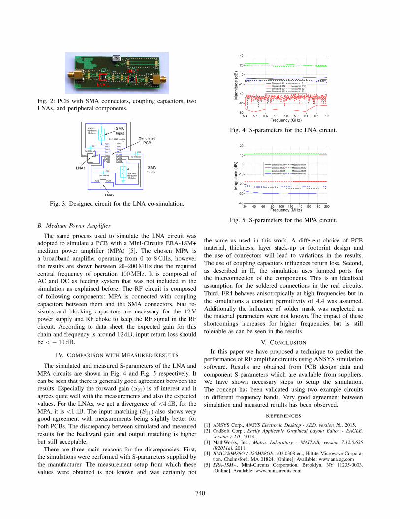
Fig. 2: PCB with SMA connectors, coupling capacitors, twoLNAs, and peripheral components.
B1-1_LNA_module
Port1
Port3
Port5
Port7
Port9
Port11
Port13 Port14
Port12
Port10
Port8
Port6
Port4
Port2
Port1Port2
1e-010farad
C21
1e-010farad
C23
PNUM=2RZ=50ohmIZ=0ohm
SMAInput
LNA1
LNA2
SMAOutput
SimulatedPCB
PNUM=1RZ=50ohmIZ=0ohm
1e-010farad
C22
Port1Port2
Fig. 3: Designed circuit for the LNA co-simulation.
B. Medium Power Amplifier
The same process used to simulate the LNA circuit wasadopted to simulate a PCB with a Mini-Circuits ERA-1SM+medium power amplifier (MPA) [5]. The chosen MPA isa broadband amplifier operating from 0 to 8GHz, howeverthe results are shown between 20–200MHz due the requiredcentral frequency of operation 100MHz. It is composed ofAC and DC as feeding system that was not included in thesimulation as explained before. The RF circuit is composedof following components: MPA is connected with couplingcapacitors between them and the SMA connectors, bias re-sistors and blocking capacitors are necessary for the 12Vpower supply and RF choke to keep the RF signal in the RFcircuit. According to data sheet, the expected gain for thischain and frequency is around 12 dB, input return loss shouldbe <− 10 dB.
IV. COMPARISON WITH MEASURED RESULTS
The simulated and measured S-parameters of the LNA andMPA circuits are shown in Fig. 4 and Fig. 5 respectively. Itcan be seen that there is generally good agreement between theresults. Especially the forward gain (S21) is of interest and itagrees quite well with the measurements and also the expectedvalues. For the LNAs, we get a divergence of <4 dB, for theMPA, it is <1 dB. The input matching (S11) also shows verygood agreement with measurements being slightly better forboth PCBs. The discrepancy between simulated and measuredresults for the backward gain and output matching is higherbut still acceptable.
There are three main reasons for the discrepancies. First,the simulations were performed with S-parameters supplied bythe manufacturer. The measurement setup from which thesevalues were obtained is not known and was certainly not
5 . 4 5 . 5 5 . 6 5 . 7 5 . 8 5 . 9 6 . 0 6 . 1 6 . 2- 8 0
- 6 0
- 4 0
- 2 0
0
2 0
4 0
S i m u l a t e d S 1 1 M e a s u r e d S 1 1 S i m u l a t e d S 1 2 M e a s u r e d S 1 2 S i m u l a t e d S 2 1 M e a s u r e d S 2 1 S i m u l a t e d S 2 2 M e a s u r e d S 2 2
Magn
itude
(dB)
F r e q u e n c y ( G H z )Fig. 4: S-parameters for the LNA circuit.
2 0 4 0 6 0 8 0 1 0 0 1 2 0 1 4 0 1 6 0 1 8 0 2 0 0- 4 0
- 3 0
- 2 0
- 1 0
0
1 0
2 0
S i m u l a t e d S 1 1 M e a s u r e d S 1 1 S i m u l a t e d S 1 2 M e a s u r e d S 1 2 S i m u l a t e d S 2 1 M e a s u r e d S 2 1 S i m u l a t e d S 2 2 M e a s u r e d S 2 2
Magn
itude
(dB)
F r e q u e n c y ( M H z )
Fig. 5: S-parameters for the MPA circuit.
the same as used in this work. A different choice of PCBmaterial, thickness, layer stack-up or footprint design andthe use of connectors will lead to variations in the results.The use of coupling capacitors influences return loss. Second,as described in II, the simulation uses lumped ports forthe interconnection of the components. This is an idealizedassumption for the soldered connections in the real circuits.Third, FR4 behaves anisotropically at high frequencies but inthe simulations a constant permittivity of 4.4 was assumed.Additionally the influence of solder mask was neglected asthe material parameters were not known. The impact of theseshortcomings increases for higher frequencies but is stilltolerable as can be seen in the results.
V. CONCLUSION
In this paper we have proposed a technique to predict theperformance of RF amplifier circuits using ANSYS simulationsoftware. Results are obtained from PCB design data andcomponent S-parameters which are available from suppliers.We have shown necessary steps to setup the simulation.The concept has been validated using two example circuitsin different frequency bands. Very good agreement betweensimulation and measured results has been observed.
REFERENCES
[1] ANSYS Corp., ANSYS Electronic Desktop - AED, version 16., 2015.[2] CadSoft Corp., Easily Applicable Graphical Layout Editor - EAGLE,
version 7.2.0., 2013.[3] MathWorks, Inc., Matrix Laboratory - MATLAB, version 7.12.0.635
(R2011a), 2011.[4] HMC320MS8G / 320MS8GE, v03.0308 ed., Hittite Microwave Corpora-
tion, Chelmsford, MA 01824. [Online]. Available: www.analog.com[5] ERA-1SM+, Mini-Circuits Corporation, Brooklyn, NY 11235-0003.
[Online]. Available: www.minicircuits.com
740
Related Documents