ILI9163 a-Si TFT LCD Single Chip Driver 132RGBx162 Resolution and 262K color Datasheet Preliminary Version: V0.13 Document No.: ILI9163DS_V0.13.pdf ILI TECHNOLOGY CORP. 4F, No. 2, Tech. 5 th Rd., Hsinchu Science Park, Taiwan 300, R.O.C. Tel.886-3-5670095; Fax.886-3-5670096 http://www.ilitek.com

Welcome message from author
This document is posted to help you gain knowledge. Please leave a comment to let me know what you think about it! Share it to your friends and learn new things together.
Transcript
ILI9163
a-Si TFT LCD Single Chip Driver 132RGBx162 Resolution and 262K color
Datasheet Preliminary
Version: V0.13
Document No.: ILI9163DS_V0.13.pdf
ILI TECHNOLOGY CORP. 4F, No. 2, Tech. 5th Rd., Hsinchu Science Park, Taiwan 300, R.O.C. Tel.886-3-5670095; Fax.886-3-5670096 http://www.ilitek.com
a-Si TFT LCD Single Chip Driver
132RGBx162 Resolution and 262K color ILI9163
Page 2 of 195 Version: 0.13
Table of Contents
1. Introduction ................................................................................................................................................ 6 2. Features..................................................................................................................................................... 6 3. Block Diagram............................................................................................................................................ 8 4. Pin Descriptions ......................................................................................................................................... 9 5. Pad Arrangement and Coordination ........................................................................................................ 15 6. Function Description ................................................................................................................................ 21 6.1. Interface Type Selection.................................................................................................................... 21 6.2. Serial Interface .................................................................................................................................. 21
6.2.1 Command Write .......................................................................................................................... 21 6.2.2 Read Function............................................................................................................................. 22
6.3. 8080-Series Parallel Interface (P68=’0’) ........................................................................................... 25 6.3.1 Write Cycle/Sequence ................................................................................................................ 25 6.3.2 Read Cycle/Sequence ................................................................................................................ 26
6.4. 6800-Series Parallel Interface (P68=’1’) ........................................................................................... 28 6.4.1 Write Cycle/Sequence ................................................................................................................ 29 6.4.2 Read Cycle/Sequence ................................................................................................................ 30
6.5. Display Data Transfer Recovery........................................................................................................ 31 6.6. Display Data Transfer Pause............................................................................................................. 32
6.6.1 Serial Interface Pause ................................................................................................................ 33 6.7. Display Data Transfer Mode.............................................................................................................. 33 6.8. Display Data Color Coding ................................................................................................................ 34
6.8.1 Serial Interface............................................................................................................................ 34 6.8.2 8-bit Parallel Interface (IM2=’1’, IM1, IM0 =”00”) ........................................................................ 38 6.8.3 16-bit Parallel Interface (IM2=’1’, IM1, IM0=”01”) ....................................................................... 41 6.8.4 9-bit Parallel Interface (IM2=’2’, IM1, IM0=”10”) ......................................................................... 44 6.8.5 18-bit Parallel Interface (IM2=’1’, IM1, IM0=”11”) ....................................................................... 44
7. Display Data RAM.................................................................................................................................... 48 7.1. Configuration ..................................................................................................................................... 48 7.2. Memory to Display Address Mapping................................................................................................ 49
7.2.1. 132RGB x 132 resolution (GM[2:0] = “101”, SMX=SMY=SRGB=’0’)......................................... 49 7.2.2. 130RGB x 130 resolution(GM[2:0] = “100”, SMX=SMY=SRGB=’0’).......................................... 50 7.2.3. 128RGB x 160 resolution (GM[2:0] = “011”, SMX=SMY=SRGB=’0’) ......................................... 50 7.2.4. 120RGB x 160 resolution (GM[2:0] = “010”, SMX=SMY=SRGB=’0’)......................................... 52 7.2.5. 128RGB x 128 resolution (GM[2:0] = “001”, SMX=SMY=SRGB=’0’)......................................... 53 7.2.6. 132RGB x 162 resolution (GM[2:0] = “000”, SMX=SMY=SRGB=’0’)......................................... 54
7.3. MCU to memory write/read direction (Address Counter) .................................................................. 55 8. Tearing Effect Output Line ....................................................................................................................... 57 8.1. Tearing Effect Line Modes................................................................................................................. 57 8.2. Tearing Effect Line Timing ................................................................................................................. 58
a-Si TFT LCD Single Chip Driver
132RGBx162 Resolution and 262K color ILI9163
Page 3 of 195 Version: 0.13
8.2.1 Example 1 MCU Write is Faster than Panel Read ..................................................................... 59 8.2.2 Example 2 MCU Write is slower than Panel Read ..................................................................... 59
9. Power ON/OFF Sequence....................................................................................................................... 61 9.1. Case 1 – RESX line is held high or Unstable by Host at Power -On ................................................ 61 9.2. Case 2 – RESX line is held Low by Host at Power On ..................................................................... 61 9.3. Uncontrolled Power Off ..................................................................................................................... 62 10. Power Level Definition ............................................................................................................................. 62 10.1. Power Levels ..................................................................................................................................... 62 10.2. Power Flow Chart.............................................................................................................................. 64 11. Gamma Curves........................................................................................................................................ 65 12. Reset........................................................................................................................................................ 66 12.1. Registers ........................................................................................................................................... 66 12.2. Input/Output Pins............................................................................................................................... 71
12.2.1 Output Pins, I/O Pins .................................................................................................................. 71 12.2.2 Input Pins .................................................................................................................................... 72
12.3. Reset Timing...................................................................................................................................... 72 13. SleepOut – Command and Self-Diagnostic Functions of Display ........................................................... 73 13.1. Register loading Detection ................................................................................................................ 73 13.2. Functionality Detection ...................................................................................................................... 74 14. Command ................................................................................................................................................ 76 14.1. Command List.......................................................................................................................................... 76 14.2. Command Description ............................................................................................................................. 78
14.2.1 NOP (00h)................................................................................................................................... 78 14.2.2 Software Reset (01h) .................................................................................................................. 79 14.2.3 Read Display Identification Information (04h)............................................................................. 80 14.2.4 Read Display Status (09h) .......................................................................................................... 81 14.2.5 Read Display Power Mode (0Ah) ............................................................................................... 85 14.2.6 Read Display MADCTL (0Bh) ..................................................................................................... 86 14.2.7 Read Display Pixel Format (0Ch) ............................................................................................... 88 14.2.8 Read Display Image Mode (0Dh) ............................................................................................... 89 14.2.9 Read Display Signal Mode (0Eh)................................................................................................ 91 14.2.10 Read Display Signal Mode (0Fh)................................................................................................ 92 14.2.11 Sleep In (10h) ............................................................................................................................. 93 14.2.12 Sleep Out (11h)........................................................................................................................... 94 14.2.13 Partial Mode On (12h) ................................................................................................................ 96 14.2.14 Normal Display Mode On (13h) .................................................................................................. 97 14.2.15 Display Inversion Off (20h) ......................................................................................................... 98 14.2.16 Display Inversion On (21h) ......................................................................................................... 99 14.2.17 Gamma Set (26h) ..................................................................................................................... 100 14.2.18 Display Off (28h) ....................................................................................................................... 102
a-Si TFT LCD Single Chip Driver
132RGBx162 Resolution and 262K color ILI9163
Page 4 of 195 Version: 0.13
14.2.19 Display On (29h) ....................................................................................................................... 104 14.2.20 Column Address Set (2Ah) ....................................................................................................... 106 14.2.21 Page Address Set (2Bh) ........................................................................................................... 109 14.2.22 Memory Write (2Ch).................................................................................................................. 112 14.2.23 Color Setting fro 4K, 65K and 262K (2Dh) ............................................................................... 113 14.2.24 Memory Read (2Eh).................................................................................................................. 115 14.2.25 Partial Area (30h) ...................................................................................................................... 117 14.2.26 Vertical Scrolling Definition (33h).............................................................................................. 119 14.2.27 Tearing Effect Line Off (34h) ..................................................................................................... 123 14.2.28 Tearing Effect Line On (35h)..................................................................................................... 125 14.2.29 Memory Access Control (36h) .................................................................................................. 127 14.2.30 Vertical Scrolling Start Address (37h) ....................................................................................... 129 14.2.31 Idle Mode Off (38h) ................................................................................................................... 130 14.2.32 Idle Mode On (39h) ................................................................................................................... 132 14.2.33 Interface Pixel Format (3Ah)..................................................................................................... 134 14.2.34 Read ID1 (DAh) ........................................................................................................................ 136 14.2.35 Read ID2 (DBh) ........................................................................................................................ 137 14.2.36 Read ID3 (DCh) ........................................................................................................................ 138 14.2.37 RGB Signal control (B0h) ......................................................................................................... 139 14.2.38 Frame Rate Control(In normal mode/Full colors) (B1h) ........................................................... 142 14.2.39 Frame Rate Control(In Idle mode/8-colors) (B2h) .................................................................... 143 14.2.40 Frame Rate Control(In Partial mode/full colors) (B3h) ............................................................. 145 14.2.41 Display Inversion Control (B4h) ................................................................................................ 147 14.2.42 RGB Interface Blanking Porch setting (B5h) ............................................................................ 148 14.2.43 Display Fuction set 5 (B6h)....................................................................................................... 150 14.2.44 Source Driver Direction Control (B7h) ...................................................................................... 152 14.2.45 Gate Driver Direction Control (B8h).......................................................................................... 153 14.2.46 Power_Control1 (C0h) .............................................................................................................. 154 14.2.47 Power_Control2 (C1h) .............................................................................................................. 156 14.2.48 Power_Control3 (C2h) .............................................................................................................. 157 14.2.49 Power_Control4 (C3h) .............................................................................................................. 159 14.2.50 Power_Control 5 (C4h) ............................................................................................................. 161 14.2.51 VCOM_Control 1 (C5h) ............................................................................................................ 163 14.2.52 VCOM_Control 2 (C6h) ............................................................................................................ 164 14.2.53 VCOM Offset Control (C7h) ...................................................................................................... 165 14.2.54 Write ID4 Value (D3h) ............................................................................................................... 167 14.2.55 NV Memory Function Controller1(D9h) .................................................................................... 169 14.2.56 NV Memory Function Controller 2(DEh)................................................................................... 170 14.2.57 Positive Gamma Correction Setting (E0h)................................................................................ 171 14.2.58 Negative Gamma Correction Setting (E1h) .............................................................................. 173
a-Si TFT LCD Single Chip Driver
132RGBx162 Resolution and 262K color ILI9163
Page 5 of 195 Version: 0.13
14.2.59 GAM_R_SEL (F2h)................................................................................................................... 175 15. Example Connection with Panel direction and Different Resolution...................................................... 176 15.1. Application of connect with panel direction (when GM=’011’)......................................................... 176 15.2. Application of connection with Different resolution.......................................................................... 178 16. OTP Programming Flow ........................................................................................................................ 187 17. Electrical Characteristics........................................................................................................................ 188 17.1. Absolute Maximum Ratings............................................................................................................. 188 17.2. DC Characteristics .......................................................................................................................... 189 17.3. AC Characteristics........................................................................................................................... 190 17.4. Display Module Parallel 18/16/9/8-bit Bus ...................................................................................... 190 17.5. Display Serial Interface ................................................................................................................... 191
17.5.1 3-pin Serial Interface................................................................................................................. 191 17.5.2 4-pin Serial Interface................................................................................................................. 192
17.6. Reset Timing Characteristics........................................................................................................... 193 18. Revision History ..................................................................................................................................... 194
a-Si TFT LCD Single Chip Driver
132RGBx162 Resolution and 262K color ILI9163
Page 6 of 195 Version: 0.13
1. Introduction ILI9163 is a 262,144-color one-chip SoC driver for a-TFT liquid crystal display with resolution of 132RGBx162
dots, comprising a 396-channel source driver, a 162-channel gate driver, 48,114bytes GRAM for graphic data of
132RGBx162 dots, and power supply circuit.
The ILI9163 supports 18-/16-/9-/8-bit data bus interface and serial peripheral interfaces (SPI). It also supplies
18-bit, 16-bit or 6-bit RGB interface for driving video signal directly from application controller. The moving
picture area can be specified in internal GRAM by window address function. The specified window area can be
updated selectively, so that moving picture can be displayed simultaneously independent of still picture area.
ILI9163 can operate with 1.65V I/O interface voltage, and an incorporated voltage follower circuit to generate
voltage levels for driving an LCD. The ILI9163 also supports a function to display in 8 colors and a sleep mode,
allowing for precise power control by software and these features make the ILI9163 an ideal LCD driver for
medium or small size portable products such as digital cellular phones, smart phone, MP3 and PMP where long
battery life is a major concern.
2. Features Display resolution: [132xRGB](H) x 162(V) Output:
396 source outputs 162 gate outputs Common electrode output
AM-LCD driver with on-chip full display RAM: 48,114 bytes
MCU Interface
8-bits, 9-bits, 16-bits, 18-bits interface with 8080-series MCU 8-bits, 9-bits, 16-bits, 18-bits interface with 6800-series MCU 12-bits, 16-bits, 18-bits RGB interface with graphic controller 3-pin/4-pin serial interface
Display mode:
Full color mode (idle mode off): 262K-colors Reduced color mode (idle mode on): 8-colors (3-bits MSB bits mode)
On chip functions:
VCOM generator and adjustment Timing generator Oscillator DC/DC converter 8 preset gamma curve selectable Line/frame inversion MTP to store initialization register setting Factory default value(Contrast, Module ID, Module version, etc) are stored on the display module
MTP:
a-Si TFT LCD Single Chip Driver
132RGBx162 Resolution and 262K color ILI9163
Page 7 of 195 Version: 0.13
7-bits for ID2 8-bits for ID3 7-bits for VCOM adjustment
Low -power consumption architecture
Low operating power supplies: VDDI = 1.65V ~ 3.3 V (interface I/O) VDD = 2.6V ~ 3.3 V (analog)
LCD Voltage drive: Source/VCOM power supply voltage
AVDD - GND = 4.5V ~ 6.0 VCL – GND = -1.0V ~ -3.0V VDD – VCL 6.0V≦
Gate driver output voltage VGH - GND = 10V ~ 16V VGL – GND = -9V ~ -16V VGH – VGL 32V≦
VCOM driver output voltage VCOMH = 2.5V ~5V VCOML = -2.5V ~ 0V VCOMH-VCOML 6.0V≦
Operate temperature range: -40 to 85℃ ℃
a-Si TFT LCD Single Chip Driver
132RGBx162 Resolution and 262K color ILI9163
Page 8 of 195 Version: 0.13
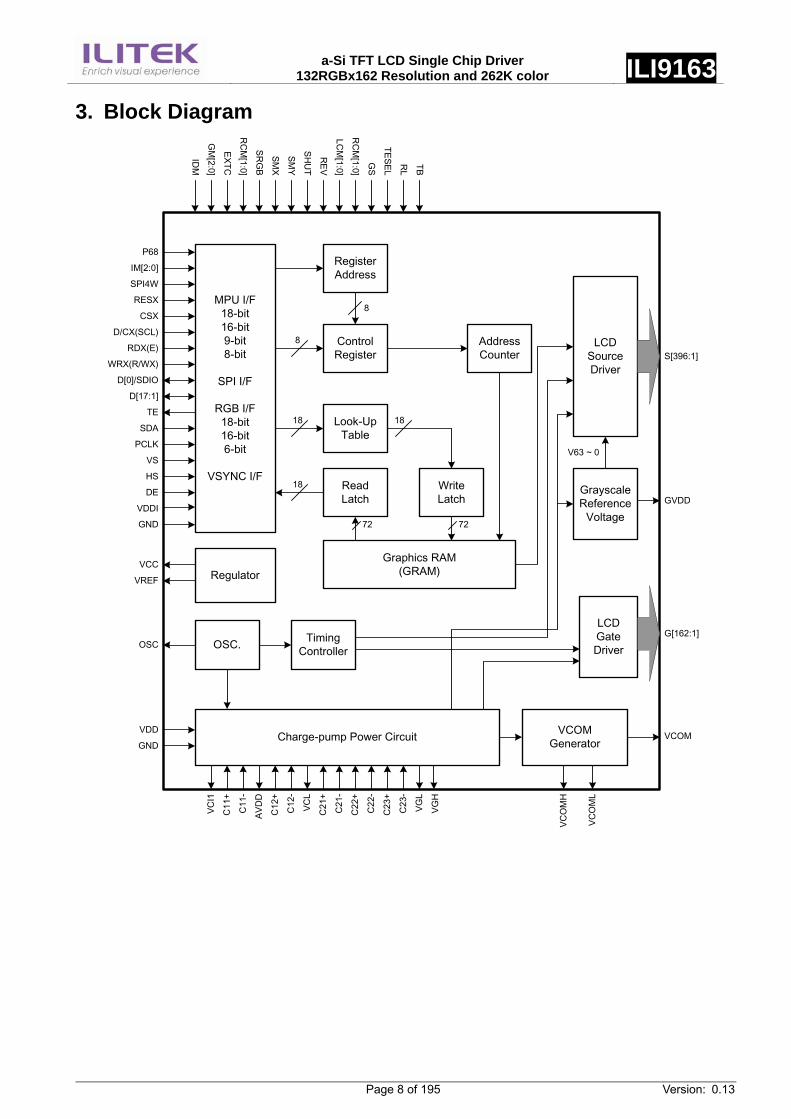
3. Block Diagram
MPU I/F18-bit16-bit9-bit8-bit
SPI I/F
RGB I/F18-bit16-bit6-bit
VSYNC I/F
CSX
D/CX(SCL)
D[0]/SDIO
RESX
IM[2:0]
VDDI
Regulator
OSC. Timing Controller
Charge-pump Power Circuit
GVDD
VCI1
C11
+
VDD
GND
C11
-AV
DD
VGH
C21
+
C21
-
VCL
C22
+
C22
-
C23
+
C23
-
VGL
VCOMGenerator
VCOM
VCO
MH
VCO
ML
RegisterAddress
Control Register
8
8
Look-UpTable
18
ReadLatch
18
18
WriteLatch
Graphics RAM(GRAM)
7272
Address Counter
LCDSourceDriver
GrayscaleReference
Voltage
V63 ~ 0
S[396:1]
LCDGateDriver
G[162:1]
GND
P68
SPI4W
RDX(E)WRX(R/WX)
D[17:1]
TE
SDA
PCLK
VS
HS
DE
OSC
EXTCG
M[2:0]
IDM
SMX
SRG
BR
CM
[1:0]
SMY
LCM
[1:0]
REV
SHU
T
TESEL
GS
RC
M[1:0]
RL
TB
VCC
VREF
C12
+
C12
-
a-Si TFT LCD Single Chip Driver
132RGBx162 Resolution and 262K color ILI9163
Page 9 of 195 Version: 0.13
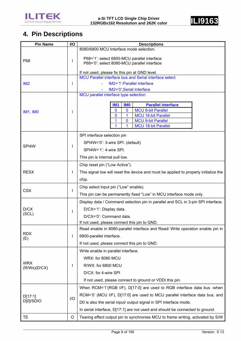
4. Pin Descriptions Pin Name I/O Descriptions
P68 I
8080/6800 MCU Interface mode selection.
P68=’1’: select 6800-MCU parallel interface P68=’0’: select 8080-MCU parallel interface
If not used, please fix this pin at GND level.
IM2 I MCU Parallel interface bus and Serial interface select
- IM2=’1’;Parallel Interface - IM2=’0’;Serial Interface
IM1, IM0 I
MCU parallel interface type selection
IM1 IM0 Parallel interface 0 0 MCU 8-bit Parallel 0 1 MCU 16-bit Parallel 1 0 MCU 9-bit Parallel 1 1 MCU 18-bit Parallel
SPI4W I
SPI interface selection pin
SPI4W=’0’: 3-wire SPI. (default)
SPI4W=’1’: 4-wire SPI.
This pin is internal pull low.
RESX I
Chip reset pin (“Low Active”).
This signal low will reset the device and must be applied to properly initialize the
chip.
CSX I Chip select input pin (“Low” enable).
This pin can be permanently fixed “Low” in MCU interface mode only.
D/CX (SCL) I
Display data / Command selection pin in parallel and SCL in 3-pin SPI interface.
D/CX=’1’: Display data.
D/CX=’0’: Command data. If not used, please connect this pin to GND.
RDX (E) I
Read enable in 8080-parallel interface and Read/ Write operation enable pin in
6800-parallel interface.
If not used, please connect this pin to GND.
WRX (R/Wx)(D/CX) I
Write enable in parallel interface.
WRX: for 8080 MCU
R/WX: for 6800 MCU
D/CX: for 4-wire SPI
If not used, please connect to ground or VDDI this pin.
D[17:1] D[0]/SDIO I/O
When RCM=’1’(RGB I/F), D[17:0] are used to RGB interface data bus -when
RCM=’0’ (MCU I/F), D[17:0] are used to MCU parallel interface data bus, and
D0 is also the serial input/ output signal in SPI interface mode.
In serial interface, D[17:1] are not used and should be connected to ground.
TE O Tearing effect output pin to synchronies MCU to frame writing, activated by S/W
a-Si TFT LCD Single Chip Driver
132RGBx162 Resolution and 262K color ILI9163
Page 10 of 195 Version: 0.13
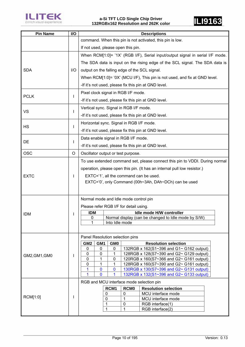
Pin Name I/O Descriptions command. When this pin is not activated, this pin is low.
If not used, please open this pin.
SDA I/O
When RCM[1:0]= ’1X’ (RGB I/F), Serial input/output signal in serial I/F mode.
The SDA data is input on the rising edge of the SCL signal. The SDA data is
output on the falling edge of the SCL signal.
When RCM[1:0]= ’0X’ (MCU I/F), This pin is not used, and fix at GND level.
-If it’s not used, please fix this pin at GND level.
PCLK I Pixel clock signal in RGB I/F mode.
-If it’s not used, please fix this pin at GND level.
VS I Vertical sync. Signal in RGB I/F mode.
-If it’s not used, please fix this pin at GND level.
HS I Horizontal sync. Signal in RGB I/F mode.
-If it’s not used, please fix this pin at GND level.
DE I Data enable signal in RGB I/F mode.
-If it’s not used, please fix this pin at GND level.
OSC O Oscillator output or test purpose.
EXTC I
To use extended command set, please connect this pin to VDDI. During normal
operation, please open this pin. (It has an internal pull low resistor.)
EXTC=’1’, all the command can be used. EXTC=’0’, only Command (00h~3Ah, DAh~DCh) can be used
IDM I
Normal mode and Idle mode control pin
Please refer RGB I/F for detail using. IDM Idle mode H/W controller
0 Normal display (can be changed to Idle mode by S/W) 1 Into Idle mode
GM2,GM1,GM0 I
Panel Resolution selection pins GM2 GM1 GM0 Resolution selection
0 0 0 132RGB x 162(S1~396 and G1~ G162 output)0 0 1 128RGB x 128(S7~390 and G2~ G129 output)0 1 0 120RGB x 160(S7~366 and G2~ G161 output)0 1 1 128RGB x 160(S7~390 and G2~ G161 output)1 0 0 130RGB x 130(S7~396 and G2~ G131 output)1 0 1 132RGB x 132(S1~396 and G2~ G133 output)
RCM[1:0] I
RGB and MCU interface mode selection pin RCM1 RCM0 Resolution selection 0 0 MCU interface mode 0 1 MCU interface mode 1 0 RGB interface(1) 1 1 RGB interface(2)
a-Si TFT LCD Single Chip Driver
132RGBx162 Resolution and 262K color ILI9163
Page 11 of 195 Version: 0.13
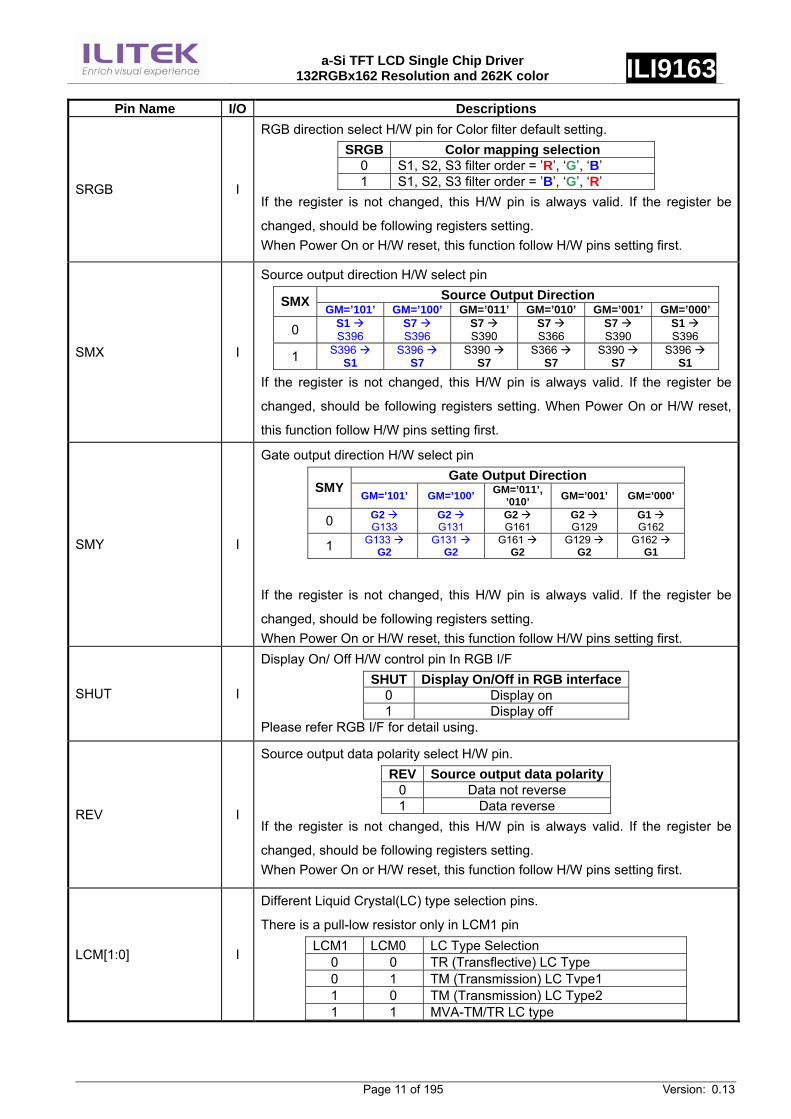
Pin Name I/O Descriptions
SRGB I
RGB direction select H/W pin for Color filter default setting. SRGB Color mapping selection
0 S1, S2, S3 filter order = ’R’, ‘G’, ‘B’ 1 S1, S2, S3 filter order = ’B’, ‘G’, ‘R’
If the register is not changed, this H/W pin is always valid. If the register be
changed, should be following registers setting. When Power On or H/W reset, this function follow H/W pins setting first.
SMX I
Source output direction H/W select pin Source Output Direction SMX GM=’101’ GM=’100’ GM=’011’ GM=’010’ GM=’001’ GM=’000’
0 S1 S396
S7 S396
S7 S390
S7 S366
S7 S390
S1 S396
1 S396 S1
S396 S7
S390 S7
S366 S7
S390 S7
S396 S1
If the register is not changed, this H/W pin is always valid. If the register be
changed, should be following registers setting. When Power On or H/W reset,
this function follow H/W pins setting first.
SMY I
Gate output direction H/W select pin Gate Output Direction
SMY GM=’101’ GM=’100’ GM=’011’,’010’ GM=’001’ GM=’000’
0 G2 G133
G2 G131
G2 G161
G2 G129
G1 G162
1 G133 G2
G131 G2
G161 G2
G129 G2
G162 G1
If the register is not changed, this H/W pin is always valid. If the register be
changed, should be following registers setting. When Power On or H/W reset, this function follow H/W pins setting first.
SHUT I
Display On/ Off H/W control pin In RGB I/F SHUT Display On/Off in RGB interface
0 Display on 1 Display off
Please refer RGB I/F for detail using.
REV I
Source output data polarity select H/W pin. REV Source output data polarity
0 Data not reverse 1 Data reverse
If the register is not changed, this H/W pin is always valid. If the register be
changed, should be following registers setting. When Power On or H/W reset, this function follow H/W pins setting first.
LCM[1:0] I
Different Liquid Crystal(LC) type selection pins.
There is a pull-low resistor only in LCM1 pin LCM1 LCM0 LC Type Selection
0 0 TR (Transflective) LC Type 0 1 TM (Transmission) LC Tvpe1 1 0 TM (Transmission) LC Type2 1 1 MVA-TM/TR LC type
a-Si TFT LCD Single Chip Driver
132RGBx162 Resolution and 262K color ILI9163
Page 12 of 195 Version: 0.13
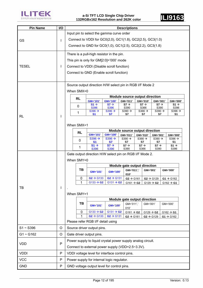
Pin Name I/O Descriptions
GS I
Input pin to select the gamma curve order
Connect to VDDI for GC0(2,0), GC1(1.8), GC2(2.5), GC3(1.0)
Connect to GND for GC0(1,0), GC1(2.5), GC2(2.2), GC3(1.8)
TESEL I
There is a pull-high resistor in the pin.
This pin is only for GM[2:0]=’000’ mode
Connect to VDDI (Disable scroll function)
Connect to GND (Enable scroll function)
RL I
Source output direction H/W select pin in RGB I/F Mode 2
When SMX=0 Module source output direction RL
GM=’101’ GM=’100’ GM=’011’ GM=’010’ GM=’001’ GM=’000’
0 S1 S396
S7 S396
S7 S390
S7 S366
S7 S390
S1 S396
1 S396 S1
S396 S7
S390 S7
S366 S7
S390 S7
S396 S1
When SMX=1 Module source output direction RL GM=’101’ GM=’100’ GM=’011’ GM=’010’ GM=’001’ GM=’000’
0 S396 S1
S396 S7
S390 S7
S366 S7
S390 S7
S396 S1
1 S1 S396
S7 S396
S7 S390
S7 S366
S7 S390
S1 S396
TB I
Gate output direction H/W select pin on RGB I/F Mode 2.
When SMY=0 Module gate output direction
TB GM=’101’ GM=’100’ GM=’011’,’010’
GM=’001’ GM=’000’
0 G2 G133 G2 G131 G2 G161 G2 G129 G1 G1621 G133 G2 G131 G2 G161 G2 G129 G2 G162 G1
.
When SMY=1 Module gate output direction
TB GM=’101’ GM=’100’ GM=’011’,’010’
GM=’001’ GM=’000’
0 G133 G2 G131 G2 G161 G2 G129 G2 G162 G11 G2 G133 G2 G131 G2 G161 G2 G129 G1 G162
Please refer RGB I/F detail using
S1 ~ S396 O Source driver output pins.
G1 ~ G162 O Gate driver output pins.
VDD PPower supply to liquid crystal power supply analog circuit.
Connect to external power supply (VDD=2.5~3.3V).
VDDI P VDDI voltage level for interface control pins.
VCC P Power supply for internal logic regulator.
GND P GND voltage output level for control pins.
a-Si TFT LCD Single Chip Driver
132RGBx162 Resolution and 262K color ILI9163
Page 13 of 195 Version: 0.13
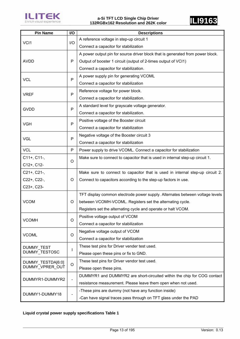
Pin Name I/O Descriptions
VCI1 I/O A reference voltage in step-up circuit 1
Connect a capacitor for stabilization
AVDD P
A power output pin for source driver block that is generated from power block.
Output of booster 1 circuit (output of 2-times output of VCI1)
Connect a capacitor for stabilization.
VCL PA power supply pin for generating VCOML
Connect a capacitor for stabilization
VREF PReference voltage for power block.
Connect a capacitor for stabilization.
GVDD PA standard level for grayscale voltage generator.
Connect a capacitor for stabilization.
VGH PPositive voltage of the Booster circuit
Connect a capacitor for stabilization
VGL PNegative voltage of the Booster circuit 3
Connect a capacitor for stabilization
VCL P Power supply to drive VCOML. Connect a capacitor for stabilization
C11+, C11-,
C12+, C12- O
Make sure to connect to capacitor that is used in internal step-up circuit 1.
C21+, C21-,
C22+, C22-,
C23+, C23-
O
Make sure to connect to capacitor that is used in internal step-up circuit 2.
Connect to capacitors according to the step-up factors in use.
VCOM O
TFT display common electrode power supply. Alternates between voltage levels
between VCOMH-VCOML. Registers set the alternating cycle.
Registers set the alternating cycle and operate or halt VCOM.
VCOMH OPositive voltage output of VCOM
Connect a capacitor for stabilization
VCOML ONegative voltage output of VCOM
Connect a capacitor for stabilization
DUMMY_TEST DUMMY_TESTOSC I
These test pins for Driver vender test used.
Please open these pins or fix to GND.
DUMMY_TESTDA[6:0] DUMMY_VPRER_OUT O
These test pins for Driver vendor test used.
Please open these pins.
DUMMYR1-DUMMYR2 - DUMMYR1 and DUMMYR2 are short-circuited within the chip for COG contact
resistance measurement. Please leave them open when not used.
DUMMY1-DUMMY18 - -These pins are dummy (not have any function inside)
-Can have signal traces pass through on TFT glass under the PAD
Liquid crystal power supply specifications Table 1
a-Si TFT LCD Single Chip Driver
132RGBx162 Resolution and 262K color ILI9163
Page 14 of 195 Version: 0.13
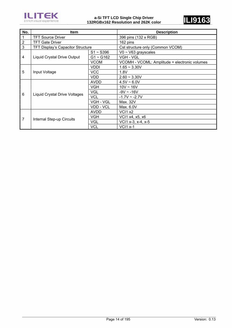
No. Item Description 1 TFT Source Driver 396 pins (132 x RGB) 2 TFT Gate Driver 162 pins 3 TFT Display’s Capacitor Structure Cst structure only (Common VCOM)
S1 ~ S396 V0 ~ V63 grayscales G1 ~ G162 VGH - VGL 4 Liquid Crystal Drive Output VCOM VCOMH - VCOML: Amplitude = electronic volumes VDDI 1.65 ~ 3.30V VCC 1.8V 5 Input Voltage VDD 2.60 ~ 3.30V AVDD 4.5V ~ 6.0V VGH 10V ~ 16V VGL -9V ~ -16V VCL -1.7V ~ -2.7V VGH - VGL Max. 32V
6 Liquid Crystal Drive Voltages
VDD - VCL Max. 6.0V AVDD VCI1 x2 VGH VCI1 x4, x5, x6 VGL VCI1 x-3, x-4, x-5
7 Internal Step-up Circuits
VCL VCI1 x-1
a-Si TFT LCD Single Chip Driver
132RGBx162 Resolution and 262K color ILI9163
Page 15 of 195 Version: 0.13
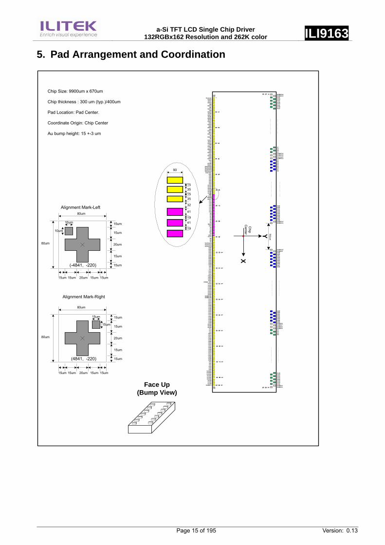
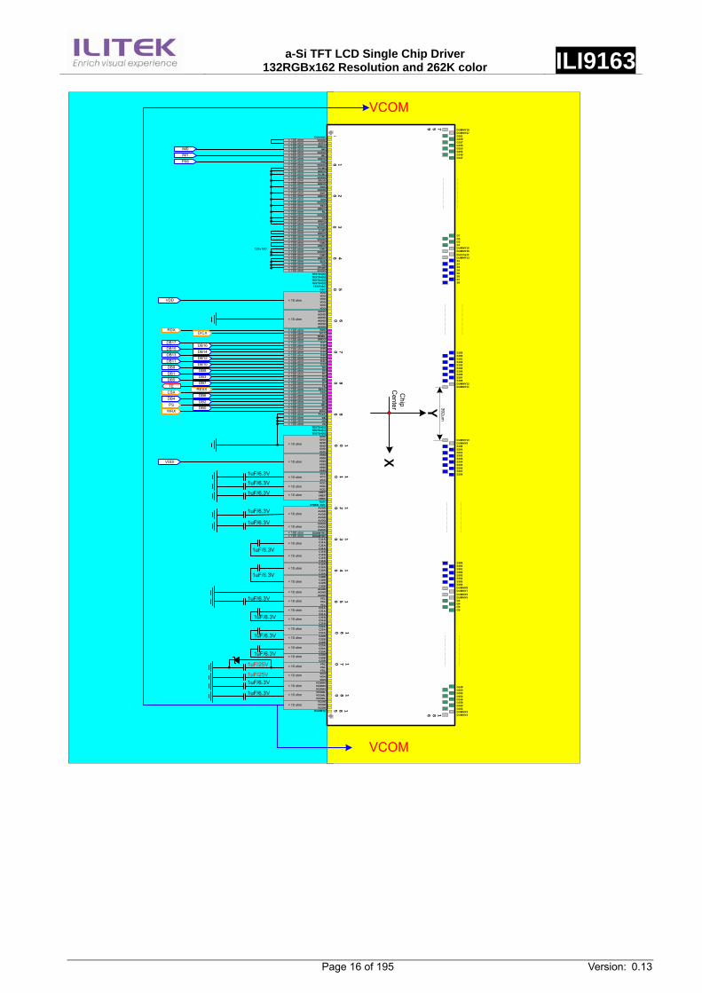
5. Pad Arrangement and Coordination
Chip Size: 9900um x 670um
Chip thickness : 300 um (typ.)/400um
Pad Location: Pad Center.
Coordinate Origin: Chip Center
Au bump height: 15 +-3 um
Face Up(Bump View)
X
Y
1
1020
3040
5060
7080
90
100
110
120
130
140
150
160
170
180
Dummy1VDDIO EXTC
GNDO IM0
VDDIO IM1
GNDO P68
VDDIORCM0 GNDO RCM1
VDDIOSRGB GNDO
SMX VDDIO
SMY GNDO
IDM VDDIO
REV GNDO
RL VDDIO
TB GNDO SHUT
VDDIOLCM0 GNDO LCM1
VDDIO GM2
GNDO GM1
VDDIO GM0
GNDOSDA
GS SPI4W VDDIO
TESTDA[6]TESTDA[5]TESTDA[4]TESTDA[3]TESTOSC
OSCVDD VDD VDD VDD VDD VDD
AGNDAGNDAGNDAGNDAGND AGND
RDX D/CX
TESELGNDO
D17 D16 D15 D14D13D12D11D10D9 D8 D1 D3 D5 D7TE
RESXCSX
D6 D4 D2
IM2 D0
WRX PCLK
DE HS VS
TESTDA[2]TESTDA[1]TESTDA[0]
GND GND GND GNDGND GND VDDI VDDI VDDI VDDI VDDI VDDI VCC VCCVCC VCI1 VCI1 VCI1
VREF VREF VREF TEST
VPRER_OUTAVDDAVDD AVDD AVDD AVDD GVDD GVDD GVDD
DUMMYR1DUMMYR2
C11AC11A C11A C11A C11B C11B C11B C11B C12A C12A C12AC12AC12BC12BC12BC12B
AGNDAGNDAGND
VCL VCLVCL
C21AC21AC21AC21BC21BC21BC22AC22AC22AC22BC22BC22BC23AC23AC23AC23BC23BC23BVGLVGL VGL VGH VGH VGH
VCOMHVCOMHVCOMHVCOMLVCOMLVCOML
VCOM VCOM VCOM
DUMMY2
Chip
Center 392um
80um
80um
10um
10um
15um
15um
20um
15um
15um
20um 15um15um15um 15um
(-4841, -220)
Alignment Mark-Left
Alignment Mark-Right
80um
80um
15um
15um
185
15um
15um
20um
15um
15um
20um 15um15um15um 15um
(4841, -220)
……
……
……
……
….
……
……
……
……
….
G148G150G152G154G156G158G160G162DUMMY4DUMMY3
DUMMY6DUMMY5G2G4G6G8
S389S390S391S392S393S394S395S396DUMMY8DUMMY7
186
DUMMY10DUMMY9S199S200S201S202S203S204S205S206S207S208
……
……
……
……
….
……
……
……
……
….
DUMMY18DUMMY17G161G159G157G155G153G151G149G147
G7G5G3G1DUMMY16DUMMY15Dummy14DUMMY13S1S2S3S4S5S6S7S8
759
S189S190S191S192S193S194S195S196S197S198DUMMY12DUMMY11
……
……
……
……
….
……
……
……
……
….
……
……
……
……
….
……
……
……
……
….
35
90
15
32
41
19
19
41
3515
a-Si TFT LCD Single Chip Driver
132RGBx162 Resolution and 262K color ILI9163
Page 16 of 195 Version: 0.13
< 100 ohm< 100 ohm
< 100 ohm< 100 ohm
< 100 ohm< 100 ohm
< 100 ohm
< 100 ohm< 100 ohm
< 100 ohm< 100 ohm
< 100 ohm< 100 ohm< 100 ohm
< 100 ohm< 100 ohm
< 100 ohm< 100 ohm
< 100 ohm
< 100 ohm< 100 ohm
< 100 ohm< 100 ohm
< 100 ohm< 100 ohm
< 100 ohm< 100 ohm
< 100 ohm< 100 ohm
< 100 ohm< 100 ohm
< 100 ohm< 100 ohm
< 100 ohm< 100 ohm< 100 ohm
< 100 ohm< 100 ohm
< 100 ohm< 100 ohm
< 100 ohm
< 100 ohm< 100 ohm
< 100 ohm< 100 ohm
< 100 ohm< 100 ohm
< 100 ohm< 100 ohm
< 100 ohm< 100 ohm
< 100 ohm< 100 ohm
< 100 ohm< 100 ohm
< 100 ohm< 100 ohm< 100 ohm< 100 ohm< 100 ohm< 100 ohm< 100 ohm< 100 ohm< 100 ohm< 100 ohm< 100 ohm< 100 ohm< 100 ohm< 100 ohm< 100 ohm< 100 ohm< 100 ohm
< 100 ohm< 100 ohm
< 100 ohm< 100 ohm
VCOM
VCOM
X
Y
1
1020
3040
5060
7080
90
100
110
120
130
140
150
160
170
180
Dummy1VDDIO EXTC
GNDO IM0
VDDIO IM1
GNDO P68
VDDIORCM0 GNDO RCM1
VDDIOSRGB GNDO
SMX VDDIO
SMY GNDO
IDM VDDIO
REV GNDO
RL VDDIO
TB GNDO SHUT
VDDIOLCM0 GNDO LCM1
VDDIO GM2
GNDO GM1
VDDIO GM0
GNDOSDA
GS SPI4W VDDIO
TESTDA[6]TESTDA[5]TESTDA[4]TESTDA[3]TESTOSC
OSCVDD VDD VDD VDD VDD VDD
AGNDAGNDAGNDAGNDAGND AGND
RDX D/CX
TESELGNDO
D17 D16 D15 D14D13D12D11D10
D9 D8 D1 D3 D5 D7TE
RESXCSX
D6 D4 D2
IM2 D0
WRX PCLK
DE HS VS
TESTDA[2]TESTDA[1]TESTDA[0]
GND GND GND GNDGND GND VDDI VDDI VDDI VDDI VDDI VDDI VCC VCCVCC VCI1 VCI1 VCI1
VREF VREF VREF TEST
VPRER_OUTAVDDAVDD AVDD AVDD AVDD GVDD GVDD GVDD
DUMMYR1DUMMYR2
C11AC11A C11A C11A C11B C11B C11B C11B C12A C12A C12AC12AC12BC12BC12BC12B
AGNDAGNDAGND
VCL VCLVCL
C21AC21AC21AC21BC21BC21BC22AC22AC22AC22BC22BC22BC23AC23AC23AC23BC23BC23BVGLVGL VGL VGH VGH VGH
VCOMHVCOMHVCOMHVCOMLVCOMLVCOML
VCOM VCOM VCOM
DUMMY2
Chip
Center 392um
185
……
……
……
……
….
……
……
……
……
….
G148G150G152G154G156G158G160G162DUMMY4DUMMY3
DUMMY6DUMMY5G2G4G6G8
S389S390S391S392S393S394S395S396DUMMY8DUMMY7
186
DUMMY10DUMMY9S199S200S201S202S203S204S205S206S207S208
……
……
……
……
….
……
……
……
……
….
DUMMY18DUMMY17G161G159G157G155G153G151G149G147
G7G5G3G1DUMMY16DUMMY15Dummy14DUMMY13S1S2S3S4S5S6S7S8
759
S189S190S191S192S193S194S195S196S197S198DUMMY12DUMMY11
……
……
……
……
….
……
……
……
……
….
……
……
……
……
….
……
……
……
……
….
< 10 ohm
< 10 ohm
< 10 ohm
< 10 ohm
< 10 ohm
< 10 ohm
< 10 ohm
< 10 ohm
< 10 ohm
< 10 ohm
< 10 ohm
< 10 ohm
< 10 ohm
< 10 ohm
< 10 ohm
< 10 ohm
< 10 ohm
< 10 ohm
< 10 ohm
< 10 ohm
< 10 ohm
< 10 ohm
< 10 ohm
< 10 ohm
< 10 ohm
< 10 ohm
VDD
WRX
DB1
DB2
DB3
DB4
DB5
DB6
DB7
DB8DB9
DB10DB11
DB12DB13
DB14DB15
DB16DB17
TERESX
CSX
PSDB0
VDDI
1uF/6.3V
1uF/6.3V
1uF/6.3V
1uF/6.3V
1uF/6.3V
1uF/6.3V
1uF/6.3V
1uF/6.3V
1uF/6.3V
1uF/6.3V
1uF/6.3V
1uF/25V
1uF/25V
1uF/6.3V
1uF/6.3V
IM0IM1P68
RDXD/CX
128x160
a-Si TFT LCD Single Chip Driver
132RGBx162 Resolution and 262K color ILI9163
Page 17 of 195 Version: 0.13
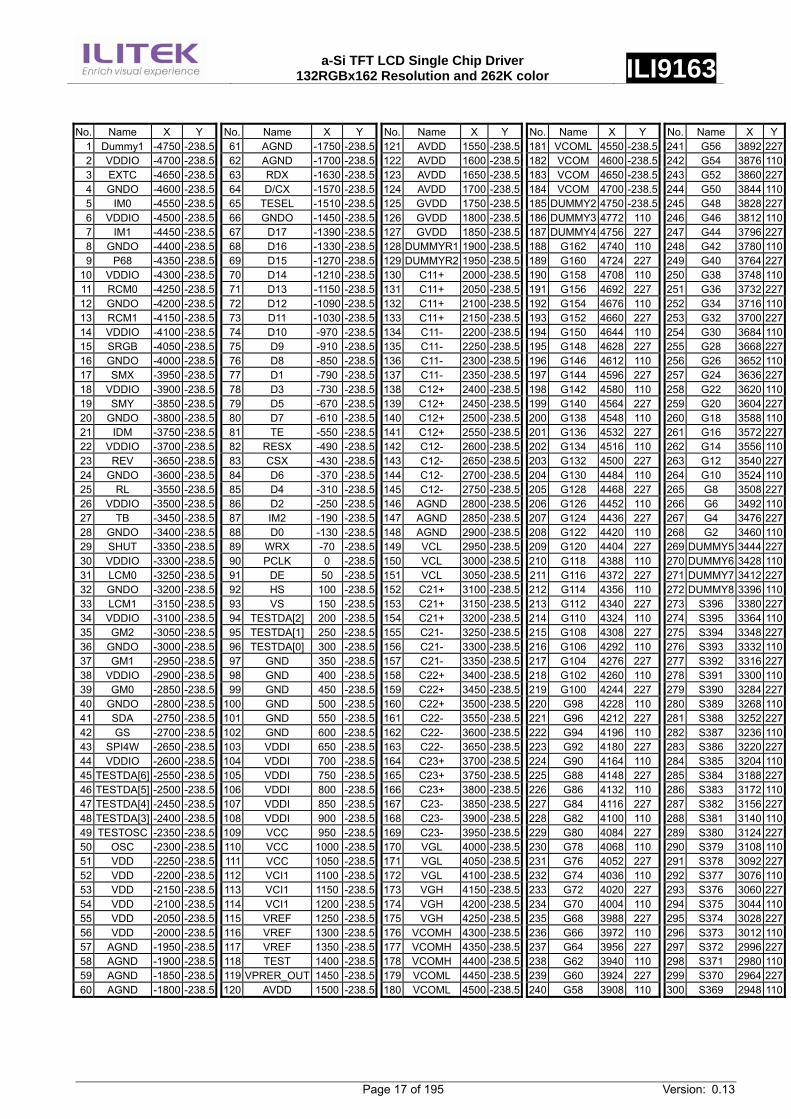
No. Name X Y No. Name X Y No. Name X Y No. Name X Y No. Name X Y
1 Dummy1 -4750 -238.5 61 AGND -1750 -238.5 121 AVDD 1550 -238.5 181 VCOML 4550 -238.5 241 G56 3892 2272 VDDIO -4700 -238.5 62 AGND -1700 -238.5 122 AVDD 1600 -238.5 182 VCOM 4600 -238.5 242 G54 3876 1103 EXTC -4650 -238.5 63 RDX -1630 -238.5 123 AVDD 1650 -238.5 183 VCOM 4650 -238.5 243 G52 3860 2274 GNDO -4600 -238.5 64 D/CX -1570 -238.5 124 AVDD 1700 -238.5 184 VCOM 4700 -238.5 244 G50 3844 1105 IM0 -4550 -238.5 65 TESEL -1510 -238.5 125 GVDD 1750 -238.5 185 DUMMY2 4750 -238.5 245 G48 3828 2276 VDDIO -4500 -238.5 66 GNDO -1450 -238.5 126 GVDD 1800 -238.5 186 DUMMY3 4772 110 246 G46 3812 1107 IM1 -4450 -238.5 67 D17 -1390 -238.5 127 GVDD 1850 -238.5 187 DUMMY4 4756 227 247 G44 3796 2278 GNDO -4400 -238.5 68 D16 -1330 -238.5 128 DUMMYR1 1900 -238.5 188 G162 4740 110 248 G42 3780 1109 P68 -4350 -238.5 69 D15 -1270 -238.5 129 DUMMYR2 1950 -238.5 189 G160 4724 227 249 G40 3764 227
10 VDDIO -4300 -238.5 70 D14 -1210 -238.5 130 C11+ 2000 -238.5 190 G158 4708 110 250 G38 3748 11011 RCM0 -4250 -238.5 71 D13 -1150 -238.5 131 C11+ 2050 -238.5 191 G156 4692 227 251 G36 3732 22712 GNDO -4200 -238.5 72 D12 -1090 -238.5 132 C11+ 2100 -238.5 192 G154 4676 110 252 G34 3716 11013 RCM1 -4150 -238.5 73 D11 -1030 -238.5 133 C11+ 2150 -238.5 193 G152 4660 227 253 G32 3700 22714 VDDIO -4100 -238.5 74 D10 -970 -238.5 134 C11- 2200 -238.5 194 G150 4644 110 254 G30 3684 11015 SRGB -4050 -238.5 75 D9 -910 -238.5 135 C11- 2250 -238.5 195 G148 4628 227 255 G28 3668 22716 GNDO -4000 -238.5 76 D8 -850 -238.5 136 C11- 2300 -238.5 196 G146 4612 110 256 G26 3652 11017 SMX -3950 -238.5 77 D1 -790 -238.5 137 C11- 2350 -238.5 197 G144 4596 227 257 G24 3636 22718 VDDIO -3900 -238.5 78 D3 -730 -238.5 138 C12+ 2400 -238.5 198 G142 4580 110 258 G22 3620 11019 SMY -3850 -238.5 79 D5 -670 -238.5 139 C12+ 2450 -238.5 199 G140 4564 227 259 G20 3604 22720 GNDO -3800 -238.5 80 D7 -610 -238.5 140 C12+ 2500 -238.5 200 G138 4548 110 260 G18 3588 11021 IDM -3750 -238.5 81 TE -550 -238.5 141 C12+ 2550 -238.5 201 G136 4532 227 261 G16 3572 22722 VDDIO -3700 -238.5 82 RESX -490 -238.5 142 C12- 2600 -238.5 202 G134 4516 110 262 G14 3556 11023 REV -3650 -238.5 83 CSX -430 -238.5 143 C12- 2650 -238.5 203 G132 4500 227 263 G12 3540 22724 GNDO -3600 -238.5 84 D6 -370 -238.5 144 C12- 2700 -238.5 204 G130 4484 110 264 G10 3524 11025 RL -3550 -238.5 85 D4 -310 -238.5 145 C12- 2750 -238.5 205 G128 4468 227 265 G8 3508 22726 VDDIO -3500 -238.5 86 D2 -250 -238.5 146 AGND 2800 -238.5 206 G126 4452 110 266 G6 3492 11027 TB -3450 -238.5 87 IM2 -190 -238.5 147 AGND 2850 -238.5 207 G124 4436 227 267 G4 3476 22728 GNDO -3400 -238.5 88 D0 -130 -238.5 148 AGND 2900 -238.5 208 G122 4420 110 268 G2 3460 11029 SHUT -3350 -238.5 89 WRX -70 -238.5 149 VCL 2950 -238.5 209 G120 4404 227 269 DUMMY5 3444 22730 VDDIO -3300 -238.5 90 PCLK 0 -238.5 150 VCL 3000 -238.5 210 G118 4388 110 270 DUMMY6 3428 11031 LCM0 -3250 -238.5 91 DE 50 -238.5 151 VCL 3050 -238.5 211 G116 4372 227 271 DUMMY7 3412 22732 GNDO -3200 -238.5 92 HS 100 -238.5 152 C21+ 3100 -238.5 212 G114 4356 110 272 DUMMY8 3396 11033 LCM1 -3150 -238.5 93 VS 150 -238.5 153 C21+ 3150 -238.5 213 G112 4340 227 273 S396 3380 22734 VDDIO -3100 -238.5 94 TESTDA[2] 200 -238.5 154 C21+ 3200 -238.5 214 G110 4324 110 274 S395 3364 11035 GM2 -3050 -238.5 95 TESTDA[1] 250 -238.5 155 C21- 3250 -238.5 215 G108 4308 227 275 S394 3348 22736 GNDO -3000 -238.5 96 TESTDA[0] 300 -238.5 156 C21- 3300 -238.5 216 G106 4292 110 276 S393 3332 11037 GM1 -2950 -238.5 97 GND 350 -238.5 157 C21- 3350 -238.5 217 G104 4276 227 277 S392 3316 22738 VDDIO -2900 -238.5 98 GND 400 -238.5 158 C22+ 3400 -238.5 218 G102 4260 110 278 S391 3300 11039 GM0 -2850 -238.5 99 GND 450 -238.5 159 C22+ 3450 -238.5 219 G100 4244 227 279 S390 3284 22740 GNDO -2800 -238.5 100 GND 500 -238.5 160 C22+ 3500 -238.5 220 G98 4228 110 280 S389 3268 11041 SDA -2750 -238.5 101 GND 550 -238.5 161 C22- 3550 -238.5 221 G96 4212 227 281 S388 3252 22742 GS -2700 -238.5 102 GND 600 -238.5 162 C22- 3600 -238.5 222 G94 4196 110 282 S387 3236 11043 SPI4W -2650 -238.5 103 VDDI 650 -238.5 163 C22- 3650 -238.5 223 G92 4180 227 283 S386 3220 22744 VDDIO -2600 -238.5 104 VDDI 700 -238.5 164 C23+ 3700 -238.5 224 G90 4164 110 284 S385 3204 11045 TESTDA[6] -2550 -238.5 105 VDDI 750 -238.5 165 C23+ 3750 -238.5 225 G88 4148 227 285 S384 3188 22746 TESTDA[5] -2500 -238.5 106 VDDI 800 -238.5 166 C23+ 3800 -238.5 226 G86 4132 110 286 S383 3172 11047 TESTDA[4] -2450 -238.5 107 VDDI 850 -238.5 167 C23- 3850 -238.5 227 G84 4116 227 287 S382 3156 22748 TESTDA[3] -2400 -238.5 108 VDDI 900 -238.5 168 C23- 3900 -238.5 228 G82 4100 110 288 S381 3140 11049 TESTOSC -2350 -238.5 109 VCC 950 -238.5 169 C23- 3950 -238.5 229 G80 4084 227 289 S380 3124 22750 OSC -2300 -238.5 110 VCC 1000 -238.5 170 VGL 4000 -238.5 230 G78 4068 110 290 S379 3108 11051 VDD -2250 -238.5 111 VCC 1050 -238.5 171 VGL 4050 -238.5 231 G76 4052 227 291 S378 3092 22752 VDD -2200 -238.5 112 VCI1 1100 -238.5 172 VGL 4100 -238.5 232 G74 4036 110 292 S377 3076 11053 VDD -2150 -238.5 113 VCI1 1150 -238.5 173 VGH 4150 -238.5 233 G72 4020 227 293 S376 3060 22754 VDD -2100 -238.5 114 VCI1 1200 -238.5 174 VGH 4200 -238.5 234 G70 4004 110 294 S375 3044 11055 VDD -2050 -238.5 115 VREF 1250 -238.5 175 VGH 4250 -238.5 235 G68 3988 227 295 S374 3028 22756 VDD -2000 -238.5 116 VREF 1300 -238.5 176 VCOMH 4300 -238.5 236 G66 3972 110 296 S373 3012 11057 AGND -1950 -238.5 117 VREF 1350 -238.5 177 VCOMH 4350 -238.5 237 G64 3956 227 297 S372 2996 22758 AGND -1900 -238.5 118 TEST 1400 -238.5 178 VCOMH 4400 -238.5 238 G62 3940 110 298 S371 2980 11059 AGND -1850 -238.5 119 VPRER_OUT 1450 -238.5 179 VCOML 4450 -238.5 239 G60 3924 227 299 S370 2964 22760 AGND -1800 -238.5 120 AVDD 1500 -238.5 180 VCOML 4500 -238.5 240 G58 3908 110 300 S369 2948 110
a-Si TFT LCD Single Chip Driver
132RGBx162 Resolution and 262K color ILI9163
Page 18 of 195 Version: 0.13
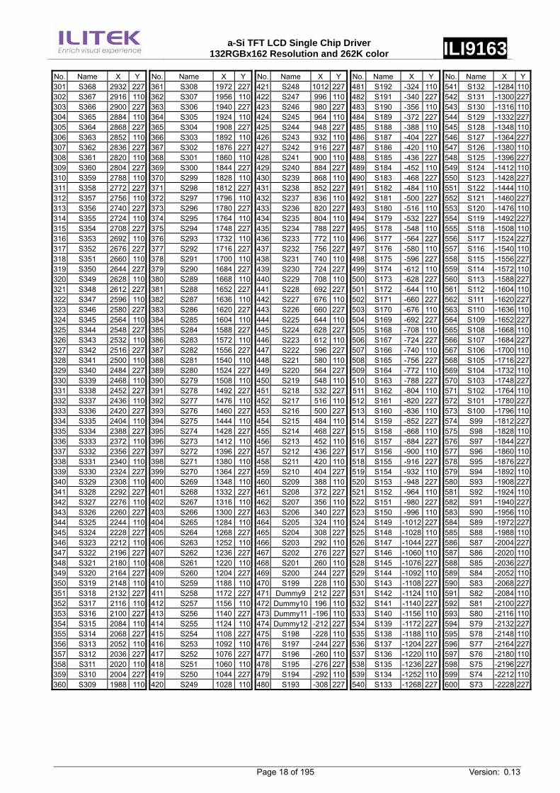
No. Name X Y No. Name X Y No. Name X Y No. Name X Y No. Name X Y301 S368 2932 227 361 S308 1972 227 421 S248 1012 227 481 S192 -324 110 541 S132 -1284 110302 S367 2916 110 362 S307 1956 110 422 S247 996 110 482 S191 -340 227 542 S131 -1300 227303 S366 2900 227 363 S306 1940 227 423 S246 980 227 483 S190 -356 110 543 S130 -1316 110304 S365 2884 110 364 S305 1924 110 424 S245 964 110 484 S189 -372 227 544 S129 -1332 227305 S364 2868 227 365 S304 1908 227 425 S244 948 227 485 S188 -388 110 545 S128 -1348 110306 S363 2852 110 366 S303 1892 110 426 S243 932 110 486 S187 -404 227 546 S127 -1364 227307 S362 2836 227 367 S302 1876 227 427 S242 916 227 487 S186 -420 110 547 S126 -1380 110308 S361 2820 110 368 S301 1860 110 428 S241 900 110 488 S185 -436 227 548 S125 -1396 227309 S360 2804 227 369 S300 1844 227 429 S240 884 227 489 S184 -452 110 549 S124 -1412 110310 S359 2788 110 370 S299 1828 110 430 S239 868 110 490 S183 -468 227 550 S123 -1428 227311 S358 2772 227 371 S298 1812 227 431 S238 852 227 491 S182 -484 110 551 S122 -1444 110312 S357 2756 110 372 S297 1796 110 432 S237 836 110 492 S181 -500 227 552 S121 -1460 227313 S356 2740 227 373 S296 1780 227 433 S236 820 227 493 S180 -516 110 553 S120 -1476 110314 S355 2724 110 374 S295 1764 110 434 S235 804 110 494 S179 -532 227 554 S119 -1492 227315 S354 2708 227 375 S294 1748 227 435 S234 788 227 495 S178 -548 110 555 S118 -1508 110316 S353 2692 110 376 S293 1732 110 436 S233 772 110 496 S177 -564 227 556 S117 -1524 227317 S352 2676 227 377 S292 1716 227 437 S232 756 227 497 S176 -580 110 557 S116 -1540 110318 S351 2660 110 378 S291 1700 110 438 S231 740 110 498 S175 -596 227 558 S115 -1556 227319 S350 2644 227 379 S290 1684 227 439 S230 724 227 499 S174 -612 110 559 S114 -1572 110320 S349 2628 110 380 S289 1668 110 440 S229 708 110 500 S173 -628 227 560 S113 -1588 227321 S348 2612 227 381 S288 1652 227 441 S228 692 227 501 S172 -644 110 561 S112 -1604 110322 S347 2596 110 382 S287 1636 110 442 S227 676 110 502 S171 -660 227 562 S111 -1620 227323 S346 2580 227 383 S286 1620 227 443 S226 660 227 503 S170 -676 110 563 S110 -1636 110324 S345 2564 110 384 S285 1604 110 444 S225 644 110 504 S169 -692 227 564 S109 -1652 227325 S344 2548 227 385 S284 1588 227 445 S224 628 227 505 S168 -708 110 565 S108 -1668 110326 S343 2532 110 386 S283 1572 110 446 S223 612 110 506 S167 -724 227 566 S107 -1684 227327 S342 2516 227 387 S282 1556 227 447 S222 596 227 507 S166 -740 110 567 S106 -1700 110328 S341 2500 110 388 S281 1540 110 448 S221 580 110 508 S165 -756 227 568 S105 -1716 227329 S340 2484 227 389 S280 1524 227 449 S220 564 227 509 S164 -772 110 569 S104 -1732 110330 S339 2468 110 390 S279 1508 110 450 S219 548 110 510 S163 -788 227 570 S103 -1748 227331 S338 2452 227 391 S278 1492 227 451 S218 532 227 511 S162 -804 110 571 S102 -1764 110332 S337 2436 110 392 S277 1476 110 452 S217 516 110 512 S161 -820 227 572 S101 -1780 227333 S336 2420 227 393 S276 1460 227 453 S216 500 227 513 S160 -836 110 573 S100 -1796 110334 S335 2404 110 394 S275 1444 110 454 S215 484 110 514 S159 -852 227 574 S99 -1812 227335 S334 2388 227 395 S274 1428 227 455 S214 468 227 515 S158 -868 110 575 S98 -1828 110336 S333 2372 110 396 S273 1412 110 456 S213 452 110 516 S157 -884 227 576 S97 -1844 227337 S332 2356 227 397 S272 1396 227 457 S212 436 227 517 S156 -900 110 577 S96 -1860 110338 S331 2340 110 398 S271 1380 110 458 S211 420 110 518 S155 -916 227 578 S95 -1876 227339 S330 2324 227 399 S270 1364 227 459 S210 404 227 519 S154 -932 110 579 S94 -1892 110340 S329 2308 110 400 S269 1348 110 460 S209 388 110 520 S153 -948 227 580 S93 -1908 227341 S328 2292 227 401 S268 1332 227 461 S208 372 227 521 S152 -964 110 581 S92 -1924 110342 S327 2276 110 402 S267 1316 110 462 S207 356 110 522 S151 -980 227 582 S91 -1940 227343 S326 2260 227 403 S266 1300 227 463 S206 340 227 523 S150 -996 110 583 S90 -1956 110344 S325 2244 110 404 S265 1284 110 464 S205 324 110 524 S149 -1012 227 584 S89 -1972 227345 S324 2228 227 405 S264 1268 227 465 S204 308 227 525 S148 -1028 110 585 S88 -1988 110346 S323 2212 110 406 S263 1252 110 466 S203 292 110 526 S147 -1044 227 586 S87 -2004 227347 S322 2196 227 407 S262 1236 227 467 S202 276 227 527 S146 -1060 110 587 S86 -2020 110348 S321 2180 110 408 S261 1220 110 468 S201 260 110 528 S145 -1076 227 588 S85 -2036 227349 S320 2164 227 409 S260 1204 227 469 S200 244 227 529 S144 -1092 110 589 S84 -2052 110350 S319 2148 110 410 S259 1188 110 470 S199 228 110 530 S143 -1108 227 590 S83 -2068 227351 S318 2132 227 411 S258 1172 227 471 Dummy9 212 227 531 S142 -1124 110 591 S82 -2084 110352 S317 2116 110 412 S257 1156 110 472 Dummy10 196 110 532 S141 -1140 227 592 S81 -2100 227353 S316 2100 227 413 S256 1140 227 473 Dummy11 -196 110 533 S140 -1156 110 593 S80 -2116 110354 S315 2084 110 414 S255 1124 110 474 Dummy12 -212 227 534 S139 -1172 227 594 S79 -2132 227355 S314 2068 227 415 S254 1108 227 475 S198 -228 110 535 S138 -1188 110 595 S78 -2148 110356 S313 2052 110 416 S253 1092 110 476 S197 -244 227 536 S137 -1204 227 596 S77 -2164 227357 S312 2036 227 417 S252 1076 227 477 S196 -260 110 537 S136 -1220 110 597 S76 -2180 110358 S311 2020 110 418 S251 1060 110 478 S195 -276 227 538 S135 -1236 227 598 S75 -2196 227359 S310 2004 227 419 S250 1044 227 479 S194 -292 110 539 S134 -1252 110 599 S74 -2212 110360 S309 1988 110 420 S249 1028 110 480 S193 -308 227 540 S133 -1268 227 600 S73 -2228 227

a-Si TFT LCD Single Chip Driver
132RGBx162 Resolution and 262K color ILI9163
Page 19 of 195 Version: 0.13
No. Name X Y No. Name X Y No. Name X Y601 S72 -2244 110 661 S12 -3204 110 721 G89 -4164 110602 S71 -2260 227 662 S11 -3220 227 722 G91 -4180 227603 S70 -2276 110 663 S10 -3236 110 723 G93 -4196 110604 S69 -2292 227 664 S9 -3252 227 724 G95 -4212 227605 S68 -2308 110 665 S8 -3268 110 725 G97 -4228 110606 S67 -2324 227 666 S7 -3284 227 726 G99 -4244 227607 S66 -2340 110 667 S6 -3300 110 727 G101 -4260 110608 S65 -2356 227 668 S5 -3316 227 728 G103 -4276 227609 S64 -2372 110 669 S4 -3332 110 729 G105 -4292 110610 S63 -2388 227 670 S3 -3348 227 730 G107 -4308 227611 S62 -2404 110 671 S2 -3364 110 731 G109 -4324 110612 S61 -2420 227 672 S1 -3380 227 732 G111 -4340 227613 S60 -2436 110 673 Dummy13 -3396 110 733 G113 -4356 110614 S59 -2452 227 674 Dummy14 -3412 227 734 G115 -4372 227615 S58 -2468 110 675 Dummy15 -3428 110 735 G117 -4388 110616 S57 -2484 227 676 Dummy16 -3444 227 736 G119 -4404 227617 S56 -2500 110 677 G1 -3460 110 737 G121 -4420 110618 S55 -2516 227 678 G3 -3476 227 738 G123 -4436 227619 S54 -2532 110 679 G5 -3492 110 739 G125 -4452 110620 S53 -2548 227 680 G7 -3508 227 740 G127 -4468 227621 S52 -2564 110 681 G9 -3524 110 741 G129 -4484 110622 S51 -2580 227 682 G11 -3540 227 742 G131 -4500 227623 S50 -2596 110 683 G13 -3556 110 743 G133 -4516 110624 S49 -2612 227 684 G15 -3572 227 744 G135 -4532 227625 S48 -2628 110 685 G17 -3588 110 745 G137 -4548 110626 S47 -2644 227 686 G19 -3604 227 746 G139 -4564 227627 S46 -2660 110 687 G21 -3620 110 747 G141 -4580 110628 S45 -2676 227 688 G23 -3636 227 748 G143 -4596 227629 S44 -2692 110 689 G25 -3652 110 749 G145 -4612 110630 S43 -2708 227 690 G27 -3668 227 750 G147 -4628 227631 S42 -2724 110 691 G29 -3684 110 751 G149 -4644 110632 S41 -2740 227 692 G31 -3700 227 752 G151 -4660 227633 S40 -2756 110 693 G33 -3716 110 753 G153 -4676 110634 S39 -2772 227 694 G35 -3732 227 754 G155 -4692 227635 S38 -2788 110 695 G37 -3748 110 755 G157 -4708 110636 S37 -2804 227 696 G39 -3764 227 756 G159 -4724 227637 S36 -2820 110 697 G41 -3780 110 757 G161 -4740 110638 S35 -2836 227 698 G43 -3796 227 758 Dummy17 -4756 227639 S34 -2852 110 699 G45 -3812 110 759 Dummy18 -4772 110640 S33 -2868 227 700 G47 -3828 227
641 S32 -2884 110 701 G49 -3844 110 ALK-R 4841 -220642 S31 -2900 227 702 G51 -3860 227 ALK-L -4841 -220643 S30 -2916 110 703 G53 -3876 110
644 S29 -2932 227 704 G55 -3892 227
645 S28 -2948 110 705 G57 -3908 110
646 S27 -2964 227 706 G59 -3924 227
647 S26 -2980 110 707 G61 -3940 110
648 S25 -2996 227 708 G63 -3956 227
649 S24 -3012 110 709 G65 -3972 110
650 S23 -3028 227 710 G67 -3988 227
651 S22 -3044 110 711 G69 -4004 110
652 S21 -3060 227 712 G71 -4020 227
653 S20 -3076 110 713 G73 -4036 110
654 S19 -3092 227 714 G75 -4052 227
655 S18 -3108 110 715 G77 -4068 110
656 S17 -3124 227 716 G79 -4084 227
657 S16 -3140 110 717 G81 -4100 110
658 S15 -3156 227 718 G83 -4116 227
659 S14 -3172 110 719 G85 -4132 110
660 S13 -3188 227 720 G87 -4148 227
a-Si TFT LCD Single Chip Driver
132RGBx162 Resolution and 262K color ILI9163
Page 20 of 195 Version: 0.13
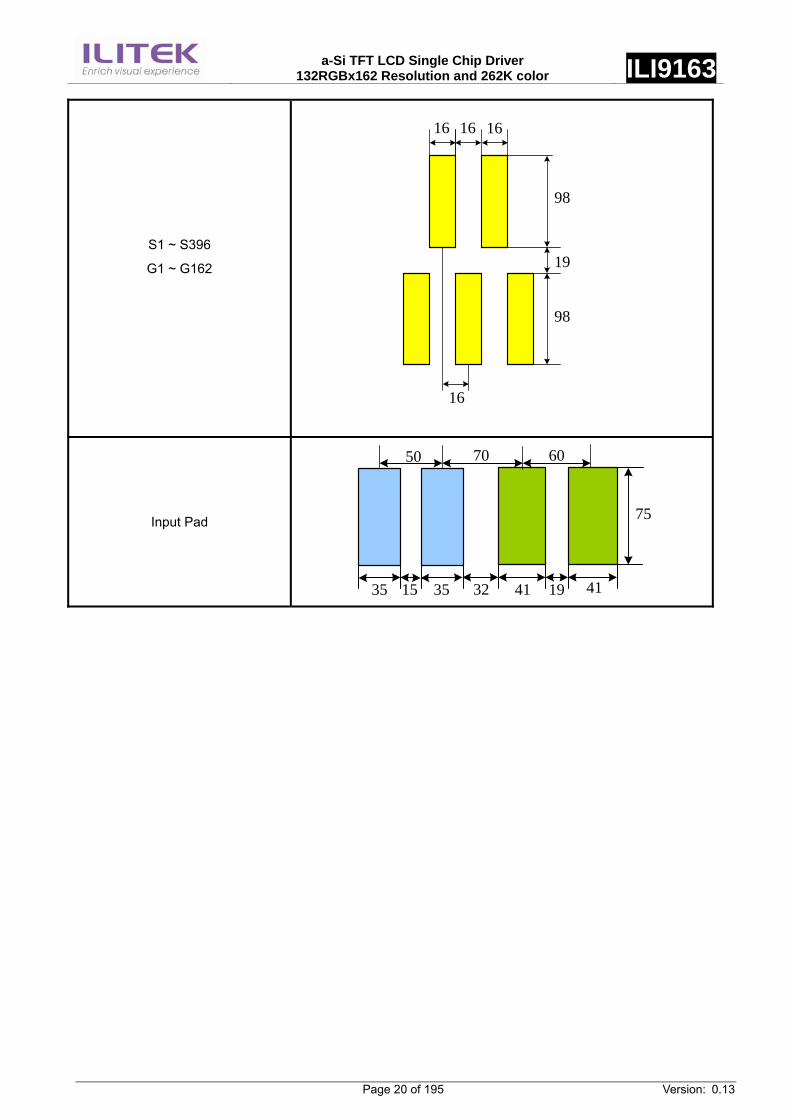
S1 ~ S396
G1 ~ G162
16 16 16
16
98
19
98
Input Pad
50 70 60
75
35 3515 32 41 19 41
a-Si TFT LCD Single Chip Driver
132RGBx162 Resolution and 262K color ILI9163
Page 21 of 195 Version: 0.13
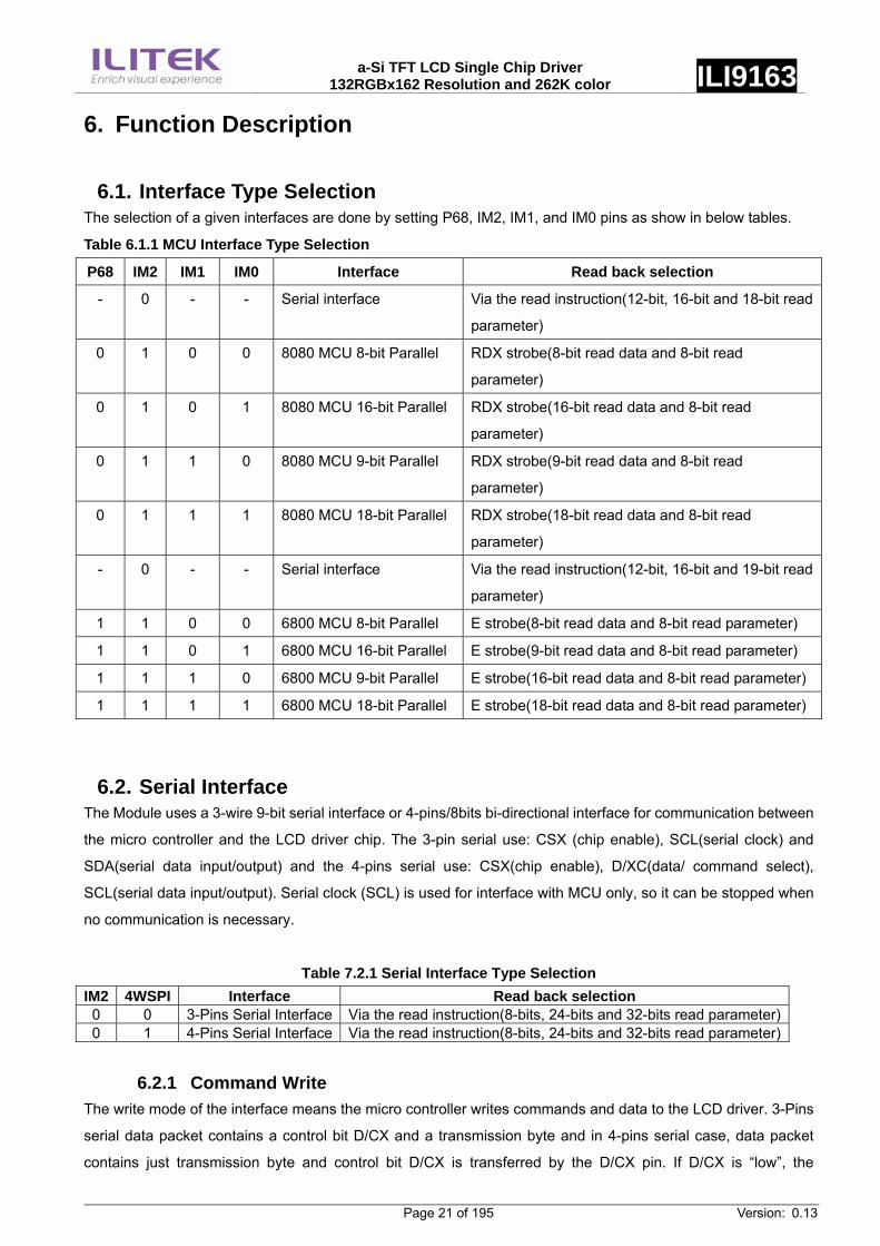
6. Function Description
6.1. Interface Type Selection The selection of a given interfaces are done by setting P68, IM2, IM1, and IM0 pins as show in below tables.
Table 6.1.1 MCU Interface Type Selection
P68 IM2 IM1 IM0 Interface Read back selection
- 0 - - Serial interface Via the read instruction(12-bit, 16-bit and 18-bit read
parameter)
0 1 0 0 8080 MCU 8-bit Parallel RDX strobe(8-bit read data and 8-bit read
parameter)
0 1 0 1 8080 MCU 16-bit Parallel RDX strobe(16-bit read data and 8-bit read
parameter)
0 1 1 0 8080 MCU 9-bit Parallel RDX strobe(9-bit read data and 8-bit read
parameter)
0 1 1 1 8080 MCU 18-bit Parallel RDX strobe(18-bit read data and 8-bit read
parameter)
- 0 - - Serial interface Via the read instruction(12-bit, 16-bit and 19-bit read
parameter)
1 1 0 0 6800 MCU 8-bit Parallel E strobe(8-bit read data and 8-bit read parameter)
1 1 0 1 6800 MCU 16-bit Parallel E strobe(9-bit read data and 8-bit read parameter)
1 1 1 0 6800 MCU 9-bit Parallel E strobe(16-bit read data and 8-bit read parameter)
1 1 1 1 6800 MCU 18-bit Parallel E strobe(18-bit read data and 8-bit read parameter)
6.2. Serial Interface The Module uses a 3-wire 9-bit serial interface or 4-pins/8bits bi-directional interface for communication between
the micro controller and the LCD driver chip. The 3-pin serial use: CSX (chip enable), SCL(serial clock) and
SDA(serial data input/output) and the 4-pins serial use: CSX(chip enable), D/XC(data/ command select),
SCL(serial data input/output). Serial clock (SCL) is used for interface with MCU only, so it can be stopped when
no communication is necessary.
Table 7.2.1 Serial Interface Type Selection IM2 4WSPI Interface Read back selection 0 0 3-Pins Serial Interface Via the read instruction(8-bits, 24-bits and 32-bits read parameter)0 1 4-Pins Serial Interface Via the read instruction(8-bits, 24-bits and 32-bits read parameter)
6.2.1 Command Write The write mode of the interface means the micro controller writes commands and data to the LCD driver. 3-Pins
serial data packet contains a control bit D/CX and a transmission byte and in 4-pins serial case, data packet
contains just transmission byte and control bit D/CX is transferred by the D/CX pin. If D/CX is “low”, the
a-Si TFT LCD Single Chip Driver
132RGBx162 Resolution and 262K color ILI9163
Page 22 of 195 Version: 0.13
transmission byte is interpreted as a command byte. If D/CX is “high”, the transmission byte is stored I the
display data RAM (Memory write command), or command register as parameter.
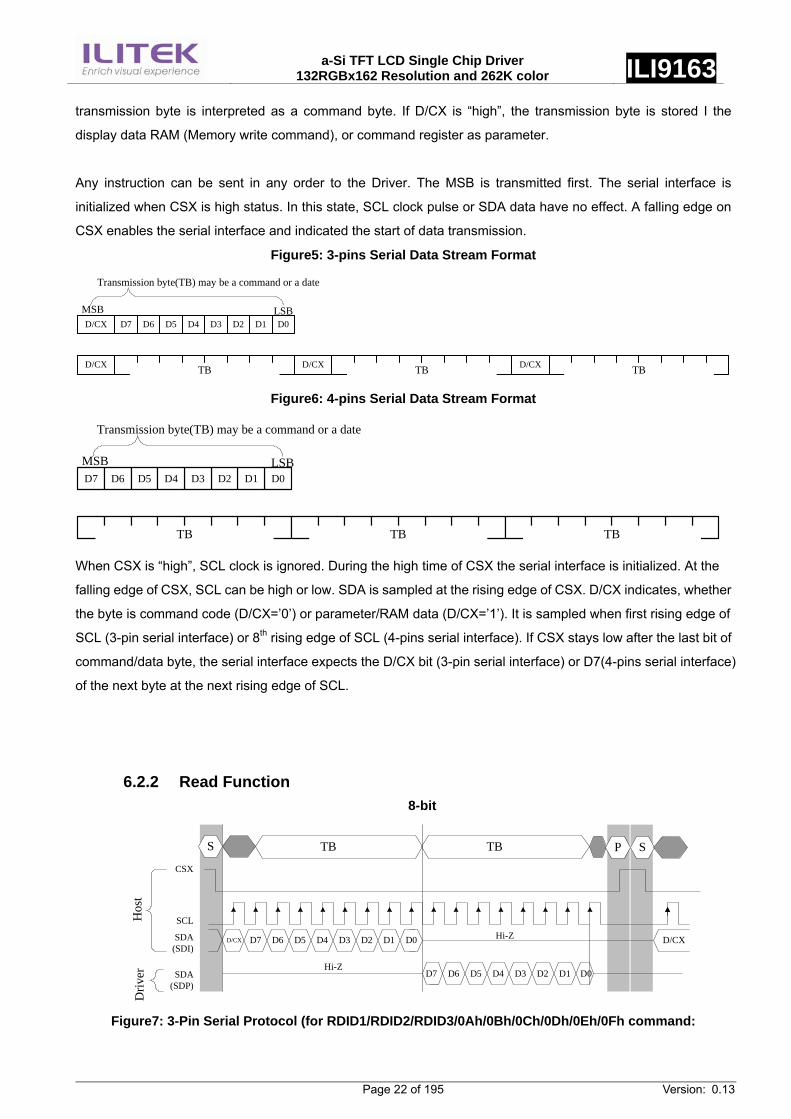
Any instruction can be sent in any order to the Driver. The MSB is transmitted first. The serial interface is
initialized when CSX is high status. In this state, SCL clock pulse or SDA data have no effect. A falling edge on
CSX enables the serial interface and indicated the start of data transmission.
Figure5: 3-pins Serial Data Stream Format
D/CX D7 D6 D0D1D2D3D5 D4
Transmission byte(TB) may be a command or a date
MSB LSB
D/CX TB D/CX TB D/CX TB
Figure6: 4-pins Serial Data Stream Format
D7 D6 D0D1D2D3D5 D4MSB LSB
Transmission byte(TB) may be a command or a date
TB TB TB
When CSX is “high”, SCL clock is ignored. During the high time of CSX the serial interface is initialized. At the
falling edge of CSX, SCL can be high or low. SDA is sampled at the rising edge of CSX. D/CX indicates, whether
the byte is command code (D/CX=’0’) or parameter/RAM data (D/CX=’1’). It is sampled when first rising edge of
SCL (3-pin serial interface) or 8th rising edge of SCL (4-pins serial interface). If CSX stays low after the last bit of
command/data byte, the serial interface expects the D/CX bit (3-pin serial interface) or D7(4-pins serial interface)
of the next byte at the next rising edge of SCL.
6.2.2 Read Function 8-bit
CSX
SCL
SDA(SDP)
Hi-Z
S TB TB P S
D/CX D7 D6 D5 D4 D3 D2 D1 D0
D7 D6 D5 D4 D3 D2 D1 D0
SDA(SDI)
D/CXHi-Z
Driv
erH
ost
Figure7: 3-Pin Serial Protocol (for RDID1/RDID2/RDID3/0Ah/0Bh/0Ch/0Dh/0Eh/0Fh command:
a-Si TFT LCD Single Chip Driver
132RGBx162 Resolution and 262K color ILI9163
Page 23 of 195 Version: 0.13
CSX
SCL
SDA(SDP)
Hi-Z
S TB TB P S
D/CX D7 D6 D5 D4 D3 D2 D1 D0
D22 D21 D20 D19
SDA(SDI)
D/CXHi-Z
Driv
erH
ost
D23 D2 D1 D0D3
Dummy Clock Cycle
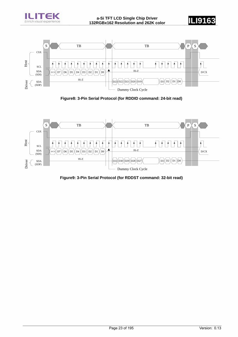
Figure8: 3-Pin Serial Protocol (for RDDID command: 24-bit read)
CSX
SCL
SDA(SDP)
Hi-Z
S TB TB P S
D/CX D7 D6 D5 D4 D3 D2 D1 D0
D30 D29 D28 D27
SDA(SDI)
D/CXHi-Z
Driv
erH
ost
D31 D2 D1 D0D3
Dummy Clock Cycle
Figure9: 3-Pin Serial Protocol (for RDDST command: 32-bit read)
a-Si TFT LCD Single Chip Driver
132RGBx162 Resolution and 262K color ILI9163
Page 24 of 195 Version: 0.13
CSX
SCL
SDA(SDO)
Hi-Z
S TB TB P S
D7 D6 D5 D4 D3 D2 D1 D0
D7 D6 D5 D4 D3 D2 D1 D0
SDA(SDI)
Hi-Z
Host(MCU to Driver)
0
D7
Host(Driver to MCU)
D/CX
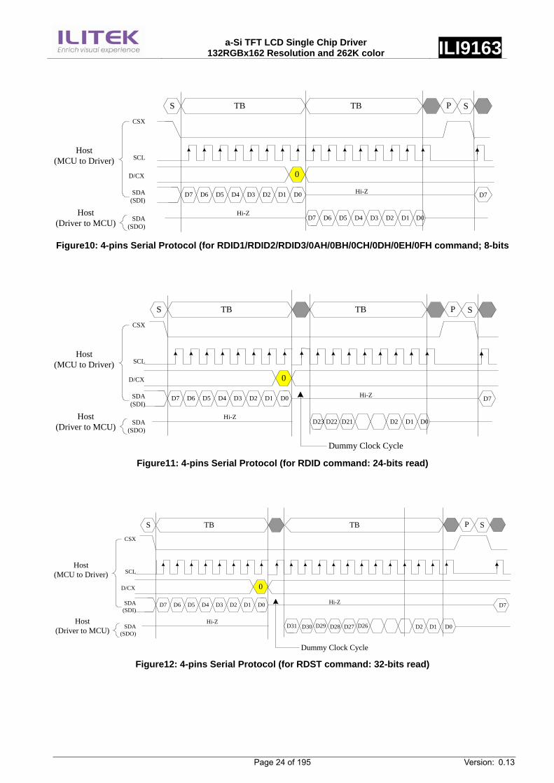
Figure10: 4-pins Serial Protocol (for RDID1/RDID2/RDID3/0AH/0BH/0CH/0DH/0EH/0FH command; 8-bits
CSX
SCL
SDA(SDO)
Hi-Z
S TB
D7 D6 D5 D4 D3 D2 D1 D0SDA(SDI)
Host(MCU to Driver)
0
Host(Driver to MCU)
D/CX
D23
TB P S
D22 D21 D2 D1 D0
Hi-Z D7
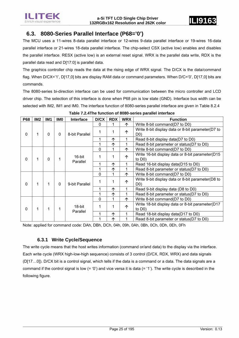
Dummy Clock Cycle Figure11: 4-pins Serial Protocol (for RDID command: 24-bits read)
CSX
SCL
SDA(SDO)
Hi-Z
S TB
D7 D6 D5 D4 D3 D2 D1 D0SDA(SDI)
Host(MCU to Driver)
0
Host(Driver to MCU)
D/CX
D31
TB
D30 D29 D26
Hi-Z
Dummy Clock Cycle
P S
D7
D28 D27 D2 D1 D0
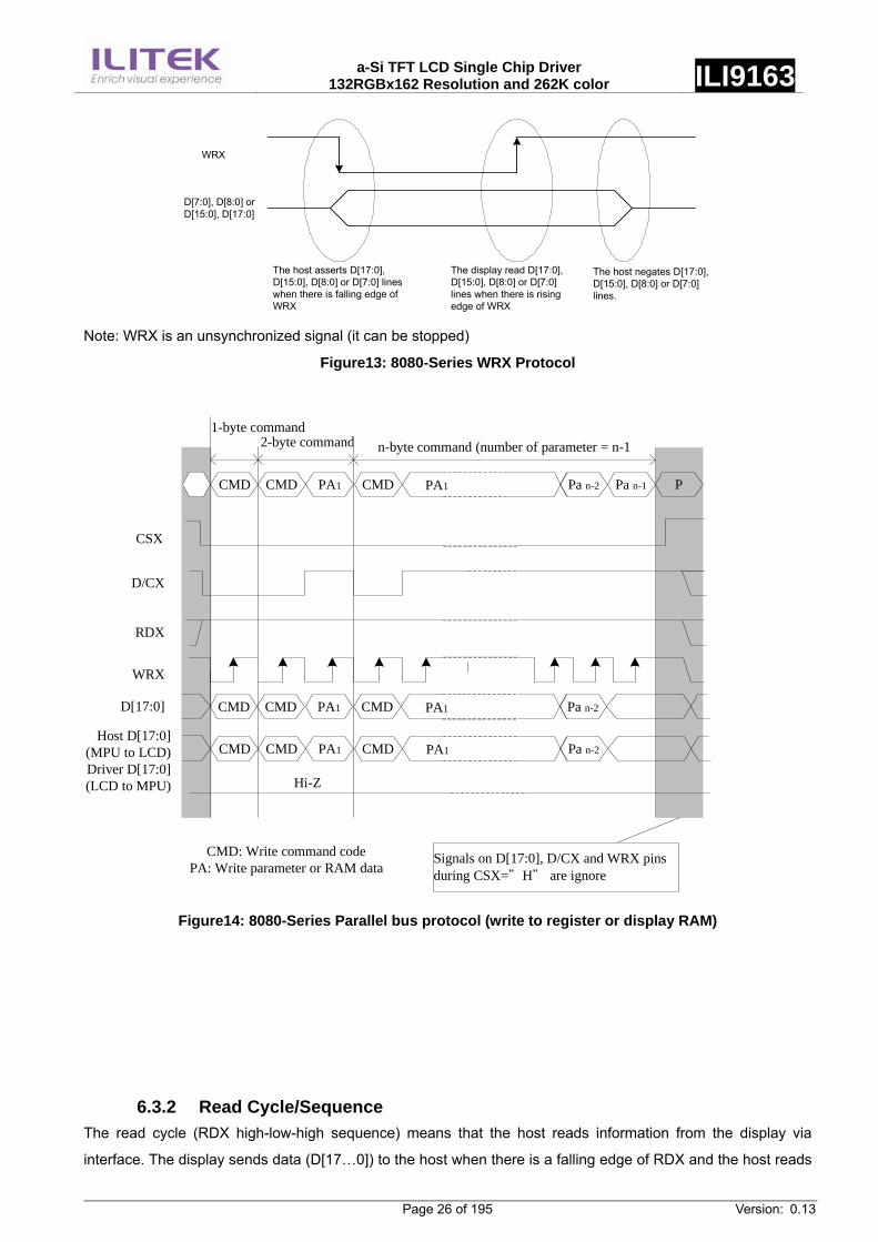
Figure12: 4-pins Serial Protocol (for RDST command: 32-bits read)
a-Si TFT LCD Single Chip Driver
132RGBx162 Resolution and 262K color ILI9163
Page 25 of 195 Version: 0.13
6.3. 8080-Series Parallel Interface (P68=’0’) The MCU uses a 11-wires 8-data parallel interface or 12-wires 9-data parallel interface or 19-wires 16-data
parallel interface or 21-wires 18-data parallel interface. The chip-select CSX (active low) enables and disables
the parallel interface. RESX (active low) is an external reset signal. WRX is the parallel data write, RDX is the
parallel data read and D[17:0] is parallel data.
The graphics controller chip reads the data at the rising edge of WRX signal. The D/CX is the data/command
flag. When D/CX=’1’, D[17,0] bits are display RAM data or command parameters. When D/C=’0’, D[17,0] bits are
commands.
The 8080-series bi-direction interface can be used for communication between the micro controller and LCD
driver chip. The selection of this interface is done when P68 pin is low state (GND). Interface bus width can be
selected with IM2, IM1 and IM0. The interface function of 8080-series parallel interface are given in Table 8.2.4
Table 7.2.4The function of 8080-series parallel interface P68 IM2 IM1 IM0 Interface D/CX RDX WRX Function
0 1 Write 8-bit command(D7 to D0)
1 1 Write 8-bit display data or 8-bit parameter(D7 to D0)
1 1 Read 8-bit display data(D7 to D0) 0 1 0 0 8-bit Parallel
1 1 Read 8-bit parameter or status(D7 to D0) 0 1 Write 8-bit command(D7 to D0)
1 1 Write 16-bit display data or 8-bit parameter(D15 to D0)
1 1 Read 16-bit display data(D15 to D0) 0 1 0 1 16-bit
Parallel
1 1 Read 8-bit parameter or status(D7 to D0) 0 1 Write 8-bit command(D7 to D0)
1 1 Write 9-bit display data or 8-bit parameter(D8 to D0)
1 1 Read 9-bit display data (D8 to D0) 0 1 1 0 9-bit Parallel
1 1 Read 8-bit parameter or status(D7 to D0) 0 1 Write 8-bit command(D7 to D0)
1 1 Write 18-bit display data or 8-bit parameter(D17 to D0)
1 1 Read 18-bit display data(D17 to D0) 0 1 1 1 18-bit
Parallel
1 1 Read 8-bit parameter or status(D7 to D0) Note: applied for command code: DAh, DBh, DCh, 04h, 09h, 0Ah, 0Bh, 0Ch, 0Dh, 0Eh, 0Fh
6.3.1 Write Cycle/Sequence The write cycle means that the host writes information (command or/and data) to the display via the interface.
Each write cycle (WRX high-low-high sequence) consists of 3 control (D/CX, RDX, WRX) and data signals
(D[17…0]). D/CX bit is a control signal, which tells if the data is a command or a data. The data signals are a
command if the control signal is low (= ‘0’) and vice versa it is data (= ‘1’). The write cycle is described in the
following figure.
a-Si TFT LCD Single Chip Driver
132RGBx162 Resolution and 262K color ILI9163
Page 26 of 195 Version: 0.13
WRX
D[7:0], D[8:0] orD[15:0], D[17:0]
The host asserts D[17:0], D[15:0], D[8:0] or D[7:0] lines when there is falling edge of WRX
The display read D[17:0], D[15:0], D[8:0] or D[7:0] lines when there is rising edge of WRX
The host negates D[17:0], D[15:0], D[8:0] or D[7:0] lines.
Note: WRX is an unsynchronized signal (it can be stopped)
Figure13: 8080-Series WRX Protocol
CMD CMD PA1 CMD Pa n-2 Pa n-1 P
CMD CMD PA1 CMD Pa n-2
PA1
PA1
CMD CMD PA1 CMD Pa n-2PA1
CSX
D/CX
RDX
WRX
D[17:0]
Host D[17:0](MPU to LCD)Driver D[17:0](LCD to MPU)
1-byte command2-byte command n-byte command (number of parameter = n-1
Hi-Z
Signals on D[17:0], D/CX and WRX pins during CSX="H" are ignore
CMD: Write command codePA: Write parameter or RAM data
Figure14: 8080-Series Parallel bus protocol (write to register or display RAM)
6.3.2 Read Cycle/Sequence The read cycle (RDX high-low-high sequence) means that the host reads information from the display via
interface. The display sends data (D[17…0]) to the host when there is a falling edge of RDX and the host reads
a-Si TFT LCD Single Chip Driver
132RGBx162 Resolution and 262K color ILI9163
Page 27 of 195 Version: 0.13
data when there is a rising edge of RDX.
RDX
D[7:0], D[8:0] orD[15:0], D[17:0]
The display asserts D[17:0], D[15:0], D[8:0] or D[7:0] lines when there is a falling edge of RDX.
The host reads D[17:0], D[15:0], D[8:0] or D[7:0] lines when there is a rising edge of RDX.
The display negates D[17:0], D[15:0], D[8:0] or D[7:0] lines
Note: RDX is an unsynchronized signal (It can be stopped).
Figure15: 8080-Series RDX Protocol
CMD DM PA1 CMD
CMD DM PA CMD
CMD CMD
CSX
D/CX
RDX
WRX
D[17:0]
Host D[17:0](MPU to LCD)
Read command Read display RAM data
Signals on D[17:0], D/CX, RDX and WRX pins during CSX="H" are ignore
CMD: Write command codePA: Write parameter or RAM data
DM Data Data P
DM PA PAHi-Z
Hi-Z
Driver D[17:0](LCD to MPU) DMHi-Z PA DMHi-Z PA PA
Figure16: 8080-Series parallel bus protocol (Read from register or display RAM)
a-Si TFT LCD Single Chip Driver
132RGBx162 Resolution and 262K color ILI9163
Page 28 of 195 Version: 0.13
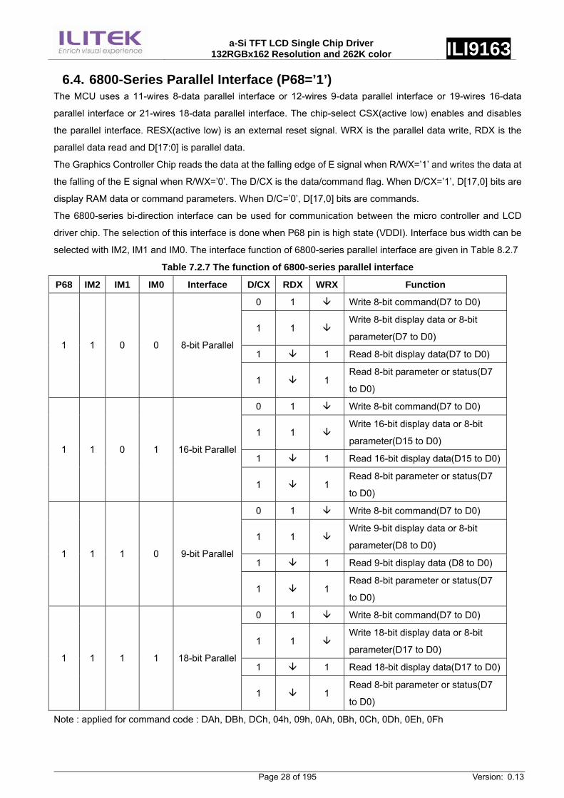
6.4. 6800-Series Parallel Interface (P68=’1’) The MCU uses a 11-wires 8-data parallel interface or 12-wires 9-data parallel interface or 19-wires 16-data
parallel interface or 21-wires 18-data parallel interface. The chip-select CSX(active low) enables and disables
the parallel interface. RESX(active low) is an external reset signal. WRX is the parallel data write, RDX is the
parallel data read and D[17:0] is parallel data.
The Graphics Controller Chip reads the data at the falling edge of E signal when R/WX=’1’ and writes the data at
the falling of the E signal when R/WX=’0’. The D/CX is the data/command flag. When D/CX=’1’, D[17,0] bits are
display RAM data or command parameters. When D/C=’0’, D[17,0] bits are commands.
The 6800-series bi-direction interface can be used for communication between the micro controller and LCD
driver chip. The selection of this interface is done when P68 pin is high state (VDDI). Interface bus width can be
selected with IM2, IM1 and IM0. The interface function of 6800-series parallel interface are given in Table 8.2.7
Table 7.2.7 The function of 6800-series parallel interface
P68 IM2 IM1 IM0 Interface D/CX RDX WRX Function
0 1 Write 8-bit command(D7 to D0)
1 1 Write 8-bit display data or 8-bit
parameter(D7 to D0)
1 1 Read 8-bit display data(D7 to D0) 1 1 0 0 8-bit Parallel
1 1 Read 8-bit parameter or status(D7
to D0)
0 1 Write 8-bit command(D7 to D0)
1 1 Write 16-bit display data or 8-bit
parameter(D15 to D0)
1 1 Read 16-bit display data(D15 to D0)1 1 0 1 16-bit Parallel
1 1 Read 8-bit parameter or status(D7
to D0)
0 1 Write 8-bit command(D7 to D0)
1 1 Write 9-bit display data or 8-bit
parameter(D8 to D0)
1 1 Read 9-bit display data (D8 to D0) 1 1 1 0 9-bit Parallel
1 1 Read 8-bit parameter or status(D7
to D0)
0 1 Write 8-bit command(D7 to D0)
1 1 Write 18-bit display data or 8-bit
parameter(D17 to D0)
1 1 Read 18-bit display data(D17 to D0)1 1 1 1 18-bit Parallel
1 1 Read 8-bit parameter or status(D7
to D0)
Note : applied for command code : DAh, DBh, DCh, 04h, 09h, 0Ah, 0Bh, 0Ch, 0Dh, 0Eh, 0Fh
a-Si TFT LCD Single Chip Driver
132RGBx162 Resolution and 262K color ILI9163
Page 29 of 195 Version: 0.13
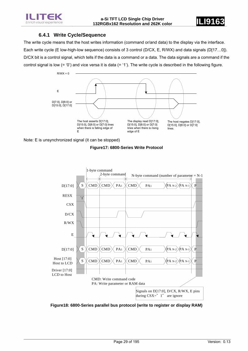
6.4.1 Write Cycle/Sequence The write cycle means that the host writes information (command or/and data) to the display via the interface.
Each write cycle (E low-high-low sequence) consists of 3 control (D/CX, E, R/WX) and data signals (D[17…0]).
D/CX bit is a control signal, which tells if the data is a command or a data. The data signals are a command if the
control signal is low (= ‘0’) and vice versa it is data (= ‘1’). The write cycle is described in the following figure.
E
D[7:0], D[8:0] orD[15:0], D[17:0]
The host asserts D[17:0], D[15:0], D[8:0] or D[7:0] lines when there is falling edge of E
The display read D[17:0], D[15:0], D[8:0] or D[7:0] lines when there is rising edge of E
The host negates D[17:0], D[15:0], D[8:0] or D[7:0] lines.
R/WX = 0
Note: E is unsynchronized signal (it can be stopped)
Figure17: 6800-Series Write Protocol
S CMD CMD PA1 CMD PA N-2 PPA1
CSX
D/CX
E
1-byte command2-byte command N-byte command (number of parameter = N-1
Signals on D[17:0], D/CX, R/WX, E pins during CSX="1" are ignore
CMD: Write command codePA: Write parameter or RAM data
PA N-1D[17:0]
RESX`1'
R/WX
S CMD CMD PA1 CMD PA N-2 PPA1 PA N-1D[17:0]
S CMD CMD PA1 CMD PA N-2 PPA1 PA N-1Host [17:0]
Host to LCD
Driver [17:0]LCD to Host
Figure18: 6800-Series parallel bus protocol (write to register or display RAM)
a-Si TFT LCD Single Chip Driver
132RGBx162 Resolution and 262K color ILI9163
Page 30 of 195 Version: 0.13
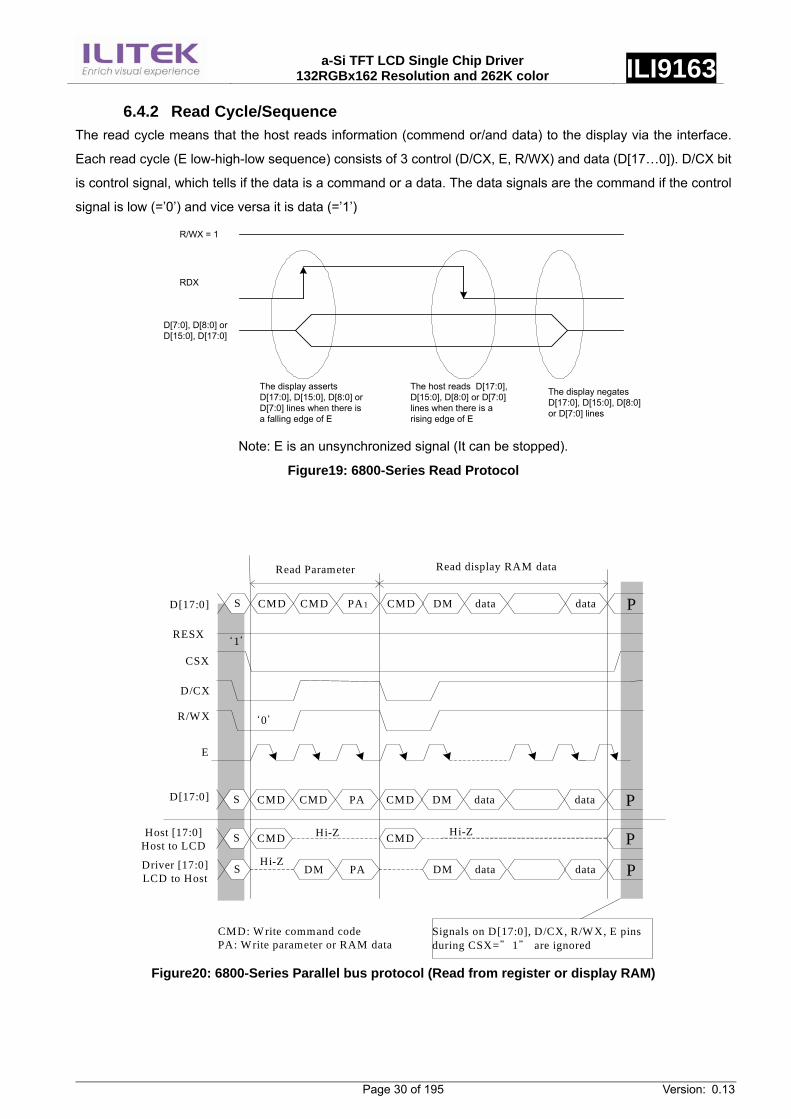
6.4.2 Read Cycle/Sequence The read cycle means that the host reads information (commend or/and data) to the display via the interface.
Each read cycle (E low-high-low sequence) consists of 3 control (D/CX, E, R/WX) and data (D[17…0]). D/CX bit
is control signal, which tells if the data is a command or a data. The data signals are the command if the control
signal is low (=’0’) and vice versa it is data (=’1’)
RDX
D[7:0], D[8:0] orD[15:0], D[17:0]
The display asserts D[17:0], D[15:0], D[8:0] or D[7:0] lines when there is a falling edge of E
The host reads D[17:0], D[15:0], D[8:0] or D[7:0] lines when there is a rising edge of E
The display negates D[17:0], D[15:0], D[8:0] or D[7:0] lines
R/WX = 1
Note: E is an unsynchronized signal (It can be stopped).
Figure19: 6800-Series Read Protocol
S CMD CMD PA1 CMD
CSX
D/CX
E
Read Parameter Read display RAM data
Signals on D[17:0], D/CX, R/WX, E pins during CSX="1" are ignored
CMD: Write command codePA: Write parameter or RAM data
D[17:0]
RESX`1'
R/WX
D[17:0]
DM data data P
S CMD CMD PA CMD DM data data P
S CMD CMDHost [17:0]Host to LCD PDriver [17:0]LCD to Host
S DM PA DM data data P
Hi-Z Hi-Z
Hi-Z
`0'
Figure20: 6800-Series Parallel bus protocol (Read from register or display RAM)
a-Si TFT LCD Single Chip Driver
132RGBx162 Resolution and 262K color ILI9163
Page 31 of 195 Version: 0.13
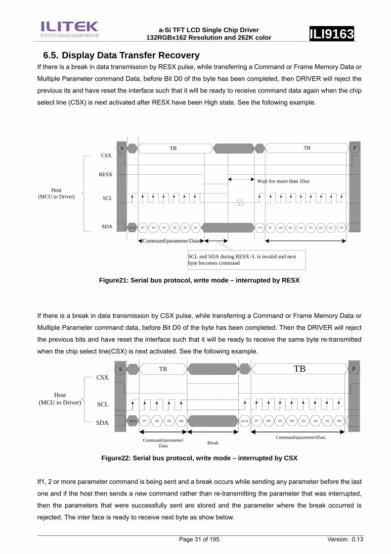
6.5. Display Data Transfer Recovery If there is a break in data transmission by RESX pulse, while transferring a Command or Frame Memory Data or
Multiple Parameter command Data, before Bit D0 of the byte has been completed, then DRIVER will reject the
previous its and have reset the interface such that it will be ready to receive command data again when the chip
select line (CSX) is next activated after RESX have been High state. See the following example.
CSXTB
Host(MCU to Driver)
S TB P
Wait for more than 10us
D/CX D7 D4D6 D5 D3 D2 D/CX D7 D4D6 D5 D3 D2 D1 D0
Command/parameter/Data
SCL and SDA during RESX=L is invalid and next byte becomes command
RESX
SCL
SDA
Figure21: Serial bus protocol, write mode – interrupted by RESX
If there is a break in data transmission by CSX pulse, while transferring a Command or Frame Memory Data or
Multiple Parameter command data, before Bit D0 of the byte has been completed. Then the DRIVER will reject
the previous bits and have reset the interface such that it will be ready to receive the same byte re-transmitted
when the chip select line(CSX) is next activated. See the following example.
CSX
Host(MCU to Driver)
S
D/CX D7 D4D6 D5 D7 D4D6 D5 D3
SCL
SDA
TB TB P
D/CX D1D2 D0
Command/parameter/Data Break
Command/parameter/Data
Figure22: Serial bus protocol, write mode – interrupted by CSX
If1, 2 or more parameter command is being sent and a break occurs while sending any parameter before the last
one and if the host then sends a new command rather than re-transmitting the parameter that was interrupted,
then the parameters that were successfully sent are stored and the parameter where the break occurred is
rejected. The inter face is ready to receive next byte as show below.
a-Si TFT LCD Single Chip Driver
132RGBx162 Resolution and 262K color ILI9163
Page 32 of 195 Version: 0.13
Note: Break can be e.g. another command or noise pulse.
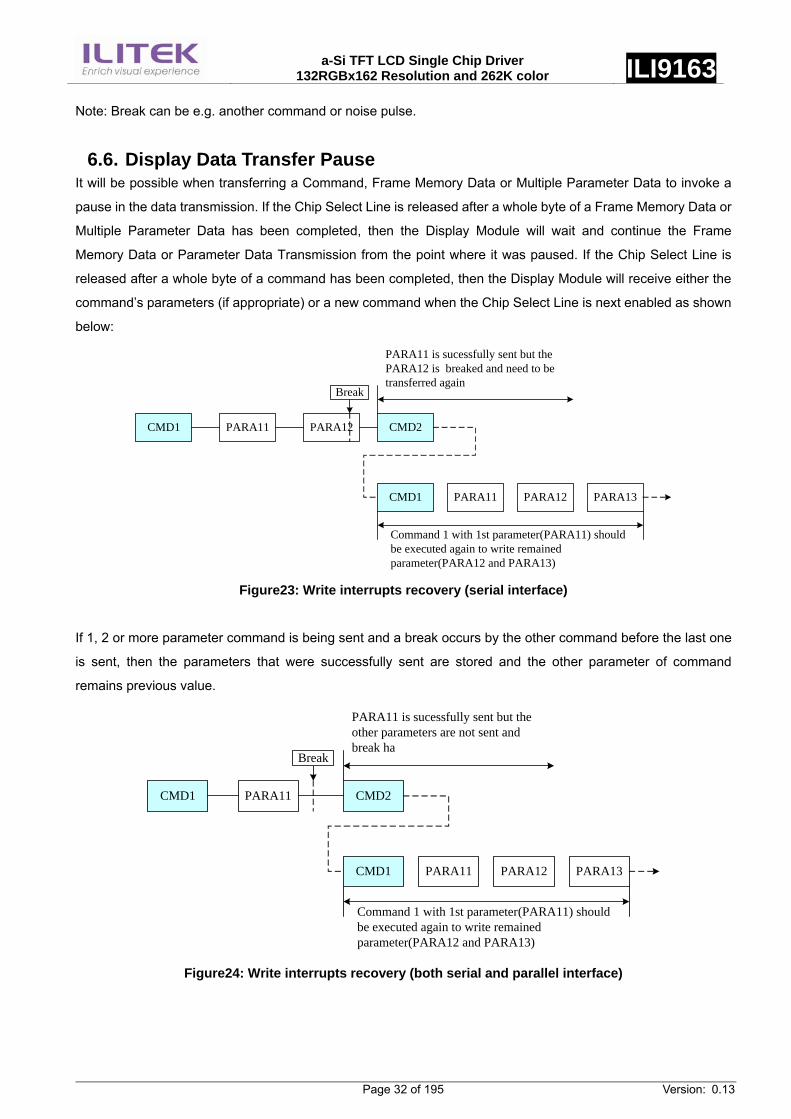
6.6. Display Data Transfer Pause It will be possible when transferring a Command, Frame Memory Data or Multiple Parameter Data to invoke a
pause in the data transmission. If the Chip Select Line is released after a whole byte of a Frame Memory Data or
Multiple Parameter Data has been completed, then the Display Module will wait and continue the Frame
Memory Data or Parameter Data Transmission from the point where it was paused. If the Chip Select Line is
released after a whole byte of a command has been completed, then the Display Module will receive either the
command’s parameters (if appropriate) or a new command when the Chip Select Line is next enabled as shown
below:
CMD1 PARA11 CMD2
CMD1 PARA11 PARA12 PARA13
Break
PARA11 is sucessfully sent but the PARA12 is breaked and need to be transferred again
Command 1 with 1st parameter(PARA11) should be executed again to write remained parameter(PARA12 and PARA13)
PARA12
Figure23: Write interrupts recovery (serial interface)
If 1, 2 or more parameter command is being sent and a break occurs by the other command before the last one
is sent, then the parameters that were successfully sent are stored and the other parameter of command
remains previous value.
CMD1 PARA11 CMD2
CMD1 PARA11 PARA12 PARA13
Break
PARA11 is sucessfully sent but the other parameters are not sent and break ha
Command 1 with 1st parameter(PARA11) should be executed again to write remained parameter(PARA12 and PARA13)
Figure24: Write interrupts recovery (both serial and parallel interface)
a-Si TFT LCD Single Chip Driver
132RGBx162 Resolution and 262K color ILI9163
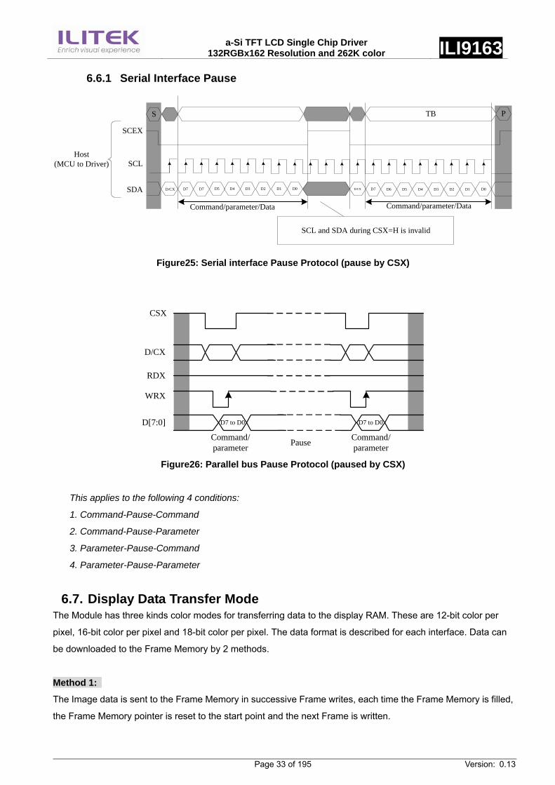
Page 33 of 195 Version: 0.13
6.6.1 Serial Interface Pause
TB
Host(MCU to Driver)
S TB P
D/CX D7 D4 D7
SCL and SDA during CSX=H is invalid
SCEX
SCL
SDA D5D7 D3 D2 D1 D0 D/CX D4D6 D5 D3 D2 D1 D0
Command/parameter/Data Command/parameter/Data
Figure25: Serial interface Pause Protocol (pause by CSX)
D7 to D0 D7 to D0
CSX
D/CX
RDX
WRX
D[7:0]
Command/parameter
Command/parameterPause
Figure26: Parallel bus Pause Protocol (paused by CSX)
This applies to the following 4 conditions:
1. Command-Pause-Command
2. Command-Pause-Parameter
3. Parameter-Pause-Command
4. Parameter-Pause-Parameter
6.7. Display Data Transfer Mode The Module has three kinds color modes for transferring data to the display RAM. These are 12-bit color per
pixel, 16-bit color per pixel and 18-bit color per pixel. The data format is described for each interface. Data can
be downloaded to the Frame Memory by 2 methods.
Method 1:
The Image data is sent to the Frame Memory in successive Frame writes, each time the Frame Memory is filled,
the Frame Memory pointer is reset to the start point and the next Frame is written.
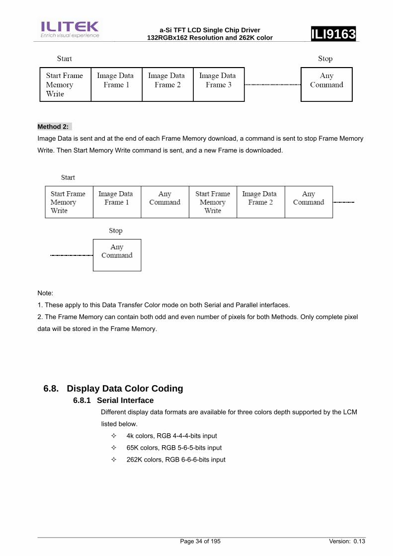
a-Si TFT LCD Single Chip Driver
132RGBx162 Resolution and 262K color ILI9163
Page 34 of 195 Version: 0.13
Method 2:
Image Data is sent and at the end of each Frame Memory download, a command is sent to stop Frame Memory
Write. Then Start Memory Write command is sent, and a new Frame is downloaded.
Note:
1. These apply to this Data Transfer Color mode on both Serial and Parallel interfaces.
2. The Frame Memory can contain both odd and even number of pixels for both Methods. Only complete pixel
data will be stored in the Frame Memory.
6.8. Display Data Color Coding 6.8.1 Serial Interface
Different display data formats are available for three colors depth supported by the LCM
listed below.
4k colors, RGB 4-4-4-bits input
65K colors, RGB 5-6-5-bits input
262K colors, RGB 6-6-6-bits input
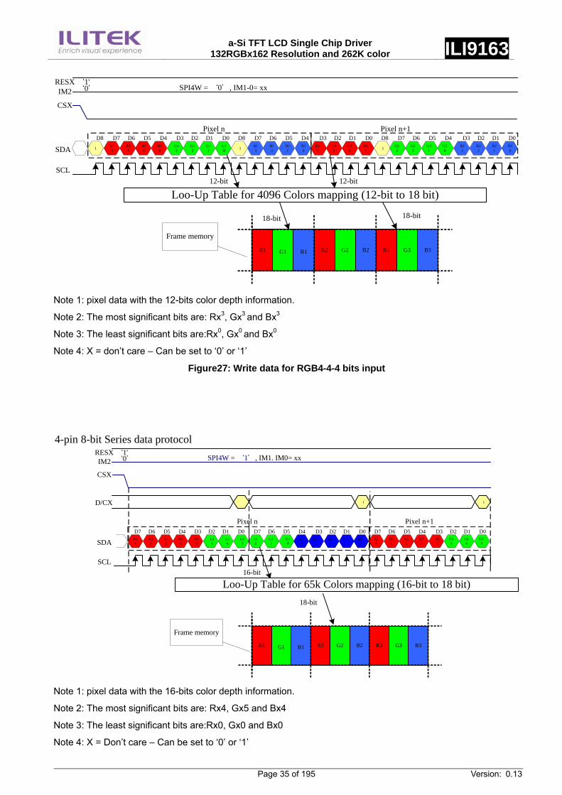
a-Si TFT LCD Single Chip Driver
132RGBx162 Resolution and 262K color ILI9163
Page 35 of 195 Version: 0.13
D8 D7 D6 D5 D4 D3 D2 D1 D0 D8 D7 D6 D5 D4 D3 D2 D1 D0 D8 D7 D6 D5 D4 D3 D2 D1 D0
RESX `1'IM2 `0' SPI4W = `0', IM1-0= xx
CSX
Pixel n Pixel n+1
SDA
SCL
Loo-Up Table for 4096 Colors mapping (12-bit to 18 bit)12-bit 12-bit
R1 G1 B1 R2 G2 B2 R3 G3 B3
18-bit 18-bit
Frame memory
1 R13
R12
R11
R10
G13
G12
G11
G10
B13
B12
B11
B101 R2
3R22
R21
R20
G23
G22
G21
G20
B23
B22
B21
B201
Note 1: pixel data with the 12-bits color depth information.
Note 2: The most significant bits are: Rx3, Gx3 and Bx3
Note 3: The least significant bits are:Rx0, Gx0 and Bx0
Note 4: X = don’t care – Can be set to ‘0’ or ‘1’
Figure27: Write data for RGB4-4-4 bits input
RESX `1'IM2 `0' SPI4W = `1', IM1. IM0= xx
CSX
D7 D6 D5 D4 D3 D2 D1 D0 D7 D6 D5 D4 D3 D2 D1 D0 D7 D6 D5 D4 D3 D2 D1 D0
Pixel n Pixel n+1
SDA
SCL16-bit
Frame memory
R14
R13
R12
R11
R10
G15
G14
G13
G12
G11
G10
B14
B13
B12
B11
B10
R24
R23
R22
R21
R20
G25
G24
G23
Loo-Up Table for 65k Colors mapping (16-bit to 18 bit)18-bit
R1 G1 B1 R2 G2 B2 R3 G3 B3
1 1D/CX
4-pin 8-bit Series data protocol
Note 1: pixel data with the 16-bits color depth information.
Note 2: The most significant bits are: Rx4, Gx5 and Bx4
Note 3: The least significant bits are:Rx0, Gx0 and Bx0
Note 4: X = Don’t care – Can be set to ‘0’ or ‘1’
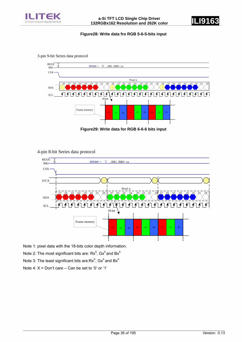
a-Si TFT LCD Single Chip Driver
132RGBx162 Resolution and 262K color ILI9163
Page 36 of 195 Version: 0.13
Figure28: Write data fro RGB 5-6-5-bits input
RESX `1'IM2 `0' SPI4W = `0', IM1. IM0= xx
CSX
D8 D7 D6 D5 D4 D3 D2 D1 D0 D8 D7 D6 D5 D4 D3 D2 D1 D0 D8 D7 D6 D5 D4 D3 D2 D1 D0
Pixel n
SDA
SCL18-bit
Frame memory
1 R15
R14
R13
R12
R11
R10 - - G1
5G14
G13
G121 G1
1G10 - - B1
5B14
B13
B12
B11
B10 - -1
R1 G1 B1 R2 G2 B2 R3 G3 B3
3-pin 9-bit Series data protocol
Figure29: Write data for RGB 6-6-6 bits input
RESX `1'IM2 `0' SPI4W = `1', IM1. IM0= xx
CSX
D7 D6 D5 D4 D3 D2 D1 D0 D7 D6 D5 D4 D3 D2 D1 D0 D7 D6 D5 D4 D3 D2 D1 D0
Pixel n
SDA
SCL
Frame memory
R14
R13
R12
R11
R10
G15
G14
G13
G12
G10
B14
B13
B12
B11
B10
18-bit
R1 G1 B1 R2 G2 B2 R3 G3 B3
1 1D/CX
G11
R15
B15
1
4-pin 8-bit Series data protocol
Note 1: pixel data with the 18-bits color depth information.
Note 2: The most significant bits are: Rx5, Gx5 and Bx5
Note 3: The least significant bits are:Rx0, Gx0 and Bx0
Note 4: X = Don’t care – Can be set to ‘0’ or ‘1’
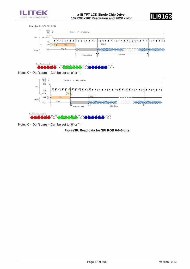
a-Si TFT LCD Single Chip Driver
132RGBx162 Resolution and 262K color ILI9163
Page 37 of 195 Version: 0.13
RESX `1'IM2 `0' SPI4W = `0', IM1. IM0= xx
CSX
- 0
D23
D23
SCLHigh-Z
R13
R12
R11
R10 - - G1
5G14
(SPI CSX)
R2EhSDA
D22 D21 D20 D19 D18 D17 D16 D23D2 D1 D0 D22 D21 D20 D19
9 Dummy Clock
High-ZSDA
1-Pixel data
Host
Driver
Read Data format as below
R15
R14
D22 D21 D20 D19 D18R13 - - B1
5R13
R12
D17 D16 D15 D14 D13 D12 D11 D10 D9 D8 D7 D6 D5 D4 D3 D2 D1 D0
- -R11
R10
B14
B13
B12
B11
B10
Read data for 3-W SPI RGB
Note: X = Don’t care – Can be set to ‘0’ or ‘1’
RESX `1'IM2 `0' SPI4W = `1', IM1. IM0= xx
CSX
-
D23
D23
SCL
R13
R12
R11
R10 - - G1
5G14
R2EhSDA
D22 D21 D20 D19 D18 D17 D16 D23D2 D1 D0 D22 D21 D20 D19
8 Dummy Clock
High-ZSDA
1-Pixel data
Read Data format as below
R15
R14
D22 D21 D20 D19 D18R13 - - B1
5R13
R12
D17 D16 D15 D14 D13 D12 D11 D10 D9 D8 D7 D6 D5 D4 D3 D2 D1 D0
- -R11
R10
B14
B13
B12
B11
B10
0D/CX
High-Z
Driver
Host
Note: X = Don’t care – Can be set to ‘0’ or ‘1’
Figure30: Read data for SPI RGB 6-6-6-bits
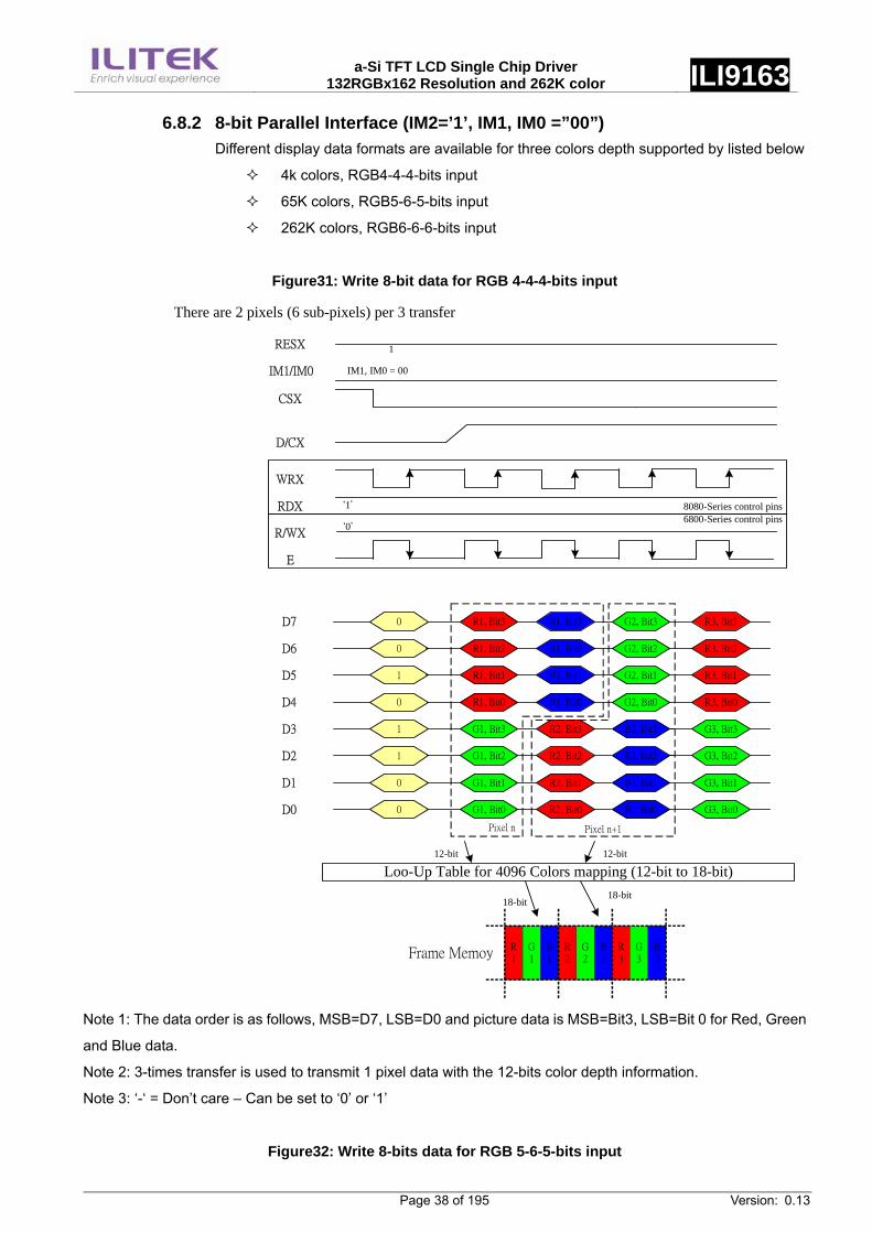
a-Si TFT LCD Single Chip Driver
132RGBx162 Resolution and 262K color ILI9163
Page 38 of 195 Version: 0.13
6.8.2 8-bit Parallel Interface (IM2=’1’, IM1, IM0 =”00”) Different display data formats are available for three colors depth supported by listed below
4k colors, RGB4-4-4-bits input
65K colors, RGB5-6-5-bits input
262K colors, RGB6-6-6-bits input
Figure31: Write 8-bit data for RGB 4-4-4-bits input
IM1/IM0
CSX
RESX
D/CX
WRX
RDX
D7
D6
D5
D4
D3
D2
D1
D0
0
0
1
0
1
1
0
0
G1, Bit3
G1, Bit2
G1, Bit1
G1, Bit0
Pixel n Pixel n+1
R1
G1
B1
R2
G2
B2
R3
G3
B3Frame Memoy
B1, Bit3
B1, Bit2
B1, Bit1
B1, Bit0
G3, Bit3
G3, Bit2
G3, Bit1
G3, Bit0
R1, Bit3
R1, Bit2
R1, Bit1
R1, Bit0
G2, Bit2
G2, Bit1
G2, Bit0
R3, Bit3
R3, Bit2
R3, Bit1
R3, Bit0
1
IM1, IM0 = 00
`1'
R/WX
E
`0'
R2, Bit3
R2, Bit2
R2, Bit1
R2, Bit0
G2, Bit3
B2, Bit3
B2, Bit2
B2, Bit1
B2, Bit0
Loo-Up Table for 4096 Colors mapping (12-bit to 18-bit)12-bit 12-bit
18-bit18-bit
There are 2 pixels (6 sub-pixels) per 3 transfer
8080-Series control pins6800-Series control pins
Note 1: The data order is as follows, MSB=D7, LSB=D0 and picture data is MSB=Bit3, LSB=Bit 0 for Red, Green
and Blue data.
Note 2: 3-times transfer is used to transmit 1 pixel data with the 12-bits color depth information.
Note 3: ‘-‘ = Don’t care – Can be set to ‘0’ or ‘1’
Figure32: Write 8-bits data for RGB 5-6-5-bits input
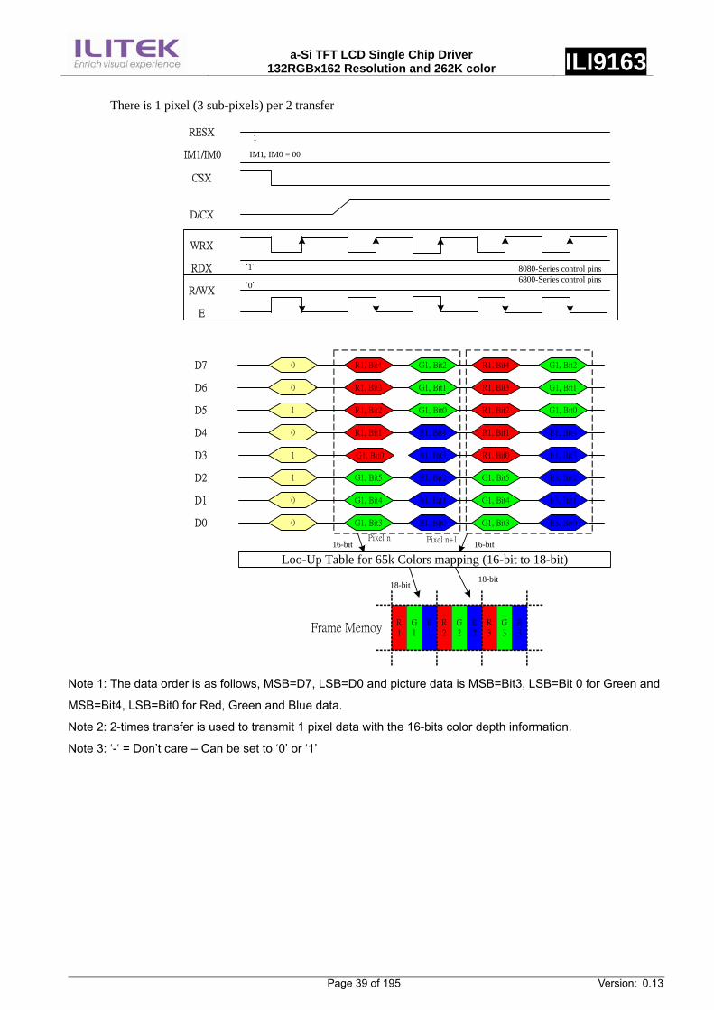
a-Si TFT LCD Single Chip Driver
132RGBx162 Resolution and 262K color ILI9163
Page 39 of 195 Version: 0.13
IM1/IM0
CSX
RESX
D/CX
WRX
RDX
D7
D6
D5
D4
D3
D2
D1
D0
0
0
1
0
1
1
0
0
G1, Bit0
G1, Bit5
G1, Bit4
G1, Bit3
Pixel n Pixel n+1
R1
G1
B1
R2
G2
B2
R3
G3
B3Frame Memoy
G1, Bit2
G1, Bit1
G1, Bit0
B1, Bit4
B1, Bit3
B3, Bit2
B3, Bit1
B3, Bit0
R1, Bit4
R1, Bit3
R1, Bit2
R1, Bit1
R1, Bit3
R1, Bit2
R1, Bit1
G1, Bit2
G1, Bit1
G1, Bit0
B1, Bit4
1
IM1, IM0 = 00
`1'
R/WX
E
`0'
B1, Bit3
B1, Bit2
B1, Bit1
B1, Bit0
R1, Bit4
R1, Bit0
G1, Bit5
G1, Bit4
G1, Bit3
Loo-Up Table for 65k Colors mapping (16-bit to 18-bit)16-bit 16-bit
18-bit18-bit
There is 1 pixel (3 sub-pixels) per 2 transfer
8080-Series control pins6800-Series control pins
Note 1: The data order is as follows, MSB=D7, LSB=D0 and picture data is MSB=Bit3, LSB=Bit 0 for Green and
MSB=Bit4, LSB=Bit0 for Red, Green and Blue data.
Note 2: 2-times transfer is used to transmit 1 pixel data with the 16-bits color depth information.
Note 3: ‘-‘ = Don’t care – Can be set to ‘0’ or ‘1’
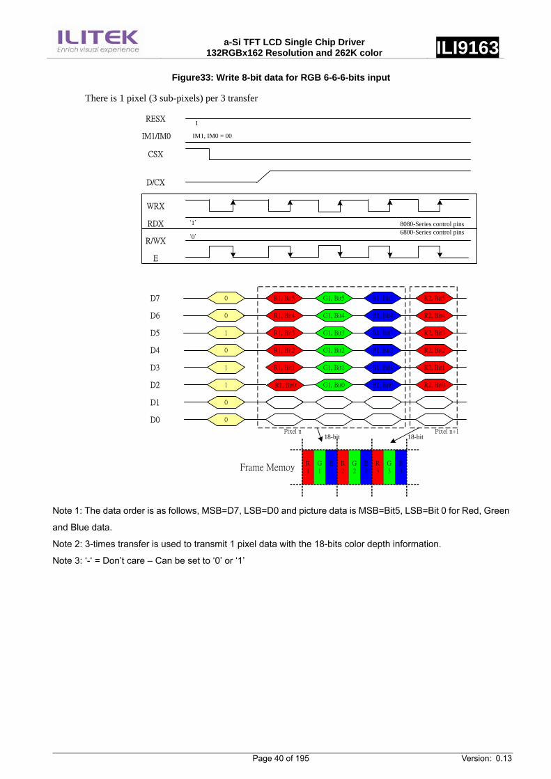
a-Si TFT LCD Single Chip Driver
132RGBx162 Resolution and 262K color ILI9163
Page 40 of 195 Version: 0.13
Figure33: Write 8-bit data for RGB 6-6-6-bits input
IM1/IM0
CSX
RESX
D/CX
WRX
RDX
D7
D6
D5
D4
D3
D2
D1
D0
0
0
1
0
1
1
0
0
R1, Bit0
Pixel n Pixel n+1
R1
G1
B1
R2
G2
B2
R3
G3
B3Frame Memoy
G1, Bit5
G1, Bit4
G1, Bit3
G1, Bit2
R2, Bit1
R2, Bit0
R1, Bit4
R1, Bit3
R1, Bit2
R1, Bit1
B1, Bit4
B1, Bit3
B1, Bit2
R2, Bit5
R2, Bit4
R2, Bit3
R2, Bit2
1
IM1, IM0 = 00
`1'
R/WX
E
`0'
G1, Bit1
G1, Bit0
B1, Bit5
B1, Bit1
B1, Bit0
18-bit 18-bit
There is 1 pixel (3 sub-pixels) per 3 transfer
8080-Series control pins6800-Series control pins
R1, Bit5
Note 1: The data order is as follows, MSB=D7, LSB=D0 and picture data is MSB=Bit5, LSB=Bit 0 for Red, Green
and Blue data.
Note 2: 3-times transfer is used to transmit 1 pixel data with the 18-bits color depth information.
Note 3: ‘-‘ = Don’t care – Can be set to ‘0’ or ‘1’
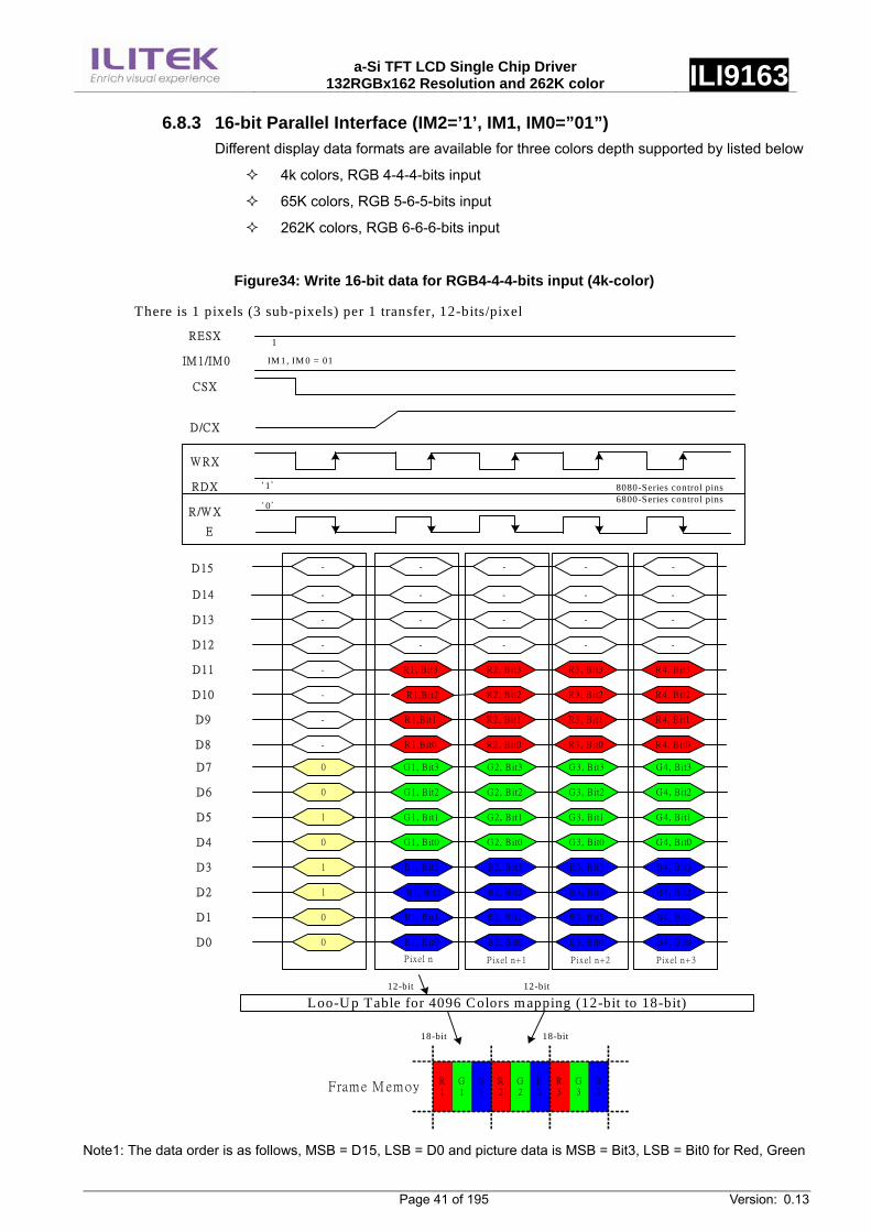
a-Si TFT LCD Single Chip Driver
132RGBx162 Resolution and 262K color ILI9163
Page 41 of 195 Version: 0.13
6.8.3 16-bit Parallel Interface (IM2=’1’, IM1, IM0=”01”) Different display data formats are available for three colors depth supported by listed below
4k colors, RGB 4-4-4-bits input
65K colors, RGB 5-6-5-bits input
262K colors, RGB 6-6-6-bits input
Figure34: Write 16-bit data for RGB4-4-4-bits input (4k-color)
IM 1/IM 0
CSX
RESX
D/CX
W RX
RDX
D7
D6
D5
D4
D3
D2
D1
D0
0
0
1
0
1
1
0
0
B1, Bit2
B1, Bit1
B1, Bit0
Pixel n Pixel n+3
R1
G1
B1
R2
G2
B2
R3
G3
B3Frame M emoy
G2, Bit3
G2, Bit2
G2, Bit1
G2, Bit0
B4, Bit3
B4, Bit2
B4, Bit1
B4, Bit0
G1, Bit2
G1, Bit1
G1, Bit0
B1, Bit3
G3, Bit2
G3, Bit1
G3, Bit0
G4, Bit3
G4, Bit2
G4, Bit1
G4, Bit0
1
IM 1, IM 0 = 01
` 1'
R/W X
E
` 0'
B2, Bit3
B2, Bit2
B2, Bit1
B2, Bit0
G3, Bit3
B3, Bit3
B3, Bit2
B3, Bit1
B3, Bit0
There is 1 pixels (3 sub-pixels) per 1 transfer, 12-bits/pixel
8080-Series control pins6800-Series control pins
G1, Bit3
D15
D14
D13
D12
D11
D10
D9
D8
-
-
-
-
-
-
-
R1,Bit2
R1,Bit1
R1,Bit0
-
-
-
R4, Bit3
R4, Bit2
R4, Bit1
R4, Bit0
-
-
-
R1, Bit3
-
-
-
-
-
-
R2, Bit3
R2, Bit2
R2, Bit1
R2, Bit0
R3, Bit3
R3, Bit2
R3, Bit1
R3, Bit0
- -- - -
Loo-Up Table for 4096 Colors m apping (12-bit to 18-bit)12-bit 12-bit
Pixel n+2Pixel n+1
18-bit 18-bit
Note1: The data order is as follows, MSB = D15, LSB = D0 and picture data is MSB = Bit3, LSB = Bit0 for Red, Green
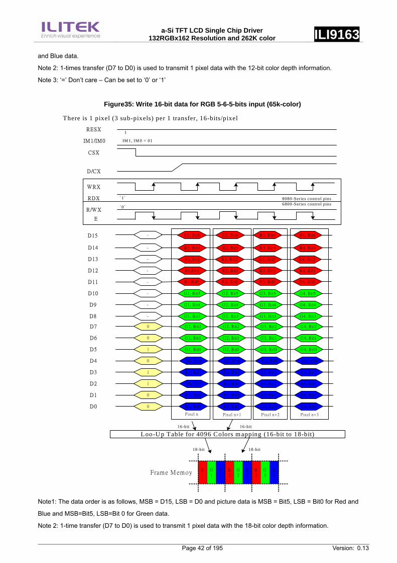
a-Si TFT LCD Single Chip Driver
132RGBx162 Resolution and 262K color ILI9163
Page 42 of 195 Version: 0.13
and Blue data.
Note 2: 1-times transfer (D7 to D0) is used to transmit 1 pixel data with the 12-bit color depth information.
Note 3: ‘=’ Don’t care – Can be set to ‘0’ or ‘1’
Figure35: Write 16-bit data for RGB 5-6-5-bits input (65k-color)
IM 1/IM 0
CSX
RESX
D/CX
W RX
RDX
D7
D6
D5
D4
D3
D2
D1
D0
0
0
1
0
1
1
0
0
B1, Bit2
B1, Bit1
B1, Bit0
Pixel n Pixel n+3
R1
G1
B1
R2
G2
B2
R3
G3
B3Frame M emoy
G2, Bit3
G2, Bit2
G2, Bit1
G2, Bit0
B4, Bit3
B4, Bit2
B4, Bit1
B4, Bit0
G1, Bit2
G1, Bit1
G1, Bit0
B1, Bit3
G3, Bit2
G3, Bit1
G3, Bit0
G4, Bit3
G4, Bit2
G4, Bit1
G4, Bit0
1
IM 1, IM 0 = 01
` 1'
R/W X
E
` 0'
B2, Bit3
B2, Bit2
B2, Bit1
B2, Bit0
G3, Bit3
B3, Bit3
B3, Bit2
B3, Bit1
B3, Bit0
There is 1 pixel (3 sub-pixels) per 1 transfer, 16-bits/pixel
8080-Series control pins6800-Series control pins
G1, Bit3
D15
D 14
D 13
D 12
D 11
D 10
D9
D8
-
-
-
-
-
-
-
R1,Bit2
R1,Bit1
R1,Bit0
R4, Bit3
R4, Bit2
R4, Bit1
R4, Bit0
R1, Bit3 R2, Bit3
R2, Bit2
R2, Bit1
R2, Bit0
R3, Bit3
R3, Bit2
R3, Bit1
R3, Bit0
-
Loo-U p Table for 4096 Colors m apping (16-bit to 18-bit)16-bit 16-bit
Pixel n+2Pixel n+1
18-bit 18-bit
R4, Bit4R1, Bit4 R2, Bit4 R3, Bit4
G2, Bit5
G2, Bit4G1, Bit4 G3, Bit4
G4, Bit5
G4, Bit4
G3, Bit5G1, Bit5
B4, Bit4B1, Bit4 B2, Bit4 B3, Bit4
Note1: The data order is as follows, MSB = D15, LSB = D0 and picture data is MSB = Bit5, LSB = Bit0 for Red and
Blue and MSB=Bit5, LSB=Bit 0 for Green data.
Note 2: 1-time transfer (D7 to D0) is used to transmit 1 pixel data with the 18-bit color depth information.
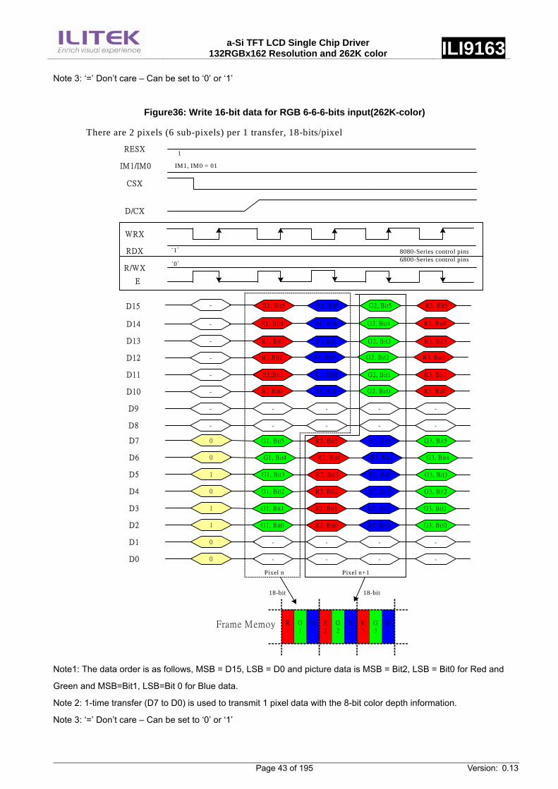
a-Si TFT LCD Single Chip Driver
132RGBx162 Resolution and 262K color ILI9163
Page 43 of 195 Version: 0.13
Note 3: ‘=’ Don’t care – Can be set to ‘0’ or ‘1’
Figure36: Write 16-bit data for RGB 6-6-6-bits input(262K-color)
IM1/IM0
CSX
RESX
D/CX
WRX
RDX
D7
D6
D5
D4
D3
D2
D1
D0
0
0
1
0
1
1
0
0
R1
G1
B1
R2
G2
B2
R3
G3
B3
Frame Memoy
R2, Bit3
R2, Bit2
R2, Bit1
R2, Bit0
G1, Bit2
G1, Bit1
G1, Bit0
B2, Bit2
B2, Bit1
B2, Bit0
G3, Bit3
G3, Bit2
G3, Bit1
G3, Bit0
1
IM1, IM0 = 01
`1'
R/WX
E
`0'
B2, Bit3
There are 2 pixels (6 sub-pixels) per 1 transfer, 18-bits/pixel
8080-Series control pins6800-Series control pins
G1, Bit3
D15
D14
D13
D12
D11
D10
D9
D8
-
-
-
-
-
-
-
R1,Bit2
R1,Bit1
R1,Bit0
R3, Bit3
R3, Bit2
R3, Bit1
R3, Bit0
R1, Bit3 B1, Bit3
B1, Bit2
B1, Bit1
B1, Bit0
G2, Bit3
G2, Bit2
G2, Bit1
G2, Bit0
-
18-bit 18-bit
R3, Bit4R1, Bit4 B1, Bit4 G2, Bit4
R2, Bit5
R2, Bit4G1, Bit4 B2, Bit4
G3, Bit5
G3, Bit4
B2, Bit5G1, Bit5
R3, Bit5R1, Bit5 B1, Bit5 G2, Bit5
- -- -
- -- -
- -- -
- -- -
Pixel n Pixel n+1
Note1: The data order is as follows, MSB = D15, LSB = D0 and picture data is MSB = Bit2, LSB = Bit0 for Red and
Green and MSB=Bit1, LSB=Bit 0 for Blue data.
Note 2: 1-time transfer (D7 to D0) is used to transmit 1 pixel data with the 8-bit color depth information.
Note 3: ‘=’ Don’t care – Can be set to ‘0’ or ‘1’
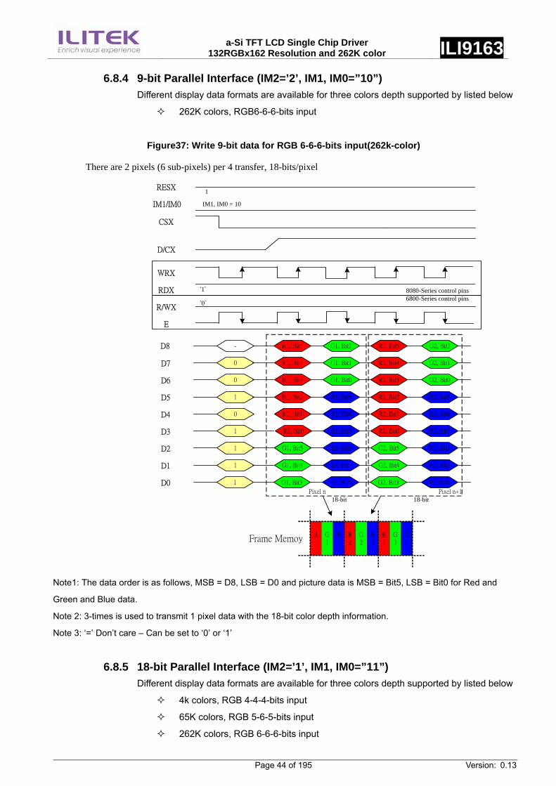
a-Si TFT LCD Single Chip Driver
132RGBx162 Resolution and 262K color ILI9163
Page 44 of 195 Version: 0.13
6.8.4 9-bit Parallel Interface (IM2=’2’, IM1, IM0=”10”) Different display data formats are available for three colors depth supported by listed below
262K colors, RGB6-6-6-bits input
Figure37: Write 9-bit data for RGB 6-6-6-bits input(262k-color)
IM1/IM0
CSX
RESX
D/CX
WRX
RDX
D7
D6
D5
D4
D3
D2
D1
D0
-
0
0
1
0
1
1
1
R1, Bit0
G1, Bit5
G1, Bit4
Pixel n Pixel n+1
R1
G1
B1
R2
G2
B2
R3
G3
B3Frame Memoy
G1, Bit2
G1, Bit1
G1, Bit0
B1, Bit5
B2, Bit4
B2, Bit3
B2, Bit2
B2, Bit1
R1, Bit4
R1, Bit3
R1, Bit2
R1, Bit1
R2, Bit4
R2, Bit3
R2, Bit2
G2, Bit2
G2, Bit1
G2, Bit0
B2, Bit5
1
IM1, IM0 = 10
`1'
R/WX
E
`0'
B1, Bit4
B1, Bit3
B1, Bit2
B1, Bit1
R2, Bit5
R2, Bit1
R2, Bit0
G2, Bit5
G2, Bit4
18-bit 18-bit
There are 2 pixels (6 sub-pixels) per 4 transfer, 18-bits/pixel
8080-Series control pins6800-Series control pins
R1, Bit5D8
1 B1, Bit0 B2, Bit0G2, Bit3G1, Bit3
Note1: The data order is as follows, MSB = D8, LSB = D0 and picture data is MSB = Bit5, LSB = Bit0 for Red and
Green and Blue data.
Note 2: 3-times is used to transmit 1 pixel data with the 18-bit color depth information.
Note 3: ‘=’ Don’t care – Can be set to ‘0’ or ‘1’
6.8.5 18-bit Parallel Interface (IM2=’1’, IM1, IM0=”11”) Different display data formats are available for three colors depth supported by listed below
4k colors, RGB 4-4-4-bits input
65K colors, RGB 5-6-5-bits input
262K colors, RGB 6-6-6-bits input
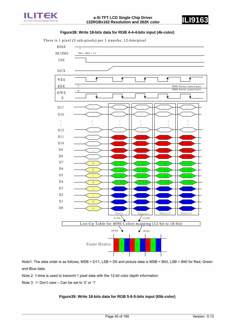
a-Si TFT LCD Single Chip Driver
132RGBx162 Resolution and 262K color ILI9163
Page 45 of 195 Version: 0.13
Figure38: Write 18-bits data for RGB 4-4-4-bits input (4k-color)
IM 1/IM 0
C SX
R ESX
D /C X
W R X
R D X
D 7
D 6
D 5
D 4
D 3
D 2
D 1
D 0
1
0
1
1
0
0
R1
G1
B1
R2
G2
B2
R3
G3
B3
F ram e M em oy
B2, B it3
B2, B it2
B2, B it1
B2, B it0
B1, B it2
B1, B it1
B1, B it0
B 3, B it2
B3, B it1
B3, B it0
B 4, B it3
B4, B it2
B4, B it1
B4, B it0
1
IM 1, IM 0 = 11
` 1'
R/W X
E
` 0'
B3, B it3
T here is 1 p ixel (3 sub-pixels) per 1 transfer, 12-bits/pixel
8080-Series control pins6800-Series control pins
B1, B it3
D 17
D 16
D 12
D 11
D 10
D 9
D 8
-
-
-
-
-
0
0
R1,B it2
R1 ,B it1
R1,B it0
R4, B it3
R4, B it2
R4, B it1
R4, B it0
R1, B it3 R2, B it3
R2, B it2
R2, B it1
R2, B it0
R 3, B it3
R3, B it2
R 3, B it1
R3, B it0
-
18-bit
12-bit
-- - -
G 2, B it1
G 2, B it0G 1, B it0 G 3, B it0
G 4, B it1
G 4, B it0
G 3, B it1G 1, B it1
-- - -
G 1, B it3 G 4, B it3G 2, B it3 G 3, B it3
G 1, B it2 G 4, B it2G 2, B it2 G 3, B it2
::
::
::
::
::
::
- - -- -
P ixel n P ixel n+1 Pixel n+2 Pixel n+3
L oo-U p T able for 4096 C olors m apping (12-bit to 18-bit)12-bit
18-bit
Note1: The data order is as follows, MSB = D11, LSB = D0 and picture data is MSB = Bit3, LSB = Bit0 for Red, Green
and Blue data.
Note 2: 1-time is used to transmit 1 pixel data with the 12-bit color depth information.
Note 3: ‘=’ Don’t care – Can be set to ‘0’ or ‘1’
Figure39: Write 18-bits data for RGB 5-6-5-bits input (65k-color)
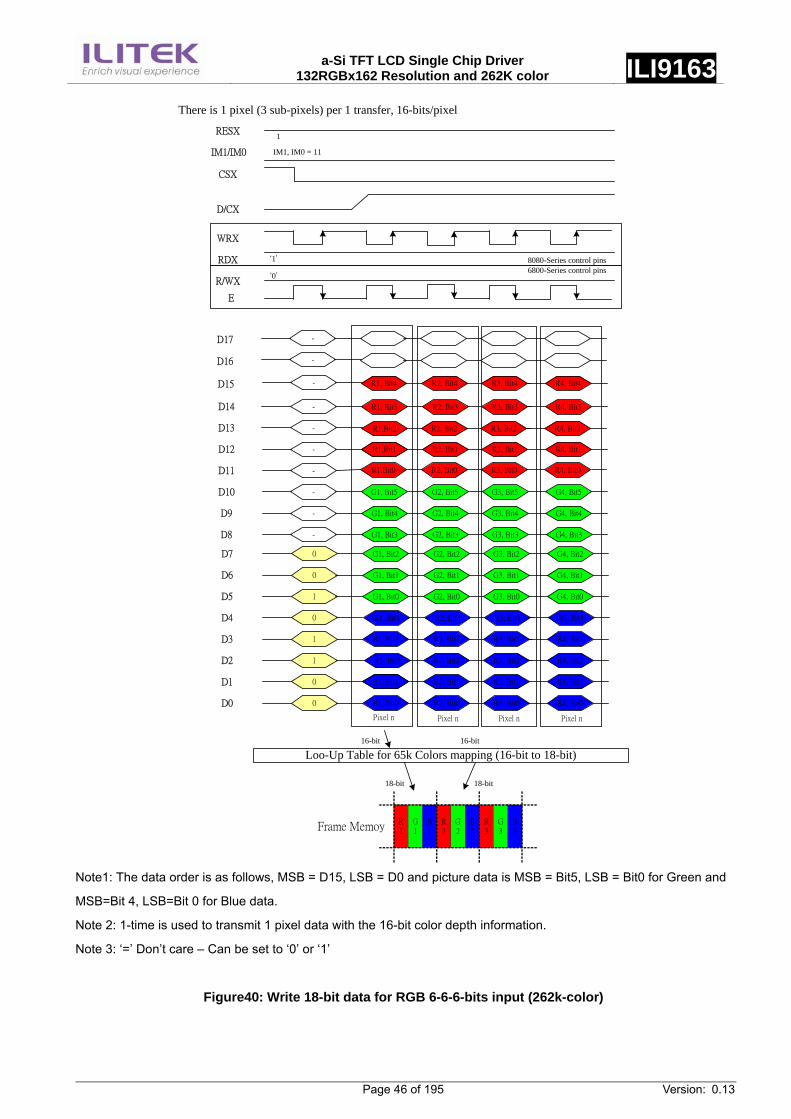
a-Si TFT LCD Single Chip Driver
132RGBx162 Resolution and 262K color ILI9163
Page 46 of 195 Version: 0.13
IM1/IM0
CSX
RESX
D/CX
WRX
RDX
D7
D6
D5
D4
D3
D2
D1
D0
0
0
1
0
1
1
0
0
R1, Bit2
R1, Bit1
R1, Bit0
Pixel n Pixel n
R1
G1
B1
R2
G2
B2
R3
G3
B3Frame Memoy
G2, Bit3
G2, Bit2
G2, Bit1
G2, Bit0
R4, Bit3
R4, Bit2
R4, Bit1
R4, Bit0
G1, Bit2
G1, Bit1
G1, Bit0
R1, Bit3
G3, Bit2
G3, Bit1
G3, Bit0
G4, Bit3
G4, Bit2
G4, Bit1
G4, Bit0
1
IM1, IM0 = 11
`1'
R/WX
E
`0'
R2, Bit3
R2, Bit2
R2, Bit1
R2, Bit0
G3, Bit3
R3, Bit3
R3, Bit2
R3, Bit1
R3, Bit0
There is 1 pixel (3 sub-pixels) per 1 transfer, 16-bits/pixel
8080-Series control pins6800-Series control pins
G1, Bit3
D15
D14
D13
D12
D11
D10
D9
D8
-
-
-
-
-
-
-
R1,Bit2
R1,Bit1
R1,Bit0
R4, Bit3
R4, Bit2
R4, Bit1
R4, Bit0
R1, Bit3 R2, Bit3
R2, Bit2
R2, Bit1
R2, Bit0
R3, Bit3
R3, Bit2
R3, Bit1
R3, Bit0
-
Loo-Up Table for 65k Colors mapping (16-bit to 18-bit)16-bit 16-bit
Pixel nPixel n
18-bit 18-bit
R4, Bit4R1, Bit4 R2, Bit4 R3, Bit4
G2, Bit5
G2, Bit4G1, Bit4 G3, Bit4
G4, Bit5
G4, Bit4
G3, Bit5G1, Bit5
R4, Bit4R1, Bit4 R2, Bit4 R3, Bit4
D16 -
D17 -
Note1: The data order is as follows, MSB = D15, LSB = D0 and picture data is MSB = Bit5, LSB = Bit0 for Green and
MSB=Bit 4, LSB=Bit 0 for Blue data.
Note 2: 1-time is used to transmit 1 pixel data with the 16-bit color depth information.
Note 3: ‘=’ Don’t care – Can be set to ‘0’ or ‘1’
Figure40: Write 18-bit data for RGB 6-6-6-bits input (262k-color)

a-Si TFT LCD Single Chip Driver
132RGBx162 Resolution and 262K color ILI9163
Page 47 of 195 Version: 0.13
IM1/IM0
CSX
RESX
D/CX
WRX
RDX
D7
D6
D5
D4
D3
D2
D1
D0
-
0
0
0
1
1
0
0
R1, Bit2
R1, Bit1
R1, Bit0
Pixel n Pixel n
R1
G1
B1
R2
G2
B2
R3
G3
B3Frame Memoy
G2, Bit3
G2, Bit2
G2, Bit1
G2, Bit0
R4, Bit3
R4, Bit2
R4, Bit1
R4, Bit0
G1, Bit2
G1, Bit1
G1, Bit0
R1, Bit3
G3, Bit2
G3, Bit1
G3, Bit0
G4, Bit3
G4, Bit2
G4, Bit1
G4, Bit0
1
IM1, IM0 = 11
`1'
R/WX
E
`0'
R2, Bit3
R2, Bit2
R2, Bit1
R2, Bit0
G3, Bit3
R3, Bit3
R3, Bit2
R3, Bit1
R3, Bit0
There is 1 pixel (3 sub-pixels) per 1 transfer, 18-bits/pixel
8080-Series control pins6800-Series control pins
G1, Bit3
D15
D14
D13
D12
D11
D10
D9
D8
-
-
-
-
-
-
-
R1,Bit2
R1,Bit1
R1,Bit0
R4, Bit3
R4, Bit2
R4, Bit1
R4, Bit0
R1, Bit3 R2, Bit3
R2, Bit2
R2, Bit1
R2, Bit0
R3, Bit3
R3, Bit2
R3, Bit1
R3, Bit0
-
Pixel nPixel n
18-bit18-bit
R4, Bit4R1, Bit4 R2, Bit4 R3, Bit4
G2, Bit5
G2, Bit4G1, Bit4 G3, Bit4
G4, Bit5
G4, Bit4
G3, Bit5G1, Bit5
R4, Bit4R1, Bit4 R2, Bit4 R3, Bit4
D16
D17 - R2, Bit5R1, Bit5 R2, Bit5 R2, Bit5
1 R4, Bit5R1, Bit5 R2, Bit5 R3, Bit5
Note1: The data order is as follows, MSB = D17, LSB = D0 and picture data is MSB = Bit5, LSB = Bit0 for Red, Green
and Blue data.
Note 2: 1-time(D17 to D0) is used to transmit 1 pixel data with the 18-bit color depth information.
Note 3: ‘=’ Don’t care – Can be set to ‘0’ or ‘1’
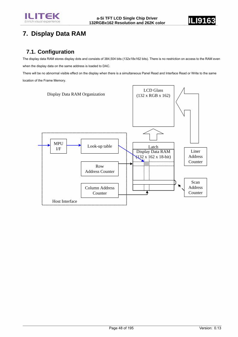
a-Si TFT LCD Single Chip Driver
132RGBx162 Resolution and 262K color ILI9163
Page 48 of 195 Version: 0.13
7. Display Data RAM
7.1. Configuration The display data RAM stores display dots and consists of 384,504 bits (132x18x162 bits). There is no restriction on access to the RAM even
when the display data on the same address is loaded to DAC.
There will be no abnormal visible effect on the display when there is a simultaneous Panel Read and Interface Read or Write to the same
location of the Frame Memory.
LCD Glass(132 x RGB x 162)
Latch Display Data RAM
(132 x 162 x 18-bit)
MPUI/F Look-up table
RowAddress Counter
Column Address Counter
Host Interface
Scan Address Counter
Liner Address Counter
Display Data RAM Organization
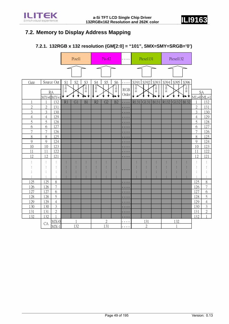
a-Si TFT LCD Single Chip Driver
132RGBx162 Resolution and 262K color ILI9163
Page 49 of 195 Version: 0.13
7.2. Memory to Display Address Mapping
7.2.1. 132RGB x 132 resolution (GM[2:0] = “101”, SMX=SMY=SRGB=’0’)
- - - -
Gate S1 S2 S3 S4 S5 S6 - - - - S391 S392 S393 S394 S395 S396
MY=0MY=1 ML=0 ML=11 1 132 R1 G1 B1 R2 G2 B2 - - - - R131 G131 B131 R132 G132 B132 1 132
2 2 131 - - - - 2 131
3 3 130 - - - - 3 1304 4 129 - - - - 4 129
5 5 128 - - - - 5 1286 6 127 - - - - 6 127
7 7 126 - - - - 7 126
8 8 125 - - - - 8 1259 9 124 - - - - 9 124
10 10 123 - - - - 10 12311 11 122 - - - - 11 122
12 12 121 - - - - 12 121
:
::
:
:
::
:
:
::
:
:
::
:
:
::
:
:
::
:
:
::
:
:
::
:
:
::
:
- - - -
:
::
:
:
::
:
:
::
:
:
::
:
:
::
:
:
::
:
:
::
:
:
::
:
125 125 8 - - - - 125 8
126 126 7 - - - - 126 7127 127 6 - - - - 127 6
128 128 5 - - - - 128 5
129 129 4 - - - - 129 4130 130 3 - - - - 130 3
131 131 2 - - - - 131 2
132 132 1 - - - - 132 1MX-0 - - - -
MX-1 - - - -
Source Out
RG
B=
0
RA RG
B=1
RG
B=
0
RG
B=
1
RGBOrder
RG
B=
0
RG
B=1
RG
B=
0
RG
B=
1
SA
CA1 2 131 132
132 131 2 1
Pixel1 Pixel2 Piexel131 Piexel132
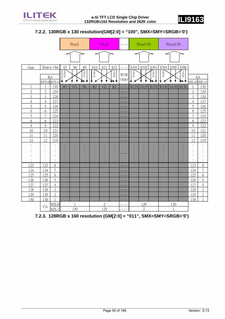
a-Si TFT LCD Single Chip Driver
132RGBx162 Resolution and 262K color ILI9163
Page 50 of 195 Version: 0.13
7.2.2. 130RGB x 130 resolution(GM[2:0] = “100”, SMX=SMY=SRGB=’0’)
- - - -
Gate S7 S8 S9 S10 S11 S12 - - - - S391 S392 S393 S394 S395 S396
MY=0MY=1 ML=0 ML=11 1 130 R1 G1 B1 R2 G2 B2 - - - - R129 G129 B129 R130 G130 B130 1 130
2 2 129 - - - - 2 129
3 3 128 - - - - 3 1284 4 127 - - - - 4 127
5 5 126 - - - - 5 1266 6 125 - - - - 6 125
7 7 124 - - - - 7 124
8 8 123 - - - - 8 1239 9 122 - - - - 9 122
10 10 121 - - - - 10 12111 11 120 - - - - 11 120
12 12 119 - - - - 12 119
:
::
:
:
::
:
:
::
:
:
::
:
:
::
:
:
::
:
:
::
:
:
::
:
:
::
:
- - - -
:
::
:
:
::
:
:
::
:
:
::
:
:
::
:
:
::
:
:
::
:
:
::
:
123 123 8 - - - - 123 8
124 124 7 - - - - 124 7125 125 6 - - - - 125 6
126 126 5 - - - - 126 5
127 127 4 - - - - 127 4128 128 3 - - - - 128 3
129 129 2 - - - - 129 2
130 130 1 - - - - 130 1MX-0 - - - -
MX-1 - - - -
Pixel1 Pixel2 Piexel129 Piexel130
Source OutR
GB
=0
RA RG
B=1
RG
B=
0
RG
B=
1
RGBOrder
RG
B=
0
RG
B=1
RG
B=
0
RG
B=
1
SA
CA1 2 129 130
130 129 2 1 7.2.3. 128RGB x 160 resolution (GM[2:0] = “011”, SMX=SMY=SRGB=’0’)
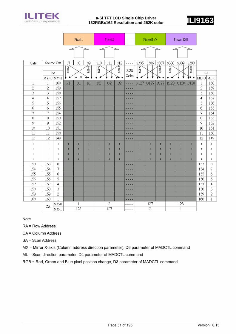
a-Si TFT LCD Single Chip Driver
132RGBx162 Resolution and 262K color ILI9163
Page 51 of 195 Version: 0.13
Note
RA = Row Address
CA = Column Address
SA = Scan Address
MX = Mirror X-axis (Column address direction parameter), D6 parameter of MADCTL command
ML = Scan direction parameter, D4 parameter of MADCTL command
RGB = Red, Green and Blue pixel position change, D3 parameter of MADCTL command
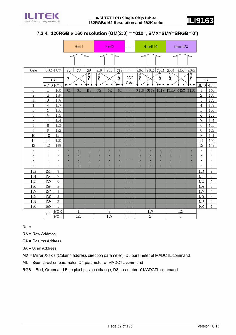
a-Si TFT LCD Single Chip Driver
132RGBx162 Resolution and 262K color ILI9163
Page 52 of 195 Version: 0.13
7.2.4. 120RGB x 160 resolution (GM[2:0] = “010”, SMX=SMY=SRGB=’0’)
Note
RA = Row Address
CA = Column Address
SA = Scan Address
MX = Mirror X-axis (Column address direction parameter), D6 parameter of MADCTL command
ML = Scan direction parameter, D4 parameter of MADCTL command
RGB = Red, Green and Blue pixel position change, D3 parameter of MADCTL command
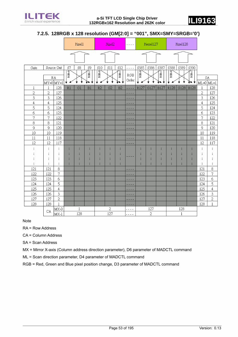
a-Si TFT LCD Single Chip Driver
132RGBx162 Resolution and 262K color ILI9163
Page 53 of 195 Version: 0.13
7.2.5. 128RGB x 128 resolution (GM[2:0] = “001”, SMX=SMY=SRGB=’0’)
Note
RA = Row Address
CA = Column Address
SA = Scan Address
MX = Mirror X-axis (Column address direction parameter), D6 parameter of MADCTL command
ML = Scan direction parameter, D4 parameter of MADCTL command
RGB = Red, Green and Blue pixel position change, D3 parameter of MADCTL command

a-Si TFT LCD Single Chip Driver
132RGBx162 Resolution and 262K color ILI9163
Page 54 of 195 Version: 0.13
7.2.6. 132RGB x 162 resolution (GM[2:0] = “000”, SMX=SMY=SRGB=’0’)
Note
RA = Row Address
CA = Column Address
SA = Scan Address
MX = Mirror X-axis (Column address direction parameter), D6 parameter of MADCTL command
ML = Scan direction parameter, D4 parameter of MADCTL command
RGB = Red, Green and Blue pixel position change, D3 parameter of MADCTL command
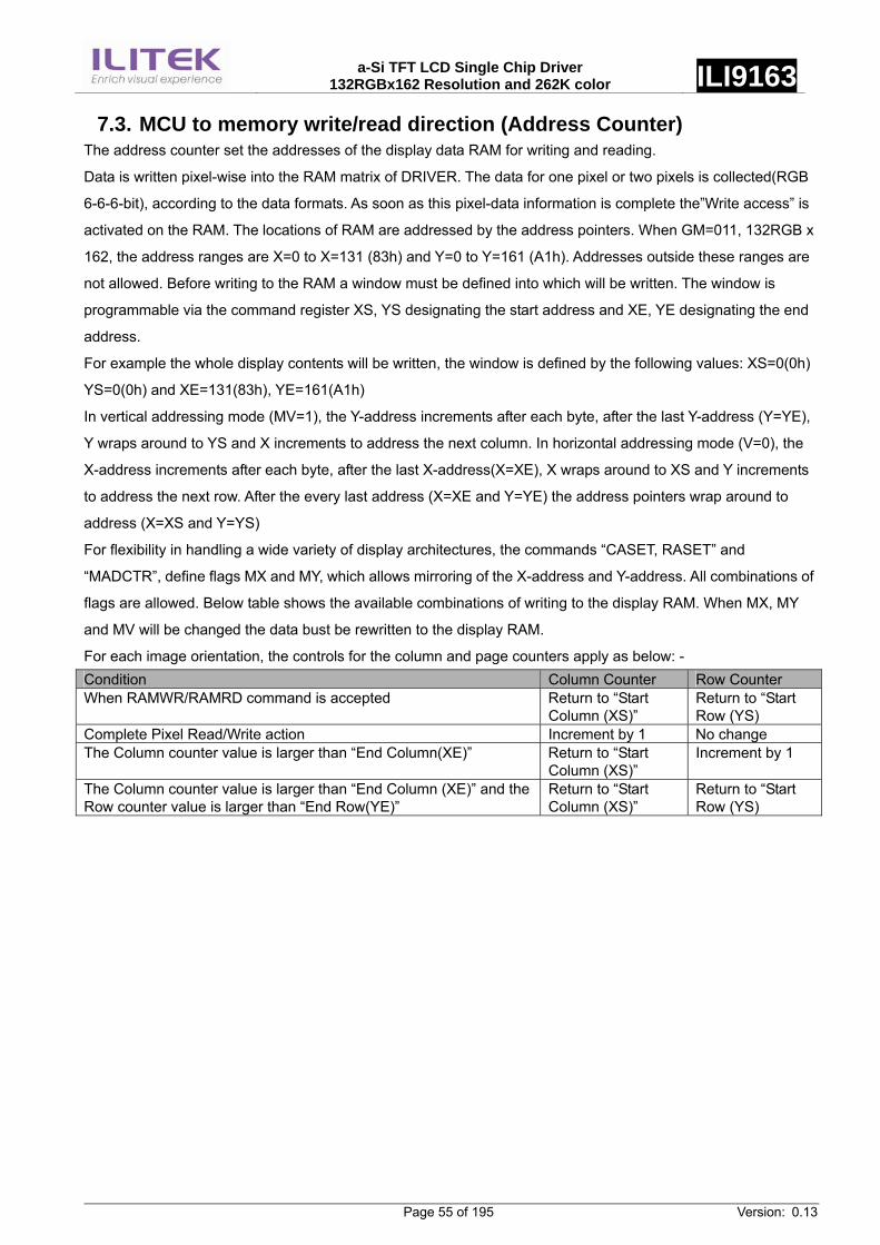
a-Si TFT LCD Single Chip Driver
132RGBx162 Resolution and 262K color ILI9163
Page 55 of 195 Version: 0.13
7.3. MCU to memory write/read direction (Address Counter) The address counter set the addresses of the display data RAM for writing and reading.
Data is written pixel-wise into the RAM matrix of DRIVER. The data for one pixel or two pixels is collected(RGB
6-6-6-bit), according to the data formats. As soon as this pixel-data information is complete the”Write access” is
activated on the RAM. The locations of RAM are addressed by the address pointers. When GM=011, 132RGB x
162, the address ranges are X=0 to X=131 (83h) and Y=0 to Y=161 (A1h). Addresses outside these ranges are
not allowed. Before writing to the RAM a window must be defined into which will be written. The window is
programmable via the command register XS, YS designating the start address and XE, YE designating the end
address.
For example the whole display contents will be written, the window is defined by the following values: XS=0(0h)
YS=0(0h) and XE=131(83h), YE=161(A1h)
In vertical addressing mode (MV=1), the Y-address increments after each byte, after the last Y-address (Y=YE),
Y wraps around to YS and X increments to address the next column. In horizontal addressing mode (V=0), the
X-address increments after each byte, after the last X-address(X=XE), X wraps around to XS and Y increments
to address the next row. After the every last address (X=XE and Y=YE) the address pointers wrap around to
address (X=XS and Y=YS)
For flexibility in handling a wide variety of display architectures, the commands “CASET, RASET” and
“MADCTR”, define flags MX and MY, which allows mirroring of the X-address and Y-address. All combinations of
flags are allowed. Below table shows the available combinations of writing to the display RAM. When MX, MY
and MV will be changed the data bust be rewritten to the display RAM.
For each image orientation, the controls for the column and page counters apply as below: - Condition Column Counter Row Counter When RAMWR/RAMRD command is accepted Return to “Start
Column (XS)” Return to “Start Row (YS)
Complete Pixel Read/Write action Increment by 1 No change The Column counter value is larger than “End Column(XE)” Return to “Start
Column (XS)” Increment by 1
The Column counter value is larger than “End Column (XE)” and the Row counter value is larger than “End Row(YE)”
Return to “Start Column (XS)”
Return to “Start Row (YS)
a-Si TFT LCD Single Chip Driver
132RGBx162 Resolution and 262K color ILI9163
Page 56 of 195 Version: 0.13
Figure41: Frame Data Write Direction According to the MADCTR parameters (MV, MX and MY)
MV MX MY
Image in the Memory(MPU)
B
E
000
B
E
100
010
110
Display Data Direction
Normal
MADCTR Parameter Image in the Driver (DDRAM)
B
E
H/W position(0,0)
X-Y address (0,0)X: CASETY: RASET
Y-Mirror
B
E
H/W position(0,0)
X-Y address (0,0)X: CASETY: RASET
X-Mirror
B
E
B
E
H/W position(0,0) X-Y address (0,0)X: CASETY: RASET
X-MirrorY-Mirror
B
E B
EH/W position(0,0)
X-Y address (0,0)X: CASETY: RASET
X-Y Exchange 001
101
011
111
B
E
B
E
X-Y address (0,0)X: CASETY: RASET
X-Y ExchangeY-Mirror
XY Exchange
XY Exchange
B
E
B
E
B
E
B
E
B
E
B
E
H/W position(0,0)
H/W position(0,0)
H/W position(0,0)
H/W position(0,0)
X-Y address (0,0)X: CASETY: RASET
X-Y address (0,0)X: CASETY: RASET
X-Y address (0,0)X: CASETY: RASET
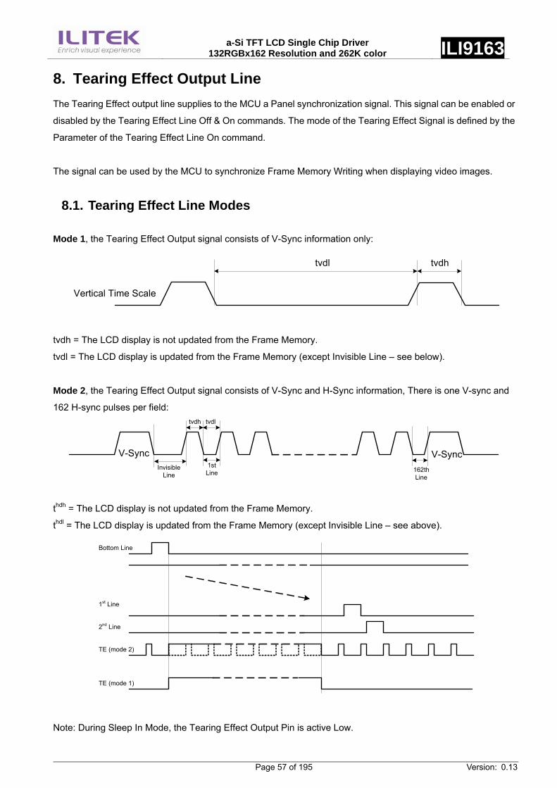
a-Si TFT LCD Single Chip Driver
132RGBx162 Resolution and 262K color ILI9163
Page 57 of 195 Version: 0.13
8. Tearing Effect Output Line The Tearing Effect output line supplies to the MCU a Panel synchronization signal. This signal can be enabled or
disabled by the Tearing Effect Line Off & On commands. The mode of the Tearing Effect Signal is defined by the
Parameter of the Tearing Effect Line On command.
The signal can be used by the MCU to synchronize Frame Memory Writing when displaying video images.
8.1. Tearing Effect Line Modes
Mode 1, the Tearing Effect Output signal consists of V-Sync information only:
tvdl tvdh
Vertical Time Scale
tvdh = The LCD display is not updated from the Frame Memory.
tvdl = The LCD display is updated from the Frame Memory (except Invisible Line – see below).
Mode 2, the Tearing Effect Output signal consists of V-Sync and H-Sync information, There is one V-sync and
162 H-sync pulses per field: tvdl
V-Sync
tvdh
1st Line 162th
Line
V-SyncInvisible
Line
thdh = The LCD display is not updated from the Frame Memory.
thdl = The LCD display is updated from the Frame Memory (except Invisible Line – see above).
Bottom Line
2nd Line
1st Line
TE (mode 2)
TE (mode 1)
Note: During Sleep In Mode, the Tearing Effect Output Pin is active Low.
a-Si TFT LCD Single Chip Driver
132RGBx162 Resolution and 262K color ILI9163
Page 58 of 195 Version: 0.13
8.2. Tearing Effect Line Timing The Tearing Effect signal is described below:
tvdh
Vertical Timing
Horizontal Timing
thdl thdh
tvdl
Table 8.2.1 AC characteristics of Tearing Effect Signal Idle Mode Off/On (Frame Rate = 58.9Hz)
Symbol Parameter min max unit descritpion
tvdl Vertical Timing Low Duration 13 - Ms tvdh Vertical Timing High Duration 1000 - µs thdl Horizontal Timing Low Duration 33 - µs thdh Horizontal Timing High Duration 25 500 µs
Notes:
1. The timings in Table 8.3.1 apply when MADCTL B4=0 and B4=1
2. The signal’s rise and fall times (tf, tr) are stipulated to be equal to or less than 15ns.
Figure42: Rise and fall times
tr tf
80%
20%
80%
20%
The Tearing Effect Output Line is fed back to the MCU and should be used as shown below to avoid
Tearing Effect:

a-Si TFT LCD Single Chip Driver
132RGBx162 Resolution and 262K color ILI9163
Page 59 of 195 Version: 0.13
8.2.1 Example 1 MCU Write is Faster than Panel Read
Data write to Frame Memory is now synchronized to the Panel Scan. It should be written during the vertical sync pulse
of the Tearing Effect Output Line. This ensures that data is always written ahead of the panel scan and each Panel
Frame refresh has a complete new image:
8.2.2 Example 2 MCU Write is slower than Panel Read
The MCU to Frame Memory write begins just after Panel Read has commenced i.e. after one horizontal sync
a-Si TFT LCD Single Chip Driver
132RGBx162 Resolution and 262K color ILI9163
Page 60 of 195 Version: 0.13
pulse of the Tearing Effect Output Line. This allows time for the image to download behind the Panel Read
pointer and finishing download during the subsequent Frame before the Read Pointer “catches” the MCU to
Frame memory write position.
a-Si TFT LCD Single Chip Driver
132RGBx162 Resolution and 262K color ILI9163
Page 61 of 195 Version: 0.13
9. Power ON/OFF Sequence VDDI and VDD can be applied in any order.
VDD and VDDI can be powered down in any order.
During power off, if LCD is in the Sleep Out mode, VDD and VDDI must be powered down minimum
120msec after RESX has been released.
During power off, if LCD is in the Sleep In mode, VDDI or VDD can be powered down minimum 0msec after
RESX has been released.
CSX can be applied at any timing or can be permanently grounded. RESX has priority over CSX.
Notes:
1. There will be no damage to the display module if the power sequences are not met.
2. There will be no abnormal visible effects on the display panel during the Power On/Off Sequences.
3. There will be no abnormal visible effects on the display between end of Power On Sequence and before
receiving Sleep Out command. Also between receiving Sleep In command and Power Off Sequence.
4. If RESX line is not held stable by host during Power On Sequence as defined in Sections 8.5.1 and 8.5.2,
then it will be necessary to apply a Hardware Reset (RESX) after Host Power On Sequence is complete to
ensure correct operation. Otherwise function is not guaranteed.
9.1. Case 1 – RESX line is held high or Unstable by Host at Power -On If RESX line is held high or unstable by the host during Power On, then a Hardware Reset must be applied after
both VDD and VDDI have been applied – otherwise correct functionality is not guaranteed. There is no timing
restriction upon this hardware reset.
Note: Unless otherwise specified, timings herein show cross point at 50% of signal/power level.
9.2. Case 2 – RESX line is held Low by Host at Power On If RESX line is held Low (and stable) by the host during Power On, then the RESX must be held low for minimum
a-Si TFT LCD Single Chip Driver
132RGBx162 Resolution and 262K color ILI9163
Page 62 of 195 Version: 0.13
10µsec after both VDD and VDDI have been applied.
Note: Unless otherwise specified, timings herein show cross point at 50% of signal/power level.
9.3. Uncontrolled Power Off The uncontrolled power off means a situation when e.g. there is removed a battery without the controlled power
off sequence. The display module must meet following requirements:
1. There cannot be any damages for the display module or the display module cannot cause any damages for
the host or lines of the interface.
2. There cannot be any abnormal visible effects (= Display must be blank) within 1 second on the display and
remains blank until “Power On Sequence” powers it up.
10. Power Level Definition 10.1. Power Levels
6 level modes are defined they are in order of Maximum Power consumption to Minimum Power
Consumption:
1. Normal Mode On (full display), Idle Mode Off, Sleep Out.
In this mode, the display is able to show maximum 262,144 colors.
2. Partial Mode On, Idle Mode Off, Sleep Out.
In this mode part of the display is used with maximum 262,144 colors.
3. Normal Mode On (full display), Idle Mode On, Sleep Out.
In this mode, the full display area is used but with 8 colors.
4. Partial Mode On, Idle Mode On, Sleep Out.
In this mode, part of the display is used but with 8 colors.
5. Sleep In Mode.
a-Si TFT LCD Single Chip Driver
132RGBx162 Resolution and 262K color ILI9163
Page 63 of 195 Version: 0.13
In this mode, the DC:DC converter, Internal oscillator and panel driver circuit are stopped. Only the MCU
interface and memory works with VDDI power supply. Contents of the memory are safe.
6. Power Off Mode.
In this mode, both VDD and VDDI are removed.
Note: Transition between modes 1-5 is controllable by MCU commands. Mode 6 is entered only when both
Power supplies are removed.
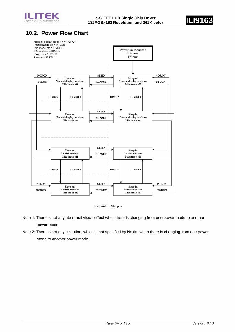
a-Si TFT LCD Single Chip Driver
132RGBx162 Resolution and 262K color ILI9163
Page 64 of 195 Version: 0.13
10.2. Power Flow Chart
Note 1: There is not any abnormal visual effect when there is changing from one power mode to another
power mode.
Note 2: There is not any limitation, which is not specified by Nokia, when there is changing from one power
mode to another power mode.
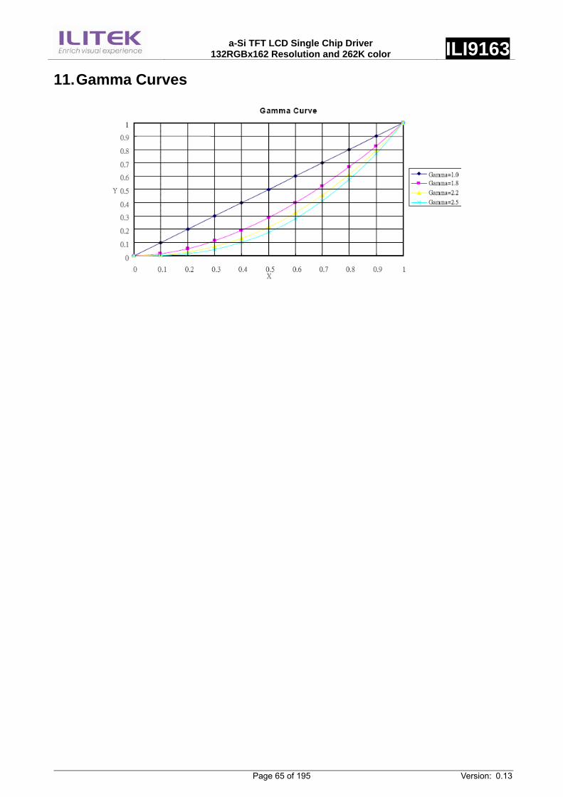
a-Si TFT LCD Single Chip Driver
132RGBx162 Resolution and 262K color ILI9163
Page 65 of 195 Version: 0.13
11. Gamma Curves
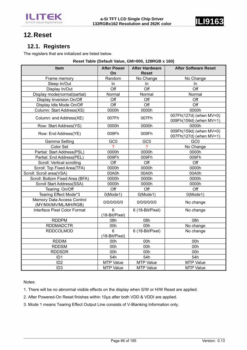
a-Si TFT LCD Single Chip Driver
132RGBx162 Resolution and 262K color ILI9163
Page 66 of 195 Version: 0.13
12. Reset 12.1. Registers
The registers that are initialized are listed below.
Reset Table (Default Value, GM=000, 128RGB x 160) Item After Power
On After Hardware
Reset After Software Reset
Frame memory Random No Change No Change Sleep In/Out In In In
Display In/Out Off Off Off Display mode(normal/partial) Normal Normal Normal
Display Inversion On/Off Off Off Off Display Idle Mode On/Off Off Off Off
Column: Start Address(XS) 0000h 0000h 0000h
Column: end Address(XE) 007Fh 007Fh 007Fh(127d) (when MV=0) 009Fh(159d) (when MV=1)
Row: Start Address(YS) 0000h 0000h 0000h
Row: End Address(YE) 009Fh 009Fh 009Fh(159d) (when MV=0) 007Fh(127d) (when MV=1)
Gamma Setting GC0 GC0 GC0 Color Set ? ? No Change
Partial: Start Address(PSL) 0000h 0000h 0000h Partial: End Address(PEL) 009Fh 009Fh 009Fh
Scroll: Vertical scrolling Off Off Off Scroll: Top Fixed Area(TFA) 0000h 0000h 0000h
Scroll: Scroll area(VSA) 00A0h 00A0h 00A0h Scroll: Bottom Fixed Area (BFA) 0000h 0000h 0000h
Scroll Start Address(SSA) 0000h 0000h 0000h Tearing: On/Off Off Off Off
Tearing Effect Mode*3 0(Mode1) 0(Mode1) 0(Mode1) Memory Data Access Control
(MY/MX/MV/ML/MH/RGB) 0/0/0/0/0/0 0/0/0/0/0/0 No change
Interface Pixel Color Format 6 (18-Bit/Pixel)
6 (18-Bit/Pixel) No change
RDDPM 08h 08h 08h RDDMADCTR 00h 00h No change RDDCOLMOD 6
(18-Bit/Pixel)6 (18-Bit/Pixel) No change
RDDIM 00h 00h 00h RDDSM 00h 00h 00h
RDDSDR 00h 00h 00h ID1 54h 54h 54h ID2 MTP Value MTP Value MTP Value ID3 MTP Value MTP Value MTP Value
Notes:
1. There will be no abnormal visible effects on the display when S/W or H/W Reset are applied.
2. After Powered-On Reset finishes within 10µs after both VDD & VDDI are applied.
3. Mode 1 means Tearing Effect Output Line consists of V-Blanking Information only.
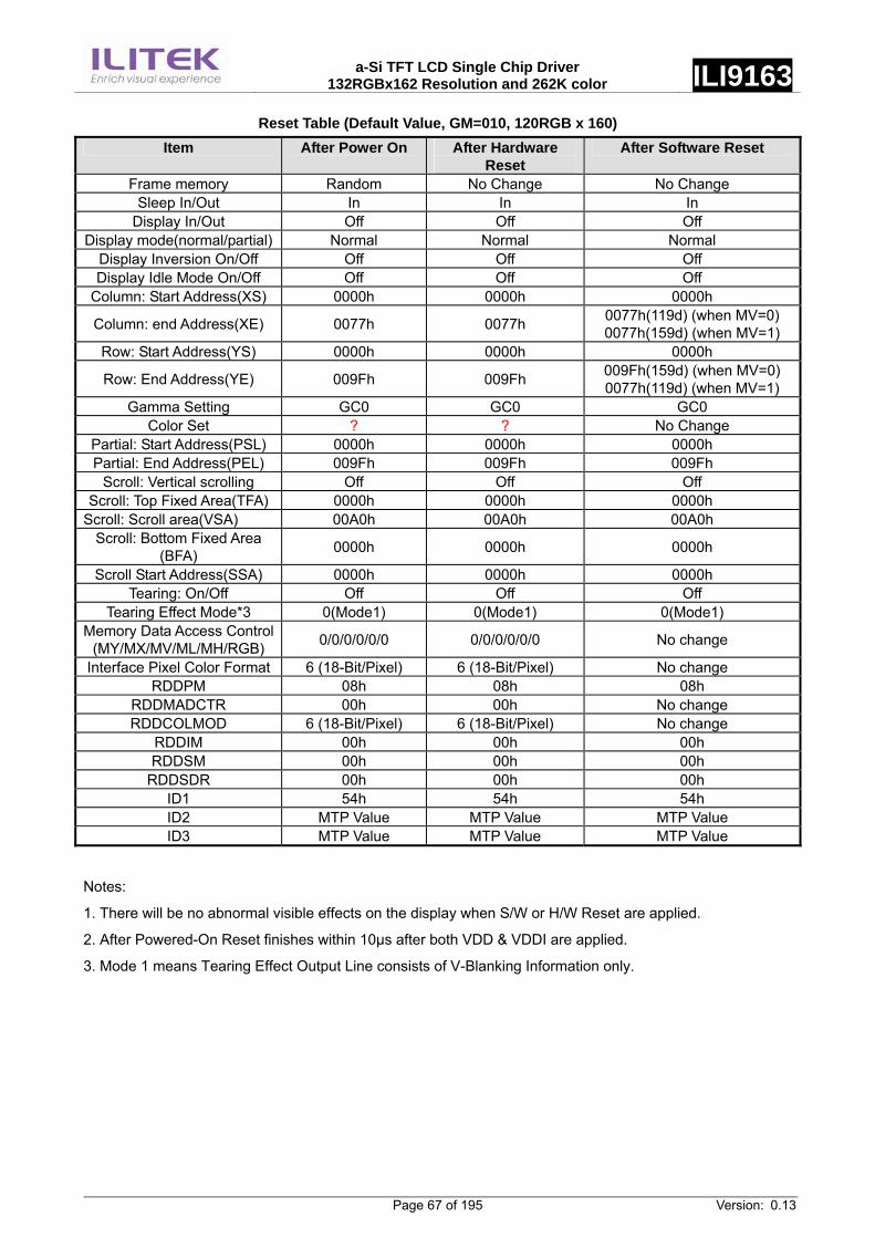
a-Si TFT LCD Single Chip Driver
132RGBx162 Resolution and 262K color ILI9163
Page 67 of 195 Version: 0.13
Reset Table (Default Value, GM=010, 120RGB x 160) Item After Power On After Hardware
Reset After Software Reset
Frame memory Random No Change No Change Sleep In/Out In In In
Display In/Out Off Off Off Display mode(normal/partial) Normal Normal Normal
Display Inversion On/Off Off Off Off Display Idle Mode On/Off Off Off Off
Column: Start Address(XS) 0000h 0000h 0000h
Column: end Address(XE) 0077h 0077h 0077h(119d) (when MV=0) 0077h(159d) (when MV=1)
Row: Start Address(YS) 0000h 0000h 0000h
Row: End Address(YE) 009Fh 009Fh 009Fh(159d) (when MV=0) 0077h(119d) (when MV=1)
Gamma Setting GC0 GC0 GC0 Color Set ? ? No Change
Partial: Start Address(PSL) 0000h 0000h 0000h Partial: End Address(PEL) 009Fh 009Fh 009Fh
Scroll: Vertical scrolling Off Off Off Scroll: Top Fixed Area(TFA) 0000h 0000h 0000h
Scroll: Scroll area(VSA) 00A0h 00A0h 00A0h Scroll: Bottom Fixed Area
(BFA) 0000h 0000h 0000h
Scroll Start Address(SSA) 0000h 0000h 0000h Tearing: On/Off Off Off Off
Tearing Effect Mode*3 0(Mode1) 0(Mode1) 0(Mode1) Memory Data Access Control
(MY/MX/MV/ML/MH/RGB) 0/0/0/0/0/0 0/0/0/0/0/0 No change
Interface Pixel Color Format 6 (18-Bit/Pixel) 6 (18-Bit/Pixel) No change RDDPM 08h 08h 08h
RDDMADCTR 00h 00h No change RDDCOLMOD 6 (18-Bit/Pixel) 6 (18-Bit/Pixel) No change
RDDIM 00h 00h 00h RDDSM 00h 00h 00h
RDDSDR 00h 00h 00h ID1 54h 54h 54h ID2 MTP Value MTP Value MTP Value ID3 MTP Value MTP Value MTP Value
Notes:
1. There will be no abnormal visible effects on the display when S/W or H/W Reset are applied.
2. After Powered-On Reset finishes within 10µs after both VDD & VDDI are applied.
3. Mode 1 means Tearing Effect Output Line consists of V-Blanking Information only.
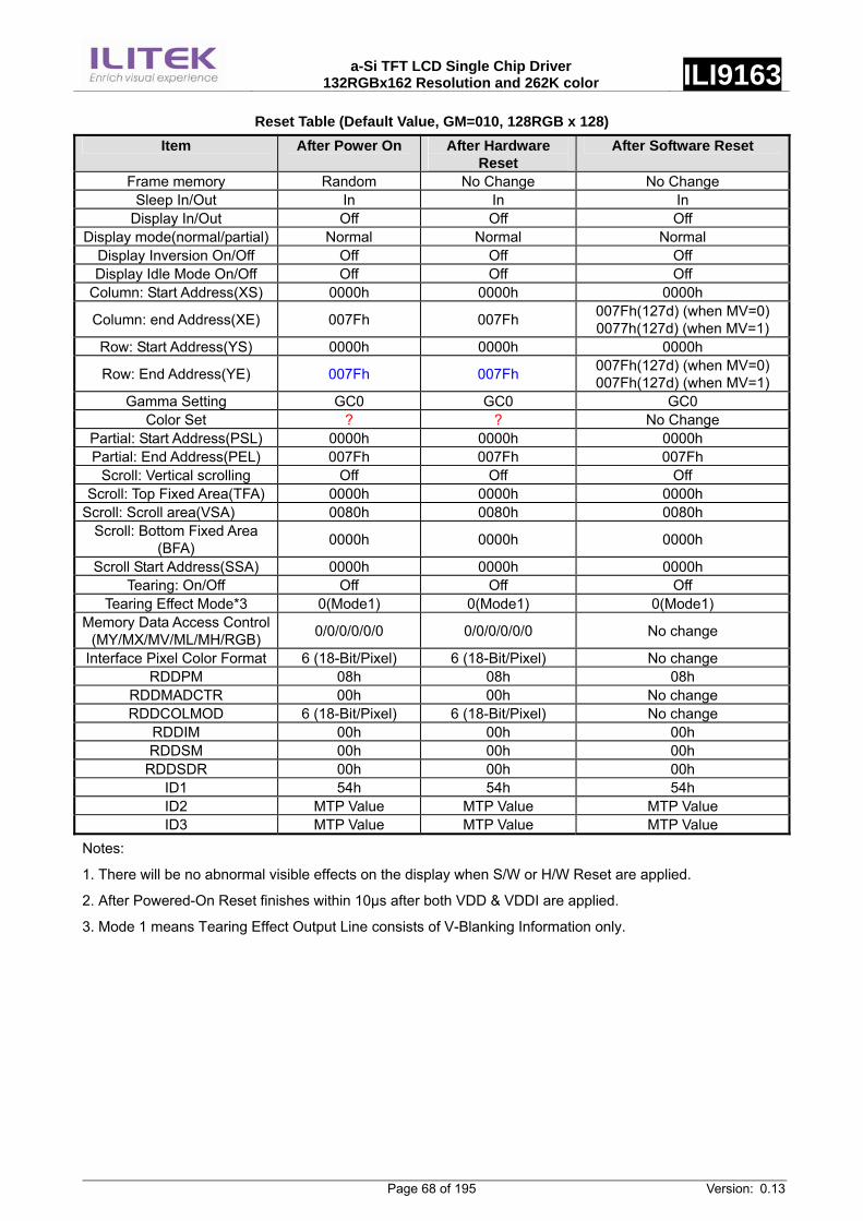
a-Si TFT LCD Single Chip Driver
132RGBx162 Resolution and 262K color ILI9163
Page 68 of 195 Version: 0.13
Reset Table (Default Value, GM=010, 128RGB x 128) Item After Power On After Hardware
Reset After Software Reset
Frame memory Random No Change No Change Sleep In/Out In In In
Display In/Out Off Off Off Display mode(normal/partial) Normal Normal Normal
Display Inversion On/Off Off Off Off Display Idle Mode On/Off Off Off Off
Column: Start Address(XS) 0000h 0000h 0000h
Column: end Address(XE) 007Fh 007Fh 007Fh(127d) (when MV=0) 0077h(127d) (when MV=1)
Row: Start Address(YS) 0000h 0000h 0000h
Row: End Address(YE) 007Fh 007Fh 007Fh(127d) (when MV=0) 007Fh(127d) (when MV=1)
Gamma Setting GC0 GC0 GC0 Color Set ? ? No Change
Partial: Start Address(PSL) 0000h 0000h 0000h Partial: End Address(PEL) 007Fh 007Fh 007Fh
Scroll: Vertical scrolling Off Off Off Scroll: Top Fixed Area(TFA) 0000h 0000h 0000h
Scroll: Scroll area(VSA) 0080h 0080h 0080h Scroll: Bottom Fixed Area
(BFA) 0000h 0000h 0000h
Scroll Start Address(SSA) 0000h 0000h 0000h Tearing: On/Off Off Off Off
Tearing Effect Mode*3 0(Mode1) 0(Mode1) 0(Mode1) Memory Data Access Control
(MY/MX/MV/ML/MH/RGB) 0/0/0/0/0/0 0/0/0/0/0/0 No change
Interface Pixel Color Format 6 (18-Bit/Pixel) 6 (18-Bit/Pixel) No change RDDPM 08h 08h 08h
RDDMADCTR 00h 00h No change RDDCOLMOD 6 (18-Bit/Pixel) 6 (18-Bit/Pixel) No change
RDDIM 00h 00h 00h RDDSM 00h 00h 00h
RDDSDR 00h 00h 00h ID1 54h 54h 54h ID2 MTP Value MTP Value MTP Value ID3 MTP Value MTP Value MTP Value
Notes:
1. There will be no abnormal visible effects on the display when S/W or H/W Reset are applied.
2. After Powered-On Reset finishes within 10µs after both VDD & VDDI are applied.
3. Mode 1 means Tearing Effect Output Line consists of V-Blanking Information only.

a-Si TFT LCD Single Chip Driver
132RGBx162 Resolution and 262K color ILI9163
Page 69 of 195 Version: 0.13
Reset Table (Default Value, GM=011, 132RGB x 162) Item After Power On After Hardware
Reset After Software Reset
Frame memory Random No Change No Change Sleep In/Out In In In
Display In/Out Off Off Off Display mode(normal/partial) Normal Normal Normal
Display Inversion On/Off Off Off Off Display Idle Mode On/Off Off Off Off
Column: Start Address(XS) 0000h 0000h 0000h
Column: end Address(XE) 0083h 0083h 0083h(131d) (when MV=0) 00A1h(161d) (when MV=1)
Row: Start Address(YS) 0000h 0000h 0000h
Row: End Address(YE) 00A1h 00A1h 00A1h(161d) (when MV=0) 0083h(131d) (when MV=1)
Gamma Setting GC0 GC0 GC0 Color Set ? ? No Change
Partial: Start Address(PSL) 0000h 0000h 0000h Partial: End Address(PEL) 00A1h 00A1h 00A1h
Scroll: Vertical scrolling Off Off Off Scroll: Top Fixed Area(TFA) 0000h 0000h 0000h
Scroll: Scroll area(VSA) 00A2h 00A2h 00A2h Scroll: Bottom Fixed Area
(BFA) 0000h 0000h 0000h
Scroll Start Address(SSA) 0000h 0000h 0000h Tearing: On/Off Off Off Off
Tearing Effect Mode*3 0(Mode1) 0(Mode1) 0(Mode1) Memory Data Access Control
(MY/MX/MV/ML/MH/RGB) 0/0/0/0/0/0 0/0/0/0/0/0 No change
Interface Pixel Color Format 6 (18-Bit/Pixel) 6 (18-Bit/Pixel) No change RDDPM 08h 08h 08h
RDDMADCTR 00h 00h No change RDDCOLMOD 6 (18-Bit/Pixel) 6 (18-Bit/Pixel) No change
RDDIM 00h 00h 00h RDDSM 00h 00h 00h
RDDSDR 00h 00h 00h ID1 54h 54h 54h ID2 MTP Value MTP Value MTP Value ID3 MTP Value MTP Value MTP Value
Notes:
1. There will be no abnormal visible effects on the display when S/W or H/W Reset are applied.
2. After Powered-On Reset finishes within 10µs after both VDD & VDDI are applied.
3. Mode 1 means Tearing Effect Output Line consists of V-Blanking Information only.
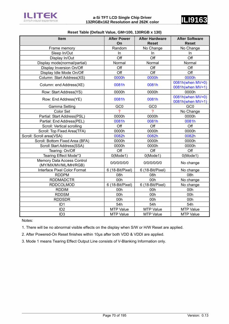
a-Si TFT LCD Single Chip Driver
132RGBx162 Resolution and 262K color ILI9163
Page 70 of 195 Version: 0.13
Reset Table (Default Value, GM=100, 130RGB x 130) Item After Power
On After Hardware
Reset After Software
Reset Frame memory Random No Change No Change
Sleep In/Out In In In Display In/Out Off Off Off
Display mode(normal/partial) Normal Normal Normal Display Inversion On/Off Off Off Off Display Idle Mode On/Off Off Off Off
Column: Start Address(XS) 0000h 0000h 0000h
Column: end Address(XE) 0081h 0081h 0081h(when MV=0)0081h(when MV=1)
Row: Start Address(YS) 0000h 0000h 0000h
Row: End Address(YE) 0081h 0081h 0081h(when MV=0)0081h(when MV=1)
Gamma Setting GC0 GC0 GC0 Color Set ? ? No Change
Partial: Start Address(PSL) 0000h 0000h 0000h Partial: End Address(PEL) 0081h 0081h 0081h
Scroll: Vertical scrolling Off Off Off Scroll: Top Fixed Area(TFA) 0000h 0000h 0000h
Scroll: Scroll area(VSA) 0082h 0082h 0082h Scroll: Bottom Fixed Area (BFA) 0000h 0000h 0000h
Scroll Start Address(SSA) 0000h 0000h 0000h Tearing: On/Off Off Off Off
Tearing Effect Mode*3 0(Mode1) 0(Mode1) 0(Mode1) Memory Data Access Control
(MY/MX/MV/ML/MH/RGB) 0/0/0/0/0/0 0/0/0/0/0/0 No change
Interface Pixel Color Format 6 (18-Bit/Pixel) 6 (18-Bit/Pixel) No change RDDPM 08h 08h 08h
RDDMADCTR 00h 00h No change RDDCOLMOD 6 (18-Bit/Pixel) 6 (18-Bit/Pixel) No change
RDDIM 00h 00h 00h RDDSM 00h 00h 00h
RDDSDR 00h 00h 00h ID1 54h 54h 54h ID2 MTP Value MTP Value MTP Value ID3 MTP Value MTP Value MTP Value
Notes:
1. There will be no abnormal visible effects on the display when S/W or H/W Reset are applied.
2. After Powered-On Reset finishes within 10µs after both VDD & VDDI are applied.
3. Mode 1 means Tearing Effect Output Line consists of V-Blanking Information only.
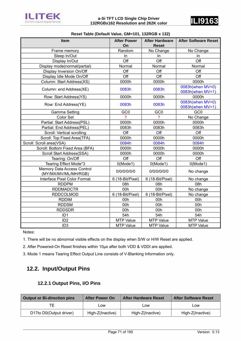
a-Si TFT LCD Single Chip Driver
132RGBx162 Resolution and 262K color ILI9163
Page 71 of 195 Version: 0.13
Reset Table (Default Value, GM=101, 132RGB x 132) Item After Power
On After Hardware
Reset After Software Reset
Frame memory Random No Change No Change Sleep In/Out In In In
Display In/Out Off Off Off Display mode(normal/partial) Normal Normal Normal
Display Inversion On/Off Off Off Off Display Idle Mode On/Off Off Off Off
Column: Start Address(XS) 0000h 0000h 0000h
Column: end Address(XE) 0083h 0083h 0083h(when MV=0) 0083h(when MV=1)
Row: Start Address(YS) 0000h 0000h 0000h
Row: End Address(YE) 0083h 0083h 0083h(when MV=0) 0083h(when MV=1)
Gamma Setting GC0 GC0 GC0 Color Set ? ? No Change
Partial: Start Address(PSL) 0000h 0000h 0000h Partial: End Address(PEL) 0083h 0083h 0083h
Scroll: Vertical scrolling Off Off Off Scroll: Top Fixed Area(TFA) 0000h 0000h 0000h
Scroll: Scroll area(VSA) 0084h 0084h 0084h Scroll: Bottom Fixed Area (BFA) 0000h 0000h 0000h
Scroll Start Address(SSA) 0000h 0000h 0000h Tearing: On/Off Off Off Off
Tearing Effect Mode*3 0(Mode1) 0(Mode1) 0(Mode1) Memory Data Access Control
(MY/MX/MV/ML/MH/RGB) 0/0/0/0/0/0 0/0/0/0/0/0 No change
Interface Pixel Color Format 6 (18-Bit/Pixel) 6 (18-Bit/Pixel) No change RDDPM 08h 08h 08h
RDDMADCTR 00h 00h No change RDDCOLMOD 6 (18-Bit/Pixel) 6 (18-Bit/Pixel) No change
RDDIM 00h 00h 00h RDDSM 00h 00h 00h
RDDSDR 00h 00h 00h ID1 54h 54h 54h ID2 MTP Value MTP Value MTP Value ID3 MTP Value MTP Value MTP Value
Notes:
1. There will be no abnormal visible effects on the display when S/W or H/W Reset are applied.
2. After Powered-On Reset finishes within 10µs after both VDD & VDDI are applied.
3. Mode 1 means Tearing Effect Output Line consists of V-Blanking Information only.
12.2. Input/Output Pins
12.2.1 Output Pins, I/O Pins
Output or Bi-direction pins After Power On After Hardware Reset After Software Reset
TE Low Low Low
D17to D0(Output driver) High-Z(Inactive) High-Z(Inactive) High-Z(Inactive)
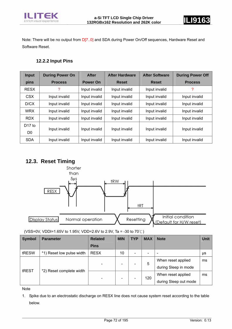
a-Si TFT LCD Single Chip Driver
132RGBx162 Resolution and 262K color ILI9163
Page 72 of 195 Version: 0.13
Note: There will be no output from D[7..0] and SDA during Power On/Off sequences, Hardware Reset and
Software Reset.
12.2.2 Input Pins
Input
pins
During Power On
Process
After
Power On
After Hardware
Reset
After Software
Reset
During Power Off
Process
RESX ? Input invalid Input invalid Input invalid ?
CSX Input invalid Input invalid Input invalid Input invalid Input invalid
D/CX Input invalid Input invalid Input invalid Input invalid Input invalid
WRX Input invalid Input invalid Input invalid Input invalid Input invalid
RDX Input invalid Input invalid Input invalid Input invalid Input invalid
D17 to
D0 Input invalid Input invalid Input invalid Input invalid Input invalid
SDA Input invalid Input invalid Input invalid Input invalid Input invalid
12.3. Reset Timing
(VSS=0V, VDDI=1.65V to 1.95V, VDD=2.6V to 2.9V, Ta = -30 to 70 )℃
Symbol Parameter Related
Pins
MIN TYP MAX Note Unit
tRESW *1) Reset low pulse width RESX 10 - - - µs
- - - 5 When reset applied
during Sleep in mode
ms
tREST *2) Reset complete width
- - - 120When reset applied
during Sleep out mode
ms
Note
1. Spike due to an electrostatic discharge on RESX line does not cause system reset according to the table
below.
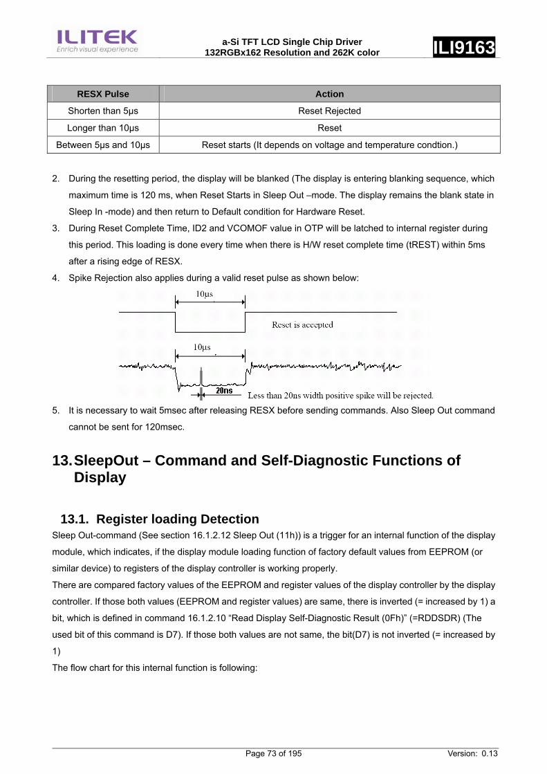
a-Si TFT LCD Single Chip Driver
132RGBx162 Resolution and 262K color ILI9163
Page 73 of 195 Version: 0.13
RESX Pulse Action
Shorten than 5µs Reset Rejected
Longer than 10µs Reset
Between 5µs and 10µs Reset starts (It depends on voltage and temperature condtion.)
2. During the resetting period, the display will be blanked (The display is entering blanking sequence, which
maximum time is 120 ms, when Reset Starts in Sleep Out –mode. The display remains the blank state in
Sleep In -mode) and then return to Default condition for Hardware Reset.
3. During Reset Complete Time, ID2 and VCOMOF value in OTP will be latched to internal register during
this period. This loading is done every time when there is H/W reset complete time (tREST) within 5ms
after a rising edge of RESX.
4. Spike Rejection also applies during a valid reset pulse as shown below:
5. It is necessary to wait 5msec after releasing RESX before sending commands. Also Sleep Out command
cannot be sent for 120msec.
13. SleepOut – Command and Self-Diagnostic Functions of Display
13.1. Register loading Detection Sleep Out-command (See section 16.1.2.12 Sleep Out (11h)) is a trigger for an internal function of the display
module, which indicates, if the display module loading function of factory default values from EEPROM (or
similar device) to registers of the display controller is working properly.
There are compared factory values of the EEPROM and register values of the display controller by the display
controller. If those both values (EEPROM and register values) are same, there is inverted (= increased by 1) a
bit, which is defined in command 16.1.2.10 “Read Display Self-Diagnostic Result (0Fh)” (=RDDSDR) (The
used bit of this command is D7). If those both values are not same, the bit(D7) is not inverted (= increased by
1)
The flow chart for this internal function is following:
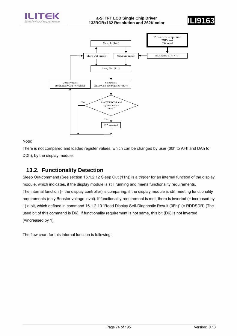
a-Si TFT LCD Single Chip Driver
132RGBx162 Resolution and 262K color ILI9163
Page 74 of 195 Version: 0.13
Note:
There is not compared and loaded register values, which can be changed by user (00h to AFh and DAh to
DDh), by the display module.
13.2. Functionality Detection Sleep Out-command (See section 16.1.2.12 Sleep Out (11h)) is a trigger for an internal function of the display
module, which indicates, if the display module is still running and meets functionality requirements.
The internal function (= the display controller) is comparing, if the display module is still meeting functionality
requirements (only Booster voltage level). If functionality requirement is met, there is inverted (= increased by
1) a bit, which defined in command 16.1.2.10 “Read Display Self-Diagnostic Result (0Fh)” (= RDDSDR) (The
used bit of this command is D6). If functionality requirement is not same, this bit (D6) is not inverted
(=increased by 1).
The flow chart for this internal function is following:
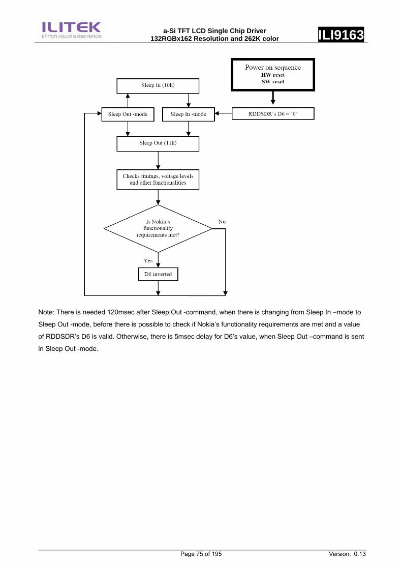
a-Si TFT LCD Single Chip Driver
132RGBx162 Resolution and 262K color ILI9163
Page 75 of 195 Version: 0.13
Note: There is needed 120msec after Sleep Out -command, when there is changing from Sleep In –mode to
Sleep Out -mode, before there is possible to check if Nokia’s functionality requirements are met and a value
of RDDSDR’s D6 is valid. Otherwise, there is 5msec delay for D6’s value, when Sleep Out –command is sent
in Sleep Out -mode.
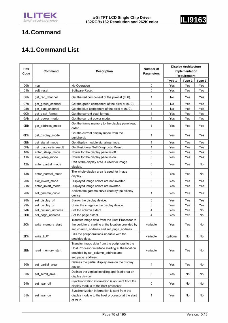
a-Si TFT LCD Single Chip Driver
132RGBx162 Resolution and 262K color ILI9163
Page 76 of 195 Version: 0.13
14. Command
14.1. Command List
Hex Code
Command Description Number of Parameters
Display Architecture Implementation
Requirement Type 1 Type 2 Type 3
00h nop No Operation 0 Yes Yes Yes 01h soft_reset Software Reset 0 Yes Yes Yes
06h get_red_channel Get the red component of the pixel at (0, 0). 1 No Yes Yes
07h get_green_channel Get the green component of the pixel at (0, 0). 1 No Yes Yes 08h get_blue_channel Get the blue component of the pixel at (0, 0). 1 No Yes Yes 0Ch get_pixel_format Get the current pixel format. 1 Yes Yes Yes 0Ah get_power_mode Get the current power mode. 1 Yes Yes Yes
0Bh get_address_mode Get the frame memory to the display panel read order.
1 Yes Yes Yes
0Dh get_display_mode Get the current display mode from the peripheral.
1 Yes Yes Yes
0Eh get_signal_mode Get display module signaling mode. 1 Yes Yes Yes 0Fh get_diagnostic_result Get Peripheral Self-Diagnostic Result 1 Yes Yes Yes 10h enter_sleep_mode Power for the display panel is off. 0 Yes Yes Yes 11h exit_sleep_mode Power for the display panel is on. 0 Yes Yes Yes
12h enter_partial_mode Part of the display area is used for image display.
0 Yes Yes No
13h enter_normal_mode The whole display area is used for image display.
0 Yes Yes No
20h exit_invert_mode Displayed image colors are not inverted. 0 Yes Yes Yes 21h enter_invert_mode Displayed image colors are inverted. 0 Yes Yes Yes
26h set_gamma_curve Selects the gamma curve used by the display device.
1 Yes Yes Yes
28h set_display_off Blanks the display device. 0 Yes Yes Yes 29h set_display_on Show the image on the display device. 0 Yes Yes Yes 2Ah set_column_address Set the column extent. 4 Yes Yes No 2Bh set_page_address Set the page extent. 4 Yes Yes No
2Ch write_memory_start Transfer image data from the Host Processor to the peripheral starting at the location provided by set_column_address and set_page_address.
variable Yes Yes No
2Dh write_LUT Fills the peripheral look-up table with the provided data.
variable optional No No
2Eh read_memory_start
Transfer image data from the peripheral to the Host Processor interface starting at the location provided by set_column_address and set_page_address.
variable Yes Yes No
30h set_partial_area Defines the partial display area on the display device.
4 Yes Yes No
33h set_scroll_area Defines the vertical scrolling and fixed area on display device.
6 Yes No No
34h set_tear_off Synchronization information is not sent from the display module to the host processor.
0 Yes No No
35h set_tear_on Synchronization information is sent from the display module to the host processor at the start of VFP.
1 Yes No No
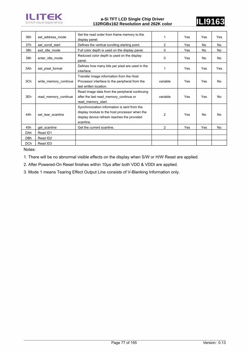
a-Si TFT LCD Single Chip Driver
132RGBx162 Resolution and 262K color ILI9163
Page 77 of 195 Version: 0.13
36h set_address_mode Set the read order from frame memory to the display panel.
1 Yes Yes Yes
37h set_scroll_start Defines the vertical scrolling starting point. 2 Yes No No 38h exit_idle_mode Full color depth is used on the display panel. 0 Yes No No
39h enter_idle_mode Reduced color depth is used on the display panel.
0 Yes No No
3Ah set_pixel_format Defines how many bits per pixel are used in the interface.
1 Yes Yes Yes
3Ch write_memory_continue Transfer image information from the Host Processor interface to the peripheral from the last written location.
variable Yes Yes No
3Eh read_memory_continue Read image data from the peripheral continuing after the last read_memory_continue or read_memory_start.
variable Yes Yes No
44h set_tear_scanline
Synchronization information is sent from the display module to the host processor when the display device refresh reaches the provided scanline.
2 Yes No No
45h get_scanline Get the current scanline. 2 Yes Yes No DAh Read ID1 DBh Read ID2 DCh Read ID3
Notes:
1. There will be no abnormal visible effects on the display when S/W or H/W Reset are applied.
2. After Powered-On Reset finishes within 10µs after both VDD & VDDI are applied.
3. Mode 1 means Tearing Effect Output Line consists of V-Blanking Information only.
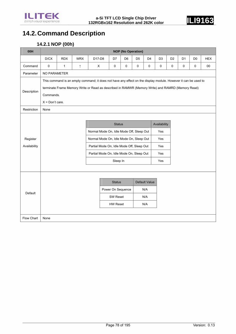
a-Si TFT LCD Single Chip Driver
132RGBx162 Resolution and 262K color ILI9163
Page 78 of 195 Version: 0.13
14.2. Command Description 14.2.1 NOP (00h)
00H NOP (No Operation)
D/CX RDX WRX D17-D8 D7 D6 D5 D4 D3 D2 D1 D0 HEX
Command 0 1 ↑ X 0 0 0 0 0 0 0 0 00
Parameter NO PARAMETER
Description
This command is an empty command; it does not have any effect on the display module. However it can be used to
terminate Frame Memory Write or Read as described in RAMWR (Memory Write) and RAMRD (Memory Read)
Commands.
X = Don’t care.
Restriction None
Register
Availability
Status Availability
Normal Mode On, Idle Mode Off, Sleep Out Yes
Normal Mode On, Idle Mode On, Sleep Out Yes
Partial Mode On, Idle Mode Off, Sleep Out Yes
Partial Mode On, Idle Mode On, Sleep Out Yes
Sleep In Yes
Default
Status Default Value
Power On Sequence N/A
SW Reset N/A
HW Reset N/A
Flow Chart None
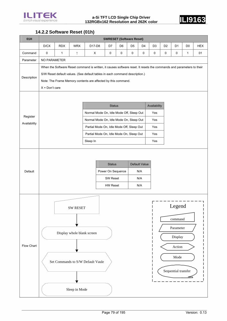
a-Si TFT LCD Single Chip Driver
132RGBx162 Resolution and 262K color ILI9163
Page 79 of 195 Version: 0.13
14.2.2 Software Reset (01h) 01H SWRESET (Software Reset)
D/CX RDX WRX D17-D8 D7 D6 D5 D4 D3 D2 D1 D0 HEX
Command 0 1 ↑ X 0 0 0 0 0 0 0 1 01
Parameter NO PARAMETER
Description
When the Software Reset command is written, it causes software reset. It resets the commands and parameters to their
S/W Reset default values. (See default tables in each command description.)
Note: The Frame Memory contents are affected by this command.
X = Don’t care
Register
Availability
Status Availability
Normal Mode On, Idle Mode Off, Sleep Out Yes
Normal Mode On, Idle Mode On, Sleep Out Yes
Partial Mode On, Idle Mode Off, Sleep Out Yes
Partial Mode On, Idle Mode On, Sleep Out Yes
Sleep In Yes
Default
Status Default Value
Power On Sequence N/A
SW Reset N/A
HW Reset N/A
Flow Chart
command
Parameter
Display
Action
Mode
LegendSW RESET
Sequential transfer
Display whole blank screen
Set Commands to S/W Default Vaule
Sleep in Mode
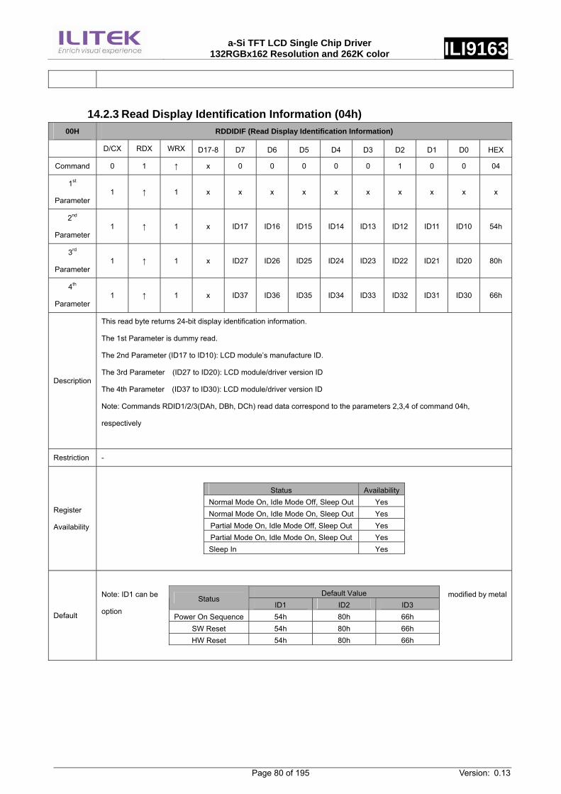
a-Si TFT LCD Single Chip Driver
132RGBx162 Resolution and 262K color ILI9163
Page 80 of 195 Version: 0.13
14.2.3 Read Display Identification Information (04h) 00H RDDIDIF (Read Display Identification Information)
D/CX RDX WRX D17-8 D7 D6 D5 D4 D3 D2 D1 D0 HEX
Command 0 1 ↑ x 0 0 0 0 0 1 0 0 04
1st
Parameter 1 ↑ 1 x x x x x x x x x x
2nd
Parameter 1 ↑ 1 x ID17 ID16 ID15 ID14 ID13 ID12 ID11 ID10 54h
3rd
Parameter 1 ↑ 1 x ID27 ID26 ID25 ID24 ID23 ID22 ID21 ID20 80h
4th
Parameter 1 ↑ 1 x ID37 ID36 ID35 ID34 ID33 ID32 ID31 ID30 66h
Description
This read byte returns 24-bit display identification information.
The 1st Parameter is dummy read.
The 2nd Parameter (ID17 to ID10): LCD module’s manufacture ID.
The 3rd Parameter (ID27 to ID20): LCD module/driver version ID
The 4th Parameter (ID37 to ID30): LCD module/driver version ID
Note: Commands RDID1/2/3(DAh, DBh, DCh) read data correspond to the parameters 2,3,4 of command 04h,
respectively
Restriction -
Register
Availability
Status Availability Normal Mode On, Idle Mode Off, Sleep Out Yes Normal Mode On, Idle Mode On, Sleep Out Yes Partial Mode On, Idle Mode Off, Sleep Out Yes Partial Mode On, Idle Mode On, Sleep Out Yes Sleep In Yes
Default
Note: ID1 can be modified by metal
option
Default Value Status
ID1 ID2 ID3 Power On Sequence 54h 80h 66h
SW Reset 54h 80h 66h HW Reset 54h 80h 66h
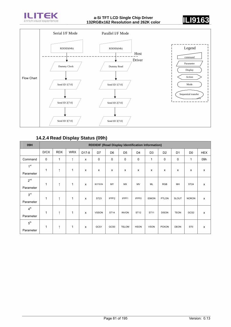
a-Si TFT LCD Single Chip Driver
132RGBx162 Resolution and 262K color ILI9163
Page 81 of 195 Version: 0.13
Flow Chart
command
Parameter
Display
Action
Mode
LegendRDDID(04h)
Sequential transfer
Parallel I/F Mode
RDDID(04h)
Serial I/F Mode
Dummy Clock
Send ID 1[7:0]
Send ID 2[7:0]
Send ID 3[7:0]
Dummy Read
Send ID 1[7:0]
Send ID 2[7:0]
Send ID 3[7:0]
Host
Driver
14.2.4 Read Display Status (09h) 09H RDDIDIF (Read Display Identification Information)
D/CX RDX WRX D17-8 D7 D6 D5 D4 D3 D2 D1 D0 HEX
Command 0 1 ↑ x 0 0 0 0 1 0 0 1 09h
1st
Parameter 1 ↑ 1 x x x x x x x x x x
2nd
Parameter 1 ↑ 1 x BOTSON MY MX MV ML RGB MH ST24 x
3rd
Parameter 1 ↑ 1 x ST23 IFPF2 IFPF1 IFPF0 IDMON PTLON SLOUT NORON x
4th
Parameter 1 ↑ 1 x VSSON ST14 INVON ST12 ST11 DISON TEON GCS2 x
5th
Parameter 1 ↑ 1 x GCS1 GCS0 TELOM HSON VSON PCKON DEON ST0 x
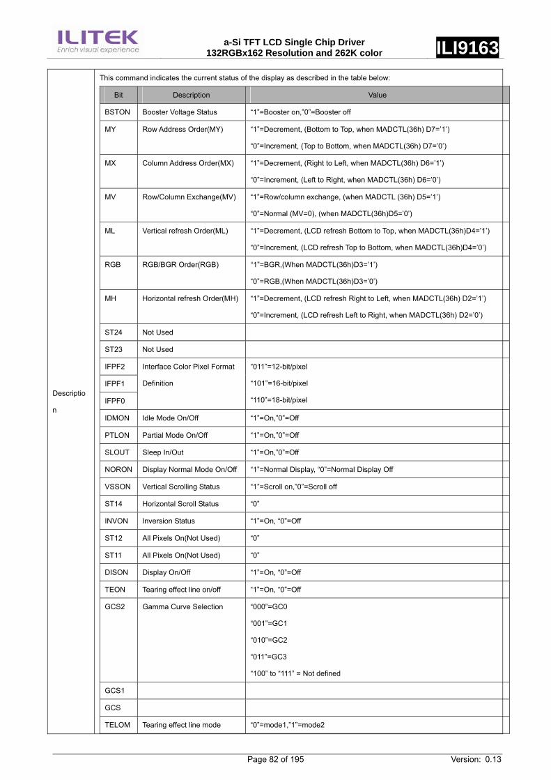
a-Si TFT LCD Single Chip Driver
132RGBx162 Resolution and 262K color ILI9163
Page 82 of 195 Version: 0.13
Descriptio
n
This command indicates the current status of the display as described in the table below:
Bit Description Value
BSTON Booster Voltage Status “1”=Booster on,”0”=Booster off
MY Row Address Order(MY) “1”=Decrement, (Bottom to Top, when MADCTL(36h) D7=’1’)
“0”=Increment, (Top to Bottom, when MADCTL(36h) D7=’0’)
MX Column Address Order(MX) “1”=Decrement, (Right to Left, when MADCTL(36h) D6=’1’)
“0”=Increment, (Left to Right, when MADCTL(36h) D6=’0’)
MV Row/Column Exchange(MV) “1”=Row/column exchange, (when MADCTL (36h) D5=’1’)
“0”=Normal (MV=0), (when MADCTL(36h)D5=’0’)
ML Vertical refresh Order(ML) “1”=Decrement, (LCD refresh Bottom to Top, when MADCTL(36h)D4=’1’)
“0”=Increment, (LCD refresh Top to Bottom, when MADCTL(36h)D4=’0’)
RGB RGB/BGR Order(RGB) “1”=BGR,(When MADCTL(36h)D3=’1’)
“0”=RGB,(When MADCTL(36h)D3=’0’)
MH Horizontal refresh Order(MH) “1”=Decrement, (LCD refresh Right to Left, when MADCTL(36h) D2=’1’)
“0”=Increment, (LCD refresh Left to Right, when MADCTL(36h) D2=’0’)
ST24 Not Used
ST23 Not Used
IFPF2
IFPF1
IFPF0
Interface Color Pixel Format
Definition
“011”=12-bit/pixel
“101”=16-bit/pixel
“110”=18-bit/pixel
IDMON Idle Mode On/Off “1”=On,”0”=Off
PTLON Partial Mode On/Off “1”=On,”0”=Off
SLOUT Sleep In/Out “1”=On,”0”=Off
NORON Display Normal Mode On/Off “1”=Normal Display, “0”=Normal Display Off
VSSON Vertical Scrolling Status “1”=Scroll on,”0”=Scroll off
ST14 Horizontal Scroll Status “0”
INVON Inversion Status “1”=On, “0”=Off
ST12 All Pixels On(Not Used) “0”
ST11 All Pixels On(Not Used) “0”
DISON Display On/Off “1”=On, “0”=Off
TEON Tearing effect line on/off “1”=On, “0”=Off
GCS2 Gamma Curve Selection “000”=GC0
“001”=GC1
“010”=GC2
“011”=GC3
“100” to “111” = Not defined
GCS1
GCS
TELOM Tearing effect line mode “0”=mode1,”1”=mode2
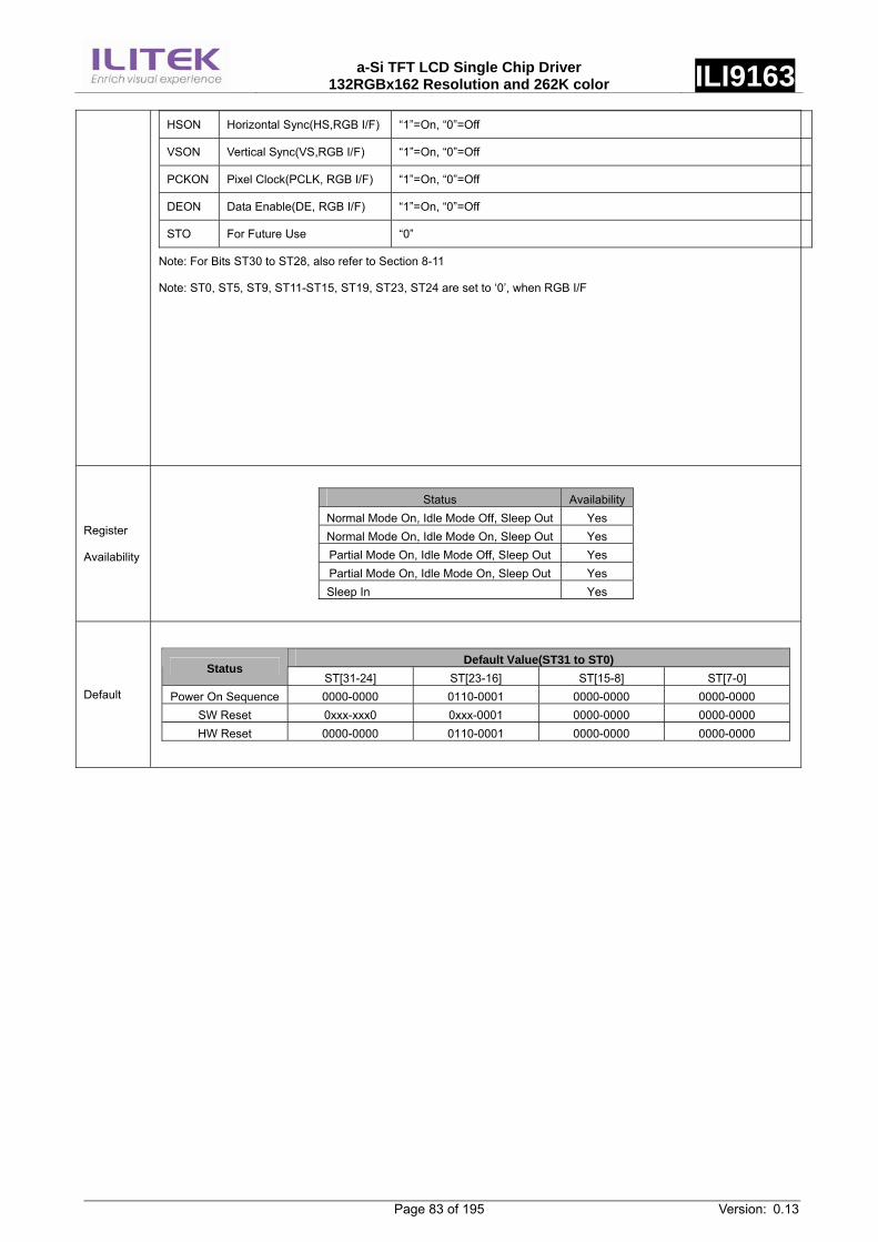
a-Si TFT LCD Single Chip Driver
132RGBx162 Resolution and 262K color ILI9163
Page 83 of 195 Version: 0.13
HSON Horizontal Sync(HS,RGB I/F) “1”=On, “0”=Off
VSON Vertical Sync(VS,RGB I/F) “1”=On, “0”=Off
PCKON Pixel Clock(PCLK, RGB I/F) “1”=On, “0”=Off
DEON Data Enable(DE, RGB I/F) “1”=On, “0”=Off
STO For Future Use “0”
Note: For Bits ST30 to ST28, also refer to Section 8-11
Note: ST0, ST5, ST9, ST11-ST15, ST19, ST23, ST24 are set to ‘0’, when RGB I/F
Register
Availability
Status Availability Normal Mode On, Idle Mode Off, Sleep Out Yes Normal Mode On, Idle Mode On, Sleep Out Yes Partial Mode On, Idle Mode Off, Sleep Out Yes Partial Mode On, Idle Mode On, Sleep Out Yes Sleep In Yes
Default
Default Value(ST31 to ST0) Status
ST[31-24] ST[23-16] ST[15-8] ST[7-0] Power On Sequence 0000-0000 0110-0001 0000-0000 0000-0000
SW Reset 0xxx-xxx0 0xxx-0001 0000-0000 0000-0000 HW Reset 0000-0000 0110-0001 0000-0000 0000-0000
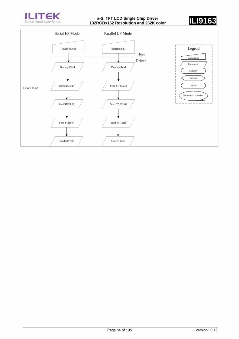
a-Si TFT LCD Single Chip Driver
132RGBx162 Resolution and 262K color ILI9163
Page 84 of 195 Version: 0.13
Flow Chart
command
Parameter
Display
Action
Mode
LegendRDDID(09h)
Sequential transfer
Parallel I/F Mode
RDDST(09h)
Serial I/F Mode
Dummy Clock
Send ST[31:24]
Send ST[23:16]
Send ST[15:8]
Dummy Read
Host
Driver
Send ST[7:0]
Send ST[31:24]
Send ST[23:16]
Send ST[15:8]
Send ST[7:0]
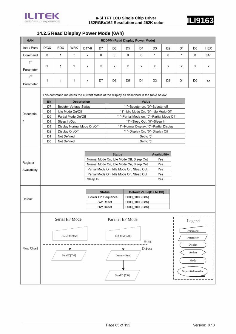
a-Si TFT LCD Single Chip Driver
132RGBx162 Resolution and 262K color ILI9163
Page 85 of 195 Version: 0.13
14.2.5 Read Display Power Mode (0Ah) 0AH RDDPM (Read Display Power Mode)
Inst / Para D/CX RDX WRX D17-8 D7 D6 D5 D4 D3 D2 D1 D0 HEX
Command 0 1 ↑ x 0 0 0 0 1 0 1 0 0Ah
1st
Parameter 1 ↑ 1 x x x x x x x x x x
2nd
Parameter 1 ↑ 1 x D7 D6 D5 D4 D3 D2 D1 D0 xx
Descriptio
n
This command indicates the current status of the display as described in the table below:
Bit Description Value D7 Booster Voltage Status “1”=Booster on, “0”=Booster off D6 Idle Mode On/Off “1”=Idle Mode On, “0”=Idle Mode Off D5 Partial Mode On/Off “1”=Partial Mode on, “0”=Partial Mode Off D4 Sleep In/Out “1”=Sleep Out, “0”=Sleep In D3 Display Normal Mode On/Off “1”=Normal Display, “0”=Partial Display D2 Display On/Off “1”=Display On, “0”=Display Off D1 Not Defined Set to ‘0’ D0 Not Defined Set to ‘0’
Register
Availability
Status Availability Normal Mode On, Idle Mode Off, Sleep Out Yes Normal Mode On, Idle Mode On, Sleep Out Yes Partial Mode On, Idle Mode Off, Sleep Out Yes Partial Mode On, Idle Mode On, Sleep Out Yes Sleep In Yes
Default
Status Default Value(D7 to D0) Power On Sequence 0000_1000(08h)
SW Reset 0000_1000(08h) HW Reset 0000_1000(08h)
Flow Chart
command
Parameter
Display
Action
Mode
Legend
RDDPM(0Ah)
Sequential transfer
Parallel I/F Mode
RDDPM(0Ah)
Serial I/F Mode
Send D[7:0] Dummy Read
Send D [7:0]
Host
Driver
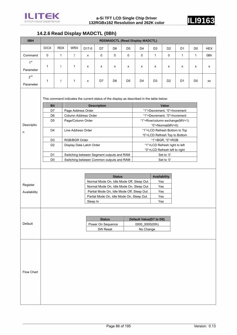
a-Si TFT LCD Single Chip Driver
132RGBx162 Resolution and 262K color ILI9163
Page 86 of 195 Version: 0.13
14.2.6 Read Display MADCTL (0Bh) 0BH RDDMADCTL (Read Display MADCTL)
D/CX RDX WRX D17-0 D7 D6 D5 D4 D3 D2 D1 D0 HEX
Command 0 1 ↑ x 0 0 0 0 1 0 1 1 0Bh
1st
Parameter 1 ↑ 1 x x x x x x x x x x
2nd
Parameter 1 ↑ 1 x D7 D6 D5 D4 D3 D2 D1 D0 xx
Descriptio
n
This command indicates the current status of the display as described in the table below:
Bit Description Value D7 Page Address Order “1”=Decrement, “0”=Increment D6 Column Address Order “1”=Decrement, “0”=Increment D5 Page/Column Order “1”=Row/column exchange(MV=1)
“0”=Normal(MV=0) D4 Line Address Order “1”=LCD Refresh Bottom to Top
“0”=LCD Refresh Top to Bottom D3 RGB/BGR Order “1”=BGR, “0”=RGB D2 Display Data Latch Order “1”=LCD Refresh right to left
“0”=LCD Refresh left to right D1 Switching between Segment outputs and RAM Set to ‘0’ D0 Switching between Common outputs and RAM Set to ‘0’
Register
Availability
Status Availability Normal Mode On, Idle Mode Off, Sleep Out Yes Normal Mode On, Idle Mode On, Sleep Out Yes Partial Mode On, Idle Mode Off, Sleep Out Yes Partial Mode On, Idle Mode On, Sleep Out Yes Sleep In Yes
Default Status Default Value(D7 to D0)
Power On Sequence 0000_0000(00h) SW Reset No Change
Flow Chart
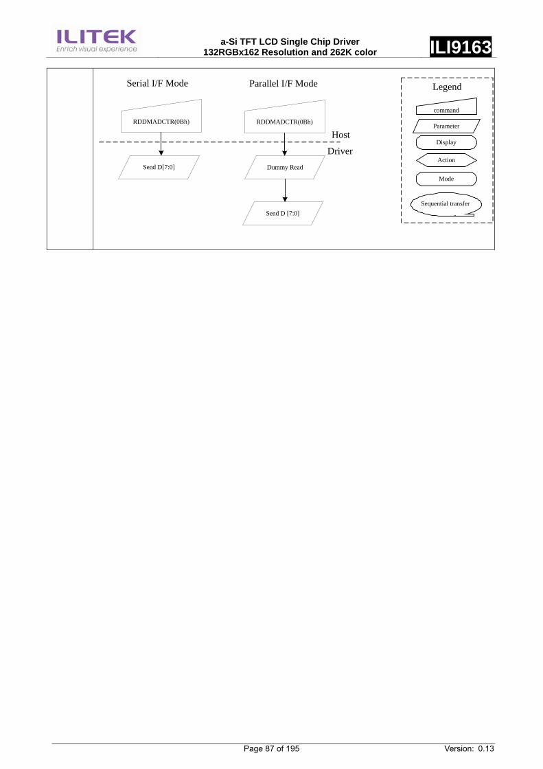
a-Si TFT LCD Single Chip Driver
132RGBx162 Resolution and 262K color ILI9163
Page 87 of 195 Version: 0.13
command
Parameter
Display
Action
Mode
Legend
RDDMADCTR(0Bh)
Sequential transfer
Parallel I/F Mode
RDDMADCTR(0Bh)
Serial I/F Mode
Send D[7:0] Dummy Read
Send D [7:0]
Host
Driver
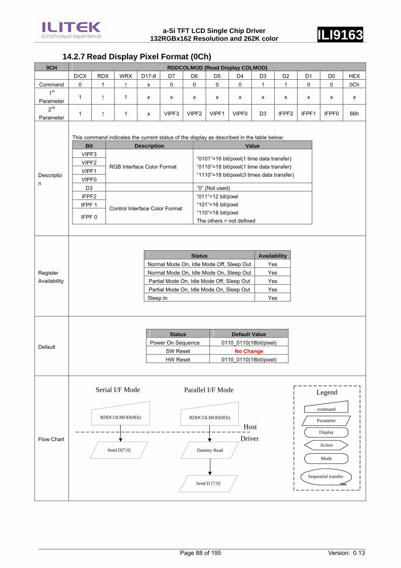
a-Si TFT LCD Single Chip Driver
132RGBx162 Resolution and 262K color ILI9163
Page 88 of 195 Version: 0.13
14.2.7 Read Display Pixel Format (0Ch) 0CH RDDCOLMOD (Read Display COLMOD)
D/CX RDX WRX D17-8 D7 D6 D5 D4 D3 D2 D1 D0 HEXCommand 0 1 ↑ x 0 0 0 0 1 1 0 0 0Ch
1st Parameter
1 ↑ 1 x x x x x x x x x x
2nd Parameter
1 ↑ 1 x VIPF3 VIPF2 VIPF1 VIPF0 D3 IFPF2 IFPF1 IFPF0 66h
Description
This command indicates the current status of the display as described in the table below: Bit Description Value
VIPF3 VIPF2 VIPF1 VIPF0
RGB Interface Color Format “0101”=16 bit/pixel(1 time data transfer) “0110”=18 bit/pixel(1 time data transfer) “1110”=18 bit/pixel(3 times data transfer)
D3 ”0” (Not used) IFPF2 IFPF 1
IFPF 0 Control Interface Color Format
“011”=12 bit/pixel “101”=16 bit/pixel “110”=18 bit/pixel The others = not defined
Register Availability
Status Availability Normal Mode On, Idle Mode Off, Sleep Out Yes Normal Mode On, Idle Mode On, Sleep Out Yes Partial Mode On, Idle Mode Off, Sleep Out Yes Partial Mode On, Idle Mode On, Sleep Out Yes Sleep In Yes
Default
Status Default Value Power On Sequence 0110_0110(18bit/pixel)
SW Reset No Change HW Reset 0110_0110(18bit/pixel)
Flow Chart
command
Parameter
Display
Action
Mode
Legend
RDDCOLMOD(0Eh)
Sequential transfer
Parallel I/F Mode
RDDCOLMOD(0Eh)
Serial I/F Mode
Send D[7:0] Dummy Read
Send D [7:0]
Host
Driver
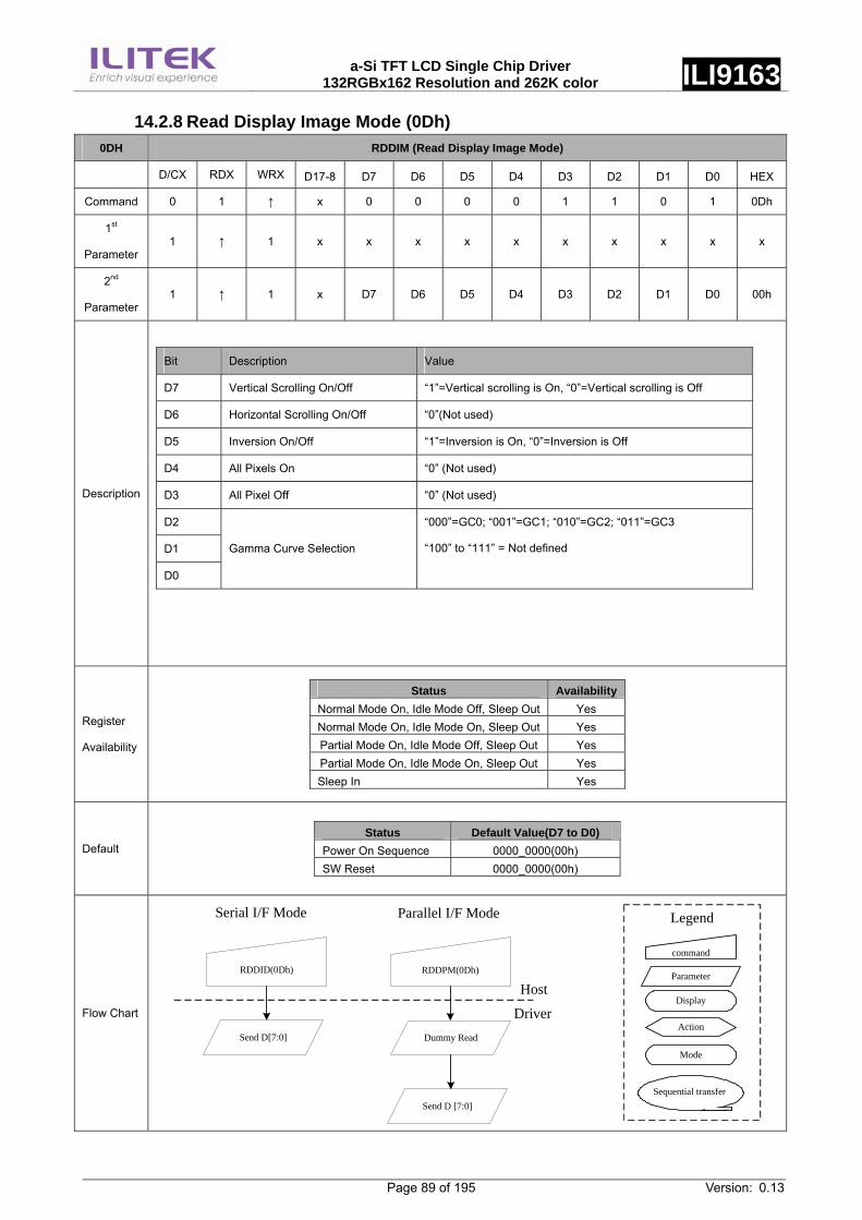
a-Si TFT LCD Single Chip Driver
132RGBx162 Resolution and 262K color ILI9163
Page 89 of 195 Version: 0.13
14.2.8 Read Display Image Mode (0Dh) 0DH RDDIM (Read Display Image Mode)
D/CX RDX WRX D17-8 D7 D6 D5 D4 D3 D2 D1 D0 HEX
Command 0 1 ↑ x 0 0 0 0 1 1 0 1 0Dh
1st
Parameter 1 ↑ 1 x x x x x x x x x x
2nd
Parameter 1 ↑ 1 x D7 D6 D5 D4 D3 D2 D1 D0 00h
Description
Bit Description Value
D7 Vertical Scrolling On/Off “1”=Vertical scrolling is On, “0”=Vertical scrolling is Off
D6 Horizontal Scrolling On/Off “0”(Not used)
D5 Inversion On/Off “1”=Inversion is On, “0”=Inversion is Off
D4 All Pixels On “0” (Not used)
D3 All Pixel Off “0” (Not used)
D2
D1
D0
Gamma Curve Selection
“000”=GC0; “001”=GC1; “010”=GC2; “011”=GC3
“100” to “111” = Not defined
Register
Availability
Status Availability Normal Mode On, Idle Mode Off, Sleep Out Yes Normal Mode On, Idle Mode On, Sleep Out Yes Partial Mode On, Idle Mode Off, Sleep Out Yes Partial Mode On, Idle Mode On, Sleep Out Yes Sleep In Yes
Default Status Default Value(D7 to D0)
Power On Sequence 0000_0000(00h) SW Reset 0000_0000(00h)
Flow Chart
command
Parameter
Display
Action
Mode
Legend
RDDPM(0Dh)
Sequential transfer
Parallel I/F Mode
RDDID(0Dh)
Serial I/F Mode
Send D[7:0] Dummy Read
Send D [7:0]
Host
Driver

a-Si TFT LCD Single Chip Driver
132RGBx162 Resolution and 262K color ILI9163
Page 90 of 195 Version: 0.13
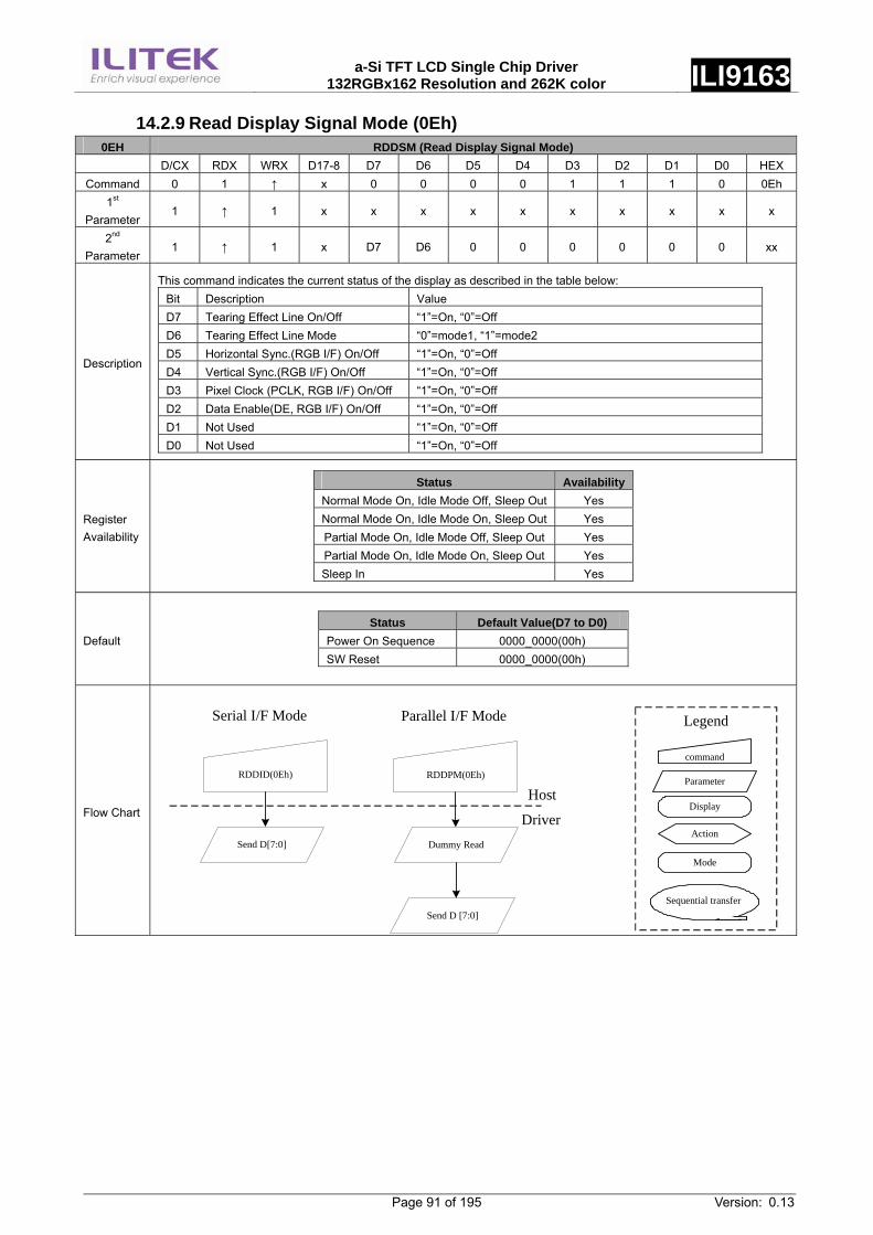
a-Si TFT LCD Single Chip Driver
132RGBx162 Resolution and 262K color ILI9163
Page 91 of 195 Version: 0.13
14.2.9 Read Display Signal Mode (0Eh) 0EH RDDSM (Read Display Signal Mode)
D/CX RDX WRX D17-8 D7 D6 D5 D4 D3 D2 D1 D0 HEXCommand 0 1 ↑ x 0 0 0 0 1 1 1 0 0Eh
1st Parameter
1 ↑ 1 x x x x x x x x x x
2nd Parameter
1 ↑ 1 x D7 D6 0 0 0 0 0 0 xx
Description
This command indicates the current status of the display as described in the table below: Bit Description Value D7 Tearing Effect Line On/Off “1”=On, “0”=Off D6 Tearing Effect Line Mode “0”=mode1, “1”=mode2 D5 Horizontal Sync.(RGB I/F) On/Off “1”=On, “0”=Off D4 Vertical Sync.(RGB I/F) On/Off “1”=On, “0”=Off D3 Pixel Clock (PCLK, RGB I/F) On/Off “1”=On, “0”=Off D2 Data Enable(DE, RGB I/F) On/Off “1”=On, “0”=Off D1 Not Used “1”=On, “0”=Off D0 Not Used “1”=On, “0”=Off
Register Availability
Status Availability Normal Mode On, Idle Mode Off, Sleep Out Yes Normal Mode On, Idle Mode On, Sleep Out Yes Partial Mode On, Idle Mode Off, Sleep Out Yes Partial Mode On, Idle Mode On, Sleep Out Yes Sleep In Yes
Default Status Default Value(D7 to D0)
Power On Sequence 0000_0000(00h) SW Reset 0000_0000(00h)
Flow Chart
command
Parameter
Display
Action
Mode
Legend
RDDPM(0Eh)
Sequential transfer
Parallel I/F Mode
RDDID(0Eh)
Serial I/F Mode
Send D[7:0] Dummy Read
Send D [7:0]
Host
Driver
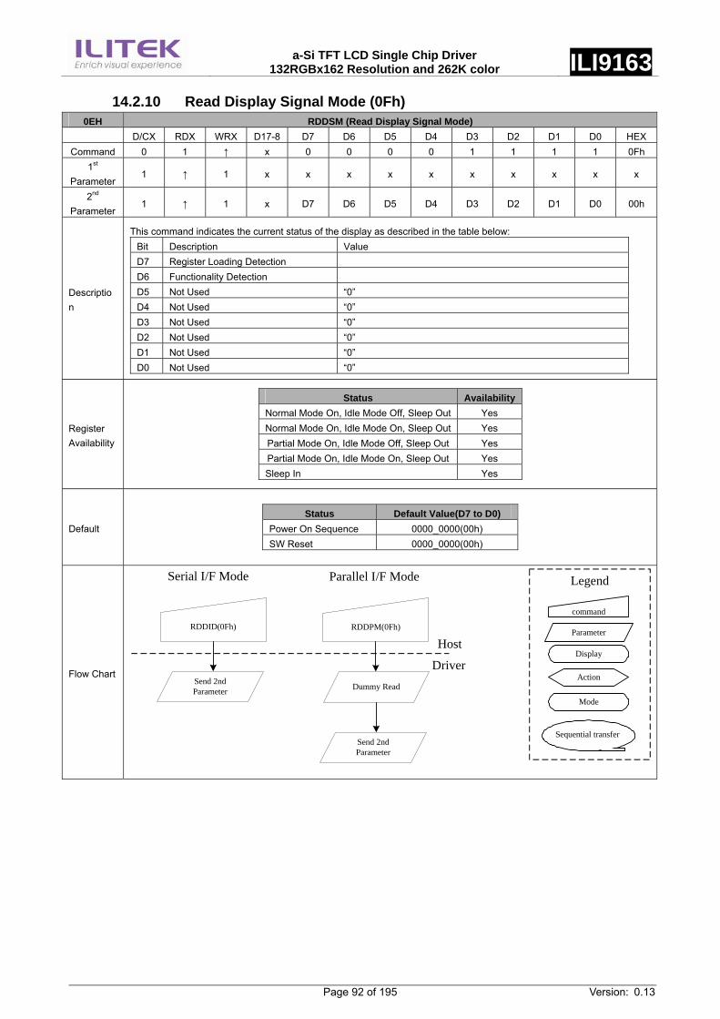
a-Si TFT LCD Single Chip Driver
132RGBx162 Resolution and 262K color ILI9163
Page 92 of 195 Version: 0.13
14.2.10 Read Display Signal Mode (0Fh) 0EH RDDSM (Read Display Signal Mode)
D/CX RDX WRX D17-8 D7 D6 D5 D4 D3 D2 D1 D0 HEXCommand 0 1 ↑ x 0 0 0 0 1 1 1 1 0Fh
1st Parameter
1 ↑ 1 x x x x x x x x x x
2nd Parameter
1 ↑ 1 x D7 D6 D5 D4 D3 D2 D1 D0 00h
Description
This command indicates the current status of the display as described in the table below: Bit Description Value D7 Register Loading Detection D6 Functionality Detection D5 Not Used “0” D4 Not Used “0” D3 Not Used “0” D2 Not Used “0” D1 Not Used “0” D0 Not Used “0”
Register Availability
Status Availability Normal Mode On, Idle Mode Off, Sleep Out Yes Normal Mode On, Idle Mode On, Sleep Out Yes Partial Mode On, Idle Mode Off, Sleep Out Yes Partial Mode On, Idle Mode On, Sleep Out Yes Sleep In Yes
Default Status Default Value(D7 to D0)
Power On Sequence 0000_0000(00h) SW Reset 0000_0000(00h)
Flow Chart
command
Parameter
Display
Action
Mode
Legend
RDDPM(0Fh)
Sequential transfer
Parallel I/F Mode
RDDID(0Fh)
Serial I/F Mode
Send 2nd Parameter Dummy Read
Send 2nd Parameter
Host
Driver
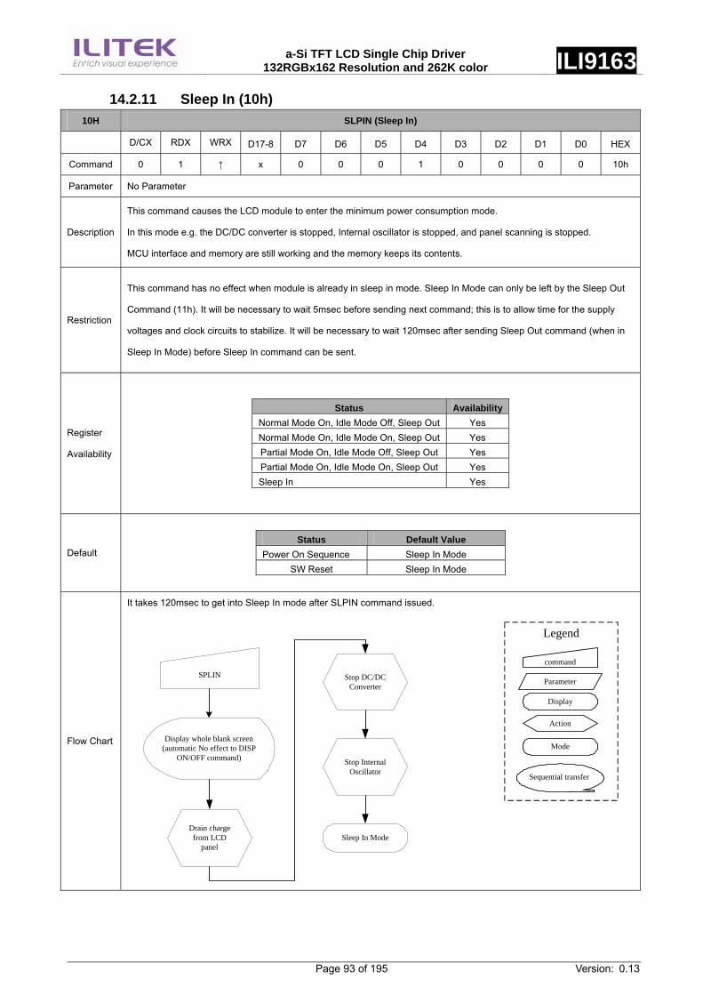
a-Si TFT LCD Single Chip Driver
132RGBx162 Resolution and 262K color ILI9163
Page 93 of 195 Version: 0.13
14.2.11 Sleep In (10h) 10H SLPIN (Sleep In)
D/CX RDX WRX D17-8 D7 D6 D5 D4 D3 D2 D1 D0 HEX
Command 0 1 ↑ x 0 0 0 1 0 0 0 0 10h
Parameter No Parameter
Description
This command causes the LCD module to enter the minimum power consumption mode.
In this mode e.g. the DC/DC converter is stopped, Internal oscillator is stopped, and panel scanning is stopped.
MCU interface and memory are still working and the memory keeps its contents.
Restriction
This command has no effect when module is already in sleep in mode. Sleep In Mode can only be left by the Sleep Out
Command (11h). It will be necessary to wait 5msec before sending next command; this is to allow time for the supply
voltages and clock circuits to stabilize. It will be necessary to wait 120msec after sending Sleep Out command (when in
Sleep In Mode) before Sleep In command can be sent.
Register
Availability
Status Availability Normal Mode On, Idle Mode Off, Sleep Out Yes Normal Mode On, Idle Mode On, Sleep Out Yes Partial Mode On, Idle Mode Off, Sleep Out Yes Partial Mode On, Idle Mode On, Sleep Out Yes Sleep In Yes
Default Status Default Value
Power On Sequence Sleep In Mode SW Reset Sleep In Mode
Flow Chart
It takes 120msec to get into Sleep In mode after SLPIN command issued.
command
Parameter
Display
Action
Mode
Legend
Sequential transfer
SPLIN
Display whole blank screen (automatic No effect to DISP
ON/OFF command)
Drain charge from LCD
panel
Stop DC/DC Converter
Stop Internal Oscillator
Sleep In Mode
a-Si TFT LCD Single Chip Driver
132RGBx162 Resolution and 262K color ILI9163
Page 94 of 195 Version: 0.13
14.2.12 Sleep Out (11h) 11H SLPOUT (Sleep Out)
D/CX RDX WRX D17-8 D7 D6 D5 D4 D3 D2 D1 D0 HEX
Command 0 1 ↑ x 0 0 0 1 0 0 0 1 11h
Parameter No Parameter
Description
This command turns off sleep mode. In this mode e.g. the DC/DC converter is enabled, Internal oscillator is started, and panel scanning is started.
Restriction
This command has no effect when module is already in sleep out mode. Sleep
Out Mode can only be left by the Sleep In Command (10h).
It will be necessary to wait 5msec before sending next command; this is to allow time for the supply voltages and clock
circuits to stabilize.
The display module loads all display supplier’s factory default values to the registers during this 5msec and there cannot
be any abnormal visual effect on the display image if factory default and register values are same when this load is done
and when the display module is already Sleep Out –mode.
The display module is doing self-diagnostic functions during this 5msec. It will be necessary to wait 120msec after
sending Sleep In command (when in Sleep Out mode) before Sleep Out command can be sent.
This command has no effect when module is already in sleep out mode.
Sleep Out Mode can only be left by HW Reset, Software Reset (01h), Sleep In (10h), or a NMI event trigger.
Register
Availability
Status Availability Normal Mode On, Idle Mode Off, Sleep Out Yes Normal Mode On, Idle Mode On, Sleep Out Yes Partial Mode On, Idle Mode Off, Sleep Out Yes Partial Mode On, Idle Mode On, Sleep Out Yes Sleep In Yes
Default
Status Default Value Power On Sequence Sleep In Mode
SW Reset Sleep In Mode HW Reset Sleep In Mode
Flow Chart It takes 120msec to become Sleep Out mode after SLPOUT command issued.
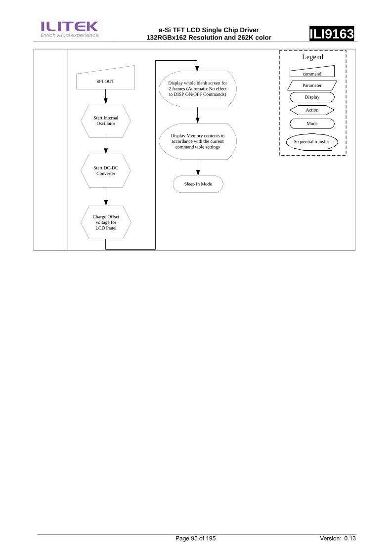
a-Si TFT LCD Single Chip Driver
132RGBx162 Resolution and 262K color ILI9163
Page 95 of 195 Version: 0.13
command
Parameter
Display
Action
Mode
Legend
Sequential transfer
SPLOUT Display whole blank screen for 2 frames (Automatic No effect to DISP ON/OFF Commands)
Start DC-DC Converter
Sleep In Mode
Charge Offset voltage for LCD Panel
Start Internal Oscillator
Display Memory contents in accordance with the current
command table settings
a-Si TFT LCD Single Chip Driver
132RGBx162 Resolution and 262K color ILI9163
Page 96 of 195 Version: 0.13
14.2.13 Partial Mode On (12h) 12H PTLON (Partial Mode On)
D/CX RDX WRX D17-8 D7 D6 D5 D4 D3 D2 D1 D0 HEX
Command 0 1 ↑ x 0 0 0 1 0 0 1 0 12h
Parameter No Parameter
Description
This command turns on partial mode. The partial mode is described by the Partial Area command (30h).
To leave Partial mode, the Normal Display On command (13h) should be written.
X = Don’t care
Note: If a command is written in a frame cycle, the command becomes effective from the next frame.
Restriction This command has no effect during Partial mode is active.
Register Availability
Status Availability Normal Mode On, Idle Mode Off, Sleep Out Yes Normal Mode On, Idle Mode On, Sleep Out Yes Partial Mode On, Idle Mode Off, Sleep Out Yes Partial Mode On, Idle Mode On, Sleep Out Yes Sleep In Yes
Default
Status Default Value Power On Sequence Normal Display Mode On
SW Reset Normal Display Mode On HW Reset Normal Display Mode On
Flow Chart See Partial Area (30h)
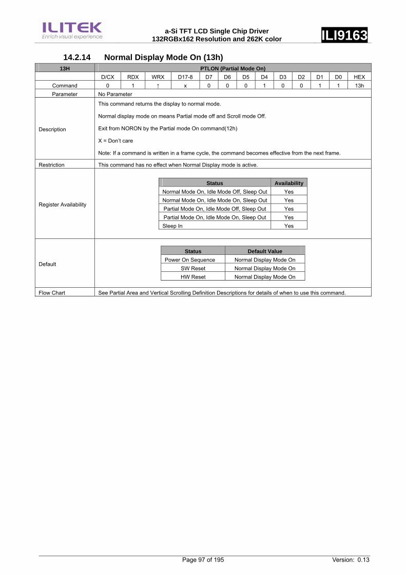
a-Si TFT LCD Single Chip Driver
132RGBx162 Resolution and 262K color ILI9163
Page 97 of 195 Version: 0.13
14.2.14 Normal Display Mode On (13h) 13H PTLON (Partial Mode On)
D/CX RDX WRX D17-8 D7 D6 D5 D4 D3 D2 D1 D0 HEX Command 0 1 ↑ x 0 0 0 1 0 0 1 1 13h Parameter No Parameter
Description
This command returns the display to normal mode.
Normal display mode on means Partial mode off and Scroll mode Off.
Exit from NORON by the Partial mode On command(12h)
X = Don’t care
Note: If a command is written in a frame cycle, the command becomes effective from the next frame.
Restriction This command has no effect when Normal Display mode is active.
Register Availability
Status Availability Normal Mode On, Idle Mode Off, Sleep Out Yes Normal Mode On, Idle Mode On, Sleep Out Yes Partial Mode On, Idle Mode Off, Sleep Out Yes Partial Mode On, Idle Mode On, Sleep Out Yes Sleep In Yes
Default
Status Default Value Power On Sequence Normal Display Mode On
SW Reset Normal Display Mode On HW Reset Normal Display Mode On
Flow Chart See Partial Area and Vertical Scrolling Definition Descriptions for details of when to use this command.
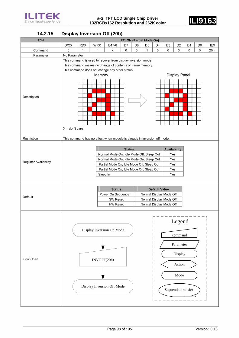
a-Si TFT LCD Single Chip Driver
132RGBx162 Resolution and 262K color ILI9163
Page 98 of 195 Version: 0.13
14.2.15 Display Inversion Off (20h) 20H PTLON (Partial Mode On)
D/CX RDX WRX D17-8 D7 D6 D5 D4 D3 D2 D1 D0 HEXCommand 0 1 ↑ x 0 0 1 0 0 0 0 0 20h Parameter No Parameter
Description
This command is used to recover from display inversion mode. This command makes no change of contents of frame memory. This command does not change any other status.
Memory Display Panel
X = don’t care
Restriction This command has no effect when module is already in inversion off mode.
Register Availability
Status Availability Normal Mode On, Idle Mode Off, Sleep Out Yes Normal Mode On, Idle Mode On, Sleep Out Yes Partial Mode On, Idle Mode Off, Sleep Out Yes Partial Mode On, Idle Mode On, Sleep Out Yes Sleep In Yes
Default
Status Default Value Power On Sequence Normal Display Mode Off
SW Reset Normal Display Mode Off HW Reset Normal Display Mode Off
Flow Chart
command
Parameter
Display
Action
Mode
Legend
Sequential transfer
INVOFF(20h)
Display Inversion Off Mode
Display Inversion On Mode
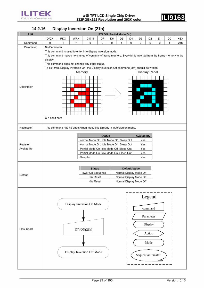
a-Si TFT LCD Single Chip Driver
132RGBx162 Resolution and 262K color ILI9163
Page 99 of 195 Version: 0.13
14.2.16 Display Inversion On (21h) 21H PTLON (Partial Mode On)
D/CX RDX WRX D17-8 D7 D6 D5 D4 D3 D2 D1 D0 HEX Command 0 1 ↑ x 0 0 1 0 0 0 0 1 21h Parameter No Parameter
Description
This command is used to enter into display inversion mode. This command makes no change of contents of frame memory. Every bit is inverted from the frame memory to the display. This command does not change any other status. To exit from Display inversion On, the Display Inversion Off command(20h) should be written.
Memory Display Panel
X = don’t care
Restriction This command has no effect when module is already in inversion on mode.
Register Availability
Status Availability Normal Mode On, Idle Mode Off, Sleep Out Yes Normal Mode On, Idle Mode On, Sleep Out Yes Partial Mode On, Idle Mode Off, Sleep Out Yes Partial Mode On, Idle Mode On, Sleep Out Yes Sleep In Yes
Default
Status Default Value Power On Sequence Normal Display Mode Off
SW Reset Normal Display Mode Off HW Reset Normal Display Mode Off
Flow Chart
command
Parameter
Display
Action
Mode
Legend
Sequential transfer
INVON(21h)
Display Inversion Off Mode
Display Inversion On Mode
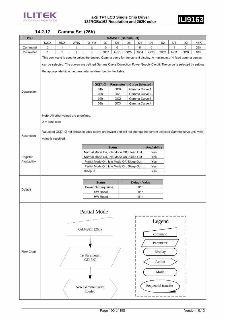
a-Si TFT LCD Single Chip Driver
132RGBx162 Resolution and 262K color ILI9163
Page 100 of 195 Version: 0.13
14.2.17 Gamma Set (26h) 26H GAMSET (Gamma Set)
D/CX RDX WRX D17-8 D7 D6 D5 D4 D3 D2 D1 D0 HEX Command 0 1 ↑ x 0 0 1 0 0 1 1 0 26h Parameter 1 1 ↑ x GC7 GC6 GC5 GC4 GC3 GC2 GC1 GC0 01h
Description
This command is used to select the desired Gamma curve for the current display. A maximum of 4 fixed gamma curves
can be selected. The curves are defined Gamma Curve Correction Power Supply Circuit. The curve is selected by setting
the appropriate bit in the parameter as described in the Table:
GC[7..0] Parameter Curve Selected01h GC0 Gamma Curve 102h GC1 Gamma Curve 204h GC2 Gamma Curve 308h GC3 Gamma Curve 4
Note: All other values are undefined.
X = don’t care
Restriction Values of GC[7..0] not shown in table above are invalid and will not change the current selected Gamma curve until valid
value is received.
Register Availability
Status Availability Normal Mode On, Idle Mode Off, Sleep Out Yes Normal Mode On, Idle Mode On, Sleep Out Yes Partial Mode On, Idle Mode Off, Sleep Out Yes Partial Mode On, Idle Mode On, Sleep Out Yes Sleep In Yes
Default
Status Default Value Power On Sequence 01h
SW Reset 01h HW Reset 01h
Flow Chart
command
Parameter
Display
Action
Mode
Legend
Sequential transfer
GAMSET (26h)
Partial Mode
1st Parameter: GC[7:0]
New Gamma Curve Loaded
a-Si TFT LCD Single Chip Driver
132RGBx162 Resolution and 262K color ILI9163
Page 101 of 195 Version: 0.13
a-Si TFT LCD Single Chip Driver
132RGBx162 Resolution and 262K color ILI9163
Page 102 of 195 Version: 0.13
14.2.18 Display Off (28h) 28H DISPOFF (Display Off)
D/CX RDX WRX D17-8 D7 D6 D5 D4 D3 D2 D1 D0 HEX Command 0 1 ↑ x 0 0 1 0 1 0 0 0 28h Parameter No Parameter
Description
This command is used to enter into DISPLAY OFF mode. In this mode, the output from Frame Memory is disabled
and blank page inserted.
This command makes no change of contents of frame memory.
This command does not change any other status.
There will be no abnormal visible effect on the display.
Exit from this command by Display On(29h)
Memory Display Panel
X = don’t care
Restriction This command has no effect when module is already in display off mode.
Register Availability
Status Availability Normal Mode On, Idle Mode Off, Sleep Out Yes Normal Mode On, Idle Mode On, Sleep Out Yes Partial Mode On, Idle Mode Off, Sleep Out Yes Partial Mode On, Idle Mode On, Sleep Out Yes Sleep In Yes
Default
Status Default Value Power On Sequence Display Off
SW Reset Display Off HW Reset Display Off
Flow Chart
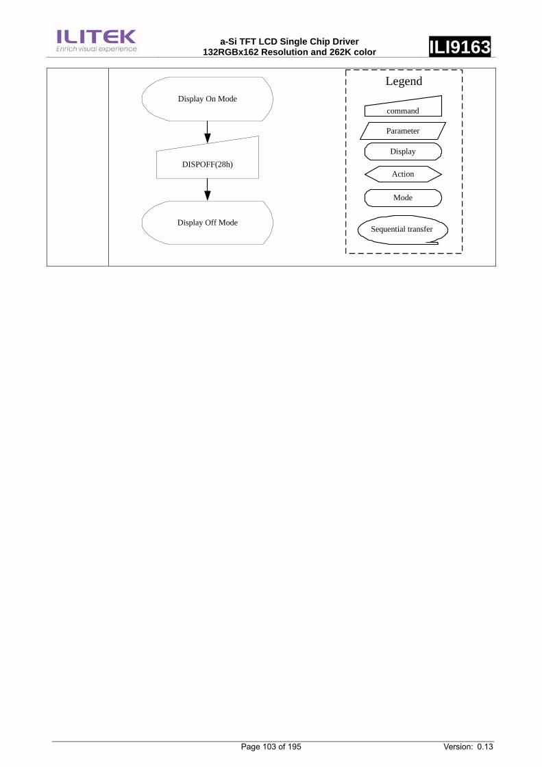
a-Si TFT LCD Single Chip Driver
132RGBx162 Resolution and 262K color ILI9163
Page 103 of 195 Version: 0.13
command
Parameter
Display
Action
Mode
Legend
Sequential transfer
Display On Mode
DISPOFF(28h)
Display Off Mode
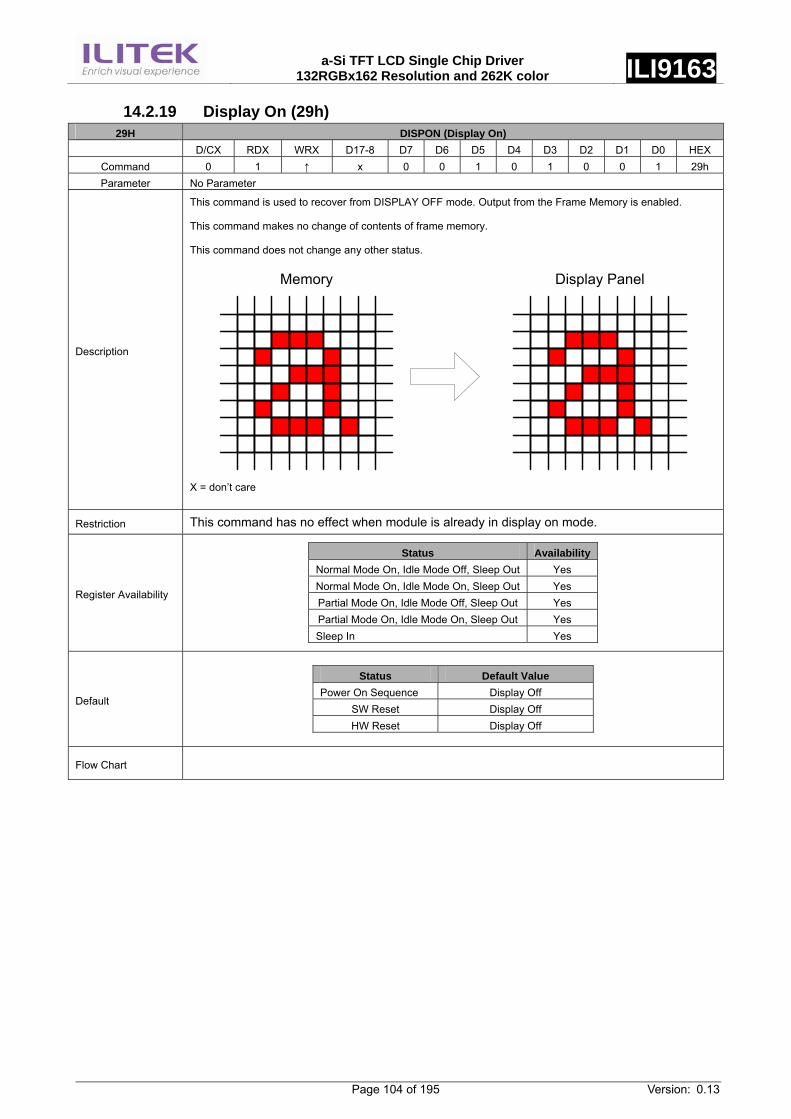
a-Si TFT LCD Single Chip Driver
132RGBx162 Resolution and 262K color ILI9163
Page 104 of 195 Version: 0.13
14.2.19 Display On (29h) 29H DISPON (Display On)
D/CX RDX WRX D17-8 D7 D6 D5 D4 D3 D2 D1 D0 HEX Command 0 1 ↑ x 0 0 1 0 1 0 0 1 29h Parameter No Parameter
Description
This command is used to recover from DISPLAY OFF mode. Output from the Frame Memory is enabled.
This command makes no change of contents of frame memory.
This command does not change any other status.
Memory Display Panel
X = don’t care
Restriction This command has no effect when module is already in display on mode.
Register Availability
Status Availability Normal Mode On, Idle Mode Off, Sleep Out Yes Normal Mode On, Idle Mode On, Sleep Out Yes Partial Mode On, Idle Mode Off, Sleep Out Yes Partial Mode On, Idle Mode On, Sleep Out Yes Sleep In Yes
Default
Status Default Value Power On Sequence Display Off
SW Reset Display Off HW Reset Display Off
Flow Chart

a-Si TFT LCD Single Chip Driver
132RGBx162 Resolution and 262K color ILI9163
Page 105 of 195 Version: 0.13
command
Parameter
Display
Action
Mode
Legend
Sequential transfer
Display On Mode
DISPON(29h)
Display Off Mode
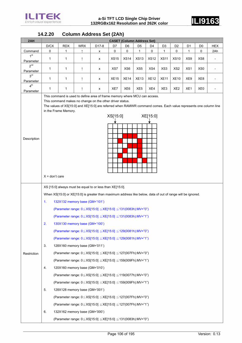
a-Si TFT LCD Single Chip Driver
132RGBx162 Resolution and 262K color ILI9163
Page 106 of 195 Version: 0.13
14.2.20 Column Address Set (2Ah) 2AH CASET (Column Address Set)
D/CX RDX WRX D17-8 D7 D6 D5 D4 D3 D2 D1 D0 HEX Command 0 1 ↑ x 0 0 1 0 1 0 1 0 2Ah
1st Parameter
1 1 ↑ x XS15 XS14 XS13 XS12 XS11 XS10 XS9 XS8 -
2nd Parameter
1 1 ↑ x XS7 XS6 XS5 XS4 XS3 XS2 XS1 XS0 -
3rd Parameter
1 1 ↑ x XE15 XE14 XE13 XE12 XE11 XE10 XE9 XE8 -
4th Parameter
1 1 ↑ x XE7 XE6 XE5 XE4 XE3 XE2 XE1 XE0 -
Description
This command is used to define area of frame memory where MCU can access. This command makes no change on the other driver status. The values of XS[15:0] and XE[15:0] are referred when RAMWR command comes. Each value represents one column line in the Frame Memory.
XS[15:0] XE[15:0]
X = don’t care
Restriction
XS [15:0] always must be equal to or less than XE[15:0].
When XS[15:0] or XE[15:0] is greater than maximum address like below, data of out of range will be ignored.
1. 132X132 memory base (GM=’101’)
(Parameter range: 0 XS[15:0] XE[15:0] 131(0083h):MV=”0”)≦ ≦ ≦
(Parameter range: 0 XS[15:0] XE[15:0] 131(0083h):MV=”1”)≦ ≦ ≦
2. 130X130 memory base (GM=’100’)
(Parameter range: 0 XS[15:0] XE[15:0] 1≦ ≦ ≦ 29(0081h):MV=”0”)
(Parameter range: 0 XS[15:0] XE[15:0] ≦ ≦ ≦129(0081h):MV=”1”)
3. 128X160 memory base (GM=’011’)
(Parameter range: 0 XS[15:0] XE[15:0] 127(007Fh):MV=”0”)≦ ≦ ≦
(Parameter range: 0 XS[15:0] XE[15:0] 159(009Fh):MV=”1”)≦ ≦ ≦
4. 120X160 memory base (GM=’010’)
(Parameter range: 0 XS[15:0] XE[15:0] 119(0077h):MV=”0”≦ ≦ ≦ )
(Parameter range: 0 XS[15:0] XE[15:0] 159(009Fh):MV=”1”)≦ ≦ ≦
5. 128X128 memory base (GM=’001’)
(Parameter range: 0 XS[15:0] XE[15:0] 127(007Fh):MV=”0”)≦ ≦ ≦
(Parameter range: 0 XS[15:0] XE[15:0] 127(007Fh):MV=”1”)≦ ≦ ≦
6. 132X162 memory base (GM=’000’)
(Parameter range: 0 XS[15:0] XE[15:0] 131(0083h):MV=”0”)≦ ≦ ≦
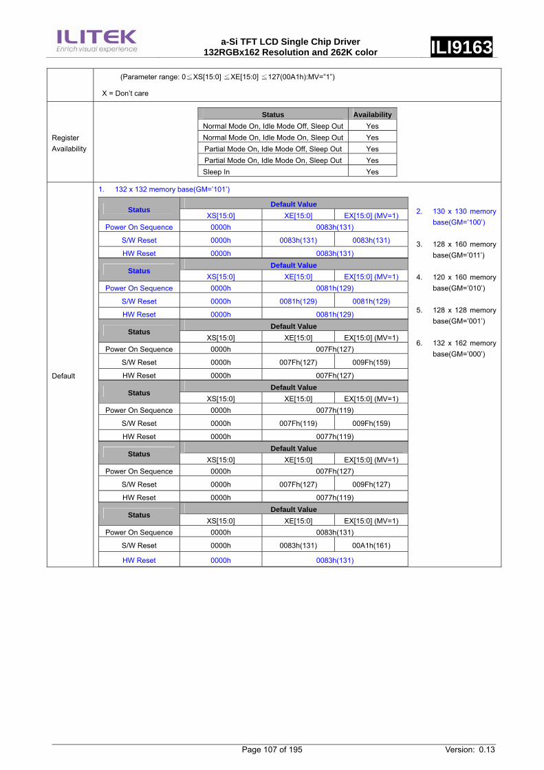
a-Si TFT LCD Single Chip Driver
132RGBx162 Resolution and 262K color ILI9163
Page 107 of 195 Version: 0.13
(Parameter range: 0 XS[15:0] XE[15:0] 127(00A1h):MV=”1”)≦ ≦ ≦
X = Don’t care
Register Availability
Status Availability Normal Mode On, Idle Mode Off, Sleep Out Yes Normal Mode On, Idle Mode On, Sleep Out Yes Partial Mode On, Idle Mode Off, Sleep Out Yes Partial Mode On, Idle Mode On, Sleep Out Yes Sleep In Yes
Default
1. 132 x 132 memory base(GM=’101’) 2. 130 x 130 memory
base(GM=’100’) 3. 128 x 160 memory
base(GM=’011’) 4. 120 x 160 memory
base(GM=’010’) 5. 128 x 128 memory
base(GM=’001’) 6. 132 x 162 memory
base(GM=’000’)
Default Value Status
XS[15:0] XE[15:0] EX[15:0] (MV=1) Power On Sequence 0000h 0083h(131)
S/W Reset 0000h 0083h(131) 0083h(131)
HW Reset 0000h 0083h(131) Default Value
Status XS[15:0] XE[15:0] EX[15:0] (MV=1)
Power On Sequence 0000h 0081h(129)
S/W Reset 0000h 0081h(129) 0081h(129)
HW Reset 0000h 0081h(129) Default Value
Status XS[15:0] XE[15:0] EX[15:0] (MV=1)
Power On Sequence 0000h 007Fh(127)
S/W Reset 0000h 007Fh(127) 009Fh(159)
HW Reset 0000h 007Fh(127) Default Value
Status XS[15:0] XE[15:0] EX[15:0] (MV=1)
Power On Sequence 0000h 0077h(119)
S/W Reset 0000h 007Fh(119) 009Fh(159)
HW Reset 0000h 0077h(119) Default Value
Status XS[15:0] XE[15:0] EX[15:0] (MV=1)
Power On Sequence 0000h 007Fh(127)
S/W Reset 0000h 007Fh(127) 009Fh(127)
HW Reset 0000h 0077h(119) Default Value
Status XS[15:0] XE[15:0] EX[15:0] (MV=1)
Power On Sequence 0000h 0083h(131)
S/W Reset 0000h 0083h(131) 00A1h(161)
HW Reset 0000h 0083h(131)
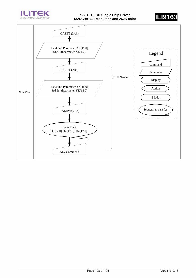
a-Si TFT LCD Single Chip Driver
132RGBx162 Resolution and 262K color ILI9163
Page 108 of 195 Version: 0.13
Flow Chart
CASET (2Ah)
1st &2nd Parameter XS[15:0]3rd & 4thparmeter XE[15:0]
RASET (2Bh)
1st &2nd Parameter YS[15:0]3rd & 4thparmeter YE[15:0]
RAMWR(2Ch)
Image DataD1[17:0],D2[17:0]..Dn[17:0]
command
Parameter
Display
Action
Mode
Legend
Sequential transfer
Any Commend
If Needed
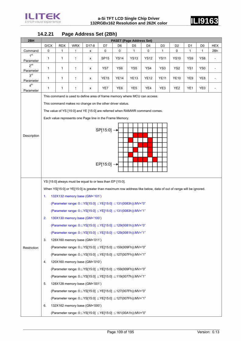
a-Si TFT LCD Single Chip Driver
132RGBx162 Resolution and 262K color ILI9163
Page 109 of 195 Version: 0.13
14.2.21 Page Address Set (2Bh) 2BH PASET (Page Address Set)
D/CX RDX WRX D17-8 D7 D6 D5 D4 D3 D2 D1 D0 HEXCommand 0 1 ↑ x 0 0 1 0 1 0 1 1 2Bh
1st Parameter
1 1 ↑ x SP15 YS14 YS13 YS12 YS11 YS10 YS9 YS8 -
2nd Parameter
1 1 ↑ x YS7 YS6 YS5 YS4 YS3 YS2 YS1 YS0 -
3rd Parameter
1 1 ↑ x YE15 YE14 YE13 YE12 YE11 YE10 YE9 YE8 -
4th Parameter
1 1 ↑ x YE7 YE6 YE5 YE4 YE3 YE2 YE1 YE0 -
Description
This command is used to define area of frame memory where MCU can access.
This command makes no change on the other driver status.
The value of YS [15:0] and YE [15:0] are referred when RAMWR command comes.
Each value represents one Page line in the Frame Memory.
SP[15:0]
EP[15:0]
Restriction
YS [15:0] always must be equal to or less than EP [15:0].
When YS[15:0] or YE[15:0] is greater than maximum row address like below, data of out of range will be ignored.
1. 132X132 memory base (GM=’101’)
(Parameter range: 0 YS[15:0] YE[15:0] 131(0083h)):MV=”0”≦ ≦ ≦
(Parameter range: 0 YS[15:0] YE[15:0] 131(0083h)):MV=”1”≦ ≦ ≦
2. 130X130 memory base (GM=’100’)
(Parameter range: 0 YS[15:0] YE[15:0] 1≦ ≦ ≦ 29(0081h)):MV=”0”
(Parameter range: 0 YS[15:0] YE[15:0] 1≦ ≦ ≦ 29(0081h)):MV=”1”
3. 128X160 memory base (GM=’011’)
(Parameter range: 0 YS[15:0] YE[15:0] 159(009Fh)):MV=”0”≦ ≦ ≦
(Parameter range: 0 YS[15:0] YE[15:0] 127(007Fh)):MV=”1”≦ ≦ ≦
4. 120X160 memory base (GM=’010’)
(Parameter range: 0 YS[15:0] YE[15:0] 159(009Fh)):MV=”0”≦ ≦ ≦
(Parameter range: 0 YS[15:0] YE[15:0] 119(0077h)):MV=”1”≦ ≦ ≦
5. 128X128 memory base (GM=’001’)
(Parameter range: 0 YS[15:0] YE[15:0] 127(007Fh)):MV=”0”≦ ≦ ≦
(Parameter range: 0 YS[15:0] YE[15:0] 127(007Fh)):MV=”1”≦ ≦ ≦
6. 132X162 memory base (GM=’000’)
(Parameter range: 0 YS[15:0] YE[≦ ≦ 15:0] 161(00A1h)):MV=”0”≦
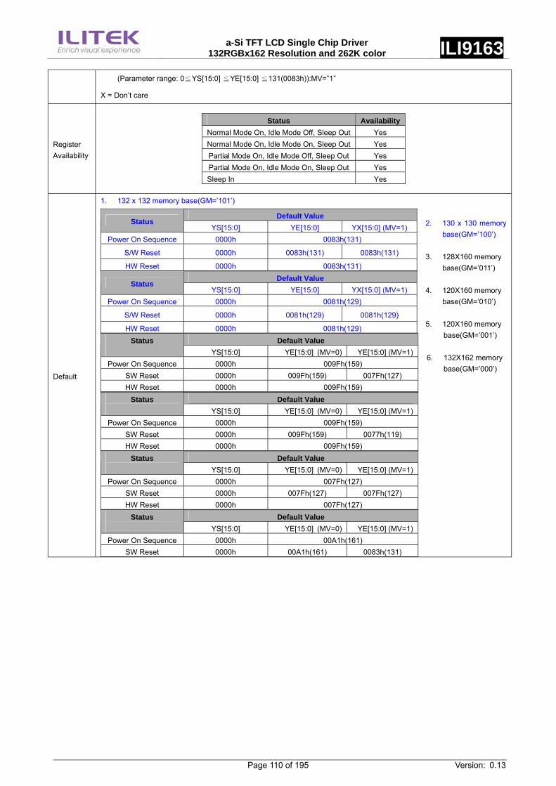
a-Si TFT LCD Single Chip Driver
132RGBx162 Resolution and 262K color ILI9163
Page 110 of 195 Version: 0.13
(Parameter range: 0 YS[15:0] YE[15:0] 131(0083h)):MV=”1”≦ ≦ ≦
X = Don’t care
Register Availability
Status Availability Normal Mode On, Idle Mode Off, Sleep Out Yes Normal Mode On, Idle Mode On, Sleep Out Yes Partial Mode On, Idle Mode Off, Sleep Out Yes Partial Mode On, Idle Mode On, Sleep Out Yes Sleep In Yes
Default
1. 132 x 132 memory base(GM=’101’) 2. 130 x 130 memory
base(GM=’100’) 3. 128X160 memory
base(GM=’011’) 4. 120X160 memory
base(GM=’010’) 5. 120X160 memory
base(GM=’001’) 6. 132X162 memory
base(GM=’000’)
Default Value Status
YS[15:0] YE[15:0] YX[15:0] (MV=1) Power On Sequence 0000h 0083h(131)
S/W Reset 0000h 0083h(131) 0083h(131)
HW Reset 0000h 0083h(131) Default Value
Status YS[15:0] YE[15:0] YX[15:0] (MV=1)
Power On Sequence 0000h 0081h(129)
S/W Reset 0000h 0081h(129) 0081h(129)
HW Reset 0000h 0081h(129) Default Value Status
YS[15:0] YE[15:0] (MV=0) YE[15:0] (MV=1) Power On Sequence 0000h 009Fh(159)
SW Reset 0000h 009Fh(159) 007Fh(127) HW Reset 0000h 009Fh(159)
Default Value Status YS[15:0] YE[15:0] (MV=0) YE[15:0] (MV=1)
Power On Sequence 0000h 009Fh(159) SW Reset 0000h 009Fh(159) 0077h(119) HW Reset 0000h 009Fh(159)
Default Value Status YS[15:0] YE[15:0] (MV=0) YE[15:0] (MV=1)
Power On Sequence 0000h 007Fh(127) SW Reset 0000h 007Fh(127) 007Fh(127) HW Reset 0000h 007Fh(127)
Default Value Status YS[15:0] YE[15:0] (MV=0) YE[15:0] (MV=1)
Power On Sequence 0000h 00A1h(161) SW Reset 0000h 00A1h(161) 0083h(131)
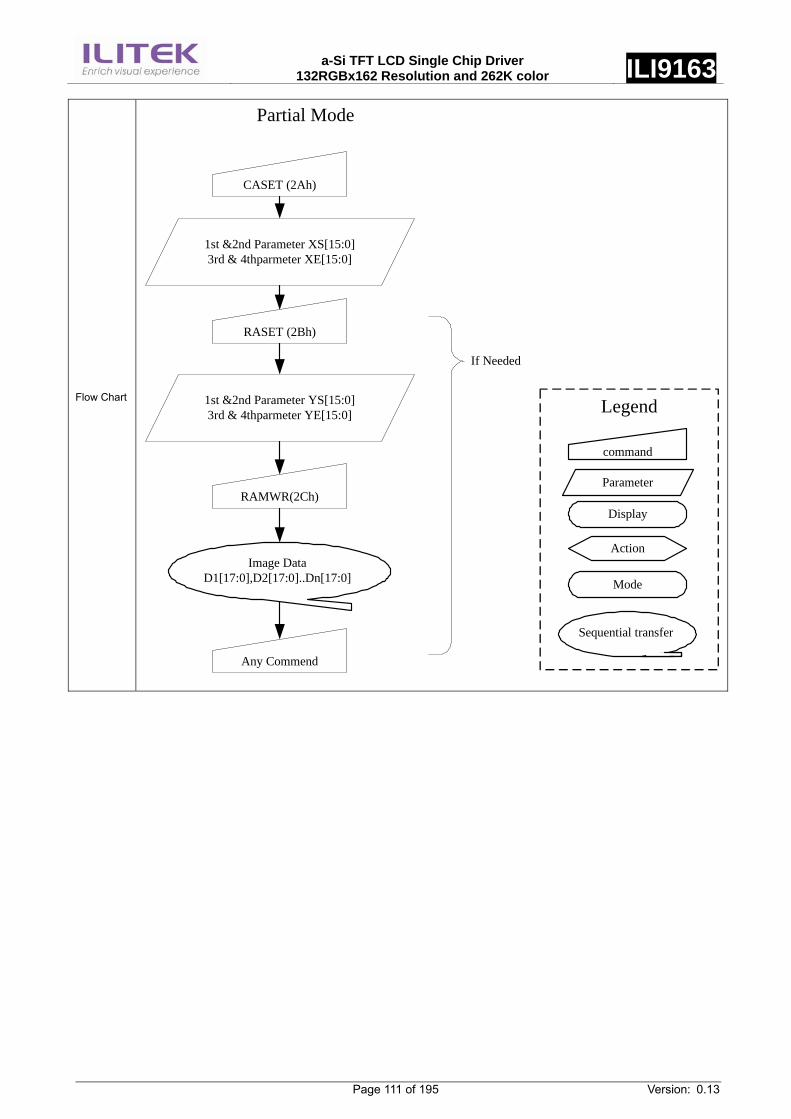
a-Si TFT LCD Single Chip Driver
132RGBx162 Resolution and 262K color ILI9163
Page 111 of 195 Version: 0.13
Flow Chart
CASET (2Ah)
1st &2nd Parameter XS[15:0]3rd & 4thparmeter XE[15:0]
RASET (2Bh)
1st &2nd Parameter YS[15:0]3rd & 4thparmeter YE[15:0]
RAMWR(2Ch)
Image DataD1[17:0],D2[17:0]..Dn[17:0]
command
Parameter
Display
Action
Mode
Legend
Sequential transfer
Any Commend
If Needed
Partial Mode
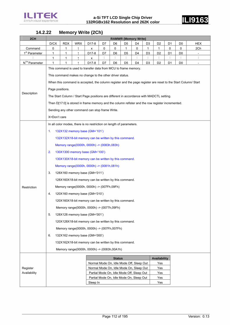
a-Si TFT LCD Single Chip Driver
132RGBx162 Resolution and 262K color ILI9163
Page 112 of 195 Version: 0.13
14.2.22 Memory Write (2Ch) 2CH RAMWR (Memory Write)
D/CX RDX WRX D17-8 D7 D6 D5 D4 D3 D2 D1 D0 HEX Command 0 1 ↑ x 0 0 1 0 1 1 0 0 2Ch
1st Parameter 1 1 ↑ D17-8 D7 D6 D5 D4 D3 D2 D1 D0 - ︰ 1 1 ↑ x ︰ ︰ ︰ ︰ ︰ ︰ ︰ ︰ ︰
NTH Parameter 1 1 ↑ D17-8 D7 D6 D5 D4 D3 D2 D1 D0 -
Description
This command is used to transfer data from MCU to frame memory.
This command makes no change to the other driver status.
When this command is accepted, the column register and the page register are reset to the Start Column/ Start
Page positions.
The Start Column / Start Page positions are different in accordance with MADCTL setting.
Then D[17:0] is stored in frame memory and the column refister and the row register incremented.
Sending any other command can stop frame Write.
X=Don’t care
Restriction
In all color modes, there is no restriction on length of parameters.
1. 132X132 memory base (GM=’101’)
132X132X18-bit memory can be written by this command.
Memory range(0000h, 0000h) -> (0083h,083h)
2. 130X1300 memory base (GM=’100’)
130X130X18-bit memory can be written by this command.
Memory range(0000h, 0000h) -> (0081h,081h)
3. 128X160 memory base (GM=’011’)
128X160X18-bit memory can be written by this command.
Memory range(0000h, 0000h) -> (007Fh,09Fh)
4. 120X160 memory base (GM=’010’)
120X160X18-bit memory can be written by this command.
Memory range(0000h, 0000h) -> (0077h,09Fh)
5. 128X128 memory base (GM=’001’)
120X128X18-bit memory can be written by this command.
Memory range(0000h, 0000h) -> (007Fh,007Fh)
6. 132X162 memory base (GM=’000’)
132X162X18-bit memory can be written by this command.
Memory range(0000h, 0000h) -> (0083h,00A1h)
Register Availability
Status Availability Normal Mode On, Idle Mode Off, Sleep Out Yes Normal Mode On, Idle Mode On, Sleep Out Yes Partial Mode On, Idle Mode Off, Sleep Out Yes Partial Mode On, Idle Mode On, Sleep Out Yes Sleep In Yes
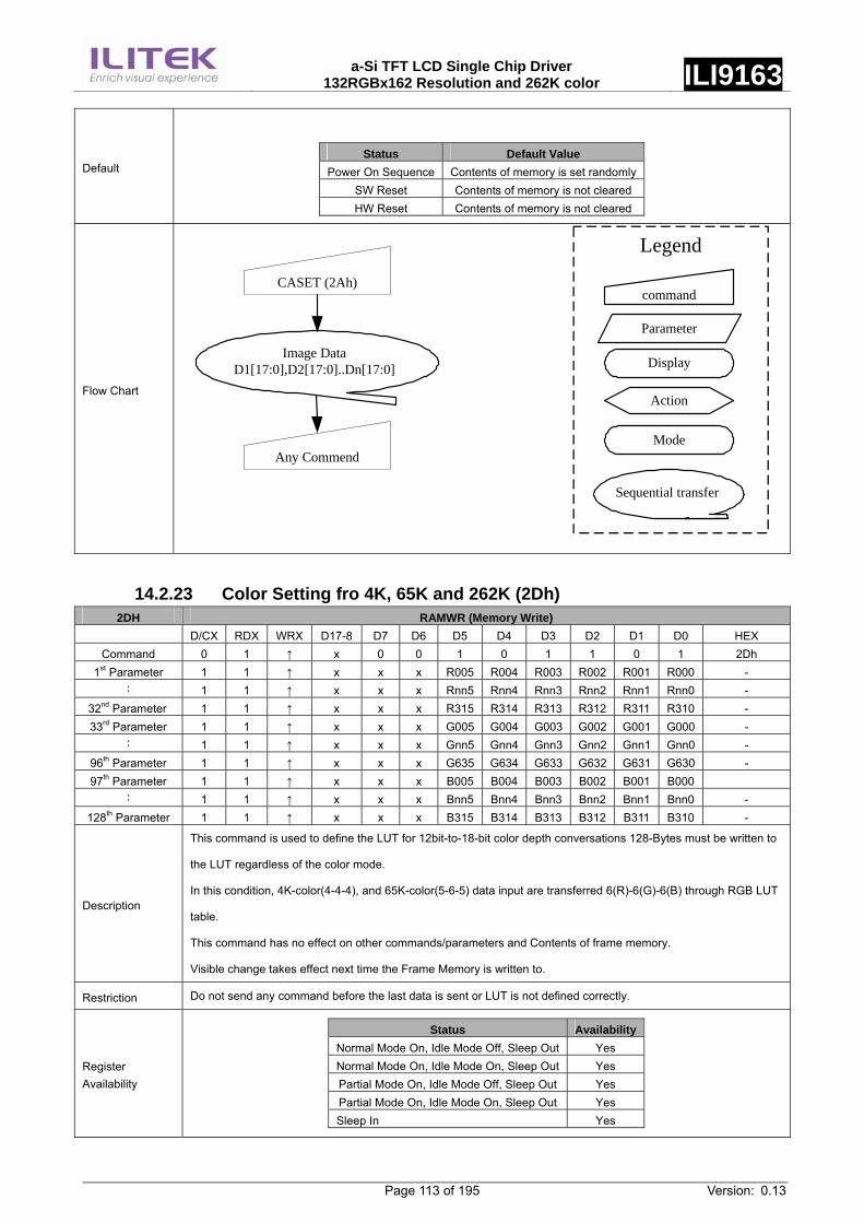
a-Si TFT LCD Single Chip Driver
132RGBx162 Resolution and 262K color ILI9163
Page 113 of 195 Version: 0.13
Default
Status Default Value
Power On Sequence Contents of memory is set randomly SW Reset Contents of memory is not cleared HW Reset Contents of memory is not cleared
Flow Chart
CASET (2Ah)
Image DataD1[17:0],D2[17:0]..Dn[17:0]
command
Parameter
Display
Action
Mode
Legend
Sequential transfer
Any Commend
14.2.23 Color Setting fro 4K, 65K and 262K (2Dh) 2DH RAMWR (Memory Write)
D/CX RDX WRX D17-8 D7 D6 D5 D4 D3 D2 D1 D0 HEX Command 0 1 ↑ x 0 0 1 0 1 1 0 1 2Dh
1st Parameter 1 1 ↑ x x x R005 R004 R003 R002 R001 R000 - ︰ 1 1 ↑ x x x Rnn5 Rnn4 Rnn3 Rnn2 Rnn1 Rnn0 -
32nd Parameter 1 1 ↑ x x x R315 R314 R313 R312 R311 R310 - 33rd Parameter 1 1 ↑ x x x G005 G004 G003 G002 G001 G000 -
︰ 1 1 ↑ x x x Gnn5 Gnn4 Gnn3 Gnn2 Gnn1 Gnn0 - 96th Parameter 1 1 ↑ x x x G635 G634 G633 G632 G631 G630 - 97th Parameter 1 1 ↑ x x x B005 B004 B003 B002 B001 B000
︰ 1 1 ↑ x x x Bnn5 Bnn4 Bnn3 Bnn2 Bnn1 Bnn0 - 128th Parameter 1 1 ↑ x x x B315 B314 B313 B312 B311 B310 -
Description
This command is used to define the LUT for 12bit-to-18-bit color depth conversations 128-Bytes must be written to
the LUT regardless of the color mode.
In this condition, 4K-color(4-4-4), and 65K-color(5-6-5) data input are transferred 6(R)-6(G)-6(B) through RGB LUT
table.
This command has no effect on other commands/parameters and Contents of frame memory.
Visible change takes effect next time the Frame Memory is written to.
Restriction Do not send any command before the last data is sent or LUT is not defined correctly.
Register Availability
Status Availability Normal Mode On, Idle Mode Off, Sleep Out Yes Normal Mode On, Idle Mode On, Sleep Out Yes Partial Mode On, Idle Mode Off, Sleep Out Yes Partial Mode On, Idle Mode On, Sleep Out Yes Sleep In Yes
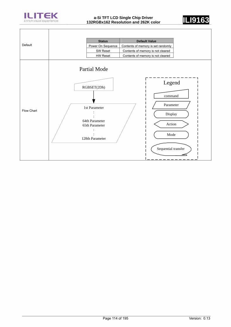
a-Si TFT LCD Single Chip Driver
132RGBx162 Resolution and 262K color ILI9163
Page 114 of 195 Version: 0.13
Default
Status Default Value
Power On Sequence Contents of memory is set randomly SW Reset Contents of memory is not cleared HW Reset Contents of memory is not cleared
Flow Chart
command
Parameter
Display
Action
Mode
Legend
Sequential transfer
RGBSET(2Dh)
Partial Mode
1st Parameter::
64th Parameter65th Parameter
::
128th Parameter
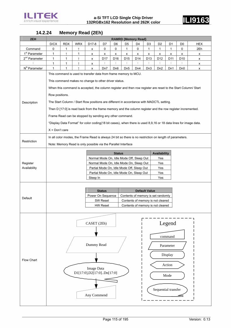
a-Si TFT LCD Single Chip Driver
132RGBx162 Resolution and 262K color ILI9163
Page 115 of 195 Version: 0.13
14.2.24 Memory Read (2Eh) 2EH RAMRD (Memory Read)
D/CX RDX WRX D17-8 D7 D6 D5 D4 D3 D2 D1 D0 HEX Command 0 1 ↑ x 0 0 1 0 1 1 1 0 2Eh
1st Parameter 1 ↑ 1 x x x x x x x x x x 2nd Parameter 1 1 ↑ x D17 D16 D15 D14 D13 D12 D11 D10 x
︰ 1 1 ↑ x ︰ ︰ ︰ ︰ ︰ ︰ ︰ ︰ x Nth Parameter 1 1 ↑ x Dn7 Dn6 Dn5 Dn4 Dn3 Dn2 Dn1 Dn0 x
Description
This command is used to transfer data from frame memory to MCU.
This command makes no change to other driver status.
When this command is accepted, the column register and then row register are reset to the Start Column/ Start
Row positions.
The Start Column / Start Row positions are different in accordance with MADCTL setting.
Then D [17:0] is read back from the frame memory and the column register and the row register incremented.
Frame Read can be stopped by sending any other command.
“Display Data Format” for color coding(18 bit cases), when there is used 8,9,16 or 18 data lines for image data.
X = Don’t care
Restriction In all color modes, the Frame Read is always 24 bit so there is no restriction on length of parameters.
Note: Memory Read is only possible via the Parallel Interface
Register Availability
Status Availability Normal Mode On, Idle Mode Off, Sleep Out Yes Normal Mode On, Idle Mode On, Sleep Out Yes Partial Mode On, Idle Mode Off, Sleep Out Yes Partial Mode On, Idle Mode On, Sleep Out Yes Sleep In Yes
Default
Status Default Value Power On Sequence Contents of memory is set randomly
SW Reset Contents of memory is not cleared HW Reset Contents of memory is not cleared
Flow Chart
CASET (2Eh)
Image DataD1[17:0],D2[17:0]..Dn[17:0]
command
Parameter
Display
Action
Mode
Legend
Sequential transferAny Commend
Dummy Read
a-Si TFT LCD Single Chip Driver
132RGBx162 Resolution and 262K color ILI9163
Page 116 of 195 Version: 0.13
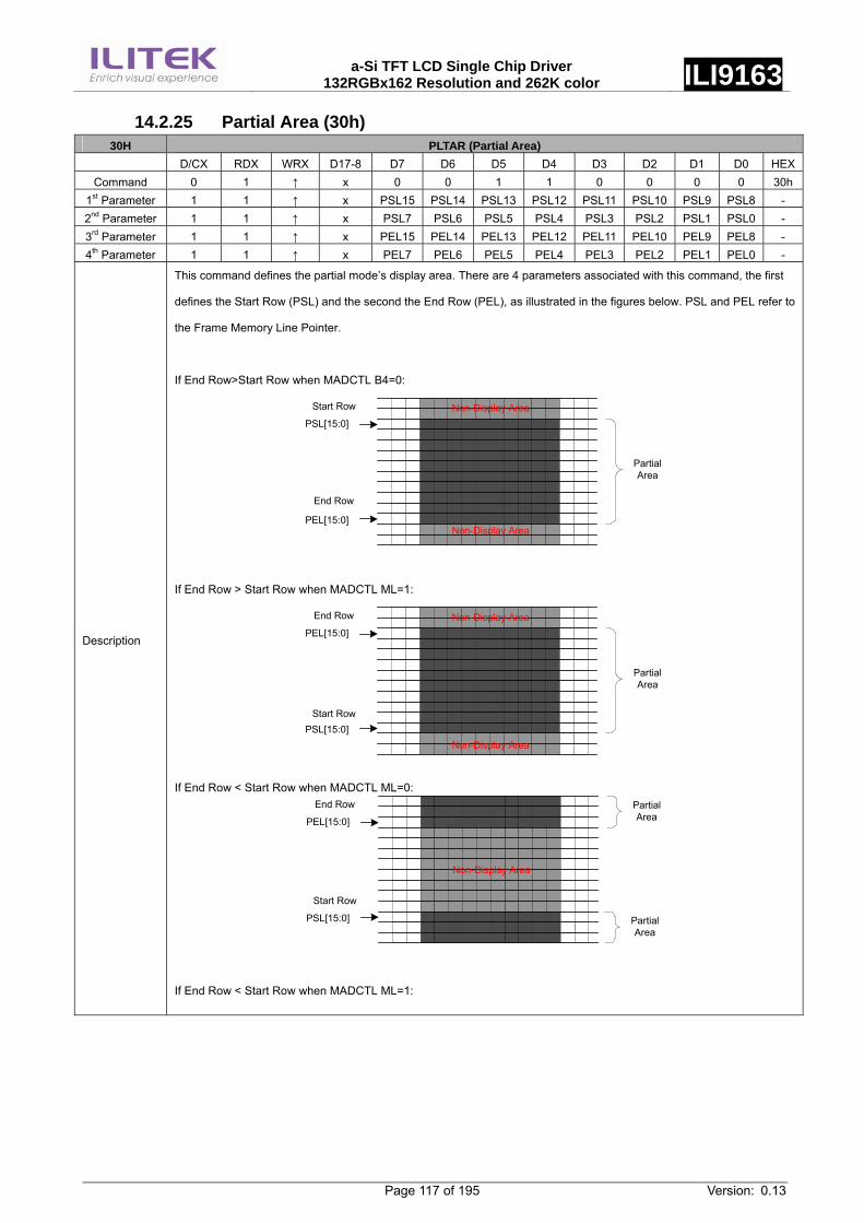
a-Si TFT LCD Single Chip Driver
132RGBx162 Resolution and 262K color ILI9163
Page 117 of 195 Version: 0.13
14.2.25 Partial Area (30h) 30H PLTAR (Partial Area)
D/CX RDX WRX D17-8 D7 D6 D5 D4 D3 D2 D1 D0 HEXCommand 0 1 ↑ x 0 0 1 1 0 0 0 0 30h
1st Parameter 1 1 ↑ x PSL15 PSL14 PSL13 PSL12 PSL11 PSL10 PSL9 PSL8 - 2nd Parameter 1 1 ↑ x PSL7 PSL6 PSL5 PSL4 PSL3 PSL2 PSL1 PSL0 - 3rd Parameter 1 1 ↑ x PEL15 PEL14 PEL13 PEL12 PEL11 PEL10 PEL9 PEL8 - 4th Parameter 1 1 ↑ x PEL7 PEL6 PEL5 PEL4 PEL3 PEL2 PEL1 PEL0 -
Description
This command defines the partial mode’s display area. There are 4 parameters associated with this command, the first
defines the Start Row (PSL) and the second the End Row (PEL), as illustrated in the figures below. PSL and PEL refer to
the Frame Memory Line Pointer.
If End Row>Start Row when MADCTL B4=0:
PSL[15:0]
Start Row
End Row
Partial Area
PEL[15:0]
Non-Display Area
Non-Display Area
If End Row > Start Row when MADCTL ML=1:
Start Row
End Row
Partial Area
PEL[15:0]
PSL[15:0]
Non-Display Area
Non-Display Area
If End Row < Start Row when MADCTL ML=0: Partial Area
End Row
Start Row
PSL[15:0]
Non-Display Area
Partial Area
PEL[15:0]
If End Row < Start Row when MADCTL ML=1:
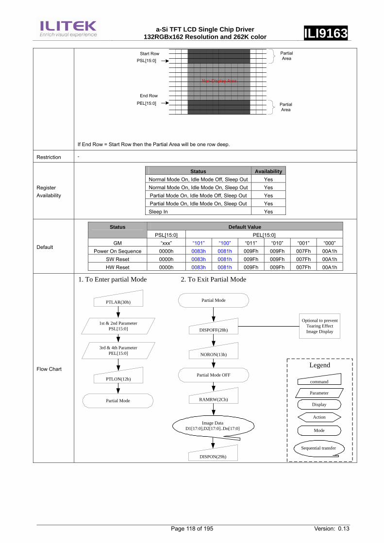
a-Si TFT LCD Single Chip Driver
132RGBx162 Resolution and 262K color ILI9163
Page 118 of 195 Version: 0.13
End Row
Start Row
Non-Display Area
Partial Area
Partial Area
PSL[15:0]
PEL[15:0]
If End Row = Start Row then the Partial Area will be one row deep.
Restriction -
Register Availability
Status Availability Normal Mode On, Idle Mode Off, Sleep Out Yes Normal Mode On, Idle Mode On, Sleep Out Yes Partial Mode On, Idle Mode Off, Sleep Out Yes Partial Mode On, Idle Mode On, Sleep Out Yes Sleep In Yes
Default
Default Value Status PSL[15:0] PEL[15:0]
GM “xxx” “101” “100” “011” “010” “001” “000” Power On Sequence 0000h 0083h 0081h 009Fh 009Fh 007Fh 00A1h
SW Reset 0000h 0083h 0081h 009Fh 009Fh 007Fh 00A1hHW Reset 0000h 0083h 0081h 009Fh 009Fh 007Fh 00A1h
Flow Chart
PTLAR(30h)
command
Parameter
Display
Action
Mode
Legend
Sequential transfer
PTLON(12h)
1st & 2nd Parameter PSL[15:0]
3rd & 4th Parameter PEL[15:0]
Partial Mode
1. To Enter partial Mode
DISPOFF(28h)
Image DataD1[17:0],D2[17:0]..Dn[17:0]
RAMRW(2Ch)
2. To Exit Partial Mode
Partial Mode
NORON(13h)
Partial Mode OFF
DISPON(29h)
Optional to prevent Tearing Effect Image Display
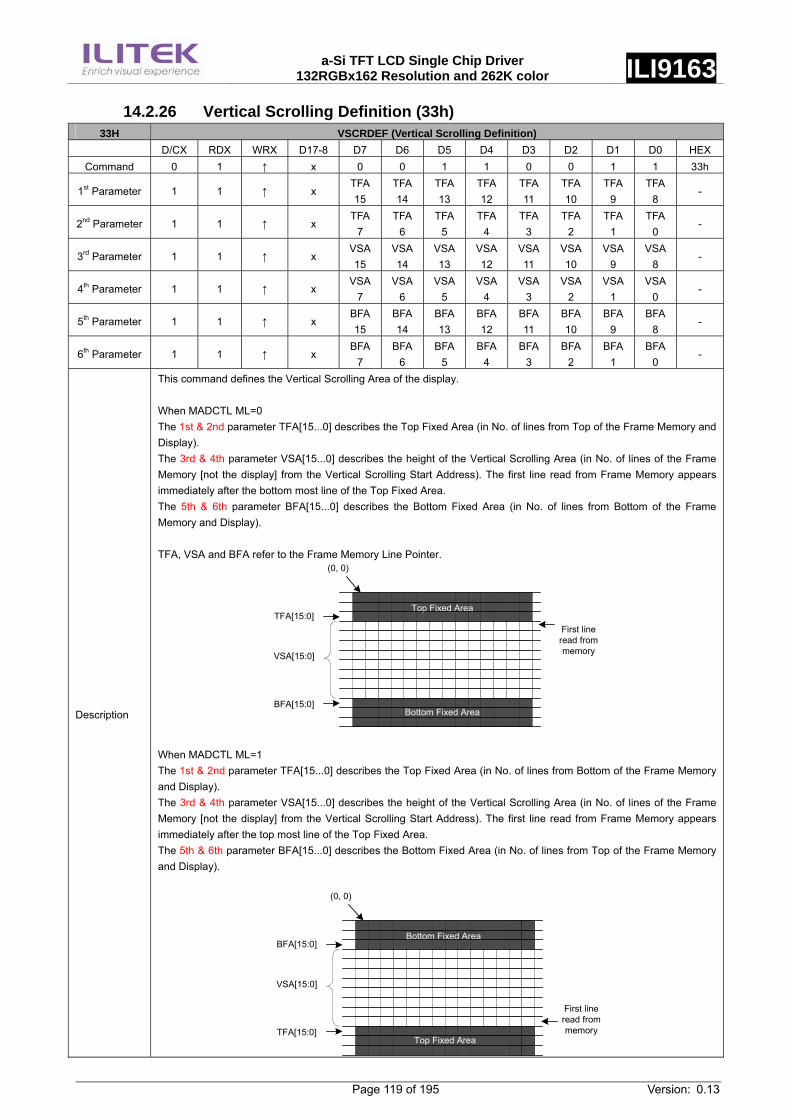
a-Si TFT LCD Single Chip Driver
132RGBx162 Resolution and 262K color ILI9163
Page 119 of 195 Version: 0.13
14.2.26 Vertical Scrolling Definition (33h) 33H VSCRDEF (Vertical Scrolling Definition)
D/CX RDX WRX D17-8 D7 D6 D5 D4 D3 D2 D1 D0 HEX Command 0 1 ↑ x 0 0 1 1 0 0 1 1 33h
1st Parameter 1 1 ↑ x TFA15
TFA14
TFA13
TFA12
TFA11
TFA 10
TFA 9
TFA8
-
2nd Parameter 1 1 ↑ x TFA
7 TFA
6 TFA
5 TFA
4 TFA
3 TFA
2 TFA
1 TFA
0 -
3rd Parameter 1 1 ↑ x VSA15
VSA14
VSA13
VSA12
VSA11
VSA 10
VSA 9
VSA8
-
4th Parameter 1 1 ↑ x VSA
7 VSA
6 VSA
5 VSA
4 VSA
3 VSA
2 VSA
1 VSA
0 -
5th Parameter 1 1 ↑ x BFA15
BFA14
BFA13
BFA12
BFA11
BFA 10
BFA 9
BFA8
-
6th Parameter 1 1 ↑ x BFA
7 BFA
6 BFA
5 BFA
4 BFA
3 BFA
2 BFA
1 BFA
0 -
Description
This command defines the Vertical Scrolling Area of the display. When MADCTL ML=0 The 1st & 2nd parameter TFA[15...0] describes the Top Fixed Area (in No. of lines from Top of the Frame Memory and Display). The 3rd & 4th parameter VSA[15...0] describes the height of the Vertical Scrolling Area (in No. of lines of the Frame Memory [not the display] from the Vertical Scrolling Start Address). The first line read from Frame Memory appears immediately after the bottom most line of the Top Fixed Area. The 5th & 6th parameter BFA[15...0] describes the Bottom Fixed Area (in No. of lines from Bottom of the Frame Memory and Display). TFA, VSA and BFA refer to the Frame Memory Line Pointer.
Top Fixed Area
Bottom Fixed Area
TFA[15:0]
BFA[15:0]
(0, 0)
First line read from memoryVSA[15:0]
When MADCTL ML=1 The 1st & 2nd parameter TFA[15...0] describes the Top Fixed Area (in No. of lines from Bottom of the Frame Memory and Display). The 3rd & 4th parameter VSA[15...0] describes the height of the Vertical Scrolling Area (in No. of lines of the Frame Memory [not the display] from the Vertical Scrolling Start Address). The first line read from Frame Memory appears immediately after the top most line of the Top Fixed Area. The 5th & 6th parameter BFA[15...0] describes the Bottom Fixed Area (in No. of lines from Top of the Frame Memory and Display).
Bottom Fixed Area
Top Fixed Area
(0, 0)
First line read from memory
Top Fixed AreaTop Fixed Area
BFA[15:0]
TFA[15:0]
VSA[15:0]
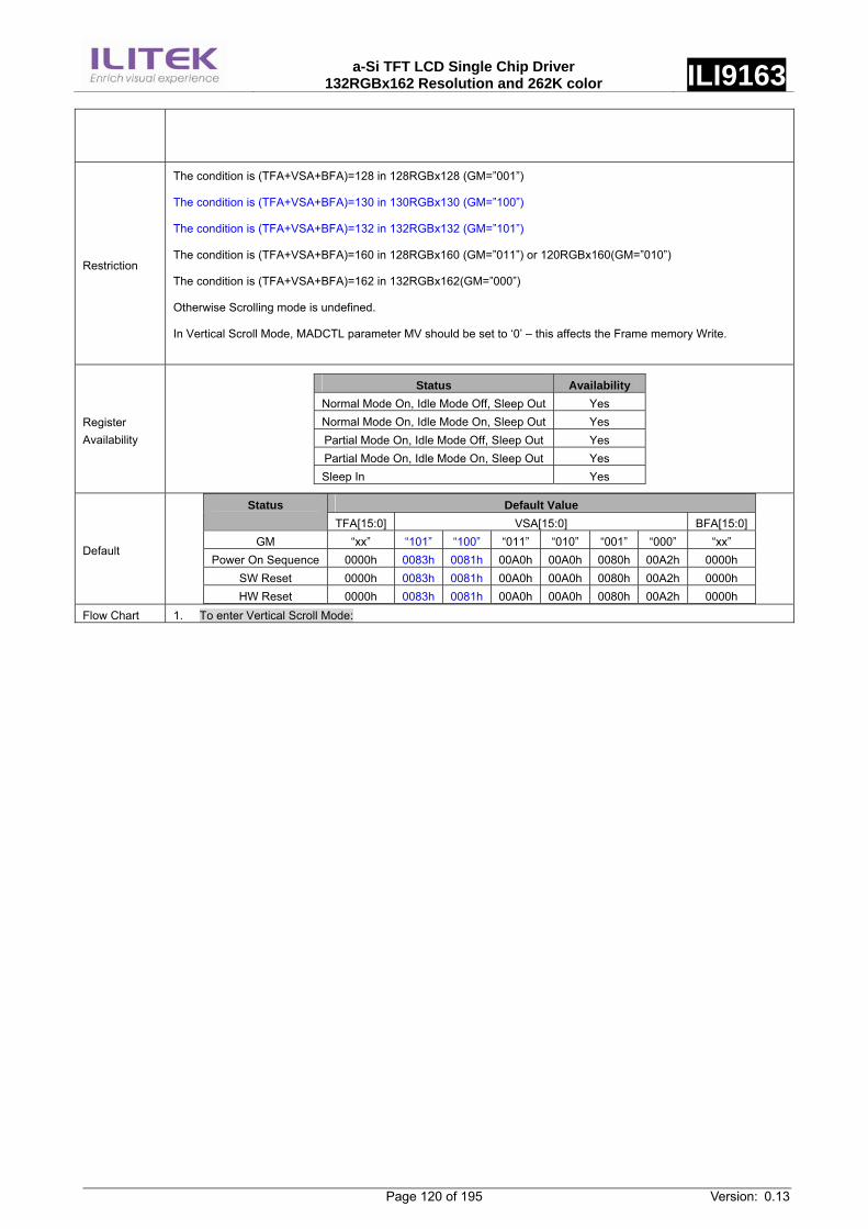
a-Si TFT LCD Single Chip Driver
132RGBx162 Resolution and 262K color ILI9163
Page 120 of 195 Version: 0.13
Restriction
The condition is (TFA+VSA+BFA)=128 in 128RGBx128 (GM=”001”)
The condition is (TFA+VSA+BFA)=130 in 130RGBx130 (GM=”100”)
The condition is (TFA+VSA+BFA)=132 in 132RGBx132 (GM=”101”)
The condition is (TFA+VSA+BFA)=160 in 128RGBx160 (GM=”011”) or 120RGBx160(GM=”010”)
The condition is (TFA+VSA+BFA)=162 in 132RGBx162(GM=”000”)
Otherwise Scrolling mode is undefined.
In Vertical Scroll Mode, MADCTL parameter MV should be set to ‘0’ – this affects the Frame memory Write.
Register Availability
Status Availability Normal Mode On, Idle Mode Off, Sleep Out Yes Normal Mode On, Idle Mode On, Sleep Out Yes Partial Mode On, Idle Mode Off, Sleep Out Yes Partial Mode On, Idle Mode On, Sleep Out Yes Sleep In Yes
Default
Default Value Status TFA[15:0] VSA[15:0] BFA[15:0]
GM “xx” “101” “100” “011” “010” “001” “000” “xx” Power On Sequence 0000h 0083h 0081h 00A0h 00A0h 0080h 00A2h 0000h
SW Reset 0000h 0083h 0081h 00A0h 00A0h 0080h 00A2h 0000h HW Reset 0000h 0083h 0081h 00A0h 00A0h 0080h 00A2h 0000h
Flow Chart 1. To enter Vertical Scroll Mode:
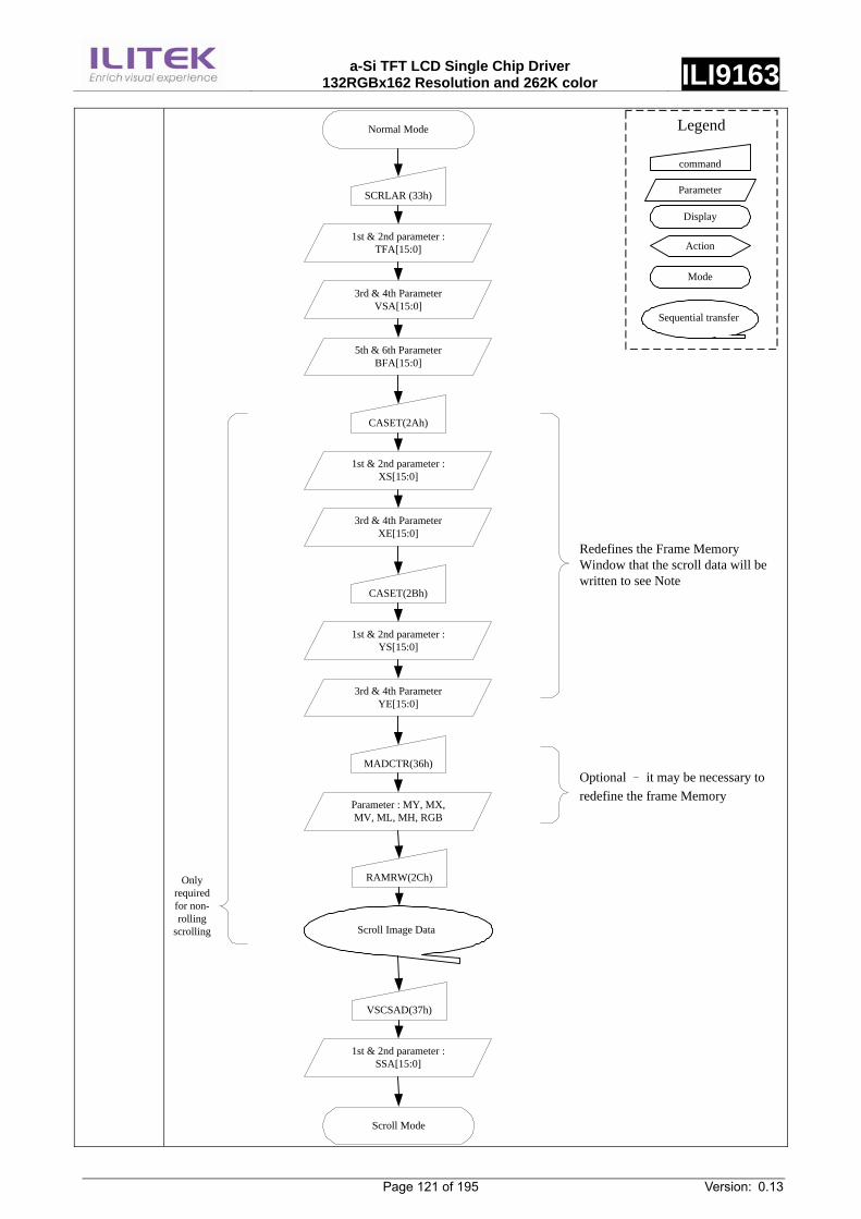
a-Si TFT LCD Single Chip Driver
132RGBx162 Resolution and 262K color ILI9163
Page 121 of 195 Version: 0.13
command
Parameter
Display
Action
Mode
Legend
Sequential transfer
Normal Mode
SCRLAR (33h)
1st & 2nd parameter : TFA[15:0]
3rd & 4th Parameter VSA[15:0]
5th & 6th Parameter BFA[15:0]
CASET(2Ah)
1st & 2nd parameter : XS[15:0]
3rd & 4th Parameter XE[15:0]
CASET(2Bh)
1st & 2nd parameter : YS[15:0]
3rd & 4th Parameter YE[15:0]
MADCTR(36h)
Parameter : MY, MX, MV, ML, MH, RGB
RAMRW(2Ch)
Scroll Image Data
VSCSAD(37h)
1st & 2nd parameter : SSA[15:0]
Scroll Mode
Only required for non-rolling
scrolling
Redefines the Frame Memory Window that the scroll data will be written to see Note
Optional – it may be necessary to redefine the frame Memory
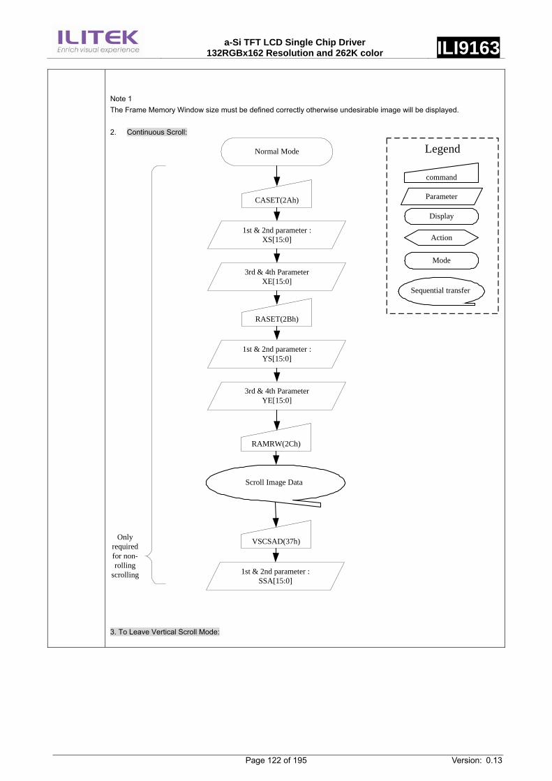
a-Si TFT LCD Single Chip Driver
132RGBx162 Resolution and 262K color ILI9163
Page 122 of 195 Version: 0.13
Note 1 The Frame Memory Window size must be defined correctly otherwise undesirable image will be displayed.
2. Continuous Scroll:
command
Parameter
Display
Action
Mode
Legend
Sequential transfer
Normal Mode
CASET(2Ah)
1st & 2nd parameter : XS[15:0]
3rd & 4th Parameter XE[15:0]
RASET(2Bh)
1st & 2nd parameter : YS[15:0]
3rd & 4th Parameter YE[15:0]
RAMRW(2Ch)
Scroll Image Data
VSCSAD(37h)
1st & 2nd parameter : SSA[15:0]
Only required for non-rolling
scrolling
3. To Leave Vertical Scroll Mode:
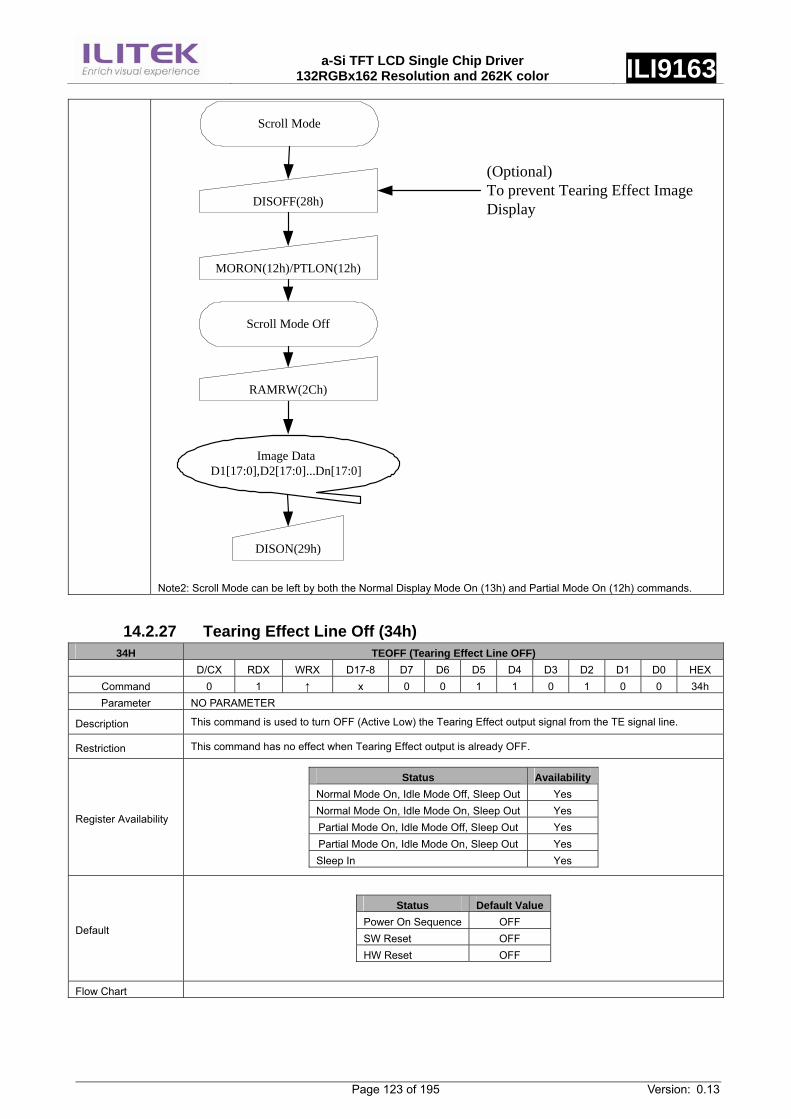
a-Si TFT LCD Single Chip Driver
132RGBx162 Resolution and 262K color ILI9163
Page 123 of 195 Version: 0.13
Scroll Mode
DISOFF(28h)
MORON(12h)/PTLON(12h)
Image Data D1[17:0],D2[17:0]...Dn[17:0]
DISON(29h)
Scroll Mode Off
RAMRW(2Ch)
(Optional)To prevent Tearing Effect Image Display
Note2: Scroll Mode can be left by both the Normal Display Mode On (13h) and Partial Mode On (12h) commands.
14.2.27 Tearing Effect Line Off (34h) 34H TEOFF (Tearing Effect Line OFF)
D/CX RDX WRX D17-8 D7 D6 D5 D4 D3 D2 D1 D0 HEX Command 0 1 ↑ x 0 0 1 1 0 1 0 0 34h Parameter NO PARAMETER
Description This command is used to turn OFF (Active Low) the Tearing Effect output signal from the TE signal line.
Restriction This command has no effect when Tearing Effect output is already OFF.
Register Availability
Status Availability Normal Mode On, Idle Mode Off, Sleep Out Yes Normal Mode On, Idle Mode On, Sleep Out Yes Partial Mode On, Idle Mode Off, Sleep Out Yes Partial Mode On, Idle Mode On, Sleep Out Yes Sleep In Yes
Default
Status Default ValuePower On Sequence OFF SW Reset OFF HW Reset OFF
Flow Chart

a-Si TFT LCD Single Chip Driver
132RGBx162 Resolution and 262K color ILI9163
Page 124 of 195 Version: 0.13
command
Parameter
Display
Action
Mode
Legend
Sequential transfer
TE Line Output ON
TEOFF(34h)
TE Line Output OFF
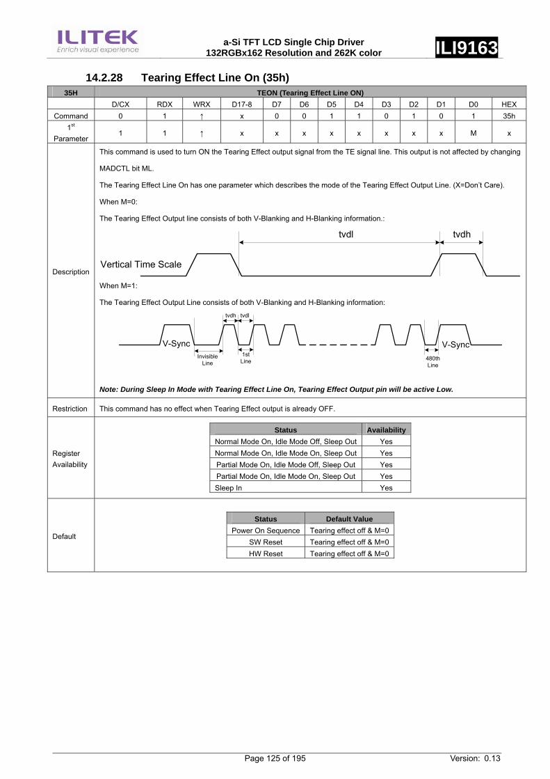
a-Si TFT LCD Single Chip Driver
132RGBx162 Resolution and 262K color ILI9163
Page 125 of 195 Version: 0.13
14.2.28 Tearing Effect Line On (35h) 35H TEON (Tearing Effect Line ON)
D/CX RDX WRX D17-8 D7 D6 D5 D4 D3 D2 D1 D0 HEX Command 0 1 ↑ x 0 0 1 1 0 1 0 1 35h
1st Parameter
1 1 ↑ x x x x x x x x M x
Description
This command is used to turn ON the Tearing Effect output signal from the TE signal line. This output is not affected by changing
MADCTL bit ML.
The Tearing Effect Line On has one parameter which describes the mode of the Tearing Effect Output Line. (X=Don’t Care).
When M=0:
The Tearing Effect Output line consists of both V-Blanking and H-Blanking information.:
tvdl tvdh
Vertical Time Scale
When M=1:
The Tearing Effect Output Line consists of both V-Blanking and H-Blanking information:
tvdl
V-Sync
tvdh
1st Line 480th
Line
V-SyncInvisible
Line
Note: During Sleep In Mode with Tearing Effect Line On, Tearing Effect Output pin will be active Low.
Restriction This command has no effect when Tearing Effect output is already OFF.
Register Availability
Status Availability Normal Mode On, Idle Mode Off, Sleep Out Yes Normal Mode On, Idle Mode On, Sleep Out Yes Partial Mode On, Idle Mode Off, Sleep Out Yes Partial Mode On, Idle Mode On, Sleep Out Yes Sleep In Yes
Default
Status Default Value Power On Sequence Tearing effect off & M=0
SW Reset Tearing effect off & M=0 HW Reset Tearing effect off & M=0
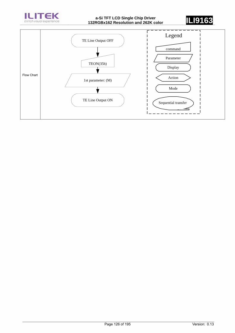
a-Si TFT LCD Single Chip Driver
132RGBx162 Resolution and 262K color ILI9163
Page 126 of 195 Version: 0.13
Flow Chart
command
Parameter
Display
Action
Mode
Legend
Sequential transfer
TE Line Output OFF
TEON(35h)
TE Line Output ON
1st parameter: (M)
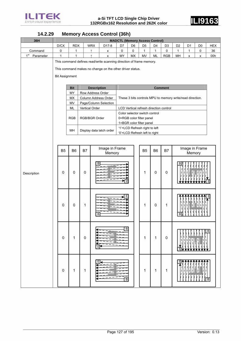
a-Si TFT LCD Single Chip Driver
132RGBx162 Resolution and 262K color ILI9163
Page 127 of 195 Version: 0.13
14.2.29 Memory Access Control (36h) 36H MADCTL (Memory Access Control)
D/CX RDX WRX D17-8 D7 D6 D5 D4 D3 D2 D1 D0 HEX Command 0 1 ↑ x 0 0 1 1 0 1 1 0 36
1st Parameter 1 1 ↑ x MY MX MV ML RGB MH x x 00h
Description
This command defines read/write scanning direction of frame memory.
This command makes no change on the other driver status.
Bit Assignment
Bit Description Comment MY Row Address Order MX Column Address OrderMV Page/Column Selection
These 3 bits controls MPU to memory write/read direction.
ML Vertical Order LCD Vertical refresh direction control
RGB RGB/BGR Order Color selector switch control 0=RGB color filter panel 1=BGR color filter panel
MH Display data latch order‘1’=LCD Refresh right to left ‘0’=LCD Refresh left to right
B5 B6 B7 Image in Frame Memory
B
E
000
B
E
B
E
B
E
100
010
110
B5 B6 B7 Image in Frame Memory
001
101
011
111
B
E
B
E
B
E
B
E
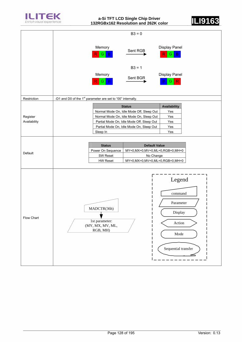
a-Si TFT LCD Single Chip Driver
132RGBx162 Resolution and 262K color ILI9163
Page 128 of 195 Version: 0.13
R G B R G B
B3 = 0
Sent RGBMemory Display Panel
R G B RGBSent BGR
Memory Display Panel
B3 = 1
Restriction -D1 and D0 of the 1st parameter are set to “00” internally.
Register Availability
Status Availability Normal Mode On, Idle Mode Off, Sleep Out Yes Normal Mode On, Idle Mode On, Sleep Out Yes Partial Mode On, Idle Mode Off, Sleep Out Yes Partial Mode On, Idle Mode On, Sleep Out Yes Sleep In Yes
Default
Status Default Value Power On Sequence MY=0,MX=0,MV=0,ML=0,RGB=0,MH=0
SW Reset No Change HW Reset MY=0,MX=0,MV=0,ML=0,RGB=0,MH=0
Flow Chart
command
Parameter
Display
Action
Mode
Legend
Sequential transfer
MADCTR(36h)
1st parameter: (MY, MX, MV, ML,
RGB, MH)
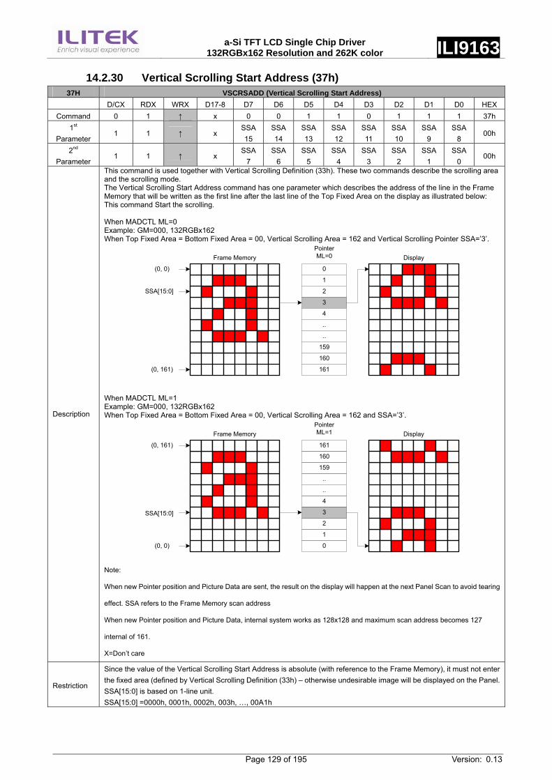
a-Si TFT LCD Single Chip Driver
132RGBx162 Resolution and 262K color ILI9163
Page 129 of 195 Version: 0.13
14.2.30 Vertical Scrolling Start Address (37h) 37H VSCRSADD (Vertical Scrolling Start Address)
D/CX RDX WRX D17-8 D7 D6 D5 D4 D3 D2 D1 D0 HEXCommand 0 1 ↑ x 0 0 1 1 0 1 1 1 37h
1st Parameter
1 1 ↑ x SSA15
SSA14
SSA13
SSA12
SSA11
SSA 10
SSA 9
SSA8
00h
2nd Parameter
1 1 ↑ x SSA
7 SSA
6 SSA
5 SSA
4 SSA
3 SSA
2 SSA
1 SSA
0 00h
Description
This command is used together with Vertical Scrolling Definition (33h). These two commands describe the scrolling area and the scrolling mode. The Vertical Scrolling Start Address command has one parameter which describes the address of the line in the Frame Memory that will be written as the first line after the last line of the Top Fixed Area on the display as illustrated below: This command Start the scrolling. When MADCTL ML=0 Example: GM=000, 132RGBx162 When Top Fixed Area = Bottom Fixed Area = 00, Vertical Scrolling Area = 162 and Vertical Scrolling Pointer SSA=’3’.
Frame Memory
(0, 0)
SSA[15:0]
(0, 161)
0
PointerML=0
1
2
3
4
..
..
159
160
161
Display
When MADCTL ML=1 Example: GM=000, 132RGBx162 When Top Fixed Area = Bottom Fixed Area = 00, Vertical Scrolling Area = 162 and SSA=’3’.
Frame Memory
(0, 0)
(0, 161)
0
PointerML=1
1
2
3
4
..
..
159
160
161
Display
SSA[15:0]
Note:
When new Pointer position and Picture Data are sent, the result on the display will happen at the next Panel Scan to avoid tearing
effect. SSA refers to the Frame Memory scan address
When new Pointer position and Picture Data, internal system works as 128x128 and maximum scan address becomes 127
internal of 161.
X=Don’t care
Restriction
Since the value of the Vertical Scrolling Start Address is absolute (with reference to the Frame Memory), it must not enter the fixed area (defined by Vertical Scrolling Definition (33h) – otherwise undesirable image will be displayed on the Panel.SSA[15:0] is based on 1-line unit. SSA[15:0] =0000h, 0001h, 0002h, 003h, …, 00A1h
a-Si TFT LCD Single Chip Driver
132RGBx162 Resolution and 262K color ILI9163
Page 130 of 195 Version: 0.13
Register Availability
Status Availability Normal Mode On, Idle Mode Off, Sleep Out Yes Normal Mode On, Idle Mode On, Sleep Out Yes Partial Mode On, Idle Mode Off, Sleep Out Yes Partial Mode On, Idle Mode On, Sleep Out Yes Sleep In Yes
Default
Status Default ValuePower On Sequence 0000h
SW Reset 0000h HW Reset 0000h
Flow Chart See Vertical Scrolling Definition (33h) description.
14.2.31 Idle Mode Off (38h) 38H IDMOFF (Idle Mode Off)
D/CX RDX WRX D17-8 D7 D6 D5 D4 D3 D2 D1 D0 HEX Command 0 1 ↑ x 0 0 1 1 1 0 0 0 38h Parameter NO PARAMETER
Description
This command is used to recover from Idle mode on.
There will be no abnormal visible effect on the display mode change transition.
In the Idle off mode
1. LCD can display maximum 4096, 65K, 262K colors.
2. Normal frame frequency is applied.
X = don’t care
Restriction This command has no effect when module is already in idle off mode.
Register Availability
Status Availability Normal Mode On, Idle Mode Off, Sleep Out Yes Normal Mode On, Idle Mode On, Sleep Out Yes Partial Mode On, Idle Mode Off, Sleep Out Yes Partial Mode On, Idle Mode On, Sleep Out Yes Sleep In Yes
Default
Status Default Value Power On Sequence Idle Mode Off
SW Reset Idle Mode Off HW Reset Idle Mode Off
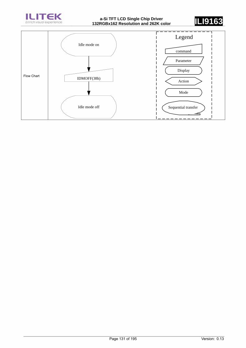
a-Si TFT LCD Single Chip Driver
132RGBx162 Resolution and 262K color ILI9163
Page 131 of 195 Version: 0.13
Flow Chart
command
Parameter
Display
Action
Mode
Legend
Sequential transfer
IDMOFF(38h)
Idle mode on
Idle mode off
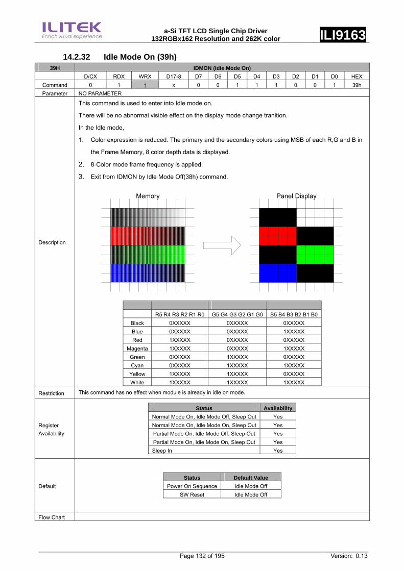
a-Si TFT LCD Single Chip Driver
132RGBx162 Resolution and 262K color ILI9163
Page 132 of 195 Version: 0.13
14.2.32 Idle Mode On (39h) 39H IDMON (Idle Mode On)
D/CX RDX WRX D17-8 D7 D6 D5 D4 D3 D2 D1 D0 HEX Command 0 1 ↑ x 0 0 1 1 1 0 0 1 39h Parameter NO PARAMETER
Description
This command is used to enter into Idle mode on.
There will be no abnormal visible effect on the display mode change tranition.
In the Idle mode,
1. Color expression is reduced. The primary and the secondary colors using MSB of each R,G and B in
the Frame Memory, 8 color depth data is displayed.
2. 8-Color mode frame frequency is applied.
3. Exit from IDMON by Idle Mode Off(38h) command.
Memory Panel Display
R5 R4 R3 R2 R1 R0 G5 G4 G3 G2 G1 G0 B5 B4 B3 B2 B1 B0
Black 0XXXXX 0XXXXX 0XXXXX Blue 0XXXXX 0XXXXX 1XXXXX Red 1XXXXX 0XXXXX 0XXXXX
Magenta 1XXXXX 0XXXXX 1XXXXX Green 0XXXXX 1XXXXX 0XXXXX Cyan 0XXXXX 1XXXXX 1XXXXX
Yellow 1XXXXX 1XXXXX 0XXXXX White 1XXXXX 1XXXXX 1XXXXX
Restriction This command has no effect when module is already in idle on mode.
Register Availability
Status Availability Normal Mode On, Idle Mode Off, Sleep Out Yes Normal Mode On, Idle Mode On, Sleep Out Yes Partial Mode On, Idle Mode Off, Sleep Out Yes Partial Mode On, Idle Mode On, Sleep Out Yes Sleep In Yes
Default Status Default Value
Power On Sequence Idle Mode Off SW Reset Idle Mode Off
Flow Chart
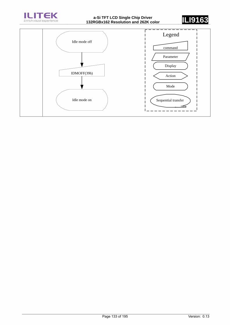
a-Si TFT LCD Single Chip Driver
132RGBx162 Resolution and 262K color ILI9163
Page 133 of 195 Version: 0.13
command
Parameter
Display
Action
Mode
Legend
Sequential transfer
IDMOFF(39h)
Idle mode off
Idle mode on
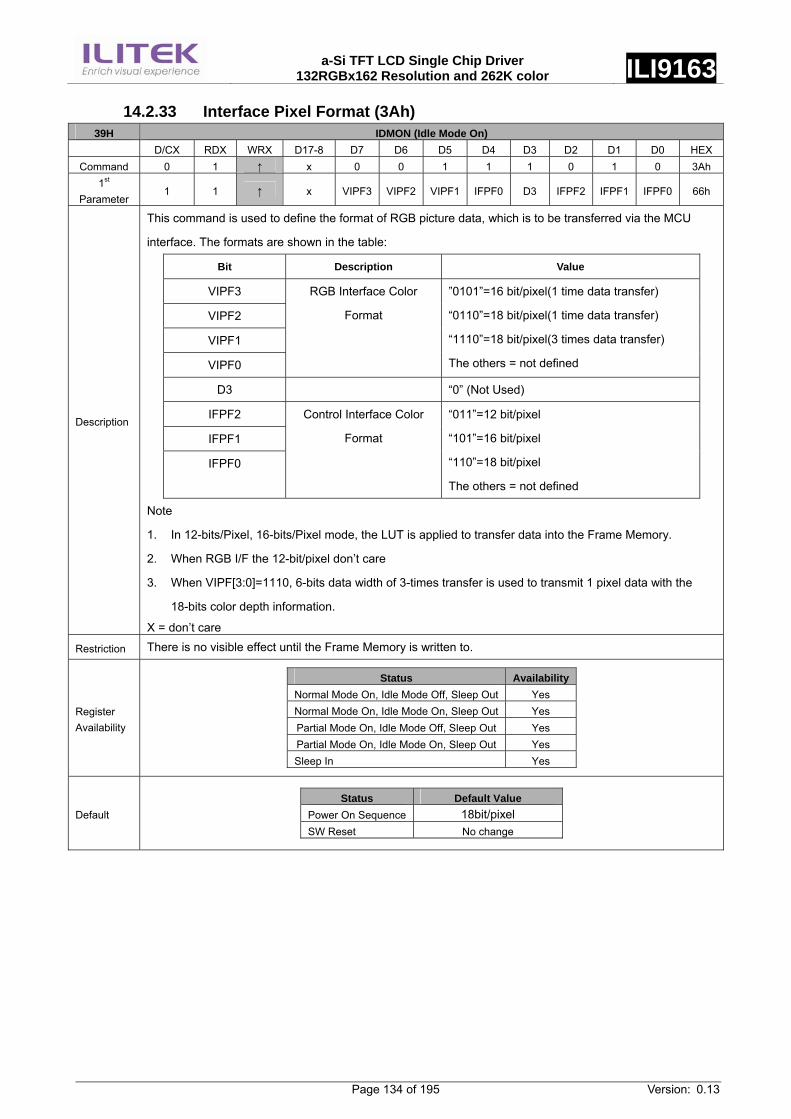
a-Si TFT LCD Single Chip Driver
132RGBx162 Resolution and 262K color ILI9163
Page 134 of 195 Version: 0.13
14.2.33 Interface Pixel Format (3Ah) 39H IDMON (Idle Mode On)
D/CX RDX WRX D17-8 D7 D6 D5 D4 D3 D2 D1 D0 HEXCommand 0 1 ↑ x 0 0 1 1 1 0 1 0 3Ah
1st Parameter
1 1 ↑ x VIPF3 VIPF2 VIPF1 IFPF0 D3 IFPF2 IFPF1 IFPF0 66h
Description
This command is used to define the format of RGB picture data, which is to be transferred via the MCU
interface. The formats are shown in the table:
Bit Description Value
VIPF3
VIPF2
VIPF1
VIPF0
RGB Interface Color
Format
”0101”=16 bit/pixel(1 time data transfer)
“0110”=18 bit/pixel(1 time data transfer)
“1110”=18 bit/pixel(3 times data transfer)
The others = not defined
D3 “0” (Not Used)
IFPF2
IFPF1
IFPF0
Control Interface Color
Format
“011”=12 bit/pixel
“101”=16 bit/pixel
“110”=18 bit/pixel
The others = not defined
Note
1. In 12-bits/Pixel, 16-bits/Pixel mode, the LUT is applied to transfer data into the Frame Memory.
2. When RGB I/F the 12-bit/pixel don’t care
3. When VIPF[3:0]=1110, 6-bits data width of 3-times transfer is used to transmit 1 pixel data with the
18-bits color depth information.
X = don’t care
Restriction There is no visible effect until the Frame Memory is written to.
Register Availability
Status Availability Normal Mode On, Idle Mode Off, Sleep Out Yes Normal Mode On, Idle Mode On, Sleep Out Yes Partial Mode On, Idle Mode Off, Sleep Out Yes Partial Mode On, Idle Mode On, Sleep Out Yes Sleep In Yes
Default Status Default Value
Power On Sequence 18bit/pixel SW Reset No change

a-Si TFT LCD Single Chip Driver
132RGBx162 Resolution and 262K color ILI9163
Page 135 of 195 Version: 0.13
Flow Chart
command
Parameter
Display
Action
Mode
Legend
Sequential transfer
18-bit/Pixel Mode
COLMOD(3Ah)
18-bit/Pixel Mode
1st parameter: IFPF[2:0] = “xxx"
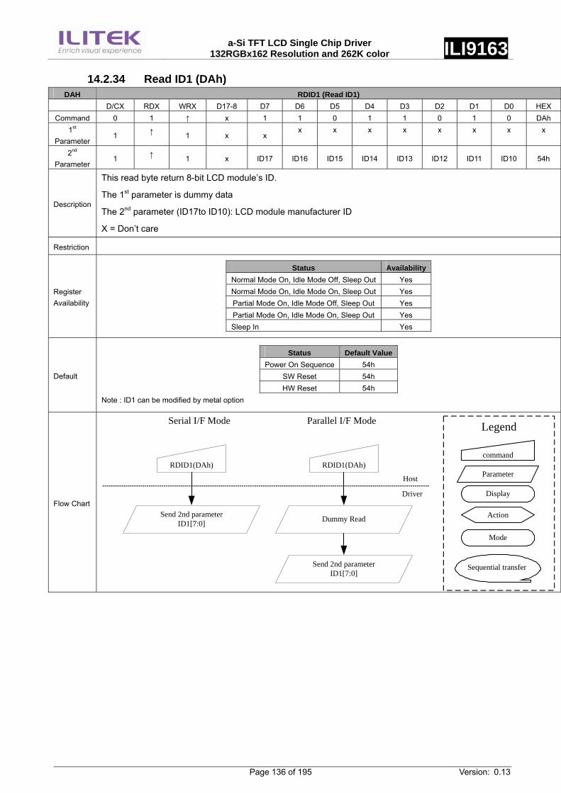
a-Si TFT LCD Single Chip Driver
132RGBx162 Resolution and 262K color ILI9163
Page 136 of 195 Version: 0.13
14.2.34 Read ID1 (DAh) DAH RDID1 (Read ID1)
D/CX RDX WRX D17-8 D7 D6 D5 D4 D3 D2 D1 D0 HEX Command 0 1 ↑ x 1 1 0 1 1 0 1 0 DAh
1st Parameter
1 ↑ 1 x x x x x x x x x x
2nd Parameter
1 ↑ 1 x ID17 ID16 ID15 ID14 ID13 ID12 ID11 ID10 54h
Description
This read byte return 8-bit LCD module’s ID.
The 1st parameter is dummy data
The 2nd parameter (ID17to ID10): LCD module manufacturer ID
X = Don’t care
Restriction
Register Availability
Status Availability Normal Mode On, Idle Mode Off, Sleep Out Yes Normal Mode On, Idle Mode On, Sleep Out Yes Partial Mode On, Idle Mode Off, Sleep Out Yes Partial Mode On, Idle Mode On, Sleep Out Yes Sleep In Yes
Default
Status Default ValuePower On Sequence 54h
SW Reset 54h HW Reset 54h
Note : ID1 can be modified by metal option
Flow Chart
command
Parameter
Display
Action
Mode
Legend
Sequential transfer
RDID1(DAh)
Dummy Read
Send 2nd parameter ID1[7:0]
RDID1(DAh)
Send 2nd parameter ID1[7:0]
Host
Driver
Serial I/F Mode Parallel I/F Mode
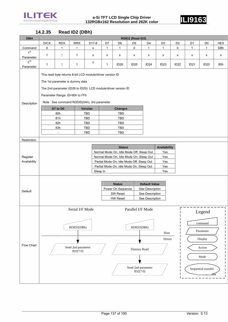
a-Si TFT LCD Single Chip Driver
132RGBx162 Resolution and 262K color ILI9163
Page 137 of 195 Version: 0.13
14.2.35 Read ID2 (DBh) DBH RDID2 (Read ID2)
D/CX RDX WRX D17-8 D7 D6 D5 D4 D3 D2 D1 D0 HEX Command 0 1 ↑ x 1 1 0 1 1 0 1 1 DBh
1st Parameter
1 ↑ 1 x x x x x x x x x x
2nd Parameter
1 ↑ 1 x
1 ID26 ID25 ID24 ID23 ID22 ID21 ID20 80h
Description
This read byte returns 8-bit LCD module/driver version ID
The 1st parameter is dummy data
The 2nd parameter (ID26 to ID20): LCD module/driver version ID
Parameter Range: ID=80h to FFh
Note : See command RDDID(04h), 3rd parameter
D7 to D0 Version Changes 80h TBD TBD 81h TBD TBD 82h TBD TBD 83h TBD TBD
- TBD TBD
Restriction
Register Availability
Status Availability Normal Mode On, Idle Mode Off, Sleep Out Yes Normal Mode On, Idle Mode On, Sleep Out Yes Partial Mode On, Idle Mode Off, Sleep Out Yes Partial Mode On, Idle Mode On, Sleep Out Yes Sleep In Yes
Default
Status Default Value Power On Sequence See Description
SW Reset See Description HW Reset See Description
Flow Chart
command
Parameter
Display
Action
Mode
Legend
Sequential transfer
RDID2(DBh)
Dummy Read
Send 2nd parameter ID2[7:0]
RDID2(DBh)
Send 2nd parameter ID2[7:0]
Host
Driver
Serial I/F Mode Parallel I/F Mode
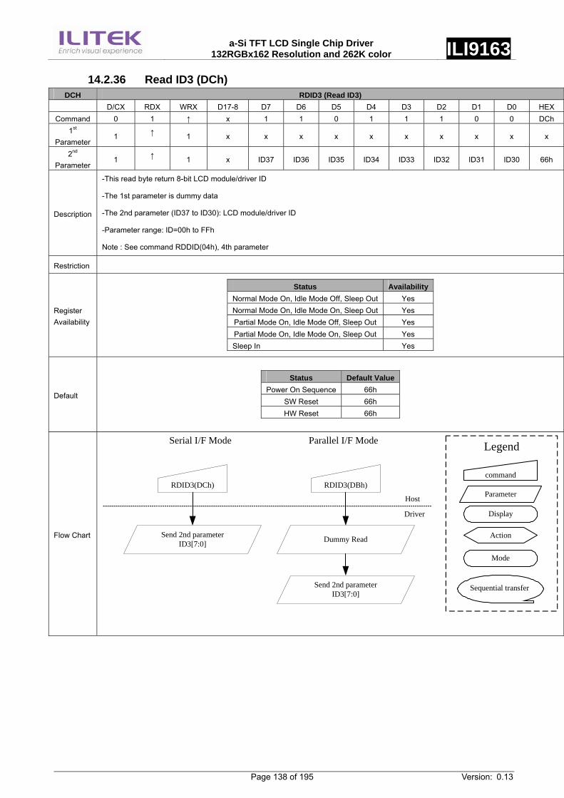
a-Si TFT LCD Single Chip Driver
132RGBx162 Resolution and 262K color ILI9163
Page 138 of 195 Version: 0.13
14.2.36 Read ID3 (DCh) DCH RDID3 (Read ID3)
D/CX RDX WRX D17-8 D7 D6 D5 D4 D3 D2 D1 D0 HEX Command 0 1 ↑ x 1 1 0 1 1 1 0 0 DCh
1st Parameter
1 ↑ 1 x x x x x x x x x x
2nd Parameter
1 ↑ 1 x ID37 ID36 ID35 ID34 ID33 ID32 ID31 ID30 66h
Description
-This read byte return 8-bit LCD module/driver ID
-The 1st parameter is dummy data
-The 2nd parameter (ID37 to ID30): LCD module/driver ID
-Parameter range: ID=00h to FFh
Note : See command RDDID(04h), 4th parameter
Restriction
Register Availability
Status Availability Normal Mode On, Idle Mode Off, Sleep Out Yes Normal Mode On, Idle Mode On, Sleep Out Yes Partial Mode On, Idle Mode Off, Sleep Out Yes Partial Mode On, Idle Mode On, Sleep Out Yes Sleep In Yes
Default
Status Default ValuePower On Sequence 66h
SW Reset 66h HW Reset 66h
Flow Chart
command
Parameter
Display
Action
Mode
Legend
Sequential transfer
RDID3(DBh)
Dummy Read
Send 2nd parameter ID3[7:0]
RDID3(DCh)
Send 2nd parameter ID3[7:0]
Host
Driver
Serial I/F Mode Parallel I/F Mode
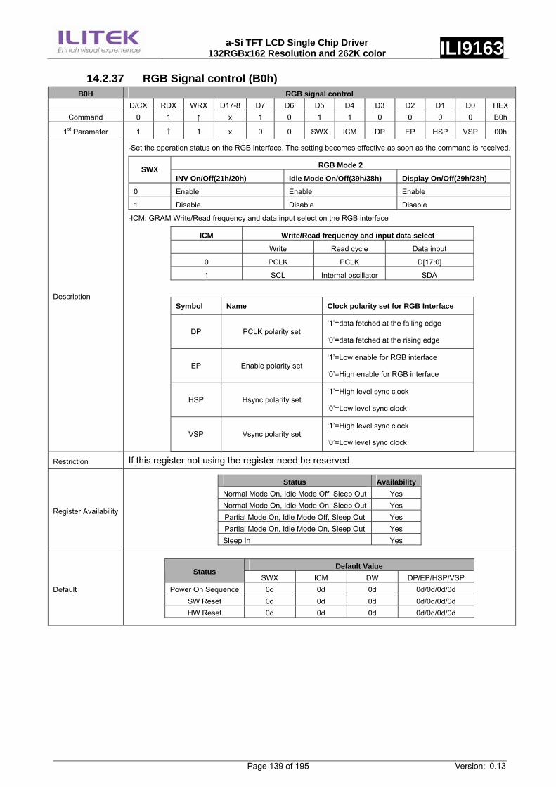
a-Si TFT LCD Single Chip Driver
132RGBx162 Resolution and 262K color ILI9163
Page 139 of 195 Version: 0.13
14.2.37 RGB Signal control (B0h) B0H RGB signal control
D/CX RDX WRX D17-8 D7 D6 D5 D4 D3 D2 D1 D0 HEXCommand 0 1 ↑ x 1 0 1 1 0 0 0 0 B0h
1st Parameter 1 ↑ 1 x 0 0 SWX ICM DP EP HSP VSP 00h
Description
-Set the operation status on the RGB interface. The setting becomes effective as soon as the command is received.
RGB Mode 2SWX INV On/Off(21h/20h) Idle Mode On/Off(39h/38h) Display On/Off(29h/28h)
0 Enable Enable Enable
1 Disable Disable Disable
-ICM: GRAM Write/Read frequency and data input select on the RGB interface
ICM Write/Read frequency and input data select
Write Read cycle Data input
0 PCLK PCLK D[17:0]
1 SCL Internal oscillator SDA
Symbol Name Clock polarity set for RGB Interface
DP PCLK polarity set ‘1’=data fetched at the falling edge
‘0’=data fetched at the rising edge
EP Enable polarity set ‘1’=Low enable for RGB interface
‘0’=High enable for RGB interface
HSP Hsync polarity set ‘1’=High level sync clock
‘0’=Low level sync clock
VSP Vsync polarity set ‘1’=High level sync clock
‘0’=Low level sync clock
Restriction If this register not using the register need be reserved.
Register Availability
Status Availability Normal Mode On, Idle Mode Off, Sleep Out Yes Normal Mode On, Idle Mode On, Sleep Out Yes Partial Mode On, Idle Mode Off, Sleep Out Yes Partial Mode On, Idle Mode On, Sleep Out Yes Sleep In Yes
Default
Default Value Status
SWX ICM DW DP/EP/HSP/VSP Power On Sequence 0d 0d 0d 0d/0d/0d/0d
SW Reset 0d 0d 0d 0d/0d/0d/0d HW Reset 0d 0d 0d 0d/0d/0d/0d
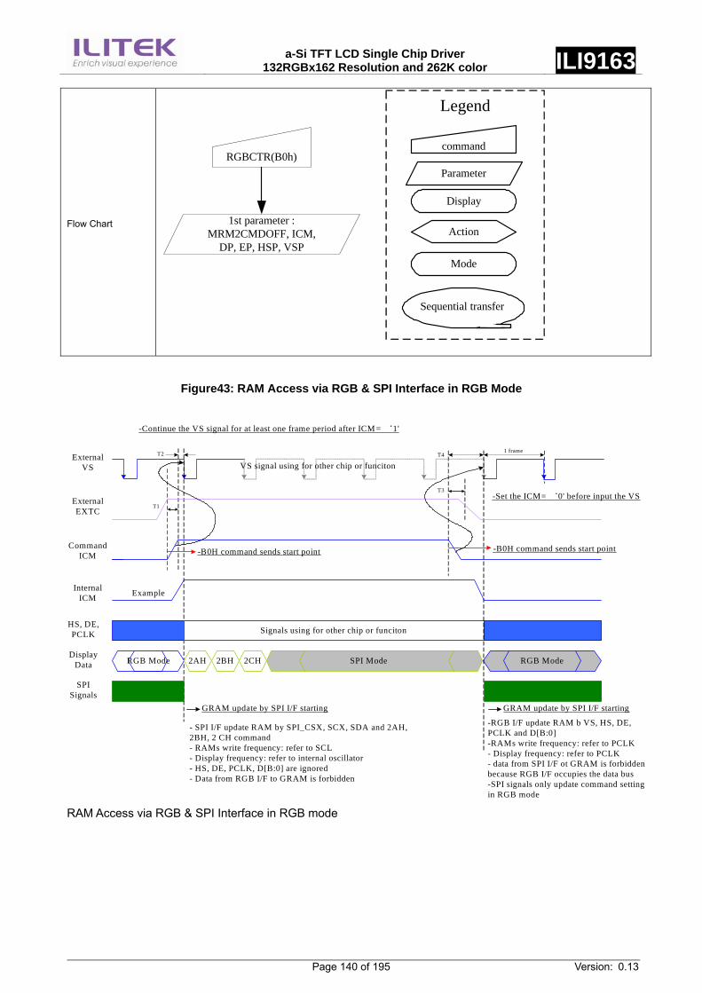
a-Si TFT LCD Single Chip Driver
132RGBx162 Resolution and 262K color ILI9163
Page 140 of 195 Version: 0.13
Flow Chart
command
Parameter
Display
Action
Mode
Legend
Sequential transfer
RGBCTR(B0h)
1st parameter : MRM2CMDOFF, ICM,
DP, EP, HSP, VSP
Figure43: RAM Access via RGB & SPI Interface in RGB Mode
-Continue the VS signal for at least one frame period after ICM = `1'
Signals using for other chip or funciton
RGB Mode 2AH 2BH 2CH SPI Mode RGB Mode
T2
VS signal using for other chip or funcitonT4
1 frameExternal
VS
External EXTC
CommandICM
Internal ICM
HS, DE, PCLK
DisplayData
SPISignals
T1
-B0H command sends start point
Example
GRAM update by SPI I/F starting
T3-Set the ICM= `0' before input the VS
-B0H command sends start point
GRAM update by SPI I/F starting
- SPI I/F update RAM by SPI_CSX, SCX, SDA and 2AH, 2BH, 2 CH command- RAMs write frequency: refer to SCL- Display frequency: refer to internal oscillator- HS, DE, PCLK, D[B:0] are ignored- Data from RGB I/F to GRAM is forbidden
-RGB I/F update RAM b VS, HS, DE, PCLK and D[B:0]-RAMs write frequency: refer to PCLK - Display frequency: refer to PCLK- data from SPI I/F ot GRAM is forbidden because RGB I/F occupies the data bus-SPI signals only update command setting in RGB mode
RAM Access via RGB & SPI Interface in RGB mode
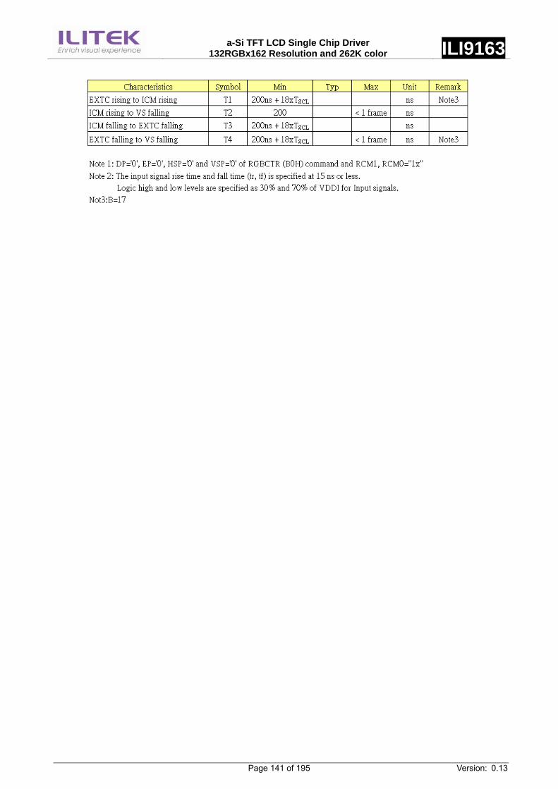
a-Si TFT LCD Single Chip Driver
132RGBx162 Resolution and 262K color ILI9163
Page 141 of 195 Version: 0.13
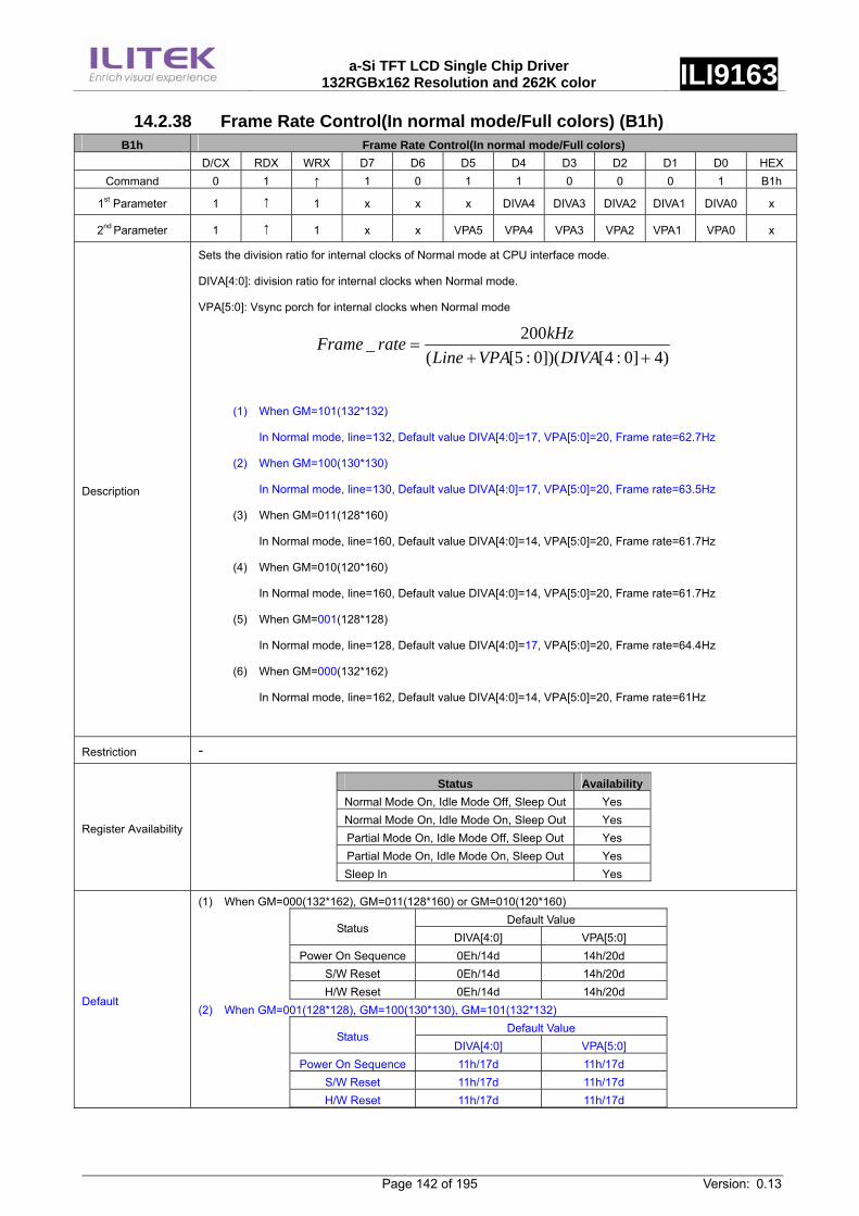
a-Si TFT LCD Single Chip Driver
132RGBx162 Resolution and 262K color ILI9163
Page 142 of 195 Version: 0.13
14.2.38 Frame Rate Control(In normal mode/Full colors) (B1h) B1h Frame Rate Control(In normal mode/Full colors)
D/CX RDX WRX D7 D6 D5 D4 D3 D2 D1 D0 HEX Command 0 1 ↑ 1 0 1 1 0 0 0 1 B1h
1st Parameter 1 ↑ 1 x x x DIVA4 DIVA3 DIVA2 DIVA1 DIVA0 x
2nd Parameter 1 ↑ 1 x x VPA5 VPA4 VPA3 VPA2 VPA1 VPA0 x
Description
Sets the division ratio for internal clocks of Normal mode at CPU interface mode.
DIVA[4:0]: division ratio for internal clocks when Normal mode.
VPA[5:0]: Vsync porch for internal clocks when Normal mode
)4]0:4[])(0:5[(200_
++=
DIVAVPALinekHzrateFrame
(1) When GM=101(132*132)
In Normal mode, line=132, Default value DIVA[4:0]=17, VPA[5:0]=20, Frame rate=62.7Hz
(2) When GM=100(130*130)
In Normal mode, line=130, Default value DIVA[4:0]=17, VPA[5:0]=20, Frame rate=63.5Hz
(3) When GM=011(128*160)
In Normal mode, line=160, Default value DIVA[4:0]=14, VPA[5:0]=20, Frame rate=61.7Hz
(4) When GM=010(120*160)
In Normal mode, line=160, Default value DIVA[4:0]=14, VPA[5:0]=20, Frame rate=61.7Hz
(5) When GM=001(128*128)
In Normal mode, line=128, Default value DIVA[4:0]=17, VPA[5:0]=20, Frame rate=64.4Hz
(6) When GM=000(132*162)
In Normal mode, line=162, Default value DIVA[4:0]=14, VPA[5:0]=20, Frame rate=61Hz
Restriction -
Register Availability
Status Availability Normal Mode On, Idle Mode Off, Sleep Out Yes Normal Mode On, Idle Mode On, Sleep Out Yes Partial Mode On, Idle Mode Off, Sleep Out Yes Partial Mode On, Idle Mode On, Sleep Out Yes Sleep In Yes
Default
(1) When GM=000(132*162), GM=011(128*160) or GM=010(120*160) Default Value
Status DIVA[4:0] VPA[5:0]
Power On Sequence 0Eh/14d 14h/20d S/W Reset 0Eh/14d 14h/20d H/W Reset 0Eh/14d 14h/20d
(2) When GM=001(128*128), GM=100(130*130), GM=101(132*132) Default Value
Status DIVA[4:0] VPA[5:0]
Power On Sequence 11h/17d 11h/17d S/W Reset 11h/17d 11h/17d H/W Reset 11h/17d 11h/17d
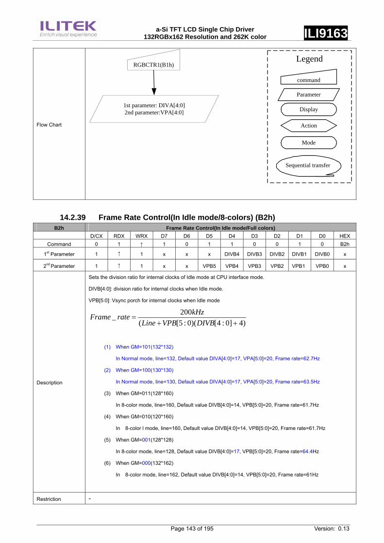
a-Si TFT LCD Single Chip Driver
132RGBx162 Resolution and 262K color ILI9163
Page 143 of 195 Version: 0.13
Flow Chart
command
Parameter
Display
Action
Mode
Legend
Sequential transfer
RGBCTR1(B1h)
1st parameter: DIVA[4:0]2nd parameter:VPA[4:0]
14.2.39 Frame Rate Control(In Idle mode/8-colors) (B2h)
B2h Frame Rate Control(In Idle mode/Full colors) D/CX RDX WRX D7 D6 D5 D4 D3 D2 D1 D0 HEX
Command 0 1 ↑ 1 0 1 1 0 0 1 0 B2h
1st Parameter 1 ↑ 1 x x x DIVB4 DIVB3 DIVB2 DIVB1 DIVB0 x
2nd Parameter 1 ↑ 1 x x VPB5 VPB4 VPB3 VPB2 VPB1 VPB0 x
Description
Sets the division ratio for internal clocks of Idle mode at CPU interface mode.
DIVB[4:0]: division ratio for internal clocks when Idle mode.
VPB[5:0]: Vsync porch for internal clocks when Idle mode
)4]0:4[)(0:5[(200_
++=
DIVBVPBLinekHzrateFrame
(1) When GM=101(132*132)
In Normal mode, line=132, Default value DIVA[4:0]=17, VPA[5:0]=20, Frame rate=62.7Hz
(2) When GM=100(130*130)
In Normal mode, line=130, Default value DIVA[4:0]=17, VPA[5:0]=20, Frame rate=63.5Hz
(3) When GM=011(128*160)
In 8-color mode, line=160, Default value DIVB[4:0]=14, VPB[5:0]=20, Frame rate=61.7Hz
(4) When GM=010(120*160)
In 8-color l mode, line=160, Default value DIVB[4:0]=14, VPB[5:0]=20, Frame rate=61.7Hz
(5) When GM=001(128*128)
In 8-color mode, line=128, Default value DIVB[4:0]=17, VPB[5:0]=20, Frame rate=64.4Hz
(6) When GM=000(132*162)
In 8-color mode, line=162, Default value DIVB[4:0]=14, VPB[5:0]=20, Frame rate=61Hz
Restriction -
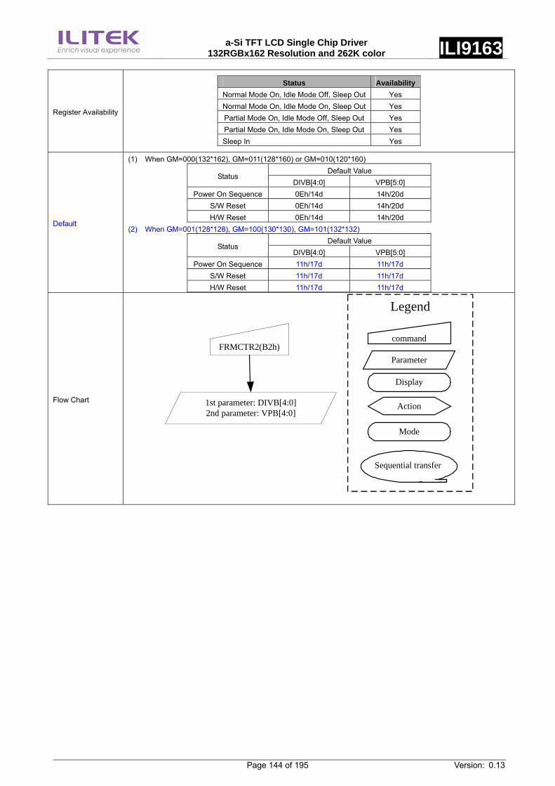
a-Si TFT LCD Single Chip Driver
132RGBx162 Resolution and 262K color ILI9163
Page 144 of 195 Version: 0.13
Register Availability
Status Availability Normal Mode On, Idle Mode Off, Sleep Out Yes Normal Mode On, Idle Mode On, Sleep Out Yes Partial Mode On, Idle Mode Off, Sleep Out Yes Partial Mode On, Idle Mode On, Sleep Out Yes Sleep In Yes
Default
(1) When GM=000(132*162), GM=011(128*160) or GM=010(120*160) Default Value
Status DIVB[4:0] VPB[5:0]
Power On Sequence 0Eh/14d 14h/20d S/W Reset 0Eh/14d 14h/20d H/W Reset 0Eh/14d 14h/20d
(2) When GM=001(128*128), GM=100(130*130), GM=101(132*132) Default Value
Status DIVB[4:0] VPB[5:0]
Power On Sequence 11h/17d 11h/17d S/W Reset 11h/17d 11h/17d H/W Reset 11h/17d 11h/17d
Flow Chart
command
Parameter
Display
Action
Mode
Legend
Sequential transfer
FRMCTR2(B2h)
1st parameter: DIVB[4:0]2nd parameter: VPB[4:0]
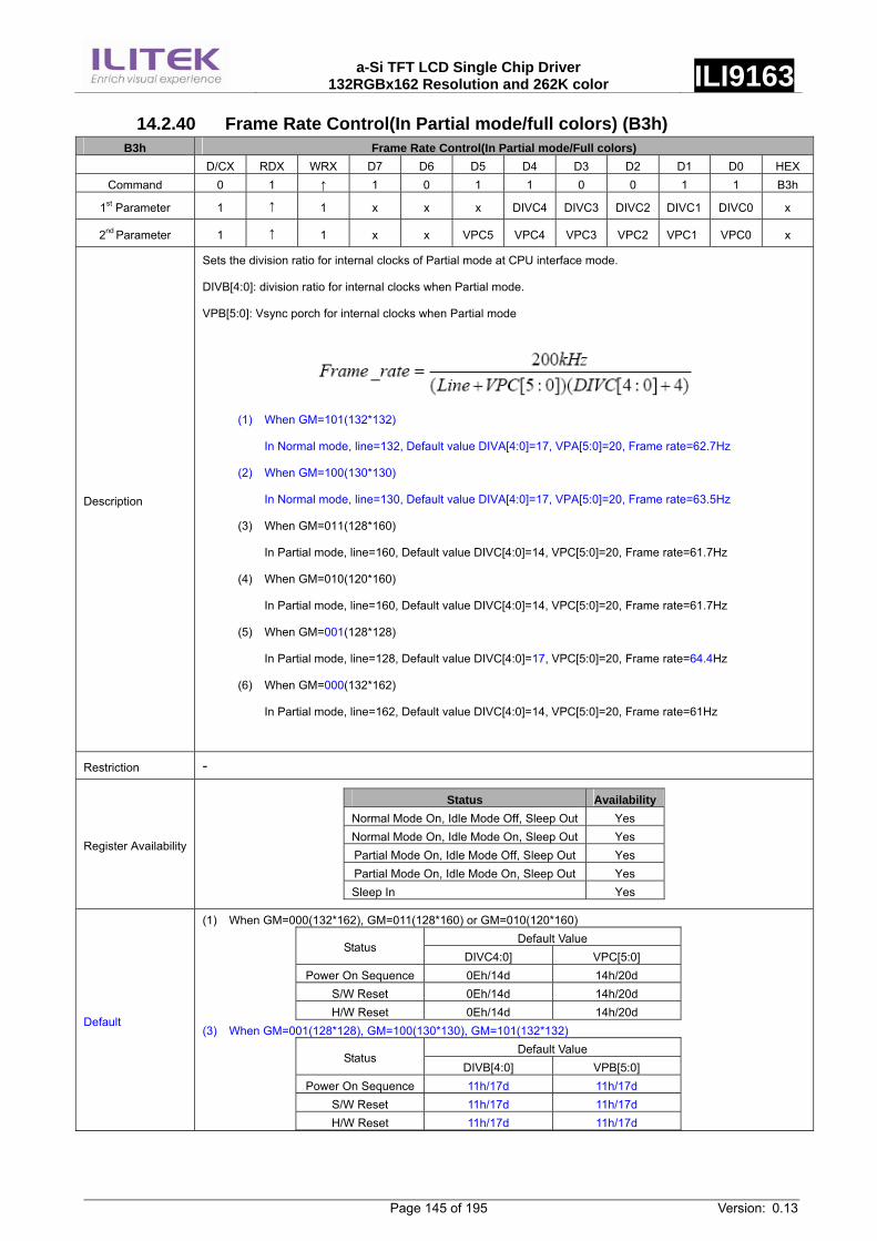
a-Si TFT LCD Single Chip Driver
132RGBx162 Resolution and 262K color ILI9163
Page 145 of 195 Version: 0.13
14.2.40 Frame Rate Control(In Partial mode/full colors) (B3h) B3h Frame Rate Control(In Partial mode/Full colors)
D/CX RDX WRX D7 D6 D5 D4 D3 D2 D1 D0 HEX Command 0 1 ↑ 1 0 1 1 0 0 1 1 B3h
1st Parameter 1 ↑ 1 x x x DIVC4 DIVC3 DIVC2 DIVC1 DIVC0 x
2nd Parameter 1 ↑ 1 x x VPC5 VPC4 VPC3 VPC2 VPC1 VPC0 x
Description
Sets the division ratio for internal clocks of Partial mode at CPU interface mode.
DIVB[4:0]: division ratio for internal clocks when Partial mode.
VPB[5:0]: Vsync porch for internal clocks when Partial mode
(1) When GM=101(132*132)
In Normal mode, line=132, Default value DIVA[4:0]=17, VPA[5:0]=20, Frame rate=62.7Hz
(2) When GM=100(130*130)
In Normal mode, line=130, Default value DIVA[4:0]=17, VPA[5:0]=20, Frame rate=63.5Hz
(3) When GM=011(128*160)
In Partial mode, line=160, Default value DIVC[4:0]=14, VPC[5:0]=20, Frame rate=61.7Hz
(4) When GM=010(120*160)
In Partial mode, line=160, Default value DIVC[4:0]=14, VPC[5:0]=20, Frame rate=61.7Hz
(5) When GM=001(128*128)
In Partial mode, line=128, Default value DIVC[4:0]=17, VPC[5:0]=20, Frame rate=64.4Hz
(6) When GM=000(132*162)
In Partial mode, line=162, Default value DIVC[4:0]=14, VPC[5:0]=20, Frame rate=61Hz
Restriction -
Register Availability
Status Availability Normal Mode On, Idle Mode Off, Sleep Out Yes Normal Mode On, Idle Mode On, Sleep Out Yes Partial Mode On, Idle Mode Off, Sleep Out Yes Partial Mode On, Idle Mode On, Sleep Out Yes Sleep In Yes
Default
(1) When GM=000(132*162), GM=011(128*160) or GM=010(120*160) Default Value
Status DIVC4:0] VPC[5:0]
Power On Sequence 0Eh/14d 14h/20d S/W Reset 0Eh/14d 14h/20d H/W Reset 0Eh/14d 14h/20d
(3) When GM=001(128*128), GM=100(130*130), GM=101(132*132) Default Value
Status DIVB[4:0] VPB[5:0]
Power On Sequence 11h/17d 11h/17d S/W Reset 11h/17d 11h/17d H/W Reset 11h/17d 11h/17d
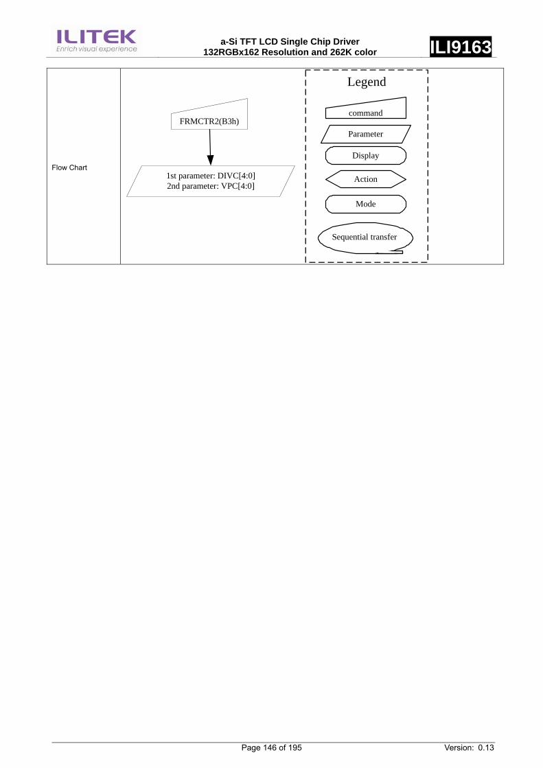
a-Si TFT LCD Single Chip Driver
132RGBx162 Resolution and 262K color ILI9163
Page 146 of 195 Version: 0.13
Flow Chart
command
Parameter
Display
Action
Mode
Legend
Sequential transfer
FRMCTR2(B3h)
1st parameter: DIVC[4:0]2nd parameter: VPC[4:0]
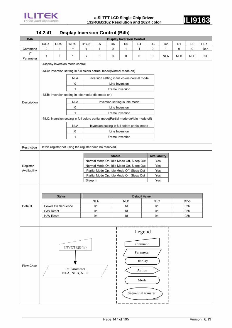
a-Si TFT LCD Single Chip Driver
132RGBx162 Resolution and 262K color ILI9163
Page 147 of 195 Version: 0.13
14.2.41 Display Inversion Control (B4h) B4h Display Inversion Control
D/CX RDX WRX D17-8 D7 D6 D5 D4 D3 D2 D1 D0 HEX Command 0 1 ↑ x 1 0 1 1 0 1 0 0 B4h
1st Parameter
1 ↑ 1 x 0 0 0 0 0 NLA NLB NLC 02H
Description
-Display Inversion mode control
-NLA: Inversion setting in full colors normal mode(Normal mode on)
NLA Inversion setting in full colors normal mode
0 Line Inversion
1 Frame Inversion
-NLB: Inversion setting in Idle mode(Idle mode on)
NLA Inversion setting in Idle mode
0 Line Inversion
1 Frame Inversion
-NLC: Inversion setting in full colors partial mode(Partial mode on/Idle mode off)
NLA Inversion setting in full colors partial mode
0 Line Inversion
1 Frame Inversion
Restriction If this register not using the register need be reserved.
Register Availability
Status Availability Normal Mode On, Idle Mode Off, Sleep Out Yes Normal Mode On, Idle Mode On, Sleep Out Yes Partial Mode On, Idle Mode Off, Sleep Out Yes Partial Mode On, Idle Mode On, Sleep Out Yes Sleep In Yes
Default
Status Default Value NLA NLB NLC D7-0 Power On Sequence 0d 1d 0d 02h S/W Reset 0d 1d 0d 02h H/W Reset 0d 1d 0d 02h
Flow Chart
command
Parameter
Display
Action
Mode
Legend
Sequential transfer
INVCTR(B4h)
1st ParameterNLA, NLB, NLC
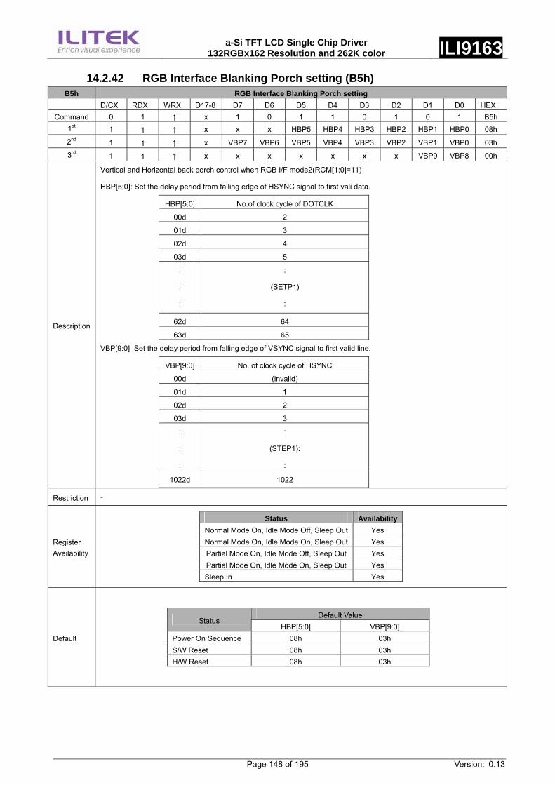
a-Si TFT LCD Single Chip Driver
132RGBx162 Resolution and 262K color ILI9163
Page 148 of 195 Version: 0.13
14.2.42 RGB Interface Blanking Porch setting (B5h) B5h RGB Interface Blanking Porch setting
D/CX RDX WRX D17-8 D7 D6 D5 D4 D3 D2 D1 D0 HEX Command 0 1 ↑ x 1 0 1 1 0 1 0 1 B5h
1st 1 1 ↑ x x x HBP5 HBP4 HBP3 HBP2 HBP1 HBP0 08h
2nd 1 1 ↑ x VBP7 VBP6 VBP5 VBP4 VBP3 VBP2 VBP1 VBP0 03h
3rd 1 1 ↑ x x x x x x x VBP9 VBP8 00h
Description
Vertical and Horizontal back porch control when RGB I/F mode2(RCM[1:0]=11)
HBP[5:0]: Set the delay period from falling edge of HSYNC signal to first vali data.
HBP[5:0] No.of clock cycle of DOTCLK
00d 2
01d 3
02d 4
03d 5
:
:
:
:
(SETP1)
:
62d 64
63d 65
VBP[9:0]: Set the delay period from falling edge of VSYNC signal to first valid line.
VBP[9:0] No. of clock cycle of HSYNC
00d (invalid)
01d 1
02d 2
03d 3
:
:
:
:
(STEP1):
:
1022d 1022
Restriction -
Register Availability
Status Availability Normal Mode On, Idle Mode Off, Sleep Out Yes Normal Mode On, Idle Mode On, Sleep Out Yes Partial Mode On, Idle Mode Off, Sleep Out Yes Partial Mode On, Idle Mode On, Sleep Out Yes Sleep In Yes
Default
Default Value Status
HBP[5:0] VBP[9:0] Power On Sequence 08h 03h S/W Reset 08h 03h H/W Reset 08h 03h
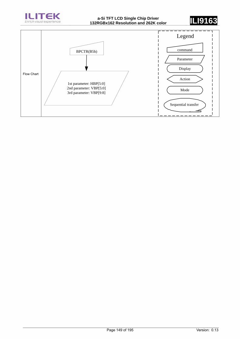
a-Si TFT LCD Single Chip Driver
132RGBx162 Resolution and 262K color ILI9163
Page 149 of 195 Version: 0.13
Flow Chart
command
Parameter
Display
Action
Mode
Legend
Sequential transfer
BPCTR(B5h)
1st parameter: HBP[5:0]2nd parameter: VBP[5:0]3rd parameter: VBP[9:8]

a-Si TFT LCD Single Chip Driver
132RGBx162 Resolution and 262K color ILI9163
Page 150 of 195 Version: 0.13
14.2.43 Display Fuction set 5 (B6h) B6h RGB Interface Blanking Porch setting
D/CX RDX WRX D17-8 D7 D6 D5 D4 D3 D2 D1 D0 HEXCommand 0 1 ↑ x 1 0 1 1 0 1 1 0 B6h
1st 1 1 ↑ x 0 0 NO1 NO0 SDT1 SDT0 EQ1 EQ2 07h
2nd 1 1 ↑ x 0 0 0 0 PTG1 PTG0 PT1 PT0 02h
Description
-1st parameter: Set output waveform relation.
-NO[1:0]: Set the amount for non-overlap of the gate output
Amount of non-overlap of the gate output NO[1:0] Refer the Internal oscillator
00 0 1 clock cycle
01 1 1.5 clock cycle
10 2 2 clock cycle
11 3 2.5 clock cycle
-SDT[1:0]: Set delay amount from gate signal falling edge to the source output.
Amount of non-overlap of the source output SDT[1:0] Refer the Internal oscillator
00 0 3.5 clock cycle
01 1 4 clock cycle
10 2 4.5 clock cycle
11 3 5 clock cycle
-EQ[1:0]: Set the Equalizing period.
EQ period EQ[1:0] Refer the Internal oscillator
00 0 No EQ
01 1 0.5 clock cycle
10 2 1 clock cycle
11 3 1.5 clock cycle
-2nd parameter: Set the output waveform in non-display area.
-PTG[1:0]: Determine gate output in a non-display area in the partial mode.
PTG[1:0] Gate output in a non-display area
00 0 Normal scan
01 1 Fix on VGL
10 2 Fix on VGL
11 3 Fix on VGL
-PT[1:0]: Determine Source/VCOM output in a non-display area in the partial mode
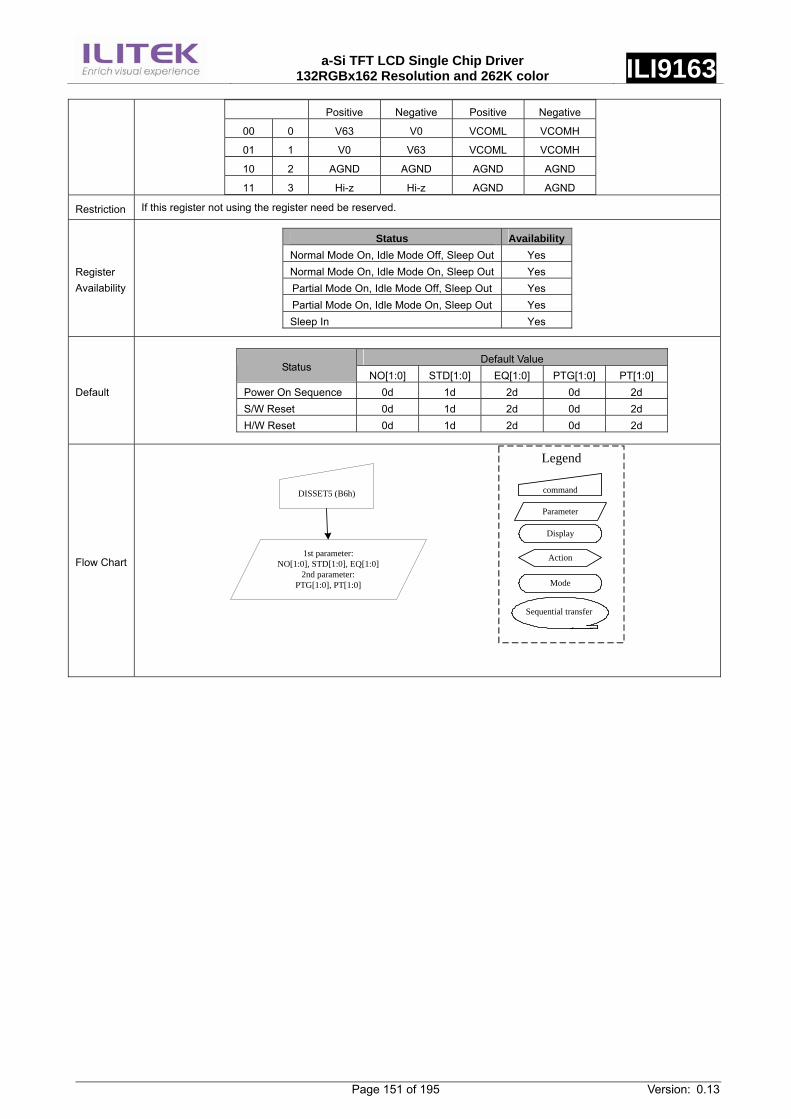
a-Si TFT LCD Single Chip Driver
132RGBx162 Resolution and 262K color ILI9163
Page 151 of 195 Version: 0.13
Positive Negative Positive Negative
00 0 V63 V0 VCOML VCOMH
01 1 V0 V63 VCOML VCOMH
10 2 AGND AGND AGND AGND
11 3 Hi-z Hi-z AGND AGND
Restriction If this register not using the register need be reserved.
Register Availability
Status Availability Normal Mode On, Idle Mode Off, Sleep Out Yes Normal Mode On, Idle Mode On, Sleep Out Yes Partial Mode On, Idle Mode Off, Sleep Out Yes Partial Mode On, Idle Mode On, Sleep Out Yes Sleep In Yes
Default
Default Value Status
NO[1:0] STD[1:0] EQ[1:0] PTG[1:0] PT[1:0] Power On Sequence 0d 1d 2d 0d 2d S/W Reset 0d 1d 2d 0d 2d H/W Reset 0d 1d 2d 0d 2d
Flow Chart
command
Parameter
Display
Action
Mode
Legend
DISSET5 (B6h)
1st parameter:NO[1:0], STD[1:0], EQ[1:0]
2nd parameter:PTG[1:0], PT[1:0]
Sequential transfer
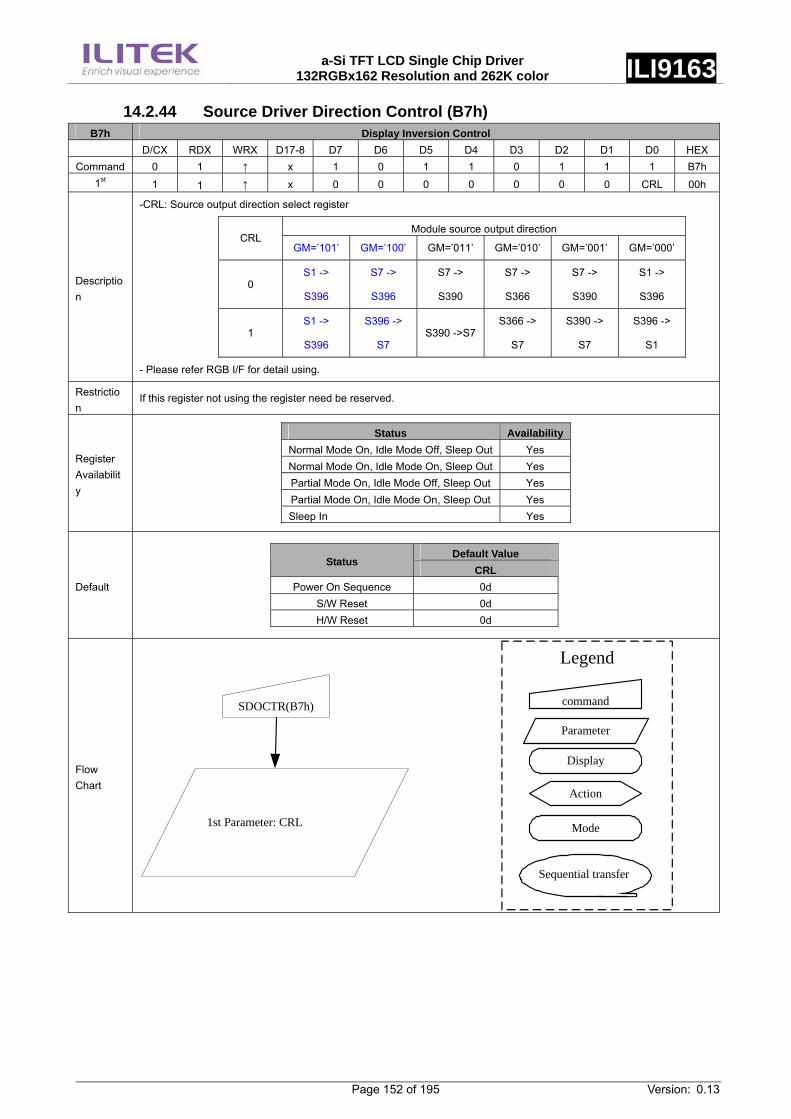
a-Si TFT LCD Single Chip Driver
132RGBx162 Resolution and 262K color ILI9163
Page 152 of 195 Version: 0.13
14.2.44 Source Driver Direction Control (B7h) B7h Display Inversion Control
D/CX RDX WRX D17-8 D7 D6 D5 D4 D3 D2 D1 D0 HEXCommand 0 1 ↑ x 1 0 1 1 0 1 1 1 B7h
1st 1 1 ↑ x 0 0 0 0 0 0 0 CRL 00h
Description
-CRL: Source output direction select register
Module source output direction CRL
GM=’101’ GM=’100’ GM=’011’ GM=’010’ GM=’001’ GM=’000’
0 S1 ->
S396
S7 ->
S396
S7 ->
S390
S7 ->
S366
S7 ->
S390
S1 ->
S396
1 S1 ->
S396
S396 ->
S7 S390 ->S7
S366 ->
S7
S390 ->
S7
S396 ->
S1
- Please refer RGB I/F for detail using.
Restriction
If this register not using the register need be reserved.
Register Availability
Status Availability Normal Mode On, Idle Mode Off, Sleep Out Yes Normal Mode On, Idle Mode On, Sleep Out Yes Partial Mode On, Idle Mode Off, Sleep Out Yes Partial Mode On, Idle Mode On, Sleep Out Yes Sleep In Yes
Default
Default Value Status
CRL Power On Sequence 0d
S/W Reset 0d H/W Reset 0d
Flow Chart
command
Parameter
Display
Action
Mode
Legend
Sequential transfer
SDOCTR(B7h)
1st Parameter: CRL
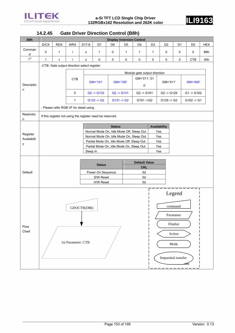
a-Si TFT LCD Single Chip Driver
132RGBx162 Resolution and 262K color ILI9163
Page 153 of 195 Version: 0.13
14.2.45 Gate Driver Direction Control (B8h) B8h Display Inversion Control
D/CX RDX WRX D17-8 D7 D6 D5 D4 D3 D2 D1 D0 HEXComman
d 0 1 ↑ x 1 0 1 1 1 0 0 0 B8h
1st 1 1 ↑ x 0 0 0 0 0 0 0 CTB 00h
Description
-CTB: Gate output direction select register
Module gate output direction
CTB GM=’101’ GM=’100’
GM=’011’,’01
0’ GM=’011’ GM=’000’
0 G2 -> G133 G2 -> G131 G2 -> G161 G2 -> G129 G1 -> G162
1 G133 -> G2 G131 -> G2 G161 ->G2 G129 -> G2 G162 -> G1
- Please refer RGB I/F for detail using.
Restriction
If this register not using the register need be reserved.
Register Availability
Status Availability Normal Mode On, Idle Mode Off, Sleep Out Yes Normal Mode On, Idle Mode On, Sleep Out Yes Partial Mode On, Idle Mode Off, Sleep Out Yes Partial Mode On, Idle Mode On, Sleep Out Yes Sleep In Yes
Default
Default Value Status
CRL Power On Sequence 0d
S/W Reset 0d H/W Reset 0d
Flow Chart
command
Parameter
Display
Action
Mode
Legend
Sequential transfer
GDOCTR(D8h)
1st Parameter: CTB
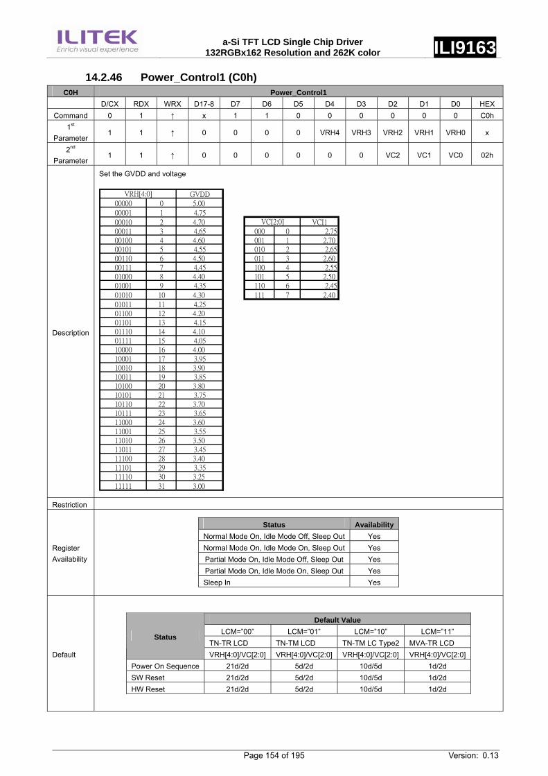
a-Si TFT LCD Single Chip Driver
132RGBx162 Resolution and 262K color ILI9163
Page 154 of 195 Version: 0.13
14.2.46 Power_Control1 (C0h) C0H Power_Control1
D/CX RDX WRX D17-8 D7 D6 D5 D4 D3 D2 D1 D0 HEXCommand 0 1 ↑ x 1 1 0 0 0 0 0 0 C0h
1st Parameter
1 1 ↑ 0 0 0 0 VRH4 VRH3 VRH2 VRH1 VRH0 x
2nd Parameter
1 1 ↑ 0 0 0 0 0 0 VC2 VC1 VC0 02h
Description
Set the GVDD and voltage
GVDD00000 0 5.00
00001 1 4.75
00010 2 4.70 VCI100011 3 4.65 000 0 2.7500100 4 4.60 001 1 2.7000101 5 4.55 010 2 2.6500110 6 4.50 011 3 2.6000111 7 4.45 100 4 2.5501000 8 4.40 101 5 2.5001001 9 4.35 110 6 2.45
01010 10 4.30 111 7 2.40
01011 11 4.2501100 12 4.2001101 13 4.1501110 14 4.1001111 15 4.0510000 16 4.0010001 17 3.9510010 18 3.9010011 19 3.8510100 20 3.8010101 21 3.7510110 22 3.7010111 23 3.6511000 24 3.6011001 25 3.5511010 26 3.5011011 27 3.4511100 28 3.4011101 29 3.3511110 30 3.25
11111 31 3.00
VRH[4:0]
VC[2:0]
Restriction
Register Availability
Status Availability Normal Mode On, Idle Mode Off, Sleep Out Yes Normal Mode On, Idle Mode On, Sleep Out Yes Partial Mode On, Idle Mode Off, Sleep Out Yes Partial Mode On, Idle Mode On, Sleep Out Yes Sleep In Yes
Default
Default Value LCM=”00” LCM=”01” LCM=”10” LCM=”11”
TN-TR LCD TN-TM LCD TN-TM LC Type2 MVA-TR LCD Status
VRH[4:0]/VC[2:0] VRH[4:0]/VC[2:0] VRH[4:0]/VC[2:0] VRH[4:0]/VC[2:0]Power On Sequence 21d/2d 5d/2d 10d/5d 1d/2d SW Reset 21d/2d 5d/2d 10d/5d 1d/2d HW Reset 21d/2d 5d/2d 10d/5d 1d/2d
a-Si TFT LCD Single Chip Driver
132RGBx162 Resolution and 262K color ILI9163
Page 155 of 195 Version: 0.13
Flow Chart
command
Parameter
Display
Action
Mode
Legend
Sequential transfer
PWCTR1(C0h)
1st Parameter: VRH[4:0]

a-Si TFT LCD Single Chip Driver
132RGBx162 Resolution and 262K color ILI9163
Page 156 of 195 Version: 0.13
14.2.47 Power_Control2 (C1h) C1H Power_Control2
D/CX RDX WRX D17-8 D7 D6 D5 D4 D3 D2 D1 D0 HEXCommand 0 1 ↑ x 1 1 0 0 0 0 0 1 C1h
1st Parameter
1 1 ↑ x 0 0 0 0 0 BT2 BT1 BT0 07h
Description
Set the AVDD, VCL, VGH and VGL supply power level.
BT[2:0] AVDD VCL VGH VGL
000 0 4.75 -2.45 4xVCI1 -3xVCI1
001 1 4.75 -2.45 4xVCI1 -4xVCI1
010 2 4.75 -2.45 5xVCI1 -3xVCI1
011 3 4.75 -2.45 5xVCI1 -4xVCI1
100 4 4.75 -2.45 5xVCI1 -5xVCI1
101 5 4.75 -2.45 6xVCI1 -3xVCI1
110 6 4.75 -2.45 6xVCI1 -4xVCI1
111 7 4.75 -2.45 6xVCI1 -5xVCI1
Restriction If this register not using the register need be reserved. The deviation value of VGH/VGL between with Measurement and Specification VGH-VGL <= 32V
Register Availability
Status Availability Normal Mode On, Idle Mode Off, Sleep Out Yes Normal Mode On, Idle Mode On, Sleep Out Yes Partial Mode On, Idle Mode Off, Sleep Out Yes Partial Mode On, Idle Mode On, Sleep Out Yes Sleep In Yes
Default
Default Value Status
BT[2:0] Power On Sequence 7d SW Reset 7d HW Reset 7d
Flow Chart
command
Parameter
Display
Action
Mode
Legend
Sequential transfer
PWCTR2(C1h)
1st Parameter: BT[2:0]
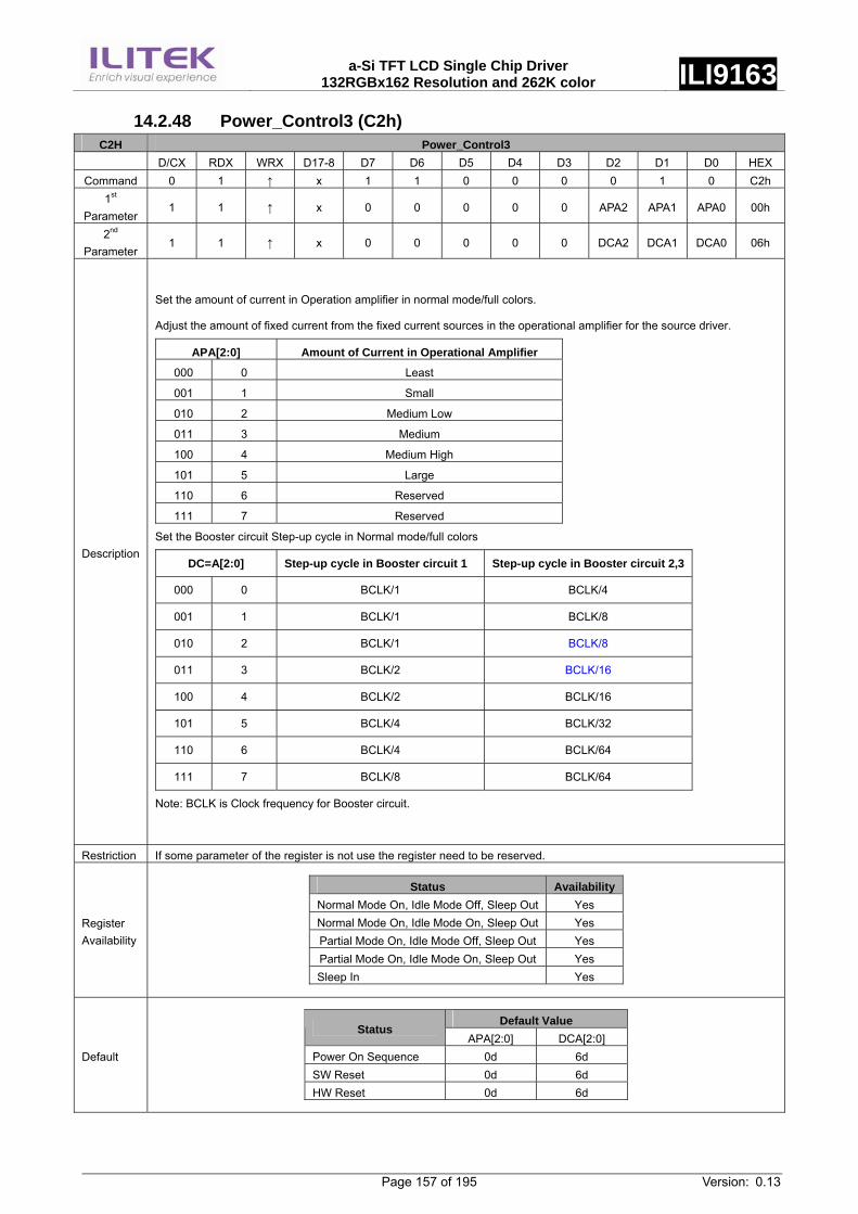
a-Si TFT LCD Single Chip Driver
132RGBx162 Resolution and 262K color ILI9163
Page 157 of 195 Version: 0.13
14.2.48 Power_Control3 (C2h) C2H Power_Control3
D/CX RDX WRX D17-8 D7 D6 D5 D4 D3 D2 D1 D0 HEXCommand 0 1 ↑ x 1 1 0 0 0 0 1 0 C2h
1st Parameter
1 1 ↑ x 0 0 0 0 0 APA2 APA1 APA0 00h
2nd Parameter
1 1 ↑ x 0 0 0 0 0 DCA2 DCA1 DCA0 06h
Description
Set the amount of current in Operation amplifier in normal mode/full colors.
Adjust the amount of fixed current from the fixed current sources in the operational amplifier for the source driver.
APA[2:0] Amount of Current in Operational Amplifier
000 0 Least
001 1 Small
010 2 Medium Low
011 3 Medium
100 4 Medium High
101 5 Large
110 6 Reserved
111 7 Reserved
Set the Booster circuit Step-up cycle in Normal mode/full colors
DC=A[2:0] Step-up cycle in Booster circuit 1 Step-up cycle in Booster circuit 2,3
000 0 BCLK/1 BCLK/4
001 1 BCLK/1 BCLK/8
010 2 BCLK/1 BCLK/8
011 3 BCLK/2 BCLK/16
100 4 BCLK/2 BCLK/16
101 5 BCLK/4 BCLK/32
110 6 BCLK/4 BCLK/64
111 7 BCLK/8 BCLK/64
Note: BCLK is Clock frequency for Booster circuit.
Restriction If some parameter of the register is not use the register need to be reserved.
Register Availability
Status Availability Normal Mode On, Idle Mode Off, Sleep Out Yes Normal Mode On, Idle Mode On, Sleep Out Yes Partial Mode On, Idle Mode Off, Sleep Out Yes Partial Mode On, Idle Mode On, Sleep Out Yes Sleep In Yes
Default
Default Value Status
APA[2:0] DCA[2:0] Power On Sequence 0d 6d SW Reset 0d 6d HW Reset 0d 6d

a-Si TFT LCD Single Chip Driver
132RGBx162 Resolution and 262K color ILI9163
Page 158 of 195 Version: 0.13
Flow Chart
command
Parameter
Display
Action
Mode
Legend
Sequential transfer
PWCTR3(C2h)
1st Parameter: APA[2:0]2nd Parameter: DCA[2:0]
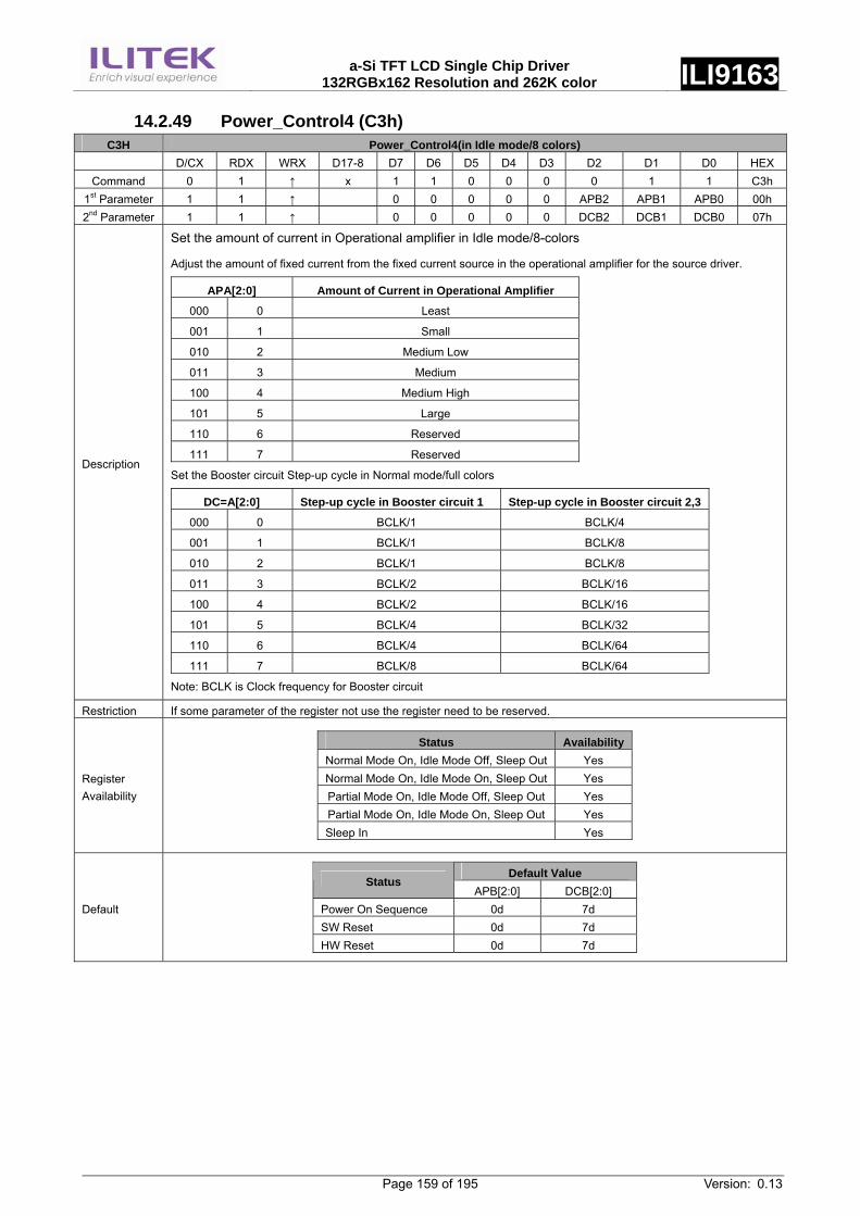
a-Si TFT LCD Single Chip Driver
132RGBx162 Resolution and 262K color ILI9163
Page 159 of 195 Version: 0.13
14.2.49 Power_Control4 (C3h) C3H Power_Control4(in Idle mode/8 colors)
D/CX RDX WRX D17-8 D7 D6 D5 D4 D3 D2 D1 D0 HEXCommand 0 1 ↑ x 1 1 0 0 0 0 1 1 C3h
1st Parameter 1 1 ↑ 0 0 0 0 0 APB2 APB1 APB0 00h 2nd Parameter 1 1 ↑ 0 0 0 0 0 DCB2 DCB1 DCB0 07h
Description
Set the amount of current in Operational amplifier in Idle mode/8-colors
Adjust the amount of fixed current from the fixed current source in the operational amplifier for the source driver.
APA[2:0] Amount of Current in Operational Amplifier
000 0 Least
001 1 Small
010 2 Medium Low
011 3 Medium
100 4 Medium High
101 5 Large
110 6 Reserved
111 7 Reserved
Set the Booster circuit Step-up cycle in Normal mode/full colors
DC=A[2:0] Step-up cycle in Booster circuit 1 Step-up cycle in Booster circuit 2,3
000 0 BCLK/1 BCLK/4
001 1 BCLK/1 BCLK/8
010 2 BCLK/1 BCLK/8
011 3 BCLK/2 BCLK/16
100 4 BCLK/2 BCLK/16
101 5 BCLK/4 BCLK/32
110 6 BCLK/4 BCLK/64
111 7 BCLK/8 BCLK/64
Note: BCLK is Clock frequency for Booster circuit
Restriction If some parameter of the register not use the register need to be reserved.
Register Availability
Status Availability Normal Mode On, Idle Mode Off, Sleep Out Yes Normal Mode On, Idle Mode On, Sleep Out Yes Partial Mode On, Idle Mode Off, Sleep Out Yes Partial Mode On, Idle Mode On, Sleep Out Yes Sleep In Yes
Default
Default Value Status
APB[2:0] DCB[2:0] Power On Sequence 0d 7d SW Reset 0d 7d HW Reset 0d 7d
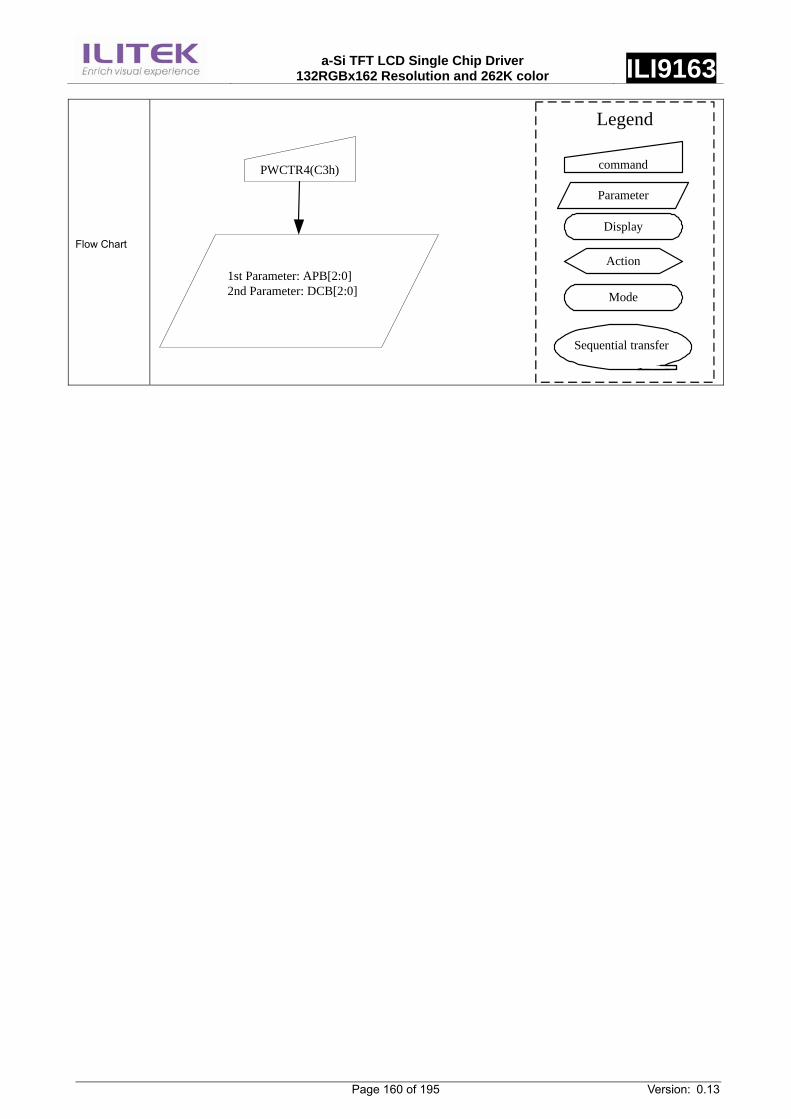
a-Si TFT LCD Single Chip Driver
132RGBx162 Resolution and 262K color ILI9163
Page 160 of 195 Version: 0.13
Flow Chart
command
Parameter
Display
Action
Mode
Legend
Sequential transfer
PWCTR4(C3h)
1st Parameter: APB[2:0]2nd Parameter: DCB[2:0]
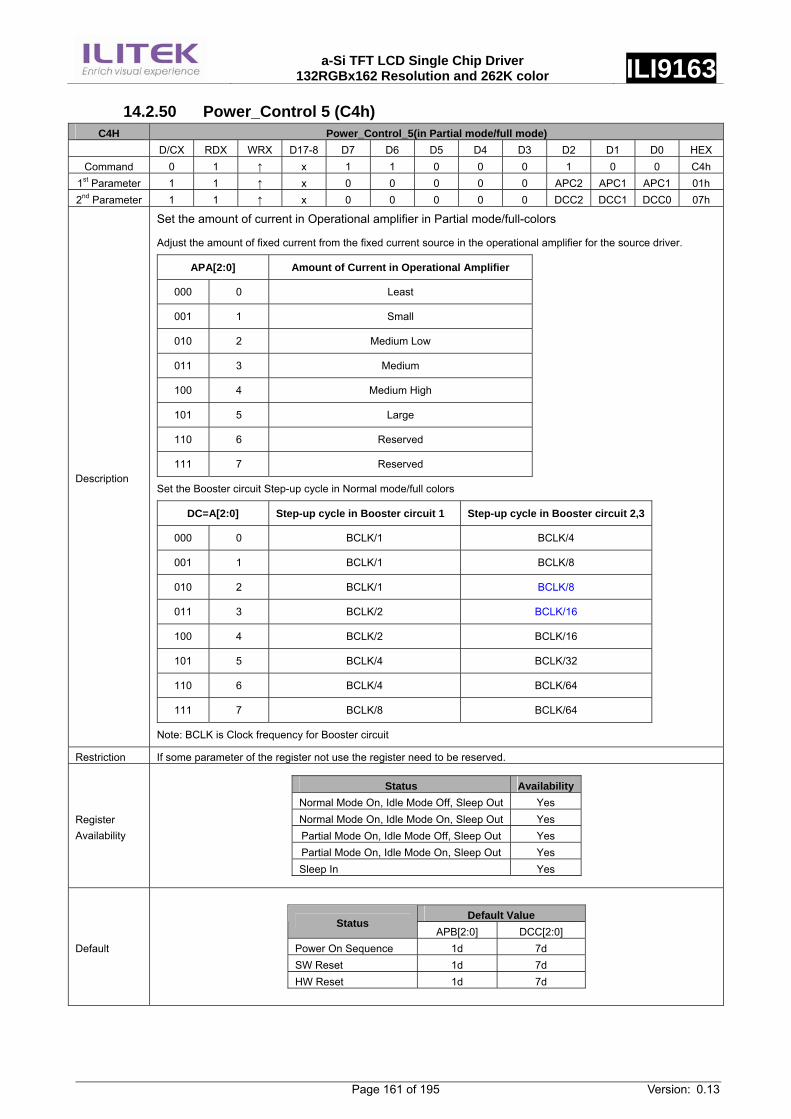
a-Si TFT LCD Single Chip Driver
132RGBx162 Resolution and 262K color ILI9163
Page 161 of 195 Version: 0.13
14.2.50 Power_Control 5 (C4h) C4H Power_Control_5(in Partial mode/full mode)
D/CX RDX WRX D17-8 D7 D6 D5 D4 D3 D2 D1 D0 HEXCommand 0 1 ↑ x 1 1 0 0 0 1 0 0 C4h
1st Parameter 1 1 ↑ x 0 0 0 0 0 APC2 APC1 APC1 01h 2nd Parameter 1 1 ↑ x 0 0 0 0 0 DCC2 DCC1 DCC0 07h
Description
Set the amount of current in Operational amplifier in Partial mode/full-colors
Adjust the amount of fixed current from the fixed current source in the operational amplifier for the source driver.
APA[2:0] Amount of Current in Operational Amplifier
000 0 Least
001 1 Small
010 2 Medium Low
011 3 Medium
100 4 Medium High
101 5 Large
110 6 Reserved
111 7 Reserved
Set the Booster circuit Step-up cycle in Normal mode/full colors
DC=A[2:0] Step-up cycle in Booster circuit 1 Step-up cycle in Booster circuit 2,3
000 0 BCLK/1 BCLK/4
001 1 BCLK/1 BCLK/8
010 2 BCLK/1 BCLK/8
011 3 BCLK/2 BCLK/16
100 4 BCLK/2 BCLK/16
101 5 BCLK/4 BCLK/32
110 6 BCLK/4 BCLK/64
111 7 BCLK/8 BCLK/64
Note: BCLK is Clock frequency for Booster circuit
Restriction If some parameter of the register not use the register need to be reserved.
Register Availability
Status Availability Normal Mode On, Idle Mode Off, Sleep Out Yes Normal Mode On, Idle Mode On, Sleep Out Yes Partial Mode On, Idle Mode Off, Sleep Out Yes Partial Mode On, Idle Mode On, Sleep Out Yes Sleep In Yes
Default
Default Value Status
APB[2:0] DCC[2:0] Power On Sequence 1d 7d SW Reset 1d 7d HW Reset 1d 7d

a-Si TFT LCD Single Chip Driver
132RGBx162 Resolution and 262K color ILI9163
Page 162 of 195 Version: 0.13
Flow Chart
command
Parameter
Display
Action
Mode
Legend
Sequential transfer
PWCTR5(C4h)
1st Parameter: APC[2:0]2nd Parameter: DCC[2:0]
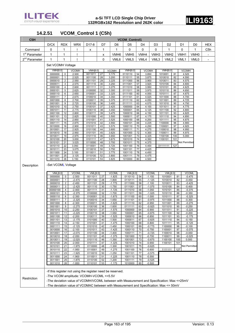
a-Si TFT LCD Single Chip Driver
132RGBx162 Resolution and 262K color ILI9163
Page 163 of 195 Version: 0.13
14.2.51 VCOM_Control 1 (C5h) C5H VCOM_Control1
D/CX RDX WRX D17-8 D7 D6 D5 D4 D3 D2 D1 D0 HEXCommand 0 1 ↑ x 1 1 0 0 0 1 0 1 C5h
1st Parameter 1 1 ↑ x VMH6 VMH5 VMH4 VMH3 VMH2 VMH1 VMH0 - 2nd Parameter 1 1 ↑ 0 VML6 VML5 VML4 VML3 VML2 VML1 VML0 -
Description
Set VCOMH Voltage
VCOMH VCOMH VCOMH VCOMH0000000 0 2.500 0011011 27 3.175 0110110 54 3.850 1010001 81 4.5250000001 1 2.525 0011100 28 3.200 0110111 55 3.875 1010010 82 4.5500000010 2 2.550 0011101 29 3.225 0111000 56 3.900 1010011 83 4.5750000011 3 2.575 0011110 30 3.250 0111001 57 3.925 1010100 84 4.6000000100 4 2.600 0011111 31 3.275 0111010 58 3.950 1010101 85 4.6250000101 5 2.625 0100000 32 3.300 0111011 59 3.975 1010110 86 4.6500000110 6 2.650 0100001 33 3.325 0111100 60 4.000 1010111 87 4.6750000111 7 2.675 0100010 34 3.350 0111101 61 4.025 1011000 88 4.7000001000 8 2.700 0100011 35 3.375 0111110 62 4.050 1011001 89 4.7250001001 9 2.725 0100100 36 3.400 0111111 63 4.075 1011010 90 4.7500001010 10 2.750 0100101 37 3.425 1000000 64 4.100 1011011 91 4.7750001011 11 2.775 0100110 38 3.450 1000001 65 4.125 1011100 92 4.8000001100 12 2.800 0100111 39 3.475 1000010 66 4.150 1011101 93 4.8250001101 13 2.825 0101000 40 3.500 1000011 67 4.175 1011110 94 4.8500001110 14 2.850 0101001 41 3.525 1000100 68 4.200 1011111 95 4.8750001111 15 2.875 0101010 42 3.550 1000101 69 4.225 1100000 96 4.9000010000 16 2.900 0101011 43 3.575 1000110 70 4.250 1100001 97 4.9250010001 17 2.925 0101100 44 3.600 1000111 71 4.275 1100010 98 4.9500010010 18 2.950 0101101 45 3.625 1001000 72 4.300 1100011 99 4.9750010011 19 2.975 0101110 46 3.650 1001001 73 4.325 1100100 100 5.0000010100 20 3.000 0101111 47 3.675 1001010 74 4.350 1100101 1010010101 21 3.025 0110000 48 3.700 1001011 75 4.3750010110 22 3.050 0110001 49 3.725 1001100 76 4.400 01111111 1270010111 23 3.075 0110010 50 3.750 1001101 77 4.4250011000 24 3.100 0110011 51 3.775 1001110 78 4.4500011001 25 3.125 0110100 52 3.800 1001111 79 4.4750011010 26 3.150 0110101 53 3.825 1010000 80 4.500
Not Permitted
VMH[6:0] VMH[6:0] VMH[6:0] VMH[6:0]
-Set VCOML Voltage
VCOML VCOML VCOML VCOML0000000 0 -2.500 0011011 27 -1.825 0110110 54 -1.150 1010001 81 -0.4750000001 1 -2.475 0011100 28 -1.800 0110111 55 -1.125 1010010 82 -0.4500000010 2 -2.450 0011101 29 -1.775 0111000 56 -1.100 1010011 83 -0.4250000011 3 -2.425 0011110 30 -1.750 0111001 57 -1.075 1010100 84 -0.400
00000100 4 -2.400 0011111 31 -1.725 0111010 58 -1.050 1010101 85 -0.3750000101 5 -2.375 0100000 32 -1.700 0111011 59 -1.025 1010110 86 -0.3500000110 6 -2.350 0100001 33 -1.675 0111100 60 -1.000 1010111 87 -0.3250000111 7 -2.325 0100010 34 -1.650 0111101 61 -0.975 1011000 88 -0.3000001000 8 -2.300 0100011 35 -1.625 0111110 62 -0.950 1011001 89 -0.2750001001 9 -2.275 0100100 36 -1.600 0111111 63 -0.925 1011010 90 -0.2500001010 10 -2.250 0100101 37 -1.575 1000000 64 -0.900 1011011 91 -0.2250001011 11 -2.225 0100110 38 -1.550 1000001 65 -0.875 1011100 92 -0.2000001100 12 -2.200 0100111 39 -1.525 1000010 66 -0.850 1011101 93 -0.1750001101 13 -2.175 0101000 40 -1.500 1000011 67 -0.825 1011110 94 -0.1500001110 14 -2.150 0101001 41 -1.475 1000100 68 -0.800 1011111 95 -0.1250001111 15 -2.125 0101010 42 -1.450 1000101 69 -0.775 1100000 96 -0.1000010000 16 -2.100 0101011 43 -1.425 1000110 70 -0.750 1100001 97 -0.0750010001 17 -2.075 0101100 44 -1.400 1000111 71 -0.725 1100010 98 -0.0500010010 18 -2.050 0101101 45 -1.375 1001000 72 -0.700 1100011 99 -0.0250010011 19 -2.025 0101110 46 -1.350 1001001 73 -0.675 1100100 100 0.0000010100 20 -2.000 0101111 47 -1.325 1001010 74 -0.650 1100101 1010010101 21 -1.975 0110000 48 -1.300 1001011 75 -0.6250010110 22 -1.950 0110001 49 -1.275 1001100 76 -0.600 1111111 1270010111 23 -1.925 0110010 50 -1.250 1001101 77 -0.5750011000 24 -1.900 0110011 51 -1.225 1001110 78 -0.5500011001 25 -1.875 0110100 52 -1.200 1001111 79 -0.5250011010 26 -1.850 0110101 53 -1.175 1010000 80 -0.500
Not Permitted
VML[6:0] VML[6:0] VML[6:0] VML[6:0]
Restriction
-If this register not using the register need be reserved. -The VCOM amplitude: VCOMH-VCOML <=5.5V -The deviation value of VCOMH/VCOML between with Measurement and Specification: Max <=25mV -The deviation value of VCOMAC between with Measurement and Specification: Max <= 50mV
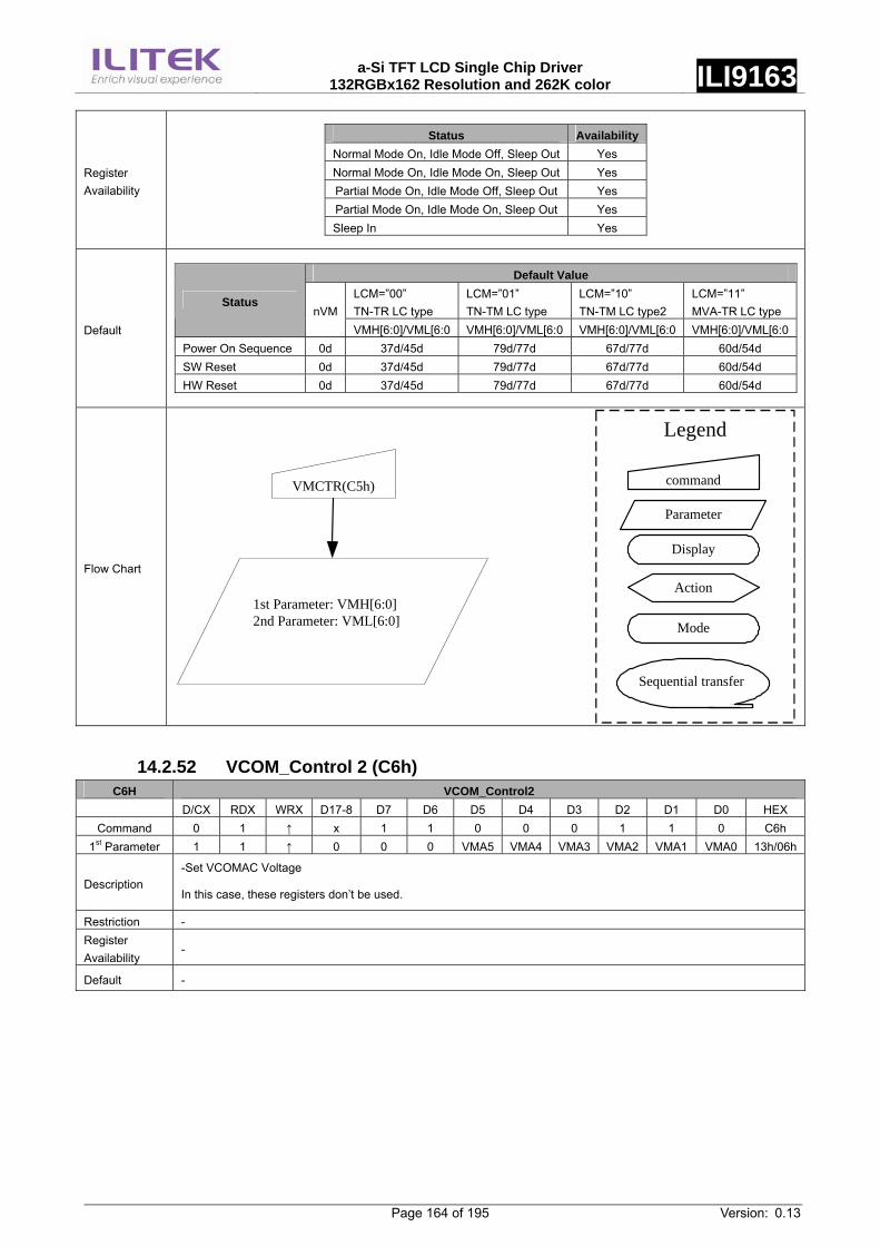
a-Si TFT LCD Single Chip Driver
132RGBx162 Resolution and 262K color ILI9163
Page 164 of 195 Version: 0.13
Register Availability
Status Availability Normal Mode On, Idle Mode Off, Sleep Out Yes Normal Mode On, Idle Mode On, Sleep Out Yes Partial Mode On, Idle Mode Off, Sleep Out Yes Partial Mode On, Idle Mode On, Sleep Out Yes Sleep In Yes
Default
Default Value LCM=”00” TN-TR LC type
LCM=”01” TN-TM LC type
LCM=”10” TN-TM LC type2
LCM=”11” MVA-TR LC type
Status nVM
VMH[6:0]/VML[6:0 VMH[6:0]/VML[6:0 VMH[6:0]/VML[6:0 VMH[6:0]/VML[6:0Power On Sequence 0d 37d/45d 79d/77d 67d/77d 60d/54d SW Reset 0d 37d/45d 79d/77d 67d/77d 60d/54d HW Reset 0d 37d/45d 79d/77d 67d/77d 60d/54d
Flow Chart
command
Parameter
Display
Action
Mode
Legend
Sequential transfer
VMCTR(C5h)
1st Parameter: VMH[6:0]2nd Parameter: VML[6:0]
14.2.52 VCOM_Control 2 (C6h) C6H VCOM_Control2
D/CX RDX WRX D17-8 D7 D6 D5 D4 D3 D2 D1 D0 HEX Command 0 1 ↑ x 1 1 0 0 0 1 1 0 C6h
1st Parameter 1 1 ↑ 0 0 0 VMA5 VMA4 VMA3 VMA2 VMA1 VMA0 13h/06h
Description -Set VCOMAC Voltage
In this case, these registers don’t be used.
Restriction - Register Availability
-
Default -
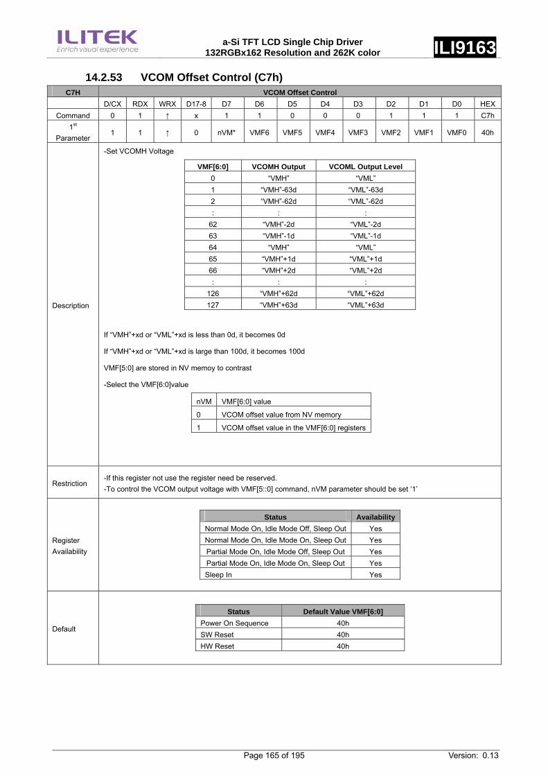
a-Si TFT LCD Single Chip Driver
132RGBx162 Resolution and 262K color ILI9163
Page 165 of 195 Version: 0.13
14.2.53 VCOM Offset Control (C7h) C7H VCOM Offset Control
D/CX RDX WRX D17-8 D7 D6 D5 D4 D3 D2 D1 D0 HEXCommand 0 1 ↑ x 1 1 0 0 0 1 1 1 C7h
1st Parameter
1 1 ↑ 0 nVM* VMF6 VMF5 VMF4 VMF3 VMF2 VMF1 VMF0 40h
Description
-Set VCOMH Voltage
VMF[6:0] VCOMH Output VCOML Output Level 0 “VMH” “VML” 1 “VMH”-63d “VML”-63d 2 “VMH”-62d “VML”-62d : : :
62 “VMH”-2d “VML”-2d 63 “VMH”-1d “VML”-1d 64 “VMH” “VML” 65 “VMH”+1d “VML”+1d 66 “VMH”+2d “VML”+2d : : :
126 “VMH”+62d “VML”+62d 127 “VMH”+63d “VML”+63d
If “VMH”+xd or “VML”+xd is less than 0d, it becomes 0d
If “VMH”+xd or “VML”+xd is large than 100d, it becomes 100d
VMF[5:0] are stored in NV memoy to contrast
-Select the VMF[6:0]value
nVM VMF[6:0] value
0 VCOM offset value from NV memory
1 VCOM offset value in the VMF[6:0] registers
Restriction -If this register not use the register need be reserved. -To control the VCOM output voltage with VMF[5::0] command, nVM parameter should be set ‘1’
Register Availability
Status Availability Normal Mode On, Idle Mode Off, Sleep Out Yes Normal Mode On, Idle Mode On, Sleep Out Yes Partial Mode On, Idle Mode Off, Sleep Out Yes Partial Mode On, Idle Mode On, Sleep Out Yes Sleep In Yes
Default
Status Default Value VMF[6:0] Power On Sequence 40h SW Reset 40h HW Reset 40h
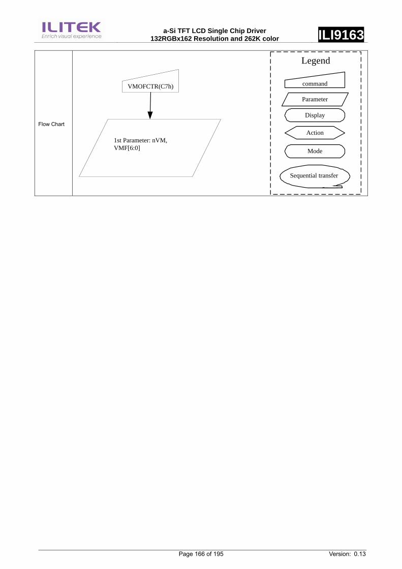
a-Si TFT LCD Single Chip Driver
132RGBx162 Resolution and 262K color ILI9163
Page 166 of 195 Version: 0.13
Flow Chart
command
Parameter
Display
Action
Mode
Legend
Sequential transfer
VMOFCTR(C7h)
1st Parameter: nVM, VMF[6:0]
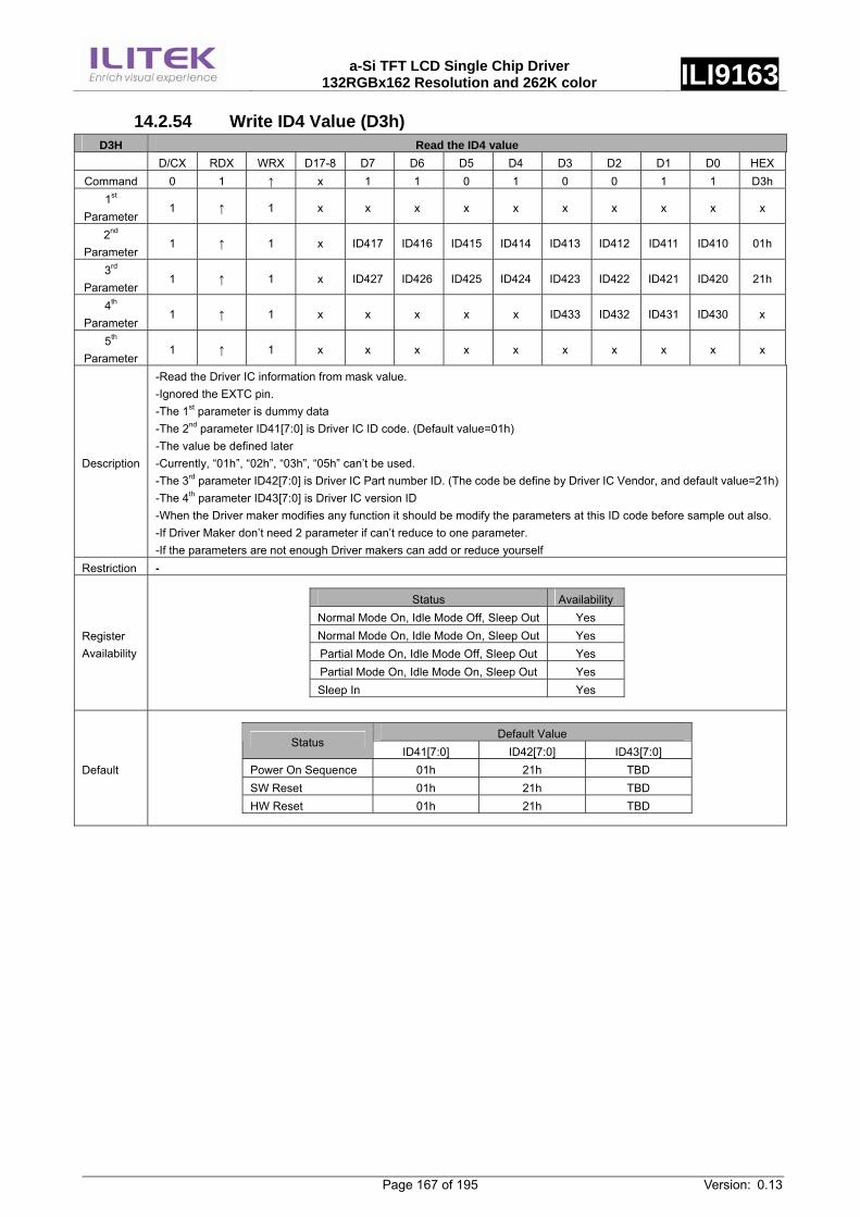
a-Si TFT LCD Single Chip Driver
132RGBx162 Resolution and 262K color ILI9163
Page 167 of 195 Version: 0.13
14.2.54 Write ID4 Value (D3h) D3H Read the ID4 value
D/CX RDX WRX D17-8 D7 D6 D5 D4 D3 D2 D1 D0 HEXCommand 0 1 ↑ x 1 1 0 1 0 0 1 1 D3h
1st Parameter
1 ↑ 1 x x x x x x x x x x
2nd Parameter
1 ↑ 1 x ID417 ID416 ID415 ID414 ID413 ID412 ID411 ID410 01h
3rd Parameter
1 ↑ 1 x ID427 ID426 ID425 ID424 ID423 ID422 ID421 ID420 21h
4th Parameter
1 ↑ 1 x x x x x ID433 ID432 ID431 ID430 x
5th Parameter
1 ↑ 1 x x x x x x x x x x
Description
-Read the Driver IC information from mask value. -Ignored the EXTC pin. -The 1st parameter is dummy data -The 2nd parameter ID41[7:0] is Driver IC ID code. (Default value=01h) -The value be defined later -Currently, “01h”, “02h”, “03h”, “05h” can’t be used. -The 3rd parameter ID42[7:0] is Driver IC Part number ID. (The code be define by Driver IC Vendor, and default value=21h)-The 4th parameter ID43[7:0] is Driver IC version ID -When the Driver maker modifies any function it should be modify the parameters at this ID code before sample out also. -If Driver Maker don’t need 2 parameter if can’t reduce to one parameter. -If the parameters are not enough Driver makers can add or reduce yourself
Restriction -
Register Availability
Status Availability Normal Mode On, Idle Mode Off, Sleep Out Yes Normal Mode On, Idle Mode On, Sleep Out Yes Partial Mode On, Idle Mode Off, Sleep Out Yes Partial Mode On, Idle Mode On, Sleep Out Yes Sleep In Yes
Default
Default Value Status
ID41[7:0] ID42[7:0] ID43[7:0] Power On Sequence 01h 21h TBD SW Reset 01h 21h TBD HW Reset 01h 21h TBD

a-Si TFT LCD Single Chip Driver
132RGBx162 Resolution and 262K color ILI9163
Page 168 of 195 Version: 0.13
Flow Chart
command
Parameter
Display
Action
Mode
Legend
Sequential transfer
RDID4(D3h)
Dummy Read
RDID4(D3h)
Dummy Clock
Host
Driver
Serial I/F Mode Parallel I/F Mode
Send ID41[7:0]
Send ID42[7:0]
Send ID43[7:0]
Send ID4N[7:0]
Send ID41[7:0]
Send ID42[7:0]
Send ID43[7:0]
Send ID4N[7:0]
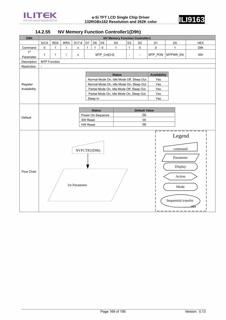
a-Si TFT LCD Single Chip Driver
132RGBx162 Resolution and 262K color ILI9163
Page 169 of 195 Version: 0.13
14.2.55 NV Memory Function Controller1(D9h) D9H NV Memory Function Controller1
D/CX RDX WRX D17-8 D7 D6 D5 D4 D3 D2 D1 D0 HEX Command 0 1 ↑ x 1 1 0 1 1 0 0 1 D9h
1st Parameter
1 1 ↑ x MTP_Cnt[3:0] - - MTP_PON MTPWR_EN 00h
Description MTP Function Restriction -
Register Availability
Status Availability Normal Mode On, Idle Mode Off, Sleep Out Yes Normal Mode On, Idle Mode On, Sleep Out Yes Partial Mode On, Idle Mode Off, Sleep Out Yes Partial Mode On, Idle Mode On, Sleep Out Yes Sleep In Yes
Default
Status Default Value Power On Sequence 00 SW Reset 00 HW Reset 00
Flow Chart
command
Parameter
Display
Action
Mode
Legend
Sequential transfer
NVFCTR1(D9h)
1st Parameter
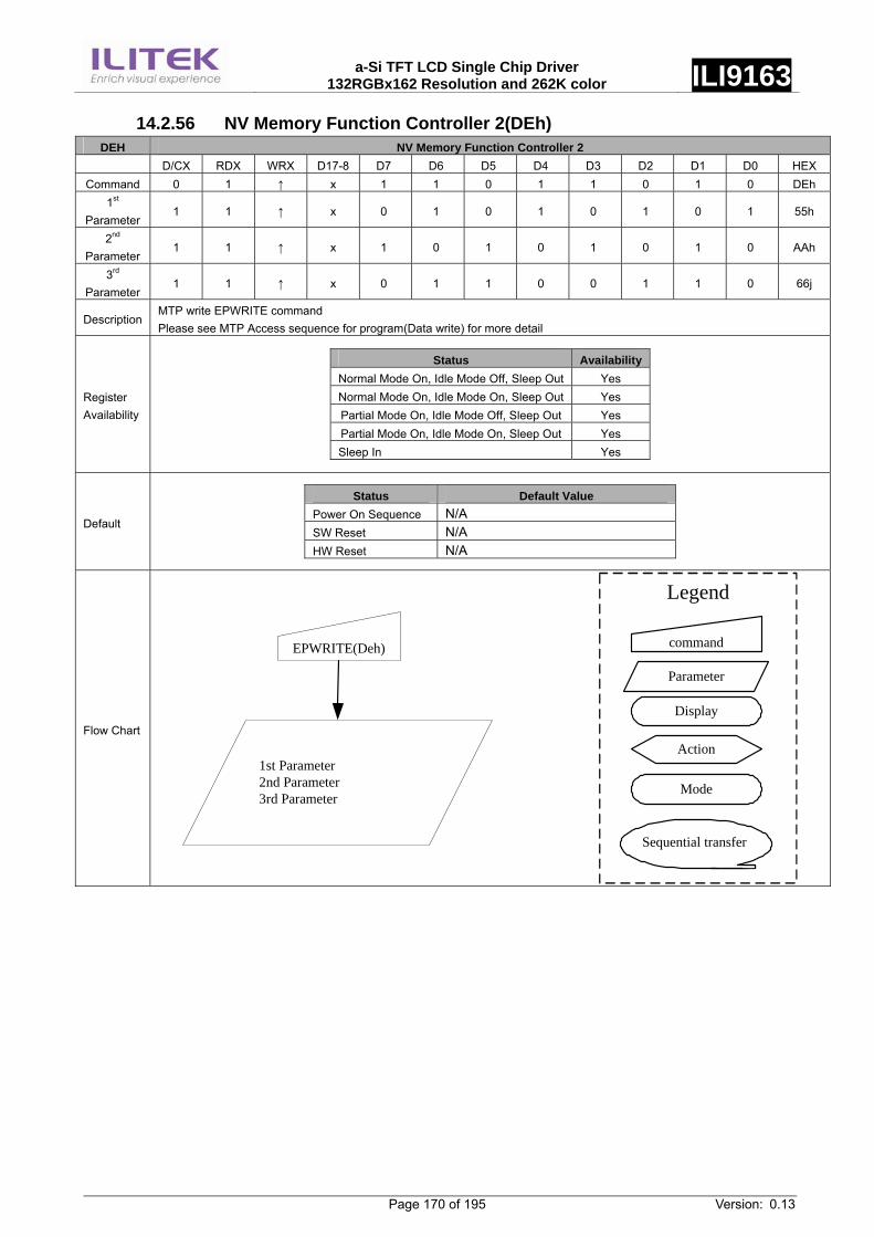
a-Si TFT LCD Single Chip Driver
132RGBx162 Resolution and 262K color ILI9163
Page 170 of 195 Version: 0.13
14.2.56 NV Memory Function Controller 2(DEh) DEH NV Memory Function Controller 2
D/CX RDX WRX D17-8 D7 D6 D5 D4 D3 D2 D1 D0 HEX Command 0 1 ↑ x 1 1 0 1 1 0 1 0 DEh
1st Parameter
1 1 ↑ x 0 1 0 1 0 1 0 1 55h
2nd Parameter
1 1 ↑ x 1 0 1 0 1 0 1 0 AAh
3rd Parameter
1 1 ↑ x 0 1 1 0 0 1 1 0 66j
Description MTP write EPWRITE command Please see MTP Access sequence for program(Data write) for more detail
Register Availability
Status Availability Normal Mode On, Idle Mode Off, Sleep Out Yes Normal Mode On, Idle Mode On, Sleep Out Yes Partial Mode On, Idle Mode Off, Sleep Out Yes Partial Mode On, Idle Mode On, Sleep Out Yes Sleep In Yes
Default
Status Default Value Power On Sequence N/A SW Reset N/A HW Reset N/A
Flow Chart
command
Parameter
Display
Action
Mode
Legend
Sequential transfer
EPWRITE(Deh)
1st Parameter2nd Parameter3rd Parameter
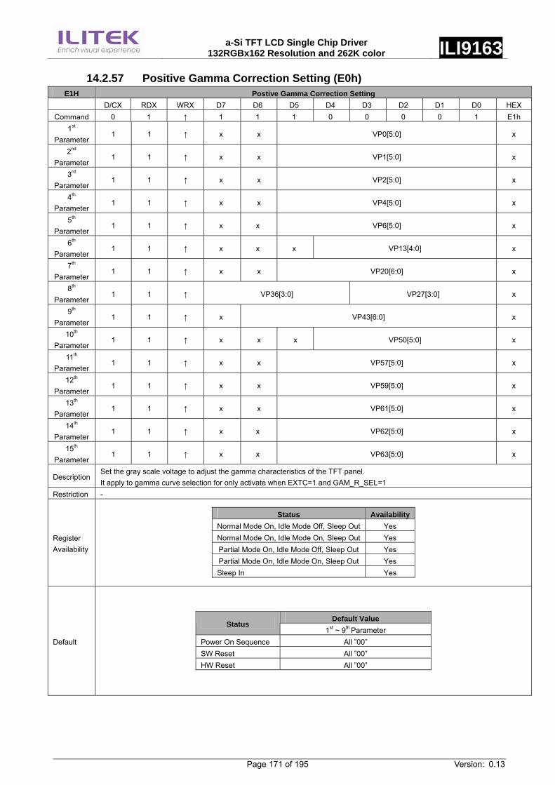
a-Si TFT LCD Single Chip Driver
132RGBx162 Resolution and 262K color ILI9163
Page 171 of 195 Version: 0.13
14.2.57 Positive Gamma Correction Setting (E0h) E1H Postive Gamma Correction Setting
D/CX RDX WRX D7 D6 D5 D4 D3 D2 D1 D0 HEX Command 0 1 ↑ 1 1 1 0 0 0 0 1 E1h
1st Parameter
1 1 ↑ x x VP0[5:0] x
2nd Parameter
1 1 ↑ x x VP1[5:0] x
3rd Parameter
1 1 ↑ x x VP2[5:0] x
4th Parameter
1 1 ↑ x x VP4[5:0] x
5th Parameter
1 1 ↑ x x VP6[5:0] x
6th Parameter
1 1 ↑ x x x VP13[4:0] x
7th Parameter
1 1 ↑ x x VP20[6:0] x
8th Parameter
1 1 ↑ VP36[3:0] VP27[3:0] x
9th Parameter
1 1 ↑ x VP43[6:0] x
10th Parameter
1 1 ↑ x x x VP50[5:0] x
11th Parameter
1 1 ↑ x x VP57[5:0] x
12th Parameter
1 1 ↑ x x VP59[5:0] x
13th Parameter
1 1 ↑ x x VP61[5:0] x
14th Parameter
1 1 ↑ x x VP62[5:0] x
15th Parameter
1 1 ↑ x x VP63[5:0] x
Description Set the gray scale voltage to adjust the gamma characteristics of the TFT panel. It apply to gamma curve selection for only activate when EXTC=1 and GAM_R_SEL=1
Restriction -
Register Availability
Status Availability Normal Mode On, Idle Mode Off, Sleep Out Yes Normal Mode On, Idle Mode On, Sleep Out Yes Partial Mode On, Idle Mode Off, Sleep Out Yes Partial Mode On, Idle Mode On, Sleep Out Yes Sleep In Yes
Default
Default Value Status
1st ~ 9th Parameter Power On Sequence All ”00” SW Reset All ”00” HW Reset All ”00”

a-Si TFT LCD Single Chip Driver
132RGBx162 Resolution and 262K color ILI9163
Page 172 of 195 Version: 0.13
Flow Chart
command
Parameter
Display
Action
Mode
Legend
Sequential transfer
GAMCTRP0(E0h)
1st Parameter2nd Parameter
::
9th Parameter
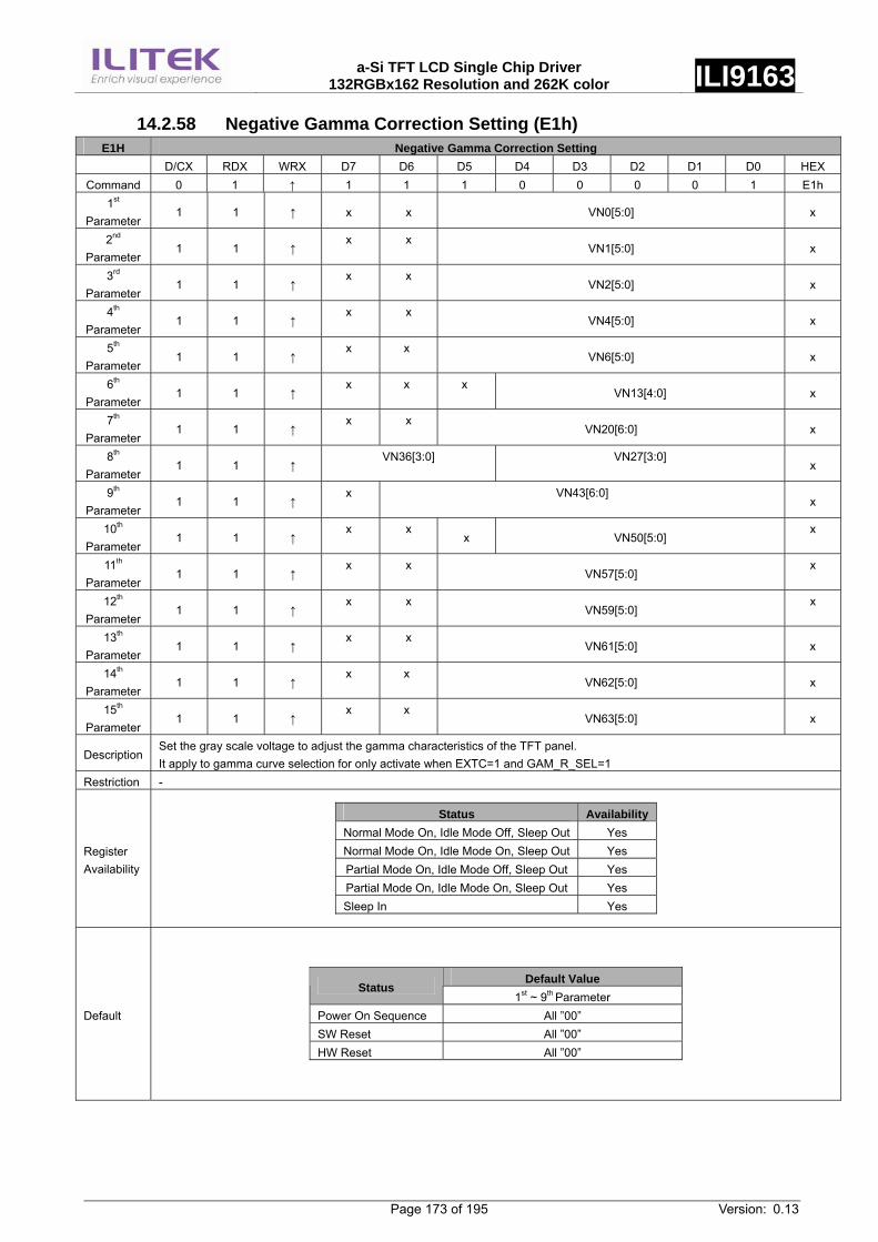
a-Si TFT LCD Single Chip Driver
132RGBx162 Resolution and 262K color ILI9163
Page 173 of 195 Version: 0.13
14.2.58 Negative Gamma Correction Setting (E1h) E1H Negative Gamma Correction Setting
D/CX RDX WRX D7 D6 D5 D4 D3 D2 D1 D0 HEX Command 0 1 ↑ 1 1 1 0 0 0 0 1 E1h
1st Parameter
1 1 ↑ x x VN0[5:0] x
2nd Parameter
1 1 ↑ x x
VN1[5:0] x
3rd Parameter
1 1 ↑ x x
VN2[5:0] x
4th Parameter
1 1 ↑ x x
VN4[5:0] x
5th Parameter
1 1 ↑ x x
VN6[5:0] x
6th Parameter
1 1 ↑ x x x
VN13[4:0] x
7th Parameter
1 1 ↑ x x
VN20[6:0] x
8th Parameter
1 1 ↑ VN36[3:0] VN27[3:0]
x
9th Parameter
1 1 ↑ x VN43[6:0]
x
10th Parameter
1 1 ↑ x x
x VN50[5:0] x
11th Parameter
1 1 ↑ x x
VN57[5:0] x
12th Parameter
1 1 ↑ x x
VN59[5:0] x
13th Parameter
1 1 ↑ x x
VN61[5:0] x
14th Parameter
1 1 ↑ x x
VN62[5:0] x
15th Parameter
1 1 ↑ x x
VN63[5:0] x
Description Set the gray scale voltage to adjust the gamma characteristics of the TFT panel. It apply to gamma curve selection for only activate when EXTC=1 and GAM_R_SEL=1
Restriction -
Register Availability
Status Availability Normal Mode On, Idle Mode Off, Sleep Out Yes Normal Mode On, Idle Mode On, Sleep Out Yes Partial Mode On, Idle Mode Off, Sleep Out Yes Partial Mode On, Idle Mode On, Sleep Out Yes Sleep In Yes
Default
Default Value Status
1st ~ 9th Parameter Power On Sequence All ”00” SW Reset All ”00” HW Reset All ”00”
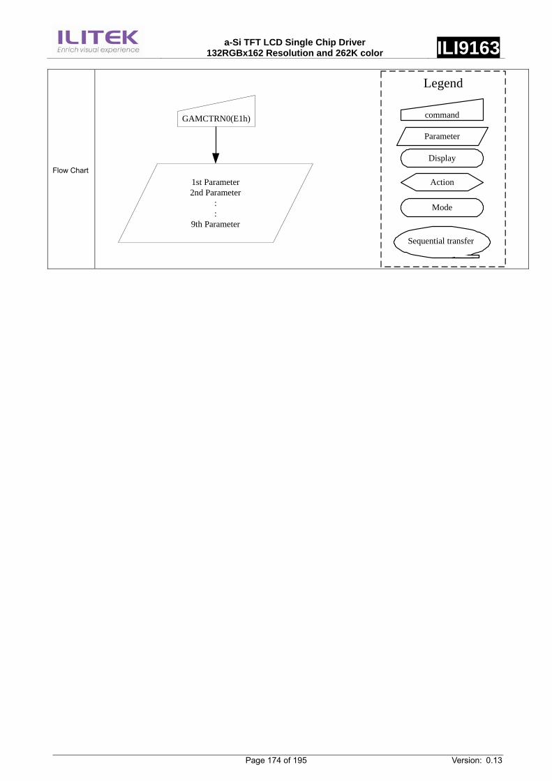
a-Si TFT LCD Single Chip Driver
132RGBx162 Resolution and 262K color ILI9163
Page 174 of 195 Version: 0.13
Flow Chart
command
Parameter
Display
Action
Mode
Legend
Sequential transfer
GAMCTRN0(E1h)
1st Parameter2nd Parameter
::
9th Parameter
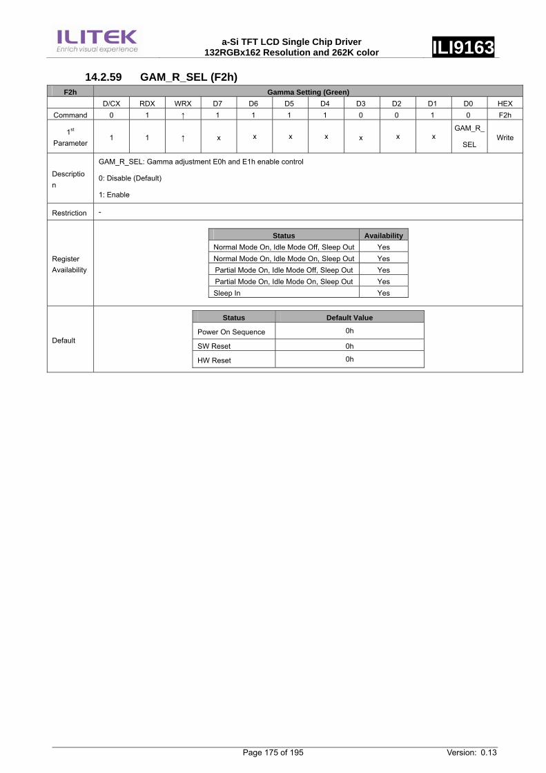
a-Si TFT LCD Single Chip Driver
132RGBx162 Resolution and 262K color ILI9163
Page 175 of 195 Version: 0.13
14.2.59 GAM_R_SEL (F2h) F2h Gamma Setting (Green)
D/CX RDX WRX D7 D6 D5 D4 D3 D2 D1 D0 HEX Command 0 1 ↑ 1 1 1 1 0 0 1 0 F2h
1st Parameter
1 1 ↑ x x x x x x x GAM_R_
SEL Write
Description
GAM_R_SEL: Gamma adjustment E0h and E1h enable control
0: Disable (Default)
1: Enable
Restriction -
Register Availability
Status Availability Normal Mode On, Idle Mode Off, Sleep Out Yes Normal Mode On, Idle Mode On, Sleep Out Yes Partial Mode On, Idle Mode Off, Sleep Out Yes Partial Mode On, Idle Mode On, Sleep Out Yes Sleep In Yes
Default
Status Default Value
Power On Sequence 0h
SW Reset 0h
HW Reset 0h

a-Si TFT LCD Single Chip Driver
132RGBx162 Resolution and 262K color ILI9163
Page 176 of 195 Version: 0.13
15. Example Connection with Panel direction and Different Resolution
15.1. Application of connect with panel direction (when GM=’011’) Case 1: (This is default case)
- 1st Pixel is at Left Top of the panle
- RGB filter order = RGB
Driver IC ( Bump down)G161
G3 S7 S390 G2
G160
1st Pixel
00h 01h 02h 7Dh 7Eh 7Fh__ __ __ __
G1
G2
G3
G4
G157
G159
G158
G160
- Direction default setting(H/W)SMX = 0SMY = 0SRGB = 0
S1 = Filter RS2 = Filter GS3 = Filter B
- Display direction control (S/W)- X- Mirror control by MX- Y- Mirror control by MY-XY- Exchange control by MV
IC (Bump down)
LCD Front side CF Glass
TFT Glass
Case 2:
- 1st Pixel is at Left Top of the panel
- RGB filter order = BGR
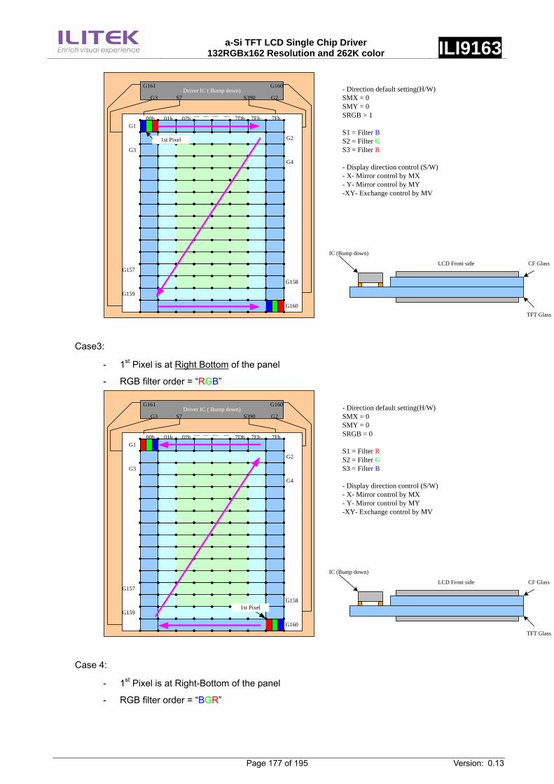
a-Si TFT LCD Single Chip Driver
132RGBx162 Resolution and 262K color ILI9163
Page 177 of 195 Version: 0.13
Driver IC ( Bump down)G161
G3 S7 S390 G2
G160
1st Pixel
00h 01h 02h 7Dh 7Eh 7Fh__ __ __ __
G1
G2
G3
G4
G157
G159
G158
G160
- Direction default setting(H/W)SMX = 0SMY = 0SRGB = 1
S1 = Filter BS2 = Filter GS3 = Filter R
- Display direction control (S/W)- X- Mirror control by MX- Y- Mirror control by MY-XY- Exchange control by MV
IC (Bump down)
LCD Front side CF Glass
TFT Glass
Case3:
- 1st Pixel is at Right Bottom of the panel
- RGB filter order = “RGB”
Driver IC ( Bump down)G161
G3 S7 S390 G2
G160
1st Pixel
00h 01h 02h 7Dh 7Eh 7Fh__ __ __ __
G1
G2
G3
G4
G157
G159
G158
G160
- Direction default setting(H/W)SMX = 0SMY = 0SRGB = 0
S1 = Filter RS2 = Filter GS3 = Filter B
- Display direction control (S/W)- X- Mirror control by MX- Y- Mirror control by MY-XY- Exchange control by MV
IC (Bump down)
LCD Front side CF Glass
TFT Glass
Case 4:
- 1st Pixel is at Right-Bottom of the panel
- RGB filter order = “BGR”
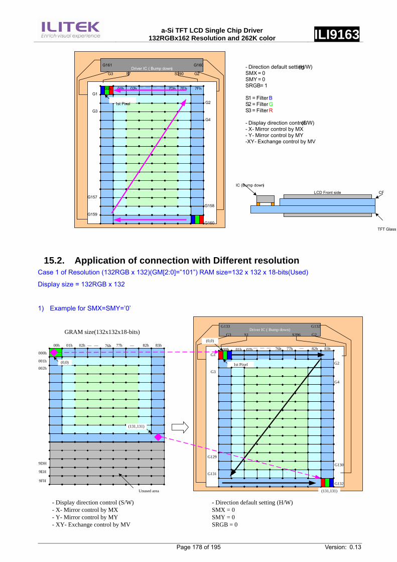
a-Si TFT LCD Single Chip Driver
132RGBx162 Resolution and 262K color ILI9163
Page 178 of 195 Version: 0.13
15.2. Application of connection with Different resolution Case 1 of Resolution (132RGB x 132)(GM[2:0]=”101”) RAM size=132 x 132 x 18-bits(Used)
Display size = 132RGB x 132
1) Example for SMX=SMY=’0’
Driver IC ( Bump down)G133
G3 S1 S396 G2
G132
00h 01h 02h 77h 82h 83h__ __ __
G1
G2
G3
G4
G129
G131
G158
(131,131)
(0,0)
(0,0)
00h 01h 02h 77h 83h__ __ 76h
Unused area
000h
001h
002h
9DH
9EH
9FH
GRAM size(132x132x18-bits)
- Display direction control (S/W)- X- Mirror control by MX- Y- Mirror control by MY- XY- Exchange control by MV
- Direction default setting (H/W)SMX = 0SMY = 0SRGB = 0
82h__
(131,131)
1st Pixel
G132
G130
G2
G4
__76h
Driver IC ( Bump down)G 161
G 3 S7 S390 G2
G160
1st Pixel
00h 01h 02h 7Dh 7Eh 7Fh__ __ __ __
G 1G2
G 3G4
G157
G159
G158
G160
- Direction default setting ( H / W ) SMX = 0SMY = 0SRGB = 1
S1 = Filter BS2 = Filter GS3 = Filter R
- Display direction control ( S/W ) - X- Mirror control by MX - Y- Mirror control by MY -XY- Exchange control by MV
IC (Bump down)
LCD Front side CF
TFT Glass
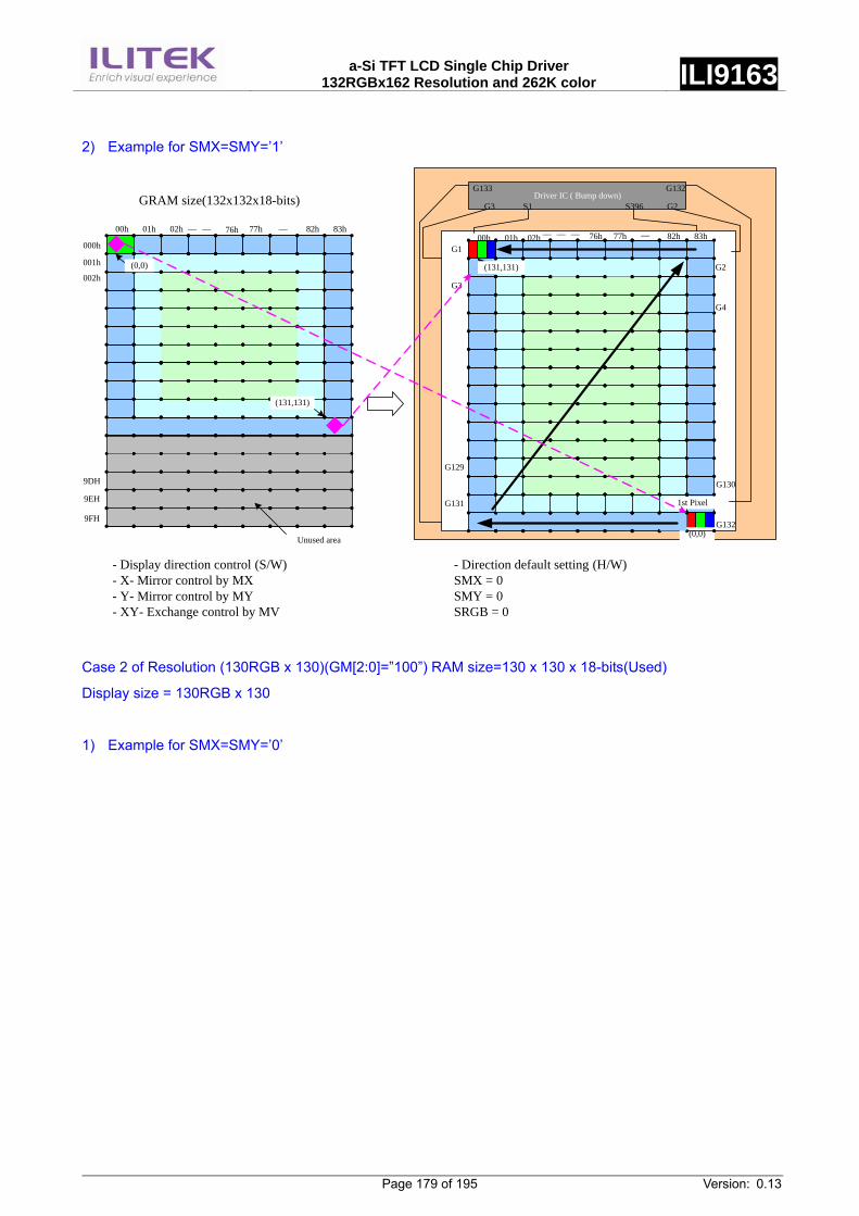
a-Si TFT LCD Single Chip Driver
132RGBx162 Resolution and 262K color ILI9163
Page 179 of 195 Version: 0.13
2) Example for SMX=SMY=’1’
Driver IC ( Bump down)G133
G3 S1 S396 G2
G132
00h 01h 02h 77h 82h 83h__ __ __
G1
G2
G3
G4
G129
G131
G158
(0,0)
(0,0)
00h 01h 02h 77h 83h__ __ 76h
Unused area
000h
001h
002h
9DH
9EH
9FH
GRAM size(132x132x18-bits)
- Display direction control (S/W)- X- Mirror control by MX- Y- Mirror control by MY- XY- Exchange control by MV
- Direction default setting (H/W)SMX = 0SMY = 0SRGB = 0
82h__
(131,131)
1st Pixel
G132
G130
G2
G4
__76h
(131,131)
Case 2 of Resolution (130RGB x 130)(GM[2:0]=”100”) RAM size=130 x 130 x 18-bits(Used)
Display size = 130RGB x 130
1) Example for SMX=SMY=’0’
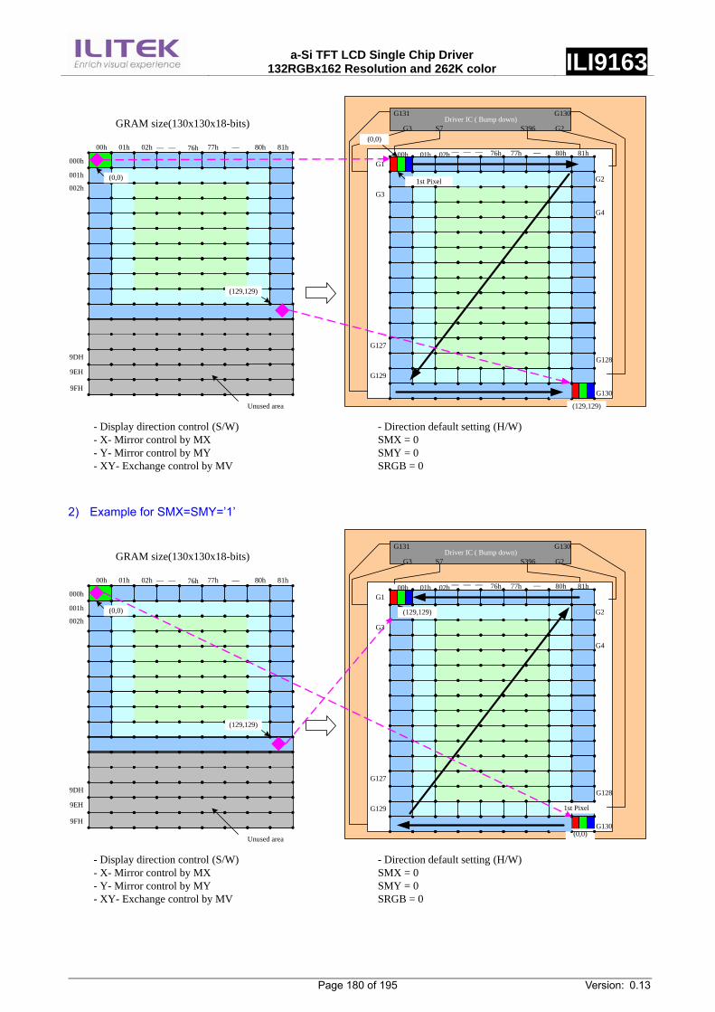
a-Si TFT LCD Single Chip Driver
132RGBx162 Resolution and 262K color ILI9163
Page 180 of 195 Version: 0.13
Driver IC ( Bump down)G131
G3 S7 S396 G2
G130
00h 01h 02h 77h 80h 81h__ __ __
G1
G2
G3
G4
G127
G129
G158
(129,129)
(0,0)
(0,0)
00h 01h 02h 77h 81h__ __ 76h
Unused area
000h
001h
002h
9DH
9EH
9FH
GRAM size(130x130x18-bits)
- Display direction control (S/W)- X- Mirror control by MX- Y- Mirror control by MY- XY- Exchange control by MV
- Direction default setting (H/W)SMX = 0SMY = 0SRGB = 0
80h__
(129,129)
1st Pixel
G130
G128
G2
G4
__76h
2) Example for SMX=SMY=’1’
Driver IC ( Bump down)G131
G3 S7 S396 G2
G130
00h 01h 02h 77h 80h 81h__ __ __
G1
G2
G3
G4
G127
G129
G158
(0,0)
(0,0)
00h 01h 02h 77h 81h__ __ 76h
Unused area
000h
001h
002h
9DH
9EH
9FH
GRAM size(130x130x18-bits)
- Display direction control (S/W)- X- Mirror control by MX- Y- Mirror control by MY- XY- Exchange control by MV
- Direction default setting (H/W)SMX = 0SMY = 0SRGB = 0
80h__
(129,129)
1st Pixel
G130
G128
G2
G4
__76h
(129,129)
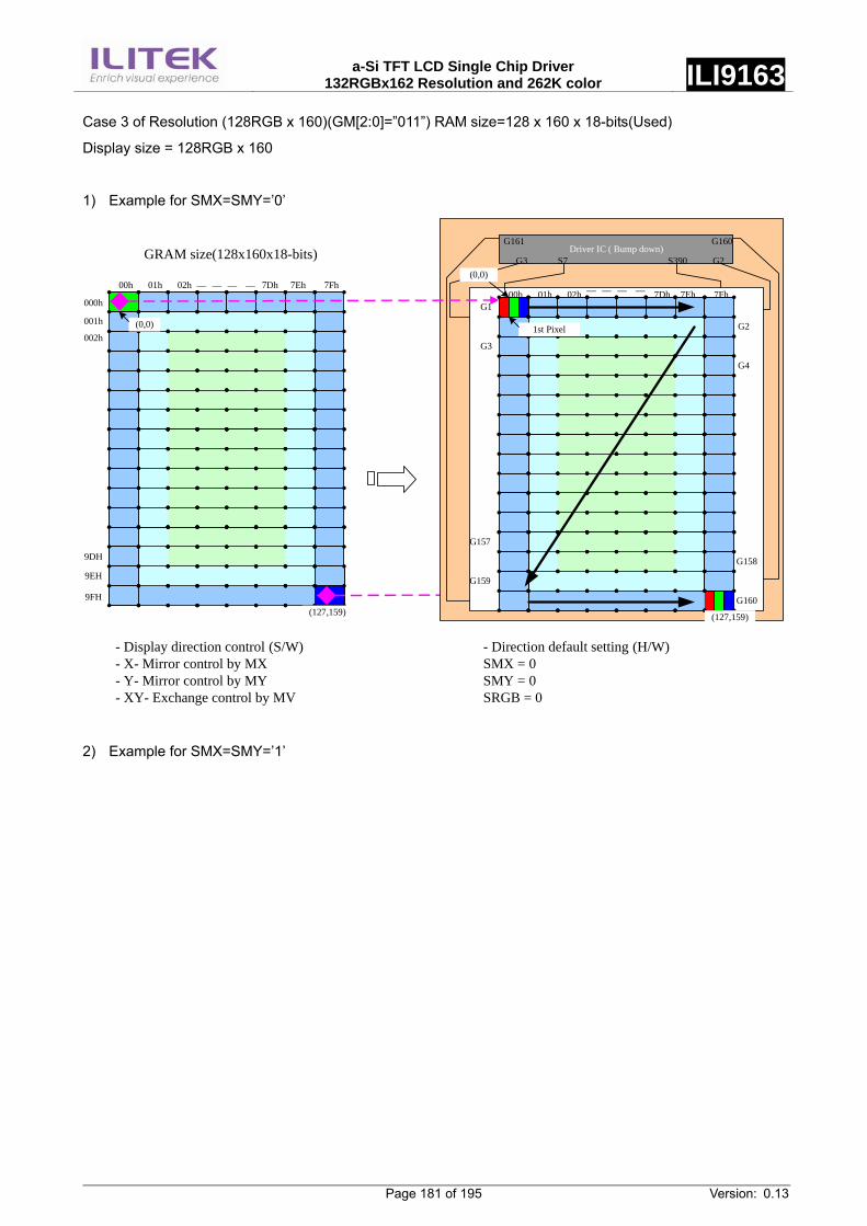
a-Si TFT LCD Single Chip Driver
132RGBx162 Resolution and 262K color ILI9163
Page 181 of 195 Version: 0.13
Case 3 of Resolution (128RGB x 160)(GM[2:0]=”011”) RAM size=128 x 160 x 18-bits(Used)
Display size = 128RGB x 160
1) Example for SMX=SMY=’0’
(0,0)
00h 01h 02h 7Dh 7Eh 7Fh__ __ __ __
(127,159)
000h
001h
002h
9DH
9EH
9FH
GRAM size(128x160x18-bits)
- Display direction control (S/W)- X- Mirror control by MX- Y- Mirror control by MY- XY- Exchange control by MV
- Direction default setting (H/W)SMX = 0SMY = 0SRGB = 0
Driver IC ( Bump down)G161
G3 S7 S390 G2
G160
1st Pixel
00h 01h 02h 7Dh 7Eh 7Fh__ __ __ __
G1
G2
G3
G4
G157
G159
G158
G160
(127,159)
(0,0)
2) Example for SMX=SMY=’1’

a-Si TFT LCD Single Chip Driver
132RGBx162 Resolution and 262K color ILI9163
Page 182 of 195 Version: 0.13
Driver IC ( Bump down)G161
G3 S7 S390 G2
G160
(127,159)
00h 01h 02h 7Dh 7Eh 7Fh__ __ __ __
G1
G2
G3
G4
G157
G159
G158
G160
(0,0)
(0,0)
00h 01h 02h 7Dh 7Eh 7Fh__ __ __ __
(127,159)
000h
001h
002h
9DH
9EH
9FH
GRAM size(128x160x18-bits)
- Display direction control (S/W)- X- Mirror control by MX- Y- Mirror control by MY- XY- Exchange control by MV
- Direction default setting (H/W)SMX = 0SMY = 0SRGB = 0
1st Pixel
Case4 of Resolution (120RGB x 160)(GM[2:0]=”010”) RAM size=120 x 160 x 18-bits(Used)
Display size = 120RGB x 160
1) Example for SMX=SMY=’0’
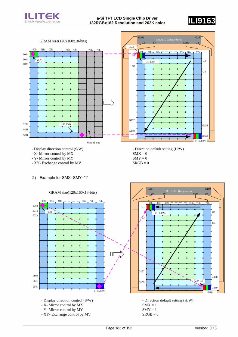
a-Si TFT LCD Single Chip Driver
132RGBx162 Resolution and 262K color ILI9163
Page 183 of 195 Version: 0.13
Driver IC ( Bump down)G161
G3 S7 S366 G2
G160
1st Pixel
00h 01h 02h 75h 76h 77h__ __ __ __
G1
G2
G3
G4
G157
G159
G158
G160
(119,159)
(0,0)
(0,0)
00h 01h 02h 7Eh 7Fh__ __ __ __
(119,159)
000h
001h
002h
9DH
9EH
9FH
GRAM size(120x160x18-bits)
- Display direction control (S/W)- X- Mirror control by MX- Y- Mirror control by MY- XY- Exchange control by MV
- Direction default setting (H/W)SMX = 0SMY = 0SRGB = 0
77h76h
Unused area
2) Example for SMX=SMY=’1’
Driver IC ( Bump down)G161
G3 S7 S366 G2
G160
(119,159)
00h 01h 02h 7Dh 7Eh 7Fh__ __ __ __
G1
G2
G3
G4
G157
G159
G158
G160
(0,0)
(0,0)
00h 01h 02h 75h 76h 77h__ __ __ __
(119,159)
000h
001h
002h
9DH
9EH
9FH
GRAM size(120x160x18-bits)
- Display direction control (S/W)- X- Mirror control by MX- Y- Mirror control by MY- XY- Exchange control by MV
- Direction default setting (H/W)SMX = 1SMY = 1SRGB = 0
1st Pixel
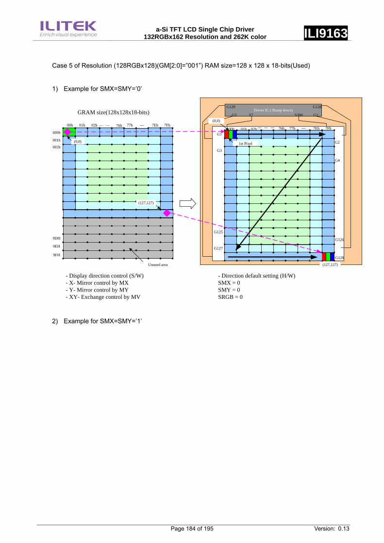
a-Si TFT LCD Single Chip Driver
132RGBx162 Resolution and 262K color ILI9163
Page 184 of 195 Version: 0.13
Case 5 of Resolution (128RGBx128)(GM[2:0]=”001”) RAM size=128 x 128 x 18-bits(Used)
1) Example for SMX=SMY=’0’
Driver IC ( Bump down)G129
G3 S7 S390 G2
G128
00h 01h 02h 77h 7Eh 7Fh__ __ __
G1
G2
G3
G4
G125
G127
G158
(127,127)
(0,0)
(0,0)
00h 01h 02h 77h 7Fh__ __ 76h
Unused area
000h
001h
002h
9DH
9EH
9FH
GRAM size(128x128x18-bits)
- Display direction control (S/W)- X- Mirror control by MX- Y- Mirror control by MY- XY- Exchange control by MV
- Direction default setting (H/W)SMX = 0SMY = 0SRGB = 0
7Eh__
(127,127)
1st Pixel
G128
G126
G2
G4
__76h
2) Example for SMX=SMY=’1’
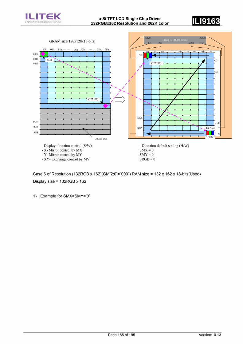
a-Si TFT LCD Single Chip Driver
132RGBx162 Resolution and 262K color ILI9163
Page 185 of 195 Version: 0.13
Driver IC ( Bump down)G129
G3 S7 S390 G2
G128
00h 01h 02h 77h 7Eh 7Fh__ __ __
G1
G2
G3
G4
G125
G127
G158
(0,0)
(0,0)
00h 01h 02h 77h 7Fh__ __ 76h
Unused area
000h
001h
002h
9DH
9EH
9FH
GRAM size(128x128x18-bits)
- Display direction control (S/W)- X- Mirror control by MX- Y- Mirror control by MY- XY- Exchange control by MV
- Direction default setting (H/W)SMX = 0SMY = 0SRGB = 0
7Eh__
(127,127)
1st Pixel
G128
G126
G2
G4
__76h
(127,127)
Case 6 of Resolution (132RGB x 162)(GM[2:0]=”000”) RAM size = 132 x 162 x 18-bits(Used)
Display size = 132RGB x 162
1) Example for SMX=SMY=’0’
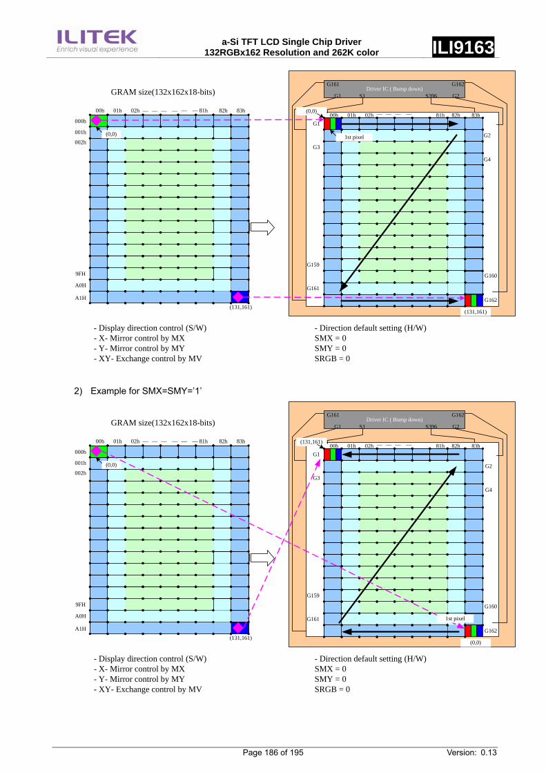
a-Si TFT LCD Single Chip Driver
132RGBx162 Resolution and 262K color ILI9163
Page 186 of 195 Version: 0.13
Driver IC ( Bump down)G161
G1 S1 S396 G2
G162
1st pixel
00h 01h 02h 81h 82h 83h__ __ __ __
G1
G2
G3
G4
G159
G161
G160
(131,161)
(0,0)
00h 01h 02h 81h__ __ __ __
(131,161)
000h
001h
002h
9FH
A0H
A1H
GRAM size(132x162x18-bits)
- Display direction control (S/W)- X- Mirror control by MX- Y- Mirror control by MY- XY- Exchange control by MV
- Direction default setting (H/W)SMX = 0SMY = 0SRGB = 0
(0,0)83h82h__ __
G162
G2
G4
2) Example for SMX=SMY=’1’
Driver IC ( Bump down)G161
G1 S1 S396 G2
G162
00h 01h 02h 81h 82h 83h__ __ __ __
G1
G2
G3
G4
G159
G161
G160
(0,0)
(0,0)
00h 01h 02h 81h__ __ __ __
(131,161)
000h
001h
002h
9FH
A0H
A1H
GRAM size(132x162x18-bits)
- Display direction control (S/W)- X- Mirror control by MX- Y- Mirror control by MY- XY- Exchange control by MV
- Direction default setting (H/W)SMX = 0SMY = 0SRGB = 0
(131,161)83h82h__ __
G162
1st pixel
G2
G4
a-Si TFT LCD Single Chip Driver
132RGBx162 Resolution and 262K color ILI9163
Page 187 of 195 Version: 0.13
16. OTP Programming Flow
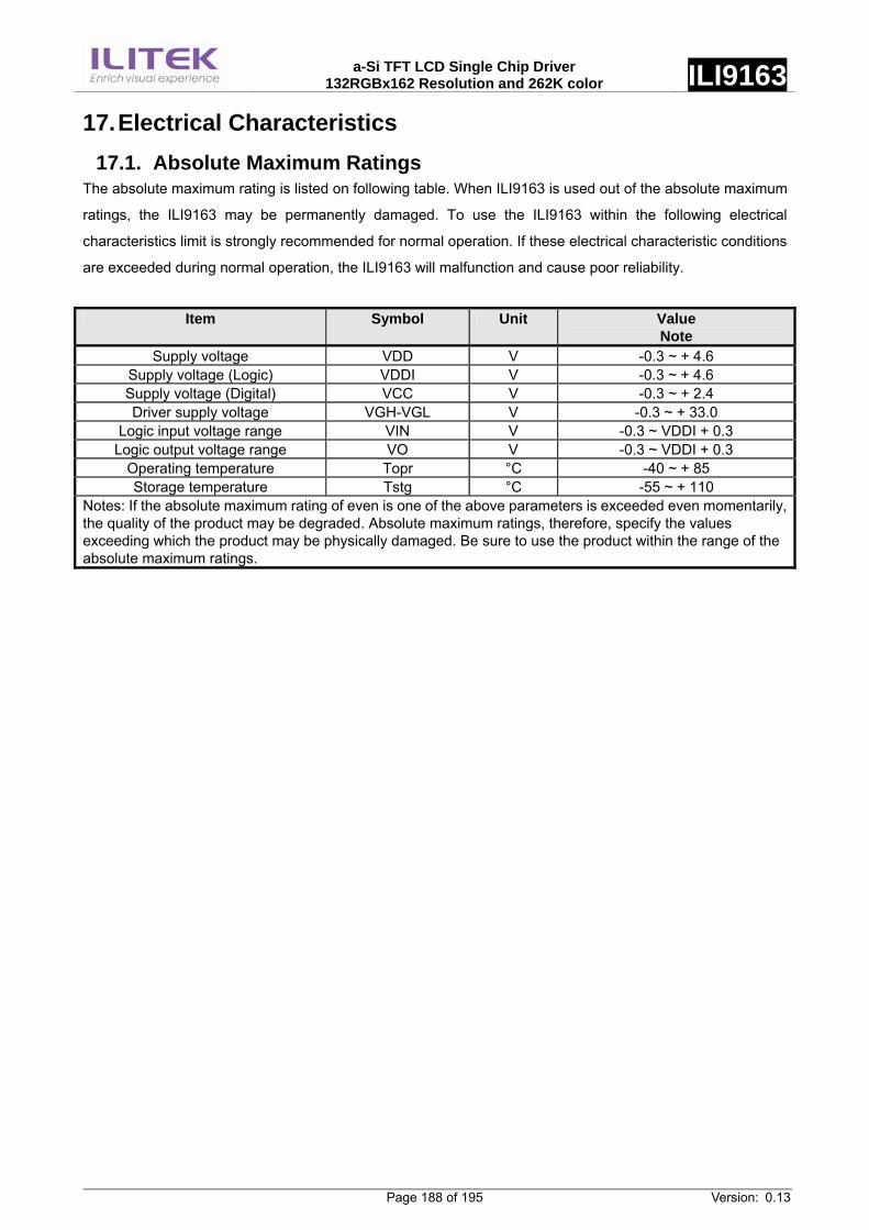
a-Si TFT LCD Single Chip Driver
132RGBx162 Resolution and 262K color ILI9163
Page 188 of 195 Version: 0.13
17. Electrical Characteristics 17.1. Absolute Maximum Ratings
The absolute maximum rating is listed on following table. When ILI9163 is used out of the absolute maximum
ratings, the ILI9163 may be permanently damaged. To use the ILI9163 within the following electrical
characteristics limit is strongly recommended for normal operation. If these electrical characteristic conditions
are exceeded during normal operation, the ILI9163 will malfunction and cause poor reliability.
Item Symbol Unit Value Note
Supply voltage VDD V -0.3 ~ + 4.6 Supply voltage (Logic) VDDI V -0.3 ~ + 4.6 Supply voltage (Digital) VCC V -0.3 ~ + 2.4 Driver supply voltage VGH-VGL V -0.3 ~ + 33.0
Logic input voltage range VIN V -0.3 ~ VDDI + 0.3 Logic output voltage range VO V -0.3 ~ VDDI + 0.3
Operating temperature Topr °C -40 ~ + 85 Storage temperature Tstg °C -55 ~ + 110
Notes: If the absolute maximum rating of even is one of the above parameters is exceeded even momentarily, the quality of the product may be degraded. Absolute maximum ratings, therefore, specify the values exceeding which the product may be physically damaged. Be sure to use the product within the range of the absolute maximum ratings.
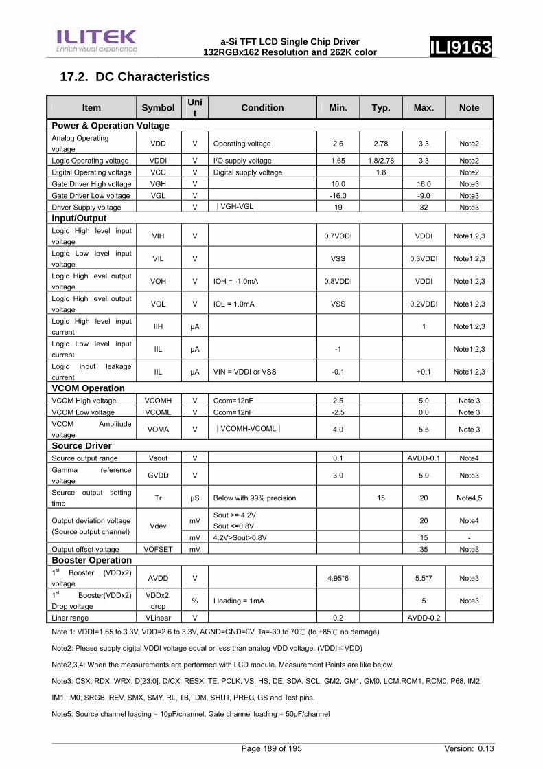
a-Si TFT LCD Single Chip Driver
132RGBx162 Resolution and 262K color ILI9163
Page 189 of 195 Version: 0.13
17.2. DC Characteristics
Item Symbol Unit Condition Min. Typ. Max. Note
Power & Operation Voltage Analog Operating voltage
VDD V Operating voltage 2.6 2.78 3.3 Note2
Logic Operating voltage VDDI V I/O supply voltage 1.65 1.8/2.78 3.3 Note2 Digital Operating voltage VCC V Digital supply voltage 1.8 Note2 Gate Driver High voltage VGH V 10.0 16.0 Note3 Gate Driver Low voltage VGL V -16.0 -9.0 Note3 Driver Supply voltage V |VGH-VGL| 19 32 Note3 Input/Output Logic High level input voltage
VIH V 0.7VDDI VDDI Note1,2,3
Logic Low level input voltage
VIL V VSS 0.3VDDI Note1,2,3
Logic High level output voltage
VOH V IOH = -1.0mA 0.8VDDI VDDI Note1,2,3
Logic High level output voltage
VOL V IOL = 1.0mA VSS 0.2VDDI Note1,2,3
Logic High level input current
IIH µA 1 Note1,2,3
Logic Low level input current
IIL µA -1 Note1,2,3
Logic input leakage current
IIL µA VIN = VDDI or VSS -0.1 +0.1 Note1,2,3
VCOM Operation VCOM High voltage VCOMH V Ccom=12nF 2.5 5.0 Note 3 VCOM Low voltage VCOML V Ccom=12nF -2.5 0.0 Note 3 VCOM Amplitude voltage
VOMA V |VCOMH-VCOML| 4.0 5.5 Note 3
Source Driver Source output range Vsout V 0.1 AVDD-0.1 Note4 Gamma reference voltage
GVDD V 3.0 5.0 Note3
Source output setting time
Tr µS Below with 99% precision 15 20 Note4,5
mV Sout >= 4.2V Sout <=0.8V
20 Note4 Output deviation voltage (Source output channel)
Vdev mV 4.2V>Sout>0.8V 15 -
Output offset voltage VOFSET mV 35 Note8 Booster Operation 1st Booster (VDDx2) voltage
AVDD V 4.95*6 5.5*7 Note3
1st Booster(VDDx2) Drop voltage
VDDx2, drop
% I loading = 1mA 5 Note3
Liner range VLinear V 0.2 AVDD-0.2
Note 1: VDDI=1.65 to 3.3V, VDD=2.6 to 3.3V, AGND=GND=0V, Ta=-30 to 70 (to +85 no damage)℃ ℃
Note2: Please supply digital VDDI voltage equal or less than analog VDD voltage. (VDDI VDD)≦
Note2,3,4: When the measurements are performed with LCD module. Measurement Points are like below.
Note3: CSX, RDX, WRX, D[23:0], D/CX, RESX, TE, PCLK, VS, HS, DE, SDA, SCL, GM2, GM1, GM0, LCM,RCM1, RCM0, P68, IM2,
IM1, IM0, SRGB, REV, SMX, SMY, RL, TB, IDM, SHUT, PREG, GS and Test pins.
Note5: Source channel loading = 10pF/channel, Gate channel loading = 50pF/channel
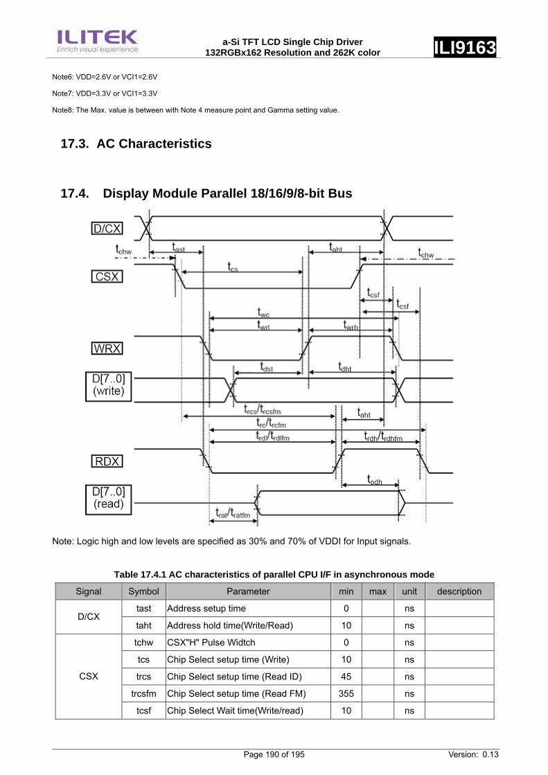
a-Si TFT LCD Single Chip Driver
132RGBx162 Resolution and 262K color ILI9163
Page 190 of 195 Version: 0.13
Note6: VDD=2.6V or VCI1=2.6V
Note7: VDD=3.3V or VCI1=3.3V
Note8: The Max. value is between with Note 4 measure point and Gamma setting value.
17.3. AC Characteristics
17.4. Display Module Parallel 18/16/9/8-bit Bus
Note: Logic high and low levels are specified as 30% and 70% of VDDI for Input signals.
Table 17.4.1 AC characteristics of parallel CPU I/F in asynchronous mode
Signal Symbol Parameter min max unit description tast Address setup time 0 ns
D/CX taht Address hold time(Write/Read) 10 ns tchw CSX"H" Pulse Widtch 0 ns tcs Chip Select setup time (Write) 10 ns trcs Chip Select setup time (Read ID) 45 ns
trcsfm Chip Select setup time (Read FM) 355 ns CSX
tcsf Chip Select Wait time(Write/read) 10 ns
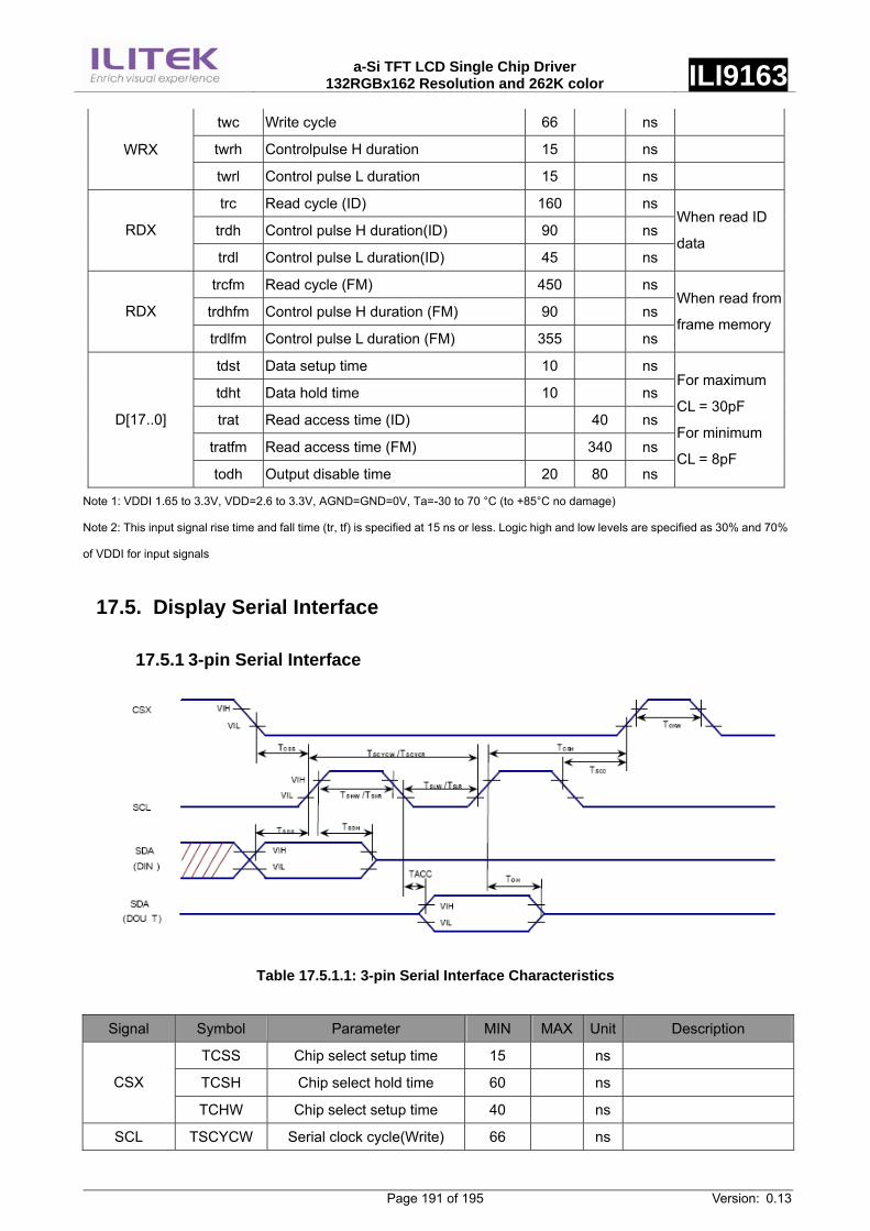
a-Si TFT LCD Single Chip Driver
132RGBx162 Resolution and 262K color ILI9163
Page 191 of 195 Version: 0.13
twc Write cycle 66 ns twrh Controlpulse H duration 15 ns WRX twrl Control pulse L duration 15 ns trc Read cycle (ID) 160 ns
trdh Control pulse H duration(ID) 90 ns RDX trdl Control pulse L duration(ID) 45 ns
When read ID
data
trcfm Read cycle (FM) 450 ns trdhfm Control pulse H duration (FM) 90 ns RDX trdlfm Control pulse L duration (FM) 355 ns
When read from
frame memory
tdst Data setup time 10 ns tdht Data hold time 10 ns trat Read access time (ID) 40 ns
tratfm Read access time (FM) 340 ns D[17..0]
todh Output disable time 20 80 ns
For maximum
CL = 30pF
For minimum
CL = 8pF
Note 1: VDDI 1.65 to 3.3V, VDD=2.6 to 3.3V, AGND=GND=0V, Ta=-30 to 70 °C (to +85°C no damage)
Note 2: This input signal rise time and fall time (tr, tf) is specified at 15 ns or less. Logic high and low levels are specified as 30% and 70%
of VDDI for input signals
17.5. Display Serial Interface
17.5.1 3-pin Serial Interface
Table 17.5.1.1: 3-pin Serial Interface Characteristics
Signal Symbol Parameter MIN MAX Unit Description
TCSS Chip select setup time 15 ns
TCSH Chip select hold time 60 ns CSX
TCHW Chip select setup time 40 ns
SCL TSCYCW Serial clock cycle(Write) 66 ns
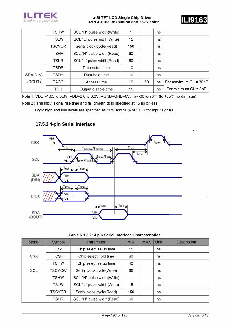
a-Si TFT LCD Single Chip Driver
132RGBx162 Resolution and 262K color ILI9163
Page 192 of 195 Version: 0.13
TSHW SCL "H" pulse width(Write) 1 ns
TSLW SCL "L" pulse width(Write) 15 ns
TSCYCR Serial clock cycle(Read) 150 ns
TSHR SCL "H" pulse width(Read) 60 ns
TSLR SCL "L" pulse width(Read) 60 ns
TSDS Data setup time 10 ns
TSDH Data hold time 10 ns
TACC Access time 10 50 ns
SDA(DIN)
(DOUT)
TOH Output disable time 15 ns
For maximum CL = 30pF
For minimum CL = 8pF
Note 1: VDDI=1.65 to 3.3V, VDD=2.6 to 3.3V, AGND=GND=0V. Ta=-30 to 70 (to +85 no damage)℃ ℃
Note 2 : The input signal rise time and fall time(tr, tf) is specified at 15 ns or less.
Logic high and low levels are specified as 10% and 90% of VDDI for Input signals.
17.5.2 4-pin Serial Interface
Table 6.1.3.2: 4 pin Serial Interface Characteristics
Signal Symbol Parameter MIN MAX Unit Description
TCSS Chip select setup time 15 ns
TCSH Chip select hold time 60 ns CSX
TCHW Chip select setup time 40 ns
TSCYCW Serial clock cycle(Write) 66 ns
TSHW SCL "H" pulse width(Write) 1 ns
TSLW SCL "L" pulse width(Write) 15 ns
TSCYCR Serial clock cycle(Read) 150 ns
SCL
TSHR SCL "H" pulse width(Read) 60 ns

a-Si TFT LCD Single Chip Driver
132RGBx162 Resolution and 262K color ILI9163
Page 193 of 195 Version: 0.13
TSLR SCL "L" pulse width(Read) 60 ns
TDCS D/CX setup time 7 ns D/CX
TDCH D/CX hold time 7 ns
TSDS Data setup time 10 ns
TSDH Data hold time 10 ns
TACC Access time 10 50 ns
SDA(DIN)
(DOUT)
TOH Output disable time 15 ns
For maximum CL = 30pF
For minimum CL = 8pF
Note 1: VDDI=1.65 to 3.3V, VDD=2.6 to 3.3V, AGND=GND=0V. Ta=-30 to 70 (to +85 no damage)℃ ℃
Note 2 : The input signal rise time and fall time(tr, tf) is specified at 15 ns or less.
Logic high and low levels are specified as 10% and 90% of VDDI for Input signals.
17.6. Reset Timing Characteristics
Reset Timing Characteristics (VCC = 1.8 ~ 3.3 V, IOVCC = 1.65 ~ 3.3 V) Item Symbol Unit Min. Typ. Max. Reset low-level width tRES ms 1 - - Reset rise time trRES µs - - 10
VIL
VIHnRESET
tREStrRES
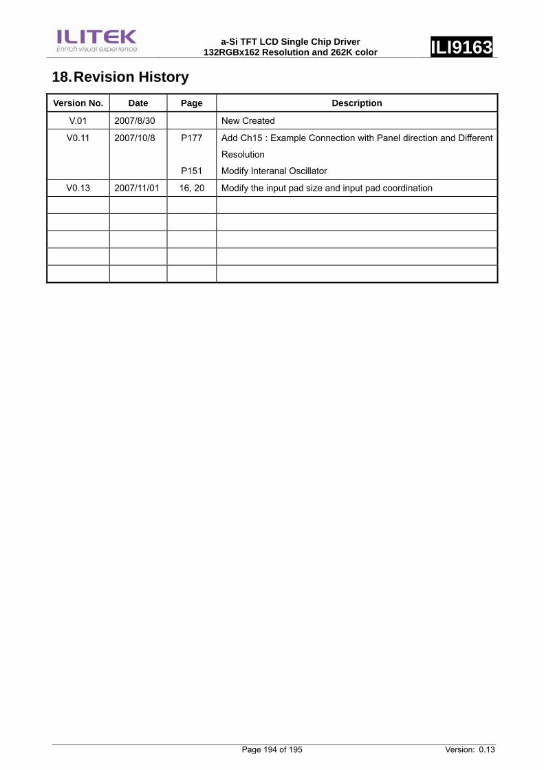
a-Si TFT LCD Single Chip Driver
132RGBx162 Resolution and 262K color ILI9163
Page 194 of 195 Version: 0.13
18. Revision History Version No. Date Page Description
V.01 2007/8/30 New Created
V0.11 2007/10/8 P177
P151
Add Ch15 : Example Connection with Panel direction and Different
Resolution
Modify Interanal Oscillator
V0.13 2007/11/01 16, 20 Modify the input pad size and input pad coordination

a-Si TFT LCD Single Chip Driver
132RGBx162 Resolution and 262K color ILI9163
Page 195 of 195 Version: 0.13
Related Documents