1/15 Integrated quantized electronics: a semiconductor quantized voltage source Authors: Frank Hohls, Armin C. Welker, Christoph Leicht, Lukas Fricke, Bernd Kaestner, Philipp Mirovsky, André Müller, Klaus Pierz, Uwe Siegner, and Hans Werner Schumacher Affiliation Physikalisch-Technische Bundesanstalt, Bundesallee 100, 38116 Braunschweig, Germany Corresponding Author: Hans Werner Schumacher E-Mail: [email protected] Phone: +49 531 592 2500 Fax: +49 531 592 69 2500 Abstract: The Josephson effect in superconductors links a quantized output voltage V out = f ·(h/2e) to the natural constants of the electron’s charge e, Planck’s constant h, and to an excitation frequency f with important applications in electrical quantum metrology. Also semiconductors are routinely applied in electrical quantum metrology making use of the quantum Hall effect. However, despite their broad range of further applications e.g. in integrated circuits, quantized voltage generation by a semiconductor device has never been obtained. Here we report a semiconductor quantized voltage source generating quantized voltages V out = f·(h/e). It is based on an integrated quantized circuit of a single electron pump operated at pumping frequency f and a quantum Hall device monolithically integrated in series. The output voltages of several μV are expected to be scalable by orders of magnitude using present technology. The device might open a new route towards the closure of the quantum metrological triangle. Furthermore it represents a universal electrical quantum reference allowing to generate quantized values of the three most relevant electrical units of voltage, current, and resistance based on fundamental constants using a single device.

Welcome message from author
This document is posted to help you gain knowledge. Please leave a comment to let me know what you think about it! Share it to your friends and learn new things together.
Transcript
1/15
Integrated quantized electronics: a semiconductor quantized voltage source
Authors: Frank Hohls, Armin C. Welker, Christoph Leicht, Lukas Fricke, Bernd Kaestner, Philipp
Mirovsky, André Müller, Klaus Pierz, Uwe Siegner, and Hans Werner Schumacher
Affiliation Physikalisch-Technische Bundesanstalt, Bundesallee 100, 38116 Braunschweig, Germany
Corresponding Author: Hans Werner Schumacher E-Mail: [email protected] Phone: +49 531 592 2500 Fax: +49 531 592 69 2500
Abstract:
The Josephson effect in superconductors links a quantized output voltage Vout = f ·(h/2e) to the
natural constants of the electron’s charge e, Planck’s constant h, and to an excitation
frequency f with important applications in electrical quantum metrology. Also semiconductors
are routinely applied in electrical quantum metrology making use of the quantum Hall effect.
However, despite their broad range of further applications e.g. in integrated circuits, quantized
voltage generation by a semiconductor device has never been obtained. Here we report a
semiconductor quantized voltage source generating quantized voltages Vout = f·(h/e). It is
based on an integrated quantized circuit of a single electron pump operated at pumping
frequency f and a quantum Hall device monolithically integrated in series. The output
voltages of several µV are expected to be scalable by orders of magnitude using present
technology. The device might open a new route towards the closure of the quantum
metrological triangle. Furthermore it represents a universal electrical quantum reference
allowing to generate quantized values of the three most relevant electrical units of voltage,
current, and resistance based on fundamental constants using a single device.
2/15
Article:
The transition from multiple interconnected electronic components to integrated
circuits revolutionized the electronics industry and enabled highly integrated devices with
new and complex functionalities [1]. With increasing integration and reduced structural
dimensions quantum size effects become more and more important and will eventually
strongly affect device operation. One prospect of these quantum size effects is the
quantization of electrical transport quantities, which involves two natural constants: the
charge of the electron e and Planck’s constant h. Making use of this quantization in quantized
electronic devices (see e.g. [2,3]) might enable new device functionalities based on their high
absolute precision and universality. Among the quantization effects occurring in
semiconductor devices are e.g. quantum-Hall resistance quantization in units of h/e2 [4], one
dimensional conductance quantization in units of e2/h [5,6], single charge quantization [7], as
well as single charge based current quantization in units of ef where f is the frequency of a
suitable AC drive voltage [8]. In superconducting Josephson junctions [9] also quantized
voltages in multiples of f·(h/2e) can be generated with important applications in electrical
quantum metrology [10]. However, in semiconductor devices such generation of quantized
voltages has not been possible up to now.
Here we report on an all-semiconductor quantized voltage source allowing the
generation of quantized voltages Vout = f·(h/e) upon application of a suitable AC drive voltage
signal with frequency f. The device is based on an integrated quantized circuit (IQC)
consisting of a non-adiabatic single-electron pump [11] and a quantum-Hall device
monolithically integrated in series. Robust operation with output voltages of several µV
corresponding to operating frequencies of a few GHz is demonstrated. The output voltage is
expected to be scalable by orders of magnitude using present technology. By using either the
functionality of the complete IQC or the functionalities of its two components it could further
3/15
serve as a universal electrical quantum reference allowing to link the three most relevant
electrical units of voltage, current and resistance to the fundamental constants e and h in a
single device.
The quantum Hall effect in two-dimensional semiconductors quantizes the relation
between the applied current I and the generated Hall voltage VH by
2
1ehIVH ν
= , (1)
where the so called filling factor ν is an integer determined by the applied magnetic field and
the carrier density of the Hall bar. Its observation and precision quantization in different
material systems like silicon [4], gallium arsenide [12], and more recently in graphene
[13,14,15] provides one of the most stringent tests of the universality of this relation.
Likewise, generation of quantized currents of amplitude
nefI = (2)
has been obtained in different metallic [16,17,18,19] and semiconducting material systems
[11,20,21,22] by periodically shuttling a number of n electrons from source to drain. Up to
now such components have generally been viewed as separate entities. However, by using
devices based on the same material system like GaAs their integration into an IQC becomes a
straightforward option to realize new device functionalities.
The IQC under investigation consists of a recently developed high current non-
adiabatic quantized charge pump [11] and a quantum Hall resistor connected in series, as
illustrated in Fig. 1(a). Both devices are fabricated from a two-dimensional electron system
based on a high mobility modulation doped GaAs/AlGaAs heterostructure (see methods).
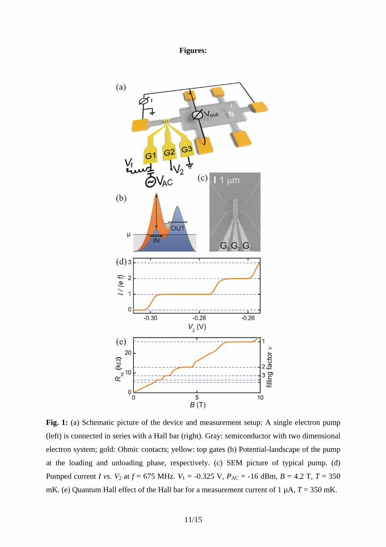
Fig. 1(b) shows a scanning electron micrograph of a typical non-adiabatic single
electron pump. The pump consists of a 900 nm wide etched constriction in the GaAs/AlGaAs
heterostructure crossed by three narrow metallic top gates G1 - G3. G3 is not essential for
4/15
pumping and is generally grounded. Negative DC voltages V1,V2 are applied to G1 and G2,
respectively, to define two electrostatic barriers and a quantum dot (QD) in between. To
induce pumping an additional sinusoidal AC gate voltage component VAC with drive
frequency f and AC power PAC is applied to G1. The principle of the resulting pumping cycle
is sketched schematically in Fig. 1(c). During the first half-cycle of the AC oscillation the left
barrier to the source lead oscillates down and becomes transparent. At the same time the
bound state of the QD drops below the chemical potential µ of the source and the QD is
loaded with electrons from the source reservoir. This phase of the pumping cycle is sketched
by the blue potential landscape in the figure. In the following phase of the pumping cycle the
height of the source barrier raises and the barrier becomes more opaque. At the same time the
QD ground state raises above µ and the QD becomes more confined. During this initialization
phase the excess electrons that were captured on the QD during the first phase of the cycle are
ejected back to source resulting in a high fidelity initialization of the dynamic QD with n
electrons [23]. In the final phase of the pumping cycle (sketched orange) the n electrons are
unloaded to the drain reservoir (right hand side) which is connected to the Hall bar before the
cycle starts over again. Under continuous AC excitation the device then acts as a quantized
current source generating a current of I = nef, where the number n of pumped charges can be
controlled by the DC gate voltages V1 and V2. A more detailed description of the physics
underlying non-adiabatic single electron pumping can be found e.g. in Refs. 11 and 23.
Fig 1(d) shows a typical operation curve of such non-adiabatic single electron pump.
The pumped current is plotted as function of V2 for fixed V1 and PAC. Two quantized current
plateaus corresponding to quantized currents of I = nef, n = 1,2 are well observed. With
increasing V2 (i.e. towards the right hand side in Fig. 1(d)) the height of the drain barrier
decreases. At the same time both the confinement of the QD and the energy of the lowest
bound QD state decrease. Hence the number n of electrons that are kept in the dot during the
5/15
initialization phase increases stepwise with V2 leading to the observed stepwise increase of I.
Note that precision measurements of the quantized currents of similar devices reported by
Giblin et al [24] have confirmed current quantization within a measurement uncertainties of
15 ppm. Note further that the optimum expected uncertainty of the current quantization can be
theoretically evaluated by fitting the measured I(V2) curves to the so-called decay cascade
model for quantum dot initialization [23]. Doing so a minimum quantized current uncertainty
of about 10-8 can be estimated from the data of Fig 1(d). It should be stressed that the current
quantization of these non-adiabatic single electron pumps is robust against variations of the
applied DC and AC gate voltages, against an applied bias voltage [25], and against applied
magnetic fields up to several tesla [26]. The latter two properties are very important for the
IQC under investigation. While the bias robustness enables on-chip integration with
components representing an ohmic load for the pumped current like in our case the Hall
device, the magnetic field robustness enables quantized current generation while the Hall
device is operated in the quantum Hall regime.
Fig. 1(e) shows the Hall resistance Rxy as function of the applied perpendicular field B.
Rxy reveals the well known Hall quantization with quantization plateaus of Rxy = ν-1·(h/e2) at
integer filling factors ν = 1,2,3,… The two most robust resistance plateaus with ν = 1 and ν =
2 are situated at magnetic fields around 8.4 T and 4.2 T, respectively, defining the optimum
operation fields for the semiconductor quantized voltage source.
When operated at these fields the IQC consists of a single charge pump delivering a
quantized current according to Eq. (2) and a serially connected quantum Hall device
converting the current into a quantized voltage according to Eq. (1). The quantized output
voltage should hence be given by
fehnVout ν
= . (3)

6/15
Vout should thus be determined by the two natural constants e and h, by the two integers n and
ν, and by the applied drive frequency f. It should thus reveal a quantization relation similar to
the Josephson relation, however, of course based on completely different physics.
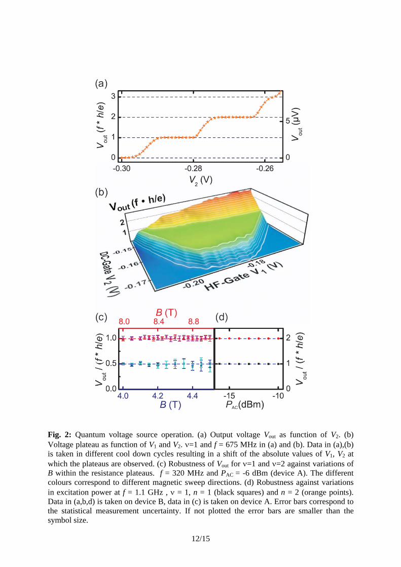
Fig. 2 shows typical measurements of quantized voltage generation of two of our IQC
devices. In (a) the device already characterized as current source in Fig. 1(d) is now operated
as voltage source at f = 675 MHz and at B = 8.4 T corresponding to filling factor ν = 1. The
output voltage Vout is plotted as function of V2. Similar to the case of the current quantization
(cf. Fig. 1(d)) now three quantized voltage plateaus corresponding to quantized voltages of
fehnVout = with n = 1,2,3 are found in the displayed data range. Quantized voltage plateaus
are also observed as function of both DC voltages V1 and V2 as shown in Fig. 2(b). Here, Vout
is displayed in a three dimensional plot as function of V1 and V2. The plot reveals a well
defined voltage plateau (green) at n = 1. The generated quantized voltage is thus robust
against variation of V1 and V2. The shape of the plateau as function of V1, V2 is again
determined by the shape of the quantized current plateau of the non-adiabatic pump [27].
A test of the robustness of the voltage quantization against variation of the other two
relevant external parameters B and VAC is displayed in Fig. 2(c) and (d), respectively. To test
the influence of a variation of B within the quantum Hall plateaus at ν = 1,2 the average Vout
within the Vout(V2) plateau and its statistical uncertainty is determined for different values of
B. In (c) Vout is plotted for f = 320 MHz in natural constants as function of magnetic fields
around ν = 1 (red dots, upper scale) and ν = 2 (blue dots, lower scale). For the whole field
range and both filling factors Vout remains well quantized within the statistical uncertainty as
indicated by the error bars (cp. methods). Next, the dependence of the voltage quantization on
the amplitude VAC and hence on the applied AC excitation power PAC will be considered. The
7/15
non-adiabatic pump requires a minimum threshold input power beyond which the generated
current remains fixed at its quantized value [27]. This robustness against variation of PAC is
well transferred to the operation of the IQC as shown in Fig. 2(d). Here, Vout is plotted as
function of PAC for excitation powers of -16 … -10 dBm. The corresponding AC voltage
amplitude VAC at G1 can be estimated to be in the range of 100 … 200 mV [27]. Parameters
for the given data are f = 1.1 GHz, ν = 1, n = 1 (black squares) and n = 2 (orange dots). Again,
no significant dependence of Vout on PAC is observed. Note that for the displayed data the
statistical uncertainty is smaller than the dot size in the graph. Hence, Vout can be considered
to be robust over a broad range of applied AC voltages.
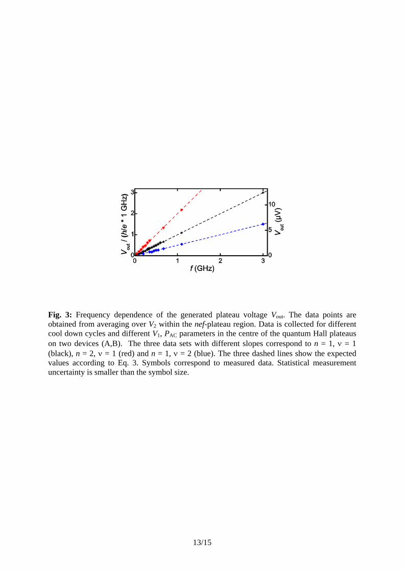
Finally the linear dependence of Vout with f as predicted by Eq. (3) is tested. Here, the
output voltage Vout inside the plateaus is plotted as function of f. Fig. 3 compiles data
measured on two devices using two different measurement setups (cp. methods) during a
number of cool down cycles. To collect the data the devices were operated inside the robust
operation region of the control parameters V1, VAC, and B. Then traces of Vout(V2) (cp. Fig.
2(a)) were taken. The average Vout in the plateau and its statistical uncertainty was derived.
Three groups of data sets are found in the plot. They can be classified according to the two
integers n and ν and hence according to the operation parameters of the two devices forming
the IQC. The black points correspond to Vout measured for n = ν = 1, the blue points
correspond to n = 1, ν = 2, and the red ones correspond to n = 2, ν = 1. All data sets are well
described by the theoretically expected curve according to Eq. 3 as indicated by the three
dashed straight lines. The data clearly evidences the expected quantization of the generated
voltage in units of h/e. To evaluate quantitatively the agreement with the theoretical
prediction we fit the slope of the measured voltages of Fig. 3 for n = ν = 1. The result of
4.1330(12) µV/GHz deviates less than 1‰ from the expected value of 4.1356 µV/GHz. Note
that this deviation is well within the systematic uncertainties given by our measurement setups
8/15
(see methods) and hence no significant deviation of Vout from the theoretically predicted value
is evident. The data presented in Fig. 3 clearly shows that the IQC is capable of generating
quantized voltages above 10 µV corresponding to operation frequencies of about 3 GHz.
Higher output voltages can be expected for optimized devices and optimized experimental
conditions. Furthermore Vout is expected to scale linear with the number of the integrated
devices of the IQC. For example the pumped current could be increased by operation of a
number of NP single-electron pumps in parallel [28, 29, 30] thereby also scaling up the output
voltage by NP. Likewise, instead of a single Hall device a serial array of NH quantum Hall
devices could be used [31] resulting in an accordingly scaled output voltage. Combining both
concepts and employing values for the available technology of NP ~ 10 [28,30] and of NH ~
100 [31] scaled up quantized output voltages of the order of tens of millivolt seem to be
realistic.
The above data illustrates that our semiconductor IQCs indeed fulfills clearly the new
semiconductor device functionality of robust quantized voltage generation. The IQC thus
links the output voltage to the two fundamental natural constants h and e with high precision
and takes advantage of their universality. We anticipate the three main features of robustness,
universality, and precision to be the major new elements in the functionality of future IQCs,
reflected in the discrete dependence of the electrical output quantity on the input. The
universality of this IQC device concept should in principle allow for its transfer to different
material systems like silicon [21,4] or even graphene [13-15] provided a suitable graphene
based quantized charge pump can be realized. One natural area of application of the given
IQC is the field of electrical quantum metrology, which aims at defining the units of physical
quantities using true invariants of nature [32]. Here the presented IQC might allow for an
alternative approach to the closure of the quantum metrological triangle [33] by direct high
precision comparison of the (scaled up) output voltage of a semiconductor quantized voltage

9/15
source to the output voltage of a Josephson based quantum voltage standard [10]. Furthermore
it can be viewed as a universal reference for electrical quantum metrology as it allows the
generation of quantized values of the three most relevant electrical units volt, ampere, and
ohm based on the fundamental constants e and h using a single device.
Acknowledgement
This work has been supported by the DFG, by EURAMET joint research project with
European Community’s Seventh Framework Programme, ERANET Plus under Grant
Agreement No. 217257, and by the Centre for Quantum Engineering and Space Time research
QUEST. C.L. has been supported by International Graduate School of Metrology,
Braunschweig.
Authors contributions
C.L., B.K., P.M., and K.P. contributed to sample fabrication. A.C.W., C.L., F.H., L.F. and
B.K. performed the experiments. F.H., A.C.W., C.L., L.F., A.M., B.K., U.S. and H.W.S.
contributed to the analysis and discussion of the experiments. F.H., A.C.W., C.L. B.K., U.S.
and H.W.S. contributed to writing the manuscript, and H.W.S. initiated and supervised the
research.
Methods:
Devices are fabricated from a GaAs/AlGaAs based modulation doped heterostructure
containing a two-dimensional electron system situated 95 nm below the surface with carrier
concentration Ne = 2.1×10¹⁵ m-2 and electron mobility of 97 m2/Vs at 4.2 K. The conducting
semiconductor channel of the pump and the Hall bar are defined simultaneously by electron-
beam lithography and wet-chemical etching. Ohmic contacts are defined by alloyed AuGeNi.
TiAu op gates are defined by electron-beam lithography and lift off. The gates have a width of
100 nm and 250 nm centre spacing. Transport measurements were done in a ³He cryostat at
10/15
base temperature of T = 350 mK. Perpendicular magnetic fields up to B = 15 T were applied
by a superconducting coil. Two devices with identical layout were measured using two
different measurement setups. To suppress drifting offset voltages of the measurement circuits
differential measurements were carried out by comparing the output signal in the region of a
pumped current and in the region of quenched pumping of the single electron pump.
The voltage generated by device A was measured using a calibrated HP 34420 nano
voltmeter. Here the drifting offset voltage was determined before each gate voltage variation
for quenched pump action at sufficiently negative gate voltage V2 and subtracted from the
measured curves. The quantized Vout were determined by averaging multiple values on the flat
part of the plateau, with the uncertainty derived from the variance of the measured voltage.
Device B was measured in a switched current setup. Here V2 was switched multiple times
between a sufficiently negative gate voltage for quenched pump action (OFF) and the chosen
working point (ON). After each switching the voltage was amplified by a Femto DLPVA
voltage amplifier with 1000 (±1%) fold gain and 1 GΩ input impedance and measured by an
analog-digital converter. The difference between ON and OFF pumping state for each
switching is averaged over a total of 200 to 800 switching actions with 5 to 12 gate voltage
changes per second. This procedure allows for long averaging of the generated voltage
without suffering from strong 1/f noise and drifts. The typical remaining statistical uncertainty
due to noise is < 0.005 µV. The dominating error source in the measurement of device B is
the systematic gain uncertainty of the voltage amplifier, specified with 1%. The linear least
square fit of the frequency dependence of Fig. 3 was performed for fixed zero offset and with
data weighting by the statistical uncertainty.
11/15
Figures:
Fig. 1: (a) Schematic picture of the device and measurement setup: A single electron pump
(left) is connected in series with a Hall bar (right). Gray: semiconductor with two dimensional
electron system; gold: Ohmic contacts; yellow: top gates (b) Potential-landscape of the pump
at the loading and unloading phase, respectively. (c) SEM picture of typical pump. (d)
Pumped current I vs. V2 at f = 675 MHz. V1 = -0.325 V, PAC = -16 dBm, B = 4.2 T, T = 350
mK. (e) Quantum Hall effect of the Hall bar for a measurement current of 1 µA, T = 350 mK.
12/15
Fig. 2: Quantum voltage source operation. (a) Output voltage Vout as function of V2. (b) Voltage plateau as function of V1 and V2. ν=1 and f = 675 MHz in (a) and (b). Data in (a),(b) is taken in different cool down cycles resulting in a shift of the absolute values of V1, V2 at which the plateaus are observed. (c) Robustness of Vout for ν=1 and ν=2 against variations of B within the resistance plateaus. f = 320 MHz and PAC = -6 dBm (device A). The different colours correspond to different magnetic sweep directions. (d) Robustness against variations in excitation power at f = 1.1 GHz , ν = 1, n = 1 (black squares) and n = 2 (orange points). Data in (a,b,d) is taken on device B, data in (c) is taken on device A. Error bars correspond to the statistical measurement uncertainty. If not plotted the error bars are smaller than the symbol size.
13/15
Fig. 3: Frequency dependence of the generated plateau voltage Vout. The data points are obtained from averaging over V2 within the nef-plateau region. Data is collected for different cool down cycles and different V1, PAC parameters in the centre of the quantum Hall plateaus on two devices (A,B). The three data sets with different slopes correspond to n = 1, ν = 1 (black), n = 2, ν = 1 (red) and n = 1, ν = 2 (blue). The three dashed lines show the expected values according to Eq. 3. Symbols correspond to measured data. Statistical measurement uncertainty is smaller than the symbol size.
14/15
References: [1] Kilby, J. S. Turning potential into realites: The invention of the integrated circuit.
Nobel Lectures 474 – 485 (2000). [2] Tsukagoshi, K., Alphenaar, B. W. & Nakazato, K. Operation of logic function in a
Coulomb blockade device. Appl. Phys. Lett. 73, 2515 – 2517 (1998). [3] Yumoto, M., Kasai, S. & Hasegawa, H. Novel quantum wire branch-switches for
binary decision diagram logic architecture: utilizing schottky wrap-gate control of GaAs/AlGaAs nanowires. Jpn. J. Appl. Phys. 41, 2671 – 2674 (2002).
[4] Klitzing, K. v., Dorda, G. & Pepper, M. New method for high-accuracy determination of the fine-structure constant based on quantized Hall resistance. Phys. Rev. Lett. 45, 494 – 497 (1980).
[5] van Wees, B. J. et al. Quantized conductance of point contacts in a two-dimensional electron gas. Phys. Rev. Lett. 60, 848 – 850 (1988).
[6] Wharam, D. A. et al. One-dimensional transport and the quantisation of the ballistic resistance. J. Phys. C: Solid State Phys. 21, L209 – L214 (1988).
[7] For a review, see Kastner, M. A. The single-electron transistor. Rev. Mod. Phys. 64, 849 – 858 (1992).
[8] See e.g. Likharev, K. Single-electron devices and their applications. Proc. IEEE 87, 606 –632 (1999).
[9] Josephson, B. D. Possible new effects in superconductive tunnelling. Physics Letters 1, 251 – 253 (1962)).
[10] Hamilton, C., Kautz, R., Steiner, R. & Lloyd, F. A practical Josephson voltage standard at 1 V. Electron Device Lett., IEEE 6, 623 – 625 (1985).
[11] Kaestner, B. et al. Single-parameter nonadiabatic quantized charge pumping. Phys. Rev. B 77, 153301 (2008).
[12] Delahaye, F., Witt, T. J., Pesel, E., Schumacher, B. & Warnecke, P. Comparison of quantum Hall effect resistance standards of the PTB and the BIPM. Metrologia 34, 211 –214 (1997).
[13] Novoselov, K. S. et al. Two-dimensional gas of massless Dirac fermions in graphene. Nature 438, 197 – 200 (2005).
[14] Zhang, Y., Tan, Y.-W., Stormer, H. L. & Kim, P. Experimental observation of the quantum Hall effect and Berry’s phase in graphene. Nature 438, 201 – 204 (2005).
[15] Tzalenchuk, A. et al. Towards a quantum resistance standard based on epitaxial graphene. Nature Nanotech. 5, 186 – 189 (2010).
[16] Devoret, M. H., Esteve, D. & Urbina, C. Single-electron transfer in metallic nanostructures. Nature 360, 547 – 553 (1992).
[17] Keller, M. W., Eichenberger, A. L., Martinis, J. M. & Zimmerman, N. M. A capacitance standard based on counting electrons. Science 285, 1706 – 1709 (1999).
[18] Pekola, J. P. et al. Hybrid single-electron transistor as a source of quantized electric current. Nature Phys. 4, 120 – 124 (2008).
[19] Koenig, D.R., Weig, E.M., Kotthaus, J.P. Ultrasonically driven nanomechanical single-electron shuttle. Nature Nanotechnology 3, 482 - 485 (2008).
[20] Kouwenhoven, L. P., Johnson, A. T., van der Vaart, N. C., Harmans, C. J. P. M. & Foxon, C. T. Quantized current in a quantum-dot turnstile using oscillating tunnel barriers. Phys. Rev. Lett. 67, 1626 – 1629 (1991).
[21] Fujiwara, A., Nishiguchi, K. & Ono, Y. Nanoampere charge pump by single-electron ratchet using silicon nanowire metal-oxide-semiconductor field-effect transistor. Appl. Phys. Lett. 92, 042102 (2008).
15/15
[22] Nevou L. et al. Current quantization in an optically driven electron pump based on
self-assembled quantum dots. Nature Physics. doi:10.1038/nphys1918 [23] Kashcheyevs, V. & Kaestner, B. Universal decay cascade model for dynamic quantum
dot initialization. Phys. Rev. Lett. 104, 186805 (2010). [24] S P Giblin, S J Wright, J D Fletcher, M Kataoka, M Pepper, T J B M Janssen, D A
Ritchie, C A Nicoll, D Anderson, and G A C Jones, An accurate high-speed single-electron quantum dot pump, New J. Phys. 12 073013 (2010).
[25] Giblin, S. P. et al. An accurate high-speed single-electron quantum dot pump. New J. Phys. 12, 073013 (2010).
[26] Kaestner, B. et al. Single-parameter quantized charge pumping in high magnetic fields. Appl. Phys. Lett. 94, 012106 (2009).
[27] Kaestner, B. et al. Robust single-parameter quantized charge pumping. Appl. Phys. Lett. 92, 192106 (2008).
[28] Mirovsky, P. et al. Synchronized single electron emission from dynamical quantum dots. Appl. Phys. Lett. 97, 252104 (2010).
[29] Wright, S. J. et al. Parallel quantized charge pumping. Phys. Rev. B 80, 113303 (2009).
[30] Maisi, V. F., Pashkin, Y. A., Kafanov, S., Tsai, J.-S. & Pekola, J. P. Parallel pumping of electrons. New J. Phys. 11, 113057 (2009).
[31] Poirier, W, Bounouh, A., Piquemal, F. and André, J. P. New generation of QHARS: discussion about the technical criteria for quantization. Metrologia, 41, 285-294 (2004).
[32] Mills, I. M., Mohr, P. J., Quinn, T. J., Taylor, B. N. & Williams, E. R. Redefinition of the kilogram, ampere, kelvin and mole: a proposed approach to implementing CIPM recommendation 1 (CI-2005). Metrologia 43, 227 (2006).
[33] Piquemal, F. et al. Fundamental electrical standards and the quantum metrological triangle. Comptes Rendus Physique 5, 857 – 879 (2004).
Related Documents

![SPIN CURRENTS IN SEMICONDUCTOR NANOSTRUCTURES: A ...bnikolic/PDF/spin_currents_oup.pdf · arXiv:0907.4122v1 [cond-mat.mes-hall] 23 Jul 2009 SPIN CURRENTS IN SEMICONDUCTOR NANOSTRUCTURES:](https://static.cupdf.com/doc/110x72/5f336dbb72f2ec2b812bb7bc/spin-currents-in-semiconductor-nanostructures-a-bnikolicpdfspincurrentsouppdf.jpg)


![arXiv:0807.0339v4 [math.RT] 5 May 2009 · 2018. 10. 22. · arXiv:0807.0339v4 [math.RT] 5 May 2009 HARISH-CHANDRA BIMODULES FOR QUANTIZED SLODOWY SLICES VICTOR GINZBURG To the memory](https://static.cupdf.com/doc/110x72/60ca8afee02cfd63577eaaa3/arxiv08070339v4-mathrt-5-may-2009-2018-10-22-arxiv08070339v4-mathrt.jpg)


![arXiv:1012.0561v3 [cond-mat.mes-hall] 27 Sep 2011 · arXiv:1012.0561v3 [cond-mat.mes-hall] 27 Sep 2011 Controlling non-Abelian statistics of Majorana fermions in semiconductor nanowires](https://static.cupdf.com/doc/110x72/5f7cf09f62c7fb4da0444a23/arxiv10120561v3-cond-matmes-hall-27-sep-2011-arxiv10120561v3-cond-matmes-hall.jpg)
![arxiv.org · arXiv:1912.08401v3 [math.QA] 20 Jun 2020 AFFINE OPEN COVERING OF THE QUANTIZED FLAG MANIFOLDS AT ROOTS OF UNITY TOSHIYUKI TANISAKI Abstract. We …](https://static.cupdf.com/doc/110x72/5fdd96735b57fb6a1253474e/arxivorg-arxiv191208401v3-mathqa-20-jun-2020-affine-open-covering-of-the-quantized.jpg)