792 IEEE JOURNAL OF SOLID-STATE CIRCUITS, VOL. 41, NO. 4, APRIL 2006 A Self-Tuning DVS Processor Using Delay-Error Detection and Correction Shidhartha Das, Student Member, IEEE, David Roberts, Student Member, IEEE, Seokwoo Lee, Sanjay Pant, David Blaauw, Member, IEEE, Todd Austin, Krisztián Flautner, Member, IEEE, and Trevor Mudge, Fellow, IEEE Abstract—In this paper, we present a dynamic voltage scaling (DVS) technique called Razor which incorporates an in situ error detection and correction mechanism to recover from timing errors. We also present the implementation details and silicon measurements results of a 64-bit processor fabricated in 0.18- m technology that uses Razor for supply voltage control. Traditional DVS techniques require significant voltage safety margins to guar- antee computational correctness at the worst case combination of process, voltage and temperature conditions, leading to a loss in energy efficiency. In Razor-based DVS, however, the supply voltage is automatically reduced to the point of first failure using the error detection and correction mechanism, thereby eliminating safety margins while still ensuring correct operation. In addition, the supply voltage can be intentionally scaled below the point of first failure of the processor to achieve an optimal tradeoff between energy savings from further voltage reduction and energy overhead from increased error detection and correction activity. We tested and measured savings due to Razor DVS for 33 different dies and obtained an average energy savings of 50% over worst case operating conditions by scaling supply voltage to achieve a 0.1% targeted error rate, at a fixed frequency of 120 MHz. Index Terms—Dynamic voltage scaling (DVS), error detection and correction, self-tuning processor, voltage safety margins. I. INTRODUCTION T HE tremendous boost in microprocessor performance enabled by technology scaling has come at the price of ever increasing power consumption. Power budgets are even more stringent for battery-operated embedded processors which handle a broad spectrum of applications with diverse energy and performance requirements [7], [14]. Dynamic voltage scaling (DVS) is a widely used technique to reduce the overall energy consumption of a processor, especially under wide workload variations. In a DVS system, the supply voltage and operating frequency are dynamically adjusted according to application demands. Due to the quadratic dependence of energy with supply voltage [12], significant energy savings are achievable with DVS. A critical issue for a DVS-enabled processor is determining the safe operating voltage under which energy savings are max- imized while guaranteeing correct operation under all condi- tions. Traditional techniques [2]–[6] described in literature use Manuscript received September 5, 2005; revised December 19, 2005. S. Das, D. Roberts, S. Lee, S. Pant, D. Blaauw, T. Austin, and T. Mudge are with the University of Michigan, Ann Arbor, MI, USA, 48109 USA (e-mail: [email protected]). K. Flautner is with ARM Ltd., Cambridge CB1 9NJ, U.K. Digital Object Identifier 10.1109/JSSC.2006.870912 a delay chain to determine the minimum voltage necessary for error-free operation at a particular frequency. The delay chain replicates the worst case critical path of the chip with addi- tional latency margins. Design time characterization of the crit- ical path determines the margins that need to be added in order to ensure that the replica delay path is guaranteed to fail be- fore the core does even in the presence of a worst case com- bination of inter- and intra-die process variations, temperature hot spots, and supply voltage uncertainties. The supply voltage is then lowered to the point where the delay chain just fails to meet timing. As silicon predictability reduces with technology scaling, the safety margins are likely to increase [13]. This leads to overly conservative operation given the extremely rare occur- rence of worst case conditions [1]. Significantly greater energy savings can be achieved with DVS by scaling the supply voltage below the “always correct” voltage level dictated by safety mar- gins and using an efficient mechanism to recover from rare worst case errors. We proposed a novel voltage management technique for DVS processors, called Razor [1], which uses a delay-error tolerant flip-flop on critical paths to scale the supply voltage to the point of first failure for a given frequency. This allows voltage margins to be eliminated, resulting in significant energy savings. In ad- dition, Razor allows the supply voltage to be scaled even lower than the first failure point into the subcritical region, deliberately tolerating a targeted error rate, thereby providing additional en- ergy savings. The operational principle of Razor is illustrated in Fig. 1 which shows the qualitative relationship between the supply voltage, energy consumption and pipeline throughput of a Razor-enabled processor. The point of first failure of the processor and the minimum allowable voltage of tradi- tional DVS techniques are also labeled in the figure. is much higher than under typical conditions, since safety margins need to be included to accommodate for worst case operating conditions. Razor relies on in situ error detection and correction capability to operate at , rather than at . The total energy of the processor is the sum of the energy required to perform standard processor operations and the energy consumed in recovery from timing er- rors . Of course, implementing Razor incurs power overhead due to which the nominal processor energy without Razor technology is slightly less than . This over- head is attributed to the use of delay-error tolerant flip-flops on the critical paths and the additional recovery logic required for Razor. However, since the extra circuitry is deployed only for those flip-flops which have critical paths terminating in them, the power overhead due to Razor is fairly minimal. In the 0018-9200/$20.00 © 2006 IEEE

Welcome message from author
This document is posted to help you gain knowledge. Please leave a comment to let me know what you think about it! Share it to your friends and learn new things together.
Transcript
792 IEEE JOURNAL OF SOLID-STATE CIRCUITS, VOL. 41, NO. 4, APRIL 2006
A Self-Tuning DVS Processor Using Delay-ErrorDetection and Correction
Shidhartha Das, Student Member, IEEE, David Roberts, Student Member, IEEE, Seokwoo Lee, Sanjay Pant,David Blaauw, Member, IEEE, Todd Austin, Krisztián Flautner, Member, IEEE, and Trevor Mudge, Fellow, IEEE
Abstract—In this paper, we present a dynamic voltage scaling(DVS) technique called Razor which incorporates an in situ errordetection and correction mechanism to recover from timingerrors. We also present the implementation details and siliconmeasurements results of a 64-bit processor fabricated in 0.18- mtechnology that uses Razor for supply voltage control. TraditionalDVS techniques require significant voltage safety margins to guar-antee computational correctness at the worst case combinationof process, voltage and temperature conditions, leading to a lossin energy efficiency. In Razor-based DVS, however, the supplyvoltage is automatically reduced to the point of first failure usingthe error detection and correction mechanism, thereby eliminatingsafety margins while still ensuring correct operation. In addition,the supply voltage can be intentionally scaled below the pointof first failure of the processor to achieve an optimal tradeoffbetween energy savings from further voltage reduction and energyoverhead from increased error detection and correction activity.We tested and measured savings due to Razor DVS for 33 differentdies and obtained an average energy savings of 50% over worstcase operating conditions by scaling supply voltage to achieve a0.1% targeted error rate, at a fixed frequency of 120 MHz.
Index Terms—Dynamic voltage scaling (DVS), error detectionand correction, self-tuning processor, voltage safety margins.
I. INTRODUCTION
THE tremendous boost in microprocessor performanceenabled by technology scaling has come at the price
of ever increasing power consumption. Power budgets areeven more stringent for battery-operated embedded processorswhich handle a broad spectrum of applications with diverseenergy and performance requirements [7], [14]. Dynamicvoltage scaling (DVS) is a widely used technique to reduce theoverall energy consumption of a processor, especially underwide workload variations. In a DVS system, the supply voltageand operating frequency are dynamically adjusted accordingto application demands. Due to the quadratic dependence ofenergy with supply voltage [12], significant energy savings areachievable with DVS.
A critical issue for a DVS-enabled processor is determiningthe safe operating voltage under which energy savings are max-imized while guaranteeing correct operation under all condi-tions. Traditional techniques [2]–[6] described in literature use
Manuscript received September 5, 2005; revised December 19, 2005.S. Das, D. Roberts, S. Lee, S. Pant, D. Blaauw, T. Austin, and T. Mudge are
with the University of Michigan, Ann Arbor, MI, USA, 48109 USA (e-mail:[email protected]).
K. Flautner is with ARM Ltd., Cambridge CB1 9NJ, U.K.Digital Object Identifier 10.1109/JSSC.2006.870912
a delay chain to determine the minimum voltage necessary forerror-free operation at a particular frequency. The delay chainreplicates the worst case critical path of the chip with addi-tional latency margins. Design time characterization of the crit-ical path determines the margins that need to be added in orderto ensure that the replica delay path is guaranteed to fail be-fore the core does even in the presence of a worst case com-bination of inter- and intra-die process variations, temperaturehot spots, and supply voltage uncertainties. The supply voltageis then lowered to the point where the delay chain just fails tomeet timing. As silicon predictability reduces with technologyscaling, the safety margins are likely to increase [13]. This leadsto overly conservative operation given the extremely rare occur-rence of worst case conditions [1]. Significantly greater energysavings can be achieved with DVS by scaling the supply voltagebelow the “always correct” voltage level dictated by safety mar-gins and using an efficient mechanism to recover from rare worstcase errors.
We proposed a novel voltage management technique for DVSprocessors, called Razor [1], which uses a delay-error tolerantflip-flop on critical paths to scale the supply voltage to the pointof first failure for a given frequency. This allows voltage marginsto be eliminated, resulting in significant energy savings. In ad-dition, Razor allows the supply voltage to be scaled even lowerthan the first failure point into the subcritical region, deliberatelytolerating a targeted error rate, thereby providing additional en-ergy savings.
The operational principle of Razor is illustrated in Fig. 1which shows the qualitative relationship between the supplyvoltage, energy consumption and pipeline throughput of aRazor-enabled processor. The point of first failure of theprocessor and the minimum allowable voltage of tradi-tional DVS techniques are also labeled in the figure.
is much higher than under typical conditions,since safety margins need to be included to accommodate forworst case operating conditions. Razor relies on in situ errordetection and correction capability to operate at , rather thanat . The total energy of the processor is the sumof the energy required to perform standard processor operations
and the energy consumed in recovery from timing er-rors . Of course, implementing Razor incurs poweroverhead due to which the nominal processor energywithout Razor technology is slightly less than . This over-head is attributed to the use of delay-error tolerant flip-flopson the critical paths and the additional recovery logic requiredfor Razor. However, since the extra circuitry is deployed onlyfor those flip-flops which have critical paths terminating inthem, the power overhead due to Razor is fairly minimal. In the
0018-9200/$20.00 © 2006 IEEE

DAS et al.: A SELF-TUNING DVS PROCESSOR USING DELAY-ERROR DETECTION AND CORRECTION 793
Fig. 1. Qualitative relationship between supply voltage, energy, and IPC.
processor that we present in this paper, only 7.4% of the totalflip-flops were critical and needed Razor recovery protection.The net power overhead due to Razor was less than 3% of thenominal chip power.
As the supply voltage is scaled, the processor energyreduces quadratically with voltage. However, as voltage isscaled below the first failure point , a significant numberof paths fail to meet timing. Hence, the error rate and therecovery energy increase exponentially. The pro-cessor throughput also reduces due to the increasing error ratebecause the processor now requires more cycles to completethe instructions. The total processor energy shows anoptimal point where the rate of change of andoffset each other. Thus, in the context of Razor, a timing erroris not a catastrophic failure but a tradeoff between the quadraticenergy savings due to voltage scaling versus the overhead ofrecovery due to errors.
In this paper, we present the first silicon implementation ofa Razor design [11]. We discuss the circuit structures used inthis new implementation and present silicon measurements for33 tested dies. The 64-bit processor implements a subset of theAlpha instruction set and was fabricated with MOSIS [10] in anindustrial 0.18- m technology. Voltage control is based on theobserved error rate and power savings are achieved by: 1) elim-inating the safety margins under nominal operating and siliconconditions and 2) scaling voltage 120 mV below the first failurepoint to achieve a 0.1% targeted error rate. We tested and mea-sured savings due to Razor DVS for 33 different dies and ob-tained an average energy savings of 50% over the worst caseoperating conditions by operating at the 0.1% error rate voltage,at a fixed frequency of 120 MHz.
The remainder of this paper is organized as follows. In Sec-tion II, we give an overview of Razor. Section III describes thetransistor level design and the operational details of the delay-error tolerant Razor flip-flop. Section IV discusses the processorimplementation details. We present our measurement results in
Section V and discuss the Razor voltage control scheme in Sec-tion VI. Finally, we offer concluding remarks in Section VII.
II. RAZOR OVERVIEW
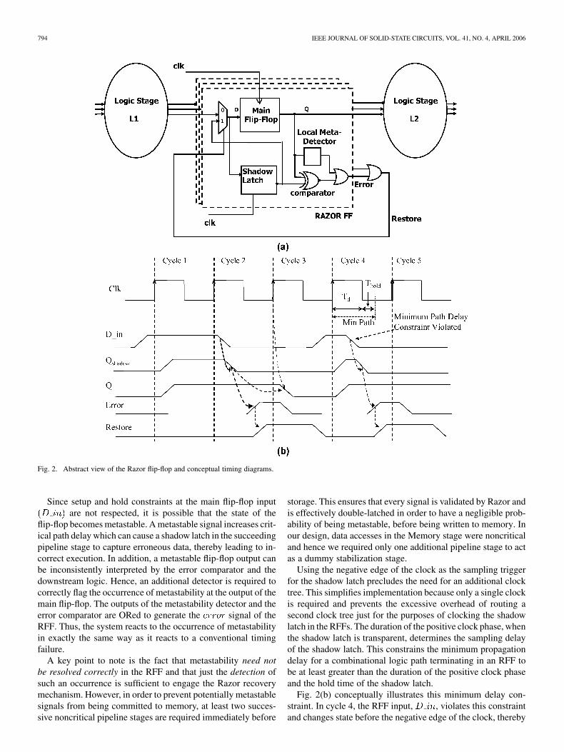
Fig. 2(a) shows the conceptual representation of the delay-error tolerant Razor flip-flop (henceforth referred to as the RFF)and timing diagrams that explain its working principle. Thestandard positive edge triggered D-flip-flop (DFF) is augmentedwith a shadow latch which is transparent in the positive phaseof the clock and samples at the negative edge. Thus, the inputdata is given additional time, equal to the duration of the posi-tive clock phase, to settle down to its correct state before beingsampled by the shadow latch. In order to ensure that the shadowlatch always captures the correct data, the minimum allowablesupply voltage needs to be constrained during design time suchthat the setup time at the shadow latch is never violated evenunder worst case conditions. A comparator flags a timing errorwhen it detects a discrepancy between the speculative data sam-pled at the main flip-flop and the correct data sampled at theshadow latch. This is illustrated in Fig. 2(b) where the RFFinput transitions after the positive clock edge in cycle 2causing the state captured at the shadow latch to bedifferent from that captured at the main flip-flop . This leadsto the signal being flagged.
Error signals of individual RFFs are OR-ed together to gen-erate the pipeline signal which overwrites the shadowlatch data into the main flip-flop, thereby restoring correct statein the cycle following the errant cycle. Thus, an errant instruc-tion is guaranteed to recover with a single cycle penalty, withouthaving to be re-executed. This ensures that forward progress inthe pipeline is always maintained. Even if every instruction failsto meet timing, the pipeline still completes, albeit at a slowerspeed. Upon detection of a timing error, a micro-architecturalrecovery technique is engaged to restore the whole pipeline toits correct state.
794 IEEE JOURNAL OF SOLID-STATE CIRCUITS, VOL. 41, NO. 4, APRIL 2006
Fig. 2. Abstract view of the Razor flip-flop and conceptual timing diagrams.
Since setup and hold constraints at the main flip-flop inputare not respected, it is possible that the state of the
flip-flop becomes metastable. A metastable signal increases crit-ical path delay which can cause a shadow latch in the succeedingpipeline stage to capture erroneous data, thereby leading to in-correct execution. In addition, a metastable flip-flop output canbe inconsistently interpreted by the error comparator and thedownstream logic. Hence, an additional detector is required tocorrectly flag the occurrence of metastability at the output of themain flip-flop. The outputs of the metastability detector and theerror comparator are ORed to generate the signal of theRFF. Thus, the system reacts to the occurrence of metastabilityin exactly the same way as it reacts to a conventional timingfailure.
A key point to note is the fact that metastability need notbe resolved correctly in the RFF and that just the detection ofsuch an occurrence is sufficient to engage the Razor recoverymechanism. However, in order to prevent potentially metastablesignals from being committed to memory, at least two succes-sive noncritical pipeline stages are required immediately before
storage. This ensures that every signal is validated by Razor andis effectively double-latched in order to have a negligible prob-ability of being metastable, before being written to memory. Inour design, data accesses in the Memory stage were noncriticaland hence we required only one additional pipeline stage to actas a dummy stabilization stage.
Using the negative edge of the clock as the sampling triggerfor the shadow latch precludes the need for an additional clocktree. This simplifies implementation because only a single clockis required and prevents the excessive overhead of routing asecond clock tree just for the purposes of clocking the shadowlatch in the RFFs. The duration of the positive clock phase, whenthe shadow latch is transparent, determines the sampling delayof the shadow latch. This constrains the minimum propagationdelay for a combinational logic path terminating in an RFF tobe at least greater than the duration of the positive clock phaseand the hold time of the shadow latch.
Fig. 2(b) conceptually illustrates this minimum delay con-straint. In cycle 4, the RFF input, , violates this constraintand changes state before the negative edge of the clock, thereby
DAS et al.: A SELF-TUNING DVS PROCESSOR USING DELAY-ERROR DETECTION AND CORRECTION 795
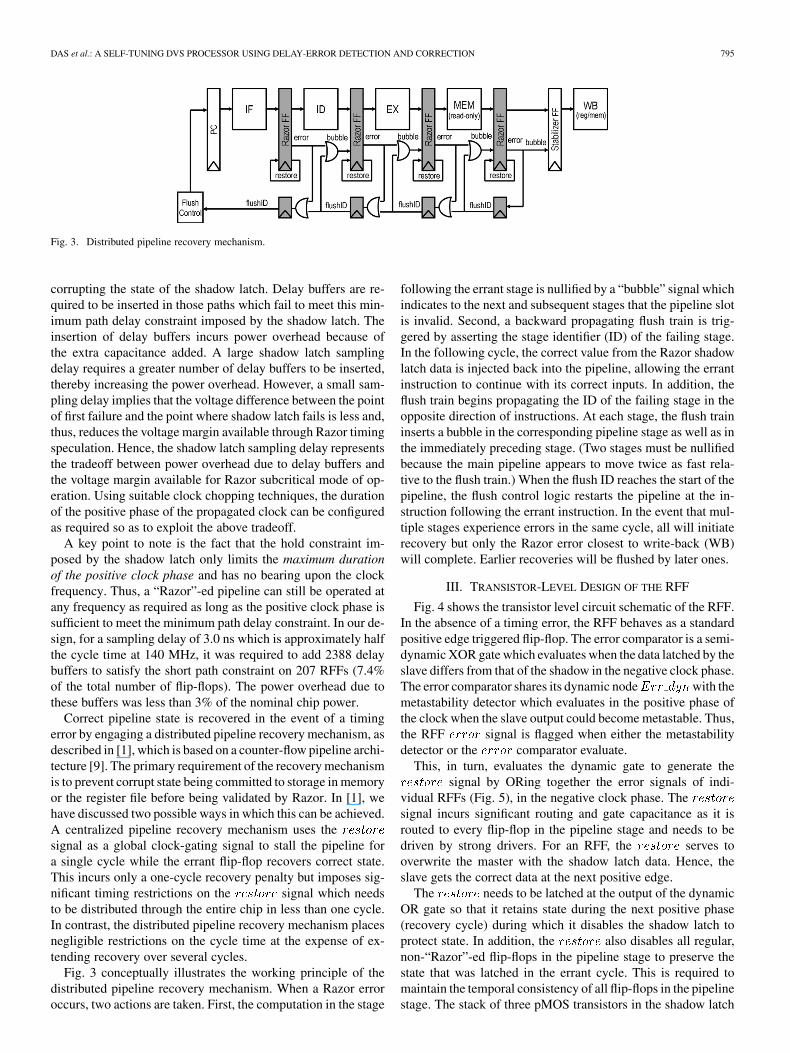
Fig. 3. Distributed pipeline recovery mechanism.
corrupting the state of the shadow latch. Delay buffers are re-quired to be inserted in those paths which fail to meet this min-imum path delay constraint imposed by the shadow latch. Theinsertion of delay buffers incurs power overhead because ofthe extra capacitance added. A large shadow latch samplingdelay requires a greater number of delay buffers to be inserted,thereby increasing the power overhead. However, a small sam-pling delay implies that the voltage difference between the pointof first failure and the point where shadow latch fails is less and,thus, reduces the voltage margin available through Razor timingspeculation. Hence, the shadow latch sampling delay representsthe tradeoff between power overhead due to delay buffers andthe voltage margin available for Razor subcritical mode of op-eration. Using suitable clock chopping techniques, the durationof the positive phase of the propagated clock can be configuredas required so as to exploit the above tradeoff.
A key point to note is the fact that the hold constraint im-posed by the shadow latch only limits the maximum durationof the positive clock phase and has no bearing upon the clockfrequency. Thus, a “Razor”-ed pipeline can still be operated atany frequency as required as long as the positive clock phase issufficient to meet the minimum path delay constraint. In our de-sign, for a sampling delay of 3.0 ns which is approximately halfthe cycle time at 140 MHz, it was required to add 2388 delaybuffers to satisfy the short path constraint on 207 RFFs (7.4%of the total number of flip-flops). The power overhead due tothese buffers was less than 3% of the nominal chip power.
Correct pipeline state is recovered in the event of a timingerror by engaging a distributed pipeline recovery mechanism, asdescribed in [1], which is based on a counter-flow pipeline archi-tecture [9]. The primary requirement of the recovery mechanismis to prevent corrupt state being committed to storage in memoryor the register file before being validated by Razor. In [1], wehave discussed two possible ways in which this can be achieved.A centralized pipeline recovery mechanism uses thesignal as a global clock-gating signal to stall the pipeline fora single cycle while the errant flip-flop recovers correct state.This incurs only a one-cycle recovery penalty but imposes sig-nificant timing restrictions on the signal which needsto be distributed through the entire chip in less than one cycle.In contrast, the distributed pipeline recovery mechanism placesnegligible restrictions on the cycle time at the expense of ex-tending recovery over several cycles.
Fig. 3 conceptually illustrates the working principle of thedistributed pipeline recovery mechanism. When a Razor erroroccurs, two actions are taken. First, the computation in the stage
following the errant stage is nullified by a “bubble” signal whichindicates to the next and subsequent stages that the pipeline slotis invalid. Second, a backward propagating flush train is trig-gered by asserting the stage identifier (ID) of the failing stage.In the following cycle, the correct value from the Razor shadowlatch data is injected back into the pipeline, allowing the errantinstruction to continue with its correct inputs. In addition, theflush train begins propagating the ID of the failing stage in theopposite direction of instructions. At each stage, the flush traininserts a bubble in the corresponding pipeline stage as well as inthe immediately preceding stage. (Two stages must be nullifiedbecause the main pipeline appears to move twice as fast rela-tive to the flush train.) When the flush ID reaches the start of thepipeline, the flush control logic restarts the pipeline at the in-struction following the errant instruction. In the event that mul-tiple stages experience errors in the same cycle, all will initiaterecovery but only the Razor error closest to write-back (WB)will complete. Earlier recoveries will be flushed by later ones.
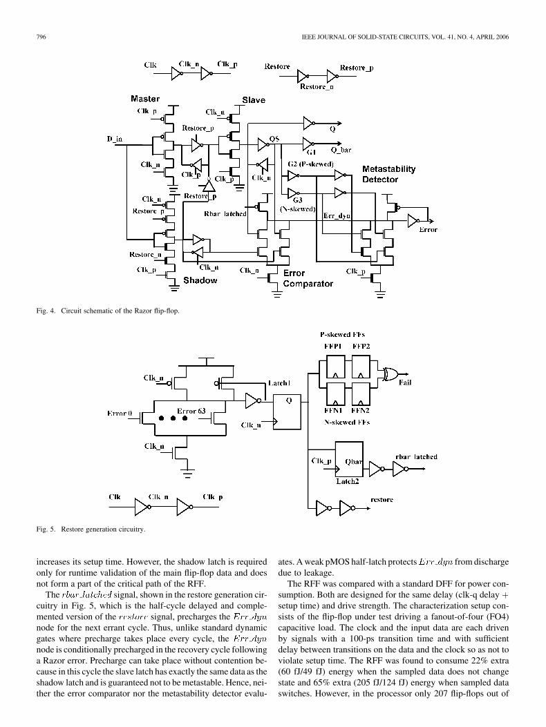
III. TRANSISTOR-LEVEL DESIGN OF THE RFF
Fig. 4 shows the transistor level circuit schematic of the RFF.In the absence of a timing error, the RFF behaves as a standardpositive edge triggered flip-flop. The error comparator is a semi-dynamic XOR gate which evaluates when the data latched by theslave differs from that of the shadow in the negative clock phase.The error comparator shares its dynamic node with themetastability detector which evaluates in the positive phase ofthe clock when the slave output could become metastable. Thus,the RFF signal is flagged when either the metastabilitydetector or the comparator evaluate.
This, in turn, evaluates the dynamic gate to generate thesignal by ORing together the error signals of indi-
vidual RFFs (Fig. 5), in the negative clock phase. Thesignal incurs significant routing and gate capacitance as it isrouted to every flip-flop in the pipeline stage and needs to bedriven by strong drivers. For an RFF, the serves tooverwrite the master with the shadow latch data. Hence, theslave gets the correct data at the next positive edge.
The needs to be latched at the output of the dynamicOR gate so that it retains state during the next positive phase(recovery cycle) during which it disables the shadow latch toprotect state. In addition, the also disables all regular,non-“Razor”-ed flip-flops in the pipeline stage to preserve thestate that was latched in the errant cycle. This is required tomaintain the temporal consistency of all flip-flops in the pipelinestage. The stack of three pMOS transistors in the shadow latch
796 IEEE JOURNAL OF SOLID-STATE CIRCUITS, VOL. 41, NO. 4, APRIL 2006
Fig. 4. Circuit schematic of the Razor flip-flop.
Fig. 5. Restore generation circuitry.
increases its setup time. However, the shadow latch is requiredonly for runtime validation of the main flip-flop data and doesnot form a part of the critical path of the RFF.
The signal, shown in the restore generation cir-cuitry in Fig. 5, which is the half-cycle delayed and comple-mented version of the signal, precharges thenode for the next errant cycle. Thus, unlike standard dynamicgates where precharge takes place every cycle, thenode is conditionally precharged in the recovery cycle followinga Razor error. Precharge can take place without contention be-cause in this cycle the slave latch has exactly the same data as theshadow latch and is guaranteed not to be metastable. Hence, nei-ther the error comparator nor the metastability detector evalu-
ates. A weak pMOS half-latch protects from dischargedue to leakage.
The RFF was compared with a standard DFF for power con-sumption. Both are designed for the same delay (clk-q delaysetup time) and drive strength. The characterization setup con-sists of the flip-flop under test driving a fanout-of-four (FO4)capacitive load. The clock and the input data are each drivenby signals with a 100-ps transition time and with sufficientdelay between transitions on the data and the clock so as not toviolate setup time. The RFF was found to consume 22% extra(60 fJ/49 fJ) energy when the sampled data does not changestate and 65% extra (205 fJ/124 fJ) energy when sampled dataswitches. However, in the processor only 207 flip-flops out of
DAS et al.: A SELF-TUNING DVS PROCESSOR USING DELAY-ERROR DETECTION AND CORRECTION 797
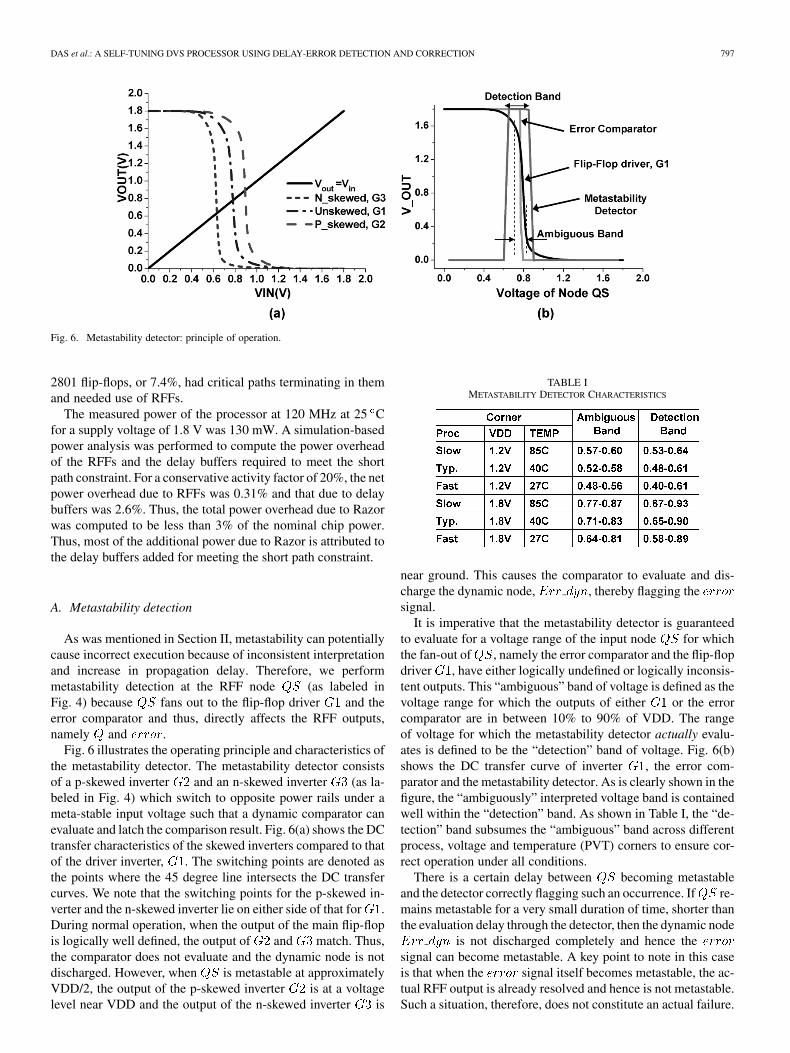
Fig. 6. Metastability detector: principle of operation.
2801 flip-flops, or 7.4%, had critical paths terminating in themand needed use of RFFs.
The measured power of the processor at 120 MHz at 25 Cfor a supply voltage of 1.8 V was 130 mW. A simulation-basedpower analysis was performed to compute the power overheadof the RFFs and the delay buffers required to meet the shortpath constraint. For a conservative activity factor of 20%, the netpower overhead due to RFFs was 0.31% and that due to delaybuffers was 2.6%. Thus, the total power overhead due to Razorwas computed to be less than 3% of the nominal chip power.Thus, most of the additional power due to Razor is attributed tothe delay buffers added for meeting the short path constraint.
A. Metastability detection
As was mentioned in Section II, metastability can potentiallycause incorrect execution because of inconsistent interpretationand increase in propagation delay. Therefore, we performmetastability detection at the RFF node (as labeled inFig. 4) because fans out to the flip-flop driver and theerror comparator and thus, directly affects the RFF outputs,namely and .
Fig. 6 illustrates the operating principle and characteristics ofthe metastability detector. The metastability detector consistsof a p-skewed inverter and an n-skewed inverter (as la-beled in Fig. 4) which switch to opposite power rails under ameta-stable input voltage such that a dynamic comparator canevaluate and latch the comparison result. Fig. 6(a) shows the DCtransfer characteristics of the skewed inverters compared to thatof the driver inverter, . The switching points are denoted asthe points where the 45 degree line intersects the DC transfercurves. We note that the switching points for the p-skewed in-verter and the n-skewed inverter lie on either side of that for .During normal operation, when the output of the main flip-flopis logically well defined, the output of and match. Thus,the comparator does not evaluate and the dynamic node is notdischarged. However, when is metastable at approximatelyVDD/2, the output of the p-skewed inverter is at a voltagelevel near VDD and the output of the n-skewed inverter is
TABLE IMETASTABILITY DETECTOR CHARACTERISTICS
near ground. This causes the comparator to evaluate and dis-charge the dynamic node, , thereby flagging thesignal.
It is imperative that the metastability detector is guaranteedto evaluate for a voltage range of the input node for whichthe fan-out of , namely the error comparator and the flip-flopdriver , have either logically undefined or logically inconsis-tent outputs. This “ambiguous” band of voltage is defined as thevoltage range for which the outputs of either or the errorcomparator are in between 10% to 90% of VDD. The rangeof voltage for which the metastability detector actually evalu-ates is defined to be the “detection” band of voltage. Fig. 6(b)shows the DC transfer curve of inverter , the error com-parator and the metastability detector. As is clearly shown in thefigure, the “ambiguously” interpreted voltage band is containedwell within the “detection” band. As shown in Table I, the “de-tection” band subsumes the “ambiguous” band across differentprocess, voltage and temperature (PVT) corners to ensure cor-rect operation under all conditions.
There is a certain delay between becoming metastableand the detector correctly flagging such an occurrence. If re-mains metastable for a very small duration of time, shorter thanthe evaluation delay through the detector, then the dynamic node
is not discharged completely and hence thesignal can become metastable. A key point to note in this caseis that when the signal itself becomes metastable, the ac-tual RFF output is already resolved and hence is not metastable.Such a situation, therefore, does not constitute an actual failure.
798 IEEE JOURNAL OF SOLID-STATE CIRCUITS, VOL. 41, NO. 4, APRIL 2006
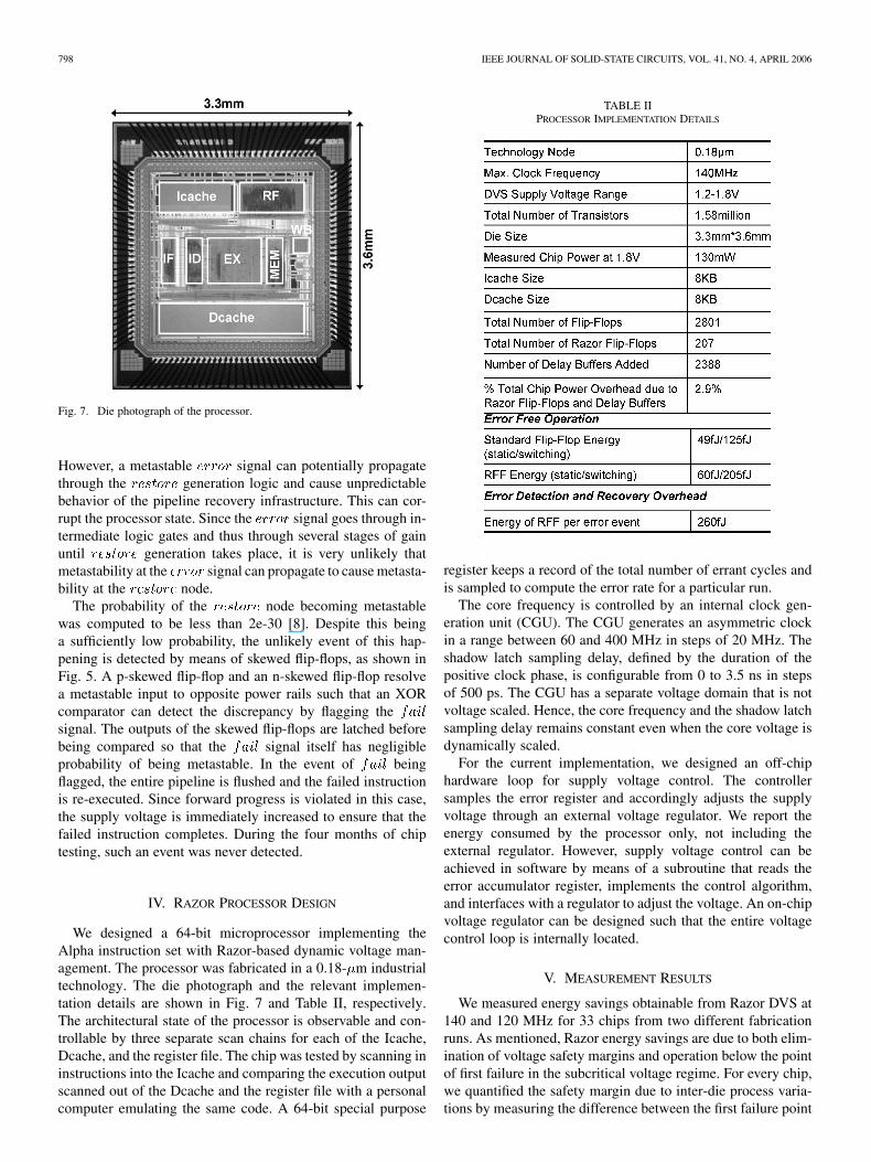
Fig. 7. Die photograph of the processor.
However, a metastable signal can potentially propagatethrough the generation logic and cause unpredictablebehavior of the pipeline recovery infrastructure. This can cor-rupt the processor state. Since the signal goes through in-termediate logic gates and thus through several stages of gainuntil generation takes place, it is very unlikely thatmetastability at the signal can propagate to cause metasta-bility at the node.
The probability of the node becoming metastablewas computed to be less than 2e-30 [8]. Despite this beinga sufficiently low probability, the unlikely event of this hap-pening is detected by means of skewed flip-flops, as shown inFig. 5. A p-skewed flip-flop and an n-skewed flip-flop resolvea metastable input to opposite power rails such that an XORcomparator can detect the discrepancy by flagging thesignal. The outputs of the skewed flip-flops are latched beforebeing compared so that the signal itself has negligibleprobability of being metastable. In the event of beingflagged, the entire pipeline is flushed and the failed instructionis re-executed. Since forward progress is violated in this case,the supply voltage is immediately increased to ensure that thefailed instruction completes. During the four months of chiptesting, such an event was never detected.
IV. RAZOR PROCESSOR DESIGN
We designed a 64-bit microprocessor implementing theAlpha instruction set with Razor-based dynamic voltage man-agement. The processor was fabricated in a 0.18- m industrialtechnology. The die photograph and the relevant implemen-tation details are shown in Fig. 7 and Table II, respectively.The architectural state of the processor is observable and con-trollable by three separate scan chains for each of the Icache,Dcache, and the register file. The chip was tested by scanning ininstructions into the Icache and comparing the execution outputscanned out of the Dcache and the register file with a personalcomputer emulating the same code. A 64-bit special purpose
TABLE IIPROCESSOR IMPLEMENTATION DETAILS
register keeps a record of the total number of errant cycles andis sampled to compute the error rate for a particular run.
The core frequency is controlled by an internal clock gen-eration unit (CGU). The CGU generates an asymmetric clockin a range between 60 and 400 MHz in steps of 20 MHz. Theshadow latch sampling delay, defined by the duration of thepositive clock phase, is configurable from 0 to 3.5 ns in stepsof 500 ps. The CGU has a separate voltage domain that is notvoltage scaled. Hence, the core frequency and the shadow latchsampling delay remains constant even when the core voltage isdynamically scaled.
For the current implementation, we designed an off-chiphardware loop for supply voltage control. The controllersamples the error register and accordingly adjusts the supplyvoltage through an external voltage regulator. We report theenergy consumed by the processor only, not including theexternal regulator. However, supply voltage control can beachieved in software by means of a subroutine that reads theerror accumulator register, implements the control algorithm,and interfaces with a regulator to adjust the voltage. An on-chipvoltage regulator can be designed such that the entire voltagecontrol loop is internally located.
V. MEASUREMENT RESULTS
We measured energy savings obtainable from Razor DVS at140 and 120 MHz for 33 chips from two different fabricationruns. As mentioned, Razor energy savings are due to both elim-ination of voltage safety margins and operation below the pointof first failure in the subcritical voltage regime. For every chip,we quantified the safety margin due to inter-die process varia-tions by measuring the difference between the first failure point

DAS et al.: A SELF-TUNING DVS PROCESSOR USING DELAY-ERROR DETECTION AND CORRECTION 799
Fig. 8. Error rate and normalized energy measurement for chip 1 and chip 2.
TABLE IIIERROR RATE AND ENERGY/INSTRUCTION AT POINT OF FIRST FAILURE AND POINT OF 0.1% ERROR RATE FOR CHIPS 1 AND 2
of the slowest (worst case process corner) chip and the chipunder test. Temperature margins were computed by the shift inthe first failure point for a chip when operating at 105 C as op-posed to operating at 25 C. In addition, by scaling the supplyvoltage below the first failure point, we measured the minimumvoltage for which error correction is achievable with Razor andthe voltage where a 0.1% error rate is attained.
A. Energy Savings From Sub-Critical Operation
Fig. 8 shows the error rates and normalized energy savingsversus supply voltage at 120 and 140 MHz for two differentchips. Energy at a particular voltage is normalized with respectto the energy at the point of first failure. For all plotted points,correct program execution with Razor error correction was ver-ified.
From Fig. 8, we note that the error rate at the point of firstfailure is very low, and is on the order of 1.0e-8, because only afew critical paths that are rarely sensitized fail to meet setup re-quirements and are flagged as timing errors. As voltage is scaledfurther into the subcritical regime the error rate increases expo-nentially. The instruction per cycle (IPC) penalty due to the errorrecovery cycles is negligible for error rates below 0.1%. Undersuch low error rates, the recovery overhead energy is also negli-gible and the total processor energy shows a quadratic reductionwith the supply voltage. At error rates exceeding 0.1%, the re-covery energy rapidly starts to dominate, offsetting the quadraticsavings due to voltage scaling. For the measured chips, the en-ergy optimal error rate fell at approximately 0.1%.
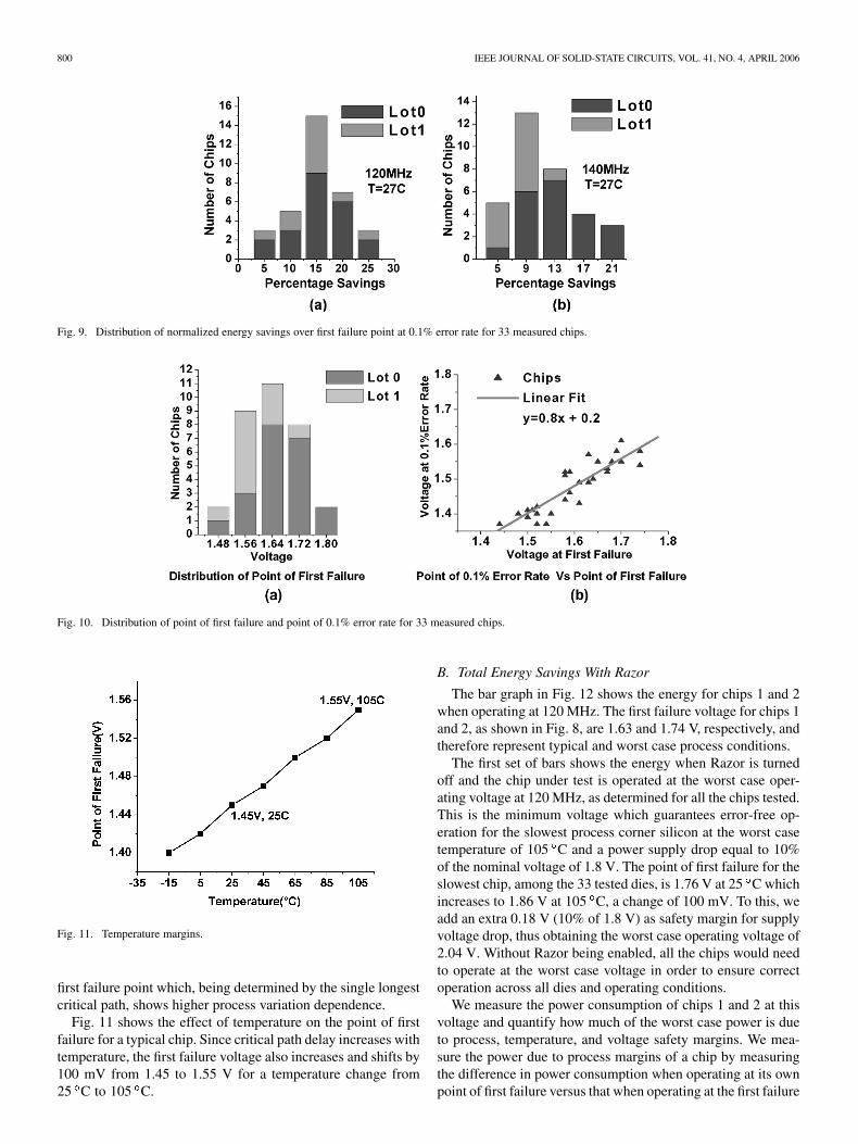
Table III shows the measured power at the point of firstfailure and the energy per instruction for both the chips at thepoint of first failure and at the point of 0.1% error rate. At120 MHz, chip 1 consumes 104.5 mW at the first failure pointand 89.7 mW at an optimal 0.1% error rate, leading to 14%energy savings with negligible IPC hit. The energy saving forchip 2 is 17%. These savings are in addition to the energy savedjust by eliminating voltage margins. Fig. 9 shows the distri-bution of the percentage normalized energy savings obtainedover the first failure point while operating at the 0.1% error ratevoltage for all the chips tested. At 120 MHz, the range extendsfrom 5% to 23% and from 5% to 19% at 140 MHz.
Fig. 10(a) shows the distribution of the first failure voltagefor the 33 measured chips. At 120 MHz, the measured range ofvariation of the first failure point is from 1.46 to 1.76 V. The cor-relation between the first failure voltage and the 0.1% error ratevoltage is shown in the scatter plot of Fig. 10(b). The 0.1% errorrate voltage shows a net variation of 0.24 V from 1.38 to 1.62 Vwhich is approximately 20% less than the variation observed forthe voltage at the point of first failure. The relative “flatness” ofthe linear fit indicates less sensitivity to process variation whenrunning at a 0.1% error rate than at the point of first failure. Thisimplies that a Razor-enabled processor, designed to operate atthe energy optimal point, is likely to show greater predictabilityin terms of performance than a conventional worst case opti-mized design. The energy optimal point requires a significantnumber of paths to fail and statistically averages out the varia-tions in path delay due to process variation, as opposed to the
800 IEEE JOURNAL OF SOLID-STATE CIRCUITS, VOL. 41, NO. 4, APRIL 2006
Fig. 9. Distribution of normalized energy savings over first failure point at 0.1% error rate for 33 measured chips.
Fig. 10. Distribution of point of first failure and point of 0.1% error rate for 33 measured chips.
Fig. 11. Temperature margins.
first failure point which, being determined by the single longestcritical path, shows higher process variation dependence.
Fig. 11 shows the effect of temperature on the point of firstfailure for a typical chip. Since critical path delay increases withtemperature, the first failure voltage also increases and shifts by100 mV from 1.45 to 1.55 V for a temperature change from25 C to 105 C.
B. Total Energy Savings With Razor
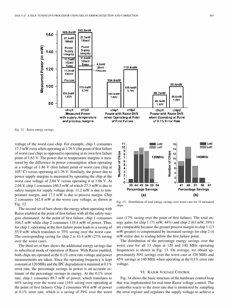
The bar graph in Fig. 12 shows the energy for chips 1 and 2when operating at 120 MHz. The first failure voltage for chips 1and 2, as shown in Fig. 8, are 1.63 and 1.74 V, respectively, andtherefore represent typical and worst case process conditions.
The first set of bars shows the energy when Razor is turnedoff and the chip under test is operated at the worst case oper-ating voltage at 120 MHz, as determined for all the chips tested.This is the minimum voltage which guarantees error-free op-eration for the slowest process corner silicon at the worst casetemperature of 105 C and a power supply drop equal to 10%of the nominal voltage of 1.8 V. The point of first failure for theslowest chip, among the 33 tested dies, is 1.76 V at 25 C whichincreases to 1.86 V at 105 C, a change of 100 mV. To this, weadd an extra 0.18 V (10% of 1.8 V) as safety margin for supplyvoltage drop, thus obtaining the worst case operating voltage of2.04 V. Without Razor being enabled, all the chips would needto operate at the worst case voltage in order to ensure correctoperation across all dies and operating conditions.
We measure the power consumption of chips 1 and 2 at thisvoltage and quantify how much of the worst case power is dueto process, temperature, and voltage safety margins. We mea-sure the power due to process margins of a chip by measuringthe difference in power consumption when operating at its ownpoint of first failure versus that when operating at the first failure
DAS et al.: A SELF-TUNING DVS PROCESSOR USING DELAY-ERROR DETECTION AND CORRECTION 801
Fig. 12. Razor energy savings.
voltage of the worst case chip. For example, chip 1 consumes17.3 mW extra when operating at 1.76 V (the point of first failureof worst case chip) as opposed to operating at its own first failurepoint of 1.63 V. The power due to temperature margins is mea-sured by the difference in power consumption when operatingat a voltage of 1.86 V (first failure point of worst case chip at105 C) versus operating at 1.76 V. Similarly, the power due topower supply margins is measured by operating the chip at theworst case voltage of 2.04 V versus operating it at 1.86 V. At2.04 V, chip 1 consumes 160.5 mW of which 27.3 mW is due tosafety margin for supply voltage drop, 11.2 mW is due to tem-perature margin, and 17.3 mW is due to process margin. Chip2 consumes 162.8 mW at the worst case voltage, as shown inFig. 12.
The second set of bars shows the energy when operating withRazor enabled at the point of first failure with all the safety mar-gins eliminated. At the point of first failure, chip 1 consumes104.5 mW while chip 2 consumes 119.4 mW of power. Thus,for chip 1, operating at the first failure point leads to a saving of55.9 mW which translates to 35% saving over the worst case.The corresponding saving for chip 2 is 43.4 mW (27% savingover the worst case).
The third set of bars shows the additional energy savings dueto subcritical mode of operation of Razor. With Razor enabled,both chips are operated at the 0.1% error rate voltage and powermeasurements are taken. Since the operating frequency is keptconstant at 120 MHz and the IPC degradation is minimal at 0.1%error rate, the percentage savings in power is an accurate es-timate of the percentage savings in energy. At the 0.1% errorrate, chip 1 consumes 89.7 mW of power, which translates to44% saving over the worst case (14% saving over operating atthe point of first failure). Chip 2 consumes 99.6 mW of powerat 0.1% error rate, which is a saving of 39% over the worst
Fig. 13. Distribution of total energy savings over worst case for 33 measuredchips.
case (17% saving over the point of first failure). The total en-ergy gains for chip 1 (71 mW, 44%) and chip 2 (63 mW, 39%)are comparable because the greater process margin in chip 1 (13mW greater) is compensated by increased savings for chip 2 (4mW extra) due to scaling below the first failure point.
The distribution of the percentage energy savings over theworst case for all 33 chips at 120 and 140 MHz operatingfrequencies is shown in Fig. 13. On average, we obtain ap-proximately 50% savings over the worst case at 120 MHz and45% savings at 140 MHz when operating at the 0.1% error ratevoltage.
VI. RAZOR VOLTAGE CONTROL
Fig. 14 shows the basic structure of the hardware control loopthat was implemented for real-time Razor voltage control. Thecontroller reacts to the error rate that is monitored by samplingthe error register and regulates the supply voltage to achieve a
802 IEEE JOURNAL OF SOLID-STATE CIRCUITS, VOL. 41, NO. 4, APRIL 2006
Fig. 14. Razor voltage control loop.
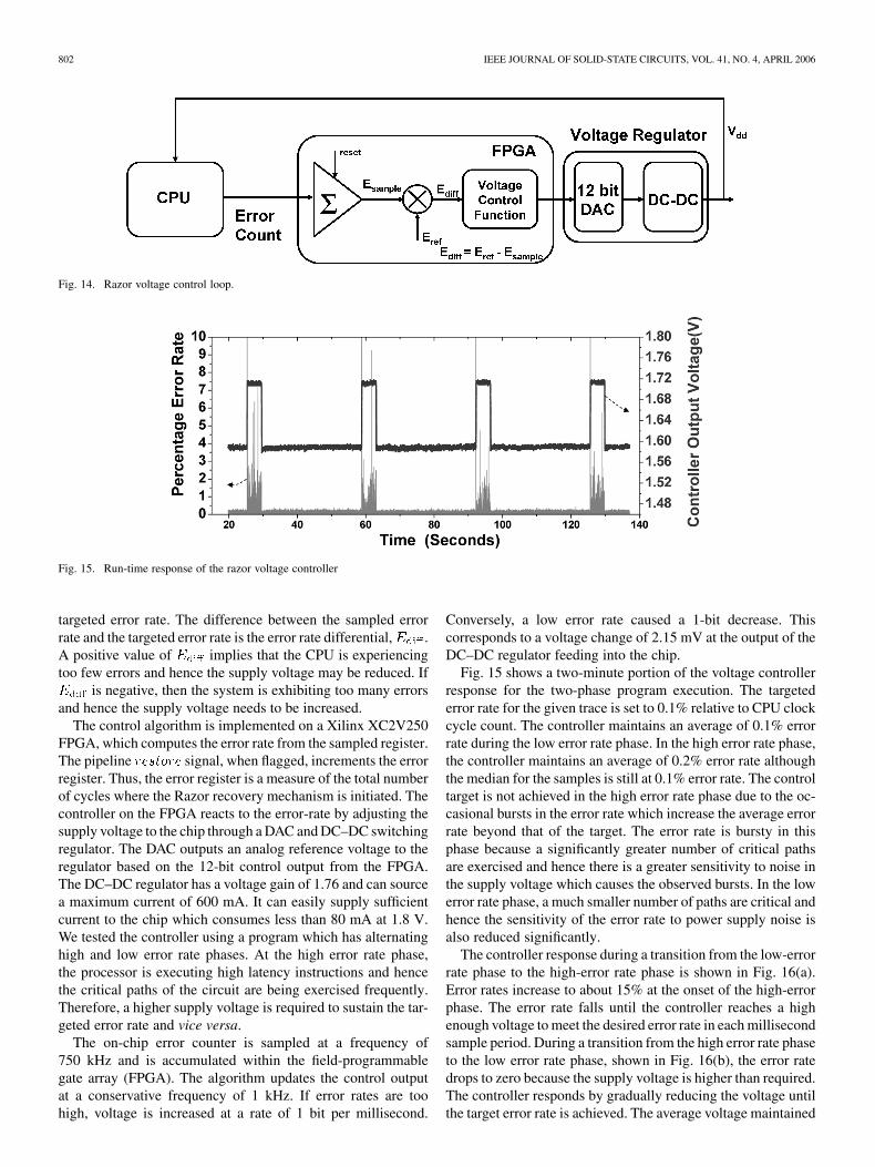
Fig. 15. Run-time response of the razor voltage controller
targeted error rate. The difference between the sampled errorrate and the targeted error rate is the error rate differential, .A positive value of implies that the CPU is experiencingtoo few errors and hence the supply voltage may be reduced. If
is negative, then the system is exhibiting too many errorsand hence the supply voltage needs to be increased.
The control algorithm is implemented on a Xilinx XC2V250FPGA, which computes the error rate from the sampled register.The pipeline signal, when flagged, increments the errorregister. Thus, the error register is a measure of the total numberof cycles where the Razor recovery mechanism is initiated. Thecontroller on the FPGA reacts to the error-rate by adjusting thesupply voltage to the chip through a DAC and DC–DC switchingregulator. The DAC outputs an analog reference voltage to theregulator based on the 12-bit control output from the FPGA.The DC–DC regulator has a voltage gain of 1.76 and can sourcea maximum current of 600 mA. It can easily supply sufficientcurrent to the chip which consumes less than 80 mA at 1.8 V.We tested the controller using a program which has alternatinghigh and low error rate phases. At the high error rate phase,the processor is executing high latency instructions and hencethe critical paths of the circuit are being exercised frequently.Therefore, a higher supply voltage is required to sustain the tar-geted error rate and vice versa.
The on-chip error counter is sampled at a frequency of750 kHz and is accumulated within the field-programmablegate array (FPGA). The algorithm updates the control outputat a conservative frequency of 1 kHz. If error rates are toohigh, voltage is increased at a rate of 1 bit per millisecond.
Conversely, a low error rate caused a 1-bit decrease. Thiscorresponds to a voltage change of 2.15 mV at the output of theDC–DC regulator feeding into the chip.
Fig. 15 shows a two-minute portion of the voltage controllerresponse for the two-phase program execution. The targetederror rate for the given trace is set to 0.1% relative to CPU clockcycle count. The controller maintains an average of 0.1% errorrate during the low error rate phase. In the high error rate phase,the controller maintains an average of 0.2% error rate althoughthe median for the samples is still at 0.1% error rate. The controltarget is not achieved in the high error rate phase due to the oc-casional bursts in the error rate which increase the average errorrate beyond that of the target. The error rate is bursty in thisphase because a significantly greater number of critical pathsare exercised and hence there is a greater sensitivity to noise inthe supply voltage which causes the observed bursts. In the lowerror rate phase, a much smaller number of paths are critical andhence the sensitivity of the error rate to power supply noise isalso reduced significantly.
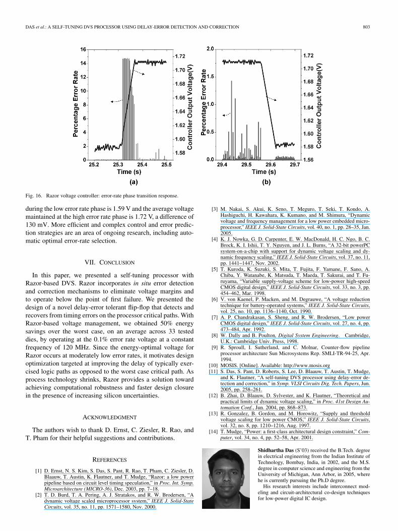
The controller response during a transition from the low-errorrate phase to the high-error rate phase is shown in Fig. 16(a).Error rates increase to about 15% at the onset of the high-errorphase. The error rate falls until the controller reaches a highenough voltage to meet the desired error rate in each millisecondsample period. During a transition from the high error rate phaseto the low error rate phase, shown in Fig. 16(b), the error ratedrops to zero because the supply voltage is higher than required.The controller responds by gradually reducing the voltage untilthe target error rate is achieved. The average voltage maintained
DAS et al.: A SELF-TUNING DVS PROCESSOR USING DELAY-ERROR DETECTION AND CORRECTION 803
Fig. 16. Razor voltage controller: error-rate phase transition response.
during the low error rate phase is 1.59 V and the average voltagemaintained at the high error rate phase is 1.72 V, a difference of130 mV. More efficient and complex control and error predic-tion strategies are an area of ongoing research, including auto-matic optimal error-rate selection.
VII. CONCLUSION
In this paper, we presented a self-tuning processor withRazor-based DVS. Razor incorporates in situ error detectionand correction mechanisms to eliminate voltage margins andto operate below the point of first failure. We presented thedesign of a novel delay-error tolerant flip-flop that detects andrecovers from timing errors on the processor critical paths. WithRazor-based voltage management, we obtained 50% energysavings over the worst case, on an average across 33 testeddies, by operating at the 0.1% error rate voltage at a constantfrequency of 120 MHz. Since the energy-optimal voltage forRazor occurs at moderately low error rates, it motivates designoptimization targeted at improving the delay of typically exer-cised logic paths as opposed to the worst case critical path. Asprocess technology shrinks, Razor provides a solution towardachieving computational robustness and faster design closurein the presence of increasing silicon uncertainties.
ACKNOWLEDGMENT
The authors wish to thank D. Ernst, C. Ziesler, R. Rao, andT. Pham for their helpful suggestions and contributions.
REFERENCES
[1] D. Ernst, N. S. Kim, S. Das, S. Pant, R. Rao, T. Pham, C. Ziesler, D.Blaauw, T. Austin, K. Flautner, and T. Mudge, “Razor: a low powerpipeline based on circuit level timing speculation,” in Proc. Int. Symp.Microarchitecture (MICRO-36), Dec. 2003, pp. 7–18.
[2] T. D. Burd, T. A. Pering, A. J. Stratakos, and R. W. Brodersen, “Adynamic voltage scaled microprocessor system,” IEEE J. Solid-StateCircuits, vol. 35, no. 11, pp. 1571–1580, Nov. 2000.
[3] M. Nakai, S. Akui, K. Seno, T. Meguro, T. Seki, T. Kondo, A.Hashiguchi, H. Kawahara, K. Kumano, and M. Shimura, “Dynamicvoltage and frequency management for a low power embedded micro-processor,” IEEE J. Solid-State Circuits, vol. 40, no. 1, pp. 28–35, Jan.2005.
[4] K. J. Nowka, G. D. Carpenter, E. W. MacDonald, H. C. Ngo, B. C.Brock, K. I. Ishii, T. Y. Nguyen, and J. L. Burns, “A 32-bit powerPCsystem-on-a-chip with support for dynamic voltage scaling and dy-namic frequency scaling,” IEEE J. Solid-State Circuits, vol. 37, no. 11,pp. 1441–1447, Nov. 2002.
[5] T. Kuroda, K. Suzuki, S. Mita, T. Fujita, F. Yamane, F. Sano, A.Chiba, Y. Watanabe, K. Matsuda, T. Maeda, T. Sakurai, and T. Fu-ruyama, “Variable supply-voltage scheme for low-power high-speedCMOS digital design,” IEEE J. Solid-State Circuits, vol. 33, no. 3, pp.454–462, Mar. 1998.
[6] V. von Kaenel, P. Macken, and M. Degrauwe, “A voltage reductiontechnique for battery-operated systems,” IEEE J. Solid-State Circuits,vol. 25, no. 10, pp. 1136–1140, Oct. 1990.
[7] A. P. Chandrakasan, S. Sheng, and R. W. Brodersen, “Low powerCMOS digital design,” IEEE J. Solid-State Circuits, vol. 27, no. 4, pp.473–484, Apr. 1992.
[8] W. Dally and B. Poulton, Digital System Engineering. Cambridge,U.K.: Cambridge Univ. Press, 1998.
[9] R. Sproull, I. Sutherland, and C. Molnar, Counter-flow pipelineprocessor architecture Sun Microsystems Rep. SMLI-TR-94-25, Apr.1994.
[10] MOSIS. [Online]. Available: http://www.mosis.org[11] S. Das, S. Pant, D. Roberts, S. Lee, D. Blaauw, T. Austin, T. Mudge,
and K. Flautner, “A self-tuning DVS processor using delay-error de-tection and correction,” in Symp. VLSI Circuits Dig. Tech. Papers, Jun.2005, pp. 258–261.
[12] B. Zhai, D. Blaauw, D. Sylvester, and K. Flautner, “Theoretical andpractical limits of dynamic voltage scaling,” in Proc. 41st Design Au-tomation Conf., Jun. 2004, pp. 868–873.
[13] R. Gonzalez, B. Gordon, and M. Horowitz, “Supply and thresholdvoltage scaling for low power CMOS,” IEEE J. Solid-State Circuits,vol. 32, no. 8, pp. 1210–1216, Aug. 1997.
[14] T. Mudge, “Power: a first-class architectural design constraint,” Com-puter, vol. 34, no. 4, pp. 52–58, Apr. 2001.
Shidhartha Das (S’03) received the B.Tech. degreein electrical engineering from the Indian Institute ofTechnology, Bombay, India, in 2002, and the M.S.degree in computer science and engineering from theUniversity of Michigan, Ann Arbor, in 2005, wherehe is currently pursuing the Ph.D degree.
His research interests include interconnect mod-eling and circuit-architectural co-design techniquesfor low-power digital IC design.

804 IEEE JOURNAL OF SOLID-STATE CIRCUITS, VOL. 41, NO. 4, APRIL 2006
David Roberts (S’04) received the M.Eng. degreein computer systems engineering from the Universityof Warwick, Coventry, U.K. He is currently pursuingthe Ph.D. degree at the University of Michigan, AnnArbor.
His research interests include low-power and ro-bust computer architectures.
Mr. Roberts is a member of the British ComputerSociety.
Seokwoo Lee received the B.S.E. degree (summacum laude) in computer science from the Universityof Michigan, Ann Arbor, in 2003. He is currentlypursuing the Ph.D. degree in the Department ofComputer Science and Engineering at the Universityof Michgan, Ann Arbor.
His research interests include computer architec-ture, variability-aware system design, reliable systemdesign, and low-power system design and computersimulations.
Sanjay Pant received the B.Tech. degree in electricalengineering from the Indian Institute of Technology,Kanpur, India, in 2001, and the M.S. degree in elec-trical engineering from the University of Michigan,Ann Arbor, in 2004, where he is currently pursuingthe Ph.D. degree.
In fall 2004 and summer 2005, he was with theStrategic CAD Laboratories, Intel Corporation,Hillsboro, OR, where he worked as a GraduateIntern. His research interests include low-powerVLSI design and signal integrity issues in power
distribution networks.
David Blaauw (M’94) received the B.S. degree inphysics and computer science from Duke University,Durham, NC, in 1986, and the M.S. and Ph.D. de-grees in computer science from the University of Illi-nois, Urbana, in 1988 and 1991, respectively.
He worked at IBM Corporation as a DevelopmentStaff Member until August 1993. From 1993 to Au-gust 2001, he worked for Motorola, Inc., Austin, TX,where he was the Manager of the High PerformanceDesign Technology group. Since August 2001, he hasbeen on the faculty of the University of Michigan as
an Associate Professor. His work has focused on VLSI design and CAD withparticular emphasis on circuit design and optimization for high-performanceand low-power designs.
Dr. Blaauw was the Technical Program Chair and General Chair for the In-ternational Symposium on Low Power Electronic and Design in 1999 and 2000,
respectively, and was the Technical Program Co-Chair and member of the Ex-ecutive Committee of the ACM/IEEE Design Automation Conference in 2000and 2001.
Todd Austin received the M.S. degree in computerengineering from the Rochester Institute of Tech-nology, Rochester, NY, and the Ph.D. degree incomputer science from the University of Wisconsin,Madison, in 1996.
He is an Associate Professor of electrical engi-neering and computer science at the University ofMichigan. His research interests include computerarchitecture, compilers, computer system verifica-tion, and performance analysis tools and techniques.
Prof. Austin has earned numerous awards, in-cluding the Ruth and Joel Spira Outstanding Teacher Award in 2002 and aNational Science Foundation CAREER Award in 2001. He is a member ofAssociation for Computing Machinery (ACM).
Krisztián Flautner (M’03) received the B.S.,M.S., and Ph.D. degrees in computer science andengineering from the University of Michigan, AnnArbor.
He is Director of Advanced Research at ARMLimited, Cambridge, U.K., and the architect ofARM’s Intelligent Energy Management technology.His research interests include high-performance,low-energy processing platforms that support ad-vanced software environments.
Dr. Flautner is a member of the Association forComputing Machinery (ACM).
Trevor Mudge (S’74–M’77–SM’84–F’95) receivedthe B.Sc. degree from the University of Reading,U.K., in 1969, and the M.S. and Ph.D. degrees incomputer science from the University of Illinois,Urbana, in 1973 and 1977, respectively.
Since 1977, he has been on the faculty of theUniversity of Michigan, Ann Arbor. He recently wasnamed the first Bredt Family Professor of ElectricalEngineering and Computer Science after concludinga ten-year term as the Director of the AdvancedComputer Architecture Laboratory, a group of eight
faculty and about 70 graduate students. He is the author of numerous papers oncomputer architecture, programming languages, VLSI design, and computervision. He has also chaired about 33 theses in these areas. His research interestsinclude computer architecture, computer-aided design, and compilers. Inaddition to his position as a faculty member, he runs Idiot Savants, a chipdesign consultancy.
Dr. Mudge is a member of the Association for Computing Machinery (ACM),the Institution of Electrical Engineers (IEE), and the British Computer Society.
Related Documents