Kaysar Rahim Starkey Hearing Technologies, Eden Prairie, MN 55344 e-mail: [email protected] Ahsan Mian 1 Mem. ASME Department of Mechanical and Materials Engineering, Wright State University, 3640 Colonel Glenn Highway, Dayton, OH 45435 e-mail: [email protected] A Review on Laser Processing in Electronic and MEMS Packaging The packaging of electronic and microelectromechanical systems (MEMS) devices is an important part of the overall manufacturing process as it ensures mechanical robustness as well as required electrical/electromechanical functionalities. The packaging integra- tion process involves the selection of packaging materials and technology, process design, fabrication, and testing. As the demand of functionalities of an electronic or MEMS device is increasing every passing year, chip size is getting larger and is occupy- ing the majority of space within a package. This requires innovative packaging technolo- gies so that integration can be done with less thermal/mechanical effect on the nearby components. Laser processing technologies for electronic and MEMS packaging have potential to obviate some of the difficulties associated with traditional packaging technol- ogies and can become an attractive alternative for small-scale integration of components. As laser processing involves very fast localized and heating and cooling, the laser can be focused at micrometer scale to perform various packaging processes such as dicing, join- ing, and patterning at the microscale with minimal or no thermal effect on surrounding material or structure. As such, various laser processing technologies are currently being explored by researchers and also being utilized by electronic and MEMS packaging industries. This paper reviews the current and future trend of electronic and MEMS pack- aging and their manufacturing processes. Emphasis is given to the laser processing tech- niques that have the potential to revolutionize the future manufacturing of electronic and MEMS packages. [DOI: 10.1115/1.4036239] Keywords: electronic packaging, MEMS packaging, laser processing 1 Introduction Electronics and microelectromechanical systems (MEMS) packaging refers to the housing of integrated circuits (IC) and electromechanical components to provide mechanical robustness and their interconnection to structure electronic systems. It incor- porates various functions, for example, chip protection and sup- port, heat dissipation, signal distribution, manufacturability and serviceability, and power distribution. Manufacturability, quality, and cost are the most important parameters to be considered while designing an electronic/MEMS package. In general, packaging technologies are categorized into three levels [1] as shown in Fig. 1. Each of the three packaging levels includes a growing number of parts, semiconductor chips, and passives that require being mounted on the system motherboard. Electronic packaging technologies keep changing based on the ongoing interest. The microelectronics business is continuously looking for higher density packaging and more chip functionality. This results in bigger chips yet smaller packages, so that the die is becoming a larger portion of the total package volume. Figure 2 demonstrates the advancement of the first level packages in the most recent years [2]. The ever-increasing interest in more chip features in smaller packages drives the future packaging technol- ogy. More recently, three-dimensional (3D) stacked die packaging strategy is adopted to mitigate some of these challenges. All the scaling-down strategies for electronic packaging shown in Fig. 2 require efficient manufacturability and cost that turn out to be all the more difficult. Two commonly utilized miniaturization proc- esses are complementary metal–oxide–semiconductor (CMOS) scaling and packaging scaling [3]. However, the packaging land- scape is changing quickly toward system level scaling due to higher cost and manufacturing challenges of CMOS scaling. Figure 3 demonstrates the paradigm shift for system level scaling. Designs in the semiconductor enterprises and packaging foundries are exceptionally centered around the advancement of system in package (SiP) module. The premise of this idea is that while CMOS is great/reasonable for specific functions, for example, logic and memory, it is not good/reasonable for all functions, for example, filters, antenna, capacitors, resistors, power amplifiers, switches, optical waveguides, surface acoustic, bulk acoustic parts, and so on [4,5]. The laser advancements offer the adaptabil- ity to incorporate the above elements in the system levels [6]. Fig. 1 Hierarchy of electronic packaging 1 Corresponding author. Contributed by the Electronic and Photonic Packaging Division of ASME for publication in the JOURNAL OF ELECTRONIC PACKAGING. Manuscript received December 25, 2016; final manuscript received February 28, 2017; published online June 14, 2017. Assoc. Editor: Satish Chaparala. Journal of Electronic Packaging SEPTEMBER 2017, Vol. 139 / 030801-1 Copyright V C 2017 by ASME Downloaded From: http://electronicpackaging.asmedigitalcollection.asme.org/ on 05/31/2018 Terms of Use: http://www.asme.org/about-asme/terms-of-use

Welcome message from author
This document is posted to help you gain knowledge. Please leave a comment to let me know what you think about it! Share it to your friends and learn new things together.
Transcript

Kaysar RahimStarkey Hearing Technologies,
Eden Prairie, MN 55344
e-mail: [email protected]
Ahsan Mian1
Mem. ASME
Department of Mechanical and
Materials Engineering,
Wright State University,
3640 Colonel Glenn Highway,
Dayton, OH 45435
e-mail: [email protected]
A Review on Laser Processing inElectronic and MEMS PackagingThe packaging of electronic and microelectromechanical systems (MEMS) devices is animportant part of the overall manufacturing process as it ensures mechanical robustnessas well as required electrical/electromechanical functionalities. The packaging integra-tion process involves the selection of packaging materials and technology, processdesign, fabrication, and testing. As the demand of functionalities of an electronic orMEMS device is increasing every passing year, chip size is getting larger and is occupy-ing the majority of space within a package. This requires innovative packaging technolo-gies so that integration can be done with less thermal/mechanical effect on the nearbycomponents. Laser processing technologies for electronic and MEMS packaging havepotential to obviate some of the difficulties associated with traditional packaging technol-ogies and can become an attractive alternative for small-scale integration of components.As laser processing involves very fast localized and heating and cooling, the laser can befocused at micrometer scale to perform various packaging processes such as dicing, join-ing, and patterning at the microscale with minimal or no thermal effect on surroundingmaterial or structure. As such, various laser processing technologies are currently beingexplored by researchers and also being utilized by electronic and MEMS packagingindustries. This paper reviews the current and future trend of electronic and MEMS pack-aging and their manufacturing processes. Emphasis is given to the laser processing tech-niques that have the potential to revolutionize the future manufacturing of electronic andMEMS packages. [DOI: 10.1115/1.4036239]
Keywords: electronic packaging, MEMS packaging, laser processing
1 Introduction
Electronics and microelectromechanical systems (MEMS)packaging refers to the housing of integrated circuits (IC) andelectromechanical components to provide mechanical robustnessand their interconnection to structure electronic systems. It incor-porates various functions, for example, chip protection and sup-port, heat dissipation, signal distribution, manufacturability andserviceability, and power distribution. Manufacturability, quality,and cost are the most important parameters to be considered whiledesigning an electronic/MEMS package. In general, packagingtechnologies are categorized into three levels [1] as shown inFig. 1. Each of the three packaging levels includes a growingnumber of parts, semiconductor chips, and passives that requirebeing mounted on the system motherboard.
Electronic packaging technologies keep changing based on theongoing interest. The microelectronics business is continuouslylooking for higher density packaging and more chip functionality.This results in bigger chips yet smaller packages, so that the die isbecoming a larger portion of the total package volume. Figure 2demonstrates the advancement of the first level packages in themost recent years [2]. The ever-increasing interest in more chipfeatures in smaller packages drives the future packaging technol-ogy. More recently, three-dimensional (3D) stacked die packagingstrategy is adopted to mitigate some of these challenges. All thescaling-down strategies for electronic packaging shown in Fig. 2require efficient manufacturability and cost that turn out to be allthe more difficult. Two commonly utilized miniaturization proc-esses are complementary metal–oxide–semiconductor (CMOS)scaling and packaging scaling [3]. However, the packaging land-scape is changing quickly toward system level scaling dueto higher cost and manufacturing challenges of CMOS scaling.Figure 3 demonstrates the paradigm shift for system level scaling.Designs in the semiconductor enterprises and packaging foundries
are exceptionally centered around the advancement of system inpackage (SiP) module. The premise of this idea is that whileCMOS is great/reasonable for specific functions, for example,logic and memory, it is not good/reasonable for all functions, forexample, filters, antenna, capacitors, resistors, power amplifiers,switches, optical waveguides, surface acoustic, bulk acousticparts, and so on [4,5]. The laser advancements offer the adaptabil-ity to incorporate the above elements in the system levels [6].
Fig. 1 Hierarchy of electronic packaging
1Corresponding author.Contributed by the Electronic and Photonic Packaging Division of ASME for
publication in the JOURNAL OF ELECTRONIC PACKAGING. Manuscript received December25, 2016; final manuscript received February 28, 2017; published online June 14,2017. Assoc. Editor: Satish Chaparala.
Journal of Electronic Packaging SEPTEMBER 2017, Vol. 139 / 030801-1Copyright VC 2017 by ASME
Downloaded From: http://electronicpackaging.asmedigitalcollection.asme.org/ on 05/31/2018 Terms of Use: http://www.asme.org/about-asme/terms-of-use
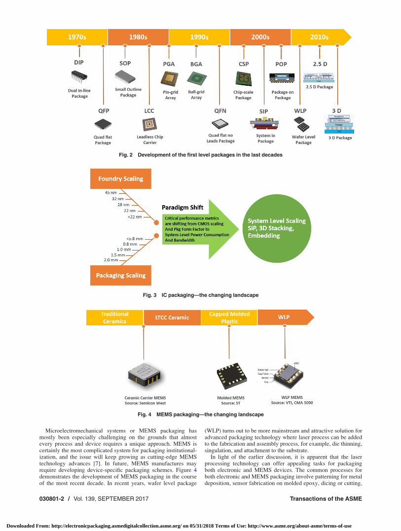
Microelectromechanical systems or MEMS packaging hasmostly been especially challenging on the grounds that almostevery process and device requires a unique approach. MEMS iscertainly the most complicated system for packaging institutional-ization, and the issue will keep growing as cutting-edge MEMStechnology advances [7]. In future, MEMS manufactures mayrequire developing device-specific packaging schemes. Figure 4demonstrates the development of MEMS packaging in the courseof the most recent decade. In recent years, wafer level package
(WLP) turns out to be more mainstream and attractive solution foradvanced packaging technology where laser process can be addedto the fabrication and assembly process, for example, die thinning,singulation, and attachment to the substrate.
In light of the earlier discussion, it is apparent that the laserprocessing technology can offer appealing tasks for packagingboth electronic and MEMS devices. The common processes forboth electronic and MEMS packaging involve patterning for metaldeposition, sensor fabrication on molded epoxy, dicing or cutting,
Fig. 2 Development of the first level packages in the last decades
Fig. 3 IC packaging—the changing landscape
Fig. 4 MEMS packaging—the changing landscape
030801-2 / Vol. 139, SEPTEMBER 2017 Transactions of the ASME
Downloaded From: http://electronicpackaging.asmedigitalcollection.asme.org/ on 05/31/2018 Terms of Use: http://www.asme.org/about-asme/terms-of-use
drilling for 3D integration, and joining of similar or dissimilarmaterials for encapsulation as well as electrical interconnection,all of which can be performed by a laser. The laser processingtechniques employed in packaging technologies use high-densitypower at a very small spot size typically at micrometer scales.The heating and cooling rate associated with laser processing arevery high that results in very little or no thermal effects on sur-rounding components. This inherent quality of laser processingcan mitigate some of the difficulties associated with small-scalepackaging as needed for packaging today’s electronic and MEMSdevices. Thus, the laser processing technology is finding an expandingnumber of uses in the manufacture of the advanced microelectronicand MEMS devices [8]. The adaptability of computer-controlled laserprocessing yields rapid turnaround times, improved precision, andreasonable pricing. It is a noncontact and clean processing methodthat can offer exact shape, size, and print registration. These mul-tiple abilities show why laser processing is becoming more widelyadopted in flexible packaging applications [9], which is discussedin detail in Sec. 3. Digital laser processing technology allowsusers to laser cut, etch, and mark on almost any material includingplastics, metals, silicone rubbers, fabrics, composites, laminatingadhesives, and other advanced materials. The main benefit is thatany design can be transferred from graphic software to laser sys-tem software to perform the laser processing. It also permits toperform multiprocess, for example, cut, imprint, and stamp in onestage. In this paper, recent advances in laser fabrication of elec-tronic and MEMS packages are reviewed. First, various laserprocessing technologies used in general are briefly discussed. Thetechniques that are currently being utilized by packaging indus-tries as well as explored by researchers are also presented. Empha-sis is given on the laser processing methods that have the potentialto revolutionize electronic and MEMS packaging industry.
2 Common Laser Processing Methods
The uses of laser technology in manufacturing electronics andMEMS packaging are broad, including fast printed circuit board(PCB) prototyping, PCB depaneling, surface-mount technology
(SMT) stencils, laser welding and soldering, laser direct structur-ing (LDS), laser micromachining and decapsulation, laser mark-ing on silicon chip, laser dicing, and singulation. In Secs. 2.1–2.6,several common laser processing techniques used in differentapplication areas are described in brief.
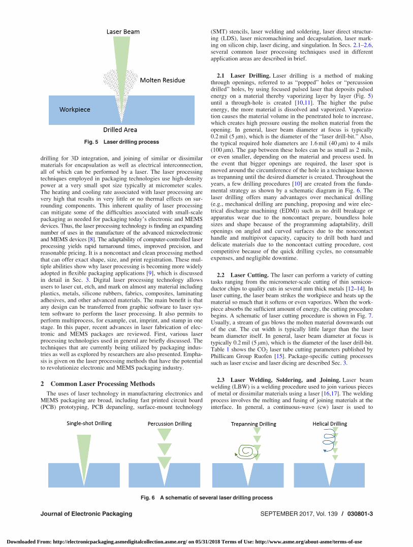
2.1 Laser Drilling. Laser drilling is a method of makingthrough openings, referred to as “popped” holes or “percussiondrilled” holes, by using focused pulsed laser that deposits pulsedenergy on a material thereby vaporizing layer by layer (Fig. 5)until a through-hole is created [10,11]. The higher the pulseenergy, the more material is dissolved and vaporized. Vaporiza-tion causes the material volume in the penetrated hole to increase,which creates high pressure ousting the molten material from theopening. In general, laser beam diameter at focus is typically0.2 mil (5 lm), which is the diameter of the “laser drill-bit.” Also,the typical required hole diameters are 1.6 mil (40 lm) to 4 mils(100 lm). The gap between these holes can be as small as 2 mils,or even smaller, depending on the material and process used. Inthe event that bigger openings are required, the laser spot ismoved around the circumference of the hole in a technique knownas trepanning until the desired diameter is created. Throughout theyears, a few drilling procedures [10] are created from the funda-mental strategy as shown by a schematic diagram in Fig. 6. Thelaser drilling offers many advantages over mechanical drilling(e.g., mechanical drilling are punching, proposing and wire elec-trical discharge machining (EDM)) such as no drill breakage orapparatus wear due to the noncontact prepare, boundless holesizes and shape because of the programming adaptability, drillopenings on angled and curved surfaces due to the noncontacthandle and multipivot capacity, capacity to drill both hard anddelicate materials due to the noncontact cutting procedure, costcompetitive because of the quick drilling cycles, no consumableexpenses, and negligible downtime.
2.2 Laser Cutting. The laser can perform a variety of cuttingtasks ranging from the micrometer-scale cutting of thin semicon-ductor chips to quality cuts in several mm thick metals [12–14]. Inlaser cutting, the laser beam strikes the workpiece and heats up thematerial so much that it softens or even vaporizes. When the work-piece absorbs the sufficient amount of energy, the cutting procedurebegins. A schematic of laser cutting procedure is shown in Fig. 7.Usually, a stream of gas blows the molten material downwards outof the cut. The cut width is typically little larger than the laserbeam diameter itself. In general, laser beam diameter at focus istypically 0.2 mil (5 lm), which is the diameter of the laser drill-bit.Table 1 shows the CO2 laser tube cutting parameters published byPhillicam Group Ruofen [15]. Package-specific cutting processessuch as laser excise and laser dicing are described Sec. 3.
2.3 Laser Welding, Soldering, and Joining. Laser beamwelding (LBW) is a welding procedure used to join various piecesof metal or dissimilar materials using a laser [16,17]. The weldingprocess involves the melting and fusing of joining materials at theinterface. In general, a continuous-wave (cw) laser is used to
Fig. 5 Laser drilling process
Fig. 6 A schematic of several laser drilling process
Journal of Electronic Packaging SEPTEMBER 2017, Vol. 139 / 030801-3
Downloaded From: http://electronicpackaging.asmedigitalcollection.asme.org/ on 05/31/2018 Terms of Use: http://www.asme.org/about-asme/terms-of-use
deliver a concentrated heat creating narrow and deep welds at highrates. LBW uses high power density (on the order of 1 MW/cm2)with little heat-affected zones, and heating and cooling rates arevery high. The spot size of the laser can vary between 0.2 mm and13 mm; however, typically smaller sizes are utilized for welding.Another class of laser joining involves melting of one part (trans-mission bonding) or no melting at all (conduction bonding), creat-ing chemical bonds and mechanical interaction at the interface. Aschematic representation of transmission laser microjoining proce-dure is shown in Fig. 8 where the laser is transmitted through thetop layer (transparent at the laser wavelength) depositing energy atthe interface that initiates the formation of chemical bonds. Com-pared with typical joining processes such as adhesive joining andsoldering, laser welding or joining have several advantages such asless damage on workpieces, higher production rates, joining
dissimilar materials with no filler, and practically no flux or otherpromoter needed to improve joint quality.
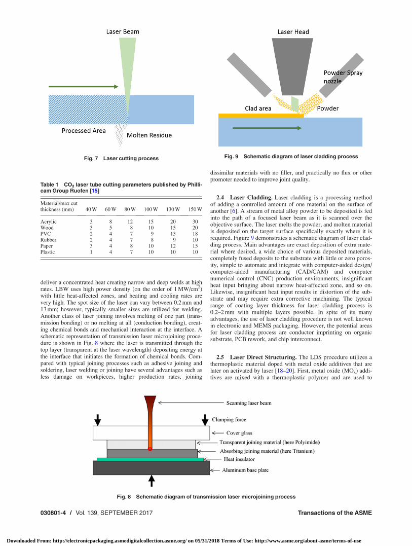
2.4 Laser Cladding. Laser cladding is a processing methodof adding a controlled amount of one material on the surface ofanother [6]. A stream of metal alloy powder to be deposited is fedinto the path of a focused laser beam as it is scanned over theobjective surface. The laser melts the powder, and molten materialis deposited on the target surface specifically exactly where it isrequired. Figure 9 demonstrates a schematic diagram of laser clad-ding process. Main advantages are exact deposition of extra mate-rial where desired, a wide choice of various deposited materials,completely fused deposits to the substrate with little or zero poros-ity, simple to automate and integrate with computer-aided design/computer-aided manufacturing (CAD/CAM) and computernumerical control (CNC) production environments, insignificantheat input bringing about narrow heat-affected zone, and so on.Likewise, insignificant heat input results in distortion of the sub-strate and may require extra corrective machining. The typicalrange of coating layer thickness for laser cladding process is0.2–2 mm with multiple layers possible. In spite of its manyadvantages, the use of laser cladding procedure is not well knownin electronic and MEMS packaging. However, the potential areasfor laser cladding process are conductor imprinting on organicsubstrate, PCB rework, and chip interconnect.
2.5 Laser Direct Structuring. The LDS procedure utilizes athermoplastic material doped with metal oxide additives that arelater on activated by laser [18–20]. First, metal oxide (MOx) addi-tives are mixed with a thermoplastic polymer and are used to
Table 1 CO2 laser tube cutting parameters published by Philli-cam Group Ruofen [15]
Material/max cutthickness (mm) 40 W 60 W 80 W 100 W 130 W 150 W
Acrylic 3 8 12 15 20 30Wood 3 5 8 10 15 20PVC 2 4 7 9 13 18Rubber 2 4 7 8 9 10Paper 3 4 8 10 12 15Plastic 1 4 7 10 10 10
Fig. 8 Schematic diagram of transmission laser microjoining process
Fig. 7 Laser cutting process Fig. 9 Schematic diagram of laser cladding process
030801-4 / Vol. 139, SEPTEMBER 2017 Transactions of the ASME
Downloaded From: http://electronicpackaging.asmedigitalcollection.asme.org/ on 05/31/2018 Terms of Use: http://www.asme.org/about-asme/terms-of-use

manufacture parts using injection molding process. A laser thencreates a track of the circuit trace on the surface of the injectionmolded doped plastic. The laser energy activates the additiveswithin the organic matrix into a species that is catalytically effec-tive for the subsequent chemical metallization. No nucleationoccurs during the processing of doped thermoplastic owing to thegood temperature resistance of MOx additives. The laser-activatedplastic parts are then subjected to metallization in chemical copperbaths. The additive has a catalytic effect in the irradiated areas sothat the metallization takes place only in the laser-structured areasof the component. It is observed that the MOx additives have noeffects on the electrical characteristics of the LDS deposited metaltraces [19]. A schematic of LDS procedure is shown in Fig. 10.
2.6 Laser-Assisted Deposition. The best-known laser-assisteddeposition procedures are ablative sputtering and laser chemicalvapor deposition (LCVD) methods [21]. By ablative sputtering,also known as pulsed laser deposition (PLD), the material isremoved from a solid target in a partial vacuum and redepositedon the workpiece [22,23]. Like conventional (RF/magnetron)sputtering, the PLD process is unable to create deposition inselected regions; rather it deposits materials on all exposed surfa-ces of the workpiece. The main advantage of the process is thathigh melting point and multicomponent materials can be depos-ited, which is not otherwise possible by other deposition methods.
3 Currently Used Laser-Based Packaging Processes
In Sec. 2, very common laser processing methods that are usedby various industries are outlined. In this section, focus is givenon the popular laser technologies adopted specifically by elec-tronic and MEMS packaging industries. While discussing thesetechniques, efforts by various researchers in the field that are pub-lished in the literature are also discussed.
3.1 Laser Drilling for Microvia Plating. The current pro-gress in superior handheld devices such as smart phones and tabletPCs is playing a critical role in the growth of the electronicsindustry. These devices incorporate high-density interconnection(HDI) that requires multilayer PCB with the electrical connectionbetween layers through interlayer vias. Four microvia creationprocesses such as laser drilling, ultraviolet (UV) exposed viamechanical drilling and plasma etching, are widely used. As ofnow, CO2 laser drilling machines are broadly used in the process-ing of interlayer microvias. Every technology has its own meritsand demerits; however, the laser drilling method is the leadingtechnology in creating blind microvias when considering cost pervia, quality, size and its dynamic range, and throughput [10].
Table 2 demonstrates the range in via sizes that the present lasertechnology offers. More than 90% of blind microvia are formedwith laser technology as shown in Table 2. In addition to blindvias, lasers are used to create buried or through microvias in HDIPCB technology as well (Fig. 11). Sun and Swenson [24] demon-strated the utilization of solid-state UV laser and CO2 lasers inelectronic packaging including via formation on PCB and via for-mation on a silicon wafer.
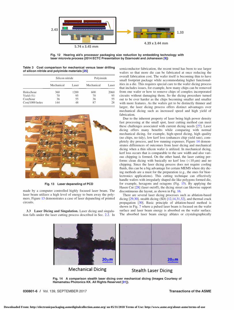
The laser drilling technology offers a good solution to packagesize reduction; one of the applications is the scaling down of hear-ing aid processors. Figure 12 demonstrates the level of size reduc-tion of a chip utilizing embedded die chip-in-flex (CIF) technologywhere laser microvia are used [9]. The CIF multichip moduleturned out to be very a successful design compared to the earlierceramic hybrid-based design. It may be mentioned here that theoriginal device was 5.74 mm� 3.45 mm� 2.43 mm thick, while thenew device was 4.39 mm� 3.44 mm� 1.325 mm thick. The lasermicrovia technology was able to achieve a volumetric size reduc-tion of 60%. The cost tradeoff between mechanical and laser viadrilling still needs some considerations. Dr. Alan Ferguson fromOxford Lasers presented a high-level report at IEE SW test work-shop on June 2008 [25] where he reported the drilling rates and tol-erances for silicon nitride and polyimide. Table 3 shows acomparison between mechanical and laser drilling of SiN and poly-imide. It is clear from the data that although the hourly rate for laserprocessing method is higher than mechanical drilling, the laserprocessing is more cost-effective for high-volume processing.
3.2 Laser Excise for Panel Singulation. Laser excise is adepaneling procedure that extracts varieties of parts from a biggersheet or board of both rigid and flex circuit [26]. Flexible circuitsare ordinarily manufactured in sheet or roll formats. One of thelast steps in the fabrication process is to extract the part from thesubstrate. There are various approaches to defining the circuits.The typical methods utilized in the flex circuit industry are ruleddie cutting, mechanical punching, and laser skiving. The trade-offs among all the singulation processes include cost, precision, orproductivity. However, the laser extracting technology offers thehighest level of accuracy as compared with any other excise tech-nology and capable of making complex shapes. Laser excisingmethod utilizes the technology where a circuit cutline can beFig. 10 LDS process and laser activation principle
Table 2 Microvia drilling technology in PCD (Coherent [11])
Drilling techniques Microvia size (lm) User applications (%)
Mechanical 100–300 1Plasma >25 to 100 2Photo-via >50 to 300 3CO2 laser >25 to 250Laser (UV) <25 to 150 94
Fig. 11 Types of vias in HDI PCB technology
Journal of Electronic Packaging SEPTEMBER 2017, Vol. 139 / 030801-5
Downloaded From: http://electronicpackaging.asmedigitalcollection.asme.org/ on 05/31/2018 Terms of Use: http://www.asme.org/about-asme/terms-of-use
made by a computer controlled highly focused laser beam. Thelaser beam utilizes a high level of energy to burn away the poly-mers. Figure 13 demonstrates a case of laser depaneling of printedcircuits.
3.3 Laser Dicing and Singulation. Laser dicing and singula-tion falls under the laser cutting process described in Sec. 2.2. In
semiconductor fabrication, the recent trend has been to use largerwafers so that more die can be fabricated at once reducing theoverall fabrication cost. The wafer itself is becoming thin to havesmall footprint package while accommodating higher functional-ities in a die. This requires special care to the wafer dicing processthat includes issues, for example, how many chips can be removedfrom one wafer or how to remove chips of complex incorporatedcircuits without damaging them. So the dicing procedure turnedout to be ever harder as the chips becoming smaller and smallerwith more features. As the wafers get to be distinctly thinner andlarger, the laser dicing process offers distinct advantages overmechanical dicing such as increased speed and high yield offabrication.
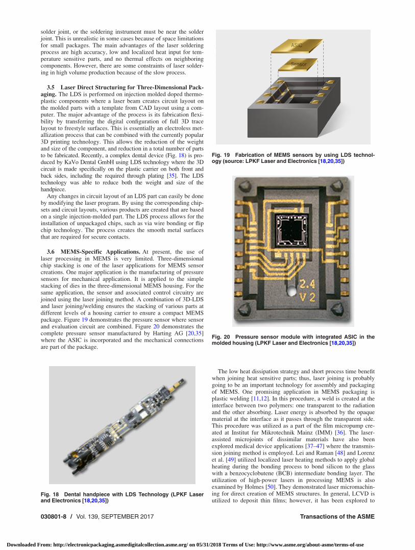
Due to the inherent property of laser being high power densityfast processing at the small spot, laser cutting method can meetthese challenges associated with current dicing needs [27]. Laserdicing offers many benefits while comparing with normalmechanical dicing, for example, high-speed dicing, high quality(no chips, no tidy), low kerf loss (enhances chip yield rate), com-pletely dry process, and low running expenses. Figure 14 demon-strates differences of outcomes from laser dicing and mechanicaldicing when a thin silicon wafer is utilized. In mechanical dicing,kerf loss occurs that is comparable to the saw width and also vari-ous chipping is formed. On the other hand, the laser cutting per-forms clean dicing with basically no kerf loss (<10 lm) and nochipping. Since the laser dicing process does not require coolingfluids, this can be a big advantage for certain MEMS where dry dic-ing methods are a must for the preparation (e.g., the ones for bioe-lectronics applications). This cutting technique can effectivelyhandle wafers with irregularly shaped die like polygons formed die,for example, hexagons and octagons (Fig. 15). By applying theHasen Cut [28] (laser on/off), the dicing street can likewise supportdiscontinuous die layout, as shown in Fig. 16.
There are several laser dicing processes such as ablation-baseddicing [29,30], stealth dicing (SD) [12,14,31,32], and thermal crackpropagation [30]. Basic principle of ablation-based method isshown in Fig. 7 where a pulsed laser beam is focused on the wafersurface and laser beam energy is absorbed on the wafer surface.The absorbed laser beam energy ablates or crystalographically
Fig. 12 Hearing aid’s processor packaging size reduction by embedding technology withlaser microvia process (2014 ECTC Presentation by Dzarnoski and Johansson [9])
Table 3 Cost comparison for mechanical versus laser drillingof silicon nitride and polyimide materials [25]
Silicon nitride Polyimide
Mechanical Laser Mechanical Laser
Holes/hour 360 1200 600 2060Yield (%) 70 95 70 95Cost/hour 36 55 36 55Cost/1000 holes 144 48 87 28
Fig. 13 Laser depaneling of PCD
Fig. 14 A comparison stealth laser dicing over mechanical dicing (Images Courtesy ofHamamatsu Photonics KK. All Rights Reserved [31]).
030801-6 / Vol. 139, SEPTEMBER 2017 Transactions of the ASME
Downloaded From: http://electronicpackaging.asmedigitalcollection.asme.org/ on 05/31/2018 Terms of Use: http://www.asme.org/about-asme/terms-of-use

deforms the wafer surface depending on the amount of absorbedenergy. If needed, the wafer is scanned multiple times until a cut ismade to the tape. Although the method offers vibration free proc-essing, the influence of heat and contamination from debris is animportant concern in the laser ablation method. When the surfaceof a wafer is ablated, the particles adhere to the wafer surface andthey become contaminants [32]. This concern is addressed bydeveloping a cleaner process called SD technique. In SD method,laser beam at a wavelength capable of transmitting trough a semi-conductor wafer (usually a solid-state laser with the wavelength of1064 nm) is focused at a point inside the semiconductor wafer byusing an objective lens. The pulsed laser with short pulse width andhigh repetition rate is condensed up to a diffraction threshold levelin the vicinity of its focal point. This localized energy creates sub-surface defects which act as crack initiation sites and guides forseparation. The next step is the tape expansion process in which acylindrical stage pushes up dicing tape separating the die along theSD lines. Figure 17 shows a schematic diagram of the SD processand the formation of a modified layer. Since the laser processingoccurs only at the inside of the wafer, the SD method offer manyadvantages over ablation-based process such as high quality (nochips and dust-free), ultra-thin chips, low kerf loss (better chip pro-duction yield), and completely dry process [12,32]. SD process canhandle 10 lm kerf width, which is an important technical advantagethat improves the chip yield per wafer [12]. Table 4 shows Hama-matsu’s Stealth technical data on chip yield improvement due to10 lm kerf width [12]. More recently, a similar process has beenexplored by Haupt et al. [30] where a near-infrared (1047 nm) cwbeam was utilized to produce thermal stress and consequently con-trolled fracture of 220-lm-thick silicon wafers.
3.4 Laser Soldering Process for Highly Integrated Three-Dimensional Packaging. Laser soldering procedures can besuccessfully employed where regular as well as customizablepoint-specific soldering is needed. The small spot size, high powerdensity laser beam offers many favorable conditions, especially
for scaled down subassemblies or sensitive components. The pro-cedure does not harm or contribute heat into adjacent components.Thus, even small electronic components in the order of a coupleof tenths of a millimeter as well as heat sensitive electronic partscan be soldered. Quick power controllability coupled with a non-contact temperature estimation to minimize thermal effect makesthe laser welding a very attractive soldering technique. In laserwelding process, the filler metal or compound is heated to its soft-ening temperatures around 450 �C. In this manner, lasers withlower yield powers (regularly <100 W) are utilized to melt thewire material, soldering paste, or solder deposits between twofirmly placed joining materials [33]. Choi and Kim [34] exhibiteda procedure to create Cu bumps on a substrate utilizing a modifiedlaser beam.
Traditional welding systems such as the soldering iron require adirect mechanical contact between the welding apparatus and the
Fig. 15 Wafer laser dicing with hexagon die process
Fig. 16 Wafer laser dicing with offset processing
Fig. 17 Basic principle of SD method
Table 4 Improved chip yield data per wafer from SD [12]
Blade dicing Stealth dicing
Work size (mm) 152Dicing street width (lm) 80 10Chip size (mm) 2� 2Effective number of chips (pcs) 3732 3996Increased number of chips/wafer (pcs) — 264Improved yield (%) 107.1
Journal of Electronic Packaging SEPTEMBER 2017, Vol. 139 / 030801-7
Downloaded From: http://electronicpackaging.asmedigitalcollection.asme.org/ on 05/31/2018 Terms of Use: http://www.asme.org/about-asme/terms-of-use
solder joint, or the soldering instrument must be near the solderjoint. This is unrealistic in some cases because of space limitationsfor small packages. The main advantages of the laser solderingprocess are high accuracy, low and localized heat input for tem-perature sensitive parts, and no thermal effects on neighboringcomponents. However, there are some constraints of laser solder-ing in high volume production because of the slow process.
3.5 Laser Direct Structuring for Three-Dimensional Pack-aging. The LDS is performed on injection molded doped thermo-plastic components where a laser beam creates circuit layout onthe molded parts with a template from CAD layout using a com-puter. The major advantage of the process is its fabrication flexi-bility by transferring the digital configuration of full 3D tracelayout to freestyle surfaces. This is essentially an electroless met-allization process that can be combined with the currently popular3D printing technology. This allows the reduction of the weightand size of the component, and reduction in a total number of partsto be fabricated. Recently, a complex dental device (Fig. 18) is pro-duced by KaVo Dental GmbH using LDS technology where the 3Dcircuit is made specifically on the plastic carrier on both front andback sides, including the required through plating [35]. The LDStechnology was able to reduce both the weight and size of thehandpiece.
Any changes in circuit layout of an LDS part can easily be doneby modifying the laser program. By using the corresponding chip-sets and circuit layouts, various products are created that are basedon a single injection-molded part. The LDS process allows for theinstallation of unpackaged chips, such as via wire bonding or flipchip technology. The process creates the smooth metal surfacesthat are required for secure contacts.
3.6 MEMS-Specific Applications. At present, the use oflaser processing in MEMS is very limited. Three-dimensionalchip stacking is one of the laser applications for MEMS sensorcreations. One major application is the manufacturing of pressuresensors for mechanical application. It is applied to the simplestacking of dies in the three-dimensional MEMS housing. For thesame application, the sensor and associated control circuitry arejoined using the laser joining method. A combination of 3D-LDSand laser joining/welding ensures the stacking of various parts atdifferent levels of a housing carrier to ensure a compact MEMSpackage. Figure 19 demonstrates the pressure sensor where sensorand evaluation circuit are combined. Figure 20 demonstrates thecomplete pressure sensor manufactured by Harting AG [20,35]where the ASIC is incorporated and the mechanical connectionsare part of the package.
The low heat dissipation strategy and short process time benefitwhen joining heat sensitive parts; thus, laser joining is probablygoing to be an important technology for assembly and packagingof MEMS. One promising application in MEMS packaging isplastic welding [11,12]. In this procedure, a weld is created at theinterface between two polymers: one transparent to the radiationand the other absorbing. Laser energy is absorbed by the opaquematerial at the interface as it passes through the transparent side.This procedure was utilized as a part of the film micropump cre-ated at Institut fur Mikrotechnik Mainz (IMM) [36]. The laser-assisted microjoints of dissimilar materials have also beenexplored medical device applications [37–47] where the transmis-sion joining method is employed. Lei and Raman [48] and Lorenzet al. [49] utilized localized laser heating methods to apply globalheating during the bonding process to bond silicon to the glasswith a benzocyclobutene (BCB) intermediate bonding layer. Theutilization of high-power lasers in processing MEMS is alsoexamined by Holmes [50]. They demonstrated laser micromachin-ing for direct creation of MEMS structures. In general, LCVD isutilized to deposit thin films; however, it has been explored to
Fig. 18 Dental handpiece with LDS Technology (LPKF Laserand Electronics [18,20,35])
Fig. 19 Fabrication of MEMS sensors by using LDS technol-ogy (source: LPKF Laser and Electronics [18,20,35])
Fig. 20 Pressure sensor module with integrated ASIC in themolded housing (LPKF Laser and Electronics [18,20,35])
030801-8 / Vol. 139, SEPTEMBER 2017 Transactions of the ASME
Downloaded From: http://electronicpackaging.asmedigitalcollection.asme.org/ on 05/31/2018 Terms of Use: http://www.asme.org/about-asme/terms-of-use
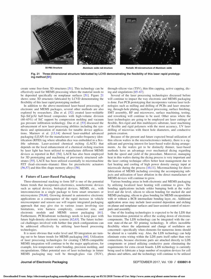
create some free-form 3D structures [51]. This technology can beeffectively used for MEMS processing where the material needs tobe deposited specifically on nonplanar surfaces [51]. Figure 21shows some 3D structures fabricated by LCVD demonstrating theflexibility of this laser rapid prototyping method.
In addition to the above-mentioned laser-based processing ofelectronic and MEMS packages, several other methods are alsoexplored by researchers. Zhu et al. [52] created laser-weldableSip–SiCp/Al half-breed composites with high-volume division(60–65%) of SiC support by compression molding and vacuumgas pressure infiltration technology. Das et al. [53] discussed theadvancement of new laser-processing abilities including the syn-thesis and optimization of materials for tunable device applica-tions. Marinov et al. [13,14] showed laser-enabled advancedpackaging (LEAP) for the manufacture of a radio-frequency iden-tification (RFID) tag where ultrathin dice was embedded in a flex-ible substrate. Laser-assisted chemical etching (LACE) thatdepends on the local enhancement of a chemical etching reactionby laser light has been utilized to manufacture different MEMSdevices as reported in Ref. [54]. LACE has also been employedfor 3D prototyping and machining of previously structured sub-strates [55]. LACE has been utilized essentially to micromachinePZT (lead–zirconate–titanate) films for piezoelectric actuators[56,57] and thin film shape memory alloys [58].
4 Future of Laser-Based Packaging
Three-dimensional stacking to form SiP is one of the potentialfuture trends that incorporates electronics, nonelectronic devicessuch as optical devices, biological devices, MEMS, etc., withinterconnection in a single package to form smart structures ormicrosystems [59,60]. Growing demand in automotive electronicapplications as a consequence of the rapid increase in vehiclemicrocomputer and sensors use will require integrated packagingapproach that may give rise to various issues involving sizelimitations, wire harness complexity, connector size, andelectronic module and MEMS sensor packaging [61].Furthermore, PCB/substrate technology needs to keep pace withfuture high-density electronic systems [62,63]. The future techni-cal challenges involved with further fine pitch configurations canbe addressed effectively by utilizing laser-based processingtechnologies.
It is more obvious that wafer level and 3D integration are turn-ing out to be future trends for MEMS packaging [64]. Utilizationof laser processing technologies for creating CMOS-compatibleMEMS integration will continue to be the major applications, forexample, low-temperature wafer bonding, precision molding, andencapsulations. Other potential uses of laser technology in futureMEMS packaging may well be through-glass vias (TGV),
through-silicon vias (TSV), thin film capping, active capping, dic-ing and singulations [65–67].
Several of the laser processing technologies discussed beforewill continue to impact the way electronic and MEMS packagingis done. Fast PCB prototyping that incorporates various laser tech-nologies such as milling and drilling of PCBs and laser structur-ing, through-hole plating, multilayer processing, surface finishing,SMT assembly, RF and microwave, surface machining, testing,and reworking will continue to be used. Other areas where thelaser technologies are going to be employed are laser cuttings offlexible, flex-rigid and thin multilayers substrate, laser machiningof flexible and rigid polymers with the most accuracy, UV laserdrilling of microvias with finest hole diameters, and conductivepattern creation.
Because of the present and future expected broad utilization ofthin silicon wafers in the microelectronics industry, there is a sig-nificant and growing interest for laser-based wafer dicing arrange-ments. As the wafers get to be distinctly thinner, laser-basedmethods have an advantage over mechanical dicing regardingboth the speed and yield of the procedure. Moreover, managingheat in thin wafers during the dicing process is very important andthe laser cutting technique offers better heat management due tofast heating and cooling of high power density energy input atmicroscale during the process [10,11]. Micromachining for directfabrication of MEMS including covering the accompanying sub-jects and utilization of laser ablation in the direct manufacture ofMEMS devices will continue to grow.
Various bonding areas in both electronic and MEMS packagingby utilizing localized laser heating will continue to grow. Thebonding applications include solder bumping both at the waferlevel and die level, silicon to silicon bonding for stacked die andMEMS packaging, silicon to glass bonding for MEMS encapsulationwith or without a BCB intermediate bonding layer, etc. Additionalapplication areas may include laser-assisted deposition and etchingon planar and nonplanar surfaces and laser-assisted control of micro-parts and assembly.
One of the leading technologies is expected to be the LDS thathas tremendous potential to affect the scaling down of electroniccomponents. The LDS technology can be integrated with the cur-rent state-of-the-art 3D printing technology. It offers incredibleflexibility where the adjustment and change of usefulness areconcerned—specifically when elements for numerous items shouldbe altered in a variable way. Also, the LDS technology can helpeliminate extra wiring within the LDS parts itself rather than wireconnections, because electronic parts are attached directly to LDScomponents or joined utilizing conductive paste eliminating therequirements for extra circuit boards. LDS technology is currentlybeing used to fabricate a large number of reception devices for cellphones and tablets, and the technology will continue to be utilized
Fig. 21 Three-dimensional structure fabricated by LCVD demonstrating the flexibility of this laser rapid prototyp-ing method [51]
Journal of Electronic Packaging SEPTEMBER 2017, Vol. 139 / 030801-9
Downloaded From: http://electronicpackaging.asmedigitalcollection.asme.org/ on 05/31/2018 Terms of Use: http://www.asme.org/about-asme/terms-of-use

in the field. Another application of LDS is medicinal hardware thatrequires smaller sizes with an increased number of functionalities.One of the great illustrations is shown in Fig. 22 where the electricalcircuit board for steering wheels manufactured by TRW Automotivefor BMW decreases the requirement for extra wiring [16,35].
5 Summary
This paper has briefly evaluated several laser processing tech-nologies in electronic and MEMS packaging. Laser technologiesoffer unique capabilities in regard to materials adaptability and3D structures. They can be combined with standard fabricationtechniques making a huge impact on the advancement of futureelectronics and MEMS packages. Key application areas are prob-ably going to be 3D packaging with better manufacturability,antenna and radio frequency packaging, medicinal wearabledevice packaging, MEMS sensors and actuators in light of practi-cal materials, and microfluidic parts and systems.
References[1] Datta, M., Osaka, T., and Schultze, J. W., 2004, Microelectronic Packaging,
CRC Press, Boca Raton, FL.[2] Vardaman, E. J., 2015, “IoT and the Impact on MEMS and Sensors Packaging,”
Tech Search International Report, Tech Search International, Austin, TX, accessedFeb. 28, 2017, http://www.meptec.org/resources/4%20-%20vardaman.pdf
[3] LaPedus, M., 2012, “Foundry Landscape Changes in 3D,” Semiconductor Engi-neering, accessed Feb. 28, 2017, http://semiengineering.com/foundry-land-scape-changes-in-3d/
[4] Szendiuch, I., 2011, “Development in Electronic Packaging—Moving to 3DSystem Configuration,” Radio Eng., 209(1), pp. 214–220.
[5] Tummala, R., 2001, Fundamentals of Microsystems Packaging, McGraw-Hill,New York.
[6] Andersson, O., and Parker, K., 2014, “High Power Diode Laser Cladding,” Fabri-cating and Metalworking, Birmingham, AL, accessed Feb. 28, 2016, http://www.fabricatingandmetalworking.com/2014/03/high-power-diode-laser-cladding/
[7] Gilleo, K., 2006, “MEMS Packaging: History and Current Trends,” MEMS J., 8,epub, accessed Mar. 22, 2017, http://www.memsjournal.com/2006/08/mems_packaging_.html
[8] Bustillo, J. M., Howe, R. T., and Muller, R. S., 1998, “Surface Micromachiningfor Microelectromechanical Systems,” Proc. IEEE, 86(8), pp. 1552–1574.
[9] Dzarnoski, J., and Johansson, S., 2014, “Ultra Small Hearing Aid ElectronicPackaging Enabled by Chip-In-Flex,” IEEE 64th Electronic Components andTechnology Conference (ECTC), Lake Buena Vista, FL, May 27–30, 157–164.
[10] TRUMPF, 2016, “Laser Cutting and Drilling,” TRUMPF, Plymouth, MI,accessed Feb. 28, 2016, http://www.trumpf-laser.com
[11] Coherent, 2016, “Laser Cutting and Applications,” Coherent Inc., Santa Clara,CA, accessed Feb. 28, 2016, https://www.coherent.com
[12] Hamamatsu Photonics KK, 2014, “Stealth Dicing Technical Information forMEMS,” Technical Report, Hamamatsu Photonics KK, Iwata, Japan, accessedMar. 22, 2017, https://www.hamamatsu.com/resources/pdf/etd/SD_tech_forMEMS_TLAS9005E.pdf
[13] Marinov, V., Swenson, O., Miller, R., Sarwar, F., Atanasov, Y., Semler, M.,and Datta, S., 2012, “Laser-Enabled Advanced Packaging of Ultrathin Bare
Dice in Flexible Substrates,” IEEE Trans. Compon., Packag., Manuf. Technol.,2(4), pp. 569–577.
[14] Marinov, V. R., Swenson, O., Atanasov, Y., and Schneck, N., 2013, “Laser-Assisted Ultrathin die Packaging: Insights From a Process Study,” Microelec-tron. Eng., 101, pp. 23–30.
[15] PHILICAM, 2015, “CO2 Laser Tube Cutting Parameter,” Jinan RuofenMachinery Co. Ltd, Shandong, China, accessed Feb. 28, 2016, http://www.co2-lasercutter.cn/support/knowledge/35.html
[16] Chaminade, C., Fogarassy, E., and Boisselier, D., 2006, “Diode Laser SolderingUsing a Lead-Free Filler Material for Electronic Packaging Structures,” Appl.Surf. Sci., 252(13), pp. 4406–4410.
[17] Liu, Y., Zeng, L., and Wang, C., 2008, “In-Situ Temperature Monitoring forProcess Control in Laser Assisted Polymer Bonding for MEMS Packaging,”IEEE 2nd Electronics System Integration Technology Conference (ESTC),Greenwich, London, Sept. 1–8, pp. 199–205.
[18] LPKF, 2016, “LDS Technology,” LPKF Laser and Electronics AG, Garbsen,Germany, accessed Feb. 28, 2016, http://www.lpkf.com
[19] Goth, C., and Romer, M., 2014, “Laser Direct Structuring and Two-ComponentInjection Molding for MID Series Production,” HARTING Mitronics, Bern,Switzerland, accessed Feb. 28, 2016, http://www.harting-mitronics.ch/fileadmin/hartingmitronics/white_papers/Laser_direct_structuring_and_two-component_injection_molding_for_MID_series_production.pdf
[20] LaserMicronics, 2016, “Three-Dimensional Circuits With LDS—Laser DirectStructuring and Metallization for 3D Mechatronic Integrated Devices,” Laser-Micronics, Garbsen, Germany, accessed Feb. 28, 2017, http://www.lasermicro-nics.com/_mediafiles/80-lds-technology-for-moulded-interconnect-devices.pdf
[21] Gower, M. C., 1994, “Excimer Lasers: Current and Future Applications inIndustry and Medicine,” Laser Processing in Manufacturing, R. C. Crafer andP. J. Oakley, eds., Springer, Dordrecht, The Netherlands, pp. 189–271.
[22] Bauerle, D., 1986, Chemical Processing With Lasers, Vol. 1, Springer-Verlag,Berlin.
[23] Kovacs, G. T. A., Maluf, N. L., and Petersen, K. E., 1998, “Bulk Micromachin-ing of Silicon,” Proc. IEEE, 86(8), pp. 1536–1551.
[24] Sun, Y., and Swenson, E., 2003, “Lasers in Electronics Packaging,” Fifth Inter-national Conference on Electronic Packaging Technology (ICEPT), Shanghai,China, Oct. 28–30, p. 137.
[25] Ferguson, A., 2008, “Comparison of Drilling Rates and Tolerances of Laser-Drilled Holes in Silicon Nitride and Polyimide Vertical Probe Cards,” IEEE SWTest Workshop, Semiconductor Test Workshop, San Diego, CA, June 8–11,accessed Feb. 28, 2017, http://www.swtest.org/swtw_library/2008proc/pdf/s06_01_ferguson_swtw2008.pdf
[26] All Flex, 2016, “Existing Flexible Circuits,” All Flex Flexible Circuits, North-field, MN, accessed Feb. 28, 2017, http://www.allflexinc.com/blog/excising-flexible-circuits/
[27] Bovatsek, J. M., and Patel, R. S., 2010, “Highest-Speed Dicing of Thin SiliconWafers With Nanosecond-Pulse 355nm q-Switched Laser Source Using Line-Focus Fluence Optimization Technique,” Proc. SPIE, 7585, p. 75850K.
[28] FOTONiKA, 2017, “FOTONiKA, Yari iletken teknolojileri,” FOTONIKA INC.,Ankara, Turkey, accessed Feb. 28, 2017, http://www.fotonika. com.tr/index.php/en/
[29] Way, D. W. C., and Ying, L. C., 2008, “High Speed Wafer Dicing With Abla-tion Laser Cut,” IEEE/CPMT International Electronics Manufacturing Technol-ogy (IEMT) Symposium, 33rd IEEE/CPMT International ElectronicsManufacturing Technology Conference (IEMT), Penang, Malaysia, Nov. 4–6.
[30] Haupt, O., Siegel, F., Schoonderbeek, A., Richter, L., Kling, R., and Ostendorf,A., 2008, “Laser Dicing of Silicon: Comparison of Ablation Mechanisms Witha Novel Technology of Thermally Induced Stress,” J. Laser Micro/Nanoeng.,3(3), pp. 135–140.
[31] Hamamatsu Photonics KK, 2005, “Stealth Dicing Technology andApplications,” Hamamatsu Photonics KK, Iwata, Japan, accessed Mar. 22, 2017,https://www.hamamatsu.com/resources/pdf/etd/SD_tech_TLAS9004E.pdf
[32] Kumagai, M., Uchiyama, N., Ohmura, E., Sugiura, R., Atsumi, K., and Fuku-mitsu, K., 2007, “Advanced Dicing Technology for Semiconductor Wafer—Stealth Dicing,” IEEE Trans. Semiconductor Manuf., 20(3), pp. 259–265.
[33] Rofin/Coherent, 2017, “Laser Soldering: Where Conventional Soldering Tech-niques Reach Their Limits,” Rofin/Coherent, Hamburg, Germany, accessedFeb. 28, 2017, https://www.rofin.com/en/applications/laser-soldering-and-braz-ing/laser-soldering/
[34] Choi, W.-S., and Kim, J., 2012, “Laser-Assisted Deposition of Cu Bumpsfor Microelectronic Packaging,” Trans. Nonferrous Metals Soc. China, 22
(Suppl. 3), pp. s683–s687.[35] LPKF Laser and Electronics, 2014, “Three-Dimensional Circuits: LPKF LDS:
Laser Direct Structuring for 3D Molded Interconnect Devices,” LPKF Laser &Electronics AG, Garbsen, Germany, accessed Feb. 28, 2017, http://www.lpkf.com/_mediafiles/1797-lpkf-laser-direct-structuring-en.pdf
[36] K€amper, K.-P., Dopper, J., Ehrfeld, W., and Oberbeck, S., 1998, “ASelf-Filling Low-Cost Membrane Micropump,” IEEE Eleventh Annual Inter-national Workshop on Micro Electro Mechanical Systems (MEMS),Heidelberg, Germany, Jan. 25–29, pp. 432–437.
[37] Newaz, G., Mian, A., Sultana, T., Mahmood, T., Georgiev, D. G., Auner, G.,Witte, R., and Herfurth, H., 2006, “A Comparison Between Glass/Polyimideand Titanium/Polyimide Microjoint Performances in Cerebrospinal Fluid,”J. Biomed. Mater. Res. Part A, 79(1), pp. 159–165.
[38] Mian, A., Sultana, T., Georgiev, D., Witte, R., Herfurth, H., Auner, G., andNewaz, G., 2009, “Postimplantation Pressure Testing and Characterization ofLaser Bonded Glass/Polyimide Microjoints,” J. Biomed. Mater. Res. Part B,90(2), pp. 614–620.
Fig. 22 Steering wheel operating element (LPKF Laser andElectronics [18,20,35])
030801-10 / Vol. 139, SEPTEMBER 2017 Transactions of the ASME
Downloaded From: http://electronicpackaging.asmedigitalcollection.asme.org/ on 05/31/2018 Terms of Use: http://www.asme.org/about-asme/terms-of-use

[39] Mian, A., Law, J., and Newaz, G., 2010, “Analysis of Laser Fabricated Micro-joint Performance in Cerebrospinal Fluid Using a Computational Approach,”J. Mech. Behav. Biomed. Mater., 4(1), pp. 117–124.
[40] Mahmooda, T., Miane, A., Amine, M. R., Auner, G., Witte, R., Herfurth,H., and Newaza, G., 2007, “Finite Element Modeling of TransmissionLaser Microjoining Process,” J. Mater. Process. Technol., 186(1–3), pp.37–44.
[41] Georgiev, D. G., Sultana, T., Mian, A., and Auner, G., 2005, “Laser Fabricationand Characterization of Sub-Millimeter Joints Between Polyimide and Ti-Coated Borosilicate Glass,” J. Mater. Sci., 40(21), pp. 5641–5647.
[42] Mian, A., Newaz, G., Mahmood, T., and Auner, G., 2007, “Mechanical Charac-terization of Glass/Polyimide Microjoints Fabricated Using CW Fiber andDiode Lasers,” J. Mater. Sci., 42(19), pp. 8150–8157.
[43] Mian, A., Newaz, G., Georgiev, D. G., Rahman, N., Vendra, L., Auner, G.,Witte, R., and Herfurth, H., 2007, “Performance of Laser Bonded Glass/Polyi-mide Microjoints in Cerebrospinal Fluid,” J. Mater. Sci.: Mater. Med., 18(3),pp. 417–427.
[44] Mian, A., Newaz, G., Vendra, L., Rahman, N., Georgiev, D. G., Auner, G.,Witte, R., and Herfurth, H., 2005, “Laser Bonded Microjoints Between Tita-nium and Polyimide for Applications in Medical Implants,” J. Mater. Sci.:Mater. Med., 16(3), pp. 229–237.
[45] Hailat, M., Mian, A., Chaudhury, Z. A., Newaz, G., Patwa, R., and Herfurth, H.J., 2012, “Laser Micro-Welding of Aluminum and Copper With and WithoutTin Foil Alloy,” Microsyst. Technol., 18(1), pp. 103–112.
[46] Mian, A., Mahmood, T., Auner, G., Witte, R., Herfurth, H., and Newaz, G.,2006, “Effects of Laser Parameters on the Mechanical Response of Laser Irradi-ated Micro-Joints,” Mater. Res. Soc. Symp. Proc., 926, pp. 90–95.
[47] Mian, A., Sultana, T., Auner, G., and Newaz, G., 2007, “Bonding Mechanismsof Laser-Fabricated Titanium/Polyimide and Titanium Coated Glass/PolyimideMicrojoints,” Surf. Interface Anal., 39(6), pp. 506–511.
[48] Lei, W., and Raman, S., 2005, “UV Laser Solutions for Electronic Interconnectand Packaging,” IEEE 6th International Conference on Electronic PackagingTechnology (ICEPT), Shenzhen, China, Aug. 30–Sept. 2.
[49] Lorenz, N., Smith, M. D., and Hand, D. P., 2011, “Wafer-Level Packaging ofSilicon to Glass With a BCB Intermediate Layer Using Localised LaserHeating,” Microelectron. Reliab., 51(12), pp. 2257–2262.
[50] Holmes, A. S., 2001, “Laser Fabrication and Assembly Processes for MEMS,”Proc. SPIE, 4274, p. 297.
[51] Wanke, M. C., Lehmann, O., M€uller, K., Wen, Q., and Stuke, M., 1997, “LaserRapid Prototyping of Photonic Band-Gap Microstructures,” Science,275(5304), pp. 1284–1286.
[52] Zhu, M.-J., Li, S., Zhao, X., and Xiong, D.-D., 2014, “Laser-Weldable Sip-SiCp/Al Hybrid Composites With Bilayer Structure for Electronic Packaging,”Trans. Nonferrous Met. Soc. China, 24(4), pp. 1032–1038.
[53] Das, R. N., Egitto, F. D., and Markovich, V. R., 2010, “Laser Processing ofMaterials: A New Strategy Toward Materials Design and Fabrication for Elec-tronic Packaging,” Circuit World, 36(2), pp. 24–32.
[54] M€ullenborn, M., Dirac, H., Peterson, J. W., and Bouwstra, S., 1995, “Fast 3DLaser Micromachining of Silicon for Micromechanical and MicrofluidicApplications,” The 8th International Conference on Solid-State Sensors andActuators and Eurosensors IX (Transducers), Stockholm, Sweden, June 25–29,pp. 166–169.
[55] M€ullenborn, M., Grey, F., and Bouwstra, S., 1997, “Laser Direct Writing onStructured Substrates,” J. Micromech. Microeng., 7(3), pp. 125–127.
[56] Lappalainenet, J., Frantti, J., Moilanen, H., and Lepp€avuori, S., 1995, “ExcimerLaser Ablation of PZT Thin Films on Silicon Cantilever Beams,” Sens. Actua-tors A, 46(1–3), pp. 104–109.
[57] Maeda, R., Kikuchi, K. M., Schroth, A., Umezawa., A., and Matsumoto, S.,1997, “Deposition of PZT Thin Films by Pulsed Laser Ablation for MEMSApplication,” Proc. SPIE, 3242, pp. 372–379.
[58] Ikuta, K., Hayashi, M., Matsuura, T., and Fujishiro, H., 1994, “Shape MemoryAlloy Thin Film Fabricated by Laser Ablation,” IEEE Workshop on MicroElectro Mechanical Systems (MEMS), Oiso, Japan, Jan. 25–28, pp. 25–28.
[59] Elshabini, A., Wang, G., and, Barlow, F., 2006, “Future Trends in ElectronicPackaging,” Proc. SPIE, 6172, pp. 255–262.
[60] Gilleo, K., 2006, “The Future of Packaging,” All Flex Flexible Circuits, North-field, MN, accessed Feb. 28, 2017, http://www.allflexinc.com/wp-content/uploads/2013/09/The-Future-of-Packaging.pdf
[61] Minorikawa, H., and Suda, S., 1990, “Current Status and Future Trends of Elec-tronic Packaging in Automotive Applications,” SAE Technical Paper No. 901134.
[62] Yoshihiri, N., and Shigeki, K., 2013, “Technology Trends and Future Historyof Semiconductor Packaging Substrate Materials,” Hitachi Chemical TechnicalReport No. 55.
[63] Cho, Y., Parmar, N. S., Nahm, S., and Choi, J. W., 2017, “Full Range Optical andElectrical Properties of Zn-doped SnO2 and Oxide/Metal/Oxide Multilayer ThinFilms Deposited on Flexible PET Substrate,” J. Alloys Compd., 694, pp. 217–222.
[64] Maarten, V., 2013, “An Overview of Emerging Trends in MEMS Packaging,”MEMS J., 5, epub, accessed Mar. 22, 2017 http://www.memsjournal.com/2013/05/an-overview-of-emerging-trends-in-mems-packaging.html
[65] Yole Developement, 2001, “Trends in MEMS Manufacturing and Packaging,”International Frequency Sensor Association (IFSA), Waterloo, ON, Canada,accessed Feb. 28, 2017, http://www.sensorsportal.com/HTML/Trends_in_MEMS.htm
[66] Heeren, H. V., and Salomon, P., 2007, MEMS Recent Developments, FutureDirections, Wolfson School of Mechanical and Manufacturing Engineering,Loughborough University, Loughborough, UK.
[67] Pryputniewicz, R. J., 2012, “Current Trends and Future Directions in MEMS,”Exp. Mech., 52(3), pp. 289–303.
Journal of Electronic Packaging SEPTEMBER 2017, Vol. 139 / 030801-11
Downloaded From: http://electronicpackaging.asmedigitalcollection.asme.org/ on 05/31/2018 Terms of Use: http://www.asme.org/about-asme/terms-of-use
Related Documents