A Review of Semiconductor Packaging …….an industrial perspective Gerry Keller Consultant Madera Solutions LLC 1 …can we apply any of this to HB LED packaging??

Welcome message from author
This document is posted to help you gain knowledge. Please leave a comment to let me know what you think about it! Share it to your friends and learn new things together.
Transcript
A Review of Semiconductor
Packaging …….an industrial perspective
Gerry Keller
Consultant
Madera Solutions LLC
1
…can we apply any of this to HB LED packaging??

Madera Solutions LLC
Abstract
2
One of the biggest limitations for LED penetration of the
lighting market is product cost.
This presentation looks at the evolution of packaging and
industrialization in semiconductors from its early days
until today and analyzes the driving forces that have
influenced that evolution.
It asks the questions 1) what can we learn from
semiconductor packaging and 2) what can we leverage
from semiconductor packaging and industrialization and
apply to HB LEDs.
Madera Solutions LLC
3
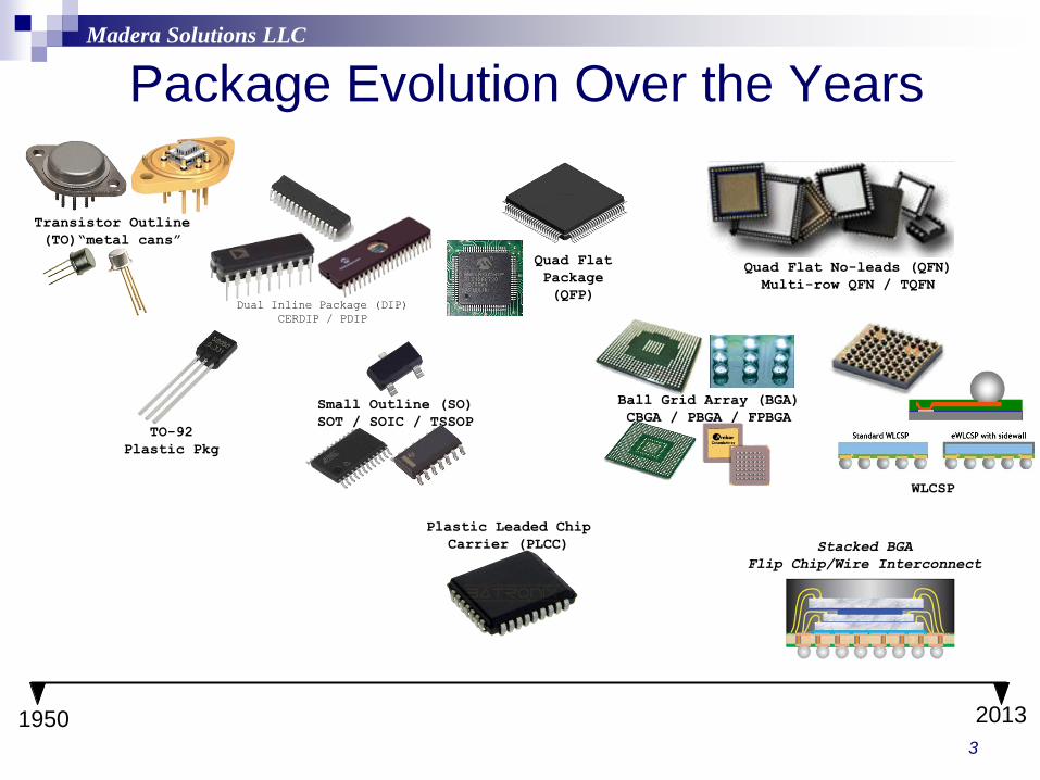
Package Evolution Over the Years
Transistor Outline
(TO)“metal cans”
Dual Inline Package (DIP)
CERDIP / PDIP
Small Outline (SO)
SOT / SOIC / TSSOP
Plastic Leaded Chip
Carrier (PLCC)
Quad Flat
Package
(QFP)
Quad Flat No-leads (QFN)
Multi-row QFN / TQFN
Stacked BGA
Flip Chip/Wire Interconnect
Ball Grid Array (BGA)
CBGA / PBGA / FPBGA
1950 2013
TO-92
Plastic Pkg
WLCSP
Madera Solutions LLC
4
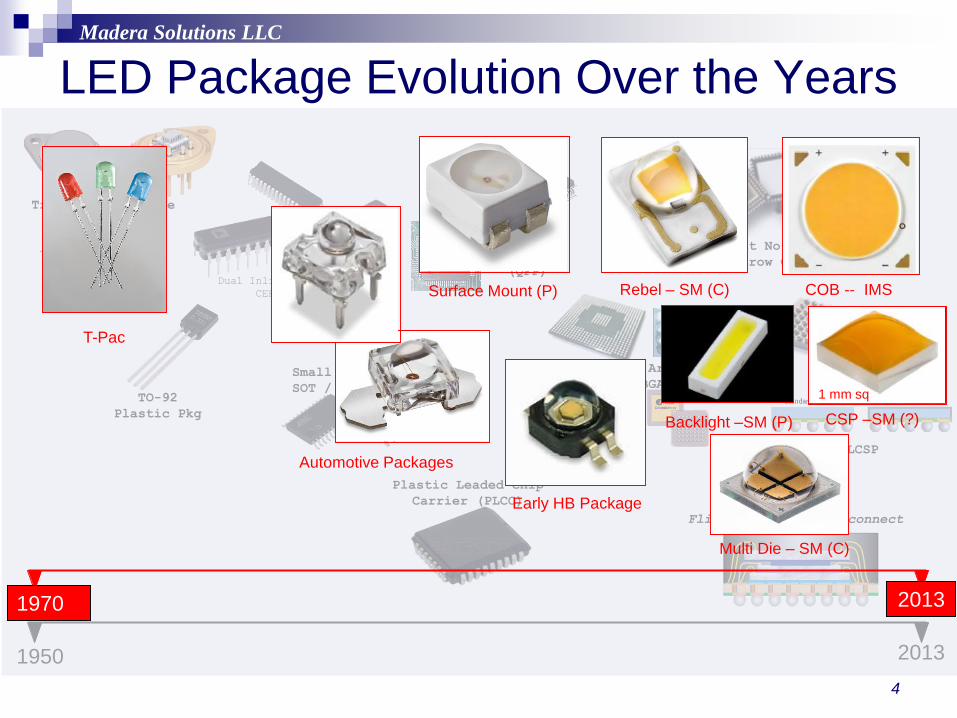
LED Package Evolution Over the Years
Transistor Outline
(TO)“metal cans”
Dual Inline Package (DIP)
CERDIP / PDIP
Small Outline (SO)
SOT / SOIC / TSSOP
Plastic Leaded Chip
Carrier (PLCC)
Quad Flat
Package
(QFP)
Quad Flat No-leads (QFN)
Multi-row QFN / TQFN
Stacked BGA
Flip Chip/Wire Interconnect
Ball Grid Array (BGA)
CBGA / PBGA / FPBGA
1950 2013
TO-92
Plastic Pkg
WLCSP
1970 2013
T-Pac
Automotive Packages
Surface Mount (P)
Early HB Package
Rebel – SM (C)
Backlight –SM (P)
COB -- IMS
Multi Die – SM (C)
CSP –SM (?)
1 mm sq

Madera Solutions LLC
Packaging Evolution (first wave)
5
TO-3
TO-18
TO-39
TO-92
TO-220
TO-52
Thru Hole Technology• Typically single unit at time (assembly jigs)
• Easy for the end user (manual assembly)
• Lead Pitch at 2.50 mm or greater
• Transitioned to lower cost plastic encapsulation
• Lead frame handling and early automation
Metal Cans Ceramic
Side-brazed DIP
CerDIP
PGA
900ml
64-PDIP
600ml
PDIP
20 Years
Plastics

Madera Solutions LLC
Characteristics of the First Wave Several Major Semicon Companies
OEM Equipment Development Teams
OEM Packaging Development Teams
Vertically integrated in many cases (own lead frames and other
materials)
Many silos to work from (a diversity of ideas/concepts)
Immaturity – nothing worked quite as it was expected to….
General dissatisfaction with quality/effectiveness
Solutions came from many suppliers Companies quick to try new ideas
Much diversity within a given company/factory
Need to clean-up, standardize became apparent
Remote solutions. Factory in one location, Development in
another
6
Diversity Innovation
Chaos
Madera Solutions LLC
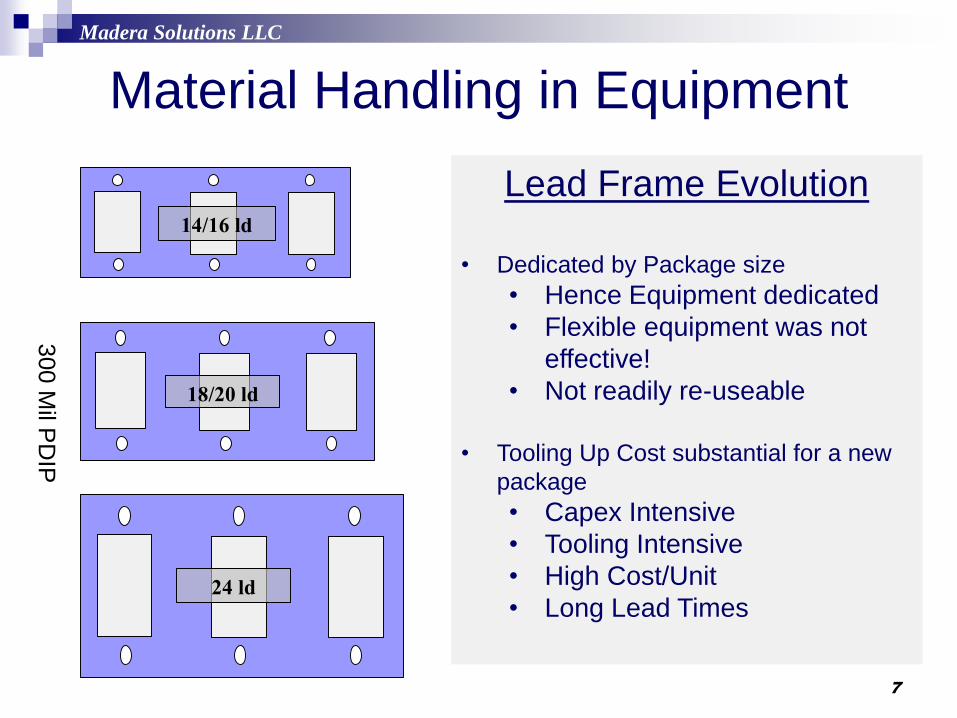
Material Handling in Equipment
7
Lead Frame Evolution
• Dedicated by Package size
• Hence Equipment dedicated
• Flexible equipment was not
effective!
• Not readily re-useable
• Tooling Up Cost substantial for a new
package
• Capex Intensive
• Tooling Intensive
• High Cost/Unit
• Long Lead Times
18/20 ld
24 ld
300 M
il PD
IP
14/16 ld

Madera Solutions LLC
Material Handling in Equipment
8
Early Efforts in Flexibility• Somewhat effective in Flexibility
• But quite wasteful on
material usage
• Okay for low volume
• Started wheels turning on
more flexible approaches

Madera Solutions LLC
Packaging Evolution (second wave)
9
Surface Mounts on Cu Substrates BGA Substrates
SOT-23
SOIC
PLCCSOT-223
CQFP
• Surface Mount Technology packaging evolved• Board Mounting technologies for Surface Mounts improved rapidly
• New Equipment required w/more Automation and Better Quality
• Smaller Pitch 1.25 mm (1.50mm for BGA)
• Matrix Lead frames (multi-rows)
Standard-
ization
QFP BGAProcess
Capability
& Quality
Factories
Beginning to
lead Effort
Engaging
Supplier Base
Surface Mount Technology

Madera Solutions LLC
Packages and Beliefs Changing
10
Courtesy of Amkor Semiconductor
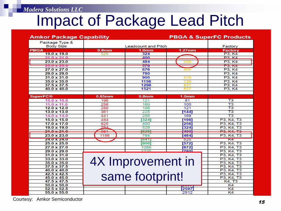
Encapsulate Utilization improved Radically over time
• More Impressive when viewed by usage per I/O
• improved significantly from a system standpoint (material usage,
waste, transportation cost, recycle costs)
/QFN
Madera Solutions LLC
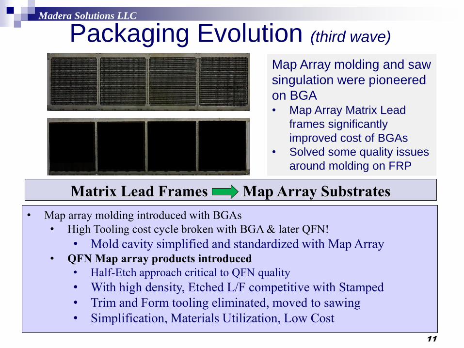
Packaging Evolution (third wave)
11
• Map array molding introduced with BGAs
• High Tooling cost cycle broken with BGA & later QFN!
• Mold cavity simplified and standardized with Map Array• QFN Map array products introduced
• Half-Etch approach critical to QFN quality
• With high density, Etched L/F competitive with Stamped
• Trim and Form tooling eliminated, moved to sawing
• Simplification, Materials Utilization, Low Cost
Matrix Lead Frames Map Array Substrates
Map Array molding and saw
singulation were pioneered
on BGA• Map Array Matrix Lead
frames significantly
improved cost of BGAs
• Solved some quality issues
around molding on FRP
Madera Solutions LLC
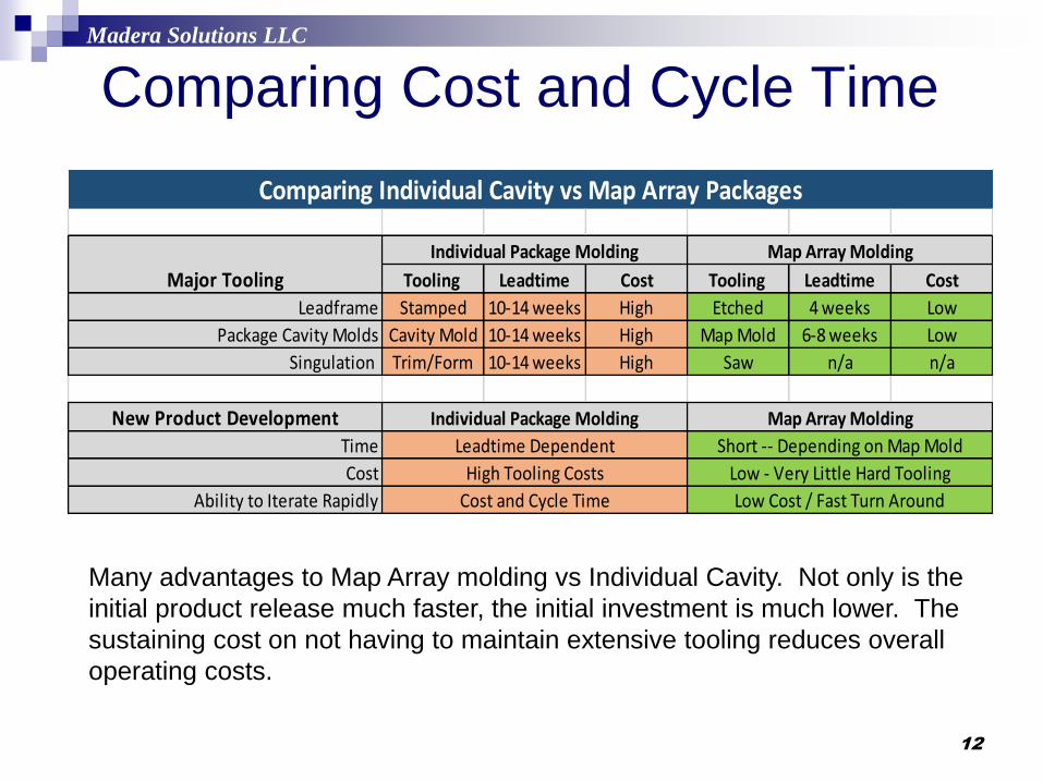
Comparing Cost and Cycle Time
12
Tooling Leadtime Cost Tooling Leadtime Cost
Leadframe Stamped 10-14 weeks High Etched 4 weeks Low
Package Cavity Molds Cavity Mold 10-14 weeks High Map Mold 6-8 weeks Low
Singulation Trim/Form 10-14 weeks High Saw n/a n/a
New Product DevelopmentTime
Cost
Ability to Iterate Rapidly
High Tooling Costs
Cost and Cycle Time
Short -- Depending on Map Mold
Low - Very Little Hard Tooling
Low Cost / Fast Turn Around
Comparing Individual Cavity vs Map Array Packages
Major Tooling
Individual Package Molding Map Array Molding
Individual Package Molding Map Array Molding
Leadtime Dependent
Many advantages to Map Array molding vs Individual Cavity. Not only is the
initial product release much faster, the initial investment is much lower. The
sustaining cost on not having to maintain extensive tooling reduces overall
operating costs.
Madera Solutions LLC
13
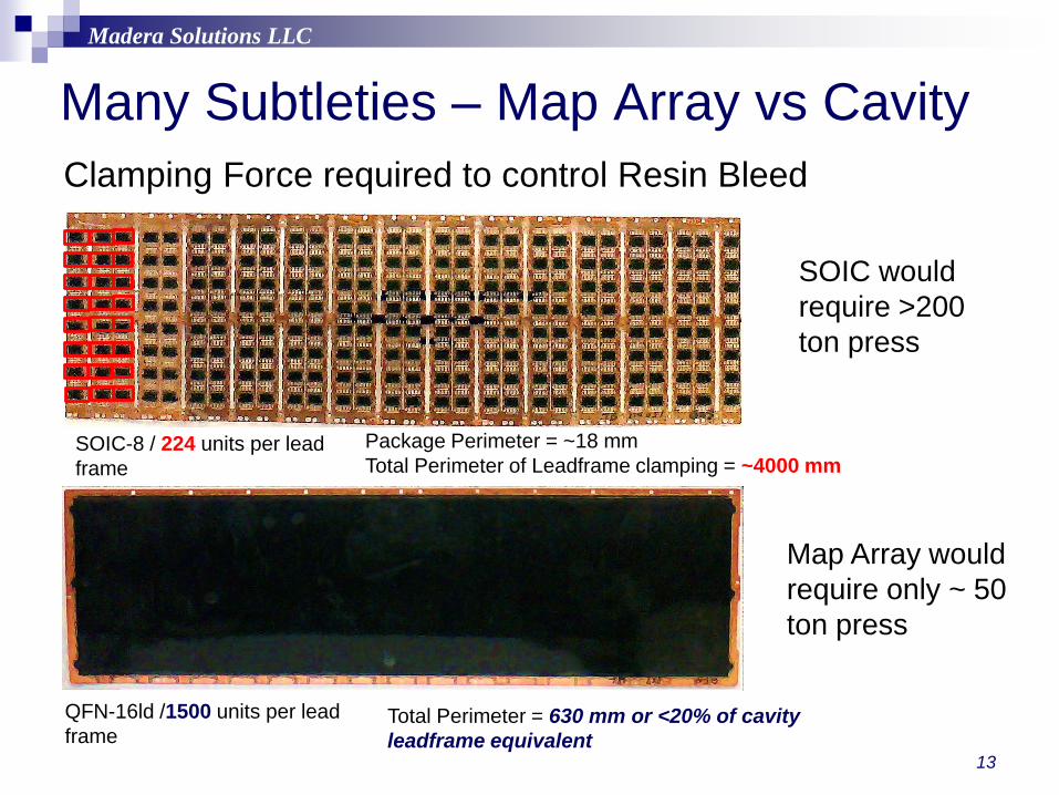
Many Subtleties – Map Array vs Cavity
Package Perimeter = ~18 mm
Total Perimeter of Leadframe clamping = ~4000 mm
Total Perimeter = 630 mm or <20% of cavity
leadframe equivalent
SOIC-8 / 224 units per lead
frame
QFN-16ld /1500 units per lead
frame
SOIC would
require >200
ton press
Map Array would
require only ~ 50
ton press
Clamping Force required to control Resin Bleed
Madera Solutions LLC
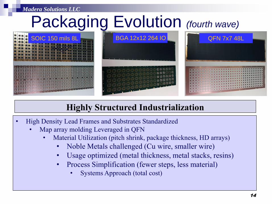
Packaging Evolution (fourth wave)
14
• High Density Lead Frames and Substrates Standardized
• Map array molding Leveraged in QFN
• Material Utilization (pitch shrink, package thickness, HD arrays)
• Noble Metals challenged (Cu wire, smaller wire)
• Usage optimized (metal thickness, metal stacks, resins)
• Process Simplification (fewer steps, less material)• Systems Approach (total cost)
Highly Structured Industrialization
BGA 12x12 264 IO QFN 7x7 48LSOIC 150 mils 8L
Madera Solutions LLC
Impact of Package Lead Pitch
15Courtesy: Amkor Semiconductor
4X Improvement in
same footprint!
Madera Solutions LLC
0
100
200
300
400
500
600
700
800
900
0 50 100 150 200 250 300
Pa
ck
ag
e s
ize
(m
m2)
Number of I/O leads
PDIP TSSOP SOIC QFP QFN Dual row QFN BGA
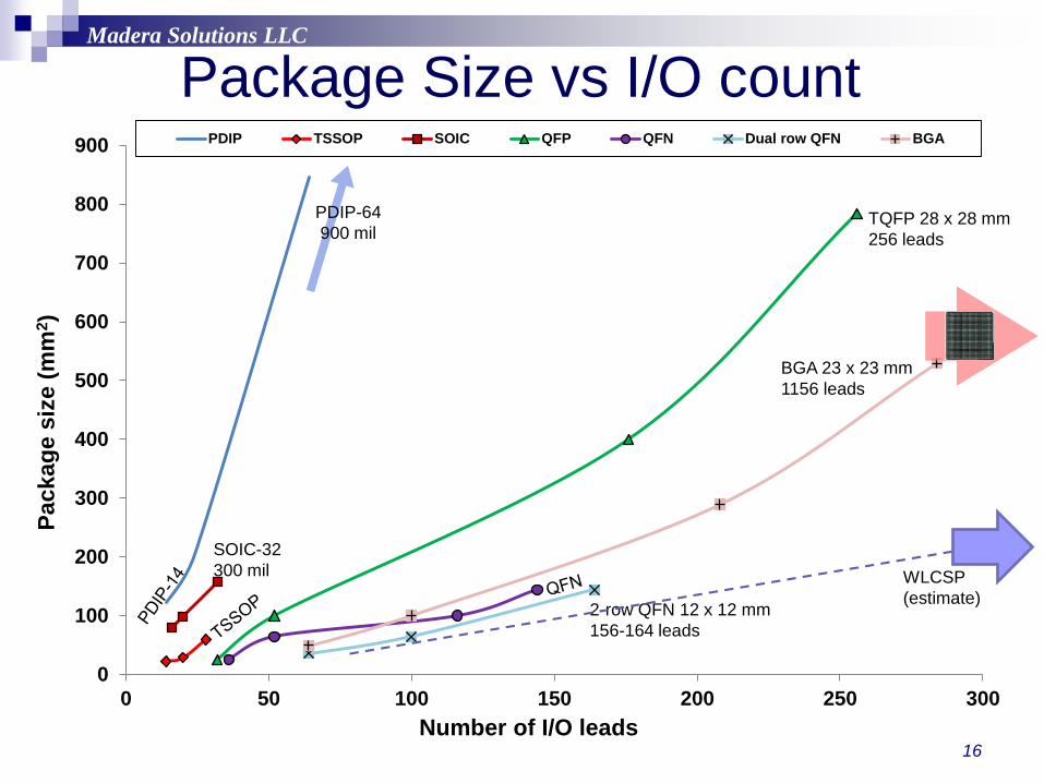
16
Package Size vs I/O count
BGA 23 x 23 mm
1156 leads
2-row QFN 12 x 12 mm
156-164 leads
TQFP 28 x 28 mm
256 leads
SOIC-32
300 mil
PDIP-64
900 mil
WLCSP
(estimate)
Madera Solutions LLC
17
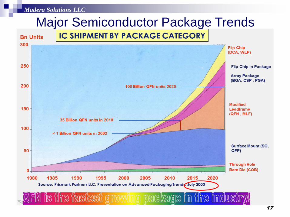
Major Semiconductor Package Trends
Madera Solutions LLC
182/10/2015
0
50
100
150
200
250
300
2011 2012 2013 2018
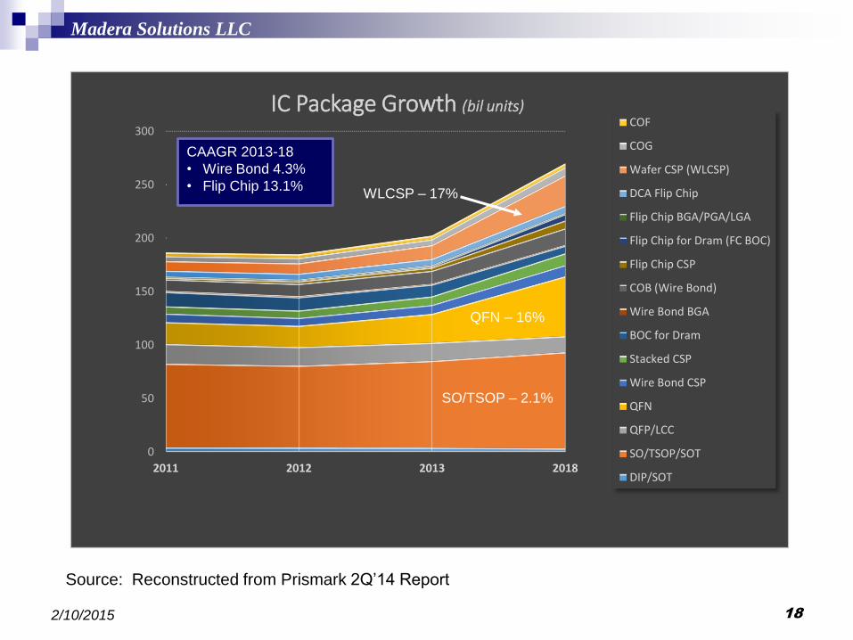
IC Package Growth (bil units)COF
COG
Wafer CSP (WLCSP)
DCA Flip Chip
Flip Chip BGA/PGA/LGA
Flip Chip for Dram (FC BOC)
Flip Chip CSP
COB (Wire Bond)
Wire Bond BGA
BOC for Dram
Stacked CSP
Wire Bond CSP
QFN
QFP/LCC
SO/TSOP/SOT
DIP/SOT
CAAGR 2013-18
• Wire Bond 4.3%
• Flip Chip 13.1%
SO/TSOP – 2.1%
QFN – 16%
WLCSP – 17%
Source: Reconstructed from Prismark 2Q’14 Report

Madera Solutions LLC
19
LC for a +35 yr
old package
Actual SOT 23 Cost Learning Curve
1
10
100
1000 10000 100000
Cumulative Volume (#M)
70% Learning Curve
1992
2004
1998
$60/K
1980
Inde
x $
/K
Major Mature Product(specific factory)
LC for a +30 yr
old package
2000-01 Recession
exposed huge cost gap
JV
Learning
Actual Learning Curve
63.3% over 12 years
2002 Industry
Benchmark
(3$/K units)
Madera Solutions LLC
20
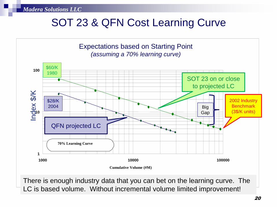
SOT 23 & QFN Cost Learning Curve
1
10
100
1000 10000 100000
Cumulative Volume (#M)
70% Learning Curve
$60/K
1980
Inde
x $
/K
Expectations based on Starting Point(assuming a 70% learning curve)
SOT 23 on or close
to projected LC
$28/K
2004
QFN projected LC
2002 Industry
Benchmark
(3$/K units)
There is enough industry data that you can bet on the learning curve. The
LC is based volume. Without incremental volume limited improvement!
Big
Gap
Madera Solutions LLC
21
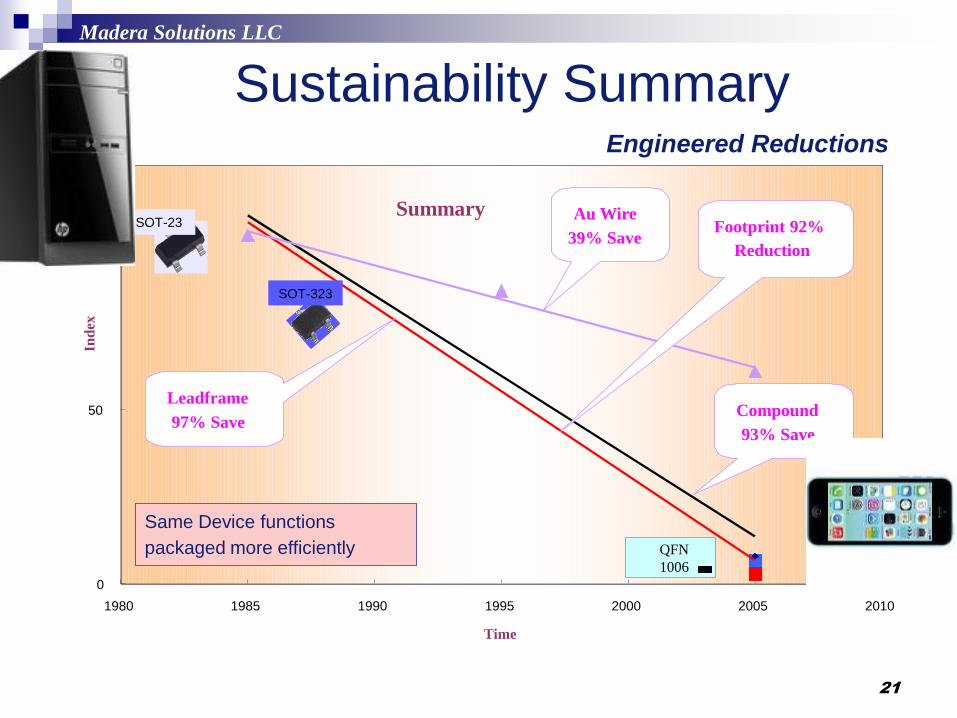
Sustainability SummaryEngineered Reductions
Summary
0
50
100
1980 1985 1990 1995 2000 2005 2010
Time
Ind
ex
QFN
1006
Au Wire
39% SaveFootprint 92%
Reduction
Compound
93% Save
Leadframe
97% Save
Same Device functions
packaged more efficiently
SOT-23
SOT-323

Madera Solutions LLC
Integrating Technological
Requirements for Industrialization
22
75 % Semicon
• Experience Curve
• Supply Chain• Materials
• Equipment
• CMs
• Volume• Quality
• Infrastructure
25 % HB LED
• Extraction
Efficiency
• LED Specific
Material Needs• Reliability
Requirements
• Optical Needs
• Thermal Needs
• Bridging to Semi
Equipment
IncorporateLeverage
Madera Solutions LLC
232/10/2015
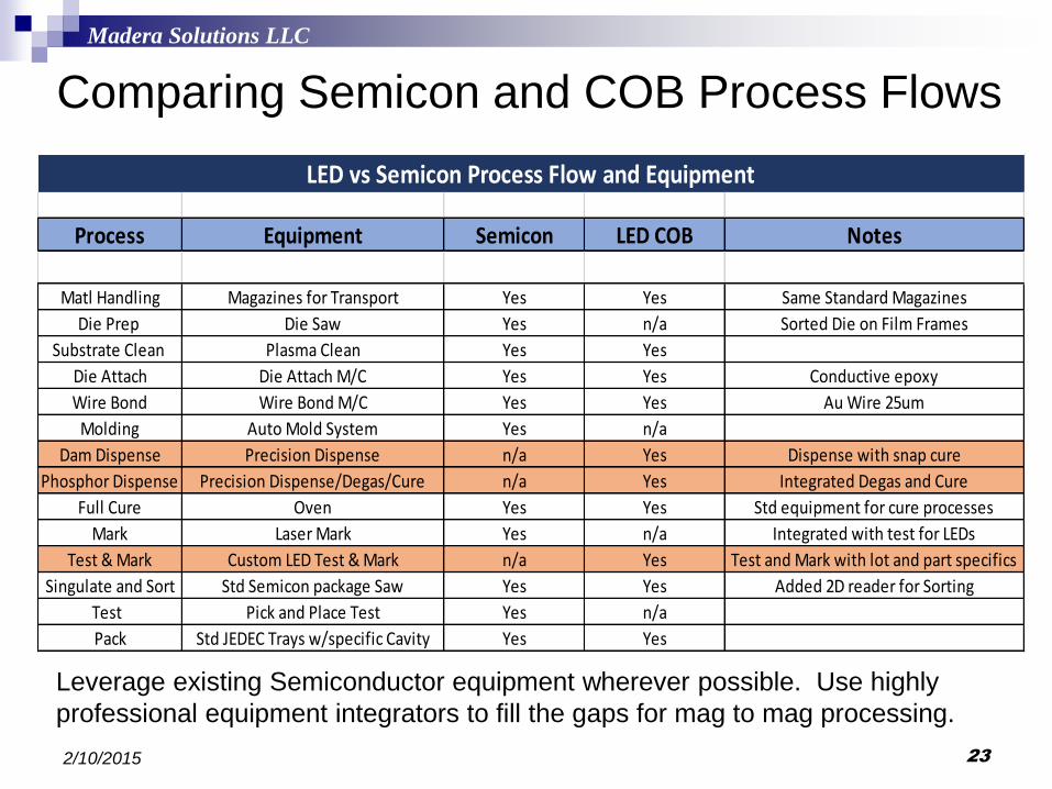
Comparing Semicon and COB Process Flows
Process Equipment Semicon LED COB Notes
Matl Handling Magazines for Transport Yes Yes Same Standard Magazines
Die Prep Die Saw Yes n/a Sorted Die on Film Frames
Substrate Clean Plasma Clean Yes Yes
Die Attach Die Attach M/C Yes Yes Conductive epoxy
Wire Bond Wire Bond M/C Yes Yes Au Wire 25um
Molding Auto Mold System Yes n/a
Dam Dispense Precision Dispense n/a Yes Dispense with snap cure
Phosphor Dispense Precision Dispense/Degas/Cure n/a Yes Integrated Degas and Cure
Full Cure Oven Yes Yes Std equipment for cure processes
Mark Laser Mark Yes n/a Integrated with test for LEDs
Test & Mark Custom LED Test & Mark n/a Yes Test and Mark with lot and part specifics
Singulate and Sort Std Semicon package Saw Yes Yes Added 2D reader for Sorting
Test Pick and Place Test Yes n/a
Pack Std JEDEC Trays w/specific Cavity Yes Yes
LED vs Semicon Process Flow and Equipment
Leverage existing Semiconductor equipment wherever possible. Use highly
professional equipment integrators to fill the gaps for mag to mag processing.

Madera Solutions LLC
What a Journey!!!
24
1950 1960 1970 1980 1990 2000 2010
Larg
er
Size
→
From this!
0603
To
this!

Madera Solutions LLC
Semicon….....a $400 Billion/Yr Industry
25
$400 Billion
Power Horse

Madera Solutions LLC
Leverage…. this Powerful Engine
26
Can HB LEDs ride in
the slipstream of
Semiconductors

Madera Solutions LLC
Appendix

Madera Solutions LLC
Why BGAs are so Popular
28
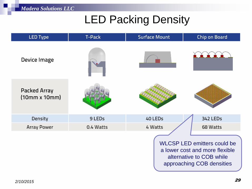
Madera Solutions LLC
292/10/2015
WLCSP LED emitters could be
a lower cost and more flexible
alternative to COB while
approaching COB densities
LED Packing Density
Madera Solutions LLC
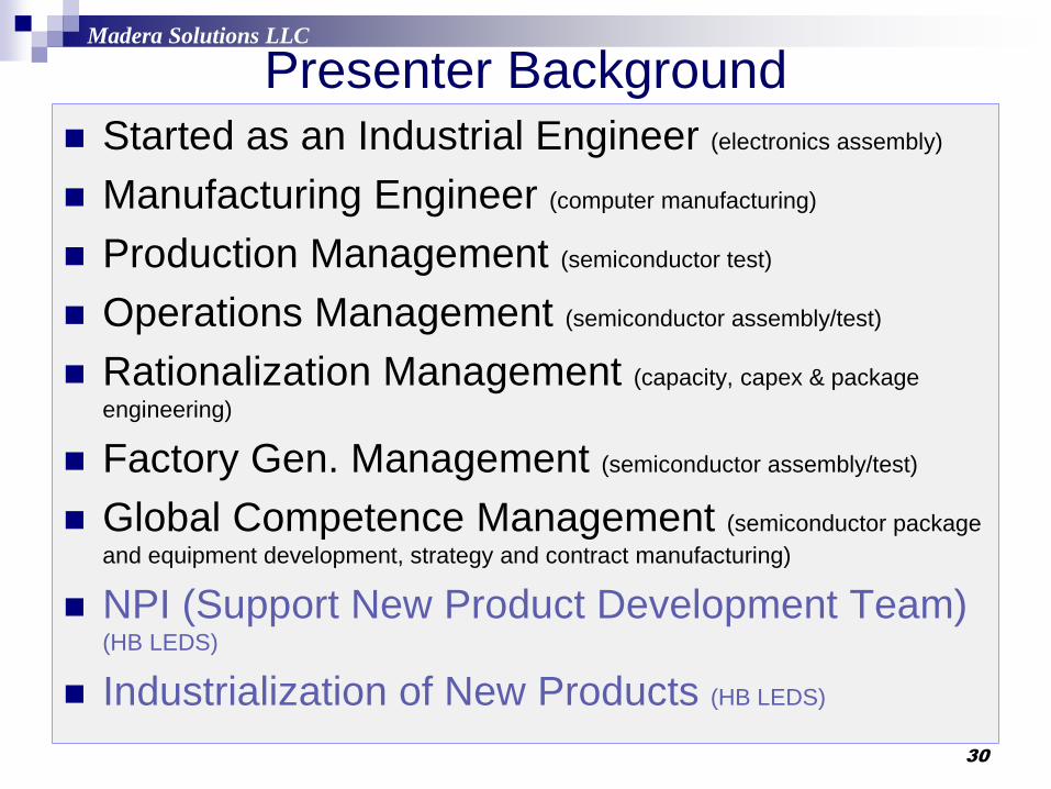
Presenter Background Started as an Industrial Engineer (electronics assembly)
Manufacturing Engineer (computer manufacturing)
Production Management (semiconductor test)
Operations Management (semiconductor assembly/test)
Rationalization Management (capacity, capex & package
engineering)
Factory Gen. Management (semiconductor assembly/test)
Global Competence Management (semiconductor package
and equipment development, strategy and contract manufacturing)
NPI (Support New Product Development Team) (HB LEDS)
Industrialization of New Products (HB LEDS)
30

Madera Solutions LLC
312/10/2015
Gerry Keller Bio
Gerry Keller has been consulting for the last 7 years mostly with LED lighting companies (start-
up and established). His focus has been new product Introduction (NPI) with DFM and
industrialization focus for those products. Activities including identification and selection of
contract manufacturers and bringing product to full production with the CMs. He has also
worked with companies on Cost Reduction strategies/programs and Quality trouble shooting.
Prior to that he had various positions with Motorola and Philips semiconductor assembly and test
operations both domestically and internationally. He started as a production manager, later
operations manager and factory general manager. He also led engineering teams with world
wide responsibility for package development and industrialization. He spent more that 12 years
living and working in Asia and traveled extensively in the region to engage equipment and
materials suppliers as well as contract manufacturers. This has enabled him to develop a
significant network of suppliers, that have proved very helpful in his consulting work.
Early in his career he worked as an industrial engineer in various industries and as a
manufacturing engineer in the computer industry. Experiences gained in those hands–on
assignments have helped to build a strong foundation for a future in operations and engineering
management. Gerry is a strong disciple of TQM, 6-Sigma, TPM and operational excellence and
has a established track record built on those disciplines.
Gerry received a BBA in Industrial Management from the University of Texas and an MBA from
Texas State University with a focus on management.
Related Documents