© July 7, 2014 Dr. Lynn Fuller, Professor Rochester Institute of Technology Microelectronic Engineering Review of IC Fabrication Technology Page 1 MICROELECTRONIC ENGINEERING ROCHESTER INSTITUTE OF TECHNOLOGY A Review of IC Fabrication Technology Dr. Lynn Fuller Webpage: http://people.rit.edu/lffeee Microelectronic Engineering Rochester Institute of Technology 82 Lomb Memorial Drive Rochester, NY 14623-5604 Tel (585) 475-2035 Email: [email protected] Department webpage: http://www.microe.rit.edu 7-7-2014 Review.ppt

Welcome message from author
This document is posted to help you gain knowledge. Please leave a comment to let me know what you think about it! Share it to your friends and learn new things together.
Transcript
© July 7, 2014 Dr. Lynn Fuller, Professor
Rochester Institute of Technology
Microelectronic Engineering
Review of IC Fabrication Technology
Page 1
MICROELECTRONIC ENGINEERING ROCHESTER INSTITUTE OF TECHNOLOGY
A Review of IC Fabrication Technology
Dr. Lynn Fuller Webpage: http://people.rit.edu/lffeee
Microelectronic Engineering Rochester Institute of Technology
82 Lomb Memorial Drive Rochester, NY 14623-5604
Tel (585) 475-2035 Email: [email protected]
Department webpage: http://www.microe.rit.edu
7-7-2014 Review.ppt
© July 7, 2014 Dr. Lynn Fuller, Professor
Rochester Institute of Technology
Microelectronic Engineering
Review of IC Fabrication Technology
Page 2
ADOBE PRESENTER
This PowerPoint module has been published using Adobe Presenter. Please click on the Notes tab in the left panel to read the instructors comments for each slide. Manually advance the slide by clicking on the play arrow or pressing the page down key.
© July 7, 2014 Dr. Lynn Fuller, Professor
Rochester Institute of Technology
Microelectronic Engineering
Review of IC Fabrication Technology
Page 3
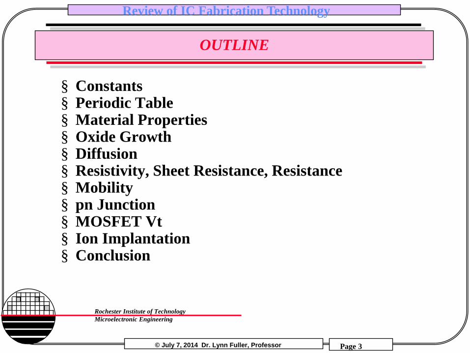
OUTLINE
§ Constants § Periodic Table § Material Properties § Oxide Growth § Diffusion § Resistivity, Sheet Resistance, Resistance § Mobility § pn Junction § MOSFET Vt § Ion Implantation § Conclusion

© July 7, 2014 Dr. Lynn Fuller, Professor
Rochester Institute of Technology
Microelectronic Engineering
Review of IC Fabrication Technology
Page 4
CONSTANTS
Electronic charge q 1.602 E -19 Coulomb
Speed of light in vacuum c 2.998E8 m/s
Permittivity of vacuum o 8.854 E -14 F/cm
Free electron Mass mo 9.11E-31 Kg
Planck constant h 6.625E-34 J s
Boltzmann constant k 1.38 E-23 J /°K = 8.625E-5 eV/°K
Avogadro’s number Ao 6.022E23 molecules/gm- mole
Thermal voltage kT/q @ 300 °K = 0.02586
PLAY
© July 7, 2014 Dr. Lynn Fuller, Professor
Rochester Institute of Technology
Microelectronic Engineering
Review of IC Fabrication Technology
Page 5
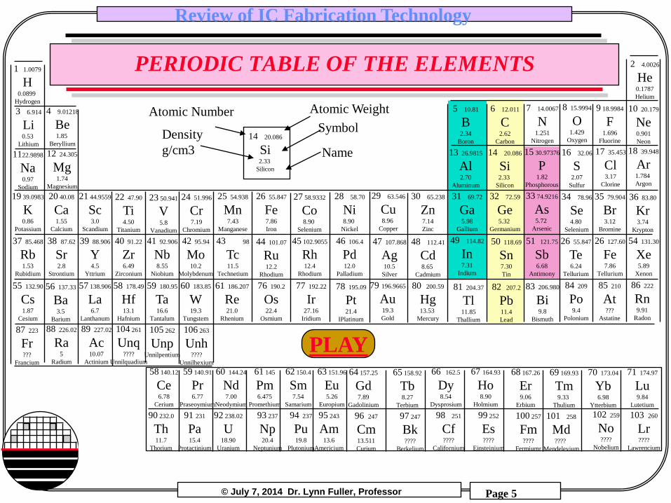
PERIODIC TABLE OF THE ELEMENTS
14 20.086
Si 2.33
Silicon
32 72.59
Ge 5.32
Germanium
6 12.011
C 2.62
Carbon
5 10.81
B 2.34
Boron
9 18.9984
F 1.696
Fluorine
8 15.9994
O 1.429
Oxygen
7 14.0067
N 1.251
Nitrogen
15 30.97376
P 1.82
Phosphorous
2 4.0026
He 0.1787
Helium
31 69.72
Ga 5.98
Gallium
13 26.9815
Al 2.70
Aluminum
48 112.41
Cd 8.65
Cadmium
33 74.9216
As 5.72
Arsenic
16 32.06
S 2.07
Sulfur
10 20.179
Ne 0.901
Neon
82 207.2
Pb 11.4
Lead
50 118.69
Sn 7.30
Tin
14 20.086
Si 2.33
Silicon
Symbol
Name
Density
g/cm3
Atomic Weight Atomic Number
79 196.9665
Au 19.3
Gold
27 58.9332
Co 8.90
Selenium
28 58.70
Ni 8.90
Nickel
29 63.546
Cu 8.96
Copper
30 65.238
Zn 7.14
Zinc
34 78.96
Se 4.80
Selenium
49 114.82
In 7.31
Indium
80 200.59
Hg 13.53
Mercury
4 9.01218
Be 1.85
Beryllium
12 24.305
Mg 1.74
Magnesium
1122.9898
Na 0.97
Sodium
3 6.914
Li 0.53
Lithium
1 1.0079
H 0.0899
Hydrogen
18 39.948
Ar 1.784
Argon
17 35.453
Cl 3.17
Clorine
51 121.75
Sb 6.68
Antimony
21 44.9559
Sc 3.0
Scandium
22 47.90
Ti 4.50
Titanium
26 55.847
Fe 7.86
Iron
25 54.938
Mn 7.43
Manganese
24 51.996
Cr 7.19
Chromium
23 50.941
V 5.8
Vanadium
57 138.906
La 6.7
Lanthanum
38 87.62
Sr 2.8
Strontium
19 39.0983
K 0.86
Potassium
20 40.08
Ca 1.55
Calcium
81 204.37
Tl 11.85
Thallium
47 107.868
Ag 10.5
Silver
105 262
Unp Unnilpentium
106 263
Unh ????
Unnilhexium
59 180.95
Ta 16.6
Tantalum
77 192.22
Ir 27.16
Iridium
76 190.2
Os 22.4
Osmium
61 186.207
Re 21.0
Rhenium
60 183.85
W 19.3
Tungstem
78 195.09
Pt 21.4
IPlatinum
46 106.4
Pd 12.0
Palladium
56 137.33
Ba 3.5
Barium
55 132.90
Cs 1.87
Cesium
58 178.49
Hf 13.1
Hafnium
87 223
Fr ???
Francium
88 226.02
Ra 5
Radium
89 227.02
Ac 10.07
Actinium
104 261
Unq ????
Unnilquadium
44 101.07
Ru 12.2
Rhodium
45 102.9055
Rh 12.4
Rhodium
41 92.906
Nb 8.55
Niobium
42 95.94
Mo 10.2
Molybdenum
43 98
Tc 11.5
Technetium
40 91.22
Zr 6.49
Zirconium
39 88.906
Y 4.5
Yttrium
37 85.468
Rb 1.53
Rubidium
69 169.93
Tm 9.33
Thulium
71 174.97
Lu 9.84
Lutetium
70 173.04
Yb 6.98
Ytterbium
68 167.26
Er 9.06
Erbium
67 164.93
Ho 8.90
Holmium
65 158.92
Tb 8.27
Terbium
66 162.5
Dy 8.54
Dysprosium
35 79.904
Br 3.12
Bromine
26 127.60
Fe 7.86
Tellurium
26 55.847
Te 6.24
Tellurium
85 210
At ???
Astatine
84 209
Po 9.4
Polonium
83 206.980
Bi 9.8
Bismuth
86 222
Rn 9.91
Radon
36 83.80
Kr 3.74
Krypton
54 131.30
Xe 5.89
Xenon
101 258
Md ????
Mendelevium
102 259
No ????
Nobelium
100 257
Fm ????
Fermiumr
99 252
Es ????
Einsteinium
97 247
Bk ????
Berkelium
98 251
Cf ????
Californium
103 260
Lr ????
Lawrencium
59 140.91
Pr 6.77
Praseoymium
62 150.4
Sm 7.54
Samarium
63 151.96
Eu 5.26
Europium
61 145
Pm 6.475
Promethium
60 144.24
Nd 7.00
Neodymium
58 140.12
Ce 6.78
Cerium
64 157.25
Gd 7.89
Gadolinium
91 231
Pa 15.4
Protactinium
94 237
Pu 19.8
Plutonium
95 243
Am 13.6
Americium
93 237
Np 20.4
Neptunium
92 238.02
U 18.90
Uranium
90 232.0
Th 11.7
Thorium
96 247
Cm 13.511
Curium
PLAY

© July 7, 2014 Dr. Lynn Fuller, Professor
Rochester Institute of Technology
Microelectronic Engineering
Review of IC Fabrication Technology
Page 6
MATERIAL PROPERTIES
Symbol Units Si Ge GaAs GaP SiO2 Si3N4
Atoms per unit cell 8 8 8 8
Atomic Number Z 14 32 31/33 31/15 14/8 14/7
Atomic weight MW g/g-mole 28.09 72.59 144.64 100.70 60.08 140.28
Lattice constant ao nm 0.54307 0.56575 0.56532 0.54505 0.775
Atomic density No cm-3 5.00E22 4.42E22 2.21E22 2.47E22 2.20E22 1.48E22
Density d g cm-3 2.328 5.323 5.316 4.13 2.19 3.44
Energy Gap 300°K Eg eV 1.124 0.67 1.42 2.24 8~9 4.7
Relative permittivity r 11.7 16.0 13.1 10.2 3.9 7.5
Index of refraction n 3.44 3.97 3.3 3.3 1.46 2.0
Melting point Tm °C 1412 937 1237 1467 1700
Specific heat Cp J (gK)-1 0.70 0.32 0.35 1.4 0.17
Thermal diffusivity K w(cmK)-1 0.87 0.36 0.44 0.004 0.32
Coefficient expansion Dth K-1 2.5E-6 5.7E-6 5.9E-6 5.3E-6 5E-6 2.8E-6
Intrinsic carrier conc ni cm-3 1.45E10 2.4E13 9.0E6
Electron Mobility µn cm2/Vs 1417 3900 8800 300 20
Hole Mobility µp cm2/Vs 471 1900 400 100 10E-8
Density of States conduction Nc cm-3 2.8E19 1.04E19 4.7E17
Density of States valance Nv cm-3 1.04E19 6.0E18 7.0E18
Breakdown Electric Field E V/cm 3E5 8E4 3.5E5 6~9E6
Effective mass electron mn*/mo 1.08 0.55 0.068 0.5
Effective mass hole mp*/mo 0.81 0.3 0.5 0.5
Electron affinity qX eV 4.05 4.00 4.07 4.3 1.0
From Muller and Kamins

© July 7, 2014 Dr. Lynn Fuller, Professor
Rochester Institute of Technology
Microelectronic Engineering
Review of IC Fabrication Technology
Page 7
OXIDE GROWTH
Oxide Thickness
Xox
Original Silicon
Surface 0.46 Xox Silicon Consumed
PLAY
Dry oxide O2 only
Wet oxide O2 bubbled through water
Steam burn H2 in O2 to make H20 (steam)

© July 7, 2014 Dr. Lynn Fuller, Professor
Rochester Institute of Technology
Microelectronic Engineering
Review of IC Fabrication Technology
Page 8
WET OXIDE GROWTH CHART
1 10 100 10-2
10-1
1
10
t, Time, (min)
Xox ,(um)
PLAY

© July 7, 2014 Dr. Lynn Fuller, Professor
Rochester Institute of Technology
Microelectronic Engineering
Review of IC Fabrication Technology
Page 9
DRY OXIDE GROWTH CHART
10 100 1,000
10
10-2
10-1
1
t, Time, (min)
xox ,(um)
PLAY
© July 7, 2014 Dr. Lynn Fuller, Professor
Rochester Institute of Technology
Microelectronic Engineering
Review of IC Fabrication Technology
Page 10
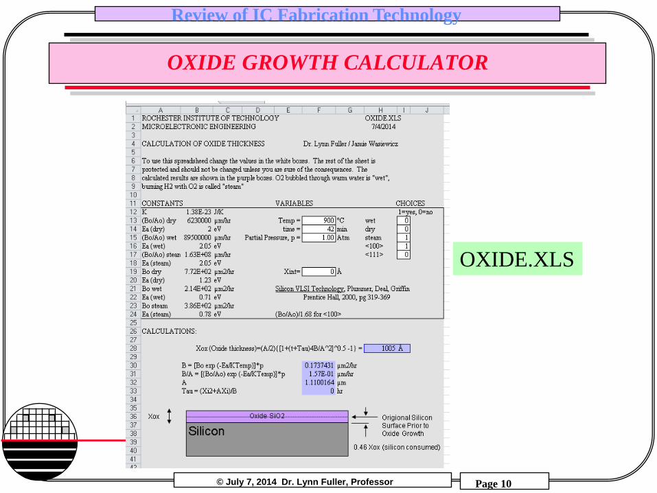
OXIDE GROWTH CALCULATOR
OXIDE.XLS

© July 7, 2014 Dr. Lynn Fuller, Professor
Rochester Institute of Technology
Microelectronic Engineering
Review of IC Fabrication Technology
Page 11
EXAMPLES
1. Estimate the oxide thickness resulting from 50 min.
soak at 1100 °C in wet oxygen.
2. If 1000 Å of oxide exists to start with, what is
resulting oxide thickness after an additional 50 min.
soak at 1100 °C in dry oxygen.

© July 7, 2014 Dr. Lynn Fuller, Professor
Rochester Institute of Technology
Microelectronic Engineering
Review of IC Fabrication Technology
Page 12
OXIDE THICKNESS COLOR CHART
Thickness Color Thickness Color
500Å Tan 4900 Blue
700 Brown 5000 Blue Green
1000 Dark Violet - Red Violet 5200 Green
1200 Royal Blue 5400 Yellow Green
1500 Light Blue - Metallic Blue 5600 GreenYellow
1700 Metallic - very light Yellow Green 5700 Yellow -"Yellowish"(at times appears to be Lt gray or matellic)
2000 LIght Gold or Yellow - Slightly Metallic 5800 Light Orange or Yellow - Pink
2200 Gold with slight Yellow Orange 6000 Carnation Pink
2500 Orange - Melon 6300 Violet Red
2700 Red Violet 6800 "Bluish"(appears violet red, Blue Green, looks grayish)
3000 Blue - Violet Blue 7200 Blue Green - Green
3100 Blue 7700 "Yellowish"
3200 Blue - Blue Green 8000 Orange
3400 Light Green 8200 Salmon
3500 Green - Yellow Green 8500 Dull, LIght Red Violet
3600 Yellow Green 8600 Violet
3700 Yellow 8700 Blue Violet
3900 Light Orange 8900 Blue
4100 Carnation Pink 9200 Blue Green
4200 Violet Red 9500 Dull Yellow Green
4400 Red Violet 9700 Yellow - "Yellowish"
4600 Violet 9900 Orange
4700 Blue Violet 10000 Carnation Pink
Blue
Blue
Blue
Blue
Blue
Blue
Blue
Blue
PLAY
Nitride Thickness = (Oxide Thickness)(Oxide Index/Nitride Index) Eg. Yellow Nitride Thickness = (2000)(1.46/2.00) = 1460

© July 7, 2014 Dr. Lynn Fuller, Professor
Rochester Institute of Technology
Microelectronic Engineering
Review of IC Fabrication Technology
Page 13
DIFFUSION FROM A CONSTANT SOURCE
N(x,t) = No erfc (x/2 Dt )
Solid
Solubility
Limit, No
x
into wafer
Wafer Background Concentration, NBC
N(x,t)
Xj
p-type
n-type
PLAY STOP
© July 7, 2014 Dr. Lynn Fuller, Professor
Rochester Institute of Technology
Microelectronic Engineering
Review of IC Fabrication Technology
Page 14
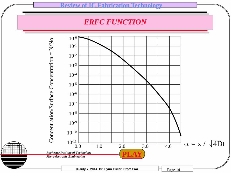
ERFC FUNCTION
10-6
10-5
10-4
10-3
10-1
10-2
10-7
10-10
10-11
10-0
10-8
10-9
3.0 1.0 2.0 4.0 0.0 = x / 4Dt Conce
ntr
atio
n/S
urf
ace
Conce
ntr
atio
n =
N/N
o
PLAY

© July 7, 2014 Dr. Lynn Fuller, Professor
Rochester Institute of Technology
Microelectronic Engineering
Review of IC Fabrication Technology
Page 15
DIFFUSION CONSTANTS AND SOLID SOLUBILITY
DIFFUSION CONSTANTS
BORON PHOSPHOROUS PHOSPHOROUS BORON PHOSPHOROUS
TEMP DRIVE-IN PRE DRIVE-IN SOLID SOLID
SOLUBILITY SOLUBILITY
NOB NOP
900 °C 1.07E-15 cm2/s 2.09e-14 cm2/s 7.49E-16 cm2/s 4.75E20 cm-3 6.75E20 cm-3
950 4.32E-15 6.11E-14 3.29E-15 4.65E20 7.97E20
1000 1.57E-14 1.65E-13 1.28E-14 4.825E20 9.200E20
1050 5.15E-14 4.11E-13 4.52E-14 5.000E20 1.043E21
1100 1.55E-13 9.61E-13 1.46E-13 5.175E20 1.165E21
1150 4.34E-13 2.12E-12 4.31E-13 5.350E20 1.288E21
1200 1.13E-12 4.42E-12 1.19E-12 5.525E20 1.410E21
1250 2.76E-12 8.78E-12 3.65E-12 5.700E20 1.533E21
PLAY
© July 7, 2014 Dr. Lynn Fuller, Professor
Rochester Institute of Technology
Microelectronic Engineering
Review of IC Fabrication Technology
Page 16
TEMPERATURE DEPENDENCE OF DIFFUSION CONSTANTS
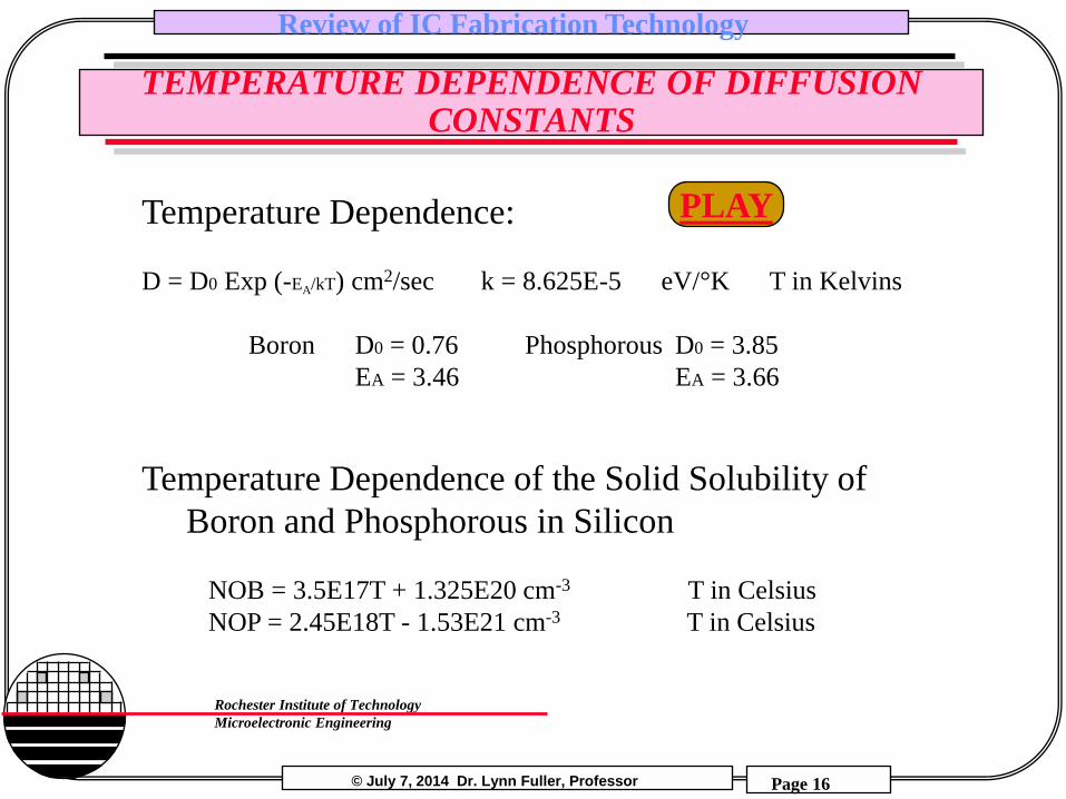
Temperature Dependence:
D = D0 Exp (-EA/kT) cm2/sec k = 8.625E-5 eV/°K T in Kelvins
Boron D0 = 0.76 Phosphorous D0 = 3.85
EA = 3.46 EA = 3.66
Temperature Dependence of the Solid Solubility of
Boron and Phosphorous in Silicon
NOB = 3.5E17T + 1.325E20 cm-3 T in Celsius
NOP = 2.45E18T - 1.53E21 cm-3 T in Celsius
PLAY

© July 7, 2014 Dr. Lynn Fuller, Professor
Rochester Institute of Technology
Microelectronic Engineering
Review of IC Fabrication Technology
Page 17
DIFFUSION FROM A LIMITED SOURCE
for erfc predeposit
Q’A (tp) = QA(tp)/Area = 2 No (Dptp) / Dose
for ion implant predeposit
Q’A(tp) = Dose
N(x,t) = Q’A(tp) Exp (- x2/4Dt)
Dt
Where D is the diffusion constant at the drive in temperature and t is the drive in diffusion time, Dp is the diffusion constant at the predeposit temperature and tp is the predeposit time
PLAY
PLAY
© July 7, 2014 Dr. Lynn Fuller, Professor
Rochester Institute of Technology
Microelectronic Engineering
Review of IC Fabrication Technology
Page 18
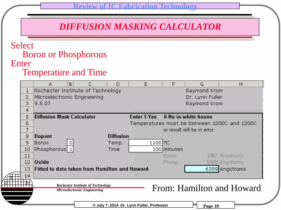
DIFFUSION MASKING CALCULATOR
Select Boron or Phosphorous Enter Temperature and Time
From: Hamilton and Howard

© July 7, 2014 Dr. Lynn Fuller, Professor
Rochester Institute of Technology
Microelectronic Engineering
Review of IC Fabrication Technology
Page 19
DIFFUSION MASKING
From: Hamilton and Howard
Phosphorous Masking Boron Masking

© July 7, 2014 Dr. Lynn Fuller, Professor
Rochester Institute of Technology
Microelectronic Engineering
Review of IC Fabrication Technology
Page 20
DIFFUSION AND DRIVE IN CALCULATIONS
DIFFUSION.XLS

© July 7, 2014 Dr. Lynn Fuller, Professor
Rochester Institute of Technology
Microelectronic Engineering
Review of IC Fabrication Technology
Page 21
DIFFUSION FROM A LIMITED SOURCE
GIVEN VALUE UNITS
Starting Wafer Resistivity Rho = 10 ohm-cm
Starting Wafer Type n-type = 1 1 1 or 0
p-type = 1 0 1 or 0
Pre Deposition Ion Implant Dose 4.00E+15 ions/cm2
Drive-in Temperature 1000 °C
Drive-in Time 360 min
CALCULATE VALUE UNITS
Diffusion Constant at Temperature of Drive-in 1.43E-14 cm/sec
CALCULATION OF DIFFUSION CONSTANTS
D0 (cm2/s) EA (eV)
Boron 0.76 3.46
Phosphorous 3.85 3.66
CALCULATIONS VALUE UNITS
Substrate Doping = 1 / (q µmax Rho) 4.42E+14 cm-3
RESULTS VALUE UNITS
Pre deposition Dose 4.00E+15 atoms/cm2
xj after drive-in = ((4 Dd td/QA) ln (Nsub (Ddtd)^0.5))^0.5 1.25 µm
average doping Nave = Dose/xj 3.21E+19 atoms/cm3
mobility (µ) at Doping equal to Nave 57 cm2/V-s
Sheet Resistance = 1/(q (µ(Nave))Dose) 27.6 ohms
Surface Concentration = Dose/ (pDt)^0.5 1.28E+20 cm-3
IonImplt.xls
© July 7, 2014 Dr. Lynn Fuller, Professor
Rochester Institute of Technology
Microelectronic Engineering
Review of IC Fabrication Technology
Page 22
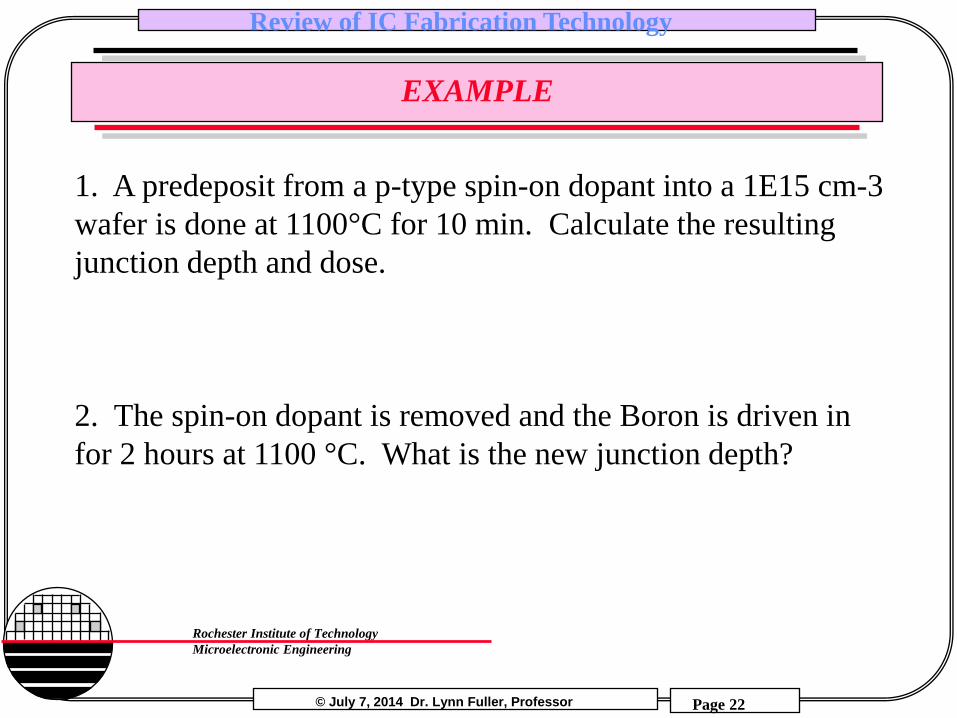
EXAMPLE
1. A predeposit from a p-type spin-on dopant into a 1E15 cm-3
wafer is done at 1100°C for 10 min. Calculate the resulting
junction depth and dose.
2. The spin-on dopant is removed and the Boron is driven in
for 2 hours at 1100 °C. What is the new junction depth?
© July 7, 2014 Dr. Lynn Fuller, Professor
Rochester Institute of Technology
Microelectronic Engineering
Review of IC Fabrication Technology
Page 23
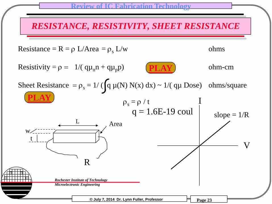
RESISTANCE, RESISTIVITY, SHEET RESISTANCE
Resistance = R = L/Area = s L/w ohms
Resistivity = 1/( qµnn + qµpp) ohm-cm
Sheet Resistance s = 1/ ( q µ(N) N(x) dx) ~ 1/( qµ Dose) ohms/square
L Area
R
w t
s = / t I
V
slope = 1/R q = 1.6E-19 coul
PLAY
PLAY

© July 7, 2014 Dr. Lynn Fuller, Professor
Rochester Institute of Technology
Microelectronic Engineering
Review of IC Fabrication Technology
Page 24
CALCULATION OF CARRIER CONCENTRATIONS
B 1.11E+03
h 6.63E-34 Jsec Nd = 3.00E+16 cm-3 Donor Concentration
o 8.85E-14 F/cm Ed= 0.049 eV below Ec
r 11.7 Na = 8.00E+15 cm-3 Acceptor Concentration
ni 1.45E+10 cm-3 Ea= 0.045 eV above Ev
Nc/T^3/2 5.43E+15
Nv/T^3/2 2.02E+15 Temp= 300 °K
Donor and Acceptor Levels (eV above or below Ev or Ec)
Boron 0.044
Phosphorous 0.045
Arsenic 0.049
CALCULATIONS: (this program makes a guess at the value of the fermi level and trys to minimize
the charge balance)
KT/q 0.026 Volts
Eg=Ego-(aT^2/(T+B)) 1.115 eV
Nc 2.82E+19 cm-3
Nv 1.34E+01 cm-3
Fermi Level, Ef 0.9295 eV above Ev
free electrons, n = Nc exp(-q(Ec-Ef)KT) 2.17E+16 cm-3
Ionized donors, Nd+ = Nd*(1+2*exp(q(Ef-Ed)/KT))^(-1) 2.97E+16 cm-3
holes, p = Nv exp(-q(Ef-Ev)KT) 3.43E-15 cm-3
Ionized acceptors, Na- = Na*(1+2*exp(q(Ea-Ef)/KT))^(-1) 8.00E+15 cm-3
Charge Balance = p + Nd+ - n - Na- 3.22E+12 cm-3
Click on Button to do Calculation
Button
Button
carrier_conc.xls

© July 7, 2014 Dr. Lynn Fuller, Professor
Rochester Institute of Technology
Microelectronic Engineering
Review of IC Fabrication Technology
Page 25
RESISTIVITY OF SILICON VS DOPING
1021
1020
1014
1015
1016
1019
1018
1017
1013
100 101 102 103 104 10-3 10-2 10-1 10-4
Boron
Phosphorous
1/(qµ(N)N)
Because µ is a function of N
and N is the doping, the
relationship between resistivity
and N is given in the figure
shown, or calculated from
equations for µ(N)
Imp
uri
ty C
on
centr
atio
n, N
, cm
-3
Resistivity, ohm-cm
PLAY

© July 7, 2014 Dr. Lynn Fuller, Professor
Rochester Institute of Technology
Microelectronic Engineering
Review of IC Fabrication Technology
Page 26
ELECTRON AND HOLE MOBILITY
Total Impurity Concentration (cm-3)
0
200
400
600
800
1000
1200
1400
1600
10^13
10^14
10^15
10^16
10^17
10^18
10^19
10^20
ArsenicBoronPhosphorus
Mo
bil
ity (
cm2/
V s
ec)
electrons
holes
Parameter Arsenic Phosphorous Boron
µmin 52.2 68.5 44.9
µmax 1417 1414 470.5
Nref 9.68X10^16 9.20X10^16 2.23X10^17
0.680 0.711 0.719
µ(N) = µ mi+ (µmax-µmin)
{1 + (N/Nref)}
Electron and hole mobilities in silicon at 300 K as functions of the total dopant concentration (N). The values plotted are the results of the curve fitting measurements from several sources. The mobility curves can be generated using the equation below with the parameters shown:
From Muller and Kamins, 3rd Ed., pg 33
PLAY
PLAY

© July 7, 2014 Dr. Lynn Fuller, Professor
Rochester Institute of Technology
Microelectronic Engineering
Review of IC Fabrication Technology
Page 27
TEMPERATURE EFFECTS ON MOBILITY
Derived empirically for silicon for T in K between 250 and 500 °K and for
N (total dopant concentration) up to 1 E20 cm-3
µn (T,N) =
µp (T,N) =
88 Tn-0.57
54.3 Tn-0.57
Where Tn = T/300
From Muller and Kamins, 3rd Ed., pg 33
1250 Tn-2.33
407 Tn-2.33
1 + [ N / (1.26E17 Tn 2.4)] ^0.88 Tn -0.146
1 + [ N / (2.35E17 Tn 2.4)]^ 0.88 Tn -0.146
+
+
PLAY

© July 7, 2014 Dr. Lynn Fuller, Professor
Rochester Institute of Technology
Microelectronic Engineering
Review of IC Fabrication Technology
Page 28
EXCELL WORKSHEET TO CALCULATE MOBILITY
MICROELECTRONIC ENGINEERING 3/13/2005
CALCULATION OF MOBILITY Dr. Lynn Fuller
To use this spreadsheed change the values in the white boxes. The rest of the sheet is
protected and should not be changed unless you are sure of the consequences. The
calculated results are shown in the purple boxes.
CONSTANTS VARIABLES CHOICES
Tn = T/300 = 1.22 1=yes, 0=no
Temp= 365 °K n-type 1
N total 1.00E+18 cm-3 p-type 0
<100>
Kamins, Muller and Chan; 3rd Ed., 2003, pg 33
mobility= 163 cm2/(V-sec)
mobility.xls

© July 7, 2014 Dr. Lynn Fuller, Professor
Rochester Institute of Technology
Microelectronic Engineering
Review of IC Fabrication Technology
Page 29
EXCELL WORKSHEET TO CALCULATE RESISTANCE
Resistors_Poly.xls
© July 7, 2014 Dr. Lynn Fuller, Professor
Rochester Institute of Technology
Microelectronic Engineering
Review of IC Fabrication Technology
Page 30
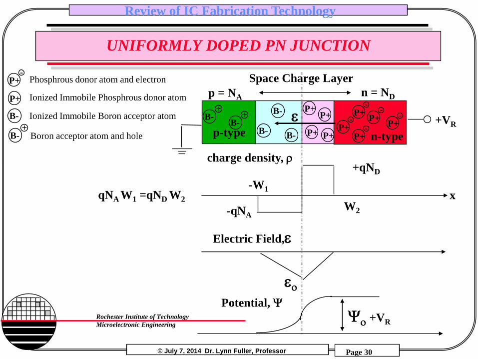
UNIFORMLY DOPED PN JUNCTION
n-type
p-type
Space Charge Layer
Potential,
Electric Field,
charge density,
n = ND p = NA
+qND
-W1
W2
+VR
x
+VR
-qNA
Ionized Immobile Phosphrous donor atom
Ionized Immobile Boron acceptor atom
Phosphrous donor atom and electron P+ -
B- +
Boron acceptor atom and hole
qNA W1 =qND W2
P+
B- B- +
B- +
P+ -
P+ B-
B- B-
P+
P+ P+ P+ -
P+ -
P+ -
P+ -

© July 7, 2014 Dr. Lynn Fuller, Professor
Rochester Institute of Technology
Microelectronic Engineering
Review of IC Fabrication Technology
Page 31
UNIFORMLY DOPED PN JUNCTION
WW1W2= [ (2q+VR) (1/NA 1/ND)]1/2
W1= W [ND/(NA ND)] W2= W [NA/(NA ND)]
= - [(2q/+VR) (NA ND/(NA ND))]1/2
Cj’rW= r[(2q+VR) (1/NA 1/ND)]1/2
= KT/q ln (NA ND /ni2)
ni = 1.45E10 cm-3
Built in Voltage:
Width of Space Charge Layer, W: with reverse bias of VR volts
Junction Capacitance per unit area:
Maximum Electric Field:
o r = 8.85E-12 (11.7) F/m
= 8.85E-14 (11.7) F/cm
W1 width on p-side W2 width on n-side

© July 7, 2014 Dr. Lynn Fuller, Professor
Rochester Institute of Technology
Microelectronic Engineering
Review of IC Fabrication Technology
Page 32
EXAMPLE
Example: If the doping concentrations are Na=1E15 and Nd=3E15
cm-3 and the reverse bias voltage is 0, then find the built in voltage,
width of the space charge layer, width on the n-side, width on the p-
side, electric field maximum and junction capacitance. Repeat for
reverse bias of 10, 40, and 100 volts.
= Vbi = KT/q ln (NA ND /ni2) =
WW1W2= [ (2/q) (+VR) (1/NA 1/ND)]1/2 =
W1 =
W2 =
Emax =
Cj =
© July 7, 2014 Dr. Lynn Fuller, Professor
Rochester Institute of Technology
Microelectronic Engineering
Review of IC Fabrication Technology
Page 33
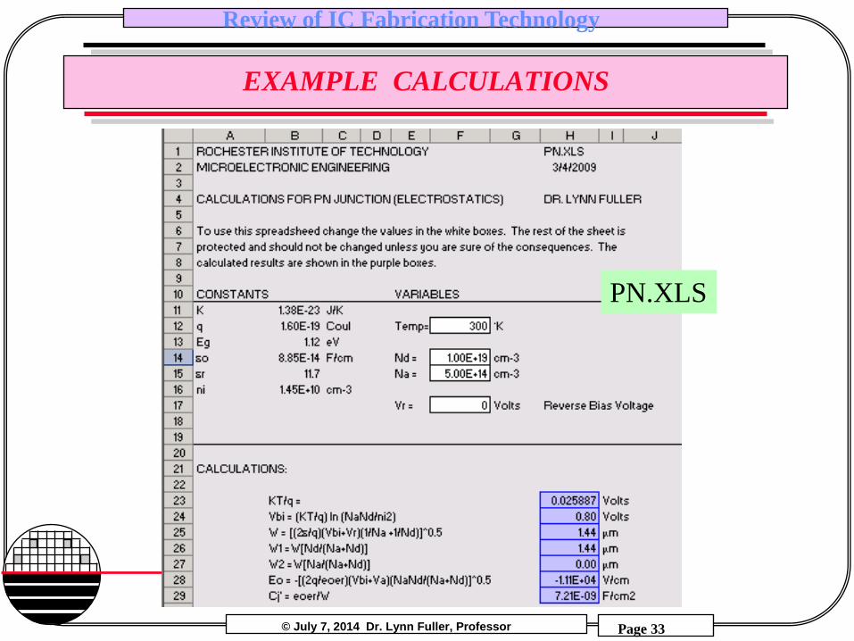
EXAMPLE CALCULATIONS
PN.XLS
© July 7, 2014 Dr. Lynn Fuller, Professor
Rochester Institute of Technology
Microelectronic Engineering
Review of IC Fabrication Technology
Page 34
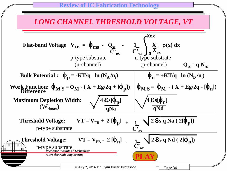
LONG CHANNEL THRESHOLD VOLTAGE, VT
Work Function: M S = M - ( X + Eg/2q + [p]) M S = M - ( X + Eg/2q - [n])
Threshold Voltage: VT = VFB - 2 [n] - 1 2 s q Nd ( 2[n])
n-type substrate C’ox
Bulk Potential : p = -KT/q ln (NA /ni) n = +KT/q ln (ND /ni)
Flat-band Voltage VFB = ms - Qss - 1 X (x) dx C’ox
Xox C’ox
p-type substrate n-type substrate
(n-channel) (p-channel)
Maximum Depletion Width: 4 s[p] 4 s[n]
qNa qNd
Threshold Voltage: VT = VFB + 2 [p] + 1 2 s q Na ( 2[p])
p-type substrate C’ox
Difference
Qss = q Nss
0
Xox
(Wdmax)
PLAY

© July 7, 2014 Dr. Lynn Fuller, Professor
Rochester Institute of Technology
Microelectronic Engineering
Review of IC Fabrication Technology
Page 35
LONG CHANNEL Vt
Gate work function, n+, p+, aluminum
Substrate doping, Nd or Na
Oxide thickness, Xox
Surface State Density, Nss or Qss
also
Substrate to Source voltage difference
0
-1
-2
-3
+1
+2
+3
n+ poly gate left scale
p+ poly gate right scale
Qf = 0
Vbs = 0
implant dose = zero
+1
0
-1
-2
+2
+3
+4
1014 1015 1016 1017
150Å
650Å
250Å
150Å
250Å
650Å
Threshold Voltage
Substrate doping, Nd or Na
PLAY
© July 7, 2014 Dr. Lynn Fuller, Professor
Rochester Institute of Technology
Microelectronic Engineering
Review of IC Fabrication Technology
Page 36
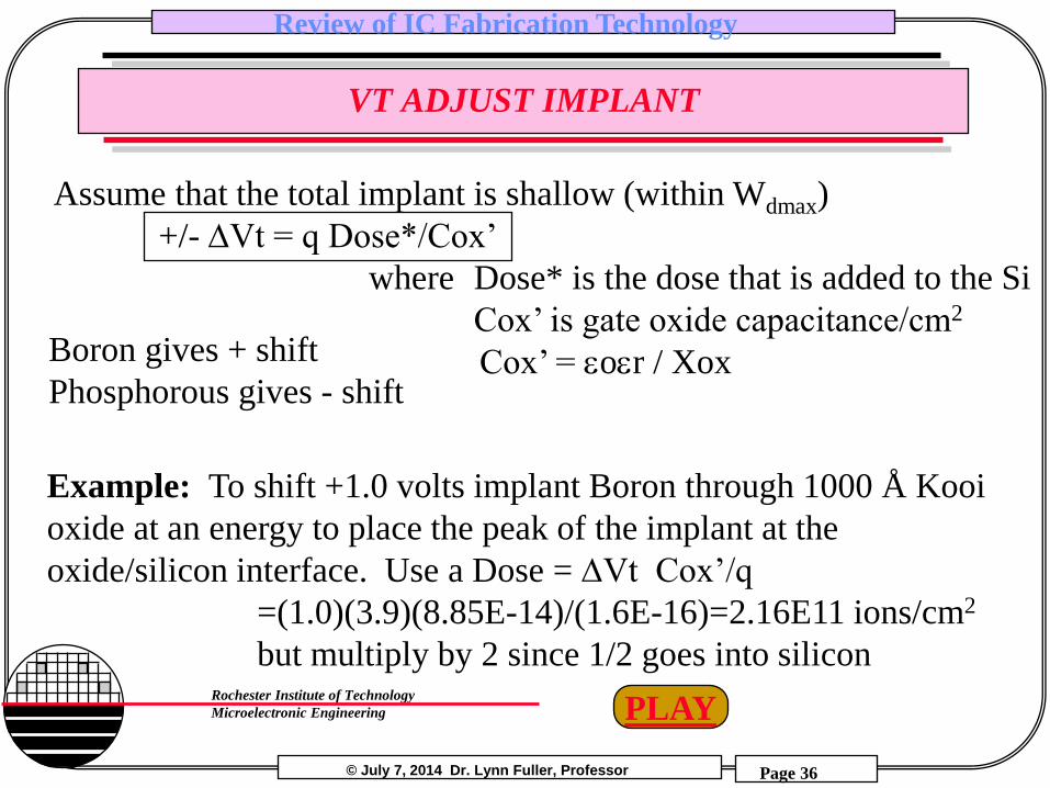
VT ADJUST IMPLANT
Assume that the total implant is shallow (within Wdmax)
+/- Vt = q Dose*/Cox’
where Dose* is the dose that is added to the Si
Cox’ is gate oxide capacitance/cm2
Cox’ = or / Xox
Example: To shift +1.0 volts implant Boron through 1000 Å Kooi
oxide at an energy to place the peak of the implant at the
oxide/silicon interface. Use a Dose = Vt Cox’/q
=(1.0)(3.9)(8.85E-14)/(1.6E-16)=2.16E11 ions/cm2
but multiply by 2 since 1/2 goes into silicon
Boron gives + shift
Phosphorous gives - shift
PLAY

© July 7, 2014 Dr. Lynn Fuller, Professor
Rochester Institute of Technology
Microelectronic Engineering
Review of IC Fabrication Technology
Page 37
MOSFET THRESHOLD VOLTAGE CALCULATION
MOSFETVT.XLS

© July 7, 2014 Dr. Lynn Fuller, Professor
Rochester Institute of Technology
Microelectronic Engineering
Review of IC Fabrication Technology
Page 38
ION IMPLANT EQUATIONS
after implant
Approximation
used in Vt
calculations
after anneal at
950 C, 15 min
-(X-Rp)2
2(Rp2+Dt) Approximation
N’ = Ni xi
After Anneal
N(x) = exp [ ]
N’
2Rp2 + 2Dt
Gaussian Implant Profile
N(x) = exp [ ]
Rp = Range
Rp = Straggle From Curves }
-(X-Rp)2
2Rp2
N’
2Rp
N’ = Dose = dt I
mqA
Ni
xi
where D is diffusion constant at the anneal temperature
t is time of anneal
x
con
centr
atio
n c
m-3
PLAY

© July 7, 2014 Dr. Lynn Fuller, Professor
Rochester Institute of Technology
Microelectronic Engineering
Review of IC Fabrication Technology
Page 39
ION IMPLANT RANGE
10 100 1,000
10-2
10-1
1
Implantation Energy (KeV)
Pro
jecte
d R
an
ge,
Rp
,(u
m)
B
P
As
Sb
PLAY

© July 7, 2014 Dr. Lynn Fuller, Professor
Rochester Institute of Technology
Microelectronic Engineering
Review of IC Fabrication Technology
Page 40
ION IMPLANT STANDARD DEVIATION
0.001
0.01
0.1
10 100 1,000 Implantation Energy (KeV)
Sta
nd
ard
Devia
tio
n,
Rp
,(u
m)
B
P
As
Sb
PLAY

© July 7, 2014 Dr. Lynn Fuller, Professor
Rochester Institute of Technology
Microelectronic Engineering
Review of IC Fabrication Technology
Page 41
ION IMPLANT MASKING CALCULATOR
Rochester Institute of Technology Lance Barron
Microelectronic Engineering Dr. Lynn Fuller
11/20/2004
IMPLANT MASK CALCULATOR Enter 1 - Yes 0 - No in white boxes
DOPANT SPECIES MASK TYPE ENERGY
B11 1 Resist 0 60 KeV
BF2 0 Poly 1
P31 0 Oxide 0
Nitride 0
Thickness to Mask >1E15/cm3 Surface Concentration 4073.011 Angstroms
This calculator is based on Silvaco Suprem simulations using the Dual Pearson model.
Lance Baron, Fall 2004
In powerpoint click on spread sheet to change settings for a new calculation

© July 7, 2014 Dr. Lynn Fuller, Professor
Rochester Institute of Technology
Microelectronic Engineering
Review of IC Fabrication Technology
Page 42
REFERENCES
1. Basic Integrated Circuit Engineering, Douglas J. Hamilton, William
G. Howard, McGraw Hill Book Co., 1975.
2. Micro Electronics Processing and Device Design, Roy a. Colclaser,
John Wiley & Sons., 1980.
3. Device Electronics for Integrated Circuits, Richard S. Muller,
Theodore I. Kamins, Mansun Chan, John Wiley & Sons.,3rd Ed., 2003.
4. VLSI Technology, Edited by S.M. Sze, McGraw-Hill Book Company,
1983.
5. Silicon Processing for the VLSI Era, Vol. 1., Stanley Wolf, Richard
Tauber, Lattice Press, 1986.
6. The Science and Engineering of Microelectronic Fabrication, Stephen
A. Campbell, Oxford University Press, 1996.

© July 7, 2014 Dr. Lynn Fuller, Professor
Rochester Institute of Technology
Microelectronic Engineering
Review of IC Fabrication Technology
Page 43
HOMEWORK - REVIEW OF IC TECHNOLOGY
1. If a window is etched in 5000 Å of oxide and the wafer is oxidized again for 50 min in wet
O2 at 1050 °C what is the new thickness (where it was 5000 Å), the thickness in the etch
window, and the step height in the silicon if all the oxide is etched off the wafer. Draw a
picture showing original Si surface.
2. A Boron diffusion is done into 5 ohm-cm n-type wafer involving two steps. First a short
predeposit at 950 C for 30 min., followed by removal of the diffusion source and a drive in at
1100 C for 2 hours. Calculate the junction depth and the sheet resistance of the diffused layers.
Estimate the oxide thickness needed to mask this diffusion.
3. For a pn junction with the p side doping of 1E17 and the n side at 1E15 calculate, width of
space charge layer, width on p side, on n side, capacitance per unit area, max electric field.
4. Calculate the threshold voltage for an aluminum gate PMOSFET fabricated on an n-type
wafer with doping of 5E15, a surface state density of 7E10, and gate oxide thickness of 150 Å.
What is the threshold voltage if the surface state density is 3E11?
5. Calculate the ion implant dose needed to shift the threshold voltage found in the problem
above to -1 Volts.
PLAY

© July 7, 2014 Dr. Lynn Fuller, Professor
Rochester Institute of Technology
Microelectronic Engineering
Review of IC Fabrication Technology
Page 44
HOMEWORK - EXACT CALCULATION OF SHEET RESISTANCE FOR A DIFFUSED LAYER
1. A Boron p-type layer is diffused into an n-type silicon wafer (1E15 cm-3) at 1100 °C for 1 hour. Calculate the exact value of the sheet resistance and compare to the approximate value.
N(x,t) = Q’A(tp) Exp (- x2/4Dt)
Dt
Sheet Resistance s = 1/ ( q µ(N) N(x) dx) ~ 1/( qµ Dose) ohms/square
µ(N) = µ min + (µmax-µmin)
{1 + (N/Nref)}
Let Q’A(tp) = 5.633E15 cm-2
D= 1.55E-13 cm2/s
t = 1 hour for Boron
µmin 44.9
µmax 470.5
Nref 2.23X10^17
0.719

© July 7, 2014 Dr. Lynn Fuller, Professor
Rochester Institute of Technology
Microelectronic Engineering
Review of IC Fabrication Technology
Page 45
HW SOLUTION - EXACT CALCULATION OF SHEET RESISTANCE FOR A DIFFUSED LAYER
Divide the diffused layer up into 100 slices and for each slice find the doping and exact mobility. Calculate the sheet resistance from the reciprocal of the sum of the conductance of each slice.
x xj
NBC
N(x)
Related Documents


